unusual dielectric response in cobalt doped reduced graphene oxide
TRANSCRIPT

Unusual dielectric response in cobalt doped reduced graphene oxideAbu Jahid Akhtar, Abhisek Gupta, Bikash Kumar Shaw, and Shyamal K. Saha Citation: Applied Physics Letters 103, 242902 (2013); doi: 10.1063/1.4845536 View online: http://dx.doi.org/10.1063/1.4845536 View Table of Contents: http://scitation.aip.org/content/aip/journal/apl/103/24?ver=pdfcov Published by the AIP Publishing
This article is copyrighted as indicated in the article. Reuse of AIP content is subject to the terms at: http://scitation.aip.org/termsconditions. Downloaded to IP:
14.139.222.45 On: Wed, 11 Dec 2013 09:57:17
Unusual dielectric response in cobalt doped reduced graphene oxide
Abu Jahid Akhtar, Abhisek Gupta, Bikash Kumar Shaw, and Shyamal K. Sahaa)
Department of Materials Science, Indian Association for the Cultivation of Science, Jadavpur,Kolkata 700032, India
(Received 6 August 2013; accepted 23 November 2013; published online 10 December 2013)
Intensive research on cobalt doped reduced graphene oxide (Co-RGO) to investigate the modification
in graphene magnetism and spin polarization due to presence of transition metal atom has been
carried out, however, its dielectric spectroscopy, particularly, how capacitance changes with impurity
levels in graphene is relatively unexplored. In the present work, dielectric spectroscopy along with
magneto-dielectric effect are investigated in Co-RGO. Contrary to other materials, here permittivity
increases abruptly with frequency in the low frequency region and continues to increase till 107 Hz.
This unusual behavior is explained on the basis of trap induced capacitance created due to impurity
levels. VC 2013 AIP Publishing LLC. [http://dx.doi.org/10.1063/1.4845536]
Graphene, a free-standing 2D system with one-atom
thickness of sp2-hybridized carbon atoms arranged in a hon-
eycomb structure, obeying Dirac physics is now-a-days the
most promising material for both electronic1–4 (e.g., high
speed transistors) as well as spintronic5–8 (e.g., spin transis-
tors) applications and becomes one of the most key material
in the field of material science, physics, chemistry, and nano-
technology. Although graphene has versatile applications in
high speed electronic devices,1,9 energy storage systems,10,11
optoelectronic devices,12 adsorption of hazardous chemicals
for water purification,13 and sensing of explosive nitromaaro-
matics,14 it is so far relatively unexplored in the area of mul-
tifunctional applications for which we need to integrate
dielectric and magnetic properties in single material.
Incidentally, both these properties of graphene are very poor.
The usual technique to improve charge transport and
current-voltage characteristics in transistors is to use the
high-k gate material. In a similar way, the spin transport and
transistor characteristics in a spin transistor are also con-
trolled by a gate electrode having magnetic impurity atoms.
Therefore, today’s main challenge to improve transistor
applications is to design new graphene based high-k material
which remains still unexplored so far. On the other hand,
being a good conductor due to p-electron delocalization gra-
phene is intrinsically poor dielectric material. Several techni-
ques have been explored in order to increase its dielectric as
well as magnetic properties of graphene.15–20
Doping is a delicate method to control the semiconduct-
ing properties of graphene as well as its dramatic influence
on electrical properties. Theoretical studies show that the
substitutional doping can modify the band structure of
graphene,21–23 e.g., nitrogen doped graphene becomes n-type
and used to fabricate field effect transistors.24–26 In the pres-
ent work, we have tried to modify its dielectric response
embedding cobalt atoms at the carbon vacancy sites and re-
markable effect of dielectric enhancement at high frequency
limit is observed. It is seen that instead of decrease, permit-
tivity increases with frequency and becomes almost saturated
at the high frequency limit. This unusual dielectric response
is explained on the basis of trap states formed at the defect
sites due to doping of cobalt atoms. Temperature dependant
dielectric behavior has also been investigated over the tem-
perature range from 140 to 303 K and it is noticed that the
permittivity value increases with temperature. The details
are reported in this Letter.
In the first step, graphene oxide (GO) is prepared using
modified Hummers method.27 To synthesize cobalt doped
reduced graphene oxide, 10 ml of GO solution is mixed with
100 ml of dimethyl formamide (DMF) in a beaker followed
by ultrasonic vibration to yield a clear homogeneous yellow
brown dispersion. Aqueous solution of cobalt chloride
(CoCl2) is then added to it and the mixture is then stirred at
room temperature for 30 min and treated again by ultrasonic
vibration for 30 min to make a uniform mixture. Finally, hy-
drazine hydrate solution (10 ml) is added to the mixture at
60 �C for 4 h under constant ultrasonic vibration and cooled
to room temperature. The mixture is then filtered and washed
thoroughly with water, alcohol, and acetone. The final prod-
uct is dried in vacuum oven at 100 �C for 24 h.
For dielectric and magneto-dielectric measurements
powdered sample is pressed in the form of a pellet with
0.8 cm2 area and 0.04 cm thickness. Using silver paste on
both sides of the pellet as electrodes the dielectric measure-
ments are done by Agilent E4980A Precision LCR Meter
and an electromagnet with field range up to 2 T. The X-ray
photoelectron spectroscopy (XPS) measurements are carried
out using OMICRON-0571 system. Raman Measurements
are carried out using LabSpec Raman spectroscope (Model
JYT6400). Microwave measurements are performed using a
broadband dielectric spectrometer (Agilent, model E4991A).
For DFT calculation we have used standard program of
GUSSIAN 03 software package.
First, we discuss the formation mechanism of Co-RGO
sample. While the first sonication of GO solution, GO sheets
are exfoliated as well as some defect states are created due to
vacancy of carbon atoms removed from the graphene lattice
as a result of tremendous local heat generated in ultrasonic
vibration. Then, Co2þ ions are attached to the functional
groups of GO and some are incorporated at the defect sites
of graphene when GO solution is stirred with CoCl2. In the
second stage of prolonged sonication (4 h) using hydrazine
a)Author to whom correspondence should be addressed. Electronic mail:
0003-6951/2013/103(24)/242902/5/$30.00 VC 2013 AIP Publishing LLC103, 242902-1
APPLIED PHYSICS LETTERS 103, 242902 (2013)
This article is copyrighted as indicated in the article. Reuse of AIP content is subject to the terms at: http://scitation.aip.org/termsconditions. Downloaded to IP:
14.139.222.45 On: Wed, 11 Dec 2013 09:57:17
hydrate, GO sheets are reduced with the reconstruction of
carbon network structure and during this process a large
number of carbon atoms are removed from the network
structure creating some vacancies which will be occupied by
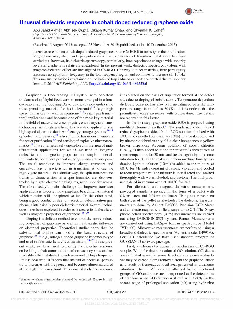
cobalt atoms. The electronic configuration of cobalt atom is
d7s2. When Co atoms are placed in a single vacancy of de-
fective graphene i.e., M/SV, one electron from s2 configura-
tion is promoted to next p level to achieve “spd”
hybridization which takes part in the in-plane bonding with
the three neighbouring carbon atoms. As reported in the liter-
ature,28 this type of hybridization for M/SV leaves 6d elec-
trons (2 paired and 2 unpaired) for cobalt atom. Among
these two unpaired electrons, one electron takes part in d-p
mixing with pz orbital of one of three neighboring carbon
atoms. As a result, each cobalt atom possesses one unpaired
electron (upe) which can act as a trap center as shown in the
schematic diagram to achieve the closed shell configuration.
The typical atomic configuration of a defect free graphene,
defective graphene and M/SV complex is shown in Figs.
1(a)–1(c), respectively. Fig. 1(d) shows how trap is produced
in cobalt atom.
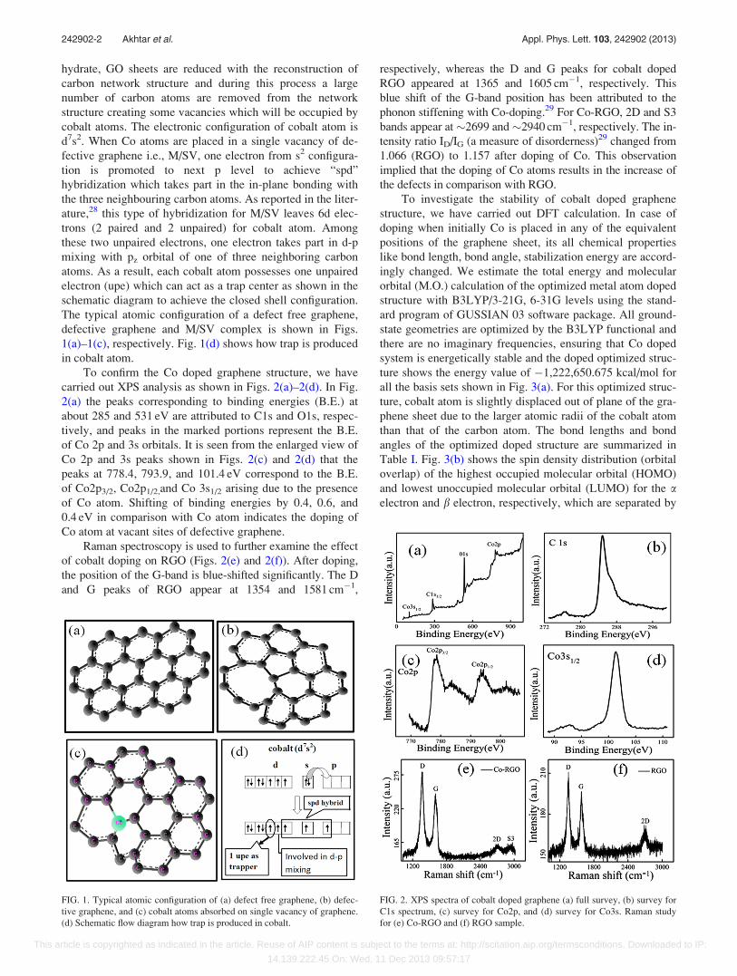
To confirm the Co doped graphene structure, we have
carried out XPS analysis as shown in Figs. 2(a)–2(d). In Fig.
2(a) the peaks corresponding to binding energies (B.E.) at
about 285 and 531 eV are attributed to C1s and O1s, respec-
tively, and peaks in the marked portions represent the B.E.
of Co 2p and 3s orbitals. It is seen from the enlarged view of
Co 2p and 3s peaks shown in Figs. 2(c) and 2(d) that the
peaks at 778.4, 793.9, and 101.4 eV correspond to the B.E.
of Co2p3/2, Co2p1/2,and Co 3s1/2 arising due to the presence
of Co atom. Shifting of binding energies by 0.4, 0.6, and
0.4 eV in comparison with Co atom indicates the doping of
Co atom at vacant sites of defective graphene.
Raman spectroscopy is used to further examine the effect
of cobalt doping on RGO (Figs. 2(e) and 2(f)). After doping,
the position of the G-band is blue-shifted significantly. The D
and G peaks of RGO appear at 1354 and 1581 cm�1,
respectively, whereas the D and G peaks for cobalt doped
RGO appeared at 1365 and 1605 cm�1, respectively. This
blue shift of the G-band position has been attributed to the
phonon stiffening with Co-doping.29 For Co-RGO, 2D and S3
bands appear at�2699 and�2940 cm�1, respectively. The in-
tensity ratio ID/IG (a measure of disorderness)29 changed from
1.066 (RGO) to 1.157 after doping of Co. This observation
implied that the doping of Co atoms results in the increase of
the defects in comparison with RGO.
To investigate the stability of cobalt doped graphene
structure, we have carried out DFT calculation. In case of
doping when initially Co is placed in any of the equivalent
positions of the graphene sheet, its all chemical properties
like bond length, bond angle, stabilization energy are accord-
ingly changed. We estimate the total energy and molecular
orbital (M.O.) calculation of the optimized metal atom doped
structure with B3LYP/3-21G, 6-31G levels using the stand-
ard program of GUSSIAN 03 software package. All ground-
state geometries are optimized by the B3LYP functional and
there are no imaginary frequencies, ensuring that Co doped
system is energetically stable and the doped optimized struc-
ture shows the energy value of �1,222,650.675 kcal/mol for
all the basis sets shown in Fig. 3(a). For this optimized struc-
ture, cobalt atom is slightly displaced out of plane of the gra-
phene sheet due to the larger atomic radii of the cobalt atom
than that of the carbon atom. The bond lengths and bond
angles of the optimized doped structure are summarized in
Table I. Fig. 3(b) shows the spin density distribution (orbital
overlap) of the highest occupied molecular orbital (HOMO)
and lowest unoccupied molecular orbital (LUMO) for the aelectron and b electron, respectively, which are separated by
FIG. 1. Typical atomic configuration of (a) defect free graphene, (b) defec-
tive graphene, and (c) cobalt atoms absorbed on single vacancy of graphene.
(d) Schematic flow diagram how trap is produced in cobalt.
FIG. 2. XPS spectra of cobalt doped graphene (a) full survey, (b) survey for
C1s spectrum, (c) survey for Co2p, and (d) survey for Co3s. Raman study
for (e) Co-RGO and (f) RGO sample.
242902-2 Akhtar et al. Appl. Phys. Lett. 103, 242902 (2013)
This article is copyrighted as indicated in the article. Reuse of AIP content is subject to the terms at: http://scitation.aip.org/termsconditions. Downloaded to IP:
14.139.222.45 On: Wed, 11 Dec 2013 09:57:17
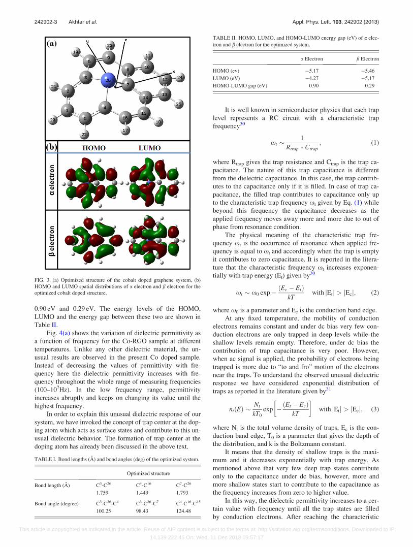
0.90 eV and 0.29 eV. The energy levels of the HOMO,
LUMO and the energy gap between these two are shown in
Table II.
Fig. 4(a) shows the variation of dielectric permittivity as
a function of frequency for the Co-RGO sample at different
temperatures. Unlike any other dielectric material, the un-
usual results are observed in the present Co doped sample.
Instead of decreasing the values of permittivity with fre-
quency here the dielectric permittivity increases with fre-
quency throughout the whole range of measuring frequencies
(100–107Hz). In the low frequency range, permittivity
increases abruptly and keeps on changing its value until the
highest frequency.
In order to explain this unusual dielectric response of our
system, we have invoked the concept of trap center at the dop-
ing atom which acts as surface states and contribute to this un-
usual dielectric behavior. The formation of trap center at the
doping atom has already been discussed in the above text.
It is well known in semiconductor physics that each trap
level represents a RC circuit with a characteristic trap
frequency30
xt �1
Rtrap � Ctrap; (1)
where Rtrap gives the trap resistance and Ctrap is the trap ca-
pacitance. The nature of this trap capacitance is different
from the dielectric capacitance. In this case, the trap contrib-
utes to the capacitance only if it is filled. In case of trap ca-
pacitance, the filled trap contributes to capacitance only up
to the characteristic trap frequency xt given by Eq. (1) while
beyond this frequency the capacitance decreases as the
applied frequency moves away more and more due to out of
phase from resonance condition.
The physical meaning of the characteristic trap fre-
quency xt is the occurrence of resonance when applied fre-
quency is equal to xt and accordingly when the trap is empty
it contributes to zero capacitance. It is reported in the litera-
ture that the characteristic frequency xt increases exponen-
tially with trap energy (Et) given by30
xt � x0 exp� ðEc � EtÞkT
with jEtj > jEcj; (2)
where x0 is a parameter and Ec is the conduction band edge.
At any fixed temperature, the mobility of conduction
electrons remains constant and under dc bias very few con-
duction electrons are only trapped in deep levels while the
shallow levels remain empty. Therefore, under dc bias the
contribution of trap capacitance is very poor. However,
when ac signal is applied, the probability of electrons being
trapped is more due to “to and fro” motion of the electrons
near the traps. To understand the observed unusual dielectric
response we have considered exponential distribution of
traps as reported in the literature given by31
ntðEÞ �Nt
kT0
exp �ðEt � EcÞkT
� �with jEtj > jEcj; (3)
where Nt is the total volume density of traps, Ec is the con-
duction band edge, T0 is a parameter that gives the depth of
the distribution, and k is the Boltzmann constant.
It means that the density of shallow traps is the maxi-
mum and it decreases exponentially with trap energy. As
mentioned above that very few deep trap states contribute
only to the capacitance under dc bias, however, more and
more shallow states start to contribute to the capacitance as
the frequency increases from zero to higher value.
In this way, the dielectric permittivity increases to a cer-
tain value with frequency until all the trap states are filled
by conduction electrons. After reaching the characteristic
FIG. 3. (a) Optimized structure of the cobalt doped graphene system, (b)
HOMO and LUMO spatial distributions of a electron and b electron for the
optimized cobalt doped structure.
TABLE I. Bond lengths (A) and bond angles (deg) of the optimized system.
Optimized structure
Bond length (A) C3-C26 C4-C16 C7-C26
1.759 1.449 1.793
Bond angle (degree) C3-C26-C4 C3-C26-C7 C4-C16-C15
100.25 98.43 124.48
TABLE II. HOMO, LUMO, and HOMO-LUMO energy gap (eV) of a elec-
tron and b electron for the optimized system.
a Electron b Electron
HOMO (ev) �5.17 �5.46
LUMO (eV) �4.27 �5.17
HOMO-LUMO gap (eV) 0.90 0.29
242902-3 Akhtar et al. Appl. Phys. Lett. 103, 242902 (2013)
This article is copyrighted as indicated in the article. Reuse of AIP content is subject to the terms at: http://scitation.aip.org/termsconditions. Downloaded to IP:
14.139.222.45 On: Wed, 11 Dec 2013 09:57:17
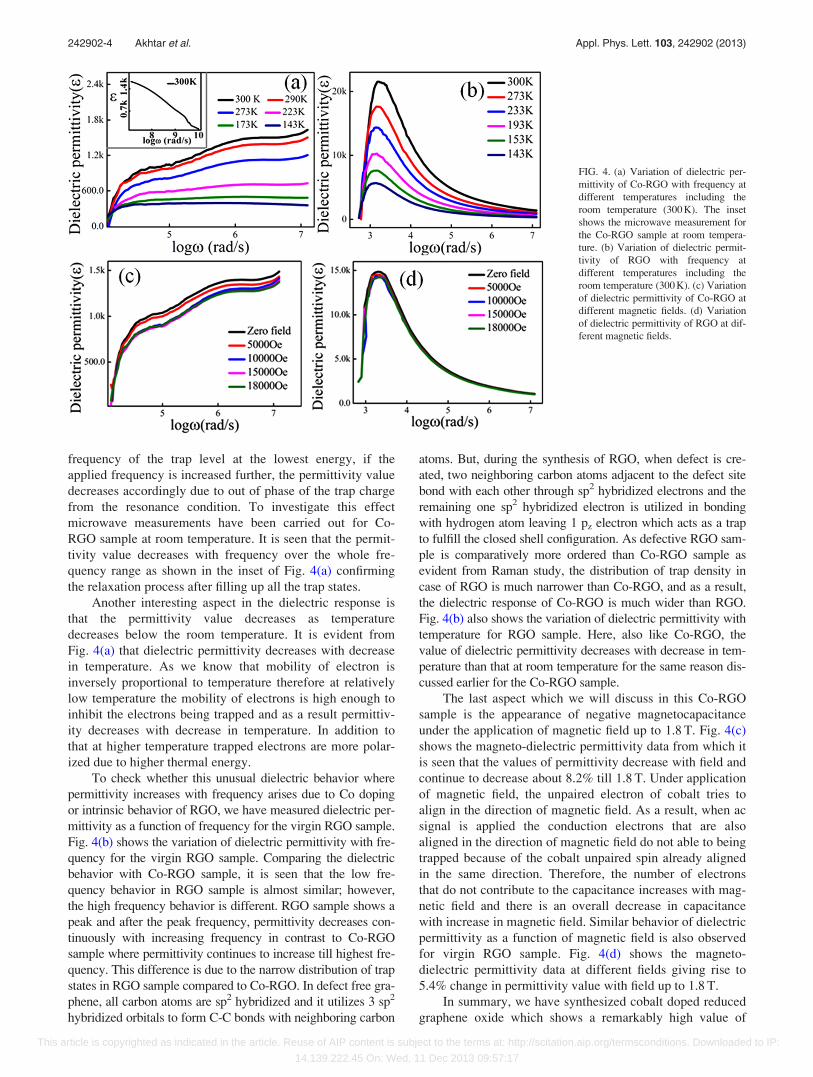
frequency of the trap level at the lowest energy, if the
applied frequency is increased further, the permittivity value
decreases accordingly due to out of phase of the trap charge
from the resonance condition. To investigate this effect
microwave measurements have been carried out for Co-
RGO sample at room temperature. It is seen that the permit-
tivity value decreases with frequency over the whole fre-
quency range as shown in the inset of Fig. 4(a) confirming
the relaxation process after filling up all the trap states.
Another interesting aspect in the dielectric response is
that the permittivity value decreases as temperature
decreases below the room temperature. It is evident from
Fig. 4(a) that dielectric permittivity decreases with decrease
in temperature. As we know that mobility of electron is
inversely proportional to temperature therefore at relatively
low temperature the mobility of electrons is high enough to
inhibit the electrons being trapped and as a result permittiv-
ity decreases with decrease in temperature. In addition to
that at higher temperature trapped electrons are more polar-
ized due to higher thermal energy.
To check whether this unusual dielectric behavior where
permittivity increases with frequency arises due to Co doping
or intrinsic behavior of RGO, we have measured dielectric per-
mittivity as a function of frequency for the virgin RGO sample.
Fig. 4(b) shows the variation of dielectric permittivity with fre-
quency for the virgin RGO sample. Comparing the dielectric
behavior with Co-RGO sample, it is seen that the low fre-
quency behavior in RGO sample is almost similar; however,
the high frequency behavior is different. RGO sample shows a
peak and after the peak frequency, permittivity decreases con-
tinuously with increasing frequency in contrast to Co-RGO
sample where permittivity continues to increase till highest fre-
quency. This difference is due to the narrow distribution of trap
states in RGO sample compared to Co-RGO. In defect free gra-
phene, all carbon atoms are sp2 hybridized and it utilizes 3 sp2
hybridized orbitals to form C-C bonds with neighboring carbon
atoms. But, during the synthesis of RGO, when defect is cre-
ated, two neighboring carbon atoms adjacent to the defect site
bond with each other through sp2 hybridized electrons and the
remaining one sp2 hybridized electron is utilized in bonding
with hydrogen atom leaving 1 pz electron which acts as a trap
to fulfill the closed shell configuration. As defective RGO sam-
ple is comparatively more ordered than Co-RGO sample as
evident from Raman study, the distribution of trap density in
case of RGO is much narrower than Co-RGO, and as a result,
the dielectric response of Co-RGO is much wider than RGO.
Fig. 4(b) also shows the variation of dielectric permittivity with
temperature for RGO sample. Here, also like Co-RGO, the
value of dielectric permittivity decreases with decrease in tem-
perature than that at room temperature for the same reason dis-
cussed earlier for the Co-RGO sample.
The last aspect which we will discuss in this Co-RGO
sample is the appearance of negative magnetocapacitance
under the application of magnetic field up to 1.8 T. Fig. 4(c)
shows the magneto-dielectric permittivity data from which it
is seen that the values of permittivity decrease with field and
continue to decrease about 8.2% till 1.8 T. Under application
of magnetic field, the unpaired electron of cobalt tries to
align in the direction of magnetic field. As a result, when ac
signal is applied the conduction electrons that are also
aligned in the direction of magnetic field do not able to being
trapped because of the cobalt unpaired spin already aligned
in the same direction. Therefore, the number of electrons
that do not contribute to the capacitance increases with mag-
netic field and there is an overall decrease in capacitance
with increase in magnetic field. Similar behavior of dielectric
permittivity as a function of magnetic field is also observed
for virgin RGO sample. Fig. 4(d) shows the magneto-
dielectric permittivity data at different fields giving rise to
5.4% change in permittivity value with field up to 1.8 T.
In summary, we have synthesized cobalt doped reduced
graphene oxide which shows a remarkably high value of
FIG. 4. (a) Variation of dielectric per-
mittivity of Co-RGO with frequency at
different temperatures including the
room temperature (300 K). The inset
shows the microwave measurement for
the Co-RGO sample at room tempera-
ture. (b) Variation of dielectric permit-
tivity of RGO with frequency at
different temperatures including the
room temperature (300 K). (c) Variation
of dielectric permittivity of Co-RGO at
different magnetic fields. (d) Variation
of dielectric permittivity of RGO at dif-
ferent magnetic fields.
242902-4 Akhtar et al. Appl. Phys. Lett. 103, 242902 (2013)
This article is copyrighted as indicated in the article. Reuse of AIP content is subject to the terms at: http://scitation.aip.org/termsconditions. Downloaded to IP:
14.139.222.45 On: Wed, 11 Dec 2013 09:57:17
dielectric permittivity along with unusual behavior where
permittivity value increases with frequency instead of
decreasing manner. 8.2% change in magnetocapacitance
with field is also observed in our Co-RGO sample. This high
value of dielectric permittivity and the unusual behavior are
explained on the basis of trap induced capacitance that is
generated due to doping atoms present in the graphene. We
believe that this observation of unusual dielectric response
with giant permittivity value will be useful in fabricating
graphene based magneto-dielectric devices.
A.J.A. acknowledges DST, New Delhi for awarding the
fellowships. A.G. and B.K.S. acknowledge CSIR for award-
ing the fellowships. S.K.S. acknowledges DST, New Delhi,
Government of India for financial support, Project No.
SR/NM/NS-1089/2011 and DST unit on Nanoscience for
providing XPS facilities.
1V. V. Cheianov, V. Fal’ko, and B. L. Altshuler, Science 315, 1252 (2007).2A. Das, S. Pisana, B. Chakraborty, S. Piscanec, S. K. Saha, U. V.
Waghmare, K. S. Novoselov, H. R. Krishnamurthy, A. K. Geim, A. C.
Ferrari, and A. K. Sood, Nat. Nanotechnol. 3, 210 (2008).3J. H. Chen, L. Li, W. G. Cullen, E. D. Williams, and M. S. Fuhrer, Nat.
Phys. 7, 535 (2011).4C. Berger, Z. Song, X. Li, X. Wu, N. Brown, C. Naud, D. Mayou, T. Li, J.
Hass, A. N. Marchenkov, E. H. Conrad, P. N. First, and W. A. de Heer,
Science 312, 1191 (2006).5D. Pesin and A. H. MacDonald, Nature Mater. 11, 409 (2012).6W. Y. Kim and K. S. Kim, Nat. Nanotechnol. 3, 408 (2008).7S. K. Saha, M. Baskey, and D. Majumdar, Adv. Mater. 22, 5531 (2010).8C. Chappert, A. Fert, and F. N. V. Dau, Nature Mater. 6, 813 (2007).9J.-U. Park, S. W. Nam, M. S. Lee, and C. M. Lieber, Nature Mater. 11,
120 (2012).
10N. G. Sahoo, Y. Pan, L. Li, and S. H. Chan, Adv. Mater. 24, 4203 (2012).11M. D. Stoller, S. Park, Y. Zhu, J. An, and R. S. Ruoff, Nano Lett. 8, 3498
(2008).12A. Gupta and S. K. Saha, Nanoscale 4, 6562 (2012).13D. Dinda, A. Gupta, and S. K. Saha, J. Mater. Chem. A 1, 11221–11228
(2013).14T. Chen, Z. Sheng, K. Wang, F. Wang, and X. Xia, Chem. Asian J. 6,
1210 (2011).15F. He, S. Lau, H. L. Chan, and J. Fan, Adv. Mater. 21, 710 (2009).16S. Lisenkov, A. N. Andriotis, and M. Menon, Phys. Rev. Lett. 108,
187208 (2012).17V. A. Rigo, T. B. Martins, A. J. R. da Silva, A. Fazzio, and R. H. Miwa,
Phys. Rev. B 79, 075435 (2009).18L. Li, R. Qin, H. Li, L. Yu, Q. Liu, G. Luo, Z. Gao, and J. Lu, ACS Nano
5, 2601 (2011).19A. J. Akhtar, A. Gupta, D. Chakravorty, and S. K. Saha, AIP Adv. 3,
072124 (2013).20S. Mandal and S. K. Saha, Nanoscale 4, 986 (2012).21F. Cervantes-Sodi, G. Csanyi, S. Piscanec, and A. C. Ferrari, Phys. Rev. B
77, 165427 (2008).22M. Deifallah, P. F. McMillan, and F. Cora, J. Phys. Chem. C 112, 5447
(2008).23T. B. Martins, R. H. Miwa, A. J. R. Silva, and A. Fazzio, Phys. Rev. Lett.
98, 196803 (2007).24X. Wang, X. Li, L. Zhang, Y. Yoon, P. K. Weber, H. Wang, J. Guo, and
H. Dai, Science 324, 768 (2009).25C. Zhang, L. Fu, N. Liu, M. Liu, Y. Wang, and Z. Liu, Adv. Mater. 23,
1020 (2011).26Y.-C. Lin, C.-Y. Lin, and P.-W. Chiu, Appl. Phys. Lett. 96, 133110
(2010).27W. S. Hummers and R. E. Offeman, J. Am. Chem. Soc. 80, 1339 (1958).28A. V. Krasheninnikov, P. O. Lehtinen, A. S. Foster, P. Pyykk€o, and R. M.
Nieminen, Phys. Rev. Lett. 102, 126807 (2009).29K. Samanta, S. Some, Y. Kim, Y. Yoon, M. Min, S. M. Lee., Y. Park, and
H. Lee, Chem. Commun. 49, 8991 (2013).30J. Bisquert, Phys. Rev. B 77, 235203 (2008).31J. Bisquert, F. Fabregat-Santiago, I. Mora-Ser�o, G. GarciaBelmonte, E. M.
Barea, and E. Palomares, Inorg. Chim. Acta 361, 684 (2008).
242902-5 Akhtar et al. Appl. Phys. Lett. 103, 242902 (2013)
This article is copyrighted as indicated in the article. Reuse of AIP content is subject to the terms at: http://scitation.aip.org/termsconditions. Downloaded to IP:
14.139.222.45 On: Wed, 11 Dec 2013 09:57:17