unidirectional measurement current-shunt monitor with dual
TRANSCRIPT
1
2
3
4
5
10
9
8
7
6
VIN+
VIN-
CMP1 OUT
CMP2 OUT
CMP1 RESET
VS
OUT
CMP1 IN+
CMP2 IN+
GND0.6V REF
1
2
3
4
5
6
7
14
13
12
11
10
9
8
VIN+
VIN-
1.2V REF OUT
CMP1 OUT
CMP2 OUT
CMP2 DELAY
CMP1 RESET
VS
OUT
CMP1 IN /0.6V REF-
CMP1 IN+
CMP2 IN+
CMP2 IN /0.6V REF-
GND
1.2V REF
INA203-Q1
www.ti.com SBOS539 –DECEMBER 2010
Unidirectional MeasurementCurrent-Shunt Monitor with Dual Comparators
Check for Samples: INA203-Q1
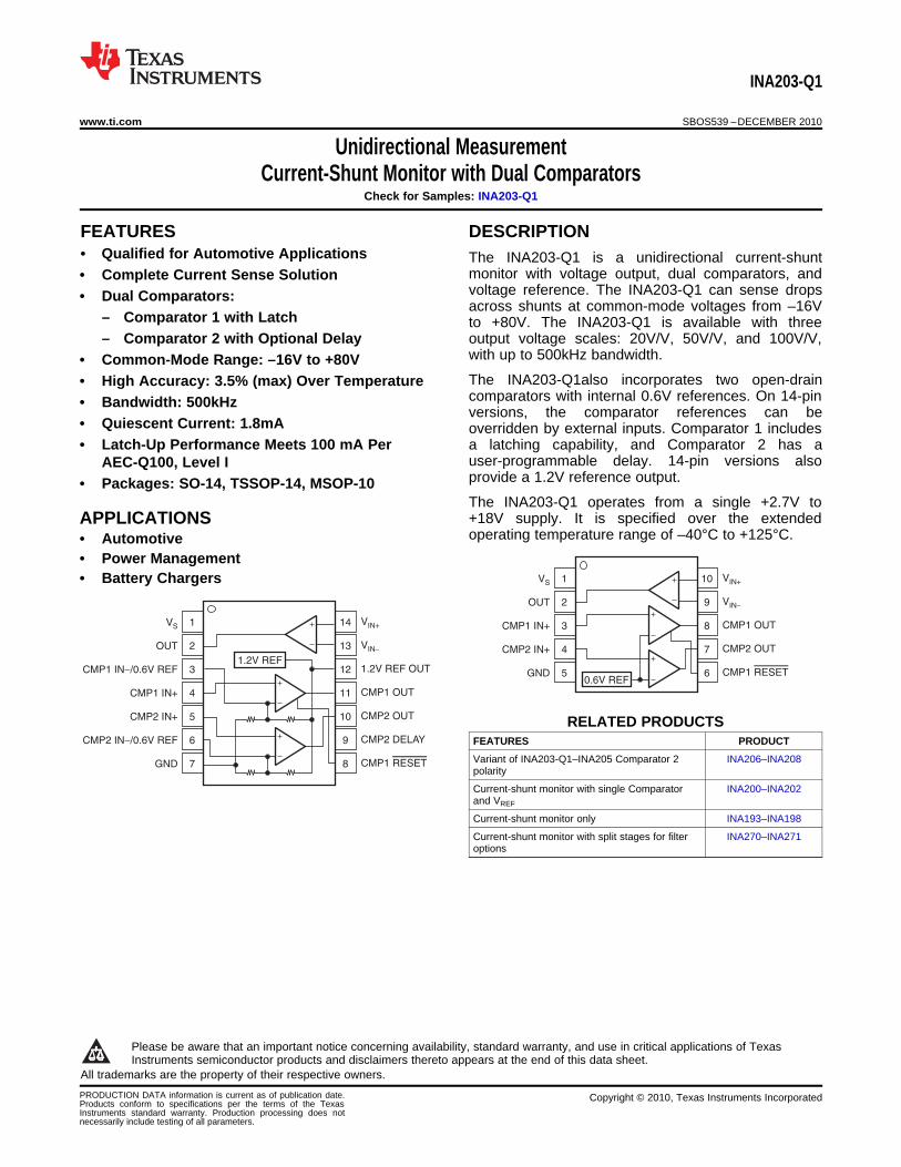
1FEATURES DESCRIPTION2• Qualified for Automotive Applications The INA203-Q1 is a unidirectional current-shunt
monitor with voltage output, dual comparators, and• Complete Current Sense Solutionvoltage reference. The INA203-Q1 can sense drops• Dual Comparators:across shunts at common-mode voltages from –16V
– Comparator 1 with Latch to +80V. The INA203-Q1 is available with three– Comparator 2 with Optional Delay output voltage scales: 20V/V, 50V/V, and 100V/V,
with up to 500kHz bandwidth.• Common-Mode Range: –16V to +80VThe INA203-Q1also incorporates two open-drain• High Accuracy: 3.5% (max) Over Temperaturecomparators with internal 0.6V references. On 14-pin• Bandwidth: 500kHzversions, the comparator references can be
• Quiescent Current: 1.8mA overridden by external inputs. Comparator 1 includes• Latch-Up Performance Meets 100 mA Per a latching capability, and Comparator 2 has a
user-programmable delay. 14-pin versions alsoAEC-Q100, Level Iprovide a 1.2V reference output.• Packages: SO-14, TSSOP-14, MSOP-10The INA203-Q1 operates from a single +2.7V to+18V supply. It is specified over the extendedAPPLICATIONSoperating temperature range of –40°C to +125°C.• Automotive
• Power Management• Battery Chargers
RELATED PRODUCTSFEATURES PRODUCT
Variant of INA203-Q1–INA205 Comparator 2 INA206–INA208polarity
Current-shunt monitor with single Comparator INA200–INA202and VREF
Current-shunt monitor only INA193–INA198
Current-shunt monitor with split stages for filter INA270–INA271options
1
Please be aware that an important notice concerning availability, standard warranty, and use in critical applications of TexasInstruments semiconductor products and disclaimers thereto appears at the end of this data sheet.
2All trademarks are the property of their respective owners.
PRODUCTION DATA information is current as of publication date. Copyright © 2010, Texas Instruments IncorporatedProducts conform to specifications per the terms of the TexasInstruments standard warranty. Production processing does notnecessarily include testing of all parameters.
INA203-Q1
SBOS539 –DECEMBER 2010 www.ti.com
This integrated circuit can be damaged by ESD. Texas Instruments recommends that all integrated circuits be handled withappropriate precautions. Failure to observe proper handling and installation procedures can cause damage.
ESD damage can range from subtle performance degradation to complete device failure. Precision integrated circuits may be moresusceptible to damage because very small parametric changes could cause the device not to meet its published specifications.
Table 1. ORDERING INFORMATION (1)
ORDERABLE PARTTA PACKAGE NUMBER TOP-SIDE MARKING
-40°C to 125°C SOIC-8 Reel of 2000 INA203AQPWRQ1 I203AQ
(1) For the most current package and ordering information see the Package Option Addendum at the end of this document, or see the TIweb site at www.ti.com.
ABSOLUTE MAXIMUM RATINGS (1)
VALUE UNIT
Supply Voltage, V+ 18 V
Differential (VIN+) – (VIN–) –18 to +18 VCurrent-Shunt Monitor AnalogInputs, VIN+and VIN– Common-Mode –16 to +80 V
Comparator Analog Input and Reset Pins GND – 0.3 to (V+) + 0.3 V
Analog Output, Out Pin GND – 0.3 to (V+) + 0.3 V
Comparator Output, Out Pin GND – 0.3 to 18 V
VREF and CMP2 Delay Pin GND – 0.3 to 10 V
Input Current Into Any Pin 5 mA
Storage Temperature –65 to +150 °C
Junction Temperature +150 °C
Human Body Model (HBM) 2000 VESD Ratings
Charged Device Model (CDM) 500 V
(1) Stresses above these ratings may cause permanent damage. Exposure to absolute maximum conditions for extended periods maydegrade device reliability. These are stress ratings only, and functional operation of the device at these or any other conditions beyondthose specified is not supported.
2 Submit Documentation Feedback Copyright © 2010, Texas Instruments Incorporated
Product Folder Link(s): INA203-Q1
INA203-Q1
www.ti.com SBOS539 –DECEMBER 2010
ELECTRICAL CHARACTERISTICS: CURRENT-SHUNT MONITORBoldface limits apply over the specified temperature range: TA = –40°C to +125°C.At TA = +25°C, VS = +12V, VCM = +12V, VSENSE = 100mV, RL = 10kΩ to GND, RPULL-UP = 5.1kΩ each connected from CMP1OUT and CMP2 OUT to VS, and CMP1 IN+ = 1V and CMP2 IN– = GND, unless otherwise noted.
CURRENT-SHUNT MONITOR PARAMETERS CONDITIONS MIN TYP MAX UNIT
INPUT
Full-Scale Sense Input Voltage VSENSE VSENSE = VIN+ – VIN– 0.15 (VS – 0.25)/Gain V
Common-Mode Input Range VCM –16 80 V
Common-Mode Rejection Ratio CMRR VCM = –16V to +80V 80 100 dB
+25°C to +125°C VCM = +12V to +80V 100 123 dB
–40°C to +25°C 90 100 dB
Offset Voltage, RTI (1) VOS ±0.5 ±2.5 mV
+25°C to +125°C ±3 mV
–40°C to +25°C ±3.5 mV
vs Temperature dVOS/dT TMIN to TMAX 5 mV/°C
vs Power Supply PSR VOUT = 2V, VCM = +18V 2.5 100 mV/V
Input Bias Current, VIN– Pin IB ±9 ±16 mA
OUTPUT (VSENSE ≥ 20mV)
Gain G 20 V/V
Gain Error VSENSE = 20mV to 100mV ±0.2 ±1 %
Over Temperature VSENSE = 20mV to 100mV ±2 %
Total Output Error (2) VSENSE = 120mV, VS = +16V ±0.75 ±2.2 %
Over Temperature VSENSE = 120mV, VS = +16V ±3.5 %
Nonlinearity Error (3) VSENSE = 20mV to 100mV ±0.002 %
Output Impedance, Pin 2 RO 1.5 Ω
Maximum Capacitive Load No Sustained Oscillation 10 nF
OUTPUT (VSENSE < 20mV) (4) –16V ≤ VCM < 0V 300 mV
0V ≤ VCM ≤ VS, VS = 5V 0.4 V
VS < VCM ≤ 80V 300 mV
VOLTAGE OUTPUT (5)
Output Swing to the Positive Rail VIN– = 11V, VIN+ = 12V (V+) – 0.15 (V+) – 0.25 V
Output Swing to GND (6) VIN– = 0V, VIN+ = –0.5V (VGND) + 0.004 (VGND) + 0.05 V
FREQUENCY RESPONSE
Bandwidth BW CLOAD = 5pF 500 kHz
Phase Margin CLOAD < 10nF 40 Degrees
Slew Rate SR 1 V/ms
VSENSE = 10mVPP to 100mVPP,Settling Time (1%) 2 msCLOAD = 5pF
NOISE, RTI
Output Voltage Noise Density 40 nV/√Hz
(1) Offset is extrapolated from measurements of the output at 20mV and 100mV VSENSE.(2) Total output error includes effects of gain error and VOS.(3) Linearity is best fit to a straight line.(4) For details on this region of operation, see the Accuracy Variations section in the Applications Information.(5) See Typical Characteristic curve Positive Output Voltage Swing vs Output Current (Figure 8).(6) Specified by design; not production tested.
Copyright © 2010, Texas Instruments Incorporated Submit Documentation Feedback 3
Product Folder Link(s): INA203-Q1
INA203-Q1
SBOS539 –DECEMBER 2010 www.ti.com
ELECTRICAL CHARACTERISTICS: COMPARATORBoldface limits apply over the specified temperature range: TA = –40°C to +125°C.At TA = +25°C, VS = +12V, VCM = +12V, VSENSE = 100mV, RL = 10kΩ to GND, and RPULL-UP = 5.1kΩ each connected fromCMP1 OUT and CMP2 OUT to VS, unless otherwise noted.
COMPARATOR PARAMETERS CONDITIONS MIN TYP MAX UNIT
OFFSET VOLTAGE
Offset Voltage Comparator Common-Mode Voltage = Threshold Voltage 2 mV
Offset Voltage Drift, Comparator 1 ±2 mV/°C
Offset Voltage Drift, Comparator 2 +5.4 mV/°C
Threshold Rising Edge on Non-Inverting input, TA = +25°C 590 608 620 mV
Over Temperature 586 625 mV
Hysteresis (1), CMP1 TA = –40°C to +85°C –8 mV
Hysteresis (1), CMP2 TA = –40°C to +85°C 8 mV
INPUT BIAS CURRENT (2)
CMP1 IN+, CMP2 IN+ 0.005 10 nA
vs Temperature 15 nA
INPUT IMPEDANCE
Pins 3 and 6 (14-pin packages only) 10 kΩ
INPUT RANGE
CMP1 IN+ and CMP2 IN+ 0V to VS – 1.5V V
Pins 3 and 6 (14-pin packages only) (3) 0V to VS – 1.5V V
OUTPUT
Large-Signal Differential Voltage Gain CMP VOUT 1V to 4V, RL ≥ 15kΩ Connected to 5V 200 V/mV
High-Level Output Current VID = 0.4V, VOH = VS 0.0001 1 mA
Low-Level Output Voltage VID = –0.6V, IOL = 2.35mA 220 300 mV
RESPONSE TIME (4)
Comparator 1 RL to 5V, CL = 15pF, 100mV Input Step with 5mV Overdrive 1.3 ms
RL to 5V, CL = 15pF, 100mV Input Step with 5mV Overdrive,Comparator 2 1.3 msCDELAY Pin Open
RESET
RESET Threshold (5) 1.1 V
Logic Input Impedance 2 MΩ
Minimum RESET Pulse Width 1.5 ms
RESET Propagation Delay 3 ms
Comparator 2 Delay Equation (6) CDELAY = tD/5 mF
Comparator 2 Delay tD CDELAY = 0.1mF 0.5 s
(1) Hysteresis refers to the threshold (the threshold specification applies to a rising edge of a noninverting input) of a falling edge on thenoninverting input of the comparator; refer to Figure 1.
(2) Specified by design; not production tested.(3) See the Comparator Maximum Input Voltage Range section in the Applications Information.(4) The comparator response time specified is the interval between the input step function and the instant when the output crosses 1.4V.(5) The CMP1 RESET input has an internal 2MΩ (typical) pull-down. Leaving the CMP1 RESET open results in a LOW state, with
transparent comparator operation.(6) The Comparator 2 delay applies to both rising and falling edges of the comparator output.
4 Submit Documentation Feedback Copyright © 2010, Texas Instruments Incorporated
Product Folder Link(s): INA203-Q1
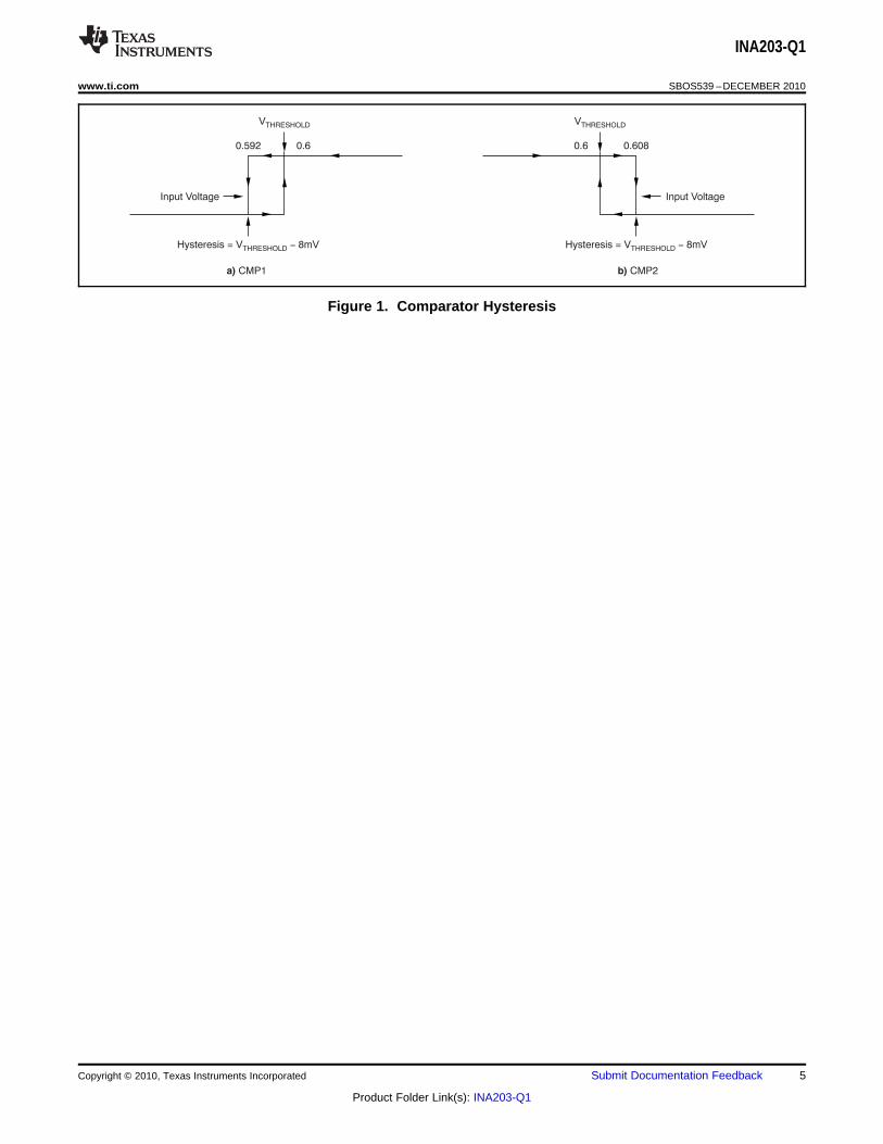
Hysteresis = VTHRESHOLD - 8mV
VTHRESHOLD
Input Voltage
0.592 0.6
a) CMP1
Hysteresis = VTHRESHOLD - 8mV
VTHRESHOLD
Input Voltage
0.6080.6
b) CMP2
INA203-Q1
www.ti.com SBOS539 –DECEMBER 2010
Figure 1. Comparator Hysteresis
Copyright © 2010, Texas Instruments Incorporated Submit Documentation Feedback 5
Product Folder Link(s): INA203-Q1
INA203-Q1
SBOS539 –DECEMBER 2010 www.ti.com
ELECTRICAL CHARACTERISTICS: REFERENCEBoldface limits apply over the specified temperature range: TA = –40°C to +125°C.At TA = +25°C, VS = +12V, VCM = +12V, VSENSE = 100mV, RL = 10kΩ to GND, and RPULL-UP = 5.1kΩ each connected fromCMP1 OUT and CMP2 OUT to VS, unless otherwise noted.
REFERENCE PARAMETERS CONDITIONS MIN TYP MAX UNIT
REFERENCE VOLTAGE
1.2VREFOUT Output Voltage 1.188 1.2 1.212 V
Reference Drift (1) dVOUT/dT TA = –40°C to +85°C 40 100 ppm/°C
0.6VREF Output Voltage (Pins 3 and 6 of 14-pin packages only) 0.6 V
Reference Drift (1) dVOUT/dT TA = –40°C to +85°C 40 100 ppm/°C
LOAD REGULATION dVOUT/dILOAD VREFOUT – 1.2V
Sourcing 0mA < ISOURCE < 0.5mA 0.4 2 mV/mA
Sinking 0mA < ISINK < 0.5mA 0.4 mV/mA
LOAD CURRENT ILOAD 1 mA
LINE REGULATION dVOUT/dVS 2.7V < VS < 18V 30 mV/V
CAPACITIVE LOAD
Reference Output Maximum Capacitive Load No Sustained Oscillations 10 nF
OUTPUT IMPEDANCE
Pins 3 and 6 of 14-Pin Packages Only 10 kΩ
(1) Specified by design; not production tested.
ELECTRICAL CHARACTERISTICS: GENERALBoldface limits apply over the specified temperature range: TA = –40°C to +125°C.All specifications at TA = +25°C, VS = +12V, VCM = +12V, VSENSE = 100mV, RL = 10kΩ to GND, RPULL-UP = 5.1kΩ eachconnected from CMP1 OUT and CMP2 OUT to VS, and CMP1 IN+ = 1V and CMP2 IN– = GND, unless otherwise noted.
GENERAL PARAMETERS CONDITIONS MIN TYP MAX UNIT
POWER SUPPLY
Operating Power Supply VS +2.7 +18 V
Quiescent Current IQ VOUT = 2V 1.8 2.2 mA
Over Temperature VSENSE = 0mV 2.8 mA
Comparator Power-On Reset Threshold (1) 1.5 V
TEMPERATURE
Specified Temperature Range –40 +125 °C
Operating Temperature Range –55 +150 °C
Storage Temperature Range –65 +150 °C
Thermal Resistance qJA
MSOP-10 Surface-Mount 200 °C/W
SO-14, TSSOP-14 Surface-Mount 150 °C/W
(1) The INA203, INA204, and INA205 are designed to power-up with the comparator in a defined reset state as long as CMP1 RESET isopen or grounded. The comparator will be in reset as long as the power supply is below the voltage shown here. The comparatorassumes a state based on the comparator input above this supply voltage. If CMP1 RESET is high at power-up, the comparator outputcomes up high and requires a reset to assume a low state, if appropriate.
6 Submit Documentation Feedback Copyright © 2010, Texas Instruments Incorporated
Product Folder Link(s): INA203-Q1
45
40
35
30
25
20
15
10
510k 100k
Ga
in (
dB
)
Frequency (Hz)
1M
G = 100 C = 1000pFLOAD
G = 50
G = 20
45
40
35
30
25
20
15
10
510k 100k
Ga
in (
dB
)
Frequency (Hz)
1M
G = 100
G = 50
G = 20
C = 0LOAD
20
18
16
14
12
10
8
6
4
2
020 100 200 300 400 500 600 700
V(V
)O
UT
V (mV)SENSE
800 900
50V/V
20V/V
100V/V
140
130
120
110
100
90
80
70
60
50
40
10 100 1k 10k
Co
mm
on
-Mo
de
an
d
Po
we
r-S
up
ply
Re
jectio
n (
dB
)
Frequency (Hz)
100k
CMR
PSR
4.0
3.5
3.0
2.5
2.0
1.5
1.0
0.5
00 50 100 150 200 250 300 350
Tota
l O
utp
ut
Err
or
(% e
rro
r o
f th
e id
ea
l o
utp
ut
va
lue
)
V (mV)SENSE
400 450 500
0.1
0.09
0.08
0.07
0.06
0.05
0.04
0.03
0.02
0.01
0-16 -12 -8 -4 0 4 128 2016
Tota
l O
utp
ut E
rror
(%)
Common-Mode Voltage (V)
... 76 80
INA203-Q1
www.ti.com SBOS539 –DECEMBER 2010
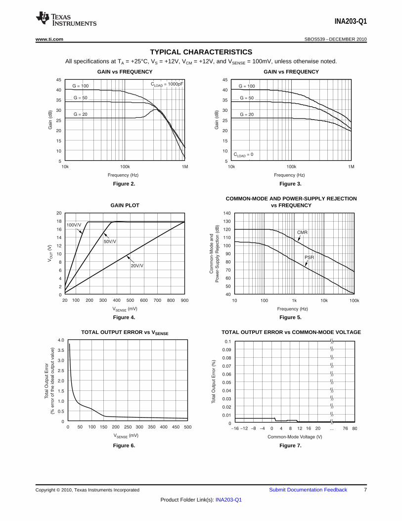
TYPICAL CHARACTERISTICSAll specifications at TA = +25°C, VS = +12V, VCM = +12V, and VSENSE = 100mV, unless otherwise noted.
GAIN vs FREQUENCY GAIN vs FREQUENCY
Figure 2. Figure 3.
COMMON-MODE AND POWER-SUPPLY REJECTIONGAIN PLOT vs FREQUENCY
Figure 4. Figure 5.
TOTAL OUTPUT ERROR vs VSENSE TOTAL OUTPUT ERROR vs COMMON-MODE VOLTAGE
Figure 6. Figure 7.
Copyright © 2010, Texas Instruments Incorporated Submit Documentation Feedback 7
Product Folder Link(s): INA203-Q1
12
11
10
9
8
7
6
5
4
3
2
1
00 5 10 15 20
Ou
tpu
t V
olta
ge
(V
)
Output Current (mA)
25 30
V = 12VS
+25 C°
+25 C°
- °40 C
- °40 C
+125 C°
+125 C°
Sourcing Current
V = 3VS
Sourcing Current
Output stage is designed
to source current. Current
sinking capability is
approximately 400 A.m
3.5
3.0
2.5
2.0
1.5
1.0
0.5
0
0 1 2 3 4 5 6 7
I(m
A)
Q
Output Voltage (V)
8 9 10
2.00
1.75
1.50
1.25
1.00
0.75
0.50
-16 -12 -8 -4 0 4 8 12 16 20 24 28
I(m
A)
Q
V (V)CM
32 36
V = 0mVSENSE
V = 12VS
V = 2.7VS
V = 100mVSENSE
V = 12VSV = 2.7VS
34
30
26
22
18
14
10
6
2.5 3.5 4.5 5.5 6.5 7.5 8.5 9.5 10.5
Outp
ut S
hort
-Circuit C
urr
ent (m
A)
Supply Voltage (V)
11.5 17 18
- °40 C
+ °25 C
+125 C°
Ou
tpu
t V
olta
ge
(5
0m
V/d
iv)
Time (2 s/div)m
G = 20
V = 10mV to 20mVSENSE
Time (2 s/div)m
G = 20
Ou
tpu
t V
olta
ge
(5
00
mV
/div
)
V = 10mV to 100mVSENSE
INA203-Q1
SBOS539 –DECEMBER 2010 www.ti.com
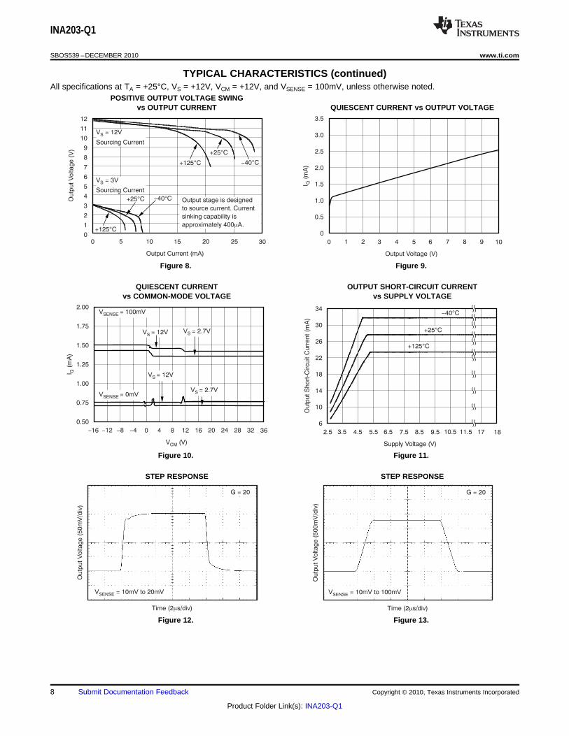
TYPICAL CHARACTERISTICS (continued)All specifications at TA = +25°C, VS = +12V, VCM = +12V, and VSENSE = 100mV, unless otherwise noted.
POSITIVE OUTPUT VOLTAGE SWINGvs OUTPUT CURRENT QUIESCENT CURRENT vs OUTPUT VOLTAGE
Figure 8. Figure 9.
QUIESCENT CURRENT OUTPUT SHORT-CIRCUIT CURRENTvs COMMON-MODE VOLTAGE vs SUPPLY VOLTAGE
Figure 10. Figure 11.
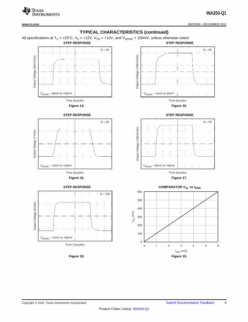
STEP RESPONSE STEP RESPONSE
Figure 12. Figure 13.
8 Submit Documentation Feedback Copyright © 2010, Texas Instruments Incorporated
Product Folder Link(s): INA203-Q1
Time (2 s/div)m
G = 20
Outp
ut V
oltage (
50m
V/d
iv)
V = 90mV to 100mVSENSE
Time (5 s/div)m
G = 50
Outp
ut V
oltage (
100m
V/d
iv)
V = 10mV to 20mVSENSE
Time (5 s/div)m
G = 50
Outp
ut V
oltage (
1V
/div
)
V = 10mV to 100mVSENSE
Time (5 s/div)m
G = 50
Ou
tpu
t V
olta
ge
(1
00
mV
/div
)
V = 90mV to 100mVSENSE
Time (10 s/div)m
G = 100
Ou
tpu
t V
olta
ge
(2
V/d
iv)
V = 10mV to 100mVSENSE
600
500
400
300
200
100
0
0 1 2 3 4 5
V(m
V)
OL
I (mA)SINK
6
INA203-Q1
www.ti.com SBOS539 –DECEMBER 2010
TYPICAL CHARACTERISTICS (continued)All specifications at TA = +25°C, VS = +12V, VCM = +12V, and VSENSE = 100mV, unless otherwise noted.
STEP RESPONSE STEP RESPONSE
Figure 14. Figure 15.
STEP RESPONSE STEP RESPONSE
Figure 16. Figure 17.
STEP RESPONSE COMPARATOR VOL vs ISINK
Figure 18. Figure 19.
Copyright © 2010, Texas Instruments Incorporated Submit Documentation Feedback 9
Product Folder Link(s): INA203-Q1
600
599
598
597
596
595
594
593
592
591
5902 4 6 8 10 12 14 16
Co
mp
ara
tor
Trip
Po
int
(mV
)
Supply Voltage (V)
18
602
601
600
599
598
597
596
-50 -25 0 25 50 75 100
Co
mp
ara
tor
Trip
Po
int
(mV
)
Temperature ( C)°
125
200
175
150
125
100
75
50
0 20 40 60 80 100 120 140 160 180
Pro
pa
ga
tio
n D
ela
y (
ns)
Overdrive Voltage (mV)
200
14
13
12
11
10
0 20 40 60 80 100 120 140 160 180
Pro
pa
ga
tio
n D
ela
y (
s)
m
Overdrive Voltage (mV)
200
1.2
1.0
0.8
0.6
0.4
0.2
0
2 4 6 8 10 12 14 16
Re
se
t V
olta
ge
(V
)
Supply Voltage (V)
18
300
275
250
225
200
175
150
125
-50 -25 0 25 50 75 100
Pro
pa
ga
tio
n D
ela
y (
ns)
Temperature ( C)°
125
INA203-Q1
SBOS539 –DECEMBER 2010 www.ti.com
TYPICAL CHARACTERISTICS (continued)All specifications at TA = +25°C, VS = +12V, VCM = +12V, and VSENSE = 100mV, unless otherwise noted.
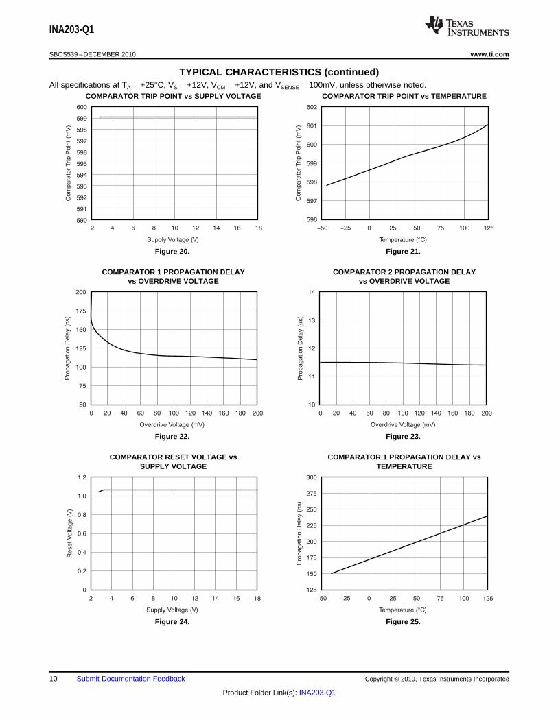
COMPARATOR TRIP POINT vs SUPPLY VOLTAGE COMPARATOR TRIP POINT vs TEMPERATURE
Figure 20. Figure 21.
COMPARATOR 1 PROPAGATION DELAY COMPARATOR 2 PROPAGATION DELAYvs OVERDRIVE VOLTAGE vs OVERDRIVE VOLTAGE
Figure 22. Figure 23.
COMPARATOR RESET VOLTAGE vs COMPARATOR 1 PROPAGATION DELAY vsSUPPLY VOLTAGE TEMPERATURE
Figure 24. Figure 25.
10 Submit Documentation Feedback Copyright © 2010, Texas Instruments Incorporated
Product Folder Link(s): INA203-Q1
Input
200mV/div
Output
2V/div
2 s/divm
V = 5mVOD
1000
100
10
1
0.1
0.010.001 0.01 0.1 1 10
Pro
pa
ga
tio
n D
ela
y (
ms)
Delay Capacitance (nF)
100
Input
200mV/div
Output
2V/div
5 s/divm
V = 5mVOD
1.22
1.21
1.20
1.19
1.18
-50 -25 0 25 50 75 100
V(V
)R
EF
Temperature ( C)°
125
INA203-Q1
www.ti.com SBOS539 –DECEMBER 2010
TYPICAL CHARACTERISTICS (continued)All specifications at TA = +25°C, VS = +12V, VCM = +12V, and VSENSE = 100mV, unless otherwise noted.
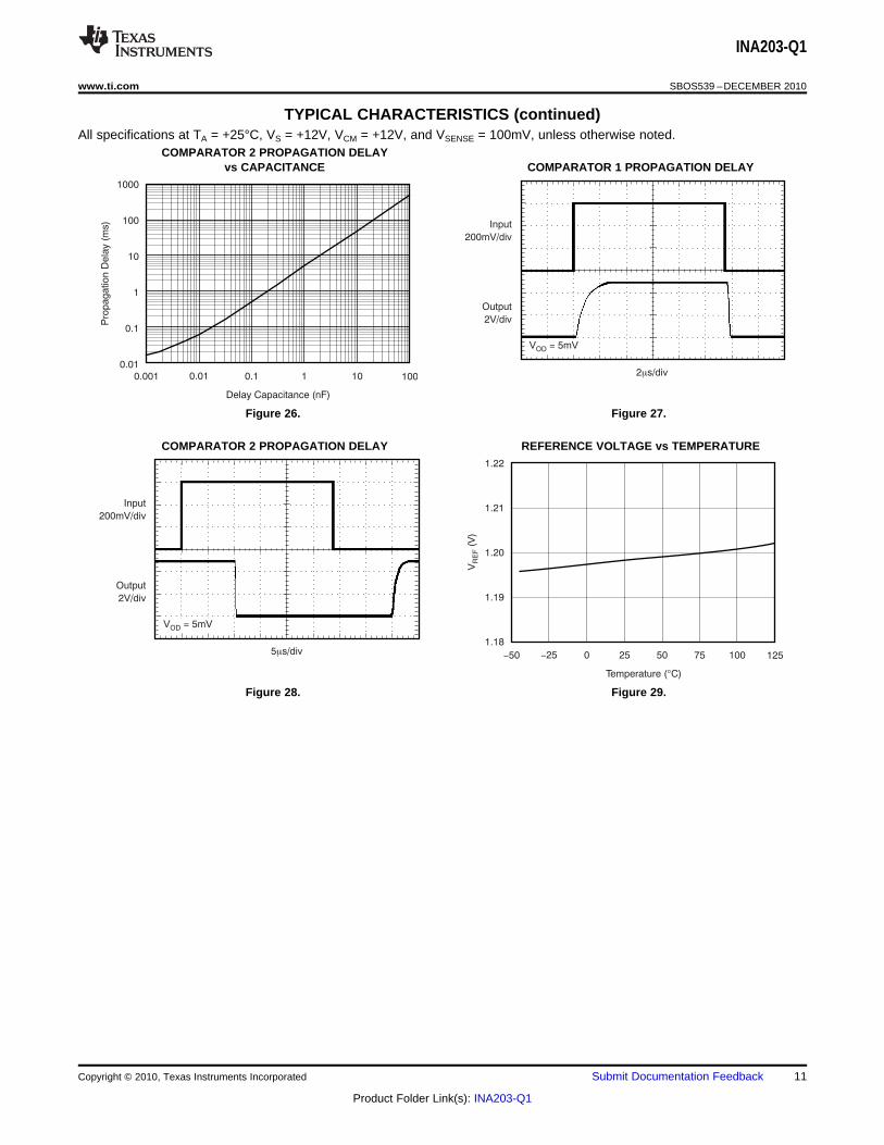
COMPARATOR 2 PROPAGATION DELAYvs CAPACITANCE COMPARATOR 1 PROPAGATION DELAY
Figure 26. Figure 27.
COMPARATOR 2 PROPAGATION DELAY REFERENCE VOLTAGE vs TEMPERATURE
Figure 28. Figure 29.
Copyright © 2010, Texas Instruments Incorporated Submit Documentation Feedback 11
Product Folder Link(s): INA203-Q1
G =V V-OUT1 OUT2
100mV 20mV-
V RTI (Referred-To-Input) =OS
VOUT1
G- 100mV
INA203
x20
RSHUNT
3mW
Load Supply
-18V to +80VLoad
5V Supply
Optional Delay
Capacitor
0.2 Fm
CBYPASS
0.01 Fm
VS
OUT
CMP1 IN /0.6 REF-
CMP1 IN+
CMP2 IN+
CMP2 IN /0.6 REF-
GND
VIN+
VIN-
1.2V REF OUT
CMP1 OUT
CMP2 OUT
CMP2 DELAY
CMP1 RESET
Current Shunt
Monitor Output 1.2V REF
RPULL-UP
4.7kW
RPULL-UP
4.7kW
Transparent/Reset
Latch
INA203-Q1
SBOS539 –DECEMBER 2010 www.ti.com
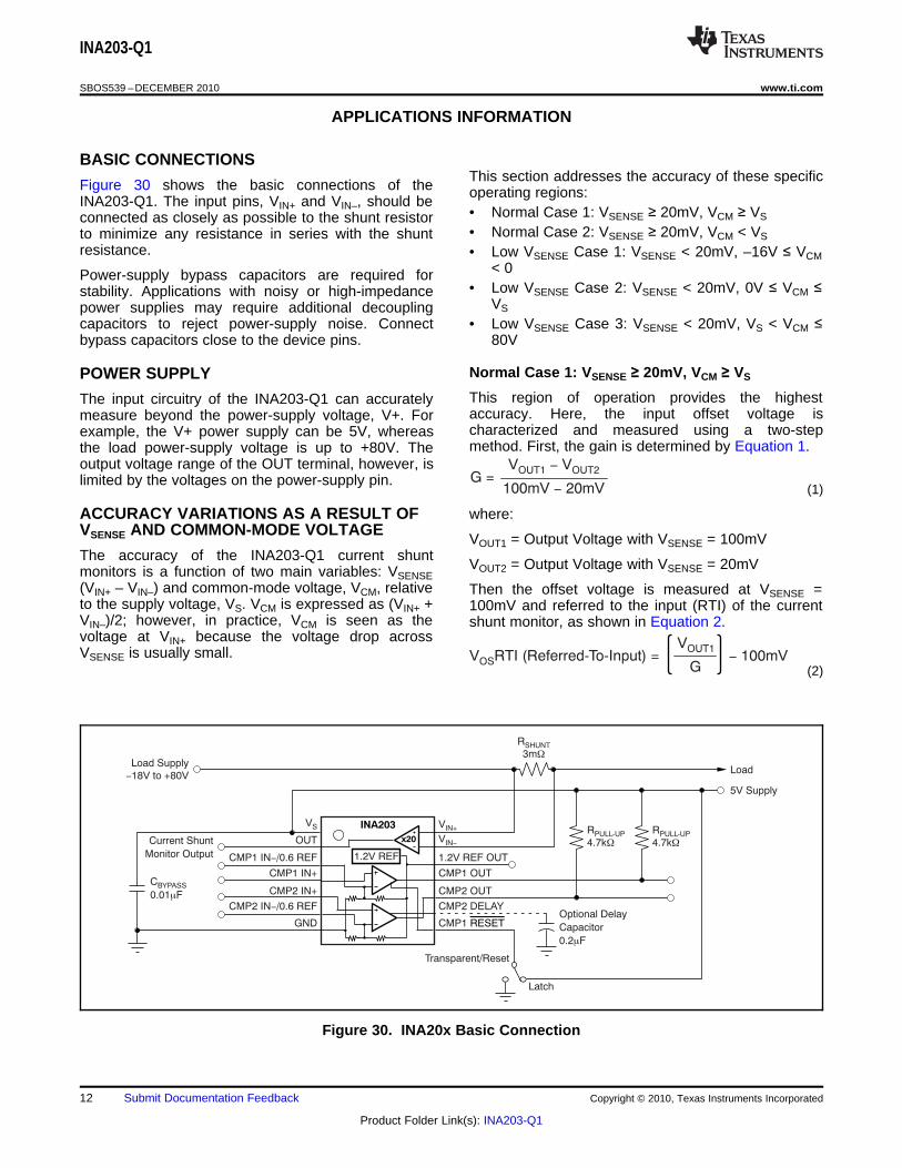
APPLICATIONS INFORMATION
BASIC CONNECTIONSThis section addresses the accuracy of these specific
Figure 30 shows the basic connections of the operating regions:INA203-Q1. The input pins, VIN+ and VIN–, should be
• Normal Case 1: VSENSE ≥ 20mV, VCM ≥ VSconnected as closely as possible to the shunt resistor• Normal Case 2: VSENSE ≥ 20mV, VCM < VSto minimize any resistance in series with the shunt
resistance. • Low VSENSE Case 1: VSENSE < 20mV, –16V ≤ VCM< 0Power-supply bypass capacitors are required for
• Low VSENSE Case 2: VSENSE < 20mV, 0V ≤ VCM ≤stability. Applications with noisy or high-impedanceVSpower supplies may require additional decoupling
capacitors to reject power-supply noise. Connect • Low VSENSE Case 3: VSENSE < 20mV, VS < VCM ≤bypass capacitors close to the device pins. 80V
Normal Case 1: VSENSE ≥ 20mV, VCM ≥ VSPOWER SUPPLYThis region of operation provides the highestThe input circuitry of the INA203-Q1 can accuratelyaccuracy. Here, the input offset voltage ismeasure beyond the power-supply voltage, V+. Forcharacterized and measured using a two-stepexample, the V+ power supply can be 5V, whereasmethod. First, the gain is determined by Equation 1.the load power-supply voltage is up to +80V. The
output voltage range of the OUT terminal, however, islimited by the voltages on the power-supply pin.
(1)
ACCURACY VARIATIONS AS A RESULT OF where:VSENSE AND COMMON-MODE VOLTAGE
VOUT1 = Output Voltage with VSENSE = 100mVThe accuracy of the INA203-Q1 current shunt
VOUT2 = Output Voltage with VSENSE = 20mVmonitors is a function of two main variables: VSENSE(VIN+ – VIN–) and common-mode voltage, VCM, relative Then the offset voltage is measured at VSENSE =to the supply voltage, VS. VCM is expressed as (VIN+ + 100mV and referred to the input (RTI) of the currentVIN–)/2; however, in practice, VCM is seen as the shunt monitor, as shown in Equation 2.voltage at VIN+ because the voltage drop acrossVSENSE is usually small.
(2)
Figure 30. INA20x Basic Connection
12 Submit Documentation Feedback Copyright © 2010, Texas Instruments Incorporated
Product Folder Link(s): INA203-Q1
2.4
2.2
2.0
1.8
1.6
1.4
1.2
1.0
0.8
0.6
0.4
0.2
0
0 2 4 6 8 10 12 14 16 18 20 22
V(V
)O
UT
V (mV)SENSE
24
V Tested LimitOUT
(1)
VCM2
VCM1
VCM3
VCM4
V , V , and VCM2 CM3 CM4
illustrate the variance
from part to part of the V that can causeCM
maximum V with V < 20mV.OUT SENSE
V Tested Limit atOUT
V = 0mV, 0 V£ CM1SENSE
V£ .S
NOTE: (1) INA203-Q1 V Tested Limit = 0.4V.OUT
Ideal
2.0
1.8
1.6
1.4
1.2
1.0
0.8
0.6
0.4
0.2
00 2 4 6 8 10 12 14 16 18
V(V
)O
UT
V (mV)SENSE
20
Actual
Ideal
INA203-Q1
www.ti.com SBOS539 –DECEMBER 2010
Low VSENSE Case 2: VSENSE < 20mV, 0V ≤ VCM ≤ VSIn the Typical Characteristics, the Output Error vsCommon-Mode Voltage curve (Figure 7) shows the This region of operation is the least accurate for thehighest accuracy for this region of operation. In this INA203-Q1. To achieve the wide input common-modeplot, VS = 12V; for VCM ≥ 12V, the output error is at its voltage range, these devices use two op amp frontminimum. This case is also used to create the ends in parallel. One op amp front end operates inVSENSE ≥ 20mV output specifications in the Electrical the positive input common-mode voltage range, andCharacteristics table. the other in the negative input region. For this case,
neither of these two internal amplifiers dominates andNormal Case 2: VSENSE ≥ 20mV, VCM < VS overall loop gain is very low. Within this region, VOUT
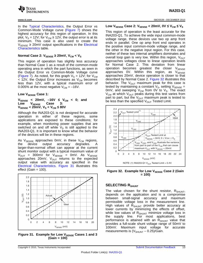
approaches voltages close to linear operation levelsThis region of operation has slightly less accuracyfor Normal Case 2. This deviation from linearthan Normal Case 1 as a result of the common-modeoperation becomes greatest the closer VSENSEoperating area in which the part functions, as seen inapproaches 0V. Within this region, as VSENSEthe Output Error vs Common-Mode Voltage curveapproaches 20mV, device operation is closer to that(Figure 7). As noted, for this graph VS = 12V; for VCMdescribed by Normal Case 2. Figure 32 illustrates this< 12V, the Output Error increases as VCM becomesbehavior. The VOUT maximum peak for this case isless than 12V, with a typical maximum error oftested by maintaining a constant VS, setting VSENSE =0.005% at the most negative VCM = –16V.0mV, and sweeping VCM from 0V to VS. The exactVCM at which VOUT peaks during this test varies fromLow VSENSE Case 1:part to part, but the VOUT maximum peak is tested to
VSENSE < 20mV, –16V ≤ VCM < 0; and be less than the specified VOUT Tested Limit.Low VSENSE Case 3:VSENSE < 20mV, VS < VCM ≤ 80V
Although the INA203-Q1 is not designed for accurateoperation in either of these regions, someapplications are exposed to these conditions; forexample, when monitoring power supplies that areswitched on and off while VS is still applied to theINA203-Q1. It is important to know what the behaviorof the devices will be in these regions.
As VSENSE approaches 0mV, in these VCM regions,the device output accuracy degrades. Alarger-than-normal offset can appear at the currentshunt monitor output with a typical maximum value ofVOUT = 300mV for VSENSE = 0mV. As VSENSEapproaches 20mV, VOUT returns to the expectedoutput value with accuracy as specified in theElectrical Characteristics. Figure 31 illustrates thiseffect (Gain = 100). Figure 32. Example for Low VSENSE Case 2 (Gain
= 100)
SELECTING RSHUNT
The value chosen for the shunt resistor, RSHUNT,depends on the application and is a compromisebetween small-signal accuracy and maximumpermissible voltage loss in the measurement line.High values of RSHUNT provide better accuracy atlower currents by minimizing the effects of offset,while low values of RSHUNT minimize voltage loss inthe supply line. For most applications, bestperformance is attained with an RSHUNT value thatprovides a full-scale shunt voltage range of 50mV to100mV. Maximum input voltage for accuratemeasurements is (VSHUNT – 0.25)/Gain.
Figure 31. Example for Low VSENSE Cases 1 and 3(Gain = 100)
Copyright © 2010, Texas Instruments Incorporated Submit Documentation Feedback 13
Product Folder Link(s): INA203-Q1
Gain Error % = 100 -
5kW
5k + RW FILT
100 ´
R << RSHUNT FILTER
3mW
VSUPPLY Load
R < 100WFILTER
R <100WFILTER
CFILTER
1
2
3
4
5
6
7
14
13
12
11
10
9
8
1.2V REF OUT
CMP1 OUT
CMP2 OUT
CMP2 DELAY
CMP1 RESET
VIN+
VIN-
VS
OUT
CMP1 IN /0.6V REF-
CMP1 IN+
CMP2 IN+
CMP2 IN /0.6V REF-
GND
1.2V REF
f =-3dB
1
2 (2R )CpFILTER FILTER
f-3dB
INA203-Q1
SBOS539 –DECEMBER 2010 www.ti.com
TRANSIENT PROTECTION OUTPUT VOLTAGE RANGE
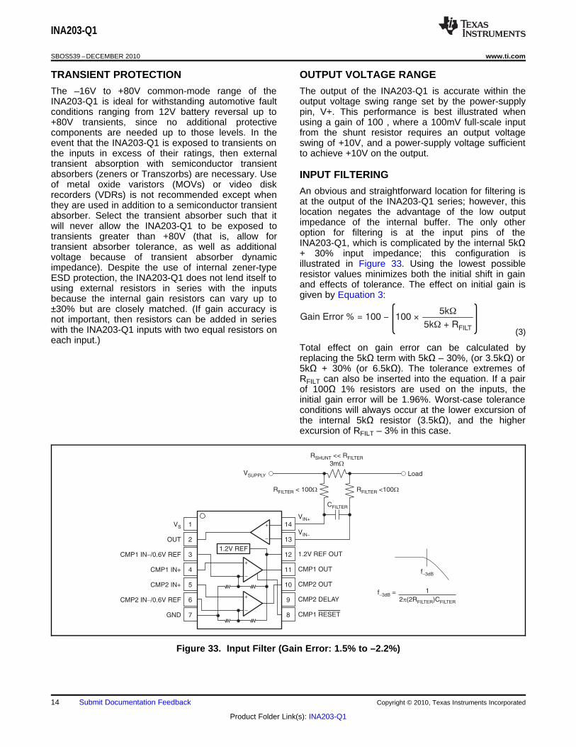
The –16V to +80V common-mode range of the The output of the INA203-Q1 is accurate within theINA203-Q1 is ideal for withstanding automotive fault output voltage swing range set by the power-supplyconditions ranging from 12V battery reversal up to pin, V+. This performance is best illustrated when+80V transients, since no additional protective using a gain of 100 , where a 100mV full-scale inputcomponents are needed up to those levels. In the from the shunt resistor requires an output voltageevent that the INA203-Q1 is exposed to transients on swing of +10V, and a power-supply voltage sufficientthe inputs in excess of their ratings, then external to achieve +10V on the output.transient absorption with semiconductor transientabsorbers (zeners or Transzorbs) are necessary. Use INPUT FILTERINGof metal oxide varistors (MOVs) or video disk
An obvious and straightforward location for filtering isrecorders (VDRs) is not recommended except whenat the output of the INA203-Q1 series; however, thisthey are used in addition to a semiconductor transientlocation negates the advantage of the low outputabsorber. Select the transient absorber such that itimpedance of the internal buffer. The only otherwill never allow the INA203-Q1 to be exposed tooption for filtering is at the input pins of thetransients greater than +80V (that is, allow forINA203-Q1, which is complicated by the internal 5kΩtransient absorber tolerance, as well as additional+ 30% input impedance; this configuration isvoltage because of transient absorber dynamicillustrated in Figure 33. Using the lowest possibleimpedance). Despite the use of internal zener-typeresistor values minimizes both the initial shift in gainESD protection, the INA203-Q1 does not lend itself toand effects of tolerance. The effect on initial gain isusing external resistors in series with the inputsgiven by Equation 3:because the internal gain resistors can vary up to
±30% but are closely matched. (If gain accuracy isnot important, then resistors can be added in serieswith the INA203-Q1 inputs with two equal resistors on (3)each input.)
Total effect on gain error can be calculated byreplacing the 5kΩ term with 5kΩ – 30%, (or 3.5kΩ) or5kΩ + 30% (or 6.5kΩ). The tolerance extremes ofRFILT can also be inserted into the equation. If a pairof 100Ω 1% resistors are used on the inputs, theinitial gain error will be 1.96%. Worst-case toleranceconditions will always occur at the lower excursion ofthe internal 5kΩ resistor (3.5kΩ), and the higherexcursion of RFILT – 3% in this case.
Figure 33. Input Filter (Gain Error: 1.5% to –2.2%)
14 Submit Documentation Feedback Copyright © 2010, Texas Instruments Incorporated
Product Folder Link(s): INA203-Q1
C (in F) =mDELAY
tD5
U2
U1
0.6V
1.2V
I2
120nA
I1
120nA
CDELAY
INA203-Q1
www.ti.com SBOS539 –DECEMBER 2010
Note that the specified accuracy of the INA203-Q1 additional features for comparator functions. Themust then be combined in addition to these comparator reference voltage of both Comparator 1tolerances. While this discussion treated accuracy and Comparator 2 can be overridden by externalworst-case conditions by combining the extremes of inputs for increased design flexibility. Comparator 2the resistor values, it is appropriate to use geometric has a programmable delay.mean or root sum square calculations to total theeffects of accuracy variations. COMPARATOR DELAY (14-Pin Version Only)
The Comparator 2 programmable delay is controlledREFERENCEby a capacitor connected to the CMP2 Delay Pin; see
The INA203-Q1 include an internal voltage reference Figure 30. The capacitor value (in mF) is selected bythat has a load regulation of 0.4mV/mA (typical), and using Equation 4:not more than 100ppm/°C of drift. Only the 14-pinpackage allows external access to reference (4)voltages, where voltages of 1.2V and 0.6V are bothavailable. Output current versus output voltage is A simplified version of the delay circuit forillustrated in the Typical Characteristics section. Comparator 2 is shown in Figure 34. The delay
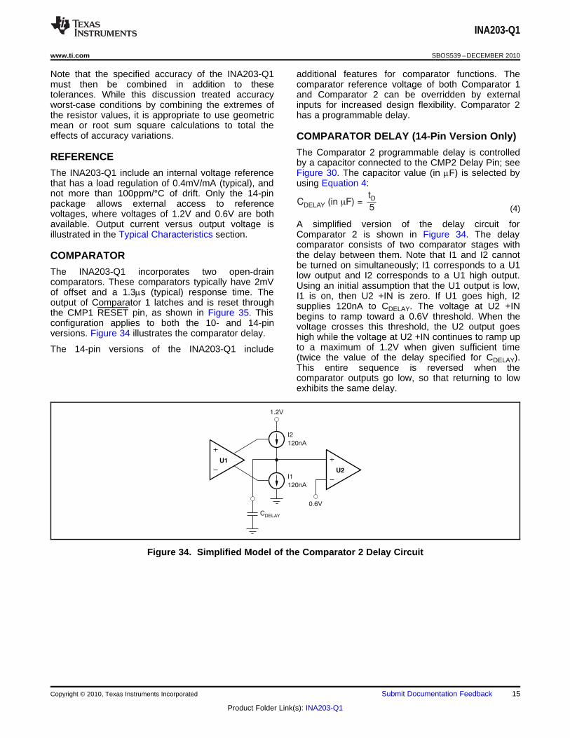
comparator consists of two comparator stages withthe delay between them. Note that I1 and I2 cannotCOMPARATORbe turned on simultaneously; I1 corresponds to a U1
The INA203-Q1 incorporates two open-drain low output and I2 corresponds to a U1 high output.comparators. These comparators typically have 2mV Using an initial assumption that the U1 output is low,of offset and a 1.3ms (typical) response time. The I1 is on, then U2 +IN is zero. If U1 goes high, I2output of Comparator 1 latches and is reset through supplies 120nA to CDELAY. The voltage at U2 +INthe CMP1 RESET pin, as shown in Figure 35. This begins to ramp toward a 0.6V threshold. When theconfiguration applies to both the 10- and 14-pin voltage crosses this threshold, the U2 output goesversions. Figure 34 illustrates the comparator delay. high while the voltage at U2 +IN continues to ramp up
to a maximum of 1.2V when given sufficient timeThe 14-pin versions of the INA203-Q1 include(twice the value of the delay specified for CDELAY).This entire sequence is reversed when thecomparator outputs go low, so that returning to lowexhibits the same delay.
Figure 34. Simplified Model of the Comparator 2 Delay Circuit
Copyright © 2010, Texas Instruments Incorporated Submit Documentation Feedback 15
Product Folder Link(s): INA203-Q1
0V
0.6V
VIN
CMP Out
RESET
20kW 20kW
CMP2 IN+
CMP1 IN-
1.2V
£ 1mA
INA203-Q1
x20
RSHUNT
3mW
Load Supply
-18V to +80VLoad
5V Supply
Optional Delay
Capacitor
0.2 Fm
CBYPASS
0.01 Fm
VS
OUT
CMP1 IN /0.6 REF-
CMP1 IN+
CMP2 IN+
CMP2 IN-
GND
VIN+
VIN-
1.2V REF OUT
CMP1 OUT
CMP2 OUT
CMP2 DELAY
CMP1 RESET
Current Shunt Monitor Output1.2V REF
RPULL-UP
4.7kW
RPULL-UP
4.7kW
Transparent/Reset
Latch
V < 11.2
INA203-Q1
SBOS539 –DECEMBER 2010 www.ti.com
Figure 35. Comparator Latching Capability
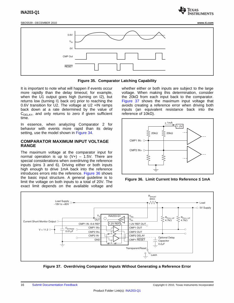
It is important to note what will happen if events occur whether either or both inputs are subject to the largemore rapidly than the delay timeout; for example, voltage. When making this determination, considerwhen the U1 output goes high (turning on I2), but the 20kΩ from each input back to the comparator.returns low (turning I1 back on) prior to reaching the Figure 37 shows the maximum input voltage that0.6V transition for U2. The voltage at U2 +IN ramps avoids creating a reference error when driving bothback down at a rate determined by the value of inputs (an equivalent resistance back into theCDELAY, and only returns to zero if given sufficient reference of 10kΩ).time.
In essence, when analyzing Comparator 2 forbehavior with events more rapid than its delaysetting, use the model shown in Figure 34.
COMPARATOR MAXIMUM INPUT VOLTAGERANGE
The maximum voltage at the comparator input fornormal operation is up to (V+) – 1.5V. There arespecial considerations when overdriving the referenceinputs (pins 3 and 6). Driving either or both inputshigh enough to drive 1mA back into the referenceintroduces errors into the reference. Figure 36 showsthe basic input structure. A general guideline is to Figure 36. Limit Current Into Reference ≤ 1mAlimit the voltage on both inputs to a total of 20V. Theexact limit depends on the available voltage and
Figure 37. Overdriving Comparator Inputs Without Generating a Reference Error
16 Submit Documentation Feedback Copyright © 2010, Texas Instruments Incorporated
Product Folder Link(s): INA203-Q1
VIN+
VIN-
1.2V REF OUT
CMP1 OUT
CMP2 OUT
CMP2 DELAY
CMP1 RESET
VS+
OUT
CMP1 IN-
CMP1 IN+
CMP2 IN+
CMP2 IN-
GND
Load
Overlimit(1)
Raychem
Polyswitch
Warning(1)
+5V Supply
3.3kW
Pull-Up
Resistors
CBYPASS
0.01 Fm
Optional
CDELAY
0.01 Fm
< 18V
Battery
Reset
Latch
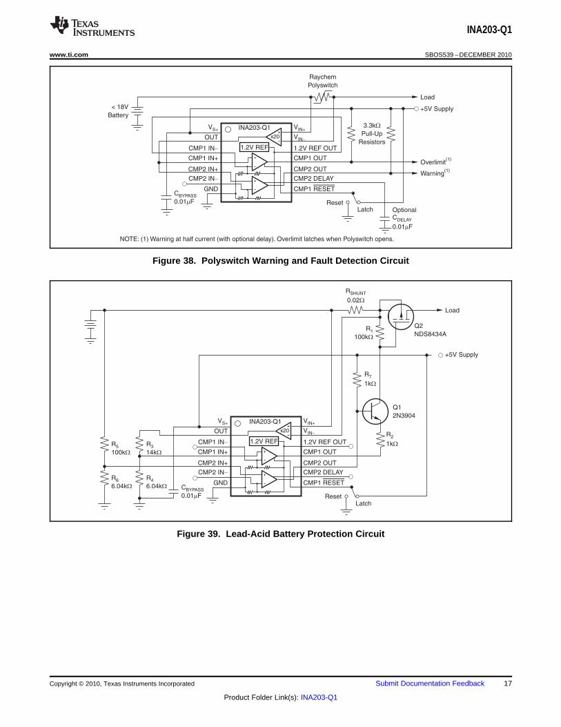
NOTE: (1) Warning at half current (with optional delay). Overlimit latches when Polyswitch opens.
INA203-Q1
x20
1.2V REF
INA203-Q1
x20
VIN+
VIN-
1.2V REF OUT
CMP1 OUT
CMP2 OUT
CMP2 DELAY
CMP1 RESET
VS+
OUT
CMP1 IN-
CMP1 IN+
CMP2 IN+
CMP2 IN-
GND
1.2V REF
Load
RSHUNT
0.02W
+5V Supply
R3
14kW
R4
6.04kW
R5
100kW
R6
6.04kW CBYPASS
0.01 Fm
Q2
NDS8434A
Q1
2N3904
R1
100kW
Latch
Reset
R2
1kW
R7
1kW
INA203-Q1
www.ti.com SBOS539 –DECEMBER 2010
Figure 38. Polyswitch Warning and Fault Detection Circuit
Figure 39. Lead-Acid Battery Protection Circuit
Copyright © 2010, Texas Instruments Incorporated Submit Documentation Feedback 17
Product Folder Link(s): INA203-Q1
PACKAGE OPTION ADDENDUM
www.ti.com 10-Jan-2011
Addendum-Page 1
PACKAGING INFORMATION
Orderable Device Status (1) Package Type PackageDrawing
Pins Package Qty Eco Plan (2) Lead/Ball Finish
MSL Peak Temp (3) Samples
(Requires Login)
INA203AQPWRQ1 ACTIVE TSSOP PW 14 2000 Green (RoHS& no Sb/Br)
CU NIPDAU Level-2-260C-1 YEAR Purchase Samples
(1) The marketing status values are defined as follows:ACTIVE: Product device recommended for new designs.LIFEBUY: TI has announced that the device will be discontinued, and a lifetime-buy period is in effect.NRND: Not recommended for new designs. Device is in production to support existing customers, but TI does not recommend using this part in a new design.PREVIEW: Device has been announced but is not in production. Samples may or may not be available.OBSOLETE: TI has discontinued the production of the device.
(2) Eco Plan - The planned eco-friendly classification: Pb-Free (RoHS), Pb-Free (RoHS Exempt), or Green (RoHS & no Sb/Br) - please check http://www.ti.com/productcontent for the latest availabilityinformation and additional product content details.TBD: The Pb-Free/Green conversion plan has not been defined.Pb-Free (RoHS): TI's terms "Lead-Free" or "Pb-Free" mean semiconductor products that are compatible with the current RoHS requirements for all 6 substances, including the requirement thatlead not exceed 0.1% by weight in homogeneous materials. Where designed to be soldered at high temperatures, TI Pb-Free products are suitable for use in specified lead-free processes.Pb-Free (RoHS Exempt): This component has a RoHS exemption for either 1) lead-based flip-chip solder bumps used between the die and package, or 2) lead-based die adhesive used betweenthe die and leadframe. The component is otherwise considered Pb-Free (RoHS compatible) as defined above.Green (RoHS & no Sb/Br): TI defines "Green" to mean Pb-Free (RoHS compatible), and free of Bromine (Br) and Antimony (Sb) based flame retardants (Br or Sb do not exceed 0.1% by weightin homogeneous material)
(3) MSL, Peak Temp. -- The Moisture Sensitivity Level rating according to the JEDEC industry standard classifications, and peak solder temperature.
Important Information and Disclaimer:The information provided on this page represents TI's knowledge and belief as of the date that it is provided. TI bases its knowledge and belief on informationprovided by third parties, and makes no representation or warranty as to the accuracy of such information. Efforts are underway to better integrate information from third parties. TI has taken andcontinues to take reasonable steps to provide representative and accurate information but may not have conducted destructive testing or chemical analysis on incoming materials and chemicals.TI and TI suppliers consider certain information to be proprietary, and thus CAS numbers and other limited information may not be available for release.
In no event shall TI's liability arising out of such information exceed the total purchase price of the TI part(s) at issue in this document sold by TI to Customer on an annual basis.
OTHER QUALIFIED VERSIONS OF INA203-Q1 :
• Catalog: INA203
NOTE: Qualified Version Definitions:
• Catalog - TI's standard catalog product
TAPE AND REEL INFORMATION
*All dimensions are nominal
Device PackageType
PackageDrawing
Pins SPQ ReelDiameter
(mm)
ReelWidth
W1 (mm)
A0(mm)
B0(mm)
K0(mm)
P1(mm)
W(mm)
Pin1Quadrant
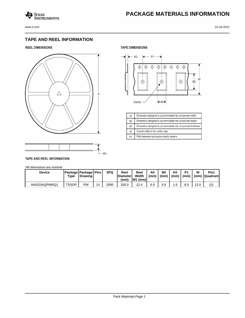
INA203AQPWRQ1 TSSOP PW 14 2000 330.0 12.4 6.9 5.6 1.6 8.0 12.0 Q1
PACKAGE MATERIALS INFORMATION
www.ti.com 14-Jul-2012
Pack Materials-Page 1
*All dimensions are nominal
Device Package Type Package Drawing Pins SPQ Length (mm) Width (mm) Height (mm)
INA203AQPWRQ1 TSSOP PW 14 2000 367.0 367.0 35.0
PACKAGE MATERIALS INFORMATION
www.ti.com 14-Jul-2012
Pack Materials-Page 2
IMPORTANT NOTICE
Texas Instruments Incorporated and its subsidiaries (TI) reserve the right to make corrections, enhancements, improvements and otherchanges to its semiconductor products and services per JESD46C and to discontinue any product or service per JESD48B. Buyers shouldobtain the latest relevant information before placing orders and should verify that such information is current and complete. Allsemiconductor products (also referred to herein as “components”) are sold subject to TI’s terms and conditions of sale supplied at the timeof order acknowledgment.
TI warrants performance of its components to the specifications applicable at the time of sale, in accordance with the warranty in TI’s termsand conditions of sale of semiconductor products. Testing and other quality control techniques are used to the extent TI deems necessaryto support this warranty. Except where mandated by applicable law, testing of all parameters of each component is not necessarilyperformed.
TI assumes no liability for applications assistance or the design of Buyers’ products. Buyers are responsible for their products andapplications using TI components. To minimize the risks associated with Buyers’ products and applications, Buyers should provideadequate design and operating safeguards.
TI does not warrant or represent that any license, either express or implied, is granted under any patent right, copyright, mask work right, orother intellectual property right relating to any combination, machine, or process in which TI components or services are used. Informationpublished by TI regarding third-party products or services does not constitute a license to use such products or services or a warranty orendorsement thereof. Use of such information may require a license from a third party under the patents or other intellectual property of thethird party, or a license from TI under the patents or other intellectual property of TI.
Reproduction of significant portions of TI information in TI data books or data sheets is permissible only if reproduction is without alterationand is accompanied by all associated warranties, conditions, limitations, and notices. TI is not responsible or liable for such altereddocumentation. Information of third parties may be subject to additional restrictions.
Resale of TI components or services with statements different from or beyond the parameters stated by TI for that component or servicevoids all express and any implied warranties for the associated TI component or service and is an unfair and deceptive business practice.TI is not responsible or liable for any such statements.
Buyer acknowledges and agrees that it is solely responsible for compliance with all legal, regulatory and safety-related requirementsconcerning its products, and any use of TI components in its applications, notwithstanding any applications-related information or supportthat may be provided by TI. Buyer represents and agrees that it has all the necessary expertise to create and implement safeguards whichanticipate dangerous consequences of failures, monitor failures and their consequences, lessen the likelihood of failures that might causeharm and take appropriate remedial actions. Buyer will fully indemnify TI and its representatives against any damages arising out of the useof any TI components in safety-critical applications.
In some cases, TI components may be promoted specifically to facilitate safety-related applications. With such components, TI’s goal is tohelp enable customers to design and create their own end-product solutions that meet applicable functional safety standards andrequirements. Nonetheless, such components are subject to these terms.
No TI components are authorized for use in FDA Class III (or similar life-critical medical equipment) unless authorized officers of the partieshave executed a special agreement specifically governing such use.
Only those TI components which TI has specifically designated as military grade or “enhanced plastic” are designed and intended for use inmilitary/aerospace applications or environments. Buyer acknowledges and agrees that any military or aerospace use of TI componentswhich have not been so designated is solely at the Buyer's risk, and that Buyer is solely responsible for compliance with all legal andregulatory requirements in connection with such use.
TI has specifically designated certain components which meet ISO/TS16949 requirements, mainly for automotive use. Components whichhave not been so designated are neither designed nor intended for automotive use; and TI will not be responsible for any failure of suchcomponents to meet such requirements.
Products Applications
Audio www.ti.com/audio Automotive and Transportation www.ti.com/automotive
Amplifiers amplifier.ti.com Communications and Telecom www.ti.com/communications
Data Converters dataconverter.ti.com Computers and Peripherals www.ti.com/computers
DLP® Products www.dlp.com Consumer Electronics www.ti.com/consumer-apps
DSP dsp.ti.com Energy and Lighting www.ti.com/energy
Clocks and Timers www.ti.com/clocks Industrial www.ti.com/industrial
Interface interface.ti.com Medical www.ti.com/medical
Logic logic.ti.com Security www.ti.com/security
Power Mgmt power.ti.com Space, Avionics and Defense www.ti.com/space-avionics-defense
Microcontrollers microcontroller.ti.com Video and Imaging www.ti.com/video
RFID www.ti-rfid.com
OMAP Mobile Processors www.ti.com/omap TI E2E Community e2e.ti.com
Wireless Connectivity www.ti.com/wirelessconnectivity
Mailing Address: Texas Instruments, Post Office Box 655303, Dallas, Texas 75265Copyright © 2012, Texas Instruments Incorporated
Mouser Electronics
Authorized Distributor
Click to View Pricing, Inventory, Delivery & Lifecycle Information: Texas Instruments:
INA203AQPWRQ1