\u003ctitle\u003eimplementation of silicon-validated variability analysis and optimization for...
TRANSCRIPT
Implementation of Silicon-Validated Variability Analysis and
Optimization for Standard Cell Libraries
Raphael Bingert1, Alain Aurand
1, Jean-Claude Marin
1, Eric Balossier
1, Thierry Devoivre
1, Yorick
Trouiller1, Florent Vautrin
1,
Nishath Verghese2, Richard Rouse
2, Michel Cote
2, Philippe Hurat
2
1STMicroelectronics, 850 rue J. Monnet, 38926 Crolles, France
2Cadence Design Systems, Inc., 2655 Seely Ave. San Jose, CA 95134, USA
ABSTRACT
Leveraging silicon validation, a model-based variability analysis has been implemented to detect sensitivity to systematic
variations in standard cell libraries using a model-based solution, to reduce performance spread at the cell level and chip
level. First, a simulation methodology to predict changes in circuit characteristics due to systematic lithography and etch
effects is described and validated in silicon. This methodology relies on these two foundations: 1) A physical shape
model predicts contours from drawn layout; 2) An electrical device model, which captures narrow width effects,
accurately reproduces drive currents of transistors based on silicon contours. The electrical model, combined with
accurate lithographic contour simulation, is used to account for systematic variations due to optical proximity effects and
to update an existing circuit netlist to give accurate delay and leakage calculations.
After a thorough validation, the contour-based simulation is used at the cell level to analyze and reduce the sensitivity of
standard cells to their layout context. Using a random context generation, the contour-based simulation is applied to each
cell of the library across multiple contexts and litho process conditions, identifying systematic shape variations due to
proximity effects and process variations and determining their impact on cell delay.
This methodology is used in the flow of cell library design to identify cells with high sensitivity to proximity effects and
consequently, large variation in delay and leakage. The contour-based circuit netlist can also be used to perform accurate
contour-based cell characterization and provide more silicon-accurate timing in the chip-design flow. A cell-variability
index (CVI) can also be derived from the cell-level analysis to provide valuable information to chip-level design
optimization tools to reduce overall variability and performance spread of integrated circuits at 65nm and below.
INTRODUCTION
Starting at 65nm, design variability increases due to lithography effects, and requires new modeling techniques to cope
with these effects during design. Because device sizes to be printed on silicon are well below the wavelength of light
used to pattern them, the 2D lithography shape effects impact transistor shapes and their electrical characteristics such as
delay and leakage. Delay and leakage characterization of circuits such as standard cells, which were typically done on
drawn layout, are no longer accurate if they do not take into account the shape variation due to lithography proximity
effects. These effects, which have a range of influence of a micron, create shape variations across standard cell
boundaries that translate into context-dependent timing variations. Current timing extraction and cell characterization
methods based on drawn layout and rules are inaccurate because they do not capture the complex 2D proximity effects
and cannot efficiently take into account context-dependent timing variations. This results in potential silicon failures due
to inaccurate timing analysis and over-design due to excessive margins.
This paper describes the development and validation of silicon-contour-based variability analysis, and the use of this
methodology by standard cell library designers to optimize the quality of the cells, and provide valuable variability
information to chip designers to reduce the sensitivity of critical paths to systematic variations. The method proposed
consists of first simulating the silicon shape from drawn design, predicting the current of the transistor from these silicon
shapes, extracting transistor parameters corresponding to this drawn current and performing timing analysis based on
silicon contours.
Design for Manufacturability through Design-Process Integration II, edited by Vivek K. Singh, Michael L. Rieger, Proc. of SPIE Vol. 6925, 69250M, (2008) · 0277-786X/08/$18 · doi: 10.1117/12.772897
Proc. of SPIE Vol. 6925 69250M-12008 SPIE Digital Library -- Subscriber Archive Copy

PREDICTIVE SHAPE SIMULATION
The shape effects for poly gates and diffusion are predicted with the Cadence Litho Physical Analyzer (LPA) tool. This
tool uses the InShape model, which captures the entire RET/OPC manufacturing flow of the ST process in a fast,
accurate and secure formulation. LPA uses this model to determine silicon contours for shapes drawn on diffusion and
poly layers, as shown in Fig 1 [1]. The InShape model characterizes process printing performance and predicts the
impact of RET, OPC, litho, etch and mask effects on design shapes (that is, drawn GDSII). Unlike lithography
simulation models that only capture the behavior of the lithography system, LPA has the ability to model the entire
RET/OPC manufacturing process, including the retargeting, assist-feature, PSM, OPC, lithography and etch effects
specific to the Crolles2 manufacturing facility. Solutions based on OPC and litho simulation come with the traditional
drawbacks of OPC in terms of runtime, data explosion and complexity. These solutions do not meet the criteria for
designers who require solutions that can be easily deployed in their computing environment and their design flows and
that meet their schedule requirements in terms of runtime.
The unique formulation of the InShape model predicts the final printed contours directly from drawn layout in a single
optimized step. In this approach, first litho or etch models are developed using litho information (NA, sigma,
wavelength, and so on) and measurements from either silicon measurements or from contours created with production
litho simulators. The InShape models developed for ST processes at 65nm and 45nm include resist and etch effects
across the target process window. The process window typically includes a total of nine process points, including three
defocus and three exposure points, but other variations such as mask biasing effects can also be included. Etch or other
effects can be modeled on top of the resist contours using table-based biasing, or directly by creating an etch model.
Next, information from the production flow, such as retargeting and scattering-bars, is used to capture the non-linear
effects of these RET techniques. Finally, the litho/etch model, RET and OPC information of the ST process are
combined within LPA’s proprietary formulation in order to produce contours directly from design database in a fraction
of the time used by traditional techniques and with comparable accuracy. Once this model has been established,
designers can apply this model with the LPA tool to simulate their design databases at a cell block or full chip level to
accurately predict the silicon contours across the process window. The InShape model is fast enough to enable
simulation across process windows on multiple cells in minutes, and a full design in hours.
Figure 1 shows the silicon contour prediction using the InShape model at different process points (focus, exposure) of
poly and active layers on the ST 65nm process and its correlation to an SEM image of the resulting silicon.
Figure 1: Transistor contour simulation across process window for the ST 65nm process and its correlation to silicon
The aforementioned technique was also used to create ST’s 45nm InShape models for poly and active. The accuracy was
then checked by comparing the contours created with the InShape models and contours created with the production flow.
This validation was done for all nine process points, which included +/- 100nm defocus effects and +/-4% exposure
effect, which is typical for an immersion lithography process.
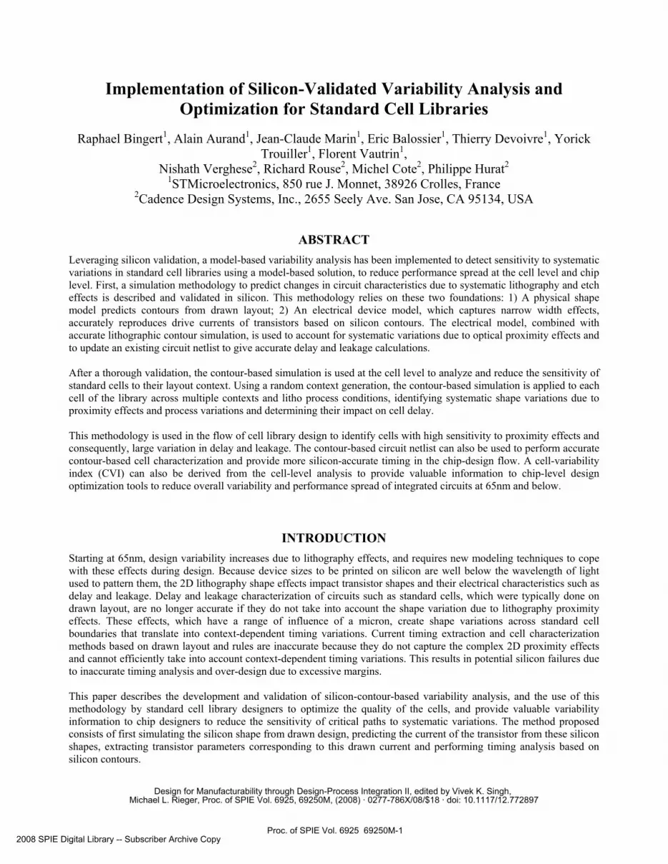
The average percent difference in critical dimension (CD) on transistor gates was measured using gauges placed every
10nm across the gate, as shown in Figure 2(a). The standard deviation for the simulation of resist contours at nominal
with a min/max of less than 5% was 0.39% on active and 0.70% for poly, as shown in Figure 2(b). The standard
deviation for the etch contours across the process window was less than 0.5% for active and less than 1.5% for poly with
a min/max of less than 7% as shown in Figure 2(c). The CD error is expressed as a percent relative to the width of the
Proc. of SPIE Vol. 6925 69250M-2
transistor. Since the post-etch target CD is 45nm, a standard deviation of 0.5% translates into 0.2nm and a min-max of
7% translates into less than 3nm. Note that these predictions are measured with contours created from drawn layout and
not from post-OPC layout. This represents the real final accuracy of the InShape models in predicting contours from
drawn shapes.
Figure 2: (a) Measurement gauges (b) Active 45nm nominal accuracy report (c) Poly 45nm nominal accuracy report
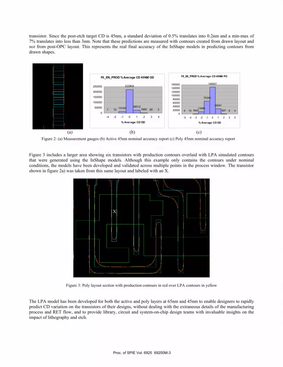
Figure 3 includes a larger area showing six transistors with production contours overlaid with LPA simulated contours
that were generated using the InShape models. Although this example only contains the contours under nominal
conditions, the models have been developed and validated across multiple points in the process window. The transistor
shown in figure 2a) was taken from this same layout and labeled with an X.
Figure 3: Poly layout section with production contours in red over LPA contours in yellow
The LPA model has been developed for both the active and poly layers at 65nm and 45nm to enable designers to rapidly
predict CD variation on the transistors of their designs, without dealing with the extraneous details of the manufacturing
process and RET flow, and to provide library, circuit and system-on-chip design teams with invaluable insights on the
impact of lithography and etch.
F0_EN_PROD % Average CD 45NM OD
1 1013145
222804
285121660 85 3
0
50000
100000
150000
200000
250000
-4 -2 -1 0 1 2 3 4
% Average CD OD
F0_E0_PROD % Average CD 45NM PO
4 15 164313486
70340
146507
28091
827 6 4
0
20000
40000
60000
80000
100000
120000
140000
160000
-5 -4 -3 -2 -1 0 1 2 3 5
% Average CD OD
(a) (b) (c)
X
Proc. of SPIE Vol. 6925 69250M-3
CONTOUR-BASED TRANSISTOR EXTRACTION
Designers are particularly interested in finding the impact of lithography variation on the design’s electrical performance,
because silicon systematic shape variation due to litho, etch and misalignment effects, as shown in Fig. 1, can lead to
changes in the drive current of a transistor, which must be predicted for accurate circuit simulation. The Cadence Litho
Electrical Analyzer (LEA) tool is a contour-based extraction methodology based on the Cadence current density-based
model (CCDM) [2, 3] to predict the drawn current of the transistors from contours. Since diffusion geometries can be
within 2x of the gate length, it is important to include narrow width effects when calculating currents of these transistors.
These effects can have a significant impact on device currents, with narrow width drive currents differing by up to 30%,
and off currents by more than 200% compared to long width devices. CCDM uses an accurate model of the current
density through the device width, and detailed knowledge of the device shape, to predict currents for 2D transistor shapes
with accurate comparison to silicon measurements.
To account for spatial variations in the device, a method is utilized that represents these spatial variations using
equivalent netlist parameters, Channel Length (Lnew), Transistor Width (Wnew), Area of Drain (ADnew), and Area of
Source (ASnew). These parameters are computed as equivalent changes to the device’s nominal parameters, L’, W’, AD’
and AS’, as shown below:
Lnew = L’ + ∆L
Wnew = W’ + ∆W
ADnew = AD’ + ∆AD
ASnew = AS’ + ∆AS (1)
In corner-based timing approaches, delays are computed for each timing corner corresponding to a combination of
process voltage and temperature conditions. The changes to length, width, drain area and source area parameters, ∆L, ∆W, ∆AD and ∆AS respectively, are calculated so as to preserve the correct behavior of the device (Ion for delay or Ioff
for leakage) under a particular corner condition. For each corner condition, the silicon-contour based transistor modeling
and parameter extraction is applied to each transistor in the context of the design to calculate the ∆L, ∆W, ∆AD and ∆AS
that gives the correct Ion when doing silicon-contour based timing analysis, or the correct Ioff when doing silicon-contour
based leakage analysis.
65NM AND 45NM VALIDATION
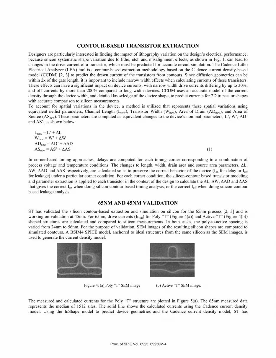
ST has validated the silicon contour-based extraction and simulation on silicon for the 65nm process [2, 3] and is
working on validation at 45nm. For 65nm, drive currents (Idsat) for Poly “T” (Figure 4(a)) and Active “T” (Figure 4(b))
shaped structures are calculated and compared to silicon measurements. In both cases, the poly-to-active spacing is
varied from 24nm to 56nm. For the purpose of validation, SEM images of the resulting silicon shapes are compared to
simulated contours. A BSIM4 SPICE model, anchored to ideal structures from the same silicon as the SEM images, is
used to generate the current density model.
Figure 4: (a) Poly “T” SEM image (b) Active “T” SEM image.
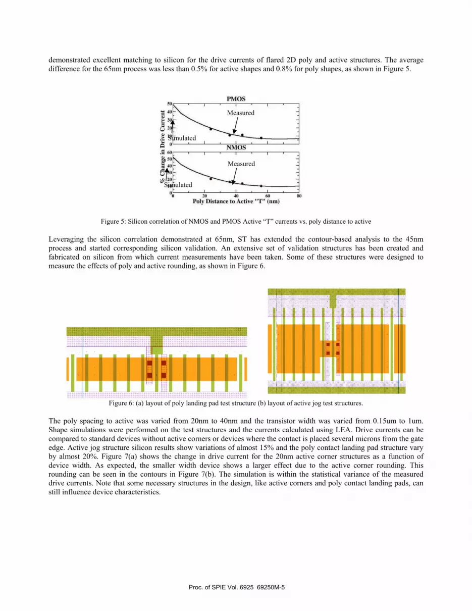
The measured and calculated currents for the Poly “T” structure are plotted in Figure 5(a). The 65nm measured data
represents the median of 1512 sites. The solid line shows the calculated currents using the Cadence current density
model. Using the InShape model to predict device geometries and the Cadence current density model, ST has
Proc. of SPIE Vol. 6925 69250M-4
20 41) 60
Poly Distance to Active "T" (nm)
PMOS
NMOS.E o
50
4o20
10
demonstrated excellent matching to silicon for the drive currents of flared 2D poly and active structures. The average
difference for the 65nm process was less than 0.5% for active shapes and 0.8% for poly shapes, as shown in Figure 5.
Figure 5: Silicon correlation of NMOS and PMOS Active “T” currents vs. poly distance to active
Leveraging the silicon correlation demonstrated at 65nm, ST has extended the contour-based analysis to the 45nm
process and started corresponding silicon validation. An extensive set of validation structures has been created and
fabricated on silicon from which current measurements have been taken. Some of these structures were designed to
measure the effects of poly and active rounding, as shown in Figure 6.
Figure 6: (a) layout of poly landing pad test structure (b) layout of active jog test structures.
The poly spacing to active was varied from 20nm to 40nm and the transistor width was varied from 0.15um to 1um.
Shape simulations were performed on the test structures and the currents calculated using LEA. Drive currents can be
compared to standard devices without active corners or devices where the contact is placed several microns from the gate
edge. Active jog structure silicon results show variations of almost 15% and the poly contact landing pad structure vary
by almost 20%. Figure 7(a) shows the change in drive current for the 20nm active corner structures as a function of
device width. As expected, the smaller width device shows a larger effect due to the active corner rounding. This
rounding can be seen in the contours in Figure 7(b). The simulation is within the statistical variance of the measured
drive currents. Note that some necessary structures in the design, like active corners and poly contact landing pads, can
still influence device characteristics.
Measured
Measured
Simulated
Simulated
Proc. of SPIE Vol. 6925 69250M-5

Figure 7: (a) Change in drive current vs. device width (b) Litho contours of active jog test structures.
45NM STANDARD CELL VARIABILITY ANALYSIS
Variability analysis is done with two different intents: to quantify the context sensitivity and to quantify the effect of
process variations.
Figure 8: Example of contours on a 45nm cell
Library context sensitivity analysis using LEA consists of creating random contexts for each standard cell under analysis.
The random contexts are created with other cells in the library. Controls are provided to the designer to independently
analyze the sensitivity to horizontal (left and right) and vertical (top and bottom) contexts. Then the contour-based
0. 1
5
0. 3
0. 6
0.00%
2.00%
4.00%
6.00%
8.00%
10.00%
12.00%
14.00%
Device Width
% C
han
ge
in
Dri
ve
Cu
rre
nt
Measure
Simulation
Proc. of SPIE Vol. 6925 69250M-6
Ella View Query
p_u_LB_n • T—aT . .y ts
EJSL
-Characterization data [Loading Data 100%]-
cnntentn deltal hrninglleakagel cnnntraintlC
Data Pint
-Current
ho-I 40.140 20-I01L20 11111111111
LaP change [nm[ Weif change
¼
Mg 00.000 t 00.000 t .300 2.700 t .Ot 2 t .000 3.000 -6.t 00 -t .700 -h.dt 0 0.000 2.3t 6
MO 00.000 070.000 0.000 t .000 t .030 t .300 3.000 -0.600 -0.300 -0.060 t .300 0.dhtMt 00.000 ht 0.000 0.300 t .300 0.626 t .000 2.000 -0.200 t .000 0.003 t .600 0.t Oh
MS 00000 070000 0000 thOU 0600 t tOO 2700 -0300 0000 -0063 0700 0t23
I—
-0
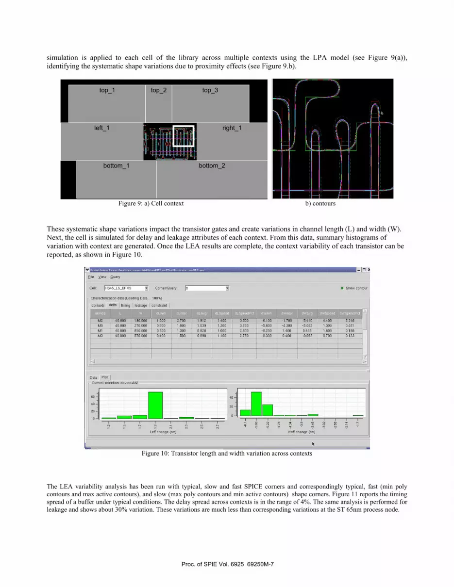
simulation is applied to each cell of the library across multiple contexts using the LPA model (see Figure 9(a)),
identifying the systematic shape variations due to proximity effects (see Figure 9.b).
Figure 9: a) Cell context b) contours
These systematic shape variations impact the transistor gates and create variations in channel length (L) and width (W).
Next, the cell is simulated for delay and leakage attributes of each context. From this data, summary histograms of
variation with context are generated. Once the LEA results are complete, the context variability of each transistor can be
reported, as shown in Figure 10.
Figure 10: Transistor length and width variation across contexts
The LEA variability analysis has been run with typical, slow and fast SPICE corners and correspondingly typical, fast (min poly
contours and max active contours), and slow (max poly contours and min active contours) shape corners. Figure 11 reports the timing
spread of a buffer under typical conditions. The delay spread across contexts is in the range of 4%. The same analysis is performed for
leakage and shows about 30% variation. These variations are much less than corresponding variations at the ST 65nm process node.
top_1 top_3 top_2
left_1
bottom_1 bottom_2
right_1
Proc. of SPIE Vol. 6925 69250M-7
•!-
H I
Figure 11: Timing and leakage spread of a buffer cell across multiple contexts at typical conditions
The designer can also run variability analysis across the process window with LEA. Since it is based on the TCL language, a designer
can write scripts in LEA to automate multi-corner process window analysis. A good illustration of these capabilities is the following
script that runs analysis across multiple points of the process window (F0_E0 F0_EP FP_EN), for both poly and active with
multiple misalignment (-20, 0 and +20nm) between poly and active layers, in both X and Y directions. The shape corner and the
misalignment can each be changed dynamically in the analysis. The characterize_cell_context command extracts the transistor
parameters from the simulated contours, creates an extracted netlist and simulates the timing, leakage, timing sensitivities and timing
constraints for the cell. The following examples illustrate the use of timing sensitivities.
#Variability analysis script for 81 process and misalignment conditions # set POppNames {F0_E0 F0_EP FP_EN} set ODppNames {F0_E0 F0_EN FN_EP} set OL {N20n 0 20n} foreach polyPW $POppNames { foreach diffPW $ODppNames { foreach xOL $OL { foreach yOL $OL { open_db $work_dir/ST45_pw set CORNER "$spiceCorner\_$polyPW\_$diffPW\_$xOL\_$yOL" if {$xOL == "N20n"} then {set xOL "-20n"} if {$yOL == "N20n"} then {set yOL "-20n"} set_gate_misalignment -x $xOL -y $yOL set_shape_corner -per_layer " PO $polyPW OD $diffPW " characterize_cell_context \ -cell_list_file ./spieCell.txt \ -create_spice –sensitivity -constraints\ -corner typ append queryCorners "$CORNER " } } } }
Analyzing the 28 transistors of an XNOR cell in one context with LEA, we find that each transistor is not equally
sensitive to process window and misalignment conditions. The spread of the channel width though process conditions for
each of the 28 transistors ranges from 3.2% to 13%, as shown in Figure 12.
Proc. of SPIE Vol. 6925 69250M-8

—H"Elle View Query
Cell: HO4OLOXNOR3X4Corner/Query: IAII
-Characterization data [Loading Data ... 10'
F 000w contour
cooteatu deOul Orninolleakagel coontrainti =M06 00.000 170.000 -1.600 7.600 0.376 0.000 03.000 -6.000 1 0.700 0.606 00.700 13.303M03 00.000 100.000 -0.000 6.700 3.001 0.600 00.000 -11.300 0.000 -0.633 10.000 10.333MO 00.000 000.000 0.700 0.000 0.060 7.700 10.000 -7.000 13.300 0.000 00.300 0.007
MOO 00.000 100.000 -1.000 7.000 0.600 0.000 03.000 -10.000 3.000 -0.01 1 1 3.000 0.033
MOO 00.000 100.000 -0.000 7.000 0.01 0 0.000 00.700 -0.000 3.300 -0.167 13.000 6.600
Ml 6 00.000 100.000 -1.000 7.000 0.063 0.000 03.000 -0.000 3.300 -0.167 13.000 6.600
MiS 00.000 100.000 -1.100 6.000 0.603 0.100 00.700 -0.000 3.300 -0.167 13.000 6.600
Mat 00.000 100.000 -1.000 7.000 0.067 0.000 00.000 -0.000 3.300 -0.167 13.000 6.600
Ml 7 00.000 100.000 -0.000 6.000 3.360 6.000 00.000 -0.000 3.300 -0.167 13.000 6.600
Ml 0 00.000 100.000 1.300 6.000 0.076 7.000 16.000 -10.100 3.100 -0.076 13.000 6.600
MO 00.000 000.000 -0.000 6.100 3.077 6.000 01.000 -6.000 10.000 0.667 17.300 6.600
Ml 6 00.000 100.000 -1.300 7.000 0.000 6.600 00.000 -0.600 3.300 -0.000 10.000 6.600
M6 00.000 000.000 -0.000 7.000 1.606 0.000 03.000 -0.000 11.000 -0.067 00.000 6.000
Mid 00.000 100.000 0.100 6.000 3.607 6.100 00.000 -0.000 3.000 -0.000 10.700 6.067
MOd 00.000 170.000 -0.700 6.000 3.000 0.000 03.000 -6.000 0.000 -0.660 13.300 7.600
Ml 00.000 000.000 -0.300 6.300 3.611 6.600 01.000 -6.000 6.000 -1.000 1 0.000 7.000
Ml 1 00.000 000.000 -0.100 7.100 0.063 0.000 03.000 -6.600 10.000 0.033 17.300 7.006
MOO 00.000 170.000 -0.300 6.000 1.606 6.600 00.000 -7.000 3.700 -1.067 11.600 6.600
Ml 0 00.000 000.000 -0.000 6.000 0.037 0.000 00.000 -6.000 0.300 -0.100 10.100 6.000
MO 00.000 000.000 -0.000 7.100 1.036 0.300 03.000 -0.000 6.000 -0.100 10.100 6.000
Ml 0 00.000 000.000 -1.600 0.000 0.033 10.100 00.000 -0.000 0.100 0.600 1 0.000 0.033
M3 00.000 000.000 -1.000 6.000 0.107 0.700 01.700 -6.000 3.000 -0.600 10.000 0.100
MO 00.000 000.000 -3.300 6.000 0.070 0.300 03.000 -7.700 0.300 -1.000 10.000 0.000
Md 00.000 000.000 -1.000 7.000 0.310 0.000 03.000 -6.000 3.000 -0.070 0.000 0.000
M7 00.000 000.000 -1.000 7.300 0.170 0.000 03.000 -6.000 0.600 -0.ddd 11.000 0.700
MO 00.000 000.000 -1.600 7.100 0.000 0.700 01.700 -7.000 0.300 -0.000 11.300 0.700
M07 00.000 000.000 -1.000 0.000 3.001 0.000 00.000 -0.000 3.600 -1.700 10.600 0.300
Ml 3 00.000 010.000 -1.100 0.000 3.070 0.100 00.700 -0.600 3.000 -1.700 1 3.000 3.060 7
dWOpeadpct
Elle View Query
Cell: 1H040_L0_4N06344 Corner/Query: 1411• Show contour
-C huructerizution dote [Loudin 8 Cute ... t hh%]
conteetu deltel hrninglleekegel conutreintiIM26 4h.hhh t 70.000 -t .600 7.6hh 2.37h 8.222 23.000 -h.hhh t 4.7hh 2.hh6 22.7hh t 3.3h3M23 4h.hhh t hh.hhh -0.800 h.7hh 3.22t 8.622 24.000 -t t .Shh 4.2hh -2.h33 t h.hhh t h.333MO 4h.hhh 220.000 h.7hh h.4hh 4.264 7.7hh t 8.280 -7.hhh t 3.Shh 2.hhh 2h.Shh 8.227
M22 4h.hhh t hh.hhh -t .4hh 7.600 2.688 8.200 23.hhh -t 0.200 3.2hh -2.4t t t 3.4hh 6.833
M20 4h.hhh t hh.hhh -2.000 7.800 2.4th 8.800 24.780 -8.800 3.300 -2.t 67 t 3.200 h.hhh
Mt h 40.000 t 80.000 -t .800 7.800 2.463 8.422 23.800 -8.822 3.322 -2.t 67 t 3.200 6.600
Mt 8 42.222 t h2.222 -t .t 22 h.222 2.683 8.t 22 22.780 -8.800 3.300 -2.t 67 t 3.200 h.h22
MSt 42.222 t 82.222 -t .822 7.800 2.467 8.222 22.822 -8.822 3.300 -2.t 67 t 3.200 6.622flU OOO OO fi fi fi 22.282 OO fi fl7 OO 6.622 /—
Cute Plot
-Current nele080w
20 —
to —
0— Lw En DEEDED11111111111Leffchenge[nm[
J
Figure 12: Channel width spread of the 28 transistors of that cell across 81 process and misalignment conditions
Figure 13: Transistor variation across 81 process and misalignment variations
Proc. of SPIE Vol. 6925 69250M-9
—Elle View LFA Utility
l',l—lyrl _______ __________///////////////////////////4yyyyy///
cell: ItULUUNOR3U4
corner/query. if
Ix'
wyenconif:
inputiflew:
cloeif:
contentiif
A
U
U66.667
3.UUU
JAM
JAM
JAM
Upifete TeUle
Oifjecte I Lu/em I
Object JJrecede J Jetc F Fcell F FFeet F FPie F FUeem F FNet F F
Men F FMere F FTect J
'+ + ><
S o'ILJ
/HU4NLUUNONUU4J0p I
- Welcome to CeMence Lityo Anelyzer Viewer t .U.U I 6.U3N3 U.UUNU ICLAV t .U
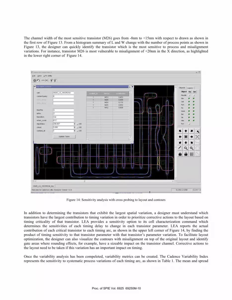
The channel width of the most sensitive transistor (M26) goes from -8nm to +15nm with respect to drawn as shown in
the first row of Figure 13. From a histogram summary of L and W change with the number of process points as shown in
Figure 13, the designer can quickly identify the transistor which is the most sensitive to process and misalignment
variations. For instance, transistor M26 is most vulnerable to misalignment of +20nm in the X direction, as highlighted
in the lower right corner of Figure 14.
Figure 14: Sensitivity analysis with cross probing to layout and contours
In addition to determining the transistors that exhibit the largest spatial variation, a designer must understand which
transistors have the largest contribution to timing variation in order to prioritize corrective actions to the layout based on
timing criticality of that transistor. LEA provides a sensitivity option to its cell characterization command which
determines the sensitivities of each timing delay to change in each transistor parameter. LEA reports the actual
contribution of each critical transistor to each timing arc, as shown in the upper left corner of Figure 14, by finding the
product of timing sensitivity to that transistor parameter with that transistor’s parameter variation. To facilitate layout
optimization, the designer can also visualize the contours with misalignment on top of the original layout and identify
gate areas where rounding effects, for example, have a sizeable impact on the transistor channel. Corrective actions to
the layout need to be taken if this variation has an important impact on timing.
Once the variability analysis has been compeleted, variability metrics can be created. The Cadence Variability Index
represents the sensitivity to systematic process variations of each timing arc, as shown in Table 1. The mean and spread
Proc. of SPIE Vol. 6925 69250M-10
of the histogram are used to derive the variability index such that the higher the index, the more robust a cell is to
systematic variability. As shown in Table 1, not all arcs have the same sensitivity to systematic variations. The
variability index for each cell offers a mechanism to compare and contrast the relative robustness of different cell types
or of different cell layouts of the same type to systematic process variation and context. Such an index is then utilized by
place-and-route tools to direct placement of cells in timing-critical areas of the design. Table 1 shows the CVI metric for
each timing arc of a 3-input NOR gate with inputs A, B, and C and output Z. For each input-output arc (such as A->Z),
the different side input conditions (such as B, C), and the rise/fall transition on the output can result in a different arc
delay and therefore a different variability index. During chip implementation, the appropriate index is selected at the cell
placement stage to ensure that timing criticality is not impacted by the use of a highly variable cell in a critical path [4].
HS45_LS_XNOR3X4, All, Z, A, , fall, B'*C, 0.01314 HS45_LS_XNOR3X4, All, Z, A, , fall, B'*C', 0.009035 HS45_LS_XNOR3X4, All, Z, A, , fall, B*C, 0.0095 HS45_LS_XNOR3X4, All, Z, A, , fall, B*C', 0.0118 HS45_LS_XNOR3X4, All, Z, A, , rise, B'*C, 0.009252 HS45_LS_XNOR3X4, All, Z, A, , rise, B'*C', 0.01409 HS45_LS_XNOR3X4, All, Z, A, , rise, B*C, 0.01406 HS45_LS_XNOR3X4, All, Z, A, , rise, B*C', 0.008468 HS45_LS_XNOR3X4, All, Z, B, , fall, A'*C, 0.3063 HS45_LS_XNOR3X4, All, Z, B, , fall, A'*C', 0.2774 HS45_LS_XNOR3X4, All, Z, B, , fall, A*C, 0.2777 HS45_LS_XNOR3X4, All, Z, B, , fall, A*C', 0.2905 HS45_LS_XNOR3X4, All, Z, B, , rise, A'*C, 0.2791 HS45_LS_XNOR3X4, All, Z, B, , rise, A'*C', 0.2987 HS45_LS_XNOR3X4, All, Z, B, , rise, A*C, 0.3017 HS45_LS_XNOR3X4, All, Z, B, , rise, A*C', 0.2874 HS45_LS_XNOR3X4, All, Z, C, , fall, A'*B, 0.2958 HS45_LS_XNOR3X4, All, Z, C, , fall, A'*B', 0.2867 HS45_LS_XNOR3X4, All, Z, C, , fall, A*B, 0.2791 HS45_LS_XNOR3X4, All, Z, C, , fall, A*B', 0.294 HS45_LS_XNOR3X4, All, Z, C, , rise, A'*B, 0.2922 HS45_LS_XNOR3X4, All, Z, C, , rise, A'*B', 0.2899 HS45_LS_XNOR3X4, All, Z, C, , rise, A*B, 0.2955 HS45_LS_XNOR3X4, All, Z, C, , rise, A*B', 0.2938
Table 1: Cadence Variability Index of HS45_LS_XNOR3X4 cell
SUMMARY
A model-based variability analysis has been implemented to detect sensitivity of standard cell libraries to systematic
variations using a model-based solution. A simulation methodology to predict changes in circuit characteristics due to
systematic lithography and etch effects was described and validated in silicon. Comparison to silicon drive current
measurements of Poly T and Active T structures on the ST 65nm process show excellent correlation, with an average
difference of less than 0.5% for active shapes and 0.8% for poly shapes. Similar validation for 45nm is on-going. The
contour-based extraction methodology was used to analyze the variability of standard cells. The context sensitivity
analysis methodology was described and used to analyze cell architecture at 65 and 45nm.The 45nm architecture was
found to be relatively resistant to context-induced variations. An analysis of the sensitivity of cells to litho and
misalignment conditions was conducted and it was found that some topologies actually create significant transistor
channel variations that translate into delay variations. A methodology to prioritize corrective layout action for transistors
that are critical to the delay variation was described. Finally, a variability index can be extracted to drive chip-level
implementation.
Proc. of SPIE Vol. 6925 69250M-11
REFERENCES
1. J. Brandenburg et al., “A Genuine Design For Manufacturing Checker for Integrated Circuit Designers”, SPIE,
2006
2. Thierry Devoivre, Richard Rouse, Nishath Verghese, Philippe Hurat, “Modeling and Validation of Silicon Contour-
Based Extraction and Simulation of Non-Uniform Devices,” CICC, 2007
3. R. Rouse, N. Verghese, B. Lee, G. Han, P. Wang, “A Predictive DFM Simulation Methodology for Systematic
Shape Variations,” CICC, 2007
4. D. Tsien, C.K Wang , Y. Ran, P. Hurat, N. Verghese, “Context-specific leakage and delay analysis of a 65nm
standard cell library for lithography-induced variability” SPIE, 2007
Proc. of SPIE Vol. 6925 69250M-12