study of porous silicon prepared using metal-induced etching (mie): a comparison with laser-induced...
TRANSCRIPT
Comparison of porous silicon prepared using metal -
induced etching (MIE) and laser - induced etching
(LIE)
Shailendra K Saxena1,Vivek Kumar2, Hari M. Rai1, Gayatri
Sahu1,Ravi K. Late1, Kapil Saxena3, A. K. Shukla3, Pankaj R
Sagdeo1,4 and Rajesh Kumar1,4 ‡1Material Research Laboratory, Discipline of Physics, School of Basic Sciences,
Indian Institute of Technology Indore, Madhya Pradesh-452017, India2 Biophysics & Nanoscience Centre, DEB-CNISM, Universita della Tuscia, I-01100
Viterbo, Italy3Department of Physics, Indian Institute of Technology Delhi, Hauz Khas, New Delhi
110016, India4Material Science and Engineering Group, Indian Institute of Technology Indore,
Madhya Pradesh-452017, India
Abstract. Porous silicon (p-Si), prepared by two routes (metal induced etching
(MIE) and laser induced etching (LIE)) have been studied by comparing the surface
morphologies. A uniformly distributed smaller (submicron sized) pores are formed
when MIE technique is used because the pore formation is driven by uniformly
distributed metal (silver in present case) nanoparticles, deposited prior to the
porosification step. Whereas in p-Si samples prepared by LIE technique, wider pores
with some variation in pore size as compared to MIE technique is observed because a
laser having gaussian profile of intensity is used for porosification. Uniformly distribute
well-aligned Si nanowires are observed in samples prepared by MIE method as seen
using cross-sectional SEM imaging, which shows a single photoluminescence (PL) peak
at 1.96 eV corresponding to red emission at room temperature. The single PL peak
confirms the presence of uniform sized nanowires in MIE samples. These vertically
aligned Si nanowires can be used for field emission application.
‡ Corresponding Author: [email protected]
arX
iv:1
403.
6269
v1 [
cond
-mat
.mes
-hal
l] 2
5 M
ar 2
014
2
1. Introduction
Attention received by porous silicon (p-Si) from scientists is known from more than
couple of decades since the discovery of its light emission properties [1,2]. p-Si is still
being studied due to its applications in various fields in addition to optoelectronic devices
[1-7]. Many reports shows applications of p-Si in advanced sensing[8-11], in making
electrodes for batteries [12,13], in carrying out mass spectroscopy [14] in carrying out
mass spectroscopy [15] and in field effect transistors [16, 17]. Different methods to
fabricate p-Si & its various applications/properties have been studied in depth and
very good reports are available [18, 19]. Various techniques used for the formation
of p-Si include strain etching [20, 21] of Si wafer in a solution of HNO 3 & HF acid,
electrochemical etching [22, 23] where an electrical bias is used for porosification of Si
wafer in etching solution of HF acid. A simpler method of photochemical etching also
known as laser induced etching (LIE) was used by Choy and Cheah [24] and later used
by many others [25 - 29]. LIE is mainly used for preparing p-Si in a localized area
on a Si wafer without using an electrical bias. A combination of two techniques (LIE
and electrochemical etching) has also been reported [30, 31] for fabrication of p-Si. All
these methods have certain advantages and disadvantages over each other and are used
depending on the convenience & suitability. LIE method and stain etching method does
not require any bias for making p-Si whereas a bias is needed while using electrochemical
etching. Stain etching is the easiest method to use but is a very slow process and does
not give a ‘reproducible & reliable result [32].
In addition to the above-mentioned techniques, method of metal assisted chemical
etching or metal induced etching (MIE) [3238] is also used for preparing p-Si at faster
rates as compared to stain etching. The MIE technique, in contrast to stain etching
technique, gives good reproducibility in p-Si formation without using any bias or
laser radiation. Moreover, MIE technique does not compromise on the light emitting
properties of p-Si in contrary to that prepared by stain etching. p-Si prepared by LIE
technique, which also is an electrodeless technique like MIE technique, gives visible
photoluminescence (PL) at room temperature similar to the p-Si prepared by MIE.
Light emitting p-Si, fabricated using these two electrodeless techniques of MIE and
LIE, should be studied to investigate the structural difference in resulting p-Si. This
will be helpful in understanding various mechanisms involved in p-Si fabrication and will
enable scientist to explore the application of p-Si beyond the traditional applications. A
comparative study will also provide knowledge to control the pore size & other parameter
to tailor different properties of p-Si.
Though the basic p-Si fabrication mechanism is the same in LIE and MIE process
(dissolution of Si atoms from Si wafer as a result of reaction with HF acid), there are
some similarities and dissimilarities between the two processes and can be summarized
as follows. In the LIE method, n-type crystalline Si substrate, while dipped in HF
acid solution, is irradiated with laser light thereby creating excess photoexcited holes
on the irradiated surface. These holes initiate the etching process [29] and result in the
3
formation of p-Si that contains Si nanostructures. On the other hand in MIE, first metal
nano particles are grown on Si wafer surface before the Si wafer is immersed in etchant
solution (HF + H2O2). Detailed mechanism of pore formation in LIE and MIE have
been reported in literature [29, 33] but a comparative study of pore formation using
both of these techniques is not available and is the theme of present paper.
Aim of this paper is to present basic properties of p-Si fabricated using MIE
technique and compare its morphological and PL properties with those of p-Si prepared
by LIE technique earlier [29]. A comparison of pore size is presented using scanning
electron microscopy (SEM) with explanation for the existing difference in pore size
in samples prepared using the two techniques. A cross- (X-) sectional SEM, done
to investigate the pore growth process shows submicron sized pore formation in MIE
samples. A uniformly distributed, well-aligned Si nano wire like structures are seen
from which a possibility of visible light emission has also been investigated using PL
spectroscopy.
2. Experimental details
p-Si samples have been prepared using above-mentioned two techniques namely LIE
and MIE. The LIE samples were prepared from commercially available wafers of n-
Si(100) having resistivity of 35 Ω cm. These wafers were cleaned in acetone and ethanol
to remove impurities prior to starting the porosification process. Mounted on two teflon
plates, these wafers were immersed in the HF acid (40 %) in a plastic container. The
LIE [27, 29] was performed by using an argon ion laser beam (photon energy of 2.41
eV) focused onto the Si wafer with laser power density of 1.76 kW/cm2. Two samples
were prepared by irradiating the wafers for 45 minutes (sample: L45 ) and 60 minutes
(sample: L60 ) with the abovementioned etching laser power density.
The MIE samples were prepared by silver (Ag) -assisted chemical etching of n-Si
(100) wafer. The cleaned wafers (as discussed above) were immersed in HF solution
to remove thin oxide layer formed at surface. These wafers were dipped in solution
containing 4.8 M HF& 5 mM AgNO3 for one minute at room temperature to deposit
Ag nano particles (AgNPs). The AgNPs deposited samples were then kept for etching
in an etching solution containing 4.6 M HF & 0.5 M H2O2 for 45 minutes (sample:
M45) and 60 minutes (sample: M60). Etched wafers were transferred in HNO3 acid to
dissolve Ag metal. Then the samples were dipped into HF solution to remove oxide layer
induced by nitric acid used in above step. Surface morphology of all the four samples
have been characterized using Field-Emission Scanning Electron Microscopy (SEM),
supra55 Zeiss. The PL from MIE sample was recorded with 325 nm laser excitation
source using DongWoo optron 80K PL system at room temperature.
4
3. Results and Discussion
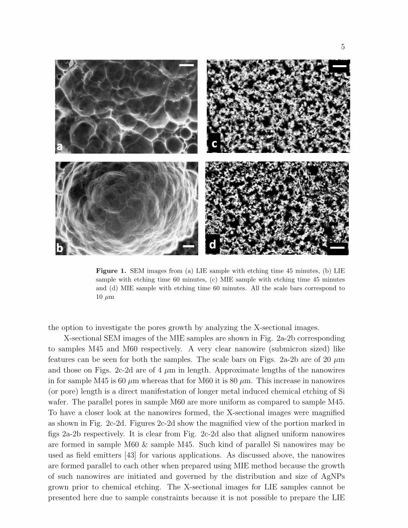
Surface morphologies, observed using SEM, of all the four samples (L45, L60, M45
& M60) have been shown in Fig. 1. Figure 1a and 1b shows SEM images of samples
prepared using LIE technique whereas the SEM images of MIE samples are shown in
Fig. 1c and 1d. The scale bars in Fig. 1a 1d correspond to 10 µm. Porous Si with
pore size of ∼10 µm can be seen in Fig. 1a and 1b corresponding to samples L45 &
L60 respectively. Comparatively wider and connected pores [29] can be seen in Fig. 1b
as compared to Fig. 1a due to increased etching time. For a given laser power density,
when the etching time is increased, more Si atoms gets dissolved in HF solution due
to chemical etching reaction to result in deeper & wider pores. It is important here to
mention that in the absence of laser, etching does not take place and porosification is
not possible. An SEM image of such a control sample is shown in Fig. S1 in the SM.
Effect of etching time and laser power density on LIE process have been studied in detail
and has been reported earlier [27, 29]. On the other hand, Figs.1c and 1d show SEM
images corresponding to MIE samples for etching times of 45 minutes (sample M45)
and 60 minutes (sample M60) respectively. Submicron sized pores are formed in MIE
samples in contrast with wider pores for the case of LIE samples (Fig. 1a-1b). Wider
pores are formed during LIE because porosofication can take place in lateral as well
as vertical direction whereas etching lead by AgNPs during MIE take place faster in
vertically downward direction rather than laterally to result in relatively smaller pores
in MIE.
Comparison of SEM images in Fig. 1 corresponding to LIE samples (Fig. 1a-1b)
and MIE samples (fig1c-1d) also reveals that the pores are densely packed for MIE
samples as compared to LIE samples. It is also evident that the pores are relatively
uniform in size for MIE samples whereas the pores formed using LIE is not uniform.
This difference can be understood as follows. As known, the LIE process is a laser
power dependent process [29]. A laser beam having Gaussian intensity profile is used
for LIE of Si wafer in HF acid. The Gaussian laser beam with maximum intensity at
the center of the beam induces highest etching rate at the center as compared to that
near the edge of the laser beam. As a result, a variation in the pores size is expected
in LIE samples. However this is not very clear from the SEM images shown in Fig.
1a-1b, a distribution in size of Si nanostructures contained in LIE samples has been
reported to explain observed Raman line-shape earlier [3942]. On the other hand, the
MIE is initiated by AgNPs on the Si wafer deposited prior to chemical etching in etchant
solution as discussed in the experimental section. It can be understood that the pore
size and pore density in the case of MIE samples are direct manifestation of AgNPs
size and distribution of AgNPs on the wafer. Furthermore, LIE technique is suitable for
localized growth of p-Si and MIE technique is suitable if one needs p-Si over a relatively
large area. Size of samples prepared using LIE is controlled by the spot size of laser
and are typically are ∼100 µm in size (sample size) due to which it is not possible to
obtain a X-sectional image of LIE samples. On the other hand, MIE samples give us
5
Figure 1. SEM images from (a) LIE sample with etching time 45 minutes, (b) LIE
sample with etching time 60 minutes, (c) MIE sample with etching time 45 minutes
and (d) MIE sample with etching time 60 minutes. All the scale bars correspond to
10 µm
the option to investigate the pores growth by analyzing the X-sectional images.
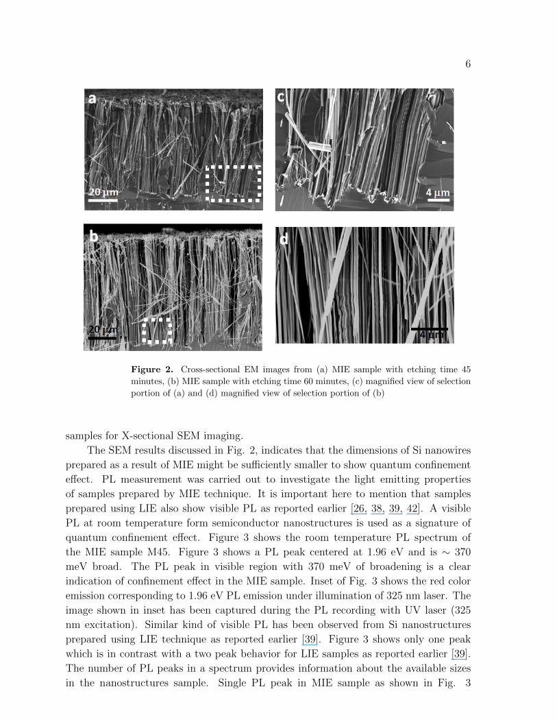
X-sectional SEM images of the MIE samples are shown in Fig. 2a-2b corresponding
to samples M45 and M60 respectively. A very clear nanowire (submicron sized) like
features can be seen for both the samples. The scale bars on Figs. 2a-2b are of 20 µm
and those on Figs. 2c-2d are of 4 µm in length. Approximate lengths of the nanowires
in for sample M45 is 60 µm whereas that for M60 it is 80 µm. This increase in nanowires
(or pore) length is a direct manifestation of longer metal induced chemical etching of Si
wafer. The parallel pores in sample M60 are more uniform as compared to sample M45.
To have a closer look at the nanowires formed, the X-sectional images were magnified
as shown in Fig. 2c-2d. Figures 2c-2d show the magnified view of the portion marked in
figs 2a-2b respectively. It is clear from Fig. 2c-2d also that aligned uniform nanowires
are formed in sample M60 & sample M45. Such kind of parallel Si nanowires may be
used as field emitters [43] for various applications. As discussed above, the nanowires
are formed parallel to each other when prepared using MIE method because the growth
of such nanowires are initiated and governed by the distribution and size of AgNPs
grown prior to chemical etching. The X-sectional images for LIE samples cannot be
presented here due to sample constraints because it is not possible to prepare the LIE
6
Figure 2. Cross-sectional EM images from (a) MIE sample with etching time 45
minutes, (b) MIE sample with etching time 60 minutes, (c) magnified view of selection
portion of (a) and (d) magnified view of selection portion of (b)
samples for X-sectional SEM imaging.
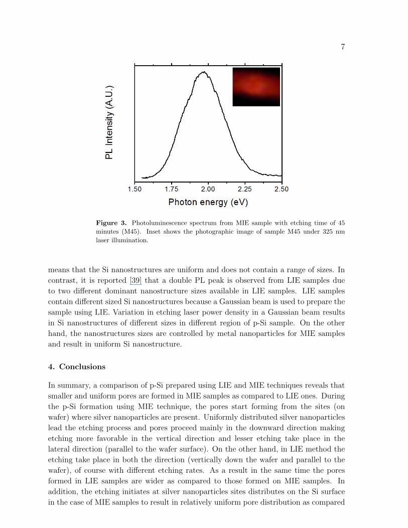
The SEM results discussed in Fig. 2, indicates that the dimensions of Si nanowires
prepared as a result of MIE might be sufficiently smaller to show quantum confinement
effect. PL measurement was carried out to investigate the light emitting properties
of samples prepared by MIE technique. It is important here to mention that samples
prepared using LIE also show visible PL as reported earlier [26, 38, 39, 42]. A visible
PL at room temperature form semiconductor nanostructures is used as a signature of
quantum confinement effect. Figure 3 shows the room temperature PL spectrum of
the MIE sample M45. Figure 3 shows a PL peak centered at 1.96 eV and is ∼ 370
meV broad. The PL peak in visible region with 370 meV of broadening is a clear
indication of confinement effect in the MIE sample. Inset of Fig. 3 shows the red color
emission corresponding to 1.96 eV PL emission under illumination of 325 nm laser. The
image shown in inset has been captured during the PL recording with UV laser (325
nm excitation). Similar kind of visible PL has been observed from Si nanostructures
prepared using LIE technique as reported earlier [39]. Figure 3 shows only one peak
which is in contrast with a two peak behavior for LIE samples as reported earlier [39].
The number of PL peaks in a spectrum provides information about the available sizes
in the nanostructures sample. Single PL peak in MIE sample as shown in Fig. 3
7
Figure 3. Photoluminescence spectrum from MIE sample with etching time of 45
minutes (M45). Inset shows the photographic image of sample M45 under 325 nm
laser illumination.
means that the Si nanostructures are uniform and does not contain a range of sizes. In
contrast, it is reported [39] that a double PL peak is observed from LIE samples due
to two different dominant nanostructure sizes available in LIE samples. LIE samples
contain different sized Si nanostructures because a Gaussian beam is used to prepare the
sample using LIE. Variation in etching laser power density in a Gaussian beam results
in Si nanostructures of different sizes in different region of p-Si sample. On the other
hand, the nanostructures sizes are controlled by metal nanoparticles for MIE samples
and result in uniform Si nanostructure.
4. Conclusions
In summary, a comparison of p-Si prepared using LIE and MIE techniques reveals that
smaller and uniform pores are formed in MIE samples as compared to LIE ones. During
the p-Si formation using MIE technique, the pores start forming from the sites (on
wafer) where silver nanoparticles are present. Uniformly distributed silver nanoparticles
lead the etching process and pores proceed mainly in the downward direction making
etching more favorable in the vertical direction and lesser etching take place in the
lateral direction (parallel to the wafer surface). On the other hand, in LIE method the
etching take place in both the direction (vertically down the wafer and parallel to the
wafer), of course with different etching rates. As a result in the same time the pores
formed in LIE samples are wider as compared to those formed on MIE samples. In
addition, the etching initiates at silver nanoparticles sites distributes on the Si surface
in the case of MIE samples to result in relatively uniform pore distribution as compared
8
to LIE samples. A laser beam having Gaussian profile of intensity used for LIE gives
rise a distribution in pore size in LIE samples & Si nanostructures are fabricated. A X-
sectional SEM image from MIE samples show that well aligned Si nanowires are formed
with increasing sizes when etching time is increased. These parallel Si nanowires may
be used for field emission devices and opens scope for further studies. The Si nanowires
in the p-Si samples prepared by MIE show visible PL at 1.96 eV (red emission) at room
temperature possibly due to weak quantum confinement effect. The PL spectrum show
only single peak for MIE samples in contrary with already reported double PL peak for
LIE samples giving confirmation that the Si nanowires are of relatively uniform size in
MIE samples as compared to LIE samples.
Acknowledgements
Authors are thankful to Sophisticated Instrument centre (SIC), IIT Indore (IIT
Indore) for providing Photoluminescence and FESEM measurement facilities. Authors
acknowledge technical support from Mr. Farhan Babu (IIT Indore) in SEM experiment.
9
References
[1] Canham LT (1990) Silicon quantum wire array fabrication by electrochemical and chemical
dissolution of wafers. Appl Phys Lett 57:10461048. doi: doi:10.1063/1.103561
[2] Cullis AG, Canham LT (1991) Visible light emission due to quantum size effects in highly porous
crystalline silicon. Nature 353:335338. doi: 10.1038/353335a0
[3] Cullis AG, Canham LT, Calcott PDJ (1997) The structural and luminescence properties of porous
silicon. J Appl Phys 82:909965. doi: doi:10.1063/1.366536
[4] Maier-Flaig F, Rinck J, Stephan M, et al. (2013) Multicolor Silicon Light-Emitting Diodes
(SiLEDs). Nano Lett. doi: 10.1021/nl3038689
[5] Soref R (2010) Silicon Photonics: A Review of Recent Literature. Silicon 2:16. doi: 10.1007/s12633-
010-9034-y
[6] Soref R (2010) Mid-infrared photonics in silicon and germanium. Nat Photonics 4:495497. doi:
10.1038/nphoton.2010.171
[7] Chen R, Li D, Hu H, et al. (2012) Tailoring Optical Properties of Silicon Nanowires by Au
Nanostructure Decorations: Enhanced Raman Scattering and Photodetection. J Phys Chem
C 116:44164422. doi: 10.1021/jp210198u
[8] . Ltant S, Sailor MJ (2000) Detection of HF Gas with a Porous Silicon Interferometer. Adv Mater
12:355359. doi: 10.1002/(SICI)1521-4095(200003)12:5¡355::AID-ADMA355¿3.0.CO;2-H
[9] Lin VS-Y, Motesharei K, Dancil K-PS, et al. (1997) A Porous Silicon-Based Optical Interferometric
Biosensor. Science 278:840843. doi: 10.1126/science.278.5339.840
[10] . Canham LT (1995) Bioactive silicon structure fabrication through nanoetching techniques. Adv
Mater 7:10331037. doi: 10.1002/adma.19950071215
[11] Wang B, Cancilla JC, Torrecilla JS, Haick H (2014) Artificial Sensing Intelligence with
Silicon Nanowires for Ultraselective Detection in the Gas Phase. Nano Lett 14:933938. doi:
10.1021/nl404335p
[12] Flavel BS, Sweetman MJ, Shearer CJ, et al. (2011) Micropatterned Arrays of Porous Silicon:
Toward Sensory Biointerfaces. ACS Appl Mater Interfaces 3:24632471. doi: 10.1021/am2003526
[13] Ge M, Rong J, Fang X, Zhou C (2012) Porous Doped Silicon Nanowires for Lithium Ion Battery
Anode with Long Cycle Life. Nano Lett 12:23182323. doi: 10.1021/nl300206e
[14] Zhao Y, Liu X, Li H, et al. (2012) Hierarchical micro/nano porous silicon Li-ion battery anodes.
Chem Commun 48:50795081. doi: 10.1039/C2CC31476B
[15] Wei J, Buriak JM, Siuzdak G (1999) Desorptionionization mass spectrometry on porous silicon.
Nature 399:243246. doi: 10.1038/20400
[16] Li Q, Koo S-M, Edelstein MD, et al. (2007) Silicon nanowire electromechanical switches for logic
device application. Nanotechnology 18:315202. doi: 10.1088/0957-4484/18/31/315202
[17] Wang B, Stelzner T, Dirawi R, et al. (2012) Field-Effect Transistors Based on Silicon Nanowire
Arrays: Effect of the Good and the Bad Silicon Nanowires. ACS Appl Mater Interfaces
4:42514258. doi: 10.1021/am300961d
[18] Fll H, Christophersen M, Carstensen J, Hasse G (2002) Formation and application of porous
silicon. Mater Sci Eng R Rep 39:93141. doi: 10.1016/S0927-796X(02)00090-6
[19] Korotcenkov G, Cho BK (2010) Silicon Porosification: State of the Art. Crit Rev Solid State Mater
Sci 35:153260. doi: 10.1080/10408436.2010.495446
[20] Vzsonyi , Szilgyi E, Petrik P, et al. (2001) Porous silicon formation by stain etching. Thin Solid
Films 388:295302. doi: 10.1016/S0040-6090(00)01816-2
[21] Gonzlez-Daz B, Guerrero-Lemus R, Marrero N, et al. (2006) Anisotropic textured silicon obtained
by stain-etching at low etching rates. J Phys Appl Phys 39:631. doi: 10.1088/0022-3727/39/4/006
[22] Shih S, Jung KH, Hsieh TY, et al. (1992) Photoluminescence and formation mechanism of
chemically etched silicon. Appl Phys Lett 60:18631865. doi: 10.1063/1.107162
[23] Astrova EV, Borovinskaya TN, Tkachenko AV, et al. (2004) Morphology of macro-pores formed
by electrochemical etching of p-type Si. J Micromechanics Microengineering 14:1022. doi:
10
10.1088/0960-1317/14/7/024
[24] Choy CH, Cheah KW (1995) Laser-induced etching of silicon. Appl Phys A 61:4550. doi:
10.1007/BF01538209
[25] Hadjersi T, Gabouze N, Yamamoto N, et al. (2004) Photoluminescence from photochemically
etched highly resistive silicon. Thin Solid Films 459:249253. doi: 10.1016/j.tsf.2003.12.103
[26] Yamamoto N, Takai H (1999) Blue Luminescence from Photochemically Etched Silicon. Jpn J
Appl Phys 38:57065709. doi: 10.7567/JJAP.38.5706
[27] Mavi HS, Prusty S, Kumar M, et al. (2006) Formation of Si and Ge quantum structures by laser-
induced etching. Phys Status Solidi -Appl Mater Sci 203:24442450. doi: 10.1002/pssa.200521027
[28] Mavi HS, Islam SS, Kumar R, Shukla AK (2006) Spectroscopic investigation of
porous GaAs prepared by laser-induced etching. J Non-Cryst Solids 352:22362242. doi:
10.1016/j.jnoncrysol.2006.02.046
[29] Kumar R, Mavi HS, Shukla AK (2008) Macro and microsurface morphology reconstructions during
laser-induced etching of silicon. Micron 39:287293. doi: 10.1016/j.micron.2007.04.005
[30] Kang Y, Jorn J (1998) Photoelectrochemical dissolution of N-type silicon. Electrochimica Acta
43:23892398. doi: 10.1016/S0013-4686(97)10150-5
[31] Juhasz R, Linnros J (2002) Silicon nanofabrication by electron beam lithography and laser-
assisted electrochemical size-reduction. Microelectron Eng 6162:563568. doi: 10.1016/S0167-
9317(02)00532-4
[32] Li X, Bohn PW (2000) Metal-assisted chemical etching in HF/H2O2 produces porous silicon. Appl
Phys Lett 77:25722574. doi: 10.1063/1.1319191
[33] Huang Z, Geyer N, Werner P, et al. (2011) Metal-Assisted Chemical Etching of Silicon: A Review.
Adv Mater 23:285308. doi: 10.1002/adma.201001784
[34] Huang Z, Shimizu T, Senz S, et al. (2009) Ordered Arrays of Vertically Aligned [110] Silicon
Nanowires by Suppressing the Crystallographically Preferred ¡100¿ Etching Directions. Nano
Lett 9:25192525. doi: 10.1021/nl803558n
[35] Huang Z, Zhang X, Reiche M, et al. (2008) Extended Arrays of Vertically Aligned Sub-10 nm
Diameter [100] Si Nanowires by Metal-Assisted Chemical Etching. Nano Lett 8:30463051. doi:
10.1021/nl802324y
[36] Lin L, Guo S, Sun X, et al. (2010) Synthesis and Photoluminescence Properties of Porous Silicon
Nanowire Arrays. Nanoscale Res Lett 5:1822. doi: 10.1007/s11671-010-9719-6
[37] Chartier C, Bastide S, Lvy-Clment C (2008) Metal-assisted chemical etching of silicon in HFH2O2.
Electrochimica Acta 53:55095516. doi: 10.1016/j.electacta.2008.03.009
[38] Zhong X, Qu Y, Lin Y-C, et al. (2011) Unveiling the Formation Pathway of Single Crystalline
Porous Silicon Nanowires. ACS Appl Mater Interfaces 3:261270. doi: 10.1021/am1009056
[39] Kumar R, Mavi HS, Shukla AK, Vankar VD (2007) Photoexcited Fano interaction in laser-etched
silicon nanostructures. J Appl Phys 101:064315. doi: 10.1063/1.2713367
[40] Kumar R, Shukla AK (2009) Quantum interference in the Raman scattering from the silicon
nanostructures. Phys Lett A 373:28822886. doi: 10.1016/j.physleta.2009.06.005
[41] Kumar R, Mavi HS, Shukla AK (2010) Spectroscopic Investigation of Quantum Confinement
Effects in Ion Implanted Silicon-on-Sapphire Films. Silicon 2:2531. doi: 10.1007/s12633-009-
9033-z
[42] Shukla AK, Kumar R, Kumar V (2010) Electronic Raman scattering in the laser-etched silicon
nanostructures. J Appl Phys 107:014306. doi: 10.1063/1.3271586
[43] Wu H-C, Tsai T-Y, Chu F-H, et al. (2010) Electron Field Emission Properties of Nanomaterials
on Rough Silicon Rods. J Phys Chem C 114:130133. doi: 10.1021/jp908566q