space radiation equivalence for effects on
TRANSCRIPT
,i 2 ‘- ;,
.* -8 .‘-*
NASA C’ONTRACTOR
REPORT
d C
NASA. Ll- --- d
SPACE RADIATION EQUIVALENCE FOR EFFECTS ON TRANSISTORS
by R. R. Brown md WI E, Home ,’ t
Prepared by ~’
_’ :: ‘> 1.. .
THE BOEING COMPANY L ‘. ,:I _ <
Seattle, Wash. , ;, <!k, ; , I ^ . ..i/.,, :
for Goddard Space FZight Center .I ,! ,’ 1, .. ,.!.,.;;l.. ., ,‘.’
‘.. ’ ‘. ..’ _, .\\’
NATIONAL AERONAUTICS AND SPACE ADMINISTRATION . WASHINGTON, D. Cm -.“:’ jiJLr &
TECH LIBRARY KAFB, NM
NASA CR-814
SPACE RADIATION EQUIVALENCE FOR
EFFECTS ON TRANSISTORS
By R. R. Brown and W. E. Horne
Distribution of this report is provided in the interest of information exchange. Responsibility for the contents resides in the author or organization that prepared it.
The appendix, the six-month report was issued by Originator as D2-84088-1 and final report as D2-84088-2.
Prepared under Contract No. NAS 5-9578 by THE BOEING COMPANY
Seattle, Wash.
for Goddard Space Flight Center
NATIONAL AERONAUTICS AND SPACE ADMINISTRATION
For sale by the Clearinghouse for Federal Scientific and Technical Information
Springfield, Virginia 22151 - CFSTI price $3.00
-
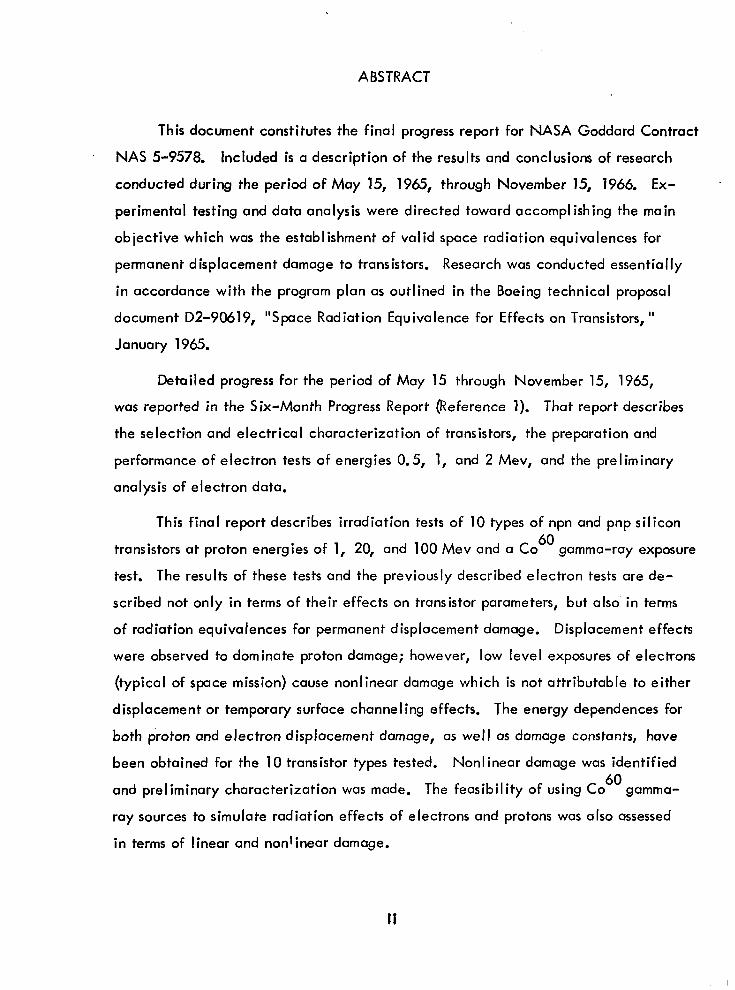
ABSTRACT
This document constitutes the final progress report for NASA Goddard Contract
NAS 5-9578. Included is a description of the results and conclusions of research
conducted during the period of May 15, 1965, through November IS, 1966. Ex-
perimental testing and data analysis were directed toward accomplishing the main
objective which was the establishment of valid space radiation equivalences for
permanent displacement damage to transistors. Research was conducted essentially
in accordance with the program plan as outlined in the Boeing technical proposal
document D2-90619, “Space Radiation Equivalence for Effects on Transistors, ”
January 1965.
Detailed progress for the period of May 15 through November 15, 1965,
was reported in the Six-Month Progress Report (Reference 1). That report describes
the selection and electrical characterization of transistors, the preparation and
performance of electron tests of energies 0.5, 1, and 2 Mev, and the preliminary
analysis of electron data.
This final report describes irradiation tests of 10 types of npn and pnp silicon
transistors at proton energies of 1, 20, and 100 Mev and a Co 60
gamma-ray exposure
test. The results of these tests and the previously described electron tests are de-
scribed not only in terms of their effects on transistor parameters, but also’ in terms
of radiation equivalences for permanent displacement damage. Displacement effects
were observed to dominate proton damage; however, low level exposures of electrons
(typical of space mission) cause nonlinear damage which is not attributable to either
displacement or temporary surface channeling effects. The energy dependences for
both proton and electron displacement damage, as well as damage constants, have
been obtained for the 10 transistor types tested. Nonlinear damage was identified
and preliminary characterization was made. The feasibility of using Co 60
gamma-
ray sources to simulate radiation effects of electrons and protons was also assessed
in terms of linear and nonlinear damage.
Ii
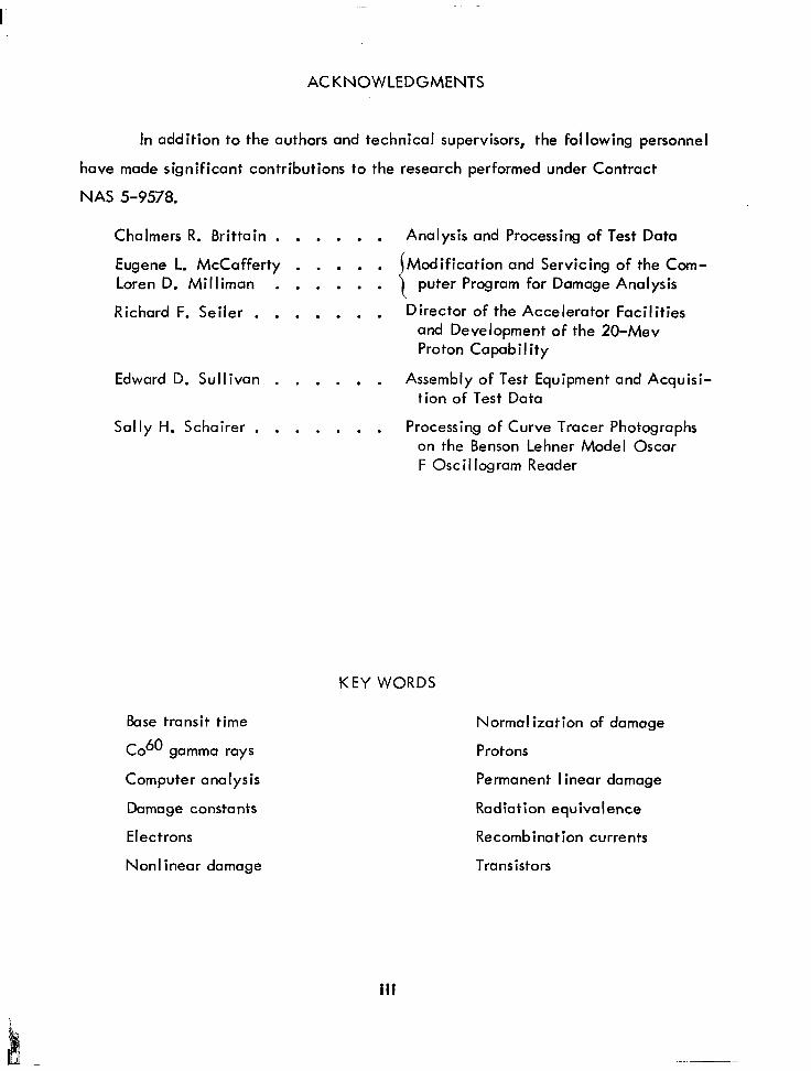
ACKNOWLEDGMENTS
In addition to the authors and technical supervisors, the following personnel
have made significant contributions to the research performed under Contract
NAS 5-9578.
Chalmers R. Brittain . . . . . . Analysis and Processing of Test Data
Eugene L. McCafferty . . . . . Modification and Servicing of the Com- Loren D. Milliman . . . . . . puter Program for Damage Analysis
Richard F. Seiler . . . . . . . ‘Director of the Accelerator Facilities and Development of the 20-Mev Proton Capability
Edward D. Sullivan . . . . . . Assembly of Test Equipment and Acquisi- tion of Test Data
Sally H. Schairer . . . . . . . Processing of Curve Tracer Photographs on the Benson Lehner Model Oscar F Oscil logram Reader
KEY WORDS
Base transit time
Co60 gamma rays
Computer analysis
Damage constants
Electrons
Non1 inear damage
Normalization of damage
Protons
Permanent I inear damage
Radiation equivalence
Recombination currents
Transistors
iii

.
TABLE OF CONTENTS
ABSTRACT. ....................... ii
ACKNOWLEDGMENTS. .................. iii
1.0 INTRODUCTION ...................
1.1 Needs. .................... 1.2 Program Description ................ 1.3 Summary of Results ................
1
1 1 2
2.0 DETAILED DISCUSSION OF PROGRESS .......... 2.1 Transistor Preparation ...............
2.1.1 Selection of Transistors. ........... 2. 1.2 Characterization of Sensitive Parameters ..... 2.1.3 Measurement of Radiation-Sensitive Parameters ... 2.1.4 Measurement of Radiation-Control Parameters ...
2.2 Test Schedule .................. 2.3 Electron Irradiation Tests .............. 2.4 Proton Irradiation Tests. ..............
2.4.1 1-Mev Test ............... 2.4.2 20-Mev Test ............... 2.4.3 100-Mev Test ...............
2.5 Co6O Gamma-Ray Test ............... 2.6 Analysis of Test Data ...............
2.6.1 Transistor Parameters Measured Passively ..... 2.6.2 Computer Analysis of Characteristic Curves ....
2.7 Displacement Equivalences ............. 2.7.1 Control Parameters for Damage Normalization ... 2.7.2 Proton and Electron Equivalences ........ 2.7.3 Proton and Electron Energy Dependence ..... 2.7.4 Other Particle Equivalences and Correlations
With Other Studies ............. 2.8 Feasibility of Simulation by Co6O Gamma Testing ..... 2.9 Identification of Nonlinear Damage ..........
5 5 5 7 7 9
11 14 14 14 15 24 30 34 34 59 89 89 94
148
153 161 167
3.0 NEW TECHNOLOGY ................. 187
4.0 CONCLUSIONS ................... 189 4.1 Conclusions ................... 189 4.2 Recommendations ................. 190
5.0 BIBLIOGRAPHY ................... 193
6.0 GLOSSARY ..................... 197
APPENDIX I . . . . . . . . . . . . . . . . . . . . l-l -I l-107
V
LIST OF ILLUSTRATIONS
No. Title Page
1 Oscillogram of a Set of Characteristic Curves ........ 10
2 Transistor Array for the 1-Mev Proton Test ......... 16
3 I-Mev Proton Flux From a l-Micron Gold Foil ........ 17
4 Chamber Schematic for the 20-Mev Proton Test ....... 18
5 20-Mev Proton Test Configuration ............ 20
6 Transistor Array for the 20-Mev Proton Test ......... 21
7 Angular Distributions From the (He3, p) Reaction ...... 22
8 lOO-Mev Proton Beam Handling System (McGill University) ... 25
9 Transistor Mounting Plates ............... 26
10 Mapping of the lOO-Mev Proton Beam Profile . . 0 . . o 0 . 27
11 Results of 100-Mev Proton Beam Mapping. ......... 29
12 Transistor Array for Gamma-Radiation Test ......... 31
13 Transistor Mount for Gammacell 200 ........... 32
14 Dependence of A(BVCBo ) on Charged Particle Fluence (2N2538). 37
15 Dependence of ACVCE (sat)] on Charged Particle Fluence (2N2538) 38
16 Dependence of ACVCE(sat)l on Charged Particle Fluence (2N743) . 39
17 Dependence of AN,, (sat)] on Charged Particle Fluence (2N834) . 40
18 Dependence of Base-Emitter Saturation Voltage on Fluence . . o 43
19 Electron-Induced Changes of lcBo (2N2303) ........ 44
20 Electron-Induced Changes of lCBO ............ 45
21 Dependence of A(lcBo ) on Proton Fluence (2N1613, 2N1711) . . 47
22 Dependence of A(lcBo) on Proton Fluence (2N2219) ..... 48
23 Dependence of A(lcBo ) on Proton Fluence (2N2801) ..... 49
24 Slight Annealing of A(lcBo) (2N1613) .......... 51
25 Slight Annealing of lCBO After 1-Mev Proton Test ...... 52
26 Annealing of lcBo of Epitaxial Mesa Devices ........ 53
27 Ic Versus VBE for 2N2303 ............... 54
28 Components of Ig Versus VBE (2N1613). .......... 56
Vi
LIST OF ILLUSTRATIONS (Continued)
No. Title Page
29
30
31
32 ’
33
34
35
36
37
38
39
40
41
42
43
44
45
46
47
48
49
50
51
52
53
54
55
56
Radiation-Induced Change in IB Versus VBE . . . . .
Chawe in IB Versus VBE After lo4 R Gamma Exposure .
2N1613 hFE Versus IE for I-Mev Protons (High Gain) .
2N1613 hFE Versus IE for I-Mev Protons (Low Gain) .
2N2219 hFE Versus I, for I-Mev Protons (High Gain) .
2N2219 hFE Versus IE for I-Mev Protons (Low Gain) .
2N834 hFE Versus IE for I-Mev Protons . . . . . .
2N1132 hFE Versus IE for l-Mev Protons . . . . . .
2N2801 hFE Versus IE for 1-Mev Protons . . . o . .
2N2411 hFE Versus IE for 2-Mev Electrons . . . . .
2N2411 hFE Versus IE for I-Mev Protons . . . . . .
2N2411 hFE Versus IE for Co 60
Gamma Rays. . . . .
2N1711 hFE Versus @ for 2-Mev Electron Test . . . .
2N1711 hFE Versus @ for I-Mev Electron Test . . . .
2N1711 hFE Versus @ for 0.5-Mev Electron Test . . .
2N1711 hFE Versus 4 for I-Mev Proton Test. . . . .
2N1711 hFE Versus 4 for 20-Mev Proton Test . . . .
2N1711 hFE Versus Q for Co 60
Gamma Test. . . . .
2N1711 hFE Versus Q Passive Data (lOO-Mev Protons) .
2N2801 hFE Versus @ for 1-Mev Proton Test. . . . .
AbFEB1) V ersus 0 for I-Mev Proton Test (2N1132) . .
A(hFE-5 V ersus @ for 20-Mev Proton Test (2N1613). .
AbFE-‘) V ersus # for lOO-Mev Proton Test (2N2538) .
(2N743) A(hFE-‘) Versus Qi (lOO-Mev Protons) . . . .
AhFEw’) V ersus 0 for 2-Mev Electron Test (2N834) . .
A(hFE-‘) V ersus @for I-Mev Electron Test (2N1613) .
AbFEB1) V ersus 0 for 0.5-Mev Electron Test (2N1132)
I-Mev Electron Linear Damage (High Exposure) . . .
. . . . 57
. . . . 58
. . . . 61
. . . . 62
. . . . 63
. . . . 64
. . . . 65
. . . . 66
. . . . 67
. . . . 69
. . . . 70
. . . . 71
. . . . 72
. . . . 73
. . . . 74
. . . . 75
. . . . 76
. . . . 77
. . . . 78
. . . . 79
. . . . 82
. . . . 83
. . . . 84
. . . . 85
. . . . 86
. . . . 87
. . . . 88
. . . . 90
vii
LIST OF ILLUSTRATIONS (Continued)
No. Title
AC,,-‘) Versus 0 for Co6’ Gamma Tests (2N2219) 0
2N1613 Equivalence Plot, Electron Test 21 . o . .
2N1613 Equivalence Plot, Electron Test 22 . . . .
2N1613 Equivalence Plot, Electron Test 23 . . 0 .
2N1613 Equivalence Plot, Co 60
Test D . 0 . . .
2N1613 Equivalence Plot, Proton Tests . . . . .
2N1613 Equivalence Plbt, Proton Test 26. . . . .
2N1711 Equivalence Plot, Electron Test 21 . . . .
2N1711 Equivalence Plot, Electron Test 22 . . . .
2N1711 Equivalence Plot, Electron Test 23 . . . .
2N1711 Equivalence Plot, Co ” Test 0 . . D . .
2N1711 Equivalence Plot, Proton Test 24. . 0 . .
2N1711 Equivalence Plot, Proton Tests . . . . .
2N2538 Equivalence Plot, Electron Tests 0 . . . .
2N2538 Equivalence Plot, Co ” Test 0 . . . . .
2N2538 Equivalence Plot, Proton Tests. . . . . .
2N2219 Equivalence Plot, Electron Test 21 . . . .
2N2219 Equivalence Plot, Electron Test 22 . . . .
2N2219 Equivalence Plot, Electron Test 23 . . . .
2N2219 Equivalence Plot, Co 60
Test . . . . . .
2N2219 Equivalence Plot, Proton Tests. . . . . .
2N743 Equivalence Plot, Electron Test 21 . . 0 .
2N743 Equivalence Plot, Electron Test 22 . . . .
2N743 Equivalence Plot, Electron Test 23 . . D .
2N743 Equivalence Plot, Co 60
Test . . . . . .
2N743 Equivalence Plot, Proton Tests . . . . . .
2N743 Equivalence Plot, Proton Test 26 . . . . .
2N834 Equivalence Plot, Electron Test 21 . . . .
Page 57
58
59
60
61
62
63
64
65
66
67
68
69
’ 70
71
72
73
74
75
76
77
78
79
80
8-i
82
83
84
. . . 0 . 91
0 . . 0 . 97
. . . . . 98
. . . . . 99
. . . . . 100
. . . . . 101
. . . . . 102
. . . . . 103
. . . . . 104
0 . . . . 105
. . . . . 106
. . . . . 107
. . . . . 108
. . . . . 109
. 0 . e . 110
. . . . . 111
. . . . . 112
. . . . . 113
. . . . . 114
. . . . . 115
. . . . . 116
. . . . . 117
. . . . . 118
. . . . . 119
. . . . . 120
. . . . . 121
. . . . . 122
. . . . . 123
vii1
LIST OF ILLUSTRATIONS (Continued)
No. Title Page
85
86
87
88
89
90
91
92
93
94
95
96
97
98
99
100
101
102
103
104
105
106
197
108
109
110
2N834 Equivalence Plot, Electron Test 22 ......... 124
2N834 Equivalence Plot, Electron Test 23 ......... 125
2N834 Equivalence Plot, Co 60
Test. ........... 126
2N834 Equivalence Plot, Proton Tests ........... 127
2N2303 Equivalence Plot, Electron Test 21 ......... 128
2N2303 Equivalence Plot, Electron Test 22 ......... 129
2N2303 Equivalence Plot, Electron Test 23 ......... 130
2N2303 Equivalence Plot, Co 60
Test ........... 131
2N2303 Equivalence Plot, Proton Tests .......... 132
2N1132 Equivalence Plot, Electron Tests .......... 133
2N1132 Equivalence Plot, Co 60
Test ........... 134
2N1132 Equivalence Plot, Proton Tests .......... 135
2N2801 Equivalence Plot, Electron Test 21 ......... 136
2N2801 Equivalence Plot, Electron Test 22 ......... 137
2N2801 Equivalence Plot, Electron Test 23 ......... 138
2N2801 Equivalence Plot, Co 60Test ........... 139
2N2801 Equivalence Plot, Proton Tests .......... 140
2N2411 Equivalence Plot, Electron Test 21 ......... 141
2N2411 Equivalence Plot, Electron Test 22 ......... 142
2N2411 Equivalence Plot, Electron Test 23 ......... 143
2N2411 Equivalence Plot, Co 60
Test ........... 144
2N2411 Equivalence Plot, Proton Tests .......... 145
Energy Dependence of Electron-Induced Displacement Damage (2N1613) .................... 150
Proton Energy Dependence of Displacement Damage (npn Transistors) .................. 151
Proton Energy Dependence of Displacement Damage (2N743). .. 152
Permanent Damage to Diodes .............. 156
IX
LIST OF ILLUSTRATIONS (Continued)
No.
111
112
113
114
115
116
117
118
119
120
121
122
123
124
125
126
127
128
129
Title Page
Permanent Damage to Solar Cells. ............ 158
Electron Displacement Damage in Silicon Devices. ...... 160
A(BVcBo) for Co 6o Gamma-Ray Exposure (2N2538) ..... 162
Dependence of ACV (sat)] on Co 60
(2N1613, 2N171fjE. Gamma-Ray Fluence
... ‘60. ........... 163
Dependence of A[vcE(Sat)l on Co Gamma-Ray Fluence (2N2219, 2N2303) ................. 164
Dependence of A(lCBo) on Co 60
Gamma-Ray Fluence (2N1613, 2N1711, 2N2219) ............. 168
Dependence of A(lCBG) on Co 6o Gamma-Ray Fluence (2N1132) . 169
Dependence of A(ICBG) on Co 6o Gamma-Ray Fluence (2N834) . 170
Dependence of A(lCBo) on Absorbed Dose (2N1613, 2N1711) . . 171
Dependence of A(lCBo) on Absorbed Dose (2N834) ...... 172
Dependence of Nonlinear Damage on Emitter Current ..... 174
Relative Importance of Linear to Nonlinear Damage ..... 175
Separation of Nonlinear Damage ............. 179
Nonlinear Damage Versus Particle Fluence ......... 181
Nonlinear Damage Versus Absorbed Dose .......... 182
Components of Recombination Current ........... 183
Change in IB Versus VBE After Exposure to 104R (Co 60
Gamma) . 184
Separated Damage Components ............. 185
Recommended Follow-on Study ............. 192
LIST OF TABLES
No. Title Page
1
2
3
4
5
6
7
8
9
10
11
12
13
14
15
16
17
18
Transistor Types Studied ................ 6
A Typical Fairchild Series 500 Data Sheet ......... 8
Irradiation Test Schedule. ............... 12
Disposition of Test Devices ............... 13
Gammacell 200 Exposure Dose Rates ........... 33
Radiation-Induced Changes in BVCBG at 100 pa ....... 35
Charged Particle Equivalences for ACVCE(sat)l. ....... 41
Proton Equivalence for lcBo Changes ........... 46
Keypunch Data Form ................. 60
Transistor Damage Constants for Proton Tests. ........ 95
Transistor Damage Constants for Electron Tests (Only for Linear Displacement Component) ............... 96
Energy-Dependent Displacement Equivalence, A(hFE -1
) .... 147
Energy and Transmission Loss in Transistor Cans. ....... 149
Particle-Type Displacement Equivalences, A(hFE -1
). ..... 154
Gamma-Ray Equivalences (Displacement Damage). ...... 165
Transistor Damage Constants for Co6’ Gamma Rays Displacement Component) ............... 166
Annealing of Nonlinear Damage ............. 177
Relative Sensitivities of Transistor Regions ......... 186
xi
1.0 INTRODUCT ION
1.1 NEEDS
The general needs that relate to space mission vulnerability of electron
systems include the ability to:
1. Extrapolate from laboratory-simulated radiation tests to space mission
performance;
2. Extrapolate from performance on an inflight test to other space mission
conditions;
3. Generalize from radiation effects on a limited number of transistors to
the effects on many types; and
4. Develop techniques to allow standardization in qualification testing
of new devices.
The results of the one-year effort of this research study were intended to be
the accomplishment of specific goals that would represent a significant step toward
an organized effort to ultimately satisfy the needs.
1.2 PROGRAM DESCR IPT ION
The specific objective of the program was the establishment of valid space
radiation equivalences for permanent damage to silicon transistors. The phrase,
radiation equivalence for permanent damage, expresses the relative effectiveness
of different types and energies of radiation for producing an equivalent amount of
permanent damage.
Reliable silicon transistors of specified constructions and designs were selected
for radiation effects testing, and 40 of each type were procured. The 10 types
represent two of each of five construction designs: npn and pnp diffused planar,
npn and pnp epitaxial planar, and npn epitaxial mesa. All of these transistors
were electrically characterized before and after radiation exposure. Selected
devices were also characterized during irradiation. In addition to obtaining
oscillograms of common-emitter characteristic curves, the following electrical !
1
parameters were measured: d. c. and small-signal a. c. common-emitter current gain,
saturation voltages, breakdown voltage, leakage current, current as a function of
base-emitter voltage, base transit time, alpha cut-off frequency, gain-bandwidth
frequency, and transition capacitances.
Charged particle irradiation of transistors was performed using electrons of
energies of approximately 0.5, 1, and 2 Mev and protons of energies of approximately
1, 20, and 100 Mev. These tests were used to establish displacement equivalences
for permanent damage for significant radiation components of the Van Allen space
environment. The possibility of obtaining gamma-ray equivalence for permanent
damage was also experimentally studied in order to assess the practicality of using
Co6’ facilities for simulation testing of space radiation effects.
Text fixtures were wired for remote selection of transistors and subsequent
dynamic recording of transistor curve traces during the irradiation tests. Transistor
ambient temperatures were monitored during exposure and measurement. Careful
dosimetry was also performed to determine valid exposure fluences.
Results of changes in transistor parameters measured on the automatic tran-
sistor tester were analyzed by hand, and data from oscillograms of transistor curve
traces were computer analyzed to show not only the dependence of radiation damage
on particle fluence but also on radiation type and particle energy. Radiation
equivalences for permanent displacement damage, norma I ized to transistor base
transit time, were determined for charged particle radiation used in the test pro-
gram, The results of this study were also compared with data obtained in earlier
Boeing studies using other particle energies. Data is presented whenever practical
in a form that is suited to the needs of design engineers.
1.3 SUMMARY OF RESULTS
Proton and electron equivalences for linear damage to transistors were
successfully obtained allowing for the determination of the energy dependence of
the effects of atomic displacements. The importance of energy dependence of
nonlinear damage was identified for electron effects on transistors, and a
2
preliminary characterization was made of this effect. The feasibility of using Co 60
gamma facilities for simulation of the effects of electrons and protons was assessed
in terms of both linear displacement damage and nonlinear ionization damage.
Proton displacement equivalences were obtained from linear damage observed -1
for changes in BVcBo, VCE(sat), VBE (sat), fCBo# and hFE l Electron dis-
placement equivalences were obtained from linear damage observed primarily from
changes of VCE(sat) and hFE -1
at very high electron exposures.
Displacement equivalences indicated fairly consistent agreement among the
ten transistor types tested (npn and pnp). Good correlation was generally obtained
between equivalences for permanent changes in hFE -‘, VcE6at)# and ICBO.
Displacement damage constants from transit time normalization were fairly consistent
for the proton tests, and agreement between devices of the same construction was
generally quite close. Nonlinear damage, however, was observed to exceed
linear damage for low exposures to electrons. The resulting electron damage
constants did not agree as closely as the proton damage constants, particularly for
the pnp devices. Proton displacement equivalences (linear damage) yielded energy
dependence for damage that was correlatable with theory above 10 Mev and with solar
cell data below 10 Mev. I n h erent shielding by transistor cans caused protons of
incident energies between 14 and 17 Mev to be significantly more effective for
displacement damage. Energy dependence for proton damage, in agreement with
solar cell results, increased more rapidly with increased energy than predicted by
theory.
co60 gamma-ray test results indicated that simulation feasibility for space
radiation effects is limited. Although Co6’ gamma rays can be useful in simulating
nonlinear damage to lcBo and hFE characteristic of electron exposure, only at
exposures in excess of lo8 R can they be used to simulate proton displacement
damage to current gains, and even then the simulation is partial.
Preliminary identification of the nonlinear damage (not temporary surface
effects due to channeling or inversion layers) was obtained for the electron and
3
gamma-ray tests. Various characteristics of nonlinear damage were observed, such
as its dominance at low radiation exposures and low emitter currents, its tendency to
saturate at high exposures (allowing for a separation of linear and nonlinear damage),
its dependence on ionization rather than displacement effects, and its correlation
with increases of base-emitter recombination current. Recommendations include
further extension of the studies of nonlinear damage to provide effective radiation
equivalences for electron damage.
2.0 DETAILED DISCUSS ION OF PROGRESS
After all transistors needed for this study were procured and characterized
electrically, a schedule for experimental testing was established. The accelerator
facilities were modified for electron and proton irradiation tests. Both the transistors
to be studied and the necessary test fixtures were prepared. Seven separate radi-
ation exposure tests were conducted; these included irradiation of transistors at three
electron and three proton energies, as well as an irradiation by Co 60
gamma rays.
During the tests, both radiation flux and transistor degradation were monitored
dynamically. Following the tests, all transistors were recharacterized electrically.
Hand analysis on data obtained passively, as well as computer analysis of transistor
characteristic curves, was performed. Radiation equivalences for displacement
effects were obtained, the feasibility of simulating proton and electron effects with
gamma rays was studied, and nonlinear damage was identified.
2. 1 TRANSISTOR PREPARATION
Transistors of selected types were procured and characterized in preparation
for the radiation exposure tests.
2.1. 1 Selection of Transistors
Ten registered types of silicon transistors were selected for radiation effects
testing. Information which identifies those specific devices is listed in Table 1.
Frequency, f, h s own in the table can be related to effective base width, as indi-
cated in Section 2.7.1. Transistor selection was made on the basis of reliability
and present utilization for missile and space vehicle electronic circuitry. These
transistor types also represent three classes of designvpitaxial mesa, diffused planar,
and epitaxial- planar. Both npn and pnp semiconductor constructions were con-
sidered in order to permit a comparison to be made between radiation equivalences
obtained from transistors with p- and n-type base regions. Two different registered
transistors of each of the same class of construction designs (e;g., npn diffused
planar) were selected in order to investigate the validity of extending radiation
5
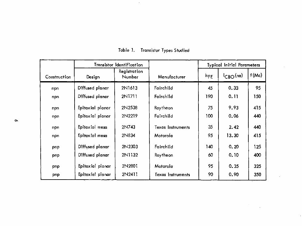
Table 1. Transistor Types Stud ied
Transistor Identification Typical Initial Parameters
Registration Zonstruction Design Number Manufacturer hFE IcBo ha) f (MC)
npn Diffused planar 2N1613 Fairchild 45 0.33 95
npn Diffused planar 2N1711 Fairchild 190 0.11 150
npn Epitaxial planar 2N2538 Raytheon 75 9.93 415
npn Epitaxial planar 2N2219 Fairchild 100 0.06 440
npn Epitaxial mesa 2N743 Texas Instruments 35 2.42 440
npn Epitax ial mesa 2N834 Motorola 95 13.30 415
PnP Diffused planar 2N 2303 Fairchild 140 0.20 125
PnP Diffused planar 2N1132 Raytheon 60 0.10 400
PnP Epitaxial planar 2N2801 Motorola 95 0.35 325
P”P Epitaxial planar 2N2411 Texas Instruments 90 0.90 350
equivalence information to other transistor types of the same construction design.
Forty transistors of each type (400 total) were procured with the specification
that transistors of the same type be of the same batch number and manufacture date
in order to give more assurance that the semiconductor batch, the construction de-
tails, and the surface conditions are the same (Reference 1). Thus, comparisons can
be made between transistors irradiated with different types of radiation with a great-
er assurance of no marked differences in the devices themselves.
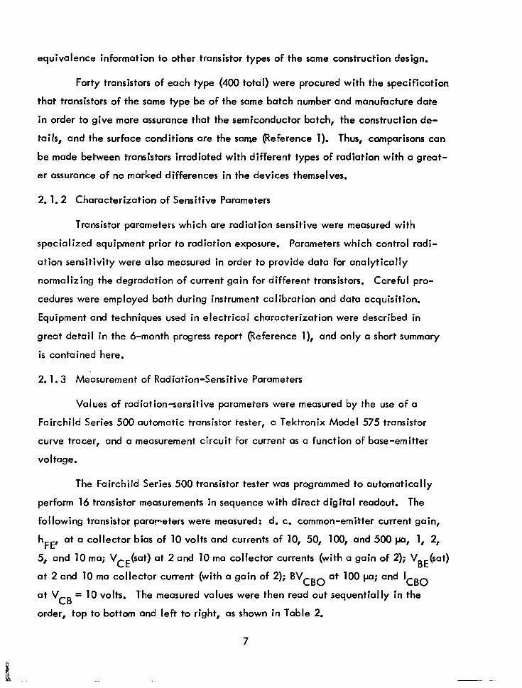
2. 1.2 Characterization of Sensitive Parameters
Transistor parameters which are radiation sensitive were measured with
specialized equipment prior to radiation exposure. Parameters which control radi-
ation sensitivity were also measured in order to provide data for analytically
normalizing the degradation of current gain for different transistors. Careful pro-
cedures were employed both during instrument calibration and data acquisition.
Equipment and techniques used in electrical characterization were described in
great detail in the 6-month progress report (Reference l), and only a short summary
is contained here.
2.1.3 Measurement of Radiation-Sensitive Parameters
Values of radiation-sensitive parameters were measured by the use of a
Fairchild Series 500 automatic transistor tester, a Tektronix Model 575 transistor
curve tracer, and a measurement circuit for current as a function of base-emitter
voltage.
The Fairchild Series 500 transistor tester was programmed to automatically
perform 16 transistor measurements in sequence with direct digital readout. The
following transistor parameters were measured: d. c. common-emitter current gain,
h FE, at a collector bias of 10 volts and currents of 10, 50, 100, and 500 pa, 1, 2,
5, and 10 ma; VCE(sat) at 2 and 10 ma collector currents (with a gain of 2); VBE(sat)
at 2 and 10 ma collector current (with a gain of 2); BVcBo at 100 pa; and lcBo
at VcB = 10 volts. The measured values were then read out sequentially in the
order, top to bottom and left to right, as shown in Table 2.
7
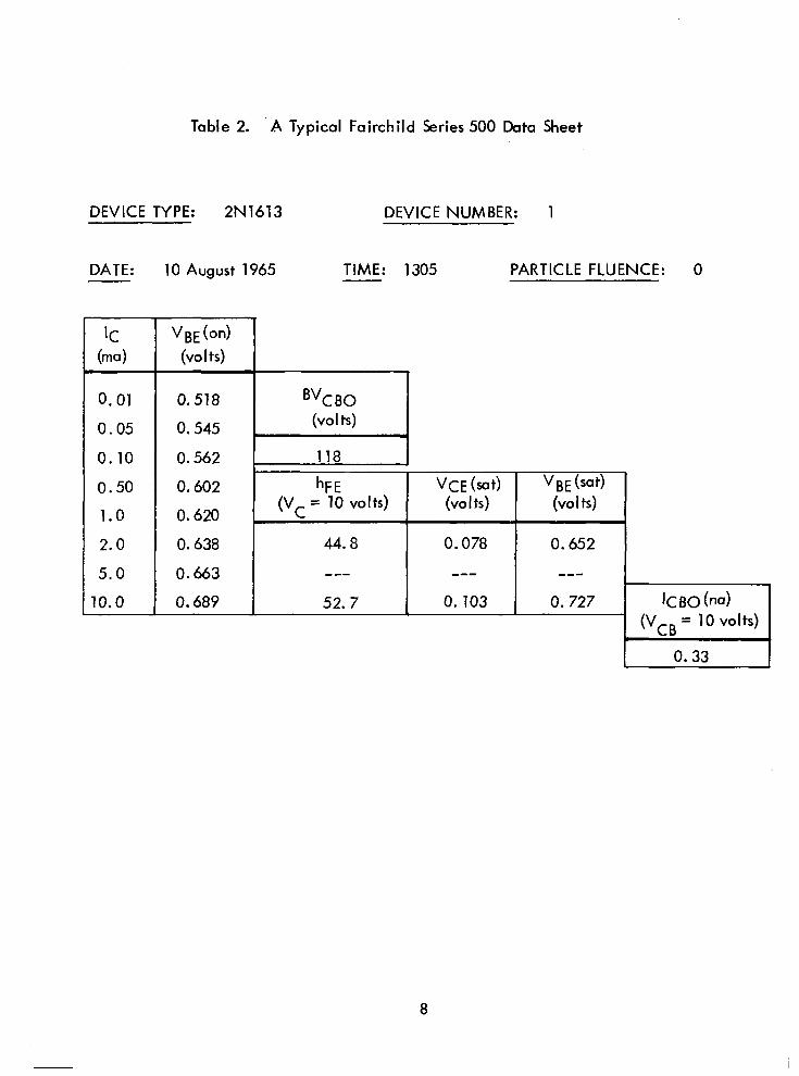
Table 2. A Typical Fairchild Series 500 Data Sheet
DEVICE TYPE: 2N1613 DEVICE NUMBER: 1
DATE: 10 August 1965 TIME: 1305 PARTICLE FLUENCE: 0
IC VBE (On) (4 (volts)
0.01
0.05
0.10
0.50
1.0
2.0
5.0
10.0
0.562
0.602 0.620
0.638
0.663
0.689
118
hFE VCE (sat) VBE (sat) \
lVc = 10 volts) (volts) (volts) ,
44.8 0.078 0.652
--- -em ---
52. 7 0.103 0.727 Ic 130 ha)
(‘CB = 10 volts)
0.33

During these measurements, the ambient temperature was maintained at
27*1 OC. The actual temperature (within 0.05OC) was recorded on the data sheets
at the time of measurement readout. The transistors were handled with insulated
pincers rather than fingers in order to assure temperature stability. Data and time
were recorded on each data sheet with an automatic time stamp. To verify instru-
ment repeatability, control transistors were measured periodically and the values
were compared with standard values obtained earlier.
A Tektronix Model 575 curve tracer was used in this study to display a family
of transistor common-emitter characteristic curves. A typical oscillogram of a set
of transistor common-emitter characteristic curves taken before irradiation is shown
in Figure l(a). The ordinate represents collector current, I c. The abscissa repre-
sents collector voltage, V c. A family of base-current curves is shown. Serial
identification numbering on the face of the oscillogram is used to key punch the
picture heading card and data cards at the oscillogram reader facility. Figure lb)
shows the back of the oscillagram. Listed is pertinent data recorded at the time the
picture was taken. This includes the IB current per step, particle fluence, temper-
a ture, etc. This data was used as input information for a transistor damage-plotting
program used on a SRU 1107 computer.
A measurement circuit for base turn-on voltage was also assembled to obtain
IB and Ic as a function of VBE (Reference 1).
2.1.4 Measurement of RadiationControl Parameters
Values of transistor parameters that are needed in order to determine radiation-
control parameters were measured by the use of the following equipment: a General
Radio Type 1607A transfer function and immittance bridge, a Tektronix 567 sampling
oscilloscope, a Boonton capacity bridge, a specially designed base transit time
circuit, and a Fairchild hfe power gain tester Model 75155.
Measurement techniques employed in obtaining control parameters from these
instruments were described in great detail in the semiannual progress report (Refer-
ence 1). Values obtained from the test instruments included base transit time, tb,
9
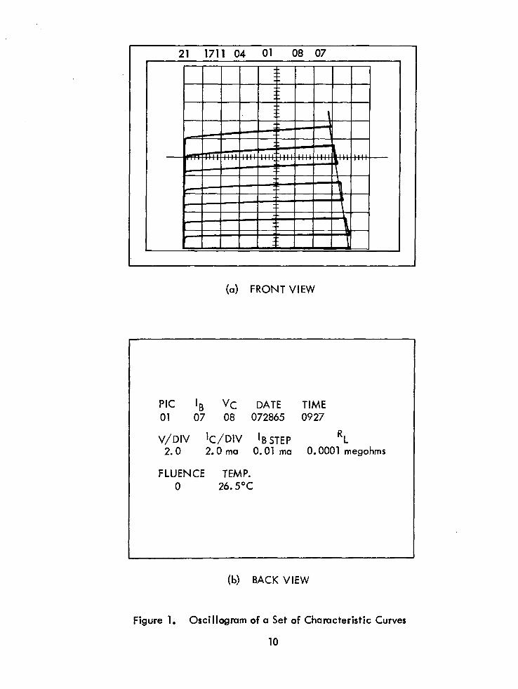
21 1711 04 01 08 07
I I I
(a) FRONT VIEW
1
PIG IB vc DATE TIME 01 07 08 072865 0927
V/DIV k/DIV IB STEP RL 2.0 2.0 ma 0.01 ma 0.0001 megohms
FLUENCE TEMP. 0 26.5OC
(b) BACK VIEW
Figure 1. Oscillogmm of a Set of Characteristic Curves
10
and gain band width frequency, fT. The use of these parameters in normalization
of transistor damage and correction for variations in effective base width is described
in Section 2.7.1.
2.2 TEST SCHFDULE
In order to simulate transistor damage for earth orbital missions, electrons
of three energies and protons of three energies were selected for transistor irradiation.
A gamma-ray test was also selected to assess the validity of space radiation simulation
using a Co 60
facility. Electron irradiation tests included energies of approximately
0.5, 1, and 2 Mev. Electrons of 0.5-Mev energy are representative of those pre-
sent with high intensity in a shield-modified spectrum. Transistor inherent shield-
ing was removed for the 0.5-Mev test. Electrons of I-Mev energy can readily
pass through the thickness of a transistor can, but suffer significant intensity and
energy loss. Although the 1-Mev intensity in space is less than that for lower
energy electrons, the displacement cross section is greater. Electrons of 2-Mev
energy are representative of those high-energy electrons still having sufficient
Van Allen intensity to be significant for transistor damage.
Proton irradiation tests included energies of 1, 20, and 100 Mev. Protons
of l.O-Mev energy are representative of those protons that degrade to low energy
in passing through both inherent and vehicle skin shielding. Transistor inherent
shielding was removed for the l.O-Mev test. Protons of 20-Mev energy can readily
pass through transistor inherent shielding but, in so doing, degrade to lower energieri
that are more effective for displacement damage. Transistors were irradiated at
energies from 14 to 17 Mev, both with and without inherent shielding. Protons of
100 Mev are representative of those protons for which it is difficult to provide
shielding, and they have the added feature of large inelastic reaction cross sections
which lead to transmutations and secondary particle production.
All the irradiation tests performed are summarixed in Table 3. A total of
400 transistors were procured for this research program. The disposition of these
devices is shown in Table 4. Selected transistors of each of the 10 transistor types
11
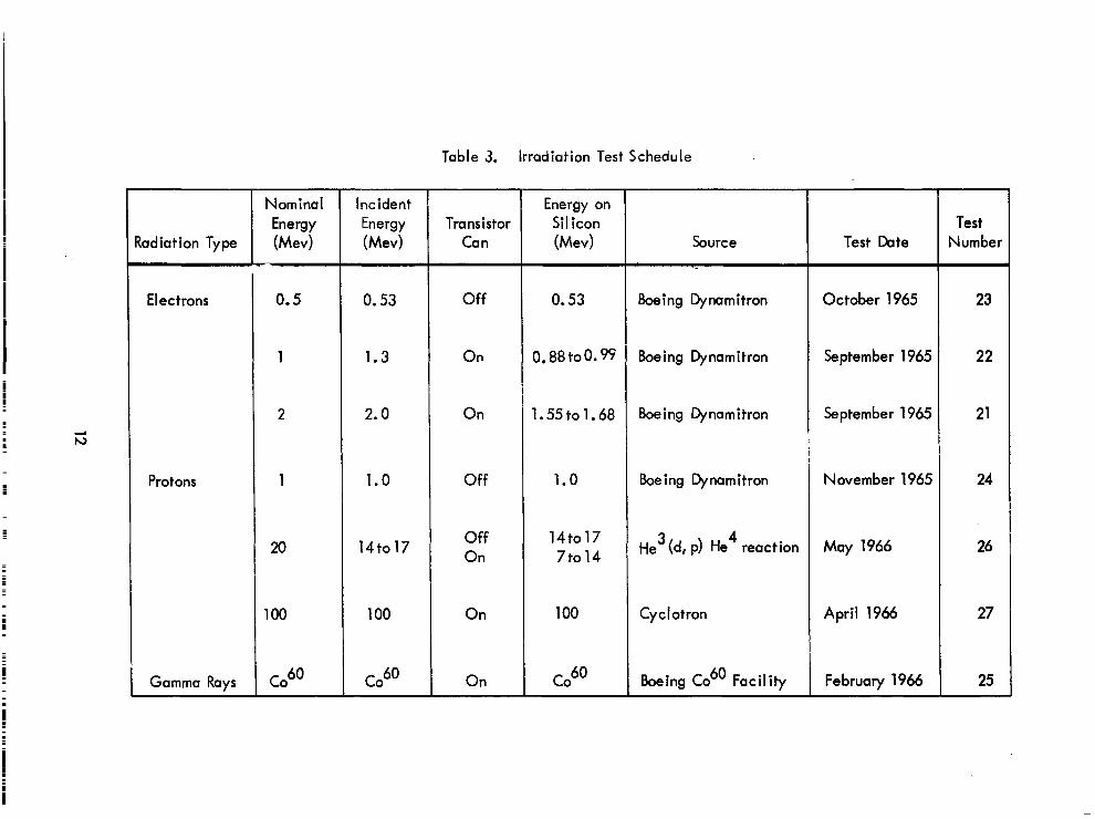
Table 3. Irradiation Test Schedule
ladiation Type
Nominal Incident Energy Energy hv) (Mev)
Electrons
Protons
Gamma Rays
0.5
1
2
1
20
100
cob0
0.53
1.3
2.0
1.0
14to17
100
cob0
Transistor Can
Off
On
On
Off
Off On
On
On
Energy on Sil icon (Mev)
0.53
0.88 too. 99
1.55t01.68
1.0
14to17 7to 14
100
co60
Source
Boeing Dynamitron
Boeing Qnamitron
Boeing Dynamitron
Boeing Dynamitron
He3 (d, p) He4 reaction May 1966
Cyclotron April 1966 27
Boeing Co6’ Facility February 1966
Test Dclte
October 1965
September 1965
September 1965
November 1965 24
Test Number
23
22
21
26
25
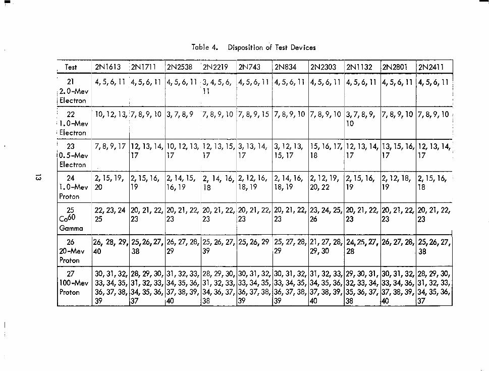
Table 4. Disposition of Test Devices
Test ~ 2N1613 j2N1711 12N2538 /2N2219 12N743 2N834 2N2303 2N1132 2N2801 12N2411 1
4,5,6, 11 4,5,6, 11 4,5,6, 11 4,5,6,11 ~4,5,6,11 1 21 ~ 4,5,6,11 4,5,6,11 4,5,6,11 3,4,5,6, 4,5,6,11 2.0-Mev ~ Electron ~
11
7,8,9,10 7,8,9,10 3,7,8,9, 10
3, 12, 13, 15,16,17, 12,13,14, 15,17 18 17
2, 14, 16, 2,12,19, 2,15,16, 18,19 20,22 19
22 10,12,13, 7,8,9,10 3,7,8,9 7,8,9,10 7,8,9,15 l.O-Mev Electron
7,8,9,10 7,8,9,10
23 7,8,9,17 12,13,14, 10,12,13, 12,13,15, 3,13,14, 0.5-Mev 17 17 17 17 Electron
24 / 2,15,19, 2,15,16, 2,14,15, 2, 14, 16, 2,12,16, l.O-Mev : 20 19 16,19 18 18,19 Proton
20,21,22, 23,24,25, 20,21,22, 23 26 23
25, 27,28, 21,27,28, 24,225,27, 29 29,30 28
Co:: 22 25' 23,24 20,21,22, 23 23 20,21,22, 20,21,22, 23 20,21,22, 23 Gamma
26 26, 28, 29, 25,26,27, 26,27,28, 25,26,27, 25,26,29 20-Mev 40 38 29 39 Proton
27 ~30,31,32,~28,29,30,~31,32,33,~28,29,30,]30,31,32, 30,31,32, 31,32,33, 29,30,31, 33,34,35, 34,35,36, 32,33,34, 36,37,38, 37,38,39, 35,36,37, 39 40 38
30,31,32, 28,29,30, 33,34,36, 31,32,33, 37,38,39, 34,35,36, 40 37
lOO-Mev 33,34,35, 31,32,33, 34,35,36, 31,32,33, 33,34,35, Proton 36,37,38, 34,35,36, 37,38,39, 34,36,37, 36,37,38,
39 37 I40 38 39
served as controls for the tests. At least four of each transistor type were exposed
for each test. At least nine of each type were exposed for the lOO-Mev proton
test. On each of the other tests, one of each transistor type was dynamically moni-
tored by means of curve-tracer photographs taken during irradiation. At least three
devices of each type were characterized by curve traces taken periodically bssive
measurements) following each exposure run. At least three passive measurements
were made during each test.
2.3 ELECTRON IRRADIATION TESTS
Electron irradiation of transistors was performed at energies as specified in
Table 3 (nominal energies of 0.5, 1, and 2 Mev). These tests were performed at
the Boeing Radiation Effects Laboratory using electrons obtained from a Dynamitron
accelerator. Transistors were exposed, in an evacuated test chamber, to electrons
that had been scattered through thin foils. The detailed description of the prepara-
t ion, performance, and dosimetry analysis of those tests was described in the semi-
annual progress report (Reference 1).
2.4 PROTON IRRADIATION TESTS
Three proton irradiation tests of transistors were conducted at nominal energies
of 1, 20, and 100 Mev (see Table 3).
2.4.1 1-Mev Proton Test
The test configuration, dosimetry, and test procedure for the I-Mev proton
test were essentially the same as for the electron tests.
Test Configuration
The same evacuated scattering chamber used in the electron tests (Reference 1)
was also used for the I-Mev proton test. Protons of energy 1. 1 Mev were scattered
through a l-micron thick gold foil, resulting in uniform exposure of axially symmetric
arrays of transistors to I-Mev protons. Diagrams and photographs of the chamber
and mounting dish were included in the earlier discussion of the electron tests. The
14
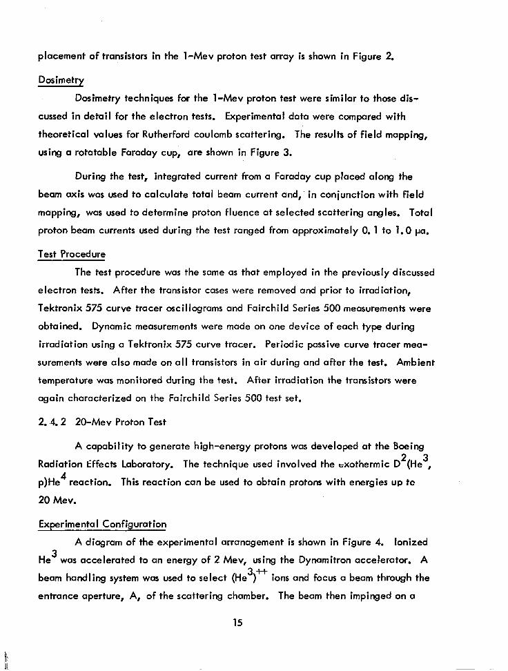
placement of transistors in the I-Mev proton test array is shown in Figure 2.
Dosimetry
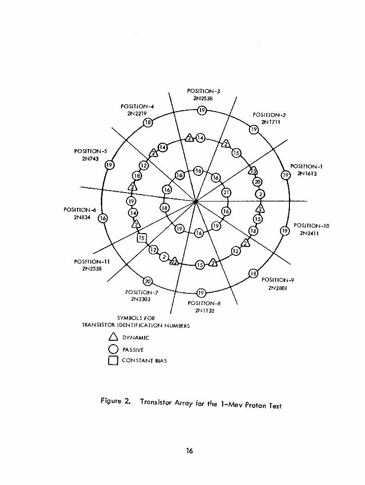
Dosimetry techniques for the 1 -Mev proton test were similar to those dis-
cussed in detail for the electron tests. Experimental data were compared with
theoretical values for Rutherford coulomb scattering. The results of field mapping,
using a rotatable Faraday cup, are shown in Figure 3.
During the test, integrated current from a Faraday cup placed along the
beam axis was used to calculate total beam current and,’ in conjunction with field
mapping, was used to determine proton fluence at selected scattering angles. Total
proton beam currents used during the test ranged from approximately 0.1 to 1.0 pa.
Test Procedure
The test procedure was the same as that employed in the previously discussed
electron tests. After the transistor cases were removed and prior to irradiation,
Tektronix 575 curve tracer oscillograms and Fairchild Series 500 measurements were
obtained. Dynamic measurements were made on one device of each type during
irradiation using a Tektronix 575 curve tracer. Periodic passive curve tracer mea-
surements were also made on all transistors in air during and after the test. Ambient
temperature was monitored during the test. After irradiation the transistors were
again characterized on the Fairchild Series 500 test set.
2. -4.2 20-Mev Proton Test
A capability to generate high-energy protons was developed at the Boeing
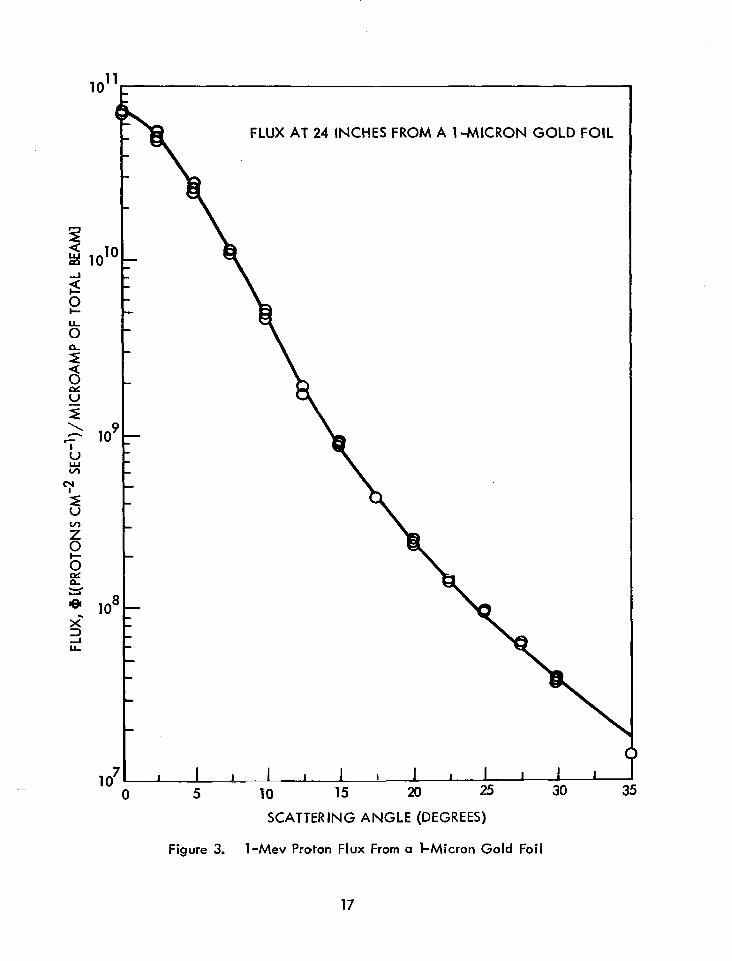
Radiation Effects Laboratory. The technique used involved the exothermic D2(He3,
p)He4 reaction. This reaction can be used to obtain protons with energies UP tc
20 Mev.
Experimental Configuration
A diagram of the experimental arranagement is shown in Figure 4. Ionized
He3 was accelerated to an energy of 2 Mev, using the Dynamitron accelerator. A
beam handling system was used to select (He 3*
) ions and focus a beam through the
entrance aperture, A, of the scattering chamber. The beam then impirlged on a
15
POSITION-5 2N743
\
POSITION-3
POSITION-4 POSITION-2
POSITION-I 1 2N2538
/
2N2411
POSITION-6 \
I 2N1132 SYMBOLS FOR
TRANSISTOR IDENTIFICATION NUMBERS
D DYNAMIC
0 PASSIVE
0 CONSTANT BIAS
Figure 2. Transistor Array for the 1-Mev Proton Test
16
1
\I
lo7 I I I I .A 1 I I I 1 I I I 0 5 10 15 20 25 30 35
SCATTERING ANGLE (DEGREES)
Figure 3. l-Mev Proton Flux From a FMicron Gold Foil
17
H-0 OUT
I
.
F_IXED
L
IRRADlqTlON AREA
L
EVACUATED SCATTERING CHAMBER
DEUTERATED ;lT;&l+JM
I r
APERTURE A He3 BEAM
Figure 4. Chamber Schematic for the 20-Mev Proton Test
deuterated titanium target (3 x lo4 angstroms thick) at an angle of 20 degrees with
the plane of the target. A second aperture, 6, placed in front of the target, acted
as a shield to prevent the direct exposure of transistors by the He3 beam. The shield
of aperture B and the target mount were made of copper and cooled with circulating
water. The Faraday cup at the rear of the chamber was used only to establish the
total beam current before the target was moved into position. The scintillation
counter in the front of the chamber served to monitor the high-energy proton yield
from the target.
Details of the sample mount are illustrated in Figure 5. Transistors were
placed at selected angles so that they were exposed to protons of energy 14 to 17
Mev. Since the energy of the protons would be seriously degraded by inherent
shielding, most transistor cans were removed. However, the placement of thin
shielding in front of these transistors was necessary in order to absorb scattered He 3
particles and secondary electrons. A diagram showing the geometry of the transistor
array for the 20-Mev test is shown in Figure 6.
Dosimetry
The angular distribution of the proton flux for the 20-Mev test was determined
from measurements obtained using a scintillation counter at a fixed angle of 165
degrees and a solid-state detector which was rotated through selected angles about
the deuterated target,
An energy calibration of the solid-state detector was performed using a
pulse height analyzer. The calibration was determined from the pulse height channel
position for 5.5-Mev alpha particles (from Am 241
), and linearity was assumed for
14-to 17-Mev proton energy deposition to pulse height for the detector. For inci-
dent 2-Mev He3 ions, the proton energy as a function of angle from the beam axis
is shown in Figure 7. This energy spread is predictable from the reaction kinetics
and the fuct that the deuterated titanium targets which were used had a thickness
comparable to the range of the He3 ions.
A typical angular distribution for an incident He3 energy of 2.0 Mev con-
sists of a forward peaking with a minimum near 90 degrees and a back angle peak
19
I .
A, B, C = TRANSISTOR MOUNTING PLATES /4AB-. A; 8: C’= THIN SHIELDS
x
15.5-MEV PROTON
\ 17-MEV PROTON \
14-MEV PROTON
-.. 3 --. . . . . . . - AXI:,
Figure 5. 2O+dev Proton Test Configuration
25 TO 45 DtG
/
NOTE: “ON” INDICATES THE TRANSISTORS THAT RETAINED INHERENT CAN SHIELDING.
Figure 6. Transistor Array for the 20-Mev Proton Test
c
20
z
T- 0 7.0
5.0
20 40 60 80 100
ANGLE FROM THE BEAM AXIS (DEGREES)
(a) ENERGY DISTRIBUTION
120
ABSOLUTE ERROR f35% RELATIVE ERROR *15%
20 40 60 80 100 120
ANGLE FROM THE BEAM AXIS (DEGREES)
(b) YIELD
Figure 7. Angular Distributions From (He3, p) Reaction
22
which is roughly half the height of the small angle maximum. Figure 7 also shows
the angular distribution of proton yield over the field of interest. For the target
configuration used in this experiment, the 30degree yield was measured to be the
same as the 165-degree yield.
To obtain proton flux, 9, at the transistor positions at selected angles, 8,
the following relation was used:
9 = Y GM (B)/r2 (1) where: Y= count rate (scintillation counter)
G= geometric constant
r = distance (target to sample)
M(B) = angular anisotropy correction factor
The calculated ratio of count rate of the solid-state detector to the scintillation
counter was 4. 1. The measured value was 4.8. Both values have associated errors
-the former primarily from the measurement of the detector aperture diameters
and the latter from measurements of the distance irom rhe detector aperture to the
target. The finite size of the beam spot on the target limits the validity of the r -2
dependence of Equation (1) for transistors mounted close to the target. If all sources
of error are considered, the overall accuracy of the flux measurements is approxi-
mately X35 percent.
In order to obtain exposure fluences for the transistors at specified times
during the experiment, the count rate from the scintillation counter was monitored
on a chart recorder and integrated numerically. The counts were then converted
to fluence using Equation (1).
Exnerimental Procedure
Before irradiation, inherent shielding (can) was removed from most of,the
transistors before they were electrically characterized on the Tektronix curve
tracer and the 500 semiconductor test set. During the irradiation test, one device
of each type was monitored dynamically beam on). Periodic passive &ream off
and open to air) data was also obtained for all transistors using the curve tracer.
23
After irradiation, all devices were again characterized using -both the curve tracer
and automatic test set.
Sufficient warmup time was allowed on the measurement instruments before
data was obtained, and periodic calibration checks of the equipment were also made.
The ambient temperature of test devices was monitored during measurements, using
a thermocouple mounted to a transistor can.
2.4.3 lOO-Mev Proton Test
able at
Protons of lOO-Mev energy were obtained using the synchrocyclotron avail-
the Foster Radiation Laboratory, McGil I University, in Montreal, Canada.
Test Configuration
The cyclotron and its beam handling system is shown schematically in Figure
8. A l/32-inch beryllium plate, located about 37 feet before the end of the
accelerator beam tube, was used to scatter a proton beam of energy 100%). 1 Mev.
The transistor mounting plates used in this test are shown in Figure 9 as they were
attached to the end of the beam tube.
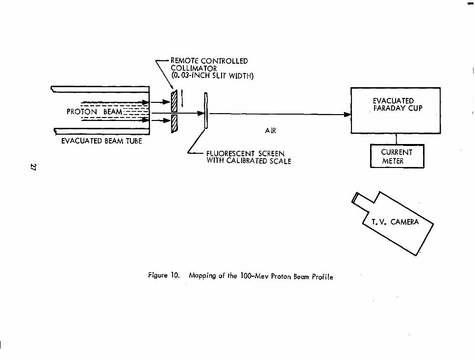
Test DOS imetrv
The uniformity of the 100-Mev proton beam was determined by two methods.
The beam was mapped using a Faraday cup and a collimating slit arrangement,
shown schematically in Figure 10.. In addition, activation foil analysis was per-
formed.
In the first mapping, the collimating slit was moved across the field and the
height of the beam transmitted was obtained from the fluorescent screen using closed
circuit television. The current admitted to the Faraday cup was read on a Keithley
410 meter. The proton flux was calculated at each collimator position using
Equation (2).
+ = 6.25 x lOI l/W, h (proton cm-2 set-I)
where: I = Faraday cup current in amps
W = width of the collimating slit C
24
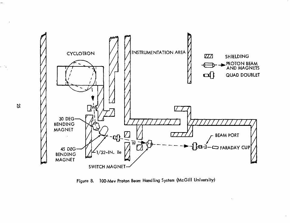
CYCLOTRON INSTRUMENTATION AREA
\ i
lzzzl SHIELDING
+3-+ PROTON BEAM AND MAGNETS
Otl QUAD DOUBLET
SWITCH MAGNET
-- -- -*+&=--o FARADAY CUP
Fiaure 8. 100-Mev Proton Beam Handling System (McGill University)
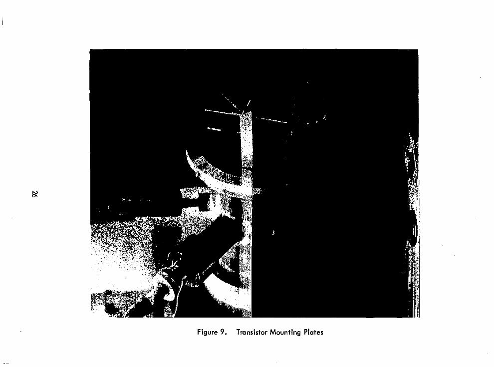
Figure 9. Transistor Mounting Plates
,----------=I
EVACUATED BEAM TUBE
REMOTE CONTROLLED COLLIMATOR I (0.03~INCH SLIT WIDTH) I
AIR
EVACUATED
b FARADAY CUP
I
/ FLUORESCENT SCREEN WITH CALIBRATED SCALE
Figure 10. Mapping of the 1000Mev Proton Beam Profile
h = height of the transmitted beam.
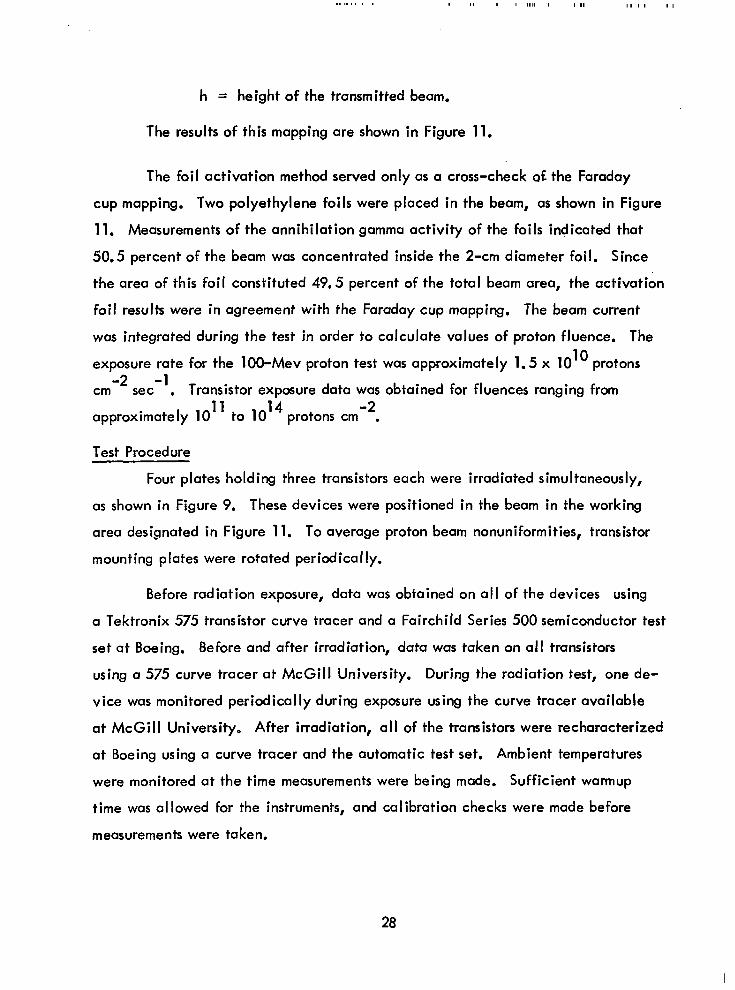
The results of this mapping are shown in Figure 11.
The foil activation method served only as a cross-check of the Faraday
cup mapping. Two polyethylene foils were placed in the beam, as shown in Figure
11. Measurements of the annihilation gamma activity of the foils indicated that
50.5 percent of the beam was concentrated inside the 2-cm diameter foil. Since
the area of this foil constituted 49.5 percent of the total beam area, the activation
foil results were in agreement with the Faraday cup mapping. The beam current
was integrated during the test in order to calculate values of proton fluence. The
exposure rate for the lOO-Mev proton test was approximately 1.5 x 10 10 protons -2 -1
cm set . Transistor exposure data was obtained for fluences ranging from
approximately 10 11
to 1014 protons cm 02.
Test Procedure
Four plates holding three transistors each were irradiated simultaneously,
as shown in Figure 9. These devices were positioned in the beam in the working
area designated in Figure 11. To average proton beam nonuniformities, transistor
mounting plates were rotated periodically.
Before radiation exposure, data was obtained on all of the devices using
a Tektronix 575 transistor curve tracer and a Fairchild Series 500 semiconductor test
set at Boeing. Before and after irradiation, data was taken on all transistors
using a 575 curve tracer at McGill University. During the radiation test, one de-
vice was monitored periodically during exposure using the curve tracer available
at McGill University. After irradiation, all of the transistors were recharacterized
at Boeing using a curve tracer and the automatic test set. Ambient temperatures
were monitored at the time measurements were being made. Sufficient warmup
time was al lowed for the instruments, and calibration checks were made before
measurements were taken.
28
WORKING AREA
-0 - 3- 3.
1 2 3
HORIZONTAL POSITION OF SLIT (CM)
(a) FARADAY CUP MAPPING
f
RADIATION FIELD OUTLINE
WORKING AREA 50.5 PERCENT
- 49.5 PERCENT OF BEAM
- 2-CM DIAMETER POLYETHYLENE SHEET
r4X4CM
POLYETHYLENE SHEET
(b) ACTIVATION FOILS
Figure 11. Results of 100-Mev Proton Beam Mapping
29
2.5 Co6’ GAMMA-RAY TEST
Co6’ gamma-ray exposure was also performed on all the transistor types
studied.
Experimental Configuration
Two experimental configurations were used during the Co 60
gamma-ray
exposure test. In the first configuration, shown in Figure 12, transistors were
arranged in a circular array about a cylindrical source. The source was located
in the Boeing Co 60
Vault and raised into the center of the array by an elevator.
In the second configuration, transistors were mounted on a cylindrical holder and
lowered into the center of a cylindrical source array. The cylindrical source array
was contained in a Gammacell 200, shown in Figure 13. The irradiation was
carried out in air for both configurations. No electrical bias was applied to the
devices during irradiation, except periodically when curve traces were obtained
on se let ted devices.
Dosimetry
The radiation fields were mapped using cobalt glass chips. These chips
were read, using a Beckman DU spectrophotometer, to a relative accuracy of about
5.0 percent and an absolute accuracy of about 10.0 percent. Exposure dose rates
for the first configuration are shown in Figure 12. Exposure dose rates for the se-
cond configuration are shown in Table 5.
Experimental Procedure
Before the gamma-ray exposure test, all transistors were characterized on
a Tektronix 575 curve tracer and a Fairchild Series 500 semiconductor test set.
During and after the test, data was obtained from the transistors using both instru-
ments.
In the first part of the test (using Configuration l), two transistors of each
type were irradiated at an exposure rate of approximately 3 x lo4 R/hr to total
exposure doses of approximately 6 x 10⁵R. One device of each type was charac-
terized during that radiation exposure using the curve tracer.
30
DOSE RATE (R/HR)
2.36 x lo4 2N1711
- 3AYlfI 4 2.32x lo4
--f @j-&G13
2N834 2N2303
3.25 x lo4 3.7 x lo4
0 PASSIVE
A DYNAMIC
Figure 12. Transistor Array for Gamma-Radiation Test
31
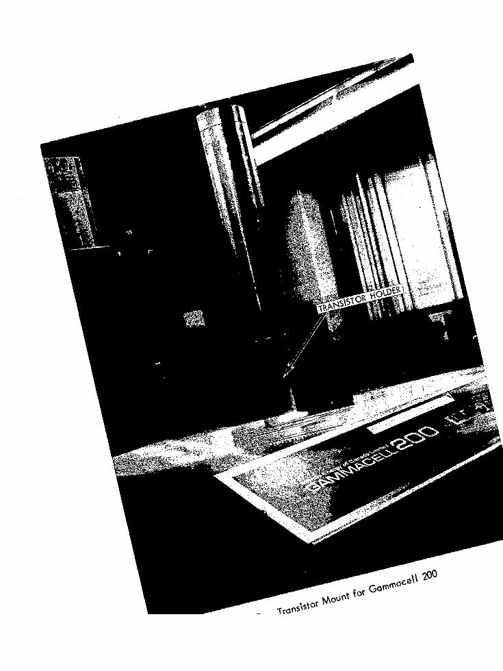
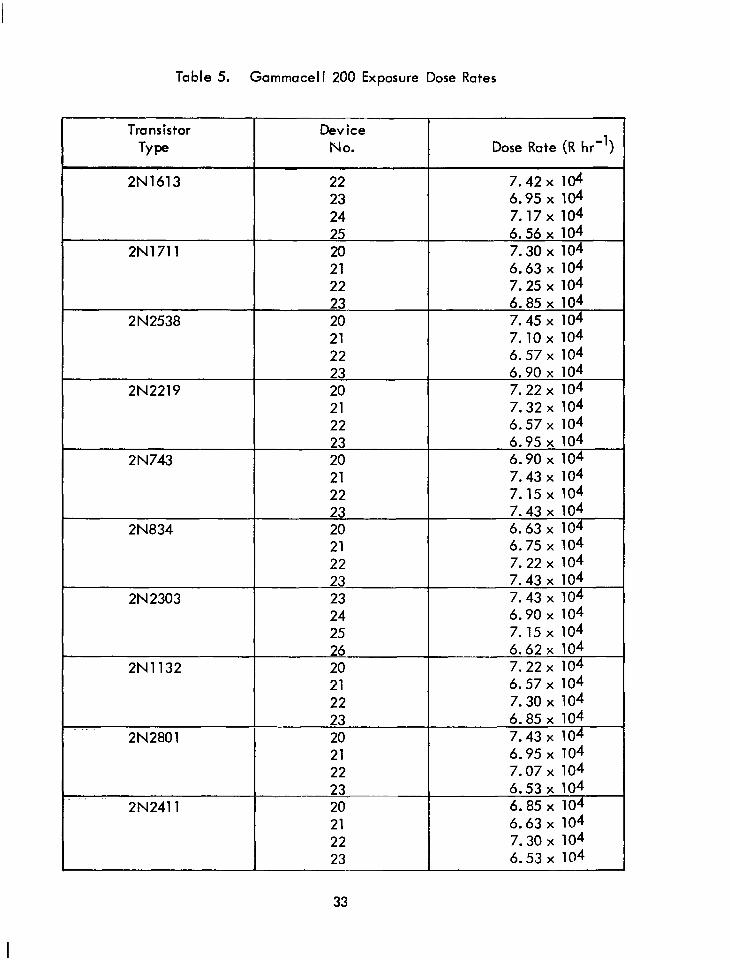
Table 5. Gammacell 200 Exposure Dose Rates
2N1613
2Nl711
2N2538
2N2219
20 7.30x 10⁴ 21 6.63 x 10⁴ 22 7.25 x 10⁴ 23 6.85 x 10⁴ 20 7.45x 10⁴ 21 7.10 x 10⁴ 22 6.57x 10⁴ 23 6.90 x 10⁴ 20 7.22x 10⁴ 21 7.32x 10⁴
2N743
22 6.57x 10⁴ 23 6.95 x 10⁴ 20 6.90 x 10⁴ 21 I 7.43x 10⁴
2N834
22 7.15 x 10⁴ 23 7.43x 10⁴ 20 6.63 x 10⁴
2N2303
2Nl132
21 6.75 x 10⁴ 22 7.22x 10⁴ 23 7.43x 10⁴ 23 7.43 x 10⁴ 24 6.90x 10⁴ 25 7.15 x 10⁴
--As- 6.62x 10⁴ 20 7.22x 10⁴ 21 6.57x 10⁴ 22 7.30x 10⁴
2N2801 23 6.85 x 10⁴ 20 7.43 x 10⁴ 21 6.95 x 10⁴ 22 7.07x 10⁴
A 6.53 x 10⁴ ._ 2N2411 20 6.85x 10⁴
Device No. Dose Rate (R hr")
22 I
7.42x 10⁴ 23 6.95 x 10⁴ 24 7.17x 10⁴ 25 6.56x 10⁴
21 6.63x 10⁴ 22 7.30x 10⁴ 23 6.53 x 10⁴
33
In the second part of the test (Configuration 2), the two transistors of each
type from Part 1, along with two additional unirradiated transistors of each type,
were inserted into a gamma-ray field of approximately 7.5 x lo4 R/hr. These
devices were exposed to total doses of approximately 3 x 10⁷R.
Before each set of transistor measurements, the test instruments were allowed
to warm up and calibration checks were made. The ambient temperature (room
temperature) was monitored with a thermocouple during the measurements.
2.6 ANALYSIS OF TEST DATA
An analysis was performed on the effects of electrons, protons, and gamma
rays on transistor parameters. The data which were analyzed included values of
those radiation-sensitive parameters measured by use of the Fairchild Series 500
semiconductor tester, as well as oscillograms of transistor common-emitter charac-
teristic curves made from the display of the Tektronix 575 curve tracer. Data
values obtained passively from the semiconductor tester were analyzed by hand
computation. Characteristic curves, obtained both passively and dynamically
(during exposure), were analyzed by the use of a computer damage-plotting program.
2.6. 1 Transistor Parameters Measured Passively
Selected values of radiation-sensitive transistor parameters, which were
measured passively, have been analyzed in order to investigate the dependence
of those parameters on electron fluence and energy.
The least radiation sensitive of the parameters which were studied was the
breakdown voltage, BVCBo (measured at a collector current of 100 pa). An
average of the values of the percentage change in BV CBO
is shown in Table 6 for
all seven irradiation tests. Most of the transistor types showed either no significant
change (within the limits of precision) or an increase in breakdown voltage which
does not appear to be a function of particle fluence. However, a decrease of
breakdown voltage was observed for transistors of type 2N2538, and the decrease
appeared to be a function of charged particle fluence. Dotted lines shown on
34
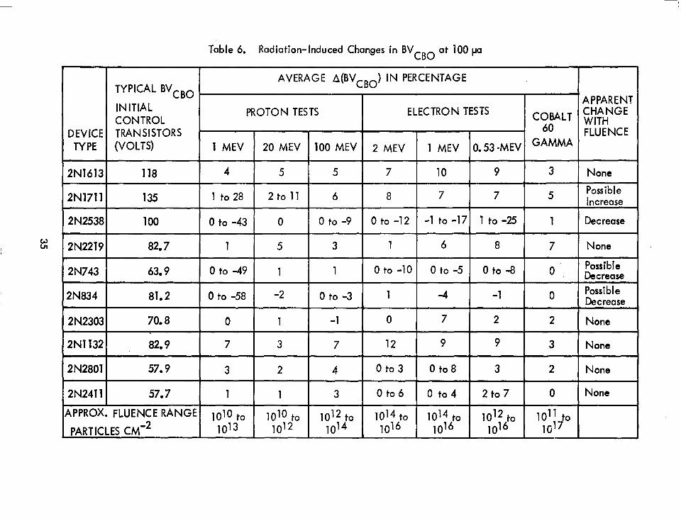
Table 6. Radiation-Induced Changes in BVcBo at 100 pa
AVERAGE A(BVCBo) IN PERCENTAGE TYPICAL BVCBO ,
INITIAL APPARENT
PROTON TESTS ELECTRON TESTS CHANGE CONTROL ‘ioMLT WITH
DEVICE TRANSISTORS FLUENCE
TYPE (VOLTS) 1 MEV 20 MEV TOO MEV 2 MEV 1 MEV 0.53 -MEV GAMMA
2N3613 118 4 5 5 7 10 9 3 None
2N1711 135 1 to 28 2to 11 6 8 7 7 5 Possible Increase
2N2538 100 0 to -43 0 0 to -9 0 to -12 -1 to-17 1 to-25 1 Decrease
2N2219 82.7 1 5 3 1 6 8 7 None
2N743 63.9 0 to -49 1 1 0 to -10 0 to -5 0 to -8 0 Possible Decrease
2N834 81.2 0 to -58 -2 0 to -3 1 -4 -1 0 Possible Decrease
2N2303 70.8 0 1 -1 0 7 2 2 None
2N1132 82.9 7 3 7 12 9 9 3 None
2N2801 57.9 3 2 4 0 to 3 0 to 8 3 2 None
2N2411 57.7 1 1 3 0 to 6 0 to4 2 to 7 0 None
4PPROX. FLUENCE RANGE 1O1O to 1010 to 1012 to 1014 to 1014 to 1012 to 1011 to
PARTICLES CM-2 10’3 1012 1014 10’6 1016 1016 lGl7
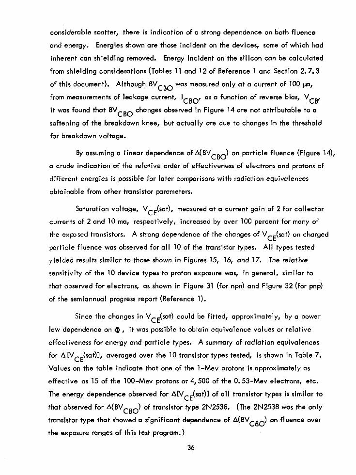
considemble scatter, there is indication of a strong dependence on both fluence
and energy. Energies shown are those incident on the devices, some of which had
inherent can shielding removed. Energy incident on the silicon can be calculated
from shielding considerations (Tables 11 and 12 of Reference 1 and Section 2.7.3
of this document). Although BVCBO was measured only at a current of 100 pa,
from measurements of leakage current, IcBo, as a function of reverse bias, VcB,
it was found that BVcBo changes observed in Figure 14 are not attributable to a
softening of the breakdown knee, but actually are due to changes in the threshold
for breakdown voltage.
By assuming a linear dependence of A(BVcBo) on particle fluence (Figure 14),
a crude indication of the relative order of effectiveness of electrons and protons of
different energies is possible for later comparisons with radiation equivalences
obtainable from other transistor parameters.
Saturation voltage, VCE(sat), measured at a current gain of 2 for collector
currents of 2 and 10 ma, respectively, increased by over 100 percent for many of
the expsed transistors. A strong dependence of the changes of VCE(sat) on charged
particle fluence was observed for all 10 of the tmnsistor types. All types tested
yielded results similar to those shown in Figures 15, 16, and 17. The relative
sensitivity of the 10 device types to proton exposure was, in general, similar to
that observed for electrons, as shown in Figure 31 (for npn) and Figure 32 (for pnp)
of the semiannual progress report (Reference 1).
Since the changes in VCE(sat) could be fitted, approximately, by a power
law dependence on 0, it was possible to obtain equivalence values or relative
effectiveness for energy and particle types. A summary of radiation equivalences
for AWCE(sat)l, averaged over the 10 transistor types tested, is shown in Table 7.
Values on the table indicate that one of the 1-Mev protons is approximately as
effective as 15 of the lOO-Mev protons or 4,500 of the 0.53-Mev electrons, etc.
The energy dependence observed for ANCE(sat)l of all transistor types is similar to
that observed for A(BVCBo ) of transistor type 2N2538. (The 2N2538 was the only
transistor type that showed a significant dependence of A(BVcBo) on fluence over
the exposure ranges of this test program.)
36
0 0
0 0
0 I
/- 0
0
0 00°0 0
0
(c’( 0 PROTONS
0
0 0 n
00 0
0/0 AVG. ,
2N2538
I,=lCQA
0 0 0 0 , 0 0- 0
0 0 .
.dO
0 0
0 ,
10’” 1014 lOI 1o16
FLUENCE, + ( PARTICLES CM-2 )
Figure 14. Dependence of A(BV CBO) on Charged Particle Fluence (2N2538)
loo
10-l
lo-2
lo-3,
10
2N2538
IC = 10MA
hFE= 2 . & 00 P ,+ ,‘b ,/’ / 0 0 0’ 0’ ~ *0’ 0 0 .z? 0 .“A 0 f0 *,,A 0’ Oyb 0
0 0
,p.’ ,‘HO ii
d’ /
0 0 0’ 0
0
0’ ,i’ ,I
0’ 0 0
0 0
0 0 0 0’ 0 0
. ‘6’ .” A
I I i ,,,,,I 1 Illl1~~ I I IllIll I 1 I ,,,I,1 I t 11111~ 1 IllIl&
1012 1013 1014 1o15 1016 101’
0
PRO:ON S
ELECTRON;
*TRANSISTOR INHERENT SHIELDING REMOVED
c
FWENCE, * (PARTICLES CM-2) Figure 15. Dependence of ANCE(sat)l on Charged Particle Fluence (2N2538)
loo II.
L
10-l = I
1o-2 -0
2N743
IC = 10 MA
hFE = 2
*- 0 0 0, 0
0’ 0’ ‘0;
0 0’ 0 0 0 0 0’ 0
‘0’ Cl
PROTONS
0’ 0
0 0’
8
0” 0
/- AwcE( SAT)] = c’#“* 78
’ 0’ ELECTRONS
* TRANSISTOR INHERENT SHIELDING REMOVED
If-l -3 1 I I I lrrlll I lIllllll I I I Ill111 I I 1111111 I I I11111 I I 11111~ .v
10 11
10 12
1o13 1o14 1o15 n 1o16 1o17
FLUENCE, 0 (PARTICLES CM-3
Figure 16. Dependence of ACVCE(sat)l on Charged Particle Fluence (2N743)
loo I-
10-l r
1o-2 ,-
0' 0 0' 0
0' 0’
0’ 0
0 0-
f
0” 0’ 0 0 0 0 0’ 0
.’ PROTONS
t
2N 834
IC = 10MA
h 2 FE=
* TRANSISTOR INHERENT SHIELDING REMOVED
I
1o-3 1 I I I I lllll I I I11111 I I I I Illll I I I llllll I I I I Ill1 I I IIlllJ
loll
L
1o12 1o13 1o14 1o15 1o16 1o17
FLUENCE, + (PARTICLES CM-2)
Figure 17. Dependence of AIVcE(sat)l on Charged Particle Fluence (2N834)
Table 7. Charged Particle Equivalences for ACVCE(sat)l
Tests
1 -Mev Proton
Can Off
20-Mev Proton Can Off
Proton Tests (Mev) Electron Tests (Mev) I I
1 20* 100 2 ** 1*** 0.53 1
I 1
1 3.0 1.5x101 ))
1. 1x10³ 2.3~10~ 4.5x10³
3.3x10-l 1 5 3.8~10~ 7.5x10² 1.5x10³
100 -Mev Proton
2-Mev Electron
6.7~10~~ 2%10-l 1 7. 5x101 1.5x10² 3x10²
9.1x10 -4 2.6x10 -3 -2
1.3x10 1 2 4
1 -Mev Electron 4. 3x10d 1. 3xlo-3 6.7~10-~ 5x10 -1 1 2
0.53-Mev Electron
Can Off 2.
2x10d 6.7x10
-4 3.3x10
-3 2.5x10
-1 5x10-l 1
* Energies 14 to 17 Mev on the silicon chip ** Energies 1.5 to 1.7 Mev on the silicon chip
*** Energies 0.8 to 1.0 Mev on the silicon chip
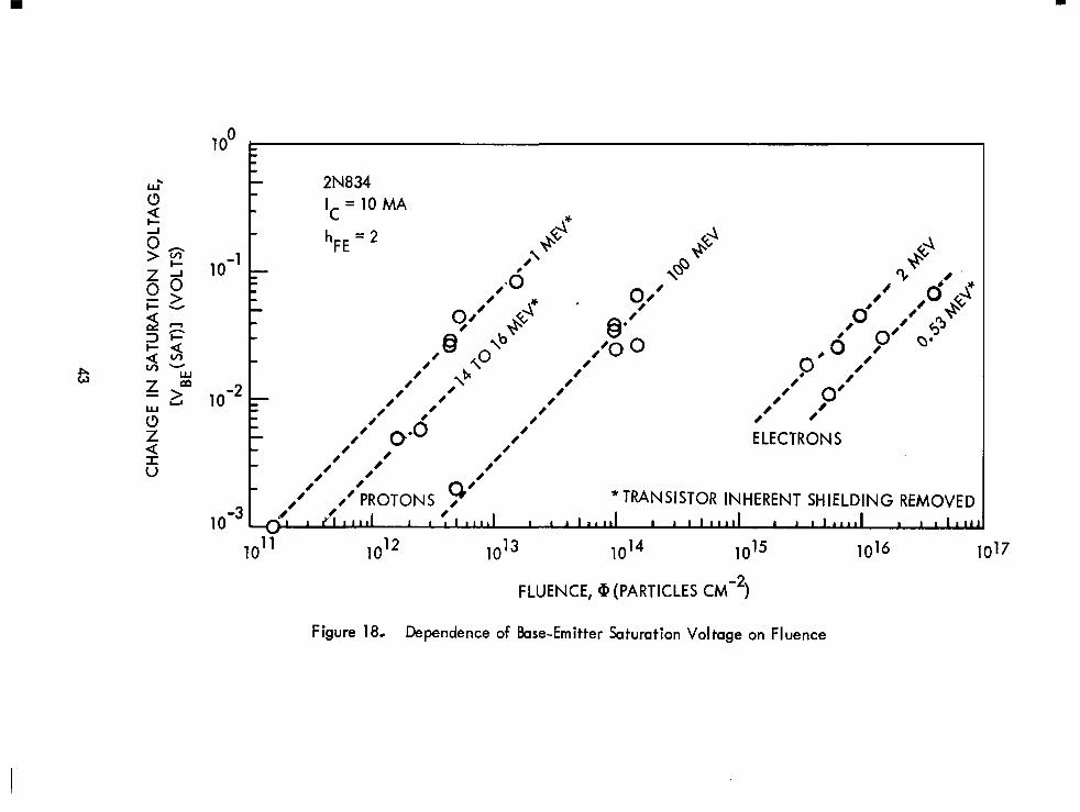
The observed changes in base-emitter saturation voltage, VBE(sat), were
smaller than those observed for V (sat). However, AN (sat)1 also shows a CE BE
strong dependence on particle.fluence, as shown in Figure 18. Charged particle
equivalences obtained from changes in VBE(sat) are, in general, comparable to
those summarized for ANCE(sat)l in Table 6.
Leakage current, Ic B. (measured at a collector-to-base reverse bias of
10 volts), was observed to show permanent increases for tmnsistors exposed to
charged particles. As described in Reference 1, A(lCBO), over a narrow range of
high exposures studied using passive data from the electron tests, showed no evidence
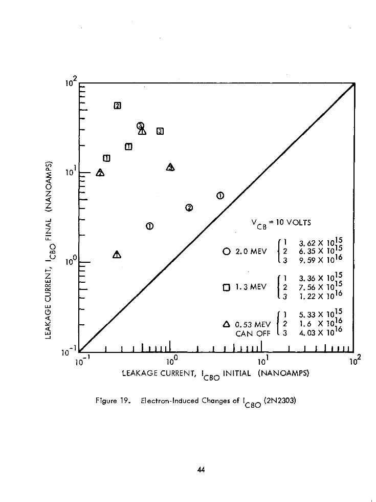
of a dependence on electron fluence. Figure 19 shows a comparison of initial-
and final-leakage currents for the 2N2303 tmnsistors irradiated in the electron
tests. The diagonal line represents values for no change. This tmnsistor type came
closest to showing a dependence on the amount of electron exposure, but it also is
the only tmnsistor that showed such a wide variation in both initial and final
values of leakage current. Five other transistor types (2N1132, 2N1613, 2N1711,
2N2219, and 2N2801) also showed large changes in leakage current but no obvious
dependence on electron energy. Electron test data on these devices is shown in
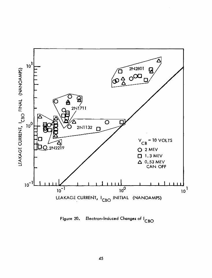
Figure 20, with the exception of the 2N1613 whose data point grouping was the
same as the 2N1711. These devices, with the exception of the 2N1132, showed
the same increase in lcBO independent of initial value, which would indicate
greater percentage increases for those of lower initial-leakage current. The re-
maining transistor types (2N743, 2N834, 2N2411, and 2N2538) showed only very
small percentage increases in leakage current. The individual groupings of tmn-
sisters shown in Figure 20 would indicate that tmnsistor types with the highest initial
values of leakage current generally would have the highest values of leakage current
following an exposure (Reference 2) even as great as 10 electrons/cm2 (an exposure 16
far in excess to that of a typical space mission). This fact was observed for all of the
tmnsistor types tested. Six types of transistors showed average changes of lCBO of
approximately an order of magnitude for the electron tests. However, four types of
tmnsistors (2N743, 2N834, 2N2411, and 2N2538) showed only small percentage
changes; thus their initial and final leakage currents would necessarily conform to
the results of the other six types.
42
10-l
1o-2
lo-3
2N834 2N834
IC IC = 10 MA = 10 MA
.* h h
FE=2 FE=2 \* ,+@‘
4
@ @
& & 4? 4? ,’ ,’
3 3 . . 0-O 0.0
9” 9” I I
0 0 4” 4” 4 * 4 * 0” 0”
‘d’$$ ‘d’$$
0 <OYb ‘Q ‘Q <OYb “‘b “‘b #’ #’
0’ Q 0’ Q
“0 “0 ,Q ,Q ?’ O’ ?’ O’ 0 0 0 0 0
0 0+ 0+
0 0 p 0’ p 0’
0 0 0 0 ’ ’ 0
0 ““o.~’
0 0 0 0
0 ““o.~’ 0
0 0 0 0 0 0 0 0
0 9” 0 9” 0 0 0 0
0 0 0 E;ECTR~N S E;ECTR~N S 0 0 0’
0 0 0 0 0’ 0 0 0 0 0 0 0 0
0 0 0 0
0 0 .,/PROTONS .,/PROTONS 9”’ 9”’ *TRANSISTOR INHERENT SHIELDING REMOVED *TRANSISTOR INHERENT SHIELDING REMOVED d d f f 0 0
1 I 1 1 I 1 lllll, 1 lllll, I I I Ilrrl I I Ill11 I I 1111111 1111111 I I II1111 1 I II1111 I I 1 1 1 1 Ill{ IIll
loll 1012 1013 lo14 1015
FLUENCE, Q (PARTICLES CM-2)
Figure 18. Dependence of Base-Emitter Saturation Voltaae on Fluence
1016 1017
0 'OLTS
2 -” loo-
A
f 2 5 0 1.3MEV : ;:;;; $
v 3 1.22 x 10¹⁶
s
I
1 5.33 x 10¹⁵
2 A 0.53 MEV -I CAN OFF 2 3 4.03x 1.6 X 1016 1016
1n -1 1 I I1llrl I I II ill[ .”
10-l loo lo1
LEAKAGE CURRENT, lcBO INITIAL (NANOAMPS)
d
lo2
Figure 19. Electron-Induced Changes of lcBO (2N2303)
44
lo1
L m - t
32 -
V CB
= 10 VOLTS
0 2 MEV
0 1.3MEV
a 0.53 MEV CAN OFF
I I I IWll I I I IIIII
loo
LEAKAGE,CURRENT, lcBo itwiAL (NANOAMPS)
Figure 20. Electron-Induced Changes of lcBo
45
Although detailed analysis of changes of lcBo were performed only for
collector voltages of 10 volts, the dependence of leakage current on voltage
(measured on selected devices) was typical of the dependence before irradiation.
Breakdown voltages (at 100 pamps), in general, showed very little change (plots as
a function of current indicate a sharp breakdown rather than a softening of the break-
down knee for exposures up to 4.24 x 10 12
1 -Mev protons/cm2). Breakdown volt-
ages after the irradiation tests all were in excess of the 10 volts used for I
measurements. CBO
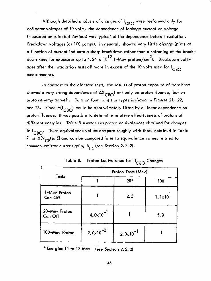
In contrast to the electron tests, the results of proton exposure of transistors
showed a very strong dependence of A(lcBo) not only on proton fluence, but on
proton energy as well. Data on four transistor types is shown in Figures 21, 22,
and 23. Since A(IcBo) could be approximately fitted by a linear dependence on
proton fl uence, it was possible to determine relative effectiveness of protons of
different energies. Table 8 summarizes proton equivalences obtained for changes
in ICBO. These equivalence values compare roughly with those obtained in Table
7 for ANCE(sat)l and con be compared later to equivalence values related to
common-emitter current gain, hFE (see Section 2.7.2).
Table 8. Proton Equivalence for lcBo Changes
Proton Tests (Mev) Tests
1 20* 100
1 -Mev Proton Con Off 1 2.5 l.lxlOl
20 -Mev Proton Con Off 4.ox1o-1 1 5.0
1 OO-Mev Proton 9. oxlo-2 2.0x10 -1 1
l Energies 14 to 17 Mev (see Section 2.5.2)
46
2+ 8 3* &
0 2N1613 0 0 El ,P 0
0 2N1711 0 0’ 0 0
‘CB = 10 VOLTS
0 0 ;” B 06 0 00 0’ ’ I&
0 $s ‘0’ 0 0 0 0 0 0 0 + o 0’ 0 AUCBO) = C@
0 0‘ 0’
\ 0 0 0 0 0 0 0 0 ” 0 0 0
0 0 0’ 0 0 O “%
0 0 ‘0’ 0 0
0 B’ “6’ 0 0 0 cp”’ ‘0’ ()“’ 0 0 0 0 0
0 0 *TRANSISTOR INHERENT
SHIELDING REMOVED 0 0 0 -’ 0
z w loo : 4 U 1,
I
w I 1 1 111111 I I I I l,lll I I I lllll I
loll 12
1013 14
10 10
FLUENCE, @ ( PROTONS CM-2 )
1
Figure 21. Dependence of A(icBd on Proton Fluence (2N1613 ,2N1711)
2 2
2N2219
0 0 1 MEV (CAN OFF) 0 5
lo1
0 14 TO 16 MN (CAN OFF) 0 0
Z A 100 MEV 6
A 0
,’ G 2 V CB = 10 VOLTS /-
/ 0 aA
,u 0
@“’
“‘A
z c 7
/‘O ,’
a” AA
I, iii 22 0’ 0,” 0- 0 2 2’ 0 0 0 tj loo A(IcB~ = CQ 0 0 0 0 0 0
5 0 0 0 “‘0 0 0 0
J z / 0 0 0
0 ‘0 0
z 0 0 0 0 0% 5 0 0
E 0
# 0 0
lo-‘
0
loll 1012 1013 1014
I Q/ I I I I Id I I I I IllI I I Illlll I I Ill
FLUENCE, QI ( PROTONS CM-2 )
Figure 22. Dependence of A(lCB0) on Proton Fluence (2N2219)
lo2
lo1
loo
: ,- I-
I
L
101’
2N2801
0 1 MEV (CAN OFF) 0 16 MEV (CAN OFF) A 100 MEV
vC B= 10 VOLTS
0 0
0 8 0
0
9” 9’ 0
0’ 0
0 0
0 0
0 0
0 0
0 0
A
$.“’ 0’
A,’ A
I I I I IIll I I I llllll I I I I III1 I I Ill
1012 1013 1014
FLUENCE,4 ( PROTONS CM-2 )
Figure 23. Dependence of A(lCeo) on Proton Fluence (2N2801)
The comparative permanency of these linear changes in A(lcBo) at room
tempemture (299°K) was verified by measuring lcBo at selected time periods
following mdiation exposure. Delta on 2N1613 devices are shown in Figure 24 for
time periods of 5, 31, and 202 days after 1 -Mev proton exposure. Figure 25 in-
dicates that only slight annealing was observed for most of the transistor types after
high-fluence proton exposure. However, CJ couple of the epituxial mesa devices
that showed anomalously large changes in leakage current at high exposures also
showed pronounced recovery, as shown in Figure 26. (No biases were applied
during or following exposure, except for measurements.) After those devices had
recovered at room temperature, they more closely fitted a linear dependence on
fluence which was similar to that shown in Figure 21, 22, and 23. The permanent
components of proton-induced A(lcBo) provided information on proton equivalences
(Table 8) similar to equivalences for ANCE(sat)l of Table 7.
Curves of collector current, Ic, as a function of base-emitter voltoge,
VBE, were plotted from data obtained on the Fairchild transistor tester (e.g.,
Figure 27). According to the analysis of Easley (Reference 3) and Goben (Reference
4), one would expect Ic to decrease as the base transport factor decreases. The
curve of Figure 27 might also be expected to appear OS a straight line on a semi-
log plot if the typical diode equation is valid.
Ic = lo Cexp(qVBdkT) - 11
where:
(3)
9 = electronic charge
k = Boltzmann’s constant
T = absolute tempemture
50
10’
L
10 11
2N1613 V
CB = 10 VOLTS
T = 299’K
.
PERIOD AFTER EXPOSURE
0 5 DAYS 0 31 DAYS A 202 DAYS
I I I Illll I I I I Ill1 I I I I lllll I
lo’2 lo’3
1 -MEV PROTON FLUENCE (PROTONS CM’2,
10 14
Figure 24. Slight Annealing of d(ICBO)(2N1613)
I 0 0 2
Z ;r: 10’ - SYMBOL SYMBOL
2 0 0 -u a a
Cl Cl
0 0 V V
z
8 8 B Ei
0 9 0 rJ
0 0 DEVICE TYPE EXPOSURE (PROTONS CM-2)
2Nl613 1.54 2N171.1 1.99 2N2303 1.63 2N1132 1.71 x 10¹³ 2N2801 2N2219 ;:z 2N 2411 1.95
I
V CB = 10 VOLTS DURING MEASUREMENT,
NO BIAS DURING OR AFTER EXPOSURE
1 I lllll I I I Illrl I
10 100
TIME AFTER PROTON EXPOSURE (DAYS)
Figure 25. Slight Annealing of lcBo After 1 -Mev Proton Test
52
0 2N743 0 2N834
5; lo2 “r 8 2 z. 2 E z 2 -”
I 10’
5 EI
2 -!
loo
-c -0
--all U
V CB
= 10 VOLTS DURING MEASUREMENT’,
NO BIAS DURING OR AFTER EXPOSURE
1 -MEV PROTON EXPOSURE OF 1.58 x 10 l3 PROTONS CM-2
I I I I I I I I I I I I I
0 30 60 90 120 150 180 210
TIME AFTER PROTON EXPOSURE (DAYS)
Figure 26. Annealing of lcBo of Epitoxial Mesa Devices
53
1o-z
105 t 0.
.
/I w
0 2N2303 NO. 18 UNEXPOSED
0 2N2303 NO. 18 EXPOSED
I/ TO 0.531-MEV ELECTRONS
0 II
(4.03 x 10’6 e/CM2)
‘/ I r
I I I I I I 1 I 1 I I I I 0.55 0.60 0.65 0.70 0.75
BASE EMITTER VOLTAGE, VBE (VOLTS)
Figure 27. Ic Versus VeE for 2N2303
0. 80
54
The IC curves, however, show a deviation from linear which, at high current,
appears at first order to be due to a transverse voltage drop in the base sheet re-
sistance and a fringing of the collector current due to the field set up by this vol-
tage drop (Reference 5). It has been shown (References 6, 7; and 8) that transistor
base current consists of the sums of components of recombination current originating
in various regions of the device. Each of the base current components, (IB) ,
approximately follows an exponential dependence on base-emitter voltage, n
(Ig) 2 (lo) exp (qVBE/nkT) n n
(4)
where : (lo) = a constant dependent on physical properties of the device and n
is a function of radiation exposure. (In some cases lo may
depend on VBE. )
n = a component number whose value at any specific value of
VBE depends on the region in which that component of
recombination current originates.
The following components have been identified:
n = 1.0 component -recombinationseneration current in the base region
1 < n L 2 component -recombinationgeneration at or near the surface and
in the bulk of the emitter space-charge region
2 ( n 5 4 components - surface channel currents
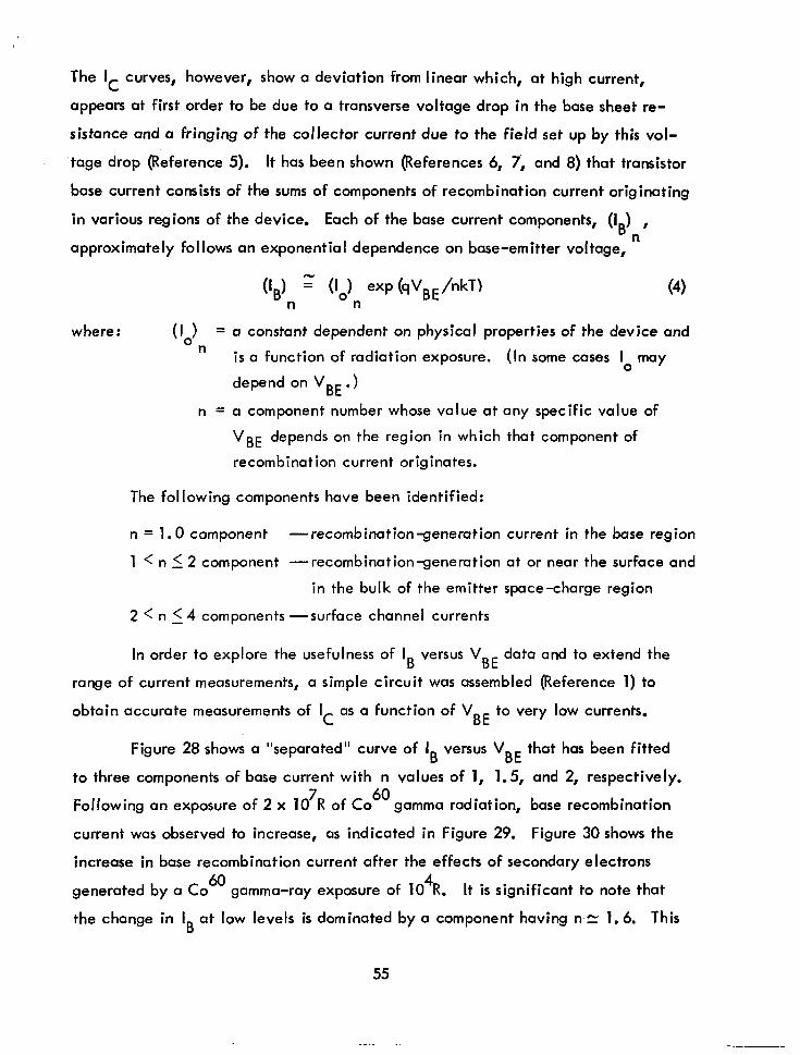
In order to explore the usefulness of IB versus VBE data and to extend the
range of current measurements, a simple circuit was assembled (Reference 1) to
obtain accurate measurements of IC as a function of V BE
to very low currents.
Figure 28 shows a “separated” curve of IB versus VBE that has been fitted
to three components of base current with n values of 1, 1.5, and 2, respectively.
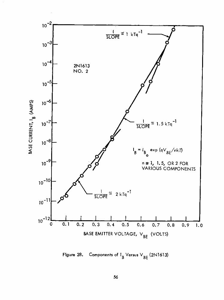
Following an exposure of 2 x 10⁷R of Co 60
gamma radiation, base recombination
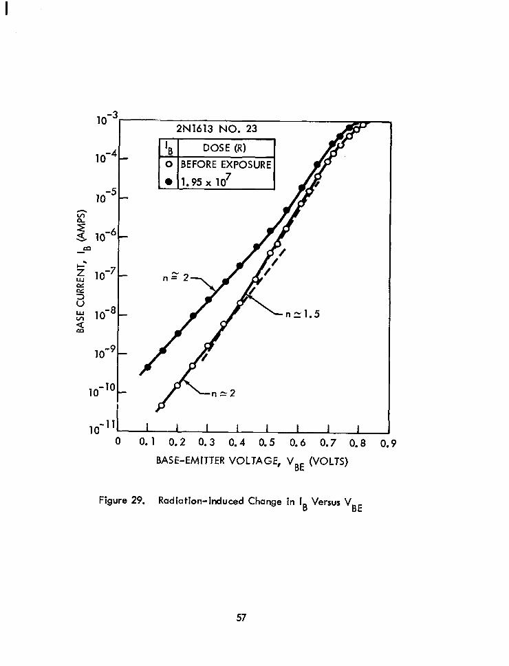
current was observed to increase, as indicated in Figure 29. Figure 30 shows the
increase in base recombination current after the effects of secondary electrons
generated by a Co 60
gamma-ray exposure of 104R. It is significant to note that
the change in IB at low levels is dominated by a component having n z 1.6. This
55
10
10
10
10
z 10
2 m
2 10’
z 5 v % 10
25
10’
lo-
70-,l
- g 1 kTq-’ I CI nrc
2N1613 NO. 2
nb.1, 1.5, OR2FOR VARIOUS COMPONENTS
2 kTq-’
I I I I I I I I I - _ 0.1 0.2 0.3 0.4 0.5 0.6 0.7 0.8
R4SE EMITTER VOLTAGE, VBE (VOLTS)
Figure 28. Components of IB Versus V BE (2N1613)
56
2N1613 NO. 23
rn I -4 - lB DOSE (R) I 1” r 1 0 IBEFORE EXPOSURE 1
I
10 -5
5
- t
3 1o-6 m
s 10-7 iii
2 s 1o-8 Q m
i
0 0. 1 0.2 0.3 0.4 0.5 0.6 0.7 0.8
BASE-EMITTER VOLTAGE, VBE (VOLTS)
0.9
Figure 29. Radiation-Induced Change in IB Versus VBE
57
1o-4
2 2 1o-5 s.
$
5r is
2 1o-6
: Q
z
z
f 2 10-7
l,o-8 0.40 0.50 0.60 0.70
BASE-EMITTER VOLTAGE, VBE (VOLTS)
Figure 30. Change in lB Versus VBE After 104R Gamma Exposure
58
slope has been associated with the emitter depletion region rather than the base
region.
As a supplementary study to this contract, a number of measurements were
performed and reported at the annual IEEE Radiation Effects Symposium (Reference 9).
Further discussion of analysis of this type of damage is also presented in Section 2.9.
2.6.2 Computer Analysis of Characteristic Curves
Data in the form of common-emitter characteristic curves were analyzed in
detail using a transistor-damage-plotting program and an SRU 1107 computer (Refer-
ence 10). Raw data consisting of oscillograms of transistor d. c. characteristics (e. g.,
Figure 1) were taken by Polaroid camera from the display of a Tektronix 575 transistor
curve tracer. Auxiliary information was fed to the computer on IBM cards (see
Table 9 for example). As many as 20 dynamic pictures (taken during radiation
exposure) were recorded on selected transistors, The raw data was transferred to
IBM card form by the use of a Benson-Lehner Model Oscar F oscillogram reader.
The reader can be used to measure trace amplitudes, apply calibrations, convert
the data to engineering units, and automatically operate a card punch.
Card punch data was fed into the SRU 1107 computer along with computer
option information. Several options were used for analysis and plotting of the
characteristic curve information. The first option employed requested a replot of
the IBM card input information into the form of Ic versus Vc plots, as was shown
in Figure 1. Plots of this type were obtained from all transistors tested and were
stored on microfilm. A microfilm reader was then used to screen for errors and thus
guarantee that correct input data had been received and stored into the computer.
The second computer option exercised was to obtain plots of d. c. current
gain, hFEt as a function of emitter current and as a family of fluences. Included
as examples of this option are copies of actual computer plots for an npn diffused
planar device (Figures 31 and 32), an npn epitaxial planar device (Figures 33 and
34), and an epitaxial mesa device (Figure 35). Examples of this computer option
for a pnp diffused planar (Figure 36) and a pnp epitaxial planar transistor (Figure 37)
59
Tmnsistor
Table 9. Keypunch Data Form
TEST HEADING CARD Tmnsirtar No. of btch
m 0
.,-..-.-.-. ..- .._._._.
Test Type No. Pictures No. CaK Mfg. 13 5 7 9 11 13 15 17 19 21 23 25 27 29 31 33 35 37 39 41 43 45 17 49 51 53 55 57 59 61 63 65 67 69 71 n 75 n 79
7 4 6 8 10 I2 14 16 18 20 22 24 26 28 30 32 34 36 38 40 42 44 46 48 50 51 54 Y M 60 62 64 66 W TO 72 74 76 78 80
23 I 11*l111 I ha A 1% ON FC CD I I I I 1 I I I I I I I I I I
I I II I I II II
I PICTURE READING CARD III 11 I I
i%lure ! I
Dd I Titke 1 )div
F LC)di: ,-Ldd k&or iklusnlx ’ ‘~T!&m:ur~ -
. No. fd (volts) i$step (m_egphms) (clcctronr/cm 2, (degrees absol utec) 13 5 7 9 11 13 15 17 19 21 23 25 27 29 31 33 35 37 39 41 43 45 47 49 51 53 55 57 59 61 63 65 67 69 71 n 75 n 79
2 4 6 8 10 12 14 16 18 20 21 24 16 2@ 30 32 34 36 38 40 42 44 '6 48 Yl 52 54 56 3 60 62 64 66 68 70 72 74 76 IE 80
Al 07 27 65 ’ 14 56 2. 0 2. 0 0 .05 O.O!IOl 0.0 29 8. 5
A2 09 28 65 1307 2.0 2. 0 0 .05 0.0001 0.0 294. 2 B 09 30 65 14 32 2. 0 2. 0 0 .05 0 .OOOl 5. 04 E 14 29 9. 7 C 09 30 65 23 35 2. 0 2. 0 0 .20 0 .OOOl 3. 64 E 15 29 8. 7 D 10 01 65 10 53 2. 0 2. 0 0 .50 0 .Oool 1. 82 E 16 29 8. 2
I
0 2 4 6 EM‘ik? CUd:NT 12 14 16 18 20
(HA)
2Nl613 TEST 24 IWSITIW 1 1 .O HCV PROTON ICRADIATIC#d DC GAIN VS. EMITTER CLJRfiENT, FAMILY OF FLUCrKfS, CaLECTCR VOCTACE = 10.0
T;iT ‘“A~;;;“’ TRA;;.NO. D$~‘;H F;d; C;;lJ; NH~if;$l CASE . . UT
PfCylE FLy$CE MAX. GAIN HINi3G;IN 52.2
f 1:9t10 46.6 39:o 4.6tlO 42.9 35.0
4 1.0+11 36.3
2;::: 9:s*11
::*eg 10: 7
: 4.2t12 1.9t12 2: t::
Figure 31. 2N1613 hFE Versus IE for I-Mev Protons (High Gain)
61
10
6-
8 ” 5,
;:
4
J-
2L
l-
cb 0
2 4 6 12
EMI :TER CL&NT 14 16 16
(HA)
ON1613 TEST 24 POSITlo(J 1 1.0 MEV PROTW IRRADIATICM
K GAIN VS. EMITTER CWRENT, FAMILY OF FLUENCES, CULECTC6 VOLTAGE = 10.0
PIC;U?E f:u$z; MAX. GAIN HIN.4G$IN
9 4:2+12 28’ 2:a
Figure 32. 2N1613 hFE Versus IE for 1 -Mev Protons (Low Gain)
62
90t
800
IOF-
600 -
--
-
- -
--I_
- .
-
--
--
0 2 4 EiTlER CUtiRtNT 10 12 14 16 (HA)
2Ep219 TEST 24 POSITI~ 4 1.0 MEV PROTW IRRADIATION
K GAIN VS. EMITTER CURRENT, FAMILY CF FLUCNCES, CCCLECTU? VCCTACE = 10.0
TEST TRANS.TYPE TRAN;.W. D;;;H ;;“L; CUTCFF NM,f:;Q CASE 24 2219 555 . cff
PIC:URE fI$kNCE
::;:;;
MA,:&IN HI~j3G~IN
3 14917 113:4 97.5 4 2:5+11 :::*5 69.7 i :*;r::
1:9+12
62:2 45.5 53.5
xi 4.2+12 24:1
Figure 33. 2N2219 hFE Versus lE for 1 -Mev Protons (High Gain)
63
0 2 4 EH:TTER CltRR:NT (MA)
10 . 12 14 16
2M2219 TEST 24 POSITIO(J 4 1.0 HEV PROTOtd IRRADIATION
K GAIN VS. EMITTER CURRENT, FAMILY OF FLUEIKES, CULECTOR VOLTAGE = 10.0
T;iT TRW:YPE TRAN;.H3. B;;;H HAKE CUTOFF NML~‘~,‘” CASE FCLD 555 . CFf
PICTURE fL4U;fC;
i 9:5*11 1.9+12 4.2+12
Figure 34. 2N2219 hFE Versus IE for 1 -Mev Protons (Low Gain)
64
-.... -. - .-.._. __-.. _ ..,. , ,.. . II . ,,--
2 4 di TTER Cu?R&T (WA)
10 12 14
tw34 TEST 24 POSITION 6 1.0 MEV PROTO(J IRRADIATION
K GAIN VS. EMITTER CVRRENT, FAMILY CF FLUEtKES, COLLECTCR KtTACE = IQ.0
WAXi6C$IN WINj6C;IN
6410 54:o 17.6 45.4
32.6
: 4.1*11 o.s*11 %*:
: l.Q+lt 4.2*12
1;:: .
16
Figure 35. 2N834 hFE Versus iE for 1 -Mev Protons
65
-.
0 1 2 3 4 5 T:ER &RENT’ 9 10 11 12 13 14 15 EMI (MA)
2Nll32 TEST 24 POSITION 8 1.0 MEV PROTCW IRRADIATION
K CAIN VS. EMITTER CURRENT, FAMILY CF FLIJENCES, CCCLECTCR VCLTAGE = 19.0
HAXi2C;IN MIN$;IN
5713 ss:1 51.9 47.8
34.4 24.1 14.3
Figure 36. 2N1132 hFE Versus IE for 1 -Mev Protons
66
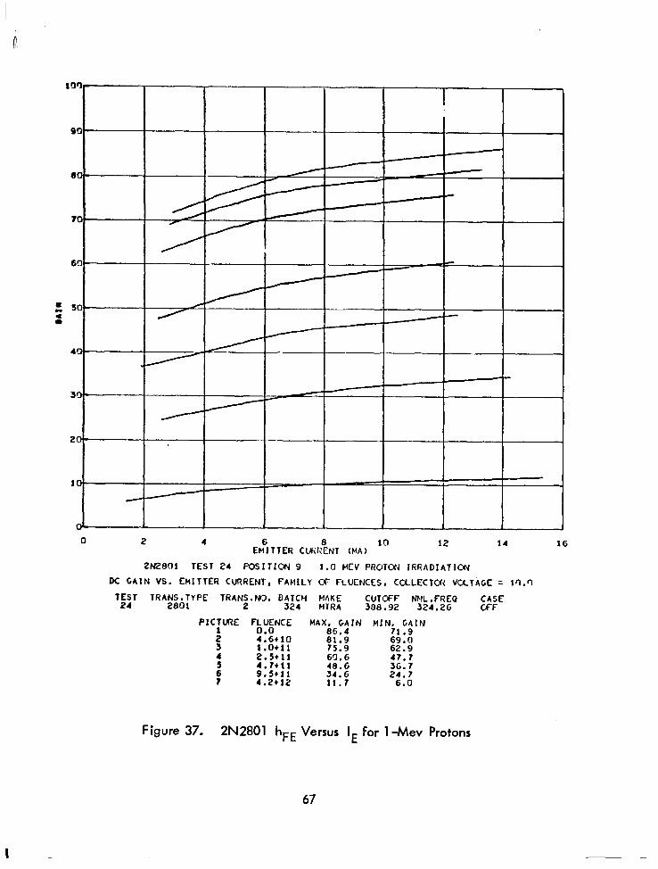
0 2 4 6 e 14 EMITTER CURRENT (MA)
10 12 16
2M2801 TEST 24 POSITION 9 1.0 MEV PROTON IRRADIATIW DC GAIN VS. EMITTER CURRENl, FAMILY Cc fLUCNCES, COLLECTW VaTiCE = lrl.‘l
T;iT TRA;;s-;YPE TRAN;.W. D;;iH ;;;: $Of; N’;‘;;‘;;” CASE . . WF
PIC:URE F,U;rJCE
f 4:6+10
MAX. GAIN MINilG;IN 86.4
1.0+11 ;:*; g:;
4 2.5+11 6Cl:G 47: I 4.7+11 46.G 36.7 9.5*11 34.6 4.2+12 11.7 2i.07 .
Figure 37. 2N2801 hFE Versus iE for 1 -Mev Protons
67
I .-
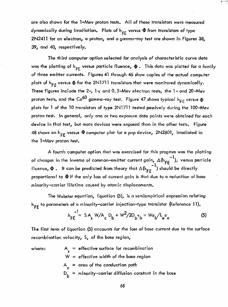
are also shown for the 1 -Mev proton tests. All of these transistors were measured
dynamically during irradiation. Plots of hFE versus * from transistors of type
2N2411 for an electron, a proton, and. a gamma-ray test are shown in Figures 38,
39, and 40, respectively.
The third computer option selected for analysis of characteristic curve data
was the plotting of hFE versus particle fluence, Q . This data was plotted for a family
of three emitter currents. Figures 41 through 46 show copies of the actual computer
plots of hFE versus Q for the 2N1711 transistors that were monitored dynamically.
These figures include the 2-, l-, and 0.5-Mev electron tests, the 1- and 20-Mev
proton tests, and the Co6’ gamma-ray test. Figure 47 shows typical hFE versus Q
plots for ‘l of the 10 transistors of type 2N1711 tested passively during the lOO-Mev
proton test. In general, only one or two exposure data points were obtained for each
device in that test, but more devices were exposed than in the other tests. Figure
48 shows an hFE versus @ computer plot for a pnp device, 2N2801, irradiated in
the 1-Mev proton test.
A fourth computer option that was exercised for this program was the plotting
of changes in the inverse of common-emitter current gain, A(h -1
), versus particle
fluence, QT . It can be predicted from theory that A(hFE -‘) shofu:d be directly
proportional to @if the only loss of current gain is that due to a reduction of base
minority-carrier lifetime caused by atomic displacements.
The Webster equation, Equation (5), is a semiempirical expression relating
hFE to parameters of a minority-carrier injection-type transistor (Reference 11).
h -1
FE = S AS W/AC Db + W2/20brb + Wub/L a
ee (5)
The first term of Equation (5) accounts for the loss of base current due to the surface
recombination velocity, S, of the base region,
where: A = effective surface for recombination
v;= effective width of the base region
A C
= area of the conduction path
Db = minority-carrier diffusion constant in the base
68
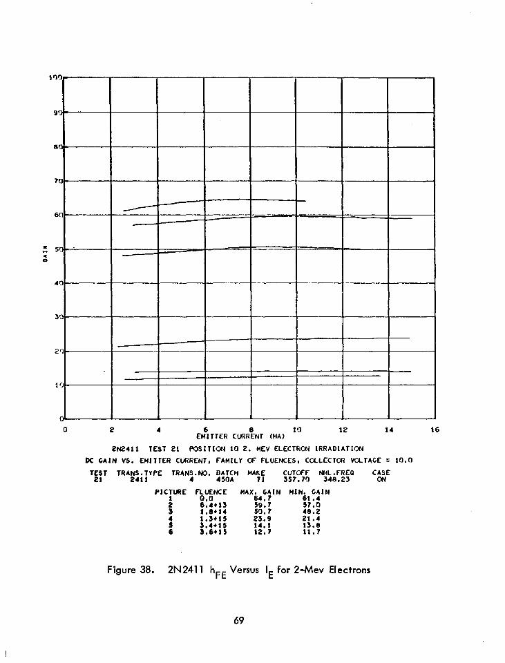
0 2 4 EH6;TTER CWRBENT 10 12 14 16 (MA)
2N2411 TEST 21 P0SlTION 10 2. MEV ELECTRCN IRRADIATIW
K CAIN VS. EMITTER CWZRENT, FAMILY CF FLUENCES, CCCLCCTOR VaTACE = IO.0
MAXli4C;IN MIN~,C~IN
591? 3710 SO.? 48.2
::*fJ 21.4
1217 ::*: .
Figure 38. 2N2411 hFE Versus IE for 2-Mev Electrons
69
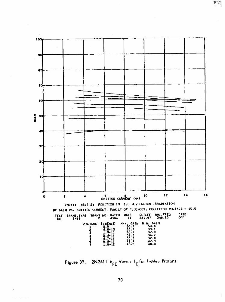
0 2 4 Enbr TTER Cu?RtNT LIdA’
l!J 12 14 16
2W411 TEST 24 POSITION 10 1.0 HEV PROTON IRRADIATION
DC GAIN VS. EMITTER Cl%RENT, FAMILY cf FLUEtKES, CULECTOR VUTAGE = 10.0
nJN;9G~JN 59:1 57.9
:z 4r:o 56.0
Figure 39. 2N2411 hFE Versus IE for 1 -Mev Protons
70
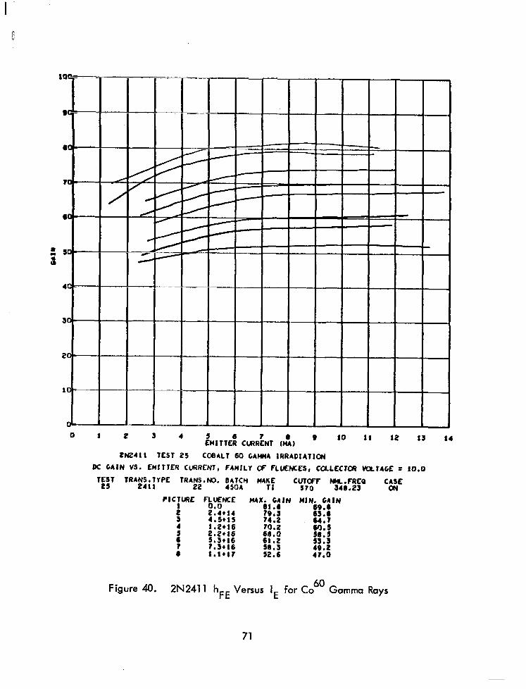
10~
DO-
oc-
10-
ao-
: so- 8
40-
SO-
20-
IQ-
0 1 2 3 4 :“JTTE: CURR:NT Jht,
9 10 11 12 1S 14
2HLSll TEST 25 COBALT 60 CAWlA IRRADIATIW
DC CAIN VS. EMJTTER CLlRRENT, FANJLY Q fLLUEHCES, CCUECTClP KXTAGE = 10.0
PIC:U?E Fh%rKE
f 2:4+14 4.5+15
4 1.2+16
: t5:::
: ?:S+16 1.1+11 52.6 41.0
Figure 40. 60
2N2411 hFE Versus IE for Co Gamma Rays
71
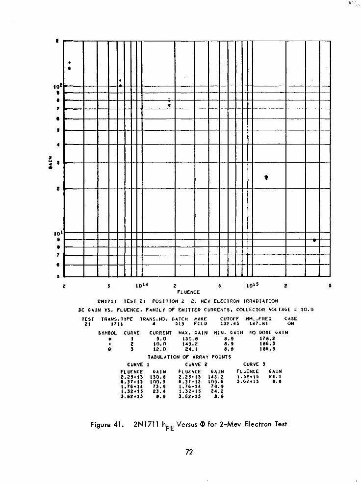
8
4
2
2
l
l
101’ 2 5 FLUENCE
ONill 1 TEST 21 POSITION 2 2. MEV ELECTRON IRRADIATION
DC GAIN VS. FLUENCE, FAMILY W EMITTER CURlitNTS, COLLECTOR VOLTAGE = 10.0
TEST TRANS. TYPE 21 IT11
1RANS.W. DATCII :;M; CUTOFF NML .FREO CASE 4 513 132.45 147.81 OH
SYHBGL CURVE +
cf : 3
CURVE
FLUENCE 2.25*13
:*2:::: 1:32*15 3.62*15
CURRENT HAX. GAIN MIN. CAIN No DOSE CAIN 5.0 130.8 176.2
10. D 143.2 ii:: 166.3 12.n 24.1 0.8 186.9
TABULATION Of ARRAY POINTS
1 CURVE 2 CURVE 3
CAIN fLUENCE GAIN FLUENCE GAIN 130.8 2.25+13 143.2 1.32*15 24.1 100.3 6.37113 109.6 3.62+15 0.8
13.9 1.?6+14 78.9 2i;i i;3i+i5 24.2
6.9 3.62t15 9.9
Figure 41. 2N1711 hFE Versus @ for 2-Mev Electron Test
72
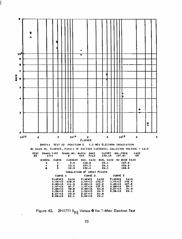
101’ 2 5 1 FLUENCE
I015 2 5
ON171 1 TEST 22 POSITION 2 1.3 HEV ELECTRON IRRADlATION
DC CAIN vs. fLuEwE, fAh4ILr w EMITTER CURRENTS, COLLECTOR VOLTAGE q 10.0
I;;1 TRANS. TYPE TRANS.NC). DATCH ;;M; CUTOFF CASE 1711 8 513 y39.13 NM;‘;:” . ON
SVMDOL CURVE CURRENT MAX. CAIN WIN. CAIN W DOSE GAIN * 5.0 138.9 23.1 195.9
t : 3 10.0 12.0 150.5 152.4 24.1 24.1 199.9 196.9
TABULATION @ ARRAV POINTS
CURVE 1 CURVE 2 CURVE 3
FLUENCE GAIN FL UENCE GAIN FLUENCE CAIN 1.44+13 136.9 1.44t13 150.5 1.44t13 152.4 4*8O+13
w 4.80t13 125.2 4.00+13
1.41*14 5e:e
1.4?+14 lOI. 4.66+14 ‘~Z 4.68*14 4.68+14 1.Q4+15 41.6 1.04+15
64.8 f-K::,” 3119 44.3 . 24.1
30.0 2.27*15 31.0 23.1 3.36+15 24.1
Figure 42. 2N 1711 hFE Versus Q for 1 -Mev Electron Test
73
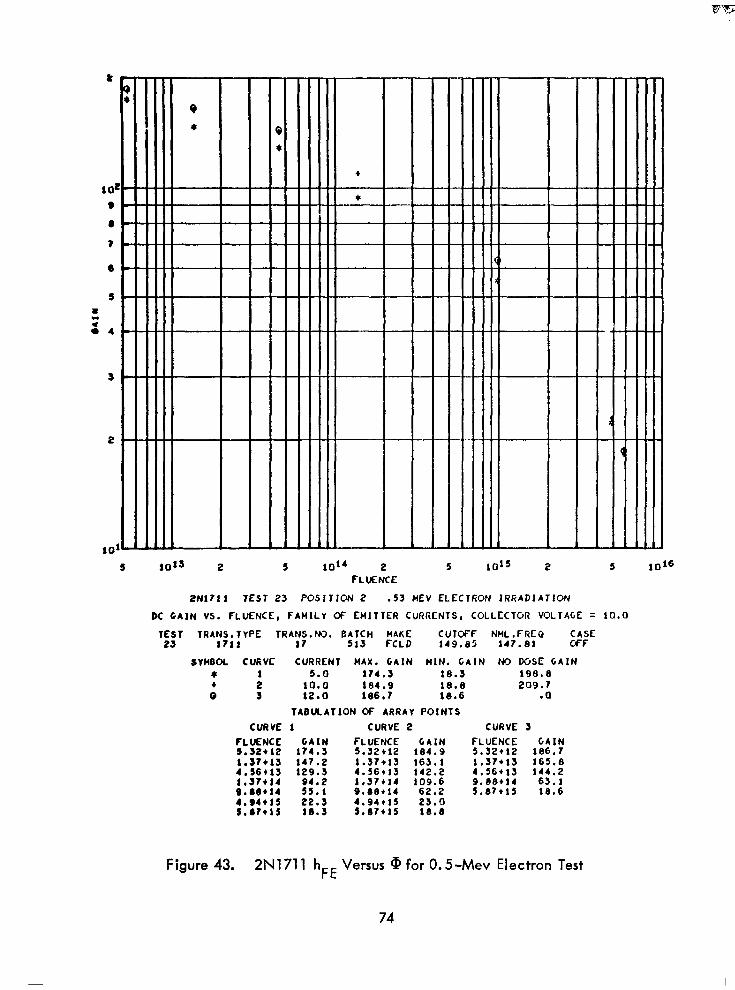
101
5 1013 2 1014 2 FLUENCE
ON171 1 TEST 23 POSITION 2 .53 HEV ELECTRON IRRADIATION
DC GAIN VS. FLUENCE, FAMILY OF EMITTER CURMNTS, COLLECTOR VOLTAGE = 10.0
TEST TRANS. TYPE TRA$.W. “;;;H ;;M; CUTOFF NHL .FRCQ CASE 23 1711 149.85 147.81 ffF
SVMDOL CURVE CURRENT MAX. CAIN MIN. GAIN h+3 DOSE GAIN + 1 5.0 114.3 16.3 190.8
t : 12.0 10.0 186.7 184.9 18.6 18.8 209.1 .o
TADULATION OF ARRAY POINTS
CURVE 1 CURVE 2 CURVE 3
:YEY:: GAIN
:‘sv:‘;‘:: GAIN FLUENCE GAIN
1:31*13 174.3 147.2 1:37+13 184.9 163.1 5.32+12 1.3?+13 186.7 165.8 4.56+13 129.3 4.56+13 142.2 4.56+13 144.2 1.37+14 94.2 1.37+14 109.6 9.9e*14 63.1 #.a@+14 55.1 9.08*14 62.2 5.a7+15 16.6
;*:;::: 4.94t15 23.0
. ::*i . 5.0?*15 18.8
1016
Figure 43. 2N1711 hFE Versus @ for 0.5~Mev Electron Test
74
10
1010 2 5 1011 2 5 1012 2
FLHNCE
2N1711 TEST 24 POSITION 2 1.0 HEV PRuTON IRRADIATION
DC GAIN vs. FLuENCE, FAMILY W EHITTCR CURRENTS, COLLECTOR VOLTAGE = 10.0
TEST TRANS. TvPE TRANS.Wn. DATCH MAKE CUTOFF NHL .FREQ CASE 24 1711 2 513 FCLD 151.73 147.81 ClFF
SYHDOL CURVE CURRENT l4AX. GAIN MIN. CAIN NO DCiSf GAIN * 1 5.0 172.1 12.1 194.1 ; 2 12.0 1O.G 161.0 1?9.9 13.6 13.4 205.4 203.3
TABULATION OF ARRAY POlNTS CURVE 1 CURVE 2 CURVE 3
FLUENCE CAIN fLUENCE CAIN FLUENCE GAIN 1.90+10 172. t 1.91)*10 179.9 1.91)+10 181.0 4.64+10 147.3 4.64+10 154.1 1.04+11 122.2 1.04+11 111.3 1.04+11 119.9 9.52+11 :*:‘,::: 64.1 2.52tll ?1.4 1.95*12 :x .
9:52+11 42.0 4.70+11 45.) 22.6 9.52+11 25.2
1.95+12 12.1 1.95112 13.4
Figure 44. 2N1711 hFE Versus @ for 1 -Mev Proton Test
75
I
6 1011 2 FLUENCE
4
#Nl?ll TElT 26 20.0 NEV PROTON ll?RADIATlON
oc CAIN vs. FLuENCE, fAnlLv 0F EMITTER CUI~R~NTS, COLLECTOR VOLTAGE = 10.0
Test TRAN~.IvPE TRANS.NO. BATCH MAKE CUTOFF NHL.fREQ CASE 26 1711 16 s13 FCLD 175.00 147.81 ON
SYNBOL CURVE CURRENT MAX. GAIN WIN. GAIN No BOSE CAIN l : 5.0 164.7 64.6 162.4 t 10.0 169.9 71.6 191.0 0 s 12.0 171.6 06.1 19~.~
TABUCATION 0F ARR~V POINTS
1 CURVE 2 CURVE 3 CURVE
FLUENCE 2.13’10 l.S2’11 2.67’11 4.17+11 s.o2*11 6.*2*11
64lN FLUENCE GAIN FLUENCE G4 I 164.7 2.?3*10 169.9 2.13*10 ¶I¶ . 123.6 1.32*11 135.5 1.32*11 131 . 108.6 2.6?+11 120.0 2.6?+11 123
64.2 4.1?+11 95.3 4.17+11 19.6 5.02+11 66.4 5.02+11 f ‘r 64.6 6.92*11 71.6
Figure 45. 2N1711 hFE Versus @ for 20-Mev Proton Test
76 -
..-.- --...... ..-.-.---. --.----...11 . . ,, , ,, ,
6
5 10*5 2 FLIJENCE
- -
-
-
-
-
2N171 l TEST 25 CODALT 60 GAMMA lRR4DlAllGN
DC GAIN VS. FLUENCE, FAMILY CT EHITTER CURRENTS, COLLECTOR VGLTAGE = 10.0
TEST TRANS. TYPE CU:CfF NHL.fREQ CASE 25 tt1t
TR4;g.W. D;&” ::I; 175.66 147.81 ON
SWDOL CURVE CURRENT MAX. CAIN MIN. GAIN No DOSE GAIN * 1 5.0 2’35.3 50.9 206.8
cf 5 12.0 10.0 211.9 222.1 55.2 54.5 224.1 .O
TADULATJON OF ARRAY POINTS
CURVE 1 CURVE 2 CURVE 3
FLUENCE GAIN FLUENCE GAIN FLUENCE CAIN 5.55+12 205.3 5.55+12 222.1 2.00+14 211.9 2.43+13 200.2 2.45t13 216.6 9.52414 189.9 2.oott4 167.9 2.0[1+14 206.9 4.06+15 156.8 9.52+14 165.5 9.52tt4 165.4 l.o5+17 55.2 4.06+15 134.1 4.octl5 152.9 2.09+16 too.9 2.09+16 110.7 4.94tt6 74.3 4.94+16 81.6 6.79+t6 65.1 6.79+16 71.5 t.03+tt 50.9 1.05+17 54.5
Figure 46. 2N1711 hFE Versus @ for Co6’ Gamma Test
77
The second term of Equation (5) accounts for the the loss of base current due
to recombination of carriers in the bulk of the base region and is represented by the
minority-carrier lifetime, T b. The third term of Equation (5) accounts for the
emitter efficiency,
where: u ando b e
= conductivities of the base and emitter regions,
respectively
L e
= emitter diffusion length
In addition to those terms expressed in Equation (5), changes in current
gain, particularly following radiation exposure, can result from losses of base
current related to: 1) recombination in the base-emitter surface and/or bulk re-
gion, and 2) channeling of current caused by inversion layers on the surface at
junctions between the transistor regions base to emitter or base to collector).
If the loss in current gain following radiation exposure is caused only by the
effect of atomic displacements on the bulk of the base region, then the reduced
lifetime due to increased recombination can be related to reduced current gain by
Equation (6):
A(hFE -‘) z (w2/2Db) A(Tb-‘)
Initial values of minority-carrier lifetime can be related to the initial density of
recombination sites, Ni:
-1 = c N.
Tbi 1 I
(6)
Atomic displacements create new defect sites, Nr , proportional to the amount of
exposure fluence, Q , of the displacement-type radiation.
Q)
-1
Tbf = c, Ni + C2Nr
A(Tb -1) = Tb -I - Tb -’ f i
= c2 Nr
80
(8)
(9)
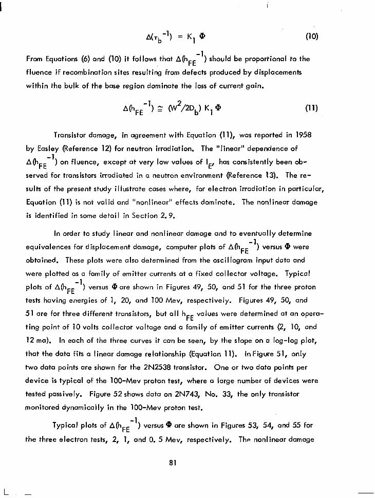
From Equations (6) and (10) it follows that A(hFE -‘) should be proportional to the
fluence if recombination sites resulting from defects produced by displacements
within the bulk of the base region dominate the loss of current gain.
AhFEw 2 ) Z (W/2Db)Kl@ (W
Transistor damage, in agreement with Equation (11), was reported in ‘1958
by Easley (Reference 12) for neutron irradiation. The “linear” dependence of
A(hFE -‘) on fl uence, except at very low values of IE, has consistently been ob-
served for transistors irradiated in a neutron environment (Reference 13). The re-
sults of the present study illustrate cases where, for electron irradiation in particular,
Equation (11) is not valid and “nonlinear” effects dominate. The nonlinear damage
is identified in some detail in Section 2.9.
In order to study linear and nonlinear damage and to eventually determine
equivalences for displacement damage, computer plots of A(h -1
FE ) versus @ were
obtained. These plots were also determined from the oscillogram input data and
were plotted as a family of emitter currents at a fixed collector voltage. Typical
plots of A(h,, -1
) versus 0 are shown in Figures 49, 50, and 51 for the three proton
tests having energies of 1, 20, and 100 Mev, respectively. Figures 49, 50, and
51 are for three different transistors, but all hFE values were determined at an opera-
ting point of 10 volts collector voltage and a family of emitter currents (2, 10, and
12 ma). In each of the three curves it can be seen, by the slope on a log-log plot,
that the data fits a linear damage relationship (Equation 11). InFigure 51, only
two data points are shown for the 2N2538 transistor. One or two data points per
device is typical of the lOO-Mev proton test, where a large number of devices were
tested passively. Figure 52 shows data on 2N743, No. 33, the only transistor
monitored dynamically in the lOO-Mev proton test.
Typical plots of A(hFE -1
) versus @ are shown in Figures 53, 54, and 55 for
the three electron tests, 2, 1, and 0. 5 Mev, respectively. The nonlinear damage
81
L. -
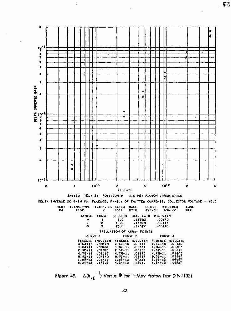
2 5 101’ 2 5 lOI2 2 5 FLUENCE
2NIl32 TEST 24 POSITJON 8 1.0 HEV PROTON IRRADIATION
DELTA INVERSE DC CAIN VS. FLUENCE, FAMILY OF EMITTER CURRENTS, C9LLECTOR VOLTAGE = 10.0
T;$ TRANS.TYPE 1RANg.W DATCH HAKE CUTCfF NHI. .f REQ CASE II32 6511 RYTH 399.56 396.77 Off
SYWDOL CURVE CURRENT MAX. GAIN HIN GAIN 6
Ii :
5.0 .I7502 .00170 iO.0 .I5040 .OOI47
3 12.0 . I4527 .OOI46
7ABWATlOti OF ARRAY POINTS
CURVE I CURVE 2 CURVE 3
FgU:;:E IW;;N :Ls”:L’:; INV.GAIN :L6”:lWg INV.GAIN
1:04+11 .OO’OI 1:04+11 .OOI47 . 00146 .00331 1.04411 : 00327
2.52+II .OIOBS 2.52+II . on922 2.52tII 0089rJ 4.70411 .02195 4.?0*11 .01873 4.?0+11 :01eo2 0.52+II eO.240 9.52tlI 03684
107222 9.52tII .03540
I .95+I2 .08422 1.95t12 I.95*12 .0695? 4.21+12 .I7502 4.24+12 .I51140 4.24ttt . I.4527
Figure 49. A(hFE -‘) v ersus @ for 1-Mev Proton Test (2Nll32)
82
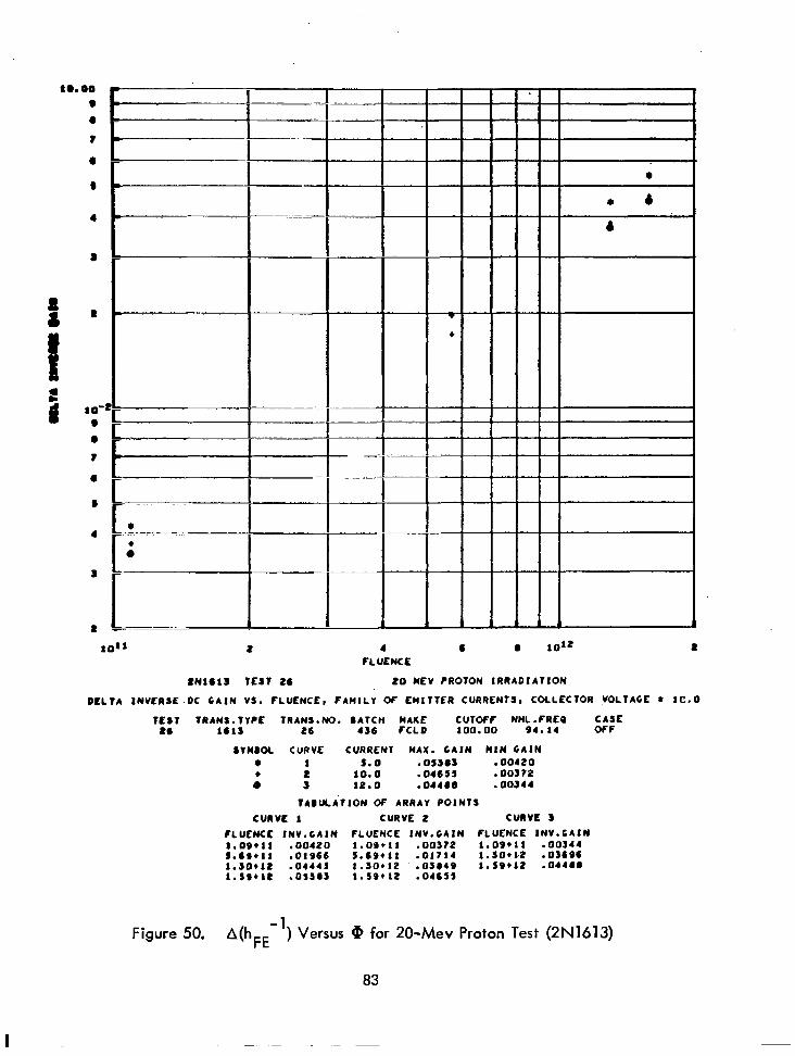
16.60
l
l
t
tWl613 TEST 26 20 MEV PROTOM IRRADIATION
DELTA INVCRIL.DC CAIN VI. fLULNCE, FAMILY Of EMITTER CURRENTS, COLLECTOR VOLTAGE 2 lC.0
WIT TRANS.TYPC TRANI.t’JO. BATCH MAKE CUTOff NNL.fREQ CASE 26 1613 26 436 FCLD 100.00 94.14 Off
8YMDOL cuavE CURRENT MAX. CAIN MlN CAIN + I 1.0 . OS383 .00420
; f 10.0 .0465S .003?2 12.0 .044e6 .00344
lADWAllON Of ARRAY POINTS CURVE I CURVE 2 CURVE 3
fLUENCt INV.CAIN FLUENCE INV.CAIN FLUENCE INV.CAlN 1.09*11 .00420 1.09*11 .003?2 1.09~11 .00344 s.60*11 .DlSC6 5.69*11 .01714 1.30*1.2 .03696 1.30*12 .04445 1.30*12 .03@49 1.59*12 .044II l.5~*12 .05383 1.59+12 .04c55
Figure 50. A(hFE -‘) v ersus Q for 20-Mev Proton Test (2N1613)
83
6
6
5
5.00 6 8 10’3 2 4 fLUENCE
8 10’4
2N2538 TEST 27 60 SERIES 10’J.O WV PROlON IRRADlATION
DELTA INVERSE DC CAIN VS. FLUENCE, FAMILY OF EMITTER CURRENTS, COLLECTOR VOLTAGE = 10.0
TEST TRANS. TYPE TR4NS.M. tM;H HAKE CUTOff NML .fREQ CASE 27 2538 64 RYTti 471.81 415.43 ON
SYMBOL CURVE CURRCNT MAX. CAIN HIN GAIN 1 I 5.0 .05043 .00672 t
f 10.0 eO.256 .00552
0 12.0 , ODOOO ,000’3D
TABULATlON OF ARRAY POINTS
CURVE I CURVE 2 CURVE 3
FLUENCE INV.CAIN FLUENCE INV.CAIN FLUENCE INV.CAIN 9.16tI2 .00672 9.76+12 5.92+13 .05043 5.92+13 :i:;::
Figure 51. A(hFE -‘) v ersus 0 for lOO-Mev Proton Test (2N2538)
84
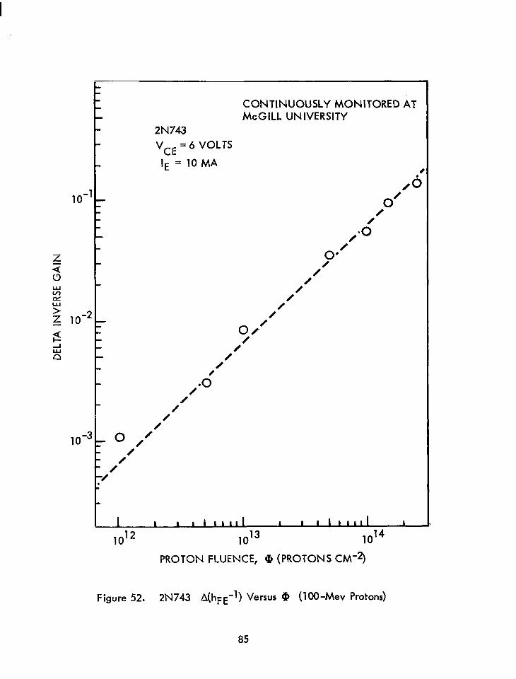
10-l - 10-l - 0’ 0
I I Q Q
,o”
cl cl / 0
% % 0 ai ai / “> “> / z z lo-2 -
lo-2 / -
z z d d
o,/’
/ cl cl /
/
,*d
0 0
0 0
lo-3 r lo-3 r 0 ,’ 0
/ - / Y-’ Y-’
- 1.. 1 L I I rrlrl I I 1I111r I c
1012 1013 1o14
CONTINUOUSLY MONITORED AT MCGILL UNIVERSITY
2N743
‘CE = 6 VOLTS
‘E = 10MA 0
PROTON FLUENCE, Q (PROTONS W-2)
Figure 52. 2N743 A(hFE-l) VerSUS @ (100-M’% Profond
85
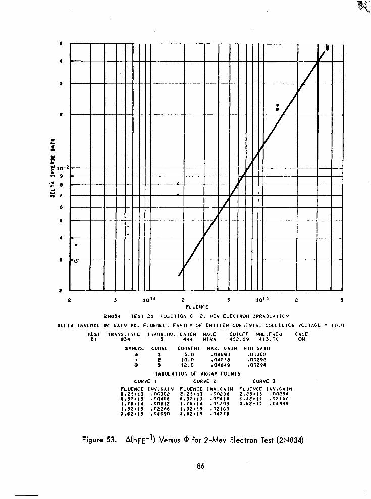
PN854
FLUCNCC
IEsT 21 Pos171ot~ c 2. TV CLCCTR~N IRRADIAT~OIJ
5
DELIA INVCRSC DC GAIN VS. FLUENCC, FAMILY OF EHlTlCfi C~liliCN15, COLLCCTOR VOLTACC = 1CI.n
TEST TRANS. TyPC TRA~JS.IJ~. DATCH HAI;~ CUTCTI- NHL .FRCQ CASE 21 614 4 444 HlkA 432.39 4t3.m ON
SVHDOL CURVE CURRCNT MAX. GAIN HIN GAIfJ *
: 5.0 .04690 .003G2
cf 10.0 .04??8 . nnese
1 12.0 .04849 .00294
IADuLA~~ON CT ARRAY POINTS
CURVC 1 CURVE 2 CURVE 3
rLUENCC INV.GAIN FLUEHCE INV.GAIN ;LF$tJ:: IW,;;:” t.23+15 nnJG2 b.5?*13 :an4fx
2.23*13 .nn29n 6.31*1J .flr1418 1:32:,3 .02137
1.?6*14 .onei2 1 .?G+14 or17 n9 1.32*15 .022&6 1.52+13 :nPlG9
3.62+15 -04849
5.62+15 .04c9n 5.62*15 .Q4??8
Figure 53. A(hFE-l) V emus @ for 2-Mev Electron Test (2N834)
86
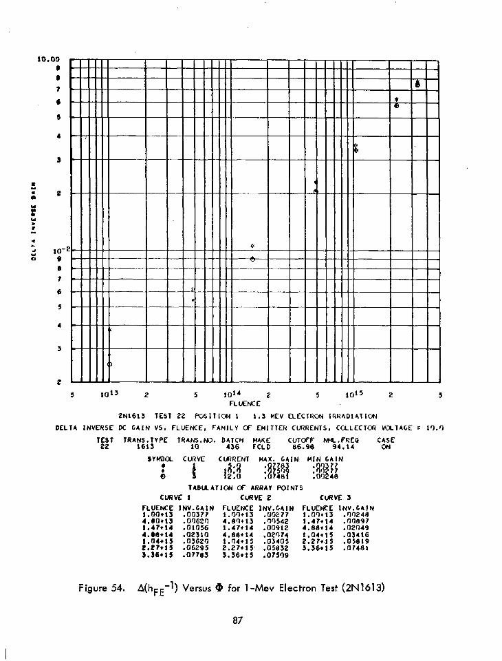
2N1613 TEST 22 POSITION 1 1.3 HCV tlEClliclN IRH*DIATLW
DELTA INVERSE DC GAIN VS. FLUhfCE, fAHlLY Cf EMITTER CURRENTS, CULfC1CW-d UTAGE = 1’Il.r)
SYHDCC CURVE CURRCNT MAX. CAIN MIN CAIN
TABUATIW @ ARRAY POINTS
CURVE 1 CURVE 2 CUZVE 3
‘y;‘o’l;‘.;;N {LxLJiC; INV.CAIN ;Li;i?: ‘;$G.G;N
4:m13 .Ot277 . !I0542 1:47+14 .om397
1.47*14 .00912 4.88114 .02049 4.08+14 .02Q74 1.04*15 .03416 1.04+15 .03405 2.27+15, .I35832 3.36+15 .07509
Figure 54. A(hFE -1) Versus d for 1 -Mev Electron Test (2N1613)
87
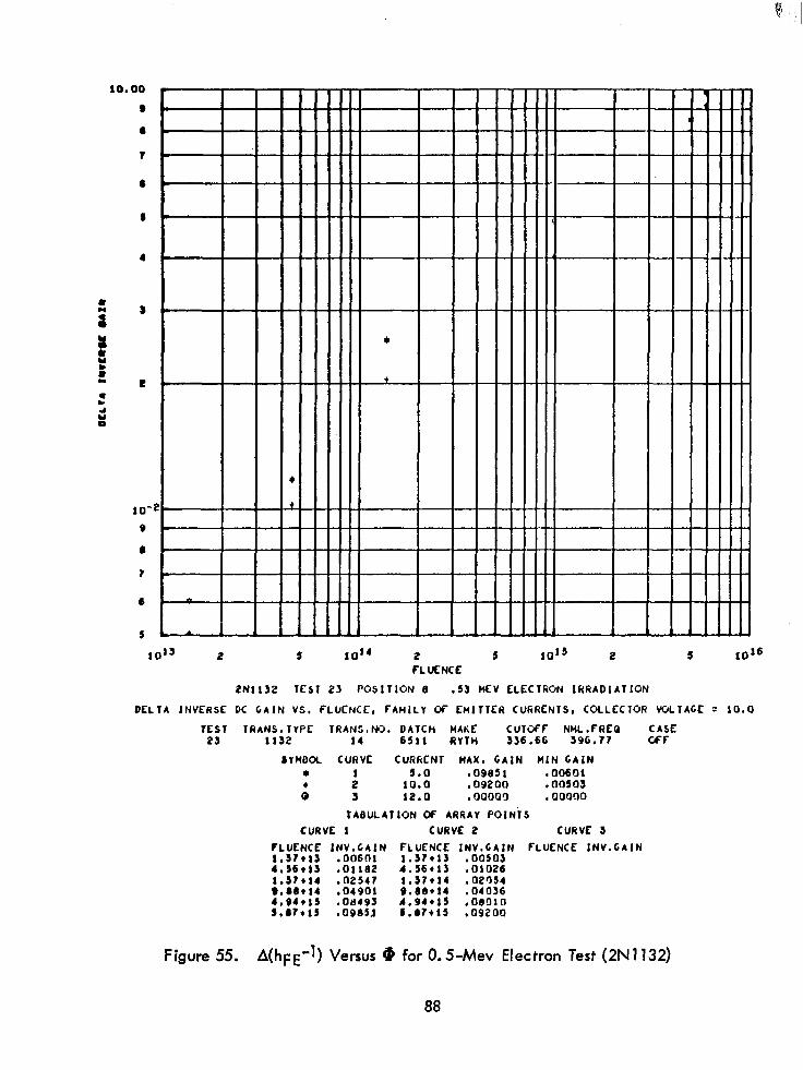
- - -
-
-
-
-
-
-
-
.
FLUfNCE
2NII32 TEST 23 POSITION 6 .53 HEV ELECTGON IRRADIATION
DELTA INVERSE DC GAIN vs. FLUCNCE, FAMILY OF EMITTER CUKAfNTS, COLLECTOR VOLTAGE = 10.0
TEST TRANS. TVPC TRANS. W. DATCH MAKE CUTOFF NHL .FREQ CASE 23 II32 I4 6511 RYIII 336.66 396.77 CfF
srnoa CURVE CURRENT MAX. CAIN MIN GAIN +
i :
5.0 .09851 ,006OI 10.0 .09200 . Cl0503
3 12.0 , OQQQ9 , omc)a
TABULATION OF ARRAY POlNiS
CURVE I CURVE 2 CURVE 3
;L;;K; ‘yD’;W;N :‘,“;K; ‘yo’;;;;N FLUENCE INV.GAIN
4:56*13 .01182 4:56+13 .OIO26 1.3?*14 .02547 1.37+14 S*86+14 .04901 @.68+IJ : oO:Z! 4.94+15 l O1493 4.94+15 .OII)ID 5.6?*15 IO9653 6.@?*15 .09200
Figure 55. A(hFE-1) V ersus (0 for 0.5~Mev Electron Test (2N 1132)
88
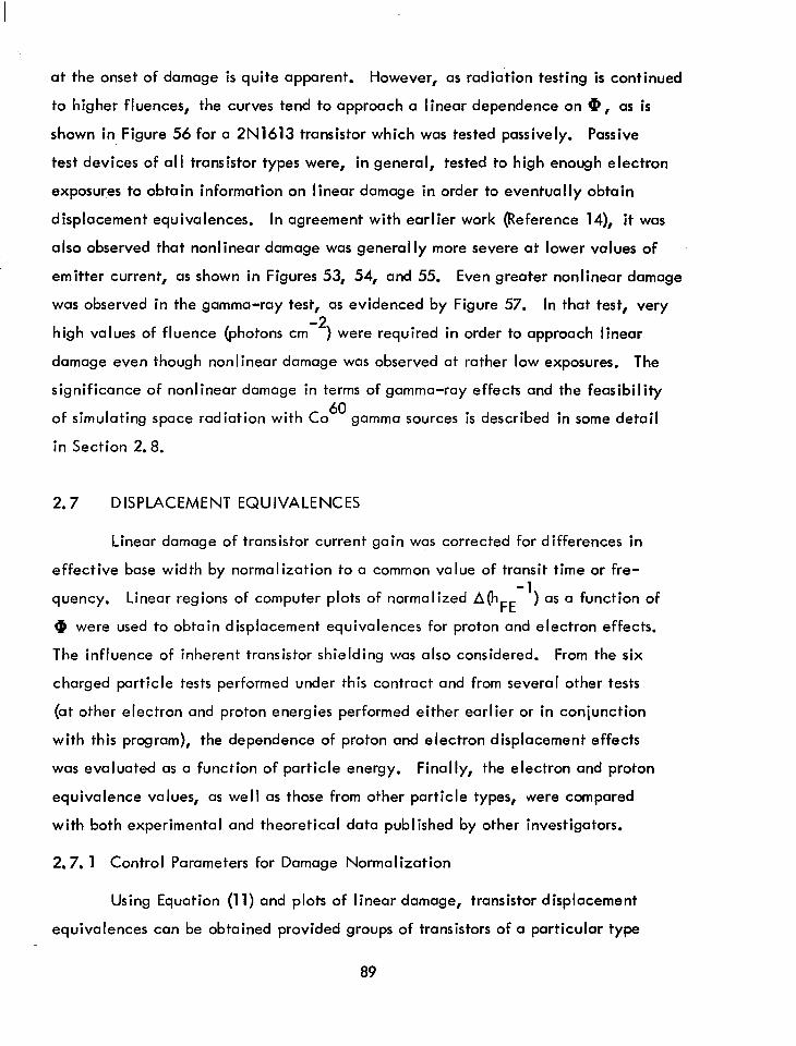
at the onset of damage is quite apparent. However, as radiation testing is continued
to higher fluences, the curves tend to approach a linear dependence on a, as is
shown in Figure 56 for a 2N1613 transistor which was tested passively. Passive
test devices of all transistor types were, in general, tested to high enough electron
exposures to obtain information on linear damage in order to eventually obtain
displacement equivalences. In agreement with earlier work (Reference 14), it was
also observed that nonlinear damage was generally more severe at lower values of
emitter current, as shown in Figures 53, 54, and 55. Even greater nonlinear damage
was observed in the gamma-ray test, as evidenced by Figure 57. In that test, very
high values of fluence (photons cm -2
) were required in order to approach linear
damage even though nonlinear damage was observed at rather low exposures. The
significance of nonlinear damage in terms of gamma-ray effects and the feasibility
of simulating space radiation with Co 60
gamma sources is described in some detail
in Section 2.8.
2.7 DISPLACEMENT EQUIVALENCES
Linear damage of transistor current gain was corrected for differences in
effective base width by normalization to a common value of transit time or fre- -1
quency. Linear regions of computer plots of normalized A(hFE ) as a function of
0 were used to obtain displacement equivalences for proton and electron effects.
The influence of inherent transistor shielding was also considered. From the six
charged particle tests performed under this contract and from several other tests
(at other electron and proton energies performed either earlier or in conjunction
with this program), the dependence of proton and electron displacement effects
was evaluated as a function of particle energy. Finally, the electron and proton
equivalence values, as well as those from other particle types, were compared
with both experimental and theoretical data published by other investigators.
2.7. 1 Control Parameters for Damage Normalization
Using Equation (11) and plots of linear damage, transistor displacement
equivalences can be obtained provided groups of transistors of a particular type
89
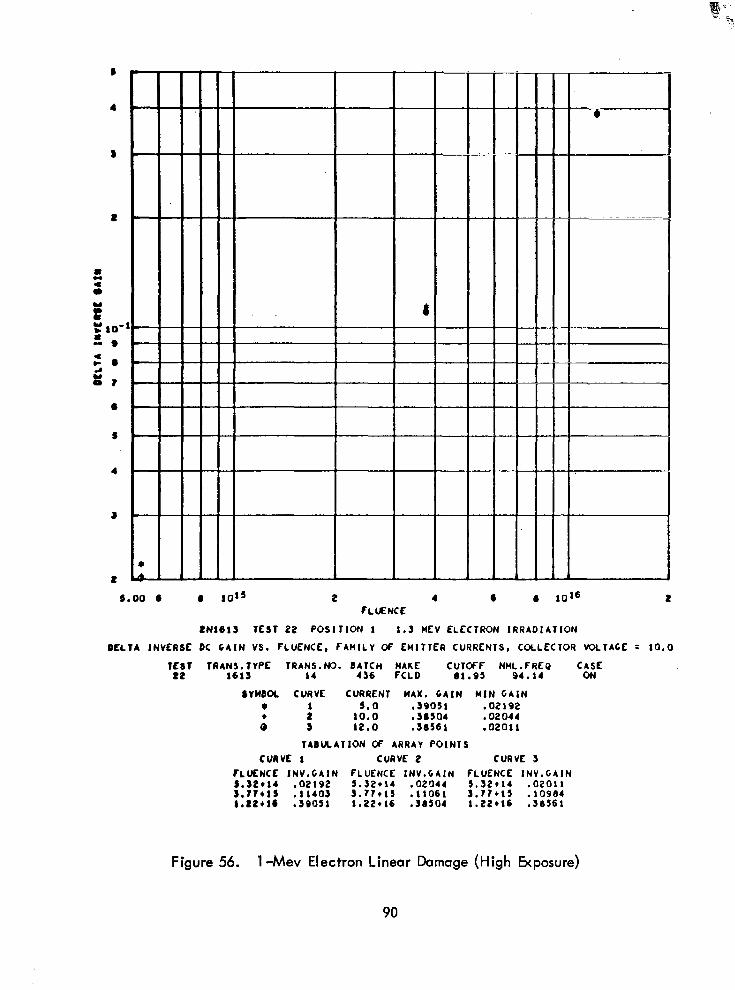
5.00 6 8 1015 2 4 6 6 1016 2 fLtnJCE
tNI613 TEST 22 POSITION I I.3 MEV ELECTRON IRRADIATION
DELTA INVERSE Dc GAIN vs. FLUENCE, FAMILY M EMITTER CURRENTS, caLEcToR VOLTAGE = to.0
1;;’ lRA;;;,rY” 1RANS.W. W&i ;;M; CUTOFF NML .FREQ I4 81.95 94.14 2iE
SYMBOL CURVE CURRENT MAX. GAIN MIN GAIN * 1 5.0 .39OSI .02192 t f 10.0 12.0 .36504 .36561 .02011 .02044
TASULATION OF ARRAY POINTS
CURVE I CURVE 2 CURVE 3
TLUENCE INV.GAIN FLUENCE INV.GAIN FLUENCE INV.GAIN 5.32+14 .02192 5.32+14 .02044 5.32rl4
:KE 3.?7+15 .I1061 3.77+15 : w 1.22+16 .38504 1.22*16 .38561
Figure 56. 1-Mev Electron Linear Damage (High Exposure)
90
1014 2 5 1015 2 5 10'6 2 5 Id' 2 fLUENCE
2N2219 TEST 25 CODALT 60 GAHMA IKRADIATION
DELTA ~NVEHSC DC GAIN vs. FLUEIJC~, FAMILY cf EMITTER CUWENTS, COLLECTOR VOLTAGE = 10.0
TEST TRA;;;;YPE 1RAtdS.W. DITCH HAKE CUTWF N;;;',";" CASE 25 22 501 FCLD 340.5t *
SYHDOC CURVf CU~~RCNT MAX. CAIN MIN GAIN l
: 5.0 OlOO? l-m012
cs 10.0 :ooero :00017
3 12.0 .ooees .OOOl6
TABULATION W ARRAY POINTS
CURVE I CURVE 2 CURVE 3 FLUCNCE INV.CAIN FLuCNCC INV.CAIN FLUCNCE INV.CAIN 2.3?+13 .00012 2.37+13 .00017 2.371l3 .00016 8.29113 . QQO39 6.29tI3 .OQO26 6.29+13 .00026 1.08114 .QOO54 1.08+14 00047
:0012c 1.68*14 .OQO42
9.68114 00172 :QOltlG
9.66414 9.66*14 .OOll5 1.44+15 1.44+15 .00154 1.44+15 .OQI21 5.94+15 .00322 3.94*15 .oo25O 3.94+15 .OO226 1.03+16 .00488 I.O3+16 .00390 1.03+1c .OO3CS 2.01+16 .005G6 2.01*16 .00452 1.01+17 .0082Q 3.03+lG 00G20 3.03ttc .00511 4.75r16 :0074G 4.?5+16 .OO617 6.54tlC 00818 1.01r17 :01097
6.54tI6 rQOG79 1.01*17 l OO870
Figure 57. A(hFE-‘) Versus 4 for Co60 Gamma Tests (2N2219)
91
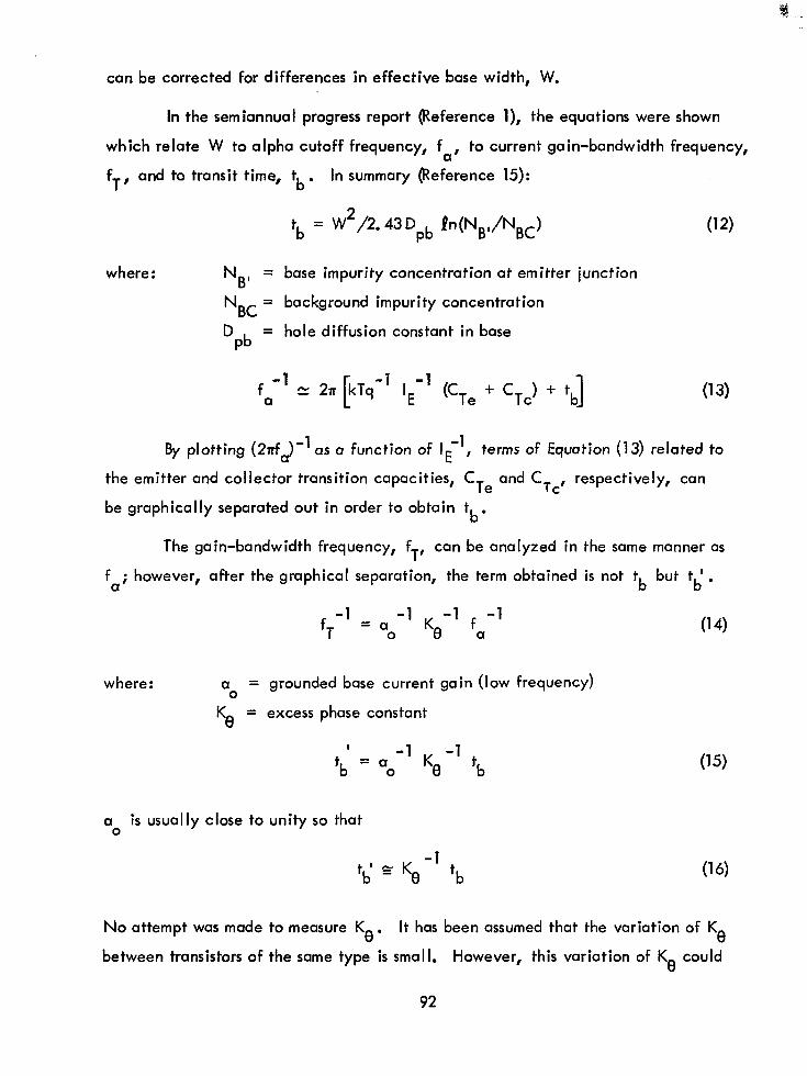
can be corrected for differences in effective base width, W.
In the semiannual progress report (Reference l), the equations were shown
which relate W to alpha cutoff frequency, fa, to current gain-bandwidth frequency,
fT, and to transit time, tb . In summary (Reference 15):
tb = W2/2. 43Dpb h(NB,/NBC) W)
where: NB’ = base impurity concentration at emitter junction
NBC = background impurity concentration
D Pb
= hole diffusion constant in base
f -’ a
IE-’ (CT, + cTc) + t 1 b (13)
By plotting (27rfa)-’ as a function of I;‘, terms of Equation (13) related to
the emitter and collector transition capacities, CTe and C Tc’
respectively, can
be graphically separated out in order to obtain t b’
The gain-bandwidth frequency, fT, can be analyzed in the same manner as
fa; however, after the graphical separation, the term obtained is not tb but tb’ .
fT -1 = -1 -1 f -1
“0 Kf3 a
where: a = 0
grounded base current gain (low frequency)
Ke = excess phase constant
I -1 -1 tb = a0 Kg tb
(14)
a0 is usually close to unity so that
-1 tb’ e Kg tb (‘4
No attempt was made to measure Kg. It has been assumed that the variation of Kg
between transistors of the same type is small. However, this variation of Kg could
92
become quite large between different types of transistors. Kf3 is a result of built-in
electric fields peculiar to the construction of the device and may vary between 0.5
and 1.0 with different constructions peference 16).
Transit frequencies were obtained from the measured values of transit time:
time:
f = (2Ttb)-’ (‘7)
f’ = (2nQ-l (‘8)
These values were used to correct for differences in effective base width and to
serve as a control parameter for normalization of A(hFE-‘) data on all transistors
of a given type. It was important in the damage normalization process that the
transit time information used be determined for the same values of emitter current
that are being specified for the current gain analysis. Thus values of f on equiva-
lence plots are for IE = 10 ma where equivalences were determined.
Equation (19) follows from Equations (11) and (12):
A6,,-‘) y.z ctbG
And thus from Equation (17)
f A(hFE -‘) Z KDQ
(‘9)
(20)
where K D is the damage constant (for linear displacement effects).
In order to obtain normalized equivalence plots for several devices of one
transistor type from the data presented for separate devices (from curves such as those
shown in Figures 49 through 57), Equation (20) was multiplied by values of fN-‘:
(f/fN) A(hFE-‘) : K’@ (21)
The fN values for each of the transistor types were arbitrarily selected to be
93
approximately the average value of f or f’ (of Equations 17 and 18) for the group
of transistors of that type tested. The normalized damage constant, K’ , as defined
by Equation (21), shows the relative sensitivity of each transistor type according to
its typical frequency, fN. Values of fN are given in Table 10 for each transistor
type*
Values of damage constants K’ and KD are shown in Table 10 for proton tests
and in Table 11 for that high exposure region of the electron damage curves that
follows a linear dependence on Q .
2.7.2 Proton and Electron Equivalences
From Table 10 it is apparent that when all devices are corrected to one
common effective base width (as is the case for K D
rather than K’ values), device
pairs of the same construction groups (e.g., the npn epitaxial planar) show very
close agreement for displacement damage. For the electron damage constants, KD,
of Table 11, it is apparent that the npn devices (first 6 types listed) normalized
together quite closely (within a factor of 3); however, considerable variation was
observed in KD for the four pnp transistor types. In particular, the pnp device
2Nli32 showed consistently higher damage constants than did the npn devices.
Normalized equivalence plots were obtained by computer analysis using
Equation (21) and values of f and f’. Figures 58 through 106 (one of the major
goals of this contract) are the equivalence plots for all 10 transistor types tested in
al I 7 of the radiation exposure tests. The values of f N
used for each transistor
type are indicated on each of the respective computer plots. The operational
point chosen far representation of this data is an emitter current of 10 ma and a
collector voltage of 10 volts (except for 2N743 transistors, which were presented
at 10 ma and 5 volts).
Dotted linear lines (i. e., satisfying Equation 21) are shown on each of the
plots as a guide to compare results with that anticipated from Equation (11). As
a I ready noted, the proton tests (except very close to threshold) obeyed a linear
fit. The electron tests, in general, fitted linear damage only at high electron
94
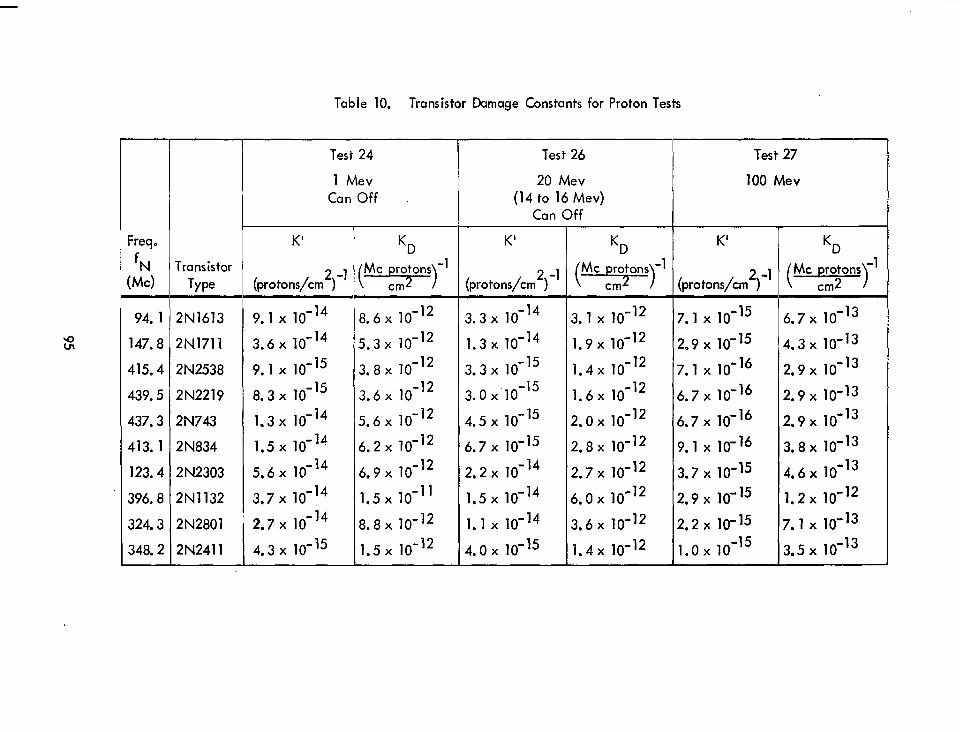
Table 10. Transistor Damage Constants for Proton Tests
Freq 0
fN (MC)
94. 1 2N1613
147.8 2N171’
415.4 2N2538
439.5 2N22’9
437.3 2N743
413.1 2N834
123.4 2N2303
396.8 2N1’32
324.3 2N280’
348.2 2N24”
Transistor Type
Test 24
1 Mev Can Off
K’ KD
(protons/cm2)-l C-J-’
9.’ x lo-‘4 8.6x lo-l2
3.6 x ‘O-l4 5.3 x lo-l2
9.’ x 10-15 3.8x lo-l2
8.3 x lo-l5 3.6 x ‘O-l2
1.3 x 10⁻¹⁴ 5.6 x ‘O-l2
1.5 x lo-‘4 6.2x lo-l2
5.6x ‘O-l4 6.9x ‘O-l2
3.7x lo-‘4 1.5x 10-l’
2.7 x ‘O-l4 8.8x 10⁻¹²
4.3 x 10⁻¹⁵ 1.5 x 10⁻¹²
Test 26
20 Mev (14 to 16 Mev)
Can Off
K’ KD
(protons/cm2)-’ (9,“
3.3x lo-l4 3.1 x 10⁻¹²
1.3 x 10⁻¹⁴ 1.9 x 10⁻¹²
3.3x lo-l5 1.4x lo-l2
3.0x lo-l5 1.6x ‘O-l2
4.5 x lo-l5 2.0x 10⁻¹²
6.7x ‘O-l5 2.8x ‘O-l2
2.2x lo-l4 2.7x ‘O-l2
1.5 x 10⁻¹⁴ 6.0x ‘O-l2
1.’ x 10-14 3.6x ‘O-l2
4.0x 10⁻¹⁵ 1.4x 10⁻¹²
Test 27
100 Mev
K’
(protons/cm2)-l
7.’ x 10-15
2.9 x ‘O-l5
7.’ x 10-16
6.7 x ‘O-l6
6.7 x ‘O-l6
9.’ x 10-16
3.7 x 10⁻¹⁵
2.9x ‘O-l5
2.2 x 10⁻¹⁵
1.0 x lo-l5
KD
( MC protons -1
cm2 )
6.7x ‘O-l3
4.3 x 10⁻¹³
2.9x ‘O-l3
2.9 x ‘O-l3
2.9x ‘O-l3
3.8x ‘O-l3
4.6x ‘O-l3
1.2x 10⁻¹²
7.’ x 10-13
3.5x lo-‘3
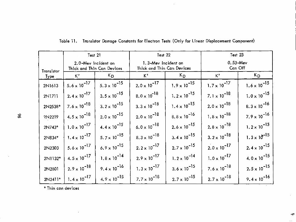
Table 11. Transistor Damage Constants for Electron Tests (Only for Linear Displacement Component)
Test 21 Test 22 Test 23
2.0-Mev Incident on 1.3-Mev Incident on 0.53-Mev
Transistor Thick and Thin Can Devices Thick and Thin Can Devices Can Off
Type
5.6 K
I KD K’ KD I KD
2Nl613 X ‘O-l7 5.3 x 10 -15 2.0 x lo-l7 1.9 x lo-l5 1.7Klo l7 - x 1.6 x ‘O-l5
2Nl711 2.4x ‘O-l7 3.5 x lo-l5 8.0 x ‘O-l8 1.2 x 10 -15 7.1
2.0x x
lo-l8 1.0x lo-l5
‘O-l8 ‘O-l5 lo-l8 lo-l5 -
2N2538* 7.6 x 3.2 x 3.3 x 1.4x 10 l8 8.3x 10 -16
?N2219 4.5 x lo-l8 2.0 x lo-l5 2.0 x lo-l8 8.8 x lo-l6 1.8 x 10 -18
7.9 x lo-l6
2N743* 1.0 x lo-l7 4.4 x lo-l5 6.0 x ‘O-l8 2.6 x ‘O-l5 2.8 x ‘O-l8 1.2x 10 -15
2N834* 1.4 x lo-l7 5.7x lo-l5 8.3x ‘O-l8 3.4 x lo-l5 3.2x ‘O-l8 1.3x l&-l5
2N2303 5.6 x ‘O-l7 6.9 x ‘O-l5 2.2x 10 -17 2.7x ‘O-l5 2: 0 x lo-l7 2.4x ‘O-l5
2N1132* 4.5 x ‘O-l7 1.8 x ‘O-l4 2.9 x ‘O-l7 1.2 x lo-l4 1.0 x lo-l7 4.0x lo-l5
2N2801 2.9 x ‘O-l8 9.4 x ‘O-l6 1.3x lo-l7 3.6 x 10 -15 7.6 x ‘O-l8 2.5 x ‘O-l5
2N241 l* 1.4x lo-l7 4.9 x lo-l5 7.7x lo-l8 2.7x 10 -15
2.7x ‘O-l8 9.4x lo-l6
* Thin can devices
8
10’
0
a t
I I I II I I I II
I I II
J I
.- I I
Figure 58. 2N1613 Equivalence Plot, Electron Test 21
97
I 10’~ 8 I 1014 8 I ILLEIUL
t;: I I I I.
l!’ I II
Figure 59. 2N1613 Equivalence Plot, Electron Test 22
98
Hii I II I I dttttl
,111 II I I d-t-tlr
I I- I d-tt-t t”’
I I,
I II 1.
I IltttH ‘1 II
I lltttll I
II I l 0 I II
tf- ! III I I1
I I I 111111 I II
Figure 60. 2N1613 Equivalence Plot, Electron Test 23
99
10” * 8 1
8
6
4
a
8
‘g-’
0 I
0
I
4
a
8
80-J
8 I
tli
10” a 5 10’s r I mmct
10”
E.U~VALCNCC 8fUDr DC PARAHETER~, NORMALIZED TO 64.1 K
DELTA INVLA8C CAIN VI fLUEtUt, EMITTER CURRENT g 10.0 MA.8 COLLCCTOR VOCTACC l 10.0 l tt8t RS, TRANSISTOR RN1613 NO. EL, FREQWNCT 8 W.0 + TtST RI, TRAN616TOR ON1616 NO. Lf, ~REOUEHCY m 116.1
: tE8T 86, TRAN618TOR ON1613 No. t4, fREQUENCV m 101.1 TtBT tl, TRAN6f8TOR tNl616 Wo. 25, fREQVENCl m SO.@
Figure 61. 2N1613 Equivalence Plot, Co6’ Test
100
loo 0
a
4
8
IO" 0
0
4
8
(0" 0
0
4
8
*0-,
8 lOI 8 a 8O’s 8 6 10”
C~UIWALCMCC SIUDI DC PAIAWE1CII. WIMALIZL8 10 l I.( NC
8CLtA lNVC48C GAIN V’) FLUENCCe LYIltC4 CUd4CNI l 10.0 MA., COLLLC104 *OCVACC l 10.0
l 8NIOIS m6r 84 colIrlc4 1 1.0 MV C401ON l4AAOlA1lON
t 8NIOlS rc6r e6 80 NCV l AOtOM l41ADlAllON 8W1.11 rc8r 8r so 6c11c6 800 NLV cAorom I~GADIAVIOW
Figure 62. 2N1613 Equivalence Plot, Proton Tests
101
-
-
-
-
-
-
-
-
-
-
T 1 S
CLUCNCC
. i
i+
EOUIVALCWCt STUDT DC CAIANCTCRS, WRM4LIZLD TO S4.8 MC
DELI4 INWRSC CAIN VS CLUCNCC, INITTLR CURRENT m 10.0 MA,c cOLLccTOa YOLTASL l 10.0
4 TCSr IO, Tr)ANSfSlOM eNI Wo. WI fRCIWNCT l 100.0 CAM wf I@ NV l TEST 80~ TRANSISTOR ,NlSlS W. ROe ~IICOlKNCT l 90.0 C&N CPf II WV
TEST ES, TRANSISTOR tNlS:S NO. @S, CRCQUCNCT ’ 94.0 CAN mf (I NV TCST Ia, TlllNSlSTOR LNl#:S I*). 40, CRCIUCMT 8 Sa.0 CAN Ow a? MV
Figure 63. 2N1613 Equivalence Plot, Proton Test 26
102
- - - - .
- - -
-
-
-
-
*
-
Figure 64. 2N1711 Equivalence Plot, Electron Test 21
103
I 10’4 2 I FLKNCE
ERUIVALENCE 8fUDy DC PARAMETERS, NORMALIZED TO 141.0 WC
DELTA INVERSE CAtN VI FLWNCE, EHtTTER CURRENT x 10.0 NA.l COLLECTOR VOLTAGE m to.0 l TEST 22, TRANSISTOR tNlT11 H3. I, fREaIIENCv 8 164.4 l TEST 22, TRANSISTOR 2NlTll No. 0, ~REWENCY m 139.1
: TEST 22, TRANSISTOR ON1711 No. S, FREOUENCY = 18O.a TEST 22, TRANSISTOR PM1711 No. 10, FREQUENCY = 11S.1
Figure 65. 2N 1711 Equivalence Plot, Electron Test 22
104
I ’
$
@.Od
1
c
IO'
0
0
I
8
10'
0
0
4
8
80'
0
0
n.00
n IO” r
- - -
-
- - - - - -
- - - - -
- - - -
I
fOUIVALCNCC IfUbV DC PA.AYfffiJ, H34MALI2fD ro 1rr.a MC
DtLfA INVfdSf CAIN VI fLUCNCf, CYIflfol CUiifNf 8 10.0 MA.. COLLCCW4 VOLtACC l 10.0
Figure 66. 2N1711 Equivalence Plot, Electron Test 23
105
8
8
Figure 67. 2N1711 Equivalence Plot, Co6’ Test
106
80’0 t I lO$l t 5 lo- t 5 10’3 FLIlENcE
EQUIVALENCE 6lUDy DC l ARIWETERS, M~?HAI.IZED TO 147.6 MC
DEL14 INVERSE CAIN VI FLUENCE, EMITTER CURRENT = 10.0 MA., COLLECTOR WLTACE = 10.0
l TEIT t4, TRINSISTOR ON1711 No. 2, FREWJENCY = lS1.7
; TEIf 24, TRANSISTOR 2Nl711 M3. 15, FREPUENCY = 154.9 fE61 t4, TRANSISTOR 2Nltll No. 16, FREQLENCY = 146.7
Figure 68. 2N1711 Equivalence Plot, Proton Test 24
107
t: 1 I ,
ti
I I II 1 1 I III I 1
III I II
DKLTA lNVK4SK 64IN V’) FLUEIICK, CmIllC4 CU4dKN1 8 10.0 m4.. COLLKCfO4 WX14CK l 10.0
0 ml 18 n rcsr 24 co#IrIoN e 1.0 Ncr C4OfON :444014r:0*
t a*# ?ll rear 20 ta.a WV c4oroN l44401411oN 8Nl I1 8 rcar 8, SO IC4ICI IQO.0 YV l 4013N I444DI4rION
Figure 69. 2N1711 Equivalence Plot, Proton Tests
108
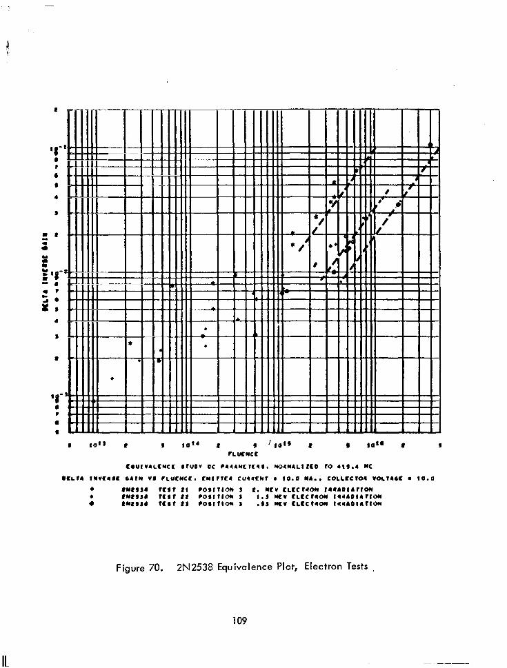
IO” 2 I ‘101s 8 s fLUCNCC
8
K~UIV4LKNCf StUDI OC l 414MCtf44. W4Y4LI2CO t0 4t3.4 WC
W~t4 INVK~SK l 4IN VI FLUCNCE. KMIttE4 CU~SfNf a 10.0 NA.. COLLKCfO4 VoL14CC 0 10.0
l RYtIsa tC#t 21 l OlltlON J 2. WCV ELKCt4ON Irlrl4OlAtlON
: tUtIS@ tCIt #t cost riot4 3 I.3 WV CLKCt4ON I4dAOI4tION 8WSS@ tK)t IS PoslrloN s .SS WV KLCCt4ON Il44DIAtlON
Figure 70. 2N2538 Equivalence Plot, Electron Tests
109
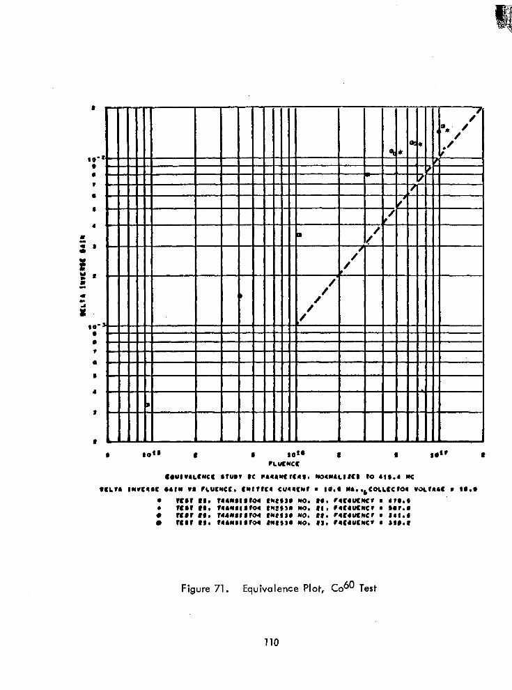
-
- - P- - -
7
/’ ‘*. / ,/
Figure 71. Equivalence Plot, Co6’ Test
110
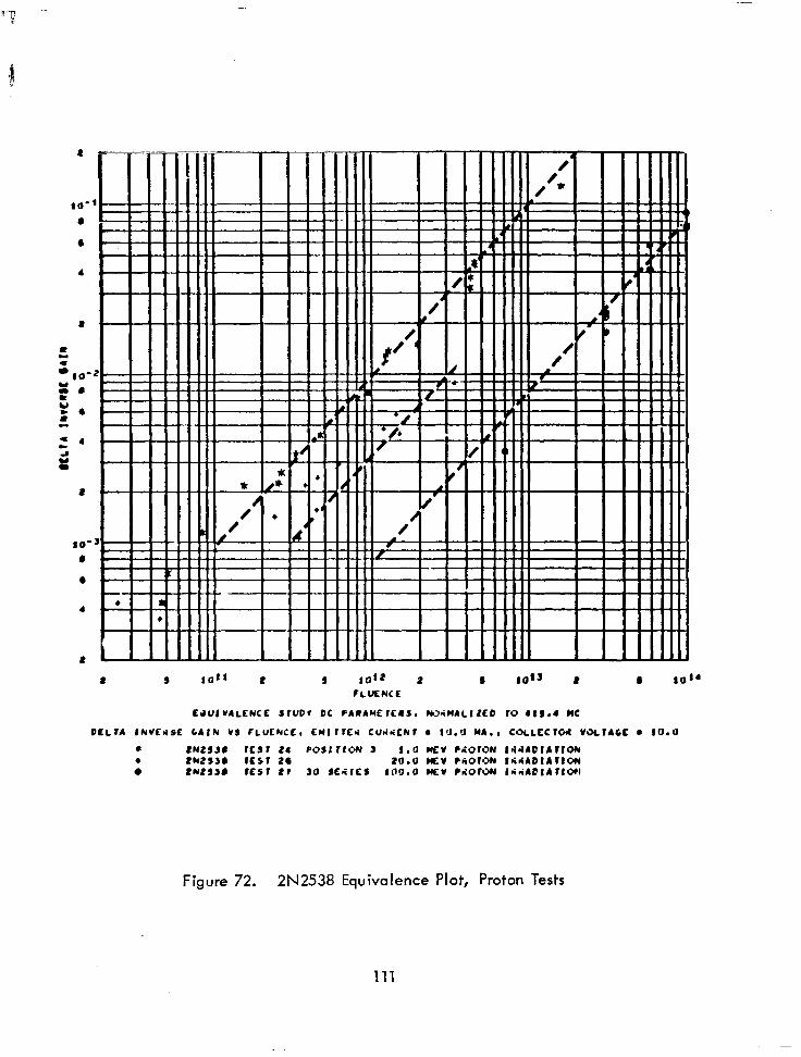
- - - -
di . - - -
I--
L:
I III II r *+: ::
4! ! I ,I
lo’* 2 s 10” # tLUENCE
, :
-
IO”
KJUlVlLENCE SfUDI DC PA4AYEfCIS. WUiYILlZLD 10 419.4 MC
DCLIA INVCdOE CAIN VI FLULNCL, EN: 1x4 culiifNr l I’J.?~ MA., CbLLEC toll voLr4cc l 10.0
0 ZNctlJ1 1fIt 24 POSI t:cJN 1 1.0 UEV l iOtON IrilADlAtlON . tcr2s34 rcsr 21 20.0 lEV PAOtON tliAD14llW l ZN2SS0 KS1 27 JO 4EilCJ 100.0 mv mor3W iiti4D:4tio+I
Figure 72. 2N2538 Equivalence Plot, Proton Tests
111
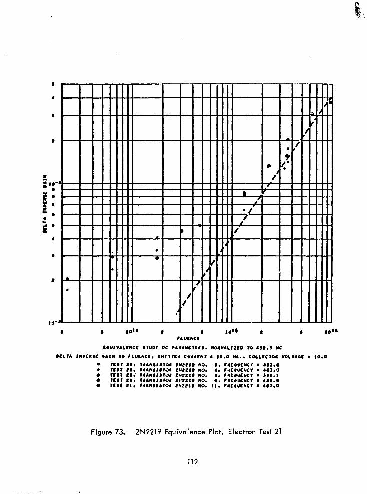
.
.
.
.
.
.
.
.
.
.
I
.
P
-
-
-
-
l
tl -
-
-
-
-
-
-
-
COUlVALCNCc 2tUDf DC CAIIMC1EdS, LloltM4LlZCO 10 4S2.5 MC
OCLIA INVEISC CAIN VI CLULNCC, ENlllCd CUdrltNf m 10.0 WA., COLLCCtOll VoLlACC l (0.0
Figure 73. 2N2219 Equivalence Plot, Electron Test 21
112
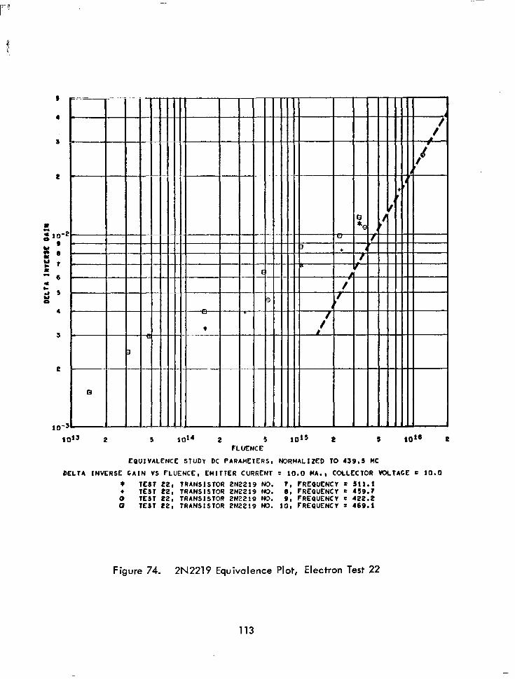
Q
-
-
-
- - - - -
-
-
-
-
- -
lOI4 2
-
~
-
-
-
-
-
-
-
-
-
I IO’@ e FL~JENCE
EQUIVALENCE STUDY DC PARAMETERS, NORMALIZED TO 439.5 MC
DELTA INVERSE CAIN VS fl.UENCE, EMITTER CURRENT = 10.0 MA., COLLECTOR YOLfAGf = 10.0 l TEST 22, TRANSISTOR 2N2219 No. ?, FREOUENCY = 111.1 t TEST 22, TRANSISTOR 2N2219 No. 8, FREQUENCY f 459.7
:: TEST 22, TRANSISTOR 2N2219 No. 9, FREQUENCY = 422.2 TEST 22, TRANSISTOR 2N2219 No. IO, FREQUENCY f 469.1
Figure 74. 2N2219 Equivalence Plot, Electron Test 22
113
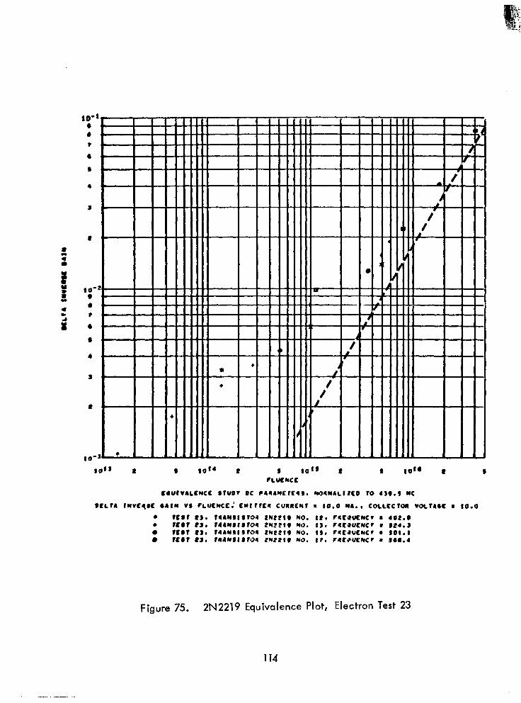
s (0’4 2 I
t
4
4 r
/I ‘1 ,
z
CLUCNCC
C*UlV4LfNCC SlVDT DC C~~~WC~L~SI NO~MILIZCD 10 439.9 WC
WLlA INVCqSC 64111 VI CLUCWCt: EWIllLll CURRLNl 8 80.0 U4. t COLLCClOll W&14&C l 10.0
0 lrS1 es. 144NSISlO~ ZNltlQ NO. Its CfiCQUCNCI a 402.0 + rrar 2Jr 144NSlSlO4 tN22t4 NO. tJ, ?4t4UtNCf l g24.1 4 rcsr 23, 144NSOlO~ 2NttlV NO. 0. ClC4UCNCI l YOt.1 0 rear 2J# 184N118102 2Nttt9 NO. I?. IrltPUCNC? m 94a.4
Figure 75. 2N2219 Equivalence Plot, Electron Test 23
114
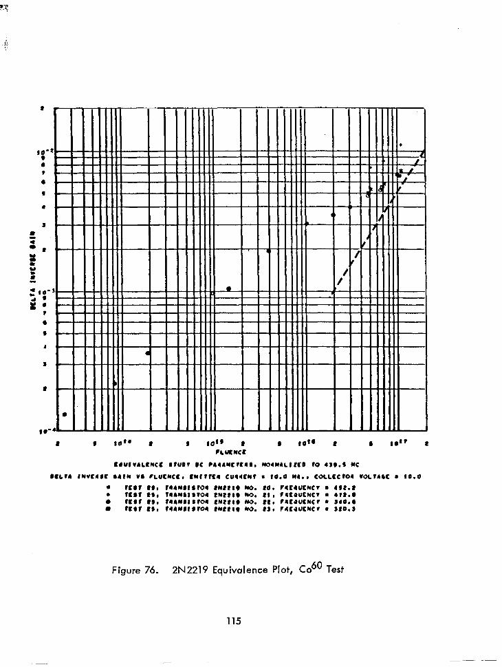
a lb” l s (01 2
PLUNCC
C4UlVALCNCC #lUDI IC ?444YCltll, NO4MALItCO 10 439.9 UC
SW.14 IMVC4SC 64111 VS rLUCNCC, tMIllC4 CU44CNl l (0.0 W4.r COLLtClO4 VOLllCC m 80.0
0 lL41 2s* 144N#lSlO4 2N2219 NO. 20, F4CIUCNCI l 422.2
: lC$l es1 ll4NllSlO4 tN2214 NO. 28, CICQUCNCT m 4I2.4 rcor rs, 144M2lfilOl 2N2214 NO. 22e IIICOUCNCI l J10.a
0 resr es, ra4wa1sroa rnrrte No. rs, rrlc4ucNcv l 320.2
Figure 76. 2N2219 Equivalence Plot, Co6’ Test
115
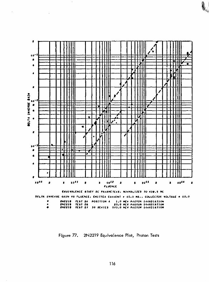
10'0 2
L
.
.
.
.
.
.
.
.
.
m
.
m
.
.
.
10’1 2 a
/
IO” t
I
.
.
.
.
.
.
m
I 80’4 2
C1UIVILCNCf SlUDI DC FAilW~Kil , W~WALf2CO 10 rte.9 MC
DtLlA INVEdSE CAIN VS CLUENCC, CWlllCd CUiiENl s IO.0 MA., COLLCClOR VOLlACE = 10.0
0 2N2219 lES1 24 P0#111oN 4 I.0 MCV CliOlON IdiADIIlION 2N228e rrsr 26 2’1.0 WEV PliOlON IRd~DlAllW 2N22 I9 rcsr 2? 30 SElilEI 1tl’J.U NEV PriOlON Iiri~DIAlION
Figure 77. 2N2219 Equivalence Plot, Proton Tests
116
10“ a
0
,
8
8
4
s
r
lo-’ l b
I
b
I
.
J
2
2
- - -
-
-
-
*
- -- -- -.
-
-
- -
10” 2 5
fLUCNiE
CJUIVALCNCE SlUCV CC PARAWETECS. N3r;HALIIEC 13 457.3 MC
DCLlA INVEASE CAIN VI fLUCNCE, EMlllfi CUliifNf = lO.‘l MA., COl.l.CCTOli VOlerACE s 5.1
. trsr 21. lfi*~sl s13c 2N r4.3 NO. 4, fIfI)UfNCV 2 358.1
. lE5T 21, IliANSISlOri 2N ?4J NO. 5, FCCJUCNCl = 415.0 0 rcsr 21, l;~~slsTOi 2L1 r4a No. l , ftiE4UCNCI = 407.3 4 lCI1 21. 16ANblSlOC 2N ?4J N3. II. fiCI)UfNC’ = 452.5
Figure 78. 2N743 Equivalence Plot, Electron Test 21
117
.
8
I w I P L ,I
0
I I I4k-IIIIll I I 1111111 I I llllll J
10” i s 10” 2 5 10” 2 5 5016 2
fLUCNCE
ceuIv4Lcucf stucr cc PACAUC~ECS, W~~WALI~EC r3 4J7.J UC
DCLTA INVCCCE CAIN VI FLUENCE, wfrrtzi cuiACNr = la.0 WA., ceLLCcr3li VoLrAGC = 5.0
l rcsr 22a IAANSl5r3i 2N 74J ND. 7, fAEJUfNCr = J34.0 . rcsr 22, 7PAN’lSrOri 2U 7AJ N3. 0, fCEJUCNcr * r-lo.0 8 1CSI 22. T~ANsI~~~A 2~ 743 NO. D, FAEJUCNCr = 4CO.5 0 lCST 22, ~kANSlSrO6 ON 74) N3. 15. FAEdclENCr 0 465.8
Figure 79. 2N743 Equivalence Plot, Electron Test 22
118
T- -T-r
II I I I I II111 I iriiiiii 4-
B I II
10” 2 s 10’S 2 I 10“ 2 s
fLVCNCE
COUIVALENCE SlUC? DC ?ACANEIE6Sr N0riWALIZEC lo 437.1 UC
DELIA INVCASF CAIN VI FLUtNCL, EMIllEI CUriiFNl = IO.0 MA.. CoLLEClOC V3LrAC.E = S.9
l rcsr 23, I~~ANSIS~OI~ 2~ rr~ NO. I, ffiE4UENCV I 4l9.4 . IESl 23, TRANSISTOR ZN 743 No. 13, f6Edufncr = 409.17 l 1CST 2J. IAANS~S~O~ ON r4~ NO. ~4. fCEJUENCl = 415.0 0 rrst 23, I~ANSIS~OL 2N ?1J NO. II, ffiCJUCNCV = 432.4
Figure 80. 2N743 Equivalence Plot, Electron Test 23
119
10'6 2 5
FLU~NCE
10’7 2
DELTA INVEKSE CAIN ws FLUENCE, ElcITTfK Cu;iXNr = l’l.‘l MA., COLLCCWC KtlACE = 5.r)
9 TEST 25, f~ANSISVS*C 2% 743 N-3. 2’1, F6f.>ufNCv = 6tl.3 4 TEST 25, T~ANSISTOK 2N 74; NO. 21 , FKE.IUCNCV = 7’12.6
t TEST IhST 2s. 2s. l~ANSISl04 ~CAYSISWK ZN 2N 743 743 NO. NC*. 23. 22. FifwfNCr fI;EWfHCv = : 615.2 2W9.2
Figure 81. 2N743 Equivalence Plot, Co6’ Test
120
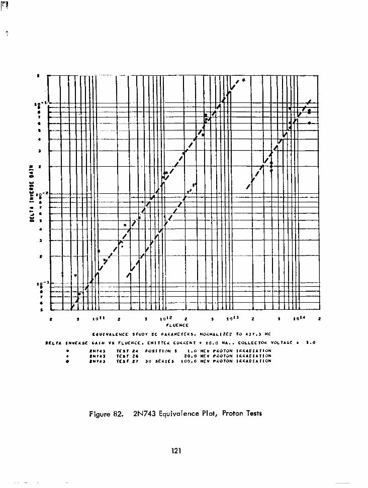
l , 4
S
2 S so” 2 5 IO12 2 5 101’ 2 5 10” 2 FLUENCE
COUI VALENCE SlUDV CC PICAWE 1fCS I NOCWALI2fC TO 4.,7.3 MC
DELTA INVCCSE CAIN VS FLUCNCE I f~fllfi CUGir(CNl - 10.0 MA.. COLLEClOl V3LlAGE L 1.0
. iNI. lfS1 24 FOSlllON I I.11 MEV PiOl3N IG#iAElAll3N
. 2N7.3 lCS1 26 20.0 MEV PiiOlON IkCAClAll3N 0 2N7.3 lCS1 2l 30 HAILS 100.0 HEV PrSOlON IK4ACIAlION
Figure 82. 2N743 Equivalence Plot, Proton Tests
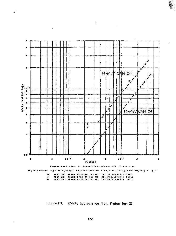
14-N,E
101’ 2 s
TLUCNCE
1012 2
COUIVALCNCC SlUE? DC l ACAUflfCS. NOiYALIZfE 13 437.3 MC
Dc~i* iwfrPsf CAIN vs fLufNcf. fMirrfI c~~if~l = 10.0 MA., co~~fcrobi V~L~AC~ = 5.0
l TCSl 29, lCANSlS1O6i ON 7.J N3. :¶, fCfJUfNCV = 399.4 . lCS1 29. l~ANSlSl0i PN I.3 NO. 29, fliCJUENCT = SI7.0 l ICI1 29, ~CANSI 5106 2~ r43 ~3. 29, FIEJUCNCV * 197.1
Figure 83. 2N743 Equivalence Plot, Proton Test 26
122
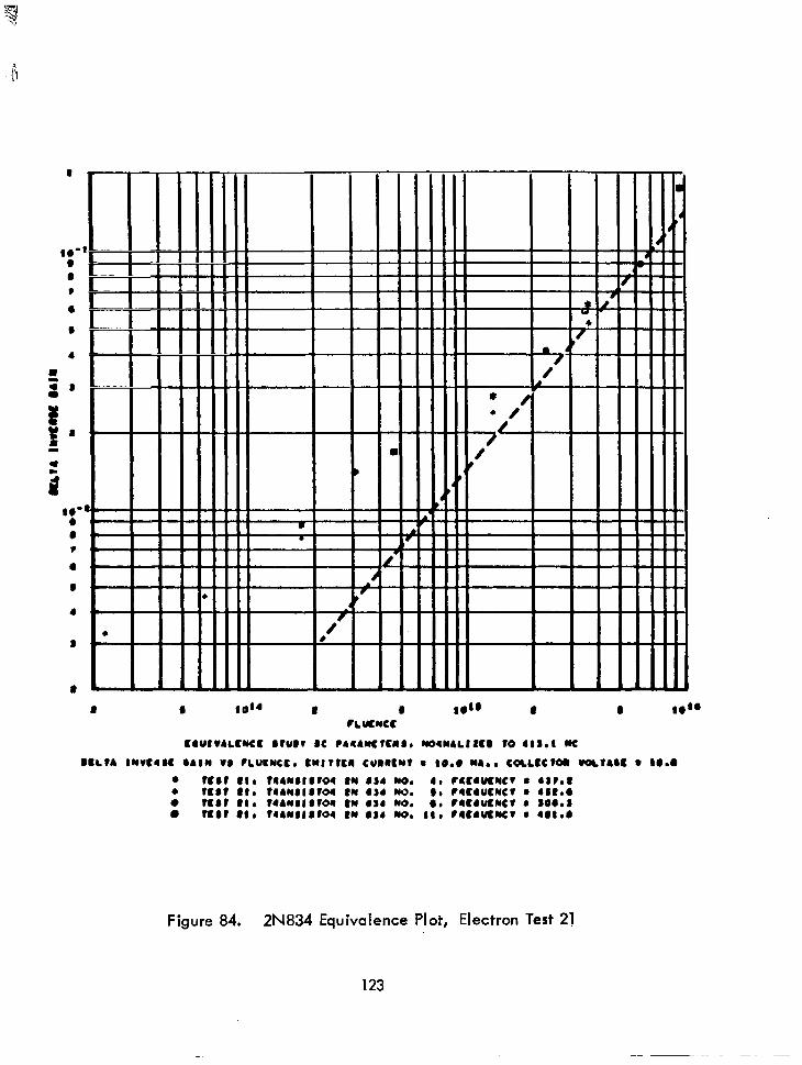
- - -
-
-
. -
I E E I I 1
T ‘f - f
4 -
.
.
.
.
.
3
.
,
.
.
.
10” a
-
3 r’
Figure 84. 2N834 Equivalence Plot, Electron Test 21
123
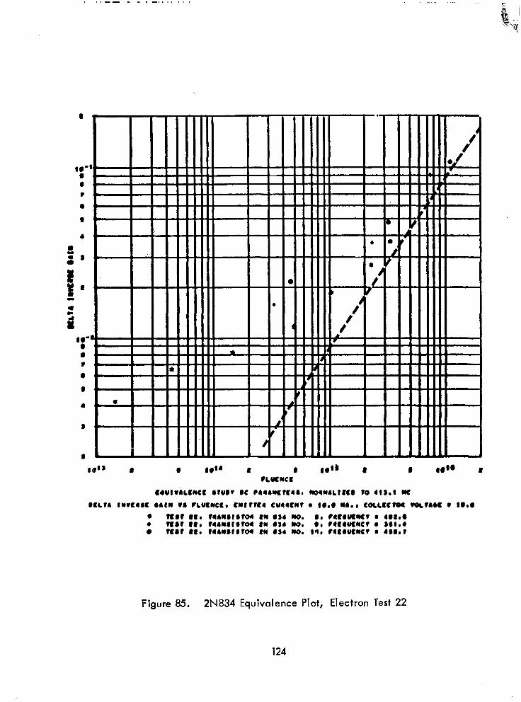
L
I I
t .
I
L
L
I
I I .
.
.
.
.
0
4
c-
-
# 10’) 8
C.. .
.
.
.
.
.
1
.
.
.
.
.
.
.
.
.
.
,
Figure 85. 2N834 Equivalence Plot, Electron Test 22
124
I
0
i - - -
-
- -
l
II l-l-7-x
IF=- l-l-7
IO” 8
- - - - - - z
-
ill
s 80” 8 QUCNCC
c4UI*4LtNCC #IUD* DC l A~AuCrC4sr YO4N4LltCO TO 4iS.l MC
DCLIA INVCISC 441m VS rLUCNCt, cutrrc4 cu~~c~f s (0.0 ~4.~ coaccro4 rar4ec l *@.a
4 rcmr 8s. ra4mststo4 IN a~4 NO. 1. V4tdUCNC~ l 1.1.#
:
war 8~. Ta4N8lSrO4 ?a 414 NO. l?, I4c4UcNCv l so.*
rcmr 8s. ra4mst s roa tw 34 NO. 0. Iac4ULNc~ l 8?2.,
0 rear es. r44asf s ma IN % JI NO. 0. rlC4UCNCV m 4t0.S l rcsr 81. ra4Ns4sfOa RN 13~4 NO. 11. IICWCWCV~ l 4rs.8
Figure 86. 2N834 Equivalence Plot, Electron Test 23
125
s 1014 8 80” 8
CIUIVALCNCC StUtt DC l AiANCtC4S. NO~NALIZtD 10 411.1 NC
##CIA tNVC4SC 44IW VS ILULNCC, CNlttC4 CWiCWt s 14.0 MA.1 COCLCCt04 WLtACC l (0.0
a rest as* ?44WS18tO4 tN #Jr NO. ,201 ClitQUCWCt s 144.0 b rear as, T44WSIStO11 tW 434 YO. It, C~COUCNCt n 4¶9.0 0 rear as. ?44NSIStO1 2W 414 NO. t2. ~~EJUtYCt l 441.0 0 mar as, t44NSlStO4 2N 434 NO. 23, t4CQUtNCI 0 SM.0
Figure 87. 2N834 Equivalence Plot, Co 60
Test
126
IO” 8 IO” 2 9 10lt 8 n 10” 8 m 1d4 8 CLUCWCE
C4UIVALCNCC SWDT DC l 444UEICdS. MO4N4LIZCD t0 4tS.t NC
mCLI4 IWIC4sL l llW Is lLUCNCCa ENltlC4 CUIIW#~ s 10.0 WA.. COLLCCtO4 VOLt4SC 9 10.0
0 DWIJI trsr 24 POsItlOw 6 1.0 WV l IOtON 1444DI41ION . 8NSJ4 rcsl to t0.D WI l 4OlOW 1444Dl4~ION l #a~ 34 rrar 8~ JO acntra 100.0 NCV l 1013N 1~44D1411OW
Figure 88. 2N834 Equivalence Plot, Proton Tests
127
8
8
8 a
C4UIVrLCNCt STUDV DC l ~GA@ICW~S. LCS~M4LItCO r0 ltJ.4 NC
DCLIA INVC#St 041W VS ILUCYCt. tutttr* cu~irwr s 10.0 MA., co~~tc~o~ VoLr4Sc V 16.0
l rcsr ri. l44WSISW1 tWtJ’)J NO. 4, r4cwrwv 8 lJ4.a l war 81, Td4NS1SrO4 2~2JqJ No. I* c4rJucwc~ m 1ts.o 0 rcsr 81. ra4aSI Sro4 tYtJ?J NO. 0, I4C4UCkC~ * 14t.4 0 rrsr 81, 144W¶IStOl CNtJ’3J 10. 11, CICJUCNCI l t4t.O
Figure 89. 2N2303 Equivalence Plot, Electron Test 21
128
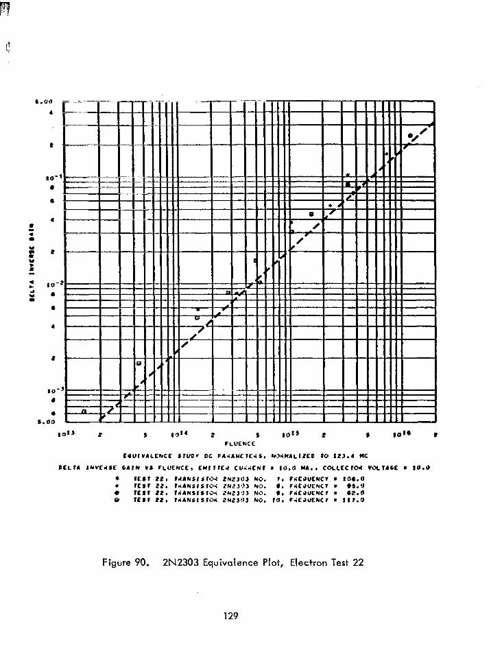
IO’ a
4 a.00
IO” 2 I 10” 2 9 FLUENCC
IO” 2
f
S to” R
EQUIUILENCC 4rUDf DC F4ilHErEiS, CLXMlLIZED r0 12J.4 WC
DCLfA INVEdSC GAIN VI FLUENCE. CI(IlfEII CUiiENI = 10.11 MA., COLLLCrOA VOLrlCt * SO.0
+ ILSI it, Id4NSI d r31 2N2303 NO. V, CliCPUCNCT s 106.U b IEII 22. tiANS1 S rOi tN23’33 WI. a, FICJUENCI = es.0 0 rEdI 220 fiANS? S 13i 2N2 193 NO. 9, FrifJUCNCI = 62.0 la rrsr 22, lriANLl S 1% 2N2303 NO. IO, CiEJUENCI r 111.0
Figure 90. 2N2303 Equivalence Plot, Electron Test 22
129
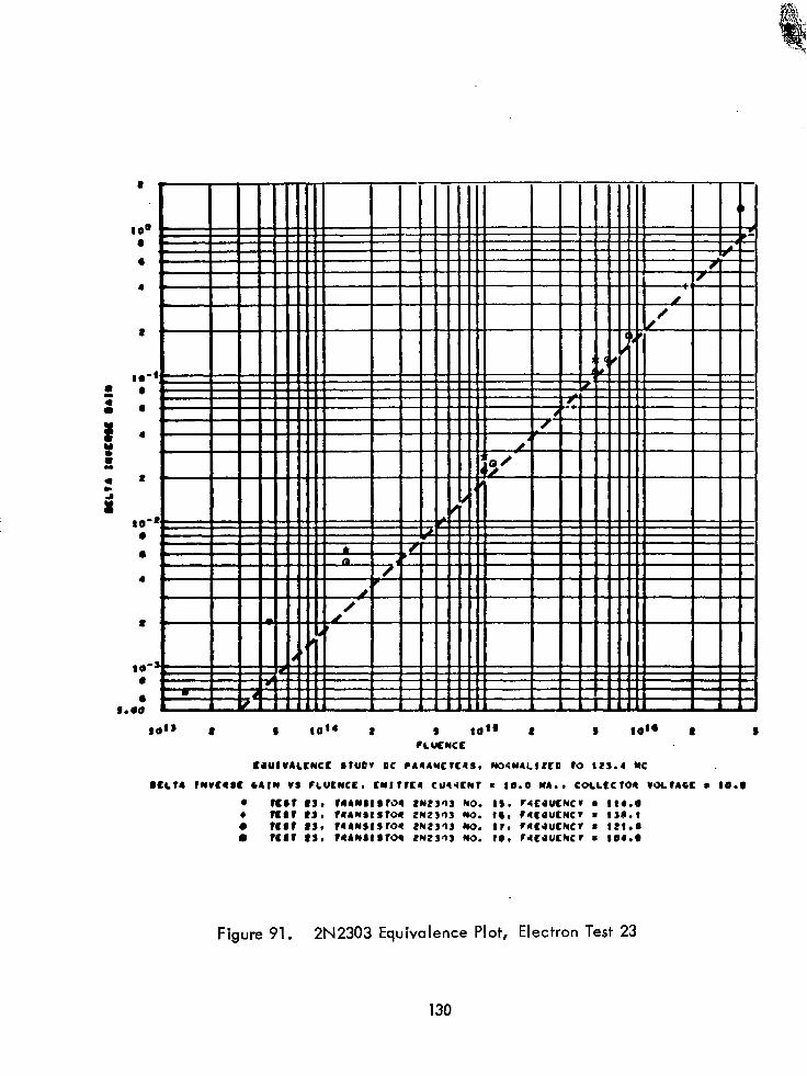
8
8
so” 8 I lOa 8 ¶ IO” 8 # (0” 8 8 *LUCWCC
C4UIVALCNCC SrUOI DC l A@lUtlEAS. LIOCN4LI2CD ‘0 ltJ.4 NC
BELT4 INVC4SC CAIN VS CLUCWCC. CNI1WA CU44CNr s ID.0 MA., COCLCCfOA VOLTACC l IO.@
4 rear If, ?AAW@1#101 tN2J’lJ NO. I¶, CltOUCWCf l ‘14.0 b war 83, tA4NSISlO~ 2NtJflJ NO. 141 IACQUCNCI s lJC.1 l MS? 8J9 TA4WJISrO~ 2NtJqJ I(O. 0, vAC4UCNCv 9 121~0 l mar tJl T44WlIStOl CM2JflJ NO. 18, CllCJUCNCl s ‘04.B
Figure 91. 2N2303 Equivalence Plot, Electron Test 23
130
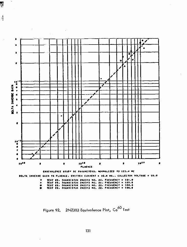
ad@ 8
-
t
3
-
-
-
-
-
-
0 1 -
.
Y
t
4
s
-
L /
LA
C4UIVALCNCC STUDI DC CAAANEtC4S. WANAL12CO 10 ltJ.4 NC
@CL?4 ‘NVCISC 44lN IS ILUCNCC, CNI tTt4 CUAACOt . 10.4 MA., CoLLCCtOa voLt44c l 10.0
l rtsr as* Tl4WSIS~O11 tWtJ’)J NO. tl, IaCOUCWC~ m I@‘.4 4 rest tn. Ta4NSIS~O4 tN2JnJ NO. 24, CIC4UCNCl 9 l?S.O 0 rear 1s. rm4usrsroa SNZJIJ MO. ‘Jr C~r4UCNCr l 104.~ 0 mar tss r44asisroa CNtJlJ NO. ta* ramucucr l 1oa.a
Figure 92. 2N2303 Equivalence Plot, Co 60
Test
131
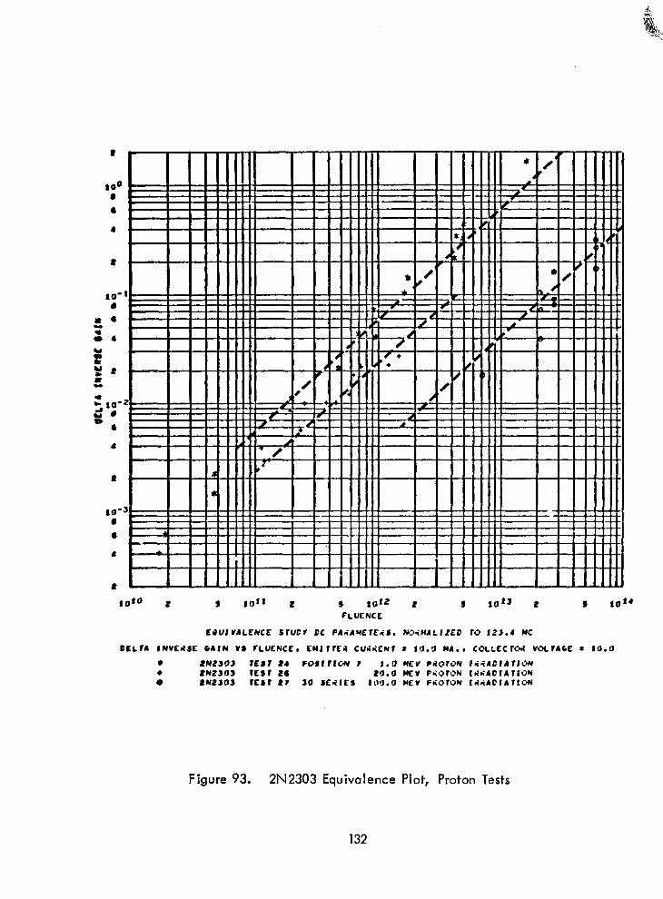
80’ a
l
4
soto i J ICI’) 2 J 1012 2 I 101’ a s 101’
FLUENCE
L3UlWALENCE SrUCI DC CA<AYErE.iSr N3iHALtZED rO Its.4 UC
DCLtA INVEliSE CAIN VI CLUENCE, LWIfrE4 CUiriENr 2 trl.‘J MA., COLLtClGli VOLrACE n tO.0
8 2N23!7., r28r 24 rest rtm I 1.0 MEW ColOrON ItiiACIAtlON 4 tN2SO3 rcsr 2~ 20.0 MEV QliOrON IddADlAtlON 0 2NiSOS rcSr 21 So SE~IEI tO’3.0 WEV FliOrON IdriAClArlON
Figure 93. 2N2303 Equivalence Plot, Proton Tests
132
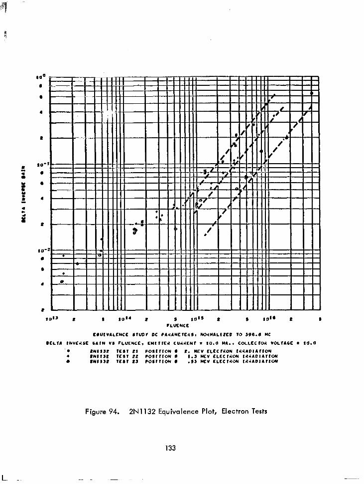
10’
0
l
1 I I1111111 I I I I11111
S to’4 2 I 10” 2 I lo’* i S FLUENCL
LOWVALENCE 6rUDf DC FAPAMEtE4S, WJWALIZEO 10 196.8 blC
DcLrA trwfdsc 611~ vs ~LUENCE, wfrrm cuirimr r 10.0 MA., co~LEcrod vo~7A6C 8 10.0
6 2Nt 112 rc6r 21 FostrIoN 9 2. MEV CLECrAON IriRADlArlON + 2Ntttt rc6r 22 Postrlofd 9 t.3 mv ELccrriCw IrilADlAltON 0 CNllS2 wsr 23 rostrtw 9 .93 HEY CLECTCON IrilADIArIOM
Figure 94. 2N1132 Equivalence Plot, Electron Tests
133
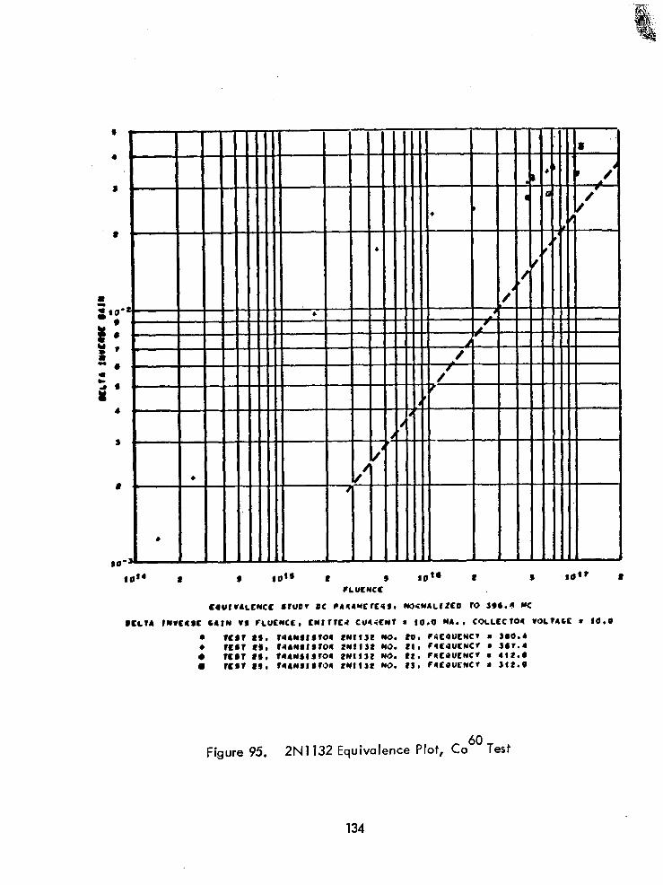
.
9 t
-
-
-
- I’
CLUEWCC
c4urv4Ltwc sruof oc CA~~EIC~J. woi~A~rzc0 to 396.4 wc
ML11 tMvt4St 64tW VS TLUCNCC, EYlrtLI CWiCNt * to.0 WA., COLLCCrO4 vOLt46E * to.9
6 fcsr rs, t44NSKSt04 tN11~2 NO. 201 ClitQUtWCT l 309.4
: rmt es, td4WStltO4 tMtt32 NO. 21, T424UCNC~ m 341.4 tC#T 89, TlAYSISIOI1 LNltJ2 NO. 22, C#:cOUCNC* s l(2.a
l tent 89, tlANSfStOl 2NtO2 NO. 2J. I4CJUCNCI s 3t2.9
Figure 95. 2N1132 Equivalence Plot, Co 60
Test
134
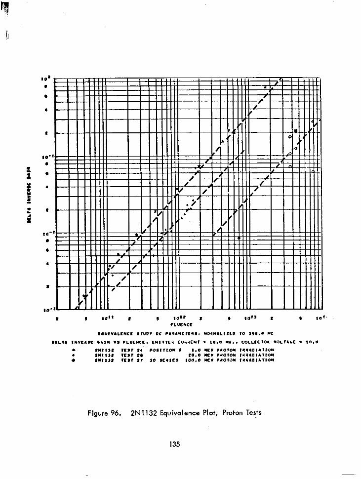
i s 10” 2 s 10’2 2 CLUENCE
s 10” 2 s 10”
LJUlVALfNCL StUDI OC l ASAWErC~b. WOiMILlttD r0 396.6 MC
mc~t4 1wcn6c 641~ vs ~LU~WC~, cuirrca cuiicmt = 80.0 ~4.. COLLCC~O~ vo~tux = 10.0
l . tNllS2 rtsr 24. fO6lllON 6 1.0 wcv clorou I~~ADIArION . 2w102 rtsr 26 20.0 MV l tiOtON 11942lAr10N 0 iNIll rcsr 21 so SC@lICS 100.0 MV l 1OrOW II~ADlAfION
Figure 96. 2N1132 Equivalence Plot, Proton Tests
135
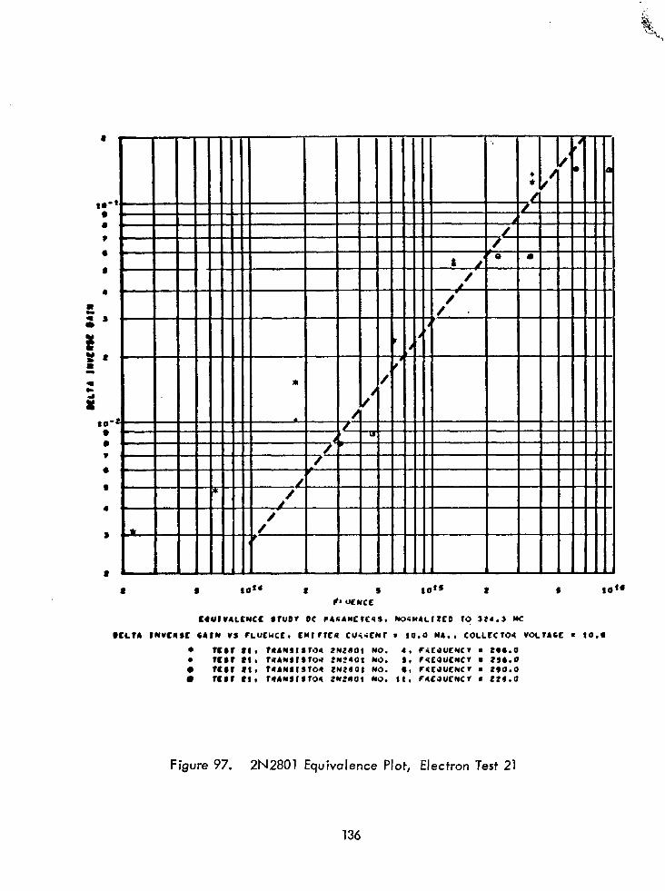
-
t
I
/
- -
- 7 0 -
-
-
- - -
-
-
-
t
&
z -
-
-
- - - - - -
-
4
S
,
10t4
CSUIVALCNCC SlUDV DC l ACAYElt4S. No~Y4LlZfD tq 324.3 WC
9CLlA IIIVCISC 64tW VS CLULUCE, CYlrrEll CUiiENr * 10.0 W&i., COLLCClOS VOLlACC * 10.1
l TCSl 2t. rfl4WSt SrOa 2NZdOI NO. 4, CiCPUCNCT l 2S4.0
: rcsr rcsr 81, 21* rawISro4 r4ANSlJtO4 tN?rOl 2N2401 NO. NO. 6, 1, FSLUUCNCT CSEUUCNCT 8 V tS6.0 290.0 l lcsl 21, l#AMSI#rO~ 2N2lOt MO. lt, CIICUUCNCV l 226.U
Figure 97. 2N2801 Equivalence Plot, Electron Test 21
136
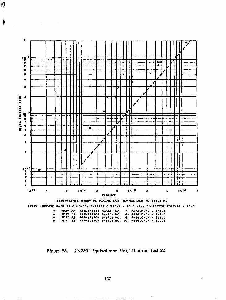
s
t
‘0’ 0 I 0 I
10” t
-
- - - - - -
-
- - - -
-
t : ;- : I I I, I I II
(0” 2 I 10” 2 s (0“ 2 ILIJCNCE
CaUIVILCNCC SrUDT DC l 4SAYEffSSr WiN4LlZtD r0 324.3 MC
DLLtA INVLISC C41N VS fLUCWCE, LYIrrE4 CUliSENr = 10.0 MI. I couEcr04 voLr46t s 10.0
l rcsr 22. r44wfsr04 zwaof NO. 7. f4E4UtNtV * 315.0 l rcsr 22, r94NsI St04 2N2401 NO. Or FliCaUENCT = 214.0 0 rcsr 22, r44NsISro9 2NtdOl NO. Dr CSEJUENCT . 321.0 0 rcsr 22, rq4NSIStOq 2N2401 NO. 10. fCCOUENC* . 230.2
Figure 98. 2N2801 Equivalence Plot,’ Electron Test 22
137
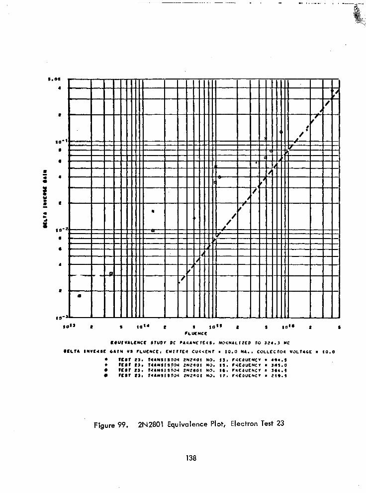
S.00
(0” t s 10” I J IO“ 2 s
fLUCNCL
LOUJV4LCNCt sruDV DC l 464YErfSs. W~N4LIZED ro 5El.J YE #CL14 IWVCI#S~ C41N VS CLUENCE, Cbtlrrfil cuiiCNr s 80.0 ~4.. coLLEcro4 wLr4tx a 10.0
0 tcsr 23. r44NSISf09 2N2401 NO. IS. fJEJULNC* * 4e4.9 l rtsr 23, ra4NslSro4 2~2~01 ~3. 19. C*EJIJENCT 8 1b3.0 l rcsr 2~~ ra4NSlSf04 2NtbOl NO. lC* fELQUENCT * JSI.9 l tcsr 2~~ t44NSlSfOi LNPIIOl NO. ITo fGCJUENC* = tt9.Y
Figure 99. 2N2801 Equivalence Plot, Electron Test 23
138
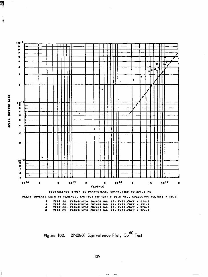
-t-T I I 11 I, I I Ill-
[ I
I
IO” e I ‘O’S 2 Y IO” 2 S IO” e fLUfNCf
CJUIVILLNCC SrUCv DC l 444Nfrf4Se W6M4LIIfD r0 324.3 MC
DEL14 IMVf4Sf C4lN VS fLUENCf. fwlrrfa cu4icwr s (0.0 MI., coLLfcro4 voLr4cf l 10.0
0 rfsr 2s. r44WSlSr09 tN2401 NO. 20, f4fPUfNCv a 2P2.0
i rcsr 2S. r44Nsisros 2NtJOl NO. 21, f#fJUfNCT s SY1.1 rfsr 2s, r44NSISrOS PN2SOl NO. 22. f4fJUfNCv m J7S.S
0 rfar tS, rdlNslSr34 2NtOOl NO. tJ, ClfJUENCT 8 J24.S
Figure 100. 2N2801 Equivalence Plot, Co 6o Test
139
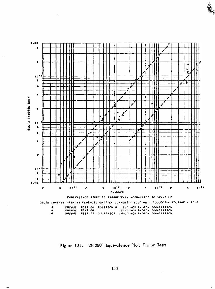
2
# s 10” 2 5 1612 2 5 IU” 2 5 IO”
fLUEME
CdUlVALfNCE SrUCT DC FliAHElEiS. HliHALlZED r0 124.3 MC
PELfA INVESSE GAIN VS FLUENCE, Enlrrfli CuiiENr t l’J.!l MA. I COLLECrOi v0LrAGf = 10.11 4 2N2001 rfsr 24 FOSI rfON 9 1.0 HEV FiOfON I<~4Cf4rION l 2NtdOl rfsr 26 20.0 MCV FliGlON IdilDI4rION 0 2N2.0 I lfsr 21 30 SEGIES 10’J.U YEV FliOr3N Iim4CIAllON
Figure 101. 2N2801 Equivalence Plot, Proton Tests
140
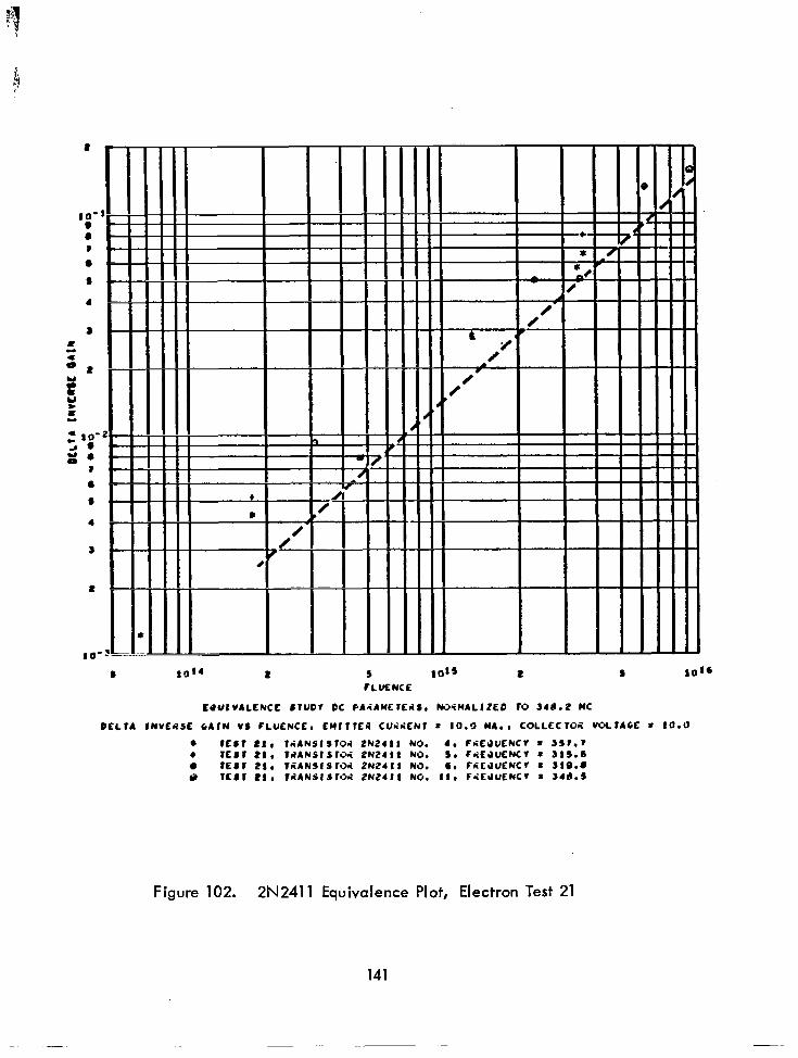
t l
T
i l
T - 10’4 2
-i / ,-
- -
-
-
-
-
-
-
-
-
-
-
-
-
-
I!
/
-
T F f T ‘F T I
-
- -
-
-
s
d
4 c
-
A
1 l- f T f- L T I
I
I fLUENCE
- -+- 7 2 t -
-
- - -
7
C4UlVALENCf SlUDT DC FAdANElE4S, WriM4LlZEO r0 14d.2 MC
DELIA INVEdSE CAIN VI fLUfNCE, EWIrrEd CUtiriENf = lO.‘J MA.. COLLfCfOl VOLrAGf * ‘0.0
4 ifsr 21, 11iilNSI STOP 2N24 I I NO. 4. flif4UENCT = SST.? t rfsr 21~ TAANSI 5 106 2N24 11 NO. 5, FllEOUENCT = IlS.6 8 wsr 21. WriANSI S 104 2N24 I: NO. S, fCEI)UENCT = S’9.S 0 ‘ES’ 21, lAANSlSl3i 2N2411 NO. ‘I, FiEOuENCT s 148.1
Figure 102. 2N2411 Equivalence Plot, Electron Test 21
141
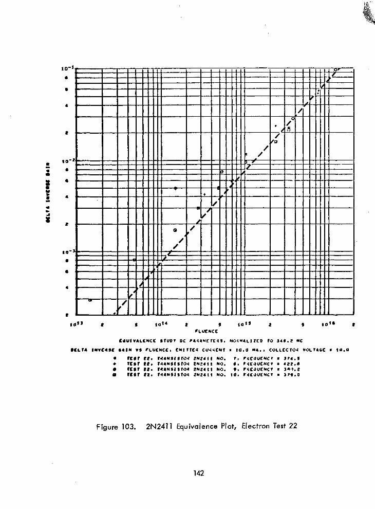
a
4
EEL
/
2
10” 2 s 101’ 2 Y IO” 2 ¶ 10” 8 FLUfNCf
C4UIV4LCNCf StUDI DC l 4i4~EfEiSt WiW4Ll2ED 10 340.2 WC
SCLr4 INVf4Sf l 4fN VS CLUCNCL, fwirrf4 cuiifNr z 10.0 ~4.. coLLfcr04 voLr4Cf = 10.0
0 rcsr 22, r~‘NSlSrOi tN2411 NO. fr FiCPUfNCr 8 Jt4.¶ t rcsr 22, rd4NSl s rOd 2N24 11 NO. S. fSE4UENCT 8 422.4
rcsr 22. l44NSI~tO4 tN2411 NO. 9. fGC4UENCT s 14ll.t 0 rcsr 22, r~4NSlSrO4 LN241’ NO. 10. fliC4UENCT 8 3I9.0
Figure 103. 2N2411 Equivalence Plot, Electron Test 22
142
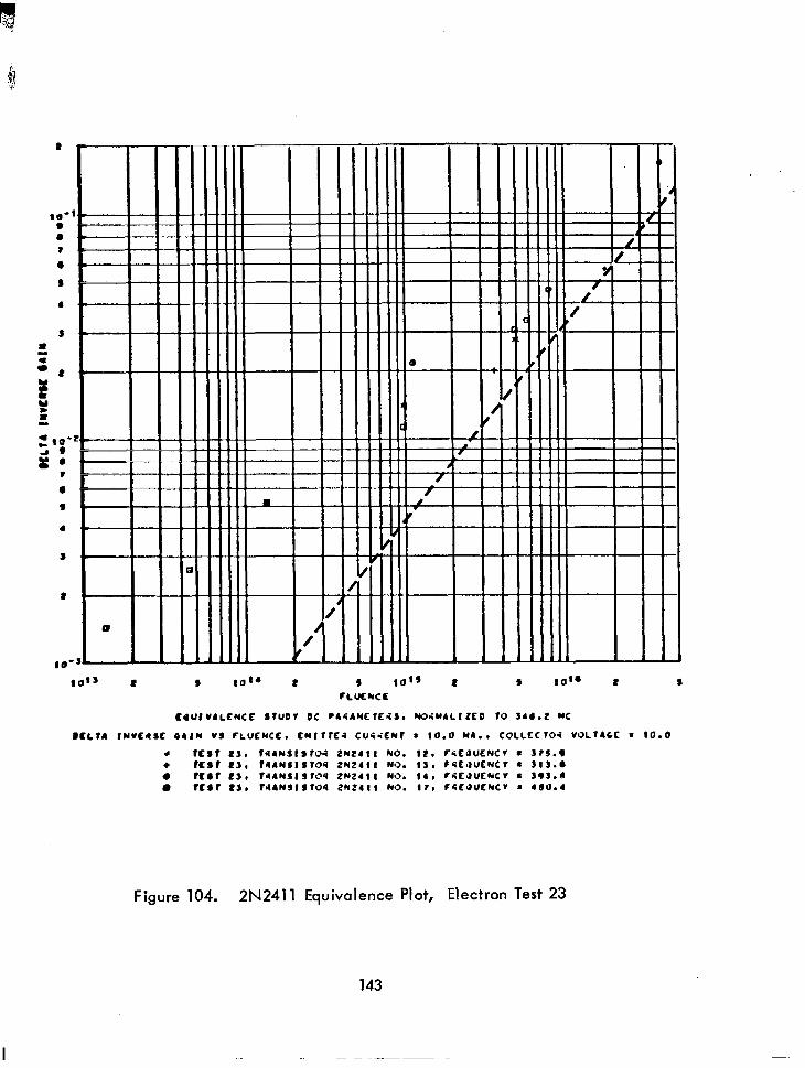
I -
I
q
(0’4 t
.
s IO” t 9 lo’s 2 S
CLUfNCf
f4U’V’LENCf SrUDT DC l 464YErEiS. NOiY4LItCD r0 344.2 MC
DELIA INVC#Sf C4lN VS fLUENCE. fbtirrf4 cuiifwr s 10.0 ~4.. coLLfcro4 voLr4cf n 10.0
4 rfsr 2s. rd4NSl¶rOii 2N2411 NO. 12. fiE4UENCT 8 ITY.9
t rfsr ~3, 144NSIS104 tN24ll NO. IS. CSEJUENCT 8 513.0 rcsr 23, r44NSlsrO4 tN241; NO. 14, CZEJUENCT 8 391.S
0 rfsr 23. r44NSlSrO4 ON2411 NO. I?, CliEJUCNCT 8 400.4
Figure 104. 2N2411 Equivalence Plot, Electron Test 23
143
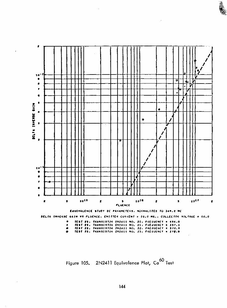
IO" 2 Y IO” 2 fLUfNCf
IO” 2
CJUIV4LfNCf SrUDT DC l 464ME rEiS. NoGW4LIzCD ro 144.2 NC
OfLl4 INVCSSC C4IN VS FLUENCE, f~lrrf~ culiif*r I to.0 ~4.. coufcro4 var46f r 10.0
l rfsr 29. lol4NSlS1~4 2N2411 NO. 20, f~EJUCNCT * 434.0 t rfsr IY, 144NSlS1OJ 2Nt411 NO. 21, f~fOlJENCT 4 SS1.S 0 rfsr 2). rd4NSlSfO4 tN2411 NO. 22. FqEJlJENCT = 9?0.0 0 rfsr 29, 194NSlSfOi 2Nt411 NO. 2s. f4CJlJENCT . 218.9
Figure 105. 2N2411 Equivalence Plot, Co 60
Test
144
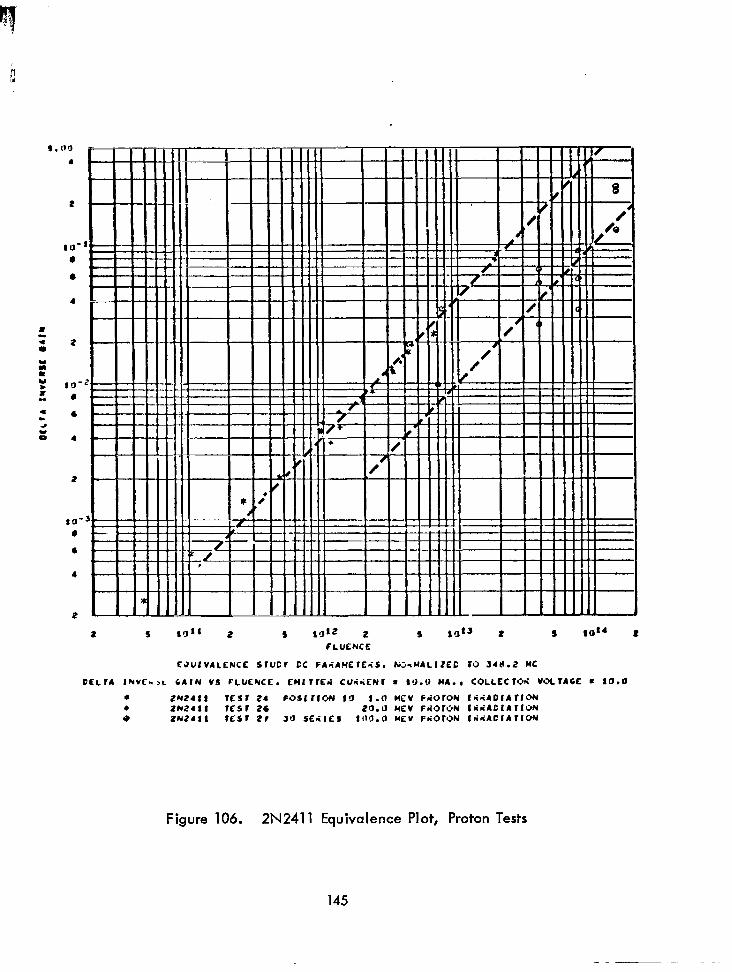
2
2
2 5 to“ 2 5 (cl’2 2 5 10” 2 5 IO” 2 f LUENCE
CJUIVALENCC SrUCI CC FAiAHiZlEiS, ti.UALIZEC 10 3411.2 MC
DELlA INVCN>L CAIN VI FLUCNCE. EWlfKti CUiiENr a 1?1.‘J MA., COLLECrOS VOLfACE n 10.0
L 2N24 I¶ msr 24 FOSlrlGN ICI 1.0 MEV FiOrON IiiADIAtlON . PN241f rcsr 26 2’3.1) MEV FliOrON ISiACIAllON 0 tN24:l rcsr 21 JO SEIIES 1tl’J.U WEV PkOlON IiriAElAIlON
Figure 106. 2N2411 Equivalence Plot, Proton Tests
145
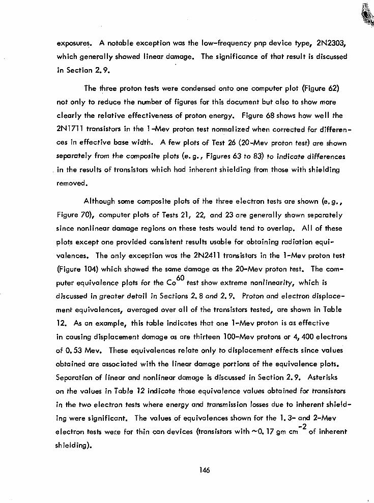
exposures. A notable exception was the low-frequency pnp device type, 2N2303,
which generally showed linear damage. The significance of that result is discussed
in Section 2.9.
The three proton tests were condensed onto one computer plot (Figure 62)
not only to reduce the number of figures for this document but also to show more
clearly the relative effectiveness of proton energy. Figure 68 shows how well the
2N1711 transistors in the 1 -Mev proton test normalized when corrected for differen-
ces in effective base width. A f ew plots of Test 26 (20-Mev proton test) are shown
separately from the composite plots (e. g., Figures 63 to 83) to indicate differences
in the results of transistors which had inherent shielding from those with shielding
removed.
Although some composite plots of the three electron tests are shown (eDg.,
Figure 70), computer plots of Tests 21, 22, and 23 are generally shown separately
since nonlinear damage regions on these tests would tend to overlap. All of these
plots except one provided consistent results usable for obtaining radiation equi-
valences. The only exception was the 2N2411 transistors in the 1-Mev proton test
(Figure 104) which showed the same damage as the 20-Mev proton test. The com-
puter equivalence plots for the Co 60
test show extreme nonlinearity, which is
discussed in greater detail in Sections 2.8 and 2.9. Proton and electron displace-
ment equivalences, averaged over all of the transistors tested, are shown in Table
12. As an example, this table indicates that one I-Mev proton is as effective
in causing displacement damage as are thirteen 100-Mev protons or 4,400 electrons
of 0.53 Mev. These equivalences relate only to displacement effects since values
obtained are associated with the linear damage portions of the equivalence plots.
Separation of linear and nonlinear damage is discussed in Section 2.9. Asterisks
on the values in Table 12 indicate those equivalence values obtained for transistors
in the two electron tests where energy and transmission losses due to inherent shield-
ing were significant. The values of equivalences shown for the 1.3- and 2-Mev
electron tests wer,e for thin can devices (transistors with -0. 17 gm cm -2
of inherent
shielding).
146
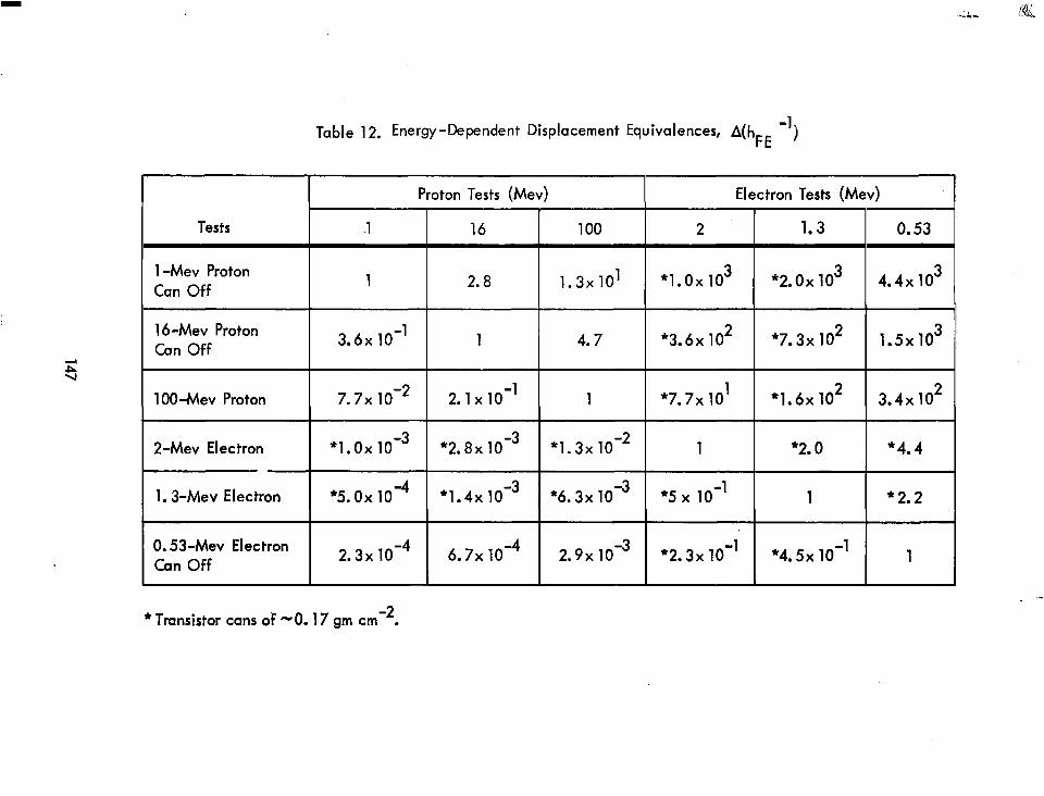
Table 12, Energy-Dependent Displacement Equivalences, A(hFE -‘)
Proton Tests (Mev) Electron Tests (Mev)
Tests
1 -Mev Proton Can Off
16 -Mev Proton Can Off
100 -Mev Proton
2-Mev Electron
1.3-Mev Electron
0.53-Mev Electron Can Off
.l 16 100 2 1.3 0.53 /
1 2.8 1.3x 101 *1.0x lo3 *2. ox 103 4.4x10³
I
3.6x 10-l 1 4.7 *3.6x lo2 *7.3x lo2 lAxlO ~
7.7x 1o-2 2.1 x 10-l 1 *7.7x lo1 *1.6x lo2 3.4x lo2
*1.0x 1o-3 *2.8x 1O-3 *1.3x 1o-2 1 *2.0 *4.4
*5.0x lod *1.4x 1o-3 *6.3x lO-3 *5 x 10-l 1 * 2.2
2.3x 1O-4 6.7x 1O-4 2.9x 1O-3 *2.3x 10-l *4.5x 10 -1
1
* Transistor cans of -0.17 gm cmB2.
2.7.3 Proton and Electron Energy Dependence
The influence of inherent shielding of the transistors (encapsulement) for
the electron tests was discussed in Reference 1. Table 13 summarizes energy and
transmission losses for transistors with typically thin and thick cans. Energy de-
gradation of 14-Mev protons passing into a transistor were determined by inte-
grating the energy loss over 1-Mev increments to account for changes in dE/dX
during penetration (Reference 17). Energy losses were calculated for the l- and
2-Mev electron tests for inherent shielding of the transistor cans (References 18
and 19). In addition, the loss of electron intensity was determined for those two
electron tests using a nomograph for electron number transmission (Reference 19).
A summary of the energy dependence of electron displacement damage
(Figure 107) and proton displacement damage (Figures 108 and 109) is given for
se let ted npn trans is ton. The data is plotted relative to a unity value arbitrarily
selected for the 0.53-Mev electron test. Data points from energies in addition to
those obtained from this study were obtained from preliminary tests performed earlier,
as well as concurrent with this study. In each figure, the experimentally determined
energy dependence of displacement damage (linear) is shown both for the silicon
only and for the thick can inherent shielding.
The effect of shielding on electron displacement damage in silicon transis-
tors acts in accordance with Table 13. Low-energy electrons are either absorbed
or reduced in number (scattered out) with subsequent energy loss. The net effect
is a significant reduction of the effectiveness of electron displacement damage at
low energies. This result would be expected since a rapid falloff with energy is
predicted both from displacement theory and from various experiments (see Section
2.7.4). The threshold in silicon for electron atomic displacement is approximately
150 kev Beferences 20 and 21).
The effect of shielding is particularly significant for space applications
since the electron intensity spectra of the Van Allen belts decrease rapidly with
increased energy. However, as was evident from A(hFE -‘) plots, linear displace-
ment damage is not the dominant electron effect on transistors for exposures
148
Table 13. Energy and Transmission Loss in Transistor Cans
dE/dX (Mev cm2 gm-‘) I-- ~~~~~~~ Thick Can Transistor I--
Thrn Can Transistor I
Energy Thick lnc ident Fe (Mev) Can
‘est No.
Particle
TYpe
Electron 21 1.95 1.38 (mean) 1.38 (mean)
1.28 1.36 (mean)
i c 22 1.36 (mean) , 0.38 1 0.88 1 38 IO.29 I 0.99 1
-t 23 0.53 Can off Can off 10 IO.531 1 I 0.53
1 0 1 1.0 / I I 1.0 Proton 24 1.0 Can off Can off
21.8 to 21.8 to 31.0 26.9
(integrate) (integrate) 6.1 7.9 --- 4.0 10.0 ---
14
Can off 1 0 / 14.0 1 0 0 1 14.0 1 26
18.5 to 18.5 to 23.5 21.8
(integrate) (integrate) 5.8 11.2 --- 3.3 13.7 ---
Can off
17
Con off 1 0 1 17.0 1 I I 17.0 0 0
27 100 --- D-m --- 100.0 --- --- 100.0 ---
loo
-
I
.
.
2N1613 TRANSISTORS
CAN ON CAN 0.21 GM CM-3 OFF
NAS 5-9578 STUDY
-
PRELIMINARY STUDY m 0 .
10’
ELECTRON ENERGY (MEV) Figure 107. Energy Dependence of Electron-Induced Displacement Damage (2N1613)
lo4
lo3
lo9
0 0
0 0
0 0
/’
T /’
I TRANSISTOR CAN CAN TYPES I I ON OFF
1 2N1613 1 0 1 0
1 2N2219 1 l 1 0
1 ALL 6 NPN 1 - 1 V
1-1 PRELIMINARY TESTS
NAS 5-9578
I I I I lllll I I I I lllll I I I Illll 1 n 1
lo-’ 10” 10’ 10’ PROTON ENERGY (MEV)
Figure 108. Proton Energy Dependence of Displacement Lbmage (npn Transistors)
-
TRANSISTOR CAN CAN TYPE ON OFF
I 2N743 PI-I NASA TND-1490
I I I Illlll I I I Illlll I I I Illll
loo 10’ 3
10’
PROTON ENERGY (MEV)
Figure 109. Proton Energy Dependence of Displacement Damage (2N743)
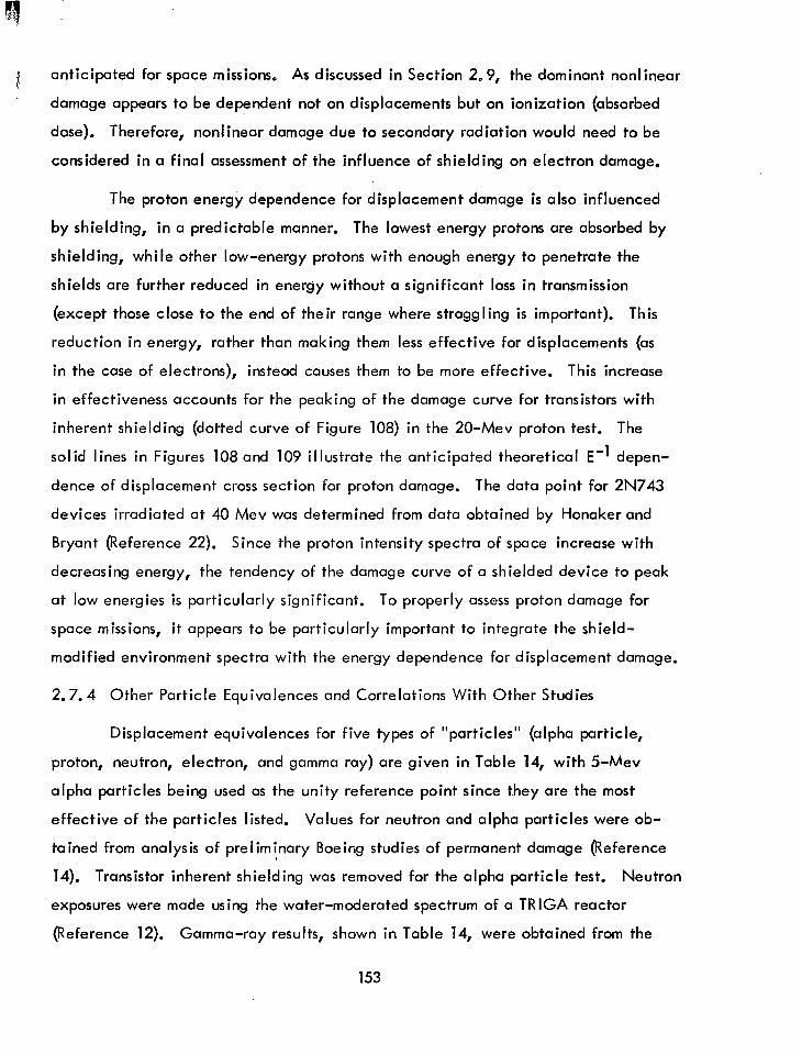
anticipated for space missions. As discussed in Section 2.9, the dominant nonlinear
damage appears to be dependent not on displacements but on ionization (absorbed
dose). Therefore, nonlinear damage due to secondary radiation would need to be
considered in a final assessment of the influence of shielding on electron damage.
The proton energy dependence for displacement damage is also influenced
by shielding, in a predictable manner. The lowest energy protons are absorbed by
shielding, while other low-energy protons with enough energy to penetrate the
shields are further reduced in energy without a significant loss in transmission
(except those close to the end of their range where straggling is important). This
reduction in energy, rather than making them less effective for displacements (as
in the case of electrons), instead causes them to be more effective. This increase
in effectiveness accounts for the peaking of the damage curve for transistors with
inherent shielding (dotted curve of Figure 108) in the 20-Mev proton test. The
solid lines in Figures 108 and 109 illustrate the anticipated theoretical E” depen-
dence of displacement cross section for proton damage. The data point for 2N743
devices irradiated at 40 Mev was determined from data obtained by Honaker and
Bryant (Reference 22). Since the proton intensity spectra of space increase with
decreasing energy, the tendency of the damage curve of a shielded device to peak
at low energies is particularly significant. To properly assess proton damage for
space missions, it appears to be particularly important to integrate the shield-
modified environment spectra with the energy dependence for displacement damage.
2.7.4 Other Particle Equivalences and Correlations With Other Studies
Displacement equivalences for five types of “particles” (alpha particle,
proton, neutron, electron, and gamma ray) are given in Table 14, with 5-Mev
alpha particles being used as the unity reference point since t.hey are the most
effective of the particles listed. Values for neutron and alpha particles were ob-
tained from analysis of preliminary Boeing studies of permanent damage (Reference
14). Transistor inherent shielding was removed for the alpha particle test. Neutron
exposures were made using the water-moderated spectrum of a TRIGA reactor
(Reference 12). Gamma-ray results, shown in Table 14, were obtained from the
153
Particle Type and
Energy
Alpha Particle (5 Mev) Can off
Proton (1 Mev) Can off
Neutron (Reactor)
Electron (1 Mev) Can off
Gamma Ray (Co60)
Table 14. Particle-Type Displacement Equivalences, A(hFE -1
)
Alpha Particle (5 Mev)
1
2.9x 10 -1
7.1 x 1o-3
*1.4x 1o-4
6.7 x 1O-6
Pro ton Neutron (1 Mev) (Reactor Spectrum)
3.5 1.4x lo2
1 4x 10’
2.5 x 10 -2
*5 x 1o-4 *2.0 x 1o-2
2.3x 10 -5
9.1 x 1o-4
Electron (1 Mev)
Gamma Ray
(Co69
*7x lo3 1.5x lo5
*2x lo3 4.3 x lo4
*5 x 10’ 1.1 x lo3
*2.2 x 10’
I
~ *4.5 x 1o-2
* Transistor cans of 0.17 gm cm ‘L
0
“7 average value of displacement equivalences for the 10 transistor types studied in
this contract. Discussion of the significance of gamma rays for studying linear
damage is presented in Sections 2.8 and 2.9.
Comparisons can be made between particle type displacement equivalences
and data reported for other types of semiconductor devices and other investigators.
Figures 110 and 111 show Boeing data for some earlier studies of displacement effects
in silicon diodes and. solar .cells (Reference 14).
The minority-carrier lifetime of diodes was measured using a Tektronix Type
S plug-in unit. Two types of silicon alloy diodes were tested, the 1 N459 (General
Instrument Company) and the lN462 fiaytheon). Measurements of I ifetime were
made before and immediately after irradiation. Both devices showed approximately
the same sensitivity to radiation and showed no damage annealing over periods of
several months.
Although the limits of error are quite large, the changes in lifetime appear
to be consistent with Equation (10). Damage constants, K,, for diode types lN459
and lN462 were found to be: (3*2) x 10-7seconds
10m8 seconds-’ for 2-Mev electrons; and (5rt3) x 10111
for reactor neutrons; (2*1) x
- seconds -1
for Co60 gamma
rays. Equivalences obtainable from Figure 110 are in rough agreement with those
found for transistor displacement damage.
The diffusion length, L, of minority carriers in silicon semiconductor material
can be related to the minority-carrier lifetime.
(22)
Changes in diffusion length, caused by radiation-induced recombination centers,
can also be related to particle fluences through Equation 10.
A (L-2) = L-2 - Lo-2 = KL+
155
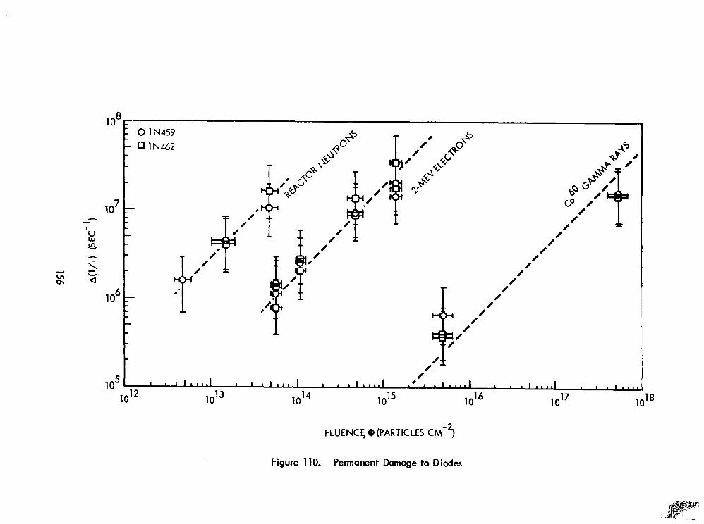
lo8
lo7
‘ti x3
3
‘;j
lo6
k OlN459 ‘- OlN459
- OlN462 - OlN462
0
L
0 0
0 0 0
/ /
0
i
0 / /’
0 0 l 0 0
0 0
0 0
/ /
0
0 -’ -’
,a51 / I I1 I,,,, 1 I ,I,,,, I Il..,, , I 1 I II,, L 1 1 ,111 I 1 111.1 1012 1013 1014 1015 1016 10” lo’*
FLUENC5@(PARTICLES CM-5
Figure 110. Permanent Damage to Diodes
Q where Lo is the initial diffusion length.
Short-circuit current, I SC’
of p-on-n or p-on-n-silicon solar ccl Is can be
related to the diffusion length, Ln, of the n region; the diffusion length, L , in P
the p region; and the junction depth, W. For uniform generation of carriers, short-
circuit current is given in Equation 25-Qeference 23):
where :
I SC
= egA(cT L, + c2Lp + c3W)
e = electronic charge
g = generation rate of carriers
A = sensitive area of the cell
(25)
Generally, the junction depth is much smaller than either of the diffusion lengths,
and the diffusion length of the base region (e.g., n region of a p-on-n solar cell)
controls I SC -
An experimenta I ly observed dependence of I on L when carriers are gen-
erated by solar or artificial light is given in Equatior(26), where
I SC = b log ,o (L/L’) (26)
b and L’ are constants (Reference 24). When L’ is eliminated by considering the
difference in short-circuit current before and after exposure, Equation (27) is
obtained (Reference 14).
A(l/L2) s L -2 4.6 (I - I 0 SC
0 SC (27)
Equation (27) is not valid for radiation exposures that are so extensive that diffusion
length of the base region is reduced to a value comparable to the lengths of
Equation (25). S I o ar cell initial diffusion length for data shown in Figure 111
was measured experimentally using the method of Gremmelmaier (Reference 25).
The damage obtainable from Figure 111 is in rough agreement with that obtained
for displacement damage of transistors.
157
L
HELIOTEK (P-N SILICON) HOFFMAN (P-N SILICON)
6( ‘-
+D ‘0’
0 0” /
/
0
0’- 0
/ / @
0 co
/ /
/ / - .
C a
105
/ /
/ 0
0 0 0
FQlt 0’
/ /
104- 1 1 IIll,, I 1 ,lllll + I, (’ ,I,, I I I ,Illll 1 L ,I,,,, 10'2
I 1 ,llllr lOI3 1o14 1o’5 10 16 10 17
10 18
FLUENCE,@ (PARTICLES d2)
Figure 111. Permanent Damage to Solar Cells
Figure 112 compares the relative effectiveness of electrons for displacement
damage to npn and pnp transistors of this study with both experimental and theoretical
data from other studies. The curve shown for theoretical cross section for silicon
displacements was calculated by Cahn (Reference 21) using basically the simple
model of Seitz and Koehler for atomic displacements in silicon (Reference 26) but
with relativistic corrections where necessary and assuming a displacement threshold
of 0. 13 ev. Although the observed transistor energy dependence does not follow
this curve, it is in rough agreement with detailed solar cell results found by Carter
and Downing (Reference 27). Their n-on-p solar cell data better fit the square of
the theoretical cross section which they suggest may mean a defect association with
a divacancy. They have attributed electron damage to the E,, + 0.3 ev defect level
Solar cell points shown in Figure 112 are for Hoffman n-on-p devices of 3.3 ohm cm
resistivity.
The proton energy dependence of damage shown in Figures 108 and 109 is
in rough agreement with the energy dependence of the displacement cross sections
for coulomb elastic scattering (- E-‘) in the region of approximately 7 to almost
100 Mev (References 26 and 28). At 100 Mev, for al I devices tested except the
epitaxial mesa transistors (2N743 and 2N834), the damage was higher than that
predicted by elastic scattering alone. Values of damage at 100 Mev were compared
with theoretical defect density published by Simon, et al. (Reference 29). The
ratio of total (due to both elastic and inelastic cross sections) theoretical defect
density to that of the elastic only is in agreement with the increase of damage
(shown above the E -1
line of Figure 108) observed with lOO-Mev protons. Below
about 6 Mev, Carter and Downing observed that proton effectiveness decreases for
damage to silicon solar cells. They found maximum sensitivity at about 2 Mev.
The relative effectiveness of 1-Mev protons to reactor neutrons of 40.0 :l. 0 shown
in Table 14 compares favorably with data obtained for neutrons by Larin and Niehaus
for the five 2Nl613 devices (Reference 30). The average damage constant yields
a ratio of 41.7:l.O.
159
6 oi I-
z! J W
Y i= 4 W ti
10’ --
loo -
0 PNP TRANSISTORS NAS 5-9578
A
0 NPN TRANSISTORS j H
V DISPLACEMENT THEORY (REFERENCE 21) NORMA’ IZED TO 1 AT 0.53 MEV
A N ON P SILICON SOLAR CELLS NASA CR-404
0 2~1613 SUPPLEMENTARY STUDY _ /
V' -v
I I I I Illll I I I I Ill1
10-l 10°
ELECTRON ENERGY (MEV) (INCIDENT ON SILICON)
Figure 112. Electron Displacement Damage in Silicon Devices
2.8 FEASIBILITY OF SIMULATION BY Co 6o GAMMA TESTING
Passive data, as well as curve traces obtained dynamically (during exposure),
were analyzed to determine the feasibility of using Co 60
sources for simulation of
electron and proton effects.
Analysis of A(BVcBo ) generally showed only small changes. Although
a strong dependence on fluence was observed for 2N2538 devices irradiated with
electrons or protons, no such dependence on exposure was observed for gamma-ray 17 -2
exposure up to 10 photons cm . Photon exposure fluence was defined as 1R
of co60 gamma radiation equa Is 1.6 x lo9 photons cm -2
. Although one of the
2N2538 transistors shown in Figure 113 suffered a significant decrease in BVcBo,
no dependence on fluence was observed, and thus no evidence for a tie-in with
displacement theory was demonstrated.
Changes of VCE (sat) did, however, reveal a strong dependence on #,
as indicated in Figures 114 and 115, The gamma-ray test data could be fitted to
the same power law dependence that was observed for the proton and electron tests
(Figures 15, 16, and 17); thus, equivalences could be obtained. These equivalences
are summarized in Table 15.
Also shown in Table 15 are the displacement equivalences for changes in -I
hFE a These values were obtained from an average of the linear damage equi-
valences of the transistor types. In several cases the linear damage of A(hFE -1
)
plots, such as Figure 57, was heavily obscured by the nonlinear damage. h those
cases, equivalence values were extrapolated from an estimate of the saturation
level of nonlinear damage. Possible separation of linear and nonlinear damage is
discussed in Section 2.9. Approximate values of damage constants for extrapolated
linear regions (displacement damage component) are shown in Table 16.
Measurement of lcBo changes made following gamma-ray exposure is
shown in Figures 116, 117, and 118. It is apparent from these figures that a
dependence on fluence exists, but not the linear dependence observed in Figures
21, 22, and 23 for the proton tests. It also appears (progression from Figure 116
161
-- B
r ’ L
,
P --- --
2N2538 0 21 Cl 22 A 23
IC = 100 PA
P , MEAN VALUE ‘0.77
I I I I IIll
1016 1017
FLUENCE, 4 ( PHOTONS CM-2)
lo'*
Figure 1’3. A(BV cBo) for Cob0 G amma-Ray Exposure (2N2538)
co60 GAMMA RAYS
m 0 2Nl613 0 ,’
0 2Nl711 0 6 0
IC = ‘OMA 0
0 0
hFE = 2 0 0
0 0
0.78 m o “4’
w’
ANCE(SAT)I = C +
/ 0
0 0
O” 0
/* ODD
0 0
1 I IIll I I I I lllll I I IIIllI I
14 10 1015 1016 1017
FLUENCE, * ( PHOTONS CM-2 )
Figure 114. Dependence of A[V CE
(sat)] on Co 6o Gamma-Ray Fluence (2Nl613, 2Nl711)
Co6’ GAMMA RAYS
A 2N2219
0 2N2303
‘C = 1oMA
hFE = 2
0 0
0 0
0 0
-0
0 0
0 0
0 0
0 0
QbA0~0 l- Ah&(SAT)I = C+ 0.78
ClOA
FLUENCE,@ ( PHOTONS CM-2 )
Figure 115. Dependence of AEVCE(sat)l on Co60 Gamma-Ray Fluence (2N2219, 2N2303)
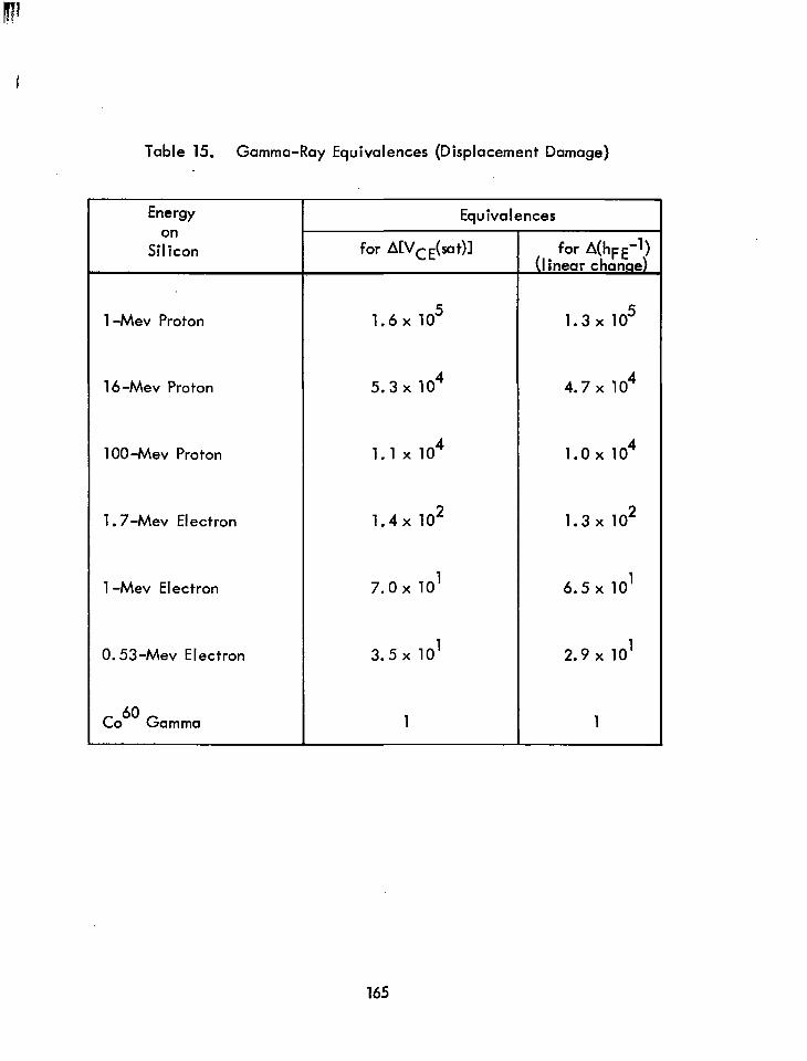
Table 15. Gamma-Ray Equivalences (Displacement Damage)
Energy on
Silicon
r
1 -Mev Proton
16 -Mev Proton
1 00-Mev Proton
1.7-Mev Electron
1 -Mev Electron
0.53-Mev Electron
co60 Gamma
Equivalences
for A[vcE(sCIt)l
1.6 x lo5
5.3 x IO4
1.1 x lo4
1.4x lo2
7.0x 10’
3.5x 10’
1
for A(hFE”) I inear change)
1.3x lo5
4.7 x lo4
1.0 x lo4
1.3x lo2
6.5 x 10’
2.9 x 10’
1
1
165
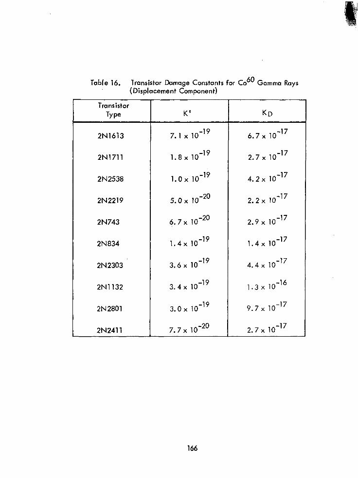
Table 16. Transistor Damage Constants for Co6' Gamma Rays (Displacement Component)
Transistor
Type K' KD
2Nl613 7.1 x lo-l9 6.7x 'O-l7
2N1711 1.8 x 'O-l9 2.7x 'O-l7
2N2538 1.0x lo-l9 4.2x lo-l7
2N2219 5.0 x lo-2o 2.2x lo-l7
2N743 0.7 x lo-2o 2.9 x 'O-l7
2N834 1.4x lo-l9 1.4x lo-l7
2N 2303 3.6x 'O-l9 4.4 x lo-l7
2Nll32 3.4x lo-l9 1.3 x lo-l6
2N2801 3.0 x lo-l9 9.7 x 'O--l7
2N2411 7.7x lo-2o 2.7 x 'O-l7
166
to 117 to 118) that the changes in leakage current seem to be saturating at high
exposures much as nonlinear changes in A(hFE -1
) were observed to saturate for
high-level electron exposure. If this nonlinear damage is related to ionization
rather than to displacements, it could indicate that the mechanism of nonlinear
damage observed in lCBO for the collector-base junction may be similar to the
mechanism of nonlinear damage observed for A(hFE -‘), which will be shown in
Section 2.9 to be related to increased recombination current of the emitter-base
junction.
To probe whether the permanent changes in lCBO for electron and gamma
exposure were related to ionization rather than to displacements (as observed for
proton exposure), changes in lCBO were plotted as a function of absorbed dose,
The transistors of Figures 116 and 118 have been replotted in Figures 119 and 120.
Added to the gamma-ray data points are electron data points for the same transistor
types. The results obtained for other device types are similar to those shown in
Figures 119 and 120. It thus appears that the electron effects are merely an ex-
tension of ionization-produced Co 60
gamma effects.
The net conclusion is that Co 60
gamma facilities may be useful in simulating
permanent effects caused by ionization such as electron-induced changes in lCBO
or possibly nonlinear electron-induced changes in h -1
FE ’ However, except for
possible changes in VCE(sat), Co 60
gamma rays do not appear to be too useful for
simulating proton damage. In particular, except at very high exposures (> 108R),
the nonlinear effects mask the linear effects. This is apparently due to the very low
ratio of displacement cross section to ionization generation resulting from Compton
electrons praduced by Co 60
gamma rays.
2.9 IDENTIFICATION OF NONLINEAR DAMAGE
Nonlinear damage has been identified as a problem for assessment of the
“permanent” effects of electron damage to transistors (not to be confused with
surface channeling and inversion layers observed for “Telstar” effects described in
Reference 31.) This section describes some of the characteristics that have been
167
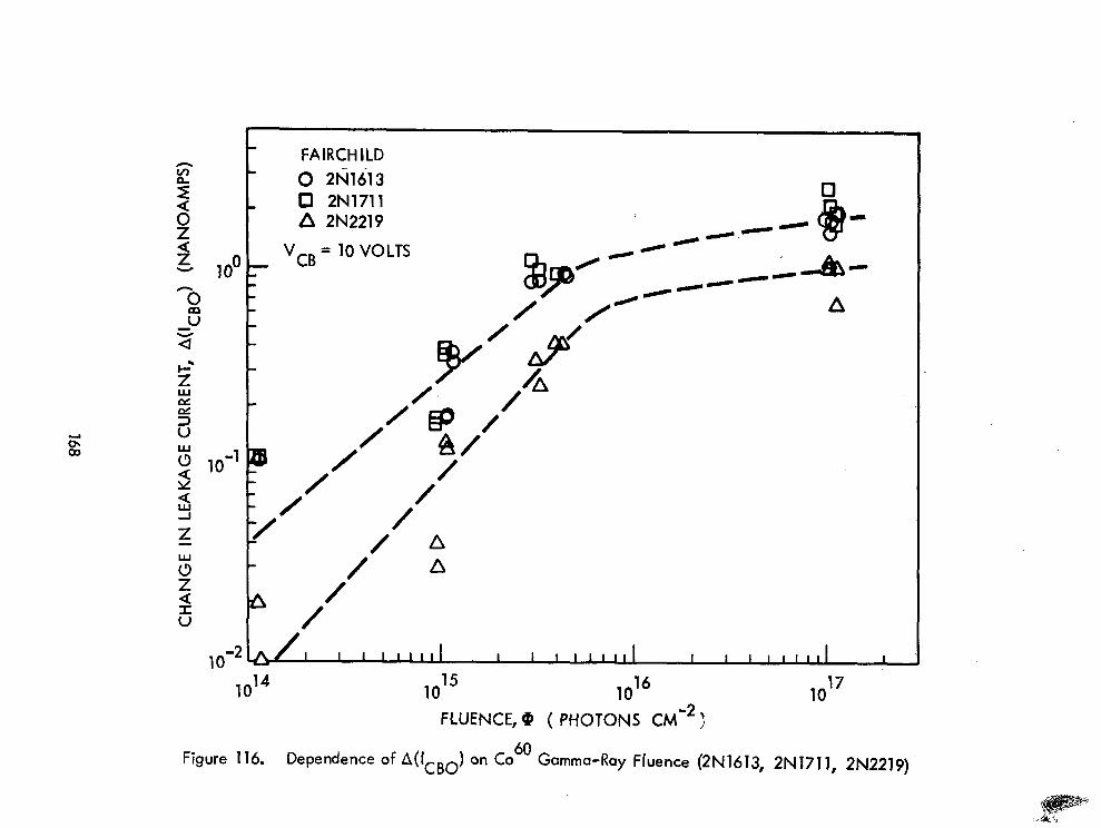
k FAIRCHILD
L t 0 2ti1813 n
0 2N1711
I
A 2N?219
V = 10 VOLTS
/ / 1o-2 I I I II111 I I I llll,I I I I II111 I
1014 10 15 1016 10
17
FLUENCE, @ ( PHOTONS CM-2 1
Figure 116. Dependence of A(lcBo) on Co6’ G ammo-Ray Fluence (2N1613, 2N1711, 2NZl9)
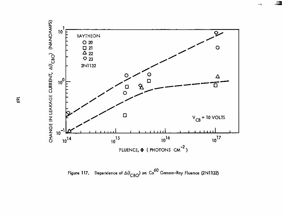
RAYTHEON
020 Cl 21 A 22 0 23
2N1132
0 w
0 0 0
0
0 0’
0 30 0 A n -
I --- U
‘CB = 10 VOLTS
v 2 10
-1w-, I I IIll I I1 lllll I I I II111 I I
6 1014 10 15 1o16 1017
FLUENCE, @ ( PHOTONS k2 )
Figure 117. Dependence of A(lcBo) on Co ” Gamma-Ray Fluence (2N1132)
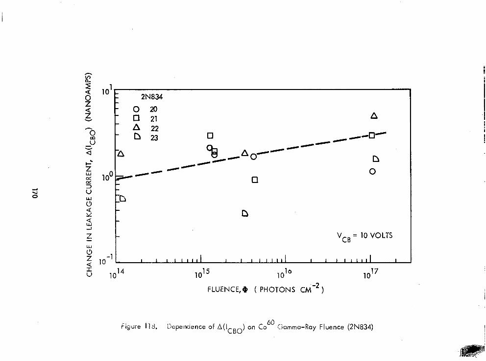
2N834
0 20 0 21 A 22 0 23 0 - H-o-
% ----
/-- a0- n /- 0
cl
A
‘CB = 10 VOLTS
I I I lllll I I I illll I I 11 WI1 I
E 1o14 1o15 1016 1o17
FLUENCE,O ( PHOTONS d2)
Figure 118. Dependence of A(lcBo) on Co ‘* Ihmma-Ray Fluence (2N834)
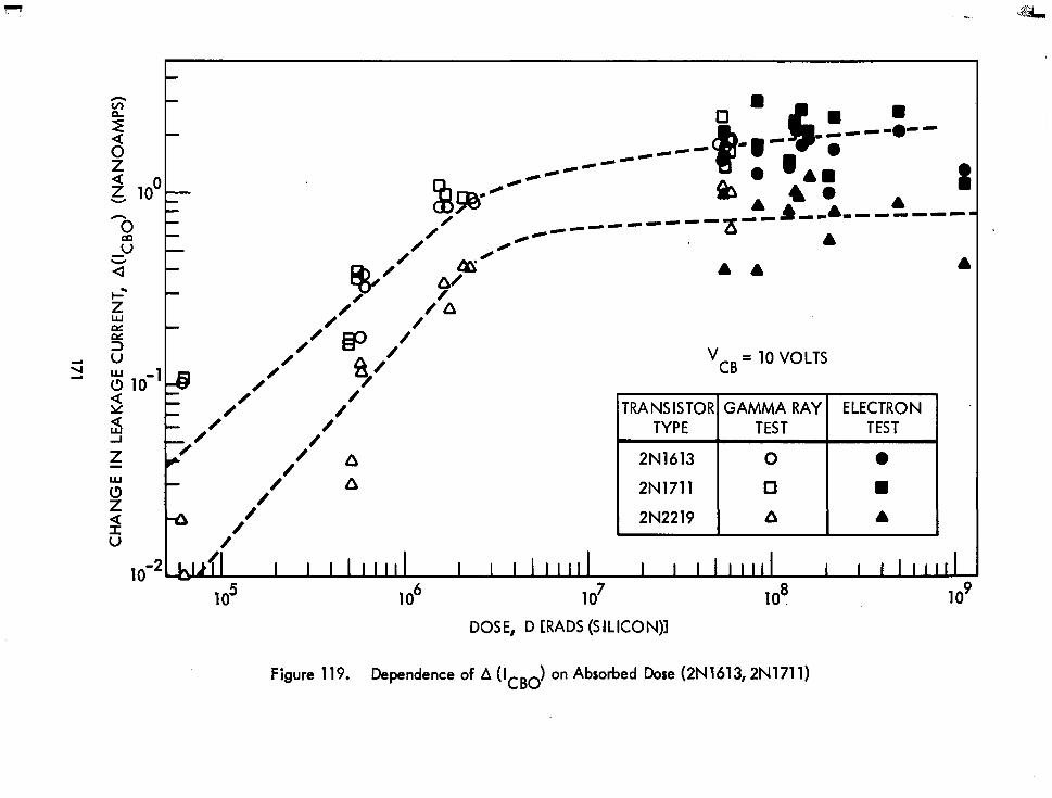
lo-2
b 0 0 A
a/ A A 0
/‘p /’ /‘A
3 ,/’ 4” V cB = 10 VOLTS
0 0 0
/’ TRANSISTOR GAMMA RAY ELECTRON
0 0
TYPE TEST TEST i 0
/’ ; 2N1613 0 a
/’ 2N1711 0 u
b /’
2N2219 Ls A 1
/f I I I Illlll I I I111111 I I I Illll I I I I11111
lo5 lo6 lo7 lo8 lo9
DOSE, D CRADS (SILICON)1
Figure 119. Dependence of A ( lCBo ) on Absorbed Dose (2N1613,2N1711)
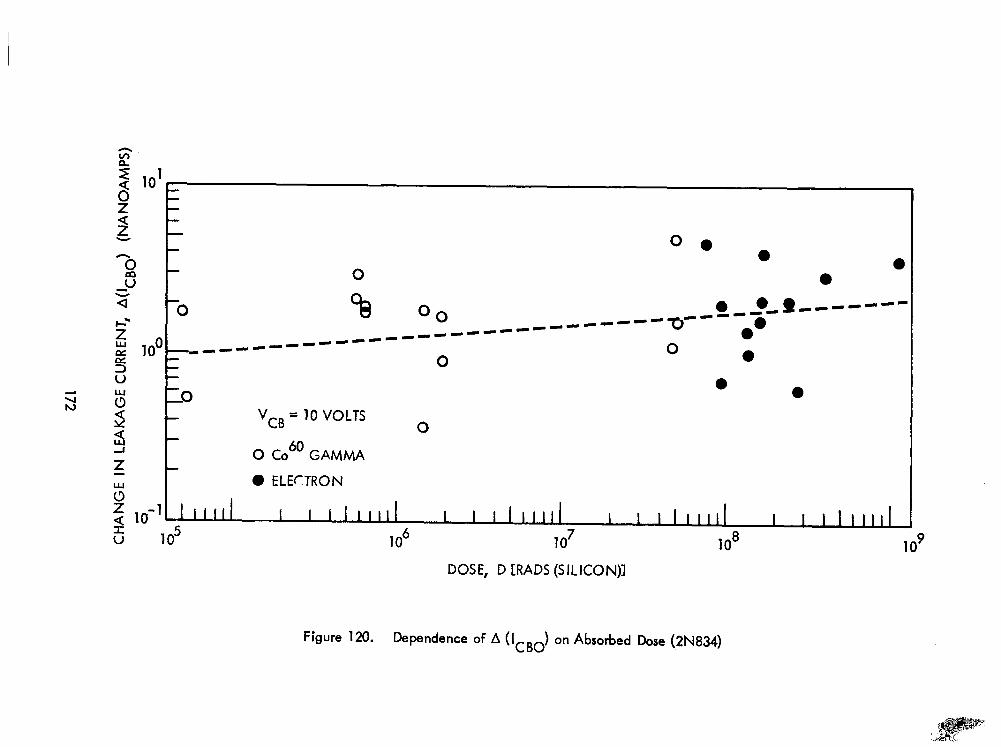
i2 -1 1,111) a 10 I I I l,,,,l I I I I lllll I I I IIHII I 5 lo5
I I llllll
lo6 lo7 lo8 lo9
DOSE, D [RADS (SILICON)1
Figure 120. Dependence of A (I CBO) on Absorbed Dose (,2N834)
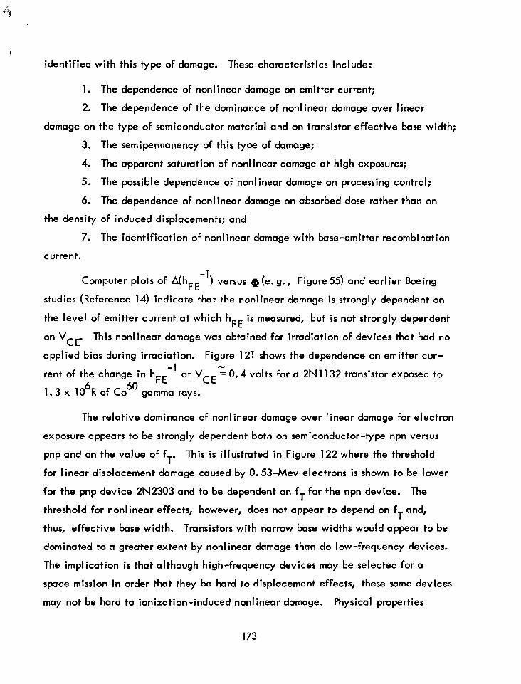
identified with this type of damage. These characteristics include:
1. The dependence of nonlinear damage on emitter current;
2. The dependence of the dominance of nonlinear damage over linear
damage on the type of semiconductor material and on transistor effective base width;
3. The semipermanency of this type of damage;
4. The apparent saturation of nonlinear damage at high exposures;
5. The possible dependence of nonlinear damage on processing control;
6. The dependence of nonlinear damage on absorbed dose rather than on
the density of induced displacements; and
7. The identification of nonlinear damage with base-emitter recombination
current.
Computer plots of A(hFE-‘) versus Ip (e. g., Figure55) and earlier Boeing
studies (Reference 14) indicate that the nonlinear damage is strongly dependent on
the level of emitter current at which h FE
is measured, but is not strongly dependent
on VCE. This nonlinear damage was obtained for irradiation of devices that had no
applied bias during irradiation. Figure 121 shows the dependence on emitter cur-
rent of the change in hFE -1
1.3 x 10⁶R of Co 60
at Vc Ez 0.4 volts for a 2N 1132 transistor exposed to
gamma rays.
The relative dominance of nonlinear damage over linear damage for electron
exposure appears to be strongly dependent both on semiconductor-type npn versus
pnp and on the value of fT. This is illustmted in Figure 122 where the threshold
for I inear displacement damage caused by 0.53-Mev electrons is shown to be lower
for the pnp device 2N2303 and to be dependent on fT for the npn device. The
threshold for nonlinear effects, however, does not appear to depend on fT and,
thus, effective base width. Tmnsistors with narrow base widths would appear to be
dominated to a greater extent by nonlinear damage than do low-frequency devices.
The implication is that although high-frequency devices may be selected for a
space mission in order that they be hard to displacement effects, these same devices
may not be hard to ionization-induced nonlinear damage. Physical properties
173
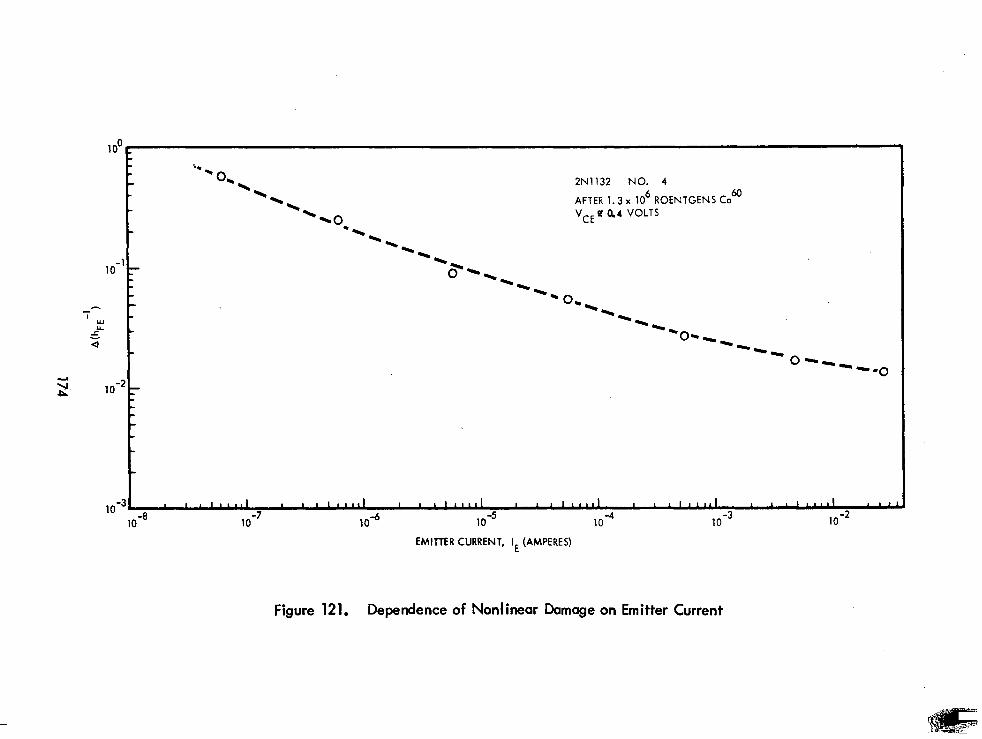
2N1132 NO. 4
AFTER 1.3 x lo6 ROENTGENS Co 60
VCE s? 0.4 VOLTS
1o-3 -8 ’ ’ ’ ’ ‘r1n’ I 1 I I,,,, I I
10 -7 -5 -4 -3 10 lod 10 10 10 1o-2
EMITTER CURRENT, IE (AMPERES) EMITTER CURRENT, IE (AMPERES)
Figure 121. Dependence of Nonlinear Damage on Emitter Current
loo
0.534EV ELECTRONS
0 2N17ll PNP
0 2N2219 FT- 123MC
P
NPN () 2N2303 F,- WMC
---- NONLINEAR COMPONENT 9/ /’ . . - LINEAR COMPONENT
1013 10 14
lOI
FLUENCE,+ (ELECTRONS CM-?
Figure 122. Relative importance of Linear to Nonlinear Damage
lol*
( e. g., effective ba se width or frequency) that contra1 sensitivity to linear displace-
ment effects do not appear to determine the relative sensitivity of transistors to non-
linear effects which, in geneml, dominate damage for typical low exposure space
missions.
Nonlinear damage appears to be semipermanent in nature, although not as
short term as are surface channeling effects (Reference 30). Table 17(a) shows that
although some room temperature recovery was noted for 2N2219 transistors that had
been heavily exposed to 1 -Mev protons , only slight annealing was observed even
for a 24-hour bake at 25OOC. Preliminary Boeing test data indicates that it is
apparently the semipermanent “non1 inear” damage and n ot the dominant “I inear”
damage that is annealable. The recovery of nonlinear damage is shown in Table
17(b) both for transistors exposed to electrons and for transistors exposed to X rays
of energy below the energy threshold for silicon displacements. From Table 17(b)
it can be seen that practically all of the nonlinear damage of the exposed devices
recovered after high-temperature treatment.
If ionization of the surface is the cause of the initial electron effects on
current gain and if these effects are saturable, then it would seem reasonable to
suggest that there may be a I imited number of prospective surface sites, N . As s-
these sites are acted upon, their number should decrease, resulting in eve&al
saturation of the effect. The conversion or rate of change of the prospective sites,
NS, with electron fluence would be expected to be proportional to the number
available.
dN J
d@ = K;N S
(28)
Ki of Equation (28) would be the energy-dependent ionization-damage constant,
since it would include the ionization rate of the incident electron. Then inte-
gration of Equation (28) and application of the initial conditions (a i = 0, Ns =
Ns.) would lead to a relation for the growth of ionization-induced surface recom- I
bination sites, N I’
as a function of electron fluence.
176
Table 17. Annealing of Nonl inear Damage
(a) Annealing of Proton Damage (2N2219) (2.1 x 10¹⁴ protons/cm2 -1 Mev)
NORMALIZED CURRENT GAIN (hFEfiFE initial) FOR ANNEALING TIMEAND TEMPERATURE OF
1 0.0184 0.0185 0.0196 0.0204 0.0506 2 0.0213 0.0227 0.0234 0.0238 0.0570 3 0.0195 0.0206 0.0210 0.0214 0.0650 4 0.0171 0.0179 0.0183 0.0186 0.0420
1
(b) Annealing of Nonlinear Electron- Induced Damage
Device
Type
2Nl711 2Nl613 2N2303 2N2801 2Nl613 2Nl613
Exposure Source
4.75 x 10¹⁴ e/cm2 1-Mev electrons 4.75 x lOI4 e/cm2 I-Mev electrons 4.75 x 10¹⁴ I-Mev electrons 4.75 x 10¹⁴
e/cm2 e/cm2 1 -Mev electrons
1.15 x l@R 105R
X rays (100 kvp) 1. 15 x X rays (100 kvp)
IE
0-4
10 0.934 10 0.892 10 0.730 10 0.864 0.2 0.715 0.2 0.665
hFE/hFt Before
Annealing
:(
i
initial)
22 Hours at 25OOC
0.985 0.927 1.000 0.960 1.000 0.970
1
177
IL
Nl = Ns Cl - exp (-ICI @)I i
(29)
Applying Equation (29) to the observed degradation of current gain would modify
the displacement equation for linear damage, as expressed in Equation (30).
A(hFE -‘) = Cs Nse Cl - exp (- Kl @)I + KD@ (30)
I
Figure 123 depicts gain degradation resulting from the 0.53-Mev electron test.
The surface term of Equation (30) represents well the observed initial degradation
of gain. The linear region of the curve of Figure 123 was extrapolated back and
subtracted from the experimental curve in order to separate the postulated displace-
ment and ionization damage. The dashed line, which represents this nonlinear
damage, has indeed the shape of a saturation curve. With the constants evaluated,
Equation (30), represented b/ the sol id line, fits the experimental data of Figure 123.
Assuming that the so-called ionization-induced damage sites are a result of
surface fabrication processes and ambient conditions at the time of fabrication, it
seems reasonable that the number of defect sites per-unit-surface area would be
similar for devices produced under similar conditions. Processing controls might
well regulate the degree of nonlinear damage generated. It might then be expected
that devices from different manufacturers would show varying degrees of regulation of
nonlinear damage. If nonlinear changes in lCBO of the collector base region are
caused by a mechanism similar to that causing nonlinear damage of A(hFE -1
) in the
base-emitter region, then the wide dispersion of A(IcBo) for Raytheon 2Nll32
transistor (shown in Figure 117) compared to the closer clustering of A(lcBd data
points for Fairchild devices (shown in Figure 116) may be an indication of the
importance of processing techniques or control.
Earlier tests using X rays of energies below the silicon displacement threshold
indicated that permanent nonlineur damage is probably caused by ionization effects
(Reference 14). This hypothesis appears to be further substantiated by the results of
this research program. Although linear damage is dominant for protons which have
a large value for the ratio of d,isplacement cross section to ionization generation,
178
r I I
1o’2
w C
- L
1o-3 -
L
L
2~1613 NO. 17 0.53~MEV ELECTRONS
ELECTRON FLUENCE, Cp (ELECTRONS/CMS
Figure 123. Separation .of Nonlinear Damage
nonlinear damage becomes increasingly more pronounced as incident electron energy
is reduced. An example was seen in Figure 94, where the displacement linear regions
are well separated but the nonlinear regions for the three electron energies blend
together. To check the influence of ionization, nonlinear damage, including a slight
amount observed at threshold for the 1 -Mev proton test, was separated for the 2Nl613
devices. This data was first plotted as a function of particle fluence in Figure 124
and then as a function of absorbed dose in Figure 125. The results of Figure 125
(the electron data points pull closer together) appear to be a further strong argu-
ment for associating nonlinear damage with ionization.
Preliminary studies of the dependence of IB on VBE (Reference 9) were used to
explore the source of nonlinear damage in transistors exposed to electrons and 60
Co
gamma rays. As described in Section 2.6.1, n components of base recombination
current separated graphically from the dependence of IB on VBE can be used to
locate regions of a transistor adversely affecting current gain of irradiated tran-
sistors. Figure 126 pictorially associates regions of a transistor with the various
n components. A grown device is used for simplicity of display. Figure 127 shows
changes in I 60
B for a 2N2801 transistor that has been exposed to 104R of Co gamma
rays. For this low value of radiation exposure, only nonlinear damage was observed.
A curve of the separated components of A(hFE -1
) versus gamma exposure is shown
in Figure 128. This curve is for a different 2N2801 transistor, whose threshold for
significant nonlinear damage is higher than the 10 4
R exposure of the device shown
in Figure 127. Significant nonlinear damage is dominated by the n 2 1.6 compo-
nent and has a threshold at an exposure less than an order of magnitude from that of
the n = 1 component for I inear displacement damage. From Figures 127 and 128
and similar data on other devices, it appears that an increase of recombination
current associated with the surface of the base-emitter region is responsible for
nonlinear damage. The relative sensitivities of the sources of transistor recombina-
tion current for those devices tested is summarized in Table 18 in relationship to
space mission exposure.
180
2Nl613 0 0:5-MEV ELECTRON . 0 1.0-M’/ ELECTRON a 2.O-MEV ELECTRON
“CE = 10 VOLTS
IE = 10 h,A
4 a0
c
0
lo-3
I-MN PROTON/
XI’ ,’ SCALE CHANGE
a
O0
0
4
0
08 0
0
a 000
0
0 O
P . I
,*[I2 ’ ’ ” “1” ’ ’ ” t”J ’ ’ ” a1J ’ ’ ” “’ 1013 1014 1015
FLUENCE, l (PARTICLES CM-2)
Figure 124. Nonlinear Damage Versus Particle Fluence
1.0:
0.01
2N1613 0 0.54EV ELECTRON 0 1. O-WV ELECTRON b ZO-MEV ELECTRON 0 Co60 GAMMA
6 /
l * V l.O-MEV PROTON #
l -
lo5 10”
DOSE, D CRADS(SILICON)l
10’ lo8
Figure 125. Nonlinear Damage Versus Absorbed Dose
I n = IOn (9) exp(qVBE/n KT)
n >2 COMPONENTS DUE\ r n = 1.0 COMPONENT CORRESPONDING TO RECOMBINATION-GENERATION
TO SURFACE CHANNEL \ / CURRENT IN THE BASE REGION
COLLECTOR
/ \ \ ’ SPACE-CHARGE REGIONS
n = 2.0 COMPONENT DUE TO-/
IN THE BULK SPACE-CHARGE RECOMBINATION-GENERATION
REGION \ 1.35nX1.8COMPONENT
\
DUE TO RECOMBINATION- GENERATION AT OR NEAR THE SURFACE OF THE SPACE- CHARGE REGION
Figure 126. Components of Recombination Current
lo-;
‘7i
lO”O
10-l’
0 n I I I
0. 10 0.20 0.30
VBE (VOLTS)
0.40 0.50
Figure 127. Change in Ig Versus V BE After Exposure to 104R (Co 60
Gamma)
184
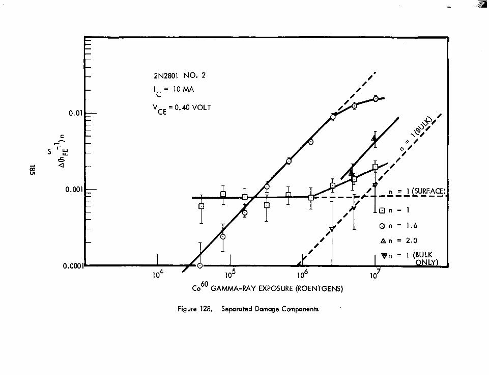
E h C
5 “Y
2N2801 NO. 2
Ic = 10 MA
V CE = 0.40 VOLT
,I/’ I ,hn =
I vn =
Co6’ GAMMA-RAY EXPOSURE (ROENTGENS)
1.6
2.0
1 (BULK ONLY)
Figure 128. Separated Damage Components
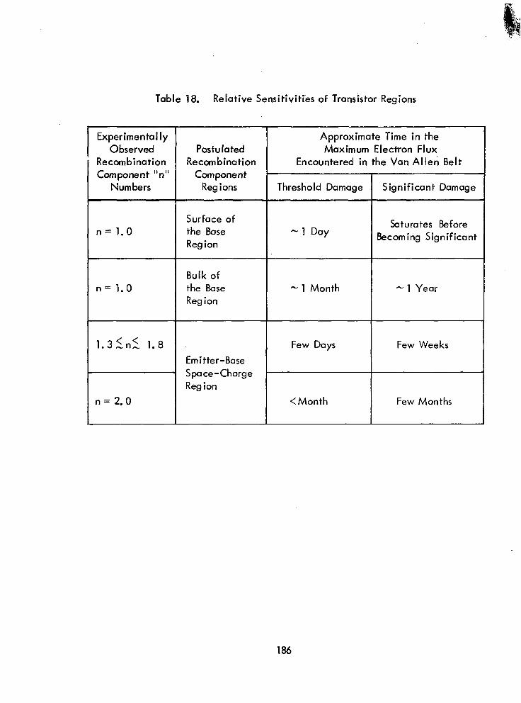
Table 18. Relative Sensitivities of Transistor Regions
Experimentally 0 bserved
, Recombination Component “n”
Numbers
1 n=l.O
i n=l.O
1 3LnL 1.8 .
n=2.0
Postu la ted Recombination
Component Reg ions
Surface of the Bose Region
Bulk of the Base Region
Emitter-Base Space-Charge Region
Approximate Time in the Maximum Electron Flux
I Encountered in the Van Allen Belt
Threshold Damage I Significant Damage I
-1 Day Saturates Before
Becoming Significant
- 1 Month - 1 Year
Few Days Few Weeks
/ Few Months 1 <Month
186
3.0 NEW TECHNOLOGY
The research work performed on this contract has been reviewed. To the
best of our knowledge there is no new technology to report.
187
II
4.0 CONCLUSIONS AND RECOMMENDATIONS
4.1 CONCLUSIONS
The following conclusions were obtained from analysis of test data.
1. Radiation equivalence information was successfully obtained for all of
the transistor types tested.
0 Displacement equivalences from analysis of A(hFE-‘) data indicated
fairly consistent agreement between the 10 transistor types (both npn
and pnp transistors).
0 Good correlation was obtained between equivalences for permanent
changes in h FE -‘I VCEbd, and lcBo-
0 Values of transistor damage constants obtained from transit time
normalization of proton test data were consistent between devices
of different types and manufacturers, in agreement with neutron
studies reported in Reference 32.
0 Nonl inear damage was observed to dominate I inear damage for
electron irradiation of interest for space missions.
0 Damage constants obtained for electron irradiation were reasonably
consistent between devices of the same type but showed considerable
variation between types and manufacturers, possibly reflecting the
influence of nonlinear damage.
0 Electron and proton displacement equivalences (linear damage) yielded
energy dependences for damage that are correlatable in part with dis-
placement theory and in part with published solar cell data.
l Inherent shielding by transistor cans reduces protons of 14 to 17 Mev
energy to lower energies that are significantly more effective for
displacement damage.
189
2. Simulation of space radiation effects by Co60 gamma rays has limitations.
0 Co60 gamma radiation can be useful in simulating the nonlinear
lCB0 and hFE degradation characteristics of electron exposure.
0 Only at exposures in excess of approximately 108R can the displace-
ment effects of proton damage be partially simulated by 60 Co gamma
exposures, except possibly changes of VCE(sat).
3. The following characteristics of nonlinear damage appear to be evident.
0 Nonlinear damage increases at a rapid rate for emitter currents
below 10 ma.
l Nonlinear damage tends to saturate with increased radiation exposure,
allowing for a separation of linear from nonlinear damage.
0 The relative dominance of nonlinear damage over linear damage is
CI function of the threshold for displacement damage and the ionization-
to-displacement ratio of the incident radiation.
l The dominant portion of nonlinear damage is induced by ionization
rather than atomic displacement.
0 Nonlinear damage is correlatable with increases in base-emitter
recombination current, while linear damage is related to recombina-
tion current in the bulk of the base region.
4.2 RECOMMENDATIONS
The following recommendations are made for continued study of radiation
equivalences:
1. Nonlinear damage should be more fully characterized, including
l Establishment of the functional dependence of nonlinear damage on
emitter current.
‘90
0 Determination of the statistical variation of nonlinear damage and its
association with processing control.
l Firm establishment of the dependence of nonlinear damage on ioniza-
tion to provide complete radiation equivalences for electron damage.
0 Further exploration of the source and control of nonlinear damage.
2. The synergistics of combined effects should be checked by simultaneous
exposures to protons and electrons to validate integration of I inear and nonlinear
effects over particle energy.
3. The influence of electrical bias (bias applied during radiation) on non-
I inear damage, in particular, should be studied.
A flow chart illustrating the recommended tasks for a continuation of this
research study is shown in Figure 129.
191
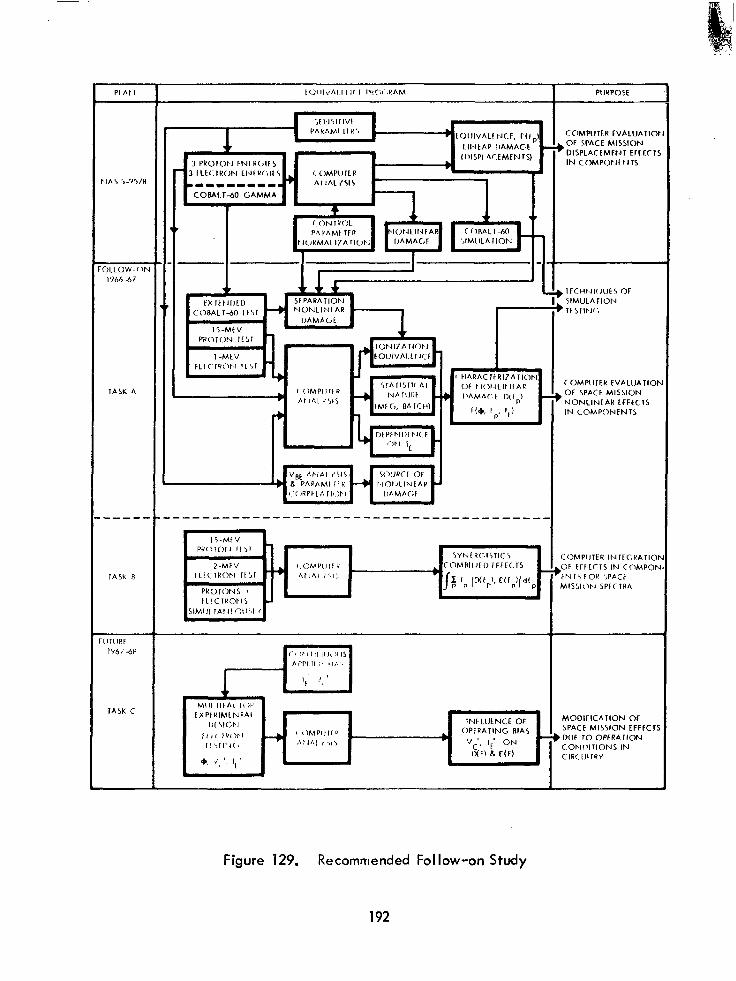
CC%4PtITER FVALIJAIIC: OF SPACE MISYON DISPLACE~.~FNI CFFFCT IN COMPO~lf~llS
IfCHI4I’)IJt\ OF
COMPIITER EVALlJATlO OF 5PACt MISUON NONLINtAR tFFLCl5 IN COMPONENTS
COMPIJTER INIEC.t!AIIC OF FfFIClS IN COMPOI tN I\ f OK :PACt MIS:lON SPFC IRA
OPfRATING RIAS
MoDlFlCAlloN Of SPACE MISSION EFFFCT D(JF TO OPERA rim CONI)ITIONS IN
Figure 129. Recommended Follow-on Study
192
5.0 BIBLIOGRAPHY
1. Brown, R. R. , and Horne, W. E. , “The Effects of Electron Radiation on Tran- sistors, ” Six-Month Progress Report for NAS 5-9578, Boeing Document D2-84088-1, December 1965. (See Appendix I )
2. Brown, R. R., “Identification of Radiation Preferred Electronics, ” Record of the 1965 International Space Electronics Symposium, Institute of Electrical and Electronic Engineers, Inc., New York, N. Y., 1965.
3. Easley, J. W., and Dooley, J. A., “On the Neutron Bombardment Reduction of Transistor Current Gain, ” J. Appl. Phys., Vol. 3, No. 6, 1960.
4. Goben, C. A., and Smits, F. M., “Anomalous Base Current Component in Neutron-Irradiated Transistors, ” Sandia Corporation Reprint SC-R-64-195, July 1964.
5. Goben, C. A., “A Study of the Neutron-Induced Base Current Component in Silicon Transistors, ” IEEE Trans. on Nut. Sci., Vol. NS-12, No. 5, pp. 134-146, 1965.
6. Sah, C. T., “Effect of Recombinations and Channel on P-N Junction and Transistor Characteristics, ” IRE Trans. on Elec. Dev., Vol. ED-9, No. 1, 1962.
7. Sob, C. T., Noyce, R. N., and Shockley, W., “Carrier Generation and Recombination in P-N Junctions and P-N Junction Characteristics, ” Proc. IRE Vol. 45, September 1957. I
8. Iwerson, J. W. et al., “Low Current Alpha in Silicon Transistors, ” IRE - Trans. on Elec. Dev., Vol. ED-9, No. 6, November 1962.
9. Horne, W, E., and Brown, R. R., “Correlation of Electron-Induced Changes in Transistor Gain With Components of Recombination Current, ” presented at the Annual IEEE Conference on Nuclear and Space Radiation Effects, Stanford University, July 1966 (to be published soon in IEEE Trans. )
10. Rooney, J. A., “Transistor Damage Plotting Program, ” Boeing Document AS 1706, March 1964.
11. Webster, W. M., “On the Variation of Junction Transistor Current Amplifi- cation Factor With Emitter Current, ” Proc. IRE, Vol. 42, No. 6, pp. 914- 920, June 1954.
193
12. Easley, J. W., “Comporison of Neutron Damage in Germanium and Silicon Transistors, ” Proceedings Third Semiannual Radiation Effects Symposium, Vol. 4, October 28-30, 1958.
13. Brown, R. R., “Equivalence of Radiation Particles for Permanent Damage in Sem iconductor Devices, ” IEEE Trans. on Nut. Sci., Vol. NS-10, No. 5, pp. 54-59, 1963.
14. Brown, R. R., “Proton and Electron Permanent Damage in Silicon Semicon- ductor Devices, ” in Radiation Effects in Electronics, STP-384, American Society for Testing and Materials, July 1965.
15. Phillips, A. B., Transistor Engineering and Introduction to Integrated Semi- conductor Circuits, McGraw-Hill Book Co., New York, N. Y., 1962.
16. Thomas, D. E., and Mol I, J. L., “Junction Transistor Short-Circuit Current Gain and Phase Determination, ” Proc. IRE, Vol. 46, pp. 1177-1184, June 1958.
17. Rich, M., and Madey, R., “Runge-Energy Tables, ” UCRL-2301, March 1954.
18. Nelms, A. T., “Energy Loss and Range of Electrons and Positrons, ” N. B. S. Circular 577, July 26, 1956.
19. Mar, B. W., “An Electron Shielding Analysis for Space Vehicles, ” Nut. Sci. and Eng., Vol. 24, pp. 193-199, 1966.
20. Loferski, J. J., and Rappaport, P., “Displacement Theory in Semiconductors, ” J. Appl. Phys., Vol. 30, No. 8, pp. 1296-l 299, 1959.
21. Cohn, J. H., “Irradiation Damage in Germanium and Silicon Due to Electrons and Gamma Rays, ” J. Appl. Phys., Vol. 30, No. 8, p. 1310, 1959.
22. Honaker, W. C., and Bryant, F. R., “Irradiation of 40-Mev and 440-Mev Protons on Transistors, ” NASA TN D-1490, Langley Research Center, January 1963.
23. Cummerow, R. L., “Photovoftaic Effect in P/N Junctions, ” Phys. Rev., Vol. 95, pp. 16-24, July 1, 1954.
24. Denney, J. M. et al., “Charged Particle Radiation Damage in Semiconductors, V: Effect of I-Mev Electron Bombardment on Solar Cells, ” Space Technology Laboratories Report, MR-28, 8653-6018-KVaOO, 1963.
194
25. Gremmelmaier, R., “irradiation of P/N Junctions With Gamma Rays: A Method of Measuring Diffusion Lengths, ” Proc. IRE, Vol. 46, pp. 1045-1049, June 1958.
26. Seitz, F., and Koehler, J. S., “Displacement of Atoms During h-radiation”, in Solid State .Physics, Vol. 2, Academic Press, pp. 305-448, 1956.
27. Carter, J. R., and Downing, R. G., “Effects of Low Energy Protons and High Energy Electrons on Silicon, ” NASA CR-404, March 1966.
28. Dienes, G. J., and Vineyard, G. H., “Radiation Effects in Solids, ” Monographs in Physics and Astronomy, Vol. II, Interscience Publishers, Inc., 1957.
29. Simon, G. W., Denney, J. M., and Downing, R. G., “Energy Dependence of Proton Damage in Silicon, ” Phys. Rev., Vol. 129, NO. 6, pp. 2454-2459, 1963.
30. Larin, F., and Niehaus, D. J., “A Generalized Approach to Transistor Damage by Radiation, ” Nucleonics, Vol. 22, No. 9, September 1964.
31. Peck, N. W., Blair, R. R., Brown, W. L., and Smits, F. M., “Surface Effects of Radiation on Transistors, ” Bell System Tech. Jour. XIII, No. 1, pp. 95-l 29, 1963.
32. Frank, M., and Larin, F., “Effect of Operating Conditions and Transistor Parameters on Gain Degradation, ” IEEE Trans. on Nut. Sci., Vol. NS-12, No. 5, pp. 126-133, 1965.
195
6.0 GLOSSARY
A
A C
A s
BVCBO
C Tc
C Te
C
D
Db
D Pb
Ef
e
f
fN
fT
f a
G
9
h
Sensitive area of solar cell
Area of conduction path
Effective area for surface recombination
Collector-base breakdown voltage
Collector transition capacitance
Emitter transition capacitance
Constant used in various equations
Diffusion length
Minority-carrier diffusion constant in the base
Hole diffusion constant in the base _
Electron energy loss in foil
Electronic charge
Transit frequency
Norma I iza t ion frequency
Gain-bandwidth frequency
Alpha cutoff frequency
Geometric constant
Generation rate of carriers
Height of the transmitted beam (lW-Mev test)
d. c. common-emitter current gain
a. c. common-emitter current gain
Faraday cup current in amps
197
hFE
h fe
I
lB
IC
‘CBO
lE
I 0
IO n
I SC
K, K,
K’
KD
Ki
Ke
k
L
L e
L n
L 0
L P
M(e)
d. c. base current
d. c. collector current
Collector-base reverse current
d. c. emitter current
Leakage current of ideal diode
A constant used in the diode equation (lB versus VBE)
Short-circuit current of a solar cell
Damage constants
Normalized damage constant (transistors)
Displacement-induced transistor damage constant
Energy-dependent ionization damage constant
The excess phase constant
Bol tzmann’s constant
Diffusion length
Emitter diffusion length
Diffusion length of n region
Initial diffusion length
Diffusion length of p region
Angular anisotropy correction factor
Base impurity concentration at emitter junction
Background impurity concentration
ionization-induced surface damage recombination sites
Initial density of carrier-recombination centers
198
N r
N S
N 5. I
4
R
Radiation-induced defect sites
Prospective surface-damage sites
Initial density of prospective surface-damage sites
Electronic charge
Roentgen
RL
r
Load resistance
Distance (target to sample)
S Surface recombination velocity
T Absolute temperature
tb
“BEtSa d
“C
“CB
“C E(sat)
w
w C
Y
a 0
Base-transit time
Base-to-emitter saturation voltage (grounded emitter)
Collector voltage
Collector-base voltage
Collector-to-emitter saturation voltage (grounded emitter)
Effective base width
Width of toll imating slit
Count rote (scintillation counter)
The grounded emitter current gain (low frequency)
dE dX
The rate of energy loss
8
Tb
Tbi
9
Scattering angle
Minority-carrier lifetime in the base region
initial minority-carrier lifetime in the base region
Particle flux
199

=b
0 e
,
Particle fluence
Conductivity of base region
Conductivity of emitter region
200
APPENDIX I
SIX-MONTH PROGRESS REPORT FOR SPACE RADIATION EQUIVALENCE
FOR EFFECTS ON TRANSISTORS D2-84088-l
ABSTRACT
This document constitutes the semi-annual progress report for NASA Goddard
Contract NAS 5-9578. Included is a detailed description of research conducted dur-
ing the period of May 15 through November 15, 1965. Experimental testing has been
directed toward accomplishing the main objective which is the establishment of valid
space radiation equivalences for transistor permanent damage. Research is progress-
ing essentially in accordance with the program plan as outlined in the Boeing tech-
nical proposal document D2-90619, “Space Radiation Equivalence for Effects on
Transistors, ” January 1965.
Transistors, representing selected semiconductor designs and construction
types, were procured from among those devices currently preferred for space appli-
cation. A description is given of equipment and the methods used for characteriza-
tion of those transistor parameters which are sensitive to radiation or which control
radiation damage.
Electron irradiation tests have been conducted at energies of 0.5, 1, and 2
Mev. Preparations for these tests including mapping of electron scattering, removal
of inherent shielding,. and development of test circuitry are described as well as the
techniques used for reliable dosimetry and for dynamic data acquisition. The results
of preliminary data analysis on selected transistors are presented as an indication of
typical analyzed data that will be obtained from the computer damage-plotting pro-
gram. These results indicate that values of base transit time can be used effectively
to normalize the degradation of transistor current gain when bulk displacement damage
is dominant. The data also indicates that the energy dependence of electron damage
should be readily separable and should provide useful equivalence information. All
of the transistor types, however, also displayed an initial degradation of current
gain, over a significant electron exposure, which appears to be attributable to the
effect of ionization on the surface recombination velocity. Post-irradiation data
obtained using the Fairchild Series 500 Semiconductor Tester showed changes in the
dependence of collector current on base turn-on voltage, VBE(on), as well as pro-
nounced increases in leakage current, ICBo, and in saturation voltage, V CE
(sat).
l-ii
B During the remaining tests attempts will be made to obtain more detailed
statistical data on the effectiveness of base transit time, tb, as a normalizing
parameter of permanent displacement damage. The relative merit of the three
methods of measuring tb will be further explored. Attempts will also be made to
investigate: (1) the influence of emitter collection efficiency on gain degradation
by careful measurement and analysis of VBE(on), and (2) methods of finding equiv-
alences for mdiation-induced changes in surface recombination velocity.
KEY WORDS
Base transit time
Damage normalization
Dynamic testing
Electrons
Permanent damage
Radiation equivalence
Surface effects
Transistors
l-iii
ACKNOWLEDGMENTS
Particular thanks is to be extended to Chalmers R. Brittain II for tedious
hours spent in reducing data and to Edward D. Sullivan for his part in assembling
test equipment and patient acquisition of test data.
l-iv
TABLE OF CONTENTS
ABSTRACT. .......................
Page
ii
ACKNOWLEDGMENTS. .................. iv
1.0 INTRODUCTION .................... 1
1.1 PROGRAM DESCRIPTION ............. 1 1.2 PROGRESS SUMMARY. .............. 2
2.0 DETAILED DISCUSSION OF PROGRESS ..........
2.1 SELECTION OF TRANSISTORS 2.2 ELECTRICAL CHARACTERIZATION &F l TR&SlST6R’S : : :
2.2.1 Measurement of Radiation Sensitive Parameters ... 2.2.2 Measurement of Radiation Control Parameters ... 2.2.3 Correlation of Damage Normalization Parameters . .
2.3 TEST SCHEDULE .................
2.4 PREPARATION FOR. ELECTRON TESTS ......... 2.4.1 Electron Scattering ............. 2.4.2 Transistor Preparation ............ 2.4.3 Preparation of Test Equipment ..........
2.5 ELECTRON IRRADIATION TESTS ........... 2.5.1 The Test Configuration ............ 2.5.2 Dosimetiy. ................ 2.5.3 Test Procedure ...............
2.6 PRELIMINARY ANALYSIS OF TEST DATA. ....... 2.6.1 Fairchild Series 500 Semiconductor Tester Data ... 2.6.2 Common-Emitter Characteristic Curves ...... 2.6.3 Radiation Equivalences. ...........
4
4 6 6
12 36
41
44 44 47 52
53 58 61 62
67 67 87 92
3.0 NEW TECHNOLOGY .................
4.0 PROGRAM FOR NEXT REPORTING INTERVAL ........
5.0 CONCLUSIONS AND RECOMMENDATIONS ........
5.1 CONCLUSIONS. ................ 5.2 RECOMMENDATIONS. ..............
6.0 BIBLIOGRAPHY. ....................
7.0 GLOSSARY. ............... t ....
98
99
100
100 100
102
104
l-v
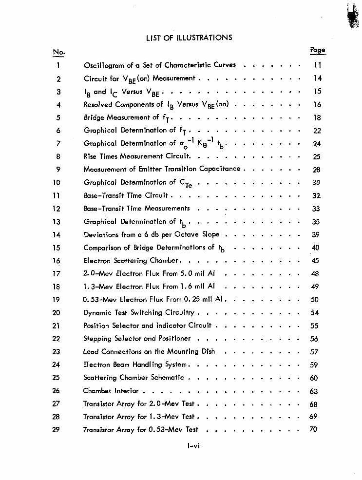
No.
1
2
3
4
5
6
7
8
9
10
11
12
13
14
15
16
17
18
19
20
21
22
23
24
25
26
27
28
29
LIST OF ILLUSTRATIONS
Oscillogram of a Set of Characteristic Curves .......
Circuit for VBE (on) Measurement ............
Ig and IC Versus VRF ................
Resolved Components of IR Versus VRE (on) ........
Bridge Measurement of fT. ..............
Graphical Determination of fT .............
Graphical Determination of a0 -1 -1 Ko tb. ........
Rise Times Measurement Circuit. ............
Measurement of Emitter Transition Capacitance .......
Graphical Determination of CT8 ............
Base-Transit Time Circuit ...............
Base-Transit Time Measurements ............
Graphical Determination of tb . . . . . ........
Deviations from a 6 db per 0CtaV8 Slope . ........
Comparison of Bridge Determinations of tb ........
Electron Scattering Chamber. . . . . . ........
2-O-Mev Electron Flux From 5.0 mil Al . ........
1.3-Mev Electron Flux From 1.6 mil Al . ........
0.53-Mev Electron Flux From 0.25 mil Al . ........
Dynamic Test Switching Circuitry . . . . ........
Position Selector and Indicator Circuit . . ........
Stepping Selector and Positioner . . . . ........
Lead Connections on the Mounting Dish . ........
Electron beam Handling System. . . . . ........
Scattering Chamber Schematic . . . . . ........
Chamber Interior . . . . . . . . . . ........
Transistor Array for 2.0-Mev Test . . . . ........
Transistor Array for 1.3-Mev Test . . . . ........
Transistor Array for 0.53-Mev Test . . . ........
Page
11
14
15
16
18
22
24
25
28
30
32
33
35
39
40
45
48
49
50
54
55
56
57
59
60
63
68
69
70
l-vi
1 No.
30
31
32
33
34
35
36
37
38
39
40
41
42
43
44
45
LIST OF ILLUSTRATIONS (Continued)
Dependence of A(BVCBd on Electron Fluence . .
A(VBE (sat)] of npn Transistors for 1 -Mev Electrons.
A(VcE(sat)l of pnp Transistors for 1 -Mev Electrons
Dependence of ACVCE(sat)l on Electron Energy. .
Changes of ICBO for the 2N23O3. . . . . . .
Transistors of Large Percentage AICBo . . . . .
Transistors of Small Percentage AIcBo . . . . .
Ic Versus VBE (on) for 2N2303. . . . . . . .
Ic Versus VBE(on) for 2N2219. . . . . . ‘. .
IC and IB Versus VBE (on) for 2N1613 . . . . .
Ic and IB Versus VBE (on) for 2N2219 . . . . .
Separation of Electron Effects on hFE . . . . .
Unnormalized Gain Degradation of 2N1613’s . .
npn Transistors Normalized to a Typical tb . . .
npn Transistors Normalized to Unit tb . . . . .
Energy Dependence of Electron Effects (2N1613) .
Page
. . . . . 73
. . . . . 75
. . . . . 76
. . . . . 77
. . . . . 79
. . . . . 80
I . . . . . 82
. . ., . . 83
. . . . . 84
. . . . . 85
. . . . . 86
. . . . . 91
. . . . . 93
. . . . . 94
. . . . . 95
. . . . . 97
l-vii
LIST OF TABLES
No. Title
1 Identification of Selected Transistor Types. ... . ......
2 A Typical Fairchild Series 500 Data Sheet. ....... -.
3 Selected Values of Sensitive Param8terS .........
4 1607A Bridge Measurements on Transistor 2N743 No. 1 ....
5 Measured Values of CTe Transistor Type 2N1132 No. 1 ...
6 Calculated Values of tx Transistor 2N1613 No. 1 ......
7 Comparison of Values of Parameters for Normal ization ....
8 Test Schedule ...................
9 Transistor Evaluation Test Plan .............
10 Electron Loss in Scattering Foils ............
11 Properties of Transistor Encapsulement ...........
12 Energy Loss in Transistor Can .............
13 Typical Delta From Current Monitoring ..........
14 Keypunch Data Form ................
15 Electron-Induced Changes in BVcBo ..........
16 Electron-Induced Changes in VCE(sat) ..........
17 Electron-Induced Changes in VBE (sat) ..........
Page
5
8
13
21
29
34
42
43
44
46
51
51
64
66
72
74
78
l-viii
1.0 INTRODUCTION
1.1 PROGRAM DESCRIPTION
The objective of the program is the establishment of valid space radiation
equivalences for permanent damage to silicon transistors. The phrase, mdiation
equivalence for permanent damage , is used to express the relative effectiveness of
different types and energies of radiation for producing an equivalent amount of
permanent damage.
Reliable silicon transistors of specified constructions and designs are to be
selected for radiation effects testing. All of these transistors will be electrically
characterized before and after radiation exposure. Selected devices will also be
characterized during irradiation. In addition to obtaining oscillograms of common
emitter characteristic curves, the following electrical parameters will be measured:
d. c. and small-signal a. c. common-emitter current gain, base turn-on voltage,
saturation voltages, breakdown voltage, leakage current, base transit time, alpha
cut-off frequency, gain-bandwidth frequency, and transition capacitances.
Charged particle irradiation of transistors will be performed using electrons
of energies of 0.5, 1, and 2 Mev and protons of energies of 1, 20, and 100 Mev.
These tests should establish the radiation equivalences for permanent damage for
significant radiation components of the Van Allen space environment. Gamma-
ray equivalence for permanent damage will also be experimentally determined in
order to assess the practicality of using cobalt40 facilities for simulation testing
of space radiation effects.
Data from oscillograms of transistor curve traces will be computer analyzed
not only to show the dependence of radiation damage on particle fluence but also
on radiation type and particle energy. Radiation equivalences for permanent
damage, normalized to transistor base transit time, will be determined for all the
types of radiation used in the test program. The results of this study will also be
compared with data obtained in earlier Boeing studies using different particle
l-l
energies and different transistor types. Data will be presented whenever practical
in a form that is most suited to the needs of design engineers.
1.2 PROGRESS SUMMARY
Silicon transistors of 10 registered types were selected for radiation effects
testing and 40 of each type were procured. The 10 types represent two of each of
five construction designs: npn and pnp diffused planar, npn and pnp epitaxial
planar, and npn epitaxial mesa.
These transistors were electrically characterized using a Fairchild Series
500 Semiconductor Tester to measure selected values of current gain, base turn-on
voltage, saturation voltages, breakdown voltage, and leakage current. Oscillo-
grams were also obtained of trarsistor common-emitter characteristics displayed on
a Tektronix 575 Curve Tracer. In addition, a correlation study was conducted in
order to determine the relative merit of various means of data acquisition for nor-
malization of the degradation of transistor current gain. Transistor parameters used
for this study included: (1) g ain bandwidth frequency as determined from measure-
ments made with a General Radio Type 1607A Transfer Function and lmmittance
Bridge, (2) gain bandwidth frequency as determined from rise-time measurements
using the Tektronix 567 Sampling Oscilloscope and associated equipment, (3)
transition capacities obtained using the Boonton Capacity Bridge 74C-SB, and
(4) base transit time obtained from a circuit specially designed for this purpose.
Data analysis from this correlation study also provided information concerning the
usefulness of the above methods for measuring these transistors over different ranges
of effective base widths and ranges of collector currents.
Electron irradiation testing of transistors was conducted at energies of 0.5,
1, and 2 Mev. Prior to these tests scattering foils were procured and the flux of
scattered electrons was mapped as a function of scattering angle. This mapping was
also correlated with theoretical values which were obtained from a Monte Carlo
computer program. In preparation for the 0.5-Mev electron test, the transistors
were de-encapsulated to eliminate inherent shielding and selected measurements
l-2
were repeated to verify the continued stability of the device. In addition a test
fixture was wired for remote selection of transistors and subsequent dynamic record-
ing of transistor curve traces during the irradiation tests. For the 0.5- and 1 -Mev
electron tests, transistor ambient temperatures were monitored within the test cham-
ber. Careful dosimetry was also performed to assure both a symmetric exposure of
the transistor arrays and a valid determination of exposure fluences. A preliminary
analysis of test data, from selected transistors, has been performed. Further detailed
analysis of the information contained in oscillograms of transistor curve traces,
obtained both during and after electron exposure, will be performed by use of the
computer damage-plotting program.
l-3
2.0 DETAILED DISCUSSION OF PROGRESS
After all tmnsistors needed for this study were procured and characterized
electrically, a schedule for experimental testing was established. The accelemtor
facility was modified for the first tests (electrons) and both the transistors and the
necessary test fixtures were prepared. Three electron irradiation tests were performed
with both radiation dosimetry and transistor degradation being monitored dynamically.
Following the tests the tmnsistors were recharacterized electrically and a preliminary
analysis of data ensued.
2. 1 SELECTION OF TRANSISTORS
Ten registered types of silicon transistors were selected for radiation effects
testing. Information which identifies those specific devices is listed in Table 1.
Transistor selection was made on the basis of reliability and present utilization for
missile and space vehicle electronic circuitry. These transistor types also repre-
sent three classes of design-epitaxial mesa, diffused planar, and epitaxial
planar-which appear to be promising for future space system applications as well.
Roth npn and pnp semiconductor constructions were considered in order to permit
a comparison to be made between radiation equivalences obtained from transistors
with p- and n-type base regions. Two different registered transistors of each of
the same cla.cs of construction designs (e. g., npn diffused planar) were selected
in order to investigate the validity of extending radiation equivalence information
to other tmnslstor types of the same construction design.
Forty transistors of each type (400 total) were procured with the specifica-
tion that transistors of the same type be of the same batch number (manufacture
date). By so doing there is more assurance that the semiconductor batch, the con-
struction details, and the surface conditions are the same. Thus, comparisons can
be made between transistors irradiated with different types of mdiation with a
greater assurance of no marked differences in the devices themselves. These batch
numbers are also I isted in Table 1. All 40 devices of each of the transistor types
listed were procured with a consistent set of batch numbers except for the 2N2303.
l-4
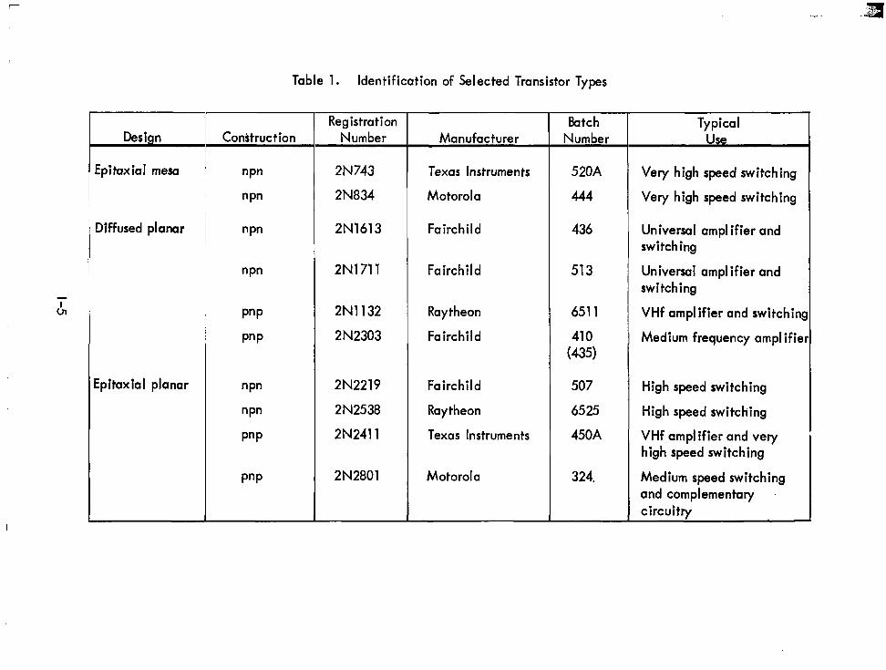
Table 1. Identification of Selected Transistor Types
Design
Epitax ial mesa
Diffused planar
Epitaxial planar
Construe t ion
“Pn
v
vn
w
P”P
PnP
nPn
nPn
P”P
PnP 2N2801 Motorola 324.
Registration Number
2N743
2N834
2N1613
2N1711
2N1132
2N2303
2N2219
2N2538
2N2411
Manufacturer
Texas Instruments
Motorola
Fairchild
Fairchild
Raytheon
Fairchild
Fairchild
Raytheon
Texas Instruments
Batch Number
520A
444
436
513
6511
410
(435)
507
6525
450A
Typical
Very high speed switching
Very high speed switching
Universal amplifier and switching
Universal amp1 ifier and switching
VHf amplifier and switchins
Medium frequency amplifier
High speed switching
High speed switching
VHf amp1 ifier and very high speed switching
For this particular transistor type, six devices have a different batch number (No. 435).
These six transistors will be included in the test as extra devices. Each one will be
irradiated in conjunction with a mate 2N2303 of batch number 410 and the test
results of each pair will be carefully compared. Batch numbers will also be useful
for obtaining further information from the manufacturers concerning details of the
manufacturing process if test results indicate the need.
2.2 ELECTRICAL CHARACTERIZATION OF TRANSISTORS
Transistor parameters which are radiation sensitive were measured with
specialized equipment prior to radiation exposure. Transistor parameters which
control radiation sensitivity were also measured in order to provide data for analy-
tically normalizing the degradation of current gain for different transistors. Care-
ful procedures were employed both during instrument calibration and during data
acquisition. A study was also made to determine the validity of various methods
of obtaining damage normalization parameters.
2.2. 1 Measurement of Radiation Sensitive Pammeters
Values of radiation sensitive pammeters were measured by the use of a
Fairchild Series 500 Semiconductor Tester, a Tektronix Model 575 Tmnsistor Curve
Tracer, and a measurement circuit for base turn-on voltage.
The Fairchild Series 500 Semiconductor Tester was programmed to automati-
cally perform 16 transistor measurements ln sequence with direct digital readout.
This tester is of a modular construction and its capability is described in detail in
its instruction manual and Its electronic specification sheets (Reference 1). The
test modules that were available for use in this research study include: (1) Test
Module Model 500A which provides for both low power d. c. and pulsed d. c.
(high current) measurements of current gain and of saturation voltage with readout
accumcy of j=2 percent, and (2) Test Module Model 5008 which provides for
measurement of breakdown voltage and leakage current with *l percent readout
accuracy. Also used for this program was Special Option H which provided the
means for measuring base turn-on voltage with *2 percent readout accuracy. In
l-6
i addition, special low beta program cards were available for measuring hFE in the
range of 0.2 to 9. One additional accessory is the Wyle Environmental Chamber
Model CN1060640 (-185OC to 325OC) which provides a means for controlling the
ambient temperature of a transistor, during measurement, within a range of approxi-
mately -lOO°C to t200°C.
The Fairchild Series 50O.i~ under constant surveillance by a factory-trained
maintenance technician. Timing checks are made at three-week intervals and
calibration checks are made at shorter periods by the use of a precision resistor
plug-in unit. The tester underwent a complete checkout by factory representatives
during the week prior to the start of measurements for this program.
The Fairchild Series 500 was programmed to measure the following transistor
parameters: d. c. common emitter current gain, hFE, at a collector voltage of 10
volts and at collector currents of 2 and 10 ma; base turn-on voltage at collector
currents of 10, 50, 100, and 500 pa, 1, 2, 5, and 10 ma; VCE(sat) at 2 and 10 ma
collector currents (with a gain of 2); VBE(sat) at 2 and 10 ma collector current (with
a gain of 2); BVCBO at 100 ua; and lcBo at VcB = 10 volts. A 30-minute warm-
up time was allowed for the tester before the measurements were taken. The measured
values were then read out sequentially in the order, top to bottom and left to right,
as shown in Table 2 (a typical Fairchild 500 data sheet).
During these measurements the ambient temperature was maintained at 27OC
*1 O. The actual temperature (%I. OSOC) was recorded on the data sheets at the time
of measurement readout. The transistors were handled with insulated pincers rather
than fingers in order to assure temperature stability. Date and time were recorded
on each data sheet with an automatic time stamp. To verify instrument repeatability,
control transistors were measured periodically and the values were compared with
standard values obtained earl ier.
The Tektronix Model 575 Curve Tracer is described in detail in its instruc-
tion manual (Reference 2). The curve tmcer is used in this study to display a family
of transistor common-emitter characteristic curves. Regulated steps of base current
are applied to the input of a transistor while a rectified sine wave is used to sweep
l-7
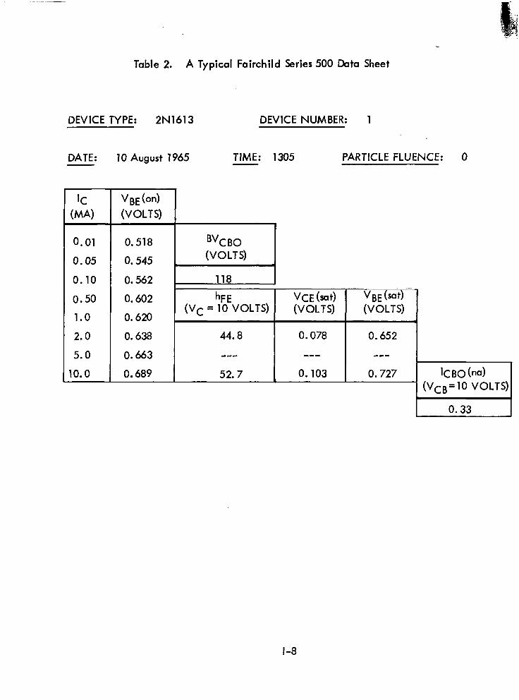
Table 2. A Typical Fairchild Series 500 Data Sheet
DEVICE TYPE: 2N1613 DEVICE NUMBER: 1
DATE: 10 August 1965 TIME: 1305 PARTICLE FLUENCE: 0
IC v BE (on)
(MA) (VOLTS) I
0.01
0.05
0.10
0.50
1.0
2.0
5.0
10.0
0.562 I 118 1
0.602
0.620
hFE VCE (sat) VBE (sat)
(VC = 10 VOLTS) (VOLTS) (VOLTS) r
0.638 44.8 0.078 0.652
0.663 -mm -mm w-w
0.689 52.7 0.103 0.727 IC BO (na) (VCB= lo VOLTS)
0.33
l-8
collector voltage. Five to ten current steps are selected with repetitive displays
at 120 to 240 steps per second.
Three accessories were used with the curve tracer: (1) a Sorenson a. c.
Voltage Regulator Model Number 1000s was used to provide kl percent control
of the input voltage; (2) a Tektronix Model C27 Camera Assembly with an object
to image ratio of 1 :O. 85 was recently procured to ensure complete presentation,
including the full graticule scale, of characteristic curves on the oscillogmms;
(3) a ground glass viewer was used during calibration to eliminate possible error
due to parallax. An additional accessory that has recently been made available
is the Type 175 High Current Adapter which provides the capability for 1OOa
peak continuous supply current and 1 kw continuous collector power.
Factory circuit specifications cite a maximum error of *2 percent for:
(1) collector voltage and volt-per-step selector, (2) collector current and ma-per-
step selector, and (3) base current. Actual accuracy, however, is strongly depen-
dent on precision calibration and zero adjusting. The curve tracer instruction
manual suggests recalibration after 500 hours of use. A high degree of consistency
in transistor oscillograms was obtained, however, by daily application of the fol-
lowing recalibration procedure:
1. A 20- to 30-minute warm-up time is allowed. (The manufacturer
recommends 10 minutes.)
2. The -150 volt supply is set to %I. 1 percent of its nominal value by
use of a Fluke Differential Voltmeter Model 801. The +lOO volt-and
+300 volt power suppl ies, internal to curve tracer, are checked for a
tolerance of +3 percent of the nominal value.
3. The d. c. balance control is precisely set for both the vertical and
the horizontal amplifiers.
4. Vertical gain and horizontal gain are set for both 0.5 and 0.01
base voltage.
l-9
5. The zero adjustment, the f adjustment, and the volt/step adjustment
are made as described in the curve tracer manual.
6. The step-selector switch is checked using 1 percent precision resistors.
7. An oscillogram is taken of the 2N1613 control transistor and it is
compared with the standard oscillogmms obtained earlier. A current
gain variation of no greater than 2 percent is allowed between oscillograms.
Zero adjustment of the display is set each time an oscillogram is taken. The
step zero adjustment is used to displace the oscilloscope display toward the graticule
I ine of zero-collector current. As the display is shifted, a position is reached at
which the zero-current trace no longer moves. When this position is determined,
further adjustment is made with the vertical -position and horizontal -position con-
trols. These controls are used (for npn transistors) to place the lower left hand por-
tion of the display in coincidence with the lower left hand comer of the graticule
scale. (For pnp transistors the coincidence is established at the upper right hand
corner.) All oscillograms for this program have been taken by the same technician
in order to Inaintain the maximum degree of consistency. These oscillograms were
taken before, during, and after irradiation tests.
A typical oscillogram of a set of transistor common-emitter characteristic
curves taken before irradiation is shown in Figure la. The ordinate represents
collector current, Ic. The abscissa represents collector voltage, Vc. A family
of base-current curves is shown. Writing on the face of the oscillogmm identifies
the transistor as device number 4 of tmnsfstor type 2N1711 used in test number 21
(2 Mev electrons). There are eight IB current steps, counting the zero step, and
collector voltage for each of these steps is over a range of 7 centimeters. This
serial identification numbering is used to key punch the picture heading card and
data cards at the oscillogram reader facility. Figure 1 b shows the back of the
oscillogram. Listed is pertinent data recorded at the time the picture was taken.
This includes the IB current per step, particle fluence, temperature, etc. This
data will be used as input information for a transistor damage-plotting program to
be analyzed using an SRU 1107 Computer.
l-10
21 1711 04 01 08 07 r 1 T I I I I I I I I
1 I I I-
A. Front View
PIG IB VC DATE TIME Al 07 08 072865 0927
v/b IV IBSTEP RL 2.OV 2.Oma 0.01 ma 0.0001 megohms
FLU. TEMP. 0 26.5OC
B. Back View
Figure 1. Oscillogmm of a Set of Chamcteristic Curves
l-l 1.
Values of some of the more sensitive parameters measured on the control
transistors (numbered 1) of the 10 transistor types are shown in Table 3. The a. c.
current gain is also determined for most of the devices by use of the base transit
time circuit described in Section 2.2.2.
A measurement circuit for base turn-on voltage was used to obtain IB and
Ic as a function of VBE(on). This circuit, shown in Figure 2, was designed and
built at Boeing.
A plot of typical data obtained from this circuit is shown in Figure 3.
The divergence of the collector and base currents from the straight lines is caused
by the transverse voltage drop in the base region (Reference 3). If the straight
line portion of the collector current is extrapolated upward, then the voltage
deviation can be determined as the voltage difference between the measured points
and the extrapolated line. The voltage increment determined from the collector
current can then be subtracted from the base current voltages to correct for the
deviation. This yields lines with three distinct slopes. By extrapolating the inter-
mediate portion of the curve to both higher and lower currents and subtracting it
from the lower and upper regions one obtains three components of base current with
reciprocal slopes of approximately 2 kTq -I, 1.5 kTq-‘, and kTq -1
as shown in
Figure 4. The three components have been identified as originating in the transi-
tion (space charge) region, at the perimeter of the emitter (that is, where the
emitter base junction intersects the surface),and in the bulk region of the base,
respectively (Reference 3).
2.2.2 Measurement of Radiation Control Parameters
The common-emitter current gain of a minority carrier injection-type tran-
sistor can be related to various regions and physical parameters of the transistor.
For charged particle degradation of translstor current gain, which can be attri-
buted to atomic displacements generated in the base region, the following depen-
dence of d. c, current gain has been observed (Reference 4).
l-12
i-
z
Table 3. Selected Values of Sensitive Parameters (at 10 volts and/or 2 ma)
CONTROL TRANSISTORi (NUMBERED 1)
2N743
2N834
2N1613
2N1711
2N1132
2N2303
2N2219
2N2538
2N2411
2N2801
hFE hfe
25.3 39
93.7 114
44.8 50.5
185 196.5
60.0 62.5
139 127
97.9 112.5
77.5 95.3
92.0 88.0
94.0 91.5
VBE (on> VCE (sat) VBE (=t) kB0 (VOLTS) (VOLTS) (VOLTS) (NA)
0.684 0.104 0.700 2.42
0.675 0.137 0.688 13.3
0.638 0.078 0.652 0.33
0.600 0.051 0.639 0.11
0.674 0.030 0.691 0.10
0.619 0.049 0.652 0.20
0.636 0.013 0.687 0.06
0.629 0.100 0.643 9.93
0.705 0.085 0.719 0.90
0.636 0.022 0.650 0.35
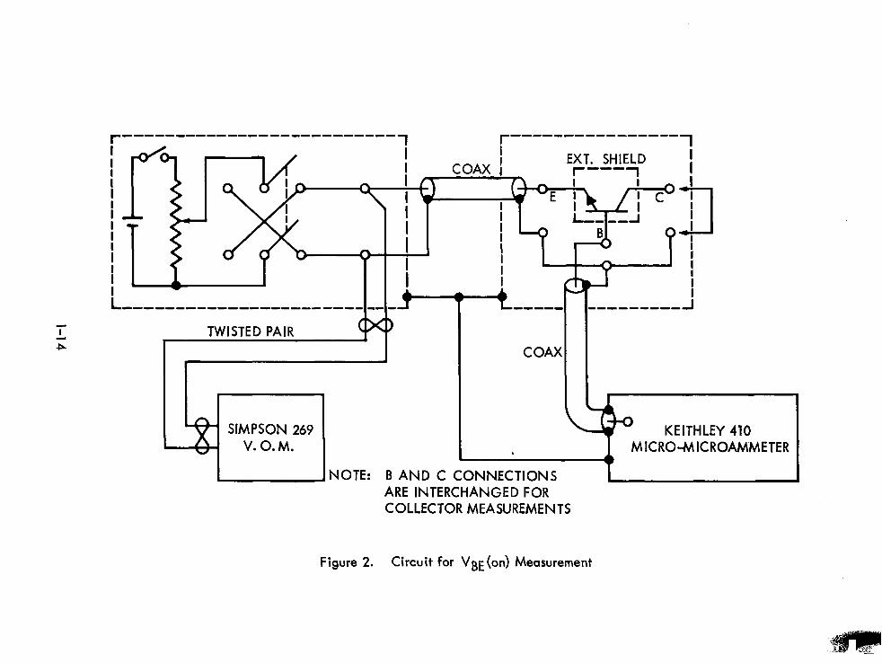
i I I
r i 7 COAX I EXT. SHIELD --- I L I l/i - I- r I -! I
’
w-----------w---------- -- -
, - TWlSTE:PAlR #‘rt
I I i _ - P----w ----mm--- n
a COAX
SIMPSON 269 KEITHLEY 410 V. 0. M. MICRO-MICROAMMETER
,NOTE: B AND C CONNECTIONS ARE INTERCHANGED FOR COLLECTOR MEASUREMENTS
Figure 2. Circuit for VBE (on) Measurement
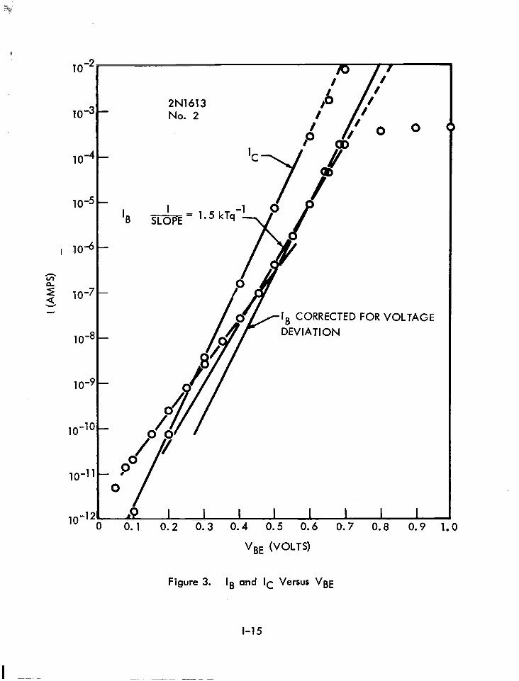
lo-2
10’3
lo-4
10-5
1 lOA
xz
2 5 lo
-7
10-a
10-9
10-10
10-11
lo-l2
2N1613 No. 2
IB I
SLOPE=l*
CORRECTED FOR VOL TAGE
0.1 0.2 0.3 0.4 0.5 0.6 0.7 0.8 0.9 1.0
VBE (VOLTS)
Figure 3. IB and IC Versus VBE
l-15
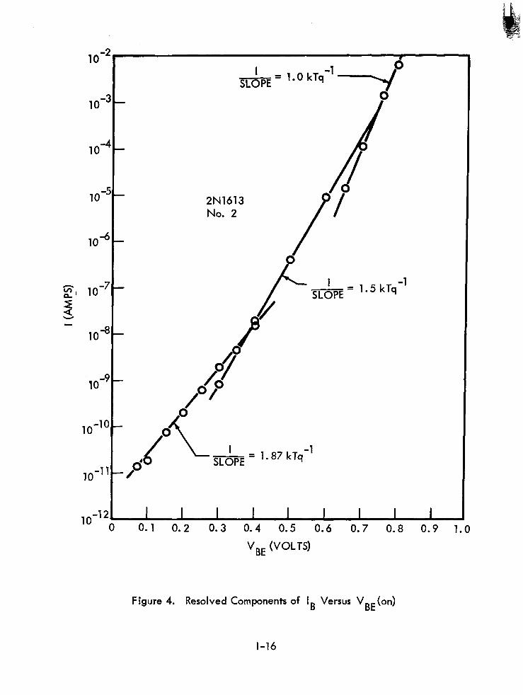
10-I
lo-’
lo-’
10’
lo4
21 lo-;
5
lo4
lo-!
lo-lo
10-l l
lo-1 2L 0
2N1613 No. 2
0.1 0.2 0.3 0.4 0.5 0.6 0.7 0.8 0.9 1.0
VBE (VOLTS)
Figure 4. Resolved Components of IB Versus VBE(on)
l-16
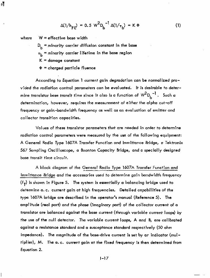
Atl/hF 3 = 0.5 W2Db-l A(&,> = K9 (1)
where W = effective base width
Db = minority carrier diffusion constant in the base
Tb = minority carrier lifetime in the base region
K = damage constant
9 = charged particle fluence
According to Equation 1 current gain degradation can be normalized pro-
vided the radiation control parameters can be evaluated. It is desirable to deter-
mine transistor base transit time since it also is a function of W2Db -1 . Such a
determination, however, requires the measurement of either the alpha cut-off
frequency or gain-bandwidth frequency as well as an evaluation of emitter and
collector transition capacities.
Values of these transistor parameters that are needed in order to determine
radiation control parameters were measured by the use of the following equipment:
A General Radio Type 1607A Transfer Function and lmmittance Bridge, a Tektronix
567 Sampling Oscilloscope, a Boonton Capacity Bridge, and a specially designed
base transit time circuit.
A block diagram of the General Radio Type 1607~ Transfer Function and -- lmmittance Bridge and the accessories used to determine gain bandwidth frequency
(fT) is shown in Figure 5. The system is essentially a balancing bridge used to
determine a. c. current gain at high frequencies. Detailed capabilities of the
type 1607A bridge are described in the operator’s manual (Reference 5). The
amplitude (real part) and the phase (imaginary part) of the collector current of a
transistor are balanced against the base current (through variable current loops) by
the use of the null detector. The variable current loops, A and B, are calibrated
against a resistance standard and a susceptance standard respectively (50 ohm
impedance). The magnitude of the base-drive current is set by ar indicator (mul-
tiplier), M. The a. c. current gain at the fixed frequency is then determined from
Equation 2.
l-17
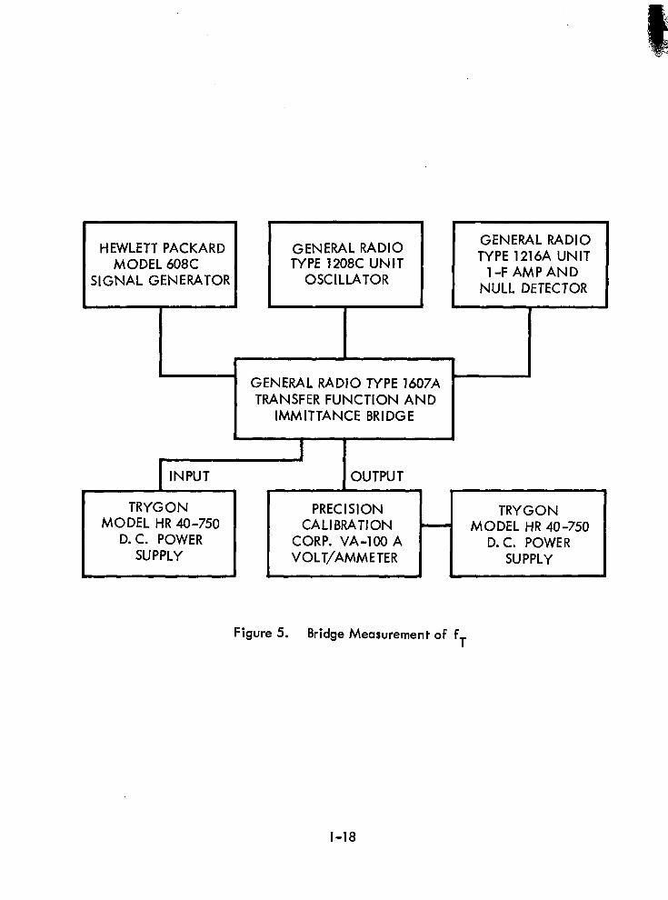
HEWLETT PACKARD MODEL 608C
SIGNAL GENERATOR
GENERAL TYPE ‘nnn
OS
GENERAL RADIO TYPE 1607A - TRANSFER FUNCTION AND
IMMITTANCE BRIDGE
I \
\ I
INPUT OUTPUT
TRYGON MODEL HR 40-750
D. C. POWER SUPPLY
- 1 PRECISION
H TRYGON
CALIBRATION MODEL HR 40-750 CORP. VA-100 A D.C. POWER VOLT/AMMETER su PPLY
Figure 5. Bridge Measurement of f T
l-18
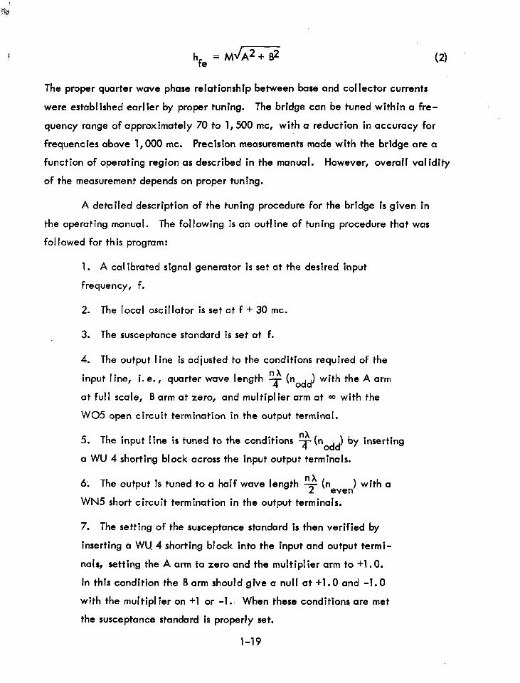
E hfe =
Mm (2)
The proper quarter wave phase relationship between base and collector currents
were established earlier by proper tuning. The bridge can be tuned within a fre-
quency range of approximately 70 to 1,500 mc, with a reduction in accuracy for
frequencies above 1,000 mc. Precision measurements made with the bridge are a
function of operating region as described in the manual. However, overall validity
of the measurement depends on proper tuning.
A detailed description of the tuning procedure for the bridge is given in
the operating manual. The following is an out1 ine of tuning procedure that was
followed for this program:
1. A calibrated signal generator is set at the desired input
frequency, f.
2. The local oscillator is set at f + 30 mc.
3. The susceptance standard is set at f.
4. The output line is adjusted to the conditions required of the
input I ine, i. e., quarter wave length y (nodd) with the A arm
at full scale, B arm at zero, and multiplier arm at Q) with the
W05 open circuit termination in the output terminal.
5. The input line is tuned to the conditions !$ (nodd) by inserting
a WU 4 shorting block across the input output terminals.
6; The output is tuned to a half wave length ?$ (neven) with a
WN5 short circuit termination in the output terminals.
7. The setting of the susceptance standard is then verified by
inserting a WU. 4 shorting block into the input and output termi-
nals, setting the A arm to zero and the multiplier arm to +l.O.
In this condition the B arm should give a null at +l.O and -1.0
with the multipl ier on +l or -1.. When these conditions are met
the susceptance standard is properly set.
l-19
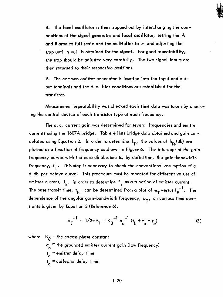
8. The local oscillator is then trapped out by interchanging the con-
nections of the signal generator and local oscillator, setting the A
and B arms to full scale and the multiplier to 00 and adjusting the
trap until a null is obtained for the signal. For good repeatability,
the trap should be adjusted very carefully. The two signal inputs are
then returned to their respective positions.
9. The common emitter connector is inserted into the input and out-
put terminals and the d. c. bias conditions are established for the
transistor.
Measurement repeatability was checked each time data was taken by check-
ing the control device of each transistor type at each frequency.
The a. c. current gain was determined for several frequencies and emitter
currents using the 1607A bridge. Table 4 lists bridge data obtained and gain cal-
culated using Equation 2. In order to determine fT, the values of hfe(db) are
plotted as a function of frequency as shown in Figure 6. The intercept of the gain-
frequency curves with the zero db abscissa is, by definition, the gain-bandwidth
frequency, fT . This step is necessary to check the conventional assumption of a
6-db-per-octave curve. This procedure must be repeated for different values of
emitter current, I E’
in order to determine f T
as a function of emitter current.
The base transit time, t -1 b’
can be determined from a plot of o T
versus I E . The
dependence of the angular gain-bandwidth frequency, tiT, on various time con-
stants is given by Equation 3 (Reference 6).
-1 WT
= 1/21r fT = K8-’ so-l (tb + te + tc) (3)
where K 8
= the excess phase constant
a o = the grounded emitter current gain (low frequency)
te = emitter delay time
5 = collector delay time
l-20
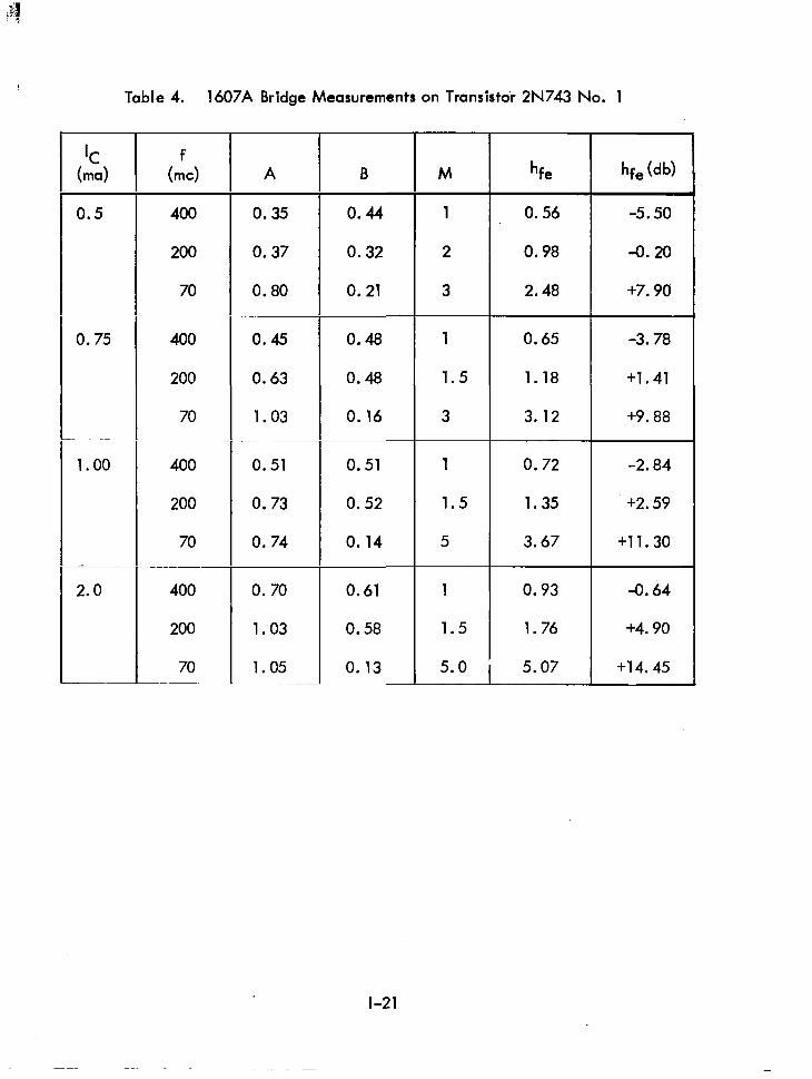
Table 4. 1607A Bridge Measurements on Transistdr 2N743 No. 1
IC (ma)
0.5
0.75
_- -
1.00
2.0
-~
L, 400
200
70
400
200
70
400
200
70
400
200
70
A B
0.35 0.44
0.37 0.32
0.80 0.21
0.45 0.48
0.63 0.48
1.03 0.16
0.51
0.73
0.74
0. 70
1.03
1.05
0.51
0.52
0.14
0.61
0.58
0.13
l-21
M
1
2
3
1
1.5
3
1
1.5
5
1
1.5
5.0
hfe hfe (db)
0.56 -5.50
0.98 -0.20
2.48 +7.90
0.65 -3.78
1.18 +1.41
3.12 +9.88
0.72 -2.84
1.35 +2.59
3.67 +11.30
0.93
1.76
-0.64
+4.90
+14.45 5.07
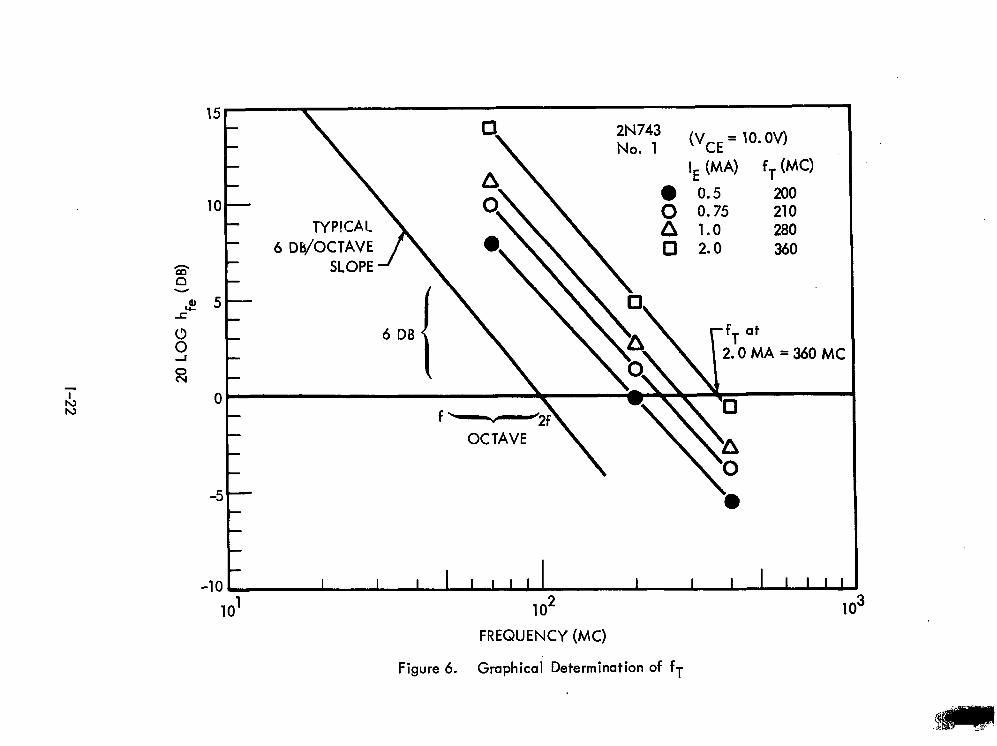
6 W/OCTAVE SLOPE
“““I \ \’ 2.OMA=360MC
mJ
10’ lo2 lo3
FREQUENCY (MC)
Figure 6. Graphical Determination of fT
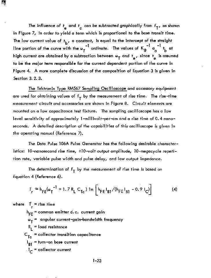
The influence of te and tc can be subtracted graphically from fT, as shown
in Figure 7, in order to yield a term which is proportional to the base transit time.
The low current value of tb, a constant, is equal to the intercept of the straight
line portion of the curve with the uT -1
ordinate. The values of K8 -’ -’ t at a o b
high current are obtained by a subtraction between w T
and t ef
since t is assumed e
to be the major term responsible for the current dependent portion of the curve In
Figure 4. A more complete discussion of the composition of Equation 3 is given in
Section 3. 2.3.
The Tektronix Type RM567 Sampling Oscilloscope and accessory equipment
are used for obtaining values of f T
by the measurement of rise time. The rise-t ime
measurement circuit and accessories are shown in Figure 8. Circuit elements are
mounted on a low capacitance test fixture. The sampling oscilloscope has a low
level sensitivity of approximately 1 -mil I ivol t-per-cm and a rise time of 0.4 nano-
seconds. A detailed description of the capabilities of this oscilloscope is given in
the operating manual (Reference 7).
The Data Pulse 106A Pulse Generator has the following desirable character-
istics: lO-nanosecond rise time, *lo-volt output amplitude, lo-megacycle repeti-
tion rate, variable pulse width and pulse delay, and low output impedance.
The determination of fT by the measurement of rise time is based on
Equation 4 (Reference 6).
T r ‘I: h&T -’ + 1.7RL CTc) ‘n hFEIB1/(hFEIB1 -0.9 ‘C) 1
where T = rise time r
hFE = common emitter d. c. current gain
WT = angular current-gain-bandwidth frequency
RL = load resistance
C Tc
= collector transition capacitance
lB1 = turn-on base current
Ic = collector current
(4)
l-23
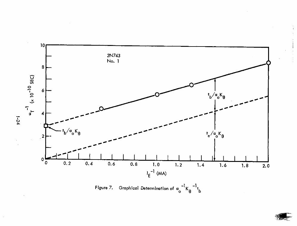
8
Figure 7. -1 -1
Graphical Determination of a Ke 0
tb
e) c I I I I I I I I I I I 0.2 0.4 0.6 0.8 1.0 1.2 1.4
IEe1 (MA)
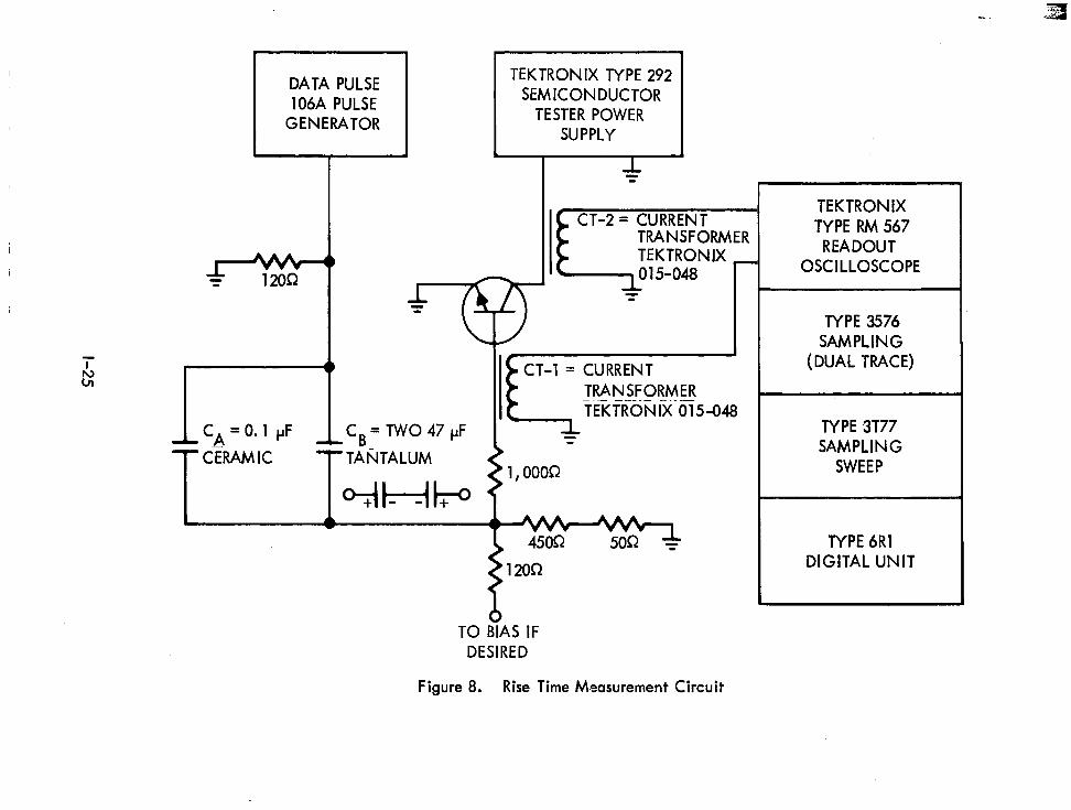
DATA PULSE 106A PULSE
GENERATOR
TEKTRONIX TYPE 292 SEMICONDUCTOR
TESTER POWER su PPLY
TYPE 3576 SAMPLING
TYPE 3T77 SAMPLING
SWEEP
TYPE 6Rl DIGITAL UNIT
TO tiAS IF DESIRED
Figure 8. Rise Time Measurement Circuit
If one assumes that RL z 0, hFE lBl = Ic then Equation 4 reduces to
T = 2.3 hFEw -1
r (5)
or
fT = 2.3 hFE/2TT
r (4
The current gain hFE is measured on the Fairchild Series 500 Semiconductor
Tester. In determining Tr the desired bias voltages were established on the Tektronix
292 Power Supply and a pulse was supplied of sufficient amplitude to give an output
pulse with’the peak current desired. The duration of the pulse was adjusted by
observing the output pulse and ascertaining when it reached full amplitude (became
flat on top). The rise time was then read out on a Tektronix 6Rl Digital Unit. The
rise time so obtained includes the rise time of the pulse generator and oscilloscope
as well as that of the transistor being tested. The rise time of the device is separated
by use of Equation 7.
Tr (measured) = C
Tr2 (transistor) + Tr2 (generator) + Tr2 (scope) 1 l/2 (7)
The sampling oscilloscope has a rise time of 0.4 nanoseconds. The specified value
of rise time of the generator was 10 nanoseconds and was verified by measurement
on the oscil loscope. As a typical example, a rise time of 52 nanoseconds was
measured at a collector current of 10 ma for transistor No. 2 of type 2N2411.
Thus the actual rise time when separated, by Equation 7, from the rise time of
the oscilloscope and generator was found to be 51 nanoseconds. The d. c. current
gain at 10 ma collector current, as measured using the Fairchild Series 500 Semi-
conductor Tester was 56.2; thus fT , as calculated from Equation 6, was 404 mc.
The Boonton Capacity Bridge Model 74C-58 is used to determine both
emitter and collector transition capacitances. These measurements are desired in
order to separate out the influence of RC-time constants on the measurements of
both gain-bandwidth frequency and alpha cut-off frequency (e. g., t, or tc of
Equation 3; discussed in more detail In Section 3.2.3). Desirable features of
l-26
the Boonton bridge include: (1) accurate capacity determinations to within 0.05
picofarads, (2) an a. c. signal level which can be reduced to less than 1 mv
(although useful nulls occur between 2 and 3 mv), and (3) an internal direct cur-
rent bias supply. Equations for determining accuracy of this instrument, as a
function of the magnitude of capacity being measured, are described in its instruc-
tion book (Reference 8). The equipment used for measuring transition capacity is
shown in Figure 9. Before measurements are made the bridge is zeroed to insure
that a null is obtained at 0.0 picofarads and 0.0 conductance with the test iig in
place.
The determination of transition capacitance is based on Equation 8 for
graded junctions (Reference 6).
CT = (KL2q/12)‘/3 (a/V)“3 (8)
where K = dielectric constant for the material c
q = electronic charge
a = the grade constant in atomJcm2
v = v. + VT
V 0
= external applied bias
vT = contact potential
CT = transition capacitance
Taking the logarithm of both sides Equation 9 is obtained from Equation 8.
An CT = (l/3) Bn (Kc2qa/12) - BnV 1 (9)
Experimentally, CT is measured for bias voltages, Vo, ranging from values
near reverse breakdown voltage to about 0.2 volts forward bias using the circuit
shown in Figure 9. Log CT is then plotted as a function of log V . A value for 0
the contact potential. is obtained by adding trial values to V. until a reasonably
straight I ine results. CT can be found for forward bias conditions by extrapolation
of the linear plot.
l-27
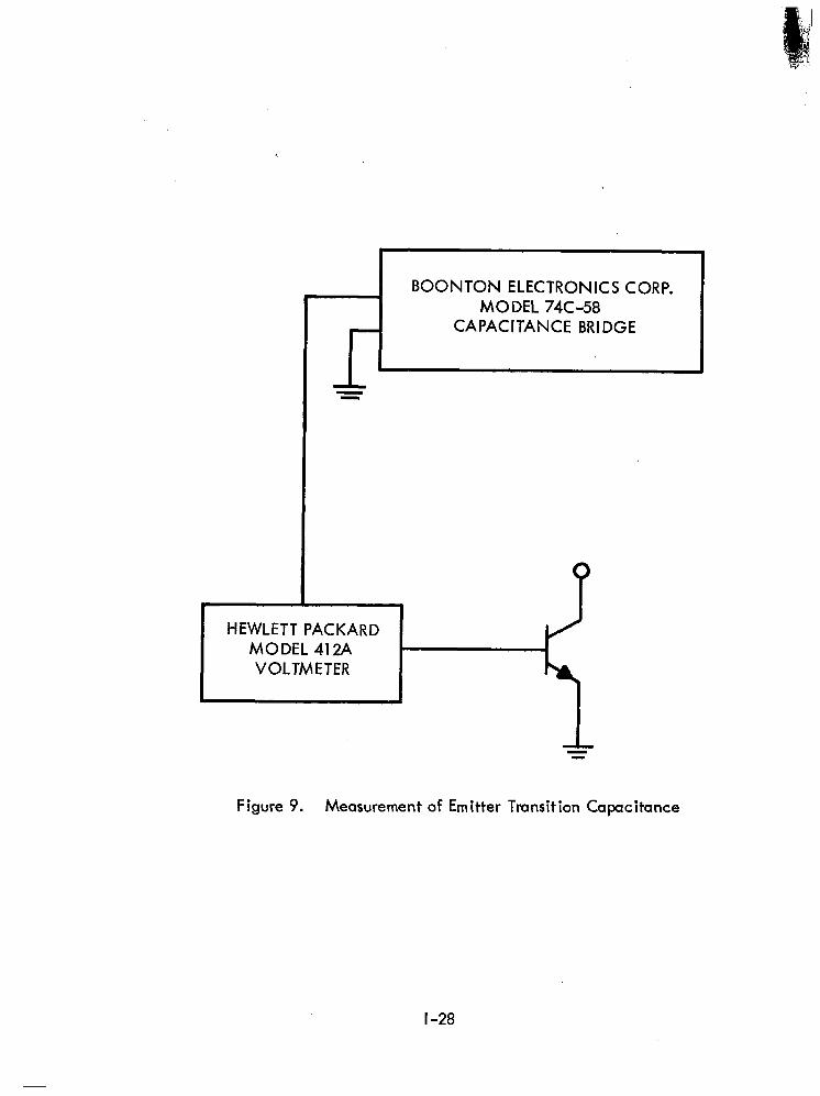
BOONTON ELECTRONICS CORP. MODEL 74C-58
CAPACITANCE BRIDGE
.
HEWLETT PACKARD MODEL 412A VOLTMETER
Figure 9. Measurement of Emitter Transition Capacitance
I-28
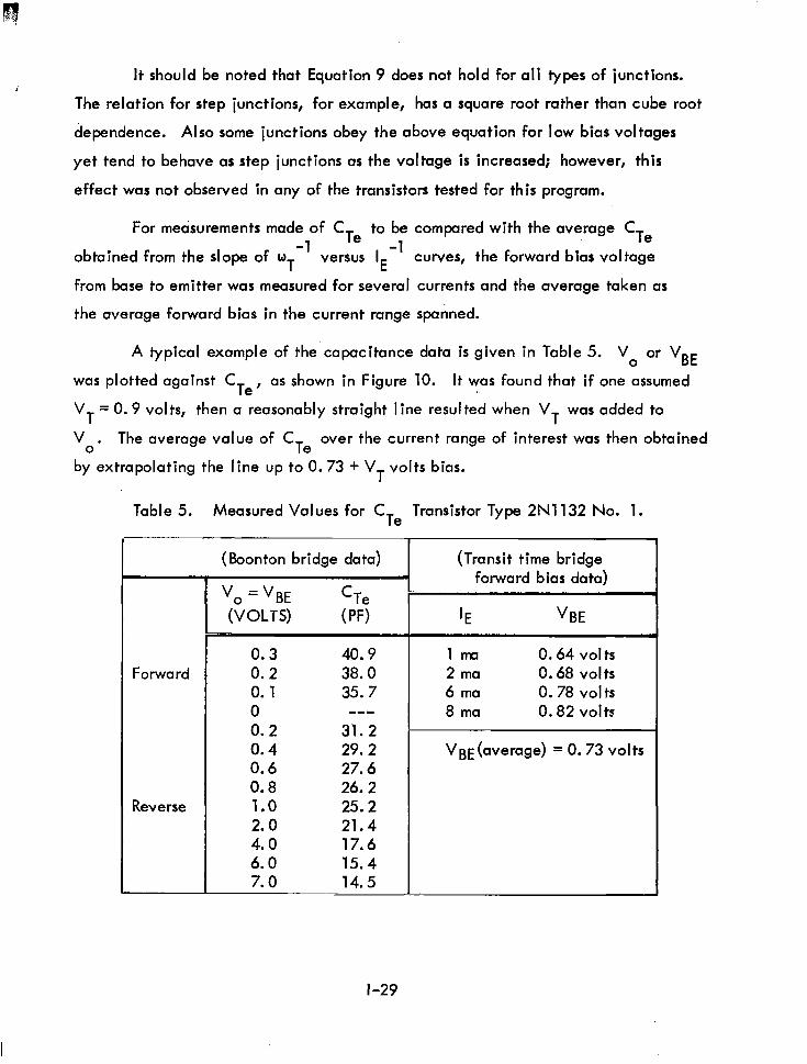
It should be noted that Equation 9 does not hold for all types of junctions.
The relation for step junctions, for example, has a square root rather than cube root
dependence. Also some junctions obey the above equation for low bias voltages
yet tend to behave as step junctions as the voltage is increased; however, this
effect was not observed in any of the transistors tested for this program.
For measurements made of C Te to be compared with the average CTe
obtained from the slope of -1
versus I -1
w T E
curves, the forward bias voltage
from base to emitter was measured for several currents and the average taken as
the average forward bias in the current range spanned.
A typical example of the’capacitance data is given in Table 5. V 0
or VBE
was plotted against CTe, as shown in Figure 10. It was found that if one assumed
V T
= 0.9 volts, then a reasonably straight line resulted when V T
was added to
V 0’
The average value of CTe over the current range of interest was then obtained
by extrapolating the line up to 0.73 + VT volts bias.
Table 5. Measured Values for CTe Transistor Type 2N1132 No. 1.
Forward
Reverse
0.3 40.9 0.2 38.0 0.1 35.7 0 ---
0.2 31.2 0.4 29.2 0.6 27.6 0.8 26.2 1.0 25.2 2.0 21.4 4.0 17.6 6.0 15.4 7.0 14.5
1mtIl 0.64 volts 2 ma 0.68 volts 6 ma 0.78 volts 8 ma 0.82 volts
VRE (average) = 0.73 volts
l-29
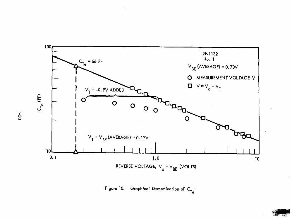
2N1132 No. 1
VBE (AVER&E) = o.73v
0 MEASUREMENT VOLTAGE V
0 V=Vo+vT
I vT + vBE (AVER&E) = 0. im \
1.0
REVERSE VOLTAGE, V o = VBE (VOLTS)
10
Figure 10. Graphical Determination of C Te
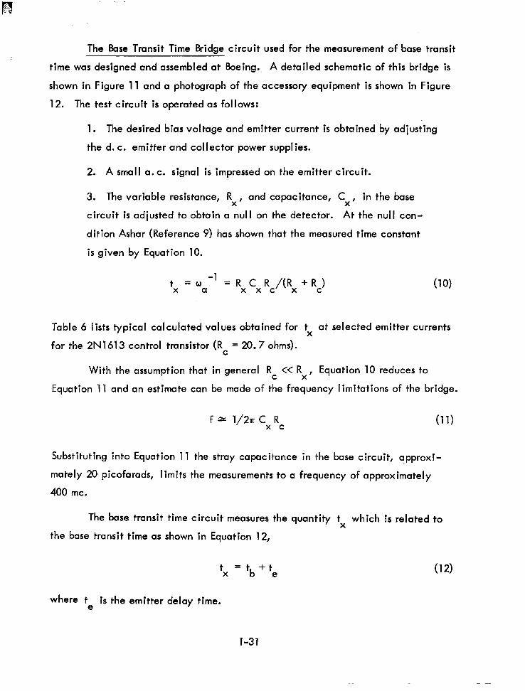
The Base Transit Time Bridge circuit used for the measurement of base transit
time was designed and assembled at Boeing. A detailed schematic of this bridge is
shown in Figure 11 and a photograph of the accessory equipment is shown in Figure
12. The test circuit is operated as follows:
1. The desired bias voltage and emitter current is obtained by adjusting
the d. c. emitter and collector power supplies.
2. A small a. c. signal is impressed on the emitter circuit.
3. The variable resistance, R X’
and capacitance, C X’
in the base
circuit is adjusted to obtain a null on the detector. At the null con-
dition Ashar (Reference 9) has shown that the measured time constant
is given by Equation 10.
tx = wa -1
= Rx cx R/R, + Rc) (‘0) Table 6 lists typical calculated values obtained for t at selected emitter currents
X
for the 2N1613 control transistor (R = 20.7 ohms). C
With the assumption that in general Rc << R , Equation 10 reduces to X
Equation 11 and an estimate can be made of the frequency limitations of the bridge.
f = 1/25r C R x c
Substituting into Equation 11 the stray capacitance in the base circuit, approxi-
mately 20 picofarads, limits the measurements to a frequency of approximately
400 mc.
The base transit time circuit measures the quantity t which is related to X
the base transit time as shown in Equation 12,
tX = tb+t
e (‘2)
where t e
is the emitter delay time.
l-31
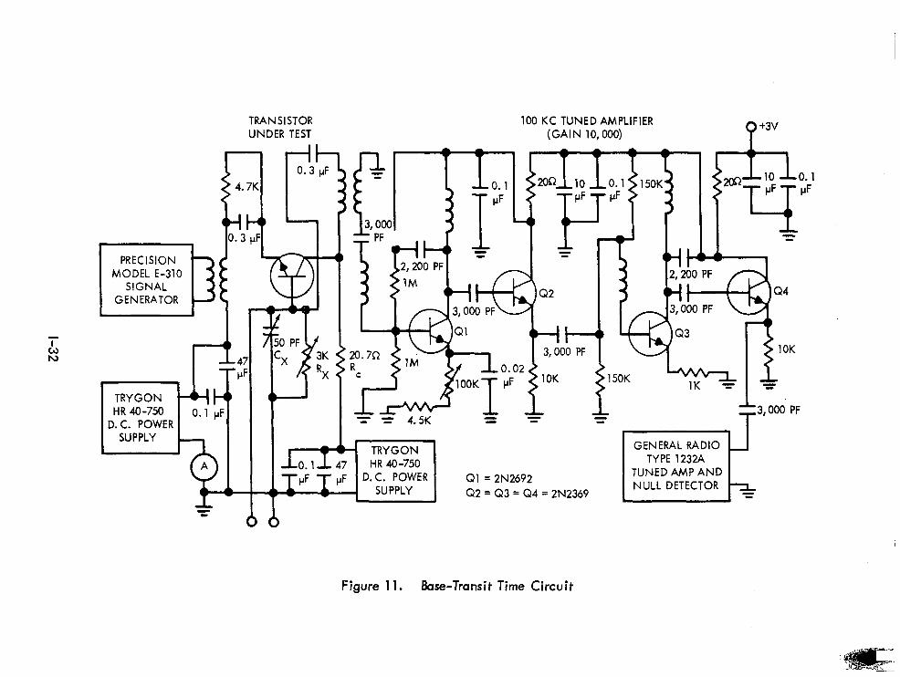
TRANSISTOR 100 KC TUNED AMPLIFIER UNDER TEST (GAIN 10,000)
+3v
r-L
MODEL E-310
TRYGON HR 40-750 0.1 pF
D. C. POWER SUPPLY
.3 uFl
47 PF
- = 4.5K i
PF
1
+ 3,000’ PF
GENERAL RADIO
Figure 11. L&e-Transit Time Circuit
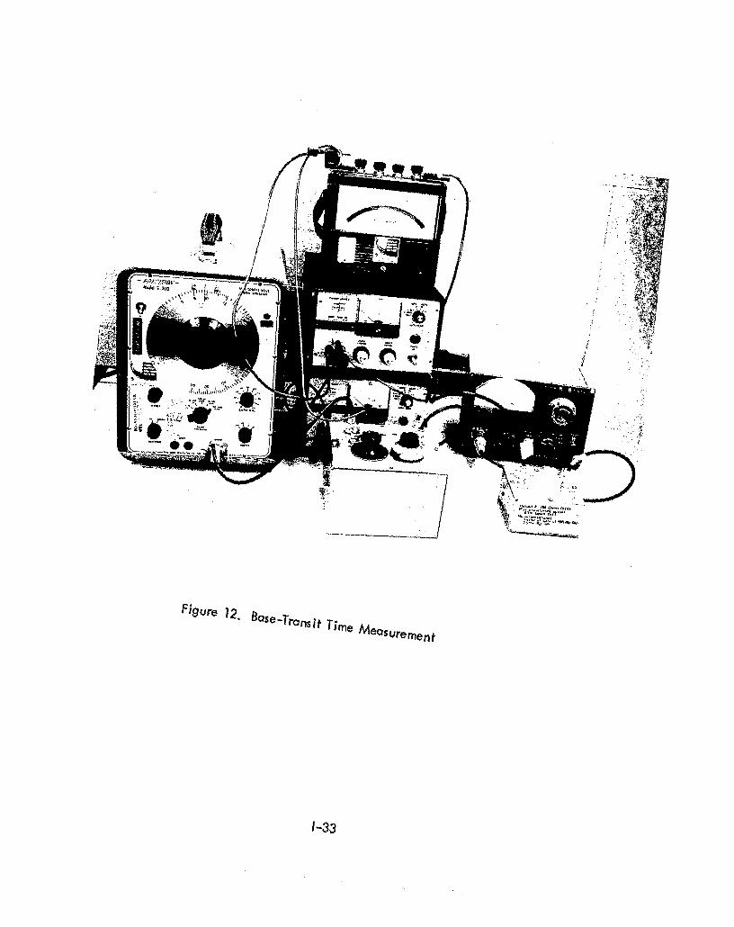
I-33
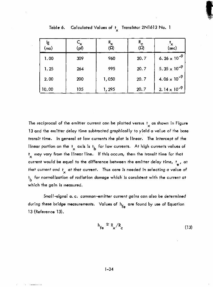
Table 6. Calculated Values of tx Transistor 2N1613 No. 1
lE Cx Rx (ma) (P9 m
1.00 309 960
1.25 264 995
2.00 200 1,050
10.00 105 1,295
20.7
20.7
20.7
20.7
tx (set)
6.26 x 1O-9
5.35 x 10⁻⁹
4.06 x 1O-9
2.14 x 10⁻⁹
The reciprocal of the emitter current can be plotted versus t, as shown in Figure
13 and the emitter delay time subtracted graphically to yield a value of the base
transit time. In general at low currents the plot is linear. The intercept of the
linear portion on the tx axis is t b for low currents. At high currents values of
tx may vary from the I inear line. If this occurs, then the transit time for that
current would be equal to the difference between the emitter delay time, t e’
at
that current and t, at that current. Thus care is needed in selecting a value of
tb for normalization of radiation damage which is consistent with the current at
which the gain is measured.
Small-signal a. c. common-emitter current gains can also be determined
during these bridge measurements. Values of hfe are found by use of Equation
13 (Reference 13).
h fe
= Rx/R C (13)
l-34
-. ..- - . . . . .
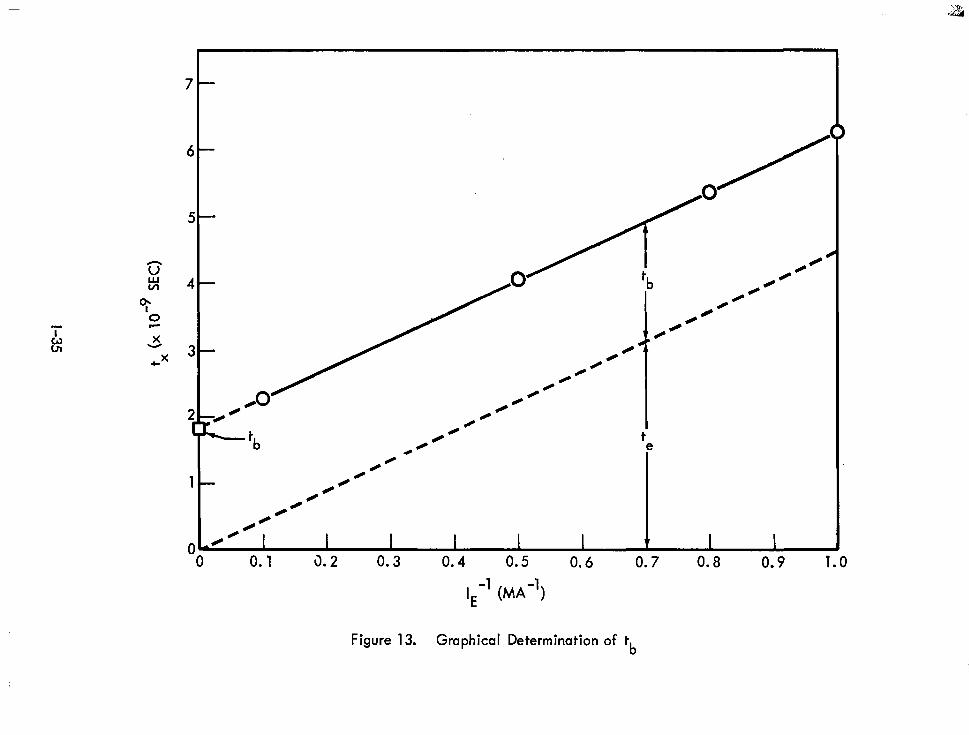
IE-l (MA-‘)
Figure 13. Graphical Determination of t b
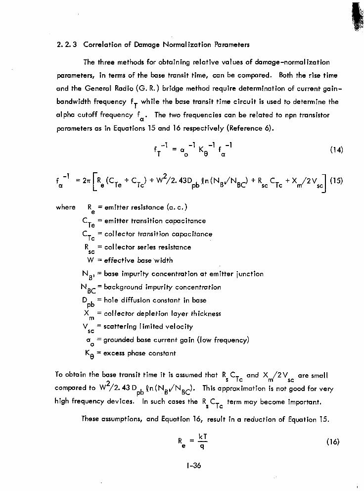
2.2.3 Correlation of Damage Normalization Parameters
The three methods for obtaining relative values of damage-normalization
parameters, in terms of the base transit time, can be compared. Both the rise time
and the General Radio (G. R.) bridge method require determination of current gain-
bandwidth frequency f,. while the base transit time circuit is used to determine the.
alpha cutoff frequency for. The two frequencies can be related to npn transistor
parameters as in Equations 15 and 16 respectively (Reference 6).
fT -1 = -1 -1 f -1
ao K0 a (14)
f -l = 2Ir a C
Re(cTe + CTc) + W2/2. 43Dpb1n(NB/NBC) + RSc CTc + Xrr/2Vsc 1 (15)
where Re = emitter resistance (a. c.)
C Te
= emitter transition capacitance
C Tc
= collector transition capacitance
R = collector series resistance
; = effective base ‘width
NB1 = base impurity concentration at emitter junction
NBC = background impurity concentration
D Pb
= hole diffusion constant in base
Xm = collector depletion layer thickness
V SC
= scattering I imited velocity
a o = grounded base current gain (low frequency)
Ke = excess phase constant
To obtain the base transit time it is assumed that Rs CTc and Xm/2V are small
compared to W2/2. 43 Dpb Jn (NB/NBC). SC
Th is approximation is not good for very
high frequency devices. In such cases the RS CTc term may become important.
These assumptions, and Equation 16, result in a reduction of Equation 15.
R =kT e q
l-36
(16)
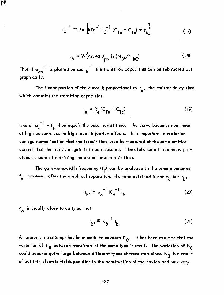
f -l = 2rr -1 -1
a IE (CTe + CTc) + tb 1
tb = w2/2- 43 Dpb h(NB,/NBC) (18)
(17)
-1 Thus if mab is plotted versus IE
-1 the transition capacities can be subtracted out
graphically.
The linear portion of the curve is proportional to t e’
the emitter delay time
which contains the transition capacities.
t e = Re tCTe + ‘Tc) (19)
where w -1
- a
te then equals the base transit time. The curve becomes nonlinear
at high currents due to high level injection effects. It is important in radiation
damage normalization that the transit time used be measured at the same emitter
current that the transistor gain is to be measured. The alpha cutoff frequency pro-
vides a means of obtaining the actual base transit time.
The gain-bandwidth frequency (fT) can be analyzed in the same manner as
fa; however, after the graphical separation, the term obtained is not tb but tb,.
-1 -1 tbt = a0 Ke tb
a o is usually close to unity so that
-1 tb,zKg tb (21)
At present, no attempt has been made to measure Kg. It has been assumed that the
variation of Kg between transistors of the same type is small. The variation of Kg
could become quite large between different types of transistors since K 8
is a result
of built-in electric fields peculiar to the construction of the device and may vary
l-37
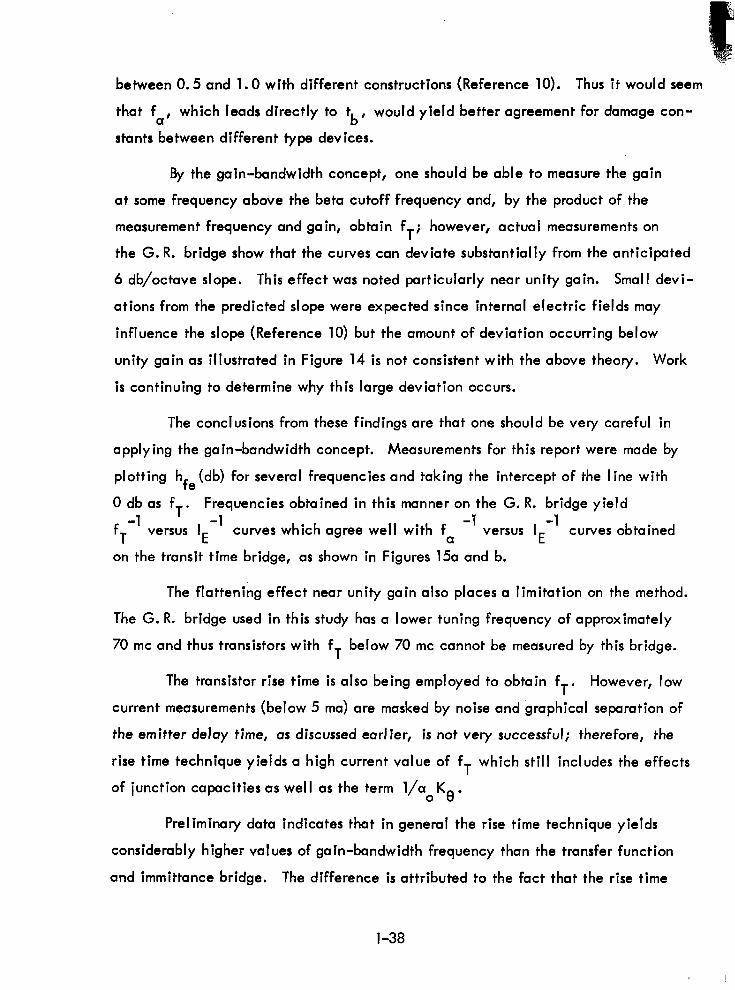
between 0.5 and 1.0 with different constructions (Reference 10). Thus it would seem
that fa, which leads directly to t b
, would yield better agreement for damage con-
stants between different type devices.
By the gain-bandwidth concept, one should be able to measure the gain
at some frequency above the beta cutoff frequency and, by the product of the
measurement frequency and gain, obtain f T h
; owever, actual measurements on
the G. R. bridge show that the curves can deviate substantially from the anticipated
6 db/octave slope. This effect was noted particularly near unity gain. Small devi-
ations from the predicted slope were expected since internal electric fields may
influence the slope (Reference 10) but the amount of deviation occurring below
unity gain as illustrated in Figure 14 is not consistent with the above theory. Work
is continuing to determine why this large deviation occurs.
The conclusions from these findings are that one should be very careful in
applying the gain-bandwidth concept. Measurements for this report were made by
plotting hfe(db) for several frequencies and taking the intercept of the line with
Odbas fT. Frequencies obtained in this manner on the G. R. bridge yield
fT -1
versus I -1
curves which agree well with fa -1
versus I -1
E E curves obtained
on the transit time bridge, as shown in Figures 15a and b.
The flattening effect near unity gain also places a limitation on the method.
The G. R. bridge used in this study has a lower tuning frequency of approximately
70 mc and thus transistors with fT below 70 mc cannot be measured by this bridge.
The transistor rise time is also being employed to obtain fT. However, low
current measurements (below 5 ma) are masked by noise and graphical separation of
the emitter delay time, as discussed earlier, is not very successful; therefore, the
rise time technique yields a high current value of f T
which still includes the effects
of junction capacities as well as the term l/a0 Ke.
Preliminary data indicates that in general the rise time technique yields
considerably higher values of gain-bandwidth frequency than the transfer function
and immittance bridge. The difference is attributed to the fact that the rise time
l-38
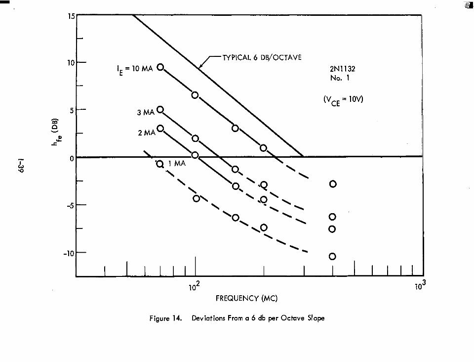
i- %
\ -TYPICAL 6 DB/OCTAVE
2N1132 No. 1
(‘CE = 1OV)
\ \
‘0,
\
\
\ 0, ’ l Q 0
ON \ ‘*Ql. \ ‘Ox \ \ 0
4 0
102 FREQUENCY (MC)
Figure 14. Deviations From a 6 db per Octave Slope
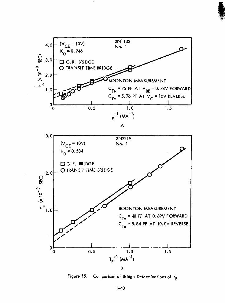
4.d
s s 3.t
m I
2 2.t X
6X l.(
3.0
2.0 G %
(5\ I 0 F
X
*x1.o
- (“CE = 1ov) 2N1132
No. 1
Ke =0.746
- 0 G. R. BRIDGE 0 TRANSIT TIME BRIDGE
Te = 75 PF AT VBE = 0.78V FORWARI
= 5.76 PF AT VC = 1OV REVERSE
0.5 1.0 1.5
IE-l (MA-l)
.A
2N2219
(vCE = 1OV) No. 1
Ke = 0.584
0 G. R. BRIDGE
0 TRANSIT TIME BRIDGE
/ 8’
k .o BOONTON MEASUREMENT
/ 9’
0 C
.a 0’
Te = 48 PF AT 0.69V FORWARD
r “Tc
- = QA “F AT 10. OV REVERSE -a.“-, r
Figure 15. Comparison of Bridge Determinations of tB
l-40
method is a large-signal measurement while the G. R. bridge method is a small-
signal measurement. Preliminary data also shows, however, that the rise-time
technique yields rather large variations in fT within a given type of tmnsistors.
It is hoped that further analysis will indicate which measurement technique yields
the best normalization results. Table 7 lists data for comparison using the three
methods. It can be seen that graphically determined values of transition capaci-
tance also agree reasonably well with those measured. The fa measurement on
the base transit time bridge agrees well with the transfer function bridge data. The
slopes of the fa -1
versus I -1
E I ines have been found to agree well with separate
measurements of the junction capacities on the Boonton Capacitance Bridge. The
method is limited to low frequency devices, however, by the amount of stray capac-
ity in the bridge circuitry.
In continuing work, a detailed comparison will be made of normalization
constants obtained by all three measurements on the same devices. The transit time
will also be checked as a function of radiation exposure to insure that it remains
constant under radiation.
2.3 TEST SCHEDULE
In order to simulate transistor damage for earth orbital missions, electrons
of three energies and protons of three energies were selected for transistor irradi-
ation. A gamma-my test is also planned to assess the validity of space radiation
simulation using a cobalt-60 facility. To date electron irradiation tests at energies
of 0.5, 1, and 2 Mev have been performed. Electrons of 0.5-Mev energy are
representative of those present with high intensity in a shield-modified spectrum.
Transistor inherent shielding was removed for the 0.5-Mev test. Electrons of l-
Mev energy can readily pass through the thickness of a transistor can. Al though
the I-Mev intensity in space is less than that for lowerenergy electrons the dis-
placement cross section is greater. Electrons of 2-Mev energy are representative
of those high-energy electrons still having sufficient Van Allen intensity to be
significant for transistor damage.
l-41
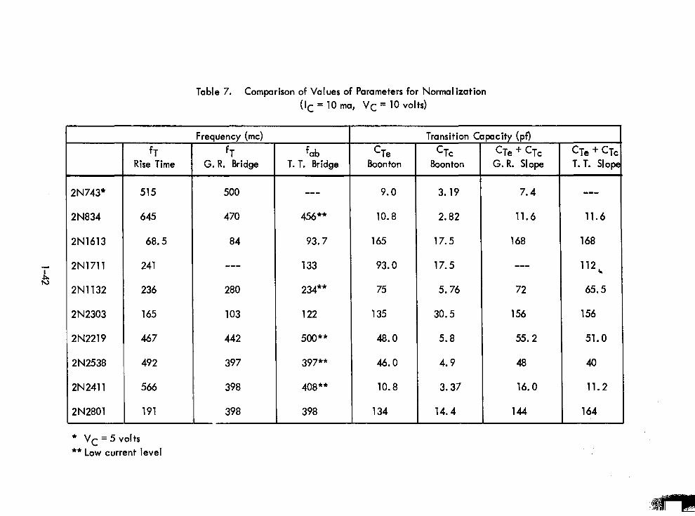
Table 7. Comparison of Values of Parameters for Normalization (1~ = 10 ma, Vc = 10 volts)
2N743' 515
2NB34 645
2N1613 68.5
2N1711 241
2N1132 236
2N2303 165
2N2219 467
2N2538 492
2N2411 566
2N2801 191
* Vc = 5 volts **Low current level
fT Rise Time
tT G. R. Bridge
500
470
84
w-m
280
103
442
397
398
398
f ab 'Te T. T. Bridge Boonton
s-s 9.0 3.19
456** 10.8 2.82
93.7 165 17.5
133 93.0 17.5
234** 75 5.76
122 135 30.5
500** 48.0 5.8
397** 46.0 4.9
408** 10.8 3.37
398 134 14.4
7.4
11.6
168
B-m
72
156
55.2
48
16.0
144
CTe +cTc T. T. Slop
---
11.6
168
112,
65.5
156
51.0
40
11.2
164
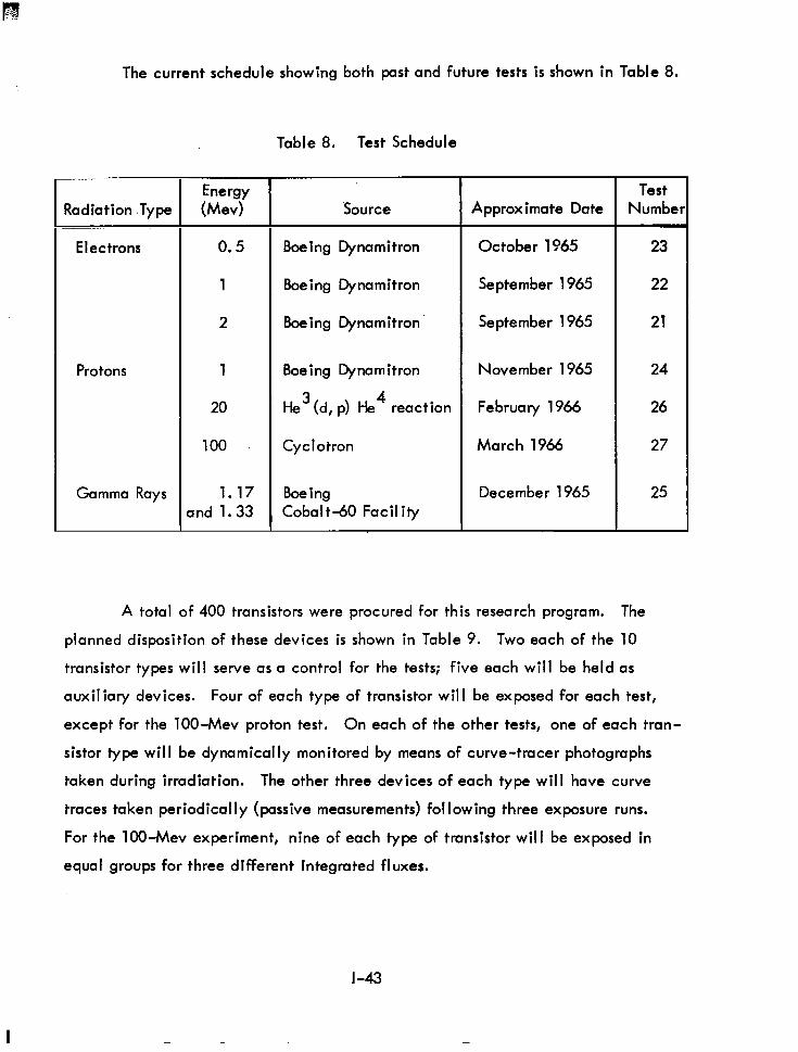
The current schedule showing both past and future tests is shown in Table 8.
Table 8. Test Schedule
Energy Radiation .Type M-1 ~ ~- ~-~
Electrons 0.5
1
2
Protons 1
20
100
Gamma Rays 1.17 and 1.33
Test Source Approximate Date Number
Boeing Dynamitron October 1865 23
Boeing Dynamitron September 1965 22
Boeing Dynamitron September 1965 21
Boeing Dynamitron November 1965 24
He3 (4 p) He4 reaction February 1966 26
Cyclotron March 1966 27
Boeing December 1965 25 Cobal t-60 Facility
A total of 400 transistors were procured for this research program. The
planned disposition of these devices is shown in Table 9. Two each of the 10
transistor types will serve as a control for the tests; five each will be held as
auxiliary devices. Four of each type of transistor will be exposed for each test,
except for the lOO-Mev proton test. On each of the other tests, one of each tran-
sistor type will be dynamically monitored by means of curve-tracer photographs
taken during irradiation. The other three devices of each type will have curve
traces taken periodically (passive measurements) following three exposure runs.
For the lOO-Mev experiment, nine of each type of transistor will be exposed in
equal groups for three different integrated fluxes.
l-43
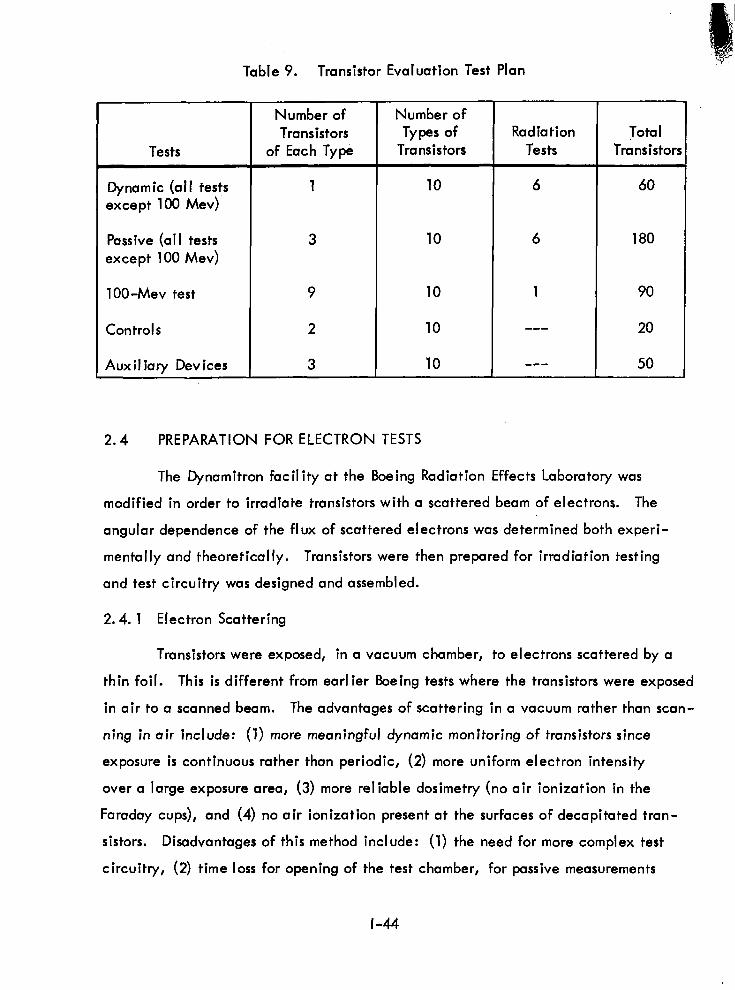
Table 9. Transistor Evaluation Test Plan
Tests
Dynamic (al I tests except 100 Mev)
Number of Number of Transistors Types of Radiation
of Each Type Transistors Tests
1 10 6
Total Transistor!
60
Passive (all tests except 100 Mev)
3 10 6 180
1 00-Mev test 9 10 1 90
Controls 2 10 m-w 20
Aux il iary Devices 3 10 -we 50
2.4 PREPARATION FOR ELECTRON TESTS
The Dynamitron facility at the Boeing Radiation Effects Laboratory was
modified in order to irradiate transistors with a scattered beam of electrons. The
angular dependence of the flux of scattered electrons was determined both experi-
mentally and theoretically. Transistors were then prepared for irradiation testing
and test circuitry was designed and assembled.
2.4. 1 Electron Scattering
Transistors were exposed, in a vacuum chamber, to electrons scattered by a
thin foil. This is different from earlier Boeing tests where the transistors were exposed
in air to a scanned beam. The advantages of scattering in a vacuum rather than scan-
ning in air include: (1) more meaningful dynamic monitoring of transistors since
exposure is continuous rather than periodic, (2) more uniform electron intensity
over a large exposure area, (3) more reliable dosimetry (no air ionization in the
Faraday cups), and (4) no air ionization present at the surfaces of decapitated tran-
sistors. Disadvantages of this method include: (1) the need for more complex test
circuitry, (2) time loss for opening of the test chamber, for passive measurements
l-44
between exposures, and subsequent evacuation, and (3) long exposure times, at
low rates, due to the slower dissipation rate of radiation-induced heat in a vacuum.
Since the Dynamitron accelerator is mounted vertically, it was necessary
to bend the electron beam to pass horizontally into the scattering chamber. This
chamber and the associated pumping system, mounted on its portable table, are
shown in Figure 16. The height of the chamber is adjustable to allow for mating
with the horizontal beam port. The chamber can also be gated off from the accel-
erator and evacuated using its 6-inch silicone oil diffusion pump with a liquid-
nitrogen-cooled baffle and a fore pump.
Figure 16. Electron Scattering Chamber
I -45
A Magnion 90-degree bending magnet was available for bending the elec-
tmn beam. This’magnet (mass energy product 16) was designed for bending protons.
In order to obtain sufficiently low magnetic field strengths, a Kepco regulated
low-current supply was procured. Then the horizontal beam was focused using a
Magnion (mass product 12) triplet-quadrupole-lensing magnet (4-foot focus). The
quadrupole magnet was controlled by a Magnion, current-regulated, duo-channel
and duo-range, power supply (0 to 400 millivolts per channel). A polarity revers-
ing switch was added in order to convert from electrons to the future proton tests
by selection of the proper channel and range. Once the focused beam was obtained,
considerable alignment of the exit beam tubing was still required in order to com-
pensate for the earth’s magnetic field.
A multiple-foil holder (6 positions) was designed and built for selection of
scattering foils. Thin aluminum foils 0.25 and 1.6 mills thick with a purity of
99.99 percent and a 5.0 mil foil with a purity of 99.0 percent were procured from
A. D. Mackay Inc., New York. The electron energy loss, AEf, within these foils
for electrons of energies selected for the tests are given in Table 10. Energy loss
was calculated from Equation 22.
AEf = pt (dE/dX) (22)
where p = density of the foil
t = thickness of the foil
(dE/dX) = the rate of energy I oss
The density of aluminum is 2.7 gm/cmm3.
Table 10. Energy Loss in Scattering Foils
Nominal Electron Energy Incident Test Energy on Foils Foil Thickness ld vdX) Al AEf
Test No. (Mev) (Me4 (Mils) (Mev cm2 gm-l) (Mev)
21 2 2.0 5.0 1.54 0.053
22 1 1.3 1.6 1.51 0.017
23 0.5 0.53 0.25 1.61 0.0028
l-46
The flux of scattered electrons, from the foils selected, was mapped prior . to each test in order to determine the exposure rates at the transistor arrays. Experi-
mental data was accumulated by the monitoring of current collected in a shielded
Faraday probe which was rotated to selected angles about the center of the scatter-
ing foil. Figures 17, 18, and 19 show experimental data from the mapping of
electron scattering in terms of the flux at the sample mounting disk (24-inch radius
from the foil). A theoretical determination of the gaussian scattering was calcu-
lated by an SRU 1107 computer using a Monte Carlo code. The Monte Carlo
scheme that is used represents, by straight I ine segments, the path an electron fol-
lows when slowing down in a material. Both the electron energy loss due to ioni-
zation or bremsstrahlung is determined for each segment and the resultant scattering
of the electron after each segment is computed from the Rethe-modified Moliere
scattering relations (Reference 11). The results of Monte Carlo analysis are also
shown in histogram form on the flux plots. Both experimental and theoretical data
were normalized to 1 pa total beam current. Agreement between experiment and
theory is quite good at the forward angles where the transistor armys were located.
2.4.2 Transistor Preparation
Transistors, for each of the 10 types procured, were numbered serially from
1 to 40 for purposes of identification. Control transistors as well as those selected
for tests are designated in this manner.
Transistor cans provided inherent shielding from electrons and consequently
their effect was considered in selecting test energies. Information concerning the
thickness of the cans was obtained both by contacting the manufacturers (Reference
12) and by decapitating transistors and measuring the thickness of the tops of their
cans with a micrometer. The pertinent properties of transistor cans are summarized
in Table 11. Kovar, I isted in Table 11, is a mild steel of composition 29 percent
Ni, 17 percent Co, 0.3 percent Mn, and 53.7 percent Fe (Reference 13). Equation
22 was used to calculate the energy loss of electrons passing through the transistor
cans. This energy loss and the resultant energy of electrons incident on the silicon
surface of transistors are listed in Table 12 for the “thinnest” and “thickest”
l-47
108- 0
I\cQ 0 EXPERIMENTAL DATA . . . . . . . ..I I...
Y : :
\
..=.====. MONTE CARLO PREDICTION . . .
. :
“% . . : . : fkl
. . . . . . . . . . . . . : : : : :
: : : 2 :
. .
0 i
:
:
: : : :
I
:
: :
: : : :
:
a,
t-1 . . . . ..I : :
: : : : :
: : : : :
: : : :
: : : : :
: : : : :
: : : x : : : : : @.
: : : : : : :
: : :......................., .
: : : :
: : : : . .
: . :
: : : : :
:
: : : .
: . :
: . . :
. . : . :
. . . : : : :
: : : : . .
: :
: : : . :
I . : :
I : : : . . . I I I I I I I
5 10 15 20 25 30
DEGREES
35
Figure 17. 2.0-Mev Electron Flux From 5.0 mil Al
l-48
. : : . . . . . . : : :
0 I . . . . . . . . EXPERIMENTAL DATA
MONTE CARLO PREDICTION
I I : : : I I 1 I I I I
5 15 20 25 30 35
. ..I
DEGREES
Figure 18. 1.3-Mev Electron Flux From 1.6 mil Al
I-49
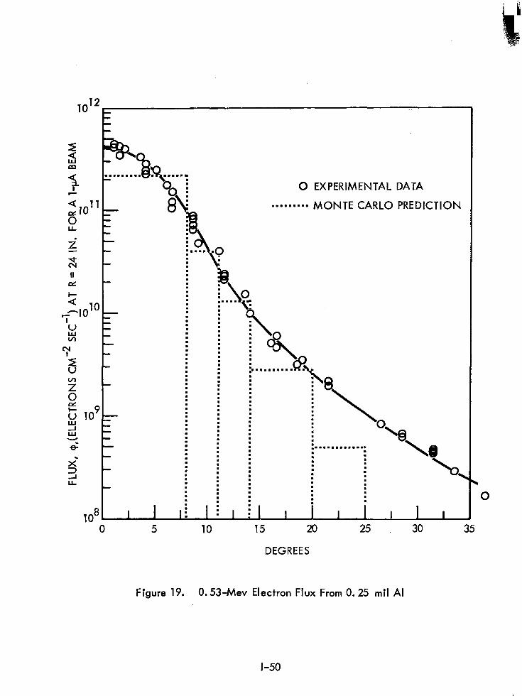
15 20
DEGREES
25
Figure 19. 0.53-Mev Electron Flux From 0.25 mil Al
I-50
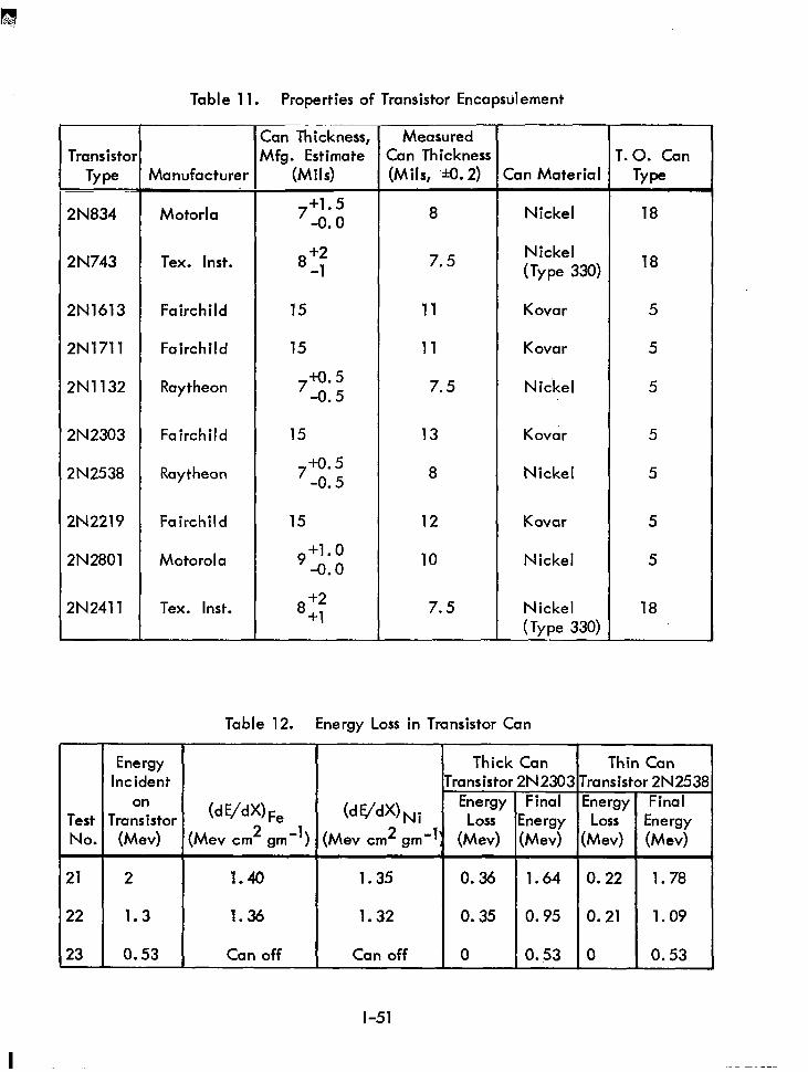
Table 11. Properties of Transistor Encapsulement
Transistor
TYpe
2N834
Manufacturer -
Motorla
Can Thickness, Measured Mfg. Estimate Can Thickness
(Mils) (Mils, ‘XI. 2)
2N743 Tex. Inst.
7+1.5 -0.0
+2 8-1
2N1613 Fairchild
2N1711 Fairchild
2N1132 Raytheon
15
15
7+o. 5 -0.5
2N2303 Fairchild 15
2N2538 Raytheon go. 5
-0.5
2N2219 Fairchild
2N2801 Motorola
15
+1.0 9d.0
2N2411 Tex. Inst. 8 +2 +1
Test No.
21 2
22 1.3
23 0.53
Energy Incident
on Transistor
(Mev)
8
Can Material
Nickel
Nickel (Type 330)
Kovar
Kovar
Nickel
r.0. Can
TYpe
18
7.5 18
11
11
7.5
13 Kovar 5
8 Nickel 5
12
10
7.5
Kovar 5
Nickel 5
Nickel (Type 330)
18
Table 12. Energy Loss in Transistor Can
Thick Can Thin Can Transistor 2N2303 Transistor 2N253E
(dE/dX)F, (dE/dN N i Energy Final Energy Final
:Mev cm* gm-‘) (Mev cm* gm’ Loss Energy Loss Energy
‘1 (Mev) (Mev) (Mev) (Mev)
1.40 1.35 0.36 1.64 0.22 1.78
1.36 1.32 0.35 0.95 0.21 1.09
Can off Can off 0 0.53 0 0.53
l-51
I
transistor cans. Incident 2.0-Mev electrons were chosen since the spectra of
electrons in the Van Allen belts decrease rapidly above 2 Mev. Incident electrons
of energy 1.3 Mev, which result in approximately 1.0 Mev incident on the semi-
conductor chip, provided a good energy separation between the 2-Mev and 0.53-
Mev tests. Cans were removed from the transistors for the 0.53-Mev test; thus
exposure was representative of electrons of approximately 0.8 Mev. Electrons of
0.8 Mev were not used for direct exposure of capsulated transistors because of a
serious loss of energy resolution and electron Intensity in passing through a transis-
tor can.
A iig was made for holding the transistors during the removal of the transis-
tor cans. A jeweler’s saw was used for con removal and filings were kept clear of
the semiconductor chips. Transistors with their cases removed were color coded
and a control transistor of each type was designated.
The stability of transistors which had been decapitated was verified by the
repeatability of values obtained on the transit time and G. R. bridges, Fairchild
Series 500 Tester, and the transistor curve tracer oscillograms taken before, after
in air, and after in a vacuum.
2.4.3 Preparation of Test Equipment
Test fixtures were prepared for the mounting and remote switching of transis-
tors as well as for the dynamic monitoring of transistor characteristic-curve traces.
Transistors were mounted in sockets that were attached to the sample-mounting dish.
The dish was spun out of aluminum in the form of a section of a sphere of .24-inch
radius. Thus, electrons scattered from the foil (24 inches away) impinged at normal
incidence to the tops of the transistors. The dish is attached to the inside of the
end plate of the scattering chamber. Shielded leads from the transistors passed
through a Deutsch high-vacuum feedthrough to a Leadex stepping switch which was
mounted to the outside of the chamber end plate. Shields on these leads were
grounded to the feedthrough which, in turn, was grounded to the chamber. Remote
control was necessary in order to monitor the transistors during irradiation without
the hazard of being exposed to the X rays generated in the magnet room. The
l-52
transistors are located approximately 100 feet from the data acquisition area. The
Leadex switch allowed remote selection of the transistors to be characterized.
Leadex switch wafers were modified so that selection of one transistor for charac-
terization automatically grounded the base and collector leads of the remaining
transistors to the Leadex switch box which in turn was grounded to the chamber
(Figure 20). Also seen in Figure 20 are the leads for a transistor which was left
under continuous bias during the tests. A remote position indicator was located in
the data acquisition area to allow the operator to identify the transistor under test.
The circuit of the positioner, which was designed and assembled for this program,
is shown in Figure 21. Roth the Leadex stepping unit and the positioning unit are
shown in Figure 22.
A bench checkout of the transistor monitoring system revealed severe dis-
tortion of the common-emitter characteristic curves. Thus, a variety of grounding
systems was investigated. However, no combination of grounding methods gave
consistently satisfactory results for al I transistors. The problem was brought under
control by two additions to the circuitry: (1) 0.001 -microfarad bypass condensers
were installed from each collector to the aluminum mounting dish and the common-
emitter line was connected to the dish through 200Q resistors at several points.which
in turn was grounded through the chamber. The placing of these components was
determined empirically. Subsequent testing indicates no significant difference
between oscillograms of the same transistor taken when mounted on the mounting
dish and when taken directly on the Tektronix Model 575 Curve Tracer. Figure 23
shows the final connections on back side of the transistor mounting dish. Shielded
base leads and shielded emitter leads were tied into separate bundles and all lead
cross over-s were made at 90”.
2.5 ELECTRON IRRADIATION TESTS
Electrons of energies 0.53, 1.3, and 2.0 Mev were obtained using the
Dynamitron accelerator. The accelerating potential is maintained by a stack of
high-voltage rectifiers. The lowest voltage at which stable-beam currents could
l-53
CHAMBER TEST CHAMBER WALL MAG’NET kOOM DATA ACQUISITION
\ LONG LEAD AREA
DYNAMIC TRANSISTORS
CONTiNt
i I I MOUNTING
JM
I DISH tttLl
THROUGH
I I
VACUl rrrr
TEKTRONIX 575
CURVE TRACER
CONTINUOUS BIAS
su PPLY
Figure 20. Dynamic Test Switching Circuitry
FG
1lOV A. C.
1
.150 !tFD ’ 5ov
LEDEX COIL
1 10K
i
1OOR
1 oon
I
i
2
loos2
o-
Figure 21. Position Selector and indicator Circuit
Figure 22. Stepping Selector and Positioner
Figure 23. Lead Connections on the Mounting Dish
readily be maintained was 0.53 Mev. The beam spot characteristics and centering
were adiusted by the exit-beam handling system. Detailed dosimetry measurements
were performed during the test and controlled procedures were followed for obtain-
ing dynamic test data.
2.5.1 The Test Configuration
Figure 24 shows the exit-beam handling system from the 90” bending magnet,
which is attached to the Dynamitron vertical beam port, to the scattering chamber.
Electrostatic lenses in the accelerator gun were adjusted in order to align the beam
for optimum entrance into the bending-magnet chamber. This alignment was
determined from the ratio of the current monitored on the water-cooled straight-
through aperature, Al, to the straight-through beam current striking the magnet
chamber walls.
The current through the bending magnet is adjusted by a regulated-current
supply in order to bend the beam into the quadrupole lensing magnet. The exit
side of the magnet is evacuated by a 4-inch oil-diffusion pump with its associated
I iquid-nitrogen baffles and fore pump. Proper beam alignment is determined by
minimizing the current collected on the quadrupole entrance aperture, A *. The
quadrupole magnet is adjusted by a regulated supply in order to focus the beam for
its entrance into the chamber aperture and subsequent impingement on the scatter-
ing foil. Optimum focusing by the quadrupole magnet is determined by the ratio
of current collected on the chamber aperture, A 3, to that passing straight through
into a fixed Faraday cup at the back of the chamber. Figure 25 shows a schematic
of the scattering chamber. The chamber is evacuated by a 6-inch oil -diffusion
pump and can be sealed off from the exit-beam tubing by use of a gate valve. When
beam passes through the entrance aperture, it can either pass directly into a fixed
Faraday cup or be scattered by a thin foil. The back of the Faraday cup consists
of a quartz window for beam viewing and a wire screen for charge collection. A
positive 300 volts is applied to the screen to reduce electron back scatter and to
reduce electron-charge buildup and its subsequent arcing in the quartz window.
l-58
Figure 24. Electron Ream Handling System
THERMOCOUPLE
REMOVABLE CHAMBER END PLATE
SYMMETRIC FARADAY CUP
PICKUP SCREEN SUPPLY
H
CURRENT INTEGRATOR SAMPLE MOUNTING
SCATTERING CHAMBER
CURVE VACUUM TRACER. STATION
Figure 25. Scattering Chamber Schematic
With a selected foil in place the beam will be scattered as illustrated in
Figure 25. The magnitude of the scattered flux decreased as a function of angle,
as was shown in Figures 17, 18, and 19, respectively, for the various tests. These
angles at which the transistor arrays were located are also shown in Figure 25. A
positive voltage of 400 volts was applied to the foil holder to aid in suppressing
the forward scattering of secondary electrons generated in the foil.
2.5.2 Dosimetry
The fluorescence of the Faraday-cup quartz window, resulting from the
incident straight-through beam, was observed using a closed-circuit television
system. The television camera was focused on the quartz window and wus used to
observe beam-spot shape, size, and centering. The spot shape and size were
altered by adjusting the field strength of the quadruople lensing magnet. An empty-
foil position on the foil holder was then centered on the beam to determine if the
spot size was small enough and whether optical alignment was accurate. Initially,
alignment had been determined by sighting with a surveyor’s transit through the
viewing plate and chamber aperture back down the beam tube to a window at the
exit of the 90-degree bending magnet. The scattering chamber was adjusted verti-
cally and horizontally so that the straight-through beam spot was centered on the
quartz viewing plate which, in turn, centered on the transistor mounting dish.
Straight-through beam current was collected on a wire screen, A4, on the face
of the quartz window at the back of the Faraday cup. A coaxial pickup cable was
connected to the screen and the beam current was monitored and integrated using
an Eldorado Electronics Model Cl-l 10 current integrator. The fixed Faraday cup
was shielded by a grounded-wire screen to reduce noise pickup and allow for
accurate low-current readings. The ratio between the current readings in the
fixed Faraday cup, A4, with the foil in and with the foil out was measured at
the beginning of a test to provide an accurate means for continuous monitoring of
the beam current during a test.
Thin aluminum foils were used for scattering electrons in order to provide
large exposure areas with uniform particle fluxes. Electron scattering provided a
l-61
constant value of uniform flux on those-transistors located in a circular array at the
same angle from the beam axis. Different fluxes were obtained by mounting tran-
sistors at different angles. A large number of transistors were exposed at each of
three different fluxes during a single test. Figure 26 shows the inside of the scat-
tering chamber with both the foil holder and the rotating Faraday probe in place,
and with transistors mounted on the dish. Measurement and calculation of scattered
flux were described in Section 2.4. 1. Those measurements were made using the
Faraday pro be, which was rotated about the foil to determine mapping as a function
of scattering angle. The cup of the Faraday probe, A5, is contained in and insu-
lated from an outer housing which acts both as a shield and a limiting aperture.
Current collected by the probe was measured on a Keithley Model 410A micro-
micro ammeter. Care was taken to zero the meter before each reading.
Table 13 shows typical current readings on the various cups and apertures
for each of the three tests, respectively. In addition to the probe and large fixed
Faraday cup, four smaller cups were placed on the sample-mounting dish in sym-
metric positions (up and down, left and right). These cups verified symmetry of
the scattered beam and were used to detect changes of the beam alignment during
an exposure run.
2.5.3 Test Procedure
At the start of each test the curve tracer was allowed to warm up. The
curve tracer was then calibrated and the Is = 0 line was zeroed and a picture was
taken of the standard 2N1613 control. The dynamic devices (one transistor of each
of the 10 types which were to be monitored on long leads during irradiation) and
the continuous-bias device were placed on the mounting dish and their long-lead
curve traces were compared with their original oscillograms. The passive devices
(three transistors of each of the 10 types which would be recharacterized directly
on the curve tracer at periods when the chamber was opened) were placed on the
mounting dish.
To begin a typical irradiation test, the scattering chamber was evacuated
to approximately 1 x 10d torr and then opened to the evacuated beam tubing.
I-62
Table 13. Typical Data From Current Monitoring
c
Straight-Through Limiter, Al
Date Time (Pamp)
9/16/65 01:45 10.5
01:48 10.5
9/23/65 10 :55 13.0
11:03 15.4
9/30/65 12 :57 22.0
13:03 22.0
Quadrupole Chamber Aperture, A2
(tJamp)
Aperture, A3
(Pamp)
1.1
0.9
1.0
1.0
3.2
3.2
3.7
3.5
1.0
1.0
10.2
10.5
Faraday CUP, A4 (Pamp)
9.4
0.5
6.4 0
0.4 1.6
34 0
2.9 0.25
Al Foil (mil)
0
5.0
Pro be Angle
(degrees)
--
45
--
10
--
20
Probe (R = 8. 8”),
A5 (tJamp)
--
4.9 x lo-4
--
3.4x lo-2
mm
I
7.4x 10⁻³
Vacuum was maintained until the end of an exposure run when the passive devices
were removed and recharacterized. Each test consisted of three exposure runs. A
full set of oscillogmms on the dynamic devices were taken before exposure.
beam current was then turned up and -appropriate dosimetry was performed,
including a foil -out to foil -in measurement of current ratio. The rotatable Faraday
probe was then set at a fixed angle, out of the way of the transistor arrays. With
the foil in place the integration of that portion of the current collected into the
fixed Faraday cup commenced. Flux rates and exposure times for each run had
been predetermined by a preliminary exposure of a selected number of transistors.
This preliminary test also aided in determining the transistor arrays and exposure
range to cover a significant range of damage.
The continuous-bias transistor and each of the dynamic transistors were
monitored periodica!ly during a particular run with oscillograms of curve traces
taken as desired. Integrated current was recorded each time an oscillogram was
taken. Occasionally during an exposure run, the beam was turned down and a full
set of pictures was taken on the dynamic transistors all at the same fluence. At
the end of an exposure run the beam was turned down, a full set of dynamic pic-
tures were taken, fluence was calculated, and the temperature of a spare transistor
in the test chamber was recorded. Following the 2-Mev electron test the tempera-
ture of the transistor mounting plate was monitored with a portable thermocouple
probe. A fixed thermocouple was then installed in the chamber prior to the 1 -Mev
electron test In order to periodically monitor transistor ambient temperature. After
the chamber was opened to the air another set of oscillograms of the dynamic tran-
sistors was taken. The passive transistors were removed and measured directly on
the curve tracer. These transistors were then placed back in the chamber, the
Faraday probe was set at a different angle, and the procedure was repeated until
three exposure runs were completed. Thus, four oscillograms of all passive transis-
tors were obtained, one before picture and three pictures at diffdrent fluences.
Table 14 shows typical data recorded on a computer keypunch data form for a
passively tested transistor. As many as 20 dynamic pictures, as a function of
l-65
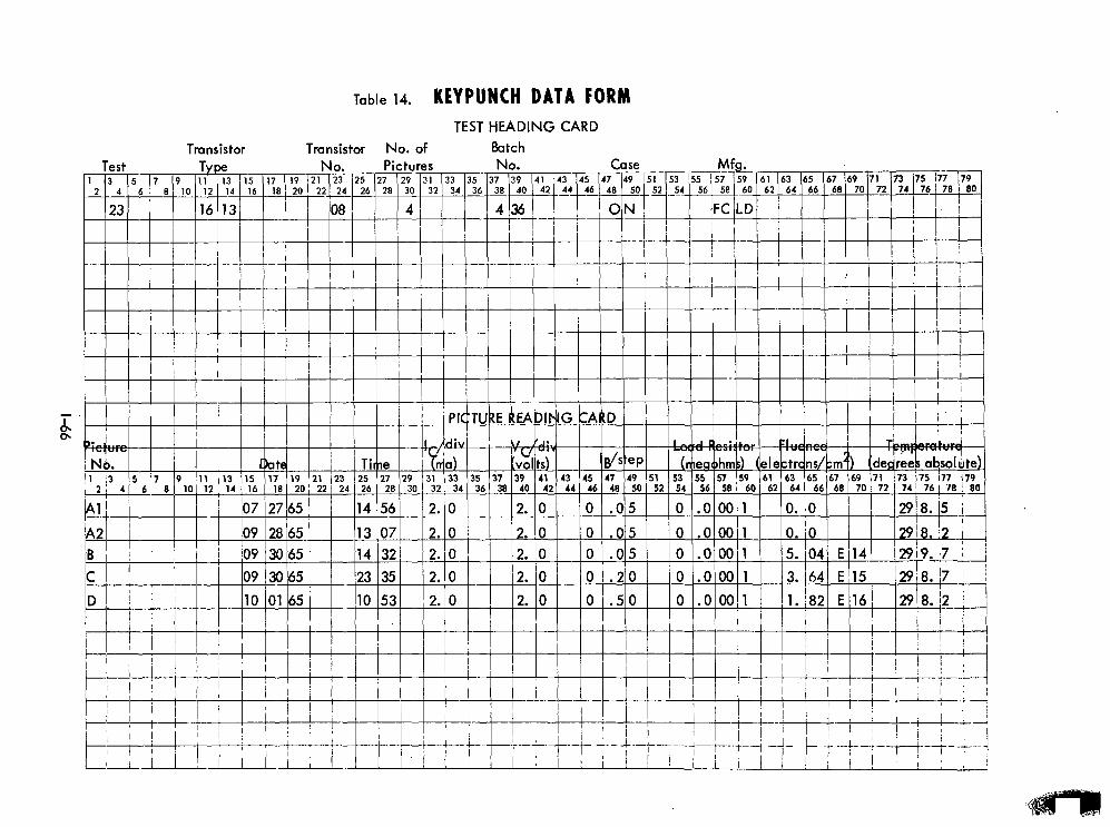
Table 14. KEYPUNCH DATA FORM
Test Transistor
TWX
TEST HEADING CARD Transistor No. of Batch
NO. Pictures No. Case Mb -_. 11 13
-. 1 3 5 7 9 15 17 19 21 23 25 27 29 31 33 35 37 39 41 43 45 47 49 51 53 '55 '57 59 61 63 65 67 69 71 73
2 4 6 0 10 12 14 lb 18 20 22 24 26 28 30 32 34 36.x 40 42 A4 46 40 50 52 -x4 56 50 -60 62 I 64 66 60 70 72 74
23 16 13 08, 4 436 ON FC LD -t- I
Date d’ s ep 17 19 ,21 123 25 27 29 31 133
321 34 35 37 139
( 40 41 43
1 45 47 49 ,51 53 55 57 59
'0 20 1 22' 24 26 28 30 36 38 42 44 46 40 50 52 54 56 58 60
’ 1307 2.0m O~.OOO 1 0. 0 / I ! :
0 .O 00 11 5. Od E’14 23 35 2. 0
10 53 2. 0
fluence, were taken of each of the 10 transistor types plus the continuous bias
transistor. Identification numbers of transistors exposed in the three electron tests
are given in Figures 27, 28, and 29.
2.6 PRELIMINARY ANALYSIS OF TEST DATA
A preliminary analysis was performed on the effects of electron irradiation
on transistor parameters. The data which were analyzed included values of those
radiation-sensitive parameters measured by use of the Fairchild Series 500 Semi-
conductor Tester as well as oscillograms of transistor common-emitter characteristic
curves made from the display of the Tektronix 575 Curve Tracer. The results of
this study are presented mainly as an indication of the direction in which the pro-
gram is proceeding. Included is an example of the effectiveness of radiation-
control parameters in normalizing the degradation of common-emitter current gain.
Preliminary correlation of radiation damage with the energy of electron radiation
is also given.
In the contract final report considerably more data will be reduced. A
greater emphasis will be placed on the correlation between the radiation-induced
changes observed and the theory of transistor behavior. Extensive data taken from
the oscillograms of characteristic curves will be computer analyzed before valid
radiation equivalences are presented.
2.6.1 Fairchild Series 500 Semiconductor Tester Data
Selected values of radiation-sensitive transistor parameters, which were
measured using the Fairchild Series 500 Semiconductor Tester (breakdown voltage,
d. c. common-emitter current gain, saturation voltages, leakage current, and base
turn-on voltage), have been analyzed. This was done in order to investigate the
dependence of those parameters on electron fluence and energy. In addition it
will provide Insight into both the role of radiation interactions in inducing sig-
nificant effects in various regions of the transistor and into the means of predicting
or control I ing these effects.
l-67

\ POSITION - 3
2N2538
POSITION -4
\ POSITION-
I
’ POSIT- , 2N2303
I SYMBOLS FOR
TRANSISTOR IDENTIFICATION NUMBERS
n DYNAMIC 0 PASSIVE
cl CONSTANT BIAS
POSITION -9
POSITION - 8
Figure 27. Transistor Army for 2.0-Mev Test
l-68
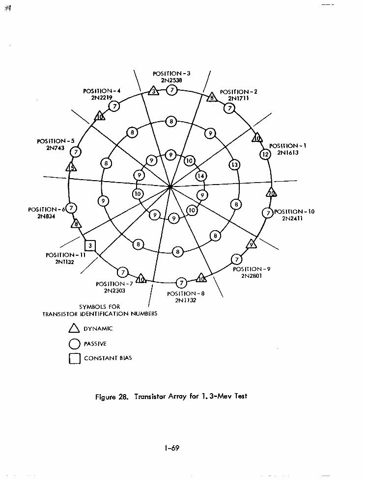
\ POSITION-3 2N2538
POSITION-4
1 POSITION -
POSITION -6
8
s
SYMBOLS FOR TRANSISTOR IDENTIFICATION NUMBERS n DYNAMIC 0 PASSIVE cl CONSTANT BIAS
Figure 28. Tmnsistor Array for 1.3-Mev Test
l-69
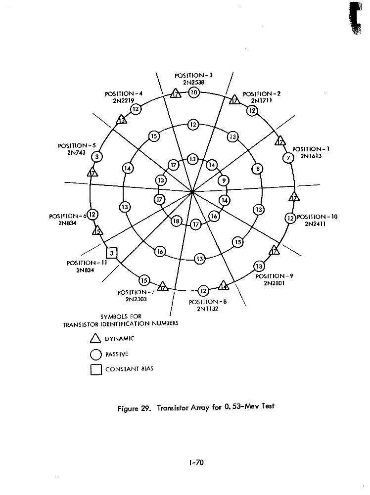
\ POSITION -3
2N2538
POSITION-4
\-I gOSITION -
a...r.m
POSITION -8
I \
2N1132 SYMBOLS FOR
TRANSISTOR IDENTIFICATION NUMBERS
A DYNAMIC 0 PASSIVE
cl CONSTANT BIAS
Figure 29. Transistor Army for 0.53~Mev Test
I-70
The least radiation sensitive of the parameters which were studied was the
breakdown voltage, BVCBo (measured at a collector current of 100 pa). Even
after extensive electron Irradiation (over 1016 electrons/cm2) only small changes
were observed for all of the 10 transistor types. An average of those values of the
percentage of change in BVCBO is shown in Table 15 for each of the three elec-
tron tests. Most of the transistor types either showed no significant change (within
the limits of precision) or showed an increase in breakdown voltage which does not
appear to be a function of electron fluence (over the range of approximately
4 x 10¹⁵ to 4 x 10¹⁶ electrons/cm2). Only a few of the devices appeared to show
any dependence on electron fluence. Both of the npn epitaxial mesa transistors,
2N743 and 2N834, as well as transistor 2N2538, showed an apparent decrease of
BVCBo with increased fluence. Both pnp epitaxial planar devices, 2N2801 and
2N2411, showed an apparent increase in BVCBo. Changes in breakdown voltage
for those transistors of typs 2N2411 and 2N2538 are plotted in Figure 30 for each
of the electron tests. A dotted line is used to compare the 2N2411 data with a
I inear dependence on fluence. Accuracy of the electron fluence measurement is
approximately 15 percent. The accuracy of the BVCBo measurement from the
Fairchild Series 500 is only about *l percent, which almost renders these values
of small change useless. However, only relative values are important for compari-
son purposes and the precision, as determined by repeatability of measurements, is
approximately %I. 2 percent. Thus, Figure 30, due to its consistent dependence on
energy, may possibly be an indication of the relative order of effectiveness of
electron energy (1.8, 1.1, and 0.5 Mev) for changes in BVCBo.
hturation voltage, VCE (sat), measured at a current gain of 2 for collector
currents of 2 and 10 ma, respectively, increased by over 100 percent for many of
the exposed transistors. Table 16 lists the observed changes in both hFE and VCE(sat)
for those transistors of each type which were exposed passively during the 1 -Mev elec-
tron test. Analysis of the changes of hFE will be discussed in detail for the data
reduced from oscillogmms of common-emitter chamcteristic curves. The strong
dependence of the changes of both hFE and VCE(sat) on electron fluence is appar-
ent. The changes in VCE (sat) for the npn transistors exposed in the 1 -Mev electron
l-71
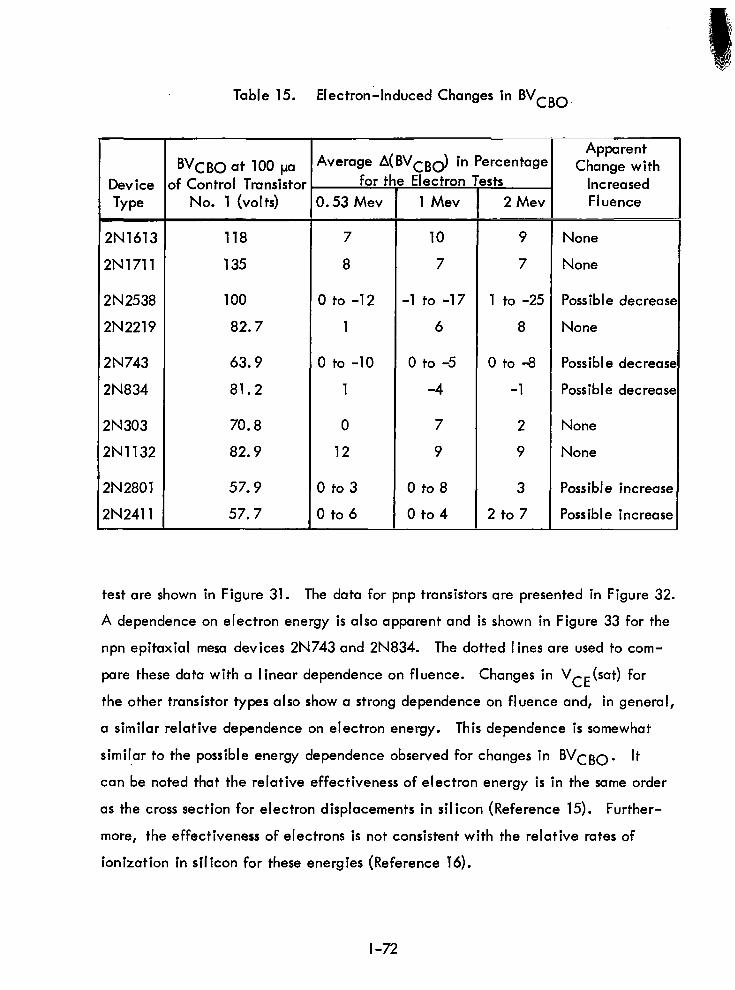
Table 15. Electron-Induced Changes in BVCBO
Apparent BVCBO at 100 pa Average A( BVCBd in Percentage
for the Electron Tests Change with
Device of Control Transistor Increased Type No. 1 (volts) 0.53 Mev 1 Mev 2 Mev FI uence
2N1613 118 7 10 9 None
2N1711 135 8 7 7 None
2N2538 100 0 to -12 -1 to -17 1 to -25 Possible decrease
2N2219 82.7 1 6 8 None
2N743 63.9 0 to -10 0 to -5 0 to -8 Possible decrease
2N834 81.2 1 -4 -1 Possible decrease
2N303 70.8 0 7 2 None
2N1132 82.9 12 9 9 None
2N2801 57.9 0 to 3 0 to 8 3 Possible increase
2N2411 57.7 0 to 6 0 to 4 2 to 7 Possible increase
test are shown in Figure 31. The data for pnp transistors are presented in Figure 32.
A dependence on electron energy is also apparent and is shown in Figure 33 for the
npn epitaxial mesa devices 2N743 and 2N834. The dotted I ines are used to com-
pare these data with a linear dependence on fluence. Changes in VCE(sat) for
the other transistor types also show a strong dependence on fluence and, in general,
a similar relative dependence on electron energy. This dependence is somewhat
similar to the possible energy dependence observed for changes in BVCBo. It
can be noted that the relative effectiveness of electron energy is in the same order
as the cross section for electron displacements in silicon (Reference 15). Further-
more, the effectiveness of electrons is not consistent with the relative rates of
ionization in silicon for these energies (Reference 16).
l-72
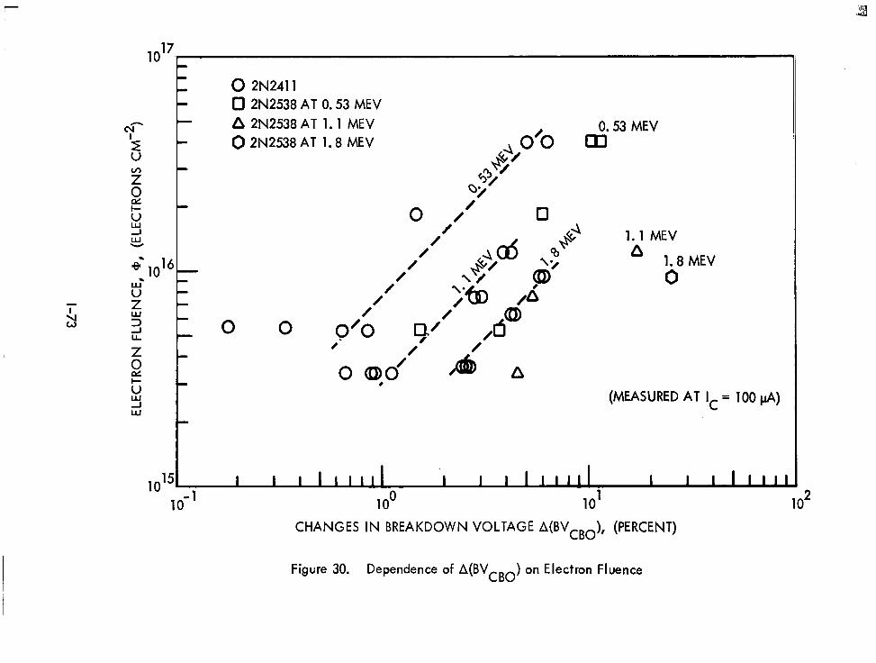
0 2N2411
0 2N2538 AT 0.53 MEV
A 2N2538 AT 1.1 MEV
0 2N2538 AT 1.8 MEV 0.53 MEV
$-$,o’” II1
+ a
9
0 0’ 0
0 o,oO b ’ A
(MEASURED AT lc = 100 pd)
1.1 MEV a
1.8MEV
0
0 0
lo-’ 10” 10’ lo2
CHANGES IN BREAKDOWN VOLTAGE A(BV CBO), (PERCENT)
Figure 30. Dependence of A(BVCBO) on Electron Fluence

r
Table 16. Electron-Induced Changes in VCE (sat) (P assive Transistors in the 1 -Mev Test)
I *= 3.36x 10'5 e/cm2 @= 7.56x 10¹⁵ c/cm2 ! *= 1.22 x 10'6 e/cm2 I
rmnrirtor
56.8
6.6
202
16.5
291
34.2
163
43.7
51.2
15.3
72.0
7.9
141
4.2
41.7
3.7
97.5
.&.&
146
18.2
0.152 11 0.232 /I '
9
9
h 2 ma
54.7
2. 2
167
9.2
136
19.9
139
24.3
33.0
9.0
92.4
7.0
119
1.8!
58.4
2.0
78.5
3.0
85.8
8.5
V&d 1 E (volts) 10ma 2ma 10 ma
61.1 0.068 O.d94
2.4 --- ---
213 0.047 0.085
9.7 0.130 0.228
186 0.103 0.095
23.6 0.122 0.138
163 0.011 0.022
29.2 0.095 0.121
43.2 0.115 0.115
8.8 '0.152 0.180 I
103 ,0.121 / 0.116 /
8.9 IO.152 i 0.163 !
115 iO.052 0.105
1.99 --- --- ,
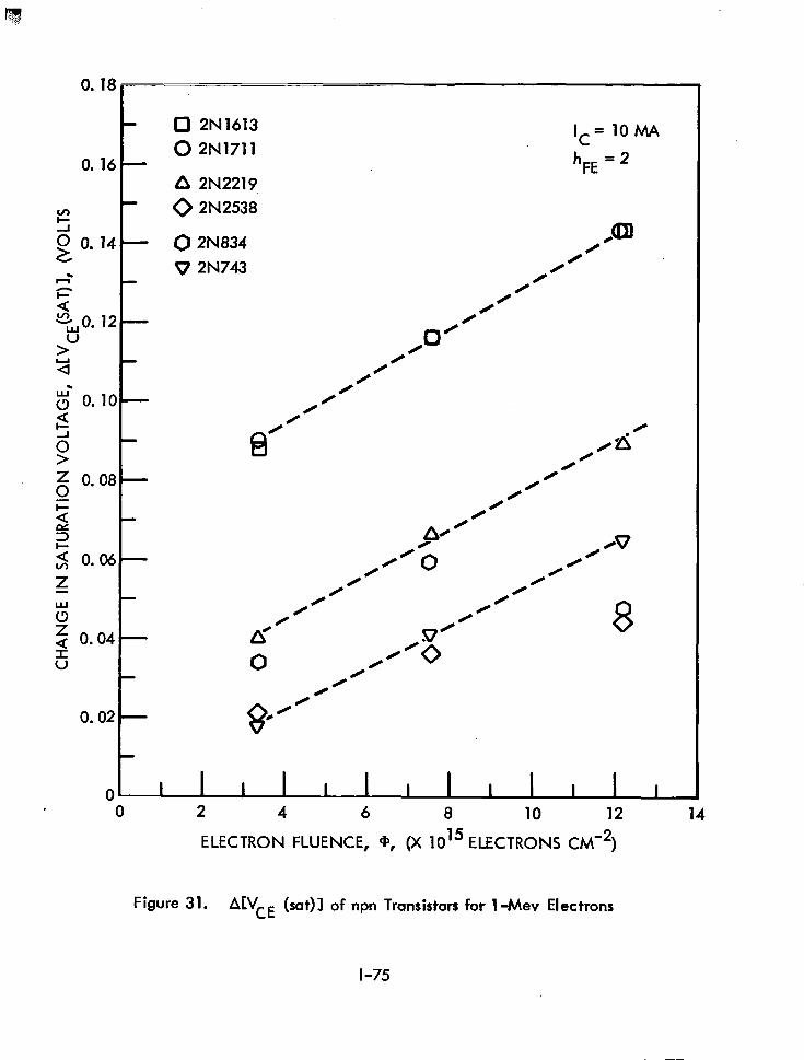
0.
0.
18~
0 2N1613 = ‘OMA 0 2N1711 IC
16 - h = FE
2
A 2N2219
0.
0 2N2538
14- 0
V
08 -
06-
04 -
02 -
0 I I I I I I I I I I I I I 0 2 4 6 8 10 12 14
ELECTRON FLUENCE, 9, (X 1015 ELECTRONS CM-2)
Figure 31. A[VcE (sat)] of npn Transistors for l-Mev Electrons
l-75
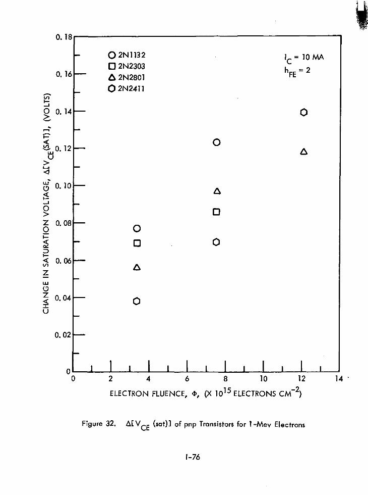
0. 18
0. 16,-
h
2 0 t
0.14-
2 l= Q =
“u 0.12-
> 3
- 2 O.lO-
5
o>
z O* O8 c 3 2 Q
2
0.06-
Yi z 4 0.04 -
U
0.02 -
0 2N1132
0 2N2303
A 2N2801
0 2N2411
IC = ‘OMA
h FE = 2
0
0
a
0
0
0
a
a
0
0
0 2 4 6 8 10 12 14 .
ELECTRON FLUENCE, a, (X 1015 ELECTRONS CM-2)
Figure 32. ALV,, (sat)] of pnp Transistors for 1-Mev Electrons
l-76
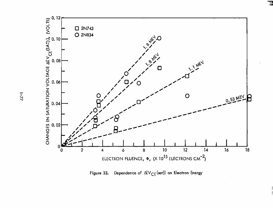
0 2N743
0 2 4 6 8 10 12 14 16 18
ELECTRON FLUENCE, a, (X 1015 ELECTRONS CM-2)
Figure 33. Dependence of LYVCE(sat)l on Electron Energy
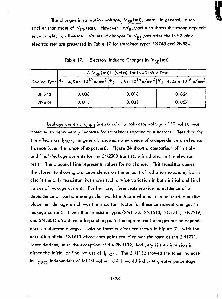
The changes in saturation voltage, VBE(sat), were, in general, much
smaller than those of VCE (sat). However, Av~~(sat) also shows the strong depend-
ence on electron fluence. Values of changes in VbE(sat) after the 0.52-Mev
electron test are presented in Table 17 for transistor types 2N743 and 2N834.
Table 17. Electron-Induced Changes in VbE (sat)
ACVBE (sat)] (volts) for 0.53-Mev Test
Device Type *‘=4.94x 10’5e/cm2 *2=1.6x 10¹⁶e/cm2 *3=4.03x 10¹⁶e/cm2
2N 743 0.006 0.016 0.034
2N834 0.01’ 0.031 0.067
,Leakage current, ICBO (measured at a collector voltage of 10 volts), was
observed to permanently increase for transistors exposed to electrons. Test data for
the effects on ICgo, in general, showed no evidence of a dependence on electron
fluence (over the range of exposures). Figure 34 shows a comparison of initial-
and final-leakage currents for the 2N2303 transistors irradiated in the electron
tests. The diagonal line represents values for no change. This transistor comes
the closest to showing any dependence on the amount of radiation exposure, but it
also is the only transistor that shows such a wide variation in both initial and final
values of leakage current. Furthermore, these tests provide no evidence of a
dependence on particle energy that would indicate whether it is ionization or dis-
placement damage which was the important factor for these permanent changes in
leakage current. Five other transistor types (2N1132, 2N1613, 2N1711, 2N2219,
and 2N2801) I a so showed large changes in leakage current changes but no depend-
ence on electron energy. Data on these devices are shown in Figure 35, with the
exception of the 2N1613 whose data point grouping was the same as the 2N1711.
These devices, with the exception of the 2N1132, had very I ittle dispersion in
either the initial or final values of ICgo. The 2N1132 showed the same increase
in ICBO independent of initial value, which would indicate greater percentage
l-78
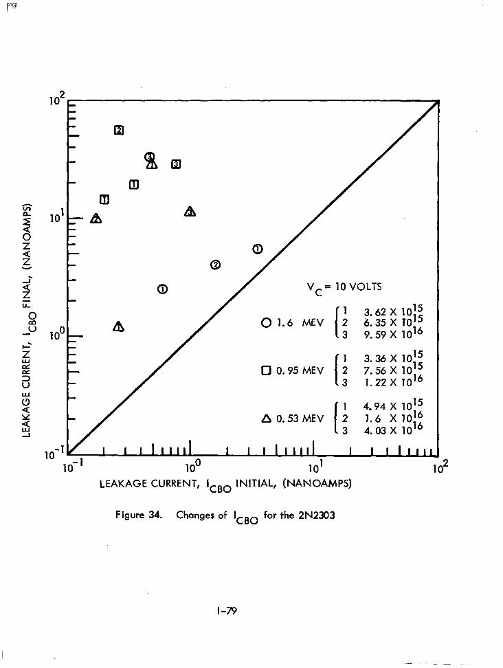
El
0 1.6 MEV I
;* g ; ;.$:
- 3 9:59x 10’6
0 0.95 MEV I : 3 36 X 7’56X
1015 1015
3 1: 22 x 10’6
4.94 x 10’5
,!I 0.53MEV I : 1.6 X 10¹⁶ 3 4.03x 1o16
I Il111ll I I I Illll 1 n , 3
lo-’ 10” 10’ 10’
LEAKAGE CURRENT, lcBo INITIAL, (NAN~AMPs)
Figure 34. Changes of lCBO for the 2N2303
l-79
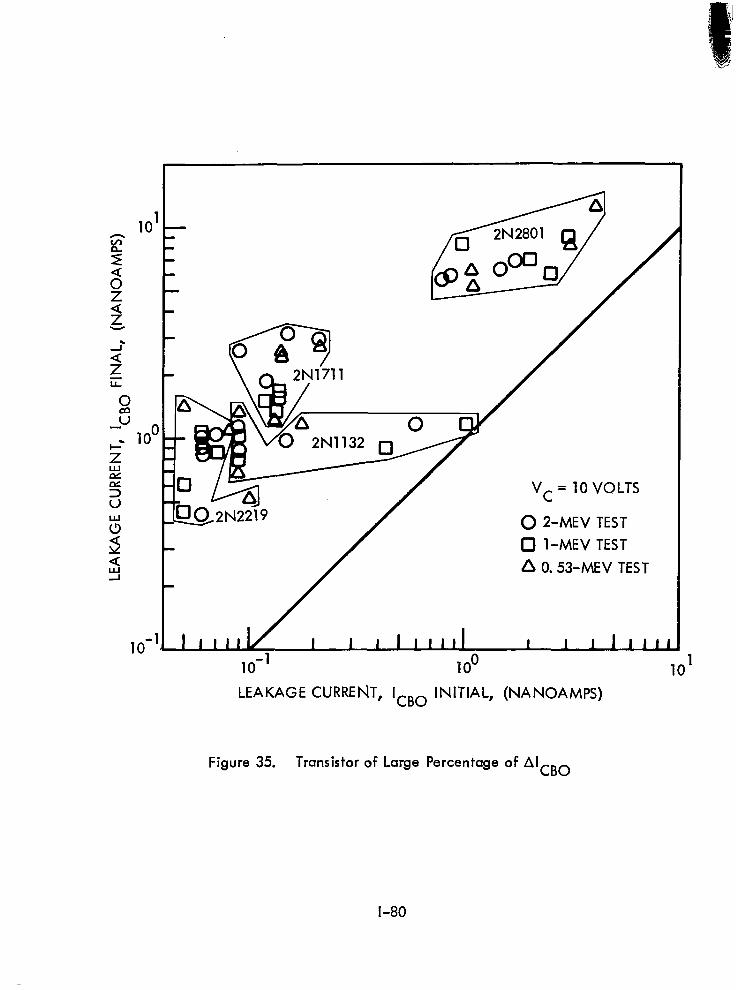
10' - E z
d
f z
ZT z iz
9 ii -"
. loo --
5 s!
5 -0 /z?i
- OJ / v,= 10 VOLTS
/ L n h -. .-a.-
2 ,lZNUlY 0 2-MEV TEST
9 0 l-MEV TEST 6 5 a 0.53-MEV TEST
10-l 10”
LEAKAGE CURRENT, lCBo INITIAL, (NANOAMPS)
Figure 35. Transistor of Large Percentage of AICBo
I-80
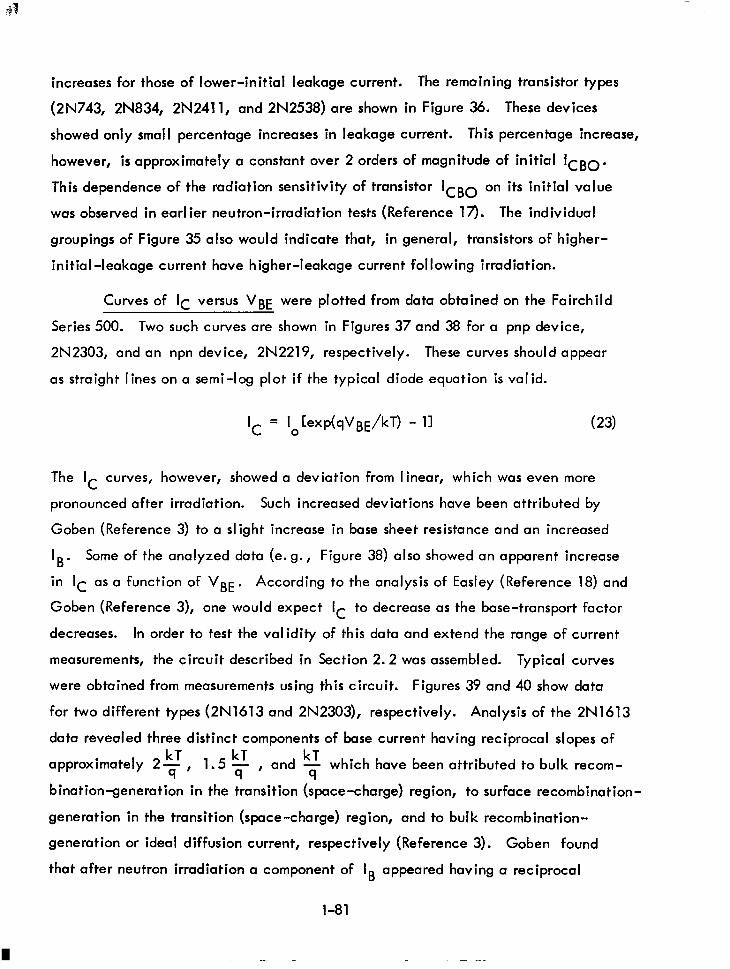
increases for those of lower-initial leakage current. The remaining transistor types
(2N743, 2N834, 2N2411, and 2N2538) are shown in Figure 36. These devices
showed only small percentage increases in leakage current. This percentage increase,
however, is approximately a constant over 2 orders of magnitude of initial ICBO.
This dependence of the radiation sensitivity of transistor lCBo on its initial value
was observed in earlier neutron-irradiation tests (Reference 17). The individual
groupings of Figure 35 also would indicate that, in general, transistors of higher-
initial-leakage current have higher-leakage current following irradiation.
Curves of IC versus VBE were plotted from data obtained on the Fairchild
Series 500. Two such curves are shown in Figures 37 and 38 for a pnp device,
2N2303, and an npn device, 2N2219, respectively. These curves should appear
as straight lines on a semi-log plot if the typical diode equation is valid.
IC = lo[exp(qVBE/kT) - 11 (23)
The Ic curves, however, showed a deviation from linear, which was even more
pronounced after irradiation. Such increased deviations have been attributed by
Goben (Reference 3) to a slight increase in base sheet resistance and an increased
lB. Some of the analyzed data (e.g., Figure 38) also showed an apparent increase
in lC as a function of VBE. According to the analysis of Easley (Reference 18) and
Goben (Reference 3), one would expect Ic to decrease as the base-transport factor
decreases. In order to test the validity of this data and extend the range of current
measurements, the circuit described in Section 2.2 was assembled. Typical curves
were obtained from measurements using this circuit. Figures 39 and 40 show data
for two different types (2N1613 and 2N2303), respectively. Analysis of the 2N1613
data revealed three distinct components of base current having reciprocal slopes of kT
approximately 2J$, 1.5 q , and kT q
which have been attributed to bulk recom-
bination-generation in the transition (space-charge) region, to surface recombination-
generation in the transition (space-charge) region, and to bulk recombination-
generation or ideal diffusion current, respectively (Reference 3). Goben found
that after neutron irradiation a component of IB appeared having a reciprocal
l-81
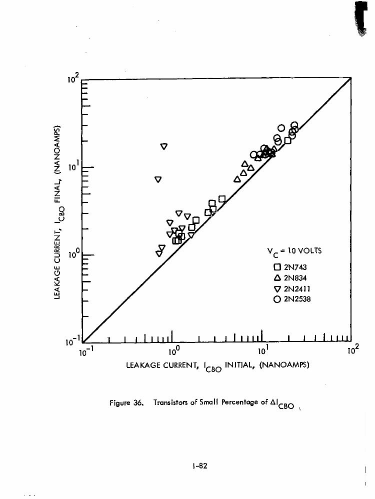
102L -
/ V
V
vC = 10 VOLTS
0 2N743 A 2N834 V 2N2411
/ 0 2N2538
10” 10’
LEAKAGE CURRENT, lcBo INITIAL, (NANOAMPS)
Figure 36. Transistors of Small Percentage of AlcBo \
I-82
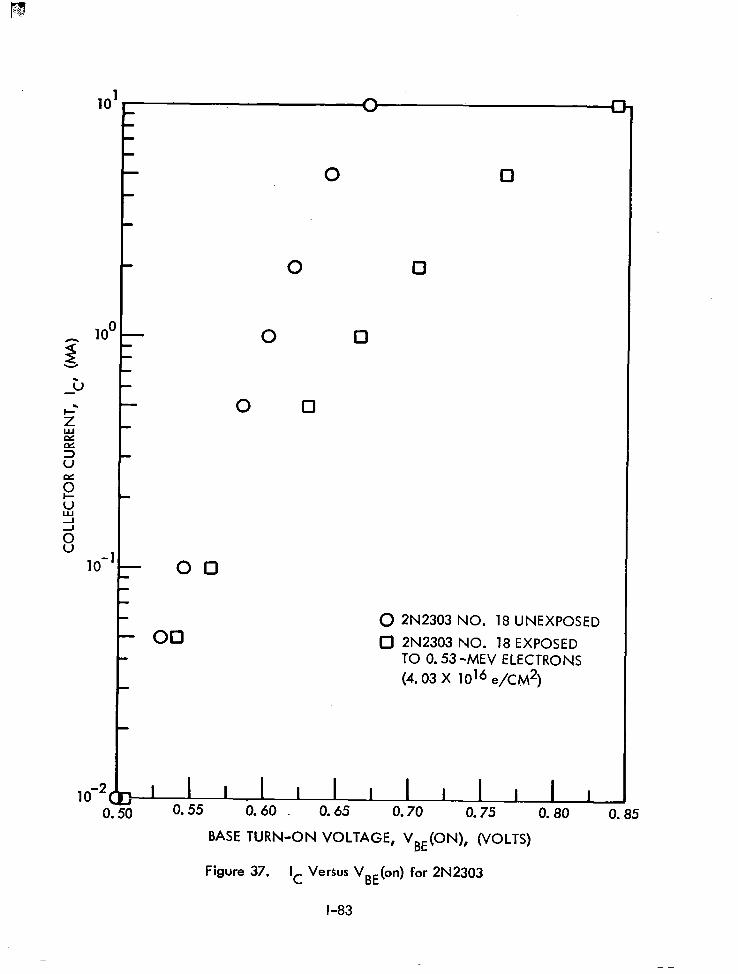
lo-*c I I I I I I I I 1 I I 0.65
I 1 I 0.50 0.55 0.60 0.70 0.75 0. 80 0.85
0 0 0
0 0
0
00 0 2N2303 NO. 18 UNEXPOSED
- 00 0 2N2303 NO. 18 EXPOSED TO 0.53 -MEV ELECTRONS
(4.03 x 10’6 e/CM*)
BASE TURN-ON VOLTAGE, VBE(ON), (VOLTS)
Figure 37. IC Versus VBE(on) for 2N2303
l-83
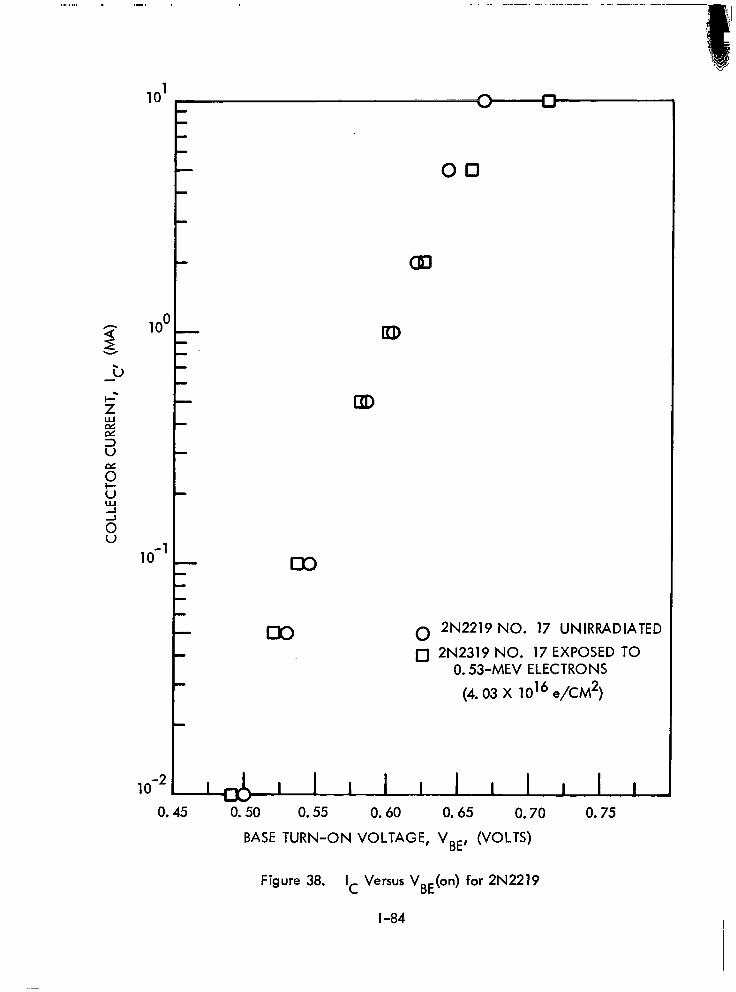
00
03
00 0 2N2219 NO. 17 UNIRRADIATED
0 2N2319 NO. 17 EXPOSED TO 0.53-MEV ELECTRONS
(4 . 03 X 1016 e/CM*)
0.45 0. 50 0.55 0.60 0.65 0.70 0.75
BASE TURN-ON VOLTAGE, VBE, (VOLTS)
Figure 38. Ic Versus VBE(on) for 2N2219
l-84
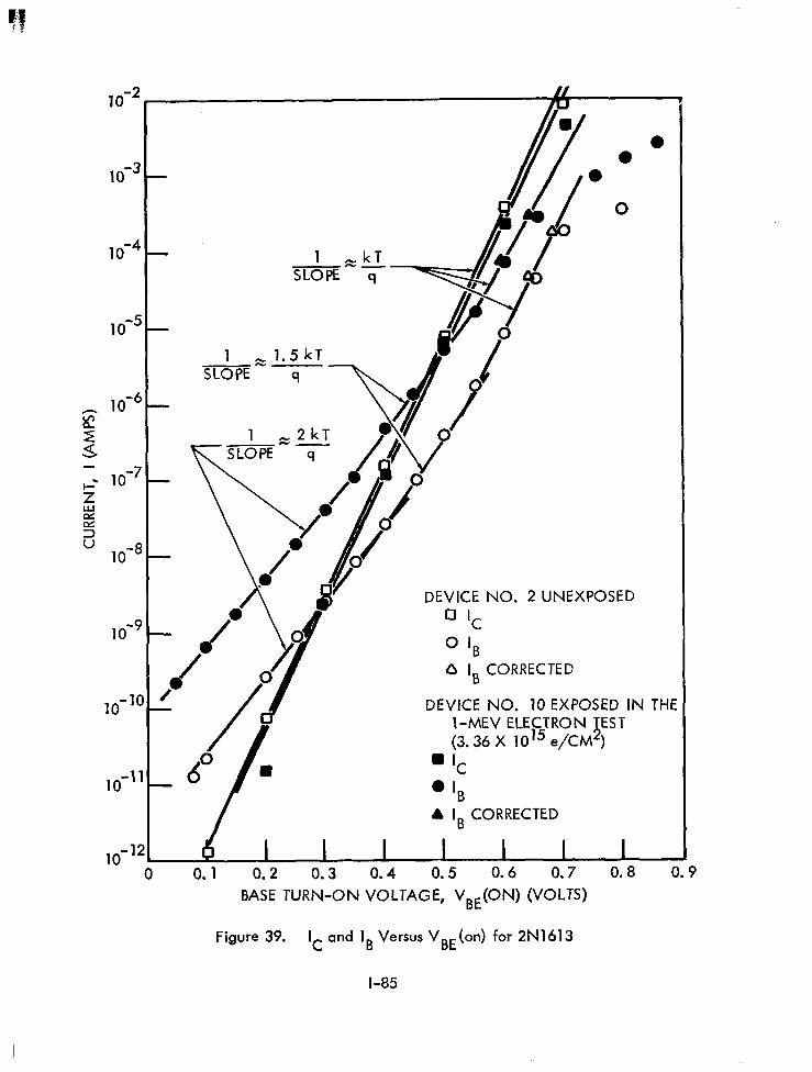
16*
1o-3
lo-4
lo-5
5 1O-6
2
- 5 lo-7
2
2 l0-E
lo-$
10-‘(
10”’
lo-‘: _
1 e kT SLopEq
1 e 1.5 kT -- SLOPE q 1
DEVICE NO. 2 UNEXPOSED 0 1, L
0 IB CORRECTED
- / d
/
0 -6 a
DEVICE NO. 10 EXPOSED IN THI I-MEV ELECTRON TEST (3.36 X 1Ol5 e/CM*)
l Ic
’ ‘B Ir IB CORRECTED
I I I
0 0.’ 0.2 0.3 0.4 0.5 0.6 0.7 0.8 0.9
BASE TURN-ON VOLTAGE, VBE(ON) (VOLTS)
Figure 39. Ic and IB Versus VBE(on) for 2N1613
l-85
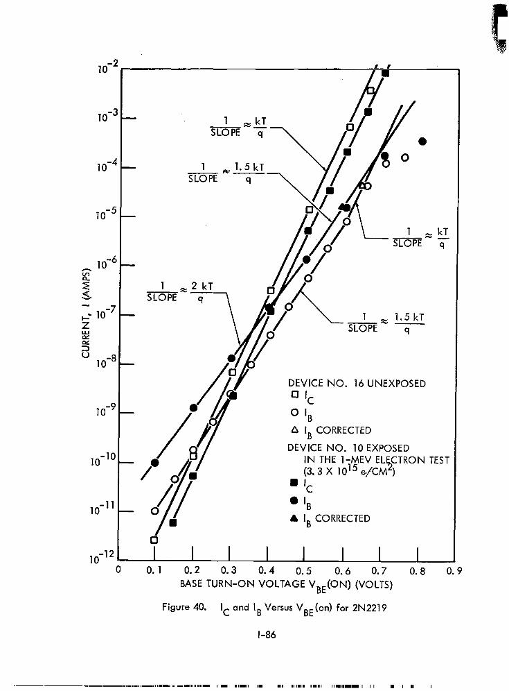
IO-:
10-l
10-l
1o-2
E 10-l
2
- 10
-7 < Z is oi
2 10+
1O-9
lo-lo
10-l’
lo-‘*
DEVICE NO. 16 UNEXPOSED
D IB CORRECTED
DEVICE NO. 10 EXPOSED
’ ‘B & IB CORRECTED
d
I I I I I I I I 0 0.1 0.2 0.3 0.4 0.5 0.6 0.7 0.8 0.9
BASE TURN-ON VOLTAGE VBE(ON) (VOLTS)
Figure 40. Ic and IB Versus VBE (on) for 2N2219
l-86
kT slope of 1.5 q- but originating in the bulk space-charge or transition region, and
it tended to dominate the base current over a large range. In Figure 39 for the
2N1613 the “1.5 y component” of IR has increased after irradiation but does
not seem to be dominant over a significantly greater current range than is the sur-
face “1.5 !$ component” in the unirradiated device. It is of further interest to kT
note that for the unirradiated 2N2219 device there is no “2 - component”; how- q
ever, in the irradiated device such a component appears and dominates lb over a
large range.
It is hoped that further tests and analysis will: (1) show whether Ic does
in fact increase with VbE as a function of irradiation in certain devices, and (2)
provide information as to the effects on current-gain degradation of the different
regions of the transistor.
2.6.2 Common-Emitter Characteristic Curves
Data was reduced from oscillograms of transistor d. c. characteristics taken
from the display of a Tektronix 575 Curve Tracer. In analyzing changes in current
gain of the transistors exposed in the three electron tests, it was consistently
observed that current gain degraded initially in a rapid fashion not predictable
by atomic-displacement theory. However, after extensive exposure, this effect
tended to saturate and the gain degradation was predictable on the basis of changes
in base minority-carrier I ifetime.
Initial-minority-carrier lifetime in the base region of a transistor, Tb. , is I
expected to be inversely proportional to the initial density, Ni, of carrier recom-
bination centers (Reference 19):
I/‘$ = cN i (24)
Electron-induced atomic displacements would form new recombination
centers. The density of these centers should be proportional to the radiation expo-
sure and will cause a decrease in minority-carrier lifetime (Reference 20); therefore,
l-87
l/l-b = cNi+K+
and
A(l/Tb) = ‘/Tb - ‘/T+ = K4 (26)
where 4’ is the electron fluence. The common-emitter current gain of a minority-
carrier injection-type transistor can be related to the base lifetime by the following
equation (Reference 21):
‘lhF E = SAs W/AC Db + O,, w/De Le + W*/*DbTb (27)
where S = surface recombination velocity
A S
= effective area for surface recombination
w= effective width of the base region
A C
= area of the conduction path
Db = minority-carrier diffusion constant in the base
abf ‘e = conductivities of the base and emitter regions, respectively
L e
= emitter diffusion length
The following relation, which was reported by Easley (Reference 22) in
1958, expresses the dependence of changes in gain on neutron fluence:
A(hFE -‘) = Kd+ (28)
where Kd is the displacement-induced transistor damage constant. The “I inear”
dependence on fluence has consistently been observed for transistors irradiated in
a neutron environment. However, analysis of the d. c. common-emitter character-
istics obtained from the recent irradiation tests show that Equation 28 is not valid
for electron effects on transistors except for large values of fluence, for which gain
degradation is severe. The “non1 inear” effects are also more pronounced at reduced
l-88
currents where the first term in Equation 27 has its greatest influence on current
gain. Thus nonlinear effects which were observed for electron damage could arise
from alterations of the surface recombination velocity. The surface recombination
velocity can be effected by chemical treatment of a transistor surface; and this
treatment which can greatly alter the common-emitter current gain is saturable
(Reference 23). Thus, it is conceivable that ionization may also induce changes
in surface recombination velocity which would saturate with heavy exposure to
ionizing radiation. Earlier tests using X rays of energies below the silicon dis-
placement threshold indicated that permanent “non1 inear” damage is probably
caused by ionization effects (Reference 4). Furthermore, this type of effect has
only been observed for charged-particle damage and, generally, only at low levels
of exposure (References 4 and 24). It is thus possible that ionizing radiation causes
permanent changes in surface recombination velocity (surface lifetime) and that
these changes dominate transistor gain degradation for low operating currents and
small values of electron fluence, while displacement damage dominates for heavy
electron exposure.
If ionization of the surface is the cause of the initial electron effects on
current gain and if these effects are saturable, then it would seem reasonable to
suggest that there may be a limited number of prospective surface sites, N,. . As I
these sites are acted upon their number should decrease resulting in eventual satura-
tion of the effect. The conversion or rate of change of the prospective sites, NS,
with electron fluence would be expected to be proportional to the number available.
dN J
da= KINS (29)
K, of Equation 29 would be the energy-dependent ionization-damage constant,
since it would include the ionization rate of the incident electron. Then integra-
tion of Equation 29 and application of the initial conditions (pi = 0, N, = N,i)
would lead to a relation for the growth of ionization-induced surface recombination
sites, N I’
as a function of electron fluence.
l-89
- . -
NI I = N,. L - exp(-KIO)]
Applying Equation 30 to the observed degradation of current gain would modify
Equation 28.
‘(‘FE -‘I = Cs NSe [I1 - exp(-KIO;] I
+ Kd9
co
where Cs is a constant which includes, in part, the constants in the first term on
the right of Equation 27.
Values of the constants in Equation 31 were calculated from curves of
experimental data on current gain degradation. Figure 41 depicts gain degrada-
tion resulting from the 0.53-Mev electron test. The experimental data points
have been corrected for ambient temperature [A(hFE-‘) of O.O008/‘C]. The sur-
face term of Equation 31 represents well the observed initial degradation of gain.
The linear region of the curve of Figure 41 was extrapolated back and subtracted
from the experimental curve in order to separate the postulated displacement and
ionization damage. The dashed I ine which represents this nonlinear damage has
indeed the shape of a saturation curve. With the constants evaluated, Equation
31, represented by the sol id I ine, fits the experimental data of Figure 41.
Assuming that the so-called ionization-induced damage sites are a result
of surface-fabrication processes and.ambient conditions at the time of fabrication,
it seems reasonable that the number of defect sites per-unit-surface area would be
similar for devices produced under similar conditions. If the above assumption is
valid, the total number of defect sites in different transistors of a given type should
differ only to the extent that their effective-surface areas differ. Further tests and
analysis are expected to provide insight on whether the nonlinear effect is truly due
to surface ionization. If it is indeed surface-ionization damage then further analy-
sis will be performed to see if values of N,. can be predicted, and if Kl is I
relatively constant for transistors of a given type.
l-90
h C
2Nl613 NO. 17 IN 0. ELECTRON TEST -
I . . . . . . . . LINEAR EXTRAPOLATION, EQUATION 28
EXPERIMENTAL DATA MINUS EQUATION 28
SATURATION TERM OF EQUATION 32
FIT OF EQUATION 32
. .* 0 .*
.** ‘@FE -‘) = 1.56 X 10%
0 .* .* l .= .*
t
.*
A6 FE -‘) = 0.008C 1 -exp (4 X 10-‘4*)1 .**‘**** ,641 -- .t
I I I IIll I I I I IYi’l I I I I Illlll 10”
I I IIlll,l I I I lllll 1012 1013 1014
ELECTRON FLUENCE, a, (ELECTRONS/CM2) 1o15 1016
NORMALIZED TO AN AMBIENT OF 26°C
EXPERIMENTAL DATA
Figure 41. Separation of Electron Effects on h FE
2.6.3 Radiation Equivalences
The results of additional data, a very preliminary analysis of curve tracer
oscillograms, are now presented to indicate the process used to eventually
arrive at values of radiation equivalences. The validity of radiation equivalences
for permanent degradation of common-emitter current gain will depend both on the
validity of the assumed dependence of degradation on fluence and on the effective-
ness of the methods used for normalizing this degradation.
This study of radiation equivalences is presently limited to conditions
where either Equation 28 is valid or where a separation can be made of the terms
in Equation 31. For this reason exposure of transistors in the electron tests was
continued until “I inear” damage was observed. Measurements of fT and base-
transit time were then used to normalize the degradation of common-emitter cur-
rent gain in the linear-damage region. The techniques used for obtaining normali-
zation parameters were described in Section 2.2.3. Figure 42 shows the unnormal-
ized current gain data of four transistors of type 2N1613 which were exposed during
the 1 -Mev electron test. The data shown is primarily for high-fluence exposure
and the dispersion between devices is shown by the two linear-fit lines. This same
data after normalization to a value of base-transit time that is typical of the 2N1613
transistors is then shown in Figure 43. Normalization by use of values of base-
transit time appears to be effective in reducing the dispersion between devices of
the same type. Figure 42 also shows the relative-damage sensitivity of npn transis-
tors of two different types. The higher frequency type, 2N743, is significantly
more radiation resistant, as would be expected from Equations 1 and 18 if W2/Db
is a damage-control factor. In Figure 43, devices of each of the two transistor
types are normalized to a value of base-transit time that is typical of each type,
respectively. In Figure 44, data for both transistor types were normalized to a
common value of base-transit time (1 x 10m9 set) and the difference in radiation
sensitivity decreased significantly. The difference between the linear regions of
the curves for the 2N1613 and 2N743 (factor of approximately 0.88) appears to be
due to the fact that the tb values used to normalize the 2N1613 transistors are
l-92
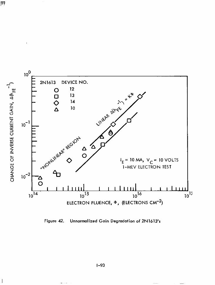
1 2Nl613 DEVICE NO.
0 ‘*
LTS
v I I I I I Ill1 1
,ol4 - I I I ll!l]
lo’5
I I Illll
1016 10li
ELECTRON FLUENCE, 9, (ELECTRONS CM-*)
Figure 42. Unnormal ized Gain Degradation of 2N 1613’s
l-93
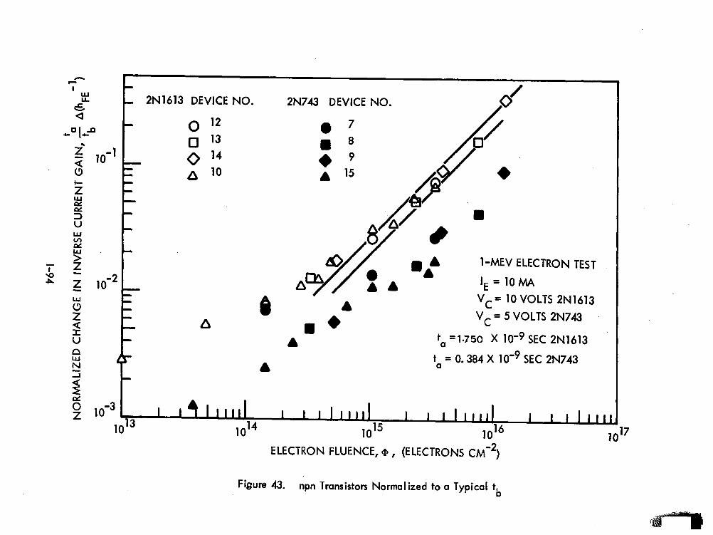
A F
I Lu L
e. - 2N1613 DEVICE NO. 2N743 DEVICE NO.
4 - 4-O p I+ 0 l2
g lo-1 0 l3 0 l4
(3 LI - A lo 2
-
xi
% - C
: w” 5 Y/ A
z lC2 - LA %
I-MEV ELECTRON TEST
= 1oMA ‘/’ ‘E
s 0 A VC= 10 VOLTS 2N1613
5 A vC = 5 VOLTS 2N743
5
0
=1.750 X 10-g SEC 2N1613 - A +a n ;;t; +a
= 0.384 X 1O-9 SEC 2N743
3 A ? 5 z 1o-3 I I I I Ill1 I
lo13
I I I1111 I I I I Ill1 1014
I 1015 lo16
I I llll[
1
ELECTRON FLUENCE, cp , (ELECTRONS CM-‘)
Figure 43. npn Transistors Normalized to a Typical tb
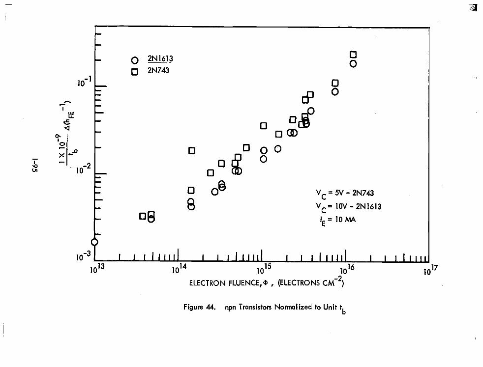
. -
0 . - 0 2N1613 -- [3 2N743 0
10-l 0 I I
8 0
I
*
0 O df e .
0a I .
0
%
0 00 0 0
0 - L -
0 @ 0 vC =!W=2N743
8 vC = 1OV - 2N1613 L
‘E = lOh44
L
r
lo-3 I I I 111’1 I I I I Ill’1 I I I I lllll I 1013 1014
I I IlIl[ 1015 1016 1
ELECTRON FLUENCE,+ , (ELECTRONS CM-2)
Figure 44. npn Transistors Normalized to Unit t b
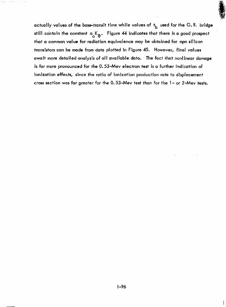
actually values of the base-transit time while values of tb used for the G. R. bridge
still contain the. constant a K 0 8’
Figure 44 indicates that there is a good prospect
that a common value for radiation equivalence may be obtained for npn silicon
transistors can be made from data plotted in Figure 45. However, final values
await more detailed analysis of all available data. The fact that nonlinear damage
is far more pronounced for the 0.53-Mev electron test is a further indication of
ionization effects, since the ratio of ionization production rate to displacement
cross section was far greater for the 0.53-Mev test than for the 1 - or 2-Mev tests.
I-96
0 2-MEV TEST
0 l-MEV TEST
a 0.53-MEV TEST
8
8
U
On 0 ‘E
= 10ma
vC = 10 volts
lo-3 I I I I lllll I I I I11111 I I I lllll I I I Illll
1o13 1014 1015 lJ6
ELECTRON FLUENCE, a, (ELECTRONS CM-2)
17
Figure 45. Energy Dependence of Electron Effects (2N1613)
3.0 NEW TECHNOLOGY
The research work performed on this contract has been reviewed. To the
best of our knowledge there is no new technology to report to date.
f-98
4.0 PROGRAM FOR NEXT REPORTIN’G INTERVAL
The next major reporting interval will be approximately 6 months from this
time. 6y then, all irradiation tests on transistors will have been completed. Data
will be computer analyzed and radiation equivalences established.
The 1 -Mev-proton test has already been performed. The final proton tests,
20 and 100 Mev, are scheduled for approximately January and March, respectively.
In addition a gamma-ray irradiation test, scheduled for December, will be con-
ducted to provide information on the feasibility of using cobalt-60 facilities for
simulating space radiation effects.
A computer code has been developed at Boeing that will aid significantly
in the analysis of data on all transistor-current-gain degradation tests (Reference
14). Data taken from oscillograms of photographs of transistor curve traces, using
an oscillogram reader, will be directly punched on IBM cards and analyzed by an
SRU 1107 computer.
Radiation-equivalence values will be presented, relative to unity damage
for the most damaging test (1 -Mev protons). Comparison will be made between
pnp and npn transistors, including not only the 10 transistor types and 7 radiation
tests of this program, but also selected transistors from past tests (2- and lo-Mev
protons; 0.8-, 2-, 5-, lo-, and 25-Mev electrons; reactor and fast-fission neu-
trons; and 5-Mev alpha particles).
Curves showing the dependence of transistor damage on particle type and
energy will also be presented and will include selected results from previous tests.
A correlation between the displacement effects of cobalt60 gamma rays
and charged particles will be made to determine the range of validity of cobalt4
gamma-ray simulation of space-radiation damage.
Data, in general, will be in a form which will allow a design engineer to
evaluate actual changes in transistor gain caused by space radiation.
l-99
5.0 CONCLUSIONS AND RECOMMENDATIONS
5.1 CONCLUSIONS
Progress of the research program has been encouraging. To date four of the
seven irradiation tests have been completed (including the 1 -Mev proton test). Pre-
liminary analysis of the electron tests has been completed and a number of conclu-
sions are evident. Only small changes of BVCBO were observed for these tests
and only limited evidence of a fluence dependence was observed. A strong depend-
ence of VCE(sat) on electron fluence has been observed. The apparent dependence
of this effect on the relative energy of the electron indicates that these changes
are probably due to atomic displacement rather than ionization. vBE(sat) was also
observed to increase with electron fluence. Values of ICBO of the transistors
tested, in general, increased but showed no dependence of AICBO on electron
fluence for exposures from 4 x 10¹⁵ to 4 x 10¹⁶ electrons/cm2.
All transistor types display an initial degradation of current gain (over a
significant electron exposure) which appears to be attributable to the effect of
ionization on the surface recombination velocity. Techniques have been success-
fully used to separate this “nonlinear” damage from damage attributable to dis-
placements. Preliminary analysis indicates that values of base-transit time can be
used effectively to normalize the degradation of transistor current gain when dis-
placement effects in the transistor base dominate damage.
The data also indicate that the energy dependence of electrons damage
should be readily separable and should provide useful equivalence information.
5.2 RECOMMENDATIONS
It is recommended that more effort be directed to determining how better
data can be obtained for transistor damage normalization. This effort should
include both study of the General Radio Transfer Function and Immittance Bridge
to determine why transistor measurements near unity gain deviate from the expected
behavior, and a correlation of the normalization data obtained by different methods.
l-100
Further, studies should be made involving large numbers of transistors of the same
type in a given test to examine the statistical variation of normalized damage
constants.
Since for electron and gamma irradiation the transistor gain degradation
is nonlinear over a large range of fluence, an effort should be made to more fully
understand this type of damage. A study of the dependence of IB on VBE as a
function of fluence seems promising as a possible method of correlating the initial
nonlinear gain degradation with damage in a given region of the transistor. Also,
further efforts to separate the I inear and saturable damage components may indi-
cate methods by which the initial nonlinear damage may be predicted.
l-l 01
6.0 BIBLIOGRAPHY
1. “Series 500 Semiconductor Tester Technical Manual with Electrical Specifi- cation No. 606886, ” Fairchild Semiconductor, December 1963.
2. “Type 575 Transistor Curve Tracer Instruction Manual, ” Tektronix, Inc., 1959.
3. Goben, C. A., and Srnits, F. M., “Anomalous Base Current Component in
Neutron Irradiated Transistors, “Sandia Corporation Reprint SC-R-64-195, July 1964.
4. Brown, R. R., “Proton and Electron Permanent Damage in Silicon Semiconduc-
tor Devices, ” a paper presented at the joint ANS and ASTM Conference: Radi- ation Effects on Electronics, Nuclear News, ANS-7, 8, p. 43, August 1964.
5. “Operating Instructions Type 1607A Transfer Function and lmmittance Bridge,” Form 1607-0100-E, General Radio Company, West Concord, Massachusetts,
July 1963.
6. Phil1 ips, A. B., Transistor Engineering and Introduction to Integrated Semicon-
ductor Circuits, New York, McGraw-Hill Book Co., 1962.
7. “Type RM567 Readout Oscilloscope Instruction Manual, ” Tektronix, Inc.
8. “Instruction Book Model 74C-58 Capacitance Bridge, ” Boonton Electronics Corporation, Morris Plains, New Jersey.
9. Ashar, K. G., “Transit Time in High-Speed Switching Transistors, ” Solid State Design, 5, 24-26, 1964. --
10. Thomas, D. E., and ‘Mel I, J. L., “Junction Transistor Short-circuit Current Gain and Phase Determination, ” Proceedings IRE, Vol. 46, pp. 1177-l 184, June 1958.
11. Bethe, H. A., “Moliere’s Theory of Multiple Scattering, Phys. Rev., 89, 1256, 1953.
-
12. Personal communication with technical representatives of Fairchild Semiconductor, Motorola, Raytheon, and Texas Instruments, Inc.
13. “Reference Data for Radio Engineers, ” Federal Telephone and Radio Corporation.
14. Rooney, J. A., “Transistor Damage Plotting Program, ” Boeing Document AS 1706, March 1964.
l-102
15. Cahn, J. H., “Irradiation Damage in Germanium and Silicon Due to Electrons and Gamma Rays, ” Jour. of Appl ied Phys., 30, 8, 1310, 1959. -
16. Nelms, A. T., “Energy Loss and Range of Electrons and Positrons, ” N. B. S. Circular 577, July 26, 1956.
17. Brown, R. R., “Identification of Radiation Preferred Electronics, ” Record of the 1965 lnternat.ional Space Electronics +mposium, Institute of Electrical and Electronic Engineers, Inc., New York, N. Y., 1965.
18. Easley, J. W., and Dooley, J. A., “On the Neutron Bombardment Reduction of Transistor Current Gain, ” Jour. of Appl ied Phys., 31, 6, 1960. -
19. Shockley, W., Electrons and Holes in Semiconductors, D. Van Nostrand Publishing Co., New York, N. Y., 1950.
20. Messenger, G. C., and Spratt, J. P., “The Effects of Neutron Irradiation on Germanium and Silicon, ” Proc. IRE, Vol. 46, No. 6, pp. 1038-1044, June 1958
21. Webster, W. M., “On the Variation of Junction Transistor Current Amplifi- cation Factor with Emitter Current, ” Proc. IRE, Vol. 42, No. 6, pp. 914- 920, June 1954.
22. Easley, J. W., “CompQrison of Neutron Damage in Germanium and Silicon Transistors, ” Proceedings Third Semiannual Radiation Effects Symposium, -- -~~ Vol. 4, October 28-30, 1958.
23. Moore, A. R., and Pankove, J. I., “The Effect of Junction Shape and Surface Recombination on Transistor Current Gain, ” Proc. IRE, Vol. 42, 6, pp. 907- 913, 1954.
24. Frank, M., Larin, F., and Niehaus, D. J., “A Generalized Approach to Transistor Damage by Radiation, ” Bendix Corporation, Research Laboratories Division, Southfield, Michigan, Nucleonics, 22, 9, 1964. -
l-103
7.0 GLOSSARY
A
A C
A S
a
B
BvC BO
cT
‘Tc
C Te
C X
Db
D Pb
Ef
fT
f a
hFE
h fe
IB
lB1
IC
‘CBO
Indicator of the transfer function and immittance bridge (real part current)
Area of conduction path
Effective area for surface recombination
The grade constant in atoms/cm2 in the transistor base region
Indicator (imaginary part of current)
Collector-base breakdown voltage
Transition capacitance
Collector transition capacitance
Emitter transition capacitance
Variable capacitance of the base-transit-time circuit
Minority carrier diffusion constant in the base
Hole diffusion constant in the base
Electron energy loss in foil
Gain-bandwidth frequency
Alpha cut-off frequency
d. c. common-emitter current gain
a. c. common-emitter current gain
d. c. base current
Turn-on base current
d. c. collector current
Collector-base reverse current
I-104

‘E
I 0
K
Kd
Kl
Ke
K E
k
L e
M
NB1
NBC
Nl
Ni
N S
R C
R e
RL
R SC
R X
S
d. c. emitter current
Leakage current of ideal diode
Damage constant
Displacement-induced transistor damage constant
Energy dependent ionization damage constant
The excess phase constant
Dielectric constant
Bol tzmann’s constant
Emitter diffusion length
Magnitude of the base drive current (multiplier)
Base impurity concentration at emitter junction
Background impurity concentration
Ionization-induced surface damage recombination sites
Initial density of carrier-recombination centers
Prospective surface-damage sites
Initial density of prospective surface-damage sites
Electronic charge
Collector resistance in base-transit-time circuit
Emitter resistance
Load resistance
Collector series resistance
Variable resistance of base-transit-time circuit
Surface recombination velocity
I-105
T
T r
t
tb
L
te
t X
VBE bat)
vC
‘CB
VcE batI
V 0
V SC
vT
W
X m
a 0
dE dX
P
8
x
‘b
Absolute temperature
Rise time
Thickness of scattering foil
Base-transit time
Collector-delay time
Emitter-delay time
Emitter-delay time plus collector-delay time
Base to emitter saturation voltage (grounded emitter)
Collector voltage
Collector-base voltage
Collector to emitter saturation voltage (grounded emitter)
External oppl ied bias
Scattering limited velocity
Contact potential
Effective base width
Collector depletion layer thickness
The grounded emitter current gain (low frequency)
The rate of energy loss
Density of the scattering foil
Scattering angle
Wavelength
Minority carrier lifetime in the base region
l-106
rbe Initial minority carrier lifetime in the base region I
9 Charged particle fluence
@T
W a
Angular gain-bandwidth frequency
Angular alpha cut-off frequency
ab .
‘J e
Conductivity of base .region
Conductivity of emitter region
I
i