simplification through integration - fpga central
TRANSCRIPT
FPGA Solutions Guide
w w w . n u h o r i z o n s . c o m
FPGAssimplification through integration
sHenzHen Tel: (86) 755 3398 2850 Fax: (86) 755 8219 0980
nanJinG Tel: (86) 21 6441 1811 Fax: (86) 21 6432 5790
taiwan Tel: (886) 2 8797 3718 Fax: (886) 2 8797 3719
vietnam Tel: (84) 90 8131 973
malaysia Tel: (60) 4 660 5888 Fax: (60) 4 660 5883
sinGapore Tel: (65) 6844 1650 Fax: (65) 6841 0494
tHailand Tel: (66) 2 694 1368 / 9 Fax: (66) 2 694 1370
australia / new zealand melbourne Tel: (61) 3 9720 6444 Fax: (61) 3 9720 9504
Sydney Tel: (61) 2 9746 1411 Fax: (61) 2 9746 1511
EMEAaustria vienna Tel: (43) 664 55 664 93 Fax: (49) 89 92 333 45 99
denmark (C-88) HørsHolm Tel: (45) 7010-4888 Fax: (45) 7010-4889
silkeborG Tel: (45) 7010-4888 Fax: (45) 7010-4889
Germany muniCH Tel: (49) 8992 333-450 Fax: (49) 8992 333-4511
HunGary naGykata Tel: (36) 3069 64544
poland warsaw Tel: (48) 602389 537
sweden (C-88) stoCkHolm Tel: (46) 08-558-038-88 Fax: (46) 08-558-038-89 united kinGdom Coventry Tel: (44) 024 7643 7437 Fax: (44) 024 7643 7401
w w w . n u h o r i z o n s . c o m
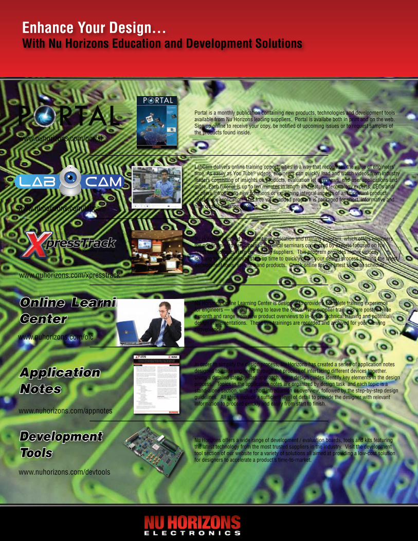
LabCam delivers online training opportunities in a way that recognizes the value of engineers’ time. As easily as You Tube® videos, engineers can quickly load and watch videos from industry leaders consisting of insights on products, evaluation kit overviews, end-user applications and more. Each tutorial is up to ten minutes in length and features technology experts, CEOs and/or peers introducing new solutions or explaining integral aspects of an important product, solution or application. This free value-added program is packaged for short, informative and high quality distance learning.
Nu Horizons is proud to present our education and training program, which offers engineers the opportunity to participate in technical seminars conducted by experts focused on the latest technologies from our leading suppliers. This program provides higher velocity learning to help minimize start-up time to quickly begin your design process utilizing the latest development tools, software and products. Check online for the latest seminar schedule.
In order to simplify the design process, Nu Horizons has created a series of application notes designed to guide engineers through the process of interfacing different devices together. Using a detailed step-by-step approach, these design guides identify key elements in the design process. Topics in the application notes are organized by design task and each topic is a stand-alone section, with a short introduction or overview, followed by the step-by-step design guidelines. All steps include a sufficient level of detail to provide the designer with relevant information to proceed quickly and easily from start to finish.
Nu Horizons offers a wide range of development / evaluation boards, tools and kits featuring the latest technology from the most trusted suppliers in the industry. Visit the development tool section of our website for a variety of solutions all aimed at providing a low-cost solution for designers to accelerate a product’s time-to-market.
www.nuhorizons.com/labcam
www.nuhorizons.com/portal
www.nuhorizons.com/xpresstrack
www.nuhorizons.com/olc
www.nuhorizons.com/appnotes
Application Notes
Online Learning Center
DevelopmentToolswww.nuhorizons.com/devtools
Portal is a monthly publication containing new products, technologies and development tools available from Nu Horizons leading suppliers. Portal is availabe both in print and on the web. Sign up online to receive your copy, be notified of upcoming issues or to request samples of the products found inside.
Nu Horizons Online Learning Center is designed to provide a complete training experience for engineers — without having to leave the office. New supplier trainings are posted twice a month and range from new product overviews to in-depth technical training and potential design implementations. These live trainings are recorded and archived for your viewing convenience.
Enhance Your Design...With Nu Horizons Education and Development Solutions
Articles Pages
Speed Design and Debug with the Nu Horizons/Xilinx Virtex-5 FXT Development Board ................................. Pg 04Embedded Processing Innovations with Virtex-5 FXT Devices ......................................................................... Pg 07Xilinx FPGA selector guides .............................................................................................................................. Pg 12
In this Issue
Associated Products Pages
Datacom
Marvell ......................................................................................................................... Pg 18
Memory Micron .......................................................................................................................... Pg 20
Power and Battery Management Solutions
Emerson ...................................................................................................................... Pg 22
Exar ............................................................................................................................. Pg 24
Linear Technology ........................................................................................................ Pg 27
Micrel ........................................................................................................................... Pg 30
Murata ......................................................................................................................... Pg 32
On Semiconductor ....................................................................................................... Pg 34
ST ................................................................................................................................ Pg 35
Timing
Pletronics ..................................................................................................................... Pg 38
FPGAs Solutions Guide
3
4
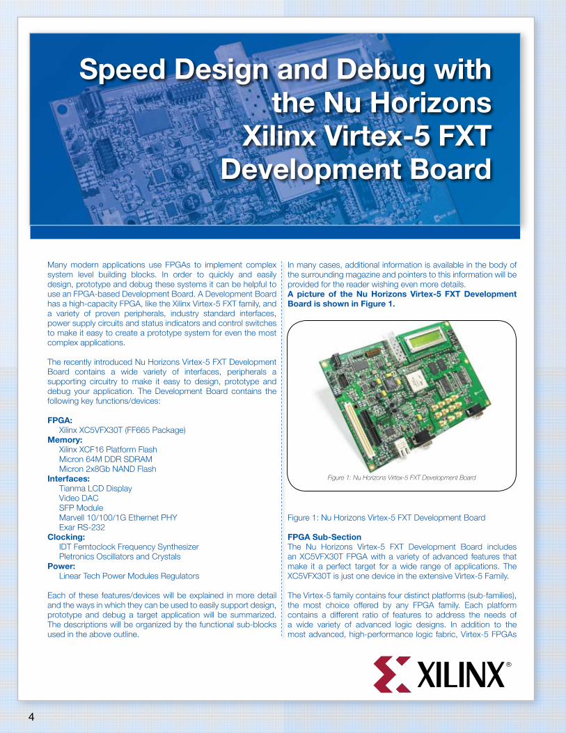
Many modern applications use FPGAs to implement complex system level building blocks. In order to quickly and easily design, prototype and debug these systems it can be helpful to use an FPGA-based Development Board. A Development Board has a high-capacity FPGA, like the Xilinx Virtex-5 FXT family, and a variety of proven peripherals, industry standard interfaces, power supply circuits and status indicators and control switches to make it easy to create a prototype system for even the most complex applications.
The recently introduced Nu Horizons Virtex-5 FXT Development Board contains a wide variety of interfaces, peripherals a supporting circuitry to make it easy to design, prototype and debug your application. The Development Board contains the following key functions/devices:
FPGA: Xilinx XC5VFX30T (FF665 Package)Memory: Xilinx XCF16 Platform Flash Micron 64M DDR SDRAM Micron 2x8Gb NAND FlashInterfaces: Tianma LCD Display Video DAC SFP Module Marvell 10/100/1G Ethernet PHY Exar RS-232Clocking: IDT Femtoclock Frequency Synthesizer Pletronics Oscillators and Crystals Power: Linear Tech Power Modules Regulators
Each of these features/devices will be explained in more detail and the ways in which they can be used to easily support design, prototype and debug a target application will be summarized. The descriptions will be organized by the functional sub-blocks used in the above outline.
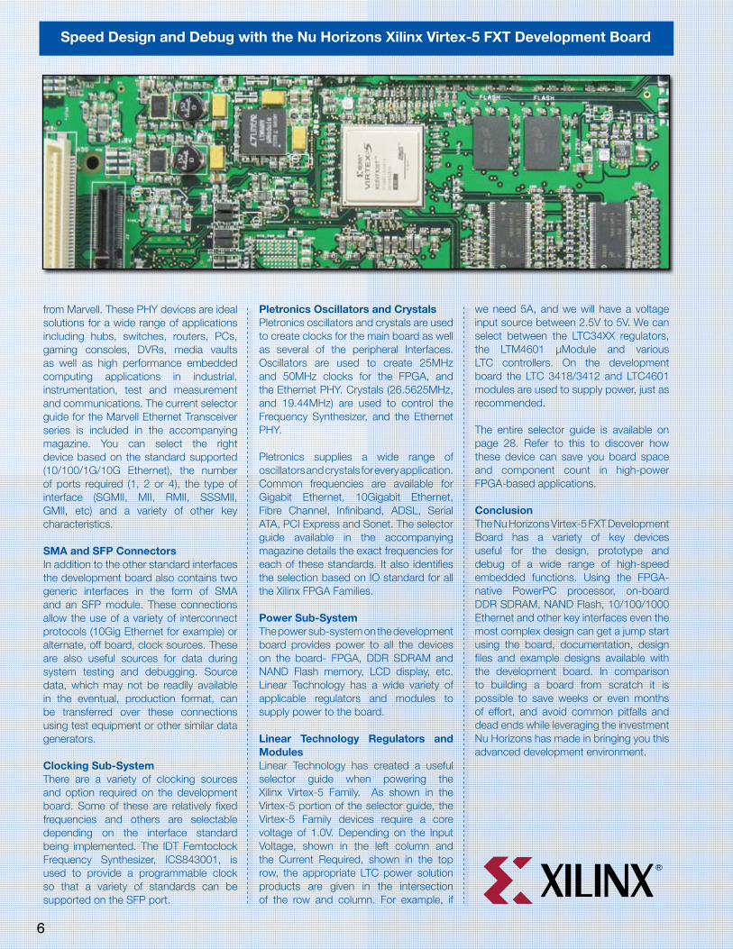
In many cases, additional information is available in the body of the surrounding magazine and pointers to this information will be provided for the reader wishing even more details. A picture of the Nu Horizons Virtex-5 FXT Development Board is shown in Figure 1.
Figure 1: Nu Horizons Virtex-5 FXT Development Board
FPGA Sub-SectionThe Nu Horizons Virtex-5 FXT Development Board includes an XC5VFX30T FPGA with a variety of advanced features that make it a perfect target for a wide range of applications. The XC5VFX30T is just one device in the extensive Virtex-5 Family.
The Virtex-5 family contains four distinct platforms (sub-families), the most choice offered by any FPGA family. Each platform contains a different ratio of features to address the needs of a wide variety of advanced logic designs. In addition to the most advanced, high-performance logic fabric, Virtex-5 FPGAs
Speed Design and Debug with the Nu Horizons
Xilinx Virtex-5 FXT Development Board
Figure 1: Nu Horizons Virtex-5 FXT Development Board
4
contain many hard-IP system level blocks, including powerful 36-Kbit block RAM/FIFOs, second generation 25 x 18 DSP slices, Select IO™ technology with built-in digitally controlled impedance, ChipSync™ source-synchronous interface blocks, system monitor functionality, enhanced clock management tiles with integrated DCM (Digital Clock Managers) and phase-locked-loop (PLL) clock generators, and advanced configuration options.
Additional platform dependant features include power-optimized high-speed serial transceiver blocks for enhanced serial connectivity, PCI Express™ compliant integrated Endpoint blocks, tri-mode Ethernet MACs (Media Access Controllers), and high-performance PowerPC® 440 microprocessor embedded blocks. These features allow advanced logic designers to build the highest levels of performance and functionality into their FPGA-based systems. Built on a 65-nm state-of-the-art copper process technology, Virtex-5 FPGAs are a programmable alternative to custom ASIC technology. Most advanced system designs require the programmable strength of FPGAs. Virtex-5 FPGAs offer the best solution for addressing the needs of high-performance logic designers, high-performance DSP designers, and high-performance embedded systems designers with unprecedented logic, DSP, hard/soft microprocessor, and connectivity capabilities. A summary of the differences between each Virtex-5 platform is given below:
LX: High-performance general logic applicationsLXT: High-performance logic with advanced serial connectivitySXT: High-performance signal processing applications with advanced serial connectivityFXT: High-performance embedded systems with advanced serial connectivity
A selector guide for the entire Virtex-5 Family is included in the accompanying magazine and shows the capabilities of each family member. The XC5VFX30T device used on the development board contains 5,120 logic slices, up to 380Kb of distributed RAM, 64 DSP 48E slices, 136 18Kb and 68 36Kb RAM blocks, 2 CMTs, 1 Power PC Processor Blocks, 1 hard
PCI Express Endpoint , 4 hard Ethernet MACs, 8 GTX Rocket IO Transceivers and 360 general purpose IOs. Each of these features is supported with additional devices on the Development Board so that even the most complex designs can be prototyped.
For more details on using the Xilinx Virtex-5 Family in embedded applications refer to the companion article in the accompanying magazine.
Memory Sub-SystemThe memory devices used on the development board complement the Xilinx Virtex-5 XC5VFX30T FPGA by providing configuration data, program data for embedded processing and storage data for a variety of data processing applications. The following sections provide a quick overview of the memory devices and their typical use during design, prototype and debugging.
Xilinx XCF16 Platform FlashThe Xilinx platform flash device is used to configure the XC5VFX30T. It holds enough configuration data to contain multiple configuration images. This is useful when bringing up the initial design since multiple test cases can be loaded and selected during debugging. Later in the development cycle multiple images can store manufacturing tests, specialized conformance or compliance tests or other manufacturing or field related applications.
Micron 64M DDR SDRAMIncluded on the development board is a 64M DDR SDRAM from Micron Technology, the MT46V16M16. There are two of the devices to create a 32-bit data interface. This memory sub-system is useful for storing program code for the embedded Power PC processor in the Virtex-5 FPGA or to be used as buffer storage for video, networking or communications applications.
Xilinx provides an easy to use Memory Controller Generator (MIG) tool that is integrated into ISE 10.1 and can generate a memory controller for the MT46V16M16 based subsystem. Nu Horizons has a useful application note showing how to interface Micron DDR memories to the
Virtex-5 Family using MIG and it can be found on the Nu Horizons web site by clicking on the Application Notes banner at the top of the page.
Micron 8Gb NAND FlashThere are two MT29H8G08ACAH1 devices on the development board and these can be used for embedded processor code storage, FPGA configuration data or for application oriented data for code conversion, video processing or DSP related algorithms. Micron NAND memory devices can be used in a variety of FPGA-based applications and provide higher speed, larger storage and improved reliability over other non-volatile alternatives. NAND devices are finding new uses in Solid State Storage (SSD), hybrid hard drives, video on demand and in memory back-up systems. For more information on the capabilities, features and uses of Micron NAND devices refer to the brochure included in the accompanying magazine.
Because the NAND Flash is non-volatile it is useful for storing code and algorithm updates so that field changes, in the final product, can be made remotely. Debugging these capabilities first on the development board can be important since bugs in this part of the design will make it difficult to provide bug fixes in the field.
Standard InterfacesThe interfaces available on the development board allow the designer to get high speed data on and off the FPGA in a variety of ways. 10/100/1G Ethernet, SMA and an SFP module are available for high speed data transfer. In addition, RS-232, a Tianma LCD display and a Video DAC are available for slower speed applications.
Marvell 10/100/1G Ethernet PHY The development board includes a Marvell 88E1119R 10/100/1G Ethernet PHY in a QFN72 package. This is connected to the hard Ethernet MAC included in the Virtex-5 device. The combination of these two devices provides a flexible Ethernet interface that can be used for a host of common applications.
The 88E1119R is just one of the Alaska® Family of Gigabit Ethernet transceivers
55
from Marvell. These PHY devices are ideal solutions for a wide range of applications including hubs, switches, routers, PCs, gaming consoles, DVRs, media vaults as well as high performance embedded computing applications in industrial, instrumentation, test and measurement and communications. The current selector guide for the Marvell Ethernet Transceiver series is included in the accompanying magazine. You can select the right device based on the standard supported (10/100/1G/10G Ethernet), the number of ports required (1, 2 or 4), the type of interface (SGMII, MII, RMII, SSSMII, GMII, etc) and a variety of other key characteristics.
SMA and SFP ConnectorsIn addition to the other standard interfaces the development board also contains two generic interfaces in the form of SMA and an SFP module. These connections allow the use of a variety of interconnect protocols (10Gig Ethernet for example) or alternate, off board, clock sources. These are also useful sources for data during system testing and debugging. Source data, which may not be readily available in the eventual, production format, can be transferred over these connections using test equipment or other similar data generators.
Clocking Sub-SystemThere are a variety of clocking sources and option required on the development board. Some of these are relatively fixed frequencies and others are selectable depending on the interface standard being implemented. The IDT Femtoclock Frequency Synthesizer, ICS843001, is used to provide a programmable clock so that a variety of standards can be supported on the SFP port.
Pletronics Oscillators and CrystalsPletronics oscillators and crystals are used to create clocks for the main board as well as several of the peripheral Interfaces. Oscillators are used to create 25MHz and 50MHz clocks for the FPGA, and the Ethernet PHY. Crystals (26.5625MHz, and 19.44MHz) are used to control the Frequency Synthesizer, and the Ethernet PHY.
Pletronics supplies a wide range of oscillators and crystals for every application. Common frequencies are available for Gigabit Ethernet, 10Gigabit Ethernet, Fibre Channel, Infiniband, ADSL, Serial ATA, PCI Express and Sonet. The selector guide available in the accompanying magazine details the exact frequencies for each of these standards. It also identifies the selection based on IO standard for all the Xilinx FPGA Families.
Power Sub-SystemThe power sub-system on the development board provides power to all the devices on the board- FPGA, DDR SDRAM and NAND Flash memory, LCD display, etc. Linear Technology has a wide variety of applicable regulators and modules to supply power to the board.
Linear Technology Regulators and ModulesLinear Technology has created a useful selector guide when powering the Xilinx Virtex-5 Family. As shown in the Virtex-5 portion of the selector guide, the Virtex-5 Family devices require a core voltage of 1.0V. Depending on the Input Voltage, shown in the left column and the Current Required, shown in the top row, the appropriate LTC power solution products are given in the intersection of the row and column. For example, if
we need 5A, and we will have a voltage input source between 2.5V to 5V. We can select between the LTC34XX regulators, the LTM4601 μModule and various LTC controllers. On the development board the LTC 3418/3412 and LTC4601 modules are used to supply power, just as recommended.
The entire selector guide is available on page 28. Refer to this to discover how these device can save you board space and component count in high-power FPGA-based applications.
ConclusionThe Nu Horizons Virtex-5 FXT Development Board has a variety of key devices useful for the design, prototype and debug of a wide range of high-speed embedded functions. Using the FPGA-native PowerPC processor, on-board DDR SDRAM, NAND Flash, 10/100/1000 Ethernet and other key interfaces even the most complex design can get a jump start using the board, documentation, design files and example designs available with the development board. In comparison to building a board from scratch it is possible to save weeks or even months of effort, and avoid common pitfalls and dead ends while leveraging the investment Nu Horizons has made in bringing you this advanced development environment.
Speed Design and Debug with the Nu Horizons Xilinx Virtex-5 FXT Development Board
6
With the advent of the Xilinx® Virtex™-5 FXT FPGA, you have an opportunity to get ahead of the embedded system design curve. The need to quickly develop and validate embedded systems has never been more apparent than in the realm of embedded system design.
Combining software and hardware to demonstrate this at a system level (as quickly as time permits) has become commonplace in the industry. By providing a more tightly coupled, flexible, scalable solution, you have a means to address many hardware and software SOC design challenges.
FPGAs provide a significantly faster path for designers to rapidly develop, prototype, and test their embedded designs. The Virtex-5 FXT device platform, the third generation FPGA to feature a PowerPC processor, has added an embedded block that will help you meet more demanding design requirements while allowing you to finish your designs quickly and easily.
In this article, we’ll provide a detailed description of the embedded processing innovations in the PowerPC 440 processor block and system interconnect. A key area of focus in the Virtex-5 FXT FPGA processor block is simplification through integration.
A corollary to this is ease of development and test. Quickly bringing up a system to allow software developers to get a head start on actual hardware is a major emphasis for the Virtex-5 FXT device’s PowerPC 440 processor.
Simplification Through Integration
Integration is key. We have reduced the amount of FPGA logic needed to build a high-performance processing system while still allowing a wide variety of topologies. You still have the flexibility and advantages of an FPGA-based implementation, but you now also have the added benefit of a hardened, integrated interconnect architecture that (among other things) maximizes access to external memory.As you will see, the result is an embedded block that allows you to develop a wider range of high-performance processing architectures in a shorter period of time. PowerPC processors
generically have three interfaces: instruction read, data read, and data write. In previous Virtex device architectures, which embedded the PowerPC 405, these processor buses would connect to FPGA fabric. The timing closure requirements of this circuitry would vary based on how many and what types of loads the design presented to the buses.
In the Virtex-5 FXT FPGA (where the processor is now the PowerPC 440), these buses are hardened and hooked directly to a new structure, an integrated 5 x 2 crossbar switch – generically referred to as the crossbar. This hardened interconnect provides significantly higher performance (with virtually no consumption of FPGA logic resources and fixed timing) when combined with the rest of the architectural enhancements in the Virtex-5 FXT device’s embedded processor block. This results in an overall system cost reduction and invariably a more tightly integrated processor system.
The processor buses only take up three of the five “crossbar master” ports on the 5 x 2 crossbar (see Figure 1). The crossbar includes two additional master ports, because in many real-
Embedded Processing Innovations with Virtex-5 FXT
Devices
PLB Slave/DMA
Processor Instruction Read
PLB Master
CrossbarSlaves
CrossbarMasters
Memory Controller Interface
Processor Data Read
Processor Data Write
PLB Slave/DMA
• By Craig Abramson , Product Marketing Manager , Xilinx, Inc. , [email protected] • Dan Isaacs , Director of Embedded Processor Marketing , Xilinx, Inc. , [email protected] • Ahmad Ansari , Principal Engineer , Xilinx, Inc., [email protected]
Figure 1 – The crossbar
7
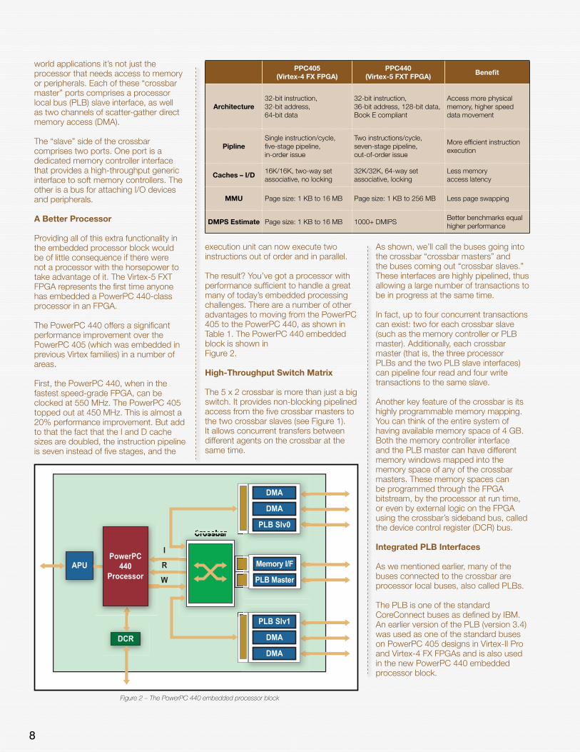
world applications it’s not just the processor that needs access to memory or peripherals. Each of these “crossbar master” ports comprises a processor local bus (PLB) slave interface, as well as two channels of scatter-gather direct memory access (DMA).
The “slave” side of the crossbar comprises two ports. One port is a dedicated memory controller interface that provides a high-throughput generic interface to soft memory controllers. The other is a bus for attaching I/O devices and peripherals.
A Better Processor
Providing all of this extra functionality in the embedded processor block would be of little consequence if there were not a processor with the horsepower to take advantage of it. The Virtex-5 FXT FPGA represents the first time anyone has embedded a PowerPC 440-class processor in an FPGA.
The PowerPC 440 offers a significant performance improvement over the PowerPC 405 (which was embedded in previous Virtex families) in a number of areas.
First, the PowerPC 440, when in the fastest speed-grade FPGA, can be clocked at 550 MHz. The PowerPC 405 topped out at 450 MHz. This is almost a 20% performance improvement. But add to that the fact that the I and D cache sizes are doubled, the instruction pipeline is seven instead of five stages, and the
execution unit can now execute two instructions out of order and in parallel.
The result? You’ve got a processor with performance sufficient to handle a great many of today’s embedded processing challenges. There are a number of other advantages to moving from the PowerPC 405 to the PowerPC 440, as shown in Table 1. The PowerPC 440 embedded block is shown in Figure 2.
High-Throughput Switch Matrix
The 5 x 2 crossbar is more than just a big switch. It provides non-blocking pipelined access from the five crossbar masters to the two crossbar slaves (see Figure 1). It allows concurrent transfers between different agents on the crossbar at the same time.
As shown, we’ll call the buses going into the crossbar “crossbar masters” and the buses coming out “crossbar slaves.” These interfaces are highly pipelined, thus allowing a large number of transactions to be in progress at the same time.
In fact, up to four concurrent transactions can exist: two for each crossbar slave (such as the memory controller or PLB master). Additionally, each crossbar master (that is, the three processor PLBs and the two PLB slave interfaces) can pipeline four read and four write transactions to the same slave.
Another key feature of the crossbar is its highly programmable memory mapping. You can think of the entire system of having available memory space of 4 GB. Both the memory controller interface and the PLB master can have different memory windows mapped into the memory space of any of the crossbar masters. These memory spaces can be programmed through the FPGA bitstream, by the processor at run time, or even by external logic on the FPGA using the crossbar’s sideband bus, called the device control register (DCR) bus.
Integrated PLB Interfaces
As we mentioned earlier, many of the buses connected to the crossbar are processor local buses, also called PLBs.
The PLB is one of the standard CoreConnect buses as defined by IBM. An earlier version of the PLB (version 3.4) was used as one of the standard buses on PowerPC 405 designs in Virtex-II Pro and Virtex-4 FX FPGAs and is also used in the new PowerPC 440 embedded processor block.
I
R
W
PowerPC440
Processor
DCR
APU
PLB Slv0
DMA
DMA
DMA
PLB Slv1
PLB Master
Memory I/F
DMA
PPC405(Virtex-4 FX FPGA)
PPC440(Virtex-5 FXT FPGA)
Benefit
Architecture32-bit instruction,32-bit address,64-bit data
32-bit instruction,36-bit address, 128-bit data,Book E compliant
Access more physicalmemory, higher speeddata movement
PiplineSingle instruction/cycle,five-stage pipeline,in-order issue
Two instructions/cycle,seven-stage pipeline,out-of-order issue
More efficient instructionexecution
Caches – I/D16K/16K, two-way setassociative, no locking
32K/32K, 64-way setassociative, locking
Less memoryaccess latency
MMU Page size: 1 KB to 16 MB Page size: 1 KB to 256 MB Less page swapping
DMPS Estimate Page size: 1 KB to 16 MB 1000+ DMIPSBetter benchmarks equalhigher performance
Figure 2 – The PowerPC 440 embedded processor block
8
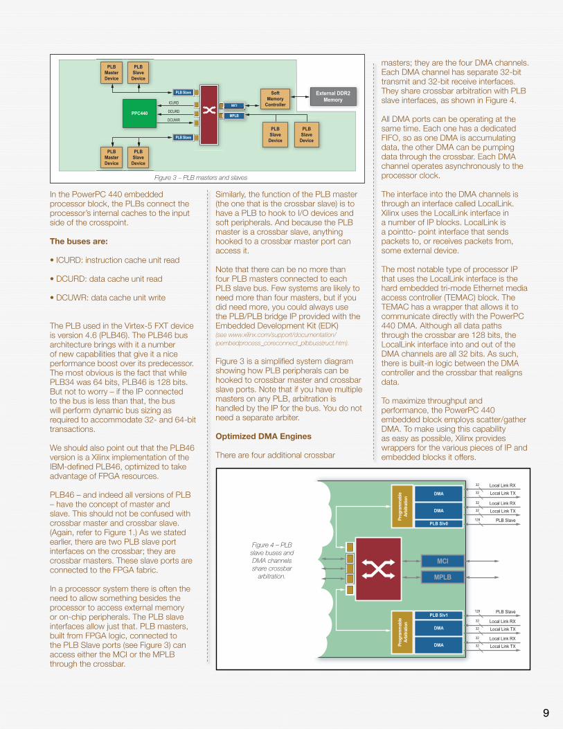
In the PowerPC 440 embedded processor block, the PLBs connect the processor’s internal caches to the input side of the crosspoint.
The buses are:
• ICURD: instruction cache unit read
• DCURD: data cache unit read
• DCUWR: data cache unit write
The PLB used in the Virtex-5 FXT device is version 4.6 (PLB46). The PLB46 bus architecture brings with it a number of new capabilities that give it a nice performance boost over its predecessor. The most obvious is the fact that while PLB34 was 64 bits, PLB46 is 128 bits. But not to worry – if the IP connected to the bus is less than that, the bus will perform dynamic bus sizing as required to accommodate 32- and 64-bit transactions.
We should also point out that the PLB46 version is a Xilinx implementation of the IBM-defined PLB46, optimized to take advantage of FPGA resources.
PLB46 – and indeed all versions of PLB– have the concept of master and slave. This should not be confused with crossbar master and crossbar slave. (Again, refer to Figure 1.) As we stated earlier, there are two PLB slave port interfaces on the crossbar; they are crossbar masters. These slave ports are connected to the FPGA fabric.
In a processor system there is often the need to allow something besides the processor to access external memory or on-chip peripherals. The PLB slave interfaces allow just that. PLB masters, built from FPGA logic, connected to the PLB Slave ports (see Figure 3) can access either the MCI or the MPLB through the crossbar.
Similarly, the function of the PLB master (the one that is the crossbar slave) is to have a PLB to hook to I/O devices and soft peripherals. And because the PLB master is a crossbar slave, anything hooked to a crossbar master port can access it.
Note that there can be no more than four PLB masters connected to each PLB slave bus. Few systems are likely to need more than four masters, but if you did need more, you could always use the PLB/PLB bridge IP provided with the Embedded Development Kit (EDK) (see www.xilinx.com/support/documentation/ipembedprocess_coreconnect_plbbusstruct.htm).
Figure 3 is a simplified system diagram showing how PLB peripherals can be hooked to crossbar master and crossbar slave ports. Note that if you have multiple masters on any PLB, arbitration is handled by the IP for the bus. You do not need a separate arbiter.
Optimized DMA Engines
There are four additional crossbar
masters; they are the four DMA channels. Each DMA channel has separate 32-bit transmit and 32-bit receive interfaces. They share crossbar arbitration with PLB slave interfaces, as shown in Figure 4.
All DMA ports can be operating at the same time. Each one has a dedicated FIFO, so as one DMA is accumulating data, the other DMA can be pumping data through the crossbar. Each DMA channel operates asynchronously to the processor clock.
The interface into the DMA channels is through an interface called LocalLink. Xilinx uses the LocalLink interface in a number of IP blocks. LocalLink is a pointto- point interface that sends packets to, or receives packets from, some external device.
The most notable type of processor IP that uses the LocalLink interface is the hard embedded tri-mode Ethernet media access controller (TEMAC) block. The TEMAC has a wrapper that allows it to communicate directly with the PowerPC 440 DMA. Although all data paths through the crossbar are 128 bits, the LocalLink interface into and out of the DMA channels are all 32 bits. As such, there is built-in logic between the DMA controller and the crossbar that realigns data.
To maximize throughput and performance, the PowerPC 440 embedded block employs scatter/gather DMA. To make using this capability as easy as possible, Xilinx provides wrappers for the various pieces of IP and embedded blocks it offers.
MCI
MPLB
PLBSlave
Device
SoftMemory
Controller
PLBSlave
Device
External DDR2Memory
PLB Slave
PLB Slave
ICURD
DCURD
DCUWR
PLBMasterDevice
PLBSlave
Device
PLBMasterDevice
PLBSlave
Device
PPC440
Figure 3 – PLB masters and slaves
PLB Slv1
DMA
DMA
MPLB
Prog
ram
mab
leAr
bitra
tion
PLB Slv0
DMA
DMA
Prog
ram
mab
leAr
bitra
tion
MCI
PLB Slave128
PLB Slave128
Local Link RX32
Local Link TX32
Local Link RX32
Local Link TX32
Local Link RX32
Local Link TX32
Local Link RX32
Local Link TX32
Figure 4 – PLB slave buses and DMA channels share crossbar
arbitration.
9
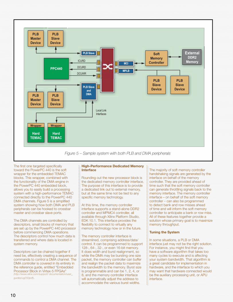
The first one targeted specifically toward the PowerPC 440 is the soft wrapper for the embedded TEMAC blocks. This wrapper, combined with the functionality of the DMA engine in the PowerPC 440 embedded block, allows you to easily build a processing system with a high-performance TEMAC connected directly to the PowerPC 440 DMA channels. Figure 5 is a simplified system showing how both DMA and PLB peripherals can be hooked to crossbar master and crossbar slave ports.
The DMA channels are controlled by descriptors, small blocks of memory that are set up by the PowerPC 440 processor before commencing DMA operations. The descriptors control how much data is transferred and where data is located in system memory.
Descriptors can be chained together if need be, effectively creating a sequence of commands to control a DMA channel. The DMA controller is covered in its entirety in the reference guide, entitled “Embedded Processor Block in Virtex-5 FPGAs” (http://www.xilinx.com/support/ documentation/user_
guides/ug200pdf).
High-Performance Dedicated Memory Interface
Rounding out the new processor block is the dedicated memory controller interface. The purpose of this interface is to provide a dedicated link out to external memory, but at the same time not be tied to any specific memory technology.
At this time, the memory controller interface supports a stand-alone DDR2 controller and MPMC4 controller, all available through Xilinx Platform Studio, EDK 10.1. This interface provides the flexibility to connect to virtually any memory technology now or in the future.
The memory controller interface is streamlined, comprising address/data/ control. It can be programmed to support 128-, 64-, 32-, or even 16-bit memory. It does width and burst realignment, so while the DMA may be bursting one size packet, the memory controller can buffer and realign the packet data to maximize the bandwidth to the memory. Burst size is programmable and can be 1, 2, 4, or 8, and the memory controller interface will automatically adjust the address to accommodate the various burst widths.
The majority of soft memory controllerhandshaking signals are generated by theinterface on behalf of the memory controller. They are provided ahead of time such that the soft memory controller can generate throttling signals back to the memory interface. The memory controller interface – on behalf of the soft memory controller – can also be programmed to detect bank and row misses ahead of time and will inform the soft memory controller to anticipate a bank or row miss. All of these features together provide a solution whose primary goal is to maximize memory throughput.
Tuning the System
In some situations, a PLB or DMA interface just may not be the right solution. For instance, you might find that you have a software algorithm that takes too many cycles to execute and is affecting your system bandwidth. That algorithm is a great candidate for implementation in hardware, and the interface to which you may want that hardware connected would be the auxiliary processing unit, or APU interface.
PLB SlaveandDMA
PLB Slave
MCI
MPLB
ICURD
DCURD
DCUWR
Local LinkInterfaces
PLBMasterDevice
PLBSlave
Device
PLBMasterDevice
PLBSlave
Device
HardTEMAC
Wrapper
HardTEMAC
Wrapper
PLBSlave
Device
SoftMemory
Controller
PLBSlave
Device
ExternalDDR2
Memory
PPC440
Figure 5 – Sample system with both PLB and DMA peripherals
10
Virtex-5 FXT Development PlatformsJump-Start Your Design
Single PPC Dual PPC
ML507 Evaluation Board• XC5VFX70T-1FF1136C• PCie x 1 Plug-In or Stand-Alone
ML510 Development Board• XC5VFX130T-1FF1738C• ATX Form Factor
Figure 6 – Xilinx ML507 evaluation and ML510 development boards
The PowerPC 440 has a second-generation APU interface that is tightly coupled to the execution units of the processor. The interface is controlled by 16 user defined instructions (UDIs). The data path of the APU interface is 128 bits.
Perhaps the most common use of the APU interface is for connecting to a floating-point unit (FPU). The FPU is IEEE754-compatible and supports both single- and double-precision operations for the PowerPC 440.
The FPU is implemented in the FPGA soft logic fabric and utilizes the DSP48E blocks. The soft logic implementation operates up to half the frequency of the hard embedded processor.
Other uses of the APU interface include hardware algorithm acceleration, as well as an alternative high-bandwidth link to block RAM.
Configuring the Embedded Block
By integrating the PowerPC 440 block in the FPGA, the processor block can be configured in multiple ways. Virtually every interface is programmable.
For example, when you build your processing system in the Xilinx Platform Studio development environment and a bitstream is created, all of the specifications of the processing system are in the bitstream. Thus, when the FPGA starts up, your processor is up and running.
Now, let’s say the processing system is up and running and you want to modify the operation of one of the DMA channels. You would do that through the DCR interface. There are DCR registers to control every aspect of DMA operation.
In fact, there is DCR access to virtually every other subsystem of the embedded block: the PLBs and crossbar, memory controller interface, and the APU controller. Refer to Figure 2 for more details.
Putting It All Together
This innovation would be for naught if Xilinx did not provide a comprehensive infrastructure to take advantage of all of the architectural enhancements. We should point out that the Virtex-5 FXT FPGA with the PowerPC 440 block represents our eighth year in embedded processing and our third generation FPGA with a hardened processor.
Throughout that time we’ve been constantly updating EDK, our award-winning Embedded Development Kit. EDK includes Platform Studio, with its comprehensive library of IP for hardware design, and Platform Studio SDK, a software development environment familiar to many embedded software engineers.
With the introduction of the Virtex-5 FXT family of devices, we continue to further strengthen our third-party alliances with support from industry-leading operating system providers, including WindRiver Systems with VxWorks and Green Hills Integrity.
Linux support is provided through LynuxWorks, Monta Vista, and WindRiver Systems. In addition, Xilinx recognizes the importance of open-source Linux, and we’re moving forward on that front.
Xilinx and its partner companies are also developing a wide variety of boards. Xilinx has multiple boards for the Virtex-5 FXT device: the ML507 with the XC5VFX70T and the ML510 with the XC5VFX130T, as shown in Figure 6. The ML507 evaluation platform enables your team to quickly begin developing hardware, software, or both. When multiple processors or a motherboard-type platform are required, the ML510 with the dualprocessor XC5VFX130T is ideal.
Conclusion
A high-performance processing solution with optimized data throughput is high on the wish list of embedded designers everywhere. This is true whether you are running critical algorithms at the heart of the latest wireless base station, switching high bandwidth data through a video switch, performing advanced signal processing for guidance systems using coprocessor acceleration, or handling complex control and system management tasks.
The Virtex-5 FXT embedded processor block, with a multi-ported non-blocking integrated processor interconnect and high-performance integrated DMA, offers a solution that allows you to focus on the key elements of your embedded design.
With a virtually unlimited number of ways to harness these embedded capabilities, the Virtex-5 FXT FPGA embedded processing solution provides a highly integrated platform for high-performance, high-throughput SOC designs.
11
4
XC4V
FX12
XC
4VFX
20
XC4V
FX40
XC
4VFX
60
XC4V
FX10
0 XC
4VFX
140
——
XC
E4VF
X40
XCE4
VFX6
0XC
E4VF
X100
XCE4
VFX1
40
10,9
44
17,0
88
37,2
48
50,5
60
84,3
52
126,
336
5,47
2 8,
544
18,6
24
25,2
80
42,1
76
63,1
68
12,3
12
19,2
24
41,9
04
56,8
80
94,8
96
142,
128
8613
429
139
565
998
7
36
68
144
232
376
552
648
1,22
4 2,
592
4,17
6 6,
768
9,93
6
XC4V
SX25
XC4V
SX35
XC4V
SX55
—XC
E4VS
X35
XCE4
VSX5
5
20,4
8030
,720
49,1
52
10,2
4015
,360
24,5
76
23,0
4034
,560
55,2
96
160
240
384
192
320
2,30
43,
456
5,76
0
128
XC4V
LX15
XC
4VLX
25
XC4V
LX40
XC
4VLX
60
XC4V
LX80
XC
4VLX
100
XC4V
LX16
0 XC
4VLX
200
——
XCE4
VLX4
0XC
E4VL
X60
XCE4
VLX8
0XC
E4VL
X100
XCE4
VLX1
60XC
E4VL
X200
Easy
path
™ C
ost
Redu
ctio
n So
luti
ons
(1)
Part
Num
ber
12,2
88
21,5
04
36,8
64
53,2
48
71,6
80
98,3
04
135,
168
178,
176
CLB
Flip
-Flo
ps
Logi
c Re
sour
ces
6,14
4 10
,752
18
,432
26
,624
35
,840
49
,152
67
,584
89
,088
Sl
ices
(2)
13,8
24
24,1
92
41,4
72
59,9
04
80,6
40
110,
592
152,
064
200,
448
Logi
c Ce
lls
Mem
ory
Reso
urce
s
Cloc
k Re
sour
ces
I/O R
esou
rces
(3)
Embe
dded
Har
d IP
Res
ourc
es
DSP
48 S
lices
Pow
erPC
™ P
roce
ssor
Blo
cks
9616
828
841
656
076
81,
056
1,39
2M
axim
um D
istr
ibut
ed R
AM
(Kbi
ts)
48
72
96
160
200
240
288
336
Bloc
k RA
M/F
IFO
w/E
CC (1
8 Kb
its
each
)
864
1,29
6 1,
728
2,88
0 3,
600
4,32
0 5,
184
6,04
8
4 4
8 12
12
20
4
88
4 8
8 8
12
12
12
12
0 0
4 8
8 8
04
40
4 4
4 8
8 8
8
320
320
448
576
768
896
320
448
640
320
448
640
640
768
960
960
960
160
160
224
228
384
448
160
224
320
160
224
320
320
384
480
480
480
LDT-
25, L
VDS-
25, L
VDSE
XT-2
5, B
LVDS
-25,
ULV
DS-2
5, L
VPEC
L-25
, LVC
MO
S25,
LVC
MO
S18,
LVC
MO
S15,
PCI
33, L
VTTL
, LVC
MO
S33,
PCI
-X, P
CI66
, GTL
, GTL
+, H
STL
I (1.
5V,1
.8V)
, HST
L II
(1.5
V,1.
8V),
HSTL
III (
1.5V
,1.8
V), H
STL
IV (1
.5V,
1.8V
), SS
TL2I
, SST
L2II,
SST
L18
I, SS
TL18
II
3232
4812
816
019
212
819
251
232
4864
6480
9696
96
11
22
22
——
——
——
——
——
—
10/1
00/1
000
Ethe
rnet
MAC
Blo
cks
22
44
44
——
——
——
——
——
—
Rock
etIO
™ S
eria
l Tra
nsce
iver
s 0
812
1620
24—
——
——
——
——
——
-10,
-11,
-12
-10,
-11,
-12
-10,
-11,
-12
-10,
-11,
-12
-10,
-11,
-12
-10,
-11
-10,
-11,
-12
-10,
-11,
-12
-10,
-11,
-12
-10,
-11,
-12
-10,
-11,
-12
-10,
-11,
-12
-10,
-11,
-12
-10,
-11,
-12
-10,
-11,
-12
-10,
-11,
-12
-10,
-11
-10,
-11
-10,
-11
-10,
-11
-10,
-11
-10,
-11
-10
-10,
-11
-10,
-11
-10,
-11
-10,
-11
7.8
4.8
12.3
17.7
23.3
30.7
40.3
51.4
9.1
13.7
22.7
4.8
7.2
13.6
21.0
33.0
47.9
-10,
-11
-10,
-11
-10,
-11
-10,
-11
-10,
-11
-10,
-11
-10
240
240
SF36
317
x 1
7 m
m24
0
320
448
320
FF66
827
x 2
7 m
m44
844
844
832
0
640
FF11
4835
x 3
5 m
m64
064
076
876
876
8
Tota
l Blo
ck R
AM
(Kbi
ts)
Dig
ital
Clo
ck M
anag
ers
(DCM
)
Phas
e-m
atch
ed C
lock
Div
ider
s (P
MCD
)
Max
imum
Sin
gle-
Ende
d I/O
s
Max
imum
Diff
eren
tial
I/O
Pai
rs
I/O S
tand
ards
Spee
d G
rade
s
Conf
igur
atio
n
Com
mer
cial
Indu
stri
al
Conf
igur
atio
n M
emor
y (M
bits
)
Not
es:
1. E
asyP
ath™
sol
utio
ns p
rovi
de a
con
vers
ion-
free
path
for v
olum
e pr
oduc
tion.
2.
Eac
h sl
ice
com
pris
es tw
o 4-
inpu
t log
ic fu
nctio
n ge
nera
tors
(LU
Ts),
two
stor
age
elem
ents
, wid
e-fu
nctio
n m
ultip
lexe
rs, a
nd c
arry
logi
c.
3. D
igita
lly C
ontr
olle
d Im
peda
nce
(DCI
) is
avai
labl
e on
I/O
s of
all
devi
ces.
4. A
vaila
ble
I/O fo
r eac
h de
vice
-pac
kage
com
bina
tion:
num
ber o
f Sel
ectIO
pin
s (n
umbe
r of R
ocke
tIO tr
ansc
eive
rs).
5. A
ll Vi
rtex
-4 L
X an
d Vi
rtex
-4 S
X de
vice
s av
aila
ble
in th
e sa
me
pack
age
are
foot
prin
t-co
mpa
tible
.
6.
All
prod
ucts
ava
ilabl
e Pb
-free
and
RoH
S-Co
mpl
iant
.
Virt
ex-4
LX
FPG
A P
latf
orm
Opt
imiz
ed fo
r H
igh-
perf
orm
ance
Log
ic (1
.2 V
olt)
Virt
ex-4
SX
FPG
A P
latf
orm
Opt
imiz
ed fo
r D
SP (1
.2 V
olt)
Virt
ex-4
FX
FPG
A P
latf
orm
Opt
imiz
ed fo
r Em
bedd
ed P
roce
ssin
g &
Ser
ial C
onne
ctiv
ity
(1.2
Vol
t)
FF15
1340
x 4
0 m
m96
096
096
0
320
(8)
352
(12)
352
(12)
FF67
227
x 2
7 m
m
448
(12)
576
(16)
576
(20)
FF11
5235
x 3
5 m
m
768
(20)
768
(24)
FF15
1740
x 4
0 m
m
Pack
age
(4,5
,6)
Are
aAv
aila
ble
Use
r I/O
s
SFA
Pac
kage
s (S
F): f
lip-c
hip
fine-
pitc
h BG
A (0
.8 m
m b
all s
paci
ng)
FFA
Pac
kage
s (F
F): f
lip-c
hip
fine-
pitc
h BG
A (1
.0 m
m b
all s
paci
ng)
Vir
tex-4
Fam
ily F
PG
As Im
port
ant:
Ver
ify a
ll da
ta in
thi
s do
cum
ent
wit
h th
e de
vice
dat
a sh
eets
fou
nd a
t w
ww
.xili
nx.c
om/v
irte
x4
MPM_199_pmatrices_Q308_Final.indd 4 9/23/08 7:28:07 AM
6
Impo
rtan
t: V
erify
all
data
in t
his
docu
men
t w
ith
the
devi
ce d
ata
shee
ts f
ound
at
ww
w.x
ilinx
.com
XC3S
50A
Exte
nded
Spa
rtan
-3A
Fam
ilyO
ptim
ized
for
Low
est T
otal
Cos
t
XC3S
200A
XC3S
400A
XC3S
700A
XC3S
1400
APa
rt N
umbe
r
50K
200K
400K
700K
1400
K
704
1,79
23,
584
5,88
811
,264
1,40
83,
584
7,16
811
,776
22,5
28CL
B Fl
ip-F
lops
1128
5692
176
Max
imum
Dis
trib
uted
RA
M (K
bits
)
316
2020
32
5428
836
036
057
6
627
3,05
42,
380
5,77
912
,251
24
48
8
144/
108
(6)
248/
195
(6)
311
372
502
64/5
0 (6
)11
2/90
(6)
142
165
227
LVTT
L, LV
CMO
S33,
LVCM
OS2
5, LV
CMO
S18,
LVCM
OS1
5, LV
CMO
S12,
HST
L15
Clas
s I,
HSTL
15 C
lass
III,
HSTL
18 C
lass
I, H
STL1
8 Cl
ass
II,
HSTL
18 C
lass
III,
PCI 3
.3V
32/6
4bit
33M
Hz, P
CI 3
.3V
64bi
t/66M
Hz, P
CI-X
3.3
V, S
STL3
Cla
ss I,
SST
L3 C
lass
II, S
STL2
Cla
ss I,
SST
L2 C
lass
II,
SSTL
18 C
lass
I, S
STL1
8 Cl
ass
II, B
us LV
DS,
LVDS
25 &
33,
LVPE
CL25
& 3
3, M
ini-L
VDS2
5 &
33,
RSD
S25
& 3
3, T
MDS
33, P
PDS2
5 &
33
3/0
16/0
20/0
20/0
32/0
Bloc
k RA
M B
lock
s
Tota
l Blo
ck R
AM
(Kbi
ts)
Use
r Fl
ash
(Kbi
ts) (
3,6)
Dig
ital
Clo
ck M
anag
ers
(DCM
s)
Max
imum
Sin
gle
Ende
d I/O
s
Max
imum
Diff
eren
tial
I/O
Pai
rs
I/O S
tand
ards
Sup
port
ed
Mul
tipl
iers
/DSP
48A
Blo
cks
-4, -
5-4
, -5
-4, -
5-4
, -5
-4, -
5Co
mm
erci
al
-4-4
-4-4
-4In
dust
rial
XC3S
D18
00A
1800
K34
00K
16,6
40
33,2
80
260
84
1,51
2
— 8 519
227
0/84
(4)
-4, -
5
-4 (5
)
XC3S
D34
00A
23,8
72
47,7
44
1,58
44,
032
8,06
413
,248
25,3
44Lo
gic
Cells
37,4
4053
,712
373
126
2,26
8
—
Yes
Yes
Yes
Yes
Yes
Sing
le C
hip
Opt
ion
No
No 8 469
213
0/12
6 (4
)
-4, -
5
-4 (5
)
0.4
Conf
igur
atio
n M
emor
y Bi
ts (K
bits
)1.
21.
92.
74.
88.
211
.7
Slic
es (2
)
Logi
c Re
sour
ces
Mem
ory
Reso
urce
s
Non
-Vol
atile
Ca
pabi
lity
Cloc
k Re
sour
ces
I/O R
esou
rces
Embe
dded
Har
d IP
Res
ourc
es
Spee
d G
rade
s
Conf
igur
atio
n
Yes
Dev
ice
DN
A S
ecur
ity
Yes
Yes
Yes
Yes
Yes
Yes
108
(8)
TQ14
422
x 2
2 m
m
144
FT25
617
x 1
7 m
m19
5 (8
)19
516
116
1
FG32
019
x 1
9 m
m24
825
1
FG40
021
x 2
1 m
m31
1 (8
)31
1
FG48
423
x 2
3 m
m37
2 (8
)37
5
CS48
419
x 1
9 m
m30
9 (5
)30
9 (5
)
FG67
627
x 2
7 m
m50
2 (8
)51
946
9
Syst
em G
ates
(1)
Pack
age
(7)
Size
Max
imum
Use
r I/O
s
TQFP
Pac
kage
s (T
Q):
thin
QFP
(0.5
mm
lead
spa
cing
)
68VQ
100
16 x
16
mm
68
VQFP
Pac
kage
s (V
Q):
very
thin
QFP
(0.5
mm
lead
spa
cing
)
FGA
Pack
ages
(FT)
: wire
-bon
d fin
e-pi
tch
thin
BG
A (1
.0 m
m b
all s
paci
ng)
Chip
Sca
le P
acka
ges
(CS)
: wire
-bon
d ch
ip-s
cale
BG
A (0
.8 m
m b
all s
paci
ng)
FGA
Pack
ages
(FG
): w
ire-b
ond
fine-
pitc
h BG
A (1
.0 m
m b
all s
paci
ng)
1. S
yste
m G
ates
incl
ude
20%
-30%
of C
LBs
used
as
RAM
s 2
. Eac
h sl
ice
com
pris
es tw
o 4-
inpu
t log
ic fu
nctio
n ge
nera
tors
(LU
Ts),
two
stor
age
elem
ents
, wid
e-fu
nctio
n
mul
tiple
xers
, and
car
ry lo
gic
3. U
ser F
lash
is th
e sp
ace
left
in th
e on
-chi
p Fl
ash
afte
r a p
ortio
n is
use
d to
sto
re c
onfig
urat
ion
bits
trea
m
4.
Inte
grat
ed in
the
DSP4
8A s
lices
(Adv
ance
d M
ultip
ly A
ccum
ulat
e el
emen
t)
5. T
he L
low
-pow
er o
ptio
n is
exc
lusi
vely
ava
ilabl
e in
CS(
G)4
84 p
acka
ge a
nd In
dust
rial
te
mpe
ratu
re ra
nge
6.
Spa
rtan
-3AN
onl
y
7. A
ll pr
oduc
ts a
vaila
ble
Pb-fr
ee a
nd R
oHS-
Com
plia
nt, c
heck
dat
ashe
et fo
r Pb
pack
age
avai
labi
lity
8. S
ingl
e ch
ip n
on-v
olat
ile o
ptio
n av
aila
ble
for t
his
pack
age
Not
es:
Sp
art
an
-3A
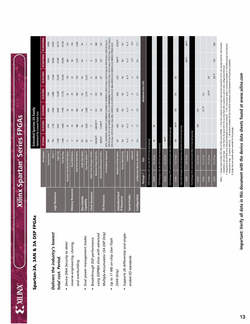
, 3A
N &
3A
DSP F
PG
As
Del
iver
s th
e in
du
stry
’s lo
wes
t to
tal c
ost
. Per
iod
.
Dev
ice
DN
A S
ecu
rity
to
det
er
re
vers
e-en
gin
eeri
ng
, cl
on
ing
,
an
d o
verb
uild
ing
Du
al p
ow
er m
anag
emen
t m
od
es
Bre
akth
rou
gh
DSP
per
form
ance
u
sin
g D
SP48
A s
lices
wit
h a
dva
nce
d
M
ult
iply
-Acc
um
ula
tor
(3A
DSP
On
ly)
Up
to
11
Mb
on
-ch
ip U
ser
Flas
h
(3
AN
On
ly)
Sup
po
rts
26 d
iffe
ren
tial
an
d s
ing
le-
en
ded
I/O
sta
nd
ard
s
MPM_199_pmatrices_Q308_Final.indd 6 9/23/08 7:30:06 AM
1313
14
2
XC5V
LX30
XC5V
LX50
XC5V
LX85
XC5V
LX11
0XC
5VLX
220
XC5V
LX33
0Pa
rt N
umbe
r
4,80
07,
200
12,9
6017
,280
34,5
6051
,840
——
XCE5
VLX8
5XC
E5VL
X110
XCE5
VLX2
20XC
E5VL
X330
Easy
Path
™ C
ost
Redu
ctio
n So
luti
ons
(1)
I/O S
tand
ards
30,7
2046
,080
82,9
4411
0,59
222
1,18
433
1,77
6Lo
gic
Cells
(3)
19,2
0028
,800
51,8
4069
,120
138,
240
207,
360
CLB
Flip
-Flo
ps
320
480
840
1,12
02,
280
3,42
0
3248
9612
819
228
8
1,15
21,
728
3,45
64,
608
6,91
210
,368
412
1212
1212
26
66
66
400
560
560
800
800
1,20
0
200
Not
es:
1. E
asyP
ath™
sol
utio
ns p
rovi
de a
con
vers
ion-
free
path
for v
olum
e pr
oduc
tion.
2.
A s
ingl
e Vi
rtex
-5 C
LB c
ompr
ises
two
slic
es, w
ith e
ach
cont
aini
ng fo
ur 6
-inpu
t LU
Ts a
nd fo
ur F
lip-F
lops
(tw
ice
the
num
ber f
ound
in a
Virt
ex-4
slic
e), f
or a
tota
l of e
ight
6-L
UTs
and
eig
ht F
lip-F
lops
per
CLB
.
3.
Virt
ex-5
logi
c ce
ll ra
tings
refle
ct th
e in
crea
sed
logi
c ca
paci
ty o
ffere
d by
the
new
6-in
put L
UT
arch
itect
ure.
4.
Dig
itally
Con
trol
led
Impe
danc
e (D
CI) i
s av
aila
ble
on I/
Os
of a
ll de
vice
s.
5.
One
sys
tem
mon
itor b
lock
incl
uded
in a
ll de
vice
s.
6.
Ava
ilabl
e I/O
for e
ach
devi
ce-p
acka
ge c
ombi
natio
n: n
umbe
r of S
elec
tIO p
ins
(num
ber o
f Roc
ketIO
tran
scei
vers
).
7.
All
prod
ucts
ava
ilabl
e Pb
-free
and
RoH
S-Co
mpl
iant
.
280
280
400
400
600
220
19 x
19
mm
FF32
422
0
Max
imum
Dis
trib
uted
RA
M (K
bits
)
Bloc
k RA
M/F
IFO
w/E
CC (3
6Kbi
ts e
ach)
Tota
l Blo
ck R
AM
(Kbi
ts)
Dig
ital
Clo
ck M
anag
ers
(DCM
)
Phas
e Lo
cked
Loo
p (P
LL)/P
MCD
Max
imum
Sin
gle-
Ende
d Pi
ns
Max
imum
Diff
eren
tial
I/O
Pai
rs
——
——
——
Pow
erPC
® 4
40 P
roce
ssor
Blo
cks
400
27 x
27
mm
FF67
644
044
044
0
35 x
35
mm
FF11
5356
056
080
0
42.5
x 4
2.5
mm
FF17
6080
080
012
00
27 x
27m
mFF
665
35 x
35m
mFF
1136
42.5
x 4
2.5m
mFF
1738
——
——
——
PCI E
xpre
ss E
ndpo
int
Bloc
ks
——
——
——
10/1
00/1
000
Ethe
rnet
MAC
Blo
cks
——
——
——
XC5V
LX30
T
4,80
0
—
30,7
20
19,2
00
320
36
1,29
6
4 2 360
180
—
360
(8)
1 4 8Ro
cket
IO™
GTP
Low
-Pow
er T
rans
ceiv
ers
XC5V
LX50
T
7,20
0
—
46,0
80
28,8
00
480
60
2,16
0
12 6 480
240
—
360
(8)
480
(12)
1 4 12
XC5V
LX85
T
12,9
60
XCEV
LXT8
5T
82,9
44
51,8
40
840
108
3,88
8
12 6 480
240
—
480
(12)
1 4 12
XC5V
LX11
0T
17,2
80
XCE5
VLX1
10T
110,
592
69,1
20
1,12
0
148
5,32
8
12 6 680
340
—
640
(16)
680
(16)
1 4 16
XC5V
LX22
0T
34,5
60
XCE5
VLX2
20T
221,
184
138,
240
2,28
0
212
7,63
2
12 6 680
340
—
680
(16)
1 4 16
XC5V
LX33
0T
51,8
40
XCE5
VLX3
30T
331,
776
207,
360
3,42
0
324
11,6
64
12 6 960
480
—
960
(24)
1 4 24
-1, -
2-1
, -2
-1, -
2-1
, -2
XC5V
LX15
5
24,3
20
XCE5
VLX1
55
155,
648
97,2
80
1,64
0
192
6,91
2
12 6 800
400
— 800
800
— — — -1, -
2-1
, -2
-1-1
, -2
XC5V
LX20
T
3,12
0
—
19,9
68
12,4
80
210
26 936 2 1 172
86 — 1 2 4
-1, -
2In
dust
rial
-1, -
2-1
, -2
-1, -
2
XC5V
LX15
5T
24,3
20
XCE5
VLX1
55T
155,
648
97,2
80
1,64
0
212
7,63
2
12 6 680
340
—
19 x
19m
mFF
323
172
(4)
172
(4)
640
(16)
680
(16)
1 4 16
——
——
——
—Ro
cket
IO™
GTX
Hig
h-Sp
eed
Tran
scei
vers
——
——
——
—— -1, -
2-1
, -2
-1
-1, -
2, -3
-1, -
2, -3
-1, -
2, -3
-1, -
2, -3
-1, -
2, -3
-1, -
2-1
, -2
-1, -
2, -3
-1, -
2Co
mm
erci
al-1
, -2,
-3-1
, -2,
-3-1
, -2,
-3-1
, -2,
-3-1
, -2
-1, -
2
8.4
12.6
21.9
29.1
42.7
53.2
79.8
9.4
6.3
Conf
igur
atio
n M
emor
y (M
bits
)14
.123
.431
.243
.155
.282
.7
Slic
es (2
)
Logi
c Re
sour
ces
Mem
ory
Reso
urce
s
Cloc
k Re
sour
ces
I/O R
esou
rces
(4)
Embe
dded
(5)
Har
d IP
Reso
urce
s
Spee
d G
rade
s
Conf
igur
atio
n
HT, L
VDS,
LVD
SEXT
, RSD
S, B
LVDS
, ULV
DS, L
VPEC
L, L
VCM
OS3
3, L
VCM
OS2
5, L
VCM
OS1
8, L
VCM
OS1
5, L
VTTL
, PCI
33, P
CI66
, PCI
-X, G
TL, G
TL+
, HS
TL I
(1.2
V,1.
5V,1
.8V)
, HST
L II
(1.5
V,1.
8V),
HSTL
III (
1.5V
,1.8
V), H
STL
IV (1
.5V,
1.8V
), SS
TL2
I, SS
TL2
II, S
STL1
8 I,
SSTL
18 II
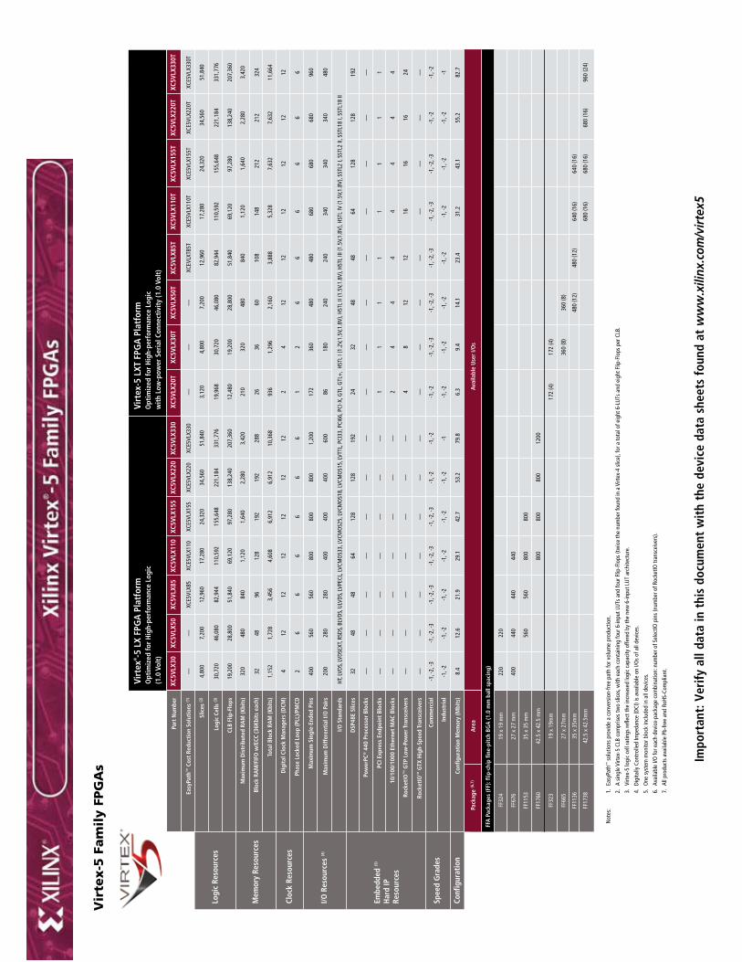
Virt
ex®-5
LX
FPG
A P
latf
orm
Opt
imiz
ed fo
r H
igh-
perf
orm
ance
Log
ic
(1.0
Vol
t)
Virt
ex-5
LXT
FPG
A P
latf
orm
Opt
imiz
ed fo
r H
igh-
perf
orm
ance
Log
ic
wit
h Lo
w-p
ower
Ser
ial C
onne
ctiv
ity
(1.0
Vol
t)
Pack
age
(6,7
)A
rea
Avai
labl
e U
ser
I/Os
3248
4864
128
192
DSP
48E
Slic
es32
4848
6412
819
212
824
128
FFA
Pac
kage
s (F
F): f
lip-c
hip
fine-
pitc
h BG
A (1
.0 m
m b
all s
paci
ng)
Impo
rtan
t: V
erify
all
data
in t
his
docu
men
t w
ith
the
devi
ce d
ata
shee
ts f
ound
at
ww
w.x
ilinx
.com
/vir
tex5
Vir
tex-5
Fam
ily F
PG
As
MPM_199_pmatrices_Q308_Final.indd 2 9/23/08 7:28:03 AM
15
3
Part
Num
ber
Easy
Path
™ C
ost
Redu
ctio
n So
luti
ons
(1)
I/O S
tand
ards
Logi
c Ce
lls (3
)
CLB
Flip
-Flo
ps
Not
es:
1. E
asyP
ath™
sol
utio
ns p
rovi
de a
con
vers
ion-
free
path
for v
olum
e pr
oduc
tion.
2.
A s
ingl
e Vi
rtex
-5 C
LB c
ompr
ises
two
slic
es, w
ith e
ach
cont
aini
ng fo
ur 6
-inpu
t LU
Ts a
nd fo
ur F
lip-F
lops
(tw
ice
the
num
ber f
ound
in a
Virt
ex-4
slic
e), f
or a
tota
l of e
ight
6-L
UTs
and
eig
ht F
lip-F
lops
per
CLB
.
3.
Virt
ex-5
logi
c ce
ll ra
tings
refle
ct th
e in
crea
sed
logi
c ca
paci
ty o
ffere
d by
the
new
6-in
put L
UT
arch
itect
ure.
4.
Dig
itally
Con
trol
led
Impe
danc
e (D
CI) i
s av
aila
ble
on I/
Os
of a
ll de
vice
s.
5.
One
sys
tem
mon
itor b
lock
incl
uded
in a
ll de
vice
s.
6.
Ava
ilabl
e I/O
for e
ach
devi
ce-p
acka
ge c
ombi
natio
n: n
umbe
r of S
elec
tIO p
ins
(num
ber o
f Roc
ketIO
tran
scei
vers
).
7.
All
prod
ucts
ava
ilabl
e Pb
-free
and
RoH
S-Co
mpl
iant
.
Max
imum
Dis
trib
uted
RA
M (K
bits
)
Bloc
k RA
M/F
IFO
w/E
CC (3
6Kbi
ts e
ach)
Tota
l Blo
ck R
AM
(Kbi
ts)
Dig
ital
Clo
ck M
anag
ers
(DCM
)
Phas
e Lo
cked
Loo
p (P
LL)/P
MCD
Max
imum
Sin
gle-
Ende
d Pi
ns
Max
imum
Diff
eren
tial
I/O
Pai
rs
Pow
erPC
® 4
40 P
roce
ssor
Blo
cks
27 x
27m
mFF
665
35 x
35m
mFF
1136
42.5
x 4
2.5m
mFF
1738
PCI E
xpre
ss E
ndpo
int
Bloc
ks
10/1
00/1
000
Ethe
rnet
MAC
Blo
cks
Rock
etIO
™ G
TP L
ow-P
ower
Tra
nsce
iver
s
XC5V
SX35
T
5,44
0
—
34,8
16
21,7
60
520
84
3,02
4
4 2 360
180
—
360
(8)
1 4 8
XC5V
SX50
T
8,16
0
XCE5
VSX5
0T
52,2
24
32,6
40
780
132
4,75
2
12 6 480
240
—
360
(8)
480
(12)
1 4 12
XC5V
SX95
T
14,7
20
XCE5
VSX9
5T
94,2
08
58,8
80
1,52
0
244
8,78
4
12 6 640
320
—
640
(16)
1 4 16
Indu
stri
al-1
, -2
-1, -
2-1
, -2
Com
mer
cial
-1, -
2, -3
-1, -
2, -3
-1, -
2
Conf
igur
atio
n M
emor
y (M
bits
)13
.420
.035
.8
XC5V
SX24
0T
37,4
40
XCE5
VSX2
40T
239,
616
149,
760
4,20
0
516
18,5
76
12 6 960
480
—
960
(24)
1 4 24 -1
-1, -
2
79.7
Slic
es (2
)
Logi
c Re
sour
ces
Mem
ory
Reso
urce
s
Cloc
k Re
sour
ces
I/O R
esou
rces
(4)
Embe
dded
(5)
Har
d IP
Reso
urce
s
Spee
d G
rade
s
Conf
igur
atio
n
HT, L
VDS,
LVD
SEXT
, RSD
S, B
LVDS
, ULV
DS, L
VPEC
L, L
VCM
OS3
3, L
VCM
OS2
5, L
VCM
OS1
8, L
VCM
OS1
5, L
VTTL
, PCI
33, P
CI66
, PCI
-X, G
TL, G
TL+
, HS
TL I
(1.2
V,1.
5V,1
.8V)
, HST
L II
(1.5
V,1.
8V),
HSTL
III (
1.5V
,1.8
V),
HSTL
IV (1
.5V,
1.8V
), SS
TL2
I, SS
TL2
II, S
STL1
8 I,
SSTL
18 II
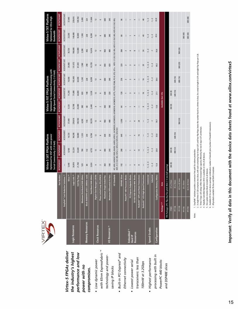
Virt
ex-5
SXT
FPG
A P
latf
orm
Opt
imiz
ed fo
r D
SP w
ith
Low
-pow
er
Seri
al C
onne
ctiv
ity
(1.0
Vol
t)
XC5V
FX30
T
5,12
0
—
32,7
68
20,4
80
380
68
2,44
8
4 2 360
180 1
360
(8)
1 4 — -1, -
2
-1, -
2, -3
13.6
XC5V
FX70
T
11,2
00
XCE5
VFXT
70T
71,6
80
44,8
00
820
148
5,32
8
12 6 640
320 1
360
(8)
640
(16)
3 4 — -1, -
2
-1, -
2, -3
27.1
Virt
ex-5
FXT
FPG
A P
latf
orm
Opt
imiz
ed fo
r Em
bedd
ed P
roce
ssin
g w
ith
Hig
h-Sp
eed
Seri
al C
onne
ctiv
ity
(1.0
Vol
t)
DSP
48E
Slic
es19
228
864
01,
056
6412
8
XC5V
FX10
0T
16,0
00
XCE5
VFXT
100T
102,
400
64,0
00
1,24
0
228
8,20
8
12 6 680
340 2
640
(16)
680
(16)
3 4 — -1, -
2
-1, -
2, -3
39.4
256
XC5V
FX13
0T
20,4
80
XCE5
VFXT
130T
131,
072
81,9
20
1,58
0
298
10,7
28
12 6 840
420 2
840
(20)
3 6 — -1, -
2-1
, -2
-1, -
2
-1, -
2, -3
49.3
320
XC5V
FX20
0T
30,7
20
XCE5
VFXT
200T
196,
608
122,
880
2,28
0
456
16,4
16
12 6 960
480 2
960
(24)
4 8 —
Rock
etIO
™ G
TX H
igh-
Spee
d Tr
ansc
eive
rs—
——
—8
1616
2024 -1
-1, -
2-1
, -2
-1, -
2
70.9
384
Virt
ex-5
TXT
Pla
tfor
mO
ptim
ized
for
Ult
ra-H
igh
Band
wid
th
XC5V
TX15
0T
23,2
00
XCE5
VTXT
150T
148,
480
92,8
00
1,50
0
228
8,20
8
12 6 680
340
XC5V
TX24
0T
37,4
40
XCE5
VTXT
240T
239,
616
149,
760
2,40
0
324
11,6
64
12 6 680
340
—
360
(40)
680
(40)
1 4 — 40 43.4
80
—
680
(48)
1 4 — 48 65.8
96
35 x
35m
mFF
1156
42.5
x 4
2.5m
mFF
1759
Pack
age
(6,7
)A
rea
Avai
labl
e U
ser
I/Os
FFA
Pac
kage
s (F
F): f
lip-c
hip
fine-
pitc
h BG
A (1
.0 m
m b
all s
paci
ng)
Impo
rtan
t: V
erify
all
data
in t
his
docu
men
t w
ith
the
devi
ce d
ata
shee
ts f
ound
at
ww
w.x
ilinx
.com
/vir
tex5
Vir
tex-5
Fam
ily F
PG
As
Vir
tex-
5 FP
GA
s d
eliv
er
the
ind
ust
ry’s
hig
hes
t
per
form
ance
an
d l
ow
p
ow
er w
ith
no
co
mp
rom
ises
.
Low
dyn
amic
po
wer
w
ith
65n
m E
xpre
ssFa
bri
c ™
te
chn
olo
gy
and
po
wer
-
sa
vin
g I
P b
lock
s
Bu
ilt-i
n P
CI
Exp
ress
® a
nd
Et
her
net
co
nn
ecti
vity
Low
est
po
wer
ser
ial
tr
ansc
eive
rs:
less
th
an
10
0mW
at
3.2G
bp
s
Hig
hes
t p
erfo
rman
ce
p
roce
ssin
g w
ith
bu
ilt i
n
Po
wer
PC 4
40 b
lock
s
an
d D
SP48
E sl
ices
15

www.xilinx.com/virtex5
©2008 Xilinx, Inc. All rights reserved. XILINX, the Xilinx logo, and other designated brands included herein are trademarks of Xilinx, Inc.The PowerPC name and logo are registered trademarks of IBM Corp. and used under license.All other trademarks are the property of their respective owners
The Virtex®-5 Family:The Ultimate System Integration Platform
®
—
www.xilinx.com/ise ®
Design Simply
Design Completely
Design Today
MPM_249 V5 TXT ad_Nexus.indd 1 12/4/08 4:06:23 PM
Datacom
Marvell ......................................................................................................................... Pg 18
Memory Micron .......................................................................................................................... Pg 20
Power and Battery Management Solutions
Emerson ...................................................................................................................... Pg 22
Exar ............................................................................................................................. Pg 24
Linear Technology ........................................................................................................ Pg 27
Micrel ........................................................................................................................... Pg 30
Murata ......................................................................................................................... Pg 32
On Semiconductor ....................................................................................................... Pg 34
ST ................................................................................................................................ Pg 35
Timing
Pletronics ..................................................................................................................... Pg 38
17
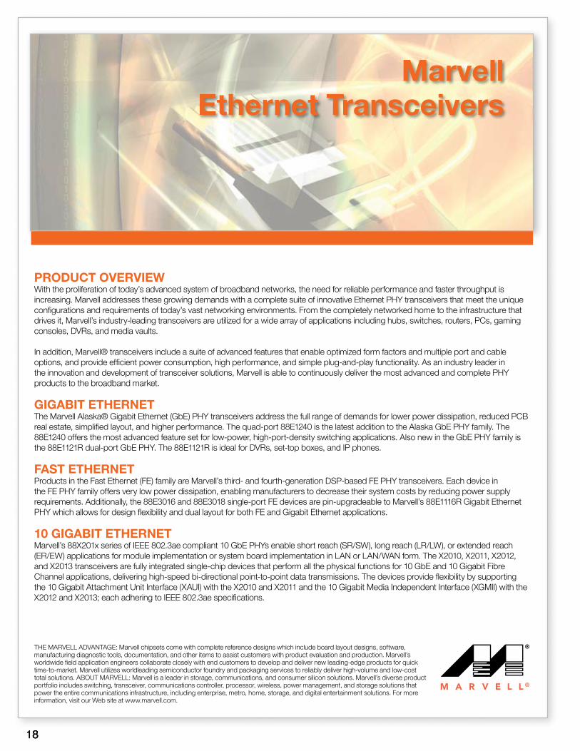
Marvell Ethernet Transceivers
PRODUCT OVERVIEWWith the proliferation of today’s advanced system of broadband networks, the need for reliable performance and faster throughput is increasing. Marvell addresses these growing demands with a complete suite of innovative Ethernet PHY transceivers that meet the unique configurations and requirements of today’s vast networking environments. From the completely networked home to the infrastructure that drives it, Marvell’s industry-leading transceivers are utilized for a wide array of applications including hubs, switches, routers, PCs, gaming consoles, DVRs, and media vaults.
In addition, Marvell® transceivers include a suite of advanced features that enable optimized form factors and multiple port and cable options, and provide efficient power consumption, high performance, and simple plug-and-play functionality. As an industry leader in the innovation and development of transceiver solutions, Marvell is able to continuously deliver the most advanced and complete PHY products to the broadband market.
GIGABIT ETHERNETThe Marvell Alaska® Gigabit Ethernet (GbE) PHY transceivers address the full range of demands for lower power dissipation, reduced PCB real estate, simplified layout, and higher performance. The quad-port 88E1240 is the latest addition to the Alaska GbE PHY family. The 88E1240 offers the most advanced feature set for low-power, high-port-density switching applications. Also new in the GbE PHY family is the 88E1121R dual-port GbE PHY. The 88E1121R is ideal for DVRs, set-top boxes, and IP phones.
FAST ETHERNETProducts in the Fast Ethernet (FE) family are Marvell’s third- and fourth-generation DSP-based FE PHY transceivers. Each device in the FE PHY family offers very low power dissipation, enabling manufacturers to decrease their system costs by reducing power supply requirements. Additionally, the 88E3016 and 88E3018 single-port FE devices are pin-upgradeable to Marvell’s 88E1116R Gigabit Ethernet PHY which allows for design flexibility and dual layout for both FE and Gigabit Ethernet applications.
10 GIGABIT ETHERNETMarvell’s 88X201x series of IEEE 802.3ae compliant 10 GbE PHYs enable short reach (SR/SW), long reach (LR/LW), or extended reach (ER/EW) applications for module implementation or system board implementation in LAN or LAN/WAN form. The X2010, X2011, X2012, and X2013 transceivers are fully integrated single-chip devices that perform all the physical functions for 10 GbE and 10 Gigabit Fibre Channel applications, delivering high-speed bi-directional point-to-point data transmissions. The devices provide flexibility by supporting the 10 Gigabit Attachment Unit Interface (XAUI) with the X2010 and X2011 and the 10 Gigabit Media Independent Interface (XGMII) with the X2012 and X2013; each adhering to IEEE 802.3ae specifications.
THE MARVELL ADVANTAGE: Marvell chipsets come with complete reference designs which include board layout designs, software, manufacturing diagnostic tools, documentation, and other items to assist customers with product evaluation and production. Marvell’s worldwide field application engineers collaborate closely with end customers to develop and deliver new leading-edge products for quick time-to-market. Marvell utilizes worldleading semiconductor foundry and packaging services to reliably deliver high-volume and low-cost total solutions. ABOUT MARVELL: Marvell is a leader in storage, communications, and consumer silicon solutions. Marvell’s diverse product portfolio includes switching, transceiver, communications controller, processor, wireless, power management, and storage solutions that power the entire communications infrastructure, including enterprise, metro, home, storage, and digital entertainment solutions. For more information, visit our Web site at www.marvell.com.
1818
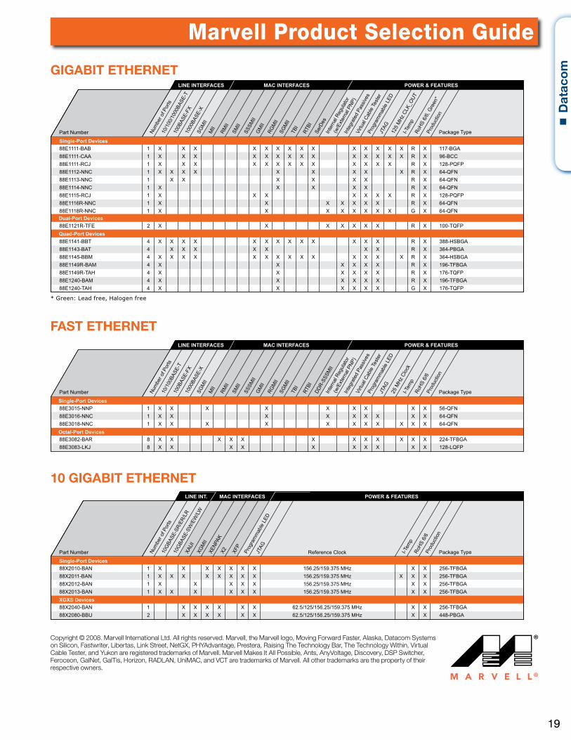
SERUTAEF & REWOPSECAFRETNI CAMSECAFRETNI ENIL
Single-Port Devices
Dual-Port Devices
Quad-Port Devices
Num
ber o
f Por
ts
Part Number 10/1
00/1
000B
ASE-
T
100B
ASE-
FX10
00BA
SE-X
SGM
IIM
II
RMII
SMII
SSSM
IIG
MII
RGM
IISG
MII
TBI
RTBI
SerD
esIn
tern
al R
egul
ator
(w
/Ext
erna
l PNP
)In
tegr
ated
Pas
sives
Virtu
al C
able
Test
er
Prog
ram
mab
le L
ED
JTAG
125
MHz
CLK
_OUT
I-Tem
pRo
HS 6
/6, G
reen
*Pr
oduc
tion
Package Type
88E1111 AGB-711 X R X X X X X X X X X X X X X X 1 BAB-88E1111 CCB-69 X R X X X X X X X X X X X X X X 1 AAC-88E1111 PFQP-821 X R X X X X X X X X X X X X X 1 JCR-
NFQ-46 X R X X X X X X X X X 1 CNN-2111E88NFQ-46 X R X X X X X X 1 CNN-3111E88NFQ-46 X R X X X X X 1 CNN-4111E88
PFQP-821 X R X X X X X X X 1 JCR-5111E8888E1116R-NNC 1 X X X X X X X R X 64-QFN88E1118R-NNC 1 X X X X X X X X G X 64-QFN
88E1121R-TFE 2 X X X X X X X R X 100-TQFP
AGBSH-883 X R X X X X X X X X X X X X X 4 TBB-1411E88AGBP-463 X R X X X X X X X 4 TAB-3411E88
AGBSH-463 X R X X X X X X X X X X X X X X 4 MBB-5411E8888E1149R-BAM 4 X X X X X X R X 196-TFBGA88E1149R-TAH 4 X X X X X X R X 176-TQFP
AGBFT-691 X R X X X X X X 4 MAB-0421E88PFQT-671 X G X X X X X X 4 HAT-0421E88
* Green: Lead free, Halogen free
SERUTAEF & REWOPSECAFRETNI CAMSECAFRETNI ENIL
Single-Port Devices
Octal-Port Devices
Num
ber o
f Por
ts10
/100
BASE
-T10
0BAS
E-FX
1000
BASE
-XSG
MII
MII
RMII
SMII
SSSM
IIG
MII
RGM
IISG
MII
TBI
RTBI
DDR-
SSSM
IIIn
tern
al R
egul
ator
(w
/Ext
erna
l PNP
)In
tegr
ated
Pas
sives
Virtu
al C
able
Test
er
Prog
ram
mab
le L
ED
JTAG
25 M
Hz C
lock
I-Tem
pRo
HS 6
/6Pr
oduc
tion
NFQ-65 X X X X X X X X X 1 PNN-5103E88NFQ-46 X X X X X X X X X 1 CNN-6103E88NFQ-46 X X X X X X X X X X X 1 CNN-8103E88
AGBFT-422 X X X X X X X X X X X X 8 RAB-2803E88PFQL-821 X X X X X X X X X X 8 JKL-3803E88
Part Number Package Type
Marvell Product Selection Guide
Copyright © 2008. Marvell International Ltd. All rights reserved. Marvell, the Marvell logo, Moving Forward Faster, Alaska, Datacom Systems on Silicon, Fastwriter, Libertas, Link Street, NetGX, PHYAdvantage, Prestera, Raising The Technology Bar, The Technology Within, Virtual Cable Tester, and Yukon are registered trademarks of Marvell. Marvell Makes It All Possible, Ants, AnyVoltage, Discovery, DSP Switcher, Feroceon, GalNet, GalTis, Horizon, RADLAN, UniMAC, and VCT are trademarks of Marvell. All other trademarks are the property of their respective owners.
SERUTAEF & REWOPSECAFRETNI CAM.TNI ENIL
Single-Port Devices
XGXS Devices
Num
ber o
f Por
ts10
GBA
SE-S
R/ER
/LR
10G
BASE
-SW
/EW
/LW
XAUI
XGM
IIXE
NPAK
X2 XFP
Prog
ram
mab
le L
ED
JTAG
RoHS
6/6
Prod
uctio
n
AGBFT-652 X X zHM 573.951/52.651 X X X X X X X 1 NAB-0102X88AGBFT-652 X X X zHM 573.951/52.651 X X X X X X X X 1 NAB-1102X88AGBFT-652 X X zHM 573.951/52.651 X X X X X 1 NAB-2102X88AGBFT-652 X X zHM 573.951/52.651 X X X X X X 1 NAB-3102X88
AGBFT-652 X X zHM 573.951/52.651/521/5.26 X X X X X X 1 NAB-0402X88AGBP-844 X X zHM 573.951/52.651/521/5.26 X X X X X X 2 UBB-0802X88
I-Tem
p
Part Number Reference Clock Package Type
10 GIGABIT ETHERNET
FAST ETHERNET
GIGABIT ETHERNET
19
D
atac
om
4 Advantages of Designing with High-Speed NAND
1. Breakthrough Performance
The high-speed interface delivers the fastest read
and write throughputs ever for a NAND Flash device.
2. Simplified DesignCompatibility with ONFI 1.0/2.0 asynchronous/
synchronous interface enables both backward-
compatible and forward-looking designs.
3. Cost SavingsReduced system complexity provides better
performance at a lower cost.
4. An Evolution of NAND Traditional NAND benefits like nonvolatility,
reliability, and density still apply, enabling
leading-edge applications to store more data.
Are your high-performance NAND Flash designs bogged down by bottlenecks and bulky designs? If you’ve been looking for a pathway to greater read/write performance than traditional NAND Flash can deliver, look at what Micron’s High-Speed NAND has to offer. Our High-Speed NAND parts deliver the fastest read and write throughputs ever for a NAND Flash device—five times the performance of existing SLC NAND devices. If we were talking cars, we’d be talking Formula 1 fast—something built to get you to market quickly with a top-notch, high-performance design.
Features
Organization• Page size – x8: 4,320 bytes (4,096 + 224 bytes)• Block size: 128 pages (512K + 28K bytes)• Plane size: 4 planes x 512 blocks per plane• Device size – 8Gb: 2,048 blocks; 16Gb: 4,096 blocks; 32Gb: 8,192 blocks
I/O and Array Performance• Up to 200 MB/s read speed• Up to 100 MB/s write speed • 100,000 program/erase cycles, 10-year data retention
Operating Temperature• –25°C to +85°C
Applications
• SSDs• Hybrid hard drives• Networking video-on-demand applications• Memory backup systems• High-performance flash cards
Micron High-Performance
Data Storage Solutions
2020
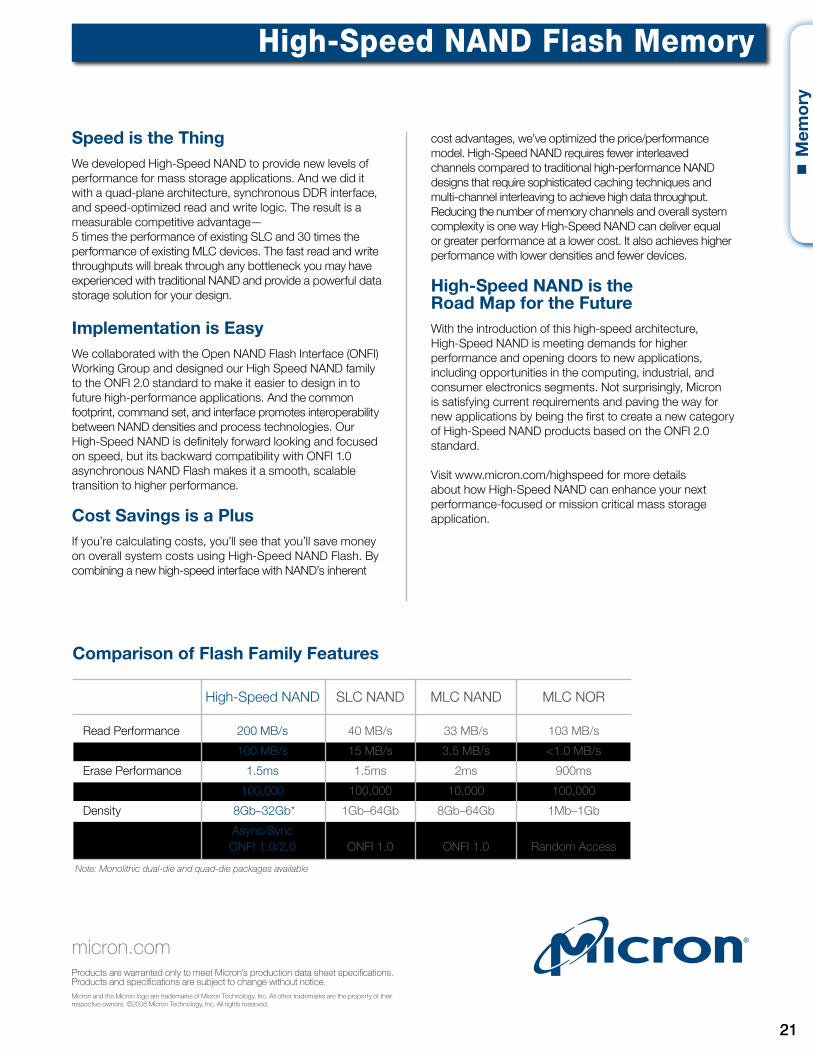
Speed is the ThingWe developed High-Speed NAND to provide new levels of performance for mass storage applications. And we did it with a quad-plane architecture, synchronous DDR interface, and speed-optimized read and write logic. The result is a measurable competitive advantage— 5 times the performance of existing SLC and 30 times the performance of existing MLC devices. The fast read and write throughputs will break through any bottleneck you may have experienced with traditional NAND and provide a powerful data storage solution for your design.
Implementation is Easy
We collaborated with the Open NAND Flash Interface (ONFI) Working Group and designed our High Speed NAND family to the ONFI 2.0 standard to make it easier to design in to future high-performance applications. And the common footprint, command set, and interface promotes interoperability between NAND densities and process technologies. Our High-Speed NAND is definitely forward looking and focused on speed, but its backward compatibility with ONFI 1.0 asynchronous NAND Flash makes it a smooth, scalable transition to higher performance.
Cost Savings is a Plus If you’re calculating costs, you’ll see that you’ll save money on overall system costs using High-Speed NAND Flash. By combining a new high-speed interface with NAND’s inherent
cost advantages, we’ve optimized the price/performance model. High-Speed NAND requires fewer interleaved channels compared to traditional high-performance NAND designs that require sophisticated caching techniques and multi-channel interleaving to achieve high data throughput. Reducing the number of memory channels and overall system complexity is one way High-Speed NAND can deliver equal or greater performance at a lower cost. It also achieves higher performance with lower densities and fewer devices.
High-Speed NAND is the Road Map for the FutureWith the introduction of this high-speed architecture, High-Speed NAND is meeting demands for higher performance and opening doors to new applications, including opportunities in the computing, industrial, and consumer electronics segments. Not surprisingly, Micron is satisfying current requirements and paving the way for new applications by being the first to create a new category of High-Speed NAND products based on the ONFI 2.0 standard.
Visit www.micron.com/highspeed for more details about how High-Speed NAND can enhance your next performance-focused or mission critical mass storage application.
micron.comProducts are warranted only to meet Micron’s production data sheet specifications. Products and specifications are subject to change without notice.
Micron and the Micron logo are trademarks of Micron Technology, Inc. All other trademarks are the property of their respective owners. ©2008 Micron Technology, Inc. All rights reserved.
Comparison of Flash Family Features
High-Speed NAND SLC NAND MLC NAND MLC NOR
Read Performance 200 MB/s 40 MB/s 33 MB/s 103 MB/s
Write Performance 100 MB/s 15 MB/s 3.5 MB/s <1.0 MB/s
Erase Performance 1.5ms 1.5ms 2ms 900ms
Endurance (cycles) 100,000 100,000 10,000 100,000
Density 8Gb–32Gb* 1Gb–64Gb 8Gb–64Gb 1Mb–1Gb
Interface Async/Sync ONFI 1.0/2.0 ONFI 1.0 ONFI 1.0 Random Access
Note: Monolithic dual-die and quad-die packages available
High-Speed NAND Flash Memory
2121
M
emo
ry
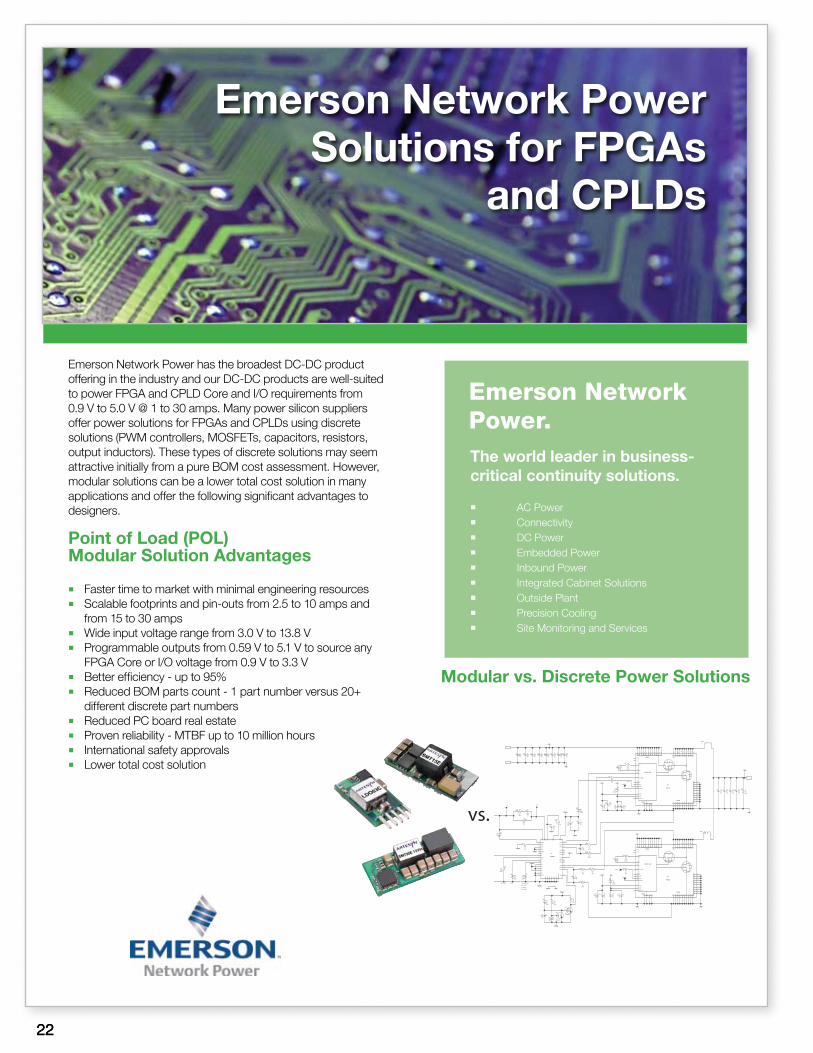
Emerson Network Power.The world leader in business-critical continuity solutions.
AC Power Connectivity DC Power Embedded Power Inbound Power Integrated Cabinet Solutions Outside Plant Precision Cooling Site Monitoring and Services
Emerson Network Power has the broadest DC-DC product offering in the industry and our DC-DC products are well-suited to power FPGA and CPLD Core and I/O requirements from 0.9 V to 5.0 V @ 1 to 30 amps. Many power silicon suppliers offer power solutions for FPGAs and CPLDs using discrete solutions (PWM controllers, MOSFETs, capacitors, resistors, output inductors). These types of discrete solutions may seem attractive initially from a pure BOM cost assessment. However, modular solutions can be a lower total cost solution in many applications and offer the following significant advantages to designers.
Point of Load (POL)Modular Solution Advantages
Faster time to market with minimal engineering resources Scalable footprints and pin-outs from 2.5 to 10 amps and from 15 to 30 amps Wide input voltage range from 3.0 V to 13.8 V Programmable outputs from 0.59 V to 5.1 V to source any FPGA Core or I/O voltage from 0.9 V to 3.3 V Better efficiency - up to 95% Reduced BOM parts count - 1 part number versus 20+ different discrete part numbers Reduced PC board real estate Proven reliability - MTBF up to 10 million hours International safety approvals Lower total cost solution
Emerson Network Power Solutions for FPGAs
and CPLDs
22
Modular vs. Discrete Power Solutions
vs.
22
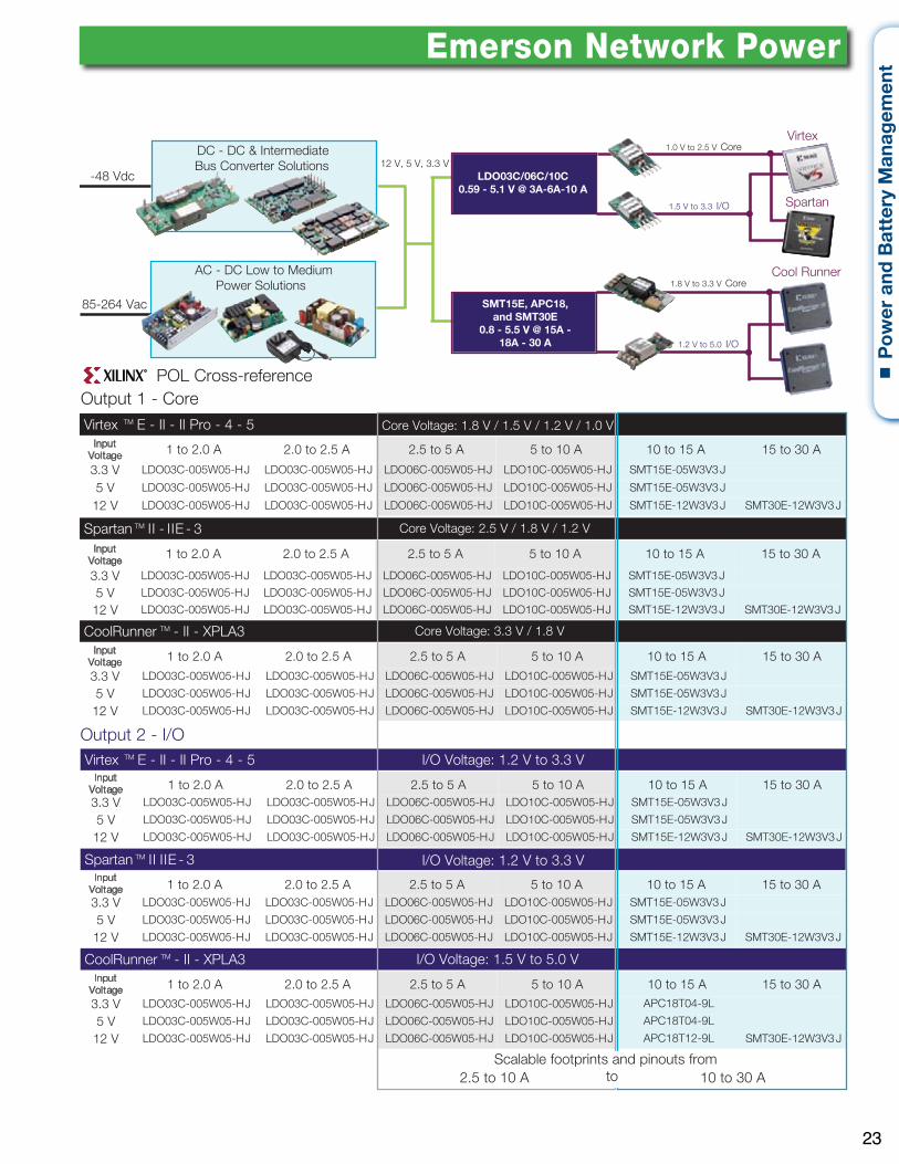
Input Voltage 1 to 2.0 A 2.0 to 2.5 A 2.5 to 5 A 5 to 10 A 10 to 15 A 15 to 30 A
3.3 V LDO03C-005W05-HJ LDO03C-005W05-HJ LDO06C-005W05-HJ LDO10C-005W05-HJ SMT15E-05W3V3J
5 V LDO03C-005W05-HJ LDO03C-005W05-HJ LDO06C-005W05-HJ LDO10C-005W05-HJ SMT15E-05W3V3J
12 V LDO03C-005W05-HJ LDO03C-005W05-HJ LDO06C-005W05-HJ LDO10C-005W05-HJ SMT15E-12W3V3J SMT30E-12W3V3J
Input Voltage
1 to 2.0 A 2.0 to 2.5 A 2.5 to 5 A 5 to 10 A 10 to 15 A 15 to 30 A
3.3 V LDO03C-005W05-HJ LDO03C-005W05-HJ LDO06C-005W05-HJ LDO10C-005W05-HJ SMT15E-05W3V3J
5 V LDO03C-005W05-HJ LDO03C-005W05-HJ LDO06C-005W05-HJ LDO10C-005W05-HJ SMT15E-05W3V3J
12 V LDO03C-005W05-HJ LDO03C-005W05-HJ LDO06C-005W05-HJ LDO10C-005W05-HJ SMT15E-12W3V3J SMT30E-12W3V3J
Input Voltage 1 to 2.0 A 2.0 to 2.5 A 2.5 to 5 A 5 to 10 A 10 to 15 A 15 to 30 A
3.3 V LDO03C-005W05-HJ LDO03C-005W05-HJ LDO06C-005W05-HJ LDO10C-005W05-HJ SMT15E-05W3V3J
5 V LDO03C-005W05-HJ LDO03C-005W05-HJ LDO06C-005W05-HJ LDO10C-005W05-HJ SMT15E-05W3V3J
12 V LDO03C-005W05-HJ LDO03C-005W05-HJ LDO06C-005W05-HJ LDO10C-005W05-HJ SMT15E-12W3V3J SMT30E-12W3V3J
Input Voltage 1 to 2.0 A 2.0 to 2.5 A 2.5 to 5 A 5 to 10 A 10 to 15 A 15 to 30 A3.3 V LDO03C-005W05-HJ LDO03C-005W05-HJ LDO06C-005W05-HJ LDO10C-005W05-HJ SMT15E-05W3V3J
5 V LDO03C-005W05-HJ LDO03C-005W05-HJ LDO06C-005W05-HJ LDO10C-005W05-HJ SMT15E-05W3V3J
12 V LDO03C-005W05-HJ LDO03C-005W05-HJ LDO06C-005W05-HJ LDO10C-005W05-HJ SMT15E-12W3V3J SMT30E-12W3V3J
Input Voltage 1 to 2.0 A 2.0 to 2.5 A 2.5 to 5 A 5 to 10 A 10 to 15 A 15 to 30 A
3.3 V LDO03C-005W05-HJ LDO03C-005W05-HJ LDO06C-005W05-HJ LDO10C-005W05-HJ APC18T04-9L
5 V LDO03C-005W05-HJ LDO03C-005W05-HJ LDO06C-005W05-HJ LDO10C-005W05-HJ APC18T04-9L
12 V LDO03C-005W05-HJ LDO03C-005W05-HJ LDO06C-005W05-HJ LDO10C-005W05-HJ APC18T12-9L SMT30E-12W3V3J
Virtex TM E - II - II Pro - 4 - 5
Spartan TM 3 - EII II
CoolRunner TM - II - XPLA3
CoolRunner TM - II - XPLA3
Spartan TM 3 - EII - II
Output 2 - I/O
Output 1 - CoreVirtex TM
DC - DC & IntermediateBus Converter Solutions
AC - DC Low to Medium Power Solutions
POL Cross-reference
E - II - II Pro - 4 - 5
-48 Vdc
85-264 Vac
12 V, 5 V, 3.3 V
1.0 V to 2.5 V Core
1.5 V to 3.3 I/O
1.8 V to 3.3 V Core
1.2 V to 5.0 I/O
Virtex
Spartan
Scalable footprints and pinouts fromto 10 to 30 A2.5 to 10 A
Cool Runner
LDO03C/06C/10C0.59 - 5.1 V @ 3A-6A-10 A
SMT15E, APC18,and SMT30E
0.8 - 5.5 V @ 15A -18A - 30 A
Core Voltage: 1.8 V / 1.5 V / 1.2 V / 1.0 V
Core Voltage: 2.5 V / 1.8 V / 1.2 V
Core Voltage: 3.3 V / 1.8 V
I/O Voltage: 1.2 V to 3.3 V
I/O Voltage: 1.2 V to 3.3 V
I/O Voltage: 1.5 V to 5.0 V
Emerson Network Power
23
P
ow
er a
nd B
atte
ry M
anag
emen
t
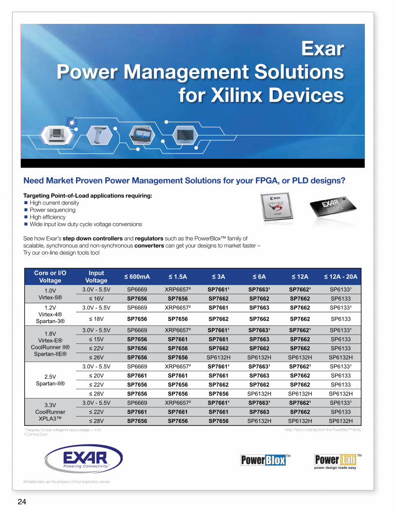
Need Market Proven Power Management Solutions for your FPGA, or PLD designs?
Targeting Point-of-Load applications requiring: High current density Power sequencing High efficiency Wide input low duty cycle voltage conversions
See how Exar’s step down controllers and regulators such as the PowerBlox™ family ofscalable, synchronous and non-synchronous converters can get your designs to market faster –Try our on-line design tools too!
Exar Power Management Solutions
for Xilinx Devices
Powerpower design made easy
¹ Requires 5V bias voltage for input voltages < 4.5V ² Coming Soon
Core or I/O Voltage
Input Voltage ≤ 600mA ≤ 1.5A ≤ 3A ≤ 6A ≤ 12A ≤ 12A - 20A
1.0VVirtex-5®
3.0V - 5.5V SP6669 XRP6657² SP7661¹ SP7663¹ SP7662¹ SP6133¹≤ 16V SP7656 SP7656 SP7662 SP7662 SP7662 SP6133
1.2V Virtex-4®
Spartan-3®
3.0V - 5.5V SP6669 XRP6657² SP7661 SP7663 SP7662 SP6133¹
≤ 18V SP7656 SP7656 SP7662 SP7662 SP7662 SP6133
1.8VVirtex-E®
CoolRunner II®Spartan-IIE®
3.0V - 5.5V SP6669 XRP6657² SP7661¹ SP7663¹ SP7662¹ SP6133¹≤ 15V SP7656 SP7661 SP7661 SP7663 SP7662 SP6133≤ 22V SP7656 SP7656 SP7662 SP7662 SP7662 SP6133≤ 26V SP7656 SP7656 SP6132H SP6132H SP6132H SP6132H
2.5VSpartan-II®
3.0V - 5.5V SP6669 XRP6657² SP7661¹ SP7663¹ SP7662¹ SP6133¹≤ 20V SP7661 SP7661 SP7661 SP7663 SP7662 SP6133≤ 22V SP7656 SP7656 SP7662 SP7662 SP7662 SP6133≤ 28V SP7656 SP7656 SP7656 SP6132H SP6132H SP6132H
3.3VCoolRunner
XPLA3™
3.0V - 5.5V SP6669 XRP6657² SP7661¹ SP7663¹ SP7662¹ SP6133¹≤ 22V SP7661 SP7661 SP7661 SP7663 SP7662 SP6133≤ 28V SP7656 SP7656 SP7656 SP6132H SP6132H SP6132H
Note: Parts in bold are from the PowerBlox™ family¹ Requires 5V bias voltage for input voltages < 4.5V² Coming Soon
All trademarks are the property of their respective owners.
24
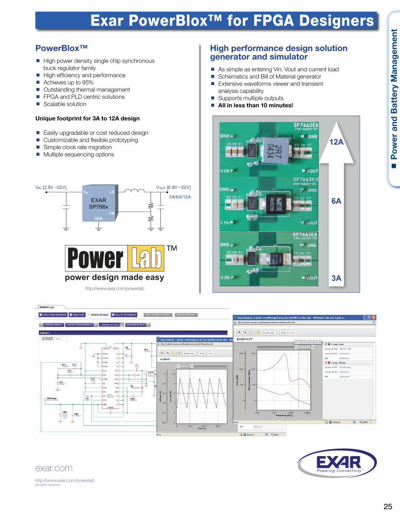
Exar PowerBlox™ for FPGA Designers
Powerpower design made easy
PowerBlox™ High power density single chip synchronous buck regulator family High efficiency and performance Achieves up to 95% Outstanding thermal management FPGA and PLD centric solutions Scalable solution
Unique footprint for 3A to 12A design
Easily upgradable or cost reduced design Customizable and flexible prototyping Simple clock rate migration Multiple sequencing options
High performance design solution generator and simulator As simple as entering Vin, Vout and current load Schematics and Bill of Material generator Extensive waveforms viewer and transient analysis capability Supports multiple outputs All in less than 10 minutes!
exar.comhttp://www.exar.com/powerlabAll rights reserved.
12A
3A
6A
http://www.exar.com/powerlab
25
P
ow
er a
nd B
atte
ry M
anag
emen
t
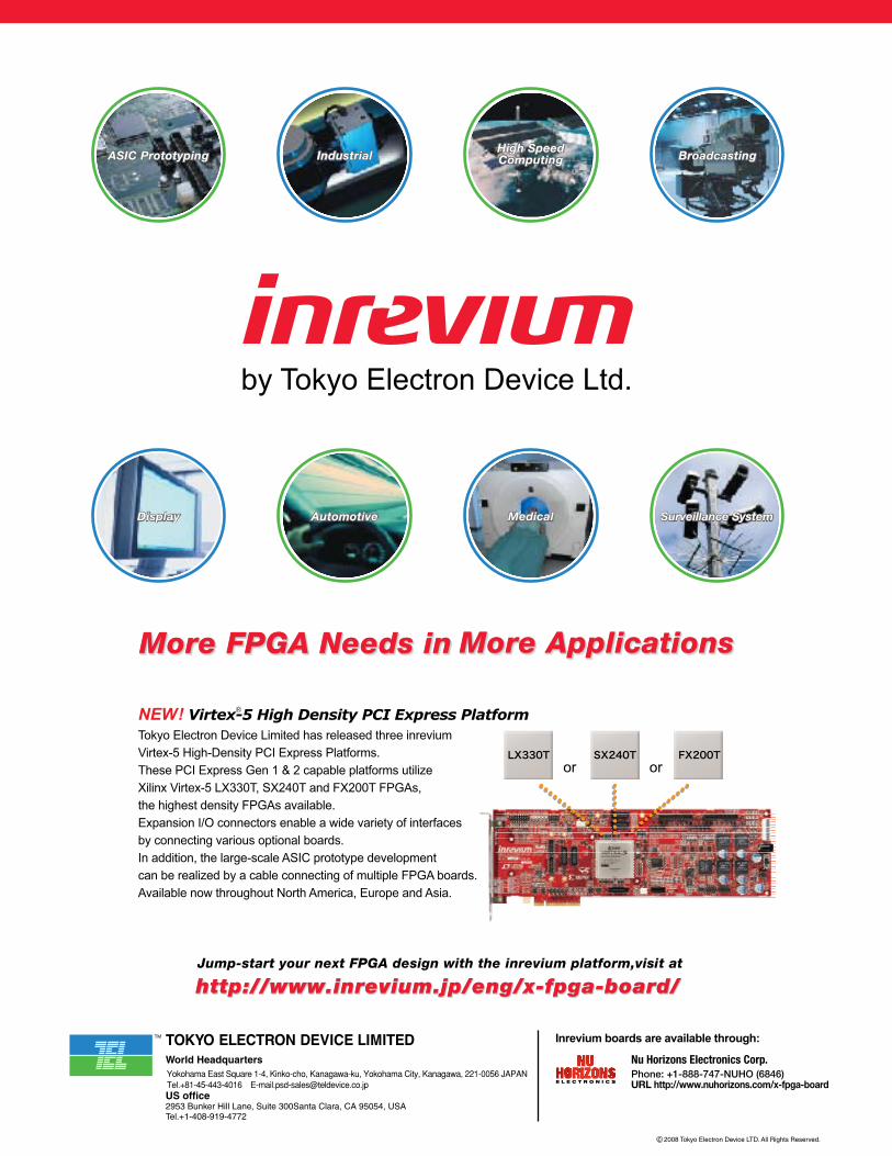
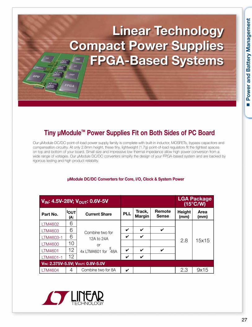
Tiny µModuleTM Power Supplies Fit on Both Sides of PC Board Our µModule DC/DC point-of-load power supply family is complete with built-in inductor, MOSFETs, bypass capacitors and compensation circuitry. At only 2.8mm height, these tiny, lightweight (1.7g) point-of-load regulators fit the tightest spaces on top and bottom of your board. Small size and impressive low thermal impedance allow high power conversion from a wide range of voltages. Our µModule DC/DC converters simplify the design of your FPGA-based system and are backed by rigorous testing and high product reliability.
Part No.
LTM4602
LTM4603
LTM4603-1
LTM4600
LTM4601
LTM4601-1VIN: 2.375V-5.5V; VOUT: 0.8V-5.0V
LTM4604
IOUT(A)
666101212
4
PLL Track,Margin
RemoteSense
VIN: 4.5V-28V; VOUT: 0.6V-5V LGA Package(15°C/W)
Height(mm)
2.8
2.3
Area(mm)
15x15
9x15
Current Share
Combine two for12A to 24A
or
4x LTM4601 for 48A
Combine two for 8A
µModule DC/DC Converters for Core, I/O, Clock & System Power
Linear Technology Compact Power Supplies for FPGA-Based Systems
27
P
ow
er a
nd B
atte
ry M
anag
emen
t
REVISION D
VIRTEX™-5 Core Voltage: 1.0VInput Supply ≤200mA ≤500mA ≤1A – 1.5A ≤2A – 5A 5A – 10A Up to 25A
1.8V LT®3020 LinearLTC®3549 Buck
LT3080 LinearLTC3409 Buck
LT3080 LinearLTC3026 Linear LTC3713 Controller LTC3713 Controller N/A
2.5V to 5VLT3020 LinearLTC3549 BuckLTC3410 Buck
LT3080 LinearLTC3406A BuckLTC3542 Buck
LTC3561 BuckLTC3411A BuckLTC3564 BuckLTC3568 Buck
LTC3412A BuckLTC3414 Buck
LTC3801 ControllerLTC3809 Controller
LTC3418 BuckLTC3822 Controller
LTM®4601 µModule™*LTC1778 Controller
LTC3822 ControllerLTC3713 ControllerLTC3832 ControllerLTC1778 Controller
≤12V to 24V LT3502 Buck LT3502 Buck
LT3493 BuckLT3685 BuckLT3481 BuckLT3505 Buck
LT3680 BuckLTC1771 ControllerLTC1778 ControllerLTC3770 Controller
LTM4601 µModule*LTC3832 ControllerLTC1778 ControllerLTC3823 Controller
2 x LTM4601 µModule*LTC1778 ControllerLTC3823 Controller
VIRTEX-4 & Spartan™-3 Family Core Voltage: 1.2VInput Supply ≤200mA ≤500mA ≤1A – 1.5A ≤2A – 5A 5A – 10A Up to 25A
1.8VLT1761 Linear
LTC3035 LinearLTC3549 Buck
LT1965 LinearLT3080 LinearLT1763 LinearLTC3409 Buck
LT1965 LinearLT3080 LinearLTC3026 Linear
LTC3713 Controller LTC3713 Controller LTC3713 Controller
2.5V to 5VLT3020 Linear
LTC3035 LinearLTC3410 BuckLTC3549 Buck
LT1965 LinearLT1763 LinearLTC3542 BuckLTC3560 Buck
LT1965 LinearLT3080 LinearLTC3411A Buck
LTC3564/8 Bucks
LTC3412A BuckLTC3414 Buck
LTC3801/9 ControllersLTC1773 Controller
LTC3418 BuckLTC3822 ControllerLTM4601 µModule*LTC1778 Controller
LTC3713 ControllerLTC3832 ControllerLTC1778 ControllerLTC3778 Controller
≤12V to 24V LT3502 BuckLT1933 BuckLT3493 BuckLT3502 Buck
LT3503 BuckLT3505 BuckLT1936 BuckLT3481Buck
LT3680 BuckLTC1771 ControllerLTM4603 µModule*LTC1778 Controller
LTM4601 µModule*LTC3772 ControllerLTC1778 ControllerLTC3823 Controller
2 x LTM4601 µModule*LTC1778 ControllerLTC3823 Controller
VIRTEX-II PRO™ & VIRTEX-II Core Voltage: 1.5VInput Supply ≤200mA ≤500mA ≤1A – 1.5A ≤2A – 5A 5A – 10A Up to 25A
1.8VLTC1844 LinearLTC3035 LinearLT1962 LinearLTC3549 Buck
LT1763 LinearLT1965 LinearLT3080 LinearLTC3409 Buck
LT1965 LinearLT3080 LinearLTC3026 Linear
LTC3713 Controller LTC3713 Controller LTC3713 Controller
2.5V to 5VLT1762 Linear
LTC3035 LinearLTC3410 BuckLTC3549 Buck
LT1965 LinearLT3080 LinearLT1763 LinearLTC3542 Buck
LTC3406A Buck
LT1965 LinearLT3080 LinearLT1963A LinearLTC3561 Buck
LTC3411A Buck
LTC3412A BuckLTC3414 Buck
LTC3801 ControllerLTC3809 Controller
LTC3418 BuckLTC3822 ControllerLTM4601 µModule*LTC1778 Controller
LTC3713 ControllerLTC3832 ControllerLTC1778 ControllerLTC3778 Controller
≤12V to 24VLT3470 BuckLT3502 BuckLT1616 Buck
LT1616 BuckLT1933 BuckLT3493 Buck
LT3503 BuckLT3505 BuckLT3481 BuckLT3684 Buck
LT3680 BuckLTC1771 ControllerLTM4603 µModule*LTC1778 Controller
LTM4601 µModule*LTC3610 Buck
LTC3772 ControllerLTC1778 ControllerLTC3823 Controller
2 x LTM4601 µModule*LTC1778 ControllerLTC3823 ControllerLT1952 Controller
VIRTEX-E, Spartan-IIE & CoolRunner™-II Core Voltage: 1.8VInput Supply ≤200mA ≤500mA ≤1A – 1.5A ≤2A – 5A 5A – 10A Up to 25A
0.9V to 1.8VLTC3525 BoostLTC3429 BoostLTC3526 Boost
LT1613 Boost N/A N/A N/A N/A
2.5V to 5V
LTC1844 LinearLTC3035 LinearLT1762 Linear
LTC3405A BuckLTC3410 Buck
LT1965 LinearLT3080 LinearLTC3542 Buck
LTC3406A Buck
LT1965 LinearLT3080 LinearLT1963A LinearLTC3561 Buck
LTC3411A Buck
LTC3414 BuckLTC3801/9 ControllersLTM4603 µModule*LTC1773 Controller
LTC3418 BuckLTC3822 ControllerLTM4601 µModule*
LTC3610 Buck
LTC3822 ControllerLTC3713 ControllerLTC3832 ControllerLTC3778 Controller
≤12V to 24VLT3470 BuckLT1934 BuckLT1616 BuckLT3502 Buck
LT1616 BuckLT3502 BuckLT1933 BuckLT3493 Buck
LT3503 BuckLT3505 BuckLT3481 BuckLT3684 Buck
LT3680 BuckLTC1771 ControllerLTM4603 µModule*LTC1778 Controller
LTM4601 µModule*LTC3610 Buck
LTC1778 ControllerLTC3823 Controller
2 x LTM4601 µModule*LTC1778 ControllerLTC3823 ControllerLT1952 Controller
Power Management Solutions for Xilinx Programmable Logic Devices
*Additional products in Module Family now available. New products highlighted in bold.
Power Management Solutions for Xilinx Programmable Logic Devices
28
www.linear.comLT/TP REV D 0807 10K
SwitcherCAD™/LTspice is a SPICE simulator for power supply, amplifi er and fi lter designs
Additional Power Support Products• Trackers/Sequencers• Margining Controllers• Silicon Oscillators• P/DSP/FPGA Supervisor Circuits• PMBus Interface Products
Spartan-II Core Voltage: 2.5VInput Supply ≤200mA ≤500mA ≤1A – 1.5A ≤2A – 5A 5A – 10A Up to 25A
1.8VLTC3525 BoostLTC3427 BoostLTC3429 BoostLTC3499 Boost
LTC3499 BoostLTC3426 BoostLTC3422 Boost
LTC3421 BoostLTC3428 BoostLTC3426 Boost
LTC3425 BoostLTC1872 Boost ControllerLTC1700 Boost Controller
N/A N/A
2.5V to 5VLTC1844 LinearLTC3035 LinearLT1962 LinearLTC3410 Buck
LT3080 LinearLT1763 LinearLT1965 LinearLTC3542 BuckLTC3560 Buck
LTC3561 BuckLTC3411A Buck
LT1619 SEPIC Controller
LTC3414 BuckLTC3801 ControllerLTC3809 Controller
LT1619 SEPIC Controller
LTC3418 BuckLTM4601 µModule*
LTC3610 BuckLTC3822 Controller
LTC3822 ControllerLTC3713 ControllerLTC3832 ControllerLTC1778 Controller
≤12V to 24VLT3470 BuckLT1934 BuckLT1616 BuckLT3502 Buck
LT1616 BuckLT3502 BuckLT1933 BuckLT3493 Buck
LT3503 BuckLT3505 BuckLT3684 BuckLT1936 Buck
LT3680 BuckLTC1771 ControllerLTM4603 µModule*LTC1778 Controller
LTM4601 µModule*LTC3610 Buck
LTC1778 ControllerLTC3823 Controller
2 x LTM4601 µModule*LTC1778 ControllerLTC3823 ControllerLT1952 Controller
CoolRunner XPLA3 Core Voltage: 3.3VInput Supply ≤200mA ≤500mA ≤1A – 1.5A ≤2A – 5A 5A – 10A Up to 25A
1.8V to 2.5VLTC3525 BoostLTC3526 BoostLTC3429 Boost
LTC3426 BoostLTC3421 BoostLTC3422 BoostLTC3499 Boost
LTC3426 BoostLTC3421 BoostLTC3428 Boost
LTC3428 BoostLTC3425 Boost
LTC1871 Boost ControllerN/A N/A
Li-Ion 2.7V to 4.2VLTC3531 Buck-BoostLTC3530 Buck-BoostLTC3440 Buck-Boost
LTC3530 Buck-BoostLTC3440 Buck-BoostLTC3538 Buck-Boost
LTC3442 Buck-BoostLTC3443 Buck-Boost
LTC1871 SEPIC Controller
LTC3785 Buck-Boost Controller
LTC1872 SEPIC ControllerLTC1871 SEPIC ControllerLT1619 SEPIC Controller
LTC3785 Buck-Boost Controller
LT1619 SEPIC ControllerLTC1682 + LTC1778
≤5VLTC1844 LinearLTC3035 LinearLT1962 LinearLTC3410 Buck
LT1965 LinearLT3080 LinearLT1763 LinearLTC3560 Buck
LT1963A LinearLTC3561 Buck
LTC3411A Buck
LTC3414 BuckLTC3415 Buck
LTC3809 ControllerLTM4603 µModule*
LTC3418 BuckLTM4601 µModule*
LTC3610 BuckLTC3778 Controller
LTC3830 ControllerLTC3832 ControllerLTC3770 ControllerLTC3778 Controller
≤12V to 24VLT3470 BuckLT1934 BuckLT1616 BuckLT3502 Buck
LT1616 BuckLT3502 BuckLT1933 BuckLT3493 Buck
LT3503 BuckLT3505 BuckLT1936 BuckLT3684 Buck
LT3680 BuckLTC1771 ControllerLTM4603 µModule*LTC1778 Controller
LTM4601 µModule*LTC3610 Buck
LTC1778 ControllerLTC3823 Controller
2 x LTM4601 µModule*LTC1778 ControllerLTC3823 ControllerLT1952 Controller
Power Supplies for I/O I/O Voltage Input Voltage 500mA 1A 2A – 5A 6A – 10A 20A
3.3V12V LT1616, LT1933 LT1936, LT1767 LT3680, LTC1778, LTC3770 LTM4601, LTC1778 2 x LTM4601, LTC1778
5V LTC3406A, LT1962, LT1965 LT1965, LTC3411A LTC3412/A, LTC3414, LTC3809 LTC3415, LTC3418, LTC1778 LTC1778
2.5V12V LT1616, LT1933 LT1936, LT1767 LT3680, LTC1778, LTC3770 LTM4601, LTC1778 LTC1778
5V LTC3560, LT1962, LT1965 LT1963A, LT1965, LTC3411A LTC3412/A, LTC3414, LTC3809 LTM4601, LTC3415, LTC3418 2 x LTM4601, LTC1778
3.3V LTC3560, LT1962, LT1965 LT1963A, LT1965, LTC3411A LTC3412/A, LTC3414, LTC3809 LTC3832, LTC3822, LTC3418 LTC3836, LT3740
1.8V5V LTC3560 LTC3411A, LT1767 LTC3412/A, LTC3414, LTC3809 LTM4601, LTC3418 2 x LTM4601, LTC1778
3.3V LTC3560 LT1963A, LT1965, LTC3411A LTC3412/A, LTC3414, LTC3809 LTC3832, LTC3822, LTC3418 LTC3836, LT3740
2.5V LTC3560, LTC3406A, LT1965 LT1963A, LT1965, LTC3411A LTC3412/A, LTC3414, LTC3801 LTC3418, LT3740 LT3740
1.5V
5V LTC3560 LTC3411A, LT1767 LTC3412/A, LTC3414, LTC3809 LTM4601, LTC3418 2 x LTM4601, LTC1778
3.3V LTC3560 LT1963A, LT1965, LTC3411A LTC3412/A, LTC3414, LTC3809 LTC3832, LTC3822, LTC3418 LTC3836, LT3740
2.5V LTC3560, LTC3406A, LT3021 LT1963A, LT1965, LTC3411A LTC3412/A, LTC3414, LTC3801 LTC3415, LTC3418, LT3740 LT3740
1.8V LTC3406A, LT3021, LT1965 LT3080, LT1965, LT1764A LT1764A, 2 x LT3080, LT3150 LT3150, LTC3713 LTC3713
Dual Output Switching RegulatorsPart Number Architecture VIN Range (V) Max IOUT(1) / IOUT(2) (A) Part Number Architecture VIN Range (V) Max IOUT(1) / IOUT(2) (A)
LTC3547 Monolithic 2.5 – 5.5 0.3/0.3 LTC3546 Monolithic 2.25 – 5.5 2/2 or 3/1
LTC3548 Monolithic 2.5 – 5.5 0.4/0.8 LT3501 Monolithic 3 – 30 3/3
LTC3419 Monolithic 2.5 – 5.5 0.6/0.6 LTC3736/–1 Controller 2.7 – 9.8 5/5
LTC3407–2 Monolithic 2.5 – 5.5 0.8/0.8 LTC3737 Controller 2.7 – 9.8 5/5
LTC3417 Monolithic 2.25 – 5.5 0.8/1.4 LTC3850 Controller 4 – 24 20/20
LTC3417A Monolithic 2.25 – 5.5 1.0/1.5 LTC3728 Controller 4 – 36 20/20
LT3508 Monolithic 3.7 – 36 1.4/1.4 LTC3708 Controller 4 – 36 20/20
LT1940 Monolithic 3.6 – 25 1.4/1.4 LTC3728 Controller 4 – 36 20/20
LT3506/A Monolithic 3.6 – 25 1.6/1.6 LTC3827 Controller 4 – 36 25/25
LT3510 Monolithic 3.3 – 25 2/2 LTC3727 Controller 4.5 – 36 25/25
29
P
ow
er a
nd B
atte
ry M
anag
emen
t
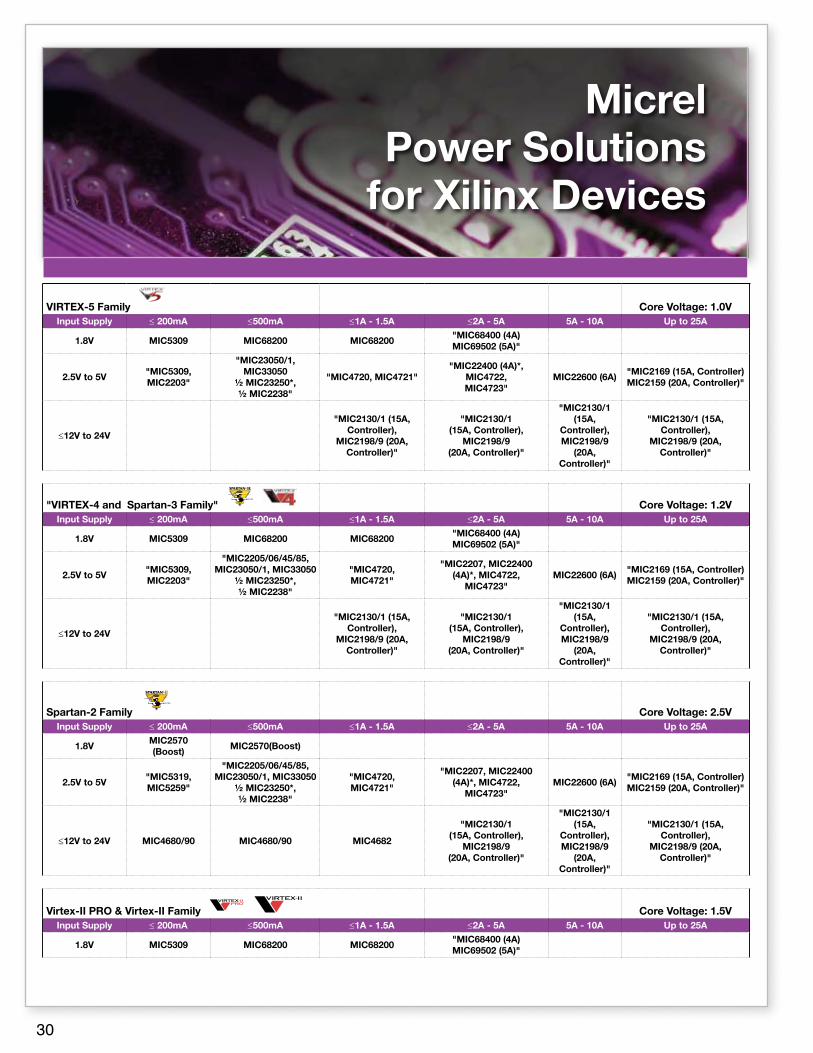
Micrel Power Solutions
for Xilinx Devices
VIRTEX-5 Family Core Voltage: 1.0VInput Supply ≤ 200mA ≤500mA ≤1A - 1.5A ≤2A - 5A 5A - 10A Up to 25A
1.8V MIC5309 MIC68200 MIC68200"MIC68400 (4A) MIC69502 (5A)"
2.5V to 5V"MIC5309, MIC2203"
"MIC23050/1, MIC33050
½ MIC23250*, ½ MIC2238"
"MIC4720, MIC4721""MIC22400 (4A)*,
MIC4722, MIC4723"
MIC22600 (6A)"MIC2169 (15A, Controller) MIC2159 (20A, Controller)"
≤12V to 24V
"MIC2130/1 (15A, Controller),
MIC2198/9 (20A, Controller)"
"MIC2130/1 (15A, Controller),
MIC2198/9 (20A, Controller)"
"MIC2130/1 (15A,
Controller), MIC2198/9
(20A, Controller)"
"MIC2130/1 (15A, Controller),
MIC2198/9 (20A, Controller)"
"VIRTEX-4 and Spartan-3 Family" Core Voltage: 1.2VInput Supply ≤ 200mA ≤500mA ≤1A - 1.5A ≤2A - 5A 5A - 10A Up to 25A
1.8V MIC5309 MIC68200 MIC68200"MIC68400 (4A) MIC69502 (5A)"
2.5V to 5V"MIC5309, MIC2203"
"MIC2205/06/45/85, MIC23050/1, MIC33050
½ MIC23250*, ½ MIC2238"
"MIC4720, MIC4721"
"MIC2207, MIC22400 (4A)*, MIC4722,
MIC4723"MIC22600 (6A)
"MIC2169 (15A, Controller) MIC2159 (20A, Controller)"
≤12V to 24V
"MIC2130/1 (15A, Controller),
MIC2198/9 (20A, Controller)"
"MIC2130/1 (15A, Controller),
MIC2198/9 (20A, Controller)"
"MIC2130/1 (15A,
Controller), MIC2198/9
(20A, Controller)"
"MIC2130/1 (15A, Controller),
MIC2198/9 (20A, Controller)"
Spartan-2 Family Core Voltage: 2.5VInput Supply ≤ 200mA ≤500mA ≤1A - 1.5A ≤2A - 5A 5A - 10A Up to 25A
1.8VMIC2570 (Boost)
MIC2570(Boost)
2.5V to 5V"MIC5319, MIC5259"
"MIC2205/06/45/85, MIC23050/1, MIC33050
½ MIC23250*, ½ MIC2238"
"MIC4720, MIC4721"
"MIC2207, MIC22400 (4A)*, MIC4722,
MIC4723"MIC22600 (6A)
"MIC2169 (15A, Controller) MIC2159 (20A, Controller)"
≤12V to 24V MIC4680/90 MIC4680/90 MIC4682
"MIC2130/1 (15A, Controller),
MIC2198/9 (20A, Controller)"
"MIC2130/1 (15A,
Controller), MIC2198/9
(20A, Controller)"
"MIC2130/1 (15A, Controller),
MIC2198/9 (20A, Controller)"
Virtex-II PRO & Virtex-II Family Core Voltage: 1.5VInput Supply ≤ 200mA ≤500mA ≤1A - 1.5A ≤2A - 5A 5A - 10A Up to 25A
1.8V MIC5309 MIC68200 MIC68200"MIC68400 (4A) MIC69502 (5A)"
30
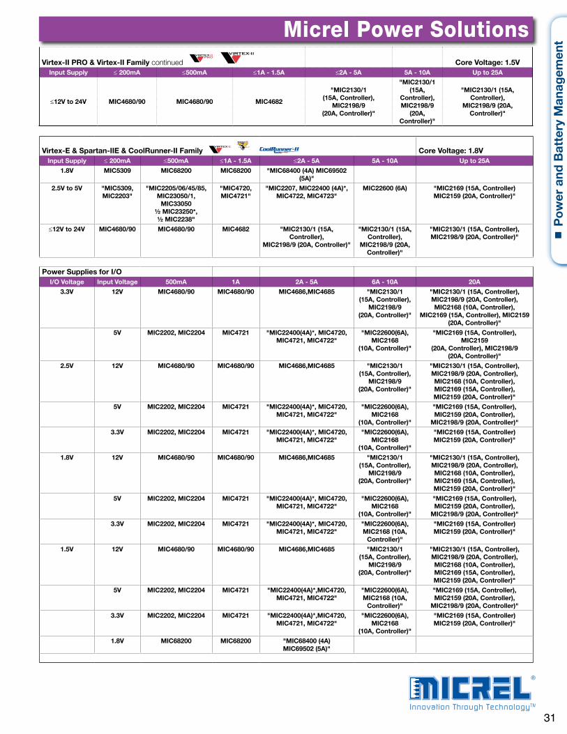
Virtex-E & Spartan-IIE & CoolRunner-II Family Core Voltage: 1.8VInput Supply ≤ 200mA ≤500mA ≤1A - 1.5A ≤2A - 5A 5A - 10A Up to 25A
1.8V MIC5309 MIC68200 MIC68200 "MIC68400 (4A) MIC69502 (5A)"
2.5V to 5V "MIC5309, MIC2203"
"MIC2205/06/45/85, MIC23050/1,
MIC33050 ½ MIC23250*, ½ MIC2238"
"MIC4720, MIC4721"
"MIC2207, MIC22400 (4A)*, MIC4722, MIC4723"
MIC22600 (6A) "MIC2169 (15A, Controller) MIC2159 (20A, Controller)"
≤12V to 24V MIC4680/90 MIC4680/90 MIC4682 "MIC2130/1 (15A, Controller),
MIC2198/9 (20A, Controller)"
"MIC2130/1 (15A, Controller),
MIC2198/9 (20A, Controller)"
"MIC2130/1 (15A, Controller), MIC2198/9 (20A, Controller)"
Power Supplies for I/OI/O Voltage Input Voltage 500mA 1A 2A - 5A 6A - 10A 20A
3.3V 12V MIC4680/90 MIC4680/90 MIC4686,MIC4685 "MIC2130/1 (15A, Controller),
MIC2198/9(20A, Controller)"
"MIC2130/1 (15A, Controller), MIC2198/9 (20A, Controller), MIC2168 (10A, Controller),
MIC2169 (15A, Controller), MIC2159 (20A, Controller)"
5V MIC2202, MIC2204 MIC4721 "MIC22400(4A)*, MIC4720, MIC4721, MIC4722"
"MIC22600(6A), MIC2168
(10A, Controller)"
"MIC2169 (15A, Controller), MIC2159
(20A, Controller), MIC2198/9 (20A, Controller)"
2.5V 12V MIC4680/90 MIC4680/90 MIC4686,MIC4685 "MIC2130/1 (15A, Controller),
MIC2198/9 (20A, Controller)"
"MIC2130/1 (15A, Controller), MIC2198/9 (20A, Controller), MIC2168 (10A, Controller), MIC2169 (15A, Controller), MIC2159 (20A, Controller)"
5V MIC2202, MIC2204 MIC4721 "MIC22400(4A)*, MIC4720, MIC4721, MIC4722"
"MIC22600(6A), MIC2168
(10A, Controller)"
"MIC2169 (15A, Controller), MIC2159 (20A, Controller),
MIC2198/9 (20A, Controller)"
3.3V MIC2202, MIC2204 MIC4721 "MIC22400(4A)*, MIC4720, MIC4721, MIC4722"
"MIC22600(6A), MIC2168
(10A, Controller)"
"MIC2169 (15A, Controller) MIC2159 (20A, Controller)"
1.8V 12V MIC4680/90 MIC4680/90 MIC4686,MIC4685 "MIC2130/1 (15A, Controller),
MIC2198/9 (20A, Controller)"
"MIC2130/1 (15A, Controller), MIC2198/9 (20A, Controller), MIC2168 (10A, Controller), MIC2169 (15A, Controller), MIC2159 (20A, Controller)"
5V MIC2202, MIC2204 MIC4721 "MIC22400(4A)*, MIC4720, MIC4721, MIC4722"
"MIC22600(6A), MIC2168
(10A, Controller)"
"MIC2169 (15A, Controller), MIC2159 (20A, Controller),
MIC2198/9 (20A, Controller)"
3.3V MIC2202, MIC2204 MIC4721 "MIC22400(4A)*, MIC4720, MIC4721, MIC4722"
"MIC22600(6A), MIC2168 (10A,
Controller)"
"MIC2169 (15A, Controller) MIC2159 (20A, Controller)"
1.5V 12V MIC4680/90 MIC4680/90 MIC4686,MIC4685 "MIC2130/1 (15A, Controller),
MIC2198/9 (20A, Controller)"
"MIC2130/1 (15A, Controller), MIC2198/9 (20A, Controller), MIC2168 (10A, Controller), MIC2169 (15A, Controller), MIC2159 (20A, Controller)"
5V MIC2202, MIC2204 MIC4721 "MIC22400(4A)*,MIC4720, MIC4721, MIC4722"
"MIC22600(6A), MIC2168 (10A,
Controller)"
"MIC2169 (15A, Controller), MIC2159 (20A, Controller),
MIC2198/9 (20A, Controller)"
3.3V MIC2202, MIC2204 MIC4721 "MIC22400(4A)*,MIC4720, MIC4721, MIC4722"
"MIC22600(6A), MIC2168
(10A, Controller)"
"MIC2169 (15A, Controller) MIC2159 (20A, Controller)"
1.8V MIC68200 MIC68200 "MIC68400 (4A) MIC69502 (5A)"
Micrel Power SolutionsVirtex-II PRO & Virtex-II Family continued Core Voltage: 1.5V
Input Supply ≤ 200mA ≤500mA ≤1A - 1.5A ≤2A - 5A 5A - 10A Up to 25A
≤12V to 24V MIC4680/90 MIC4680/90 MIC4682
"MIC2130/1 (15A, Controller),
MIC2198/9 (20A, Controller)"
"MIC2130/1 (15A,
Controller), MIC2198/9
(20A, Controller)"
"MIC2130/1 (15A, Controller),
MIC2198/9 (20A, Controller)"
31
P
ow
er a
nd B
atte
ry M
anag
emen
t
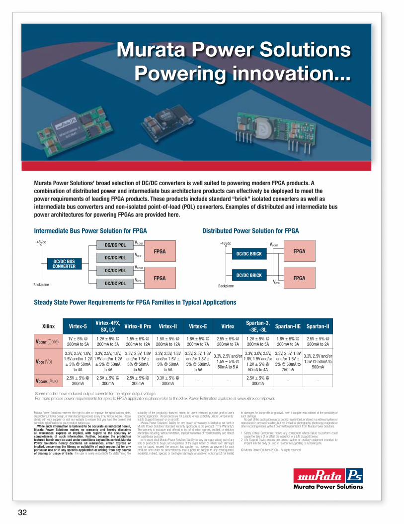
Distributed Power Solution for FPGA
Xilinx Virtex-5Virtex-4FX,
SX, LXVirtex-II Pro Virtex-II Virtex-E Virtex
Spartan-3, -3E, -3L
Spartan-IIE Spartan-II
VCCINT (Core) 1V ± 5% @ 200mA to 5A
1.2V ± 5% @ 200mA to 5A
1.5V ± 5% @ 200mA to 12A
1.5V ± 5% @ 200mA to 12A
1.8V ± 5% @ 200mA to 7A
2.5V ± 5% @ 200mA to 7A
1.2V ± 5% @ 200mA to 5A
1.8V ± 5% @ 200mA to 3A
2.5V ± 5% @ 200mA to 2A
VCCO (Vo)
3.3V, 2.5V, 1.8V, 1.5V and/or 1.2V ± 5% @ 50mA
to 4A
3.3V, 2.5V, 1.8V, 1.5V and/or 1.2V ± 5% @ 50mA
to 4A
3.3V, 2.5V, 1.8V and/or 1.5V ± 5% @ 50mA
to 5A
3.3V, 2.5V, 1.8V and/or 1.5V ± 5% @ 50mA
to 5A
3.3V, 2.5V, 1.8V and/or 1.5V ± 5% @ 500mA
to 5A
3.3V, 2.5V and/or 1.5V ± 5% @ 50mA to 5 A
3.3V, 3.0V, 2.5V, 1.8V, 1.5V and/or
1.2V ± 5% @ 50mA to 4A
3.3V, 2.5V, 1.8V and/or 1.5V ±
5% @ 50mA to 750mA
3.3V, 2.5V and/or 1.5V @ 50mA to
500mA
VCCAUX (Aux) 2.5V ± 5% @ 300mA
2.5V ± 5% @ 300mA
2.5V ± 5% @ 300mA
3.3V ± 5% @ 300mA
– –2.5V ± 5% @
300mA– –
Murata Power Solutions’ broad selection of DC/DC converters is well suited to powering modern FPGA products. A combination of distributed power and intermediate bus architecture products can effectively be deployed to meet the power requirements of leading FPGA products. These products include standard “brick” isolated converters as well as intermediate bus converters and non-isolated point-of-load (POL) converters. Examples of distributed and intermediate bus power architectures for powering FPGAs are provided here.
Steady State Power Requirements for FPGA Families in Typical Applications
Intermediate Bus Power Solution for FPGA
Murata Power Solutions reserves the right to alter or improve the specifications, data, descriptions, internal design, or manufacturing process at any time, without notice. Please check with your supplier or visit our website to ensure that you have the current and complete specification for your product before use.
While such information is believed to be accurate as indicated herein, Murata Power Solutions makes no warranty and hereby disclaims all warranties, express or implied, with regard to the accuracy or completeness of such information. Further, because the product(s) featured herein may be used under conditions beyond its control, Murata Power Solutions hereby disclaims all warranties, either express or implied, concerning the fitness or suitability of such product(s) for any particular use or in any specific application or arising from any course of dealing or usage of trade. The user is solely responsible for determining the
suitability of the product(s) featured herein for user’s intended purpose and in user’s specific application. The products are not suitable for use as Safety Critical Components,1 in Life Support Devices2 or on aircraft.
Murata Power Solutions’ liability for any breach of warranty is limited as set forth in Murata Power Solutions’ standard warranty applicable to the product (“The Warranty”). The warranty is exclusive and offered in lieu of all other express, implied, or statutory warranties including, without limitation, implied warranties of merchantability and fitness for a particular purpose.
In no event shall Murata Power Solutions’ liability for any damages arising out of any sale of products to buyer, and regardless of the legal theory on which such damages may be based, exceed the amount that supplier has received as payment for such products and under no circumstances shall supplier be subject to any consequential, incidental, indirect, special, or contingent damages whatsoever, including but not limited
to damages for lost profits or goodwill, even if supplier was advised of the possibility of such damage.
No part of this publication may be copied, transmitted, or stored in a retrieval system or reproduced in any way including, but not limited to, photography, photocopy, magnetic or other recording means, without prior written permission from Murata Power Solutions.
1 Safety Critical Component means any component whose failure to perform could cause the failure of, or affect the operation of a Life Support Device.
2 Life Support Device means any device, system or ancillary equipment intended for implant into the body or used in relation to supporting or sustaining life.
© Murata Power Solutions 2008 – All rights reserved
DC/DC POLFPGA
FPGA
-48Vdc
Backplane
DC/DC BUSCONVERTER
DC/DC POL
DC/DC POL
DC/DC POL
VCCINT
VCCINT
VCCO
VCCO
DC/DC BRICK
VCCINT
VCCO
FPGA
FPGA
-48Vdc
Backplane
DC/DC BRICK
Some models have reduced output currents for the higher output voltage. For more precise power requirements for specific FPGA applications please refer to the Xilinx Power Estimators available at www.xilinx.com/power.
Murata Power Solutions Powering innovation...
32
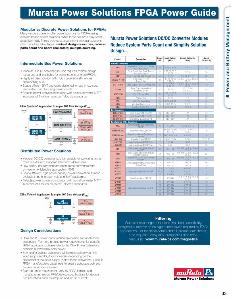
Murata Power Solutions FPGA Power Guide
Product Description Power(W)
Input Voltage(Vdc)
Output Voltage(s)(Vdc)
Output Current (A)
Isolated Converters
ULQ Single Output, Quarter Brick, Through Hole/Surface Mount 66 18-36 & 36-75 1.2-12 25
ULE Single Output, Eighth Brick, Through Hole/Surface Mount 60 9-18, 18-36, &
36-75 1.2-24 30
UHP Single Output, Half Brick, Through Hole 148 36-75 1.5, 1.8, 2.5, 3.3 60
A Series 7-15W Single Output, 1" x 2", Through Hole 15 10-18, 18-36
& 36-751.2, 1.5, 1.8, 2.5, 3.3, 5.0,
12, 15 10
UHE 12-30W Single Output, 1.6" x 2", Through Hole 10 9-18, 9-36, & 36-75
1.2, 1.5, 1.8, 2.5, 3.3, 5.0, 12, 15 10
Q-Class Single Output, Quarter BrickSingle Board, PTH 144 36-75 1.2, 1.5, 1.8,
2.5, 3.3, 12 55
UWR 7-15W 1" x 2", Through Hole 15 10-8, 18-36, & 36-75 1.2-15 6
HPH 70A Half Brick 350 36-75 1-5 70UVQ Low-Profile Quarter Brick 125 18-36 & 36-75 1.2-48 40UQQ Wide Input Quarter Brick 105 9-36 & 18-75 3.3-15 25UCQ Low-Cost Quarter Brick 115 18-36 & 36-75 3.3 & 5 35
Bus ConvertersEUS15-120 Single Output Eighth Brick, Pth 180 36V – 55V 12 15EUS20-120 Single Output Eighth Brick, Pth 240 36V – 55V 12 20QUS20-120 Single Output Quarter Brick, Pth 240 36V – 55V 12 20
Non-Isolated (POL) Converters
NGA Single Adjustable and Fixed Output, SIP/DIP 10 4.75-28 1.8, 2.5, 3.3, 5.0 2
LSM/LSN-10A Single Fixed Output, SMT/SIP 50 3.0-3.6, 4.5-5.0, 10.8-13.2
1.0, 1.2, 1.5, 1.8, 2.5, 3.3, 5.0 10
LSM/LSN-16A Single Adjustable and Fixed Output, SMT/SIP 50 3.0-5.5 & 10-14 0.75-5.0 16
LSM/LSN2 Adjustable Output SMT/SIP 52 2.4-5.5 8.3-14 0.75-5 6, 10, 16LSN2-T/22 Adjustable Output SMT/SIP 22A 112 8.3-14 0.8-5 22LSN2-T30 Adjustable Output SMT/SIP 30A 150 6-14 0.8-5 30
LEN Single Output, Eighth Brick, Through Hole/SMT 125 10.2-13.8 0.8, 1.0, 1.2, 1.5, 1.8, 2.5,
3.3, 5.0 28
HEN Single Output, Eighth Brick, Through Hole/SMT, High di/dt 125 10.2-13.8 0.8, 1.0, 1.2, 1.5, 1.8, 2.5,
3.3, 5.0 25
LQN Single Output, Quarter Brick, Through Hole/SMT 225 10.2-13.8 0.8, 1.0, 1.2, 1.5, 1.8, 2.5,
3.3, 5.0 50
VCN60 Single Adjustable Output, Through Hole, Vertical Mount
120 10.2-13.2 0.6-3.5 60VCN70 140 10.2-13.2 0.6-3.5 70
NCA005Single Adjustable Output, SMT/SIP
16.5 3.0V-5.5V 0.75-3.3 5NCA015 49.5 3.0V-5.5V 0.75-3.3 15NEA005 25 8.3V-14V 0.75-5.0 5
NEF010 Single Fixed Output, SMT/SIP 50 8.3V-14V 1.0, 1.2, 1.5, 1.8, 2.0, 2.5, 3.3, 5.0 10
NEA010
Single Adjustable Output, SMT/SIP
50 8.3V-14V 0.75-5.0 10NEA016 80 8.3V-14V 0.75-5.0 16NFA010 50 6.0V-14V 0.75-5.0 10NFA016 80 6.0V-14V 0.75-5.0 16NFA020 100 6.0V-14V 0.75-5.0 20
Murata Power Solutions DC/DC Converter Modules Reduce System Parts Count and Simplify Solution Design…
-48Vdc
VCCINT
20A @ 1.5VdcULE
Eighth Brick
ULEEighth Brick
10A @ 3.3VdcVCCO
VCCAUX
10A @ 3.3Vdc
Xilinx Spartan-3 Application Example, 10A Core Voltage (VCCINT)
Xilinx Virtex-II Application Example, 40A Core Voltage (VCCINT)
LSM2-T/30-D12R-C VCCINT
30A @ 2.5V
VCCAUX
4A @ 1.5V
Other Loads8A @ 1.5V
VCCO
5A @ 3.3V
EUS20-12020A @ 12V
EUS20-12020A @ 12V
-48Vdc
LSM2-T/16-D12-C
LSM2-T/6-D12-C
Design Considerations
• Core and I/O power consumption are design and application dependent. For more precise power requirements for specific FPGA applications please refer to the Xilinx Power Estimators available at www.xilinx.com/power.• Bulk and/or bypass capacitors will be required between the input supply and DC/DC converters depending on the placement of the input supply relative to the converters. Consult FPGA manufacturers datasheets to ensure adequate bulk and bypass capacitors are used.• Start-up profile requirements vary by FPGA families and manufacturers; review FPGA device specifications for design considerations such as ramp-up and inrush current.
FilteringOur extensive range of inductors has been specifically
designed to operate at the high current levels required by FPGA applications. For technical details and full product datasheets,
or to request a copy of our Magnetics data book. Visit us at : www.murata-ps.com/magnetics
Intermediate Bus Power Solutions
• Modular DC/DC converter solution requires minimal design resources and is suitable for powering one or more FPGAs• Highly efficient solution with POL conversion efficiencies approaching 93%• Space efficient SMT packages designed for use in low-cost automated manufacturing environments• Reliable power conversion solution with typical converter MTTF in excess of 1 million hours per Telcordia standards
Modular vs Discrete Power Solutions for FPGAsMany vendors currently offer power solutions for FPGAs using discrete based power solutions. While these solutions may seem attractive initially from a pure cost assessment, modular solutions offer many key advantages: minimal design resources; reduced parts count and board real estate; multiple sourcing.
Distributed Power Solutions
• Modular DC/DC converter solution suitable for powering one or more FPGAs from standard telecomm -48Vdc bus• Low profile, industry standard open frame converters with conversion efficiencies approaching 90%• Space efficient, high power density power conversion solution available in both through hole and SMT packaging• Reliable power conversion solution with typical converter MTTF in excess of 1 million hours per Telcordia standards
P
ow
er a
nd B
atte
ry M
anag
emen
t
33
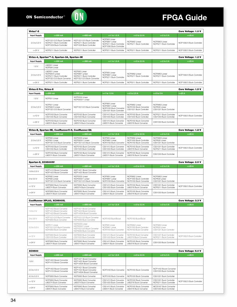
FPGA Guide
Virtex®-5 Core Voltage: 1.0 V
Input Supply <=200 mA <=500 mA <=1 to 1.5 A <=2 to 2.5 A <=3 to 5 A <=25 A
2.5 to 5.5 VNCP1521/2/3 Buck Controller NCP5211 Buck Controller NCP1529 Buck Controller
NCP1521/2/3 Buck Controller NCP5211 Buck Controller NCP1529 Buck Controller
NCP565 Linear NCP5661 Linear NCP5211 Buck Controller NCP1595 Buck Controller
NCP5662 Linear NCP5211 Buck Controller
NCP5663 Linear NCP5211 Buck Controller
NCP1582/3 Buck Controller
<=24 V NCP5211 Buck Controller NCP5211 Buck Controller NCP5211 Buck Controller NCP5211 Buck Controller NCP5211 Buck Controller NCP1582/3 Buck Controller
Virtex-4, Spartan™-3, Spartan-3A, Spartan-3E Core Voltage: 1.2 V
Input Supply <=200 mA <=500 mA <=1 to 1.5 A <=2 to 2.5 A <=3 to 5 A <=25 A
1.8 VLM2931 Linear NCP584 Linear
2.5 to 5.5 V
LM2931 Linear NCP584/5 Linear NCP5211 Buck Controller NCP1521/2/3 Buck Converter
NCP565 Linear NCP5661 Linear NCP5211 Buck Controller NCP1521/2/3 Buck Converter
NCP565 Linear NCP5661 Linear NCP5211 Buck Controller
NCP5662 Linear NCP5211 Buck Controller
NCP5663 Linear NCP5211 Buck Controller
NCP1582/3 Buck Controller
<=24 V NCP5211 Buck Controller NCP5211 Buck Controller NCP5211 Buck Controller NCP5211 Buck Controller NCP5211 Buck Controller NCP1582/3 Buck Controller
Virtex-II Pro, Virtex-II Core Voltage: 1.5 V
Input Supply <=200 mA <=500 mA <=1 to 1.5 A <=2 to 2.5 A <=3 to 5 A <=25 A
1.8 V NCP551 LinearNCP3335 Linear NCP5500/1 Linear
2.5 to 5.5 VNCP551 Linear NCP582/3 Linear NCP1521/2/3 Buck Converter
NCP1521/2/3 Buck Converter
NCP565 Linear NCP5661 Linear NCP3163 Buck Converter CS51031 Buck Controller
NCP5662 Linear NCP3163 Buck Converter CS51031 Buck Controller
NCP5663 Linear NCP630 Linear CS51031 Buck Controller
<=12 VNCP3163 Buck Converter CS51033 Buck Converter
NCP3163 Buck Converter CS51033 Buck Converter
CS51413 Buck Converter CS51033 Buck Controller
NCP3163 Buck Converter CS51033 Buck Controller
NCP5211 Buck Controller CS51033 Buck Controller
NCP1582/3 Buck Controller
<=24 VNCP3163 Buck Converter LM2574 Buck Converter
NCP3163 Buck Converter LM2574 Buck Converter
CS51413 Buck Converter LM2574 Buck Converter
NCP3163 Buck Converter LM2576 Buck Converter
CS51033 Buck Controller
Virtex-E, Spartan-IIE, CoolRunner®-II, CoolRunner-IIA Core Voltage: 1.8 V
Input Supply <=200 mA <=500 mA <=1 to 1.5 A <=2 to 2.5 A <=3 to 5 A <=25 A
2.5 to 5.5 VNCP584 Linear NCP561 Linear NCP1521/2/3 Buck Converter
NCP3335 Linear NCP5500/1 Linear NCP1521/2/3 Buck Converter
NCP565 Linear NCP5661 Linear NCP3163 Buck Converter
NCP5662 Linear NCP1550 Buck Controller NCP3163 Buck Converter
NCP5663 Linear NCP630 Linear CS51031 Buck Controller
<=12 VNCP3163 Buck Converter CS51033 Buck Controller
NCP3163 Buck Converter CS51033 Buck Controller
CS51413 Buck Converter CS51033 Buck Controller
NCP3163 Buck Converter LM2576 Buck Converter
CS51031 Buck Controller NCP5211 Buck Controller
NCP1582/3 Buck Controller
<=24 VNCP3163 Buck Converter LM2574 Buck Converter
NCP3163 Buck Converter LM2574 Buck Converter
CS51413 Buck Converter LM2574 Buck Converter
NCP3163 Buck Converter LM2576 Buck Converter
CS51033 Buck Controller
Spartan-II, XC9500XV Core Voltage: 2.5 V
Input Supply <=200 mA <=500 mA <=1 to 1.5 A <=2 to 2.5 A <=3 to 5 A <=25 A
1.8 to 2.5 VNCP1410 Boost Converter NCP1423 Boost Converter
NCP1421 Boost Converter NCP1422 Boost Converter
3 to 5.5 VNCP582 Linear NCP583 Linear NCP1521/2/3 Buck Converter
NCP3335 Linear NCP5500/1 Linear NCP1521/2/3 Buck Converter
NCP565 Linear NCP5661 Linear NCP3163 Buck Converter
NCP5662 Linear NCP1550 Buck Controller NCP3163 Buck Converter
NCP5663 Linear NCP630 Linear CS51031 Buck Controller
<=12 VNCP3063 Buck Converter LM2574 Buck Converter
NCP3063 Buck Converter LM2574 Buck Converter
CS51413 Buck Converter CS51033 Buck Controller
NCP3163 Buck Converter LM2576 Buck Converter
CS51031 Buck Controller NCP5211 Buck Controller
NCP1582/3 Buck Controller
<=24 VNCP3063 Buck Converter LM2574 Buck Converter
NCP3063 Buck Converter LM2574 Buck Converter
CS51413 Buck Converter LM2574 Buck Converter
NCP3163 Buck Converter LM2576 Buck Converter
CS51033 Buck Controller
CoolRunner XPLA3, XC9500XL Core Voltage: 3.3 V
Input Supply <=200 mA <=500 mA <=1 to 1.5 A <=2 to 2.5 A <=3 to 5 A <=25 A
1.8 to 3 VNCP1402 Boost Converter NCP1410 Boost Converter NCP1423 Boost Converter
NCP1421 Boost Converter NCP1422 Boost Converter NCP1450A Boost Converter
3 to 3.6 VNCP1521/2/3 Buck Converter NCP3063 Buck Converter
NCP1521/2/3 Buck Converter NCP3063 Buck Converter
NCP3163 Buck/Boost NCP3163 Buck/Boost
3.3 to 5.5 VNCP511 Linear NCP1521/2/3 Buck Converter NCP3063 Buck Converter
NCP3335 Linear NCP5500/1 Linear NCP1521/2/3 Buck Converter NCP3063 Buck Converter
NCP565 Linear NCP5661 Linear NCP3163 Buck Converter
NCP5662 Linear NCP1550 Buck Controller NCP3163 Buck Converter
NCP5663 Linear NCP630 Linear CS51031 Buck Controller
<=12 VNCP3063 Buck Converter CS51033 Buck Controller
NCP3063 Buck Converter CS51033 Buck Controller
CS51413 Buck Converter CS51033 Buck Controller
NCP3163 Buck Converter LM2576 Buck Converter
CS51031 Buck Controller NCP5211 Buck Controller
NCP1582/3 Buck Controller
<=24 VNCP3063 Buck Converter LM2574 Buck Converter
NCP3063 Buck Converter LM2574 Buck Converter
CS51413 Buck Converter LM2574 Buck Converter
NCP3163 Buck Converter LM2576 Buck Converter
CS51033 Buck Controller
XC9500 Core Voltage: 5.0 V
Input Supply <=200 mA <=500 mA <=1 to 1.5 A <=2 to 2.5 A <=3 to 5 A <=25 A
1.8 VNCP1402 Boost Converter NCP1410 Boost Converter
NCP1421 Boost Converter NCP1422 Boost Converter NCP1450A Boost Converter
2.5 to 4.5 VNCP1402 Boost Converter NCP1410 Boost Converter
NCP1421 Boost Converter NCP1422 Boost Converter NCP1450A Boost Converter
NCP3163 Buck Converter NCP3163 Buck ConverterNCP1442 Boost Converter CS51033 Buck Controller
4.5 to 5.5 V NCP3063 Buck Converter NCP3063 Buck Converter NCP3163 Buck Converter NCP3163 Buck Converter CS51031 Buck Controller
<=12 VNCP3063 Buck Converter LM2574 Buck Converter
NCP3063 Buck Converter LM2574 Buck Converter
CS51413 Buck Converter CS51033 Buck Controller
NCP3163 Buck Converter LM2576 Buck Converter
CS51031 Buck Controller NCP5211 Buck Controller
NCP1582/3 Buck Controller
<=24 VNCP3063 Buck Converter LM2574 Buck Converter
NCP3063 Buck Converter LM2574 Buck Converter
CS51413 Buck Converter LM2574 Buck Converter
NCP3163 Buck Converter LM2576 Buck Converter
MC33167 Buck Converter CS51033 Buck Controller
34
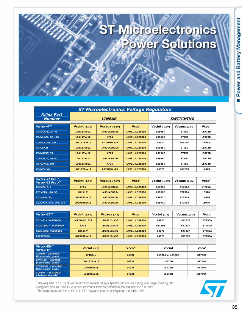
ST Microelectronics Voltage Regulators Xilinx Part
Number LINEAR SWITCHING
Virtex-4™ Vccint (1.2V) Vccaux (2.5V) Vcco1 Vccint (1.2V) Vccaux (2.5V) Vcco1
XC4VLX15, 25, 40 LD1117xx12 L4931ABD25x L4931, LD29300 L6926D ST750 L5972D
XC4VLX60, 80, 100 LD1117xx12 KF25 L4931, LD29300 L6926D ST750 L5972D
XC4VLX160, 200 LD1117Axx12 LD29080 x25 L4931, LD29300 L5970 L6926D L4973
XC4VSX25 LD1117xx12 L4931ABD25x L4931, LD29300 L6926D ST750 L5972D
XC4VSX35, 55 LD1117xx12 KF25 L4931, LD29300 L6926D ST750 L5972D
XC4VFX12, 20, 40 LD1117xx12 L4931ABD25x L4931, LD29300 L6926D ST750 L5972D
XC4VFX60, 100 LD1117xx12 KF25 L4931, LD29300 L6926D ST750 L5972D
XC4VFX140 LD1117Axx12 LD29080 x25 L4931, LD29300 L5970 L6926D L4973
Virtex-II Pro™ Virtex-II Pro X™
Vccint (1.5V) Vccaux (2.5V) Vcco1 Vccint (1.5V) Vccaux (2.5V) Vcco1
XC2VP2, 4, 7 KF15 L4931ABD25x L4931, LD29300 L6926D ST750A ST750A
XC2VP20, x20, 30 LD11172 L4931ABD25x L4931, LD29300 L5970D ST750A L5970
XC2VP40, 50, LD29150xx15 L4931ABD25x L4931, LD29300 L5972D ST750A L5970
XC2VP70, X70, 100, 125 LD29300xx15 L4931ABD25x L4931, LD29300 L5973D ST750A L5970
Virtex-II™ Vccint (1.5V) Vccaux (3.3) Vcco1 Vccint (1.5) Vccaux (3.3) Vcco1
XC2V40 - XC2V1000 L4931ABD15TR LD2981Cxx33 L4931, LD29300 L5970 ST763A ST750A
XC2V1500 - XC2V3000 KF15 LD2981Cxx33 L4931, LD29300 ST1S03 ST763A ST750A
XC2V4000, XC2V6000 LD11172 LD2981Cxx33 L4931, LD29300 L4973 ST763A ST750A
XCE2V8000 LD29150xx15 LD2981Cxx33 L4931, LD29300 L4973 ST763A ST750A
Virtex-EM™ Virtex-E™
Vccint (1.8) Vcco1 Vccint Vcco1
XCV50E – XVC600E (Commercial grade ) LF18Cxx L4931 L6926D or L5970D ST750A
XCV812E – XCV200E (Commercial grade )
LD1117Axx18 L4931 L5970D ST750A
XCV2600E - XCV3200 (Commercial grade ) LD1086xx18 L4931 L5972D ST750A
XCV50E - XCV3200E ( Industrial grade) LD1085xx18 L4931 L5973D ST750A
1 The required I/O current will depend on several design specific factors, including I/O usage, loading, etc. Designers should use FPGA power estimator tools to determine the required Iccio current.2 The adjustable version of the LD1117 regulator can be configured to supply 1.5V.
ST Microelectronics Power Solutions
1 The required I/O current will depend on several design specific factors, including I/O usage, loading, etc.Designers should use FPGA power estimator tools to determine the required Iccio current.2 The adjustable version of the LD1117 regulator can be configured to supply 1.5V.
P
ow
er a
nd B
atte
ry M
anag
emen
t
35
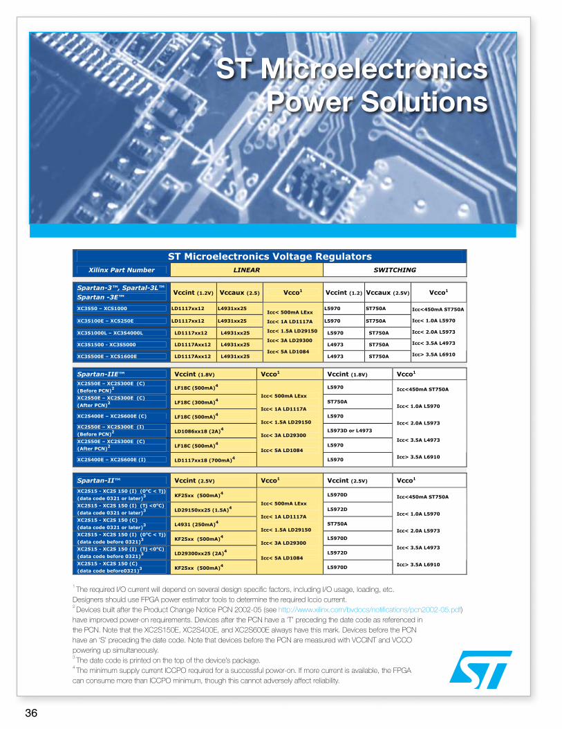
ST Microelectronics Power Solutions
ST Microelectronics Voltage Regulators
Xilinx Part Number LINEAR SWITCHING
Spartan-3™, Spartal-3L™
Spartan -3E™ Vccint (1.2V) Vccaux (2.5) Vcco1 Vccint (1.2) Vccaux (2.5V) Vcco1
XC3S50 – XCS1000 LD1117xx12 L4931xx25 L5970 ST750A
XC3S100E – XCS250E LD1117xx12 L4931xx25 L5970 ST750A
XC3S1000L – XC3S4000L LD1117xx12 L4931xx25 L5970 ST750A
XC3S1500 - XC3S5000 LD1117Axx12 L4931xx25 L4973 ST750A
XC3S500E – XCS1600E LD1117Axx12 L4931xx25
Icc< 500mA LExx
Icc< 1A LD1117A
Icc< 1.5A LD29150
Icc< 3A LD29300 Icc< 5A LD1084
L4973 ST750A
Icc<450mA ST750A Icc< 1.0A L5970 Icc< 2.0A L5973 Icc< 3.5A L4973 Icc> 3.5A L6910
Spartan-IIE™ Vccint (1.8V) Vcco1 Vccint (1.8V) Vcco1 XC2S50E – XC2S300E (C)
(Before PCN)2 LF18C (500mA)4 L5970
XC2S50E – XC2S300E (C)
(After PCN)2 LF18C (300mA)4 ST750A
XC2S400E – XC2S600E (C) LF18C (500mA)4 L5970
XC2S50E – XC2S300E (I)
(Before PCN)2 LD1086xx18 (2A)4 L5973D or L4973
XC2S50E – XC2S300E (C)
(After PCN)2 LF18C (500mA)4 L5970
XC2S400E – XC2S600E (I) LD1117xx18 (700mA)4
Icc< 500mA LExx
Icc< 1A LD1117A
Icc< 1.5A LD29150
Icc< 3A LD29300
Icc< 5A LD1084
L5970
Icc<450mA ST750A Icc< 1.0A L5970 Icc< 2.0A L5973 Icc< 3.5A L4973 Icc> 3.5A L6910
Spartan-II™ Vccint (2.5V) Vcco1 Vccint (2.5V) Vcco1
XC2S15 - XC2S 150 (I) (0oC < Tj)
(data code 0321 or later)3 KF25xx (500mA)4 L5970D
XC2S15 - XC2S 150 (I) (Tj <0oC)
(data code 0321 or later)3 LD29150xx25 (1.5A)4 L5972D
XC2S15 - XC2S 150 (C)
(data code 0321 or later)3 L4931 (250mA)4 ST750A
XC2S15 - XC2S 150 (I) (0oC < Tj)
(data code before 0321)3 KF25xx (500mA)4 L5970D
XC2S15 - XC2S 150 (I) (Tj <0oC)
(data code before 0321)3 LD29300xx25 (2A)4 L5972D
XC2S15 - XC2S 150 (C)
(data code before0321)3 KF25xx (500mA)4
Icc< 500mA LExx
Icc< 1A LD1117A
Icc< 1.5A LD29150
Icc< 3A LD29300
Icc< 5A LD1084
L5970D
Icc<450mA ST750A Icc< 1.0A L5970 Icc< 2.0A L5973 Icc< 3.5A L4973 Icc> 3.5A L6910
1 The required I/O current will depend on several design specific factors, including I/O usage, loading, etc. Designers should use FPGA power estimator tools to determine the required Iccio current.2Devices built after the Product Change Notice PCN 2002-05 (see http://www.xilinx.com/bvdocs/notifications/pcn2002-05.pdf)have improved power-on requirements. Devices after the PCN have a ‘T’ preceding the date code as referenced in the PCN. Note that the XC2S150E, XC2S400E, and XC2S600E always have this mark. Devices before the PCN have an ‘S’ preceding the date code. Note that devices before the PCN are measured with VCCINT and VCCO powering up simultaneously.3The date code is printed on the top of the device’s package.4 The minimum supply current ICCPO required for a successful power-on. If more current is available, the FPGA can consume more than ICCPO minimum, though this cannot adversely affect reliability.
1 The required I/O current will depend on several design specific factors, including I/O usage, loading, etc.
Designers should use FPGA power estimator tools to determine the required Iccio current.2 Devices built after the Product Change Notice PCN 2002-05 (see http://www.xilinx.com/bvdocs/notifications/pcn2002-05.pdf)
have improved power-on requirements. Devices after the PCN have a ‘T’ preceding the date code as referenced inthe PCN. Note that the XC2S150E, XC2S400E, and XC2S600E always have this mark. Devices before the PCNhave an ‘S’ preceding the date code. Note that devices before the PCN are measured with VCCINT and VCCOpowering up simultaneously.3 The date code is printed on the top of the device’s package.
4 The minimum supply current ICCPO required for a successful power-on. If more current is available, the FPGA
can consume more than ICCPO minimum, though this cannot adversely affect reliability.
36
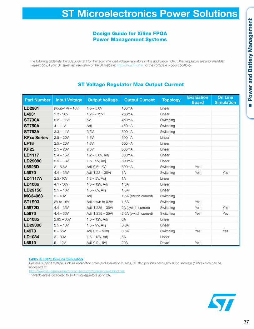
Design Guide for Xilinx FPGA Power Management Systems
ST Microelectronics Power Solutions
The following table lists the output current for the recommended voltage regulators in this application note. Other regulators are also available, please consult your ST sales representative or the ST website: http://www.st.com, for the complete product portfolio.
L497x & L597x On-Line SimulatorsBesides support material such as application notes and evaluation boards, ST also provides online simulation software (“SW”) which can be accessed at:http://www.st.com/stonline/products/support/designin/switchingl.htmThis software is dedicated to switching regulators up to 2A.
P
ow
er a
nd B
atte
ry M
anag
emen
t
Part Number Input Voltage Output Voltage Output Current TopologyEvaluation
BoardOn Line
SimulationLD2981 (Vout+1V) – 16V 1.5 – 5.0V 100mA Linear
L4931 3.3 - 20V 1.25 – 12V 250mA Linear
ST730A 5.2 – 11V 5V 450mA Switching
ST750A 4 – 11V Adj. 450mA Switching
ST763A 3.3 – 11V 3.3V 500mA Switching
KFxx Series 2.5 – 20V 1.5V 500mA Linear
LF18 2.5 – 20V 1.8V 500mA Linear
KF25 2.5 – 20V 2.5V 500mA Linear
LD1117 2.4 – 15V 1.2 – 5.0V, Adj 800mA Linear
LD29080 2.5 – 13V 1.5 – 9V, Adj 800mA Linear
L6926D 2 – 5.5V Adj (0.6 - 5V) 800mA Switching Yes
L5970 4.4 – 36V Adj (1.23 – 35V) 1A Switching Yes Yes
LD1117A 2.5 -10V 1.2 – 5V, Adj 1A Linear
LD1086 4.1 - 30V 1.5 – 12V, Adj 1.5A Linear
LD29150 2.5 – 13V 1.5 – 8V, Adj 1.5A Linear
MC34063 3 – 40V Adj 1.5A (switch current) Switching
ST1S03 3V to 16V Adj down to 0.8V 1.5A Switching Yes
L5972D 4.4 – 36V Adj (1.235 – 35V) 2A (switch current) Switching Yes Yes
L5973 4.4 – 36V Adj (1.235 – 35V) 2.5A (switch current) Switching Yes Yes
LD1085 2.85 – 30V 1.5 – 12V, Adj 3A Linear
LD29300 2.5 – 13V 1.5 – 9V, Adj 3.0A Linear
L4973 8 – 55V Adj (0.5 – 50V) 3.5A Switching Yes Yes
LD1084 3 – 30V 1.5 – 12V, Adj 5A Linear
L6910 5 – 12V Adj (0.9 – 5V) 20A Driver Yes
ST Voltage Regulator Max Output Current
37
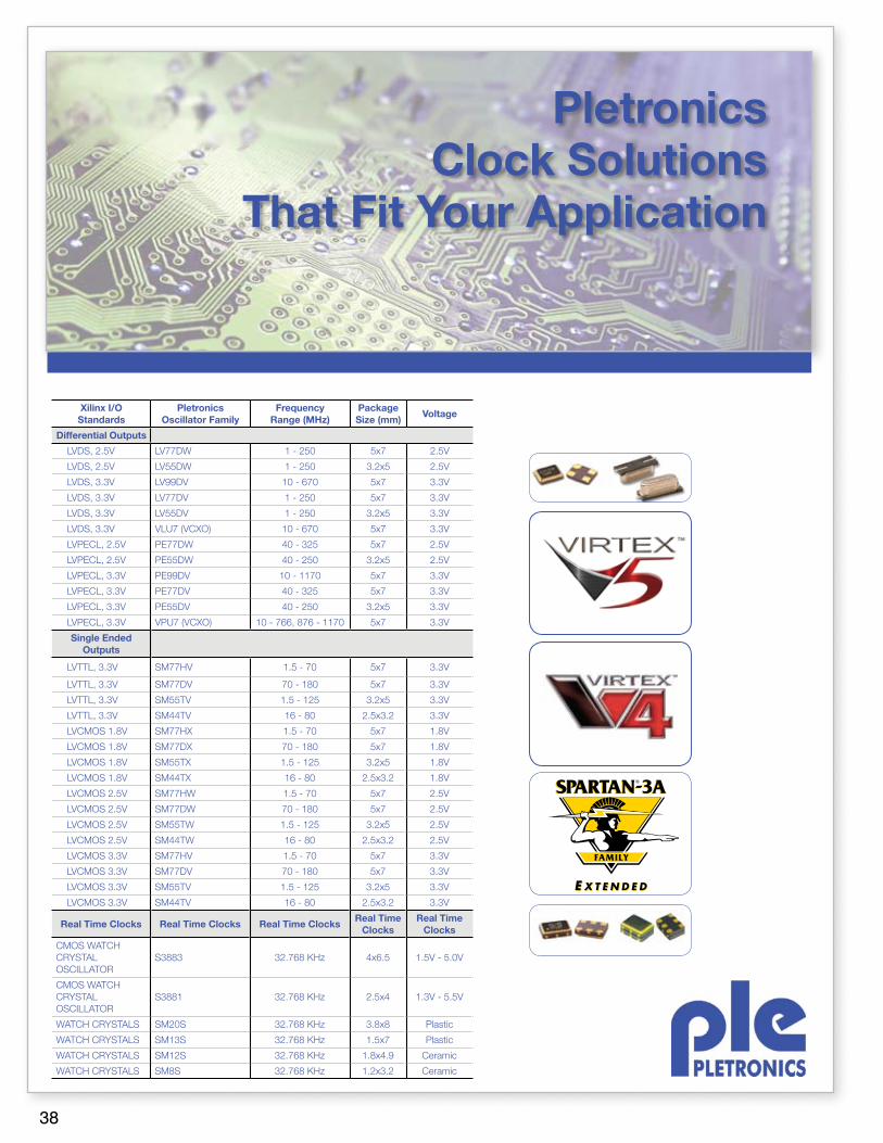
Pletronics Clock Solutions
That Fit Your Application
Xilinx I/O Standards
PletronicsOscillator Family
FrequencyRange (MHz)
PackageSize (mm)
Voltage
Differential Outputs
LVDS, 2.5V LV77DW 1 - 250 5x7 2.5V
LVDS, 2.5V LV55DW 1 - 250 3.2x5 2.5V
LVDS, 3.3V LV99DV 10 - 670 5x7 3.3V
LVDS, 3.3V LV77DV 1 - 250 5x7 3.3V
LVDS, 3.3V LV55DV 1 - 250 3.2x5 3.3V
LVDS, 3.3V VLU7 (VCXO) 10 - 670 5x7 3.3V
LVPECL, 2.5V PE77DW 40 - 325 5x7 2.5V
LVPECL, 2.5V PE55DW 40 - 250 3.2x5 2.5V
LVPECL, 3.3V PE99DV 10 - 1170 5x7 3.3V
LVPECL, 3.3V PE77DV 40 - 325 5x7 3.3V
LVPECL, 3.3V PE55DV 40 - 250 3.2x5 3.3V
LVPECL, 3.3V VPU7 (VCXO) 10 - 766, 876 - 1170 5x7 3.3V
Single Ended Outputs
LVTTL, 3.3V SM77HV 1.5 - 70 5x7 3.3V
LVTTL, 3.3V SM77DV 70 - 180 5x7 3.3V
LVTTL, 3.3V SM55TV 1.5 - 125 3.2x5 3.3V
LVTTL, 3.3V SM44TV 16 - 80 2.5x3.2 3.3V
LVCMOS 1.8V SM77HX 1.5 - 70 5x7 1.8V
LVCMOS 1.8V SM77DX 70 - 180 5x7 1.8V
LVCMOS 1.8V SM55TX 1.5 - 125 3.2x5 1.8V
LVCMOS 1.8V SM44TX 16 - 80 2.5x3.2 1.8V
LVCMOS 2.5V SM77HW 1.5 - 70 5x7 2.5V
LVCMOS 2.5V SM77DW 70 - 180 5x7 2.5V
LVCMOS 2.5V SM55TW 1.5 - 125 3.2x5 2.5V
LVCMOS 2.5V SM44TW 16 - 80 2.5x3.2 2.5V
LVCMOS 3.3V SM77HV 1.5 - 70 5x7 3.3V
LVCMOS 3.3V SM77DV 70 - 180 5x7 3.3V
LVCMOS 3.3V SM55TV 1.5 - 125 3.2x5 3.3V
LVCMOS 3.3V SM44TV 16 - 80 2.5x3.2 3.3V
Real Time Clocks Real Time Clocks Real Time ClocksReal Time
ClocksReal Time
Clocks
CMOS WATCH CRYSTALOSCILLATOR
S3883 32.768 KHz 4x6.5 1.5V - 5.0V
CMOS WATCH CRYSTALOSCILLATOR
S3881 32.768 KHz 2.5x4 1.3V - 5.5V
WATCH CRYSTALS SM20S 32.768 KHz 3.8x8 Plastic
WATCH CRYSTALS SM13S 32.768 KHz 1.5x7 Plastic
WATCH CRYSTALS SM12S 32.768 KHz 1.8x4.9 Ceramic
WATCH CRYSTALS SM8S 32.768 KHz 1.2x3.2 Ceramic
38
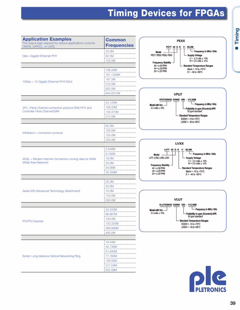
Timing Devices for FPGAs
Application ExamplesThe output logic required for various applications could be CMOS, LVPECL, or LVDS.
CommonFrequencies
Gbe =Gigabit Ethernet PHY
25.0M
62.5M
125.0M
10Gbe = 10 Gigabit Ethernet PHY/XAUI
156.25M
161.1328M
187.5M
312.5M
625.0M
644.5312M
2FC =Fibre Channel connection protocol SAS PHY and Controller Fibre Channel/SAN
53.125M
106.25M
159.375M
212.5M
Infiniband = connection protocal
62.5M
100.0M
125.0M
250.0M
ADSL = Modem Internet Connection moving data for WAN (Wide Area Network)
2.048M
8.192M
16.0M
20.0M
34.56M
35.328M
Serial ATA (Advanced Technology Attachment)
25.0M
50.0M
75.0M
150.0M
300.0M
PCI/PCI Express
33.333M
66.667M
100.0M
133.333M
266.666M
400.0M
Sonet: Long distance Optical Networking Ring
19.44M
44.736M
51.840M
77.760M
155.52M
311.04M
622.08M
T
imin
g
3939
UNITED STATESCorporate Headquarters70 Maxess RoadMelville, NY 11747Tel: 631-396-5000Fax: 631-396-5050
alabamaTel: 256-722-9330Fax: 256-722-9348
arizonaTel: 800-359-4818Fax: 480-345-5528
CaliforniaSan JoSe
Tel: 408-434-0800 Fax: 408-434-6849IrvIne
Tel: 949-470-1011 Fax: 949-470-1104San DIego
Tel: 858-576-0088 Fax: 858-576-0990LoS angeLeS
Tel: 818-874-9600 Fax: 818-874-9605
ColoradoTel: 800-200-1586Fax: 303-379-2162
floridanorth FLorIDa
Tel: 407-831-0016 Fax: 425-928-4018South FLorIDa
Tel: 954-735-2555 Fax: 954-735-2880
GeorGiaTel: 770-416-8666Fax: 770-416-9060
illinoisTel: 847-706-9100Fax: 847-706-9111
marylandTel: 410-309-0030Fax: 410-309-0088
massaCHusettsTel: 978-774-3330Fax: 978-774-6633
minnesotaTel: 952-942-9030Fax: 952-942-9144
new JerseyTel: 973-882-8300Fax: 973-882-8398
new yorkMeLvILLe
Tel: 631-396-5000 Fax: 631-396-5050rocheSter
Tel: 585-292-0777 Fax: 585-292-0750
nortH CarolinaTel: 919-787-9426Fax: 919-787-9430
oHioTel: 330-963-9933Fax: 330-963-9944
oreGonTel: 503-439-1200Fax: 503-439-6286
pennsylvaniaTel: 215-659-8405Fax: 215-659-1331
texasDaLLaS
Tel: 972-202-5100 Fax: 972-202-5079auStIn
Tel: 512-382-3742 Fax: 512-382-3743
utaHTel: 800-200-1586Fax: 972-479-1410
wasHinGtonTel: 425-452-7077Fax: 425-452-7081
CANADAMontreaL
Tel: 905-761-1911 Fax: 905-761-2811ottawa
Tel: 905-761-1911 Fax: 905-761-2811 toronto
Tel: 905-761-1911 Fax: 905-761-2811
MEXICOchIhuahua Tel: (52) 65 6648 7157 Fax: (52) 65 6207 1851JaLISco Tel: (52) 33 3133 2043 Fax: (52) 33 3133 1782
ASIA/PACIFICasia Headquarters50 Kallang Avenue#06-01, Noel Corporate BuildingSingapore 339505 Tel: (65) 6844 1650
india banGalore Tel: (91) 80 4123 5217 / 18 / 19 Fax: (91) 80 4112 2803
CHennai Tel: (91) 97909 20925
Hyderabad Tel: (91) 40 6631 6357 Fax: (91) 40 2781 3456
pune Tel: (91) 99 6060 2822 Fax: (91) 98 9068 1081
new delHi Tel: (91) 11 4167 4374/75 Fax: (91) 11 4167 4376
Greater CHina HonG konG Tel: (852) 3511 9911 Fax: (852) 3511 9990
beiJinG Tel: (86) 10 8225 1376 / 7 Fax: (86) 10 8225 1375 CHenGdu Tel: (86) 28-6622-5166
HanGzHou Tel: (86) 571 5676 5811
sHanGHai Tel: (86) 21 6441 1811 Fax: (86) 21 6432 5790
wuHan Tel: (86) 27 8769 0810 Fax: (86) 27 8769 0820
sHenzHen Tel: (86) 755 3398 2850 Fax: (86) 755 8219 0980
nanJinG Tel: (86) 21 6441 1811 Fax: (86) 21 6432 5790
taiwan Tel: (886) 2 8797 3718 Fax: (886) 2 8797 3719
vietnam Tel: (84) 90 8131 973
malaysia Tel: (60) 4 660 5888 Fax: (60) 4 660 5883
sinGapore Tel: (65) 6844 1650 Fax: (65) 6841 0494
tHailand Tel: (66) 2 694 1368 / 9 Fax: (66) 2 694 1370
australia / new zealand melbourne Tel: (61) 3 9720 6444 Fax: (61) 3 9720 9504
Sydney Tel: (61) 2 9746 1411 Fax: (61) 2 9746 1511
EMEAaustria vienna Tel: (43) 664 55 664 93 Fax: (49) 89 92 333 45 99
denmark (C-88) HørsHolm Tel: (45) 7010-4888 Fax: (45) 7010-4889
silkeborG Tel: (45) 7010-4888 Fax: (45) 7010-4889
Germany muniCH Tel: (49) 8992 333-450 Fax: (49) 8992 333-4511
HunGary naGykata Tel: (36) 3069 64544
poland warsaw Tel: (48) 602389 537
sweden (C-88) stoCkHolm Tel: (46) 08-558-038-88 Fax: (46) 08-558-038-89 united kinGdom Coventry Tel: (44) 024 7643 7437 Fax: (44) 024 7643 7401
MississippiGuadalajara
= Distribution Center
Singapore
Hong Kong
Coventry, UK
w w w . n u h o r i z o n s . c o m
Global Contact Information Nu Horizons Electronics