sealed ultra low-k organosilica films with improved electrical, mechanical and chemical properties
TRANSCRIPT

Journal ofMaterials Chemistry C
PAPER
aGhent University, Department of inorganic
(S3), 9000 Ghent, Belgium. E-mail: pascal.v
83; Tel: +329 264 44 42bGhent University, Department of solid state
BelgiumcIMEC, Kapeldreef 75, 3001 Heverlee, Belgiu
Cite this: J. Mater. Chem. C, 2013, 1,3961
Received 20th March 2013Accepted 23rd April 2013
DOI: 10.1039/c3tc30522h
www.rsc.org/MaterialsC
This journal is ª The Royal Society of
Sealed ultra low-k organosilica films with improvedelectrical, mechanical and chemical properties
Frederik Goethals,a Elisabeth Levrau,b Glenn Pollefeyt,a Mikhail R. Baklanov,c
Ivan Ciofi,c Kris Vanstreels,c Christophe Detavernier,b Isabel Van Driesschea
and Pascal Van Der Voort*a
In this contribution, we present sealed ultra low-k organosilica films that have improved electrical,
mechanical and chemical properties. The films consist of a mesoporous ethylene-bridged organosilica
layer at the bottom and an almost non-porous cyclic carbon-bridged top layer. This top layer effectively
seals metal penetration during atomic layer deposition processes. Furthermore, by applying this sealing
approach we can lower the dielectric constant of the pristine mesoporous film from 2.5 to 2.07 while
we can also lower the leakage current and improve the mechanical and chemical stability.
Introduction
To further improve the performance and to reduce the powerconsumption of microelectronic devices, the dielectric layerthat insulates the conductive wires should have an ultra low-kvalue or relative dielectric constant (k < 2.1).1 Mesoporousorganosilica materials that contain low polarisable organicbridges in the silica network (the so-called periodic mesoporousorganosilicas, PMOs) are some of the most promising ultra low-k materials.2–4 This is because they combine an organosilicanetwork with a high porosity. The porosity drastically reducesthe k-value because the pores are lled with air which has ak-value of almost 1.5
On the other hand, highly porous materials also have somedisadvantages. At the moment, they lack the requiredmechanical stability to survive chemical mechanical polishing(CMP) processes.4,6 Further, the pores are interconnected andrelatively large in size (3 nm or more).7 This means that gaseousmetal ions, which are released during integration processes,can easily diffuse into the pores leading to higher leakagecurrent densities, lower breakdown voltage or even completefailure of the dielectric low-k lm.8 The latter can be avoided bysealing the pores.3 To seal pores up to 2 nm plasma treat-ments,9–13 chemical vapor deposition (CVD)14–16 and atomiclayer deposition (ALD) are commonly used techniques.17,18
However, for larger pores the existing sealing techniques areno longer efficient anymore. Plasma sealing, e.g. by densica-tion of the top layer, leads to unacceptable shrinkage of the
and physical chemistry, Krijgslaan 281
[email protected]; Fax: +329 264 49
sciences, Krijgslaan 281 (S1), 9000 Ghent,
m
Chemistry 2013
lm.19 In the case of CVD and ALD processes, the size ofprecursor molecules becomes much smaller than the porediameter and they are deeply diffused into the pores, resultingin pore lling rather than pore sealing.5 Therefore, other strat-egies to efficiently seal pores larger than 2 nm are required.
An interesting approach is modication of the top surface oflow-k lms. This modication creates functional groups whichcan react with sealant molecules.20,21 Other promisingapproaches are pore lling with a labile polymer which can beremoved aer processing or thermal treatments that causecollapsing of the pore connections.22,23
Recently, we reported the possibility to seal the pores ofmesoporous lms by the deposition of a dielectric layer on topof a low-k material.24 This was achieved by preassembling thesealant molecules consisting of cyclic-bridged organosilaneprecursors into larger molecules by aging the starting mixturebefore deposition.
In this paper, we provide evidence that diffusion of thesealant molecules into the porous material is dependent on theaging time of the precursor. Therefore the sealing organosilanemixture was deposited every 24 hours on top of ethane PMOlms and the resulting 2-layer lm was characterized byellipsometry. The sealant layer has the advantage that thematerial itself has a low dielectric constant owing to the highamount of low polarisable organic groups.25,26 This means thatthe effective dielectric constant (porous lm + top layer) shouldnot be signicantly higher compared to the pristine low-k lm.
Furthermore, we were able to sufficiently narrow the poreentrances of the ethane PMO lm to prevent ALD precursordiffusion. To prove this, we deposited TiO2 via ALD and inves-tigated the presence of Ti in the porous material by X-ray uo-rescence (XRF), transmission electron microscopy (TEM) andscanning transmission electron microscopy energy-dispersiveX-ray spectroscopy (STEM-EDX).
J. Mater. Chem. C, 2013, 1, 3961–3966 | 3961

Journal of Materials Chemistry C Paper
Finally, the inuence of this sealing method on the electricalandmechanical properties of the ethane PMO lm is presented.The investigated electrical properties are the dielectric constant,leakage current and breakdown voltage. For the mechanicalproperties, the Young's modulus and hardness are reportedwhile for the chemical properties, the etch resistance againstalkaline solutions is presented.
Experimental sectionChemicals
Chloromethyltriethoxysilane (95%) and 1,2-bis(triethoxysilyl)-ethane (97%) were purchased from ABCR; hydrochloric acid(HCl, 37%), pentane (97%) and absolute ethanol were obtainedfrom Fiers; tetrakis(dimethylamino)titanium(IV) (TDMAT, 99%)were obtained from Strem Chemicals; Brij-76, tetrahydrofuran(THF, >99.9%) and Mg turnings (>99.5%) were purchased fromAldrich; and iron trichloride (FeCl3, 99%) was purchased fromAcros. All materials were used as received.
Synthesis
Preparation of the periodic mesoporous ethylene-bridgedorganosilica lms (ethane PMOs). 1.2 g Brij-76 was dissolved in20 ml ethanol and 1.5 ml (0.1 M) HCl. Then 3 ml of 1,2-bis-(triethoxysilyl)ethane and 1.5 ml H2O were added to the solutionand this was aged for 1 day. The solution was then spin coated ona Si-wafer at a rate of 5000 rpm. The surfactant was removed bytreating the lm at 400 �C for 5 hours. Because a dense layerdeposition reduces the overall porosity, thelms that were sealedhad a higher pristine porosity than the non-sealed lms. Toachieve this, more surfactant was added (1.8 g instead of 1.2 g).
Preparation of the cyclic carbon-bridged organosilanes.24 Asolution of 70 ml 0.5 wt% FeCl3 in dry THF was added to 7 g Mgturnings and stirred until a grey colored mixture was appeared.This mixture was kept under an inert atmosphere. Then, asolution of 100 ml 14.2 v% chloromethyl triethoxysilane in dryTHF was rapidly added to the mixture and stirred for 48 h at50 �C. The mixture was ltered off and the solvent was removedfrom the ltrate. Pentane was added to the residue and thismixture was also ltered. The remaining oil consists of cycliccarbon-bridged organosilanes as shown in Scheme 1.
Preparation of the cyclic-bridged organosilica dense layer.0.5 ml of the cyclic carbon-bridged organosilane mixture wasdissolved in 20 ml ethanol, 0.5 ml (0.1 M) HCl and 0.5 ml H2Oand aged for a certain time. Solutions with different aging times(0 to 9 days) were then spin-coated at 5000 rpm on top of theorganosilica lm to form an organosilica top layer. An addi-tional baking step was performed at 400 �C under a nitrogenatmosphere to remove all the volatiles and to complete thecondensation of the cyclic carbon-bridged precursor.
Scheme 1 Synthesis of cyclic carbon-bridged organosilanes.
3962 | J. Mater. Chem. C, 2013, 1, 3961–3966
TiO2 deposition on the ultra low-k lms by atomic layerdeposition
Atomic layer deposition of titanium dioxide was performed onthe synthesized low-k lms to investigate the sealing propertiesof the top layer. ALD is a self-limiting thin lm growth tech-nique in which a substrate is exposed to chemical precursorsand water in an alternating way.27 The lms in this work weretreated in a home-built ALD reactor and subjected to 100 ALDcycles. Each ALD cycle involved two subsequent self-terminatinghalf reactions.
In the rst half reaction, the sample is exposed to TDMAT[Ti(NMe2)4] vapour for 10 seconds, followed by 40 secondsevacuation of the reaction chamber. The second half reactionconsists of a 10 second water vapor pulse followed by 40seconds of evacuation under vacuum. The depositions werecarried out at a temperature of 120 �C with TDMAT–H2O pres-sures of 0.3 Pa. Before ALD treatment the low-k lms wereevacuated in a vacuum at the deposition temperature for 1 hour.
Characterization
The refractive index and thickness of the layer were analyzed ona J. A. Woollam ellipsometer alpha-SE. The total porosity wascalculated from the refractive index using the Lorentz–Lorenzformula.28
For the porosity measurement, a spectroscopic ellipsometerSentech 801 is mounted in a vacuum chamber that can be lledwith solvent vapor (toluene) in a controlled way. The pressure ofthe toluene vapor is raised in steps from the vacuum level up tothe saturation pressure. The pressure dependent condensationoccurs in the open pores and the refractive index of the sampleis changed. The total pore volume is calculated from the changein refractive index at saturation pressure using the Lorentz–Lorenz equation.28
Water contact angle values were obtained by using a Kruss-DSA 30 Drop Shape Analysis System using the tangent 1 model.
To determine the amount of titanium deposited by ALDX-Ray Fluorescence (XRF) spectroscopy measurements wereperformed using a Bruker Artax system consisting of a Mo X-raysource (Mo K radiation and Bremsstrahlung continuum) and anXFlash 5010 silicon dri detector.
TEM measurements were performed with a Cs-correctedJEOL JEM 2200 FS microscope, operating at 200 kV. Themicroscope was operated in STEM-mode with a spot size of 0.5nm to perform the EDX measurements. The cross-sectionalTEM samples were prepared by Focused Ion Beam (FIB).
The dielectric constant of the lms was calculated from thecapacitance of a parallel plate capacitor at 100 kHz using a HP4192A LF impedance analyzer. Aluminum dots were used as topcontacts and a heavily doped silicon wafer was used as thebottom contact. The bottom of the silicon wafer was scratchedto remove the native silicon dioxide and a eutectic indium–
gallium alloy was attached to make a good ohmic contactwith the impedance analyzer. The leakage current and break-down voltage were obtained by performing current–voltage(I–V) measurements on a HP4156 Semiconductor ParameterAnalyzer.
This journal is ª The Royal Society of Chemistry 2013

Paper Journal of Materials Chemistry C
Diffuse reectance infra-red Fourier transform (DRIFT)spectra were obtained on a Thermo 6700 FLEX FTIR/FT-Ramansystem, equipped with a nitrogen cooled MCT-A detector.
The Young's modulus and hardness of the low-k dielectriclms were measured by nano-indentation using a NanoIndenter XP system from MTS Corporation, with a dynamiccontact module (DCM) and a continuous-stiffness measure-ment (CSM) option under constant strain rate conditions(0.05 s�1).
Results and discussionInvestigation of sealant properties/characteristics
Because diffusion of the sealant into the porous material is amain issue, possible diffusion of the top layer was rst inves-tigated by ellipsometry. Therefore, the thickness and refractiveindex of the pristine ethane PMO lm were determined usingthe Cauchy model.
Next the sealing layer was deposited on top of the ethanePMO lm and the total thickness (ethane PMO + top layer) wasdetermined. By knowing the thickness of the porous lm andthe total thickness, the thickness of the top layer can becalculated.
To investigate the refractive index (and thus the porosity) ofthe ethane PMO lm aer the dense layer deposition, a two-layer Cauchy model was used. One layer model ts the porouslm and the other the top lm. Assuming that the thickness ofthe ethane PMO lm does not signicantly change aer the toplayer deposition, this parameter can be xed and only theparameters that inuence the refractive index are tted. In thecase that the refractive index of the porous lm is similar beforeand aer the top layer deposition, there is no signicantdiffusion of the top layer.
To see if the aging time leads to large oligomers that canexceed the pore size, the sealant solution was spin-coated every24 hours on ethane PMO lms with pore sizes around 3 nm. Theresults are shown in Fig. 1. Due to the fact that the porosity ofthe different porous organosilica samples was not exactly thesame, the relative porosity (ratio porosity aer/before deposi-tion) was plotted as a function of the aging time. It can be seenfrom the gure that before 5 days the porosity of the ethanePMO lm aer deposition is lower than the pristine lm.
Fig. 1 Relative porosity of mesoporous organosilica films after deposition of thetop layer.
This journal is ª The Royal Society of Chemistry 2013
This means that the sealant molecules are not large enoughand will diffuse into the porous material, lling up the pores.Aer 5 days of aging the porosity of the ethane PMO lms doesnot change, meaning that the sealant molecules are too large toenter the pores.
Since moisture and metal uptake in the pores of the low-klm can deteriorate its quality, it is important that the top layerseals the internal surface from the environment. Here, thesealant properties of the top layer are investigated by adsorp-tion/desorption analysis and by depositing a TiO2 layer on thesamples by means of ALD. ALD is based on sequential, self-limiting surface reactions where the precursors absorb on allthe surface sites available in the growth chamber and within thepores of the samples.
Fig. 2 shows the toluene physisorption isotherms of theethane PMOs before and aer top layer deposition. It can beseen that aer the top layer deposition the total porosity (porouslm + dense lm compared to pristine porous lm) is decreasedfrom 50% to 40% which can be expected when an almostnonporous material is deposited on top of a highly porous layer.However, a high porosity still remains. Further, the desorptionbranch is delayed which means that bottle necks are formedreducing the pore entrances and the pores are partially sealed.29
Aer the TiO2 deposition, the samples were analyzed by XRFto determine the amount of titanium that was deposited on thesamples. In Fig. 3, the analysis shows that there is twice asmuch deposited on the pristine ethane PMO lm (EPMO) ascompared to a planar SiO2 substrate. This indicates that theTDMAT gas molecules can diffuse into the pores of the low-kmaterial covering the internal surface.
However, when the organosilica top layer is applied, theamount of titanium deposited on the low-k lm (sealed EPMO)is the same as on a planar reference (SiO2). This indicates thatthe TDMAT molecules cannot diffuse through the dense toplayer of the low-k lm and thus the pores are sealed.
More visual evidence that the top layer prevents ALD metaldiffusion is presented by the TEM image in Fig. 4a. A uniformTiO2 layer is clearly visible and a sharp interface between the toporganosilica layer and the TiO2 layer is observed. To ensure thatno Ti penetrated into the mesoporous layer, a line scan
Fig. 2 Toluene physisorption isotherms before and after top layer deposition.
J. Mater. Chem. C, 2013, 1, 3961–3966 | 3963

Fig. 3 The amount of Ti deposited by ALD as measured by XRF.
Fig. 4 (a) HRTEM image of the sealed ethane PMO film and (b) amount of ALDdeposited Ti in sealed and non-sealed ethane PMOs as measured by EDX.
Journal of Materials Chemistry C Paper
was performed and the relative Ti concentration was deter-mined by EDX.
Fig. 4b shows the amount of Ti as a function of the lmdepth of sealed and non-sealed ethane PMO lms as measuredby EDX. The rst measured point (distance ¼ 0) is in the TiO2
layer which explains the high concentration of Ti. Whenconsidering the non-sealed ethane PMO, it can be seen that theamount of Ti decreases as a function of the lm depth.However, even at a depth of 40 nm, Ti can still be found. On theother hand, the amount of Ti immediately drops to zero when atop organosilica layer is deposited on the ethane PMO lm(sealed ethane PMO). From the XRF, TEM and EDX measure-ments, it can be concluded that the top organosilica layereffectively prevents diffusion of metal ions.
Fig. 5 DRIFT spectrum of the pristine and sealed ethane PMO film.
Impact on the electrical and mechanical properties
To investigate the inuence of the sealing on the electrical,mechanical and chemical properties, a pristine (EPMO) andsealed sample (SEPMO) with porosities around 40% andthicknesses around 250 nm were prepared. The porosities,contact angles and dielectric constants are given in Table 1.
Table 1 Porosity, water contact angle and k-value of the pristine (EPMO) andsealed ethane PMO film (SEPMO)
SamplePorosity(%)
Water contactangle (�) k-Valuea
EPMO 38 68 2.5SEPMO 41.5 71 2.07
a Error bar is �3%.
3964 | J. Mater. Chem. C, 2013, 1, 3961–3966
It can be seen from the table that sample SEPMO has a lowerk-value compared to sample EPMO. The relatively high k-valueof sample EPMO can probably be attributed to the adsorbedmoisture which is also indicated here by a relatively low contactangle. However, the contact angle of SEPMO is also not veryhigh although the k-value is in this case very low. This assumesthat the top layer treatment is sufficient to block moisture. Toconrm this, DRIFT spectra of the sealed and non-sealedsamples were obtained and the results are presented in Fig. 5. Itcan be seen that the pristine ethane PMO lm adsorbs a smallamount of water, presented by the broad absorption band in theregion 3500–3300 cm�1. On the other hand there is noabsorption band in that region for the sealed ethane PMOshowing that it does not adsorb moisture and a very low k-valuecan be obtained.
The leakage current at various electric elds is given in Fig. 6.Similar to the k-value the leakage current of the pristine EPMOlm is higher which is also due to the less hydrophobic char-acter of the lm. It increases quite rapidly when the voltage israised. A good result is again obtained for sample SEPMO. Atlow voltage it has a sufficiently low leakage current and even at3 MV cm�1, the leakage current is in the same order as at 1 MVcm�1. The electrical breakdown voltage is for both lms higherthan 3.5 MV cm�1 which satises the low-k applicationrequirements.
The inuence of the sealing on the mechanical propertiesof the ethane PMO lms is shown in Fig. 7. The Young'smodulus of the sealed EPMO is signicantly higher than thepristine EPMO even with the fact that the sealed ethane PMO
Fig. 6 Leakage current density of the pristine and sealed ethane PMO film atvarious electric fields.
This journal is ª The Royal Society of Chemistry 2013
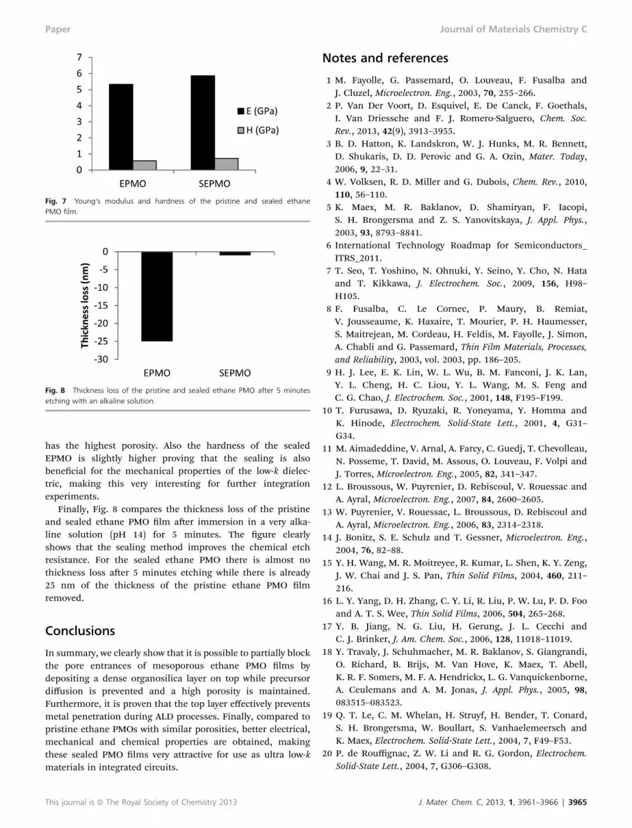
Fig. 7 Young's modulus and hardness of the pristine and sealed ethanePMO film.
Fig. 8 Thickness loss of the pristine and sealed ethane PMO after 5 minutesetching with an alkaline solution.
Paper Journal of Materials Chemistry C
has the highest porosity. Also the hardness of the sealedEPMO is slightly higher proving that the sealing is alsobenecial for the mechanical properties of the low-k dielec-tric, making this very interesting for further integrationexperiments.
Finally, Fig. 8 compares the thickness loss of the pristineand sealed ethane PMO lm aer immersion in a very alka-line solution (pH 14) for 5 minutes. The gure clearlyshows that the sealing method improves the chemical etchresistance. For the sealed ethane PMO there is almost nothickness loss aer 5 minutes etching while there is already25 nm of the thickness of the pristine ethane PMO lmremoved.
Conclusions
In summary, we clearly show that it is possible to partially blockthe pore entrances of mesoporous ethane PMO lms bydepositing a dense organosilica layer on top while precursordiffusion is prevented and a high porosity is maintained.Furthermore, it is proven that the top layer effectively preventsmetal penetration during ALD processes. Finally, compared topristine ethane PMOs with similar porosities, better electrical,mechanical and chemical properties are obtained, makingthese sealed PMO lms very attractive for use as ultra low-kmaterials in integrated circuits.
This journal is ª The Royal Society of Chemistry 2013
Notes and references
1 M. Fayolle, G. Passemard, O. Louveau, F. Fusalba andJ. Cluzel, Microelectron. Eng., 2003, 70, 255–266.
2 P. Van Der Voort, D. Esquivel, E. De Canck, F. Goethals,I. Van Driessche and F. J. Romero-Salguero, Chem. Soc.Rev., 2013, 42(9), 3913–3955.
3 B. D. Hatton, K. Landskron, W. J. Hunks, M. R. Bennett,D. Shukaris, D. D. Perovic and G. A. Ozin, Mater. Today,2006, 9, 22–31.
4 W. Volksen, R. D. Miller and G. Dubois, Chem. Rev., 2010,110, 56–110.
5 K. Maex, M. R. Baklanov, D. Shamiryan, F. Iacopi,S. H. Brongersma and Z. S. Yanovitskaya, J. Appl. Phys.,2003, 93, 8793–8841.
6 International Technology Roadmap for Semiconductors_ITRS_2011.
7 T. Seo, T. Yoshino, N. Ohnuki, Y. Seino, Y. Cho, N. Hataand T. Kikkawa, J. Electrochem. Soc., 2009, 156, H98–H105.
8 F. Fusalba, C. Le Cornec, P. Maury, B. Remiat,V. Jousseaume, K. Haxaire, T. Mourier, P. H. Haumesser,S. Maitrejean, M. Cordeau, H. Feldis, M. Fayolle, J. Simon,A. Chabli and G. Passemard, Thin Film Materials, Processes,and Reliability, 2003, vol. 2003, pp. 186–205.
9 H. J. Lee, E. K. Lin, W. L. Wu, B. M. Fanconi, J. K. Lan,Y. L. Cheng, H. C. Liou, Y. L. Wang, M. S. Feng andC. G. Chao, J. Electrochem. Soc., 2001, 148, F195–F199.
10 T. Furusawa, D. Ryuzaki, R. Yoneyama, Y. Homma andK. Hinode, Electrochem. Solid-State Lett., 2001, 4, G31–G34.
11 M. Aimadeddine, V. Arnal, A. Farcy, C. Guedj, T. Chevolleau,N. Posseme, T. David, M. Assous, O. Louveau, F. Volpi andJ. Torres, Microelectron. Eng., 2005, 82, 341–347.
12 L. Broussous, W. Puyrenier, D. Rebiscoul, V. Rouessac andA. Ayral, Microelectron. Eng., 2007, 84, 2600–2605.
13 W. Puyrenier, V. Rouessac, L. Broussous, D. Rebiscoul andA. Ayral, Microelectron. Eng., 2006, 83, 2314–2318.
14 J. Bonitz, S. E. Schulz and T. Gessner, Microelectron. Eng.,2004, 76, 82–88.
15 Y. H. Wang, M. R. Moitreyee, R. Kumar, L. Shen, K. Y. Zeng,J. W. Chai and J. S. Pan, Thin Solid Films, 2004, 460, 211–216.
16 L. Y. Yang, D. H. Zhang, C. Y. Li, R. Liu, P. W. Lu, P. D. Fooand A. T. S. Wee, Thin Solid Films, 2006, 504, 265–268.
17 Y. B. Jiang, N. G. Liu, H. Gerung, J. L. Cecchi andC. J. Brinker, J. Am. Chem. Soc., 2006, 128, 11018–11019.
18 Y. Travaly, J. Schuhmacher, M. R. Baklanov, S. Giangrandi,O. Richard, B. Brijs, M. Van Hove, K. Maex, T. Abell,K. R. F. Somers, M. F. A. Hendrickx, L. G. Vanquickenborne,A. Ceulemans and A. M. Jonas, J. Appl. Phys., 2005, 98,083515–083523.
19 Q. T. Le, C. M. Whelan, H. Struyf, H. Bender, T. Conard,S. H. Brongersma, W. Boullart, S. Vanhaelemeersch andK. Maex, Electrochem. Solid-State Lett., 2004, 7, F49–F53.
20 P. de Rouffignac, Z. W. Li and R. G. Gordon, Electrochem.Solid-State Lett., 2004, 7, G306–G308.
J. Mater. Chem. C, 2013, 1, 3961–3966 | 3965

Journal of Materials Chemistry C Paper
21 S. Armini, J. L. Prado, J. Swerts, Y. Sun, M. Krishtab,J. Meersschaut, M. Blauw, M. Baklanov and P. Verdonck,Electrochem. Solid-State Lett., 2012, 1, P42–P44.
22 T. Frot, W. Volksen, S. Purushothaman, R. Bruce andG. Dubois, Adv. Mater., 2011, 23, 2828–2832.
23 M. Kruk and C. M. Hui, J. Am. Chem. Soc., 2008, 130, 1528–1529.
24 F. Goethals, M. R. Baklanov, I. Cio, C. Detavernier, P. VanDer Voort and I. Van Driessche, Chem. Commun., 2012, 48,2797–2799.
3966 | J. Mater. Chem. C, 2013, 1, 3961–3966
25 F. Goethals, I. Cio, O. Madia, K. Vanstreels, M. R. Baklanov,C. Detavernier, P. Van der Voort and I. Van Driessche,J. Mater. Chem., 2012, 22, 8281–8286.
26 K. Landskron, B. D. Hatton, D. D. Perovic and G. A. Ozin,Science, 2003, 302, 266–269.
27 S. M. George, Chem. Rev., 2010, 110, 111–131.28 M. R. Baklanov and K. P. Mogilnikov, Appl. Opt., 2000, 30,
491–496.29 M. R. Baklanov, K. P. Mogilnikov and J. H. Yim, Mater. Res.
Soc. Symp. Proc., 2004, 812, 55–60.
This journal is ª The Royal Society of Chemistry 2013