scalable architecture for nanotechnology - nist
TRANSCRIPT
Page 1 of 10 TIP White Paper
Technology Innovation Program Mail Stop 4750 National Institute of Standards and Technology 100 Bureau Drive Gaithersburg, MD 20899-4750 Email: [email protected]. Att. Critical National Needs Ideas CRITICAL NATIONAL NEED IDEA Title: Scalable Architecture for Nanotechnology Submitting Organization: Contact:
Imiplex LLC 1970 Timber Lakes Drive Yardley, PA 19067
F. Raymond Salemme, PhD 215-962-2642 <[email protected]>
Key Words: Nanotechnology, Diagnostics, Biosensors, Personalized Medicine, Water Purification, Energy Storage Critical Technology Need & Impact: The ability to control the structural and functional properties of materials at the nanoscale has the potential to broadly enable technologies in areas as diverse as energy, water purification, semiconductor device fabrication, and medical devices. The successful development of such technology would have tremendous societal and economic benefit to US citizens and insure US leadership in one of the most important emerging manufacturing technologies of the twenty-first century. The importance of nanotechnology has been clearly recognized with the establishment of the National Nanotechnology Initiative (http://www.nano.gov/) which coordinates interdisciplinary work performed within and funded by US Government agencies. Nevertheless, numerous barriers remain to the complete realization of the technology. Among these is the “Precise and arbitrary manipulation and positioning of large numbers of nanostructures” as identified as the number one “Difficult Problem in Nanotechnology” on the MITRE nanosystems website (http://www.mitre.org/tech/nanotech/nanosystems/problems.html). What is fundamentally required to enable the broad applicability of nanotechnology is a common underlying approach, embodied in a scalable architectural platform, that will allow the fabrication of materials and devices with features at the nanoscale using a uniform assembly strategy. What needs to be envisioned is a technological approach, although different in execution, that is conceptually similar to the top-down approach employed in conventional semiconductor fabrication, in that once it is technically implemented, it can be used to manufacture a host of different materials and devices using a common underlying manufacturing approach. In this white paper, we advocate the development of a flexible and scalable technology for nanotechnology using a combination top-down and bottom-up self-assembly methods. Engineered proteins, polymers that are able to spontaneously self-assemble to organize thousands of atoms with atomic precision, represent a key component of the platform that we envisage. We propose the development of a flexible set of architectural components that can be assembled into an essentially infinite set of engineered nanostructures with one, two, and three-dimensional organization. We see two limiting end uses for nanostructures assembled with proteins. In one limiting application, the protein nanostructures could in themselves be the basis for functional biomaterials. In a second limiting application, the organized structures formed of the protein materials can essentially serve as a resist or template, enabling the patterning of other materials. It is also possible to envision hybrid structures that incorporate nanostructures using a combination of these methods (Figure 1). A nanometer (nm) is 1x10⁻⁹ meters, roughly equivalent to the length of a carbon atom chain nine atoms long, and substantially less than the wavelength of visible light (~400 nM). Many studies recognize the potential utility of being able to control assembly architecture at the nanoscale. Some key advantages include: Miniaturization: The efficiency of electronic or memory devices ultimately devolves on maximizing the density with which discrete components can be manufactured on an appropriate substrate. Silicon-based semiconductor fabrication technology has continuously progressed over the last 40 years according to
Page 2 of 10 TIP White Paper
Moore’s Law, with an approximate doubling in device density every two years. As a result, processes are now in place or under development that will produce integrated circuits with 45 nm features. Although there have been many (incorrect) predictions made in recent years that practical limits to device miniaturization had been reached, many believe that pushing device densities beyond the latest generation may be subject to fundamental physical limitations (International Technology Roadmap for Semiconductors (http://www.itrs.net/reports.html)). Emergence of New Properties: There is considerable interest in exploiting the emergence of new properties in very small systems for development of new kinds of functional devices. These can range from effects that stem from the statistical or quantum characteristics that emerge in very small systems, to novel physical characteristics that emerge through the interaction of light with structures having dimensions less than optical wavelengths. Biological System Interfaces: One of the most exciting possibilities for nanotechnology involves the development of materials or devices that can directly interact with biological systems and/or directly incorporate biological macromolecules as intrinsic structural or functional components. Virtually all of the functionality and interaction specificity of biological systems is manifest in the structure of macromolecules structurally organized at the nanoscale, principally proteins and nucleic acids, which are macromolecules respectively specialized for structure-function and information storage and processing roles. Most proteins, which are polymers of amino acids, spontaneously fold to form uniquely organized, tightly packed structures that self-organize thousands of atoms with atomic precision over ranges of 1 to 100 nm, and manifest a wide range of structural, catalytic, binding, and signal transducing properties. Many proteins can intrinsically, or can be engineered to, bind to surfaces with a defined orientation, a characteristic that is important in processes such as active filtration, directional transport of chemical substances, or charge storage on surfaces. The rich functionally of proteins physically arises from near equivalence of several different types of interaction forces (e.g. electrostatic, van der Walls interaction, and solvation effects) and the corresponding effects of statistical energy fluctuations on the order of a few kT that dominate the behavior of biological systems on the molecular scale (Phillips & Quake, 2006). Scalability: A key aspect enabling the broad application of a novel manufacturing technology is scalability. In the context of engineered nanostructures, there are two different aspects of scalability. The first aspect involves the ability to manufacture structures using a parallel manufacturing process. For example, many early conceptions of nanostructure fabrication – motivated by studies demonstrating the ability to manipulate single atoms using atomic force microscopy - envisioned that devices could be assembled essentially atom by atom using molecular scale atomic manipulators (Drexler, 1992). However, it is apparent that this would be an impractical process for assembling many devices owing to the time required to perform what is intrinsically a serial process that would have to repeated many thousands (if not millions) of times per individual nanostructure. As outlined below, it seems feasible that the combination of a top-down approach, able to specify the position of few nucleation sites, coupled with a self-assembly process around each of the nucleii, can produce highly engineered nanostructures in a parallel production mode. A second aspect of scalability applies to the use of nanostructures for intrinsically large-scale applications. An example would an application like water purification or desalinization, which might require active membrane structures that are organized on the nanostructural level, but would have to be manufactured on a very large scale to provide useful capacity. Additional applications that could require large-scale assemblies include energy storage devices or photovoltaic cells. In this respect it is estimated that engineered proteins may ultimately be produced in (green) plants for a few dollars a pound, potentially making such applications economically feasible propositions. (http:// www.sciencedaily.com/releases/1999/07/990715134504.htm). Technology Development Plan: Our overall technology development concept is outlined in Figure 1. The approach that we envision is initiated through the development of a set of basic molecular building blocks that we term “struts” and “nodes”. Struts and nodes are engineered protein molecules that provide the underlying architecture for the devices and materials ultimately manufactured using the technology. Struts are basically linear structural elements, while nodes are generally protein structures or assemblies with Cn rotational or 3-dimensional point group symmetry.
Page 3 of 10 TIP White Paper
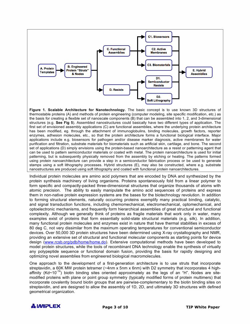
Figure 1. Scalable Architecture for Nanotechnology. The basic concept is to use known 3D structures of thermostable proteins (A) and methods of protein engineering (computer modeling, site specific modification, etc.) as the basis for creating a flexible set of nanoscale components (B) that can be assembled into 1, 2, and 3-dimensional structures (e.g. See Fig 5). Assembled nanostructures could basically have two different types of application. The first set of envisioned assembly applications (C) are functional assemblies, where the underlying protein architecture has been modified, eg. through the attachment of immunoglobulins, binding molecules, growth factors, reporter enzymes, adhesion molecules, etc., so that the protein architecture forms a functional biological interface. Major applications include e.g. biosensors for pathogen and/or disease marker diagnosis, active membranes for water purification and filtration, substrate materials for biomaterials such as artificial skin, cartilage, and bone. The second set of applications (D) simply envisions using the protein-based nanoarchitecture as a resist or patterning agent that can be used to pattern semiconductor materials or coated with metal. The protein nanoarchitecture is used for initial patterning, but is subsequently physically removed from the assembly by etching or heating. The patterns formed using protein nanoarchitecture can provide a step in a semiconductor fabrication process or be used to generate stamps using a soft lithography processes. Hybrid structures (E), may also be constructed, where e.g. substrate nanostructures are produced using soft lithography and coated with functional protein nanoarchitectures.
Individual protein molecules are amino acid polymers that are encoded by DNA and synthesized by the protein synthesis machinery of living organisms. Proteins spontaneously fold from a linear polymer to form specific and compactly-packed three-dimensional structures that organize thousands of atoms with atomic precision. The ability to easily manipulate the amino acid sequences of proteins and express them in non-native protein expression systems are the bases for the biotechnology revolution. In addition to forming structural elements, naturally occurring proteins exemplify many practical binding, catalytic, and signal transduction functions, including chemomechanical, electromechanical, optomechanical, and optoelectronic mechanisms, and frequently form hierarchical assemblies of great structural and functional complexity. Although we generally think of proteins as fragile materials that work only in water, many examples exist of proteins that form essentially solid-state structural materials (e.g. silk). In addition, many functional protein molecules and enzymes exist in nature that have thermal stabilities in excess of 80 deg C, not very dissimilar from the maximum operating temperatures for conventional semiconductor devices. Over 50,000 3D protein structures have been determined using X-ray crystallography and NMR, providing an extensive set of structural and functional molecular components as starting points for device design (www.rcsb.org/pdb/home/home.do). Extensive computational methods have been developed to model protein structures, while the tools of recombinant DNA technology enable the synthesis of virtually any polypeptide sequence or functional domain fusion, providing the basis for rapidly designing and optimizing novel assemblies from engineered biological macromolecules.
One approach to the development of a first-generation architecture is to use struts that incorporate streptavidin, a 60K MW protein tetramer (~4nm x 5nm x 6nm) with D2 symmetry that incorporates 4 high-affinity (Kd~10-14) biotin binding sites oriented approximately as the legs of an “H”. Nodes are site-modified proteins with plane or point group symmetry (typically modified forms of protein multimers) that incorporate covalently bound biotin groups that are pairwise-complementary to the biotin binding sites on streptavidin, and are designed to allow the assembly of 1D, 2D, and ultimately 3D structures with defined geometrical organization.
Page 4 of 10 TIP White Paper
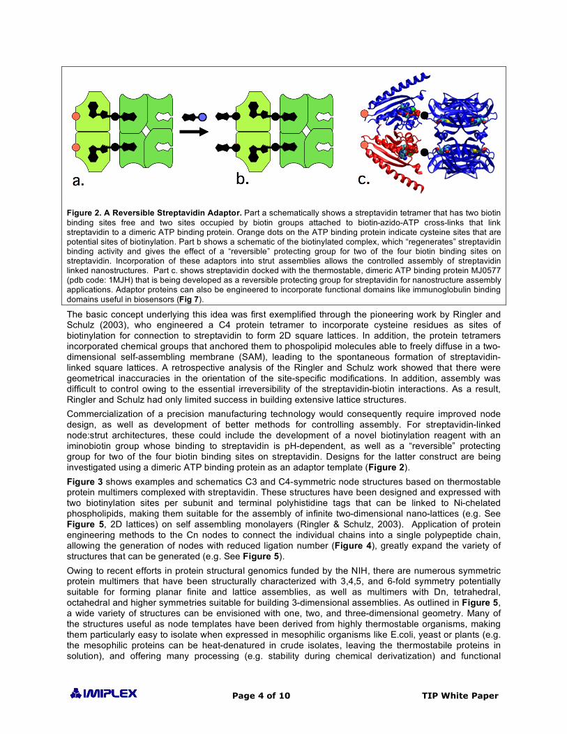
Figure 2. A Reversible Streptavidin Adaptor. Part a schematically shows a streptavidin tetramer that has two biotin binding sites free and two sites occupied by biotin groups attached to biotin-azido-ATP cross-links that link streptavidin to a dimeric ATP binding protein. Orange dots on the ATP binding protein indicate cysteine sites that are potential sites of biotinylation. Part b shows a schematic of the biotinylated complex, which “regenerates” streptavidin binding activity and gives the effect of a “reversible” protecting group for two of the four biotin binding sites on streptavidin. Incorporation of these adaptors into strut assemblies allows the controlled assembly of streptavidin linked nanostructures. Part c. shows streptavidin docked with the thermostable, dimeric ATP binding protein MJ0577 (pdb code: 1MJH) that is being developed as a reversible protecting group for streptavidin for nanostructure assembly applications. Adaptor proteins can also be engineered to incorporate functional domains like immunoglobulin binding domains useful in biosensors (Fig 7).
The basic concept underlying this idea was first exemplified through the pioneering work by Ringler and Schulz (2003), who engineered a C4 protein tetramer to incorporate cysteine residues as sites of biotinylation for connection to streptavidin to form 2D square lattices. In addition, the protein tetramers incorporated chemical groups that anchored them to phospolipid molecules able to freely diffuse in a two-dimensional self-assembling membrane (SAM), leading to the spontaneous formation of streptavidin-linked square lattices. A retrospective analysis of the Ringler and Schulz work showed that there were geometrical inaccuracies in the orientation of the site-specific modifications. In addition, assembly was difficult to control owing to the essential irreversibility of the streptavidin-biotin interactions. As a result, Ringler and Schulz had only limited success in building extensive lattice structures. Commercialization of a precision manufacturing technology would consequently require improved node design, as well as development of better methods for controlling assembly. For streptavidin-linked node:strut architectures, these could include the development of a novel biotinylation reagent with an iminobiotin group whose binding to streptavidin is pH-dependent, as well as a “reversible” protecting group for two of the four biotin binding sites on streptavidin. Designs for the latter construct are being investigated using a dimeric ATP binding protein as an adaptor template (Figure 2). Figure 3 shows examples and schematics C3 and C4-symmetric node structures based on thermostable protein multimers complexed with streptavidin. These structures have been designed and expressed with two biotinylation sites per subunit and terminal polyhistidine tags that can be linked to Ni-chelated phospholipids, making them suitable for the assembly of infinite two-dimensional nano-lattices (e.g. See Figure 5, 2D lattices) on self assembling monolayers (Ringler & Schulz, 2003). Application of protein engineering methods to the Cn nodes to connect the individual chains into a single polypeptide chain, allowing the generation of nodes with reduced ligation number (Figure 4), greatly expand the variety of structures that can be generated (e.g. See Figure 5). Owing to recent efforts in protein structural genomics funded by the NIH, there are numerous symmetric protein multimers that have been structurally characterized with 3,4,5, and 6-fold symmetry potentially suitable for forming planar finite and lattice assemblies, as well as multimers with Dn, tetrahedral, octahedral and higher symmetries suitable for building 3-dimensional assemblies. As outlined in Figure 5, a wide variety of structures can be envisioned with one, two, and three-dimensional geometry. Many of the structures useful as node templates have been derived from highly thermostable organisms, making them particularly easy to isolate when expressed in mesophilic organisms like E.coli, yeast or plants (e.g. the mesophilic proteins can be heat-denatured in crude isolates, leaving the thermostabile proteins in solution), and offering many processing (e.g. stability during chemical derivatization) and functional
Page 5 of 10 TIP White Paper
advantages. Protein expression in plants could ultimately reduce material costs to a few dollars a pound, potentially making such making the large scale use of protein-based nanostructures for chemical processing, energy or filtration applications a commercially practical proposition (http:// www.sciencedaily.com/releases/1999/07/990715134504.htm).
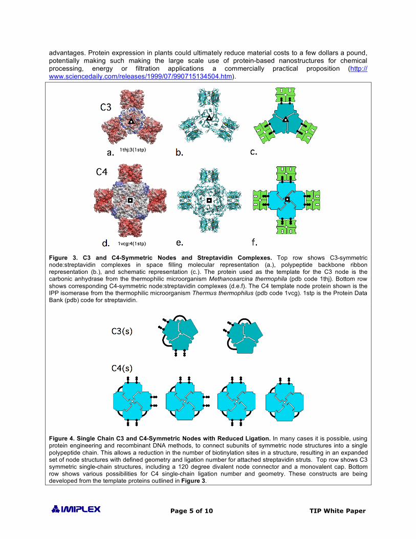
Figure 3. C3 and C4-Symmetric Nodes and Streptavidin Complexes. Top row shows C3-symmetric node:streptavidin complexes in space filling molecular representation (a.), polypeptide backbone ribbon representation (b.), and schematic representation (c.). The protein used as the template for the C3 node is the carbonic anhydrase from the thermophilic microorganism Methanosarcina thermophila (pdb code 1thj). Bottom row shows corresponding C4-symmetric node:streptavidin complexes (d.e.f). The C4 template node protein shown is the IPP isomerase from the thermophilic microorganism Thermus thermophilus (pdb code 1vcg). 1stp is the Protein Data Bank (pdb) code for streptavidin.
Figure 4. Single Chain C3 and C4-Symmetric Nodes with Reduced Ligation. In many cases it is possible, using protein engineering and recombinant DNA methods, to connect subunits of symmetric node structures into a single polypeptide chain. This allows a reduction in the number of biotinylation sites in a structure, resulting in an expanded set of node structures with defined geometry and ligation number for attached streptavidin struts. Top row shows C3 symmetric single-chain structures, including a 120 degree divalent node connector and a monovalent cap. Bottom row shows various possibilities for C4 single-chain ligation number and geometry. These constructs are being developed from the template proteins outlined in Figure 3.
Page 6 of 10 TIP White Paper
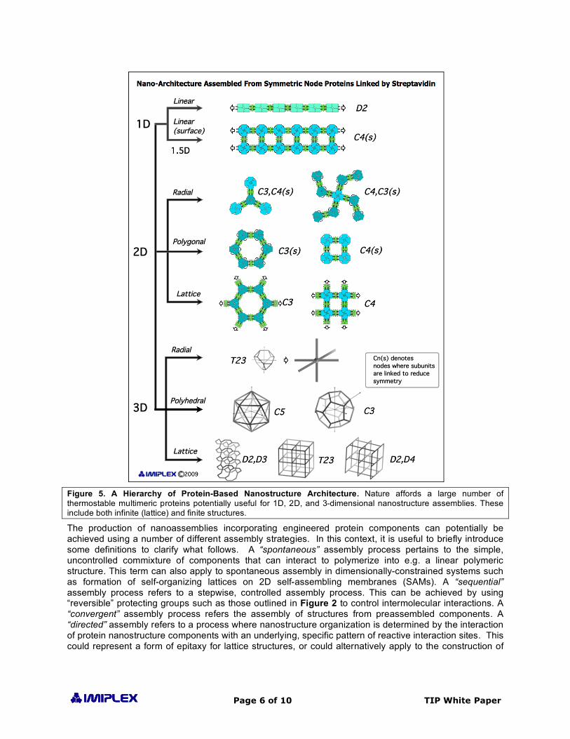
Figure 5. A Hierarchy of Protein-Based Nanostructure Architecture. Nature affords a large number of thermostable multimeric proteins potentially useful for 1D, 2D, and 3-dimensional nanostructure assemblies. These include both infinite (lattice) and finite structures.
The production of nanoassemblies incorporating engineered protein components can potentially be achieved using a number of different assembly strategies. In this context, it is useful to briefly introduce some definitions to clarify what follows. A “spontaneous” assembly process pertains to the simple, uncontrolled commixture of components that can interact to polymerize into e.g. a linear polymeric structure. This term can also apply to spontaneous assembly in dimensionally-constrained systems such as formation of self-organizing lattices on 2D self-assembling membranes (SAMs). A “sequential” assembly process refers to a stepwise, controlled assembly process. This can be achieved by using “reversible” protecting groups such as those outlined in Figure 2 to control intermolecular interactions. A “convergent” assembly process refers the assembly of structures from preassembled components. A “directed” assembly refers to a process where nanostructure organization is determined by the interaction of protein nanostructure components with an underlying, specific pattern of reactive interaction sites. This could represent a form of epitaxy for lattice structures, or could alternatively apply to the construction of
Page 7 of 10 TIP White Paper
precision assemblies nucleated at specific sites as outlined below. Table 1 outlines the approaches principally used (methods are often used in combination) for the nanostructure assemblies in Figure 5. Nanostructure Assembly Method 1D Linear Spontaneous polymerization 1.5D Linear Spontaneous, sequential (SAM surfaces) Radial Spontaneous, sequential, convergent (SAM surfaces) 2D Polygonal Spontaneous or directed (SAM surfaces) Lattice Spontaneous, (convergent) (SAM surfaces) Radial Spontaneous, (convergent) 3D Polyhedral Spontaneous, (convergent) Lattice Spontaneous (convergent, directed)
Table 1. An outline of the principal assembly strategies used to develop representative nanostructure architectures shown in Figure 5. These strategies can generally be complemented with additional approaches (brackets).
Many applications of protein-based nanotechnology, such as the development of linear polymers as substrates for biomaterials (Figure 5 1D) or the nanoassemblies for biosensors described as illustrative examples below, will achieve useful performance improvements relative to current approaches even if the structures are only organized on a local or statistical level. Nevertheless, the ultimate objective is to develop a robust technology enabling the precision assembly of nanostructures, outlined above as the key “Difficult Problem in Nanotechnology” on the MITRE website.
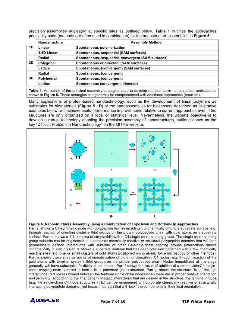
Figure 6. Nanostructures Assembly using a Combination of Top-Down and Bottom-Up Approaches. Part a. shows a C4-symmetric node with polypeptide termini enabling it to chemically bind to a substrate surface; e.g. through reaction of orienting cysteine thiol groups on the protein polypeptide chain with gold atoms on a substrate surface. Part b. shows a 1:1 complex of streptavidin with a C4-single-chain capping group. The single-chain capping group subunits can be engineered to incorporate chemically reactive or structural polypeptide domains that will form geometrically defined interactions with subunits of other C4-single-chain capping groups (Interactions shows schematically in Part c.) Part d. shows a substrate material that has been precision patterned with a few chemically reactive sites (e.g. one or small clusters of gold atoms positioned using atomic force microscopy or other methods). Part e. shows these sites as points of immobilization of biotin-functionalized C4 nodes: e.g. through reaction of the gold atoms with terminal cysteine thiol groups on the protein polypeptide chain. Nodes immobilized at this stage generally will have substantial flexibility in orientation. Part f shows the result of addition of a streptavidin:C4 single-chain capping node complex to form a finite patterned (tiled) structure. Part g. shows the structure “fixed” through interactions (red boxes) formed between the terminal single chain nodes when there are in proper relative orientation and proximity. According to the final pattern of static interactions that are desired in the structure, the terminal groups (e.g. the single-chain C4 node structures in b.) can be engineered to incorporate chemically reactive or structurally interacting polypeptide domains (red boxes in part g.) that will “lock” the components in their final orientation .
Page 8 of 10 TIP White Paper
Figure 6 outlines an approach to nanostructure assembly that involves a combination of directed top-down and convergent bottom-up assembly strategies. The process is initiated with the formation of a few reactive chemical loci on a planar substrate, as could potentially be achieved using a variety of top-down nanopatterning methods or atomic force microscopy. These nucleation sites can in turn be reacted with protein molecules or protein nanoassemblies, which in themselves are precision, self-assembled nanostructures, to form larger assemblies. In principle, an arbitrarily large number of finite and semi-infinite structures can be created using this approach, where the initial immobilization of only a few atoms, or cluster of atoms, can serve to restrict the organizational degrees of freedom the structure can subsequently assume as it is progressively assembled. This directed assembly approach can allow structures to be built up in a parallel, stepwise fashion to create structures of essentially arbitrary complexity. With the proper design tools (i.e. essentially variations of the computational tools currently used in protein modeling and crystallography), and the development of accompanying process technology, structures incorporating millions of atoms located with atomic precision can potentially be manufactured.
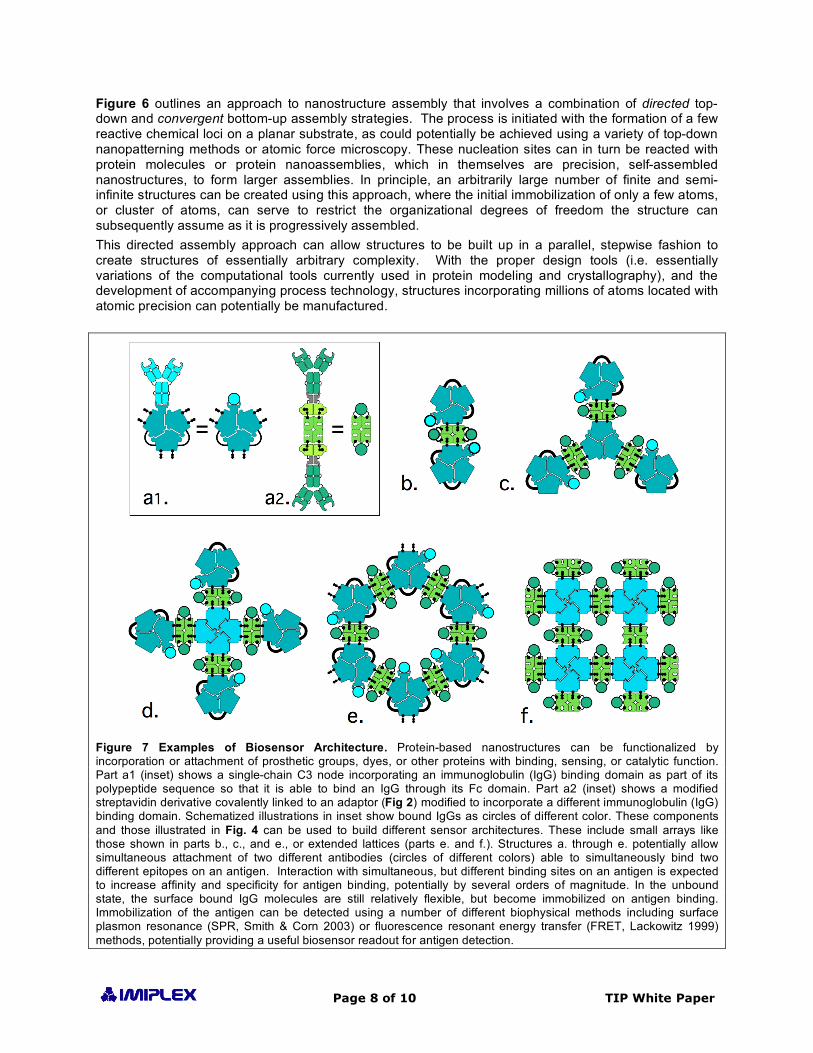
Figure 7 Examples of Biosensor Architecture. Protein-based nanostructures can be functionalized by incorporation or attachment of prosthetic groups, dyes, or other proteins with binding, sensing, or catalytic function. Part a1 (inset) shows a single-chain C3 node incorporating an immunoglobulin (IgG) binding domain as part of its polypeptide sequence so that it is able to bind an IgG through its Fc domain. Part a2 (inset) shows a modified streptavidin derivative covalently linked to an adaptor (Fig 2) modified to incorporate a different immunoglobulin (IgG) binding domain. Schematized illustrations in inset show bound IgGs as circles of different color. These components and those illustrated in Fig. 4 can be used to build different sensor architectures. These include small arrays like those shown in parts b., c., and e., or extended lattices (parts e. and f.). Structures a. through e. potentially allow simultaneous attachment of two different antibodies (circles of different colors) able to simultaneously bind two different epitopes on an antigen. Interaction with simultaneous, but different binding sites on an antigen is expected to increase affinity and specificity for antigen binding, potentially by several orders of magnitude. In the unbound state, the surface bound IgG molecules are still relatively flexible, but become immobilized on antigen binding. Immobilization of the antigen can be detected using a number of different biophysical methods including surface plasmon resonance (SPR, Smith & Corn 2003) or fluorescence resonant energy transfer (FRET, Lackowitz 1999) methods, potentially providing a useful biosensor readout for antigen detection.
Page 9 of 10 TIP White Paper
Although it will undoubtedly take many years of effort to establish whether the full potential of protein-based nanotechnology can be realized in all of the dimensions outlined here, we note that useful devices can potentially arise throughout the development of the technology, much in the way that the technology required to build a transistor radio ultimately evolved into today’s multiprocessor semiconductor fabrication technology. One area where even simple protein-based nanoassemblies could have positive societal and economic impact is in the development of improved biosensors. The current worldwide in vitro diagnostics (IVD) market is worth around $51 billion (about 7% of the world pharma market) and is expected to grow at an annual growth rate of about 8% to $76 billion in 2012. The “biomarker” component is one of the fastest growing components of IVD and is estimated to grow in real terms at a compound annual growth rate (CAGR) of 17.6%, from $5.5 billion in 2007 to $12.4 billion in 2012 (http://www.biophoenix.com/tocs/biomarkers.htm). Functionally there are two different segments: nucleic acid biomarkers (e.g. single nucleotide polymorphisms-SNPs, genetic mutations) and protein biomarkers (cell surface proteins, cytokines, amyloid peptides, pathogen proteins, toxins, etc.). The key objectives of human DNA diagnostics generally involve determination of an individual’s specific genetic background as an indicator of human disease proclivity. The key objectives of human protein marker detection generally involve determination of the status of disease progression in an individual. The major driver of the market expansion for biomarker diagnostics is the recognition of the potential of “personalized medicine”. It is increasingly clear that although there are numerous established correlations between single gene or protein markers and disease proclivity or state of progression, for most diseases the situation is much more complex. Nevertheless, patients, drug developers, physicians, and insurers are all demanding better diagnostics as the trend to personalized medicine accelerates. In the protein biomarker space, most detection schemes utilize antibodies as the basic molecular mechanism for recognition of a protein marker or antigen. A number of studies have emphasized the observed or potential improvements in detector affinity and specificity that are associated with organized, high density immobilization of in IgGs on sensor array surfaces (e.g. Soukka et al. 2001). However, an additional aspect that is unique to the constructs and devices potentially developed using protein-based nanoassemblies, is the ability to precisely position the relative orientation of two (or ultimately more) IgG molecules on a substrate surface, creating a detector that can attach to different epitopes of an antigen simultaneously. Figure 7 illustrates how the components outlined above could be used to assemble several different biosensor architectures, several of which immobilize different antibodies in close proximity. The resulting, highly specific capture agent can provide the basis for a biosensor, since the binding of an anitgen would “freeze” the relative orientations of the bound IgGs (whose interdomain connections are otherwise quite flexible), an effect that could be potentially detected using a variety of biophysical methods including surface plasmon resonance (SPR, Smith & Corn 2003) or fluorescence resonant energy transfer (FRET, Lackowitz 1999) methods. Why is this important? As outlined in the introduction, the importance of nanotechnology to US economic competitiveness and the welfare of its citizens has been clearly recognized with the establishment of the National Nanotechnology Initiative (http://www.nano.gov/) that organizes interdisciplinary work performed within and funded by US Government agencies. NIST itself is playing a major role, since the development of new nanometrology methods will be key to the successful commercial deployment of the technology (http://www.nist.gov/public_affairs/nanotech.htm). Nevertheless, numerous barriers remain to the complete realization of nanotechnology. Among these is the “Precise and arbitrary manipulation and positioning of large numbers of nanostructures” as identified as the number one “Difficult Problem in Nanotechnology” on the MITRE nanosystems website (http://www.mitre.org/tech/nanotech/nanosystems/problems.html). Why is TIP funding needed to support this effort? In the US, much of the breakthrough, high-risk technology is developed through the efforts of individuals in small entrepreneurial businesses, often working on ideas “outside of the mainstream”. However, in the present environment, where the US biotechnology industry is experiencing the worst financing environment in its 40-year history, it is extremely difficult to raise financing for novel biotechnology, especially if it is only a component of a much larger technology effort as is envisioned here. One way to approach this challenge is to build a technology (and the company around it) using a bootstrap approach, where e.g. components and nanoassemblies are developed in collaboration with university researchers, sold initially as research
Page 10 of 10 TIP White Paper
reagents, and subsequently, as more complex nanoassemblies are developed, into successively higher value markets. In this way, the components can become broadly enabling tools for the biomedical and nanotechnology communities who can build upon the architecture and functionality that has been developed. However, this is far from an optimal strategy owing to the limited technical resources of a small startup and the broad range of expertise required to optimally execute the strategy from design through device realization (Fig 1). TIP support could serve as the focus for a consortium of academic, government, industry, and entrepreneurial business researchers to insure that the best resources are brought to bear on this important problem. This is not only an issue that devolves around having the required resources and financing, but also represents an area where NIST has a unique role to play given the key role of metrology in the development of this technology How does the technology leverage other US investments? As outlined in Figure 1 and described above, the technology envisioned would comprise only a minor component of the already extensive activities of the National Nanotechnology Initiative. Nevertheless, it could be a key component that enabled many new developments, broadly impacting many areas, but particularly those involving the interface between nanotechnology and biotechnology. References: Drexler, KE “Nanosystems: Molecular Machinery, Manufacturing, and Computation” Wiley Interscience
(1992) International Technology Roadmap for Semiconductors (http://www.itrs.net/reports.html) Lakowicz,JR "Principles of Fluorescence Spectroscopy", Plenum Publishing Corporation, 2nd edition
(July 1, 1999) Phillips R & Quake, SR “The Biological Frontiers of Physics” Physics Today (May 2006) p38-43 Ringler P, Schulz G “Self-Assembly of Proteins into Designed Networks” Science (2003) 302:106-109. Smith EA, Corn RM. Surface Plasmon Resonance Imaging as a Tool to Monitor Biomolecular Interactions
in an Array Based Format. Appl. Spectroscopy, 2003, 57, 320A-332A. Soukka T, Harma H, Paukkunen J, Lovgren T “Utilization of Kinetically Enhanced Monovalent Binding
Affinity by Immunoassays Based on Multivalent Nanoparticle-Antibody Bioconjugates” Anal Chem (2001) 73:2254-2260.