sarvagya paavan dwivedi - photonics research group
TRANSCRIPT
Universiteit GentFaculteit Ingenieurswetenschappen en Architectuur
Vakgroep Informatietechnologie
Tolerante Spectrale Filters met Behulp vanNanofotonische Golfgeleiders in SiliciumTolerant Spectral Filters using Silicon NanophotonicWaveguides
Sarvagya Paavan Dwivedi
Proefschrift tot het bekomen van de graad vanDoctor in de Ingenieurswetenschappen:
FotonicaAcademiejaar 2015-2016

Universiteit GentFaculteit Ingenieurswetenschappen en Architectuur
Vakgroep Informatietechnologie
Promotoren: Prof. Dr. Ir. Wim Bogaerts
Examencommisse:
Prof. Dr. Ir. Luc Taerwe (voorzitter) Universiteit Gent, SEProf. Dr. Ir. Wim Bogaerts Universiteit Gent, INTECProf. Dr. Ir. Roel Baets Universiteit Gent, INTECProf. Dr. Ir. Peter Bienstman Universiteit Gent, INTECDr. Ir. Stephane Clemmen Universiteit Gent, INTECDr. Ir. Pieter Dumon Luceda PhotonicsDr. Ir. Peter De Heyn IMECProf. Dr. Ir. Jeroen Beeckman Universiteit Gent, ELIS
Universiteit GentFaculteit Ingenieurswetenschappen en Architectuur
Vakgroep InformatietechnologieSint-Pietersnieuwstraat 41, 9000 Gent, Belgie
Tel.: +32-9-264 3324Fax.: +32-9-264 3593

4
Acknowledgement
It all started way back in the early 2011 when I was working in Bangalore forComsol as Application Engineer. Although I was enjoying the challenging job atComsol working under Vineet, yet it was somehow always back in my mind to pur-sue something new and creative. I learnt a lot from you Vineet. Special thanks tomy friend Harish, who inspired and guided me initially with his wonderful postdocstories from Colorado, Boulder. Not many friends were happy with my decision ofleaving my corporate career but my family stood by me firmly to pursue researchcareer. My mother, father and my twin sisters Milie Di and Julie Di, were reallyhappy proclaiming wow to my right decision in life. I am sure the happiest personat that time was my father as he himself a great researcher throughout his life. Andmy mother because she is happy with whatever makes me happy. My sisters havealways been supportive and only because of them I feel like I am still a kid :). I amso fortunate to have a lovely niece Suhani and wonderful nephews Neel and Baby.This was a brief background.
Then I landed in this beautiful city of Ghent to start my career as a doctoralresearcher on 13th October 2011. All credit goes to my promoter Wim. He is theone who always listened to me with my ideas, guided me in a way so that I get aconfidence in whatever I do, answered my silliest possible questions and never gotbored in answering them countless times. He supported me in all my failures andalways said ”OK, if this is not working, we have at least learnt something from it.”I consider myself blessed to have him as my promoter. To all the professors in thegroup, Roel, Dries, Geert, Peter, Gunther, Nicolas and Bart, I cannot thank themenough for making this group so diverse at the same time like a big family andkeeping its flag high as one of the best in the world. I am very fortunate to haveworked in this wonderful group which provided me care, attention, affection andsupport in abundant measure. I am surely going to miss all this.
This long journey cannot be completed until without mentioning so many spe-cial people in this wonderful group. Starting from Bendix, how can I forget thenumber of cups of coffee we had in the last four years, on an average 3-4 per day(right?). Apart from this, it was a pleasure discussing all the research problemsover the coffee. Special thanks to Floriane for inviting me so many times to makeme realize how well is the French cuisine. I really enjoyed their wedding at southof France and my best wishes to lovely Kiya and Meline. Alfonso, we joined to-
ii
gether, we deliberated almost every day even on trivial things and we are leavingalmost at the same time, I am sure we miss all the fun. Best wishes for your post-doc new position in the US. Aditya, remember the very first day I joined; I came toyour office and asked a few things. From the day one you have been a great friendand will always be. And, I think we should start our Starbucks coffee over theweekends again? It was nice to see and discuss about Ge-on-Si Mid IR frameworkyou developed. I wish you and Kirti a happy married life. Ananth (Daddu), youhave been there whenever I asked for any help as an elder brother. I think it wouldbe very difficult for me in my next phase of life doing things without taking yourlovely suggestions. Heartiest congratulations to Kamal (Bhabhi) and you for thenew phase in your life.
Thank you, Hui Yu, for teaching me the design and characterization of siliconmodulators. Muneeb, I have to learn the kind of patience you have as a person.You have been a great friend; I enjoyed discussing various research topics withyou and the dinner we shared at the Indian place. Utsav, it was very nice sharinga flat with you. I enjoyed the spicy food you cooked and the long discussions weshared over the weekends on various topics whether it is movies, societal scenario,or even a bit of non-linear optics. Thomas, I guess you must be enjoying your stayin the US. It was great working with you on effective index extraction methods.Fredric, it was nice chatting with you along with Anton (Tawarish) almost everyday in the evenings. Fredric, congrats for your future postdoc position and Tawar-ish many congrats for the new phase which is coming soon in your life. It was apleasure meeting you guys. Shibnath you have always been helpful either for gen-eral suggestions or any specific design help. Michael, thanks for all your help withsemi and fully automatic setup. I could not imagine measuring so many devices indue course of time without your help. Liesbet, thanks for all your help in takingSEM images on a short request. Amin (and Leila), you have been a nice colleagueand a great friend. It was nice working with you on OCS lab course and then onvarious discussions on high speed measurements. I am missing our evening TTmatches along with Ananth. Peter DH, it was nice working with you on CWDMand especially on designing wideband directional couplers. I hope the improveddesign will work on the system level and we can compete with IBM and others.Herbert, it was wonderful working with you for almost a year. I am sure yourproject is coming along well. Peter for helping me in all my doubts and keepingthe plants alive in our wonderful office. Geert, I enjoyed working with you as a TAfor the OCS course. I myself learned so many new things. Martin, many thanksfor all your help Caphe, it gave me the flexibility to test my circuits quickly. Bart,you have always been helpful in sorting technical things out. Yanlu, thanks foryour help with low reflection grating couplers.
The Brug food was not so enjoyable without you guys: Jesper, Antonio, Jan-Willem, Daan, Sren, Alejandro, Michael, Artur, Andrew, Ashim, Kasper, Paul,Koen, Peter Wuytens, Ali, Floris, Rodica, Alexandre and Stephanne. Andreas(thanks for your help in Dutch summary) and Sarah, many congratulations forthe new phase coming into your life. Also, thanks to Jing, Chen, Weiqiang, Bin,Ruijun, Yunpeng and Zhechao for being so nice colleagues.
iii
Special thanks to Thijs, Eva, Abdul and Antonio for the new simulation anddesign of experiment framework. I think it is going to help students in the fu-ture to minimize the obvious mistakes. Many thanks to Ilse VR, Ilse M, Kristien,Mike, Bert, Jeroen, Jelle and Peter Guns for providing all possible help wheneverrequired.
On the professional note, I would like to thank our small design group led byWim which includes Antonio, Alfonso, Ang, Yufei and myself. The weekly Mon-day morning Design meetings really helped me in prioritizing my work. Specialthanks to Yufei and Antonio for helping me at the last minute in error analysis withthe Monte Carlo. You guys are great. Ang, I am going to miss your funny jokesfor sure.
My former colleagues Pieter, Shankar, Karel, Andrea, Samir, Rajesh, Sukumar,Adil, Amit, Youssef, Pauline, Sam, Elewout, Cristina and Yingtao many thanks toyou guys for always been helpful and ready with suggestions when I joined thisgroup. There are so many great friends I made here and I would like to say thanksfor making the journey memorable. Paula and Else for wonderful food, moviesand concert we shared. Manan, Namrata, Saurav, Sulakshna, Aditya, Kirti, Gau-rav, Niharika, Ananth, Kamal, Utsav and Aswhin, it was great spending time withyou guys on numerous Indian festivals and occasions. Manan and Namarata con-gratulations to your parenthood and welcome to Taashi. Shailesh, Sachin, Chetna,Ark, Vatsala, Abhishek and Karthik it was wonderful time spending with you guys.Manu, you have been a great friend and like a family back from our IIT days. It’sgreat that you moved from Gttingen to Cologne so that we can visit each othermore often. A special thanks to all my friends (Preeti Patil, Sarang and Gopal)from FOC Lab at IIT Bombay back in my master days and my Prof. R.K. Shev-gaonkar who taught me Fiber Optics.
I would like to thank again, my parents, my twin sisters, my niece and nephewsfor being there for me and my fiance Shweta for her continuous support in the lastdays of my PhD. We didn’t get any chance to spend some time together after ourengagement, but from now on certainly we will.
I would like to thank again Wim for giving me this opportunity to work withhim.
Finally, I would like to thank all my Jury members for providing valuable andconstructive comments to improve my thesis. I hope you all will enjoy reading it.
Last, but certainly not the least, I am going to miss this wonderful city ofGhent in the future and the time I spent here as a PhD student at the world’s bestPhotonics Research Group.
Ghent, February 2016Sarvagya Dwivedi

Table of Contents
Acknowledgement i
Nederlandse samenvatting xxv1 Onze bijdrage en resultaten . . . . . . . . . . . . . . . . . . . . . xxvi2 Conclusie . . . . . . . . . . . . . . . . . . . . . . . . . . . . . . xxxiii
English summary xxxv3 Our Contribution and Results . . . . . . . . . . . . . . . . . . . . xxxvi4 Conclusion . . . . . . . . . . . . . . . . . . . . . . . . . . . . . xlii
1 Introduction 1-11.1 Rationale . . . . . . . . . . . . . . . . . . . . . . . . . . . . . . 1-21.2 Goal . . . . . . . . . . . . . . . . . . . . . . . . . . . . . . . . . 1-41.3 Outline . . . . . . . . . . . . . . . . . . . . . . . . . . . . . . . 1-41.4 Publications . . . . . . . . . . . . . . . . . . . . . . . . . . . . . 1-5
1.4.1 Patent . . . . . . . . . . . . . . . . . . . . . . . . . . . . 1-51.4.2 Publications in international journals . . . . . . . . . . . 1-51.4.3 Publications in international conferences . . . . . . . . . 1-6
References . . . . . . . . . . . . . . . . . . . . . . . . . . . . . . . . . 1-8
2 Silicon-On-Insulator Waveguides 2-12.1 Introduction . . . . . . . . . . . . . . . . . . . . . . . . . . . . . 2-12.2 SOI platform . . . . . . . . . . . . . . . . . . . . . . . . . . . . 2-1
2.2.1 Introduction to SOI waveguides . . . . . . . . . . . . . . 2-42.2.2 Modelling of SOI waveguides . . . . . . . . . . . . . . . 2-52.2.3 SOI waveguide sensitivity . . . . . . . . . . . . . . . . . 2-7
2.2.3.1 Sensitivity to waveguide geometry . . . . . . . 2-82.2.3.2 Sensitivity to environmental temperature . . . . 2-92.2.3.3 Sensitivity to wavelength . . . . . . . . . . . . 2-9
2.3 Fabrication of SOI photonic integrated circuits . . . . . . . . . . . 2-102.4 Characterization . . . . . . . . . . . . . . . . . . . . . . . . . . . 2-12
2.4.1 Vertical coupling . . . . . . . . . . . . . . . . . . . . . . 2-132.4.2 Waveguide loss measurements . . . . . . . . . . . . . . . 2-14
2.5 Experimental extraction of effective index of the SOI photonicwaveguides . . . . . . . . . . . . . . . . . . . . . . . . . . . . . 2-15
vi
2.5.1 Existing methods to (not) characterize the effective index . 2-162.5.1.1 Prism coupling . . . . . . . . . . . . . . . . . . 2-162.5.1.2 Fourier-space imaging . . . . . . . . . . . . . . 2-172.5.1.3 Ellipsometry . . . . . . . . . . . . . . . . . . . 2-172.5.1.4 On-chip interferometers . . . . . . . . . . . . . 2-172.5.1.5 Simulation . . . . . . . . . . . . . . . . . . . . 2-18
2.5.2 Our method to extract the effective Index . . . . . . . . . 2-182.5.2.1 Extracting the effective index from a single MZI 2-182.5.2.2 Using high-order MZI . . . . . . . . . . . . . . 2-212.5.2.3 A second low-order MZI . . . . . . . . . . . . 2-232.5.2.4 Extraction of thermo-optic coefficient . . . . . . 2-24
2.5.3 Design and fabrication . . . . . . . . . . . . . . . . . . . 2-252.5.4 Measurements and analysis . . . . . . . . . . . . . . . . . 2-26
2.5.4.1 Automatic vertical alignment . . . . . . . . . . 2-262.5.4.2 Device measurements . . . . . . . . . . . . . . 2-272.5.4.3 Fitting . . . . . . . . . . . . . . . . . . . . . . 2-282.5.4.4 Error analysis: Bootstrapping method . . . . . . 2-292.5.4.5 Error analysis: Monte Carlo simulations . . . . 2-312.5.4.6 Thermo-optic coefficient measurements . . . . 2-342.5.4.7 Wafer scale measurements . . . . . . . . . . . . 2-35
2.6 Conclusion and discussion . . . . . . . . . . . . . . . . . . . . . 2-37References . . . . . . . . . . . . . . . . . . . . . . . . . . . . . . . . . 2-38
3 Silicon Photonic Based Flat-band Wavelength Filters 3-13.1 Introduction . . . . . . . . . . . . . . . . . . . . . . . . . . . . . 3-13.2 FIR Wavelength Filters . . . . . . . . . . . . . . . . . . . . . . . 3-33.3 SOI Based Wavelength Filters . . . . . . . . . . . . . . . . . . . 3-43.4 MZI Cascaded Filters . . . . . . . . . . . . . . . . . . . . . . . . 3-7
3.4.1 Introduction and Design . . . . . . . . . . . . . . . . . . 3-73.4.2 Fabrication and Measurements . . . . . . . . . . . . . . . 3-8
3.5 Arrayed Waveguide Gratings . . . . . . . . . . . . . . . . . . . . 3-113.5.1 Flat band AWGs . . . . . . . . . . . . . . . . . . . . . . 3-12
3.6 Echelle Gratings . . . . . . . . . . . . . . . . . . . . . . . . . . . 3-163.6.1 Flat band Echelle Gratings . . . . . . . . . . . . . . . . . 3-17
3.7 Comparison . . . . . . . . . . . . . . . . . . . . . . . . . . . . . 3-183.8 Coarse Wavelength Division Multiplexer for the O-band: Need . . 3-193.9 Design and Simulation . . . . . . . . . . . . . . . . . . . . . . . 3-203.10 Fabrication . . . . . . . . . . . . . . . . . . . . . . . . . . . . . 3-243.11 Measurements and Analysis . . . . . . . . . . . . . . . . . . . . 3-24
3.11.1 Device measurements . . . . . . . . . . . . . . . . . . . 3-243.11.2 Wafer scale measurements . . . . . . . . . . . . . . . . 3-273.11.3 Thermal simulation and measurements . . . . . . . . . . 3-293.11.4 Performance estimation of CWDM demultiplexer using
system simulation . . . . . . . . . . . . . . . . . . . . . 3-303.12 Conclusion and Discussion . . . . . . . . . . . . . . . . . . . . . 3-32
vii
References . . . . . . . . . . . . . . . . . . . . . . . . . . . . . . . . . 3-35
4 All-Silicon Athermal Wavelength Filters 4-14.1 Introduction . . . . . . . . . . . . . . . . . . . . . . . . . . . . . 4-14.2 Thermal Sensitivity of Silicon Photonic Wavelength Filters . . . . 4-24.3 Passive compensation of FIR Filters . . . . . . . . . . . . . . . . 4-54.4 Athermal MZI . . . . . . . . . . . . . . . . . . . . . . . . . . . . 4-5
4.4.1 Method . . . . . . . . . . . . . . . . . . . . . . . . . . . 4-54.4.2 Design and Simulation . . . . . . . . . . . . . . . . . . . 4-74.4.3 Fabrication and Measurements . . . . . . . . . . . . . . . 4-7
4.5 Athermal Four Channel De-multiplexer . . . . . . . . . . . . . . 4-114.5.1 Design and Simulation . . . . . . . . . . . . . . . . . . . 4-114.5.2 Fabricated De-multiplexer and Measurements . . . . . . . 4-15
4.6 All-Silicon Athermal Arrayed Waveguide Gratings . . . . . . . . 4-164.6.1 Design and Simulation . . . . . . . . . . . . . . . . . . . 4-174.6.2 Fabrication and Measurements . . . . . . . . . . . . . . . 4-18
4.7 Conclusion and Discussion . . . . . . . . . . . . . . . . . . . . . 4-20References . . . . . . . . . . . . . . . . . . . . . . . . . . . . . . . . . 4-23
5 A Compact All-Silicon Temperature Insensitive Filter Using Splitter-Polarization Rotator 5-15.1 Introduction . . . . . . . . . . . . . . . . . . . . . . . . . . . . . 5-15.2 Method . . . . . . . . . . . . . . . . . . . . . . . . . . . . . . . 5-35.3 Splitter Polarization Rotator . . . . . . . . . . . . . . . . . . . . 5-35.4 Design . . . . . . . . . . . . . . . . . . . . . . . . . . . . . . . . 5-65.5 Fabrication . . . . . . . . . . . . . . . . . . . . . . . . . . . . . 5-95.6 Measurements and Analysis . . . . . . . . . . . . . . . . . . . . 5-9
5.6.1 Parameter Extraction . . . . . . . . . . . . . . . . . . . . 5-115.6.2 Measurement and Designed Device Analysis . . . . . . . 5-14
5.7 Footprint Comparison and Sensitivity . . . . . . . . . . . . . . . 5-185.8 Applications . . . . . . . . . . . . . . . . . . . . . . . . . . . . . 5-19
5.8.1 Sensing . . . . . . . . . . . . . . . . . . . . . . . . . . . 5-195.9 Conclusion and Discussion . . . . . . . . . . . . . . . . . . . . . 5-21References . . . . . . . . . . . . . . . . . . . . . . . . . . . . . . . . . 5-22
6 Maximizing Fabrication and Thermal tolerances of All-Silicon FIRwavelength filters 6-16.1 Introduction . . . . . . . . . . . . . . . . . . . . . . . . . . . . . 6-16.2 Proposed Method . . . . . . . . . . . . . . . . . . . . . . . . . . 6-26.3 Fabrication Tolerant MZI filter . . . . . . . . . . . . . . . . . . . 6-5
6.3.1 Design and Fabrication . . . . . . . . . . . . . . . . . . . 6-56.3.2 Measurements and Analysis . . . . . . . . . . . . . . . . 6-7
6.4 Fabrication Tolerant AWG . . . . . . . . . . . . . . . . . . . . . 6-106.5 Fabrication and Thermal Tolerant MZI . . . . . . . . . . . . . . . 6-12
6.5.1 Design and Fabrication . . . . . . . . . . . . . . . . . . . 6-12
viii
6.5.2 Measurements and Analysis . . . . . . . . . . . . . . . . 6-146.5.3 Footprint Analysis . . . . . . . . . . . . . . . . . . . . . 6-15
6.6 Higher Order Filters . . . . . . . . . . . . . . . . . . . . . . . . . 6-156.6.1 Fabrication and Thermal Tolerant Demultiplexer . . . . . 6-166.6.2 Fabrication and Thermal Tolerant Flat Band Filters . . . . 6-16
6.7 Conclusion and Discussion . . . . . . . . . . . . . . . . . . . . . 6-20References . . . . . . . . . . . . . . . . . . . . . . . . . . . . . . . . . 6-22
7 Conclusion and Future Perspectives 7-17.1 Conclusion . . . . . . . . . . . . . . . . . . . . . . . . . . . . . 7-17.2 Current and future perspectives . . . . . . . . . . . . . . . . . . . 7-2
List of Figures
1 Camerabeeld van gefabriceerde MZI’s voor de extractie van debrekingsindex van een 600nm brede golfgeleider. . . . . . . . . . xxvii
2 (a) Gesimuleerde en geextraheerde effective brekingsindex neffvan 470, 602 and 805 nm brede golfgeleiders en (b) gesimuleerdeen gemeten groepsindex ng over de C-band. . . . . . . . . . . . . xxviii
3 Camerabeeld van een blok van een vierkanaals tweetraps gecas-cadeerde demultiplexer (detailbeeld: SEM-beeld van een direc-tionele koppelaar) . . . . . . . . . . . . . . . . . . . . . . . . . . xxviii
4 Gemeen, genormalizeerde transmissie van de demultiplexer metaanduiding van de kanaalspatiering (CS), het verlies (IL) en deoverspraak (XT) op de standaard ITU golflengtes. . . . . . . . . . xxix
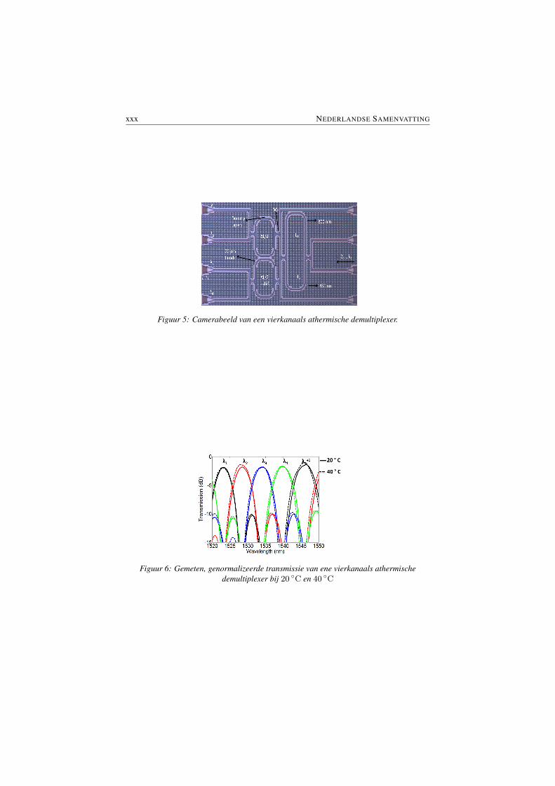
5 Camerabeeld van een vierkanaals athermische demultiplexer. . . . xxx6 Gemeten, genormalizeerde transmissie van ene vierkanaals ather-
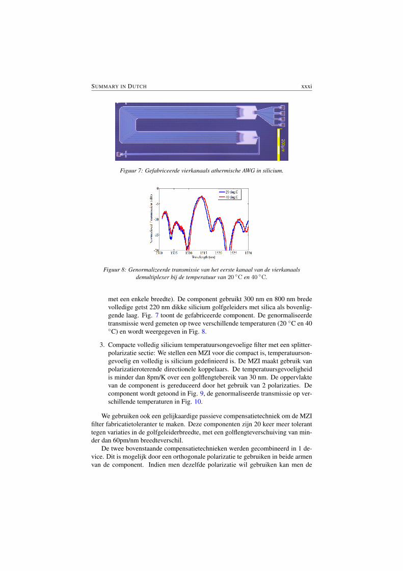
mische demultiplexer bij 20 ◦C en 40 ◦C . . . . . . . . . . . . . . xxx7 Gefabriceerde vierkanaals athermische AWG in silicium. . . . . . xxxi8 Genormalizeerde transmissie van het eerste kanaal van de vierkanaals
demultiplexer bij de temperatuur van 20 ◦C en 40 ◦C. . . . . . . xxxi9 SEM-beeld van een athermische MZI fiter met een detail van de
splitter-polarizatiedraaier en de versmalling in the onderste arm. . xxxii10 (a) Gemeten transmissie van de gefabriceerde demultiplexer bij
drie verschillende temperaturen. (b) De thermische gevoeligheidzoals ontworpen, zoals gesimuleerd op basis van het SEM-beeld,en zoals gemeten. . . . . . . . . . . . . . . . . . . . . . . . . . . xxxii
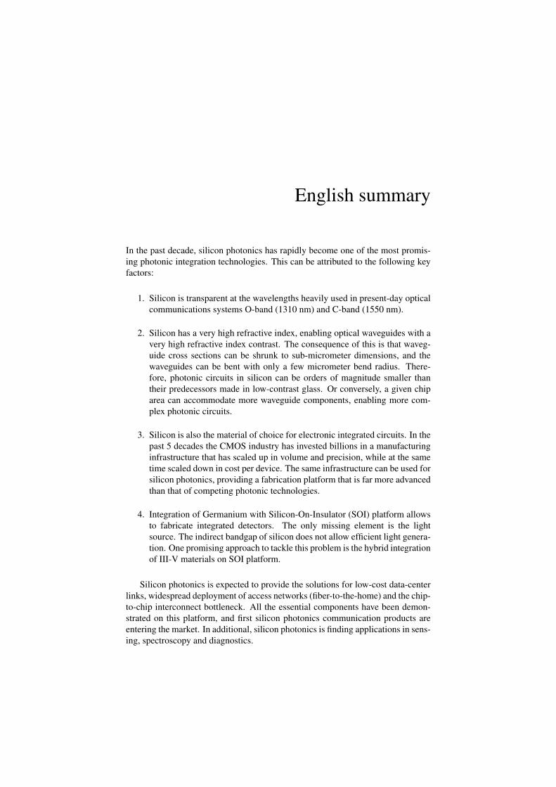
11 SEM-beeld van de gefabriceerde MZI met ondiep geetste MMI. . xxxii12 (a) Genormaliseerde transmissie en (b) dλ
dw -variatie als functie vangolflengte . . . . . . . . . . . . . . . . . . . . . . . . . . . . . . xxxiii
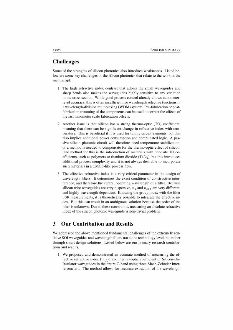
13 Camera image of set of fabricated devices for 600 nm wide wave-guide. . . . . . . . . . . . . . . . . . . . . . . . . . . . . . . . . xxxvii
14 (a) Simulated and extracted neff of 470, 602 and 805 nm widewaveguides and (b) Simulated and extracted ng over the C-band . xxxvii
15 Camera image of fabricated single block and 4-channel dual stagecascaded MZI demultiplexing filter (Inset: SEM image of one ofthe directional coupler showing gap and coupling length). . . . . xxxviii
x
16 Normalized measured transmission of the demux filter showingchannel spacing (CS), insertion loss (IL) and crosstalk (XT) at ITUgrid wavelengths. . . . . . . . . . . . . . . . . . . . . . . . . . . xxxviii
17 Camera image of fabricated 4-channel athermal demultiplexer . . xxxix18 Measured normalized transmission of 4-channel athermal demul-
tiplexer at 20 ◦C and 40 ◦C . . . . . . . . . . . . . . . . . . . . . xl19 Fabricated all-silicon four channels athermal AWG . . . . . . . . xl20 Normalized first channel response of all silicon athermal AWG at
temperatures 20 ◦C and 40 ◦C . . . . . . . . . . . . . . . . . . . xli21 SEM image of fabricated athermal MZI filter with zoomed in SPR
and waveguide tapering in the lower arm . . . . . . . . . . . . . . xli22 (a) Measured transmission of fabricated device at three different
temperatures. (b) Thermal sensitivity designed, simulated (afterSEM) and measured device . . . . . . . . . . . . . . . . . . . . . xli
23 SEM image of fabricated MZI filter with shallow etch MMI . . . . xlii24 (a) Normalized measured transmission and (b) dλ
dw variation withwavelength. . . . . . . . . . . . . . . . . . . . . . . . . . . . . . xlii
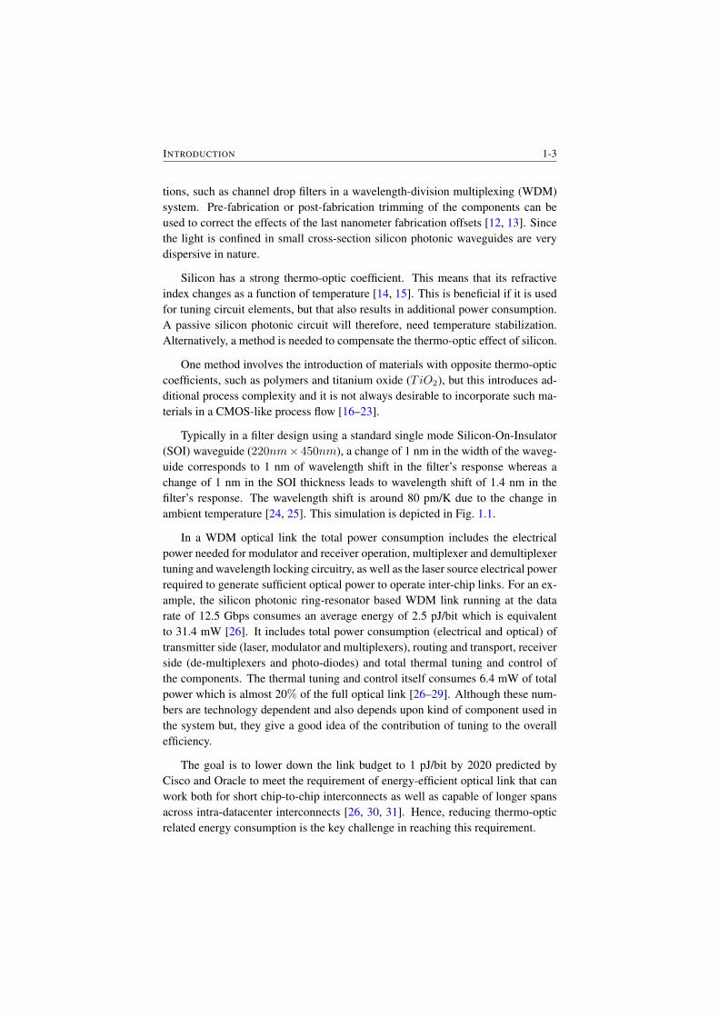
1.1 (a) Conventional Mach-Zehnder Interferometer (MZI) filter andsimulated mode profile of the waveguide with width 450 nm andthickness 220 nm at a wavelength of 1550 nm. Simulated effectiverefractive index and sensitivity of the MZI spectrum position with(b) temperature, (c) width and (d) height variation respectively.The simulation is performed for the air cladding. . . . . . . . . . 1-4
2.1 Size (a) of the square core for single mode operation for differentplatforms: Silica, Silicon nitride and Silicon-on-Insulator in theC-band. . . . . . . . . . . . . . . . . . . . . . . . . . . . . . . . 2-2
2.2 Cross sectional drawing of an SOI wafer. . . . . . . . . . . . . . . 2-32.3 Cross section of some standard SOI waveguides: Rib, Strip, Socket
and Slot. . . . . . . . . . . . . . . . . . . . . . . . . . . . . . . . 2-52.4 (a) Finite element mesh of the strip waveguide (b) TE mode profile
and (c) TM mode profile of strip waveguide. TE mode profiles of(d) Rib, (e) Socket and (f) Slot waveguide. Arrows are electricfield lines . . . . . . . . . . . . . . . . . . . . . . . . . . . . . . 2-6
2.5 Simulated neff of strip waveguide with waveguide width for aircladding with core thickness = 220 nm . . . . . . . . . . . . . . . 2-7
2.6 Simulated neff of strip waveguide with waveguide thickness forair cladding with core width = 450 nm . . . . . . . . . . . . . . . 2-8
2.7 Simulated neff of strip waveguide and sensitivity of spectrum po-sition for any wavelength filter with increasing waveguide corewidth. Here, h = 220 nm and T = 20 ◦C . . . . . . . . . . . . . . 2-9
2.8 Simulated neff of strip waveguide and sensitivity of spectrum po-sition for any wavelength filter with increasing waveguide corethickness. Here, w = 450 nm and T = 20 ◦C . . . . . . . . . . . . 2-10

xi
2.9 Simulated neff of strip waveguide and sensitivity of spectrum po-sition for any wavelength filter with increasing temperature. Here,w = 450 nm and h = 220 nm . . . . . . . . . . . . . . . . . . . . 2-11
2.10 Simulated ng of strip waveguide with air/ oxide as top claddingwith increasing core width . . . . . . . . . . . . . . . . . . . . . 2-12
2.11 Overview of the fabrication process of SOI photonic waveguideusing 193 nm optical lithography . . . . . . . . . . . . . . . . . . 2-13
2.12 Fabricated waveguides, SEM image of (a) the strip waveguide and(b) waveguide spiral . . . . . . . . . . . . . . . . . . . . . . . . 2-14
2.13 The measurement setup for vertical coupling . . . . . . . . . . . . 2-152.14 One of the standard spiral used for loss measurement . . . . . . . 2-162.15 Propagation loss extraction of 450 nm wide strip and 600 nm wide
rib waveguide at 1550 nm . . . . . . . . . . . . . . . . . . . . . 2-162.16 The estimated ∆neff allowed and maximum fabrication varia-
tions for three different waveguides 450, 600 and 800 nm for in-creasing filter order m. Inset 1: Zoomed plot showing the regionof operation of which order to choose when their maximum fabri-cation in a different waveguides. Inset 2: Simulated 2D TE modeprofile of 800 nm wide and 220 nm SOI waveguide with oxide astop cladding at room temperature. . . . . . . . . . . . . . . . . . 2-20
2.17 (a) Simulated transmission of a filter with some orderm and addedthe fabrication variations and, (b) Simulated transmission of a filterwith sufficiently low order m and added the fabrication variations. 2-21
2.18 Simulated effective index for neighboring order at resonant wave-lengths for 450 nm waveguide. Shown error margin is due to themaximum fabrication variations . . . . . . . . . . . . . . . . . . 2-22
2.19 Simulated circuit transmission of an MZI filter made out of 450nm wide and 215 nm thick SOI waveguide with m = 15, m′ = 16and M = 110 respectively . . . . . . . . . . . . . . . . . . . . . 2-23
2.20 (a). Camera image of set of fabricated devices for 600 nm widewaveguide and (b) SEM image of fabricated MZI with M = 110showing the MMI, bend radius r and path length difference ∆L.Inset: Low reflection compact grating coupler. . . . . . . . . . . 2-24
2.21 The automatic setup using vertical coupling for (a) photonic diesand (b) wafer . . . . . . . . . . . . . . . . . . . . . . . . . . . . 2-26
2.22 The zoom in image of semi-automatic setup . . . . . . . . . . . . 2-272.23 Measured and fitted normalized spectrum of MZI designed with
450 nm wide and 215 nm thick silicon waveguide (a) higher filterorder and (b) lower filter order. . . . . . . . . . . . . . . . . . . . 2-28
2.24 Simulated mode profile and XSEM image of 470 nm, 604 and805 nm wide and 211 nm thick waveguides. Side wall angles ofthe trapezoidal waveguides can be easily seen in the SEM. Siliconcorner rounding in the waveguide is due to the passive short loopspecific process; which involves oxide deposition after the hard-mask removal. . . . . . . . . . . . . . . . . . . . . . . . . . . . . 2-29
xii
2.25 (a) Simulated and extracted neff of 470, 602 and 805 nm widewaveguides and (b) Simulated and extracted ng over the C-band . 2-30
2.26 Extracted dneff
dT of 470, 602 and 805 nm wide waveguides . . . . 2-312.27 Extracted neff when an error is introduced on (a) the absolute
laser accuracy, (b) the grating coupler peak wavelength, (c) thelaser output power, (d) Histogram of neff0 after 100 iterationswith stochastic variations on these three error contributions usingMonte Carlo simulations . . . . . . . . . . . . . . . . . . . . . . 2-32
2.28 Error extraction ε(a) on 470 nm waveguide after 100 iterationsthrough Monte Carlo simulations . . . . . . . . . . . . . . . . . 2-33
2.29 Wafer map, distribution and radial plot of 470 nm wide fabricatedwaveguide at 1550 nm. Thickness variation is 211±2 nm and σ oflinewidth variation is 5 nm. Top-down SEM in nm at 3 locations.(a) neff and (b) ng . . . . . . . . . . . . . . . . . . . . . . . . . 2-34
2.30 Wafer map, distribution and radial plot of 604 nm wide fabricatedwaveguide at 1550 nm. Thickness variation is 211±2 nm and σ ofline width variation is 4 nm. Top-down SEM in nm at 3 locations.(a) neff and (b) ng . . . . . . . . . . . . . . . . . . . . . . . . . 2-35
2.31 Wafer map, distribution and radial plot of 805 nm wide fabricatedwaveguide at 1550 nm. Measured thickness is 211±2 nm and σ ofline width variation is 4 nm. Top-down SEM in nm at 3 locations.(a) neff and (b) ng . . . . . . . . . . . . . . . . . . . . . . . . . 2-36
3.1 Finite impulse response filter based on constant delay lines (from [7]) 3-33.2 Schematic representation of performance metrics of a wavelength
filter: insertion loss, insertion loss non-uniformity, neighbor chan-nel crosstalk, phase error crosstalk, 1dB and 10dB channel band-width. Passband aspect ratio is 1dB/10 dB channel bandwidth(from [7]). . . . . . . . . . . . . . . . . . . . . . . . . . . . . . 3-5
3.3 Different implementations of optical filters based on delay lines.(a) a Mach-Zehnder lattice filter, (b) an Arrayed Waveguide Grat-ing, (c) an Echelle Grating and (d) a Ring Resonator. (a-c) are fi-nite impulse response filters, consisting only of feed forward delaylines. The ring resonator (d) introduces a feed-back loop, makingan infinite impulse response filter. Figure is from [7]. . . . . . . . 3-6
3.4 Schematic for a 1× 4 demultiplexer. (a) Single MZI in each stageand, (b) 4 MZIs cascaded in each stage with directional couplerswith a power coupling coefficients to get flat band response. . . . 3-7
3.5 Circuit simulation of (a) Single MZI in each stage and, (b) with a4-MZIs lattice filter in each stage . . . . . . . . . . . . . . . . . . 3-9
3.6 MZI based 4-channel demultiplexer (a) fabricated device, (b) nor-malized measure transmission . . . . . . . . . . . . . . . . . . . 3-10
3.7 Cascaded MZI based 4-channel demultiplexer (a) fabricated and,(b) normalized measure transmission . . . . . . . . . . . . . . . 3-11
xiii
3.8 Array Waveguide Gratings (a) operation principle, (b) the overlapof the image field profile with the aperture mode gives rise to awider wavelength response (c) Flat band response which can beobtained by using MMI as an input aperture . . . . . . . . . . . . 3-12
3.9 MMI (a) schematic (from [36]) , (b) simulated field distribution atthe end of MMI of width 5µm for different lengths (c) simulatedE-field and (d) intensity field with length of MMI as 17µm . . . . 3-13
3.10 Flat band 4 channel AWG simulation (a) with 16 delay lines, thedesigned one and, (b) with 24 delay lines. As we increase thenumber of delay lines the roll-off becomes steep at the same timephase errors increase. . . . . . . . . . . . . . . . . . . . . . . . . 3-14
3.11 (a) Camera image of fabricated MMI-AWG and, (b) measured nor-malized transmission response . . . . . . . . . . . . . . . . . . . 3-15
3.12 (a) Echelle grating (from [7]. Basic design of the echelle gratingwhere the input and output apertures are located on the Rowlandcircle. (b) Fabricated echelle gratings [4]. (c) Etch gratings facets[40] and (d) Bragg mirror grating facets [41] . . . . . . . . . . . 3-16
3.13 (Simulated transmission of MMI-echelle grating . . . . . . . . . . 3-173.14 (a) Camera image of fabricated device MMI - echelle grating and,
(b) measured normalized transmission response . . . . . . . . . . 3-183.15 Schematic of the cascaded dual stage cascaded MZI de-multiplexing
filter. Stage 1 constitutes the tree-like structure of block A. Sim-ilar structures in stage 2 carry even and odd wavelengths. Eachblock is a set of four cascaded MZIs. Cascaded MZI parameters:path length difference ∆L, directional coupler and power couplingcoefficients K are shown. . . . . . . . . . . . . . . . . . . . . . 3-21
3.16 Simulation of (a) the individual block splitting odd and even wave-lengths and, (b) Tree-like structure showing the improved channelssuppression and band flatness. . . . . . . . . . . . . . . . . . . . 3-22
3.17 Full wave simulation of the power coupling with coupling lengthof directional couplers at their respective center wavelengths and atITU grid. Dotted lines show 50 % coupling at 1271 nm, 1301 nmand 1331 nm wavelengths. Inset: directional coupler sketch show-ing the straight, bend section and gap. . . . . . . . . . . . . . . . 3-23
3.18 Simulated transmission of the demux filter showing the channelwidth and guard band according to [50]. . . . . . . . . . . . . . . 3-24
3.19 Camera image of fabricated single block and 4-channel dual stagecascaded MZI demultiplexing filter (Inset: SEM image of one ofthe directional coupler showing gap and coupling length). . . . . 3-25
3.20 Reference waveguide at ITU grids . . . . . . . . . . . . . . . . . 3-263.21 Normalized measured transmission of the demux filter showing
channel spacing (CS), insertion loss (IL) and crosstalk (XT) at ITUgrid wavelengths. . . . . . . . . . . . . . . . . . . . . . . . . . . 3-27
3.22 Wafer scale distribution and contour plots showing mean IL andXT at ITU grids. . . . . . . . . . . . . . . . . . . . . . . . . . . 3-28
xiv
3.23 Wafer scale contour plots showing (a) the center wavelength ofchannel 3 around 1311 nm and (b) the channel spacing over thewafer. . . . . . . . . . . . . . . . . . . . . . . . . . . . . . . . . 3-29
3.24 Simulated spectral shift at 20 ◦C, 60 ◦C and 170 ◦C. . . . . . . . . 3-303.25 a) Measured spectral shift of two center channels at 20 ◦C and
60 ◦C and b) insertion loss or the normalized transmission with re-spect to reference waveguide showing the channel pass-bands withincreasing temperature. The fact that all the channels are withinthe 1 dB BW demonstrates the thermal tolerance of de-mux filter . 3-31
3.26 Simulation setup to determine the system evaluation of demultiplexer3-323.27 Simulated eye diagram of channel 2 with input power of 0 dBm
and 2 km of single mode fiber . . . . . . . . . . . . . . . . . . . 3-323.28 Simulated BER of 4 CWDM channels with different input power
of the CW laser. . . . . . . . . . . . . . . . . . . . . . . . . . . . 3-333.29 Simulated BER of channel 2 with channel de-tuning. . . . . . . . 3-34
4.1 Transmission of a conventional MZI for different temperatures;oxide top cladding, core width is 450 nm . . . . . . . . . . . . . . 4-3
4.2 Sensitivity of spectrum position to temperature of a conventionalMZI, AWG, and ring resonator with the air and oxide top-claddingat λ = 1550 nm . . . . . . . . . . . . . . . . . . . . . . . . . . . 4-3
4.3 SEM picture of a waveguide where the corrugated sidewall is vis-ible; width of waveguide is 400 nm . . . . . . . . . . . . . . . . . 4-4
4.4 Variation of neff with respect to width for TE and TM polariza-tion, for air and oxide top-cladding; λ = 1.55µm . . . . . . . . . 4-5
4.5 Schematic of MZI filter with modes in each arm . . . . . . . . . 4-64.6 Thermo-optic coefficient of fully etch silicon waveguide of 220 nm
thickness at λ = 1550 nm . . . . . . . . . . . . . . . . . . . . . . 4-84.7 (a) Modified interference order M and (b) dλ
dT with wide waveg-uide . . . . . . . . . . . . . . . . . . . . . . . . . . . . . . . . . 4-8
4.8 Camera image of fabricated all-silicon athermal MZI with widerand narrower waveguide section. The taper section is clearly seenin both arms. . . . . . . . . . . . . . . . . . . . . . . . . . . . . 4-9
4.9 Simulated 5µm long taper section showing the field intensity . . . 4-94.10 Thermally controlled chuck placed on the semi-automatic setup. . 4-104.11 Normalized transmission of athermal MZI filter at 30 ◦C and 50 ◦C.
The thermal sensitivity of the MZI is less than 10 pm/K in entireC-band . . . . . . . . . . . . . . . . . . . . . . . . . . . . . . . . 4-11
4.12 Schematic of a four channel a-thermal demultiplexer, a) block di-agram and b) cascaded MZI stages. Each MZI is combination of300 nm and 450 nm waveguide, K is power coupling coefficient . 4-12
4.13 Simulated circuit transmission of 4-channel athermal demultiplexerat 20 ◦C and 40 ◦C . . . . . . . . . . . . . . . . . . . . . . . . . 4-14
4.14 Camera image of fabricated 4-channel athermal demultiplexer . . 4-15
xv
4.15 Measured normalized transmission of 4-channel athermal demul-tiplexer at 20 ◦C and 40 ◦C . . . . . . . . . . . . . . . . . . . . . 4-16
4.16 Schematic of all-silicon athermal AWG . . . . . . . . . . . . . . 4-174.17 Design layout of all-silicon athermal AWG. The absolute length
of wider section decreases at the outermost section while the nar-rower section length increases. The wider waveguide is 800 nmwide and the narrower section is 300 nm. . . . . . . . . . . . . . 4-19
4.18 Fabricated all-silicon four channels athermal AWG . . . . . . . . 4-194.19 Normalized one channel response of standard silicon AWG at tem-
peratures 20 ◦C and 40 ◦C. . . . . . . . . . . . . . . . . . . . . . 4-204.20 Normalized first channel response of all silicon athermal AWG at
temperatures 20 ◦C and 40 ◦C . . . . . . . . . . . . . . . . . . . 4-214.21 Normalized all four channels of all silicon athermal AWG at 20 ◦C
and 40 ◦C . . . . . . . . . . . . . . . . . . . . . . . . . . . . . . 4-21
5.1 Simulated TO coefficients of TE and TM modes of SOI waveguideas a function of core width at a wavelength of 1550 nm. . . . . . . 5-2
5.2 Schematic of the proposed temperature insensitive filter with TMand TE mode profile . . . . . . . . . . . . . . . . . . . . . . . . 5-3
5.3 Schematic structure of the splitter and polarization rotator. (a)three dimensional model; (b) x-y cross section . . . . . . . . . . . 5-4
5.4 neff variation with waveguide width of an SOI waveguide withair cladding (inset) showing a phase matching condition at 1550 nm 5-5
5.5 Simulated mode beating in an SPR from one mode to another asa function of coupling length showing the full mode conversion at1550 nm. I and O represents the input and output port of an SPR . 5-5
5.6 Intensity profile for the calculated cross coupling length from theinput TE mode to the output TM mode at 1550 nm . . . . . . . . 5-6
5.7 SEM image of fabricated athermal MZI filter with zoomed in SPRand waveguide tapering in the lower arm . . . . . . . . . . . . . . 5-10
5.8 (a)SPR cross section and (b) SPR test structure showing input TEmode, coupling length and outputs . . . . . . . . . . . . . . . . . 5-10
5.9 Fourier transform of transmission spectrum. . . . . . . . . . . . . 5-125.10 (a) Transmission of designed device to be athermal at center wave-
length of 1540 nm, (b) simulated transmission of fabricated device,after taking cross section, and (c) measured transmission of fabri-cated device at three different temperatures. (d) Thermal sensitiv-ity of (a), (b) and (c), the a-thermal region shifted by 20 nm due tofabrication variations. . . . . . . . . . . . . . . . . . . . . . . . . 5-15
5.11 Group index as a function of core width for different wavelengthsλ = (1500, . . . , 1600) nm. . . . . . . . . . . . . . . . . . . . . . 5-16
5.12 Thermo-optic coefficients of TE and TM mode waveguides for thedesigned and the measured waveguide widths . . . . . . . . . . . 5-17
5.13 Measured transmission of the SPR test structure for different cou-pling lengths . . . . . . . . . . . . . . . . . . . . . . . . . . . . 5-18
xvi
5.14 TO coefficients of TE and TM polarization at different waveguidewidths for air top-cladding. . . . . . . . . . . . . . . . . . . . . . 5-20
5.15 Simulated shift in the resonant wavelength of the separate armsTM, TE and device (differential) with cladding refractive indexvariation in refractive index unit (RIU) at two different temperatures.5-21
6.1 Contour plot of ( dλdw2) of proposed filter at λ = 1550 nm and at T
= 20 ◦C . . . . . . . . . . . . . . . . . . . . . . . . . . . . . . . 6-46.2 Schematic of MZI filter with different waveguide width in each arm 6-66.3 Effective refractive index and its sensitivity of strip waveguide of
thickness 220 nm with varying core width at wavelength of 1550 nm 6-66.4 SEM image of fabricated MZI filter with shallow etch MMI . . . . 6-76.5 (a) Simulated spectra of a conventional MZI for 0, -2 and +2 nm
width offset. (b) Simulated spectra of the optimized design for 0, -10 and +10 nm width offset (c) Normalized measured transmissionand (d) dλ
dw variation with wavelength. . . . . . . . . . . . . . . . 6-86.6 (a) Measured transmission of fabrication tolerant filter at T = 20 ◦C,
30 ◦C and 40 ◦C, (b) thermal sensitivity dλdT variation simulated
and measured . . . . . . . . . . . . . . . . . . . . . . . . . . . . 6-96.7 Camera image of AWG with deliberate width variation of 20 nm . 6-106.8 Normalized and measured single channel response of the two AWGs,
one with nominal width and another with linewidth variation of20 nm . . . . . . . . . . . . . . . . . . . . . . . . . . . . . . . . 6-11
6.9 Normalized and measured of all four channels response of the twoAWGs, one with nominal width and another with linewidth varia-tion of 20 nm . . . . . . . . . . . . . . . . . . . . . . . . . . . . 6-11
6.10 SEM image of fabricated MZI filter with SPR . . . . . . . . . . . 6-126.11 (a) Simulated spectra of optimized design for 0, -10 and +10 nm
width offset and at T = 30 ◦C and 40 ◦C and 50 ◦C, (b) normalizedmeasured transmission, (c) width sensitivity dλ
dw and (d) thermalsensitivity dλ
dT simulated and measured . . . . . . . . . . . . . . . 6-136.12 Bar and cross port measured transmission of SPR at different tem-
peratures. SEM image of SPR (inset) . . . . . . . . . . . . . . . . 6-146.13 Longest arm of the fabrication and thermal tolerant MZI, normal-
ized to the arm length difference of a conventional MZI with a corewidth of 450 nm. . . . . . . . . . . . . . . . . . . . . . . . . . . 6-16
6.14 (a) Schematic of two stages filter 4 channel de-multiplexer withk=0.5, (b) simulated transmission of filter at T = 30 ◦C, 50 ◦C andwith width variation of (-10,0,+10 )nm . . . . . . . . . . . . . . . 6-17
6.15 Block diagram filter of 2-stage 4-channel cascaded mzi lattice fil-ter. In block A the coupling coefficients are mentioned and nowdelay line comes from different waveguide widths w1 and w2 withcorresponding lengths L1 and L2 . . . . . . . . . . . . . . . . . . 6-18

xvii
6.16 Circuit simulation of spectral shift of fabrication insensitive 4-channel flat band de-multiplexer . . . . . . . . . . . . . . . . . . 6-19
6.17 Simulated TO coefficients of the SOI waveguide at 1310 nm and inshowing the mode profile of 250 nm and 380 nm wide waveguides 6-20
6.18 Simulated spectral shift of thermally insensitive demultiplexer at20 ◦C and 60 ◦C . . . . . . . . . . . . . . . . . . . . . . . . . . . 6-21

List of Tables
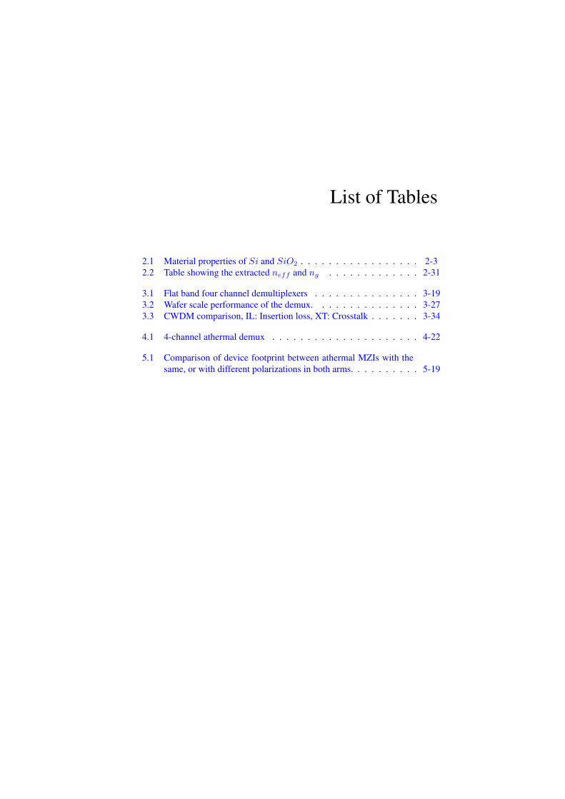
2.1 Material properties of Si and SiO2 . . . . . . . . . . . . . . . . . 2-32.2 Table showing the extracted neff and ng . . . . . . . . . . . . . 2-31
3.1 Flat band four channel demultiplexers . . . . . . . . . . . . . . . 3-193.2 Wafer scale performance of the demux. . . . . . . . . . . . . . . 3-273.3 CWDM comparison, IL: Insertion loss, XT: Crosstalk . . . . . . . 3-34
4.1 4-channel athermal demux . . . . . . . . . . . . . . . . . . . . . 4-22
5.1 Comparison of device footprint between athermal MZIs with thesame, or with different polarizations in both arms. . . . . . . . . . 5-19


List of Acronyms
A
AWG Array Waveguide GratingsAu Gold
B
BOX Buried OxideBPM Beam Propagation Method
C
CMOS Complementary Metal-Oxide SemiconductorCWDM Coarse Wavelength Division Multiplexing
D
DBR Distributed Bragg ReflectorDC Directional CouplerDWDM Dense Wavelength Division Multiplexing
F
FEM Finite Element Method
xxii
FDTD Finite Difference Time DomainFIB Fcoused Ion BeamFMM Film Mode MatchingFPR Free Propagation RegionFSR Free Spectral Range
G
GbE Gigabit EthernetGe GermaniumGC Grating Coupler
I
ITU International Telecommunication Union
K
K Kelvin
M
MMI Multimode InterferenceMZI Mach-Zehnder Interferometer
P
PCG Planar Concave GratingPIC Photonic Integrated Circuit
R
xxiii
RLMZI Ring Loaded Mach-Zehnder Interferometer
S
SEM Scanning Electron MicroscopeSi SiliconSiN Silicon NitrideSiO Silicon OxideSOI Silicon on InsulatorSPR Splitter Polarization RotatorSK Socket
T
TE Transverse ElectricTM Transverse MagneticTi TitaniumTDSEM Top Down Scanning Electron MicroscopeTO Thermo Optic
W
WDM Wavelength Division Multiplexing

Nederlandse samenvatting–Summary in Dutch–
Het voorbije decenium is siliciumfotonica een van de meestbelovende optischeintegratietechnieken geworden. De hoofdredenen hiervoor zijn:
1. Silicium is transparant voor de golflengtes die het meest gebruikt wordenin optische communicatie systemen, de zogenaamde O-band (1310 nm) enC-band (1550 nm).
2. Silicium heeft een heel grote brekingsindex, wat zorgt voor golfgeleidersmet een heel groot contrast in brekingsindex tussen de kern en de omge-ving. Hierdoor kunnen de golfgeleiderdimensies geschaald worden naarsub-micrometer orde. Tevens kunnen bochten gemaakt worden met eenstraal van slechts enkele micrometer. Deze compacte basiscomponentenzorgen ervoor dat de totale oppervlakte van het volledige optische circuitin silicium een orde kleiner is dan die van andere technologin (vaak glas-gebaseerd). Anders gesteld kunnen er meer functies gentegreerd worden opdezelfde oppervlakte, wat toelaat om de complexiteit te verhogen.
3. Silicium is ook het dominante material in electronische integratie. De voor-bije 50 jaar heeft de CMOS industrie miljarden genvesteerd in fabricatie-technologie. Zowel het volume als de precisie werden geoptimaliseerd ter-wijl de kost per component steeds kleiner is geworden. Deze zelfde infra-structuur kan gebruikt worden voor siliciumfotonica, waardoor de fabrica-tiekwaliteit een stuk verder staat dan deze bij de concurrerende technologin.
4. Integratie van germanium met het silicium-op-isolator (SOI) platform laattoe om ook de detectoren te integreren. Aangezien de passieve componen-ten al van hoge kwaliteit kunnen zijn, is het laatste ontbrekende element delichtbron. Door de indirecte bandkloof zijn efficinte bronnen rechtstreeks opsilicium niet mogelijk. De hybride III-V integratie techniek op SOI wordtmomenteel geoptimaliseerd om ook dit probleem uit de weg te helpen.
Siliciumfotonica wordt gezien als de oplossing voor goedkope verbindingenin datacenters, voor brede uitrol van access networks (fiber-to-the-home) en voorinterconnecties tussen chips. Alle essentile componenten zijn reeds aangetoond
xxvi NEDERLANDSE SAMENVATTING
op dit platform en de eerste siliciumfotonische producten zijn op de communica-tiemarkt. Daarenboven worden andere markten zoals sensoren, spectroscopie endiagnose aangeboord.
UitdagingenEen aantal van de sterke punten van siliciumfotonica introduceren echter nieuwezwakheden. We lijsten enkele van de nieuwe uitdagingen op:
1. Het hoge contrast in brekingsindex, dat om kleine golfgeleiders en scherpebochten toelaat, zorgt er ook voor dat de structuur heel gevoelig wordt aanenige afwijking van de golfgeleiderdimensies. Hoewel de CMOS-fabricatietechniekenal nanometerschaal precisie haalt, is dit vaak niet goed genoeg voor functio-naliteit die gevoelig is aan golflengte, zoals in een wavelength-division mul-tiplexing (WDM) systemen. Om de laatste aanpassingen te brengen wordende golfgeleiders vaak getrimd voor of na de fabricatie.
2. De thermisch-optische (TO) cofficint van silicium is vrij groot. Dit wil zeg-gen dat de brekingsindex zal variren in functie van temperatuur. Indien je ditwil gebruiken om het circuit bewust te benvloeden is dit voordelig, maar ditzorgt tegelijk ook voor een groot energieverbruik en complexe logica. Pas-sieve siliciumfotonische circuits gebruiken daarom meestal temperatuursta-bilisatie. Een alternatief hiervoor is de introductie van materialen met eentegengestelde TO cofficint, zoals polymeren of titanium dioxide (TiO2),maar dit verhoogt de complexiteit in fabricatie. Bovendien worden zo’nmaterialen niet altijd toegelaten in CMOS processen.
3. De effectieve brekingsindex is een van de belangrijkste parameters bij hetontwerpen van golflengtefilters. Dit bepaald immers wanneer er construc-tieve interferentie optreedt en bijgevolg de centrale golflengte van de filter.Door de hoge dispersie van siliciumgolfgeleiders zijn de groepsbrekingsin-dex ng en de effectieve index neff zeer verschillend en sterk afhankelijk vangolflengte. Als men de groepsindex kent, is het theoretisch gezien mogelijkom de effectieve index te berekenen, maar in praktijk is de data vaak nietgoed genoeg.
1 Onze bijdrage en resultatenHierboven hebben we de fundamentele uitdagingen uiteen gezet van de hyperge-voelig SOI golfgeleiders en golflengtefilters. We pakten deze niet aan via techno-logie, maar via slimmere ontwerptechnieken. Hieronder lijsten we onze belang-rijkste resultaten op.
1. We stelden een nieuwe accurate methode voor om de effictieve brekings-index (neff ) en thermo-optische cofficint te meten van silicium-op-isolator
SUMMARY IN DUTCH xxvii
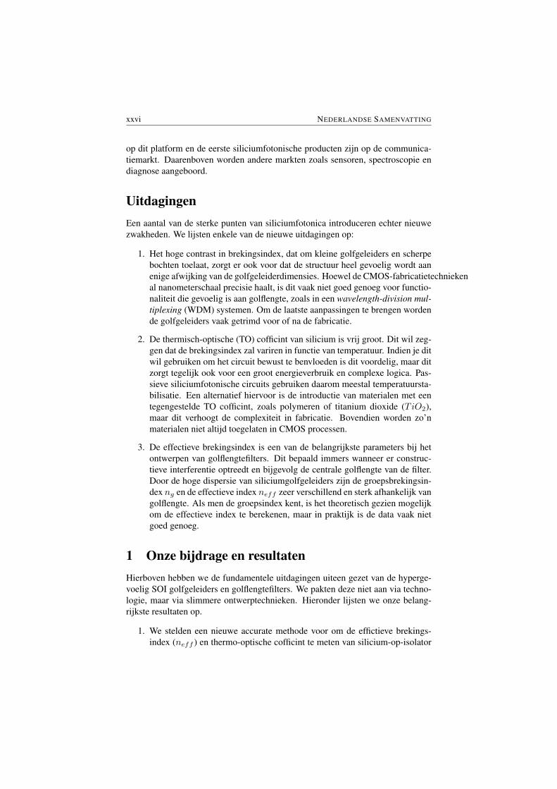
Figuur 1: Camerabeeld van gefabriceerde MZI’s voor de extractie van de brekingsindexvan een 600nm brede golfgeleider.
golfgeleider. Deze methode werkt in de volledige C-band en gebruikt drieMach-Zehnder Interferometers (MZI). Ze laat toe om de golflengtedisper-sie accuraat te extraheren en houdt rekening met variaties in fabricatie. Wegebruiken twee MZI’s met een lage orde m, i.e. een grote spectraal bereik(FSR). Hierdoor kunnen we de orde van de filter correct schatten in de C-band. De derde MZI heeft een veel hogere orde en een kleine FSR, wat onshelpt om de golflengteafhankelijkheid van de groepsindex ng te extraheren.Om de TO cofficint te bepalen, meten we ze dezelfde MZI’s op verschil-lende temperaturen. De gefabriceerde componenten en de gesimuleerde engemeten resultaten worden getoond in Fig. 1 en Fig. 2.
Om de golflengtefilters tolerant te maken aan fabricatiefouten en fluctuatiesvan temperatuur, hebben we de doorlaatband vlakker gemaakt. Met deze techniekhebben we verschillende SOI demultiplexers vergeleken, bijvoorbeeld arrayed wa-veguide gratings (AWG), echelle gratings en gecascadeerde MZI filters. Gecasca-deerde MZI filters waren de beste keuze voor korte-afstandsinterconnecties, waareen laag energiebudget en lage kost van kritisch belang zijn.
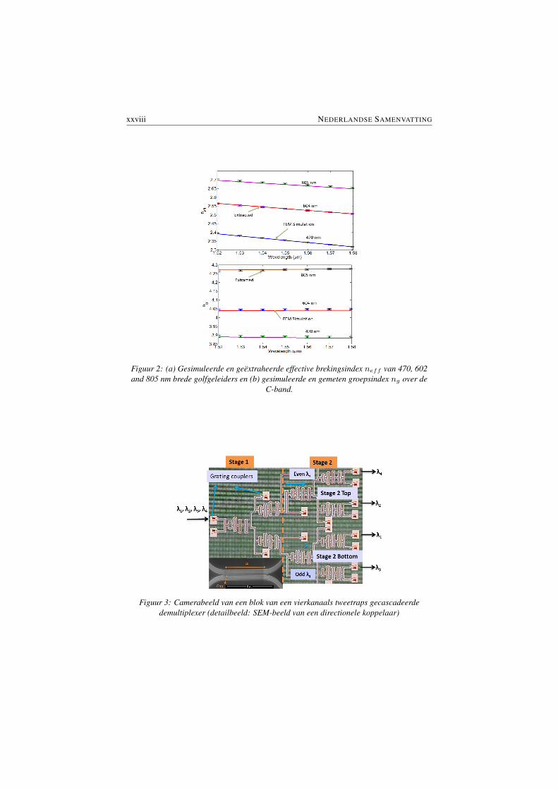
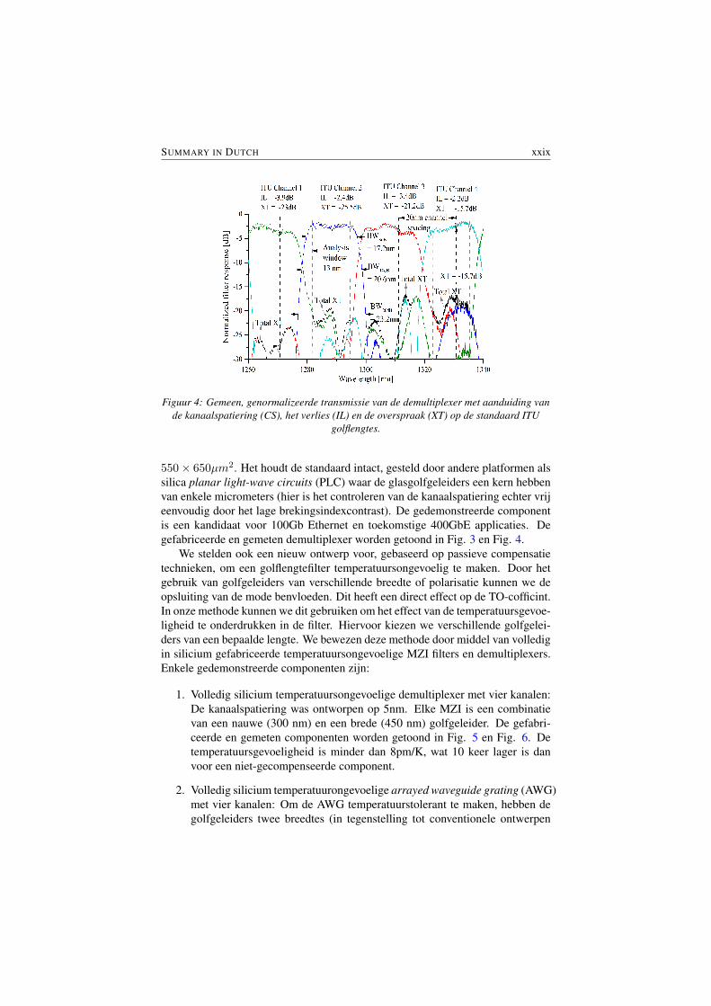
We demonstreerden een vierkanaals demultiplexer voor de O-band, gebaseerdop een tweetraps gecascadeerde MZI, die zowel robuust is als lage verliezen heeft.De transferfunctie met vlakke doorlaatband werd gerealiseerd met een 4e orde ge-cascadeerde MZI filter. De kanalen van de gemeten component liggen 20nm uitelkaar, over een bereik van 80nm. Het spectrum is gecentreerd op 1301 nm meteen vlakke doorlaatband over 60 % van de kanaalspatiering, en dit om fluctuatiesin temperature tot 100 ◦C en de fabricatievariaties op te vangen. Karakterisatieover een volledige wafer toont dat het gemiddelde insertieverlies onder de 3dBligt en dat de overspraak beer is dan -18dB. Deze brede doorlaatbanden makende demultiplexer van nature uit thermisch robuust. Dit laat toe om ongekoelde la-sers te gebruiken en maakt thermische controle overbodig, wat een positief gevolgheeft voor het vermogengebruik en de kost. De oppervlakte van de component is
xxviii NEDERLANDSE SAMENVATTING
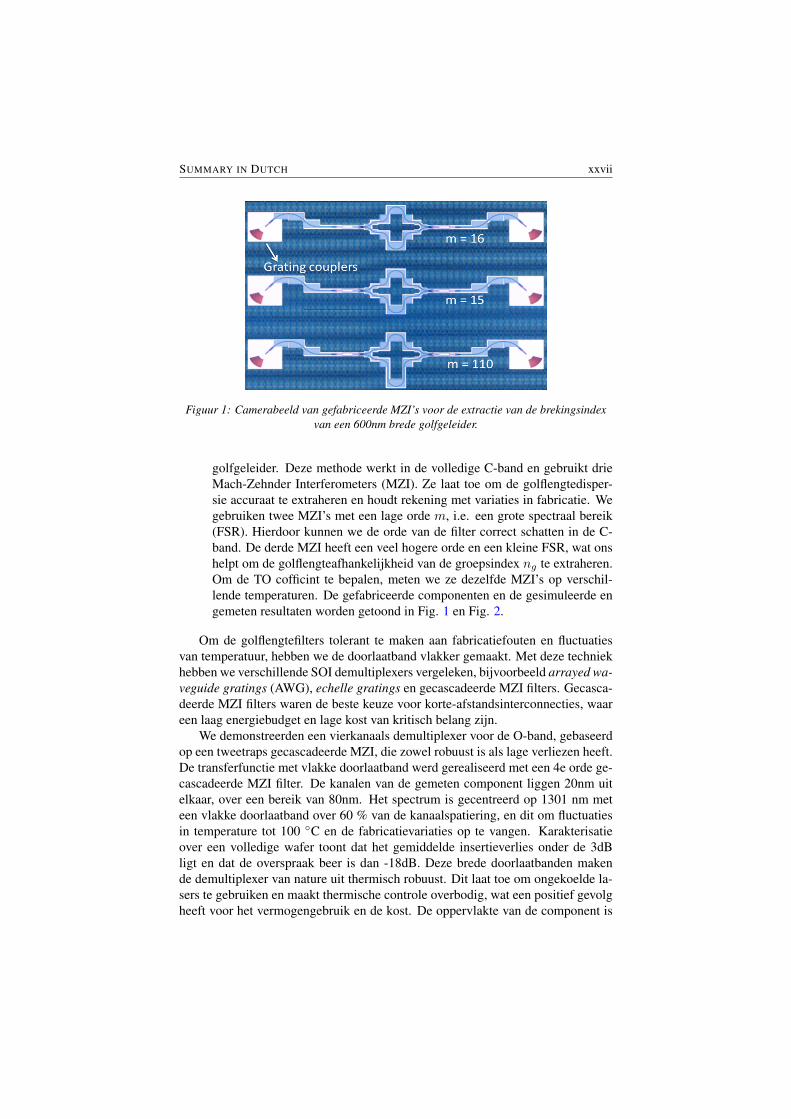
Figuur 2: (a) Gesimuleerde en geextraheerde effective brekingsindex neff van 470, 602and 805 nm brede golfgeleiders en (b) gesimuleerde en gemeten groepsindex ng over de
C-band.
Figuur 3: Camerabeeld van een blok van een vierkanaals tweetraps gecascadeerdedemultiplexer (detailbeeld: SEM-beeld van een directionele koppelaar)
SUMMARY IN DUTCH xxix
Figuur 4: Gemeen, genormalizeerde transmissie van de demultiplexer met aanduiding vande kanaalspatiering (CS), het verlies (IL) en de overspraak (XT) op de standaard ITU
golflengtes.
550× 650µm2. Het houdt de standaard intact, gesteld door andere platformen alssilica planar light-wave circuits (PLC) waar de glasgolfgeleiders een kern hebbenvan enkele micrometers (hier is het controleren van de kanaalspatiering echter vrijeenvoudig door het lage brekingsindexcontrast). De gedemonstreerde componentis een kandidaat voor 100Gb Ethernet en toekomstige 400GbE applicaties. Degefabriceerde en gemeten demultiplexer worden getoond in Fig. 3 en Fig. 4.
We stelden ook een nieuw ontwerp voor, gebaseerd op passieve compensatietechnieken, om een golflengtefilter temperatuursongevoelig te maken. Door hetgebruik van golfgeleiders van verschillende breedte of polarisatie kunnen we deopsluiting van de mode benvloeden. Dit heeft een direct effect op de TO-cofficint.In onze methode kunnen we dit gebruiken om het effect van de temperatuursgevoe-ligheid te onderdrukken in de filter. Hiervoor kiezen we verschillende golfgelei-ders van een bepaalde lengte. We bewezen deze methode door middel van volledigin silicium gefabriceerde temperatuursongevoelige MZI filters en demultiplexers.Enkele gedemonstreerde componenten zijn:
1. Volledig silicium temperatuursongevoelige demultiplexer met vier kanalen:De kanaalspatiering was ontworpen op 5nm. Elke MZI is een combinatievan een nauwe (300 nm) en een brede (450 nm) golfgeleider. De gefabri-ceerde en gemeten componenten worden getoond in Fig. 5 en Fig. 6. Detemperatuursgevoeligheid is minder dan 8pm/K, wat 10 keer lager is danvoor een niet-gecompenseerde component.
2. Volledig silicium temperatuurongevoelige arrayed waveguide grating (AWG)met vier kanalen: Om de AWG temperatuurstolerant te maken, hebben degolfgeleiders twee breedtes (in tegenstelling tot conventionele ontwerpen
xxx NEDERLANDSE SAMENVATTING
Figuur 5: Camerabeeld van een vierkanaals athermische demultiplexer.
Figuur 6: Gemeten, genormalizeerde transmissie van ene vierkanaals athermischedemultiplexer bij 20 ◦C en 40 ◦C
SUMMARY IN DUTCH xxxi
Figuur 7: Gefabriceerde vierkanaals athermische AWG in silicium.
Figuur 8: Genormalizeerde transmissie van het eerste kanaal van de vierkanaalsdemultiplexer bij de temperatuur van 20 ◦C en 40 ◦C.
met een enkele breedte). De component gebruikt 300 nm en 800 nm bredevolledige getst 220 nm dikke silicium golfgeleiders met silica als bovenlig-gende laag. Fig. 7 toont de gefabriceerde component. De genormaliseerdetransmissie werd gemeten op twee verschillende temperaturen (20 ◦C en 40◦C) en wordt weergegeven in Fig. 8.
3. Compacte volledig silicium temperatuursongevoelige filter met een splitter-polarizatie sectie: We stellen een MZI voor die compact is, temperatuurson-gevoelig en volledig is silicium gedefinieerd is. De MZI maakt gebruik vanpolarizatieroterende directionele koppelaars. De temperatuursgevoeligheidis minder dan 8pm/K over een golflengtebereik van 30 nm. De oppervlaktevan de component is gereduceerd door het gebruik van 2 polarizaties. Decomponent wordt getoond in Fig. 9, de genormaliseerde transmissie op ver-schillende temperaturen in Fig. 10.
We gebruiken ook een gelijkaardige passieve compensatietechniek om de MZIfilter fabricatietoleranter te maken. Deze componenten zijn 20 keer meer toleranttegen variaties in de golfgeleiderbreedte, met een golflengteverschuiving van min-der dan 60pm/nm breedteverschil.
De twee bovenstaande compensatietechnieken werden gecombineerd in 1 de-vice. Dit is mogelijk door een orthogonale polarizatie te gebruiken in beide armenvan de component. Indien men dezelfde polarizatie wil gebruiken kan men de

xxxii NEDERLANDSE SAMENVATTING
Figuur 9: SEM-beeld van een athermische MZI fiter met een detail van desplitter-polarizatiedraaier en de versmalling in the onderste arm.
Figuur 10: (a) Gemeten transmissie van de gefabriceerde demultiplexer bij drieverschillende temperaturen. (b) De thermische gevoeligheid zoals ontworpen, zoals
gesimuleerd op basis van het SEM-beeld, en zoals gemeten.
Figuur 11: SEM-beeld van de gefabriceerde MZI met ondiep geetste MMI.
SUMMARY IN DUTCH xxxiii
Figuur 12: (a) Genormaliseerde transmissie en (b) dλdw
-variatie als functie van golflengte
golfgeleiderbreedte variren. Het ontwerp is zoals getoond in Fig. 10 met geopti-malizeerde breedte voor fabricagefouten. We meten een verschuiving van minderdan ±65pm/nm en temperatuursgevoeligheid van ±15pm/K over een golfleng-tebereik van 40 nm.
2 ConclusieVan bovenstaande discussie kan geconcludeerd worden dat een slim ontwerp defundamentele problemen van het SOI platform kan aanpakken. We namen de uit-daging aan om de effectieve brekingsindex van hoogdispersieve silicium golfge-leiders accurater te bepalen. We demonstreerden een robuuste demultiplexer metvlakke doorlaatband en kanaalspatiering van 20 nm voor 100 GbE applicaties. Wehebben ook componenten gemaakt die compenseren voor fabricatie-imperfecties(vooral de golfgeleiderbreedte) en temperatuursgevoeligheid. Verschillende FIRfilters werden aangetoond zoals AWG’s en MZI’s. De combinatie van deze ont-werpen met vlakke doorlaatband en compensatieschema’s kunnen de performantienog verder opkrikken, wat van belang is voor interconnecties op chip. Met dezegerealiseerde ontwerpen hebben we aangetoond dat enkele uitdagingen kunnen/-zullen opgelost worden zonder het fabricatieprocess verder te compliceren.

English summary
In the past decade, silicon photonics has rapidly become one of the most promis-ing photonic integration technologies. This can be attributed to the following keyfactors:
1. Silicon is transparent at the wavelengths heavily used in present-day opticalcommunications systems O-band (1310 nm) and C-band (1550 nm).
2. Silicon has a very high refractive index, enabling optical waveguides with avery high refractive index contrast. The consequence of this is that waveg-uide cross sections can be shrunk to sub-micrometer dimensions, and thewaveguides can be bent with only a few micrometer bend radius. There-fore, photonic circuits in silicon can be orders of magnitude smaller thantheir predecessors made in low-contrast glass. Or conversely, a given chiparea can accommodate more waveguide components, enabling more com-plex photonic circuits.
3. Silicon is also the material of choice for electronic integrated circuits. In thepast 5 decades the CMOS industry has invested billions in a manufacturinginfrastructure that has scaled up in volume and precision, while at the sametime scaled down in cost per device. The same infrastructure can be used forsilicon photonics, providing a fabrication platform that is far more advancedthan that of competing photonic technologies.
4. Integration of Germanium with Silicon-On-Insulator (SOI) platform allowsto fabricate integrated detectors. The only missing element is the lightsource. The indirect bandgap of silicon does not allow efficient light genera-tion. One promising approach to tackle this problem is the hybrid integrationof III-V materials on SOI platform.
Silicon photonics is expected to provide the solutions for low-cost data-centerlinks, widespread deployment of access networks (fiber-to-the-home) and the chip-to-chip interconnect bottleneck. All the essential components have been demon-strated on this platform, and first silicon photonics communication products areentering the market. In additional, silicon photonics is finding applications in sens-ing, spectroscopy and diagnostics.
xxxvi ENGLISH SUMMARY
ChallengesSome of the strengths of silicon photonics also introduce weaknesses. Listed be-low are some key challenges of the silicon photonics that relate to the work in themanuscript:
1. The high refractive index contrast that allows the small waveguides andsharp bends also makes the waveguides highly sensitive to any variationin the cross section. While good process control already allows nanometer-level accuracy, this is often insufficient for wavelength selective functions ina wavelength-division multiplexing (WDM) system. Pre-fabrication or post-fabrication trimming of the components can be used to correct the effects ofthe last nanometer scale fabrication offsets.
2. Another issue is that silicon has a strong thermo-optic (TO) coefficient,meaning that there can be significant change in refractive index with tem-perature. This is beneficial if it is used for tuning circuit elements, but thatalso implies additional power consumption and complicated logic. A pas-sive silicon photonic circuit will therefore need temperature stabilization,or a method is needed to compensate for the thermo-optic effect of silicon.One method for this is the introduction of materials with opposite TO co-efficients, such as polymers or titanium dioxide (TiO2), but this introducesadditional process complexity and it is not always desirable to incorporatesuch materials in a CMOS-like process flow.
3. The effective refractive index is a very critical parameter in the design ofwavelength filters. It determines the exact condition of constructive inter-ference, and therefore the central operating wavelength of a filter. Becausesilicon wire waveguides are very dispersive, ng and neff are very different,and highly wavelength dependent. Knowing the group index with the filterFSR measurements, it is theoretically possible to integrate the effective in-dex. But this can result in an ambiguous solution because the order of thefilter is unknown. Due to these constraints, measuring an absolute refractiveindex of the silicon photonic waveguide is non-trivial problem.
3 Our Contribution and ResultsWe addressed the above mentioned fundamental challenges of the extremely sen-sitive SOI waveguides and wavelength filters not at the technology level, but ratherthrough smart design solutions. Listed below are our primary research contribu-tions and results.
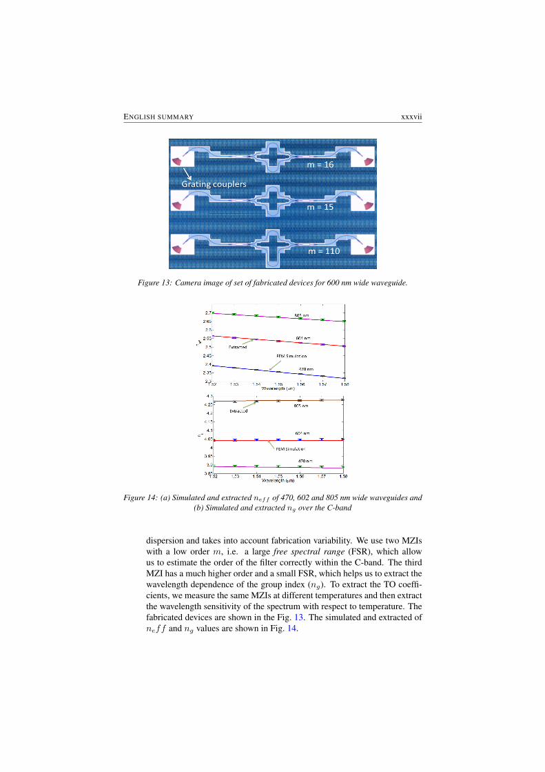
1. We proposed and demonstrated an accurate method of measuring the ef-fective refractive index (neff ) and thermo-optic coefficient of Silicon-On-Insulator waveguides in the entire C-band using three Mach-Zehnder Inter-ferometers. The method allows for accurate extraction of the wavelength
ENGLISH SUMMARY xxxvii
Figure 13: Camera image of set of fabricated devices for 600 nm wide waveguide.
Figure 14: (a) Simulated and extracted neff of 470, 602 and 805 nm wide waveguides and(b) Simulated and extracted ng over the C-band
dispersion and takes into account fabrication variability. We use two MZIswith a low order m, i.e. a large free spectral range (FSR), which allowus to estimate the order of the filter correctly within the C-band. The thirdMZI has a much higher order and a small FSR, which helps us to extract thewavelength dependence of the group index (ng). To extract the TO coeffi-cients, we measure the same MZIs at different temperatures and then extractthe wavelength sensitivity of the spectrum with respect to temperature. Thefabricated devices are shown in the Fig. 13. The simulated and extracted ofneff and ng values are shown in Fig. 14.
xxxviii ENGLISH SUMMARY
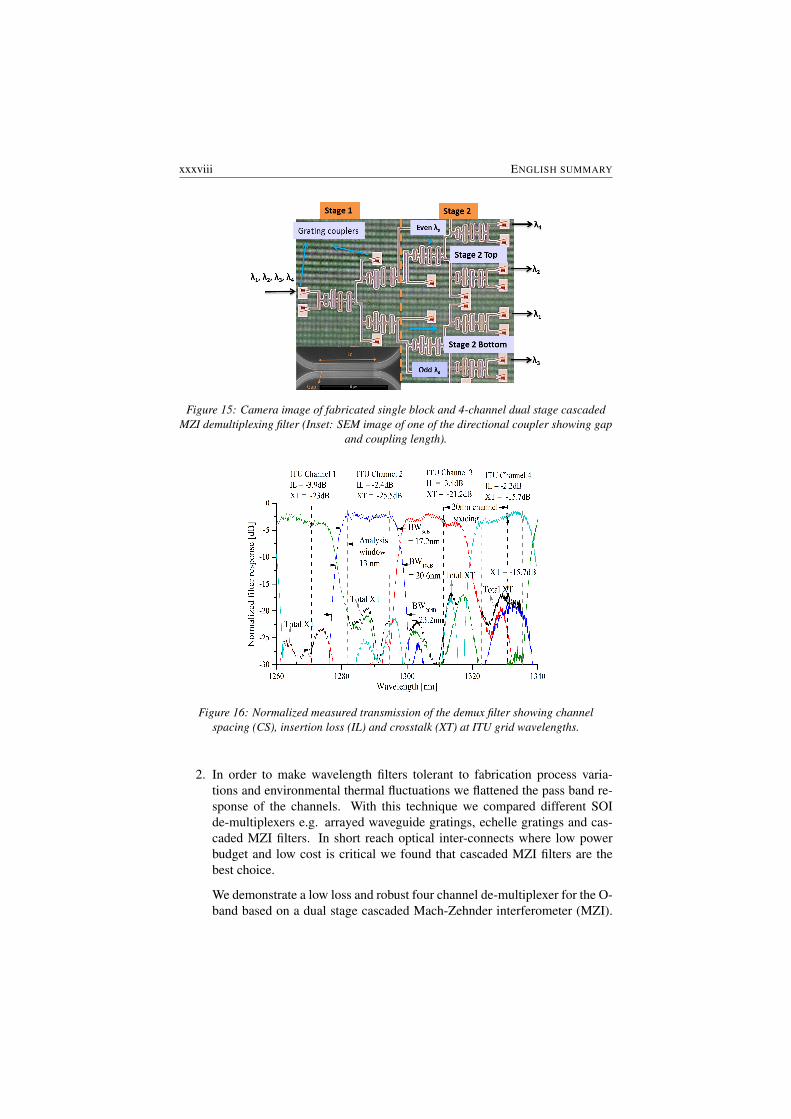
Figure 15: Camera image of fabricated single block and 4-channel dual stage cascadedMZI demultiplexing filter (Inset: SEM image of one of the directional coupler showing gap
and coupling length).
Figure 16: Normalized measured transmission of the demux filter showing channelspacing (CS), insertion loss (IL) and crosstalk (XT) at ITU grid wavelengths.
2. In order to make wavelength filters tolerant to fabrication process varia-tions and environmental thermal fluctuations we flattened the pass band re-sponse of the channels. With this technique we compared different SOIde-multiplexers e.g. arrayed waveguide gratings, echelle gratings and cas-caded MZI filters. In short reach optical inter-connects where low powerbudget and low cost is critical we found that cascaded MZI filters are thebest choice.
We demonstrate a low loss and robust four channel de-multiplexer for the O-band based on a dual stage cascaded Mach-Zehnder interferometer (MZI).
ENGLISH SUMMARY xxxix
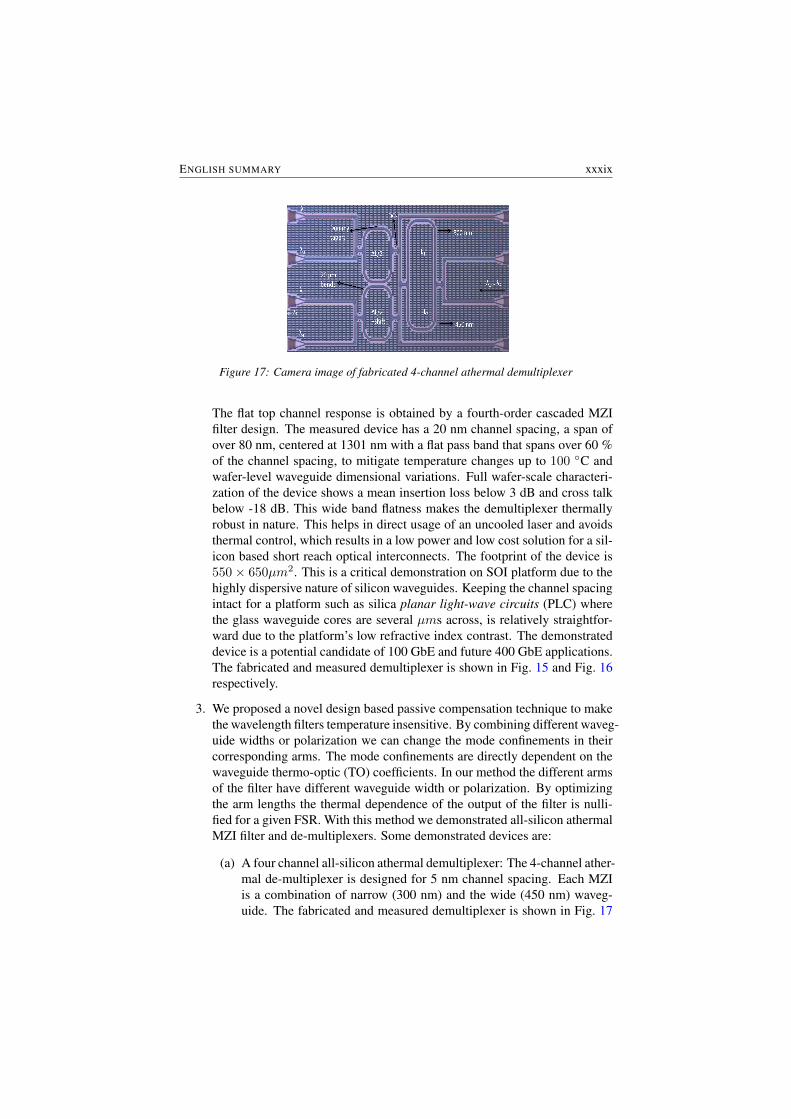
Figure 17: Camera image of fabricated 4-channel athermal demultiplexer
The flat top channel response is obtained by a fourth-order cascaded MZIfilter design. The measured device has a 20 nm channel spacing, a span ofover 80 nm, centered at 1301 nm with a flat pass band that spans over 60 %of the channel spacing, to mitigate temperature changes up to 100 ◦C andwafer-level waveguide dimensional variations. Full wafer-scale characteri-zation of the device shows a mean insertion loss below 3 dB and cross talkbelow -18 dB. This wide band flatness makes the demultiplexer thermallyrobust in nature. This helps in direct usage of an uncooled laser and avoidsthermal control, which results in a low power and low cost solution for a sil-icon based short reach optical interconnects. The footprint of the device is550× 650µm2. This is a critical demonstration on SOI platform due to thehighly dispersive nature of silicon waveguides. Keeping the channel spacingintact for a platform such as silica planar light-wave circuits (PLC) wherethe glass waveguide cores are several µms across, is relatively straightfor-ward due to the platform’s low refractive index contrast. The demonstrateddevice is a potential candidate of 100 GbE and future 400 GbE applications.The fabricated and measured demultiplexer is shown in Fig. 15 and Fig. 16respectively.
3. We proposed a novel design based passive compensation technique to makethe wavelength filters temperature insensitive. By combining different waveg-uide widths or polarization we can change the mode confinements in theircorresponding arms. The mode confinements are directly dependent on thewaveguide thermo-optic (TO) coefficients. In our method the different armsof the filter have different waveguide width or polarization. By optimizingthe arm lengths the thermal dependence of the output of the filter is nulli-fied for a given FSR. With this method we demonstrated all-silicon athermalMZI filter and de-multiplexers. Some demonstrated devices are:
(a) A four channel all-silicon athermal demultiplexer: The 4-channel ather-mal de-multiplexer is designed for 5 nm channel spacing. Each MZIis a combination of narrow (300 nm) and the wide (450 nm) waveg-uide. The fabricated and measured demultiplexer is shown in Fig. 17
xl ENGLISH SUMMARY
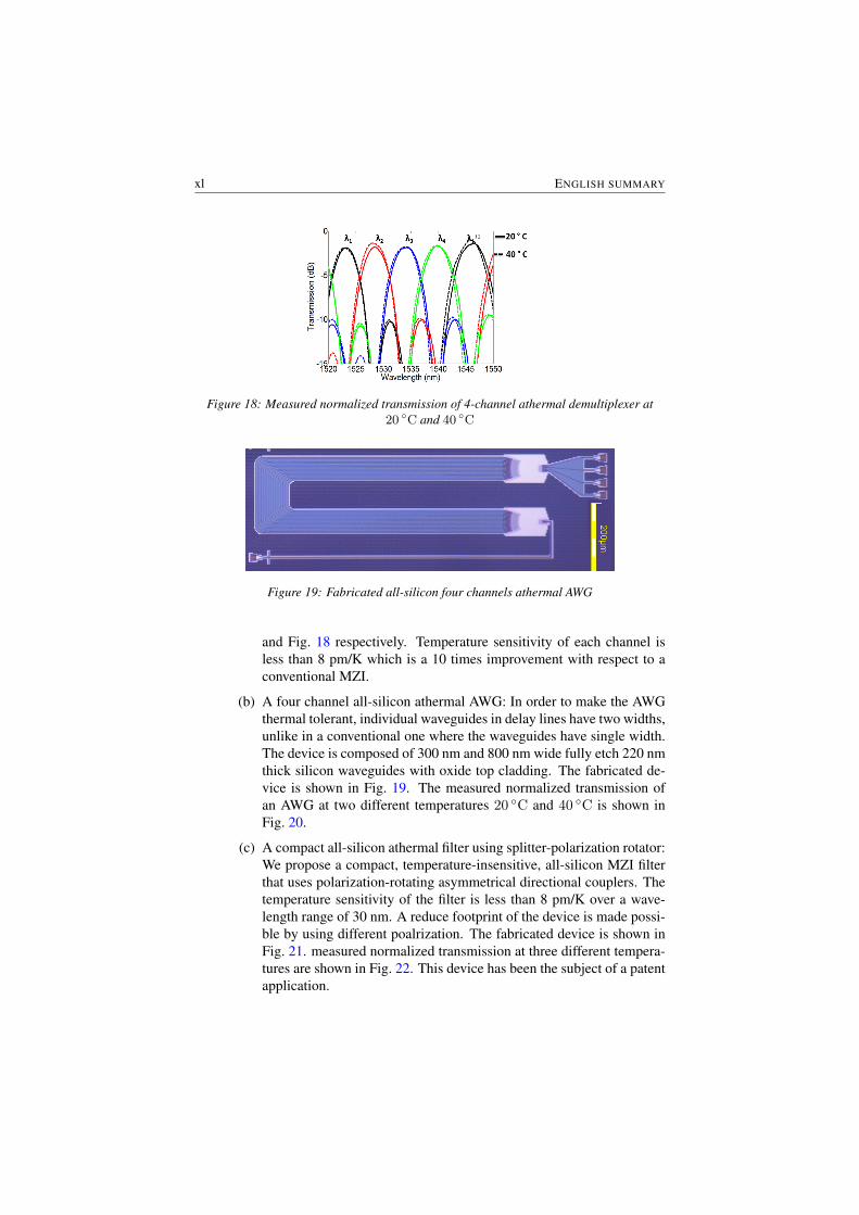
Figure 18: Measured normalized transmission of 4-channel athermal demultiplexer at20 ◦C and 40 ◦C
Figure 19: Fabricated all-silicon four channels athermal AWG
and Fig. 18 respectively. Temperature sensitivity of each channel isless than 8 pm/K which is a 10 times improvement with respect to aconventional MZI.
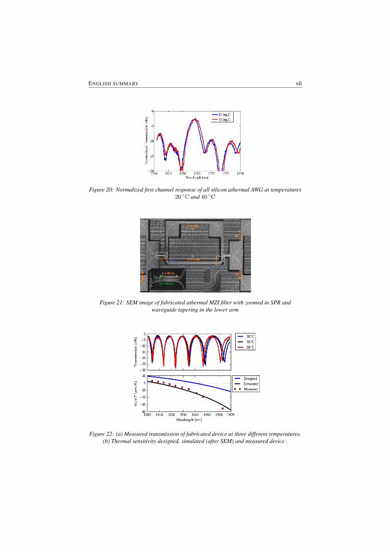
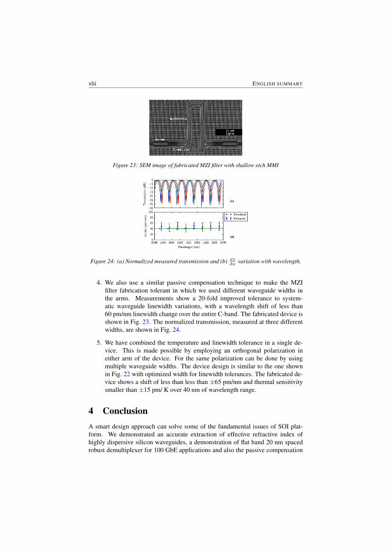
(b) A four channel all-silicon athermal AWG: In order to make the AWGthermal tolerant, individual waveguides in delay lines have two widths,unlike in a conventional one where the waveguides have single width.The device is composed of 300 nm and 800 nm wide fully etch 220 nmthick silicon waveguides with oxide top cladding. The fabricated de-vice is shown in Fig. 19. The measured normalized transmission ofan AWG at two different temperatures 20 ◦C and 40 ◦C is shown inFig. 20.
(c) A compact all-silicon athermal filter using splitter-polarization rotator:We propose a compact, temperature-insensitive, all-silicon MZI filterthat uses polarization-rotating asymmetrical directional couplers. Thetemperature sensitivity of the filter is less than 8 pm/K over a wave-length range of 30 nm. A reduce footprint of the device is made possi-ble by using different poalrization. The fabricated device is shown inFig. 21. measured normalized transmission at three different tempera-tures are shown in Fig. 22. This device has been the subject of a patentapplication.
ENGLISH SUMMARY xli
Figure 20: Normalized first channel response of all silicon athermal AWG at temperatures20 ◦C and 40 ◦C
Figure 21: SEM image of fabricated athermal MZI filter with zoomed in SPR andwaveguide tapering in the lower arm
Figure 22: (a) Measured transmission of fabricated device at three different temperatures.(b) Thermal sensitivity designed, simulated (after SEM) and measured device .
xlii ENGLISH SUMMARY
Figure 23: SEM image of fabricated MZI filter with shallow etch MMI
Figure 24: (a) Normalized measured transmission and (b) dλdw
variation with wavelength.
4. We also use a similar passive compensation technique to make the MZIfilter fabrication tolerant in which we used different waveguide widths inthe arms. Measurements show a 20-fold improved tolerance to system-atic waveguide linewidth variations, with a wavelength shift of less than60 pm/nm linewidth change over the entire C-band. The fabricated device isshown in Fig. 23. The normalized transmission, measured at three differentwidths, are shown in Fig. 24.
5. We have combined the temperature and linewidth tolerance in a single de-vice. This is made possible by employing an orthogonal polarization ineither arm of the device. For the same polarization can be done by usingmultiple waveguide widths. The device design is similar to the one shownin Fig. 22 with optimized width for linewidth tolerances. The fabricated de-vice shows a shift of less than less than ±65 pm/nm and thermal sensitivitysmaller than ±15 pm/ K over 40 nm of wavelength range.
4 ConclusionA smart design approach can solve some of the fundamental issues of SOI plat-form. We demonstrated an accurate extraction of effective refractive index ofhighly dispersive silicon waveguides, a demonstration of flat band 20 nm spacedrobust demultiplexer for 100 GbE applications and also the passive compensation

ENGLISH SUMMARY xliii
of various FIR filters like MZIs and AWGs. Combining the flat band approach andpassive compensation techniques can further improve the performances of the de-multiplexers which are critical for on chip optical interconnects. We have shownthat without altering the fabrication process itself and with novel design approachsome critical issues of silicon photonic devices can be resolved.


1Introduction
”Tolerance always has limits - it cannot tolerate what is itself actively intolerant.”
– Sidney Hook
1-2 INTRODUCTION
Tolerance and efficiency are among the most important measures of perfor-mance of any evolved technology ranging from space research to a hand-heldelectronic device. If we take an example of a mobile phone, it is designed tobe efficient in operation and handle some extra stress, temperature, pressure andeven interaction with water. If we take another example of an RF antenna attachedto a satellite, it has to be efficient enough to receive or send signals in extremeenvironmental conditions.
The same kind of tolerance and efficiency are needed in the area of opticalcommunications as well. Bandwidth demand is increasing day-by-day. Opticalfiber links have been a huge success over the years for keeping up with the de-mand for the high-density data communications for long haul and metro networkfor more than a decade. Due to the massive data access between end users andthe providers the energy consumption is huge. To keep up with this big data de-mand the data centers need to be extremely energy efficient [1]. However, the bulkoptical devices consume a significant amount of power.
Silicon photonics is a recent technology which has been developed over thepast decade and which is still developing to cater to the need of high speed lowpower interconnects for rack-to-rack and chip-to-chip communication [2–7].
Silicon is the most commonly used material for electronics. Since it is trans-parent to the heavily used present-day optical communication window (i.e. Oand C-band), it is also a very interesting material for optics. Silicon has a veryhigh refractive index, enabling optical waveguides with a very high refractive in-dex contrast . As a consequence, the waveguide cross sections can be shrunk tosub-micrometer dimensions, and the waveguides can be bent with only a few µm
bend radius [8]. Therefore, photonic circuits in silicon can be orders of magnitudesmaller than their predecessors made in low-contrast glass. Conversely, a givenchip area can accommodate more waveguide components, enabling more complexphotonic circuits.
Silicon photonics uses the standard complementary metal oxide semiconductor(CMOS) integration technology and hence can be fabricated within the standardCMOS fab lines [9, 10]. In other terms, it reduces the overall cost due to massproduction of the devices while maintaining high performance within the existingfab-lines with a proven technological track record.
1.1 Rationale
From some of the strengths of silicon photonics also emerge the weaknesses. Thehigh refractive index contrast that allows the small waveguides and sharp bendsalso makes the waveguides highly sensitive to any variation in the cross sec-tion [11] and operating wavelength. While good process control already allowsnanometer-level accuracy, this is often insufficient for wavelength-selective func-
INTRODUCTION 1-3
tions, such as channel drop filters in a wavelength-division multiplexing (WDM)system. Pre-fabrication or post-fabrication trimming of the components can beused to correct the effects of the last nanometer fabrication offsets [12, 13]. Sincethe light is confined in small cross-section silicon photonic waveguides are verydispersive in nature.
Silicon has a strong thermo-optic coefficient. This means that its refractiveindex changes as a function of temperature [14, 15]. This is beneficial if it is usedfor tuning circuit elements, but that also results in additional power consumption.A passive silicon photonic circuit will therefore, need temperature stabilization.Alternatively, a method is needed to compensate the thermo-optic effect of silicon.
One method involves the introduction of materials with opposite thermo-opticcoefficients, such as polymers and titanium oxide (TiO2), but this introduces ad-ditional process complexity and it is not always desirable to incorporate such ma-terials in a CMOS-like process flow [16–23].
Typically in a filter design using a standard single mode Silicon-On-Insulator(SOI) waveguide (220nm× 450nm), a change of 1 nm in the width of the waveg-uide corresponds to 1 nm of wavelength shift in the filter’s response whereas achange of 1 nm in the SOI thickness leads to wavelength shift of 1.4 nm in thefilter’s response. The wavelength shift is around 80 pm/K due to the change inambient temperature [24, 25]. This simulation is depicted in Fig. 1.1.
In a WDM optical link the total power consumption includes the electricalpower needed for modulator and receiver operation, multiplexer and demultiplexertuning and wavelength locking circuitry, as well as the laser source electrical powerrequired to generate sufficient optical power to operate inter-chip links. For an ex-ample, the silicon photonic ring-resonator based WDM link running at the datarate of 12.5 Gbps consumes an average energy of 2.5 pJ/bit which is equivalentto 31.4 mW [26]. It includes total power consumption (electrical and optical) oftransmitter side (laser, modulator and multiplexers), routing and transport, receiverside (de-multiplexers and photo-diodes) and total thermal tuning and control ofthe components. The thermal tuning and control itself consumes 6.4 mW of totalpower which is almost 20% of the full optical link [26–29]. Although these num-bers are technology dependent and also depends upon kind of component used inthe system but, they give a good idea of the contribution of tuning to the overallefficiency.
The goal is to lower down the link budget to 1 pJ/bit by 2020 predicted byCisco and Oracle to meet the requirement of energy-efficient optical link that canwork both for short chip-to-chip interconnects as well as capable of longer spansacross intra-datacenter interconnects [26, 30, 31]. Hence, reducing thermo-opticrelated energy consumption is the key challenge in reaching this requirement.
1-4 INTRODUCTION
Figure 1.1: (a) Conventional Mach-Zehnder Interferometer (MZI) filter and simulatedmode profile of the waveguide with width 450 nm and thickness 220 nm at a wavelength of1550 nm. Simulated effective refractive index and sensitivity of the MZI spectrum position
with (b) temperature, (c) width and (d) height variation respectively. The simulation isperformed for the air cladding.
1.2 Goal
The goal of this work is to address the above mentioned issues of extremely sen-sitive silicon photonic waveguides and the wavelength filters not at the technologylevel, but rather through smart design solutions. The objective is to propose anddemonstrate a method that does not involve any extra material or fabrication pro-cess.
In other words, the motivation of this work is to answer few fundamental ques-tions like is it possible to make tolerant all-silicon demultiplexer which can beincorporated directly to an optical link just by design and it will lower down theenergy consumption? Or, is it possible to make a wavelength filter just by designwhich is robust with respect to the fabrication and temperature variations?
1.3 Outline
Chapter 2 starts with an introduction to silicon photonic waveguides mainly devel-oped on the Imec platform. It then deals with the study of a robust and accuratemodel of the highly dispersive SOI waveguides and their fundamental parameterslike effective refractive index and thermo-optic coefficients, which should then be

INTRODUCTION 1-5
validated experimentally.Chapter 3 deals with different SOI-based wavelength filters e.g, arrayed waveg-
uide gratings, echelle gratings and cascaded Mach-Zehnder Interferometers (MZIs),mainly targeted at coarse wavelength division multiplexing (CWDM) applicationsfor both C-band (center wavelength at 1550 nm and channel spacing of 6.4 nm)and the O-band (center wavelength at 1310 nm channel spacing of 20 nm). Wehave achieved the robust demultiplexers by flattening the channel pass band re-sponses. The demonstrated cascaded MZI based demultiplexer for the O-band isa potential candidate for 100 Gigabit Ethernet (GBE), due to its low loss and wideflat band of 13 nm. The presented de-multiplexers does not require thermal tuningdue to the wide flat pass band and hence contribute in lowering down the powerbudget of the optical link.
Chapter 4 gives an introduction to an all-silicon passive compensation tech-nique to make wavelength filters insensitive to the thermal fluctuations. We applythe technique to various devices like MZIs, cascaded MZIs and arrayed waveguidegratings (AWGs).
Chapter 5 focuses on the implementation of a compact athermal MZI filter.The device achieves a reduced footprint by making use of both the TE and the TMpolarization, compared to the TE-based design presented in the previous chapter.The device presented in this chapter is also the subject of a patent application [32].
Finally in chapter 6 we extend the concept of athermal filters and explore thepossibility of addressing fabrication tolerances separately and also together withthermal tolerances. We also explore the possibilities of combination of flat passband approach with passive compensation. Presented simulations shows that thesewavelength filters are much more robust in terms of thermal tuning or fabricationvariations.
1.4 Publications
1.4.1 Patent
1. Sarvagya Dwivedi, Wim Bogaerts, Integrated Photonic Devices with Re-duced Sensitivity to External Influences, US9075251 B2, Dec. 2013
1.4.2 Publications in international journals
1. S. Dwivedi, P. De Heyn, A. Rahim, P. Absil, J. Van Campenhout, W. Bo-gaerts, ” Flat-band Four-Channel Coarse Wavelength Division Multiplexeron Silicon-On-Insulator for the O-Band”, submitted for publication in Jour-nal of Lightwave Technology, IEEE/OSA.
1-6 INTRODUCTION
2. S. Dwivedi, A. Ruocco, Michael Vanslembrouck, T. Spuesens, P. Bienst-man, P. Dumon, T. Van Vaerenbergh, W. Bogaerts, ” Experimental extractionof effective refractive index and thermo-optic coefficients of Silicon-On-Insulator waveguides using interferometers”, Journal of Lightwave Tech-nology, 33(21),IEEE/OSA, pp.4471 4477, Nov. 2015.
3. S. Dwivedi, H. D’heer, W. Bogaerts, ”Maximizing fabrication and thermaltolerances of all-silicon FIR wavelength filtering devices”, IEEE PhotonicsTechnology Letters , vol. 27(8), IEEE, pp. 871-874, Apr. 2015.
4. A. Malik, S. Dwivedi, L. Van Landschoot, M. Muneeb, Y. Shimura, G. Lep-age, J. Van Campenhout, W. Vanherle, T. Van Opstal, R. Loo, G. Roelkens,”Ge-on-Si and Ge-on-SOI thermo-optic phase shifters for the mid-infrared”,Optics Express, vol. 22(23), Optical Society of America, pp. 28479-28488,Nov. 2014.
5. S. Dwivedi, H. D’heer, W. Bogaerts, ”A compact all-silicon temperatureinsensitive filter for WDM and bio-sensing applications”, IEEE PhotonicsTechnology Letters , vol. 25(22), IEEE, pp. 2167 - 2170, Nov. 2013.
6. H. Yu, M. Pantouvaki, S. Dwivedi, P. Verheyen, G. Lepage, R. Baets, W. Bo-gaerts, P. Absil, J. Van Campenhout, ”Compact, Thermally Tunable SiliconRacetrack Modulators Based on an Asymmetric Waveguide”, IEEE Photon-ics Technology Letters, vol. 25(2), IEEE, pp. 159 - 162, Jan. 2013.
1.4.3 Publications in international conferences
1. S. Dwivedi, P. De Heyn, P. Absil, J. Van Campenhout, W. Bogaerts, ”CoarseWavelength Division Multiplexer on Silicon-On-Insulator for 100 GbE”,12th International Conference on Group IV Photonics (GFP), IEEE, Van-couver, Canada, p.WC2, Aug. 2015.
2. S. Dwivedi, T. Van Vaerenbergh, A. Ruocco, T. Spuesens, P. Bienstman, P.Dumon, W. Bogaerts, ”Measurements of Effective Refractive Index of SOIWaveguides using Interferometers”, Integrated Photonics Research, Siliconand Nano Photonics, Boston, United States, p.IM2A.6, 2015.
3. W. Bogaerts, S. Pathak, A. Ruocco, S. Dwivedi, ”Silicon photonics non-resonant wavelength filters: comparison between AWGs, echelle gratingsand cascaded Mach-Zehnder filters.” (invited), Proc. SPIE 9365, IntegratedOptics: Devices, Materials, and Technologies XIX, SPIE, Sin Francisco,United States, Feb. 2015.
INTRODUCTION 1-7
4. S. Dwivedi, H. D’heer, W. Bogaerts, ”Fabrication and Thermal Tolerant all-Silicon Wavelength Filtering Devices”, IEEE Photonics Society Benelux,IEEE , Enschede, Netherlands, Nov. 2014.
5. S. Dwivedi, H. D’heer, W. Bogaerts, ”Fabrication tolerant silicon MZI fil-ter”, 11th International Conference on Group IV Photonics (GFP), IEEE,Paris, France, pp. 147-148, Aug. 2014.
6. S. Dwivedi, H. D’heer, W. Bogaerts, ”A compact temperature insensitivefilter using splitter polarization-rotating section”, 10th International Confer-ence on Group IV Photonics (GFP), IEEE, Seoul, South Korea, p. WC6,Aug. 2013.
7. S. Dwivedi, W. Bogaerts, ”Compact Athermal Filter in Silicon Waveguidesfor WDM and bio-sensing applications”, Fiber Optics and Photonics 2012,vol. p.M.2.B.3, Optical Society of America, Chennai, India, Dec. 2012.
1-8 INTRODUCTION
References[1] K. Hinton, J. Baliga, M.Z. Feng, R.W.A. Ayre, and RodneyS. Tucker. Power
consumption and energy efficiency in the internet. Network, IEEE, 25(2):6–12, March 2011.
[2] C. Gunn. CMOS Photonics for High-Speed Interconnects. Micro, IEEE,26(2):58–66, March 2006.
[3] B. Jalali and S. Fathpour. Silicon Photonics. Lightwave Technology, Journalof, 24(12):4600–4615, Dec 2006.
[4] D.A.B. Miller. Device Requirements for Optical Interconnects to SiliconChips. Proceedings of the IEEE, 97(7):1166–1185, July 2009.
[5] S. Assefa, S. Shank, W. Green, M. Khater, E. Kiewra, C. Reinholm, S. Kam-lapurkar, A. Rylyakov, C. Schow, F. Horst, Huapu Pan, T. Topuria, P. Rice,D.M. Gill, J. Rosenberg, T. Barwicz, Min Yang, J. Proesel, J. Hofrichter,B. Offrein, Xiaoxiong Gu, W. Haensch, J. Ellis-Monaghan, and Y. Vlasov.A 90nm CMOS integrated Nano-Photonics technology for 25Gbps WDM op-tical communications applications. In Electron Devices Meeting (IEDM),2012 IEEE International, pages 33.8.1–33.8.3, Dec 2012.
[6] Y.A. Vlasov. Silicon CMOS-integrated nano-photonics for computer anddata communications beyond 100G. Communications Magazine, IEEE,50(2):s67–s72, February 2012.
[7] Frederic Boeuf, Sebastien Cremer, Enrico Temporiti, Massimo Fere’, MarkShaw, Nathalie Vulliet, bastien orlando, Delia Ristoiu, Alexis Farcy, ThierryPinguet, Attila Mekis, Gianlorenzo Masini, Peng Sun, Yuemeng Chi, HervePetiton, Sebastien Jan, Jean-Robert Manouvrier, Charles Baudot, PatrickLe-Maitre, Jean Francois CARPENTIER, Laurent Salager, Matteo Traldi,Luca Maggi, Danilo Rigamonti, Chiara Zaccherini, Carolina Elemi, BernardSautreuil, and Luigi Verga. Recent Progress in Silicon Photonics R&D andManufacturing on 300mm Wafer Platform. In Optical Fiber CommunicationConference, page W3A.1. Optical Society of America, 2015.
[8] S.K. Selvaraja, P. Jaenen, W. Bogaerts, D. Van Thourhout, P. Dumon, andR. Baets. Fabrication of Photonic Wire and Crystal Circuits in Silicon-on-Insulator Using 193-nm Optical Lithography. Lightwave Technology, Jour-nal of, 27(18):4076–4083, Sept 2009.
[9] http://http://www.st.com/web/en/press/cn/t3279.
[10] http://www.intel.com/content/www/us/en/research/intel-labs-silicon-photonics-research.html.
INTRODUCTION 1-9
[11] S.K. Selvaraja, P. Jaenen, W. Bogaerts, D. Van Thourhout, P. Dumon, andR. Baets. Fabrication of Photonic Wire and Crystal Circuits in Silicon-on-Insulator Using 193-nm Optical Lithography. Lightwave Technology, Jour-nal of, 27(18):4076–4083, Sept 2009.
[12] Shankar Kumar Selvaraja, Wim Bogaerts, Dries VanThourhout, and MarcSchaekers. Thermal trimming and tuning of hydrogenated amorphous siliconnanophotonic devices. Applied Physics Letters, 97(7):–, 2010.
[13] J. Schrauwen, D. Van Thourhout, and R. Baets. Trimming of silicon ringresonator by electron beam induced compaction and strain. Opt. Express,16(6):3738–3743, Mar 2008.
[14] Francesco G. Della Corte, Maurizio Esposito Montefusco, Luigi Moretti, IvoRendina, and Giuseppe Cocorullo. Temperature dependence analysis of thethermo-optic effect in silicon by single and double oscillator models. Journalof Applied Physics, 88(12):7115–7119, 2000.
[15] Joris Van Campenhout, William M. J. Green, Solomon Assefa, and Yurii A.Vlasov. Integrated NiSi waveguide heaters for CMOS-compatible siliconthermo-optic devices. Opt. Lett., 35(7):1013–1015, Apr 2010.
[16] Jie Teng, Pieter Dumon, Wim Bogaerts, Hongbo Zhang, Xigao Jian, XiuyouHan, Mingshan Zhao, Geert Morthier, and Roel Baets. Athermal Silicon-on-insulator ring resonators by overlaying a polymer cladding on narrowedwaveguides. Opt. Express, 17(17):14627–14633, Aug 2009.
[17] Vivek Raghunathan, Tomoyuki Izuhara, Jurgen Michel, and Lionel Kimer-ling. Stability of polymer-dielectric bi-layers for athermal silicon photonics.Opt. Express, 20(14):16059–16066, Jul 2012.
[18] Jong-Moo Lee, Duk-Jun Kim, Hokyun Ahn, Sang-Ho Park, and GyungockKim. Temperature Dependence of Silicon Nanophotonic Ring ResonatorWith a Polymeric Overlayer. Lightwave Technology, Journal of, 25(8):2236–2243, Aug 2007.
[19] Biswajeet Guha, Jaime Cardenas, and Michal Lipson. Athermal sili-con microring resonators with titanium oxide cladding. Opt. Express,21(22):26557–26563, Nov 2013.
[20] Stevan S. Djordjevic, Kuanping Shang, Binbin Guan, Stanley T. S. Cheung,Ling Liao, Juthika Basak, Hai-Feng Liu, and S. J. B. Yoo. CMOS-compatible,athermal silicon ring modulators clad with titanium dioxide. Opt. Express,21(12):13958–13968, Jun 2013.
1-10 INTRODUCTION
[21] Jock Bovington, Rui Wu, Kwang-Ting Cheng, and John E. Bowers. Thermalstress implications in athermal TiO2 waveguides on a silicon substrate. Opt.Express, 22(1):661–666, Jan 2014.
[22] Feng Qiu, Andrew M. Spring, Feng Yu, and Shiyoshi Yokoyama. Comple-mentary metaloxidesemiconductor compatible athermal silicon nitride/tita-nium dioxide hybrid micro-ring resonators. Applied Physics Letters, 102(5),2013.
[23] Shaoqi Feng, Kuanping Shang, Jock T. Bovington, Rui Wu, Binbin Guan,Kwang-Ting Cheng, John E. Bowers, and S. J. Ben Yoo. Athermal siliconring resonators clad with titanium dioxide for 1.3 µm wavelength operation.Opt. Express, 23(20):25653–25660, Oct 2015.
[24] K. Okamoto. Wavelength-Division-Multiplexing Devices in Thin SOI: Ad-vances and Prospects. Selected Topics in Quantum Electronics, IEEE Jour-nal of, 20(4):248–257, July 2014.
[25] S. Dwivedi, H. D’heer, and W. Bogaerts. Maximizing Fabrication and Ther-mal Tolerances of All-Silicon FIR Wavelength Filters. Photonics TechnologyLetters, IEEE, 27(8):871–874, April 2015.
[26] A. V. Krishnamoorthy, H. Schwetman, X. Zheng, and R. Ho. Energy-EfficientPhotonics in Future High-Connectivity Computing Systems. J. LightwaveTechnol., 33(4):889–900, Feb 2015.
[27] Xuezhe Zheng, Ivan Shubin, Guoliang Li, Thierry Pinguet, Attila Mekis, JinYao, Hiren Thacker, Ying Luo, Joey Costa, Kannan Raj, John E. Cunning-ham, and Ashok V. Krishnamoorthy. A tunable 1x4 silicon CMOS photonicwavelength multiplexer/demultiplexer for dense optical interconnects. Opt.Express, 18(5):5151–5160, Mar 2010.
[28] Xuezhe Zheng, Eric Chang, Philip Amberg, Ivan Shubin, Jon Lexau, FrankieLiu, Hiren Thacker, Stevan S. Djordjevic, Shiyun Lin, Ying Luo, Jin Yao,Jin-Hyoung Lee, Kannan Raj, Ron Ho, John E. Cunningham, and Ashok V.Krishnamoorthy. A high-speed, tunable silicon photonic ring modulatorintegrated with ultra-efficient active wavelength control. Opt. Express,22(10):12628–12633, May 2014.
[29] Zhiping Zhou, Bing Yin, Qingzhong Deng, Xinbai Li, and Jishi Cui. Lower-ing the energy consumption in silicon photonic devices and systems [Invited].Photon. Res., 3(5):B28–B46, Oct 2015.
[30] Cisco Visual Networking Index: Forecast and Methodology, 2014-2019.

INTRODUCTION 1-11
[31] Yu Li, Yu Zhang, Lei Zhang, and Andrew W. Poon. Silicon and hybridsilicon photonic devices for intra-datacenter applications: state of the artand perspectives [Invited]. Photon. Res., 3(5):B10–B27, Oct 2015.
[32] S. Dwivedi and W. Bogaerts. Integrated photonic devices with reduced sen-sitivity to external influences, July 7 2015. US Patent 9,075,251.

2Silicon-On-Insulator Waveguides
2.1 Introduction
Optical waveguides need to confine light along a path on chip, so it can be used totransport a signal between two points. The most straightforward way to constructa waveguide is to use a core with a high refractive index surrounded by a lowerrefractive index. A well-known example of such a waveguide is an optical fiber,consisting of two types of glass with a slight difference in refractive index.
In this chapter SOI waveguides are studied. The focus of the first part of thechapter is to have an accurate model of the SOI waveguides and their fundamentalparameters like effective refractive index (neff ), group index (ng) and thermo-optic (TO) coefficients. The second part discusses the novel method which is de-veloped to validate these parameters experimentally.
2.2 SOI platform
The silicon-on-insulator (SOI) platform is gaining prominence for industrial pro-duction of integrated photonics devices since it can use the well established and ex-isting infrastructure of complementary metal-oxide-semiconductor (CMOS) pro-cess technology for fabrication. This offers a scaling avenue to large-volume pro-duction at an affordable cost. SOI can be used to define waveguides with a highrefractive index contrast between the core and the cladding. This enables dense in-tegrated photonic circuits with sub-micron waveguide cores and sharp bends. This

2-2 CHAPTER 2
Figure 2.1: Size (a) of the square core for single mode operation for different platforms:Silica, Silicon nitride and Silicon-on-Insulator in the C-band.
is because in the photonic scaling laws, it all depends upon the index contrast. Itis an approximation of parameter V-number in optical fibers which determines thecutoff condition for all possible guided modes [1]. The maximum core size (a) fora single mode operation for a square core embedded in a uniform cladding can beestimated by:
a ≈ λ
2.√
(n2core − n2
cladding)(2.1)
The comparison of the single mode operation for SOI with other standard plat-forms operating at conventional band (C-band) with center wavelength of 1550 nmis shown in Fig. 2.1. It can be easily seen that for the SOI platform a < 300 nm
(we assume a square waveguide in this plot, but the scaling is similar for other coregeometries).
The cross section of a typical SOI material stack is shown in Fig. 2.2. TheSOI material stack consists of 220 nm thick crystalline Silicon (Si) core and 2 µmof buried oxide (SiO2). The thickness is chosen as 220 nm for several reasons.First, with this thickness, the optical mode is smallest for a width of 450 nm atwavelength of 1550 nm, hence with such waveguides it is possible to make bendswith 2-3 µm bend radius without significant bending losses. Second, it providesa single mode behavior of the waveguide. As the optical waveguides get largerthey can support more higher order modes [2]. The 2 µm box is chosen to avoidthe leakage loss into the substrate. This stack is based on IMEC silicon photonicspassives platform.
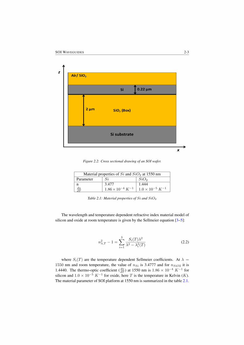
SOI WAVEGUIDES 2-3
Figure 2.2: Cross sectional drawing of an SOI wafer.
Material properties of Si and SiO2 at 1550 nmParameter Si SiO2
n 3.477 1.444dndT 1.86×10⁻⁴ K−1 1.0× 10⁻⁵ K−1
Table 2.1: Material properties of Si and SiO2
The wavelength and temperature dependent refractive index material model ofsilicon and oxide at room temperature is given by the Sellmeier equation [3–5]:
n2λ,T − 1 =
3∑i=1
Si(T )λ2
λ2 − λ2i (T )
(2.2)
where Si(T ) are the temperature dependent Sellmeier coefficients. At λ =
1550 nm and room temperature, the value of nSi is 3.4777 and for nSiO2 it is1.4440. The thermo-optic coefficient ( dndT ) at 1550 nm is 1.86 × 10⁻⁴ K−1 forsilicon and 1.0 × 10⁻⁵ K−1 for oxide, here T is the temperature in Kelvin (K).The material parameter of SOI platform at 1550 nm is summarized in the table 2.1.

2-4 CHAPTER 2
2.2.1 Introduction to SOI waveguides
This work is largely based on the IMEC silicon photonics platform (we usuallycall it SOI platform in this report) which offers Multi Project Wafer (MPW) runsand is available through euro-practice [6]. The SOI platform allows for differentwaveguide cross sections as shown in Fig. 2.3, which are useful for different ap-plications. The most standard ones are Strip waveguides and Rib waveguides. Thestrip waveguide, which consists of a fully-etched silicon line, is the most widelyused one for different on chip interconnect functions like routing, connections be-tween components and for different passive circuit functionality like wavelengthfiltering etc. [7].
Ribs, or shallow etched waveguides, have a partial etch of 70 nm of rib sectionfollowed by 150 nm of slab section. This waveguide is mainly used for active com-ponents like carrier injection or depletion modulators where slab section is usedfor doping and metal connection [8]. This partial step is also used in grating cou-plers [9–13] for coupling light in and out of the photonic chip and wavelength fil-tering devices like arrayed waveguide gratings (AWGs) and echelle gratings [14].The propagation loss of rib waveguides are lower than the strip waveguides so theyare mostly used for long delay lines [15].
A Socket waveguide is a bit of compromise between strip and a rib waveguidewhere the etch step is increased to 150 nm and the slab section is just 70 nm.Increasing the etch depth helps in smaller bend radius and lower loss than a stripwaveguide. Hence, there is a possibility of compact ring modulators with similarfunctionality like rib waveguides [16].
In a slot waveguide, the mode is confined in the low index region either air oroxide i.e. in the slot section. Slot waveguide is quite useful for various applicationslike low power modulators and sensing due to an efficient mode overlap in a slotarea either by liquid crystals for modulators [17] or with any sensing element [18,19].
The propagation inside the waveguide can be described in terms of eigen-modes: a field distribution in and around the core that propagates as a single entityat a fixed velocity. Such an eigenmode is characterized by a propagation vector βor an effective refractive index neff . The propagation speed of the mode in thewaveguide is given by c
neff, with c the speed of light in vacuum. Depending on
their dimensions, waveguide can support multiple eigenmodes, that is propagateindependently with their own neff .
Finally, there is the issue of polarization. Modes in optical waveguides canbe classified according to their polarization, i.e the orientation of electric field (E-field) components. This classification is done with respect to the plane of the chip.The Transverse Electric (TE) mode is the one in which the E-field is in-plane ofthe chip, while for the Transverse Magnetic (TM) mode, it is perpendicular tothe plane (in vertical direction). A strip waveguide always supports both TE and
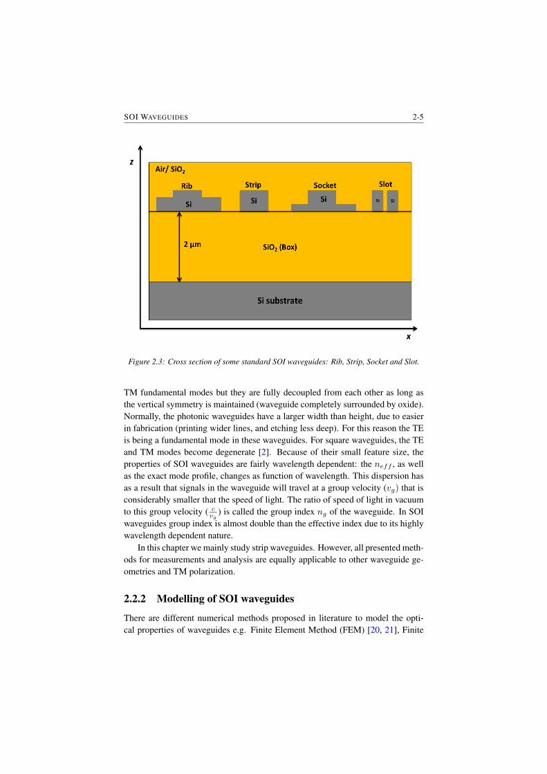
SOI WAVEGUIDES 2-5
Figure 2.3: Cross section of some standard SOI waveguides: Rib, Strip, Socket and Slot.
TM fundamental modes but they are fully decoupled from each other as long asthe vertical symmetry is maintained (waveguide completely surrounded by oxide).Normally, the photonic waveguides have a larger width than height, due to easierin fabrication (printing wider lines, and etching less deep). For this reason the TEis being a fundamental mode in these waveguides. For square waveguides, the TEand TM modes become degenerate [2]. Because of their small feature size, theproperties of SOI waveguides are fairly wavelength dependent: the neff , as wellas the exact mode profile, changes as function of wavelength. This dispersion hasas a result that signals in the waveguide will travel at a group velocity (vg) that isconsiderably smaller that the speed of light. The ratio of speed of light in vacuumto this group velocity ( cvg ) is called the group index ng of the waveguide. In SOIwaveguides group index is almost double than the effective index due to its highlywavelength dependent nature.
In this chapter we mainly study strip waveguides. However, all presented meth-ods for measurements and analysis are equally applicable to other waveguide ge-ometries and TM polarization.
2.2.2 Modelling of SOI waveguides
There are different numerical methods proposed in literature to model the opti-cal properties of waveguides e.g. Finite Element Method (FEM) [20, 21], Finite

2-6 CHAPTER 2
Figure 2.4: (a) Finite element mesh of the strip waveguide (b) TE mode profile and (c) TMmode profile of strip waveguide. TE mode profiles of (d) Rib, (e) Socket and (f) Slot
waveguide. Arrows are electric field lines
Difference Time Domain (FDTD) [22, 23], Beam Propagation Method (BPM)[24, 25] and Film Mode Matching (FMM) [26, 27] are the few most commonused ones.
The neff of a guided mode of an SOI waveguide at a given wavelength is afunction of the material, the waveguide cross-sectional geometry and environmen-tal temperature. We can conceptually simplify this as
neff (λ) = f(w, h, T ) (2.3)
where w and h are waveguide width and thickness respectively and T is the envi-ronment temperature.
The wave equation for mode analysis is given by:
∇× (∇× E)− k20εrE = 0 (2.4)
In the mode analysis we solve mainly for propagation constant: α+ jβ, whereα is attenuation and β is propagation constant. In Eq. 2.4, εr is a material param-eter given by (n − jk)2, where n is real part and jk is the imaginary part of thebulk refractive index.
In this work, most of the eigen mode simulations of the SOI waveguide modeare performed by the finite element method (FEM) from COMSOL, taking a wave-length and temperature dependent material model as given in Eq. 2.2. Fig. 2.4
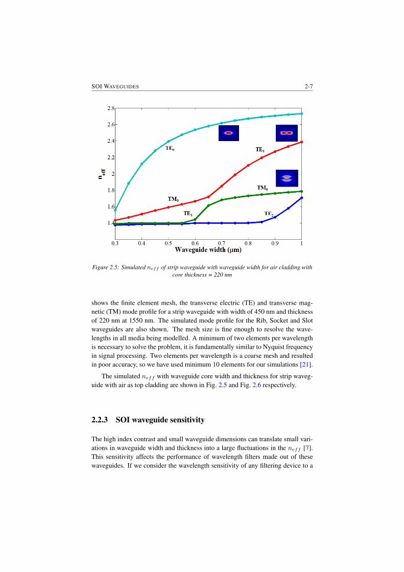
SOI WAVEGUIDES 2-7
Figure 2.5: Simulated neff of strip waveguide with waveguide width for air cladding withcore thickness = 220 nm
shows the finite element mesh, the transverse electric (TE) and transverse mag-netic (TM) mode profile for a strip waveguide with width of 450 nm and thicknessof 220 nm at 1550 nm. The simulated mode profile for the Rib, Socket and Slotwaveguides are also shown. The mesh size is fine enough to resolve the wave-lengths in all media being modelled. A minimum of two elements per wavelengthis necessary to solve the problem, it is fundamentally similar to Nyquist frequencyin signal processing. Two elements per wavelength is a coarse mesh and resultedin poor accuracy, so we have used minimum 10 elements for our simulations [21].
The simulated neff with waveguide core width and thickness for strip waveg-uide with air as top cladding are shown in Fig. 2.5 and Fig. 2.6 respectively.
2.2.3 SOI waveguide sensitivity
The high index contrast and small waveguide dimensions can translate small vari-ations in waveguide width and thickness into a large fluctuations in the neff [7].This sensitivity affects the performance of wavelength filters made out of thesewaveguides. If we consider the wavelength sensitivity of any filtering device to a
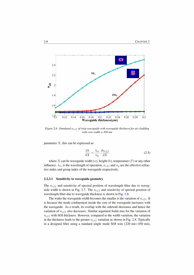
2-8 CHAPTER 2
Figure 2.6: Simulated neff of strip waveguide with waveguide thickness for air claddingwith core width = 450 nm
parameter X , this can be expressed as:
dλ
dX=λmng
.dneffdX
(2.5)
whereX can be waveguide width (w), height (h), temperature (T ) or any otherinfluence. λm is the wavelength of operation, neff and ng are the effective refrac-tive index and group index of the waveguide respectively.
2.2.3.1 Sensitivity to waveguide geometry
The neff and sensitivity of spectral position of wavelength filter due to waveg-uide width is shown in Fig. 2.7. The neff and sensitivity of spectral position ofwavelength filter due to waveguide thickness is shown in Fig. 2.8.
The wider the waveguide width becomes the smaller is the variation of neff . Itis because the mode confinement inside the core of the waveguide increases withthe waveguide. As a result, its overlap with the sidewall decreases and hence thevariation of neff also decreases. Similar argument holds true for the variation ofneff with SOI thickness. However, compared to the width variation, the variationin the thickness leads to the greater neff variation as shown in Fig. 2.8. Typicallyin a designed filter using a standard single mode SOI wire (220 nm×450 nm),
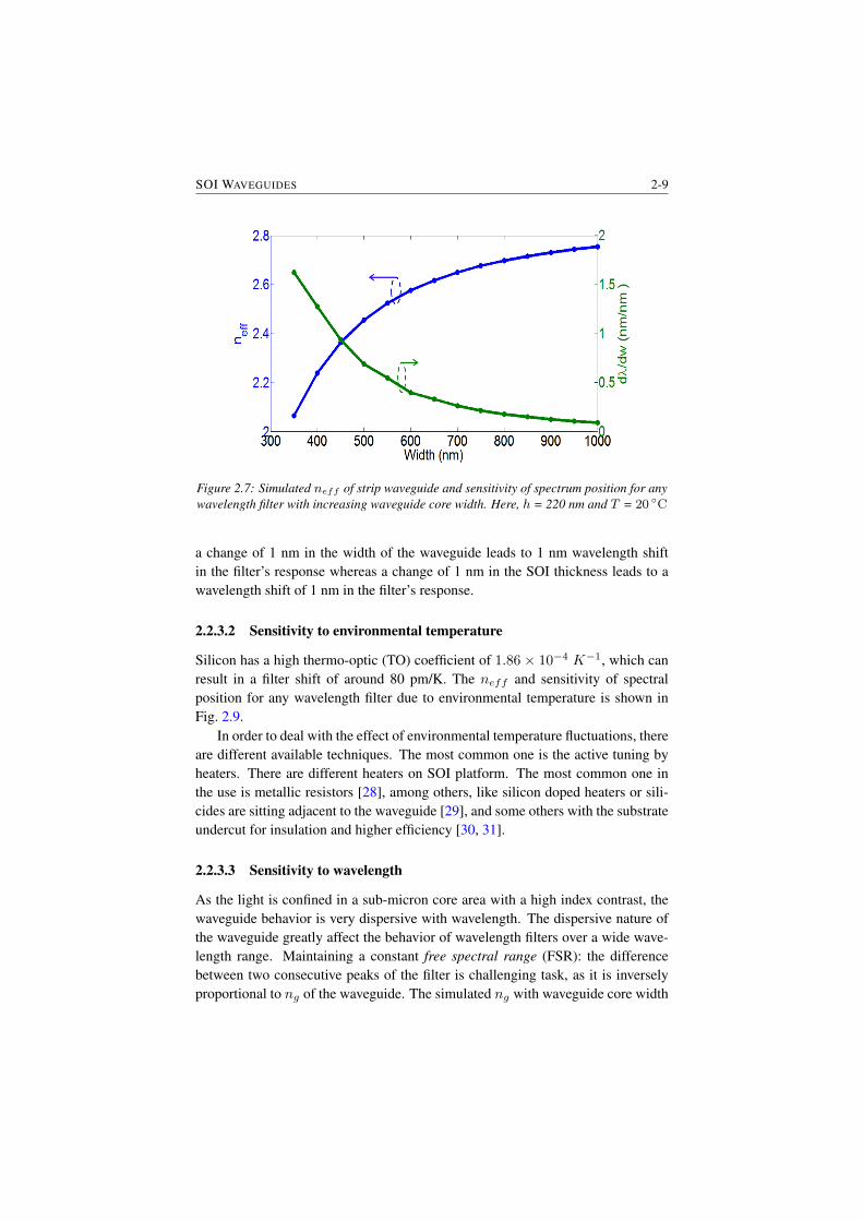
SOI WAVEGUIDES 2-9
Figure 2.7: Simulated neff of strip waveguide and sensitivity of spectrum position for anywavelength filter with increasing waveguide core width. Here, h = 220 nm and T = 20 ◦C
a change of 1 nm in the width of the waveguide leads to 1 nm wavelength shiftin the filter’s response whereas a change of 1 nm in the SOI thickness leads to awavelength shift of 1 nm in the filter’s response.
2.2.3.2 Sensitivity to environmental temperature
Silicon has a high thermo-optic (TO) coefficient of 1.86 × 10⁻⁴ K−1, which canresult in a filter shift of around 80 pm/K. The neff and sensitivity of spectralposition for any wavelength filter due to environmental temperature is shown inFig. 2.9.
In order to deal with the effect of environmental temperature fluctuations, thereare different available techniques. The most common one is the active tuning byheaters. There are different heaters on SOI platform. The most common one inthe use is metallic resistors [28], among others, like silicon doped heaters or sili-cides are sitting adjacent to the waveguide [29], and some others with the substrateundercut for insulation and higher efficiency [30, 31].
2.2.3.3 Sensitivity to wavelength
As the light is confined in a sub-micron core area with a high index contrast, thewaveguide behavior is very dispersive with wavelength. The dispersive nature ofthe waveguide greatly affect the behavior of wavelength filters over a wide wave-length range. Maintaining a constant free spectral range (FSR): the differencebetween two consecutive peaks of the filter is challenging task, as it is inverselyproportional to ng of the waveguide. The simulated ng with waveguide core width
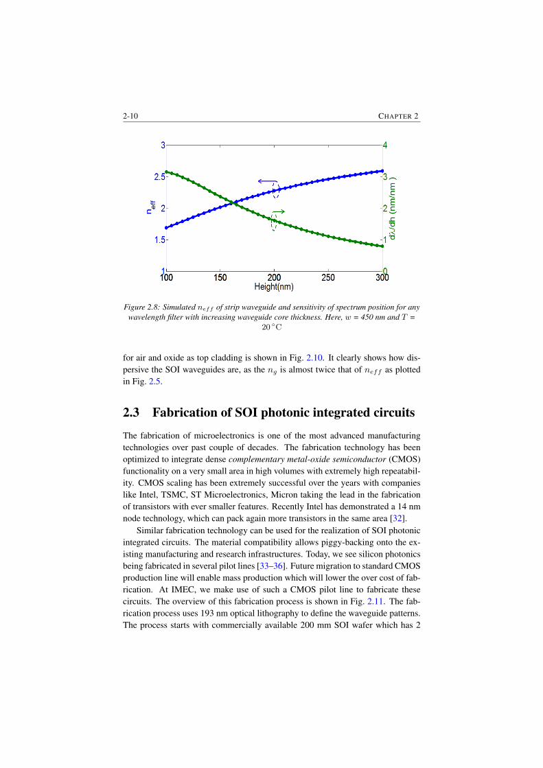
2-10 CHAPTER 2
Figure 2.8: Simulated neff of strip waveguide and sensitivity of spectrum position for anywavelength filter with increasing waveguide core thickness. Here, w = 450 nm and T =
20 ◦C
for air and oxide as top cladding is shown in Fig. 2.10. It clearly shows how dis-persive the SOI waveguides are, as the ng is almost twice that of neff as plottedin Fig. 2.5.
2.3 Fabrication of SOI photonic integrated circuits
The fabrication of microelectronics is one of the most advanced manufacturingtechnologies over past couple of decades. The fabrication technology has beenoptimized to integrate dense complementary metal-oxide semiconductor (CMOS)functionality on a very small area in high volumes with extremely high repeatabil-ity. CMOS scaling has been extremely successful over the years with companieslike Intel, TSMC, ST Microelectronics, Micron taking the lead in the fabricationof transistors with ever smaller features. Recently Intel has demonstrated a 14 nmnode technology, which can pack again more transistors in the same area [32].
Similar fabrication technology can be used for the realization of SOI photonicintegrated circuits. The material compatibility allows piggy-backing onto the ex-isting manufacturing and research infrastructures. Today, we see silicon photonicsbeing fabricated in several pilot lines [33–36]. Future migration to standard CMOSproduction line will enable mass production which will lower the over cost of fab-rication. At IMEC, we make use of such a CMOS pilot line to fabricate thesecircuits. The overview of this fabrication process is shown in Fig. 2.11. The fab-rication process uses 193 nm optical lithography to define the waveguide patterns.The process starts with commercially available 200 mm SOI wafer which has 2
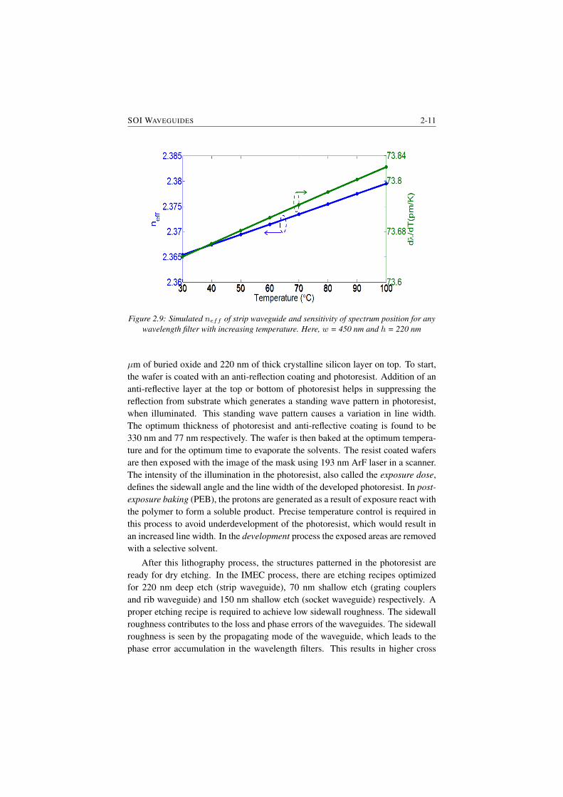
SOI WAVEGUIDES 2-11
Figure 2.9: Simulated neff of strip waveguide and sensitivity of spectrum position for anywavelength filter with increasing temperature. Here, w = 450 nm and h = 220 nm
µm of buried oxide and 220 nm of thick crystalline silicon layer on top. To start,the wafer is coated with an anti-reflection coating and photoresist. Addition of ananti-reflective layer at the top or bottom of photoresist helps in suppressing thereflection from substrate which generates a standing wave pattern in photoresist,when illuminated. This standing wave pattern causes a variation in line width.The optimum thickness of photoresist and anti-reflective coating is found to be330 nm and 77 nm respectively. The wafer is then baked at the optimum tempera-ture and for the optimum time to evaporate the solvents. The resist coated wafersare then exposed with the image of the mask using 193 nm ArF laser in a scanner.The intensity of the illumination in the photoresist, also called the exposure dose,defines the sidewall angle and the line width of the developed photoresist. In post-exposure baking (PEB), the protons are generated as a result of exposure react withthe polymer to form a soluble product. Precise temperature control is required inthis process to avoid underdevelopment of the photoresist, which would result inan increased line width. In the development process the exposed areas are removedwith a selective solvent.
After this lithography process, the structures patterned in the photoresist areready for dry etching. In the IMEC process, there are etching recipes optimizedfor 220 nm deep etch (strip waveguide), 70 nm shallow etch (grating couplersand rib waveguide) and 150 nm shallow etch (socket waveguide) respectively. Aproper etching recipe is required to achieve low sidewall roughness. The sidewallroughness contributes to the loss and phase errors of the waveguides. The sidewallroughness is seen by the propagating mode of the waveguide, which leads to thephase error accumulation in the wavelength filters. This results in higher cross

2-12 CHAPTER 2
0.3 0.4 0.5 0.6 0.7 0.8 0.9 1.0
Core width (µm)
2.0
2.5
3.0
3.5
4.0
4.5
5.0n
g()
TE0,air
TM0,air
TE0,oxide
TM0,oxide
Figure 2.10: Simulated ng of strip waveguide with air/ oxide as top cladding withincreasing core width
talk in their performance. The detailed process is discussed in the thesis of S. K.Selvaraja [37]. The fabricated strip waveguide and spiral are shown in Fig. 2.12.
2.4 Characterization
In order to characterize the optical properties of SOI waveguides and other wave-length filtering devices, the light needs to be coupled with the fiber into the pho-tonic chip and then out of the chip to another fiber. Normally, we measure thetransmission of the device as a function of operating wavelength. There are dif-ferent coupling methods. The most common ones are either vertical coupling byusing a fiber grating couplers or horizontal coupling (also called edge coupling)in which one has a cleaved chip and light is coupled horizontally via fiber. Inthis work, we have characterized our all devices via vertical coupling throughfiber grating couplers. The vertical coupling via grating couplers has a numberof advantages over other methods: For instance, it does not require any post-processing, it has good alignment tolerances, the coupling structure is compactin size, and it is possible to achieve high coupling efficiency . However, they havelimited bandwidth, back-reflection problems and work for only one polarizationat a time [9, 10, 38]. There has been extensive research in the past few years toimprove the efficiency, reduce the back-reflection and couple light through boththe polarization [11, 12, 39].
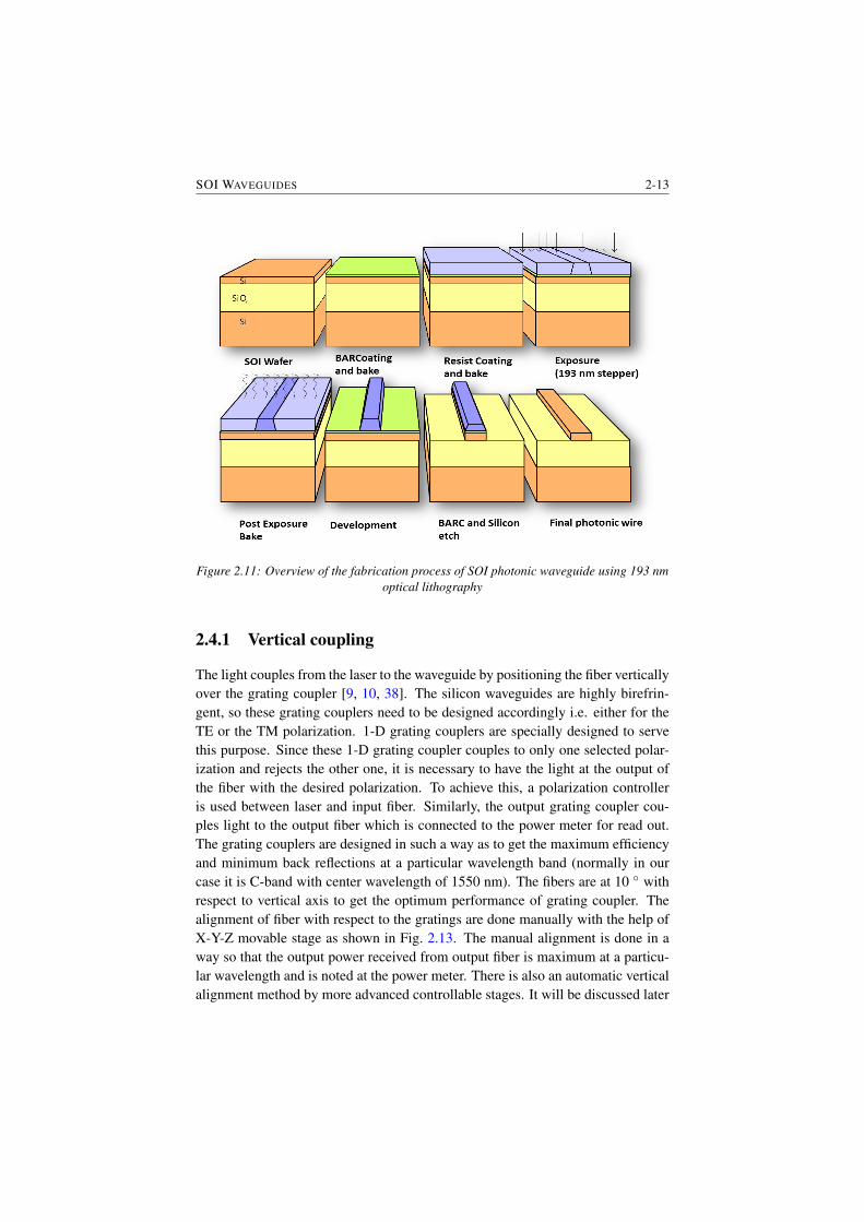
SOI WAVEGUIDES 2-13
Figure 2.11: Overview of the fabrication process of SOI photonic waveguide using 193 nmoptical lithography
2.4.1 Vertical coupling
The light couples from the laser to the waveguide by positioning the fiber verticallyover the grating coupler [9, 10, 38]. The silicon waveguides are highly birefrin-gent, so these grating couplers need to be designed accordingly i.e. either for theTE or the TM polarization. 1-D grating couplers are specially designed to servethis purpose. Since these 1-D grating coupler couples to only one selected polar-ization and rejects the other one, it is necessary to have the light at the output ofthe fiber with the desired polarization. To achieve this, a polarization controlleris used between laser and input fiber. Similarly, the output grating coupler cou-ples light to the output fiber which is connected to the power meter for read out.The grating couplers are designed in such a way as to get the maximum efficiencyand minimum back reflections at a particular wavelength band (normally in ourcase it is C-band with center wavelength of 1550 nm). The fibers are at 10 ◦ withrespect to vertical axis to get the optimum performance of grating coupler. Thealignment of fiber with respect to the gratings are done manually with the help ofX-Y-Z movable stage as shown in Fig. 2.13. The manual alignment is done in away so that the output power received from output fiber is maximum at a particu-lar wavelength and is noted at the power meter. There is also an automatic verticalalignment method by more advanced controllable stages. It will be discussed later
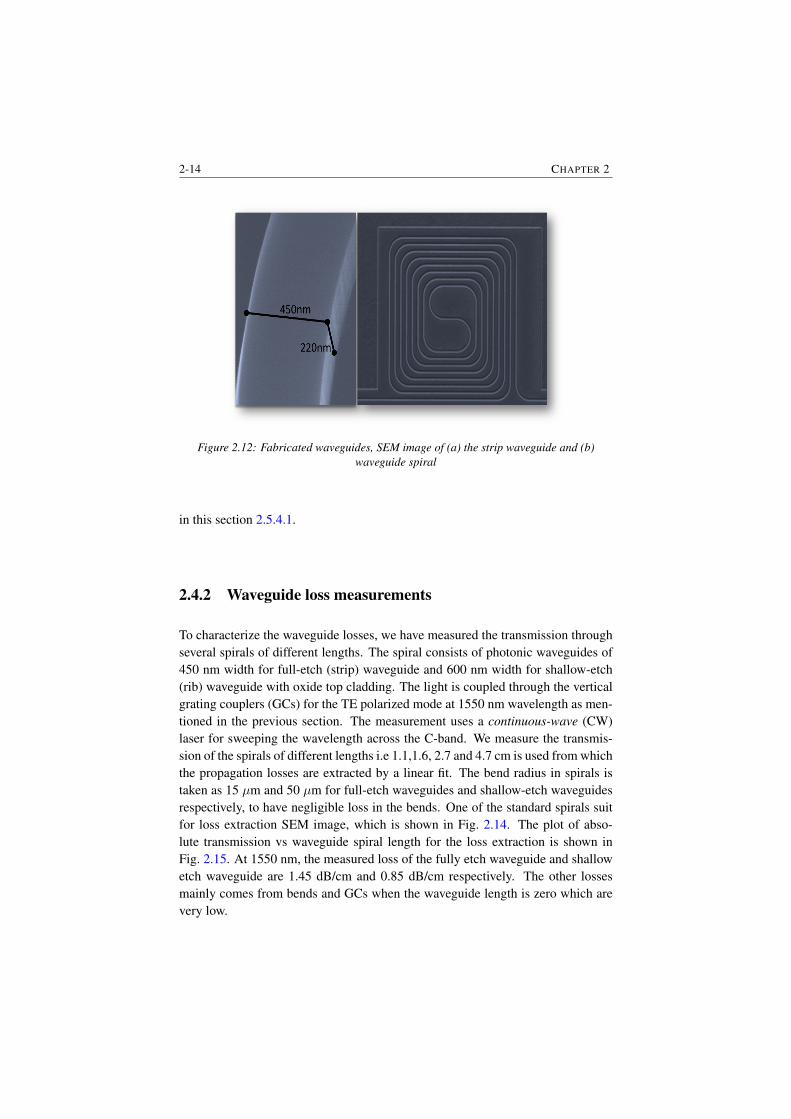
2-14 CHAPTER 2
Figure 2.12: Fabricated waveguides, SEM image of (a) the strip waveguide and (b)waveguide spiral
in this section 2.5.4.1.
2.4.2 Waveguide loss measurements
To characterize the waveguide losses, we have measured the transmission throughseveral spirals of different lengths. The spiral consists of photonic waveguides of450 nm width for full-etch (strip) waveguide and 600 nm width for shallow-etch(rib) waveguide with oxide top cladding. The light is coupled through the verticalgrating couplers (GCs) for the TE polarized mode at 1550 nm wavelength as men-tioned in the previous section. The measurement uses a continuous-wave (CW)laser for sweeping the wavelength across the C-band. We measure the transmis-sion of the spirals of different lengths i.e 1.1,1.6, 2.7 and 4.7 cm is used from whichthe propagation losses are extracted by a linear fit. The bend radius in spirals istaken as 15 µm and 50 µm for full-etch waveguides and shallow-etch waveguidesrespectively, to have negligible loss in the bends. One of the standard spirals suitfor loss extraction SEM image, which is shown in Fig. 2.14. The plot of abso-lute transmission vs waveguide spiral length for the loss extraction is shown inFig. 2.15. At 1550 nm, the measured loss of the fully etch waveguide and shallowetch waveguide are 1.45 dB/cm and 0.85 dB/cm respectively. The other lossesmainly comes from bends and GCs when the waveguide length is zero which arevery low.
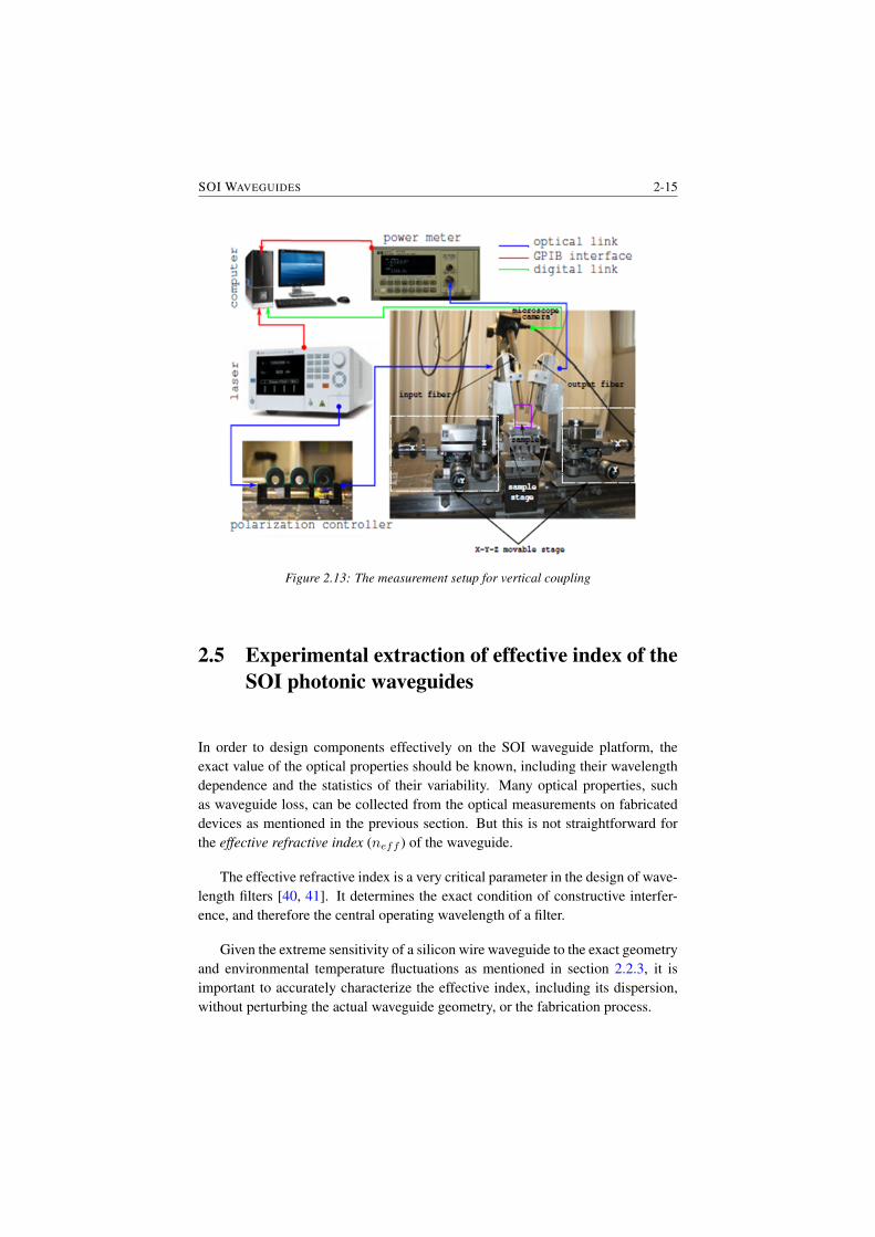
SOI WAVEGUIDES 2-15
Figure 2.13: The measurement setup for vertical coupling
2.5 Experimental extraction of effective index of theSOI photonic waveguides
In order to design components effectively on the SOI waveguide platform, theexact value of the optical properties should be known, including their wavelengthdependence and the statistics of their variability. Many optical properties, suchas waveguide loss, can be collected from the optical measurements on fabricateddevices as mentioned in the previous section. But this is not straightforward forthe effective refractive index (neff ) of the waveguide.
The effective refractive index is a very critical parameter in the design of wave-length filters [40, 41]. It determines the exact condition of constructive interfer-ence, and therefore the central operating wavelength of a filter.
Given the extreme sensitivity of a silicon wire waveguide to the exact geometryand environmental temperature fluctuations as mentioned in section 2.2.3, it isimportant to accurately characterize the effective index, including its dispersion,without perturbing the actual waveguide geometry, or the fabrication process.
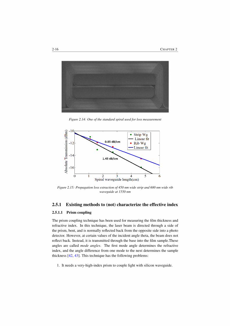
2-16 CHAPTER 2
Figure 2.14: One of the standard spiral used for loss measurement
Figure 2.15: Propagation loss extraction of 450 nm wide strip and 600 nm wide ribwaveguide at 1550 nm
2.5.1 Existing methods to (not) characterize the effective index
2.5.1.1 Prism coupling
The prism coupling technique has been used for measuring the film thickness andrefractive index. In this technique, the laser beam is directed through a side ofthe prism, bent, and is normally reflected back from the opposite side into a photodetector. However, at certain values of the incident angle theta, the beam does notreflect back. Instead, it is transmitted through the base into the film sample.Theseangles are called mode angles. The first mode angle determines the refractiveindex, and the angle difference from one mode to the next determines the samplethickness [42, 43]. This technique has the following problems:
1. It needs a very-high-index prism to couple light with silicon waveguide.

SOI WAVEGUIDES 2-17
2. Hard to couple into narrow line (better for sheets/slabs).
3. Film thickness information is needed for the refractive index measurements.
2.5.1.2 Fourier-space imaging
Fourier space imaging is another method in which the phase information of prop-agating mode is transferred into far-field by linear probe grating sitting close towaveguide and hence can measure the dispersion accurately [44]. But, this tech-nique faces the following problems:
1. It perturbs the waveguide optical properties.
2. It perturbs the waveguide patterning during fabrication (proximity effects,loading).
Techniques using scattering with weak higher-order periodic perturbations ef-fectively not only perturb the waveguide, but also change the local pattern density,and thus could even influence the fabrication process [7].
2.5.1.3 Ellipsometry
Ellipsometry is another technique which consists of the measurement of the changein polarization state of the light upon reflection from the sample of interest. It isused for characterizing the dielectric properties of thin films like refractive index,composition, roughness, doping concentration etc [45]. However, it faces the fol-lowing problems:
1. It is useful for the slab but not easy to use on narrow waveguides.
2. It loses accuracy in multilayer stacks.
2.5.1.4 On-chip interferometers
Methods which rely on the relative features in the transmission spectrum of theinterferometric devices, measure ng rather than neff [46]. Silicon strip waveg-uides are very dispersive, ng and neff are very different, and highly wavelengthdependent. Estimating the group index, it is theoretically possible to integrate theeffective index, but this can result in an ambiguous solution. An integration needsa constant which is nothing but the exact interference order of the measured filterat a particular wavelength.
Therefore, a method is needed to extract the effective index (as well as thegroup index) unambiguously and including their wavelength dispersion and tem-perature dependence.
2-18 CHAPTER 2
2.5.1.5 Simulation
Simulation of a waveguide cross section to extract the waveguide mode proper-ties is also possible, but at best it gives a good estimate of the effective index. Inpractice, the geometry of a buried silicon waveguide is hard to measure experi-mentally, even with high-resolution SEM. Also, boundary effects in the materialproperties can also affect the effective index but cannot be perceived by visual orSEM inspections. However, simulations provide a first estimate which we use inour method as a starting point to improve the accuracy.
2.5.2 Our method to extract the effective Index
We present a simple approach to accurately measure the neff of a silicon photonicswaveguide that overcomes the problems described in the previous section. Ourmethod uses three Mach-Zehnder interferometers (MZI) designed with the samephotonic wire located as close as possible to each other. MZIs are good candidatesas they are simple in design, linear in phase response and flexible in choosing thefilter order. Also, an MZI can be designed with symmetric bend sections, enablingdelay to be entirely in the straight waveguide sections.
In contrast, while using ring resonators, the measurements must be done atsufficiently low power levels to avoid nonlinear effects [47–49]. Also, the resultingmeasurement will be a weighted average of the bends, the straight sections andthe coupling sections. The measurement is even more complicated because inachieving the highest accuracy the ring needs to be critically coupled, requiringprecise control of the waveguide to ring gap dimension.
In our method, we use two MZIs with a low order m, i.e. a large free spectralrange (FSR), which allow us to estimate the order of the filter correctly within theC-band. The third MZI has a much higher order and a small FSR, which helps us toextract the wavelength dependence of the group index (ng). To extract the TO co-efficients, we measure the same MZIs at different temperatures and then extract thewavelength sensitivity of the spectrum with respect to temperature. Since individ-ual device parameter extraction does not give much information, we also performand present wafer-scale measurements for three different waveguide widths of 450nm, 600 nm and 800 nm respectively. Our method is generic in nature and shouldwork for all the integrated waveguide platforms.
2.5.2.1 Extracting the effective index from a single MZI
In any given wavelength filter, as in our MZI, we get constructive interference atthe output when
m.λm = neff (λm).∆L (2.6)
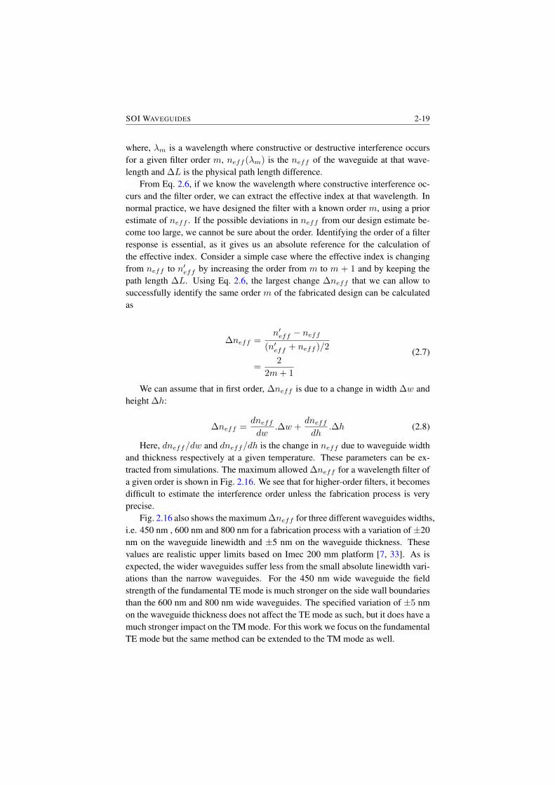
SOI WAVEGUIDES 2-19
where, λm is a wavelength where constructive or destructive interference occursfor a given filter order m, neff (λm) is the neff of the waveguide at that wave-length and ∆L is the physical path length difference.
From Eq. 2.6, if we know the wavelength where constructive interference oc-curs and the filter order, we can extract the effective index at that wavelength. Innormal practice, we have designed the filter with a known order m, using a priorestimate of neff . If the possible deviations in neff from our design estimate be-come too large, we cannot be sure about the order. Identifying the order of a filterresponse is essential, as it gives us an absolute reference for the calculation ofthe effective index. Consider a simple case where the effective index is changingfrom neff to n′eff by increasing the order from m to m + 1 and by keeping thepath length ∆L. Using Eq. 2.6, the largest change ∆neff that we can allow tosuccessfully identify the same order m of the fabricated design can be calculatedas
∆neff =n′eff − neff
(n′eff + neff )/2
=2
2m+ 1
(2.7)
We can assume that in first order, ∆neff is due to a change in width ∆w andheight ∆h:
∆neff =dneffdw
.∆w +dneffdh
.∆h (2.8)
Here, dneff/dw and dneff/dh is the change in neff due to waveguide widthand thickness respectively at a given temperature. These parameters can be ex-tracted from simulations. The maximum allowed ∆neff for a wavelength filter ofa given order is shown in Fig. 2.16. We see that for higher-order filters, it becomesdifficult to estimate the interference order unless the fabrication process is veryprecise.
Fig. 2.16 also shows the maximum ∆neff for three different waveguides widths,i.e. 450 nm , 600 nm and 800 nm for a fabrication process with a variation of ±20nm on the waveguide linewidth and ±5 nm on the waveguide thickness. Thesevalues are realistic upper limits based on Imec 200 mm platform [7, 33]. As isexpected, the wider waveguides suffer less from the small absolute linewidth vari-ations than the narrow waveguides. For the 450 nm wide waveguide the fieldstrength of the fundamental TE mode is much stronger on the side wall boundariesthan the 600 nm and 800 nm wide waveguides. The specified variation of ±5 nmon the waveguide thickness does not affect the TE mode as such, but it does have amuch stronger impact on the TM mode. For this work we focus on the fundamentalTE mode but the same method can be extended to the TM mode as well.
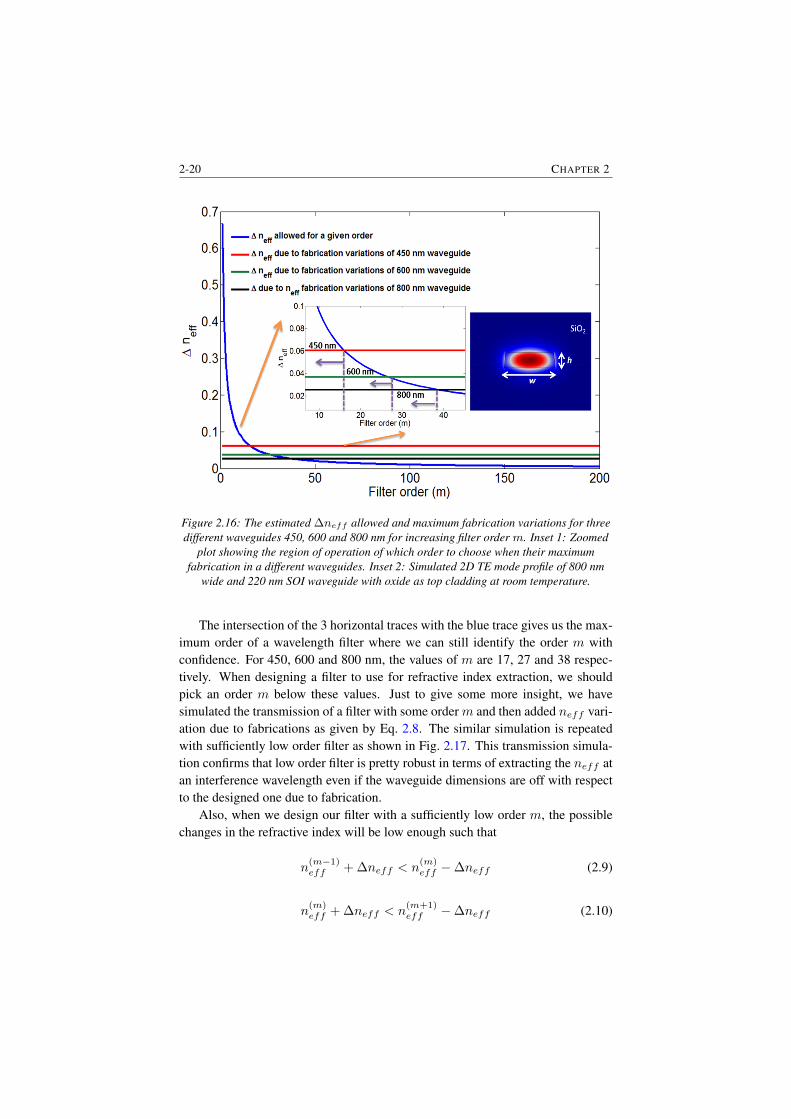
2-20 CHAPTER 2
Figure 2.16: The estimated ∆neff allowed and maximum fabrication variations for threedifferent waveguides 450, 600 and 800 nm for increasing filter order m. Inset 1: Zoomed
plot showing the region of operation of which order to choose when their maximumfabrication in a different waveguides. Inset 2: Simulated 2D TE mode profile of 800 nm
wide and 220 nm SOI waveguide with oxide as top cladding at room temperature.
The intersection of the 3 horizontal traces with the blue trace gives us the max-imum order of a wavelength filter where we can still identify the order m withconfidence. For 450, 600 and 800 nm, the values of m are 17, 27 and 38 respec-tively. When designing a filter to use for refractive index extraction, we shouldpick an order m below these values. Just to give some more insight, we havesimulated the transmission of a filter with some orderm and then added neff vari-ation due to fabrications as given by Eq. 2.8. The similar simulation is repeatedwith sufficiently low order filter as shown in Fig. 2.17. This transmission simula-tion confirms that low order filter is pretty robust in terms of extracting the neff atan interference wavelength even if the waveguide dimensions are off with respectto the designed one due to fabrication.
Also, when we design our filter with a sufficiently low order m, the possiblechanges in the refractive index will be low enough such that
n(m−1)eff + ∆neff < n
(m)eff −∆neff (2.9)
n(m)eff + ∆neff < n
(m+1)eff −∆neff (2.10)
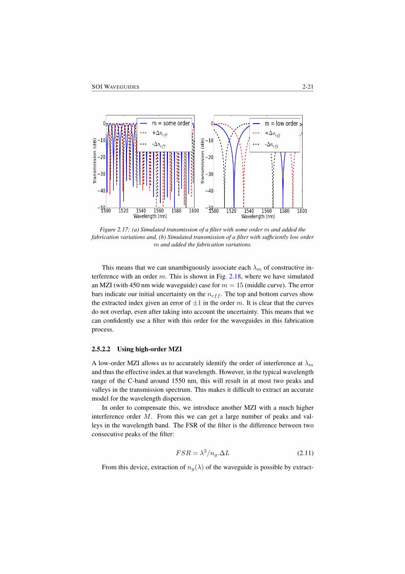
SOI WAVEGUIDES 2-21
Figure 2.17: (a) Simulated transmission of a filter with some order m and added thefabrication variations and, (b) Simulated transmission of a filter with sufficiently low order
m and added the fabrication variations.
This means that we can unambiguously associate each λm of constructive in-terference with an order m. This is shown in Fig. 2.18, where we have simulatedan MZI (with 450 nm wide waveguide) case for m = 15 (middle curve). The errorbars indicate our initial uncertainty on the neff . The top and bottom curves showthe extracted index given an error of ±1 in the order m. It is clear that the curvesdo not overlap, even after taking into account the uncertainty. This means that wecan confidently use a filter with this order for the waveguides in this fabricationprocess.
2.5.2.2 Using high-order MZI
A low-order MZI allows us to accurately identify the order of interference at λmand thus the effective index at that wavelength. However, in the typical wavelengthrange of the C-band around 1550 nm, this will result in at most two peaks andvalleys in the transmission spectrum. This makes it difficult to extract an accuratemodel for the wavelength dispersion.
In order to compensate this, we introduce another MZI with a much higherinterference order M . From this we can get a large number of peaks and val-leys in the wavelength band. The FSR of the filter is the difference between twoconsecutive peaks of the filter:
FSR = λ2/ng.∆L (2.11)
From this device, extraction of ng(λ) of the waveguide is possible by extract-
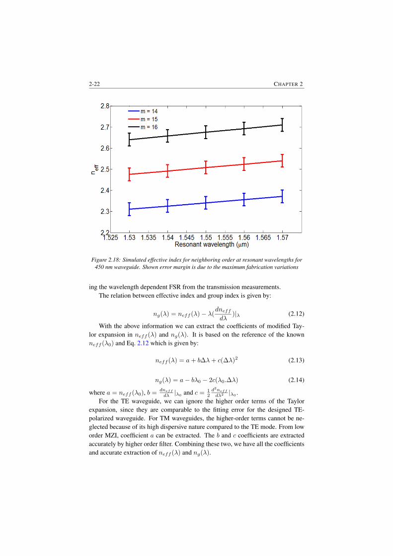
2-22 CHAPTER 2
Figure 2.18: Simulated effective index for neighboring order at resonant wavelengths for450 nm waveguide. Shown error margin is due to the maximum fabrication variations
ing the wavelength dependent FSR from the transmission measurements.The relation between effective index and group index is given by:
ng(λ) = neff (λ)− λ(dneffdλ
)|λ (2.12)
With the above information we can extract the coefficients of modified Tay-lor expansion in neff (λ) and ng(λ). It is based on the reference of the knownneff (λ0) and Eq. 2.12 which is given by:
neff (λ) = a+ b∆λ+ c(∆λ)2 (2.13)
ng(λ) = a− bλ0 − 2c(λ0.∆λ) (2.14)
where a = neff (λ0), b =dneff
dλ |λ0 and c = 12d2neff
dλ2 |λ0 .For the TE waveguide, we can ignore the higher order terms of the Taylor
expansion, since they are comparable to the fitting error for the designed TE-polarized waveguide. For TM waveguides, the higher-order terms cannot be ne-glected because of its high dispersive nature compared to the TE mode. From loworder MZI, coefficient a can be extracted. The b and c coefficients are extractedaccurately by higher order filter. Combining these two, we have all the coefficientsand accurate extraction of neff (λ) and ng(λ).
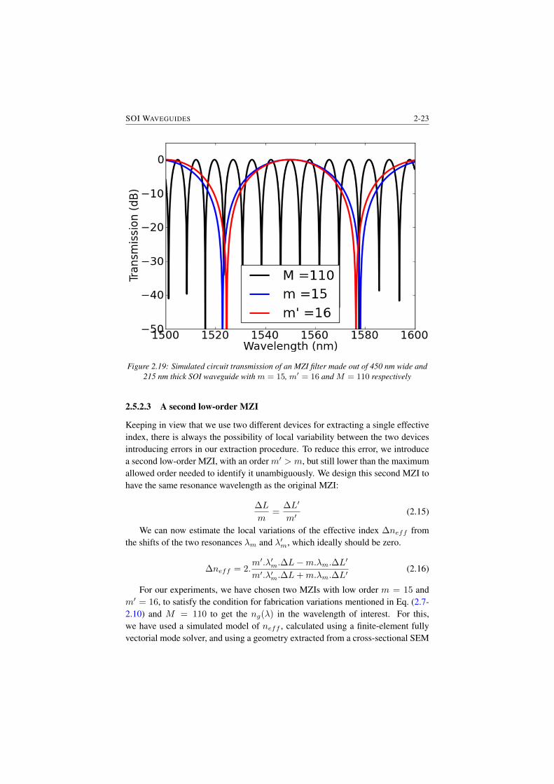
SOI WAVEGUIDES 2-23
Figure 2.19: Simulated circuit transmission of an MZI filter made out of 450 nm wide and215 nm thick SOI waveguide with m = 15, m′ = 16 and M = 110 respectively
2.5.2.3 A second low-order MZI
Keeping in view that we use two different devices for extracting a single effectiveindex, there is always the possibility of local variability between the two devicesintroducing errors in our extraction procedure. To reduce this error, we introducea second low-order MZI, with an order m′ > m, but still lower than the maximumallowed order needed to identify it unambiguously. We design this second MZI tohave the same resonance wavelength as the original MZI:
∆L
m=
∆L′
m′(2.15)
We can now estimate the local variations of the effective index ∆neff fromthe shifts of the two resonances λm and λ′m, which ideally should be zero.
∆neff = 2.m′.λ′m.∆L−m.λm.∆L′
m′.λ′m.∆L+m.λm.∆L′(2.16)
For our experiments, we have chosen two MZIs with low order m = 15 andm′ = 16, to satisfy the condition for fabrication variations mentioned in Eq. (2.7-2.10) and M = 110 to get the ng(λ) in the wavelength of interest. For this,we have used a simulated model of neff , calculated using a finite-element fullyvectorial mode solver, and using a geometry extracted from a cross-sectional SEM
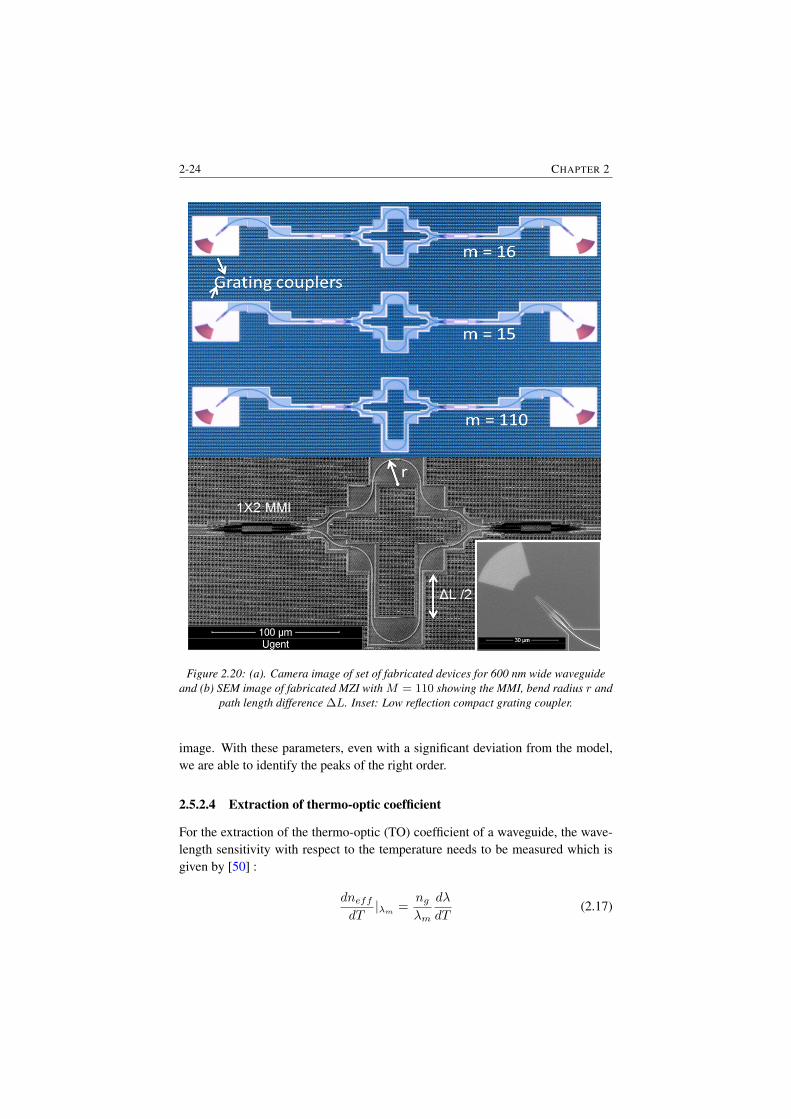
2-24 CHAPTER 2
Figure 2.20: (a). Camera image of set of fabricated devices for 600 nm wide waveguideand (b) SEM image of fabricated MZI with M = 110 showing the MMI, bend radius r and
path length difference ∆L. Inset: Low reflection compact grating coupler.
image. With these parameters, even with a significant deviation from the model,we are able to identify the peaks of the right order.
2.5.2.4 Extraction of thermo-optic coefficient
For the extraction of the thermo-optic (TO) coefficient of a waveguide, the wave-length sensitivity with respect to the temperature needs to be measured which isgiven by [50] :
dneffdT|λm =
ngλm
dλ
dT(2.17)

SOI WAVEGUIDES 2-25
The TO coefficient of the waveguide is extracted after extracting the ng at agiven wavelength λm and the filter transmission at different temperatures T .
An alternative method to extract the TO coefficient is to extract neff (λm) fromthe low order MZIs for different temperatures and then use equation (2.6) directlyat a given wavelength.
2.5.3 Design and fabrication
The MZIs are simulated and designed for three different waveguides, i.e. 450 nm,600 nm and 800 nm wide respectively and with 215 nm thick silicon wires forvaluesm = 15,m′ = 16 andM = 110 respectively. The full eigenmode solutionsas discussed in section 2 are fed to the circuit solver CAPHE to get the transmissionresponse at fixed room temperature [51, 52]. The simulated transmission of thethree 450 nm MZI filters for m = 15, m′ = 16 and M = 110 is shown inFig. 2.19. As they have been designed for that condition, the three simulationsshow constructive interference at λm of 1550 nm.
Devices are designed using IPKISS, a designed framework by Luceda Pho-tonics, which generates the layouts directly from a parametric description of theMZI [52].
Since the quality of the transmission trace is essential for an accurate extrac-tion, we have designed the test circuits to minimize reflections. There are differentsources of contribution towards reflection in the SOI based wavelength devices.The major contributions to reflection are from the grating couplers to and fromthe chip. Therefore, we use compact off-axis grating couplers with reduce backreflections [13]. They are designed at an angle of 45 deg to the in-plane fiberaxis, and they direct backreflections away from the input waveguide. This reducesback-reflection of curved grating couplers from -20 dB to -50 dB.
The arms of the MZI are designed with a relatively large bend radius of 20µm to avoid reflections from the straight-bend interface and to minimize the loss.The arms are symmetric except for the vertical straight section which incorporatesthe actual delay ∆L. This cancels out possible effects of bend-radius dependenceof neff . Our device focuses on measuring and extracting the neff of straightphotonic wires. It can be extended to extract the bend mode waveguide refractiveindex by incorporating the delay line in the bend sections.
The side wall roughness of the waveguide is unavoidable which depends uponthe fabrication. This effect is prominent in 450 nm wide waveguides which grad-ually decreases for wider waveguides i.e for 600 and 800 nm.
For equal splitting and combining the light, the device uses wide band 1 × 2
multimode interference (MMI) based splitter. By using a symmetric splitter andcombiner, we reduce the effect of wavelength dependence in directional couplers,noting that the couplers do not inherently introduce a phase delay between the
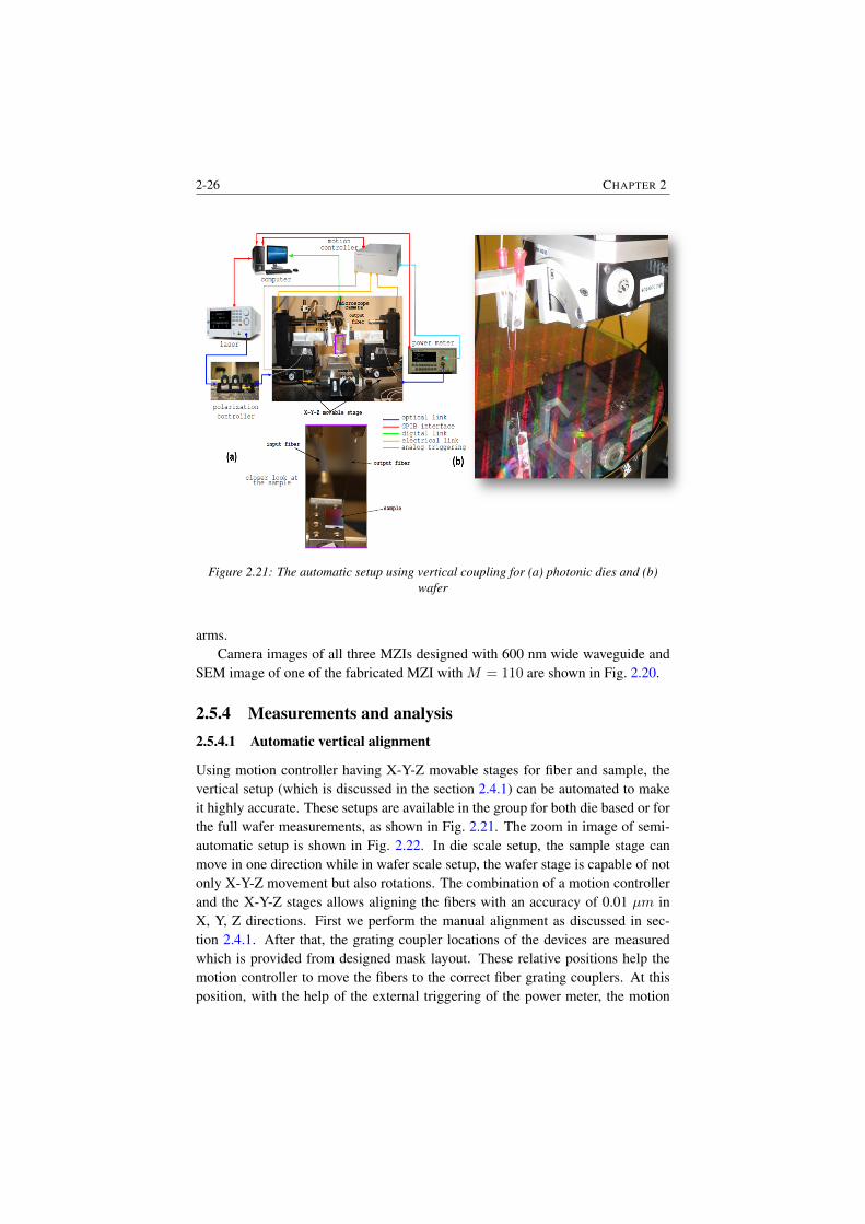
2-26 CHAPTER 2
Figure 2.21: The automatic setup using vertical coupling for (a) photonic dies and (b)wafer
arms.Camera images of all three MZIs designed with 600 nm wide waveguide and
SEM image of one of the fabricated MZI with M = 110 are shown in Fig. 2.20.
2.5.4 Measurements and analysis2.5.4.1 Automatic vertical alignment
Using motion controller having X-Y-Z movable stages for fiber and sample, thevertical setup (which is discussed in the section 2.4.1) can be automated to makeit highly accurate. These setups are available in the group for both die based or forthe full wafer measurements, as shown in Fig. 2.21. The zoom in image of semi-automatic setup is shown in Fig. 2.22. In die scale setup, the sample stage canmove in one direction while in wafer scale setup, the wafer stage is capable of notonly X-Y-Z movement but also rotations. The combination of a motion controllerand the X-Y-Z stages allows aligning the fibers with an accuracy of 0.01 µm inX, Y, Z directions. First we perform the manual alignment as discussed in sec-tion 2.4.1. After that, the grating coupler locations of the devices are measuredwhich is provided from designed mask layout. These relative positions help themotion controller to move the fibers to the correct fiber grating couplers. At thisposition, with the help of the external triggering of the power meter, the motion
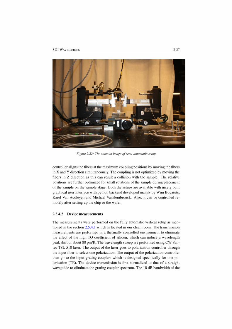
SOI WAVEGUIDES 2-27
Figure 2.22: The zoom in image of semi-automatic setup
controller aligns the fibers at the maximum coupling positions by moving the fibersin X and Y direction simultaneously. The coupling is not optimized by moving thefibers in Z direction as this can result a collision with the sample. The relativepositions are further optimized for small rotations of the sample during placementof the sample on the sample stage. Both the setups are available with nicely builtgraphical user interface with python backend developed mainly by Wim Bogaerts,Karel Van Acoleyen and Michael Vanslembrouck. Also, it can be controlled re-motely after setting up the chip or the wafer.
2.5.4.2 Device measurements
The measurements were performed on the fully automatic vertical setup as men-tioned in the section 2.5.4.1 which is located in our clean room. The transmissionmeasurements are performed in a thermally controlled environment to eliminatethe effect of the high TO coefficient of silicon, which can induce a wavelengthpeak shift of about 80 pm/K. The wavelength sweep are performed using CW San-tec TSL 510 laser. The output of the laser goes to polarization controller throughthe input fiber to select one polarization. The output of the polarization controllerthen go to the input grating couplers which is designed specifically for one po-larization (TE). The device transmission is first normalized to that of a straightwaveguide to eliminate the grating coupler spectrum. The 10 dB bandwidth of the
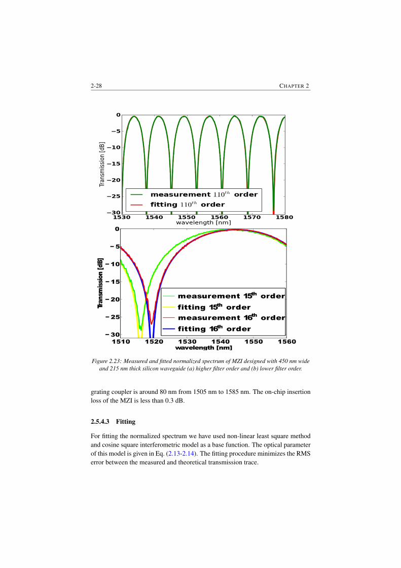
2-28 CHAPTER 2
Figure 2.23: Measured and fitted normalized spectrum of MZI designed with 450 nm wideand 215 nm thick silicon waveguide (a) higher filter order and (b) lower filter order.
grating coupler is around 80 nm from 1505 nm to 1585 nm. The on-chip insertionloss of the MZI is less than 0.3 dB.
2.5.4.3 Fitting
For fitting the normalized spectrum we have used non-linear least square methodand cosine square interferometric model as a base function. The optical parameterof this model is given in Eq. (2.13-2.14). The fitting procedure minimizes the RMSerror between the measured and theoretical transmission trace.
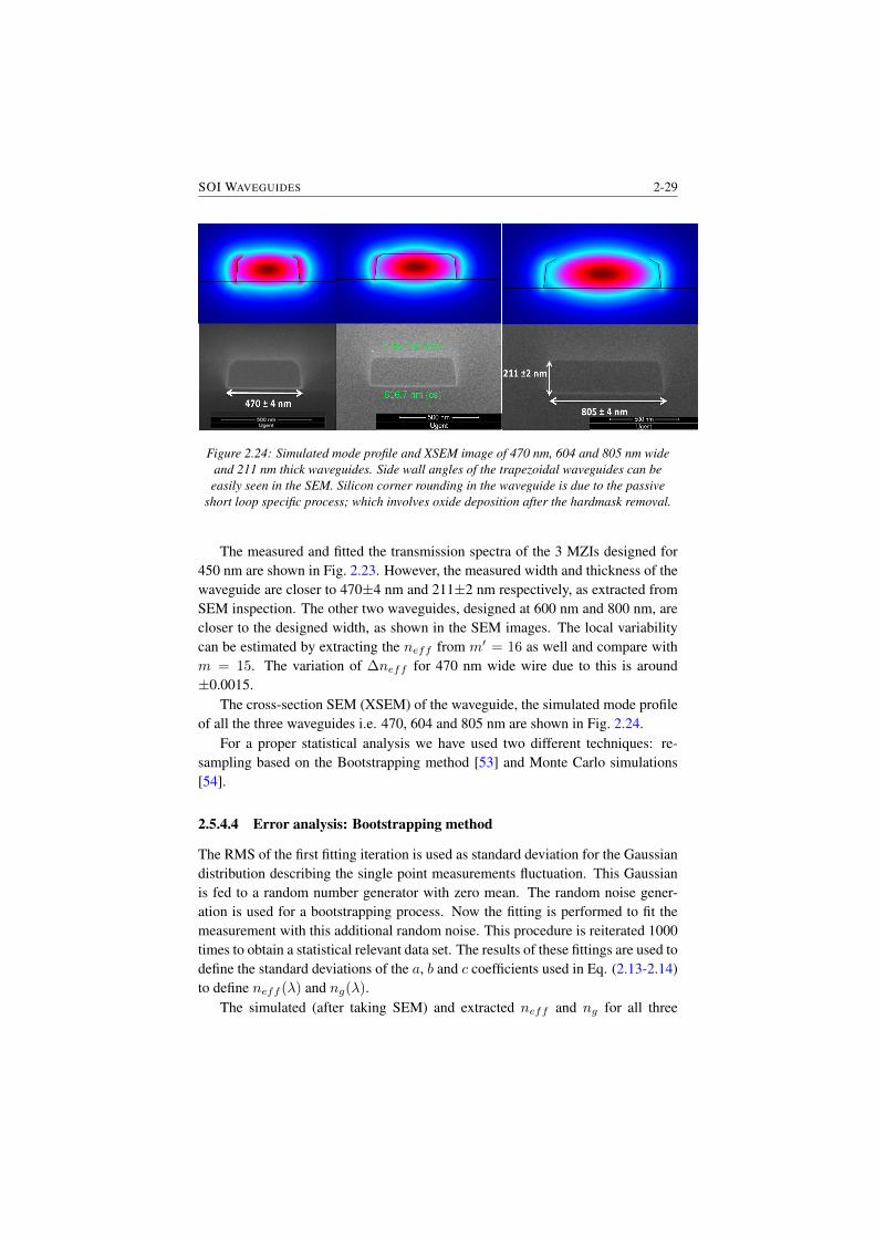
SOI WAVEGUIDES 2-29
Figure 2.24: Simulated mode profile and XSEM image of 470 nm, 604 and 805 nm wideand 211 nm thick waveguides. Side wall angles of the trapezoidal waveguides can beeasily seen in the SEM. Silicon corner rounding in the waveguide is due to the passive
short loop specific process; which involves oxide deposition after the hardmask removal.
The measured and fitted the transmission spectra of the 3 MZIs designed for450 nm are shown in Fig. 2.23. However, the measured width and thickness of thewaveguide are closer to 470±4 nm and 211±2 nm respectively, as extracted fromSEM inspection. The other two waveguides, designed at 600 nm and 800 nm, arecloser to the designed width, as shown in the SEM images. The local variabilitycan be estimated by extracting the neff from m′ = 16 as well and compare withm = 15. The variation of ∆neff for 470 nm wide wire due to this is around±0.0015.
The cross-section SEM (XSEM) of the waveguide, the simulated mode profileof all the three waveguides i.e. 470, 604 and 805 nm are shown in Fig. 2.24.
For a proper statistical analysis we have used two different techniques: re-sampling based on the Bootstrapping method [53] and Monte Carlo simulations[54].
2.5.4.4 Error analysis: Bootstrapping method
The RMS of the first fitting iteration is used as standard deviation for the Gaussiandistribution describing the single point measurements fluctuation. This Gaussianis fed to a random number generator with zero mean. The random noise gener-ation is used for a bootstrapping process. Now the fitting is performed to fit themeasurement with this additional random noise. This procedure is reiterated 1000times to obtain a statistical relevant data set. The results of these fittings are used todefine the standard deviations of the a, b and c coefficients used in Eq. (2.13-2.14)to define neff (λ) and ng(λ).
The simulated (after taking SEM) and extracted neff and ng for all three
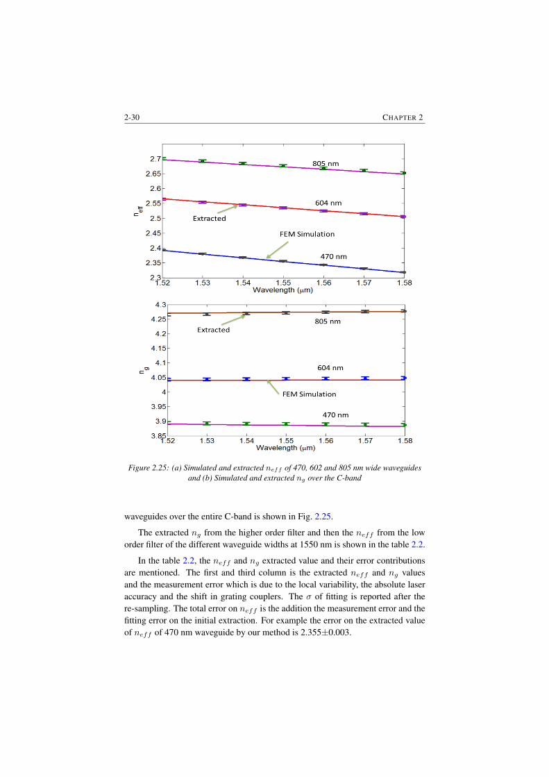
2-30 CHAPTER 2
Figure 2.25: (a) Simulated and extracted neff of 470, 602 and 805 nm wide waveguidesand (b) Simulated and extracted ng over the C-band
waveguides over the entire C-band is shown in Fig. 2.25.
The extracted ng from the higher order filter and then the neff from the loworder filter of the different waveguide widths at 1550 nm is shown in the table 2.2.
In the table 2.2, the neff and ng extracted value and their error contributionsare mentioned. The first and third column is the extracted neff and ng valuesand the measurement error which is due to the local variability, the absolute laseraccuracy and the shift in grating couplers. The σ of fitting is reported after there-sampling. The total error on neff is the addition the measurement error and thefitting error on the initial extraction. For example the error on the extracted valueof neff of 470 nm waveguide by our method is 2.355±0.003.
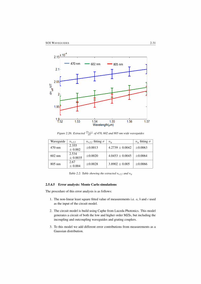
SOI WAVEGUIDES 2-31
Figure 2.26: Extracted dneff
dTof 470, 602 and 805 nm wide waveguides
Waveguide neff neff fitting σ ng ng fitting σ
470 nm2.355± 0.002 ±0.0013 4.2739 ± 0.0042 ±0.0063
602 nm2.534± 0.0035 ±0.0020 4.0453 ± 0.0045 ±0.0064
805 nm2.67± 0.004 ±0.0028 3.8902 ± 0.005 ±0.0066
Table 2.2: Table showing the extracted neff and ng
2.5.4.5 Error analysis: Monte Carlo simulations
The procedure of this error analysis is as follows:
1. The non-linear least square fitted value of measurements i.e. a, b and c usedas the input of the circuit model.
2. The circuit model is build using Caphe from Luceda Photonics. This modelgenerates a circuit of both the low and higher order MZIs, but including theincoupling and outcoupling waveguides and grating couplers.
3. To this model we add different error contributions from measurements as aGaussian distribution.

2-32 CHAPTER 2
Figure 2.27: Extracted neff when an error is introduced on (a) the absolute laseraccuracy, (b) the grating coupler peak wavelength, (c) the laser output power, (d)
Histogram of neff0 after 100 iterations with stochastic variations on these three errorcontributions using Monte Carlo simulations
4. After adding these error contributions we fit the new transmission spectrumusing our fitting algorithm. This fit gives a new value and we can call as a′,b′ and c′.
5. The error can be estimated by taking the difference between the initial fittedvalue on measurement and this new fitted value of circuit simulation i.e.error on ε(a) = a′ − a and similarly for estimating ε(b) and ε(c).
6. We re-iterate this process 100 times to generate a reliable value for the erroron a, b and c.
When measuring the MZIs, we identified different contributions to include inthe circuit model:
1. Absolute laser accuracy: This parameter is defined as the variations in thelaser actual wavelength and the wavelength it shows during the measure-ments. For Santec TSL-510 (C-band) it is ±2.5 pm.
2. Laser output power or laser noise: This is basically the output power fluctu-ations from laser. For the laser used this is ±0.2 dB.
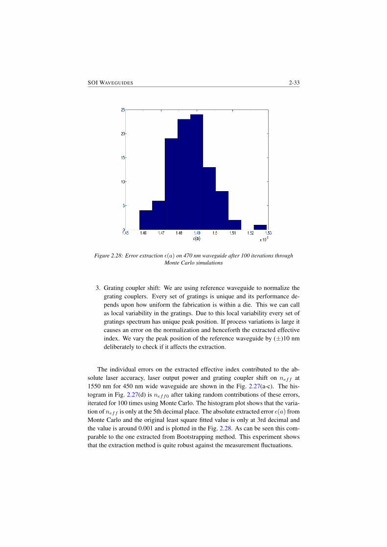
SOI WAVEGUIDES 2-33
Figure 2.28: Error extraction ε(a) on 470 nm waveguide after 100 iterations throughMonte Carlo simulations
3. Grating coupler shift: We are using reference waveguide to normalize thegrating couplers. Every set of gratings is unique and its performance de-pends upon how uniform the fabrication is within a die. This we can callas local variability in the gratings. Due to this local variability every set ofgratings spectrum has unique peak position. If process variations is large itcauses an error on the normalization and henceforth the extracted effectiveindex. We vary the peak position of the reference waveguide by (±)10 nmdeliberately to check if it affects the extraction.
The individual errors on the extracted effective index contributed to the ab-solute laser accuracy, laser output power and grating coupler shift on neff at1550 nm for 450 nm wide waveguide are shown in the Fig. 2.27(a-c). The his-togram in Fig. 2.27(d) is neff0 after taking random contributions of these errors,iterated for 100 times using Monte Carlo. The histogram plot shows that the varia-tion of neff is only at the 5th decimal place. The absolute extracted error ε(a) fromMonte Carlo and the original least square fitted value is only at 3rd decimal andthe value is around 0.001 and is plotted in the Fig. 2.28. As can be seen this com-parable to the one extracted from Bootstrapping method. This experiment showsthat the extraction method is quite robust against the measurement fluctuations.
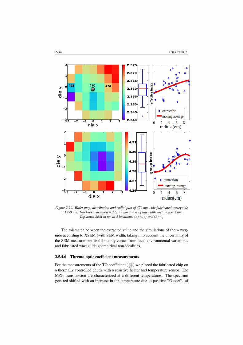
2-34 CHAPTER 2
Figure 2.29: Wafer map, distribution and radial plot of 470 nm wide fabricated waveguideat 1550 nm. Thickness variation is 211±2 nm and σ of linewidth variation is 5 nm.
Top-down SEM in nm at 3 locations. (a) neff and (b) ng
The mismatch between the extracted value and the simulations of the waveg-uide according to XSEM (with SEM width, taking into account the uncertainty ofthe SEM measurement itself) mainly comes from local environmental variations,and fabricated waveguide geometrical non-idealities.
2.5.4.6 Thermo-optic coefficient measurements
For the measurements of the TO coefficient ( dndT ) we placed the fabricated chip ona thermally controlled chuck with a resistive heater and temperature sensor. TheMZIs transmission are characterized at a different temperatures. The spectrumgets red shifted with an increase in the temperature due to positive TO coeff. of
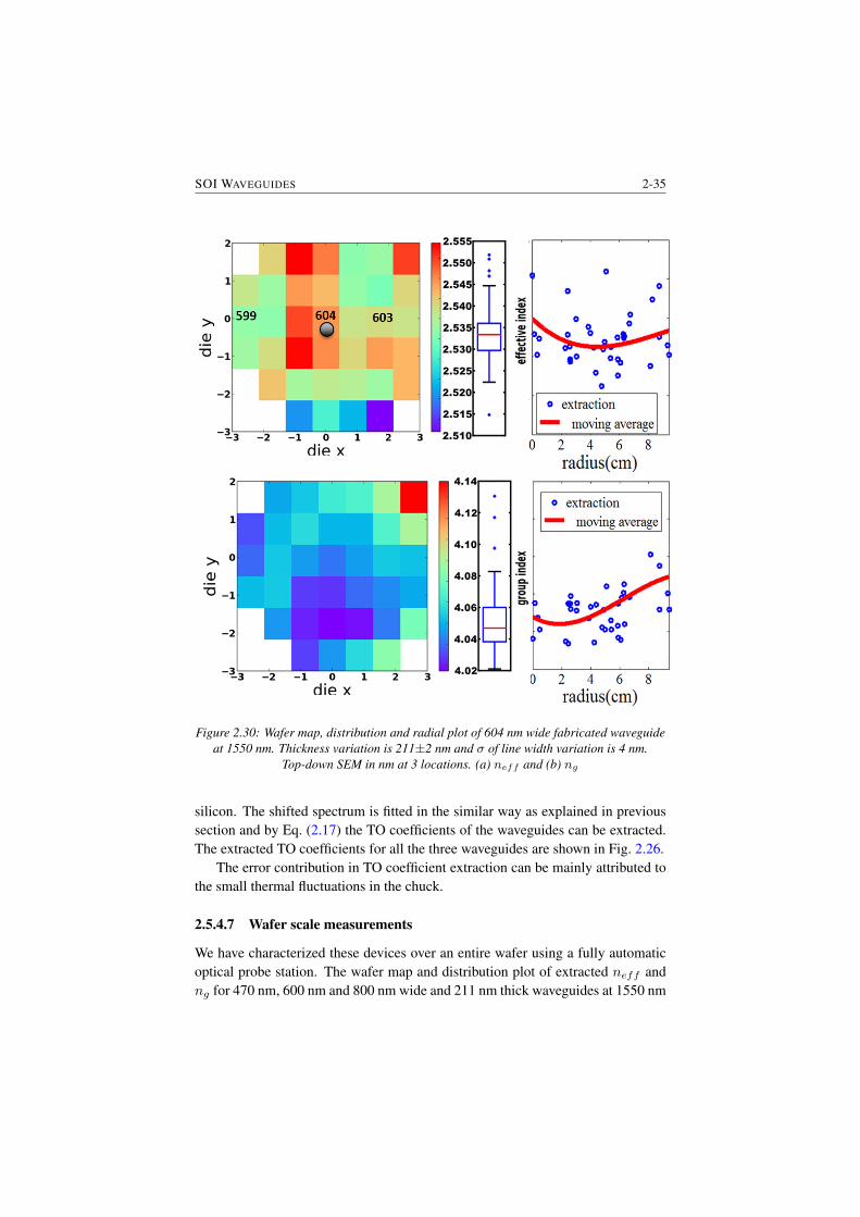
SOI WAVEGUIDES 2-35
Figure 2.30: Wafer map, distribution and radial plot of 604 nm wide fabricated waveguideat 1550 nm. Thickness variation is 211±2 nm and σ of line width variation is 4 nm.
Top-down SEM in nm at 3 locations. (a) neff and (b) ng
silicon. The shifted spectrum is fitted in the similar way as explained in previoussection and by Eq. (2.17) the TO coefficients of the waveguides can be extracted.The extracted TO coefficients for all the three waveguides are shown in Fig. 2.26.
The error contribution in TO coefficient extraction can be mainly attributed tothe small thermal fluctuations in the chuck.
2.5.4.7 Wafer scale measurements
We have characterized these devices over an entire wafer using a fully automaticoptical probe station. The wafer map and distribution plot of extracted neff andng for 470 nm, 600 nm and 800 nm wide and 211 nm thick waveguides at 1550 nm
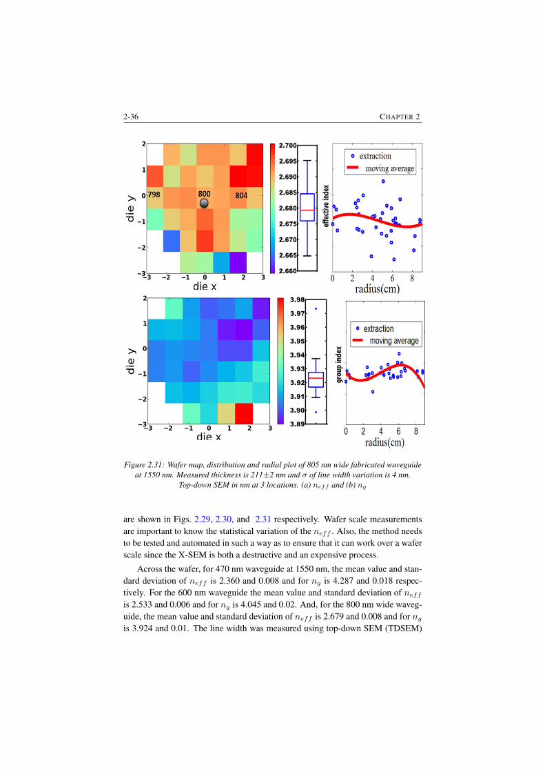
2-36 CHAPTER 2
Figure 2.31: Wafer map, distribution and radial plot of 805 nm wide fabricated waveguideat 1550 nm. Measured thickness is 211±2 nm and σ of line width variation is 4 nm.
Top-down SEM in nm at 3 locations. (a) neff and (b) ng
are shown in Figs. 2.29, 2.30, and 2.31 respectively. Wafer scale measurementsare important to know the statistical variation of the neff . Also, the method needsto be tested and automated in such a way as to ensure that it can work over a waferscale since the X-SEM is both a destructive and an expensive process.
Across the wafer, for 470 nm waveguide at 1550 nm, the mean value and stan-dard deviation of neff is 2.360 and 0.008 and for ng is 4.287 and 0.018 respec-tively. For the 600 nm waveguide the mean value and standard deviation of neffis 2.533 and 0.006 and for ng is 4.045 and 0.02. And, for the 800 nm wide waveg-uide, the mean value and standard deviation of neff is 2.679 and 0.008 and for ngis 3.924 and 0.01. The line width was measured using top-down SEM (TDSEM)
SOI WAVEGUIDES 2-37
provided by the foundry at 3 different locations of the wafer and is shown on thewafer maps.
The deviation of the extracted effective and group indices is mainly influencedby two effects: the thickness and the line width variation over the wafer. Thicknessvariation is due to the SOI polishing and can be considered to be slow across thewafer. As provided by the foundry it is only a few nm over the entire wafer.The line width is correlated to lithographic process and it is performed using diebased stepping which introduces discrete variations. The effect of the line width istherefore more pronounced than the effect of the thickness. As a result, we see aslow variation which is superimposed with a faster variation on the wafer maps.
2.6 Conclusion and discussionIn this chapter we have discussed the SOI platform, its material stack and fabrica-tion process, in particular the most fundamental component of the platform i.e. theSOI photonic waveguide. We have shown the mode simulations of different typesof SOI waveguides, their geometrical, wavelength and thermal sensitivities. Thewaveguide loss has been measured using grating couplers.
We have then proposed and demonstrated a novel method for measuring therefractive index of dispersive SOI waveguides. Combining 3 MZIs of low andhigh order, we can extract the wavelength and temperature dependent effectiveindex and the group index unambiguously. We also obtain an estimate for the localvariability of the effective index accurately. It does not perturb the waveguide oflocal pattern density, which is essential in a high-contrast waveguide platform suchas silicon photonics.
This method can be applied to the TM polarization, different types of waveg-uides and can also be extended to other waveguide platforms. This method can befurther extended i.e. extraction might well be possible just by cascading two MZIsin series in which one is with the lower order and another with higher order. Inthat case, the fitting of the transmission envelope gives the neff at that wavelengthwhile fitting the full transmission spectrum extracts the higher order terms of neffi.e. ng of the waveguide.
2-38 CHAPTER 2
References[1] Gerd Keiser. Optical fiber communication. NY: McGraw-Hill, 2000.
[2] Wim Bogaerts, Liu Liu, and Gunther Roelkens. Technologies and BuildingBlocks for On-Chip Optical Interconnects. In Ian O’Connor and GabrielaNicolescu, editors, Integrated Optical Interconnect Architectures for Embed-ded Systems, Embedded Systems, pages 27–78. Springer New York, 2013.
[3] Berge Tatian. Fitting refractive-index data with the Sellmeier dispersion for-mula. Appl. Opt., 23(24):4477–4485, Dec 1984.
[4] G. Ghosh, M. Endo, and T. Iwasaki. Temperature-dependent Sellmeier coef-ficients and chromatic dispersions for some optical fiber glasses. LightwaveTechnology, Journal of, 12(8):1338–1342, Aug 1994.
[5] Bradley J. Frey, Douglas B. Leviton, and Timothy J. Madison. Temperature-dependent refractive index of silicon and germanium, July 2006.
[6] http://www.europractice-ic.com/SiPhotonics_general.php.
[7] S.K. Selvaraja, W. Bogaerts, P. Dumon, D. Van Thourhout, and R. Baets.Subnanometer Linewidth Uniformity in Silicon Nanophotonic Waveguide De-vices Using CMOS Fabrication Technology. Selected Topics in QuantumElectronics, IEEE Journal of, 16(1):316–324, Jan 2010.
[8] Hui Yu, Marianna Pantouvaki, Joris Van Campenhout, Dietmar Korn,Katarzyna Komorowska, Pieter Dumon, Yanlu Li, Peter Verheyen, PhilippeAbsil, Luca Alloatti, David Hillerkuss, Juerg Leuthold, Roel Baets, and WimBogaerts. Performance tradeoff between lateral and interdigitated dopingpatterns for high speed carrier-depletion based silicon modulators. Opt. Ex-press, 20(12):12926–12938, Jun 2012.
[9] Dirk Taillaert, Peter Bienstman, and Roel Baets. Compact efficient broad-band grating coupler for silicon-on-insulator waveguides. Opt. Lett.,29(23):2749–2751, Dec 2004.
[10] D. Vermeulen, S. Selvaraja, P. Verheyen, G. Lepage, W. Bogaerts, P. Ab-sil, D. Van Thourhout, and G. Roelkens. High-efficiency fiber-to-chip grat-ing couplers realized using an advanced CMOS-compatible Silicon-On-Insulator platform. Opt. Express, 18(17):18278–18283, Aug 2010.
[11] D. Vermeulen, Y. De Koninck, Y. Li, E. Lambert, W. Bogaerts, R. Baets,and G. Roelkens. Reflectionless grating couplers for Silicon-on-Insulatorphotonic integrated circuits. Opt. Express, 20(20):22278–22283, Sep 2012.
SOI WAVEGUIDES 2-39
[12] Yanlu Li, Lianyan Li, Bin Tian, G. Roelkens, and R.G. Baets. ReflectionlessTilted Grating Couplers With Improved Coupling Efficiency Based on a Sili-con Overlay. Photonics Technology Letters, IEEE, 25(13):1195–1198, July2013.
[13] Yanlu Li, Diedrik Vermeulen, Yannick De Koninck, Gunay Yurtsever,Gunther Roelkens, and Roel Baets. Compact grating couplers on silicon-on-insulator with reduced backreflection. Opt. Lett., 37(21):4356–4358, Nov2012.
[14] S. Pathak, P. Dumon, D. Van Thourhout, and W. Bogaerts. Comparisonof AWGs and Echelle Gratings for Wavelength Division Multiplexing onSilicon-on-Insulator. Photonics Journal, IEEE, 6(5):1–9, Oct 2014.
[15] Shankar K. Selvaraja, Gustaf Winroth, Sabrina Locorotondo, Gayle Mur-doch, Alexey Milenin, Christie Delvaux, Patrick Ong, Shibnath Pathak,Weiqiang Xie, Gunther Sterckx, Guy Lepage, Dries Van Thourhout, WimBogaerts, Joris Van Campenhout, and Philippe Absil. 193nm immersionlithography for high-performance silicon photonic circuits, 2014.
[16] Marianna Pantouvaki, Peter Verheyen, Guy Lepage, Jeroen De Coster, HuiYu, Peter De Heyn, Adil Masood, Wim Bogaerts, Philippe Absil, andJoris Van Campenhout. 8x14Gb/s Si Ring WDM Modulator Array withIntegrated Tungsten Heaters and Ge Monitor Photodetectors. In OpticalFiber Communication Conference, page Th1C.5. Optical Society of Amer-ica, 2014.
[17] Yufei Xing, T. Ako, J.P. George, D. Korn, Hui Yu, P. Verheyen, M. Pan-touvaki, G. Lepage, P. Absil, A. Ruocco, C. Koos, J. Leuthold, K. Neyts,J. Beeckman, and W. Bogaerts. Digitally Controlled Phase Shifter Using anSOI Slot Waveguide With Liquid Crystal Infiltration. Photonics TechnologyLetters, IEEE, 27(12):1269–1272, June 2015.
[18] Carlos A. Barrios, Kristinn B. Gylfason, Benito Sanchez, Amadeu Griol,H. Sohlstrom, M. Holgado, and R. Casquel. Slot-waveguide biochemicalsensor. Opt. Lett., 32(21):3080–3082, Nov 2007.
[19] Francesco Dell’Olio and Vittorio M. Passaro. Optical sensing by optimizedsilicon slot waveguides. Opt. Express, 15(8):4977–4993, Apr 2007.
[20] Jianming Jin. The Finite Element Method in Electromagnetics. Wiley-IEEEPress, 3rd edition, 2014.
[21] http://www.comsol.com/.

2-40 CHAPTER 2
[22] R.M. Joseph and Allen Taflove. Spatial soliton deflection mechanism in-dicated by FD-TD Maxwell’s equations modeling. Photonics TechnologyLetters, IEEE, 6(10):1251–1254, Oct 1994.
[23] http://www.lumerical.com/.
[24] J. Van Roey, J. van der Donk, and P. E. Lagasse. Beam-propagation method:analysis and assessment. J. Opt. Soc. Am., 71(7):803–810, Jul 1981.
[25] http://optiwave.com/category/products/component-design/optibpm/.
[26] P. Bienstman, E. Six, M. Roelens, M. Vanwolleghem, and R. Baets. Calcu-lation of bending losses in dielectric waveguides using eigenmode expan-sion and perfectly matched layers. Photonics Technology Letters, IEEE,14(2):164–166, Feb 2002.
[27] http://www.photond.com/.
[28] F. Gan, T. Barwicz, M.A. Popovic, M.S. Dahlem, C.W. Holzwarth, P.T. Ra-kich, H.I. Smith, E.P. Ippen, and F.X. Kartner. Maximizing the Thermo-OpticTuning Range of Silicon Photonic Structures. In Photonics in Switching,2007, pages 67–68, Aug 2007.
[29] Joris Van Campenhout, William M. J. Green, Solomon Assefa, and Yurii A.Vlasov. Integrated NiSi waveguide heaters for CMOS-compatible siliconthermo-optic devices. Opt. Lett., 35(7):1013–1015, Apr 2010.
[30] Po Dong, Wei Qian, Hong Liang, Roshanak Shafiiha, Dazeng Feng, Guo-liang Li, John E. Cunningham, Ashok V. Krishnamoorthy, and Mehdi As-ghari. Thermally tunable silicon racetrack resonators with ultralow tuningpower. Opt. Express, 18(19):20298–20304, Sep 2010.
[31] A. Masood, M. Pantouvaki, G. Lepage, P. Verheyen, J. Van Campenhout,P. Absil, D. Van Thourhout, and W. Bogaerts. Comparison of heater archi-tectures for thermal control of silicon photonic circuits. In Group IV Photon-ics (GFP), 2013 IEEE 10th International Conference on, pages 83–84, Aug2013.
[32] http://www.intel.com/content/www/us/en/silicon-innovations/intel-14nm-technology.
[33] Philippe P. Absil, Peter Verheyen, Peter De Heyn, Marianna Pantouvaki, GuyLepage, Jeroen De Coster, and Joris Van Campenhout. Silicon photonicsintegrated circuits: a manufacturing platform for high density, low poweroptical I/O’s. Opt. Express, 23(7):9369–9378, Apr 2015.
SOI WAVEGUIDES 2-41
[34] https://www.a-star.edu.sg/ime/RESEARCH/NANO-PHOTONICS-PROGRAMME.aspx.
[35] T. Mogami, T. Horikawa, K. Kinoshita, H. Sasaki, K. Morito, and K. Kurata.A 300mm Si photonics platform for optical interconnection. In Intercon-nect Technology Conference and 2015 IEEE Materials for Advanced Metal-lization Conference (IITC/MAM), 2015 IEEE International, pages 273–276,May 2015.
[36] Frederic Boeuf, Sebastien Cremer, Enrico Temporiti, Massimo Fere’, MarkShaw, Nathalie Vulliet, bastien orlando, Delia Ristoiu, Alexis Farcy, ThierryPinguet, Attila Mekis, Gianlorenzo Masini, Peng Sun, Yuemeng Chi, HervePetiton, Sebastien Jan, Jean-Robert Manouvrier, Charles Baudot, PatrickLe-Maitre, Jean Francois CARPENTIER, Laurent Salager, Matteo Traldi,Luca Maggi, Danilo Rigamonti, Chiara Zaccherini, Carolina Elemi, BernardSautreuil, and Luigi Verga. Recent Progress in Silicon Photonics R&D andManufacturing on 300mm Wafer Platform. In Optical Fiber CommunicationConference, page W3A.1. Optical Society of America, 2015.
[37] S.K. Selvaraja. Wafer-Scale Fabrication Technology for Silicon Photonic In-tegrated Circuits., PhD thesis, Ghent University, 2011.
[38] F. Van Laere, T. Claes, Jonathan Schrauwen, S. Scheerlinck, W. Bogaerts,D. Taillaert, L. O’Faolain, D. Van Thourhout, and R. Baets. Compact Focus-ing Grating Couplers for Silicon-on-Insulator Integrated Circuits. PhotonicsTechnology Letters, IEEE, 19(23):1919–1921, Dec 2007.
[39] S. Pathak, M. Vanslembrouck, P. Dumon, D. Van Thourhout, and W. Bo-gaerts. Compact SOI-based polarization diversity wavelength de-multiplexercircuit using two symmetric AWGs. Opt. Express, 20(26):B493–B500, Dec2012.
[40] W. Bogaerts, S.K. Selvaraja, P. Dumon, J. Brouckaert, K. De Vos,D. Van Thourhout, and R. Baets. Silicon-on-Insulator Spectral Filters Fab-ricated With CMOS Technology. Selected Topics in Quantum Electronics,IEEE Journal of, 16(1):33–44, Jan 2010.
[41] Wim Bogaerts, Shibnath Pathak, Alfonso Ruocco, and Sarvagya Dwivedi.Silicon photonics non-resonant wavelength filters: comparison betweenAWGs, echelle gratings, and cascaded Mach-Zehnder filters. volume 9365,pages 93650H–93650H–12. SPIE, April 2015.
[42] Hidetoshi Onodera, Ikuo Awai, and Jun ichi Ikenoue. Refractive-index mea-surement of bulk materials: prism coupling method. Appl. Opt., 22(8):1194–1197, Apr 1983.
2-42 CHAPTER 2
[43] M. R. Shenoy, Sukhdev Roy, and K. Thyagarajan. Simple prism couplingtechnique to measure the refractive index of a liquid and its variation withtemperature. Review of Scientific Instruments, 61(3), 1990.
[44] J. Jagerska, N. Le Thomas, R. Houdre, J. Bolten, C. Moormann,T. Wahlbrink, J. Ctyroky, M. Waldow, and M. Forst. Dispersion propertiesof silicon nanophotonic waveguides investigated with Fourier optics. Opt.Lett., 32(18):2723–2725, Sep 2007.
[45] L Lvesque. Refractive index determination of materials on thin transparentsubstrates using ellipsometry. Physics Education, 35(5):359, 2000.
[46] Eric Dulkeith, Fengnian Xia, Laurent Schares, William M. J. Green, andYurii A. Vlasov. Group index and group velocity dispersion in silicon-on-insulator photonic wires. Opt. Express, 14(9):3853–3863, May 2006.
[47] Xi Chen, Zheng Li, Moustafa Mohamed, Li Shang, and Alan R. Mickelson.Parameter extraction from fabricated silicon photonic devices. Appl. Opt.,53(7):1396–1405, Mar 2014.
[48] Amir Arbabi and Lynford L. Goddard. Measurements of the refractive in-dices and thermo-optic coefficients of Si3N4 and SiOx using microring reso-nances. Opt. Lett., 38(19):3878–3881, Oct 2013.
[49] W. Bogaerts, P. De Heyn, T. Van Vaerenbergh, K. De Vos, S. Kumar Sel-varaja, T. Claes, P. Dumon, P. Bienstman, D. Van Thourhout, and R. Baets.Silicon microring resonators. Laser and Photonics Reviews, 6(1).
[50] S. Dwivedi, H. D’heer, and W. Bogaerts. Maximizing Fabrication and Ther-mal Tolerances of All-Silicon FIR Wavelength Filters. Photonics TechnologyLetters, IEEE, 27(8):871–874, April 2015.
[51] Martin Fiers, Thomas Van Vaerenbergh, Ken Caluwaerts, Dries Vande Gin-ste, Benjamin Schrauwen, Joni Dambre, and Peter Bienstman. Time-domainand frequency-domain modeling of nonlinear optical components at thecircuit-level using a node-based approach. J. Opt. Soc. Am. B, 29(5):896–900, May 2012.
[52] http://www.lucedaphotonics.com/.
[53] Christopher Z Mooney, Robert D Duval, and Robert Duval. Bootstrapping: Anonparametric approach to statistical inference. Number 94-95. Sage, 1993.
[54] Christopher Z Mooney. Monte carlo simulation, volume 116. Sage Publica-tions, 1997.
3Silicon Photonic Based Flat-band
Wavelength Filters
In this chapter, we present different SOI based wavelength filters, which are mainlytargeted at coarse wavelength division multiplexing (CWDM) applications for boththe C-band (center wavelength at 1550 nm) and the O-band (center wavelength at1310 nm). For the C-band we have targeted for a 30 nm wide wavelength bandwhile for O-band it is 80 nm wide to match the CWDM ITU grid specification[1]. We compare finite impulse response (FIR) filters, such as arrayed waveguidegratings (AWG), echelle gratings (also called planar concave gratings or PCG)and cascaded Mach-Zehnder filters. We discuss their operation principles, designcriteria and different performance metrics (e.g. insertion loss or cross talk). Wederive the strengths and weaknesses the operation principles and confirm thosewith the experimental data from fabricated devices.
3.1 Introduction
The International Technology Roadmap for Semiconductors (ITRS) has projectedthe bandwidth requirement for I/O communications to reach the level of TB/s in thenear future [2]. Silicon photonics is a potentially attractive technology to meet thegrowing bandwidth demand [3]. Since it can be fabricated with CMOS technology,it has the potential to scale to higher volume production with a high process yield.
To scale the bandwidth of silicon optical interconnects, wavelength division
3-2 CHAPTER 3
multiplexing (WDM) is a way forward where individual channel high speed signalsare modulated on different wavelength carriers. This can range from coarse WDMwith a few widely spaced channels to ultra dense WDM with over thousand closelypacked wavelength channels. To effectively multiplex and demultiplex these com-munication channels, good wavelength filters are required, with sufficiently lowinsertion and a high rejection ratio of the other communication channels. In ad-dition, wavelength filters can be useful for sensing applications. Many opticalsensors rely on spectral information. For instance, a wavelength shift is relatedto a specific quantity (e.g. concentration of biomarkers in a biosensor, or strainin a fiber Bragg grating sensor), or it can be spectroscopic information, such asspectral fingerprints of gases and complex molecules. The requirements for theseapplications can differ significantly from those of WDM communications.
There are different techniques to make wavelength filters, but almost all ofthem rely on interference of two of more light paths. In this chapter, we discussdifferent implementations of finite impulse response (FIR) filters. These filters arebased on a finite set of interfering optical delay lines in a feed-forward architecture.The main examples of such filters in an integrated circuit include Mach-Zehnderinterferometers (MZI), arrayed waveguide gratings (AWG) and echelle gratings[4, 5]. In contrast to FIR filters, it is also possible to make infinite impulse response(IIR) filters in a PIC. These include a feed-back mechanism, with optical delaypaths coupling back on themselves. This will cause multiple self-interferences oflight waves, which will lead to resonances. The feedback cavity can be based on atravelling wave such as in ring resonators, or on a standing wave, such as a Fabry-Perot cavity. IIR wavelength filters have a significant advantage (compared to FIRfilters) in the sense that they use the same delay line multiple lines. Thereforethey have less problems in matching the delay lengths, and the device footprint isusually very compact. It is also relatively easy to obtain narrow filter line widths.However, a key drawback of the resonant filters is that the multiple rounds alsointroduce a higher optical peak power in the filter. Therefore, IIR filters can sufferfrom nonlinear effects, even at a low power [6].
In this chapter, we first give an overview of the functionality of FIR filters andthen discuss SOI based wavelength filters. We have already discussed the SOIwaveguide and wavelength filter sensitivities in the chapter 2, so we focus on themethods to make the filters tolerant to fabrication process variations and environ-mental thermal fluctuations. We also compare the different types of filters andselect the one which suits the best for the coarse wavelength division multiplex-ing (CWDM) at O-band where low cost and high speed (preferably 100 GbE-400GbE) is a primary requirement.
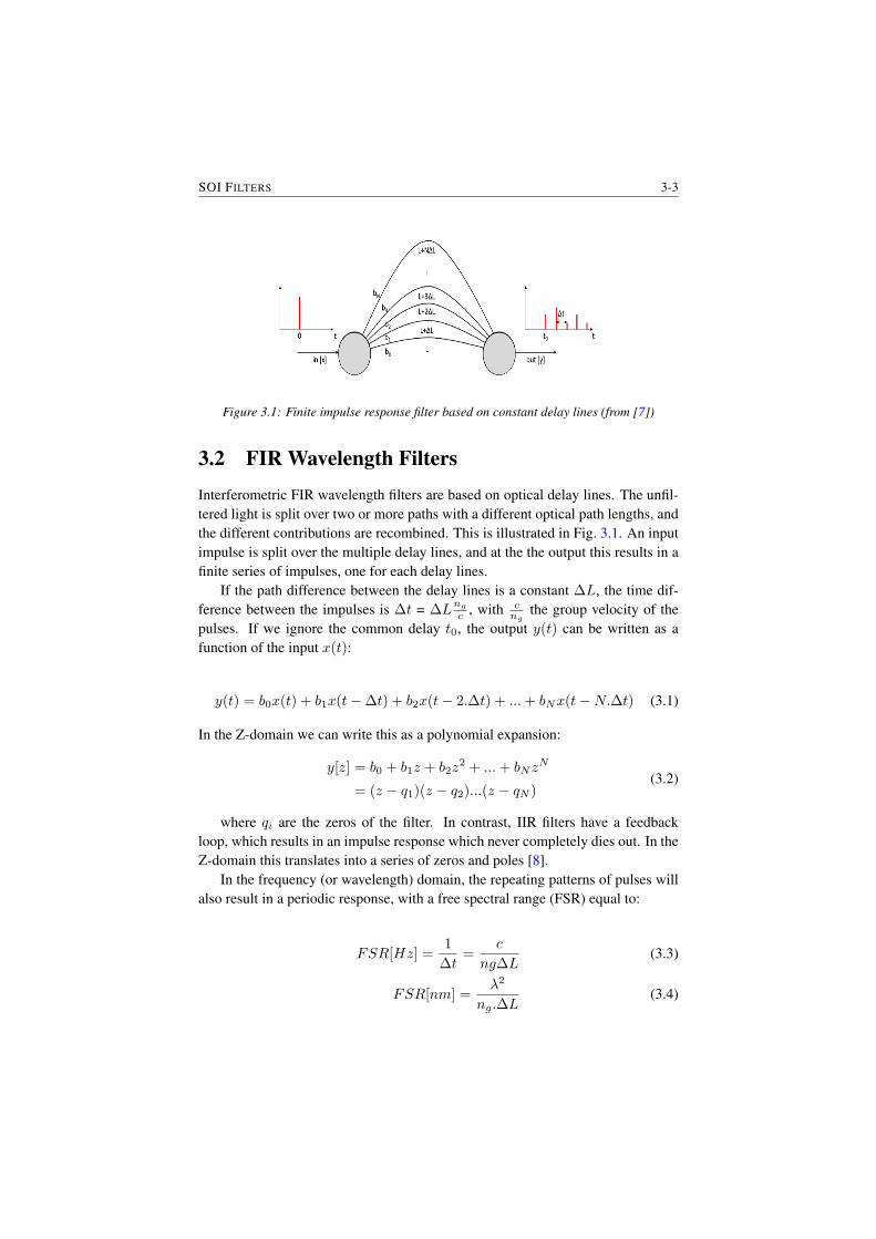
SOI FILTERS 3-3
Figure 3.1: Finite impulse response filter based on constant delay lines (from [7])
3.2 FIR Wavelength Filters
Interferometric FIR wavelength filters are based on optical delay lines. The unfil-tered light is split over two or more paths with a different optical path lengths, andthe different contributions are recombined. This is illustrated in Fig. 3.1. An inputimpulse is split over the multiple delay lines, and at the the output this results in afinite series of impulses, one for each delay lines.
If the path difference between the delay lines is a constant ∆L, the time dif-ference between the impulses is ∆t = ∆L
ng
c , with cng
the group velocity of thepulses. If we ignore the common delay t0, the output y(t) can be written as afunction of the input x(t):
y(t) = b0x(t) + b1x(t−∆t) + b2x(t− 2.∆t) + ...+ bNx(t−N.∆t) (3.1)
In the Z-domain we can write this as a polynomial expansion:
y[z] = b0 + b1z + b2z2 + ...+ bNz
N
= (z − q1)(z − q2)...(z − qN )(3.2)
where qi are the zeros of the filter. In contrast, IIR filters have a feedbackloop, which results in an impulse response which never completely dies out. In theZ-domain this translates into a series of zeros and poles [8].
In the frequency (or wavelength) domain, the repeating patterns of pulses willalso result in a periodic response, with a free spectral range (FSR) equal to:
FSR[Hz] =1
∆t=
c
ng∆L(3.3)
FSR[nm] =λ2
ng.∆L(3.4)
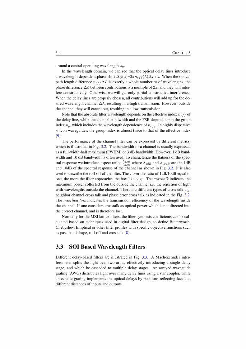
3-4 CHAPTER 3
around a central operating wavelength λ0.In the wavelength domain, we can see that the optical delay lines introduce
a wavelength dependent phase shift ∆φ(λ)=2πneff (λ)∆L/λ. When the opticalpath length difference neff∆L is exactly a whole number m of wavelengths, thephase difference ∆φ between contributions is a multiple of 2π, and they will inter-fere constructively. Otherwise we will get only partial constructive interference.When the delay lines are properly chosen, all contributions will add up for the de-sired wavelength channel ∆λ, resulting in a high transmission. However, outsidethe channel they will cancel out, resulting in a low transmission.
Note that the absolute filter wavelength depends on the effective index neff ofthe delay line, while the channel bandwidth and the FSR depends upon the groupindex ng , which includes the wavelength dependence of neff . In highly dispersivesilicon waveguides, the group index is almost twice to that of the effective index[9].
The performance of the channel filter can be expressed by different metrics,which is illustrated in Fig. 3.2. The bandwidth of a channel is usually expressedas a full-width-half maximum (FWHM) or 3 dB bandwidth. However, 1 dB band-width and 10 dB bandwidth is often used. To characterize the flatness of the spec-tral response we introduce aspect ratio: λ1dB
λ1dBwhere λ1dB and λ10dB are the 1dB
and 10dB of the spectral response of the channel as shown in Fig. 3.2. It is alsoused to describe the roll-off of the filter. The closer the ratio of 1dB/10dB equal toone, the more the filter approaches the box-like edge. The crosstalk indicates themaximum power collected from the outside the channel i.e. the rejection of lightwith wavelengths outside the channel. There are different types of cross talk e.g.neighbor channel cross talk and phase error cross talk as indicated in the Fig. 3.2.The insertion loss indicates the transmission efficiency of the wavelength insidethe channel. If one considers crosstalk as optical power which is not directed intothe correct channel, and is therefore lost.
Normally for the MZI lattice filters, the filter synthesis coefficients can be cal-culated based on techniques used in digital filter design, to define Butterworth,Chebyshev, Elliptical or other filter profiles with specific objective functions suchas pass-band shape, roll-off and crosstalk [8].
3.3 SOI Based Wavelength Filters
Different delay-based filters are illustrated in Fig. 3.3. A Mach-Zehnder inter-ferometer splits the light over two arms, effectively introducing a single delaystage, and which be cascaded to multiple delay stages. An arrayed waveguidegrating (AWG) distributes light over many delay lines using a star coupler, whilean echelle grating implements the optical delays by positions reflecting facets atdifferent distances of inputs and outputs.
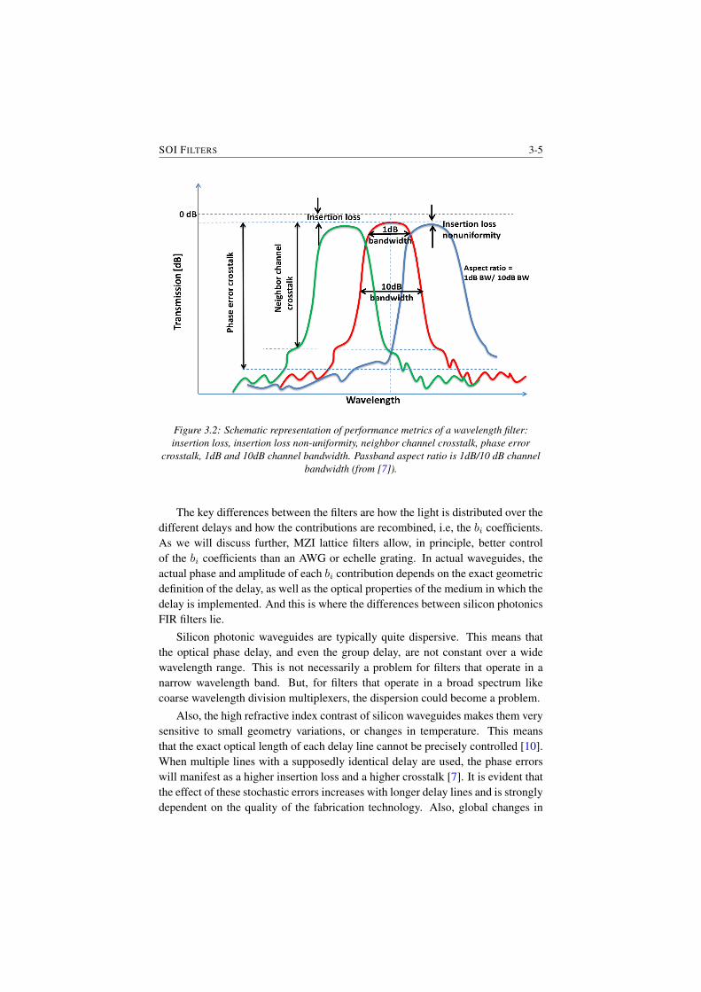
SOI FILTERS 3-5
Figure 3.2: Schematic representation of performance metrics of a wavelength filter:insertion loss, insertion loss non-uniformity, neighbor channel crosstalk, phase error
crosstalk, 1dB and 10dB channel bandwidth. Passband aspect ratio is 1dB/10 dB channelbandwidth (from [7]).
The key differences between the filters are how the light is distributed over thedifferent delays and how the contributions are recombined, i.e, the bi coefficients.As we will discuss further, MZI lattice filters allow, in principle, better controlof the bi coefficients than an AWG or echelle grating. In actual waveguides, theactual phase and amplitude of each bi contribution depends on the exact geometricdefinition of the delay, as well as the optical properties of the medium in which thedelay is implemented. And this is where the differences between silicon photonicsFIR filters lie.
Silicon photonic waveguides are typically quite dispersive. This means thatthe optical phase delay, and even the group delay, are not constant over a widewavelength range. This is not necessarily a problem for filters that operate in anarrow wavelength band. But, for filters that operate in a broad spectrum likecoarse wavelength division multiplexers, the dispersion could become a problem.
Also, the high refractive index contrast of silicon waveguides makes them verysensitive to small geometry variations, or changes in temperature. This meansthat the exact optical length of each delay line cannot be precisely controlled [10].When multiple lines with a supposedly identical delay are used, the phase errorswill manifest as a higher insertion loss and a higher crosstalk [7]. It is evident thatthe effect of these stochastic errors increases with longer delay lines and is stronglydependent on the quality of the fabrication technology. Also, global changes in
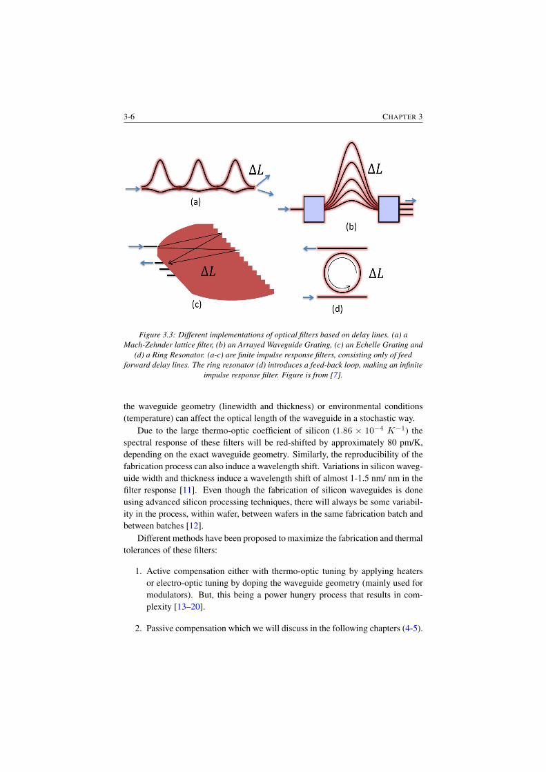
3-6 CHAPTER 3
Figure 3.3: Different implementations of optical filters based on delay lines. (a) aMach-Zehnder lattice filter, (b) an Arrayed Waveguide Grating, (c) an Echelle Grating and
(d) a Ring Resonator. (a-c) are finite impulse response filters, consisting only of feedforward delay lines. The ring resonator (d) introduces a feed-back loop, making an infinite
impulse response filter. Figure is from [7].
the waveguide geometry (linewidth and thickness) or environmental conditions(temperature) can affect the optical length of the waveguide in a stochastic way.
Due to the large thermo-optic coefficient of silicon (1.86 × 10⁻⁴ K−1) thespectral response of these filters will be red-shifted by approximately 80 pm/K,depending on the exact waveguide geometry. Similarly, the reproducibility of thefabrication process can also induce a wavelength shift. Variations in silicon waveg-uide width and thickness induce a wavelength shift of almost 1-1.5 nm/ nm in thefilter response [11]. Even though the fabrication of silicon waveguides is doneusing advanced silicon processing techniques, there will always be some variabil-ity in the process, within wafer, between wafers in the same fabrication batch andbetween batches [12].
Different methods have been proposed to maximize the fabrication and thermaltolerances of these filters:
1. Active compensation either with thermo-optic tuning by applying heatersor electro-optic tuning by doping the waveguide geometry (mainly used formodulators). But, this being a power hungry process that results in com-plexity [13–20].
2. Passive compensation which we will discuss in the following chapters (4-5).
SOI FILTERS 3-7
Figure 3.4: Schematic for a 1 × 4 demultiplexer. (a) Single MZI in each stage and, (b) 4MZIs cascaded in each stage with directional couplers with a power coupling coefficients
to get flat band response.
3. Flattening the channel pass bands. This method is the focus of this chapter.We have implemented four channel de-multiplexer at C-band to demonstratethis concept for different FIR filters.
3.4 MZI Cascaded Filters
3.4.1 Introduction and Design
A simple MZI is a 2 × 2 filter with a single delay path. These single MZIs con-nected in cascaded fashion can work as a demultiplexer or a channel selector. Thedemultiplexer can also be used as a multiplexer since it is a reciprocal device. Fordemultiplexer with M stages, there are 2M outputs. The architecture is referred toas a log2N filter because of its number of stages M = log2N where N is numberof channels [8]. The wavelength selector is similar to the demultiplexer where onlyone output port is used. The transfer function for any input and output port is theproduct of the transfer functions for the individual stages.
The schematic of the M = log2N filter based on 2 stages MZI 4-channeldemultiplexer is shown in Fig. 3.4. As shown in Fig. 3.4(a), the desired filterresponse of each channel is sinusoidal because every stage is single delay line.
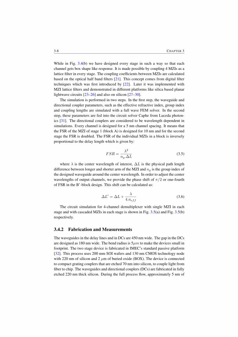
3-8 CHAPTER 3
While in Fig. 3.4(b) we have designed every stage in such a way so that eachchannel gets box shape like response. It is made possible by coupling 4 MZIs as alattice filter in every stage. The coupling coefficients between MZIs are calculatedbased on the optical half band filters [21]. This concept comes from digital filtertechniques which was first introduced by [22]. Later it was implemented withMZI lattice filters and demonstrated in different platforms like silica based planarlightwave circuits [23–26] and also on silicon [27–30].
The simulation is performed in two steps. In the first step, the waveguide anddirectional coupler parameters, such as the effective refractive index, group indexand coupling lengths are simulated with a full wave FEM solver. In the secondstep, these parameters are fed into the circuit solver Caphe from Luceda photon-ics [31]. The directional couplers are considered to be wavelength dependent insimulations. Every channel is designed for a 5 nm channel spacing. It means thatthe FSR of the MZI of stage 1 (block A) is designed for 10 nm and for the secondstage the FSR is doubled. The FSR of the individual MZIs in a block is inverselyproportional to the delay length which is given by:
FSR =λ2
ng.∆L(3.5)
where λ is the center wavelength of interest, ∆L is the physical path lengthdifference between longer and shorter arm of the MZI and ng is the group index ofthe designed waveguide around the center wavelength. In order to adjust the centerwavelengths of output channels, we provide the phase shift of π/2 or one-fourthof FSR in the B’-block design. This shift can be calculated as:
∆L′ = ∆L+λ
4.neff(3.6)
The circuit simulation for 4-channel demultiplexer with single MZI in eachstage and with cascaded MZIs in each stage is shown in Fig. 3.5(a) and Fig. 3.5(b)respectively.
3.4.2 Fabrication and Measurements
The waveguides in the delay lines and in DCs are 450 nm wide. The gap in the DCsare designed as 180 nm wide. The bend radius is 5µm to make the devices small infootprint. The two stage device is fabricated in IMEC’s standard passive platform[32]. This process uses 200 mm SOI wafers and 130 nm CMOS technology nodewith 220 nm of silicon and 2 µm of buried oxide (BOX). The device is connectedto compact grating couplers that are etched 70 nm into silicon, to couple light fromfiber to chip. The waveguides and directional couplers (DCs) are fabricated in fullyetched 220 nm thick silicon. During the full process flow, approximately 5 nm of
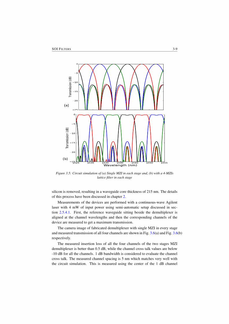
SOI FILTERS 3-9
Figure 3.5: Circuit simulation of (a) Single MZI in each stage and, (b) with a 4-MZIslattice filter in each stage
silicon is removed, resulting in a waveguide core thickness of 215 nm. The detailsof this process have been discussed in chapter 2.
Measurements of the devices are performed with a continuous-wave Agilentlaser with 4 mW of input power using semi-automatic setup discussed in sec-tion 2.5.4.1. First, the reference waveguide sitting beside the demultiplexer isaligned at the channel wavelengths and then the corresponding channels of thedevice are measured to get a maximum transmission.
The camera image of fabricated demultiplexer with single MZI in every stageand measured transmission of all four channels are shown in Fig. 3.6(a) and Fig. 3.6(b)respectively.
The measured insertion loss of all the four channels of the two stages MZIdemultiplexer is better than 0.5 dB, while the channel cross talk values are below-10 dB for all the channels. 1 dB bandwidth is considered to evaluate the channelcross talk. The measured channel spacing is 5 nm which matches very well withthe circuit simulation. This is measured using the center of the 1 dB channel
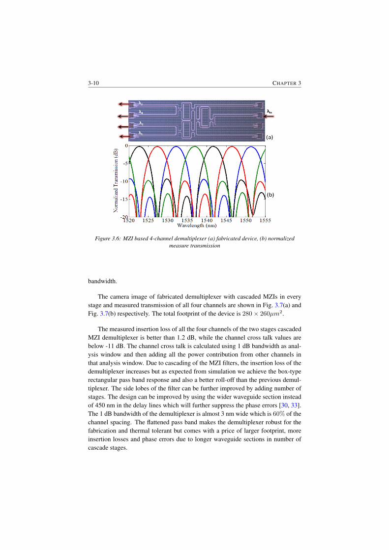
3-10 CHAPTER 3
Figure 3.6: MZI based 4-channel demultiplexer (a) fabricated device, (b) normalizedmeasure transmission
bandwidth.
The camera image of fabricated demultiplexer with cascaded MZIs in everystage and measured transmission of all four channels are shown in Fig. 3.7(a) andFig. 3.7(b) respectively. The total footprint of the device is 280× 260µm2.
The measured insertion loss of all the four channels of the two stages cascadedMZI demultiplexer is better than 1.2 dB, while the channel cross talk values arebelow -11 dB. The channel cross talk is calculated using 1 dB bandwidth as anal-ysis window and then adding all the power contribution from other channels inthat analysis window. Due to cascading of the MZI filters, the insertion loss of thedemultiplexer increases but as expected from simulation we achieve the box-typerectangular pass band response and also a better roll-off than the previous demul-tiplexer. The side lobes of the filter can be further improved by adding number ofstages. The design can be improved by using the wider waveguide section insteadof 450 nm in the delay lines which will further suppress the phase errors [30, 33].The 1 dB bandwidth of the demultiplexer is almost 3 nm wide which is 60% of thechannel spacing. The flattened pass band makes the demultiplexer robust for thefabrication and thermal tolerant but comes with a price of larger footprint, moreinsertion losses and phase errors due to longer waveguide sections in number ofcascade stages.
SOI FILTERS 3-11
Figure 3.7: Cascaded MZI based 4-channel demultiplexer (a) fabricated and, (b)normalized measure transmission
3.5 Arrayed Waveguide Gratings
Arrayed waveguide gratings are another mechanism to implement the interferenceof multiple delay lines. The principle is illustrated in Fig. 3.8(a) Incoming lightis distributed over many lines in a star coupler. The individual contributions arethen recombined in a star coupler. However, the recombination mechanism issignificantly different from MZI cascaded filter. The star couplers function as animaging system. When all the contributions of the delay lines are in phase, thefield profile of the input aperture is imagined in the plane of the output apertures.The quality of this image depends on the number of contributions (delay lines), butit is never perfect. When the wavelength changes, there will be a constant phasedifference between every two arms, and this will tilt the phase front in the outputstar coupler. This, in turn, will shift the image. Therefore, there is a one-to-one
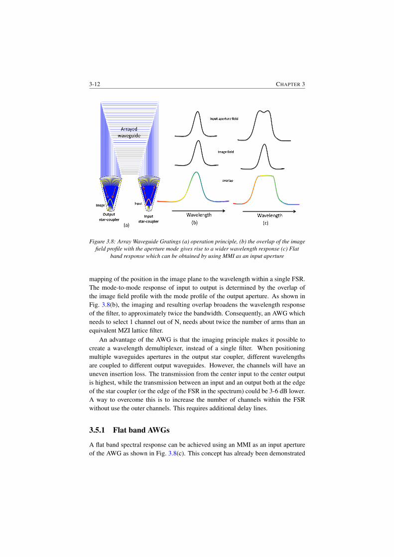
3-12 CHAPTER 3
Figure 3.8: Array Waveguide Gratings (a) operation principle, (b) the overlap of the imagefield profile with the aperture mode gives rise to a wider wavelength response (c) Flat
band response which can be obtained by using MMI as an input aperture
mapping of the position in the image plane to the wavelength within a single FSR.The mode-to-mode response of input to output is determined by the overlap ofthe image field profile with the mode profile of the output aperture. As shown inFig. 3.8(b), the imaging and resulting overlap broadens the wavelength responseof the filter, to approximately twice the bandwidth. Consequently, an AWG whichneeds to select 1 channel out of N, needs about twice the number of arms than anequivalent MZI lattice filter.
An advantage of the AWG is that the imaging principle makes it possible tocreate a wavelength demultiplexer, instead of a single filter. When positioningmultiple waveguides apertures in the output star coupler, different wavelengthsare coupled to different output waveguides. However, the channels will have anuneven insertion loss. The transmission from the center input to the center outputis highest, while the transmission between an input and an output both at the edgeof the star coupler (or the edge of the FSR in the spectrum) could be 3-6 dB lower.A way to overcome this is to increase the number of channels within the FSRwithout use the outer channels. This requires additional delay lines.
3.5.1 Flat band AWGs
A flat band spectral response can be achieved using an MMI as an input apertureof the AWG as shown in Fig. 3.8(c). This concept has already been demonstrated

SOI FILTERS 3-13
Figure 3.9: MMI (a) schematic (from [36]) , (b) simulated field distribution at the end ofMMI of width 5µm for different lengths (c) simulated E-field and (d) intensity field with
length of MMI as 17µm
in different platforms [34, 35] including silicon [33]. In order to get the flattopresponse, the design of MMI is very critical. The primary design parameters are:MMI width, MMI length, taper width, taper length and position. With optimiza-tion of these parameters, we can tailor the input aperture field and obtain a broader,more uniform pass band at the output. The detailed design, simulation and op-timization of these types of devices is explained in the PhD thesis of ShibnathPathak [36].
We have designed four channel flat band AWGs for 800 GHz (6.4 nm) of chan-nel spacing. The input MMI aperture is optimized using Fimmprop from photondesign [37] (can be done in CAMFR as well [38]). The width of the MMI aper-ture is first optimized which is found to be 5µm wide. The length is then sweptto get the desired input aperture field. The schematic of MMI, the simulated fieldand intensity profile, and the field distribution at the end of the MMI for differentlengths are shown in Fig. 3.9.
The optimized length has been obtained by simulation between 16 to 20 µm,the one we have already used in the design i.e. 17 µm.
The simulation of the AWG is performed using IPKISS from Luceda photon-ics [31]. The model is based on the integration of different tools which handle theparts of an AWG. It includes input star coupler, delay lines and output star cou-
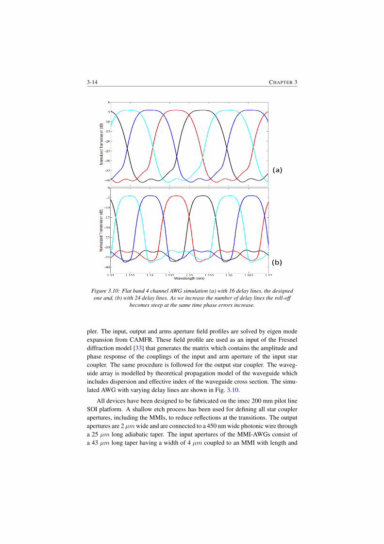
3-14 CHAPTER 3
Figure 3.10: Flat band 4 channel AWG simulation (a) with 16 delay lines, the designedone and, (b) with 24 delay lines. As we increase the number of delay lines the roll-off
becomes steep at the same time phase errors increase.
pler. The input, output and arms aperture field profiles are solved by eigen modeexpansion from CAMFR. These field profile are used as an input of the Fresneldiffraction model [33] that generates the matrix which contains the amplitude andphase response of the couplings of the input and arm aperture of the input starcoupler. The same procedure is followed for the output star coupler. The waveg-uide array is modelled by theoretical propagation model of the waveguide whichincludes dispersion and effective index of the waveguide cross section. The simu-lated AWG with varying delay lines are shown in Fig. 3.10.
All devices have been designed to be fabricated on the imec 200 mm pilot lineSOI platform. A shallow etch process has been used for defining all star couplerapertures, including the MMIs, to reduce reflections at the transitions. The outputapertures are 2 µmwide and are connected to a 450 nm wide photonic wire througha 25 µm long adiabatic taper. The input apertures of the MMI-AWGs consist ofa 43 µm long taper having a width of 4 µm coupled to an MMI with length and
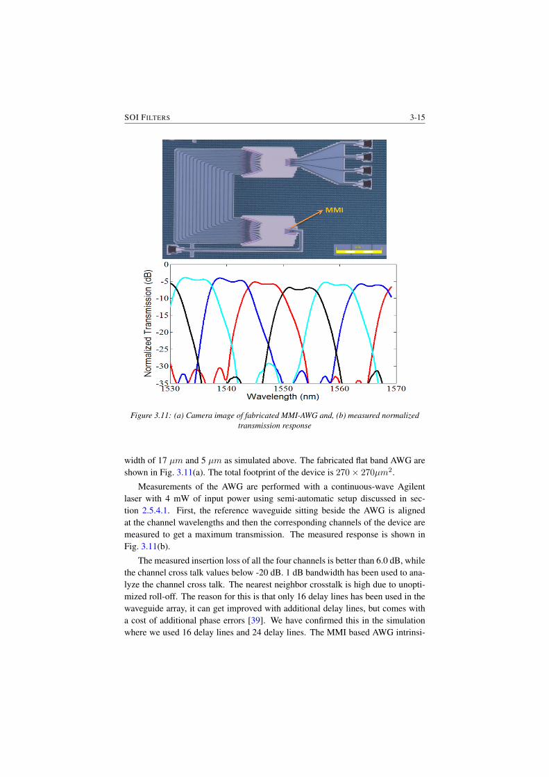
SOI FILTERS 3-15
Figure 3.11: (a) Camera image of fabricated MMI-AWG and, (b) measured normalizedtransmission response
width of 17 µm and 5 µm as simulated above. The fabricated flat band AWG areshown in Fig. 3.11(a). The total footprint of the device is 270× 270µm2.
Measurements of the AWG are performed with a continuous-wave Agilentlaser with 4 mW of input power using semi-automatic setup discussed in sec-tion 2.5.4.1. First, the reference waveguide sitting beside the AWG is alignedat the channel wavelengths and then the corresponding channels of the device aremeasured to get a maximum transmission. The measured response is shown inFig. 3.11(b).
The measured insertion loss of all the four channels is better than 6.0 dB, whilethe channel cross talk values below -20 dB. 1 dB bandwidth has been used to ana-lyze the channel cross talk. The nearest neighbor crosstalk is high due to unopti-mized roll-off. The reason for this is that only 16 delay lines has been used in thewaveguide array, it can get improved with additional delay lines, but comes witha cost of additional phase errors [39]. We have confirmed this in the simulationwhere we used 16 delay lines and 24 delay lines. The MMI based AWG intrinsi-
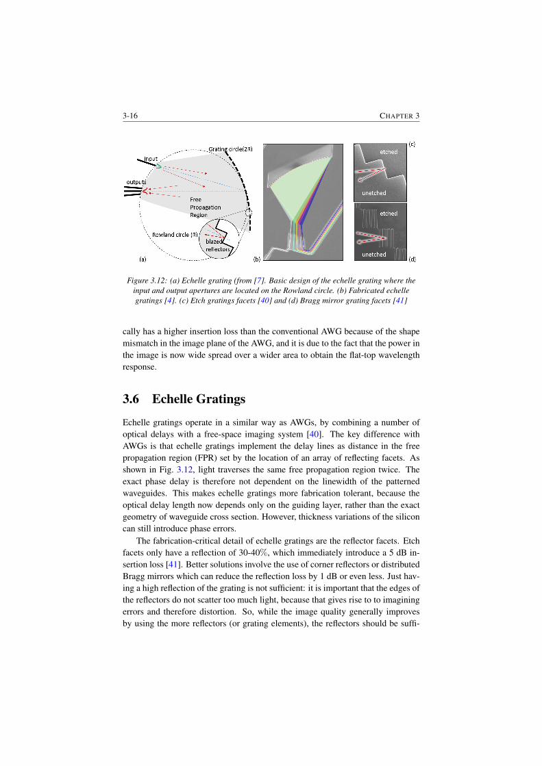
3-16 CHAPTER 3
Figure 3.12: (a) Echelle grating (from [7]. Basic design of the echelle grating where theinput and output apertures are located on the Rowland circle. (b) Fabricated echellegratings [4]. (c) Etch gratings facets [40] and (d) Bragg mirror grating facets [41]
cally has a higher insertion loss than the conventional AWG because of the shapemismatch in the image plane of the AWG, and it is due to the fact that the power inthe image is now wide spread over a wider area to obtain the flat-top wavelengthresponse.
3.6 Echelle Gratings
Echelle gratings operate in a similar way as AWGs, by combining a number ofoptical delays with a free-space imaging system [40]. The key difference withAWGs is that echelle gratings implement the delay lines as distance in the freepropagation region (FPR) set by the location of an array of reflecting facets. Asshown in Fig. 3.12, light traverses the same free propagation region twice. Theexact phase delay is therefore not dependent on the linewidth of the patternedwaveguides. This makes echelle gratings more fabrication tolerant, because theoptical delay length now depends only on the guiding layer, rather than the exactgeometry of waveguide cross section. However, thickness variations of the siliconcan still introduce phase errors.
The fabrication-critical detail of echelle gratings are the reflector facets. Etchfacets only have a reflection of 30-40%, which immediately introduce a 5 dB in-sertion loss [41]. Better solutions involve the use of corner reflectors or distributedBragg mirrors which can reduce the reflection loss by 1 dB or even less. Just hav-ing a high reflection of the grating is not sufficient: it is important that the edges ofthe reflectors do not scatter too much light, because that gives rise to to imaginingerrors and therefore distortion. So, while the image quality generally improvesby using the more reflectors (or grating elements), the reflectors should be suffi-
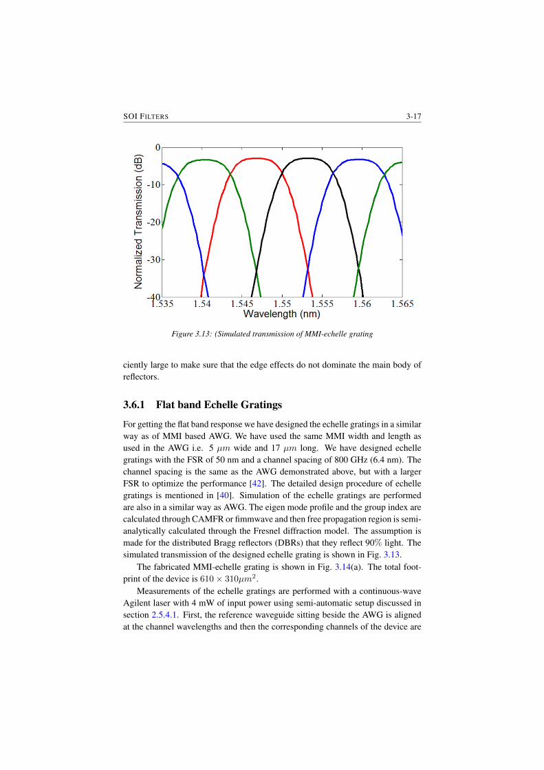
SOI FILTERS 3-17
Figure 3.13: (Simulated transmission of MMI-echelle grating
ciently large to make sure that the edge effects do not dominate the main body ofreflectors.
3.6.1 Flat band Echelle Gratings
For getting the flat band response we have designed the echelle gratings in a similarway as of MMI based AWG. We have used the same MMI width and length asused in the AWG i.e. 5 µm wide and 17 µm long. We have designed echellegratings with the FSR of 50 nm and a channel spacing of 800 GHz (6.4 nm). Thechannel spacing is the same as the AWG demonstrated above, but with a largerFSR to optimize the performance [42]. The detailed design procedure of echellegratings is mentioned in [40]. Simulation of the echelle gratings are performedare also in a similar way as AWG. The eigen mode profile and the group index arecalculated through CAMFR or fimmwave and then free propagation region is semi-analytically calculated through the Fresnel diffraction model. The assumption ismade for the distributed Bragg reflectors (DBRs) that they reflect 90% light. Thesimulated transmission of the designed echelle grating is shown in Fig. 3.13.
The fabricated MMI-echelle grating is shown in Fig. 3.14(a). The total foot-print of the device is 610× 310µm2.
Measurements of the echelle gratings are performed with a continuous-waveAgilent laser with 4 mW of input power using semi-automatic setup discussed insection 2.5.4.1. First, the reference waveguide sitting beside the AWG is alignedat the channel wavelengths and then the corresponding channels of the device are

3-18 CHAPTER 3
Figure 3.14: (a) Camera image of fabricated device MMI - echelle grating and, (b)measured normalized transmission response
measured to get a maximum transmission. The measured response is shown inFig. 3.14(b).
The measured insertion loss of all the four channels is better than 6.0 dB, whilethe channel cross talk values below -20 dB. 1 dB bandwidth window has been usedto analyze the channel cross talk.
3.7 Comparison
We have compared all the three above mentioned devices in terms of insertion loss,channel cross talk, 1 dB/10 dB bandwidth in table 3.1.
We can see that the MZI cascaded filters are most appropriate in terms of inser-tion loss and the roll-off or aspect ratio (1dB/ 10dB ratio) and is due to engineeredpass band. In terms of channel crosstalk AWG and echelle gratings are better.As we have seen from the simulations the roll-off of an AWG can be improvedby adding more delay lines. It certainly improves the nearest neighbor crosstalk.
SOI FILTERS 3-19
Device Insertion loss (dB) Crosstalk (dB) 1dB/10dB Footprint (µm2)Cascaded MZI 1.2 -11 0.9 280×260MMI-AWG 5.0 -20 0.6 270×270MMI-Echelle Gratings 5.2 -21 0.44 610×310
Table 3.1: Flat band four channel demultiplexers
However, at the same time the phase error increase as well. For echelle grat-ings the nearest neighbor crosstalk and phase error crosstalk is quite close. Allthese demonstrations are for four channels coarse wavelength demultiplexers andit changes when number of channel increases or the channel spacing decreases.One such comparison, we can find in [7]. If we compare in this particular analysisabout the footprint, MZI cascaded filters and AWGs are competing.
3.8 Coarse Wavelength Division Multiplexer for theO-band: Need
There are different types of WDM filters depending on the application: Dense-WDM (DWDM) channels are usually spaced between 12.5 GHz to 100 GHz whilein Coarse WDM (CWDM) the channel spacing is 20 nm as proposed by Interna-tional Telecom Union (ITU) [1, 43]. Due to this wide wavelength spacing, thetransmitters deployed in CWDM applications do not require expensive controlmechanism, which is favourable for inexpensive short reach optical interconnects.
Keeping the channel spacing intact over the entire wavelength range of thefilter, is fairly easy in a platform such as silica planar light-wave circuits (PLC),where the glass waveguide cores are several µms across and have a low refrac-tive index contrast and dispersion [25, 26]. But this low contrast also requirescentimeter-scale waveguide components. Due to the high material index contraston the silicon-on-insulator (SOI) platform, it is possible to keep the waveguidecross section in the submicrometer range with waveguide bends that can be shrunkdown to the order of µms. However, this also makes the waveguide propertiesvery dispersive with wavelength. As a result, it is difficult to keep the channelperformance intact over a wide wavelength range, as essential parameters suchas waveguide effective index and coupling strengths of directional couplers (DC)change significantly.
To achieve the key requirement of power efficiency of 1 pJ/bit [44] for shortreach and on-chip optical link in CWDM applications, CWDM (de-)multiplexersneed to have: (1) to keep the channel spacing of 20 nm intact over a wide band-width, (2) to have a low insertion loss and low cross talk, (3) be compact in size,(4) be manufacturable with standard CMOS processes, and (5) robust against fab-rication and environmental thermal fluctuations.
3-20 CHAPTER 3
Channel band flattening in pass bands is possible in the different FIR basedfilters as discussed in the previous section. In filters with an imaging-based starcoupler, such as AWGs and PCGs as demonstrated above, a flat passband usuallyincurs the cost of additional insertion losses [33, 45].
Ring-based IIR filters are not ideally suited for CWDM due to their inherentlynarrow bandwidth [46]. Increasing the overall bandwidth and free spectral rangewould require the use of smaller, lower-quality rings, and these can become verylossy for small bend radii.
There have been various demonstrations of different demultiplexers on SOIdemonstrated for CWDM applications , based on PCGs and AWGs [42, 47, 48]and contra-directional couplers [49] but these either suffer from thermal and fabri-cation tolerance issues or limited by the fabrication technology.
The challenges for silicon based CWDM transceiver is to have a minimumchannel insertion loss, without the use of a thermo-electric cooler (TEC). Thislatter aspect should reduce the cost, enable the use of an uncooled DFB laser array,and reduce the operational power consumption.
Considering all the above discussed parameters, cascaded MZI based de-multiplexersappear to be the best suited option for a passive filter designed for the CWDMwavelength grid. By cascading multiple MZIs using correct coupling coefficients,the pass band can be engineered while keeping the device quite compact. Such anapproach for WDM channels with narrower spacing has been proposed before [30]but here it is extended to a wider wavelength range (with the correspondingly largerdispersion between channels) to meet the ITU-T CWDM grid [1]. Our proposeddesign is a dual stage cascaded MZI de-multiplexing filter with flat band responseand channels centered at ITU grid wavelengths of 1271 nm, 1291 nm, 1311 nm and1331 nm. We have also used the measured results to test the device in a 100 GbEsystem simulation with every channel carrying 28 Gb/s data.
3.9 Design and Simulation
The building block of the demultiplexer (demux) is a set of four cascaded MZIsdesigned to get a maximally flat response for a given FSR. Coupling coefficientcalculations are based on FIR optical half-band filters [21]. The FSR of the indi-vidual MZIs in a building block is inversely proportional to the delay length and isgiven by Eq. 3.5.
The demux is divided into two stages, and each stage consists of two cascadedMZI blocks (schematic in Fig. 3.15). The first block is designed as an interleaver,and splits the odd and even wavelength channels. Outputs are then sent to a secondblock that enhances the suppression of unwanted wavelengths. The first stage iscentered in the O-band (i.e. at 1301 nm), and each MZI at this stage is designedfor an FSR of 40 nm. The second stage is designed in a similar fashion as the first
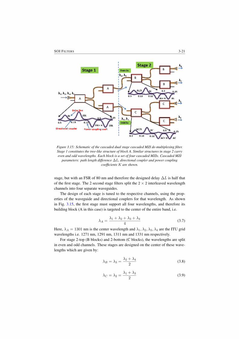
SOI FILTERS 3-21
Figure 3.15: Schematic of the cascaded dual stage cascaded MZI de-multiplexing filter.Stage 1 constitutes the tree-like structure of block A. Similar structures in stage 2 carryeven and odd wavelengths. Each block is a set of four cascaded MZIs. Cascaded MZI
parameters: path length difference ∆L, directional coupler and power couplingcoefficients K are shown.
stage, but with an FSR of 80 nm and therefore the designed delay ∆L is half thatof the first stage. The 2 second stage filters split the 2× 2 interleaved wavelengthchannels into four separate waveguides.
The design of each stage is tuned to the respective channels, using the prop-erties of the waveguide and directional couplers for that wavelength. As shownin Fig. 3.15, the first stage must support all four wavelengths, and therefore itsbuilding block (A in this case) is targeted to the center of the entire band, i.e.
λA =λ1 + λ2 + λ3 + λ4
4(3.7)
Here, λA = 1301 nm is the center wavelength and λ1, λ2, λ3, λ4 are the ITU gridwavelengths i.e. 1271 nm, 1291 nm, 1311 nm and 1331 nm respectively.
For stage 2-top (B blocks) and 2-bottom (C blocks), the wavelengths are splitin even and odd channels. These stages are designed on the center of these wave-lengths which are given by:
λB = λ3 =λ2 + λ4
2(3.8)
λC = λ2 =λ1 + λ3
2(3.9)
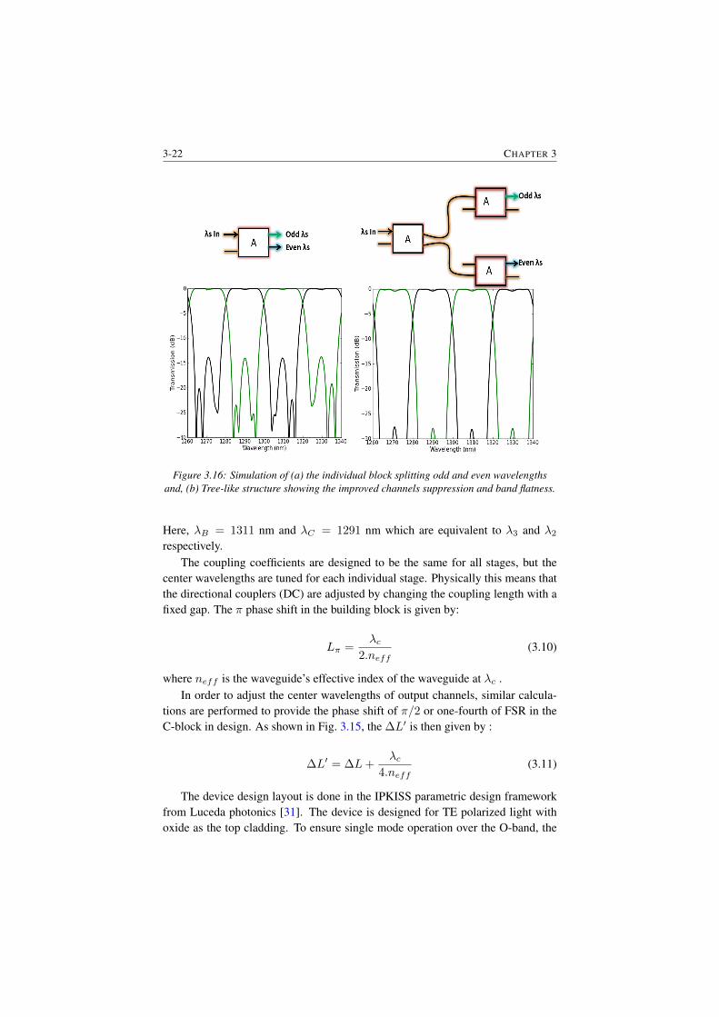
3-22 CHAPTER 3
Figure 3.16: Simulation of (a) the individual block splitting odd and even wavelengthsand, (b) Tree-like structure showing the improved channels suppression and band flatness.
Here, λB = 1311 nm and λC = 1291 nm which are equivalent to λ3 and λ2
respectively.The coupling coefficients are designed to be the same for all stages, but the
center wavelengths are tuned for each individual stage. Physically this means thatthe directional couplers (DC) are adjusted by changing the coupling length with afixed gap. The π phase shift in the building block is given by:
Lπ =λc
2.neff(3.10)
where neff is the waveguide’s effective index of the waveguide at λc .In order to adjust the center wavelengths of output channels, similar calcula-
tions are performed to provide the phase shift of π/2 or one-fourth of FSR in theC-block in design. As shown in Fig. 3.15, the ∆L′ is then given by :
∆L′ = ∆L+λc
4.neff(3.11)
The device design layout is done in the IPKISS parametric design frameworkfrom Luceda photonics [31]. The device is designed for TE polarized light withoxide as the top cladding. To ensure single mode operation over the O-band, the
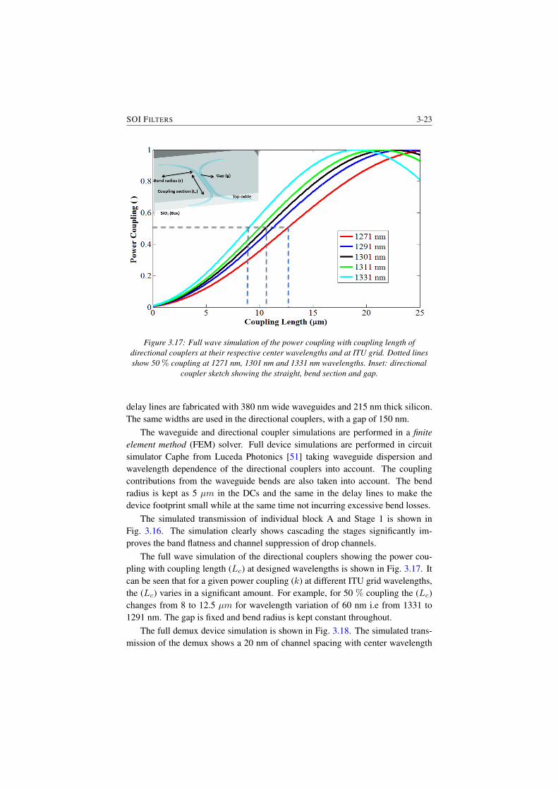
SOI FILTERS 3-23
Figure 3.17: Full wave simulation of the power coupling with coupling length ofdirectional couplers at their respective center wavelengths and at ITU grid. Dotted linesshow 50 % coupling at 1271 nm, 1301 nm and 1331 nm wavelengths. Inset: directional
coupler sketch showing the straight, bend section and gap.
delay lines are fabricated with 380 nm wide waveguides and 215 nm thick silicon.The same widths are used in the directional couplers, with a gap of 150 nm.
The waveguide and directional coupler simulations are performed in a finiteelement method (FEM) solver. Full device simulations are performed in circuitsimulator Caphe from Luceda Photonics [51] taking waveguide dispersion andwavelength dependence of the directional couplers into account. The couplingcontributions from the waveguide bends are also taken into account. The bendradius is kept as 5 µm in the DCs and the same in the delay lines to make thedevice footprint small while at the same time not incurring excessive bend losses.
The simulated transmission of individual block A and Stage 1 is shown inFig. 3.16. The simulation clearly shows cascading the stages significantly im-proves the band flatness and channel suppression of drop channels.
The full wave simulation of the directional couplers showing the power cou-pling with coupling length (Lc) at designed wavelengths is shown in Fig. 3.17. Itcan be seen that for a given power coupling (k) at different ITU grid wavelengths,the (Lc) varies in a significant amount. For example, for 50 % coupling the (Lc)changes from 8 to 12.5 µm for wavelength variation of 60 nm i.e from 1331 to1291 nm. The gap is fixed and bend radius is kept constant throughout.
The full demux device simulation is shown in Fig. 3.18. The simulated trans-mission of the demux shows a 20 nm of channel spacing with center wavelength

3-24 CHAPTER 3
Figure 3.18: Simulated transmission of the demux filter showing the channel width andguard band according to [50].
at 1301 nm. The simulated cross-talk is around -25 dB and the insertion loss isaround 1 dB. The pass band channel width and guard band are 13 nm and 7 nmrespectively which matches with specifications of the ITU [50].
3.10 FabricationThe fabrication of the device is briefly discussed in section 3.4.2. The details ofthis process have been discussed in chapter 2. The grating coupler uses the same70 nm etch process but the periods are set in such a way as the efficiency of thecoupling of light to the chip is maximum at the O-band.
The camera image of fabricated single block, demultiplexer and the SEM im-age of one of DCs are shown in Fig. 3.19. The length of the DCs for 50 % ofpower coupling at 1301 nm is around 10.3 µm. The total footprint of the device is550× 650µm2. This can be further reduced by folding the stages.
3.11 Measurements and Analysis
3.11.1 Device measurements
The transmission measurements of the device are performed with a continuous-wave O-band tunable laser. First, the reference waveguide sitting beside the de-mux filter is aligned at ITU grid wavelengths and then the corresponding channels
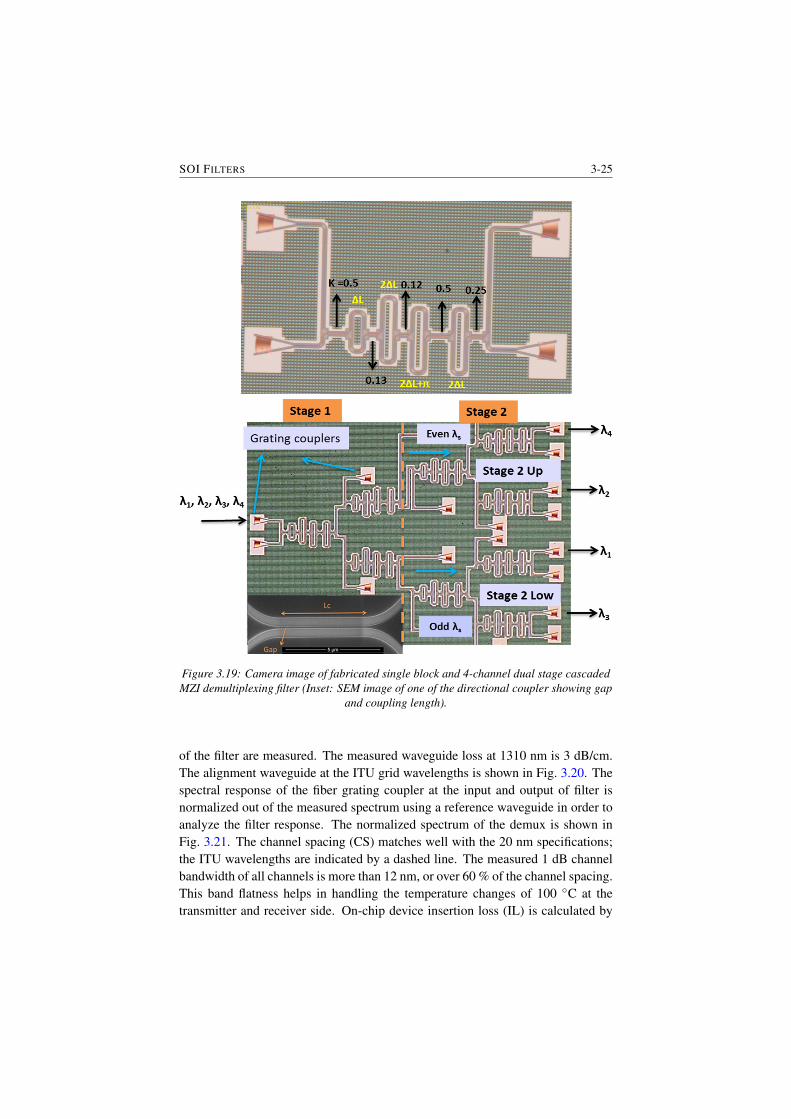
SOI FILTERS 3-25
Figure 3.19: Camera image of fabricated single block and 4-channel dual stage cascadedMZI demultiplexing filter (Inset: SEM image of one of the directional coupler showing gap
and coupling length).
of the filter are measured. The measured waveguide loss at 1310 nm is 3 dB/cm.The alignment waveguide at the ITU grid wavelengths is shown in Fig. 3.20. Thespectral response of the fiber grating coupler at the input and output of filter isnormalized out of the measured spectrum using a reference waveguide in order toanalyze the filter response. The normalized spectrum of the demux is shown inFig. 3.21. The channel spacing (CS) matches well with the 20 nm specifications;the ITU wavelengths are indicated by a dashed line. The measured 1 dB channelbandwidth of all channels is more than 12 nm, or over 60 % of the channel spacing.This band flatness helps in handling the temperature changes of 100 ◦C at thetransmitter and receiver side. On-chip device insertion loss (IL) is calculated by
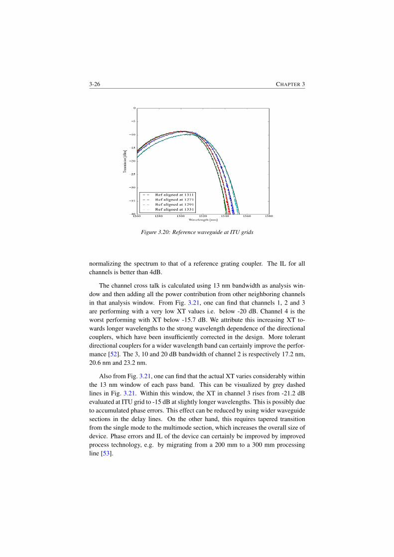
3-26 CHAPTER 3
Figure 3.20: Reference waveguide at ITU grids
normalizing the spectrum to that of a reference grating coupler. The IL for allchannels is better than 4dB.
The channel cross talk is calculated using 13 nm bandwidth as analysis win-dow and then adding all the power contribution from other neighboring channelsin that analysis window. From Fig. 3.21, one can find that channels 1, 2 and 3are performing with a very low XT values i.e. below -20 dB. Channel 4 is theworst performing with XT below -15.7 dB. We attribute this increasing XT to-wards longer wavelengths to the strong wavelength dependence of the directionalcouplers, which have been insufficiently corrected in the design. More tolerantdirectional couplers for a wider wavelength band can certainly improve the perfor-mance [52]. The 3, 10 and 20 dB bandwidth of channel 2 is respectively 17.2 nm,20.6 nm and 23.2 nm.
Also from Fig. 3.21, one can find that the actual XT varies considerably withinthe 13 nm window of each pass band. This can be visualized by grey dashedlines in Fig. 3.21. Within this window, the XT in channel 3 rises from -21.2 dBevaluated at ITU grid to -15 dB at slightly longer wavelengths. This is possibly dueto accumulated phase errors. This effect can be reduced by using wider waveguidesections in the delay lines. On the other hand, this requires tapered transitionfrom the single mode to the multimode section, which increases the overall size ofdevice. Phase errors and IL of the device can certainly be improved by improvedprocess technology, e.g. by migrating from a 200 mm to a 300 mm processingline [53].
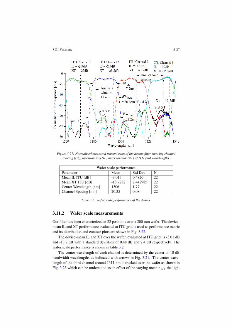
SOI FILTERS 3-27
Figure 3.21: Normalized measured transmission of the demux filter showing channelspacing (CS), insertion loss (IL) and crosstalk (XT) at ITU grid wavelengths.
Wafer scale performanceParameter Mean Std Dev NMean IL ITU [dB] -3.015 0.4820 22Mean XT ITU [dB] -18.7282 2.442985 22Center Wavelength [nm] 1306 1.77 22Channel Spacing [nm] 20.35 0.08 22
Table 3.2: Wafer scale performance of the demux.
3.11.2 Wafer scale measurements
Our filter has been characterized at 22 positions over a 200 mm wafer. The device-mean IL and XT performance evaluated at ITU grid is used as performance metricand its distribution and contour plots are shown in Fig. 3.22.
The device-mean IL and XT over the wafer, evaluated at ITU grid, is -3.01 dBand -18.7 dB with a standard deviation of 0.48 dB and 2.4 dB respectively. Thewafer scale performance is shown in table 3.2.
The center wavelength of each channel is determined by the center of 10 dBbandwidth wavelengths as indicated with arrows in Fig. 3.21. The center wave-length of the third channel around 1311 nm is tracked over the wafer as shown inFig. 3.23 which can be understood as an effect of the varying mean neff the light
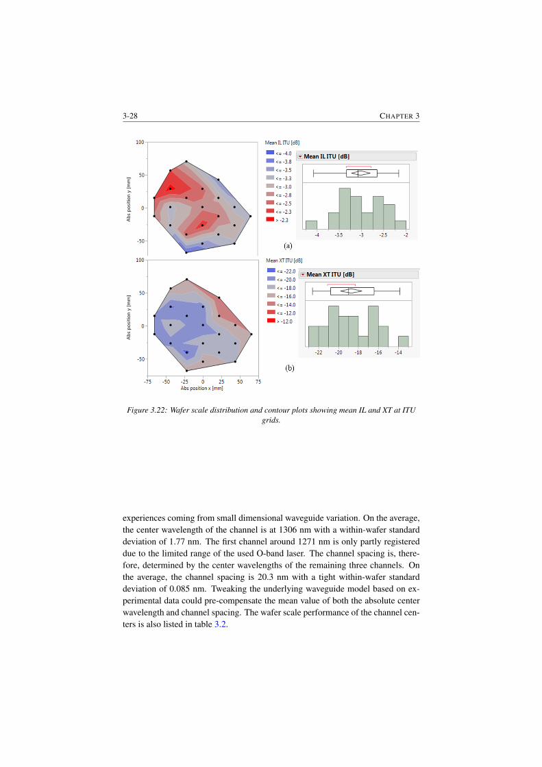
3-28 CHAPTER 3
Figure 3.22: Wafer scale distribution and contour plots showing mean IL and XT at ITUgrids.
experiences coming from small dimensional waveguide variation. On the average,the center wavelength of the channel is at 1306 nm with a within-wafer standarddeviation of 1.77 nm. The first channel around 1271 nm is only partly registereddue to the limited range of the used O-band laser. The channel spacing is, there-fore, determined by the center wavelengths of the remaining three channels. Onthe average, the channel spacing is 20.3 nm with a tight within-wafer standarddeviation of 0.085 nm. Tweaking the underlying waveguide model based on ex-perimental data could pre-compensate the mean value of both the absolute centerwavelength and channel spacing. The wafer scale performance of the channel cen-ters is also listed in table 3.2.
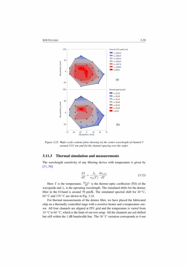
SOI FILTERS 3-29
Figure 3.23: Wafer scale contour plots showing (a) the center wavelength of channel 3around 1311 nm and (b) the channel spacing over the wafer.
3.11.3 Thermal simulation and measurements
The wavelength sensitivity of any filtering device with temperature is given by[11, 54]:
dλ
dT=
λcng(T )
dneffdT
(3.12)
Here T is the temperature, dneff
dT is the thermo-optic coefficient (TO) of thewaveguide and λc is the operating wavelength. The simulated shifts for the demuxfilter in the O-band is around 70 pm/K. The simulated spectral shift for 20 ◦C,60 ◦C and 170 ◦C are shown in Fig. 3.24.
For thermal measurements of the demux filter, we have placed the fabricatedchip on a thermally controlled stage with a resistive heater and a temperature sen-sor. All four channels are aligned at ITU grid and the temperature is varied from10 ◦C to 60 ◦C, which is the limit of our test setup. All the channels are red shiftedbut still within the 1 dB bandwidth line. The 50 ◦C variation corresponds to 4 nm
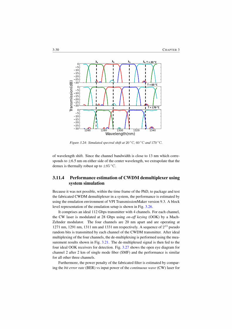
3-30 CHAPTER 3
Figure 3.24: Simulated spectral shift at 20 ◦C, 60 ◦C and 170 ◦C.
of wavelength shift. Since the channel bandwidth is close to 13 nm which corre-sponds to ±6.5 nm on either side of the center wavelength, we extrapolate that thedemux is thermally robust up to ±85 ◦C.
3.11.4 Performance estimation of CWDM demultiplexer usingsystem simulation
Because it was not possible, within the time frame of the PhD, to package and testthe fabricated CWDM demultiplexer in a system, the performance is estimated byusing the emulation environment of VPI TransmissionMaker version 9.3. A blocklevel representation of the emulation setup is shown in Fig. 3.26.
It comprises an ideal 112 Gbps transmitter with 4 channels. For each channel,the CW laser is modulated at 28 Gbps using on-off keying (OOK) by a Mach-Zehnder modulator. The four channels are 20 nm apart and are operating at1271 nm, 1291 nm, 1311 nm and 1331 nm respectively. A sequence of 213 pseudorandom bits is transmitted by each channel of the CWDM transmitter. After idealmultiplexing of the four channels, the de-multiplexing is performed using the mea-surement results shown in Fig. 3.21. The de-multiplexed signal is then fed to thefour ideal OOK receivers for detection. Fig. 3.27 shows the open eye diagram forchannel 2 after 2 km of single mode fiber (SMF) and the performance is similarfor all other three channels.
Furthermore, the power penalty of the fabricated filter is estimated by compar-ing the bit error rate (BER) vs input power of the continuous wave (CW) laser for
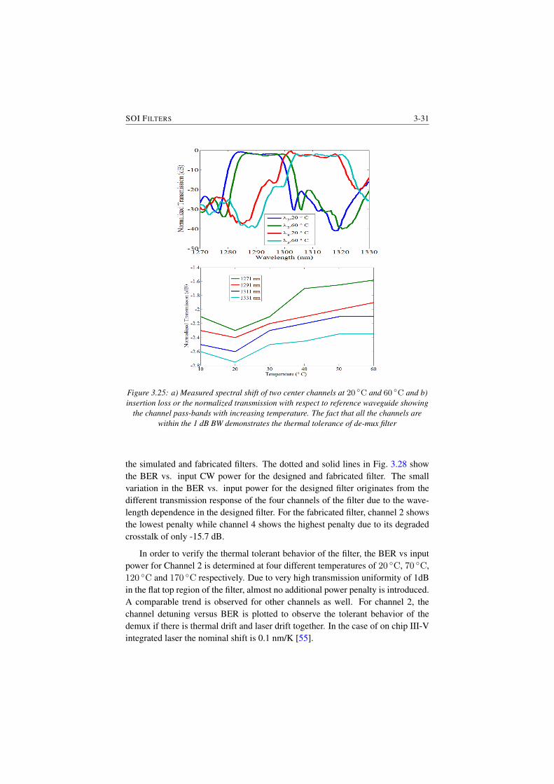
SOI FILTERS 3-31
Figure 3.25: a) Measured spectral shift of two center channels at 20 ◦C and 60 ◦C and b)insertion loss or the normalized transmission with respect to reference waveguide showing
the channel pass-bands with increasing temperature. The fact that all the channels arewithin the 1 dB BW demonstrates the thermal tolerance of de-mux filter
the simulated and fabricated filters. The dotted and solid lines in Fig. 3.28 showthe BER vs. input CW power for the designed and fabricated filter. The smallvariation in the BER vs. input power for the designed filter originates from thedifferent transmission response of the four channels of the filter due to the wave-length dependence in the designed filter. For the fabricated filter, channel 2 showsthe lowest penalty while channel 4 shows the highest penalty due to its degradedcrosstalk of only -15.7 dB.
In order to verify the thermal tolerant behavior of the filter, the BER vs inputpower for Channel 2 is determined at four different temperatures of 20 ◦C, 70 ◦C,120 ◦C and 170 ◦C respectively. Due to very high transmission uniformity of 1dBin the flat top region of the filter, almost no additional power penalty is introduced.A comparable trend is observed for other channels as well. For channel 2, thechannel detuning versus BER is plotted to observe the tolerant behavior of thedemux if there is thermal drift and laser drift together. In the case of on chip III-Vintegrated laser the nominal shift is 0.1 nm/K [55].
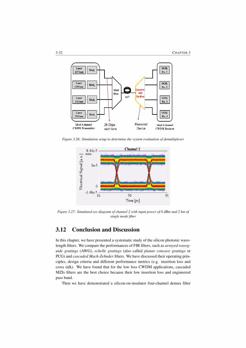
3-32 CHAPTER 3
Figure 3.26: Simulation setup to determine the system evaluation of demultiplexer
Figure 3.27: Simulated eye diagram of channel 2 with input power of 0 dBm and 2 km ofsingle mode fiber
3.12 Conclusion and Discussion
In this chapter, we have presented a systematic study of the silicon photonic wave-length filters. We compare the performances of FIR filters, such as arrayed waveg-uide gratings (AWG), echelle gratings (also called planar concave gratings orPCG) and cascaded Mach-Zehnder filters. We have discussed their operating prin-ciples, design criteria and different performance metrics (e.g. insertion loss andcross talk). We have found that for the low loss CWDM applications, cascadedMZIs filters are the best choice because their low insertion loss and engineeredpass band.
Then we have demonstrated a silicon-on-insulator four-channel demux filter
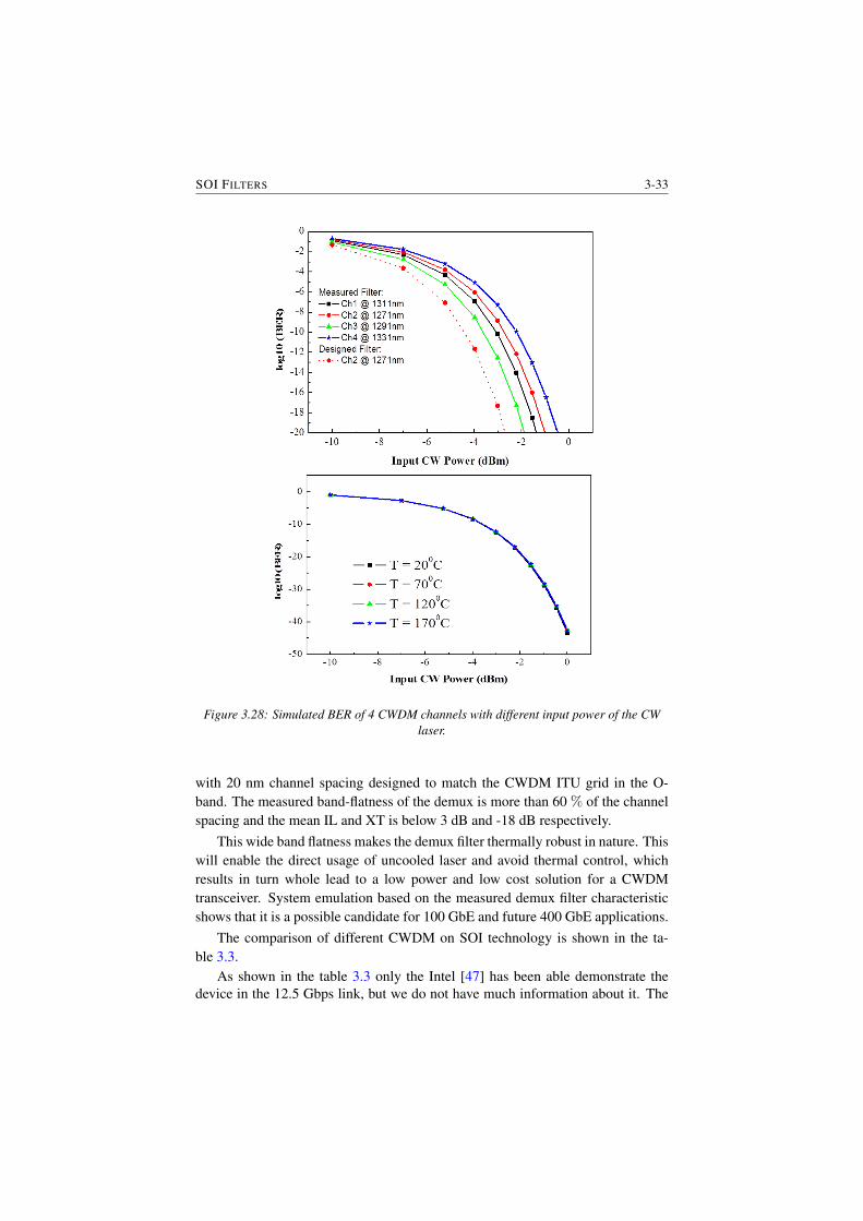
SOI FILTERS 3-33
Figure 3.28: Simulated BER of 4 CWDM channels with different input power of the CWlaser.
with 20 nm channel spacing designed to match the CWDM ITU grid in the O-band. The measured band-flatness of the demux is more than 60 % of the channelspacing and the mean IL and XT is below 3 dB and -18 dB respectively.
This wide band flatness makes the demux filter thermally robust in nature. Thiswill enable the direct usage of uncooled laser and avoid thermal control, whichresults in turn whole lead to a low power and low cost solution for a CWDMtransceiver. System emulation based on the measured demux filter characteristicshows that it is a possible candidate for 100 GbE and future 400 GbE applications.
The comparison of different CWDM on SOI technology is shown in the ta-ble 3.3.
As shown in the table 3.3 only the Intel [47] has been able demonstrate thedevice in the 12.5 Gbps link, but we do not have much information about it. The
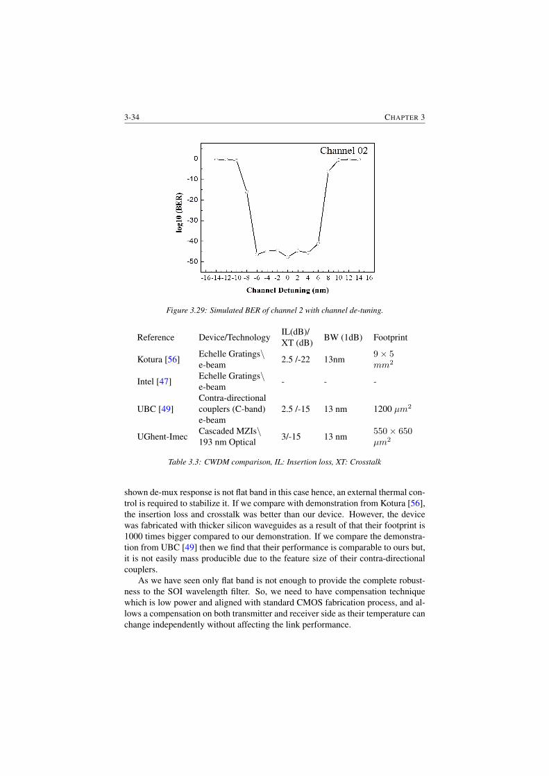
3-34 CHAPTER 3
Figure 3.29: Simulated BER of channel 2 with channel de-tuning.
Reference Device/TechnologyIL(dB)/XT (dB) BW (1dB) Footprint
Kotura [56]Echelle Gratings\e-beam 2.5 /-22 13nm
9× 5mm2
Intel [47]Echelle Gratings\e-beam - - -
UBC [49]Contra-directionalcouplers (C-band)e-beam
2.5 /-15 13 nm 1200 µm2
UGhent-ImecCascaded MZIs\193 nm Optical 3/-15 13 nm
550× 650µm2
Table 3.3: CWDM comparison, IL: Insertion loss, XT: Crosstalk
shown de-mux response is not flat band in this case hence, an external thermal con-trol is required to stabilize it. If we compare with demonstration from Kotura [56],the insertion loss and crosstalk was better than our device. However, the devicewas fabricated with thicker silicon waveguides as a result of that their footprint is1000 times bigger compared to our demonstration. If we compare the demonstra-tion from UBC [49] then we find that their performance is comparable to ours but,it is not easily mass producible due to the feature size of their contra-directionalcouplers.
As we have seen only flat band is not enough to provide the complete robust-ness to the SOI wavelength filter. So, we need to have compensation techniquewhich is low power and aligned with standard CMOS fabrication process, and al-lows a compensation on both transmitter and receiver side as their temperature canchange independently without affecting the link performance.
SOI FILTERS 3-35
References[1] G.695: Optical interfaces for coarse wavelength division multi-
plexing applications . https://www.itu.int/rec/T-REC-G.695-201501-I/. [Online].
[2] D.A.B. Miller. Device Requirements for Optical Interconnects to SiliconChips. Proceedings of the IEEE, 97(7):1166–1185, July 2009.
[3] Y.A. Vlasov. Silicon CMOS-integrated nano-photonics for computer anddata communications beyond 100G. Communications Magazine, IEEE,50(2):s67–s72, February 2012.
[4] W. Bogaerts, S.K. Selvaraja, P. Dumon, J. Brouckaert, K. De Vos,D. Van Thourhout, and R Baets. Silicon-on-Insulator Spectral Filters Fab-ricated With CMOS Technology. Selected Topics in Quantum Electronics,IEEE Journal of, 16(1):33–44, Jan 2010.
[5] K. Okamoto. Wavelength-Division-Multiplexing Devices in Thin SOI: Ad-vances and Prospects. Selected Topics in Quantum Electronics, IEEE Jour-nal of, 20(4):248–257, July 2014.
[6] W. Bogaerts, P. De Heyn, T. Van Vaerenbergh, K. De Vos, S. Kumar Sel-varaja, T. Claes, P. Dumon, P. Bienstman, D. Van Thourhout, and R. Baets.Silicon microring resonators. Laser Photonics Reviews, 6(1):47–73, 2012.
[7] Wim Bogaerts, Shibnath Pathak, Alfonso Ruocco, and Sarvagya Dwivedi.Silicon photonics non-resonant wavelength filters: comparison betweenAWGs, echelle gratings, and cascaded Mach-Zehnder filters. volume 9365,pages 93650H–93650H–12. SPIE, April 2015.
[8] Christi K. Madsen and Jian H. Zhao. Optical Filter Design and Analysis,pages 1–17. John Wiley Sons, Inc., 2001.
[9] Eric Dulkeith, Fengnian Xia, Laurent Schares, William M. J. Green, andYurii A. Vlasov. Group index and group velocity dispersion in silicon-on-insulator photonic wires. Opt. Express, 14(9):3853–3863, May 2006.
[10] T. Goh, S. Suzuki, and A. Sugita. Estimation of waveguide phase error insilica-based waveguides. Lightwave Technology, Journal of, 15(11):2107–2113, Nov 1997.
[11] S. Dwivedi, H. D’heer, and W. Bogaerts. Maximizing Fabrication and Ther-mal Tolerances of All-Silicon FIR Wavelength Filters. Photonics TechnologyLetters, IEEE, 27(8):871–874, April 2015.
[12] S.K. Selvaraja, W. Bogaerts, P. Dumon, D. Van Thourhout, and R. Baets.Subnanometer Linewidth Uniformity in Silicon Nanophotonic Waveguide De-vices Using CMOS Fabrication Technology. Selected Topics in QuantumElectronics, IEEE Journal of, 16(1):316–324, Jan 2010.
3-36 CHAPTER 3
[13] F. Gan, T. Barwicz, M.A. Popovic, M.S. Dahlem, C.W. Holzwarth, P.T. Ra-kich, H.I. Smith, E.P. Ippen, and F.X. Kartner. Maximizing the Thermo-OpticTuning Range of Silicon Photonic Structures. In Photonics in Switching,2007, pages 67–68, Aug 2007.
[14] Joris Van Campenhout, William M. J. Green, Solomon Assefa, and Yurii A.Vlasov. Integrated NiSi waveguide heaters for CMOS-compatible siliconthermo-optic devices. Opt. Lett., 35(7):1013–1015, Apr 2010.
[15] Po Dong, Wei Qian, Hong Liang, Roshanak Shafiiha, Dazeng Feng, Guo-liang Li, John E. Cunningham, Ashok V. Krishnamoorthy, and Mehdi As-ghari. Thermally tunable silicon racetrack resonators with ultralow tuningpower. Opt. Express, 18(19):20298–20304, Sep 2010.
[16] A. Masood, M. Pantouvaki, G. Lepage, P. Verheyen, J. Van Campenhout,P. Absil, D. Van Thourhout, and W. Bogaerts. Comparison of heater archi-tectures for thermal control of silicon photonic circuits. In Group IV Photon-ics (GFP), 2013 IEEE 10th International Conference on, pages 83–84, Aug2013.
[17] Qianfan Xu, Sasikanth Manipatruni, Brad Schmidt, Jagat Shakya, andMichal Lipson. 12.5 Gbit/s carrier-injection-based silicon micro-ring sili-con modulators. Opt. Express, 15(2):430–436, Jan 2007.
[18] F. Y. Gardes, D. J. Thomson, N. G. Emerson, and G. T. Reed. 40 Gb/ssilicon photonics modulator for TE and TM polarisations. Opt. Express,19(12):11804–11814, Jun 2011.
[19] L. Alloatti, D. Korn, R. Palmer, D. Hillerkuss, J. Li, A. Barklund, R. Dinu,J. Wieland, M. Fournier, J. Fedeli, H. Yu, W. Bogaerts, P. Dumon, R. Baets,C. Koos, W. Freude, and J. Leuthold. 42.7 Gbit/s electro-optic modulator insilicon technology. Opt. Express, 19(12):11841–11851, Jun 2011.
[20] Hui Yu, M. Pantouvaki, S. Dwivedi, P. Verheyen, G. Lepage, R. Baets,W. Bogaerts, P. Absil, and J. Van Campenhout. Compact Thermally TunableSilicon Racetrack Modulators Based on an Asymmetric Waveguide. Photon-ics Technology Letters, IEEE, 25(2):159–162, Jan 2013.
[21] K. Jinguji and Manabu Oguma. Optical half-band filters. Lightwave Tech-nology, Journal of, 18(2):252–259, Feb 2000.
[22] J.H. McClellan, T.W. Parks, and L. Rabiner. A computer program for design-ing optimum FIR linear phase digital filters. Audio and Electroacoustics,IEEE Transactions on, 21(6):506–526, Dec 1973.
[23] M. Kawachi. Recent progress in silica-based planar lightwave circuits onsilicon. Optoelectronics, IEE Proceedings -, 143(5):257–262, Oct 1996.
SOI FILTERS 3-37
[24] A. Kaneko, T. Goh, H. Yamada, T. Tanaka, and I. Ogawa. Design and appli-cations of silica-based planar lightwave circuits. Selected Topics in QuantumElectronics, IEEE Journal of, 5(5):1227–1236, Sep 1999.
[25] Qian Wang and Sailing He. Optimal design of planar wavelength circuitsbased on Mach-Zehnder Interferometers and their cascaded forms. Light-wave Technology, Journal of, 23(3):1284–1290, March 2005.
[26] T. Mizuno, M. Oguma, T. Kitoh, Y. Inoue, and H. Takahashi. Lattice-formCWDM interleave filter using silica-based planar lightwave circuit. Photon-ics Technology Letters, IEEE, 18(15):1570–1572, Aug 2006.
[27] Koji Yamada, Tetsufumi Shoji, Tai Tsuchizawa, Toshifumi Watanabe, Junichi Takahashi, and Sei ichi Itabashi. Silicon-wire-based ultrasmall latticefilters with wide free spectral ranges. Opt. Lett., 28(18):1663–1664, Sep2003.
[28] Pieter Dumon, Gino Priem, Luis Romeu Nunes, Wim Bogaerts, Dries VanThourhout, Peter Bienstman, Tak Keung Liang, Masahiro Tsuchiya, PatrickJaenen, Stephan Beckx, Johan Wouters, and Roel Baets. Linear and Nonlin-ear Nanophotonic Devices Based on Silicon-on-Insulator Wire Waveguides.Japanese Journal of Applied Physics, 45(8S):6589, 2006.
[29] S.S. Djordjevic, L.W. Luo, S. Ibrahim, N.K. Fontaine, C.B. Poitras, BinbinGuan, L. Zhou, K. Okamoto, Zhi Ding, M. Lipson, and S.J.B. Yoo. Fully Re-configurable Silicon Photonic Lattice Filters With Four Cascaded Unit Cells.Photonics Technology Letters, IEEE, 23(1):42–44, Jan 2011.
[30] Folkert Horst, William M.J. Green, Solomon Assefa, Steven M. Shank,Yurii A. Vlasov, and Bert Jan Offrein. Cascaded Mach-Zehnder wave-length filters in silicon photonics for low loss and flat pass-band WDM (de-)multiplexing. Opt. Express, 21(10):11652–11658, May 2013.
[31] http://www.lucedaphotonics.com/.
[32] Philippe P. Absil, Peter Verheyen, Peter De Heyn, Marianna Pantouvaki, GuyLepage, Jeroen De Coster, and Joris Van Campenhout. Silicon photonicsintegrated circuits: a manufacturing platform for high density, low poweroptical I/O’s. Opt. Express, 23(7):9369–9378, Apr 2015.
[33] S. Pathak, M. Vanslembrouck, P. Dumon, D. Van Thourhout, and W. Bo-gaerts. Optimized Silicon AWG With Flattened Spectral Response Using anMMI Aperture. Lightwave Technology, Journal of, 31(1):87–93, Jan 2013.
[34] J.B.D. Soole, M.R. Amersfoort, H.P. Leblanc, N.C. Andreadakis, A. Ra-jhel, C. Caneau, R. Bhat, M.A. Koza, C. Youtsey, and I. Adesida. Use ofmultimode interference couplers to broaden the passband of wavelength-dispersive integrated WDM filters. Photonics Technology Letters, IEEE,8(10):1340–1342, Oct 1996.
3-38 CHAPTER 3
[35] Daoxin Dai, Weiquan Mei, and Sailing He. Using a tapered {MMI} to flattenthe passband of an {AWG}. Optics Communications, 219(16):233 – 239,2003.
[36] Shibnath Pathak. Silicon Nano-Photonics Based Arrayed Waveguide Grat-ings, PhD thesis, Ghent University, 2014.
[37] http://www.photond.com/.
[38] urlhttp://camfr.sourceforge.net/.
[39] M.K. Smit and C. Van Dam. PHASAR-based WDM-devices: Principles, de-sign and applications. Selected Topics in Quantum Electronics, IEEE Journalof, 2(2):236–250, Jun 1996.
[40] J. Brouckaert, W. Bogaerts, P. Dumon, D. Van Thourhout, and R. Baets. Pla-nar Concave Grating Demultiplexer Fabricated on a Nanophotonic Silicon-on-Insulator Platform. Lightwave Technology, Journal of, 25(5):1269–1275,May 2007.
[41] J. Brouckaert, W. Bogaerts, S. Selvaraja, P. Dumon, R. Baets, andD. Van Thourhout. Planar Concave Grating Demultiplexer With High Reflec-tive Bragg Reflector Facets. Photonics Technology Letters, IEEE, 20(4):309–311, Feb 2008.
[42] S. Pathak, P. Dumon, D. Van Thourhout, and W. Bogaerts. Comparisonof AWGs and Echelle Gratings for Wavelength Division Multiplexing onSilicon-on-Insulator. Photonics Journal, IEEE, 6(5):1–9, Oct 2014.
[43] G.694.1 : Spectral grids for WDM applications: DWDM frequency grid .http://www.itu.int/rec/T-REC-G.694.1-201202-I/. [On-line].
[44] A.V. Krishnamoorthy, H. Schwetman, X. Zheng, and R. Ho. Energy-EfficientPhotonics in Future High-Connectivity Computing Systems. LightwaveTechnology, Journal of, 33(4):889–900, Feb 2015.
[45] C. Sciancalepore, R.J. Lycett, J.A. Dallery, S. Pauliac, K. Hassan,J. Harduin, H. Duprez, U. Weidenmueller, D.F.G. Gallagher, S. Menezo, andB. Ben Bakir. Low-Crosstalk Fabrication-Insensitive Echelle Grating De-multiplexers on Silicon-on-Insulator. Photonics Technology Letters, IEEE,27(5):494–497, March 2015.
[46] P. De Heyn, J. De Coster, P. Verheyen, G. Lepage, M. Pantouvaki, P. Ab-sil, W. Bogaerts, J. Van Campenhout, and D. Van Thourhout. Fabrication-Tolerant Four-Channel Wavelength-Division-Multiplexing Filter Based onCollectively Tuned Si Microrings. Lightwave Technology, Journal of,31(16):2785–2792, Aug 2013.
SOI FILTERS 3-39
[47] Andrew Alduino, Ling Liao, Richard Jones, Michael Morse, Brian Kim, Wei-Zen Lo, Juthika Basak, Brian Koch, Hai-Feng Liu, Haisheng Rong, MatthewSysak, Christine Krause, Rushdy Saba, Dror Lazar, Lior Horwitz, Roi Bar,Stas Litski, Ansheng Liu, Kevin Sullivan, Olufemi Dosunmu, Neil Na, TaoYin, Frederick Haubensack, I wei Hsieh, John Heck, Robert Beatty, HyundaiPark, Jock Bovington, Simon Lee, Hat Nguyen, Hinmeng Au, Katie Nguyen,Priya Merani, Mahtab Hakami, and Mario Paniccia. Demonstration of aHigh Speed 4-Channel Integrated Silicon Photonics WDM Link with HybridSilicon Lasers. In Integrated Photonics Research, Silicon and Nanophoton-ics and Photonics in Switching, page PDIWI5. Optical Society of America,2010.
[48] J. Brouckaert, G. Roelkens, S.K. Selvaraja, W. Bogaerts, P. Dumon, S. Ver-stuyft, D. Van Thourhout, and R. Baets. Silicon-on-Insulator CWDM PowerMonitor/Receiver With Integrated Thin-Film InGaAs Photodetectors. Pho-tonics Technology Letters, IEEE, 21(19):1423–1425, Oct 2009.
[49] Wei Shi, Han Yun, Charlie Lin, Mark Greenberg, Xu Wang, Yun Wang,Sahba Talebi Fard, Jonas Flueckiger, Nicolas A. F. Jaeger, and LukasChrostowski. Ultra-compact, flat-top demultiplexer using anti-reflectioncontra-directional couplers for CWDM networks on silicon. Opt. Express,21(6):6733–6738, Mar 2013.
[50] IEEE P802.3bm 40Gb/s and 100Gb/s Ethernet Task Force. http://www.ieee802.org/3/bm/public/nov12/vlasov_01a_1112_optx.pdf. [Online].
[51] Martin Fiers, Thomas Van Vaerenbergh, Ken Caluwaerts, Dries Vande Gin-ste, Benjamin Schrauwen, Joni Dambre, and Peter Bienstman. Time-domainand frequency-domain modeling of nonlinear optical components at thecircuit-level using a node-based approach. J. Opt. Soc. Am. B, 29(5):896–900, May 2012.
[52] Zeqin Lu et al. Broadband silicon photonic directional coupler usingasymmetric-waveguide based phase control. Opt. Express, 23(3):3795–3808,Feb 2015.
[53] S.K. Selvaraja, P. De Heyn, G. Winroth, P. Ong, G. Lepage, C. Cailler,A. Rigny, K.K. Bourdelle, W. Bogaerts, D. Van Thourhout, J. Van Camp-enhout, and P. Absil. Highly uniform and low-loss passive silicon photonicsdevices using a 300mm CMOS platform. In Optical Fiber CommunicationsConference and Exhibition (OFC), 2014, pages 1–3, March 2014.
[54] Jie Teng, Pieter Dumon, Wim Bogaerts, Hongbo Zhang, Xigao Jian, XiuyouHan, Mingshan Zhao, Geert Morthier, and Roel Baets. Athermal Silicon-on-insulator ring resonators byoverlaying a polymer cladding on narrowed-waveguides. Opt. Express, 17(17):14627–14633, Aug 2009.
3-40 CHAPTER 3
[55] Shahram Keyvaninia, Gunther Roelkens, Dries Van Thourhout, ChristopheJany, Marco Lamponi, Alban Le Liepvre, Francois Lelarge, Dalila Make,Guang-Hua Duan, Damien Bordel, and Jean-Marc Fedeli. Demonstration ofa heterogeneously integrated III-V/SOI single wavelength tunable laser. Opt.Express, 21(3):3784–3792, Feb 2013.
[56] Dazeng Feng, Wei Qian, Hong Liang, Cheng-Chih Kung, J. Fong, B.J. Luff,and M. Asghari. Novel fabrication tolerant flat-top demultiplexers based onetched diffraction gratings in SOI. In Group IV Photonics, 2008 5th IEEEInternational Conference on, pages 386–388, Sept 2008.
4All-Silicon Athermal Wavelength
Filters
In the previous chapter we have seen that we can develop wavelength filters moretolerant to fabrication and temperature variations by flattening the pass band. Butdue to the high thermo-optic coefficient of silicon these pass bands are still red orblue shifted as the operating temperature fluctuates. In this chapter, we present anall-silicon passive compensation technique to make wavelength filters insensitiveto thermal fluctuations by design. We apply this technique to demonstrate differentFIR filters like MZIs and AWGs to make them temperature insensitive.
4.1 Introduction
The spectral response of a silicon photonic filter depends on the effective index ofthe delay line, which is determined by the waveguide geometry and by the tem-perature, and other less pronounced effects such as stress or irradiation [1]. Anychange in these parameters will change the effective index, and as a consequence,the spectral response of the device will shift accordingly. For many applications,drift due to the ambient temperature is the most problematic issue. To compensatefor this effect, different techniques have been proposed to make silicon wavelengthfilters thermally insensitive:
1. The introduction of materials with a negative thermo-optic coefficient as acladding, such as polymers [2]. In this case a part of the waveguide modefeels the negative thermo-optic material. A temperature change will affect
4-2 CHAPTER 4
an opposite shift of polymer cladding and silicon core, balancing out thechange in modal effective index. However, such materials are not alwayseasy to incorporate in a CMOS-like process flow. Also, the accurate balancebetween the materials and the optical confinement is delicate to achieve.
2. Titanium oxide (TiO2), recently gained attention for being CMOS-like ma-terial and with a negative thermo-optic (TO) coefficient [3]. Ring resonatorbased filters with TiO2 cladding on top of the waveguide made temperatureinsensitive by canceling the positive TO of Si with negative TO of TiO2.Number of demonstrations has been shown e.g. TM polarization basedathermal ring resonator [4] and narrow rib waveguide based ring modula-tors [5]. However, this material is still in testing phase for its CMOS com-patibility and integration with Back-end-of-line (BEOL) processes [6, 7].
3. Local heaters can be used to dynamically stabilize the device. This approachconsumes power and requires supporting logic [8–11].
Therefore, there is a need for a method which does not required any usage ofextra material or active tuning. In this chapter, we propose the method of passivecompensation and then demonstrate the technique with a number of devices e.g.MZIs, cascaded MZIs, AWGs.
4.2 Thermal Sensitivity of Silicon Photonic Wave-length Filters
Silicon photonic waveguide components are inherently sensitive to temperature.Temperature can change due to ambient temperature variations, which are gener-ally uniform over the chip. But temperature on the chip can also change locally,due to integrated electronics, lasers, or even due to neighboring active heaters.Both global and local temperature variations can be time-dependent. A conse-quence of temperature variations is that the spectrum position changes with tem-perature, as shown in Fig. 4.1. The sensitivity of the spectrum position to temper-ature for a conventional MZI, AWG is given by:
dλmdT
=λmng
(α.neff +dneffdT
) (4.1)
where α is the thermal expansion coefficient of the substrate (α = 1LdLdT ). The
expansion coefficient (α = 3×10⁻⁶K−1) is two orders of magnitude smaller thanthe (TO = 2 × 10⁻⁴K−1) and will be neglected in the remainder of this work.However, all the techniques used in this chapter could also be extended to includethe effect of substrate expansion.
As can be seen in Fig. 4.2, a conventional MZI, AWG, and ring resonator withthe TE polarization, has a temperature sensitivity of 75pm/K for a core width of
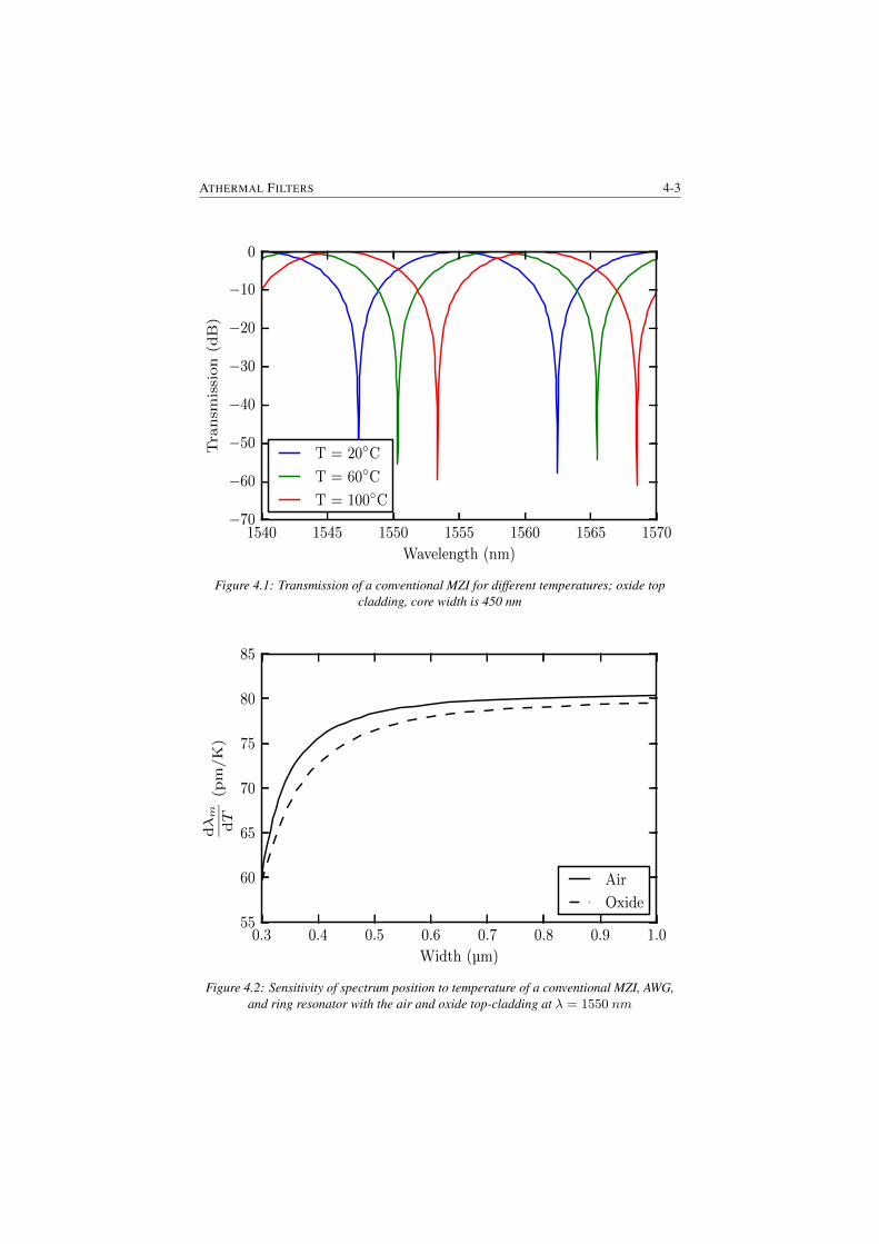
ATHERMAL FILTERS 4-3
1540 1545 1550 1555 1560 1565 1570
Wavelength (nm)
−70
−60
−50
−40
−30
−20
−10
0
Tra
nsm
issi
on
(dB
)
T = 20◦C
T = 60◦C
T = 100◦C
Figure 4.1: Transmission of a conventional MZI for different temperatures; oxide topcladding, core width is 450 nm
0.3 0.4 0.5 0.6 0.7 0.8 0.9 1.0
Width (µm)
55
60
65
70
75
80
85
dλm
dT
(pm
/K
)
Air
Oxide
Figure 4.2: Sensitivity of spectrum position to temperature of a conventional MZI, AWG,and ring resonator with the air and oxide top-cladding at λ = 1550 nm
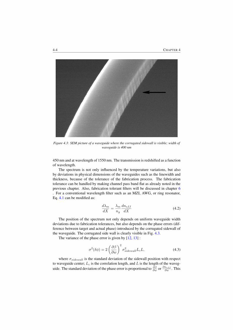
4-4 CHAPTER 4
Figure 4.3: SEM picture of a waveguide where the corrugated sidewall is visible; width ofwaveguide is 400 nm
450 nm and at wavelength of 1550 nm. The transmission is redshifted as a functionof wavelength.
The spectrum is not only influenced by the temperature variations, but alsoby deviations in physical dimensions of the waveguides such as the linewidth andthickness, because of the tolerance of the fabrication process. The fabricationtolerance can be handled by making channel pass band flat as already noted in theprevious chapter. Also, fabrication tolerant filters will be discussed in chapter 6. For a conventional wavelength filter such as an MZI, AWG, or ring resonator,Eq. 4.1 can be modified as:
dλmdX
=λmng
dneffdX
(4.2)
The position of the spectrum not only depends on uniform waveguide widthdeviations due to fabrication tolerances, but also depends on the phase errors (dif-ference between target and actual phase) introduced by the corrugated sidewall ofthe waveguide. The corrugated side wall is clearly visible in Fig. 4.3.
The variance of the phase error is given by [12, 13] :
σ2(δφ) = 2
(∂β
∂w
)2
σ2sidewallLcL, (4.3)
where σsidewall is the standard deviation of the sidewall position with respectto waveguide center; Lc is the correlation length, and L is the length of the waveg-uide. The standard deviation of the phase error is proportional to ∂β
∂w or ∂neff
∂w . This
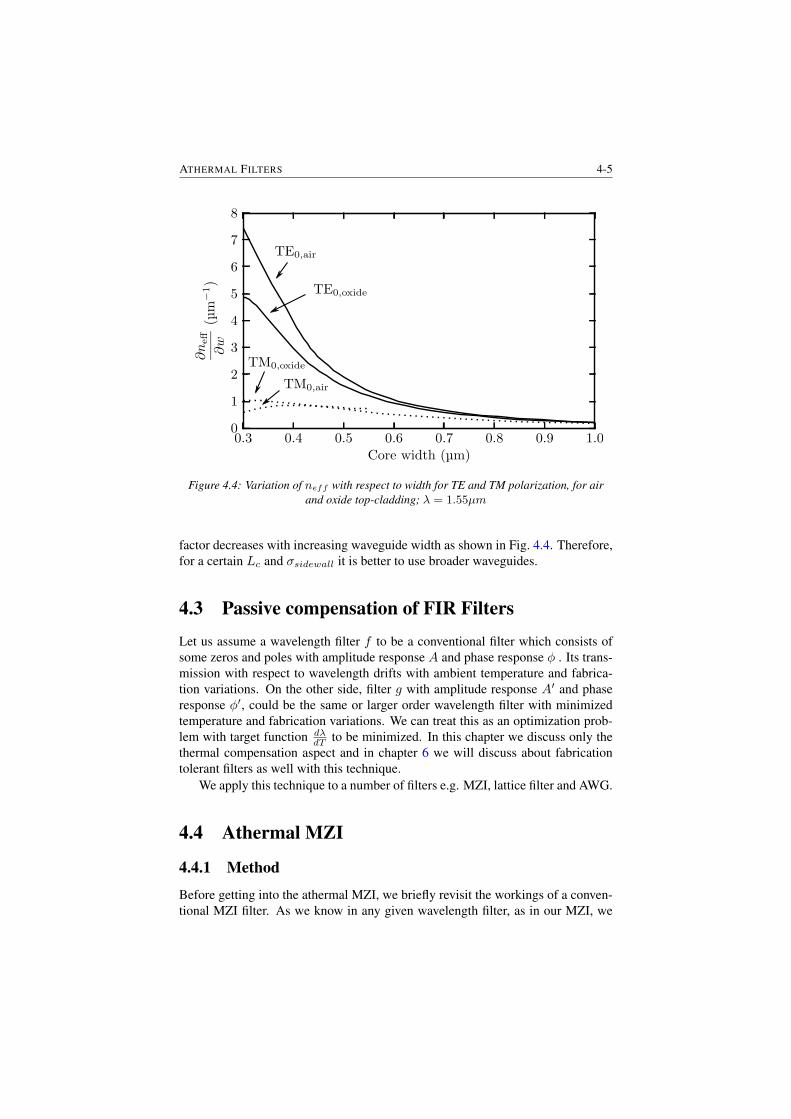
ATHERMAL FILTERS 4-5
Figure 4.4: Variation of neff with respect to width for TE and TM polarization, for airand oxide top-cladding; λ = 1.55µm
factor decreases with increasing waveguide width as shown in Fig. 4.4. Therefore,for a certain Lc and σsidewall it is better to use broader waveguides.
4.3 Passive compensation of FIR Filters
Let us assume a wavelength filter f to be a conventional filter which consists ofsome zeros and poles with amplitude response A and phase response φ . Its trans-mission with respect to wavelength drifts with ambient temperature and fabrica-tion variations. On the other side, filter g with amplitude response A′ and phaseresponse φ′, could be the same or larger order wavelength filter with minimizedtemperature and fabrication variations. We can treat this as an optimization prob-lem with target function dλ
dT to be minimized. In this chapter we discuss only thethermal compensation aspect and in chapter 6 we will discuss about fabricationtolerant filters as well with this technique.
We apply this technique to a number of filters e.g. MZI, lattice filter and AWG.
4.4 Athermal MZI
4.4.1 Method
Before getting into the athermal MZI, we briefly revisit the workings of a conven-tional MZI filter. As we know in any given wavelength filter, as in our MZI, we
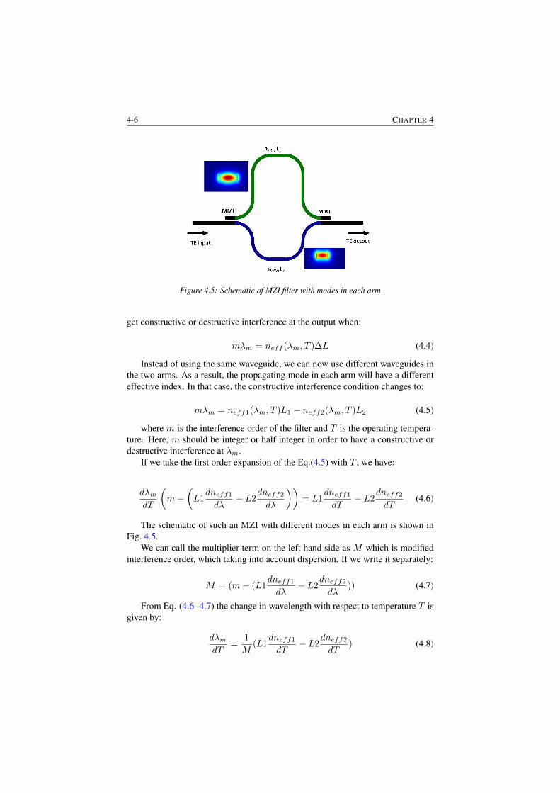
4-6 CHAPTER 4
Figure 4.5: Schematic of MZI filter with modes in each arm
get constructive or destructive interference at the output when:
mλm = neff (λm, T )∆L (4.4)
Instead of using the same waveguide, we can now use different waveguides inthe two arms. As a result, the propagating mode in each arm will have a differenteffective index. In that case, the constructive interference condition changes to:
mλm = neff1(λm, T )L1 − neff2(λm, T )L2 (4.5)
where m is the interference order of the filter and T is the operating tempera-ture. Here, m should be integer or half integer in order to have a constructive ordestructive interference at λm.
If we take the first order expansion of the Eq.(4.5) with T , we have:
dλmdT
(m−
(L1dneff1
dλ− L2
dneff2
dλ
))= L1
dneff1
dT− L2
dneff2
dT(4.6)
The schematic of such an MZI with different modes in each arm is shown inFig. 4.5.
We can call the multiplier term on the left hand side as M which is modifiedinterference order, which taking into account dispersion. If we write it separately:
M = (m− (L1dneff1
dλ− L2
dneff2
dλ)) (4.7)
From Eq. (4.6 -4.7) the change in wavelength with respect to temperature T isgiven by:
dλmdT
=1
M(L1
dneff1
dT− L2
dneff2
dT) (4.8)
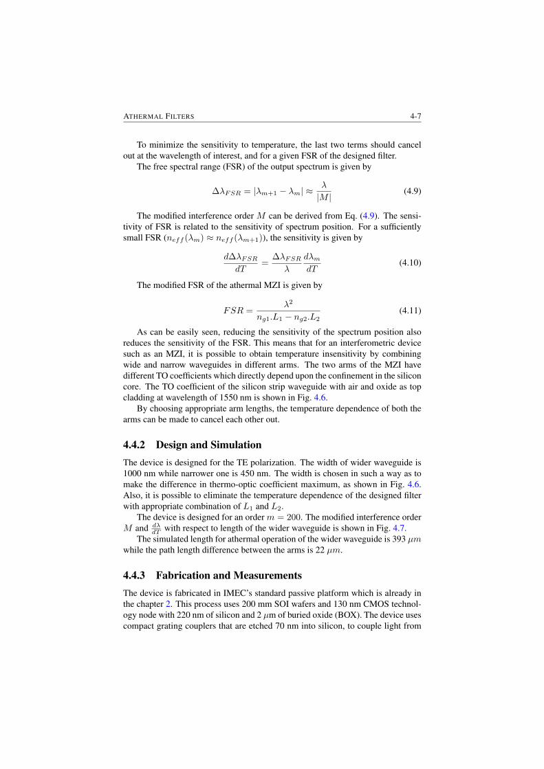
ATHERMAL FILTERS 4-7
To minimize the sensitivity to temperature, the last two terms should cancelout at the wavelength of interest, and for a given FSR of the designed filter.
The free spectral range (FSR) of the output spectrum is given by
∆λFSR = |λm+1 − λm| ≈λ
|M |(4.9)
The modified interference order M can be derived from Eq. (4.9). The sensi-tivity of FSR is related to the sensitivity of spectrum position. For a sufficientlysmall FSR (neff (λm) ≈ neff (λm+1)), the sensitivity is given by
d∆λFSRdT
=∆λFSR
λ
dλmdT
(4.10)
The modified FSR of the athermal MZI is given by
FSR =λ2
ng1.L1 − ng2.L2(4.11)
As can be easily seen, reducing the sensitivity of the spectrum position alsoreduces the sensitivity of the FSR. This means that for an interferometric devicesuch as an MZI, it is possible to obtain temperature insensitivity by combiningwide and narrow waveguides in different arms. The two arms of the MZI havedifferent TO coefficients which directly depend upon the confinement in the siliconcore. The TO coefficient of the silicon strip waveguide with air and oxide as topcladding at wavelength of 1550 nm is shown in Fig. 4.6.
By choosing appropriate arm lengths, the temperature dependence of both thearms can be made to cancel each other out.
4.4.2 Design and SimulationThe device is designed for the TE polarization. The width of wider waveguide is1000 nm while narrower one is 450 nm. The width is chosen in such a way as tomake the difference in thermo-optic coefficient maximum, as shown in Fig. 4.6.Also, it is possible to eliminate the temperature dependence of the designed filterwith appropriate combination of L1 and L2.
The device is designed for an order m = 200. The modified interference orderM and dλ
dT with respect to length of the wider waveguide is shown in Fig. 4.7.The simulated length for athermal operation of the wider waveguide is 393 µm
while the path length difference between the arms is 22 µm.
4.4.3 Fabrication and MeasurementsThe device is fabricated in IMEC’s standard passive platform which is already inthe chapter 2. This process uses 200 mm SOI wafers and 130 nm CMOS technol-ogy node with 220 nm of silicon and 2 µm of buried oxide (BOX). The device usescompact grating couplers that are etched 70 nm into silicon, to couple light from
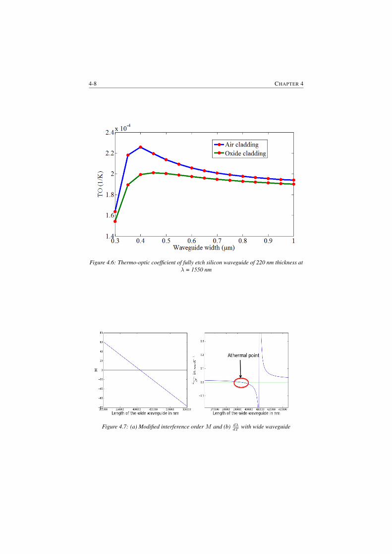
4-8 CHAPTER 4
Figure 4.6: Thermo-optic coefficient of fully etch silicon waveguide of 220 nm thickness atλ = 1550 nm
Figure 4.7: (a) Modified interference order M and (b) dλdT
with wide waveguide
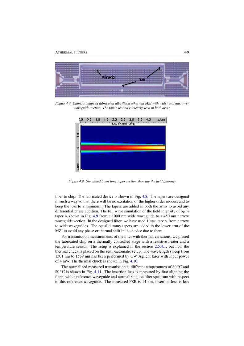
ATHERMAL FILTERS 4-9
Figure 4.8: Camera image of fabricated all-silicon athermal MZI with wider and narrowerwaveguide section. The taper section is clearly seen in both arms.
Figure 4.9: Simulated 5µm long taper section showing the field intensity
fiber to chip. The fabricated device is shown in Fig. 4.8. The tapers are designedin such a way so that there will be no excitation of the higher order modes, and tokeep the loss to a minimum. The tapers are added in both the arms to avoid anydifferential phase addition. The full wave simulation of the field intensity of 5µmtaper is shown in Fig. 4.9 from a 1000 nm wide waveguide to a 450 nm narrowwaveguide section. In the designed filter, we have used 10µm tapers from narrowto wide waveguides. The equal dummy tapers are added in the lower arm of theMZI to avoid any phase or thermal shift in the device due to them.
For transmission measurements of the filter with thermal variations, we placedthe fabricated chip on a thermally controlled stage with a resistive heater and atemperature sensor. The setup is explained in the section 2.5.4.1, but now thethermal chuck is placed on the semi-automatic setup. The wavelength sweep from1501 nm to 1569 nm has been performed by CW Agilent laser with input powerof 4 mW. The thermal chuck is shown in Fig. 4.10.
The normalized measured transmission at different temperatures of 30 ◦C and50 ◦C is shown in Fig. 4.11. The insertion loss is measured by first aligning thefibers with a reference waveguide and normalizing the filter spectrum with respectto this reference waveguide. The measured FSR is 14 nm, insertion loss is less
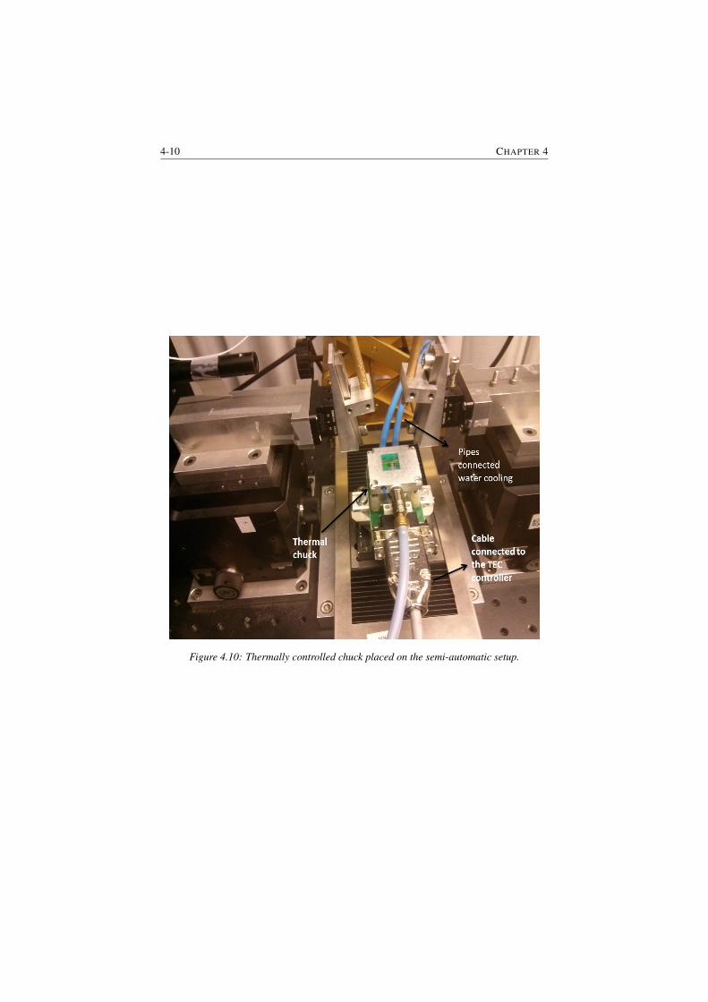
4-10 CHAPTER 4
Figure 4.10: Thermally controlled chuck placed on the semi-automatic setup.

ATHERMAL FILTERS 4-11
Figure 4.11: Normalized transmission of athermal MZI filter at 30 ◦C and 50 ◦C. Thethermal sensitivity of the MZI is less than 10 pm/K in entire C-band
than 1 dB and the extinction ratio is more than 20 dB. The high extinction ratio iscaused due to the good splitting balance in the MMI which acts as input and outputcoupler. The measured thermal sensitivity of the MZI is less than 10 pm/K in theentire C-band. The improvement is more than 8 times than the conventional MZI.
4.5 Athermal Four Channel De-multiplexer
As we have seen by using different mode confinements in either arms we can makea thermally insensitive MZI filter. In this section, this concept is extended to higherorder filters like 4-channel demultiplexers. The scheme is shown in Fig. 4.12.
4.5.1 Design and Simulation
The four channel athermal de-multiplexer is based on two stages of cascadedMZIs. It is designed for oxide cladding and for TE polarization. As mentionedin chapter 3, the FSR of the normal wavelength filter is given by
FSR =λ2
ng∆L(4.12)
The modified FSR of the athermal MZI is given by Eq. 4.11.From Eqs. (4.8-4.9), the wavelength shift due to temperature which needs to
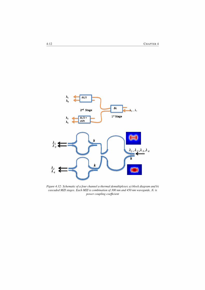
4-12 CHAPTER 4
Figure 4.12: Schematic of a four channel a-thermal demultiplexer, a) block diagram and b)cascaded MZI stages. Each MZI is combination of 300 nm and 450 nm waveguide, K is
power coupling coefficient
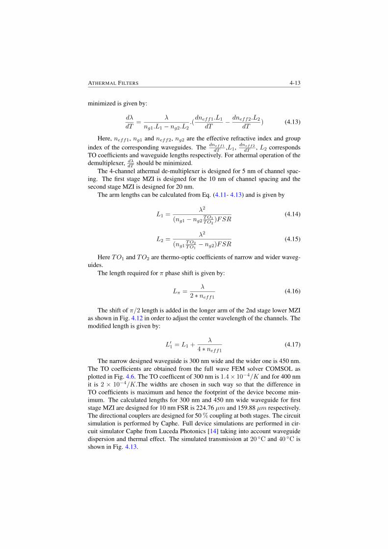
ATHERMAL FILTERS 4-13
minimized is given by:
dλ
dT=
λ
ng1.L1 − ng2.L2.(dneff1.L1
dT− dneff2.L2
dT) (4.13)
Here, neff1, ng1 and neff2, ng2 are the effective refractive index and groupindex of the corresponding waveguides. The dneff1
dT ,L1, dneff2
dT , L2 correspondsTO coefficients and waveguide lengths respectively. For athermal operation of thedemultiplexer, dλdT should be minimized.
The 4-channel athermal de-multiplexer is designed for 5 nm of channel spac-ing. The first stage MZI is designed for the 10 nm of channel spacing and thesecond stage MZI is designed for 20 nm.
The arm lengths can be calculated from Eq. (4.11- 4.13) and is given by
L1 =λ2
(ng1 − ng2 TO1
TO2)FSR
(4.14)
L2 =λ2
(ng1TO2
TO1− ng2)FSR
(4.15)
Here TO1 and TO2 are thermo-optic coefficients of narrow and wider waveg-uides.
The length required for π phase shift is given by:
Lπ =λ
2 ∗ neff1(4.16)
The shift of π/2 length is added in the longer arm of the 2nd stage lower MZIas shown in Fig. 4.12 in order to adjust the center wavelength of the channels. Themodified length is given by:
L′1 = L1 +λ
4 ∗ neff1(4.17)
The narrow designed waveguide is 300 nm wide and the wider one is 450 nm.The TO coefficients are obtained from the full wave FEM solver COMSOL asplotted in Fig. 4.6. The TO coefficent of 300 nm is 1.4× 10⁻⁴/K and for 400 nmit is 2 × 10⁻⁴/K.The widths are chosen in such way so that the difference inTO coefficients is maximum and hence the footprint of the device become min-imum. The calculated lengths for 300 nm and 450 nm wide waveguide for firststage MZI are designed for 10 nm FSR is 224.76 µm and 159.88 µm respectively.The directional couplers are designed for 50 % coupling at both stages. The circuitsimulation is performed by Caphe. Full device simulations are performed in cir-cuit simulator Caphe from Luceda Photonics [14] taking into account waveguidedispersion and thermal effect. The simulated transmission at 20 ◦C and 40 ◦C isshown in Fig. 4.13.
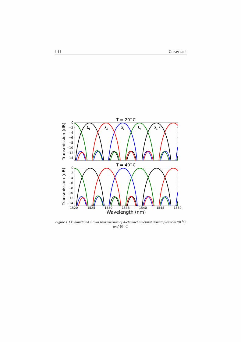
4-14 CHAPTER 4
Figure 4.13: Simulated circuit transmission of 4-channel athermal demultiplexer at 20 ◦Cand 40 ◦C
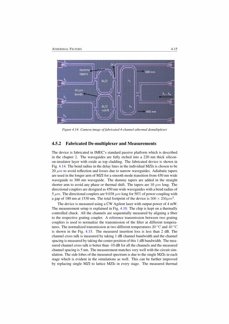
ATHERMAL FILTERS 4-15
Figure 4.14: Camera image of fabricated 4-channel athermal demultiplexer
4.5.2 Fabricated De-multiplexer and Measurements
The device is fabricated in IMEC’s standard passive platform which is describedin the chapter 2. The waveguides are fully etched into a 220 nm thick silicon-on-insulator layer with oxide as top cladding. The fabricated device is shown inFig. 4.14. The bend radius in the delay lines in the individual MZIs is chosen to be20 µm to avoid reflection and losses due to narrow waveguides. Adiabatic tapersare used in the longer arm of MZI for a smooth mode transition from 450 nm widewaveguide to 300 nm waveguide. The dummy tapers are added in the straightshorter arm to avoid any phase or thermal shift. The tapers are 10 µm long. Thedirectional couplers are designed as 450 nm wide waveguides with a bend radius of5 µm. The directional couplers are 9.038 µm long for 50% of power coupling witha gap of 180 nm at 1530 nm. The total footprint of the device is 500× 250µm2.
The device is measured using a CW Agilent laser with output power of 4 mW.The measurement setup is explained in Fig. 4.10. The chip is kept on a thermallycontrolled chuck. All the channels are sequentially measured by aligning a fiberto the respective grating coupler. A reference transmission between two gratingcouplers is used to normalize the transmission of the filter at different tempera-tures. The normalized transmission at two different temperatures 20 ◦C and 40 ◦Cis shown in the Fig. 4.15. The measured insertion loss is less than 2 dB. Thechannel cross talk is measured by taking 1 dB channel bandwidth and the channelspacing is measured by taking the center position of this 1 dB bandwidth. The mea-sured channel cross talk is better than -10 dB for all the channels and the measuredchannel spacing is 5 nm. The measurement matches very well with the circuit sim-ulation. The side lobes of the measured spectrum is due to the single MZIs in eachstage which is evident in the simulations as well. This can be further improvedby replacing single MZI to lattice MZIs in every stage. The measured thermal

4-16 CHAPTER 4
Figure 4.15: Measured normalized transmission of 4-channel athermal demultiplexer at20 ◦C and 40 ◦C
sensitivity of the demultiplexer is less than 10 pm/K over the entire C-band. Thesame device without thermal compensation would shift 80 pm/K, hence we showan 8-fold improvement in thermal tolerances. The additional insertion loss comesfrom the narrow waveguide where the mode is pushed out of the waveguide coreand hence suffers from higher scattering losses. The loss and footprint can furtherbe improved by keeping the narrow waveguide only in the straight sections, whilefor the bends the 450 nm wide waveguides could be used. We can then use thetighter bends instead of 20µm ones. But, in that case there will be two additionaltapers in each arm of the MZI which would increase the size and possibly the lossalso, so there is a trade off in this design.
4.6 All-Silicon Athermal Arrayed Waveguide Grat-ings
Arrayed waveguide gratings (AWG) face the similar problem of temperature de-pendence like other wavelength filters on SOI. In lower contrast material like silicaAWG suffer much less from this problem due to its lower TO coefficient. Theirare several demonstrations of athermal silicon AWG with polymer cladding ontop similar to the one for ring resonators [15, 16]. However, they face the simi-lar CMOS compatibility issues. In order to apply the same passive compensationtechniques to AWGs, we can treat them as a a set of MZIs connected in parallel.The schematic of the athermal AWG is shown in Fig. 4.16.
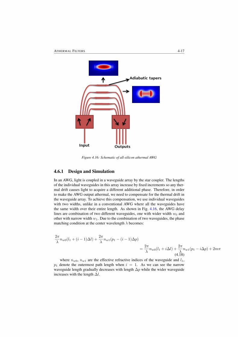
ATHERMAL FILTERS 4-17
Figure 4.16: Schematic of all-silicon athermal AWG
4.6.1 Design and Simulation
In an AWG, light is coupled in a waveguide array by the star coupler. The lengthsof the individual waveguides in this array increase by fixed increments so any ther-mal drift causes light to acquire a different additional phase. Therefore, in orderto make the AWG output athermal, we need to compensate for the thermal drift inthe waveguide array. To achieve this compensation, we use individual waveguideswith two widths, unlike in a conventional AWG where all the waveguides havethe same width over their entire length. As shown in Fig. 4.16, the AWG delaylines are combination of two different waveguides, one with wider width w0 andother with narrow width w1. Due to the combination of two waveguides, the phasematching condition at the center wavelength λ becomes:
2π
λnw0(l1 + (i− 1)∆l) +
2π
λnw1(p1 − (i− 1)∆p)
=2π
λnw0(l1 + i∆l) +
2π
λnw1(p1 − i∆p) + 2mπ
(4.18)where nw0, nw1 are the effective refractive indices of the waveguide and l1,
p1 denote the outermost path length when i = 1. As we can see the narrowwaveguide length gradually decreases with length ∆p while the wider waveguideincreases with the length ∆l.
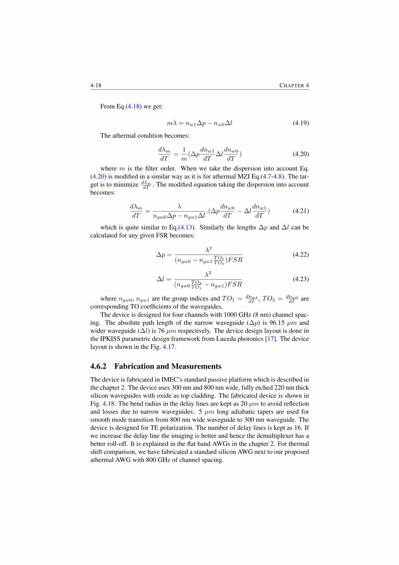
4-18 CHAPTER 4
From Eq.(4.18) we get:
mλ = nw1∆p− nw0∆l (4.19)
The athermal condition becomes:
dλmdT
=1
m(∆p
dnw1
dT∆ldnw0
dT) (4.20)
where m is the filter order. When we take the dispersion into account Eq.(4.20) is modified in a similar way as it is for athermal MZI Eq.(4.7-4.8). The tar-get is to minimize dλm
dT . The modified equation taking the dispersion into accountbecomes:
dλmdT
=λ
ngw0∆p− ngw1∆l.(∆p
dnw0
dT−∆l
dnw1
dT) (4.21)
which is quite similar to Eq.(4.13). Similarly the lengths ∆p and ∆l can becalculated for any given FSR becomes:
∆p =λ2
(ngw0 − ngw1TO1
TO2)FSR
(4.22)
∆l =λ2
(ngw0TO2
TO1− ngw1)FSR
(4.23)
where ngw0, ngw1 are the group indices and TO1 = dnw1
dT , TO2 = dnw0
dT arecorresponding TO coefficients of the waveguides.
The device is designed for four channels with 1000 GHz (8 nm) channel spac-ing. The absolute path length of the narrow waveguide (∆p) is 96.15 µm andwider waveguide (∆l) is 76 µm respectively. The device design layout is done inthe IPKISS parametric design framework from Luceda photonics [17]. The devicelayout is shown in the Fig. 4.17.
4.6.2 Fabrication and MeasurementsThe device is fabricated in IMEC’s standard passive platform which is described inthe chapter 2. The device uses 300 nm and 800 nm wide, fully etched 220 nm thicksilicon waveguides with oxide as top cladding. The fabricated device is shown inFig. 4.18. The bend radius in the delay lines are kept as 20 µm to avoid reflectionand losses due to narrow waveguides. 5 µm long adiabatic tapers are used forsmooth mode transition from 800 nm wide waveguide to 300 nm waveguide. Thedevice is designed for TE polarization. The number of delay lines is kept as 16. Ifwe increase the delay line the imaging is better and hence the demultiplexer has abetter roll-off. It is explained in the flat band AWGs in the chapter 2. For thermalshift comparison, we have fabricated a standard silicon AWG next to our proposedathermal AWG with 800 GHz of channel spacing.
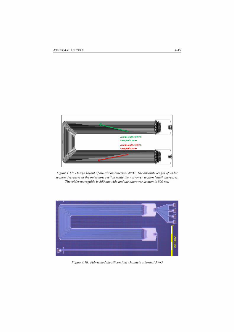
ATHERMAL FILTERS 4-19
Figure 4.17: Design layout of all-silicon athermal AWG. The absolute length of widersection decreases at the outermost section while the narrower section length increases.
The wider waveguide is 800 nm wide and the narrower section is 300 nm.
Figure 4.18: Fabricated all-silicon four channels athermal AWG
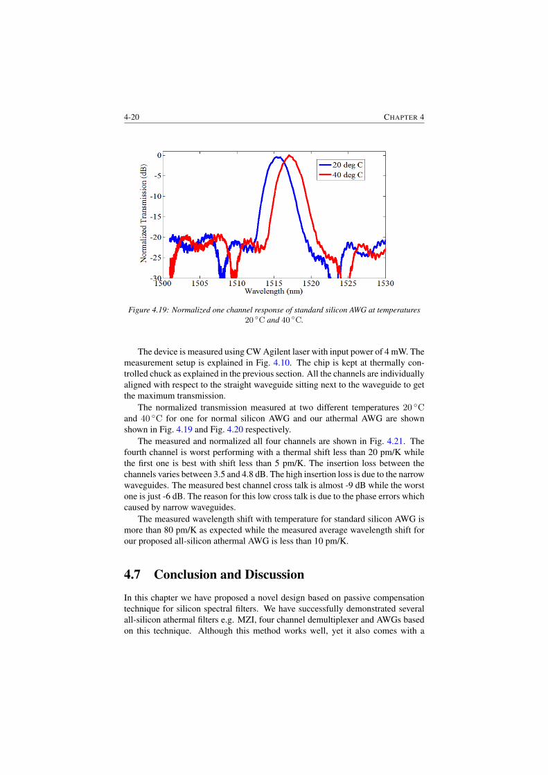
4-20 CHAPTER 4
Figure 4.19: Normalized one channel response of standard silicon AWG at temperatures20 ◦C and 40 ◦C.
The device is measured using CW Agilent laser with input power of 4 mW. Themeasurement setup is explained in Fig. 4.10. The chip is kept at thermally con-trolled chuck as explained in the previous section. All the channels are individuallyaligned with respect to the straight waveguide sitting next to the waveguide to getthe maximum transmission.
The normalized transmission measured at two different temperatures 20 ◦Cand 40 ◦C for one for normal silicon AWG and our athermal AWG are shownshown in Fig. 4.19 and Fig. 4.20 respectively.
The measured and normalized all four channels are shown in Fig. 4.21. Thefourth channel is worst performing with a thermal shift less than 20 pm/K whilethe first one is best with shift less than 5 pm/K. The insertion loss between thechannels varies between 3.5 and 4.8 dB. The high insertion loss is due to the narrowwaveguides. The measured best channel cross talk is almost -9 dB while the worstone is just -6 dB. The reason for this low cross talk is due to the phase errors whichcaused by narrow waveguides.
The measured wavelength shift with temperature for standard silicon AWG ismore than 80 pm/K as expected while the measured average wavelength shift forour proposed all-silicon athermal AWG is less than 10 pm/K.
4.7 Conclusion and Discussion
In this chapter we have proposed a novel design based on passive compensationtechnique for silicon spectral filters. We have successfully demonstrated severalall-silicon athermal filters e.g. MZI, four channel demultiplexer and AWGs basedon this technique. Although this method works well, yet it also comes with a
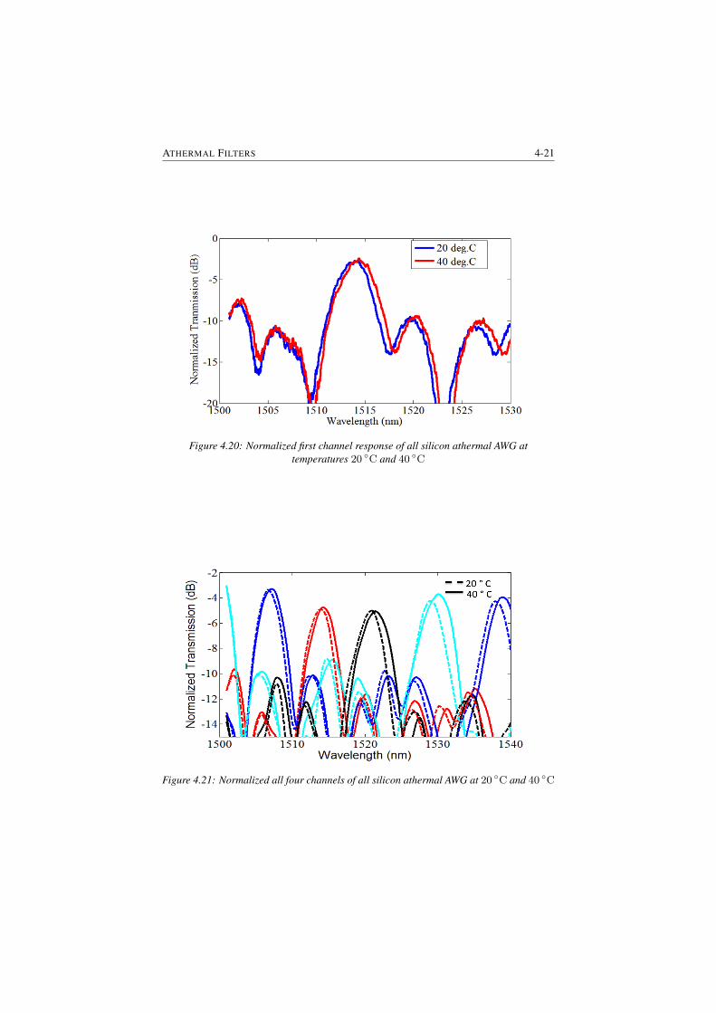
ATHERMAL FILTERS 4-21
Figure 4.20: Normalized first channel response of all silicon athermal AWG attemperatures 20 ◦C and 40 ◦C
Figure 4.21: Normalized all four channels of all silicon athermal AWG at 20 ◦C and 40 ◦C
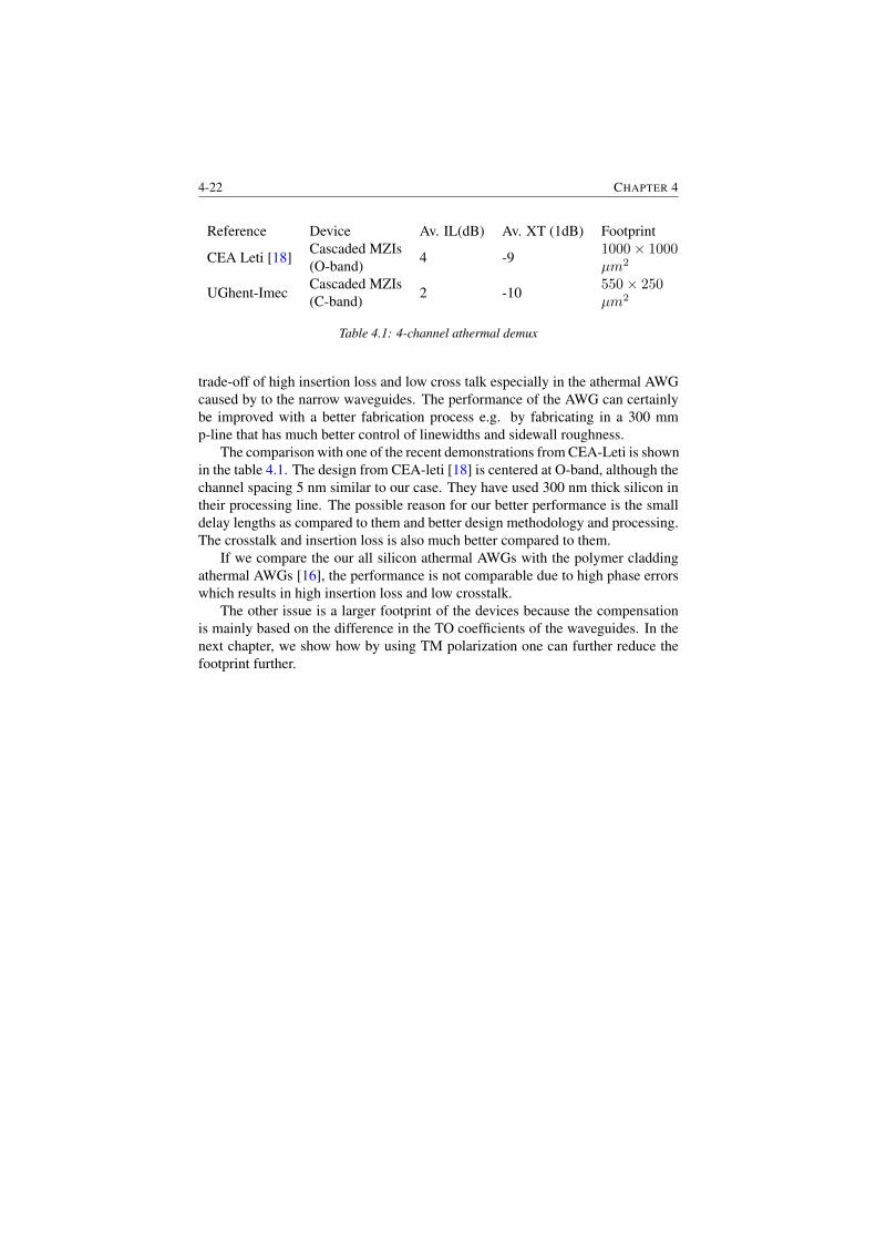
4-22 CHAPTER 4
Reference Device Av. IL(dB) Av. XT (1dB) Footprint
CEA Leti [18]Cascaded MZIs(O-band) 4 -9
1000× 1000µm2
UGhent-ImecCascaded MZIs(C-band) 2 -10
550× 250µm2
Table 4.1: 4-channel athermal demux
trade-off of high insertion loss and low cross talk especially in the athermal AWGcaused by to the narrow waveguides. The performance of the AWG can certainlybe improved with a better fabrication process e.g. by fabricating in a 300 mmp-line that has much better control of linewidths and sidewall roughness.
The comparison with one of the recent demonstrations from CEA-Leti is shownin the table 4.1. The design from CEA-leti [18] is centered at O-band, although thechannel spacing 5 nm similar to our case. They have used 300 nm thick silicon intheir processing line. The possible reason for our better performance is the smalldelay lengths as compared to them and better design methodology and processing.The crosstalk and insertion loss is also much better compared to them.
If we compare the our all silicon athermal AWGs with the polymer claddingathermal AWGs [16], the performance is not comparable due to high phase errorswhich results in high insertion loss and low crosstalk.
The other issue is a larger footprint of the devices because the compensationis mainly based on the difference in the TO coefficients of the waveguides. In thenext chapter, we show how by using TM polarization one can further reduce thefootprint further.
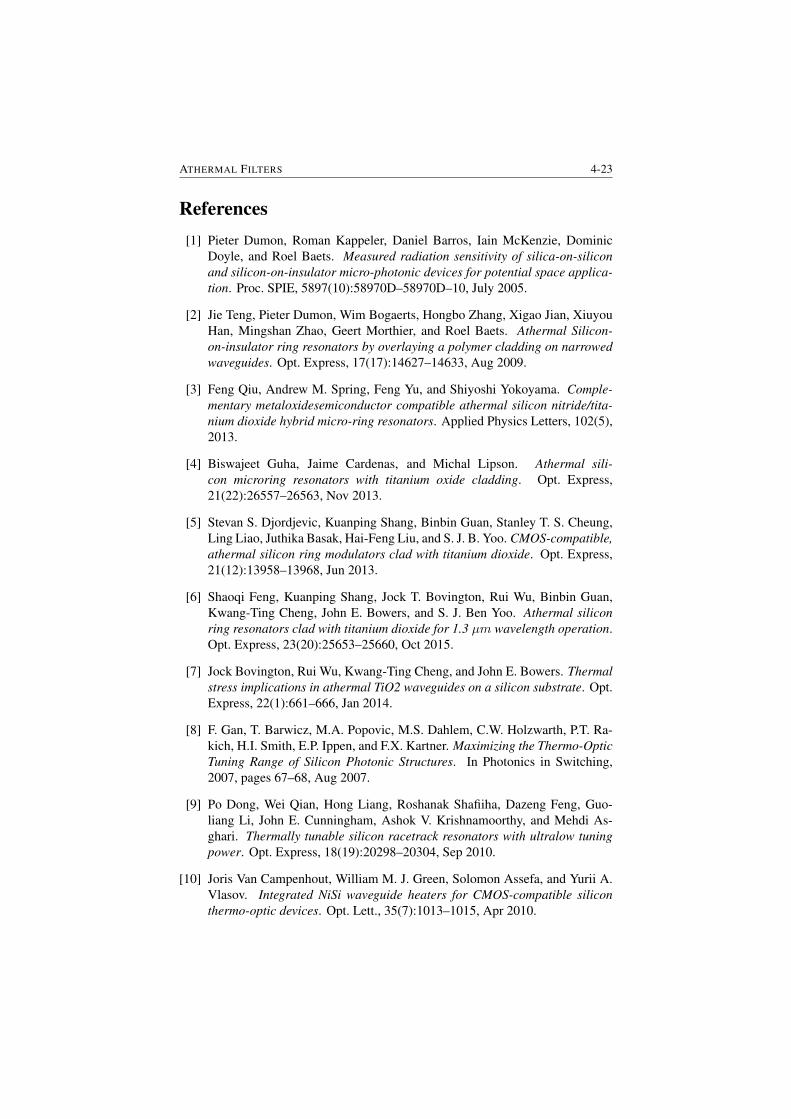
ATHERMAL FILTERS 4-23
References[1] Pieter Dumon, Roman Kappeler, Daniel Barros, Iain McKenzie, Dominic
Doyle, and Roel Baets. Measured radiation sensitivity of silica-on-siliconand silicon-on-insulator micro-photonic devices for potential space applica-tion. Proc. SPIE, 5897(10):58970D–58970D–10, July 2005.
[2] Jie Teng, Pieter Dumon, Wim Bogaerts, Hongbo Zhang, Xigao Jian, XiuyouHan, Mingshan Zhao, Geert Morthier, and Roel Baets. Athermal Silicon-on-insulator ring resonators by overlaying a polymer cladding on narrowedwaveguides. Opt. Express, 17(17):14627–14633, Aug 2009.
[3] Feng Qiu, Andrew M. Spring, Feng Yu, and Shiyoshi Yokoyama. Comple-mentary metaloxidesemiconductor compatible athermal silicon nitride/tita-nium dioxide hybrid micro-ring resonators. Applied Physics Letters, 102(5),2013.
[4] Biswajeet Guha, Jaime Cardenas, and Michal Lipson. Athermal sili-con microring resonators with titanium oxide cladding. Opt. Express,21(22):26557–26563, Nov 2013.
[5] Stevan S. Djordjevic, Kuanping Shang, Binbin Guan, Stanley T. S. Cheung,Ling Liao, Juthika Basak, Hai-Feng Liu, and S. J. B. Yoo. CMOS-compatible,athermal silicon ring modulators clad with titanium dioxide. Opt. Express,21(12):13958–13968, Jun 2013.
[6] Shaoqi Feng, Kuanping Shang, Jock T. Bovington, Rui Wu, Binbin Guan,Kwang-Ting Cheng, John E. Bowers, and S. J. Ben Yoo. Athermal siliconring resonators clad with titanium dioxide for 1.3 µm wavelength operation.Opt. Express, 23(20):25653–25660, Oct 2015.
[7] Jock Bovington, Rui Wu, Kwang-Ting Cheng, and John E. Bowers. Thermalstress implications in athermal TiO2 waveguides on a silicon substrate. Opt.Express, 22(1):661–666, Jan 2014.
[8] F. Gan, T. Barwicz, M.A. Popovic, M.S. Dahlem, C.W. Holzwarth, P.T. Ra-kich, H.I. Smith, E.P. Ippen, and F.X. Kartner. Maximizing the Thermo-OpticTuning Range of Silicon Photonic Structures. In Photonics in Switching,2007, pages 67–68, Aug 2007.
[9] Po Dong, Wei Qian, Hong Liang, Roshanak Shafiiha, Dazeng Feng, Guo-liang Li, John E. Cunningham, Ashok V. Krishnamoorthy, and Mehdi As-ghari. Thermally tunable silicon racetrack resonators with ultralow tuningpower. Opt. Express, 18(19):20298–20304, Sep 2010.
[10] Joris Van Campenhout, William M. J. Green, Solomon Assefa, and Yurii A.Vlasov. Integrated NiSi waveguide heaters for CMOS-compatible siliconthermo-optic devices. Opt. Lett., 35(7):1013–1015, Apr 2010.
4-24 CHAPTER 4
[11] Adil Masood, Marianna Pantouvaki, Danny Goossens, Guy Lepage, PeterVerheyen, Joris Van Campenhout, Philippe Absil, Dries Van Thourhout, andWim Bogaerts. Fabrication and characterization of CMOS-compatible inte-grated tungsten heaters for thermo-optic tuning in silicon photonics devices.Opt. Mater. Express, 4(7):1383–1388, Jul 2014.
[12] T. Goh, S. Suzuki, and A. Sugita. Estimation of waveguide phase error insilica-based waveguides. Lightwave Technology, Journal of, 15(11):2107–2113, Nov 1997.
[13] P. Dumon. Ultra-compact integrated optical filters in silicon-on insulator bymeans of wafer-scale technology, Ph.D. thesis, Ghent university, 2007.
[14] Martin Fiers, Thomas Van Vaerenbergh, Ken Caluwaerts, Dries Vande Gin-ste, Benjamin Schrauwen, Joni Dambre, and Peter Bienstman. Time-domainand frequency-domain modeling of nonlinear optical components at thecircuit-level using a node-based approach. J. Opt. Soc. Am. B, 29(5):896–900, May 2012.
[15] Xiang Wang, Simiao Xiao, Weiwei Zheng, Fan Wang, Yinlei Hao, XiaoqingJiang, Minghua Wang, and Jianyi Yang. Athermal silicon arrayed waveguidegrating with polymer-filled slot structure. In Group IV Photonics, 2008 5thIEEE International Conference on, pages 253–255, Sept 2008.
[16] Linghua Wang, Wim Bogaerts, Pieter Dumon, Shankar Kumar Selvaraja, JieTeng, Shibnath Pathak, Xiuyou Han, Jinyan Wang, Xigao Jian, MingshanZhao, Roel Baets, and Geert Morthier. Athermal arrayed waveguide grat-ings in silicon-on-insulator by overlaying a polymer cladding on narrowedarrayed waveguides. Appl. Opt., 51(9):1251–1256, Mar 2012.
[17] http://www.lucedaphotonics.com/.
[18] Karim Hassan, Corrado Sciancalepore, Julie Harduin, Thomas Ferrotti,Sylvie Menezo, and Badhise Ben Bakir. Toward athermal silicon-on-insulator (de)multiplexers in the O-band. Opt. Lett., 40(11):2641–2644, Jun2015.
5Compact All-Silicon Temperature
Insensitive Filter UsingSplitter-Polarization Rotator Section
In this chapter, we propose a novel approach to the all-silicon athermal MZI filterpresented in the previous chapter. The device achieves a reduced footprint by mak-ing use of both the TE and the TM polarization, compared to the TE-based designin chapter 4. We discuss the design, simulation, fabrication and characterizationof this device, with a detailed discussion of the splitter/combiner which also actsas a polarization rotator.
The device presented in this chapter is also the subject of a patent application[1].
5.1 IntroductionAs discussed in chapter 4, the spectrum of an interferometric device such as aMach-Zehnder interferometer (MZI) can be made temperature insensitive by com-bining wide and narrow waveguides in different arms. In this technique, the twoarms of the MZI have different thermo-optic (TO) coefficients which directly de-pend upon the confinement of the propagating mode in the silicon core. By choos-ing appropriate arm lengths, the temperature dependence of both the arms can bemade to cancel each other out. However, this technique increases the device foot-print considerably [2]. To reduce the footprint, the difference in the thermo-optic(TO) coefficient between the two arms should be as large as possible. It is possi-
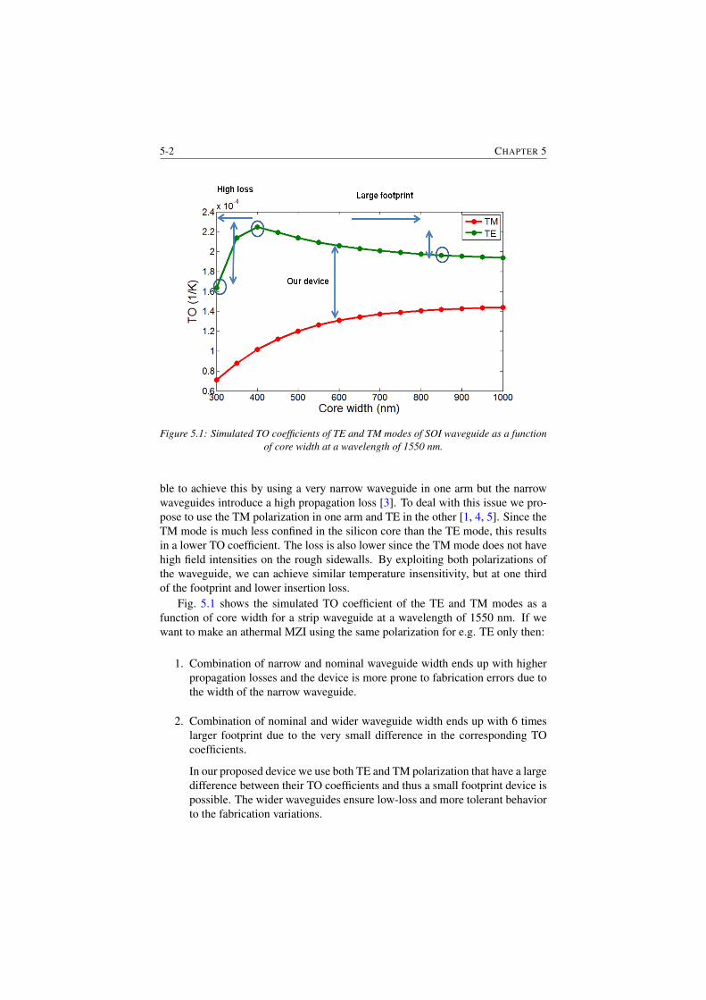
5-2 CHAPTER 5
Figure 5.1: Simulated TO coefficients of TE and TM modes of SOI waveguide as a functionof core width at a wavelength of 1550 nm.
ble to achieve this by using a very narrow waveguide in one arm but the narrowwaveguides introduce a high propagation loss [3]. To deal with this issue we pro-pose to use the TM polarization in one arm and TE in the other [1, 4, 5]. Since theTM mode is much less confined in the silicon core than the TE mode, this resultsin a lower TO coefficient. The loss is also lower since the TM mode does not havehigh field intensities on the rough sidewalls. By exploiting both polarizations ofthe waveguide, we can achieve similar temperature insensitivity, but at one thirdof the footprint and lower insertion loss.
Fig. 5.1 shows the simulated TO coefficient of the TE and TM modes as afunction of core width for a strip waveguide at a wavelength of 1550 nm. If wewant to make an athermal MZI using the same polarization for e.g. TE only then:
1. Combination of narrow and nominal waveguide width ends up with higherpropagation losses and the device is more prone to fabrication errors due tothe width of the narrow waveguide.
2. Combination of nominal and wider waveguide width ends up with 6 timeslarger footprint due to the very small difference in the corresponding TOcoefficients.
In our proposed device we use both TE and TM polarization that have a largedifference between their TO coefficients and thus a small footprint device ispossible. The wider waveguides ensure low-loss and more tolerant behaviorto the fabrication variations.
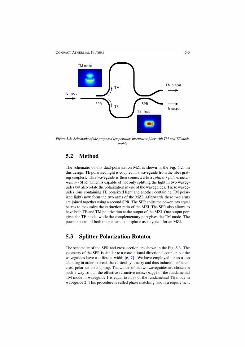
COMPACT ATHERMAL FILTERS 5-3
Figure 5.2: Schematic of the proposed temperature insensitive filter with TM and TE modeprofile
5.2 Method
The schematic of this dual-polarization MZI is shown in the Fig. 5.2. Inthis design, TE polarized light is coupled in a waveguide from the fiber grat-ing couplers. This waveguide is then connected to a splitter / polarization-rotator (SPR) which is capable of not only splitting the light in two waveg-uides but also rotate the polarization in one of the waveguides. These waveg-uides (one containing TE polarized light and another containing TM polar-ized light) now form the two arms of the MZI. Afterwards these two armsare joined together using a second SPR. The SPR splits the power into equalhalves to maximize the extinction ratio of the MZI. The SPR also allows tohave both TE and TM polarization at the output of the MZI. One output portgives the TE mode, while the complementary port gives the TM mode. Thepower spectra of both outputs are in antiphase as is typical for an MZI.
5.3 Splitter Polarization Rotator
The schematic of the SPR and cross-section are shown in the Fig. 5.3. Thegeometry of the SPR is similar to a conventional directional coupler, but thewaveguides have a different width [6, 7]. We have employed air as a topcladding in order to break the vertical symmetry and thus induce an efficientcross polarization coupling. The widths of the two waveguides are chosen insuch a way so that the effective refractive index (neff ) of the fundamentalTM mode in waveguide 1 is equal to neff of the fundamental TE mode inwaveguide 2. This procedure is called phase matching, and is a requirement
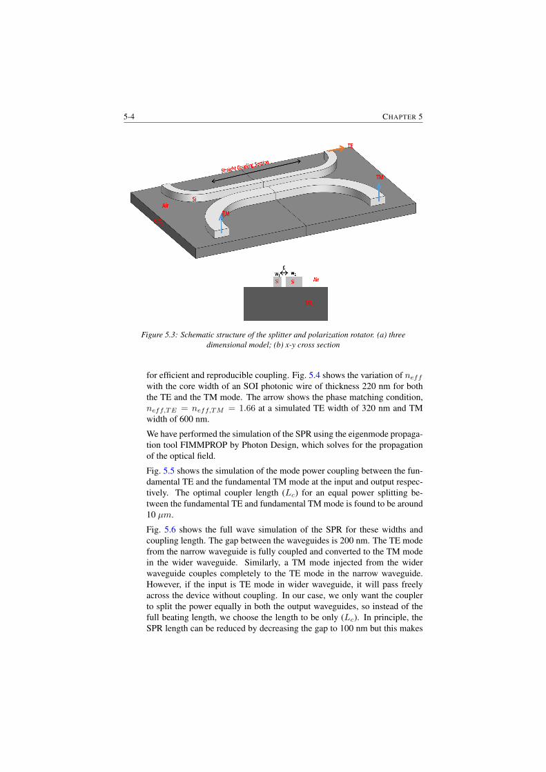
5-4 CHAPTER 5
Figure 5.3: Schematic structure of the splitter and polarization rotator. (a) threedimensional model; (b) x-y cross section
for efficient and reproducible coupling. Fig. 5.4 shows the variation of neffwith the core width of an SOI photonic wire of thickness 220 nm for boththe TE and the TM mode. The arrow shows the phase matching condition,neff,TE = neff,TM = 1.66 at a simulated TE width of 320 nm and TMwidth of 600 nm.
We have performed the simulation of the SPR using the eigenmode propaga-tion tool FIMMPROP by Photon Design, which solves for the propagationof the optical field.
Fig. 5.5 shows the simulation of the mode power coupling between the fun-damental TE and the fundamental TM mode at the input and output respec-tively. The optimal coupler length (Lc) for an equal power splitting be-tween the fundamental TE and fundamental TM mode is found to be around10 µm.
Fig. 5.6 shows the full wave simulation of the SPR for these widths andcoupling length. The gap between the waveguides is 200 nm. The TE modefrom the narrow waveguide is fully coupled and converted to the TM modein the wider waveguide. Similarly, a TM mode injected from the widerwaveguide couples completely to the TE mode in the narrow waveguide.However, if the input is TE mode in wider waveguide, it will pass freelyacross the device without coupling. In our case, we only want the couplerto split the power equally in both the output waveguides, so instead of thefull beating length, we choose the length to be only (Lc). In principle, theSPR length can be reduced by decreasing the gap to 100 nm but this makes
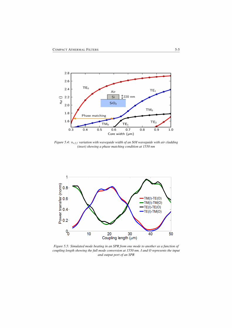
COMPACT ATHERMAL FILTERS 5-5
Figure 5.4: neff variation with waveguide width of an SOI waveguide with air cladding(inset) showing a phase matching condition at 1550 nm
Figure 5.5: Simulated mode beating in an SPR from one mode to another as a function ofcoupling length showing the full mode conversion at 1550 nm. I and O represents the input
and output port of an SPR
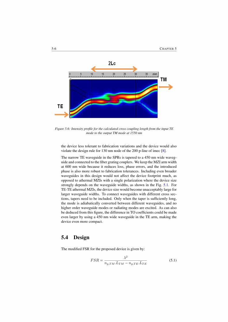
5-6 CHAPTER 5
Figure 5.6: Intensity profile for the calculated cross coupling length from the input TEmode to the output TM mode at 1550 nm
the device less tolerant to fabrication variations and the device would alsoviolate the design rule for 130 nm node of the 200 p-line of imec [8].
The narrow TE waveguide in the SPRs is tapered to a 450 nm wide waveg-uide and connected to the fiber grating couplers. We keep the MZI arm widthat 600 nm wide because it reduces loss, phase errors, and the introducedphase is also more robust to fabrication tolerances. Including even broaderwaveguides in this design would not affect the device footprint much, asopposed to athermal MZIs with a single polarization where the device sizestrongly depends on the waveguide widths, as shown in the Fig. 5.1. ForTE-TE athermal MZIs, the device size would become unacceptably large forlarger waveguide widths. To connect waveguides with different cross sec-tions, tapers need to be included. Only when the taper is sufficiently long,the mode is adiabatically converted between different waveguides, and nohigher order waveguide modes or radiating modes are excited. As can alsobe deduced from this figure, the difference in TO coefficients could be madeeven larger by using a 450 nm wide waveguide in the TE arm, making thedevice even more compact.
5.4 Design
The modified FSR for the proposed device is given by:
FSR =λ2
ng,TM .LTM − ng,TE .LTE(5.1)

COMPACT ATHERMAL FILTERS 5-7
where ng,TM , ng,TE andLTM , LTE correspond to the group index and thelength of TM and TE arm waveguides guiding the TE and TM polarization,respectively. This equation is similar to Eq. 4.11 but, now it is replaced withTE and TM mode arms.
As can be derived from Eq. (4.13), in an athermal MZI, we would have(dλm
dT = 0), with TE and TM polarizations obtained when both arm lengthsare related by:
LTELTM
=TOTMTOTE
∣∣∣∣λ0, T0
(5.2)
Here, T is the temperature and TO is the thermo-optic coefficient of thecorresponding arms. For a particular waveguide geometry, wavelength λ0,and temperature T0, the arm lengths are chosen in such a way that the abovecondition is satisfied. Because this condition depends on temperature andwavelength, it leads to a zero spectral shift only for a certain temperature,and wavelength. Also, the TO coefficient depends on the core width, height,and sidewall slope, which are prone to fabrication tolerances. In good ap-proximation, the TO coefficient can be assumed to be temperature indepen-dent. Taking into account the athermal condition, the thermal sensitivity ofthe spectrum position becomes:
dλmdT
=TOTM
TOTE
TOTM
∣∣∣0− TOTE
ng,TMTOTE
TOTM
∣∣∣0− ng,TE
(5.3)
It follows from Eq. (5.2) that LTM is larger than LTE because TOTEis larger than TOTM , and for any core width. Combining Eq. (5.1) andEq. (5.3) gives the required arms lengths to have an athermal MZI with aparticular FSR is given by:
LTE =λ2(
ng,TMTOTE
TOTM− ng,TE
)∆λFSR
, (5.4)
LTM =λ2(
ng,TM − ng,TE TOTM
TOTE
)∆λFSR
(5.5)
For simulation, tapers can be approximated by a staircase profile which canbe seen as a concatenation of short-length waveguides with increasing or de-creasing widths. When taking enough staircase sections, the summation ofall tapers will converge to an integral of the propagation. Using this lumpedapproximation, tapers are easy to add to a circuit simulation. When they are
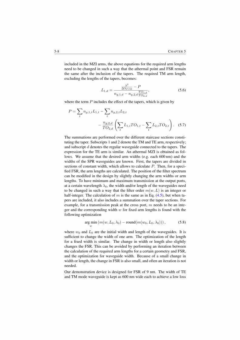
5-8 CHAPTER 5
included in the MZI arms, the above equations for the required arm lengthsneed to be changed in such a way that the athermal point and FSR remainthe same after the inclusion of the tapers. The required TM arm length,excluding the lengths of the tapers, becomes:
L1,d =λ2
∆λFSR− P
ng,1,d − ng,2,d TO1,d
TO2,d
, (5.6)
where the term P includes the effect of the tapers, which is given by
P =∑t
ng,1,tL1,t −∑t
ng,2,tL2,t
− ng,2,dTO2,d
(∑t
L1,tTO1,t −∑t
L2,tTO2,t
). (5.7)
The summations are performed over the different staircase sections consti-tuting the taper. Subscripts 1 and 2 denote the TM and TE arm, respectively;and subscript d denotes the regular waveguide connected to the tapers. Theexpression for the TE arm is similar. An athermal MZI is obtained as fol-lows. We assume that the desired arm widths (e.g. each 600 nm) and thewidths of the SPR waveguides are known. First, the tapers are divided insections of constant width, which allows to calculate P . Then, for a speci-fied FSR, the arm lengths are calculated. The position of the filter spectrumcan be modified in the design by slightly changing the arm widths or armlengths. To have minimum and maximum transmission at the output ports,at a certain wavelength λ0, the width and/or length of the waveguides needto be changed in such a way that the filter order m(w,L) is an integer orhalf-integer. The calculation of m is the same as in Eq. (4.5), but when ta-pers are included, it also includes a summation over the taper sections. Forexample, for a transmission peak at the cross port, m needs to be an inte-ger and the corresponding width w for fixed arm lengths is found with thefollowing optimization
arg minw
(m(w,L0, λ0)− round(m(w0, L0, λ0))) , (5.8)
where w0 and L0 are the initial width and length of the waveguides. It issufficient to change the width of one arm. The optimization of the lengthfor a fixed width is similar. The change in width or length also slightlychanges the FSR. This can be avoided by performing an iteration betweenthe calculation of the required arm lengths for a certain geometry and FSR,and the optimization for waveguide width. Because of a small change inwidth or length, the change in FSR is also small, and often an iteration is notneeded.
Our demonstration device is designed for FSR of 9 nm. The width of TEand TM mode waveguide is kept as 600 nm wide each to achieve a low loss
COMPACT ATHERMAL FILTERS 5-9
and small phase errors. Also, by using these widths a very compact filtercan be realized which is due to the large difference in their correspondingTO coefficients difference, as shown in the Fig. 5.1.
5.5 Fabrication
The device has been fabricated in the imec 200 mm CMOS pilot line, usingsilicon-on-insulator wafers with 220 nm of silicon and 2 µm of buried oxide.The details of this process have already been discussed in chapter 2. Thefabricated device, one of the test SPR structures and its cross which arefabricated separately as shown in Fig. 5.7 and Fig. 5.8, respectively.
The input TE-polarized light passes through the SPR that splits and convertshalf of the power into TM polarization. The TM light goes to the upperarm, while the remaining half of the input power remains in the lower armas the TE polarized light. Finally, both polarizations combine at the MZIoutput using a similar SPR as a combiner. The device also includes adiabatictapers before and after the SPR section. The need for an adiabatic taper isto prevent coupling between the fundamental mode and the higher ordermodes.
Compact curved grating couplers designed for operation in the 1550 nmwavelength range are added to couple light in and out of the device [9].Depending on the arm, a coupler for either the TE or the TM polarizationis used. The length of designed TM arm of the MZI is 213.25 µm which islonger than TE arm of 139.25 µm. It is due to the lower TO coefficient ofTM mode (see Eqs. (5.2)-(5.5)).
The fabricated length of the SPR is 10 µm and the gap is 190 nm. The widthof the SPR waveguides is 560 nm and 310 nm respectively, as measuredfrom a FIB cross section image. The fabricated width of both the upperTM arm and lower TE arm is 560 nm. Adiabatic tapers in the TE arm areshown in the inset of Fig. 5.7. Since the upper arm guides the TM mode,larger bends with a radius of 25 µm are used in the design for the lowerradiation loss. In the upper arm of the device there are no tapers as thewidth of the upper arm and the SPR waveguide width is the same. We havealso incorporated separate test structures for the SPR with a sweep of thecoupling length and widths. The footprint of the device is 188× 125µm2.
5.6 Measurements and Analysis
All the devices are characterized in continuous wave (CW) regime. Themeasurement set-up consists of a CW laser source, followed by a polar-ization controller, the sample to be characterized, and a power meter and
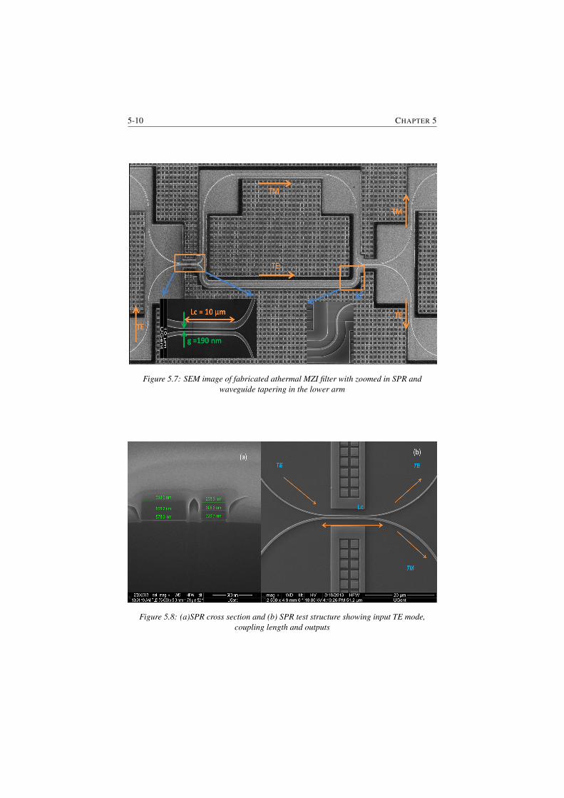
5-10 CHAPTER 5
Figure 5.7: SEM image of fabricated athermal MZI filter with zoomed in SPR andwaveguide tapering in the lower arm
Figure 5.8: (a)SPR cross section and (b) SPR test structure showing input TE mode,coupling length and outputs
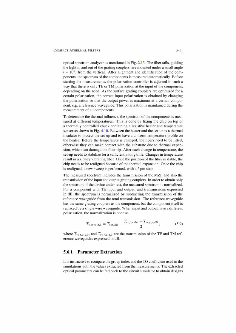
COMPACT ATHERMAL FILTERS 5-11
optical spectrum analyzer as mentioned in Fig. 2.13. The fiber tails, guidingthe light in and out of the grating couplers, are mounted under a small angle(∼ 10◦) from the vertical. After alignment and identification of the com-ponents, the spectrum of the components is measured automatically. Beforestarting the measurements, the polarization controller is adjusted in such away that there is only TE or TM polarization at the input of the component,depending on the need. As the surface grating couplers are optimized for acertain polarization, the correct input polarization is obtained by changingthe polarization so that the output power is maximum at a certain compo-nent, e.g. a reference waveguide. This polarization is maintained during themeasurement of all components.
To determine the thermal influence, the spectrum of the components is mea-sured at different temperatures. This is done by fixing the chip on top ofa thermally controlled chuck containing a resistive heater and temperaturesensor as shown in Fig. 4.10. Between the heater and the set-up is a thermalinsulator to protect the set-up and to have a uniform temperature profile onthe heater. Before the temperature is changed, the fibers need to be lifted,otherwise they can make contact with the substrate due to thermal expan-sion, which can damage the fiber tip. After each change in temperature, theset-up needs to stabilize for a sufficiently long time. Changes in temperatureresult in a slowly vibrating fiber. Once the position of the fiber is stable, thechip needs to be realigned because of the thermal expansion. Once the chipis realigned, a new sweep is performed, with a 5 pm step.
The measured spectrum includes the transmission of the MZI, and also thetransmission of the input and output grating couplers. In order to obtain onlythe spectrum of the device under test, the measured spectrum is normalized.For a component with TE input and output, and transmissions expressedin dB, the spectrum is normalized by subtracting the transmission of thereference waveguide from the total transmission. The reference waveguidehas the same grating couplers as the component, but the component itself isreplaced by a single wire waveguide. When input and output have a differentpolarization, the normalization is done as
Tnorm,dB = Ttot,dB −Tref,s,dB + Tref,p,dB
2, (5.9)
where Tref,s,dB , and Tref,p,dB are the transmission of the TE and TM ref-erence waveguides expressed in dB.
5.6.1 Parameter Extraction
It is instructive to compare the group index and the TO coefficient used in thesimulations with the values extracted from the measurements. The extractedoptical parameters can be fed back to the circuit simulator to obtain designs
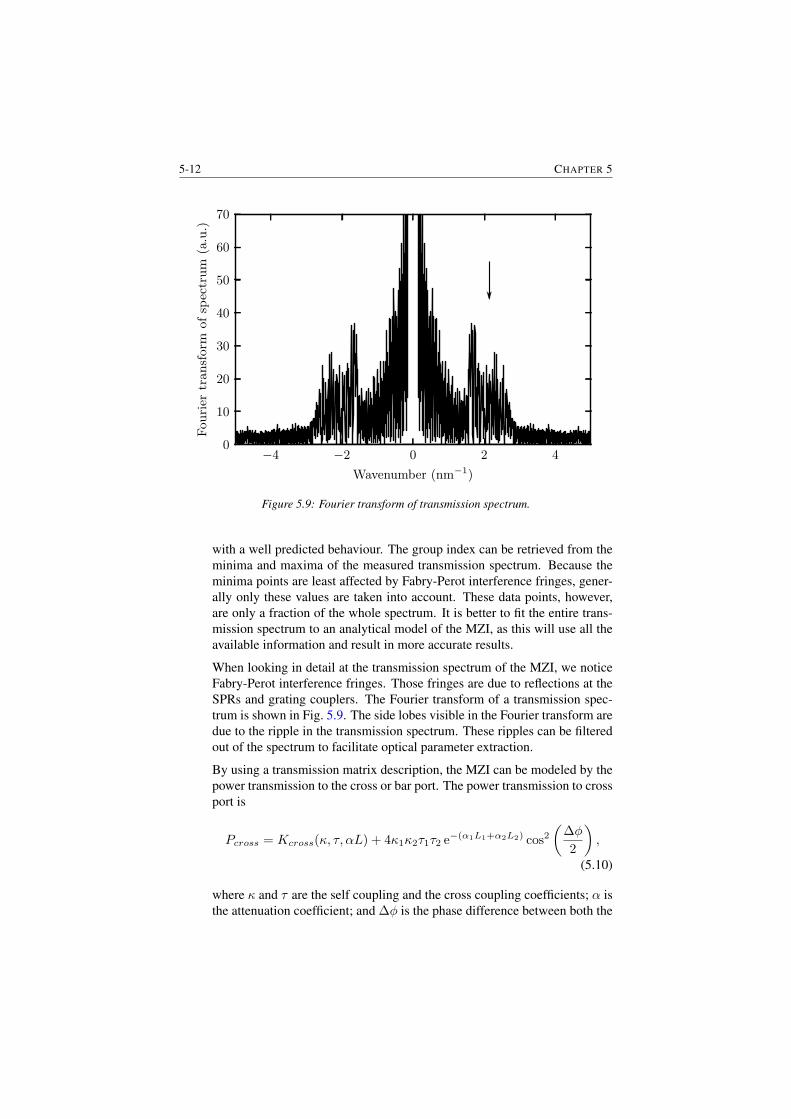
5-12 CHAPTER 5
Figure 5.9: Fourier transform of transmission spectrum.
with a well predicted behaviour. The group index can be retrieved from theminima and maxima of the measured transmission spectrum. Because theminima points are least affected by Fabry-Perot interference fringes, gener-ally only these values are taken into account. These data points, however,are only a fraction of the whole spectrum. It is better to fit the entire trans-mission spectrum to an analytical model of the MZI, as this will use all theavailable information and result in more accurate results.
When looking in detail at the transmission spectrum of the MZI, we noticeFabry-Perot interference fringes. Those fringes are due to reflections at theSPRs and grating couplers. The Fourier transform of a transmission spec-trum is shown in Fig. 5.9. The side lobes visible in the Fourier transform aredue to the ripple in the transmission spectrum. These ripples can be filteredout of the spectrum to facilitate optical parameter extraction.
By using a transmission matrix description, the MZI can be modeled by thepower transmission to the cross or bar port. The power transmission to crossport is
Pcross = Kcross(κ, τ, αL) + 4κ1κ2τ1τ2 e−(α1L1+α2L2) cos2
(∆φ
2
),
(5.10)
where κ and τ are the self coupling and the cross coupling coefficients; α isthe attenuation coefficient; and ∆φ is the phase difference between both the
COMPACT ATHERMAL FILTERS 5-13
arms. The power transmission to the bar port is in antiphase given by
Pbar = Kbar(κ, τ, αL) + 4κ1κ2τ1τ2 e−(α1L1+α2L2) sin2
(∆φ
2
). (5.11)
When we assume a = e−α1L1 = e−α1L1 , we get
Kcross(κ, τ, αL) = a2(κ2
2τ21 + κ2
1τ22 − 2κ1τ1κ2τ2
), (5.12)
Kbar(κ, τ, αL) = a2(κ2
1κ22 + τ2
1 τ22 − 2κ1τ1κ2τ2
). (5.13)
To extract the group index and the TO coefficient, it is assumed that theeffective index is of the form
neff = n0 + n1∆ν + n2∆T + n3∆T∆ν, (5.14)
so that the group index and the TO coefficient are linearly dependent onfrequency as
ng|T0= ng,0 + ng,1∆ν (5.15)
TO = TO0 + TO1∆ν (5.16)
If the amplitude of the power transmission is assumed to be a second orderpolynomial, then the fitting equation is
P (ν, T ) = (a0ν2 + a1ν + a2) cos2
(a3ν
2 + a4ν + a5νT + a6ν2T + a7
)+ a8
(5.17)
This is a two dimensional fitting problem. The term a7 takes into accountimperfections in the model. Coefficients a3 to a6 take into account the fre-quency and temperature dependence of the effective index; and a8 takes intoaccount the non-infinite extinction ratio due to deviations in the couplingcoefficients. The thermal behaviour of the coupling coefficients can also beincluded by adding temperature dependent terms in the amplitude factor. Wefit the measurements to this model with a least squares optimization algo-rithm. The extracted parameters from the transmission spectra of one outputport can be compared with the extracted parameters from the other outputport, or the transmissions of both ports can be fed into the fitting algorithmtogether in order to increase the number of data points.
The least squares optimization algorithm has the tendency to converge inlocal minima. Therefore, it is important to provide a good initial guess ofthe fitting coefficients. The fitting algorithm is structured as follows. Firstthe peaks and troughs of a measured spectrum are searched for. From themaxima, an initial guess of the coefficients in the amplitude factor is made.This is done by fitting a second order polynomial through these maxima. Aninitial guess of the period is found from the distance between two successiveminima. The fitting algorithm returns the extracted parameters, which are
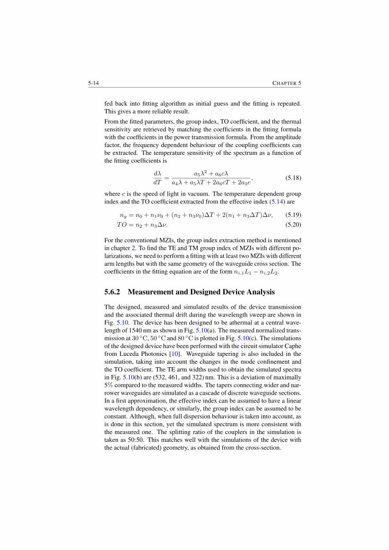
5-14 CHAPTER 5
fed back into fitting algorithm as initial guess and the fitting is repeated.This gives a more reliable result.
From the fitted parameters, the group index, TO coefficient, and the thermalsensitivity are retrieved by matching the coefficients in the fitting formulawith the coefficients in the power transmission formula. From the amplitudefactor, the frequency dependent behaviour of the coupling coefficients canbe extracted. The temperature sensitivity of the spectrum as a function ofthe fitting coefficients is
dλ
dT=
a5λ2 + a6cλ
a4λ+ a5λT + 2a6cT + 2a3c, (5.18)
where c is the speed of light in vacuum. The temperature dependent groupindex and the TO coefficient extracted from the effective index (5.14) are
ng = n0 + n1ν0 + (n2 + n3ν0)∆T + 2(n1 + n3∆T )∆ν, (5.19)TO = n2 + n3∆ν. (5.20)
For the conventional MZIs, the group index extraction method is mentionedin chapter 2. To find the TE and TM group index of MZIs with different po-larizations, we need to perform a fitting with at least two MZIs with differentarm lengths but with the same geometry of the waveguide cross section. Thecoefficients in the fitting equation are of the form ni,1L1 − ni,2L2.
5.6.2 Measurement and Designed Device Analysis
The designed, measured and simulated results of the device transmissionand the associated thermal drift during the wavelength sweep are shown inFig. 5.10. The device has been designed to be athermal at a central wave-length of 1540 nm as shown in Fig. 5.10(a). The measured normalized trans-mission at 30 ◦C, 50 ◦C and 80 ◦C is plotted in Fig. 5.10(c). The simulationsof the designed device have been performed with the circuit simulator Caphefrom Luceda Photonics [10]. Waveguide tapering is also included in thesimulation, taking into account the changes in the mode confinement andthe TO coefficient. The TE arm widths used to obtain the simulated spectrain Fig. 5.10(b) are (532, 461, and 322) nm. This is a deviation of maximally5% compared to the measured widths. The tapers connecting wider and nar-rower waveguides are simulated as a cascade of discrete waveguide sections.In a first approximation, the effective index can be assumed to have a linearwavelength dependency, or similarly, the group index can be assumed to beconstant. Although, when full dispersion behaviour is taken into account, asis done in this section, yet the simulated spectrum is more consistent withthe measured one. The splitting ratio of the couplers in the simulation istaken as 50:50. This matches well with the simulations of the device withthe actual (fabricated) geometry, as obtained from the cross-section.
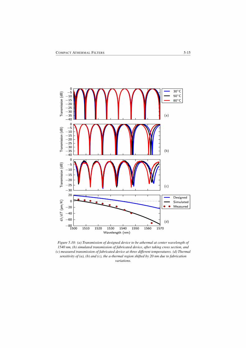
COMPACT ATHERMAL FILTERS 5-15
Figure 5.10: (a) Transmission of designed device to be athermal at center wavelength of1540 nm, (b) simulated transmission of fabricated device, after taking cross section, and
(c) measured transmission of fabricated device at three different temperatures. (d) Thermalsensitivity of (a), (b) and (c), the a-thermal region shifted by 20 nm due to fabrication
variations.
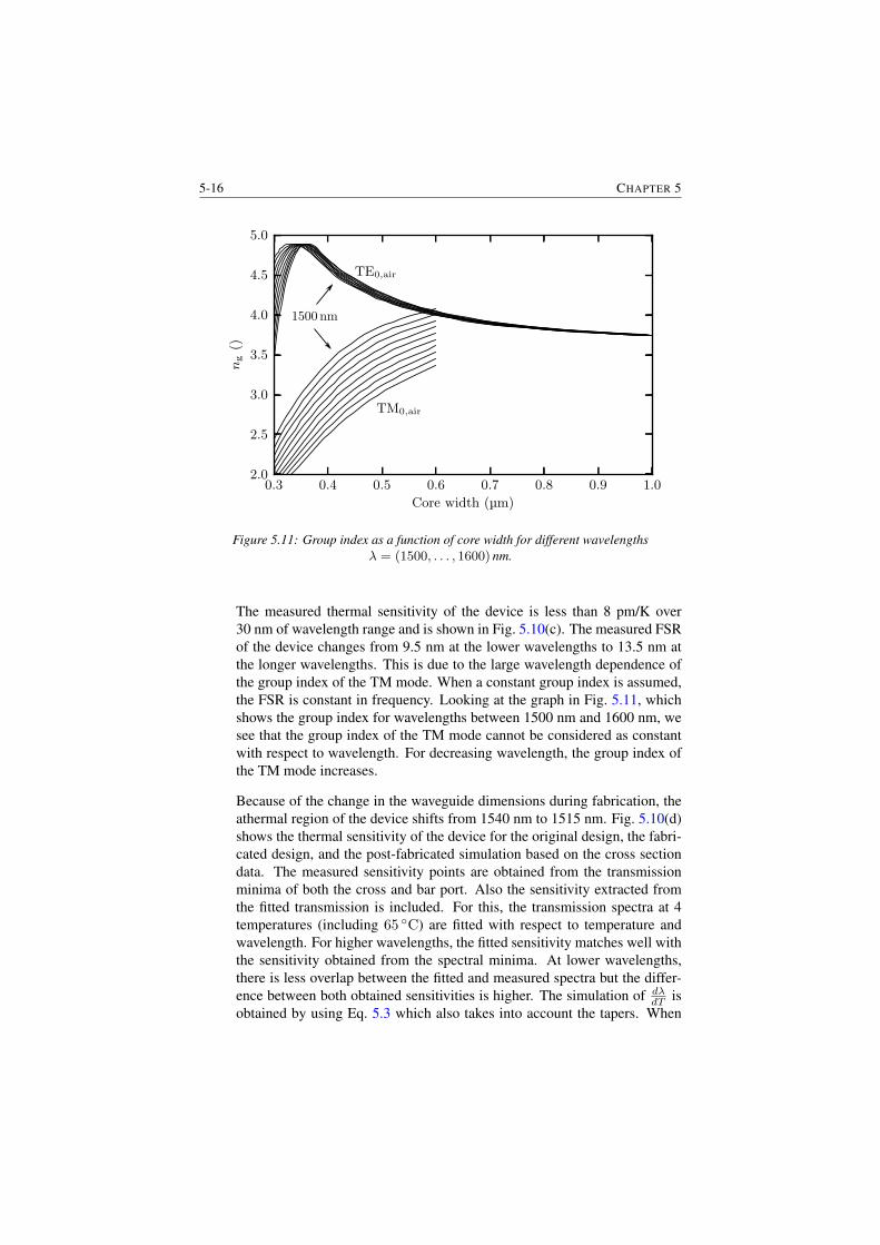
5-16 CHAPTER 5
Figure 5.11: Group index as a function of core width for different wavelengthsλ = (1500, . . . , 1600) nm.
The measured thermal sensitivity of the device is less than 8 pm/K over30 nm of wavelength range and is shown in Fig. 5.10(c). The measured FSRof the device changes from 9.5 nm at the lower wavelengths to 13.5 nm atthe longer wavelengths. This is due to the large wavelength dependence ofthe group index of the TM mode. When a constant group index is assumed,the FSR is constant in frequency. Looking at the graph in Fig. 5.11, whichshows the group index for wavelengths between 1500 nm and 1600 nm, wesee that the group index of the TM mode cannot be considered as constantwith respect to wavelength. For decreasing wavelength, the group index ofthe TM mode increases.
Because of the change in the waveguide dimensions during fabrication, theathermal region of the device shifts from 1540 nm to 1515 nm. Fig. 5.10(d)shows the thermal sensitivity of the device for the original design, the fabri-cated design, and the post-fabricated simulation based on the cross sectiondata. The measured sensitivity points are obtained from the transmissionminima of both the cross and bar port. Also the sensitivity extracted fromthe fitted transmission is included. For this, the transmission spectra at 4temperatures (including 65 ◦C) are fitted with respect to temperature andwavelength. For higher wavelengths, the fitted sensitivity matches well withthe sensitivity obtained from the spectral minima. At lower wavelengths,there is less overlap between the fitted and measured spectra but the differ-ence between both obtained sensitivities is higher. The simulation of dλ
dT isobtained by using Eq. 5.3 which also takes into account the tapers. When
COMPACT ATHERMAL FILTERS 5-17
Figure 5.12: Thermo-optic coefficients of TE and TM mode waveguides for the designedand the measured waveguide widths
using the same geometry and effective indices of the waveguide sections,the result of this equation is virtually identical with the sensitivity extractedfrom the spectra simulated with Caphe.
Furthermore, there is also a deviation of 5% between the measured widthand simulated width to obtain a simulated spectrum close to the measuredone. The uncertainty of SEM measurements is 3%. When the waveguidewidths obtained by SEM measurements are used in the simulations, an ather-mal wavelength at 1521 nm would be expected. The component is designedfor a wavelength of 1531 nm which takes into account the waveguide offsetsprovided by imec. The discrepancy between the measurements and the sim-ulation using the waveguide widths from the SEM measurements is due tothe mismatch between the actual optical parameters and the parameters usedin the circuit simulator.
It is also found that the TO coefficients are quite wavelength dependent andtherefore the device spectrum is red shifted with the increasing temperaturefor the wavelengths lower than the athermal point, while at longer wave-lengths the spectrum is blue shifted. The TO coefficients for the TE andthe TM mode of the designed and measured waveguide widths are shownin Fig. 5.12. It means for wavelengths larger than the athermal point, dλm
dTis negative, while it is positive for wavelengths smaller than the athermalpoint.
We have also characterized the SPR separately. The transmission spectrumof the SPR for cross coupling is shown in Fig. 5.13 for varying couplinglengths. It shows that the coupling length of 10 µm is the closest to the de-sired 3 dB of power transfer from the input to the TM mode in the other arm.
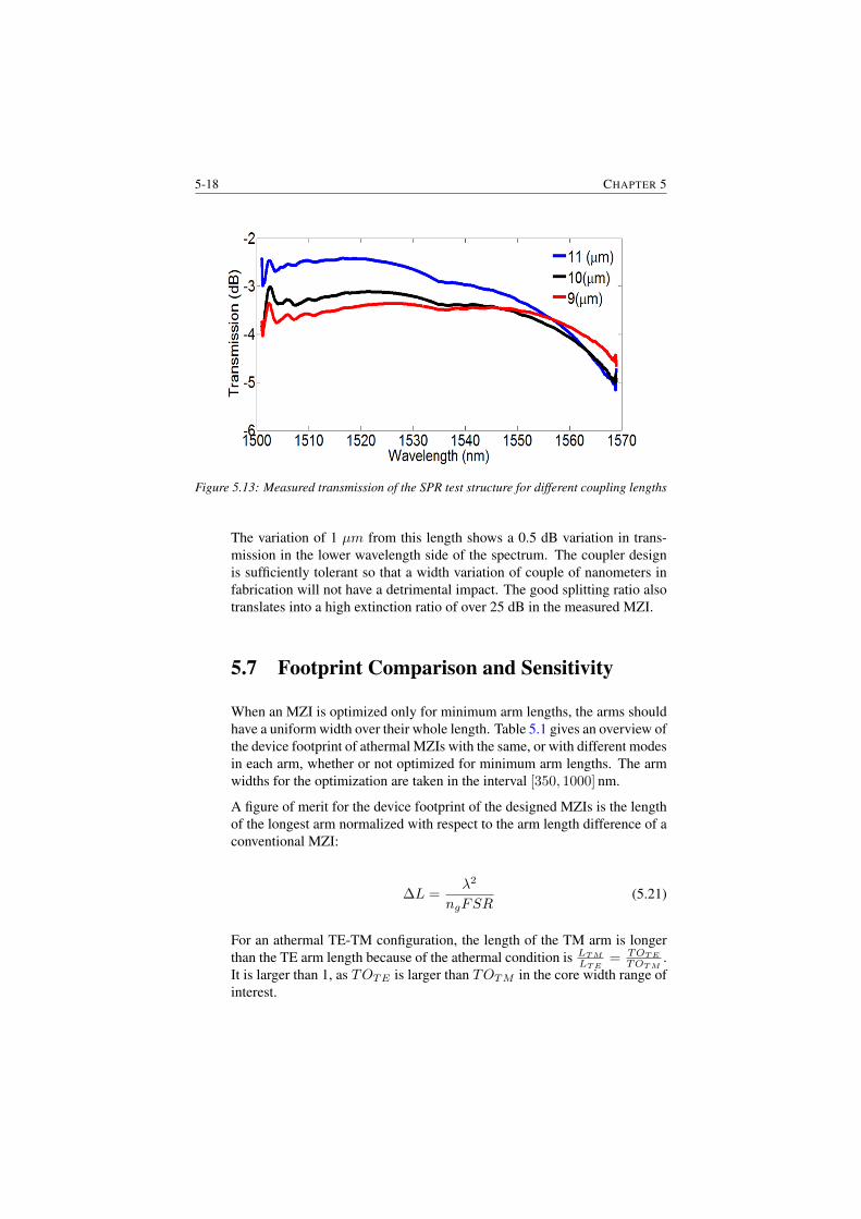
5-18 CHAPTER 5
Figure 5.13: Measured transmission of the SPR test structure for different coupling lengths
The variation of 1 µm from this length shows a 0.5 dB variation in trans-mission in the lower wavelength side of the spectrum. The coupler designis sufficiently tolerant so that a width variation of couple of nanometers infabrication will not have a detrimental impact. The good splitting ratio alsotranslates into a high extinction ratio of over 25 dB in the measured MZI.
5.7 Footprint Comparison and Sensitivity
When an MZI is optimized only for minimum arm lengths, the arms shouldhave a uniform width over their whole length. Table 5.1 gives an overview ofthe device footprint of athermal MZIs with the same, or with different modesin each arm, whether or not optimized for minimum arm lengths. The armwidths for the optimization are taken in the interval [350, 1000] nm.
A figure of merit for the device footprint of the designed MZIs is the lengthof the longest arm normalized with respect to the arm length difference of aconventional MZI:
∆L =λ2
ngFSR(5.21)
For an athermal TE-TM configuration, the length of the TM arm is longerthan the TE arm length because of the athermal condition is LTM
LTE= TOTE
TOTM.
It is larger than 1, as TOTE is larger than TOTM in the core width range ofinterest.
COMPACT ATHERMAL FILTERS 5-19
Mode arm 1 –Mode arm 2 w1 (nm) w2 (nm) L2
∆Lconv
()Optimized for
TE – TE 350 1000 6.91 Minimumarm length
TM – TM 350 1000 5.90 Minimumarm length
TE – TM 1000 350 2.90 Minimumarm length
TE – TM 450 450 3.31 –
Table 5.1: Comparison of device footprint between athermal MZIs with the same, or withdifferent polarizations in both arms.
When the optimum widths are compared with the graph of the TO coeffi-cients, it can be seen that the device footprint is minimum when the dif-ference in the TO coefficients is largest. For TE or TM polarizations, thedifference in TO coefficients is largest for a very small and a very largewaveguide width. For TE and TM polarizations, the difference in TO coeffi-cients is larger while the device footprint is smaller compared to waveguideswith only TE or TM polarizations.
Compared to a TE-TM MZI, the thermal sensitivity of a TE-TE MZI canbe small over a large wavelength range. A small sensitivity over a largewavelength range is obtained when the TO coefficient of the mode in thesecond arm has the same wavelength dependence as the TO coefficient of themode in the first arm scaled by a factor TO2
TO1
∣∣∣0. The difference between both
TO coefficients also needs to be as large as possible to obtain an acceptabledevice footprint. However, as can be seen in Fig. 5.14, the TO coefficients ofthe TE and TM modes do not follow the same slope for any combination ofwaveguide widths of interest. The factor TO2
TO1
∣∣∣0
is different from one whichmakes the wavelength dependent sensitivity higher. This explains that anathermal MZI based on TE and TM polarizations has a smaller athermalwavelength range than an athermal MZI with only TE polarization.
5.8 Applications
5.8.1 Sensing
Simulations are performed to test the sensing capabilities of the dual polar-ization MZI. Because we use two polarizations that have a very differentoverlap with the upper cladding, the MZI device can be used as a sensorwithout the need of a protective overcladding or selective sensing window
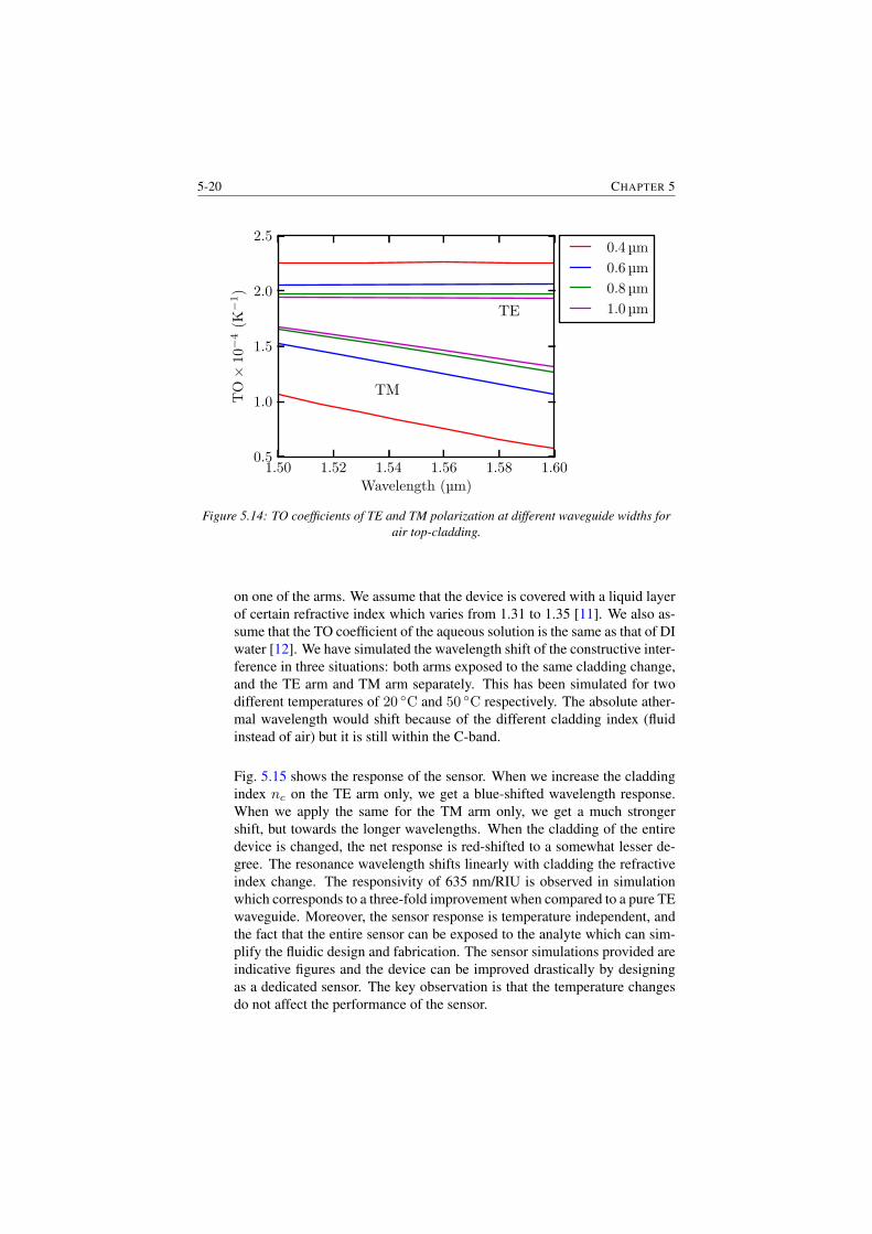
5-20 CHAPTER 5
TE
TM
Figure 5.14: TO coefficients of TE and TM polarization at different waveguide widths forair top-cladding.
on one of the arms. We assume that the device is covered with a liquid layerof certain refractive index which varies from 1.31 to 1.35 [11]. We also as-sume that the TO coefficient of the aqueous solution is the same as that of DIwater [12]. We have simulated the wavelength shift of the constructive inter-ference in three situations: both arms exposed to the same cladding change,and the TE arm and TM arm separately. This has been simulated for twodifferent temperatures of 20 ◦C and 50 ◦C respectively. The absolute ather-mal wavelength would shift because of the different cladding index (fluidinstead of air) but it is still within the C-band.
Fig. 5.15 shows the response of the sensor. When we increase the claddingindex nc on the TE arm only, we get a blue-shifted wavelength response.When we apply the same for the TM arm only, we get a much strongershift, but towards the longer wavelengths. When the cladding of the entiredevice is changed, the net response is red-shifted to a somewhat lesser de-gree. The resonance wavelength shifts linearly with cladding the refractiveindex change. The responsivity of 635 nm/RIU is observed in simulationwhich corresponds to a three-fold improvement when compared to a pure TEwaveguide. Moreover, the sensor response is temperature independent, andthe fact that the entire sensor can be exposed to the analyte which can sim-plify the fluidic design and fabrication. The sensor simulations provided areindicative figures and the device can be improved drastically by designingas a dedicated sensor. The key observation is that the temperature changesdo not affect the performance of the sensor.
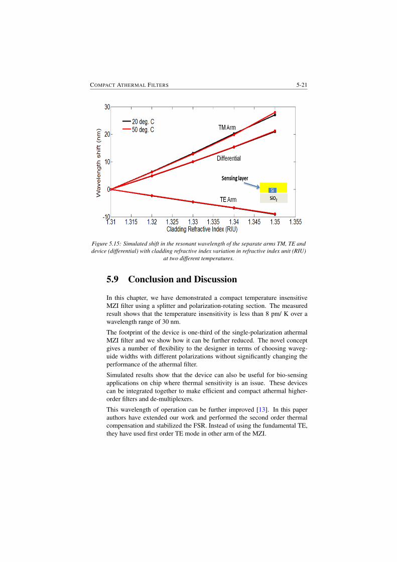
COMPACT ATHERMAL FILTERS 5-21
Figure 5.15: Simulated shift in the resonant wavelength of the separate arms TM, TE anddevice (differential) with cladding refractive index variation in refractive index unit (RIU)
at two different temperatures.
5.9 Conclusion and Discussion
In this chapter, we have demonstrated a compact temperature insensitiveMZI filter using a splitter and polarization-rotating section. The measuredresult shows that the temperature insensitivity is less than 8 pm/ K over awavelength range of 30 nm.
The footprint of the device is one-third of the single-polarization athermalMZI filter and we show how it can be further reduced. The novel conceptgives a number of flexibility to the designer in terms of choosing waveg-uide widths with different polarizations without significantly changing theperformance of the athermal filter.
Simulated results show that the device can also be useful for bio-sensingapplications on chip where thermal sensitivity is an issue. These devicescan be integrated together to make efficient and compact athermal higher-order filters and de-multiplexers.
This wavelength of operation can be further improved [13]. In this paperauthors have extended our work and performed the second order thermalcompensation and stabilized the FSR. Instead of using the fundamental TE,they have used first order TE mode in other arm of the MZI.
5-22 CHAPTER 5
References
[1] S. Dwivedi and W. Bogaerts. Integrated photonic devices with reducedsensitivity to external influences, July 7 2015. US Patent 9,075,251.
[2] Mutsunori Uenuma and Teruaki Motooka. Temperature-independentsilicon waveguide optical filter. Opt. Lett., 34(5):599–601, Mar 2009.
[3] Biswajeet Guha, Alexander Gondarenko, and Michal Lipson. Minimiz-ing temperature sensitivity of silicon Mach-Zehnder interferometers.Opt. Express, 18(3):1879–1887, Feb 2010.
[4] S. Dwivedi, H. D’heer, and W. Bogaerts. Maximizing Fabrication andThermal Tolerances of All-Silicon FIR Wavelength Filters. PhotonicsTechnology Letters, IEEE, 27(8):871–874, April 2015.
[5] S. Dwivedi, H. D’heer, and W. Bogaerts. A compact temperature in-sensitive filter using splitter polarization-rotating section. In Group IVPhotonics (GFP), 2013 IEEE 10th International Conference on, pages29–30, Aug 2013.
[6] Liu Liu, Yunhong Ding, Kresten Yvind, and Jørn M. Hvam. Silicon-on-insulator polarization splitting and rotating device for polarizationdiversity circuits. Opt. Express, 19(13):12646–12651, Jun 2011.
[7] Daoxin Dai and John E. Bowers. Novel concept for ultracompact po-larization splitter-rotator based on silicon nanowires. Opt. Express,19(11):10940–10949, May 2011.
[8] Philippe P. Absil, Peter Verheyen, Peter De Heyn, Marianna Pantou-vaki, Guy Lepage, Jeroen De Coster, and Joris Van Campenhout. Sil-icon photonics integrated circuits: a manufacturing platform for highdensity, low power optical I/O’s. Opt. Express, 23(7):9369–9378, Apr2015.
[9] F. Van Laere, T. Claes, Jonathan Schrauwen, S. Scheerlinck, W. Bo-gaerts, D. Taillaert, L. O’Faolain, D. Van Thourhout, and R. Baets.Compact Focusing Grating Couplers for Silicon-on-Insulator Inte-grated Circuits. Photonics Technology Letters, IEEE, 19(23):1919–1921, Dec 2007.
[10] http://www.lucedaphotonics.com/.
[11] Katrien De Vos, Irene Bartolozzi, Etienne Schacht, Peter Bienstman,and Roel Baets. Silicon-on-Insulator microring resonator for sensitiveand label-free biosensing. Opt. Express, 15(12):7610–7615, Jun 2007.
[12] Young Ho Kim, Seong Jun Park, Sie-Wook Jeon, Seongmin Ju, Chang-Soo Park, Won-Taek Han, and Byeong Ha Lee. Thermo-optic coeffi-cient measurement of liquids based on simultaneous temperature andrefractive index sensing capability of a two-mode fiber interferometricprobe. Opt. Express, 20(21):23744–23754, Oct 2012.

COMPACT ATHERMAL FILTERS 5-23
[13] Peng Xing and Jaime Viegas. Broadband CMOS-compatible SOItemperature insensitive Mach-Zehnder interferometer. Opt. Express,23(19):24098–24107, Sep 2015.

6Maximizing Fabrication and
Thermal tolerances of All-SiliconFIR wavelength filters
In the chapters (4-5) we have proposed and demonstrated a passive compen-sation of all silicon wavelength filters. In this chapter, we extend this con-cept, and explore the possibility of fabrication tolerances along with thermaltolerances.
6.1 Introduction
One of the most pronounced weaknesses of silicon nanophotonics is theneed of extremely precise fabrication, especially for passive wavelength fil-ter devices. The high index contrast and submicron waveguide dimensionswould translate any change in waveguide width and height into a substantialchange in the effective refractive index [1].
The fabrication processes have considerably improved with the availabilityof advanced lithographic and etching techniques. The major fab-lines movefrom 200 mm to 300 mm where the line-width variation is already in theorder of a few nanometers [2–4] and the loss of typical single mode stripwaveguides are less than a 1 dB/cm. However, these final few nano-meter
6-2 CHAPTER 6
precision still poses a very difficult issue for the accuracy of wavelengthfilters.
Fabrication variations can be actively compensated (e.g. with thermal tun-ing), but this drives up the power consumption and complicates the devicewith active control circuitry. Pre-fabrication or post-fabrication trimming ofthe components can be used to correct the effects of the last nanometer fab-rication offsets. However, it comes with a significantly increased cost of thewhole fabrication process [5, 6].
In this chapter, we demonstrate a technique to make a wavelength filter toler-ant to linewidth variations by design, without changing the fabrication pro-cess itself. We show that it is indeed possible to get a fabrication tolerantMZI filter by using different mode confinement in the arms of the filter.Also, since simultaneous fabrication and thermal tolerances are needed tomake the SOI platform truly robust, we extend the technique and show thatit can used to make the circuit tolerant both to linewidth variations and am-bient temperature fluctuations. Simulations show that the technique can beused for higher order filters with multiple channels.
6.2 Proposed Method
The wavelength sensitivity expression of any FIR filter is given in Eq. 4.2as mentioned in chapter (4).
The wavelength shift of an MZI is around 1 nm and 1.4 nm for 1 nm changein the waveguide width and thickness, respectively. These variations holdgood for all waveguide based FIR filtering devices on SOI.
To compensate the wavelength sensitivity due to the fabrication variations,we introduce design variations such as different waveguide width in eacharm as mentioned in section 4.3. The modified expression for the sensitivitythen becomes the modified form of Eq. 4.13:
dλ
dX=
λ
ng1.L1 − ng2.L2.(dneff1.L1
dX− dneff2.L2
dX) (6.1)
which we try to minimize. This is a first-order approximation. Here, Xcan be the waveguide width w, height h instead of temperature T or anyother influence. We assume here that the influence affects the entire deviceuniformly. λm is the wavelength of operation, and ng is the group index.
For a device tolerant to width variations, the condition for zero sensitivity atwavelength and for a given free spectral range (FSR) becomes:
L1
L2=
∂neff,2
∂w∂neff,1
∂w
∣∣∣∣∣geometry, λ0, T0
. (6.2)
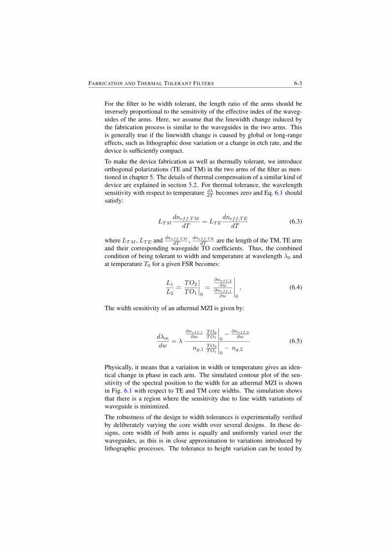
FABRICATION AND THERMAL TOLERANT FILTERS 6-3
For the filter to be width tolerant, the length ratio of the arms should beinversely proportional to the sensitivity of the effective index of the waveg-uides of the arms. Here, we assume that the linewidth change induced bythe fabrication process is similar to the waveguides in the two arms. Thisis generally true if the linewidth change is caused by global or long-rangeeffects, such as lithographic dose variation or a change in etch rate, and thedevice is sufficiently compact.
To make the device fabrication as well as thermally tolerant, we introduceorthogonal polarizations (TE and TM) in the two arms of the filter as men-tioned in chapter 5. The details of thermal compensation of a similar kind ofdevice are explained in section 5.2. For thermal tolerance, the wavelengthsensitivity with respect to temperature dλ
dT becomes zero and Eq. 6.1 shouldsatisfy:
LTMdneff,TM
dT= LTE
dneff,TEdT
(6.3)
where LTM , LTE and dneff,TM
dT , dneff,TE
dT are the length of the TM, TE armand their corresponding waveguide TO coefficients. Thus, the combinedcondition of being tolerant to width and temperature at wavelength λ0 andat temperature T0 for a given FSR becomes:
L1
L2=TO2
TO1
∣∣∣∣0
=∂neff,2
∂w∂neff,1
∂w
∣∣∣∣∣0
, (6.4)
The width sensitivity of an athermal MZI is given by:
dλmdw
= λ
∂neff,1
∂wTO2
TO1
∣∣∣0− ∂neff,2
∂w
ng,1TO2
TO1
∣∣∣0− ng,2
(6.5)
Physically, it means that a variation in width or temperature gives an iden-tical change in phase in each arm. The simulated contour plot of the sen-sitivity of the spectral position to the width for an athermal MZI is shownin Fig. 6.1 with respect to TE and TM core widths. The simulation showsthat there is a region where the sensitivity due to line width variations ofwaveguide is minimized.
The robustness of the design to width tolerances is experimentally verifiedby deliberately varying the core width over several designs. In these de-signs, core width of both arms is equally and uniformly varied over thewaveguides, as this is in close approximation to variations introduced bylithographic processes. The tolerance to height variation can be tested by
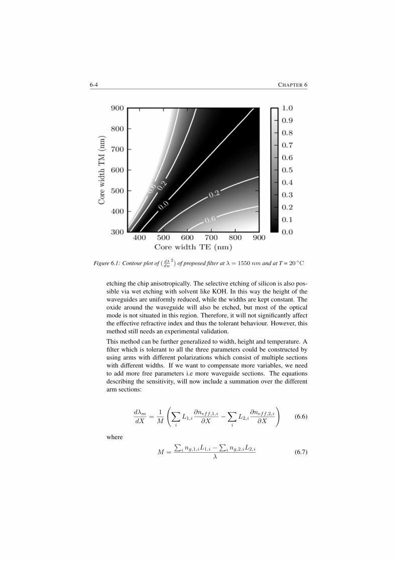
6-4 CHAPTER 6
Figure 6.1: Contour plot of ( dλdw
2) of proposed filter at λ = 1550 nm and at T = 20 ◦C
etching the chip anisotropically. The selective etching of silicon is also pos-sible via wet etching with solvent like KOH. In this way the height of thewaveguides are uniformly reduced, while the widths are kept constant. Theoxide around the waveguide will also be etched, but most of the opticalmode is not situated in this region. Therefore, it will not significantly affectthe effective refractive index and thus the tolerant behaviour. However, thismethod still needs an experimental validation.
This method can be further generalized to width, height and temperature. Afilter which is tolerant to all the three parameters could be constructed byusing arms with different polarizations which consist of multiple sectionswith different widths. If we want to compensate more variables, we needto add more free parameters i.e more waveguide sections. The equationsdescribing the sensitivity, will now include a summation over the differentarm sections:
dλmdX
=1
M
(∑i
L1,i∂neff,1,i∂X
−∑i
L2,i∂neff,2,i∂X
)(6.6)
where
M =
∑i ng,1,iL1,i −
∑i ng,2,iL2,i
λ(6.7)
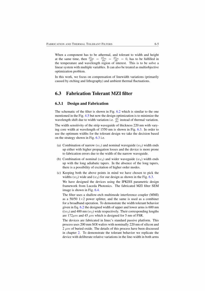
FABRICATION AND THERMAL TOLERANT FILTERS 6-5
When a component has to be athermal, and tolerant to width and heightat the same time, then dλm
dT = dλm
dw = dλm
dh = 0, has to be fulfilled inthe temperature and wavelength region of interest. This is to be solve alinear system with multiple variables. It can also be treated as multiobjectiveoptimization problem.
In this work, we focus on compensation of linewidth variations (primarilycaused by etching and lithography) and ambient thermal fluctuations.
6.3 Fabrication Tolerant MZI filter
6.3.1 Design and Fabrication
The schematic of the filter is shown in Fig. 6.2 which is similar to the onementioned in the Fig. 4.5 but now the design optimization is to minimize thewavelength shift due to width variation i.e. dλ
dw instead of thermal variation.
The width sensitivity of the strip waveguide of thickness 220 nm with vary-ing core width at wavelength of 1550 nm is shown in Fig. 6.3. In order touse the optimum widths for the tolerant design we take the decision basedon the strategy shown in Fig. 6.3 i.e.
(a) Combination of narrow (w1) and nominal waveguide (w2) width endsup either with higher propagation losses and the device is more proneto fabrication errors due to the width of the narrow waveguide.
(b) Combination of nominal (w2) and wider waveguide (w4) width endsup with the long adiabatic tapers. In the absence of the long tapers,there is a possibility of excitation of higher order modes.
(c) Keeping both the above points in mind we have chosen to pick thewidths (w2) wide and (w3) for our design as shown in the Fig. 6.3.We have designed the devices using the IPKISS parametric designframework from Luceda Photonics. The fabricated MZI filter SEMimage is shown in Fig. 6.4.The filter uses a shallow-etch multimode interference coupler (MMI)as a 50/50 1×2 power splitter, and the same is used as a combinerfor a broadband operation. To demonstrate the width tolerant behaviorgiven in Eq. 6.2 the designed width of upper and lower arms is 600 nm((w3) and 400 nm (w2) wide respectively. Their corresponding lengthsare 172µm and 45 µm which is designed for 5 nm of FSR.The devices are fabricated in Imec’s standard passive platform. Thisprocess uses 200 mm SOI wafers with nominally 220 nm of silicon and2 µm of buried oxide. The details of this process have been discussedin chapter 2. To demonstrate the tolerant behavior we replicate thedevice with deliberate relative variations in the line-width in both arms
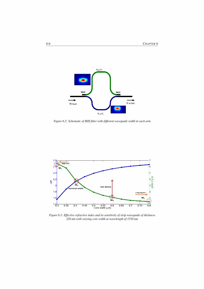
6-6 CHAPTER 6
Figure 6.2: Schematic of MZI filter with different waveguide width in each arm
Figure 6.3: Effective refractive index and its sensitivity of strip waveguide of thickness220 nm with varying core width at wavelength of 1550 nm
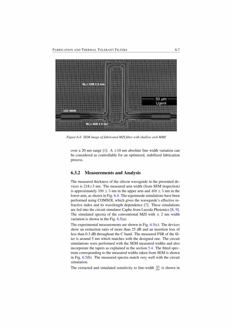
FABRICATION AND THERMAL TOLERANT FILTERS 6-7
Figure 6.4: SEM image of fabricated MZI filter with shallow etch MMI
over a 20 nm range [1]. A ±10 nm absolute line width variation canbe considered as controllable for an optimized, stabilized fabricationprocess.
6.3.2 Measurements and Analysis
The measured thickness of the silicon waveguide in the presented de-vices is 218±3 nm. The measured arm width (from SEM inspection)is approximately 598 ± 5 nm in the upper arm and 408 ± 5 nm in thelower arm, as shown in Fig. 6.4. The eigenmode simulations have beenperformed using COMSOL which gives the waveguide’s effective re-fractive index and its wavelength dependence [7]. These simulationsare fed into the circuit simulator Caphe from Luceda Photonics [8, 9].The simulated spectra of the conventional MZI with ± 2 nm widthvariation is shown in the Fig. 6.5(a).The experimental measurements are shown in Fig. 6.5(c). The devicesshow an extinction ratio of more than 25 dB and an insertion loss ofless than 0.3 dB throughout the C band. The measured FSR of the fil-ter is around 5 nm which matches with the designed one. The circuitsimulations were performed with the SEM measured widths and alsoincorporate the tapers as explained in the section 5.4. The fitted spec-trum corresponding to the measured widths taken from SEM is shownin Fig. 6.5(b). The measured spectra match very well with the circuitsimulation.The extracted and simulated sensitivity to line-width dλ
dw is shown in
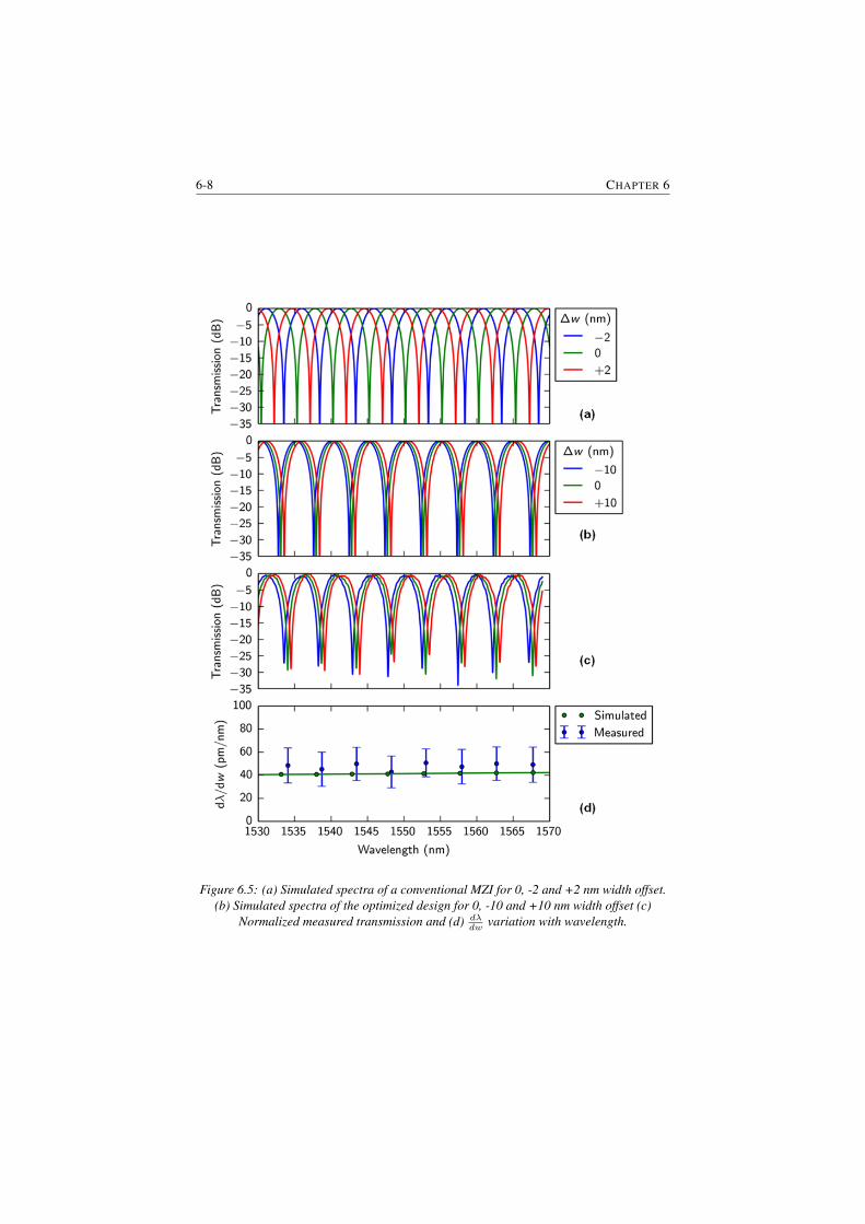
6-8 CHAPTER 6
Figure 6.5: (a) Simulated spectra of a conventional MZI for 0, -2 and +2 nm width offset.(b) Simulated spectra of the optimized design for 0, -10 and +10 nm width offset (c)
Normalized measured transmission and (d) dλdw
variation with wavelength.
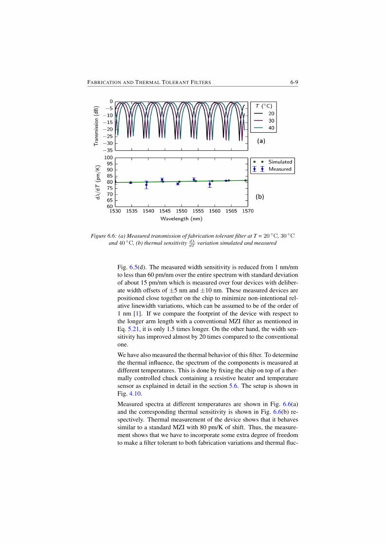
FABRICATION AND THERMAL TOLERANT FILTERS 6-9
Figure 6.6: (a) Measured transmission of fabrication tolerant filter at T = 20 ◦C, 30 ◦Cand 40 ◦C, (b) thermal sensitivity dλ
dTvariation simulated and measured
Fig. 6.5(d). The measured width sensitivity is reduced from 1 nm/nmto less than 60 pm/nm over the entire spectrum with standard deviationof about 15 pm/nm which is measured over four devices with deliber-ate width offsets of ±5 nm and ±10 nm. These measured devices arepositioned close together on the chip to minimize non-intentional rel-ative linewidth variations, which can be assumed to be of the order of1 nm [1]. If we compare the footprint of the device with respect tothe longer arm length with a conventional MZI filter as mentioned inEq. 5.21, it is only 1.5 times longer. On the other hand, the width sen-sitivity has improved almost by 20 times compared to the conventionalone.
We have also measured the thermal behavior of this filter. To determinethe thermal influence, the spectrum of the components is measured atdifferent temperatures. This is done by fixing the chip on top of a ther-mally controlled chuck containing a resistive heater and temperaturesensor as explained in detail in the section 5.6. The setup is shown inFig. 4.10.
Measured spectra at different temperatures are shown in Fig. 6.6(a)and the corresponding thermal sensitivity is shown in Fig. 6.6(b) re-spectively. Thermal measurement of the device shows that it behavessimilar to a standard MZI with 80 pm/K of shift. Thus, the measure-ment shows that we have to incorporate some extra degree of freedomto make a filter tolerant to both fabrication variations and thermal fluc-
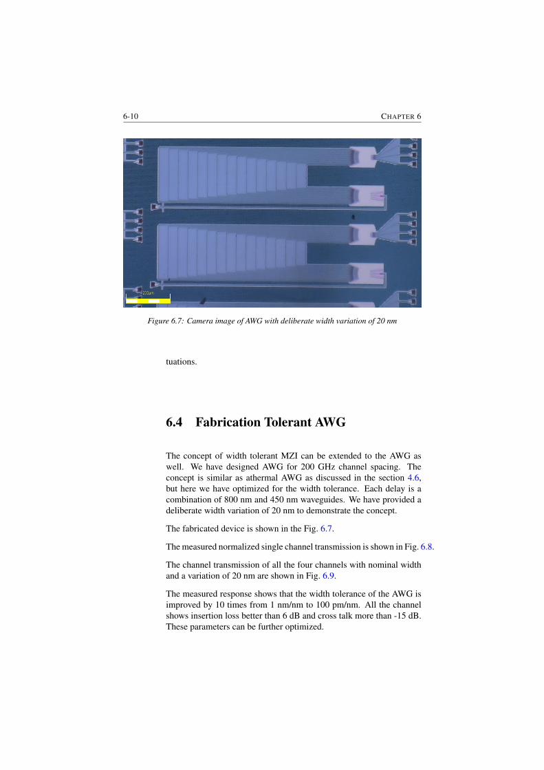
6-10 CHAPTER 6
Figure 6.7: Camera image of AWG with deliberate width variation of 20 nm
tuations.
6.4 Fabrication Tolerant AWG
The concept of width tolerant MZI can be extended to the AWG aswell. We have designed AWG for 200 GHz channel spacing. Theconcept is similar as athermal AWG as discussed in the section 4.6,but here we have optimized for the width tolerance. Each delay is acombination of 800 nm and 450 nm waveguides. We have provided adeliberate width variation of 20 nm to demonstrate the concept.
The fabricated device is shown in the Fig. 6.7.
The measured normalized single channel transmission is shown in Fig. 6.8.
The channel transmission of all the four channels with nominal widthand a variation of 20 nm are shown in Fig. 6.9.
The measured response shows that the width tolerance of the AWG isimproved by 10 times from 1 nm/nm to 100 pm/nm. All the channelshows insertion loss better than 6 dB and cross talk more than -15 dB.These parameters can be further optimized.
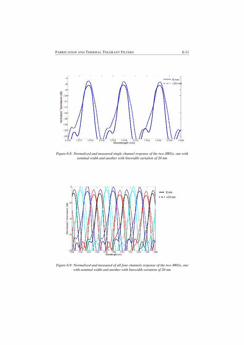
FABRICATION AND THERMAL TOLERANT FILTERS 6-11
Figure 6.8: Normalized and measured single channel response of the two AWGs, one withnominal width and another with linewidth variation of 20 nm
Figure 6.9: Normalized and measured of all four channels response of the two AWGs, onewith nominal width and another with linewidth variation of 20 nm
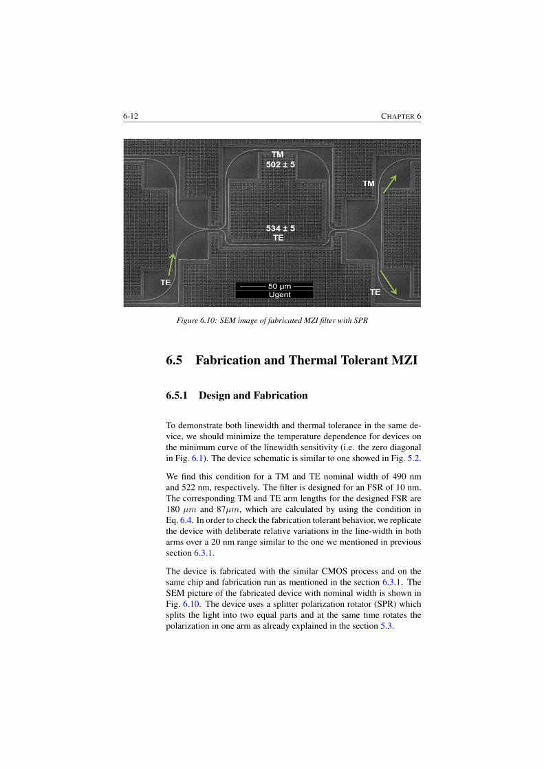
6-12 CHAPTER 6
Figure 6.10: SEM image of fabricated MZI filter with SPR
6.5 Fabrication and Thermal Tolerant MZI
6.5.1 Design and Fabrication
To demonstrate both linewidth and thermal tolerance in the same de-vice, we should minimize the temperature dependence for devices onthe minimum curve of the linewidth sensitivity (i.e. the zero diagonalin Fig. 6.1). The device schematic is similar to one showed in Fig. 5.2.
We find this condition for a TM and TE nominal width of 490 nmand 522 nm, respectively. The filter is designed for an FSR of 10 nm.The corresponding TM and TE arm lengths for the designed FSR are180 µm and 87µm, which are calculated by using the condition inEq. 6.4. In order to check the fabrication tolerant behavior, we replicatethe device with deliberate relative variations in the line-width in botharms over a 20 nm range similar to the one we mentioned in previoussection 6.3.1.
The device is fabricated with the similar CMOS process and on thesame chip and fabrication run as mentioned in the section 6.3.1. TheSEM picture of the fabricated device with nominal width is shown inFig. 6.10. The device uses a splitter polarization rotator (SPR) whichsplits the light into two equal parts and at the same time rotates thepolarization in one arm as already explained in the section 5.3.
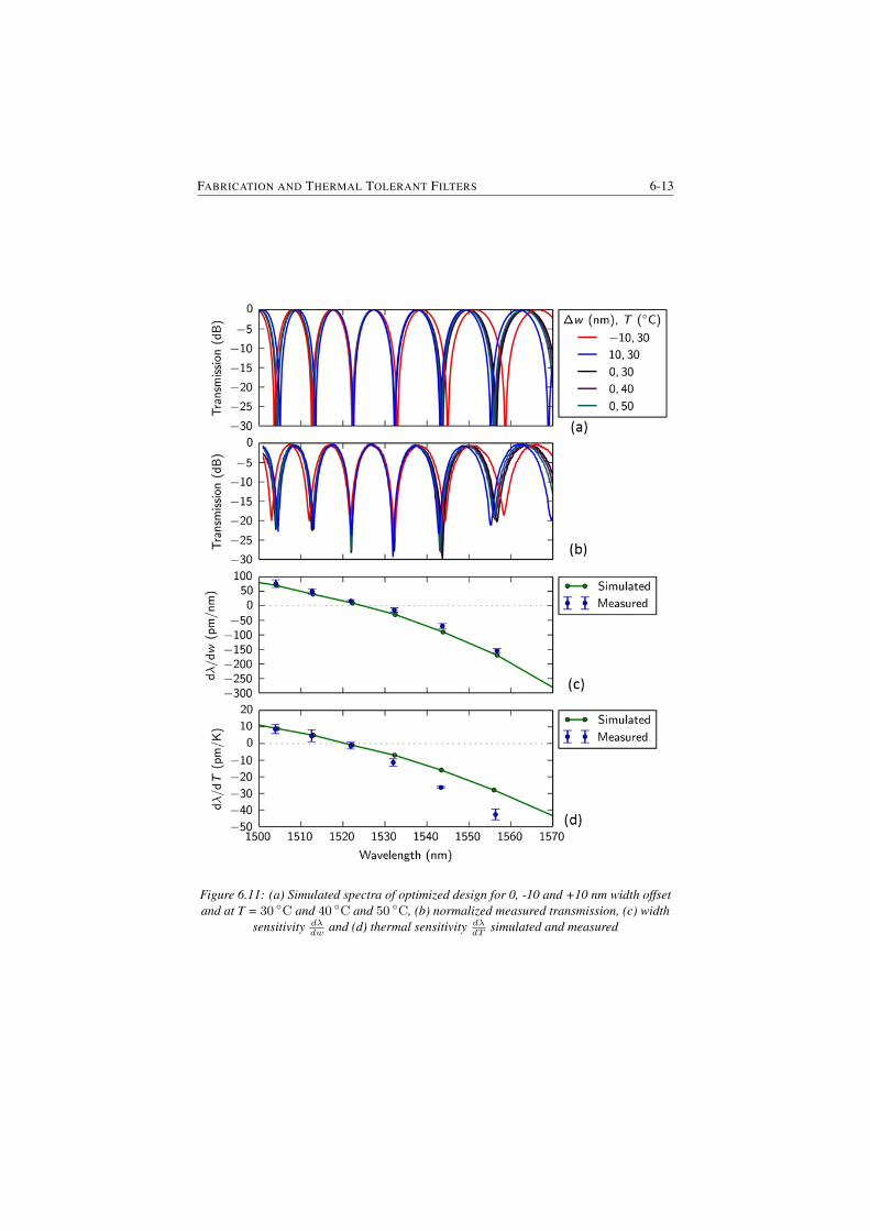
FABRICATION AND THERMAL TOLERANT FILTERS 6-13
Figure 6.11: (a) Simulated spectra of optimized design for 0, -10 and +10 nm width offsetand at T = 30 ◦C and 40 ◦C and 50 ◦C, (b) normalized measured transmission, (c) width
sensitivity dλdw
and (d) thermal sensitivity dλdT
simulated and measured
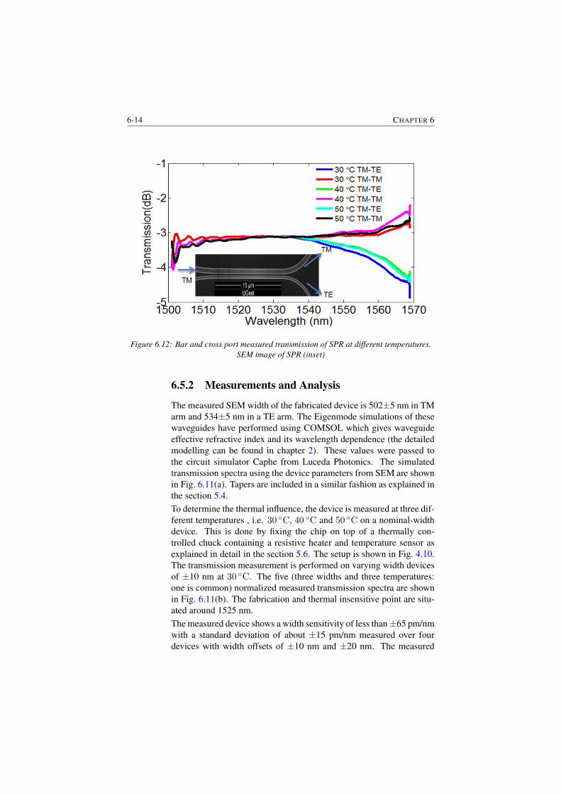
6-14 CHAPTER 6
Figure 6.12: Bar and cross port measured transmission of SPR at different temperatures.SEM image of SPR (inset)
6.5.2 Measurements and Analysis
The measured SEM width of the fabricated device is 502±5 nm in TMarm and 534±5 nm in a TE arm. The Eigenmode simulations of thesewaveguides have performed using COMSOL which gives waveguideeffective refractive index and its wavelength dependence (the detailedmodelling can be found in chapter 2). These values were passed tothe circuit simulator Caphe from Luceda Photonics. The simulatedtransmission spectra using the device parameters from SEM are shownin Fig. 6.11(a). Tapers are included in a similar fashion as explained inthe section 5.4.To determine the thermal influence, the device is measured at three dif-ferent temperatures , i.e. 30 ◦C, 40 ◦C and 50 ◦C on a nominal-widthdevice. This is done by fixing the chip on top of a thermally con-trolled chuck containing a resistive heater and temperature sensor asexplained in detail in the section 5.6. The setup is shown in Fig. 4.10.The transmission measurement is performed on varying width devicesof ±10 nm at 30 ◦C. The five (three widths and three temperatures:one is common) normalized measured transmission spectra are shownin Fig. 6.11(b). The fabrication and thermal insensitive point are situ-ated around 1525 nm.The measured device shows a width sensitivity of less than±65 pm/nmwith a standard deviation of about ±15 pm/nm measured over fourdevices with width offsets of ±10 nm and ±20 nm. The measured
FABRICATION AND THERMAL TOLERANT FILTERS 6-15
thermal sensitivity is less than ±15 pm/K with a standard deviation ofabout 3 pm/K over the wide wavelength range of 40 nm from 1501 to1540 nm. The simulated and measured width as well as the thermalsensitivity are shown in the Fig. 6.11(c) and Fig. 6.11(d) respectively.The simulated spectra match very well with the measured device whichconfirms the accuracy of the circuit model.
The width sensitivity changes from positive to negative on the differentsides of the insensitivity point. A similar behavior can be seen whilevarying the temperature of the device. This phenomenon is due tothe neff variation with w (dneff
dw ) and T (dneff
dT ) for TM waveguidewith increasing wavelength. This variation changes at much faster ratethan in the TE waveguide. If we compare the response with the widthtolerant device shown in Fig. 6.5, the wider waveguide is always redshifted over the entire wavelength range and width sensitivity is muchflatter.
We have characterized the SPR separately for completeness of themeasurements since these devices have been fabricated in a differentfabrication run compared to the one which is fabricated and measuredin the section 5.6.2.
The measured transmission of the SPR at different temperatures isshown in Fig. 6.12. The SPR is designed for equal power splittingin C-band, but we do see a deviation from that value for longer wave-lengths. This will not significantly affect the athermal/width tolerantbehavior, but it will result in a lower extinction ratio of the MZI.
6.5.3 Footprint Analysis
The device is fairly compact due to large difference in TO coefficientsbetween the arms, as shown in the Fig. 5.1. Fig. 6.13 displays theratio of the required longest arm length of the presented fabrication andthermal tolerant MZI, to the arm length difference of a conventionalMZI with a core width of 450 nm. The required longest arm length is3.2 times longer than the conventional MZI. The comparison is madewith the demonstrated filter which is designed for FSR of 10 nm.
6.6 Higher Order Filters
The next step is to use these presented integral components to buildhigher order filters for different WDM applications.
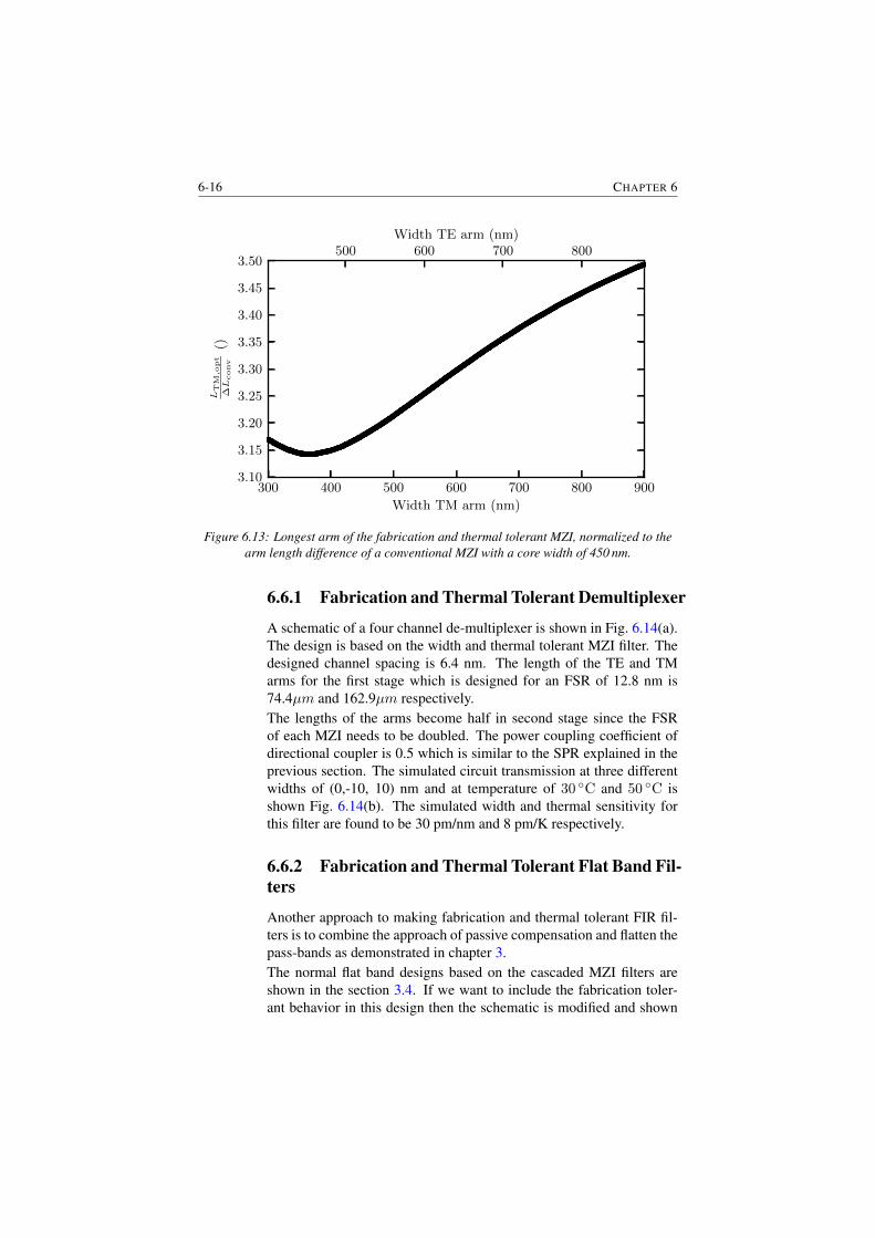
6-16 CHAPTER 6
300 400 500 600 700 800 900
Width TM arm (nm)
3.10
3.15
3.20
3.25
3.30
3.35
3.40
3.45
3.50
LT
M,o
pt
∆L
conv
()
500 600 700 800Width TE arm (nm)
Figure 6.13: Longest arm of the fabrication and thermal tolerant MZI, normalized to thearm length difference of a conventional MZI with a core width of 450 nm.
6.6.1 Fabrication and Thermal Tolerant Demultiplexer
A schematic of a four channel de-multiplexer is shown in Fig. 6.14(a).The design is based on the width and thermal tolerant MZI filter. Thedesigned channel spacing is 6.4 nm. The length of the TE and TMarms for the first stage which is designed for an FSR of 12.8 nm is74.4µm and 162.9µm respectively.The lengths of the arms become half in second stage since the FSRof each MZI needs to be doubled. The power coupling coefficient ofdirectional coupler is 0.5 which is similar to the SPR explained in theprevious section. The simulated circuit transmission at three differentwidths of (0,-10, 10) nm and at temperature of 30 ◦C and 50 ◦C isshown Fig. 6.14(b). The simulated width and thermal sensitivity forthis filter are found to be 30 pm/nm and 8 pm/K respectively.
6.6.2 Fabrication and Thermal Tolerant Flat Band Fil-ters
Another approach to making fabrication and thermal tolerant FIR fil-ters is to combine the approach of passive compensation and flatten thepass-bands as demonstrated in chapter 3.The normal flat band designs based on the cascaded MZI filters areshown in the section 3.4. If we want to include the fabrication toler-ant behavior in this design then the schematic is modified and shown
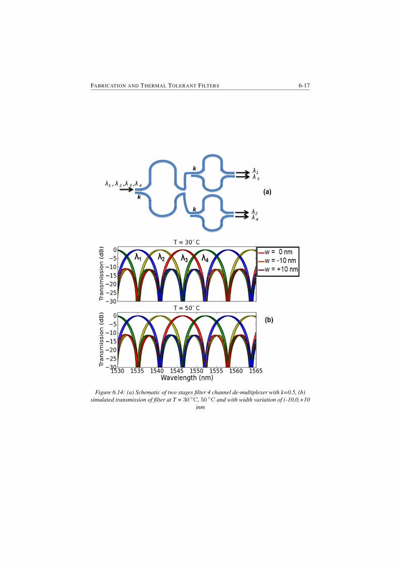
FABRICATION AND THERMAL TOLERANT FILTERS 6-17
Figure 6.14: (a) Schematic of two stages filter 4 channel de-multiplexer with k=0.5, (b)simulated transmission of filter at T = 30 ◦C, 50 ◦C and with width variation of (-10,0,+10
)nm
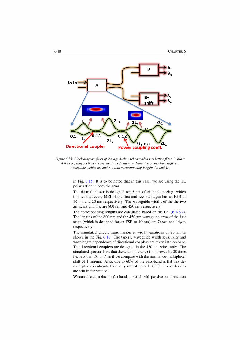
6-18 CHAPTER 6
Figure 6.15: Block diagram filter of 2-stage 4-channel cascaded mzi lattice filter. In blockA the coupling coefficients are mentioned and now delay line comes from different
waveguide widths w1 and w2 with corresponding lengths L1 and L2
in Fig. 6.15. It is to be noted that in this case, we are using the TEpolarization in both the arms.The de-multiplexer is designed for 5 nm of channel spacing; whichimplies that every MZI of the first and second stages has an FSR of10 nm and 20 nm respectively. The waveguide widths of the the twoarms, w1 and w2, are 800 nm and 450 nm respectively.The corresponding lengths are calculated based on the Eq. (6.1-6.2).The lengths of the 800 nm and the 450 nm waveguide arms of the firststage (which is designed for an FSR of 10 nm) are 76µm and 14µmrespectively.The simulated circuit transmission at width variations of 20 nm isshown in the Fig. 6.16. The tapers, waveguide width sensitivity andwavelength dependence of directional couplers are taken into account.The directional couplers are designed in the 450 nm wires only. Thesimulated spectra show that the width tolerance is improved by 20 timesi.e. less than 50 pm/nm if we compare with the normal de-multiplexershift of 1 nm/nm. Also, due to 60% of the pass-band is flat this de-multiplexer is already thermally robust upto ±15 ◦C. These devicesare still in fabrication.We can also combine the flat band approach with passive compensation
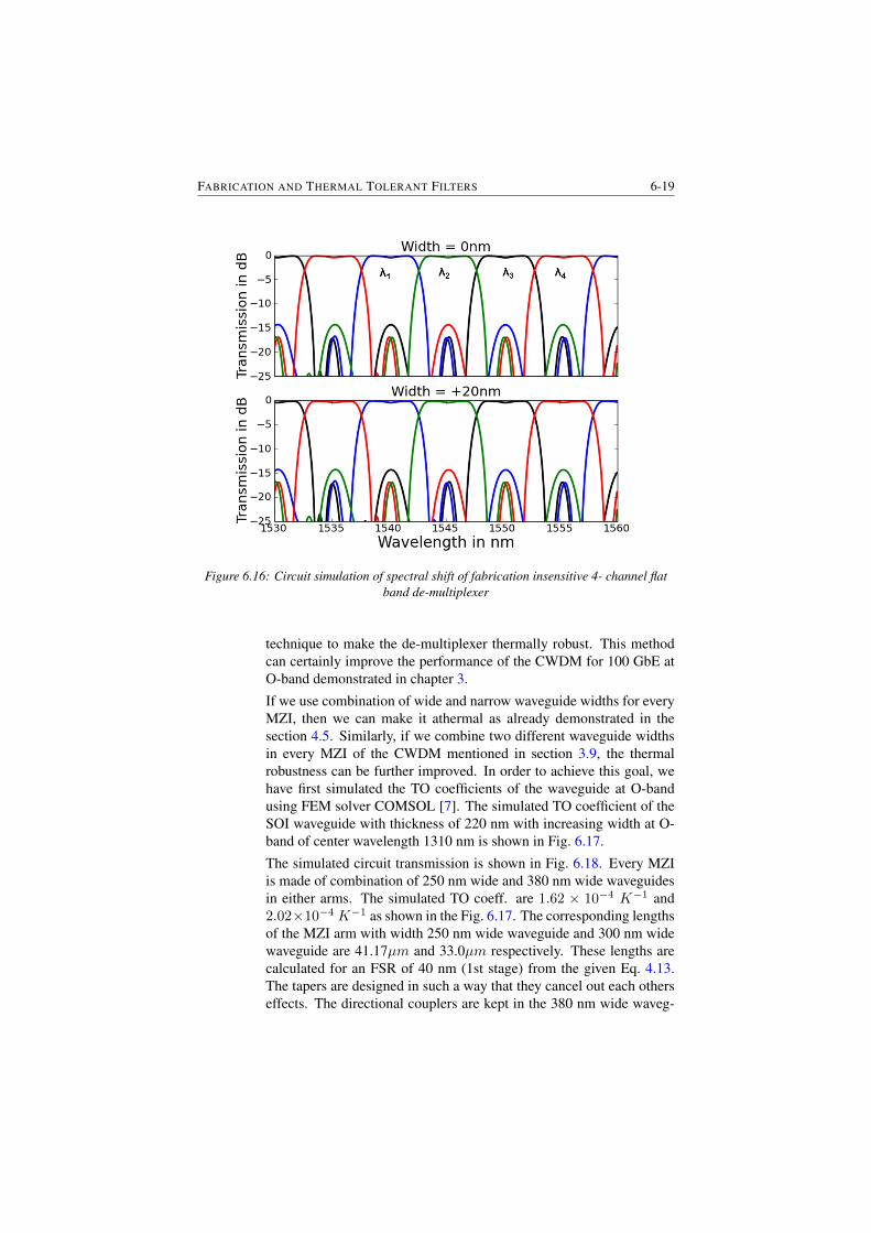
FABRICATION AND THERMAL TOLERANT FILTERS 6-19
Figure 6.16: Circuit simulation of spectral shift of fabrication insensitive 4- channel flatband de-multiplexer
technique to make the de-multiplexer thermally robust. This methodcan certainly improve the performance of the CWDM for 100 GbE atO-band demonstrated in chapter 3.
If we use combination of wide and narrow waveguide widths for everyMZI, then we can make it athermal as already demonstrated in thesection 4.5. Similarly, if we combine two different waveguide widthsin every MZI of the CWDM mentioned in section 3.9, the thermalrobustness can be further improved. In order to achieve this goal, wehave first simulated the TO coefficients of the waveguide at O-bandusing FEM solver COMSOL [7]. The simulated TO coefficient of theSOI waveguide with thickness of 220 nm with increasing width at O-band of center wavelength 1310 nm is shown in Fig. 6.17.
The simulated circuit transmission is shown in Fig. 6.18. Every MZIis made of combination of 250 nm wide and 380 nm wide waveguidesin either arms. The simulated TO coeff. are 1.62 × 10⁻⁴ K−1 and2.02×10−4 K−1 as shown in the Fig. 6.17. The corresponding lengthsof the MZI arm with width 250 nm wide waveguide and 300 nm widewaveguide are 41.17µm and 33.0µm respectively. These lengths arecalculated for an FSR of 40 nm (1st stage) from the given Eq. 4.13.The tapers are designed in such a way that they cancel out each otherseffects. The directional couplers are kept in the 380 nm wide waveg-
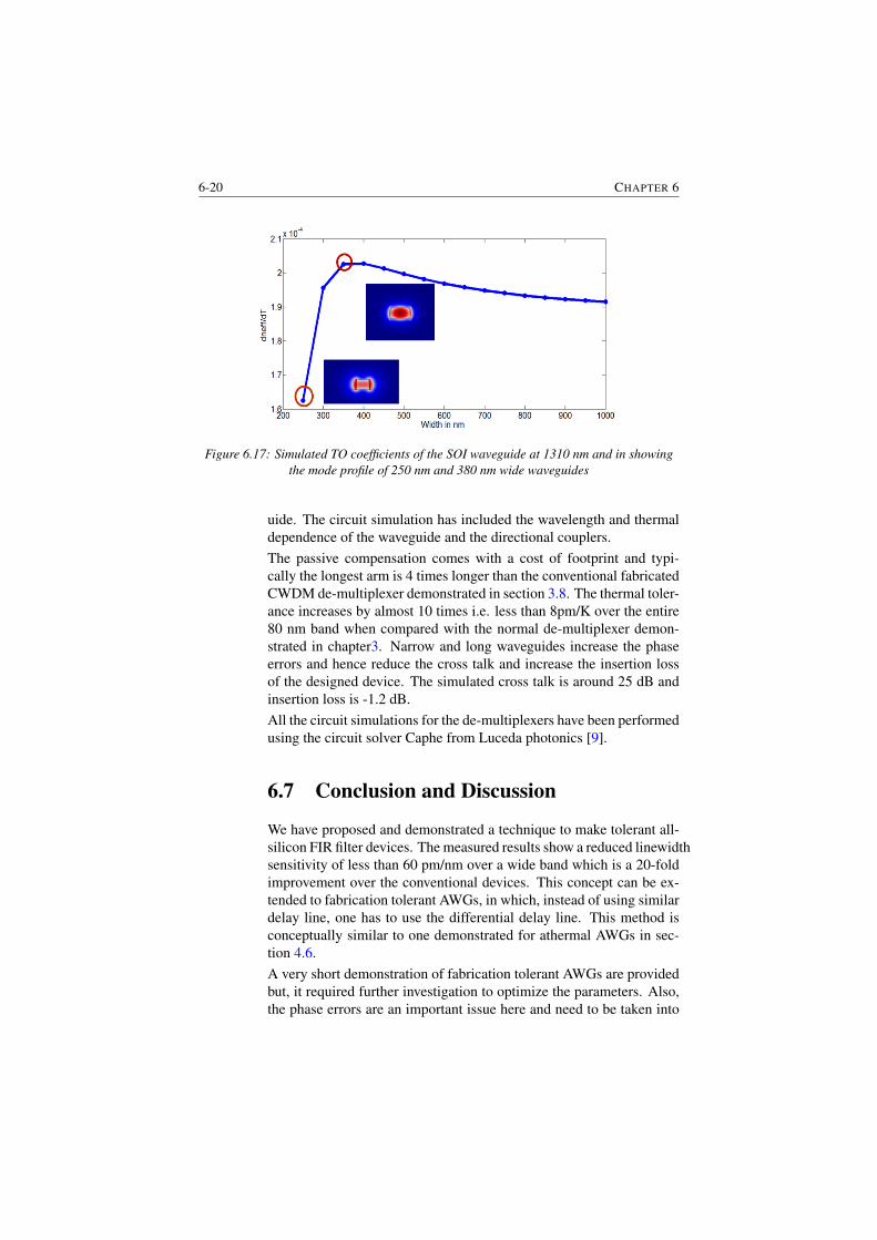
6-20 CHAPTER 6
Figure 6.17: Simulated TO coefficients of the SOI waveguide at 1310 nm and in showingthe mode profile of 250 nm and 380 nm wide waveguides
uide. The circuit simulation has included the wavelength and thermaldependence of the waveguide and the directional couplers.The passive compensation comes with a cost of footprint and typi-cally the longest arm is 4 times longer than the conventional fabricatedCWDM de-multiplexer demonstrated in section 3.8. The thermal toler-ance increases by almost 10 times i.e. less than 8pm/K over the entire80 nm band when compared with the normal de-multiplexer demon-strated in chapter3. Narrow and long waveguides increase the phaseerrors and hence reduce the cross talk and increase the insertion lossof the designed device. The simulated cross talk is around 25 dB andinsertion loss is -1.2 dB.All the circuit simulations for the de-multiplexers have been performedusing the circuit solver Caphe from Luceda photonics [9].
6.7 Conclusion and Discussion
We have proposed and demonstrated a technique to make tolerant all-silicon FIR filter devices. The measured results show a reduced linewidthsensitivity of less than 60 pm/nm over a wide band which is a 20-foldimprovement over the conventional devices. This concept can be ex-tended to fabrication tolerant AWGs, in which, instead of using similardelay line, one has to use the differential delay line. This method isconceptually similar to one demonstrated for athermal AWGs in sec-tion 4.6.A very short demonstration of fabrication tolerant AWGs are providedbut, it required further investigation to optimize the parameters. Also,the phase errors are an important issue here and need to be taken into
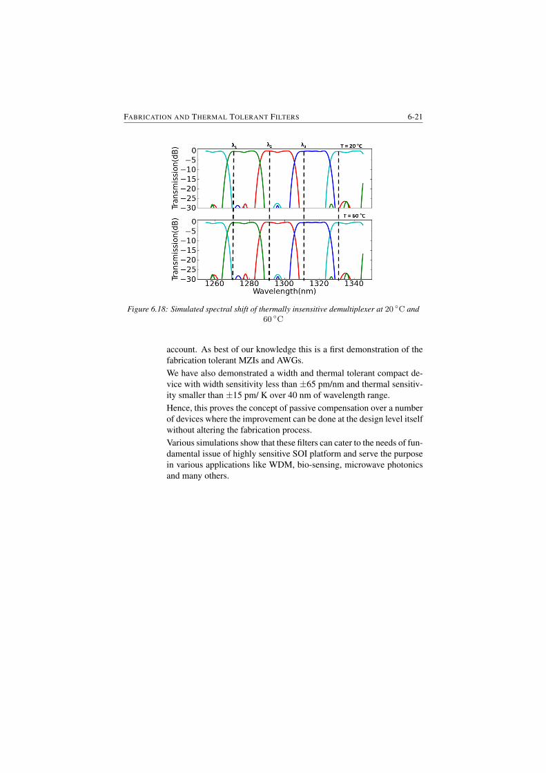
FABRICATION AND THERMAL TOLERANT FILTERS 6-21
Figure 6.18: Simulated spectral shift of thermally insensitive demultiplexer at 20 ◦C and60 ◦C
account. As best of our knowledge this is a first demonstration of thefabrication tolerant MZIs and AWGs.We have also demonstrated a width and thermal tolerant compact de-vice with width sensitivity less than ±65 pm/nm and thermal sensitiv-ity smaller than ±15 pm/ K over 40 nm of wavelength range.Hence, this proves the concept of passive compensation over a numberof devices where the improvement can be done at the design level itselfwithout altering the fabrication process.Various simulations show that these filters can cater to the needs of fun-damental issue of highly sensitive SOI platform and serve the purposein various applications like WDM, bio-sensing, microwave photonicsand many others.
6-22 CHAPTER 6
References
[1] S.K. Selvaraja, W. Bogaerts, P. Dumon, D. Van Thourhout,and R. Baets. Subnanometer Linewidth Uniformity in SiliconNanophotonic Waveguide Devices Using CMOS Fabrication Tech-nology. Selected Topics in Quantum Electronics, IEEE Journal of,16(1):316–324, Jan 2010.
[2] Frederic Boeuf, Sebastien Cremer, Enrico Temporiti, MassimoFere’, Mark Shaw, Nathalie Vulliet, bastien orlando, Delia Ristoiu,Alexis Farcy, Thierry Pinguet, Attila Mekis, Gianlorenzo Masini,Peng Sun, Yuemeng Chi, Herve Petiton, Sebastien Jan, Jean-Robert Manouvrier, Charles Baudot, Patrick Le-Maitre, Jean Fran-cois CARPENTIER, Laurent Salager, Matteo Traldi, Luca Maggi,Danilo Rigamonti, Chiara Zaccherini, Carolina Elemi, BernardSautreuil, and Luigi Verga. Recent Progress in Silicon PhotonicsR&D and Manufacturing on 300mm Wafer Platform. In OpticalFiber Communication Conference, page W3A.1. Optical Societyof America, 2015.
[3] Tohru Mogami, Tsuyoshi Horikawa, Keizo Kinoshita, HironoriSasaki, Ken Morito, and Kazuhiko Kurata. High-performanceoptical waveguide devices using 300 mm Si photonics platform.Microelectronic Engineering, pages –, 2015.
[4] S.K. Selvaraja, P. De Heyn, G. Winroth, P. Ong, G. Lep-age, C. Cailler, A. Rigny, K.K. Bourdelle, W. Bogaerts,D. Van Thourhout, J. Van Campenhout, and P. Absil. Highlyuniform and low-loss passive silicon photonics devices using a300mm CMOS platform. In Optical Fiber Communications Con-ference and Exhibition (OFC), 2014, pages 1–3, March 2014.
[5] Shankar Kumar Selvaraja, Wim Bogaerts, Dries VanThourhout,and Marc Schaekers. Thermal trimming and tuning of hy-drogenated amorphous silicon nanophotonic devices. AppliedPhysics Letters, 97(7):–, 2010.
[6] J. Schrauwen, D. Van Thourhout, and R. Baets. Trimming of sil-icon ring resonator by electron beam induced compaction andstrain. Opt. Express, 16(6):3738–3743, Mar 2008.
[7] http://www.comsol.com/.[8] Martin Fiers, Thomas Van Vaerenbergh, Ken Caluwaerts,
Dries Vande Ginste, Benjamin Schrauwen, Joni Dambre, and PeterBienstman. Time-domain and frequency-domain modeling of non-linear optical components at the circuit-level using a node-basedapproach. J. Opt. Soc. Am. B, 29(5):896–900, May 2012.
[9] http://www.lucedaphotonics.com/.
7Conclusion and Future
Perspectives
7.1 Conclusion
As we have elaborated throughout this work, the control of tolerancesis essential in any technological process and device. During the courseof this work we have made a number of important contributions to-wards developing an all silicon design based approach in realizing fab-rication and temperature tolerant, and power efficient silicon photonicintegrated circuits. We have been able to show that smart design ap-proach can solve some issues of the SOI platform which were thoughtto impose an inherent limitation on the functionality of the photoniccomponents and circuitry. The important contributions and achieve-ments of this work are summarized below:
i. We have proposed and demonstrated a method for measuring therefractive index of highly dispersive SOI waveguides. This is animportant step forward in the characterization of the integratedwaveguide devices, because hitherto it was only possible to ac-curately characterize the group index. By combining 3 MZIs oflower and higher order we can extract the wavelength and temper-ature dependent effective index and the group index unambigu-ously, and also obtain an estimate for the local variability of theeffective index. The demonstrated method does not perturb the
7-2 CHAPTER 7
waveguide of local pattern density, which is essential in a high-contrast waveguide platform such as silicon photonics.
ii. We have proposed and demonstrated a low loss robust demulti-plexer which is based on cascaded MZIs with a 20 nm channelspacing in the O-band. By engineering the channel pass band weshowed that the device can handle the temperature variations upto 100 ◦C and wafer-level waveguide dimensional variations. Thisdevice is a critical demonstration for the SOI platform because itcan be integrated with uncooled lasers in CWDM systems andhence provide a low cost high speed 100GbE and 400GbE solu-tion for short reach interconnects.
iii. We have proposed and demonstrated a passive compensation de-sign technique of various FIR filters like MZIs and AWGs andhave shown an improvement in thermal tolerances by 10 timesand linewidth variations by 20 times.
iv. We have also shown compact and low loss, athermal, and fabrica-tion tolerant devices by exploiting the different polarizations.
Combining the flat band approach and passive compensation techniqueone can further improve the performances of the de-multiplexers whichare critical for on chip optical interconnects. Overall in an optical link,the power consumption due to thermal tuning and control elements canbe as high as 20% of the total power consumption and by having ther-mally tolerant designs one can significantly reduce the power budgetof the overall system. We have thus shown several proof-of-principlecomponents which clearly demonstrate the potential of smart designapproaches to overcome fundamental limitations of silicon photonics.
7.2 Current and future perspectives
The basic components have been investigated, therefore the future worklies in further improving the performance and use them in an actualproduct demonstration, such as in a 100 GbE link for short reach inter-connects. It would include an on-chip heterogeneously integrated III-V-on-SOI directly modulated high speed laser or off-chip lasers modu-lated by on-chip silicon modulators, multiplexer on the transmitter sideand de-multiplexer and germanium photo-diodes on the receiver side.This is similar to the 100 GbE link we showed in simulation. The in-dividual components mentioned have already been demonstrated andfew designs for demultiplxer connected with photodiodes are alreadyundergoing fabrication and will soon be ready for characterization.The multiplexers with electro-absorption modulators are also under-going fabrication. This work is in collaboration with imec. On thetransmitter side design has been sent for fabrication in which the di-
CONCLUSION 7-3
rectly modulated III-V-on-SOI laser will be present at the input of thede-multiplexer carrying 10 to 25 Gbps data in each channel.The performance of these devices (especially athermal AWGs) can cer-tainly be improved by using better fabrication techniques like thosebeing developed on a 300 mm p-line instead of the 200 mm process,where the roughness is much better controlled.Other approach to improve the performance of athermal AWG could beto use a combination of TE and TM mode waveguide in each delay linewith the help of two low loss polarization rotators. In this AWG theTE light which is coming from the input star coupler is first convertedto TM by the first polarization rotator and then converted back to TEbefore the output grating coupler by the second polarization rotator.The principal of operation is an extension of TE-TM MZI and now theAWG delay lines are short due to the large TO coefficient differencebetween the two modes. The most critical part of this demonstrationis a low loss polarization rotator otherwise this will add up to the in-sertion loss of the AWG. So there is a need for robust and low losspolarization rotator in SOI. The other advantage of using TM mode inAWG is lower phase errors that would improve the crosstalk figure ofthe AWG.The another basic component which needs some smart design opti-mization is a directional coupler that can operate over wider band-widths typically (80 to 100 nm) for a given coupling coefficient. Therobustness in directional couplers are critical for other filters like ringresonators as well.In this work we have discussed mainly FIR filters. It would be inter-esting to extend the passive compensation technique to IIR filters (e.g.ring resonators) as well. The present techniques don’t yet solve thethermal drift issue of self interfering devices.It is worth mentioning that the techniques described in this thesis canbe applied to other waveguide platforms operating at different wave-lengths or even SOI at different wavelengths. One particular regionof interest is the mid-IR wavelength (3-12)µm where SOI waveguidescould be used till 4 µm wavelength and beyond that GE-on-Si takesover. This wavelength range is appealing because of specific and muchstronger absorption lines of many gases and liquids. Recently therehas been interest in miniaturizing the sensing systems using integratedwaveguides circuits.Any spectroscopic system requires WDM components and if they suf-fer from fabrication and thermal drifts, then predicting the behaviorof the system becomes difficult. Implementing our techniques wouldimprove the performance of existing passive components operating inthe mid-IR wavelength regime. One particularly interesting exampleis that of an athermal AWG. As we saw in this thesis that the athermal
7-4 CHAPTER 7
AWG suffers from high cross talk which arises because of the higherphase errors from the longer delay arms. There has been a demonstra-tion of an AWG based on Ge-on-Si which although has a much higherside wall roughness, already shows a cross talk of 18 dB at 5.3 µmbecause of the waveguide geometry there is very less influence of theside wall roughness. If we make an athermal AWG in Ge-on-Si, thenthere is a high chance that the device would show similar cross talklevels while improving the thermal behavior.Of course each of these topics would require a significant researcheffort in their own right. This shows that the future research potentialof tolerant silicon waveguide based devices is large and may inspirea lot of new exciting applications. Also, the presented method areequally useful for the other material platforms e.g. Ge-on-Si for mid-IR wavelength and silicon nitride for visible wavelengths.