s1d13a04 technical manual - newhaven display
TRANSCRIPT
S1D13A04 LCD/USB Companion Chip
S1D13A04TECHNICAL MANUAL
Document Number: X37A-Q-001-01
Copyright © 2001 Epson Research and Development, Inc. All Rights Reserved.
Information in this document is subject to change without notice. You may download and use this document, but only for your own use inevaluating Seiko Epson/EPSON products. You may not modify the document. Epson Research and Development, Inc. disclaims anyrepresentation that the contents of this document are accurate or current. The Programs/Technologies described in this document may contain material protected under U.S. and/or International Patent laws.
EPSON is a registered trademark of Seiko Epson Corporation. All other trademarks are the property of their respective owners.

Page 2 Epson Research and DevelopmentVancouver Design Center
THIS PAGE LEFT BLANK
S1D13A04 TECHNICAL MANUALX37A-Q-001-01 Issue Date: 01/10/02

Epson Research and Development Page 3Vancouver Design Center
COMPREHENSIVE SUPPORT TOOLSEPSON provides the designer and manufacturer a complete set of resources and tools for the development of LCD Graphics Systems.
Documentation• Technical manuals• Evaluation/Demonstration board manual
Evaluation/Demonstration Board• Assembled and fully tested Graphics Evaluation/Demonstration board• Schematic of Evaluation/Demonstration board
• Parts List• Installation Guide• CPU Independent Software Utilities
• Evaluation Software• Display Drivers
Application Engineering SupportEPSON offers the following services through their Sales and Marketing Network:
• Sales Technical Support
• Customer Training• Design Assistance
Application Engineering Support
Engineering and Sales Support is provided by:
JapanSeiko Epson CorporationElectronic Devices Marketing Division421-8, Hino, Hino-shiTokyo 191-8501, JapanTel: 042-587-5812Fax: 042-587-5564http://www.epson.co.jp
Hong KongEpson Hong Kong Ltd.20/F., Harbour Centre25 Harbour RoadWanchai, Hong KongTel: 2585-4600Fax: 2827-4346http://www.epson.com.hk/
TaiwanEpson Taiwan Technology & Trading Ltd.10F, No. 287Nanking East RoadSec. 3, Taipei, TaiwanTel: 02-2717-7360Fax: 02-2712-9164http://www.epson.com.tw/
SingaporeEpson Singapore Pte., Ltd.No. 1Temasek Avenue #36-00Millenia TowerSingapore, 039192Tel: 337-7911Fax: 334-2716http://www.epson.com.sg/
EuropeEpson Europe Electronics GmbHRiesstrasse 1580992 Munich, GermanyTel: 089-14005-0Fax: 089-14005-110http://www.epson-electronics.de
North AmericaEpson Electronics America, Inc.150 River Oaks ParkwaySan Jose, CA 95134, USATel: (408) 922-0200Fax: (408) 922-0238http://www.eea.epson.com
TECHNICAL MANUAL S1D13A04Issue Date: 01/10/02 X37A-Q-001-01

Page 4 Epson Research and DevelopmentVancouver Design Center
THIS PAGE LEFT BLANK
S1D13A04 TECHNICAL MANUALX37A-Q-001-01 Issue Date: 01/10/02
GRAPHICS
S1D13A04
ENERGYSAVING
EPSON
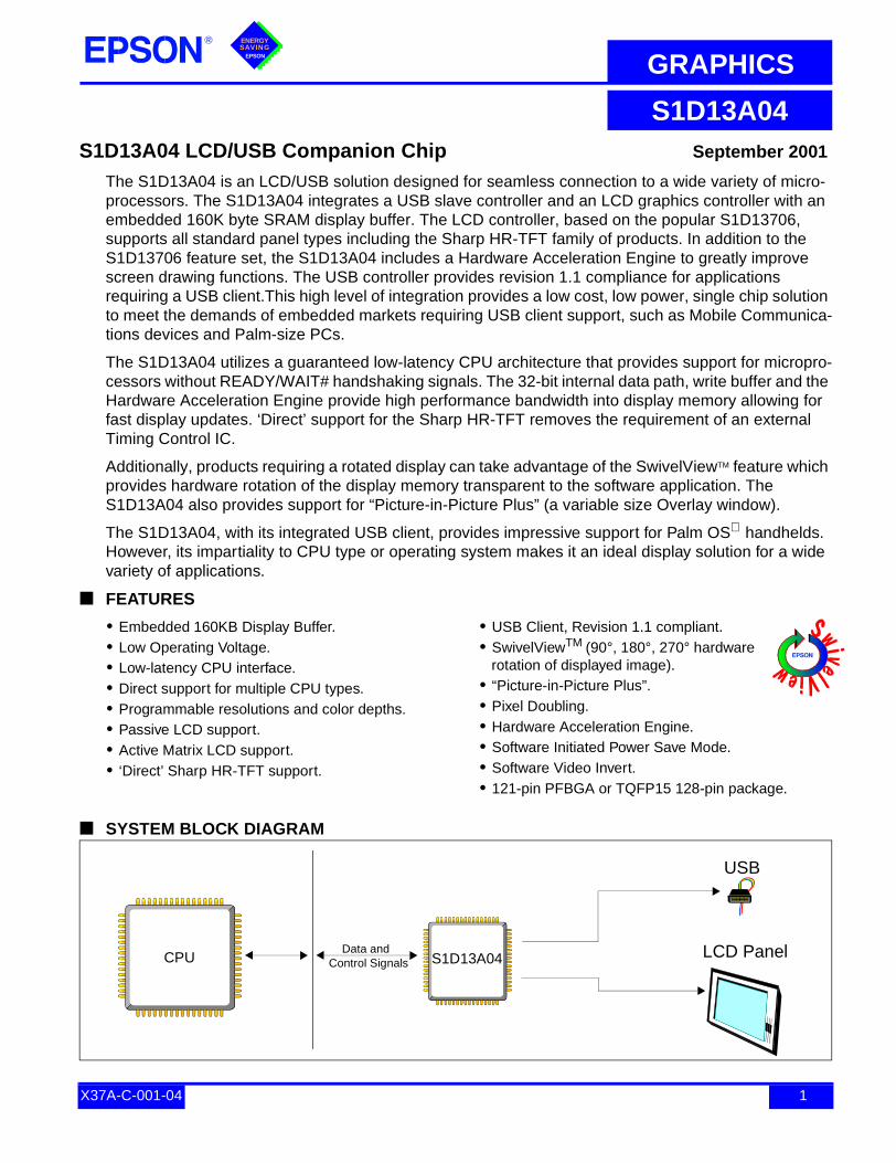
S1D13A04 LCD/USB Companion Chip September 2001
The S1D13A04 is an LCD/USB solution designed for seamless connection to a wide variety of micro-processors. The S1D13A04 integrates a USB slave controller and an LCD graphics controller with an embedded 160K byte SRAM display buffer. The LCD controller, based on the popular S1D13706, supports all standard panel types including the Sharp HR-TFT family of products. In addition to the S1D13706 feature set, the S1D13A04 includes a Hardware Acceleration Engine to greatly improve screen drawing functions. The USB controller provides revision 1.1 compliance for applications requiring a USB client.This high level of integration provides a low cost, low power, single chip solution to meet the demands of embedded markets requiring USB client support, such as Mobile Communica-tions devices and Palm-size PCs.
The S1D13A04 utilizes a guaranteed low-latency CPU architecture that provides support for micropro-cessors without READY/WAIT# handshaking signals. The 32-bit internal data path, write buffer and the Hardware Acceleration Engine provide high performance bandwidth into display memory allowing for fast display updates. ‘Direct’ support for the Sharp HR-TFT removes the requirement of an external Timing Control IC.
Additionally, products requiring a rotated display can take advantage of the SwivelViewTM feature which provides hardware rotation of the display memory transparent to the software application. The S1D13A04 also provides support for “Picture-in-Picture Plus” (a variable size Overlay window).
The S1D13A04, with its integrated USB client, provides impressive support for Palm OS handhelds. However, its impartiality to CPU type or operating system makes it an ideal display solution for a wide variety of applications.
FEATURES
SYSTEM BLOCK DIAGRAM
• Embedded 160KB Display Buffer.• Low Operating Voltage.• Low-latency CPU interface.• Direct support for multiple CPU types.• Programmable resolutions and color depths.• Passive LCD support.• Active Matrix LCD support.• ‘Direct’ Sharp HR-TFT support.
• USB Client, Revision 1.1 compliant.• SwivelViewTM (90°, 180°, 270° hardware
rotation of displayed image).• “Picture-in-Picture Plus”.• Pixel Doubling.• Hardware Acceleration Engine.• Software Initiated Power Save Mode.• Software Video Invert.• 121-pin PFBGA or TQFP15 128-pin package.
S1D13A04Data and
CPU Control SignalsLCD Panel
USB
X37A-C-001-04 1

GRAPHICS
S1D13A04
DESCRIPTION CPU Interface
• ‘Fixed’ low-latency CPU access times.
• Direct support for:Hitachi SH-4 / SH-3.Motorola M68xxx (REDCAP2, DragonBall, ColdFire).MPU bus interface with programmable READY.
Memory Interface• Embedded 160K byte SRAM display buffer.
Power Down Modes• Software Initiated Power Save Mode.
Operating Voltage• COREVDD 2.0 ± 10% or 2.5 ± 10% volts.
• IOVDD 3.0 ± 10% volts.
Clock Source• Three independent clock inputs including dedicated
USB clock (single clock possible if USB not required).
• Flexible clock source selection and divides.
Package• 121-pin PFBGA.
• 128-pin TQFP15.
Integrated USB Features• USB Client, Revision 1.1 Compliant.
Integrated LCD Controller Features• 1/2/4/8/16 bit-per-pixel (bpp) support.
• Up to 64 gray shades on monochrome passive panels.• Up to 64K colors on passive/active matrix panels.• Single-panel, single-drive passive displays.
• 4/8-bit monochrome LCD interface.• 4/8/16-bit color passive LCD interface.
• 9/12/18-bit Active matrix TFT interface.• 18-bit ‘Direct’ HR-TFT interface.
• SwivelView: hardware rotation by 90°, 180°, 270°.• “Picture-in-Picture Plus”: displays a variable size
window overlaid over background image.• Pixel Doubling: horizontal and vertical resolutions can
be doubled without any additional memory.
• Software video invert.• Typical resolutions supported:
320x240@16 bpp320x320@8 bpp160x160@16 bpp (2 pages)160x240@16 bpp
• 2D BitBLT Engine.Write BLT Transparent Write BLTMove BLT Transparent Move BLTSolid Fill BLT Read BLTPattern Fill Color Expansion BLTMove BLT with Color Expansion
CONTACT YOUR SALES REPRESENTATIVE FOR THESE COMPREHENSIVE DESIGN TOOLS
• S1D13A04 TechnicalManual
• Palm OS Hardware Abstraction Layer
• S5U13A04 Evaluation Boards • Windows CE Display Driver• CPU Independent Software
Utilities• VXWorks TornadoTM Display
Driver
Copyright © 2000, 2001 Epson Research and Development, Inc. All rights reserved. VDCInformation in this document is subject to change without notice. You may download and use this document, but only for your own use in evaluating Seiko Epson/EPSON products. You may not modify the document. Epson Research and Development, Inc. disclaims any representation that the contents of this document areaccurate or current. The Programs/Technologies described in this document may contain material protected under U.S. and/or International Patent laws. EPSON is a registered trademark of Seiko Epson Corporation. Palm Computing is a registered trademark and the Palm OS platform Platinum logo is a trademarkof Palm Computing, Inc., 3Com or its subsidiaries. Microsoft, Windows, and the Windows CE Logo are registered trademarks of Microsoft Corporation. All othertrademarks are the property of their respective owners.
JapanSeiko Epson CorporationElectronic Devices Marketing Division421-8, Hino, Hino-shiTokyo 191-8501, JapanTel: 042-587-5812Fax: 042-587-5564http://www.epson.co.jp
Hong KongEpson Hong Kong Ltd.20/F., Harbour Centre25 Harbour RoadWanchai, Hong KongTel: 2585-4600Fax: 2827-4346http://www.epson.com.hk/
TaiwanEpson Taiwan Technology & Trading Ltd.10F, No. 287Nanking East RoadSec. 3, Taipei, TaiwanTel: 02-2717-7360Fax: 02-2712-9164http://www.epson.com.tw/
SingaporeEpson Singapore Pte., Ltd.No. 1Temasek Avenue #36-00Millenia TowerSingapore, 039192Tel: 337-7911Fax: 334-2716http://www.epson.com.sg/
EuropeEpson Europe Electronics GmbHRiesstrasse 1580992 Munich, GermanyTel: 089-14005-0Fax: 089-14005-110http://www.epson-electronics.de
North AmericaEpson Electronics America, Inc.150 River Oaks ParkwaySan Jose, CA 95134, USATel: (408) 922-0200Fax: (408) 922-0238http://www.eea.epson.com
X37A-C-001-04 2
S1D13A04 LCD/USB Companion Chip
Hardware Functional Specification
Document Number: X37A-A-001-06
Status: Revision 6.0
Issue Date: 2003/05/01
Copyright © 2001, 2003 Epson Research and Development, Inc. All Rights Reserved.
Information in this document is subject to change without notice. You may download and use this document, but only for your own use inevaluating Seiko Epson/EPSON products. You may not modify the document. Epson Research and Development, Inc. disclaims anyrepresentation that the contents of this document are accurate or current. The Programs/Technologies described in this document may contain material protected under U.S. and/or International Patent laws.
EPSON is a registered trademark of Seiko Epson Corporation. All other Trademarks are the property of their respective owners

Page 2 Epson Research and DevelopmentVancouver Design Center
THIS PAGE LEFT BLANK
S1D13A04 Hardware Functional SpecificationX37A-A-001-06 Issue Date: 2003/05/01
Revision 6.0
Epson Research and Development Page 3Vancouver Design Center
Table of Contents
1 Introduction . . . . . . . . . . . . . . . . . . . . . . . . . . . . . . . . . . . . . . . 111.1 Scope . . . . . . . . . . . . . . . . . . . . . . . . . . . . . . . . . . 11
1.2 Overview Description . . . . . . . . . . . . . . . . . . . . . . . . . . . 11
2 Features . . . . . . . . . . . . . . . . . . . . . . . . . . . . . . . . . . . . . . . . . 122.1 Integrated Frame Buffer . . . . . . . . . . . . . . . . . . . . . . . . . . 12
2.2 CPU Interface . . . . . . . . . . . . . . . . . . . . . . . . . . . . . . 12
2.3 Display Support . . . . . . . . . . . . . . . . . . . . . . . . . . . . . . 12
2.4 Display Modes . . . . . . . . . . . . . . . . . . . . . . . . . . . . . . 12
2.5 Display Features . . . . . . . . . . . . . . . . . . . . . . . . . . . . . 13
2.6 Clock Source . . . . . . . . . . . . . . . . . . . . . . . . . . . . . . . 13
2.7 USB Device . . . . . . . . . . . . . . . . . . . . . . . . . . . . . . . 13
2.8 2D Acceleration . . . . . . . . . . . . . . . . . . . . . . . . . . . . . 13
2.9 Miscellaneous . . . . . . . . . . . . . . . . . . . . . . . . . . . . . . 14
3 Typical System Implementation Diagrams . . . . . . . . . . . . . . . . . . . . . . 153.1 Typical System Diagrams. . . . . . . . . . . . . . . . . . . . . . . . . . 15
3.2 USB Interface . . . . . . . . . . . . . . . . . . . . . . . . . . . . . . 19
4 Pins . . . . . . . . . . . . . . . . . . . . . . . . . . . . . . . . . . . . . . . . . . . 204.1 Pinout Diagram - PFBGA - 121-pin . . . . . . . . . . . . . . . . . . . . . . 20
4.2 Pinout Diagram - TQFP15 - 128-pin . . . . . . . . . . . . . . . . . . . . . 21
4.3 Pin Descriptions . . . . . . . . . . . . . . . . . . . . . . . . . . . . . 22
4.3.1 Host Interface . . . . . . . . . . . . . . . . . . . . . . . . . . . . . . . . . . . . . 22
4.3.2 LCD Interface . . . . . . . . . . . . . . . . . . . . . . . . . . . . . . . . . . . . . 26
4.3.3 Clock Input . . . . . . . . . . . . . . . . . . . . . . . . . . . . . . . . . . . . . . 29
4.3.4 Miscellaneous . . . . . . . . . . . . . . . . . . . . . . . . . . . . . . . . . . . . . 29
4.3.5 Power And Ground . . . . . . . . . . . . . . . . . . . . . . . . . . . . . . . . . . 29
4.4 Summary of Configuration Options . . . . . . . . . . . . . . . . . . . . . . 30
4.5 Host Bus Interface Pin Mapping . . . . . . . . . . . . . . . . . . . . . . . 31
4.6 LCD Interface Pin Mapping . . . . . . . . . . . . . . . . . . . . . . . . . 32
5 D.C. Characteristics . . . . . . . . . . . . . . . . . . . . . . . . . . . . . . . . . . 33
6 A.C. Characteristics . . . . . . . . . . . . . . . . . . . . . . . . . . . . . . . . . . 346.1 Clock Timing . . . . . . . . . . . . . . . . . . . . . . . . . . . . . . 34
6.1.1 Input Clocks . . . . . . . . . . . . . . . . . . . . . . . . . . . . . . . . . . . . . . 34
6.1.2 Internal Clocks . . . . . . . . . . . . . . . . . . . . . . . . . . . . . . . . . . . . 35
6.2 CPU Interface Timing . . . . . . . . . . . . . . . . . . . . . . . . . . . 36
6.2.1 Generic #1 Interface Timing (e.g. Epson EOC33) . . . . . . . . . . . . . . . . . . 36
6.2.2 Generic #2 Interface Timing (e.g. ISA) . . . . . . . . . . . . . . . . . . . . . . . . 38
Hardware Functional Specification S1D13A04Issue Date: 2003/05/01 X37A-A-001-06
Revision 6.0
Page 4 Epson Research and DevelopmentVancouver Design Center
6.2.3 Hitachi SH-3 Interface Timing . . . . . . . . . . . . . . . . . . . . . . . . . . . . 40
6.2.4 Hitachi SH-4 Interface Timing . . . . . . . . . . . . . . . . . . . . . . . . . . . . 42
6.2.5 Motorola MC68K #1 Interface Timing (e.g. MC68000) . . . . . . . . . . . . . . . 44
6.2.6 Motorola MC68K #2 Interface Timing (e.g. MC68030) . . . . . . . . . . . . . . . 46
6.2.7 Motorola REDCAP2 Interface Timing . . . . . . . . . . . . . . . . . . . . . . . . 48
6.2.8 Motorola Dragonball Interface Timing with DTACK (e.g. MC68EZ328/MC68VZ328) 50
6.2.9 Motorola Dragonball Interface Timing w/o DTACK (e.g. MC68EZ328/MC68VZ328) 52
6.3 LCD Power Sequencing . . . . . . . . . . . . . . . . . . . . . . . . . . .54
6.3.1 Passive/TFT Power-On Sequence . . . . . . . . . . . . . . . . . . . . . . . . . . . 54
6.3.2 Passive/TFT Power-Off Sequence . . . . . . . . . . . . . . . . . . . . . . . . . . . 55
6.3.3 ‘Direct’ HR-TFT Interface Power-On/Off Sequence . . . . . . . . . . . . . . . . . 55
6.4 Display Interface . . . . . . . . . . . . . . . . . . . . . . . . . . . . . .56
6.4.1 Generic STN Panel Timing . . . . . . . . . . . . . . . . . . . . . . . . . . . . . . 58
6.4.2 Single Monochrome 4-Bit Panel Timing . . . . . . . . . . . . . . . . . . . . . . . 60
6.4.3 Single Monochrome 8-Bit Panel Timing . . . . . . . . . . . . . . . . . . . . . . . 62
6.4.4 Single Color 4-Bit Panel Timing . . . . . . . . . . . . . . . . . . . . . . . . . . . 64
6.4.5 Single Color 8-Bit Panel Timing (Format 1) . . . . . . . . . . . . . . . . . . . . . 66
6.4.6 Single Color 8-Bit Panel Timing (Format 2) . . . . . . . . . . . . . . . . . . . . . 68
6.4.7 Single Color 16-Bit Panel Timing . . . . . . . . . . . . . . . . . . . . . . . . . . . 70
6.4.8 Generic TFT Panel Timing . . . . . . . . . . . . . . . . . . . . . . . . . . . . . . 72
6.4.9 9/12/18-Bit TFT Panel Timing . . . . . . . . . . . . . . . . . . . . . . . . . . . . 73
6.4.10 160x160 Sharp ‘Direct’ HR-TFT Panel Timing (e.g. LQ031B1DDxx) . . . . . . . 76
6.4.11 320x240 Sharp ‘Direct’ HR-TFT Panel Timing (e.g. LQ039Q2DS01) . . . . . . . . 80
6.5 USB Timing . . . . . . . . . . . . . . . . . . . . . . . . . . . . . . . .82
7 Clocks . . . . . . . . . . . . . . . . . . . . . . . . . . . . . . . . . . . . . . . . . . .847.1 Clock Descriptions . . . . . . . . . . . . . . . . . . . . . . . . . . . . .84
7.1.1 BCLK . . . . . . . . . . . . . . . . . . . . . . . . . . . . . . . . . . . . . . . . . 84
7.1.2 MCLK . . . . . . . . . . . . . . . . . . . . . . . . . . . . . . . . . . . . . . . . . 84
7.1.3 PCLK . . . . . . . . . . . . . . . . . . . . . . . . . . . . . . . . . . . . . . . . . 85
7.1.4 PWMCLK . . . . . . . . . . . . . . . . . . . . . . . . . . . . . . . . . . . . . . . 86
7.1.5 USBCLK . . . . . . . . . . . . . . . . . . . . . . . . . . . . . . . . . . . . . . . 86
7.2 Clock Selection . . . . . . . . . . . . . . . . . . . . . . . . . . . . . .87
7.3 Clocks versus Functions . . . . . . . . . . . . . . . . . . . . . . . . . . .88
8 Registers . . . . . . . . . . . . . . . . . . . . . . . . . . . . . . . . . . . . . . . . .898.1 Register Mapping . . . . . . . . . . . . . . . . . . . . . . . . . . . . .89
8.2 Register Set . . . . . . . . . . . . . . . . . . . . . . . . . . . . . . . .89
8.3 LCD Register Descriptions (Offset = 0h) . . . . . . . . . . . . . . . . . . . .91
8.3.1 Read-Only Configuration Registers . . . . . . . . . . . . . . . . . . . . . . . . . . 91
8.3.2 Clock Configuration Registers . . . . . . . . . . . . . . . . . . . . . . . . . . . . 92
S1D13A04 Hardware Functional SpecificationX37A-A-001-06 Issue Date: 2003/05/01
Revision 6.0
Epson Research and Development Page 5Vancouver Design Center
8.3.3 Panel Configuration Registers . . . . . . . . . . . . . . . . . . . . . . . . . . . . . 93
8.3.4 Look-Up Table Registers . . . . . . . . . . . . . . . . . . . . . . . . . . . . . . . 98
8.3.5 Display Mode Registers . . . . . . . . . . . . . . . . . . . . . . . . . . . . . . . . 100
8.3.6 Picture-in-Picture Plus (PIP+) Registers . . . . . . . . . . . . . . . . . . . . . . . 105
8.3.7 Miscellaneous Registers . . . . . . . . . . . . . . . . . . . . . . . . . . . . . . . . 110
8.4 USB Registers (Offset = 4000h) . . . . . . . . . . . . . . . . . . . . . . . 117
8.5 2D Acceleration (BitBLT) Registers (Offset = 8000h) . . . . . . . . . . . . . . 135
8.6 2D Accelerator (BitBLT) Data Register Descriptions . . . . . . . . . . . . . . . 141
9 2D Accelerator (BitBLT) Engine . . . . . . . . . . . . . . . . . . . . . . . . . . . . 1429.1 Overview . . . . . . . . . . . . . . . . . . . . . . . . . . . . . . . . 142
9.2 BitBLT Operations . . . . . . . . . . . . . . . . . . . . . . . . . . . . 142
10 Frame Rate Calculation . . . . . . . . . . . . . . . . . . . . . . . . . . . . . . . . 143
11 Display Data Formats . . . . . . . . . . . . . . . . . . . . . . . . . . . . . . . . . 144
12 Look-Up Table Architecture . . . . . . . . . . . . . . . . . . . . . . . . . . . . . . 14512.1 Monochrome Modes . . . . . . . . . . . . . . . . . . . . . . . . . . . . 145
12.2 Color Modes . . . . . . . . . . . . . . . . . . . . . . . . . . . . . . . 147
13 SwivelView™ . . . . . . . . . . . . . . . . . . . . . . . . . . . . . . . . . . . . . . 15113.1 Concept . . . . . . . . . . . . . . . . . . . . . . . . . . . . . . . . . 151
13.2 90° SwivelView™ . . . . . . . . . . . . . . . . . . . . . . . . . . . . 151
13.2.1 Register Programming . . . . . . . . . . . . . . . . . . . . . . . . . . . . . . . . 152
13.3 180° SwivelView™ . . . . . . . . . . . . . . . . . . . . . . . . . . . . 153
13.3.1 Register Programming . . . . . . . . . . . . . . . . . . . . . . . . . . . . . . . . 153
13.4 270° SwivelView™ . . . . . . . . . . . . . . . . . . . . . . . . . . . . 154
13.4.1 Register Programming . . . . . . . . . . . . . . . . . . . . . . . . . . . . . . . . 155
14 Picture-in-Picture Plus (PIP+) . . . . . . . . . . . . . . . . . . . . . . . . . . . . . 15614.1 Concept . . . . . . . . . . . . . . . . . . . . . . . . . . . . . . . . . 156
14.2 With SwivelView Enabled . . . . . . . . . . . . . . . . . . . . . . . . . 157
14.2.1 SwivelView 90° . . . . . . . . . . . . . . . . . . . . . . . . . . . . . . . . . . . . 157
14.2.2 SwivelView 180° . . . . . . . . . . . . . . . . . . . . . . . . . . . . . . . . . . . 157
14.2.3 SwivelView 270° . . . . . . . . . . . . . . . . . . . . . . . . . . . . . . . . . . . 158
15 Power Save Mode . . . . . . . . . . . . . . . . . . . . . . . . . . . . . . . . . . . . 159
16 Mechanical Data . . . . . . . . . . . . . . . . . . . . . . . . . . . . . . . . . . . . 160
17 References . . . . . . . . . . . . . . . . . . . . . . . . . . . . . . . . . . . . . . . 162
18 Sales and Technical Support . . . . . . . . . . . . . . . . . . . . . . . . . . . . . 163
Hardware Functional Specification S1D13A04Issue Date: 2003/05/01 X37A-A-001-06
Revision 6.0

Page 6 Epson Research and DevelopmentVancouver Design Center
THIS PAGE LEFT BLANK
S1D13A04 Hardware Functional SpecificationX37A-A-001-06 Issue Date: 2003/05/01
Revision 6.0
Epson Research and Development Page 7Vancouver Design Center
List of Tables
Table 4-1: PFBGA 121-pin Mapping . . . . . . . . . . . . . . . . . . . . . . . . . . . . . . . . . 20
Table 4-2: Host Interface Pin Descriptions . . . . . . . . . . . . . . . . . . . . . . . . . . . . . . 22
Table 4-3: LCD Interface Pin Descriptions . . . . . . . . . . . . . . . . . . . . . . . . . . . . . . 26
Table 4-4: Clock Input Pin Descriptions. . . . . . . . . . . . . . . . . . . . . . . . . . . . . . . . 29
Table 4-5: Miscellaneous Pin Descriptions . . . . . . . . . . . . . . . . . . . . . . . . . . . . . . 29
Table 4-6: Power And Ground Pin Descriptions . . . . . . . . . . . . . . . . . . . . . . . . . . . 29
Table 4-7: Summary of Power-On/Reset Options . . . . . . . . . . . . . . . . . . . . . . . . . . . 30
Table 4-8: Host Bus Interface Pin Mapping . . . . . . . . . . . . . . . . . . . . . . . . . . . . . . 31
Table 4-9: LCD Interface Pin Mapping . . . . . . . . . . . . . . . . . . . . . . . . . . . . . . . . 32
Table 5-1: Absolute Maximum Ratings . . . . . . . . . . . . . . . . . . . . . . . . . . . . . . . . 33
Table 5-2: Recommended Operating Conditions . . . . . . . . . . . . . . . . . . . . . . . . . . . 33
Table 5-3: Electrical Characteristics for VDD = 3.3V typical . . . . . . . . . . . . . . . . . . . . . 33
Table 6-1: Clock Input Requirements for CLKI when CLKI to BCLK divide > 1 . . . . . . . . . . 34
Table 6-2: Clock Input Requirements for CLKI when CLKI to BCLK divide = 1 . . . . . . . . . . 35
Table 6-3: Clock Input Requirements for CLKI2 . . . . . . . . . . . . . . . . . . . . . . . . . . . 35
Table 6-4: Internal Clock Requirements . . . . . . . . . . . . . . . . . . . . . . . . . . . . . . . . 35
Table 6-5: Generic #1 Interface Timing . . . . . . . . . . . . . . . . . . . . . . . . . . . . . . . . 37
Table 6-6: Generic #1 Interface Truth Table for Little Endian . . . . . . . . . . . . . . . . . . . . 37
Table 6-7: Generic #1 Interface Truth Table for Big Endian . . . . . . . . . . . . . . . . . . . . . 37
Table 6-8: Generic #2 Interface Timing . . . . . . . . . . . . . . . . . . . . . . . . . . . . . . . . 39
Table 6-9: Generic #2 Interface Truth Table for Little Endian . . . . . . . . . . . . . . . . . . . . 39
Table 6-10: Hitachi SH-3 Interface Timing . . . . . . . . . . . . . . . . . . . . . . . . . . . . . . . 41
Table 6-11: Hitachi SH-4 Interface Timing . . . . . . . . . . . . . . . . . . . . . . . . . . . . . . . 43
Table 6-12: Motorola MC68K#1 Interface Timing . . . . . . . . . . . . . . . . . . . . . . . . . . . 45
Table 6-13: Motorola MC68K#2 Interface Timing . . . . . . . . . . . . . . . . . . . . . . . . . . . 47
Table 6-14: Motorola Redcap2 Interface Timing . . . . . . . . . . . . . . . . . . . . . . . . . . . . 49
Table 6-15: Motorola Dragonball Interface Timing with DTACK . . . . . . . . . . . . . . . . . . . 51
Table 6-16: Motorola Dragonball Interface Timing w/o DTACK . . . . . . . . . . . . . . . . . . . 53
Table 6-17: Passive/TFT Power-On Sequence Timing . . . . . . . . . . . . . . . . . . . . . . . . . 54
Table 6-18: Passive/TFT Power-Off Sequence Timing. . . . . . . . . . . . . . . . . . . . . . . . . 55
Table 6-19: Panel Timing Parameter Definition and Register Summary . . . . . . . . . . . . . . . . 57
Table 6-20: Single Monochrome 4-Bit Panel A.C. Timing . . . . . . . . . . . . . . . . . . . . . . . 61
Table 6-21: Single Monochrome 8-Bit Panel A.C. Timing . . . . . . . . . . . . . . . . . . . . . . . 63
Table 6-22: Single Color 4-Bit Panel A.C. Timing . . . . . . . . . . . . . . . . . . . . . . . . . . . 65
Table 6-23: Single Color 8-Bit Panel A.C. Timing (Format 1) . . . . . . . . . . . . . . . . . . . . . 67
Table 6-24: Single Color 8-Bit Panel A.C. Timing (Format 2) . . . . . . . . . . . . . . . . . . . . . 69
Table 6-25: Single Color 16-Bit Panel A.C. Timing . . . . . . . . . . . . . . . . . . . . . . . . . . 71
Hardware Functional Specification S1D13A04Issue Date: 2003/05/01 X37A-A-001-06
Revision 6.0
Page 8 Epson Research and DevelopmentVancouver Design Center
Table 6-26: TFT A.C. Timing . . . . . . . . . . . . . . . . . . . . . . . . . . . . . . . . . . . . . . 75
Table 6-27: 160x160 Sharp ‘Direct’ HR-TFT Horizontal Timing . . . . . . . . . . . . . . . . . . . 77
Table 6-28: 160x160 Sharp ‘Direct’ HR-TFT Panel Vertical Timing . . . . . . . . . . . . . . . . . 79
Table 6-29: 320x240 Sharp ‘Direct’ HR-TFT Panel Horizontal Timing . . . . . . . . . . . . . . . . 81
Table 6-30: 320x240 Sharp ‘Direct’ HR-TFT Panel Vertical Timing . . . . . . . . . . . . . . . . . 81
Table 6-31 USB Interface Timing . . . . . . . . . . . . . . . . . . . . . . . . . . . . . . . . . . . 83
Table 7-1: BCLK Clock Selection . . . . . . . . . . . . . . . . . . . . . . . . . . . . . . . . . . . 84
Table 7-2: MCLK Clock Selection. . . . . . . . . . . . . . . . . . . . . . . . . . . . . . . . . . . 84
Table 7-3: PCLK Clock Selection . . . . . . . . . . . . . . . . . . . . . . . . . . . . . . . . . . . 85
Table 7-4: Relationship between MCLK and PCLK. . . . . . . . . . . . . . . . . . . . . . . . . . 86
Table 7-5: PWMCLK Clock Selection. . . . . . . . . . . . . . . . . . . . . . . . . . . . . . . . . 86
Table 7-6: S1D13A04 Internal Clock Requirements. . . . . . . . . . . . . . . . . . . . . . . . . . 88
Table 8-1: S1D13A04 Register Mapping . . . . . . . . . . . . . . . . . . . . . . . . . . . . . . . 89
Table 8-2: S1D13A04 Register Set . . . . . . . . . . . . . . . . . . . . . . . . . . . . . . . . . . 89
Table 8-3: MCLK Divide Selection . . . . . . . . . . . . . . . . . . . . . . . . . . . . . . . . . . 92
Table 8-4: PCLK Divide Selection. . . . . . . . . . . . . . . . . . . . . . . . . . . . . . . . . . . 92
Table 8-5: PCLK Source Selection. . . . . . . . . . . . . . . . . . . . . . . . . . . . . . . . . . . 93
Table 8-6: Panel Data Width Selection . . . . . . . . . . . . . . . . . . . . . . . . . . . . . . . . 93
Table 8-7: Active Panel Resolution Selection . . . . . . . . . . . . . . . . . . . . . . . . . . . . . 94
Table 8-8: LCD Panel Type Selection . . . . . . . . . . . . . . . . . . . . . . . . . . . . . . . . . 94
Table 8-9: SwivelViewTM Mode Select Options . . . . . . . . . . . . . . . . . . . . . . . . . . . 95
Table 8-10: LCD Bit-per-pixel Selection . . . . . . . . . . . . . . . . . . . . . . . . . . . . . . . . 96
Table 8-11: 32-bit Address Increments for Color Depth . . . . . . . . . . . . . . . . . . . . . . . .106
Table 8-12: 32-bit Address Increments for Color Depth . . . . . . . . . . . . . . . . . . . . . . . .107
Table 8-13: 32-bit Address Increments for Color Depth . . . . . . . . . . . . . . . . . . . . . . . .108
Table 8-14: 32-bit Address Increments for Color Depth . . . . . . . . . . . . . . . . . . . . . . . .109
Table 8-15: PWM Clock Divide Select Options . . . . . . . . . . . . . . . . . . . . . . . . . . . .114
Table 8-16: PWMCLK Source Selection . . . . . . . . . . . . . . . . . . . . . . . . . . . . . . . .115
Table 8-17: PWMOUT Duty Cycle Select Options . . . . . . . . . . . . . . . . . . . . . . . . . . .115
Table 8-18: BitBLT FIFO Words Available . . . . . . . . . . . . . . . . . . . . . . . . . . . . . .136
Table 8-19 :BitBLT ROP Code/Color Expansion Function Selection . . . . . . . . . . . . . . . . .137
Table 8-20 :BitBLT Operation Selection . . . . . . . . . . . . . . . . . . . . . . . . . . . . . . . .138
Table 8-21 :BitBLT Source Start Address Selection . . . . . . . . . . . . . . . . . . . . . . . . . .139
Table 15-1: Power Save Mode Function Summary . . . . . . . . . . . . . . . . . . . . . . . . . . .159
S1D13A04 Hardware Functional SpecificationX37A-A-001-06 Issue Date: 2003/05/01
Revision 6.0
Epson Research and Development Page 9Vancouver Design Center
List of Figures
Figure 3-1: Typical System Diagram (Generic #1 Bus) . . . . . . . . . . . . . . . . . . . . . . . . 15
Figure 3-2: Typical System Diagram (Generic #2 Bus) . . . . . . . . . . . . . . . . . . . . . . . . 15
Figure 3-3: Typical System Diagram (Hitachi SH-4 Bus) . . . . . . . . . . . . . . . . . . . . . . . 16
Figure 3-4: Typical System Diagram (Hitachi SH-3 Bus) . . . . . . . . . . . . . . . . . . . . . . . 16
Figure 3-5: Typical System Diagram (MC68K # 1, Motorola 16-Bit 68000) . . . . . . . . . . . . . 17
Figure 3-6: Typical System Diagram (MC68K #2, Motorola 32-Bit 68030) . . . . . . . . . . . . . . 17
Figure 3-7: Typical System Diagram (Motorola REDCAP2 Bus) . . . . . . . . . . . . . . . . . . . 18
Figure 3-8: Typical System Diagram (Motorola MC68EZ328/MC68VZ328 “DragonBall” Bus) . . . 18
Figure 3-9: USB Typical Implementation. . . . . . . . . . . . . . . . . . . . . . . . . . . . . . . . 19
Figure 4-1: Pinout Diagram - PFBGA 121-pin . . . . . . . . . . . . . . . . . . . . . . . . . . . . . 20
Figure 4-2: Pinout Diagram - TQFP15 128-pin . . . . . . . . . . . . . . . . . . . . . . . . . . . . . 21
Figure 6-1: Clock Input Requirements . . . . . . . . . . . . . . . . . . . . . . . . . . . . . . . . . 34
Figure 6-2: Generic #1 Interface Timing . . . . . . . . . . . . . . . . . . . . . . . . . . . . . . . . 36
Figure 6-3: Generic #2 Interface Timing . . . . . . . . . . . . . . . . . . . . . . . . . . . . . . . . 38
Figure 6-4: Hitachi SH-3 Interface Timing . . . . . . . . . . . . . . . . . . . . . . . . . . . . . . . 40
Figure 6-5: Hitachi SH-4 Interface Timing . . . . . . . . . . . . . . . . . . . . . . . . . . . . . . . 42
Figure 6-6: Motorola MC68K #1 Interface Timing. . . . . . . . . . . . . . . . . . . . . . . . . . . 44
Figure 6-7: Motorola MC68K #2 Interface Timing. . . . . . . . . . . . . . . . . . . . . . . . . . . 46
Figure 6-8: Motorola Redcap2 Interface Timing . . . . . . . . . . . . . . . . . . . . . . . . . . . . 48
Figure 6-9: Motorola Dragonball Interface Timing with DTACK . . . . . . . . . . . . . . . . . . . 50
Figure 6-10: Motorola Dragonball Interface Timing w/o DTACK . . . . . . . . . . . . . . . . . . . 52
Figure 6-11: Passive/TFT Power-On Sequence Timing . . . . . . . . . . . . . . . . . . . . . . . . . 54
Figure 6-12: Passive/TFT Power-Off Sequence Timing . . . . . . . . . . . . . . . . . . . . . . . . . 55
Figure 6-13: Panel Timing Parameters . . . . . . . . . . . . . . . . . . . . . . . . . . . . . . . . . 56
Figure 6-14: Generic STN Panel Timing . . . . . . . . . . . . . . . . . . . . . . . . . . . . . . . . . 58
Figure 6-15: Single Monochrome 4-Bit Panel Timing . . . . . . . . . . . . . . . . . . . . . . . . . . 60
Figure 6-16: Single Monochrome 4-Bit Panel A.C. Timing . . . . . . . . . . . . . . . . . . . . . . . 61
Figure 6-17: Single Monochrome 8-Bit Panel Timing . . . . . . . . . . . . . . . . . . . . . . . . . . 62
Figure 6-18: Single Monochrome 8-Bit Panel A.C. Timing . . . . . . . . . . . . . . . . . . . . . . . 63
Figure 6-19: Single Color 4-Bit Panel Timing . . . . . . . . . . . . . . . . . . . . . . . . . . . . . . 64
Figure 6-20: Single Color 4-Bit Panel A.C. Timing . . . . . . . . . . . . . . . . . . . . . . . . . . . 65
Figure 6-21: Single Color 8-Bit Panel Timing (Format 1) . . . . . . . . . . . . . . . . . . . . . . . . 66
Figure 6-22: Single Color 8-Bit Panel A.C. Timing (Format 1) . . . . . . . . . . . . . . . . . . . . . 67
Figure 6-23: Single Color 8-Bit Panel Timing (Format 2) . . . . . . . . . . . . . . . . . . . . . . . . 68
Figure 6-24: Single Color 8-Bit Panel A.C. Timing (Format 2) . . . . . . . . . . . . . . . . . . . . . 69
Figure 6-25: Single Color 16-Bit Panel Timing . . . . . . . . . . . . . . . . . . . . . . . . . . . . . 70
Figure 6-26: Single Color 16-Bit Panel A.C. Timing . . . . . . . . . . . . . . . . . . . . . . . . . . 71
Hardware Functional Specification S1D13A04Issue Date: 2003/05/01 X37A-A-001-06
Revision 6.0
Page 10 Epson Research and DevelopmentVancouver Design Center
Figure 6-27: Generic TFT Panel Timing . . . . . . . . . . . . . . . . . . . . . . . . . . . . . . . . .72
Figure 6-28: 18-Bit TFT Panel Timing . . . . . . . . . . . . . . . . . . . . . . . . . . . . . . . . . .73
Figure 6-29: TFT A.C. Timing . . . . . . . . . . . . . . . . . . . . . . . . . . . . . . . . . . . . . .74
Figure 6-30: 160x160 Sharp ‘Direct’ HR-TFT Panel Horizontal Timing . . . . . . . . . . . . . . . .76
Figure 6-31: 160x160 Sharp ‘Direct’ HR-TFT Panel Vertical Timing. . . . . . . . . . . . . . . . . .78
Figure 6-32: 320x240 Sharp ‘Direct’ HR-TFT Panel Horizontal Timing . . . . . . . . . . . . . . . .80
Figure 6-33: 320x240 Sharp ‘Direct’ HR-TFT Panel Vertical Timing. . . . . . . . . . . . . . . . . .81
Figure 6-34 Data Signal Rise and Fall Time . . . . . . . . . . . . . . . . . . . . . . . . . . . . . . .82
Figure 6-35 Differential Data Jitter . . . . . . . . . . . . . . . . . . . . . . . . . . . . . . . . . . .82
Figure 6-36 Differential to EOP Transition Skew and EOP Width . . . . . . . . . . . . . . . . . . .82
Figure 6-37 Receiver Jitter Tolerance . . . . . . . . . . . . . . . . . . . . . . . . . . . . . . . . . .83
Figure 7-1: Clock Selection . . . . . . . . . . . . . . . . . . . . . . . . . . . . . . . . . . . . . . .87
Figure 8-1: Display Data Byte/Word Swap . . . . . . . . . . . . . . . . . . . . . . . . . . . . . . 111
Figure 8-2: PWM Clock Block Diagram . . . . . . . . . . . . . . . . . . . . . . . . . . . . . . . 114
Figure 11-1: 4/8/16 Bit-Per-Pixel Display Data Memory Organization . . . . . . . . . . . . . . . . 144
Figure 12-1: 1 Bit-per-pixel Monochrome Mode Data Output Path . . . . . . . . . . . . . . . . . . 145
Figure 12-2: 2 Bit-per-pixel Monochrome Mode Data Output Path . . . . . . . . . . . . . . . . . . 145
Figure 12-3: 4 Bit-per-pixel Monochrome Mode Data Output Path . . . . . . . . . . . . . . . . . . 146
Figure 12-4: 8 Bit-per-pixel Monochrome Mode Data Output Path . . . . . . . . . . . . . . . . . . 146
Figure 12-5: 1 Bit-Per-Pixel Color Mode Data Output Path . . . . . . . . . . . . . . . . . . . . . . 147
Figure 12-6: 2 Bit-Per-Pixel Color Mode Data Output Path . . . . . . . . . . . . . . . . . . . . . . 148
Figure 12-7: 4 Bit-Per-Pixel Color Mode Data Output Path . . . . . . . . . . . . . . . . . . . . . . 149
Figure 12-8: 8 Bit-per-pixel Color Mode Data Output Path . . . . . . . . . . . . . . . . . . . . . . 150
Figure 13-1: Relationship Between The Screen Image and the Image Refreshed in 90° SwivelView. 152
Figure 13-2: Relationship Between The Screen Image and the Image Refreshed in 180° SwivelView.153
Figure 13-3: Relationship Between The Screen Image and the Image Refreshed in 270° SwivelView.154
Figure 14-1: Picture-in-Picture Plus with SwivelView disabled . . . . . . . . . . . . . . . . . . . . 156
Figure 14-2: Picture-in-Picture Plus with SwivelView 90° enabled . . . . . . . . . . . . . . . . . . 157
Figure 14-3: Picture-in-Picture Plus with SwivelView 180° enabled . . . . . . . . . . . . . . . . . 157
Figure 14-4: Picture-in-Picture Plus with SwivelView 270° enabled . . . . . . . . . . . . . . . . . 158
Figure 16-1: Mechanical Data PFBGA 121-pin Package . . . . . . . . . . . . . . . . . . . . . . . 160
Figure 16-2: Mechanical Data TQFP15 128-pin Package . . . . . . . . . . . . . . . . . . . . . . . 161
S1D13A04 Hardware Functional SpecificationX37A-A-001-06 Issue Date: 2003/05/01
Revision 6.0
Epson Research and Development Page 11Vancouver Design Center
1 Introduction
1.1 Scope
This is the Hardware Functional Specification for the S1D13A04 LCD/USB Companion Chip. Included in this document are timing diagrams, AC and DC characteristics, register descriptions, and power management descriptions. This document is intended for two audiences: Video Subsystem Designers and Software Developers.
This document is updated as appropriate. Please check for the latest revision of this document before beginning any development. The latest revision can be downloaded at www.erd.epson.com
We appreciate your comments on our documentation. Please contact us via email at [email protected].
1.2 Overview Description
The S1D13A04 is an LCD/USB solution designed for seamless connection to a wide variety of microprocessors. The S1D13A04 integrates a USB slave controller and an LCD graphics controller with an embedded 160K byte SRAM display buffer. The LCD controller, based on the popular S1D13706, supports all standard panel types including the Sharp HR-TFT family of products. In addition to the S1D13706 feature set, the S1D13A04 includes a Hardware Acceleration Engine to greatly improve screen drawing functions. The USB controller provides revision 1.1 compliance for applications requiring a USB client.This high level of integration provides a low cost, low power, single chip solution to meet the demands of embedded markets requiring USB client support, such as Mobile Communications devices and Palm-size PCs.
The S1D13A04 utilizes a guaranteed low-latency CPU architecture that provides support for microprocessors without READY/WAIT# handshaking signals. The 32-bit internal data path, write buffer and the Hardware Acceleration Engine provide high performance bandwidth into display memory allowing for fast display updates. ‘Direct’ support for the Sharp HR-TFT removes the requirement of an external Timing Control IC.
Additionally, products requiring a rotated display can take advantage of the SwivelViewTM feature which provides hardware rotation of the display memory transparent to the software application. The S1D13A04 also provides support for “Picture-in-Picture Plus” (a variable size Overlay window).
The S1D13A04, with its integrated USB client, provides impressive support for Palm OS handhelds. However, its impartiality to CPU type or operating system makes it an ideal display solution for a wide variety of applications.
Hardware Functional Specification S1D13A04Issue Date: 2003/05/01 X37A-A-001-06
Revision 6.0
Page 12 Epson Research and DevelopmentVancouver Design Center
2 Features
2.1 Integrated Frame Buffer
• Embedded 160k byte SRAM display buffer.
2.2 CPU Interface
• Direct support of the following interfaces:Generic MPU bus interface with programmable ready (WAIT#).Hitachi SH-4 / SH-3.Motorola M68K.Motorola MC68EZ328/MC68VZ328 DragonBall.Motorola “REDCAP2” - no WAIT# signal.
• “Fixed” low-latency CPU access times.
• Registers are memory-mapped - M/R# input selects between memory and register address space.
• The complete 160k byte display buffer is directly and contiguously available through the 18-bit address bus.
2.3 Display Support
• Single-panel, single drive passive displays.
• 4/8-bit monochrome LCD interface.
• 4/8/16-bit color LCD interface.
• Active Matrix TFT interface.
• 9/12/18-bit interface.
• ‘Direct’ support for 18-bit Sharp HR-TFT LCD or compatible interface.
2.4 Display Modes
• 1/2/4/8/16 bit-per-pixel (bpp) color depths.
• Up to 64 gray shades on monochrome passive LCD panels.
• Up to 64K colors on passive panels.
• Up to 64K colors on active matrix LCD panels.
• Example resolutions:320x240 at a color depth of 16 bpp320x320 at a color depth of 8 bpp160x160 at a color depth of 16 bpp (2 pages)160x240 at a color depth of 16 bpp
S1D13A04 Hardware Functional SpecificationX37A-A-001-06 Issue Date: 2003/05/01
Revision 6.0
Epson Research and Development Page 13Vancouver Design Center
2.5 Display Features
• SwivelView™: 90°, 180°, 270° counter-clockwise hardware rotation of display image.
• Virtual display support: displays images larger than the panel size through the use of panning and scrolling.
• Picture-in-Picture Plus (PIP+): displays a variable size window overlaid over back-ground image.
• Pixel Doubling: independent control of both horizontal and vertical pixel doubling.
• example usage: 160x160 8 bpp can be expanded to 320x320 8 bpp without any addi-tional memory.
• Double Buffering/Multi-pages: provides smooth animation and instantaneous screen updates.
2.6 Clock Source
• Three independent clock inputs: CLKI, CLKI2 and USBCLK.
• Flexible clock source selection:
• internal Bus Clock (BCLK) selected from CLKI or CLKI/2 (CNF6)
• internal Memory Clock (MCLK) selected from BCLK or BCLK divide ratio (REG[04h)
• internal Pixel Clock (PCLK) selected from CLKI, CLKI2, MCLK, or BCLK. PCLK can also be divided down from source (REG[08h])
• Single clock input possible if USB support not required.
2.7 USB Device
• USB Client, revision 1.1 compliant.
• Dedicated clock input: USBCLK.
2.8 2D Acceleration
• 2D BitBLT engine including:
Write BitBLT Transparent Write BitBLTMove BitBLT Transparent Move BitBLTSolid Fill BitBLT Read BitBLTPattern Fill BitBLT Color Expansion BitBLTMove BitBLT with Color Expansion
Hardware Functional Specification S1D13A04Issue Date: 2003/05/01 X37A-A-001-06
Revision 6.0
Page 14 Epson Research and DevelopmentVancouver Design Center
2.9 Miscellaneous
• Software Video Invert.
• Software initiated Power Save mode.
• General Purpose Input/Output pins are available.
• IO Operates at 3.3 volts ± 10%.
• Core operates at 2.0 volts ± 10% or 2.5 volts ± 10%.
• 121-pin PFBGA package.
• 128-pin TQFP15 package.
S1D13A04 Hardware Functional SpecificationX37A-A-001-06 Issue Date: 2003/05/01
Revision 6.0
Epson Research and Development Page 15Vancouver Design Center
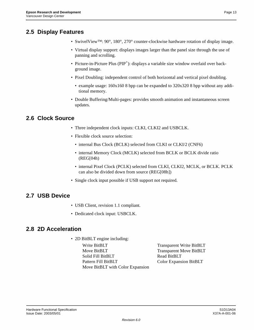
3 Typical System Implementation Diagrams
3.1 Typical System Diagrams.
Figure 3-1: Typical System Diagram (Generic #1 Bus).
Figure 3-2: Typical System Diagram (Generic #2 Bus)
S1D13A04
FPLINE
FPFRAME
FPSHIFT
DRDY
FPDAT[15:0]
CLK
I2
Oscillator
FPLINE
FPFRAME
FPSHIFT
MOD
D[15:0]
16-bit
Generic #1BUS
RESET#
D[15:0]
RD0#
WAIT#
A[17:1]
BUSCLK
RD/WR#
AB[17:1]
DB[15:0]
WE1#
RD#
M/R#
CS#
CLKI
WAIT#
RESET#
A[27:18]
CSn#
WE1# GPIO0
Decoder
WE0#WE0#
SingleLCD
Display
Bia
s P
ower
BS#
RD1#
IOVDD
VSS
AB0
S1D13A04
FPLINE
FPFRAME
FPSHIFT
DRDY
FPDAT[8:0]
CLK
I2
Oscillator
FPLINE
FPFRAME
FPSHIFT
DRDY
D[8:0]9-bit
Generic #2BUS
RESET#
D[15:0]
RD#
WAIT#
A[17:0]
BUSCLK
RD/WR#
AB[17:0]
DB[15:0]
WE1#
RD#
M/R#
CS#
CLKI
WAIT#
RESET#
A[27:18]
CSn#
BHE# GPIO0
Decoder
WE0#WE#
TFT
Bia
s P
ower
BS#
IOVDD
Display
Hardware Functional Specification S1D13A04Issue Date: 2003/05/01 X37A-A-001-06
Revision 6.0
Page 16 Epson Research and DevelopmentVancouver Design Center
.
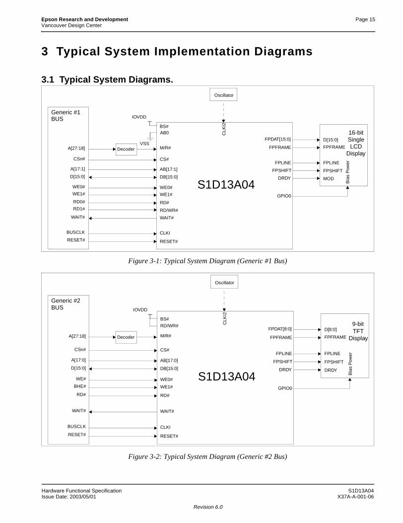
Figure 3-3: Typical System Diagram (Hitachi SH-4 Bus).
Figure 3-4: Typical System Diagram (Hitachi SH-3 Bus)
S1D13A04
FPLINE
FPFRAME
FPSHIFT
DRDY
FPDAT[9:0]
FPLINE
FPFRAME
FPSHIFT
DRDY
D[9:0]
12-bit
SH-4BUS
RESET#
WE0#
D[15:0]
BS#
RD/WR#
RD#
RDY#
A[17:1]
CKIO
WE0#
RD/WR#
AB[17:1]
DB[15:0]
WE1#
BS#
RD#
M/R#
CS#
CLKI
WAIT#
RESET#
A[25:18]
CSn#
WE1#
GPIO0
CLK
I2
Oscillator
TFTDisplay
Bia
s P
ower
FPDAT12
FPDAT15
D10D11
DecoderVSS
AB0
S1D13A04
FPLINE
FPFRAME
FPSHIFT
DRDY
FPDAT[17:0]
FPLINE
FPFRAME
FPSHIFT
DRDY
D[17:0]
18-bit
SH-3BUS
RESET#
WE0#
D[15:0]
BS#
RD/WR#
RD#
WAIT#
A[17:1]
CKIO
WE0#
RD/WR#
AB[17:1]
DB[15:0]
WE1#
BS#
RD#
M/R#
CS#
CLKI
WAIT#
RESET#
A[25:18]
CSn#
WE1#
GPIO0
CLK
I2
Oscillator
TFTDisplay
Bia
s P
ower
DecoderVSS
AB0
S1D13A04 Hardware Functional SpecificationX37A-A-001-06 Issue Date: 2003/05/01
Revision 6.0
Epson Research and Development Page 17Vancouver Design Center
.
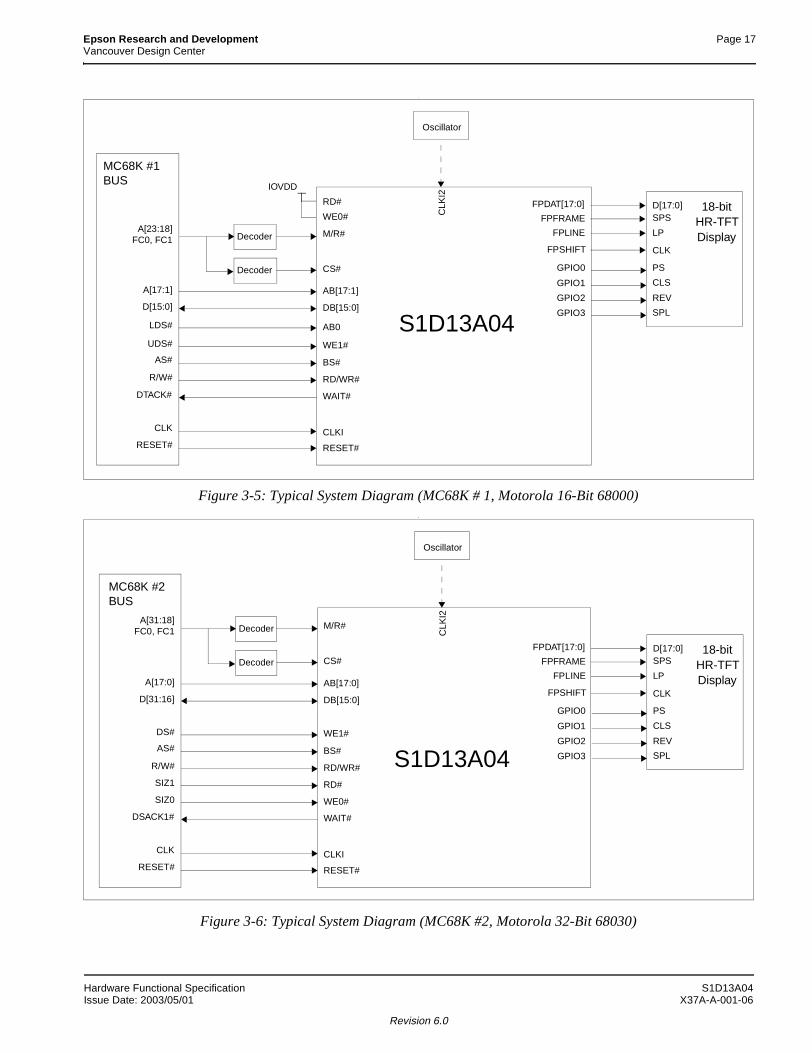
Figure 3-5: Typical System Diagram (MC68K # 1, Motorola 16-Bit 68000).
Figure 3-6: Typical System Diagram (MC68K #2, Motorola 32-Bit 68030)
S1D13A04
FPLINE
FPFRAME
FPSHIFT
FPDAT[17:0]
LP
SPS
CLK
D[17:0] 18-bit
MC68K #1BUS
RESET#
LDS#
D[15:0]
AS#
R/W#
DTACK#
A[17:1]
CLK
AB0
RD/WR#
AB[17:1]
DB[15:0]
WE1#
BS#
M/R#
CS#
CLKI
WAIT#
RESET#
A[23:18]FC0, FC1 Decoder
Decoder
UDS#
CLK
I2
Oscillator
HR-TFTDisplay
RD#
WE0#
IOVDD
GPIO0
GPIO1
GPIO2
GPIO3
PS
CLS
REV
SPL
S1D13A04
MC68K #2BUS
RESET#
SIZ0
D[31:16]
AS#
R/W#
SIZ1
DSACK1#
A[17:0]
CLK
WE0#
RD/WR#
AB[17:0]
DB[15:0]
WE1#
BS#
RD#
M/R#
CS#
CLKI
WAIT#
RESET#
A[31:18]FC0, FC1 Decoder
Decoder
DS#
CLK
I2
Oscillator
FPLINE
FPFRAME
FPSHIFT
FPDAT[17:0]
LP
SPS
CLK
D[17:0] 18-bitHR-TFTDisplay
GPIO0
GPIO1
GPIO2
GPIO3
PS
CLS
REV
SPL
Hardware Functional Specification S1D13A04Issue Date: 2003/05/01 X37A-A-001-06
Revision 6.0
Page 18 Epson Research and DevelopmentVancouver Design Center
.
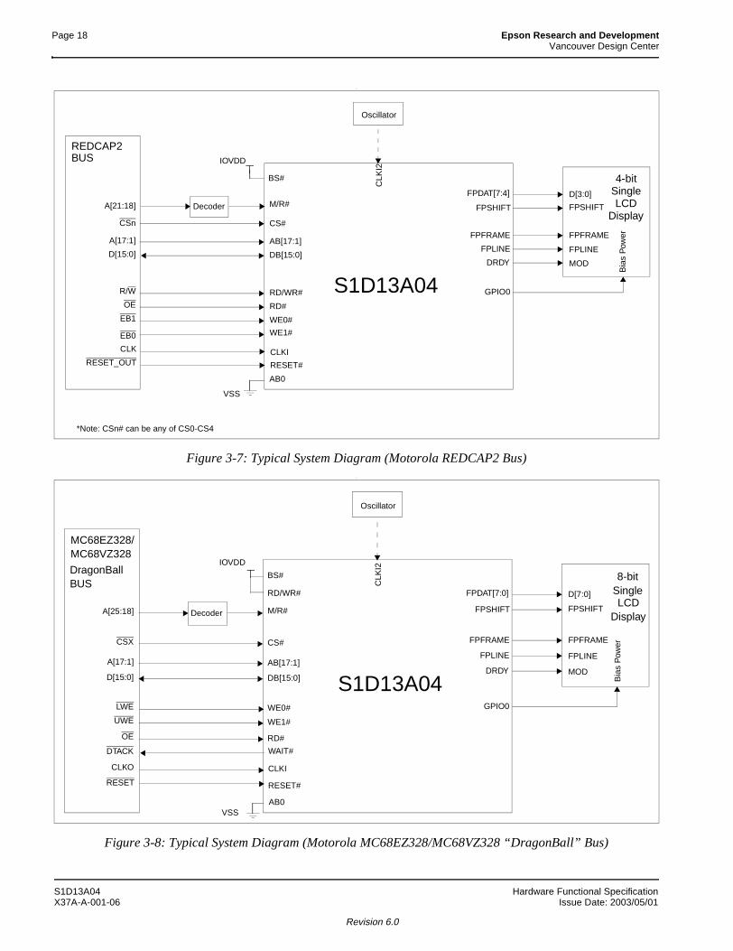
Figure 3-7: Typical System Diagram (Motorola REDCAP2 Bus).
Figure 3-8: Typical System Diagram (Motorola MC68EZ328/MC68VZ328 “DragonBall” Bus)
S1D13A04
FPFRAME
FPSHIFT
FPLINE
DRDY
FPDAT[7:4]
FPFRAME
FPSHIFT
FPLINE
MOD
D[3:0]
4-bit
REDCAP2BUS
RESET_OUT
EB1
D[15:0]
R/W
OE
A[17:1]
CLK
WE0#
RD/WR#
AB[17:1]
DB[15:0]
WE1#
RD#
M/R#
CS#
CLKI
RESET#
A[21:18] Decoder
EB0
GPIO0
CLK
I2
Oscillator
SingleLCD
Bia
s P
ower
CSn
*Note: CSn# can be any of CS0-CS4
Display
BS#
VSS
AB0
IOVDD
S1D13A04
FPFRAME
FPSHIFT
FPLINE
DRDY
FPDAT[7:0]
FPFRAME
FPSHIFT
FPLINE
MOD
D[7:0]
8-bit
MC68EZ328/
RESET
D[15:0]
OE
DTACK
A[17:1]
CLKO
RD/WR#
AB[17:1]
DB[15:0]
WE1#
RD#
M/R#
CS#
CLKI
WAIT#
RESET#
A[25:18]
CSX
UWE
GPIO0
Decoder
WE0#LWE
IOVDD
CLK
I2
Oscillator
Single
Bia
s P
ower
BS#DragonBallBUS
LCDDisplay
MC68VZ328
VSSAB0
S1D13A04 Hardware Functional SpecificationX37A-A-001-06 Issue Date: 2003/05/01
Revision 6.0
Epson Research and Development Page 19Vancouver Design Center
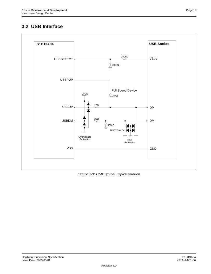
3.2 USB Interface
Figure 3-9: USB Typical Implementation
USBDP
USBDM
S1D13A04 USB Socket
USBDETECT
USBPUP
DM
DP
VBus
GNDVSS
LVDD
NNCD5.6LG
150kΩ
300kΩ
1.5kΩ
20Ω
20Ω
300kΩ
Full Speed Device
OvervoltageProtection ESD
Protection
Hardware Functional Specification S1D13A04Issue Date: 2003/05/01 X37A-A-001-06
Revision 6.0
Page 20 Epson Research and DevelopmentVancouver Design Center
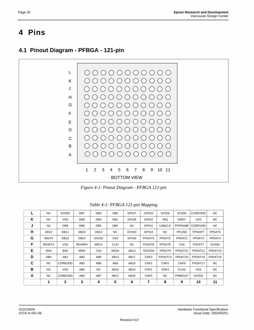
4 Pins
4.1 Pinout Diagram - PFBGA - 121-pin
Figure 4-1: Pinout Diagram - PFBGA 121-pin
Table 4-1: PFBGA 121-pin Mapping
L NC IOVDD DB7 DB3 DB0 GPIO7 GPIO3 GPIO0 IOVDD COREVDD NC
K NC VSS DB8 DB4 DB1 GPIO6 GPIO2 IRQ DRDY VSS NC
J NC DB9 DB6 DB5 DB2 NC GPIO1 USBCLK FPFRAME COREVDD NC
H DB12 DB11 DB10 DB13 NC IOVDD GPIO4 NC FPLINE FPSHIFT FPDAT0
G WAIT# DB15 DB14 IOVDD VSS GPIO5 FPDAT5 FPDAT1 FPDAT2 FPDAT3 FPDAT4
F RESET# VSS RD/WR# WE1# CLKI NC FPDAT8 FPDAT6 VSS FPDAT7 IOVDD
E RD# BS# M/R# CS# WE0# AB13 TESTEN FPDAT9 FPDAT12 FPDAT11 FPDAT10
D AB0 AB1 AB2 AB8 AB12 AB17 CNF3 FPDAT13 FPDAT16 FPDAT15 FPDAT14
C NC COREVDD AB3 AB6 AB9 AB16 CNF2 CNF5 CNF6 FPDAT17 NC
B NC VSS AB5 NC AB10 AB14 CNF1 CNF4 CLKI2 VSS NC
A NC COREVDD AB4 AB7 AB11 AB15 CNF0 NC PWMOUT IOVDD NC
1 2 3 4 5 6 7 8 9 10 11
L
K
J
H
G
F
E
D
C
B
A
1 2 3 4 5 6 7 8 9 10 11
BOTTOM VIEW
S1D13A04 Hardware Functional SpecificationX37A-A-001-06 Issue Date: 2003/05/01
Revision 6.0
Epson Research and Development Page 21Vancouver Design Center
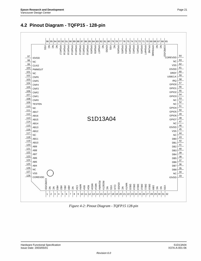
4.2 Pinout Diagram - TQFP15 - 128-pin
Figure 4-2: Pinout Diagram - TQFP15 128-pin
1 2 3 4 5 6 7 8 9 10 11 12 13 14 15 16 17 18 19 20 21 22 23 24 25 26 27 28 29 30 31 32
96 95 94 93 92 91 90 89 88 87 86 85 84 83 7475 73 72 71 70 69 68 67 66 6582 81 80 79 78 77 76
128
127
126
125
124
123
122
121
120
119
118
117
116
115
114
113
112
111
110
109
108
107
106
105
104
103
102
101
100
99
98
97
33
34
35
36
37
38
39
40
41
42
43
44
45
46
47
48
49
50
58
59
60
61
62
63
51
52
53
54
55
56
57
64
S1D13A04M
/R#
RD
/WR
#
RD
#
WE
1#
RE
SE
T#
NC
CLK
I
DB
15
DB
12
DB
10
DB
9
NC
NC
VS
S
DB
11
CO
RE
VD
D
BS
#
IOVDD
VSS
IRQ
DB
14
FP
DAT
7
NC
NC
CO
RE
VD
D
COREVDD
NC
GPIO0
IOVDD
DRDY
USBCLK
GPIO1
GPIO2
CNF3
FP
DAT
12
CNF6
CNF5
NC
FP
DAT
15
GPIO3
NC
NC
GPIO5
GPIO6
GPIO7
VSS
NC
DB0
DB1
DB2
DB3
DB4
DB5
DB6
COREVDD
AB
1
CS
#
NC
AB
0
AB
2
AB
3
NC
NC
AB9
AB10
AB12
AB13
AB14
AB15
AB16
AB17
TESTEN
NC
CNF2
NC
CNF4
IOVDD
NC
FP
DAT
8
NC
FP
DAT
6
FP
DAT
5
FP
DAT
4
FP
DAT
3
FP
DAT
2
FP
FR
AM
E
NC
NC
NC
VS
S
CLKI2
DB7
NC
WA
IT#
VS
S
IOV
DD
DB
13NC
GPIO4
IOVDD
FP
DAT
9
FP
DAT
11
FP
DAT
1
FP
SH
IFT
FP
DAT
13
DB8
FP
DAT
14
FP
DAT
17
VS
S
IOV
DD
CNF0
FP
DAT
16
CNF1
NC
AB11
AB5
VSS
NC
AB6
AB7
AB8
AB4
PWMOUT
FP
DAT
10
FP
LINE
WE
0#
FP
DAT
0NC
Hardware Functional Specification S1D13A04Issue Date: 2003/05/01 X37A-A-001-06
Revision 6.0
Page 22 Epson Research and DevelopmentVancouver Design Center
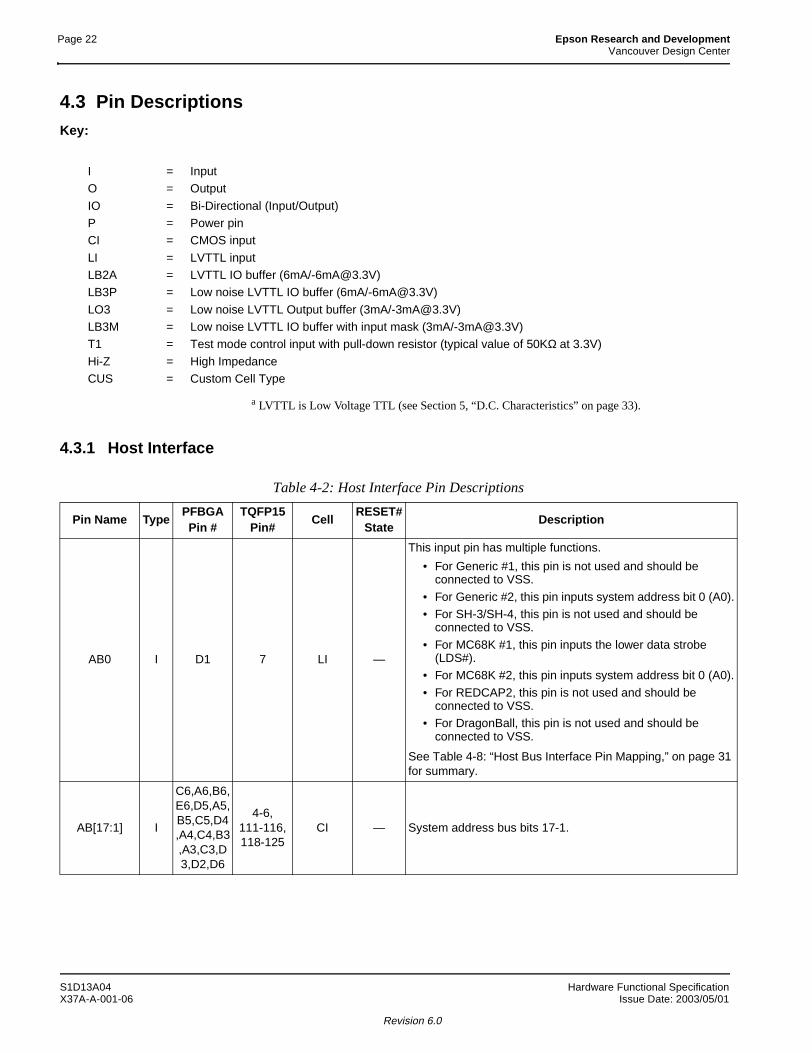
4.3 Pin DescriptionsKey:
a LVTTL is Low Voltage TTL (see Section 5, “D.C. Characteristics” on page 33).
4.3.1 Host Interface
I = InputO = Output
IO = Bi-Directional (Input/Output)P = Power pinCI = CMOS input
LI = LVTTL inputLB2A = LVTTL IO buffer (6mA/[email protected])LB3P = Low noise LVTTL IO buffer (6mA/[email protected])
LO3 = Low noise LVTTL Output buffer (3mA/[email protected])LB3M = Low noise LVTTL IO buffer with input mask (3mA/[email protected])T1 = Test mode control input with pull-down resistor (typical value of 50KΩ at 3.3V)
Hi-Z = High ImpedanceCUS = Custom Cell Type
Table 4-2: Host Interface Pin Descriptions
Pin Name TypePFBGAPin #
TQFP15 Pin#
CellRESET#
StateDescription
AB0 I D1 7 LI —
This input pin has multiple functions.
• For Generic #1, this pin is not used and should be connected to VSS.
• For Generic #2, this pin inputs system address bit 0 (A0).• For SH-3/SH-4, this pin is not used and should be
connected to VSS.
• For MC68K #1, this pin inputs the lower data strobe (LDS#).
• For MC68K #2, this pin inputs system address bit 0 (A0).
• For REDCAP2, this pin is not used and should be connected to VSS.
• For DragonBall, this pin is not used and should be connected to VSS.
See Table 4-8: “Host Bus Interface Pin Mapping,” on page 31 for summary.
AB[17:1] I
C6,A6,B6,E6,D5,A5,B5,C5,D4,A4,C4,B3,A3,C3,D3,D2,D6
4-6,111-116, 118-125
CI — System address bus bits 17-1.
S1D13A04 Hardware Functional SpecificationX37A-A-001-06 Issue Date: 2003/05/01
Revision 6.0
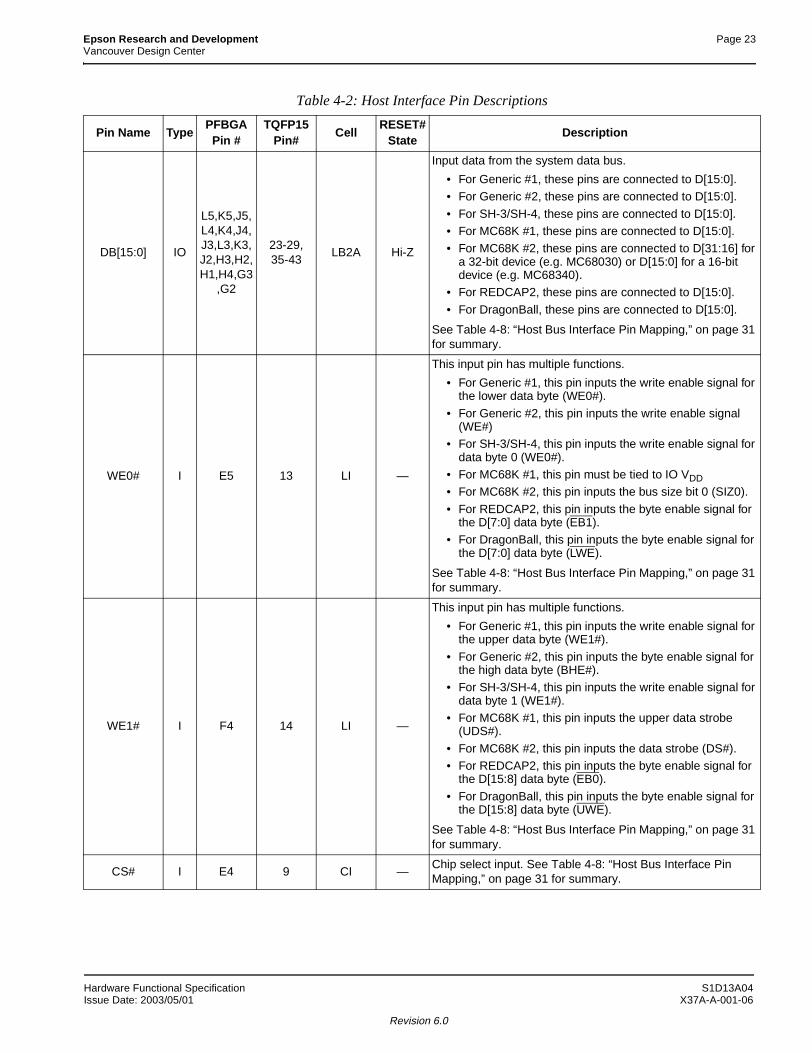
Epson Research and Development Page 23Vancouver Design Center
DB[15:0] IO
L5,K5,J5,L4,K4,J4,J3,L3,K3,J2,H3,H2,H1,H4,G3
,G2
23-29,35-43
LB2A Hi-Z
Input data from the system data bus.
• For Generic #1, these pins are connected to D[15:0].• For Generic #2, these pins are connected to D[15:0].
• For SH-3/SH-4, these pins are connected to D[15:0].• For MC68K #1, these pins are connected to D[15:0].• For MC68K #2, these pins are connected to D[31:16] for
a 32-bit device (e.g. MC68030) or D[15:0] for a 16-bit device (e.g. MC68340).
• For REDCAP2, these pins are connected to D[15:0].
• For DragonBall, these pins are connected to D[15:0].
See Table 4-8: “Host Bus Interface Pin Mapping,” on page 31 for summary.
WE0# I E5 13 LI —
This input pin has multiple functions.
• For Generic #1, this pin inputs the write enable signal for the lower data byte (WE0#).
• For Generic #2, this pin inputs the write enable signal (WE#)
• For SH-3/SH-4, this pin inputs the write enable signal for data byte 0 (WE0#).
• For MC68K #1, this pin must be tied to IO VDD
• For MC68K #2, this pin inputs the bus size bit 0 (SIZ0).
• For REDCAP2, this pin inputs the byte enable signal for the D[7:0] data byte (EB1).
• For DragonBall, this pin inputs the byte enable signal for the D[7:0] data byte (LWE).
See Table 4-8: “Host Bus Interface Pin Mapping,” on page 31 for summary.
WE1# I F4 14 LI —
This input pin has multiple functions.
• For Generic #1, this pin inputs the write enable signal for the upper data byte (WE1#).
• For Generic #2, this pin inputs the byte enable signal for the high data byte (BHE#).
• For SH-3/SH-4, this pin inputs the write enable signal for data byte 1 (WE1#).
• For MC68K #1, this pin inputs the upper data strobe (UDS#).
• For MC68K #2, this pin inputs the data strobe (DS#).• For REDCAP2, this pin inputs the byte enable signal for
the D[15:8] data byte (EB0).
• For DragonBall, this pin inputs the byte enable signal for the D[15:8] data byte (UWE).
See Table 4-8: “Host Bus Interface Pin Mapping,” on page 31 for summary.
CS# I E4 9 CI —Chip select input. See Table 4-8: “Host Bus Interface Pin Mapping,” on page 31 for summary.
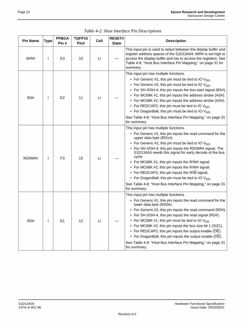
Table 4-2: Host Interface Pin Descriptions
Pin Name TypePFBGA
Pin #TQFP15
Pin#Cell
RESET# State
Description
Hardware Functional Specification S1D13A04Issue Date: 2003/05/01 X37A-A-001-06
Revision 6.0
Page 24 Epson Research and DevelopmentVancouver Design Center
M/R# I E3 10 LI —
This input pin is used to select between the display buffer and register address spaces of the S1D13A04. M/R# is set high to access the display buffer and low to access the registers. See Table 4-8: “Host Bus Interface Pin Mapping,” on page 31 for summary.
BS# I E2 11 LI —
This input pin has multiple functions.
• For Generic #1, this pin must be tied to IO VDD.• For Generic #2, this pin must be tied to IO VDD.• For SH-3/SH-4, this pin inputs the bus start signal (BS#).
• For MC68K #1, this pin inputs the address strobe (AS#).• For MC68K #2, this pin inputs the address strobe (AS#).• For REDCAP2, this pin must be tied to IO VDD.
• For DragonBall, this pin must be tied to IO VDD.
See Table 4-8: “Host Bus Interface Pin Mapping,” on page 31 for summary.
RD/WR# I F3 15 LI —
This input pin has multiple functions.
• For Generic #1, this pin inputs the read command for the upper data byte (RD1#).
• For Generic #2, this pin must be tied to IO VDD.• For SH-3/SH-4, this pin inputs the RD/WR# signal. The
S1D13A04 needs this signal for early decode of the bus cycle.
• For MC68K #1, this pin inputs the R/W# signal.• For MC68K #2, this pin inputs the R/W# signal.
• For REDCAP2, this pin inputs the R/W signal.• For DragonBall, this pin must be tied to IO VDD.
See Table 4-8: “Host Bus Interface Pin Mapping,” on page 31 for summary.
RD# I E1 12 LI —
This input pin has multiple functions.
• For Generic #1, this pin inputs the read command for the lower data byte (RD0#).
• For Generic #2, this pin inputs the read command (RD#).• For SH-3/SH-4, this pin inputs the read signal (RD#).
• For MC68K #1, this pin must be tied to IO VDD.• For MC68K #2, this pin inputs the bus size bit 1 (SIZ1).• For REDCAP2, this pin inputs the output enable (OE).
• For DragonBall, this pin inputs the output enable (OE).
See Table 4-8: “Host Bus Interface Pin Mapping,” on page 31 for summary.
Table 4-2: Host Interface Pin Descriptions
Pin Name TypePFBGAPin #
TQFP15 Pin#
CellRESET#
StateDescription
S1D13A04 Hardware Functional SpecificationX37A-A-001-06 Issue Date: 2003/05/01
Revision 6.0
Epson Research and Development Page 25Vancouver Design Center
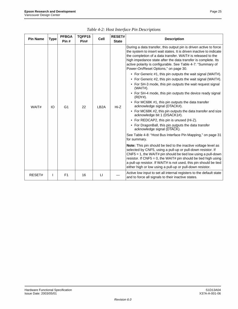
WAIT# IO G1 22 LB2A Hi-Z
During a data transfer, this output pin is driven active to force the system to insert wait states. It is driven inactive to indicate the completion of a data transfer. WAIT# is released to the high impedance state after the data transfer is complete. Its active polarity is configurable. See Table 4-7: “Summary of Power-On/Reset Options,” on page 30.
• For Generic #1, this pin outputs the wait signal (WAIT#).
• For Generic #2, this pin outputs the wait signal (WAIT#).• For SH-3 mode, this pin outputs the wait request signal
(WAIT#).
• For SH-4 mode, this pin outputs the device ready signal (RDY#).
• For MC68K #1, this pin outputs the data transfer acknowledge signal (DTACK#).
• For MC68K #2, this pin outputs the data transfer and size acknowledge bit 1 (DSACK1#).
• For REDCAP2, this pin is unused (Hi-Z).• For DragonBall, this pin outputs the data transfer
acknowledge signal (DTACK).
See Table 4-8: “Host Bus Interface Pin Mapping,” on page 31 for summary.
Note: This pin should be tied to the inactive voltage level as selected by CNF5, using a pull-up or pull-down resistor. If CNF5 = 1, the WAIT# pin should be tied low using a pull-down resistor. If CNF5 = 0, the WAIT# pin should be tied high using a pull-up resistor. If WAIT# is not used, this pin should be tied either high or low using a pull-up or pull-down resistor.
RESET# I F1 16 LI —Active low input to set all internal registers to the default state and to force all signals to their inactive states.
Table 4-2: Host Interface Pin Descriptions
Pin Name TypePFBGA
Pin #TQFP15
Pin#Cell
RESET# State
Description
Hardware Functional Specification S1D13A04Issue Date: 2003/05/01 X37A-A-001-06
Revision 6.0
Page 26 Epson Research and DevelopmentVancouver Design Center
4.3.2 LCD Interface
Table 4-3: LCD Interface Pin Descriptions
Pin Name TypePFBGA
Pin#TQFP15
Pin#Cell
RESET# State
Description
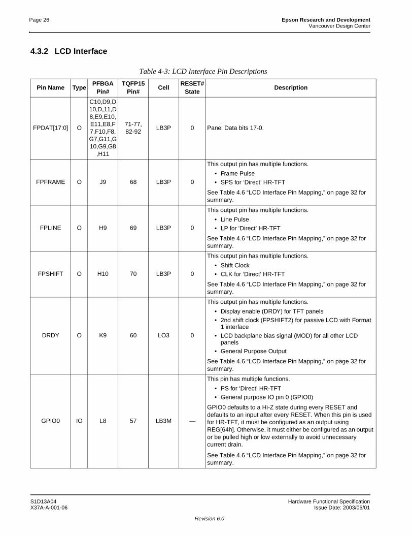
FPDAT[17:0] O
C10,D9,D10,D,11,D8,E9,E10,E11,E8,F7,F10,F8,G7,G11,G10,G9,G8
,H11
71-77,82-92
LB3P 0 Panel Data bits 17-0.
FPFRAME O J9 68 LB3P 0
This output pin has multiple functions.
• Frame Pulse• SPS for ‘Direct’ HR-TFT
See Table 4.6 “LCD Interface Pin Mapping,” on page 32 for summary.
FPLINE O H9 69 LB3P 0
This output pin has multiple functions.
• Line Pulse
• LP for ‘Direct’ HR-TFT
See Table 4.6 “LCD Interface Pin Mapping,” on page 32 for summary.
FPSHIFT O H10 70 LB3P 0
This output pin has multiple functions.
• Shift Clock• CLK for ‘Direct’ HR-TFT
See Table 4.6 “LCD Interface Pin Mapping,” on page 32 for summary.
DRDY O K9 60 LO3 0
This output pin has multiple functions.
• Display enable (DRDY) for TFT panels• 2nd shift clock (FPSHIFT2) for passive LCD with Format
1 interface
• LCD backplane bias signal (MOD) for all other LCD panels
• General Purpose Output
See Table 4.6 “LCD Interface Pin Mapping,” on page 32 for summary.
GPIO0 IO L8 57 LB3M —
This pin has multiple functions.
• PS for ‘Direct’ HR-TFT• General purpose IO pin 0 (GPIO0)
GPIO0 defaults to a Hi-Z state during every RESET and defaults to an input after every RESET. When this pin is used for HR-TFT, it must be configured as an output using REG[64h]. Otherwise, it must either be configured as an output or be pulled high or low externally to avoid unnecessary current drain.
See Table 4.6 “LCD Interface Pin Mapping,” on page 32 for summary.
S1D13A04 Hardware Functional SpecificationX37A-A-001-06 Issue Date: 2003/05/01
Revision 6.0
Epson Research and Development Page 27Vancouver Design Center
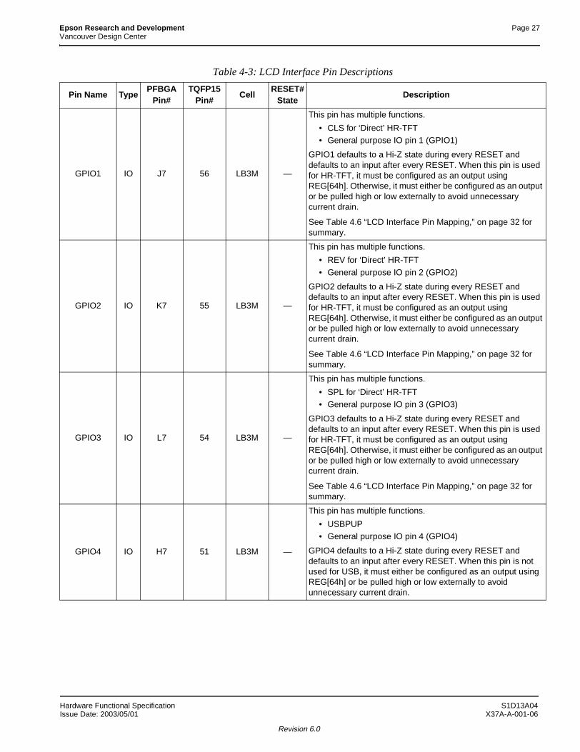
GPIO1 IO J7 56 LB3M —
This pin has multiple functions.
• CLS for ‘Direct’ HR-TFT• General purpose IO pin 1 (GPIO1)
GPIO1 defaults to a Hi-Z state during every RESET and defaults to an input after every RESET. When this pin is used for HR-TFT, it must be configured as an output using REG[64h]. Otherwise, it must either be configured as an output or be pulled high or low externally to avoid unnecessary current drain.
See Table 4.6 “LCD Interface Pin Mapping,” on page 32 for summary.
GPIO2 IO K7 55 LB3M —
This pin has multiple functions.
• REV for ‘Direct’ HR-TFT
• General purpose IO pin 2 (GPIO2)
GPIO2 defaults to a Hi-Z state during every RESET and defaults to an input after every RESET. When this pin is used for HR-TFT, it must be configured as an output using REG[64h]. Otherwise, it must either be configured as an output or be pulled high or low externally to avoid unnecessary current drain.
See Table 4.6 “LCD Interface Pin Mapping,” on page 32 for summary.
GPIO3 IO L7 54 LB3M —
This pin has multiple functions.
• SPL for ‘Direct’ HR-TFT• General purpose IO pin 3 (GPIO3)
GPIO3 defaults to a Hi-Z state during every RESET and defaults to an input after every RESET. When this pin is used for HR-TFT, it must be configured as an output using REG[64h]. Otherwise, it must either be configured as an output or be pulled high or low externally to avoid unnecessary current drain.
See Table 4.6 “LCD Interface Pin Mapping,” on page 32 for summary.
GPIO4 IO H7 51 LB3M —
This pin has multiple functions.
• USBPUP• General purpose IO pin 4 (GPIO4)
GPIO4 defaults to a Hi-Z state during every RESET and defaults to an input after every RESET. When this pin is not used for USB, it must either be configured as an output using REG[64h] or be pulled high or low externally to avoid unnecessary current drain.
Table 4-3: LCD Interface Pin Descriptions
Pin Name TypePFBGA
Pin#TQFP15
Pin#Cell
RESET# State
Description
Hardware Functional Specification S1D13A04Issue Date: 2003/05/01 X37A-A-001-06
Revision 6.0
Page 28 Epson Research and DevelopmentVancouver Design Center
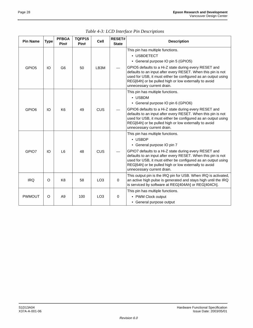
GPIO5 IO G6 50 LB3M —
This pin has multiple functions.
• USBDETECT• General purpose IO pin 5 (GPIO5)
GPIO5 defaults to a Hi-Z state during every RESET and defaults to an input after every RESET. When this pin is not used for USB, it must either be configured as an output using REG[64h] or be pulled high or low externally to avoid unnecessary current drain.
GPIO6 IO K6 49 CUS —
This pin has multiple functions.
• USBDM• General purpose IO pin 6 (GPIO6)
GPIO6 defaults to a Hi-Z state during every RESET and defaults to an input after every RESET. When this pin is not used for USB, it must either be configured as an output using REG[64h] or be pulled high or low externally to avoid unnecessary current drain.
GPIO7 IO L6 48 CUS —
This pin has multiple functions.
• USBDP
• General purpose IO pin 7
GPIO7 defaults to a Hi-Z state during every RESET and defaults to an input after every RESET. When this pin is not used for USB, it must either be configured as an output using REG[64h] or be pulled high or low externally to avoid unnecessary current drain.
IRQ O K8 58 LO3 0This output pin is the IRQ pin for USB. When IRQ is activated, an active high pulse is generated and stays high until the IRQ is serviced by software at REG[404Ah] or REG[404Ch].
PWMOUT O A9 100 LO3 0
This pin has multiple functions.
• PWM Clock output
• General purpose output
Table 4-3: LCD Interface Pin Descriptions
Pin Name TypePFBGA
Pin#TQFP15
Pin#Cell
RESET# State
Description
S1D13A04 Hardware Functional SpecificationX37A-A-001-06 Issue Date: 2003/05/01
Revision 6.0
Epson Research and Development Page 29Vancouver Design Center
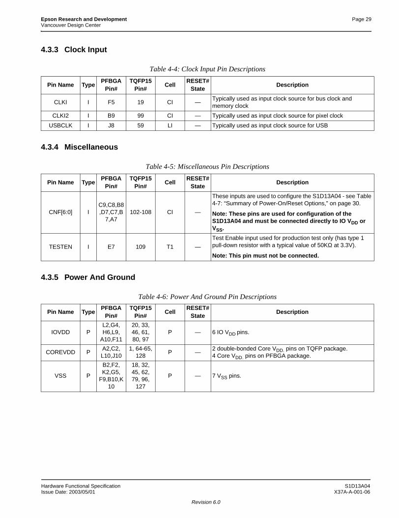
4.3.3 Clock Input
4.3.4 Miscellaneous
4.3.5 Power And Ground
Table 4-4: Clock Input Pin Descriptions
Pin Name TypePFBGA
Pin#TQFP15
Pin#Cell
RESET# State
Description
CLKI I F5 19 CI —Typically used as input clock source for bus clock and memory clock
CLKI2 I B9 99 CI — Typically used as input clock source for pixel clock
USBCLK I J8 59 LI — Typically used as input clock source for USB
Table 4-5: Miscellaneous Pin Descriptions
Pin Name TypePFBGA
Pin#TQFP15
Pin#Cell
RESET# State
Description
CNF[6:0] IC9,C8,B8,D7,C7,B
7,A7102-108 CI —
These inputs are used to configure the S1D13A04 - see Table 4-7: “Summary of Power-On/Reset Options,” on page 30.
Note: These pins are used for configuration of the S1D13A04 and must be connected directly to IO VDD or VSS.
TESTEN I E7 109 T1 —
Test Enable input used for production test only (has type 1 pull-down resistor with a typical value of 50KΩ at 3.3V).
Note: This pin must not be connected.
Table 4-6: Power And Ground Pin Descriptions
Pin Name TypePFBGA
Pin#TQFP15
Pin#Cell
RESET# State
Description
IOVDD PL2,G4, H6,L9,
A10,F11
20, 33, 46, 61, 80, 97
P — 6 IO VDD pins.
COREVDD PA2,C2,L10,J10
1, 64-65, 128
P —2 double-bonded Core VDD. pins on TQFP package.4 Core VDD. pins on PFBGA package.
VSS P
B2,F2,K2,G5,
F9,B10,K10
18, 32, 45, 62, 79, 96,
127
P — 7 VSS pins.
Hardware Functional Specification S1D13A04Issue Date: 2003/05/01 X37A-A-001-06
Revision 6.0
Page 30 Epson Research and DevelopmentVancouver Design Center
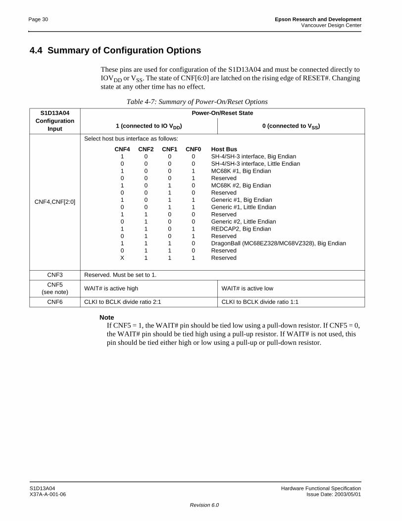
4.4 Summary of Configuration Options
These pins are used for configuration of the S1D13A04 and must be connected directly to IOVDD or VSS. The state of CNF[6:0] are latched on the rising edge of RESET#. Changing state at any other time has no effect.
NoteIf CNF5 = 1, the WAIT# pin should be tied low using a pull-down resistor. If CNF5 = 0, the WAIT# pin should be tied high using a pull-up resistor. If WAIT# is not used, this pin should be tied either high or low using a pull-up or pull-down resistor.
Table 4-7: Summary of Power-On/Reset Options
S1D13A04 Configuration
Input
Power-On/Reset State
1 (connected to IO VDD) 0 (connected to VSS)
CNF4,CNF[2:0]
Select host bus interface as follows:
CNF4 CNF2 CNF1 CNF0 Host Bus1 0 0 0 SH-4/SH-3 interface, Big Endian0 0 0 0 SH-4/SH-3 interface, Little Endian1 0 0 1 MC68K #1, Big Endian0 0 0 1 Reserved1 0 1 0 MC68K #2, Big Endian0 0 1 0 Reserved1 0 1 1 Generic #1, Big Endian0 0 1 1 Generic #1, Little Endian1 1 0 0 Reserved0 1 0 0 Generic #2, Little Endian1 1 0 1 REDCAP2, Big Endian0 1 0 1 Reserved1 1 1 0 DragonBall (MC68EZ328/MC68VZ328), Big Endian0 1 1 0 ReservedX 1 1 1 Reserved
CNF3 Reserved. Must be set to 1.
CNF5(see note)
WAIT# is active high WAIT# is active low
CNF6 CLKI to BCLK divide ratio 2:1 CLKI to BCLK divide ratio 1:1
S1D13A04 Hardware Functional SpecificationX37A-A-001-06 Issue Date: 2003/05/01
Revision 6.0
Epson Research and Development Page 31Vancouver Design Center
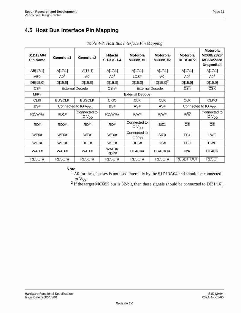
4.5 Host Bus Interface Pin Mapping
Note1 A0 for these busses is not used internally by the S1D13A04 and should be connected
to VSS.2 If the target MC68K bus is 32-bit, then these signals should be connected to D[31:16].
Table 4-8: Host Bus Interface Pin Mapping
S1D13A04 Pin Name
Generic #1 Generic #2Hitachi
SH-3 /SH-4Motorola
MC68K #1Motorola
MC68K #2Motorola
REDCAP2
Motorola MC68EZ328/MC68VZ328 DragonBall
AB[17:1] A[17:1] A[17:1] A[17:1] A[17:1] A[17:1] A[17:1] A[17:1]
AB0 A01 A0 A01 LDS# A0 A01 A01
DB[15:0] D[15:0] D[15:0] D[15:0] D[15:0] D[15:0]2 D[15:0] D[15:0]
CS# External Decode CSn# External Decode CSn CSX
M/R# External Decode
CLKI BUSCLK BUSCLK CKIO CLK CLK CLK CLKO
BS# Connected to IO VDD BS# AS# AS# Connected to IO VDD
RD/WR# RD1#Connected to
IO VDDRD/WR# R/W# R/W# R/W
Connected to IO VDD
RD# RD0# RD# RD#Connected to
IO VDDSIZ1 OE OE
WE0# WE0# WE# WE0#Connected to
IO VDDSIZ0 EB1 LWE
WE1# WE1# BHE# WE1# UDS# DS# EB0 UWE
WAIT# WAIT# WAIT#WAIT#/RDY#
DTACK# DSACK1# N/A DTACK
RESET# RESET# RESET# RESET# RESET# RESET# RESET_OUT RESET
Hardware Functional Specification S1D13A04Issue Date: 2003/05/01 X37A-A-001-06
Revision 6.0
Page 32 Epson Research and DevelopmentVancouver Design Center
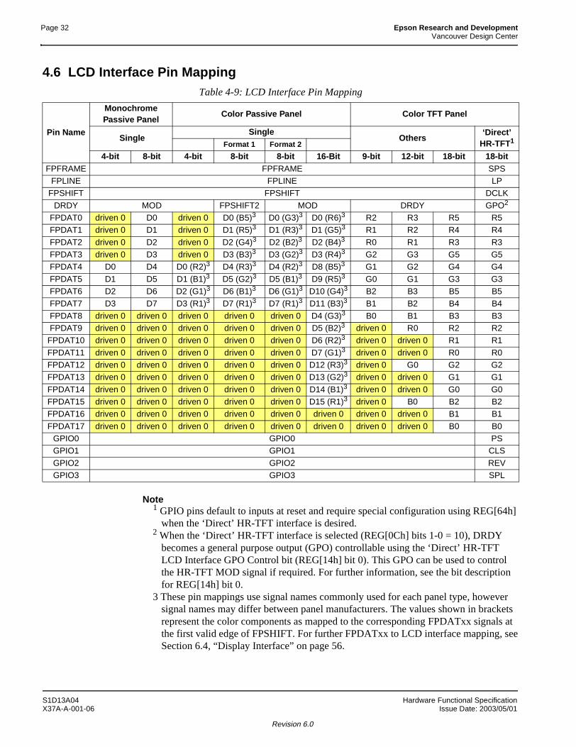
4.6 LCD Interface Pin Mapping
Note1 GPIO pins default to inputs at reset and require special configuration using REG[64h]
when the ‘Direct’ HR-TFT interface is desired.2 When the ‘Direct’ HR-TFT interface is selected (REG[0Ch] bits 1-0 = 10), DRDY
becomes a general purpose output (GPO) controllable using the ‘Direct’ HR-TFTLCD Interface GPO Control bit (REG[14h] bit 0). This GPO can be used to controlthe HR-TFT MOD signal if required. For further information, see the bit descriptionfor REG[14h] bit 0.
3 These pin mappings use signal names commonly used for each panel type, howeversignal names may differ between panel manufacturers. The values shown in bracketsrepresent the color components as mapped to the corresponding FPDATxx signals atthe first valid edge of FPSHIFT. For further FPDATxx to LCD interface mapping, seeSection 6.4, “Display Interface” on page 56.
Table 4-9: LCD Interface Pin Mapping
Pin Name
Monochrome Passive Panel
Color Passive Panel Color TFT Panel
SingleSingle
Others‘Direct’
HR-TFT1Format 1 Format 2
4-bit 8-bit 4-bit 8-bit 8-bit 16-Bit 9-bit 12-bit 18-bit 18-bitFPFRAME FPFRAME SPS
FPLINE FPLINE LPFPSHIFT FPSHIFT DCLK
DRDY MOD FPSHIFT2 MOD DRDY GPO2
FPDAT0 driven 0 D0 driven 0 D0 (B5)3 D0 (G3)3 D0 (R6)3 R2 R3 R5 R5FPDAT1 driven 0 D1 driven 0 D1 (R5)3 D1 (R3)3 D1 (G5)3 R1 R2 R4 R4
FPDAT2 driven 0 D2 driven 0 D2 (G4)3 D2 (B2)3 D2 (B4)3 R0 R1 R3 R3FPDAT3 driven 0 D3 driven 0 D3 (B3)3 D3 (G2)3 D3 (R4)3 G2 G3 G5 G5FPDAT4 D0 D4 D0 (R2)3 D4 (R3)3 D4 (R2)3 D8 (B5)3 G1 G2 G4 G4
FPDAT5 D1 D5 D1 (B1)3 D5 (G2)3 D5 (B1)3 D9 (R5)3 G0 G1 G3 G3FPDAT6 D2 D6 D2 (G1)3 D6 (B1)3 D6 (G1)3 D10 (G4)3 B2 B3 B5 B5FPDAT7 D3 D7 D3 (R1)3 D7 (R1)3 D7 (R1)3 D11 (B3)3 B1 B2 B4 B4
FPDAT8 driven 0 driven 0 driven 0 driven 0 driven 0 D4 (G3)3 B0 B1 B3 B3FPDAT9 driven 0 driven 0 driven 0 driven 0 driven 0 D5 (B2)3 driven 0 R0 R2 R2
FPDAT10 driven 0 driven 0 driven 0 driven 0 driven 0 D6 (R2)3 driven 0 driven 0 R1 R1
FPDAT11 driven 0 driven 0 driven 0 driven 0 driven 0 D7 (G1)3 driven 0 driven 0 R0 R0FPDAT12 driven 0 driven 0 driven 0 driven 0 driven 0 D12 (R3)3 driven 0 G0 G2 G2FPDAT13 driven 0 driven 0 driven 0 driven 0 driven 0 D13 (G2)3 driven 0 driven 0 G1 G1
FPDAT14 driven 0 driven 0 driven 0 driven 0 driven 0 D14 (B1)3 driven 0 driven 0 G0 G0FPDAT15 driven 0 driven 0 driven 0 driven 0 driven 0 D15 (R1)3 driven 0 B0 B2 B2FPDAT16 driven 0 driven 0 driven 0 driven 0 driven 0 driven 0 driven 0 driven 0 B1 B1
FPDAT17 driven 0 driven 0 driven 0 driven 0 driven 0 driven 0 driven 0 driven 0 B0 B0GPIO0 GPIO0 PSGPIO1 GPIO1 CLS
GPIO2 GPIO2 REVGPIO3 GPIO3 SPL
S1D13A04 Hardware Functional SpecificationX37A-A-001-06 Issue Date: 2003/05/01
Revision 6.0
Epson Research and Development Page 33Vancouver Design Center
5 D.C. Characteristics
NoteWhen applying Supply Voltages to the S1D13A04, Core VDD must be applied to the chip before, or simultaneously with IO VDD, or damage to the chip may result.
1. When Core VDD is 2.0V ± 10%, the MCLK must be less than or equal to 30MHz (MCLK ≤ 30MHz)
Table 5-1: Absolute Maximum Ratings
Symbol Parameter Rating Units
Core VDD Supply Voltage VSS - 0.3 to 3.0 V
IO VDD Supply Voltage VSS - 0.3 to 4.0 V
VIN Input Voltage VSS - 0.3 to IO VDD + 0.5 V
VOUT Output Voltage VSS - 0.3 to IO VDD + 0.5 V
TSTG Storage Temperature -65 to 150 ° C
TSOL Solder Temperature/Time 260 for 10 sec. max at lead ° C
Table 5-2: Recommended Operating Conditions
Symbol Parameter Condition Min Typ Max Units
Core VDD Supply VoltageVSS = 0 V 1.8 (note 1) 2.0 (note 1) 2.2 (note 1) V
VSS = 0 V 2.25 2.5 2.75 V
IO VDD Supply Voltage VSS = 0 V 3.0 3.3 3.6 V
VIN Input VoltageVSS IO VDD V
VSS CORE VDD
TOPR Operating Temperature -40 25 85 ° C
Table 5-3: Electrical Characteristics for VDD = 3.3V typical
Symbol Parameter Condition Min Typ Max UnitsIDDS Quiescent Current Quiescent Conditions 170 µAIIZ Input Leakage Current -1 1 µA
IOZ Output Leakage Current -1 1 µA
VOH High Level Output VoltageVDD = min.IOH = -3mA (Type 1)
-6mA (Type 2)VDD - 0.4 V
VOL Low Level Output VoltageVDD = min.IOL = 3mA (Type 1)
6mA (Type 2)0.4 V
VIH High Level Input Voltage LVTTL Level, VDD = max 2.0 V
VIL Low Level Input Voltage LVTTL Level, VDD = min 0.8 VRPD Pull Down Resistance VIN = VDD 20 50 120 kΩCI Input Pin Capacitance 10 pF
CO Output Pin Capacitance 10 pFCIO Bi-Directional Pin Capacitance 10 pF
Hardware Functional Specification S1D13A04Issue Date: 2003/05/01 X37A-A-001-06
Revision 6.0
Page 34 Epson Research and DevelopmentVancouver Design Center
6 A.C. Characteristics
Conditions: IO VDD = 3.3V ± 10%TA = -40° C to 85° CTrise and Tfall for all inputs must be < 5 nsec (10% ~ 90%)CL = 50pF (Bus/MPU Interface)CL = 0pF (LCD Panel Interface)
6.1 Clock Timing
6.1.1 Input Clocks
Figure 6-1: Clock Input Requirements
NoteMaximum internal requirements for clocks derived from CLKI must be considered when determining the frequency of CLKI. See Section 6.1.2, “Internal Clocks” on page 35 for internal clock requirements.
Table 6-1: Clock Input Requirements for CLKI when CLKI to BCLK divide > 1
Symbol Parameter Min Max Units
fOSC
Input Clock Frequency (CLKI) 100 MHz
TOSC
Input Clock period (CLKI) 1/fOSC
ns
tPWH
Input Clock Pulse Width High (CLKI) 4.5 ns
tPWL
Input Clock Pulse Width Low (CLKI) 4.5 ns
tf
Input Clock Fall Time (10% - 90%) 5 ns
tr
Input Clock Rise Time (10% - 90%) 5 ns
tPWLtPWH
t f
Clock Input Waveform
tr
TOSC
VIH
VIL10%
90%
S1D13A04 Hardware Functional SpecificationX37A-A-001-06 Issue Date: 2003/05/01
Revision 6.0
Epson Research and Development Page 35Vancouver Design Center
NoteMaximum internal requirements for clocks derived from CLKI must be considered when determining the frequency of CLKI. See Section 6.1.2, “Internal Clocks” on page 35 for internal clock requirements.
NoteMaximum internal requirements for clocks derived from CLKI2 must be considered when determining the frequency of CLKI2. See Section 6.1.2, “Internal Clocks” on page 35 for internal clock requirements.
6.1.2 Internal Clocks
1. When COREVDD = 2.0V ±10% fMCLK max = 30MHz.2. MCLK is derived from BCLK, therefore when BCLK is greater than 50MHz, MCLK must be divided using
REG[04h] bits 5-4.
NoteFor further information on internal clocks, refer to Section 7, “Clocks” on page 84.
Table 6-2: Clock Input Requirements for CLKI when CLKI to BCLK divide = 1
Symbol Parameter Min Max Units
fOSC
Input Clock Frequency (CLKI) 66 MHz
TOSC
Input Clock period (CLKI) 1/fOSC
ns
tPWH
Input Clock Pulse Width High (CLKI) 3 ns
tPWL
Input Clock Pulse Width Low (CLKI) 3 ns
tf
Input Clock Fall Time (10% - 90%) 5 ns
tr
Input Clock Rise Time (10% - 90%) 5 ns
Table 6-3: Clock Input Requirements for CLKI2
Symbol Parameter Min Max Units
fOSC
Input Clock Frequency (CLKI2) 66 MHz
TOSC
Input Clock period (CLKI2) 1/fOSC
ns
tPWH
Input Clock Pulse Width High (CLKI2) 3 ns
tPWL
Input Clock Pulse Width Low (CLKI2) 3 ns
tf
Input Clock Fall Time (10% - 90%) 5 ns
tr
Input Clock Rise Time (10% - 90%) 5 ns
Table 6-4: Internal Clock Requirements
Symbol Parameter Min Max Units
fBCLK
Bus Clock frequency 66 MHz
fMCLK
Memory Clock frequency50
(note 1,note 2)MHz
fPCLK
Pixel Clock frequency 50 MHz
fPWMCLK
PWM Clock frequency 66 MHz
Hardware Functional Specification S1D13A04Issue Date: 2003/05/01 X37A-A-001-06
Revision 6.0
Page 36 Epson Research and DevelopmentVancouver Design Center
6.2 CPU Interface Timing
6.2.1 Generic #1 Interface Timing (e.g. Epson EOC33)
Figure 6-2: Generic #1 Interface Timing
CLK
A[16:1], M/R#
CS#
WE0#, WE1#, RD0#, RD1#
WAIT#
D[15:0] (write)
D[15:0] (read)
TCLK
t1
t2
t3
t4
t5
t14
t6
t7
t8
t9t10
t11
t12
t13
valid
valid
S1D13A04 Hardware Functional SpecificationX37A-A-001-06 Issue Date: 2003/05/01
Revision 6.0
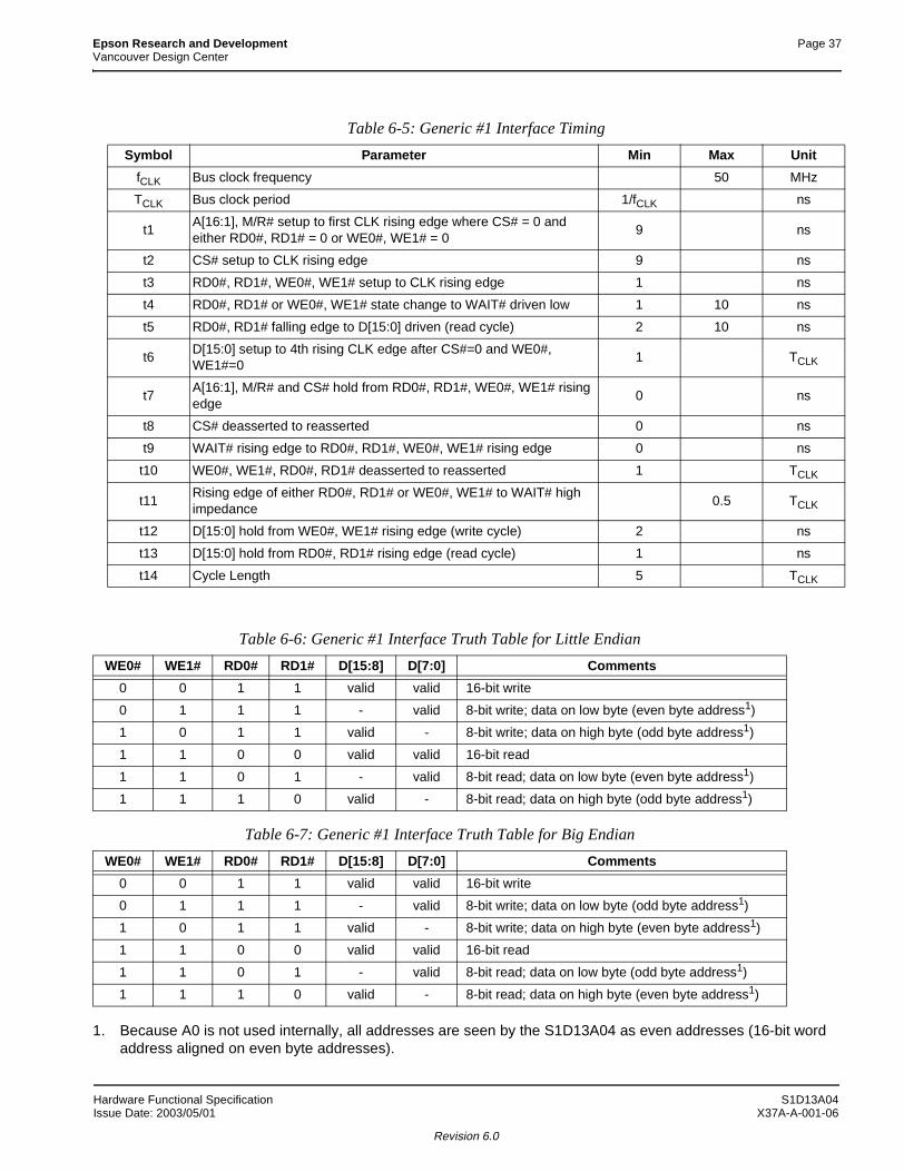
Epson Research and Development Page 37Vancouver Design Center
1. Because A0 is not used internally, all addresses are seen by the S1D13A04 as even addresses (16-bit wordaddress aligned on even byte addresses).
Table 6-5: Generic #1 Interface Timing
Symbol Parameter Min Max Unit
fCLK Bus clock frequency 50 MHz
TCLK Bus clock period 1/fCLK ns
t1A[16:1], M/R# setup to first CLK rising edge where CS# = 0 and either RD0#, RD1# = 0 or WE0#, WE1# = 0
9 ns
t2 CS# setup to CLK rising edge 9 ns
t3 RD0#, RD1#, WE0#, WE1# setup to CLK rising edge 1 ns
t4 RD0#, RD1# or WE0#, WE1# state change to WAIT# driven low 1 10 ns
t5 RD0#, RD1# falling edge to D[15:0] driven (read cycle) 2 10 ns
t6D[15:0] setup to 4th rising CLK edge after CS#=0 and WE0#, WE1#=0
1 TCLK
t7A[16:1], M/R# and CS# hold from RD0#, RD1#, WE0#, WE1# rising edge
0 ns
t8 CS# deasserted to reasserted 0 ns
t9 WAIT# rising edge to RD0#, RD1#, WE0#, WE1# rising edge 0 ns
t10 WE0#, WE1#, RD0#, RD1# deasserted to reasserted 1 TCLK
t11Rising edge of either RD0#, RD1# or WE0#, WE1# to WAIT# high impedance
0.5 TCLK
t12 D[15:0] hold from WE0#, WE1# rising edge (write cycle) 2 ns
t13 D[15:0] hold from RD0#, RD1# rising edge (read cycle) 1 ns
t14 Cycle Length 5 TCLK
Table 6-6: Generic #1 Interface Truth Table for Little Endian
WE0# WE1# RD0# RD1# D[15:8] D[7:0] Comments
0 0 1 1 valid valid 16-bit write
0 1 1 1 - valid 8-bit write; data on low byte (even byte address1)
1 0 1 1 valid - 8-bit write; data on high byte (odd byte address1)
1 1 0 0 valid valid 16-bit read
1 1 0 1 - valid 8-bit read; data on low byte (even byte address1)
1 1 1 0 valid - 8-bit read; data on high byte (odd byte address1)
Table 6-7: Generic #1 Interface Truth Table for Big Endian
WE0# WE1# RD0# RD1# D[15:8] D[7:0] Comments
0 0 1 1 valid valid 16-bit write
0 1 1 1 - valid 8-bit write; data on low byte (odd byte address1)
1 0 1 1 valid - 8-bit write; data on high byte (even byte address1)
1 1 0 0 valid valid 16-bit read
1 1 0 1 - valid 8-bit read; data on low byte (odd byte address1)
1 1 1 0 valid - 8-bit read; data on high byte (even byte address1)
Hardware Functional Specification S1D13A04Issue Date: 2003/05/01 X37A-A-001-06
Revision 6.0
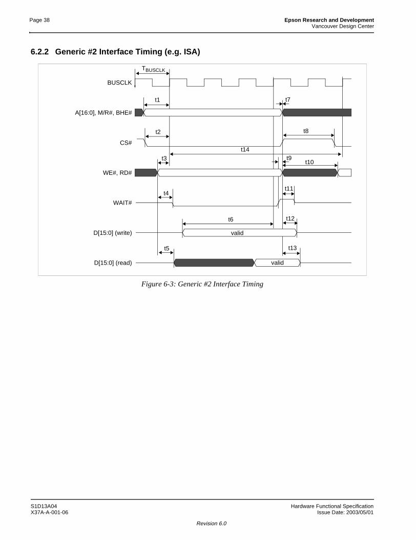
Page 38 Epson Research and DevelopmentVancouver Design Center
6.2.2 Generic #2 Interface Timing (e.g. ISA)
Figure 6-3: Generic #2 Interface Timing
BUSCLK
A[16:0], M/R#, BHE#
CS#
WE#, RD#
WAIT#
D[15:0] (write)
D[15:0] (read)
TBUSCLK
t1
t2
t3
t4
t5
t14
t6
t7
t8
t9t10
t11
t12
t13
valid
valid
S1D13A04 Hardware Functional SpecificationX37A-A-001-06 Issue Date: 2003/05/01
Revision 6.0
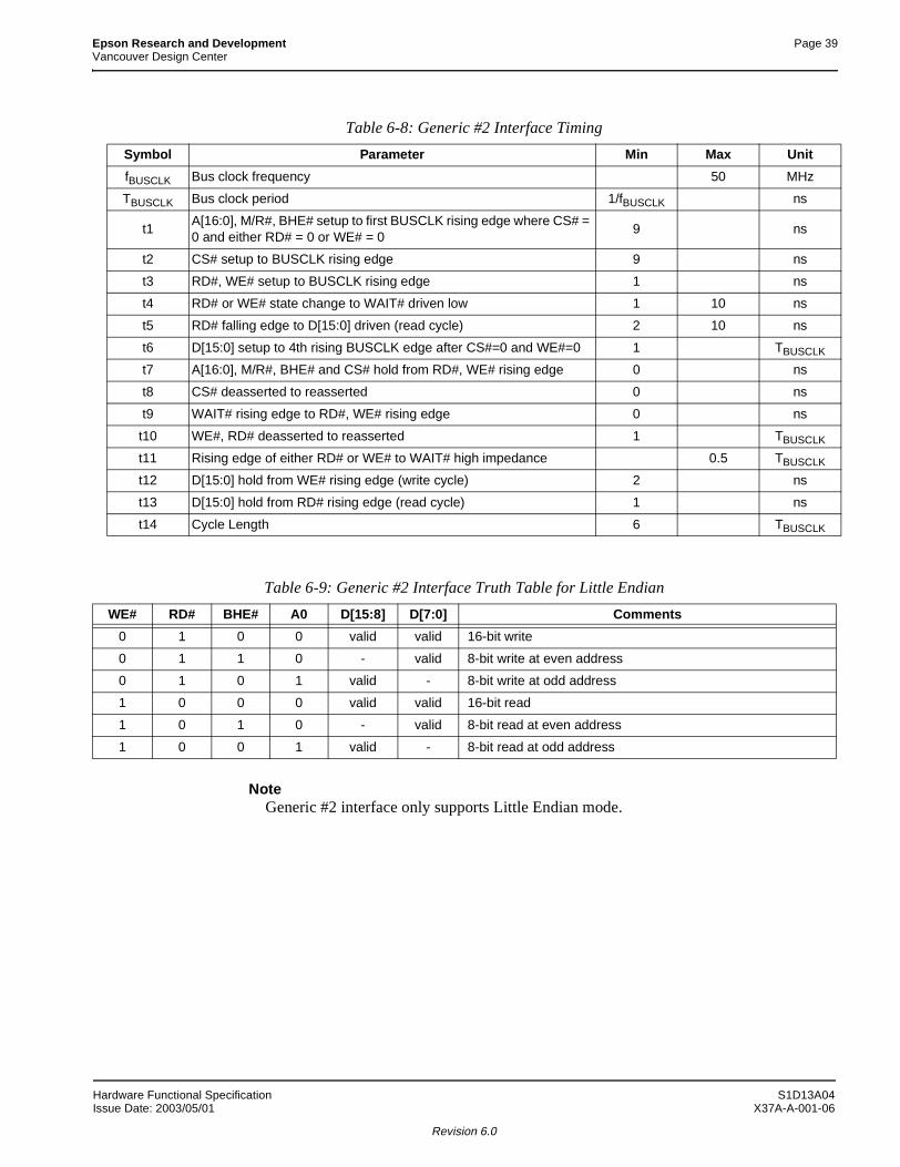
Epson Research and Development Page 39Vancouver Design Center
NoteGeneric #2 interface only supports Little Endian mode.
Table 6-8: Generic #2 Interface Timing
Symbol Parameter Min Max Unit
fBUSCLK Bus clock frequency 50 MHz
TBUSCLK Bus clock period 1/fBUSCLK ns
t1A[16:0], M/R#, BHE# setup to first BUSCLK rising edge where CS# = 0 and either RD# = 0 or WE# = 0
9 ns
t2 CS# setup to BUSCLK rising edge 9 ns
t3 RD#, WE# setup to BUSCLK rising edge 1 ns
t4 RD# or WE# state change to WAIT# driven low 1 10 ns
t5 RD# falling edge to D[15:0] driven (read cycle) 2 10 ns
t6 D[15:0] setup to 4th rising BUSCLK edge after CS#=0 and WE#=0 1 TBUSCLK
t7 A[16:0], M/R#, BHE# and CS# hold from RD#, WE# rising edge 0 ns
t8 CS# deasserted to reasserted 0 ns
t9 WAIT# rising edge to RD#, WE# rising edge 0 ns
t10 WE#, RD# deasserted to reasserted 1 TBUSCLK
t11 Rising edge of either RD# or WE# to WAIT# high impedance 0.5 TBUSCLK
t12 D[15:0] hold from WE# rising edge (write cycle) 2 ns
t13 D[15:0] hold from RD# rising edge (read cycle) 1 ns
t14 Cycle Length 6 TBUSCLK
Table 6-9: Generic #2 Interface Truth Table for Little Endian
WE# RD# BHE# A0 D[15:8] D[7:0] Comments
0 1 0 0 valid valid 16-bit write
0 1 1 0 - valid 8-bit write at even address
0 1 0 1 valid - 8-bit write at odd address
1 0 0 0 valid valid 16-bit read
1 0 1 0 - valid 8-bit read at even address
1 0 0 1 valid - 8-bit read at odd address
Hardware Functional Specification S1D13A04Issue Date: 2003/05/01 X37A-A-001-06
Revision 6.0
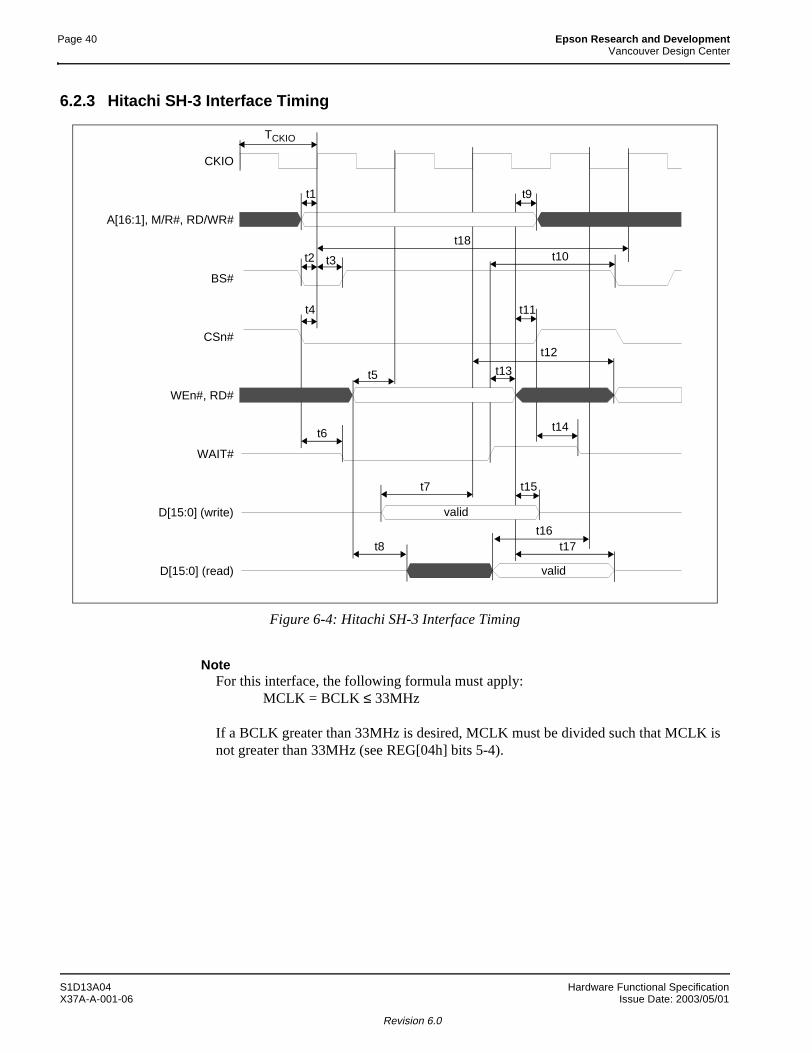
Page 40 Epson Research and DevelopmentVancouver Design Center
6.2.3 Hitachi SH-3 Interface Timing
Figure 6-4: Hitachi SH-3 Interface Timing
NoteFor this interface, the following formula must apply:
MCLK = BCLK ≤ 33MHz
If a BCLK greater than 33MHz is desired, MCLK must be divided such that MCLK is not greater than 33MHz (see REG[04h] bits 5-4).
CKIO
A[16:1], M/R#, RD/WR#
BS#
CSn#
WEn#, RD#
WAIT#
D[15:0] (write)
D[15:0] (read)
TCKIO
t1
t2 t3
t4
t6
t8
t7
t5 t13
t15
t16t17
t14
t12
t11
t9
t18t10
valid
valid
S1D13A04 Hardware Functional SpecificationX37A-A-001-06 Issue Date: 2003/05/01
Revision 6.0
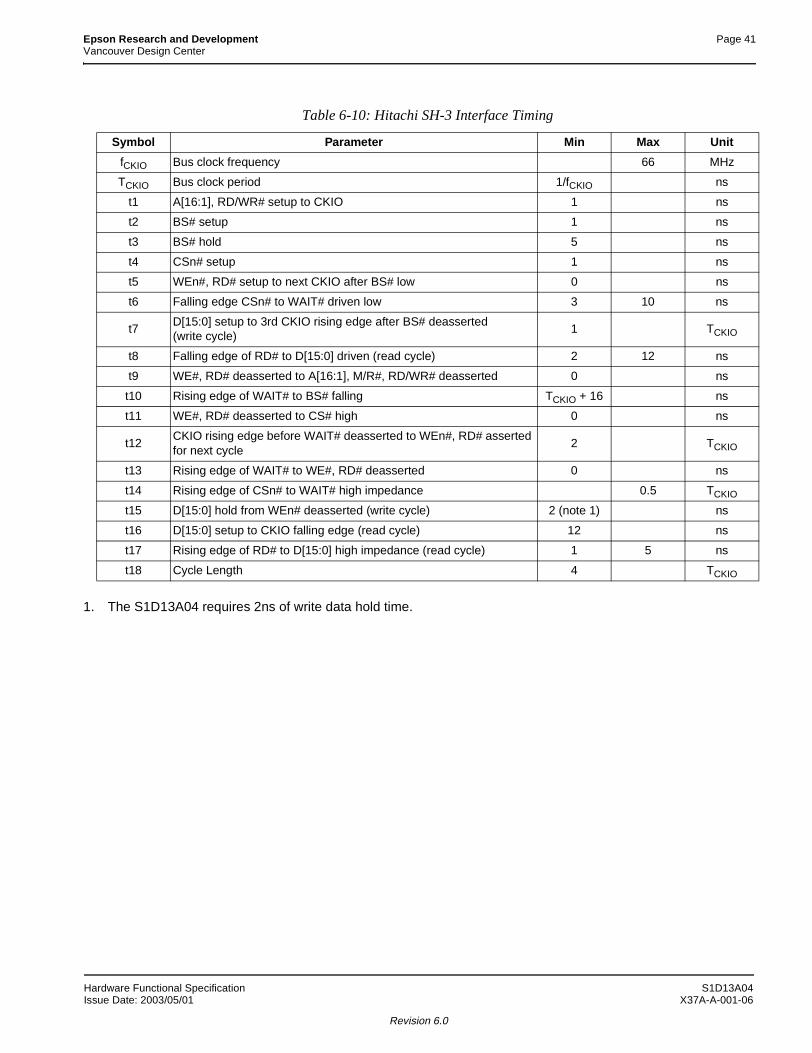
Epson Research and Development Page 41Vancouver Design Center
1. The S1D13A04 requires 2ns of write data hold time.
Table 6-10: Hitachi SH-3 Interface Timing
Symbol Parameter Min Max Unit
fCKIO Bus clock frequency 66 MHz
TCKIO Bus clock period 1/fCKIO ns
t1 A[16:1], RD/WR# setup to CKIO 1 ns
t2 BS# setup 1 ns
t3 BS# hold 5 ns
t4 CSn# setup 1 ns
t5 WEn#, RD# setup to next CKIO after BS# low 0 ns
t6 Falling edge CSn# to WAIT# driven low 3 10 ns
t7D[15:0] setup to 3rd CKIO rising edge after BS# deasserted(write cycle)
1 TCKIO
t8 Falling edge of RD# to D[15:0] driven (read cycle) 2 12 ns
t9 WE#, RD# deasserted to A[16:1], M/R#, RD/WR# deasserted 0 ns
t10 Rising edge of WAIT# to BS# falling TCKIO + 16 ns
t11 WE#, RD# deasserted to CS# high 0 ns
t12CKIO rising edge before WAIT# deasserted to WEn#, RD# asserted for next cycle
2 TCKIO
t13 Rising edge of WAIT# to WE#, RD# deasserted 0 ns
t14 Rising edge of CSn# to WAIT# high impedance 0.5 TCKIO
t15 D[15:0] hold from WEn# deasserted (write cycle) 2 (note 1) ns
t16 D[15:0] setup to CKIO falling edge (read cycle) 12 ns
t17 Rising edge of RD# to D[15:0] high impedance (read cycle) 1 5 ns
t18 Cycle Length 4 TCKIO
Hardware Functional Specification S1D13A04Issue Date: 2003/05/01 X37A-A-001-06
Revision 6.0
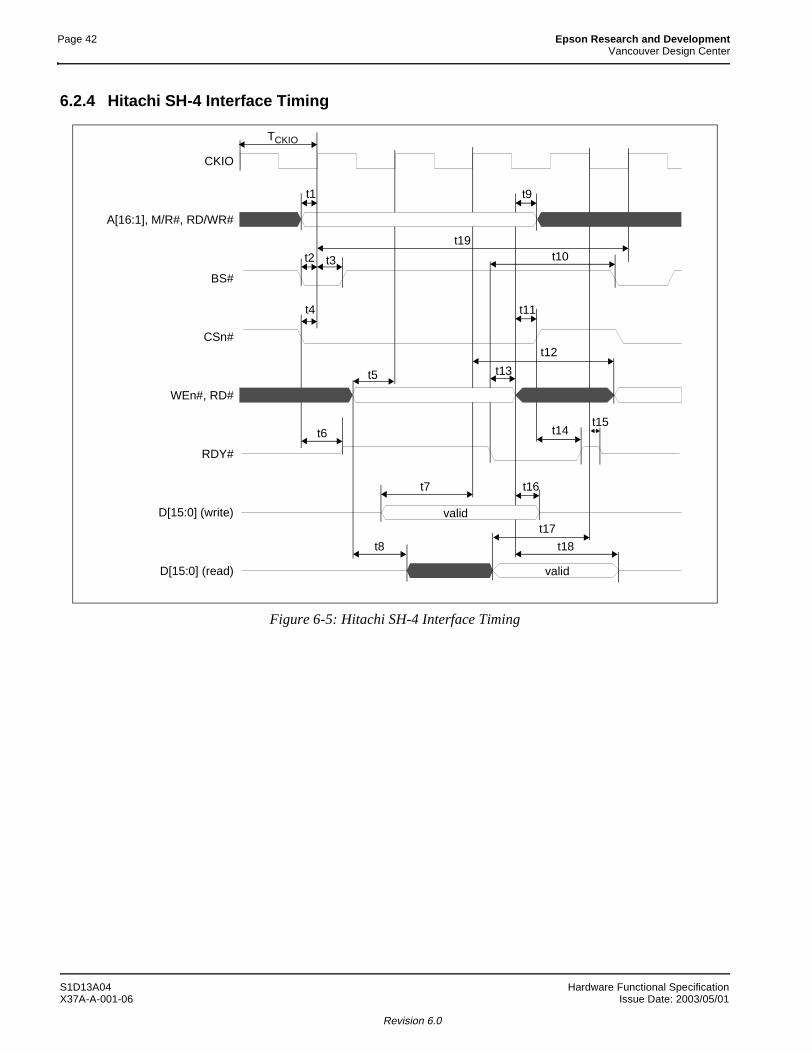
Page 42 Epson Research and DevelopmentVancouver Design Center
6.2.4 Hitachi SH-4 Interface Timing
Figure 6-5: Hitachi SH-4 Interface Timing
CKIO
A[16:1], M/R#, RD/WR#
BS#
CSn#
WEn#, RD#
RDY#
D[15:0] (write)
D[15:0] (read)
TCKIO
t1
t2 t3
t4
t6
t8
t7
t5 t13
t16
t17
t18
t14
t12
t11
t9
t19t10
t15
valid
valid
S1D13A04 Hardware Functional SpecificationX37A-A-001-06 Issue Date: 2003/05/01
Revision 6.0
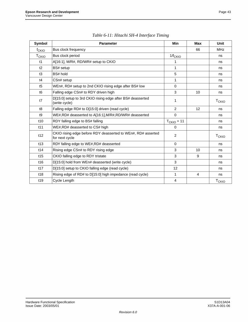
Epson Research and Development Page 43Vancouver Design Center
Table 6-11: Hitachi SH-4 Interface Timing
Symbol Parameter Min Max Unit
fCKIO Bus clock frequency 66 MHz
TCKIO Bus clock period 1/fCKIO ns
t1 A[16:1], M/R#, RD/WR# setup to CKIO 1 ns
t2 BS# setup 1 ns
t3 BS# hold 5 ns
t4 CSn# setup 1 ns
t5 WEn#, RD# setup to 2nd CKIO rising edge after BS# low 0 ns
t6 Falling edge CSn# to RDY driven high 3 10 ns
t7D[15:0] setup to 3rd CKIO rising edge after BS# deasserted(write cycle)
1 TCKIO
t8 Falling edge RD# to D[15:0] driven (read cycle) 2 12 ns
t9 WE#,RD# deasserted to A[16:1],M/R#,RD/WR# deasserted 0 ns
t10 RDY falling edge to BS# falling TCKIO + 11 ns
t11 WE#,RD# deasserted to CS# high 0 ns
t12CKIO rising edge before RDY deasserted to WEn#, RD# asserted for next cycle
2 TCKIO
t13 RDY falling edge to WE#,RD# deasserted 0 ns
t14 Rising edge CSn# to RDY rising edge 3 10 ns
t15 CKIO falling edge to RDY tristate 3 9 ns
t16 D[15:0] hold from WEn# deasserted (write cycle) 3 ns
t17 D[15:0] setup to CKIO falling edge (read cycle) 12 ns
t18 Rising edge of RD# to D[15:0] high impedance (read cycle) 1 4 ns
t19 Cycle Length 4 TCKIO
Hardware Functional Specification S1D13A04Issue Date: 2003/05/01 X37A-A-001-06
Revision 6.0
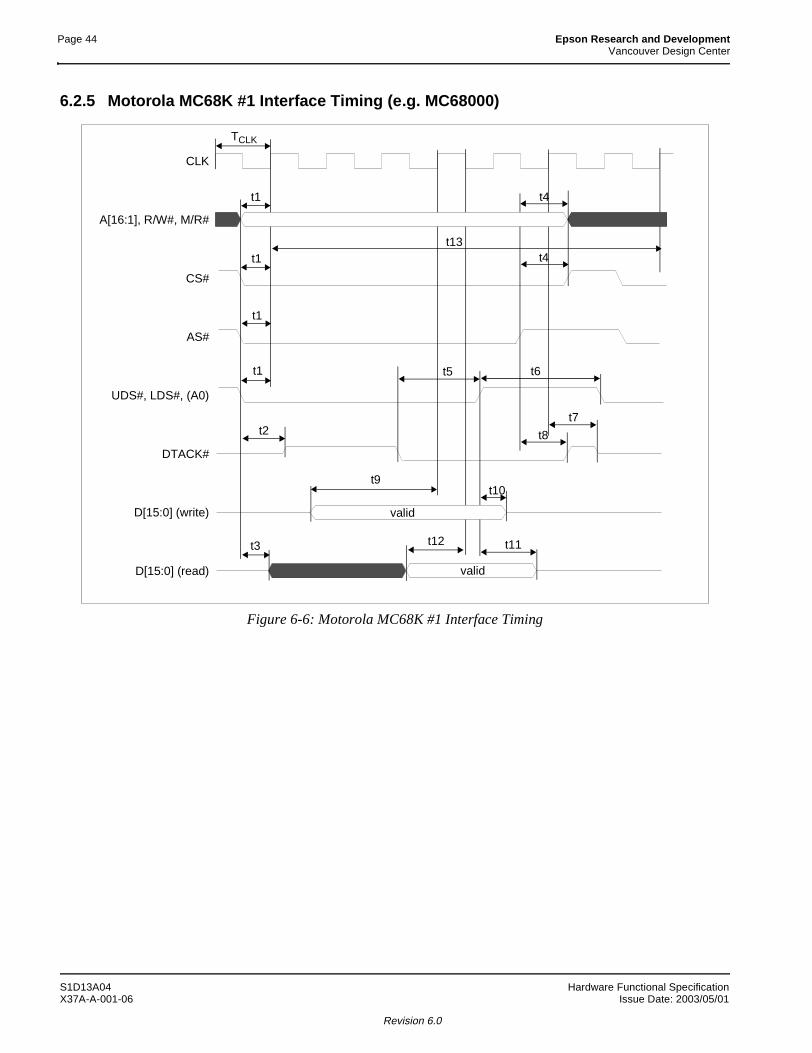
Page 44 Epson Research and DevelopmentVancouver Design Center
6.2.5 Motorola MC68K #1 Interface Timing (e.g. MC68000)
Figure 6-6: Motorola MC68K #1 Interface Timing
CLK
A[16:1], R/W#, M/R#
CS#
AS#
UDS#, LDS#, (A0)
DTACK#
D[15:0] (write)
D[15:0] (read)
TCLK
t1
t1
t1
t1
t2
t3
t9
t5 t6
t7
t8
t10
t11
t4
t4t13
t12
valid
valid
S1D13A04 Hardware Functional SpecificationX37A-A-001-06 Issue Date: 2003/05/01
Revision 6.0
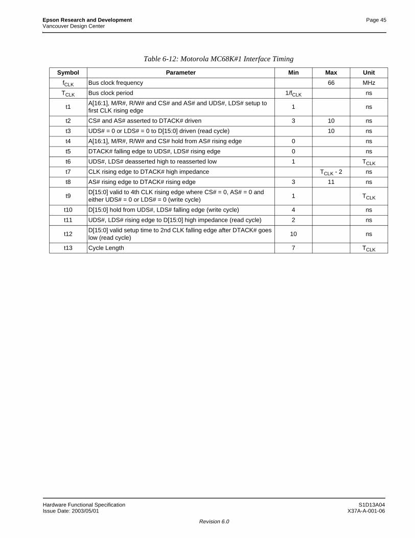
Epson Research and Development Page 45Vancouver Design Center
Table 6-12: Motorola MC68K#1 Interface Timing
Symbol Parameter Min Max Unit
fCLK Bus clock frequency 66 MHz
TCLK Bus clock period 1/fCLK ns
t1A[16:1], M/R#, R/W# and CS# and AS# and UDS#, LDS# setup to first CLK rising edge
1 ns
t2 CS# and AS# asserted to DTACK# driven 3 10 ns
t3 UDS# = 0 or LDS# = 0 to D[15:0] driven (read cycle) 10 ns
t4 A[16:1], M/R#, R/W# and CS# hold from AS# rising edge 0 ns
t5 DTACK# falling edge to UDS#, LDS# rising edge 0 ns
t6 UDS#, LDS# deasserted high to reasserted low 1 TCLK
t7 CLK rising edge to DTACK# high impedance TCLK - 2 ns
t8 AS# rising edge to DTACK# rising edge 3 11 ns
t9D[15:0] valid to 4th CLK rising edge where CS# = 0, AS# = 0 and either UDS# = 0 or LDS# = 0 (write cycle)
1 TCLK
t10 D[15:0] hold from UDS#, LDS# falling edge (write cycle) 4 ns
t11 UDS#, LDS# rising edge to D[15:0] high impedance (read cycle) 2 ns
t12D[15:0] valid setup time to 2nd CLK falling edge after DTACK# goes low (read cycle)
10 ns
t13 Cycle Length 7 TCLK
Hardware Functional Specification S1D13A04Issue Date: 2003/05/01 X37A-A-001-06
Revision 6.0
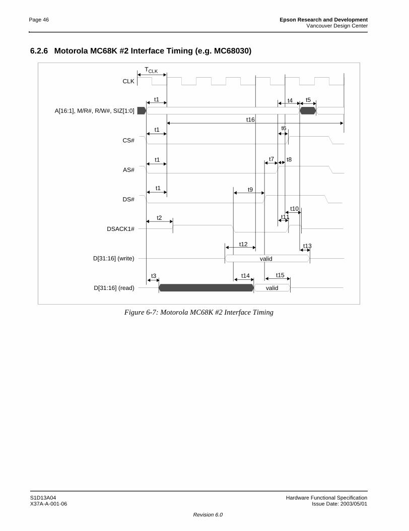
Page 46 Epson Research and DevelopmentVancouver Design Center
6.2.6 Motorola MC68K #2 Interface Timing (e.g. MC68030)
Figure 6-7: Motorola MC68K #2 Interface Timing
t6
CLK
A[16:1], M/R#, R/W#, SIZ[1:0]
CS#
AS#
DS#
DSACK1#
D[31:16] (write)
D[31:16] (read)
TCLK
t1
t1
t1
t1
t2
t3 t14 t15
t12 t13
t11t10
t9
t16
t7
t4 t5
t8
valid
valid
S1D13A04 Hardware Functional SpecificationX37A-A-001-06 Issue Date: 2003/05/01
Revision 6.0
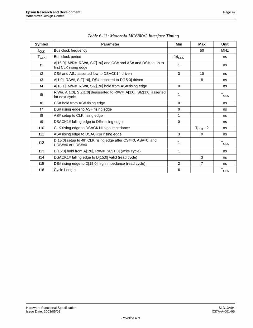
Epson Research and Development Page 47Vancouver Design Center
Table 6-13: Motorola MC68K#2 Interface Timing
Symbol Parameter Min Max Unit
fCLK Bus clock frequency 50 MHz
TCLK Bus clock period 1/fCLK ns
t1A[16:0], M/R#, R/W#, SIZ[1:0] and CS# and AS# and DS# setup to first CLK rising edge
1 ns
t2 CS# and AS# asserted low to DSACK1# driven 3 10 ns
t3 A[1:0], R/W#, SIZ[1:0], DS# asserted to D[15:0] driven 8 ns
t4 A[16:1], M/R#, R/W#, SIZ[1:0] hold from AS# rising edge 0 ns
t5R/W#, A[1:0], SIZ[1:0] deasserted to R/W#, A[1:0], SIZ[1:0] asserted for next cycle
1 TCLK
t6 CS# hold from AS# rising edge 0 ns
t7 DS# rising edge to AS# rising edge 0 ns
t8 AS# setup to CLK rising edge 1 ns
t9 DSACK1# falling edge to DS# rising edge 0 ns
t10 CLK rising edge to DSACK1# high impedance TCLK - 2 ns
t11 AS# rising edge to DSACK1# rising edge 3 9 ns
t12D[15:0] setup to 4th CLK rising edge after CS#=0, AS#=0, and UDS#=0 or LDS#=0
1 TCLK
t13 D[15:0] hold from A[1:0], R/W#, SIZ[1:0] (write cycle) 1 ns
t14 DSACK1# falling edge to D[15:0] valid (read cycle) 3 ns
t15 DS# rising edge to D[15:0] high impedance (read cycle) 2 7 ns
t16 Cycle Length 6 TCLK
Hardware Functional Specification S1D13A04Issue Date: 2003/05/01 X37A-A-001-06
Revision 6.0
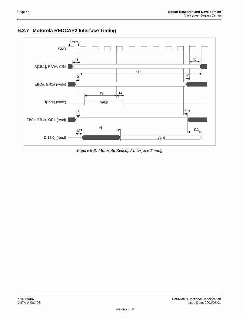
Page 48 Epson Research and DevelopmentVancouver Design Center
6.2.7 Motorola REDCAP2 Interface Timing
Figure 6-8: Motorola Redcap2 Interface Timing
CKO
A[16:1], R/W#, CS#
EBO#, EB1# (write)
D[15:0] (write)
EB0#, EB1#, OE# (read)
D[15:0] (read)
TCKO
t1
t2
t5
t7t6
t3 t4
t11
t10
t9t12
t8
valid
valid
S1D13A04 Hardware Functional SpecificationX37A-A-001-06 Issue Date: 2003/05/01
Revision 6.0
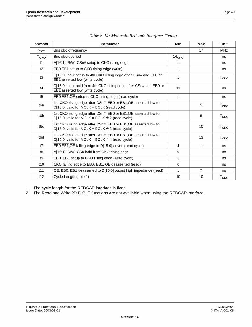
Epson Research and Development Page 49Vancouver Design Center
1. The cycle length for the REDCAP interface is fixed.2. The Read and Write 2D BitBLT functions are not available when using the REDCAP interface.
Table 6-14: Motorola Redcap2 Interface Timing
Symbol Parameter Min Max Unit
fCKO Bus clock frequency 17 MHz
TCKO Bus clock period 1/fCKO ns
t1 A[16:1], R/W, CSn# setup to CKO rising edge 1 ns
t2 EB0,EB1 setup to CKO rising edge (write) 1 ns
t3D[15:0] input setup to 4th CKO rising edge after CSn# and EB0 or EB1 asserted low (write cycle)
1 TCKO
t4D[15:0] input hold from 4th CKO rising edge after CSn# and EB0 or EB1 asserted low (write cycle)
11 ns
t5 EB0,EB1,OE setup to CKO rising edge (read cycle) 1 ns
t6a1st CKO rising edge after CSn#, EB0 or EB1,OE asserted low to D[15:0] valid for MCLK = BCLK (read cycle)
5 TCKO
t6b1st CKO rising edge after CSn#, EB0 or EB1,OE asserted low to D[15:0] valid for MCLK = BCLK ÷ 2 (read cycle)
8 TCKO
t6c1st CKO rising edge after CSn#, EB0 or EB1,OE asserted low to D[15:0] valid for MCLK = BCLK ÷ 3 (read cycle)
10 TCKO
t6d1st CKO rising edge after CSn#, EB0 or EB1,OE asserted low to D[15:0] valid for MCLK = BCLK ÷ 4 (read cycle)
13 TCKO
t7 EB0,EB1,OE falling edge to D[15:0] driven (read cycle) 4 11 ns
t8 A[16:1], R/W, CSn hold from CKO rising edge 0 ns
t9 EB0, EB1 setup to CKO rising edge (write cycle) 1 ns
t10 CKO falling edge to EB0, EB1, OE deasserted (read) 0 ns
t11 OE, EB0, EB1 deasserted to D[15:0] output high impedance (read) 1 7 ns
t12 Cycle Length (note 1) 10 10 TCKO
Hardware Functional Specification S1D13A04Issue Date: 2003/05/01 X37A-A-001-06
Revision 6.0
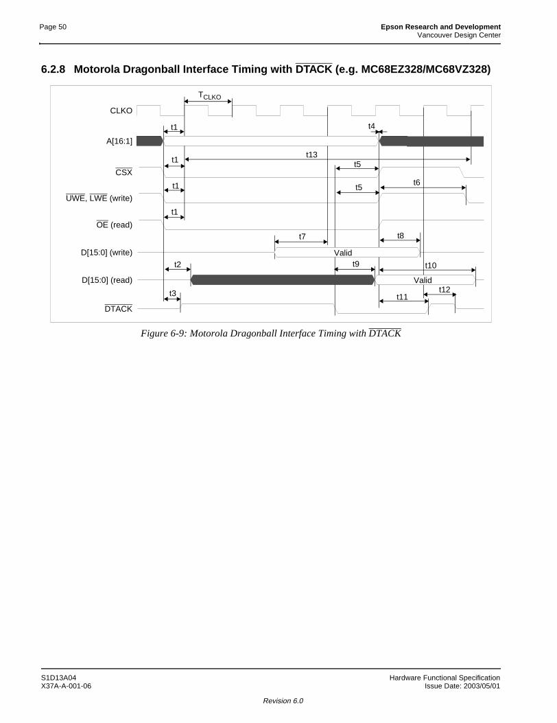
Page 50 Epson Research and DevelopmentVancouver Design Center
6.2.8 Motorola Dragonball Interface Timing with DTACK (e.g. MC68EZ328/MC68VZ328)
Figure 6-9: Motorola Dragonball Interface Timing with DTACK
CLKO
A[16:1]
CSX
UWE, LWE (write)
OE (read)
D[15:0] (write)
D[15:0] (read)
DTACK
TCLKO
t1
t1
t1
t1
t4
t5t13
t5t6
t8
t10
t12t11
t9
t7
t2
t3
Valid
Valid
S1D13A04 Hardware Functional SpecificationX37A-A-001-06 Issue Date: 2003/05/01
Revision 6.0
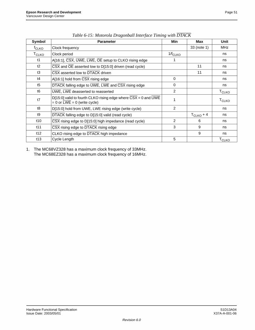
Epson Research and Development Page 51Vancouver Design Center
1. The MC68VZ328 has a maximum clock frequency of 33MHz.The MC68EZ328 has a maximum clock frequency of 16MHz.
Table 6-15: Motorola Dragonball Interface Timing with DTACKSymbol Parameter Min Max Unit
fCLKO Clock frequency 33 (note 1) MHz
TCLKO Clock period 1/fCLKO ns
t1 A[16:1], CSX, UWE, LWE, OE setup to CLKO rising edge 1 ns
t2 CSX and OE asserted low to D[15:0] driven (read cycle) 11 ns
t3 CSX asserted low to DTACK driven 11 ns
t4 A[16:1] hold from CSX rising edge 0 ns
t5 DTACK falling edge to UWE, LWE and CSX rising edge 0 ns
t6 UWE, LWE deasserted to reasserted 2 TCLKO
t7 D[15:0] valid to fourth CLKO rising edge where CSX = 0 and UWE = 0 or LWE = 0 (write cycle)
1 TCLKO
t8 D[15:0] hold from UWE, LWE rising edge (write cycle) 2 ns
t9 DTACK falling edge to D[15:0] valid (read cycle) TCLKO + 4 ns
t10 CSX rising edge to D[15:0] high impedance (read cycle) 2 6 ns
t11 CSX rising edge to DTACK rising edge 3 9 ns
t12 CLKO rising edge to DTACK high impedance 9 ns
t13 Cycle Length 5 TCLKO
Hardware Functional Specification S1D13A04Issue Date: 2003/05/01 X37A-A-001-06
Revision 6.0
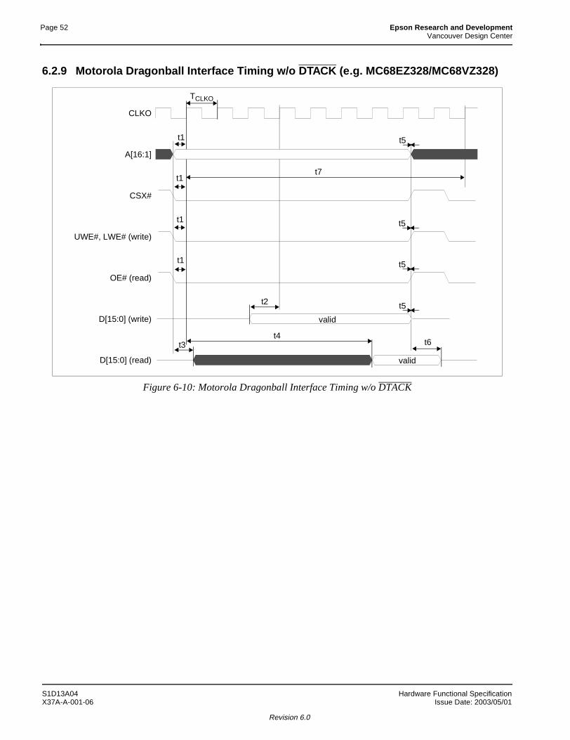
Page 52 Epson Research and DevelopmentVancouver Design Center
6.2.9 Motorola Dragonball Interface Timing w/o DTACK (e.g. MC68EZ328/MC68VZ328)
Figure 6-10: Motorola Dragonball Interface Timing w/o DTACK
CLKO
A[16:1]
CSX#
UWE#, LWE# (write)
OE# (read)
D[15:0] (write)
D[15:0] (read)
TCLKO
t1
t1
t1
t1
t2
t3t4
t7
t5
t6
t5
t5
t5
valid
valid
S1D13A04 Hardware Functional SpecificationX37A-A-001-06 Issue Date: 2003/05/01
Revision 6.0
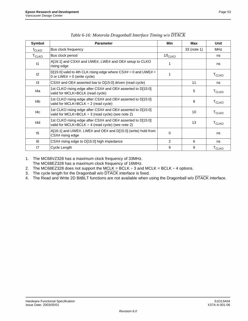
Epson Research and Development Page 53Vancouver Design Center
1. The MC68VZ328 has a maximum clock frequency of 33MHz.The MC68EZ328 has a maximum clock frequency of 16MHz.
2. The MC68EZ328 does not support the MCLK = BCLK ÷ 3 and MCLK = BCLK ÷ 4 options.3. The cycle length for the Dragonball w/o DTACK interface is fixed.4. The Read and Write 2D BitBLT functions are not available when using the Dragonball w/o DTACK interface.
Table 6-16: Motorola Dragonball Interface Timing w/o DTACK
Symbol Parameter Min Max Unit
fCLKO Bus clock frequency 33 (note 1) MHz
TCLKO Bus clock period 1/fCLKO ns
t1A[16:1] and CSX# and UWE#, LWE# and OE# setup to CLKO rising edge
1 ns
t2D[15:0] valid to 4th CLK rising edge where CSX# = 0 and UWE# = 0 or LWE# = 0 (write cycle)
1 TCLKO
t3 CSX# and OE# asserted low to D[15:0] driven (read cycle) 11 ns
t4a1st CLKO rising edge after CSX# and OE# asserted to D[15:0] valid for MCLK=BCLK (read cycle)
5 TCLKO
t4b1st CLKO rising edge after CSX# and OE# asserted to D[15:0] valid for MCLK=BCLK ÷ 2 (read cycle)
8 TCLKO
t4c1st CLKO rising edge after CSX# and OE# asserted to D[15:0] valid for MCLK=BCLK ÷ 3 (read cycle) (see note 2)
10 TCLKO
t4d1st CLKO rising edge after CSX# and OE# asserted to D[15:0] valid for MCLK=BCLK ÷ 4 (read cycle) (see note 2)
13 TCLKO
t5A[16:1] and UWE#, LWE# and OE# and D[15:0] (write) hold from CSX# rising edge
0 ns
t6 CSX# rising edge to D[15:0] high impedance 2 6 ns
t7 Cycle Length 9 9 TCLKO
Hardware Functional Specification S1D13A04Issue Date: 2003/05/01 X37A-A-001-06
Revision 6.0
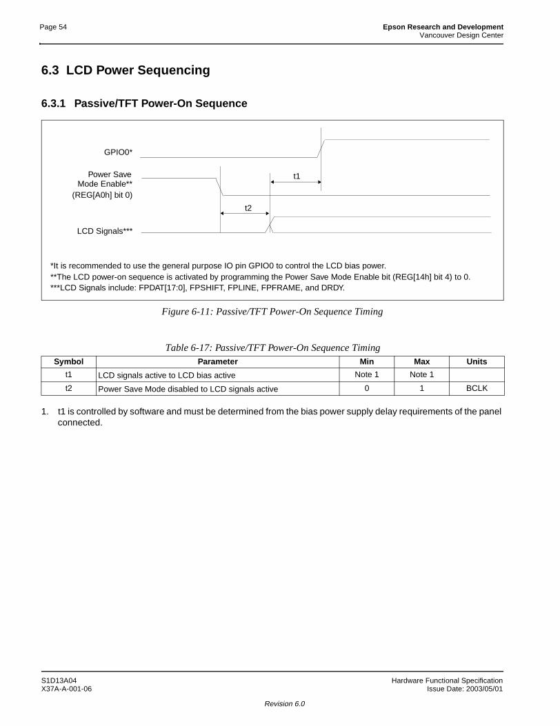
Page 54 Epson Research and DevelopmentVancouver Design Center
6.3 LCD Power Sequencing
6.3.1 Passive/TFT Power-On Sequence
Figure 6-11: Passive/TFT Power-On Sequence Timing
1. t1 is controlled by software and must be determined from the bias power supply delay requirements of the panel connected.
Table 6-17: Passive/TFT Power-On Sequence Timing Symbol Parameter Min Max Units
t1 LCD signals active to LCD bias active Note 1 Note 1
t2 Power Save Mode disabled to LCD signals active 0 1 BCLK
LCD Signals***
GPIO0*
Power Save t1
*It is recommended to use the general purpose IO pin GPIO0 to control the LCD bias power.
t2
**The LCD power-on sequence is activated by programming the Power Save Mode Enable bit (REG[14h] bit 4) to 0.***LCD Signals include: FPDAT[17:0], FPSHIFT, FPLINE, FPFRAME, and DRDY.
(REG[A0h] bit 0)Mode Enable**
S1D13A04 Hardware Functional SpecificationX37A-A-001-06 Issue Date: 2003/05/01
Revision 6.0
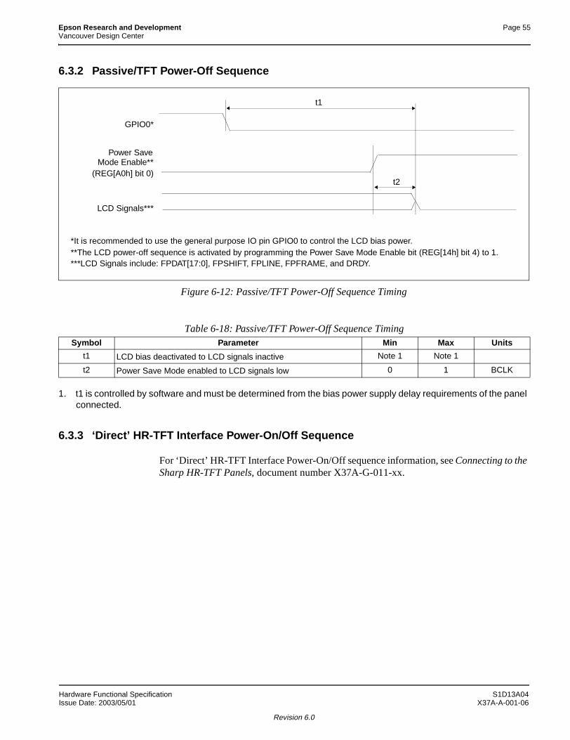
Epson Research and Development Page 55Vancouver Design Center
6.3.2 Passive/TFT Power-Off Sequence
Figure 6-12: Passive/TFT Power-Off Sequence Timing
1. t1 is controlled by software and must be determined from the bias power supply delay requirements of the panel connected.
6.3.3 ‘Direct’ HR-TFT Interface Power-On/Off Sequence
For ‘Direct’ HR-TFT Interface Power-On/Off sequence information, see Connecting to the Sharp HR-TFT Panels, document number X37A-G-011-xx.
Table 6-18: Passive/TFT Power-Off Sequence Timing Symbol Parameter Min Max Units
t1 LCD bias deactivated to LCD signals inactive Note 1 Note 1
t2 Power Save Mode enabled to LCD signals low 0 1 BCLK
LCD Signals***
GPIO0*
t1
*It is recommended to use the general purpose IO pin GPIO0 to control the LCD bias power. **The LCD power-off sequence is activated by programming the Power Save Mode Enable bit (REG[14h] bit 4) to 1.***LCD Signals include: FPDAT[17:0], FPSHIFT, FPLINE, FPFRAME, and DRDY.
t2
Power Save
(REG[A0h] bit 0)Mode Enable**
Hardware Functional Specification S1D13A04Issue Date: 2003/05/01 X37A-A-001-06
Revision 6.0
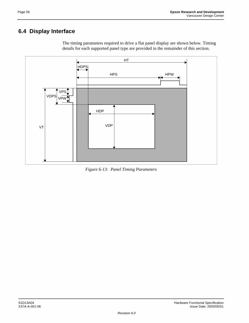
Page 56 Epson Research and DevelopmentVancouver Design Center
6.4 Display Interface
The timing parameters required to drive a flat panel display are shown below. Timing details for each supported panel type are provided in the remainder of this section.
Figure 6-13: Panel Timing Parameters
HT
VDPVT
VDPSVPW
VPS
HDP
HPWHPS
HDPS
S1D13A04 Hardware Functional SpecificationX37A-A-001-06 Issue Date: 2003/05/01
Revision 6.0
Epson Research and Development Page 57Vancouver Design Center
H
H
H
HHV
VVV
V
1. For passive panels, the HDP must be a minimum of 32 pixels and must be increased by multiples of 16.For TFT panels, the HDP must be a minimum of 8 pixels and must be increased by multiples of 8.
2. The following formulas must be valid for all panel timings:HDPS + HDP < HTVDPS + VDP < VT
Table 6-19: Panel Timing Parameter Definition and Register Summary
Symbol Description Derived From UnitsT Horizontal Total ((REG[20h] bits 6-0) + 1) x 8
Ts
DP1 Horizontal Display Period1 ((REG[24h] bits 6-0) + 1) x 8
DPS Horizontal Display Period Start PositionFor STN panels: ((REG[28h] bits 9-0) + 22)For TFT panels: ((REG[28h] bits 9-0) + 5)
PS FPLINE Pulse Start Position (REG[2Ch] bits 9-0) + 1PW FPLINE Pulse Width (REG[2Ch] bits 22-16) + 1T Vertical Total (REG[30h] bits 9-0) + 1
Lines (HT)DP Vertical Display Period (REG[34h] bits 9-0) + 1DPS Vertical Display Period Start Position REG[38h] bits 9-0PS FPFRAME Pulse Start Position REG[2Ch] bits 9-0
PW FPFRAME Pulse Width (REG[3Ch] bits 18-16) + 1
Hardware Functional Specification S1D13A04Issue Date: 2003/05/01 X37A-A-001-06
Revision 6.0
Page 58 Epson Research and DevelopmentVancouver Design Center
6.4.1 Generic STN Panel Timing
Figure 6-14: Generic STN Panel Timing
FPFRAME
VT (= 1 Frame)
MOD1(DRDY)
FPLINE
MOD2(DRDY)
FPLINE
VDP
VPW
HT (= 1 Line)
HDPS HDP
FPDAT[17:0]
FPDAT[17:0]
1PCLK
FPSHIFT
HPWHPS
S1D13A04 Hardware Functional SpecificationX37A-A-001-06 Issue Date: 2003/05/01
Revision 6.0
Epson Research and Development Page 59Vancouver Design Center
VT = Vertical Total = [(REG[30h] bits 9-0) + 1] linesVPS = FPFRAME Pulse Start Position = 0 lines, because REG[2Ch] bits 9-0 = 0VPW = FPFRAME Pulse Width = [(REG[3Ch] bits 18-16) + 1] linesVDPS = Vertical Display Period Start Position = 0 lines, because REG[38h] bits 9-0 = 0VDP = Vertical Display Period = [(REG[34h] bits 9-0) + 1] linesHT = Horizontal Total = [((REG[20h] bits 6-0) + 1) x 8] pixelsHPS = FPLINE Pulse Start Position = [(REG[2Ch] bits 9-0) + 1] pixelsHPW = FPLINE Pulse Width = [(REG[2Ch] bits 22-16) + 1] pixelsHDPS = Horizontal Display Period Start Position= 22 pixels, because REG[28h] bits 9-0 = 0HDP = Horizontal Display Period = [((REG[24h] bits 6-0) + 1) x 8] pixels*For passive panels, the HDP must be a minimum of 32 pixels and must be increased by multiples of 16.*HPS must comply with the following formula:
HPS > HDP + 22HPS + HPW < HT
*Panel Type Bits (REG[0Ch] bits 1-0) = 00b (STN)*FPFRAME Pulse Polarity Bit (REG[3Ch] bit 23) = 1 (active high)*FPLINE Polarity Bit (REG[2Ch] bit 23) = 1 (active high)*MOD1 is the MOD signal when REG[0Ch] bits 21-16 = 0 (MOD toggles every FPFRAME)*MOD2 is the MOD signal when REG[0Ch] bits 21-16 = n (MOD toggles every n FPLINE)
Hardware Functional Specification S1D13A04Issue Date: 2003/05/01 X37A-A-001-06
Revision 6.0
Page 60 Epson Research and DevelopmentVancouver Design Center
6.4.2 Single Monochrome 4-Bit Panel Timing
Figure 6-15: Single Monochrome 4-Bit Panel Timing
VDP = Vertical Display Period = (REG[34h] bits 9:0) + 1 Lines
VNDP = Vertical Non-Display Period= VT - VDP= (REG[30h] bits 9:0) - (REG[34h] bits 9:0) Lines
HDP = Horizontal Display Period= ((REG[24h] bits 6:0) + 1) x 8Ts
HNDP = Horizontal Non-Display Period= HT - HDP= (((REG[20h] bits 6:0) + 1) x 8Ts) - (((REG[24h] bits 6:0) + 1) x 8Ts)
FPLINE
FPSHIFT
FPFRAME
FPLINE
DRDY (MOD)
DRDY (MOD)
* Diagram drawn with 2 FPLINE vertical blank periodExample timing for a 320x240 panel
FPDAT[7:4]
FPDAT6FPDAT5
FPDAT4
FPDAT7
VDP
LINE1 LINE2 LINE3 LINE4 LINE239 LINE240 LINE1 LINE2
1-2 1-6 1-318
1-3 1-7 1-319
1-4 1-8 1-320
1-1 1-5 1-317
VNDP
HDP HNDP
Invalid
Invalid
Invalid
Invalid Invalid
Invalid
Invalid
Invalid
Invalid Invalid
S1D13A04 Hardware Functional SpecificationX37A-A-001-06 Issue Date: 2003/05/01
Revision 6.0
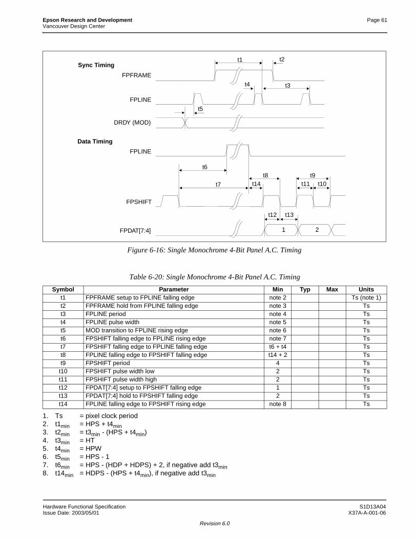
Epson Research and Development Page 61Vancouver Design Center
Figure 6-16: Single Monochrome 4-Bit Panel A.C. Timing
1. Ts = pixel clock period2. t1min = HPS + t4min3. t2min = t3min - (HPS + t4min)4. t3min = HT5. t4min = HPW6. t5min = HPS - 17. t6min = HPS - (HDP + HDPS) + 2, if negative add t3min8. t14min = HDPS - (HPS + t4min), if negative add t3min
Table 6-20: Single Monochrome 4-Bit Panel A.C. Timing
Symbol Parameter Min Typ Max Unitst1 FPFRAME setup to FPLINE falling edge note 2 Ts (note 1)t2 FPFRAME hold from FPLINE falling edge note 3 Tst3 FPLINE period note 4 Tst4 FPLINE pulse width note 5 Tst5 MOD transition to FPLINE rising edge note 6 Tst6 FPSHIFT falling edge to FPLINE rising edge note 7 Tst7 FPSHIFT falling edge to FPLINE falling edge t6 + t4 Tst8 FPLINE falling edge to FPSHIFT falling edge t14 + 2 Tst9 FPSHIFT period 4 Ts
t10 FPSHIFT pulse width low 2 Tst11 FPSHIFT pulse width high 2 Tst12 FPDAT[7:4] setup to FPSHIFT falling edge 1 Tst13 FPDAT[7:4] hold to FPSHIFT falling edge 2 Tst14 FPLINE falling edge to FPSHIFT rising edge note 8 Ts
FPFRAME
FPLINE
DRDY (MOD)
Sync Timing
FPLINE
FPSHIFT
FPDAT[7:4]
Data Timing
t12 t13
t14 t10t11
t5
t1 t2
t3t4
t8 t9
1 2
t7
t6
Hardware Functional Specification S1D13A04Issue Date: 2003/05/01 X37A-A-001-06
Revision 6.0
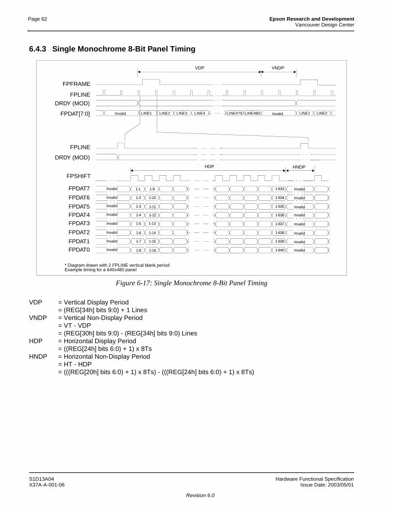
Page 62 Epson Research and DevelopmentVancouver Design Center
6.4.3 Single Monochrome 8-Bit Panel Timing
Figure 6-17: Single Monochrome 8-Bit Panel Timing
VDP = Vertical Display Period = (REG[34h] bits 9:0) + 1 Lines
VNDP = Vertical Non-Display Period= VT - VDP= (REG[30h] bits 9:0) - (REG[34h] bits 9:0) Lines
HDP = Horizontal Display Period= ((REG[24h] bits 6:0) + 1) x 8Ts
HNDP = Horizontal Non-Display Period= HT - HDP= (((REG[20h] bits 6:0) + 1) x 8Ts) - (((REG[24h] bits 6:0) + 1) x 8Ts)
FPLINE
FPSHIFT
FPFRAME
FPLINE
DRDY (MOD)
DRDY (MOD)
* Diagram drawn with 2 FPLINE vertical blank periodExample timing for a 640x480 panel
FPDAT[7:0]
FPDAT6
FPDAT5FPDAT4
FPDAT7
FPDAT2
FPDAT1FPDAT0
FPDAT3
HNDP
VDP
LINE1 LINE2 LINE3 LINE4 LINE479 LINE480 LINE1 LINE2
1-2 1-10 1-634
1-3 1-11 1-635
1-4 1-12 1-636
1-5 1-13 1-637
1-6 1-14 1-638
1-7 1-15 1-639
1-8 1-16 1-640
1-1 1-9 1-633
VNDP
HDP
Invalid
Invalid
Invalid
Invalid
Invalid
Invalid
Invalid
Invalid
Invalid
Invalid
Invalid
Invalid
Invalid
Invalid
Invalid
Invalid
Invalid Invalid
S1D13A04 Hardware Functional SpecificationX37A-A-001-06 Issue Date: 2003/05/01
Revision 6.0

Epson Research and Development Page 63Vancouver Design Center
Figure 6-18: Single Monochrome 8-Bit Panel A.C. Timing
1. Ts = pixel clock period2. t1min = HPS + t4min3. t2min = t3min - (HPS + t4min)4. t3min = HT5. t4min = HPW6. t5min = HPS - 17. t6min = HPS - (HDP + HDPS) + 4, if negative add t3min8. t14min = HDPS - (HPS + t4min), if negative add t3min
Table 6-21: Single Monochrome 8-Bit Panel A.C. Timing
Symbol Parameter Min Typ Max Unitst1 FPFRAME setup to FPLINE falling edge note 2 Ts (note 1)t2 FPFRAME hold from FPLINE falling edge note 3 Tst3 FPLINE period note 4 Tst4 FPLINE pulse width note 5 Tst5 MOD transition to FPLINE rising edge note 6 Tst6 FPSHIFT falling edge to FPLINE rising edge note 7 Tst7 FPSHIFT falling edge to FPLINE falling edge t6 + t4 Tst8 FPLINE falling edge to FPSHIFT falling edge t14 + 4 Tst9 FPSHIFT period 8 Ts
t10 FPSHIFT pulse width low 4 Tst11 FPSHIFT pulse width high 4 Tst12 FPDAT[7:0] setup to FPSHIFT falling edge 4 Tst13 FPDAT[7:0] hold to FPSHIFT falling edge 4 Tst14 FPLINE falling edge to FPSHIFT rising edge note 8 Ts
t12 t13
FPFRAME
FPLINE
DRDY (MOD)
Sync Timing
FPLINE
FPSHIFT
FPDAT[7:0]
Data Timing
t5
t1 t2
t3t4
t14t8 t9
t10t11
1 2
t7
t6
Hardware Functional Specification S1D13A04Issue Date: 2003/05/01 X37A-A-001-06
Revision 6.0
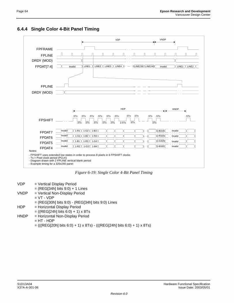
Page 64 Epson Research and DevelopmentVancouver Design Center
6.4.4 Single Color 4-Bit Panel Timing
Figure 6-19: Single Color 4-Bit Panel Timing
VDP = Vertical Display Period = (REG[34h] bits 9:0) + 1 Lines
VNDP = Vertical Non-Display Period= VT - VDP= (REG[30h] bits 9:0) - (REG[34h] bits 9:0) Lines
HDP = Horizontal Display Period= ((REG[24h] bits 6:0) + 1) x 8Ts
HNDP = Horizontal Non-Display Period= HT - HDP= (((REG[20h] bits 6:0) + 1) x 8Ts) - (((REG[24h] bits 6:0) + 1) x 8Ts)
FPLINE
FPFRAME
FPLINE
DRDY (MOD)
DRDY (MOD)
FPSHIFT
VDP
LINE1 LINE2 LINE3 LINE4 LINE239 LINE240 LINE1 LINE2
VNDP
1-R1
1-G1
1-B1
1-R2
1-G2
1-B2
1-R3
1-G3
1-B3
1-R4
1-G4
1-B4
1-B319
1-R320
1-G320
1-B320
HDP HNDP
FPDAT[7:4]
FPDAT4
FPDAT5
FPDAT6
FPDAT7Invalid
Invalid
Invalid
Invalid
Invalid
Invalid
Invalid
Invalid
InvalidInvalid
- Diagram drawn with 2 FPLINE vertical blank period- Example timing for a 320x240 panel
Notes:
- Ts = Pixel clock period (PCLK)- FPSHIFT uses extended low states in order to process 8 pixels in 6 FPSHIFT clocks
.5Ts .5Ts.5Ts .5Ts .5Ts .5Ts .5Ts .5Ts .5Ts
.5Ts .5Ts .5Ts .5Ts .5Ts .5Ts2.5Ts
.5Ts .5Ts
.5Ts
S1D13A04 Hardware Functional SpecificationX37A-A-001-06 Issue Date: 2003/05/01
Revision 6.0

Epson Research and Development Page 65Vancouver Design Center
Figure 6-20: Single Color 4-Bit Panel A.C. Timing
1. Ts = pixel clock period2. t1min = HPS + t4min3. t2min = t3min - (HPS + t4min)4. t3min = HT5. t4min = HPW6. t5min = HPS - 17. t6min = HPS - (HDP + HDPS) + 1.5), if negative add t3min8. t14min = HDPS - (HPS + t4min) + 1, if negative add t3min
Table 6-22: Single Color 4-Bit Panel A.C. Timing
Symbol Parameter Min Typ Max Unitst1 FPFRAME setup to FPLINE falling edge note 2 Ts (note 1)t2 FPFRAME hold from FPLINE falling edge note 3 Tst3 FPLINE period note 4 Tst4 FPLINE pulse width note 5 Tst5 MOD transition to FPLINE rising edge note 6 Tst6 FPSHIFT falling edge to FPLINE rising edge note 7 Tst7 FPSHIFT falling edge to FPLINE falling edge t6 + t4 Tst8 FPLINE falling edge to FPSHIFT falling edge t14 + 0.5 Tst9 FPSHIFT period 1 Ts
t10 FPSHIFT pulse width low 0.5 Tst11 FPSHIFT pulse width high 0.5 Tst12 FPDAT[7:4] setup to FPSHIFT falling edge 0.5 Tst13 FPDAT[7:4] hold to FPSHIFT falling edge 0.5 Tst14 FPLINE falling edge to FPSHIFT rising edge note 8 Ts
FPFRAME
FPLINE
DRDY (MOD)
Sync Timing
FPLINE
FPSHIFT
FPDAT[7:4]
Data Timing
t14
t1 t2
t3t4
t8 t9t10t11
t12 t13
1 2
t7
t6
t5
Hardware Functional Specification S1D13A04Issue Date: 2003/05/01 X37A-A-001-06
Revision 6.0
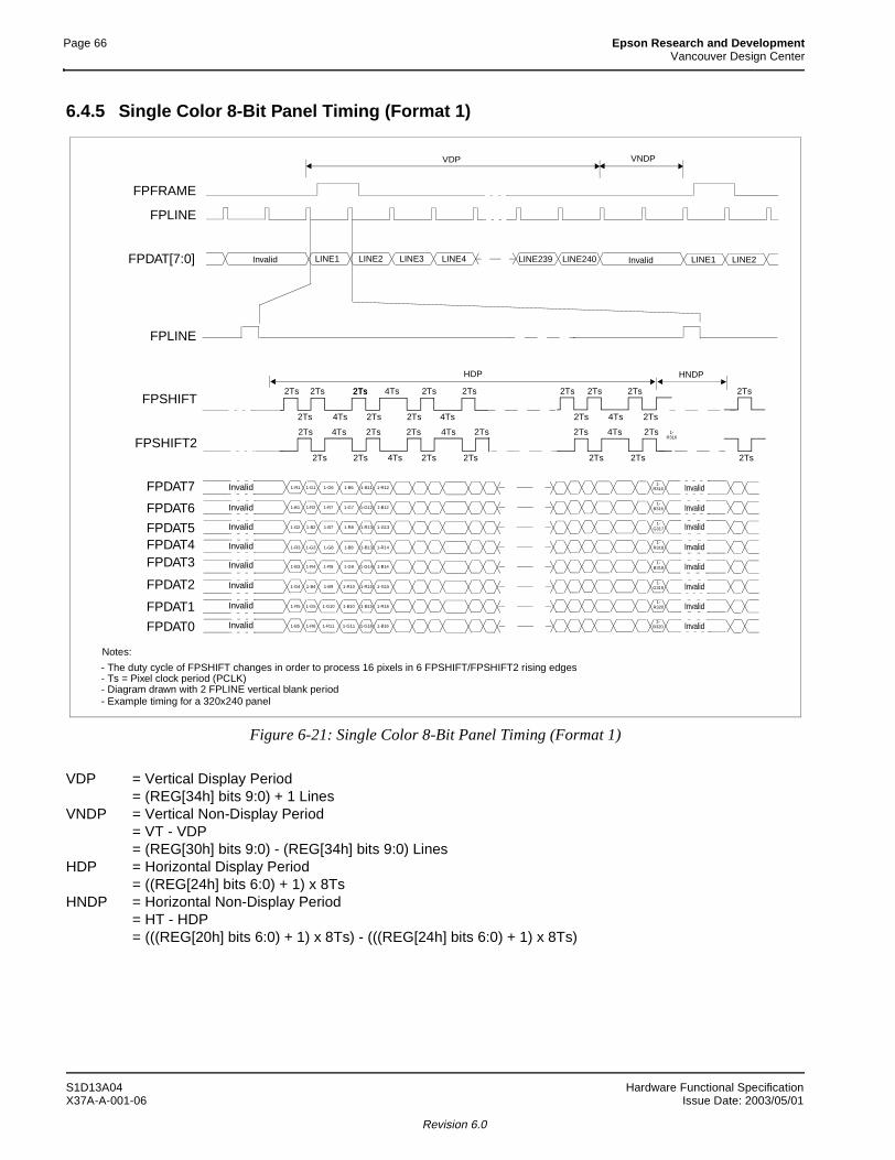
Page 66 Epson Research and DevelopmentVancouver Design Center
6.4.5 Single Color 8-Bit Panel Timing (Format 1)
Figure 6-21: Single Color 8-Bit Panel Timing (Format 1)
VDP = Vertical Display Period = (REG[34h] bits 9:0) + 1 Lines
VNDP = Vertical Non-Display Period= VT - VDP= (REG[30h] bits 9:0) - (REG[34h] bits 9:0) Lines
HDP = Horizontal Display Period= ((REG[24h] bits 6:0) + 1) x 8Ts
HNDP = Horizontal Non-Display Period= HT - HDP= (((REG[20h] bits 6:0) + 1) x 8Ts) - (((REG[24h] bits 6:0) + 1) x 8Ts)
FPLINE
FPSHIFT2
FPFRAME
FPLINE
FPSHIFT
FPDAT[7:0]
VDP
LINE1 LINE2 LINE3 LINE4 LINE239 LINE240 LINE1 LINE2
HDP
VNDP
HNDP
FPDAT5
FPDAT6
FPDAT4FPDAT3
FPDAT2
FPDAT1
FPDAT0
FPDAT7 Invalid
Invalid
Invalid
Invalid
Invalid
Invalid
Invalid
Invalid
Invalid
Invalid
Invalid
Invalid
Invalid
Invalid
Invalid
Invalid
Invalid Invalid
- Diagram drawn with 2 FPLINE vertical blank period- Example timing for a 320x240 panel
Notes:
- Ts = Pixel clock period (PCLK)- The duty cycle of FPSHIFT changes in order to process 16 pixels in 6 FPSHIFT/FPSHIFT2 rising edges
2Ts 2Ts 2Ts 2Ts 2Ts 2Ts 2Ts 2Ts 2Ts
2Ts 2Ts 2Ts 2Ts 2Ts
2Ts 2Ts 2Ts 2Ts 2Ts 2Ts
2Ts
4Ts
4Ts
4Ts 4Ts
4Ts4Ts
4Ts
4Ts
2Ts 2Ts 2Ts 2Ts 2Ts 2Ts
2Ts
1-R1
1-B1
1-G2
1-R3
1-B3
1-G4
1-R5
1-B5 1-R6
1-G5
1-B4
1-R4 1-R9 1-G9 1-G14 1-B14
1-R14
1-G13
1-B12
1-R121-B61-G6
1-R7
1-B7
1-G8
1-B9
1-G10
1-R11 1-G11 1-B16
1-B10
1-R10
1-B8
1-R8
1-G7
1-B11
1-B2
1-R2
1-G1
1-G3
1-R15
1-B15
1-G16
1-B13
1-G15
1-R13
1-G12
1-R16
1-R316
1-R316
1-B316
1-G317
1-R318
1-B318
1-G319
1-R320
1-B320
S1D13A04 Hardware Functional SpecificationX37A-A-001-06 Issue Date: 2003/05/01
Revision 6.0
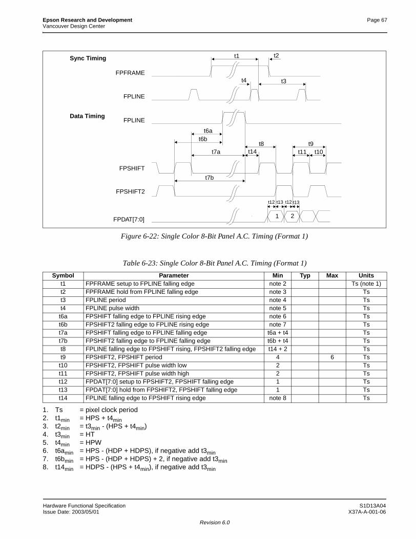
Epson Research and Development Page 67Vancouver Design Center
Figure 6-22: Single Color 8-Bit Panel A.C. Timing (Format 1)
1. Ts = pixel clock period2. t1min = HPS + t4min3. t2min = t3min - (HPS + t4min)4. t3min = HT5. t4min = HPW6. t6amin = HPS - (HDP + HDPS), if negative add t3min7. t6bmin = HPS - (HDP + HDPS) + 2, if negative add t3min8. t14min = HDPS - (HPS + t4min), if negative add t3min
Table 6-23: Single Color 8-Bit Panel A.C. Timing (Format 1)
Symbol Parameter Min Typ Max Unitst1 FPFRAME setup to FPLINE falling edge note 2 Ts (note 1)t2 FPFRAME hold from FPLINE falling edge note 3 Tst3 FPLINE period note 4 Tst4 FPLINE pulse width note 5 Ts
t6a FPSHIFT falling edge to FPLINE rising edge note 6 Tst6b FPSHIFT2 falling edge to FPLINE rising edge note 7 Tst7a FPSHIFT falling edge to FPLINE falling edge t6a + t4 Tst7b FPSHIFT2 falling edge to FPLINE falling edge t6b + t4 Tst8 FPLINE falling edge to FPSHIFT rising, FPSHIFT2 falling edge t14 + 2 Tst9 FPSHIFT2, FPSHIFT period 4 6 Ts
t10 FPSHIFT2, FPSHIFT pulse width low 2 Tst11 FPSHIFT2, FPSHIFT pulse width high 2 Tst12 FPDAT[7:0] setup to FPSHIFT2, FPSHIFT falling edge 1 Tst13 FPDAT[7:0] hold from FPSHIFT2, FPSHIFT falling edge 1 Tst14 FPLINE falling edge to FPSHIFT rising edge note 8 Ts
FPFRAME
FPLINE
Sync Timing
FPLINE
FPSHIFT
FPDAT[7:0]
Data Timing
t14
t1 t2
t3t4
t8 t9t10t11
t12 t13
21
t7a
t6b
FPSHIFT2
t6a
t7b
t12 t13
Hardware Functional Specification S1D13A04Issue Date: 2003/05/01 X37A-A-001-06
Revision 6.0
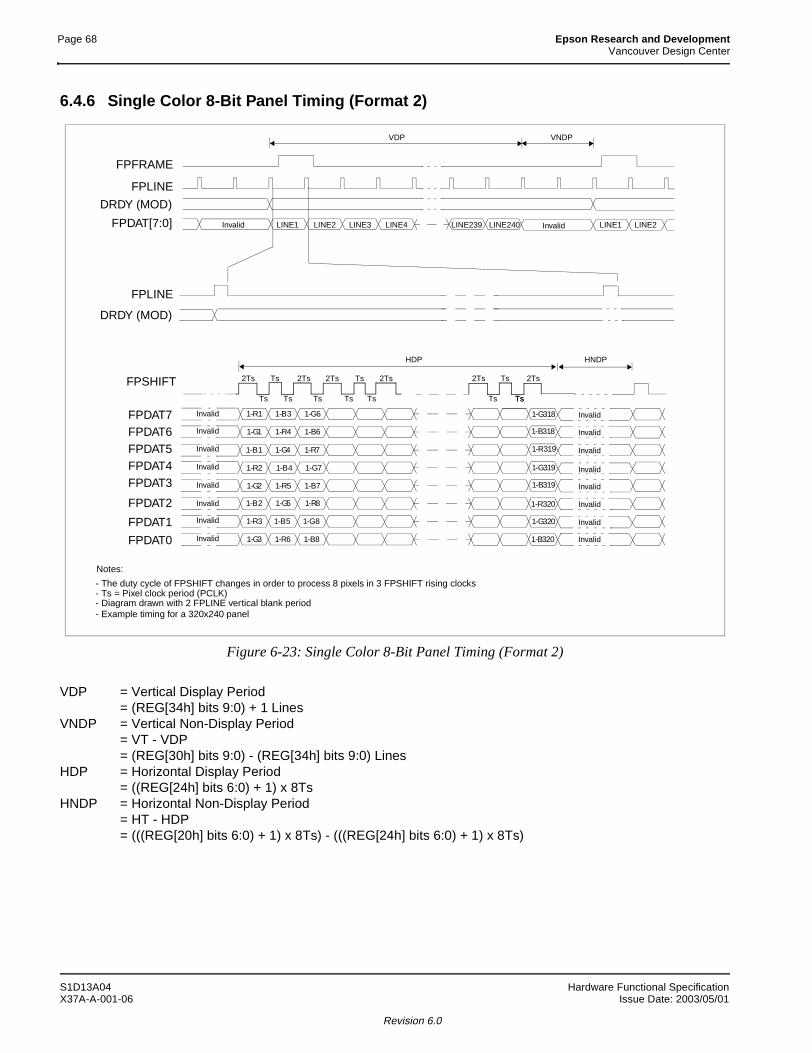
Page 68 Epson Research and DevelopmentVancouver Design Center
6.4.6 Single Color 8-Bit Panel Timing (Format 2)
Figure 6-23: Single Color 8-Bit Panel Timing (Format 2)
VDP = Vertical Display Period = (REG[34h] bits 9:0) + 1 Lines
VNDP = Vertical Non-Display Period= VT - VDP= (REG[30h] bits 9:0) - (REG[34h] bits 9:0) Lines
HDP = Horizontal Display Period= ((REG[24h] bits 6:0) + 1) x 8Ts
HNDP = Horizontal Non-Display Period= HT - HDP= (((REG[20h] bits 6:0) + 1) x 8Ts) - (((REG[24h] bits 6:0) + 1) x 8Ts)
FPLINE
FPFRAME
FPLINE
DRDY (MOD)
DRDY (MOD)
FPSHIFT
VDP
LINE1 LINE2 LINE3 LINE4 LINE239 LINE240 LINE1 LINE2
VNDP
1-R1
1-G1
1-B1
1-R2
1-G2
1-B2
1-R3
1-G3
1-B3
1-R4
1-G4
1-B4
1-R5
1-G5
1-B5
1-R6
1-G6
1-B6
1-R7
1-G7
1-B7
1-R8
1-G8
1-B8
1-G318
1-B318
1-R319
1-G319
1-B319
1-R320
1-G320
1-B320
HDP HNDP
FPDAT[7:0]
FPDAT7FPDAT6FPDAT5FPDAT4FPDAT3
FPDAT2
FPDAT1
FPDAT0
Invalid
Invalid
Invalid
Invalid
Invalid
Invalid
Invalid
Invalid
Invalid
Invalid
Invalid
Invalid
Invalid
Invalid
Invalid
Invalid
InvalidInvalid
2Ts 2Ts 2Ts 2Ts 2Ts 2Ts
Ts
Ts
Ts Ts Ts Ts
Ts
Ts
Ts
TsTs
- Diagram drawn with 2 FPLINE vertical blank period- Example timing for a 320x240 panel
Notes:
- Ts = Pixel clock period (PCLK)- The duty cycle of FPSHIFT changes in order to process 8 pixels in 3 FPSHIFT rising clocks
S1D13A04 Hardware Functional SpecificationX37A-A-001-06 Issue Date: 2003/05/01
Revision 6.0

Epson Research and Development Page 69Vancouver Design Center
Figure 6-24: Single Color 8-Bit Panel A.C. Timing (Format 2)
1. Ts = pixel clock period2. t1min = HPS + t4min3. t2min = t3min - (HPS + t4min)4. t3min = HT5. t4min = HPW6. t5min = HPS - 17. t6min = HPS - (HDP + HDPS) + 1, if negative add t3min8. t14min = HDPS - (HPS + t4min), if negative add t3min
Table 6-24: Single Color 8-Bit Panel A.C. Timing (Format 2)
Symbol Parameter Min Typ Max Unitst1 FPFRAME setup to FPLINE falling edge note 2 Ts (note 1)t2 FPFRAME hold from FPLINE falling edge note 3 Tst3 FPLINE period note 4 Tst4 FPLINE pulse width note 5 Tst5 MOD transition to FPLINE rising edge note 6 Tst6 FPSHIFT falling edge to FPLINE rising edge note 7 Tst7 FPSHIFT falling edge to FPLINE falling edge t6 + t4 Tst8 FPLINE falling edge to FPSHIFT falling edge t14 + 2 Tst9 FPSHIFT period 2 Ts
t10 FPSHIFT pulse width low 1 Tst11 FPSHIFT pulse width high 1 Tst12 FPDAT[7:0] setup to FPSHIFT falling edge 1 Tst13 FPDAT[7:0] hold to FPSHIFT falling edge 1 Tst14 FPLINE falling edge to FPSHIFT rising edge note 8 Ts
t14 t10t11
t12 t13
Data Timing
FPFRAME
t1 t2
t3
t5
t4
FPLINE
DRDY (MOD)
Sync Timing
FPLINE
FPSHIFT
t8 t9
1 2
t7
t6
FPDAT[7:0]
Hardware Functional Specification S1D13A04Issue Date: 2003/05/01 X37A-A-001-06
Revision 6.0
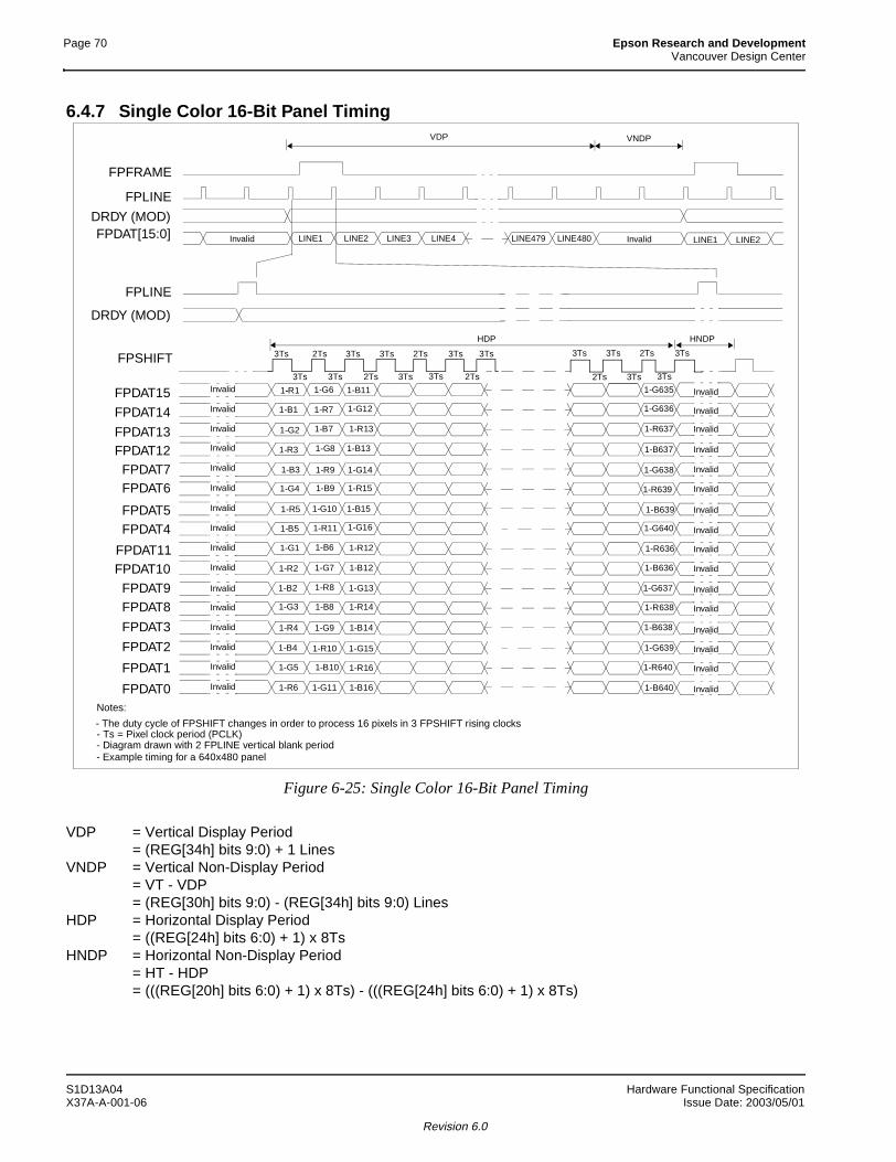
Page 70 Epson Research and DevelopmentVancouver Design Center
6.4.7 Single Color 16-Bit Panel Timing
Figure 6-25: Single Color 16-Bit Panel Timing
VDP = Vertical Display Period = (REG[34h] bits 9:0) + 1 Lines
VNDP = Vertical Non-Display Period= VT - VDP= (REG[30h] bits 9:0) - (REG[34h] bits 9:0) Lines
HDP = Horizontal Display Period= ((REG[24h] bits 6:0) + 1) x 8Ts
HNDP = Horizontal Non-Display Period= HT - HDP= (((REG[20h] bits 6:0) + 1) x 8Ts) - (((REG[24h] bits 6:0) + 1) x 8Ts)
VDP
FPLINE
FPSHIFT
LINE1 LINE2 LINE3 LINE4 LINE479 LINE480
FPFRAME
LINE1 LINE2
FPLINE
DRDY (MOD)
DRDY (MOD)
VNDP
HDP
1-R1 1-G6 1-G635
1-B1 1-R7 1-G636
1-G2 1-B7 1-R637
1-R3 1-G8 1-B637
1-B3 1-R9 1-G638
1-G4 1-B9 1-R639
1-R5 1-G10 1-B639
1-G1 1-B6 1-R636
1-R2 1-G7 1-B636
1-B2 1-R8 1-G637
1-G3 1-B8 1-R638
1-R4 1-G9 1-B638
1-B4 1-R10 1-G639
1-G5 1-B10 1-R640
1-R6 1-G11 1-B640
1-B11
1-G12
1-R13
1-B13
1-G14
1-R15
1-B15
1-R12
1-B12
1-G13
1-R14
1-B14
1-G15
1-R16
1-B16
1-B5 1-R11 1-G6401-G16
HNDP
- Diagram drawn with 2 FPLINE vertical blank period- Example timing for a 640x480 panel
FPDAT[15:0]
FPDAT15
FPDAT9FPDAT8
FPDAT3
FPDAT2
FPDAT1
FPDAT0
FPDAT5FPDAT4
FPDAT11FPDAT10
FPDAT12FPDAT7FPDAT6
FPDAT13
FPDAT14
Invalid
Invalid
Invalid
Invalid
Invalid
Invalid
Invalid
Invalid
Invalid
Invalid
Invalid
Invalid
Invalid
Invalid
Invalid
Invalid
Invalid
Invalid
Invalid
Invalid
Invalid
Invalid
Invalid
Invalid
Invalid
Invalid
Invalid
Invalid
Invalid
Invalid
Invalid
Invalid
Invalid Invalid
-
3Ts
3Ts 3Ts
3Ts 3Ts
3Ts 3Ts
3Ts 3Ts2Ts
2Ts
2Ts
2Ts
3Ts 3Ts 3Ts2Ts
3Ts 3Ts2Ts
Notes:
- Ts = Pixel clock period (PCLK)- The duty cycle of FPSHIFT changes in order to process 16 pixels in 3 FPSHIFT rising clocks
S1D13A04 Hardware Functional SpecificationX37A-A-001-06 Issue Date: 2003/05/01
Revision 6.0
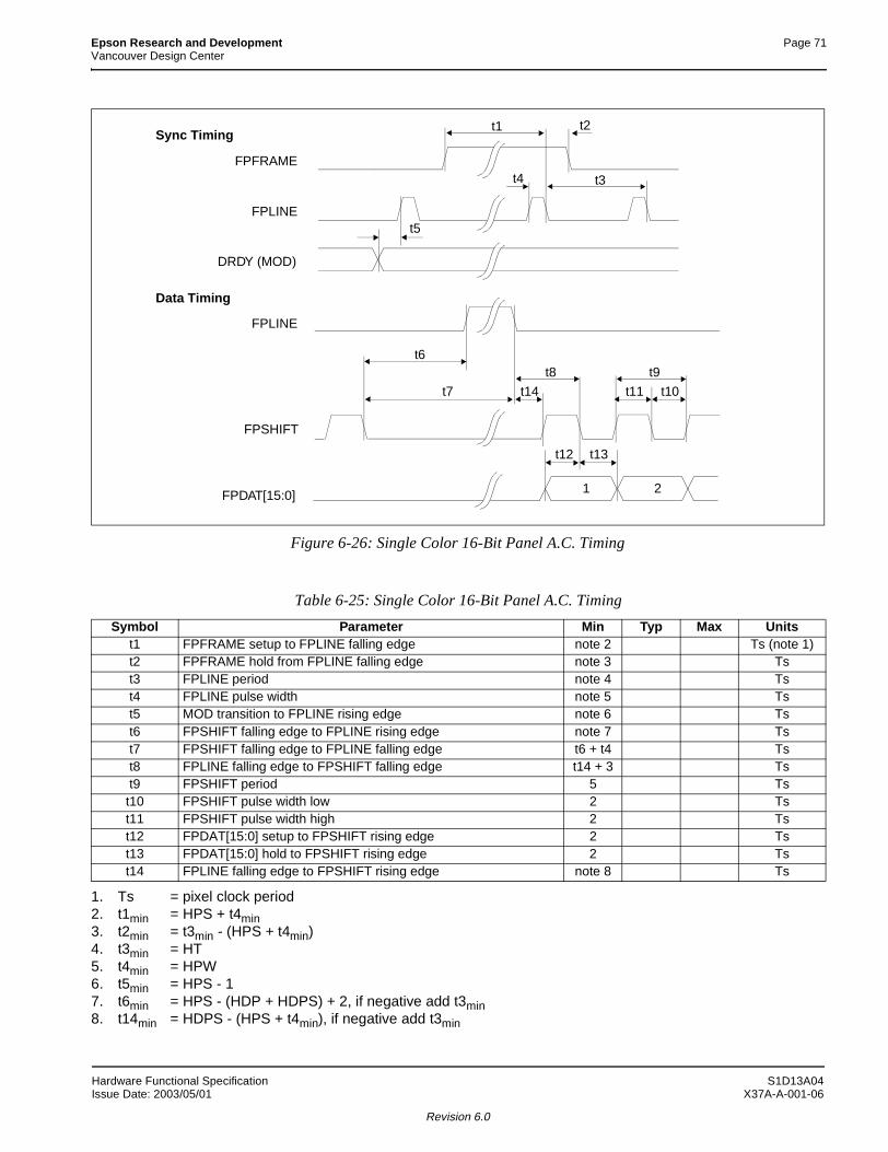
Epson Research and Development Page 71Vancouver Design Center
Figure 6-26: Single Color 16-Bit Panel A.C. Timing
1. Ts = pixel clock period2. t1min = HPS + t4min3. t2min = t3min - (HPS + t4min)4. t3min = HT5. t4min = HPW6. t5min = HPS - 17. t6min = HPS - (HDP + HDPS) + 2, if negative add t3min8. t14min = HDPS - (HPS + t4min), if negative add t3min
Table 6-25: Single Color 16-Bit Panel A.C. Timing
Symbol Parameter Min Typ Max Unitst1 FPFRAME setup to FPLINE falling edge note 2 Ts (note 1)t2 FPFRAME hold from FPLINE falling edge note 3 Tst3 FPLINE period note 4 Tst4 FPLINE pulse width note 5 Tst5 MOD transition to FPLINE rising edge note 6 Tst6 FPSHIFT falling edge to FPLINE rising edge note 7 Tst7 FPSHIFT falling edge to FPLINE falling edge t6 + t4 Tst8 FPLINE falling edge to FPSHIFT falling edge t14 + 3 Tst9 FPSHIFT period 5 Ts
t10 FPSHIFT pulse width low 2 Tst11 FPSHIFT pulse width high 2 Tst12 FPDAT[15:0] setup to FPSHIFT rising edge 2 Tst13 FPDAT[15:0] hold to FPSHIFT rising edge 2 Tst14 FPLINE falling edge to FPSHIFT rising edge note 8 Ts
t14 t10t11
Data Timing
FPFRAME
t1 t2
t3
t5
t4
FPLINE
DRDY (MOD)
Sync Timing
FPLINE
FPSHIFT
t8 t9
t7
t6
t12 t13
1 2FPDAT[15:0]
Hardware Functional Specification S1D13A04Issue Date: 2003/05/01 X37A-A-001-06
Revision 6.0
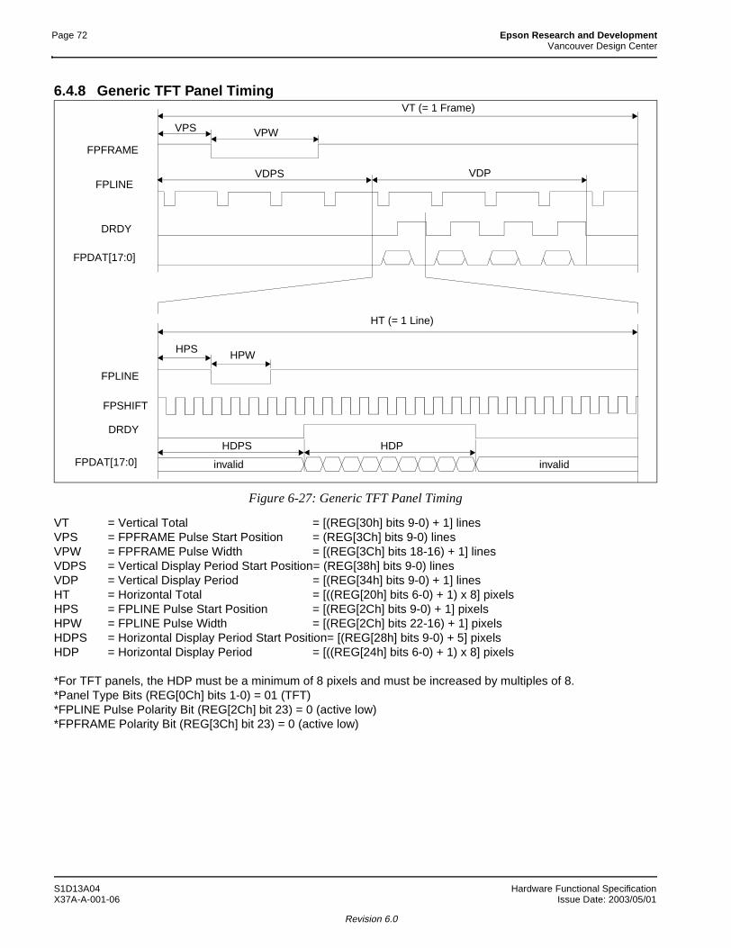
Page 72 Epson Research and DevelopmentVancouver Design Center
6.4.8 Generic TFT Panel Timing
Figure 6-27: Generic TFT Panel Timing
VT = Vertical Total = [(REG[30h] bits 9-0) + 1] linesVPS = FPFRAME Pulse Start Position = (REG[3Ch] bits 9-0) linesVPW = FPFRAME Pulse Width = [(REG[3Ch] bits 18-16) + 1] linesVDPS = Vertical Display Period Start Position= (REG[38h] bits 9-0) linesVDP = Vertical Display Period = [(REG[34h] bits 9-0) + 1] linesHT = Horizontal Total = [((REG[20h] bits 6-0) + 1) x 8] pixelsHPS = FPLINE Pulse Start Position = [(REG[2Ch] bits 9-0) + 1] pixelsHPW = FPLINE Pulse Width = [(REG[2Ch] bits 22-16) + 1] pixelsHDPS = Horizontal Display Period Start Position= [(REG[28h] bits 9-0) + 5] pixelsHDP = Horizontal Display Period = [((REG[24h] bits 6-0) + 1) x 8] pixels
*For TFT panels, the HDP must be a minimum of 8 pixels and must be increased by multiples of 8.*Panel Type Bits (REG[0Ch] bits 1-0) = 01 (TFT)*FPLINE Pulse Polarity Bit (REG[2Ch] bit 23) = 0 (active low)*FPFRAME Polarity Bit (REG[3Ch] bit 23) = 0 (active low)
FPFRAME
VT (= 1 Frame)
DRDY
FPLINE
DRDY
FPLINEVDPS
VPS VPW
VDP
HT (= 1 Line)
HPS
HDPS HDP
FPDAT[17:0]
FPDAT[17:0] invalid invalid
FPSHIFT
HPW
S1D13A04 Hardware Functional SpecificationX37A-A-001-06 Issue Date: 2003/05/01
Revision 6.0
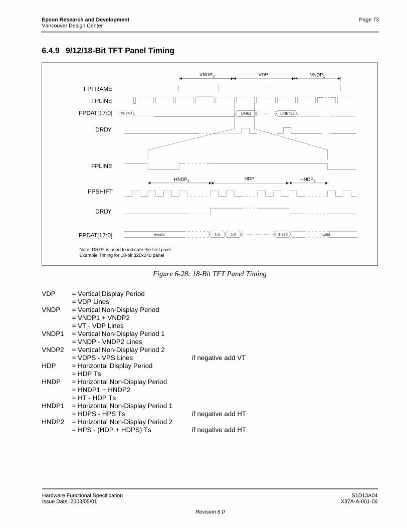
Epson Research and Development Page 73Vancouver Design Center
6.4.9 9/12/18-Bit TFT Panel Timing
Figure 6-28: 18-Bit TFT Panel Timing
VDP = Vertical Display Period= VDP Lines
VNDP = Vertical Non-Display Period= VNDP1 + VNDP2= VT - VDP Lines
VNDP1 = Vertical Non-Display Period 1= VNDP - VNDP2 Lines
VNDP2 = Vertical Non-Display Period 2= VDPS - VPS Lines if negative add VT
HDP = Horizontal Display Period= HDP Ts
HNDP = Horizontal Non-Display Period= HNDP1 + HNDP2 = HT - HDP Ts
HNDP1 = Horizontal Non-Display Period 1= HDPS - HPS Ts if negative add HT
HNDP2 = Horizontal Non-Display Period 2= HPS - (HDP + HDPS) Ts if negative add HT
FPFRAME
FPLINE
LINE1 LINE480
1-1 1-2 1-320
FPLINE
FPSHIFT
DRDY
FPDAT[17:0]
VDP
DRDY
Note: DRDY is used to indicate the first pixelExample Timing for 18-bit 320x240 panel
VNDP2
HDPHNDP1 HNDP2
LINE240
VNDP1
FPDAT[17:0] invalid invalid
Hardware Functional Specification S1D13A04Issue Date: 2003/05/01 X37A-A-001-06
Revision 6.0
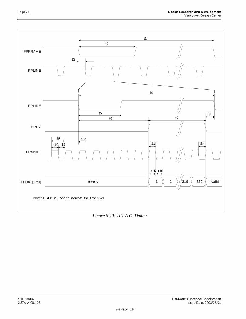
Page 74 Epson Research and DevelopmentVancouver Design Center
Figure 6-29: TFT A.C. Timing
t3
t5
FPLINE
t1
t4
FPFRAME
DRDY
FPSHIFT
320
t2
FPLINE
21 319
t13t10 t11 t14
t15 t16
t7t8
t9 t12
FPDAT[17:0]
Note: DRDY is used to indicate the first pixel
t6
invalidinvalid
S1D13A04 Hardware Functional SpecificationX37A-A-001-06 Issue Date: 2003/05/01
Revision 6.0
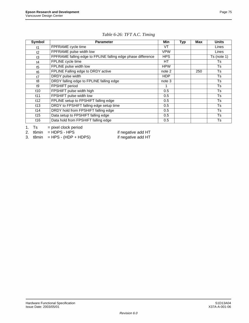
Epson Research and Development Page 75Vancouver Design Center
1. Ts = pixel clock period2. t6min = HDPS - HPS if negative add HT3. t8min = HPS - (HDP + HDPS) if negative add HT
Table 6-26: TFT A.C. Timing
Symbol Parameter Min Typ Max Units
t1 FPFRAME cycle time VT Lines
t2 FPFRAME pulse width low VPW Lines
t3 FPFRAME falling edge to FPLINE falling edge phase difference HPS Ts (note 1)
t4 FPLINE cycle time HT Ts
t5 FPLINE pulse width low HPW Ts
t6 FPLINE Falling edge to DRDY active note 2 250 Ts
t7 DRDY pulse width HDP Tst8 DRDY falling edge to FPLINE falling edge note 3 Tst9 FPSHIFT period 1 Ts
t10 FPSHIFT pulse width high 0.5 Tst11 FPSHIFT pulse width low 0.5 Tst12 FPLINE setup to FPSHIFT falling edge 0.5 Tst13 DRDY to FPSHIFT falling edge setup time 0.5 Tst14 DRDY hold from FPSHIFT falling edge 0.5 Tst15 Data setup to FPSHIFT falling edge 0.5 Tst16 Data hold from FPSHIFT falling edge 0.5 Ts
Hardware Functional Specification S1D13A04Issue Date: 2003/05/01 X37A-A-001-06
Revision 6.0
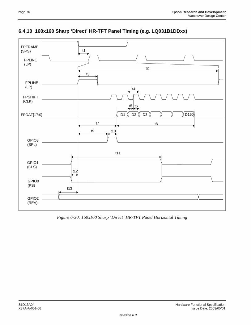
Page 76 Epson Research and DevelopmentVancouver Design Center
6.4.10 160x160 Sharp ‘Direct’ HR-TFT Panel Timing (e.g. LQ031B1DDxx)
Figure 6-30: 160x160 Sharp ‘Direct’ HR-TFT Panel Horizontal Timing
FPLINE
t2
FPDAT[17:0]
t3
t4
t12
t11
GPIO3
GPIO2
t10t9
FPSHIFT
GPIO1
GPIO0
D1
t13
t8
D2 D3 D160
FPLINE
t1FPFRAME
t7
(SPS)
(LP)
(LP)
(CLK)
(SPL)
(CLS)
(PS)
(REV)
t5 t6
S1D13A04 Hardware Functional SpecificationX37A-A-001-06 Issue Date: 2003/05/01
Revision 6.0
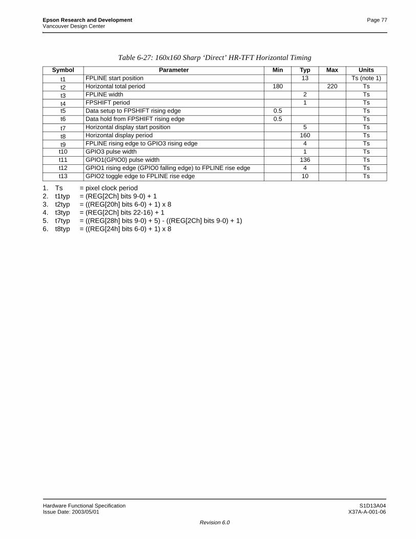
Epson Research and Development Page 77Vancouver Design Center
1. Ts = pixel clock period2. t1typ = (REG[2Ch] bits 9-0) + 13. t2typ = ((REG[20h] bits 6-0) + 1) x 84. t3typ = (REG[2Ch] bits 22-16) + 15. t7typ = ((REG[28h] bits 9-0) + 5) - ((REG[2Ch] bits 9-0) + 1)6. t8typ = ((REG[24h] bits 6-0) + 1) x 8
Table 6-27: 160x160 Sharp ‘Direct’ HR-TFT Horizontal Timing
Symbol Parameter Min Typ Max Units
t1 FPLINE start position 13 Ts (note 1)
t2 Horizontal total period 180 220 Ts
t3 FPLINE width 2 Ts
t4 FPSHIFT period 1 Tst5 Data setup to FPSHIFT rising edge 0.5 Tst6 Data hold from FPSHIFT rising edge 0.5 Ts
t7 Horizontal display start position 5 Ts
t8 Horizontal display period 160 Ts
t9 FPLINE rising edge to GPIO3 rising edge 4 Tst10 GPIO3 pulse width 1 Tst11 GPIO1(GPIO0) pulse width 136 Tst12 GPIO1 rising edge (GPIO0 falling edge) to FPLINE rise edge 4 Tst13 GPIO2 toggle edge to FPLINE rise edge 10 Ts
Hardware Functional Specification S1D13A04Issue Date: 2003/05/01 X37A-A-001-06
Revision 6.0
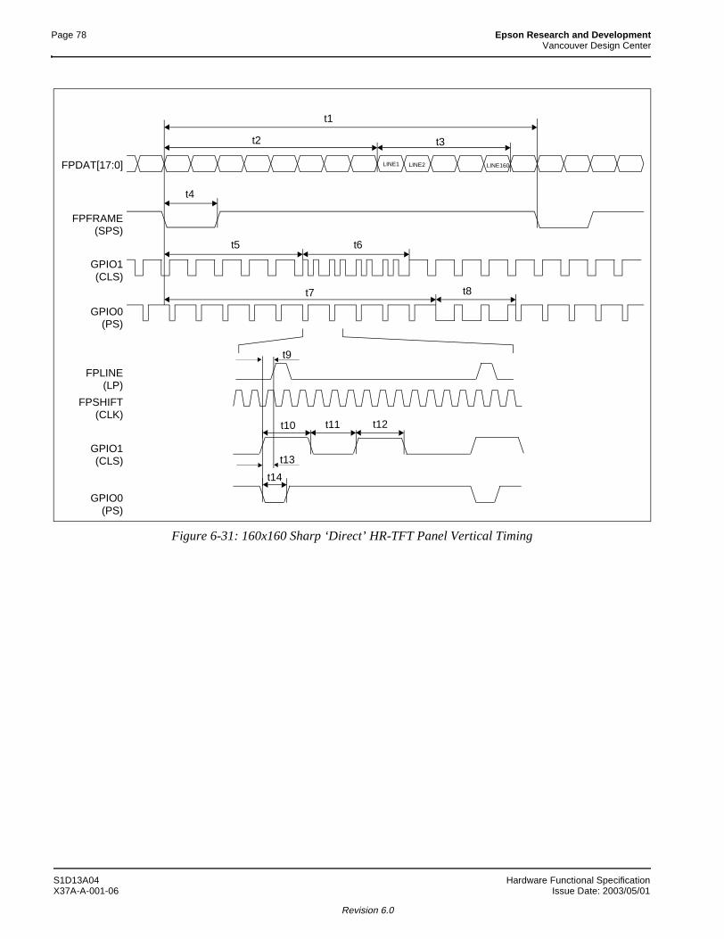
Page 78 Epson Research and DevelopmentVancouver Design Center
Figure 6-31: 160x160 Sharp ‘Direct’ HR-TFT Panel Vertical Timing
t1
FPDAT[17:0]
GPIO1
t4
FPFRAME
GPIO0
t2 t3
LINE1 LINE2 LINE160
t5 t6
t7 t8
t10 t11 t12
GPIO1
GPIO0
t9
t13
t14
FPLINE
FPSHIFT
(SPS)
(CLS)
(PS)
(LP)
(CLK)
(CLS)
(PS)
S1D13A04 Hardware Functional SpecificationX37A-A-001-06 Issue Date: 2003/05/01
Revision 6.0
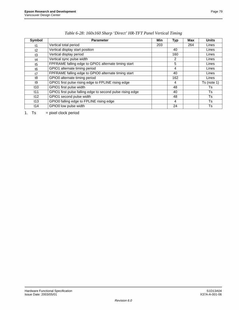
Epson Research and Development Page 79Vancouver Design Center
1. Ts = pixel clock period
Table 6-28: 160x160 Sharp ‘Direct’ HR-TFT Panel Vertical Timing
Symbol Parameter Min Typ Max Units
t1 Vertical total period 203 264 Lines
t2 Vertical display start position 40 Lines
t3 Vertical display period 160 Lines
t4 Vertical sync pulse width 2 Lines
t5 FPFRAME falling edge to GPIO1 alternate timing start 5 Lines
t6 GPIO1 alternate timing period 4 Lines
t7 FPFRAME falling edge to GPIO0 alternate timing start 40 Linest8 GPIO0 alternate timing period 162 Linest9 GPIO1 first pulse rising edge to FPLINE rising edge 4 Ts (note 1)
t10 GPIO1 first pulse width 48 Tst11 GPIO1 first pulse falling edge to second pulse rising edge 40 Tst12 GPIO1 second pulse width 48 Tst13 GPIO0 falling edge to FPLINE rising edge 4 Tst14 GPIO0 low pulse width 24 Ts
Hardware Functional Specification S1D13A04Issue Date: 2003/05/01 X37A-A-001-06
Revision 6.0
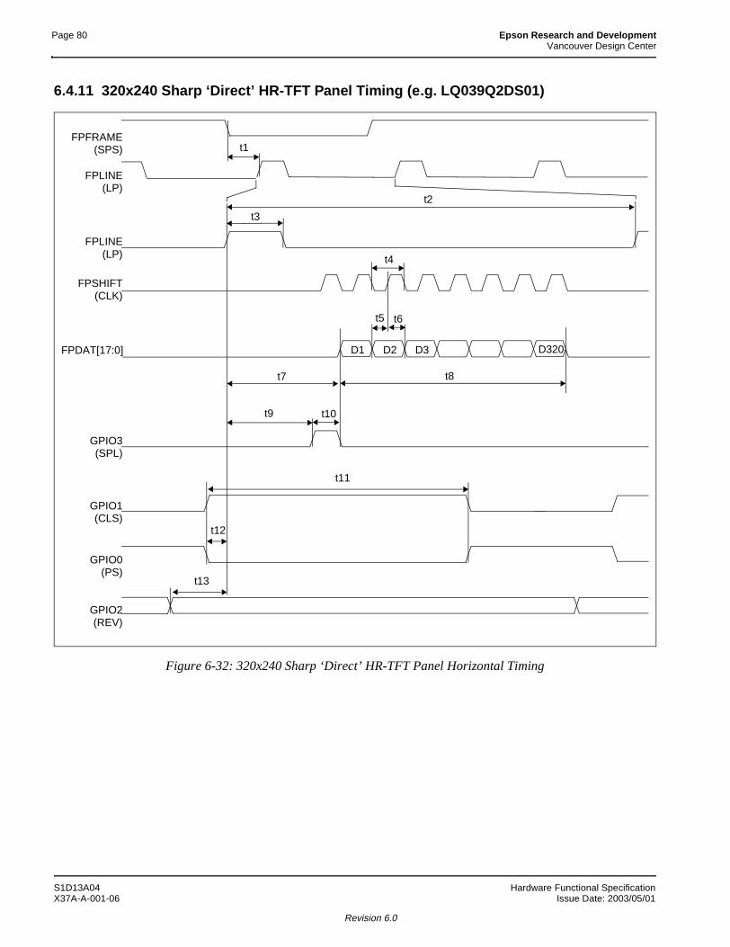
Page 80 Epson Research and DevelopmentVancouver Design Center
6.4.11 320x240 Sharp ‘Direct’ HR-TFT Panel Timing (e.g. LQ039Q2DS01)
Figure 6-32: 320x240 Sharp ‘Direct’ HR-TFT Panel Horizontal Timing
FPLINE
t2
FPDAT[17:0]
t3
t4
t12
t11
GPIO3
GPIO2
t10t9
FPSHIFT
GPIO1
GPIO0
D1
t13
t6
D2 D3 D320
FPLINE
t1FPFRAME
(SPS)
(LP)
(LP)
(CLK)
(SPL)
(CLS)
(PS)
(REV)
t5
t7 t8
S1D13A04 Hardware Functional SpecificationX37A-A-001-06 Issue Date: 2003/05/01
Revision 6.0
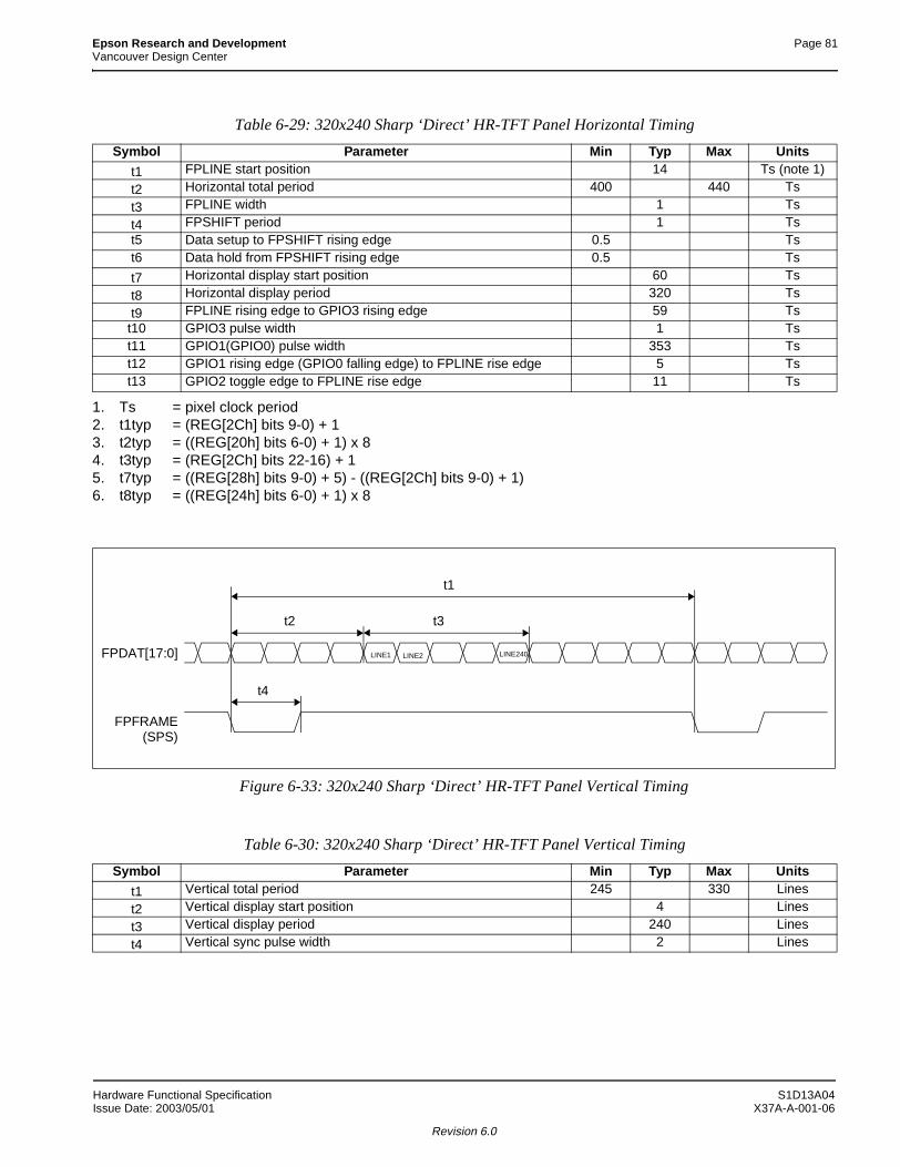
Epson Research and Development Page 81Vancouver Design Center
1. Ts = pixel clock period2. t1typ = (REG[2Ch] bits 9-0) + 13. t2typ = ((REG[20h] bits 6-0) + 1) x 84. t3typ = (REG[2Ch] bits 22-16) + 15. t7typ = ((REG[28h] bits 9-0) + 5) - ((REG[2Ch] bits 9-0) + 1)6. t8typ = ((REG[24h] bits 6-0) + 1) x 8
Figure 6-33: 320x240 Sharp ‘Direct’ HR-TFT Panel Vertical Timing
Table 6-29: 320x240 Sharp ‘Direct’ HR-TFT Panel Horizontal Timing
Symbol Parameter Min Typ Max Units
t1 FPLINE start position 14 Ts (note 1)
t2 Horizontal total period 400 440 Ts
t3 FPLINE width 1 Ts
t4 FPSHIFT period 1 Tst5 Data setup to FPSHIFT rising edge 0.5 Tst6 Data hold from FPSHIFT rising edge 0.5 Ts
t7 Horizontal display start position 60 Ts
t8 Horizontal display period 320 Ts
t9 FPLINE rising edge to GPIO3 rising edge 59 Tst10 GPIO3 pulse width 1 Tst11 GPIO1(GPIO0) pulse width 353 Tst12 GPIO1 rising edge (GPIO0 falling edge) to FPLINE rise edge 5 Tst13 GPIO2 toggle edge to FPLINE rise edge 11 Ts
Table 6-30: 320x240 Sharp ‘Direct’ HR-TFT Panel Vertical Timing
Symbol Parameter Min Typ Max Units
t1 Vertical total period 245 330 Lines
t2 Vertical display start position 4 Lines
t3 Vertical display period 240 Lines
t4 Vertical sync pulse width 2 Lines
t1
t4
FPFRAME
t2 t3
LINE1 LINE2 LINE240FPDAT[17:0]
(SPS)
Hardware Functional Specification S1D13A04Issue Date: 2003/05/01 X37A-A-001-06
Revision 6.0
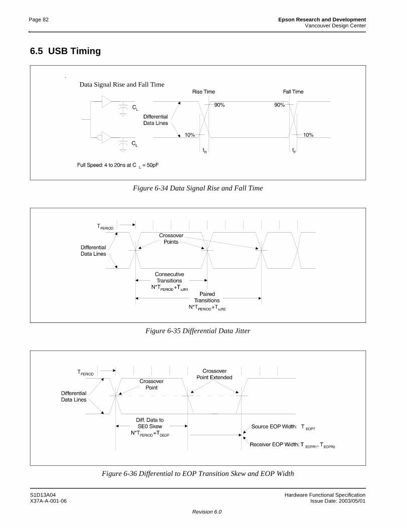
Page 82 Epson Research and DevelopmentVancouver Design Center
6.5 USB Timing
Figure 6-34 Data Signal Rise and Fall Time
Figure 6-35 Differential Data Jitter
Figure 6-36 Differential to EOP Transition Skew and EOP Width
Data Signal Rise and Fall Time
S1D13A04 Hardware Functional SpecificationX37A-A-001-06 Issue Date: 2003/05/01
Revision 6.0
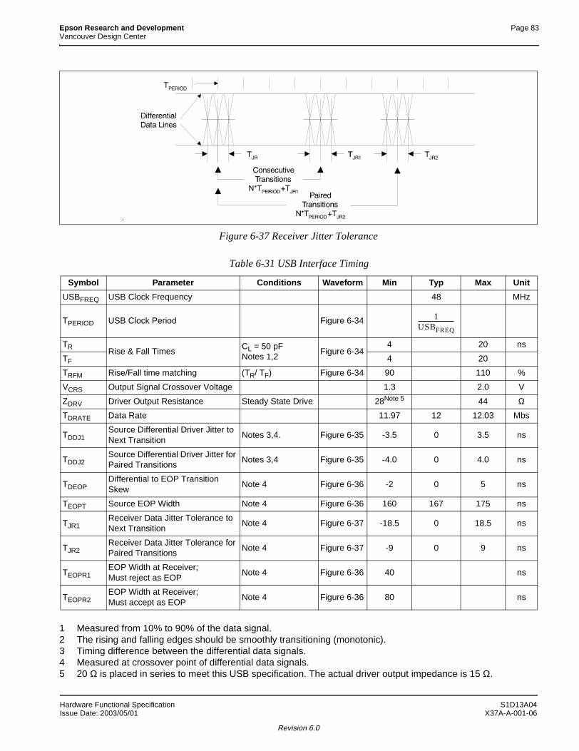
Epson Research and Development Page 83Vancouver Design Center
Figure 6-37 Receiver Jitter Tolerance
1 Measured from 10% to 90% of the data signal.2 The rising and falling edges should be smoothly transitioning (monotonic).3 Timing difference between the differential data signals.4 Measured at crossover point of differential data signals.5 20 Ω is placed in series to meet this USB specification. The actual driver output impedance is 15 Ω.
Table 6-31 USB Interface Timing
Symbol Parameter Conditions Waveform Min Typ Max Unit
USBFREQ USB Clock Frequency 48 MHz
TPERIOD USB Clock Period Figure 6-34
TR Rise & Fall Times
CL = 50 pFNotes 1,2
Figure 6-344 20 ns
TF 4 20
TRFM Rise/Fall time matching (TR/ TF) Figure 6-34 90 110 %
VCRS Output Signal Crossover Voltage 1.3 2.0 V
ZDRV Driver Output Resistance Steady State Drive 28Note 5 44 Ω
TDRATE Data Rate 11.97 12 12.03 Mbs
TDDJ1 Source Differential Driver Jitter to Next Transition
Notes 3,4. Figure 6-35 -3.5 0 3.5 ns
TDDJ2 Source Differential Driver Jitter for Paired Transitions
Notes 3,4 Figure 6-35 -4.0 0 4.0 ns
TDEOP Differential to EOP Transition Skew
Note 4 Figure 6-36 -2 0 5 ns
TEOPT Source EOP Width Note 4 Figure 6-36 160 167 175 ns
TJR1Receiver Data Jitter Tolerance to Next Transition
Note 4 Figure 6-37 -18.5 0 18.5 ns
TJR2Receiver Data Jitter Tolerance for Paired Transitions
Note 4 Figure 6-37 -9 0 9 ns
TEOPR1EOP Width at Receiver; Must reject as EOP
Note 4 Figure 6-36 40 ns
TEOPR2EOP Width at Receiver; Must accept as EOP
Note 4 Figure 6-36 80 ns
1USBFREQ-------------------------
Hardware Functional Specification S1D13A04Issue Date: 2003/05/01 X37A-A-001-06
Revision 6.0
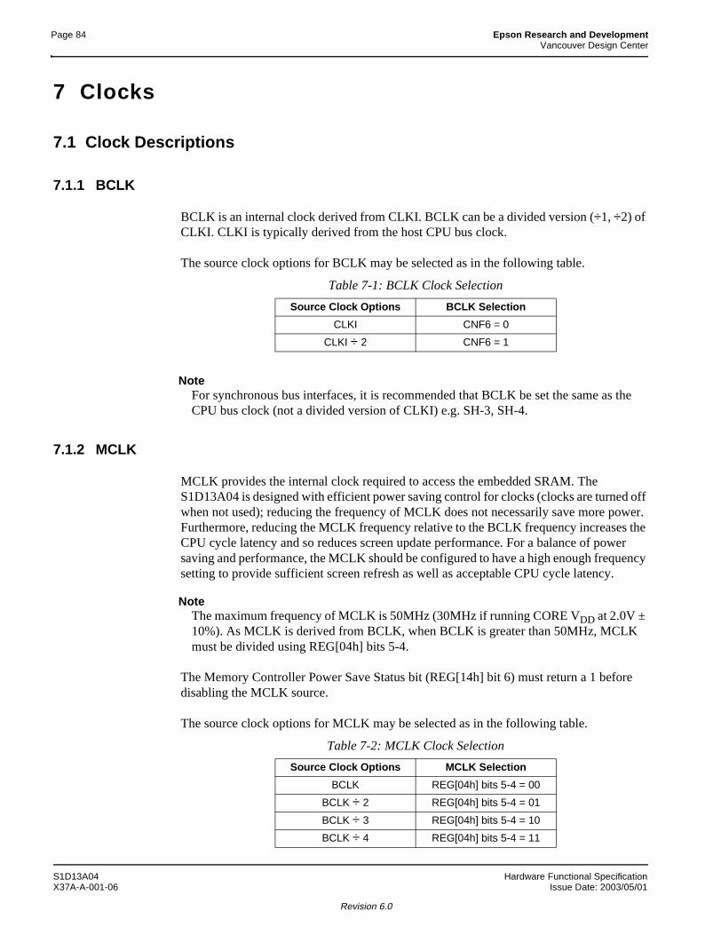
Page 84 Epson Research and DevelopmentVancouver Design Center
7 Clocks
7.1 Clock Descriptions
7.1.1 BCLK
BCLK is an internal clock derived from CLKI. BCLK can be a divided version (÷1, ÷2) of CLKI. CLKI is typically derived from the host CPU bus clock.
The source clock options for BCLK may be selected as in the following table.
NoteFor synchronous bus interfaces, it is recommended that BCLK be set the same as the CPU bus clock (not a divided version of CLKI) e.g. SH-3, SH-4.
7.1.2 MCLK
MCLK provides the internal clock required to access the embedded SRAM. The S1D13A04 is designed with efficient power saving control for clocks (clocks are turned off when not used); reducing the frequency of MCLK does not necessarily save more power. Furthermore, reducing the MCLK frequency relative to the BCLK frequency increases the CPU cycle latency and so reduces screen update performance. For a balance of power saving and performance, the MCLK should be configured to have a high enough frequency setting to provide sufficient screen refresh as well as acceptable CPU cycle latency.
NoteThe maximum frequency of MCLK is 50MHz (30MHz if running CORE VDD at 2.0V ± 10%). As MCLK is derived from BCLK, when BCLK is greater than 50MHz, MCLK must be divided using REG[04h] bits 5-4.
The Memory Controller Power Save Status bit (REG[14h] bit 6) must return a 1 before disabling the MCLK source.
The source clock options for MCLK may be selected as in the following table.
Table 7-1: BCLK Clock Selection
Source Clock Options BCLK Selection
CLKI CNF6 = 0
CLKI ÷ 2 CNF6 = 1
Table 7-2: MCLK Clock Selection
Source Clock Options MCLK Selection
BCLK REG[04h] bits 5-4 = 00
BCLK ÷ 2 REG[04h] bits 5-4 = 01
BCLK ÷ 3 REG[04h] bits 5-4 = 10
BCLK ÷ 4 REG[04h] bits 5-4 = 11
S1D13A04 Hardware Functional SpecificationX37A-A-001-06 Issue Date: 2003/05/01
Revision 6.0
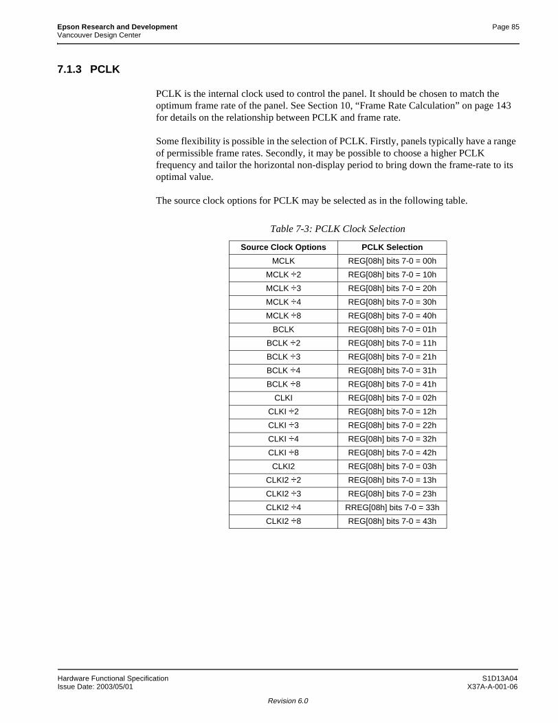
Epson Research and Development Page 85Vancouver Design Center
7.1.3 PCLK
PCLK is the internal clock used to control the panel. It should be chosen to match the optimum frame rate of the panel. See Section 10, “Frame Rate Calculation” on page 143 for details on the relationship between PCLK and frame rate.
Some flexibility is possible in the selection of PCLK. Firstly, panels typically have a range of permissible frame rates. Secondly, it may be possible to choose a higher PCLK frequency and tailor the horizontal non-display period to bring down the frame-rate to its optimal value.
The source clock options for PCLK may be selected as in the following table.
Table 7-3: PCLK Clock Selection
Source Clock Options PCLK Selection
MCLK REG[08h] bits 7-0 = 00h
MCLK ÷2 REG[08h] bits 7-0 = 10h
MCLK ÷3 REG[08h] bits 7-0 = 20h
MCLK ÷4 REG[08h] bits 7-0 = 30h
MCLK ÷8 REG[08h] bits 7-0 = 40h
BCLK REG[08h] bits 7-0 = 01h
BCLK ÷2 REG[08h] bits 7-0 = 11h
BCLK ÷3 REG[08h] bits 7-0 = 21h
BCLK ÷4 REG[08h] bits 7-0 = 31h
BCLK ÷8 REG[08h] bits 7-0 = 41h
CLKI REG[08h] bits 7-0 = 02h
CLKI ÷2 REG[08h] bits 7-0 = 12h
CLKI ÷3 REG[08h] bits 7-0 = 22h
CLKI ÷4 REG[08h] bits 7-0 = 32h
CLKI ÷8 REG[08h] bits 7-0 = 42h
CLKI2 REG[08h] bits 7-0 = 03h
CLKI2 ÷2 REG[08h] bits 7-0 = 13h
CLKI2 ÷3 REG[08h] bits 7-0 = 23h
CLKI2 ÷4 RREG[08h] bits 7-0 = 33h
CLKI2 ÷8 REG[08h] bits 7-0 = 43h
Hardware Functional Specification S1D13A04Issue Date: 2003/05/01 X37A-A-001-06
Revision 6.0
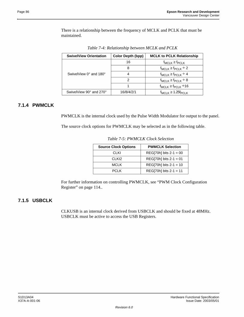
Page 86 Epson Research and DevelopmentVancouver Design Center
There is a relationship between the frequency of MCLK and PCLK that must be maintained.
7.1.4 PWMCLK
PWMCLK is the internal clock used by the Pulse Width Modulator for output to the panel.
The source clock options for PWMCLK may be selected as in the following table.
For further information on controlling PWMCLK, see “PWM Clock Configuration Register” on page 114..
7.1.5 USBCLK
CLKUSB is an internal clock derived from USBCLK and should be fixed at 48MHz. USBCLK must be active to access the USB Registers.
Table 7-4: Relationship between MCLK and PCLK
SwivelView Orientation Color Depth (bpp) MCLK to PCLK Relationship
SwivelView 0° and 180°
16 fMCLK ≥ fPCLK
8 fMCLK ≥ fPCLK ÷ 24 fMCLK ≥ fPCLK ÷ 42 fMCLK ≥ fPCLK ÷ 81 fMCLK ≥ fPCLK ÷16
SwivelView 90° and 270° 16/8/4/2/1 fMCLK ≥ 1.25fPCLK
Table 7-5: PWMCLK Clock Selection
Source Clock Options PWMCLK Selection
CLKI REG[70h] bits 2-1 = 00
CLKI2 REG[70h] bits 2-1 = 01
MCLK REG[70h] bits 2-1 = 10
PCLK REG[70h] bits 2-1 = 11
S1D13A04 Hardware Functional SpecificationX37A-A-001-06 Issue Date: 2003/05/01
Revision 6.0
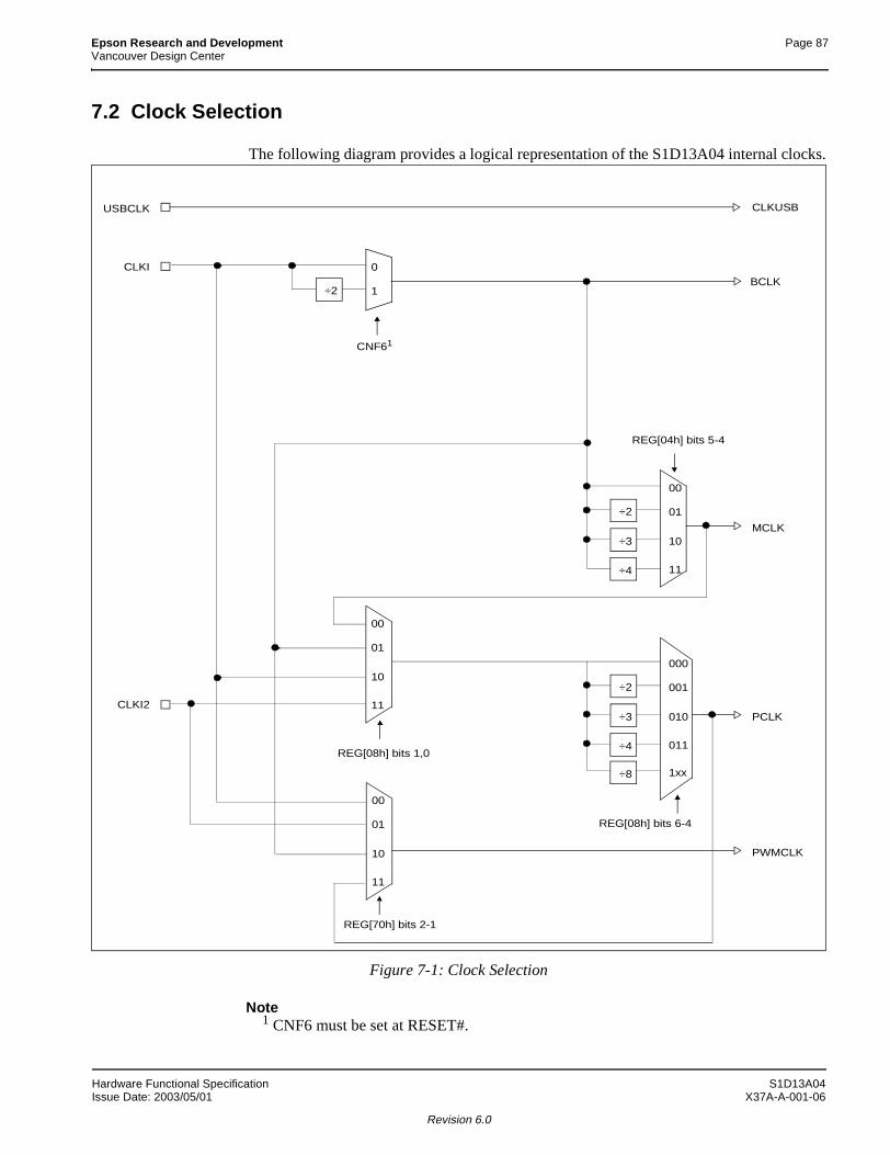
Epson Research and Development Page 87Vancouver Design Center
7.2 Clock Selection
The following diagram provides a logical representation of the S1D13A04 internal clocks.
Figure 7-1: Clock Selection
Note1 CNF6 must be set at RESET#.
CLKI
CLKI2
÷2
0
1BCLK
÷2
÷3
÷4
00
01
10
11
MCLK
00
01
10
11
÷2
÷3
÷4
000
001
010
011
÷8 1xx
PCLK
PWMCLK
REG[08h] bits 1,0
REG[70h] bits 2-1
REG[08h] bits 6-4
REG[04h] bits 5-4
CNF61
CLKUSBUSBCLK
00
01
10
11
Hardware Functional Specification S1D13A04Issue Date: 2003/05/01 X37A-A-001-06
Revision 6.0
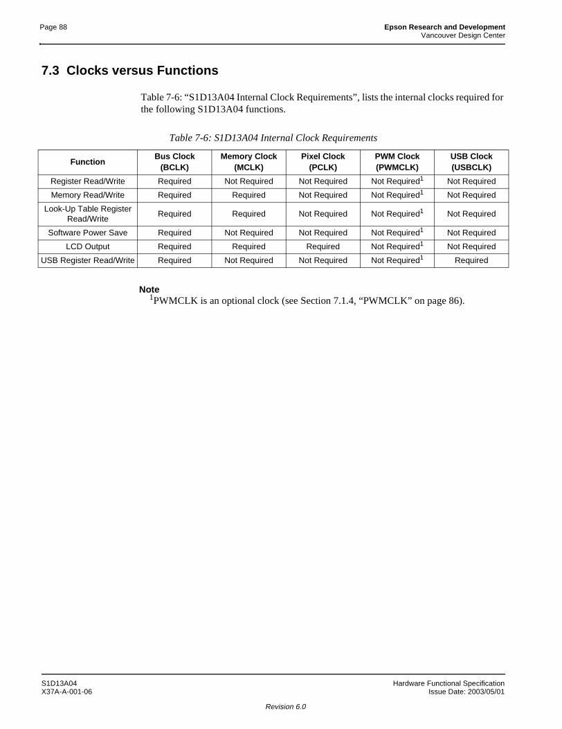
Page 88 Epson Research and DevelopmentVancouver Design Center
7.3 Clocks versus Functions
Table 7-6: “S1D13A04 Internal Clock Requirements”, lists the internal clocks required for the following S1D13A04 functions.
Note1PWMCLK is an optional clock (see Section 7.1.4, “PWMCLK” on page 86).
Table 7-6: S1D13A04 Internal Clock Requirements
FunctionBus Clock
(BCLK)Memory Clock
(MCLK)Pixel Clock
(PCLK)PWM Clock (PWMCLK)
USB Clock(USBCLK)
Register Read/Write Required Not Required Not Required Not Required1 Not Required
Memory Read/Write Required Required Not Required Not Required1 Not Required
Look-Up Table Register Read/Write
Required Required Not Required Not Required1 Not Required
Software Power Save Required Not Required Not Required Not Required1 Not Required
LCD Output Required Required Required Not Required1 Not Required
USB Register Read/Write Required Not Required Not Required Not Required1 Required
S1D13A04 Hardware Functional SpecificationX37A-A-001-06 Issue Date: 2003/05/01
Revision 6.0
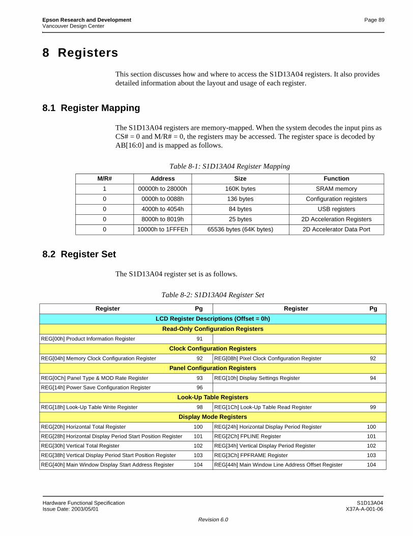
Epson Research and Development Page 89Vancouver Design Center
8 Registers
This section discusses how and where to access the S1D13A04 registers. It also provides detailed information about the layout and usage of each register.
8.1 Register Mapping
The S1D13A04 registers are memory-mapped. When the system decodes the input pins as CS# = 0 and M/R# = 0, the registers may be accessed. The register space is decoded by AB[16:0] and is mapped as follows.
8.2 Register Set
The S1D13A04 register set is as follows.
Table 8-1: S1D13A04 Register Mapping
M/R# Address Size Function
1 00000h to 28000h 160K bytes SRAM memory
0 0000h to 0088h 136 bytes Configuration registers
0 4000h to 4054h 84 bytes USB registers
0 8000h to 8019h 25 bytes 2D Acceleration Registers
0 10000h to 1FFFEh 65536 bytes (64K bytes) 2D Accelerator Data Port
Table 8-2: S1D13A04 Register Set
Register Pg Register Pg
LCD Register Descriptions (Offset = 0h)
Read-Only Configuration Registers
REG[00h] Product Information Register 91
Clock Configuration Registers
REG[04h] Memory Clock Configuration Register 92 REG[08h] Pixel Clock Configuration Register 92
Panel Configuration Registers
REG[0Ch] Panel Type & MOD Rate Register 93 REG[10h] Display Settings Register 94
REG[14h] Power Save Configuration Register 96
Look-Up Table Registers
REG[18h] Look-Up Table Write Register 98 REG[1Ch] Look-Up Table Read Register 99
Display Mode Registers
REG[20h] Horizontal Total Register 100 REG[24h] Horizontal Display Period Register 100
REG[28h] Horizontal Display Period Start Position Register 101 REG[2Ch] FPLINE Register 101
REG[30h] Vertical Total Register 102 REG[34h] Vertical Display Period Register 102
REG[38h] Vertical Display Period Start Position Register 103 REG[3Ch] FPFRAME Register 103
REG[40h] Main Window Display Start Address Register 104 REG[44h] Main Window Line Address Offset Register 104
Hardware Functional Specification S1D13A04Issue Date: 2003/05/01 X37A-A-001-06
Revision 6.0
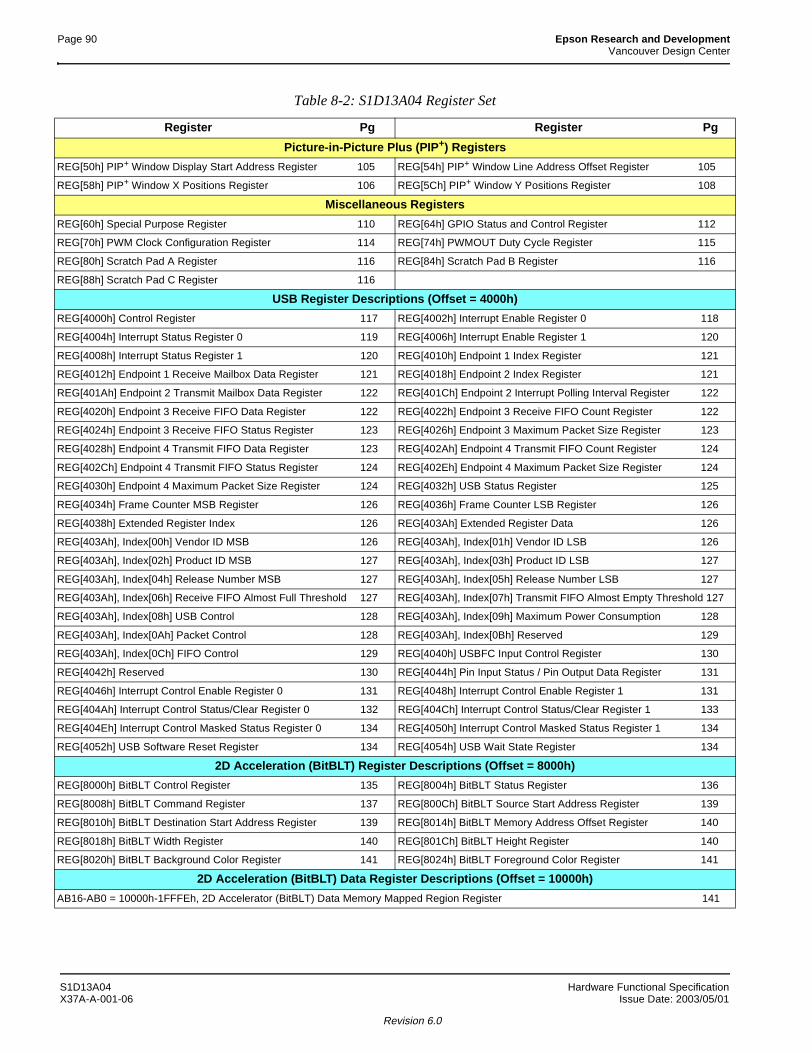
Page 90 Epson Research and DevelopmentVancouver Design Center
Picture-in-Picture Plus (PIP+) Registers
REG[50h] PIP+ Window Display Start Address Register 105 REG[54h] PIP+ Window Line Address Offset Register 105
REG[58h] PIP+ Window X Positions Register 106 REG[5Ch] PIP+ Window Y Positions Register 108
Miscellaneous Registers
REG[60h] Special Purpose Register 110 REG[64h] GPIO Status and Control Register 112
REG[70h] PWM Clock Configuration Register 114 REG[74h] PWMOUT Duty Cycle Register 115
REG[80h] Scratch Pad A Register 116 REG[84h] Scratch Pad B Register 116
REG[88h] Scratch Pad C Register 116
USB Register Descriptions (Offset = 4000h)
REG[4000h] Control Register 117 REG[4002h] Interrupt Enable Register 0 118
REG[4004h] Interrupt Status Register 0 119 REG[4006h] Interrupt Enable Register 1 120
REG[4008h] Interrupt Status Register 1 120 REG[4010h] Endpoint 1 Index Register 121
REG[4012h] Endpoint 1 Receive Mailbox Data Register 121 REG[4018h] Endpoint 2 Index Register 121
REG[401Ah] Endpoint 2 Transmit Mailbox Data Register 122 REG[401Ch] Endpoint 2 Interrupt Polling Interval Register 122
REG[4020h] Endpoint 3 Receive FIFO Data Register 122 REG[4022h] Endpoint 3 Receive FIFO Count Register 122
REG[4024h] Endpoint 3 Receive FIFO Status Register 123 REG[4026h] Endpoint 3 Maximum Packet Size Register 123
REG[4028h] Endpoint 4 Transmit FIFO Data Register 123 REG[402Ah] Endpoint 4 Transmit FIFO Count Register 124
REG[402Ch] Endpoint 4 Transmit FIFO Status Register 124 REG[402Eh] Endpoint 4 Maximum Packet Size Register 124
REG[4030h] Endpoint 4 Maximum Packet Size Register 124 REG[4032h] USB Status Register 125
REG[4034h] Frame Counter MSB Register 126 REG[4036h] Frame Counter LSB Register 126
REG[4038h] Extended Register Index 126 REG[403Ah] Extended Register Data 126
REG[403Ah], Index[00h] Vendor ID MSB 126 REG[403Ah], Index[01h] Vendor ID LSB 126
REG[403Ah], Index[02h] Product ID MSB 127 REG[403Ah], Index[03h] Product ID LSB 127
REG[403Ah], Index[04h] Release Number MSB 127 REG[403Ah], Index[05h] Release Number LSB 127
REG[403Ah], Index[06h] Receive FIFO Almost Full Threshold 127 REG[403Ah], Index[07h] Transmit FIFO Almost Empty Threshold 127
REG[403Ah], Index[08h] USB Control 128 REG[403Ah], Index[09h] Maximum Power Consumption 128
REG[403Ah], Index[0Ah] Packet Control 128 REG[403Ah], Index[0Bh] Reserved 129
REG[403Ah], Index[0Ch] FIFO Control 129 REG[4040h] USBFC Input Control Register 130
REG[4042h] Reserved 130 REG[4044h] Pin Input Status / Pin Output Data Register 131
REG[4046h] Interrupt Control Enable Register 0 131 REG[4048h] Interrupt Control Enable Register 1 131
REG[404Ah] Interrupt Control Status/Clear Register 0 132 REG[404Ch] Interrupt Control Status/Clear Register 1 133
REG[404Eh] Interrupt Control Masked Status Register 0 134 REG[4050h] Interrupt Control Masked Status Register 1 134
REG[4052h] USB Software Reset Register 134 REG[4054h] USB Wait State Register 134
2D Acceleration (BitBLT) Register Descriptions (Offset = 8000h)
REG[8000h] BitBLT Control Register 135 REG[8004h] BitBLT Status Register 136
REG[8008h] BitBLT Command Register 137 REG[800Ch] BitBLT Source Start Address Register 139
REG[8010h] BitBLT Destination Start Address Register 139 REG[8014h] BitBLT Memory Address Offset Register 140
REG[8018h] BitBLT Width Register 140 REG[801Ch] BitBLT Height Register 140
REG[8020h] BitBLT Background Color Register 141 REG[8024h] BitBLT Foreground Color Register 141
2D Acceleration (BitBLT) Data Register Descriptions (Offset = 10000h)
AB16-AB0 = 10000h-1FFFEh, 2D Accelerator (BitBLT) Data Memory Mapped Region Register 141
Table 8-2: S1D13A04 Register Set
Register Pg Register Pg
S1D13A04 Hardware Functional SpecificationX37A-A-001-06 Issue Date: 2003/05/01
Revision 6.0
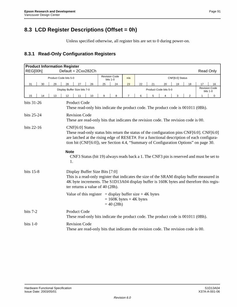
Epson Research and Development Page 91Vancouver Design Center
8.3 LCD Register Descriptions (Offset = 0h)
Unless specified otherwise, all register bits are set to 0 during power-on.
8.3.1 Read-Only Configuration Registers
bits 31-26 Product CodeThese read-only bits indicate the product code. The product code is 001011 (0Bh).
bits 25-24 Revision CodeThese are read-only bits that indicates the revision code. The revision code is 00.
bits 22-16 CNF[6:0] StatusThese read-only status bits return the status of the configuration pins CNF[6:0]. CNF[6:0] are latched at the rising edge of RESET#. For a functional description of each configura-tion bit (CNF[6:0]), see Section 4.4, “Summary of Configuration Options” on page 30.
NoteCNF3 Status (bit 19) always reads back a 1. The CNF3 pin is reserved and must be set to 1.
bits 15-8 Display Buffer Size Bits [7:0]This is a read-only register that indicates the size of the SRAM display buffer measured in 4K byte increments. The S1D13A04 display buffer is 160K bytes and therefore this regis-ter returns a value of 40 (28h).
Value of this register = display buffer size ÷ 4K bytes= 160K bytes ÷ 4K bytes= 40 (28h)
bits 7-2 Product CodeThese read-only bits indicate the product code. The product code is 001011 (0Bh).
bits 1-0 Revision CodeThese are read-only bits that indicates the revision code. The revision code is 00.
Product Information RegisterREG[00h] Default = 2Cxx282Ch Read Only
Product Code bits 5-0 Revision Code bits 1-0 n/a CNF[6:0] Status
31 30 29 28 27 26 25 24 23 22 21 20 19 18 17 16
Display Buffer Size bits 7-0 Product Code bits 5-0 Revision Code bits 1-0
15 14 13 12 11 10 9 8 7 6 5 4 3 2 1 0
Hardware Functional Specification S1D13A04Issue Date: 2003/05/01 X37A-A-001-06
Revision 6.0
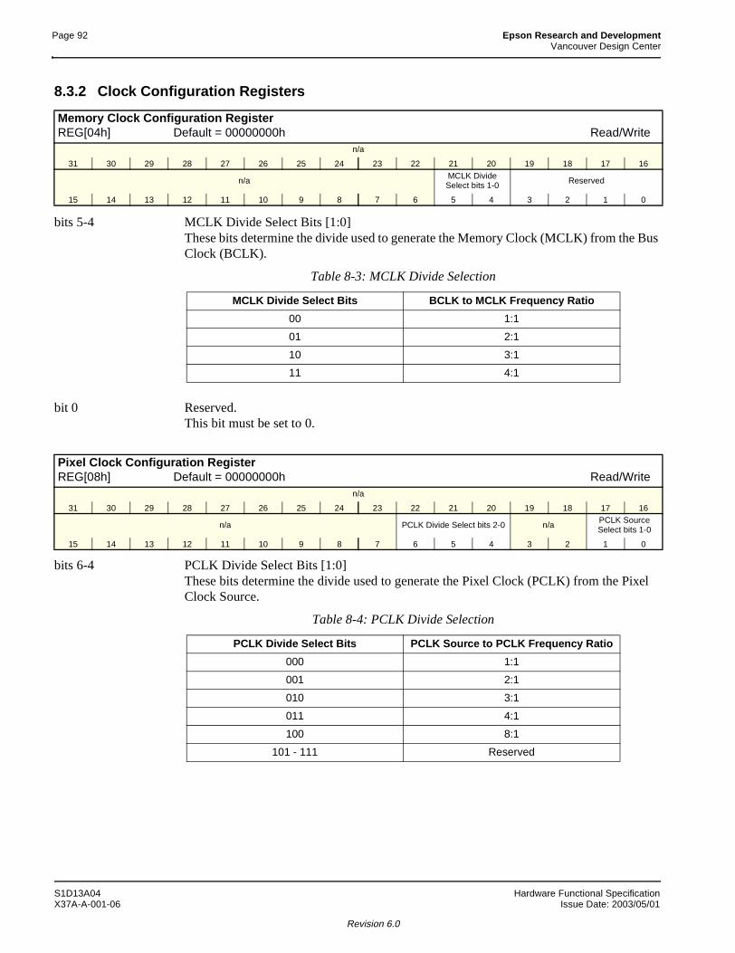
Page 92 Epson Research and DevelopmentVancouver Design Center
8.3.2 Clock Configuration Registers
bits 5-4 MCLK Divide Select Bits [1:0]These bits determine the divide used to generate the Memory Clock (MCLK) from the Bus Clock (BCLK).
bit 0 Reserved.This bit must be set to 0.
bits 6-4 PCLK Divide Select Bits [1:0]These bits determine the divide used to generate the Pixel Clock (PCLK) from the Pixel Clock Source.
Memory Clock Configuration RegisterREG[04h] Default = 00000000h Read/Write
n/a
31 30 29 28 27 26 25 24 23 22 21 20 19 18 17 16
n/a MCLK Divide Select bits 1-0 Reserved
15 14 13 12 11 10 9 8 7 6 5 4 3 2 1 0
Table 8-3: MCLK Divide Selection
MCLK Divide Select Bits BCLK to MCLK Frequency Ratio
00 1:1
01 2:1
10 3:1
11 4:1
Pixel Clock Configuration RegisterREG[08h] Default = 00000000h Read/Write
n/a
31 30 29 28 27 26 25 24 23 22 21 20 19 18 17 16
n/a PCLK Divide Select bits 2-0 n/aPCLK Source Select bits 1-0
15 14 13 12 11 10 9 8 7 6 5 4 3 2 1 0
Table 8-4: PCLK Divide Selection
PCLK Divide Select Bits PCLK Source to PCLK Frequency Ratio
000 1:1
001 2:1
010 3:1
011 4:1
100 8:1
101 - 111 Reserved
S1D13A04 Hardware Functional SpecificationX37A-A-001-06 Issue Date: 2003/05/01
Revision 6.0
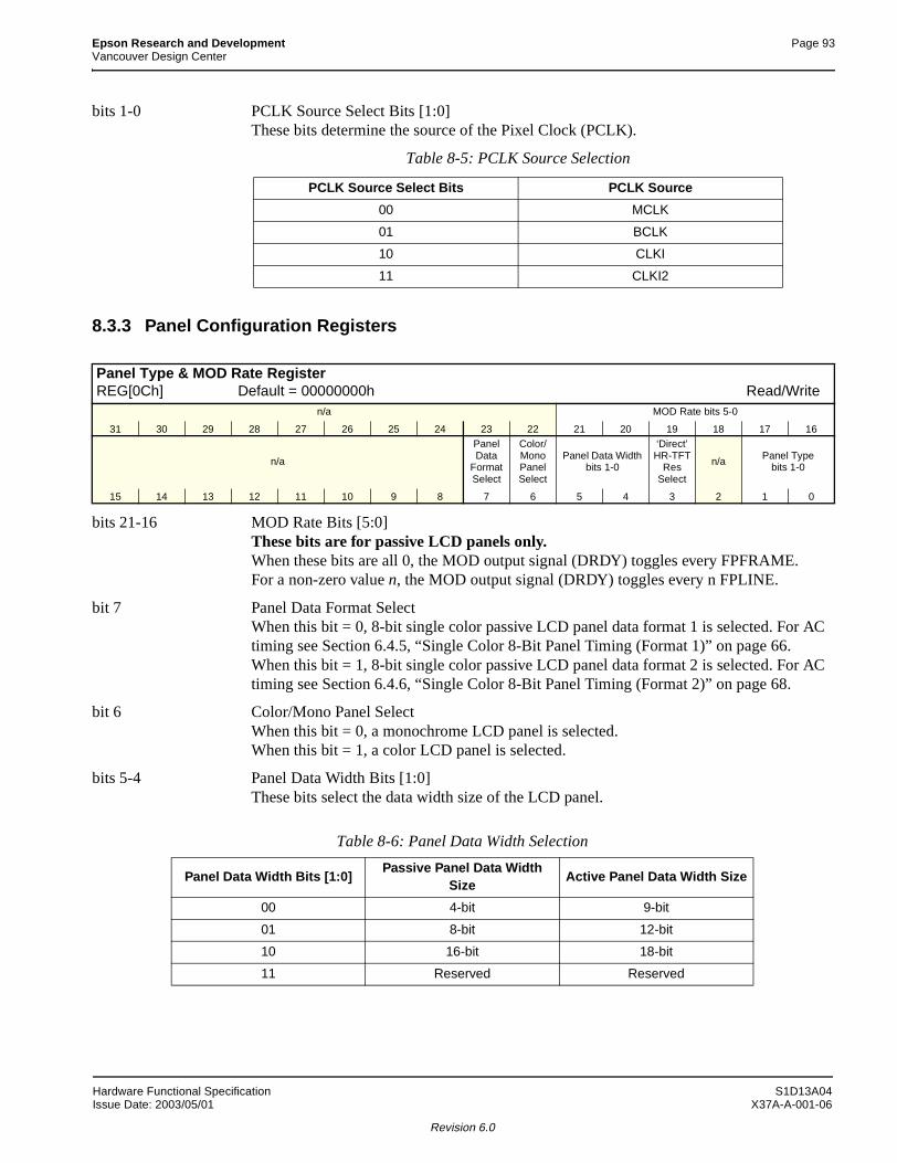
Epson Research and Development Page 93Vancouver Design Center
bits 1-0 PCLK Source Select Bits [1:0]These bits determine the source of the Pixel Clock (PCLK).
8.3.3 Panel Configuration Registers
bits 21-16 MOD Rate Bits [5:0]These bits are for passive LCD panels only.When these bits are all 0, the MOD output signal (DRDY) toggles every FPFRAME. For a non-zero value n, the MOD output signal (DRDY) toggles every n FPLINE.
bit 7 Panel Data Format SelectWhen this bit = 0, 8-bit single color passive LCD panel data format 1 is selected. For AC timing see Section 6.4.5, “Single Color 8-Bit Panel Timing (Format 1)” on page 66.When this bit = 1, 8-bit single color passive LCD panel data format 2 is selected. For AC timing see Section 6.4.6, “Single Color 8-Bit Panel Timing (Format 2)” on page 68.
bit 6 Color/Mono Panel SelectWhen this bit = 0, a monochrome LCD panel is selected.When this bit = 1, a color LCD panel is selected.
bits 5-4 Panel Data Width Bits [1:0]These bits select the data width size of the LCD panel.
Table 8-5: PCLK Source Selection
PCLK Source Select Bits PCLK Source
00 MCLK
01 BCLK
10 CLKI
11 CLKI2
Panel Type & MOD Rate RegisterREG[0Ch] Default = 00000000h Read/Write
n/a MOD Rate bits 5-0
31 30 29 28 27 26 25 24 23 22 21 20 19 18 17 16
n/a
Panel Data
Format Select
Color/Mono Panel Select
Panel Data Width bits 1-0
‘Direct’ HR-TFT
Res Select
n/a Panel Typebits 1-0
15 14 13 12 11 10 9 8 7 6 5 4 3 2 1 0
Table 8-6: Panel Data Width Selection
Panel Data Width Bits [1:0]Passive Panel Data Width
SizeActive Panel Data Width Size
00 4-bit 9-bit
01 8-bit 12-bit
10 16-bit 18-bit
11 Reserved Reserved
Hardware Functional Specification S1D13A04Issue Date: 2003/05/01 X37A-A-001-06
Revision 6.0
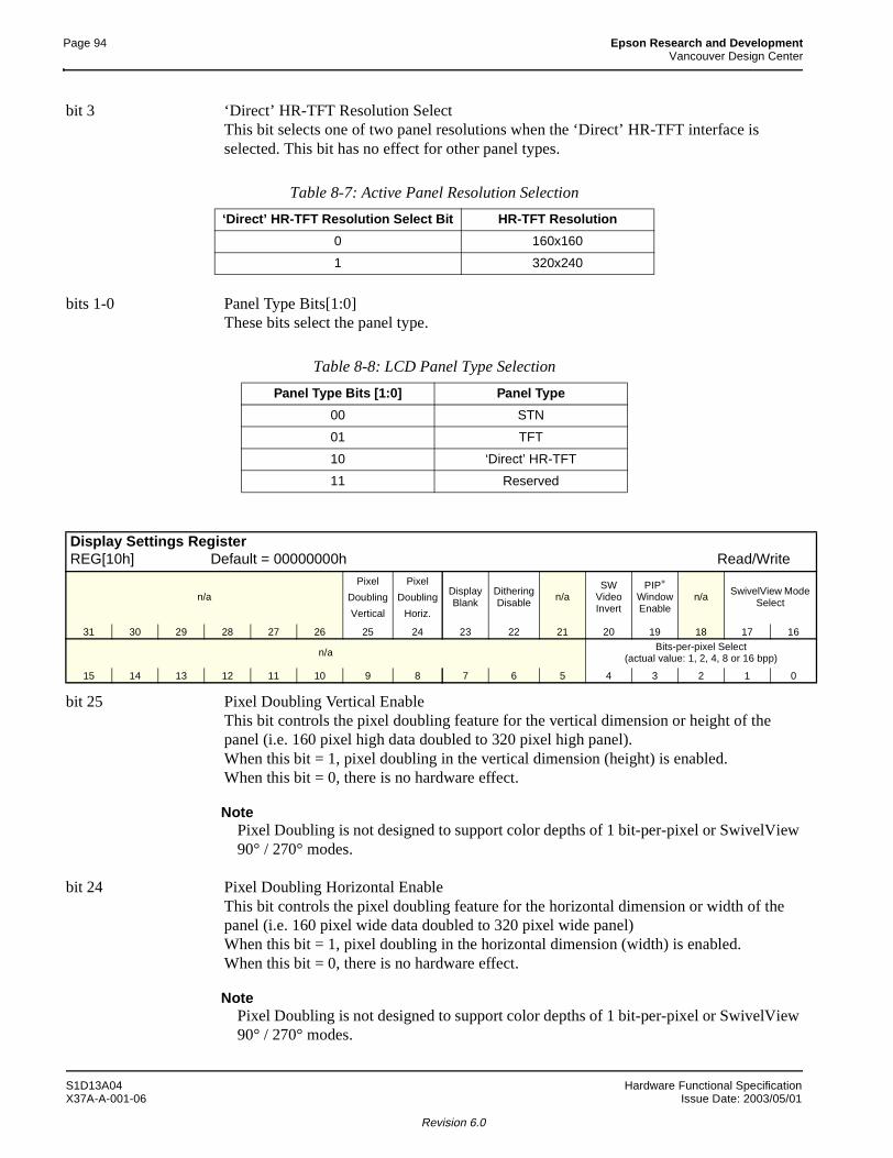
Page 94 Epson Research and DevelopmentVancouver Design Center
bit 3 ‘Direct’ HR-TFT Resolution SelectThis bit selects one of two panel resolutions when the ‘Direct’ HR-TFT interface is selected. This bit has no effect for other panel types.
bits 1-0 Panel Type Bits[1:0]These bits select the panel type.
bit 25 Pixel Doubling Vertical EnableThis bit controls the pixel doubling feature for the vertical dimension or height of the panel (i.e. 160 pixel high data doubled to 320 pixel high panel).When this bit = 1, pixel doubling in the vertical dimension (height) is enabled.When this bit = 0, there is no hardware effect.
NotePixel Doubling is not designed to support color depths of 1 bit-per-pixel or SwivelView 90° / 270° modes.
bit 24 Pixel Doubling Horizontal EnableThis bit controls the pixel doubling feature for the horizontal dimension or width of the panel (i.e. 160 pixel wide data doubled to 320 pixel wide panel)When this bit = 1, pixel doubling in the horizontal dimension (width) is enabled.When this bit = 0, there is no hardware effect.
NotePixel Doubling is not designed to support color depths of 1 bit-per-pixel or SwivelView 90° / 270° modes.
Table 8-7: Active Panel Resolution Selection
‘Direct’ HR-TFT Resolution Select Bit HR-TFT Resolution
0 160x160
1 320x240
Table 8-8: LCD Panel Type Selection
Panel Type Bits [1:0] Panel Type
00 STN
01 TFT
10 ‘Direct’ HR-TFT
11 Reserved
Display Settings RegisterREG[10h] Default = 00000000h Read/Write
n/a
Pixel
Doubling
Vertical
Pixel
Doubling
Horiz.
Display Blank
Dithering Disable
n/aSW
Video Invert
PIP+ Window Enable
n/a SwivelView Mode Select
31 30 29 28 27 26 25 24 23 22 21 20 19 18 17 16
n/a Bits-per-pixel Select(actual value: 1, 2, 4, 8 or 16 bpp)
15 14 13 12 11 10 9 8 7 6 5 4 3 2 1 0
S1D13A04 Hardware Functional SpecificationX37A-A-001-06 Issue Date: 2003/05/01
Revision 6.0
Epson Research and Development Page 95Vancouver Design Center
bit 23 Display BlankWhen this bit = 0, the LCD display pipeline is enabled.When this bit = 1, the LCD display pipeline is disabled and all LCD data outputs are forced to zero (i.e., the screen is blanked).
bit 22 Dithering DisableWhen this bit = 0, dithering on the passive LCD panel is enabled, allowing a maximum of 64K colors (218) or 64 gray shades in 1/2/4/8 bpp mode. In 16bpp mode, only 64K colors (216) can also be achieved.When this bit = 1, dithering on the passive LCD panel is disabled, allowing a maximum of 4096 colors (212) or 16 gray shades.The dithering algorithm provides more shades of each primary color.
NoteFor a summary of the results of dithering for each color depth, see Table 8-10: “LCD Bit-per-pixel Selection,” on page 96.
bit 20 Software Video InvertWhen this bit = 0, video data is normal.When this bit = 1, video data is inverted.
NoteVideo data is inverted after the Look-Up Table
bit 19 PIP+ Window EnableThis bit enables a PIP+ window within the main window. The location of the PIP+ win-dow within the landscape window is determined by the PIP+ X Position register (REG[58h]) and PIP+ Y Position register (REG[5Ch]). The PIP+ window has its own Dis-play Start Address register (REG[50h]) and Memory Address Offset register (REG[54h]). The PIP+ window shares the same color depth and SwivelViewTM orientation as the main window.When this bit = 1, the PIP+ window is enabled.When this bit = 0, the PIP+ window is disabled.
bit 17-16 SwivelView Mode Select Bits [1:0]These bits select different SwivelViewTM orientations:
Table 8-9: SwivelViewTM Mode Select Options
SwivelView Mode Select Bits SwivelView Orientation
00 0° (Normal)
01 90°
10 180°
11 270°
Hardware Functional Specification S1D13A04Issue Date: 2003/05/01 X37A-A-001-06
Revision 6.0
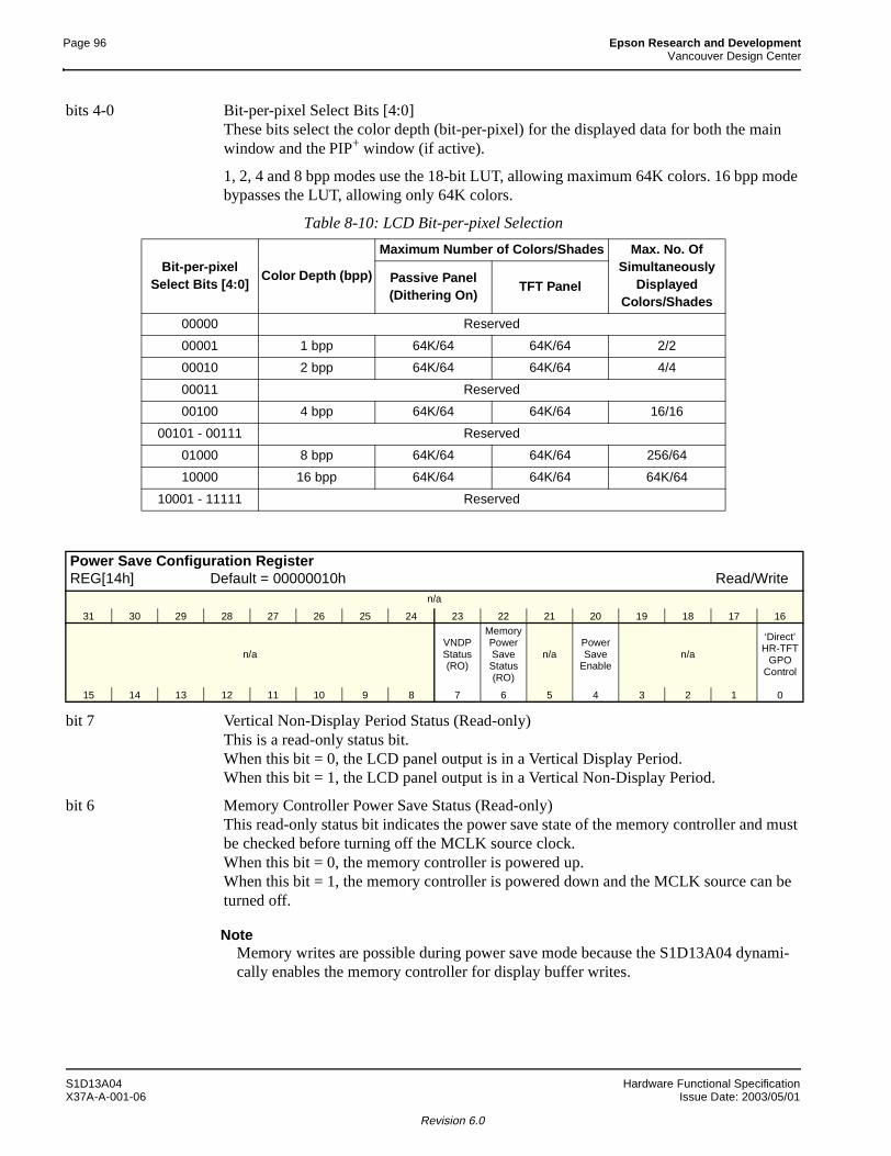
Page 96 Epson Research and DevelopmentVancouver Design Center
bits 4-0 Bit-per-pixel Select Bits [4:0]These bits select the color depth (bit-per-pixel) for the displayed data for both the main window and the PIP+ window (if active).
1, 2, 4 and 8 bpp modes use the 18-bit LUT, allowing maximum 64K colors. 16 bpp mode bypasses the LUT, allowing only 64K colors.
bit 7 Vertical Non-Display Period Status (Read-only)This is a read-only status bit.When this bit = 0, the LCD panel output is in a Vertical Display Period. When this bit = 1, the LCD panel output is in a Vertical Non-Display Period.
bit 6 Memory Controller Power Save Status (Read-only)This read-only status bit indicates the power save state of the memory controller and must be checked before turning off the MCLK source clock.When this bit = 0, the memory controller is powered up.When this bit = 1, the memory controller is powered down and the MCLK source can be turned off.
NoteMemory writes are possible during power save mode because the S1D13A04 dynami-cally enables the memory controller for display buffer writes.
Table 8-10: LCD Bit-per-pixel Selection
Bit-per-pixel Select Bits [4:0]
Color Depth (bpp)
Maximum Number of Colors/Shades Max. No. Of Simultaneously
Displayed Colors/Shades
Passive Panel (Dithering On)
TFT Panel
00000 Reserved
00001 1 bpp 64K/64 64K/64 2/2
00010 2 bpp 64K/64 64K/64 4/4
00011 Reserved
00100 4 bpp 64K/64 64K/64 16/16
00101 - 00111 Reserved
01000 8 bpp 64K/64 64K/64 256/64
10000 16 bpp 64K/64 64K/64 64K/64
10001 - 11111 Reserved
Power Save Configuration RegisterREG[14h] Default = 00000010h Read/Write
n/a
31 30 29 28 27 26 25 24 23 22 21 20 19 18 17 16
n/aVNDP Status (RO)
Memory Power Save Status (RO)
n/aPower Save
Enablen/a
‘Direct’ HR-TFT
GPO Control
15 14 13 12 11 10 9 8 7 6 5 4 3 2 1 0
S1D13A04 Hardware Functional SpecificationX37A-A-001-06 Issue Date: 2003/05/01
Revision 6.0
Epson Research and Development Page 97Vancouver Design Center
bit 4 Power Save Mode EnableWhen this bit = 1, the software initiated power save mode is enabled.When this bit = 0, the software initiated power save mode is disabled.At reset, this bit is set to 1. For a summary of Power Save Mode, see Section 15, “Power Save Mode” on page 159.
NoteMemory writes are possible during power save mode because the S1D13A04 dynami-cally enables the memory controller for display buffer writes.
Power Considerations:The S1D13A04 may experience higher than normal Quiescent Current immediately after applying power. To prevent this condition, the following start up sequence must be followed:
1. Power-up/Reset the S1D13A04.
2. Initialize all registers.
3. Disable power save mode (set REG[14h] bit 4 to 0)
NoteBy default, Power Save Mode is enabled (equal to 1) after power-up/Reset. If it is desir-able/necessary to remain in power save mode for any length of time after power-up/Re-set, the above described condition can be prevented by performing a R/W access to the embedded memory.
bit 0 ‘Direct’ HR-TFT LCD Interface GPO ControlThis bit is for HR-TFT panels only. For all other panel types, this bit has no effect. When the ‘direct’ HR-TFT LCD interface is selected (REG[0Ch] bits 1-0 = 10), the DRDY pin becomes a general purpose output (GPO). This GPO can be used to control the HR-TFT MOD signal.When this bit = 0, DRDY (GPO) is forced low.When this bit = 1, DRDY (GPO) is forced high.
Hardware Functional Specification S1D13A04Issue Date: 2003/05/01 X37A-A-001-06
Revision 6.0
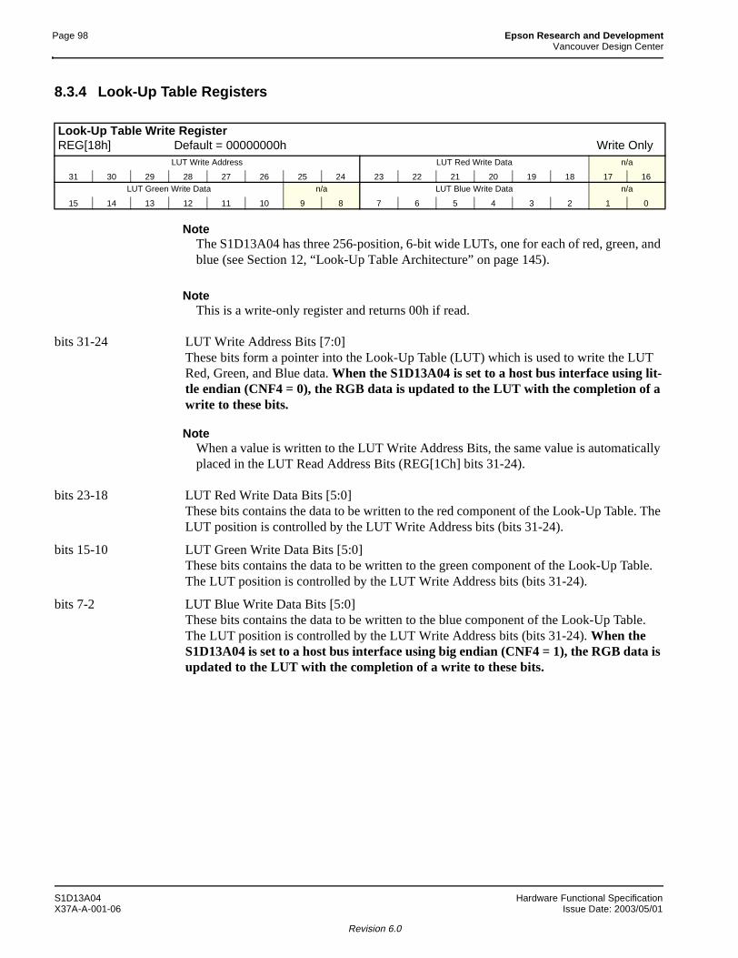
Page 98 Epson Research and DevelopmentVancouver Design Center
8.3.4 Look-Up Table Registers
NoteThe S1D13A04 has three 256-position, 6-bit wide LUTs, one for each of red, green, and blue (see Section 12, “Look-Up Table Architecture” on page 145).
NoteThis is a write-only register and returns 00h if read.
bits 31-24 LUT Write Address Bits [7:0]These bits form a pointer into the Look-Up Table (LUT) which is used to write the LUT Red, Green, and Blue data. When the S1D13A04 is set to a host bus interface using lit-tle endian (CNF4 = 0), the RGB data is updated to the LUT with the completion of a write to these bits.
NoteWhen a value is written to the LUT Write Address Bits, the same value is automatically placed in the LUT Read Address Bits (REG[1Ch] bits 31-24).
bits 23-18 LUT Red Write Data Bits [5:0]These bits contains the data to be written to the red component of the Look-Up Table. The LUT position is controlled by the LUT Write Address bits (bits 31-24).
bits 15-10 LUT Green Write Data Bits [5:0]These bits contains the data to be written to the green component of the Look-Up Table. The LUT position is controlled by the LUT Write Address bits (bits 31-24).
bits 7-2 LUT Blue Write Data Bits [5:0]These bits contains the data to be written to the blue component of the Look-Up Table. The LUT position is controlled by the LUT Write Address bits (bits 31-24). When the S1D13A04 is set to a host bus interface using big endian (CNF4 = 1), the RGB data is updated to the LUT with the completion of a write to these bits.
Look-Up Table Write RegisterREG[18h] Default = 00000000h Write Only
LUT Write Address LUT Red Write Data n/a
31 30 29 28 27 26 25 24 23 22 21 20 19 18 17 16LUT Green Write Data n/a LUT Blue Write Data n/a
15 14 13 12 11 10 9 8 7 6 5 4 3 2 1 0
S1D13A04 Hardware Functional SpecificationX37A-A-001-06 Issue Date: 2003/05/01
Revision 6.0
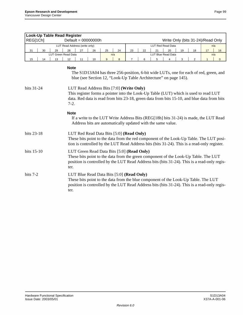
Epson Research and Development Page 99Vancouver Design Center
NoteThe S1D13A04 has three 256-position, 6-bit wide LUTs, one for each of red, green, and blue (see Section 12, “Look-Up Table Architecture” on page 145).
bits 31-24 LUT Read Address Bits [7:0] (Write Only)This register forms a pointer into the Look-Up Table (LUT) which is used to read LUT data. Red data is read from bits 23-18, green data from bits 15-10, and blue data from bits 7-2.
NoteIf a write to the LUT Write Address Bits (REG[18h] bits 31-24) is made, the LUT Read Address bits are automatically updated with the same value.
bits 23-18 LUT Red Read Data Bits [5:0] (Read Only)These bits point to the data from the red component of the Look-Up Table. The LUT posi-tion is controlled by the LUT Read Address bits (bits 31-24). This is a read-only register.
bits 15-10 LUT Green Read Data Bits [5:0] (Read Only)These bits point to the data from the green component of the Look-Up Table. The LUT position is controlled by the LUT Read Address bits (bits 31-24). This is a read-only regis-ter.
bits 7-2 LUT Blue Read Data Bits [5:0] (Read Only)These bits point to the data from the blue component of the Look-Up Table. The LUT position is controlled by the LUT Read Address bits (bits 31-24). This is a read-only regis-ter.
Look-Up Table Read RegisterREG[1Ch] Default = 00000000h Write Only (bits 31-24)/Read Only
LUT Read Address (write only) LUT Red Read Data n/a
31 30 29 28 27 26 25 24 23 22 21 20 19 18 17 16
LUT Green Read Data n/a LUT Blue Read Data n/a
15 14 13 12 11 10 9 8 7 6 5 4 3 2 1 0
Hardware Functional Specification S1D13A04Issue Date: 2003/05/01 X37A-A-001-06
Revision 6.0
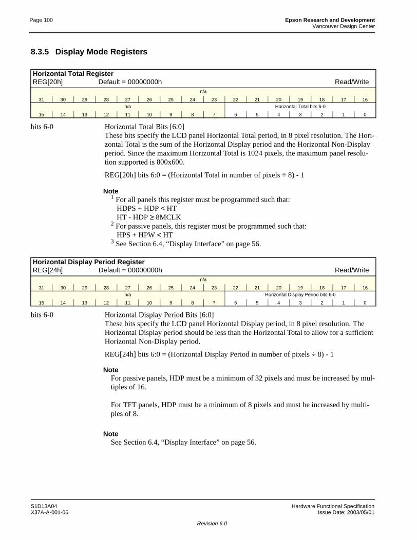
Page 100 Epson Research and DevelopmentVancouver Design Center
8.3.5 Display Mode Registers
bits 6-0 Horizontal Total Bits [6:0]These bits specify the LCD panel Horizontal Total period, in 8 pixel resolution. The Hori-zontal Total is the sum of the Horizontal Display period and the Horizontal Non-Display period. Since the maximum Horizontal Total is 1024 pixels, the maximum panel resolu-tion supported is 800x600.
REG[20h] bits 6:0 = (Horizontal Total in number of pixels ÷ 8) - 1
Note1 For all panels this register must be programmed such that:
HDPS + HDP < HTHT - HDP ≥ 8MCLK
2 For passive panels, this register must be programmed such that:HPS + HPW < HT
3 See Section 6.4, “Display Interface” on page 56.
bits 6-0 Horizontal Display Period Bits [6:0]These bits specify the LCD panel Horizontal Display period, in 8 pixel resolution. The Horizontal Display period should be less than the Horizontal Total to allow for a sufficient Horizontal Non-Display period.
REG[24h] bits 6:0 = (Horizontal Display Period in number of pixels ÷ 8) - 1
NoteFor passive panels, HDP must be a minimum of 32 pixels and must be increased by mul-tiples of 16.
For TFT panels, HDP must be a minimum of 8 pixels and must be increased by multi-ples of 8.
NoteSee Section 6.4, “Display Interface” on page 56.
Horizontal Total RegisterREG[20h] Default = 00000000h Read/Write
n/a
31 30 29 28 27 26 25 24 23 22 21 20 19 18 17 16n/a Horizontal Total bits 6-0
15 14 13 12 11 10 9 8 7 6 5 4 3 2 1 0
Horizontal Display Period RegisterREG[24h] Default = 00000000h Read/Write
n/a
31 30 29 28 27 26 25 24 23 22 21 20 19 18 17 16n/a Horizontal Display Period bits 6-0
15 14 13 12 11 10 9 8 7 6 5 4 3 2 1 0
S1D13A04 Hardware Functional SpecificationX37A-A-001-06 Issue Date: 2003/05/01
Revision 6.0
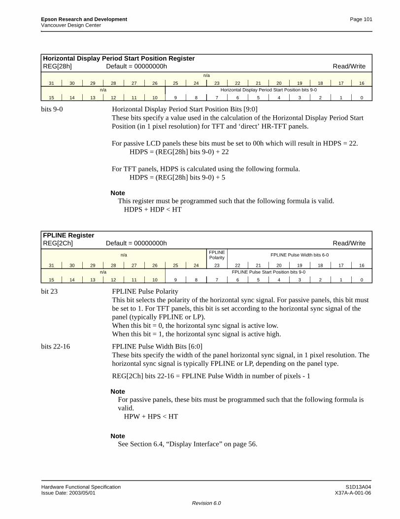
Epson Research and Development Page 101Vancouver Design Center
bits 9-0 Horizontal Display Period Start Position Bits [9:0]These bits specify a value used in the calculation of the Horizontal Display Period Start Position (in 1 pixel resolution) for TFT and ‘direct’ HR-TFT panels.
For passive LCD panels these bits must be set to 00h which will result in HDPS = 22.HDPS = (REG[28h] bits 9-0) + 22
For TFT panels, HDPS is calculated using the following formula.HDPS = (REG[28h] bits 9-0) + 5
NoteThis register must be programmed such that the following formula is valid.
HDPS + HDP < HT
bit 23 FPLINE Pulse PolarityThis bit selects the polarity of the horizontal sync signal. For passive panels, this bit must be set to 1. For TFT panels, this bit is set according to the horizontal sync signal of the panel (typically FPLINE or LP).When this bit = 0, the horizontal sync signal is active low.When this bit = 1, the horizontal sync signal is active high.
bits 22-16 FPLINE Pulse Width Bits [6:0]These bits specify the width of the panel horizontal sync signal, in 1 pixel resolution. The horizontal sync signal is typically FPLINE or LP, depending on the panel type.
REG[2Ch] bits 22-16 = FPLINE Pulse Width in number of pixels - 1
NoteFor passive panels, these bits must be programmed such that the following formula is valid.
HPW + HPS < HT
NoteSee Section 6.4, “Display Interface” on page 56.
Horizontal Display Period Start Position RegisterREG[28h] Default = 00000000h Read/Write
n/a
31 30 29 28 27 26 25 24 23 22 21 20 19 18 17 16
n/a Horizontal Display Period Start Position bits 9-0
15 14 13 12 11 10 9 8 7 6 5 4 3 2 1 0
FPLINE RegisterREG[2Ch] Default = 00000000h Read/Write
n/a FPLINE Polarity FPLINE Pulse Width bits 6-0
31 30 29 28 27 26 25 24 23 22 21 20 19 18 17 16
n/a FPLINE Pulse Start Position bits 9-0
15 14 13 12 11 10 9 8 7 6 5 4 3 2 1 0
Hardware Functional Specification S1D13A04Issue Date: 2003/05/01 X37A-A-001-06
Revision 6.0
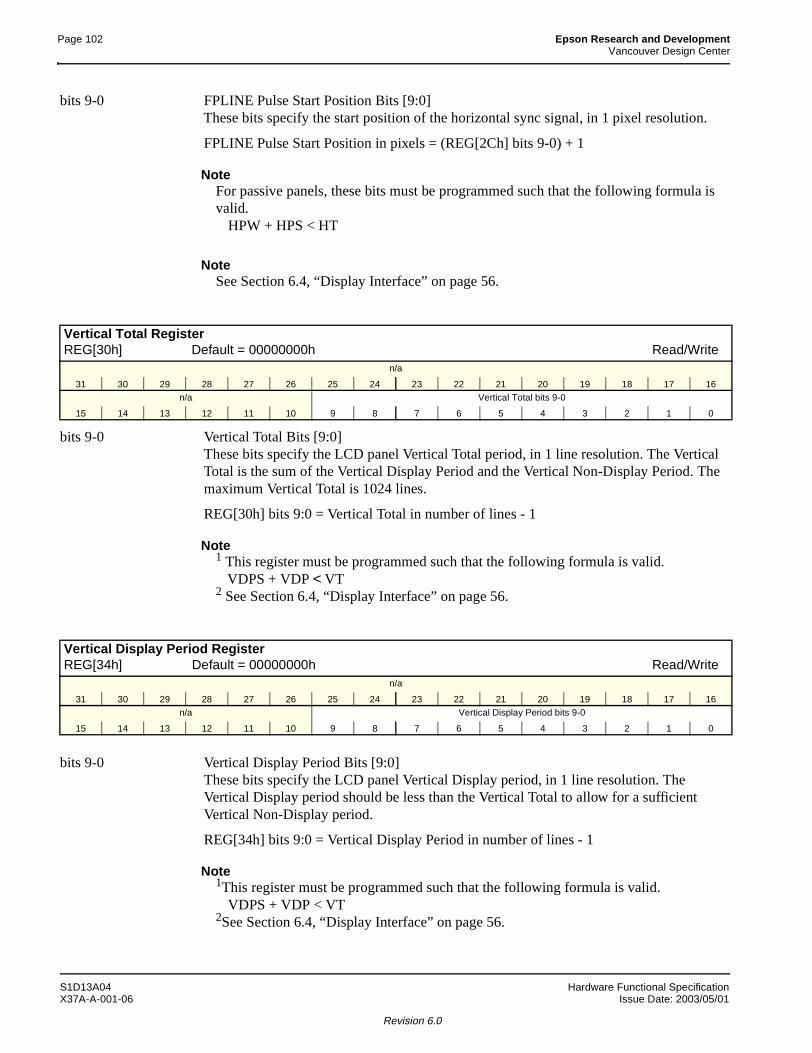
Page 102 Epson Research and DevelopmentVancouver Design Center
bits 9-0 FPLINE Pulse Start Position Bits [9:0]These bits specify the start position of the horizontal sync signal, in 1 pixel resolution.
FPLINE Pulse Start Position in pixels = (REG[2Ch] bits 9-0) + 1
NoteFor passive panels, these bits must be programmed such that the following formula is valid.
HPW + HPS < HT
NoteSee Section 6.4, “Display Interface” on page 56.
bits 9-0 Vertical Total Bits [9:0]These bits specify the LCD panel Vertical Total period, in 1 line resolution. The VerticalTotal is the sum of the Vertical Display Period and the Vertical Non-Display Period. Themaximum Vertical Total is 1024 lines.
REG[30h] bits 9:0 = Vertical Total in number of lines - 1
Note1 This register must be programmed such that the following formula is valid.
VDPS + VDP < VT2 See Section 6.4, “Display Interface” on page 56.
bits 9-0 Vertical Display Period Bits [9:0]These bits specify the LCD panel Vertical Display period, in 1 line resolution. The Vertical Display period should be less than the Vertical Total to allow for a sufficient Vertical Non-Display period.
REG[34h] bits 9:0 = Vertical Display Period in number of lines - 1
Note1This register must be programmed such that the following formula is valid.
VDPS + VDP < VT2See Section 6.4, “Display Interface” on page 56.
Vertical Total RegisterREG[30h] Default = 00000000h Read/Write
n/a
31 30 29 28 27 26 25 24 23 22 21 20 19 18 17 16n/a Vertical Total bits 9-0
15 14 13 12 11 10 9 8 7 6 5 4 3 2 1 0
Vertical Display Period RegisterREG[34h] Default = 00000000h Read/Write
n/a
31 30 29 28 27 26 25 24 23 22 21 20 19 18 17 16n/a Vertical Display Period bits 9-0
15 14 13 12 11 10 9 8 7 6 5 4 3 2 1 0
S1D13A04 Hardware Functional SpecificationX37A-A-001-06 Issue Date: 2003/05/01
Revision 6.0
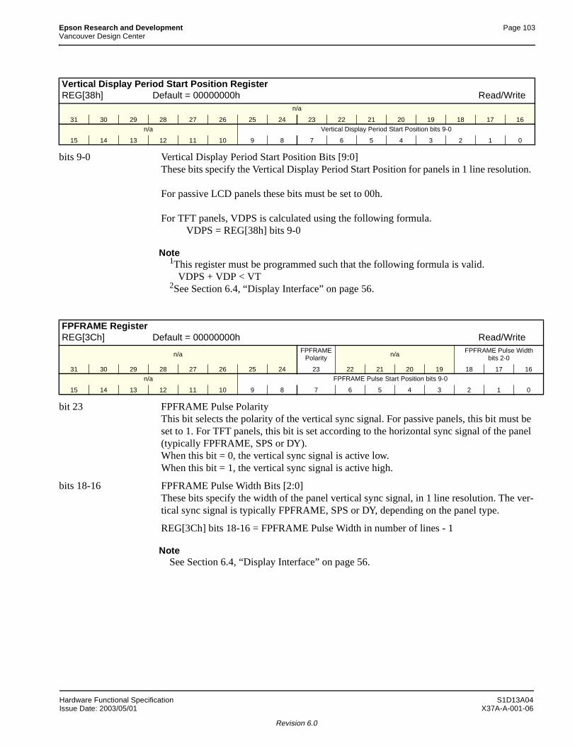
Epson Research and Development Page 103Vancouver Design Center
bits 9-0 Vertical Display Period Start Position Bits [9:0]These bits specify the Vertical Display Period Start Position for panels in 1 line resolution.
For passive LCD panels these bits must be set to 00h.
For TFT panels, VDPS is calculated using the following formula.VDPS = REG[38h] bits 9-0
Note1This register must be programmed such that the following formula is valid.
VDPS + VDP < VT2See Section 6.4, “Display Interface” on page 56.
bit 23 FPFRAME Pulse PolarityThis bit selects the polarity of the vertical sync signal. For passive panels, this bit must be set to 1. For TFT panels, this bit is set according to the horizontal sync signal of the panel (typically FPFRAME, SPS or DY).When this bit = 0, the vertical sync signal is active low.When this bit = 1, the vertical sync signal is active high.
bits 18-16 FPFRAME Pulse Width Bits [2:0]These bits specify the width of the panel vertical sync signal, in 1 line resolution. The ver-tical sync signal is typically FPFRAME, SPS or DY, depending on the panel type.
REG[3Ch] bits 18-16 = FPFRAME Pulse Width in number of lines - 1
NoteSee Section 6.4, “Display Interface” on page 56.
Vertical Display Period Start Position RegisterREG[38h] Default = 00000000h Read/Write
n/a
31 30 29 28 27 26 25 24 23 22 21 20 19 18 17 16
n/a Vertical Display Period Start Position bits 9-0
15 14 13 12 11 10 9 8 7 6 5 4 3 2 1 0
FPFRAME RegisterREG[3Ch] Default = 00000000h Read/Write
n/aFPFRAME
Polarity n/aFPFRAME Pulse Width
bits 2-0
31 30 29 28 27 26 25 24 23 22 21 20 19 18 17 16n/a FPFRAME Pulse Start Position bits 9-0
15 14 13 12 11 10 9 8 7 6 5 4 3 2 1 0
Hardware Functional Specification S1D13A04Issue Date: 2003/05/01 X37A-A-001-06
Revision 6.0
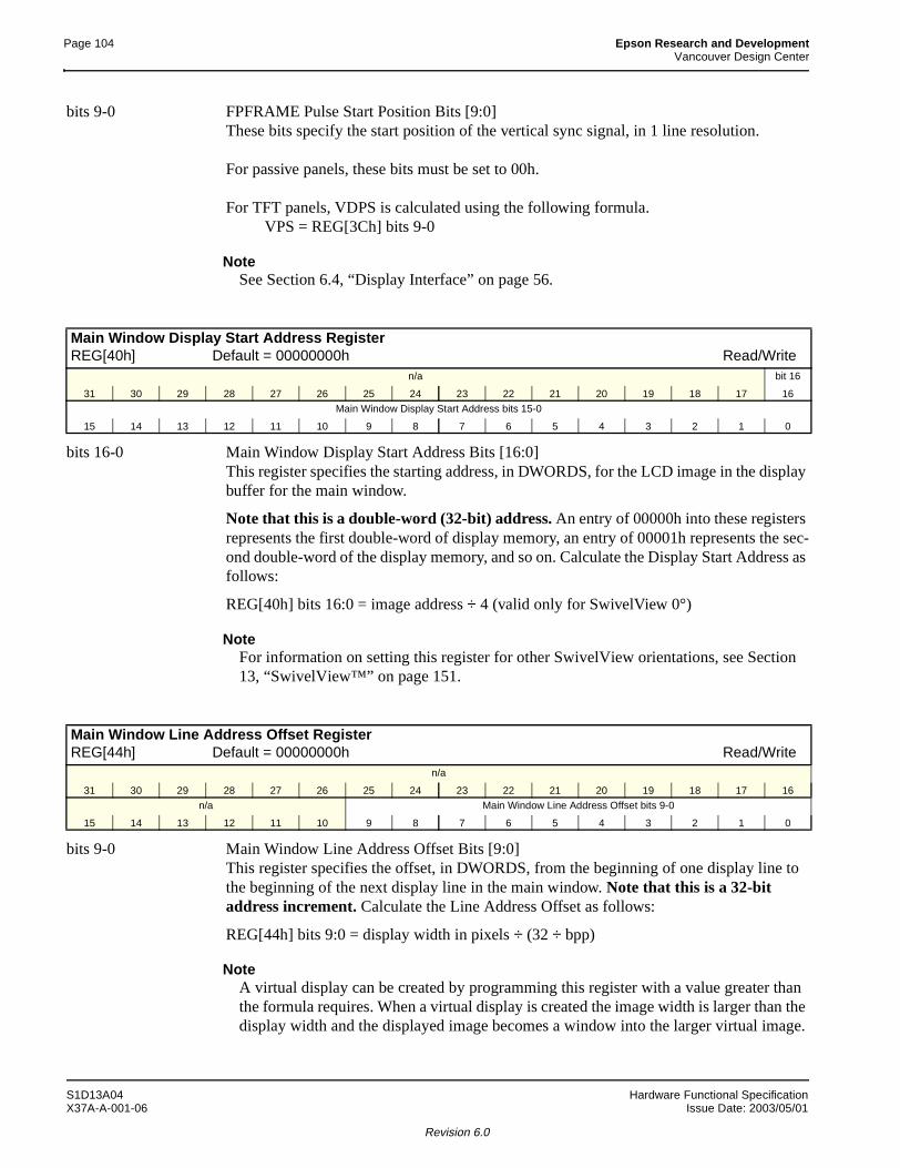
Page 104 Epson Research and DevelopmentVancouver Design Center
bits 9-0 FPFRAME Pulse Start Position Bits [9:0]These bits specify the start position of the vertical sync signal, in 1 line resolution.
For passive panels, these bits must be set to 00h.
For TFT panels, VDPS is calculated using the following formula.VPS = REG[3Ch] bits 9-0
NoteSee Section 6.4, “Display Interface” on page 56.
bits 16-0 Main Window Display Start Address Bits [16:0]This register specifies the starting address, in DWORDS, for the LCD image in the display buffer for the main window.
Note that this is a double-word (32-bit) address. An entry of 00000h into these registers represents the first double-word of display memory, an entry of 00001h represents the sec-ond double-word of the display memory, and so on. Calculate the Display Start Address as follows:
REG[40h] bits 16:0 = image address ÷ 4 (valid only for SwivelView 0°)
NoteFor information on setting this register for other SwivelView orientations, see Section 13, “SwivelView™” on page 151.
bits 9-0 Main Window Line Address Offset Bits [9:0]This register specifies the offset, in DWORDS, from the beginning of one display line to the beginning of the next display line in the main window. Note that this is a 32-bit address increment. Calculate the Line Address Offset as follows:
REG[44h] bits 9:0 = display width in pixels ÷ (32 ÷ bpp)
NoteA virtual display can be created by programming this register with a value greater than the formula requires. When a virtual display is created the image width is larger than the display width and the displayed image becomes a window into the larger virtual image.
Main Window Display Start Address RegisterREG[40h] Default = 00000000h Read/Write
n/a bit 16
31 30 29 28 27 26 25 24 23 22 21 20 19 18 17 16
Main Window Display Start Address bits 15-0
15 14 13 12 11 10 9 8 7 6 5 4 3 2 1 0
Main Window Line Address Offset RegisterREG[44h] Default = 00000000h Read/Write
n/a
31 30 29 28 27 26 25 24 23 22 21 20 19 18 17 16
n/a Main Window Line Address Offset bits 9-0
15 14 13 12 11 10 9 8 7 6 5 4 3 2 1 0
S1D13A04 Hardware Functional SpecificationX37A-A-001-06 Issue Date: 2003/05/01
Revision 6.0
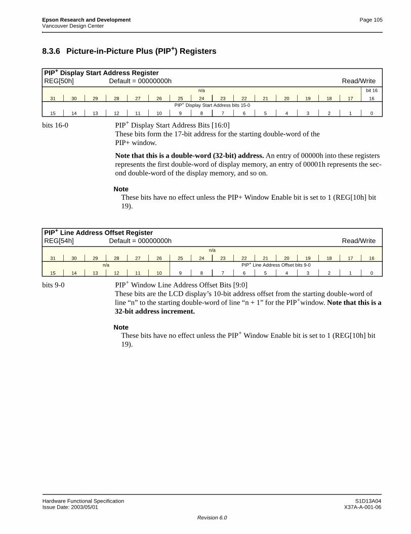
Epson Research and Development Page 105Vancouver Design Center
8.3.6 Picture-in-Picture Plus (PIP+) Registers
bits 16-0 PIP+ Display Start Address Bits [16:0]These bits form the 17-bit address for the starting double-word of thePIP+ window.
Note that this is a double-word (32-bit) address. An entry of 00000h into these registers represents the first double-word of display memory, an entry of 00001h represents the sec-ond double-word of the display memory, and so on.
NoteThese bits have no effect unless the PIP+ Window Enable bit is set to 1 (REG[10h] bit 19).
bits 9-0 PIP+ Window Line Address Offset Bits [9:0]These bits are the LCD display’s 10-bit address offset from the starting double-word ofline “n” to the starting double-word of line “n + 1” for the PIP+window. Note that this is a32-bit address increment.
NoteThese bits have no effect unless the PIP+ Window Enable bit is set to 1 (REG[10h] bit 19).
PIP+ Display Start Address RegisterREG[50h] Default = 00000000h Read/Write
n/a bit 16
31 30 29 28 27 26 25 24 23 22 21 20 19 18 17 16PIP+ Display Start Address bits 15-0
15 14 13 12 11 10 9 8 7 6 5 4 3 2 1 0
PIP+ Line Address Offset RegisterREG[54h] Default = 00000000h Read/Write
n/a
31 30 29 28 27 26 25 24 23 22 21 20 19 18 17 16n/a PIP+ Line Address Offset bits 9-0
15 14 13 12 11 10 9 8 7 6 5 4 3 2 1 0
Hardware Functional Specification S1D13A04Issue Date: 2003/05/01 X37A-A-001-06
Revision 6.0
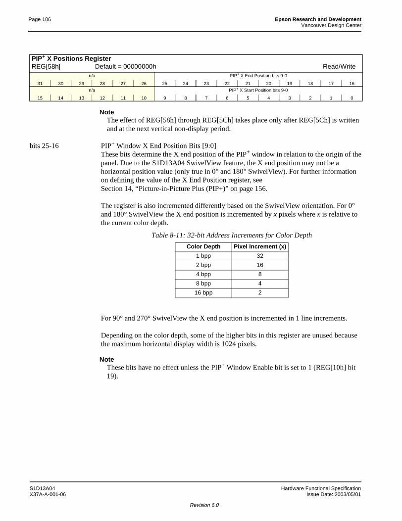
Page 106 Epson Research and DevelopmentVancouver Design Center
NoteThe effect of REG[58h] through REG[5Ch] takes place only after REG[5Ch] is written and at the next vertical non-display period.
bits 25-16 PIP+ Window X End Position Bits [9:0]These bits determine the X end position of the PIP+ window in relation to the origin of thepanel. Due to the S1D13A04 SwivelView feature, the X end position may not be ahorizontal position value (only true in 0° and 180° SwivelView). For further informationon defining the value of the X End Position register, seeSection 14, “Picture-in-Picture Plus (PIP+)” on page 156.
The register is also incremented differently based on the SwivelView orientation. For 0°and 180° SwivelView the X end position is incremented by x pixels where x is relative tothe current color depth.
For 90° and 270° SwivelView the X end position is incremented in 1 line increments.
Depending on the color depth, some of the higher bits in this register are unused becausethe maximum horizontal display width is 1024 pixels.
NoteThese bits have no effect unless the PIP+ Window Enable bit is set to 1 (REG[10h] bit 19).
PIP+ X Positions RegisterREG[58h] Default = 00000000h Read/Write
n/a PIP+ X End Position bits 9-0
31 30 29 28 27 26 25 24 23 22 21 20 19 18 17 16
n/a PIP+ X Start Position bits 9-0
15 14 13 12 11 10 9 8 7 6 5 4 3 2 1 0
Table 8-11: 32-bit Address Increments for Color Depth
Color Depth Pixel Increment (x)
1 bpp 32
2 bpp 16
4 bpp 8
8 bpp 4
16 bpp 2
S1D13A04 Hardware Functional SpecificationX37A-A-001-06 Issue Date: 2003/05/01
Revision 6.0
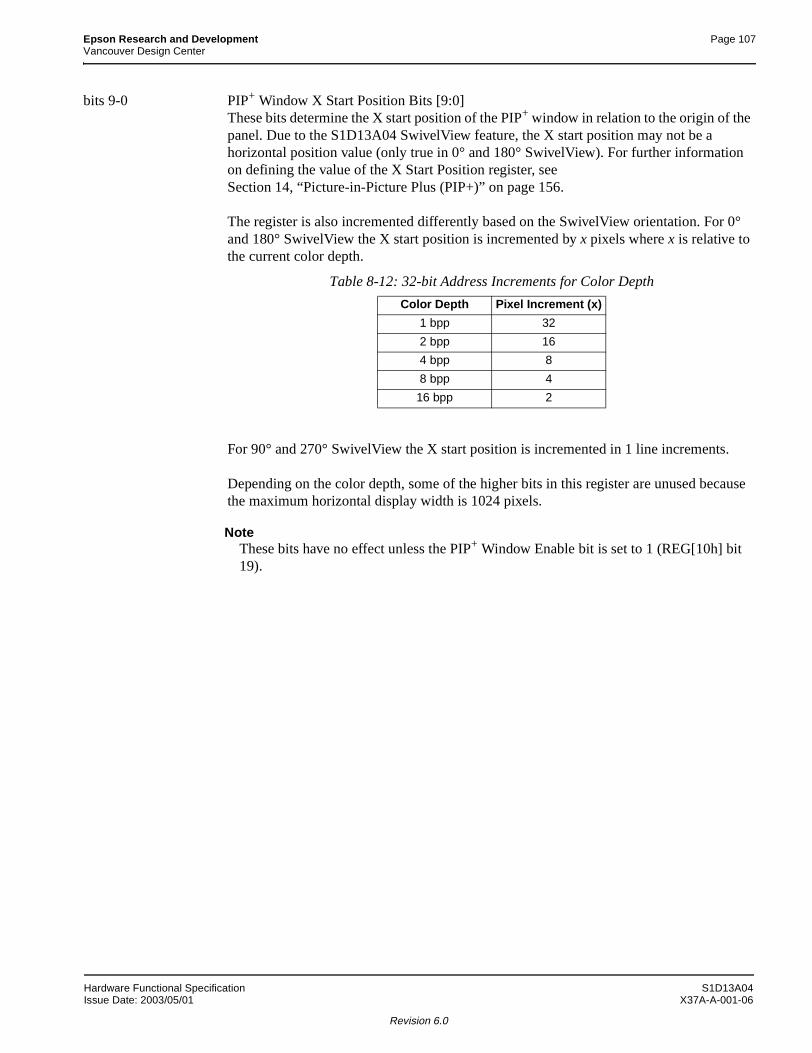
Epson Research and Development Page 107Vancouver Design Center
bits 9-0 PIP+ Window X Start Position Bits [9:0]These bits determine the X start position of the PIP+ window in relation to the origin of the panel. Due to the S1D13A04 SwivelView feature, the X start position may not be ahorizontal position value (only true in 0° and 180° SwivelView). For further informationon defining the value of the X Start Position register, seeSection 14, “Picture-in-Picture Plus (PIP+)” on page 156.
The register is also incremented differently based on the SwivelView orientation. For 0°and 180° SwivelView the X start position is incremented by x pixels where x is relative tothe current color depth.
For 90° and 270° SwivelView the X start position is incremented in 1 line increments.
Depending on the color depth, some of the higher bits in this register are unused becausethe maximum horizontal display width is 1024 pixels.
NoteThese bits have no effect unless the PIP+ Window Enable bit is set to 1 (REG[10h] bit 19).
Table 8-12: 32-bit Address Increments for Color Depth
Color Depth Pixel Increment (x)
1 bpp 32
2 bpp 16
4 bpp 8
8 bpp 4
16 bpp 2
Hardware Functional Specification S1D13A04Issue Date: 2003/05/01 X37A-A-001-06
Revision 6.0
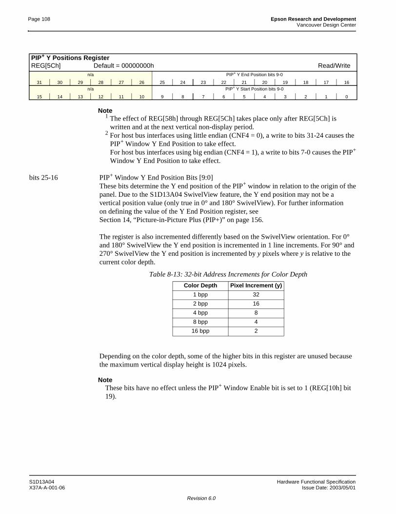
Page 108 Epson Research and DevelopmentVancouver Design Center
Note1 The effect of REG[58h] through REG[5Ch] takes place only after REG[5Ch] is
written and at the next vertical non-display period.2 For host bus interfaces using little endian (CNF4 = 0), a write to bits 31-24 causes the
PIP+ Window Y End Position to take effect.For host bus interfaces using big endian (CNF4 = 1), a write to bits 7-0 causes the PIP+
Window Y End Position to take effect.
bits 25-16 PIP+ Window Y End Position Bits [9:0]These bits determine the Y end position of the PIP+ window in relation to the origin of thepanel. Due to the S1D13A04 SwivelView feature, the Y end position may not be avertical position value (only true in 0° and 180° SwivelView). For further informationon defining the value of the Y End Position register, seeSection 14, “Picture-in-Picture Plus (PIP+)” on page 156.
The register is also incremented differently based on the SwivelView orientation. For 0°and 180° SwivelView the Y end position is incremented in 1 line increments. For 90° and270° SwivelView the Y end position is incremented by y pixels where y is relative to thecurrent color depth.
Depending on the color depth, some of the higher bits in this register are unused becausethe maximum vertical display height is 1024 pixels.
NoteThese bits have no effect unless the PIP+ Window Enable bit is set to 1 (REG[10h] bit 19).
PIP+ Y Positions RegisterREG[5Ch] Default = 00000000h Read/Write
n/a PIP+ Y End Position bits 9-0
31 30 29 28 27 26 25 24 23 22 21 20 19 18 17 16
n/a PIP+ Y Start Position bits 9-0
15 14 13 12 11 10 9 8 7 6 5 4 3 2 1 0
Table 8-13: 32-bit Address Increments for Color Depth
Color Depth Pixel Increment (y)
1 bpp 32
2 bpp 16
4 bpp 8
8 bpp 4
16 bpp 2
S1D13A04 Hardware Functional SpecificationX37A-A-001-06 Issue Date: 2003/05/01
Revision 6.0

Epson Research and Development Page 109Vancouver Design Center
bits 9-0 PIP+ Window Y Start Position Bits [9:0]These bits determine the Y start position of the PIP+ window in relation to the origin of the panel. Due to the S1D13A04 SwivelView feature, the Y start position may not be avertical position value (only true in 0° and 180° SwivelView). For further informationon defining the value of the Y Start Position register, seeSection 14, “Picture-in-Picture Plus (PIP+)” on page 156.
The register is also incremented differently based on the SwivelView orientation. For 0°and 180° SwivelView the Y start position is incremented in 1 line increments. For 90° and270° SwivelView the Y start position is incremented by y pixels where y is relative to thecurrent color depth.
Depending on the color depth, some of the higher bits in this register are unused becausethe maximum vertical display height is 1024 pixels.
NoteThese bits have no effect unless the PIP+ Window Enable bit is set to 1 (REG[10h] bit 19).
Table 8-14: 32-bit Address Increments for Color Depth
Color Depth Pixel Increment (y)
1 bpp 32
2 bpp 16
4 bpp 8
8 bpp 4
16 bpp 2
Hardware Functional Specification S1D13A04Issue Date: 2003/05/01 X37A-A-001-06
Revision 6.0
Page 110 Epson Research and DevelopmentVancouver Design Center
8.3.7 Miscellaneous Registers
bits 23-16 Reserved.These bits must be set to 0.
bit 7 2D Byte SwapThis bit enables the word data sent to/read from the 2D BitBLT port to be swapped (byte 0 and byte 1 are swapped).
NoteThis bit is only used when the S1D13A04 is configured for Big Endian (CNF4 = 1 at RESET#). If configured for Little Endian (CNF4 = 0), this bit has no effect.
bit 6 Display Data Word SwapThe display pipe fetches 32-bits of data from the display buffer. This bit enables the lower 16-bit word and the upper 16-bit word to be swapped before sending them to the LCD dis-play. If the Display Data Byte Swap bit is also enabled, then the byte order of the fetched 32-bit data is reversed.
NoteThis bit is only used when the S1D13A04 is configured for Big Endian (CNF4 = 1 at RESET#). If configured for Little Endian (CNF4 = 0), this bit has no effect.
Special Purpose RegisterREG[60h] Default = 00000000h Read/Write
n/a Reserved
31 30 29 28 27 26 25 24 23 22 21 20 19 18 17 16
n/a2D
Byte Swap
Display Data Word Swap
Display Data Byte Swap
n/aLatch Byte
Selectn/a
15 14 13 12 11 10 9 8 7 6 5 4 3 2 1 0
S1D13A04 Hardware Functional SpecificationX37A-A-001-06 Issue Date: 2003/05/01
Revision 6.0
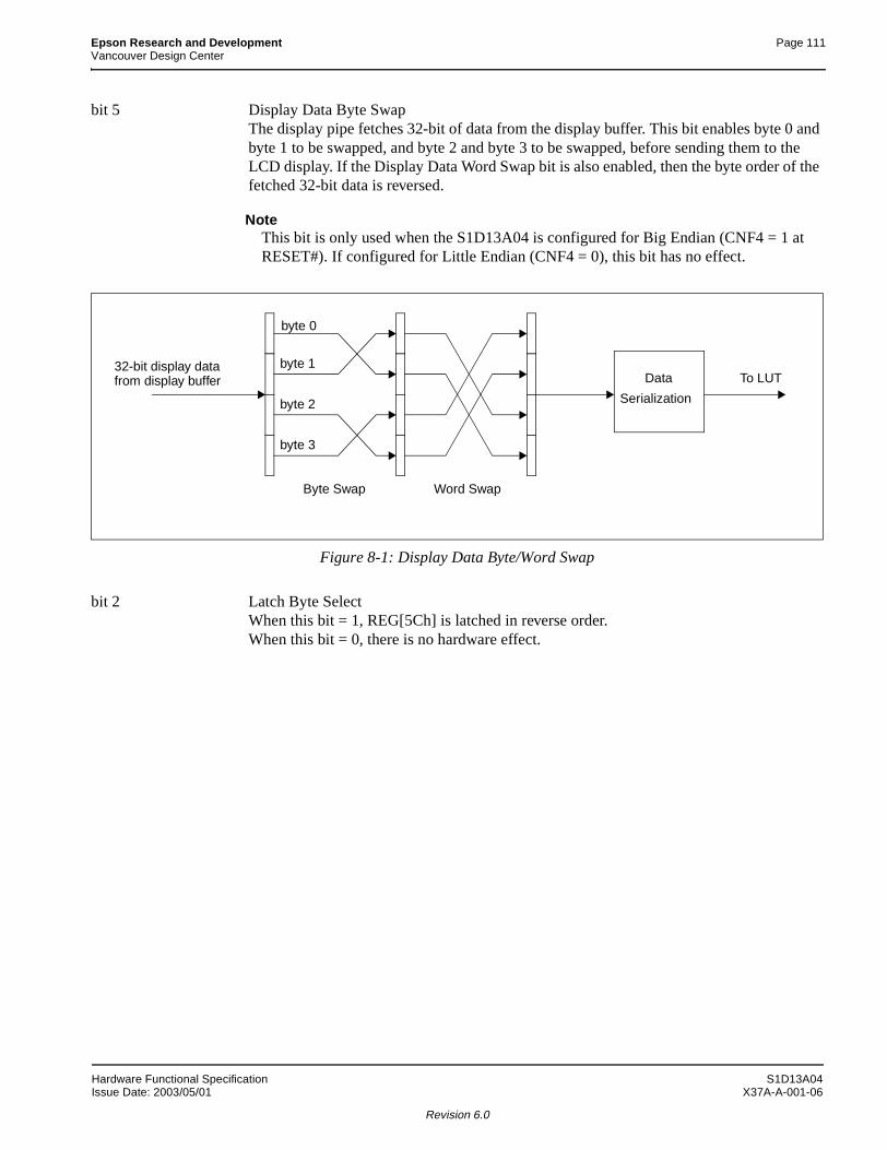
Epson Research and Development Page 111Vancouver Design Center
bit 5 Display Data Byte SwapThe display pipe fetches 32-bit of data from the display buffer. This bit enables byte 0 and byte 1 to be swapped, and byte 2 and byte 3 to be swapped, before sending them to the LCD display. If the Display Data Word Swap bit is also enabled, then the byte order of the fetched 32-bit data is reversed.
NoteThis bit is only used when the S1D13A04 is configured for Big Endian (CNF4 = 1 at RESET#). If configured for Little Endian (CNF4 = 0), this bit has no effect.
Figure 8-1: Display Data Byte/Word Swap
bit 2 Latch Byte SelectWhen this bit = 1, REG[5Ch] is latched in reverse order.When this bit = 0, there is no hardware effect.
byte 0
byte 1
byte 2
byte 3
32-bit display datafrom display buffer
Byte Swap Word Swap
Data
Serialization
To LUT
Hardware Functional Specification S1D13A04Issue Date: 2003/05/01 X37A-A-001-06
Revision 6.0
Page 112 Epson Research and DevelopmentVancouver Design Center
NoteThe GPIO pins default as inputs after power-up and must be configured using the bits in this register.
NoteFor information on GPIO pin mapping when the ‘direct’ HR-TFT LCD interface is se-lected, see Table 4-9: “LCD Interface Pin Mapping,” on page 32.
bits 31-24 GPIO[7:0] Pin Input Enable bitsThese bits are used to enable the input function of each GPIO pin. They must be changed to a 1 after power-on reset to enable the input function of the corresponding GPIO pin (default is 0).
NoteThe default for GPIO5 Pin Input Enable is 1.
bits 23-16 GPIO[7:0] Pin IO ConfigurationWhen this bit = 0 (default), the corresponding GPIO pin is configured as an input pin.When this bit = 1, the corresponding GPIO pin is configured as an output pin.
NoteThe input function of each GPIO pin must be enabled using the GPIO[7:0] Pin Input En-able bits (bits 31-24) before the input configuration takes effect.
bit 7 GPIO7 Pin IO StatusWhen GPIO7 is configured as an output, writing a 1 to this bit drives GPIO7 high and writing a 0 to this bit drives GPIO7 low.When GPIO7 is configured as an input, a read from this bit returns the status of GPIO7.
bit 6 GPIO6 Pin IO StatusWhen GPIO6 is configured as an output, writing a 1 to this bit drives GPIO6 high and writing a 0 to this bit drives GPIO6 low.When GPIO6 is configured as an input, a read from this bit returns the status of GPIO6.
bit 5 GPIO5 Pin IO StatusWhen GPIO5 is configured as an output, writing a 1 to this bit drives GPIO5 high and writing a 0 to this bit drives GPIO5 low.When GPIO5 is configured as an input, a read from this bit returns the status of GPIO5.
GPIO Status and Control RegisterREG[64h] Default = 20000000h Read/WriteGPIO7 Input
Enable
GPIO6 Input
Enable
GPIO5 Input
Enable
GPIO4 Input
Enable
GPIO3 Input
Enable
GPIO2 Input
Enable
GPIO1 Input
Enable
GPIO0 Input
Enable
GPIO7 Config
GPIO6 Config
GPIO5 Config
GPIO4 Config
GPIO3 Config
GPIO2 Config
GPIO1 Config
GPIO0 Config
31 30 29 28 27 26 25 24 23 22 21 20 19 18 17 16
n/a GPIO7 Status
GPIO6 Status
GPIO5 Status
GPIO4 Status
GPIO3 Status
GPIO2 Status
GPIO1 Status
GPIO0 Status
15 14 13 12 11 10 9 8 7 6 5 4 3 2 1 0
S1D13A04 Hardware Functional SpecificationX37A-A-001-06 Issue Date: 2003/05/01
Revision 6.0
Epson Research and Development Page 113Vancouver Design Center
bit 4 GPIO4 Pin IO StatusWhen GPIO4 is configured as an output, writing a 1 to this bit drives GPIO4 high and writing a 0 to this bit drives GPIO4 low.When GPIO4 is configured as an input, a read from this bit returns the status of GPIO4.
bit 3 GPIO3 Pin IO StatusWhen the ‘Direct’ HR-TFT LCD interface is not selected (REG[0Ch] bits 1:0) and GPIO3 is configured as an output, writing a 1 to this bit drives GPIO3 high and writing a 0 to this bit drives GPIO3 low.When the ‘Direct’ HR-TFT LCD interface is not selected (REG[0Ch] bits 1:0) and GPIO3 is configured as an input, a read from this bit returns the status of GPIO3.
When the ‘Direct’ HR-TFT LCD interface is enabled (REG[0Ch] bits 1:0 = 10), GPIO0 outputs the SPL signal automatically and writing to this bit has no effect.
bit 2 GPIO2 Pin IO StatusWhen the ‘Direct’ HR-TFT LCD interface is not selected (REG[0Ch] bits 1:0) and GPIO2 is configured as an output, writing a 1 to this bit drives GPIO2 high and writing a 0 to this bit drives GPIO2 low.When the ‘Direct’ HR-TFT LCD interface is not selected (REG[0Ch] bits 1:0) and GPIO2 is configured as an input, a read from this bit returns the status of GPIO2.
When the ‘Direct’ HR-TFT LCD interface is enabled (REG[0Ch] bits 1:0 = 10), GPIO0 outputs the REV signal automatically and writing to this bit has no effect.
bit 1 GPIO1 Pin IO StatusWhen the ‘Direct’ HR-TFT LCD interface is not selected (REG[0Ch] bits 1:0) and GPIO1 is configured as an output, writing a 1 to this bit drives GPIO1 high and writing a 0 to this bit drives GPIO1 low.When the ‘Direct’ HR-TFT LCD interface is not selected (REG[0Ch] bits 1:0) and GPIO1 is configured as an input, a read from this bit returns the status of GPIO1.
When the ‘Direct’ HR-TFT LCD interface is enabled (REG[0Ch] bits 1:0 = 10), GPIO0 outputs the CLS signal automatically and writing to this bit has no effect.
bit 0 GPIO0 Pin IO StatusWhen the ‘Direct’ HR-TFT LCD interface is not selected (REG[0Ch] bits 1:0) and GPIO0 is configured as an output, writing a 1 to this bit drives GPIO0 high and writing a 0 to this bit drives GPIO0 low.When the ‘Direct’ HR-TFT LCD interface is not selected (REG[0Ch] bits 1:0) and GPIO0 is configured as an input, a read from this bit returns the status of GPIO0.
When the ‘Direct’ HR-TFT LCD interface is enabled (REG[0Ch] bits 1:0 = 10), GPIO0 outputs the PS signal automatically and writing to this bit has no effect.
Hardware Functional Specification S1D13A04Issue Date: 2003/05/01 X37A-A-001-06
Revision 6.0
Page 114 Epson Research and DevelopmentVancouver Design Center
Figure 8-2: PWM Clock Block DiagramNote
For further information on PWMCLK, see Section 7.1.4, “PWMCLK” on page 86.
bits 7-4 PWM Clock Divide Select Bits [3:0]The value of these bits represents the power of 2 by which the selected PWM clock source is divided.
NoteThis divided clock is further divided by 256 before it is output at PWMOUT.
PWM Clock Configuration RegisterREG[70h] Default = 00000000h Read/Write
n/a
31 30 29 28 27 26 25 24 23 22 21 20 19 18 17 16
n/aPWM Clock Divide Select
bits 3-0
PWM Clock Force High
PWMCLK Source Select bits 1-0
PWM Clock
Enable
15 14 13 12 11 10 9 8 7 6 5 4 3 2 1 0
Table 8-15: PWM Clock Divide Select Options
PWM Clock Divide Select Bits [3:0] PWM Clock Divide Amount
0h 1
1h 2
2h 4
3h 8
4h 16
5h 32
6h 64
7h 128
8h 256
9h 512
Ah 1024
Bh 2048
Ch 4096
Dh 8192
Eh 16384
Fh 32768
PWM ClockDivider
PWM Duty CycleModulation to PWMOUTPWMCLK
DividedClock
Clock Source / 2 m
m = PWM Clock Divide Select value
Duty = n / 256
n = PWM Clock Duty Cycle
frequency = Clock Source / (2m X 256)
PWM Clock Force High
PWM Clock Enable
S1D13A04 Hardware Functional SpecificationX37A-A-001-06 Issue Date: 2003/05/01
Revision 6.0
Epson Research and Development Page 115Vancouver Design Center
bit 3 PWM Clock Force HighWhen this bit = 0, the PWMOUT pin function is controlled by the PWM Clock enable bit.When this bit = 1, the PWMOUT pin is forced to high.
bit 1 PWMCLK Source Select Bits [1:0]These bits determine the source of PWMCLK.
NoteFor further information on the PWMCLK source select, see Section 7.2, “Clock Selec-tion” on page 87.
bit 0 PWM Clock EnableWhen this bit = 0, PWMOUT output acts as a general purpose output pin controllable by bit 3 of REG[70h].When this bit = 1, the PWM Clock circuitry is enabled.
NoteThe PWM Clock circuitry is disabled when Power Save Mode is enabled.
bits 7-0 PWMOUT Duty Cycle Bits [7:0]This register determines the duty cycle of the PWMOUT output.
Table 8-16: PWMCLK Source Selection
PWMCLK Source Select Bits PWMCLK Source
00 CLKI
01 CLKI2
10 BCLK
11 PCLK
PWMOUT Duty Cycle RegisterREG[74h] Default = 00000000h Read/Write
n/a
31 30 29 28 27 26 25 24 23 22 21 20 19 18 17 16
n/a PWMOUT Duty Cycle bits 7-0
15 14 13 12 11 10 9 8 7 6 5 4 3 2 1 0
Table 8-17: PWMOUT Duty Cycle Select Options
PWMOUT Duty Cycle [7:0] PWMOUT Duty Cycle
00h Always Low
01h High for 1 out of 256 clock periods
02h High for 2 out of 256 clock periods
... ...
FFh High for 255 out of 256 clock periods
Hardware Functional Specification S1D13A04Issue Date: 2003/05/01 X37A-A-001-06
Revision 6.0
Page 116 Epson Research and DevelopmentVancouver Design Center
bits 31-0 Scratch Pad A Bits [31:0]This register contains general purpose read/write bits. These bits have no effect on hard-ware.
NoteThe contents of the Scratch Pad A register defaults to an un-defined state after initial power-up. Any data written to this register remains intact when the S1D13A04 is reset, as long as the chip is not powered off.
bits 31-0 Scratch Pad B Bits [31:0]This register contains general purpose read/write bits. These bits have no effect on hard-ware.
NoteThe contents of the Scratch Pad B register defaults to an un-defined state after initial power-up. Any data written to this register remains intact when the S1D13A04 is reset, as long as the chip is not powered off.
bits 31-0 Scratch Pad C Bits [31:0]This register contains general purpose read/write bits. These bits have no effect on hard-ware.
NoteThe contents of the Scratch Pad C register defaults to an un-defined state after initial power-up. Any data written to this register remains intact when the S1D13A04 is reset, as long as the chip is not powered off.
Scratch Pad A RegisterREG[80h] Default = not applicable Read/Write
Scratch Pad A bits 31-24
31 30 29 28 27 26 25 24 23 22 21 20 19 18 17 16
Scratch Pad A bits 15-0
15 14 13 12 11 10 9 8 7 6 5 4 3 2 1 0
Scratch Pad B RegisterREG[84h] Default = not applicable Read/Write
Scratch Pad B bits 31-24
31 30 29 28 27 26 25 24 23 22 21 20 19 18 17 16Scratch Pad B bits 15-0
15 14 13 12 11 10 9 8 7 6 5 4 3 2 1 0
Scratch Pad C RegisterREG[88h] Default = not applicable Read/Write
Scratch Pad C bits 31-24
31 30 29 28 27 26 25 24 23 22 21 20 19 18 17 16Scratch Pad C bits 15-0
15 14 13 12 11 10 9 8 7 6 5 4 3 2 1 0
S1D13A04 Hardware Functional SpecificationX37A-A-001-06 Issue Date: 2003/05/01
Revision 6.0
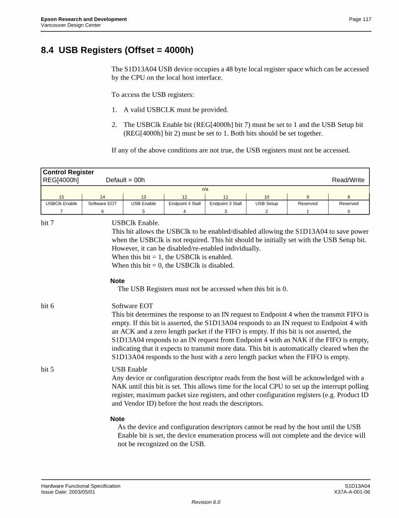
Epson Research and Development Page 117Vancouver Design Center
8.4 USB Registers (Offset = 4000h)
The S1D13A04 USB device occupies a 48 byte local register space which can be accessed by the CPU on the local host interface.
To access the USB registers:
1. A valid USBCLK must be provided.
2. The USBClk Enable bit (REG[4000h] bit 7) must be set to 1 and the USB Setup bit (REG[4000h] bit 2) must be set to 1. Both bits should be set together.
If any of the above conditions are not true, the USB registers must not be accessed.
bit 7 USBClk Enable.This bit allows the USBClk to be enabled/disabled allowing the S1D13A04 to save power when the USBClk is not required. This bit should be initially set with the USB Setup bit. However, it can be disabled/re-enabled individually.When this bit = 1, the USBClk is enabled.When this bit = 0, the USBClk is disabled.
NoteThe USB Registers must not be accessed when this bit is 0.
bit 6 Software EOTThis bit determines the response to an IN request to Endpoint 4 when the transmit FIFO is empty. If this bit is asserted, the S1D13A04 responds to an IN request to Endpoint 4 with an ACK and a zero length packet if the FIFO is empty. If this bit is not asserted, the S1D13A04 responds to an IN request from Endpoint 4 with an NAK if the FIFO is empty, indicating that it expects to transmit more data. This bit is automatically cleared when the S1D13A04 responds to the host with a zero length packet when the FIFO is empty.
bit 5 USB EnableAny device or configuration descriptor reads from the host will be acknowledged with a NAK until this bit is set. This allows time for the local CPU to set up the interrupt polling register, maximum packet size registers, and other configuration registers (e.g. Product ID and Vendor ID) before the host reads the descriptors.
NoteAs the device and configuration descriptors cannot be read by the host until the USB Enable bit is set, the device enumeration process will not complete and the device will not be recognized on the USB.
Control RegisterREG[4000h] Default = 00h Read/Write
n/a
15 14 13 12 11 10 9 8USBClk Enable Software EOT USB Enable Endpoint 4 Stall Endpoint 3 Stall USB Setup Reserved Reserved
7 6 5 4 3 2 1 0
Hardware Functional Specification S1D13A04Issue Date: 2003/05/01 X37A-A-001-06
Revision 6.0
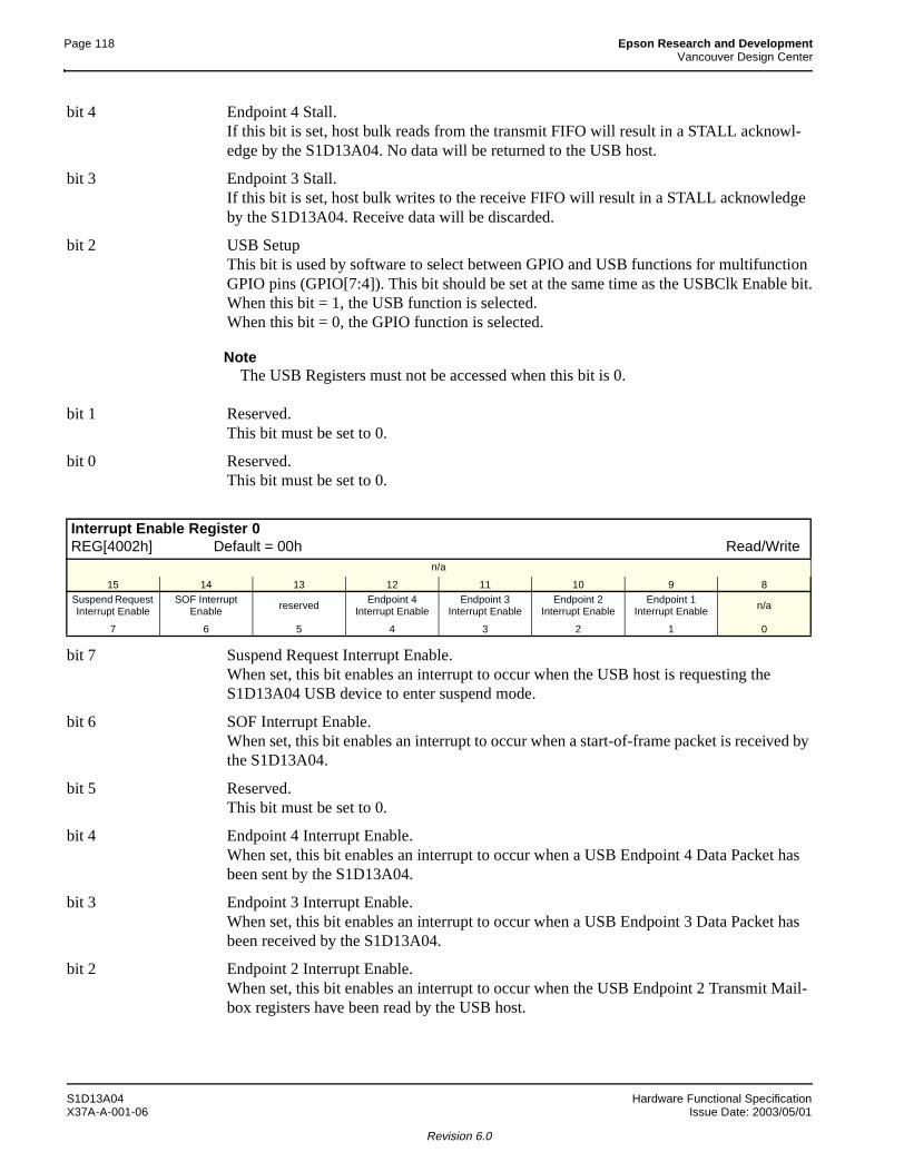
Page 118 Epson Research and DevelopmentVancouver Design Center
bit 4 Endpoint 4 Stall. If this bit is set, host bulk reads from the transmit FIFO will result in a STALL acknowl-edge by the S1D13A04. No data will be returned to the USB host.
bit 3 Endpoint 3 Stall. If this bit is set, host bulk writes to the receive FIFO will result in a STALL acknowledge by the S1D13A04. Receive data will be discarded.
bit 2 USB SetupThis bit is used by software to select between GPIO and USB functions for multifunction GPIO pins (GPIO[7:4]). This bit should be set at the same time as the USBClk Enable bit.When this bit = 1, the USB function is selected.When this bit = 0, the GPIO function is selected.
NoteThe USB Registers must not be accessed when this bit is 0.
bit 1 Reserved.This bit must be set to 0.
bit 0 Reserved.This bit must be set to 0.
bit 7 Suspend Request Interrupt Enable. When set, this bit enables an interrupt to occur when the USB host is requesting the S1D13A04 USB device to enter suspend mode.
bit 6 SOF Interrupt Enable. When set, this bit enables an interrupt to occur when a start-of-frame packet is received by the S1D13A04.
bit 5 Reserved.This bit must be set to 0.
bit 4 Endpoint 4 Interrupt Enable. When set, this bit enables an interrupt to occur when a USB Endpoint 4 Data Packet has been sent by the S1D13A04.
bit 3 Endpoint 3 Interrupt Enable. When set, this bit enables an interrupt to occur when a USB Endpoint 3 Data Packet has been received by the S1D13A04.
bit 2 Endpoint 2 Interrupt Enable. When set, this bit enables an interrupt to occur when the USB Endpoint 2 Transmit Mail-box registers have been read by the USB host.
Interrupt Enable Register 0REG[4002h] Default = 00h Read/Write
n/a
15 14 13 12 11 10 9 8Suspend Request Interrupt Enable
SOF Interrupt Enable reserved
Endpoint 4 Interrupt Enable
Endpoint 3 Interrupt Enable
Endpoint 2 Interrupt Enable
Endpoint 1 Interrupt Enable n/a
7 6 5 4 3 2 1 0
S1D13A04 Hardware Functional SpecificationX37A-A-001-06 Issue Date: 2003/05/01
Revision 6.0

Epson Research and Development Page 119Vancouver Design Center
bit 1 Endpoint 1 Interrupt Enable. When set, this bit enables an interrupt to occur when the USB Endpoint 1 Receive Mail-box registers have been written to by the USB host.
bit 7 Suspend Request Interrupt Status. This bit indicates when a suspend-request has been received by the S1D13A04. Writing a 1 clears this bit.
bit 6 SOF Interrupt Status. This bit indicates when a start-of-frame packet has been received by the S1D13A04. Writ-ing a 1 clears this bit.
bit 5 Reserved.This bit must be set to 0.
bit 4 Endpoint 4 Interrupt Status. This bit indicates when a USB Endpoint 4 Data packet has been sent by the S1D13A04. Writing a 1 clears this bit.
bit 3 Endpoint 3 Interrupt Status (Receive FIFO Valid). This bit indicates when a USB Endpoint 3 Data packet has been received by the S1D13A04. No more packets to endpoint 3 will be accepted until this bit is cleared. Writ-ing a 1 clears this bit.
bit 2 Endpoint 2 Interrupt Status. This bit indicates when the USB Endpoint 2 Mailbox registers have been read by the USB host. Writing a 1 clears this bit.
bit 1 Endpoint 1 Interrupt Status (Receive Mailbox Valid). This bit indicates when the USB Endpoint 1 Mailbox registers have been written to by the USB host. Writing a 1 clears this bit.
bit 0 Upper Interrupt Active (read only). At least one interrupt status bit is set in register REG[4008h].
Interrupt Status Register 0REG[4004h] Default = 00h Read/Write
n/a
15 14 13 12 11 10 9 8
Suspend Request Interrupt Status
SOF Interrupt Status
Reserved Endpoint 4 Interrupt Status
Endpoint 3 Interrupt Status
Endpoint 2 Interrupt Status
Endpoint 1 Interrupt Status
Upper Interrupt Active
(read only)
7 6 5 4 3 2 1 0
Hardware Functional Specification S1D13A04Issue Date: 2003/05/01 X37A-A-001-06
Revision 6.0
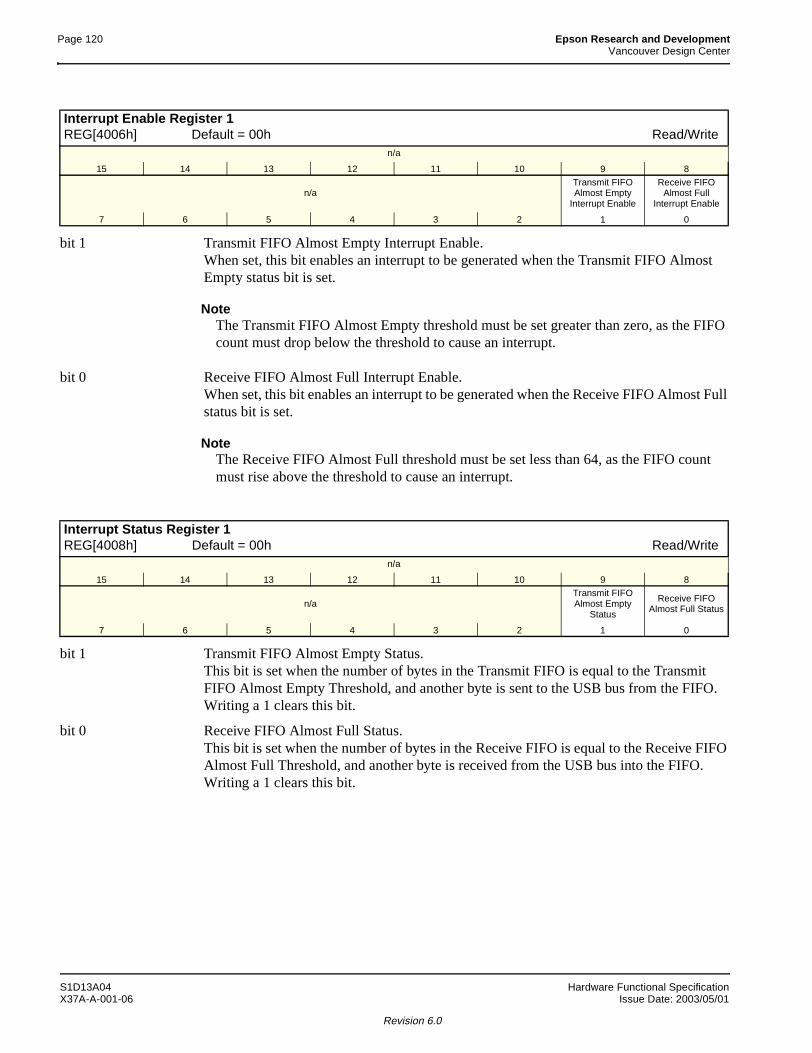
Page 120 Epson Research and DevelopmentVancouver Design Center
bit 1 Transmit FIFO Almost Empty Interrupt Enable. When set, this bit enables an interrupt to be generated when the Transmit FIFO Almost Empty status bit is set.
NoteThe Transmit FIFO Almost Empty threshold must be set greater than zero, as the FIFO count must drop below the threshold to cause an interrupt.
bit 0 Receive FIFO Almost Full Interrupt Enable.When set, this bit enables an interrupt to be generated when the Receive FIFO Almost Full status bit is set.
NoteThe Receive FIFO Almost Full threshold must be set less than 64, as the FIFO count must rise above the threshold to cause an interrupt.
bit 1 Transmit FIFO Almost Empty Status. This bit is set when the number of bytes in the Transmit FIFO is equal to the Transmit FIFO Almost Empty Threshold, and another byte is sent to the USB bus from the FIFO. Writing a 1 clears this bit.
bit 0 Receive FIFO Almost Full Status. This bit is set when the number of bytes in the Receive FIFO is equal to the Receive FIFO Almost Full Threshold, and another byte is received from the USB bus into the FIFO. Writing a 1 clears this bit.
Interrupt Enable Register 1REG[4006h] Default = 00h Read/Write
n/a
15 14 13 12 11 10 9 8
n/aTransmit FIFO Almost Empty
Interrupt Enable
Receive FIFO Almost Full
Interrupt Enable
7 6 5 4 3 2 1 0
Interrupt Status Register 1REG[4008h] Default = 00h Read/Write
n/a
15 14 13 12 11 10 9 8
n/aTransmit FIFO Almost Empty
Status
Receive FIFO Almost Full Status
7 6 5 4 3 2 1 0
S1D13A04 Hardware Functional SpecificationX37A-A-001-06 Issue Date: 2003/05/01
Revision 6.0
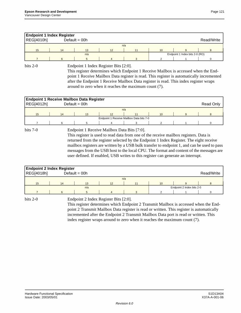
Epson Research and Development Page 121Vancouver Design Center
bits 2-0 Endpoint 1 Index Register Bits [2:0]. This register determines which Endpoint 1 Receive Mailbox is accessed when the End-point 1 Receive Mailbox Data register is read. This register is automatically incremented after the Endpoint 1 Receive Mailbox Data register is read. This index register wraps around to zero when it reaches the maximum count (7).
bits 7-0 Endpoint 1 Receive Mailbox Data Bits [7:0]. This register is used to read data from one of the receive mailbox registers. Data is returned from the register selected by the Endpoint 1 Index Register. The eight receive mailbox registers are written by a USB bulk transfer to endpoint 1, and can be used to pass messages from the USB host to the local CPU. The format and content of the messages are user defined. If enabled, USB writes to this register can generate an interrupt.
bits 2-0 Endpoint 2 Index Register Bits [2:0]. This register determines which Endpoint 2 Transmit Mailbox is accessed when the End-point 2 Transmit Mailbox Data register is read or written. This register is automatically incremented after the Endpoint 2 Transmit Mailbox Data port is read or written. This index register wraps around to zero when it reaches the maximum count (7).
Endpoint 1 Index RegisterREG[4010h] Default = 00h Read/Write
n/a
15 14 13 12 11 10 9 8
n/a Endpoint 1 Index bits 2-0 (RO)
7 6 5 4 3 2 1 0
Endpoint 1 Receive Mailbox Data RegisterREG[4012h] Default = 00h Read Only
n/a
15 14 13 12 11 10 9 8Endpoint 1 Receive Mailbox Data bits 7-0
7 6 5 4 3 2 1 0
Endpoint 2 Index RegisterREG[4018h] Default = 00h Read/Write
n/a
15 14 13 12 11 10 9 8n/a Endpoint 2 Index bits 2-0
7 6 5 4 3 2 1 0
Hardware Functional Specification S1D13A04Issue Date: 2003/05/01 X37A-A-001-06
Revision 6.0
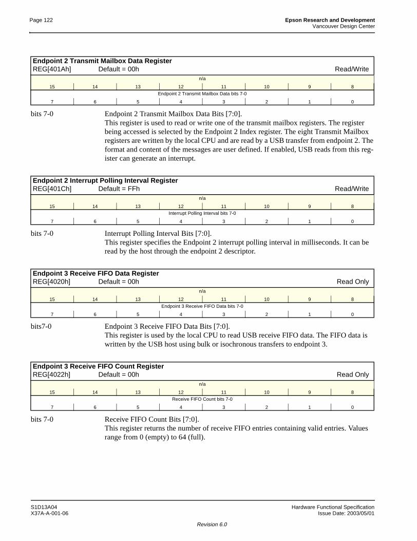
Page 122 Epson Research and DevelopmentVancouver Design Center
bits 7-0 Endpoint 2 Transmit Mailbox Data Bits [7:0]. This register is used to read or write one of the transmit mailbox registers. The register being accessed is selected by the Endpoint 2 Index register. The eight Transmit Mailbox registers are written by the local CPU and are read by a USB transfer from endpoint 2. The format and content of the messages are user defined. If enabled, USB reads from this reg-ister can generate an interrupt.
bits 7-0 Interrupt Polling Interval Bits [7:0]. This register specifies the Endpoint 2 interrupt polling interval in milliseconds. It can be read by the host through the endpoint 2 descriptor.
bits7-0 Endpoint 3 Receive FIFO Data Bits [7:0]. This register is used by the local CPU to read USB receive FIFO data. The FIFO data is written by the USB host using bulk or isochronous transfers to endpoint 3.
bits 7-0 Receive FIFO Count Bits [7:0]. This register returns the number of receive FIFO entries containing valid entries. Values range from 0 (empty) to 64 (full).
Endpoint 2 Transmit Mailbox Data RegisterREG[401Ah] Default = 00h Read/Write
n/a
15 14 13 12 11 10 9 8
Endpoint 2 Transmit Mailbox Data bits 7-0
7 6 5 4 3 2 1 0
Endpoint 2 Interrupt Polling Interval RegisterREG[401Ch] Default = FFh Read/Write
n/a
15 14 13 12 11 10 9 8Interrupt Polling Interval bits 7-0
7 6 5 4 3 2 1 0
Endpoint 3 Receive FIFO Data RegisterREG[4020h] Default = 00h Read Only
n/a
15 14 13 12 11 10 9 8
Endpoint 3 Receive FIFO Data bits 7-0
7 6 5 4 3 2 1 0
Endpoint 3 Receive FIFO Count RegisterREG[4022h] Default = 00h Read Only
n/a
15 14 13 12 11 10 9 8Receive FIFO Count bits 7-0
7 6 5 4 3 2 1 0
S1D13A04 Hardware Functional SpecificationX37A-A-001-06 Issue Date: 2003/05/01
Revision 6.0
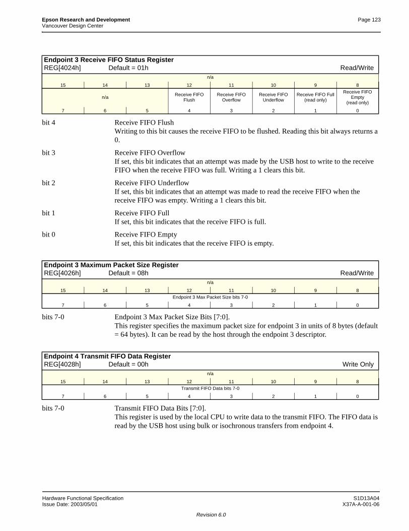
Epson Research and Development Page 123Vancouver Design Center
bit 4 Receive FIFO FlushWriting to this bit causes the receive FIFO to be flushed. Reading this bit always returns a 0.
bit 3 Receive FIFO OverflowIf set, this bit indicates that an attempt was made by the USB host to write to the receive FIFO when the receive FIFO was full. Writing a 1 clears this bit.
bit 2 Receive FIFO UnderflowIf set, this bit indicates that an attempt was made to read the receive FIFO when the receive FIFO was empty. Writing a 1 clears this bit.
bit 1 Receive FIFO FullIf set, this bit indicates that the receive FIFO is full.
bit 0 Receive FIFO EmptyIf set, this bit indicates that the receive FIFO is empty.
bits 7-0 Endpoint 3 Max Packet Size Bits [7:0]. This register specifies the maximum packet size for endpoint 3 in units of 8 bytes (default = 64 bytes). It can be read by the host through the endpoint 3 descriptor.
bits 7-0 Transmit FIFO Data Bits [7:0]. This register is used by the local CPU to write data to the transmit FIFO. The FIFO data is read by the USB host using bulk or isochronous transfers from endpoint 4.
Endpoint 3 Receive FIFO Status RegisterREG[4024h] Default = 01h Read/Write
n/a
15 14 13 12 11 10 9 8
n/a Receive FIFO Flush
Receive FIFO Overflow
Receive FIFO Underflow
Receive FIFO Full(read only)
Receive FIFO Empty
(read only)
7 6 5 4 3 2 1 0
Endpoint 3 Maximum Packet Size RegisterREG[4026h] Default = 08h Read/Write
n/a
15 14 13 12 11 10 9 8Endpoint 3 Max Packet Size bits 7-0
7 6 5 4 3 2 1 0
Endpoint 4 Transmit FIFO Data RegisterREG[4028h] Default = 00h Write Only
n/a
15 14 13 12 11 10 9 8Transmit FIFO Data bits 7-0
7 6 5 4 3 2 1 0
Hardware Functional Specification S1D13A04Issue Date: 2003/05/01 X37A-A-001-06
Revision 6.0
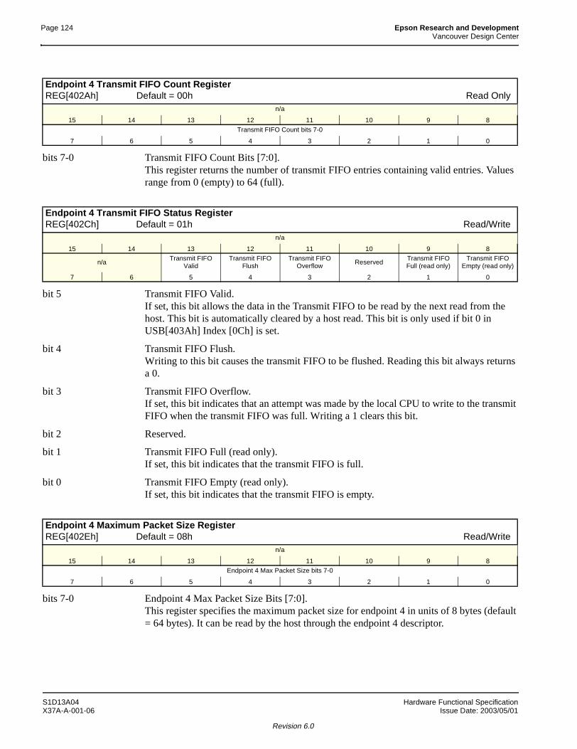
Page 124 Epson Research and DevelopmentVancouver Design Center
bits 7-0 Transmit FIFO Count Bits [7:0]. This register returns the number of transmit FIFO entries containing valid entries. Values range from 0 (empty) to 64 (full).
bit 5 Transmit FIFO Valid. If set, this bit allows the data in the Transmit FIFO to be read by the next read from the host. This bit is automatically cleared by a host read. This bit is only used if bit 0 in USB[403Ah] Index [0Ch] is set.
bit 4 Transmit FIFO Flush. Writing to this bit causes the transmit FIFO to be flushed. Reading this bit always returns a 0.
bit 3 Transmit FIFO Overflow. If set, this bit indicates that an attempt was made by the local CPU to write to the transmit FIFO when the transmit FIFO was full. Writing a 1 clears this bit.
bit 2 Reserved.
bit 1 Transmit FIFO Full (read only). If set, this bit indicates that the transmit FIFO is full.
bit 0 Transmit FIFO Empty (read only). If set, this bit indicates that the transmit FIFO is empty.
bits 7-0 Endpoint 4 Max Packet Size Bits [7:0]. This register specifies the maximum packet size for endpoint 4 in units of 8 bytes (default = 64 bytes). It can be read by the host through the endpoint 4 descriptor.
Endpoint 4 Transmit FIFO Count RegisterREG[402Ah] Default = 00h Read Only
n/a
15 14 13 12 11 10 9 8
Transmit FIFO Count bits 7-0
7 6 5 4 3 2 1 0
Endpoint 4 Transmit FIFO Status RegisterREG[402Ch] Default = 01h Read/Write
n/a
15 14 13 12 11 10 9 8
n/aTransmit FIFO
ValidTransmit FIFO
FlushTransmit FIFO
Overflow ReservedTransmit FIFO Full (read only)
Transmit FIFO Empty (read only)
7 6 5 4 3 2 1 0
Endpoint 4 Maximum Packet Size RegisterREG[402Eh] Default = 08h Read/Write
n/a
15 14 13 12 11 10 9 8Endpoint 4 Max Packet Size bits 7-0
7 6 5 4 3 2 1 0
S1D13A04 Hardware Functional SpecificationX37A-A-001-06 Issue Date: 2003/05/01
Revision 6.0
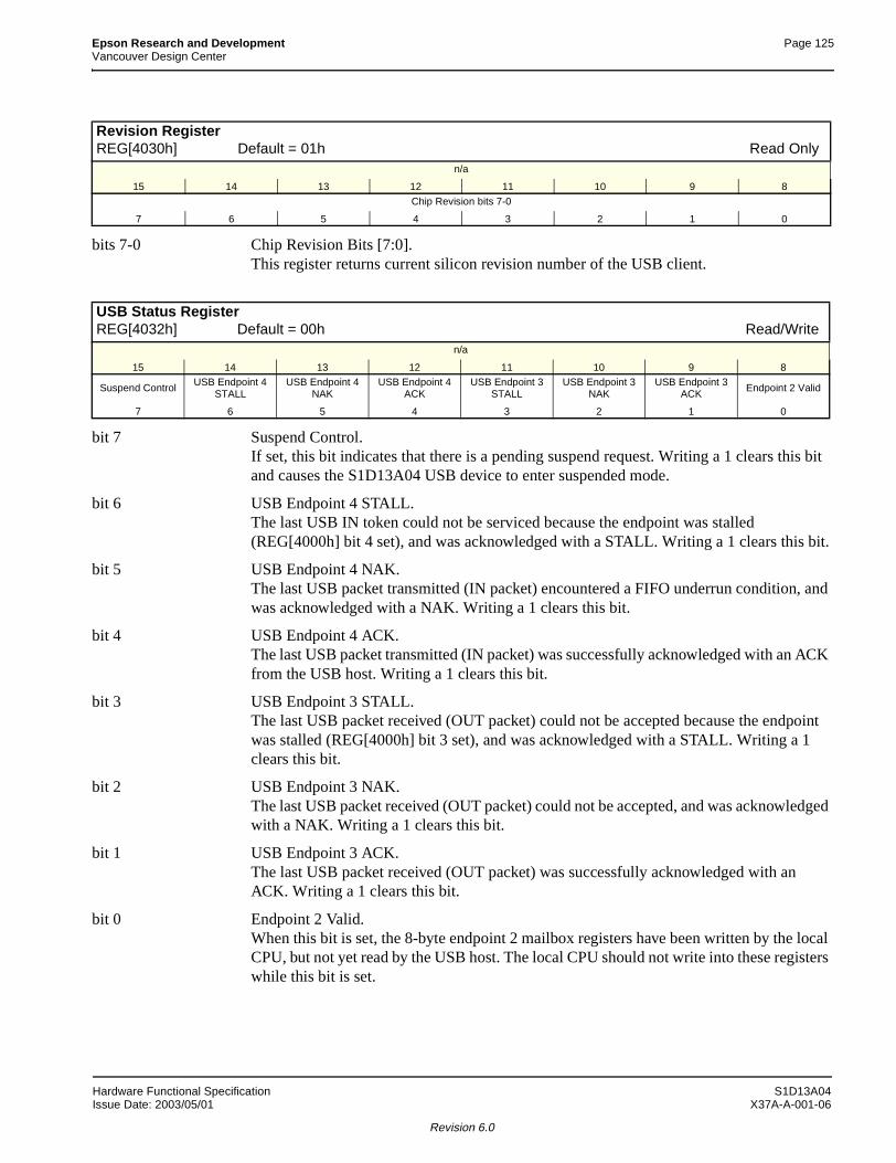
Epson Research and Development Page 125Vancouver Design Center
bits 7-0 Chip Revision Bits [7:0]. This register returns current silicon revision number of the USB client.
bit 7 Suspend Control. If set, this bit indicates that there is a pending suspend request. Writing a 1 clears this bit and causes the S1D13A04 USB device to enter suspended mode.
bit 6 USB Endpoint 4 STALL. The last USB IN token could not be serviced because the endpoint was stalled (REG[4000h] bit 4 set), and was acknowledged with a STALL. Writing a 1 clears this bit.
bit 5 USB Endpoint 4 NAK. The last USB packet transmitted (IN packet) encountered a FIFO underrun condition, and was acknowledged with a NAK. Writing a 1 clears this bit.
bit 4 USB Endpoint 4 ACK. The last USB packet transmitted (IN packet) was successfully acknowledged with an ACK from the USB host. Writing a 1 clears this bit.
bit 3 USB Endpoint 3 STALL. The last USB packet received (OUT packet) could not be accepted because the endpoint was stalled (REG[4000h] bit 3 set), and was acknowledged with a STALL. Writing a 1 clears this bit.
bit 2 USB Endpoint 3 NAK.The last USB packet received (OUT packet) could not be accepted, and was acknowledged with a NAK. Writing a 1 clears this bit.
bit 1 USB Endpoint 3 ACK. The last USB packet received (OUT packet) was successfully acknowledged with an ACK. Writing a 1 clears this bit.
bit 0 Endpoint 2 Valid. When this bit is set, the 8-byte endpoint 2 mailbox registers have been written by the local CPU, but not yet read by the USB host. The local CPU should not write into these registers while this bit is set.
Revision RegisterREG[4030h] Default = 01h Read Only
n/a
15 14 13 12 11 10 9 8
Chip Revision bits 7-0
7 6 5 4 3 2 1 0
USB Status RegisterREG[4032h] Default = 00h Read/Write
n/a
15 14 13 12 11 10 9 8
Suspend Control USB Endpoint 4 STALL
USB Endpoint 4 NAK
USB Endpoint 4 ACK
USB Endpoint 3 STALL
USB Endpoint 3 NAK
USB Endpoint 3 ACK
Endpoint 2 Valid
7 6 5 4 3 2 1 0
Hardware Functional Specification S1D13A04Issue Date: 2003/05/01 X37A-A-001-06
Revision 6.0
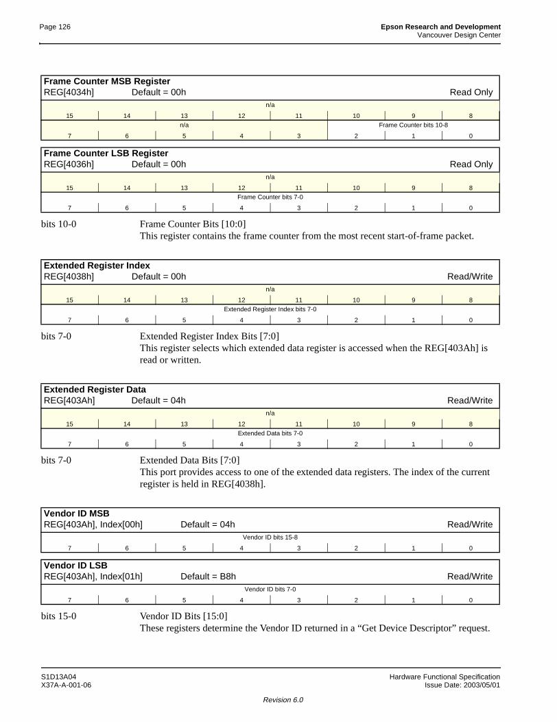
Page 126 Epson Research and DevelopmentVancouver Design Center
bits 10-0 Frame Counter Bits [10:0] This register contains the frame counter from the most recent start-of-frame packet.
bits 7-0 Extended Register Index Bits [7:0] This register selects which extended data register is accessed when the REG[403Ah] is read or written.
bits 7-0 Extended Data Bits [7:0] This port provides access to one of the extended data registers. The index of the current register is held in REG[4038h].
bits 15-0 Vendor ID Bits [15:0] These registers determine the Vendor ID returned in a “Get Device Descriptor” request.
Frame Counter MSB RegisterREG[4034h] Default = 00h Read Only
n/a
15 14 13 12 11 10 9 8
n/a Frame Counter bits 10-8
7 6 5 4 3 2 1 0
Frame Counter LSB RegisterREG[4036h] Default = 00h Read Only
n/a
15 14 13 12 11 10 9 8Frame Counter bits 7-0
7 6 5 4 3 2 1 0
Extended Register IndexREG[4038h] Default = 00h Read/Write
n/a
15 14 13 12 11 10 9 8Extended Register Index bits 7-0
7 6 5 4 3 2 1 0
Extended Register DataREG[403Ah] Default = 04h Read/Write
n/a
15 14 13 12 11 10 9 8
Extended Data bits 7-0
7 6 5 4 3 2 1 0
Vendor ID MSBREG[403Ah], Index[00h] Default = 04h Read/Write
Vendor ID bits 15-8
7 6 5 4 3 2 1 0
Vendor ID LSBREG[403Ah], Index[01h] Default = B8h Read/Write
Vendor ID bits 7-0
7 6 5 4 3 2 1 0
S1D13A04 Hardware Functional SpecificationX37A-A-001-06 Issue Date: 2003/05/01
Revision 6.0
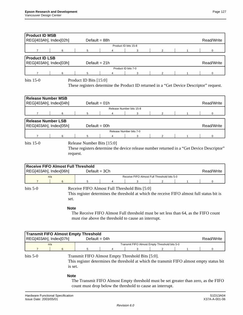
Epson Research and Development Page 127Vancouver Design Center
bits 15-0 Product ID Bits [15:0] These registers determine the Product ID returned in a “Get Device Descriptor” request.
bits 15-0 Release Number Bits [15:0] These registers determine the device release number returned in a “Get Device Descriptor” request.
bits 5-0 Receive FIFO Almost Full Threshold Bits [5:0] This register determines the threshold at which the receive FIFO almost full status bit is set.
NoteThe Receive FIFO Almost Full threshold must be set less than 64, as the FIFO count must rise above the threshold to cause an interrupt.
bits 5-0 Transmit FIFO Almost Empty Threshold Bits [5:0]. This register determines the threshold at which the transmit FIFO almost empty status bit is set.
NoteThe Transmit FIFO Almost Empty threshold must be set greater than zero, as the FIFO count must drop below the threshold to cause an interrupt.
Product ID MSBREG[403Ah], Index[02h] Default = 88h Read/Write
Product ID bits 15-8
7 6 5 4 3 2 1 0
Product ID LSBREG[403Ah], Index[03h] Default = 21h Read/Write
Product ID bits 7-0
7 6 5 4 3 2 1 0
Release Number MSBREG[403Ah], Index[04h] Default = 01h Read/Write
Release Number bits 15-8
7 6 5 4 3 2 1 0
Release Number LSBREG[403Ah], Index[05h] Default = 00h Read/Write
Release Number bits 7-0
7 6 5 4 3 2 1 0
Receive FIFO Almost Full ThresholdREG[403Ah], Index[06h] Default = 3Ch Read/Write
n/a Receive FIFO Almost Full Threshold bits 5-0
7 6 5 4 3 2 1 0
Transmit FIFO Almost Empty ThresholdREG[403Ah], Index[07h] Default = 04h Read/Write
n/a Transmit FIFO Almost Empty Threshold bits 5-0
7 6 5 4 3 2 1 0
Hardware Functional Specification S1D13A04Issue Date: 2003/05/01 X37A-A-001-06
Revision 6.0
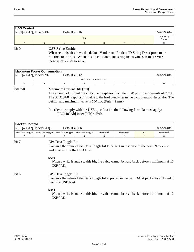
Page 128 Epson Research and DevelopmentVancouver Design Center
bit 0 USB String Enable. When set, this bit allows the default Vendor and Product ID String Descriptors to be returned to the host. When this bit is cleared, the string index values in the Device Descriptor are set to zero.
bits 7-0 Maximum Current Bits [7:0]. The amount of current drawn by the peripheral from the USB port in increments of 2 mA. The S1D13A04 reports this value to the host controller in the configuration descriptor. The default and maximum value is 500 mA (FAh * 2 mA).
In order to comply with the USB specification the following formula must apply:REG[403Ah] index[09h] ≤ FAh.
bit 7 EP4 Data Toggle Bit. Contains the value of the Data Toggle bit to be sent in response to the next IN token to endpoint 4 from the USB host.
NoteWhen a write is made to this bit, the value cannot be read back before a minimum of 12 USBCLK.
bit 6 EP3 Data Toggle Bit. Contains the value of the Data Toggle bit expected in the next DATA packet to endpoint 3 from the USB host.
NoteWhen a write is made to this bit, the value cannot be read back before a minimum of 12 USBCLK.
USB ControlREG[403Ah], Index[08h] Default = 01h Read/Write
n/aUSB String
Enable
7 6 5 4 3 2 1 0
Maximum Power ConsumptionREG[403Ah], Index[09h] Default = FAh Read/Write
Maximum Current bits 7-0
7 6 5 4 3 2 1 0
Packet ControlREG[403Ah], Index[0Ah] Default = 00h Read/WriteEP4 Data Toggle EP3 Data Toggle EP2 Data Toggle EP1 Data Toggle Reserved Reserved n/a Reserved
7 6 5 4 3 2 1 0
S1D13A04 Hardware Functional SpecificationX37A-A-001-06 Issue Date: 2003/05/01
Revision 6.0
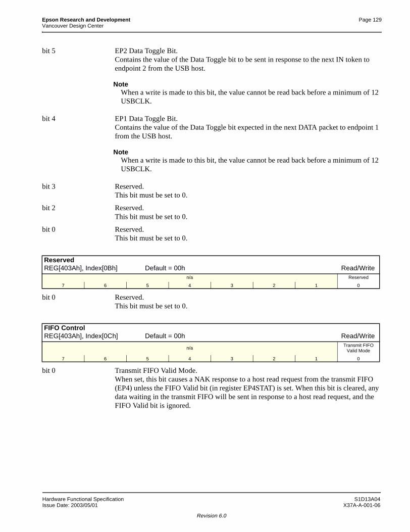
Epson Research and Development Page 129Vancouver Design Center
bit 5 EP2 Data Toggle Bit. Contains the value of the Data Toggle bit to be sent in response to the next IN token to endpoint 2 from the USB host.
NoteWhen a write is made to this bit, the value cannot be read back before a minimum of 12 USBCLK.
bit 4 EP1 Data Toggle Bit. Contains the value of the Data Toggle bit expected in the next DATA packet to endpoint 1 from the USB host.
NoteWhen a write is made to this bit, the value cannot be read back before a minimum of 12 USBCLK.
bit 3 Reserved.This bit must be set to 0.
bit 2 Reserved.This bit must be set to 0.
bit 0 Reserved.This bit must be set to 0.
bit 0 Reserved.This bit must be set to 0.
bit 0 Transmit FIFO Valid Mode. When set, this bit causes a NAK response to a host read request from the transmit FIFO (EP4) unless the FIFO Valid bit (in register EP4STAT) is set. When this bit is cleared, any data waiting in the transmit FIFO will be sent in response to a host read request, and the FIFO Valid bit is ignored.
ReservedREG[403Ah], Index[0Bh] Default = 00h Read/Write
n/a Reserved
7 6 5 4 3 2 1 0
FIFO ControlREG[403Ah], Index[0Ch] Default = 00h Read/Write
n/a Transmit FIFO Valid Mode
7 6 5 4 3 2 1 0
Hardware Functional Specification S1D13A04Issue Date: 2003/05/01 X37A-A-001-06
Revision 6.0
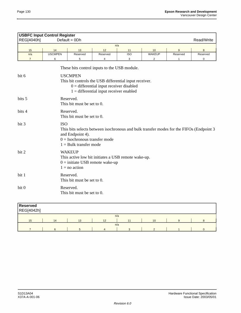
Page 130 Epson Research and DevelopmentVancouver Design Center
These bits control inputs to the USB module.
bit 6 USCMPENThis bit controls the USB differential input receiver.
0 = differential input receiver disabled1 = differential input receiver enabled
bits 5 Reserved.This bit must be set to 0.
bits 4 Reserved.This bit must be set to 0.
bit 3 ISO This bits selects between isochronous and bulk transfer modes for the FIFOs (Endpoint 3 and Endpoint 4).0 = Isochronous transfer mode1 = Bulk transfer mode
bit 2 WAKEUP This active low bit initiates a USB remote wake-up.0 = initiate USB remote wake-up1 = no action
bit 1 Reserved.This bit must be set to 0.
bit 0 Reserved.This bit must be set to 0.
USBFC Input Control RegisterREG[4040h] Default = 0Dh Read/Write
n/a
15 14 13 12 11 10 9 8
n/a USCMPEN Reserved Reserved ISO WAKEUP Reserved Reserved
7 6 5 4 3 2 1 0
ReservedREG[4042h]
n/a
15 14 13 12 11 10 9 8
n/a
7 6 5 4 3 2 1 0
S1D13A04 Hardware Functional SpecificationX37A-A-001-06 Issue Date: 2003/05/01
Revision 6.0
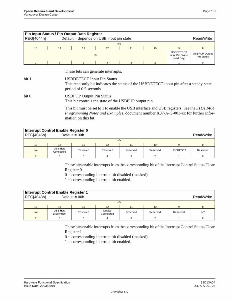
Epson Research and Development Page 131Vancouver Design Center
These bits can generate interrupts.
bit 1 USBDETECT Input Pin StatusThis read-only bit indicates the status of the USBDETECT input pin after a steady-state period of 0.5 seconds.
bit 0 USBPUP Output Pin StatusThis bit controls the state of the USBPUP output pin.
This bit must be set to 1 to enable the USB interface and USB registers. See the S1D13A04 Programming Notes and Examples, document number X37-A-G-003-xx for further infor-mation on this bit.
These bits enable interrupts from the corresponding bit of the Interrupt Control Status/Clear Register 0.0 = corresponding interrupt bit disabled (masked).1 = corresponding interrupt bit enabled.
These bits enable interrupts from the corresponding bit of the Interrupt Control Status/Clear Register 1.0 = corresponding interrupt bit disabled (masked).1 = corresponding interrupt bit enabled.
Pin Input Status / Pin Output Data RegisterREG[4044h] Default = depends on USB input pin state Read/Write
n/a
15 14 13 12 11 10 9 8
n/aUSBDETECT
Input Pin Status(read only)
USBPUP Output Pin Status
7 6 5 4 3 2 1 0
Interrupt Control Enable Register 0REG[4046h] Default = 00h Read/Write
n/a
15 14 13 12 11 10 9 8
n/a USB Host Connected Reserved Reserved Reserved Reserved USBRESET Reserved
7 6 5 4 3 2 1 0
Interrupt Control Enable Register 1REG[4048h] Default = 00h Read/Write
n/a
15 14 13 12 11 10 9 8
n/a USB Host Disconnect
Reserved Device Configured
Reserved Reserved Reserved INT
7 6 5 4 3 2 1 0
Hardware Functional Specification S1D13A04Issue Date: 2003/05/01 X37A-A-001-06
Revision 6.0
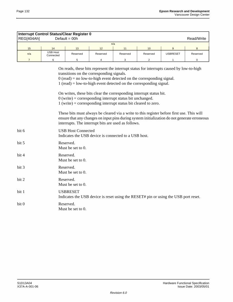
Page 132 Epson Research and DevelopmentVancouver Design Center
On reads, these bits represent the interrupt status for interrupts caused by low-to-high transitions on the corresponding signals.0 (read) = no low-to-high event detected on the corresponding signal.1 (read) = low-to-high event detected on the corresponding signal.
On writes, these bits clear the corresponding interrupt status bit.0 (write) = corresponding interrupt status bit unchanged.1 (write) = corresponding interrupt status bit cleared to zero.
These bits must always be cleared via a write to this register before first use. This will ensure that any changes on input pins during system initialization do not generate erroneous interrupts. The interrupt bits are used as follows.
bit 6 USB Host ConnectedIndicates the USB device is connected to a USB host.
bit 5 Reserved.Must be set to 0.
bit 4 Reserved.Must be set to 0.
bit 3 Reserved.Must be set to 0.
bit 2 Reserved.Must be set to 0.
bit 1 USBRESETIndicates the USB device is reset using the RESET# pin or using the USB port reset.
bit 0 Reserved.Must be set to 0.
Interrupt Control Status/Clear Register 0REG[404Ah] Default = 00h Read/Write
n/a
15 14 13 12 11 10 9 8
n/a USB Host Connected Reserved Reserved Reserved Reserved USBRESET Reserved
7 6 5 4 3 2 1 0
S1D13A04 Hardware Functional SpecificationX37A-A-001-06 Issue Date: 2003/05/01
Revision 6.0
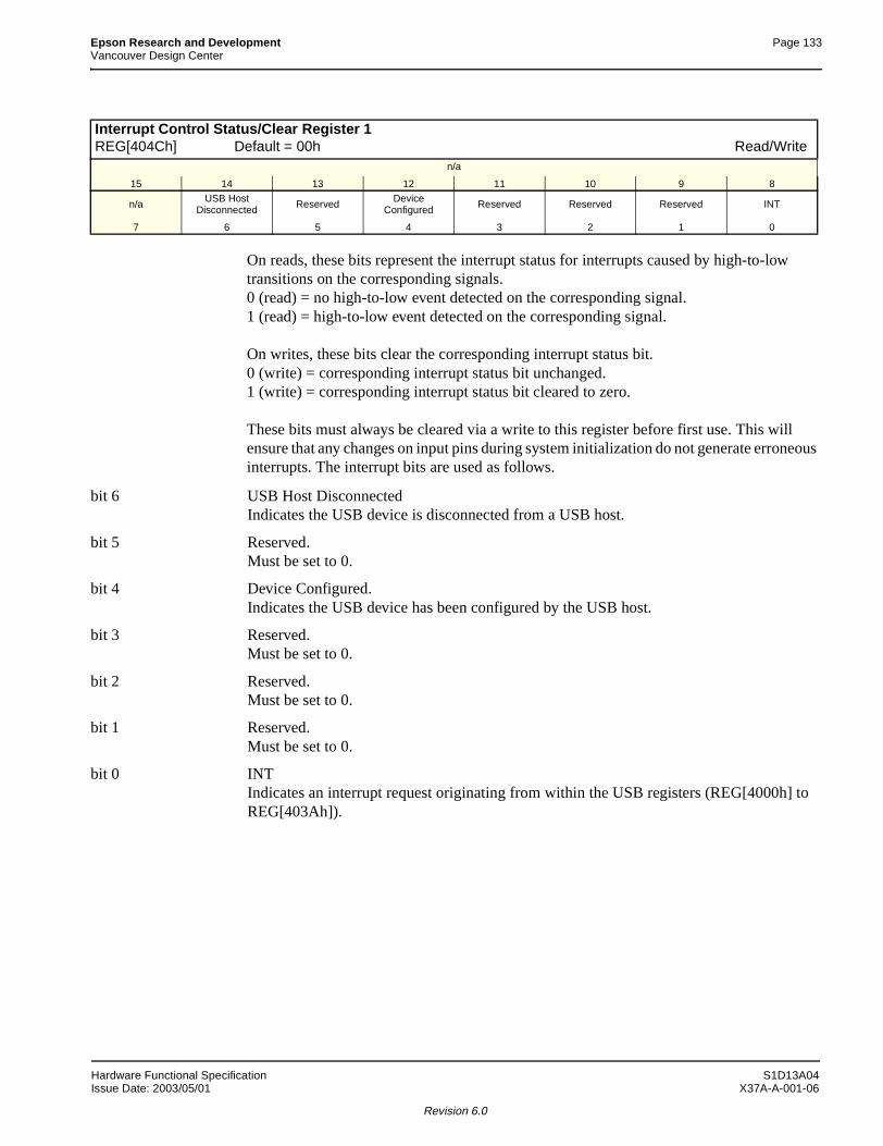
Epson Research and Development Page 133Vancouver Design Center
On reads, these bits represent the interrupt status for interrupts caused by high-to-low transitions on the corresponding signals.0 (read) = no high-to-low event detected on the corresponding signal.1 (read) = high-to-low event detected on the corresponding signal.
On writes, these bits clear the corresponding interrupt status bit.0 (write) = corresponding interrupt status bit unchanged.1 (write) = corresponding interrupt status bit cleared to zero.
These bits must always be cleared via a write to this register before first use. This will ensure that any changes on input pins during system initialization do not generate erroneous interrupts. The interrupt bits are used as follows.
bit 6 USB Host DisconnectedIndicates the USB device is disconnected from a USB host.
bit 5 Reserved.Must be set to 0.
bit 4 Device Configured.Indicates the USB device has been configured by the USB host.
bit 3 Reserved.Must be set to 0.
bit 2 Reserved.Must be set to 0.
bit 1 Reserved.Must be set to 0.
bit 0 INTIndicates an interrupt request originating from within the USB registers (REG[4000h] to REG[403Ah]).
Interrupt Control Status/Clear Register 1REG[404Ch] Default = 00h Read/Write
n/a
15 14 13 12 11 10 9 8
n/a USB Host Disconnected Reserved Device
Configured Reserved Reserved Reserved INT
7 6 5 4 3 2 1 0
Hardware Functional Specification S1D13A04Issue Date: 2003/05/01 X37A-A-001-06
Revision 6.0
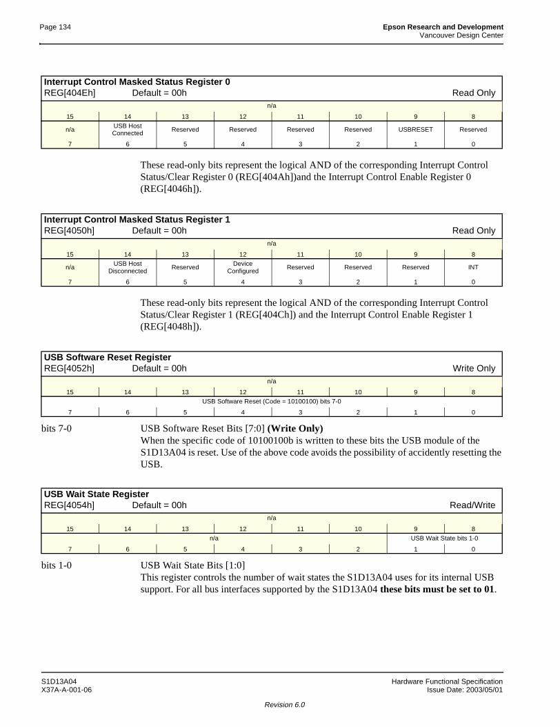
Page 134 Epson Research and DevelopmentVancouver Design Center
These read-only bits represent the logical AND of the corresponding Interrupt Control Status/Clear Register 0 (REG[404Ah])and the Interrupt Control Enable Register 0 (REG[4046h]).
These read-only bits represent the logical AND of the corresponding Interrupt Control Status/Clear Register 1 (REG[404Ch]) and the Interrupt Control Enable Register 1 (REG[4048h]).
bits 7-0 USB Software Reset Bits [7:0] (Write Only)When the specific code of 10100100b is written to these bits the USB module of the S1D13A04 is reset. Use of the above code avoids the possibility of accidently resetting the USB.
bits 1-0 USB Wait State Bits [1:0]This register controls the number of wait states the S1D13A04 uses for its internal USB support. For all bus interfaces supported by the S1D13A04 these bits must be set to 01.
Interrupt Control Masked Status Register 0REG[404Eh] Default = 00h Read Only
n/a
15 14 13 12 11 10 9 8
n/a USB Host Connected Reserved Reserved Reserved Reserved USBRESET Reserved
7 6 5 4 3 2 1 0
Interrupt Control Masked Status Register 1REG[4050h] Default = 00h Read Only
n/a
15 14 13 12 11 10 9 8
n/a USB Host Disconnected
Reserved Device Configured
Reserved Reserved Reserved INT
7 6 5 4 3 2 1 0
USB Software Reset RegisterREG[4052h] Default = 00h Write Only
n/a
15 14 13 12 11 10 9 8USB Software Reset (Code = 10100100) bits 7-0
7 6 5 4 3 2 1 0
USB Wait State RegisterREG[4054h] Default = 00h Read/Write
n/a
15 14 13 12 11 10 9 8
n/a USB Wait State bits 1-0
7 6 5 4 3 2 1 0
S1D13A04 Hardware Functional SpecificationX37A-A-001-06 Issue Date: 2003/05/01
Revision 6.0
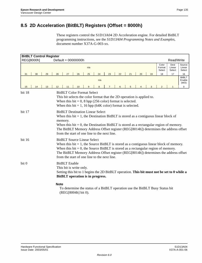
Epson Research and Development Page 135Vancouver Design Center
8.5 2D Acceleration (BitBLT) Registers (Offset = 8000h)
These registers control the S1D13A04 2D Acceleration engine. For detailed BitBLT programming instructions, see the S1D13A04 Programming Notes and Examples, document number X37A-G-003-xx.
bit 18 BitBLT Color Format SelectThis bit selects the color format that the 2D operation is applied to.When this bit = 0, 8 bpp (256 color) format is selected.When this bit = 1, 16 bpp (64K color) format is selected.
bit 17 BitBLT Destination Linear SelectWhen this bit = 1, the Destination BitBLT is stored as a contiguous linear block ofmemory.When this bit = 0, the Destination BitBLT is stored as a rectangular region of memory.The BitBLT Memory Address Offset register (REG[8014h]) determines the address offset from the start of one line to the next line.
bit 16 BitBLT Source Linear SelectWhen this bit = 1, the Source BitBLT is stored as a contiguous linear block of memory. When this bit = 0, the Source BitBLT is stored as a rectangular region of memory.The BitBLT Memory Address Offset register (REG[8014h]) determines the address offset from the start of one line to the next line.
bit 0 BitBLT EnableThis bit is write only.Setting this bit to 1 begins the 2D BitBLT operation. This bit must not be set to 0 while a BitBLT operation is in progress.
NoteTo determine the status of a BitBLT operation use the BitBLT Busy Status bit (REG[8004h] bit 0).
BitBLT Control RegisterREG[8000h] Default = 00000000h Read/Write
n/aColor
Format Select
Dest Linear Select
Source Linear Select
31 30 29 28 27 26 25 24 23 22 21 20 19 18 17 16
n/aBitBLT Enable(WO)
15 14 13 12 11 10 9 8 7 6 5 4 3 2 1 0
Hardware Functional Specification S1D13A04Issue Date: 2003/05/01 X37A-A-001-06
Revision 6.0
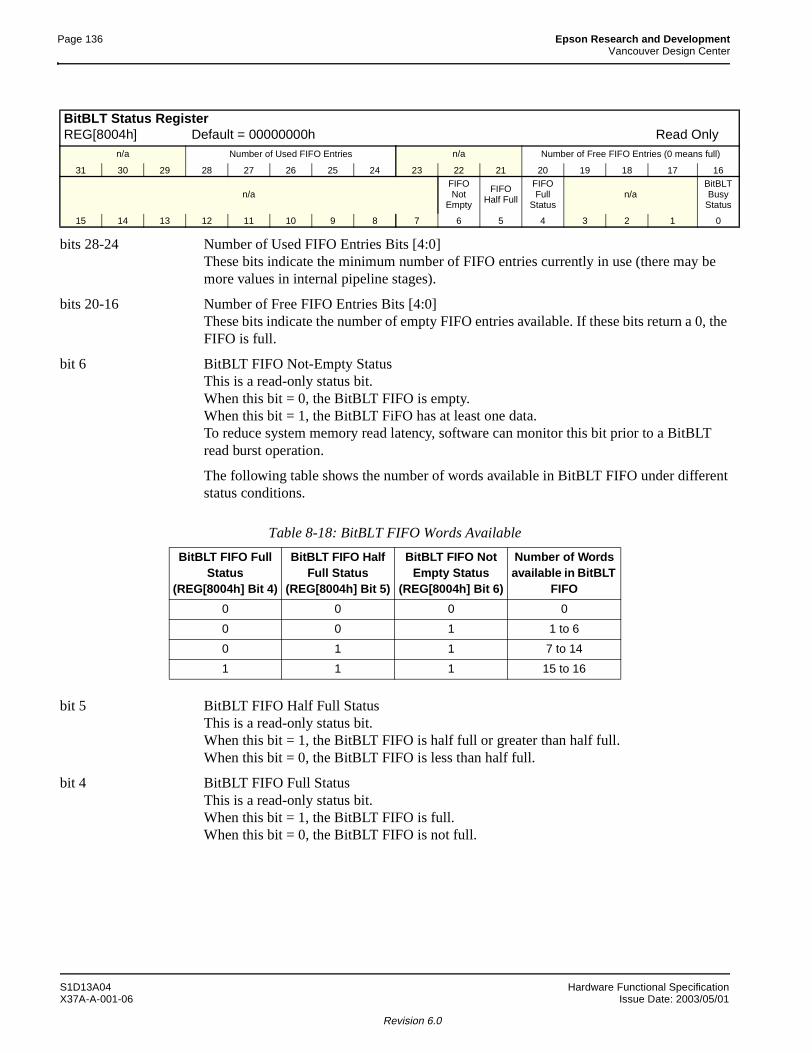
Page 136 Epson Research and DevelopmentVancouver Design Center
bits 28-24 Number of Used FIFO Entries Bits [4:0]These bits indicate the minimum number of FIFO entries currently in use (there may be more values in internal pipeline stages).
bits 20-16 Number of Free FIFO Entries Bits [4:0]These bits indicate the number of empty FIFO entries available. If these bits return a 0, the FIFO is full.
bit 6 BitBLT FIFO Not-Empty StatusThis is a read-only status bit.When this bit = 0, the BitBLT FIFO is empty.When this bit = 1, the BitBLT FiFO has at least one data.To reduce system memory read latency, software can monitor this bit prior to a BitBLT read burst operation.
The following table shows the number of words available in BitBLT FIFO under differentstatus conditions.
bit 5 BitBLT FIFO Half Full StatusThis is a read-only status bit.When this bit = 1, the BitBLT FIFO is half full or greater than half full.When this bit = 0, the BitBLT FIFO is less than half full.
bit 4 BitBLT FIFO Full StatusThis is a read-only status bit.When this bit = 1, the BitBLT FIFO is full.When this bit = 0, the BitBLT FIFO is not full.
BitBLT Status RegisterREG[8004h] Default = 00000000h Read Only
n/a Number of Used FIFO Entries n/a Number of Free FIFO Entries (0 means full)
31 30 29 28 27 26 25 24 23 22 21 20 19 18 17 16
n/aFIFO Not
Empty
FIFO Half Full
FIFO Full
Statusn/a
BitBLT Busy
Status
15 14 13 12 11 10 9 8 7 6 5 4 3 2 1 0
Table 8-18: BitBLT FIFO Words Available
BitBLT FIFO Full Status
(REG[8004h] Bit 4)
BitBLT FIFO Half Full Status
(REG[8004h] Bit 5)
BitBLT FIFO Not Empty Status
(REG[8004h] Bit 6)
Number of Words available in BitBLT
FIFO
0 0 0 0
0 0 1 1 to 6
0 1 1 7 to 14
1 1 1 15 to 16
S1D13A04 Hardware Functional SpecificationX37A-A-001-06 Issue Date: 2003/05/01
Revision 6.0
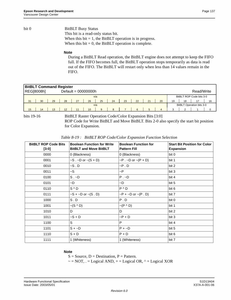
Epson Research and Development Page 137Vancouver Design Center
bit 0 BitBLT Busy StatusThis bit is a read-only status bit.When this bit = 1, the BitBLT operation is in progress.When this bit = 0, the BitBLT operation is complete.
NoteDuring a BitBLT Read operation, the BitBLT engine does not attempt to keep the FIFO full. If the FIFO becomes full, the BitBLT operation stops temporarily as data is read out of the FIFO. The BitBLT will restart only when less than 14 values remain in the FIFO.
bits 19-16 BitBLT Raster Operation Code/Color Expansion Bits [3:0]ROP Code for Write BitBLT and Move BitBLT. Bits 2-0 also specify the start bit position for Color Expansion.
NoteS = Source, D = Destination, P = Pattern.~ = NOT, . = Logical AND, + = Logical OR, ^ = Logical XOR
BitBLT Command RegisterREG[8008h] Default = 00000000h Read/Write
n/a BitBLT ROP Code bits 3-0
31 30 29 28 27 26 25 24 23 22 21 20 19 18 17 16
n/a BitBLT Operation bits 3-0
15 14 13 12 11 10 9 8 7 6 5 4 3 2 1 0
Table 8-19 : BitBLT ROP Code/Color Expansion Function Selection
BitBLT ROP Code Bits [3:0]
Boolean Function for Write BitBLT and Move BitBLT
Boolean Function forPattern Fill
Start Bit Position for Color Expansion
0000 0 (Blackness) 0 (Blackness) bit 0
0001 ~S . ~D or ~(S + D) ~P . ~D or ~(P + D) bit 1
0010 ~S . D ~P . D bit 2
0011 ~S ~P bit 3
0100 S . ~D P . ~D bit 4
0101 ~D ~D bit 5
0110 S ^ D P ^ D bit 6
0111 ~S + ~D or ~(S . D) ~P + ~D or ~(P . D) bit 7
1000 S . D P . D bit 0
1001 ~(S ^ D) ~(P ^ D) bit 1
1010 D D bit 2
1011 ~S + D ~P + D bit 3
1100 S P bit 4
1101 S + ~D P + ~D bit 5
1110 S + D P + D bit 6
1111 1 (Whiteness) 1 (Whiteness) bit 7
Hardware Functional Specification S1D13A04Issue Date: 2003/05/01 X37A-A-001-06
Revision 6.0
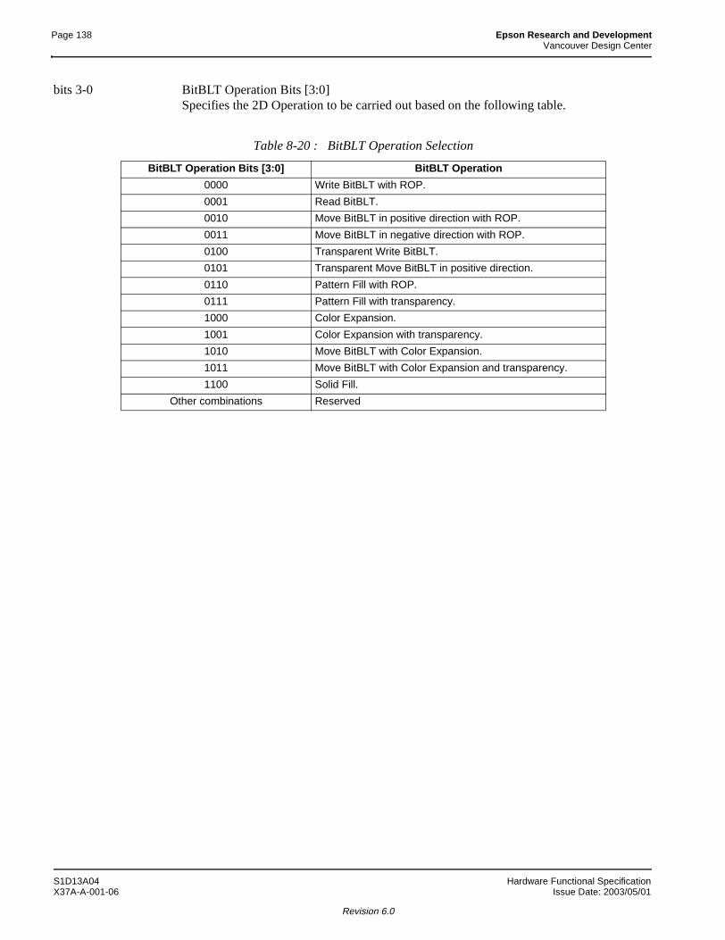
Page 138 Epson Research and DevelopmentVancouver Design Center
bits 3-0 BitBLT Operation Bits [3:0]Specifies the 2D Operation to be carried out based on the following table.
Table 8-20 : BitBLT Operation Selection
BitBLT Operation Bits [3:0] BitBLT Operation
0000 Write BitBLT with ROP.
0001 Read BitBLT.
0010 Move BitBLT in positive direction with ROP.
0011 Move BitBLT in negative direction with ROP.
0100 Transparent Write BitBLT.
0101 Transparent Move BitBLT in positive direction.
0110 Pattern Fill with ROP.
0111 Pattern Fill with transparency.
1000 Color Expansion.
1001 Color Expansion with transparency.
1010 Move BitBLT with Color Expansion.
1011 Move BitBLT with Color Expansion and transparency.
1100 Solid Fill.
Other combinations Reserved
S1D13A04 Hardware Functional SpecificationX37A-A-001-06 Issue Date: 2003/05/01
Revision 6.0
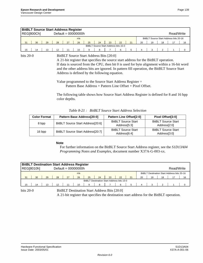
Epson Research and Development Page 139Vancouver Design Center
bits 20-0 BitBLT Source Start Address Bits [20:0]A 21-bit register that specifies the source start address for the BitBLT operation.If data is sourced from the CPU, then bit 0 is used for byte alignment within a 16-bit wordand the other address bits are ignored. In pattern fill operation, the BitBLT Source StartAddress is defined by the following equation.
Value programmed to the Source Start Address Register =Pattern Base Address + Pattern Line Offset + Pixel Offset.
The following table shows how Source Start Address Register is defined for 8 and 16 bpp color depths.
NoteFor further information on the BitBLT Source Start Address register, see the S1D13A04 Programming Notes and Examples, document number X37A-G-003-xx.
bits 20-0 BitBLT Destination Start Address Bits [20:0]A 21-bit register that specifies the destination start address for the BitBLT operation.
BitBLT Source Start Address RegisterREG[800Ch] Default = 00000000h Read/Write
n/a BitBLT Source Start Address bits 20-16
31 30 29 28 27 26 25 24 23 22 21 20 19 18 17 16BitBLT Source Start Address bits 15-0
15 14 13 12 11 10 9 8 7 6 5 4 3 2 1 0
Table 8-21 : BitBLT Source Start Address Selection
Color Format Pattern Base Address[20:0] Pattern Line Offset[2:0] Pixel Offset[3:0]
8 bpp BitBLT Source Start Address[20:6]BitBLT Source Start
Address[5:3]BitBLT Source Start
Address[2:0]
16 bpp BitBLT Source Start Address[20:7]BitBLT Source Start
Address[6:4]BitBLT Source Start
Address[3:0]
BitBLT Destination Start Address RegisterREG[8010h] Default = 00000000h Read/Write
n/a BitBLT Destination Start Address bits 20-16
31 30 29 28 27 26 25 24 23 22 21 20 19 18 17 16
BitBLT Destination Start Address bits 15-0
15 14 13 12 11 10 9 8 7 6 5 4 3 2 1 0
Hardware Functional Specification S1D13A04Issue Date: 2003/05/01 X37A-A-001-06
Revision 6.0
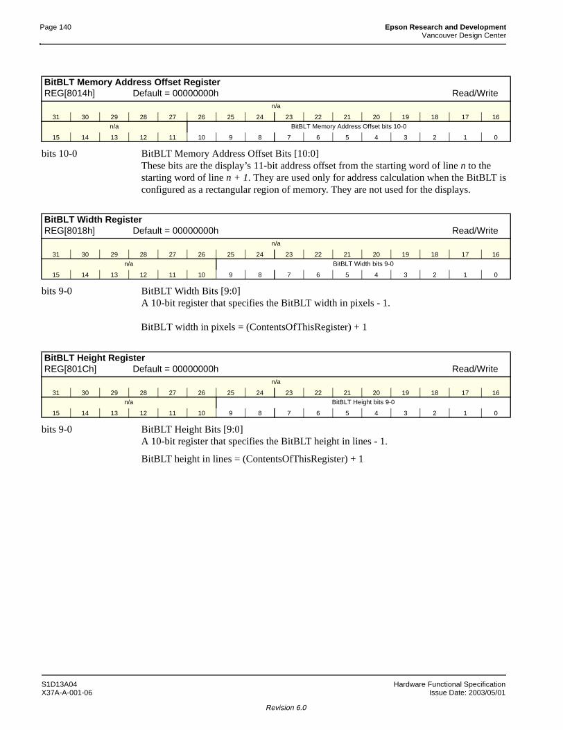
Page 140 Epson Research and DevelopmentVancouver Design Center
bits 10-0 BitBLT Memory Address Offset Bits [10:0]These bits are the display’s 11-bit address offset from the starting word of line n to the starting word of line n + 1. They are used only for address calculation when the BitBLT isconfigured as a rectangular region of memory. They are not used for the displays.
bits 9-0 BitBLT Width Bits [9:0]A 10-bit register that specifies the BitBLT width in pixels - 1.
BitBLT width in pixels = (ContentsOfThisRegister) + 1
bits 9-0 BitBLT Height Bits [9:0]A 10-bit register that specifies the BitBLT height in lines - 1.
BitBLT height in lines = (ContentsOfThisRegister) + 1
BitBLT Memory Address Offset RegisterREG[8014h] Default = 00000000h Read/Write
n/a
31 30 29 28 27 26 25 24 23 22 21 20 19 18 17 16
n/a BitBLT Memory Address Offset bits 10-0
15 14 13 12 11 10 9 8 7 6 5 4 3 2 1 0
BitBLT Width RegisterREG[8018h] Default = 00000000h Read/Write
n/a
31 30 29 28 27 26 25 24 23 22 21 20 19 18 17 16
n/a BitBLT Width bits 9-0
15 14 13 12 11 10 9 8 7 6 5 4 3 2 1 0
BitBLT Height RegisterREG[801Ch] Default = 00000000h Read/Write
n/a
31 30 29 28 27 26 25 24 23 22 21 20 19 18 17 16
n/a BitBLT Height bits 9-0
15 14 13 12 11 10 9 8 7 6 5 4 3 2 1 0
S1D13A04 Hardware Functional SpecificationX37A-A-001-06 Issue Date: 2003/05/01
Revision 6.0
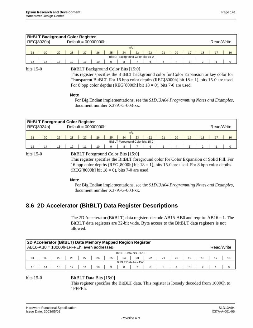
Epson Research and Development Page 141Vancouver Design Center
bits 15-0 BitBLT Background Color Bits [15:0]This register specifies the BitBLT background color for Color Expansion or key color for Transparent BitBLT. For 16 bpp color depths (REG[8000h] bit 18 = 1), bits 15-0 are used. For 8 bpp color depths (REG[8000h] bit 18 = 0), bits 7-0 are used.
NoteFor Big Endian implementations, see the S1D13A04 Programming Notes and Examples, document number X37A-G-003-xx.
bits 15-0 BitBLT Foreground Color Bits [15:0]This register specifies the BitBLT foreground color for Color Expansion or Solid Fill. For 16 bpp color depths (REG[8000h] bit 18 = 1), bits 15-0 are used. For 8 bpp color depths (REG[8000h] bit 18 = 0), bits 7-0 are used.
NoteFor Big Endian implementations, see the S1D13A04 Programming Notes and Examples, document number X37A-G-003-xx.
8.6 2D Accelerator (BitBLT) Data Register Descriptions
The 2D Accelerator (BitBLT) data registers decode AB15-AB0 and require AB16 = 1. The BitBLT data registers are 32-bit wide. Byte access to the BitBLT data registers is not allowed.
bits 15-0 BitBLT Data Bits [15:0]This register specifies the BitBLT data. This register is loosely decoded from 10000h to 1FFFEh.
BitBLT Background Color RegisterREG[8020h] Default = 00000000h Read/Write
n/a
31 30 29 28 27 26 25 24 23 22 21 20 19 18 17 16
BitBLT Background Color bits 15-0
15 14 13 12 11 10 9 8 7 6 5 4 3 2 1 0
BitBLT Foreground Color RegisterREG[8024h] Default = 00000000h Read/Write
n/a
31 30 29 28 27 26 25 24 23 22 21 20 19 18 17 16BitBLT Foreground Color bits 15-0
15 14 13 12 11 10 9 8 7 6 5 4 3 2 1 0
2D Accelerator (BitBLT) Data Memory Mapped Region RegisterAB16-AB0 = 10000h-1FFFEh, even addresses Read/Write
BitBLT Data bits 31-16
31 30 29 28 27 26 25 24 23 22 21 20 19 18 17 16
BitBLT Data bits 15-0
15 14 13 12 11 10 9 8 7 6 5 4 3 2 1 0
Hardware Functional Specification S1D13A04Issue Date: 2003/05/01 X37A-A-001-06
Revision 6.0
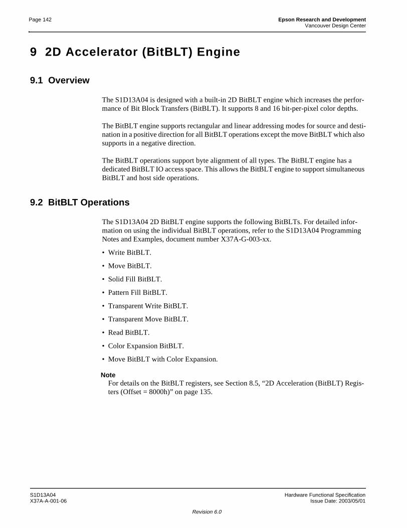
Page 142 Epson Research and DevelopmentVancouver Design Center
9 2D Accelerator (BitBLT) Engine
9.1 Overview
The S1D13A04 is designed with a built-in 2D BitBLT engine which increases the perfor-mance of Bit Block Transfers (BitBLT). It supports 8 and 16 bit-per-pixel color depths.
The BitBLT engine supports rectangular and linear addressing modes for source and desti-nation in a positive direction for all BitBLT operations except the move BitBLT which also supports in a negative direction.
The BitBLT operations support byte alignment of all types. The BitBLT engine has a dedicated BitBLT IO access space. This allows the BitBLT engine to support simultaneous BitBLT and host side operations.
9.2 BitBLT Operations
The S1D13A04 2D BitBLT engine supports the following BitBLTs. For detailed infor-mation on using the individual BitBLT operations, refer to the S1D13A04 Programming Notes and Examples, document number X37A-G-003-xx.
• Write BitBLT.
• Move BitBLT.
• Solid Fill BitBLT.
• Pattern Fill BitBLT.
• Transparent Write BitBLT.
• Transparent Move BitBLT.
• Read BitBLT.
• Color Expansion BitBLT.
• Move BitBLT with Color Expansion.
NoteFor details on the BitBLT registers, see Section 8.5, “2D Acceleration (BitBLT) Regis-ters (Offset = 8000h)” on page 135.
S1D13A04 Hardware Functional SpecificationX37A-A-001-06 Issue Date: 2003/05/01
Revision 6.0
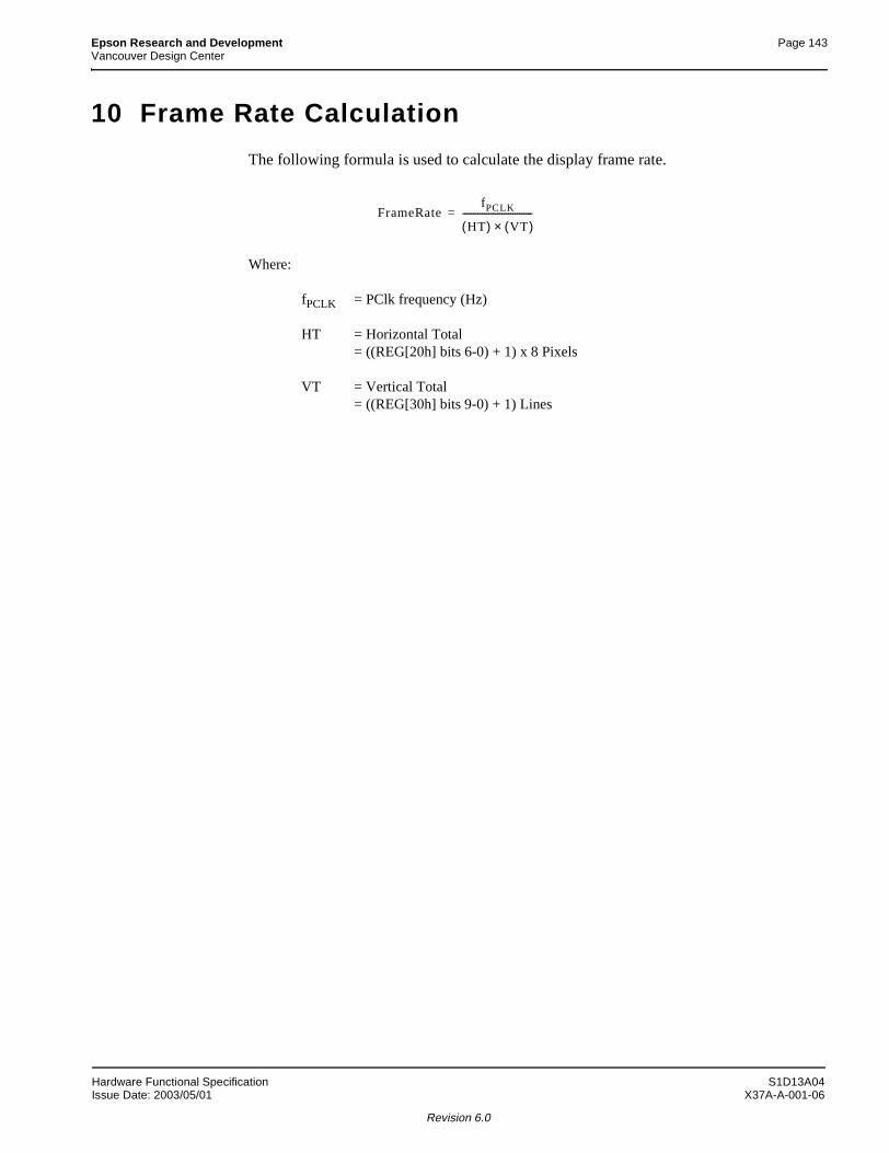
Epson Research and Development Page 143Vancouver Design Center
10 Frame Rate Calculation
The following formula is used to calculate the display frame rate.
Where:
fPCLK = PClk frequency (Hz)
HT = Horizontal Total= ((REG[20h] bits 6-0) + 1) x 8 Pixels
VT = Vertical Total= ((REG[30h] bits 9-0) + 1) Lines
FrameRatefPCLK
HT( ) VT( )×--------------------------------=
Hardware Functional Specification S1D13A04Issue Date: 2003/05/01 X37A-A-001-06
Revision 6.0
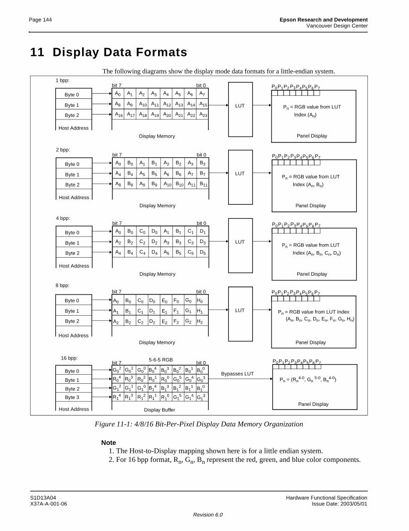
Page 144 Epson Research and DevelopmentVancouver Design Center
11 Display Data FormatsThe following diagrams show the display mode data formats for a little-endian system.
Figure 11-1: 4/8/16 Bit-Per-Pixel Display Data Memory Organization
Note1. The Host-to-Display mapping shown here is for a little endian system.2. For 16 bpp format, Rn, Gn, Bn represent the red, green, and blue color components.
4 bpp:
A0 B0 C0 D0 A1 B1 C1 D1
Host Address
Display Memory
A2 B2 C2 D2 A3 B3 C3 D3
bit 7 bit 0
A4 B4 C4 D4 A5 B5 C5 D5
Host AddressDisplay Memory
bit 7 bit 08 bpp:
A0 B0 C0 D0 E0 F0 G0 H0
A1 B1 C1 D1 E1 F1 G1 H1
A2 B2 C2 D2 E2 F2 G2 H2
Byte 0
Byte 1
Byte 2
Byte 0
Byte 1
Byte 2
Panel Display
P0P1P2 P3P4P5P6 P7
Panel Display
P0P1P2 P3P4P5P6 P7
(An, Bn, Cn, Dn, En, Fn, Gn, Hn)
16 bpp:
R04
Host Address Display Buffer
bit 7 bit 0
R03 R0
2 R01 R0
0 G05 G0
4 G03
G02 G0
1 G00 B0
4 B03 B0
2 B01 B0
0
R14 R1
3 R12 R1
1 R10 G1
5 G14 G1
3
G12 G1
1 G10 B1
4 B13 B1
2 B11 B1
0
5-6-5 RGB
Byte 0
Byte 1
Byte 2
Byte 3Panel Display
P0P1P2 P3P4P5P6 P7
Pn = (Rn4-0, Gn 5-0, Bn
4-0)
2 bpp:
A0 B0 A1 B1 A2 B2 A3 B3
Host Address
Display Memory
A4 B4 A5 B5 A6 B6 A7 B7
bit 7 bit 0
A8 B8 A9 B9 A10 B10 A11 B11
Byte 0
Byte 1
Byte 2
Panel Display
P0P1P2 P3P4P5P6 P7
1 bpp:
A0 A1 A2 A3 A4 A5 A6 A7
Host Address
Display Memory
A8 A9 A10 A11 A12 A13 A14 A15
bit 7 bit 0
A16 A17 A18 A19 A20 A21 A22 A23
Byte 0
Byte 1
Byte 2
Panel Display
P0P1P2 P3P4P5P6 P7
LUT
LUT
LUT
LUT
Bypasses LUT
Pn = RGB value from LUT
Index (An, Bn, Cn, Dn)
Pn = RGB value from LUT
Index (An, Bn)
Pn = RGB value from LUT
Index (An)
Pn = RGB value from LUT Index
S1D13A04 Hardware Functional SpecificationX37A-A-001-06 Issue Date: 2003/05/01
Revision 6.0
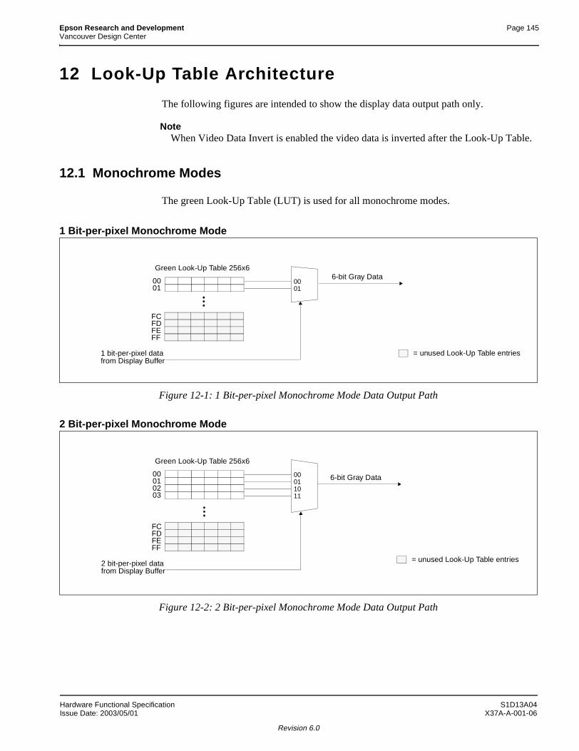
Epson Research and Development Page 145Vancouver Design Center
12 Look-Up Table Architecture
The following figures are intended to show the display data output path only.
NoteWhen Video Data Invert is enabled the video data is inverted after the Look-Up Table.
12.1 Monochrome Modes
The green Look-Up Table (LUT) is used for all monochrome modes.
1 Bit-per-pixel Monochrome Mode
Figure 12-1: 1 Bit-per-pixel Monochrome Mode Data Output Path
2 Bit-per-pixel Monochrome Mode
Figure 12-2: 2 Bit-per-pixel Monochrome Mode Data Output Path
Green Look-Up Table 256x6
0001
1 bit-per-pixel data
6-bit Gray Data
from Display Buffer= unused Look-Up Table entries
0001
FCFDFEFF
Green Look-Up Table 256x6
0001
2 bit-per-pixel data
6-bit Gray Data
from Display Buffer
1011
= unused Look-Up Table entries
00010203
FCFDFEFF
Hardware Functional Specification S1D13A04Issue Date: 2003/05/01 X37A-A-001-06
Revision 6.0
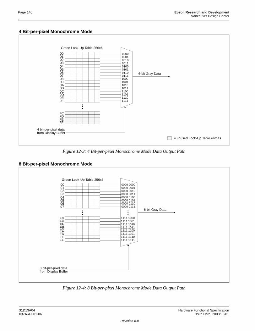
Page 146 Epson Research and DevelopmentVancouver Design Center
4 Bit-per-pixel Monochrome Mode
Figure 12-3: 4 Bit-per-pixel Monochrome Mode Data Output Path
8 Bit-per-pixel Monochrome Mode
Figure 12-4: 8 Bit-per-pixel Monochrome Mode Data Output Path
Green Look-Up Table 256x6
00000001
4 bit-per-pixel data
6-bit Gray Data
from Display Buffer
00100011010001010110011110001001101010111100110111101111
= unused Look-Up Table entries
00010203
FCFDFEFF
0405060708090A0B0C0D0E0F
0000 00000000 0001
6-bit Gray Data
0000 00100000 00110000 01000000 01010000 01100000 0111
1111 10001111 10011111 10101111 10111111 11001111 11011111 11101111 1111
Green Look-Up Table 256x6
0001020304050607
F8F9FAFBFCFDFEFF
8 bit-per-pixel datafrom Display Buffer
S1D13A04 Hardware Functional SpecificationX37A-A-001-06 Issue Date: 2003/05/01
Revision 6.0
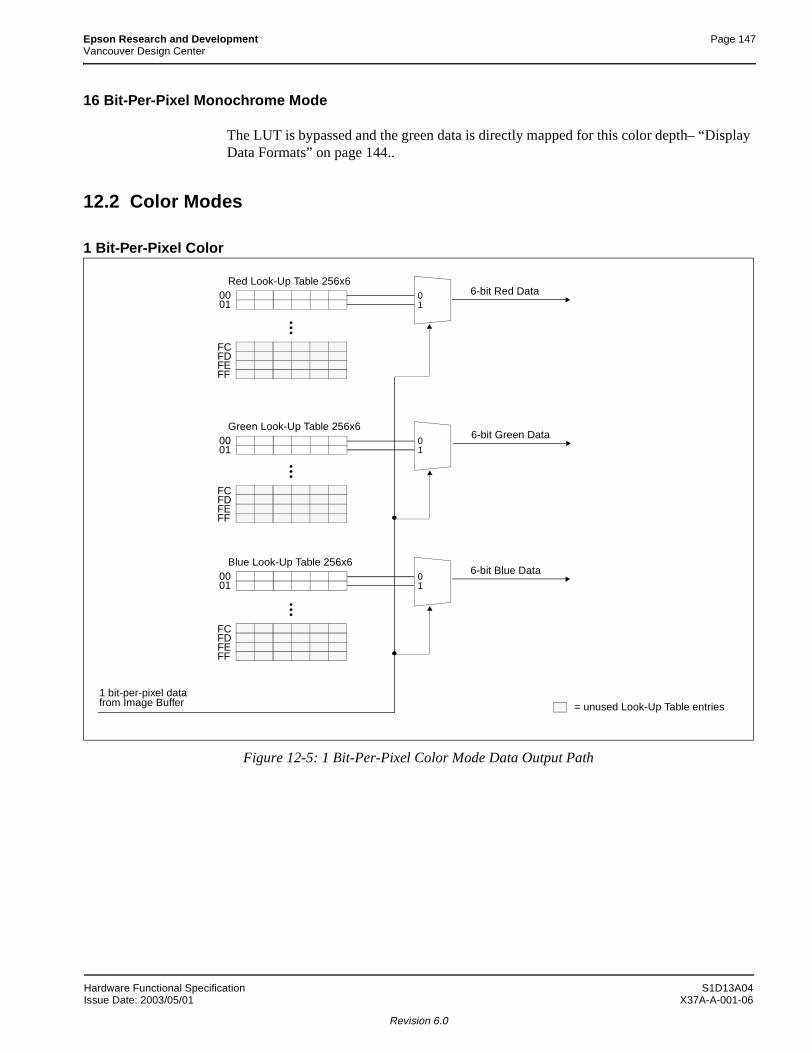
Epson Research and Development Page 147Vancouver Design Center
16 Bit-Per-Pixel Monochrome Mode
The LUT is bypassed and the green data is directly mapped for this color depth– “Display Data Formats” on page 144..
12.2 Color Modes
1 Bit-Per-Pixel Color
Figure 12-5: 1 Bit-Per-Pixel Color Mode Data Output Path
1 bit-per-pixel datafrom Image Buffer
6-bit Blue Data01
Blue Look-Up Table 256x60001
FCFDFEFF
6-bit Red Data01
Red Look-Up Table 256x60001
FCFDFEFF
6-bit Green Data01
Green Look-Up Table 256x60001
FCFDFEFF
= unused Look-Up Table entries
Hardware Functional Specification S1D13A04Issue Date: 2003/05/01 X37A-A-001-06
Revision 6.0
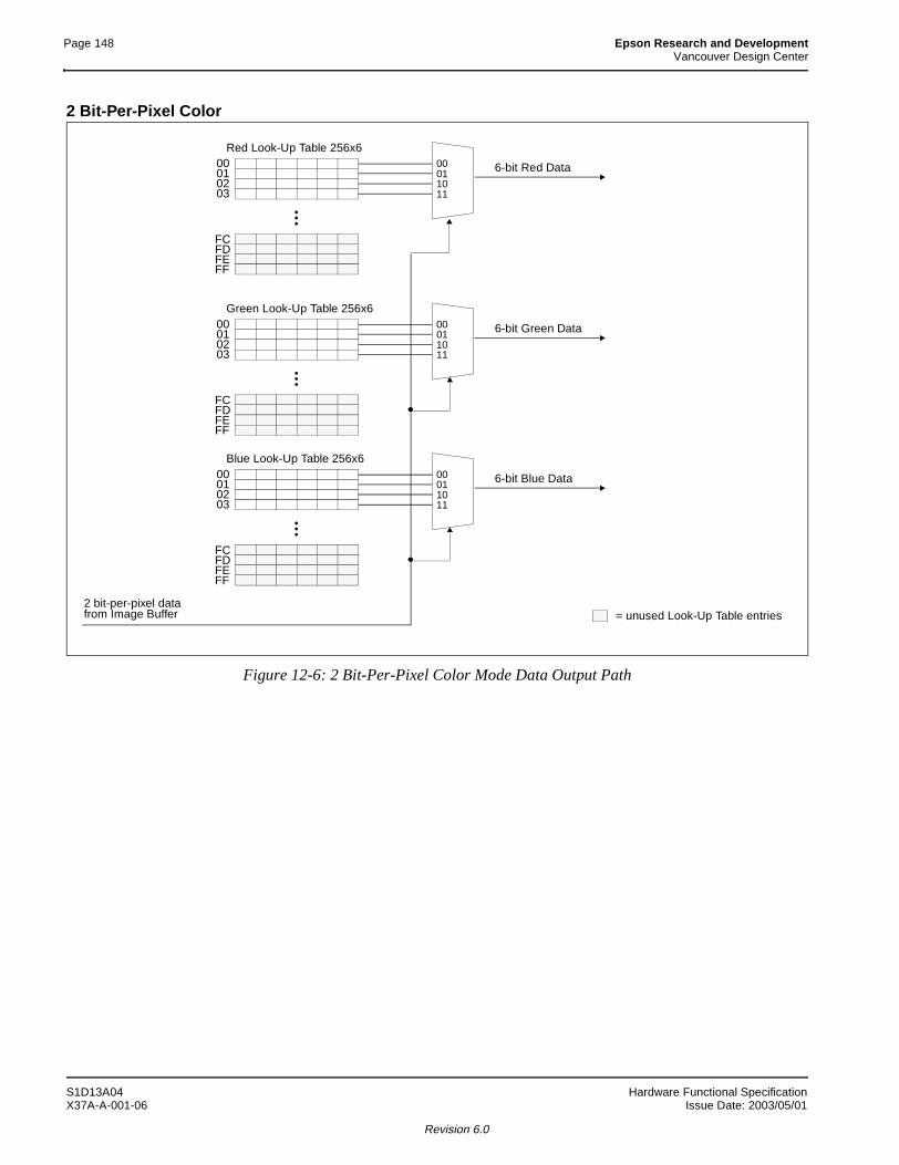
Page 148 Epson Research and DevelopmentVancouver Design Center
2 Bit-Per-Pixel Color
Figure 12-6: 2 Bit-Per-Pixel Color Mode Data Output Path
2 bit-per-pixel datafrom Image Buffer
6-bit Blue Data00011011
Blue Look-Up Table 256x600010203
FCFDFEFF
6-bit Red Data00011011
Red Look-Up Table 256x600010203
FCFDFEFF
6-bit Green Data00011011
Green Look-Up Table 256x600010203
FCFDFEFF
= unused Look-Up Table entries
S1D13A04 Hardware Functional SpecificationX37A-A-001-06 Issue Date: 2003/05/01
Revision 6.0
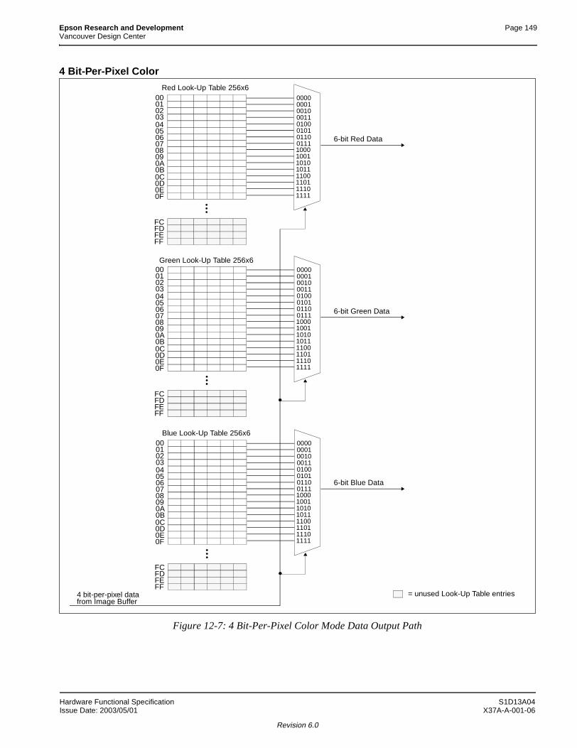
Epson Research and Development Page 149Vancouver Design Center
4 Bit-Per-Pixel Color
Figure 12-7: 4 Bit-Per-Pixel Color Mode Data Output Path
00000001
4 bit-per-pixel data
6-bit Red Data
from Image Buffer
00100011010001010110011110001001101010111100110111101111
6-bit Green Data
6-bit Blue Data
Red Look-Up Table 256x600010203
FCFDFEFF
0405060708090A0B0C0D0E0F
0000000100100011010001010110011110001001101010111100110111101111
Green Look-Up Table 256x600010203
FCFDFEFF
0405060708090A0B0C0D0E0F
0000000100100011010001010110011110001001101010111100110111101111
Blue Look-Up Table 256x600010203
FCFDFEFF
0405060708090A0B0C0D0E0F
= unused Look-Up Table entries
Hardware Functional Specification S1D13A04Issue Date: 2003/05/01 X37A-A-001-06
Revision 6.0
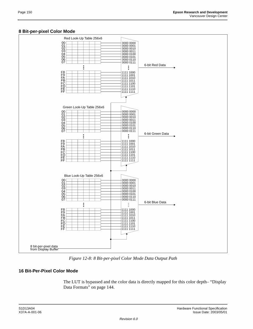
Page 150 Epson Research and DevelopmentVancouver Design Center
8 Bit-per-pixel Color Mode
Figure 12-8: 8 Bit-per-pixel Color Mode Data Output Path
16 Bit-Per-Pixel Color Mode
The LUT is bypassed and the color data is directly mapped for this color depth– “Display Data Formats” on page 144.
Red Look-Up Table 256x600010203
0000 00000000 0001
8 bit-per-pixel data
6-bit Red Data
from Display Buffer
0000 00100000 0011
04050607
0000 01000000 01010000 01100000 0111
F8F9FAFBFCFDFEFF
1111 10001111 10011111 10101111 10111111 11001111 11011111 11101111 1111
0000 00000000 0001
6-bit Green Data
0000 00100000 00110000 01000000 01010000 01100000 0111
1111 10001111 10011111 10101111 10111111 11001111 11011111 11101111 1111
0000 00000000 0001
6-bit Blue Data
0000 00100000 00110000 01000000 01010000 01100000 0111
1111 10001111 10011111 10101111 10111111 11001111 11011111 11101111 1111
Green Look-Up Table 256x60001020304050607
F8F9FAFBFCFDFEFF
Blue Look-Up Table 256x60001020304050607
F8F9FAFBFCFDFEFF
S1D13A04 Hardware Functional SpecificationX37A-A-001-06 Issue Date: 2003/05/01
Revision 6.0
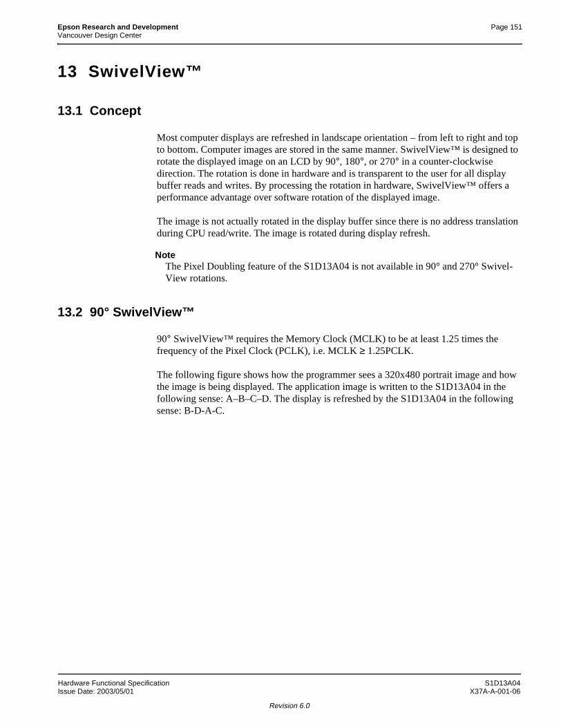
Epson Research and Development Page 151Vancouver Design Center
13 SwivelView™
13.1 Concept
Most computer displays are refreshed in landscape orientation – from left to right and top to bottom. Computer images are stored in the same manner. SwivelView™ is designed to rotate the displayed image on an LCD by 90°, 180°, or 270° in a counter-clockwise direction. The rotation is done in hardware and is transparent to the user for all display buffer reads and writes. By processing the rotation in hardware, SwivelView™ offers a performance advantage over software rotation of the displayed image.
The image is not actually rotated in the display buffer since there is no address translation during CPU read/write. The image is rotated during display refresh.
NoteThe Pixel Doubling feature of the S1D13A04 is not available in 90° and 270° Swivel-View rotations.
13.2 90° SwivelView™
90° SwivelView™ requires the Memory Clock (MCLK) to be at least 1.25 times the frequency of the Pixel Clock (PCLK), i.e. MCLK ≥ 1.25PCLK.
The following figure shows how the programmer sees a 320x480 portrait image and how the image is being displayed. The application image is written to the S1D13A04 in the following sense: A–B–C–D. The display is refreshed by the S1D13A04 in the following sense: B-D-A-C.
Hardware Functional Specification S1D13A04Issue Date: 2003/05/01 X37A-A-001-06
Revision 6.0
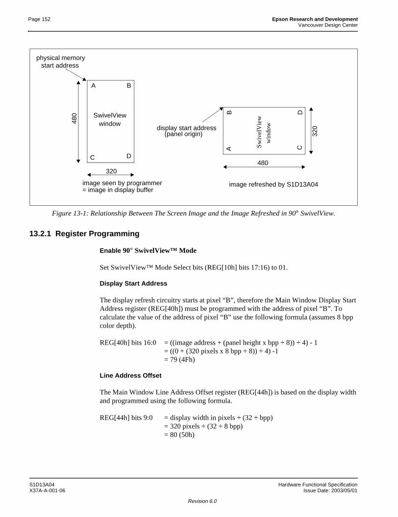
Page 152 Epson Research and DevelopmentVancouver Design Center
Figure 13-1: Relationship Between The Screen Image and the Image Refreshed in 90° SwivelView.
13.2.1 Register Programming
Enable 90° SwivelView™ Mode
Set SwivelView™ Mode Select bits (REG[10h] bits 17:16) to 01.
Display Start Address
The display refresh circuitry starts at pixel “B”, therefore the Main Window Display Start Address register (REG[40h]) must be programmed with the address of pixel “B”. To calculate the value of the address of pixel “B” use the following formula (assumes 8 bpp color depth).
REG[40h] bits 16:0 = ((image address + (panel height x bpp ÷ 8)) ÷ 4) - 1= ((0 + (320 pixels x 8 bpp ÷ 8)) ÷ 4) -1= 79 (4Fh)
Line Address Offset
The Main Window Line Address Offset register (REG[44h]) is based on the display width and programmed using the following formula.
REG[44h] bits 9:0 = display width in pixels ÷ (32 ÷ bpp)= 320 pixels ÷ (32 ÷ 8 bpp)= 80 (50h)
image seen by programmer= image in display buffer
480
SwivelViewwindow48
0
320
A B
C D
DC
BA
320
Sw
ivel
Vie
w
win
dowdisplay start address
image refreshed by S1D13A04
(panel origin)
physical memorystart address
S1D13A04 Hardware Functional SpecificationX37A-A-001-06 Issue Date: 2003/05/01
Revision 6.0
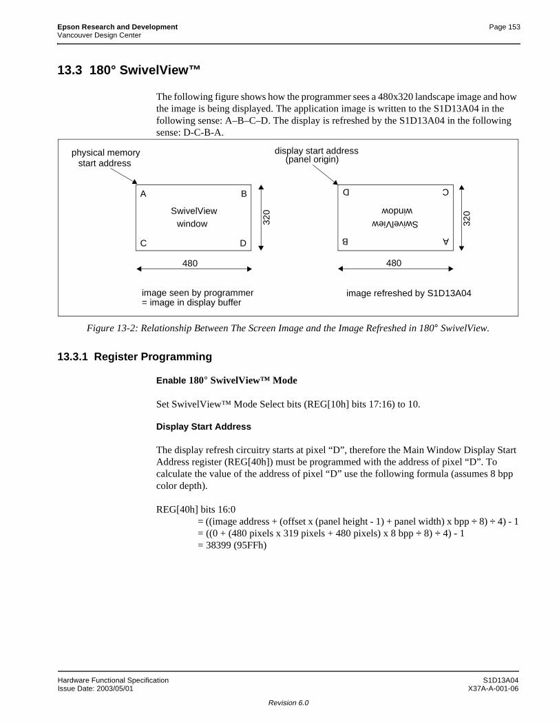
Epson Research and Development Page 153Vancouver Design Center
13.3 180° SwivelView™
The following figure shows how the programmer sees a 480x320 landscape image and how the image is being displayed. The application image is written to the S1D13A04 in the following sense: A–B–C–D. The display is refreshed by the S1D13A04 in the following sense: D-C-B-A.
Figure 13-2: Relationship Between The Screen Image and the Image Refreshed in 180° SwivelView.
13.3.1 Register Programming
Enable 180° SwivelView™ Mode
Set SwivelView™ Mode Select bits (REG[10h] bits 17:16) to 10.
Display Start Address
The display refresh circuitry starts at pixel “D”, therefore the Main Window Display Start Address register (REG[40h]) must be programmed with the address of pixel “D”. To calculate the value of the address of pixel “D” use the following formula (assumes 8 bpp color depth).
REG[40h] bits 16:0 = ((image address + (offset x (panel height - 1) + panel width) x bpp ÷ 8) ÷ 4) - 1= ((0 + (480 pixels x 319 pixels + 480 pixels) x 8 bpp ÷ 8) ÷ 4) - 1= 38399 (95FFh)
image seen by programmer= image in display buffer
480
SwivelViewwindow
48032
0
A B
C D
320
image refreshed by S1D13A04
SwivelViewwindow
AB
CD
display start address(panel origin)
physical memorystart address
Hardware Functional Specification S1D13A04Issue Date: 2003/05/01 X37A-A-001-06
Revision 6.0
Page 154 Epson Research and DevelopmentVancouver Design Center
Line Address Offset
The Main Window Line Address Offset register (REG[44h]) is based on the display width and programmed using the following formula.
REG[44h] bits 9:0 = display width in pixels ÷ (32 ÷ bpp)= 480 pixels ÷ (32 ÷ 8 bpp)= 120 (78h)
13.4 270° SwivelView™
270° SwivelView™ requires the Memory Clock (MCLK) to be at least 1.25 times the frequency of the Pixel Clock (PCLK), i.e. MCLK ≥ 1.25PCLK.
The following figure shows how the programmer sees a 320x480 portrait image and how the image is being displayed. The application image is written to the S1D13A04 in the following sense: A–B–C–D. The display is refreshed by the S1D13A04 in the following sense: C-A-D-B.
Figure 13-3: Relationship Between The Screen Image and the Image Refreshed in 270° SwivelView.
image seen by programmer= image in display buffer
480
SwivelViewwindow48
0
320
A B
C D
DC
BA
320
SwivelV
iew
window
image refreshed by S1D13A04
physical memory
display start address(panel origin)
start address
S1D13A04 Hardware Functional SpecificationX37A-A-001-06 Issue Date: 2003/05/01
Revision 6.0
Epson Research and Development Page 155Vancouver Design Center
13.4.1 Register Programming
Enable 270° SwivelView™ Mode
Set SwivelView™ Mode Select bits (REG[10h] bits 17:16) to 11.
Display Start Address
The display refresh circuitry starts at pixel “C”, therefore the Main Window Display Start Address register (REG[40h]) must be programmed with the address of pixel “C”. To calculate the value of the address of pixel “C” use the following formula (assumes 8 bpp color depth).
REG[40h] bits 16:0 = (image address + ((panel width - 1) x offset x bpp ÷ 8) ÷ 4)= (0 + ((480 pixels - 1) x 320 pixels x 8 bpp ÷ 8) ÷ 4)= 38320 (95B0h)
Line Address Offset
The Main Window Line Address Offset register (REG[44h]) is based on the display width and programmed using the following formula.
REG[44h] bits 9:0 = display width in pixels ÷ (32 ÷ bpp)= 320 pixels ÷ (32 ÷ 8 bpp)= 80 (50h)
Hardware Functional Specification S1D13A04Issue Date: 2003/05/01 X37A-A-001-06
Revision 6.0
Page 156 Epson Research and DevelopmentVancouver Design Center
14 Picture-in-Picture Plus (PIP+)
14.1 Concept
Picture-in-Picture Plus (PIP+) enables a secondary window (or PIP+ window) within the main display window. The PIP+ window may be positioned anywhere within the virtual display and is controlled through the PIP+ Window control registers (REG[50h] through REG[5Ch]). The PIP+ window retains the same color depth and SwivelView orientation as the main window.
The following diagram shows an example of a PIP+ window within a main window and the registers used to position it.
Figure 14-1: Picture-in-Picture Plus with SwivelView disabled
PIP+ window
main-window
PIP+ window y start position
panel’s origin
PIP+ window y end position
PIP+ window x start position PIP+ window x end position
0° SwivelViewTM
(REG[58h] bits 9-0) (REG[58h] bits 25-16)
(REG[5Ch] bits 25-16)
(REG[5Ch] bits 9-0)
S1D13A04 Hardware Functional SpecificationX37A-A-001-06 Issue Date: 2003/05/01
Revision 6.0
Epson Research and Development Page 157Vancouver Design Center
14.2 With SwivelView Enabled
14.2.1 SwivelView 90°
Figure 14-2: Picture-in-Picture Plus with SwivelView 90° enabled
14.2.2 SwivelView 180°
Figure 14-3: Picture-in-Picture Plus with SwivelView 180° enabled
PIP+ window
main-window
PIP+ window y start position
panel’s origin
PIP+ window y end position
PIP+ window x start positionPIP+ window x end position
90° SwivelViewTM
(REG[58h] bits 25-16) (REG[58h] bits 9-0)
(REG[5Ch] bits 9-0)
(REG[5Ch] bits 25-16)
PIP+ window
main-window
PIP+ window y start position panel’s originPIP+ window y end position
PIP+ window x start positionPIP+ window x end position
180° SwivelViewTM
(REG[58h] bits 25-16) (REG[58h] bits 9-0)
(REG[5Ch] bits 25-16) (REG[5Ch] bits 9-0)
Hardware Functional Specification S1D13A04Issue Date: 2003/05/01 X37A-A-001-06
Revision 6.0
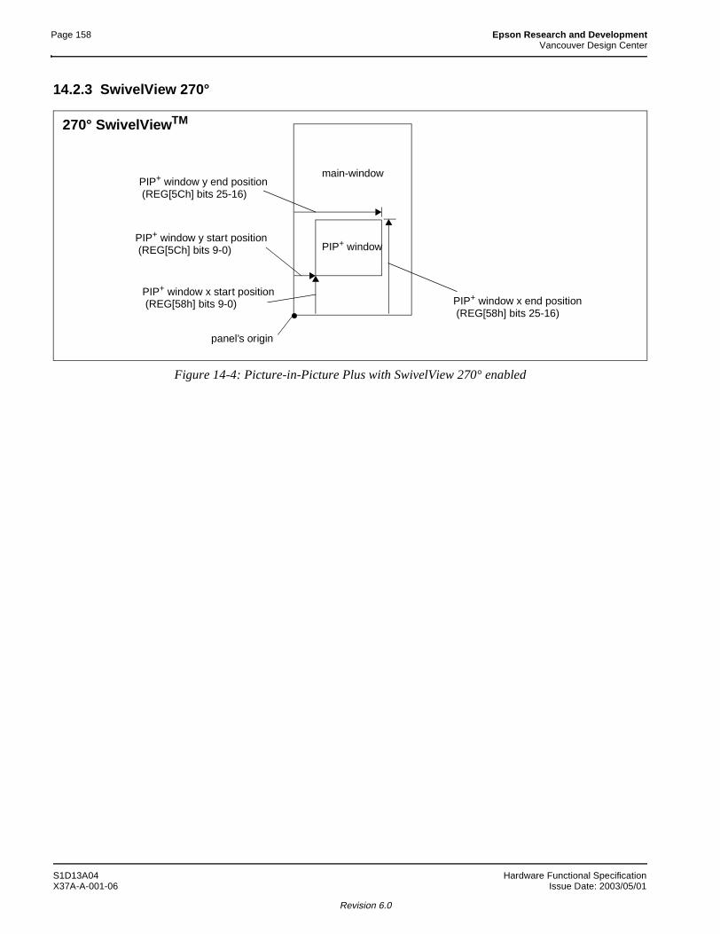
Page 158 Epson Research and DevelopmentVancouver Design Center
14.2.3 SwivelView 270°
Figure 14-4: Picture-in-Picture Plus with SwivelView 270° enabled
PIP+ window
main-window
PIP+ window y start position
panel’s origin
PIP+ window y end position
PIP+ window x start positionPIP+ window x end position
270° SwivelViewTM
(REG[58h] bits 25-16)
(REG[5Ch] bits 25-16)
(REG[5Ch] bits 9-0)
(REG[58h] bits 9-0)
S1D13A04 Hardware Functional SpecificationX37A-A-001-06 Issue Date: 2003/05/01
Revision 6.0
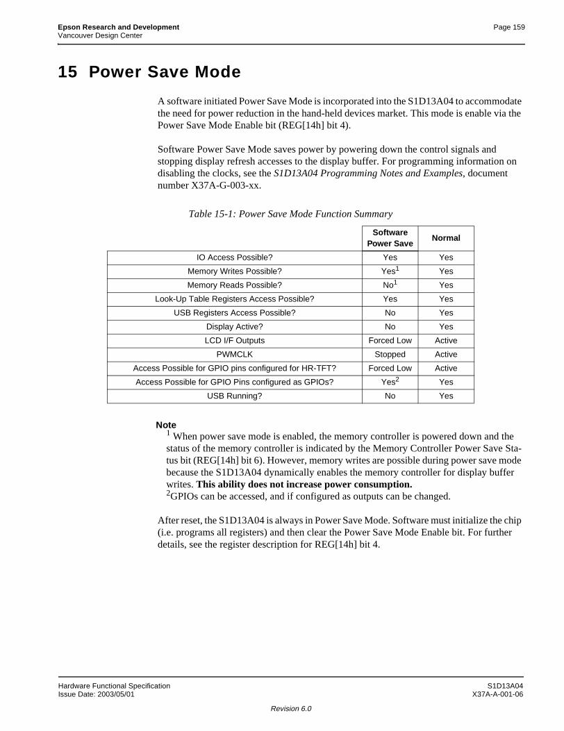
Epson Research and Development Page 159Vancouver Design Center
15 Power Save Mode
A software initiated Power Save Mode is incorporated into the S1D13A04 to accommodate the need for power reduction in the hand-held devices market. This mode is enable via the Power Save Mode Enable bit (REG[14h] bit 4).
Software Power Save Mode saves power by powering down the control signals and stopping display refresh accesses to the display buffer. For programming information on disabling the clocks, see the S1D13A04 Programming Notes and Examples, document number X37A-G-003-xx.
Note1 When power save mode is enabled, the memory controller is powered down and the status of the memory controller is indicated by the Memory Controller Power Save Sta-tus bit (REG[14h] bit 6). However, memory writes are possible during power save mode because the S1D13A04 dynamically enables the memory controller for display buffer writes. This ability does not increase power consumption. 2GPIOs can be accessed, and if configured as outputs can be changed.
After reset, the S1D13A04 is always in Power Save Mode. Software must initialize the chip (i.e. programs all registers) and then clear the Power Save Mode Enable bit. For further details, see the register description for REG[14h] bit 4.
Table 15-1: Power Save Mode Function Summary
Software Power Save
Normal
IO Access Possible? Yes Yes
Memory Writes Possible? Yes1 Yes
Memory Reads Possible? No1 Yes
Look-Up Table Registers Access Possible? Yes Yes
USB Registers Access Possible? No Yes
Display Active? No Yes
LCD I/F Outputs Forced Low Active
PWMCLK Stopped Active
Access Possible for GPIO pins configured for HR-TFT? Forced Low Active
Access Possible for GPIO Pins configured as GPIOs? Yes2 Yes
USB Running? No Yes
Hardware Functional Specification S1D13A04Issue Date: 2003/05/01 X37A-A-001-06
Revision 6.0
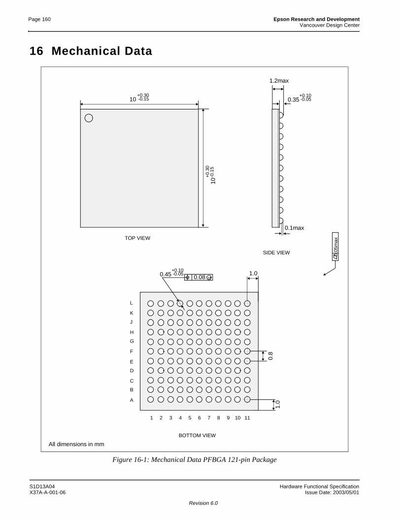
Page 160 Epson Research and DevelopmentVancouver Design Center
16 Mechanical Data
Figure 16-1: Mechanical Data PFBGA 121-pin Package
All dimensions in mm
10
1.2max
0.
05m
axTOP VIEW
L
K
J
H
G
F
E
D
C
B
A
1 2 3 4 5 6 7 8 9 10 11
0.8
1.0
0.45
BOTTOM VIEW
0.08 M
SIDE VIEW
1.0
-0.15+0.30
10-0
.15
+0.
30
0.35 -0.05+0.10
0.1max
-0.05+0.10
S1D13A04 Hardware Functional SpecificationX37A-A-001-06 Issue Date: 2003/05/01
Revision 6.0
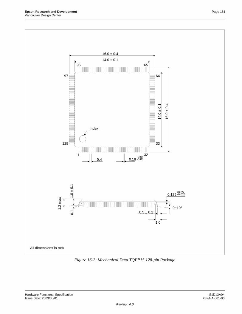
Epson Research and Development Page 161Vancouver Design Center
Figure 16-2: Mechanical Data TQFP15 128-pin Package
1 32
96 65
64
33
97
128
Index
0~10°
14.0 ± 0.1
14.0
± 0
.1
16.0 ± 0.4
16.0
± 0
.4
0.4 0.16
1.0
± 0
.1
0.125
1.0
0.5 ± 0.2
All dimensions in mm
-0.03+0.05
1.2
max
0.1
-0.025+0.05
Hardware Functional Specification S1D13A04Issue Date: 2003/05/01 X37A-A-001-06
Revision 6.0
Page 162 Epson Research and DevelopmentVancouver Design Center
17 References
The following documents contain additional information related to the S1D13A04. Document numbers are listed in parenthesis after the document name. All documents can be found at the Epson Research and Development Website at www.erd.epson.com.
• 13A04CFG Configuration Utility Users Manual (X37A-B-001-xx)
• 13A04PLAY Diagnostic Utility Users Manual (X37A-B-002-xx)
• 13A04BMP Demonstration Program User Manual (X37A-B-003-xx)
• S1D13A04 Product Brief (X37A-C-001-xx)
• S1D13A04 Wind River WindML v2.0 Display Drivers (X37A-E-002-xx)
• S1D13A04 Linux Console Driver (X37A-E-004-xx)
• S1D13A04 QNX Photon v2.0 Display Drivers (X37A-E-005-xx)
• S1D13A04 Windows CE v3.x Display Drivers (X37A-E-006-xx)
• Interfacing to the Toshiba TMPR3905/3912 Microprocessor (X37A-G-002-xx)
• S1D13A04 Programming Notes And Examples (X37A-G-003-xx)
• S5U13A04B00C Rev. 1.0 Evaluation Board User Manual (X37A-G-004-xx)
• Interfacing to the PC Card Bus (X37A-G-005-xx)
• S1D13A04 Power Consumption (X37A-G-006-xx)
• Interfacing to the NEC VR4102/VR4111 Microprocessors (X37A-G-007-xx)
• Interfacing to the NEC VR4181 Microprocessor (X37A-G-008-xx)
• Interfacing to the Motorola MPC821 Microprocessor (X37A-G-009-xx)
• Interfacing to the Motorola MCF5307 "Coldfire" Microprocessors (X37A-G-010-xx)
• Connecting to the Sharp HR-TFT Panels (X37A-G-011-xx)
• Interfacing to the Motorola MC68VZ328 Dragonball Microprocessor (X37A-G-012-xx)
• Interfacing to the Intel StrongARM SA-1110 Microprocessor (X37A-G-013-xx)
• S1D13A04 Register Summary (X37A-R-001-xx)
S1D13A04 Hardware Functional SpecificationX37A-A-001-06 Issue Date: 2003/05/01
Revision 6.0

Epson Research and Development Page 163Vancouver Design Center
18 Sales and Technical Support
JapanSeiko Epson CorporationElectronic Devices Marketing Division421-8, Hino, Hino-shiTokyo 191-8501, JapanTel: 042-587-5812Fax: 042-587-5564http://www.epson.co.jp/
Hong KongEpson Hong Kong Ltd.20/F., Harbour Centre25 Harbour RoadWanchai, Hong KongTel: 2585-4600Fax: 2827-4346http://www.epson.com.hk/
TaiwanEpson Taiwan Technology & Trading Ltd.10F, No. 287Nanking East RoadSec. 3, Taipei, TaiwanTel: 02-2717-7360Fax: 02-2712-9164http://www.epson.com.tw/
SingaporeEpson Singapore Pte., Ltd.No. 1Temasek Avenue #36-00Millenia TowerSingapore, 039192Tel: 337-7911Fax: 334-2716http://www.epson.com.sg/
EuropeEpson Europe Electronics GmbHRiesstrasse 1580992 Munich, GermanyTel: 089-14005-0Fax: 089-14005-110http://www.epson-electronics.de/
North AmericaEpson Electronics America, Inc.150 River Oaks ParkwaySan Jose, CA 95134, USATel: (408) 922-0200Fax: (408) 922-0238http://www.eea.epson.com/
Hardware Functional Specification S1D13A04Issue Date: 2003/05/01 X37A-A-001-06
Revision 6.0

Page 164 Epson Research and DevelopmentVancouver Design Center
THIS PAGE LEFT BLANK
S1D13A04 Hardware Functional SpecificationX37A-A-001-06 Issue Date: 2003/05/01
Revision 6.0
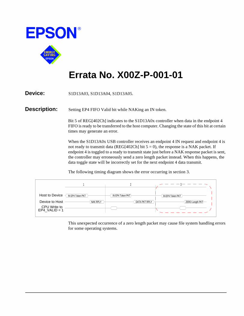
Errata No. X00Z-P-001-01
Device: S1D13A03, S1D13A04, S1D13A05.
Description: Setting EP4 FIFO Valid bit while NAKing an IN token.
Bit 5 of REG[402Ch] indicates to the S1D13A0x controller when data in the endpoint 4 FIFO is ready to be transferred to the host computer. Changing the state of this bit at certain times may generate an error.
When the S1D13A0x USB controller receives an endpoint 4 IN request and endpoint 4 is not ready to transmit data (REG[402Ch] bit 5 = 0), the response is a NAK packet. If endpoint 4 is toggled to a ready to transmit state just before a NAK response packet is sent, the controller may erroneously send a zero length packet instead. When this happens, the data toggle state will be incorrectly set for the next endpoint 4 data transmit.
The following timing diagram shows the error occurring in section 3.
This unexpected occurrence of a zero length packet may cause file system handling errors for some operating systems.
Host to Device
Device to Host
CPU Write to EP4_VALID = 1
1 2 3
IN EP4 Token PKT IN EP4 Token PKT IN EP4 Token PKT
NAK RPLY DATA PKT RPLY ZERO Length PKT
Page 2 Epson Research and DevelopmentVancouver Design Center
Corrective Action:
There are two software solutions for this occurrence.
Disable USB Receiver before setting the EP4 FIFO Valid bit
The first solution involves disabling the USB receiver to avoid responding to an EP4 IN packet. During the time the USB receiver is disabled the EP4 FIFO Valid bit is set.
When the local CPU is ready to send data on endpoint 4 the steps to follow are:
1. Disable the USB differential input receiver (REG[4040h] bit 6 = 0)
2. Wait a minimum of 1µs. If needed, delays may be added
3. Enable the EP4 FIFO Valid bit (REG[402Ch] bit 5 = 1)
4. Clear the EP4 Interrupt status bit (REG[4004h] bit 4 = 1)
5. Enable the USB differential input receiver (REG[4040h] bit 6 = 1)
NoteSteps 1 through 5 are time critical and must be performed in less than 6 µs.
NoteTo comply with “EP4 NAK Status not set correctly in USB Status register”, steps 3 and 4 must be completed within 5 µs of each other. For further information on “EP4 NAK Status not set correctly in USB Status register”, see the S1D13A0x Programming Notes and Examples, document numbers X36A-G-003-xx, X37A-G-003-xx, andX40A-G-003-xx.
EP4 FIFO Valid bit set after NAK and before the next IN token.
The second solution is to wait until immediately after the USB has responded to an IN request with a NAK packet before setting the transmit FIFO valid bit. This solution is recommended only for fast processors.
When the local CPU is ready to send data on endpoint 4, it must first detect that a NAK packet has been sent. This is done by reading the EP4 Interrupt Status bit (REG[4004h] bit 4). If the EP4 FIFO Valid bit was not set, the EP4 Interrupt Status bit is set only if a NAK packet has been sent. When the local CPU detects the NAK it must immediately set the EP4 FIFO Valid bit (before responding to the next IN token).
After filling the EP4 FIFO the steps to follow before setting the EP4 FIFO Valid bit are:
1. Clear the EP4 Interrupt Status bit (REG[4004h] bit 4)
2. Read the EP4 Interrupt Status bit (REG[4004h] bit 4) until it is set
3. Set the EP4 FIFO Valid bit (REG[402Ch] bit 5 = 1)
NoteThe setting of the EP4 FIFO Valid bit is time critical. The EP4 FIFO Valid bit must beset within 3 µs after the EP4 Interrupt Status has been set internally by the S1D13A0x.
Errata No. X00Z-P-001-01X00Z-P-001-01 Issue Date: 2002/08/22

S1D13A04 LCD/USB Companion Chip
Programming Notes and Examples
Document Number: X37A-G-003-05
Copyright © 2001, 2002 Epson Research and Development, Inc. All Rights Reserved.
Information in this document is subject to change without notice. You may download and use this document, but only for your own use inevaluating Seiko Epson/EPSON products. You may not modify the document. Epson Research and Development, Inc. disclaims anyrepresentation that the contents of this document are accurate or current. The Programs/Technologies described in this document may contain material protected under U.S. and/or International Patent laws.
EPSON is a registered trademark of Seiko Epson Corporation. All other trademarks are the property of their respective owners.

Page 2 Epson Research and DevelopmentVancouver Design Center
THIS PAGE LEFT BLANK
S1D13A04 Programming Notes and ExamplesX37A-G-003-05 Issue Date: 2002/08/21
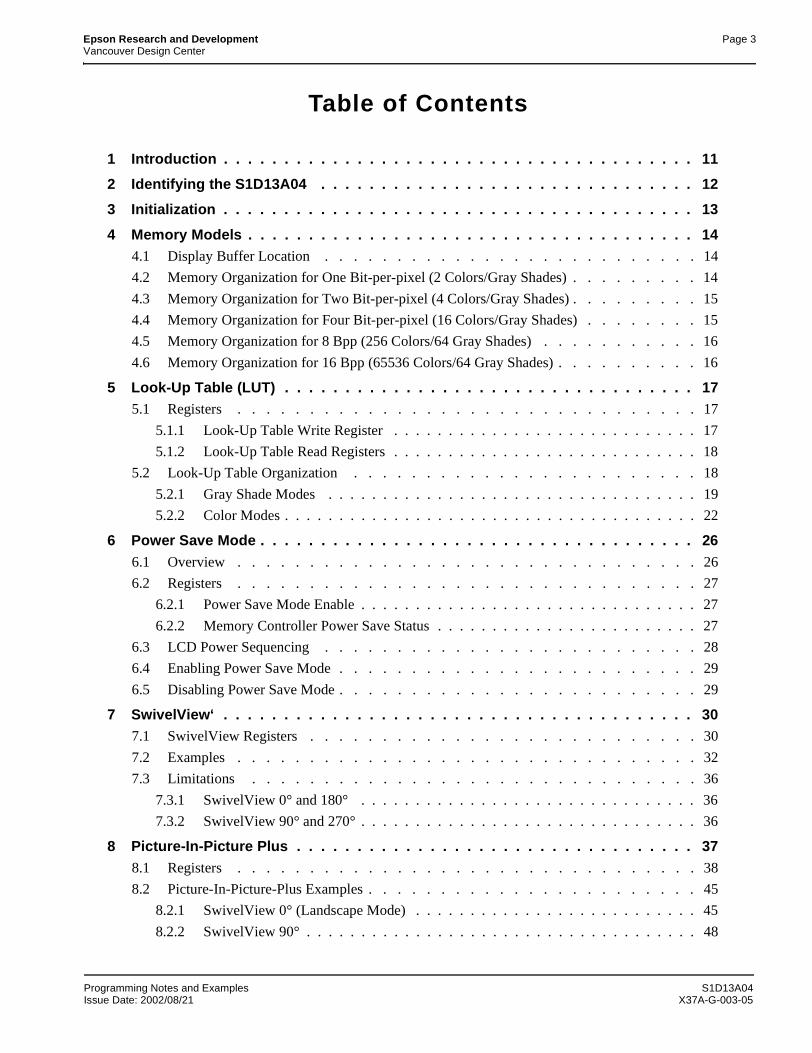
Epson Research and Development Page 3Vancouver Design Center
Table of Contents
1 Introduction . . . . . . . . . . . . . . . . . . . . . . . . . . . . . . . . . . . . . . . 11
2 Identifying the S1D13A04 . . . . . . . . . . . . . . . . . . . . . . . . . . . . . . . 12
3 Initialization . . . . . . . . . . . . . . . . . . . . . . . . . . . . . . . . . . . . . . . 13
4 Memory Models . . . . . . . . . . . . . . . . . . . . . . . . . . . . . . . . . . . . . 144.1 Display Buffer Location . . . . . . . . . . . . . . . . . . . . . . . . . . 14
4.2 Memory Organization for One Bit-per-pixel (2 Colors/Gray Shades) . . . . . . . . . 14
4.3 Memory Organization for Two Bit-per-pixel (4 Colors/Gray Shades) . . . . . . . . . 15
4.4 Memory Organization for Four Bit-per-pixel (16 Colors/Gray Shades) . . . . . . . . 15
4.5 Memory Organization for 8 Bpp (256 Colors/64 Gray Shades) . . . . . . . . . . . 16
4.6 Memory Organization for 16 Bpp (65536 Colors/64 Gray Shades) . . . . . . . . . . 16
5 Look-Up Table (LUT) . . . . . . . . . . . . . . . . . . . . . . . . . . . . . . . . . . 175.1 Registers . . . . . . . . . . . . . . . . . . . . . . . . . . . . . . . . 17
5.1.1 Look-Up Table Write Register . . . . . . . . . . . . . . . . . . . . . . . . . . . . 17
5.1.2 Look-Up Table Read Registers . . . . . . . . . . . . . . . . . . . . . . . . . . . . 18
5.2 Look-Up Table Organization . . . . . . . . . . . . . . . . . . . . . . . . 18
5.2.1 Gray Shade Modes . . . . . . . . . . . . . . . . . . . . . . . . . . . . . . . . . . 19
5.2.2 Color Modes . . . . . . . . . . . . . . . . . . . . . . . . . . . . . . . . . . . . . . 22
6 Power Save Mode . . . . . . . . . . . . . . . . . . . . . . . . . . . . . . . . . . . . 266.1 Overview . . . . . . . . . . . . . . . . . . . . . . . . . . . . . . . . 26
6.2 Registers . . . . . . . . . . . . . . . . . . . . . . . . . . . . . . . . 27
6.2.1 Power Save Mode Enable . . . . . . . . . . . . . . . . . . . . . . . . . . . . . . . 27
6.2.2 Memory Controller Power Save Status . . . . . . . . . . . . . . . . . . . . . . . . 27
6.3 LCD Power Sequencing . . . . . . . . . . . . . . . . . . . . . . . . . . 28
6.4 Enabling Power Save Mode . . . . . . . . . . . . . . . . . . . . . . . . . 29
6.5 Disabling Power Save Mode . . . . . . . . . . . . . . . . . . . . . . . . . 29
7 SwivelView‘ . . . . . . . . . . . . . . . . . . . . . . . . . . . . . . . . . . . . . . . 307.1 SwivelView Registers . . . . . . . . . . . . . . . . . . . . . . . . . . . 30
7.2 Examples . . . . . . . . . . . . . . . . . . . . . . . . . . . . . . . . 32
7.3 Limitations . . . . . . . . . . . . . . . . . . . . . . . . . . . . . . . 36
7.3.1 SwivelView 0° and 180° . . . . . . . . . . . . . . . . . . . . . . . . . . . . . . . 36
7.3.2 SwivelView 90° and 270° . . . . . . . . . . . . . . . . . . . . . . . . . . . . . . . 36
8 Picture-In-Picture Plus . . . . . . . . . . . . . . . . . . . . . . . . . . . . . . . . . 378.1 Registers . . . . . . . . . . . . . . . . . . . . . . . . . . . . . . . . 38
8.2 Picture-In-Picture-Plus Examples . . . . . . . . . . . . . . . . . . . . . . . 45
8.2.1 SwivelView 0° (Landscape Mode) . . . . . . . . . . . . . . . . . . . . . . . . . . 45
8.2.2 SwivelView 90° . . . . . . . . . . . . . . . . . . . . . . . . . . . . . . . . . . . . 48
Programming Notes and Examples S1D13A04Issue Date: 2002/08/21 X37A-G-003-05
Page 4 Epson Research and DevelopmentVancouver Design Center
8.2.3 SwivelView 180° . . . . . . . . . . . . . . . . . . . . . . . . . . . . . . . . . . . 51
8.2.4 SwivelView 270° . . . . . . . . . . . . . . . . . . . . . . . . . . . . . . . . . . . 54
8.3 Limitations . . . . . . . . . . . . . . . . . . . . . . . . . . . . . . . .57
8.3.1 SwivelView 0° and 180° . . . . . . . . . . . . . . . . . . . . . . . . . . . . . . . 57
8.3.2 SwivelView 90° and 270° . . . . . . . . . . . . . . . . . . . . . . . . . . . . . . . 57
9 2D BitBLT Engine . . . . . . . . . . . . . . . . . . . . . . . . . . . . . . . . . . . . .589.1 Registers . . . . . . . . . . . . . . . . . . . . . . . . . . . . . . . . .58
9.2 BitBLT Descriptions . . . . . . . . . . . . . . . . . . . . . . . . . . . .66
9.2.1 Write BitBLT with ROP . . . . . . . . . . . . . . . . . . . . . . . . . . . . . . . 67
9.2.2 Color Expansion BitBLT . . . . . . . . . . . . . . . . . . . . . . . . . . . . . . . 70
9.2.3 Color Expansion BitBLT With Transparency . . . . . . . . . . . . . . . . . . . . . 74
9.2.4 Solid Fill BitBLT . . . . . . . . . . . . . . . . . . . . . . . . . . . . . . . . . . . 74
9.2.5 Move BitBLT in a Positive Direction with ROP . . . . . . . . . . . . . . . . . . . 76
9.2.6 Move BitBLT in Negative Direction with ROP . . . . . . . . . . . . . . . . . . . . 78
9.2.7 Transparent Write BitBLT . . . . . . . . . . . . . . . . . . . . . . . . . . . . . . . 79
9.2.8 Transparent Move BitBLT in Positive Direction . . . . . . . . . . . . . . . . . . . 82
9.2.9 Pattern Fill BitBLT with ROP . . . . . . . . . . . . . . . . . . . . . . . . . . . . . 84
9.2.10 Pattern Fill BitBLT with Transparency . . . . . . . . . . . . . . . . . . . . . . . . 86
9.2.11 Move BitBLT with Color Expansion . . . . . . . . . . . . . . . . . . . . . . . . . 88
9.2.12 Transparent Move BitBLT with Color Expansion . . . . . . . . . . . . . . . . . . 89
9.2.13 Read BitBLT . . . . . . . . . . . . . . . . . . . . . . . . . . . . . . . . . . . . . . 89
9.3 S1D13A04 BitBLT Synchronization . . . . . . . . . . . . . . . . . . . . . .92
9.4 S1D13A04 BitBLT Known Limitations . . . . . . . . . . . . . . . . . . . .93
9.5 Sample Code . . . . . . . . . . . . . . . . . . . . . . . . . . . . . . .93
10 Programming the USB Controller . . . . . . . . . . . . . . . . . . . . . . . . . . . .9410.1 Registers and Interrupts . . . . . . . . . . . . . . . . . . . . . . . . . . .94
10.1.1 Registers . . . . . . . . . . . . . . . . . . . . . . . . . . . . . . . . . . . . . . . . 94
10.1.2 Interrupts . . . . . . . . . . . . . . . . . . . . . . . . . . . . . . . . . . . . . . . . 95
10.2 Initialization . . . . . . . . . . . . . . . . . . . . . . . . . . . . . . . .95
10.2.1 GPIO Setup . . . . . . . . . . . . . . . . . . . . . . . . . . . . . . . . . . . . . . 95
10.2.2 USB Registers . . . . . . . . . . . . . . . . . . . . . . . . . . . . . . . . . . . . . 96
10.3 Data Transfers . . . . . . . . . . . . . . . . . . . . . . . . . . . . . . .97
10.3.1 Receiving Data from the Host - the OUT command . . . . . . . . . . . . . . . . . 97
10.3.2 Sending Data to the Host - the IN command . . . . . . . . . . . . . . . . . . . . .101
10.4 Known Issues . . . . . . . . . . . . . . . . . . . . . . . . . . . . . . 106
10.4.1 EP4 NAK Status not set correctly in USB Status Register . . . . . . . . . . . . . .106
10.4.2 Write to EP4 FIFO Valid bit cleared by NAK . . . . . . . . . . . . . . . . . . . .107
10.4.3 EP3 Interrupt Status bit set by NAKs . . . . . . . . . . . . . . . . . . . . . . . . .107
10.4.4 “EP2 Valid Bit” in USB Status can be erroneously set by firmware . . . . . . . . .110
S1D13A04 Programming Notes and ExamplesX37A-G-003-05 Issue Date: 2002/08/21
Epson Research and Development Page 5Vancouver Design Center
10.4.5 Setting EP4 FIFO Valid bit while NAKing IN token . . . . . . . . . . . . . . . . . 110
11 Hardware Abstraction Layer . . . . . . . . . . . . . . . . . . . . . . . . . . . . . . 11211.1 Introduction . . . . . . . . . . . . . . . . . . . . . . . . . . . . . . . 112
11.2 API for the HAL Library . . . . . . . . . . . . . . . . . . . . . . . . . . 112
11.2.1 Startup Routines . . . . . . . . . . . . . . . . . . . . . . . . . . . . . . . . . . . . 113
11.2.2 Memory Access . . . . . . . . . . . . . . . . . . . . . . . . . . . . . . . . . . . . 115
11.2.3 Register Access . . . . . . . . . . . . . . . . . . . . . . . . . . . . . . . . . . . . 116
11.2.4 Clock Support . . . . . . . . . . . . . . . . . . . . . . . . . . . . . . . . . . . . . 118
11.2.5 Miscellaneous . . . . . . . . . . . . . . . . . . . . . . . . . . . . . . . . . . . . . 119
12 Sample Code . . . . . . . . . . . . . . . . . . . . . . . . . . . . . . . . . . . . . . 121
13 Sales and Technical Support . . . . . . . . . . . . . . . . . . . . . . . . . . . . . 122
Programming Notes and Examples S1D13A04Issue Date: 2002/08/21 X37A-G-003-05

Page 6 Epson Research and DevelopmentVancouver Design Center
THIS PAGE LEFT BLANK
S1D13A04 Programming Notes and ExamplesX37A-G-003-05 Issue Date: 2002/08/21
Epson Research and Development Page 7Vancouver Design Center
List of Tables
Table 5-1: Look-Up Table Configurations . . . . . . . . . . . . . . . . . . . . . . . . . . . . . . 18
Table 5-2: Suggested LUT Values for 1 Bpp Gray Shade . . . . . . . . . . . . . . . . . . . . . . 19
Table 5-3: Suggested LUT Values for 4 Bpp Gray Shade . . . . . . . . . . . . . . . . . . . . . . 19
Table 5-4: Suggested LUT Values for 4 Bpp Gray Shade . . . . . . . . . . . . . . . . . . . . . . 20
Table 5-5: Suggested LUT Values for 8 Bpp Gray Shade . . . . . . . . . . . . . . . . . . . . . . 21
Table 5-6: Suggested LUT Values for 1 bpp Color . . . . . . . . . . . . . . . . . . . . . . . . . . 22
Table 5-7: Suggested LUT Values for 2 bpp Color . . . . . . . . . . . . . . . . . . . . . . . . . . 22
Table 5-8: Suggested LUT Values for 4 bpp Color . . . . . . . . . . . . . . . . . . . . . . . . . . 23
Table 5-9: Suggested LUT Values 8 bpp Color . . . . . . . . . . . . . . . . . . . . . . . . . . . . 24
Table 7-1: SwivelView Mode Select Bits . . . . . . . . . . . . . . . . . . . . . . . . . . . . . . . 30
Table 8-1: 32-bit Address Increments for PIP+ X Position in SwivelView 0° and 180° . . . . . . . 40
Table 8-2: 32-bit Address Increments for Color Depth . . . . . . . . . . . . . . . . . . . . . . . . 41
Table 8-3: 32-bit Address Increments for Color Depth . . . . . . . . . . . . . . . . . . . . . . . . 42
Table 8-4: 32-bit Address Increments for Color Depth . . . . . . . . . . . . . . . . . . . . . . . . 44
Table 9-1: BitBLT FIFO Words Available . . . . . . . . . . . . . . . . . . . . . . . . . . . . . . 60
Table 9-2 : BitBLT ROP Code/Color Expansion Function Selection . . . . . . . . . . . . . . . . . 61
Table 9-3 : BitBLT Operation Selection . . . . . . . . . . . . . . . . . . . . . . . . . . . . . . . . 62
Table 9-4 : BitBLT Source Start Address Selection . . . . . . . . . . . . . . . . . . . . . . . . . . 63
Table 9-5: Possible BitBLT FIFO Writes . . . . . . . . . . . . . . . . . . . . . . . . . . . . . . . 69
Table 9-6: Possible BitBLT FIFO Writes . . . . . . . . . . . . . . . . . . . . . . . . . . . . . . . 74
Table 9-7: Possible BitBLT FIFO Writes . . . . . . . . . . . . . . . . . . . . . . . . . . . . . . . 82
Table 9-8: Possible BitBLT FIFO Reads . . . . . . . . . . . . . . . . . . . . . . . . . . . . . . . 91
Table 10-1: USB Controller Initialization Sequence . . . . . . . . . . . . . . . . . . . . . . . . . . 96
Table 11-1: HAL Library API . . . . . . . . . . . . . . . . . . . . . . . . . . . . . . . . . . . . . 112
Programming Notes and Examples S1D13A04Issue Date: 2002/08/21 X37A-G-003-05

Page 8 Epson Research and DevelopmentVancouver Design Center
THIS PAGE LEFT BLANK
S1D13A04 Programming Notes and ExamplesX37A-G-003-05 Issue Date: 2002/08/21
Epson Research and Development Page 9Vancouver Design Center
List of Figures
Figure 4-1: Pixel Storage for 1 Bpp in One Byte of Display Buffer . . . . . . . . . . . . . . . . . . 14
Figure 4-2: Pixel Storage for 2 Bpp in One Byte of Display Buffer . . . . . . . . . . . . . . . . . . 15
Figure 4-3: Pixel Storage for 4 Bpp in One Byte of Display Buffer . . . . . . . . . . . . . . . . . . 15
Figure 4-4: Pixel Storage for 8 Bpp in One Byte of Display Buffer . . . . . . . . . . . . . . . . . . 16
Figure 4-5: Pixel Storage for 16 Bpp in Two Bytes of Display Buffer . . . . . . . . . . . . . . . . 16
Figure 8-1: Picture-in-Picture Plus with SwivelView disabled . . . . . . . . . . . . . . . . . . . . 37
Figure 8-2: Picture-in-Picture Plus with SwivelView disabled . . . . . . . . . . . . . . . . . . . . 45
Figure 8-3: Picture-in-Picture Plus with SwivelView 90° enabled . . . . . . . . . . . . . . . . . . . 48
Figure 8-4: Picture-in-Picture Plus with SwivelView 180° enabled . . . . . . . . . . . . . . . . . . 51
Figure 8-5: Picture-in-Picture Plus with SwivelView 270° enabled . . . . . . . . . . . . . . . . . . 54
Figure 9-1: Move BitBLT Usage . . . . . . . . . . . . . . . . . . . . . . . . . . . . . . . . . . . . 76
Figure 10-1: Endpoint 1 Data Reception . . . . . . . . . . . . . . . . . . . . . . . . . . . . . . . . 98
Figure 10-2: Endpoint 3 Data Reception . . . . . . . . . . . . . . . . . . . . . . . . . . . . . . . 100
Figure 10-3: EndPoint 2 Data Transmission . . . . . . . . . . . . . . . . . . . . . . . . . . . . . . 102
Figure 10-4: Endpoint 4 Data Transmission . . . . . . . . . . . . . . . . . . . . . . . . . . . . . . 103
Figure 10-5: Endpoint 4 Interrupt Handling . . . . . . . . . . . . . . . . . . . . . . . . . . . . . . 105
Figure 10-6: Firmware Looping Continuously on Received OUT packets . . . . . . . . . . . . . . 108
Figure 10-7: Endpoint 3 Program Flow for Slow CPU . . . . . . . . . . . . . . . . . . . . . . . . 109
Programming Notes and Examples S1D13A04Issue Date: 2002/08/21 X37A-G-003-05

Page 10 Epson Research and DevelopmentVancouver Design Center
THIS PAGE LEFT BLANK
S1D13A04 Programming Notes and ExamplesX37A-G-003-05 Issue Date: 2002/08/21

Epson Research and Development Page 11Vancouver Design Center
1 Introduction
This guide discusses programming issues and provides examples for the main features of the S1D13A04, such as SwivelView, Picture-in-Picture Plus, and the BitBLT engine. The example source code referenced in this guide is available on the web at www.erd.epson.com.
This guide also introduces the Hardware Abstraction Layer (HAL), which is designed to simplify the programming of the S1D13A04. Most S1D13xxx products have HAL support, thus allowing OEMs to do multiple designs with a common code base.
This document is updated as appropriate. Please check the Epson Research and Devel-opment website at www.erd.epson.com for the latest revision of this document and source before beginning any development.
We appreciate your comments on our documentation. Please contact us via email at [email protected].
Programming Notes and Examples S1D13A04Issue Date: 2002/08/21 X37A-G-003-05
Page 12 Epson Research and DevelopmentVancouver Design Center
2 Identifying the S1D13A04
The S1D13A04 can be identified by reading the value contained in the Product Information Register (REG[00h]). To identify the S1D13A04 follow the steps below.
1. Read REG[00h].
2. The production version of the S1D13A04 returns a value of 2Cxx282Ch (where xx depends on the configuration of the CNF[6:0] pins). This value can be broken down into the following.
1. The product code for the S1D13A04 is 0Bh (001011 binary) and can be found in bits 7-2 and also in bits 31-26.
2. The revision code is 0h (00 binary) and can be found in bits 1-0 and again in bits 25-24.
3. The display buffer size is 28h (00101000 binary) and is contained in bits 15-8.
NoteThe display buffer size is the distinguishing value between the S1D13A03 and the S1D13A04 as they share the same product code and revision code. For the correct dis-play buffer size for the S1D13A03, see the S1D13A03 Hardware Functional Specifica-tion, document number X36A-A-001-xx.
S1D13A04 Programming Notes and ExamplesX37A-G-003-05 Issue Date: 2002/08/21
Epson Research and Development Page 13Vancouver Design Center
3 Initialization
This section describes how to initialize the S1D13A04. Sample code for performing initial-ization of the S1D13A04 is provided in the file init13A04.c which is available on the internet at www.erd.epson.com.
S1D13A04 initialization can be broken into the following steps.
1. Set all registers to initial values. The values are obtained by using the s1d13A04.h file that is exported by the 13A04CFG.EXE configuration utility. For more information on 13A04CFG, see the 13A04CFG User Manual, document number X37A-B-001-xx.
2. Program the Look-Up Table (LUT) with color values. For details on programming the LUT, see Section 5, “Look-Up Table (LUT)” on page 17.
3. Clear the display buffer.
If the system implementation uses a clock chip instead of a fixed oscillator, refer to the HAL (Hardware Abstraction Layer) sample code available on the internet at www.erd.epson.com. For example, the Epson S5U13A04B00C evaluation board uses a Cypress clock chip.
Programming Notes and Examples S1D13A04Issue Date: 2002/08/21 X37A-G-003-05
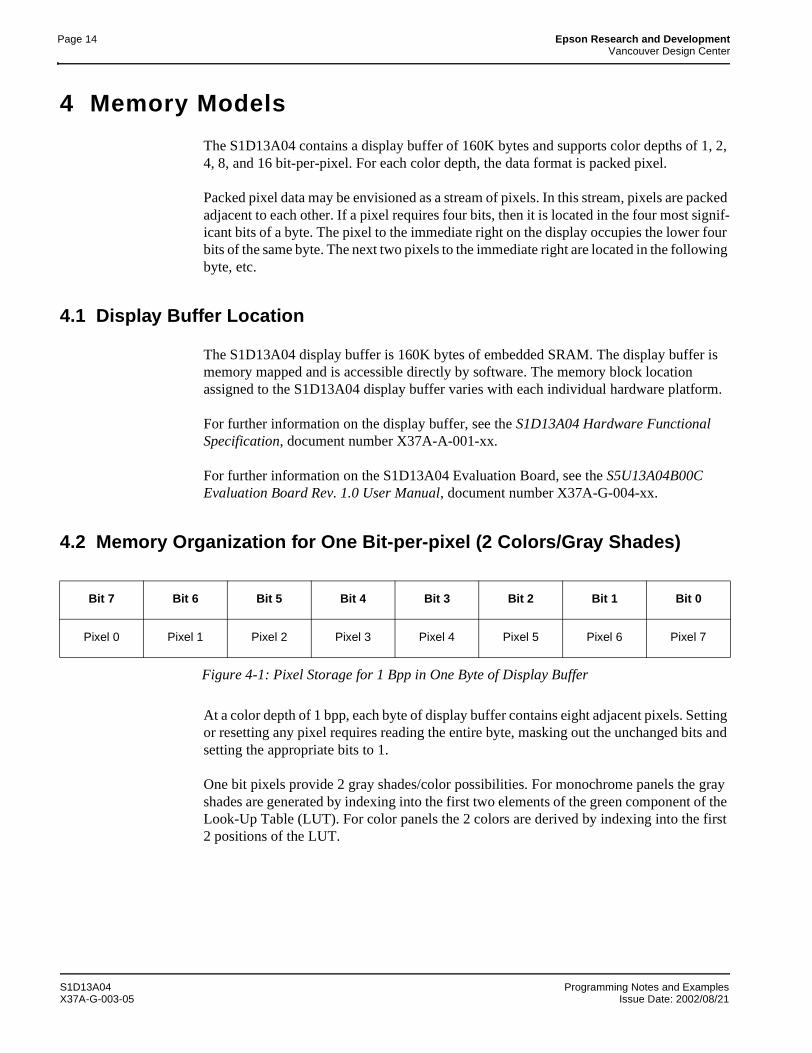
Page 14 Epson Research and DevelopmentVancouver Design Center
4 Memory Models
The S1D13A04 contains a display buffer of 160K bytes and supports color depths of 1, 2, 4, 8, and 16 bit-per-pixel. For each color depth, the data format is packed pixel.
Packed pixel data may be envisioned as a stream of pixels. In this stream, pixels are packed adjacent to each other. If a pixel requires four bits, then it is located in the four most signif-icant bits of a byte. The pixel to the immediate right on the display occupies the lower four bits of the same byte. The next two pixels to the immediate right are located in the following byte, etc.
4.1 Display Buffer Location
The S1D13A04 display buffer is 160K bytes of embedded SRAM. The display buffer is memory mapped and is accessible directly by software. The memory block location assigned to the S1D13A04 display buffer varies with each individual hardware platform.
For further information on the display buffer, see the S1D13A04 Hardware Functional Specification, document number X37A-A-001-xx.
For further information on the S1D13A04 Evaluation Board, see the S5U13A04B00C Evaluation Board Rev. 1.0 User Manual, document number X37A-G-004-xx.
4.2 Memory Organization for One Bit-per-pixel (2 Colors/Gray Shades)
Figure 4-1: Pixel Storage for 1 Bpp in One Byte of Display Buffer
At a color depth of 1 bpp, each byte of display buffer contains eight adjacent pixels. Setting or resetting any pixel requires reading the entire byte, masking out the unchanged bits and setting the appropriate bits to 1.
One bit pixels provide 2 gray shades/color possibilities. For monochrome panels the gray shades are generated by indexing into the first two elements of the green component of the Look-Up Table (LUT). For color panels the 2 colors are derived by indexing into the first 2 positions of the LUT.
Bit 7 Bit 6 Bit 5 Bit 4 Bit 3 Bit 2 Bit 1 Bit 0
Pixel 0 Pixel 1 Pixel 2 Pixel 3 Pixel 4 Pixel 5 Pixel 6 Pixel 7
S1D13A04 Programming Notes and ExamplesX37A-G-003-05 Issue Date: 2002/08/21
Epson Research and Development Page 15Vancouver Design Center
4.3 Memory Organization for Two Bit-per-pixel (4 Colors/Gray Shades)
Figure 4-2: Pixel Storage for 2 Bpp in One Byte of Display Buffer
At a color depth of 2 bpp, each byte of display buffer contains four adjacent pixels. Setting or resetting any pixel requires reading the entire byte, masking out the unchanged bits and setting the appropriate bits to 1.
Two bit pixels provide 4 gray shades/color possibilities. For monochrome panels the gray shades are generated by indexing into the first 4 elements of the green component of the Look-Up Table (LUT). For color panels the 4 colors are derived by indexing into the first 4 positions of the LUT.
4.4 Memory Organization for Four Bit-per-pixel (16 Colors/Gray Shades)
Figure 4-3: Pixel Storage for 4 Bpp in One Byte of Display Buffer
At a color depth of 4 bpp, each byte of display buffer contains two adjacent pixels. Setting or resetting any pixel requires reading the entire byte, masking out the upper or lower nibble (4 bits) and setting the appropriate bits to 1.
Four bit pixels provide 16 gray shades/color possibilities. For monochrome panels the gray shades are generated by indexing into the first 16 elements of the green component of the Look-Up Table (LUT). For color panels the 16 colors are derived by indexing into the first 16 positions of the LUT.
Bit 7 Bit 6 Bit 5 Bit 4 Bit 3 Bit 2 Bit 1 Bit 0
Pixel 0 bits 1-0
Pixel 1 bits 1-0
Pixel 2 bits 1-0
Pixel 3 bits 1-0
Bit 7 Bit 6 Bit 5 Bit 4 Bit 3 Bit 2 Bit 1 Bit 0
Pixel 0 bits 3-0
Pixel 1 bits 3-0
Programming Notes and Examples S1D13A04Issue Date: 2002/08/21 X37A-G-003-05
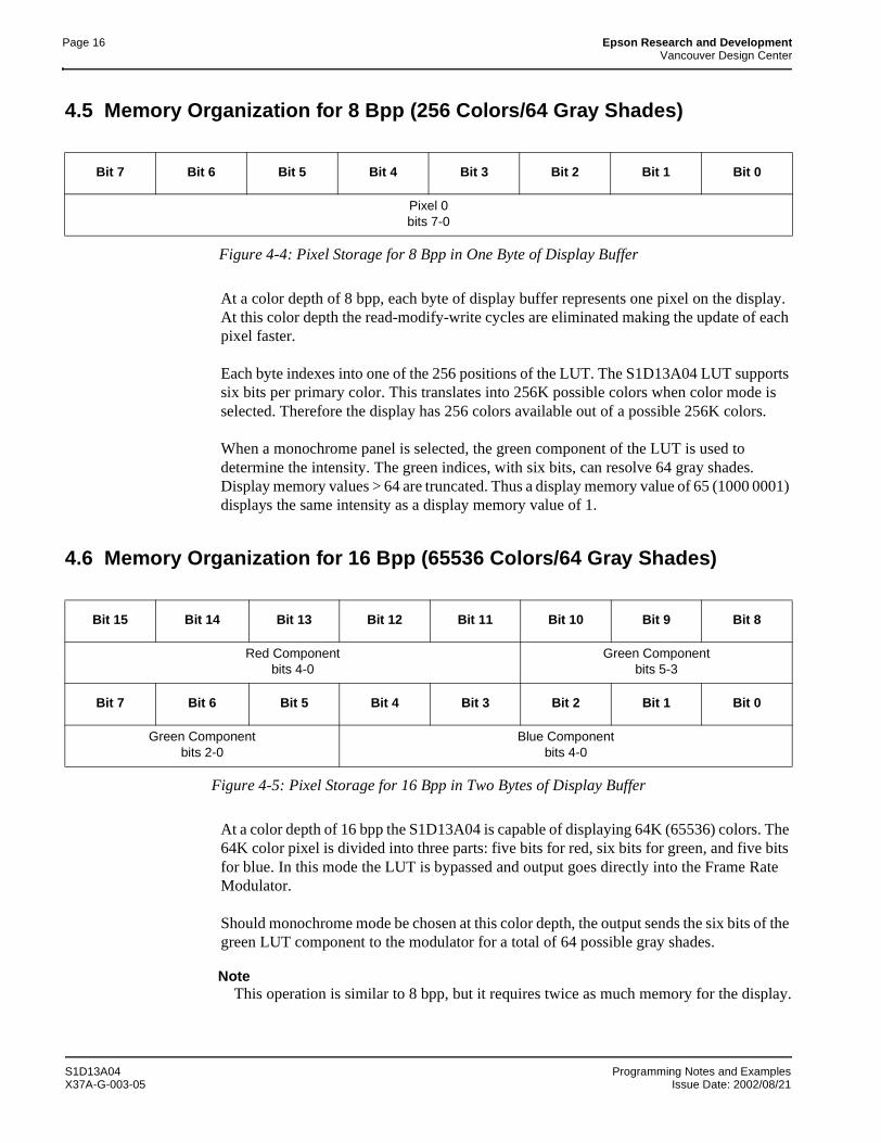
Page 16 Epson Research and DevelopmentVancouver Design Center
4.5 Memory Organization for 8 Bpp (256 Colors/64 Gray Shades)
Figure 4-4: Pixel Storage for 8 Bpp in One Byte of Display Buffer
At a color depth of 8 bpp, each byte of display buffer represents one pixel on the display. At this color depth the read-modify-write cycles are eliminated making the update of each pixel faster.
Each byte indexes into one of the 256 positions of the LUT. The S1D13A04 LUT supports six bits per primary color. This translates into 256K possible colors when color mode is selected. Therefore the display has 256 colors available out of a possible 256K colors.
When a monochrome panel is selected, the green component of the LUT is used to determine the intensity. The green indices, with six bits, can resolve 64 gray shades. Display memory values > 64 are truncated. Thus a display memory value of 65 (1000 0001) displays the same intensity as a display memory value of 1.
4.6 Memory Organization for 16 Bpp (65536 Colors/64 Gray Shades)
Figure 4-5: Pixel Storage for 16 Bpp in Two Bytes of Display Buffer
At a color depth of 16 bpp the S1D13A04 is capable of displaying 64K (65536) colors. The 64K color pixel is divided into three parts: five bits for red, six bits for green, and five bits for blue. In this mode the LUT is bypassed and output goes directly into the Frame Rate Modulator.
Should monochrome mode be chosen at this color depth, the output sends the six bits of the green LUT component to the modulator for a total of 64 possible gray shades.
NoteThis operation is similar to 8 bpp, but it requires twice as much memory for the display.
Bit 7 Bit 6 Bit 5 Bit 4 Bit 3 Bit 2 Bit 1 Bit 0
Pixel 0bits 7-0
Bit 15 Bit 14 Bit 13 Bit 12 Bit 11 Bit 10 Bit 9 Bit 8
Red Componentbits 4-0
Green Componentbits 5-3
Bit 7 Bit 6 Bit 5 Bit 4 Bit 3 Bit 2 Bit 1 Bit 0
Green Componentbits 2-0
Blue Componentbits 4-0
S1D13A04 Programming Notes and ExamplesX37A-G-003-05 Issue Date: 2002/08/21
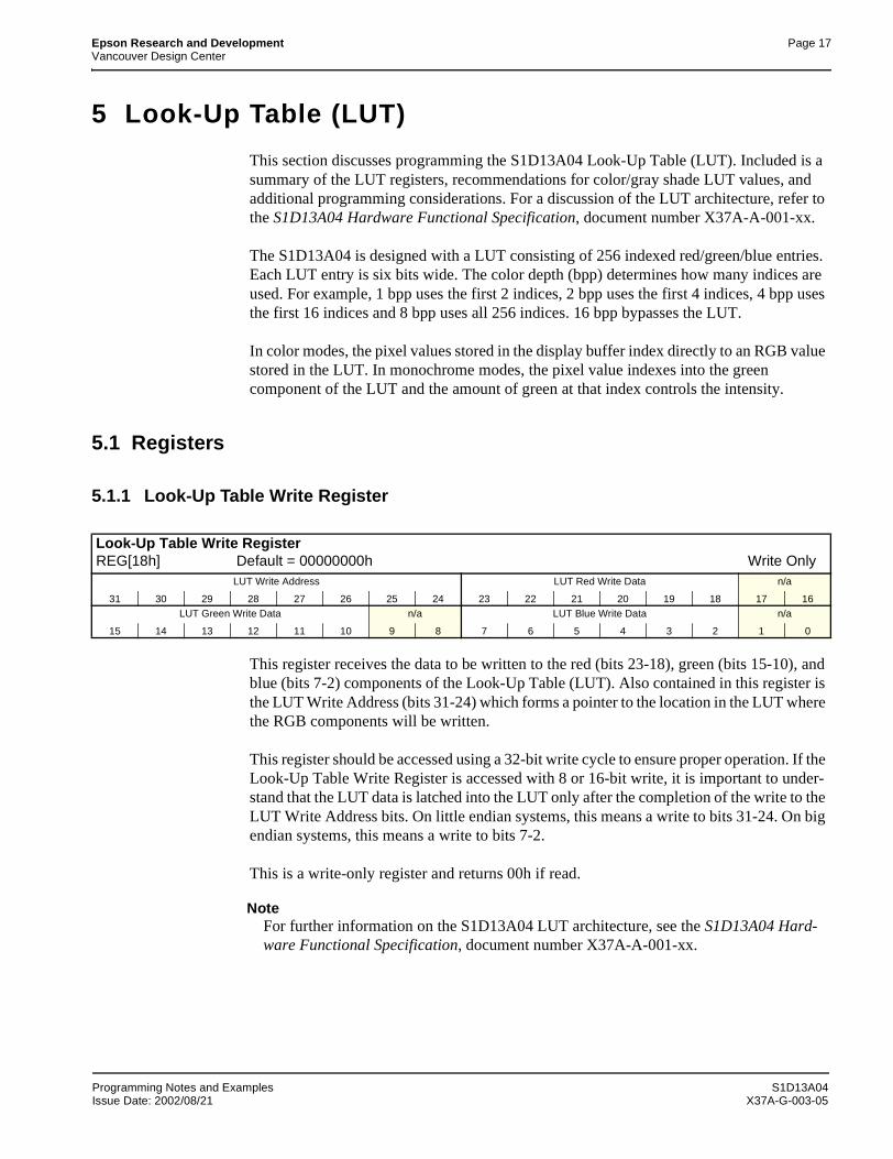
Epson Research and Development Page 17Vancouver Design Center
5 Look-Up Table (LUT)
This section discusses programming the S1D13A04 Look-Up Table (LUT). Included is a summary of the LUT registers, recommendations for color/gray shade LUT values, and additional programming considerations. For a discussion of the LUT architecture, refer to the S1D13A04 Hardware Functional Specification, document number X37A-A-001-xx.
The S1D13A04 is designed with a LUT consisting of 256 indexed red/green/blue entries. Each LUT entry is six bits wide. The color depth (bpp) determines how many indices are used. For example, 1 bpp uses the first 2 indices, 2 bpp uses the first 4 indices, 4 bpp uses the first 16 indices and 8 bpp uses all 256 indices. 16 bpp bypasses the LUT.
In color modes, the pixel values stored in the display buffer index directly to an RGB value stored in the LUT. In monochrome modes, the pixel value indexes into the green component of the LUT and the amount of green at that index controls the intensity.
5.1 Registers
5.1.1 Look-Up Table Write Register
This register receives the data to be written to the red (bits 23-18), green (bits 15-10), and blue (bits 7-2) components of the Look-Up Table (LUT). Also contained in this register is the LUT Write Address (bits 31-24) which forms a pointer to the location in the LUT where the RGB components will be written.
This register should be accessed using a 32-bit write cycle to ensure proper operation. If the Look-Up Table Write Register is accessed with 8 or 16-bit write, it is important to under-stand that the LUT data is latched into the LUT only after the completion of the write to the LUT Write Address bits. On little endian systems, this means a write to bits 31-24. On big endian systems, this means a write to bits 7-2.
This is a write-only register and returns 00h if read.
NoteFor further information on the S1D13A04 LUT architecture, see the S1D13A04 Hard-ware Functional Specification, document number X37A-A-001-xx.
Look-Up Table Write RegisterREG[18h] Default = 00000000h Write Only
LUT Write Address LUT Red Write Data n/a
31 30 29 28 27 26 25 24 23 22 21 20 19 18 17 16LUT Green Write Data n/a LUT Blue Write Data n/a
15 14 13 12 11 10 9 8 7 6 5 4 3 2 1 0
Programming Notes and Examples S1D13A04Issue Date: 2002/08/21 X37A-G-003-05
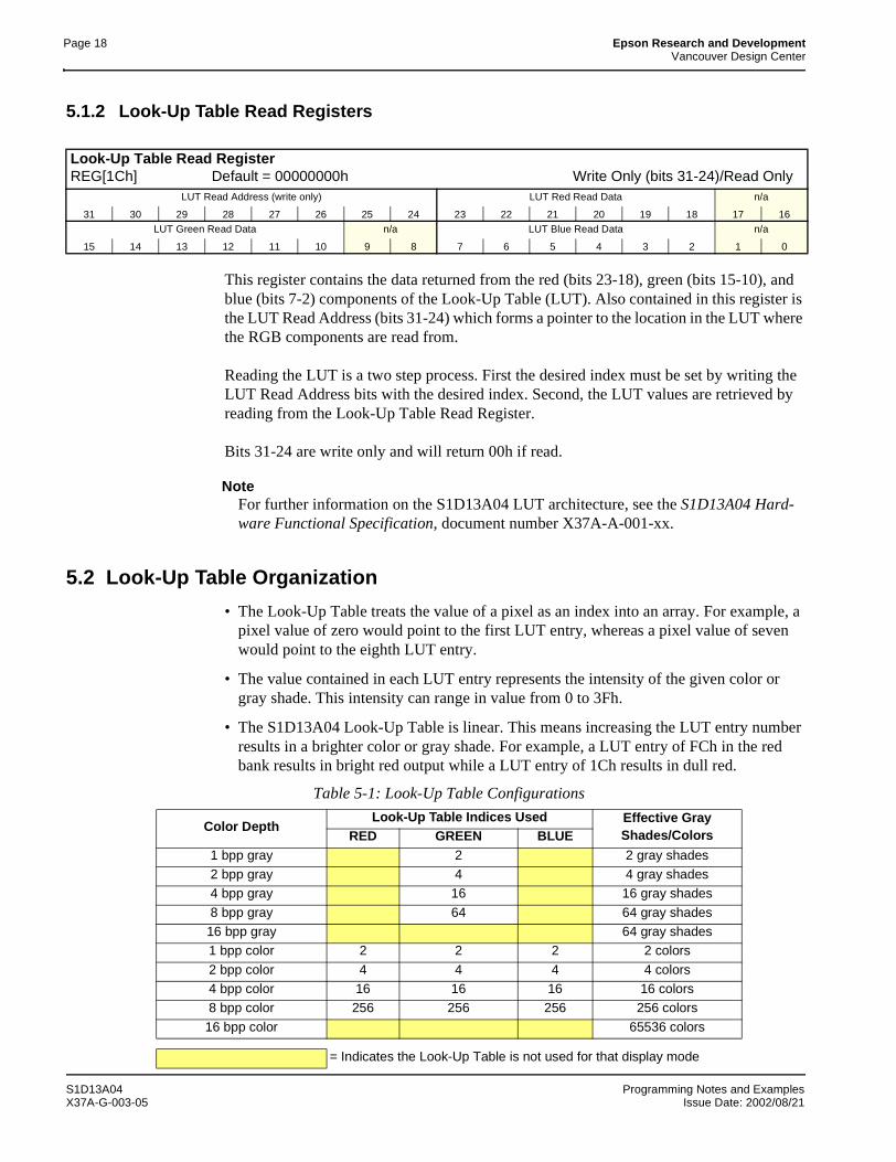
Page 18 Epson Research and DevelopmentVancouver Design Center
5.1.2 Look-Up Table Read Registers
This register contains the data returned from the red (bits 23-18), green (bits 15-10), and blue (bits 7-2) components of the Look-Up Table (LUT). Also contained in this register is the LUT Read Address (bits 31-24) which forms a pointer to the location in the LUT where the RGB components are read from.
Reading the LUT is a two step process. First the desired index must be set by writing the LUT Read Address bits with the desired index. Second, the LUT values are retrieved by reading from the Look-Up Table Read Register.
Bits 31-24 are write only and will return 00h if read.
NoteFor further information on the S1D13A04 LUT architecture, see the S1D13A04 Hard-ware Functional Specification, document number X37A-A-001-xx.
5.2 Look-Up Table Organization
• The Look-Up Table treats the value of a pixel as an index into an array. For example, a pixel value of zero would point to the first LUT entry, whereas a pixel value of seven would point to the eighth LUT entry.
• The value contained in each LUT entry represents the intensity of the given color or gray shade. This intensity can range in value from 0 to 3Fh.
• The S1D13A04 Look-Up Table is linear. This means increasing the LUT entry number results in a brighter color or gray shade. For example, a LUT entry of FCh in the red bank results in bright red output while a LUT entry of 1Ch results in dull red.
Look-Up Table Read RegisterREG[1Ch] Default = 00000000h Write Only (bits 31-24)/Read Only
LUT Read Address (write only) LUT Red Read Data n/a
31 30 29 28 27 26 25 24 23 22 21 20 19 18 17 16LUT Green Read Data n/a LUT Blue Read Data n/a
15 14 13 12 11 10 9 8 7 6 5 4 3 2 1 0
Table 5-1: Look-Up Table Configurations
Color DepthLook-Up Table Indices Used Effective Gray
Shades/ColorsRED GREEN BLUE1 bpp gray 2 2 gray shades2 bpp gray 4 4 gray shades4 bpp gray 16 16 gray shades
8 bpp gray 64 64 gray shades16 bpp gray 64 gray shades1 bpp color 2 2 2 2 colors
2 bpp color 4 4 4 4 colors4 bpp color 16 16 16 16 colors8 bpp color 256 256 256 256 colors
16 bpp color 65536 colors
= Indicates the Look-Up Table is not used for that display mode
S1D13A04 Programming Notes and ExamplesX37A-G-003-05 Issue Date: 2002/08/21
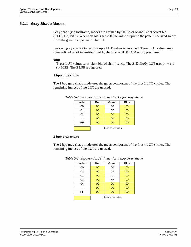
Epson Research and Development Page 19Vancouver Design Center
5.2.1 Gray Shade Modes
Gray shade (monochrome) modes are defined by the Color/Mono Panel Select bit (REG[0Ch] bit 6). When this bit is set to 0, the value output to the panel is derived solely from the green component of the LUT.
For each gray shade a table of sample LUT values is provided. These LUT values are a standardized set of intensities used by the Epson S1D13A04 utility programs.
NoteThese LUT values carry eight bits of significance. The S1D13A04 LUT uses only the six MSB. The 2 LSB are ignored.
1 bpp gray shade
The 1 bpp gray shade mode uses the green component of the first 2 LUT entries. The remaining indices of the LUT are unused.
2 bpp gray shade
The 2 bpp gray shade mode uses the green component of the first 4 LUT entries. The remaining indices of the LUT are unused.
Table 5-2: Suggested LUT Values for 1 Bpp Gray Shade
Index Red Green Blue00 00 00 0001 00 FF 0002 00 00 00
... 00 00 00FF 00 00 00
Unused entries
Table 5-3: Suggested LUT Values for 4 Bpp Gray Shade
Index Red Green Blue00 00 00 00
01 00 55 0002 00 AA 0003 00 FF 00
04 00 00 00... 00 00 00FF 00 00 00
Unused entries
Programming Notes and Examples S1D13A04Issue Date: 2002/08/21 X37A-G-003-05
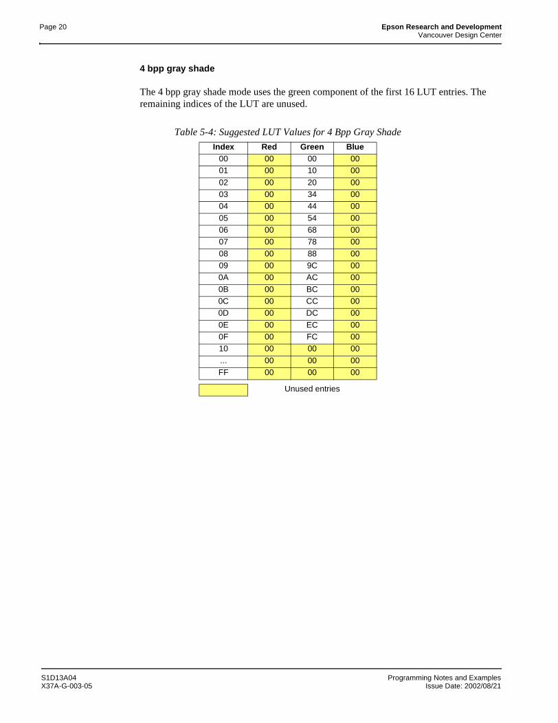
Page 20 Epson Research and DevelopmentVancouver Design Center
4 bpp gray shade
The 4 bpp gray shade mode uses the green component of the first 16 LUT entries. The remaining indices of the LUT are unused.
Table 5-4: Suggested LUT Values for 4 Bpp Gray Shade
Index Red Green Blue00 00 00 0001 00 10 00
02 00 20 0003 00 34 0004 00 44 00
05 00 54 0006 00 68 0007 00 78 00
08 00 88 0009 00 9C 000A 00 AC 00
0B 00 BC 000C 00 CC 000D 00 DC 00
0E 00 EC 000F 00 FC 0010 00 00 00
... 00 00 00FF 00 00 00
Unused entries
S1D13A04 Programming Notes and ExamplesX37A-G-003-05 Issue Date: 2002/08/21
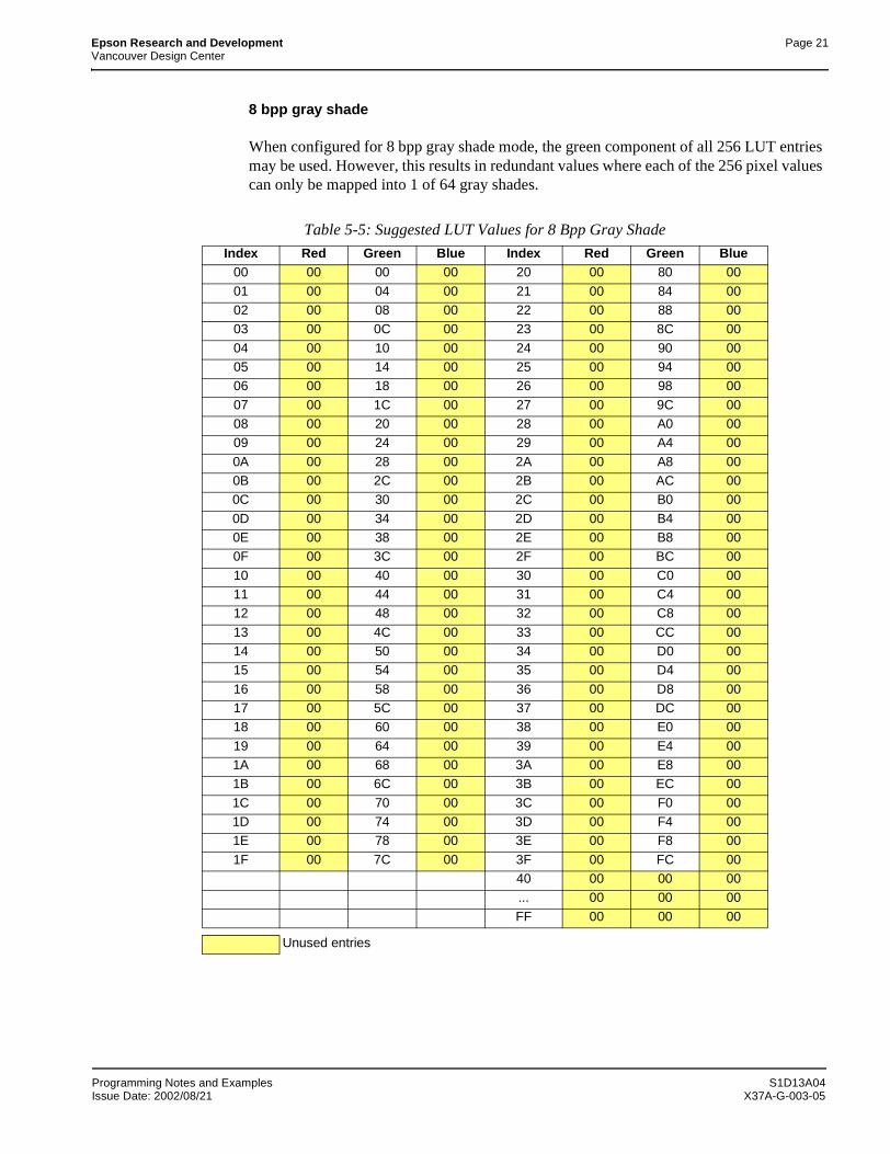
Epson Research and Development Page 21Vancouver Design Center
8 bpp gray shade
When configured for 8 bpp gray shade mode, the green component of all 256 LUT entries may be used. However, this results in redundant values where each of the 256 pixel values can only be mapped into 1 of 64 gray shades.
Table 5-5: Suggested LUT Values for 8 Bpp Gray Shade
Index Red Green Blue Index Red Green Blue00 00 00 00 20 00 80 00
01 00 04 00 21 00 84 0002 00 08 00 22 00 88 0003 00 0C 00 23 00 8C 00
04 00 10 00 24 00 90 0005 00 14 00 25 00 94 0006 00 18 00 26 00 98 00
07 00 1C 00 27 00 9C 0008 00 20 00 28 00 A0 0009 00 24 00 29 00 A4 00
0A 00 28 00 2A 00 A8 000B 00 2C 00 2B 00 AC 000C 00 30 00 2C 00 B0 00
0D 00 34 00 2D 00 B4 000E 00 38 00 2E 00 B8 000F 00 3C 00 2F 00 BC 00
10 00 40 00 30 00 C0 0011 00 44 00 31 00 C4 0012 00 48 00 32 00 C8 00
13 00 4C 00 33 00 CC 0014 00 50 00 34 00 D0 0015 00 54 00 35 00 D4 00
16 00 58 00 36 00 D8 0017 00 5C 00 37 00 DC 0018 00 60 00 38 00 E0 00
19 00 64 00 39 00 E4 001A 00 68 00 3A 00 E8 001B 00 6C 00 3B 00 EC 00
1C 00 70 00 3C 00 F0 001D 00 74 00 3D 00 F4 001E 00 78 00 3E 00 F8 00
1F 00 7C 00 3F 00 FC 0040 00 00 00... 00 00 00
FF 00 00 00
Unused entries
Programming Notes and Examples S1D13A04Issue Date: 2002/08/21 X37A-G-003-05
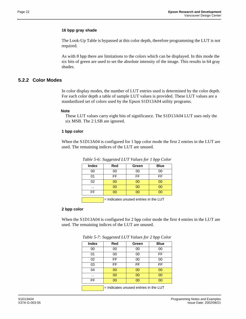
Page 22 Epson Research and DevelopmentVancouver Design Center
16 bpp gray shade
The Look-Up Table is bypassed at this color depth, therefore programming the LUT is not required.
As with 8 bpp there are limitations to the colors which can be displayed. In this mode the six bits of green are used to set the absolute intensity of the image. This results in 64 gray shades.
5.2.2 Color Modes
In color display modes, the number of LUT entries used is determined by the color depth. For each color depth a table of sample LUT values is provided. These LUT values are a standardized set of colors used by the Epson S1D13A04 utility programs.
NoteThese LUT values carry eight bits of significance. The S1D13A04 LUT uses only the six MSB. The 2 LSB are ignored.
1 bpp color
When the S1D13A04 is configured for 1 bpp color mode the first 2 entries in the LUT are used. The remaining indices of the LUT are unused.
2 bpp color
When the S1D13A04 is configured for 2 bpp color mode the first 4 entries in the LUT are used. The remaining indices of the LUT are unused.
Table 5-6: Suggested LUT Values for 1 bpp Color
Index Red Green Blue00 00 00 0001 FF FF FF
02 00 00 00... 00 00 00FF 00 00 00
= Indicates unused entries in the LUT
Table 5-7: Suggested LUT Values for 2 bpp Color
Index Red Green Blue00 00 00 00
01 00 00 FF02 FF 00 0003 FF FF FF
04 00 00 00... 00 00 00FF 00 00 00
= Indicates unused entries in the LUT
S1D13A04 Programming Notes and ExamplesX37A-G-003-05 Issue Date: 2002/08/21
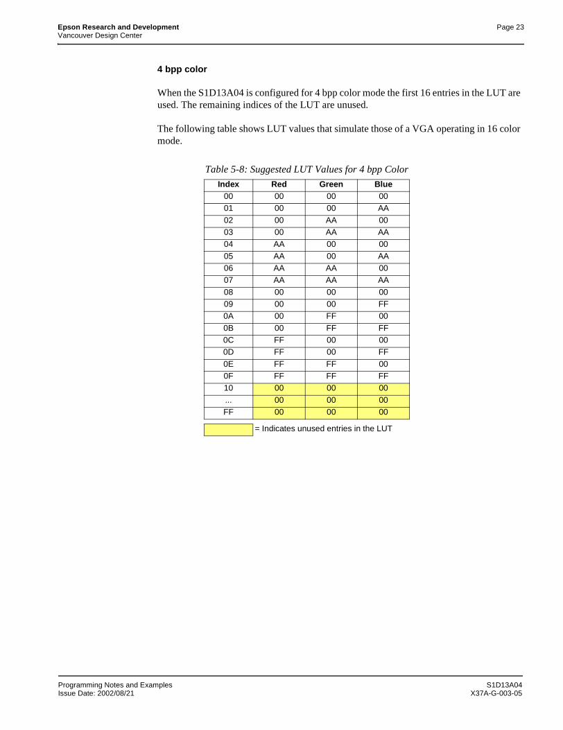
Epson Research and Development Page 23Vancouver Design Center
4 bpp color
When the S1D13A04 is configured for 4 bpp color mode the first 16 entries in the LUT are used. The remaining indices of the LUT are unused.
The following table shows LUT values that simulate those of a VGA operating in 16 color mode.
Table 5-8: Suggested LUT Values for 4 bpp Color
Index Red Green Blue00 00 00 0001 00 00 AA
02 00 AA 0003 00 AA AA04 AA 00 00
05 AA 00 AA06 AA AA 0007 AA AA AA
08 00 00 0009 00 00 FF0A 00 FF 00
0B 00 FF FF0C FF 00 000D FF 00 FF
0E FF FF 000F FF FF FF10 00 00 00
... 00 00 00FF 00 00 00
= Indicates unused entries in the LUT
Programming Notes and Examples S1D13A04Issue Date: 2002/08/21 X37A-G-003-05
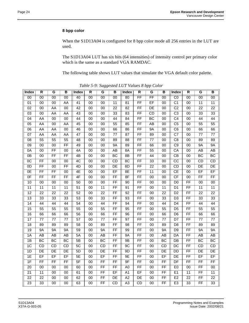
Page 24 Epson Research and DevelopmentVancouver Design Center
8 bpp color
When the S1D13A04 is configured for 8 bpp color mode all 256 entries in the LUT are used.
The S1D13A04 LUT has six bits (64 intensities) of intensity control per primary color which is the same as a standard VGA RAMDAC.
The following table shows LUT values that simulate the VGA default color palette.
Table 5-9: Suggested LUT Values 8 bpp Color
Index R G B Index R G B Index R G B Index R G B00 00 00 00 40 00 00 00 80 FF FF 00 C0 00 00 0001 00 00 AA 41 00 00 11 81 FF EF 00 C1 00 11 1102 00 AA 00 42 00 00 22 82 FF DE 00 C2 00 22 22
03 00 AA AA 43 00 00 33 83 FF CD 00 C3 00 33 3304 AA 00 00 44 00 00 44 84 FF BC 00 C4 00 44 4405 AA 00 AA 45 00 00 55 85 FF AB 00 C5 00 55 55
06 AA AA 00 46 00 00 66 86 FF 9A 00 C6 00 66 6607 AA AA AA 47 00 00 77 87 FF 89 00 C7 00 77 7708 55 55 55 48 00 00 89 88 FF 77 00 C8 00 89 89
09 00 00 FF 49 00 00 9A 89 FF 66 00 C9 00 9A 9A0A 00 FF 00 4A 00 00 AB 8A FF 55 00 CA 00 AB AB0B 00 FF FF 4B 00 00 BC 8B FF 44 00 CB 00 BC BC
0C FF 00 00 4C 00 00 CD 8C FF 33 00 CC 00 CD CD0D FF 00 FF 4D 00 00 DE 8D FF 22 00 CD 00 DE DE0E FF FF 00 4E 00 00 EF 8E FF 11 00 CE 00 EF EF
0F FF FF FF 4F 00 00 FF 8F FF 00 00 CF 00 FF FF10 00 00 00 50 00 00 FF 90 FF 00 00 D0 FF 00 0011 11 11 11 51 00 11 FF 91 FF 00 11 D1 FF 11 11
12 22 22 22 52 00 22 FF 92 FF 00 22 D2 FF 22 2213 33 33 33 53 00 33 FF 93 FF 00 33 D3 FF 33 3314 44 44 44 54 00 44 FF 94 FF 00 44 D4 FF 44 44
15 55 55 55 55 00 55 FF 95 FF 00 55 D5 FF 55 5516 66 66 66 56 00 66 FF 96 FF 00 66 D6 FF 66 6617 77 77 77 57 00 77 FF 97 FF 00 77 D7 FF 77 77
18 89 89 89 58 00 89 FF 98 FF 00 89 D8 FF 89 8919 9A 9A 9A 59 00 9A FF 99 FF 00 9A D9 FF 9A 9A1A AB AB AB 5A 00 AB FF 9A FF 00 AB DA FF AB AB
1B BC BC BC 5B 00 BC FF 9B FF 00 BC DB FF BC BC1C CD CD CD 5C 00 CD FF 9C FF 00 CD DC FF CD CD1D DE DE DE 5D 00 DE FF 9D FF 00 DE DD FF DE DE
1E EF EF EF 5E 00 EF FF 9E FF 00 EF DE FF EF EF1F FF FF FF 5F 00 FF FF 9F FF 00 FF DF FF FF FF20 00 00 00 60 00 FF FF A0 FF 00 FF E0 00 FF 00
21 11 00 00 61 00 FF EF A1 EF 00 FF E1 11 FF 1122 22 00 00 62 00 FF DE A2 DE 00 FF E2 22 FF 2223 33 00 00 63 00 FF CD A3 CD 00 FF E3 33 FF 33
S1D13A04 Programming Notes and ExamplesX37A-G-003-05 Issue Date: 2002/08/21
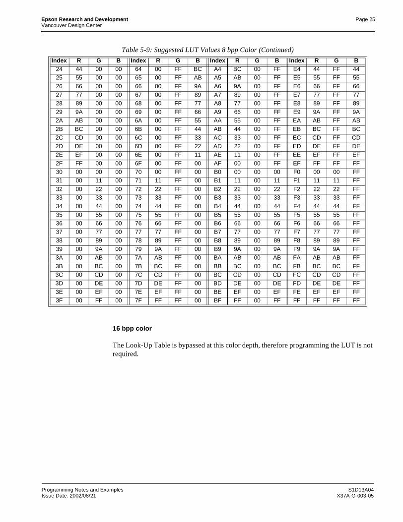
Epson Research and Development Page 25Vancouver Design Center
16 bpp color
The Look-Up Table is bypassed at this color depth, therefore programming the LUT is not required.
24 44 00 00 64 00 FF BC A4 BC 00 FF E4 44 FF 4425 55 00 00 65 00 FF AB A5 AB 00 FF E5 55 FF 55
26 66 00 00 66 00 FF 9A A6 9A 00 FF E6 66 FF 6627 77 00 00 67 00 FF 89 A7 89 00 FF E7 77 FF 7728 89 00 00 68 00 FF 77 A8 77 00 FF E8 89 FF 89
29 9A 00 00 69 00 FF 66 A9 66 00 FF E9 9A FF 9A2A AB 00 00 6A 00 FF 55 AA 55 00 FF EA AB FF AB2B BC 00 00 6B 00 FF 44 AB 44 00 FF EB BC FF BC
2C CD 00 00 6C 00 FF 33 AC 33 00 FF EC CD FF CD2D DE 00 00 6D 00 FF 22 AD 22 00 FF ED DE FF DE2E EF 00 00 6E 00 FF 11 AE 11 00 FF EE EF FF EF
2F FF 00 00 6F 00 FF 00 AF 00 00 FF EF FF FF FF30 00 00 00 70 00 FF 00 B0 00 00 00 F0 00 00 FF31 00 11 00 71 11 FF 00 B1 11 00 11 F1 11 11 FF
32 00 22 00 72 22 FF 00 B2 22 00 22 F2 22 22 FF33 00 33 00 73 33 FF 00 B3 33 00 33 F3 33 33 FF34 00 44 00 74 44 FF 00 B4 44 00 44 F4 44 44 FF
35 00 55 00 75 55 FF 00 B5 55 00 55 F5 55 55 FF36 00 66 00 76 66 FF 00 B6 66 00 66 F6 66 66 FF37 00 77 00 77 77 FF 00 B7 77 00 77 F7 77 77 FF
38 00 89 00 78 89 FF 00 B8 89 00 89 F8 89 89 FF39 00 9A 00 79 9A FF 00 B9 9A 00 9A F9 9A 9A FF3A 00 AB 00 7A AB FF 00 BA AB 00 AB FA AB AB FF
3B 00 BC 00 7B BC FF 00 BB BC 00 BC FB BC BC FF3C 00 CD 00 7C CD FF 00 BC CD 00 CD FC CD CD FF3D 00 DE 00 7D DE FF 00 BD DE 00 DE FD DE DE FF
3E 00 EF 00 7E EF FF 00 BE EF 00 EF FE EF EF FF3F 00 FF 00 7F FF FF 00 BF FF 00 FF FF FF FF FF
Table 5-9: Suggested LUT Values 8 bpp Color (Continued)
Index R G B Index R G B Index R G B Index R G B
Programming Notes and Examples S1D13A04Issue Date: 2002/08/21 X37A-G-003-05

Page 26 Epson Research and DevelopmentVancouver Design Center
6 Power Save Mode
The S1D13A04 is designed for very low-power applications. During normal operation, the internal clocks are dynamically disabled when not required. The S1D13A04 design also includes a Power Save Mode to further save power. When Power Save Mode is initiated, LCD power sequencing is required to ensure the LCD bias power supply is disabled properly. For further information on LCD power sequencing, see Section 6.3, “LCD Power Sequencing” on page 28.
For Power Save Mode AC Timing, see the S1D13A04 Hardware Functional Specification, document number X37A-A-001-xx.
6.1 Overview
The S1D13A04 includes a software initiated Power Save Mode. Enabling/disabling Power Save Mode is controlled using the Power Save Mode Enable bit (REG[14h] bit 4).
While Power Save Mode is enabled the following conditions apply.
• Registers are accessible (USB registers are not accessible)
• Memory writes are possible1
• Memory reads are not possible
• LCD display is inactive.
• LCD interface outputs are forced low.
Note1 Memory writes are possible during power save mode because the S1D13A04 dynami-cally enables the memory controller for display buffer writes.
S1D13A04 Programming Notes and ExamplesX37A-G-003-05 Issue Date: 2002/08/21
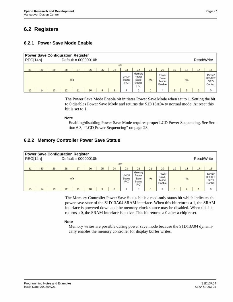
Epson Research and Development Page 27Vancouver Design Center
6.2 Registers
6.2.1 Power Save Mode Enable
The Power Save Mode Enable bit initiates Power Save Mode when set to 1. Setting the bit to 0 disables Power Save Mode and returns the S1D13A04 to normal mode. At reset this bit is set to 1.
NoteEnabling/disabling Power Save Mode requires proper LCD Power Sequencing. See Sec-tion 6.3, “LCD Power Sequencing” on page 28.
6.2.2 Memory Controller Power Save Status
The Memory Controller Power Save Status bit is a read-only status bit which indicates the power save state of the S1D13A04 SRAM interface. When this bit returns a 1, the SRAM interface is powered down and the memory clock source may be disabled. When this bit returns a 0, the SRAM interface is active. This bit returns a 0 after a chip reset.
NoteMemory writes are possible during power save mode because the S1D13A04 dynami-cally enables the memory controller for display buffer writes.
Power Save Configuration RegisterREG[14h] Default = 00000010h Read/Write
n/a
31 30 29 28 27 26 25 24 23 22 21 20 19 18 17 16
n/aVNDP Status (RO)
Memory Power Save Status (RO)
n/a
Power Save Mode
Enable
n/a
‘Direct’ HR-TFT
GPO Control
15 14 13 12 11 10 9 8 7 6 5 4 3 2 1 0
Power Save Configuration RegisterREG[14h] Default = 00000010h Read/Write
n/a
31 30 29 28 27 26 25 24 23 22 21 20 19 18 17 16
n/aVNDP Status (RO)
Memory Power Save Status (RO)
n/a
Power Save Mode
Enable
n/a
‘Direct’ HR-TFT
GPO Control
15 14 13 12 11 10 9 8 7 6 5 4 3 2 1 0
Programming Notes and Examples S1D13A04Issue Date: 2002/08/21 X37A-G-003-05
Page 28 Epson Research and DevelopmentVancouver Design Center
6.3 LCD Power Sequencing
The S1D13A04 requires LCD power sequencing (the process of powering-on and powering-off the LCD panel). LCD power sequencing allows the LCD bias voltage to discharge prior to shutting down the LCD signals, preventing long term damage to the panel and avoiding unsightly “lines” at power-on/power-off.
Proper LCD power sequencing for power-off requires a delay from the time the LCD power is disabled to the time the LCD signals are shut down. Power-on requires the LCD signals to be active prior to applying power to the LCD. This time interval depends on the LCD bias power supply design. For example, the LCD bias power supply on the S5U13A04B00C Evaluation Board requires 0.5 seconds to fully discharge. Other power supply designs may vary.
This section assumes the LCD bias power is controlled through GPIO0. The S1D13A04 GPIO pins are multi-use pins and may not be available in all system designs. For further information on the availability of GPIO pins, see the S1D13A04 Hardware Functional Specification, document number X37A-A-001-xx.
NoteThis section discusses LCD power sequencing for passive and TFT (non-HR-TFT) pan-els only. For further information on LCD power sequencing the HR-TFT, see Connect-ing to the Sharp HR-TFT Panels, document number X37A-G-011-xx.
S1D13A04 Programming Notes and ExamplesX37A-G-003-05 Issue Date: 2002/08/21
Epson Research and Development Page 29Vancouver Design Center
6.4 Enabling Power Save Mode
Power Save Mode must be enabled using the following steps.
1. Turn off the LCD bias power.
NoteThe S5U13A04B00C uses GPIO0 to control the LCD bias power supplies. Your system design may vary.
2. Wait for the LCD bias power supply to discharge. The discharge time is based on the discharge rate of the power supply.
3. Enable Power Save Mode - set REG[14h] bit 4 to 1.
The S1D13A04 is now in Power Save Mode. To further increase power savings PCLK and MCLK can be switched off (see steps 4 and 5).
4. At this time, the LCD pixel clock source may be disabled.
5. After the Memory Controller Power Save Status bit (REG[14h] bit 6)returns a 1, the Memory Clock source may be shut down.
6.5 Disabling Power Save Mode
Bring the S1D13A04 out of Power Save Mode using the following steps.
1. If the Memory Clock source is shut down, it must be started.
2. If the pixel clock is disabled, it must be started.
3. Disable Power Save Mode - set REG[14h] bit 4 to 0.
4. Wait for the LCD bias power supply to charge. The charge is based on the time re-quired for the LCD power supply to reach operating voltage.
5. Enable the LCD bias power.
NoteThe S5U13A04B00C uses GPIO0 to control the LCD bias power supplies. Your system design may vary.
Programming Notes and Examples S1D13A04Issue Date: 2002/08/21 X37A-G-003-05
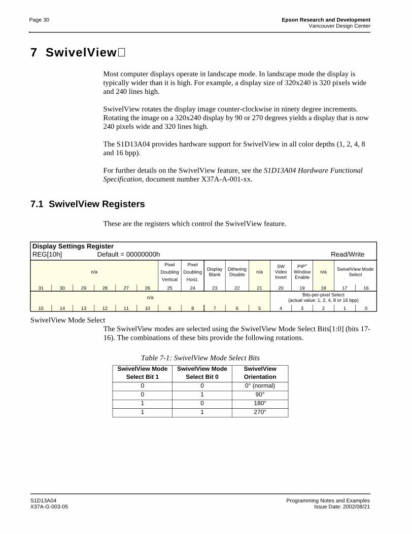
Page 30 Epson Research and DevelopmentVancouver Design Center
7 SwivelViewMost computer displays operate in landscape mode. In landscape mode the display is typically wider than it is high. For example, a display size of 320x240 is 320 pixels wide and 240 lines high.
SwivelView rotates the display image counter-clockwise in ninety degree increments. Rotating the image on a 320x240 display by 90 or 270 degrees yields a display that is now 240 pixels wide and 320 lines high.
The S1D13A04 provides hardware support for SwivelView in all color depths (1, 2, 4, 8 and 16 bpp).
For further details on the SwivelView feature, see the S1D13A04 Hardware Functional Specification, document number X37A-A-001-xx.
7.1 SwivelView Registers
These are the registers which control the SwivelView feature.
SwivelView Mode SelectThe SwivelView modes are selected using the SwivelView Mode Select Bits[1:0] (bits 17-16). The combinations of these bits provide the following rotations.
Display Settings RegisterREG[10h] Default = 00000000h Read/Write
n/a
Pixel
Doubling
Vertical
Pixel
Doubling
Horiz.
Display Blank
Dithering Disable n/a
SW Video Invert
PIP+ Window Enable
n/aSwivelView Mode
Select
31 30 29 28 27 26 25 24 23 22 21 20 19 18 17 16
n/a Bits-per-pixel Select(actual value: 1, 2, 4, 8 or 16 bpp)
15 14 13 12 11 10 9 8 7 6 5 4 3 2 1 0
Table 7-1: SwivelView Mode Select Bits
SwivelView Mode Select Bit 1
SwivelView Mode Select Bit 0
SwivelView Orientation
0 0 0° (normal)0 1 90°1 0 180°
1 1 270°
S1D13A04 Programming Notes and ExamplesX37A-G-003-05 Issue Date: 2002/08/21
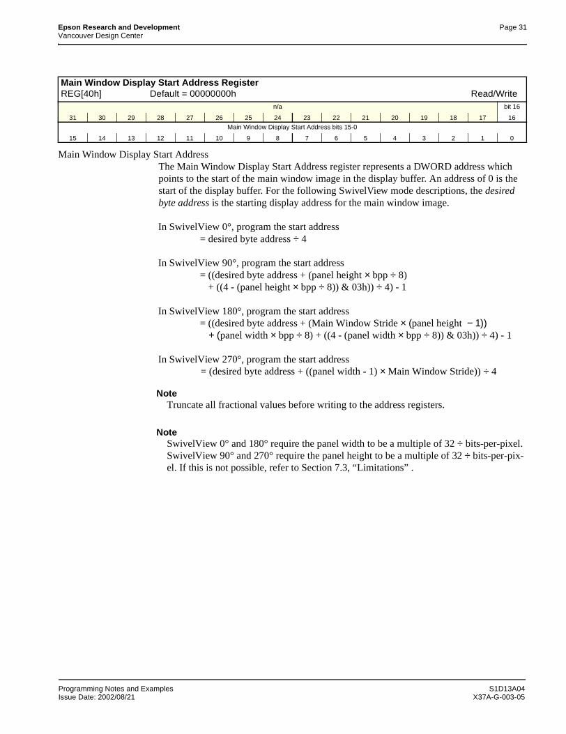
Epson Research and Development Page 31Vancouver Design Center
Main Window Display Start AddressThe Main Window Display Start Address register represents a DWORD address which points to the start of the main window image in the display buffer. An address of 0 is the start of the display buffer. For the following SwivelView mode descriptions, the desired byte address is the starting display address for the main window image.
In SwivelView 0°, program the start address= desired byte address ÷ 4
In SwivelView 90°, program the start address= ((desired byte address + (panel height × bpp ÷ 8)
+ ((4 - (panel height × bpp ÷ 8)) & 03h)) ÷ 4) - 1
In SwivelView 180°, program the start address= ((desired byte address + (Main Window Stride × (panel height − 1))
+ (panel width × bpp ÷ 8) + ((4 - (panel width × bpp ÷ 8)) & 03h)) ÷ 4) - 1
In SwivelView 270°, program the start address= (desired byte address + ((panel width - 1) × Main Window Stride)) ÷ 4
NoteTruncate all fractional values before writing to the address registers.
NoteSwivelView 0° and 180° require the panel width to be a multiple of 32 ÷ bits-per-pixel. SwivelView 90° and 270° require the panel height to be a multiple of 32 ÷ bits-per-pix-el. If this is not possible, refer to Section 7.3, “Limitations” .
Main Window Display Start Address RegisterREG[40h] Default = 00000000h Read/Write
n/a bit 16
31 30 29 28 27 26 25 24 23 22 21 20 19 18 17 16
Main Window Display Start Address bits 15-0
15 14 13 12 11 10 9 8 7 6 5 4 3 2 1 0
Programming Notes and Examples S1D13A04Issue Date: 2002/08/21 X37A-G-003-05

Page 32 Epson Research and DevelopmentVancouver Design Center
Main Window Line Address OffsetThe Main Window Line Address Offset register indicates the number of dwords per line in the main window image.
For SwivelView 0° and 180°, the image width must be at least the panel width. For SwivelView 90° and 270°, the image width must be at least the panel height. In addition, the image width must be a multiple of 32 ÷ bpp. If the image width is not such a multiple, a slightly larger width must be chosen (see Section 7.3, “Limitations” ).
Panel width and panel height refer to the physical panel dimensions in pixels. Stride is the number of bytes required for one line of the image; the offset register represents the stride in DWORD steps.
Main Window Stride = image width × bpp ÷ 8
NoteImage width can be larger than panel width (or panel height, for SwivelView 90° or 270°).
number of dwords per line = image width ÷ (32 ÷ bpp)
7.2 Examples
Example 1: In SwivelView 0° (normal) mode, program the main window registers for a 320x240 panel at a color depth of 4 bpp.
1. Determine the main window display start address.The main window is typically placed at the start of display memory which is at display address 0.
main window display start address register= desired byte address ÷ 4= 0
Program the Main Window Display Start Address register. REG[40h] is set to 00000000h.
Main Window Line Address Offset RegisterREG[44h] Default = 00000000h Read/Write
n/a
31 30 29 28 27 26 25 24 23 22 21 20 19 18 17 16
n/a Main Window Line Address Offset bits 9-0
15 14 13 12 11 10 9 8 7 6 5 4 3 2 1 0
S1D13A04 Programming Notes and ExamplesX37A-G-003-05 Issue Date: 2002/08/21
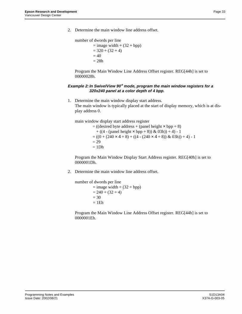
Epson Research and Development Page 33Vancouver Design Center
2. Determine the main window line address offset.
number of dwords per line= image width ÷ (32 ÷ bpp)= 320 ÷ (32 ÷ 4)= 40= 28h
Program the Main Window Line Address Offset register. REG[44h] is set to 00000028h.
Example 2: In SwivelView 90° mode, program the main window registers for a 320x240 panel at a color depth of 4 bpp.
1. Determine the main window display start address.The main window is typically placed at the start of display memory, which is at dis-play address 0.
main window display start address register= ((desired byte address + (panel height × bpp ÷ 8)
+ ((4 - (panel height × bpp ÷ 8)) & 03h)) ÷ 4) - 1= ((0 + (240 × 4 ÷ 8) + ((4 - (240 × 4 ÷ 8)) & 03h)) ÷ 4) - 1= 29= 1Dh
Program the Main Window Display Start Address register. REG[40h] is set to 0000001Dh.
2. Determine the main window line address offset.
number of dwords per line= image width ÷ (32 ÷ bpp)= 240 ÷ (32 ÷ 4)= 30= 1Eh
Program the Main Window Line Address Offset register. REG[44h] is set to 0000001Eh.
Programming Notes and Examples S1D13A04Issue Date: 2002/08/21 X37A-G-003-05
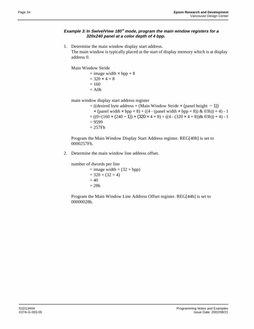
Page 34 Epson Research and DevelopmentVancouver Design Center
Example 3: In SwivelView 180° mode, program the main window registers for a 320x240 panel at a color depth of 4 bpp.
1. Determine the main window display start address.The main window is typically placed at the start of display memory which is at display address 0.
Main Window Stride= image width × bpp ÷ 8= 320 × 4 ÷ 8= 160= A0h
main window display start address register= ((desired byte address + (Main Window Stride × (panel height − 1))
+ (panel width × bpp ÷ 8) + ((4 - (panel width × bpp ÷ 8)) & 03h)) ÷ 4) - 1= ((0+(160 × (240 − 1)) + (320 × 4 ÷ 8) + ((4 - (320 × 4 ÷ 8))& 03h)) ÷ 4) - 1= 9599= 257Fh
Program the Main Window Display Start Address register. REG[40h] is set to 0000257Fh.
2. Determine the main window line address offset.
number of dwords per line= image width ÷ (32 ÷ bpp)= 320 ÷ (32 ÷ 4) = 40 = 28h
Program the Main Window Line Address Offset register. REG[44h] is set to 00000028h.
S1D13A04 Programming Notes and ExamplesX37A-G-003-05 Issue Date: 2002/08/21
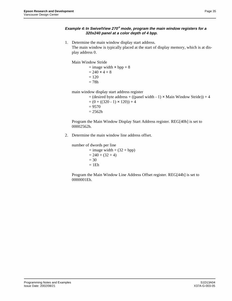
Epson Research and Development Page 35Vancouver Design Center
Example 4: In SwivelView 270° mode, program the main window registers for a 320x240 panel at a color depth of 4 bpp.
1. Determine the main window display start address.The main window is typically placed at the start of display memory, which is at dis-play address 0.
Main Window Stride= image width × bpp ÷ 8= 240 × 4 ÷ 8 = 120= 78h
main window display start address register = (desired byte address + ((panel width - 1) × Main Window Stride)) ÷ 4 = (0 + ((320 - 1) × 120)) ÷ 4 = 9570= 2562h
Program the Main Window Display Start Address register. REG[40h] is set to 00002562h.
2. Determine the main window line address offset.
number of dwords per line= image width ÷ (32 ÷ bpp)= 240 ÷ (32 ÷ 4) = 30 = 1Eh
Program the Main Window Line Address Offset register. REG[44h] is set to 0000001Eh.
Programming Notes and Examples S1D13A04Issue Date: 2002/08/21 X37A-G-003-05
Page 36 Epson Research and DevelopmentVancouver Design Center
7.3 Limitations
7.3.1 SwivelView 0° and 180°
In SwivelView 0° and 180°, the Main Window Line Address Offset register (REG[44h]) requires the panel width to be a multiple of 32 ÷ bits-per-pixel. If this is not the case, then the Main Window Line Address Offset register must be programmed to a longer line which meets this requirement. This longer line creates a virtual image where the width is main window line address offset register × 32 ÷ bits-per-pixel. In SwivelView 0°, this virtual image should be drawn in display memory as left justified, and in SwivelView 180°, this virtual image should be drawn in display memory as right justified. A left-justified image is one drawn in display memory such that each of the image’s lines only use the left most portion of the line width defined by the line address offset register (i.e. starting at horizontal position 0). A right-justified image is one drawn in display memory such that each of the image’s lines only use the right most portion of the line width defined by the line address offset register (i.e. starting at a non-zero horizontal position which is the virtual width - image width).
7.3.2 SwivelView 90° and 270°
In SwivelView 90° and 270°, the Main Window Line Address Offset register (REG[44h]) requires the panel height to be a multiple of 32 ÷ bits-per-pixel. If this is not the case, then the Main Window Line Address Offset register must be programmed to a longer line which meets this requirement. This longer line creates a virtual image whose width is main window line address offset register × 32 ÷ bits-per-pixel. In SwivelView 270°, this virtual image should be drawn in display memory as left justified, and in SwivelView 90°, this virtual image should be drawn in display memory as right justified. A left-justified image is one drawn in display memory such that each of the image’s lines only use the left most portion of the line width defined by the line address offset register (i.e. starting at horizontal position 0). A right-justified image is one drawn in display memory such that each of the image’s lines only use the right most portion of the line width defined by the line address offset register (i.e. starting at a non-zero horizontal position which is the virtual width - image width).
S1D13A04 Programming Notes and ExamplesX37A-G-003-05 Issue Date: 2002/08/21
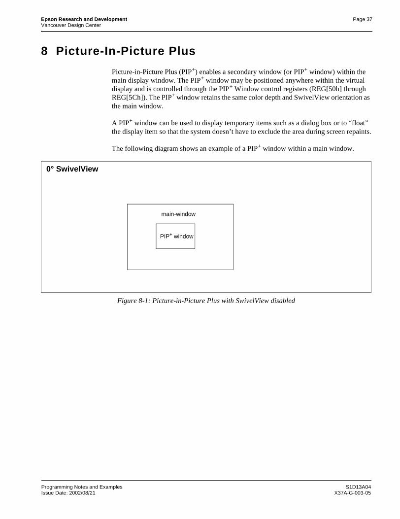
Epson Research and Development Page 37Vancouver Design Center
8 Picture-In-Picture Plus
Picture-in-Picture Plus (PIP+) enables a secondary window (or PIP+ window) within the main display window. The PIP+ window may be positioned anywhere within the virtual display and is controlled through the PIP+ Window control registers (REG[50h] through REG[5Ch]). The PIP+ window retains the same color depth and SwivelView orientation as the main window.
A PIP+ window can be used to display temporary items such as a dialog box or to “float” the display item so that the system doesn’t have to exclude the area during screen repaints.
The following diagram shows an example of a PIP+ window within a main window.
Figure 8-1: Picture-in-Picture Plus with SwivelView disabled
PIP+ window
main-window
0° SwivelView
Programming Notes and Examples S1D13A04Issue Date: 2002/08/21 X37A-G-003-05
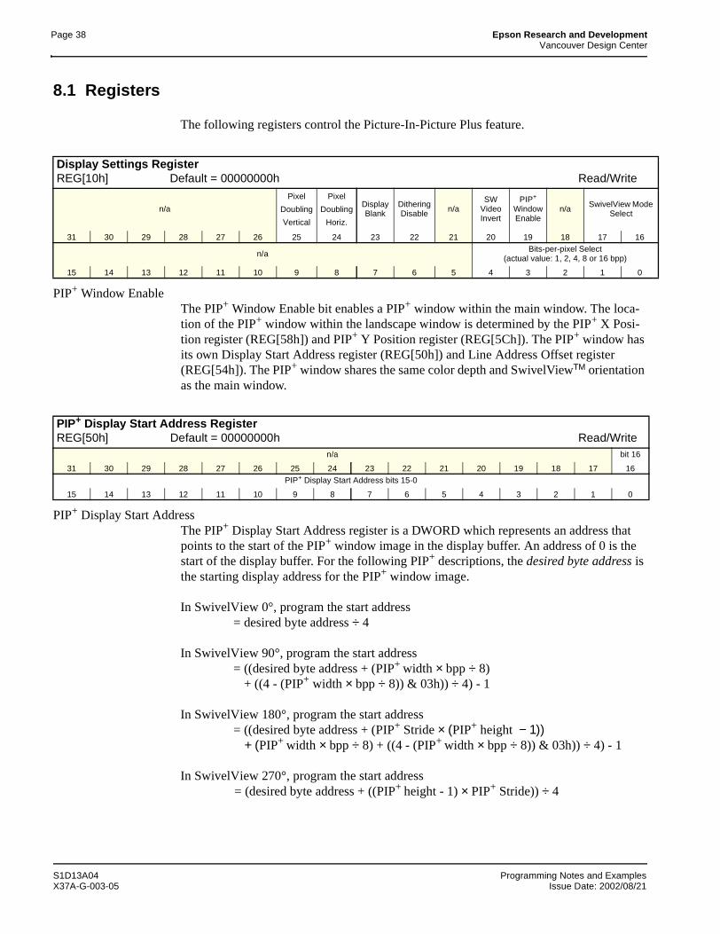
Page 38 Epson Research and DevelopmentVancouver Design Center
8.1 Registers
The following registers control the Picture-In-Picture Plus feature.
PIP+ Window EnableThe PIP+ Window Enable bit enables a PIP+ window within the main window. The loca-tion of the PIP+ window within the landscape window is determined by the PIP+ X Posi-tion register (REG[58h]) and PIP+ Y Position register (REG[5Ch]). The PIP+ window has its own Display Start Address register (REG[50h]) and Line Address Offset register (REG[54h]). The PIP+ window shares the same color depth and SwivelViewTM orientation as the main window.
PIP+ Display Start AddressThe PIP+ Display Start Address register is a DWORD which represents an address that points to the start of the PIP+ window image in the display buffer. An address of 0 is the start of the display buffer. For the following PIP+ descriptions, the desired byte address is the starting display address for the PIP+ window image.
In SwivelView 0°, program the start address= desired byte address ÷ 4
In SwivelView 90°, program the start address= ((desired byte address + (PIP+ width × bpp ÷ 8)
+ ((4 - (PIP+ width × bpp ÷ 8)) & 03h)) ÷ 4) - 1
In SwivelView 180°, program the start address= ((desired byte address + (PIP+ Stride × (PIP+ height − 1))
+ (PIP+ width × bpp ÷ 8) + ((4 - (PIP+ width × bpp ÷ 8)) & 03h)) ÷ 4) - 1
In SwivelView 270°, program the start address= (desired byte address + ((PIP+ height - 1) × PIP+ Stride)) ÷ 4
Display Settings RegisterREG[10h] Default = 00000000h Read/Write
n/a
Pixel
Doubling
Vertical
Pixel
Doubling
Horiz.
Display Blank
Dithering Disable n/a
SW Video Invert
PIP+ Window Enable
n/a SwivelView Mode Select
31 30 29 28 27 26 25 24 23 22 21 20 19 18 17 16
n/aBits-per-pixel Select
(actual value: 1, 2, 4, 8 or 16 bpp)
15 14 13 12 11 10 9 8 7 6 5 4 3 2 1 0
PIP+ Display Start Address RegisterREG[50h] Default = 00000000h Read/Write
n/a bit 16
31 30 29 28 27 26 25 24 23 22 21 20 19 18 17 16PIP+ Display Start Address bits 15-0
15 14 13 12 11 10 9 8 7 6 5 4 3 2 1 0
S1D13A04 Programming Notes and ExamplesX37A-G-003-05 Issue Date: 2002/08/21
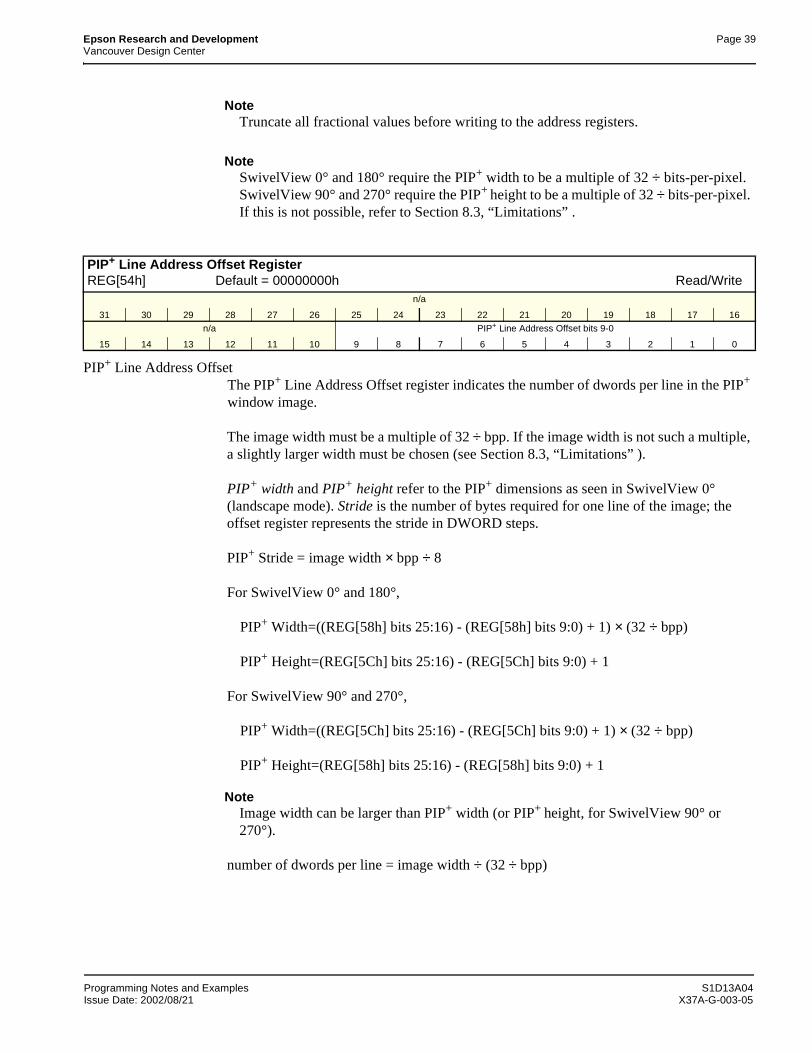
Epson Research and Development Page 39Vancouver Design Center
NoteTruncate all fractional values before writing to the address registers.
NoteSwivelView 0° and 180° require the PIP+ width to be a multiple of 32 ÷ bits-per-pixel. SwivelView 90° and 270° require the PIP+ height to be a multiple of 32 ÷ bits-per-pixel. If this is not possible, refer to Section 8.3, “Limitations” .
PIP+ Line Address OffsetThe PIP+ Line Address Offset register indicates the number of dwords per line in the PIP+ window image.
The image width must be a multiple of 32 ÷ bpp. If the image width is not such a multiple, a slightly larger width must be chosen (see Section 8.3, “Limitations” ).
PIP+ width and PIP+ height refer to the PIP+ dimensions as seen in SwivelView 0° (landscape mode). Stride is the number of bytes required for one line of the image; the offset register represents the stride in DWORD steps.
PIP+ Stride = image width × bpp ÷ 8
For SwivelView 0° and 180°,
PIP+ Width=((REG[58h] bits 25:16) - (REG[58h] bits 9:0) + 1) × (32 ÷ bpp)
PIP+ Height=(REG[5Ch] bits 25:16) - (REG[5Ch] bits 9:0) + 1
For SwivelView 90° and 270°,
PIP+ Width=((REG[5Ch] bits 25:16) - (REG[5Ch] bits 9:0) + 1) × (32 ÷ bpp)
PIP+ Height=(REG[58h] bits 25:16) - (REG[58h] bits 9:0) + 1
NoteImage width can be larger than PIP+ width (or PIP+ height, for SwivelView 90° or 270°).
number of dwords per line = image width ÷ (32 ÷ bpp)
PIP+ Line Address Offset RegisterREG[54h] Default = 00000000h Read/Write
n/a
31 30 29 28 27 26 25 24 23 22 21 20 19 18 17 16
n/a PIP+ Line Address Offset bits 9-0
15 14 13 12 11 10 9 8 7 6 5 4 3 2 1 0
Programming Notes and Examples S1D13A04Issue Date: 2002/08/21 X37A-G-003-05
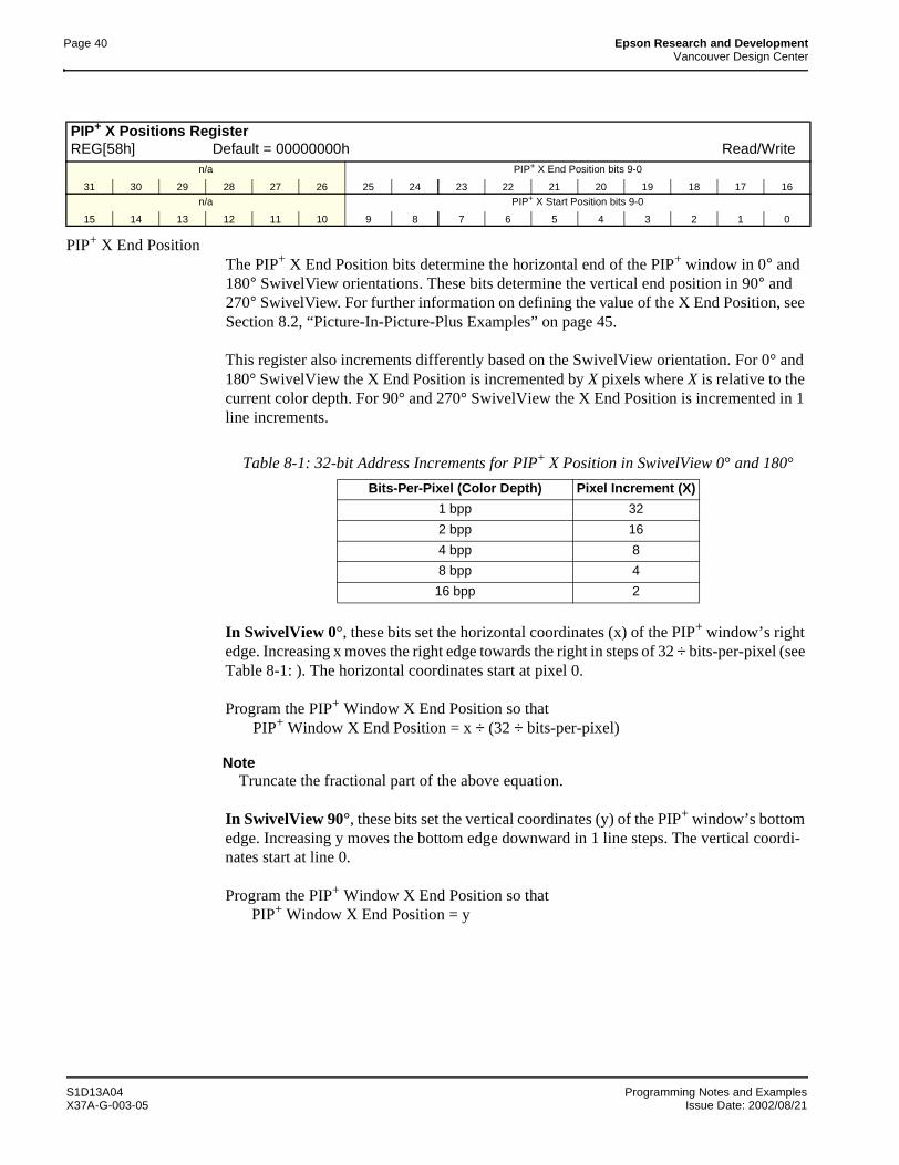
Page 40 Epson Research and DevelopmentVancouver Design Center
PIP+ X End PositionThe PIP+ X End Position bits determine the horizontal end of the PIP+ window in 0° and 180° SwivelView orientations. These bits determine the vertical end position in 90° and 270° SwivelView. For further information on defining the value of the X End Position, see Section 8.2, “Picture-In-Picture-Plus Examples” on page 45.
This register also increments differently based on the SwivelView orientation. For 0° and 180° SwivelView the X End Position is incremented by X pixels where X is relative to the current color depth. For 90° and 270° SwivelView the X End Position is incremented in 1 line increments.
In SwivelView 0°, these bits set the horizontal coordinates (x) of the PIP+ window’s right edge. Increasing x moves the right edge towards the right in steps of 32 ÷ bits-per-pixel (see Table 8-1: ). The horizontal coordinates start at pixel 0.
Program the PIP+ Window X End Position so thatPIP+ Window X End Position = x ÷ (32 ÷ bits-per-pixel)
NoteTruncate the fractional part of the above equation.
In SwivelView 90°, these bits set the vertical coordinates (y) of the PIP+ window’s bottom edge. Increasing y moves the bottom edge downward in 1 line steps. The vertical coordi-nates start at line 0.
Program the PIP+ Window X End Position so thatPIP+ Window X End Position = y
PIP+ X Positions RegisterREG[58h] Default = 00000000h Read/Write
n/a PIP+ X End Position bits 9-0
31 30 29 28 27 26 25 24 23 22 21 20 19 18 17 16
n/a PIP+ X Start Position bits 9-0
15 14 13 12 11 10 9 8 7 6 5 4 3 2 1 0
Table 8-1: 32-bit Address Increments for PIP+ X Position in SwivelView 0° and 180°
Bits-Per-Pixel (Color Depth) Pixel Increment (X)
1 bpp 32
2 bpp 16
4 bpp 8
8 bpp 4
16 bpp 2
S1D13A04 Programming Notes and ExamplesX37A-G-003-05 Issue Date: 2002/08/21
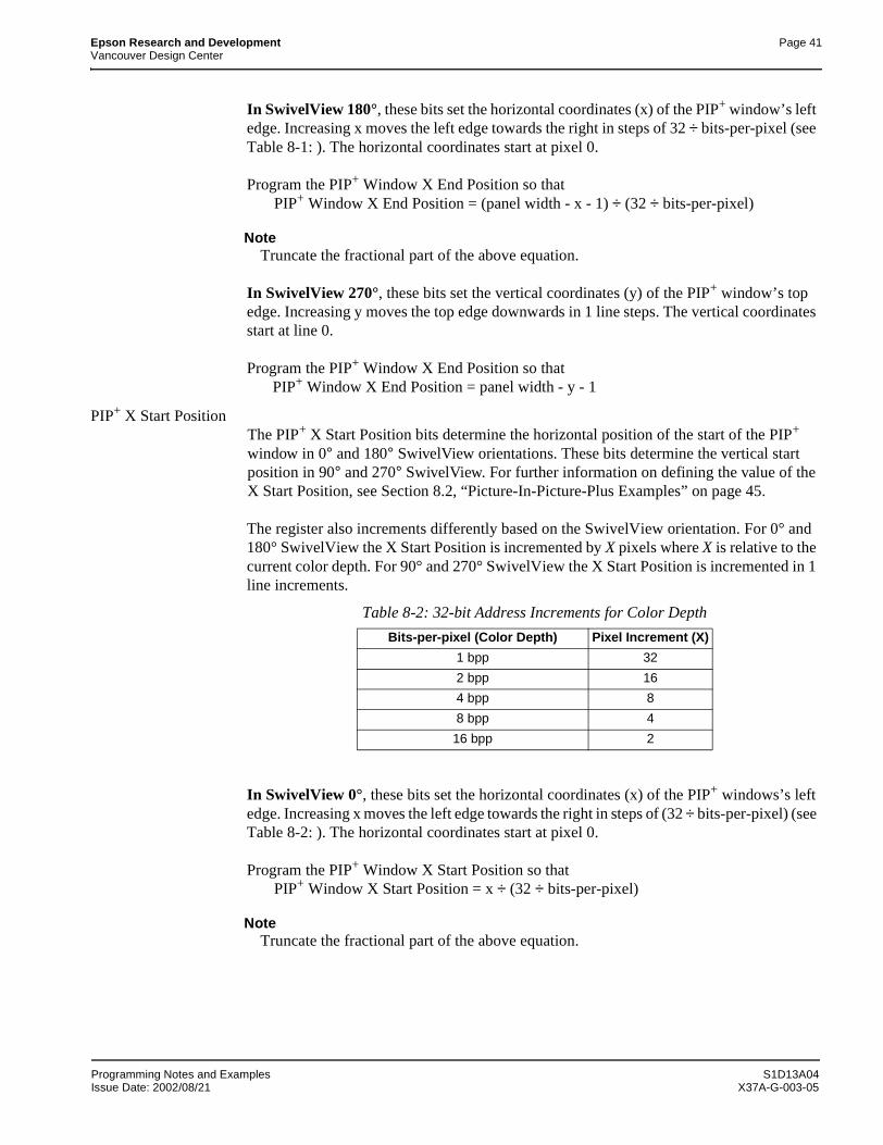
Epson Research and Development Page 41Vancouver Design Center
In SwivelView 180°, these bits set the horizontal coordinates (x) of the PIP+ window’s left edge. Increasing x moves the left edge towards the right in steps of 32 ÷ bits-per-pixel (see Table 8-1: ). The horizontal coordinates start at pixel 0.
Program the PIP+ Window X End Position so thatPIP+ Window X End Position = (panel width - x - 1) ÷ (32 ÷ bits-per-pixel)
NoteTruncate the fractional part of the above equation.
In SwivelView 270°, these bits set the vertical coordinates (y) of the PIP+ window’s top edge. Increasing y moves the top edge downwards in 1 line steps. The vertical coordinates start at line 0.
Program the PIP+ Window X End Position so thatPIP+ Window X End Position = panel width - y - 1
PIP+ X Start PositionThe PIP+ X Start Position bits determine the horizontal position of the start of the PIP+ window in 0° and 180° SwivelView orientations. These bits determine the vertical start position in 90° and 270° SwivelView. For further information on defining the value of the X Start Position, see Section 8.2, “Picture-In-Picture-Plus Examples” on page 45.
The register also increments differently based on the SwivelView orientation. For 0° and 180° SwivelView the X Start Position is incremented by X pixels where X is relative to the current color depth. For 90° and 270° SwivelView the X Start Position is incremented in 1 line increments.
In SwivelView 0°, these bits set the horizontal coordinates (x) of the PIP+ windows’s left edge. Increasing x moves the left edge towards the right in steps of (32 ÷ bits-per-pixel) (see Table 8-2: ). The horizontal coordinates start at pixel 0.
Program the PIP+ Window X Start Position so thatPIP+ Window X Start Position = x ÷ (32 ÷ bits-per-pixel)
NoteTruncate the fractional part of the above equation.
Table 8-2: 32-bit Address Increments for Color Depth
Bits-per-pixel (Color Depth) Pixel Increment (X)
1 bpp 32
2 bpp 16
4 bpp 8
8 bpp 4
16 bpp 2
Programming Notes and Examples S1D13A04Issue Date: 2002/08/21 X37A-G-003-05
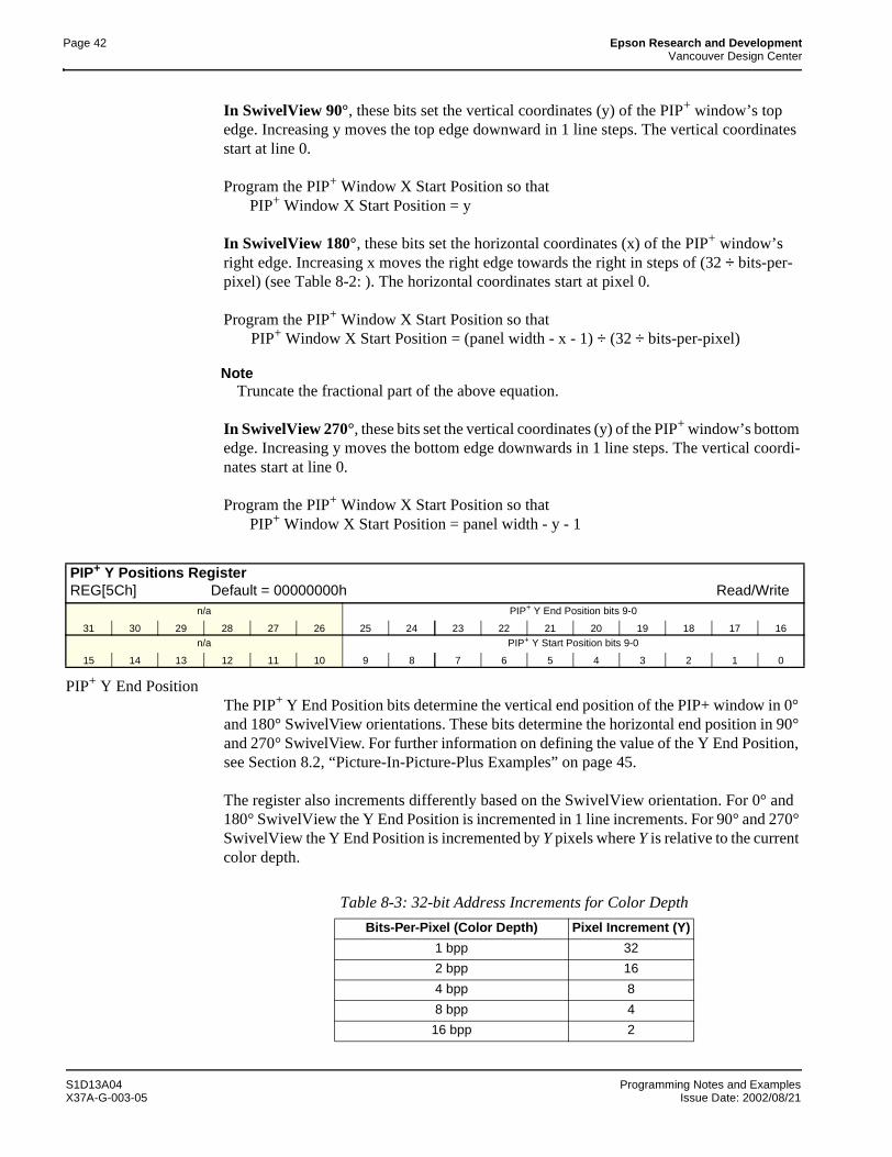
Page 42 Epson Research and DevelopmentVancouver Design Center
In SwivelView 90°, these bits set the vertical coordinates (y) of the PIP+ window’s top edge. Increasing y moves the top edge downward in 1 line steps. The vertical coordinates start at line 0.
Program the PIP+ Window X Start Position so thatPIP+ Window X Start Position = y
In SwivelView 180°, these bits set the horizontal coordinates (x) of the PIP+ window’s right edge. Increasing x moves the right edge towards the right in steps of (32 ÷ bits-per-pixel) (see Table 8-2: ). The horizontal coordinates start at pixel 0.
Program the PIP+ Window X Start Position so thatPIP+ Window X Start Position = (panel width - x - 1) ÷ (32 ÷ bits-per-pixel)
NoteTruncate the fractional part of the above equation.
In SwivelView 270°, these bits set the vertical coordinates (y) of the PIP+ window’s bottom edge. Increasing y moves the bottom edge downwards in 1 line steps. The vertical coordi-nates start at line 0.
Program the PIP+ Window X Start Position so thatPIP+ Window X Start Position = panel width - y - 1
PIP+ Y End PositionThe PIP+ Y End Position bits determine the vertical end position of the PIP+ window in 0° and 180° SwivelView orientations. These bits determine the horizontal end position in 90° and 270° SwivelView. For further information on defining the value of the Y End Position, see Section 8.2, “Picture-In-Picture-Plus Examples” on page 45.
The register also increments differently based on the SwivelView orientation. For 0° and 180° SwivelView the Y End Position is incremented in 1 line increments. For 90° and 270° SwivelView the Y End Position is incremented by Y pixels where Y is relative to the current color depth.
PIP+ Y Positions RegisterREG[5Ch] Default = 00000000h Read/Write
n/a PIP+ Y End Position bits 9-0
31 30 29 28 27 26 25 24 23 22 21 20 19 18 17 16n/a PIP+ Y Start Position bits 9-0
15 14 13 12 11 10 9 8 7 6 5 4 3 2 1 0
Table 8-3: 32-bit Address Increments for Color Depth
Bits-Per-Pixel (Color Depth) Pixel Increment (Y)
1 bpp 32
2 bpp 16
4 bpp 8
8 bpp 4
16 bpp 2
S1D13A04 Programming Notes and ExamplesX37A-G-003-05 Issue Date: 2002/08/21
Epson Research and Development Page 43Vancouver Design Center
In SwivelView 0°, these bits set the vertical coordinates (y) of the PIP+ windows’s bottom edge. Increasing y moves the bottom edge downwards in 1 line steps. The vertical coordi-nates start at line 0.
Program the PIP+ Window Y End Position so thatPIP+ Window Y End Position = y
In SwivelView 90°, these bits set the horizontal coordinates (x) of the PIP+ window’s left edge. Increasing x moves the left edge towards the right in steps of (32 ÷ bits-per-pixel) (see Table 8-3: ). The horizontal coordinates start at pixel 0.
Program the PIP+ Window Y End Position so thatPIP+ Window Y End Position = (panel height - x - 1) ÷ (32 ÷ bits-per-pixel)
NoteTruncate the fractional part of the above equation.
In SwivelView 180°, these bits set the vertical coordinates (y) of the PIP+ window’s top edge. Increasing y moves the top edge downwards in 1 line steps. The vertical coordinates start at line 0.
Program the PIP+ Window Y End Position so thatPIP+ Window Y End Position = panel height - y - 1
In SwivelView 270°, these bits set the horizontal coordinates (x) of the PIP+ window’s right edge. Increasing x moves the right edge towards the right in steps of (32 ÷ bits-per-pixel) (see Table 8-3: ). The horizontal coordinates start at pixel 0.
Program the PIP+ Window Y End Position so thatPIP+ Window Y End Position = x ÷ (32 ÷ bits-per-pixel)
NoteTruncate the fractional part of the above equation.
Programming Notes and Examples S1D13A04Issue Date: 2002/08/21 X37A-G-003-05
Page 44 Epson Research and DevelopmentVancouver Design Center
PIP+ Y Start PositionThe PIP+ Y Start Position bits determine the vertical start position of the PIP+ window in 0° and 180° SwivelView orientations. These bits determine the horizontal start position in 90° and 270° SwivelView. For further information on defining the value of the Y Start Position, see Section 8.2, “Picture-In-Picture-Plus Examples” on page 45.
The register also increments differently based on the SwivelView orientation. For 0° and 180° SwivelView the Y Start Position is incremented in 1 line increments. For 90° and 270° SwivelView the Y Start Position is incremented by Y pixels where Y is relative to the current color depth.
In SwivelView 0°, these bits set the vertical coordinates (y) of the PIP+ windows’s top edge. Increasing y moves the top edge downwards in 1 line steps. The vertical coordinates start at line 0.
Program the PIP+ Window Y Start Position so thatPIP+ Window Y Start Position = y
In SwivelView 90°, these bits set the horizontal coordinates (x) of the PIP+ window’s right edge. Increasing x moves the right edge towards the right in steps of (32 ÷ bits-per-pixel) (see Table 8-4: ). The horizontal coordinates start at pixel 0.
Program the PIP+ Window Y Start Position so thatPIP+ Window Y Start Position = (panel height - x - 1) ÷ (32 ÷ bits-per-pixel)
NoteTruncate the fractional part of the above equation.
In SwivelView 180°, these bits set the vertical coordinates (y) of the PIP+ window’s bottom edge. Increasing y moves the bottom edge downwards in 1 line steps. The vertical coordi-nates start at line 0.
Program the PIP+ Window Y Start Position so thatPIP+ Window Y Start Position = panel height - y - 1
Table 8-4: 32-bit Address Increments for Color Depth
Bits-Per-Pixel (Color Depth) Pixel Increment (Y)
1 bpp 32
2 bpp 16
4 bpp 8
8 bpp 4
16 bpp 2
S1D13A04 Programming Notes and ExamplesX37A-G-003-05 Issue Date: 2002/08/21
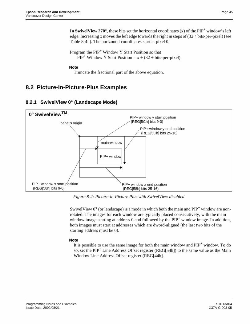
Epson Research and Development Page 45Vancouver Design Center
In SwivelView 270°, these bits set the horizontal coordinates (x) of the PIP+ window’s left edge. Increasing x moves the left edge towards the right in steps of (32 ÷ bits-per-pixel) (see Table 8-4: ). The horizontal coordinates start at pixel 0.
Program the PIP+ Window Y Start Position so thatPIP+ Window Y Start Position = x ÷ (32 ÷ bits-per-pixel)
NoteTruncate the fractional part of the above equation.
8.2 Picture-In-Picture-Plus Examples
8.2.1 SwivelView 0° (Landscape Mode)
Figure 8-2: Picture-in-Picture Plus with SwivelView disabled
SwivelView 0° (or landscape) is a mode in which both the main and PIP+ window are non- rotated. The images for each window are typically placed consecutively, with the main window image starting at address 0 and followed by the PIP+ window image. In addition, both images must start at addresses which are dword-aligned (the last two bits of the starting address must be 0).
NoteIt is possible to use the same image for both the main window and PIP+ window. To do so, set the PIP+ Line Address Offset register (REG[54h]) to the same value as the Main Window Line Address Offset register (REG[44h].
PIP+ window
main-window
PIP+ window y start position
panel’s origin
PIP+ window y end position
PIP+ window x start position PIP+ window x end position
0° SwivelViewTM
(REG[58h] bits 9-0) (REG[58h] bits 25-16)
(REG[5Ch] bits 25-16)
(REG[5Ch] bits 9-0)
Programming Notes and Examples S1D13A04Issue Date: 2002/08/21 X37A-G-003-05

Page 46 Epson Research and DevelopmentVancouver Design Center
Example 5: Program the PIP+ window registers for a 320x240 panel at 4 bpp, with the PIP+ window positioned at (80, 60) with a width of 160 and a height of 120.
1. Determine the value for the PIP+ Window X Positions and PIP+ Window Y Positions registers. Let the top left corner of the PIP+ window be (x1, y1), and let the bottom right corner be (x2, y2), where x2 = x1 + width - 1 and y2 = y1 + height - 1. The PIP+ Window X Positions register sets the horizontal coordinates of the PIP+ window’s top left and bottom right corners. The PIP+ Window Y Positions register sets the vertical coordinates of the PIP+ window’s top left and bottom right corners.
The required values are calculated as follows:
X Start Position= x1 ÷ (32 ÷ bpp)= 80 ÷ (32 ÷ 4)= 10= 0Ah
Y Start Position= y1= 60= 3Ch
X End Position= x2 ÷ (32 ÷ bpp)= (80 + 160 - 1) ÷ (32 ÷ 4)= 29.875= 1Dh (truncated fractional part)
Y End Position= y2= 60 + 120 - 1= 179= B3h
S1D13A04 Programming Notes and ExamplesX37A-G-003-05 Issue Date: 2002/08/21
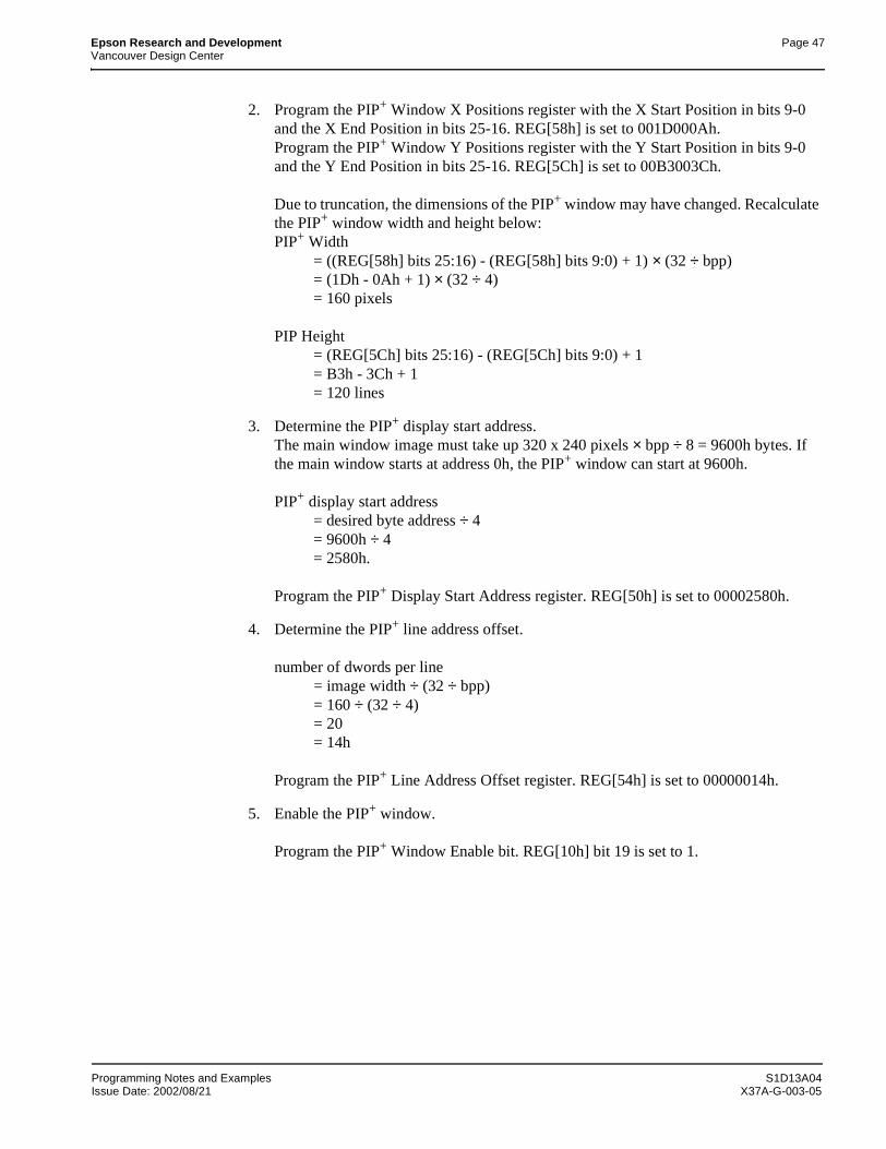
Epson Research and Development Page 47Vancouver Design Center
2. Program the PIP+ Window X Positions register with the X Start Position in bits 9-0 and the X End Position in bits 25-16. REG[58h] is set to 001D000Ah.Program the PIP+ Window Y Positions register with the Y Start Position in bits 9-0 and the Y End Position in bits 25-16. REG[5Ch] is set to 00B3003Ch.
Due to truncation, the dimensions of the PIP+ window may have changed. Recalculate the PIP+ window width and height below:PIP+ Width
= ((REG[58h] bits 25:16) - (REG[58h] bits 9:0) + 1) × (32 ÷ bpp)= (1Dh - 0Ah + 1) × (32 ÷ 4)= 160 pixels
PIP Height= (REG[5Ch] bits 25:16) - (REG[5Ch] bits 9:0) + 1= B3h - 3Ch + 1= 120 lines
3. Determine the PIP+ display start address.The main window image must take up 320 x 240 pixels × bpp ÷ 8 = 9600h bytes. If the main window starts at address 0h, the PIP+ window can start at 9600h.
PIP+ display start address= desired byte address ÷ 4= 9600h ÷ 4= 2580h.
Program the PIP+ Display Start Address register. REG[50h] is set to 00002580h.
4. Determine the PIP+ line address offset.
number of dwords per line= image width ÷ (32 ÷ bpp)= 160 ÷ (32 ÷ 4)= 20= 14h
Program the PIP+ Line Address Offset register. REG[54h] is set to 00000014h.
5. Enable the PIP+ window.
Program the PIP+ Window Enable bit. REG[10h] bit 19 is set to 1.
Programming Notes and Examples S1D13A04Issue Date: 2002/08/21 X37A-G-003-05
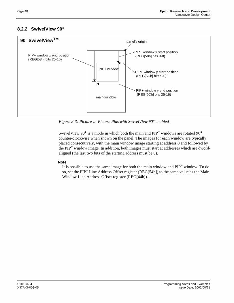
Page 48 Epson Research and DevelopmentVancouver Design Center
8.2.2 SwivelView 90°
Figure 8-3: Picture-in-Picture Plus with SwivelView 90° enabled
SwivelView 90° is a mode in which both the main and PIP+ windows are rotated 90° counter-clockwise when shown on the panel. The images for each window are typically placed consecutively, with the main window image starting at address 0 and followed by the PIP+ window image. In addition, both images must start at addresses which are dword-aligned (the last two bits of the starting address must be 0).
NoteIt is possible to use the same image for both the main window and PIP+ window. To do so, set the PIP+ Line Address Offset register (REG[54h]) to the same value as the Main Window Line Address Offset register (REG[44h]).
PIP+ window
main-window
PIP+ window y start position
panel’s origin
PIP+ window y end position
PIP+ window x start positionPIP+ window x end position
90° SwivelViewTM
(REG[58h] bits 25-16) (REG[58h] bits 9-0)
(REG[5Ch] bits 9-0)
(REG[5Ch] bits 25-16)
S1D13A04 Programming Notes and ExamplesX37A-G-003-05 Issue Date: 2002/08/21
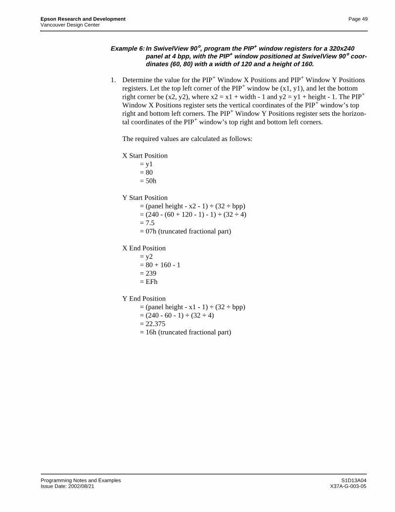
Epson Research and Development Page 49Vancouver Design Center
Example 6: In SwivelView 90°, program the PIP+ window registers for a 320x240 panel at 4 bpp, with the PIP+ window positioned at SwivelView 90° coor-dinates (60, 80) with a width of 120 and a height of 160.
1. Determine the value for the PIP+ Window X Positions and PIP+ Window Y Positions registers. Let the top left corner of the PIP+ window be (x1, y1), and let the bottom right corner be (x2, y2), where x2 = x1 + width - 1 and y2 = y1 + height - 1. The PIP+ Window X Positions register sets the vertical coordinates of the PIP+ window’s top right and bottom left corners. The PIP+ Window Y Positions register sets the horizon-tal coordinates of the PIP+ window’s top right and bottom left corners.
The required values are calculated as follows:
X Start Position= y1= 80= 50h
Y Start Position= (panel height - x2 - 1) ÷ (32 ÷ bpp)= (240 - (60 + 120 - 1) - 1) ÷ (32 ÷ 4)= 7.5= 07h (truncated fractional part)
X End Position= y2= 80 + 160 - 1= 239= EFh
Y End Position= (panel height - x1 - 1) ÷ (32 ÷ bpp)= (240 - 60 - 1) ÷ (32 ÷ 4)= 22.375= 16h (truncated fractional part)
Programming Notes and Examples S1D13A04Issue Date: 2002/08/21 X37A-G-003-05
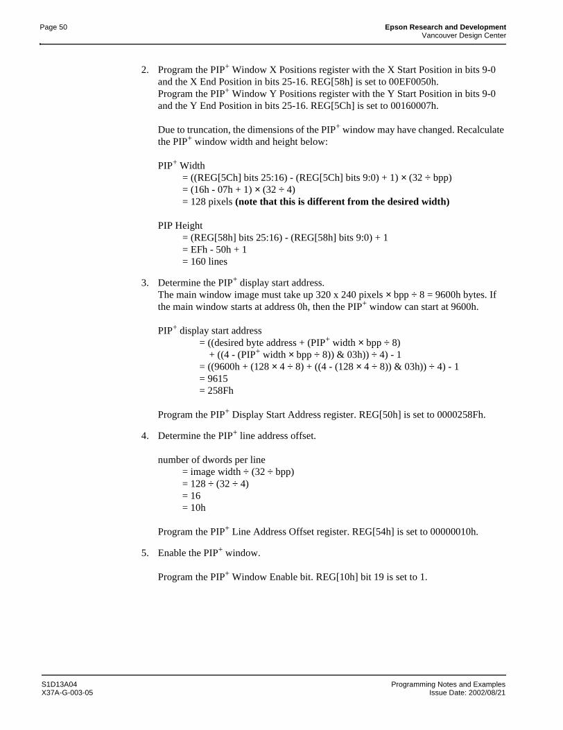
Page 50 Epson Research and DevelopmentVancouver Design Center
2. Program the PIP+ Window X Positions register with the X Start Position in bits 9-0 and the X End Position in bits 25-16. REG[58h] is set to 00EF0050h.Program the PIP+ Window Y Positions register with the Y Start Position in bits 9-0 and the Y End Position in bits 25-16. REG[5Ch] is set to 00160007h.
Due to truncation, the dimensions of the PIP+ window may have changed. Recalculate the PIP+ window width and height below:
PIP+ Width= ((REG[5Ch] bits 25:16) - (REG[5Ch] bits 9:0) + 1) × (32 ÷ bpp)= (16h - 07h + 1) × (32 ÷ 4)= 128 pixels (note that this is different from the desired width)
PIP Height= (REG[58h] bits 25:16) - (REG[58h] bits 9:0) + 1= EFh - 50h + 1= 160 lines
3. Determine the PIP+ display start address.The main window image must take up 320 x 240 pixels × bpp ÷ 8 = 9600h bytes. If the main window starts at address 0h, then the PIP+ window can start at 9600h.
PIP+ display start address= ((desired byte address + (PIP+ width × bpp ÷ 8)
+ ((4 - (PIP+ width × bpp ÷ 8)) & 03h)) ÷ 4) - 1= ((9600h + (128 × 4 ÷ 8) + ((4 - (128 × 4 ÷ 8)) & 03h)) ÷ 4) - 1= 9615= 258Fh
Program the PIP+ Display Start Address register. REG[50h] is set to 0000258Fh.
4. Determine the PIP+ line address offset.
number of dwords per line= image width ÷ (32 ÷ bpp)= 128 ÷ (32 ÷ 4)= 16= 10h
Program the PIP+ Line Address Offset register. REG[54h] is set to 00000010h.
5. Enable the PIP+ window.
Program the PIP+ Window Enable bit. REG[10h] bit 19 is set to 1.
S1D13A04 Programming Notes and ExamplesX37A-G-003-05 Issue Date: 2002/08/21
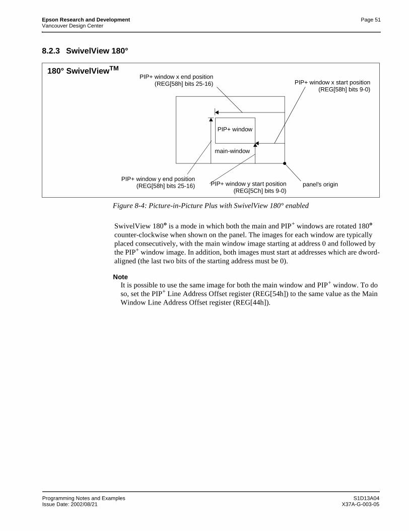
Epson Research and Development Page 51Vancouver Design Center
8.2.3 SwivelView 180°
Figure 8-4: Picture-in-Picture Plus with SwivelView 180° enabled
SwivelView 180° is a mode in which both the main and PIP+ windows are rotated 180° counter-clockwise when shown on the panel. The images for each window are typically placed consecutively, with the main window image starting at address 0 and followed by the PIP+ window image. In addition, both images must start at addresses which are dword-aligned (the last two bits of the starting address must be 0).
NoteIt is possible to use the same image for both the main window and PIP+ window. To do so, set the PIP+ Line Address Offset register (REG[54h]) to the same value as the Main Window Line Address Offset register (REG[44h]).
PIP+ window
main-window
PIP+ window y start position panel’s originPIP+ window y end position
PIP+ window x start positionPIP+ window x end position
180° SwivelViewTM
(REG[58h] bits 25-16) (REG[58h] bits 9-0)
(REG[58h] bits 25-16) (REG[5Ch] bits 9-0)
Programming Notes and Examples S1D13A04Issue Date: 2002/08/21 X37A-G-003-05

Page 52 Epson Research and DevelopmentVancouver Design Center
Example 7: In SwivelView 180°, program the PIP+ window registers for a 320x240 panel at 4 bpp, with the PIP+ window positioned at SwivelView 180° co-ordinates (80, 60) with a width of 160 and a height of 120.
1. Determine the value for the PIP+ Window X Positions and PIP+ Window Y Positions registers. Let the top left corner of the PIP+ window be (x1, y1), and let the bottom right corner be (x2, y2), where x2 = x1 + width - 1 and y2 = y1 + height - 1. The PIP+ Window X Positions register sets the horizontal coordinates of the PIP+ window’s bottom right and top left corner. The PIP+ Window Y Positions register sets the verti-cal coordinates of the PIP+ window’s bottom right and top left corner.
The required values are calculated as follows:
X Start Position= (panel width - x2 - 1) ÷ (32 ÷ bpp)= (320 - (80 + 160 - 1) - 1) ÷ (32 ÷ 4)= 10= 0Ah
Y Start Position= panel height - y2 - 1= 240 - (60 + 120 - 1) - 1= 60 = 3Ch
X End Position= (panel width - x1 - 1) ÷ (32 ÷ bpp)= (320 - 80 - 1) ÷ (32 ÷ 4)= 29.875= 1Dh (truncated fractional part)
Y End Position= panel height - y1 - 1= 240 - 60 - 1 = 179 = B3h
S1D13A04 Programming Notes and ExamplesX37A-G-003-05 Issue Date: 2002/08/21
Epson Research and Development Page 53Vancouver Design Center
Program the PIP+ Window X Positions register with the X Start Position in bits 9-0 and the X End Position in bits 25-16. REG[58h] is set to 001D000Ah.Program the PIP+ Window Y Positions register with the Y Start Position in bits 9-0 and the Y End Position in bits 25-16. REG[5Ch] is set to 00B3003Ch.
Due to truncation, the dimensions of the PIP+ window may have changed. Recalculate the PIP+ window width and height below:
PIP+ Width= ((REG[58h] bits 25:16) - (REG[58h] bits 9:0) + 1) × (32 ÷ bpp)= (1Dh - 0Ah + 1) × (32 ÷ 4)= 160 pixels
PIP Height= (REG[5Ch] bits 25:16) - (REG[5Ch] bits 9:0) + 1= B3h - 3Ch + 1= 120 lines
2. Determine the PIP+ display start address.The main window image must take up 320 x 240 pixels × bpp ÷ 8 = 9600h bytes. If the main window starts at address 0h, then the PIP+ window can start at 9600h.
PIP+ Stride= image width × bpp ÷ 8= 160 × 4 ÷ 8= 80= 50h
PIP+ display start address= ((desired byte address + (PIP+ Stride × (PIP+ height - 1))
+ (PIP+ width × bpp ÷ 8) + ((4 - (PIP width × bpp ÷ 8)) & 03h)) ÷ 4) - 1= ((9600h + (80 × (120 - 1)) + (160 × 4 ÷ 8) + ((4 - (160 × 4 ÷ 8))&03h)) ÷ 4) - 1= 11999= 2EDFh
Program the PIP+ Display Start Address register. REG[50h] is set to 00002EDFh.
3. Determine the PIP+ line address offset.
number of dwords per line= image width ÷ (32 ÷ bpp)= 160 ÷ (32 ÷ 4)= 20= 14h
Program the PIP+ Line Address Offset register. REG[54h] is set to 00000014h.
4. Enable the PIP+ window.
Program the PIP+ Window Enable bit. REG[10h] bit 19 is set to 1.
Programming Notes and Examples S1D13A04Issue Date: 2002/08/21 X37A-G-003-05
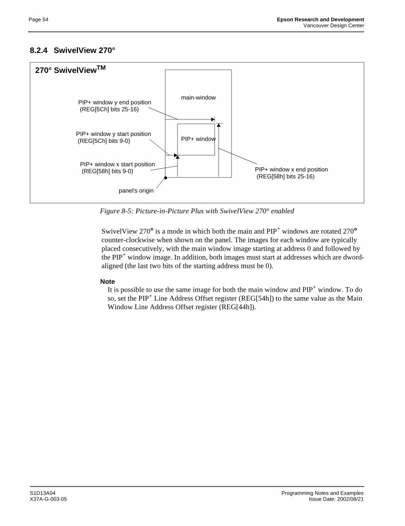
Page 54 Epson Research and DevelopmentVancouver Design Center
8.2.4 SwivelView 270°
Figure 8-5: Picture-in-Picture Plus with SwivelView 270° enabled
SwivelView 270° is a mode in which both the main and PIP+ windows are rotated 270° counter-clockwise when shown on the panel. The images for each window are typically placed consecutively, with the main window image starting at address 0 and followed by the PIP+ window image. In addition, both images must start at addresses which are dword-aligned (the last two bits of the starting address must be 0).
NoteIt is possible to use the same image for both the main window and PIP+ window. To do so, set the PIP+ Line Address Offset register (REG[54h]) to the same value as the Main Window Line Address Offset register (REG[44h]).
PIP+ window
main-window
PIP+ window y start position
panel’s origin
PIP+ window y end position
PIP+ window x start positionPIP+ window x end position
270° SwivelViewTM
(REG[58h] bits 25-16)
(REG[5Ch] bits 25-16)
(REG[5Ch] bits 9-0)
(REG[58h] bits 9-0)
S1D13A04 Programming Notes and ExamplesX37A-G-003-05 Issue Date: 2002/08/21
Epson Research and Development Page 55Vancouver Design Center
Example 8: In SwivelView 270°, program the PIP+ window registers for a 320x240 panel at 4 bpp, with the PIP+ window positioned at SwivelView 270° co-ordinates (60, 80) with a width of 120 and a height of 160.
1. Determine the value for the PIP+ Window X Positions and PIP+ Window Y Positions registers. Let the top left corner of the PIP+ window be (x1, y1), and let the bottom right corner be (x2, y2), where x2 = x1 + width - 1 and y2 = y1 + height - 1. The PIP+ Window X Positions register sets the vertical coordinates of the PIP+ window’s top right and bottom left corner. The PIP+ Window Y Positions register sets the horizontal coordinates of the PIP+ window’s top right and bottom left corner.
The required values are calculated as follows:
X Start Position= panel width - y2 - 1= 320 - (80 + 160 - 1) - 1= 80 = 50h
Y Start Position= x1 ÷ (32 ÷ bpp)= 60 ÷ (32 ÷ 4) = 7.5= 07h (truncated fractional part)
X End Position= panel width - y1 - 1= 320 - 80 - 1 = 239 = EFh
Y End Position= x2 ÷ (32 ÷ bpp)= (60 + 120 - 1) ÷ (32 ÷ 4) = 22.375= 16h (truncated fractional part)
Programming Notes and Examples S1D13A04Issue Date: 2002/08/21 X37A-G-003-05
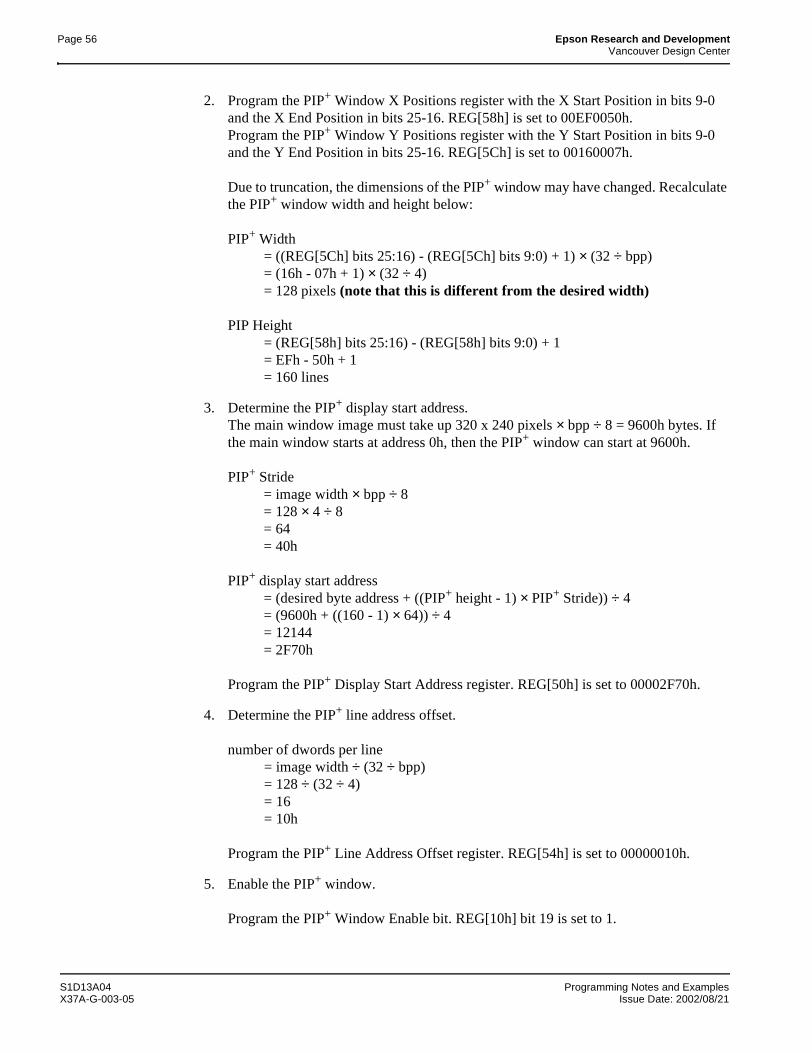
Page 56 Epson Research and DevelopmentVancouver Design Center
2. Program the PIP+ Window X Positions register with the X Start Position in bits 9-0 and the X End Position in bits 25-16. REG[58h] is set to 00EF0050h.Program the PIP+ Window Y Positions register with the Y Start Position in bits 9-0 and the Y End Position in bits 25-16. REG[5Ch] is set to 00160007h.
Due to truncation, the dimensions of the PIP+ window may have changed. Recalculate the PIP+ window width and height below:
PIP+ Width= ((REG[5Ch] bits 25:16) - (REG[5Ch] bits 9:0) + 1) × (32 ÷ bpp)= (16h - 07h + 1) × (32 ÷ 4)= 128 pixels (note that this is different from the desired width)
PIP Height= (REG[58h] bits 25:16) - (REG[58h] bits 9:0) + 1= EFh - 50h + 1= 160 lines
3. Determine the PIP+ display start address.The main window image must take up 320 x 240 pixels × bpp ÷ 8 = 9600h bytes. If the main window starts at address 0h, then the PIP+ window can start at 9600h.
PIP+ Stride= image width × bpp ÷ 8= 128 × 4 ÷ 8= 64= 40h
PIP+ display start address= (desired byte address + ((PIP+ height - 1) × PIP+ Stride)) ÷ 4= (9600h + ((160 - 1) × 64)) ÷ 4= 12144= 2F70h
Program the PIP+ Display Start Address register. REG[50h] is set to 00002F70h.
4. Determine the PIP+ line address offset.
number of dwords per line= image width ÷ (32 ÷ bpp)= 128 ÷ (32 ÷ 4) = 16= 10h
Program the PIP+ Line Address Offset register. REG[54h] is set to 00000010h.
5. Enable the PIP+ window.
Program the PIP+ Window Enable bit. REG[10h] bit 19 is set to 1.
S1D13A04 Programming Notes and ExamplesX37A-G-003-05 Issue Date: 2002/08/21
Epson Research and Development Page 57Vancouver Design Center
8.3 Limitations
8.3.1 SwivelView 0° and 180°
The PIP+ Line Address Offset register (REG[54h]) requires the PIP+ window image width to be a multiple of 32 ÷ bits-per-pixel. If this formula is not satisfied, then the PIP+ Line Address Offset register must be programmed to the next larger value that satisfies the formula.
8.3.2 SwivelView 90° and 270°
The PIP+ Line Address Offset register (REG[54h]) requires the PIP+ window image width to be a multiple of 32 ÷ bits-per-pixel. If this formula is not satisfied, then the PIP+ Line Address Offset register must be programmed to the next larger value that satisfies the formula.
Programming Notes and Examples S1D13A04Issue Date: 2002/08/21 X37A-G-003-05
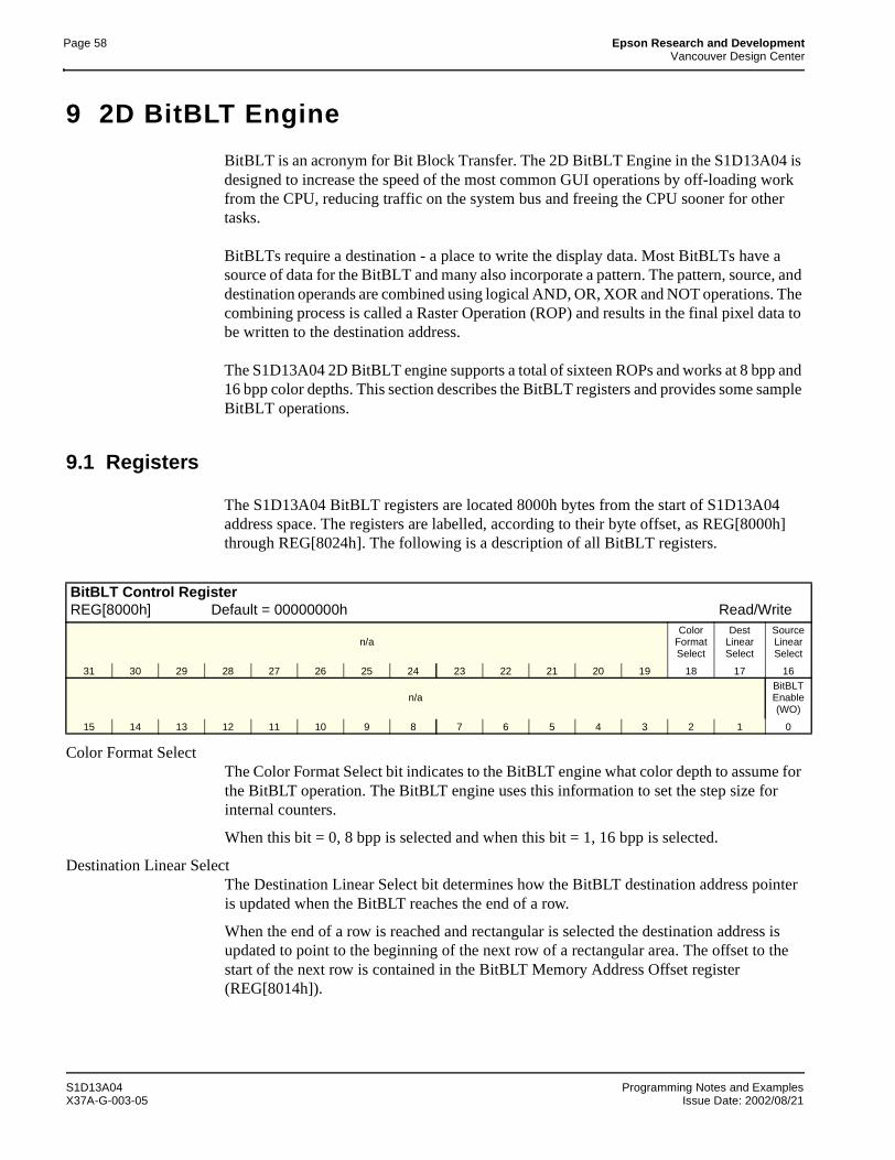
Page 58 Epson Research and DevelopmentVancouver Design Center
9 2D BitBLT Engine
BitBLT is an acronym for Bit Block Transfer. The 2D BitBLT Engine in the S1D13A04 is designed to increase the speed of the most common GUI operations by off-loading work from the CPU, reducing traffic on the system bus and freeing the CPU sooner for other tasks.
BitBLTs require a destination - a place to write the display data. Most BitBLTs have a source of data for the BitBLT and many also incorporate a pattern. The pattern, source, and destination operands are combined using logical AND, OR, XOR and NOT operations. The combining process is called a Raster Operation (ROP) and results in the final pixel data to be written to the destination address.
The S1D13A04 2D BitBLT engine supports a total of sixteen ROPs and works at 8 bpp and 16 bpp color depths. This section describes the BitBLT registers and provides some sample BitBLT operations.
9.1 Registers
The S1D13A04 BitBLT registers are located 8000h bytes from the start of S1D13A04 address space. The registers are labelled, according to their byte offset, as REG[8000h] through REG[8024h]. The following is a description of all BitBLT registers.
Color Format SelectThe Color Format Select bit indicates to the BitBLT engine what color depth to assume for the BitBLT operation. The BitBLT engine uses this information to set the step size for internal counters.
When this bit = 0, 8 bpp is selected and when this bit = 1, 16 bpp is selected.
Destination Linear SelectThe Destination Linear Select bit determines how the BitBLT destination address pointer is updated when the BitBLT reaches the end of a row.
When the end of a row is reached and rectangular is selected the destination address is updated to point to the beginning of the next row of a rectangular area. The offset to the start of the next row is contained in the BitBLT Memory Address Offset register (REG[8014h]).
BitBLT Control RegisterREG[8000h] Default = 00000000h Read/Write
n/aColor
Format Select
Dest Linear Select
Source Linear Select
31 30 29 28 27 26 25 24 23 22 21 20 19 18 17 16
n/aBitBLT Enable(WO)
15 14 13 12 11 10 9 8 7 6 5 4 3 2 1 0
S1D13A04 Programming Notes and ExamplesX37A-G-003-05 Issue Date: 2002/08/21
Epson Research and Development Page 59Vancouver Design Center
When the end of a row is reached and destination linear is selected the destination address is updated to the next available memory offset. The result is data which is jammed together with one row immediately following the next in display memory. This is useful when it is desired to compactly save a rectangular area into off screen memory.
When this bit = 0, the BitBLT destination is stored as a rectangular region of memory. When this bit = 1, the BitBLT destination is stored as a contiguous linear block of mem-ory.
Source Linear SelectThe Source Linear Select bit determines how the source address pointer is updated when the BitBLT reaches the end of a row.
When the end of a row is reached and rectangular is selected the source address is updated to point to the beginning of the next row of a rectangular area. The offset to the start of the next row is contained in the BitBLT Memory Address Offset register (REG[8014h]).
When the end of a row is reached and source linear is selected the source address is updated to the next available memory offset. The result is data, which was jammed together with one row immediately following the next in display memory, can now be expanded back to a rectangular area.
When this bit = 0, the BitBLT source is stored as a rectangular region of memory.When this bit = 1, the BitBLT source is stored as a contiguous linear block of memory.
BitBLT EnableThis bit is write only.Setting this bit to 1 begins the 2D BitBLT operation. This bit must not be set to 0 while a BitBLT operation is in progress.
NoteTo determine the status of a BitBLT operation use the BitBLT Busy Status bit (REG[8004h] bit 0).
Programming Notes and Examples S1D13A04Issue Date: 2002/08/21 X37A-G-003-05
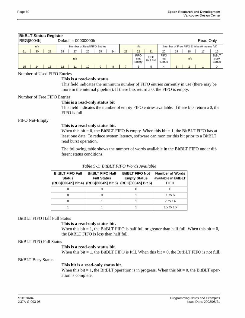
Page 60 Epson Research and DevelopmentVancouver Design Center
Number of Used FIFO EntriesThis is a read-only status.This field indicates the minimum number of FIFO entries currently in use (there may be more in the internal pipeline). If these bits return a 0, the FIFO is empty.
Number of Free FIFO EntriesThis is a read-only status bitThis field indicates the number of empty FIFO entries available. If these bits return a 0, the FIFO is full.
FIFO Not-EmptyThis is a read-only status bit.When this bit = 0, the BitBLT FIFO is empty. When this bit = 1, the BitBLT FiFO has at least one data. To reduce system latency, software can monitor this bit prior to a BitBLT read burst operation.
The following table shows the number of words available in the BitBLT FIFO under dif-ferent status conditions.
BitBLT FIFO Half Full StatusThis is a read-only status bit.When this bit = 1, the BitBLT FIFO is half full or greater than half full. When this bit = 0, the BitBLT FIFO is less than half full.
BitBLT FIFO Full StatusThis is a read-only status bit.When this bit = 1, the BitBLT FIFO is full. When this bit = 0, the BitBLT FIFO is not full.
BitBLT Busy StatusThis bit is a read-only status bit.When this bit = 1, the BitBLT operation is in progress. When this bit = 0, the BitBLT oper-ation is complete.
BitBLT Status RegisterREG[8004h] Default = 00000000h Read Only
n/a Number of Used FIFO Entries n/a Number of Free FIFO Entries (0 means full)
31 30 29 28 27 26 25 24 23 22 21 20 19 18 17 16
n/aFIFO Not
Empty
FIFO Half Full
FIFO Full
Statusn/a
BitBLT Busy
Status
15 14 13 12 11 10 9 8 7 6 5 4 3 2 1 0
Table 9-1: BitBLT FIFO Words Available
BitBLT FIFO Full Status
(REG[8004h] Bit 4)
BitBLT FIFO Half Full Status
(REG[8004h] Bit 5)
BitBLT FIFO Not Empty Status
(REG[8004h] Bit 6)
Number of Words available in BitBLT
FIFO
0 0 0 0
0 0 1 1 to 6
0 1 1 7 to 14
1 1 1 15 to 16
S1D13A04 Programming Notes and ExamplesX37A-G-003-05 Issue Date: 2002/08/21
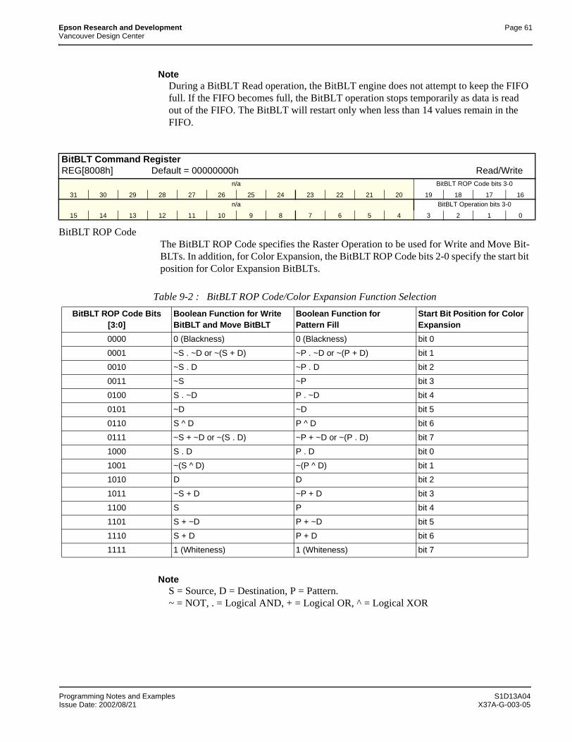
Epson Research and Development Page 61Vancouver Design Center
NoteDuring a BitBLT Read operation, the BitBLT engine does not attempt to keep the FIFO full. If the FIFO becomes full, the BitBLT operation stops temporarily as data is read out of the FIFO. The BitBLT will restart only when less than 14 values remain in the FIFO.
BitBLT ROP CodeThe BitBLT ROP Code specifies the Raster Operation to be used for Write and Move Bit-BLTs. In addition, for Color Expansion, the BitBLT ROP Code bits 2-0 specify the start bit position for Color Expansion BitBLTs.
NoteS = Source, D = Destination, P = Pattern.~ = NOT, . = Logical AND, + = Logical OR, ^ = Logical XOR
BitBLT Command RegisterREG[8008h] Default = 00000000h Read/Write
n/a BitBLT ROP Code bits 3-0
31 30 29 28 27 26 25 24 23 22 21 20 19 18 17 16n/a BitBLT Operation bits 3-0
15 14 13 12 11 10 9 8 7 6 5 4 3 2 1 0
Table 9-2 : BitBLT ROP Code/Color Expansion Function Selection
BitBLT ROP Code Bits [3:0]
Boolean Function for Write BitBLT and Move BitBLT
Boolean Function forPattern Fill
Start Bit Position for Color Expansion
0000 0 (Blackness) 0 (Blackness) bit 0
0001 ~S . ~D or ~(S + D) ~P . ~D or ~(P + D) bit 1
0010 ~S . D ~P . D bit 2
0011 ~S ~P bit 3
0100 S . ~D P . ~D bit 4
0101 ~D ~D bit 5
0110 S ^ D P ^ D bit 6
0111 ~S + ~D or ~(S . D) ~P + ~D or ~(P . D) bit 7
1000 S . D P . D bit 0
1001 ~(S ^ D) ~(P ^ D) bit 1
1010 D D bit 2
1011 ~S + D ~P + D bit 3
1100 S P bit 4
1101 S + ~D P + ~D bit 5
1110 S + D P + D bit 6
1111 1 (Whiteness) 1 (Whiteness) bit 7
Programming Notes and Examples S1D13A04Issue Date: 2002/08/21 X37A-G-003-05
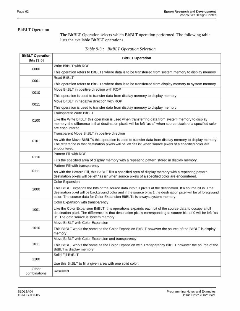
Page 62 Epson Research and DevelopmentVancouver Design Center
BitBLT OperationThe BitBLT Operation selects which BitBLT operation performed. The following table lists the available BitBLT operations.
Table 9-3 : BitBLT Operation Selection
BitBLT Operation Bits [3:0]
BitBLT Operation
0000Write BitBLT with ROP
This operation refers to BitBLTs where data is to be transferred from system memory to display memory
0001Read BitBLT
This operation refers to BitBLTs where data is to be transferred from display memory to system memory
0010Move BitBLT in positive direction with ROP
This operation is used to transfer data from display memory to display memory
0011Move BitBLT in negative direction with ROP
This operation is used to transfer data from display memory to display memory
0100
Transparent Write BitBLT
Like the Write BitBLT this operation is used when transferring data from system memory to display memory, the difference is that destination pixels will be left “as is” when source pixels of a specified color are encountered.
0101
Transparent Move BitBLT in positive direction
As with the Move BitBLTs this operation is used to transfer data from display memory to display memory. The difference is that destination pixels will be left “as is” when source pixels of a specified color are encountered.
0110Pattern Fill with ROP
Fills the specified area of display memory with a repeating pattern stored in display memory.
0111
Pattern Fill with transparency
As with the Pattern Fill, this BitBLT fills a specified area of display memory with a repeating pattern, destination pixels will be left “as is” when source pixels of a specified color are encountered.
1000
Color Expansion
This BitBLT expands the bits of the source data into full pixels at the destination. If a source bit is 0 the destination pixel will be background color and if the source bit is 1 the destination pixel will be of foreground color. The source data for Color Expansion BitBLTs is always system memory.
1001
Color Expansion with transparency
Like the Color Expansion BitBLT, this operations expands each bit of the source data to occupy a full destination pixel. The difference, is that destination pixels corresponding to source bits of 0 will be left “as is”. The data source is system memory
1010
Move BitBLT with Color Expansion
This BitBLT works the same as the Color Expansion BitBLT however the source of the BitBLT is display memory.
1011
Move BitBLT with Color Expansion and transparency
This BitBLT works the same as the Color Expansion with Transparency BitBLT however the source of the BitBLT is display memory.
1100Solid Fill BitBLT
Use this BitBLT to fill a given area with one solid color.
Other combinations
Reserved
S1D13A04 Programming Notes and ExamplesX37A-G-003-05 Issue Date: 2002/08/21
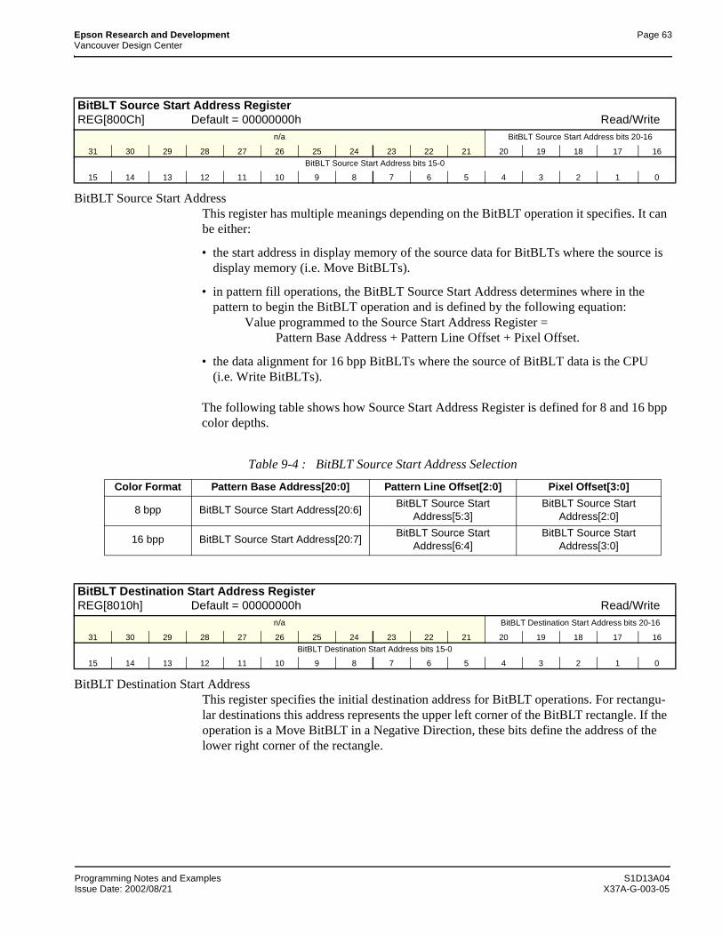
Epson Research and Development Page 63Vancouver Design Center
BitBLT Source Start AddressThis register has multiple meanings depending on the BitBLT operation it specifies. It can be either:
• the start address in display memory of the source data for BitBLTs where the source is display memory (i.e. Move BitBLTs).
• in pattern fill operations, the BitBLT Source Start Address determines where in the pattern to begin the BitBLT operation and is defined by the following equation:
Value programmed to the Source Start Address Register =Pattern Base Address + Pattern Line Offset + Pixel Offset.
• the data alignment for 16 bpp BitBLTs where the source of BitBLT data is the CPU(i.e. Write BitBLTs).
The following table shows how Source Start Address Register is defined for 8 and 16 bpp color depths.
BitBLT Destination Start AddressThis register specifies the initial destination address for BitBLT operations. For rectangu-lar destinations this address represents the upper left corner of the BitBLT rectangle. If the operation is a Move BitBLT in a Negative Direction, these bits define the address of the lower right corner of the rectangle.
BitBLT Source Start Address RegisterREG[800Ch] Default = 00000000h Read/Write
n/a BitBLT Source Start Address bits 20-16
31 30 29 28 27 26 25 24 23 22 21 20 19 18 17 16BitBLT Source Start Address bits 15-0
15 14 13 12 11 10 9 8 7 6 5 4 3 2 1 0
Table 9-4 : BitBLT Source Start Address Selection
Color Format Pattern Base Address[20:0] Pattern Line Offset[2:0] Pixel Offset[3:0]
8 bpp BitBLT Source Start Address[20:6]BitBLT Source Start
Address[5:3]BitBLT Source Start
Address[2:0]
16 bpp BitBLT Source Start Address[20:7]BitBLT Source Start
Address[6:4]BitBLT Source Start
Address[3:0]
BitBLT Destination Start Address RegisterREG[8010h] Default = 00000000h Read/Write
n/a BitBLT Destination Start Address bits 20-16
31 30 29 28 27 26 25 24 23 22 21 20 19 18 17 16BitBLT Destination Start Address bits 15-0
15 14 13 12 11 10 9 8 7 6 5 4 3 2 1 0
Programming Notes and Examples S1D13A04Issue Date: 2002/08/21 X37A-G-003-05
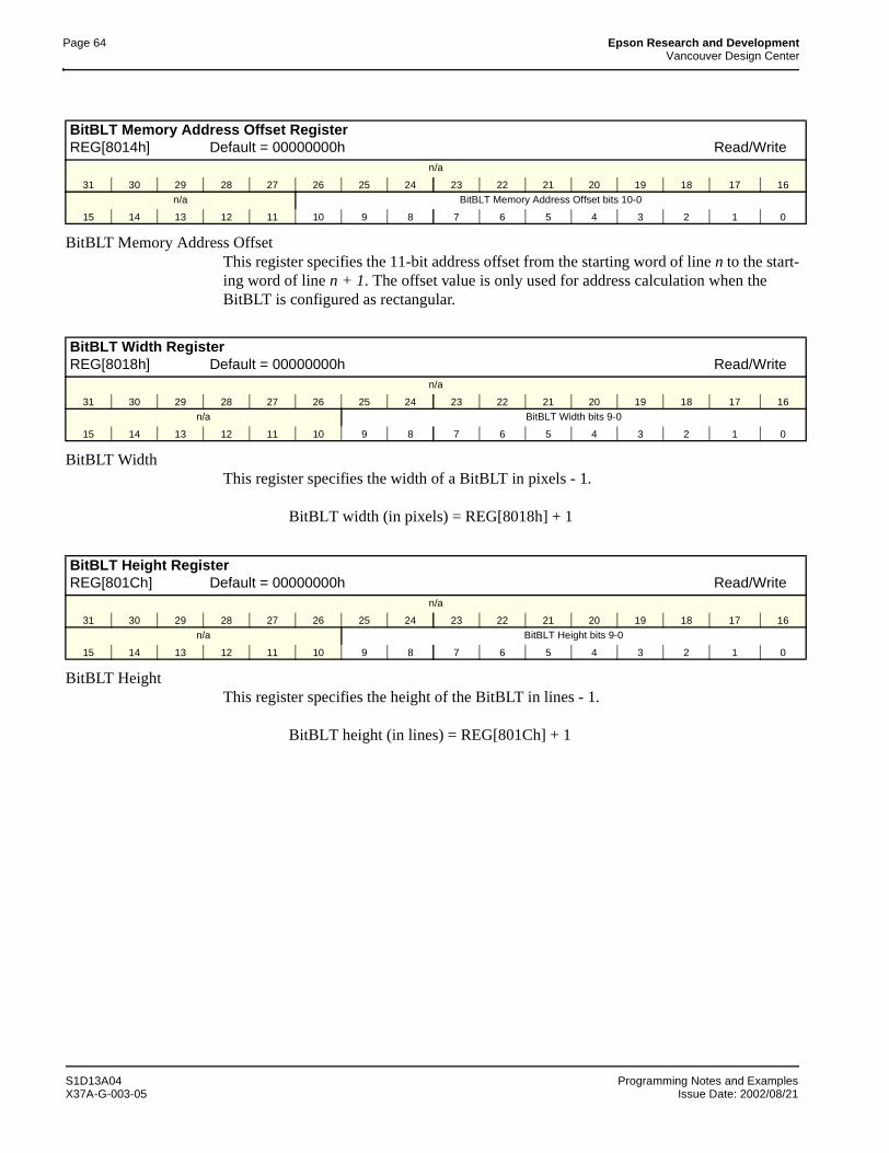
Page 64 Epson Research and DevelopmentVancouver Design Center
BitBLT Memory Address OffsetThis register specifies the 11-bit address offset from the starting word of line n to the start-ing word of line n + 1. The offset value is only used for address calculation when theBitBLT is configured as rectangular.
BitBLT WidthThis register specifies the width of a BitBLT in pixels - 1.
BitBLT width (in pixels) = REG[8018h] + 1
BitBLT HeightThis register specifies the height of the BitBLT in lines - 1.
BitBLT height (in lines) = REG[801Ch] + 1
BitBLT Memory Address Offset RegisterREG[8014h] Default = 00000000h Read/Write
n/a
31 30 29 28 27 26 25 24 23 22 21 20 19 18 17 16
n/a BitBLT Memory Address Offset bits 10-0
15 14 13 12 11 10 9 8 7 6 5 4 3 2 1 0
BitBLT Width RegisterREG[8018h] Default = 00000000h Read/Write
n/a
31 30 29 28 27 26 25 24 23 22 21 20 19 18 17 16
n/a BitBLT Width bits 9-0
15 14 13 12 11 10 9 8 7 6 5 4 3 2 1 0
BitBLT Height RegisterREG[801Ch] Default = 00000000h Read/Write
n/a
31 30 29 28 27 26 25 24 23 22 21 20 19 18 17 16
n/a BitBLT Height bits 9-0
15 14 13 12 11 10 9 8 7 6 5 4 3 2 1 0
S1D13A04 Programming Notes and ExamplesX37A-G-003-05 Issue Date: 2002/08/21
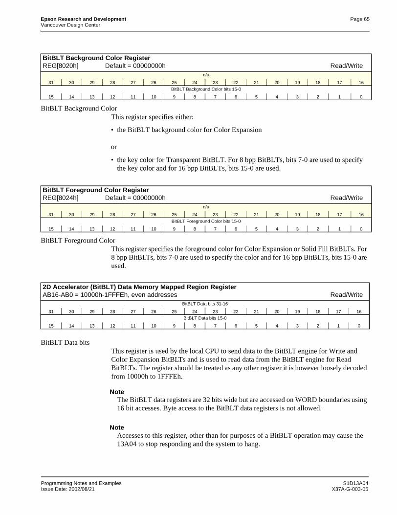
Epson Research and Development Page 65Vancouver Design Center
BitBLT Background ColorThis register specifies either:
• the BitBLT background color for Color Expansion
or
• the key color for Transparent BitBLT. For 8 bpp BitBLTs, bits 7-0 are used to specify the key color and for 16 bpp BitBLTs, bits 15-0 are used.
BitBLT Foreground ColorThis register specifies the foreground color for Color Expansion or Solid Fill BitBLTs. For 8 bpp BitBLTs, bits 7-0 are used to specify the color and for 16 bpp BitBLTs, bits 15-0 are used.
BitBLT Data bitsThis register is used by the local CPU to send data to the BitBLT engine for Write and Color Expansion BitBLTs and is used to read data from the BitBLT engine for ReadBitBLTs. The register should be treated as any other register it is however loosely decoded from 10000h to 1FFFEh.
NoteThe BitBLT data registers are 32 bits wide but are accessed on WORD boundaries using 16 bit accesses. Byte access to the BitBLT data registers is not allowed.
NoteAccesses to this register, other than for purposes of a BitBLT operation may cause the 13A04 to stop responding and the system to hang.
BitBLT Background Color RegisterREG[8020h] Default = 00000000h Read/Write
n/a
31 30 29 28 27 26 25 24 23 22 21 20 19 18 17 16
BitBLT Background Color bits 15-0
15 14 13 12 11 10 9 8 7 6 5 4 3 2 1 0
BitBLT Foreground Color RegisterREG[8024h] Default = 00000000h Read/Write
n/a
31 30 29 28 27 26 25 24 23 22 21 20 19 18 17 16
BitBLT Foreground Color bits 15-0
15 14 13 12 11 10 9 8 7 6 5 4 3 2 1 0
2D Accelerator (BitBLT) Data Memory Mapped Region RegisterAB16-AB0 = 10000h-1FFFEh, even addresses Read/Write
BitBLT Data bits 31-16
31 30 29 28 27 26 25 24 23 22 21 20 19 18 17 16BitBLT Data bits 15-0
15 14 13 12 11 10 9 8 7 6 5 4 3 2 1 0
Programming Notes and Examples S1D13A04Issue Date: 2002/08/21 X37A-G-003-05
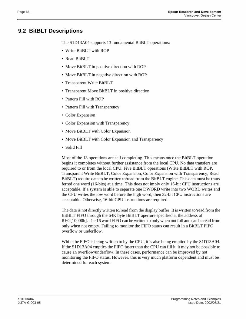
Page 66 Epson Research and DevelopmentVancouver Design Center
9.2 BitBLT Descriptions
The S1D13A04 supports 13 fundamental BitBLT operations:
• Write BitBLT with ROP
• Read BitBLT
• Move BitBLT in positive direction with ROP
• Move BitBLT in negative direction with ROP
• Transparent Write BitBLT
• Transparent Move BitBLT in positive direction
• Pattern Fill with ROP
• Pattern Fill with Transparency
• Color Expansion
• Color Expansion with Transparency
• Move BitBLT with Color Expansion
• Move BitBLT with Color Expansion and Transparency
• Solid Fill
Most of the 13 operations are self completing. This means once the BitBLT operation begins it completes without further assistance from the local CPU. No data transfers are required to or from the local CPU. Five BitBLT operations (Write BitBLT with ROP, Transparent Write BitBLT, Color Expansion, Color Expansion with Transparency, Read BitBLT) require data to be written to/read from the BitBLT engine. This data must be trans-ferred one word (16-bits) at a time. This does not imply only 16-bit CPU instructions are acceptable. If a system is able to separate one DWORD write into two WORD writes and the CPU writes the low word before the high word, then 32-bit CPU instructions are acceptable. Otherwise, 16-bit CPU instructions are required.
The data is not directly written to/read from the display buffer. It is written to/read from the BitBLT FIFO through the 64K byte BitBLT aperture specified at the address of REG[10000h]. The 16 word FIFO can be written to only when not full and can be read from only when not empty. Failing to monitor the FIFO status can result in a BitBLT FIFO overflow or underflow.
While the FIFO is being written to by the CPU, it is also being emptied by the S1D13A04. If the S1D13A04 empties the FIFO faster than the CPU can fill it, it may not be possible to cause an overflow/underflow. In these cases, performance can be improved by not monitoring the FIFO status. However, this is very much platform dependent and must be determined for each system.
S1D13A04 Programming Notes and ExamplesX37A-G-003-05 Issue Date: 2002/08/21

Epson Research and Development Page 67Vancouver Design Center
9.2.1 Write BitBLT with ROP
Write BitBLTs increase the speed of transferring data from system memory to the display buffer. The Write BitBLT with ROP accepts data from the CPU and writes it into display memory. This BitBLT is typically used to copy a bitmap image from system memory to the display buffer.
Write BitBLTs support 16 ROPs, the most frequently used being ROP 0Ch (Copy Source to Destination). Write BitBLTs support both rectangular and linear destinations. Using a linear destination it is possible to move an image to off screen memory in a compact format for later restoration using a Move BitBLT.
During a Write BitBLT operation the BitBLT engine expects to receive a particular number of WORDs and it is the responsibility of the CPU to provide the required amount of data.
When performing BitBLT at 16 bpp color depth the number of WORDS to be sent is the same as the number of pixels to be transferred as each pixel is one WORD wide. The number of WORD writes the BitBLT engine expects is calculated using the following formula.
WORDS = Pixels= BitBLTWidth × BitBLTHeight
When the color depth is 8 bpp the formula must take into consideration that the BitBLT engine accepts only WORD accesses and each pixel is one BYTE. This may lead to a different number of WORD transfers than there are pixels to transfer.
The number of WORD accesses is dependant on the position of the first pixel within the first WORD of each row. Is the pixel stored in the low byte or the high byte of the WORD? This aspect of the BitBLT is called phase and is determined as follows:
Source phase is 0 when the first pixel is in the low byte and the second pixel is in the high byte of the WORD. When the source phase is 0, bit 0 of the Source Start Address Register is 0. The Source Phase is 1 if the first pixel of each row is contained in the high byte of the WORD, the contents of the low byte are ignored. When the source phase is 1, bit 0 of the Source Start Address Register is set.
Depending on the Source Phase and the BitBLT Width, the last WORD may contain only one pixel. In this case it is always in the low byte. The number of WORD writes the BitBLT engine expects for 8 bpp color depths is shown in the following formula.
WORDS = ((BitBLTWidth + 1 + SourcePhase) ÷ 2) × BitBLTHeight
The BitBLT engine requires this number of WORDS to be sent from the local CPU before it will end the Write BitBLT operation.
Programming Notes and Examples S1D13A04Issue Date: 2002/08/21 X37A-G-003-05
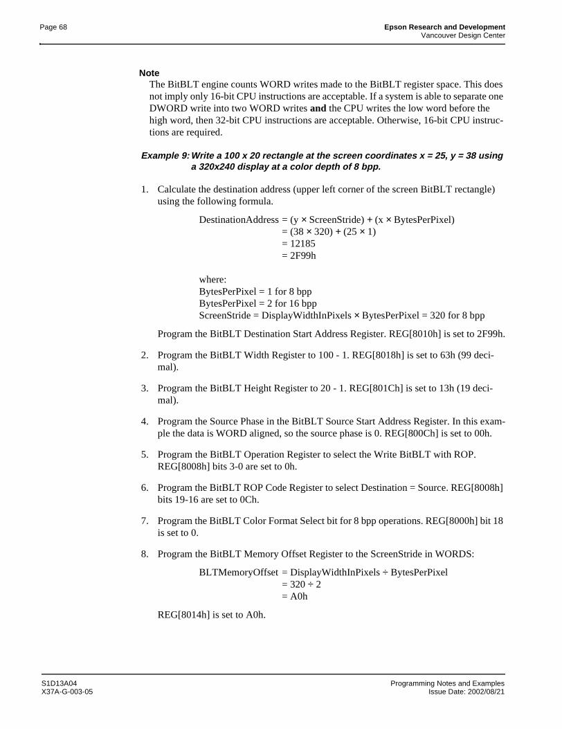
Page 68 Epson Research and DevelopmentVancouver Design Center
NoteThe BitBLT engine counts WORD writes made to the BitBLT register space. This does not imply only 16-bit CPU instructions are acceptable. If a system is able to separate one DWORD write into two WORD writes and the CPU writes the low word before the high word, then 32-bit CPU instructions are acceptable. Otherwise, 16-bit CPU instruc-tions are required.
Example 9: Write a 100 x 20 rectangle at the screen coordinates x = 25, y = 38 using a 320x240 display at a color depth of 8 bpp.
1. Calculate the destination address (upper left corner of the screen BitBLT rectangle) using the following formula.
DestinationAddress = (y × ScreenStride) + (x × BytesPerPixel)= (38 × 320) + (25 × 1)= 12185= 2F99h
where:BytesPerPixel = 1 for 8 bppBytesPerPixel = 2 for 16 bppScreenStride = DisplayWidthInPixels × BytesPerPixel = 320 for 8 bpp
Program the BitBLT Destination Start Address Register. REG[8010h] is set to 2F99h.
2. Program the BitBLT Width Register to 100 - 1. REG[8018h] is set to 63h (99 deci-mal).
3. Program the BitBLT Height Register to 20 - 1. REG[801Ch] is set to 13h (19 deci-mal).
4. Program the Source Phase in the BitBLT Source Start Address Register. In this exam-ple the data is WORD aligned, so the source phase is 0. REG[800Ch] is set to 00h.
5. Program the BitBLT Operation Register to select the Write BitBLT with ROP. REG[8008h] bits 3-0 are set to 0h.
6. Program the BitBLT ROP Code Register to select Destination = Source. REG[8008h] bits 19-16 are set to 0Ch.
7. Program the BitBLT Color Format Select bit for 8 bpp operations. REG[8000h] bit 18 is set to 0.
8. Program the BitBLT Memory Offset Register to the ScreenStride in WORDS:
BLTMemoryOffset = DisplayWidthInPixels ÷ BytesPerPixel= 320 ÷ 2= A0h
REG[8014h] is set to A0h.
S1D13A04 Programming Notes and ExamplesX37A-G-003-05 Issue Date: 2002/08/21
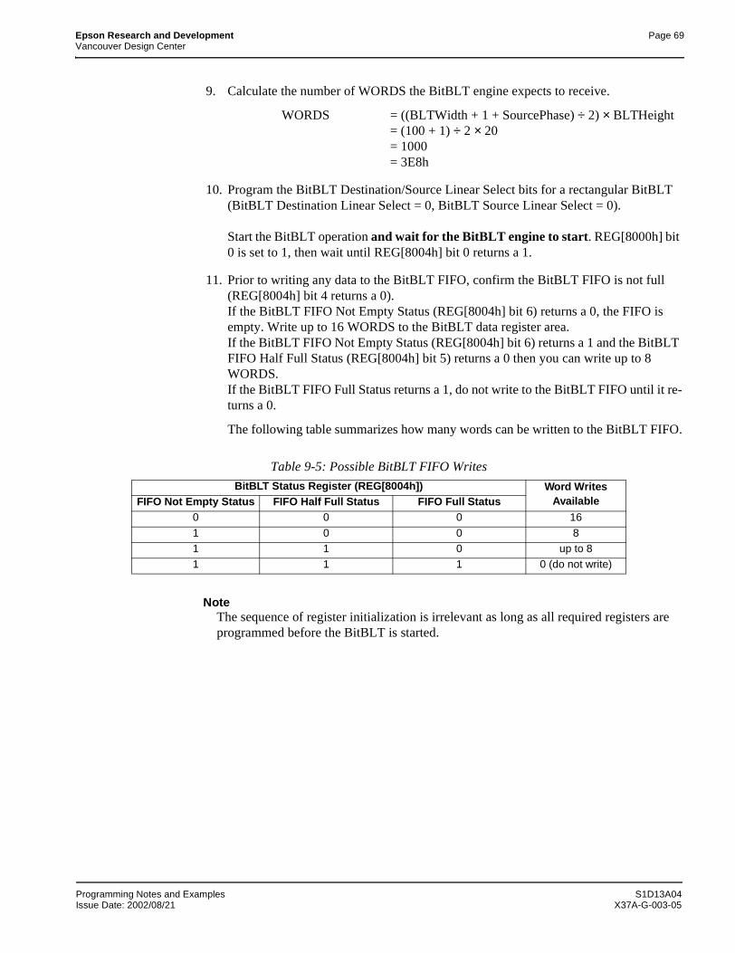
Epson Research and Development Page 69Vancouver Design Center
9. Calculate the number of WORDS the BitBLT engine expects to receive.
WORDS = ((BLTWidth + 1 + SourcePhase) ÷ 2) × BLTHeight= (100 + 1) ÷ 2 × 20= 1000= 3E8h
10. Program the BitBLT Destination/Source Linear Select bits for a rectangular BitBLT (BitBLT Destination Linear Select = 0, BitBLT Source Linear Select = 0).
Start the BitBLT operation and wait for the BitBLT engine to start. REG[8000h] bit 0 is set to 1, then wait until REG[8004h] bit 0 returns a 1.
11. Prior to writing any data to the BitBLT FIFO, confirm the BitBLT FIFO is not full (REG[8004h] bit 4 returns a 0).If the BitBLT FIFO Not Empty Status (REG[8004h] bit 6) returns a 0, the FIFO is empty. Write up to 16 WORDS to the BitBLT data register area.If the BitBLT FIFO Not Empty Status (REG[8004h] bit 6) returns a 1 and the BitBLT FIFO Half Full Status (REG[8004h] bit 5) returns a 0 then you can write up to 8 WORDS.If the BitBLT FIFO Full Status returns a 1, do not write to the BitBLT FIFO until it re-turns a 0.
The following table summarizes how many words can be written to the BitBLT FIFO.
NoteThe sequence of register initialization is irrelevant as long as all required registers are programmed before the BitBLT is started.
Table 9-5: Possible BitBLT FIFO Writes
BitBLT Status Register (REG[8004h]) Word Writes AvailableFIFO Not Empty Status FIFO Half Full Status FIFO Full Status
0 0 0 16
1 0 0 81 1 0 up to 81 1 1 0 (do not write)
Programming Notes and Examples S1D13A04Issue Date: 2002/08/21 X37A-G-003-05
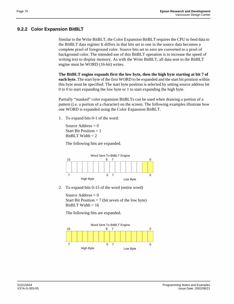
Page 70 Epson Research and DevelopmentVancouver Design Center
9.2.2 Color Expansion BitBLT
Similar to the Write BitBLT, the Color Expansion BitBLT requires the CPU to feed data to the BitBLT data register It differs in that bits set to one in the source data becomes a complete pixel of foreground color. Source bits set to zero are converted to a pixel of background color. The intended use of this BitBLT operation is to increase the speed of writing text to display memory. As with the Write BitBLT, all data sent to the BitBLT engine must be WORD (16-bit) writes.
The BitBLT engine expands first the low byte, then the high byte starting at bit 7 of each byte. The start byte of the first WORD to be expanded and the start bit position within this byte must be specified. The start byte position is selected by setting source address bit 0 to 0 to start expanding the low byte or 1 to start expanding the high byte.
Partially “masked” color expansion BitBLTs can be used when drawing a portion of a pattern (i.e. a portion of a character) on the screen. The following examples illustrate how one WORD is expanded using the Color Expansion BitBLT.
1. To expand bits 0-1 of the word:
Source Address = 0Start Bit Position = 1BitBLT Width = 2
The following bits are expanded.
2. To expand bits 0-15 of the word (entire word)
Source Address = 0Start Bit Position = 7 (bit seven of the low byte)BitBLT Width = 16
The following bits are expanded.
15 8 7 0
0707High Byte Low Byte
Word Sent To BitBLT Engine
15 8 7 0
0707High Byte Low Byte
Word Sent To BitBLT Engine
S1D13A04 Programming Notes and ExamplesX37A-G-003-05 Issue Date: 2002/08/21
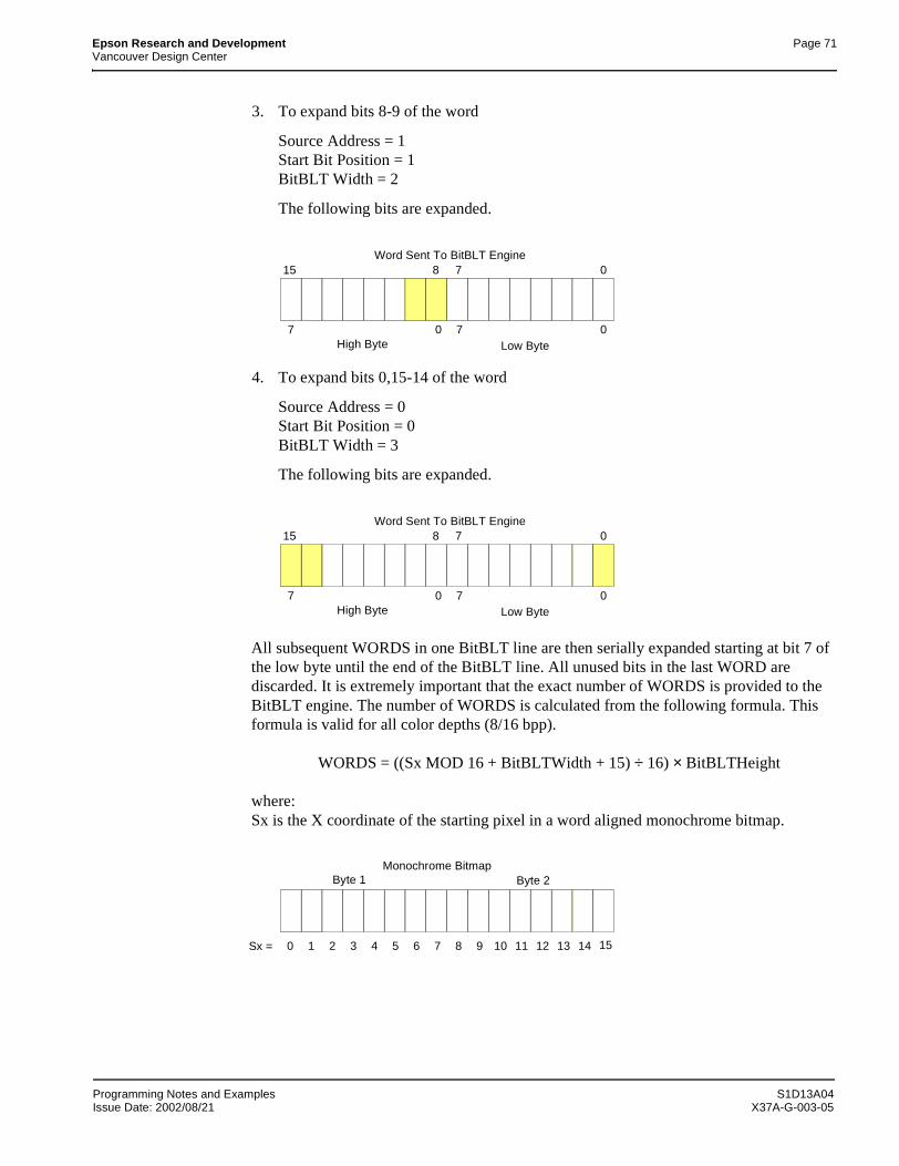
Epson Research and Development Page 71Vancouver Design Center
3. To expand bits 8-9 of the word
Source Address = 1Start Bit Position = 1BitBLT Width = 2
The following bits are expanded.
4. To expand bits 0,15-14 of the word
Source Address = 0Start Bit Position = 0BitBLT Width = 3
The following bits are expanded.
All subsequent WORDS in one BitBLT line are then serially expanded starting at bit 7 of the low byte until the end of the BitBLT line. All unused bits in the last WORD are discarded. It is extremely important that the exact number of WORDS is provided to the BitBLT engine. The number of WORDS is calculated from the following formula. This formula is valid for all color depths (8/16 bpp).
WORDS = ((Sx MOD 16 + BitBLTWidth + 15) ÷ 16) × BitBLTHeight
where:Sx is the X coordinate of the starting pixel in a word aligned monochrome bitmap.
15 8 7 0
0707High Byte Low Byte
Word Sent To BitBLT Engine
15 8 7 0
0707High Byte Low Byte
Word Sent To BitBLT Engine
15765
Byte 1Monochrome Bitmap
Byte 2
43210 1412111098 13Sx =
Programming Notes and Examples S1D13A04Issue Date: 2002/08/21 X37A-G-003-05
Page 72 Epson Research and DevelopmentVancouver Design Center
Example 10: Color expand a rectangle of 12 x 18 starting at the coordinatesSx = 125, Sy = 17 using a 320x240 display at a color depth of 8 bpp.
This example assumes a monochrome, WORD aligned bitmap of dimensions 300 x 600 with the origin at an address A. The color expanded rectangle will be displayed at the screen coordinates X = 20, Y = 30. The foreground color corresponds to the LUT entry at index 134, the background color to index 124.
1. First we need to calculate the address of the WORD within the monochrome bitmap containing the pixel x = 125,y = 17.
SourceAddress = BitmapOrigin + (y × SourceStride) + (x ÷ 8)= A + (Sy × SourceStride) + (Sx ÷ 8)= A + (17 × 38) + (125 ÷ 8)= A + 646 + 15= A + 661
where:SourceStride = (BitmapWidth + 15) ÷ 16
= (300 + 15) ÷ 16= 19 WORDS per line= 38 BYTES per line
2. Calculate the destination address (upper left corner of the screen BitBLT rectangle) using the following formula.
DestinationAddress = (Y × ScreenStride) + (X × BytesPerPixel)= (30 × 320) + (20 × 1)= 9620= 2594h
where:BytesPerPixel = 1 for 8 bppBytesPerPixel = 2 for 16 bppScreenStride = DisplayWidthInPixels × BytesPerPixel = 320 for 8 bpp
Program the BitBLT Destination Start Address Register. REG[8010h] is set to 2594h.
3. Program the BitBLT Width Register to 12 - 1. REG[8018h] is set to 0Bh (11 decimal).
4. Program the BitBLT Height Register to 18 - 1. REG[801Ch] is set to 11h (17 deci-mal).
5. Program the Source Phase in the BitBLT Source Start Address Register. In this exam-ple the source address equals A + 661 (odd), so REG[800Ch] is set to 1.
Since only bit 0 flags the source phase, more efficient code would simply write the low byte of the SourceAddress into REG[800Ch] directly -- not needing to test for an odd/even address. Note that in 16 bpp color depths the Source address is guaranteed to be even.
6. Program the BitBLT Operation Register to select the Color Expand BitBLT. REG[8008h] bits 3-0 are set to 8h.
S1D13A04 Programming Notes and ExamplesX37A-G-003-05 Issue Date: 2002/08/21
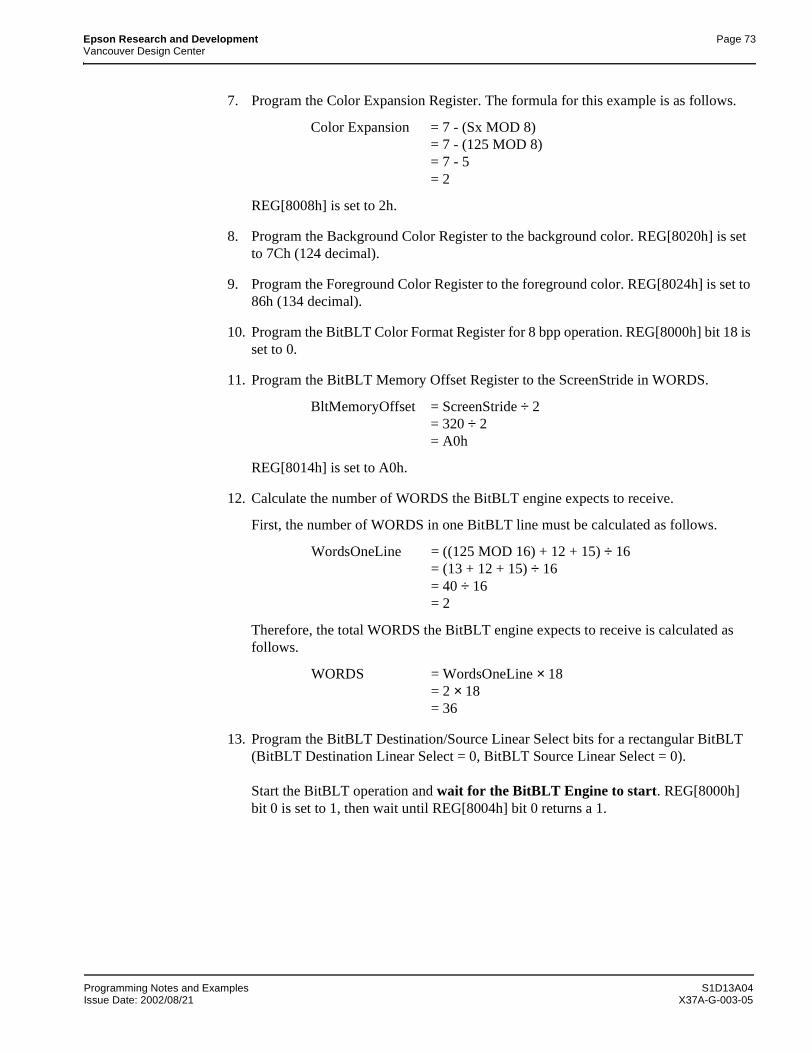
Epson Research and Development Page 73Vancouver Design Center
7. Program the Color Expansion Register. The formula for this example is as follows.
Color Expansion = 7 - (Sx MOD 8)= 7 - (125 MOD 8)= 7 - 5= 2
REG[8008h] is set to 2h.
8. Program the Background Color Register to the background color. REG[8020h] is set to 7Ch (124 decimal).
9. Program the Foreground Color Register to the foreground color. REG[8024h] is set to 86h (134 decimal).
10. Program the BitBLT Color Format Register for 8 bpp operation. REG[8000h] bit 18 is set to 0.
11. Program the BitBLT Memory Offset Register to the ScreenStride in WORDS.
BltMemoryOffset = ScreenStride ÷ 2= 320 ÷ 2= A0h
REG[8014h] is set to A0h.
12. Calculate the number of WORDS the BitBLT engine expects to receive.
First, the number of WORDS in one BitBLT line must be calculated as follows.
WordsOneLine = ((125 MOD 16) + 12 + 15) ÷ 16= (13 + 12 + 15) ÷ 16= 40 ÷ 16= 2
Therefore, the total WORDS the BitBLT engine expects to receive is calculated as follows.
WORDS = WordsOneLine × 18= 2 × 18= 36
13. Program the BitBLT Destination/Source Linear Select bits for a rectangular BitBLT (BitBLT Destination Linear Select = 0, BitBLT Source Linear Select = 0).
Start the BitBLT operation and wait for the BitBLT Engine to start. REG[8000h] bit 0 is set to 1, then wait until REG[8004h] bit 0 returns a 1.
Programming Notes and Examples S1D13A04Issue Date: 2002/08/21 X37A-G-003-05
Page 74 Epson Research and DevelopmentVancouver Design Center
14. Prior to writing all WORDS to the BitBLT FIFO, confirm the BitBLT FIFO is not full (REG[8004h] bit 4 returns a 0). One WORD expands into 16 pixels which fills all 16 FIFO words in 16 bpp or 8 FIFO words in 8 bpp.
The following table summarizes how many words can be written to the BitBLT FIFO.
NoteThe sequence of register setup is irrelevant as long as all required registers are pro-grammed before the BitBLT is started.
9.2.3 Color Expansion BitBLT With Transparency
This BitBLT operation is virtually identical to the Color Expand BitBLT, the difference is in how background bits are handled. Bits in the source bitmap which are set to zero result in the destination pixel being left untouched. Bits set to one are expanded to the foreground color.
Use this BitBLT operation to overlay text onto any background while leaving the background intact.
Refer to the Color Expansion BitBLT for sample calculations and keep the following points in mind:
• Program the BitBLT operation bits, REG[8008h] bits 3-0, to 09h instead of 08h.
• Setting a background color, REG[8020h], is not required.
9.2.4 Solid Fill BitBLT
The Solid Fill BitBLT fills a rectangular area of the display buffer with a solid color. This operation is used to paint large screen areas or to set areas of the display buffer to a given value.
This BitBLT operation is self completing. After setting the width, height, destination start position and (foreground) color the BitBLT engine is started. When the region of display memory is filled with the given color the BitBLT engine will automatically stop.
Table 9-6: Possible BitBLT FIFO Writes
BitBLT Status Register (REG[8004h]) 8 bpp WordWrites Available
16 bpp Word Writes AvailableFIFO Not Empty Status FIFO Half Full Status FIFO Full Status
0 0 0 2 11 0 0 1
0 (do not write)1 1 00 (do not write)
1 1 1
S1D13A04 Programming Notes and ExamplesX37A-G-003-05 Issue Date: 2002/08/21
Epson Research and Development Page 75Vancouver Design Center
Example 11: Fill a red 9 x 301 rectangle at the screen coordinates x = 100, y = 10 us-ing a 320x240 display at a color depth of 16 bpp.
1. Calculate the destination address (upper left corner of the destination rectangle) using the following formula.
DestinationAddress = (y × ScreenStride) + (x × BytesPerPixel)= (10 × (320 × 2)) + (100 × 2)= 6600= 19C8h
where:BytesPerPixel = 1 for 8 bppBytesPerPixel = 2 for 16 bppScreenStride = DisplayWidthInPixels × BytesPerPixel = 640 for 16 bpp.
Program the BitBLT Destination Start Address Register. REG[8010h] is set to 19C8h.
2. Program the BitBLT Width Register to 9 - 1. REG[8018h] is set to 08h.
3. Program the BitBLT Height Register to 301 - 1. REG[801Ch] is set to 12Ch (300 dec-imal).
4. Program the BitBLT Foreground Color Register. REG[8024h] is set to F800h (Full in-tensity red in 16 bpp is F800h).
5. Program the BitBLT Operation Register to select Solid Fill. REG[8008h] bits 3-0 are set to 0Ch.
6. Program the BitBLT Color Format Register for 16 bpp operations. REG[8000h] bit 18 is set to 1.
7. Program the BitBLT Memory Offset Register to the ScreenStride in WORDS.
BltMemoryOffset = ScreenStride ÷ 2= 320= 140h
REG[8014h] is set to 0140h.
8. Program the BitBLT Destination/Source Linear Select bits for a rectangular BitBLT (BitBLT Destination Linear Select = 0, BitBLT Source Linear Select = 0).
Start the BitBLT operation. REG[8000h] bit 0 is set to 1.
NoteThe sequence of register setup is irrelevant as long as all required registers are pro-grammed before the BitBLT is started.
Programming Notes and Examples S1D13A04Issue Date: 2002/08/21 X37A-G-003-05
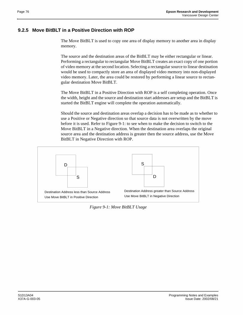
Page 76 Epson Research and DevelopmentVancouver Design Center
9.2.5 Move BitBLT in a Positive Direction with ROP
The Move BitBLT is used to copy one area of display memory to another area in display memory.
The source and the destination areas of the BitBLT may be either rectangular or linear. Performing a rectangular to rectangular Move BitBLT creates an exact copy of one portion of video memory at the second location. Selecting a rectangular source to linear destination would be used to compactly store an area of displayed video memory into non-displayed video memory. Later, the area could be restored by performing a linear source to rectan-gular destination Move BitBLT.
The Move BitBLT in a Positive Direction with ROP is a self completing operation. Once the width, height and the source and destination start addresses are setup and the BitBLT is started the BitBLT engine will complete the operation automatically.
Should the source and destination areas overlap a decision has to be made as to whether to use a Positive or Negative direction so that source data is not overwritten by the move before it is used. Refer to Figure 9-1: to see when to make the decision to switch to the Move BitBLT in a Negative direction. When the destination area overlaps the original source area and the destination address is greater then the source address, use the Move BitBLT in Negative Direction with ROP.
Figure 9-1: Move BitBLT Usage
D
S
S
D
Destination Address less than Source Address
Use Move BitBLT in Positive Direction
Destination Address greater than Source Address
Use Move BitBLT in Negative Direction
S1D13A04 Programming Notes and ExamplesX37A-G-003-05 Issue Date: 2002/08/21
Epson Research and Development Page 77Vancouver Design Center
Example 12: Copy a 9 x 101 rectangle at the screen coordinates x = 100, y = 10 to screen coordinates x = 200, y = 20 using a 320x240 display at a color depth of 16 bpp.
1. Calculate the source and destination addresses (upper left corners of the source and destination rectangles), using the following formula.
SourceAddress = (y × ScreenStride) + (x × BytesPerPixel)= (10 × (320 × 2)) + (100 × 2)= 6600= 19C8h
DestinationAddress = (y × ScreenStride) + (x × BytesPerPixel)= (20 × (320 × 2)) + (200 × 2)= 13200= 3390h
where:BytesPerPixel = 1 for 8 bppBytesPerPixel = 2 for 16 bppScreenStride = DisplayWidthInPixels × BytesPerPixel = 640 for 16 bpp
Program the BitBLT Source Start Address Register. REG[800Ch] is set to 19C8h.
Program the BitBLT Destination Start Address Register. REG[8010h] is set to 3390h.
2. Program the BitBLT Width Register to 9 - 1. REG[8018h] is set to 08h.
3. Program the BitBLT Height Register to 101 - 1. REG[801Ch] is set to 64h (100 deci-mal).
4. Program the BitBLT Operation Register to select the Move BitBLT in Positive Direc-tion with ROP. REG[8008h] bits 3-0 are set to 2h.
5. Program the BitBLT ROP Code Register to select Destination = Source. REG[8008h] bits 19-16 are set to 0Ch.
6. Program the BitBLT Color Format Select bit for 16 bpp operations. REG[8000h] bit 18 is set to 1.
7. Program the BitBLT Memory Offset Register to the ScreenStride in WORDS.
BltMemoryOffset = ScreenStride ÷ 2= 320= 140h
REG[8014h] is set to 0140h.
Programming Notes and Examples S1D13A04Issue Date: 2002/08/21 X37A-G-003-05
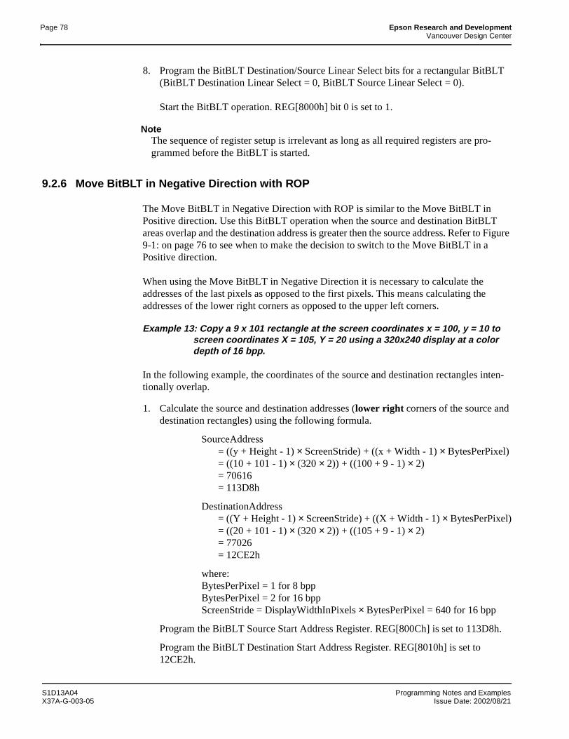
Page 78 Epson Research and DevelopmentVancouver Design Center
8. Program the BitBLT Destination/Source Linear Select bits for a rectangular BitBLT (BitBLT Destination Linear Select = 0, BitBLT Source Linear Select = 0).
Start the BitBLT operation. REG[8000h] bit 0 is set to 1.
NoteThe sequence of register setup is irrelevant as long as all required registers are pro-grammed before the BitBLT is started.
9.2.6 Move BitBLT in Negative Direction with ROP
The Move BitBLT in Negative Direction with ROP is similar to the Move BitBLT in Positive direction. Use this BitBLT operation when the source and destination BitBLT areas overlap and the destination address is greater then the source address. Refer to Figure 9-1: on page 76 to see when to make the decision to switch to the Move BitBLT in a Positive direction.
When using the Move BitBLT in Negative Direction it is necessary to calculate the addresses of the last pixels as opposed to the first pixels. This means calculating the addresses of the lower right corners as opposed to the upper left corners.
Example 13: Copy a 9 x 101 rectangle at the screen coordinates x = 100, y = 10 to screen coordinates X = 105, Y = 20 using a 320x240 display at a color depth of 16 bpp.
In the following example, the coordinates of the source and destination rectangles inten-tionally overlap.
1. Calculate the source and destination addresses (lower right corners of the source and destination rectangles) using the following formula.
SourceAddress = ((y + Height - 1) × ScreenStride) + ((x + Width - 1) × BytesPerPixel)= ((10 + 101 - 1) × (320 × 2)) + ((100 + 9 - 1) × 2)= 70616= 113D8h
DestinationAddress= ((Y + Height - 1) × ScreenStride) + ((X + Width - 1) × BytesPerPixel)= ((20 + 101 - 1) × (320 × 2)) + ((105 + 9 - 1) × 2)= 77026= 12CE2h
where:BytesPerPixel = 1 for 8 bppBytesPerPixel = 2 for 16 bppScreenStride = DisplayWidthInPixels × BytesPerPixel = 640 for 16 bpp
Program the BitBLT Source Start Address Register. REG[800Ch] is set to 113D8h.
Program the BitBLT Destination Start Address Register. REG[8010h] is set to 12CE2h.
S1D13A04 Programming Notes and ExamplesX37A-G-003-05 Issue Date: 2002/08/21
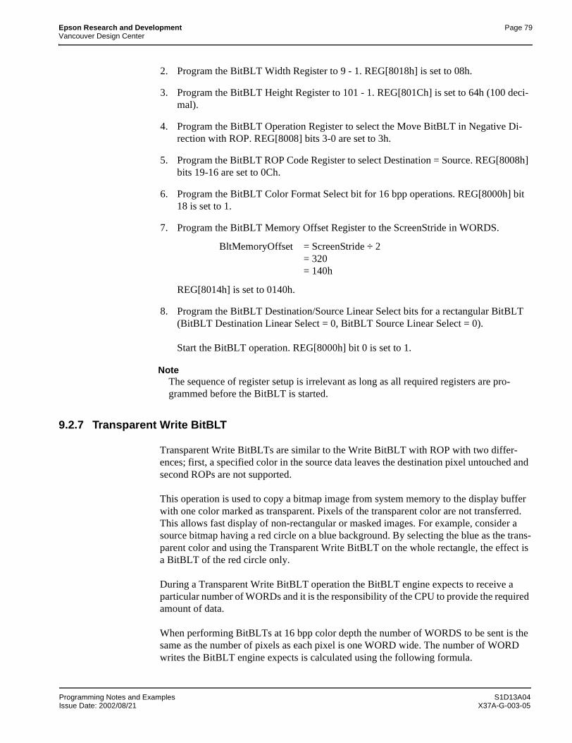
Epson Research and Development Page 79Vancouver Design Center
2. Program the BitBLT Width Register to 9 - 1. REG[8018h] is set to 08h.
3. Program the BitBLT Height Register to 101 - 1. REG[801Ch] is set to 64h (100 deci-mal).
4. Program the BitBLT Operation Register to select the Move BitBLT in Negative Di-rection with ROP. REG[8008] bits 3-0 are set to 3h.
5. Program the BitBLT ROP Code Register to select Destination = Source. REG[8008h] bits 19-16 are set to 0Ch.
6. Program the BitBLT Color Format Select bit for 16 bpp operations. REG[8000h] bit 18 is set to 1.
7. Program the BitBLT Memory Offset Register to the ScreenStride in WORDS.
BltMemoryOffset = ScreenStride ÷ 2= 320= 140h
REG[8014h] is set to 0140h.
8. Program the BitBLT Destination/Source Linear Select bits for a rectangular BitBLT (BitBLT Destination Linear Select = 0, BitBLT Source Linear Select = 0).
Start the BitBLT operation. REG[8000h] bit 0 is set to 1.
NoteThe sequence of register setup is irrelevant as long as all required registers are pro-grammed before the BitBLT is started.
9.2.7 Transparent Write BitBLT
Transparent Write BitBLTs are similar to the Write BitBLT with ROP with two differ-ences; first, a specified color in the source data leaves the destination pixel untouched and second ROPs are not supported.
This operation is used to copy a bitmap image from system memory to the display buffer with one color marked as transparent. Pixels of the transparent color are not transferred. This allows fast display of non-rectangular or masked images. For example, consider a source bitmap having a red circle on a blue background. By selecting the blue as the trans-parent color and using the Transparent Write BitBLT on the whole rectangle, the effect is a BitBLT of the red circle only.
During a Transparent Write BitBLT operation the BitBLT engine expects to receive a particular number of WORDs and it is the responsibility of the CPU to provide the required amount of data.
When performing BitBLTs at 16 bpp color depth the number of WORDS to be sent is the same as the number of pixels as each pixel is one WORD wide. The number of WORD writes the BitBLT engine expects is calculated using the following formula.
Programming Notes and Examples S1D13A04Issue Date: 2002/08/21 X37A-G-003-05

Page 80 Epson Research and DevelopmentVancouver Design Center
WORDS = Pixels= BitBLTWidth × BitBLTHeight
When the color depth is 8 bpp the formula must take into consideration that the BitBLT engine accepts only WORD accesses and each pixel is one BYTE. This may lead to a different number of WORD transfers than there are pixels to transfer.
The number of WORD accesses is dependant on the position of the first pixel within the first WORD of each row. Is the pixel stored in the low byte or the high byte of the WORD? This aspect of the BitBLT is called phase and is determined as follows:
Source phase is 0 when the first pixel is in the low byte and the second pixel is in the high byte of the WORD. When the source phase is 0, bit 0 of the Source Start Address Register is 0. The Source Phase is 1 if the first pixel of each row is contained in the high byte of the WORD, the contents of the low byte are ignored. When the source phase is 1, bit 0 of the Source Start Address Register is set.
Depending on the Source Phase and the BitBLT Width, the last WORD may contain only one pixel. In this case it is always in the low byte. The number of WORD writes the BitBLT engine expects for 8 bpp color depths is shown in the following formula.
WORDS = ((BitBLTWidth + 1 + SourcePhase) ÷ 2) × BitBLTHeight
Once the Transparent Write BitBLT begins, the BitBLT engine remains active until all pixels have been written. The BitBLT engine requires this number of WORDS to be sent from the local CPU before it ends the Transparent Write BitBLT operation.
NoteThe BitBLT engine counts WORD writes made to the BitBLT register. This does not imply only 16-bit CPU instructions are acceptable. If a system is able to separate one DWORD write into two WORD writes and the CPU writes the low word before the high word, then 32-bit CPU instructions are acceptable. Otherwise, 16-bit CPU instruc-tions are required.
Example 14: Write 100 x 20 pixels at the screen coordinates x = 25, y = 38 using a 320x240 display at a color depth of 8 bpp. Transparent color is high in-tensity blue (assume LUT Index 124).
1. Calculate the destination address (upper left corner of the screen BitBLT rectangle), using the formula:
DestinationAddress = (y × ScreenStride) + (x × BytesPerPixel)= (38 × 320) + (25 × 1)= 12185= 2F99h
where:BytesPerPixel = 1 for 8 bppBytesPerPixel = 2 for 16 bppScreenStride = DisplayWidthInPixels × BytesPerPixel = 320 for 8 bpp
Program the BitBLT Destination Start Address Register. REG[8010h] is set to 2F99h.
S1D13A04 Programming Notes and ExamplesX37A-G-003-05 Issue Date: 2002/08/21

Epson Research and Development Page 81Vancouver Design Center
2. Program the BitBLT Width Register to 100 - 1. REG[8018h] is set to 63h (99 deci-mal).
3. Program the BitBLT Height Register to 20 - 1. REG[801Ch] is set to 13h (19 deci-mal).
4. Program the Source Phase in the BitBLT Source Start Address Register. In this exam-ple, the data is WORD aligned, so the source phase is 0. REG[800Ch] is set to 00h.
5. Program the BitBLT Operation Register to select Transparent Write BitBLT. REG[8008h] bits 3-0 are set to 4h.
6. Program the BitBLT Background Color Register to select transparent color. REG[8020h] is set to 7Ch (124 decimal).
7. Program the BitBLT Color Format Select bit for 8 bpp operations. REG[8000h] bit 18 is set to 0.
8. Program the BitBLT Memory Offset Register to the ScreenStride in WORDS.
BltMemoryOffset = ScreenStride ÷ 2= 320 ÷ 2= 160= A0h
REG[8014h] is set to 0A0h.
9. Calculate the number of WORDS the BitBLT engine expects to receive.
WORDS = ((BLTWidth + 1 + SourcePhase) ÷ 2) × BLTHeight= (100 + 1 + 0) ÷ 2 × 20= 1000= 3E8h
10. Program the BitBLT Destination/Source Linear Select bits for a rectangular BitBLT (BitBLT Destination Linear Select = 0, BitBLT Source Linear Select = 0).
Start the BitBLT operation and wait for the BitBLT engine to start. REG[8000h] bit 0 is set to 1, then wait until REG[8004h] bit 0 returns a 1.
Programming Notes and Examples S1D13A04Issue Date: 2002/08/21 X37A-G-003-05
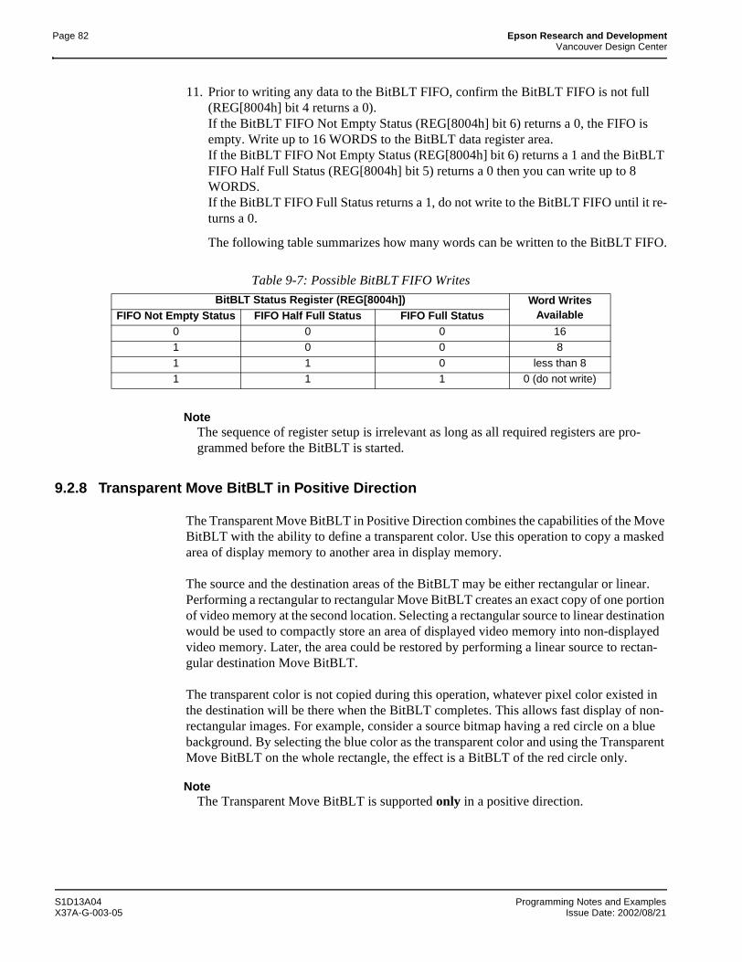
Page 82 Epson Research and DevelopmentVancouver Design Center
11. Prior to writing any data to the BitBLT FIFO, confirm the BitBLT FIFO is not full (REG[8004h] bit 4 returns a 0).If the BitBLT FIFO Not Empty Status (REG[8004h] bit 6) returns a 0, the FIFO is empty. Write up to 16 WORDS to the BitBLT data register area.If the BitBLT FIFO Not Empty Status (REG[8004h] bit 6) returns a 1 and the BitBLT FIFO Half Full Status (REG[8004h] bit 5) returns a 0 then you can write up to 8 WORDS.If the BitBLT FIFO Full Status returns a 1, do not write to the BitBLT FIFO until it re-turns a 0.
The following table summarizes how many words can be written to the BitBLT FIFO.
NoteThe sequence of register setup is irrelevant as long as all required registers are pro-grammed before the BitBLT is started.
9.2.8 Transparent Move BitBLT in Positive Direction
The Transparent Move BitBLT in Positive Direction combines the capabilities of the Move BitBLT with the ability to define a transparent color. Use this operation to copy a masked area of display memory to another area in display memory.
The source and the destination areas of the BitBLT may be either rectangular or linear. Performing a rectangular to rectangular Move BitBLT creates an exact copy of one portion of video memory at the second location. Selecting a rectangular source to linear destination would be used to compactly store an area of displayed video memory into non-displayed video memory. Later, the area could be restored by performing a linear source to rectan-gular destination Move BitBLT.
The transparent color is not copied during this operation, whatever pixel color existed in the destination will be there when the BitBLT completes. This allows fast display of non-rectangular images. For example, consider a source bitmap having a red circle on a blue background. By selecting the blue color as the transparent color and using the Transparent Move BitBLT on the whole rectangle, the effect is a BitBLT of the red circle only.
NoteThe Transparent Move BitBLT is supported only in a positive direction.
Table 9-7: Possible BitBLT FIFO Writes
BitBLT Status Register (REG[8004h]) Word Writes AvailableFIFO Not Empty Status FIFO Half Full Status FIFO Full Status
0 0 0 161 0 0 8
1 1 0 less than 81 1 1 0 (do not write)
S1D13A04 Programming Notes and ExamplesX37A-G-003-05 Issue Date: 2002/08/21
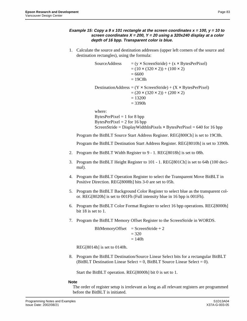
Epson Research and Development Page 83Vancouver Design Center
Example 15: Copy a 9 x 101 rectangle at the screen coordinates x = 100, y = 10 to screen coordinates X = 200, Y = 20 using a 320x240 display at a color depth of 16 bpp. Transparent color is blue.
1. Calculate the source and destination addresses (upper left corners of the source and destination rectangles), using the formula:
SourceAddress = (y × ScreenStride) + (x × BytesPerPixel)= (10 × (320 × 2)) + (100 × 2)= 6600= 19C8h
DestinationAddress = (Y × ScreenStride) + (X × BytesPerPixel)= (20 × (320 × 2)) + (200 × 2)= 13200= 3390h
where:BytesPerPixel = 1 for 8 bppBytesPerPixel = 2 for 16 bppScreenStride = DisplayWidthInPixels × BytesPerPixel = 640 for 16 bpp
Program the BitBLT Source Start Address Register. REG[800Ch] is set to 19C8h.
Program the BitBLT Destination Start Address Register. REG[8010h] is set to 3390h.
2. Program the BitBLT Width Register to 9 - 1. REG[8018h] is set to 08h.
3. Program the BitBLT Height Register to 101 - 1. REG[801Ch] is set to 64h (100 deci-mal).
4. Program the BitBLT Operation Register to select the Transparent Move BitBLT in Positive Direction. REG[8008h] bits 3-0 are set to 05h.
5. Program the BitBLT Background Color Register to select blue as the transparent col-or. REG[8020h] is set to 001Fh (Full intensity blue in 16 bpp is 001Fh).
6. Program the BitBLT Color Format Register to select 16 bpp operations. REG[8000h] bit 18 is set to 1.
7. Program the BitBLT Memory Offset Register to the ScreenStride in WORDS.
BltMemoryOffset = ScreenStride ÷ 2= 320= 140h
REG[8014h] is set to 0140h.
8. Program the BitBLT Destination/Source Linear Select bits for a rectangular BitBLT (BitBLT Destination Linear Select = 0, BitBLT Source Linear Select = 0).
Start the BitBLT operation. REG[8000h] bit 0 is set to 1.
NoteThe order of register setup is irrelevant as long as all relevant registers are programmed before the BitBLT is initiated.
Programming Notes and Examples S1D13A04Issue Date: 2002/08/21 X37A-G-003-05
Page 84 Epson Research and DevelopmentVancouver Design Center
9.2.9 Pattern Fill BitBLT with ROP
The Pattern Fill BitBLT with ROP fills a specified area of display memory with a pattern. The pattern is repeated until the fill area is completely filled. The fill pattern is limited to an eight by eight pixel array and must be loaded to off-screen video memory before starting the BitBLT. The pattern can be logically combined with the destination using any of the 16 ROP codes, but typically the copy pattern ROP is used (ROP code 0Ch).
A pattern is defined to be an array of 8x8 pixels and the pattern data must be stored in consecutive bytes of display memory (64 consecutive bytes for 8 bpp color depths and 128 bytes for 16 bpp color depths). For 8 bpp color depths the pattern must begin on a 64 byte boundary, for 16 bpp color depths the pattern must begin on a 128 byte boundary.
This operation is self completing. Once the parameters have been entered and the BitBLT started the BitBLT engine will fill all of the specified memory with the pattern.
To fill an area using the pattern BitBLT, the BitBLT engine requires the location of the pattern, the destination rectangle position and size, and the ROP code. The BitBLT engine also needs to know which pixel from the pattern is the first pixel in the destination rectangle (the pattern start phase). This allows seamless redrawing of any part of the screen using the pattern fill.
Example 16: Fill a 100 x 150 rectangle at the screen coordinates x = 10, y = 20 with the pattern in off-screen memory at offset 27000h using a 320x240 dis-play at a color depth of 8 bpp. The first pixel (upper left corner) of the rectangle is the pattern pixel at x = 3, y = 4.
1. Calculate the destination address (upper left corner of the destination rectangle), using the formula:
DestinationAddress = (y × ScreenStride) + (x × BytesPerPixel)= (20 × 320) + (10 × 1)= 6410= 190Ah
where:BytesPerPixel = 1 for 8 bppBytesPerPixel = 2 for 16 bppScreenStride = DisplayWidthInPixels × BytesPerPixels = 320 for 8 bpp
Program the BitBLT Destination Start Address Register. REG[8010h] is set to 190Ah.
S1D13A04 Programming Notes and ExamplesX37A-G-003-05 Issue Date: 2002/08/21
Epson Research and Development Page 85Vancouver Design Center
2. Calculate the source address. This is the address of the pixel in the pattern that is the origin of the destination fill area. The pattern begins at offset 156K but the first pattern pixel is at x = 3, y = 4. Therefore, an offset within the pattern itself must be calculated.
SourceAddress= PatternOffset + StartPatternY × 8 × BytesPerPixel + StartPatternX × BytesPerPixel= 156K + (4 × 8 × 1) + (3 × 1)= 156K + 35= 159779= 27023h
where:BytesPerPixel = 1 for 8 bppBytesPerPixel = 2 for 16 bpp
Program the BitBLT Source Start Address Register. REG[800Ch] is set to 27023h.
3. Program the BitBLT Width Register to 100 - 1. REG[8018h] is set to 63h (99 deci-mal).
4. Program the BitBLT Height Register to 150-1. REG[801Ch] is set to 95h (149 deci-mal).
5. Program the BitBLT Operation Register to select the Pattern Fill with ROP. REG[8008h] bits 3-0 are set to 6h.
6. Program the BitBLT ROP Code Register to select Destination = Source. REG[8008h] bits 19-16 are set to 0Ch.
7. Program the BitBLT Color Format Select bit for 8 bpp operations. REG[8000h] bit 18 is set to 0.
8. Program the BitBLT Memory Offset Register to the ScreenStride in WORDS.
BltMemoryOffset = ScreenStride ÷ 2= 320 ÷ 2= 160= A0h
REG[8014h] is set to 00A0h.
9. Program the BitBLT Destination/Source Linear Select bits for a rectangular BitBLT (BitBLT Destination Linear Select = 0, BitBLT Source Linear Select = 0).
Start the BitBLT operation. REG[8000h] bit 0 is set to 1.
NoteThe sequence of register setup is irrelevant as long as all required registers are pro-grammed before the BitBLT is started.
Programming Notes and Examples S1D13A04Issue Date: 2002/08/21 X37A-G-003-05
Page 86 Epson Research and DevelopmentVancouver Design Center
9.2.10 Pattern Fill BitBLT with Transparency
This operation is very similar to the Pattern Fill BitBLT with the difference being that one color can be specified to be transparent. Whenever the Transparent color is encountered in the pattern data the destination is left as is. This operation is useful to create hatched or striped patterns where the original image shows through the hatching.
The requirements for this BitBLT are the same as for the Pattern Fill BitBLT the only change in programming is that the BitBLT Operation field of REG[8008h] must be set to 07h and the BitBLT Background color register, REG[8020h] must be set to the desired color.
Example 17: Fill a 100 x 150 rectangle at the screen coordinates x = 10, y = 20 with the pattern in off-screen memory at offset 27000h using a 320x240 dis-play at a color depth of 8 bpp. The first pixel (upper left corner) of the rectangle is the pattern pixel at x = 3, y = 4. Transparent color is blue (as-sumes LUT index 1).
1. Calculate the destination address (upper left corner of destination rectangle), using the formula:
DestinationAddress = (y × ScreenStride) + (x × BytesPerPixel)= (20 × 320) + (10 × 1)= 6410= 190Ah
where:BytesPerPixel = 1 for 8 bppBytesPerPixel = 2 for 16 bppScreenStride = DisplayWidthInPixels × BytesPerPixels = 320 for 8 bpp
Program the BitBLT Destination Start Address Register. REG[8010h] is set to 190Ah.
2. Calculate the source address. This is the address of the pixel in the pattern that is the origin of the destination fill area. The pattern begins at offset 1M, but the first pattern pixel is at x = 3, y = 4. Therefore, an offset within the pattern itself must be calculated.
SourceAddress= PatternOffset + StartPatternY × 8 × BytesPerPixel + StartPatternX × BytesPerPixel= 156K + (4 × 8 × 1) + (3 × 1)= 156K + 35= 159779= 27023h
where:BytesPerPixel = 1 for 8 bppBytesPerPixel = 2 for 16 bpp
Program the BitBLT Source Start Address Register. REG[800Ch] is set to 27023h.
3. Program the BitBLT Width Register to 100 - 1. REG[8018h] is set to 63h (99 deci-mal).
S1D13A04 Programming Notes and ExamplesX37A-G-003-05 Issue Date: 2002/08/21
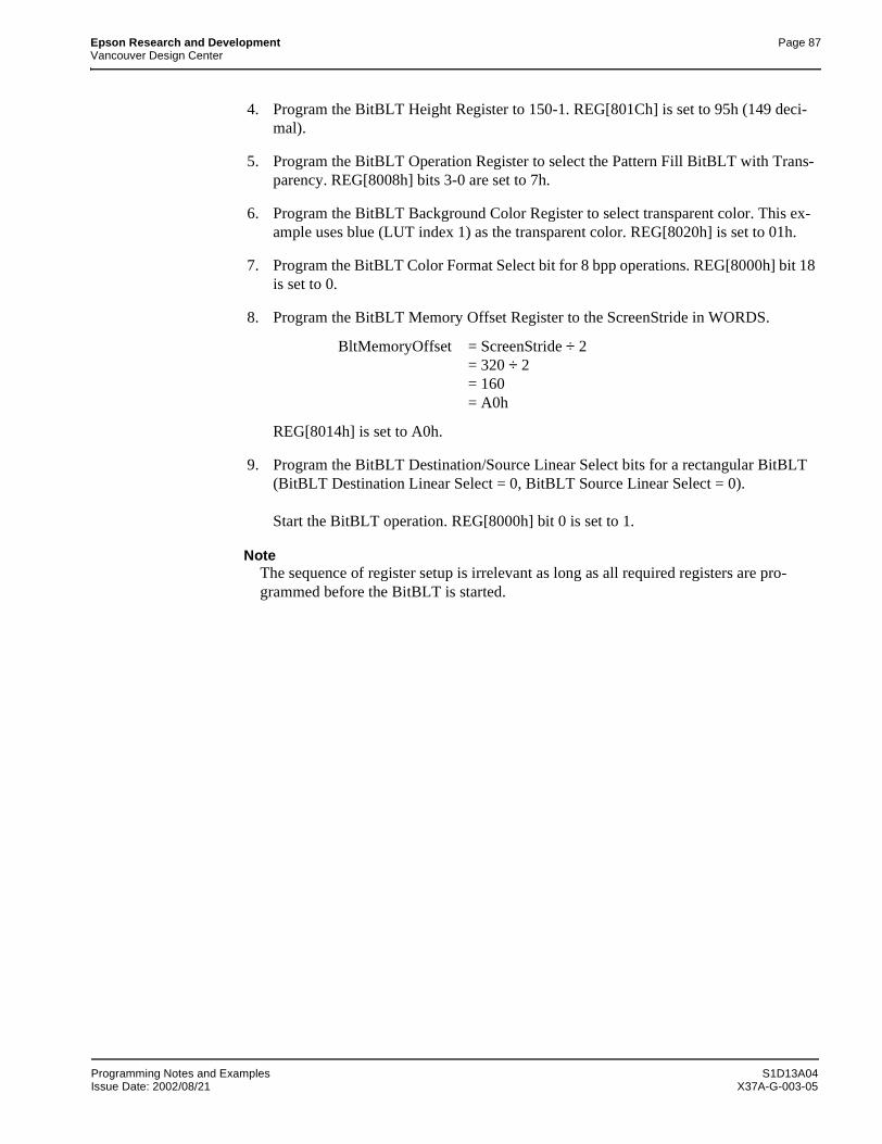
Epson Research and Development Page 87Vancouver Design Center
4. Program the BitBLT Height Register to 150-1. REG[801Ch] is set to 95h (149 deci-mal).
5. Program the BitBLT Operation Register to select the Pattern Fill BitBLT with Trans-parency. REG[8008h] bits 3-0 are set to 7h.
6. Program the BitBLT Background Color Register to select transparent color. This ex-ample uses blue (LUT index 1) as the transparent color. REG[8020h] is set to 01h.
7. Program the BitBLT Color Format Select bit for 8 bpp operations. REG[8000h] bit 18 is set to 0.
8. Program the BitBLT Memory Offset Register to the ScreenStride in WORDS.
BltMemoryOffset = ScreenStride ÷ 2= 320 ÷ 2= 160= A0h
REG[8014h] is set to A0h.
9. Program the BitBLT Destination/Source Linear Select bits for a rectangular BitBLT (BitBLT Destination Linear Select = 0, BitBLT Source Linear Select = 0).
Start the BitBLT operation. REG[8000h] bit 0 is set to 1.
NoteThe sequence of register setup is irrelevant as long as all required registers are pro-grammed before the BitBLT is started.
Programming Notes and Examples S1D13A04Issue Date: 2002/08/21 X37A-G-003-05

Page 88 Epson Research and DevelopmentVancouver Design Center
9.2.11 Move BitBLT with Color Expansion
The Move BitBLT with Color Expansion takes a monochrome bitmap as the source and color expands it into the destination. All bits set to one in the source are expanded to desti-nation pixels of the selected foreground color. All bits set to zero in the source are expanded to pixels of the selected background color.
The Move BitBLT with Color Expansion is used to accelerate text drawing. A monochrome bitmap of a font, in off-screen video memory, occupies very little space and takes advantage of the hardware acceleration. Since the foreground and background colors are programmable, text of any color can be created.
The Move BitBLT with Color Expansion can move data from one rectangular area to another, or either the source or destination may be specified to be linear. Storing rectangular display data in linear format in off screen memory results in a tremendous space saving.
Example 18: Color expand a 9 x 16 rectangle using the pattern in off-screen memory at 27000h and move it to the screen coordinates x = 200, y = 20. Assume a 320x240 display at a color depth of 16 bpp, Foreground color of black, and background color of white.
1. Calculate the destination and source addresses (upper left corner of the destination and source rectangles), using the formula.
DestinationAddress = (y × ScreenStride) + (x × BytesPerPixel)= (20 × (320 × 2)) + (200 × 2)= 13200= 3390h
where:BytesPerPixel = 1 for 8 bppBytesPerPixel = 2 for 16 bppScreenStride = DisplayWidthInPixels × BytesPerPixels = 640 for 16 bpp
SourceAddress = 156K= 27000h
Program the BitBLT Destination Start Address Register. REG[8010h] is set to 3390h.
Program the BitBLT Source Start Address Register. REG[800Ch] is set to 27000h.
2. Program the BitBLT Width Register to 9 - 1. REG[8018h] is set to 08h.
3. Program the BitBLT Height Register to 16 - 1. REG[801Ch] is set to 0Fh.
4. Program the BitBLT ROP Code/Color Expansion Register. REG[8008h] bits 19-16 are set to 7h.
5. Program the BitBLT Operation Register to select the Move BitBLT with Color Ex-pansion. REG[8008h] bits 3-0 are set to 0Bh.
6. Program the BitBLT Foreground Color Register to select black (in 16 bpp black = 0000h). REG[8024h] is set to 0000h.
S1D13A04 Programming Notes and ExamplesX37A-G-003-05 Issue Date: 2002/08/21
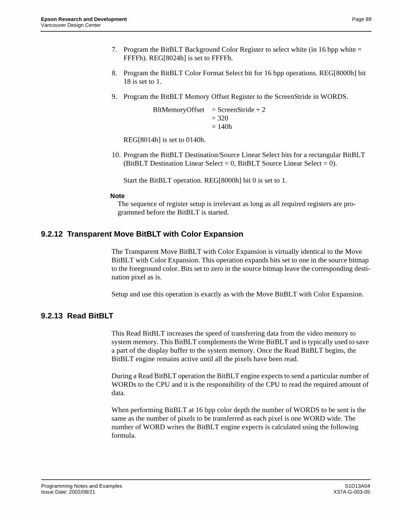
Epson Research and Development Page 89Vancouver Design Center
7. Program the BitBLT Background Color Register to select white (in 16 bpp white = FFFFh). REG[8024h] is set to FFFFh.
8. Program the BitBLT Color Format Select bit for 16 bpp operations. REG[8000h] bit 18 is set to 1.
9. Program the BitBLT Memory Offset Register to the ScreenStride in WORDS.
BltMemoryOffset = ScreenStride ÷ 2= 320= 140h
REG[8014h] is set to 0140h.
10. Program the BitBLT Destination/Source Linear Select bits for a rectangular BitBLT (BitBLT Destination Linear Select = 0, BitBLT Source Linear Select = 0).
Start the BitBLT operation. REG[8000h] bit 0 is set to 1.
NoteThe sequence of register setup is irrelevant as long as all required registers are pro-grammed before the BitBLT is started.
9.2.12 Transparent Move BitBLT with Color Expansion
The Transparent Move BitBLT with Color Expansion is virtually identical to the Move BitBLT with Color Expansion. This operation expands bits set to one in the source bitmap to the foreground color. Bits set to zero in the source bitmap leave the corresponding desti-nation pixel as is.
Setup and use this operation is exactly as with the Move BitBLT with Color Expansion.
9.2.13 Read BitBLT
This Read BitBLT increases the speed of transferring data from the video memory to system memory. This BitBLT complements the Write BitBLT and is typically used to save a part of the display buffer to the system memory. Once the Read BitBLT begins, the BitBLT engine remains active until all the pixels have been read.
During a Read BitBLT operation the BitBLT engine expects to send a particular number of WORDs to the CPU and it is the responsibility of the CPU to read the required amount of data.
When performing BitBLT at 16 bpp color depth the number of WORDS to be sent is the same as the number of pixels to be transferred as each pixel is one WORD wide. The number of WORD writes the BitBLT engine expects is calculated using the following formula.
Programming Notes and Examples S1D13A04Issue Date: 2002/08/21 X37A-G-003-05
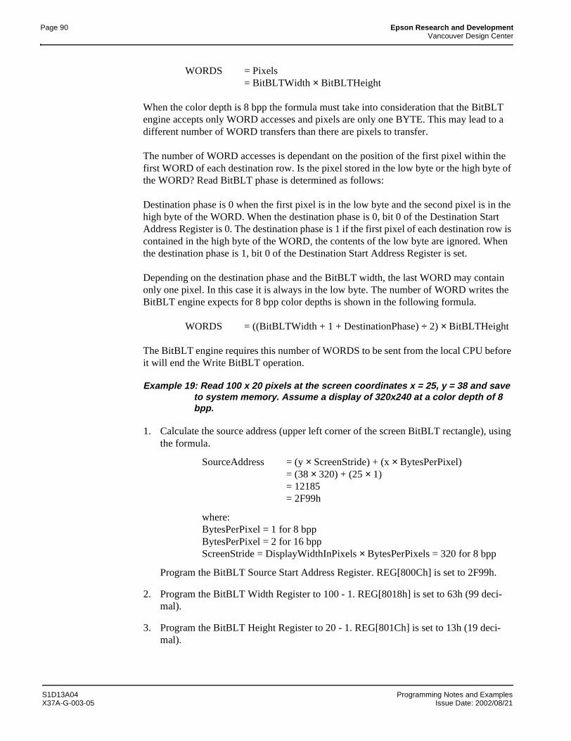
Page 90 Epson Research and DevelopmentVancouver Design Center
WORDS = Pixels= BitBLTWidth × BitBLTHeight
When the color depth is 8 bpp the formula must take into consideration that the BitBLT engine accepts only WORD accesses and pixels are only one BYTE. This may lead to a different number of WORD transfers than there are pixels to transfer.
The number of WORD accesses is dependant on the position of the first pixel within the first WORD of each destination row. Is the pixel stored in the low byte or the high byte of the WORD? Read BitBLT phase is determined as follows:
Destination phase is 0 when the first pixel is in the low byte and the second pixel is in the high byte of the WORD. When the destination phase is 0, bit 0 of the Destination Start Address Register is 0. The destination phase is 1 if the first pixel of each destination row is contained in the high byte of the WORD, the contents of the low byte are ignored. When the destination phase is 1, bit 0 of the Destination Start Address Register is set.
Depending on the destination phase and the BitBLT width, the last WORD may contain only one pixel. In this case it is always in the low byte. The number of WORD writes the BitBLT engine expects for 8 bpp color depths is shown in the following formula.
WORDS = ((BitBLTWidth + 1 + DestinationPhase) ÷ 2) × BitBLTHeight
The BitBLT engine requires this number of WORDS to be sent from the local CPU before it will end the Write BitBLT operation.
Example 19: Read 100 x 20 pixels at the screen coordinates x = 25, y = 38 and save to system memory. Assume a display of 320x240 at a color depth of 8 bpp.
1. Calculate the source address (upper left corner of the screen BitBLT rectangle), using the formula.
SourceAddress = (y × ScreenStride) + (x × BytesPerPixel)= (38 × 320) + (25 × 1)= 12185= 2F99h
where:BytesPerPixel = 1 for 8 bppBytesPerPixel = 2 for 16 bppScreenStride = DisplayWidthInPixels × BytesPerPixels = 320 for 8 bpp
Program the BitBLT Source Start Address Register. REG[800Ch] is set to 2F99h.
2. Program the BitBLT Width Register to 100 - 1. REG[8018h] is set to 63h (99 deci-mal).
3. Program the BitBLT Height Register to 20 - 1. REG[801Ch] is set to 13h (19 deci-mal).
S1D13A04 Programming Notes and ExamplesX37A-G-003-05 Issue Date: 2002/08/21
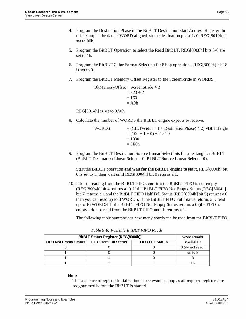
Epson Research and Development Page 91Vancouver Design Center
4. Program the Destination Phase in the BitBLT Destination Start Address Register. In this example, the data is WORD aligned, so the destination phase is 0. REG[8010h] is set to 00h.
5. Program the BitBLT Operation to select the Read BitBLT. REG[8008h] bits 3-0 are set to 1h.
6. Program the BitBLT Color Format Select bit for 8 bpp operations. REG[8000h] bit 18 is set to 0.
7. Program the BitBLT Memory Offset Register to the ScreenStride in WORDS.
BltMemoryOffset = ScreenStride ÷ 2= 320 ÷ 2= 160= A0h
REG[8014h] is set to 0A0h.
8. Calculate the number of WORDS the BitBLT engine expects to receive.
WORDS = ((BLTWidth + 1 + DestinationPhase) ÷ 2) ×BLTHeight= (100 + 1 + 0) ÷ 2 × 20= 1000= 3E8h
9. Program the BitBLT Destination/Source Linear Select bits for a rectangular BitBLT (BitBLT Destination Linear Select = 0, BitBLT Source Linear Select = 0).
Start the BitBLT operation and wait for the BitBLT engine to start. REG[8000h] bit 0 is set to 1, then wait until REG[8004h] bit 0 returns a 1.
10. Prior to reading from the BitBLT FIFO, confirm the BitBLT FIFO is not empty (REG[8004h] bit 4 returns a 1). If the BitBLT FIFO Not Empty Status (REG[8004h] bit 6) returns a 1 and the BitBLT FIFO Half Full Status (REG[8004h] bit 5) returns a 0 then you can read up to 8 WORDS. If the BitBLT FIFO Full Status returns a 1, read up to 16 WORDS. If the BitBLT FIFO Not Empty Status returns a 0 (the FIFO is empty), do not read from the BitBLT FIFO until it returns a 1.
The following table summarizes how many words can be read from the BitBLT FIFO.
NoteThe sequence of register initialization is irrelevant as long as all required registers are programmed before the BitBLT is started.
Table 9-8: Possible BitBLT FIFO Reads
BitBLT Status Register (REG[8004h]) Word Reads AvailableFIFO Not Empty Status FIFO Half Full Status FIFO Full Status
0 0 0 0 (do not read)1 0 0 up to 81 1 0 8
1 1 1 16
Programming Notes and Examples S1D13A04Issue Date: 2002/08/21 X37A-G-003-05
Page 92 Epson Research and DevelopmentVancouver Design Center
9.3 S1D13A04 BitBLT Synchronization
A BitBLT operation can only be started if the BitBLT engine is not busy servicing another BitBLT. Before a new operation is started, software must confirm the BitBLT Busy Status bit (REG[8004h] bit 0) is set to zero. The status of this bit can either be tested after each BitBLT operation, or before each BitBLT operation.
Testing the BitBLT Status After
Testing the BitBLT Active Status after starting a new BitBLT is simpler and less prone to errors.
To test after each BitBLT operation, perform the following.
1. Program and start the BitBLT engine.
2. Wait for the current BitBLT operation to finish -- Poll the BitBLT Busy Status bit (REG[8004h] bit 0) until it returns a 0.
3. Continue with program execution.
Testing the BitBLT Status Before
Testing the BitBLT Active Status before starting a new BitBLT results in better perfor-mance, as both CPU and BitBLT engine can be running at the same time. This is most useful for BitBLTs that are self completing (once started they don’t require any CPU assis-tance). While the BitBLT engine is busy, the CPU can do other tasks. To test before each BitBLT operation, perform the following.
1. Wait for the current BitBLT operation to finish -- Poll the BitBLT Busy Status bit (REG[8004h] bit 0) until it returns a 0.
2. Program and start the new BitBLT operation.
3. Continue with program execution (CPU and BitBLT engine work independently).
This approach can pose problems when mixing CPU and BitBLT access to the display buffer. For example, if the CPU writes a pixel while the BitBLT engine is running and the CPU writes a pixel before the BitBLT finishes, the pixel may be overwritten by the BitBLT. To avoid this scenario, always assure no BitBLT is in progress before accessing the display buffer with the CPU, or don’t use the CPU to access the display buffer at all.
S1D13A04 Programming Notes and ExamplesX37A-G-003-05 Issue Date: 2002/08/21
Epson Research and Development Page 93Vancouver Design Center
9.4 S1D13A04 BitBLT Known Limitations
The S1D13A04 BitBLT engine has the following limitations.
• The 2D Accelerator Data Memory Mapped register must not be accessed except during BitBLT operations. Read from the register only during Read BitBLT operations and write to the register only during Write and Color Expand BitBLTs. Accessing the register at any other time may result in S1D13A04 stopping to respond and the system to freeze.
• The Read and Write BitBLT operations are not available when the S1D13A04 is config-ured for the Redcap or Dragonball without DTACK host bus interfaces.
• A BitBLT operation cannot be terminated once it has been started.
9.5 Sample Code
Sample code demonstrating how to program the S1D13A04 BitBLT engine is provided in the file A04sample.zip. This file is available on the internet at www.erd.epson.com.
Programming Notes and Examples S1D13A04Issue Date: 2002/08/21 X37A-G-003-05
Page 94 Epson Research and DevelopmentVancouver Design Center
10 Programming the USB Controller
USB (Universal Serial Bus) is an external bus designed to ease the connection and use of peripheral devices. USB incorporates a host/client architecture in which the host initiates all data transactions and the client either receives or supplies data to the host.
USB offers the following features to the end user:
• Single plug type for all peripheral devices.
• Support for up to 127 simultaneous devices.
• Speeds up to 12 Megabits per second.
• “hot-plugging” peripherals.
The S1D13A04 USB controller supports revision 1.1 of the USB specification. The S1D13A04 USB controller handles many common USB tasks without requiring local processor intervention. For example, setup and data transfers are handled automatically by the S1D13A04 controller. The controller notifies the local CPU, through an interrupt, when data is ready to be read from the FIFO or when data has been transmitted to the host.
This section demonstrates how to program and use the S1D13A04 USB controller. Topics covered include:
• Basic concepts such as registers and interrupts
• Initialization and data transfers
• S1D13A04 USB known issues.
10.1 Registers and Interrupts
10.1.1 Registers
Configuration, interrupt notification, and data transfers are all done using the S1D13A04 USB registers. The USB registers are located 4000h bytes past the beginning of S1D13A04 address space and should be written/read using 16 bit accesses.
On most systems the start of S1D13A04 address space, is fixed by the system design. The S1D13A04 evaluation board uses a PCI interface, thus the start of S1D13A04 address space may vary from one session to the next. Example code is written using a pointer to the USB registers (pUSB). The USB examples do not show how to obtain the register address. For a description of how to get the register address when using the S5U13A04B00C evaluation board, refer to the function halAcquireController() in Section 11, “Hardware Abstraction Layer” on page 112.
S1D13A04 Programming Notes and ExamplesX37A-G-003-05 Issue Date: 2002/08/21
Epson Research and Development Page 95Vancouver Design Center
10.1.2 Interrupts
The S1D13A04 uses an interrupt to notify the local CPU when a USB event, which requires servicing, occurs. Events, such as USB reset and data transfer notifications generate inter-rupts.
It is beyond the scope of this document to explain how to setup and configure the interrupt system for the variety of platforms the S1D13A04 supports. The examples and flowcharts assume there is one interrupt handling routine which will determine the cause of the interrupt and call the appropriate handler function. It is assumed the user understands the mechanics and architecture of their system well enough setup a routine which will receive an interrupt notification and determine the cause of the interrupt.
10.2 Initialization
Initialization describes the process of setting the registers state to enable the USB controller for use. There are two cases where the USB registers need to be initialized. When the system is powered up and the registers need to be prepared for first use. The second time the registers need to be initialized is after receiving a RESET request from the host controller.
Refer to Section 10.2.2, “USB Registers” on page 96 for an example of the register initial-ization sequence.
10.2.1 GPIO Setup
The S1D13A04 shares four lines between GPIO and USB use. Before any accesses are made to the USB section the GPIO lines must be configured. To set the GPIO lines write the binary value 0010xxxx-1101xxxx-00000000-xxxxxxxx (2xDx00xxh) to REG[64h], the GPIO Status and Control register.
NoteX’s represent a don’t care state. Depending on other system configuration (i.e. panel technology) certain don’t care bits may have to be set also. See the S1D13A04 Hard-ware Functional Specification, document number X37A-A-001, for more information regarding the bits in the GPIO Status and Control register.
Programming Notes and Examples S1D13A04Issue Date: 2002/08/21 X37A-G-003-05
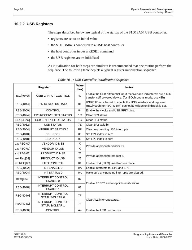
Page 96 Epson Research and DevelopmentVancouver Design Center
10.2.2 USB Registers
The steps described below are typical of the startup of the S1D13A04 USB controller.
• registers are set to an initial value
• the S1D13A04 is connected to a USB host controller
• the host controller issues a RESET command
• the USB registers are re-initialized
As initialization for both steps are similar it is recommended that one routine perform the sequence. The following table depicts a typical register initialization sequence.
Table 10-1: USB Controller Initialization Sequence
RegisterValue (hex)
Notes
REG[4040h] USBFC INPUT CONTROL 40Enable the USB differential input receiver and indicate we are a bulk transfer self powered device. (for ISOchronous mode, use 43h)
REG[4044] PIN IO STATUS DATA 01USBPUP must be set to enable the USB interface and registers. REG[4000h] to REG[403Ah] cannot be written until this bit is set.
REG[4000] CONTROL 84 Enable the clocks and USB GPIO pins.
REG[4024] EP3 RECEIVE FIFO STATUS 1C Clear EP3 status.
REG[402C] USB EP4 TX FIFO STATUS 1C Clear EP4 status
REG[4032] USB STATUS 7E Clear EP2 valid bit
REG[4004] INTERRUPT STATUS 0 FF Clear any pending USB interrupts
REG[4010] EP1 INDEX 00 Set EP1 index to zero
REG[4018] EP2 INDEX 00 Set EP2 index to zero
ext REG[00]
ext REG[01]
VENDOR ID MSB
VENDOR ID LSB
??
??Provide appropriate vendor ID
ext REG[02]
ext Reg[03]
PRODUCT ID MSB
PRODUCT ID LSB
??
??Provide appropriate product ID
ext REG[0C] FIFO CONTROL 01 Enable EP4 (FIFO) valid transfer mode.
REG[4002] INT ENABLE 0 0A Enable interrupts for EP1 and EP3
REG[4004] INT STATUS 0 0A Make sure any pending interrupts are cleared.
REG[4046INTERRUPT CONTROL
ENABLE 002
Enable RESET and endpoints notificationsREG[4048]
INTERRUPT CONTROL ENABLE 1
01
REG[404A]INTERRUPT CONTROL
STATUS/CLEAR 07F
Clear ALL interrupt status...REG[404C]
INTERRUPT CONTROL STATUS/CLEAR 1
7F
REG[4000] CONTROL A4 Enable the USB port for use
S1D13A04 Programming Notes and ExamplesX37A-G-003-05 Issue Date: 2002/08/21
Epson Research and Development Page 97Vancouver Design Center
The USB controller is ready for operation with the following configuration:
• Endpoint 1 (mailbox receive) is configured for bulk OUT and Endpoint 2 (mailbox transmit) is configured for interrupt IN. The functionality of these endpoints cannot be altered.
• Endpoint 3 (FIFO receive) is configured for bulk in and Endpoint 4 (FIFO transmit) is configured for bulk out. Endpoints 3 and 4 may also be configured for isochronous oper-ation.
When the S1D13A04 is connected to a host controller, the host will issue a RESET command to the S1D13A04. In response to the RESET the S1D13A04 clears all USB registers in the range REG[4000h] to REG[403Ah]. The client software must respond to the reset and reprogram the USB registers. A host controller may issue a RESET at any time during operation.
After the S1D13A04 receives the RESET and re-initializes the registers, the host controller starts the USB SETUP phase. The SETUP sequence is handled entirely by the S1D13A04 USB controller. After the setup is complete the S1D13A3 is ready to begin transferring data.
NotePrior to initializing the registers, host controller accesses are responded to with NAKs. After being configured, host controller accesses will be handled in the normal way.
NoteA Vendor ID can be obtained through the USB Implementers Forum athttp://www.usb.org.
10.3 Data Transfers
The S1D13A04 USB requires very little local CPU assistance during data transfers. For the most part data transfers from the host involve reading a FIFO data register when notified of that the transfer is complete or writing a FIFO register and setting a ’ready’ bit to send data to the host.
The following sections expand on the data transfer mechanism.
10.3.1 Receiving Data from the Host - the OUT command
Data transferred from the host to the S1D13A04 is directed to either EndPoint 1 (the mailbox) or EndPoint 3 (the FIFO). When the data packet has been successfully received the S1D13A04 generates an interrupt.
On receipt of the interrupt the local CPU examines the masked interrupt status registers REG[404Eh] and REG[4050h] to determine the source of the interrupt. If the interrupt came from bit 0 of the Negative Interrupt Masked Status register, REG[4050h], the next step is to examine REG[4004] to determine the exact cause of the interrupt.
Programming Notes and Examples S1D13A04Issue Date: 2002/08/21 X37A-G-003-05
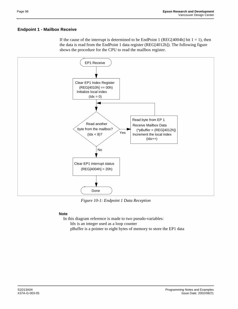
Page 98 Epson Research and DevelopmentVancouver Design Center
Endpoint 1 - Mailbox Receive
If the cause of the interrupt is determined to be EndPoint 1 (REG[4004h] bit 1 = 1), then the data is read from the EndPoint 1 data register (REG[4012h]). The following figure shows the procedure for the CPU to read the mailbox register.
Figure 10-1: Endpoint 1 Data Reception
NoteIn this diagram reference is made to two pseudo-variables:
Idx is an integer used as a loop counterpBuffer is a pointer to eight bytes of memory to store the EP1 data
EP1 Receive
Clear EP1 Index Register
Read another
byte from the mailbox?
(Idx < 8)?
Clear EP1 interrupt status
Read byte from EP 1
Receive Mailbox Data
Initialize local index
Done
(Idx = 0)
(*pBuffer = (REG[4012h])
(REG[4004h] = 20h)
No
Yes
(REG[4010h] == 00h)
Increment the local index(Idx++)
S1D13A04 Programming Notes and ExamplesX37A-G-003-05 Issue Date: 2002/08/21
Epson Research and Development Page 99Vancouver Design Center
Endpoint 3 - FIFO Receive
If the cause of the interrupt is determined to be EndPoint 3, REG[4004h] bit 3 = 1b, then the host controller has sent data to EndPoint 3. Figure 10-2: shows the procedure for reading data from EndPoint 3.
An EndPoint 3 interrupt is generated when the number of bytes in the receive FIFO equal the value in the Receive FIFO Almost Full Threshold register (REG[403Ah], Index[06h]). The default value is sixty bytes. On systems where bulk transfers are used, the default value for the receive FIFO threshold should be satisfactory.
Systems with slow processors, high interrupt service latency, or configured for isochronous operation may have to decrease this value to allow the CPU time to begin reading data before the data transfer overflows the FIFO.
Programming Notes and Examples S1D13A04Issue Date: 2002/08/21 X37A-G-003-05
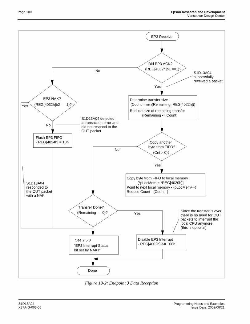
Page 100 Epson Research and DevelopmentVancouver Design Center
Figure 10-2: Endpoint 3 Data Reception
EP3 Receive
No
Yes
Did EP3 ACK?(REG[4032h]b1 ==1)?
EP3 NAK?
(REG[4032h]b2 == 1)?Determine transfer size
Reduce size of remaining transfer
Copy anotherbyte from FIFO?
(Cnt > 0)?
Copy byte from FIFO to local memory
(Count = min(Remaining, REG[4022h]))
(Remaining -= Count)
(*pLocMem = *REG[4020h)]Point to next local memory - (pLocMem++)Reduce Count - (Count--)
Transfer Done?(Remaining == 0)?
Flush EP3 FIFO- REG[4024h] = 10h
Done
See 2.5.3
“EP3 Interrupt Statusbit set by NAKs”
Disable EP3 Interrupt- REG[4002h] &= ~08h
Yes
Yes
Yes
No
No S1D13A04successfullyreceived a packet
Since the transfer is over, there is no need for OUTpackets to interrupt thelocal CPU anymore(this is optional)
S1D13A04responded tothe OUT packetwith a NAK
S1D13A04 detecteda transaction error anddid not respond to theOUT packet
S1D13A04 Programming Notes and ExamplesX37A-G-003-05 Issue Date: 2002/08/21
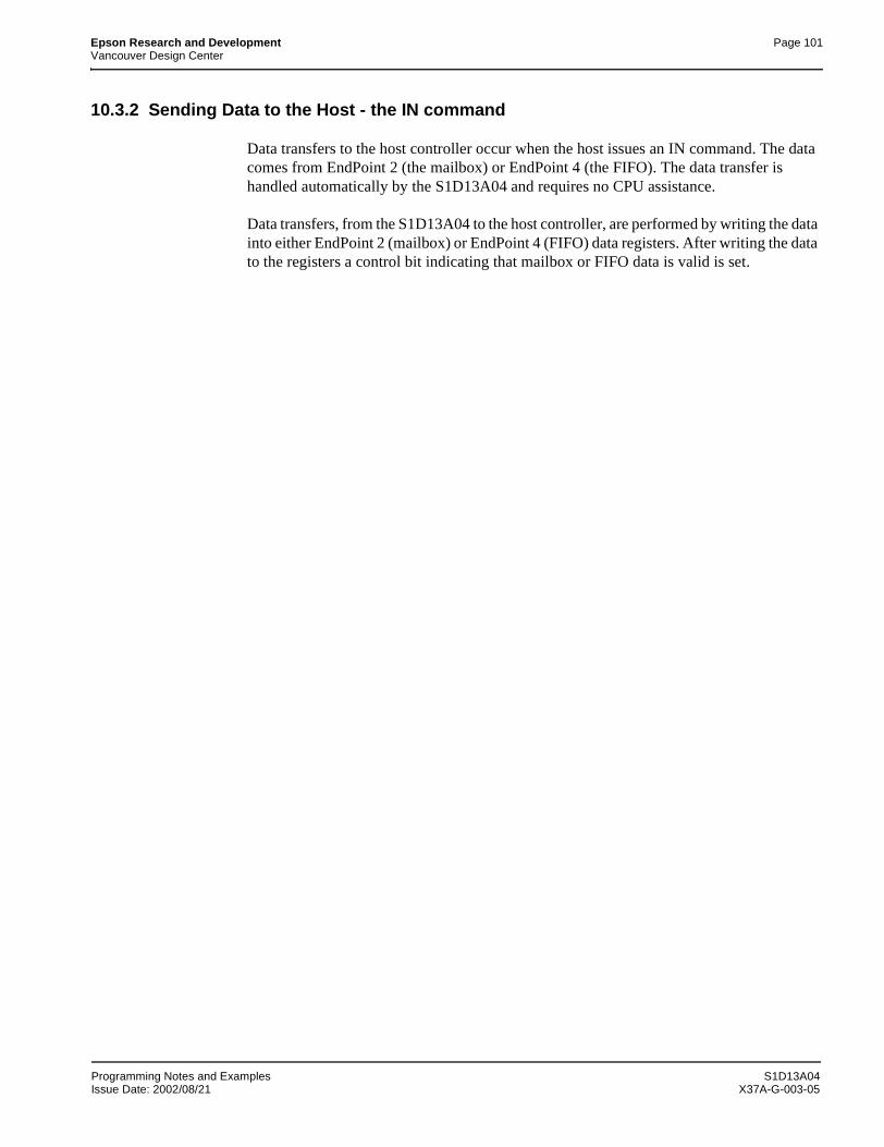
Epson Research and Development Page 101Vancouver Design Center
10.3.2 Sending Data to the Host - the IN command
Data transfers to the host controller occur when the host issues an IN command. The data comes from EndPoint 2 (the mailbox) or EndPoint 4 (the FIFO). The data transfer is handled automatically by the S1D13A04 and requires no CPU assistance.
Data transfers, from the S1D13A04 to the host controller, are performed by writing the data into either EndPoint 2 (mailbox) or EndPoint 4 (FIFO) data registers. After writing the data to the registers a control bit indicating that mailbox or FIFO data is valid is set.
Programming Notes and Examples S1D13A04Issue Date: 2002/08/21 X37A-G-003-05
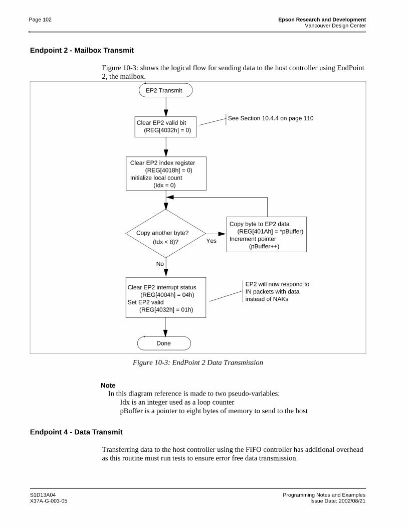
Page 102 Epson Research and DevelopmentVancouver Design Center
Endpoint 2 - Mailbox Transmit
Figure 10-3: shows the logical flow for sending data to the host controller using EndPoint 2, the mailbox.
Figure 10-3: EndPoint 2 Data Transmission
NoteIn this diagram reference is made to two pseudo-variables:
Idx is an integer used as a loop counterpBuffer is a pointer to eight bytes of memory to send to the host
Endpoint 4 - Data Transmit
Transferring data to the host controller using the FIFO controller has additional overhead as this routine must run tests to ensure error free data transmission.
No
Yes
EP2 Transmit
Clear EP2 valid bit(REG[4032h] = 0)
Clear EP2 index register(REG[4018h] = 0)
Initialize local count(Idx = 0)
Copy byte to EP2 data(REG[401Ah] = *pBuffer)
Increment pointer(pBuffer++)
Copy another byte?
(Idx < 8)?
Clear EP2 interrupt status(REG[4004h] = 04h)
Set EP2 valid(REG[4032h] = 01h)
Done
EP2 will now respond toIN packets with datainstead of NAKs
See Section 10.4.4 on page 110
S1D13A04 Programming Notes and ExamplesX37A-G-003-05 Issue Date: 2002/08/21
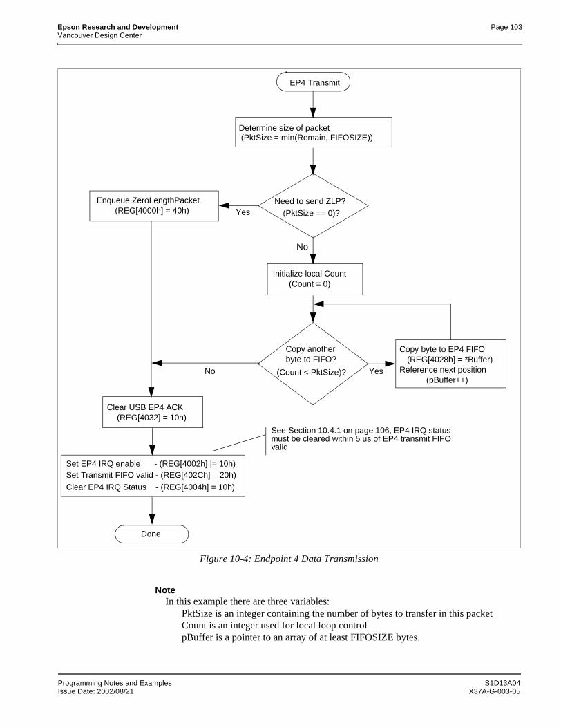
Epson Research and Development Page 103Vancouver Design Center
Figure 10-4: Endpoint 4 Data Transmission
NoteIn this example there are three variables:
PktSize is an integer containing the number of bytes to transfer in this packetCount is an integer used for local loop controlpBuffer is a pointer to an array of at least FIFOSIZE bytes.
No
Yes
EP4 Transmit
Determine size of packet(PktSize = min(Remain, FIFOSIZE))
Need to send ZLP?(PktSize == 0)?
Initialize local Count(Count = 0)
Copy another
(Count < PktSize)?
byte to FIFO?Copy byte to EP4 FIFO
(REG[4028h] = *Buffer)Reference next position
(pBuffer++)
Enqueue ZeroLengthPacket(REG[4000h] = 40h)
Clear USB EP4 ACK(REG[4032] = 10h)
Set EP4 IRQ enable - (REG[4002h] |= 10h)Set Transmit FIFO valid - (REG[402Ch] = 20h)
Clear EP4 IRQ Status - (REG[4004h] = 10h)
Done
YesNo
See Section 10.4.1 on page 106, EP4 IRQ status must be cleared within 5 us of EP4 transmit FIFO valid
Programming Notes and Examples S1D13A04Issue Date: 2002/08/21 X37A-G-003-05
Page 104 Epson Research and DevelopmentVancouver Design Center
To ensure the host controller receives the packet error free, an interrupt handler for EndPoint 4 must be configured and the flow control as shown in the following diagram must be implemented.
S1D13A04 Programming Notes and ExamplesX37A-G-003-05 Issue Date: 2002/08/21
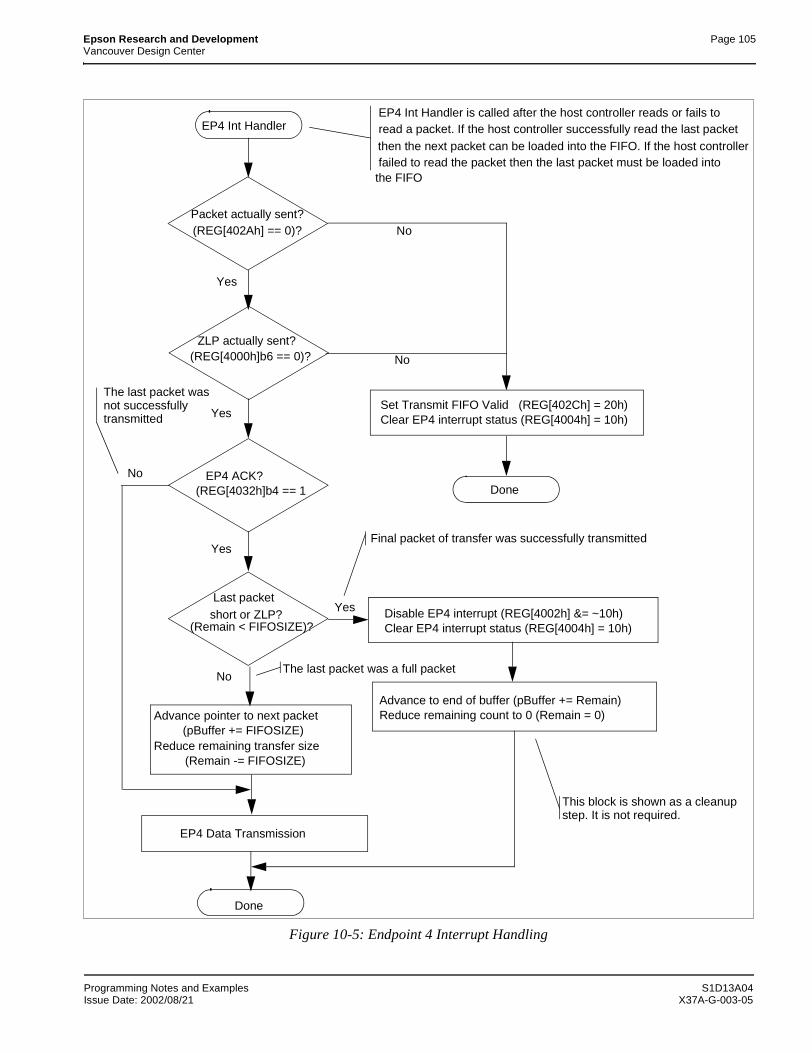
Epson Research and Development Page 105Vancouver Design Center
Figure 10-5: Endpoint 4 Interrupt Handling
Yes
No
EP4 Int Handler
Packet actually sent?(REG[402Ah] == 0)?
ZLP actually sent?(REG[4000h]b6 == 0)?
EP4 ACK?(REG[4032h]b4 == 1
Last packetshort or ZLP?
(Remain < FIFOSIZE)?
Advance pointer to next packet
Reduce remaining transfer size
Disable EP4 interrupt (REG[4002h] &= ~10h)Clear EP4 interrupt status (REG[4004h] = 10h)
Advance to end of buffer (pBuffer += Remain)Reduce remaining count to 0 (Remain = 0)
Done
Set Transmit FIFO Valid (REG[402Ch] = 20h)Clear EP4 interrupt status (REG[4004h] = 10h)
Done
Yes
Yes
Yes
No
No
No
(pBuffer += FIFOSIZE)
(Remain -= FIFOSIZE)
EP4 Data Transmission
EP4 Int Handler is called after the host controller reads or fails toread a packet. If the host controller successfully read the last packetthen the next packet can be loaded into the FIFO. If the host controllerfailed to read the packet then the last packet must be loaded into
This block is shown as a cleanupstep. It is not required.
Final packet of transfer was successfully transmitted
The last packet wasnot successfullytransmitted
The last packet was a full packet
the FIFO
Programming Notes and Examples S1D13A04Issue Date: 2002/08/21 X37A-G-003-05
Page 106 Epson Research and DevelopmentVancouver Design Center
NoteIn the diagram the variables:
pBuffer is a pointer to the local memory buffer containing the data to be transferred to the host controllerRemain is an integer tracking the number of bytes still to be sent.
10.4 Known Issues
This section presents known issues with USB transfers when using the S1D13A04 USB controller.
10.4.1 EP4 NAK Status not set correctly in USB Status Register
The EP4 NAK status bit is not set in the USB Status Register (REG4032h]) when the S1D13A04 responds to an IN request on EP4 with a NAK. As a result, a local CPU receiving an “EP4 Packet Transmitted” interrupt may mistakenly believe a bus error occurred in the most recently transmitted packet.
Work Around
Disable the EP4 Packet Transmitted interrupt when no data is queued for transmission to the local CPU. The basic flow is:
In Chip Initialization Code
Do not enable ‘EP4 Packet Transmitted’ bit in Interrupt Enable Register 0 (REG[4002h]).
When Local Side Wishes to Send Data
1. Put data to transmit in FIFO.
2. Enable ‘EP4 Packet Transmitted’ bit in Interrupt Enable Register 0.
3. Set FIFO Valid (if using FIFO Valid Mode == TRUE). See Section 10.4.2 on page 107 for more information on setting the FIFO Valid.
4. Clear ‘EP4 Packet Transmitted’ status bit in Interrupt Status Register 0 (REG[4004]).
NoteStep 4 is time-critical. It must be performed within 5 µs after Step 3.
In Packet Transmitted Interrupt Routine
Disable ‘EP4 Packet Transmitted’ bit in Interrupt Enable Register 0.
S1D13A04 Programming Notes and ExamplesX37A-G-003-05 Issue Date: 2002/08/21
Epson Research and Development Page 107Vancouver Design Center
10.4.2 Write to EP4 FIFO Valid bit cleared by NAK
After the local CPU sets EP4 FIFO Valid (in Endpoint 4 FIFO Status Register, REG[402Ch]), the S1D13A04 will erroneously clear the EP4 valid bit if the S1D13A04 is concurrently sending a NAK handshake in response to a previous IN token to EP4.
Work Around
The work-around is in the ‘EP4 Packet Transmitted’ interrupt routine. It requires the interrupt routine to know whether the recently queued packet was a zero-length packet or not, so that must be stored as a bit when the packet was loaded into the FIFO. On entry to the ‘EP4 Packet Transmitted’ interrupt routine:
For a non-zero-length Packet
Check the FIFO count. If it is non-zero, this error occurred. In that case, set FIFO Valid again, clear the interrupt status bit, and exit the interrupt routine.
For a zero-length Packet
Check the Software EOT bit (in Control Register, REG[4000h]). If it is set, the FIFO Valid write failed. In that case, set FIFO Valid again, clear the interrupt status bit, and exit the interrupt routine
10.4.3 EP3 Interrupt Status bit set by NAKs
When receiving Bulk OUT packets from a Host PC, the S1D13A04 “Endpoint 3 Interrupt Status” interrupt typically is used to notify the peripheral firmware that a packet has been received. This bit also serves as the “Receive FIFO Valid” bit, so additional packets addressed to Endpoint 3 are NAKed until this status bit is cleared. Once cleared, however, it may become set by another packet which is NAKed by the S1D13A04, causing the Receive FIFO to become “Valid” again. The Host PC may immediately attempt to re-transmit the NAKed packet. The firmware should be written to prevent a cycle in which the FIFO is “Valid” each time that the Host PC sends an OUT packet.
The following rules govern the S1D13A04’s behavior regarding packets received on Endpoint 3:
Rule A. At the end of a received OUT token to EP3 (and before the data is received), the S1D13A04 decides to NAK the packet if the “EP3 Interrupt Status” bit is set, and will therefore throw away data received.
Rule B. At the end of a received packet (including one which is NAKed), the S1D13A04 sets the “EP3 Interrupt Status” bit.
Rule C. Local firmware should clear the “EP3 Interrupt Status” bit after reading all bytes out of the EP3 Receive FIFO.
Programming Notes and Examples S1D13A04Issue Date: 2002/08/21 X37A-G-003-05
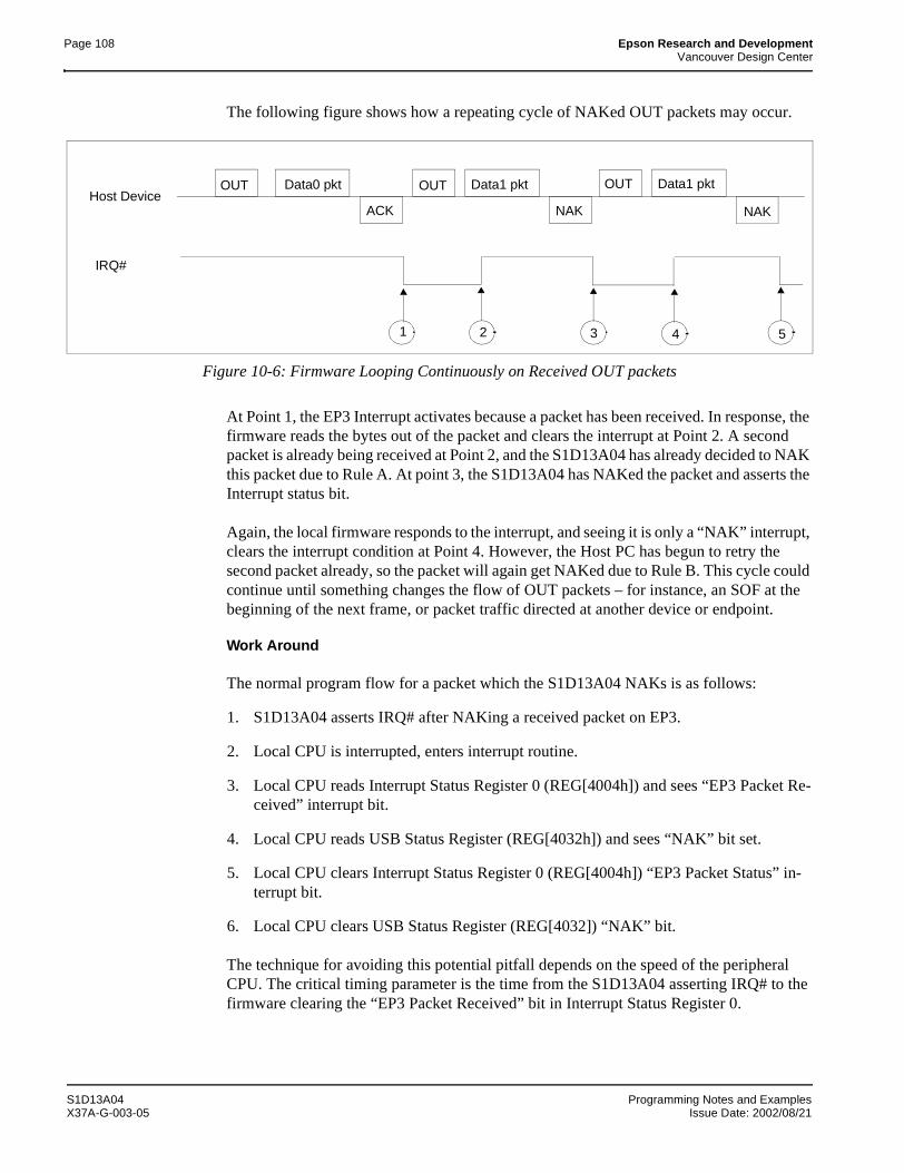
Page 108 Epson Research and DevelopmentVancouver Design Center
The following figure shows how a repeating cycle of NAKed OUT packets may occur.
Figure 10-6: Firmware Looping Continuously on Received OUT packets
At Point 1, the EP3 Interrupt activates because a packet has been received. In response, the firmware reads the bytes out of the packet and clears the interrupt at Point 2. A second packet is already being received at Point 2, and the S1D13A04 has already decided to NAK this packet due to Rule A. At point 3, the S1D13A04 has NAKed the packet and asserts the Interrupt status bit.
Again, the local firmware responds to the interrupt, and seeing it is only a “NAK” interrupt, clears the interrupt condition at Point 4. However, the Host PC has begun to retry the second packet already, so the packet will again get NAKed due to Rule B. This cycle could continue until something changes the flow of OUT packets – for instance, an SOF at the beginning of the next frame, or packet traffic directed at another device or endpoint.
Work Around
The normal program flow for a packet which the S1D13A04 NAKs is as follows:
1. S1D13A04 asserts IRQ# after NAKing a received packet on EP3.
2. Local CPU is interrupted, enters interrupt routine.
3. Local CPU reads Interrupt Status Register 0 (REG[4004h]) and sees “EP3 Packet Re-ceived” interrupt bit.
4. Local CPU reads USB Status Register (REG[4032h]) and sees “NAK” bit set.
5. Local CPU clears Interrupt Status Register 0 (REG[4004h]) “EP3 Packet Status” in-terrupt bit.
6. Local CPU clears USB Status Register (REG[4032]) “NAK” bit.
The technique for avoiding this potential pitfall depends on the speed of the peripheral CPU. The critical timing parameter is the time from the S1D13A04 asserting IRQ# to the firmware clearing the “EP3 Packet Received” bit in Interrupt Status Register 0.
Host Device
IRQ#
OUT Data0 pkt
ACK
OUT Data1 pkt
NAK
OUT
NAK
Data1 pkt
21 3 4 5
S1D13A04 Programming Notes and ExamplesX37A-G-003-05 Issue Date: 2002/08/21
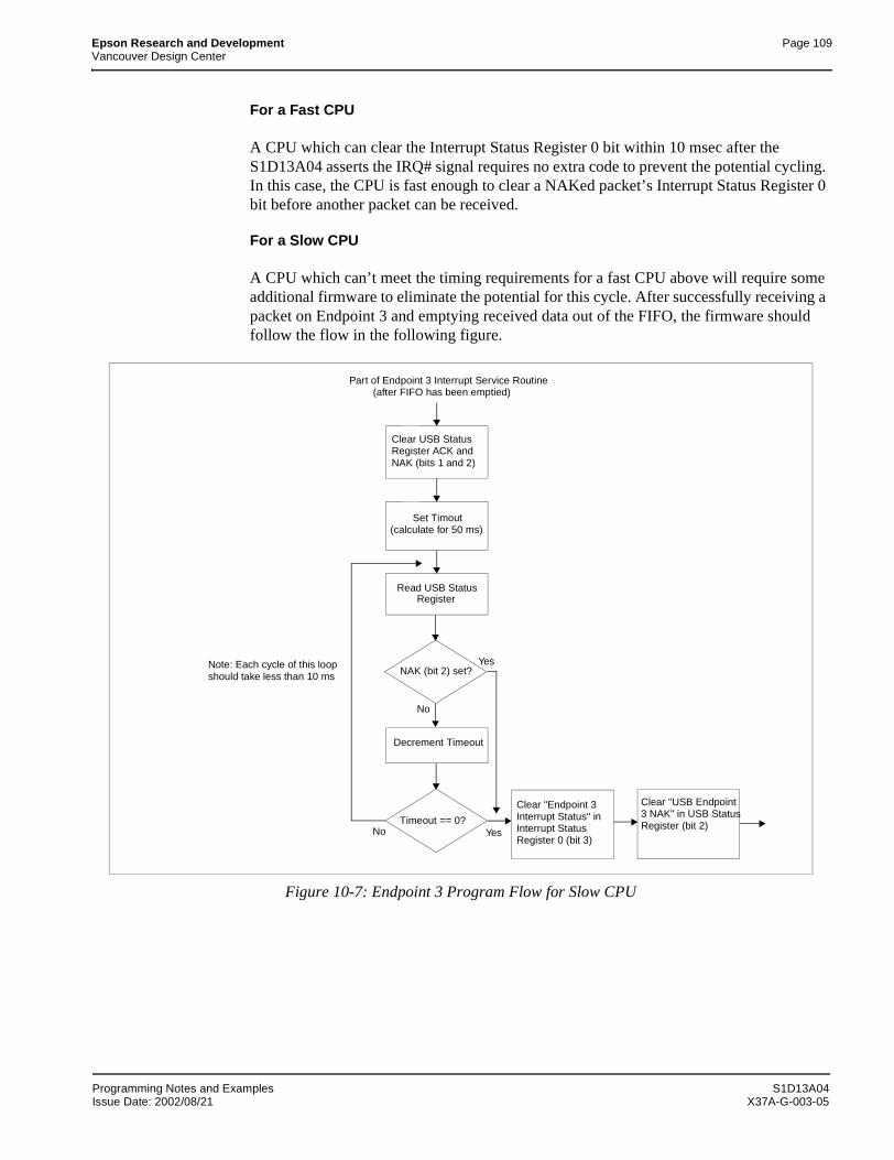
Epson Research and Development Page 109Vancouver Design Center
For a Fast CPU
A CPU which can clear the Interrupt Status Register 0 bit within 10 msec after the S1D13A04 asserts the IRQ# signal requires no extra code to prevent the potential cycling. In this case, the CPU is fast enough to clear a NAKed packet’s Interrupt Status Register 0 bit before another packet can be received.
For a Slow CPU
A CPU which can’t meet the timing requirements for a fast CPU above will require some additional firmware to eliminate the potential for this cycle. After successfully receiving a packet on Endpoint 3 and emptying received data out of the FIFO, the firmware should follow the flow in the following figure.
Figure 10-7: Endpoint 3 Program Flow for Slow CPU
Part of Endpoint 3 Interrupt Service Routine(after FIFO has been emptied)
Clear USB StatusRegister ACK andNAK (bits 1 and 2)
Set Timout(calculate for 50 ms)
Read USB StatusRegister
NAK (bit 2) set?
Decrement Timeout
Timeout == 0?
Yes
YesNo
No
Clear "Endpoint 3Interrupt Status" inInterrupt StatusRegister 0 (bit 3)
Clear "USB Endpoint3 NAK" in USB StatusRegister (bit 2)
Note: Each cycle of this loopshould take less than 10 ms
Programming Notes and Examples S1D13A04Issue Date: 2002/08/21 X37A-G-003-05
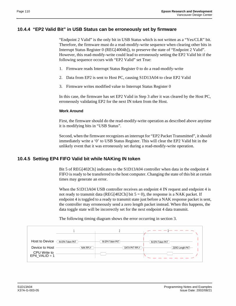
Page 110 Epson Research and DevelopmentVancouver Design Center
10.4.4 “EP2 Valid Bit” in USB Status can be erroneously set by firmware
“Endpoint 2 Valid” is the only bit in USB Status which is not written as a “Yes/CLR” bit. Therefore, the firmware must do a read-modify-write sequence when clearing other bits in Interrupt Status Register 0 (REG[4004h]), to preserve the state of “Endpoint 2 Valid”. However, this read-modify-write could lead to erroneously setting the EP2 Valid bit if the following sequence occurs with “EP2 Valid” set True:
1. Firmware reads Interrupt Status Register 0 to do a read-modify-write
2. Data from EP2 is sent to Host PC, causing S1D13A04 to clear EP2 Valid
3. Firmware writes modified value to Interrupt Status Register 0
In this case, the firmware has set EP2 Valid in Step 3 after it was cleared by the Host PC, erroneously validating EP2 for the next IN token from the Host.
Work Around
First, the firmware should do the read-modify-write operation as described above anytime it is modifying bits in “USB Status”.
Second, when the firmware recognizes an interrupt for “EP2 Packet Transmitted”, it should immediately write a ‘0’ to USB Status Register. This will clear the EP2 Valid bit in the unlikely event that it was erroneously set during a read-modify-write operation.
10.4.5 Setting EP4 FIFO Valid bit while NAKing IN token
Bit 5 of REG[402Ch] indicates to the S1D13A04 controller when data in the endpoint 4 FIFO is ready to be transferred to the host computer. Changing the state of this bit at certain times may generate an error.
When the S1D13A04 USB controller receives an endpoint 4 IN request and endpoint 4 is not ready to transmit data (REG[402Ch] bit 5 = 0), the response is a NAK packet. If endpoint 4 is toggled to a ready to transmit state just before a NAK response packet is sent, the controller may erroneously send a zero length packet instead. When this happens, the data toggle state will be incorrectly set for the next endpoint 4 data transmit.
The following timing diagram shows the error occurring in section 3.
Host to Device
Device to Host
CPU Write to EP4_VALID = 1
1 2 3
IN EP4 Token PKT IN EP4 Token PKT IN EP4 Token PKT
NAK RPLY DATA PKT RPLY ZERO Length PKT
S1D13A04 Programming Notes and ExamplesX37A-G-003-05 Issue Date: 2002/08/21
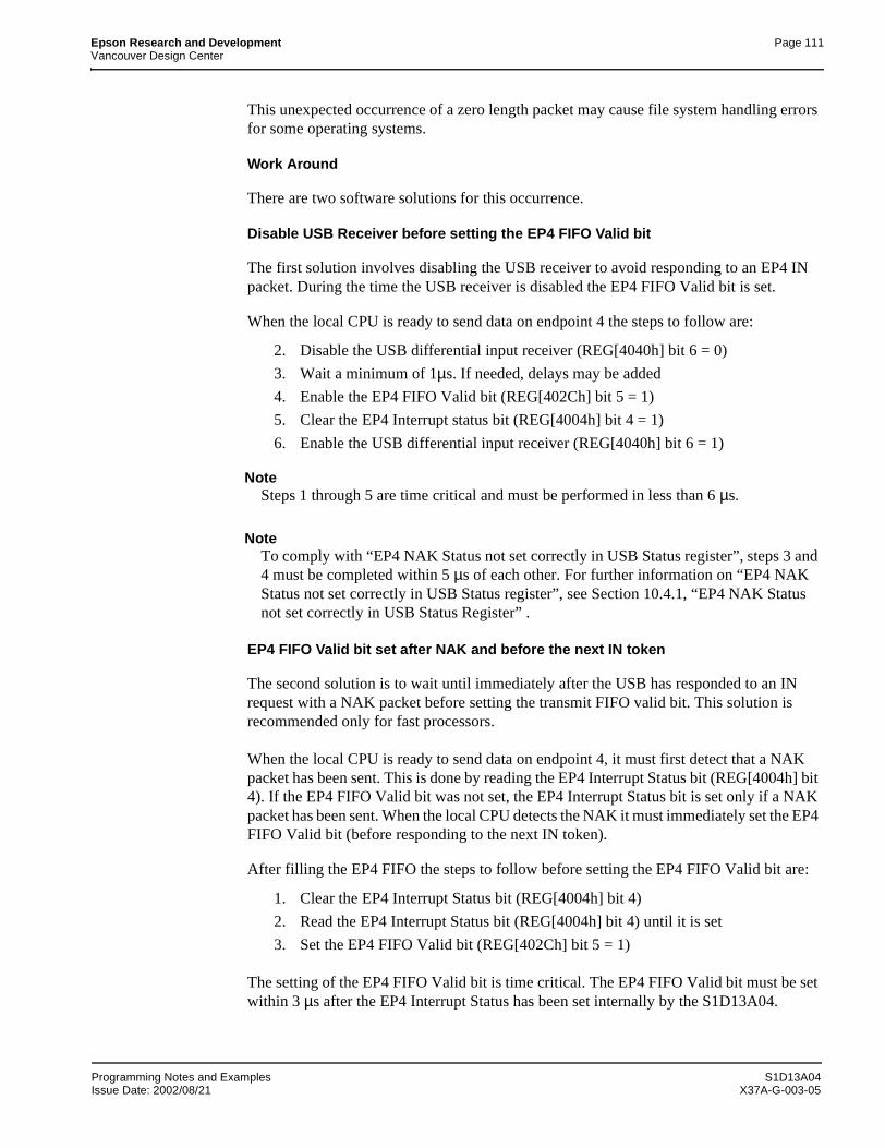
Epson Research and Development Page 111Vancouver Design Center
This unexpected occurrence of a zero length packet may cause file system handling errors for some operating systems.
Work Around
There are two software solutions for this occurrence.
Disable USB Receiver before setting the EP4 FIFO Valid bit
The first solution involves disabling the USB receiver to avoid responding to an EP4 IN packet. During the time the USB receiver is disabled the EP4 FIFO Valid bit is set.
When the local CPU is ready to send data on endpoint 4 the steps to follow are:
2. Disable the USB differential input receiver (REG[4040h] bit 6 = 0)
3. Wait a minimum of 1µs. If needed, delays may be added
4. Enable the EP4 FIFO Valid bit (REG[402Ch] bit 5 = 1)
5. Clear the EP4 Interrupt status bit (REG[4004h] bit 4 = 1)
6. Enable the USB differential input receiver (REG[4040h] bit 6 = 1)
NoteSteps 1 through 5 are time critical and must be performed in less than 6 µs.
NoteTo comply with “EP4 NAK Status not set correctly in USB Status register”, steps 3 and 4 must be completed within 5 µs of each other. For further information on “EP4 NAK Status not set correctly in USB Status register”, see Section 10.4.1, “EP4 NAK Status not set correctly in USB Status Register” .
EP4 FIFO Valid bit set after NAK and before the next IN token
The second solution is to wait until immediately after the USB has responded to an IN request with a NAK packet before setting the transmit FIFO valid bit. This solution is recommended only for fast processors.
When the local CPU is ready to send data on endpoint 4, it must first detect that a NAK packet has been sent. This is done by reading the EP4 Interrupt Status bit (REG[4004h] bit 4). If the EP4 FIFO Valid bit was not set, the EP4 Interrupt Status bit is set only if a NAK packet has been sent. When the local CPU detects the NAK it must immediately set the EP4 FIFO Valid bit (before responding to the next IN token).
After filling the EP4 FIFO the steps to follow before setting the EP4 FIFO Valid bit are:
1. Clear the EP4 Interrupt Status bit (REG[4004h] bit 4)
2. Read the EP4 Interrupt Status bit (REG[4004h] bit 4) until it is set
3. Set the EP4 FIFO Valid bit (REG[402Ch] bit 5 = 1)
The setting of the EP4 FIFO Valid bit is time critical. The EP4 FIFO Valid bit must be set within 3 µs after the EP4 Interrupt Status has been set internally by the S1D13A04.
Programming Notes and Examples S1D13A04Issue Date: 2002/08/21 X37A-G-003-05
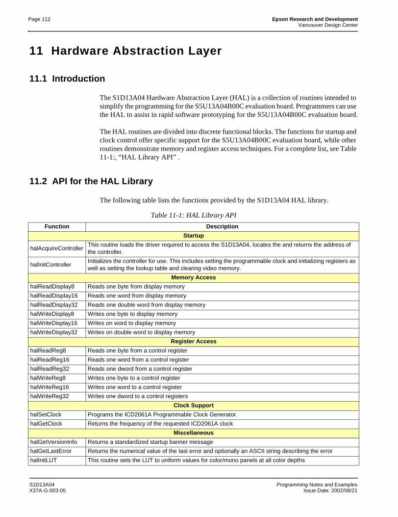
Page 112 Epson Research and DevelopmentVancouver Design Center
11 Hardware Abstraction Layer
11.1 Introduction
The S1D13A04 Hardware Abstraction Layer (HAL) is a collection of routines intended to simplify the programming for the S5U13A04B00C evaluation board. Programmers can use the HAL to assist in rapid software prototyping for the S5U13A04B00C evaluation board.
The HAL routines are divided into discrete functional blocks. The functions for startup and clock control offer specific support for the S5U13A04B00C evaluation board, while other routines demonstrate memory and register access techniques. For a complete list, see Table 11-1:, “HAL Library API” .
11.2 API for the HAL Library
The following table lists the functions provided by the S1D13A04 HAL library.
Table 11-1: HAL Library API
Function Description
Startup
halAcquireControllerThis routine loads the driver required to access the S1D13A04, locates the and returns the address of the controller.
halInitControllerInitializes the controller for use. This includes setting the programmable clock and initializing registers as well as setting the lookup table and clearing video memory.
Memory Access
halReadDisplay8 Reads one byte from display memory
halReadDisplay16 Reads one word from display memory
halReadDisplay32 Reads one double word from display memory
halWriteDisplay8 Writes one byte to display memory
halWriteDisplay16 Writes on word to display memory
halWriteDisplay32 Writes on double word to display memory
Register Access
halReadReg8 Reads one byte from a control register
halReadReg16 Reads one word from a control register
halReadReg32 Reads one dword from a control register
halWriteReg8 Writes one byte to a control register
halWriteReg16 Writes one word to a control register
halWriteReg32 Writes one dword to a control registers
Clock Support
halSetClock Programs the ICD2061A Programmable Clock Generator.
halGetClock Returns the frequency of the requested ICD2061A clock
Miscellaneous
halGetVersionInfo Returns a standardized startup banner message
halGetLastError Returns the numerical value of the last error and optionally an ASCII string describing the error
halInitLUT This routine sets the LUT to uniform values for color/mono panels at all color depths
S1D13A04 Programming Notes and ExamplesX37A-G-003-05 Issue Date: 2002/08/21

Epson Research and Development Page 113Vancouver Design Center
11.2.1 Startup Routines
There are two routines dedicated to startup and initializing the S1D13A04. Typically these two functions are the first two HAL routines a program will call.
The startup routines locate the S1D13A04 controller and initialize HAL data structures. As the name suggests, the initialization routine prepares the S1D13A04 for use. Splitting the startup functionality allows programs to start and locate the S1D13A04 but delay or possibly never initialize the controller.
Boolean halAcquireController(UInt32 * pMem, UInt32 * pReg)
Description: This routine initializes data structures and initiates the link between the application soft-ware and the hardware. When the S1D13A04 HAL is used this routine must be the first HAL function called.
On PCI platforms, the routine attempts to load the S1D13xxx driver. If the driver loads successfully then a check is made for the existence of an S1D13A04.
Parameters: pMem Pointer to an unsigned 32-bit integer which will receive the offset to the firstbyte of display memory. The offset may be cast to a pointer to accessdisplay memory.
pReg Pointer to an unsigned 32-bit integer which will receive the offset to the firstbyte of register space. The offset may be cast to a pointer and to accessS1D13A04 registers.
On Win32 systems the returned offsets correspond to a linear addresseswithin the callers address space.
Return Value: TRUE (non-zero) if the routine is able to locate an S1D13A04.pMem will contain the offset to the first byte of display memory.pRegs will contain the address of the first 13A04 control register.
FALSE (zero) if an S1D13A04 is not located.pMem and pRegs will be undefined.If additional error information is required call halGetLastError().
Note1. This routine must be called before any other HAL routine is called.2. For programs written for the S1D13A04 evaluation board, an application may call
this routine to obtain pointers to the registers and display memory and then performall S1D13A04 accesses directly.
3. This routine does not modify S1D13A04 registers or memory.
Programming Notes and Examples S1D13A04Issue Date: 2002/08/21 X37A-G-003-05
Page 114 Epson Research and DevelopmentVancouver Design Center
Boolean halInitController(UInt32 Flags)
Description: This routine performs the initialization portion of the startup sequence.Initialization of the S1D13A04 evaluation board consists of several steps:- Program the ICD2061A clock generator- Set the initial state of the control- Set the LUT to its default value- Clear video memory
All display memory and nearly every control register can or will be affected by the initial-ization.
Any, or all, of the initialization steps may be bypassed according to values contained in the Flags parameter. This allows for conditional run-time changes to the initialization.
Parameters: Flags contains initialization specific information. The default action of the HAL is to per-form all initialization steps. Flags contain specific instructions for bypassing certain ini-tialization steps. The values for Flags are:
fDONT_RESETThe first step of the initialization process is to perform a software. Setting this flag bypasses the software reset.
fDONT_SET_CLOCKSSetting this flag causes initialization to skip programming the ICD2061Aclock generator. Normally the clock on the S5U13A04B00C is programmedto configured values during initialization.
fDONT_INIT_REGSBypass register initialization. Normally the init process sets the registervalues to a known state. Setting this flag bypasses this step.
fDONT_INIT_LUTBypass look-up table initialization.
fDONT_CLEAR_MEMThe final step of the initialization process is to clear video display memory. Setting this flag will bypass this step.
Return Value: TRUE (non-zero) if the initialization was successful.
FALSE (zero) if the HAL was unable to initialize the S1D13A04If additional error information is required call halGetLastError()
S1D13A04 Programming Notes and ExamplesX37A-G-003-05 Issue Date: 2002/08/21
Epson Research and Development Page 115Vancouver Design Center
11.2.2 Memory Access
The S1D13A04 HAL includes six memory access functions. The primary purpose of the memory access functions is to demonstrate how to access display memory using the C programming language. Most programs that need to access memory will bypass the HAL and access memory directly.
UInt8 halReadDisplay8(UInt32 Offset)
Description: Reads and returns the value of one byte of display memory.
Parameters: Offset A 32 bit offset to the byte to be read from display memory
Return Value: The value of the byte at the requested offset.
UInt16 halReadDisplay16(UInt32 Offset)
Description: Reads and returns the value of one word of display memory.
Parameters: Offset A 32 bit byte offset to the word to be read from display memoryTo prevent system slowdowns and possibly memory faults, Offset should bea word multiple.
Return Value: The value of the word at the requested offset.
UInt32 halReadDisplay32(UInt32 Offset)
Description: Reads and returns the value of one dword of display memory.
Parameters: Offset A 32 bit byte offset to the dword to be read from display memory.To prevent system slowdowns and possibly memory faults, Offset should bea dword multiple.
Return Value: The value of the dword at the requested offset.
void halWriteDisplay8(UInt32 Offset, UInt8 Value, UInt32 Count)
Description: Writes a byte into display memory at the requested address.
Parameters: Offset A 32 bit byte offset to the byte to be written to display memory.
Value The byte value to be written to display memory.
Count The number of times to repeat Value in memory. By including a count (orloop) value this function can efficiently fill display memory.
Return Value: Nothing.
Programming Notes and Examples S1D13A04Issue Date: 2002/08/21 X37A-G-003-05
Page 116 Epson Research and DevelopmentVancouver Design Center
void halWriteDisplay16(UInt32 Offset, UInt16 Value, UInt32 Count)
Description: Writes a word into display memory at the requested offset.
Parameters: Offset a 32 bit byte offset to the byte to be written to display memory. To preventsystem slowdowns and possibly memory faults, Offset should be a wordmultiple.
Value the word value to be written to display memory.
Count the number of times to repeat the Value in memory. By including a count (orloop) value this function can efficiently fill display memory.
Return Value: Nothing.
void halWriteDisplay32(UInt32 Offset, UInt32 Value, UInt32 Count)
Description: Writes a dword into display memory at the requested offset.
Parameters: Offset A 32 bit byte offset to the byte to be written to display memory. To preventsystem slowdowns and possibly memory faults, Offset should be a dwordmultiple.
Value The dword value to be written to display memory.
Count The number of times to repeat the Value in memory. By including a count(or loop) value this function can efficiently fill display memory.
Return Value: Nothing.
11.2.3 Register Access
The S1D13A04 HAL includes six register access functions. The primary purpose of the register access functions is to demonstrate how to access the S1D13A04 control registers using the C programming language. Most programs that need to access the registers will bypass the HAL and access the registers directly.
UInt8 halReadReg8(UInt32 Index)
Description: Reads and returns the contents of one byte of an S1D13A04 register at the requested off-set. No S1D13A04 registers are changed
Parameters: Index 32 bit offset to the register to read. Index is zero based from the beginningof register address space. (e.g. if Index == 04h then the Memory ClockConfiguration register will be read and if Index == 8000h then the BitBLTControl Register will be read)
Return Value: The value read from the register.
Use caution in selecting the index and when interpreting values returned from halReadReg8() to ensure the correct meaning is given to the values. Changing between big endian and little endian will move relative register offsets.
S1D13A04 Programming Notes and ExamplesX37A-G-003-05 Issue Date: 2002/08/21
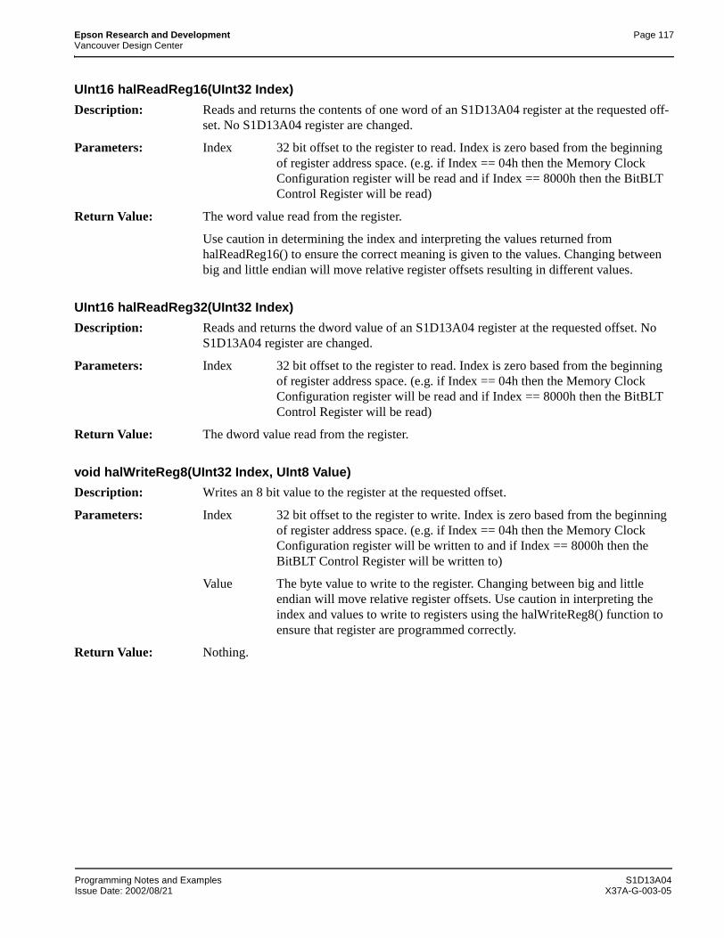
Epson Research and Development Page 117Vancouver Design Center
UInt16 halReadReg16(UInt32 Index)
Description: Reads and returns the contents of one word of an S1D13A04 register at the requested off-set. No S1D13A04 register are changed.
Parameters: Index 32 bit offset to the register to read. Index is zero based from the beginningof register address space. (e.g. if Index == 04h then the Memory ClockConfiguration register will be read and if Index == 8000h then the BitBLTControl Register will be read)
Return Value: The word value read from the register.
Use caution in determining the index and interpreting the values returned from halReadReg16() to ensure the correct meaning is given to the values. Changing between big and little endian will move relative register offsets resulting in different values.
UInt16 halReadReg32(UInt32 Index)
Description: Reads and returns the dword value of an S1D13A04 register at the requested offset. No S1D13A04 register are changed.
Parameters: Index 32 bit offset to the register to read. Index is zero based from the beginningof register address space. (e.g. if Index == 04h then the Memory ClockConfiguration register will be read and if Index == 8000h then the BitBLTControl Register will be read)
Return Value: The dword value read from the register.
void halWriteReg8(UInt32 Index, UInt8 Value)
Description: Writes an 8 bit value to the register at the requested offset.
Parameters: Index 32 bit offset to the register to write. Index is zero based from the beginningof register address space. (e.g. if Index == 04h then the Memory ClockConfiguration register will be written to and if Index == 8000h then theBitBLT Control Register will be written to)
Value The byte value to write to the register. Changing between big and littleendian will move relative register offsets. Use caution in interpreting theindex and values to write to registers using the halWriteReg8() function toensure that register are programmed correctly.
Return Value: Nothing.
Programming Notes and Examples S1D13A04Issue Date: 2002/08/21 X37A-G-003-05
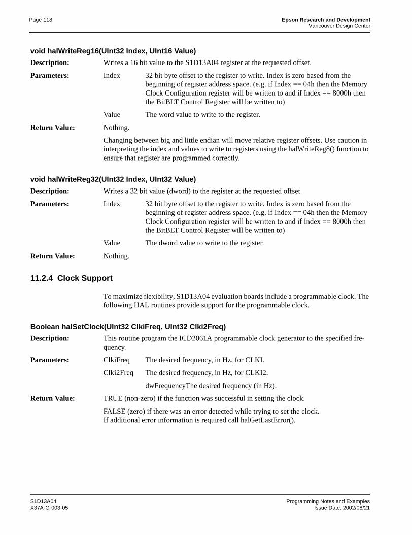
Page 118 Epson Research and DevelopmentVancouver Design Center
void halWriteReg16(UInt32 Index, UInt16 Value)
Description: Writes a 16 bit value to the S1D13A04 register at the requested offset.
Parameters: Index 32 bit byte offset to the register to write. Index is zero based from thebeginning of register address space. (e.g. if Index == 04h then the MemoryClock Configuration register will be written to and if Index == 8000h thenthe BitBLT Control Register will be written to)
Value The word value to write to the register.
Return Value: Nothing.
Changing between big and little endian will move relative register offsets. Use caution in interpreting the index and values to write to registers using the halWriteReg8() function to ensure that register are programmed correctly.
void halWriteReg32(UInt32 Index, UInt32 Value)
Description: Writes a 32 bit value (dword) to the register at the requested offset.
Parameters: Index 32 bit byte offset to the register to write. Index is zero based from thebeginning of register address space. (e.g. if Index == 04h then the MemoryClock Configuration register will be written to and if Index == 8000h thenthe BitBLT Control Register will be written to)
Value The dword value to write to the register.
Return Value: Nothing.
11.2.4 Clock Support
To maximize flexibility, S1D13A04 evaluation boards include a programmable clock. The following HAL routines provide support for the programmable clock.
Boolean halSetClock(UInt32 ClkiFreq, UInt32 Clki2Freq)
Description: This routine program the ICD2061A programmable clock generator to the specified fre-quency.
Parameters: ClkiFreq The desired frequency, in Hz, for CLKI.
Clki2Freq The desired frequency, in Hz, for CLKI2.
dwFrequencyThe desired frequency (in Hz).
Return Value: TRUE (non-zero) if the function was successful in setting the clock.
FALSE (zero) if there was an error detected while trying to set the clock.If additional error information is required call halGetLastError().
S1D13A04 Programming Notes and ExamplesX37A-G-003-05 Issue Date: 2002/08/21
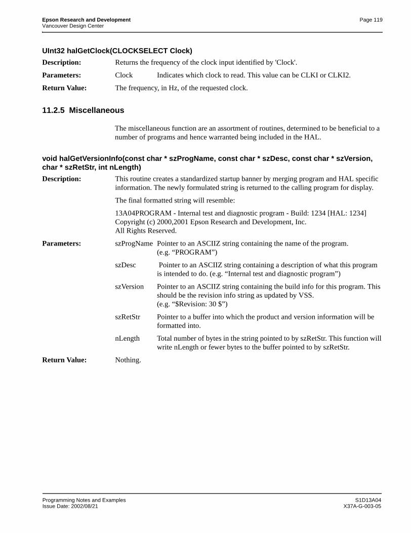
Epson Research and Development Page 119Vancouver Design Center
UInt32 halGetClock(CLOCKSELECT Clock)
Description: Returns the frequency of the clock input identified by 'Clock'.
Parameters: Clock Indicates which clock to read. This value can be CLKI or CLKI2.
Return Value: The frequency, in Hz, of the requested clock.
11.2.5 Miscellaneous
The miscellaneous function are an assortment of routines, determined to be beneficial to a number of programs and hence warranted being included in the HAL.
void halGetVersionInfo(const char * szProgName, const char * szDesc, const char * szVersion, char * szRetStr, int nLength)
Description: This routine creates a standardized startup banner by merging program and HAL specific information. The newly formulated string is returned to the calling program for display.
The final formatted string will resemble:
13A04PROGRAM - Internal test and diagnostic program - Build: 1234 [HAL: 1234]Copyright (c) 2000,2001 Epson Research and Development, Inc.All Rights Reserved.
Parameters: szProgName Pointer to an ASCIIZ string containing the name of the program.(e.g. “PROGRAM”)
szDesc Pointer to an ASCIIZ string containing a description of what this programis intended to do. (e.g. “Internal test and diagnostic program”)
szVersion Pointer to an ASCIIZ string containing the build info for this program. Thisshould be the revision info string as updated by VSS.(e.g. “$Revision: 30 $”)
szRetStr Pointer to a buffer into which the product and version information will beformatted into.
nLength Total number of bytes in the string pointed to by szRetStr. This function willwrite nLength or fewer bytes to the buffer pointed to by szRetStr.
Return Value: Nothing.
Programming Notes and Examples S1D13A04Issue Date: 2002/08/21 X37A-G-003-05
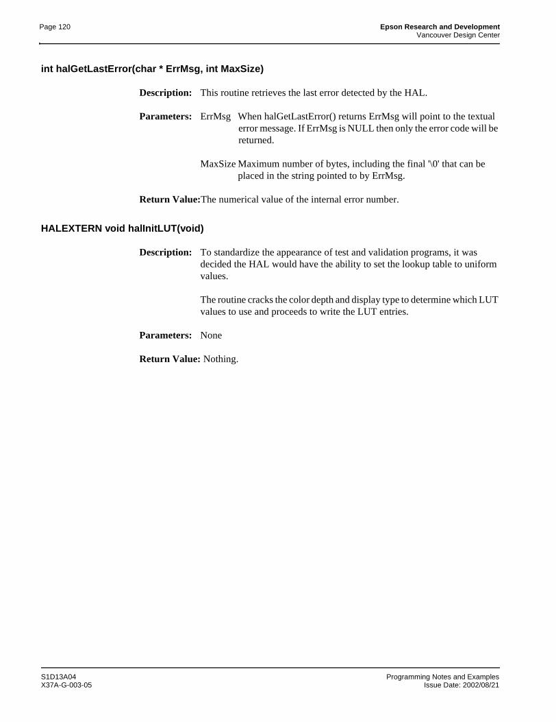
Page 120 Epson Research and DevelopmentVancouver Design Center
int halGetLastError(char * ErrMsg, int MaxSize)
Description: This routine retrieves the last error detected by the HAL.
Parameters: ErrMsg When halGetLastError() returns ErrMsg will point to the textual error message. If ErrMsg is NULL then only the error code will be returned.
MaxSize Maximum number of bytes, including the final '\0' that can be placed in the string pointed to by ErrMsg.
Return Value:The numerical value of the internal error number.
HALEXTERN void halInitLUT(void)
Description: To standardize the appearance of test and validation programs, it was decided the HAL would have the ability to set the lookup table to uniform values.
The routine cracks the color depth and display type to determine which LUT values to use and proceeds to write the LUT entries.
Parameters: None
Return Value: Nothing.
S1D13A04 Programming Notes and ExamplesX37A-G-003-05 Issue Date: 2002/08/21
Epson Research and Development Page 121Vancouver Design Center
12 Sample Code
Example source code demonstrating programming the S1D13A04 using the HAL library is available on the internet at www.erd.epson.com.
Programming Notes and Examples S1D13A04Issue Date: 2002/08/21 X37A-G-003-05

Page 122 Epson Research and DevelopmentVancouver Design Center
13 Sales and Technical Support
JapanSeiko Epson CorporationElectronic Devices Marketing Division421-8, Hino, Hino-shiTokyo 191-8501, JapanTel: 042-587-5812Fax: 042-587-5564http://www.epson.co.jp/
Hong KongEpson Hong Kong Ltd.20/F., Harbour Centre25 Harbour RoadWanchai, Hong KongTel: 2585-4600Fax: 2827-4346http://www.epson.com.hk/
TaiwanEpson Taiwan Technology & Trading Ltd.10F, No. 287Nanking East RoadSec. 3, Taipei, TaiwanTel: 02-2717-7360Fax: 02-2712-9164http://www.epson.com.tw/
SingaporeEpson Singapore Pte., Ltd.No. 1Temasek Avenue #36-00Millenia TowerSingapore, 039192Tel: 337-7911Fax: 334-2716http://www.epson.com.sg/
EuropeEpson Europe Electronics GmbHRiesstrasse 1580992 Munich, GermanyTel: 089-14005-0Fax: 089-14005-110http://www.epson-electronics.de/
North AmericaEpson Electronics America, Inc.150 River Oaks ParkwaySan Jose, CA 95134, USATel: (408) 922-0200Fax: (408) 922-0238http://www.eea.epson.com/
S1D13A04 Programming Notes and ExamplesX37A-G-003-05 Issue Date: 2002/08/21
Epson Research and Development Page 1Vancouver Design Center
READ-ONLY CONFIGURATION REGISTERS
CLOCK CONFIGURATION REGISTERS
PANEL CONFIGURATION REGISTERS
LOOK-UP TABLE REGISTERS
Product Information RegisterREG[00h] Default = 2Cxx282Ch Read Only
Product Code Revision Code n/a CNF[6:4] Status Reserved CNF[2:0] Status
31 30 29 28 27 26 25 24 23 22 21 20 19 18 17 16
Display Buffer Size Product Code Revision Code
15 14 13 12 11 10 9 8 7 6 5 4 3 2 1 0
Memory Clock Configuration RegisterREG[04h] Default = 00000000h Read/Write
n/a
31 30 29 28 27 26 25 24 23 22 21 20 19 18 17 16
n/a MCLK Divide Select Reserved
15 14 13 12 11 10 9 8 7 6 5 4 3 2 1 0
Pixel Clock Configuration RegisterREG[08h] Default = 00000000h Read/Write
n/a
31 30 29 28 27 26 25 24 23 22 21 20 19 18 17 16
n/a PCLK Divide Select n/a PCLK Source Select
15 14 13 12 11 10 9 8 7 6 5 4 3 2 1 0
Panel Type & MOD Rate RegisterREG[0Ch] Default = 00000000h Read/Write
n/a MOD Rate
31 30 29 28 27 26 25 24 23 22 21 20 19 18 17 16
n/aPanel Data
Format Select
Color/ Mono Panel Select
Panel Data Width‘Direct’
HR-TFT Res Select
n/a Panel Type
15 14 13 12 11 10 9 8 7 6 5 4 3 2 1 0
Display Settings RegisterREG[10h] Default = 00000000h Read/Write
n/aPixel
Doubling Vertical
Pixel Doubling
Horiz.
Display Blank
Dithering Disable
n/aSW Video
Invert
PIP+ Window Enable
n/a SwivelView Mode Select
31 30 29 28 27 26 25 24 23 22 21 20 19 18 17 16
n/aBits-per-pixel Select
(actual value: 1, 2, 4, 8, 16 bpp)
15 14 13 12 11 10 9 8 7 6 5 4 3 2 1 0
Power Save Configuration RegisterREG[14h] Default = 00000010h Read/Write
n/a
31 30 29 28 27 26 25 24 23 22 21 20 19 18 17 16
n/aVNDP Status (RO)
Memory Power Save Status (RO)
n/aPower Save
Enablen/a
‘Direct’HR-TFT
GPO Control
15 14 13 12 11 10 9 8 7 6 5 4 3 2 1 0
Look-Up Table Write RegisterREG[18h] Default = 00000000h Write Only
LUT Write Address LUT Red Write Data n/a
31 30 29 28 27 26 25 24 23 22 21 20 19 18 17 16
LUT Green Write Data n/a LUT Blue Write Data n/a
15 14 13 12 11 10 9 8 7 6 5 4 3 2 1 0
Look-Up Table Read RegisterREG[1Ch] Default = 00000000h Write Only (bits 31-24)/Read Only
LUT Read Address (write only) LUT Red Read Data n/a
31 30 29 28 27 26 25 24 23 22 21 20 19 18 17 16
LUT Green Read Data n/a LUT Blue Read Data n/a
15 14 13 12 11 10 9 8 7 6 5 4 3 2 1 0
Register Summary S1D13A04Issue Date: 01/10/02 X37A-R-001-01
Page 2 Epson Research and DevelopmentVancouver Design Center
DISPLAY MODE REGISTERSHorizontal Total RegisterREG[20h] Default = 00000000h Read/Write
n/a
31 30 29 28 27 26 25 24 23 22 21 20 19 18 17 16
n/a Horizontal Total bits 6-0
15 14 13 12 11 10 9 8 7 6 5 4 3 2 1 0
Horizontal Display Period RegisterREG[24h] Default = 00000000h Read/Write
n/a
31 30 29 28 27 26 25 24 23 22 21 20 19 18 17 16
n/a Horizontal Display Period bits 6-0
15 14 13 12 11 10 9 8 7 6 5 4 3 2 1 0
Horizontal Display Period Start Position RegisterREG[28h] Default = 00000000h Read/Write
n/a
31 30 29 28 27 26 25 24 23 22 21 20 19 18 17 16
n/a Horizontal Display Period Start Position bits 9-0
15 14 13 12 11 10 9 8 7 6 5 4 3 2 1 0
FPLINE RegisterREG[2Ch] Default = 00000000h Read/Write
n/aFPLINE Polarity
FPLINE Pulse Width bits 6-0
31 30 29 28 27 26 25 24 23 22 21 20 19 18 17 16
n/a FPLINE Pulse Start Position bits 9-0
15 14 13 12 11 10 9 8 7 6 5 4 3 2 1 0
Vertical Total RegisterREG[30h] Default = 00000000h Read/Write
n/a
31 30 29 28 27 26 25 24 23 22 21 20 19 18 17 16
n/a Vertical Total bits 9-0
15 14 13 12 11 10 9 8 7 6 5 4 3 2 1 0
Vertical Display Period RegisterREG[34h] Default = 00000000h Read/Write
n/a
31 30 29 28 27 26 25 24 23 22 21 20 19 18 17 16
n/a Vertical Display Period bits 9-0
15 14 13 12 11 10 9 8 7 6 5 4 3 2 1 0
Vertical Display Period Start Position RegisterREG[38h] Default = 00000000h Read/Write
n/a
31 30 29 28 27 26 25 24 23 22 21 20 19 18 17 16
n/a Vertical Display Period Start Position bits 9-0
15 14 13 12 11 10 9 8 7 6 5 4 3 2 1 0
FPFRAME RegisterREG[3Ch] Default = 00000000h Read/Write
n/aFPFRAME
Polarityn/a
FPFRAME Pulse Widthbits 2-0
31 30 29 28 27 26 25 24 23 22 21 20 19 18 17 16
n/a FPFRAME Pulse Start Position bits 9-0
15 14 13 12 11 10 9 8 7 6 5 4 3 2 1 0
Main Window Display Start Address RegisterREG[40h] Default = 00000000h Read/Write
n/a bit 16
31 30 29 28 27 26 25 24 23 22 21 20 19 18 17 16
Main Window Display Start Address bits 15-0
15 14 13 12 11 10 9 8 7 6 5 4 3 2 1 0
Main Window Line Address Offset RegisterREG[44h] Default = 00000000h Read/Write
n/a
31 30 29 28 27 26 25 24 23 22 21 20 19 18 17 16
n/a Main Window Line Address Offset bits 9-0
15 14 13 12 11 10 9 8 7 6 5 4 3 2 1 0
S1D13A04 Register SummaryX37A-R-001-01 Issue Date: 01/10/02
Epson Research and Development Page 3Vancouver Design Center
PICTURE-IN-PICTURE PLUS (PIP+) REGISTERS
MISCELLANEOUS REGISTERS
PIP+ Display Start Address RegisterREG[50h] Default = 00000000h Read/Write
n/a bit 16
31 30 29 28 27 26 25 24 23 22 21 20 19 18 17 16
PIP+ Window Display Start Address bits 15-0
15 14 13 12 11 10 9 8 7 6 5 4 3 2 1 0
PIP+ Window Line Address Offset RegisterREG[54h] Default = 00000000h Read/Write
n/a
31 30 29 28 27 26 25 24 23 22 21 20 19 18 17 16
n/a PIP+ Window Line Address Offset bits 9-0
15 14 13 12 11 10 9 8 7 6 5 4 3 2 1 0
PIP+ Window X Positions RegisterREG[58h] Default = 00000000h Read/Write
n/a PIP+ Window X End Position bits 9-0
31 30 29 28 27 26 25 24 23 22 21 20 19 18 17 16
n/a PIP+ Window X Start Position bits 9-0
15 14 13 12 11 10 9 8 7 6 5 4 3 2 1 0
PIP+ Window Y Positions RegisterREG[5Ch] Default = 00000000h Read/Write
n/a PIP+ Window Y End Position bits 9-0
31 30 29 28 27 26 25 24 23 22 21 20 19 18 17 16
n/a PIP+ Window Y Start Position bits 9-0
15 14 13 12 11 10 9 8 7 6 5 4 3 2 1 0
Special Purpose RegisterREG[60h] Default = 00000000h Read/Write
n/a Reserved
31 30 29 28 27 26 25 24 23 22 21 20 19 18 17 16
n/a2D Byte Swap
Display Data Word
Swap
Display Data Byte
Swapn/a
Latch Byte Select
n/a
15 14 13 12 11 10 9 8 7 6 5 4 3 2 1 0
GPIO Status and Control RegisterREG[64h] Default = 00000000h Read/Write
GPIO7 Input
Enable
GPIO6 Input
Enable
GPIO5 Input
Enable
GPIO4 Input
Enable
GPIO3 Input
Enable
GPIO2 Input
Enable
GPIO1 Input
Enable
GPIO0 Input
Enable
GPIO7 Config
GPIO6 Config
GPIO5 Config
GPIO4 Config
GPIO3 Config
GPIO2 Config
GPIO1 Config
GPIO0 Config
31 30 29 28 27 26 25 24 23 22 21 20 19 18 17 16
n/aGPIO7 Status
GPIO6 Status
GPIO5 Status
GPIO4 Status
GPIO3 Status
GPIO2 Status
GPIO1 Status
GPIO0 Status
15 14 13 12 11 10 9 8 7 6 5 4 3 2 1 0
Brightness (PWM) Configuration RegisterREG[70h] Default = 00000000h Read/Write
n/a
31 30 29 28 27 26 25 24 23 22 21 20 19 18 17 16
n/aPWM Clock Divide Select
bits 3-0PWM Clock Force High
PWMCLK Source Select bits 1-0
PWM Clock
Enable
15 14 13 12 11 10 9 8 7 6 5 4 3 2 1 0
Brightness (PWM) Duty Cycle RegisterREG[74h] Default = 00000000h Read/Write
n/a
31 30 29 28 27 26 25 24 23 22 21 20 19 18 17 16
n/a PWMOUT Duty Cycle bits 7-0
15 14 13 12 11 10 9 8 7 6 5 4 3 2 1 0
Scratch Pad A RegisterREG[80h] Default = not applicable Read/Write
Scratch Pad A bits 31-24
31 30 29 28 27 26 25 24 23 22 21 20 19 18 17 16
Scratch Pad A bits 15-0
15 14 13 12 11 10 9 8 7 6 5 4 3 2 1 0
Scratch Pad B RegisterREG[84h] Default = not applicable Read/Write
Scratch Pad B bits 31-24
31 30 29 28 27 26 25 24 23 22 21 20 19 18 17 16
Scratch Pad B bits 15-0
15 14 13 12 11 10 9 8 7 6 5 4 3 2 1 0
Scratch Pad C RegisterREG[88h] Default = not applicable Read/Write
Scratch Pad C bits 31-24
31 30 29 28 27 26 25 24 23 22 21 20 19 18 17 16
Scratch Pad C bits 15-0
15 14 13 12 11 10 9 8 7 6 5 4 3 2 1 0
Register Summary S1D13A04Issue Date: 01/10/02 X37A-R-001-01
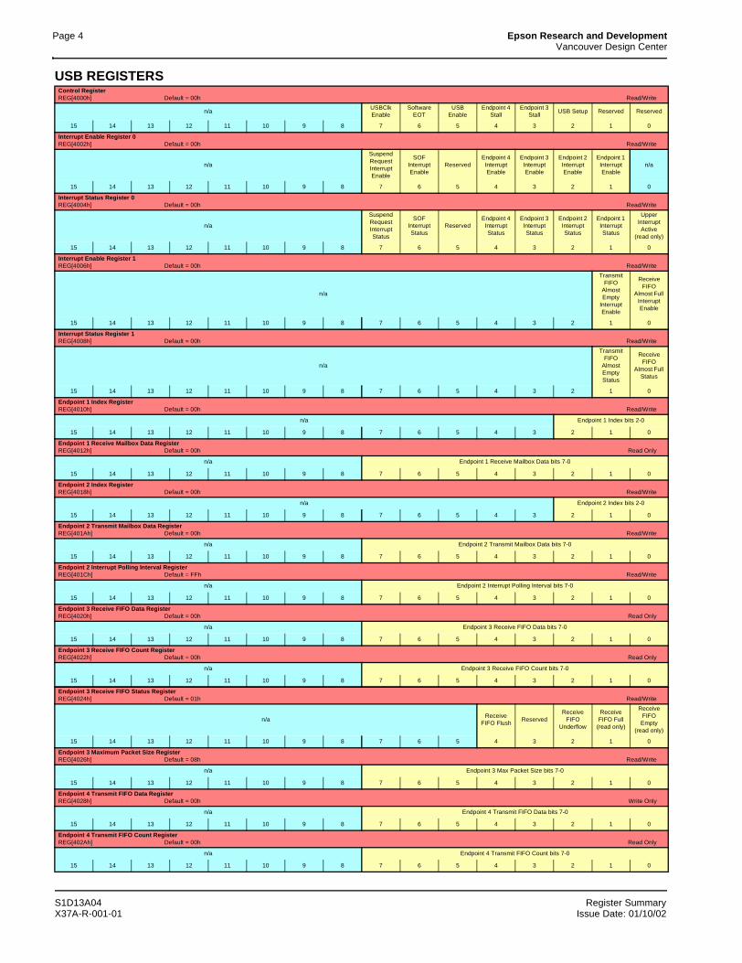
Page 4 Epson Research and DevelopmentVancouver Design Center
USB REGISTERSControl RegisterREG[4000h] Default = 00h Read/Write
n/aUSBClk Enable
Software EOT
USB Enable
Endpoint 4 Stall
Endpoint 3 Stall
USB Setup Reserved Reserved
15 14 13 12 11 10 9 8 7 6 5 4 3 2 1 0
Interrupt Enable Register 0REG[4002h] Default = 00h Read/Write
n/a
Suspend Request Interrupt Enable
SOF Interrupt Enable
ReservedEndpoint 4 Interrupt Enable
Endpoint 3 Interrupt Enable
Endpoint 2 Interrupt Enable
Endpoint 1 Interrupt Enable
n/a
15 14 13 12 11 10 9 8 7 6 5 4 3 2 1 0
Interrupt Status Register 0REG[4004h] Default = 00h Read/Write
n/a
Suspend Request Interrupt Status
SOF Interrupt Status
ReservedEndpoint 4 Interrupt Status
Endpoint 3 Interrupt Status
Endpoint 2 Interrupt Status
Endpoint 1 Interrupt Status
Upper Interrupt Active
(read only)
15 14 13 12 11 10 9 8 7 6 5 4 3 2 1 0
Interrupt Enable Register 1REG[4006h] Default = 00h Read/Write
n/a
Transmit FIFO
Almost Empty
Interrupt Enable
Receive FIFO
Almost Full Interrupt Enable
15 14 13 12 11 10 9 8 7 6 5 4 3 2 1 0
Interrupt Status Register 1REG[4008h] Default = 00h Read/Write
n/a
Transmit FIFO
Almost Empty Status
Receive FIFO
Almost Full Status
15 14 13 12 11 10 9 8 7 6 5 4 3 2 1 0
Endpoint 1 Index RegisterREG[4010h] Default = 00h Read/Write
n/a Endpoint 1 Index bits 2-0
15 14 13 12 11 10 9 8 7 6 5 4 3 2 1 0
Endpoint 1 Receive Mailbox Data RegisterREG[4012h] Default = 00h Read Only
n/a Endpoint 1 Receive Mailbox Data bits 7-0
15 14 13 12 11 10 9 8 7 6 5 4 3 2 1 0
Endpoint 2 Index RegisterREG[4018h] Default = 00h Read/Write
n/a Endpoint 2 Index bits 2-0
15 14 13 12 11 10 9 8 7 6 5 4 3 2 1 0
Endpoint 2 Transmit Mailbox Data RegisterREG[401Ah] Default = 00h Read/Write
n/a Endpoint 2 Transmit Mailbox Data bits 7-0
15 14 13 12 11 10 9 8 7 6 5 4 3 2 1 0
Endpoint 2 Interrupt Polling Interval RegisterREG[401Ch] Default = FFh Read/Write
n/a Endpoint 2 Interrupt Polling Interval bits 7-0
15 14 13 12 11 10 9 8 7 6 5 4 3 2 1 0
Endpoint 3 Receive FIFO Data RegisterREG[4020h] Default = 00h Read Only
n/a Endpoint 3 Receive FIFO Data bits 7-0
15 14 13 12 11 10 9 8 7 6 5 4 3 2 1 0
Endpoint 3 Receive FIFO Count RegisterREG[4022h] Default = 00h Read Only
n/a Endpoint 3 Receive FIFO Count bits 7-0
15 14 13 12 11 10 9 8 7 6 5 4 3 2 1 0
Endpoint 3 Receive FIFO Status RegisterREG[4024h] Default = 01h Read/Write
n/aReceive
FIFO FlushReserved
Receive FIFO
Underflow
Receive FIFO Full
(read only)
Receive FIFO Empty
(read only)
15 14 13 12 11 10 9 8 7 6 5 4 3 2 1 0
Endpoint 3 Maximum Packet Size RegisterREG[4026h] Default = 08h Read/Write
n/a Endpoint 3 Max Packet Size bits 7-0
15 14 13 12 11 10 9 8 7 6 5 4 3 2 1 0
Endpoint 4 Transmit FIFO Data RegisterREG[4028h] Default = 00h Write Only
n/a Endpoint 4 Transmit FIFO Data bits 7-0
15 14 13 12 11 10 9 8 7 6 5 4 3 2 1 0
Endpoint 4 Transmit FIFO Count RegisterREG[402Ah] Default = 00h Read Only
n/a Endpoint 4 Transmit FIFO Count bits 7-0
15 14 13 12 11 10 9 8 7 6 5 4 3 2 1 0
S1D13A04 Register SummaryX37A-R-001-01 Issue Date: 01/10/02
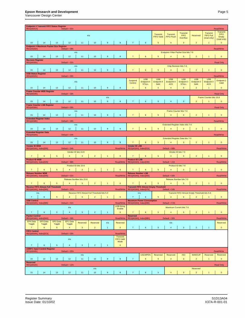
Epson Research and Development Page 5Vancouver Design Center
Endpoint 4 Transmit FIFO Status RegisterREG[402Ch] Default = 01h Read/Write
n/aTransmit
FIFO ValidTransmit
FIFO Flush
Transmit FIFO
OverflowReserved
Transmit FIFO Full
(read only)
Transmit FIFO
Empty (read only)
15 14 13 12 11 10 9 8 7 6 5 4 3 2 1 0
Endpoint 4 Maximum Packet Size RegisterREG[402Eh] Default = 08h Read/Write
n/a Endpoint 4 Max Packet Size bits 7-0
15 14 13 12 11 10 9 8 7 6 5 4 3 2 1 0
Revision RegisterREG[4030h] Default = 01h Read Only
n/a Chip Revision bits 7-0
15 14 13 12 11 10 9 8 7 6 5 4 3 2 1 0
USB Status RegisterREG[4032h] Default = 00h Read/Write
n/aSuspend Control
USB Endpoint 4
STALL
USB Endpoint 4
NAK
USB Endpoint 4
ACK
USB Endpoint 3
STALL
USB Endpoint 3
NAK
USB Endpoint 3
ACK
Endpoint 2 Valid
15 14 13 12 11 10 9 8 7 6 5 4 3 2 1 0
Frame Counter MSB RegisterREG[4034h] Default = 00h Read Only
n/a Frame Counter bits 10-8
15 14 13 12 11 10 9 8 7 6 5 4 3 2 1 0
Frame Counter LSB RegisterREG[4036h] Default = 00h Read Only
n/a Frame Counter bits 7-0
15 14 13 12 11 10 9 8 7 6 5 4 3 2 1 0
Extended Register IndexREG[4038h] Default = 00h Read/Write
n/a Extended Register Index bits 7-0
15 14 13 12 11 10 9 8 7 6 5 4 3 2 1 0
Extended Register DataREG[403Ah] Default = 04h Read/Write
n/a Extended Register Data bits 7-0
15 14 13 12 11 10 9 8 7 6 5 4 3 2 1 0
Vendor ID MSBREG[403Ah], Index[00h] Default = 04h Read/Write
Vendor ID LSBREG[403Ah], Index[01h] Default = B8h Read/Write
Vendor ID bits 15-8 Vendor ID bits 7-0
7 6 5 4 3 2 1 0 7 6 5 4 3 2 1 0
Product ID MSBREG[403Ah], Index[02h] Default = 88h Read/Write
Product ID LSBREG[403Ah], Index[03h] Default = 21h Read/Write
Product ID bits 15-8 Product ID bits 7-0
7 6 5 4 3 2 1 0 7 6 5 4 3 2 1 0
Release Number MSBREG[403Ah], Index[04h] Default = 01h Read/Write
Release Number LSBREG[403Ah], Index[05h] Default = 00h Read/Write
Release Number bits 15-8 Release Number bits 7-0
7 6 5 4 3 2 1 0 7 6 5 4 3 2 1 0
Receive FIFO Almost Full ThresholdREG[403Ah], Index[06h] Default = 3Ch Read/Write
Transmit FIFO Almost Empty ThresholdREG[403Ah], Index[07h] Default = 04h Read/Write
n/a Receive FIFO Almost Full Threshold bits 5-0 n/a Transmit FIFO Almost Empty Threshold bits 5-0
7 6 5 4 3 2 1 0 7 6 5 4 3 2 1 0
USB ControlREG[403Ah], Index[08h] Default = 01h Read/Write
Maximum Power ConsumptionREG[403Ah], Index[09h] Default = FAh Read/Write
n/aUSB String
EnableMaximum Current bits 7-0
7 6 5 4 3 2 1 0 7 6 5 4 3 2 1 0
Packet ControlREG[403Ah], Index[0Ah] Default = 00h Read/Write
ReservedREG[403Ah], Index[0Bh] Default = 00h Read/Write
EP4 Data Toggle
EP3 Data Toggle
EP2 Data Toggle
EP1 Data Toggle
Reserved Reserved n/a Reserved n/a Reserved
7 6 5 4 3 2 1 0 7 6 5 4 3 2 1 0
FIFO ControlREG[403Ah], Index[0Ch] Default = 00h Read/Write
n/aTransmit
FIFO Valid Mode
7 6 5 4 3 2 1 0
USBFC Input Control RegisterREG[4040h] Default = 0Dh Read/Write
n/a USCMPEN Reserved Reserved ISO WAKEUP Reserved Reserved
15 14 13 12 11 10 9 8 7 6 5 4 3 2 1 0
Reserved REG[4042h] Default = 1Dh Read Only
n/a Reserved
15 14 13 12 11 10 9 8 7 6 5 4 3 2 1 0
Register Summary S1D13A04Issue Date: 01/10/02 X37A-R-001-01
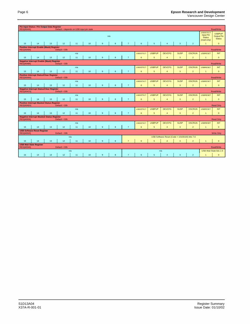
Page 6 Epson Research and DevelopmentVancouver Design Center
Pin Input Status / Pin Output Data RegisterREG[4044h] Default = depends on USB input pin state Read/Write
n/a
USBDETECT Input Pin
Status(read only)
USBPUP Output Pin
Status
15 14 13 12 11 10 9 8 7 6 5 4 3 2 1 0
Positive Interrupt Enable (Mask) RegisterREG[4046h] Default = 00h Read/Write
n/a USBDETECT USBPUP DEVCFG SUSP OSCRUN USBRESET INT
15 14 13 12 11 10 9 8 7 6 5 4 3 2 1 0
Negative Interrupt Enable (Mask) RegisterREG[4048h] Default = 00h Read/Write
n/a USBDETECT USBPUP DEVCFG SUSP OSCRUN USBRESET INT
15 14 13 12 11 10 9 8 7 6 5 4 3 2 1 0
Positive Interrupt Status/Clear RegisterREG[404Ah] Default = 00h Read/Write
n/a USBDETECT USBPUP DEVCFG SUSP OSCRUN USBRESET INT
15 14 13 12 11 10 9 8 7 6 5 4 3 2 1 0
Negative Interrupt Status/Clear RegisterREG[404Ch] Default = 00h Read/Write
n/a USBDETECT USBPUP DEVCFG SUSP OSCRUN USBRESET INT
15 14 13 12 11 10 9 8 7 6 5 4 3 2 1 0
Positive Interrupt Masked Status RegisterREG[404Eh] Default = 00h Read Only
n/a USBDETECT USBPUP DEVCFG SUSP OSCRUN USBRESET INT
15 14 13 12 11 10 9 8 7 6 5 4 3 2 1 0
Negative Interrupt Masked Status RegisterREG[4050h] Default = 00h Read Only
n/a USBDETECT USBPUP DEVCFG SUSP OSCRUN USBRESET INT
15 14 13 12 11 10 9 8 7 6 5 4 3 2 1 0
USB Software Reset RegisterREG[4052h] Default = 00h Write Only
n/a USB Software Reset (Code = 10100100) bits 7-0
15 14 13 12 11 10 9 8 7 6 5 4 3 2 1 0
USB Wait State RegisterREG[4054h] Default = 00h Read/Write
n/a n/a USB Wait State bits 1-0
15 14 13 12 11 10 9 8 7 6 5 4 3 2 1 0
S1D13A04 Register SummaryX37A-R-001-01 Issue Date: 01/10/02
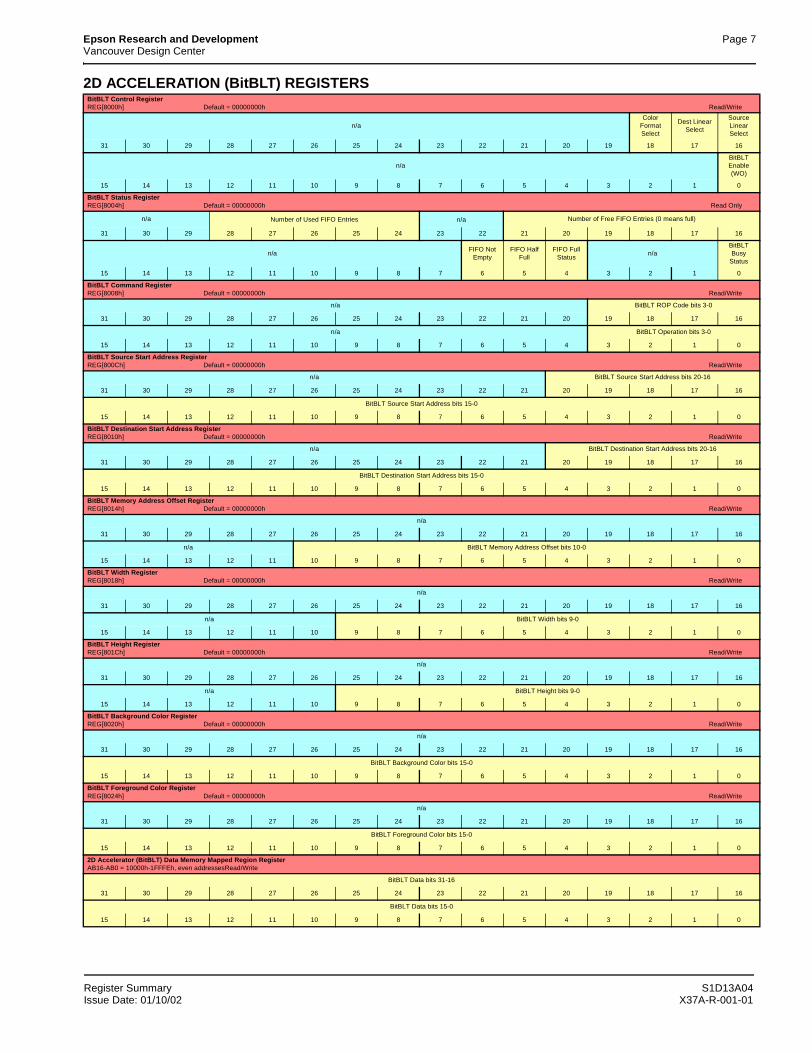
Epson Research and Development Page 7Vancouver Design Center
2D ACCELERATION (BitBLT) REGISTERSBitBLT Control RegisterREG[8000h] Default = 00000000h Read/Write
n/aColor
Format Select
Dest Linear Select
Source Linear Select
31 30 29 28 27 26 25 24 23 22 21 20 19 18 17 16
n/aBitBLT Enable (WO)
15 14 13 12 11 10 9 8 7 6 5 4 3 2 1 0
BitBLT Status RegisterREG[8004h] Default = 00000000h Read Only
n/a Number of Used FIFO Entries n/a Number of Free FIFO Entries (0 means full)
31 30 29 28 27 26 25 24 23 22 21 20 19 18 17 16
n/aFIFO Not
EmptyFIFO Half
FullFIFO Full
Statusn/a
BitBLT Busy
Status
15 14 13 12 11 10 9 8 7 6 5 4 3 2 1 0
BitBLT Command RegisterREG[8008h] Default = 00000000h Read/Write
n/a BitBLT ROP Code bits 3-0
31 30 29 28 27 26 25 24 23 22 21 20 19 18 17 16
n/a BitBLT Operation bits 3-0
15 14 13 12 11 10 9 8 7 6 5 4 3 2 1 0
BitBLT Source Start Address RegisterREG[800Ch] Default = 00000000h Read/Write
n/a BitBLT Source Start Address bits 20-16
31 30 29 28 27 26 25 24 23 22 21 20 19 18 17 16
BitBLT Source Start Address bits 15-0
15 14 13 12 11 10 9 8 7 6 5 4 3 2 1 0
BitBLT Destination Start Address RegisterREG[8010h] Default = 00000000h Read/Write
n/a BitBLT Destination Start Address bits 20-16
31 30 29 28 27 26 25 24 23 22 21 20 19 18 17 16
BitBLT Destination Start Address bits 15-0
15 14 13 12 11 10 9 8 7 6 5 4 3 2 1 0
BitBLT Memory Address Offset RegisterREG[8014h] Default = 00000000h Read/Write
n/a
31 30 29 28 27 26 25 24 23 22 21 20 19 18 17 16
n/a BitBLT Memory Address Offset bits 10-0
15 14 13 12 11 10 9 8 7 6 5 4 3 2 1 0
BitBLT Width RegisterREG[8018h] Default = 00000000h Read/Write
n/a
31 30 29 28 27 26 25 24 23 22 21 20 19 18 17 16
n/a BitBLT Width bits 9-0
15 14 13 12 11 10 9 8 7 6 5 4 3 2 1 0
BitBLT Height RegisterREG[801Ch] Default = 00000000h Read/Write
n/a
31 30 29 28 27 26 25 24 23 22 21 20 19 18 17 16
n/a BitBLT Height bits 9-0
15 14 13 12 11 10 9 8 7 6 5 4 3 2 1 0
BitBLT Background Color RegisterREG[8020h] Default = 00000000h Read/Write
n/a
31 30 29 28 27 26 25 24 23 22 21 20 19 18 17 16
BitBLT Background Color bits 15-0
15 14 13 12 11 10 9 8 7 6 5 4 3 2 1 0
BitBLT Foreground Color RegisterREG[8024h] Default = 00000000h Read/Write
n/a
31 30 29 28 27 26 25 24 23 22 21 20 19 18 17 16
BitBLT Foreground Color bits 15-0
15 14 13 12 11 10 9 8 7 6 5 4 3 2 1 0
2D Accelerator (BitBLT) Data Memory Mapped Region RegisterAB16-AB0 = 10000h-1FFFEh, even addressesRead/Write
BitBLT Data bits 31-16
31 30 29 28 27 26 25 24 23 22 21 20 19 18 17 16
BitBLT Data bits 15-0
15 14 13 12 11 10 9 8 7 6 5 4 3 2 1 0
Register Summary S1D13A04Issue Date: 01/10/02 X37A-R-001-01

Page 8 Epson Research and DevelopmentVancouver Design Center
THIS PAGE LEFT BLANK
S1D13A04 Register SummaryX37A-R-001-01 Issue Date: 01/10/02
S1D13A04 LCD/USB Companion Chip
13A04CFG Configuration Program
Document Number: X37A-B-001-01
Copyright © 2001 Epson Research and Development, Inc. All Rights Reserved.
Information in this document is subject to change without notice. You may download and use this document, but only for your own use inevaluating Seiko Epson/EPSON products. You may not modify the document. Epson Research and Development, Inc. disclaims anyrepresentation that the contents of this document are accurate or current. The Programs/Technologies described in this document may contain material protected under U.S. and/or International Patent laws.
EPSON is a registered trademark of Seiko Epson Corporation. Microsoft and Windows are registered trademarks of Microsoft Corporation.All other trademarks are the property of their respective owners.

Page 2 Epson Research and DevelopmentVancouver Design Center
THIS PAGE LEFT BLANK
S1D13A04 13A04CFG Configuration ProgramX37A-B-001-01 Issue Date: 01/10/19
Epson Research and Development Page 3Vancouver Design Center
Table of Contents
13A04CFG . . . . . . . . . . . . . . . . . . . . . . . . . . . . . . . . . . . . . . . . . . . . . . . . 5
S1D13A04 Supported Evaluation Platforms . . . . . . . . . . . . . . . . . . . . . . 5
Installation . . . . . . . . . . . . . . . . . . . . . . . . . . . . . . . . . . . 5
Usage . . . . . . . . . . . . . . . . . . . . . . . . . . . . . . . . . . . . . 5
13A04CFG Configuration Tabs . . . . . . . . . . . . . . . . . . . . . . . . . . . 6
General Tab . . . . . . . . . . . . . . . . . . . . . . . . . . . . . . . . . . . . . . . . . . . 6
Preferences Tab . . . . . . . . . . . . . . . . . . . . . . . . . . . . . . . . . . . . . . . . . 8
Clocks Tab . . . . . . . . . . . . . . . . . . . . . . . . . . . . . . . . . . . . . . . . . . . 10
Panel Tab . . . . . . . . . . . . . . . . . . . . . . . . . . . . . . . . . . . . . . . . . . . . 14
Panel Power Tab . . . . . . . . . . . . . . . . . . . . . . . . . . . . . . . . . . . . . . . . 18
Registers Tab . . . . . . . . . . . . . . . . . . . . . . . . . . . . . . . . . . . . . . . . . . 20
Direct Tab . . . . . . . . . . . . . . . . . . . . . . . . . . . . . . . . . . . . . . . . . . . 21
13A04CFG Menus . . . . . . . . . . . . . . . . . . . . . . . . . . . . . . . 23
Open... . . . . . . . . . . . . . . . . . . . . . . . . . . . . . . . . . . . . . . . . . . . . . 23
Save . . . . . . . . . . . . . . . . . . . . . . . . . . . . . . . . . . . . . . . . . . . . . . 24
Save As... . . . . . . . . . . . . . . . . . . . . . . . . . . . . . . . . . . . . . . . . . . . . 24
Configure Multiple . . . . . . . . . . . . . . . . . . . . . . . . . . . . . . . . . . . . . . . 25
Export . . . . . . . . . . . . . . . . . . . . . . . . . . . . . . . . . . . . . . . . . . . . . 26
Enable Tooltips . . . . . . . . . . . . . . . . . . . . . . . . . . . . . . . . . . . . . . . . 27
Tooltip Delay . . . . . . . . . . . . . . . . . . . . . . . . . . . . . . . . . . . . . . . . . . 27
ERD on the Web . . . . . . . . . . . . . . . . . . . . . . . . . . . . . . . . . . . . . . . . 27
Update Common Controls . . . . . . . . . . . . . . . . . . . . . . . . . . . . . . . . . . . 27
About 13A04CFG . . . . . . . . . . . . . . . . . . . . . . . . . . . . . . . . . . . . . . . 27
Comments . . . . . . . . . . . . . . . . . . . . . . . . . . . . . . . . . . 28
13A04CFG Configuration Program S1D13A04Issue Date: 01/10/19 X37A-B-001-01

Page 4 Epson Research and DevelopmentVancouver Design Center
THIS PAGE LEFT BLANK
S1D13A04 13A04CFG Configuration ProgramX37A-B-001-01 Issue Date: 01/10/19
Epson Research and Development Page 5Vancouver Design Center
13A04CFG
13A04CFG is an interactive Windows® program that calculates register values for a user-defined S1D13A04 configuration. The configuration information can be used to directly alter the operating characteristics of the S1D13A04 utilities or any program built with the Hardware Abstraction Layer (HAL) library. Alternatively, the configuration information can be saved in a variety of text file formats for use in other applications.
S1D13A04 Supported Evaluation Platforms
13A04CFG runs on PC system running Windows 9x/ME/NT/2000 and can modify Win32 .exe files and .s9 format files.
Installation
Create a directory for 13A04cfg.exe and copy the files 13A04cfg.exe and panels.def to that directory. Panels.def contains configuration information for a number of panels and must reside in the same directory as 13A04cfg.exe.
Usage
To start 13A04CFG from the Windows desktop, click on the My Computer icon and run the program 13a04cfg.exe from the installed directory.
To start 13A04CFG from a Windows command prompt, change to the directory 13A04cfg.exe was installed to and type the command 13A04cfg.
The basic procedure for using 13A04CFG is:
1. Start 13A04CFG as described above.
2. Open an existing file to serve as a starting reference point (this step is optional).
3. Modify the configuration. For specific information on editing the configuration, see “13A04CFG Configuration Tabs” on page 6.
4. Save the new configuration. The configuration information can be saved in two ways; as an ASCII text file or by modifying an executable image on disk.
Several ASCII text file formats are supported. Most are formatted C header files used to build display drivers or standalone applications.
Utility files based on the Hardware Abstraction Layer (HAL) can be modified directly by 13A04CFG.
13A04CFG Configuration Program S1D13A04Issue Date: 01/10/19 X37A-B-001-01
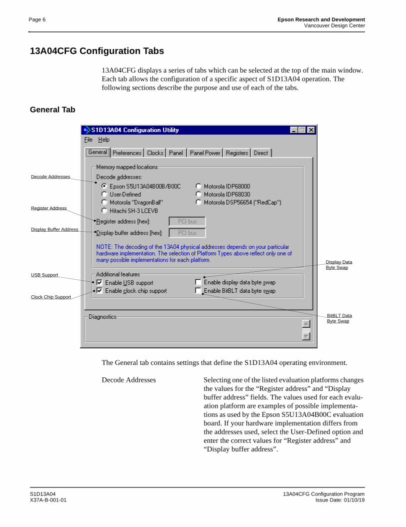
Page 6 Epson Research and DevelopmentVancouver Design Center
13A04CFG Configuration Tabs
13A04CFG displays a series of tabs which can be selected at the top of the main window. Each tab allows the configuration of a specific aspect of S1D13A04 operation. The following sections describe the purpose and use of each of the tabs.
General Tab
The General tab contains settings that define the S1D13A04 operating environment.
Decode Addresses Selecting one of the listed evaluation platforms changes the values for the “Register address” and “Display buffer address” fields. The values used for each evalu-ation platform are examples of possible implementa-tions as used by the Epson S5U13A04B00C evaluation board. If your hardware implementation differs from the addresses used, select the User-Defined option and enter the correct values for “Register address” and “Display buffer address”.
Decode Addresses
Register Address
Display Buffer Address
USB Support
Clock Chip Support
Display Data
BitBLT Data
Byte Swap
Byte Swap
S1D13A04 13A04CFG Configuration ProgramX37A-B-001-01 Issue Date: 01/10/19
Epson Research and Development Page 7Vancouver Design Center
NoteWhen “Epson S5U13A04B00B/B00C Evaluation Board” is selected, the register and display buffer addresses are blanked because the evaluation board uses the PCI interface and the decode addresses are determined by the system BIOS during boot-up.
Register Address The physical address of the start of register decode space (in hexadecimal).
This field is automatically set according to the Decode Address unless the “User-Defined” decode address is selected.
Display Buffer Address The physical address of the start of display buffer decode space (in hexadecimal).
This field is automatically set according to the Decode Address unless the “User-Defined” decode address is selected.
USB Support The S1D13A04 contains a USB client controller. If this box is checked, chip initialization will configure GPIO[7:4] for use by the USB controller. For further information on the S1D13A04 USB implementation, see the S1D13A04 Hardware Functional Specification, document number X37A-A-001-xx.
Clock Chip Support The S5U13A04B00C evaluation board implements a Cypress ICD2061A Clock Synthesizer which can be used to generate CLKI and CLKI2. When this box is checked, GPIO[3:1] are reserved for Clock Synthesizer support. Selecting a HR-TFT panel will disable this feature as the HR-TFT requires GPIO[3:0].
Note that this feature is only available when using the S5U13A04B00C.
Display Data Byte Swap When this box is checked, the word data from the display buffer is byte swapped. This box should be checked when the display color depth is 16 bpp on a Big Endian platform.
BitBLT Data Byte Swap When this box is checked, word data sent to/read from the 2D BitBLT memory is byte swapped. This box should be checked when using the 2D BitBLT functions on a Big Endian platform.
13A04CFG Configuration Program S1D13A04Issue Date: 01/10/19 X37A-B-001-01
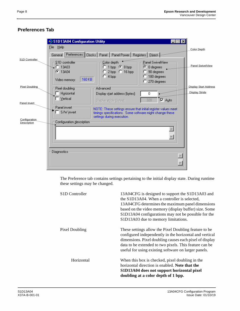
Page 8 Epson Research and DevelopmentVancouver Design Center
Preferences Tab
The Preference tab contains settings pertaining to the initial display state. During runtime these settings may be changed.
S1D Controller 13A04CFG is designed to support the S1D13A03 and the S1D13A04. When a controller is selected, 13A04CFG determines the maximum panel dimensions based on the video memory (display buffer) size. Some S1D13A04 configurations may not be possible for the S1D13A03 due to memory limitations.
Pixel Doubling These settings allow the Pixel Doubling feature to be configured independently in the horizontal and vertical dimensions. Pixel doubling causes each pixel of display data to be extended to two pixels. This feature can be useful for using existing software on larger panels.
Horizontal When this box is checked, pixel doubling in the horizontal direction is enabled. Note that the S1D13A04 does not support horizontal pixel doubling at a color depth of 1 bpp.
S1D Controller
Panel SwivelView
Panel Invert
Pixel Doubling
Color Depth
Display Start Address
ConfigurationDescription
Display Stride
S1D13A04 13A04CFG Configuration ProgramX37A-B-001-01 Issue Date: 01/10/19
Epson Research and Development Page 9Vancouver Design Center
Vertical When this box is checked, pixel doubling in the vertical direction is enabled. Note that the S1D13A04 does not support vertical pixel doubling at a color depth of 1 bpp.
Panel Invert The S1D13A04 can invert the display data going to the LCD panel. When this box is checked, video data is inverted. Display data is inverted after the Look-Up Table, which means colors are truly inverted.
Configuration Description This field allows the user to enter a description for a particular configuration. This field is saved in the HAL information and is displayed when a HAL-based utility is run.
Color Depth Sets the initial color depth on the LCD panel. If there is insufficient display buffer for the selected width and height then a warning is displayed in the diagnostic area.
Panel SwivelView The S1D13A04 SwivelView feature is capable of rotating the image displayed on an LCD panel 90°, 180°, or 270° in a counter-clockwise direction. This setting determines the initial orientation of the panel.
Advanced These settings allow fine tuning of the start address and stride. The start address defines the offset into the display buffer (video memory) of the pixel which will be displayed in the top left corner of the panel. Stride defines the number of bytes required to step from the first pixel on one row to the first pixel on the next row (i.e. 160 pixel wide display at 16 bpp requires 320 bytes per horizontal row).
Display Start Address This option sets the start address for the main window of the panel. Typically the start address is set to zero.
Display Stride This option sets the stride for the main window of the panel. To set the stride equal to the size of the display, select the “auto” box. To increase the stride, uncheck the “auto” box and enter the desired stride.
NoteThe stride value must be greater than or equal tothe number of bytes required by one line ofdisplay memory.
13A04CFG Configuration Program S1D13A04Issue Date: 01/10/19 X37A-B-001-01
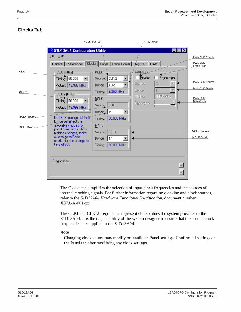
Page 10 Epson Research and DevelopmentVancouver Design Center
Clocks Tab
The Clocks tab simplifies the selection of input clock frequencies and the sources of internal clocking signals. For further information regarding clocking and clock sources, refer to the S1D13A04 Hardware Functional Specification, document numberX37A-A-001-xx.
The CLKI and CLKI2 frequencies represent clock values the system provides to the S1D13A04. It is the responsibility of the system designer to ensure that the correct clock frequencies are supplied to the S1D13A04.
NoteChanging clock values may modify or invalidate Panel settings. Confirm all settings on the Panel tab after modifying any clock settings.
CLKI
CLKI2
BCLK Source
BCLK Divide
PWMCLK
PWMCLK Source
PCLK Source PCLK Divide
MCLK Source
MCLK Divide
PWMCLK
PWMCLK Enable
PWMCLK Divide
Force High
Duty Cycle
S1D13A04 13A04CFG Configuration ProgramX37A-B-001-01 Issue Date: 01/10/19
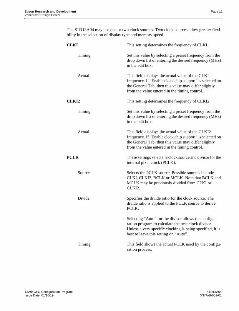
Epson Research and Development Page 11Vancouver Design Center
The S1D13A04 may use one or two clock sources. Two clock sources allow greater flexi-bility in the selection of display type and memory speed.
CLKI This setting determines the frequency of CLKI.
Timing Set this value by selecting a preset frequency from the drop down list or entering the desired frequency (MHz) in the edit box.
Actual This field displays the actual value of the CLKI frequency. If “Enable clock chip support” is selected on the General Tab, then this value may differ slightly from the value entered in the timing control.
CLKI2 This setting determines the frequency of CLKI2.
Timing Set this value by selecting a preset frequency from the drop down list or entering the desired frequency (MHz) in the edit box.
Actual This field displays the actual value of the CLKI2 frequency. If “Enable clock chip support” is selected on the General Tab, then this value may differ slightly from the value entered in the timing control.
PCLK These settings select the clock source and divisor for the internal pixel clock (PCLK).
Source Selects the PCLK source. Possible sources include CLKI, CLKI2, BCLK or MCLK. Note that BCLK and MCLK may be previously divided from CLKI or CLKI2.
Divide Specifies the divide ratio for the clock source. The divide ratio is applied to the PCLK source to derive PCLK.
Selecting “Auto” for the divisor allows the configu-ration program to calculate the best clock divisor. Unless a very specific clocking is being specified, it is best to leave this setting on “Auto”.
Timing This field shows the actual PCLK used by the configu-ration process.
13A04CFG Configuration Program S1D13A04Issue Date: 01/10/19 X37A-B-001-01
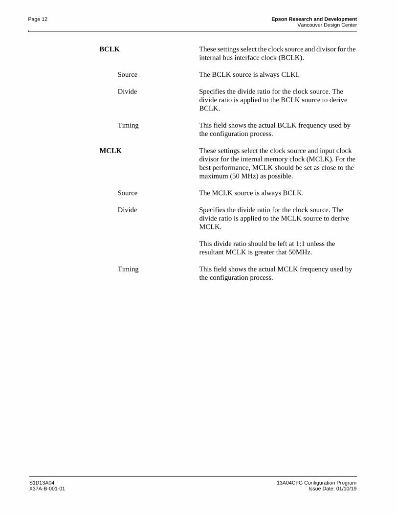
Page 12 Epson Research and DevelopmentVancouver Design Center
BCLK These settings select the clock source and divisor for the internal bus interface clock (BCLK).
Source The BCLK source is always CLKI.
Divide Specifies the divide ratio for the clock source. The divide ratio is applied to the BCLK source to derive BCLK.
Timing This field shows the actual BCLK frequency used by the configuration process.
MCLK These settings select the clock source and input clock divisor for the internal memory clock (MCLK). For the best performance, MCLK should be set as close to the maximum (50 MHz) as possible.
Source The MCLK source is always BCLK.
Divide Specifies the divide ratio for the clock source. The divide ratio is applied to the MCLK source to derive MCLK.
This divide ratio should be left at 1:1 unless the resultant MCLK is greater that 50MHz.
Timing This field shows the actual MCLK frequency used by the configuration process.
S1D13A04 13A04CFG Configuration ProgramX37A-B-001-01 Issue Date: 01/10/19
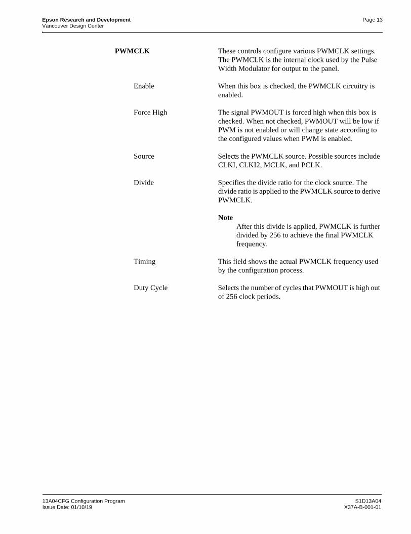
Epson Research and Development Page 13Vancouver Design Center
PWMCLK These controls configure various PWMCLK settings. The PWMCLK is the internal clock used by the Pulse Width Modulator for output to the panel.
Enable When this box is checked, the PWMCLK circuitry is enabled.
Force High The signal PWMOUT is forced high when this box is checked. When not checked, PWMOUT will be low if PWM is not enabled or will change state according to the configured values when PWM is enabled.
Source Selects the PWMCLK source. Possible sources include CLKI, CLKI2, MCLK, and PCLK.
Divide Specifies the divide ratio for the clock source. The divide ratio is applied to the PWMCLK source to derive PWMCLK.
NoteAfter this divide is applied, PWMCLK is furtherdivided by 256 to achieve the final PWMCLKfrequency.
Timing This field shows the actual PWMCLK frequency used by the configuration process.
Duty Cycle Selects the number of cycles that PWMOUT is high out of 256 clock periods.
13A04CFG Configuration Program S1D13A04Issue Date: 01/10/19 X37A-B-001-01
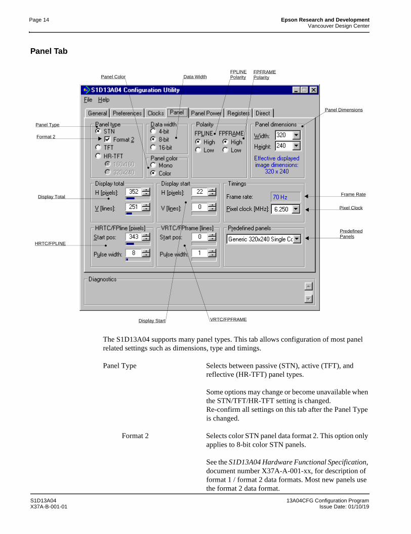
Page 14 Epson Research and DevelopmentVancouver Design Center
Panel Tab
The S1D13A04 supports many panel types. This tab allows configuration of most panel related settings such as dimensions, type and timings.
Panel Type Selects between passive (STN), active (TFT), and reflective (HR-TFT) panel types.
Some options may change or become unavailable when the STN/TFT/HR-TFT setting is changed.Re-confirm all settings on this tab after the Panel Type is changed.
Format 2 Selects color STN panel data format 2. This option only applies to 8-bit color STN panels.
See the S1D13A04 Hardware Functional Specification, document number X37A-A-001-xx, for description of format 1 / format 2 data formats. Most new panels use the format 2 data format.
Panel Type
Panel Dimensions
HRTC/FPLINE
VRTC/FPFRAME
Panel ColorFPLINE FPFRAME
Frame Rate
Pixel Clock
PredefinedPanels
PolarityPolarity
Display Start
Data Width
Format 2
Display Total
S1D13A04 13A04CFG Configuration ProgramX37A-B-001-01 Issue Date: 01/10/19
Epson Research and Development Page 15Vancouver Design Center
Data Width Selects the panel data width. Panel data width is the number of bits of data transferred to the LCD panel on each clock cycle and shouldn’t be confused with color depth which determines the number of displayed colors.
When a passive panel type is selected, the available options are 4, 8, and 16 bit. When an active panel type (TFT/HR-TFT) is selected, the available options are 9, 12, and 18 bit.
Panel Color Selects between a monochrome or color panel.
Polarity Allows selection of the polarity for the FPLINE and FPRAME pulses.
NoteSelecting the wrong pulse polarity may damagethe panel.
FPLINE Polarity Selects the polarity of the FPLINE pulse.
Refer to the panel specification for the correct polarity of the FPLINE pulse.
FPFRAME Polarity Selects the polarity of the FPFRAME pulse.
Refer to the panel specification for the correct polarity of the FPFRAME pulse.
Panel Dimensions These fields specify the panel width and height. A number of common widths and height are available in the selection boxes. If the width/height of your panel is not listed, enter the actual panel dimensions into the edit field.
For passive panels, manually entered pixel widths must be a minimum of 32 pixels and can be increased by multiples of 16. For TFT panels, manually entered pixel widths must be a minimum of 8 pixels and can be increased by multiples of 8. If a value is entered that does not meet these requirements, 13A04CFG rounds up the value to the next allowable width. The changed value is reported in the diagnostics portion of the window.
13A04CFG Configuration Program S1D13A04Issue Date: 01/10/19 X37A-B-001-01
Page 16 Epson Research and DevelopmentVancouver Design Center
Display Total It is recommended that the automatically generated Display Total values be used. However, manual adjustment may be used to improve the quality of the displayed image by fine tuning the horizontal and vertical display totals.
The display total equals the display period plus the non-display period. Refer to S1D13A04 Hardware Functional Specification, document number X37A-A-001-xx, for a complete description of the Display Total settings.
NoteIf the horizontal or vertical display totals are settoo small, 13A04CFG will display a yellowwarning message in the diagnostics portion of thewindow.
Display Start It is recommended that the automatically generated Display Start values be used. However, manual adjustment may be used to improve the quality of the displayed image by fine tuning the horizontal and vertical display start positions.
Refer to S1D13A04 Hardware Functional Specifi-cation, document number X37A-A-001-xx, for a complete description of the Display Start settings.
NoteIf the horizontal or vertical display start values areset to values that violate the S1D13A04 HardwareFunctional Specification, 13A04CFG will displaya yellow warning message in the diagnosticsportion of the window.
Frame Rate The Frame Rate (in Hz) is calculated and displayed based on the current settings as selected on the various tabs. If the resulting Frame Rate is not acceptable, adjust the settings to change the frame rate.
Panel dimensions are fixed therefore frame rate can only be adjusted by changing either the PCLK frequency or display total values.
Pixel Clock Select the desired Pixel Clock (in MHz) from the drop-down list. The range of frequencies displayed is dependent on the PCLK source and divide settings as selected on the Clocks tab.
S1D13A04 13A04CFG Configuration ProgramX37A-B-001-01 Issue Date: 01/10/19
Epson Research and Development Page 17Vancouver Design Center
HRTC/FPLINE (pixels) These settings allow fine tuning of the TFT line pulse parameters. Refer to S1D13A04 Hardware Functional Specification, document number X37A-A-001-xx for a complete description of the FPLINE pulse settings.
Start pos Specifies the delay (in pixels) from the start of the horizontal non-display period to the leading edge of the FPLINE pulse.
Pulse Width Specifies the width (in pixels) of the horizontal sync signal (FPLINE).
VRTC/FPFRAME (lines) These settings allow fine tuning of the frame pulse parameters. Refer to S1D13A04 Hardware Functional Specification, document number X37A-A-001-xx, for a complete description of the FPFRAME pulse settings.
Start pos Specifies the delay (in lines) from the start of the vertical non-display period to the leading edge of the FPFRAME pulse.
Pulse width Specifies the pulse width (in lines) of the vertical sync signal (FPFRAME).
Predefined Panels 13A04CFG uses a file (panels.def) which contains predefined settings for a number of LCD panels. If the file panels.def is present in the same directory as 13A04cfg.exe, the predefined panels are available in the drop-down list. If a panel is selected from the list, 13A04CFG preconfigures its settings to nominal panel values.
13A04CFG Configuration Program S1D13A04Issue Date: 01/10/19 X37A-B-001-01
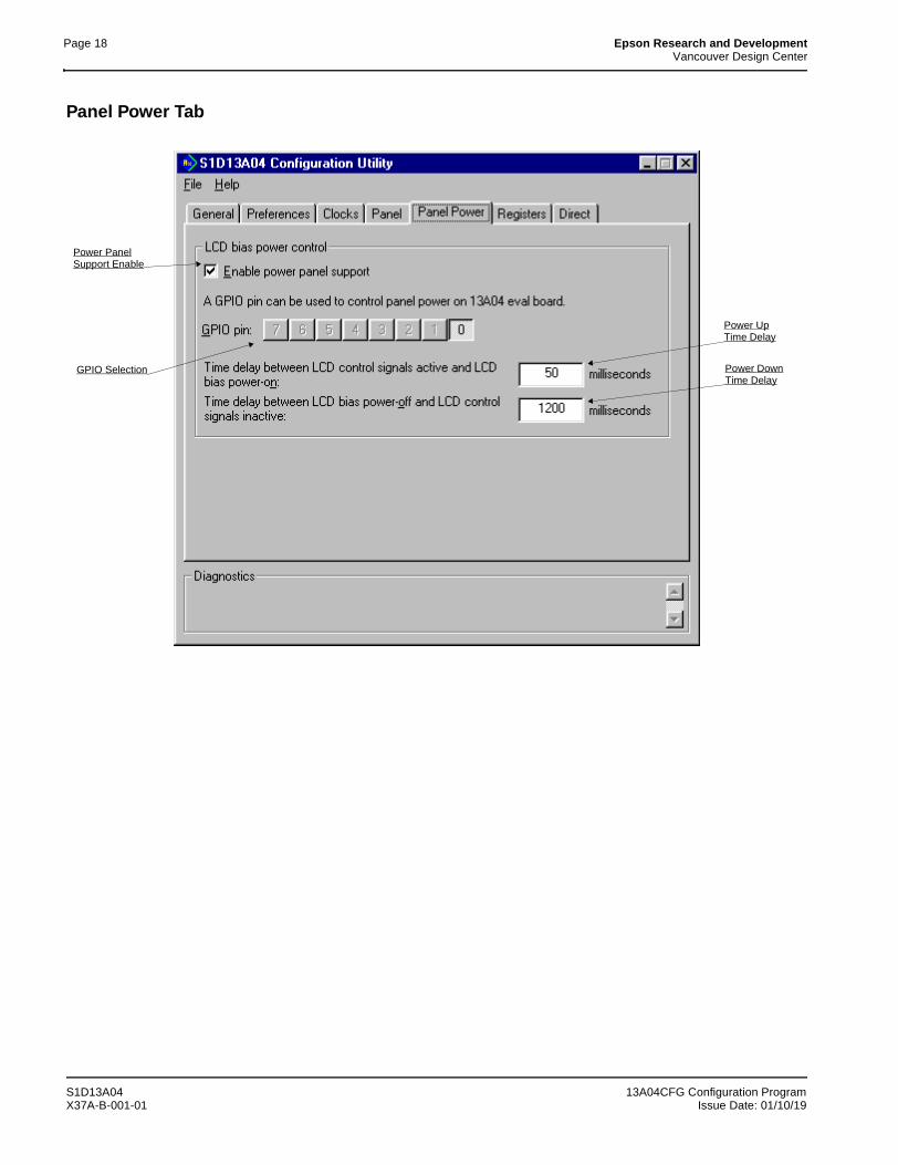
Page 18 Epson Research and DevelopmentVancouver Design Center
Panel Power Tab
Power UpTime Delay
Power DownTime Delay
Power Panel
GPIO Selection
Support Enable
S1D13A04 13A04CFG Configuration ProgramX37A-B-001-01 Issue Date: 01/10/19
Epson Research and Development Page 19Vancouver Design Center
The S5U13A04B00C evaluation board is designed to use a GPIO signal to control the LCD bias power. The following settings configure panel power support.
Power Panel Support Enable When this box is checked, the LCD bias power to the panel is controlled by the selected GPIO pin. When this box is unchecked, the LCD bias power must be controlled by the CPU or some other means.
GPIO Selection This setting selects the GPIO pin used to control the LCD bias power. The default is GPIO0 (GPIO0 is used on the S1D13A04 evaluation board).
Power Up Time Delay This setting controls the maximum time delay between when the S1D13A04 control signals are turned on and the LCD panel is powered-on. This setting must be configured according to the specification for the panel being used.
This value is used by Epson evaluation software designed for the S5U13A04B00C evaluation board.
Power Down Time Delay This setting controls the minimum time delay between when the LCD panel is powered-off and when the S1D13A04 control signals are turned off. This setting must be configured according to the specification for the panel being used.
This value is used by Epson evaluation software designed for the S5U13A04B00C evaluation board.
13A04CFG Configuration Program S1D13A04Issue Date: 01/10/19 X37A-B-001-01
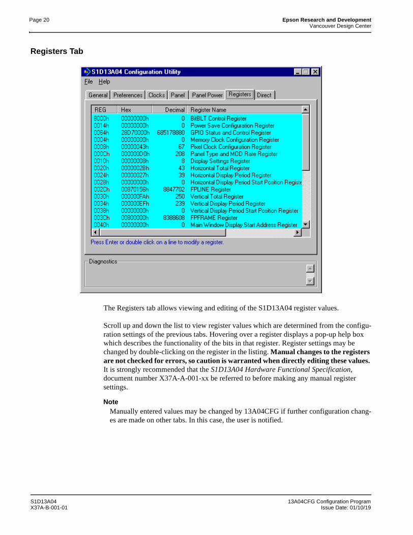
Page 20 Epson Research and DevelopmentVancouver Design Center
Registers Tab
The Registers tab allows viewing and editing of the S1D13A04 register values.
Scroll up and down the list to view register values which are determined from the configu-ration settings of the previous tabs. Hovering over a register displays a pop-up help box which describes the functionality of the bits in that register. Register settings may be changed by double-clicking on the register in the listing. Manual changes to the registers are not checked for errors, so caution is warranted when directly editing these values. It is strongly recommended that the S1D13A04 Hardware Functional Specification, document number X37A-A-001-xx be referred to before making any manual register settings.
NoteManually entered values may be changed by 13A04CFG if further configuration chang-es are made on other tabs. In this case, the user is notified.
S1D13A04 13A04CFG Configuration ProgramX37A-B-001-01 Issue Date: 01/10/19
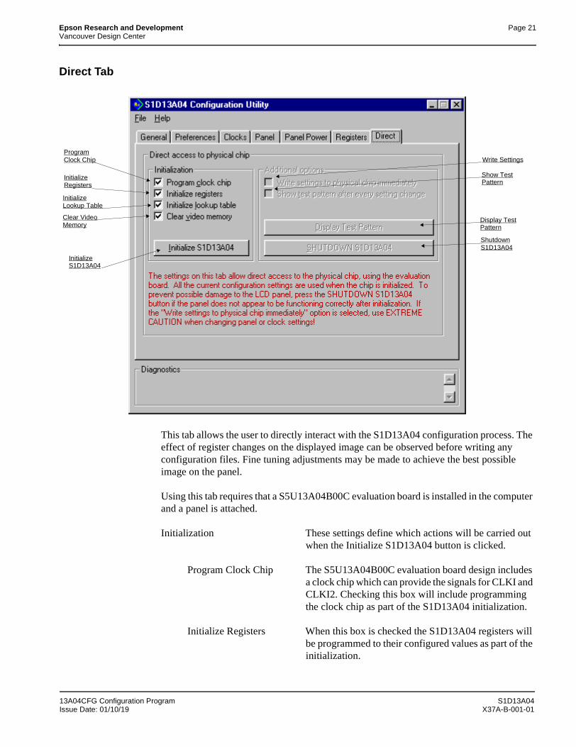
Epson Research and Development Page 21Vancouver Design Center
Direct Tab
This tab allows the user to directly interact with the S1D13A04 configuration process. The effect of register changes on the displayed image can be observed before writing any configuration files. Fine tuning adjustments may be made to achieve the best possible image on the panel.
Using this tab requires that a S5U13A04B00C evaluation board is installed in the computer and a panel is attached.
Initialization These settings define which actions will be carried out when the Initialize S1D13A04 button is clicked.
Program Clock Chip The S5U13A04B00C evaluation board design includes a clock chip which can provide the signals for CLKI and CLKI2. Checking this box will include programming the clock chip as part of the S1D13A04 initialization.
Initialize Registers When this box is checked the S1D13A04 registers will be programmed to their configured values as part of the initialization.
Show Test
Display Test
Program
Initialize
Initialize
Clear VideoMemory
Clock Chip
Registers
Lookup Table
Initialize
Write Settings
Shutdown
S1D13A04
Pattern
Pattern
S1D13A04
13A04CFG Configuration Program S1D13A04Issue Date: 01/10/19 X37A-B-001-01
Page 22 Epson Research and DevelopmentVancouver Design Center
Initialize Lookup Table When this box is checked the S1D13A04 Lookup Table is programmed as part of the initialization.
Clear Video Memory When this box is checked the S1D13A04 display buffer will be cleared (set to zeros) as part of the initialization.
Initialize S1D13A04 Clicking this button initializes the S1D13A04 according to the options selected.
Additional Options After initializing the S1D13A04, these further options become available.
Write Settings This setting should be used with caution. Checking this box will cause setting changes on any tab to immedi-ately update the associated register(s).
Show Test Pattern Checking this box will update the test pattern in the display buffer after every setting change. This is useful when fine tuning panel settings as the results of the change are immediately visible.
Display Test Pattern Clicking this button causes 13A04CFG to draw a test pattern into display memory. The pattern is based on the configured width, height, rotation and color depth.
Shutdown S1D13A04 Clicking this button shuts down the S1D13A04. This feature is necessary should a setting change appear to be damaging or harmful to the attached panel.
S1D13A04 13A04CFG Configuration ProgramX37A-B-001-01 Issue Date: 01/10/19
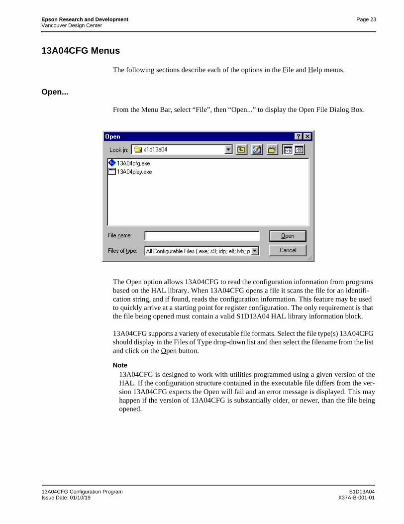
Epson Research and Development Page 23Vancouver Design Center
13A04CFG Menus
The following sections describe each of the options in the File and Help menus.
Open...
From the Menu Bar, select “File”, then “Open...” to display the Open File Dialog Box.
The Open option allows 13A04CFG to read the configuration information from programs based on the HAL library. When 13A04CFG opens a file it scans the file for an identifi-cation string, and if found, reads the configuration information. This feature may be used to quickly arrive at a starting point for register configuration. The only requirement is that the file being opened must contain a valid S1D13A04 HAL library information block.
13A04CFG supports a variety of executable file formats. Select the file type(s) 13A04CFG should display in the Files of Type drop-down list and then select the filename from the list and click on the Open button.
Note13A04CFG is designed to work with utilities programmed using a given version of theHAL. If the configuration structure contained in the executable file differs from the ver-sion 13A04CFG expects the Open will fail and an error message is displayed. This mayhappen if the version of 13A04CFG is substantially older, or newer, than the file beingopened.
13A04CFG Configuration Program S1D13A04Issue Date: 01/10/19 X37A-B-001-01
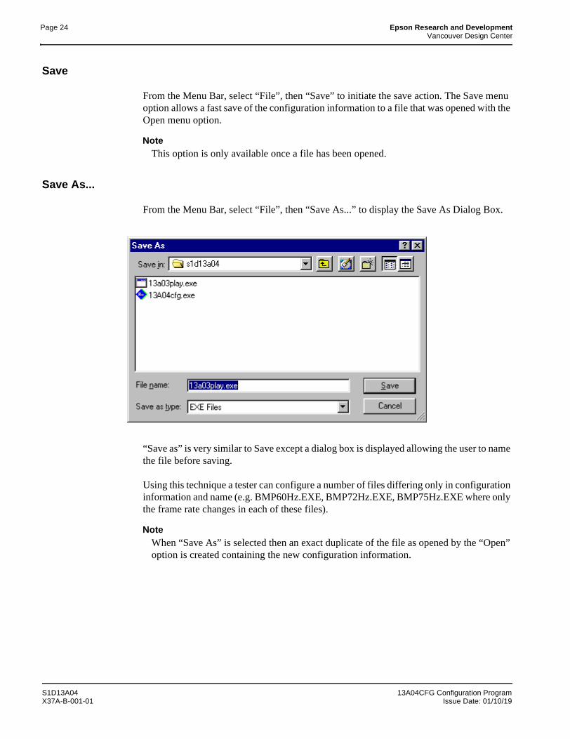
Page 24 Epson Research and DevelopmentVancouver Design Center
Save
From the Menu Bar, select “File”, then “Save” to initiate the save action. The Save menu option allows a fast save of the configuration information to a file that was opened with the Open menu option.
NoteThis option is only available once a file has been opened.
Save As...
From the Menu Bar, select “File”, then “Save As...” to display the Save As Dialog Box.
“Save as” is very similar to Save except a dialog box is displayed allowing the user to name the file before saving.
Using this technique a tester can configure a number of files differing only in configuration information and name (e.g. BMP60Hz.EXE, BMP72Hz.EXE, BMP75Hz.EXE where only the frame rate changes in each of these files).
NoteWhen “Save As” is selected then an exact duplicate of the file as opened by the “Open” option is created containing the new configuration information.
S1D13A04 13A04CFG Configuration ProgramX37A-B-001-01 Issue Date: 01/10/19
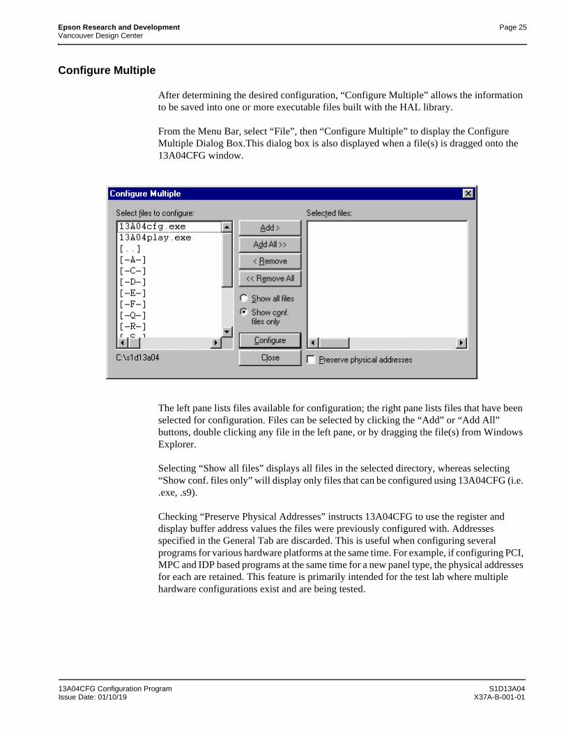
Epson Research and Development Page 25Vancouver Design Center
Configure Multiple
After determining the desired configuration, “Configure Multiple” allows the information to be saved into one or more executable files built with the HAL library.
From the Menu Bar, select “File”, then “Configure Multiple” to display the Configure Multiple Dialog Box.This dialog box is also displayed when a file(s) is dragged onto the 13A04CFG window.
The left pane lists files available for configuration; the right pane lists files that have been selected for configuration. Files can be selected by clicking the “Add” or “Add All” buttons, double clicking any file in the left pane, or by dragging the file(s) from Windows Explorer.
Selecting “Show all files” displays all files in the selected directory, whereas selecting “Show conf. files only” will display only files that can be configured using 13A04CFG (i.e. .exe, .s9).
Checking “Preserve Physical Addresses” instructs 13A04CFG to use the register and display buffer address values the files were previously configured with. Addresses specified in the General Tab are discarded. This is useful when configuring several programs for various hardware platforms at the same time. For example, if configuring PCI, MPC and IDP based programs at the same time for a new panel type, the physical addresses for each are retained. This feature is primarily intended for the test lab where multiple hardware configurations exist and are being tested.
13A04CFG Configuration Program S1D13A04Issue Date: 01/10/19 X37A-B-001-01
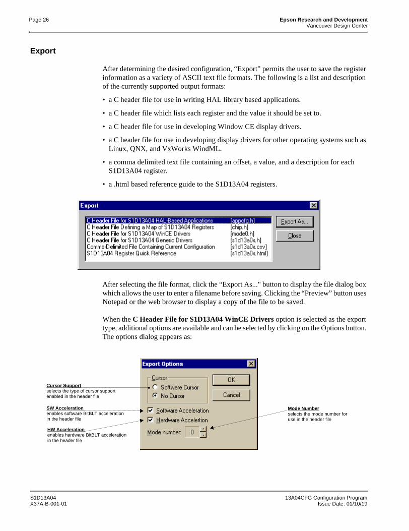
Page 26 Epson Research and DevelopmentVancouver Design Center
Export
After determining the desired configuration, “Export” permits the user to save the register information as a variety of ASCII text file formats. The following is a list and description of the currently supported output formats:
• a C header file for use in writing HAL library based applications.
• a C header file which lists each register and the value it should be set to.
• a C header file for use in developing Window CE display drivers.
• a C header file for use in developing display drivers for other operating systems such as Linux, QNX, and VxWorks WindML.
• a comma delimited text file containing an offset, a value, and a description for each S1D13A04 register.
• a .html based reference guide to the S1D13A04 registers.
After selecting the file format, click the “Export As..." button to display the file dialog box which allows the user to enter a filename before saving. Clicking the “Preview” button uses Notepad or the web browser to display a copy of the file to be saved.
When the C Header File for S1D13A04 WinCE Drivers option is selected as the export type, additional options are available and can be selected by clicking on the Options button. The options dialog appears as:
Mode Number
Cursor Support
SW Accelerationselects the mode number foruse in the header file
selects the type of cursor supportenabled in the header file
enables software BitBLT accelerationin the header file
HW Accelerationenables hardware BitBLT accelerationin the header file
S1D13A04 13A04CFG Configuration ProgramX37A-B-001-01 Issue Date: 01/10/19
Epson Research and Development Page 27Vancouver Design Center
Enable Tooltips
Tooltips provide useful information about many of the items on the configuration tabs. Placing the mouse pointer over nearly any item on any tab generates a popup window containing helpful advice and hints.
To enable/disable tooltips check/uncheck the “Tooltips” option form the “Help” menu.
NoteTooltips are enabled by default.
Tooltip Delay
This option sets the length of time the cursor must be left over an item before its associated tooltip is displayed.
ERD on the Web
This “Help” menu item is actually a hotlink to the Epson Research and Development website. Selecting “Help” then “ERD on the Web” starts the default web browser and points it to the ERD product web site.
The latest software, drivers, and documentation for the S1D13A04 is available at this website.
Update Common Controls
13A04CFG uses some of the latest common control DLLs. On systems using earlier versions of the common controls, certain controls may not appear correctly. This option updates the Common Controls required for proper operation of 13A04CFG.
About 13A04CFG
Selecting the “About 13A04CFG” option from the “Help” menu displays the about dialog box for 13A04CFG. The about dialog box contains version information and the copyright notice for 13A04CFG.
13A04CFG Configuration Program S1D13A04Issue Date: 01/10/19 X37A-B-001-01

Page 28 Epson Research and DevelopmentVancouver Design Center
Comments
• On any tab particular options may be grayed out if selecting them would violate the operational specification of the S1D13A04 (i.e. Selecting TFT or STN on the Panel tab enables/disables options specific to the panel type).
• The file panels.def is a text file containing operational specifications for several supported, and tested, panels. This file can be edited with any text editor.
• 13A04CFG allows manually altering register values. The manual changes may violate memory and LCD timings as specified in the S1D13A04 Hardware Functional Specifi-cation, document number X37A-A-001-xx. If this is done, unpredictable results may occur. Epson Research and Development, Inc. does not assume liability for any damage done to the display device as a result of configuration errors.
• Yellow diagnostic warnings are designed to draw attention to important errors in the configuration and should be corrected before saving the configuration.
• 13A04CFG can be configured by making a copy of the file 13A04cfg.exe and config-uring the copy. It is not possible to configure the original while it is running. The newly saved information becomes the default configuration for that copy of 13A04cfg.exe.
S1D13A04 13A04CFG Configuration ProgramX37A-B-001-01 Issue Date: 01/10/19
S1D13A04 LCD/USB Companion Chip
13A04PLAY Diagnostic Utility
Document Number: X37A-B-002-01
Copyright © 2001 Epson Research and Development, Inc. All Rights Reserved.
Information in this document is subject to change without notice. You may download and use this document, but only for your own use inevaluating Seiko Epson/EPSON products. You may not modify the document. Epson Research and Development, Inc. disclaims anyrepresentation that the contents of this document are accurate or current. The Programs/Technologies described in this document may contain material protected under U.S. and/or International Patent laws.
EPSON is a registered trademark of Seiko Epson Corporation. Microsoft and Windows are registered trademarks of Microsoft Corporation.All other trademarks are the property of their respective owners.

Page 2 Epson Research and DevelopmentVancouver Design Center
THIS PAGE LEFT BLANK
S1D13A04 13A04PLAY Diagnostic UtilityX37A-B-002-01 Issue Date: 01/10/05
Epson Research and Development Page 3Vancouver Design Center
13A04PLAY
13A04PLAY is a diagnostic utility which allows a user to read/write all the registers and display buffer of the S1D13A04. Commands are received from the standard input device, and messages are sent to the standard output device. On Intel platforms the console provides standard input/output. For most embedded systems the serial device provides these functions.
Commands can be entered interactively by a user, or be executed from a script file. Scripting is a powerful feature which allows command sequences to be used repeatedly without re-entry.
S1D13A04 Supported Evaluation Platforms
13A04PLAY is available as an executable for PCs running Windows® 9x/ME/NT/2000 and as C source code which can be modified and recompiled to allow 13A04PLAY to run on other platforms.
13A04PLAY Diagnostic Utility S1D13A04Issue Date: 01/10/05 X37A-B-002-01
Page 4 Epson Research and DevelopmentVancouver Design Center
Installation
PC platform
Copy the file 13A04play.exe to a directory in the path (e.g. PATH=C:\S1D13A04).
Embedded platform
Download the program 13A04play to the system.
Usage
PC platform
At the prompt, type:
13A04play [/?]
Where:
/? displays copyright and program version information.
Embedded platform
Execute 13A04play and at the prompt, type the command line argument /?.
Where:
/? displays copyright and program version information.
S1D13A04 13A04PLAY Diagnostic UtilityX37A-B-002-01 Issue Date: 01/10/05
Epson Research and Development Page 5Vancouver Design Center
Commands
The following commands are intended to be used from within the 13A04PLAY program. However, simple commands can also be executed from the command line(e.g. 13A04play f 0 14000 AB q).
NoteIf the host platform is big endian, reading/writing words and dwords to/from the regis-ters and display buffer may be incorrect. It may be necessary for the user to manuallyswap the bytes in order to perform the IO correctly. For further information on little/bigendian and the S1D13A04 byte/word swapping capabilities, see the S1D13A04 Hard-ware Functional Specification, document number X37A-A-001-xx.
CLKI freqSets the frequency of CLKI.
Where:freq The desired frequency for CLKI (in MHz).
CLKI2 freqSets the frequency of CLKI2.
Where:freq The desired frequency for CLKI2 (in MHz).
D[8|16|32] [startaddr [endaddr|len]]Displays a memory dump from the specified display buffer address range.
Where:8|16|32 The unit size: 8-bit (bytes), 16-bit (words), 32-bit (dwords).
If a unit size is not specified, this command uses the unit sizefrom the last Dump command performed. If no previousDump command has been issued, the unit size defaults to8-bit.
startaddr The starting address to read data from. Specifying aperiod (.) uses the same starting address as the last Dumpcommand performed. Specifying a startaddr of two periods(..) will back the start address by the size of len.
endaddr|len Determines how many units to continue dumping thecontents of the display buffer. A number without a prefixrepresents a physical ending address. If an “L” prefix isused, the number that follows represents len, which is thenumber of bytes/words/dwords to be dumped. Len is basedon the unit size. For example, 'L8' when the unit size is16-bit would cause the Dump command to dump 8 wordsfrom the starting address.
13A04PLAY Diagnostic Utility S1D13A04Issue Date: 01/10/05 X37A-B-002-01
Page 6 Epson Research and DevelopmentVancouver Design Center
F[8|16|32] startaddr endaddr|len data1 [data2 data3 ...]Fills a specified address range in the display buffer.
Where:8|16|32 The unit size: 8-bit (bytes), 16-bit (words), 32-bit (dwords).
If a unit size is not specified, this command uses the unit sizefrom the last Fill command performed. If no previous Fillcommand has been issued, the unit size defaults to 8-bit.
startaddr The starting address to begin filling at. Specifying aperiod (.) uses the same starting address as the last Fillcommand performed.
endaddr|len Determines how many units to fill the display buffer with. Anumber without a prefix represents a physical endingaddress. If a “L” prefix is used, the number that followsrepresents len, or the number of bytes/words/dwords to befilled. Len is based on the unit size. For example, 'L8' whenthe unit size is 16-bit would cause the Fill command to fill 8words from the starting address.
data The value(s) used to fill the display buffer. If multiplevalues are given, the pattern repeats through memory.Values can be combinations of 'text' or numbers. Numbersare assumed to be hexadecimal values unless otherwisespecified with the correct suffix (binary = i, octal = o,decimal = t, hexadecimal = h).For example, 101i = 101 binary.
H [lines]Sets the number of lines of data that are displayed at a time. The display is halted after the specified number of lines. Setting the number of lines to 0 disables the halt function and allows the data to continue displaying until all data has been shown.
This command is useful when large blocks of the display buffer or the contents of the LUT are being viewed.
Where:lines Number of lines that are shown before halting the
displayed data (decimal value).
IInitializes the S1D13A04 registers with the default register settings as configured by the utility 13A04CFG. To initialize the S1D13A04 with different register values, reconfigure 13A04PLAY using 13A04CFG. For further information on 13A04CFG, see the 13A04CFG User Manual, document number X37A-B-001-xx.
NoteIf the “I” command is used before 13A04PLAY is configured, an error message is dis-played and no further action is taken.
S1D13A04 13A04PLAY Diagnostic UtilityX37A-B-002-01 Issue Date: 01/10/05
Epson Research and Development Page 7Vancouver Design Center
L index [red green blue]Reads/writes the red, green, and blue Look-Up Table (LUT) components. If the red, green, and blue components are not specified, the LUT for the given index is read and the RGB values are displayed.
Where:index Index into the LUT (hex).red Red component of the LUT (hex).green Green component of the LUT (hex).blue Blue component of the LUT (hex).
NoteOnly bits 7-2 of each color are used in the LUT. The least significant two bits of the col-ors are discarded. For example, the command L 0 1 2 3 will set each RGB component of LUT index 0 to 0, as the values 1, 2, an 3 use only the least significant bits.
LAReads and displays all LUT values.
M [bpp]Sets the color depth (bpp). If no color depth is provided, information about the current settings are displayed.
Where:bpp Color depth to be set (1/2/4/8/16 bpp).
NoteThis command reads and interprets the S1D13A04 control registers. To function cor-rectly the registers must have been initialized using the ‘I’ command.
QQuits the program.
R[8|16|32] [addr1 addr2 addr3 ...]Reads the display buffer at the address locations given.
Where:8|16|32 The unit size: 8-bit (bytes), 16-bit (words), 32-bit (dwords).
If a unit size is not specified, this command uses the unit sizefrom the last Read command performed. If no previousRead command has been issued, the unit size defaults to8-bit.
addr The address to read data from. Multiple addresses can begiven.
13A04PLAY Diagnostic Utility S1D13A04Issue Date: 01/10/05 X37A-B-002-01
Page 8 Epson Research and DevelopmentVancouver Design Center
Run scriptfileThis command opens the file scriptfile and executes each line as if it were typed from the command prompt. For more information on scriptfiles, see Section , “Script Files” on page 12.
Where:scriptfile The file containing 13A04PLAY commands
S[8|16|32] startaddr endaddr|len data1 [data2 data3 data4 ...]Search the display buffer for the given data.
Where:8|16|32 The unit size: 8-bit (bytes), 16-bit (words), 32-bit (dwords).
If a unit size is not specified, this command uses the unit sizefrom the last Search command performed. If no previousSearch command has been issued, the unit size defaults to8-bit.
startaddr The starting address to begin the search from. Specifying aperiod (.) uses the same starting address as the last Searchcommand performed.
endaddr|len Determines how many units of the display buffer will besearched through. A number without a prefix represents aphysical ending address. If a “L” prefix is used, the numberthat follows represents len, or the number ofbytes/words/dwords to be searched through. Len is based onthe unit size. For example, 'L8' when the unit size is 16-bitwould cause the Search command to search 8 words fromthe starting address.
data The value(s) to search the display buffer for. Values can becombinations of 'text' or numbers. Numbers areassumed to be hexadecimal values unless otherwisespecified with the correct suffix (binary = i, octal = o,decimal = t, hexadecimal = h).For example, 101i = 101 binary.
ShowShows a test pattern on the display. The test pattern is based on current register settings and may not display correctly if the registers are not configured properly.
Use this command to display an image during testing. After adjusting a register value, use the show command to view the effect on the display.
S1D13A04 13A04PLAY Diagnostic UtilityX37A-B-002-01 Issue Date: 01/10/05
Epson Research and Development Page 9Vancouver Design Center
U index [data]Reads/writes data to the USB register at index. If no data is specified, the command reads and displays the contents from the USB register at index.
Where:index Index into the USB registers (hex).data The value to be written to the register. Numbers are assumed
to be hexadecimal values unless otherwise specified withthe correct suffix (binary = i, octal = o, decimal = t,hexadecimal = h).For example, 101i = 101 binary.
UAReads and displays the contents of all the USB registers.
UX index [data]This command automates the writes/reads into the indexed USB registers located at REG[4038h] and REG[403Ah]. Index represents the value that would be written into REG[4038h] if separate operations were done to access the index and data registers. If no data is specified, the command reads and displays the contents of the specified extended USB register.
Where:index Index into USB registers at REG[403Ah] (hex).data The value to be written to the indexed data register.
Numbers are assumed to be hexadecimal values unlessotherwise specified with the correct suffix (binary = i,octal = o, decimal = t, hexadecimal = h).For example, 101i = 101 binary.
13A04PLAY Diagnostic Utility S1D13A04Issue Date: 01/10/05 X37A-B-002-01
Page 10 Epson Research and DevelopmentVancouver Design Center
W[8|16|32] [startaddr [data1 data2 data3 data4 ...]]Writes the given data sequence to the display buffer starting at startaddr location.
Where:8|16|32 The unit size: 8-bit (bytes), 16-bit (words), 32-bit (dwords).
If a unit size is not specified, this command uses the unit sizefrom the last Write command performed. If no previousWrite command has been issued, the unit size defaults to8-bit.
startaddr The starting address to write data to. Specifying aperiod (.) uses the same starting address as the last Writecommand performed.
data Values to write to the display buffer. If no data is given, thenthis function enters MODIFY mode. This mode prompts theuser with the address and it's current data. While in thismode, the user can type any of the following.
- new values (in hex)- ENTER or SPACE - moves to the next memory
location (if data is specified the previousmemory location is updated, if no data isspecified no change is made)
- “-” - moves to the previous memory location- “Q” or “.” - exits MODIFY mode
X[8|16|32] [index [data]]Reads/writes data to the register at index. If no data is specified, the register is read and the contents are displayed.
Where:8|16|32 The unit size: 8-bit (bytes), 16-bit (words), 32-bit (dwords).
If a unit size is not specified, this command uses the unit sizefrom the last X command performed. If no previous Xcommand has been issued, the unit size defaults to 8-bit.
index Index into the registers (hex).data The value to be written to the register. Numbers are
assumed to be hexadecimal values unless otherwisespecified with the correct suffix (binary = i, octal = o,decimal = t, hexadecimal = h).For example, 101i = 101 binary.
XAReads and displays the contents of all the S1D13A04 registers.
?Displays the help screen. The help screen contains a summary of all available commands.
S1D13A04 13A04PLAY Diagnostic UtilityX37A-B-002-01 Issue Date: 01/10/05
Epson Research and Development Page 11Vancouver Design Center
13A04PLAY Example
1. Configure 13A04PLAY using the utility 13A04CFG. For further information on 13A04CFG, see the 13A04CFG User Manual, document number X37A-B-001-xx.
2. Type 13A04PLAY to start the program.
3. Type ? for help.
4. Type i to initialize the registers.
5. Type xa to display the contents of the registers.
6. Type x 80 to read register 80h.
7. Type x 80 10 to write 10h to register 80h.
8. Type f 0 ffff aa to fill the first 10000h bytes of the display buffer with AAh.
9. Type d 0 ff to read the first 100h bytes of the display buffer.
10. Type show to display a test pattern.
11. Type m to display current mode information.
12. Type m 2 to set the color depth to 2 bpp.
13. Type show to display a test pattern.
14. Type q to exit the program.
13A04PLAY Diagnostic Utility S1D13A04Issue Date: 01/10/05 X37A-B-002-01
Page 12 Epson Research and DevelopmentVancouver Design Center
Script Files
13A04PLAY can be controlled by a script file. This is useful when:
• there is no display to monitor command keystroke accuracy.
• various registers must be quickly changed to view results.
A script file is an ASCII text file with one 13A04PLAY command per line. Script files can be executed from within 13A04PLAY using the Run command (e.g. = run dumpregs.scr). Alternately, the script file can be executed from the OS command prompt. On a PC platform, a typical script command line might be:
13A04PLAY run dumpregs.scr > results
This causes the file dumpregs.scr to be interpreted as commands by 13A04PLAY and the results to be redirected to the file results.
Example 1: Create a script file that reads all registers.
; This file initializes the S1D13A04 and reads the registers.; Note: after a semicolon (;), all characters on a line are ignored.
; Initialize the S1D13A04i
; Read all registersxa
S1D13A04 13A04PLAY Diagnostic UtilityX37A-B-002-01 Issue Date: 01/10/05
S1D13A04 LCD/USB Companion Chip
13A04BMP Demonstration Program
Document Number: X37A-B-003-01
Copyright © 2001 Epson Research and Development, Inc. All Rights Reserved.
Information in this document is subject to change without notice. You may download and use this document, but only for your own use inevaluating Seiko Epson/EPSON products. You may not modify the document. Epson Research and Development, Inc. disclaims anyrepresentation that the contents of this document are accurate or current. The Programs/Technologies described in this document may contain material protected under U.S. and/or International Patent laws.
EPSON is a registered trademark of Seiko Epson Corporation. Microsoft and Windows are registered trademarks of Microsoft Corporation.All other trademarks are the property of their respective owners.

Page 2 Epson Research and DevelopmentVancouver Design Center
THIS PAGE LEFT BLANK
S1D13A04 13A04BMP Demonstration ProgramX37A-B-003-01 Issue Date: 01/10/04
Epson Research and Development Page 3Vancouver Design Center
13A04BMP
13A04BMP is a demonstration utility used to show the S1D13A04 display capabilities by rendering bitmap images on the display device. The program displays a bitmap stored in Windows BMP file format and then exits. 13A04BMP supports SviwelView™ (90°, 180°, and 270° hardware rotation of the display image).
13A04BMP is designed to operate on a personal computer (PC) within a 32-bit environment only (Windows® 9x/NT/ME/2000). Other embedded platforms are not supported due to the possible lack of system memory or structured file system.
The 13A04BMP demonstration utility must be configured to work with your hardware configuration. The program 13A04CFG can be used to configure 13A04BMP. For further information on 13A04CFG, refer to the 13A04CFG Users Manual, document number X37A-B-001-xx.
S1D13A04 Supported Evaluation Platforms
13A04BMP supports the following S1D13A04 evaluation platforms:
• PC with an Intel 80x86 processor running Windows 9x/NT/ME/2000.
NoteThe 13A04BMP source code may be modified by the OEM to support other evaluationplatforms.
Installation
Copy the file 13A04bmp.exe to a directory in the path (e.g. PATH=C:\S1D13A04).
13A04BMP Demonstration Program S1D13A04Issue Date: 01/10/04 X37A-B-003-01
Page 4 Epson Research and DevelopmentVancouver Design Center
Usage
At the prompt, type:
13A04bmp bmpfile [/?]
Where:
bmpfile Specifies filename of the windows format bmp image to be displayed.
/? Displays the help message.
Note13A04BMP displays the bmpfile image and returns to the prompt.
13A04BMP Examples
To display a .bmp image in the main window on an LCD, type the following:13A04bmp bmpfile.bmp
NoteTo display a bmpfile using SwivelView, configure 13A04bmp.exe for the selectedSwivelView mode using the configuration program 13A04CFG. For further informationon 13A04CFG, see the 13A04CFG User Manual, document number X37A-B-001-xx.
Comments
• 13A04BMP displays only Windows BMP format images.
• A 24-bit true color bitmap is displayed at a color depth of 16 bit-per-pixel.
• Only the green component of the image is seen on a monochrome panel.
• 13A04BMP does not perform any image translations. The image to display must be the desired dimensions and color depth.
S1D13A04 13A04BMP Demonstration ProgramX37A-B-003-01 Issue Date: 01/10/04

S1D13A04 LCD/USB Companion Chip
Wind River WindML v2.0 Display Drivers
Document Number: X37A-E-002-01
Copyright © 2001 Epson Research and Development, Inc. All Rights Reserved.
Information in this document is subject to change without notice. You may download and use this document, but only for your own use inevaluating Seiko Epson/EPSON products. You may not modify the document. Epson Research and Development, Inc. disclaims anyrepresentation that the contents of this document are accurate or current. The Programs/Technologies described in this document may contain material protected under U.S. and/or International Patent laws.
EPSON is a registered trademark of Seiko Epson Corporation. All other trademarks are the property of their respective owners.

Page 2 Epson Research and DevelopmentVancouver Design Center
THIS PAGE LEFT BLANK
S1D13A04 Wind River WindML v2.0 Display DriversX37A-E-002-01 Issue Date: 01/09/28

Epson Research and Development Page 3Vancouver Design Center
Wind River WindML v2.0 DISPLAY DRIVERS
The Wind River WindML v2.0 display drivers for the S1D13A04 LCD/USB Companion Chip are intended as “reference” source code for OEMs developing for Wind River’s WindML v2.0. The driver package provides support for both 8 and 16 bit-per-pixel color depths. The source code is written for portability and contains functionality for most features of the S1D13A04. Source code modification is required to produces a smaller, more efficient driver for mass production.
The WindML display drivers are designed around a common configuration include file called mode0.h which is generated by the configuration utility 13A04CFG. This design allows for easy customization of display type, clocks, decode addresses, rotation, etc. by OEMs. For further information on 13A04CFG, see the 13A04CFG Configuration Program User Manual, document number X37A-B-001-xx.
NoteThe WindML display drivers are provided as “reference” source code only. They are in-tended to provide a basis for OEMs to develop their own drivers for WindML v2.0. These drivers are not backwards compatible with UGL v1.2. For information on UGL v1.2 display drivers, contact us via email at [email protected].
This document and the source code for the WindML display drivers is updated as appro-priate. Please check the Epson Research and Development website at www.erd.epson.com for the latest revisions before beginning any development.
We appreciate your comments on our documentation. Please contact us via email at [email protected].
Wind River WindML v2.0 Display Drivers S1D13A04Issue Date: 01/09/28 X37A-E-002-01

Page 4 Epson Research and DevelopmentVancouver Design Center
Building a WindML v2.0 Display Driver
The following instructions produce a bootable disk that automatically starts the UGL demo program. These instructions assume that Wind River’s Tornado platform is already installed.
NoteFor the example steps where the drive letter is given as “x:”. Substitute “x” with the drive letter that your development environment is on.
1. Create a working directory and unzip the WindML display driver into it.
From a command prompt or GUI interface create a new directory (e.g. x:\13A04).
Unzip the file 13A04windml.zip to the newly created working directory. The files will be unzipped to the directories “x:\13A04\8bpp” and “x:\13A04\16bpp”.
2. Configure for the target execution model.
This example build creates a VxWorks image that fits onto and boots from a single floppy diskette. In order for the VxWorks image to fit on the disk certain modifica-tions are required.
Replace the file “x:\Tornado\target\config\pcPentium\config.h” with the file “x:\13A04\8bpp\File\config.h” (or “x:\13A04\16bpp\File\config.h”). The new con-fig.h file removes networking components and configures the build image for booting from a floppy disk.
NoteRather than simply replacing the original config.h file, rename it so the file can be kept for reference purposes.
3. Build a boot ROM image.
From the Tornado tool bar, select Build -> Build Boot ROM. Select “pcPentium” as the BSP and “bootrom_uncmp” as the image.
4. Create a bootable disk (in drive A:).
From a command prompt change to the directory “x:\Tornado\host\x86-win32\bin” and run the batch file torvars.bat. Next, change to the directory “x:\Tornado\tar-get\config\pcPentium” and type:
mkboot a: bootrom_uncmp
S1D13A04 Wind River WindML v2.0 Display DriversX37A-E-002-01 Issue Date: 01/09/28
Epson Research and Development Page 5Vancouver Design Center
5. If necessary, generate a new mode0.h configuration file.
The file mode0.h contains the register values required to set the screen resolution, col-or depth (bpp), display type, rotation, etc. The mode0.h file included with the drivers, may not contain applicable values and must be regenerated. The configuration pro-gram 13A04CFG can be used to build a new mode0.h file. If building for 8 bpp, place the new mode0.h file in the directory “x:\13A04\8bpp\File”. If building for 16 bpp, place the new mode0.h file in “x:\13A04\16bpp\File”.
NoteMode0.h should be created using the configuration utility 13A04CFG. For more infor-mation on 13A04CFG, see the 13A04CFG Configuration Program User Manual, docu-ment number X37A-B-001-xx available at www.erd.epson.com.
6. Build the WindML v2.0 library.
From a command prompt change to the directory “x:\Tornado\host\x86-win32\bin” and run the batch file torvars.bat. Next, change to the directory “x:\Tornado\tar-get\src\ugl” and type the command:
make CPU=PENTIUM ugl
7. Open the S1D13A04 workspace.
From the Tornado tool bar, select File->Open Workspace...->Existing->Browse... and select the file “x:\13A04\8bpp\13A03.wsp” (or “x:\13A04\16bpp\13A04.wsp”).
8. Add support for single line comments.
The WindML v2.0 display driver source code uses single line comment notation, “//”, rather than the ANSI conventional comments, “/*...*/”.
To add support for single line comments follow these steps:
a. In the Tornado “Workspace Views” window, click on the “Builds” tab.
b. Expand the “8bpp Builds” (or “16bpp Builds”) view by clicking on the “+” next to it. The expanded view will contain the item “default”. Right-click on “default” and select “Properties...”. A “Properties:” window will appear.
c. Select the “C/C++ compiler” tab to display the command switches used in the build. Remove the “-ansi” switch from the line that contains “-g -mpentium -ansi -nostdinc -DRW_MULTI_THREAD”.(Refer to GNU ToolKit user's guide for details)
Wind River WindML v2.0 Display Drivers S1D13A04Issue Date: 01/09/28 X37A-E-002-01
Page 6 Epson Research and DevelopmentVancouver Design Center
9. Compile the VxWorks image.
Select the “Builds” tab in the Tornado “Workspace Views” window.
Right-click on “8bpp files” (or “16bpp files”) and select “Dependencies...”. Click on “OK” to regenerate project file dependencies for “All Project files”.
Right-click on “8bpp files” (or “16bpp files”) and select “ReBuild All(vxWorks)” to build VxWorks.
10. Copy the VxWorks file to the diskette.
From a command prompt or through the Windows interface, copy the file “x:\13A04\8bpp\default\vxWorks” (or “x:\13A04\16bpp\default\vxWorks”) to the bootable disk created in step 4.
11. Start the VxWorks demo.
Boot the target PC with the VxWorks bootable diskette to run the UGL demo program automatically.
S1D13A04 Wind River WindML v2.0 Display DriversX37A-E-002-01 Issue Date: 01/09/28

S1D13A04 LCD/USB Companion Chip
Linux Console Driver
Document Number: X37A-E-004-01
Copyright © 2001 Epson Research and Development, Inc. All Rights Reserved.
Information in this document is subject to change without notice. You may download and use this document, but only for your own use inevaluating Seiko Epson/EPSON products. You may not modify the document. Epson Research and Development, Inc. disclaims anyrepresentation that the contents of this document are accurate or current. The Programs/Technologies described in this document may contain material protected under U.S. and/or International Patent laws.
EPSON is a registered trademark of Seiko Epson Corporation.

Page 2 Epson Research and DevelopmentVancouver Design Center
THIS PAGE LEFT BLANK
S1D13A04 Linux Console DriverX37A-E-004-01 Issue Date: 01/09/28
Epson Research and Development Page 3Vancouver Design Center
Linux Console Driver
The Linux console driver for the S1D13A04 LCD/USB Companion Chip is intended as “reference” source code for OEMs developing for Linux, and supports 4, 8, and 16 bit-per-pixel color depths. The source code is written for portability and contains functionality for most features of the S1D13A04. Source code modification is required to provide a smaller driver for mass production.
A Graphical User Interface (GUI) such as Gnome can obtain the frame buffer address from this driver allowing the Linux GUI the ability to update the display.
The console driver is designed around a common configuration include file called s1d13A04.h, which is generated by the configuration utility 13A04CFG. This design allows for easy customization of display type, clocks, decode addresses, rotation, etc. by OEMs. For further information on 13A04CFG, see the 13A04CFG Configuration Program User Manual, document number X37A-B-001-xx.
NoteThe Linux console driver is provided as “reference” source code only. The driver is in-tended to provide a basis for OEMs to develop their own drivers for Linux.
This document and the source code for the Linux console drivers are updated as appro-priate. Please check the Epson Research and Development website at www.erd.epson.com for the latest revisions or before beginning any development.
We appreciate your comments on our documentation. Please contact us via e-mail at [email protected].
Linux Console Driver S1D13A04Issue Date: 01/09/28 X37A-E-004-01

Page 4 Epson Research and DevelopmentVancouver Design Center
Building the Console Driver for Linux Kernel 2.2.x
Follow the steps below to construct a copy of the Linux operating system using the S1D13A04 as the console display device. These instructions assume that the GNU devel-opment environment is installed and the user is familiar with GNU and the Linux operating system.
1. Acquire the Linux kernel source code.
You can obtain the Linux kernel source code from your Linux supplier or download the source from: ftp://ftp.kernel.org.
The S1D13A04 reference driver requires Linux kernel 2.2.x. The example S1D13A04 reference driver available on www.erd.epson.com was built using Red Hat Linux 6.1, kernel version 2.2.17.
For information on building the kernel refer to the readme file at:ftp://ftp.linuxberg.com/pub/linux/kernel/README
NoteBefore continuing with modifications for the S1D13A04, you should ensure that you can build and start the Linux operating system.
2. Unzip the console driver files.
Using a zip file utility, unzip the S1D13A04 archive to a temporary directory. (e.g. /tmp)
When completed the following files should be located in the temporary directory.s1d13xxxfb.cs1d13A04.hConfig.infbmem.cfbcon-cfb4.c, andMakefile
3. Copy the console driver files to the build directory.
Copy the following files to the directory /usr/src/linux/drivers/video./tmp/s1d13xxxfb.c and/tmp/s1d13A04.h
Copy the remaining source files into the directory /usr/src/linux/drivers/video replac-ing the files of the same name.
/tmp/Config.in/tmp/fbmem.c/tmp/fbcon-cfb4.c, and/tmp/Makefile
If your kernel version is not 2.2.17, or you want to retain greater control of the build process, use a text editor to cut and paste the sections dealing with the Epson driver in the corresponding files of the same names.
S1D13A04 Linux Console DriverX37A-E-004-01 Issue Date: 01/09/28
Epson Research and Development Page 5Vancouver Design Center
4. Modify s1d13A04.h
The file s1d13A04.h contains the register values required to set the screen resolution, color depth (bpp), display type, active display (LCD), display rotation, etc.
Before building the console driver, refer to the descriptions in the file s1d13A04.h for the default settings of the console driver. If the default does not match the configura-tion you are building for then s1d13A04.h must be regenerated with the correct infor-mation.
Use the program 13A04CFG to generate the required header file. For information on how to use 13A04CFG, refer to the 13A04CFG Configuration Program User Manual, document number X37A-B-001-xx, available at www.erd.epson.com
After selecting the desired configuration, choose “File->Export” and select the “C Header File for S1D13A04 Generic Drivers” option. Save the new configuration as s1d13A04.h in the /usr/src/linux/drivers/video, replacing the original configuration file.
5. Configure the video options.
From the command prompt in the directory /usr/src/linux run the command:make menuconfig
This command will start a text based interface which allows the selection of build time parameters. From the text interface under “Console drivers” options, select:
“Support for frame buffer devices”“Epson LCD/CRT controllers support”“S1D13A04 support”“Advanced low level driver options”“xBpp packed pixels support” *
* where x is the color depth being compile for.
If you are using the Epson S5U13A04B00C evaluation board then you must also se-lect:
“Epson PCI Bridge adapter support”
Once you have configured the kernel options, save and exit the configuration utility.
6. Compile and install the kernel.
Build the kernel with the following sequence of commands.make depmake clean make bzImage/sbin/lilo (if running lilo)
Linux Console Driver S1D13A04Issue Date: 01/09/28 X37A-E-004-01
Page 6 Epson Research and DevelopmentVancouver Design Center
7. Boot to the Linux operating system.
If you are using lilo (Linux Loader), modify the lilo configuration file as discussed in the kernel build README file. If there were no errors during the build, from the com-mand prompt run:
lilo
and reboot your system.
NoteIn order to use the S1D13A04 console driver with X server, you need to configure the X server to use the FBDEV device. The information on the necessary files and instructions for this process is available on the Internet at www.xfree86.org
S1D13A04 Linux Console DriverX37A-E-004-01 Issue Date: 01/09/28

Epson Research and Development Page 7Vancouver Design Center
Building the Console Driver for Linux Kernel 2.4.x
Follow the steps below to construct a copy of the Linux operating system using the S1D13A04 as the console display device. These instructions assume that the GNU devel-opment environment is installed and the user is familiar with GNU and the Linux operating system.
1. Acquire the Linux kernel source code.
You can obtain the Linux kernel source code from your Linux supplier or download the source from: ftp://ftp.kernel.org.
The S1D13A04 reference driver requires Linux kernel 2.4.x or greater. The example S1D13A04 reference driver available on www.erd.epson.com was built using Red Hat Linux 6.1, kernel version 2.4.5.
For information on building the kernel refer to the readme file at:ftp://ftp.linuxberg.com/pub/linux/kernel/README
NoteBefore continuing with modifications for the S1D13A04, you should ensure that you can build and start the Linux operating system.
2. Unzip the console driver files.
Using a zip file utility, unzip the S1D13A04 archive to a temporary directory. (e.g. /tmp)
When completed the files:Config.infbmem.cfbcon-cfb4.cMakefile
should be located in the temporary directory (/tmp), and the files:Makefiles1d13xxxfb.cs1d13A04.h
should be located in a sub-directory called epson within the temporary directory (/tmp/epson).
Linux Console Driver S1D13A04Issue Date: 01/09/28 X37A-E-004-01
Page 8 Epson Research and DevelopmentVancouver Design Center
3. Copy the console driver files to the build directory. Make the directory /usr/src/linux/drivers/video/epson.
Copy the files/tmp/epson/s1d13xxxfb.c /tmp/epson/s1d13A04.h/tmp/epson/Makefile
to the directory /usr/src/linux/drivers/video/epson.
Copy the remaining source files/tmp/Config.in/tmp/fbmem.c/tmp/fbcon-cfb4.c/tmp/Makefile
into the directory /usr/src/linux/drivers/video replacing the files of the same name.
If your kernel version is not 2.4.5 or you want to retain greater control of the build process then use a text editor and cut and paste the sections dealing with the Epson driver in the corresponding files of the same names.
4. Modify s1d13A04.h
The file s1d13A04.h contains the register values required to set the screen resolution, color depth (bpp), display type, active display (LCD/CRT), display rotation, etc.
Before building the console driver, refer to the descriptions in the file s1d13A04.h for the default settings of the console driver. If the default does not match the configura-tion you are building for then s1d13A04.h will have to be regenerated with the correct information.
Use the program 13A04CFG to generate the required header file. For information on how to use 13A04CFG, refer to the 13A04CFG Configuration Program User Manual, document number X37A-B-001-xx, available at www.erd.epson.com
After selecting the desired configuration, choose “File->Export” and select the “C Header File for S1D13A04 Generic Drivers” option. Save the new configuration as s1d13A04.h in the /usr/src/linux/drivers/video, replacing the original configuration file.
S1D13A04 Linux Console DriverX37A-E-004-01 Issue Date: 01/09/28

Epson Research and Development Page 9Vancouver Design Center
5. Configure the video options.
From the command prompt in the directory /usr/src/linux run the command:make menuconfig
This command will start a text based interface which allows the selection of build time parameters. From the options presented select:
“Code maturity level” options“Prompt for development and/or incomplete drivers”
“Console drivers” options“Frame-buffer support”
“Support for frame buffer devices (EXPERIMENTAL)”“EPSON LCD/CRT/TV controller support”
“EPSON S1D13A04 Support”“Advanced low-level driver options”
“xbpp packed pixels support” *
* where x is the color depth being compiled for.
If you are using the Epson S5U13A04B00C evaluation board then you must also se-lect:
“Epson PCI Bridge adapter support”
Once you have configured the kernel options, save and exit the configuration utility.
6. Compile and install the kernel
Build the kernel with the following sequence of commands: make depmake clean make bzImage/sbin/lilo (if running lilo)
7. Boot to the Linux operating system
If you are using lilo (Linux Loader), modify the lilo configuration file as discussed in the kernel build README file. If there were no errors during the build, from the com-mand prompt run:
lilo
and reboot your system.
NoteIn order to use the S1D13A04 console driver with X server, you need to configure the Xserver to use the FBDEV device. A good place to look for the necessary files and in-structions on this process is on the Internet at www.xfree86.org
Linux Console Driver S1D13A04Issue Date: 01/09/28 X37A-E-004-01

Page 10 Epson Research and DevelopmentVancouver Design Center
THIS PAGE LEFT BLANK
S1D13A04 Linux Console DriverX37A-E-004-01 Issue Date: 01/09/28
S1D13A04 LCD/USB Companion Chip
QNX Photon v2.0 Display Driver
Document Number: X37A-E-005-01
Copyright © 2001 Epson Research and Development, Inc. All Rights Reserved.
Information in this document is subject to change without notice. You may download and use this document, but only for your own use inevaluating Seiko Epson/EPSON products. You may not modify the document. Epson Research and Development, Inc. disclaims anyrepresentation that the contents of this document are accurate or current. The Programs/Technologies described in this document may contain material protected under U.S. and/or International Patent laws.EPSON is a registered trademark of Seiko Epson Corporation. All other trademarks are the property of their respective owners.

Page 2 Epson Research and DevelopmentVancouver Design Center
THIS PAGE LEFT BLANK
S1D13A04 QNX Photon v2.0 Display DriverX37A-E-005-01 Issue Date: 01/10/19
Epson Research and Development Page 3Vancouver Design Center
QNX Photon v2.0 Display Driver
The Photon v2.0 display driver for the S1D13A04 LCD/USB Companion Chip is intended as “reference” source code for OEMs developing for QNX platforms. The driver package provides support for 8 and 16 bit-per-pixel color depths. The source code is written for portability and contains functionality for most features of the S1D13A04. Source code modification is required to provide a smaller driver for mass production.
The current revision of the driver is designed for use with either QNX RTP or QNX4 from the latest product CD (Dec. 99).
The Photon v2.0 display driver is designed around a common configuration include file called S1D13A04.h, which is generated by the configuration utility 13A04CFG. This design allows for easy customization of display type, clocks, decode addresses, rotation, etc. by OEMs. For further information on 13A04CFG, see the 13A04CFG Configuration Program User Manual, document number X37A-B-001-xx.
NoteThe QNX display drivers are provided as “reference” source code only. They are intend-ed to provide a basis for OEMs to develop their own drivers for QNX Photon v2.0.
This document and the source code for the QNX display drivers are updated as appropriate. Please check the Epson Research and Development website at www.erd.epson.com for the latest revisions before beginning any development.
We appreciate your comments on our documentation. Please contact us via e-mail at [email protected].
QNX Photon v2.0 Display Driver S1D13A04Issue Date: 01/10/19 X37A-E-005-01
Page 4 Epson Research and DevelopmentVancouver Design Center
Building the Photon v2.0 Display Driver
The following steps build the Photon v2.0 display driver and integrate it into the QNX operating system. These instructions assume the QNX developer environment is correctly installed and the developer is familiar with building for the QNX operating system.
Unpack the Graphics Driver Development Kit Archive
1. Install the QNX ddk package using the Package Manager utility.
For information about the Drivers Development Kit contact QNX directly.
2. Once the ddk package is installed, copy the directory tree /usr/scr/gddk_v1.0 into the Project directory.
3. Change directory to Project/gddk_1.0/devg.
4. Unpack the display driver files using the commands:
#gunzip S1D13A04.tar.gz
#tar –xvf S1D13A04.tar
This unpacks the files into the directory Project/gddk_1.0/devg/S1D13A04.
Configure the Driver
The files s1d13A04_16.h and s1d13A04_8.h contain register values required to set the screen resolution, color depth (bpp), display type, rotation, etc. The s1d13A04.h file included with the drivers may not contain applicable values and must be regenerated. The configuration program 13A04CFG can be used to build new s1d13A04_16.h and s1d13A04_8.h files.
NoteS1d13A04.h should be created using the configuration utility 13A04CFG. For more in-formation on 13A04CFG, see the 13A04CFG Configuration Program User Manual,document number X37A-B-001-xx available at www.erd.epson.com.
Build the Driver
The first time the driver is built, the following command ensures that all drivers and required libraries are built. At the root of the Project source tree, type make.
NoteTo build drivers for X86 NTO type ‘OSLIST=nto CPULIST=x86 make’.
Further builds do not require all libraries to be re-built. To build only the S1D13A04 display driver, change to the directory gddk_1.0/devg/s1d13A04 and type make.
S1D13A04 QNX Photon v2.0 Display DriverX37A-E-005-01 Issue Date: 01/10/19
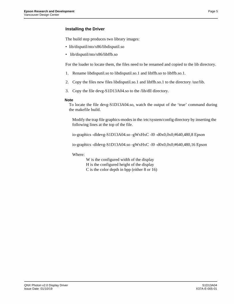
Epson Research and Development Page 5Vancouver Design Center
Installing the Driver
The build step produces two library images:
• lib/disputil/nto/x86/libdisputil.so
• lib/disputil/nto/x86/libffb.so
For the loader to locate them, the files need to be renamed and copied to the lib directory.
1. Rename libdisputil.so to libdisputil.so.1 and libffb.so to libffb.so.1.
2. Copy the files new files libdisputil.so.1 and libffb.so.1 to the directory /usr/lib.
3. Copy the file devg-S1D13A04.so to the /lib/dll directory.
NoteTo locate the file devg-S1D13A04.so, watch the output of the ‘true’ command duringthe makefile build.
Modify the trap file graphics-modes in the /etc/system/config directory by inserting the following lines at the top of the file.
io-graphics -dldevg-S1D13A04.so -gWxHxC -I0 -d0x0,0x0;#640,480,8 Epson
io-graphics -dldevg-S1D13A04.so -gWxHxC -I0 -d0x0,0x0;#640,480,16 Epson
Where:W is the configured width of the displayH is the configured height of the displayC is the color depth in bpp (either 8 or 16)
QNX Photon v2.0 Display Driver S1D13A04Issue Date: 01/10/19 X37A-E-005-01

Page 6 Epson Research and DevelopmentVancouver Design Center
Run the Driver
NoteFor the remaining steps the S5U13A04B00C evaluation board must be installed on thetest platform.
It is recommended that the driver be verified before starting QNX with the S1D13A04 as the primary display. To verify the driver, type the following command at the root of the Project source tree (gddk_1.0 directory).
util/bench/nto/x86/o/devg-bench -dldevg/S1D13A04/nto/x86/dll/devg-S1D13A04.so -mW,H,C,F -d0x0,0x0
Where:W is the configured width of the displayH is the configured height of the displayC is the color depth in bpp (either 8 or 16)F is the configured frame rate
This command starts the bench utility which will initialize the driver as the secondary display and exercise the drivers main functions. If the display appears satisfactory, restart QNX Photon and the restart will result in the S1D13A04 display driver becoming the primary display device.
Comments
• To restore the display driver to the default, comment out changes made to the trap file crt.$NODE.
S1D13A04 QNX Photon v2.0 Display DriverX37A-E-005-01 Issue Date: 01/10/19
S1D13A04 LCD/USB Companion Chip
Windows® CE 3.x Display Driver
Document Number: X37A-E-006-01
Copyright © 2001 Epson Research and Development, Inc. All Rights Reserved.
Information in this document is subject to change without notice. You may download and use this document, but only for your own use inevaluating Seiko Epson/EPSON products. You may not modify the document. Epson Research and Development, Inc. disclaims anyrepresentation that the contents of this document are accurate or current. The Programs/Technologies described in this document may contain material protected under U.S. and/or International Patent laws.
EPSON is a registered trademark of Seiko Epson Corporation. Microsoft and Windows are registered trademarks of Microsoft Corporation.All other trademarks are the property of their respective owners.

Page 2 Epson Research and DevelopmentVancouver Design Center
THIS PAGE LEFT BLANK
S1D13A04 Windows® CE 3.x Display DriverX37A-E-006-01 Issue Date: 01/10/19
Epson Research and Development Page 3Vancouver Design Center
WINDOWS® CE 3.0 DISPLAY DRIVER
Windows CE v3.0 display driver for the S1D13A04 LCD/USB Companion Chip is intended as “reference” source code for OEMs developing for the Microsoft Window CE platform. The driver supports 4, 8 and 16 bit-per-pixel color depths in landscape mode (no rotation), and 8 and 16 bit-per-pixel color depths in SwivelView™ 90 degree, 180 degree and 270 degree modes. The source code is written for portability and contains functionality for most features of the S1D13A04. Source code modification is required to provide a smaller driver for mass production.
The Windows CE v3.0 display driver is designed around a common configuration include file called mode0.h, which is generated by the configuration utility 13A04CFG. This design allows for easy customization of display type, clocks, decode addresses, rotation, etc. by OEMs. For further information on 13A04CFG, see the 13A04CFG Configuration Program User Manual, document number X37A-B-001-xx.
NoteThe Windows CE display driver is provided as “reference” source code only. They are intended to provide a basis for OEMs to develop their own drivers for Microsoft Win-dows CE v3.0.
This document and the source code for the Windows CE v3.0 driver is updated as appro-priate. Before beginning any development, please check the Epson Research and Devel-opment Website at www.erd.epson.com for the latest revisions.
We appreciate your comments on our documentation. Please contact us via email at [email protected].
Windows® CE 3.x Display Driver S1D13A04Issue Date: 01/10/19 X37A-E-006-01
Page 4 Epson Research and DevelopmentVancouver Design Center
Example Driver Builds
The following section describes how to build the Windows CE display driver for Windows CE Platform Builder 3.00 using the GUI interface.
Build for CEPC (X86) on Windows CE Platform Builder 3.00 using the GUI Interface
1. Install Microsoft Windows 2000 Professional, or Windows NT Workstation version 4.0 with Service Pack 5 or later.
2. Install Platform Builder 3.00.
3. Start Platform Builder by double-clicking on the Microsoft Windows CE Platform Builder icon.
4. Create a new project.
a. Select File | New.
b. In the dialog box, select the Platforms tab.
c. In the platforms dialog box, select “WCE Platform”, set a location for the project (such as x:\myproject), set the platform name (such as myplatform), and set the processor to “Win32 (WCE x86)”.
d. Click the OK button.
e. In the dialog box “WCE Platform - Step 1 of 2”, select CEPC.
f. Click the Next button.
g. In the dialog box “WCE Platform - Step 2 of 2”, select Maximum OS (Maxall).
h. Click the Finish button.
i. In the dialog box “New Platform Information”, click the OK button.
5. Set the active configuration to “Win32 (WCE x86) Release”.
a. From the Build menu, select “Set Active Configuration”.
b. Select “MYPLATFORM - Win32 (WCE x86) Release”.
c. Click the OK button.
S1D13A04 Windows® CE 3.x Display DriverX37A-E-006-01 Issue Date: 01/10/19

Epson Research and Development Page 5Vancouver Design Center
6. Add the environment variable DDI_S1D13A04.
a. From the Platform menu, select “Settings”.
b. Select the “Environment” tab.
c. In the Variable box, type “DDI_S1D13A04”.
d. In the Value box, type “1”.
e. Click the Set button.
f. Click the OK button.
7. Create a new directory S1D13A04, under x:\wince300\platform\cepc\drivers\display, and copy the S1D13A04 driver source code into this new directory.
8. Add the S1D13A04 driver component.
a. From the Platform menu, select “Insert | User Component”.
b. Set “Files of type:” to “All Files (*.*)”.
c. Select the file x:\wince300\platform\cepc\drivers\display\S1D13A04\sources.
d. Click the OK button.
e. In the “User Component Target File” dialog box, select browse and then select the path and the file name of “sources” as in step c.
f. Click the OK button.
9. Delete the component “ddi_flat”.
a. In the Platform window, select the ComponentView tab.
b. Show the tree for MYPLATFORM components by clicking on the ‘+’ sign at the root of the tree.
c. Right-click on the ddi_flat component.
d. Select “Delete”.
e. From the File menu, select “Save Workspace”.
Windows® CE 3.x Display Driver S1D13A04Issue Date: 01/10/19 X37A-E-006-01
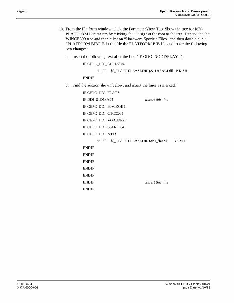
Page 6 Epson Research and DevelopmentVancouver Design Center
10. From the Platform window, click the ParameterView Tab. Show the tree for MY-PLATFORM Parameters by clicking the ‘+’ sign at the root of the tree. Expand the the WINCE300 tree and then click on “Hardware Specific Files” and then double click “PLATFORM.BIB”. Edit the file the PLATFORM.BIB file and make the following two changes:
a. Insert the following text after the line “IF ODO_NODISPLAY !”:
IF CEPC_DDI_S1D13A04
ddi.dll $(_FLATRELEASEDIR)\S1D13A04.dll NK SH
ENDIF
b. Find the section shown below, and insert the lines as marked:
IF CEPC_DDI_FLAT !
IF DDI_S1D13A04! ;Insert this line
IF CEPC_DDI_S3VIRGE !
IF CEPC_DDI_CT655X !
IF CEPC_DDI_VGA8BPP !
IF CEPC_DDI_S3TRIO64 !
IF CEPC_DDI_ATI !
ddi.dll $(_FLATRELEASEDIR)\ddi_flat.dll NK SH
ENDIF
ENDIF
ENDIF
ENDIF
ENDIF
ENDIF ;Insert this line
ENDIF
S1D13A04 Windows® CE 3.x Display DriverX37A-E-006-01 Issue Date: 01/10/19
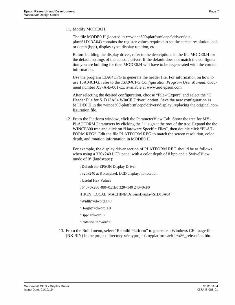
Epson Research and Development Page 7Vancouver Design Center
11. Modify MODE0.H.
The file MODE0.H (located in x:\wince300\platform\cepc\drivers\dis-play\S1D13A04) contains the register values required to set the screen resolution, col-or depth (bpp), display type, display rotation, etc.
Before building the display driver, refer to the descriptions in the file MODE0.H for the default settings of the console driver. If the default does not match the configura-tion you are building for then MODE0.H will have to be regenerated with the correct information.
Use the program 13A04CFG to generate the header file. For information on how to use 13A04CFG, refer to the 13A04CFG Configuration Program User Manual, docu-ment number X37A-B-001-xx, available at www.erd.epson.com
After selecting the desired configuration, choose “File->Export” and select the “C Header File for S1D13A04 WinCE Driver” option. Save the new configuration as MODE0.H in the \wince300\platform\cepc\drivers\display, replacing the original con-figuration file.
12. From the Platform window, click the ParameterView Tab. Show the tree for MY-PLATFORM Parameters by clicking the ‘+’ sign at the root of the tree. Expand the the WINCE300 tree and click on “Hardware Specific Files”, then double click “PLAT-FORM.REG”. Edit the file PLATFORM.REG to match the screen resolution, color depth, and rotation information in MODE0.H.
For example, the display driver section of PLATFORM.REG should be as follows when using a 320x240 LCD panel with a color depth of 8 bpp and a SwivelView mode of 0° (landscape):
; Default for EPSON Display Driver
; 320x240 at 8 bits/pixel, LCD display, no rotation
; Useful Hex Values
; 640=0x280 480=0x1E0 320=140 240=0xF0
[HKEY_LOCAL_MACHINE\Drivers\Display\S1D13A04]
“Width”=dword:140
“Height”=dword:F0
“Bpp”=dword:8
“Rotation”=dword:0
13. From the Build menu, select “Rebuild Platform” to generate a Windows CE image file (NK.BIN) in the project directory x:\myproject\myplatform\reldir\x86_release\nk.bin.
Windows® CE 3.x Display Driver S1D13A04Issue Date: 01/10/19 X37A-E-006-01

Page 8 Epson Research and DevelopmentVancouver Design Center
Installation for CEPC Environment
Once the NK.BIN file is built, the CEPC environment can be started by booting either from a floppy or hard drive configured with a Windows 9x operating system. The two methods are described below.
1. To start CEPC from a floppy drive:
a. Create a bootable floppy disk.
b. Copy HIMEM.SYS to the floppy disk and edit CONFIG.SYS on the floppy disk to contain only the following line:
device=a:\himem.sys
c. Edit AUTOEXEC.BAT on the floppy disk to contain the following lines:
loadcepc /B:38400 /C:1 c:\nk.bin
d. Search for loadcepc.exe in the Windows CE directories and copy loadcepc.exe to the bootable floppy disk.
e. Copy NK.BIN to c:\.
f. Boot the system from the bootable floppy disk.
2. To start CEPC from a hard drive:
a. Search for loadcepc.exe in the Windows CE directories and copy loadcepc.exe to C:\.
b. Edit CONFIG.SYS on the hard drive to contain only the following line:
device=c:\himem.sys
c. Edit AUTOEXEC.BAT on the hard drive to contain the following lines:
loadcepc /B:38400 /C:1 c:\nk.bin
d. Copy NK.BIN to c:\.
e. Boot the system.
S1D13A04 Windows® CE 3.x Display DriverX37A-E-006-01 Issue Date: 01/10/19
Epson Research and Development Page 9Vancouver Design Center
Configuration
There are several issues to consider when configuring the display driver. The issues cover debugging support, register initialization values and memory allocation. Each of these issues is discussed in the following sections.
Compile Switches
There are several switches, specific to the S1D13A04 display driver, which affect the display driver.
The switches are added or removed from the compile switches in the file SOURCES.
WINCEVER
This option is automatically set to the numerical version of WinCE for version 2.12 or later. If the environment variable, _WINCEOSVER is not defined, then WINCEVER will default to 2.11. The S1D13A04 display driver may test against this option to support different WinCE version-specific features.
EnablePreferVmem
This option enables the use of off-screen video memory. When this option is enabled, WinCE can optimize some BLT operations by using off-screen video memory to store images. You may need to disable this option if your off-screen video memory is limited.
ENABLE_CLOCK_CHIP
This option is used to enable support for the ICD2061A clock generator. This clock chip is used on the S5U13A04B00C evaluation board. The S1D13A04 display drivers can program the clock chip to support the frequencies required in the MODE tables.
If you are not using the S5U13A04B00C evaluation board, you should disable this option.
EpsonMessages
This debugging option enables the display of EPSON-specific debug messages. These debug message are sent to the serial debugging port. This option should be disabled unless you are debugging the display driver, as they will significantly impact the performance of the display driver.
DEBUG_MONITOR
This option enables the use of the debug monitor. The debug monitor can be invoked when the display driver is first loaded and can be used to view registers, and perform a few debugging tasks. The debug monitor is still under development and is UNTESTED.
Windows® CE 3.x Display Driver S1D13A04Issue Date: 01/10/19 X37A-E-006-01
Page 10 Epson Research and DevelopmentVancouver Design Center
This option should remain disabled unless you are performing specific debugging tasks that require the debug monitor.
MonoPanel
This option is intended for the support of monochrome panels only.
The option causes palette colors to be grayscaled for correct display on a mono panel. For use with color panels this option should not be enabled.
DEBUG_BLT
This option enables special BLT debugging messages on the debugging serial port. This option, when enabled, will drastically impact display driver performance, and should only be used to track down failures in the BLT operations.
This option should be disabled unless doing BLT debugging.
Mode File
A second variable which will affect the finished display driver is the register configurations contained in the mode file.
The MODE tables (contained in files MODE0.H, MODE1.H, MODE2.H . . .) contain register information to control the desired display mode. The MODE tables must be generated by the configuration program 13A04CFG.EXE. The display driver comes with one example MODE table:
• MODE0.H - LCD 8-bit STN color, 320x240, 8bpp, 70Hz
By default, only MODE0.H is used by the display driver. New mode tables can be created using the 13A04CFG program. Edit the #include section of MODE.H to add the new mode table.
If you only support a single mode table, you do not need to add any information to the WinCE registry. If, however, you support more that one display mode, you should create registry values (see below) that will establish the initial display mode. If your display driver contains multiple mode tables, and if you do not add any registry values, the display driver will default to the first mode table in your list.
To select which display mode the display driver should use upon boot, add the following lines to your PLATFORM.REG file:
[HKEY_LOCAL_MACHINE\Drivers\Display\S1D13A04]
S1D13A04 Windows® CE 3.x Display DriverX37A-E-006-01 Issue Date: 01/10/19
Epson Research and Development Page 11Vancouver Design Center
“Width”=dword:140“Height”=dword:F0“Bpp”=dword:8“Rotation”=dword:0
Note that all dword values are in hexadecimal, therefore 140h = 320 and F0h = 240. When the display driver starts, it will read these values in the registry and attempt to match a mode table against them. All values must be present and valid for a match to occur, otherwise the display driver will default to the first mode table in your list.
A WinCE desktop application (or control panel applet) can change these registry values, and the display driver will select a different mode upon warmboot. This allows the display driver to support different display configurations and/or orientations. An example appli-cation that controls these registry values will be made available upon the next release of the display driver; preliminary alpha code is available by special request.
Resource Management Issues
The Windows CE 3.0 OEM must deal with certain display driver issues relevant to Windows CE 3.0. These issues require the OEM balance factors such as: system vs. display memory utilization, video performance, and power off capabilities.
The section “Simple Display Driver Configuration” on page 13 provides a configuration which should work with most Windows CE platforms. This section is only intended as a means of getting started. Once the developer has a functional system, it is recommended to optimize the display driver configuration as described below in “Description of Windows CE Display Driver Issues”.
Description of Windows CE Display Driver Issues
The following are some issues to consider when configuring the display driver to work with Windows CE:
1. When Windows CE enters the Suspend state (power-off), the LCD controller and dis-play memory may lose power, depending on how the OEM sets up the system. If dis-play memory loses power, all images stored in display memory are lost.
If power-off/power-on features are required, the OEM has several options:
• If display memory power is turned off, add code to the display driver to save any images in display memory to system memory before power-off, and add code to restore these images after power-on.
• If display memory power is turned off, instruct Windows CE to redraw all images upon power-on. Unfortunately it is not possible to instruct Windows CE to redraw any off-screen images, such as icons, slider bars, etc., so in this case the OEM must also configure the display driver to never use off-screen memory.
• Ensure that display memory never loses power.
Windows® CE 3.x Display Driver S1D13A04Issue Date: 01/10/19 X37A-E-006-01
Page 12 Epson Research and DevelopmentVancouver Design Center
2. Using off-screen display memory significantly improves display performance. For ex-ample, slider bars appear more smooth when using off-screen memory. To enable or disable the use of off-screen memory, edit the file: x:\wince300\platform\cepc\driv-ers\display\S1D13A04\sources. In SOURCES, there is a line which, when uncom-mented, will instruct Windows CE to use off-screen display memory (if sufficient display memory is available):
CDEFINES=$(CDEFINES) -DEnablePreferVmem
3. In the file PROJECT.REG under CE 3.0, there is a key called PORepaint (search the Windows CE directories for PROJECT.REG). PORepaint is relevant when the Sus-pend state is entered or exited. PORepaint can be set to 0, 1, or 2 as described below:
a. PORepaint=0
• This mode tells Windows CE not to save or restore display memory on sus-pend or resume.
• Since display data is not saved and not repainted, this is the FASTEST mode.
• Main display data in display memory must NOT be corrupted or lost on sus-pend. The memory clock must remain running.
• Off-screen data in display memory must NOT be corrupted or lost on sus-pend. The memory clock must remain running.
• This mode cannot be used if power to the display memory is turned off.
b. PORepaint=1
• This is the default mode for Windows CE.
• This mode tells Windows CE to save the main display data to the system memory on suspend.
• This mode is used if display memory power is going to be turned off when the system is suspended, and there is enough system memory to save the image.
• Any off-screen data in display memory is LOST when suspended. Therefore off-screen memory usage must either be disabled in the display driver (i.e: EnablePreferVmem not defined in SOURCES file), or new OEM-specific code must be added to the display driver to save off-screen data to system memory when the system is suspended, and restored when resumed.
• If off-screen data is used (provided that the OEM has provided code to save off-screen data when the system suspends), additional code must be added to the display driver’s surface allocation routine to prevent the display driver from allocating the “main memory save region” in display memory. When WinCE OS attempts to allocate a buffer to save the main display data, WinCE OS marks the allocation request as preferring display memory. We believe this is incorrect. Code must be added to prevent this specific allocation from being allocated in display memory - it MUST be allocated from system mem-ory.
• Since the main display data is copied to system memory on suspend, and then simply copied back on resume, this mode is FAST, but not as fast as mode 0.
S1D13A04 Windows® CE 3.x Display DriverX37A-E-006-01 Issue Date: 01/10/19

Epson Research and Development Page 13Vancouver Design Center
c. PORepaint=2
• This mode tells WinCE to not save the main display data on suspend, and causes WinCE to REPAINT the main display on resume.
• This mode is used if display memory power is going to be turned off when the system is suspended, and there is not enough system memory to save the im-age.
• Any off-screen data in display memory is LOST, and since there is insuffi-cient system memory to save display data, off-screen memory usage MUST be disabled.
• When the system is resumed, WinCE instructs all running applications to re-paint themselves. This is the SLOWEST of the three modes.
Simple Display Driver Configuration
The following display driver configuration should work with most platforms running Windows CE. This configuration disables the use of off-screen display memory and forces the system to redraw the main display upon power-on.
1. This step disables the use of off-screen display memory.Edit the file x:\wince300\platform\cepc\drivers\display\S1D13A04\sources and change the line
CDEFINES=$(CDEFINES) -DEnablePreferVmem
to
#CDEFINES=$(CDEFINES) -DEnablePreferVmem
2. This step causes the system to redraw the main display upon power-on. This step is only required if display memory loses power when Windows CE is shut down. If dis-play memory is kept powered up (set the S1D13A04 in powersave mode), then the display data will be maintained and this step can be skipped.
Search for the file PROJECT.REG in your Windows CE directories, and inside PROJECT.REG find the key PORepaint. Change PORepaint as follows:
“PORepaint”=dword:2
Windows® CE 3.x Display Driver S1D13A04Issue Date: 01/10/19 X37A-E-006-01
Page 14 Epson Research and DevelopmentVancouver Design Center
Comments
• The display driver is CPU independent, allowing use of the driver for several Windows CE Platform Builder supported platforms. The file s1dflat.cpp will require editing for the correct values of PhysicalPortAddr, PhysicalVmemAddr, etc.
• The sample code defaults to a 320x240 8-bit color passive LCD panel in SwivelView 0° mode (landscape) with a color depth of 8 bpp. To support other settings, use 13A04CFG.EXE to generate a proper MODE0.H file. For further information, refer to the 13A04CFG Configuration Program User Manual, document number X37A-B-001-xx.
• By default, the 13A04CFG program assumes PCI addressing for the S5U13A04B00C evaluation board. This means that the display driver will automatically locate the S1D13A04 by scanning the PCI bus (currently only supported for the CEPC platform). If you select the address option “Other” and fill in your own custom addresses for the registers and video memory, then the display driver will not scan the PCI bus and will use the specific addresses you have chosen.
• If you are running the display driver on hardware other than the S5U13A04B00C evalu-ation board, you must ensure that your hardware provides the correct clock frequencies for CLKI and CLKI2. 13A04CFG defaults to 50MHz for both CLKI and CLKI2.
On the evaluation board, the display driver will correctly program the clock chip to support the CLKI and CLKI2 frequencies. On customer hardware, you must ensure that the clocks you provide to all clock inputs match the settings you chose in the Clocks tab of the 13A04CFG program. For more information on setting the clocks, see the 13A04CFG User Manual, document number X37A-B-001-xx.
If you run the S1D13A04 with a single clock source, make sure your clock sources for PCLK, BCLK, and MCLK are correctly set to use the correct clock input source. Also ensure that you enable the clock dividers as required for different display hardware.
• If you are using 13A04CFG.EXE to produce multiple MODE tables, make sure you change the Mode Number setting for each mode table you generate. The display driver supports multiple mode tables, but only if each mode table has a unique mode number. For more information on setting the mode number, see the 13A04CFG User Manual, document number X37A-B-001-xx.
• The 13A04CFG program assumes you are using the S5U13A04B00C evaluation board, and defaults the Panel Power control to GPIO0. 13A04CFG allows you to change the GPIO pin used to control panel power, or to disable the use of GPIO pins altogether. If this is changed from the default, your driver will no longer be able to control panel power on the S5U13A04B00C evaluation board, and your panel may not be powered up correctly.
• At this time, the driver has been tested on the x86 CPUs and have been run with Plat-form Builder v3.00.
S1D13A04 Windows® CE 3.x Display DriverX37A-E-006-01 Issue Date: 01/10/19
S1D13A04 LCD/USB Companion Chip
Windows® CE 3.x USB Driver
Document Number: X37A-E-007-01
Copyright © 2001 Epson Research and Development, Inc. All Rights Reserved.
Information in this document is subject to change without notice. You may download and use this document, but only for your own use inevaluating Seiko Epson/EPSON products. You may not modify the document. Epson Research and Development, Inc. disclaims anyrepresentation that the contents of this document are accurate or current. The Programs/Technologies described in this document may contain material protected under U.S. and/or International Patent laws.
EPSON is a registered trademark of Seiko Epson Corporation. Microsoft and Windows are registered trademarks of Microsoft Corporation.All other trademarks are the property of their respective owners.

Page 2 Epson Research and DevelopmentVancouver Design Center
THIS PAGE LEFT BLANK
S1D13A04 Windows® CE 3.x USB DriverX37A-E-007-01 Issue Date: 01/10/19
Epson Research and Development Page 3Vancouver Design Center
WINDOWS® CE 3.0 USB DRIVER
The Windows CE v3.0 USB driver for the S1D13A04 LCD/USB Companion Chip is a client driver, which supports Microsoft ActiveSync 3.1. This driver is intended as “reference” source code for OEMs developing for the Microsoft Window CE platform and provide a basis for OEMs to develop their own drivers.
This document and the source code for the Windows CE v3.0 USB driver is updated as appropriate. Before beginning any development, please check the Epson Research and Development Website at www.erd.epson.com for the latest revisions.
We appreciate your comments on our documentation. Please contact us via email at [email protected].
Windows® CE 3.x USB Driver S1D13A04Issue Date: 01/10/19 X37A-E-007-01
Page 4 Epson Research and DevelopmentVancouver Design Center
Example Driver Builds
Build for CEPC (X86) on Windows CE Platform Builder 3.00 using the GUI Interface
1. Install Microsoft Windows 2000 Professional or Windows 98.
2. Install Platform Builder 3.00.
3. Start Platform Builder by double-clicking on the Microsoft Windows CE Platform Builder icon.
4. Create a new project.
a. Select File | New.
b. In the dialog box, select the Platforms tab.
c. In the Platforms dialog box:- select “WCE Platform”- set a location for the project (such as x:\myproject)- set the platform name (such as myplatform)- set the processor to “Win32 (WCE x86)”
d. Click the OK button.
e. In the WCE Platform - Step 1 of 2 dialog box, select “CEPC”.
f. Click the Next button.
g. In the WCE Platform - Step 2 of 2 dialog box, select “Maximum OS (Maxall)”.
h. Click the Finish button.
i. In the New Platform Information dialog box, click the OK button.
5. Set the active configuration to “Win32 (WCE x86) Release”.
a. From the Build menu, select “Set Active Configuration”.
b. Select “MYPLATFORM - Win32 (WCE x86) Release”.
c. Click the OK button.
6. Add the environment variable USB_S1D13A04.
a. From the Platform menu, select “Settings”.
b. Select the “Environment” tab.
c. In the Variable box, type “USB_S1D13A04”.
d. In the Value box, type “1”.
e. Click the Set button.
f. Click the OK button.
S1D13A04 Windows® CE 3.x USB DriverX37A-E-007-01 Issue Date: 01/10/19
Epson Research and Development Page 5Vancouver Design Center
7. Create a new directory 13A04USB, under x:\wince300\platform\cepc\drivers, and copy the 13A04USB driver source code into this new directory.
8. Add the 13A04USB driver component.
a. From the Platform menu, select “Insert | User Component”.
b. Set Files of type: to “All Files (*.*)”.
c. Select the file x:\wince300\platform\cepc\drivers\13A04USB\sources.
d. Click the OK button.
e. In the User Component Target File dialog box, select browse and then select the path/filename of the file sources.
f. Click the OK button.
9. From the Platform window, click the Parameter View Tab. Show the tree for MY-PLATFORM Parameters by clicking on the ‘+’ sign at the root of the tree. Expand the the WINCE300 tree and then click the “Hardware Specific Files” and then double click the “PLATFORM.BIB”. Edit the file platform.bib and make the following two changes:
Find the section shown below, and insert the line as marked:
IF IMGUSB
IF CEPC_UHCI
uhci.dll $(_FLATRELEASEDIR)\uhci.dll NK SH
ENDIF
IF CEPC_OHCI
ohci.dll $(_FLATRELEASEDIR)\ohci.dll NK SH
ENDIF
usbd.dll $(_FLATRELEASEDIR)\usbd.dll NK SH
usbhid.dll $(_FLATRELEASEDIR)\usbhid.dll NK SH
ENDIF
IF USB_S1D13A04 ;Insert this line
13a04usb.dll $(_FLATRELEASEDIR)\13a04usb.dll NK SH ;Insert this line
ENDIF ;Insert this line
ENDIF
Windows® CE 3.x USB Driver S1D13A04Issue Date: 01/10/19 X37A-E-007-01
Page 6 Epson Research and DevelopmentVancouver Design Center
10. From the Platform window, click the Parameter View Tab. Show the tree for MY-PLATFORM Parameters by clicking on the ‘+’ sign at the root of the tree. Expand the WINCE300 tree and click the “Hardware Specific Files”, then double click the “PLATFORM.REG”. Insert the following section in the file platform.reg to in-clude the settings for 13A04USB driver.
[HKEY_LOCAL_MACHINE\Drivers\BuiltIn\13A0XUSB]
"Dll"="13A04USB.dll"
"Prefix"="COM"
"Tsp"="Unimodem.dll"
"DeviceArrayIndex"=dword:1
"Order"=dword:2
"DeviceType"=dword:0
"FriendlyName"="S1D13A04 USB"
"DevConfig"=hex: 10,00, 00,00, 05,00,00,00, 10,01,00,00, 00,4B,00,00, 00,00, 08, 00, 00, 00,00,00,00
; "PhysicalAddress"=dword:0x08000000 ; for non-cepc environment only
; "IRQ"=dword:05 ; for non-cepc environment only
11. From the Build menu, select “Rebuild Platform” to generate a Windows CE image file (nk.bin) in the project directory x:\myproject\myplatform\reldir\x86_release\nk.bin.
S1D13A04 Windows® CE 3.x USB DriverX37A-E-007-01 Issue Date: 01/10/19

Epson Research and Development Page 7Vancouver Design Center
Installation and Execution from CEPC Environment
Once the nk.bin file is built, the CEPC environment can be started by booting either from a floppy (step 1) or a hard drive (step 2) configured with a Windows 9x operating system. Both methods are described below.
1. To start CEPC by booting from a floppy drive:
a. Create a bootable floppy disk.
b. Copy himem.sys to the floppy disk and edit config.sys on the floppy disk to con-tain only the following line:
device=a:\himem.sys
c. Edit autoexec.bat on the floppy disk to contain the following line:
loadcepc /B:38400 /C:1 c:\nk.bin
d. Search for loadcepc.exe in your Windows CE directories, and copy the file to the bootable floppy disk.
e. Copy nk.bin to c:\.
f. Boot the system from the bootable floppy disk.
2. To start CEPC by booting from a hard drive:
a. Search for loadcepc.exe in the Windows CE directories, and copy the file to C:\.
b. Edit config.sys on the hard drive to contain only the following line:
device=c:\himem.sys
c. Edit autoexec.bat on the hard drive to contain the following line:
loadcepc /B:38400 /C:1 c:\nk.bin
d. Copy nk.bin to C:\.
e. Boot the system
3. Install Windows 2000 Professional on a host machine.
4. Install ActiveSync 3.1 on the host machine.
5. Install the included wceusbsh.sys on the host machine, by following the procedures below:
a. Unzip the file wceusbsh.zip to a directory on your hard drive.
b. Find the file wceusbsh.inf.
c. Right click the “WCEUSBSH.INF” file icon.
d. Select Install.
Windows® CE 3.x USB Driver S1D13A04Issue Date: 01/10/19 X37A-E-007-01
Page 8 Epson Research and DevelopmentVancouver Design Center
6. Connect a USB cable from the USB device (S5U13A04B00C board) to the USB host machine.
7. Boot the Windows CE machine from a floppy (created in step 1) or from the hard drive (created in step 2).
8. From the Windows CE desktop:- click the Start button- click Run- click Browse.
9. Find the file repllog.exe (by default it resides in \windows) and select it.
10. Click the OK button. The ActiveSync window on the host desktop is automatically in-voked, and the New Partnership window is opened automatically. This window prompts: “Would you like to set up a partnership?”
11. Click the No button.
12. Click the Next button.
13. The Microsoft ActiveSync Window is opened automatically and should display “Guest connected”.
14. Click the “Explore” button from the Microsoft ActiveSync window. File transfers are now possible through the USB cable.
Compile Switches
There are switches specific to the S1D13A04 USB driver which affect the USB driver. These switches are added or removed from the compile switches in the file sources.
CEPC
This option must be set for the CEPC platform and removed for all other platforms.
EPSONMESSAGES
This debugging option enables the display of EPSON-specific debug messages. These debug message are sent to the serial debugging port. This option should be disabled unless you are debugging the USB driver, as they will significantly impact the performance of the USB driver.
S1D13A04 Windows® CE 3.x USB DriverX37A-E-007-01 Issue Date: 01/10/19
Epson Research and Development Page 9Vancouver Design Center
Address and IRQ Modifications
• The USB driver is CPU independent, and it can be used on other platforms that support USB under Windows CE Platform Builder 3.0. If this driver is to support non-cepc plat-forms, the file project.reg requires editing to set the correct values of “PhysicalAd-dress” and “IRQ”.
• The variables DEFAULT_PHYSICAL_ADDRESS and DEFAULT_IRQ in the file 13a0xhw.h must be changed to reflect the values required by each implementation.
• If the entries of “PhysicalAddress” and “IRQ” are removed from the project.reg file, the USB driver uses the values of DEFAULT_PHYSICAL_ADDRESS and DEFAULT_IRQ contained in the file 13a0xhw.h.
Windows® CE 3.x USB Driver S1D13A04Issue Date: 01/10/19 X37A-E-007-01
Page 10 Epson Research and DevelopmentVancouver Design Center
Comments
• S5U13A04B00C Evaluation Board must be configured to enable USB support. This includes configuration changes to the dip switch and confirming that the proper USBClk is available on U13. See the S5U13A04B00C Rev. 1.0 Evaluation Board User Manual, document number X37A-G-004-xx.
• This USB driver is independent of the S1D13A04 Windows CE v3.x display driver, but may be run together with S1D13A04 display driver. For information on the S1D13A04 CE Display Driver, see the Windows CE 3.x Display Driver, document number X37A-E-006-xx.
• At this time, the driver has been tested on the x86 CPUs and has been run with Platform Builder v3.00.
S1D13A04 Windows® CE 3.x USB DriverX37A-E-007-01 Issue Date: 01/10/19
S1D13XXX 32-Bit Windows Device Driver Installation Guide
Document No. X00A-E-003-04
Copyright © 1999, 2001 Epson Research and Development, Inc. All Rights Reserved.
Information in this document is subject to change without notice. You may download and use this document, but only for your own use inevaluating Seiko Epson/EPSON products. You may not modify the document. Epson Research and Development, Inc. disclaims anyrepresentation that the contents of this document are accurate or current. The Programs/Technologies described in this document may contain material protected under U.S. and/or International Patent laws.EPSON is a registered trademark of Seiko Epson Corporation. All Trademarks are the property of their respective owners

Page 2 Epson Research and DevelopmentVancouver Design Center
THIS PAGE LEFT BLANK
S1D13XXX 32-Bit Windows Device Driver Installation GuideX00A-E-003-04 Issue Date: 01/04/17
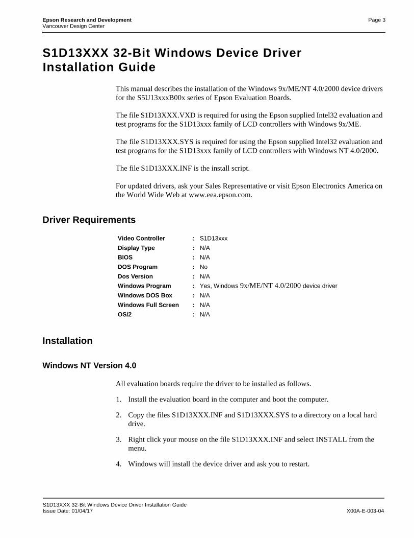
Epson Research and Development Page 3Vancouver Design Center
S1D13XXX 32-Bit Windows Device Driver Installation Guide
This manual describes the installation of the Windows 9x/ME/NT 4.0/2000 device drivers for the S5U13xxxB00x series of Epson Evaluation Boards.
The file S1D13XXX.VXD is required for using the Epson supplied Intel32 evaluation and test programs for the S1D13xxx family of LCD controllers with Windows 9x/ME.
The file S1D13XXX.SYS is required for using the Epson supplied Intel32 evaluation and test programs for the S1D13xxx family of LCD controllers with Windows NT 4.0/2000.
The file S1D13XXX.INF is the install script.
For updated drivers, ask your Sales Representative or visit Epson Electronics America on the World Wide Web at www.eea.epson.com.
Driver Requirements
Installation
Windows NT Version 4.0
All evaluation boards require the driver to be installed as follows.
1. Install the evaluation board in the computer and boot the computer.
2. Copy the files S1D13XXX.INF and S1D13XXX.SYS to a directory on a local hard drive.
3. Right click your mouse on the file S1D13XXX.INF and select INSTALL from the menu.
4. Windows will install the device driver and ask you to restart.
Video Controller : S1D13xxx
Display Type : N/A
BIOS : N/A
DOS Program : No
Dos Version : N/A
Windows Program : Yes, Windows 9x/ME/NT 4.0/2000 device driver
Windows DOS Box : N/A
Windows Full Screen : N/A
OS/2 : N/A
S1D13XXX 32-Bit Windows Device Driver Installation Guide Issue Date: 01/04/17 X00A-E-003-04
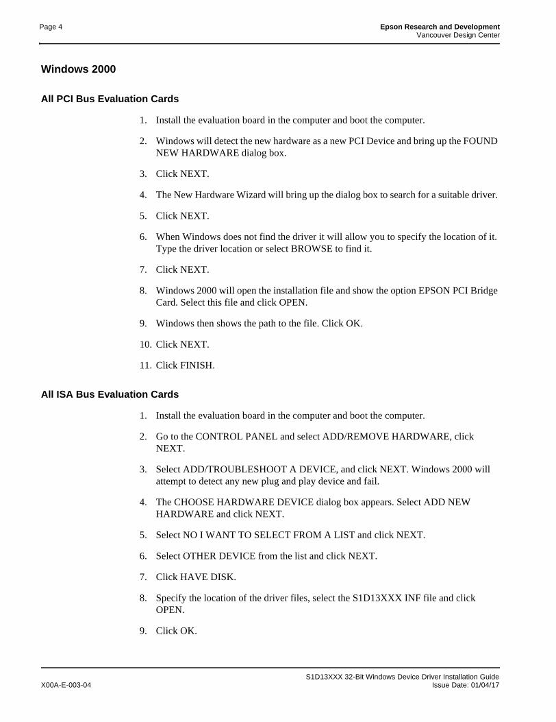
Page 4 Epson Research and DevelopmentVancouver Design Center
Windows 2000
All PCI Bus Evaluation Cards
1. Install the evaluation board in the computer and boot the computer.
2. Windows will detect the new hardware as a new PCI Device and bring up the FOUND NEW HARDWARE dialog box.
3. Click NEXT.
4. The New Hardware Wizard will bring up the dialog box to search for a suitable driver.
5. Click NEXT.
6. When Windows does not find the driver it will allow you to specify the location of it. Type the driver location or select BROWSE to find it.
7. Click NEXT.
8. Windows 2000 will open the installation file and show the option EPSON PCI Bridge Card. Select this file and click OPEN.
9. Windows then shows the path to the file. Click OK.
10. Click NEXT.
11. Click FINISH.
All ISA Bus Evaluation Cards
1. Install the evaluation board in the computer and boot the computer.
2. Go to the CONTROL PANEL and select ADD/REMOVE HARDWARE, click NEXT.
3. Select ADD/TROUBLESHOOT A DEVICE, and click NEXT. Windows 2000 will attempt to detect any new plug and play device and fail.
4. The CHOOSE HARDWARE DEVICE dialog box appears. Select ADD NEW HARDWARE and click NEXT.
5. Select NO I WANT TO SELECT FROM A LIST and click NEXT.
6. Select OTHER DEVICE from the list and click NEXT.
7. Click HAVE DISK.
8. Specify the location of the driver files, select the S1D13XXX INF file and click OPEN.
9. Click OK.
S1D13XXX 32-Bit Windows Device Driver Installation GuideX00A-E-003-04 Issue Date: 01/04/17
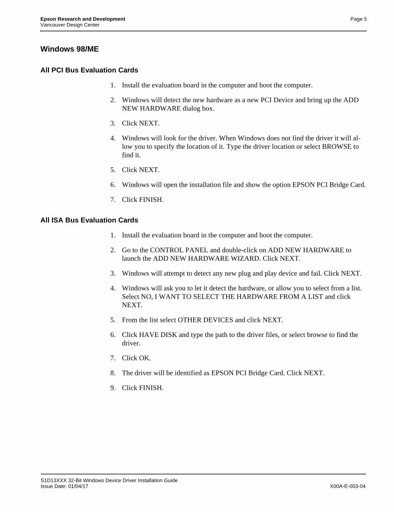
Epson Research and Development Page 5Vancouver Design Center
Windows 98/ME
All PCI Bus Evaluation Cards
1. Install the evaluation board in the computer and boot the computer.
2. Windows will detect the new hardware as a new PCI Device and bring up the ADD NEW HARDWARE dialog box.
3. Click NEXT.
4. Windows will look for the driver. When Windows does not find the driver it will al-low you to specify the location of it. Type the driver location or select BROWSE to find it.
5. Click NEXT.
6. Windows will open the installation file and show the option EPSON PCI Bridge Card.
7. Click FINISH.
All ISA Bus Evaluation Cards
1. Install the evaluation board in the computer and boot the computer.
2. Go to the CONTROL PANEL and double-click on ADD NEW HARDWARE to launch the ADD NEW HARDWARE WIZARD. Click NEXT.
3. Windows will attempt to detect any new plug and play device and fail. Click NEXT.
4. Windows will ask you to let it detect the hardware, or allow you to select from a list. Select NO, I WANT TO SELECT THE HARDWARE FROM A LIST and click NEXT.
5. From the list select OTHER DEVICES and click NEXT.
6. Click HAVE DISK and type the path to the driver files, or select browse to find the driver.
7. Click OK.
8. The driver will be identified as EPSON PCI Bridge Card. Click NEXT.
9. Click FINISH.
S1D13XXX 32-Bit Windows Device Driver Installation Guide Issue Date: 01/04/17 X00A-E-003-04
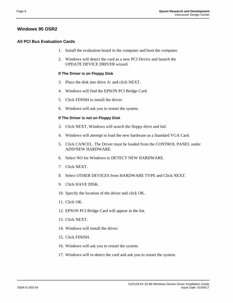
Page 6 Epson Research and DevelopmentVancouver Design Center
Windows 95 OSR2
All PCI Bus Evaluation Cards
1. Install the evaluation board in the computer and boot the computer.
2. Windows will detect the card as a new PCI Device and launch the UPDATE DEVICE DRIVER wizard.
If The Driver is on Floppy Disk
3. Place the disk into drive A: and click NEXT.
4. Windows will find the EPSON PCI Bridge Card.
5. Click FINISH to install the driver.
6. Windows will ask you to restart the system.
If The Driver is not on Floppy Disk
3. Click NEXT, Windows will search the floppy drive and fail.
4. Windows will attempt to load the new hardware as a Standard VGA Card.
5. Click CANCEL. The Driver must be loaded from the CONTROL PANEL under ADD/NEW HARDWARE.
6. Select NO for Windows to DETECT NEW HARDWARE.
7. Click NEXT.
8. Select OTHER DEVICES from HARDWARE TYPE and Click NEXT.
9. Click HAVE DISK.
10. Specify the location of the driver and click OK.
11. Click OK.
12. EPSON PCI Bridge Card will appear in the list.
13. Click NEXT.
14. Windows will install the driver.
15. Click FINISH.
16. Windows will ask you to restart the system.
17. Windows will re-detect the card and ask you to restart the system.
S1D13XXX 32-Bit Windows Device Driver Installation GuideX00A-E-003-04 Issue Date: 01/04/17

Epson Research and Development Page 7Vancouver Design Center
All ISA Bus Evaluation Cards
1. Install the evaluation board in the computer and boot the computer.
2. Go to the CONTROL PANEL and select ADD NEW HARDWARE.
3. Click NEXT.
4. Select NO and click NEXT.
5. Select OTHER DEVICES and click NEXT.
6. Click Have Disk.
7. Specify the location of the driver files and click OK.
8. Click Next.
9. Click Finish.
Previous Versions of Windows 95
All PCI Bus Evaluation Cards
1. Install the evaluation board in the computer and boot the computer.
2. Windows will detect the card.
3. Select DRIVER FROM DISK PROVIDED BY MANUFACTURER.
4. Click OK.
5. Specify a path to the location of the driver files.
6. Click OK.
7. Windows will find the S1D13XXX.INF file.
8. Click OK.
9. Click OK and Windows will install the driver.
S1D13XXX 32-Bit Windows Device Driver Installation Guide Issue Date: 01/04/17 X00A-E-003-04

Page 8 Epson Research and DevelopmentVancouver Design Center
All ISA Bus Evaluation Cards
1. Install the evaluation board in the computer and boot the computer.
2. Go to the CONTROL PANEL and select ADD NEW HARDWARE.
3. Click NEXT.
4. Select NO and click NEXT.
5. Select OTHER DEVICES from the HARDWARE TYPES list.
6. Click HAVE DISK.
7. Specify the location of the driver files and click OK.
8. Select the file S1D13XXX.INF and click OK.
9. Click OK.
10. The EPSON PCI Bridge Card should be selected in the list window.
11. Click NEXT.
12. Click NEXT.
13. Click Finish.
S1D13XXX 32-Bit Windows Device Driver Installation GuideX00A-E-003-04 Issue Date: 01/04/17
S1D13A04 LCD/USB Companion Chip
S5U13A04B00C Rev. 1.0 Evaluation Board User Manual
Document Number: X37A-G-004-02
Copyright © 2001, 2002 Epson Research and Development, Inc. All Rights Reserved.
Information in this document is subject to change without notice. You may download and use this document, but only for your own use inevaluating Seiko Epson/EPSON products. You may not modify the document. Epson Research and Development, Inc. disclaims anyrepresentation that the contents of this document are accurate or current. The Programs/Technologies described in this document may contain material protected under U.S. and/or International Patent laws.
EPSON is a registered trademark of Seiko Epson Corporation. All other trademarks are the property of their respective owners.

Page 2 Epson Research and DevelopmentVancouver Design Center
THIS PAGE LEFT BLANK
S1D13A04 S5U13A04B00C Rev. 1.0 Evaluation Board User ManualX37A-G-004-02 Issue Date: 02/01/28
Epson Research and Development Page 3Vancouver Design Center
Table of Contents
1 Introduction . . . . . . . . . . . . . . . . . . . . . . . . . . . . . . . . . . . . . . . . 7
2 Features . . . . . . . . . . . . . . . . . . . . . . . . . . . . . . . . . . . . . . . . . . 8
3 Installation and Configuration . . . . . . . . . . . . . . . . . . . . . . . . . . . . . . 93.1 Configuration DIP Switches . . . . . . . . . . . . . . . . . . . . . . . . . . 9
3.2 Configuration Jumpers . . . . . . . . . . . . . . . . . . . . . . . . . . . 11
4 CPU Interface . . . . . . . . . . . . . . . . . . . . . . . . . . . . . . . . . . . . . . 144.1 CPU Interface Pin Mapping . . . . . . . . . . . . . . . . . . . . . . . . . 14
4.2 CPU Bus Connector Pin Mapping . . . . . . . . . . . . . . . . . . . . . . 15
5 LCD Interface Pin Mapping . . . . . . . . . . . . . . . . . . . . . . . . . . . . . . 17
6 Technical Description . . . . . . . . . . . . . . . . . . . . . . . . . . . . . . . . . 196.1 PCI Bus Support . . . . . . . . . . . . . . . . . . . . . . . . . . . . . 19
6.2 Direct Host Bus Interface Support . . . . . . . . . . . . . . . . . . . . . . 19
6.3 S1D13A04 Embedded Memory . . . . . . . . . . . . . . . . . . . . . . . 19
6.4 Adjustable LCD Panel Negative Power Supply . . . . . . . . . . . . . . . . . 19
6.5 Adjustable LCD Panel Positive Power Supply . . . . . . . . . . . . . . . . . . 20
6.6 Software Adjustable LCD Backlight Intensity Support Using PWM . . . . . . . . . 20
6.7 LCD Panel Support . . . . . . . . . . . . . . . . . . . . . . . . . . . . 20
6.7.1 Direct LCD Connector . . . . . . . . . . . . . . . . . . . . . . . . . . . . . . . . 20
6.7.2 Extended LCD Connector . . . . . . . . . . . . . . . . . . . . . . . . . . . . . . . 21
6.8 USB Support . . . . . . . . . . . . . . . . . . . . . . . . . . . . . . . 21
6.8.1 USB IRQ Support . . . . . . . . . . . . . . . . . . . . . . . . . . . . . . . . . . . 21
7 Clock Synthesizer and Clock Options . . . . . . . . . . . . . . . . . . . . . . . . 227.1 Clock Programming . . . . . . . . . . . . . . . . . . . . . . . . . . . . 22
8 References . . . . . . . . . . . . . . . . . . . . . . . . . . . . . . . . . . . . . . . 238.1 Documents . . . . . . . . . . . . . . . . . . . . . . . . . . . . . . . 23
8.2 Document Sources . . . . . . . . . . . . . . . . . . . . . . . . . . . . 23
9 Parts List . . . . . . . . . . . . . . . . . . . . . . . . . . . . . . . . . . . . . . . . 24
10 Schematics . . . . . . . . . . . . . . . . . . . . . . . . . . . . . . . . . . . . . . . 26
11 Board Layout . . . . . . . . . . . . . . . . . . . . . . . . . . . . . . . . . . . . . . 32
12 Sales and Technical Support . . . . . . . . . . . . . . . . . . . . . . . . . . . . . 3312.1 Epson Companion Chips (S1D13A04) . . . . . . . . . . . . . . . . . . . . . 33
S5U13A04B00C Rev. 1.0 Evaluation Board User Manual S1D13A04Issue Date: 02/01/28 X37A-G-004-02

Page 4 Epson Research and DevelopmentVancouver Design Center
THIS PAGE LEFT BLANK
S1D13A04 S5U13A04B00C Rev. 1.0 Evaluation Board User ManualX37A-G-004-02 Issue Date: 02/01/28
Epson Research and Development Page 5Vancouver Design Center
List of Tables
Table 3-1: Configuration DIP Switch Settings . . . . . . . . . . . . . . . . . . . . . . . . . . . . 10
Table 3-2: Jumper Summary . . . . . . . . . . . . . . . . . . . . . . . . . . . . . . . . . . . . . 11
Table 4-1: CPU Interface Pin Mapping . . . . . . . . . . . . . . . . . . . . . . . . . . . . . . . . 14
Table 4-2: CPU Bus Connector (H3) Pinout . . . . . . . . . . . . . . . . . . . . . . . . . . . . . 15
Table 4-3: CPU Bus Connector (H4) Pinout . . . . . . . . . . . . . . . . . . . . . . . . . . . . . 16
Table 5-1: LCD Signal Connector (H1) . . . . . . . . . . . . . . . . . . . . . . . . . . . . . . . . 17
Table 5-2: Extended LCD Signal Connector (H2) . . . . . . . . . . . . . . . . . . . . . . . . . . 18
Table 9-1: Parts List . . . . . . . . . . . . . . . . . . . . . . . . . . . . . . . . . . . . . . . . . . 24
List of Figures
Figure 3-1: Configuration DIP Switch (SW1) Location . . . . . . . . . . . . . . . . . . . . . . . . 9
Figure 3-2: Configuration Jumper (JP1) Location . . . . . . . . . . . . . . . . . . . . . . . . . . . 11
Figure 3-3: Configuration Jumper (JP2) Location . . . . . . . . . . . . . . . . . . . . . . . . . . . 12
Figure 3-4: Configuration Jumper (JP3) Location . . . . . . . . . . . . . . . . . . . . . . . . . . . 12
Figure 3-5: Configuration Jumper (JP4) Location . . . . . . . . . . . . . . . . . . . . . . . . . . . 13
Figure 3-6: Configuration Jumper (JP5) Location . . . . . . . . . . . . . . . . . . . . . . . . . . . 13
Figure 7-1: Symbolic Clock Synthesizer Connections . . . . . . . . . . . . . . . . . . . . . . . . . 22
Figure 10-1: S1D13A04B00C Schematics (1 of 6) . . . . . . . . . . . . . . . . . . . . . . . . . . . 26
Figure 10-2: S1D13A04B00C Schematics (2 of 6) . . . . . . . . . . . . . . . . . . . . . . . . . . . 27
Figure 10-3: S1D13A04B00C Schematics (3 of 6) . . . . . . . . . . . . . . . . . . . . . . . . . . . 28
Figure 10-4: S1D13A04B00C Schematics (4 of 6) . . . . . . . . . . . . . . . . . . . . . . . . . . . 29
Figure 10-5: S1D13A04B00C Schematics (5 of 6) . . . . . . . . . . . . . . . . . . . . . . . . . . . 30
Figure 10-6: S1D13A04B00C Schematics (6 of 6) . . . . . . . . . . . . . . . . . . . . . . . . . . . 31
Figure 11-1: S5U13A04B00C Board Layout . . . . . . . . . . . . . . . . . . . . . . . . . . . . . . 32
S5U13A04B00C Rev. 1.0 Evaluation Board User Manual S1D13A04Issue Date: 02/01/28 X37A-G-004-02

Page 6 Epson Research and DevelopmentVancouver Design Center
THIS PAGE LEFT BLANK
S1D13A04 S5U13A04B00C Rev. 1.0 Evaluation Board User ManualX37A-G-004-02 Issue Date: 02/01/28
Epson Research and Development Page 7Vancouver Design Center
1 Introduction
This manual describes the setup and operation of the S5U13A04B00C Rev. 1.0 Evaluation Board. The board is designed as an evaluation platform for the S1D13A04 LCD/USB Companion Chip.
This user manual is updated as appropriate. Please check the Epson Research and Devel-opment Website at www.erd.epson.com for the latest revision of this document before beginning any development.
We appreciate your comments on our documentation. Please contact us via email at [email protected].
S5U13A04B00C Rev. 1.0 Evaluation Board User Manual S1D13A04Issue Date: 02/01/28 X37A-G-004-02
Page 8 Epson Research and DevelopmentVancouver Design Center
2 Features
Following are some features of the S5U13A04B00C Rev. 1.0 Evaluation Board:
• 121-pin PFBGA S1D13A04 Embedded Memory LCD Controller with 160K bytes of embedded SRAM.
• PCI bus operation through onboard PCI bridge.
• CPU/Bus interface header strips for non-PCI bus operation.
• Configuration options.
• On-board adjustable positive LCD bias power supply from +23V to +40V.
• On-board adjustable negative LCD bias power supply from -14V to -24V.
• Software adjustable backlight intensity support using PWMOUT.
• 4/8-bit 3.3V or 5V single monochrome passive LCD panel support.
• 4/8/16-bit 3.3V or 5V single color passive LCD panel support.
• 9/12/18-bit 3.3V or 5V active matrix TFT LCD panel support.
• Direct interface for 18-bit Epson D-TFD LCD panel support.
• Direct interface for 18-bit Sharp HR-TFT LCD panel support.
• Programmable clock synthesizer to CLKI and CLKI2 for maximum clock flexibility.
• Connector for USB client support.
• Software initiated power save mode.
• Selectable clock source for CLKI and CLKI2.
• External oscillator support for CLKI and CLKI2.
S1D13A04 S5U13A04B00C Rev. 1.0 Evaluation Board User ManualX37A-G-004-02 Issue Date: 02/01/28
Epson Research and Development Page 9Vancouver Design Center
3 Installation and Configuration
The S5U13A04B00C is designed to support as many platforms as possible. The S5U13A04B00C incorporates a DIP switch and five jumpers which allow both the evalu-ation board and the S1D13A04 LCD controller to be configured for a specified evaluation platform.
3.1 Configuration DIP Switches
The S1D13A04 has configuration inputs (CNF[6:0]) which are read on the rising edge of RESET#. In order to configure the S1D13A04 for multiple Host Bus Interfaces an eight-position DIP switch (SW1) is required. The following figure shows the location of DIP switch SW1 on the S5U13A04B00C.
Figure 3-1: Configuration DIP Switch (SW1) Location
DIP Switch - SW1
S5U13A04B00C Rev. 1.0 Evaluation Board User Manual S1D13A04Issue Date: 02/01/28 X37A-G-004-02
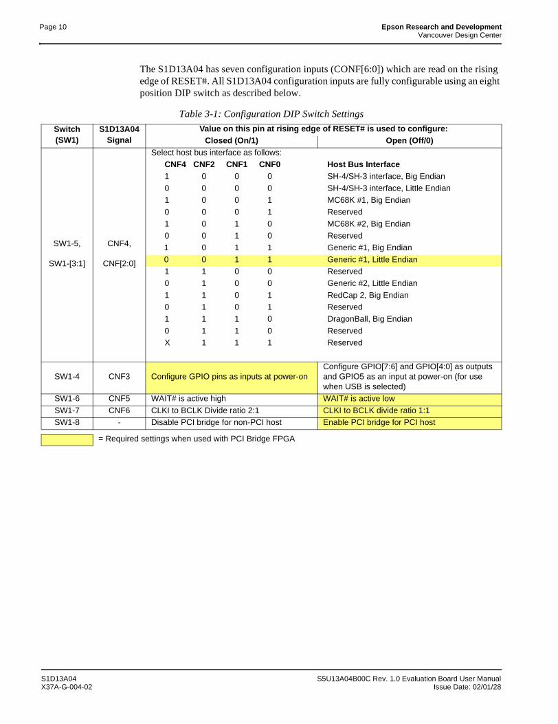
Page 10 Epson Research and DevelopmentVancouver Design Center
The S1D13A04 has seven configuration inputs (CONF[6:0]) which are read on the rising edge of RESET#. All S1D13A04 configuration inputs are fully configurable using an eight position DIP switch as described below.
Table 3-1: Configuration DIP Switch Settings
Switch (SW1)
S1D13A04 Signal
Value on this pin at rising edge of RESET# is used to configure:Closed (On/1) Open (Off/0)
SW1-5,
SW1-[3:1]
CNF4,
CNF[2:0]
Select host bus interface as follows:CNF4 CNF2 CNF1 CNF0 Host Bus Interface1 0 0 0 SH-4/SH-3 interface, Big Endian
0 0 0 0 SH-4/SH-3 interface, Little Endian1 0 0 1 MC68K #1, Big Endian0 0 0 1 Reserved
1 0 1 0 MC68K #2, Big Endian0 0 1 0 Reserved1 0 1 1 Generic #1, Big Endian
0 0 1 1 Generic #1, Little Endian1 1 0 0 Reserved0 1 0 0 Generic #2, Little Endian
1 1 0 1 RedCap 2, Big Endian0 1 0 1 Reserved1 1 1 0 DragonBall, Big Endian
0 1 1 0 ReservedX 1 1 1 Reserved
SW1-4 CNF3 Configure GPIO pins as inputs at power-onConfigure GPIO[7:6] and GPIO[4:0] as outputs and GPIO5 as an input at power-on (for use when USB is selected)
SW1-6 CNF5 WAIT# is active high WAIT# is active low
SW1-7 CNF6 CLKI to BCLK Divide ratio 2:1 CLKI to BCLK divide ratio 1:1SW1-8 - Disable PCI bridge for non-PCI host Enable PCI bridge for PCI host
= Required settings when used with PCI Bridge FPGA
S1D13A04 S5U13A04B00C Rev. 1.0 Evaluation Board User ManualX37A-G-004-02 Issue Date: 02/01/28
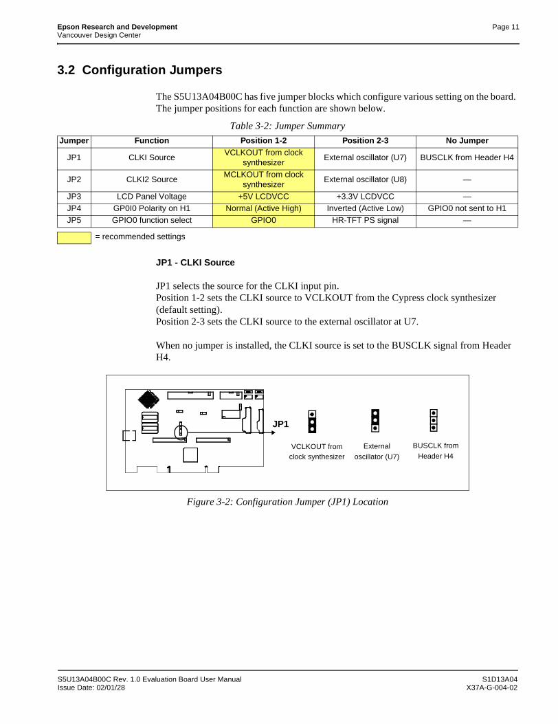
Epson Research and Development Page 11Vancouver Design Center
3.2 Configuration Jumpers
The S5U13A04B00C has five jumper blocks which configure various setting on the board. The jumper positions for each function are shown below.
JP1 - CLKI Source
JP1 selects the source for the CLKI input pin.Position 1-2 sets the CLKI source to VCLKOUT from the Cypress clock synthesizer (default setting).Position 2-3 sets the CLKI source to the external oscillator at U7.
When no jumper is installed, the CLKI source is set to the BUSCLK signal from Header H4.
Figure 3-2: Configuration Jumper (JP1) Location
Table 3-2: Jumper Summary
Jumper Function Position 1-2 Position 2-3 No Jumper
JP1 CLKI SourceVCLKOUT from clock
synthesizerExternal oscillator (U7) BUSCLK from Header H4
JP2 CLKI2 SourceMCLKOUT from clock
synthesizerExternal oscillator (U8) —
JP3 LCD Panel Voltage +5V LCDVCC +3.3V LCDVCC —JP4 GP0I0 Polarity on H1 Normal (Active High) Inverted (Active Low) GPIO0 not sent to H1JP5 GPIO0 function select GPIO0 HR-TFT PS signal —
= recommended settings
JP1
VCLKOUT fromclock synthesizer
External
oscillator (U7)
BUSCLK from
Header H4
S5U13A04B00C Rev. 1.0 Evaluation Board User Manual S1D13A04Issue Date: 02/01/28 X37A-G-004-02
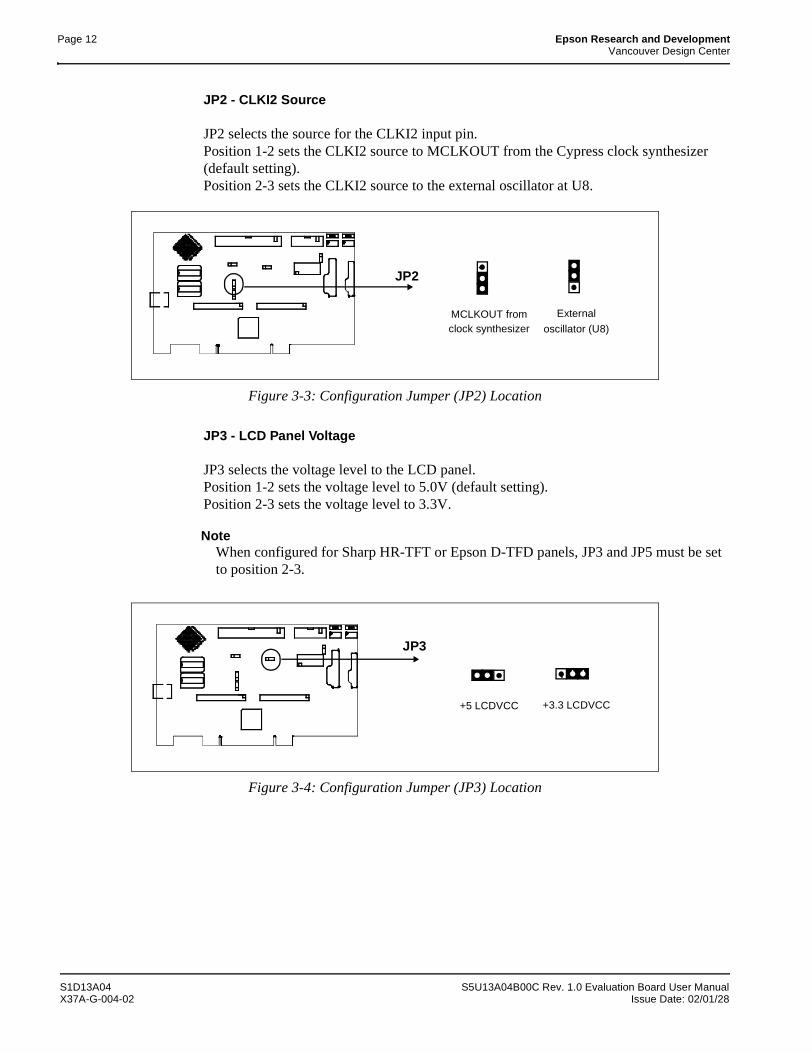
Page 12 Epson Research and DevelopmentVancouver Design Center
JP2 - CLKI2 Source
JP2 selects the source for the CLKI2 input pin.Position 1-2 sets the CLKI2 source to MCLKOUT from the Cypress clock synthesizer (default setting).Position 2-3 sets the CLKI2 source to the external oscillator at U8.
Figure 3-3: Configuration Jumper (JP2) Location
JP3 - LCD Panel Voltage
JP3 selects the voltage level to the LCD panel.Position 1-2 sets the voltage level to 5.0V (default setting).Position 2-3 sets the voltage level to 3.3V.
NoteWhen configured for Sharp HR-TFT or Epson D-TFD panels, JP3 and JP5 must be set to position 2-3.
Figure 3-4: Configuration Jumper (JP3) Location
JP2
MCLKOUT fromclock synthesizer
External
oscillator (U8)
+5 LCDVCC +3.3 LCDVCC
JP3
S1D13A04 S5U13A04B00C Rev. 1.0 Evaluation Board User ManualX37A-G-004-02 Issue Date: 02/01/28
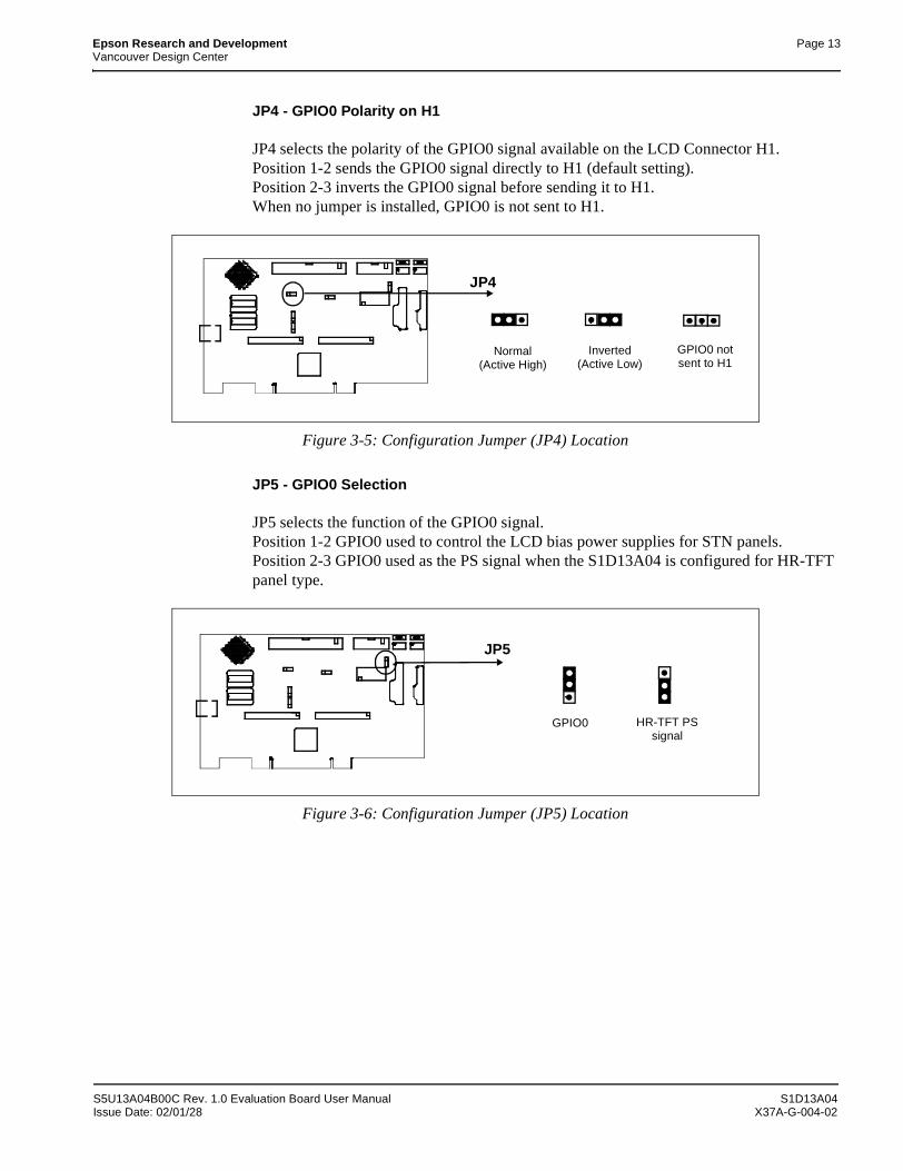
Epson Research and Development Page 13Vancouver Design Center
JP4 - GPIO0 Polarity on H1
JP4 selects the polarity of the GPIO0 signal available on the LCD Connector H1.Position 1-2 sends the GPIO0 signal directly to H1 (default setting).Position 2-3 inverts the GPIO0 signal before sending it to H1.When no jumper is installed, GPIO0 is not sent to H1.
Figure 3-5: Configuration Jumper (JP4) Location
JP5 - GPIO0 Selection
JP5 selects the function of the GPIO0 signal.Position 1-2 GPIO0 used to control the LCD bias power supplies for STN panels.Position 2-3 GPIO0 used as the PS signal when the S1D13A04 is configured for HR-TFT panel type.
Figure 3-6: Configuration Jumper (JP5) Location
Normal Inverted GPIO0 not
JP4
(Active High) (Active Low) sent to H1
JP5
GPIO0 HR-TFT PSsignal
S5U13A04B00C Rev. 1.0 Evaluation Board User Manual S1D13A04Issue Date: 02/01/28 X37A-G-004-02
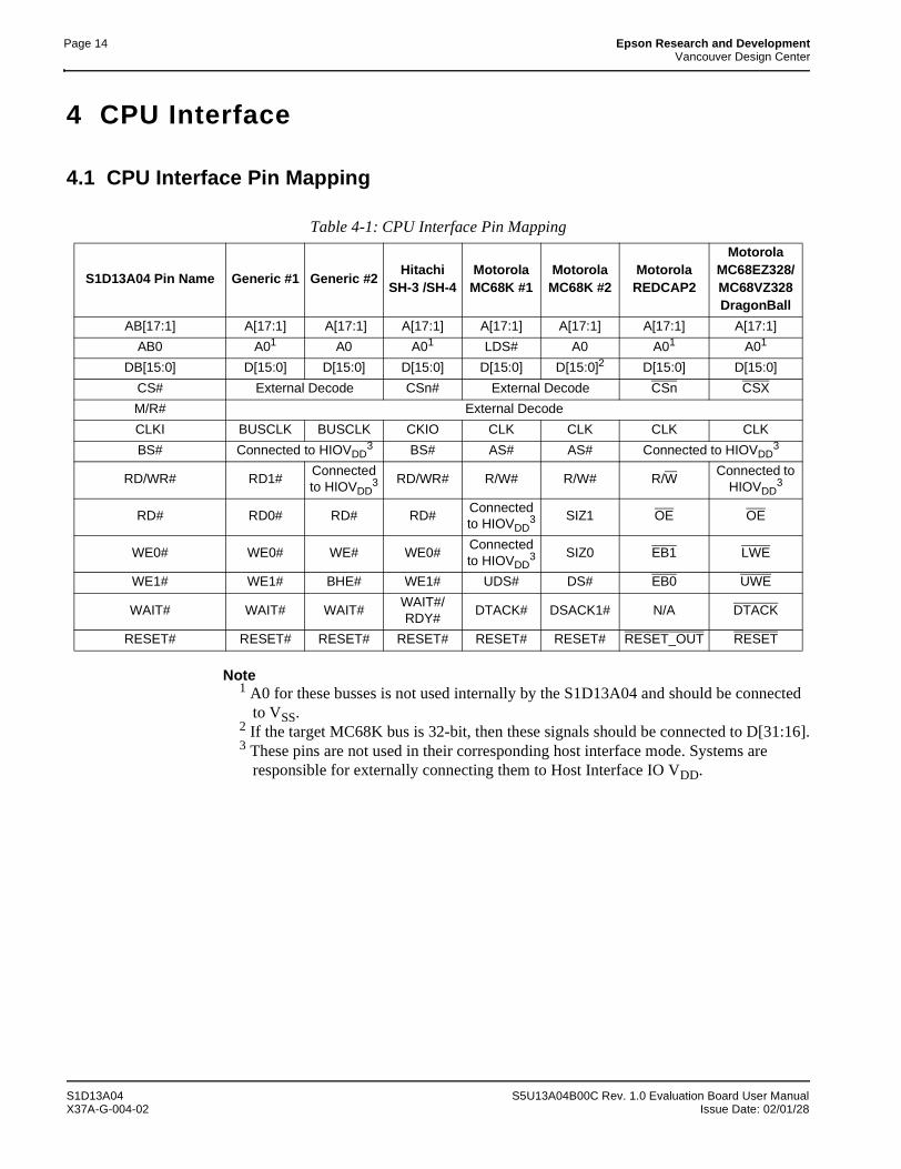
Page 14 Epson Research and DevelopmentVancouver Design Center
4 CPU Interface
4.1 CPU Interface Pin Mapping
Note1 A0 for these busses is not used internally by the S1D13A04 and should be connected
to VSS.2 If the target MC68K bus is 32-bit, then these signals should be connected to D[31:16].3 These pins are not used in their corresponding host interface mode. Systems are
responsible for externally connecting them to Host Interface IO VDD.
Table 4-1: CPU Interface Pin Mapping
S1D13A04 Pin Name Generic #1 Generic #2Hitachi
SH-3 /SH-4Motorola
MC68K #1Motorola
MC68K #2Motorola
REDCAP2
Motorola MC68EZ328/MC68VZ328 DragonBall
AB[17:1] A[17:1] A[17:1] A[17:1] A[17:1] A[17:1] A[17:1] A[17:1]
AB0 A01 A0 A01 LDS# A0 A01 A01
DB[15:0] D[15:0] D[15:0] D[15:0] D[15:0] D[15:0]2 D[15:0] D[15:0]
CS# External Decode CSn# External Decode CSn CSX
M/R# External Decode
CLKI BUSCLK BUSCLK CKIO CLK CLK CLK CLK
BS# Connected to HIOVDD3 BS# AS# AS# Connected to HIOVDD
3
RD/WR# RD1#Connected to HIOVDD
3 RD/WR# R/W# R/W# R/WConnected to
HIOVDD3
RD# RD0# RD# RD#Connected to HIOVDD
3 SIZ1 OE OE
WE0# WE0# WE# WE0#Connected to HIOVDD
3 SIZ0 EB1 LWE
WE1# WE1# BHE# WE1# UDS# DS# EB0 UWE
WAIT# WAIT# WAIT#WAIT#/RDY#
DTACK# DSACK1# N/A DTACK
RESET# RESET# RESET# RESET# RESET# RESET# RESET_OUT RESET
S1D13A04 S5U13A04B00C Rev. 1.0 Evaluation Board User ManualX37A-G-004-02 Issue Date: 02/01/28
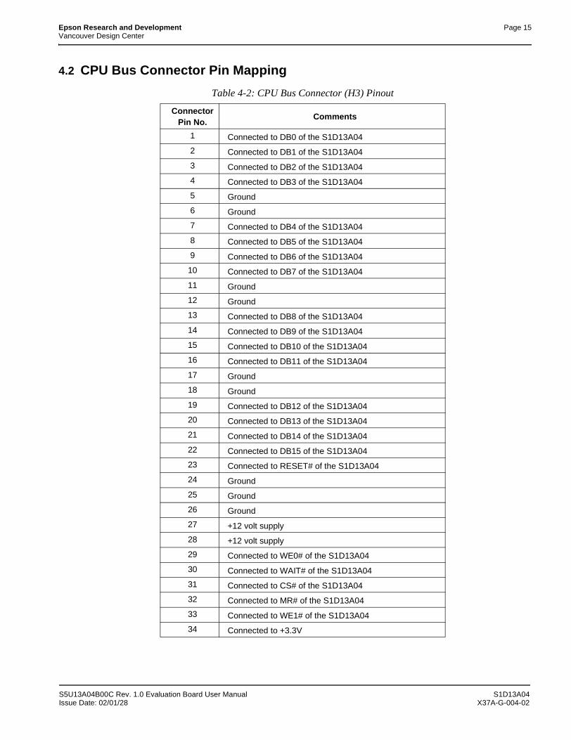
Epson Research and Development Page 15Vancouver Design Center
4.2 CPU Bus Connector Pin Mapping
Table 4-2: CPU Bus Connector (H3) Pinout
Connector Pin No.
Comments
1 Connected to DB0 of the S1D13A04
2 Connected to DB1 of the S1D13A04
3 Connected to DB2 of the S1D13A04
4 Connected to DB3 of the S1D13A04
5 Ground
6 Ground
7 Connected to DB4 of the S1D13A04
8 Connected to DB5 of the S1D13A04
9 Connected to DB6 of the S1D13A04
10 Connected to DB7 of the S1D13A04
11 Ground
12 Ground
13 Connected to DB8 of the S1D13A04
14 Connected to DB9 of the S1D13A04
15 Connected to DB10 of the S1D13A04
16 Connected to DB11 of the S1D13A04
17 Ground
18 Ground
19 Connected to DB12 of the S1D13A04
20 Connected to DB13 of the S1D13A04
21 Connected to DB14 of the S1D13A04
22 Connected to DB15 of the S1D13A04
23 Connected to RESET# of the S1D13A04
24 Ground
25 Ground
26 Ground
27 +12 volt supply
28 +12 volt supply
29 Connected to WE0# of the S1D13A04
30 Connected to WAIT# of the S1D13A04
31 Connected to CS# of the S1D13A04
32 Connected to MR# of the S1D13A04
33 Connected to WE1# of the S1D13A04
34 Connected to +3.3V
S5U13A04B00C Rev. 1.0 Evaluation Board User Manual S1D13A04Issue Date: 02/01/28 X37A-G-004-02
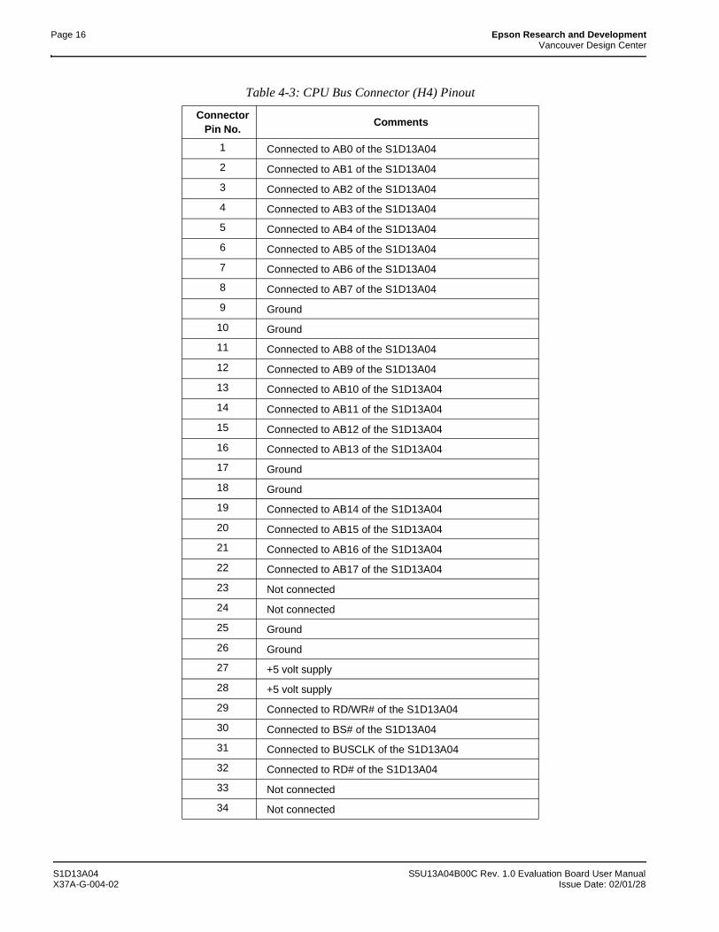
Page 16 Epson Research and DevelopmentVancouver Design Center
Table 4-3: CPU Bus Connector (H4) Pinout
Connector Pin No.
Comments
1 Connected to AB0 of the S1D13A04
2 Connected to AB1 of the S1D13A04
3 Connected to AB2 of the S1D13A04
4 Connected to AB3 of the S1D13A04
5 Connected to AB4 of the S1D13A04
6 Connected to AB5 of the S1D13A04
7 Connected to AB6 of the S1D13A04
8 Connected to AB7 of the S1D13A04
9 Ground
10 Ground
11 Connected to AB8 of the S1D13A04
12 Connected to AB9 of the S1D13A04
13 Connected to AB10 of the S1D13A04
14 Connected to AB11 of the S1D13A04
15 Connected to AB12 of the S1D13A04
16 Connected to AB13 of the S1D13A04
17 Ground
18 Ground
19 Connected to AB14 of the S1D13A04
20 Connected to AB15 of the S1D13A04
21 Connected to AB16 of the S1D13A04
22 Connected to AB17 of the S1D13A04
23 Not connected
24 Not connected
25 Ground
26 Ground
27 +5 volt supply
28 +5 volt supply
29 Connected to RD/WR# of the S1D13A04
30 Connected to BS# of the S1D13A04
31 Connected to BUSCLK of the S1D13A04
32 Connected to RD# of the S1D13A04
33 Not connected
34 Not connected
S1D13A04 S5U13A04B00C Rev. 1.0 Evaluation Board User ManualX37A-G-004-02 Issue Date: 02/01/28
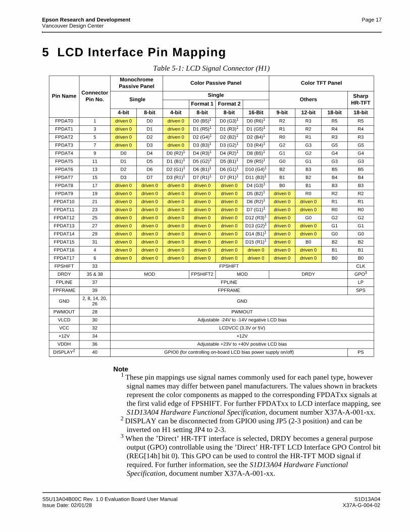
Epson Research and Development Page 17Vancouver Design Center
5 LCD Interface Pin Mapping
Note1 These pin mappings use signal names commonly used for each panel type, however
signal names may differ between panel manufacturers. The values shown in bracketsrepresent the color components as mapped to the corresponding FPDATxx signals atthe first valid edge of FPSHIFT. For further FPDATxx to LCD interface mapping, seeS1D13A04 Hardware Functional Specification, document number X37A-A-001-xx.
2 DISPLAY can be disconnected from GPIO0 using JP5 (2-3 position) and can beinverted on H1 setting JP4 to 2-3.
3 When the ’Direct’ HR-TFT interface is selected, DRDY becomes a general purposeoutput (GPO) controllable using the ’Direct’ HR-TFT LCD Interface GPO Control bit(REG[14h] bit 0). This GPO can be used to control the HR-TFT MOD signal ifrequired. For further information, see the S1D13A04 Hardware FunctionalSpecification, document number X37A-A-001-xx.
Table 5-1: LCD Signal Connector (H1)
Pin NameConnector
Pin No.
Monochrome Passive Panel
Color Passive Panel Color TFT Panel
SingleSingle
OthersSharp
HR-TFTFormat 1 Format 2
4-bit 8-bit 4-bit 8-bit 8-bit 16-Bit 9-bit 12-bit 18-bit 18-bit
FPDAT0 1 driven 0 D0 driven 0 D0 (B5)1 D0 (G3)1 D0 (R6)1 R2 R3 R5 R5
FPDAT1 3 driven 0 D1 driven 0 D1 (R5)1 D1 (R3)1 D1 (G5)1 R1 R2 R4 R4
FPDAT2 5 driven 0 D2 driven 0 D2 (G4)1 D2 (B2)1 D2 (B4)1 R0 R1 R3 R3
FPDAT3 7 driven 0 D3 driven 0 D3 (B3)1 D3 (G2)1 D3 (R4)1 G2 G3 G5 G5
FPDAT4 9 D0 D4 D0 (R2)1 D4 (R3)1 D4 (R2)1 D8 (B5)1 G1 G2 G4 G4
FPDAT5 11 D1 D5 D1 (B1)1 D5 (G2)1 D5 (B1)1 D9 (R5)1 G0 G1 G3 G3
FPDAT6 13 D2 D6 D2 (G1)1 D6 (B1)1 D6 (G1)1 D10 (G4)1 B2 B3 B5 B5
FPDAT7 15 D3 D7 D3 (R1)1 D7 (R1)1 D7 (R1)1 D11 (B3)1 B1 B2 B4 B4
FPDAT8 17 driven 0 driven 0 driven 0 driven 0 driven 0 D4 (G3)1 B0 B1 B3 B3
FPDAT9 19 driven 0 driven 0 driven 0 driven 0 driven 0 D5 (B2)1 driven 0 R0 R2 R2
FPDAT10 21 driven 0 driven 0 driven 0 driven 0 driven 0 D6 (R2)1 driven 0 driven 0 R1 R1
FPDAT11 23 driven 0 driven 0 driven 0 driven 0 driven 0 D7 (G1)1 driven 0 driven 0 R0 R0
FPDAT12 25 driven 0 driven 0 driven 0 driven 0 driven 0 D12 (R3)1 driven 0 G0 G2 G2
FPDAT13 27 driven 0 driven 0 driven 0 driven 0 driven 0 D13 (G2)1 driven 0 driven 0 G1 G1
FPDAT14 29 driven 0 driven 0 driven 0 driven 0 driven 0 D14 (B1)1 driven 0 driven 0 G0 G0
FPDAT15 31 driven 0 driven 0 driven 0 driven 0 driven 0 D15 (R1)1 driven 0 B0 B2 B2
FPDAT16 4 driven 0 driven 0 driven 0 driven 0 driven 0 driven 0 driven 0 driven 0 B1 B1
FPDAT17 6 driven 0 driven 0 driven 0 driven 0 driven 0 driven 0 driven 0 driven 0 B0 B0
FPSHIFT 33 FPSHIFT CLK
DRDY 35 & 38 MOD FPSHIFT2 MOD DRDY GPO3
FPLINE 37 FPLINE LP
FPFRAME 39 FPFRAME SPS
GND2, 8, 14, 20,
26 GND
PWMOUT 28 PWMOUT
VLCD 30 Adjustable -24V to -14V negative LCD bias
VCC 32 LCDVCC (3.3V or 5V)
+12V 34 +12V
VDDH 36 Adjustable +23V to +40V positive LCD bias
DISPLAY2 40 GPIO0 (for controlling on-board LCD bias power supply on/off) PS
S5U13A04B00C Rev. 1.0 Evaluation Board User Manual S1D13A04Issue Date: 02/01/28 X37A-G-004-02
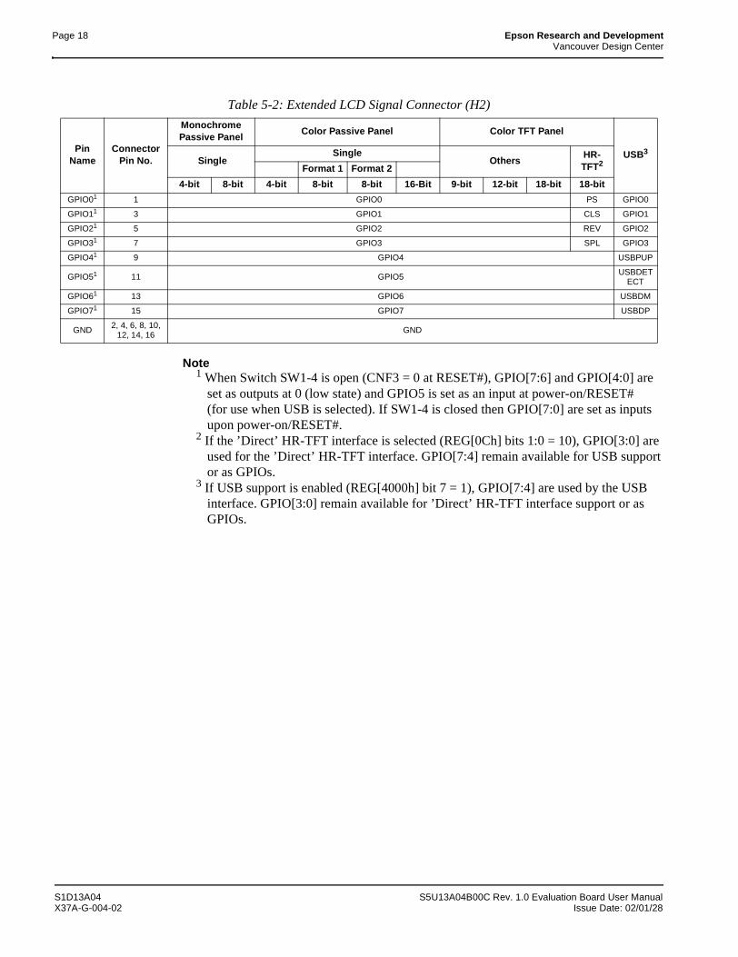
Page 18 Epson Research and DevelopmentVancouver Design Center
Note1 When Switch SW1-4 is open (CNF3 = 0 at RESET#), GPIO[7:6] and GPIO[4:0] are
set as outputs at 0 (low state) and GPIO5 is set as an input at power-on/RESET#(for use when USB is selected). If SW1-4 is closed then GPIO[7:0] are set as inputsupon power-on/RESET#.
2 If the ’Direct’ HR-TFT interface is selected (REG[0Ch] bits 1:0 = 10), GPIO[3:0] areused for the ’Direct’ HR-TFT interface. GPIO[7:4] remain available for USB supportor as GPIOs.
3 If USB support is enabled (REG[4000h] bit 7 = 1), GPIO[7:4] are used by the USBinterface. GPIO[3:0] remain available for ’Direct’ HR-TFT interface support or asGPIOs.
Table 5-2: Extended LCD Signal Connector (H2)
Pin Name
Connector Pin No.
Monochrome Passive Panel
Color Passive Panel Color TFT Panel
USB3 Single
SingleOthers
HR-TFT2Format 1 Format 2
4-bit 8-bit 4-bit 8-bit 8-bit 16-Bit 9-bit 12-bit 18-bit 18-bit
GPIO01 1 GPIO0 PS GPIO0
GPIO11 3 GPIO1 CLS GPIO1
GPIO21 5 GPIO2 REV GPIO2
GPIO31 7 GPIO3 SPL GPIO3
GPIO41 9 GPIO4 USBPUP
GPIO51 11 GPIO5 USBDETECT
GPIO61 13 GPIO6 USBDM
GPIO71 15 GPIO7 USBDP
GND 2, 4, 6, 8, 10, 12, 14, 16
GND
S1D13A04 S5U13A04B00C Rev. 1.0 Evaluation Board User ManualX37A-G-004-02 Issue Date: 02/01/28
Epson Research and Development Page 19Vancouver Design Center
6 Technical Description
6.1 PCI Bus Support
The S1D13A04 does not have on-chip PCI bus interface support. The S1D13A04B00C uses the PCI Bridge FPGA to support the PCI bus.
6.2 Direct Host Bus Interface Support
The S5U13A04B00C is specifically designed to work using the PCI Bridge FPGA in a standard PCI bus environment. However, the S1D13A04 directly supports many other host bus interfaces. Connectors H3 and H4 provide the necessary IO pins to interface to these host buses. For further information on the host bus interfaces supported, see “CPU Interface” on page 14.
NoteThe PCI Bridge FPGA must be disabled using SW1-8 in order for direct host bus inter-face to operate properly.
6.3 S1D13A04 Embedded Memory
The S1D13A04 has 160K bytes of embedded SRAM. The 160K byte display buffer address space is directly and contiguously available through the 18-bit address bus.
6.4 Adjustable LCD Panel Negative Power Supply
Most monochrome passive LCD panels require a negative power supply to provide between -14V and -24V (Iout=45mA). Such a power supply (VLCD) has been provided on the S5U13A04B00C board. VLCD can be adjusted using potentiometer R39 to provide an output voltage from -14V to -24V, and is enabled/disabled using the S1D13A04 general purpose signal, GPIO0 (active high).
NoteWhen manually adjusting the voltage, set the potentiometer according to the panel’s specific power requirements before connecting the panel.
S5U13A04B00C Rev. 1.0 Evaluation Board User Manual S1D13A04Issue Date: 02/01/28 X37A-G-004-02
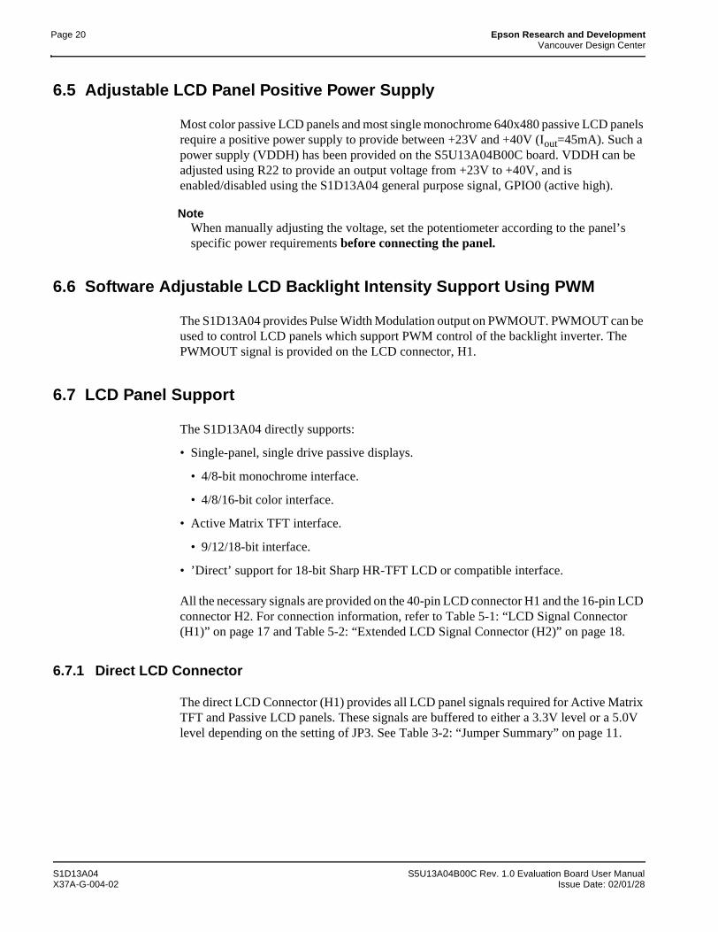
Page 20 Epson Research and DevelopmentVancouver Design Center
6.5 Adjustable LCD Panel Positive Power Supply
Most color passive LCD panels and most single monochrome 640x480 passive LCD panels require a positive power supply to provide between +23V and +40V (Iout=45mA). Such a power supply (VDDH) has been provided on the S5U13A04B00C board. VDDH can be adjusted using R22 to provide an output voltage from +23V to +40V, and is enabled/disabled using the S1D13A04 general purpose signal, GPIO0 (active high).
NoteWhen manually adjusting the voltage, set the potentiometer according to the panel’s specific power requirements before connecting the panel.
6.6 Software Adjustable LCD Backlight Intensity Support Using PWM
The S1D13A04 provides Pulse Width Modulation output on PWMOUT. PWMOUT can be used to control LCD panels which support PWM control of the backlight inverter. The PWMOUT signal is provided on the LCD connector, H1.
6.7 LCD Panel Support
The S1D13A04 directly supports:
• Single-panel, single drive passive displays.
• 4/8-bit monochrome interface.
• 4/8/16-bit color interface.
• Active Matrix TFT interface.
• 9/12/18-bit interface.
• ’Direct’ support for 18-bit Sharp HR-TFT LCD or compatible interface.
All the necessary signals are provided on the 40-pin LCD connector H1 and the 16-pin LCD connector H2. For connection information, refer to Table 5-1: “LCD Signal Connector (H1)” on page 17 and Table 5-2: “Extended LCD Signal Connector (H2)” on page 18.
6.7.1 Direct LCD Connector
The direct LCD Connector (H1) provides all LCD panel signals required for Active Matrix TFT and Passive LCD panels. These signals are buffered to either a 3.3V level or a 5.0V level depending on the setting of JP3. See Table 3-2: “Jumper Summary” on page 11.
S1D13A04 S5U13A04B00C Rev. 1.0 Evaluation Board User ManualX37A-G-004-02 Issue Date: 02/01/28
Epson Research and Development Page 21Vancouver Design Center
6.7.2 Extended LCD Connector
The S1D13A04 directly supports Sharp 18-bit HR-TFT and compatible panels. The extended LCD connector (H2) provides the extra signals required to support these panels. The signals on this connector are provided directly from the S1D13A04 without any buffering and are 3.3V signals.
6.8 USB Support
The S1D13A04 USB controller provides a Revision 1.1 compliant USB client. The S1D13A04 acts as a USB device and connects to an upstream hub or USB host through connector J1 on the S5U13A04B00C evaluation board. Clamping diodes have been added to protect the USB bus from ESD and shorting.
6.8.1 USB IRQ Support
The S1D13A04 supports interrupts through output pin, IRQ. This interrupt can be used to support interrupts from the USB client of the S1D13A04. The S5U13A04B00C evaluation board supports this capability by connecting IRQ to the PCI interrupt INTA# of the PCI slot that the S5U13A04B00C evaluation board is connected to.
S5U13A04B00C Rev. 1.0 Evaluation Board User Manual S1D13A04Issue Date: 02/01/28 X37A-G-004-02
Page 22 Epson Research and DevelopmentVancouver Design Center
7 Clock Synthesizer and Clock Options
For maximum flexibility, the S5U13A04B00C implements a Cypress ICD2061A Clock Synthesizer. MCLKOUT from the clock synthesizer is connected to CLKI2 of the S1D13A04 and VCLKOUT from the clock synthesizer is connected to CLKI of the S1D13A04. A 14.31818MHz crystal (Y1) is connected to XTALIN and XTALOUT of the clock synthesizer and provides the reference clock to the clock synthesizer.
Figure 7-1: Symbolic Clock Synthesizer Connections
At power-on, CLKI2 (MCLKOUT) is configured to be 40MHz and CLKI (VCLKOUT) is configured at 25.175MHz.
NoteIf a Sharp HR-TFT panel is selected, the clock synthesizer cannot be programmed, and external oscillators must provide the clock signals to CLKI and CLKI2. Jumpers JP1 and JP2 allow selection of external oscillators U7 and U8 as the clock source for both CLKI and CLKI2. For further information, see Table 3-2: “Jumper Summary” on page 11.
7.1 Clock Programming
The S1D13A04 utilities automatically program the clock generator. If manual programming of the clock generator is required, refer to the source code for the S1D13A04 utilities available on the internet at www.erd.epson.com.
For further information on programming the clock generator, refer to the Cypress ICD2061A specification.
NoteWhen CLKI and CLKI2 are programmed to multiples of each other (e.g. CLKI = 20MHz, CLKI2 = 40MHz), the clock output signals from the Cypress clock generator may jitter. Refer to the Cypress ICD2061A specification for details.
To avoid this problem, set CLKI and CLKI2 to different frequencies and use the S1D13A04 internal clock divides to obtain the lower frequencies.
XTALIN MCLKOUT
VCLKOUT
CLKI2
CLKI
14.31818 MHz
ICD2061ASynthesizer reference
S1D13A04 S5U13A04B00C Rev. 1.0 Evaluation Board User ManualX37A-G-004-02 Issue Date: 02/01/28
Epson Research and Development Page 23Vancouver Design Center
8 References
8.1 Documents
• Epson Research and Development, Inc., S1D13A04 Hardware Functional Specification, document number X37A-A-001-xx.
• Epson Research and Development, Inc., S1D13A04 Programming Notes and Examples, document number X37A-G-003-xx.
• Cypress Semiconductor Corporation, ICD2061A Data Sheet.
8.2 Document Sources
• Epson Research and Development: http://www.erd.epson.com.
• Cypress Semiconductor Corporation Website: http://www.cypress.com.
S5U13A04B00C Rev. 1.0 Evaluation Board User Manual S1D13A04Issue Date: 02/01/28 X37A-G-004-02
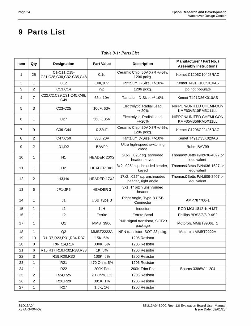
Page 24 Epson Research and DevelopmentVancouver Design Center
9 Parts List
Table 9-1: Parts List
Item Qty Designation Part Value DescriptionManufacturer / Part No. / Assembly Instructions
1 25C1-C11,C15-
C21,C28,C30,C32-C35,C480.1u
Ceramic Chip, 50V X7R +/-5%, 1206 pckg.
Kemet C1206C104J5RAC
2 1 C12 10u,10V Tantalum C-Size, +/-10% Kemet T491C106K010AS
3 2 C13,C14 n/p 1206 pckg. Do not populate
4 7C22,C2,C29,C31,C45,C46,
C4968u, 10V Tantalum D-Size, +/-10% Kemet T491D86K010AS
5 3 C23-C25 10uF, 63VElectrolytic, Radial Lead,
+/-20%NIPPON/UNITED CHEMI-CON
KMF63VB10RM5X11LL
6 1 C27 56uF, 35VElectrolytic, Radial Lead,
+/-20%NIPPON/UNITED CHEMI-CON
KMF35VB56RM5X11LL
7 9 C36-C44 0.22uFCeramic Chip, 50V X7R +/-5%,
1206 pckg.Kemet C1206C224J5RAC
8 2 C47,C50 33u, 20V Tantalum D-Size, +/-10% Kemet T491D33K020AS
9 2 D1,D2 BAV99Ultra high-speed switching
diodeRohm BAV99
10 1 H1 HEADER 20X220x2, .025" sq. shrouded
header, keyedThomas&Betts P/N:636-4027 or
equivalent
11 1 H2 HEADER 8X28x2, .025" sq. shrouded header,
keyedThomas&Betts P/N:636-1627 or
equivalent
12 2 H3,H4 HEADER 17X217x2, .025" sq. unshrouded
header, right angleThomas&Betts P/N:609-3407 or
equivalent
13 5 JP1-JP5 HEADER 33x1 .1" pitch unshrouded
header
14 1 J1 USB Type BRight Angle, Type B USB
ConnectorAMP787780-1
15 1 L1 1uH Inductor RCD MCI-1812 1uH MT
16 1 L2 Ferrite Ferrite Bead Phillips BDS3/3/8.9-4S2
17 1 Q1 MMBT3906PNP signal transistor, SOT23
packageMotorola MMBT3906LT1
18 1 Q2 MMBT2222A NPN transistor, SOT-23 pckg. Motorola MMBT2222A
19 13 R1-R7,R23,R31,R34-R37 15K, 5% 1206 Resistor
20 8 R8-R14,R16 330K, 5% 1206 Resistor
21 6 R15,R17,R18,R32,R33,R38 1K, 5% 1206 Resistor
22 3 R19,R20,R30 100K, 5% 1206 Resistor
23 1 R21 470 Ohm, 5% 1206 Resistor
24 1 R22 200K Pot 200K Trim Pot Bourns 3386W-1-204
25 2 R24,R25 20 Ohm, 1% 1206 Resistor
26 2 R26,R29 301K, 1% 1206 Resistor
27 1 R27 1.5K, 1% 1206 Resistor
S1D13A04 S5U13A04B00C Rev. 1.0 Evaluation Board User ManualX37A-G-004-02 Issue Date: 02/01/28
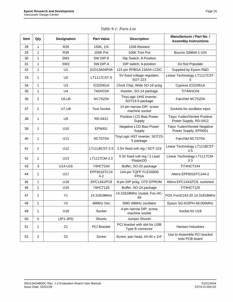
Epson Research and Development Page 25Vancouver Design Center
28 1 R28 150K, 1% 1206 Resistor
29 1 R39 100K Pot 100K Trim Pot Bourns 3386W-1-104
30 1 SW1 SW DIP-8 Dip Switch, 8-Position
31 1 SW2 SW DIP-4 DIP switch, 4-position Do Not Populate
32 1 U1 S1D13A04F0A 121-pin PFBGA 13A04 LCDC Supplied by Epson R&D
33 1 U2 LT1117CST-55V fixed voltage regulator,
SOT-223Linear Technology LT1117CST-
5
34 1 U3 ICD2061A Clock Chip, Wide SO-16 pckg Cypress ICD2061A
35 1 U4 74AHC04 Inverter, SO-14 package TI74AHC04
36 2 U5,U6 NC7SZ04TinyLogic UHS inverter,
SOT23-5 packageFairchild NC7SZ04
37 2 U7,U8 Test Socket14 pin narrow DIP, screw
machine socketSockets for oscillator input
38 1 U9 RD-0412Positive LCD Bias Power
SupplyTaiyo Yuden/Xentek Positive
Power Supply, RD-0412
39 1 U10 EPN001Negative LCD Bias Power
SupplyTaiyo Yuden/Xentek Negative
Power Supply, EPN001
40 1 U11 NC7ST04TinyLogic HST inverter, SOT23-
5 packageFairchild NC7ST04
41 1 U12 LT1118CST-2.5 2.5V fixed volt reg / SOT-223Linear Technology LT1118CST-
2.5
42 1 U13 LT1117CM-3.33.3V fixed volt reg / 3 Lead
PlasticDDLinear Technology LT1117CM-
3.3
43 3 U14-U16 74HCT244 Buffer, SO-20 package TI74HCT244
44 1 U17EPF6016TC14
4-2144-pin TQFP FLEX6000
FPGAAltera EPF6016TC144-2
45 1 U18 EPC1441PC8 8-pin DIP pckg, OTP EPROM Altera EPC1441PC8, socketed
46 1 U19 74HCT125 Buffer, SO-14 package TI74HCT125
47 1 Y1 14.31818MHz14.31818MHz crystal, Fox HC-
49FOX FoxS/143-20 14.31818MHz
48 1 Y2 48MHz Osc SMD 48MHz oscillator Epson SG-615PH-48.000MHz
49 1 U18 Socket4-pin narrow DIP, screw
machine socketSocket for U18
50 5 (JP1-JP5) Shunts Jumper Shunts
51 1 Z1 PCI BracketPCI bracket with slot for USB
Type B connectorHansen Industries
52 2 Z2 Screw Screw, pan head, #4-40 x 1/4"Use to Assemble PCI bracket
onto PCB board
Table 9-1: Parts List
Item Qty Designation Part Value DescriptionManufacturer / Part No. / Assembly Instructions
S5U13A04B00C Rev. 1.0 Evaluation Board User Manual S1D13A04Issue Date: 02/01/28 X37A-G-004-02
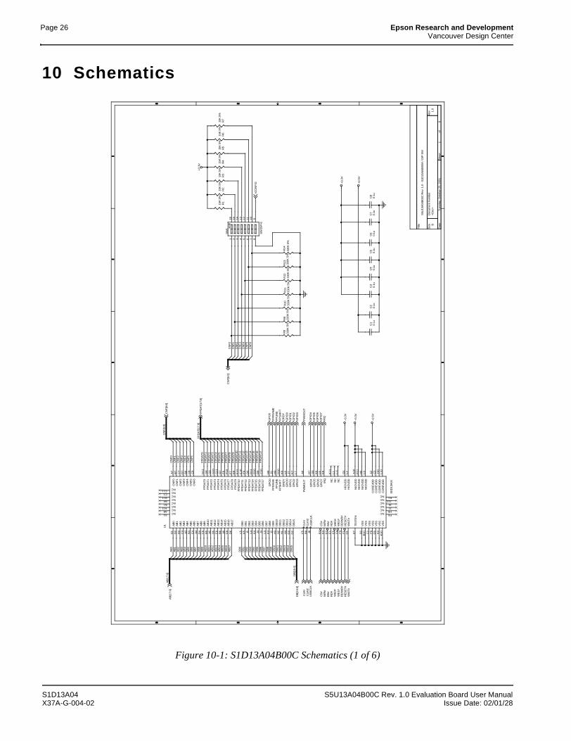
Page 26 Epson Research and DevelopmentVancouver Design Center
10 Schematics
Figure 10-1: S1D13A04B00C Schematics (1 of 6)
5 5
4 4
3 3
2 2
1 1
DD
CC
BB
AA
<D
oc>
1.0
S5U
13A
04B
00C
Rev.
1.0
- S
1D13
A04
B00A
/ D
IP S
W
B
16
Tue
sday
, O
ctob
er 2
3, 2
001
Titl
e
Siz
eD
ocu
ment
Num
ber
Rev
Dat
e:S
hee
tof
CN
F3
CN
F6
CN
F1
CN
F2
CN
F5
CN
F0
CN
F4
DB
14
FP
DA
T8
AB
0
FP
DA
T15
DB
2
FP
DA
T6
DB
[15:0
]
DB
3
CN
F4
AB
14
FP
DA
T10
CN
F3
AB
10
AB
2
FP
DA
T14
AB
11
CN
F[6
:0]
AB
15
DB
10
DB
12
FP
DA
T1
DB
8
DB
13
CN
F0
AB
8
FP
DA
T3
AB
9
DB
11
FP
DA
T0
FP
DA
T13
FP
DA
T4
AB
12
CN
F6
FP
DA
T7
FP
DA
T2
CN
F1
CN
F2
DB
1
CN
F5
FP
DA
T17
DB
0
AB
6
DB
9
AB
5
AB
16
FP
DA
T[1
7:0
]
DB
5
AB
7
DB
15
AB
4A
B3
FP
DA
T9
DB
7
FP
DA
T11
DB
6
FP
DA
T5
FP
DA
T12
AB
1
FP
DA
T16
DB
4
AB
13
AB
[17:
0]
AB
17
CN
F[6
:0]
nC
ON
FIG
RD
/WR
#W
E1#
FP
FR
AM
E
FP
DA
T[1
7:0]
GP
IO6
BS
#
GP
IO7C
NF
[6:0
]
FP
SH
IFT
IRQ
GP
IO3
DR
DY
M/R
#
RD
#
WA
IT#
WE
0#
GP
IO4
FP
LIN
E
RE
SE
T#
CS
#
PW
MO
UT
CLK
I
US
BC
LK
DB
[15:
0]
CLK
I2
AB
[17:
0]
GP
IO5
GP
IO2
GP
IO1
GP
IO0
GP
O0
+3.
3V
+2.
5V
+3.3
V
+3.
3V
+2.
5V
+3.
3V
R10
330K
5%
R8
330
K 5
%
R4
15K
5%
R11
330
K 5
%
C1
0.1u
R12
330
K 5
%
C2
0.1
u
R13
330K
5%
C3
0.1
u
R14
330K
5%
C4
0.1u
R6
15K
5%
C5
0.1u
C6
0.1u
C7
0.1u
R7
15K
5%
C8
0.1u
R3
15K
5%
R5
15K
5%
R2
15K
5%
U1
SE
D13A
04
A10
B8
C7
C2
D5
B5
C4
B9
C9
A7
A6
C6
D4
A3
D10
C10
C8
B7
E7
B6
C5
B3
D3
G4
F11
E9
D11
A9
D7
E6
A5
A4
C3
E4
D1
E10
E8
D8
D9
B2
D6
B10D
2
E3
E5
E1
E11
F10
F7
F2
F9
K11
L1
G5
E2
F3
F1
G7
G11
G10
F8
K2
L11
K10F
4
F5
G2
G1
G8
H11
H10
G9
K9
J7
L4
H3
H4
G3
H1
L9
J9 H9
K8
L7
L6
K5 J4 L3
H2
L2
J8
K7
K6
G6
J5 K3 J2
H6
L8
H7
A2
L5
K4 J3
J10
L10
H5
H8
J1J6J11K1
F6A1A8A11B1B4B11C1C11 N
IOV
DD
CN
F4
CN
F2
CO
RE
VD
D
AB
12
AB
10
AB
6
CLK
I2
CN
F6
CN
F0
AB
15A
B16
AB
8
AB
4
FP
DA
T15
FP
DA
T17
CN
F5
CN
F1
TE
ST
EN
AB
14
AB
9
AB
5
AB
2
HIO
VD
D
NIO
VD
D
FP
DA
T12
FP
DA
T14
PW
MO
UT
CN
F3
AB
13
AB
11
AB
7
AB
3
CS
#
AB
0
FP
DA
T11
FP
DA
T9
FP
DA
T13
FP
DA
T16
VS
S
AB
17
VS
S
AB
1
M/R
#
WE
0#R
D#
FP
DA
T10
FP
DA
T7
FP
DA
T8
VS
SV
SS
NC
NC
VS
S
BS
#
RD
/WR
#R
ES
ET
#
FP
DA
T5
FP
DA
T4
FP
DA
T3
FP
DA
T6
VS
S
NC
VS
S
WE
1#
CLK
I
DB
15
WA
IT#
FP
DA
T1
FP
DA
T0
FP
SH
IFT
FP
DA
T2
DR
DY
GP
IO1
DB
3
DB
10
DB
13
DB
14
DB
12
NIO
VD
D
FP
RA
ME
FP
LIN
E
IRQ
GP
IO3
GP
IO7
DB
1
DB
5
DB
7
DB
11
HIO
VD
D
US
BC
LK
GP
IO2
GP
IO6
GP
IO5
DB
2
DB
8D
B9
NIO
VD
D
GP
IO0
GP
IO4
CO
RE
VD
D
DB
0
DB
4
DB
6
CO
RE
VD
DC
OR
EV
DD
NC
GP
O0
NCNCNCNC
NCNCNCNCNCNCNCNCNC
SW
1
SW
DIP
-8
1 2 3 4 5 6 7 8
16 15 14 13 12 11 10 9
R1
15K
5%
R9
330K
5%
S1D13A04 S5U13A04B00C Rev. 1.0 Evaluation Board User ManualX37A-G-004-02 Issue Date: 02/01/28
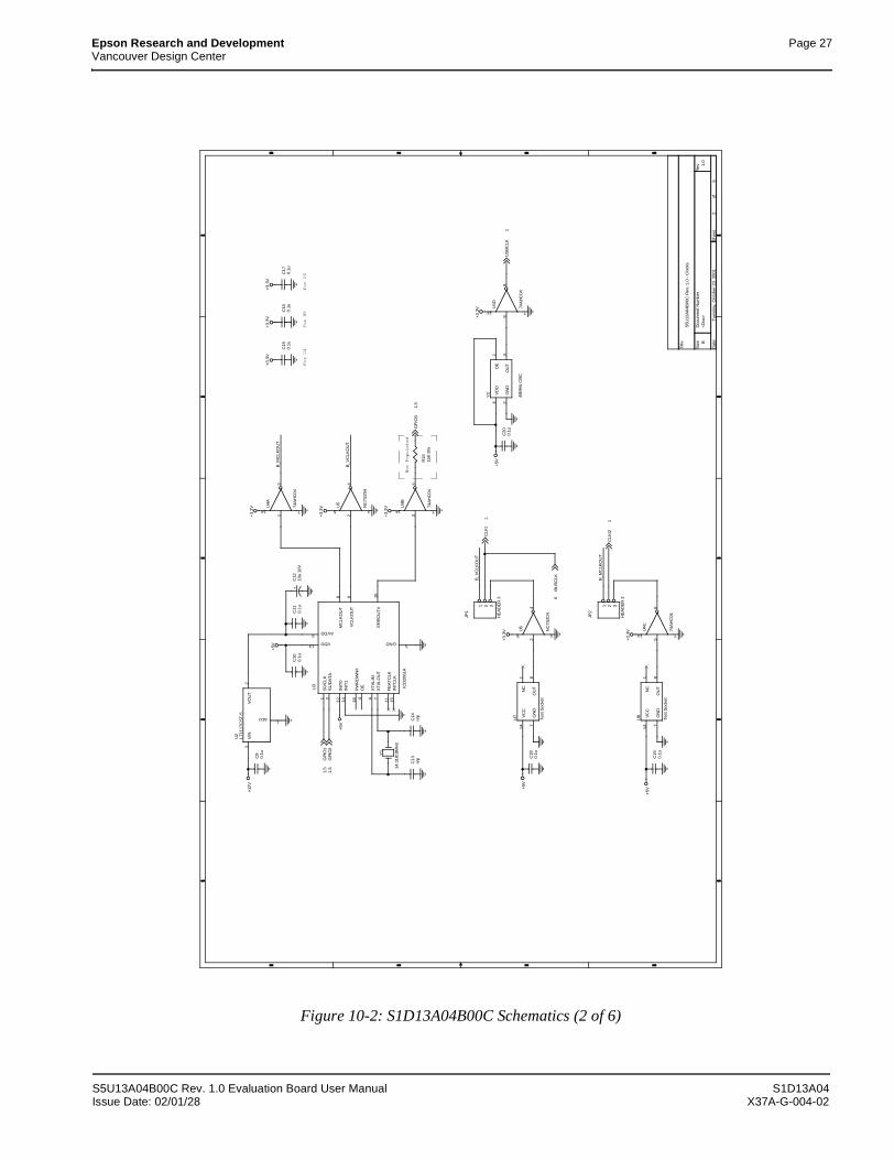
Epson Research and Development Page 27Vancouver Design Center
Figure 10-2: S1D13A04B00C Schematics (2 of 6)
5 5
4 4
3 3
2 2
1 1
DD
CC
BB
AA
For U4
For U5
For U6
Not Populated
<D
oc>
1.0
S5U
13A
04B
00C
Rev.
1.0
- C
lock
s
B
26
Tues
day
, O
ctob
er 2
3, 2
001
Titl
e
Siz
eD
ocu
men
t Num
ber
Rev
Dat
e:S
hee
tof
B_V
CLK
OU
T
B_M
CLK
OU
T
B_V
CLK
OU
T
B_M
CLK
OU
T
GP
IO1
1,5
GP
IO2
1,5
GP
IO3
1,5
BU
SC
LK6
CLK
I1
US
BC
LK1
CLK
I21
+5V
+5V
+5V
+5V
+12
V+3.
3V
+3.
3V
+3.
3V
+3.3
V
+3.3
V
+3.
3V
+3.3
V
+3.3
V
+3.3
V
+5V
U8
Tes
t Sock
et
14 7
81V
CC
GN
DO
UT
NC
U4C
74A
HC
04
56
14 7
Y2
48M
Hz
OS
C
1 324
OE
OU
TG
ND
VD
D
C20
0.1u
C17
0.1u
C9
0.1u
U7
Tes
t Sock
et
14 7
81V
CC
GN
DO
UT
NC
C19
0.1u
U5
NC
7S
Z04
24
5 3
U4D
74A
HC
04
98
14 7
C18
0.1u
U4A
74A
HC
04
12
14 7
U2
LT11
17C
ST
-53
1
2V
IN
ADJ
VO
UT
C15
0.1
uC
100.1
uC
110.1
u+
C12
10u
10V
R15
15K
5%
U3 IC
D20
61A
13
3
5
1 2
12
14
16 4 6 7
11
15
8 9 10
VDD
AVDD
GND
S0/C
LK
S1/D
AT
A
INIT
0IN
IT1
PW
RD
WN
#O
E
XT
ALIN
XT
ALO
UT
FE
AT
CLK
INT
CLK
MC
LKO
UT
VC
LKO
UT
ER
RO
UT
#
C16
0.1
u
Y1
14.
3181
8MH
z
JP2
HE
AD
ER
3
1 2 3
C14
n/p
C13
n/p
U4B
74A
HC
04
34
14 7
JP1
HE
AD
ER
3
1 2 3
U6
NC
7SZ
04
24
5 3
S5U13A04B00C Rev. 1.0 Evaluation Board User Manual S1D13A04Issue Date: 02/01/28 X37A-G-004-02
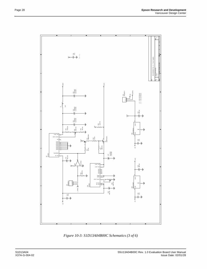
Page 28 Epson Research and DevelopmentVancouver Design Center
Figure 10-3: S1D13A04B00C Schematics (3 of 6)
5 5
4 4
3 3
2 2
1 1
DD
CC
BB
AA
For U11
1 2
5
.0V
LC
D P
anel
s
2 3
3
.3V
LC
D P
anel
s
<D
oc>
1.0
S5U
13A
04B
00C
Rev.
1.0
- P
ower
Supp
lies
B
36
Tues
day
, O
ctob
er 2
3, 2
001
Titl
e
Siz
eD
ocu
men
t Num
ber
Rev
Dat
e:S
hee
tof
GP
IO0
1
+5V
+5V
+3.3
V
+5V
+5V
+5V
LCD
VC
C
+5V
+3.3
V
+5V
+2.5
V
VD
DH
VLC
D
C30
0.1
u+
C31
68u
10V
+
C27
56u
F/3
5VLow
ES
R
R22
200
K P
ot
13
2+
C23
10u
F/6
3VLow
ES
R
C21
0.1u
JP5
HE
AD
ER
3
123
+C
2410u
F/6
3VLow
ES
R
+C
2510u
F/6
3VLow
ES
RU
11
NC
7ST
04
24
5 3
R39
100
K P
ot
13
2
U13
LT111
7CM
-3.3
3
1
2V
IN
ADJ
VO
UT
U10
EP
N001
1
2
3
45
6
789
1110
DC_OUT
DC_OUT
NC
GNDGND
VOUT_ADJ
NCNCNC
DC_INDC_IN
Q2
MM
BT
2222
A
1
23
Q1
MM
BT
390
6
1
2 3
R16
330
K 5
%
L1 1uH
R21
470
K 5
%
R23
15K
5%
R19
100
K 5
%
R20
100K
5%
R17
1K 5
%
R18
1K 5
%
JP3
HE
AD
ER
3
123
U9
RD
-0412
1
2
3
45678
9
1011
12
VOUT_ADJ
DC_IN
REMOTE
GNDGNDGNDGNDGND
NC
GNDGND
DC_OUT
+C
22
68u
10V
+C
2668
u 10
V
C28
0.1u
C32
0.1
u
+C
2968u
10V
U12
RC
1117
S25
T
3
1
2V
IN
ADJ
VO
UT
S1D13A04 S5U13A04B00C Rev. 1.0 Evaluation Board User ManualX37A-G-004-02 Issue Date: 02/01/28
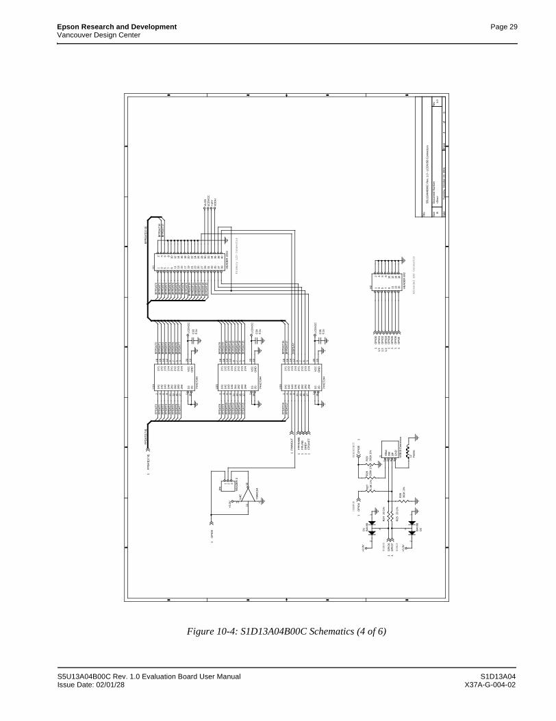
Epson Research and Development Page 29Vancouver Design Center
Figure 10-4: S1D13A04B00C Schematics (4 of 6)
5 5
4 4
3 3
2 2
1 1
DD
CC
BB
AA
USBDETECT
USBDM
USBDP
USBPUP
Extended LCD Connector
Primary LCD Connector
<D
oc>
1.0
S5U
13A
04B
00C
Rev.
1.0
- L
CD
/US
B C
onn
ecto
rs
B
46
Tues
day
, O
ctob
er 2
3, 2
001
Titl
e
Siz
eD
ocu
men
t Num
ber
Rev
Dat
e:S
hee
tof
BF
PD
AT
[17:0
]
DIS
PLA
Y
BF
PD
AT
12
BF
PD
AT
5
BF
PD
AT
15
BF
PD
AT
12
BF
PD
AT
10
BF
PD
AT
3
BF
PD
AT
6
BF
PD
AT
0
BF
PD
AT
15
BF
PD
AT
9
BF
PD
AT
5
BF
PD
AT
10
BF
PD
AT
14
BF
PD
AT
11
BF
PD
AT
7
BF
PD
AT
1B
FP
DA
T0
BF
PD
AT
2
BF
PD
AT
17
BF
PD
AT
6
BF
PD
AT
14
BF
PD
AT
11
BF
PD
AT
8
BF
PD
AT
4
BF
PD
AT
7
BF
PD
AT
16
BF
PD
AT
2
BF
PD
AT
13
BF
PD
AT
8
BF
PD
AT
1
BF
PD
AT
9
BF
PD
AT
13
BF
PD
AT
3B
FP
DA
T4
BF
PD
AT
16B
FP
DA
T17
FP
DA
T7
FP
DA
T11
FP
DA
T10
FP
DA
T1
FP
DA
T12
FP
DA
T2
FP
DA
T17
FP
DA
T9
FP
DA
T4
FP
DA
T14
FP
DA
T16
FP
DA
T6
FP
DA
T3
FP
DA
T5
FP
DA
T[1
7:0]
FP
DA
T13
FP
DA
T0
FP
DA
T8
FP
DA
T15
FP
LIN
E1
DR
DY
1F
PS
HIF
T1
FP
FR
AM
E1
GP
IO0
1G
PIO
11,
3G
PIO
21,
3G
PIO
31,
3G
PIO
41
GP
IO5
1G
PIO
61
GP
O0
1
GP
IO0
1
PW
MO
UT
1
GP
IO7
1G
PIO
61
GP
IO4
1G
PIO
51
FP
DA
T[1
7:0
]1
+12
V
+3.
3V
LC
DV
CC
LC
DV
CC
LC
DV
CC
LCD
VC
C
+3.3
V
+3.3
V
VLC
D
VD
DH
R29
301
K 1
%
C34
0.1
u
D1
BA
V99
1
3
2
R26
301
K 1
%
H1
HE
AD
ER
20X
2
12
34
56
78
910
1112
1314
1516
1718
1920
2122
2324
2526
2728
2930
3132
3334
3536
3738
3940
D2
BA
V99
1
3
2
U14
74H
CT
244
2 4 6 811 13 15 17
119
18
16
14
12
9 7 5 3 20
10
1A1
1A2
1A3
1A4
2A1
2A2
2A3
2A4
1G 2G
1Y
11Y
21Y
31Y
42Y
12Y
22Y
32Y
4
VC
CG
ND
U16
74H
CT
244
2 4 6 811 13 15 17
119
18
16
14
12
9 7 5 3 20
10
1A1
1A2
1A3
1A4
2A1
2A2
2A3
2A4
1G 2G
1Y
11Y
21Y
31Y
42Y
12Y
22Y
32Y
4
VC
CG
ND
C33
0.1
u
JP4
HE
AD
ER
3
1 2 3
J1 US
B B
Con
nect
or
1 2 3 4
VB
usD
MD
PG
ND
U4E
74A
HC
04
11
10
14 7
R24
20
1%
U15
74H
CT
244
2 4 6 811 13 15 17
119
18
16
14
12
9 7 5 3 20
10
1A1
1A2
1A3
1A4
2A1
2A2
2A3
2A4
1G 2G
1Y
11Y
21Y
31Y
42Y
12Y
22Y
32Y
4
VC
CG
ND
R25
20
1%
R28
150K
1%
H2
HE
AD
ER
8X
2
12
34
56
78
910
1112
1314
1516
C35
0.1
u
R27
1.5K
1%
L2 Fer
rite
S5U13A04B00C Rev. 1.0 Evaluation Board User Manual S1D13A04Issue Date: 02/01/28 X37A-G-004-02
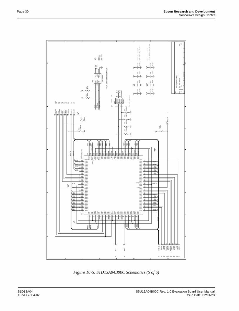
Page 30 Epson Research and DevelopmentVancouver Design Center
Figure 10-5: S1D13A04B00C Schematics (5 of 6)
A A
B B
C C
D D
E E
44
33
22
11
FP
GA
con
figur
atio
n E
PR
OM
Do Not Populate
Place one on each
+5V Power Pin of U18
Place one on each
+3.3V Power Pin of U18
<D
oc>
1.0
S5U
13A
04B
00C
- F
PG
A
B
56
Tues
day
, O
ctob
er 2
3, 2
001
Titl
e
Siz
eD
ocu
men
t Num
ber
Rev
Dat
e:S
hee
tof
AD13
AD9
AD15
AD16
AD18
AD23
AD10
AD12
AD19
AD24
AD8
AD20
AD22
AD25
AD17
AD11
AD21
AD14
AD
0A
D1
AD
2A
D3
AD
4
AD
5A
D6
AD
7A
D27
AD
26
AD
29
AD
28
AD
30
AD
31
DB15DB14
DB13DB12
DB11DB10
DB
9
DB
2D
B1
DB
0
DB
6D
B5
DB
3D
B4
DB
7D
B8
DB
[15:0
]
AB
15A
B16
AB9
AB1AB0
AB11
AB2
AB12
AB4
AB10
AB6
AB13
AB8
AB5
AB7
AB
14
AB3
DCLK
DATA nSTATUS
CO
NF
_DO
NE
nS
TA
TU
SC
ON
F_D
ON
E
DC
LK
DA
TA
AB
[17:
0]
AD
[31:0
]
AB
17
TR
DY
#5
ST
OP
#5
PA
R5
IRD
Y#
5
DE
VS
EL#
5
PE
RR
#5
SE
RR
#5
AB
[17:
0]
1,5
M/R
#1,
5
WE
0#
1,5
DB
[15:0
]1,
5
BS
#1,
5R
D#
1,5
WE
1#
1,5
RD
/WR
#1,
5
CS
#1,
5
BU
SC
LK1,
2,5
RE
SE
T#
1,5
C/B
E0#
5
IDS
EL
5C
/BE
3#5
C/B
E1#
5
WA
IT#
1,5
FR
AM
E#
5C
/BE
2#5
AD
[31:0
]5
RS
T#
5
CLK
5
nC
ON
FIG
1
+5V
+5V
+5V
+5V
+5V
+5V
+5V
+5V
+5V
+5V
+5V
+5V
+5V
+5V
+5V
+3.3
V
+3.
3V
+3.3
V+3.3
V+3.3
V
+3.3
V
R32
1K 5
%
C37
0.2
2u
R35
15K
5%
C43
0.22u
R33
1K 5
%
C42
0.22u
R36
15K
5%
R30
100
K 5
%
R38
1K
5%
C40
0.22
u
R37
15K
5%
U17
EP
F601
6TC
144-
2
1 2 3 4 5 6 7 8 910
11
12
13
14
15
16
17
18
19
20
21
22
23
24
25
26
27
28
29
30
31
32
33
34
35
36
373839404142434445464748495051525354555657585960616263646566676869707172
73
74
75
76
77
78
79
80
81
82
83
84
85
86
87
88
89
90
91
92
93
94
95
96
97
98
99
100
101
102
103
104
105
106
107
108
109110111112113114115116117118119120121122123124125126127128129130131132133134135136137138139140141142143144
IO1
IO2
IO3
nC
EG
ND
Vcc
int
Vcc
ioIO
8IO
9IO
10IO
11IO
12IO
13IO
14IO
15IO
16I1
7G
ND
Vcc
ioI2
0IO
21IO
22IO
23IO
24IO
25IO
26IO
27IO
28IO
29G
ND
Vcc
int
Vcc
ioM
SE
LIO
34IO
35IO
36
IO37IO38IO39IO40IO41IO42IO43IO44IO45IO46IO47IO48IO49IO50IO51IO52nCONFIGGNDVccionSTATUSIO57IO58IO59IO60IO61IO62IO63IO64IO65IO66IO67IO68IO69IO70IO71IO72IO
73IO
74IO
75G
ND
Vcc
int
Vcc
ioIO
79IO
80IO
81IO
82IO
83IO
84IO
85IO
86IO
87IO
88I89
GN
DV
ccioI92
IO93
IO94
IO95
IO96
IO97
IO98
IO99
IO10
0IO
101
GN
DV
ccin
tV
ccio
CO
NF_D
ON
EIO
106
IO10
7IO
108
IO109IO110IO111IO112IO113IO114IO115IO116IO117IO118IO119IO120IO121IO122IO123IO124DATAGNDVccio
DCLKIO129IO130IO131IO132IO133IO134IO135IO136IO137IO138IO139IO140IO141IO142IO143IO144
C39
0.22u
R31
15K
5%
SW
2
SW
DIP
-4
1 2 3 4
8 7 6 5
C36
0.2
2u
C41
0.2
2u
C38
0.22u
U18
EP
C14
41P
C8
1 2 3 45678
DA
TA
DC
LK
OE
nC
SG
ND
nC
AS
CV
CC
VC
C
R34
15K
5%
C44
0.22
u
S1D13A04 S5U13A04B00C Rev. 1.0 Evaluation Board User ManualX37A-G-004-02 Issue Date: 02/01/28
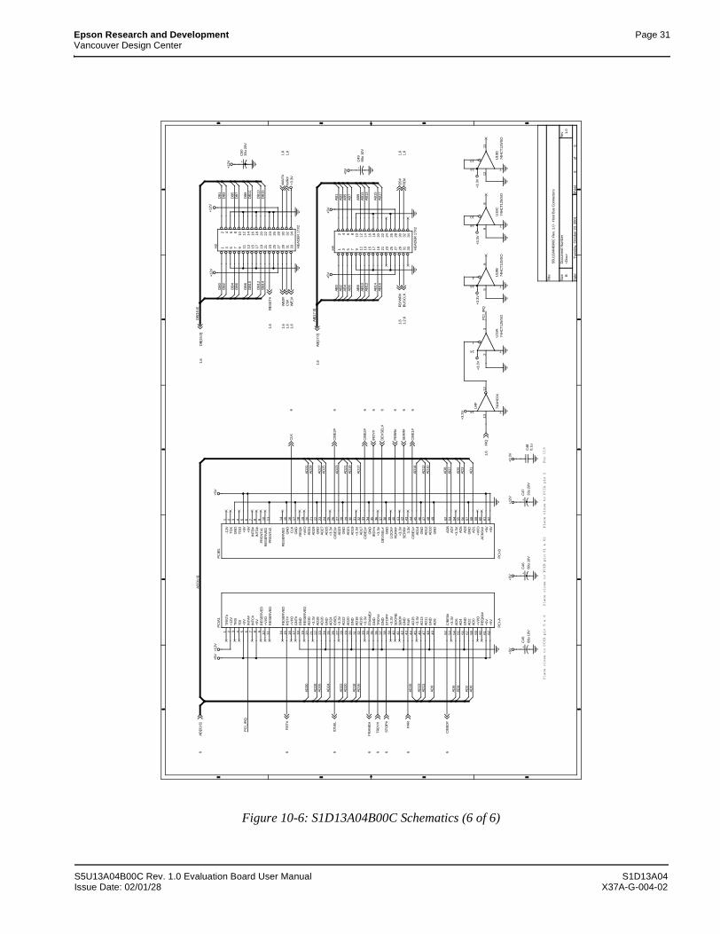
Epson Research and Development Page 31Vancouver Design Center
Figure 10-6: S1D13A04B00C Schematics (6 of 6)
5 5
4 4
3 3
2 2
1 1
DD
CC
BB
AA
Place close to PCIA pin 2
Place close to PCIB pin 5 & 6
Place close to PCIB pin 61 & 62
For U19
<D
oc>
1.0
S5U
13A
04B
00C
Rev.
1.0
- H
ost
Bus
Conn
ect
ors
B
66
Tues
day
, O
ctob
er 2
3, 2
001
Titl
e
Siz
eD
ocu
men
t Num
ber
Rev
Dat
e:S
hee
tof
AD
26
AD
1
AD
13
AD
2
AD
24
AD
8
AD
30
AD
18
AD
14
AD
25
AD
15
AD
20A
D19
AD
12
AD
22
AD
[31:
0]
AD
10A
D9
AD
17
AD
6A
D7
AD
21
AD
29
AD
27
AD
4
AD
16
AD
23
AD
5
AD
31
AD
28
AD
0
AD
11
AD
3
DB
8
AB
1
AB
5A
B6
DB
1
DB
15
DB
9
DB
5
DB
[15:0
]
AB
7
DB
7
DB
0
DB
6
AB
4
DB
12
AB
2
AB
12
DB
3
AB
3
DB
2
AB
14
DB
4
AB
13
AB
0
AB
9
DB
10
AB
[17:
0]
DB
14
AB
16
AB
8A
B10
AB
15
AB
11
DB
11
DB
13
AB
17
PC
I_IR
Q
PC
I_IR
Q
IRD
Y#
6
ST
OP
#6
C/B
E1#
6
AD
[31:0
]6
RS
T#
6
PE
RR
#6
DE
VS
EL#
6
IDS
EL
6
CLK
6
FR
AM
E#
6
C/B
E3#
6
SE
RR
#6
PA
R6
C/B
E0#
6
C/B
E2#
6
TR
DY
#6
BS
#1,
6R
D/W
R#
1,6
WA
IT#
1,6
BU
SC
LK
1,2
,6
CS
#1,
6W
E1#
1,6
DB
[15:0
]1,6
AB
[17:
0]
1,6
RD
#1,
6
RE
SE
T#
1,6
WE
0#1,
6M
/R#
1,6
IRQ
1,6
+12
V+5V
+12
V
+5V
+12V
+12V
+5V
+5V
+12V
+3.3
V+3.
3V
+3.
3V
+5V
+5V
+5V
+3.
3V
+3.
3V
+3.
3V
+3.3
V
+C
47
33u
20V
PC
IB1
PC
I-B
1 2 3 4 5 6 7 8 9 10 11 14 15 16 17 18 19 20 21 22 23 24 25 26 27 28 29 30 31 32 33 34 35 36 37 38 39 40 41 42 43 44 45 46 47 48 49 52 53 54 55 56 57 58 59 60 61 62
-12V
TC
KG
ND
TD
O+5V
+5V
INT
B#
INT
D#
PR
SN
T#1
RE
SE
RV
ED
PR
SN
T#2
RE
SE
RV
ED
GN
DC
LKG
ND
RE
Q#
+V
I/OA
D31
AD
29
GN
DA
D27
AD
25
+3.3
VC
/BE
3#
AD
23
GN
DA
D21
AD
19
+3.3
VA
D17
C/B
E2#
GN
DIR
DY
#+3.3
VD
EV
SE
L#
GN
DLO
CK
#P
ER
R#
+3.3
VS
ER
R#
3.3V
C/B
E1#
AD
14
GN
DA
D12
AD
10
GN
D
AD
8A
D7
+3.3
VA
D5
AD
3G
ND
AD
1+V
I/OA
CK
64#
+5V
+5V
PC
IA1
PC
I-A
1 2 3 4 5 6 7 8 910
11
14
15
16
17
18
19
20
21
22
23
24
25
26
27
28
29
30
31
32
33
34
35
36
37
38
39
40
41
42
43
44
45
46
47
48
49
52
53
54
55
56
57
58
59
60
61
62
TR
ST#
+12V
TM
ST
DI
+5V
INT
A#
INT
C#
+5V
RE
SE
RV
ED
+V
I/O
RE
SE
RV
ED
RE
SE
RV
ED
RS
T#
+V
I/O
GN
T#
GN
DR
ES
ER
VE
DA
D30
+3.3
VA
D28
AD
26G
ND
AD
24ID
SE
L+3.3
VA
D22
AD
20G
ND
AD
18A
D16
+3.3
VF
RA
ME
#G
ND
TR
DY
#G
ND
ST
OP
#+3.3
VS
DO
NE
SB
O#
GN
DP
AR
AD
15+3.3
VA
D13
AD
11G
ND
AD
9
C/B
E0#
+3.3
VA
D6
AD
4G
ND
AD
2A
D0
+V
I/O
RE
Q64
#+5V
+5V
+C
50
33u
20V
+C
45
68u
10V
C48
0.1
u
+C
46
68u
10V
U4F
74A
HC
04
13
12
14 7
U19
A74H
CT
125
/SO
23
14
1
7
H4
HE
AD
ER
17X
2
12
34
56
78
910
11
12
13
14
15
16
17
18
19
20
21
22
23
24
25
26
27
28
29
30
31
32
33
34
U19
B74H
CT
125
/SO
56
14
4
7
H3
HE
AD
ER
17X
2
12
34
56
78
910
11
12
13
14
15
16
17
18
19
20
21
22
23
24
25
26
27
28
29
30
31
32
33
34
U19
C74H
CT
125
/SO
98
14
10
7
U19D
74H
CT
125/
SO
12
11
14
13
7+C
49
68u
10V
S5U13A04B00C Rev. 1.0 Evaluation Board User Manual S1D13A04Issue Date: 02/01/28 X37A-G-004-02
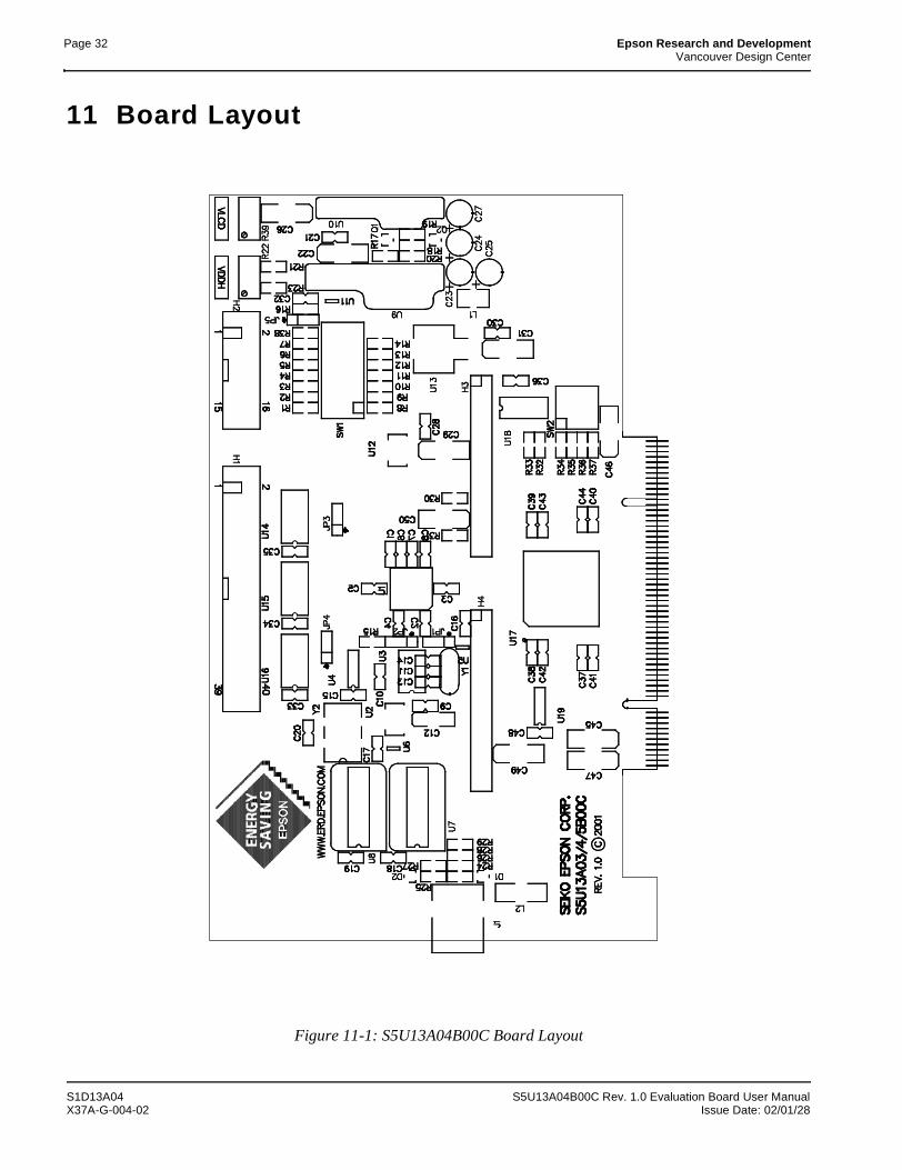
Page 32 Epson Research and DevelopmentVancouver Design Center
11 Board Layout
Figure 11-1: S5U13A04B00C Board Layout
S1D13A04 S5U13A04B00C Rev. 1.0 Evaluation Board User ManualX37A-G-004-02 Issue Date: 02/01/28

Epson Research and Development Page 33Vancouver Design Center
12 Sales and Technical Support
12.1 Epson Companion Chips (S1D13A04)JapanSeiko Epson CorporationElectronic Devices Marketing Division421-8, Hino, Hino-shiTokyo 191-8501, JapanTel: 042-587-5812Fax: 042-587-5564http://www.epson.co.jp/
Hong KongEpson Hong Kong Ltd.20/F., Harbour Centre25 Harbour RoadWanchai, Hong KongTel: 2585-4600Fax: 2827-4346http://www.epson.com.hk//
TaiwanEpson Taiwan Technology & Trading Ltd.10F, No. 287Nanking East RoadSec. 3, Taipei, TaiwanTel: 02-2717-7360Fax: 02-2712-9164http://www.epson.com.tw/
SingaporeEpson Singapore Pte., Ltd.No. 1Temasek Avenue #36-00Millenia TowerSingapore, 039192Tel: 337-7911Fax: 334-2716http://www.epson.com.sg/
EuropeEpson Europe Electronics GmbHRiesstrasse 1580992 Munich, GermanyTel: 089-14005-0Fax: 089-14005-110http://www.epson-electronics.de/
North AmericaEpson Electronics America, Inc.150 River Oaks ParkwaySan Jose, CA 95134, USATel: (408) 922-0200Fax: (408) 922-0238http://www.eea.epson.com/
S5U13A04B00C Rev. 1.0 Evaluation Board User Manual S1D13A04Issue Date: 02/01/28 X37A-G-004-02

Page 34 Epson Research and DevelopmentVancouver Design Center
THIS PAGE LEFT BLANK
S1D13A04 S5U13A04B00C Rev. 1.0 Evaluation Board User ManualX37A-G-004-02 Issue Date: 02/01/28
S1D13A04 LCD/USB Companion Chip
Interfacing to the Toshiba MIPS TMPR3905/3912 Microprocessors
Document Number: X37A-G-002-01
Copyright © 2001 Epson Research and Development, Inc. All Rights Reserved.
Information in this document is subject to change without notice. You may download and use this document, but only for your own use inevaluating Seiko Epson/EPSON products. You may not modify the document. Epson Research and Development, Inc. disclaims anyrepresentation that the contents of this document are accurate or current. The Programs/Technologies described in this document may contain material protected under U.S. and/or International Patent laws.
EPSON is a registered trademark of Seiko Epson Corporation. All other trademarks are the property of their respective owners.

Page 2 Epson Research and DevelopmentVancouver Design Center
THIS PAGE LEFT BLANK
S1D13A04 Interfacing to the Toshiba MIPS TMPR3905/3912 MicroprocessorsX37A-G-002-01 Issue Date: 01/10/12
Epson Research and Development Page 3Vancouver Design Center
Table of Contents
1 Introduction . . . . . . . . . . . . . . . . . . . . . . . . . . . . . . . . . . . . . . . . 7
2 Interfacing to the TMPR3905/12 . . . . . . . . . . . . . . . . . . . . . . . . . . . . . 82.1 The Toshiba TMPR3905/12 System Bus . . . . . . . . . . . . . . . . . . . . . 8
2.1.1 Overview . . . . . . . . . . . . . . . . . . . . . . . . . . . . . . . . . . . . . . . . 8
2.1.2 Card Access Cycles . . . . . . . . . . . . . . . . . . . . . . . . . . . . . . . . . . . 8
3 S1D13A04 Host Bus Interface . . . . . . . . . . . . . . . . . . . . . . . . . . . . . 103.1 Host Bus Interface Pin Mapping . . . . . . . . . . . . . . . . . . . . . . . 10
3.2 Host Bus Interface Signals . . . . . . . . . . . . . . . . . . . . . . . . . 11
4 Toshiba TMPR3905/12 to S1D13A04 Interface . . . . . . . . . . . . . . . . . . . . 124.1 Hardware Description . . . . . . . . . . . . . . . . . . . . . . . . . . . 12
4.2 S1D13A04 Hardware Configuration . . . . . . . . . . . . . . . . . . . . . 14
4.3 Memory Mapping and Aliasing . . . . . . . . . . . . . . . . . . . . . . . 14
5 Software . . . . . . . . . . . . . . . . . . . . . . . . . . . . . . . . . . . . . . . . . 15
6 References . . . . . . . . . . . . . . . . . . . . . . . . . . . . . . . . . . . . . . . 166.1 Documents . . . . . . . . . . . . . . . . . . . . . . . . . . . . . . . 16
6.2 Document Sources . . . . . . . . . . . . . . . . . . . . . . . . . . . . 16
7 Sales and Technical Support . . . . . . . . . . . . . . . . . . . . . . . . . . . . . 177.1 EPSON LCD/USB Companion Chips (S1D13A04) . . . . . . . . . . . . . . . 17
7.2 Toshiba MIPS TMPR3905/12 Processor . . . . . . . . . . . . . . . . . . . . 17
Interfacing to the Toshiba MIPS TMPR3905/3912 Microprocessors S1D13A04Issue Date: 01/10/12 X37A-G-002-01

Page 4 Epson Research and DevelopmentVancouver Design Center
THIS PAGE LEFT BLANK
S1D13A04 Interfacing to the Toshiba MIPS TMPR3905/3912 MicroprocessorsX37A-G-002-01 Issue Date: 01/10/12
Epson Research and Development Page 5Vancouver Design Center
List of Tables
Table 3-1: Host Bus Interface Pin Mapping . . . . . . . . . . . . . . . . . . . . . . . . . . . . . . 10
Table 4-1: Summary of Power-On/Reset Options . . . . . . . . . . . . . . . . . . . . . . . . . . . 14
List of Figures
Figure 2-1: Toshiba 3905/12 PC Card Memory/Attribute Cycle . . . . . . . . . . . . . . . . . . . . 9
Figure 2-2: Toshiba 3905/12 PC Card IO Cycle . . . . . . . . . . . . . . . . . . . . . . . . . . . . 9
Figure 4-1: S1D13A04 to TMPR3905/12 Direct Connection . . . . . . . . . . . . . . . . . . . . . 12
Interfacing to the Toshiba MIPS TMPR3905/3912 Microprocessors S1D13A04Issue Date: 01/10/12 X37A-G-002-01

Page 6 Epson Research and DevelopmentVancouver Design Center
THIS PAGE LEFT BLANK
S1D13A04 Interfacing to the Toshiba MIPS TMPR3905/3912 MicroprocessorsX37A-G-002-01 Issue Date: 01/10/12

Epson Research and Development Page 7Vancouver Design Center
1 Introduction
This application note describes the hardware and software environment necessary to provide an interface between the S1D13A04 USB/LCD Companion Chip and the Toshiba MIPS TMPR3905/3912 processors.
The designs described in this document are presented only as examples of how suchinterfaces might be implemented. This application note is updated as appropriate. Please check the Epson Research and Development website at www.erd.epson.com for the latest revision of this document before beginning any development.
We appreciate your comments on our documentation. Please contact us via email at [email protected].
Interfacing to the Toshiba MIPS TMPR3905/3912 Microprocessors S1D13A04Issue Date: 01/10/12 X37A-G-002-01
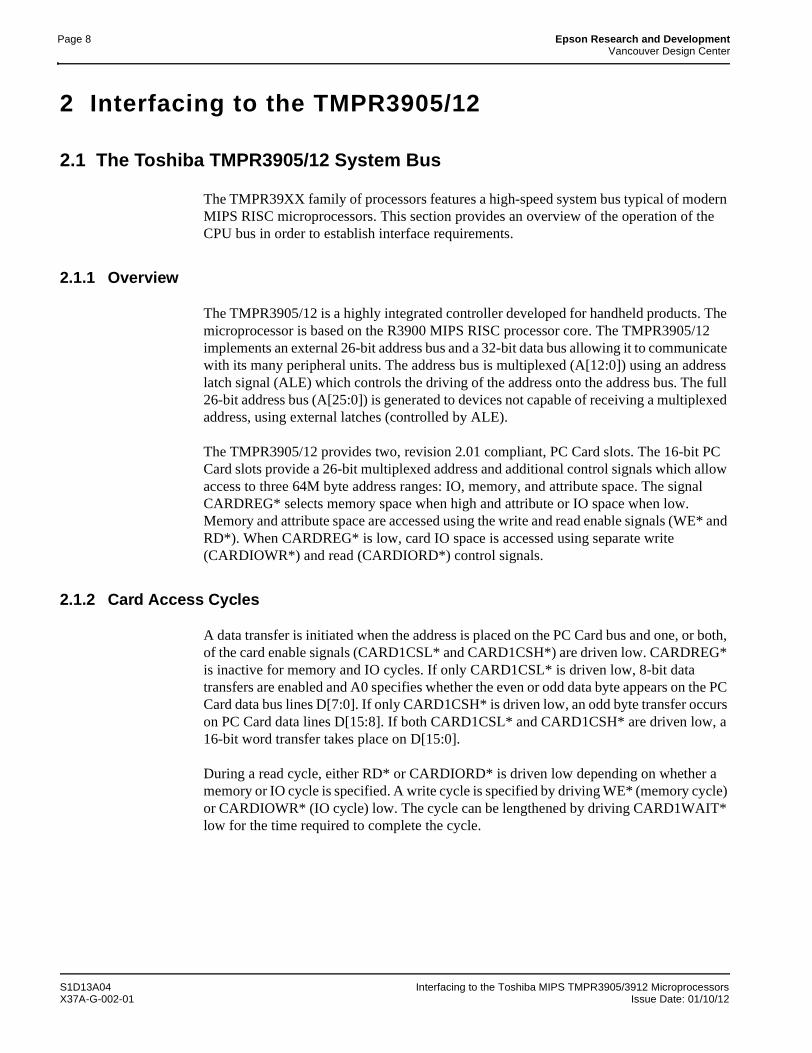
Page 8 Epson Research and DevelopmentVancouver Design Center
2 Interfacing to the TMPR3905/12
2.1 The Toshiba TMPR3905/12 System Bus
The TMPR39XX family of processors features a high-speed system bus typical of modern MIPS RISC microprocessors. This section provides an overview of the operation of the CPU bus in order to establish interface requirements.
2.1.1 Overview
The TMPR3905/12 is a highly integrated controller developed for handheld products. The microprocessor is based on the R3900 MIPS RISC processor core. The TMPR3905/12 implements an external 26-bit address bus and a 32-bit data bus allowing it to communicate with its many peripheral units. The address bus is multiplexed (A[12:0]) using an address latch signal (ALE) which controls the driving of the address onto the address bus. The full 26-bit address bus (A[25:0]) is generated to devices not capable of receiving a multiplexed address, using external latches (controlled by ALE).
The TMPR3905/12 provides two, revision 2.01 compliant, PC Card slots. The 16-bit PC Card slots provide a 26-bit multiplexed address and additional control signals which allow access to three 64M byte address ranges: IO, memory, and attribute space. The signal CARDREG* selects memory space when high and attribute or IO space when low. Memory and attribute space are accessed using the write and read enable signals (WE* and RD*). When CARDREG* is low, card IO space is accessed using separate write (CARDIOWR*) and read (CARDIORD*) control signals.
2.1.2 Card Access Cycles
A data transfer is initiated when the address is placed on the PC Card bus and one, or both, of the card enable signals (CARD1CSL* and CARD1CSH*) are driven low. CARDREG* is inactive for memory and IO cycles. If only CARD1CSL* is driven low, 8-bit data transfers are enabled and A0 specifies whether the even or odd data byte appears on the PC Card data bus lines D[7:0]. If only CARD1CSH* is driven low, an odd byte transfer occurs on PC Card data lines D[15:8]. If both CARD1CSL* and CARD1CSH* are driven low, a 16-bit word transfer takes place on D[15:0].
During a read cycle, either RD* or CARDIORD* is driven low depending on whether a memory or IO cycle is specified. A write cycle is specified by driving WE* (memory cycle) or CARDIOWR* (IO cycle) low. The cycle can be lengthened by driving CARD1WAIT* low for the time required to complete the cycle.
S1D13A04 Interfacing to the Toshiba MIPS TMPR3905/3912 MicroprocessorsX37A-G-002-01 Issue Date: 01/10/12
Epson Research and Development Page 9Vancouver Design Center
Figure 2-1: “Toshiba 3905/12 PC Card Memory/Attribute Cycle,” illustrates a typical memory/attribute cycle on the Toshiba 3905/12 PC Card bus.
Figure 2-1: Toshiba 3905/12 PC Card Memory/Attribute Cycle
Figure 2-2: “Toshiba 3905/12 PC Card IO Cycle,” illustrates a typical IO cycle on the Toshiba 3905/12 PC Card bus.
Figure 2-2: Toshiba 3905/12 PC Card IO Cycle
A[25:0]
CARD1CSL*
RD*
CARD1WAIT*
D[31:16]
CARDREG*
CARD1CSH*
WE*
ALE
A[25:0]
CARD1CSL*
CARDIORD*
CARD1WAIT*
D[31:16]
CARDREG*
CARD1CSH*
CARDIOWR*
ALE
Interfacing to the Toshiba MIPS TMPR3905/3912 Microprocessors S1D13A04Issue Date: 01/10/12 X37A-G-002-01
Page 10 Epson Research and DevelopmentVancouver Design Center
3 S1D13A04 Host Bus Interface
The S1D13A04 directly supports multiple processors. The S1D13A04 implements a 16-bit Generic #2 Host Bus Interface which is most suitable for connection to the Toshiba TMPR3905/12 microprocessor.
The Generic #2 Host Bus Interface is selected by the S1D13A04 on the rising edge of RESET#. After releasing reset the bus interface signals assume their selected configuration. For details on the S1D13A04 configuration, see Section 4.2, “S1D13A04 Hardware Configuration” on page 14.
3.1 Host Bus Interface Pin Mapping
The following table shows the functions of each Host Bus Interface signal.
Table 3-1: Host Bus Interface Pin Mapping
S1D13A04 Pin Names Toshiba TMPR3905/12
AB[17:0] External Decode
DB[15:8] D[23:16]
DB[7:0] D[31:24]
WE1# External Decode
CS# External Decode
M/R# External Decode
CLKI DCLKOUT
BS# Connect to IOVDD from the S1D13A04
RD/WR# Connect to IOVDD from the S1D13A04
RD# CARDIORD*
WE0# CARDIOWR*
WAIT# CARD1WAIT*
RESET# system RESET
S1D13A04 Interfacing to the Toshiba MIPS TMPR3905/3912 MicroprocessorsX37A-G-002-01 Issue Date: 01/10/12

Epson Research and Development Page 11Vancouver Design Center
3.2 Host Bus Interface Signals
The Host Bus Interface requires the following signals.
• CLKI is a clock input required by the S1D13A04 Host Bus Interface as a source for its internal bus and memory clocks. This clock is typically driven by the host CPU system clock. For example, DCLKOUT from the Toshiba TMPR3905/12.
• The address inputs AB[12:0] are connected directly to the TMPR3905/12 address bus. Since the TMPR3905/12 has a multiplexed address bus, the other address inputs A[17:13] must be generated using an external latch controlled by the address latch enable signal (ALE). The low data byte on the TMPR3905/12 data bus for 16-bit ports is D[31:24] and connects to the S1D13A04 low data byte, D[7:0]. The high data byte on the TMPR3905/12 data bus for 16-bit ports is D[23:16] and connects to the S1D13A04 high data byte, D[15:0]. The hardware engineer must ensure that CNF4 selects the proper endian mode upon reset.
• Chip Select (CS#) is driven by external decoding circuitry to select the S1D13A04.
• M/R# (memory/register) selects between memory or register accesses. This signal is generated by the external address decode circuitry. For this example, M/R# is connected to address line A18, allowing system address A18 to select between memory or register accesses.
• WE1# is connected to CARD1CSH* and is the high byte enable for both read and write cycles.
• WE0# is connected to CARDIOWR* (the write enable signal) and must be driven low when the Toshiba TMPR3905/12 is writing data to the S1D13A04.
• RD# is connected to CARDIORD* (the read enable signal) and must be driven low when the Toshiba TMPR3905/12 is reading data from the S1D13A04.
• WAIT# connects to CARD1WAIT* and is a signal which is output from the S1D13A04 to the TMPR3905/12 that indicates when data is ready (read cycle) or accepted (write cycle) on the host bus. Since host CPU accesses to the S1D13A04 may occur asynchro-nously to the display update, it is possible that contention may occur in accessing the S1D13A04 internal registers and/or display buffer. The WAIT# line resolves these contentions by forcing the host to wait until the resource arbitration is complete.
• The Bus Status (BS#) and Read/Write (RD/WR#) signals are not used in this implemen-tation of the Toshiba TMPR3905/12 using the Generic #2 Host Bus Interface. These pins must be tied high (connected to IO VDD).
Interfacing to the Toshiba MIPS TMPR3905/3912 Microprocessors S1D13A04Issue Date: 01/10/12 X37A-G-002-01
Page 12 Epson Research and DevelopmentVancouver Design Center
4 Toshiba TMPR3905/12 to S1D13A04 Interface
4.1 Hardware Description
In this implementation, the S1D13A04 occupies the TMPR3905/12 PC Card slot #1 IO address space. IO address space closely matches the timing parameters for the S1D13A04 Generic #2 Host Bus Interface.
The address bus of the TMPR3905/12 PC Card interface is multiplexed and must be demul-tiplexed using an advanced CMOS latch (e.g., 74AHC373).
BS# (bus start) and RD/WR# are not used in this implementation and should be tied high (connected to IO VDD).
A pull-up resistor is attached to WAIT# to speed up its rise time when terminating a cycle.
The following diagram demonstrates a typical implementation of the TMPR3905/12 to S1D13A04 interface.
Figure 4-1: S1D13A04 to TMPR3905/12 Direct Connection
WE0#
RD#
DB[7:0]
WAIT#
S1D13A04
RESET#
AB[17:13]
D[31:24]
CARD1WAIT*
A[12:0]
TMPR3905/12
pull-up
Oscillator
WE1#CARD1CSL*CARD1CSH*
Latch
ALE
System RESET
CARDIOWR*
CARDIORD*
BS#
RD/WR#
IO VDD
ENDIAN
DB[15:8]D[23:16]
AB[12:0]
HIOVDD
DCLKOUT
...or...
CS#
CLKI2See text
Clock divider
Note:When connecting the S1D13A04 RESET# pin, the system designer should be aware of all conditions that may reset the S1D13A04 (e.g. CPU reset can be asserted during wake-up from power-down modes, or during debug states).
CLKI
A18
M/R#
S1D13A04 Interfacing to the Toshiba MIPS TMPR3905/3912 MicroprocessorsX37A-G-002-01 Issue Date: 01/10/12
Epson Research and Development Page 13Vancouver Design Center
The Generic #2 Host Bus Interface control signals of the S1D13A04 are asynchronous with respect to the S1D13A04 bus clock. This gives the system designer full flexibility to choose the appropriate source (or sources) for CLKI and CLKI2. The choice of whether both clocks should be the same, and whether to use DCLKOUT (divided) as clock source, should be based on the desired:
• pixel and frame rates.
• power budget.
• part count.
• maximum S1D13A04 clock frequencies.
The S1D13A04 also has internal clock dividers providing additional flexibility.
Interfacing to the Toshiba MIPS TMPR3905/3912 Microprocessors S1D13A04Issue Date: 01/10/12 X37A-G-002-01
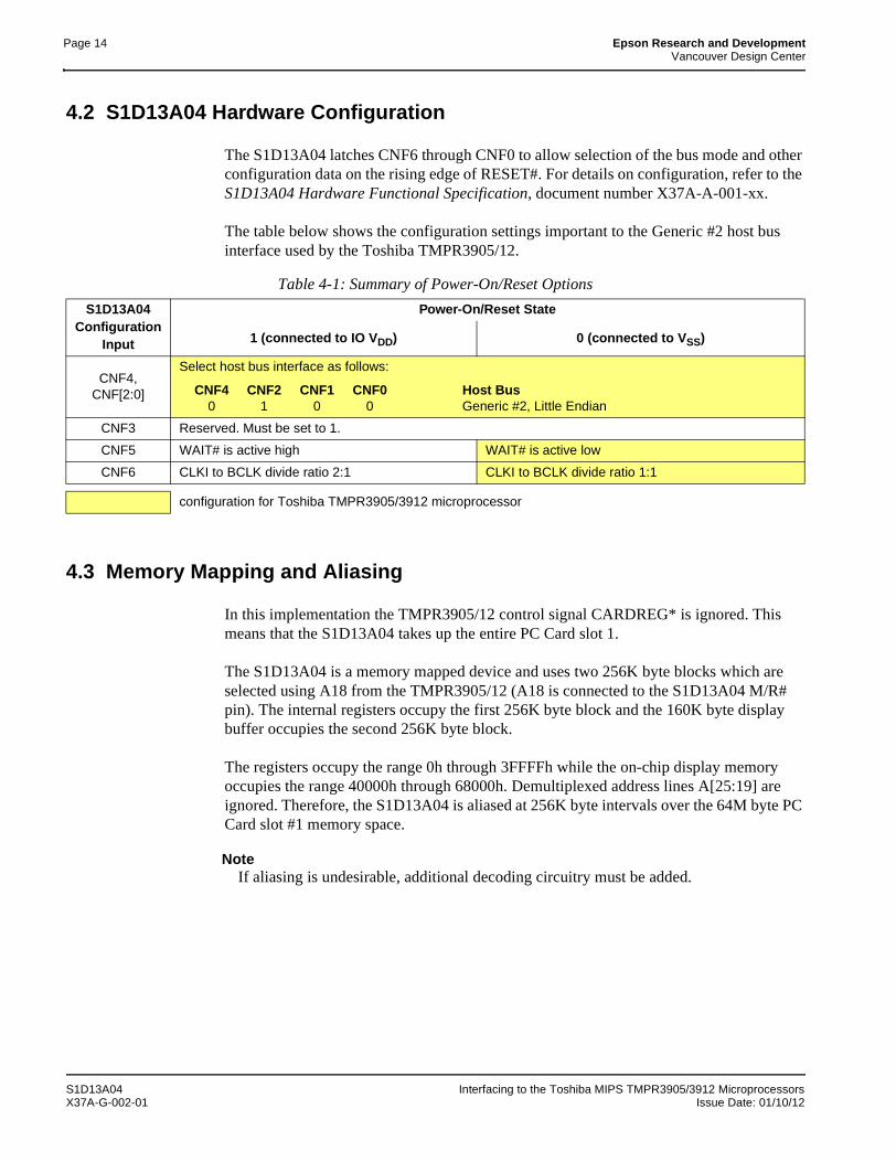
Page 14 Epson Research and DevelopmentVancouver Design Center
4.2 S1D13A04 Hardware Configuration
The S1D13A04 latches CNF6 through CNF0 to allow selection of the bus mode and other configuration data on the rising edge of RESET#. For details on configuration, refer to the S1D13A04 Hardware Functional Specification, document number X37A-A-001-xx.
The table below shows the configuration settings important to the Generic #2 host bus interface used by the Toshiba TMPR3905/12.
4.3 Memory Mapping and Aliasing
In this implementation the TMPR3905/12 control signal CARDREG* is ignored. This means that the S1D13A04 takes up the entire PC Card slot 1.
The S1D13A04 is a memory mapped device and uses two 256K byte blocks which are selected using A18 from the TMPR3905/12 (A18 is connected to the S1D13A04 M/R# pin). The internal registers occupy the first 256K byte block and the 160K byte display buffer occupies the second 256K byte block.
The registers occupy the range 0h through 3FFFFh while the on-chip display memory occupies the range 40000h through 68000h. Demultiplexed address lines A[25:19] are ignored. Therefore, the S1D13A04 is aliased at 256K byte intervals over the 64M byte PC Card slot #1 memory space.
NoteIf aliasing is undesirable, additional decoding circuitry must be added.
Table 4-1: Summary of Power-On/Reset Options
S1D13A04 Configuration
Input
Power-On/Reset State
1 (connected to IO VDD) 0 (connected to VSS)
CNF4, CNF[2:0]
Select host bus interface as follows:
CNF4 CNF2 CNF1 CNF0 Host Bus0 1 0 0 Generic #2, Little Endian
CNF3 Reserved. Must be set to 1.
CNF5 WAIT# is active high WAIT# is active low
CNF6 CLKI to BCLK divide ratio 2:1 CLKI to BCLK divide ratio 1:1
configuration for Toshiba TMPR3905/3912 microprocessor
S1D13A04 Interfacing to the Toshiba MIPS TMPR3905/3912 MicroprocessorsX37A-G-002-01 Issue Date: 01/10/12

Epson Research and Development Page 15Vancouver Design Center
5 Software
Test utilities and display drivers are available for the S1D13A04. Full source code is available for both the test utilities and the drivers.
The test utilities are configurable for different panel types using a program called 13A04CFG (see document number X37A-B-001-xx), or by directly modifying the source. The display drivers can be customized by the OEM for different panel types, resolutions and color depths only by modifying the source.
The S1D13A04 test utilities and display drivers are available from your sales support contact (see Section 7, “Sales and Technical Support”) or www.erd.epson.com.
Interfacing to the Toshiba MIPS TMPR3905/3912 Microprocessors S1D13A04Issue Date: 01/10/12 X37A-G-002-01
Page 16 Epson Research and DevelopmentVancouver Design Center
6 References
6.1 Documents
• Toshiba America Electrical Components, Inc., TMPR3905/12 Specification.
• Epson Research and Development, Inc., S1D13A04 Hardware Functional Specification, Document Number X37A-A-001-xx.
• Epson Research and Development, Inc., S5U13A04B00C Rev. 1.0 ISA Bus Evaluation Board User Manual, Document Number X37A-G-004-xx.
• Epson Research and Development, Inc., S1D13A04 Programming Notes and Examples, Document Number X37A-G-003-xx.
6.2 Document Sources
• Toshiba America Electrical Components Website: www.toshiba.com/taec.
• Epson Research and Development Website: www.erd.epson.com.
S1D13A04 Interfacing to the Toshiba MIPS TMPR3905/3912 MicroprocessorsX37A-G-002-01 Issue Date: 01/10/12
Epson Research and Development Page 17Vancouver Design Center
7 Sales and Technical Support
7.1 EPSON LCD/USB Companion Chips (S1D13A04)
7.2 Toshiba MIPS TMPR3905/12 Processor
JapanSeiko Epson CorporationElectronic Devices Marketing Division421-8, Hino, Hino-shiTokyo 191-8501, JapanTel: 042-587-5812Fax: 042-587-5564http://www.epson.co.jp
Hong KongEpson Hong Kong Ltd.20/F., Harbour Centre25 Harbour RoadWanchai, Hong KongTel: 2585-4600Fax: 2827-4346http://www.epson.com.hk/
TaiwanEpson Taiwan Technology & Trading Ltd.10F, No. 287Nanking East RoadSec. 3, Taipei, TaiwanTel: 02-2717-7360Fax: 02-2712-9164http://www.epson.com.tw/
SingaporeEpson Singapore Pte., Ltd.No. 1Temasek Avenue #36-00Millenia TowerSingapore, 039192Tel: 337-7911Fax: 334-2716http://www.epson.com.sg/
EuropeEpson Europe Electronics GmbHRiesstrasse 1580992 Munich, GermanyTel: 089-14005-0Fax: 089-14005-110http://www.epson-electronics.de
North AmericaEpson Electronics America, Inc.150 River Oaks ParkwaySan Jose, CA 95134, USATel: (408) 922-0200Fax: (408) 922-0238http://www.eea.epson.com
http://www.toshiba.com/taec/nonflash/indexproducts.html
Interfacing to the Toshiba MIPS TMPR3905/3912 Microprocessors S1D13A04Issue Date: 01/10/12 X37A-G-002-01

Page 18 Epson Research and DevelopmentVancouver Design Center
THIS PAGE LEFT BLANK
S1D13A04 Interfacing to the Toshiba MIPS TMPR3905/3912 MicroprocessorsX37A-G-002-01 Issue Date: 01/10/12
S1D13A04 LCD/USB Companion Chip
Interfacing to the PC Card Bus
Document Number: X37A-G-005-01
Copyright © 2001 Epson Research and Development, Inc. All Rights Reserved.
Information in this document is subject to change without notice. You may download and use this document, but only for your own use inevaluating Seiko Epson/EPSON products. You may not modify the document. Epson Research and Development, Inc. disclaims anyrepresentation that the contents of this document are accurate or current. The Programs/Technologies described in this document may contain material protected under U.S. and/or International Patent laws.
EPSON is a registered trademark of Seiko Epson Corporation. All other trademarks are the property of their respective owners.

Page 2 Epson Research and DevelopmentVancouver Design Center
THIS PAGE LEFT BLANK
S1D13A04 Interfacing to the PC Card BusX37A-G-005-01 Issue Date: 01/10/12
Epson Research and Development Page 3Vancouver Design Center
Table of Contents
1 Introduction . . . . . . . . . . . . . . . . . . . . . . . . . . . . . . . . . . . . . . . . 7
2 Interfacing to the PC Card Bus . . . . . . . . . . . . . . . . . . . . . . . . . . . . . 82.1 The PC Card System Bus . . . . . . . . . . . . . . . . . . . . . . . . . . . 8
2.1.1 PC Card Overview . . . . . . . . . . . . . . . . . . . . . . . . . . . . . . . . . . . 8
2.1.2 Memory Access Cycles . . . . . . . . . . . . . . . . . . . . . . . . . . . . . . . . . 8
3 S1D13A04 Host Bus Interface . . . . . . . . . . . . . . . . . . . . . . . . . . . . . 103.1 Host Bus Interface Pin Mapping . . . . . . . . . . . . . . . . . . . . . . . 10
3.2 Host Bus Interface Signals . . . . . . . . . . . . . . . . . . . . . . . . . 11
4 PC Card to S1D13A04 Interface . . . . . . . . . . . . . . . . . . . . . . . . . . . . 124.1 Hardware Connections . . . . . . . . . . . . . . . . . . . . . . . . . . . 12
4.2 S1D13A04 Hardware Configuration . . . . . . . . . . . . . . . . . . . . . 13
4.3 Register/Memory Mapping . . . . . . . . . . . . . . . . . . . . . . . . . 13
5 Software . . . . . . . . . . . . . . . . . . . . . . . . . . . . . . . . . . . . . . . . . 14
6 References . . . . . . . . . . . . . . . . . . . . . . . . . . . . . . . . . . . . . . . 156.1 Documents . . . . . . . . . . . . . . . . . . . . . . . . . . . . . . . 15
6.2 Document Sources . . . . . . . . . . . . . . . . . . . . . . . . . . . . 15
7 Sales and Technical Support . . . . . . . . . . . . . . . . . . . . . . . . . . . . . 167.1 EPSON LCD/USB Companion Chips (S1D13A04) . . . . . . . . . . . . . . . 16
7.2 PC Card Standard . . . . . . . . . . . . . . . . . . . . . . . . . . . . . 16
Interfacing to the PC Card Bus S1D13A04Issue Date: 01/10/12 X37A-G-005-01

Page 4 Epson Research and DevelopmentVancouver Design Center
THIS PAGE LEFT BLANK
S1D13A04 Interfacing to the PC Card BusX37A-G-005-01 Issue Date: 01/10/12
Epson Research and Development Page 5Vancouver Design Center
List of Tables
Table 3-1: Host Bus Interface Pin Mapping . . . . . . . . . . . . . . . . . . . . . . . . . . . . . . 10
Table 4-1: Summary of Power-On/Reset Options . . . . . . . . . . . . . . . . . . . . . . . . . . . 13
List of Figures
Figure 2-1: PC Card Read Cycle . . . . . . . . . . . . . . . . . . . . . . . . . . . . . . . . . . . . 9
Figure 2-2: PC Card Write Cycle . . . . . . . . . . . . . . . . . . . . . . . . . . . . . . . . . . . . 9
Figure 4-1: Typical Implementation of PC Card to S1D13A04 Interface . . . . . . . . . . . . . . .12
Interfacing to the PC Card Bus S1D13A04Issue Date: 01/10/12 X37A-G-005-01

Page 6 Epson Research and DevelopmentVancouver Design Center
THIS PAGE LEFT BLANK
S1D13A04 Interfacing to the PC Card BusX37A-G-005-01 Issue Date: 01/10/12

Epson Research and Development Page 7Vancouver Design Center
1 Introduction
This application note describes the hardware and software environment required to interface the S1D13A04 LCD/USB Companion Chip and the PC Card (PCMCIA) bus.
The designs described in this document are presented only as examples of how such inter-faces might be implemented. This application note is updated as appropriate. Please check the Epson Research and Development website at www.erd.epson.com for the latest revision of this document before beginning any development.
We appreciate your comments on our documentation. Please contact us via email at [email protected].
Interfacing to the PC Card Bus S1D13A04Issue Date: 01/10/12 X37A-G-005-01
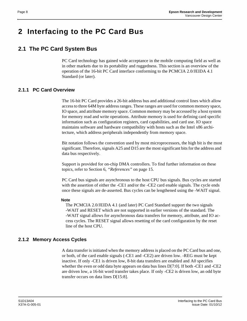
Page 8 Epson Research and DevelopmentVancouver Design Center
2 Interfacing to the PC Card Bus
2.1 The PC Card System Bus
PC Card technology has gained wide acceptance in the mobile computing field as well as in other markets due to its portability and ruggedness. This section is an overview of the operation of the 16-bit PC Card interface conforming to the PCMCIA 2.0/JEIDA 4.1 Standard (or later).
2.1.1 PC Card Overview
The 16-bit PC Card provides a 26-bit address bus and additional control lines which allow access to three 64M byte address ranges. These ranges are used for common memory space, IO space, and attribute memory space. Common memory may be accessed by a host system for memory read and write operations. Attribute memory is used for defining card specific information such as configuration registers, card capabilities, and card use. IO space maintains software and hardware compatibility with hosts such as the Intel x86 archi-tecture, which address peripherals independently from memory space.
Bit notation follows the convention used by most microprocessors, the high bit is the mostsignificant. Therefore, signals A25 and D15 are the most significant bits for the address and data bus respectively.
Support is provided for on-chip DMA controllers. To find further information on these topics, refer to Section 6, “References” on page 15.
PC Card bus signals are asynchronous to the host CPU bus signals. Bus cycles are started with the assertion of either the -CE1 and/or the -CE2 card enable signals. The cycle ends once these signals are de-asserted. Bus cycles can be lengthened using the -WAIT signal.
NoteThe PCMCIA 2.0/JEIDA 4.1 (and later) PC Card Standard support the two signals -WAIT and RESET which are not supported in earlier versions of the standard. The -WAIT signal allows for asynchronous data transfers for memory, attribute, and IO ac-cess cycles. The RESET signal allows resetting of the card configuration by the reset line of the host CPU.
2.1.2 Memory Access Cycles
A data transfer is initiated when the memory address is placed on the PC Card bus and one, or both, of the card enable signals (-CE1 and -CE2) are driven low. -REG must be kept inactive. If only -CE1 is driven low, 8-bit data transfers are enabled and A0 specifies whether the even or odd data byte appears on data bus lines D[7:0]. If both -CE1 and -CE2 are driven low, a 16-bit word transfer takes place. If only -CE2 is driven low, an odd byte transfer occurs on data lines D[15:8].
S1D13A04 Interfacing to the PC Card BusX37A-G-005-01 Issue Date: 01/10/12
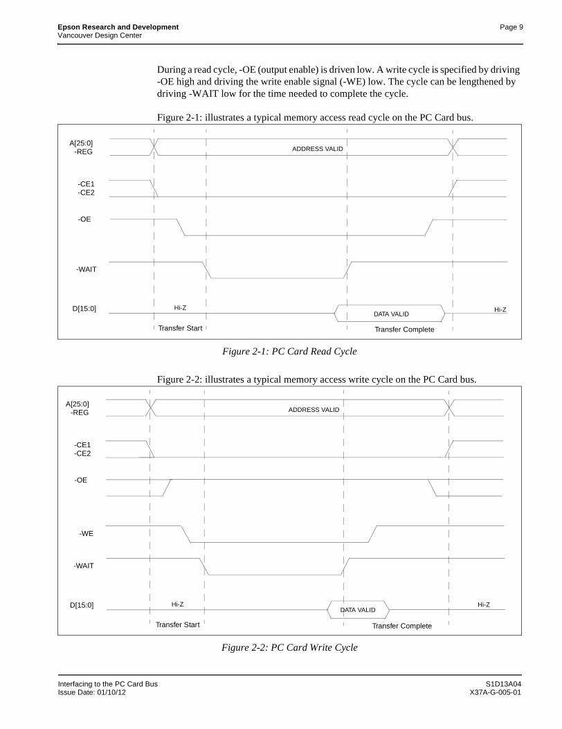
Epson Research and Development Page 9Vancouver Design Center
During a read cycle, -OE (output enable) is driven low. A write cycle is specified by driving -OE high and driving the write enable signal (-WE) low. The cycle can be lengthened by driving -WAIT low for the time needed to complete the cycle.
Figure 2-1: illustrates a typical memory access read cycle on the PC Card bus.
Figure 2-1: PC Card Read Cycle
Figure 2-2: illustrates a typical memory access write cycle on the PC Card bus.
Figure 2-2: PC Card Write Cycle
A[25:0]
-CE1
-OE
-WAIT
ADDRESS VALID
DATA VALIDHi-Z Hi-ZD[15:0]
-REG
-CE2
Transfer Start Transfer Complete
A[25:0]
-CE1
-OE
-WAIT
ADDRESS VALID
DATA VALIDHi-Z Hi-ZD[15:0]
-REG
-CE2
Transfer Start Transfer Complete
-WE
Interfacing to the PC Card Bus S1D13A04Issue Date: 01/10/12 X37A-G-005-01
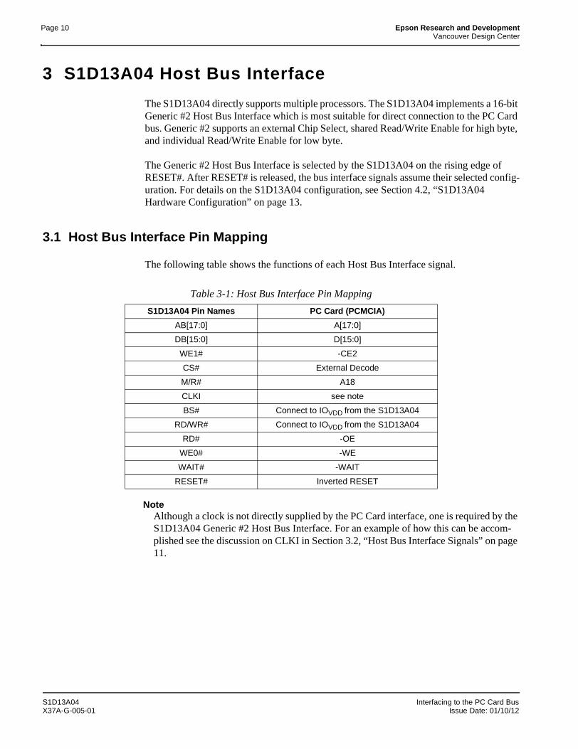
Page 10 Epson Research and DevelopmentVancouver Design Center
3 S1D13A04 Host Bus Interface
The S1D13A04 directly supports multiple processors. The S1D13A04 implements a 16-bit Generic #2 Host Bus Interface which is most suitable for direct connection to the PC Card bus. Generic #2 supports an external Chip Select, shared Read/Write Enable for high byte, and individual Read/Write Enable for low byte.
The Generic #2 Host Bus Interface is selected by the S1D13A04 on the rising edge of RESET#. After RESET# is released, the bus interface signals assume their selected config-uration. For details on the S1D13A04 configuration, see Section 4.2, “S1D13A04 Hardware Configuration” on page 13.
3.1 Host Bus Interface Pin Mapping
The following table shows the functions of each Host Bus Interface signal.
NoteAlthough a clock is not directly supplied by the PC Card interface, one is required by the S1D13A04 Generic #2 Host Bus Interface. For an example of how this can be accom-plished see the discussion on CLKI in Section 3.2, “Host Bus Interface Signals” on page 11.
Table 3-1: Host Bus Interface Pin Mapping
S1D13A04 Pin Names PC Card (PCMCIA)
AB[17:0] A[17:0]
DB[15:0] D[15:0]
WE1# -CE2
CS# External Decode
M/R# A18
CLKI see note
BS# Connect to IOVDD from the S1D13A04
RD/WR# Connect to IOVDD from the S1D13A04
RD# -OE
WE0# -WE
WAIT# -WAIT
RESET# Inverted RESET
S1D13A04 Interfacing to the PC Card BusX37A-G-005-01 Issue Date: 01/10/12
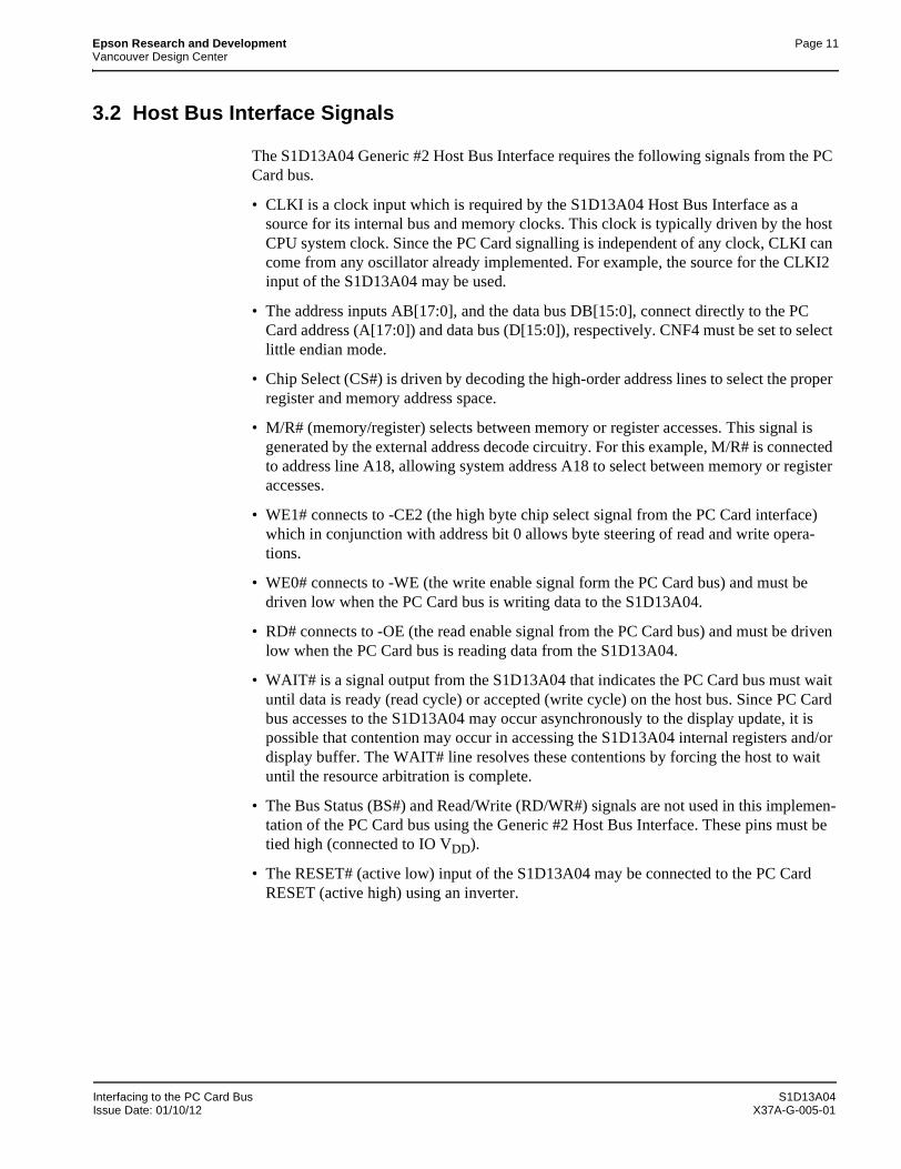
Epson Research and Development Page 11Vancouver Design Center
3.2 Host Bus Interface Signals
The S1D13A04 Generic #2 Host Bus Interface requires the following signals from the PC Card bus.
• CLKI is a clock input which is required by the S1D13A04 Host Bus Interface as a source for its internal bus and memory clocks. This clock is typically driven by the host CPU system clock. Since the PC Card signalling is independent of any clock, CLKI can come from any oscillator already implemented. For example, the source for the CLKI2 input of the S1D13A04 may be used.
• The address inputs AB[17:0], and the data bus DB[15:0], connect directly to the PC Card address (A[17:0]) and data bus (D[15:0]), respectively. CNF4 must be set to select little endian mode.
• Chip Select (CS#) is driven by decoding the high-order address lines to select the proper register and memory address space.
• M/R# (memory/register) selects between memory or register accesses. This signal is generated by the external address decode circuitry. For this example, M/R# is connected to address line A18, allowing system address A18 to select between memory or register accesses.
• WE1# connects to -CE2 (the high byte chip select signal from the PC Card interface) which in conjunction with address bit 0 allows byte steering of read and write opera-tions.
• WE0# connects to -WE (the write enable signal form the PC Card bus) and must be driven low when the PC Card bus is writing data to the S1D13A04.
• RD# connects to -OE (the read enable signal from the PC Card bus) and must be driven low when the PC Card bus is reading data from the S1D13A04.
• WAIT# is a signal output from the S1D13A04 that indicates the PC Card bus must wait until data is ready (read cycle) or accepted (write cycle) on the host bus. Since PC Card bus accesses to the S1D13A04 may occur asynchronously to the display update, it is possible that contention may occur in accessing the S1D13A04 internal registers and/or display buffer. The WAIT# line resolves these contentions by forcing the host to wait until the resource arbitration is complete.
• The Bus Status (BS#) and Read/Write (RD/WR#) signals are not used in this implemen-tation of the PC Card bus using the Generic #2 Host Bus Interface. These pins must be tied high (connected to IO VDD).
• The RESET# (active low) input of the S1D13A04 may be connected to the PC Card RESET (active high) using an inverter.
Interfacing to the PC Card Bus S1D13A04Issue Date: 01/10/12 X37A-G-005-01
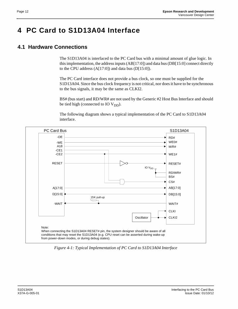
Page 12 Epson Research and DevelopmentVancouver Design Center
4 PC Card to S1D13A04 Interface
4.1 Hardware Connections
The S1D13A04 is interfaced to the PC Card bus with a minimal amount of glue logic. In this implementation, the address inputs (AB[17:0]) and data bus (DB[15:0] connect directly to the CPU address (A[17:0]) and data bus (D[15:0]).
The PC Card interface does not provide a bus clock, so one must be supplied for the S1D13A04. Since the bus clock frequency is not critical, nor does it have to be synchronous to the bus signals, it may be the same as CLKI2.
BS# (bus start) and RD/WR# are not used by the Generic #2 Host Bus Interface and should be tied high (connected to IO VDD).
The following diagram shows a typical implementation of the PC Card to S1D13A04 interface.
Figure 4-1: Typical Implementation of PC Card to S1D13A04 Interface
RD/WR#
RD#
DB[15:0]
WAIT#
CLKI
S1D13A04
RESET#
AB[17:0]
-OE
D[15:0]
-WAIT
A[17:0]
PC Card Bus
15K pull-up
CLKI2Oscillator
WE1#
WE0#
CS#
-WE
-CE1-CE2
RESETIO VDD
BS#
Note:When connecting the S1D13A04 RESET# pin, the system designer should be aware of all conditions that may reset the S1D13A04 (e.g. CPU reset can be asserted during wake-up from power-down modes, or during debug states).
A18 M/R#
S1D13A04 Interfacing to the PC Card BusX37A-G-005-01 Issue Date: 01/10/12
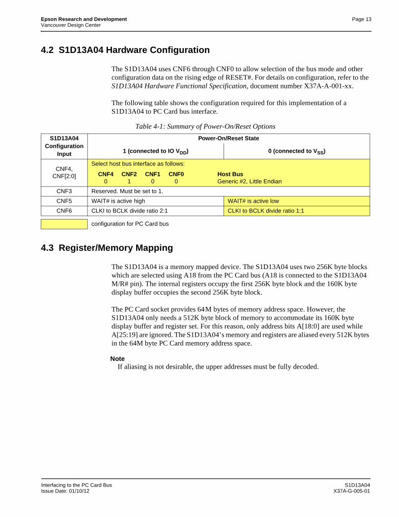
Epson Research and Development Page 13Vancouver Design Center
4.2 S1D13A04 Hardware Configuration
The S1D13A04 uses CNF6 through CNF0 to allow selection of the bus mode and other configuration data on the rising edge of RESET#. For details on configuration, refer to the S1D13A04 Hardware Functional Specification, document number X37A-A-001-xx.
The following table shows the configuration required for this implementation of a S1D13A04 to PC Card bus interface.
4.3 Register/Memory Mapping
The S1D13A04 is a memory mapped device. The S1D13A04 uses two 256K byte blocks which are selected using A18 from the PC Card bus (A18 is connected to the S1D13A04 M/R# pin). The internal registers occupy the first 256K byte block and the 160K byte display buffer occupies the second 256K byte block.
The PC Card socket provides 64M bytes of memory address space. However, the S1D13A04 only needs a 512K byte block of memory to accommodate its 160K byte display buffer and register set. For this reason, only address bits A[18:0] are used while A[25:19] are ignored. The S1D13A04’s memory and registers are aliased every 512K bytes in the 64M byte PC Card memory address space.
NoteIf aliasing is not desirable, the upper addresses must be fully decoded.
Table 4-1: Summary of Power-On/Reset Options
S1D13A04 Configuration
Input
Power-On/Reset State
1 (connected to IO VDD) 0 (connected to VSS)
CNF4, CNF[2:0]
Select host bus interface as follows:
CNF4 CNF2 CNF1 CNF0 Host Bus0 1 0 0 Generic #2, Little Endian
CNF3 Reserved. Must be set to 1.
CNF5 WAIT# is active high WAIT# is active low
CNF6 CLKI to BCLK divide ratio 2:1 CLKI to BCLK divide ratio 1:1
configuration for PC Card bus
Interfacing to the PC Card Bus S1D13A04Issue Date: 01/10/12 X37A-G-005-01
Page 14 Epson Research and DevelopmentVancouver Design Center
5 Software
Test utilities and display drivers are available for the S1D13A04. Full source code is available for both the test utilities and the drivers.
The test utilities are configurable for different panel types using a program called 13A04CFG (see document number X37A-B-001-xx), or by directly modifying the source. The display drivers can be customized by the OEM for different panel types, resolutions and color depths only by modifying the source.
The S1D13A04 test utilities and display drivers are available from your sales support contact (see Section 7, “Sales and Technical Support”) or www.erd.epson.com.
S1D13A04 Interfacing to the PC Card BusX37A-G-005-01 Issue Date: 01/10/12
Epson Research and Development Page 15Vancouver Design Center
6 References
6.1 Documents
• PC Card (PCMCIA) Standard March 1997.
• Epson Research and Development, Inc., S1D13A04 Hardware Functional Specification, document number X37A-A-001-xx.
• Epson Research and Development, Inc., S5U13A04B00C Rev. 1.0 Evaluation Board User Manual, document number X37A-G-004-xx.
• Epson Research and Development, Inc., S1D13A04 Programming Notes and Examples, Document Number X37A-G-003-xx.
6.2 Document Sources
• PC Card Website: www.pc-card.com.
• Epson Research and Development Website: www.erd.epson.com.
Interfacing to the PC Card Bus S1D13A04Issue Date: 01/10/12 X37A-G-005-01
Page 16 Epson Research and DevelopmentVancouver Design Center
7 Sales and Technical Support
7.1 EPSON LCD/USB Companion Chips (S1D13A04)
7.2 PC Card Standard
JapanSeiko Epson CorporationElectronic Devices Marketing Division421-8, Hino, Hino-shiTokyo 191-8501, JapanTel: 042-587-5812Fax: 042-587-5564http://www.epson.co.jp
Hong KongEpson Hong Kong Ltd.20/F., Harbour Centre25 Harbour RoadWanchai, Hong KongTel: 2585-4600Fax: 2827-4346http://www.epson.com.hk/
TaiwanEpson Taiwan Technology & Trading Ltd.10F, No. 287Nanking East RoadSec. 3, Taipei, TaiwanTel: 02-2717-7360Fax: 02-2712-9164http://www.epson.com.tw/
SingaporeEpson Singapore Pte., Ltd.No. 1Temasek Avenue #36-00Millenia TowerSingapore, 039192Tel: 337-7911Fax: 334-2716http://www.epson.com.sg/
EuropeEpson Europe Electronics GmbHRiesstrasse 1580992 Munich, GermanyTel: 089-14005-0Fax: 089-14005-110http://www.epson-electronics.de
North AmericaEpson Electronics America, Inc.150 River Oaks ParkwaySan Jose, CA 95134, USATel: (408) 922-0200Fax: (408) 922-0238http://www.eea.epson.com
PCMCIA (Personal Computer Memory Card International Association)
2635 North First Street, Suite 209 San Jose, CA 95134 Tel: (408) 433-2273 Fax: (408) 433-9558 http://www.pc-card.com
S1D13A04 Interfacing to the PC Card BusX37A-G-005-01 Issue Date: 01/10/12

S1D13A04 LCD/USB Companion Chip
Power Consumption
Document Number: X37A-G-006-01
Copyright © 2001 Epson Research and Development, Inc. All Rights Reserved.
Information in this document is subject to change without notice. You may download and use this document, but only for your own use inevaluating Seiko Epson/EPSON products. You may not modify the document. Epson Research and Development, Inc. disclaims anyrepresentation that the contents of this document are accurate or current. The Programs/Technologies described in this document may contain material protected under U.S. and/or International Patent laws.
EPSON is a registered trademark of Seiko Epson Corporation. All other trademarks are the property of their respective owners.

Page 2 Epson Research and DevelopmentVancouver Design Center
THIS PAGE LEFT BLANK
S1D13A04 Power ConsumptionX37A-G-006-01 Issue Date: 01/10/29

Epson Research and Development Page 3Vancouver Design Center
1 S1D13A04 Power Consumption
S1D13A04 power consumption is affected by many system design variables.
• Input clock frequency (CLKI/CLKI2): the CLKI/CLKI2 frequency determines the LCD frame-rate, CPU performance to memory, and other functions – the higher the input clock frequency, the higher the frame-rate, performance and power consumption.
• CPU interface: the S1D13A04 current consumption depends on the BCLK frequency, data width, number of toggling pins, and other factors – the higher the BCLK, the higher the CPU performance and power consumption.
• VDD voltage level: the voltage level affects power consumption – the higher the voltage, the higher the consumption.
• Display mode: the resolution and color depth affect power consumption – the higher theresolution/color depth, the higher the consumption.
• Internal CLK divide: internal registers allow the input clock to be divided before going to the internal logic blocks – the higher the divide, the lower the power consumption.
There is a power save mode in the S1D13A04. The power consumption is affected by various system design variables.
• Clock states during the power save mode: disabling the clocks during power save mode has substantial power savings.
Power Consumption S1D13A04Issue Date: 01/10/29 X37A-G-006-01
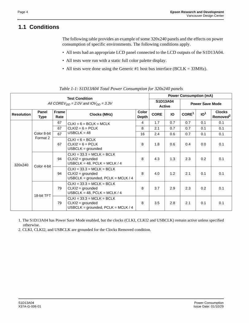
Page 4 Epson Research and DevelopmentVancouver Design Center
Re 2
3
1.1 Conditions
The following table provides an example of some 320x240 panels and the effects on power consumption of specific environments. The following conditions apply.
• All tests had an appropriate LCD panel connected to the LCD outputs of the S1D13A04.
• All tests were run with a static full color palette display.
• All tests were done using the Generic #1 host bus interface (BCLK = 33MHz).
1. The S1D13A04 has Power Save Mode enabled, but the clocks (CLKI, CLKI2 and USBCLK) remain active unless specifiedotherwise.
2. CLKI, CLKI2, and USBCLK are grounded for the Clocks Removed condition.
Table 1-1: S1D13A04 Total Power Consumption for 320x240 panels
Test ConditionAll COREVDD = 2.0V and IOVDD = 3.3V
Power Consumption (mA)
S1D13A04 Active
Power Save Mode
solutionPanel Type
Frame Rate
Clocks (MHz)Color Depth
CORE IO CORE1 IO1 Clocks Removed
20x240
Color 8-bit Format 2
67 CLKI = 6 = BCLK = MCLKCLKI2 = 6 = PCLKUSBCLK = 48
4 1.7 0.7 0.7 0.1 0.1
67 8 2.1 0.7 0.7 0.1 0.1
67 16 2.4 0.6 0.7 0.1 0.1
67CLKI = 6 = BCLKCLKI2 = 6 = PCLKUSBCLK = grounded
8 1.8 0.6 0.4 0.0 0.1
Color 4-bit
94CLKI = 33.3 = MCLK = BCLKCLKI2 = groundedUSBCLK = 48, PCLK = MCLK / 4
8 4.3 1.3 2.3 0.2 0.1
94CLKI = 33.3 = MCLK = BCLKCLKI2 = groundedUSBCLK = grounded, PCLK = MCLK / 4
8 4.0 1.2 2.1 0.1 0.1
18-bit TFT
79CLKI = 33.3 = MCLK = BCLKCLKI2 = groundedUSBCLK = 48, PCLK = MCLK / 4
8 3.7 2.9 2.3 0.2 0.1
79CLKI = 33.3 = MCLK = BCLKCLKI2 = groundedUSBCLK = grounded, PCLK = MCLK / 4
8 3.5 2.8 2.1 0.1 0.1
S1D13A04 Power ConsumptionX37A-G-006-01 Issue Date: 01/10/29
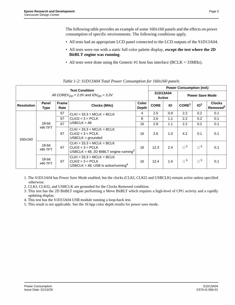
Epson Research and Development Page 5Vancouver Design Center
Re 2
1
The following table provides an example of some 160x160 panels and the effects on power consumption of specific environments. The following conditions apply.
• All tests had an appropriate LCD panel connected to the LCD outputs of the S1D13A04.
• All tests were run with a static full color palette display, except the test where the 2D BitBLT engine was running.
• All tests were done using the Generic #1 host bus interface (BCLK = 33MHz).
1. The S1D13A04 has Power Save Mode enabled, but the clocks (CLKI, CLKI2 and USBCLK) remain active unless specifiedotherwise.
2. CLKI, CLKI2, and USBCLK are grounded for the Clocks Removed condition.3. This test has the 2D BitBLT engine performing a Move BitBLT which requires a high-level of CPU activity and a rapidly
updating display.4. This test has the S1D13A04 USB module running a loop-back test.5. This result is not applicable. See the 16 bpp color depth results for power save mode.
Table 1-2: S1D13A04 Total Power Consumption for 160x160 panels
Test ConditionAll COREVDD = 2.0V and IOVDD = 3.3V
Power Consumption (mA)
S1D13A04 Active
Power Save Mode
solutionPanel Type
Frame Rate
Clocks (MHz)Color Depth
CORE IO CORE1 IO1 ClocksRemoved
60x160
18-bitHR-TFT
67 CLKI = 33.3 = MCLK = BCLKCLKI2 = 3 = PCLKUSBCLK = 48
4 2.5 0.9 2.2 0.2 0.1
67 8 2.6 1.1 2.2 0.2 0.1
67 16 2.8 1.1 2.2 0.2 0.1
67CLKI = 33.3 = MCLK = BCLKCLKI2 = 3 = PCLKUSBCLK = grounded
16 2.6 1.0 4.2 0.1 0.1
18-bitHR-TFT
67CLKI = 33.3 = MCLK = BCLKCLKI2 = 3 = PCLKUSBCLK = 48, 2D BitBLT engine running3
16 12.3 2.4 5 5 0.1
18-bitHR-TFT
67CLKI = 33.3 = MCLK = BCLKCLKI2 = 3 = PCLKUSBCLK = 48, USB is active/running4
16 12.4 1.6 5 5 0.1
Power Consumption S1D13A04Issue Date: 01/10/29 X37A-G-006-01
Page 6 Epson Research and DevelopmentVancouver Design Center
2 Summary
The system design variables in Section 1, “S1D13A04 Power Consumption” and in Table 1-1: “S1D13A04 Total Power Consumption for 320x240 panels” show that S1D13A04 power consumption depends on the specific implementation. Active Mode power consumption depends on the desired CPU performance and LCD frame-rate, whereas power save mode consumption depends on the CPU Interface and Input Clock state.
In a typical design environment, the S1D13A04 can be configured to be an extremely power-efficient LCD Controller with high performance and flexibility.
S1D13A04 Power ConsumptionX37A-G-006-01 Issue Date: 01/10/29
S1D13A04 LCD/USB Companion Chip
Interfacing to the NEC VR4102 / VR4111 Microprocessors
Document Number: X37A-G-007-01
Copyright © 2001 Epson Research and Development, Inc. All Rights Reserved.
Information in this document is subject to change without notice. You may download and use this document, but only for your own use inevaluating Seiko Epson/EPSON products. You may not modify the document. Epson Research and Development, Inc. disclaims anyrepresentation that the contents of this document are accurate or current. The Programs/Technologies described in this document may contain material protected under U.S. and/or International Patent laws.
EPSON is a registered trademark of Seiko Epson Corporation. All Trademarks are the property of their respective owners.

Page 2 Epson Research and DevelopmentVancouver Design Center
THIS PAGE LEFT BLANK
S1D13A04 Interfacing to the NEC VR4102 / VR4111 MicroprocessorsX37A-G-007-01 Issue Date: 01/10/12
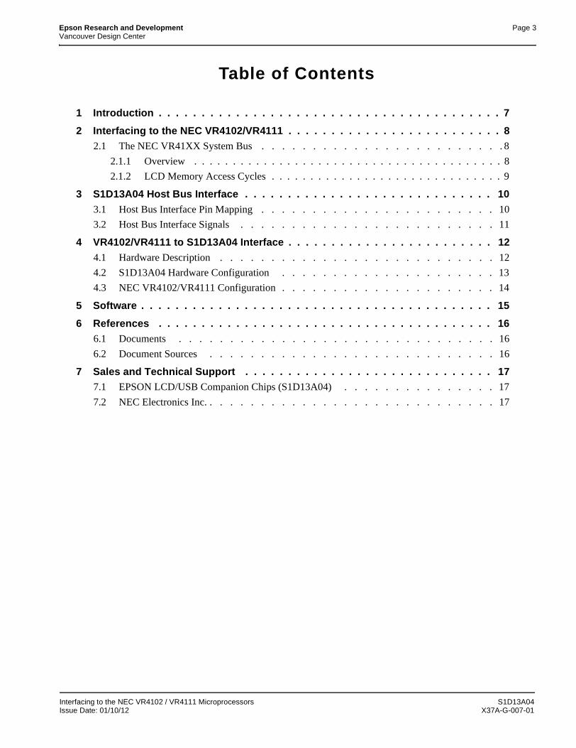
Epson Research and Development Page 3Vancouver Design Center
Table of Contents
1 Introduction . . . . . . . . . . . . . . . . . . . . . . . . . . . . . . . . . . . . . . . . 7
2 Interfacing to the NEC VR4102/VR4111 . . . . . . . . . . . . . . . . . . . . . . . . . 82.1 The NEC VR41XX System Bus . . . . . . . . . . . . . . . . . . . . . . . . 8
2.1.1 Overview . . . . . . . . . . . . . . . . . . . . . . . . . . . . . . . . . . . . . . . . 8
2.1.2 LCD Memory Access Cycles . . . . . . . . . . . . . . . . . . . . . . . . . . . . . . 9
3 S1D13A04 Host Bus Interface . . . . . . . . . . . . . . . . . . . . . . . . . . . . . 103.1 Host Bus Interface Pin Mapping . . . . . . . . . . . . . . . . . . . . . . . 10
3.2 Host Bus Interface Signals . . . . . . . . . . . . . . . . . . . . . . . . . 11
4 VR4102/VR4111 to S1D13A04 Interface . . . . . . . . . . . . . . . . . . . . . . . . 124.1 Hardware Description . . . . . . . . . . . . . . . . . . . . . . . . . . . 12
4.2 S1D13A04 Hardware Configuration . . . . . . . . . . . . . . . . . . . . . 13
4.3 NEC VR4102/VR4111 Configuration . . . . . . . . . . . . . . . . . . . . . 14
5 Software . . . . . . . . . . . . . . . . . . . . . . . . . . . . . . . . . . . . . . . . . 15
6 References . . . . . . . . . . . . . . . . . . . . . . . . . . . . . . . . . . . . . . . 166.1 Documents . . . . . . . . . . . . . . . . . . . . . . . . . . . . . . . 16
6.2 Document Sources . . . . . . . . . . . . . . . . . . . . . . . . . . . . 16
7 Sales and Technical Support . . . . . . . . . . . . . . . . . . . . . . . . . . . . . 177.1 EPSON LCD/USB Companion Chips (S1D13A04) . . . . . . . . . . . . . . . 17
7.2 NEC Electronics Inc. . . . . . . . . . . . . . . . . . . . . . . . . . . . . 17
Interfacing to the NEC VR4102 / VR4111 Microprocessors S1D13A04Issue Date: 01/10/12 X37A-G-007-01

Page 4 Epson Research and DevelopmentVancouver Design Center
THIS PAGE LEFT BLANK
S1D13A04 Interfacing to the NEC VR4102 / VR4111 MicroprocessorsX37A-G-007-01 Issue Date: 01/10/12
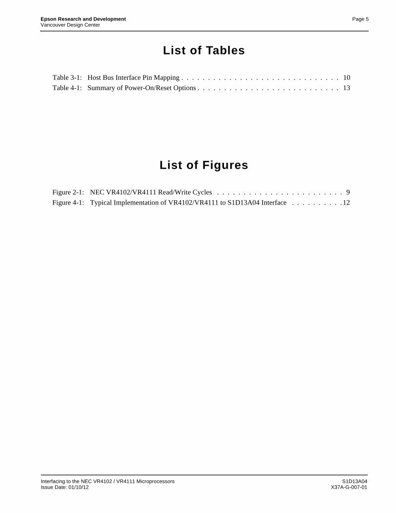
Epson Research and Development Page 5Vancouver Design Center
List of Tables
Table 3-1: Host Bus Interface Pin Mapping . . . . . . . . . . . . . . . . . . . . . . . . . . . . . . 10
Table 4-1: Summary of Power-On/Reset Options . . . . . . . . . . . . . . . . . . . . . . . . . . . 13
List of Figures
Figure 2-1: NEC VR4102/VR4111 Read/Write Cycles . . . . . . . . . . . . . . . . . . . . . . . . 9
Figure 4-1: Typical Implementation of VR4102/VR4111 to S1D13A04 Interface . . . . . . . . . . 12
Interfacing to the NEC VR4102 / VR4111 Microprocessors S1D13A04Issue Date: 01/10/12 X37A-G-007-01

Page 6 Epson Research and DevelopmentVancouver Design Center
THIS PAGE LEFT BLANK
S1D13A04 Interfacing to the NEC VR4102 / VR4111 MicroprocessorsX37A-G-007-01 Issue Date: 01/10/12

Epson Research and Development Page 7Vancouver Design Center
1 Introduction
This application note describes the hardware and software environment required to interface the S1D13A04 LCD/USB Companion Chip and the NEC VR4102/4111 micro-processor. The NEC VR4102 and VR4111 microprocessors are specifically designed to support an external LCD controller.
The designs described in this document are presented only as examples of how such inter-faces might be implemented. This application note is updated as appropriate. Please check the Epson Research and Development website at www.erd.epson.com for the latest revision of this document before beginning any development.
We appreciate your comments on our documentation. Please contact us via email at [email protected].
Interfacing to the NEC VR4102 / VR4111 Microprocessors S1D13A04Issue Date: 01/10/12 X37A-G-007-01
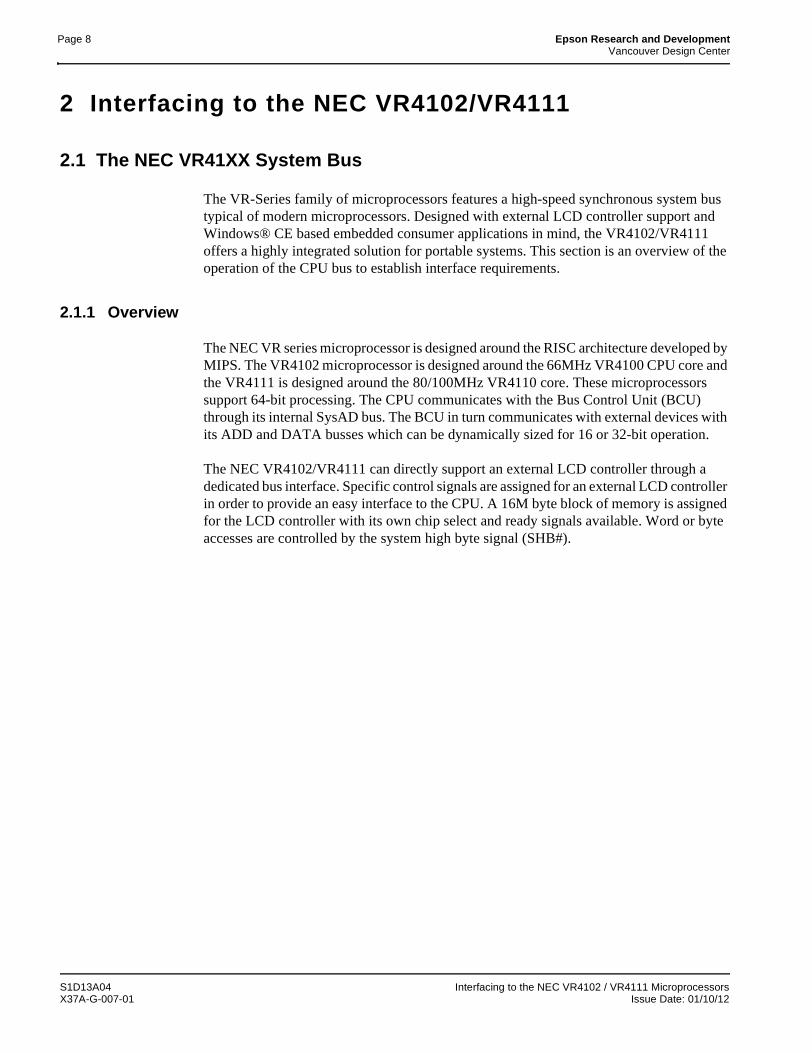
Page 8 Epson Research and DevelopmentVancouver Design Center
2 Interfacing to the NEC VR4102/VR4111
2.1 The NEC VR41XX System Bus
The VR-Series family of microprocessors features a high-speed synchronous system bus typical of modern microprocessors. Designed with external LCD controller support and Windows® CE based embedded consumer applications in mind, the VR4102/VR4111 offers a highly integrated solution for portable systems. This section is an overview of the operation of the CPU bus to establish interface requirements.
2.1.1 Overview
The NEC VR series microprocessor is designed around the RISC architecture developed by MIPS. The VR4102 microprocessor is designed around the 66MHz VR4100 CPU core and the VR4111 is designed around the 80/100MHz VR4110 core. These microprocessors support 64-bit processing. The CPU communicates with the Bus Control Unit (BCU) through its internal SysAD bus. The BCU in turn communicates with external devices with its ADD and DATA busses which can be dynamically sized for 16 or 32-bit operation.
The NEC VR4102/VR4111 can directly support an external LCD controller through a dedicated bus interface. Specific control signals are assigned for an external LCD controller in order to provide an easy interface to the CPU. A 16M byte block of memory is assigned for the LCD controller with its own chip select and ready signals available. Word or byte accesses are controlled by the system high byte signal (SHB#).
S1D13A04 Interfacing to the NEC VR4102 / VR4111 MicroprocessorsX37A-G-007-01 Issue Date: 01/10/12
Epson Research and Development Page 9Vancouver Design Center
2.1.2 LCD Memory Access Cycles
Once an address in the LCD block of memory is placed on the external address bus (ADD[25:0]) the LCD chip select (LCDCS#) is driven low. The read enable (RD#) or write enable (WR#) signals are driven low for the appropriate cycle. LCDRDY is driven low by the S1D13A04 to insert wait states into the cycle. The system high byte enable is driven low for 16-bit transfers and high for 8-bit transfers.
Figure 2-1: “NEC VR4102/VR4111 Read/Write Cycles,” shows the read and write cycles to the LCD Controller Interface.
Figure 2-1: NEC VR4102/VR4111 Read/Write Cycles
TCLK
ADD[25:0]
LCDCS#
WR#,RD#
LCDRDY
VALID
VALID
VALIDHi-Z Hi-Z
D[15:0]
D[15:0]
(write)
(read)
SHB#
Interfacing to the NEC VR4102 / VR4111 Microprocessors S1D13A04Issue Date: 01/10/12 X37A-G-007-01
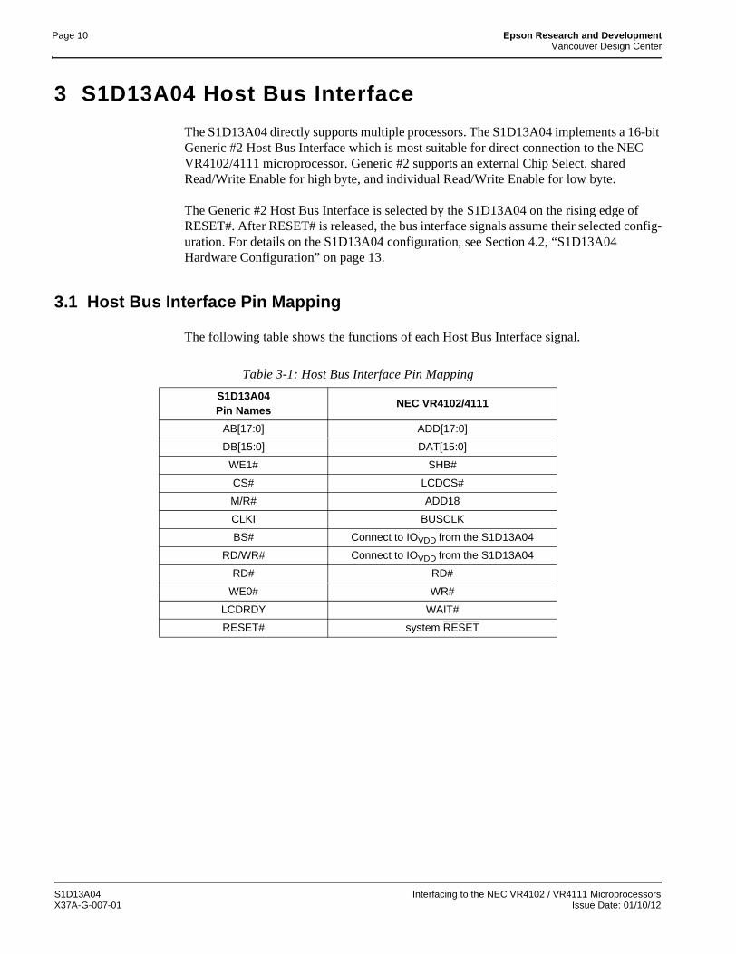
Page 10 Epson Research and DevelopmentVancouver Design Center
3 S1D13A04 Host Bus Interface
The S1D13A04 directly supports multiple processors. The S1D13A04 implements a 16-bit Generic #2 Host Bus Interface which is most suitable for direct connection to the NEC VR4102/4111 microprocessor. Generic #2 supports an external Chip Select, shared Read/Write Enable for high byte, and individual Read/Write Enable for low byte.
The Generic #2 Host Bus Interface is selected by the S1D13A04 on the rising edge of RESET#. After RESET# is released, the bus interface signals assume their selected config-uration. For details on the S1D13A04 configuration, see Section 4.2, “S1D13A04 Hardware Configuration” on page 13.
3.1 Host Bus Interface Pin Mapping
The following table shows the functions of each Host Bus Interface signal.
Table 3-1: Host Bus Interface Pin Mapping
S1D13A04Pin Names
NEC VR4102/4111
AB[17:0] ADD[17:0]
DB[15:0] DAT[15:0]
WE1# SHB#
CS# LCDCS#
M/R# ADD18
CLKI BUSCLK
BS# Connect to IOVDD from the S1D13A04
RD/WR# Connect to IOVDD from the S1D13A04
RD# RD#
WE0# WR#
LCDRDY WAIT#
RESET# system RESET
S1D13A04 Interfacing to the NEC VR4102 / VR4111 MicroprocessorsX37A-G-007-01 Issue Date: 01/10/12
Epson Research and Development Page 11Vancouver Design Center
3.2 Host Bus Interface Signals
The Host Bus Interface requires the following signals:
• CLKI is a clock input which is required by the S1D13A04 Host Bus Interface as a source for its internal bus and memory clocks. This clock is typically driven by the host CPU system clock. For this example, BUSCLK from the NEC VR4102/4111 is used for CLKI.
• The address inputs AB[17:0], and the data bus DB[15:0], connect directly to the NEC VR4102/4111 address bus (ADD[17:0]) and data bus (DAT[15:0]), respectively. CNF4 must be set to select little endian mode.
• Chip Select (CS#) must be driven low by LCDCS# whenever the S1D13A04 is accessed by the VR4102/4111.
• M/R# (memory/register) selects between memory or register accesses. This signal is generated by the external address decode circuitry. For this example, M/R# is connected to address line ADD18, allowing system address ADD18 to select between memory or register accesses.
• WE1# connects to SHB# (the high byte enable signal from the NEC VR4102/4111) which in conjunction with address bit 0 allows byte steering of read and write opera-tions.
• WE0# connects to WR# (the write enable signal from the NEC VR4102/4111) and must be driven low when the VR4102/4111 is writing data to the S1D13A04.
• RD# connects to RD# (the read enable signal from the NEC VR4102/4111) and must be driven low when the VR4102/4111 is reading data from the S1D13A04.
• WAIT# connects to LCDRDY and is a signal output from the S1D13A04 that indicates the VR4102/VR4111 must wait until data is ready (read cycle) or accepted (write cycle) on the host bus. Since VR4102/VR4111 accesses to the S1D13A04 may occur asyn-chronously to the display update, it is possible that contention may occur in accessing the S1D13A04 internal registers and/or display buffer. The WAIT# line resolves these contentions by forcing the host to wait until the resource arbitration is complete.
• The Bus Status (BS#) and Read/Write (RD/WR#) signals are not used in this implemen-tation of the NEC VR4102/4111 interface using the Generic #2 Host Bus Interface. These pins must be tied high (connected to IO VDD).
Interfacing to the NEC VR4102 / VR4111 Microprocessors S1D13A04Issue Date: 01/10/12 X37A-G-007-01
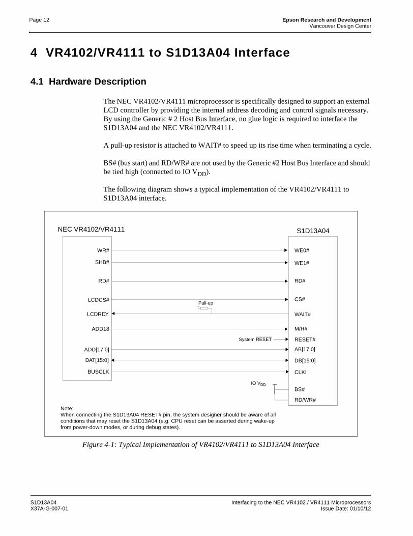
Page 12 Epson Research and DevelopmentVancouver Design Center
4 VR4102/VR4111 to S1D13A04 Interface
4.1 Hardware Description
The NEC VR4102/VR4111 microprocessor is specifically designed to support an external LCD controller by providing the internal address decoding and control signals necessary. By using the Generic # 2 Host Bus Interface, no glue logic is required to interface the S1D13A04 and the NEC VR4102/VR4111.
A pull-up resistor is attached to WAIT# to speed up its rise time when terminating a cycle.
BS# (bus start) and RD/WR# are not used by the Generic #2 Host Bus Interface and should be tied high (connected to IO VDD).
The following diagram shows a typical implementation of the VR4102/VR4111 to S1D13A04 interface.
Figure 4-1: Typical Implementation of VR4102/VR4111 to S1D13A04 Interface
WE1#
WE0#
DB[15:0]
WAIT#
RD#
CLKI
S1D13A04
CS#
RESET#
AB[17:0]
SHB#
WR#
DAT[15:0]
LCDCS#
RD#
BUSCLK
LCDRDY
ADD[17:0]
NEC VR4102/VR4111
Pull-up
BS#
RD/WR#
System RESET
Note:When connecting the S1D13A04 RESET# pin, the system designer should be aware of all conditions that may reset the S1D13A04 (e.g. CPU reset can be asserted during wake-up from power-down modes, or during debug states).
IO VDD
M/R#ADD18
S1D13A04 Interfacing to the NEC VR4102 / VR4111 MicroprocessorsX37A-G-007-01 Issue Date: 01/10/12
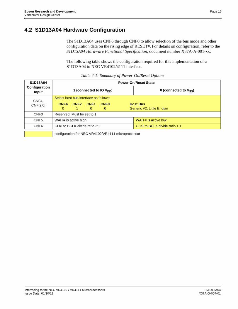
Epson Research and Development Page 13Vancouver Design Center
4.2 S1D13A04 Hardware Configuration
The S1D13A04 uses CNF6 through CNF0 to allow selection of the bus mode and other configuration data on the rising edge of RESET#. For details on configuration, refer to the S1D13A04 Hardware Functional Specification, document number X37A-A-001-xx.
The following table shows the configuration required for this implementation of a S1D13A04 to NEC VR4102/4111 interface.
Table 4-1: Summary of Power-On/Reset Options
S1D13A04 Configuration
Input
Power-On/Reset State
1 (connected to IO VDD) 0 (connected to VSS)
CNF4, CNF[2:0]
Select host bus interface as follows:
CNF4 CNF2 CNF1 CNF0 Host Bus0 1 0 0 Generic #2, Little Endian
CNF3 Reserved. Must be set to 1.
CNF5 WAIT# is active high WAIT# is active low
CNF6 CLKI to BCLK divide ratio 2:1 CLKI to BCLK divide ratio 1:1
configuration for NEC VR4102/VR4111 microprocessor
Interfacing to the NEC VR4102 / VR4111 Microprocessors S1D13A04Issue Date: 01/10/12 X37A-G-007-01
Page 14 Epson Research and DevelopmentVancouver Design Center
4.3 NEC VR4102/VR4111 Configuration
The NEC VR4102/4111 provides the internal address decoding necessary to map an external LCD controller. Physical address 0A00_0000h to 0AFF_FFFFh (16M bytes) is reserved for an external LCD controller by the NEC VR4102/4111.
The S1D13A04 is a memory mapped device. The S1D13A04 uses two 256K byte blocks which are selected using ADD18 from the NEC VR4102/4111 (ADD18 is connected to the S1D13A04 M/R# pin).The internal registers occupy the first 256K byte block and the 160K byte display buffer occupies the second 256K byte block.
The starting address of the S1D13A04 internal registers is located at 0A00_0000h and the starting address of the display buffer is located at 0A04_0000h. These blocks are aliased over the entire 16M byte address space.
NoteIf aliasing is not desirable, the upper addresses must be fully decoded.
The NEC VR4102/VR4111 has a 16-bit internal register named BCUCNTREG2 located at 0B00_0002h. It must be set to the value of 0001h which indicates that LCD controller accesses use a non-inverting data bus.
The 16-bit internal register named BCUCNTREG1 (located at 0B00_0000h) must have bit D[13] (ISA/LCD bit) set to 0. This reserves 16M bytes (from 0A00_0000h to 0AFF_FFFFh) for use by the LCD controller and not as ISA bus memory space.
S1D13A04 Interfacing to the NEC VR4102 / VR4111 MicroprocessorsX37A-G-007-01 Issue Date: 01/10/12

Epson Research and Development Page 15Vancouver Design Center
5 Software
Test utilities and display drivers are available for the S1D13A04. Full source code is available for both the test utilities and the drivers.
The test utilities are configurable for different panel types using a program called 13A04CFG (see document number X37A-B-001-xx), or by directly modifying the source. The display drivers can be customized by the OEM for different panel types, resolutions and color depths only by modifying the source.
The S1D13A04 test utilities and display drivers are available from your sales support contact (see Section 7, “Sales and Technical Support”) or www.erd.epson.com.
Interfacing to the NEC VR4102 / VR4111 Microprocessors S1D13A04Issue Date: 01/10/12 X37A-G-007-01
Page 16 Epson Research and DevelopmentVancouver Design Center
6 References
6.1 Documents
• NEC Electronics Inc., VR4102/VR4111 64/32-bit Microprocessor Preliminary User’s Manual.
• Epson Research and Development, Inc., S1D13A04 Hardware Functional Specification, document number X37A-A-001-xx.
• Epson Research and Development, Inc., S5U13A04B00C Rev. 1.0 Evaluation Board User Manual, document number X37A-G-004-xx.
• Epson Research and Development, Inc., S1D13A04 Programming Notes and Examples, document number X37A-G-003-xx.
6.2 Document Sources
• NEC Electronics Inc. Website: www.necel.com.
• Epson Research and Development Website: www.erd.epson.com.
S1D13A04 Interfacing to the NEC VR4102 / VR4111 MicroprocessorsX37A-G-007-01 Issue Date: 01/10/12
Epson Research and Development Page 17Vancouver Design Center
7 Sales and Technical Support
7.1 EPSON LCD/USB Companion Chips (S1D13A04)
7.2 NEC Electronics Inc.
JapanSeiko Epson CorporationElectronic Devices Marketing Division421-8, Hino, Hino-shiTokyo 191-8501, JapanTel: 042-587-5812Fax: 042-587-5564http://www.epson.co.jp
Hong KongEpson Hong Kong Ltd.20/F., Harbour Centre25 Harbour RoadWanchai, Hong KongTel: 2585-4600Fax: 2827-4346http://www.epson.com.hk/
TaiwanEpson Taiwan Technology & Trading Ltd.10F, No. 287Nanking East RoadSec. 3, Taipei, TaiwanTel: 02-2717-7360Fax: 02-2712-9164http://www.epson.com.tw/
SingaporeEpson Singapore Pte., Ltd.No. 1Temasek Avenue #36-00Millenia TowerSingapore, 039192Tel: 337-7911Fax: 334-2716http://www.epson.com.sg/
EuropeEpson Europe Electronics GmbHRiesstrasse 1580992 Munich, GermanyTel: 089-14005-0Fax: 089-14005-110http://www.epson-electronics.de
North AmericaEpson Electronics America, Inc.150 River Oaks ParkwaySan Jose, CA 95134, USATel: (408) 922-0200Fax: (408) 922-0238http://www.eea.epson.com
NEC Electronics Inc. (U.S.A.)Corporate Headquarters2880 Scott Blvd.Santa Clara, CA 95050-8062, USATel: (800) 366-9782Fax: (800) 729-9288http://www.necel.com
Interfacing to the NEC VR4102 / VR4111 Microprocessors S1D13A04Issue Date: 01/10/12 X37A-G-007-01

Page 18 Epson Research and DevelopmentVancouver Design Center
THIS PAGE LEFT BLANK
S1D13A04 Interfacing to the NEC VR4102 / VR4111 MicroprocessorsX37A-G-007-01 Issue Date: 01/10/12
S1D13A04 LCD/USB Companion Chip
Interfacing to the NEC VR4181A™ Microprocessor
Document Number: X37A-G-008-01
Copyright © 2001 Epson Research and Development, Inc. All Rights Reserved.
Information in this document is subject to change without notice. You may download and use this document, but only for your own use inevaluating Seiko Epson/EPSON products. You may not modify the document. Epson Research and Development, Inc. disclaims anyrepresentation that the contents of this document are accurate or current. The Programs/Technologies described in this document may contain material protected under U.S. and/or International Patent laws.
EPSON is a registered trademark of Seiko Epson Corporation. All Trademarks are the property of their respective owners.

Page 2 Epson Research and DevelopmentVancouver Design Center
THIS PAGE LEFT BLANK
S1D13A04 Interfacing to the NEC VR4181A™ MicroprocessorX37A-G-008-01 Issue Date: 01/10/12
Epson Research and Development Page 3Vancouver Design Center
Table of Contents
1 Introduction . . . . . . . . . . . . . . . . . . . . . . . . . . . . . . . . . . . . . . . . 7
2 Interfacing to the NEC VR4181A . . . . . . . . . . . . . . . . . . . . . . . . . . . . . 82.1 The NEC VR4181A System Bus . . . . . . . . . . . . . . . . . . . . . . . . 8
2.1.1 Overview . . . . . . . . . . . . . . . . . . . . . . . . . . . . . . . . . . . . . . . . 8
2.1.2 LCD Memory Access Signals . . . . . . . . . . . . . . . . . . . . . . . . . . . . . . 9
3 S1D13A04 Host Bus Interface . . . . . . . . . . . . . . . . . . . . . . . . . . . . . 103.1 Host Bus Interface Pin Mapping . . . . . . . . . . . . . . . . . . . . . . . 10
3.2 Host Bus Interface Signals . . . . . . . . . . . . . . . . . . . . . . . . . 11
4 VR4181A to S1D13A04 Interface . . . . . . . . . . . . . . . . . . . . . . . . . . . . 124.1 Hardware Description . . . . . . . . . . . . . . . . . . . . . . . . . . . 12
4.2 S1D13A04 Hardware Configuration . . . . . . . . . . . . . . . . . . . . . 13
4.3 NEC VR4181A Configuration . . . . . . . . . . . . . . . . . . . . . . . . 14
5 Software . . . . . . . . . . . . . . . . . . . . . . . . . . . . . . . . . . . . . . . . . 15
6 References . . . . . . . . . . . . . . . . . . . . . . . . . . . . . . . . . . . . . . . 166.1 Documents . . . . . . . . . . . . . . . . . . . . . . . . . . . . . . . 16
6.2 Document Sources . . . . . . . . . . . . . . . . . . . . . . . . . . . . 16
7 Technical Support . . . . . . . . . . . . . . . . . . . . . . . . . . . . . . . . . . . 177.1 EPSON LCD/USB Companion Chips (S1D13A04) . . . . . . . . . . . . . . . 17
7.2 NEC Electronics Inc. . . . . . . . . . . . . . . . . . . . . . . . . . . . . 17
Interfacing to the NEC VR4181A™ Microprocessor S1D13A04Issue Date: 01/10/12 X37A-G-008-01

Page 4 Epson Research and DevelopmentVancouver Design Center
THIS PAGE LEFT BLANK
S1D13A04 Interfacing to the NEC VR4181A™ MicroprocessorX37A-G-008-01 Issue Date: 01/10/12
Epson Research and Development Page 5Vancouver Design Center
List of Tables
Table 3-1: Host Bus Interface Pin Mapping . . . . . . . . . . . . . . . . . . . . . . . . . . . . . . 10
Table 4-1: Summary of Power-On/Reset Options . . . . . . . . . . . . . . . . . . . . . . . . . . . 13
List of Figures
Figure 4-1: Typical Implementation of VR4181A to S1D13A04 Interface . . . . . . . . . . . . . . 12
Interfacing to the NEC VR4181A™ Microprocessor S1D13A04Issue Date: 01/10/12 X37A-G-008-01

Page 6 Epson Research and DevelopmentVancouver Design Center
THIS PAGE LEFT BLANK
S1D13A04 Interfacing to the NEC VR4181A™ MicroprocessorX37A-G-008-01 Issue Date: 01/10/12

Epson Research and Development Page 7Vancouver Design Center
1 Introduction
This application note describes the hardware and software environment required to interface the S1D13A04 LCD/USB Companion Chip and the NEC VR4181A micropro-cessor. The NEC VR4181A microprocessor is specifically designed to support an external LCD controller.
The designs described in this document are presented only as examples of how suchinterfaces might be implemented. This application note is updated as appropriate. Please check the Epson Research and Development website at www.erd.epson.com for the latest revision of this document before beginning any development.
We appreciate your comments on our documentation. Please contact us via email at [email protected].
Interfacing to the NEC VR4181A™ Microprocessor S1D13A04Issue Date: 01/10/12 X37A-G-008-01
Page 8 Epson Research and DevelopmentVancouver Design Center
2 Interfacing to the NEC VR4181A
2.1 The NEC VR4181A System Bus
The VR-Series family of microprocessors features a high-speed synchronous system bus typical of modern microprocessors. Designed with external LCD controller support and Windows® CE based embedded consumer applications in mind, the VR4181A offers a highly integrated solution for portable systems. This section is an overview of the operation of the CPU bus to establish interface requirements.
2.1.1 Overview
The NEC VR4181A is designed around the RISC architecture developed by MIPS. This microprocessor is designed around the 100MHz VR4110 CPU core which supports the MIPS III and MIPS16 instruction sets. The CPU communicates with external devices via an ISA interface.
While the VR4181A has an embedded LCD controller, this internal controller can be disabled to provide direct support for an external LCD controller through its external ISA bus. A 64 to 512K byte block of memory is assigned to the external LCD controller with a dedicated chip select signal (LCDCS#). Word or byte accesses are controlled by the system high byte signal (#UBE).
S1D13A04 Interfacing to the NEC VR4181A™ MicroprocessorX37A-G-008-01 Issue Date: 01/10/12
Epson Research and Development Page 9Vancouver Design Center
2.1.2 LCD Memory Access Signals
The S1D13A04 requires an addressing range of 256K bytes. When the VR4181A external LCD controller chip select signal is programmed to a window of that size, the S1D13A04 resides in the VR4181A physical address range of 133C 0000h to 133F FFFFh. This range is part of the external ISA memory space.
The following signals are required to access an external LCD controller. All signals obey ISA signalling rules.
• A[16:0] is the address bus.
• #UBE is the high byte enable (active low).
• #LCDCS is the chip select for the S1D13A04 (active low).
• D[15:0] is the data bus.
• #MEMRD is the read command (active low).
• #MEMWR is the write command (active low).
• #MEMCS16 is the acknowledge for 16-bit peripheral capability (active low).
• IORDY is the ready signal from S1D13A04.
• SYSCLK is the prescalable bus clock (optional).
Once an address in the LCD block of memory is accessed, the LCD chip select (#LCDCS) is driven low. The read or write enable signals (#MEMRD or #MEMWR) are driven low for the appropriate cycle and IORDY is driven low by the S1D13A04 to insert wait states into the cycle. The high byte enable (UBE#) is driven low for 16-bit transfers and high for 8-bit transfers.
Interfacing to the NEC VR4181A™ Microprocessor S1D13A04Issue Date: 01/10/12 X37A-G-008-01
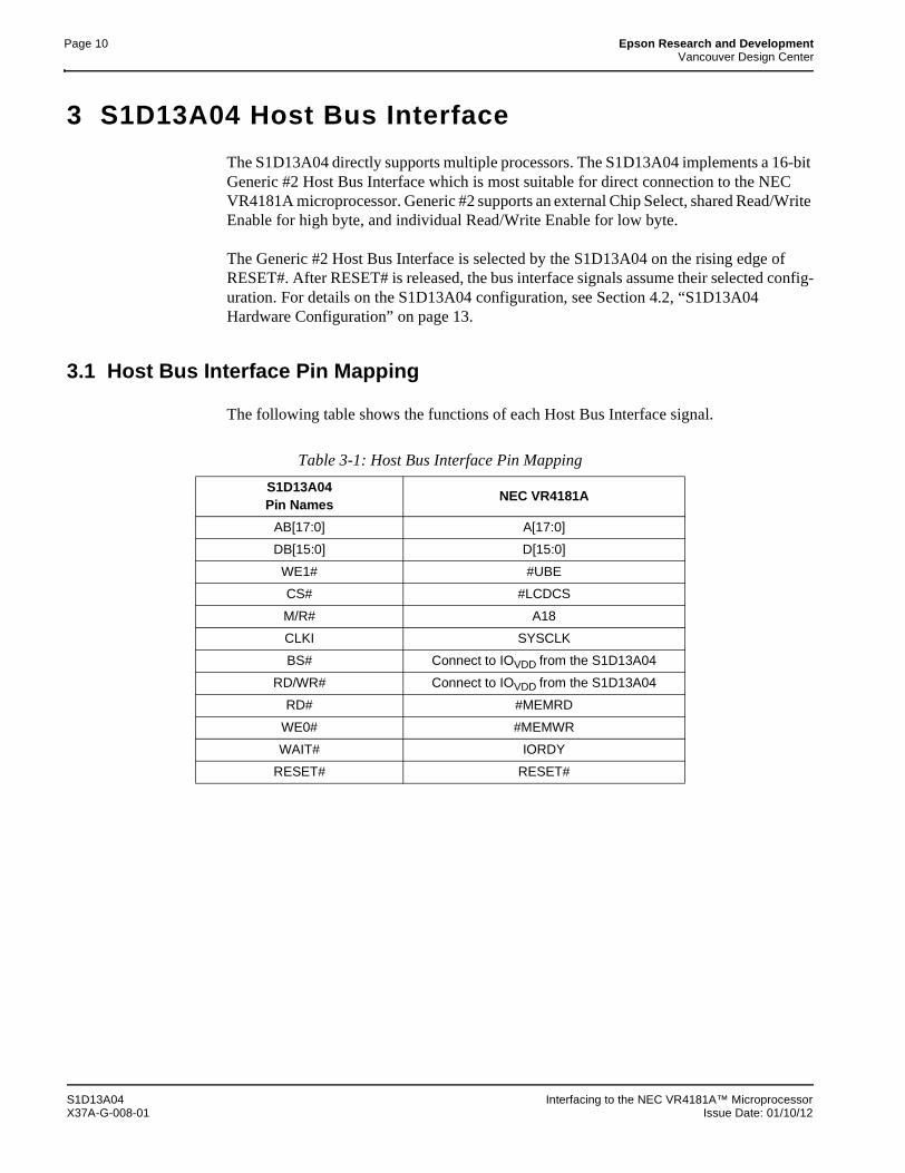
Page 10 Epson Research and DevelopmentVancouver Design Center
3 S1D13A04 Host Bus Interface
The S1D13A04 directly supports multiple processors. The S1D13A04 implements a 16-bit Generic #2 Host Bus Interface which is most suitable for direct connection to the NEC VR4181A microprocessor. Generic #2 supports an external Chip Select, shared Read/Write Enable for high byte, and individual Read/Write Enable for low byte.
The Generic #2 Host Bus Interface is selected by the S1D13A04 on the rising edge of RESET#. After RESET# is released, the bus interface signals assume their selected config-uration. For details on the S1D13A04 configuration, see Section 4.2, “S1D13A04 Hardware Configuration” on page 13.
3.1 Host Bus Interface Pin Mapping
The following table shows the functions of each Host Bus Interface signal.
Table 3-1: Host Bus Interface Pin Mapping
S1D13A04Pin Names
NEC VR4181A
AB[17:0] A[17:0]
DB[15:0] D[15:0]
WE1# #UBE
CS# #LCDCS
M/R# A18
CLKI SYSCLK
BS# Connect to IOVDD from the S1D13A04
RD/WR# Connect to IOVDD from the S1D13A04
RD# #MEMRD
WE0# #MEMWR
WAIT# IORDY
RESET# RESET#
S1D13A04 Interfacing to the NEC VR4181A™ MicroprocessorX37A-G-008-01 Issue Date: 01/10/12
Epson Research and Development Page 11Vancouver Design Center
3.2 Host Bus Interface Signals
The interface requires the following signals.
• CLKI is a clock input which is required by the S1D13A04 Host Bus Interface as a source for its internal bus and memory clocks. This clock is typically driven by the host CPU system clock. For this example, SYSCLK from the NEC VR4181A is used for CLKI.
• The address inputs AB[17:0], and the data bus DB[15:0], connect directly to the NEC VR4181A address (A[17:0]) and data bus (D[15:0]), respectively. CNF4 must be set to select little endian mode.
• Chip Select (CS#) must be driven low by #LCDCS whenever the S1D13A04 is accessed by the VR4181A.
• M/R# (memory/register) selects between memory or register accesses. This signal is generated by the external address decode circuitry. For this example, M/R# is connected to address line A18, allowing system address A18 to select between memory or register accesses.
• WE1# connects to #UBE (the high byte enable signal from the NEC VR4181A) which in conjunction with address bit 0 allows byte steering of read and write operations.
• WE0# connects to #MEMWR (the write enable signal from the NEC VR4181A) and must be driven low when the NEC VR4181A is writing data to the S1D13A04.
• RD# connects to #MEMRD (the read enable signal from the NEC VR4181A) and must be driven low when the NEC VR4181A is reading data from the S1D13A04.
• WAIT# connects to IORDY and is a signal which is output from the S1D13A04 which indicates the NEC VR4181A must wait until data is ready (read cycle) or accepted (write cycle) on the host bus. Since VR4181A accesses to the S1D13A04 may occur asynchronously to the display update, it is possible that contention may occur in accessing the S1D13A04 internal registers and/or display buffer. The WAIT# line resolves these contentions by forcing the host to wait until the resource arbitration is complete.
• The Bus Status (BS#) and Read/Write (RD/WR#) signals are not used in this implemen-tation of the NEC VR4181A interface using the Generic #2 Host Bus Interface. These pins must be tied high (connected to IO VDD).
Interfacing to the NEC VR4181A™ Microprocessor S1D13A04Issue Date: 01/10/12 X37A-G-008-01
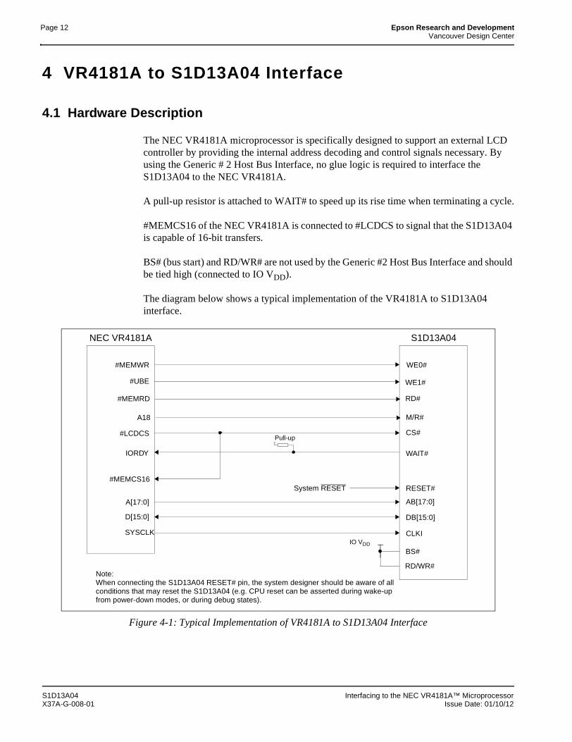
Page 12 Epson Research and DevelopmentVancouver Design Center
4 VR4181A to S1D13A04 Interface
4.1 Hardware Description
The NEC VR4181A microprocessor is specifically designed to support an external LCD controller by providing the internal address decoding and control signals necessary. By using the Generic # 2 Host Bus Interface, no glue logic is required to interface the S1D13A04 to the NEC VR4181A.
A pull-up resistor is attached to WAIT# to speed up its rise time when terminating a cycle.
#MEMCS16 of the NEC VR4181A is connected to #LCDCS to signal that the S1D13A04 is capable of 16-bit transfers.
BS# (bus start) and RD/WR# are not used by the Generic #2 Host Bus Interface and should be tied high (connected to IO VDD).
The diagram below shows a typical implementation of the VR4181A to S1D13A04 interface.
Figure 4-1: Typical Implementation of VR4181A to S1D13A04 Interface
WE1#
WE0#
DB[15:0]
WAIT#
RD#
CLKI
S1D13A04
CS#
RESET#
AB[17:0]
#UBE
#MEMWR
D[15:0]
#LCDCS
#MEMRD
IORDY
A[17:0]
NEC VR4181A
Pull-up
BS#
RD/WR#
System RESET#MEMCS16
Note:When connecting the S1D13A04 RESET# pin, the system designer should be aware of all conditions that may reset the S1D13A04 (e.g. CPU reset can be asserted during wake-up from power-down modes, or during debug states).
M/R#A18
IO VDD
SYSCLK
S1D13A04 Interfacing to the NEC VR4181A™ MicroprocessorX37A-G-008-01 Issue Date: 01/10/12
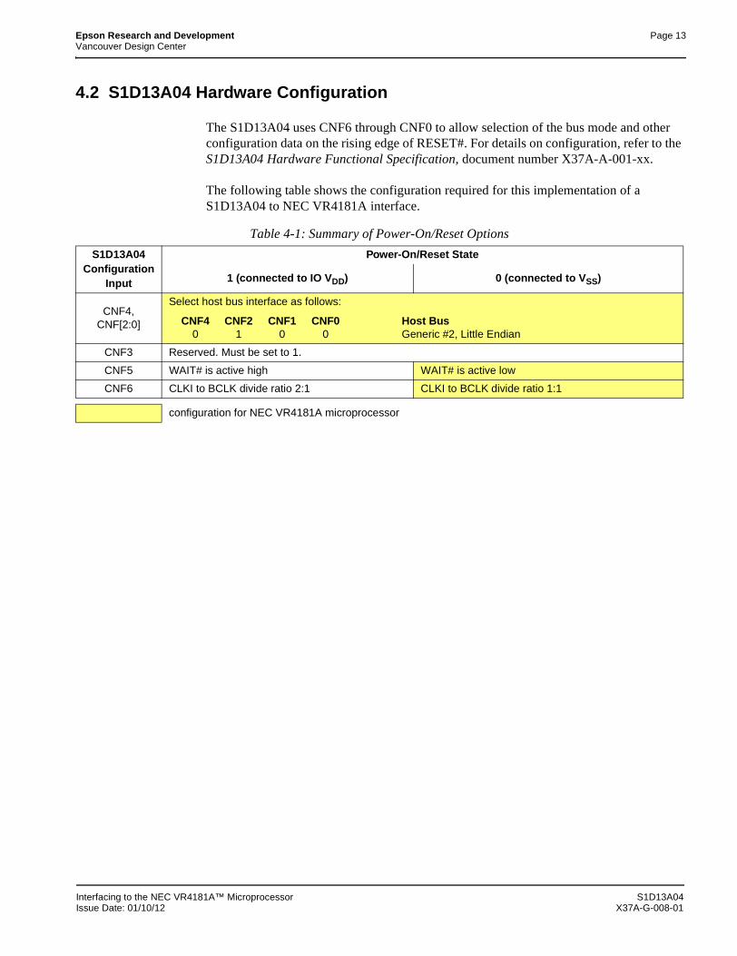
Epson Research and Development Page 13Vancouver Design Center
4.2 S1D13A04 Hardware Configuration
The S1D13A04 uses CNF6 through CNF0 to allow selection of the bus mode and other configuration data on the rising edge of RESET#. For details on configuration, refer to the S1D13A04 Hardware Functional Specification, document number X37A-A-001-xx.
The following table shows the configuration required for this implementation of a S1D13A04 to NEC VR4181A interface.
Table 4-1: Summary of Power-On/Reset Options
S1D13A04 Configuration
Input
Power-On/Reset State
1 (connected to IO VDD) 0 (connected to VSS)
CNF4, CNF[2:0]
Select host bus interface as follows:
CNF4 CNF2 CNF1 CNF0 Host Bus0 1 0 0 Generic #2, Little Endian
CNF3 Reserved. Must be set to 1.
CNF5 WAIT# is active high WAIT# is active low
CNF6 CLKI to BCLK divide ratio 2:1 CLKI to BCLK divide ratio 1:1
configuration for NEC VR4181A microprocessor
Interfacing to the NEC VR4181A™ Microprocessor S1D13A04Issue Date: 01/10/12 X37A-G-008-01
Page 14 Epson Research and DevelopmentVancouver Design Center
4.3 NEC VR4181A Configuration
The S1D13A04 is a memory mapped device. The S1D13A04 uses two 256K byte blocks which are selected using A18 from the NEC VR4181A (A18 is connected to the S1D13A04 M/R# pin).The internal registers occupy the first 256K byte block and the 160K byte display buffer occupies the second 256K byte block.
When the VR4181A embedded LCD controller is disabled, the external LCD controller chip select signal (#LCDCS) decodes either a 64K byte, 128K byte, 256K byte, or 512K byte memory block in the VR4181A external ISA memory. The S1D13A04 requires this block of memory to be set to 512K bytes. With this configuration, the S1D13A04 internal registers starting address is located at physical memory location 133C_0000h and the display buffer is located at memory location 1340_0000h.
The NEC VR4181A must be configured through its internal registers to map the S1D13A04 to the external LCD controller space. The following register values must be set.
• Register LCDGPMD at address 0B00_032Eh must be set as follows.
• Bit 7 must be set to 1 to disable the internal LCD controller and enable the external LCD controller interface. Disabling the internal LCD controller also maps pin SHCLK to #LCDCS and pin LOCLK to #MEMCS16.
• Bits [1:0] must be set to 11b to reserve 512Kbytes of memory address range,133C_0000h to 1343_FFFFh for the external LCD controller.
• Register GPMD2REG at address 0B00_0304h must be set as follows.
• Bits [9:8] (GP20MD[1:0]) must be set to 11’b to map pin GPIO20 to #UBE.
• Bits [5:4] (GP18MD[1:0]) must be set to 01’b to map pin GPIO18 to IORDY.
S1D13A04 Interfacing to the NEC VR4181A™ MicroprocessorX37A-G-008-01 Issue Date: 01/10/12

Epson Research and Development Page 15Vancouver Design Center
5 Software
Test utilities and display drivers are available for the S1D13A04. Full source code is available for both the test utilities and the drivers.
The test utilities are configurable for different panel types using a program called 13A04CFG (see document number X37A-B-001-xx), or by directly modifying the source. The display drivers can be customized by the OEM for different panel types, resolutions and color depths only by modifying the source.
The S1D13A04 test utilities and display drivers are available from your sales support contact (see Section 7, “Sales and Technical Support”) or www.erd.epson.com.
Interfacing to the NEC VR4181A™ Microprocessor S1D13A04Issue Date: 01/10/12 X37A-G-008-01
Page 16 Epson Research and DevelopmentVancouver Design Center
6 References
6.1 Documents
• NEC Electronics Inc., NEC VR4181A Target Specification, Revision 0.5, 9/11/98
• Epson Research and Development, Inc., S1D13A04 Hardware Functional Specification, document number X37A-A-001-xx.
• Epson Research and Development, Inc., S5U13A04B00C Rev. 1.0 Evaluation Board User Manual, document number X37A-G-004-xx.
• Epson Research and Development, Inc., S1D13A04 Programming Notes and Examples, document number X37A-G-003-xx.
6.2 Document Sources
• NEC Electronics Inc.Website: www.necel.com.
• Epson Research and Development Website: www.erd.epson.com.
S1D13A04 Interfacing to the NEC VR4181A™ MicroprocessorX37A-G-008-01 Issue Date: 01/10/12
Epson Research and Development Page 17Vancouver Design Center
7 Sales and Technical Support
7.1 EPSON LCD/USB Companion Chips (S1D13A04)
7.2 NEC Electronics Inc.
JapanSeiko Epson CorporationElectronic Devices Marketing Division421-8, Hino, Hino-shiTokyo 191-8501, JapanTel: 042-587-5812Fax: 042-587-5564http://www.epson.co.jp
Hong KongEpson Hong Kong Ltd.20/F., Harbour Centre25 Harbour RoadWanchai, Hong KongTel: 2585-4600Fax: 2827-4346http://www.epson.com.hk/
TaiwanEpson Taiwan Technology & Trading Ltd.10F, No. 287Nanking East RoadSec. 3, Taipei, TaiwanTel: 02-2717-7360Fax: 02-2712-9164http://www.epson.com.tw/
SingaporeEpson Singapore Pte., Ltd.No. 1Temasek Avenue #36-00Millenia TowerSingapore, 039192Tel: 337-7911Fax: 334-2716http://www.epson.com.sg/
EuropeEpson Europe Electronics GmbHRiesstrasse 1580992 Munich, GermanyTel: 089-14005-0Fax: 089-14005-110http://www.epson-electronics.de
North AmericaEpson Electronics America, Inc.150 River Oaks ParkwaySan Jose, CA 95134, USATel: (408) 922-0200Fax: (408) 922-0238http://www.eea.epson.com
NEC Electronics Inc. (U.S.A.)Corporate Headquarters2880 Scott Blvd.Santa Clara, CA 95050-8062, USATel: (800) 366-9782Fax: (800) 729-9288http://www.necel.com
Interfacing to the NEC VR4181A™ Microprocessor S1D13A04Issue Date: 01/10/12 X37A-G-008-01

Page 18 Epson Research and DevelopmentVancouver Design Center
THIS PAGE LEFT BLANK
S1D13A04 Interfacing to the NEC VR4181A™ MicroprocessorX37A-G-008-01 Issue Date: 01/10/12
S1D13A04 LCD/USB Companion Chip
Interfacing to the Motorola MPC82x Microprocessor
Document Number: X37A-G-009-01
Copyright © 2001 Epson Research and Development, Inc. All Rights Reserved.
Information in this document is subject to change without notice. You may download and use this document, but only for your own use inevaluating Seiko Epson/EPSON products. You may not modify the document. Epson Research and Development, Inc. disclaims anyrepresentation that the contents of this document are accurate or current. The Programs/Technologies described in this document may contain material protected under U.S. and/or International Patent laws.
EPSON is a registered trademark of Seiko Epson Corporation. All Trademarks are the property of their respective owners.

Page 2 Epson Research and DevelopmentVancouver Design Center
THIS PAGE LEFT BLANK
S1D13A04 Interfacing to the Motorola MPC82x MicroprocessorX37A-G-009-01 Issue Date: 01/10/05
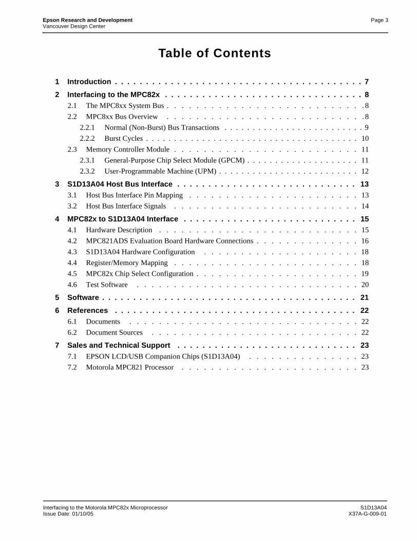
Epson Research and Development Page 3Vancouver Design Center
Table of Contents
1 Introduction . . . . . . . . . . . . . . . . . . . . . . . . . . . . . . . . . . . . . . . . 7
2 Interfacing to the MPC82x . . . . . . . . . . . . . . . . . . . . . . . . . . . . . . . . 82.1 The MPC8xx System Bus . . . . . . . . . . . . . . . . . . . . . . . . . . . 8
2.2 MPC8xx Bus Overview . . . . . . . . . . . . . . . . . . . . . . . . . . . 8
2.2.1 Normal (Non-Burst) Bus Transactions . . . . . . . . . . . . . . . . . . . . . . . . . 9
2.2.2 Burst Cycles . . . . . . . . . . . . . . . . . . . . . . . . . . . . . . . . . . . . . . 10
2.3 Memory Controller Module . . . . . . . . . . . . . . . . . . . . . . . . . 11
2.3.1 General-Purpose Chip Select Module (GPCM) . . . . . . . . . . . . . . . . . . . . 11
2.3.2 User-Programmable Machine (UPM) . . . . . . . . . . . . . . . . . . . . . . . . . 12
3 S1D13A04 Host Bus Interface . . . . . . . . . . . . . . . . . . . . . . . . . . . . . 133.1 Host Bus Interface Pin Mapping . . . . . . . . . . . . . . . . . . . . . . . 13
3.2 Host Bus Interface Signals . . . . . . . . . . . . . . . . . . . . . . . . . 14
4 MPC82x to S1D13A04 Interface . . . . . . . . . . . . . . . . . . . . . . . . . . . . 154.1 Hardware Description . . . . . . . . . . . . . . . . . . . . . . . . . . . 15
4.2 MPC821ADS Evaluation Board Hardware Connections . . . . . . . . . . . . . . 16
4.3 S1D13A04 Hardware Configuration . . . . . . . . . . . . . . . . . . . . . 18
4.4 Register/Memory Mapping . . . . . . . . . . . . . . . . . . . . . . . . . 18
4.5 MPC82x Chip Select Configuration . . . . . . . . . . . . . . . . . . . . . . 19
4.6 Test Software . . . . . . . . . . . . . . . . . . . . . . . . . . . . . . 20
5 Software . . . . . . . . . . . . . . . . . . . . . . . . . . . . . . . . . . . . . . . . . 21
6 References . . . . . . . . . . . . . . . . . . . . . . . . . . . . . . . . . . . . . . . 226.1 Documents . . . . . . . . . . . . . . . . . . . . . . . . . . . . . . . 22
6.2 Document Sources . . . . . . . . . . . . . . . . . . . . . . . . . . . . 22
7 Sales and Technical Support . . . . . . . . . . . . . . . . . . . . . . . . . . . . . 237.1 EPSON LCD/USB Companion Chips (S1D13A04) . . . . . . . . . . . . . . . 23
7.2 Motorola MPC821 Processor . . . . . . . . . . . . . . . . . . . . . . . . 23
Interfacing to the Motorola MPC82x Microprocessor S1D13A04Issue Date: 01/10/05 X37A-G-009-01

Page 4 Epson Research and DevelopmentVancouver Design Center
THIS PAGE LEFT BLANK
S1D13A04 Interfacing to the Motorola MPC82x MicroprocessorX37A-G-009-01 Issue Date: 01/10/05
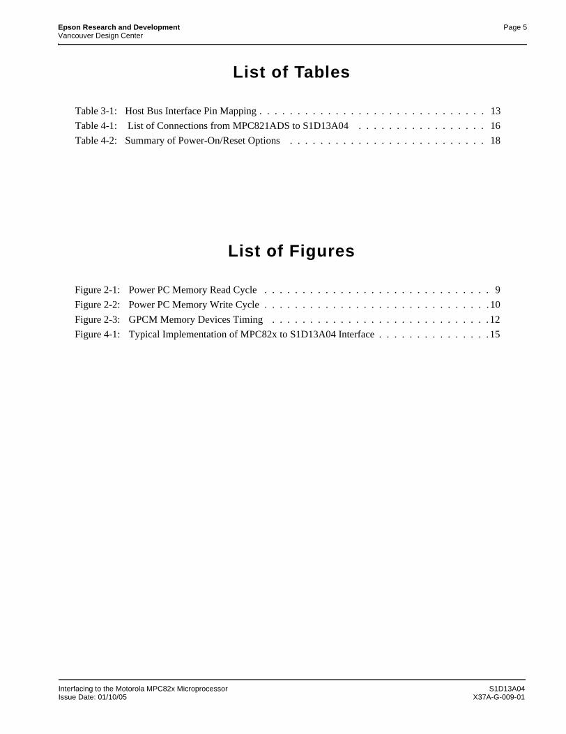
Epson Research and Development Page 5Vancouver Design Center
List of Tables
Table 3-1: Host Bus Interface Pin Mapping . . . . . . . . . . . . . . . . . . . . . . . . . . . . . . 13
Table 4-1: List of Connections from MPC821ADS to S1D13A04 . . . . . . . . . . . . . . . . . 16
Table 4-2: Summary of Power-On/Reset Options . . . . . . . . . . . . . . . . . . . . . . . . . . 18
List of Figures
Figure 2-1: Power PC Memory Read Cycle . . . . . . . . . . . . . . . . . . . . . . . . . . . . . . 9
Figure 2-2: Power PC Memory Write Cycle . . . . . . . . . . . . . . . . . . . . . . . . . . . . . . 10
Figure 2-3: GPCM Memory Devices Timing . . . . . . . . . . . . . . . . . . . . . . . . . . . . . 12
Figure 4-1: Typical Implementation of MPC82x to S1D13A04 Interface . . . . . . . . . . . . . . . 15
Interfacing to the Motorola MPC82x Microprocessor S1D13A04Issue Date: 01/10/05 X37A-G-009-01

Page 6 Epson Research and DevelopmentVancouver Design Center
THIS PAGE LEFT BLANK
S1D13A04 Interfacing to the Motorola MPC82x MicroprocessorX37A-G-009-01 Issue Date: 01/10/05

Epson Research and Development Page 7Vancouver Design Center
1 Introduction
This application note describes the hardware and software environment required to interface the S1D13A04 LCD/USB Companion Chip and the Motorola MPC82x micropro-cessor.
The designs described in this document are presented only as examples of how such inter-faces might be implemented. This application note is updated as appropriate. Please check the Epson Research and Development website at www.erd.epson.com for the latest revision of this document before beginning any development.
We appreciate your comments on our documentation. Please contact us via email at [email protected].
Interfacing to the Motorola MPC82x Microprocessor S1D13A04Issue Date: 01/10/05 X37A-G-009-01
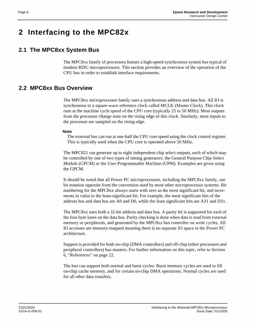
Page 8 Epson Research and DevelopmentVancouver Design Center
2 Interfacing to the MPC82x
2.1 The MPC8xx System Bus
The MPC8xx family of processors feature a high-speed synchronous system bus typical of modern RISC microprocessors. This section provides an overview of the operation of the CPU bus in order to establish interface requirements.
2.2 MPC8xx Bus Overview
The MPC8xx microprocessor family uses a synchronous address and data bus. All IO is synchronous to a square-wave reference clock called MCLK (Master Clock). This clock runs at the machine cycle speed of the CPU core (typically 25 to 50 MHz). Most outputs from the processor change state on the rising edge of this clock. Similarly, most inputs to the processor are sampled on the rising edge.
NoteThe external bus can run at one-half the CPU core speed using the clock control register. This is typically used when the CPU core is operated above 50 MHz.
The MPC821 can generate up to eight independent chip select outputs, each of which may be controlled by one of two types of timing generators: the General Purpose Chip Select Module (GPCM) or the User-Programmable Machine (UPM). Examples are given using the GPCM.
It should be noted that all Power PC microprocessors, including the MPC8xx family, use bit notation opposite from the convention used by most other microprocessor systems. Bit numbering for the MPC8xx always starts with zero as the most significant bit, and incre-ments in value to the least-significant bit. For example, the most significant bits of the address bus and data bus are A0 and D0, while the least significant bits are A31 and D31.
The MPC8xx uses both a 32-bit address and data bus. A parity bit is supported for each of the four byte lanes on the data bus. Parity checking is done when data is read from external memory or peripherals, and generated by the MPC8xx bus controller on write cycles. All IO accesses are memory-mapped meaning there is no separate IO space in the Power PC architecture.
Support is provided for both on-chip (DMA controllers) and off-chip (other processors and peripheral controllers) bus masters. For further information on this topic, refer to Section 6, “References” on page 22.
The bus can support both normal and burst cycles. Burst memory cycles are used to fillon-chip cache memory, and for certain on-chip DMA operations. Normal cycles are used for all other data transfers.
S1D13A04 Interfacing to the Motorola MPC82x MicroprocessorX37A-G-009-01 Issue Date: 01/10/05
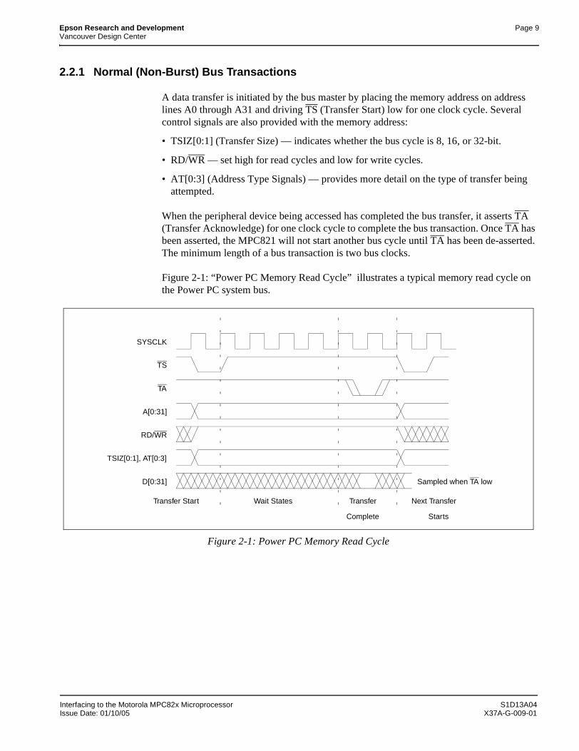
Epson Research and Development Page 9Vancouver Design Center
2.2.1 Normal (Non-Burst) Bus Transactions
A data transfer is initiated by the bus master by placing the memory address on address lines A0 through A31 and driving TS (Transfer Start) low for one clock cycle. Several control signals are also provided with the memory address:
• TSIZ[0:1] (Transfer Size) — indicates whether the bus cycle is 8, 16, or 32-bit.
• RD/WR — set high for read cycles and low for write cycles.
• AT[0:3] (Address Type Signals) — provides more detail on the type of transfer being attempted.
When the peripheral device being accessed has completed the bus transfer, it asserts TA (Transfer Acknowledge) for one clock cycle to complete the bus transaction. Once TA has been asserted, the MPC821 will not start another bus cycle until TA has been de-asserted. The minimum length of a bus transaction is two bus clocks.
Figure 2-1: “Power PC Memory Read Cycle” illustrates a typical memory read cycle on the Power PC system bus.
Figure 2-1: Power PC Memory Read Cycle
A[0:31]
D[0:31]
TSIZ[0:1], AT[0:3]
TS
TA
SYSCLK
Wait StatesTransfer Start Transfer Next Transfer
Sampled when TA low
RD/WR
Complete Starts
Interfacing to the Motorola MPC82x Microprocessor S1D13A04Issue Date: 01/10/05 X37A-G-009-01
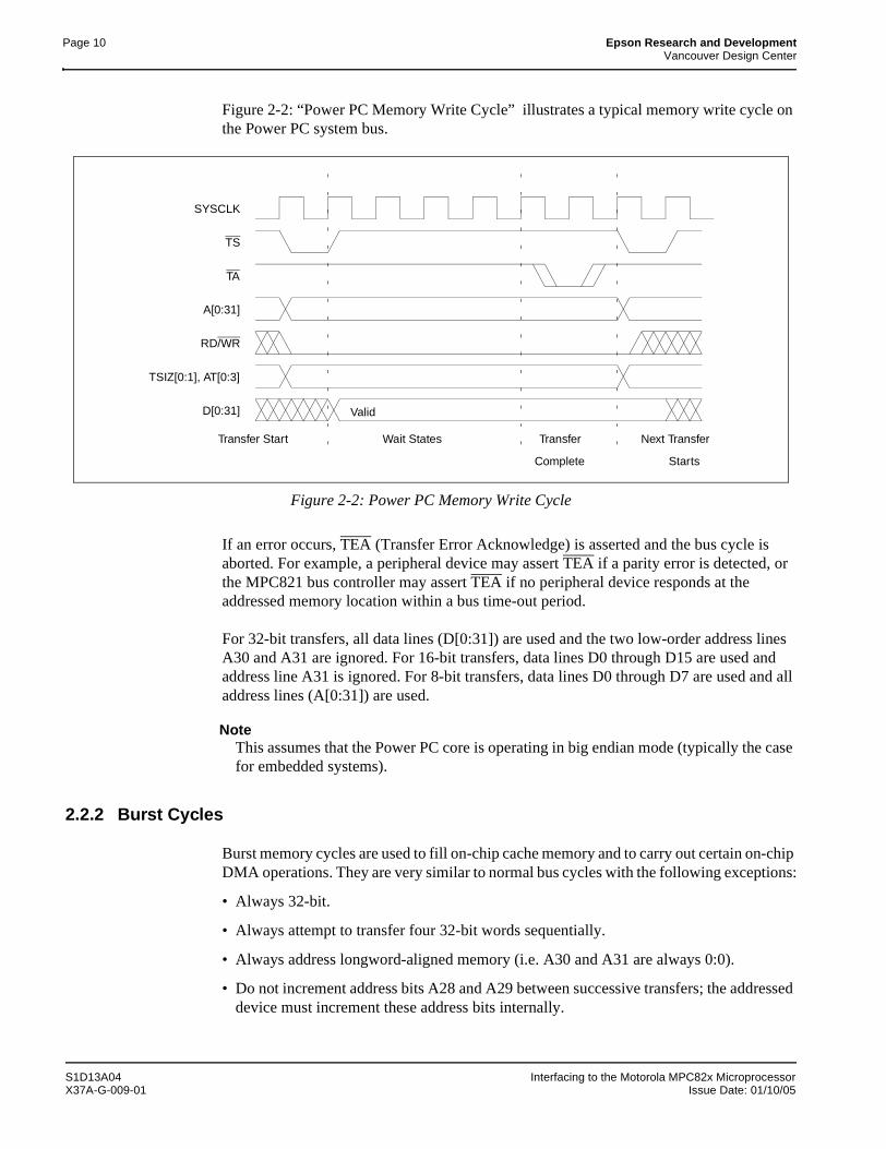
Page 10 Epson Research and DevelopmentVancouver Design Center
Figure 2-2: “Power PC Memory Write Cycle” illustrates a typical memory write cycle on the Power PC system bus.
Figure 2-2: Power PC Memory Write Cycle
If an error occurs, TEA (Transfer Error Acknowledge) is asserted and the bus cycle is aborted. For example, a peripheral device may assert TEA if a parity error is detected, or the MPC821 bus controller may assert TEA if no peripheral device responds at the addressed memory location within a bus time-out period.
For 32-bit transfers, all data lines (D[0:31]) are used and the two low-order address lines A30 and A31 are ignored. For 16-bit transfers, data lines D0 through D15 are used and address line A31 is ignored. For 8-bit transfers, data lines D0 through D7 are used and all address lines (A[0:31]) are used.
NoteThis assumes that the Power PC core is operating in big endian mode (typically the case for embedded systems).
2.2.2 Burst Cycles
Burst memory cycles are used to fill on-chip cache memory and to carry out certain on-chip DMA operations. They are very similar to normal bus cycles with the following exceptions:
• Always 32-bit.
• Always attempt to transfer four 32-bit words sequentially.
• Always address longword-aligned memory (i.e. A30 and A31 are always 0:0).
• Do not increment address bits A28 and A29 between successive transfers; the addressed device must increment these address bits internally.
A[0:31]
D[0:31]
TSIZ[0:1], AT[0:3]
TS
TA
SYSCLK
Wait StatesTransfer Start
RD/WR
Valid
Transfer Next Transfer
Complete Starts
S1D13A04 Interfacing to the Motorola MPC82x MicroprocessorX37A-G-009-01 Issue Date: 01/10/05
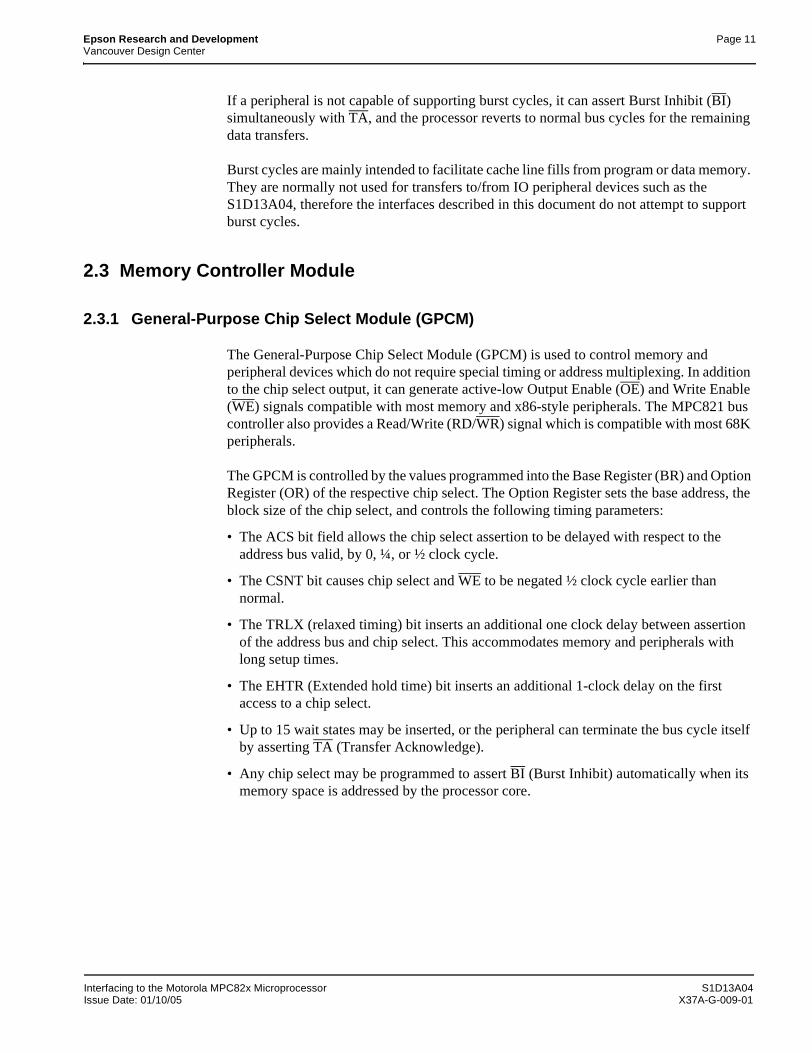
Epson Research and Development Page 11Vancouver Design Center
If a peripheral is not capable of supporting burst cycles, it can assert Burst Inhibit (BI) simultaneously with TA, and the processor reverts to normal bus cycles for the remaining data transfers.
Burst cycles are mainly intended to facilitate cache line fills from program or data memory. They are normally not used for transfers to/from IO peripheral devices such as the S1D13A04, therefore the interfaces described in this document do not attempt to support burst cycles.
2.3 Memory Controller Module
2.3.1 General-Purpose Chip Select Module (GPCM)
The General-Purpose Chip Select Module (GPCM) is used to control memory and peripheral devices which do not require special timing or address multiplexing. In addition to the chip select output, it can generate active-low Output Enable (OE) and Write Enable (WE) signals compatible with most memory and x86-style peripherals. The MPC821 bus controller also provides a Read/Write (RD/WR) signal which is compatible with most 68K peripherals.
The GPCM is controlled by the values programmed into the Base Register (BR) and Option Register (OR) of the respective chip select. The Option Register sets the base address, the block size of the chip select, and controls the following timing parameters:
• The ACS bit field allows the chip select assertion to be delayed with respect to the address bus valid, by 0, ¼, or ½ clock cycle.
• The CSNT bit causes chip select and WE to be negated ½ clock cycle earlier than normal.
• The TRLX (relaxed timing) bit inserts an additional one clock delay between assertion of the address bus and chip select. This accommodates memory and peripherals with long setup times.
• The EHTR (Extended hold time) bit inserts an additional 1-clock delay on the first access to a chip select.
• Up to 15 wait states may be inserted, or the peripheral can terminate the bus cycle itself by asserting TA (Transfer Acknowledge).
• Any chip select may be programmed to assert BI (Burst Inhibit) automatically when its memory space is addressed by the processor core.
Interfacing to the Motorola MPC82x Microprocessor S1D13A04Issue Date: 01/10/05 X37A-G-009-01
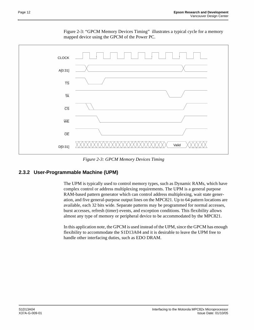
Page 12 Epson Research and DevelopmentVancouver Design Center
Figure 2-3: “GPCM Memory Devices Timing” illustrates a typical cycle for a memory mapped device using the GPCM of the Power PC.
Figure 2-3: GPCM Memory Devices Timing
2.3.2 User-Programmable Machine (UPM)
The UPM is typically used to control memory types, such as Dynamic RAMs, which have complex control or address multiplexing requirements. The UPM is a general purpose RAM-based pattern generator which can control address multiplexing, wait state gener-ation, and five general-purpose output lines on the MPC821. Up to 64 pattern locations are available, each 32 bits wide. Separate patterns may be programmed for normal accesses, burst accesses, refresh (timer) events, and exception conditions. This flexibility allows almost any type of memory or peripheral device to be accommodated by the MPC821.
In this application note, the GPCM is used instead of the UPM, since the GPCM has enough flexibility to accommodate the S1D13A04 and it is desirable to leave the UPM free to handle other interfacing duties, such as EDO DRAM.
A[0:31]
D[0:31]
TS
TA
CLOCK
Valid
CS
WE
OE
S1D13A04 Interfacing to the Motorola MPC82x MicroprocessorX37A-G-009-01 Issue Date: 01/10/05
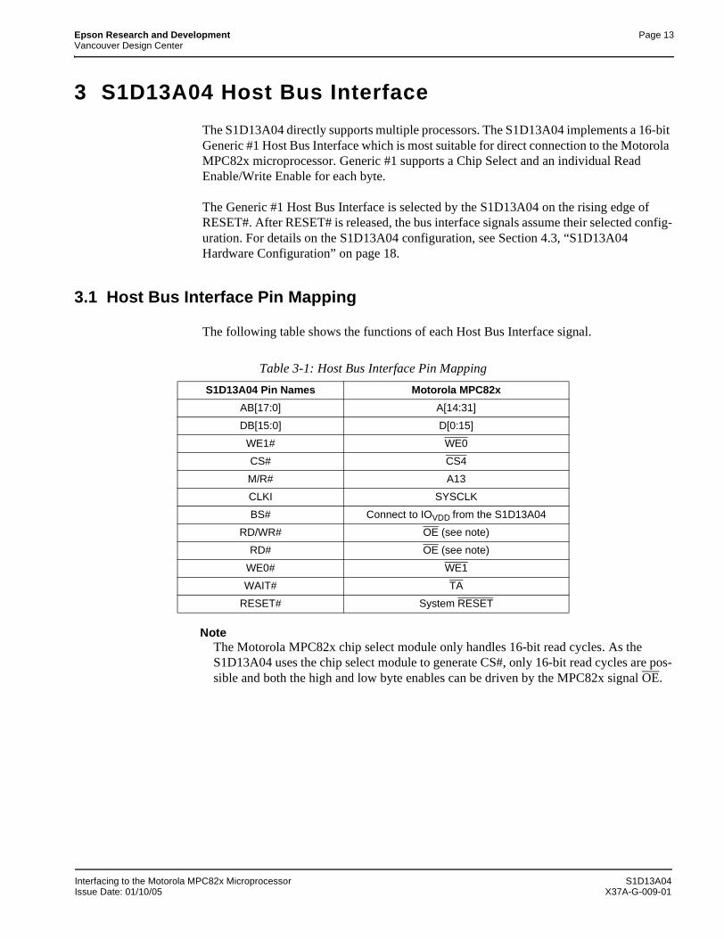
Epson Research and Development Page 13Vancouver Design Center
3 S1D13A04 Host Bus Interface
The S1D13A04 directly supports multiple processors. The S1D13A04 implements a 16-bit Generic #1 Host Bus Interface which is most suitable for direct connection to the Motorola MPC82x microprocessor. Generic #1 supports a Chip Select and an individual Read Enable/Write Enable for each byte.
The Generic #1 Host Bus Interface is selected by the S1D13A04 on the rising edge of RESET#. After RESET# is released, the bus interface signals assume their selected config-uration. For details on the S1D13A04 configuration, see Section 4.3, “S1D13A04 Hardware Configuration” on page 18.
3.1 Host Bus Interface Pin Mapping
The following table shows the functions of each Host Bus Interface signal.
NoteThe Motorola MPC82x chip select module only handles 16-bit read cycles. As the S1D13A04 uses the chip select module to generate CS#, only 16-bit read cycles are pos-sible and both the high and low byte enables can be driven by the MPC82x signal OE.
Table 3-1: Host Bus Interface Pin Mapping
S1D13A04 Pin Names Motorola MPC82x
AB[17:0] A[14:31]
DB[15:0] D[0:15]
WE1# WE0
CS# CS4
M/R# A13
CLKI SYSCLK
BS# Connect to IOVDD from the S1D13A04
RD/WR# OE (see note)
RD# OE (see note)
WE0# WE1
WAIT# TA
RESET# System RESET
Interfacing to the Motorola MPC82x Microprocessor S1D13A04Issue Date: 01/10/05 X37A-G-009-01
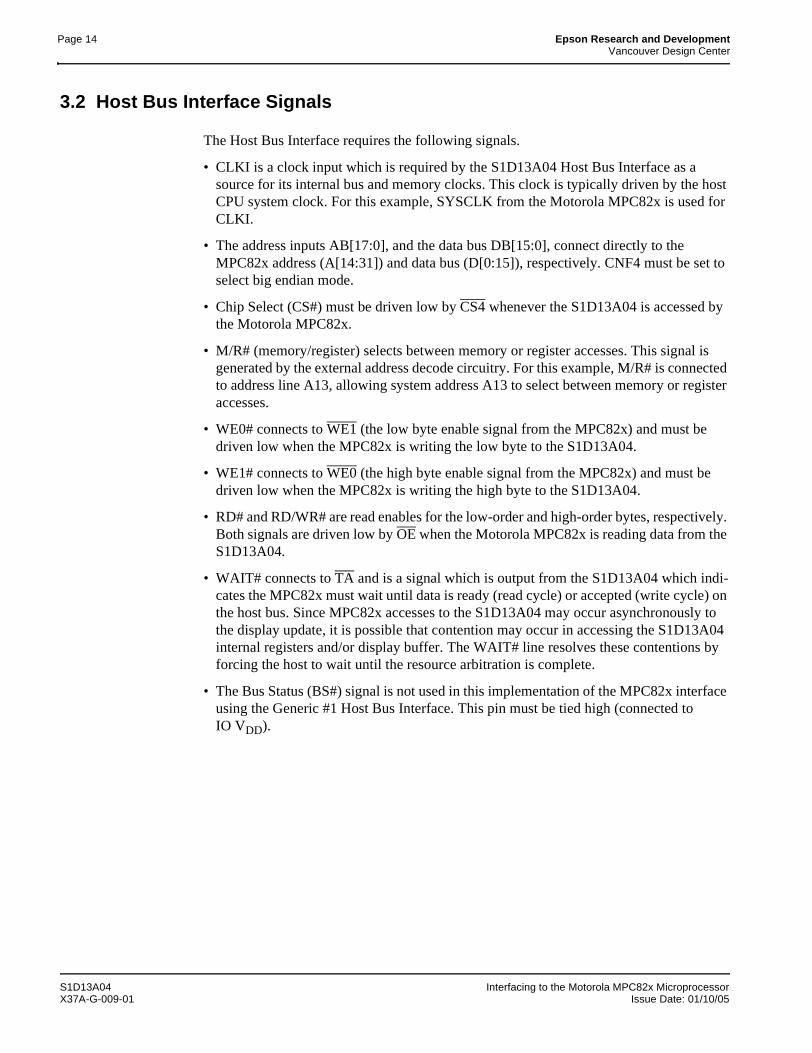
Page 14 Epson Research and DevelopmentVancouver Design Center
3.2 Host Bus Interface Signals
The Host Bus Interface requires the following signals.
• CLKI is a clock input which is required by the S1D13A04 Host Bus Interface as a source for its internal bus and memory clocks. This clock is typically driven by the host CPU system clock. For this example, SYSCLK from the Motorola MPC82x is used for CLKI.
• The address inputs AB[17:0], and the data bus DB[15:0], connect directly to the MPC82x address (A[14:31]) and data bus (D[0:15]), respectively. CNF4 must be set to select big endian mode.
• Chip Select (CS#) must be driven low by CS4 whenever the S1D13A04 is accessed by the Motorola MPC82x.
• M/R# (memory/register) selects between memory or register accesses. This signal is generated by the external address decode circuitry. For this example, M/R# is connected to address line A13, allowing system address A13 to select between memory or register accesses.
• WE0# connects to WE1 (the low byte enable signal from the MPC82x) and must be driven low when the MPC82x is writing the low byte to the S1D13A04.
• WE1# connects to WE0 (the high byte enable signal from the MPC82x) and must be driven low when the MPC82x is writing the high byte to the S1D13A04.
• RD# and RD/WR# are read enables for the low-order and high-order bytes, respectively. Both signals are driven low by OE when the Motorola MPC82x is reading data from the S1D13A04.
• WAIT# connects to TA and is a signal which is output from the S1D13A04 which indi-cates the MPC82x must wait until data is ready (read cycle) or accepted (write cycle) on the host bus. Since MPC82x accesses to the S1D13A04 may occur asynchronously to the display update, it is possible that contention may occur in accessing the S1D13A04 internal registers and/or display buffer. The WAIT# line resolves these contentions by forcing the host to wait until the resource arbitration is complete.
• The Bus Status (BS#) signal is not used in this implementation of the MPC82x interface using the Generic #1 Host Bus Interface. This pin must be tied high (connected toIO VDD).
S1D13A04 Interfacing to the Motorola MPC82x MicroprocessorX37A-G-009-01 Issue Date: 01/10/05
Epson Research and Development Page 15Vancouver Design Center
4 MPC82x to S1D13A04 Interface
4.1 Hardware Description
The interface between the S1D13A04 and the MPC82x requires no external glue logic. The polarity of the WAIT# signal must be selected as active high by connecting CNF5 toIO VDD (see Table 4-2:, “Summary of Power-On/Reset Options,” on page 18).
BS# (bus start) is not used in this implementation and should be tied high (connected toIO VDD).
The following diagram shows a typical implementation of the MPC82x to S1D13A04 interface.
Figure 4-1: Typical Implementation of MPC82x to S1D13A04 Interface
Table 4-1:, “List of Connections from MPC821ADS to S1D13A04” on page 16 shows the connections between the pins and signals of the MPC82x and the S1D13A04.
MPC82x S1D13A04
A[14:31]
D[0:15]
CS4
TA
WE0
WE1
OE
SYSCLK
AB[17:0]
DB[15:0]
CS#
WAIT#
WE1#
WE0#
RD/WR#
RD#
CLKI
RESET#
BS#
System RESET
Note:When connecting the S1D13A04 RESET# pin, the system designer should be aware of all conditions that may reset the S1D13A04 (e.g. CPU reset can be asserted during wake-up from power-down modes, or during debug states).
M/R#A13IO VDD
Interfacing to the Motorola MPC82x Microprocessor S1D13A04Issue Date: 01/10/05 X37A-G-009-01
Page 16 Epson Research and DevelopmentVancouver Design Center
NoteThe interface was designed using a Motorola MPC821 Application DevelopmentSystem (ADS). The ADS board has 5 volt logic connected to the data bus, so theinterface included two 74F245 octal buffers on D[0:15] between the ADS and the S1D13A04. In a true 3 volt system, no buffering is necessary.
4.2 MPC821ADS Evaluation Board Hardware Connections
The following table details the connections between the pins and signals of the MPC821 and the S1D13A04.
Table 4-1: List of Connections from MPC821ADS to S1D13A04
MPC821 Signal Name MPC821ADS Connector and Pin Name S1D13A04 Signal Name
2.0V (see note 1) P9-D24 COREVDD
3.3V P9-A22 IOVDD
A14 (see note 2) P6-C20 AB17
A15 (see note 2) P6-D20 AB16
A16 (see note 2) P6-B24 AB15
A17 (see note 2) P6-C24 AB14
A18 (see note 2) P6-D23 AB13
A19 (see note 2) P6-D22 AB12
A20 (see note 2) P6-D19 AB11
A21 (see note 2) P6-A19 AB10
A22 (see note 2) P6-D28 AB9
A23 (see note 2) P6-A28 AB8
A24 (see note 2) P6-C27 AB7
A25 (see note 2) P6-A26 AB6
A26 (see note 2) P6-C26 AB5
A27 (see note 2) P6-A25 AB4
A28 (see note 2) P6-D26 AB3
A29 (see note 2) P6-B25 AB2
A30 (see note 2) P6-B19 AB1
A31 (see note 2) P6-D17 AB0
D0 (see note 3) P12-A9 D15
D1 (see note 3) P12-C9 D14
D2 (see note 3) P12-D9 D13
D3 (see note 3) P12-A8 D12
D4 (see note 3) P12-B8 D11
D5 (see note 3) P12-D8 D10
D6 (see note 3) P12-B7 D9
D7 (see note 3) P12-C7 D8
D8 (see note 3) P12-A15 D7
D9 (see note 3) P12-C15 D6
S1D13A04 Interfacing to the Motorola MPC82x MicroprocessorX37A-G-009-01 Issue Date: 01/10/05
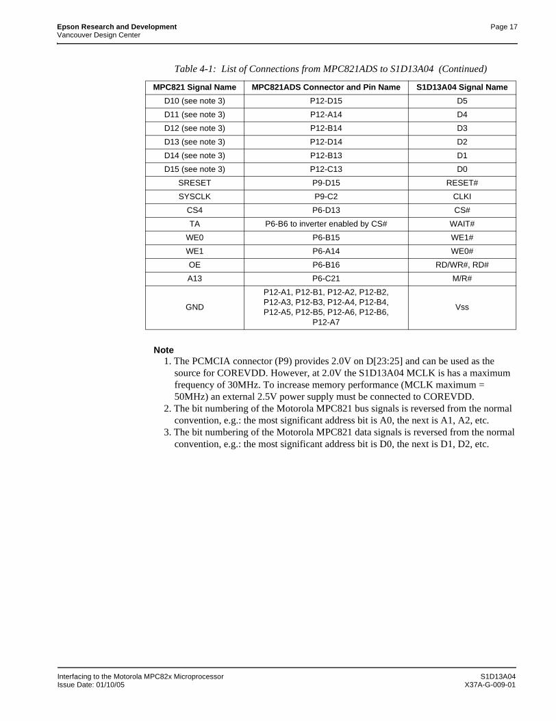
Epson Research and Development Page 17Vancouver Design Center
Note1. The PCMCIA connector (P9) provides 2.0V on D[23:25] and can be used as the
source for COREVDD. However, at 2.0V the S1D13A04 MCLK is has a maximumfrequency of 30MHz. To increase memory performance (MCLK maximum =50MHz) an external 2.5V power supply must be connected to COREVDD.
2. The bit numbering of the Motorola MPC821 bus signals is reversed from the normalconvention, e.g.: the most significant address bit is A0, the next is A1, A2, etc.
3. The bit numbering of the Motorola MPC821 data signals is reversed from the normalconvention, e.g.: the most significant address bit is D0, the next is D1, D2, etc.
D10 (see note 3) P12-D15 D5
D11 (see note 3) P12-A14 D4
D12 (see note 3) P12-B14 D3
D13 (see note 3) P12-D14 D2
D14 (see note 3) P12-B13 D1
D15 (see note 3) P12-C13 D0
SRESET P9-D15 RESET#
SYSCLK P9-C2 CLKI
CS4 P6-D13 CS#
TA P6-B6 to inverter enabled by CS# WAIT#
WE0 P6-B15 WE1#
WE1 P6-A14 WE0#
OE P6-B16 RD/WR#, RD#
A13 P6-C21 M/R#
GND
P12-A1, P12-B1, P12-A2, P12-B2, P12-A3, P12-B3, P12-A4, P12-B4, P12-A5, P12-B5, P12-A6, P12-B6,
P12-A7
Vss
Table 4-1: List of Connections from MPC821ADS to S1D13A04 (Continued)
MPC821 Signal Name MPC821ADS Connector and Pin Name S1D13A04 Signal Name
Interfacing to the Motorola MPC82x Microprocessor S1D13A04Issue Date: 01/10/05 X37A-G-009-01
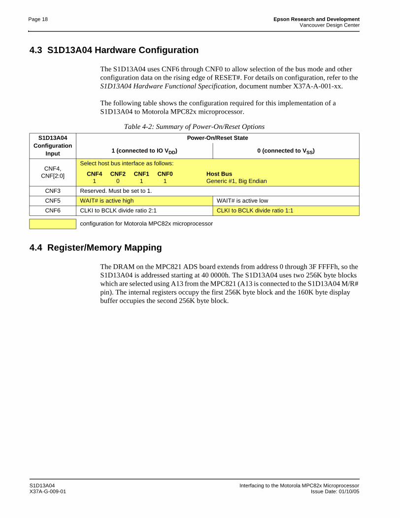
Page 18 Epson Research and DevelopmentVancouver Design Center
4.3 S1D13A04 Hardware Configuration
The S1D13A04 uses CNF6 through CNF0 to allow selection of the bus mode and other configuration data on the rising edge of RESET#. For details on configuration, refer to the S1D13A04 Hardware Functional Specification, document number X37A-A-001-xx.
The following table shows the configuration required for this implementation of a S1D13A04 to Motorola MPC82x microprocessor.
4.4 Register/Memory Mapping
The DRAM on the MPC821 ADS board extends from address 0 through 3F FFFFh, so the S1D13A04 is addressed starting at 40 0000h. The S1D13A04 uses two 256K byte blocks which are selected using A13 from the MPC821 (A13 is connected to the S1D13A04 M/R# pin). The internal registers occupy the first 256K byte block and the 160K byte display buffer occupies the second 256K byte block.
Table 4-2: Summary of Power-On/Reset Options
S1D13A04 Configuration
Input
Power-On/Reset State
1 (connected to IO VDD) 0 (connected to VSS)
CNF4, CNF[2:0]
Select host bus interface as follows:
CNF4 CNF2 CNF1 CNF0 Host Bus1 0 1 1 Generic #1, Big Endian
CNF3 Reserved. Must be set to 1.
CNF5 WAIT# is active high WAIT# is active low
CNF6 CLKI to BCLK divide ratio 2:1 CLKI to BCLK divide ratio 1:1
configuration for Motorola MPC82x microprocessor
S1D13A04 Interfacing to the Motorola MPC82x MicroprocessorX37A-G-009-01 Issue Date: 01/10/05
Epson Research and Development Page 19Vancouver Design Center
4.5 MPC82x Chip Select Configuration
Chip select 4 is used to control the S1D13A04. The following options are selected in the base address register (BR4).
• BA (0:16) = 0000 0000 0100 0000 0 – set starting address of S1D13A04 to 40 0000h
• AT (0:2) = 0 – ignore address type bits.
• PS (0:1) = 1:0 – memory port size is 16 bits
• PARE = 0 – disable parity checking
• WP = 0 – disable write protect
• MS (0:1) = 0:0 – select General Purpose Chip Select module to control this chip select
• V = 1 – set valid bit to enable chip select
The following options were selected in the option register (OR4).
• AM (0:16) = 1111 1111 1100 0000 0 – mask all but upper 10 address bits; S1D13A04 consumes 4M byte of address space
• ATM (0:2) = 0 – ignore address type bits
• CSNT = 0 – normal CS/WE negation
• ACS (0:1) = 1:1 – delay CS assertion by ½ clock cycle from address lines
• BI = 1 – assert Burst Inhibit
• SCY (0:3) = 0 – wait state selection; this field is ignored since external transfer acknowledge is used; see SETA below
• SETA = 1 – the S1D13A04 generates an external transfer acknowledge using the WAIT# line
• TRLX = 0 – normal timing
• EHTR = 0 – normal timing
Interfacing to the Motorola MPC82x Microprocessor S1D13A04Issue Date: 01/10/05 X37A-G-009-01
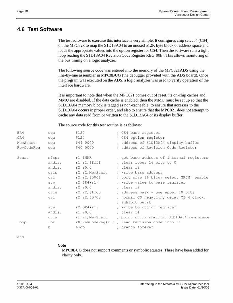
Page 20 Epson Research and DevelopmentVancouver Design Center
4.6 Test Software
The test software to exercise this interface is very simple. It configures chip select 4 (CS4) on the MPC82x to map the S1D13A04 to an unused 512K byte block of address space and loads the appropriate values into the option register for CS4. Then the software runs a tight loop reading the S1D13A04 Revision Code Register REG[00h]. This allows monitoring of the bus timing on a logic analyzer.
The following source code was entered into the memory of the MPC821ADS using the line-by-line assembler in MPC8BUG (the debugger provided with the ADS board). Once the program was executed on the ADS, a logic analyzer was used to verify operation of the interface hardware.
It is important to note that when the MPC821 comes out of reset, its on-chip caches and MMU are disabled. If the data cache is enabled, then the MMU must be set up so that the S1D13A04 memory block is tagged as non-cacheable, to ensure that accesses to the S1D13A04 occurs in proper order, and also to ensure that the MPC821 does not attempt to cache any data read from or written to the S1D13A04 or its display buffer.
The source code for this test routine is as follows:
BR4 equ $120 ; CS4 base registerOR4 equ $124 ; CS4 option registerMemStart equ $44 0000 ; address of S1D13A04 display bufferRevCodeReg equ $40 0000 ; address of Revision Code Register
Start mfspr r1,IMMR ; get base address of internal registersandis. r1,r1,$ffff ; clear lower 16 bits to 0andis. r2,r0,0 ; clear r2oris r2,r2,MemStart ; write base addressori r2,r2,$0801 ; port size 16 bits; select GPCM; enablestw r2,BR4(r1) ; write value to base registerandis. r2,r0,0 ; clear r2oris r2,r2,$ffc0 ; address mask – use upper 10 bitsori r2,r2,$0708 ; normal CS negation; delay CS ½ clock;
; inhibit burststw r2,OR4(r1) ; write to option registerandis. r1,r0,0 ; clear r1oris r1,r1,MemStart ; point r1 to start of S1D13A04 mem space
Loop lbz r0,RevCodeReg(r1) ; read revision code into r1b Loop ; branch forever
end
NoteMPC8BUG does not support comments or symbolic equates. These have been added for clarity only.
S1D13A04 Interfacing to the Motorola MPC82x MicroprocessorX37A-G-009-01 Issue Date: 01/10/05
Epson Research and Development Page 21Vancouver Design Center
5 Software
Test utilities and display drivers are available for the S1D13A04. Full source code is available for both the test utilities and the drivers.
The test utilities are configurable for different panel types using a program called 13A04CFG (see document number X37A-B-001-xx), or by directly modifying the source. The display drivers can be customized by the OEM for different panel types, resolutions and color depths only by modifying the source.
The S1D13A04 test utilities and display drivers are available from your sales support contact (see Section 7, “Sales and Technical Support”) or www.erd.epson.com.
Interfacing to the Motorola MPC82x Microprocessor S1D13A04Issue Date: 01/10/05 X37A-G-009-01
Page 22 Epson Research and DevelopmentVancouver Design Center
6 References
6.1 Documents
• Motorola Inc., Power PC MPC821 Portable Systems Microprocessor User’s Manual, Motorola Publication no. MPC821UM/; available on the Internet at http://www.mot.com/SPS/ADC/pps/_subpgs/_documentation/821/821UM.html.
• Epson Research and Development, Inc., S1D13A04 Hardware Functional Specification, Document Number X37A-A-001-xx.
• Epson Research and Development, Inc., S5U13A04B00C Rev. 1.0 Evaluation Board User Manual, Document Number X37A-G-004-xx.
• Epson Research and Development, Inc., S1D13A04 Programming Notes and Examples, Document Number X37A-G-003-xx.
6.2 Document Sources
• Motorola Inc. Literature Distribution Center: (800) 441-2447.
• Motorola Inc. Website: www.mot.com.
• Epson Research and Development Website: www.erd.epson.com.
S1D13A04 Interfacing to the Motorola MPC82x MicroprocessorX37A-G-009-01 Issue Date: 01/10/05
Epson Research and Development Page 23Vancouver Design Center
7 Sales and Technical Support
7.1 EPSON LCD/USB Companion Chips (S1D13A04)
7.2 Motorola MPC821 Processor
• Motorola Design Line, (800) 521-6274.
• Local Motorola sales office or authorized distributor.
JapanSeiko Epson CorporationElectronic Devices Marketing Division421-8, Hino, Hino-shiTokyo 191-8501, JapanTel: 042-587-5812Fax: 042-587-5564http://www.epson.co.jp
Hong KongEpson Hong Kong Ltd.20/F., Harbour Centre25 Harbour RoadWanchai, Hong KongTel: 2585-4600Fax: 2827-4346http://www.epson.com.hk/
TaiwanEpson Taiwan Technology & Trading Ltd.10F, No. 287Nanking East RoadSec. 3, Taipei, TaiwanTel: 02-2717-7360Fax: 02-2712-9164http://www.epson.com.tw/
SingaporeEpson Singapore Pte., Ltd.No. 1Temasek Avenue #36-00Millenia TowerSingapore, 039192Tel: 337-7911Fax: 334-2716http://www.epson.com.sg/
EuropeEpson Europe Electronics GmbHRiesstrasse 1580992 Munich, GermanyTel: 089-14005-0Fax: 089-14005-110http://www.epson-electronics.de
North AmericaEpson Electronics America, Inc.150 River Oaks ParkwaySan Jose, CA 95134, USATel: (408) 922-0200Fax: (408) 922-0238http://www.eea.epson.com
Interfacing to the Motorola MPC82x Microprocessor S1D13A04Issue Date: 01/10/05 X37A-G-009-01

Page 24 Epson Research and DevelopmentVancouver Design Center
THIS PAGE LEFT BLANK
S1D13A04 Interfacing to the Motorola MPC82x MicroprocessorX37A-G-009-01 Issue Date: 01/10/05
S1D13A04 LCD/USB Companion Chip
Interfacing to the Motorola MCF5307 "ColdFire" Microprocessor
Document Number: X37A-G-010-01
Copyright © 2001 Epson Research and Development, Inc. All Rights Reserved.
Information in this document is subject to change without notice. You may download and use this document, but only for your own use inevaluating Seiko Epson/EPSON products. You may not modify the document. Epson Research and Development, Inc. disclaims anyrepresentation that the contents of this document are accurate or current. The Programs/Technologies described in this document may contain material protected under U.S. and/or International Patent laws.
EPSON is a registered trademark of Seiko Epson Corporation. All Trademarks are the property of their respective owners.

Page 2 Epson Research and DevelopmentVancouver Design Center
THIS PAGE LEFT BLANK
S1D13A04 Interfacing to the Motorola MCF5307 "ColdFire" MicroprocessorX37A-G-010-01 Issue Date: 01/10/12
Epson Research and Development Page 3Vancouver Design Center
Table of Contents
1 Introduction . . . . . . . . . . . . . . . . . . . . . . . . . . . . . . . . . . . . . . . . 7
2 Interfacing to the MCF5307 . . . . . . . . . . . . . . . . . . . . . . . . . . . . . . . 82.1 The MCF5307 System Bus . . . . . . . . . . . . . . . . . . . . . . . . . . 8
2.1.1 Overview . . . . . . . . . . . . . . . . . . . . . . . . . . . . . . . . . . . . . . . . 8
2.1.2 Normal (Non-Burst) Bus Transactions . . . . . . . . . . . . . . . . . . . . . . . . . 8
2.1.3 Burst Cycles . . . . . . . . . . . . . . . . . . . . . . . . . . . . . . . . . . . . . . . 9
2.2 Chip-Select Module . . . . . . . . . . . . . . . . . . . . . . . . . . . . 10
3 S1D13A04 Host Bus Interface . . . . . . . . . . . . . . . . . . . . . . . . . . . . . 113.1 Host Bus Interface Pin Mapping . . . . . . . . . . . . . . . . . . . . . . . 11
3.2 Host Bus Interface Signals . . . . . . . . . . . . . . . . . . . . . . . . . 12
4 MCF5307 To S1D13A04 Interface . . . . . . . . . . . . . . . . . . . . . . . . . . . 134.1 Hardware Description . . . . . . . . . . . . . . . . . . . . . . . . . . . 13
4.2 S1D13A04 Hardware Configuration . . . . . . . . . . . . . . . . . . . . . 14
4.3 Register/Memory Mapping . . . . . . . . . . . . . . . . . . . . . . . . . 15
4.4 MCF5307 Chip Select Configuration . . . . . . . . . . . . . . . . . . . . . 15
5 Software . . . . . . . . . . . . . . . . . . . . . . . . . . . . . . . . . . . . . . . . . 16
6 References . . . . . . . . . . . . . . . . . . . . . . . . . . . . . . . . . . . . . . . 176.1 Documents . . . . . . . . . . . . . . . . . . . . . . . . . . . . . . . 17
6.2 Document Sources . . . . . . . . . . . . . . . . . . . . . . . . . . . . 17
7 Sales and Technical Support . . . . . . . . . . . . . . . . . . . . . . . . . . . . . 187.1 EPSON LCD/USB Companion Chips (S1D13A04) . . . . . . . . . . . . . . . 18
7.2 Motorola MCF5307 Processor . . . . . . . . . . . . . . . . . . . . . . . . 18
Interfacing to the Motorola MCF5307 "ColdFire" Microprocessor S1D13A04Issue Date: 01/10/12 X37A-G-010-01

Page 4 Epson Research and DevelopmentVancouver Design Center
THIS PAGE LEFT BLANK
S1D13A04 Interfacing to the Motorola MCF5307 "ColdFire" MicroprocessorX37A-G-010-01 Issue Date: 01/10/12
Epson Research and Development Page 5Vancouver Design Center
List of Tables
Table 3-1: Host Bus Interface Pin Mapping . . . . . . . . . . . . . . . . . . . . . . . . . . . . . . 11
Table 4-1: Summary of Power-On/Reset Options . . . . . . . . . . . . . . . . . . . . . . . . . . 14
List of Figures
Figure 2-1: MCF5307 Memory Read Cycle . . . . . . . . . . . . . . . . . . . . . . . . . . . . . . 9
Figure 2-2: MCF5307 Memory Write Cycle . . . . . . . . . . . . . . . . . . . . . . . . . . . . . . 9
Figure 2-3: Chip Select Module Outputs Timing . . . . . . . . . . . . . . . . . . . . . . . . . . . 10
Figure 4-1: Typical Implementation of MCF5307 to S1D13A04 Interface . . . . . . . . . . . . . . 13
Interfacing to the Motorola MCF5307 "ColdFire" Microprocessor S1D13A04Issue Date: 01/10/12 X37A-G-010-01

Page 6 Epson Research and DevelopmentVancouver Design Center
THIS PAGE LEFT BLANK
S1D13A04 Interfacing to the Motorola MCF5307 "ColdFire" MicroprocessorX37A-G-010-01 Issue Date: 01/10/12

Epson Research and Development Page 7Vancouver Design Center
1 Introduction
This application note describes the hardware and software environment required to interface the S1D13A04 LCD/USB Companion Chip and the Motorola MCF5307 “Coldfire” Processor.
The designs described in this document are presented only as examples of how such inter-faces might be implemented. This application note is updated as appropriate. Please check the Epson Research and Development website at www.erd.epson.com for the latest revision of this document before beginning any development.
We appreciate your comments on our documentation. Please contact us via email at [email protected].
Interfacing to the Motorola MCF5307 "ColdFire" Microprocessor S1D13A04Issue Date: 01/10/12 X37A-G-010-01
Page 8 Epson Research and DevelopmentVancouver Design Center
2 Interfacing to the MCF5307
2.1 The MCF5307 System Bus
The MCF5200/5300 family of processors feature a high-speed synchronous system bus typical of modern microprocessors. This section is an overview of the operation of the CPU bus in order to establish interface requirements.
2.1.1 Overview
The MCF5307 microprocessor family uses a synchronous address and data bus, very similar in architecture to the MC68040 and MPC8xx. All outputs and inputs are timed with respect to a square-wave reference clock called BCLK0 (Master Clock). This clock runs at a software-selectable divisor rate from the machine cycle speed of the CPU core (typically 20 to 33 MHz). Both the address and the data bus are 32 bits in width. All IO accesses are memory-mapped; there is no separate IO space in the Coldfire architecture.
The bus can support two types of cycles, normal and burst. Burst memory cycles are used to fill on-chip cache memories, and for certain on-chip DMA operations. Normal cycles are used for all other data transfers.
2.1.2 Normal (Non-Burst) Bus Transactions
A data transfer is initiated by the bus master by placing the memory address on address lines A31 through A0 and driving TS (Transfer Start) low for one clock cycle. Several control signals are also provided with the memory address:
• SIZ[1:0] (Transfer Size) — indicates whether the bus cycle is 8, 16, or 32-bit.
• R/W — set high for read cycles and low for write cycles.
• TT[1:0] (Transfer Type Signals) — provides more detail on the type of transfer being attempted.
• TIP (Transfer In Progress) — asserts whenever a bus cycle is active.
When the peripheral device being accessed has completed the bus transfer, it asserts TA (Transfer Acknowledge) for one clock cycle to complete the bus transaction. Once TA has been asserted, the MCF5307 will not start another bus cycle until TA has been de-asserted. The minimum length of a bus transaction is two bus clocks.
S1D13A04 Interfacing to the Motorola MCF5307 "ColdFire" MicroprocessorX37A-G-010-01 Issue Date: 01/10/12
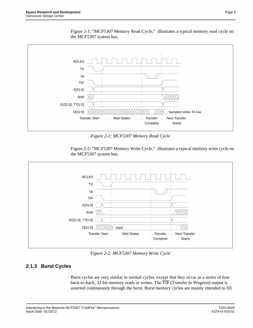
Epson Research and Development Page 9Vancouver Design Center
Figure 2-1: “MCF5307 Memory Read Cycle,” illustrates a typical memory read cycle on the MCF5307 system bus.
Figure 2-1: MCF5307 Memory Read Cycle
Figure 2-2: “MCF5307 Memory Write Cycle,” illustrates a typical memory write cycle on the MCF5307 system bus.
Figure 2-2: MCF5307 Memory Write Cycle
2.1.3 Burst Cycles
Burst cycles are very similar to normal cycles, except that they occur as a series of four back-to-back, 32-bit memory reads or writes. The TIP (Transfer In Progress) output is asserted continuously through the burst. Burst memory cycles are mainly intended to fill
A[31:0]
D[31:0]
SIZ[1:0], TT[1:0]
TS
TA
BCLK0
Wait StatesTransfer Start Transfer Next Transfer
Sampled when TA low
R/W
Complete Starts
TIP
A[31:0]
D[31:0]
SIZ[1:0], TT[1:0]
TS
TA
BCLK0
Wait StatesTransfer Start
R/W
Valid
Transfer Next Transfer
Complete Starts
TIP
Interfacing to the Motorola MCF5307 "ColdFire" Microprocessor S1D13A04Issue Date: 01/10/12 X37A-G-010-01
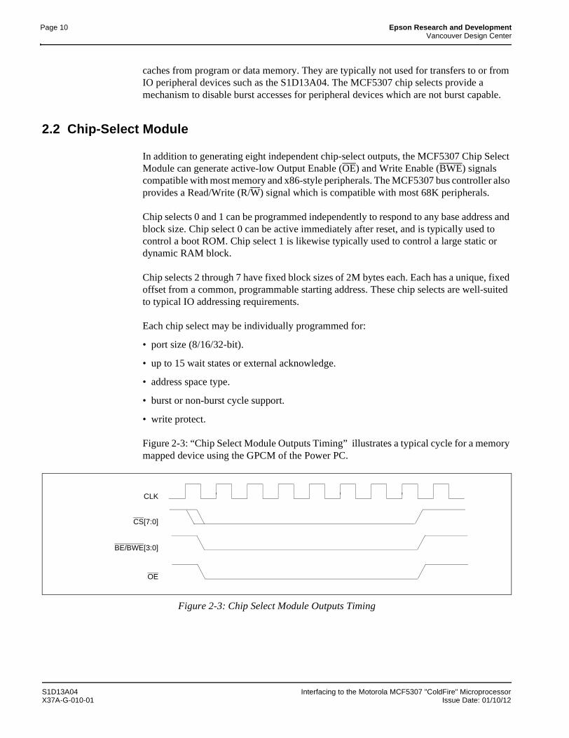
Page 10 Epson Research and DevelopmentVancouver Design Center
caches from program or data memory. They are typically not used for transfers to or from IO peripheral devices such as the S1D13A04. The MCF5307 chip selects provide a mechanism to disable burst accesses for peripheral devices which are not burst capable.
2.2 Chip-Select Module
In addition to generating eight independent chip-select outputs, the MCF5307 Chip Select Module can generate active-low Output Enable (OE) and Write Enable (BWE) signals compatible with most memory and x86-style peripherals. The MCF5307 bus controller also provides a Read/Write (R/W) signal which is compatible with most 68K peripherals.
Chip selects 0 and 1 can be programmed independently to respond to any base address and block size. Chip select 0 can be active immediately after reset, and is typically used to control a boot ROM. Chip select 1 is likewise typically used to control a large static or dynamic RAM block.
Chip selects 2 through 7 have fixed block sizes of 2M bytes each. Each has a unique, fixed offset from a common, programmable starting address. These chip selects are well-suited to typical IO addressing requirements.
Each chip select may be individually programmed for:
• port size (8/16/32-bit).
• up to 15 wait states or external acknowledge.
• address space type.
• burst or non-burst cycle support.
• write protect.
Figure 2-3: “Chip Select Module Outputs Timing” illustrates a typical cycle for a memory mapped device using the GPCM of the Power PC.
Figure 2-3: Chip Select Module Outputs Timing
CLK
CS[7:0]
BE/BWE[3:0]
OE
S1D13A04 Interfacing to the Motorola MCF5307 "ColdFire" MicroprocessorX37A-G-010-01 Issue Date: 01/10/12
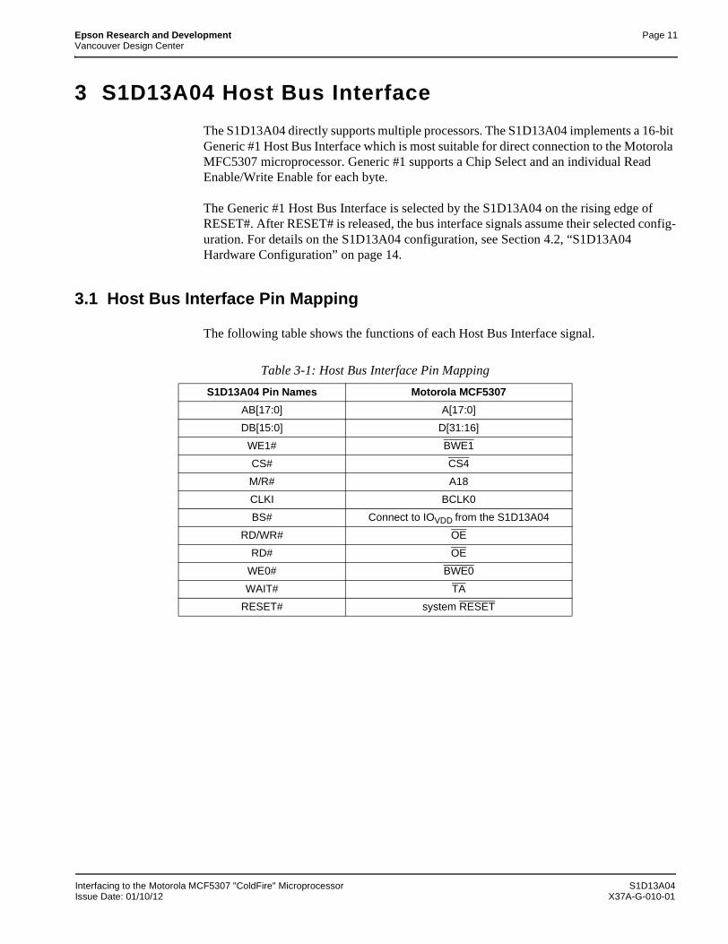
Epson Research and Development Page 11Vancouver Design Center
3 S1D13A04 Host Bus Interface
The S1D13A04 directly supports multiple processors. The S1D13A04 implements a 16-bit Generic #1 Host Bus Interface which is most suitable for direct connection to the Motorola MFC5307 microprocessor. Generic #1 supports a Chip Select and an individual Read Enable/Write Enable for each byte.
The Generic #1 Host Bus Interface is selected by the S1D13A04 on the rising edge of RESET#. After RESET# is released, the bus interface signals assume their selected config-uration. For details on the S1D13A04 configuration, see Section 4.2, “S1D13A04 Hardware Configuration” on page 14.
3.1 Host Bus Interface Pin Mapping
The following table shows the functions of each Host Bus Interface signal.
Table 3-1: Host Bus Interface Pin Mapping
S1D13A04 Pin Names Motorola MCF5307
AB[17:0] A[17:0]
DB[15:0] D[31:16]
WE1# BWE1
CS# CS4
M/R# A18
CLKI BCLK0
BS# Connect to IOVDD from the S1D13A04
RD/WR# OE
RD# OE
WE0# BWE0
WAIT# TA
RESET# system RESET
Interfacing to the Motorola MCF5307 "ColdFire" Microprocessor S1D13A04Issue Date: 01/10/12 X37A-G-010-01
Page 12 Epson Research and DevelopmentVancouver Design Center
3.2 Host Bus Interface Signals
The Host Bus Interface requires the following signals.
• CLKI is a clock input which is required by the S1D13A04 Host Bus Interface as a source for its internal bus and memory clocks. This clock is typically driven by the host CPU system clock. For this example, BCLK0 from the Motorola MCF5307 is used for CLKI.
• The address inputs AB[17:0] connect directly to the MCF5307 address bus (A[17:0]).
• DB[7:0] connects D[23:16] (the MCF5307 low order byte). DB[15:8] connects to D[31:24] (the MCF5307 high order byte). CNF4 must be set to select big endian mode.
• Chip Select (CS#) must be driven low by CS4 whenever the S1D13A04 is accessed by the Motorola MCF5307.
• M/R# (memory/register) selects between memory or register accesses. This signal is generated by the external address decode circuitry. For this example, M/R# is connected to address line A18, allowing system address A18 to select between memory or register accesses.
• WE0# connects to BWE0 (the low byte enable signal from the MCF5307) and must be driven low when the MCF5307 is writing the low byte to the S1D13A04.
• WE1# connects to BWE1 (the high byte enable signal from the MCF5307) and must be driven low when the MCF5307 is writing the high byte to the S1D13A04.
• RD# and RD/WR# are read enables for the low-order and high-order bytes, respectively. Both signals are driven low by OE when the Motorola MCF5307 is reading data from the S1D13A04.
• WAIT# connects to TA and is a signal which is output from the S1D13A04 that indi-cates the host CPU must wait until data is ready (read cycle) or accepted (write cycle) on the host bus. Since host CPU accesses to the S1D13A04 may occur asynchronously to the display update, it is possible that contention may occur in accessing the S1D13A04 internal registers and/or refresh memory. The WAIT# line resolves these contentions by forcing the host to wait until the resource arbitration is complete. This signal is active low and may need to be inverted if the host CPU wait state signal is active high.
• The Bus Status (BS#) signal is not used in the bus interface for Generic #1 mode and must be tied high to IO VDD.
S1D13A04 Interfacing to the Motorola MCF5307 "ColdFire" MicroprocessorX37A-G-010-01 Issue Date: 01/10/12
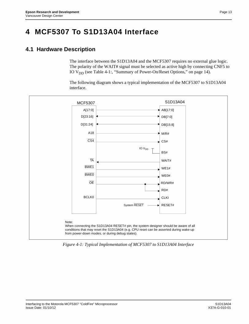
Epson Research and Development Page 13Vancouver Design Center
4 MCF5307 To S1D13A04 Interface
4.1 Hardware Description
The interface between the S1D13A04 and the MCF5307 requires no external glue logic. The polarity of the WAIT# signal must be selected as active high by connecting CNF5 to IO VDD (see Table 4-1:, “Summary of Power-On/Reset Options,” on page 14).
The following diagram shows a typical implementation of the MCF5307 to S1D13A04 interface.
Figure 4-1: Typical Implementation of MCF5307 to S1D13A04 Interface
MCF5307 S1D13A04
A[17:0]
D[23:16]
CS4
TA
BWE1
BWE0
OE
BCLK0
AB[17:0]
DB[7:0]
CS#
WAIT#
WE1#
WE0#
RD/WR#
RD#
CLKI
RESET#
BS#
System RESET
Note:When connecting the S1D13A04 RESET# pin, the system designer should be aware of all conditions that may reset the S1D13A04 (e.g. CPU reset can be asserted during wake-up from power-down modes, or during debug states).
M/R#A18
IO VDD
D[31:24] DB[15:8]
Interfacing to the Motorola MCF5307 "ColdFire" Microprocessor S1D13A04Issue Date: 01/10/12 X37A-G-010-01
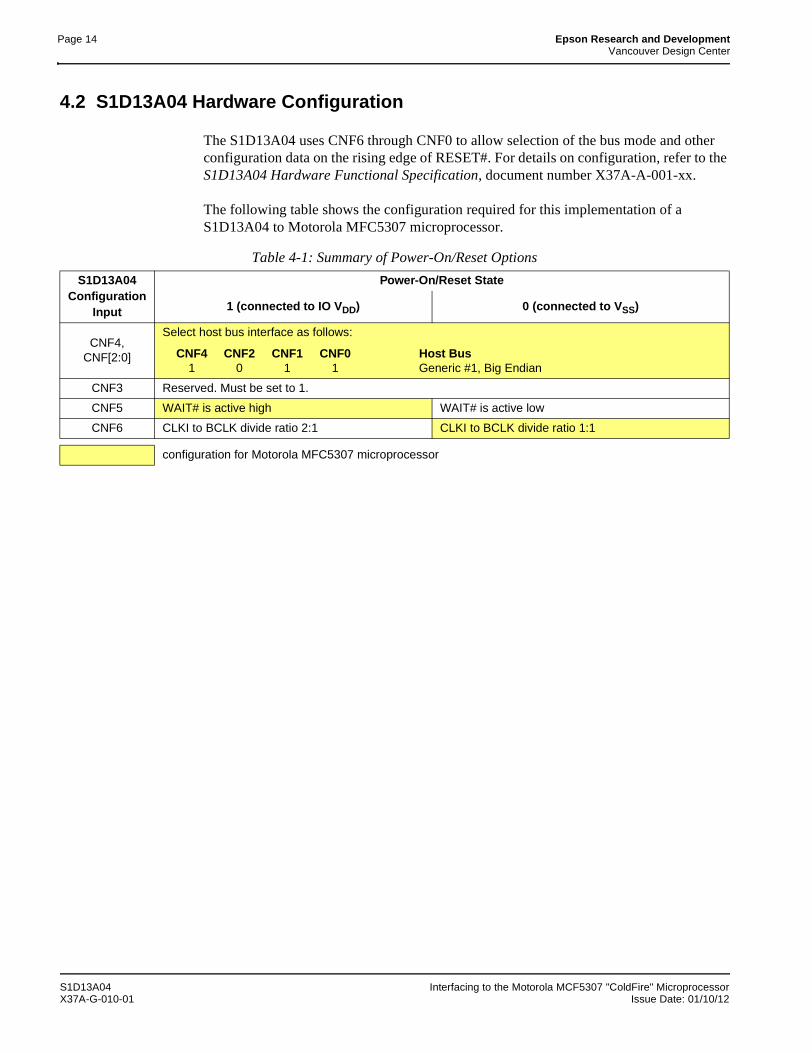
Page 14 Epson Research and DevelopmentVancouver Design Center
4.2 S1D13A04 Hardware Configuration
The S1D13A04 uses CNF6 through CNF0 to allow selection of the bus mode and other configuration data on the rising edge of RESET#. For details on configuration, refer to the S1D13A04 Hardware Functional Specification, document number X37A-A-001-xx.
The following table shows the configuration required for this implementation of a S1D13A04 to Motorola MFC5307 microprocessor.
Table 4-1: Summary of Power-On/Reset Options
S1D13A04 Configuration
Input
Power-On/Reset State
1 (connected to IO VDD) 0 (connected to VSS)
CNF4, CNF[2:0]
Select host bus interface as follows:
CNF4 CNF2 CNF1 CNF0 Host Bus1 0 1 1 Generic #1, Big Endian
CNF3 Reserved. Must be set to 1.
CNF5 WAIT# is active high WAIT# is active low
CNF6 CLKI to BCLK divide ratio 2:1 CLKI to BCLK divide ratio 1:1
configuration for Motorola MFC5307 microprocessor
S1D13A04 Interfacing to the Motorola MCF5307 "ColdFire" MicroprocessorX37A-G-010-01 Issue Date: 01/10/12
Epson Research and Development Page 15Vancouver Design Center
4.3 Register/Memory Mapping
The S1D13A04 uses two 256K byte blocks which are selected using A18 from the MCF5307 (A18 is connected to the S1D13A04 M/R# pin). The internal registers occupy the first 256K bytes block and the 160K byte display buffer occupies the second 256K byte block. These two blocks of memory are aliased over the entire 2M byte space.
NoteIf aliasing is not desirable, the upper addresses must be fully decoded.
4.4 MCF5307 Chip Select Configuration
Chip Selects 0 and 1 have programmable block sizes from 64K bytes through 2G bytes. However, these chip selects would normally be needed to control system RAM and ROM. Therefore, one of the IO chip selects CS2 through CS7 is required to address the entire address space of the S1D13A04. These IO chip selects have a fixed, 2M byte block size. In the example interface, chip select 4 is used to control the S1D13A04. The CSBAR register should be set to the upper 8 bits of the desired base address.
The following options should be selected in the chip select mask registers (CSMR4/5).
• WP = 0 – disable write protect
• AM = 0 - enable alternate bus master access to the S1D13A04
• C/I = 1 - disable CPU space access to the S1D13A04
• SC = 1 - disable Supervisor Code space access to the S1D13A04
• SD = 0 - enable Supervisor Data space access to the S1D13A04
• UC = 1 - disable User Code space access to the S1D13A04
• UD = 0 - enable User Data space access to the S1D13A04
• V = 1 - global enable (“Valid”) for the chip select
The following options should be selected in the chip select control registers (CSCR4/5).
• WS0-3 = 0 - no internal wait state setting
• AA = 0 - no automatic acknowledgment
• PS (1:0) = 1:0 – memory port size is 16 bits
• BEM = 0 – Byte enable/write enable active on writes only
• BSTR = 0 – disable burst reads
• BSTW = 0 – disable burst writes
Interfacing to the Motorola MCF5307 "ColdFire" Microprocessor S1D13A04Issue Date: 01/10/12 X37A-G-010-01
Page 16 Epson Research and DevelopmentVancouver Design Center
5 Software
Test utilities and display drivers are available for the S1D13A04. Full source code is available for both the test utilities and the drivers.
The test utilities are configurable for different panel types using a program called 13A04CFG (see document number X37A-B-001-xx), or by directly modifying the source. The display drivers can be customized by the OEM for different panel types, resolutions and color depths only by modifying the source.
The S1D13A04 test utilities and display drivers are available from your sales support contact (see Section 7, “Sales and Technical Support”) or www.erd.epson.com.
S1D13A04 Interfacing to the Motorola MCF5307 "ColdFire" MicroprocessorX37A-G-010-01 Issue Date: 01/10/12
Epson Research and Development Page 17Vancouver Design Center
6 References
6.1 Documents
• Motorola Inc., MCF5307 ColdFire® Integrated Microprocessor User’s Manual, Motorola Publication no. MCF5307UM; available on the Internet at http://www.mot.com/SPS/HPESD/prod/coldfire/5307UM.html.
• Epson Research and Development, Inc., S1D13A04 Hardware Functional Specification, document number X37A-A-001-xx.
• Epson Research and Development, Inc., S5U13A04B00C Rev. 1.0 Evaluation Board User Manual, document number X37A-G-004-xx.
• Epson Research and Development, Inc., S1D13A04 Programming Notes and Examples, document number X37A-G-003-xx.
6.2 Document Sources
• Motorola Inc.: Motorola Literature Distribution Center, (800) 441-2447.
• Motorola Inc. Website: www.mot.com.
• Epson Research and Development Website: www.erd.epson.com.
Interfacing to the Motorola MCF5307 "ColdFire" Microprocessor S1D13A04Issue Date: 01/10/12 X37A-G-010-01
Page 18 Epson Research and DevelopmentVancouver Design Center
7 Sales and Technical Support
7.1 EPSON LCD/USB Companion Chips (S1D13A04)
7.2 Motorola MCF5307 Processor
• Motorola Design Line, (800) 521-6274.
• Local Motorola sales office or authorized distributor.
JapanSeiko Epson CorporationElectronic Devices Marketing Division421-8, Hino, Hino-shiTokyo 191-8501, JapanTel: 042-587-5812Fax: 042-587-5564http://www.epson.co.jp
Hong KongEpson Hong Kong Ltd.20/F., Harbour Centre25 Harbour RoadWanchai, Hong KongTel: 2585-4600Fax: 2827-4346http://www.epson.com.hk/
TaiwanEpson Taiwan Technology & Trading Ltd.10F, No. 287Nanking East RoadSec. 3, Taipei, TaiwanTel: 02-2717-7360Fax: 02-2712-9164http://www.epson.com.tw/
SingaporeEpson Singapore Pte., Ltd.No. 1Temasek Avenue #36-00Millenia TowerSingapore, 039192Tel: 337-7911Fax: 334-2716http://www.epson.com.sg/
EuropeEpson Europe Electronics GmbHRiesstrasse 1580992 Munich, GermanyTel: 089-14005-0Fax: 089-14005-110http://www.epson-electronics.de
North AmericaEpson Electronics America, Inc.150 River Oaks ParkwaySan Jose, CA 95134, USATel: (408) 922-0200Fax: (408) 922-0238http://www.eea.epson.com
S1D13A04 Interfacing to the Motorola MCF5307 "ColdFire" MicroprocessorX37A-G-010-01 Issue Date: 01/10/12

S1D13A04 LCD/USB Companion Chip
Connecting to the Sharp HR-TFT Panels
Document Number: X37A-G-011-01
Copyright © 2001 Epson Research and Development, Inc. All Rights Reserved.
Information in this document is subject to change without notice. You may download and use this document, but only for your own use inevaluating Seiko Epson/EPSON products. You may not modify the document. Epson Research and Development, Inc. disclaims anyrepresentation that the contents of this document are accurate or current. The Programs/Technologies described in this document may contain material protected under U.S. and/or International Patent laws.
EPSON is a registered trademark of Seiko Epson Corporation. All other trademarks are the property of their respective owners.

Page 2 Epson Research and DevelopmentVancouver Design Center
THIS PAGE LEFT BLANK
S1D13A04 Connecting to the Sharp HR-TFT PanelsX37A-G-011-01 Issue Date: 01/10/12
Epson Research and Development Page 3Vancouver Design Center
Table of Contents
1 Introduction . . . . . . . . . . . . . . . . . . . . . . . . . . . . . . . . . . . . . . . . 7
2 Connecting to the Sharp LQ039Q2DS01 HR-TFT . . . . . . . . . . . . . . . . . . . . 82.1 External Power Supplies . . . . . . . . . . . . . . . . . . . . . . . . . . . 8
2.1.1 Gray Scale Voltages for Gamma Correction . . . . . . . . . . . . . . . . . . . . . . 8
2.1.2 Digital/Analog Power Supplies . . . . . . . . . . . . . . . . . . . . . . . . . . . . . 9
2.1.3 DC Gate Driver Power Supplies . . . . . . . . . . . . . . . . . . . . . . . . . . . . 9
2.1.4 AC Gate Driver Power Supplies . . . . . . . . . . . . . . . . . . . . . . . . . . . 10
2.2 HR-TFT MOD Signal . . . . . . . . . . . . . . . . . . . . . . . . . . . 11
2.3 S1D13A04 to LQ039Q2DS01 Pin Mapping . . . . . . . . . . . . . . . . . . 12
3 Connecting to the Sharp LQ031B1DDxx HR-TFT . . . . . . . . . . . . . . . . . . . 143.1 External Power Supplies . . . . . . . . . . . . . . . . . . . . . . . . . . 14
3.1.1 Gray Scale Voltages for Gamma Correction . . . . . . . . . . . . . . . . . . . . . 14
3.1.2 Digital/Analog Power Supplies . . . . . . . . . . . . . . . . . . . . . . . . . . . . 15
3.1.3 DC Gate Driver Power Supplies . . . . . . . . . . . . . . . . . . . . . . . . . . . 15
3.1.4 AC Gate Driver Power Supplies . . . . . . . . . . . . . . . . . . . . . . . . . . . 15
3.2 HR-TFT MOD Signal . . . . . . . . . . . . . . . . . . . . . . . . . . . 15
3.3 S1D13A04 to LQ031B1DDxx Pin Mapping . . . . . . . . . . . . . . . . . . 16
4 Test Software . . . . . . . . . . . . . . . . . . . . . . . . . . . . . . . . . . . . . . 18
5 References . . . . . . . . . . . . . . . . . . . . . . . . . . . . . . . . . . . . . . . 195.1 Documents . . . . . . . . . . . . . . . . . . . . . . . . . . . . . . . 19
5.2 Document Sources . . . . . . . . . . . . . . . . . . . . . . . . . . . . 19
6 Technical Support . . . . . . . . . . . . . . . . . . . . . . . . . . . . . . . . . . . 206.1 EPSON LCD/USB Companion Chips (S1D13A04) . . . . . . . . . . . . . . . 20
6.2 Sharp HR-TFT Panel . . . . . . . . . . . . . . . . . . . . . . . . . . . 20
Connecting to the Sharp HR-TFT Panels S1D13A04Issue Date: 01/10/12 X37A-G-011-01

Page 4 Epson Research and DevelopmentVancouver Design Center
THIS PAGE LEFT BLANK
S1D13A04 Connecting to the Sharp HR-TFT PanelsX37A-G-011-01 Issue Date: 01/10/12
Epson Research and Development Page 5Vancouver Design Center
List of Tables
Table 2-1: HR-TFT Power-On/Off Sequence Timing . . . . . . . . . . . . . . . . . . . . . . . . . 11
Table 2-2: S1D13A04 to LQ039Q2DS01 Pin Mapping . . . . . . . . . . . . . . . . . . . . . . . . 12
Table 3-1: S1D13A04 to LQ031B1DDxx Pin Mapping. . . . . . . . . . . . . . . . . . . . . . . . 16
List of Figures
Figure 2-1: Sharp LQ039Q2DS01 Gray Scale Voltage (V0-V9) Generation . . . . . . . . . . . . . 8
Figure 2-2: Panel Gate Driver DC Power Supplies . . . . . . . . . . . . . . . . . . . . . . . . . . . 9
Figure 2-3: Panel Gate Driver AC Power Supplies . . . . . . . . . . . . . . . . . . . . . . . . . . . 10
Figure 2-4: HR-TFT Power-On/Off Sequence Timing . . . . . . . . . . . . . . . . . . . . . . . . . 11
Figure 3-1: Sharp LQ031B1DDxx Gray Scale Voltage (V0-V9) Generation . . . . . . . . . . . . . 14
Connecting to the Sharp HR-TFT Panels S1D13A04Issue Date: 01/10/12 X37A-G-011-01

Page 6 Epson Research and DevelopmentVancouver Design Center
THIS PAGE LEFT BLANK
S1D13A04 Connecting to the Sharp HR-TFT PanelsX37A-G-011-01 Issue Date: 01/10/12
Epson Research and Development Page 7Vancouver Design Center
1 Introduction
This application note describes the hardware and software environment required to connect to the Sharp HR-TFT panels directly supported by the S1D13A04. These panels are:
• Sharp LQ031B1DDXX 160 x 160 HR-TFT panel.
• Sharp LQ039Q2DS01 320 x 240 HR-TFT panel.
The designs described in this document are presented only as examples of how suchinterfaces might be implemented. This application note is updated as appropriate. Please check the Epson Research and Development website at www.erd.epson.com for the latest revision of this document before beginning any development.
We appreciate your comments on our documentation. Please contact us via email at [email protected].
Connecting to the Sharp HR-TFT Panels S1D13A04Issue Date: 01/10/12 X37A-G-011-01
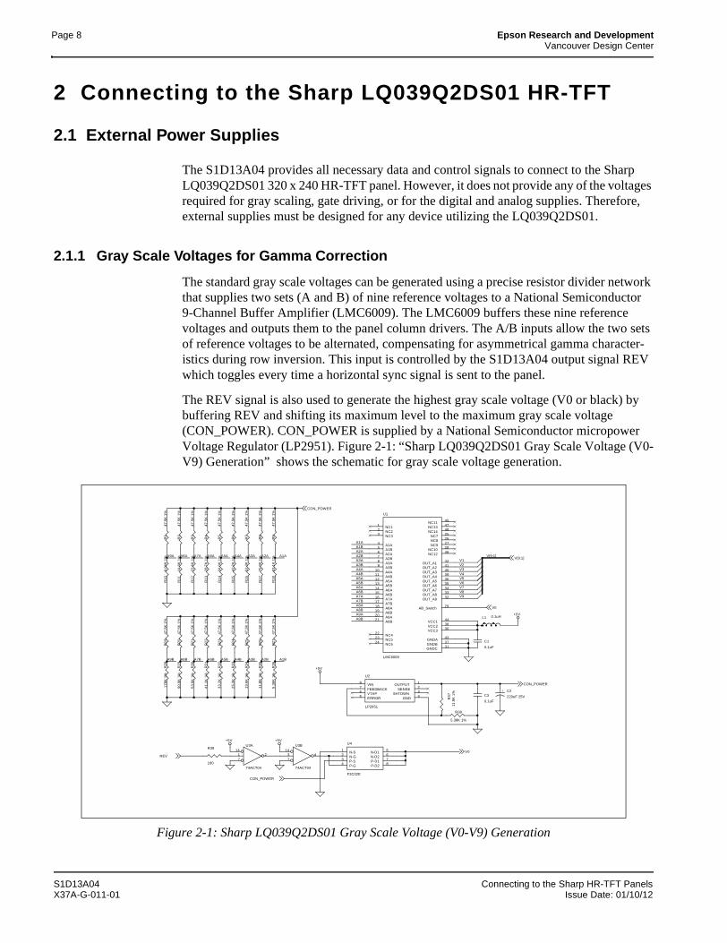
Page 8 Epson Research and DevelopmentVancouver Design Center
2 Connecting to the Sharp LQ039Q2DS01 HR-TFT
2.1 External Power Supplies
The S1D13A04 provides all necessary data and control signals to connect to the Sharp LQ039Q2DS01 320 x 240 HR-TFT panel. However, it does not provide any of the voltages required for gray scaling, gate driving, or for the digital and analog supplies. Therefore, external supplies must be designed for any device utilizing the LQ039Q2DS01.
2.1.1 Gray Scale Voltages for Gamma Correction
The standard gray scale voltages can be generated using a precise resistor divider network that supplies two sets (A and B) of nine reference voltages to a National Semiconductor9-Channel Buffer Amplifier (LMC6009). The LMC6009 buffers these nine reference voltages and outputs them to the panel column drivers. The A/B inputs allow the two sets of reference voltages to be alternated, compensating for asymmetrical gamma character-istics during row inversion. This input is controlled by the S1D13A04 output signal REV which toggles every time a horizontal sync signal is sent to the panel.
The REV signal is also used to generate the highest gray scale voltage (V0 or black) by buffering REV and shifting its maximum level to the maximum gray scale voltage (CON_POWER). CON_POWER is supplied by a National Semiconductor micropower Voltage Regulator (LP2951). Figure 2-1: “Sharp LQ039Q2DS01 Gray Scale Voltage (V0-V9) Generation” shows the schematic for gray scale voltage generation.
Figure 2-1: Sharp LQ039Q2DS01 Gray Scale Voltage (V0-V9) Generation
A4B
A7B
A6A
V9
V3
A1B
A3B
A8B
A1B
V4
V2
A2B
A7A
V[9:1]A9A
A6A
A6B
A5A
A9B
A8B A4B
V8V7
V1A8A
A3B
A2A
A9A
A6B
A5B
A4A
A4A
A2AA1A
V6
A7A
A1A
A2BA9B
A5B
A7B
V5
A3AA5A
A8A
A3A
V0
CON_POWER
V[9:1]
CON_POWER
V0
CON_POWER
REV
+5V
+5V
+5V +5V
R3
711
.8K
1%
R38
5.38K 1%
R1
114
.3K
1%
R1
222
.6K
1%
R1
328
.7K
1%
R1
434
.0K
1%
R1
542
.2K
1%
R1
652
.3K
1%
R1
775
.0K
1%
R1
893
.1K
1%
C3
0.1uF
L1 0.1uH
+ C2
220uF 25V
R1
47.5
K 1
%
R2
47.5
K 1
%
R3
47.5
K 1
%
R4
47.5
K 1
%
R5
47.5
K 1
%
R6
47.5
K 1
%
R7
47.5
K 1
%
R8
47.5
K 1
%
R9
47.5
K 1
% U1
LMC6009
123
222324
25262728
45
46
4748
456789
101112131415161718192021
424140393635343332
29
433731
443830
NC1NC2NC3
NC4NC5NC6
NC7NC8NC9
NC10
NC11
NC12
NC13NC14
A1AA1BA2AA2BA3AA3BA4AA4BA5AA5BA6AA6BA7AA7BA8AA8BA9AA9B
OUT_A1OUT_A2OUT_A3OUT_A4OUT_A5OUT_A6OUT_A7OUT_A8OUT_A9
AB_Switch
GNDAGNDBGNDC
VCC1VCC2VCC3
C1
0.1uF
R1
06.
04K
1%
U2
LP2951
12345
678 OUTPUT
SENSESHTDWN
GNDERRORVTAPFEEDBACKVIN
R2
817
8K
1%
R1
947
.5K
1%
R2
99
0.9
K 1
%R
20
47.5
K 1
%
R3
05
3.6
K 1
%
R3
14
1.1
K 1
%
R3
23
3.2
K 1
%
R2
147
.5K
1%
R39
180
R3
32
5.3
K 1
%
R2
247
.5K
1%
U4
F2C02E
1234
5678
N-SN-GP-SP-G
N-D1N-D2P-D1P-D2
R3
41
9.6
K 1
%
R2
347
.5K
1%
R3
51
1.8
K 1
%
R2
447
.5K
1%
R2
547
.5K
1%
R3
65
.36
K 1
%
U3B
74ACT04
3 414
7
U3A
74ACT04
1 214
7
R2
647
.5K
1%
R2
747
.5K
1%
S1D13A04 Connecting to the Sharp HR-TFT PanelsX37A-G-011-01 Issue Date: 01/10/12
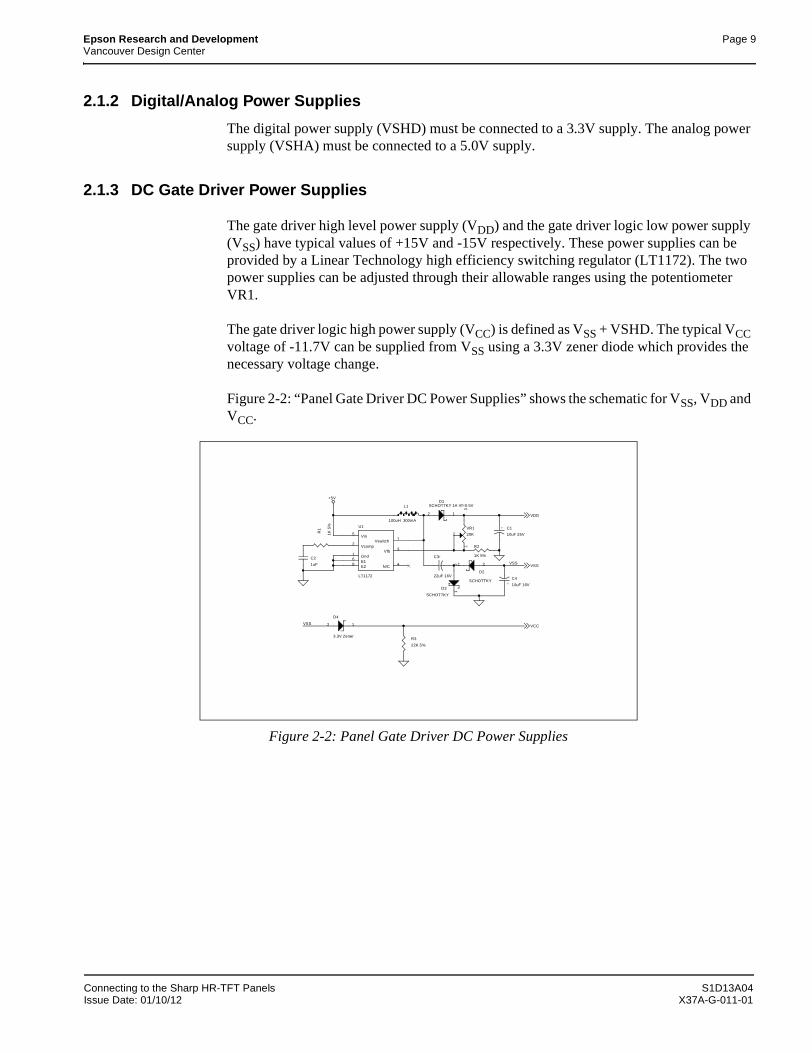
Epson Research and Development Page 9Vancouver Design Center
2.1.2 Digital/Analog Power Supplies
The digital power supply (VSHD) must be connected to a 3.3V supply. The analog power supply (VSHA) must be connected to a 5.0V supply.
2.1.3 DC Gate Driver Power Supplies
The gate driver high level power supply (VDD) and the gate driver logic low power supply (VSS) have typical values of +15V and -15V respectively. These power supplies can be provided by a Linear Technology high efficiency switching regulator (LT1172). The two power supplies can be adjusted through their allowable ranges using the potentiometer VR1.
The gate driver logic high power supply (VCC) is defined as VSS + VSHD. The typical VCC voltage of -11.7V can be supplied from VSS using a 3.3V zener diode which provides the necessary voltage change.
Figure 2-2: “Panel Gate Driver DC Power Supplies” shows the schematic for VSS, VDD and VCC.
Figure 2-2: Panel Gate Driver DC Power Supplies
VSS
VSSVSS
VCC
VDD
+5V
+ C1
10uF 25V
+C3
22uF 16VD2
SCHOTTKY
21
L1
100uH 300mA
D3
SCHOTTKY
21
R2
1K 5%
VR1
20K
13
2R1
1K 5
%
D4
3.3V Zener
2 1
R3
22K 5%
+
C4
10uF 16V
D1SCHOTTKY 1A Vf=0.5V
2 1
C2
1uF
U1
LT1172
68
1
7
3
4
5
2
E1E2
Gnd
Vswitch
Vfb
N/C
Vin
Vcomp
Connecting to the Sharp HR-TFT Panels S1D13A04Issue Date: 01/10/12 X37A-G-011-01
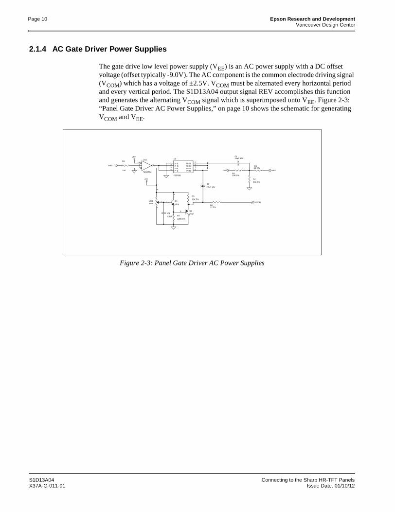
Page 10 Epson Research and DevelopmentVancouver Design Center
2.1.4 AC Gate Driver Power Supplies
The gate drive low level power supply (VEE) is an AC power supply with a DC offset voltage (offset typically -9.0V). The AC component is the common electrode driving signal (VCOM) which has a voltage of ±2.5V. VCOM must be alternated every horizontal period and every vertical period. The S1D13A04 output signal REV accomplishes this function and generates the alternating VCOM signal which is superimposed onto VEE. Figure 2-3: “Panel Gate Driver AC Power Supplies,” on page 10 shows the schematic for generating VCOM and VEE.
Figure 2-3: Panel Gate Driver AC Power Supplies
REV
VSS
VCOM
VEE
+5V
+5V
R215K 5%
R322 5%
R4
27K 5%
+
C122uF 16V
U1A
74ACT04
1 214
7
Q1
NPN1
23
Q2
PNP1
23
VR1100K
13
2
+ C2
22uF 16V
R622 5%
R5
12K 5%
R7
120K 5%
R1
180
U2
F2C02E
1234
5678
N-SN-GP-SP-G
N-D1N-D2P-D1P-D2
C3
0.1uF
S1D13A04 Connecting to the Sharp HR-TFT PanelsX37A-G-011-01 Issue Date: 01/10/12
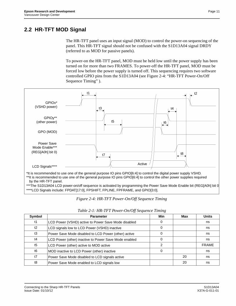
Epson Research and Development Page 11Vancouver Design Center
2.2 HR-TFT MOD Signal
The HR-TFT panel uses an input signal (MOD) to control the power-on sequencing of the panel. This HR-TFT signal should not be confused with the S1D13A04 signal DRDY (referred to as MOD for passive panels).
To power-on the HR-TFT panel, MOD must be held low until the power supply has been turned on for more than two FRAMES. To power-off the HR-TFT panel, MOD must be forced low before the power supply is turned off. This sequencing requires two software controlled GPIO pins from the S1D13A04 (see Figure 2-4: “HR-TFT Power-On/Off Sequence Timing” ).
Figure 2-4: HR-TFT Power-On/Off Sequence Timing
Table 2-1: HR-TFT Power-On/Off Sequence TimingSymbol Parameter Min Max Units
t1 LCD Power (VSHD) active to Power Save Mode disabled 0 ns
t2 LCD signals low to LCD Power (VSHD) inactive 0 ns
t3 Power Save Mode disabled to LCD Power (other) active 0 ns
t4 LCD Power (other) inactive to Power Save Mode enabled 0 ns
t5 LCD Power (other) active to MOD active 2 FRAME
t6 MOD inactive to LCD Power (other) inactive 0 ns
t7 Power Save Mode disabled to LCD signals active 20 ns
t8 Power Save Mode enabled to LCD signals low 20 ns
LCD Signals****
GPO (MOD)
t1
*It is recommended to use one of the general purpose IO pins GPIO[6:4] to control the digital power supply VSHD.
***The S1D13A04 LCD power-on/off sequence is activated by programming the Power Save Mode Enable bit (REG[A0h] bit 0)****LCD Signals include: FPDAT[17:0], FPSHIFT, FPLINE, FPFRAME, and GPIO[3:0].
t5
Power Save
(REG[A0h] bit 0)Mode Enable***
t6
Active
t3 t4
t2
GPIOy**
GPIOx*
t7 t8
(other power)
(VSHD power)
**It is recommended to use one of the general purpose IO pins GPIO[6:4] to control the other power supplies required by the HR-TFT panel.
Connecting to the Sharp HR-TFT Panels S1D13A04Issue Date: 01/10/12 X37A-G-011-01
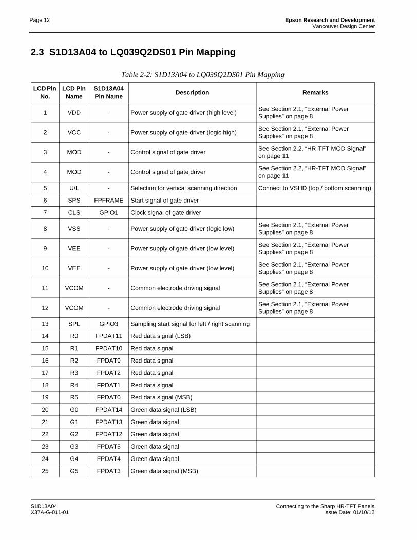
Page 12 Epson Research and DevelopmentVancouver Design Center
2.3 S1D13A04 to LQ039Q2DS01 Pin Mapping
Table 2-2: S1D13A04 to LQ039Q2DS01 Pin Mapping
LCD Pin No.
LCD Pin Name
S1D13A04 Pin Name
Description Remarks
1 VDD - Power supply of gate driver (high level)See Section 2.1, “External Power Supplies” on page 8
2 VCC - Power supply of gate driver (logic high)See Section 2.1, “External Power Supplies” on page 8
3 MOD - Control signal of gate driverSee Section 2.2, “HR-TFT MOD Signal” on page 11
4 MOD - Control signal of gate driverSee Section 2.2, “HR-TFT MOD Signal” on page 11
5 U/L - Selection for vertical scanning direction Connect to VSHD (top / bottom scanning)
6 SPS FPFRAME Start signal of gate driver
7 CLS GPIO1 Clock signal of gate driver
8 VSS - Power supply of gate driver (logic low)See Section 2.1, “External Power Supplies” on page 8
9 VEE - Power supply of gate driver (low level)See Section 2.1, “External Power Supplies” on page 8
10 VEE - Power supply of gate driver (low level)See Section 2.1, “External Power Supplies” on page 8
11 VCOM - Common electrode driving signalSee Section 2.1, “External Power Supplies” on page 8
12 VCOM - Common electrode driving signalSee Section 2.1, “External Power Supplies” on page 8
13 SPL GPIO3 Sampling start signal for left / right scanning
14 R0 FPDAT11 Red data signal (LSB)
15 R1 FPDAT10 Red data signal
16 R2 FPDAT9 Red data signal
17 R3 FPDAT2 Red data signal
18 R4 FPDAT1 Red data signal
19 R5 FPDAT0 Red data signal (MSB)
20 G0 FPDAT14 Green data signal (LSB)
21 G1 FPDAT13 Green data signal
22 G2 FPDAT12 Green data signal
23 G3 FPDAT5 Green data signal
24 G4 FPDAT4 Green data signal
25 G5 FPDAT3 Green data signal (MSB)
S1D13A04 Connecting to the Sharp HR-TFT PanelsX37A-G-011-01 Issue Date: 01/10/12
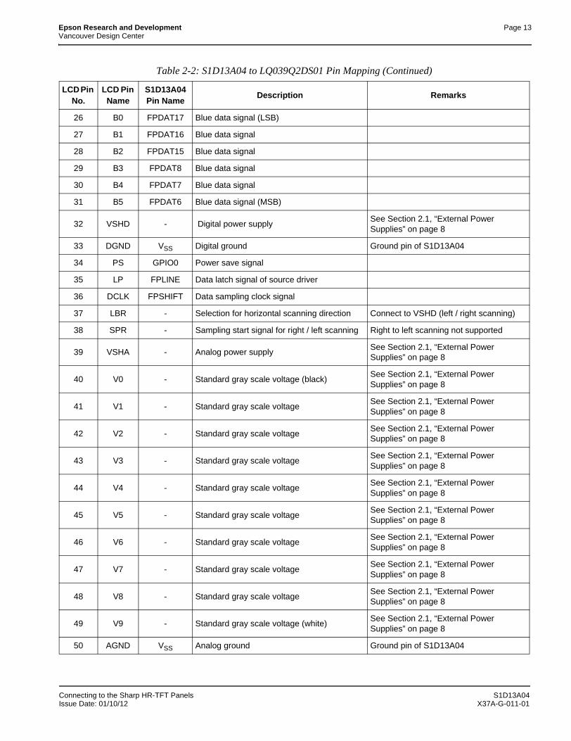
Epson Research and Development Page 13Vancouver Design Center
26 B0 FPDAT17 Blue data signal (LSB)
27 B1 FPDAT16 Blue data signal
28 B2 FPDAT15 Blue data signal
29 B3 FPDAT8 Blue data signal
30 B4 FPDAT7 Blue data signal
31 B5 FPDAT6 Blue data signal (MSB)
32 VSHD - Digital power supplySee Section 2.1, “External Power Supplies” on page 8
33 DGND VSS Digital ground Ground pin of S1D13A04
34 PS GPIO0 Power save signal
35 LP FPLINE Data latch signal of source driver
36 DCLK FPSHIFT Data sampling clock signal
37 LBR - Selection for horizontal scanning direction Connect to VSHD (left / right scanning)
38 SPR - Sampling start signal for right / left scanning Right to left scanning not supported
39 VSHA - Analog power supplySee Section 2.1, “External Power Supplies” on page 8
40 V0 - Standard gray scale voltage (black)See Section 2.1, “External Power Supplies” on page 8
41 V1 - Standard gray scale voltageSee Section 2.1, “External Power Supplies” on page 8
42 V2 - Standard gray scale voltageSee Section 2.1, “External Power Supplies” on page 8
43 V3 - Standard gray scale voltageSee Section 2.1, “External Power Supplies” on page 8
44 V4 - Standard gray scale voltageSee Section 2.1, “External Power Supplies” on page 8
45 V5 - Standard gray scale voltageSee Section 2.1, “External Power Supplies” on page 8
46 V6 - Standard gray scale voltageSee Section 2.1, “External Power Supplies” on page 8
47 V7 - Standard gray scale voltageSee Section 2.1, “External Power Supplies” on page 8
48 V8 - Standard gray scale voltageSee Section 2.1, “External Power Supplies” on page 8
49 V9 - Standard gray scale voltage (white)See Section 2.1, “External Power Supplies” on page 8
50 AGND VSS Analog ground Ground pin of S1D13A04
Table 2-2: S1D13A04 to LQ039Q2DS01 Pin Mapping (Continued)
LCD Pin No.
LCD Pin Name
S1D13A04 Pin Name
Description Remarks
Connecting to the Sharp HR-TFT Panels S1D13A04Issue Date: 01/10/12 X37A-G-011-01
Page 14 Epson Research and DevelopmentVancouver Design Center
3 Connecting to the Sharp LQ031B1DDxx HR-TFT
3.1 External Power Supplies
The S1D13A04 provides all necessary data and control signals to connect to the Sharp LQ031B1DDxx 160x160 HR-TFT panel(s). However, it does not provide any of the voltages required for the backlight, gray scaling, gate driving, or for the digital and analog supplies. Therefore, external supplies must be designed for any device utilizing the LQ031B1DDxx.
The LQ031B1DDxx (160x160) has the same voltage requirements as the LQ039Q2DS01 (320x240). All the circuits used to generate the various voltages for the LQ039Q2DS01 panel also apply to the LQ031B1DDxx panel. This section provides additional circuits for generating some of these voltages.
3.1.1 Gray Scale Voltages for Gamma Correction
The standard gray scale voltages can be generated using a precise resistor divider network as described in Section 2.1.1, “Gray Scale Voltages for Gamma Correction” on page 8. Alternately, they can be generated using a Sharp gray scale IC. The Sharp IR3E203 elimi-nates the large resistor network used to provide the 10 gray scale voltages and combines their function into a single IC.
The S1D13A04 output signal REV is used to alternate the gray scale voltages and connects to the SW input of the IR3E203 IC. The COM signal is used in generating the gate driver panel AC voltage, VCOM and is explained in Section 3.1.4, “AC Gate Driver Power Supplies” on page 15. Figure 3-1: “Sharp LQ031B1DDxx Gray Scale Voltage (V0-V9) Generation” shows the circuit that generates the gray scale voltages using the Sharp IR3E203 IC.
Figure 3-1: Sharp LQ031B1DDxx Gray Scale Voltage (V0-V9) Generation
5V
COM
V[9:0]
REV
V0V1V2V3V4V5V6V7V8V9
U1
SHARP IR3E203
11718
23
4
567891112131415
10
16
NCNCNC
VD
D
VC
C
COM
V0V1V2V3V4V5V6V7V8V9
GND
SW
C14.7uF
C22.2uF
S1D13A04 Connecting to the Sharp HR-TFT PanelsX37A-G-011-01 Issue Date: 01/10/12

Epson Research and Development Page 15Vancouver Design Center
3.1.2 Digital/Analog Power Supplies
The digital power supply (VSHD) must be connected to a 3.3V supply. The analog power supply (VSHA) must be connected to a 5.0V supply.
3.1.3 DC Gate Driver Power Supplies
See Section 2.1.3, “DC Gate Driver Power Supplies” on page 9 and Figure 2-2: “Panel Gate Driver DC Power Supplies,” on page 9 for details on generating VSS, VDD, and VCC.
3.1.4 AC Gate Driver Power Supplies
See Section 2.1.4, “AC Gate Driver Power Supplies” on page 10 and Figure 2-3: “Panel Gate Driver AC Power Supplies,” on page 10 for details on generating VEE and VCOM. If the Sharp IR3E203 is used to generate the gray scale voltages, the COM signal can be connected to the input of the F2C02E MOSFET instead of the buffered REV signal.
3.2 HR-TFT MOD Signal
See Section 2.2, “HR-TFT MOD Signal” on page 11 for details on controlling the MOD signal through software.
Connecting to the Sharp HR-TFT Panels S1D13A04Issue Date: 01/10/12 X37A-G-011-01

Page 16 Epson Research and DevelopmentVancouver Design Center
3.3 S1D13A04 to LQ031B1DDxx Pin Mapping
Table 3-1: S1D13A04 to LQ031B1DDxx Pin Mapping
LCD Pin No.
LCD Pin Name
S1D13A04 Pin Name
Description Remarks
1 VDD - Power supply of gate driver (high level)See Section 3.1, “External Power Supplies” on page 14
2 VCC - Power supply of gate driver (logic high)See Section 3.1, “External Power Supplies” on page 14
3 MOD - Control signal of gate driverSee Section 3.2, “HR-TFT MOD Signal” on page 15
4 MOD - Control signal of gate driverSee Section 3.2, “HR-TFT MOD Signal” on page 15
5 U/L - Selection for vertical scanning direction Connect to VSHD (top / bottom scanning)
6 SPS FPFRAME Start signal of gate driver
7 CLS GPIO1 Clock signal of gate driver
8 VSS - Power supply of gate driver (logic low)See Section 3.1, “External Power Supplies” on page 14
9 VEE - Power supply of gate driver (low level)See Section 3.1, “External Power Supplies” on page 14
10 VEE - Power supply of gate driver (low level)See Section 3.1, “External Power Supplies” on page 14
11 VCOM - Common electrode driving signalSee Section 3.1, “External Power Supplies” on page 14
12 VCOM - Common electrode driving signalSee Section 3.1, “External Power Supplies” on page 14
13 SPL GPIO3 Sampling start signal for left / right scanning
14 R0 FPDAT11 Red data signal (LSB)
15 R1 FPDAT10 Red data signal
16 R2 FPDAT9 Red data signal
17 R3 FPDAT2 Red data signal
18 R4 FPDAT1 Red data signal
19 R5 FPDAT0 Red data signal (MSB)
20 G0 FPDAT14 Green data signal (LSB)
21 G1 FPDAT13 Green data signal
22 G2 FPDAT12 Green data signal
23 G3 FPDAT5 Green data signal
24 G4 FPDAT4 Green data signal
25 G5 FPDAT3 Green data signal (MSB)
S1D13A04 Connecting to the Sharp HR-TFT PanelsX37A-G-011-01 Issue Date: 01/10/12

Epson Research and Development Page 17Vancouver Design Center
26 B0 FPDAT17 Blue data signal (LSB)
27 B1 FPDAT16 Blue data signal
28 B2 FPDAT15 Blue data signal
29 B3 FPDAT8 Blue data signal
30 B4 FPDAT7 Blue data signal
31 B5 FPDAT6 Blue data signal (MSB)
32 VSHD - Digital power supplySee Section 3.1, “External Power Supplies” on page 14
33 DGND VSS Digital ground Ground pin of S1D13A04
34 PS GPIO0 Power save signal
35 LP FPLINE Data latch signal of source driver
36 DCLK FPSHIFT Data sampling clock signal
37 LBR - Selection for horizontal scanning direction Connect to VSHD (left / right scanning)
38 SPR - Sampling start signal for right / left scanning Right to left scanning not supported
39 VSHA - Analog power supplySee Section 3.1, “External Power Supplies” on page 14
40 V0 - Standard gray scale voltage (black)See Section 3.1, “External Power Supplies” on page 14
41 V1 - Standard gray scale voltageSee Section 3.1, “External Power Supplies” on page 14
42 V2 - Standard gray scale voltageSee Section 3.1, “External Power Supplies” on page 14
43 V3 - Standard gray scale voltageSee Section 3.1, “External Power Supplies” on page 14
44 V4 - Standard gray scale voltageSee Section 3.1, “External Power Supplies” on page 14
45 V5 - Standard gray scale voltageSee Section 3.1, “External Power Supplies” on page 14
46 V6 - Standard gray scale voltageSee Section 3.1, “External Power Supplies” on page 14
47 V7 - Standard gray scale voltageSee Section 3.1, “External Power Supplies” on page 14
48 V8 - Standard gray scale voltageSee Section 3.1, “External Power Supplies” on page 14
49 V9 - Standard gray scale voltage (white)See Section 3.1, “External Power Supplies” on page 14
50 AGND VSS Analog ground Ground pin of S1D13A04
Table 3-1: S1D13A04 to LQ031B1DDxx Pin Mapping (Continued)
LCD Pin No.
LCD Pin Name
S1D13A04 Pin Name
Description Remarks
Connecting to the Sharp HR-TFT Panels S1D13A04Issue Date: 01/10/12 X37A-G-011-01
Page 18 Epson Research and DevelopmentVancouver Design Center
4 Test Software
Test utilities and display drivers are available for the S1D13A04. Full source code is available for both the test utilities and the drivers.
The test utilities are configurable for different panel types using a program called 13A04CFG (see document number X37A-B-001-xx), or by directly modifying the source. The display drivers can be customized by the OEM for different panel types, resolutions and color depths only by modifying the source.
The S1D13A04 test utilities and display drivers are available from your sales support contact (see Section 6, “Sales &Technical Support”) or at www.erd.epson.com.
S1D13A04 Connecting to the Sharp HR-TFT PanelsX37A-G-011-01 Issue Date: 01/10/12
Epson Research and Development Page 19Vancouver Design Center
5 References
5.1 Documents
• Sharp Electronics Corporation, LQ039Q2DS01 Specification.
• Sharp Electronics Corporation, LQ031B1DDxx Specification.
• Epson Research and Development, Inc., S1D13A04 Hardware Functional Specification, Document Number X37A-A-001-xx.
• Epson Research and Development, Inc., S1D13A04 Programming Notes and Examples, Document Number X37A-G-003-xx.
• Epson Research and Development, Inc., S5U13A04B00C Rev. 1.0 ISA Bus Evaluation Board User Manual, Document Number X37A-G-004-xx.
5.2 Document Sources
• Sharp Electronics Corporation Website: www.sharpmeg.com.
• Epson Research and Development Website: www.erd.epson.com.
Connecting to the Sharp HR-TFT Panels S1D13A04Issue Date: 01/10/12 X37A-G-011-01

Page 20 Epson Research and DevelopmentVancouver Design Center
6 Sales &Technical Support
6.1 EPSON LCD/USB Companion Chips (S1D13A04)
6.2 Sharp HR-TFT Panel
http://www.sharpmeg.com
JapanSeiko Epson CorporationElectronic Devices Marketing Division421-8, Hino, Hino-shiTokyo 191-8501, JapanTel: 042-587-5812Fax: 042-587-5564http://www.epson.co.jp
Hong KongEpson Hong Kong Ltd.20/F., Harbour Centre25 Harbour RoadWanchai, Hong KongTel: 2585-4600Fax: 2827-4346http://www.epson.com.hk/
TaiwanEpson Taiwan Technology & Trading Ltd.10F, No. 287Nanking East RoadSec. 3, Taipei, TaiwanTel: 02-2717-7360Fax: 02-2712-9164http://www.epson.com.tw/
SingaporeEpson Singapore Pte., Ltd.No. 1Temasek Avenue #36-00Millenia TowerSingapore, 039192Tel: 337-7911Fax: 334-2716http://www.epson.com.sg/
EuropeEpson Europe Electronics GmbHRiesstrasse 1580992 Munich, GermanyTel: 089-14005-0Fax: 089-14005-110http://www.epson-electronics.de
North AmericaEpson Electronics America, Inc.150 River Oaks ParkwaySan Jose, CA 95134, USATel: (408) 922-0200Fax: (408) 922-0238http://www.eea.epson.com
S1D13A04 Connecting to the Sharp HR-TFT PanelsX37A-G-011-01 Issue Date: 01/10/12
S1D13A04 LCD/USB Companion Chip
Interfacing to the Motorola MC68VZ328 Dragonball Microprocessor
Document Number: X37A-G-012-01
Copyright © 2001 Epson Research and Development, Inc. All Rights Reserved.
Information in this document is subject to change without notice. You may download and use this document, but only for your own use inevaluating Seiko Epson/EPSON products. You may not modify the document. Epson Research and Development, Inc. disclaims anyrepresentation that the contents of this document are accurate or current. The Programs/Technologies described in this document may contain material protected under U.S. and/or International Patent laws.
EPSON is a registered trademark of Seiko Epson Corporation. All Trademarks are the property of their respective owners.

Page 2 Epson Research and DevelopmentVancouver Design Center
THIS PAGE LEFT BLANK
S1D13A04 Interfacing to the Motorola MC68VZ328 Dragonball MicroprocessorX37A-G-012-01 Issue Date: 01/10/12
Epson Research and Development Page 3Vancouver Design Center
Table of Contents
1 Introduction . . . . . . . . . . . . . . . . . . . . . . . . . . . . . . . . . . . . . . . . 7
2 Interfacing to the MC68VZ328 . . . . . . . . . . . . . . . . . . . . . . . . . . . . . . 82.1 The MC68VZ328 System Bus . . . . . . . . . . . . . . . . . . . . . . . . . 8
2.2 Chip-Select Module . . . . . . . . . . . . . . . . . . . . . . . . . . . . . 8
3 S1D13A04 Host Bus Interface . . . . . . . . . . . . . . . . . . . . . . . . . . . . . . 93.1 Host Bus Interface Pin Mapping . . . . . . . . . . . . . . . . . . . . . . . . 9
3.2 Host Bus Interface Signals . . . . . . . . . . . . . . . . . . . . . . . . . 10
4 MC68VZ328 to S1D13A04 Interface . . . . . . . . . . . . . . . . . . . . . . . . . . 114.1 Hardware Description . . . . . . . . . . . . . . . . . . . . . . . . . . . 11
4.2 S1D13A04 Hardware Configuration . . . . . . . . . . . . . . . . . . . . . 12
4.2.1 Register/Memory Mapping . . . . . . . . . . . . . . . . . . . . . . . . . . . . . . 13
4.2.2 MC68VZ328 Chip Select and Pin Configuration . . . . . . . . . . . . . . . . . . . 13
5 Software . . . . . . . . . . . . . . . . . . . . . . . . . . . . . . . . . . . . . . . . . 14
6 References . . . . . . . . . . . . . . . . . . . . . . . . . . . . . . . . . . . . . . . 156.1 Documents . . . . . . . . . . . . . . . . . . . . . . . . . . . . . . . 15
6.2 Document Sources . . . . . . . . . . . . . . . . . . . . . . . . . . . . 15
7 Sales and Technical Support . . . . . . . . . . . . . . . . . . . . . . . . . . . . . 167.1 EPSON LCD/USB Companion Chips (S1D13A04) . . . . . . . . . . . . . . . 16
7.2 Motorola MC68VZ328 Processor . . . . . . . . . . . . . . . . . . . . . . . 16
Interfacing to the Motorola MC68VZ328 Dragonball Microprocessor S1D13A04Issue Date: 01/10/12 X37A-G-012-01

Page 4 Epson Research and DevelopmentVancouver Design Center
THIS PAGE LEFT BLANK
S1D13A04 Interfacing to the Motorola MC68VZ328 Dragonball MicroprocessorX37A-G-012-01 Issue Date: 01/10/12
Epson Research and Development Page 5Vancouver Design Center
List of Tables
Table 3-1: Host Bus Interface Pin Mapping . . . . . . . . . . . . . . . . . . . . . . . . . . . . . . . 9
Table 4-1: Summary of Power-On/Reset Options . . . . . . . . . . . . . . . . . . . . . . . . . . 12
Table 4-2: WS Bit Programming . . . . . . . . . . . . . . . . . . . . . . . . . . . . . . . . . . . 13
List of Figures
Figure 4-1: Typical Implementation of MC68VZ328 to S1D13A04 Interface . . . . . . . . . . . . 11
Interfacing to the Motorola MC68VZ328 Dragonball Microprocessor S1D13A04Issue Date: 01/10/12 X37A-G-012-01

Page 6 Epson Research and DevelopmentVancouver Design Center
THIS PAGE LEFT BLANK
S1D13A04 Interfacing to the Motorola MC68VZ328 Dragonball MicroprocessorX37A-G-012-01 Issue Date: 01/10/12

Epson Research and Development Page 7Vancouver Design Center
1 Introduction
This application note describes the hardware and software environment required to interface the S1D13A04 LCD/USB Companion Chip and the Motorola MC68VZ328 Dragonball VZ microprocessor.
The designs described in this document are presented only as examples of how suchinterfaces might be implemented. This application note is updated as appropriate. Please check the Epson Research and Development website at www.erd.epson.com for the latest revision of this document before beginning any development.
We appreciate your comments on our documentation. Please contact us via email at [email protected].
Interfacing to the Motorola MC68VZ328 Dragonball Microprocessor S1D13A04Issue Date: 01/10/12 X37A-G-012-01
Page 8 Epson Research and DevelopmentVancouver Design Center
2 Interfacing to the MC68VZ328
2.1 The MC68VZ328 System Bus
The Motorola MC68VZ328 “Dragonball VZ” is the third generation in the Dragonball microprocessor family. The Dragonball VZ is an integrated controller designed for handheld products. It is based upon the FLX68000 microprocessor core and uses a 24-bit address bus and 16-bit data bus. The Dragonball VZ is faster than its predecessors and the DRAM controller now supports SDRAM. The bus interface consists of all the standard MC68000 bus interface signals except AS, plus some new signals intended to simplify the interface to typical memory and peripheral devices. The 68000 signals are multiplexed with IrDA, SPI and LCD controller signals.
The MC68000 bus control signals are well documented in the Motorola user manuals, and are not be described here. The new signals are as follows.
• Output Enable (OE) is asserted when a read cycle is in progress. It is intended to connect to the output enable control signal of a typical static RAM, EPROM, or Flash EPROM device.
• Upper Write Enable and Lower Write Enable (UWE / LWE) are asserted during memory write cycles for the upper and lower bytes of the 16-bit data bus. They may be directly connected to the write enable inputs of a typical memory device.
2.2 Chip-Select Module
The MC68VZ328 can generate up to 8 chip select outputs which are organized into four groups (A through D).
Each chip select group has a common base address register and address mask register allowing the base address and block size of the entire group to be set. In addition, each chip select within a group has its own address compare and address mask register to activate the chip select for a subset of the group’s address block. Each chip select may also be individ-ually programmed to control an 8 or 16-bit device. Lastly, each chip select can either generate from 0 through 6 wait states internally, or allow the memory or peripheral device to terminate the cycle externally using the standard MC68000 DTACK signal.
Chip select groups A and B are used to control ROM, SRAM, and Flash memory devices and have a block size of 128K bytes to 16M bytes. Chip select A0 is active immediately after reset and is a global chip select so it is typically used to control a boot EPROM device. A0 ceases to decode globally once its chip select registers are programmed. Groups C and D are special in that they can also control DRAM interfaces. These last two groups have block size of 32K bytes to 4M bytes.
S1D13A04 Interfacing to the Motorola MC68VZ328 Dragonball MicroprocessorX37A-G-012-01 Issue Date: 01/10/12
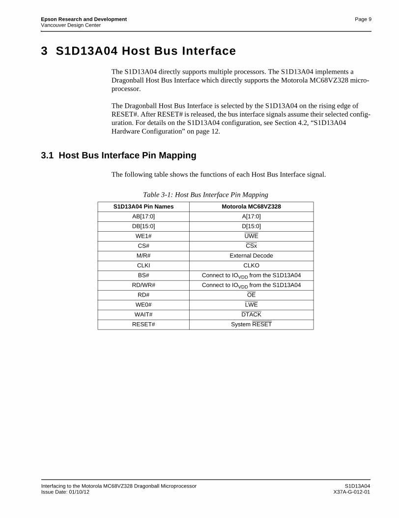
Epson Research and Development Page 9Vancouver Design Center
3 S1D13A04 Host Bus Interface
The S1D13A04 directly supports multiple processors. The S1D13A04 implements a Dragonball Host Bus Interface which directly supports the Motorola MC68VZ328 micro-processor.
The Dragonball Host Bus Interface is selected by the S1D13A04 on the rising edge of RESET#. After RESET# is released, the bus interface signals assume their selected config-uration. For details on the S1D13A04 configuration, see Section 4.2, “S1D13A04 Hardware Configuration” on page 12.
3.1 Host Bus Interface Pin Mapping
The following table shows the functions of each Host Bus Interface signal.
Table 3-1: Host Bus Interface Pin Mapping
S1D13A04 Pin Names Motorola MC68VZ328
AB[17:0] A[17:0]
DB[15:0] D[15:0]
WE1# UWE
CS# CSx
M/R# External Decode
CLKI CLKO
BS# Connect to IOVDD from the S1D13A04
RD/WR# Connect to IOVDD from the S1D13A04
RD# OE
WE0# LWE
WAIT# DTACK
RESET# System RESET
Interfacing to the Motorola MC68VZ328 Dragonball Microprocessor S1D13A04Issue Date: 01/10/12 X37A-G-012-01
Page 10 Epson Research and DevelopmentVancouver Design Center
3.2 Host Bus Interface Signals
The Host Bus Interface requires the following signals.
• CLKI is a clock input required by the S1D13A04 Host Bus Interface as a source for its internal bus and memory clocks. This clock is typically driven by the host CPU system clock. For this example, CLK0 from the Motorola MC68VZ328 is used for CLKI.
• The address inputs AB[17:0], and the data bus DB[15:0], connect directly to the MC68VZ328 address (A[17:0]) and data bus (D[15:0]), respectively. CNF4 must be set to one to select big endian mode.
• Chip Select (CS#) must be driven low by one of the Dragonball VZ chip select outputs from the chip select module whenever the S1D13A04 is accessed by the MC68VZ328.
• M/R# (memory/register) selects between memory or register accesses. This signal is generated by the external address decode circuitry. For this example, M/R# is connected to address line A18, allowing system address A18 to select between memory or register accesses.
• WE0# connects to LWE (the low data byte write strobe enable of the MC68VZ328) and is asserted when valid data is written to the low byte of a 16-bit device.
• WE1# connects to UWE (the upper data byte write strobe enable of the MC68VZ328) and is asserted when valid data is written to the high byte of a 16-bit device.
• RD# connects to OE (the read output enable of the MC68VZ328) and is asserted during a read cycle of the MC68VZ328 microprocessor.
• RD/WR# is not used for the Dragonball host bus interface and must be tied high toIO VDD.
• WAIT# connects to DTACK and is a signal which is output from the S1D13A04 indi-cating the MC68VZ328 must wait until data is ready (read cycle) or accepted (write cycle) on the host bus. MC68VZ328 accesses to the S1D13A04 may occur asynchro-nously to the display update.
• BS# is not used for the Dragonball host bus interface and must be tied high to IO VDD.
S1D13A04 Interfacing to the Motorola MC68VZ328 Dragonball MicroprocessorX37A-G-012-01 Issue Date: 01/10/12
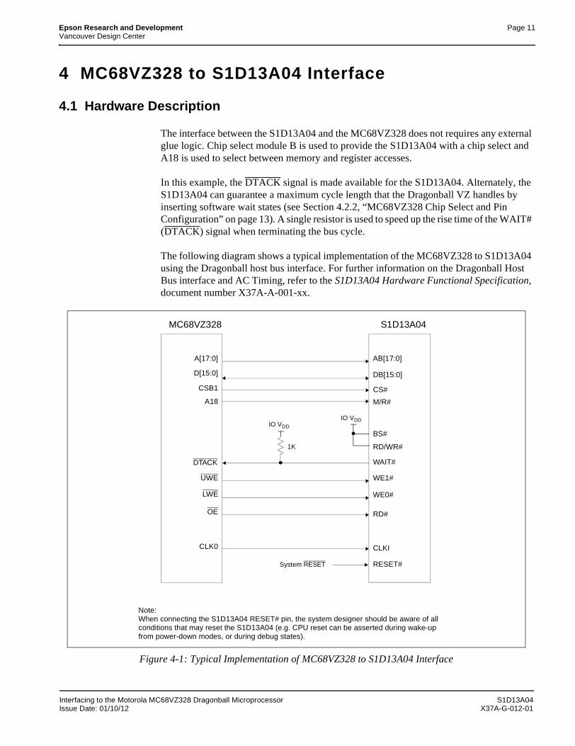
Epson Research and Development Page 11Vancouver Design Center
4 MC68VZ328 to S1D13A04 Interface
4.1 Hardware Description
The interface between the S1D13A04 and the MC68VZ328 does not requires any external glue logic. Chip select module B is used to provide the S1D13A04 with a chip select and A18 is used to select between memory and register accesses.
In this example, the DTACK signal is made available for the S1D13A04. Alternately, the S1D13A04 can guarantee a maximum cycle length that the Dragonball VZ handles by inserting software wait states (see Section 4.2.2, “MC68VZ328 Chip Select and Pin Configuration” on page 13). A single resistor is used to speed up the rise time of the WAIT# (DTACK) signal when terminating the bus cycle.
The following diagram shows a typical implementation of the MC68VZ328 to S1D13A04 using the Dragonball host bus interface. For further information on the Dragonball Host Bus interface and AC Timing, refer to the S1D13A04 Hardware Functional Specification, document number X37A-A-001-xx.
Figure 4-1: Typical Implementation of MC68VZ328 to S1D13A04 Interface
MC68VZ328 S1D13A04
A[17:0]
D[15:0]
DTACK
UWE
LWE
OE
CLK0
AB[17:0]
DB[15:0]
CS#
WAIT#
WE1#
WE0#
RD#
RD/WR#
CLKI
RESET#
IO VDD
1K
CSB1
BS#
Note:When connecting the S1D13A04 RESET# pin, the system designer should be aware of all conditions that may reset the S1D13A04 (e.g. CPU reset can be asserted during wake-up from power-down modes, or during debug states).
System RESET
IO VDD
A18 M/R#
Interfacing to the Motorola MC68VZ328 Dragonball Microprocessor S1D13A04Issue Date: 01/10/12 X37A-G-012-01
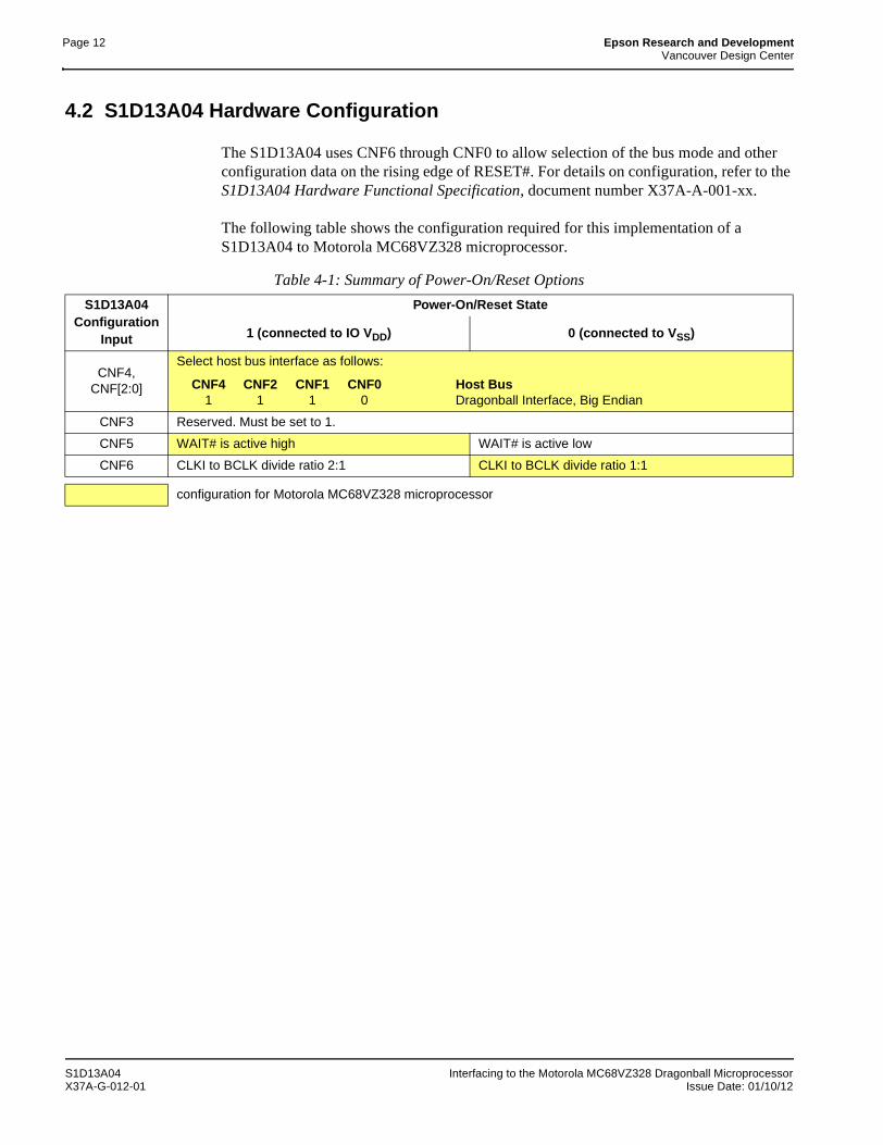
Page 12 Epson Research and DevelopmentVancouver Design Center
4.2 S1D13A04 Hardware Configuration
The S1D13A04 uses CNF6 through CNF0 to allow selection of the bus mode and other configuration data on the rising edge of RESET#. For details on configuration, refer to the S1D13A04 Hardware Functional Specification, document number X37A-A-001-xx.
The following table shows the configuration required for this implementation of a S1D13A04 to Motorola MC68VZ328 microprocessor.
Table 4-1: Summary of Power-On/Reset Options
S1D13A04 Configuration
Input
Power-On/Reset State
1 (connected to IO VDD) 0 (connected to VSS)
CNF4, CNF[2:0]
Select host bus interface as follows:
CNF4 CNF2 CNF1 CNF0 Host Bus1 1 1 0 Dragonball Interface, Big Endian
CNF3 Reserved. Must be set to 1.
CNF5 WAIT# is active high WAIT# is active low
CNF6 CLKI to BCLK divide ratio 2:1 CLKI to BCLK divide ratio 1:1
configuration for Motorola MC68VZ328 microprocessor
S1D13A04 Interfacing to the Motorola MC68VZ328 Dragonball MicroprocessorX37A-G-012-01 Issue Date: 01/10/12

Epson Research and Development Page 13Vancouver Design Center
4.2.1 Register/Memory Mapping
The S1D13A04 requires two 256K byte segments in memory for the display buffer and its internal registers. To accommodate this block size, it is preferable (but not required) to use one of the chip selects from groups A or B. Groups A and B can have a size range of 128K bytes to 16M bytes and groups C and D have a size range of 32K bytes to 16M bytes. Therefore, any chip select other than CSA0 would be suitable for the S1D13A04 interface.
In the example interface, chip select CSB1 controls the S1D13A04. A 512K byte address space is used by setting the SIZ bits of Chip Select Register B (FFFFF116h) to 512k bytes. The S1D13A04 internal registers occupy the first 256K byte block and the 160K byte display buffer is located in the second 256K byte block. A18 from the MC68VZ328 is used to select between these two 256K byte blocks.
4.2.2 MC68VZ328 Chip Select and Pin Configuration
The chip select used to map the S1D13A04 (in this example CSB1) must have its RO (Read Only) bit set to 0, its BSW (Bus Data Width) set to 1 for a 16-bit bus, and the WS (Wait states) bits should be set to 111b to allow the S1D13A04 to terminate bus cycles externally with DTACK. The DTACK pin function must be enabled with Register FFFFF433, Port G Select Register, bit 0.
If Chip Select Group B is used as the chip select module for the S1D13A04, SRAM timing must be enabled by setting the Chip Select Control Register 1 (FFFFF10Ah) SR16 bit = 0b.
Early cycle detection for static memory must be disabled by setting the Chip Select Control Register 2 (FFFFF10Ch) ECDS bit = 0b.
If DTACK is not used, then the WS bits should be set to either 4, 6, 10, or 12 software wait states depending on the divide ratio between the S1D13A04 MCLK and BCLK. The WS bits should be set as follows.
Table 4-2: WS Bit ProgrammingS1D13A04 MCLK to BCLK Divide Ratio WS Bits (wait states)
MCLK = BCLK 4
MCLK = BCLK ÷ 2 6
MCLK = BCLK ÷ 3 10
MCLK = BCLK ÷ 4 12
Interfacing to the Motorola MC68VZ328 Dragonball Microprocessor S1D13A04Issue Date: 01/10/12 X37A-G-012-01
Page 14 Epson Research and DevelopmentVancouver Design Center
5 Software
Test utilities and display drivers are available for the S1D13A04. Full source code is available for both the test utilities and the drivers.
The test utilities are configurable for different panel types using a program called 13A04CFG (see document number X37A-B-001-xx), or by directly modifying the source. The display drivers can be customized by the OEM for different panel types, resolutions and color depths only by modifying the source.
The S1D13A04 test utilities and display drivers are available from your sales support contact (see Section 7, “Sales and Technical Support”) or at www.erd.epson.com.
S1D13A04 Interfacing to the Motorola MC68VZ328 Dragonball MicroprocessorX37A-G-012-01 Issue Date: 01/10/12
Epson Research and Development Page 15Vancouver Design Center
6 References
6.1 Documents
• Motorola Inc., MC68VZ328 DragonBall-VZ® Integrated Processor User’s Manual, Motorola Publication no. MC683VZ28UM; available on the Internet at http://www.mot.com/SPS/WIRELESS/products/MC68VZ328.html.
• Epson Research and Development, Inc., S1D13A04 Hardware Functional Specification, Document Number X37A-A-001-xx.
• Epson Research and Development, Inc., S5U13A04B00C Rev. 1.0 Evaluation Board User Manual, Document Number X37A-G-004-xx.
• Epson Research and Development, Inc., S1D13A04 Programming Notes and Examples, Document Number X37A-G-003-xx.
6.2 Document Sources
• Motorola Inc. Literature Distribution Center: (800) 441-2447.
• Motorola Inc. Website: www.mot.com.
• Epson Research and Development Website: www.erd.epson.com.
Interfacing to the Motorola MC68VZ328 Dragonball Microprocessor S1D13A04Issue Date: 01/10/12 X37A-G-012-01
Page 16 Epson Research and DevelopmentVancouver Design Center
7 Sales and Technical Support
7.1 EPSON LCD/USB Companion Chips (S1D13A04)
7.2 Motorola MC68VZ328 Processor
• Motorola Design Line, (800) 521-6274.
• Local Motorola sales office or authorized distributor.
JapanSeiko Epson CorporationElectronic Devices Marketing Division421-8, Hino, Hino-shiTokyo 191-8501, JapanTel: 042-587-5812Fax: 042-587-5564http://www.epson.co.jp
Hong KongEpson Hong Kong Ltd.20/F., Harbour Centre25 Harbour RoadWanchai, Hong KongTel: 2585-4600Fax: 2827-4346http://www.epson.com.hk/
TaiwanEpson Taiwan Technology & Trading Ltd.10F, No. 287Nanking East RoadSec. 3, Taipei, TaiwanTel: 02-2717-7360Fax: 02-2712-9164http://www.epson.com.tw/
SingaporeEpson Singapore Pte., Ltd.No. 1Temasek Avenue #36-00Millenia TowerSingapore, 039192Tel: 337-7911Fax: 334-2716http://www.epson.com.sg/
EuropeEpson Europe Electronics GmbHRiesstrasse 1580992 Munich, GermanyTel: 089-14005-0Fax: 089-14005-110http://www.epson-electronics.de
North AmericaEpson Electronics America, Inc.150 River Oaks ParkwaySan Jose, CA 95134, USATel: (408) 922-0200Fax: (408) 922-0238http://www.eea.epson.com
S1D13A04 Interfacing to the Motorola MC68VZ328 Dragonball MicroprocessorX37A-G-012-01 Issue Date: 01/10/12
S1D13A04 LCD/USB Companion Chip
Interfacing to the Intel StrongARM SA-1110 Microprocessor
Document Number: X37A-G-013-01
Copyright © 2001 Epson Research and Development, Inc. All Rights Reserved.
Information in this document is subject to change without notice. You may download and use this document, but only for your own use inevaluating Seiko Epson/EPSON products. You may not modify the document. Epson Research and Development, Inc. disclaims anyrepresentation that the contents of this document are accurate or current. The Programs/Technologies described in this document may contain material protected under U.S. and/or International Patent laws.
EPSON is a registered trademark of Seiko Epson Corporation. All Trademarks are the property of their respective owners.

Page 2 Epson Research and DevelopmentVancouver Design Center
THIS PAGE LEFT BLANK
S1D13A04 Interfacing to the Intel StrongARM SA-1110 MicroprocessorX37A-G-013-01 Issue Date: 01/10/12
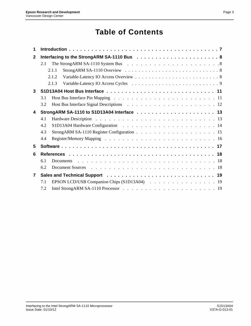
Epson Research and Development Page 3Vancouver Design Center
Table of Contents
1 Introduction . . . . . . . . . . . . . . . . . . . . . . . . . . . . . . . . . . . . . . . . 7
2 Interfacing to the StrongARM SA-1110 Bus . . . . . . . . . . . . . . . . . . . . . . 82.1 The StrongARM SA-1110 System Bus . . . . . . . . . . . . . . . . . . . . . 8
2.1.1 StrongARM SA-1110 Overview . . . . . . . . . . . . . . . . . . . . . . . . . . . . 8
2.1.2 Variable-Latency IO Access Overview . . . . . . . . . . . . . . . . . . . . . . . . . 8
2.1.3 Variable-Latency IO Access Cycles . . . . . . . . . . . . . . . . . . . . . . . . . . 9
3 S1D13A04 Host Bus Interface . . . . . . . . . . . . . . . . . . . . . . . . . . . . . 113.1 Host Bus Interface Pin Mapping . . . . . . . . . . . . . . . . . . . . . . . 11
3.2 Host Bus Interface Signal Descriptions . . . . . . . . . . . . . . . . . . . . 12
4 StrongARM SA-1110 to S1D13A04 Interface . . . . . . . . . . . . . . . . . . . . . 134.1 Hardware Description . . . . . . . . . . . . . . . . . . . . . . . . . . . 13
4.2 S1D13A04 Hardware Configuration . . . . . . . . . . . . . . . . . . . . . 14
4.3 StrongARM SA-1110 Register Configuration . . . . . . . . . . . . . . . . . . 15
4.4 Register/Memory Mapping . . . . . . . . . . . . . . . . . . . . . . . . . 16
5 Software . . . . . . . . . . . . . . . . . . . . . . . . . . . . . . . . . . . . . . . . . 17
6 References . . . . . . . . . . . . . . . . . . . . . . . . . . . . . . . . . . . . . . . 186.1 Documents . . . . . . . . . . . . . . . . . . . . . . . . . . . . . . . 18
6.2 Document Sources . . . . . . . . . . . . . . . . . . . . . . . . . . . . 18
7 Sales and Technical Support . . . . . . . . . . . . . . . . . . . . . . . . . . . . . 197.1 EPSON LCD/USB Companion Chips (S1D13A04) . . . . . . . . . . . . . . . 19
7.2 Intel StrongARM SA-1110 Processor . . . . . . . . . . . . . . . . . . . . . 19
Interfacing to the Intel StrongARM SA-1110 Microprocessor S1D13A04Issue Date: 01/10/12 X37A-G-013-01

Page 4 Epson Research and DevelopmentVancouver Design Center
THIS PAGE LEFT BLANK
S1D13A04 Interfacing to the Intel StrongARM SA-1110 MicroprocessorX37A-G-013-01 Issue Date: 01/10/12
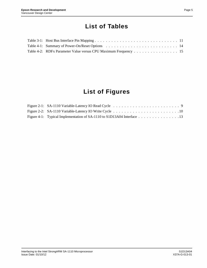
Epson Research and Development Page 5Vancouver Design Center
List of Tables
Table 3-1: Host Bus Interface Pin Mapping . . . . . . . . . . . . . . . . . . . . . . . . . . . . . . 11
Table 4-1: Summary of Power-On/Reset Options . . . . . . . . . . . . . . . . . . . . . . . . . . 14
Table 4-2: RDFx Parameter Value versus CPU Maximum Frequency . . . . . . . . . . . . . . . . 15
List of Figures
Figure 2-1: SA-1110 Variable-Latency IO Read Cycle . . . . . . . . . . . . . . . . . . . . . . . . 9
Figure 2-2: SA-1110 Variable-Latency IO Write Cycle . . . . . . . . . . . . . . . . . . . . . . . . 10
Figure 4-1: Typical Implementation of SA-1110 to S1D13A04 Interface . . . . . . . . . . . . . . . 13
Interfacing to the Intel StrongARM SA-1110 Microprocessor S1D13A04Issue Date: 01/10/12 X37A-G-013-01

Page 6 Epson Research and DevelopmentVancouver Design Center
THIS PAGE LEFT BLANK
S1D13A04 Interfacing to the Intel StrongARM SA-1110 MicroprocessorX37A-G-013-01 Issue Date: 01/10/12

Epson Research and Development Page 7Vancouver Design Center
1 Introduction
This application note describes the hardware and software environment required to provide an interface between the S1D13A04 LCD/USB Companion Chip and the Intel StrongARM SA-1110 Microprocessor.
The designs described in this document are presented only as examples of how suchinterfaces might be implemented. This application note is updated as appropriate. Please check the Epson Research and Development website at www.erd.epson.com for the latest revision of this document before beginning any development.
We appreciate your comments on our documentation. Please contact us via email at [email protected].
Interfacing to the Intel StrongARM SA-1110 Microprocessor S1D13A04Issue Date: 01/10/12 X37A-G-013-01
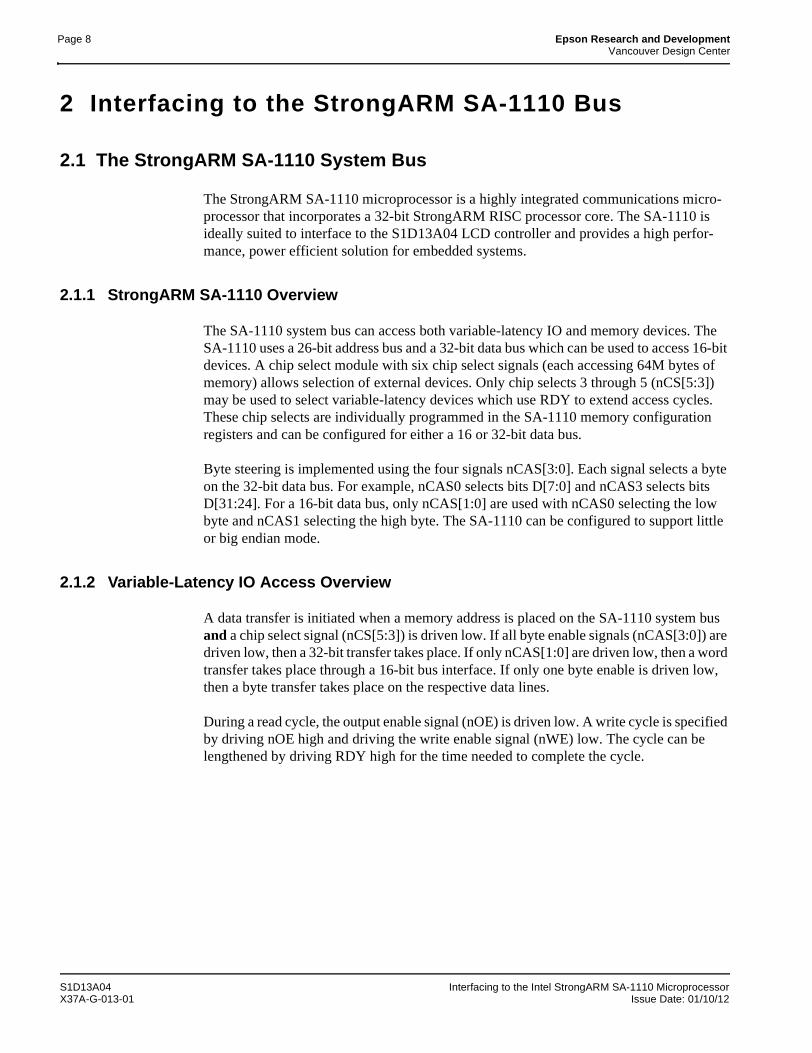
Page 8 Epson Research and DevelopmentVancouver Design Center
2 Interfacing to the StrongARM SA-1110 Bus
2.1 The StrongARM SA-1110 System Bus
The StrongARM SA-1110 microprocessor is a highly integrated communications micro-processor that incorporates a 32-bit StrongARM RISC processor core. The SA-1110 is ideally suited to interface to the S1D13A04 LCD controller and provides a high perfor-mance, power efficient solution for embedded systems.
2.1.1 StrongARM SA-1110 Overview
The SA-1110 system bus can access both variable-latency IO and memory devices. The SA-1110 uses a 26-bit address bus and a 32-bit data bus which can be used to access 16-bit devices. A chip select module with six chip select signals (each accessing 64M bytes of memory) allows selection of external devices. Only chip selects 3 through 5 (nCS[5:3]) may be used to select variable-latency devices which use RDY to extend access cycles. These chip selects are individually programmed in the SA-1110 memory configuration registers and can be configured for either a 16 or 32-bit data bus.
Byte steering is implemented using the four signals nCAS[3:0]. Each signal selects a byte on the 32-bit data bus. For example, nCAS0 selects bits D[7:0] and nCAS3 selects bits D[31:24]. For a 16-bit data bus, only nCAS[1:0] are used with nCAS0 selecting the low byte and nCAS1 selecting the high byte. The SA-1110 can be configured to support little or big endian mode.
2.1.2 Variable-Latency IO Access Overview
A data transfer is initiated when a memory address is placed on the SA-1110 system bus and a chip select signal (nCS[5:3]) is driven low. If all byte enable signals (nCAS[3:0]) are driven low, then a 32-bit transfer takes place. If only nCAS[1:0] are driven low, then a word transfer takes place through a 16-bit bus interface. If only one byte enable is driven low, then a byte transfer takes place on the respective data lines.
During a read cycle, the output enable signal (nOE) is driven low. A write cycle is specified by driving nOE high and driving the write enable signal (nWE) low. The cycle can be lengthened by driving RDY high for the time needed to complete the cycle.
S1D13A04 Interfacing to the Intel StrongARM SA-1110 MicroprocessorX37A-G-013-01 Issue Date: 01/10/12
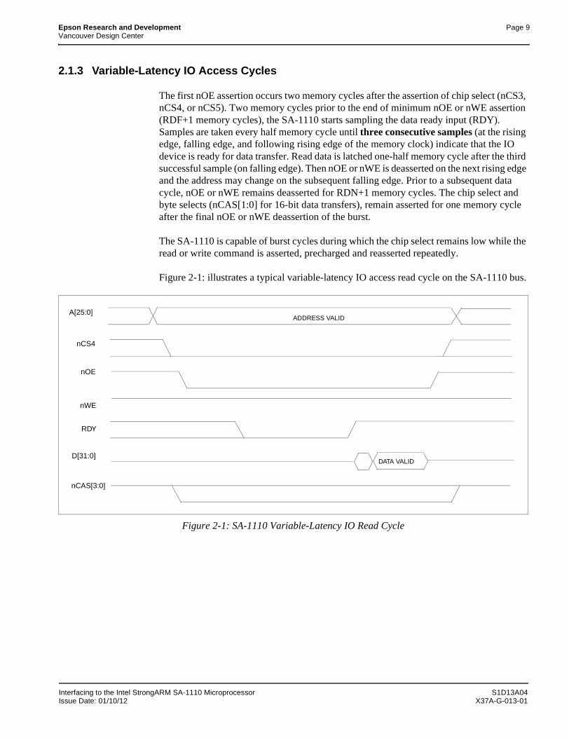
Epson Research and Development Page 9Vancouver Design Center
2.1.3 Variable-Latency IO Access Cycles
The first nOE assertion occurs two memory cycles after the assertion of chip select (nCS3, nCS4, or nCS5). Two memory cycles prior to the end of minimum nOE or nWE assertion (RDF+1 memory cycles), the SA-1110 starts sampling the data ready input (RDY). Samples are taken every half memory cycle until three consecutive samples (at the rising edge, falling edge, and following rising edge of the memory clock) indicate that the IO device is ready for data transfer. Read data is latched one-half memory cycle after the third successful sample (on falling edge). Then nOE or nWE is deasserted on the next rising edge and the address may change on the subsequent falling edge. Prior to a subsequent data cycle, nOE or nWE remains deasserted for RDN+1 memory cycles. The chip select and byte selects (nCAS[1:0] for 16-bit data transfers), remain asserted for one memory cycle after the final nOE or nWE deassertion of the burst.
The SA-1110 is capable of burst cycles during which the chip select remains low while the read or write command is asserted, precharged and reasserted repeatedly.
Figure 2-1: illustrates a typical variable-latency IO access read cycle on the SA-1110 bus.
Figure 2-1: SA-1110 Variable-Latency IO Read Cycle
A[25:0]
nCS4
nOE
RDY
ADDRESS VALID
DATA VALIDD[31:0]
nWE
nCAS[3:0]
Interfacing to the Intel StrongARM SA-1110 Microprocessor S1D13A04Issue Date: 01/10/12 X37A-G-013-01
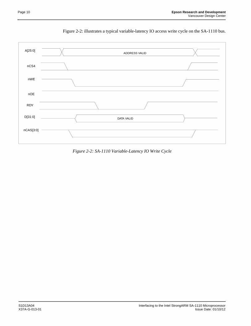
Page 10 Epson Research and DevelopmentVancouver Design Center
Figure 2-2: illustrates a typical variable-latency IO access write cycle on the SA-1110 bus.
Figure 2-2: SA-1110 Variable-Latency IO Write Cycle
A[25:0]
nCS4
nWE
ADDRESS VALID
DATA VALIDD[31:0]
nOE
nCAS[3:0]
RDY
S1D13A04 Interfacing to the Intel StrongARM SA-1110 MicroprocessorX37A-G-013-01 Issue Date: 01/10/12
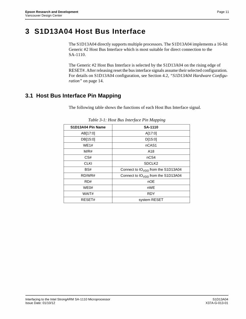
Epson Research and Development Page 11Vancouver Design Center
3 S1D13A04 Host Bus Interface
The S1D13A04 directly supports multiple processors. The S1D13A04 implements a 16-bit Generic #2 Host Bus Interface which is most suitable for direct connection to theSA-1110.
The Generic #2 Host Bus Interface is selected by the S1D13A04 on the rising edge of RESET#. After releasing reset the bus interface signals assume their selected configuration. For details on S1D13A04 configuration, see Section 4.2, “S1D13A04 Hardware Configu-ration” on page 14.
3.1 Host Bus Interface Pin Mapping
The following table shows the functions of each Host Bus Interface signal.
Table 3-1: Host Bus Interface Pin Mapping
S1D13A04 Pin Name SA-1110
AB[17:0] A[17:0]
DB[15:0] D[15:0]
WE1# nCAS1
M/R# A18
CS# nCS4
CLKI SDCLK2
BS# Connect to IOVDD from the S1D13A04
RD/WR# Connect to IOVDD from the S1D13A04
RD# nOE
WE0# nWE
WAIT# RDY
RESET# system RESET
Interfacing to the Intel StrongARM SA-1110 Microprocessor S1D13A04Issue Date: 01/10/12 X37A-G-013-01
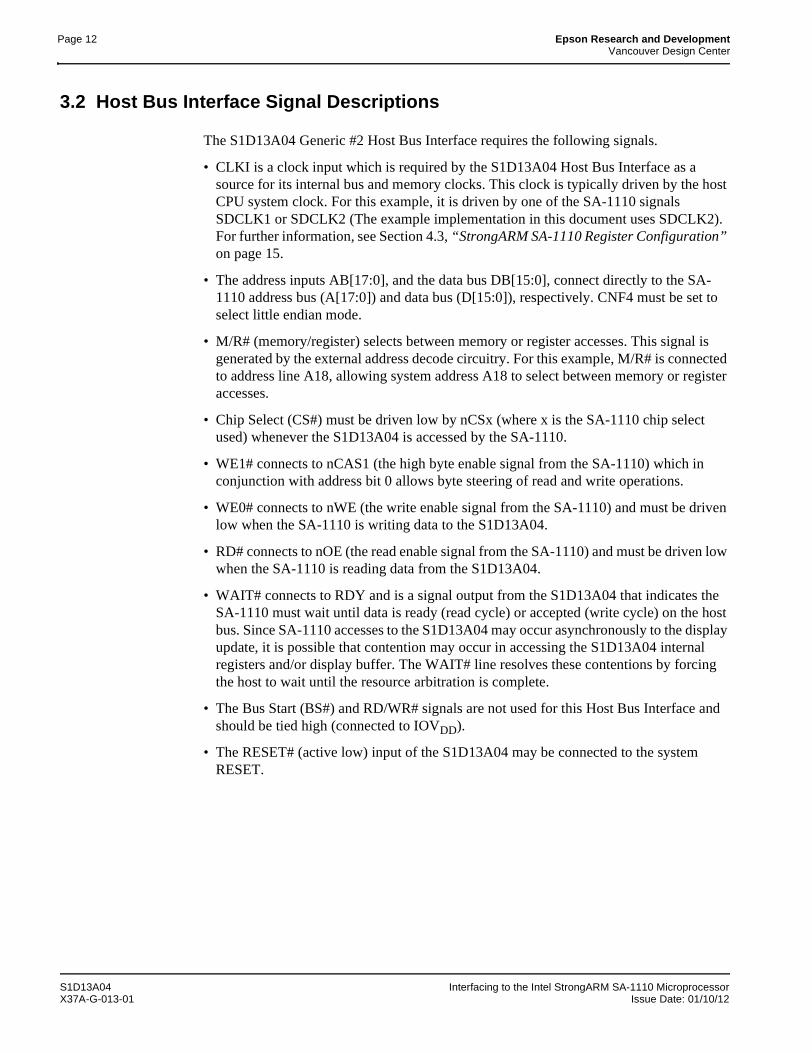
Page 12 Epson Research and DevelopmentVancouver Design Center
3.2 Host Bus Interface Signal Descriptions
The S1D13A04 Generic #2 Host Bus Interface requires the following signals.
• CLKI is a clock input which is required by the S1D13A04 Host Bus Interface as a source for its internal bus and memory clocks. This clock is typically driven by the host CPU system clock. For this example, it is driven by one of the SA-1110 signals SDCLK1 or SDCLK2 (The example implementation in this document uses SDCLK2). For further information, see Section 4.3, “StrongARM SA-1110 Register Configuration” on page 15.
• The address inputs AB[17:0], and the data bus DB[15:0], connect directly to the SA-1110 address bus (A[17:0]) and data bus (D[15:0]), respectively. CNF4 must be set to select little endian mode.
• M/R# (memory/register) selects between memory or register accesses. This signal is generated by the external address decode circuitry. For this example, M/R# is connected to address line A18, allowing system address A18 to select between memory or register accesses.
• Chip Select (CS#) must be driven low by nCSx (where x is the SA-1110 chip select used) whenever the S1D13A04 is accessed by the SA-1110.
• WE1# connects to nCAS1 (the high byte enable signal from the SA-1110) which in conjunction with address bit 0 allows byte steering of read and write operations.
• WE0# connects to nWE (the write enable signal from the SA-1110) and must be driven low when the SA-1110 is writing data to the S1D13A04.
• RD# connects to nOE (the read enable signal from the SA-1110) and must be driven low when the SA-1110 is reading data from the S1D13A04.
• WAIT# connects to RDY and is a signal output from the S1D13A04 that indicates the SA-1110 must wait until data is ready (read cycle) or accepted (write cycle) on the host bus. Since SA-1110 accesses to the S1D13A04 may occur asynchronously to the display update, it is possible that contention may occur in accessing the S1D13A04 internal registers and/or display buffer. The WAIT# line resolves these contentions by forcing the host to wait until the resource arbitration is complete.
• The Bus Start (BS#) and RD/WR# signals are not used for this Host Bus Interface and should be tied high (connected to IOVDD).
• The RESET# (active low) input of the S1D13A04 may be connected to the system RESET.
S1D13A04 Interfacing to the Intel StrongARM SA-1110 MicroprocessorX37A-G-013-01 Issue Date: 01/10/12
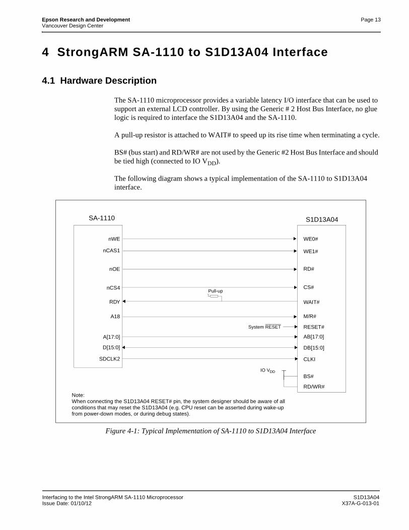
Epson Research and Development Page 13Vancouver Design Center
4 StrongARM SA-1110 to S1D13A04 Interface
4.1 Hardware Description
The SA-1110 microprocessor provides a variable latency I/O interface that can be used to support an external LCD controller. By using the Generic # 2 Host Bus Interface, no glue logic is required to interface the S1D13A04 and the SA-1110.
A pull-up resistor is attached to WAIT# to speed up its rise time when terminating a cycle.
BS# (bus start) and RD/WR# are not used by the Generic #2 Host Bus Interface and should be tied high (connected to IO VDD).
The following diagram shows a typical implementation of the SA-1110 to S1D13A04 interface.
Figure 4-1: Typical Implementation of SA-1110 to S1D13A04 Interface
WE1#
WE0#
DB[15:0]
WAIT#
RD#
CLKI
S1D13A04
CS#
RESET#
AB[17:0]
nCAS1
nWE
D[15:0]
nCS4
nOE
SDCLK2
RDY
A[17:0]
SA-1110
Pull-up
BS#
RD/WR#
System RESET
Note:When connecting the S1D13A04 RESET# pin, the system designer should be aware of all conditions that may reset the S1D13A04 (e.g. CPU reset can be asserted during wake-up from power-down modes, or during debug states).
IO VDD
M/R#A18
Interfacing to the Intel StrongARM SA-1110 Microprocessor S1D13A04Issue Date: 01/10/12 X37A-G-013-01
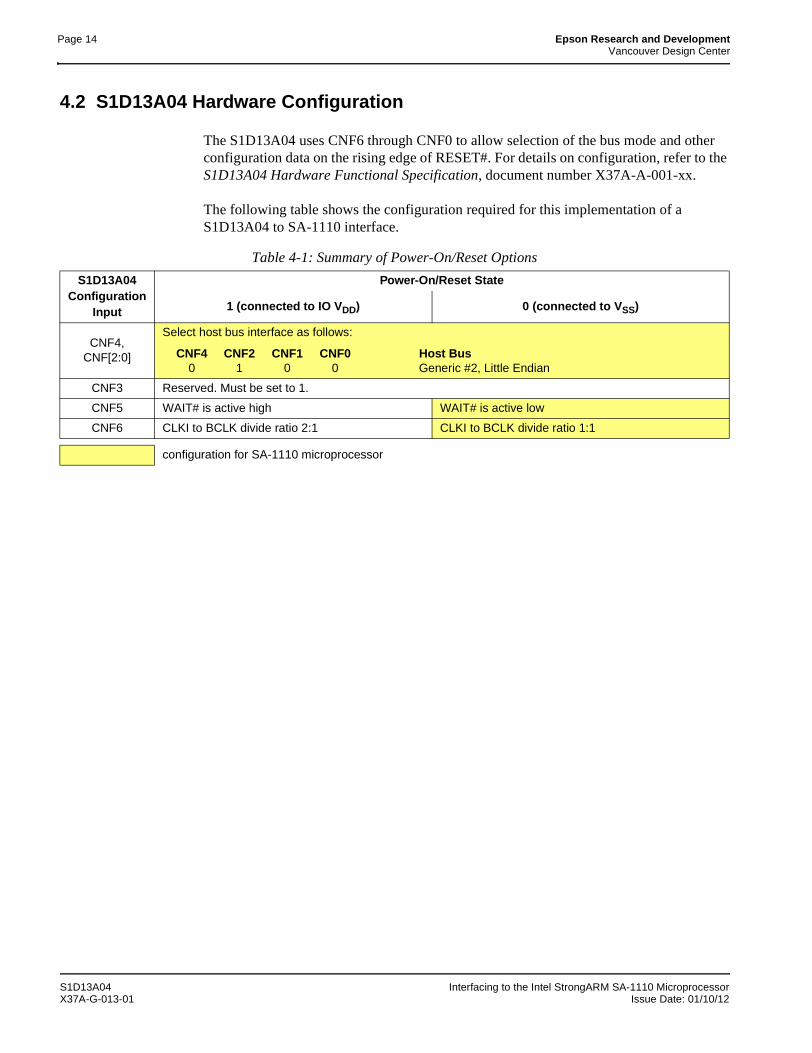
Page 14 Epson Research and DevelopmentVancouver Design Center
4.2 S1D13A04 Hardware Configuration
The S1D13A04 uses CNF6 through CNF0 to allow selection of the bus mode and other configuration data on the rising edge of RESET#. For details on configuration, refer to the S1D13A04 Hardware Functional Specification, document number X37A-A-001-xx.
The following table shows the configuration required for this implementation of a S1D13A04 to SA-1110 interface.
Table 4-1: Summary of Power-On/Reset Options
S1D13A04 Configuration
Input
Power-On/Reset State
1 (connected to IO VDD) 0 (connected to VSS)
CNF4, CNF[2:0]
Select host bus interface as follows:
CNF4 CNF2 CNF1 CNF0 Host Bus0 1 0 0 Generic #2, Little Endian
CNF3 Reserved. Must be set to 1.
CNF5 WAIT# is active high WAIT# is active low
CNF6 CLKI to BCLK divide ratio 2:1 CLKI to BCLK divide ratio 1:1
configuration for SA-1110 microprocessor
S1D13A04 Interfacing to the Intel StrongARM SA-1110 MicroprocessorX37A-G-013-01 Issue Date: 01/10/12
Epson Research and Development Page 15Vancouver Design Center
4.3 StrongARM SA-1110 Register Configuration
The SA-1110 requires configuration of several of its internal registers to interface to the S1D13A04 Generic #2 Host Bus Interface.
• The Static Memory Control Registers (MSC[2:0]) are read/write registers containing control bits for configuring static memory or variable-latency IO devices. These regis-ters correspond to chip select pairs nCS[5:4], nCS[3:2], and nCS[1:0] respectively. Each of the three registers contains two identical CNFG fields, one for each chip select within the pair. Since only nCS[5:3] controls variable-latency IO devices, MSC2 and MSC1 should be programmed based on the chip select used.
Parameter RTx<1:0> should be set to 01b (selects variable-latency IO mode).
Parameter RBWx should be set to 1 (selects 16-bit bus width).
Parameter RDFx<4:0> should be set according to the maximum desired CPUfrequency as indicated in the table below.
Parameter RDNx<4:0> should be set to 0 (minimum command precharge time).
Parameter RRRx<2:0> should be set to 0 (minimum nCSx precharge time).
• The S1D13A04 endian mode is set to little endian. To program the SA-1110 for little endian set bit 7 of the control register (register 1) to 0.
• The CLKI signal input to the S1D13A04 from one of the SDCLK[2:1] pins is a deriva-tive of the SA-1110 internal processor speed (either divide by 2 or 4). The S1D13A04 Generic #2 Host Bus Interface has a maximum BCLK of 50MHz. Therefore, if the processor clock is higher than 100MHz, either divide the BCLK input using the S1D13A04 configuration pin CNF6 (see Table 4-1: “Summary of Power-On/Reset Options” ) or set SDCLK1/SDCLK2 to CPU clock divided by four using the DRAM Refresh Control Register (MDREFR bit 26 = 1 for SDCLK2, MDREFR bit 22 = 1 for SDCLK1).
Table 4-2: RDFx Parameter Value versus CPU Maximum Frequency
CPU Frequency (MHz) RDFx57.3 - 85.9 1
88.5 - 143.2 2147.5 - 200.5 3206.4 - 221.2 4
Interfacing to the Intel StrongARM SA-1110 Microprocessor S1D13A04Issue Date: 01/10/12 X37A-G-013-01
Page 16 Epson Research and DevelopmentVancouver Design Center
4.4 Register/Memory Mapping
The S1D13A04 is a memory-mapped device. The SA-1110 uses the memory assigned to a chip select (nCS4 in this example) to map the S1D13A04 internal registers and display buffer. The S1D13A04 uses two 256K byte blocks which are selected using A18 from the SA-1110 (A18 is connected to the S1D13A04 M/R# pin).The internal registers occupy the first 256K bytes block and the 160K byte display buffer occupies the second 256K byte block.
Each variable-latency IO chip select is assigned 128M Bytes of address space. Therefore; if nCS4 is used the S1D13A04 registers will be located at 4000 0000h and the display buffer will be located at 4004 0000h. These blocks are aliased over the entire 128M byte address space.
NoteIf aliasing is not desirable, the upper addresses must be fully decoded.
S1D13A04 Interfacing to the Intel StrongARM SA-1110 MicroprocessorX37A-G-013-01 Issue Date: 01/10/12

Epson Research and Development Page 17Vancouver Design Center
5 Software
Test utilities and display drivers are available for the S1D13A04. Full source code is available for both the test utilities and the drivers.
The test utilities are configurable for different panel types using a program called 13A04CFG (see document number X37A-B-001-xx), or by directly modifying the source. The display drivers can be customized by the OEM for different panel types, resolutions and color depths only by modifying the source.
The S1D13A04 test utilities and display drivers are available from your sales support contact (see Section 7, “Sales and Technical Support”) or www.erd.epson.com.
Interfacing to the Intel StrongARM SA-1110 Microprocessor S1D13A04Issue Date: 01/10/12 X37A-G-013-01
Page 18 Epson Research and DevelopmentVancouver Design Center
6 References
6.1 Documents
• Intel Corporation, StrongARM® SA-1110 Microprocessor Advanced Developer’s Manual, Order Number 278240-001.
• Epson Research and Development, Inc., S1D13A04 Hardware Functional Specification, Document Number X37A-A-001-xx.
• Epson Research and Development, Inc., S1D13A04 Programming Notes and Examples,Document Number X37A-G-003-xx.
• Epson Research and Development, Inc., S5U13A04B00C Rev. 1.0 ISA Bus Evaluation Board User Manual, Document Number X37A-G-004-xx.
6.2 Document Sources
• Intel Developers Website: http://developer.intel.com.
• Intel Literature contact: 1(800) 548-4725.
• Epson Research and Development Website: www.erd.epson.com.
S1D13A04 Interfacing to the Intel StrongARM SA-1110 MicroprocessorX37A-G-013-01 Issue Date: 01/10/12
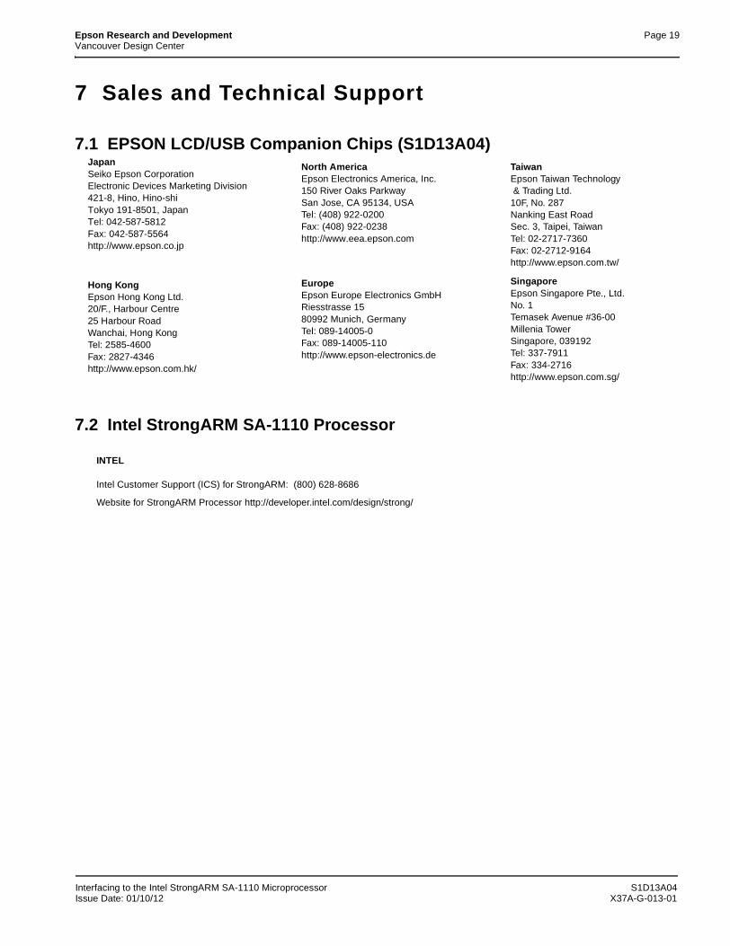
Epson Research and Development Page 19Vancouver Design Center
7 Sales and Technical Support
7.1 EPSON LCD/USB Companion Chips (S1D13A04)
7.2 Intel StrongARM SA-1110 Processor
JapanSeiko Epson CorporationElectronic Devices Marketing Division421-8, Hino, Hino-shiTokyo 191-8501, JapanTel: 042-587-5812Fax: 042-587-5564http://www.epson.co.jp
Hong KongEpson Hong Kong Ltd.20/F., Harbour Centre25 Harbour RoadWanchai, Hong KongTel: 2585-4600Fax: 2827-4346http://www.epson.com.hk/
TaiwanEpson Taiwan Technology & Trading Ltd.10F, No. 287Nanking East RoadSec. 3, Taipei, TaiwanTel: 02-2717-7360Fax: 02-2712-9164http://www.epson.com.tw/
SingaporeEpson Singapore Pte., Ltd.No. 1Temasek Avenue #36-00Millenia TowerSingapore, 039192Tel: 337-7911Fax: 334-2716http://www.epson.com.sg/
EuropeEpson Europe Electronics GmbHRiesstrasse 1580992 Munich, GermanyTel: 089-14005-0Fax: 089-14005-110http://www.epson-electronics.de
North AmericaEpson Electronics America, Inc.150 River Oaks ParkwaySan Jose, CA 95134, USATel: (408) 922-0200Fax: (408) 922-0238http://www.eea.epson.com
INTEL
Intel Customer Support (ICS) for StrongARM: (800) 628-8686
Website for StrongARM Processor http://developer.intel.com/design/strong/
Interfacing to the Intel StrongARM SA-1110 Microprocessor S1D13A04Issue Date: 01/10/12 X37A-G-013-01

Page 20 Epson Research and DevelopmentVancouver Design Center
THIS PAGE LEFT BLANK
S1D13A04 Interfacing to the Intel StrongARM SA-1110 MicroprocessorX37A-G-013-01 Issue Date: 01/10/12