probing the wavefunction of the surface states in bi 2 se 3 topological insulator: a realistic...
TRANSCRIPT
arX
iv:s
ubm
it/08
3795
5 [
cond
-mat
.mes
-hal
l] 4
Nov
201
3
Probing the wavefunction of the surface states in Bi2Se3 topological insulator: a
realistic tight-binding approach
A. Pertsova and C. M. CanaliDepartment of Physics and Electrical Engineering,
Linnæus University, Norra Vagen 49, 391 82, Kalmar, Sweden
(Dated: November 4, 2013)
We report on microscopic tight-binding modeling of surface states in Bi2Se3 three-dimensionaltopological insulator, based on a sp3 Slater-Koster Hamiltonian, with parameters calculated fromdensity functional theory. The effect of spin-orbit interaction on the electronic structure of the bulkand of a slab with finite thickness is investigated. In particular, a phenomenological criterion ofband inversion is formulated for both bulk and slab, based on the calculated atomic- and orbital-projections of the wavefunctions, associated with valence and conduction band extrema at the centerof the Brillouin zone. We carry out a thorough analysis of the calculated bandstructures of slabs withvarying thickness, where surface states are identified using a quantitative criterion according to theirspatial distribution. The thickness-dependent energy gap, attributed to inter-surface interaction,and the emergence of gapless surface states for slabs above a critical thickness are investigated. Wemap out the transition to the infinite-thickness limit by calculating explicitly the modifications inthe spatial distribution and spin-character of the surface states wavefunction with increasing the slabthickness. Our numerical analysis shows that the system must be approximately forty quintuple-layers thick to exhibit completely decoupled surface states, localized on the opposite surfaces. Theseresults have implications on the effect of external perturbations on the surface states near the Diracpoint.
PACS numbers: 73.20.At, 71.15.-m, 73.90.+f
I. INTRODUCTION
Topological insulator1,2 (TI) materials host on theirboundaries a novel type of topological states of quan-tum matter, which, unlike the quantum Hall state, existwithout the breaking of time-reversal symmetry.3,4 The-oretical prediction and subsequent experimental demon-stration of these topological states in both two-5,6 (2D)and three-dimensional7–17 (3D) systems have given riseto what is now one of the most rapidly developing fieldsin condensed matter physics. Apart from providing atest platform for fundamental concepts, the study of TIsholds promise for novel applications in materials scienceand chemistry,18 spintronics19 and quantum computa-tion.20,21 However, to be able to fully explore the poten-tial of TIs, it is essential to have a detailed knowledge ofthe nature and properties of topological surface states inreal TI materials,22 as well as a quantitative understand-ing of how they respond to external perturbations.23–25
Experimentally, these questions are being addressed withadvanced surface-sensitive experimental probes, such asspin- and angle-resolved photoemission spectroscopy16
[(SR)-ARPES] and scanning tunneling microscopy26,27
(STM).
Along with experimental advances, there is a grow-ing need for atomistic modeling of TIs that would en-able quantitative predictions and direct comparison withexperiment. Significant progress has been made in us-ing ab initio methods to calculate electronic13,28–30 andmagnetic31–34 properties of TIs. However, such methodssuffer from severe computational limitations, particularlyin the case of slab geometry as well as surface supercell
calculations, which are employed in studies of impurity-doping effects. In addition, more accurate ab initio meth-ods often lack the conceptual transparency and flexibilityof the model Hamiltonian approaches, which have beenof fundamental importance for driving progress in thisresearch field.3,4 Microscopic tight-binding (TB) models,which have already proved successful in quantitative de-scription of electronic and magnetic properties of semi-conductors,35,36 may provide a convenient platform toaddress similar issues in TIs. Several studies have re-cently appeared in the literature, in which TB descrip-tions with different level of complexity have been intro-duced, ranging from models built on a simplified latticestructure37 or a restricted orbital basis set inferred fromsymmetry arguments38,39 to fully microscopic models,with parameters extracted from density functional the-ory (DFT).28,40–42 To date, the latter class of models isstill the least represented among the model Hamiltonianapproaches to TIs.In this work we employ a microscopic TB model to
study the properties of surface states in Bi2Se3, a pro-totypical 3D TI, which belongs, along with Bi2Te3 andSb2Te3, to the family of binary tetradymite semiconduc-tors with layered structure.43 Although these materialshave been studied for decades due to their excellent ther-moelectric properties,44–46 they have recently attractedconsiderable attention as 3D TIs, e.g. materials thatexhibit topologically protected conducting surface stateswith linear (Dirac) dispersion and helical spin-texture,traversing the bulk insulating gap.14–17 Due to a rela-tively large band gap (0.3 eV for Bi2Se3) and rather sim-ple surface states, consisting of a single Dirac cone,16 theBi2Se3 family of 3D TIs is the most studied both exper-
2
imentally and theoretically.
Our treatment is based on the sp3 Slater-KosterHamiltonian.47 We use the parametrization developed byKobayashi,40 by fitting to DFT calculations. Through-out this work, our strategy has been to make use of thecomputational efficiency and simplifications, offered bythe TB approach, in order to investigate key features ofthe surface states in Bi2Se3 3D TI, which are inaccessi-ble by ab initio methods. Importantly, we consider slabswith thicknesses ranging from 1 to 100 quintuple layers(QLs), which corresponds to length scales in the range of1-100 nm. In contrast, thicknesses typically investigatedin ab-initio–based studies do not exceed several quintu-ple layers.30 In agreement with previous reports,48–50 wefind a gap due to interaction between opposite surfaces,which decreases with increasing the slab thickness. Start-ing from 5 QLs, the size of the gap becomes smaller than10−3 eV, and one can identify surface states with lineardispersion and helical spin-texture. For each slab thick-ness we determine the surface character of Bloch statesusing the procedure put forward in Ref. 29, i.e. based onthe contribution of the real-space projected wavefunctiononto the two surfaces of the slab.
Explicit calculations of the atomic- and orbital-projections of the wavefunctions, associated with valenceand conduction band extrema in both bulk and slab ge-ometry, allowed us to construct a phenomenological pic-ture of band inversion. The latter effect is induced byspin-orbit interaction and is responsible for the occur-rence of topological surface states across the bulk insu-lating gap.13 Furthermore, based on a similar analysis,we were able to track the changes in the spatial distri-bution and the spin character of the surface states wave-functions at and in the vicinity of the Dirac point, for in-creasing slab thickness. Our calculations showed that thestates corresponding to top and bottom surfaces becomecompletely decoupled, i.e. spatially separated, only forvery thick slabs containing 40 QLs. We also calculatedthe spin-orientation of the surface states in momentumspace as a function of thickness. The disturbances inthe helical spin-texture, expressed through in-plane andout-of-plane tilting angles of the spin, are shown to besignificant for thin slabs up to 10 QLs and are manifesta-tions of both inter-surface interaction and the proximityto bulk states.
The rest of the paper is organized as follows. In Sec-tion II we discuss the details of the TB model and somecomputational aspects. The results of the simulations arepresented in Section III. We begin in Section III A by ana-lyzing the effect of SO on the bulk bandstructures, wherethe bulk band inversion is interpreted as a characteristicchange in the spatial distributions of the orbital-resolvedprojections of the wavefunctions at conductance and va-lence band extrema at the Γ point. The results of surfacebandstructure calculations are presented in Section III B,in particular the spatial character of the states emergingwithin the bulk gap and the opening of the gap at finitethicknesses are described quantitatively in Section III B 1.
We also discuss the procedure to identify the invertedcharacter on conduction and valence bands in the pres-ence of SO for a slab geometry. In Section III B 2, basedon the analysis of the wavefunctions of the states at theDirac point, a quantitative criterion of an infinitely thickslab, with no interaction between the surfaces, is formu-lated. In addition, we comment on the orbital characterof the wavefunctions at the Dirac point, especially onthe non-negligible contribution of the in-plane p-orbitals.The spin-properties of the Dirac-cone states and devi-ations from the perfect spin-momentum locking due tointer-surface interaction and the presence of bulk statesare calculated in Section III B 3. Finally, Section IV con-tains our conclusions.
II. METHODS
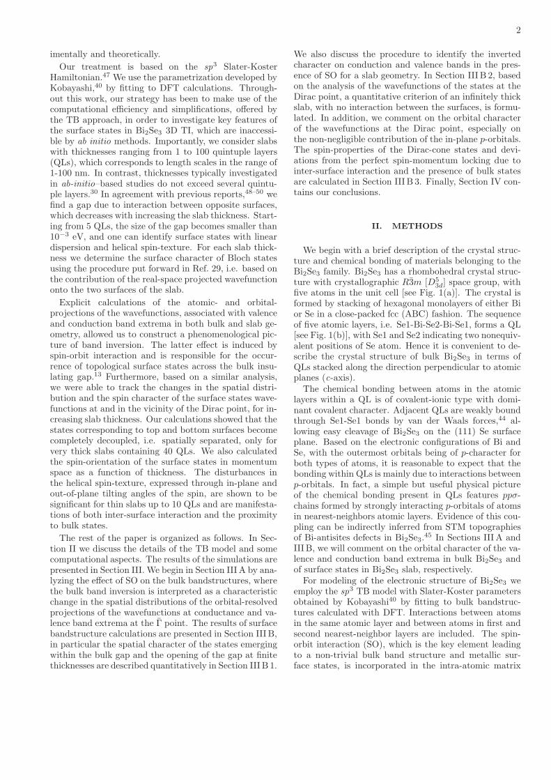
We begin with a brief description of the crystal struc-ture and chemical bonding of materials belonging to theBi2Se3 family. Bi2Se3 has a rhombohedral crystal struc-ture with crystallographic R3m [D5
3d] space group, withfive atoms in the unit cell [see Fig. 1(a)]. The crystal isformed by stacking of hexagonal monolayers of either Bior Se in a close-packed fcc (ABC) fashion. The sequenceof five atomic layers, i.e. Se1-Bi-Se2-Bi-Se1, forms a QL[see Fig. 1(b)], with Se1 and Se2 indicating two nonequiv-alent positions of Se atom. Hence it is convenient to de-scribe the crystal structure of bulk Bi2Se3 in terms ofQLs stacked along the direction perpendicular to atomicplanes (c-axis).The chemical bonding between atoms in the atomic
layers within a QL is of covalent-ionic type with domi-nant covalent character. Adjacent QLs are weakly boundthrough Se1-Se1 bonds by van der Waals forces,44 al-lowing easy cleavage of Bi2Se3 on the (111) Se surfaceplane. Based on the electronic configurations of Bi andSe, with the outermost orbitals being of p-character forboth types of atoms, it is reasonable to expect that thebonding within QLs is mainly due to interactions betweenp-orbitals. In fact, a simple but useful physical pictureof the chemical bonding present in QLs features ppσ-chains formed by strongly interacting p-orbitals of atomsin nearest-neighbors atomic layers. Evidence of this cou-pling can be indirectly inferred from STM topographiesof Bi-antisites defects in Bi2Se3.
45 In Sections III A andIII B, we will comment on the orbital character of the va-lence and conduction band extrema in bulk Bi2Se3 andof surface states in Bi2Se3 slab, respectively.For modeling of the electronic structure of Bi2Se3 we
employ the sp3 TB model with Slater-Koster parametersobtained by Kobayashi40 by fitting to bulk bandstruc-tures calculated with DFT. Interactions between atomsin the same atomic layer and between atoms in first andsecond nearest-neighbor layers are included. The spin-orbit interaction (SO), which is the key element leadingto a non-trivial bulk band structure and metallic sur-face states, is incorporated in the intra-atomic matrix
3
FIG. 1. (Color online) Crystal structure of Bi2Se3. (a) Rhom-bohedral unit cell of the bulk crystal. Se1 and Se2 refer totwo non-equivalent positions of Se atoms. (b) The structureof 1 QL formed by five alternating atomic layers of Bi andSe. (c) The Brillouin zone of the bulk crystal and that of the(111) surface of Bi2Se3.
elements.51 Thus the Hamiltonian of the system reads
H(k) =∑
ii′,σ
αα′
tαα′
ii′ eik·rii′ cσ†iα c
σi′α′ (1)
+∑
i,σσ′
αα′
λi 〈i, α, σ| ~L · ~S |i, α′, σ′〉 cσ†iα cσ′
iα′ ,
where k is the reciprocal-lattice vector that spans theBrillouin zone, i(i′) is the atomic index, α(α′) labelsatomic orbitals {s , px, py, pz}, and σ(σ′) denotes thespin. Here i refers to the atomic positions in the unitcell, while i′ 6=i runs over all neighbors of atom i, includ-ing atoms in the adject cells, with rii′ being the vectorconnecting the two atoms (rii′=0 for i=i′). The coef-
ficients tαα′
ii′ are the Slater-Koster parameters (for i=i′
tαα′
ii′ ≡ tααii give the on-site energies) and cσ†iα(cσiα) is the
creation(annihilation) operator for an electron with spinσ at the atomic orbital α of site i. The second term inEq. (1) represents the on-site SO, where |i, α, σ〉 are spin-
and orbital-resolved atomic orbitals, ~L is the orbital an-
gular momentum operator and ~S is the spin operator;λi is the SO strength. We refer to Ref. 40 for the exactparametrization of tαα
′
ii′ and λi.In bulk-bandstructure calculations we use the rhombo-
hedral unit cell with five nonequivalent atoms, with thecell repeated periodically in x-, y- and z-directions. Incalculations involving the Bi2Se3 (111) surface we con-sider a slab consisting of N quintuple layers, or, equiva-lently, of 5N atomic layers. Since each atomic layer is anequilateral triangular lattice, it is sufficient to assign oneatom per each layer, which gives a total of 5N atoms inthe slab unit cell. The slab is finite along the z-direction(QL-stacking axis), with the unit cell repeated periodi-cally in the x-y plane. Using this TB model we were ableto compute bandstructures of slabs with thicknesses upto 100 QLs with a reasonable computational cost.
III. RESULTS AND DISCUSSION
A. Band inversion in bulk Bi2Se3
The presence of gapless edge or surface states, ro-bust against time-reversal-invariant perturbations, dis-tinguishes a topological insulating phase from a trivialone. However, in order to elucidate the origin of the topo-logical order in existing TIs and to facilitate the search fornew TI materials, it is necessary to have a set of criteriathat allow us to differentiate between topologically triv-ial and non-trivial insulators, based on the informationabout their bulk properties. Within the framework oftopological band theory,4,7–9,11,52 time-reversal-invariantinsulators are classified according to a Z2 topological in-variant, assigned to their bandstructure. In 2D thereis a single Z2 invariant, which distinguishes the quan-tum spin-Hall state (2D TI), as in HgTe/CdTe quantumwells, from an ordinary insulator. In 3D a set of four Z2
invariants leads to a classification based of three classes,namely strong TIs, weak TIs and ordinary insulators.For systems with inversion symmetry, the Z2 invariant isdetermined by the product of the parity eigenvalues ofoccupied bands at the time-reversal-invariant momentain the Brillouin zone.8 Using this scheme, a few strongTIs have been predicted, such as strained α-Sn and HgTe,Bi1−xSbx and Bi2Se3-like 3D TIs.The emergence of topological order can be understood
using the concept of band inversion.8,13,53,54 Clearly, anecessary condition for a TI is the existence of a non-trivial bulk band gap. In fact, in the above mentionedmaterials, a topological phase transition, or alternativelya change in the value of the Z2 invariant which in turnimplies the existence of gapless states on the boundary,is accompanied by a visible and well-defined change inthe bandstructure. This change occurs precisely in theinsulating gap and can be observed as a function of anexternal or an intrinsic parameter. In HgTe, which is azero-gap semiconductor but acquires a gap due to exter-nal potential in a quantum well structure, the bands withs- and p-character are inverted with respect to their usualsequence at the Γ point.5 A similar mechanism is real-ized in strained α-Sn, which has recently been shown toexhibit a 3D TI phase, with Dirac-like surface states em-
4
anating from the second lowest valence band across thestrained-induced gap.42 In Bi1−xSbx alloy the invertedbandstructure is characterized by a change in the orderof the bands with even (Ls) and odd (La) parity at theL point of the Brillouin zone compared to pure Bi. Thisinversion is induced by Sb doping and is due to the strongTI character of the valence band of pure Sb.8 In Bi2Se33D TI a non-trivial bulk band gap owns its existence toSO, with the parity of the valence and conduction bandinverted at the Γ point.13 Without SO the material wouldbe a trivial insulator. However, in the presence of SO thechange in the parity of one of the occupied bands leadsto a change in the value of the Z2 invariant, signaling atopological phase transition.An intuitive way of describing band inversion theoret-
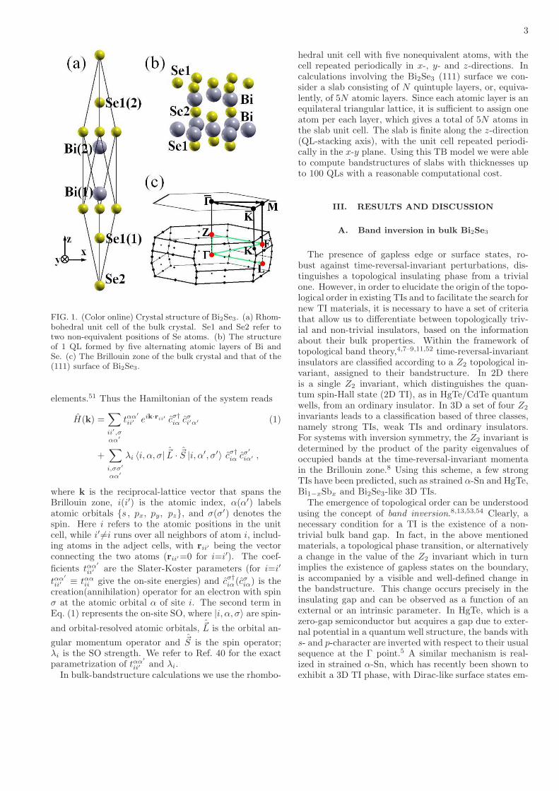
ically is to look at charge density distributions of theinverted bands at the point of the Brillouin zone, wherethe inversion is expected to occur, as functions of a char-acteristic parameter.53 Here we apply this procedure tobulk Bi2Se3. The calculated bandstructures without andwith SO are shown in Fig. 2(a) and (b), respectively. Theeffect of SO is clearly seen as an increase of the gap anda change in the curvature of the valence band at the Γpoint.
-2
-1
0
1
2
Γ ΓΖ F L-2
-1
0
1
2
Ene
rgy
(eV
)
Γ ΓΖ F L
(b)(a)
SO=0
FIG. 2. Bandstructures of bulk Bi2Se3 (a) without and (b)with spin-orbit interaction. Dashed lines show the positionof the Fermi level, taken as a reference energy. Filled(open)circles indicate the position of VBM(CBM) at the Γ point ofthe bulk Brillouin zone. The Brillouin zone of the bulk crystaland the path along the high-symmetry directions are depictedin Fig. 1(c).
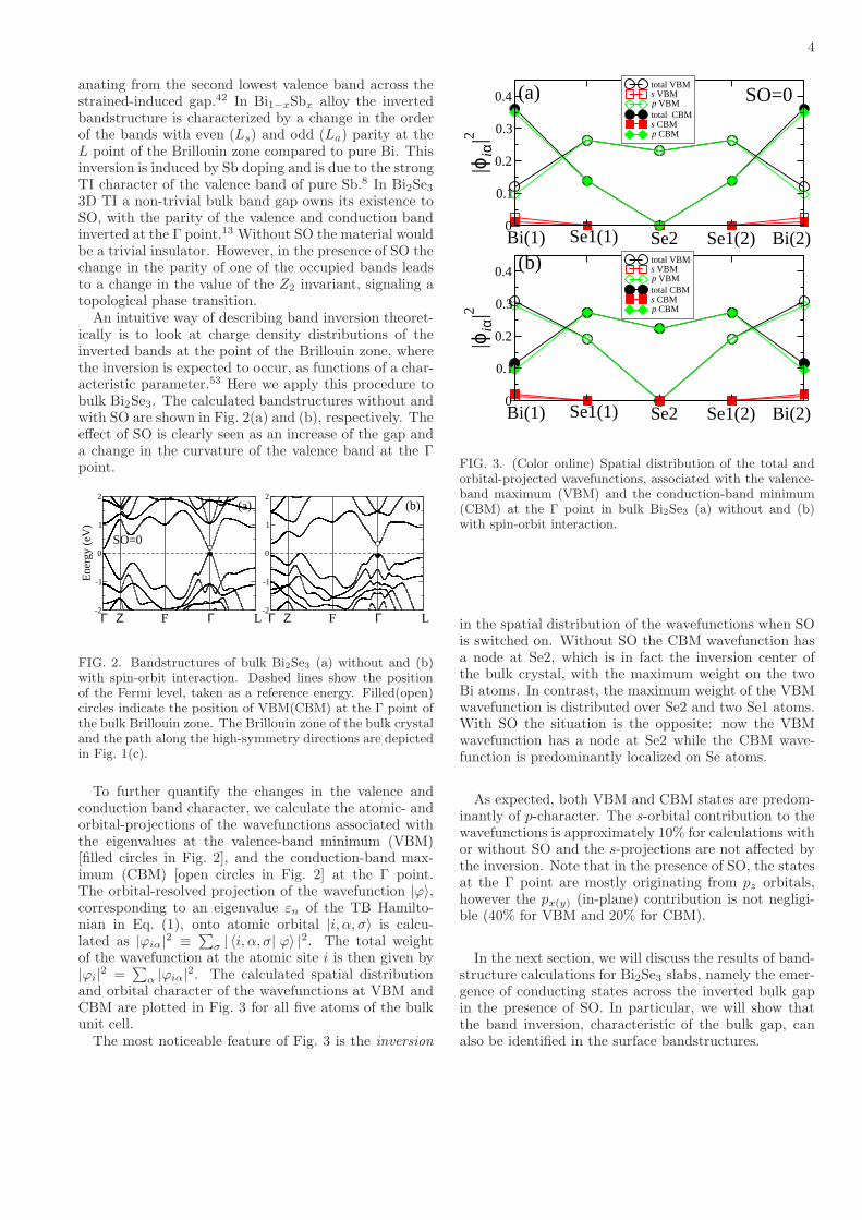
To further quantify the changes in the valence andconduction band character, we calculate the atomic- andorbital-projections of the wavefunctions associated withthe eigenvalues at the valence-band minimum (VBM)[filled circles in Fig. 2], and the conduction-band max-imum (CBM) [open circles in Fig. 2] at the Γ point.The orbital-resolved projection of the wavefunction |ϕ〉,corresponding to an eigenvalue εn of the TB Hamilto-nian in Eq. (1), onto atomic orbital |i, α, σ〉 is calcu-lated as |ϕiα|
2 ≡∑
σ | 〈i, α, σ| ϕ〉 |2. The total weight
of the wavefunction at the atomic site i is then given by|ϕi|
2 =∑
α |ϕiα|2. The calculated spatial distribution
and orbital character of the wavefunctions at VBM andCBM are plotted in Fig. 3 for all five atoms of the bulkunit cell.The most noticeable feature of Fig. 3 is the inversion
0
0.1
0.2
0.3
0.4
|ϕiα
|2
total VBMs VBMp VBMtotal CBMs CBMp CBM
Bi(1) Se1(1) Se2 Se1(2) Bi(2)
0
0.1
0.2
0.3
0.4
|ϕiα
|2
total VBMs VBMp VBMtotal CBMs CBMp CBM
Bi(1) Se1(1) Se2 Se1(2) Bi(2)
SO=0(a)
(b)
FIG. 3. (Color online) Spatial distribution of the total andorbital-projected wavefunctions, associated with the valence-band maximum (VBM) and the conduction-band minimum(CBM) at the Γ point in bulk Bi2Se3 (a) without and (b)with spin-orbit interaction.
in the spatial distribution of the wavefunctions when SOis switched on. Without SO the CBM wavefunction hasa node at Se2, which is in fact the inversion center ofthe bulk crystal, with the maximum weight on the twoBi atoms. In contrast, the maximum weight of the VBMwavefunction is distributed over Se2 and two Se1 atoms.With SO the situation is the opposite: now the VBMwavefunction has a node at Se2 while the CBM wave-function is predominantly localized on Se atoms.
As expected, both VBM and CBM states are predom-inantly of p-character. The s-orbital contribution to thewavefunctions is approximately 10% for calculations withor without SO and the s-projections are not affected bythe inversion. Note that in the presence of SO, the statesat the Γ point are mostly originating from pz orbitals,however the px(y) (in-plane) contribution is not negligi-ble (40% for VBM and 20% for CBM).
In the next section, we will discuss the results of band-structure calculations for Bi2Se3 slabs, namely the emer-gence of conducting states across the inverted bulk gapin the presence of SO. In particular, we will show thatthe band inversion, characteristic of the bulk gap, canalso be identified in the surface bandstructures.
5
B. Wavefunction-based analysis of surface states in
Bi2Se3 slab
1. Surface bandstructures and thickness-dependent gap
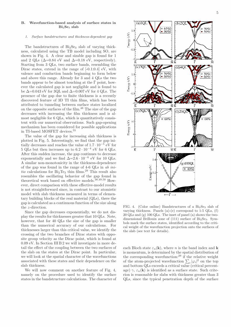
The bandstructures of Bi2Se3 slab of varying thick-ness, calculated using the TB model including SO, areshown in Fig. 4. A clear and sizable gap is found for 1and 2 QLs (∆=0.84 eV and ∆=0.18 eV, respectively).Starting from 3 QLs, two surface bands, resembling theDirac states, extend in the range of [-0.1;0.4] eV, withvalence and conduction bands beginning to form belowand above this range. Already for 3 and 4 QLs the twobands appear to be almost touching at the Γ point, how-ever the calculated gap is not negligible and is found tobe ∆=0.043 eV for 3QL and ∆=0.007 eV for 4 QLs. Thepresence of the gap due to finite thickness is a recentlydiscovered feature of 3D TI thin films, which has beenattributed to tunneling between surface states localizedon the opposite surfaces of the film.48 The size of the gapdecreases with increasing the film thickness and is al-most negligible for 6 QLs, which is quantitatively consis-tent with our numerical observations. Such gap-openingmechanism has been considered for possible applicationsin TI-based MOSFET devices.55
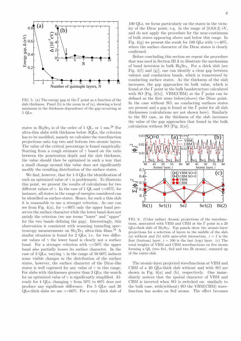
The value of the gap for increasing slab thickness isplotted in Fig. 5. Interestingly, we find that the gap ini-tially decreases and reaches the value of 1.7 · 10−5 eV for5 QLs but then increases up to 6.2 · 10−4 eV for 6 QLs.After this sudden increase, the gap continues to decreaseexponentially and we find ∆=2.6 · 10−6 eV for 10 QLs.A similar non-monotonicity in the thickness-dependenceof the gap was found in the range of 4-6 QLs in ab ini-
tio calculations for Bi2Te3 thin films.29 This result alsoresembles the oscillating behavior of the gap found intheoretical work based on effective models.38,49,50 How-ever, direct comparison with these effective-model resultsis not straightforward since, in contrast to our atomisticmodel with slab thickness measured in terms of elemen-tary building blocks of the real material (QLs), there thegap is calculated as a continuous function of the size alongthe z-direction.Since the gap decreases exponentially, we do not dis-
play the results for thicknesses greater that 10 QLs. Note,however, that for 40 QLs the size of the gap is smallerthan the numerical accuracy of our calculations. Forthicknesses larger than this critical value, we identify thecrossing of the two branches of Dirac states with oppo-site group velocity as the Dirac point, which is found at0.09 eV. In Section III B 2 we will investigate in more de-tail the effect of the coupling between the two surfaces ofthe slab on the states at the Dirac point. In particular,we will look at the spatial character of the wavefunctionsassociated with these states and their dependence on theslab thickness.We will now comment on another feature of Fig. 4,
namely on the procedure used to identify the surfacestates in the bandstructure calculations. The character of
FIG. 4. (Color online) Bandstructures of a Bi2Se3 slab ofvarying thickness. Panels (a)-(e) correspond to 1-5 QLs, (f)20 QLs and (g) 100 QLs. The inset of panel (a) shows the two-dimensional Brillouin zone of (111) surface of Bi2Se3. Sym-bols mark the surface states, identified according to the criti-cal weight of the wavefunction projection onto the surfaces ofthe slab (see text for details).
each Bloch state εn(k), where n is the band index and k
is momentum, is determined by the spatial distribution ofthe corresponding wavefunction:29 if the relative weightof the atom-projected wavefunction
∑i |ϕi|
2 on the topand bottom QLs exceeds a critical value (critical percent-age) γ, εn(k) is identified as a surface state. Such crite-rion is reasonable for slabs with thickness greater than 3QLs, since the typical penetration depth of the surface
6
1 2 3 4 5 6 7 8 9 10Number of quintuple layers, N
0.2
0.4
0.6
0.8E
nerg
y ga
p, ∆
(eV
)
4 5 6 7 8 9 10N
0
2
4
6
8
∆ (1
0-3eV
)
(a)(b)
FIG. 5. (a) The energy gap at the Γ point as a function of theslab thickness. Panel (b) is the zoom in of (a), showing a localminimum in the thickness dependence of the gap occurring at5 QLs.
states in Bi2Se3 is of the order of 1 QL, or 1 nm.28 Forultra-thin slabs with thickness below 3QLs, the criterionhas to be modified, namely we calculate the wavefunctionprojections onto top two and bottom two atomic layers.The value of the critical percentage is found empirically.Starting from a rough estimate of γ based on the ratiobetween the penetration depth and the slab thickness,the value should then be optimized in such a way thata small change around this value does not significantlymodify the resulting distribution of the surface states.
We find, however, that for 1-3 QLs the identification ofsuch an optimized value of γ is problematic. To illustratethis point, we present the results of calculations for twodifferent values of γ. In the case of 1 QL and γ=65%, forinstance, all states in the range of energies considered canbe identified as surface states. Hence, for such a thin slabit is reasonable to use a stronger criterion. As one cansee from Fig. 4(a), for γ=90% only the upper band pre-serves the surface character while the lower band does notsatisfy the criterion (we use terms ”lower” and ”upper”for the two bands defining the gap). Interestingly, thisobservation is consistent with scanning tunneling spec-troscopy measurements on Sb2Te3 ultra-thin films.56 Asimilar situation is found for 2 QLs, i.e. for two differ-ent values of γ the lower band is clearly not a surfaceband. For a stronger criterion with γ=50% the upperband also partially looses its surface character. In thecase of 3 QLs, varying γ in the range of 50-60% inducessome visible changes in the distribution of the surfacestates, however, the surface character of the Dirac-likestates is well captured for any value of γ in this range.For slabs with thicknesses greater than 3 QLs, the searchfor an optimized value of γ is significantly simplified. Al-ready for 4 QLs, changing γ from 50% to 60% does notproduce any significant difference. For 5 QLs- and 20QLs-thick slabs we use γ=60%. For a very thick slab of
100 QLs, we focus particularly on the states in the vicin-ity of the Dirac point, e.g. in the range of [0.0;0.3] eV,and do not apply the procedure for the near-continuumof bulk states appearing above and below this range. InFig. 4(g) we present the result for 100 QLs with γ=40%,where the surface character of the Dirac states is clearlyconfirmed.Before concluding this section we repeat the procedure
that was used in Section IIIA to illustrate the mechanismof band inversion in bulk Bi2Se3. For a thick slab [seeFig. 4(f) and (g)], one can identify a clear gap betweenvalence and conduction bands, which is transversed byconducting surface states. As the thickness of the slabincreases, the gap approaches its bulk value, which isfound at the Γ point in the bulk bandstructure calculatedwith SO [Fig. 2(b)]. VBM(CBM) at the Γ point can bedefined as the first state below(above) the Dirac point.In the case without SO, no conducting surfaces statesare present and a gap is found at the Γ point for all slabthicknesses (calculations are not shown here). Similarlyto the SO case, as the thickness of the slab increasesthe value of the gap approaches that found in the bulkcalculation without SO [Fig. 2(a)].
0
0.1
0.2
0.3
0.4
0.5
Σ i|ϕ
i|2
VBM SO=0CBM SO=0VBMCBM
40 45 50 55 60Atomic layer, i
0
0.02
0.04
40 45 50 55 60Atomic layer, i
0
0.01
0.02
0.03|ϕ
i|2
VBMCBM
Bi(1) Se1(1) Se2 Se1(2) Bi(2)
(a)SO=0
Se2Se2 Se2 Se2 Se2 Se2 Se2 Se2
(b)
(c)
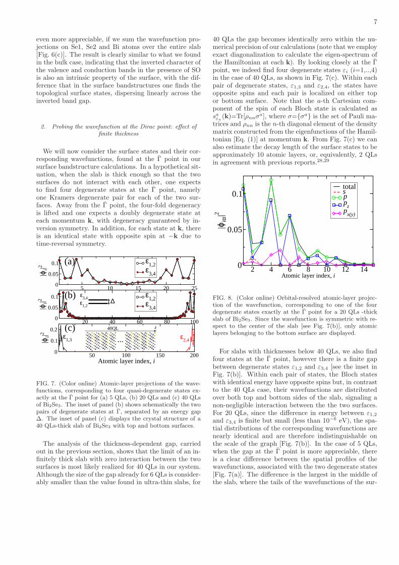
FIG. 6. (Color online) Atomic projections of the wavefunc-tions, associated with VBM and CBM at the Γ point in a 20QLs-thick slab of Bi2Se3. Top panels show the atomic-layerprojections for a selection of layers in the middle of the slab(a) without and (b) with spin-orbit interaction. i = 1 is thefirst (bottom) layer, i = 100 is the last (top) layer. (c) Thetotal weights of VBM and CBM wavefunctions on five atomsforming a QL (two Se1, Se2 and two Bi atoms), summed upof the entire slab.
The atomic-layer projected wavefunctions at VBM andCBM of a 20 QLs-thick slab without and with SO areshown in Fig. 6(a) and (b), respectively. One imme-diately notices that the spatial character of VBM andCBM is inverted when SO is switched on: similarly tothe bulk case, with(without) SO the VBM(CBM) wave-function has nodes on Se2 atoms. The effect becomes
7
even more appreciable, if we sum the wavefunction pro-jections on Se1, Se2 and Bi atoms over the entire slab[Fig. 6(c)]. The result is clearly similar to what we foundin the bulk case, indicating that the inverted character ofthe valence and conduction bands in the presence of SOis also an intrinsic property of the surface, with the dif-ference that in the surface bandstructures one finds thetopological surface states, dispersing linearly across theinverted band gap.
2. Probing the wavefunction at the Dirac point: effect of
finite thickness
We will now consider the surface states and their cor-responding wavefunctions, found at the Γ point in oursurface bandstructure calculations. In a hypothetical sit-uation, when the slab is thick enough so that the twosurfaces do not interact with each other, one expectsto find four degenerate states at the Γ point, namelyone Kramers degenerate pair for each of the two sur-faces. Away from the Γ point, the four-fold degeneracyis lifted and one expects a doubly degenerate state ateach momentum k, with degeneracy guaranteed by in-version symmetry. In addition, for each state at k, thereis an identical state with opposite spin at −k due totime-reversal symmetry.
5 10 15 20 250
0.05
0.1
|ϕi|2
ε1,2
ε3,4
20 40 60 80 1000
0.05
0.1
|ϕi|2
ε1,2
ε3,4
50 100 150 200Atomic layer index, i
0
0.1
0.2
|ϕi|2 ε
1,3 ε2,4
(a)
(b)
(c)
ε1,2
ε3,4 ∆
z
...
40QL
FIG. 7. (Color online) Atomic-layer projections of the wave-functions, corresponding to four quasi-degenerate states ex-actly at the Γ point for (a) 5 QLs, (b) 20 QLs and (c) 40 QLsof Bi2Se3. The inset of panel (b) shows schematically the twopairs of degenerate states at Γ, separated by an energy gap∆. The inset of panel (c) displays the crystal structure of a40 QLs-thick slab of Bi2Se3 with top and bottom surfaces.
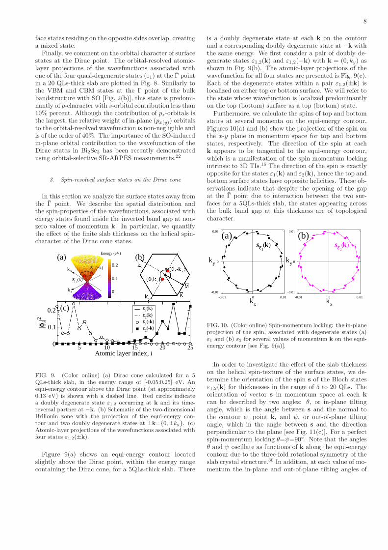
The analysis of the thickness-dependent gap, carriedout in the previous section, shows that the limit of an in-finitely thick slab with zero interaction between the twosurfaces is most likely realized for 40 QLs in our system.Although the size of the gap already for 6 QLs is consider-ably smaller than the value found in ultra-thin slabs, for
40 QLs the gap becomes identically zero within the nu-merical precision of our calculations (note that we employexact diagonalization to calculate the eigen-spectrum ofthe Hamiltonian at each k). By looking closely at the Γpoint, we indeed find four degenerate states εi (i=1,..,4)in the case of 40 QLs, as shown in Fig. 7(c). Within eachpair of degenerate states, ε1,3 and ε2,4, the states haveopposite spins and each pair is localized on either topor bottom surface. Note that the a-th Cartesian com-ponent of the spin of each Bloch state is calculated assaεn(k)=Tr[ρnnσ
a], where σ={σa} is the set of Pauli ma-trices and ρnn is the n-th diagonal element of the densitymatrix constructed from the eigenfunctions of the Hamil-tonian [Eq. (1)] at momentum k. From Fig. 7(c) we canalso estimate the decay length of the surface states to beapproximately 10 atomic layers, or, equivalently, 2 QLsin agreement with previous reports.28,29
2 4 6 8 10 12 14Atomic layer index, i
0
0.05
0.1
|ϕiα
|2
totalspp
zp
x(y)
FIG. 8. (Color online) Orbital-resolved atomic-layer projec-tion of the wavefunction, corresponding to one of the fourdegenerate states exactly at the Γ point for a 20 QLs -thickslab of Bi2Se3. Since the wavefunction is symmetric with re-spect to the center of the slab [see Fig. 7(b)], only atomiclayers belonging to the bottom surface are displayed.
For slabs with thicknesses below 40 QLs, we also findfour states at the Γ point, however there is a finite gapbetween degenerate states ε1,2 and ε3,4 [see the inset inFig. 7(b)]. Within each pair of states, the Bloch stateswith identical energy have opposite spins but, in contrastto the 40 QLs case, their wavefunctions are distributedover both top and bottom sides of the slab, signaling anon-negligible interaction between the the two surfaces.For 20 QLs, since the difference in energy between ε1,2and ε3,4 is finite but small (less than 10−6 eV), the spa-tial distributions of the corresponding wavefunctions arenearly identical and are therefore indistinguishable onthe scale of the graph [Fig. 7(b)]. In the case of 5 QLs,when the gap at the Γ point is more appreciable, thereis a clear difference between the spatial profiles of thewavefunctions, associated with the two degenerate states[Fig. 7(a)]. The difference is the largest in the middle ofthe slab, where the tails of the wavefunctions of the sur-
8
face states residing on the opposite sides overlap, creatinga mixed state.Finally, we comment on the orbital character of surface
states at the Dirac point. The orbital-resolved atomic-layer projections of the wavefunctions associated withone of the four quasi-degenerate states (ε1) at the Γ pointin a 20 QLs-thick slab are plotted in Fig. 8. Similarly tothe VBM and CBM states at the Γ point of the bulkbandstructure with SO [Fig. 2(b)], this state is predomi-nantly of p-character with s-orbital contribution less than10% percent. Although the contribution of pz-orbitals isthe largest, the relative weight of in-plane (px(y)) orbitalsto the orbital-resolved wavefunction is non-negligible andis of the order of 40%. The importance of the SO-inducedin-plane orbital contribution to the wavefunction of theDirac states in Bi2Se3 has been recently demonstratedusing orbital-selective SR-ARPES measurements.22
3. Spin-resolved surface states on the Dirac cone
In this section we analyze the surface states away fromthe Γ point. We describe the spatial distribution andthe spin-properties of the wavefunctions, associated withenergy states found inside the inverted band gap at non-zero values of momentum k. In particular, we quantifythe effect of the finite slab thickness on the helical spin-character of the Dirac cone states.
5 10 15 20 25Atomic layer index, i
0
0.1
0.2
|ϕi|2
ε1(k)
ε2(k)
ε1(-k)
ε2(-k)
0.1
0.2
0
xk
yk
(−k)ε1,2
ε1,2
(k)
Energy (eV)(b)(a)
(c)
FIG. 9. (Color online) (a) Dirac cone calculated for a 5QLs-thick slab, in the energy range of [-0.05:0.25] eV. Anequi-energy contour above the Dirac point (at approximately0.13 eV) is shown with a dashed line. Red circles indicatea doubly degenerate state ε1,2 occurring at k and its time-reversal partner at −k. (b) Schematic of the two-dimensionalBrillouin zone with the projection of the equi-energy con-tour and two doubly degenerate states at ±k={0,±ky}. (c)Atomic-layer projections of the wavefunctions associated withfour states ε1,2(±k).
Figure 9(a) shows an equi-energy contour locatedslightly above the Dirac point, within the energy rangecontaining the Dirac cone, for a 5QLs-thick slab. There
is a doubly degenerate state at each k on the contourand a corresponding doubly degenerate state at −k withthe same energy. We first consider a pair of doubly de-generate states ε1,2(k) and ε1,2(−k) with k = (0, ky) asshown in Fig. 9(b). The atomic-layer projections of thewavefunction for all four states are presented is Fig. 9(c).Each of the degenerate states within a pair ε1,2(±k) islocalized on either top or bottom surface. We will refer tothe state whose wavefunction is localized predominantlyon the top (bottom) surface as a top (bottom) state.Furthermore, we calculate the spins of top and bottom
states at several momenta on the equi-energy contour.Figures 10(a) and (b) show the projection of the spin onthe x-y plane in momentum space for top and bottomstates, respectively. The direction of the spin at eachk appears to be tangential to the equi-energy contour,which is a manifestation of the spin-momentum lockingintrinsic to 3D TIs.16 The direction of the spin is exactlyopposite for the states ε1(k) and ε2(k), hence the top andbottom surface states have opposite helicities. These ob-servations indicate that despite the opening of the gapat the Γ point due to interaction between the two sur-faces for a 5QLs-thick slab, the states appearing acrossthe bulk band gap at this thickness are of topologicalcharacter.
-0.01
0
0.01
-0.01 0 0.01
-0.01
0
0.01
-0.01 0 0.01
2
(a) (b)
kx
ks ( )ε
k
sε2k( )
1
x
ky
ky
FIG. 10. (Color online) Spin-momentum locking: the in-planeprojection of the spin, associated with degenerate states (a)ε1 and (b) ε2 for several values of momentum k on the equi-energy contour [see Fig. 9(a)].
In order to investigate the effect of the slab thicknesson the helical spin-texture of the surface states, we de-termine the orientation of the spin s of the Bloch statesε1,2(k) for thicknesses in the range of 5 to 20 QLs. Theorientation of vector s in momentum space at each k
can be described by two angles: θ, or in-plane tiltingangle, which is the angle between s and the normal tothe contour at point k, and ψ, or out-of-plane tiltingangle, which in the angle between s and the directionperpendicular to the plane [see Fig. 11(c)]. For a perfectspin-momentum locking θ=ψ=90◦. Note that the anglesθ and ψ oscillate as functions of k along the equi-energycontour due to the three-fold rotational symmetry of theslab crystal structure.30 In addition, at each value of mo-mentum the in-plane and out-of-plane tilting angles of
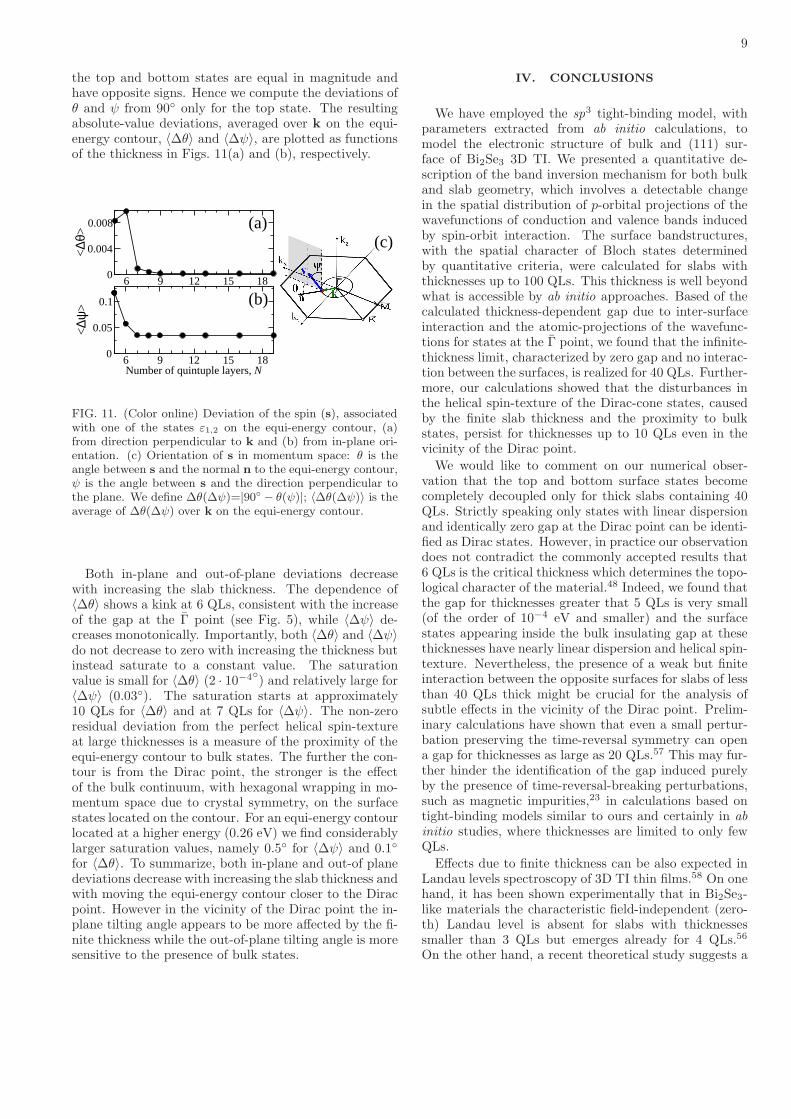
9
the top and bottom states are equal in magnitude andhave opposite signs. Hence we compute the deviations ofθ and ψ from 90◦ only for the top state. The resultingabsolute-value deviations, averaged over k on the equi-energy contour, 〈∆θ〉 and 〈∆ψ〉, are plotted as functionsof the thickness in Figs. 11(a) and (b), respectively.
6 9 12 15 180
0.004
0.008
<∆θ>
6 9 12 15 18Number of quintuple layers, N
0
0.05
0.1
<∆ψ
>
(c)(a)
(b)
FIG. 11. (Color online) Deviation of the spin (s), associatedwith one of the states ε1,2 on the equi-energy contour, (a)from direction perpendicular to k and (b) from in-plane ori-entation. (c) Orientation of s in momentum space: θ is theangle between s and the normal n to the equi-energy contour,ψ is the angle between s and the direction perpendicular tothe plane. We define ∆θ(∆ψ)=|90◦ − θ(ψ)|; 〈∆θ(∆ψ)〉 is theaverage of ∆θ(∆ψ) over k on the equi-energy contour.
Both in-plane and out-of-plane deviations decreasewith increasing the slab thickness. The dependence of〈∆θ〉 shows a kink at 6 QLs, consistent with the increaseof the gap at the Γ point (see Fig. 5), while 〈∆ψ〉 de-creases monotonically. Importantly, both 〈∆θ〉 and 〈∆ψ〉do not decrease to zero with increasing the thickness butinstead saturate to a constant value. The saturationvalue is small for 〈∆θ〉 (2 · 10−4◦) and relatively large for〈∆ψ〉 (0.03◦). The saturation starts at approximately10 QLs for 〈∆θ〉 and at 7 QLs for 〈∆ψ〉. The non-zeroresidual deviation from the perfect helical spin-textureat large thicknesses is a measure of the proximity of theequi-energy contour to bulk states. The further the con-tour is from the Dirac point, the stronger is the effectof the bulk continuum, with hexagonal wrapping in mo-mentum space due to crystal symmetry, on the surfacestates located on the contour. For an equi-energy contourlocated at a higher energy (0.26 eV) we find considerablylarger saturation values, namely 0.5◦ for 〈∆ψ〉 and 0.1◦
for 〈∆θ〉. To summarize, both in-plane and out-of planedeviations decrease with increasing the slab thickness andwith moving the equi-energy contour closer to the Diracpoint. However in the vicinity of the Dirac point the in-plane tilting angle appears to be more affected by the fi-nite thickness while the out-of-plane tilting angle is moresensitive to the presence of bulk states.
IV. CONCLUSIONS
We have employed the sp3 tight-binding model, withparameters extracted from ab initio calculations, tomodel the electronic structure of bulk and (111) sur-face of Bi2Se3 3D TI. We presented a quantitative de-scription of the band inversion mechanism for both bulkand slab geometry, which involves a detectable changein the spatial distribution of p-orbital projections of thewavefunctions of conduction and valence bands inducedby spin-orbit interaction. The surface bandstructures,with the spatial character of Bloch states determinedby quantitative criteria, were calculated for slabs withthicknesses up to 100 QLs. This thickness is well beyondwhat is accessible by ab initio approaches. Based of thecalculated thickness-dependent gap due to inter-surfaceinteraction and the atomic-projections of the wavefunc-tions for states at the Γ point, we found that the infinite-thickness limit, characterized by zero gap and no interac-tion between the surfaces, is realized for 40 QLs. Further-more, our calculations showed that the disturbances inthe helical spin-texture of the Dirac-cone states, causedby the finite slab thickness and the proximity to bulkstates, persist for thicknesses up to 10 QLs even in thevicinity of the Dirac point.
We would like to comment on our numerical obser-vation that the top and bottom surface states becomecompletely decoupled only for thick slabs containing 40QLs. Strictly speaking only states with linear dispersionand identically zero gap at the Dirac point can be identi-fied as Dirac states. However, in practice our observationdoes not contradict the commonly accepted results that6 QLs is the critical thickness which determines the topo-logical character of the material.48 Indeed, we found thatthe gap for thicknesses greater that 5 QLs is very small(of the order of 10−4 eV and smaller) and the surfacestates appearing inside the bulk insulating gap at thesethicknesses have nearly linear dispersion and helical spin-texture. Nevertheless, the presence of a weak but finiteinteraction between the opposite surfaces for slabs of lessthan 40 QLs thick might be crucial for the analysis ofsubtle effects in the vicinity of the Dirac point. Prelim-inary calculations have shown that even a small pertur-bation preserving the time-reversal symmetry can opena gap for thicknesses as large as 20 QLs.57 This may fur-ther hinder the identification of the gap induced purelyby the presence of time-reversal-breaking perturbations,such as magnetic impurities,23 in calculations based ontight-binding models similar to ours and certainly in ab
initio studies, where thicknesses are limited to only fewQLs.
Effects due to finite thickness can be also expected inLandau levels spectroscopy of 3D TI thin films.58 On onehand, it has been shown experimentally that in Bi2Se3-like materials the characteristic field-independent (zero-th) Landau level is absent for slabs with thicknessessmaller than 3 QLs but emerges already for 4 QLs.56
On the other hand, a recent theoretical study suggests a
10
splitting of the zero-th Landau level due to hybridizationbetween top and bottom surface states.59 Based on theseconsiderations, one might expect that a non-negligibleinter-surface interaction can lead to more subtle internalstructure of the zero-th Landau level, persisting even forrelatively large thicknesses.We anticipate that microscopic tight-binding models,
combined with input from ab initio calculations, will playan increasingly important role in practical calculations ofvarious properties of TI materials. These include thedetailed character of the surfaces states wavefunction,which to some extent can be already probed experimen-tally,22 and the interplay between the surfaces states andexternal perturbations.24 In fact, a finite-cluster tight-binding approach, based on the model used in the presentwork, has been already employed in the study of nativedefects in Bi2Se3, showing good agreement between thecalculated local densities of states around the defects andexperimental STM topographies.60 In connection to thislast point, we would like to mention that despite exten-sive studies of the effect of magnetic doping in 3D TIs,
a consistent microscopic description of a single magneticimpurity in a TI environment appears to be incomplete,especially when compared to the progress that has beenmade in investigating similar questions in semiconduc-tors, both theoretically35,36 and experimentally.61,62 Arealistic tight-binding approach can be indispensable inproviding such a microscopic description for single impu-rities in 3D TIs.
ACKNOWLEDGMENTS
We are grateful to A. H. MacDonald for illuminatingdiscussions. We acknowledge helpful interactions withM. R. Mahani. This work was supported by the Facultyof Natural Sciences at Linnaeus University and by theSwedish Research Council under Grant Number: 621-2010-3761. Computational resources have been providedby the Lunarc center for scientific and technical comput-ing at Lund University.
1 M. Z. Hasan and C. L. Kane, Rev. Mod. Phys. 82, 3045(2010).
2 X.-L. Qi and S.-C. Zhang, Rev. Mod. Phys. 83, 1057(2011).
3 C. L. Kane and E. J. Mele, Phys. Rev. Lett, 95 , 226801(2005).
4 C. L. Kane and E. J. Mele, Phys. Rev. Lett. 95, 146802(2005).
5 B. A. Bernevig, T. L. Hughes, and S.-C. Zhang, Science314, 1757 (2006).
6 M. Konig, S. Wiedmann, C. Brune, A. Roth, H. Buhmann,L. W. Molenkamp, X.-L. Qi, and S.-C. Zhang, Science 318,766 (2007).
7 L. Fu, C. L. Kane, and E. J. Mele, Phys. Rev. Lett. 98,106803 (2007).
8 L. Fu and C. L. Kane, Phys. Rev. B 76, 045302 (2007).9 J. E. Moore and L. Balents, Phys. Rev. B 75, 121306(2007).
10 J. C. Y. Teo, L. Fu, and C. L. Kane, Phys. Rev. B 78,045426 (2008).
11 R. Roy, Phys. Rev. B 79, 195322 (2009).12 H.-J. Zhang, C.-X. Liu, X.-L. Qi, X.-Y. Deng, X. Dai, S.-
C. Zhang, and Z. Fang, Phys. Rev. B 80, 085307 (2009).13 H. Zhang, C.-X. Liu, X.-L. Qi, X. Dai, Z. Fang, and S.-
C. Zhang, Nature Physics 5, 438 (2009).14 D. Hsieh, D. Qian, L. Wray. Y. Xia, Y. S. Hor, R. J. Cava,
and M. Z. Hasan, Nature 452, 970 (2008).15 Y. Xia, D. Qian, D. Hsieh, L. Wray, A. Pal, H. Lin, A. Ban-
sil, D. Grauer, Y. S. Hor, R. J. Cava, and M. Z. Hasan,Nature Physics 5, 398 (2009).
16 D. Hsieh, Y. Xia, D. Qian, L. Wray1, J. H. Dil, F. Meier,J. Osterwalder, L. Patthey, J. G. Checkelsky, N. P. Ong,A. V. Fedorov, H.Lin, A. Bansil, D. Grauer, Y. S. Hor,R. J. Cava, and M. Z. Hasan, Nature 460, 1101 (2009).
17 Y. L. Chen, J. G. Analytis, J.-H. Chu, Z. K. Liu, S.-K. Mo,X. L. Qi, H. J. Zhang, D. H. Lu, X. Dai, Z. Fang, S. C.Zhang, I. R. Fisher, Z. Hussain, and Z.-X. Shen, Science
325, 178 (2009).18 D. Kong and Y. Cui, Nature Chemistry 3, 845 (2011).19 D. Pesin and A. H. MacDonald, Nature Mater. 11, 409
(2012).20 N. Read, Phys. Today 65(7), 38 (2012).21 C. Nayak, S. H. Simon, A. Stern, M. Freedman, and
S. Das Sarma, Rev. Mod. Phys. 80, 1083 (2008).22 Y. Cao, J. A. Waugh, X-W. Zhang, J-W. Luo, Q. Wang,
T. J. Reber, S. K. Mo, Z. Xu, A. Yang, J. Schneeloch,G. D. Gu, M. Brahlek, N. Bansal, S. Oh, A. Zunger, andD. S. Dessau, Nature Physics 9, 499 (2013).
23 Q. Liu, C. X. Liu, C. Xu, X. L. Qi, and S.-C. Zhang, Phys.Rev. Lett. 102, 156603 (2009).
24 L. A. Wray, S.-Y. Xu, Y. Xia, D. Hsieh, A. V. Fedorov,Y. S. Hor, R. J. Cava, A. Bansil, H. Lin, and M. Z. Hasan,Nature Physics 7, 32 (2010).
25 H. Beidenkopf, P. Roushan, J. Seo, L. Gorman, I. Drozdov,Y. S. Hor, R. J. Cava, and A. Yazdani, Nature Physics 7,939 (2011).
26 P. Roushan, J. Seo, C. V. Parker, Y. S. Hor, D. Hsieh,D. Qian, A. Richardella, M. Z. Hasan, R. J. Cava, andA. Yazdani, Nature 460, 1106 (2009).
27 Y. S. Hor, P. Roushan, H. Beidenkopf, J. Seo, D. Qu,J. G. Checkelsky, L. A. Wray, D. Hsieh, Y. Xia, S.-Y. Xu, D. Qian, M. Z. Hasan, N. P. Ong, A. Yazdani,and R. J. Cava, Phys. Rev. B 81, 195203 (2010).
28 W. Zhang, R. Yu, H.-J. Zhang, X. Dai, and Z. Fang, New.J. Phys. 12, 065013 (2010).
29 K. Park, J.J. Heremans, V.W. Scarola, and D. Minic, Phys.Rev. Lett. 105, 186801 (2010).
30 Y. Zhao, Y. Hu, L. Liu, Y. Zhu, and H. Guo, Nano Lett.11, 2088 (2011).
31 C. Niu, Y. Dai, M. Guo, W. Wei, Y. Ma, and B. Huang,Appl. Phys. Lett. 98, 252502 (2011).
32 J.-M. Zhang, W. Zhu,Y. Zhang, D. Xiao, and Y. Yao,Phys. Rev. Lett. 109, 266405 (2012).
33 J. Henk, A. Ernst, S. V. Eremeev, E. V. Chulkov,
11
I. V. Maznichenko, and I. Mertig, Phys. Rev. Lett. 108,206801 (2012).
34 L. B. Abdalla, L. Seixas, T. M. Schmidt, R. H. Miwa, andA. Fazzio, Phys. Rev. B 88, 045312 (2013).
35 J.-M. Tang and M. E. Flatte, Phys. Rev. Lett. 92, 047201(2004).
36 T. O. Strandberg, C. M. Canali, and A. H. MacDonald,Phys. Rev. B 80, 024425 (2009).
37 A. M. Black-Schaffer and A. V. Balatsky, Phys. Rev. B85, 121103(R) (2012); A. M. Black-Schaffer and A. V. Bal-atsky, Phys. Rev. B 86, 115433 (2012).
38 C.-X. Liu, X.-L. Qi, H. J. Zhang, X. Dai, Z. Fang, andS.-C. Zhang, Phys. Rev. B 82, 045122 (2010).
39 S. Mao, A. Yamakage, and Y. Kuramoto, Phys. Rev. B 84,115413 (2011).
40 K. Kobayashi, Phys. Rev. B 84, 205424 (2011).41 M. S. Bahramy, P. D. C. King, A. de la Torre, J. Chang,
M. Shi, L. Patthey, G. Balakrishnan, Ph. Hofmann,R. Arita, N. Nagaosa, and F. Baumberger, Nature Com-munications 3, 1159 (2012).
42 A. Barfuss, L. Dudy, M. R. Scholz, H. Roth, P. Hopfner,C. Blumenstein, G. Landolt, J. H. Dil, N. C. Plumb,M. Radovic, A. Bostwick, E. Rotenberg, A. Fleszar,G. Bihlmayer, D. Wortmann, G. Li, W. Hanke,R. Claessen, and J. Schafer, Phys. Rev. Lett. 111, 157205(2013).
43 Collaboration: Authors and editors of the volumesIII/17E-17F-41C: Antimony telluride (Sb2Te3) crystalstructure, chemical bond, lattice parameters (includingdata for Bi2Se3, Bi2Te3). Madelung, O., Rossler, U.,Schulz, M. (ed.). Springer Materials - The Landolt-Bornstein Database.
44 S. K. Mishra, S. Satpathy, and O. Jepsen, J. Phys.: Con-dens. Matter 9, 461 (1997).
45 S. Urazhdin, D. Bilc, S. H. Tessmer, S. D. Mahanti,T. Kyratsi,and M. G. Kanatzidis, Phys. Rev. B 66,161306(R) (2002).
46 S. Urazhdin, D. Bilc, S. D. Mahanti, and S. H. Tessmer,and Theodora Kyratsi, and M. G. Kanatzidis, Phys. Rev.B 69, 085313 (2004).
47 J. C. Koster and G. F. Slater, Phys. Rev. 94, 1498 (1954).48 Y. Zhang, K. He, C.-Z. Chang, C.-L. Song, L.-L. Wang,
X. Chen, J.-F. Jia, Z. Fang, X. Dai, W.-Y. Shan, S.-Q. Shen, Q. Niu, X.-L. Qi, S.-C. Zhang, X.-C. Ma, andQ.-K. Xue, Nature Physics 6, 584 (2010).
49 J. Linder, T. Yokoyama, and A. Sudbø, Phys. Rev. B 80,205401 (2009).
50 H.-Z. Lu, W.-Y. Shan, W. Yao, Q. Niu, and S.-Q. Shen,Phys. Rev. B 81, 115407 (2010).
51 W. A. Harrison, Elementary electronic structure (WorldScientific, 2004), p. 199.
52 L. Fu and C. L. Kane, Phys. Rev. B 74, 195312 (2006).53 B. Yan, C.-X. Liu, H.-J. Zhang, C.-Y. Yam, X.-L. Qi,
T. Frauenheim, and S.-C. Zhang, EPL 90, 37002 (2010).54 Z. Zhu, Y. Cheng and U. Schwingenschlogl, Phys. Rev. B
85, 235401 (2012).55 J. Chang, L. F. Register, and S. K. Banerjee, J. Appl.
Phys. 112, 124511 (2012).56 Y. Jiang, Y. Wang, M. Chen, Z. Li, C. Song, K. He,
L. Wang, X. Chen, X. Ma, and Q.-K. Xue, Phys. Rev.Lett. 108, 016401 (2012).
57 A. Pertsova and C. M. Canali (unpublished).58 T. Hanaguri, K. Igarashi, M. Kawamura, H. Takagi, and
T. Sasagawa, Phys. Rev. B 82, 081305(R) (2010).59 Z. Yang and J. H. Han, Phys. Rev. B 83, 045415 (2011).60 M. R. Mahani, A. Pertsova, M. F. Islam, C. M. Canali,
A. H. MacDonald, Theoretical studies of single magneticimpurities on the surface of semiconductors and topologicalinsulators, MRS Online Proceedings Library, 1564, mrss13-1564-gg01-01 (2013).
61 A. M. Yakunin, A. Yu. Silov, P. M. Koenraad, J. H. Wolter,W. Van Roy, J. De Boeck, J.-M. Tang, and M. E. Flatte,Phys. Rev. Lett. 92, 216806 (2004).
62 D. Kitchen, A. Richardella, J.-M. Tang, M. E. Flatte,and A. Yazdani, Nature 442, 436 (2006).