overcoming the challenges in very deep submicron
TRANSCRIPT
Overcoming the Challenges in Very Deep Submicron for area reduction, power reduction and faster design closure
A THESIS SUBMITTED IN PARTIAL FULFILLMENT
OF THE REQUIREMENTS FOR THE DEGREE OF
Master of Technology in
VLSI Design and Embedded System
By
K. RAKESH Roll No: 20507010
Department of Electronics and Communication Engineering
National Institute Of Technology
Rourkela
2007
Overcoming the Challenges in Very Deep Submicron for area reduction, power reduction and faster design closure
A THESIS SUBMITTED IN PARTIAL FULFILLMENT
OF THE REQUIREMENTS FOR THE DEGREE OF
Master of Technology
in VLSI Design and Embedded System
By
K. RAKESH
Roll No: 20507010
Under the Guidance of
Prof. K. K. MAHAPATRA
Department of Electronics and Communication Engineering
National Institute Of Technology
Rourkela
2007

National Institute of Technology Rourkela
CERTIFICATE
This is to certify that the thesis entitled, “Overcoming the Challenges in Very Deep
Submicron for area reduction, power reduction and faster design closure” submitted
by Mr. Koyyalamudi Rakesh (20507010) in partial fulfillment of the requirements for
the award of Master of Technology Degree in Electronics & Communication
Engineering with specialization in “VLSI Design & Embedded System” at the
National Institute of Technology, Rourkela (Deemed University) is an authentic work
carried out by him under my supervision and guidance.
To the best of my knowledge, the matter embodied in the thesis has not been submitted to
any other University / Institute for the award of any Degree or Diploma.
Prof. K.K. Mahapatra Dept. of Electronics & Communication Engg.
Date: National Institute of Technology Rourkela-769008

ACKNOWLEDGEMENTS
This project is by far the most significant accomplishment in my life and it would be
impossible without people who supported me and believed in me.
I would like to extend my gratitude & my sincere thanks to my honorable, esteemed
supervisor Professor Dr. K. K. Mahapatra, Department of Electronics and Communication
Engineering. He is not only a great lecturer with deep vision but also and most importantly a
kind person. His trust and support inspired me in the most important moments of making
right decisions and I am glad to work with him.
I want to thank all my teachers Dr. G.S. Rath Sir, Dr. G. Panda Sir, Dr. S.K. Patra
Sir and Dr. S.K. Meher Sir for providing a solid background for my studies and research
thereafter. They have been great sources of inspiration to me and I thank them from the
bottom of my heart.
I would like to take this privilege to express my deep sense of gratitude to my project
guide, Mr. Suresh Parameswaran for his valuable help and inspiring guidance that
facilitated me to carry out this work satisfactorily. I sincerely thank for his exemplary
guidance and encouragement. I would like to thank all the team members of VLSI Design at
Ikanos Communications for the support in the project.
I would like to thank all those who made my stay in Rourkela an unforgettable and
rewarding experience.
Last but not least I would like to thank my parents, who taught me the value of hard
work by their own example. They rendered me enormous support during the whole tenure of
my stay in NIT Rourkela.
K.RAKESH
i

CONTENTS
Chapter No Description Page No
Acknowledgements -------------------------------------------- i
Contents --------------------------------------------------------- ii
Abstract ---------------------------------------------------------- v
List of Figures -------------------------------------------------- vi
List of Tables --------------------------------------------------- vii
Abbreviations used -------------------------------------------- viii
Chapter 1 1 Introduction -------------------------------------------------------- 1
1.1 Introduction -------------------------------------------------------- 2
1.2 Motivation ----------------------------------------------------------2
1.3 Back ground literature survey ----------------------------------- 3
1.4 Thesis contribution ------------------------------------------------4
1.5 Thesis outline ------------------------------------------------------ 4
Chapter 2 2 Physical Design Flow-------------------------------------------- 5
2.1 Introduction ------------------------------------------------------- 6
2.2 Challenges in physical design implementation---------------- 6
2.3 Industry standard physical design flow------------------------- 7
2.4 Inputs --------------------------------------------------------------- 8
2.5 Floorplanning------------------------------------------------------ 9
2.6 Placement ---------------------------------------------------------- 11
2.7 Placement optimization------------------------------------------- 12
2.8 Clock tree synthesis----------------------------------------------- 12
2.9 CTS optimization--------------------------------------------------13
2.10 Routing------------------------------------------------------------13
ii

2.11 Routing optimization---------------------------------------------14
2.12 Parasitic extraction ---------------------------------------------- 15
2.13 Timing analysis -------------------------------------------------- 15
2.14 Crosstalk analysis------------------------------------------------ 16
2.15 IR-drop analysis-------------------------------------------------- 18
Chapter 3 3 Security Protocol Engine----------------------------------------- 20
3.1 Introduction --------------------------------------------------------- 21
3.2 Hashing algorithms -------------------------------------------------21
3.3 Encryption algorithms --------------------------------------------- 22
3.4 PD implementation details of the block--------------------------24
Chapter 4 4 Significance of Parameters --------------------------------------- 25
4.1 Power dissipation---------------------------------------------------- 26
4.2 Leakage power ------------------------------------------------------ 27
4.3 IR-drop --------------------------------------------------------------- 28
4.4 Clock skew -----------------------------------------------------------29
4.5 Crosstalk victim nets ------------------------------------------------30
Chapter 5 5 Limitations & Constraints -----------------------------------------31
5.1 Introduction -----------------------------------------------------------32
5.2 Block level constraints ----------------------------------------------33
5.3 chip level constraints------------------------------------------------ 35
5.4 EDA & Foundry constraints--------------------------------------- 35
Chapter 6 6 Experiments & Analysis------------------------------------------- 36
6.1 Power grid experiment --------------------------------------------- 37
6.2 Leakage power optimization--------------------------------------- 42
6.3 Multiple clock tree strategies -------------------------------------- 42
iii

6.4 Adding extra metal layers for routing --------------------------- 44
6.5 Design dependant floorplanning techniques -------------------- 44
Chapter 7 7 Conclusion ----------------------------------------------------------- 47
7.1 Achievement of thesis --------------------------------------------- 48
7.2 scope for future work ---------------------------------------------- 49
References -------------------------------------------------------------- 50
iv
Abstract
The project is aimed at understanding the existing very deep sub-micron (VDSM)
implementation of a digital design, analyzing it from the point of view of power, area and
timing and to come up with solutions and strategies to optimize the implementation in terms
of power, area and timing. The effort involved, to understand the constraints, reasons and the
requirements resulting in the existing implementation of the design. Further, various
experiments were carried out to improve the design in various aspects like power, area and
timing. The tradeoffs required and the benefits of each of the experiments were contrasted
and analyzed. The optimum solutions and strategies which balance the requirements were
tried out and published at the end of the report.
v
LIST OF FIGURES
Figure No Figure Title Page No
Fig 2.1 Industry standard physical design flow--------------------------------- 8
Fig 2.2 Different types of power structures------------------------------------- 11
Fig 2.3 Crosstalk induced delay push-out--------------------------------------- 17
Fig 2.4 Crosstalk induced delay pull-in------------------------------------------17
Fig 2.5 Crosstalk induced functional failures----------------------------------- 17
Fig 2.6 Typical power grid structure--------------------------------------------- 18
Fig 6.1 The color coding of voltage drop distribution------------------------- 38
Fig 6.2 IR-drop distribution map for Experiment-1---------------------------- 39
Fig 6.3 IR-drop distribution map for Experiment-2---------------------------- 39
Fig 6.4 IR-drop distribution map for Experiment-3---------------------------- 40
Fig 6.5 IR-drop distribution map for Experiment-4---------------------------- 40
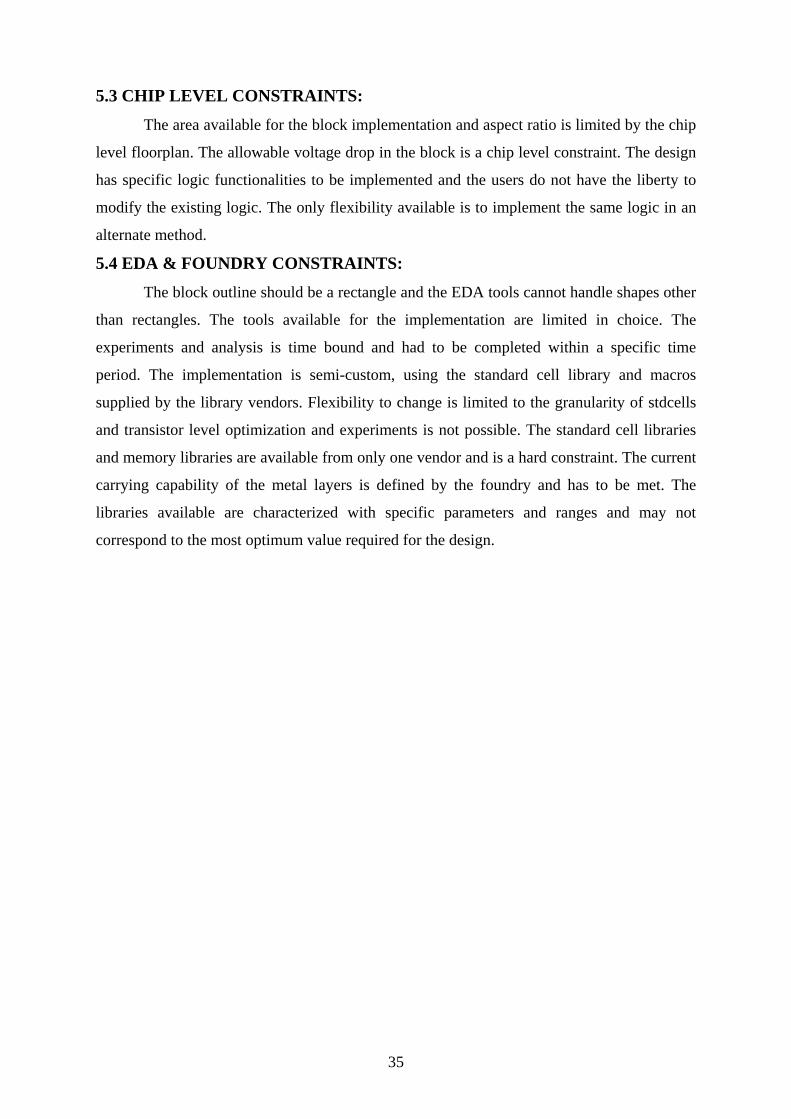
Fig 6.6 IR-drop distribution map for Experiment-5---------------------------- 41
Fig 6.7 IR-drop distribution map for Experiment-6---------------------------- 41
Fig 6.8 Distribution of logic-A without a region------------------------------- 45
Fig 6.9 Distribution of logic-A with a region----------------------------------- 45
Fig 6.10 Distribution of logic-B without a density screen---------------------- 46
Fig 6.11 Distribution of logic-B with a density screen-------------------------- 46
vi

LIST OF TABLES
Table No Table Title Page No
3.1 EDA tools used for block implementation-------------------------- 24
6.1 Power grids with various pitch and width combinations---------- 37
6.2 Leakage power optimization------------------------------------------ 42
6.3 Multiple clock tree strategies ----------------------------------------- 43
6.4 Adding extra metal layers for routing-------------------------------- 44
vii
ABBREVIATIONS USED
ASIC -------------------------- Application-Specific Integrated Circuit
VDSM -------------------------- Very Deep Sub Micron
EDA -------------------------- Electronic Design Automation
DRC -------------------------- Design Rule Constraints
CTS -------------------------- Clock Tree Synthesis
RTL -------------------------- Register Transfer Level
HDL -------------------------- Hardware Description Language
DRV -------------------------- Design Rule Violations
SOC --------------------------- System-On-Chip
SPE --------------------------- Security Protocol Engine
MD5 -------------------------- Message Digest Algorithm
SHA1 -------------------------- Secure Hash Algorithm
DES -------------------------- Data Encryption Standard
TDES -------------------------- Triple Data Encryption Standard
AES --------------------------- Advanced Encryption Standard
viii

Chapter 1
INTRODUCTION
1
1. INTRODUCTION
1.1 INTRODUCTION:
Due to the evolution of Very-Deep-Submicron (VDSM) technology, the
semiconductor industry is facing exciting new challenges all the time. As minimum layout
dimensions continue to shrink and the number of functions that can be put on a SOC
continues to grow, signal integrity has become a major issue causing chip failures. Large
power dissipation in the chip due to sub-threshold leakage is becoming uncontrollable.
Leakage power is taking more importance as it becomes a dominant component of the overall
power in a chip.
Physical design of VLSI systems is the process of transforming structural
representation of a VLSI system into layout representation. The objective of physical design
automation is to carry out such transformation efficiently using place & route tool so that the
resulting layout satisfies the topological, geometric, timing and power-consumption
constraints of the design. This thesis throws light on various design automation problems in
the physical design process of VLSI circuits, including floorplanning, routing, compaction,
leakage power reduction and signal integrity effects. Physical implementation of a design has
been considered in the purview of the various design and automation constraints, alternate
methods of implementations analysed and the optimal solutions recommended.
1.2 MOTIVATION:
Conventionally, the challenge in VLSI design was to write the RTL code that would
result in the most efficient gate level implementation of the logic. With the advancements in
the Electronic Design Automation (EDA), the synthesis tools have become sophisticated
enough to map an RTL description to an efficient gate level implementation based on the
constraints given to them. Also with the shrinking transistor sizes and the corresponding
reduction in the physical area of logic gates, the worries of having a few extra gates have
disappeared as the differential gate area is negligible. On the other hand, the challenges in the
physical design has been increasing with the decrease in the transistor sizes, especially in
relation to the interconnect sizes. This has resulted in a focus shift from logic design to
physical design in the chip design world and most of the research work is going in the
physical design of integrated circuits. This thesis aims at analyzing some of these physical
design parameters and techniques using EDA tools.
2

1.3 BACKGROUND LITERATURE SURVEY:
In the late 1980s, when the average chip contained fewer than 10,000 gates, logic
synthesis tools arrived in the marketplace. To decide whether or not a synthesis result was
good, designers looked at the speed and area reported by the synthesis tool. Thus, the Quality
of Results goodness measure was born. The ever increasing demand for integrated circuits,
strict price/performance goals, time-to-market pressures and rapid developments in
semiconductor process technologies are driving designs of 0.35 micron and below. These
processes have come to be known as deep sub-micron technologies or very deep sub-micron,
with the rapid shrinking of process technologies, an entire range of issues including signal
integrity [13],[15] problems such as on-chip crosstalk [21], IR drop [9],[14], power
consumption [22] and accurate parasitic extraction need to be addressed. Whenever the
industry moves from one technology node to another, existing power constraints are
tightened and new constraints emerge. Power-related constraints are now being imposed
throughout the entire design flow in order to maximize the performance and reliability of
devices. In the case of today's extremely large and complex designs, implementing reliable
power network and minimizing power dissipation [19] have become major challenges.
Smaller process geometries have led to a dramatic increase in problems due to IR drop i.e. the
voltage drop [20] across in a chip’s power network. As the term implies, IR drop results from
the current and resistance associated with the power network. Also the number of metal
layers [18] will increase to 8 in the near future and will even grow to 10 or more. The high
packing density of the transistors and the many levels of metal interconnect lead to all kinds
of electrical problems that have to be solved. These problems are grouped as deep-submicron
problems. Typical examples are, cross talk between neighboring interconnects lines, parasitic
capacitors, resistors and inductors in wires, electro-migration etc. In the past, most of the
delay [16] was caused in the logic cells. Today and certainly in the next generation processes,
80% or more of the total delay is due to interconnects.
1.4 THESIS CONTRIBUTION:
The physical design flow and the concepts behind each step of the process have been
studied. Then the constraints, reasons and the requirements resulting in the existing
implementation of the physical design have been studied. Further, various experiments have
been carried out to improve the design in various aspects like power, area and timing. The
tradeoffs required and the benefits of each of the experiments have been contrasted and
analyzed.
3

1.5 THESIS OUTLINE:
Following this introduction the remaining part of the thesis is organized as under,
Chapter 2 provides the industry standard physical design flow and brief description of
physical design methodology. Chapter 3 provides design details used for physical design
implementation. Chapter 4 discusses the significance of different parameters associated with
physical design flow. Chapter 5 discusses the limitations and constraints of block level
physical design implementation. Chapter 6 discusses the various experiments carried out to
improve the design performance and also provides the analysis and importance of each
experiment. Chapter 7 summarizes the work undertaken in this thesis and points to possible
directions for future work.
4

Chapter 2
PHYSICAL DESIGN FLOW
5

2. PHYSICAL DESIGN FLOW
2.1 INTRODUCTION:
Physical design of VLSI systems is the process of transforming structural
representation of a VLSI system into layout representation. The objective of physical design
automation is to carry out such transformation efficiently using EDA tools so that the
resulting layout satisfies topological, geometric, timing and power-consumption constraints
of the design.
2.2 CHALLENGES IN PHYSICAL DESIGN IMPLEMENTATION:
Designing a high performance VLSI chip using process technologies at 0.35um or
below is a tremendous challenge. While market windows continue to shrink, design
complexity is rapidly increasing due to the combination of finer geometries, design size,
higher clock frequency and lower voltage. As a result, interconnect and signal integrity has
emerged as dominant factors to be managed in order to successfully complete designs. This
renders obsolete most of the conventional design flows that have not been designed to
address all of these new effects. Simply making incremental improvements to existing tools
and methods will not address the full extent of the issues.
New technologies and flows are required that have been designed from the ground up
for challenges associated with design done at 0.35um and below. Challenges in physical
design accelerating advances in process technology have resulted in a number of key
challenges facing designers of multi-million gate chips today: timing closure, signal integrity,
design variable interdependence, clock and power routing, design sign-off and design size.
Timing closure continues to be an illusive goal. Today, timing closure is very complex and
can only be assured by accurately modeling and evaluating the propagation delays of the
library cells, the physical placement of the cells and the electrical characteristics of the
interconnect. Signal integrity has emerged as a determining factor to not only the timing, but
to the functional integrity of the chip as well. As the ratio of cross-coupling capacitance to
inter-layer capacitance increases, the rate of timing and functional violations due to signal
integrity problems also rises.
6

Signal integrity (SI) issues such as crosstalk delay and noise become critical for
system-on-chip (SoC) designs at about the 150-nanometer (nm) technology node and
unavoidable at 130-nm and below. These SI issues can lead to major timing-closure
difficulties. Fortunately, several years of experience with SI at very deep submicron
geometries have led to efficient methodologies throughout the design flow for preventing,
detecting and fixing SI effects. Given the extent of the SI design challenge, designers must
take steps to ensure signal integrity throughout the design cycle. With feature sizes ranging
from 180 to 65nm, today's very deep submicron (VDSM) semiconductor technologies pose
new modeling challenges to design closure and timing sign-off. To quickly achieve timing
closure and sign-off, Spice-level accuracy at higher levels of abstraction (starting with cell
level) is required. However, problems with inconsistent use and inaccuracies of current cell
library formats make this difficult. Because delay calculation is responsible for timing closure
and sign-off throughout the design flow, it is important to consider the impact of library
model accuracy and consistency on delay calculation.
While there are many design variable interdependencies to be dealt with, perhaps the
most important is the trade-off between routability, timing, and power consumption.
Optimizing for any one may cause problems with the others. Clock and power networks
consume massive amounts of routing resources. Their construction and analysis must be
started early and they must be tailored for an individual chip’s requirements. Clock trees are
frequently inserted after detailed placement is complete. Power networks are frequently pre-
determined based on statistical or empirical estimates. Physical design is now as important as
logic design in determining whether the requirements are achievable. Design size has
exceeded the limitations of gate-level design tools. It is not possible to design and implement
a multi-million gate chip as an indivisible whole. The chip must be planned at a high level,
partitioned into smaller pieces, and then completed using lower level tools.
2.3 INDUSTRY STANDARD PHYSICAL DESIGN FLOW: The following diagram describes the industry standard physical design flow. The
detailed description of each step has given in the next sessions.
7

crosstalk analysis
timing analysis
IR drop analysis
floorplanning
cts optimization
routing
clock tree synthesis
place optimization
routing optimization
placement
parasitic extraction
layout verification
Libraries
netlist
Manufacturing
Fig 2.1: Industry standard physical design flow 2.4 INPUTS TO PHYSICAL DESIGN:
2.4.1 Netlist:
Synthesizing a design results in a transformation from an HDL description into a
netlist. A netlist is a list of necessary gates needed to implement the RTL architecture and
how they are connected (taken from a technology and vendor dependent library). A netlist is
used as input to the Place and Route (P&R) process and to verify functionality after synthesis
when the gate delays are included. Since a netlist does not contain any information about
physical placement of the gates on the chip or the lengths of the connecting wires, wire
delays can not be simulated using a netlist.
2.4.2 Generating a Technology File:
The technology files provides the software with design rules for placement and
routing, and interconnect resistance and capacitance data for generating RC values and
8
wireload models for the design. The technology file also contains process information for the
metals interconnect layers, including metal thickness, metal resistance, and line-to-line
capacitance values of metal layers, for determining coupling capacitance.
2.4.3 Preparing Timing Libraries
Timing library files contain timing information in ASCII format for all of the standard
cells, blocks and I/O pad cells.
2.4.5 Design Constraints:
Maximum fanout, maximum transition time, clock definitions, clock uncertainties for
setup/hold times, size of the floor plan, I/O pin locations, input/output delays for the design.
2.5 FLOORPLANNING:
As the focus shifts from logic to interconnect, floor planning assumes an increasingly
important role. Floorplanning is the process of identifying cells/structures that need to be
placed close together in order to meet the design objectives such as die-size and performance.
At the same time we allocate space for clock and power wiring and decide on the location of
the I/O and power pads. At the start of floorplanning we have a netlist describing memory
modules, the logic cells within the block, and their connections. The input to a floorplanning
tool is a hierarchical netlist that describes the interconnection of the memory modules, the
logic cells (NAND, NOR, D flip-flop, and so on) within the block, and the logic cell
connectors. The netlist is a logical description of the ASIC, the floorplan is a physical
description of an ASIC. Floorplanning is thus a mapping between the logical description (the
netlist) and the physical description (the floorplan).
2.5.1 Macro placement:
Macros are generally placed around the peripheral of the block because:
To provide a contiguous area for standard cells.
Higher freedom for place-and-route tools during placement and routing of the
standard cells.
The goal of macro placement is to:
Reduce timing-critical paths between the macros and interfacing logic.
Reduce interconnections in the following order:
Input/Output pins to macros.
Macro to macro.
Macro to standard cells
9

2.5.2 Power Planning:
Power planning is the process of defining the power and ground nets of design and
specifying their structures, which distribute power through your design:
• Power rings
• Power mesh
• Power Rails
2.5.2.1 Power rings:
Two types of power ring structures are,
1. Core ring
2. Macro ring
Core ring:
A ring that encloses the core with one or more sets of power and ground rings and
provides external power from the pad ring to core structures. Typically, the top and bottom
sides and any other horizontal segments of a core ring are located on a horizontal metal layer;
while the left, right, and any other vertical segments are on a vertical layer. Vias connect the
ring sides, if necessary.
Macro ring:
A ring that encloses one or more macros with power and ground rings, providing
those macros with power. Macro rings do not always have four sides, and they often have
wire extensions from one or more sides that connect to nearby power and ground wires of the
same net.
2.5.2.2 Power mesh:
One or two repeated sets of pairs of parallel (vertical or horizontal) power and ground
wires that supply power to the core. The mesh can consist of a single net or a pattern of two
or more nets that repeat at regular intervals across the design.
2.5.2.3 Power rails:
Power and ground wires that supply power to the standard cells that are placed in
standard cell rows. Power rails draw power from rings and mesh to which they are connected.
Power rail wires are on a single layer.
10
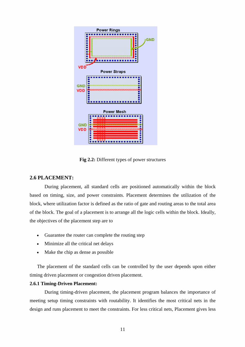
Fig 2.2: Different types of power structures
2.6 PLACEMENT:
During placement, all standard cells are positioned automatically within the block
based on timing, size, and power constraints. Placement determines the utilization of the
block, where utilization factor is defined as the ratio of gate and routing areas to the total area
of the block. The goal of a placement is to arrange all the logic cells within the block. Ideally,
the objectives of the placement step are to
• Guarantee the router can complete the routing step
• Minimize all the critical net delays
• Make the chip as dense as possible
The placement of the standard cells can be controlled by the user depends upon either
timing driven placement or congestion driven placement.
2.6.1 Timing-Driven Placement:
During timing-driven placement, the placement program balances the importance of
meeting setup timing constraints with routability. It identifies the most critical nets in the
design and runs placement to meet the constraints. For less critical nets, Placement gives less
11
attention to meeting timing constraints and more attention to enhancing routability. A
complete constraints file is essential for running timing-driven placement.
2.6.2 Congestion-Driven Placement:
During congestion-driven placement, the Placement program reduces the placement
congestion after placement. This automatically applies to the whole block, and can be applied
after global placement, timing optimization, or clock tree synthesis, when routability becomes
the ultimate goal. Timing is not considered, therefore, the preservation of timing is not
guaranteed, although it usually results in better timing due to the improvement in congestion
and the reduction in wire length.
2.7 PLACE OPTIMIZATION:
The place & route tool uses some or all of the following techniques when optimizing
the design, depending on the design stage and the parameters specified.
Adding buffers
Deleting buffers
Upsizing gates
Down sizing gates
Moving instances
This first optimization step identifies and repairs a large number of timing problems
occurring in the early stages of the implementation process. The optimization step first
globally reduces delays on all nets by buffering and gate sizing. Then the tool identifies and
repairs design rule violations (DRV) such as maximum capacitance, maximum transition and
maximum fanout.
2.8 CLOCK TREE SYNTHESIS:
High-performance ASICs require careful clock design to achieve full performance.
They distribute clock signals based on user-defined specifications, such as target clock delay
(that is, the delay between the root-clock net and leaf-cell clock), clock buffer types, and
maximum clock load. Effective clock tree synthesis results in minimal prelayout clock skew.
To get a well-balanced tree with low skew and steep clock edges, we wanted to limit the cell
fanout to a lower value than for the synthesis of the rest of the design. We did so to ensure
that the buffers used in the clock nets would drive only a limited number of flip-flops.
12

Major clock design goals are
Minimize clock skew and optimize clock buffers to meet skew specifications and
minimize clock-tree power dissipation.
Designing clock distribution networks for high-speed chips is more complex than just
meeting design specifications.
Clock networks are very power hungry, so power dissipation should be kept in mind
The dynamic switching currents that cause the high power dissipation also affect
interconnect reliability – so wide wire widths may have to be used.
Clock-to-signal net coupling can cause excessive on-chip noise
Main job of clock-design tools is to vary routing paths and placement of the clocked
cells and buffers to meet skew specifications.
Many Considerations for clock tree building:
• Timing-related specifications:
o Latency (clock input to clocked element delay)
o Skew (variation in arrival time to clocked elements)
• Non-timing specifications:
o Power dissipation (static and dynamic)
o Signal integrity (noise resulting from clock-to-signal coupling)
2.9 CTS OPTIMIZATION:
The goals of CTS optimization include:
Fixing remaining DRVs
Fixing hold time violations
Optimizing remaining setup violations
Correcting timing with propagated clocks
2.10 ROUTING:
Once the designer has floorplanned a block and the logic cells within the flexible
regions of the block have been placed, it is time to make the connections by routing the
block. This is still a hard problem that is made easier by dividing it into smaller problems.
Routing is usually split into global routing followed by detailed routing.
13

2.10.1 Global Routing:
A global router does not make any connections, it just plans them. We typically global
route the whole block before detail routing the whole block. The input to the global router is a
floorplan that includes the locations of all the fixed and flexible macros, the placement
information of all the logic cells. The goal of global routing is to provide complete
instructions to the detailed router on where to route every net. The common objectives of the
global routing are of the following:
• Minimize the total interconnect length.
• Maximize the probability that the detailed router can complete the routing.
• Minimize the critical path delay.
2.10.2 Detailed Routing:
The global routing step determines the channels to be used for each interconnect.
Using this information the detailed router decides the exact location and layers for each
interconnect. The goal of detailed routing is to complete all the connections between logic
cells. The most common objective is to minimize one or more of the following:
• The total interconnect length
• The number of layer changes that the connections have to make
• The delay of critical paths
• Minimizing the number of layer changes corresponds to minimizing the number of
vias that add parasitic resistance and capacitance to a connection.
2.11 ROUTING OPTIMIZATION:
The goals of post-route optimization include:
Analyses cross coupling capacitance effects on glitch and noise
Repairing DRVs
Reruns timing analysis
Repairs setup violations
Repairs hold violations
Leakage power reduction
14

2.12 PARASITIC EXTRACTION:
Parasitic extraction is the calculation of the per net capacitance and resistance values
that are required for such things as delay calculation, timing analysis, and signal integrity.
Parasitic extraction is performed by analyzing each net and taking into account many
important effects through the use of 3D-characterized rules. These effects are mostly due to
the dielectric stack, the net’s proximity to other neighboring nets, and the net’s own topology.
Sheet resistance is the parasitic resistance defined for each conductor layer and via. Net
capacitance is calculated by adding the capacitive sub components of the net and then
multiplying the sum by the total length of the net. The following are the different components
taken into consideration for total capacitance calculation:
2.12.1 Area and Lateral Cap Components:
• Area capacitance is defined as the capacitance from the top/bottom of the conductor
surface to the bottom/top of another conductor or substrate.
• Lateral capacitance is defined as the capacitance between two adjacent wires on the
same metal layer.
2.12.2 Fringe and Cross Cap Components:
• Fringe capacitance is calculated from the sidewall to the top and bottom of another
conductor.
• Cross capacitance is defined as the capacitance of a conductor to an array of wires
crossing above or below it.
2.13 TIMING ANALYSIS:
In a synchronous digital system, data is supposed to move in lockstep, advancing one
stage on each tick of the clock signal. This is enforced by synchronizing elements such as
flip-flops or latches, which copy their input to their output when instructed to do so by the
clock. In such a system only two kinds of timing errors are possible. One is setup time
violation and another one is hold time violation. The time when a signal arrives can vary due
to many reasons - the input data may vary, the circuit may perform different operations, the
temperature and voltage may change, and there are manufacturing differences in the exact
construction of each part. The main goal of timing analysis is to verify that despite these
possible variations, all signals will arrive neither too early nor too late and hence proper
circuit operation can be assured. The following are some of the terms used while analyzing a
path for timing.
15

Critical path:
The critical path is defined as the path between an input and an output with the
maximum delay. Once the circuit timing has been computed, the critical path can easily be
found by using a trace back method.
Arrival timing:
The arrival time of a signal is the time elapsed for a signal to arrive at a certain point.
The reference, or time 0.0, is often taken as the arrival time of a clock signal. To calculate the
arrival time, delay calculation of all the component of the path will be required. Arrival times,
and indeed almost all times in timing analysis, are normally kept as a pair of values - the
earliest possible time at which a signal can change, and the latest.
Required time:
This is the latest time at which a signal can arrive without making the clock cycle
longer than desired. The computation of the required time proceeds as follows. At each
primary output, the required times for rise/fall are set according to the specifications provided
to the circuit. Next, a backward topological traversal is carried out, processing each gate
when the required times at all of its fanouts are known.
Slack:
The slack associated with each connection is the difference between the required time
and the arrival time. A positive slack s at a node implies that the arrival time at that node may
be increased by s without affecting the overall delay of the circuit. Conversely, negative slack
implies that a path is too slow, and the path must speed up if the whole circuit is to work at
the desired speed.
2.14 CROSSTALK ANALYSIS:
As chip designers migrate to nanometer technologies, the interconnect wires become
taller and thinner, with closer wire spacing and higher sidewalls similar to parallel plate
capacitors. As a result, the on-chip coupling capacitance between the wires now contributes
to more than 50 percent of the total wire capacitance. This is increasingly causing chips to
fail, under-perform, or suffer from low yields.
2.14.1 Setup Failure:
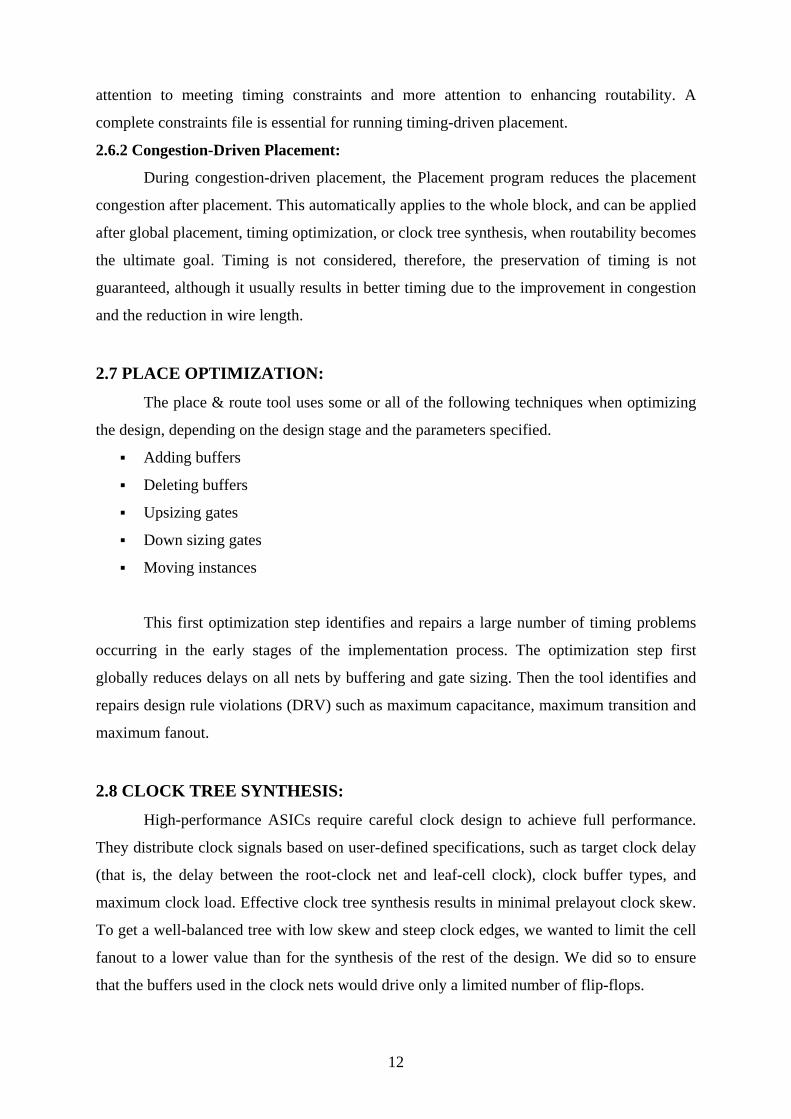
Consider the circuit shown in Figure. When there is no crosstalk, the green line shows
the waveform at the victim net. But, when the aggressor net a1 switches in the opposite
direction of the victim net, the crosstalk increases the delay at the victim net as shown by the
16
yellow line. This increase in delay can cause the signal to arrive too late at a latch or a flip-
flop, resulting in a setup failure.
Fig 2.3: Crosstalk Induced Delay Push-Out
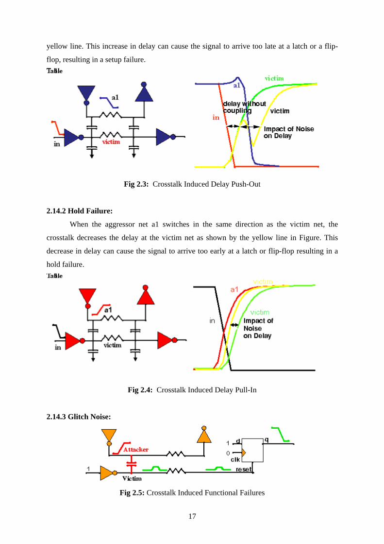
2.14.2 Hold Failure:
When the aggressor net a1 switches in the same direction as the victim net, the
crosstalk decreases the delay at the victim net as shown by the yellow line in Figure. This
decrease in delay can cause the signal to arrive too early at a latch or flip-flop resulting in a
hold failure.
Fig 2.4: Crosstalk Induced Delay Pull-In
2.14.3 Glitch Noise:
Fig 2.5: Crosstalk Induced Functional Failures
17
Crosstalk noise can also cause functional failures. For instance, in Figure, the
crosstalk-induced glitch on the reset line can cause the intended steady-state logic value of 1
at the flip-flop Q output to be reset to an unintended logic value of 0.
2.15 IR-DROP ANALYSIS: Due to Very-Deep-Submicron (VDSM) technology evolution the semiconductor
industry is facing exciting new challenges all the time. As minimum layout dimensions
continue to shrink and the number of functions that can be put on a SOC continues to grow,
creating signal integrity as a major issue causing chip failures. IR drop is a signal integrity
effect caused by wire resistance and current drawn off from the power and ground grids. If
the wire resistance is too high or the cell current larger than predicted, an unacceptable
voltage drop may occur. Nanometer designs are extremely susceptible to IR drop because
power and ground wire resistivity increases with decreasing geometries, while the overall
power supply voltage decreases. This results in poor performance and increased noise
susceptibility. Furthermore, gates with different voltage levels communicating with each
other across the chip can propagate erroneous data, causing a malfunction. Gate delays
increase non-linearly as voltage at gates decrease. This may lead to setup or hold timing
violations depending on which path these gates are residing. The increase in gate delay due to
IR-drop on the data path can ultimately lead to setup timing violations. On the contrary, the
voltage drop on the buffers and inverter cells of the clock path will cause the delay in arrival
of clock signal, resulting in a hold violation. The following figure illustrates the IR Drop
concept:
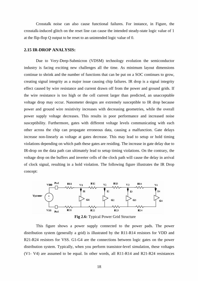
Fig 2.6: Typical Power Grid Structure
This figure shows a power supply connected to the power pads. The power
distribution system (generally a grid) is illustrated by the R11-R14 resistors for VDD and
R21-R24 resistors for VSS. G1-G4 are the connections between logic gates on the power
distribution system. Typically, when you perform transistor-level simulation, these voltages
(V1- V4) are assumed to be equal. In other words, all R11-R14 and R21-R24 resistances
18

would be 0.0 ohms, so all G1-G4 gates would have ideal power supply voltages, VDD and
VSS. In reality, the power grid resistances of a chip are non-zero. For example, gate G4 never
has an ideal VDD voltage at its power pin when it is active, it has a lower voltage. The
current flowing from the power supply to G4 must flow through the power distribution
network. A current, I, flowing through an effective resistance, R, introduces a voltage drop, V
= IR. IR drop on the VSS power grid distribution network is an increase in the VSS voltage at
gates G1-G4.
Figure 2.6 also illustrates the complexity of power grids and IR drop. Assume that
gate G4 has a VDD power grid current of I4 amperes. No other gate has current. The I4
current flows from the power supply through the power grid to G4. The IR drop at gate G4 is
then I4 (R11+R12+R13+R14). In addition, because of the I4 current at gate G4, gate G2 does
not have an ideal power supply. It has an IR drop of I4 (R11+R12). Therefore, the current of
each gate in a design causes some type of IR drop for all other gates in the design. If the gates
along the metal line switch together, the IR drop can be large. Given simultaneous currents
I1-I4 for the G1-G4 gates, respectively, in Figure 2.15, the IR drop at gate G4 would be the
following:
I1(R11)+I2(R11+R12)+I3(R11+R12+R13)+I4(R11+R12+R13+R14)
19

Chapter 3
SECURITY PROTOCOL ENGINE
20
3. SECURITY PROTOCOL ENGINE 3.1 INTRODUCTION:
The physical design implementation presented in this thesis was developed over a
period of time based on actual design experience from a SoC block called Security Protocol
Engine (SPE) of Ikanos network processor. A network processor is an integrated circuit
which has a feature set specifically targeted at the networking application domain. Network
processors are typically software programmable devices and would have generic
characteristics similar to general purpose central processing units that are commonly used in
many different types of equipment and products.
The Security Protocol Engine supports industry accepted hashing algorithms and
encryption algorithms.
The supported hashing algorithms are:
Message Digest Algorithm (MD5)
Secure Hash Algorithm-1 (SHA1)
The supported encryption algorithms are:
Data Encryption Standard (DES)
Triple Data Encryption standard (TDES)
Advanced encryption Standard (AES)
3.2 HASHING ALGORITHMS:
A hashing algorithm takes a variable length data message and creates a fixed size
message digest. The message digest is the output of a hashing algorithm.
3.2.1 Message Digest Algorithm (MD5):
The algorithm takes as input a message of arbitrary length and produces as output a
128-bit message digest of the input. It is conjectured that it is computationally infeasible to
produce two messages having the same message digest, or to produce any message having a
given prespecified target message digest. The MD5 algorithm is intended for digital signature
applications, where a large file must be compressed in a secure manner before being
encrypted with a secret key. The MD5 algorithm is designed to be quite fast on 32-bit
machines. In addition, the MD5 algorithm does not require any large substitution tables, the
algorithm can be coded quite compactly.
21

3.2.2 Secure Hash Algorithm-1 (SHA-1):
The algorithm is used for computing a condensed representation of a message or a
data file. When a message of any length less than 264 bits is input, the SHA-1 produces a 160-
bit output called a message digest. The message digest can then, for example, be input to a
signature algorithm which generates or verifies the signature for the message. Signing the
message digest rather than the message often improves the efficiency of the process because
the message digest is usually much smaller in size than the message. The same hash
algorithm must be used by the verifier of a digital signature as was used by the creator of the
digital signature. Any change to the message in transit will, with very high probability, result
in a different message digest, and the signature will fail to verify. The SHA-1 is called secure
because it is computationally infeasible to find a message which corresponds to a given
message digest, or to find two different messages which produce the same message digest.
3.3 ENCRYPTION ALGORITHMS:
Encryption is the process of converting a plaintext message into cipher text which can
be decoded back into the original message. An encryption algorithm along with a key is used
in the encryption and decryption of data. There are several types of data encryptions which
form the basis of network security. Encryption schemes are based on block or stream ciphers.
The type and length of the keys utilized depend upon the encryption algorithm and the
amount of security needed. In conventional symmetric encryption a single key is used. With
this key, the sender can encrypt a message and a recipient can decrypt the message but the
security of the key becomes problematic. In asymmetric encryption, the encryption key and
the decryption key are different. One is a public key by which the sender can encrypt the
message and the other is a private key by which a recipient can decrypt the message.
Encrypting data converts it to an unintelligible form called cipher. Decrypting cipher
converts the data back to its original form called plaintext. The algorithm described in this
standard specifies both enciphering and deciphering operations which are based on a binary
number called a key.
3.3.1 Data Encryption Standard (DES):
A key consists of 64 binary digits ("O"s or "1"s) of which 56 bits are randomly
generated and used directly by the algorithm. The other 8 bits, which are not used by the
algorithm, are used for error detection. The 8 error detecting bits are set to make the parity of
each 8-bit byte of the key odd, i.e., there is an odd number of "1"s in each 8-bit byte.
Authorized users of encrypted computer data must have the key that was used to encipher the
22
data in order to decrypt it. The encryption algorithm specified in this standard is commonly
known among those using the standard. The unique key chosen for use in a particular
application makes the results of encrypting data using the algorithm unique. Selection of a
different key causes the cipher that is produced for any given set of inputs to be different. The
cryptographic security of the data depends on the security provided for the key used to
encipher and decipher the data.
Data can be recovered from cipher only by using exactly the same key used to
encipher it. Unauthorized recipients of the cipher who know the algorithm but do not have the
correct key cannot derive the original data algorithmically. However, anyone who does have
the key and the algorithm can easily decipher the cipher and obtain the original data. A
standard algorithm based on a secure key thus provides a basis for exchanging encrypted
computer data by issuing the key used to encipher it to those authorized to have the data. Data
that is considered sensitive by the responsible authority, data that has a high value, or data
that represents a high value should be cryptographically protected if it is vulnerable to
unauthorized disclosure or undetected modification during transmission or while in storage.
3.3.2 Triple Data Encryption standard (TDES):
Triple DES is simply another mode of DES operation. It takes three 64-bit keys, for
an overall key length of 192 bits. The Triple DES breaks the user provided key into three sub
keys, padding the keys if necessary so they are each 64 bits long. The procedure for
encryption is exactly the same as regular DES, but it is repeated three times. Hence the name
Triple DES. The data is encrypted with the first key, decrypted with the second key, and
finally encrypted again with the third key.
Consequently, Triple DES runs three times slower than standard DES, but is much
more secure if used properly. The procedure for decrypting something is the same as the
procedure for encryption, except it is executed in reverse. Like DES, data is encrypted and
decrypted in 64-bit chunks. Unfortunately, there are some weak keys that one should be
aware of, if all three keys, the first and second keys, or the second and third keys are the
same, then the encryption procedure is essentially the same as standard DES. This situation is
to be avoided because it is the same as using a really slow version of regular DES.
Note that although the input key for DES is 64 bits long, the actual key used by DES
is only 56 bits in length. The least significant (right-most) bit in each byte is a parity bit, and
should be set so that there are always an odd number of 1s in every byte. These parity bits are
ignored, so only the seven most significant bits of each byte are used, resulting in a key
23

length of 56 bits. This means that the effective key strength for Triple DES is actually 168
bits because each of the three keys contains 8 parity bits that are not used during the
encryption process.
3.3.3 Advanced encryption standard (AES):
AES has a fixed block size of 128 bits and a key size of 128, 192 or 256 bits. Most of
AES calculations are done in a special finite field. AES operates on a 4×4 array of bytes,
termed the state. For encryption, each round of AES (except the last round) consists of four
stages:
1. AddRoundKey — each byte of the state is combined with the round key; each round
key is derived from the cipher key using a key schedule.
2. SubBytes — a non-linear substitution step where each byte is replaced with another
according to a lookup table.
3. ShiftRows — a transposition step where each row of the state is shifted cyclically a
certain number of steps.
4. MixColumns — a mixing operation which operates on the columns of the state,
combining the four bytes in each column using a linear transformation.
The final round replaces the MixColumns stage with another instance of AddRoundKey.
3.4 PHYSICAL DESIGN IMPLEMENTATION OF BLOCK:
a) 90 nm implementation
b) 333 MHz clock frequency
c) Gate count of the design is 480K
d) Area used for block implementation is 1.498 mm2
e) EDA tools used for the block implementation are
Tool EDA Vendor Purpose
SOC Encounter Cadence Design Systems Place & Route
RedHawk Apache Design Solutions IR-drop Analysis
Celtic Cadence Design Systems Crosstalk Analysis
Table 3.1: EDA tools used for block implementation
24

Chapter 4
SIGNIFICANCE OF PARAMETERS
25
4. SIGNIFICANCE OF PARAMETERS 4.1 POWER DISSIPATION:
As the design size is shrinking to the ultra deep sub microns and density is increasing
to millions of gates in a system on chip, large power dissipation in the chip due to sub-
threshold leakage is becoming uncontrollable in the practical world. It is taking more
importance as it is becoming dominant component for the overall power in the chip.
The power consumption in silicon primarily consists of two main components,
namely Dynamic power and Static power. The static power constitutes leakage power due to
sub-threshold current and standby power. This passive energy for leakage dissipation of the
device is not in active mode of operation for time toff duration. There will also be some
percentage of leakage power during the active mode. This passive energy has been emerged
as one of the important design parameters in the sub micron low power systems where battery
running life is critical in today’s portable electronic gadgets. This pushes through the design
performance limits with power-delay product as a measurable parameter. The leakage power
dissipation can never be made zero but only can be minimized.
There have been multiple techniques used in the past to reduce the dynamic power
dissipation and have been implemented successfully through the different levels of design
abstraction. The leakage power has been a biggest concern increasing day by day due to
scaling of process technologies shrinking, with scaling down of supply voltage but without
the proportionate scaling of threshold voltage, Vt. The sub threshold leakage increases
exponentially as the threshold voltage is reduced.
The delay of logical gates increases with the increase in threshold voltage (High Vt),
whereas the static power decreases with the increase in threshold voltage. This can be
represented by a simple gate delay equation:
Delay, Td = (CLVdd ) / (Vdd – Vt)a ------------- 4.1
In the equation 4.1, Td represents the propagation delay, CL is the load capacitance,
Vdd is the supply voltage and Vt is the threshold voltage for the transistor. a is the coefficient
and represents the effect due to shortening of the device channel length. On the other hand,
the interconnect delay has been dominating the gate delays causing many issues in meeting
26

the chip performance parameters such as power, delay, area and signal integrity. In order to
reduce the interconnect delay on a path, this needs to be buffered up using the chain of
repeaters by accounting for the driver size and the load size in order to meet the delay
constraint on that path. The repeaters for this chain should be selected with the right size and
characterized with low power in order to meet not only timing but also to meet the power
constraints. This is a very tedious task for the EDA tool although it might come up with a
good trade-off. Designers try different circuit techniques and schemes in order to minimize
the leakage power to trade off the speed of the circuit. If one tries to control the leakage
power, there happens the speed degradation of the circuit which is a real problem in any high
performance design.
4.2 LEAKAGE POWER OPTIMIZATION METHODOLOGY:
Considering all the above discussions, a good beginning optimal point is very much
necessary when the leakage power and speed of the design are critical. When all the required
work in the architectural abstraction is complete and a qualified RTL for the design is ready,
then the remaining work is left to the design automation tools right from the synthesis all the
way to the final routed stage. There are various factors that are considered which affect the
performance of the low power design.
4.2.1 Area Reclamation:
There has been almost no discussion in the past with respect to the density of the chip
when it comes to the low power discussions. It is always a very good starting point to reduce
the density of the chip which directly removes the redundant logic and unused components in
the design. This has many advantages as it reduces the number of resources used and reduces
the congestion of overall design. This factor also affects the percentage decrease in
interconnects thereby reducing the respective delays.
4.2.2 Characterization of Library Cells:
The library cell characterization plays an important role as the design automation
tools relies on the accuracy of the library. A typical low power library will have not only area
and delay cost functions, but also will have power cost functions. There will be leakage
power characterized for each input pin state. The target library for the technology mapping
for leakage power should have the cells with multiple Vt cells for maximum benefits in order
to apply the multiple Vt schemes towards the leakage power optimizations. In this flow, two
combinations of Vt are used: 1. High Vt and 2. Low Vt for the same logic function specified
in the library. This is the minimum requirement in the technology library in order to pursue
27

the leakage power optimization using the Cadence® tools. No other changes in the design
procedures are required as the technology mapping handles them in order to utilize the
multiple Vt technology. Combinations of high Vt and low Vt can be used to characterize the
complex Vt cells in the library apart from just high Vt and just low Vt cells.
4.2.3 Gate Sizing:
The gates can be sized-resized depending on the fan-out of loads to minimize the
power dissipation in the design. The static power dissipation of a gate can be expressed as a
function of delay and also the device geometry represented by W/L ratio. By gate resizing to
achieve the leakage reduction, the area of the circuit will also be reduced. However,
decreasing the size of a gate makes it slower as its drive capacity is decreased. So the tool
should be really capable of finding out the loads, drivers for the entire path and apply the
transformations accordingly. This technique along with a very good logic restructuring can be
served towards minimizing the delay and power of a path concurrently with most of the
energy dissipated near the final load trying to satisfy the input timing constraints and the
initial timing targets. There should be a good trade-off between power and delay while trying
to resize the gate.
4.2.4 Signal Integrity:
The multiple Vt techniques are applied during the optimization in order to reduce the power
while meeting the delay constraints at the same time. The high Vt devices are used on the
slower path to reduce the leakage power whereas the low Vt devices are used for critical path
where the delay constraint is very tight. Since the low Vt devices can switch faster, they are
also sensitive to the noise. So one of the factors to keep in mind while optimizing the power
after the routing would be to consider the noise penalty of low Vt devices on faster paths.
This is quite interesting as the leakage power reduces due to high Vt cells, the noise also
reduces.
4.3 IR-DROP:
IR drop is a signal integrity effect caused by wire resistance and current draw off of
the power and ground grids. If the wire resistance is too high or the cell current larger than
predicted, an unacceptable voltage drop may occur. This voltage drop causes the supply
voltage to the affected cells to be lower than required, leading to larger gate and signal delays
that can consequently cause timing degradation in the signal paths as well as clock skew.
Lowered power supply current due to IR voltage drop also reduces the noise margins and
28

compromises the signal integrity of the design. The following are some tips to deal with IR-
drop issues:
4.3.1 Proper power-planning:
Ensure uniform power distribution throughout the chip area is the key to have
minimum IR drop in the design. Provide reasonable number of horizontal as well as vertical
power stripes with appropriate width in the design.
4.3.2 Increase the width of the power stripes:
This will help in decreasing the resistance in the path and hence the voltage drop. But
this will reduce the routing resource in the design. Apply this option only if you have enough
routing resources.
4.3.3 Perform pre-layout signal integrity analysis:
In conventional IC design flows signal integrity analysis is performed as a post-layout
activity. Unfortunately, this is the wrong time to be analyzing for signal integrity effects.
After doing floor planning perform IR-drop analysis to make sure that your power planning is
not giving you large IR-drop in the design. If you get dissatisfying result, do power planning
again and make sure that power is distributed uniformly throughout the design.
4.3.4 Provide extra power stripes:
In the region that experience large IR-drop provide extra power strips.
4.3.5 Setup positive slack:
Try to achieve sensible positive slack(Setup margin) at the end of your final routing
stage to make sure that final the design will not violate setup timing even if there is slight
delay due to IR drop.
4.4 CLOCK SKEW:
In circuit design, clock skew is a phenomenon in synchronous circuits in which the
clock signal (sent from the clock circuit) arrives at different components at different times.
This is typically due to two causes. The first is a material flaw, which causes a signal to travel
faster or slower than expected. The second is distance: if the signal has to travel the entire
length of a circuit, it will likely (depending on the circuit's size) arrive at different parts of the
circuit at different times.
Clock skew can cause harm in two ways. Suppose that a logic path travels through
combinational logic from a source flip-flop to a destination flip-flop. If the destination flip-
flop receives the clock tick later than the source flip-flop, and if the logic path delay is short
enough, then the data signal might arrive at the destination flip-flop before the clock tick,
29
destroying there the previous data that should have been clocked through. This is called a
hold violation because the previous data is not held long enough at the destination flip-flop to
be properly clocked through. If the destination flip-flop receives the clock tick earlier than the
source flip-flop, then the data signal has that much less time to reach the destination flip-flop
before the next clock tick. If it fails to do so, a setup violation occurs, so-called because the
new data was not set up and stable before the next clock tick arrived. A hold violation is more
serious than a setup violation because it cannot be fixed by increasing the clock period.
4.5 CROSSTALK VICTIM NETS:
With process technologies evolving from 0.18 micron to 0.13 micron and on to 90
nanometers, signal integrity effects are strongly influencing the performance of integrated
circuits. Two of the key ones are noise and delay due to cross-coupling capacitance. Noise
may cause functional failures; delay may result in timing violations. When a signal switches,
it may affect the voltage waveform of a neighboring net. The switching net is typically
identified as the "aggressor" and the affected net is the "victim." Crosstalk can impair both
timing and functionality. When the victim net is quiescent, crosstalk can result in a noise-
induced functional failure when the noise is propagated to the input of a register (latch or flip-
flop) and changes the state of the latch. When the switching windows of the aggressor and
victim nets overlap and the nets switch in opposite directions, crosstalk will increase the
delay of the victim net, which may result in setup violations. When the nets switch in the
same directions, crosstalk will reduce the delay of the victim net, which may result in hold
violations.
4.5.1 Crosstalk avoidance:
Crosstalk delay problems could only be fixed after detailed routing. Typical methods
included buffer insertion, cell resizing, track reassignment of the victim nets and additional
wire spacing allocated to victim nets. Cell resizing can be very effective since the
replacement of cells has a localized effect on the layout and will require only reconnection of
the signals to the equivalent pins. Inserting a buffer can be difficult since its addition can
introduce additional delay and may result in a timing violation in the critical path. Buffer
insertion can also increase power consumption. Track reassignment associates moving a wire
from one routing track to a different one, can solve the identified crosstalk problem.
However, this may introduce new crosstalk effects on other nets and create new critical paths.
30

Chapter 5
LIMITATIONS & CONSTRAINTS
31

5. LIMITATIONS & CONSTRAINTS
5.1 INTRODUCTION:
As designers move to 0.35um technologies and below, the convergence of
performance-driven design constraints intensifies the demand for new approaches for
integrated circuit (IC) physical design. At these geometries, more complex manufacturing
effects dramatically impact the way engineers need to tune physical designs for optimal
performance. Besides addressing familiar speed and capacity concerns, advanced physical
design requires an architectural approach that emphasizes quality of results, more effective
convergence across a broader array of constraints, and significantly greater control by
designers of the physical design process itself. Faster routing of larger designs is not enough,
and design convergence means much more than area, timing and power. Instead, designers
need the ability to analyze routing more effectively, and incrementally improve performance
with each design iteration. As the electronics industry continues to drive toward more
advanced manufacturing technologies, semiconductor companies face shrinking product
lifecycles and rising demand for greater functionality.
For engineers, each advance in design and manufacturing capabilities brings greater
challenges in every phase of development, yet dictates a greater need to reach closure on a
growing list of divergent constraints arising from each stage in the development cycle. As
engineering teams move designs from high-level and detailed logic design to floorplanning
and routing in physical design, they must work collaboratively to ensure that physical design
maintains tight objectives for design performance, functionality and manufacturability.
Accordingly, physical design and verification needs to work smoothly in the design flow,
efficiently providing detailed results needed to ensure high quality results within tightening
product schedules. Yet, as designs move to deep nanometer technologies at 65nm and below,
designers find that electronic design automation (EDA) tools developed even for 90nm
designs are unable to address the further challenges associated with these advanced
technologies. Inevitably, the lack of precise analysis of device performance at these new
geometries forces design teams to make tradeoffs and concessions to ensure
manufacturability.
The experiments and analysis done are constrained by the following:
1. Block level constraints
2. Chip level constraints
3. EDA & Foundry based constraints
32
5.2 BLOCK-LEVEL CONSTRAINT ANALYSIS:
Today's large chip designs are divided into blocks that are given to different design
teams. Each team is given a target set of constraints for that particular block. At the block
level, Design Constraints can find several types of issues. Many of these issues relate to
timing, a critical challenge for most designs.
5.2.1 Design Rule Constraints:
As the synthesis tool translates the RTL into gates, it tries to meet the speed and area
constraints requested by the designer. If the library is pushed to its limits and the tool must
choose between meeting an optimization goal or a design rule priority, it satisfies
the DRCs first. DRCs must take precedence over optimization constraints because if the gates
of a library cannot meet the designer’s requirements there is nothing that can be done except
get a higher performance library (in terms of speed) or a library with smaller
cells (in terms of area). Although the library limitations play a role in forming the DRCs, the
designer can also set limits on the library by specifying maximum fanout, transition, and
capacitance to provide margin in the design. The designer must be sure that the DRCs are
consistent for the entire design by propagating all user-set limits to all levels through
appropriate use of design constraint files. When setting DRCs, first consult the library to
understand its limitations. Even if the designer chooses to use the same limits specified by the
library, put them in the design constraint file that pertains to the design, so there are no
questions what the limits are and where they are applied. The following are the design
compiler commands to set DRC limits.
set_max_fanout:
Every input pin of every gate of the library has a fanout-load attribute. The sum of all
fanout loads connected to an output cannot exceed the max_fanout limit. The command limits
only the number of gates driven by any given output. Loading from wire capacitance is not
controlled with this command.
set_max_transition:
The transition time is the amount of time it takes to charge or discharge a node. It is a
product of the signal-line capacitance and resistance. The command set_max_transition
watches the RC delay on a wire. In an effort to stay below the max_transition limit, the tool
may increase the drive capacity of a gate to better swing the load or limit the capacitance and
resistance by setting constraints that can be passed on to the floor planner. The characteristics
of the wire, such as area, capacitance, and resistance, are found in the wire-load model.
33

set_max_capacitance:
There are two components to a load on a net: fanout (other gates) and interconnect
capacitance. The command set_max_capacitance checks to see that no gate drives more
capacitance than the limit. There is no direct correlation between the command and net delay,
simply between the command and capacitance. The wire-load model details the capacitance
of a wire.
5.2.2 Optimization Constraints:
After the DRCs are met, the tool works on optimizing the design. The most important
optimization constraint is speed. The tool uses an internal timing analyzer to determine if a
path meets the required time. It sums up the delays of every element in a path to see if the
total delay is faster or slower than required. The delay is measured from one sequential
element to the next. A sequential element is considered to be a flip-flop or a latch. A more
precise definition of a path is from an output pin to an input pin with a setup-and-hold-time
requirement. The timing analyzer considers the clock tree to be ideal which means there is no
delay between the clock source and the input of any gate. In a design where the clock signal
goes directly from the clock tree to the gates, its operation is nearly ideal. Any design
technique, such as gated clocks, that places delays in the clock’s path will not work unless the
amount of delay in the clock is quantified. It is possible to use the clock skew parameter to
account for the delay in the clock, but it must include both the skew of the tree and the delay
through gates. The designer can control the speed of the circuit with commands explained
below.
create_clock:
At a minimum, the tool must know the clock’s period and duty cycle. The clock sets
the time allowed for signals to propagate between sequential elements. The create_clock
command also specifies clock skew.
set_input_delay:
Timing constraints can be placed on input ports with set_input_delay command. To
avoid timing violations, input ports are accommodated with some delay. Similarly
set_output_delay.
set_max_delay:
Timing constraints can be placed on asynchronous paths with set_max_delay and
set_min_delay. The values set by these two commands determine the time allowed to
propagate through a path not controlled by a clock. Similarly set_min_delay.
34
5.3 CHIP LEVEL CONSTRAINTS:
The area available for the block implementation and aspect ratio is limited by the chip
level floorplan. The allowable voltage drop in the block is a chip level constraint. The design
has specific logic functionalities to be implemented and the users do not have the liberty to
modify the existing logic. The only flexibility available is to implement the same logic in an
alternate method.
5.4 EDA & FOUNDRY CONSTRAINTS:
The block outline should be a rectangle and the EDA tools cannot handle shapes other
than rectangles. The tools available for the implementation are limited in choice. The
experiments and analysis is time bound and had to be completed within a specific time
period. The implementation is semi-custom, using the standard cell library and macros
supplied by the library vendors. Flexibility to change is limited to the granularity of stdcells
and transistor level optimization and experiments is not possible. The standard cell libraries
and memory libraries are available from only one vendor and is a hard constraint. The current
carrying capability of the metal layers is defined by the foundry and has to be met. The
libraries available are characterized with specific parameters and ranges and may not
correspond to the most optimum value required for the design.
35

Chapter 6
EXPERIMENTS & ANALYSIS
36

6. EXPERIMENTS & ANALYSIS The following experiments have conducted to improve the implementation:
1. Power grids with various pitch and width combinations
2. Leakage power optimization
3. Multiple clock tree strategies
4. Adding extra metal layers for routing
5. Design dependant floorplanning techniques
6.1 POWER GRID WITH VARIOUS PITCH & WIDTH COMBINATIONS: The power grid of the chip is designed in such a way that it can distribute the current
within the block with every cell in the block getting a standard supply voltage. The power
grid in the block should align with the chip level power grid and should at the maximum
allow a drop of 2mV within the block. The width of the strap, the location of the straps and
the spacing between straps can have a significant impact on the available routing resources in
the block as the power mesh takes a significant portion of the available routing resources.
Since the power straps are wide pieces of metal, they also have special routing rules to be
followed for any routes going in parallel and adjacent to them. In general top layers are
preferred for power routing. In this block implementation metal 6 & metal 7 layers are used
for power grid.
List of
Experiments Width (um)
Spacing(um)
Max. IR Drop(mV)
Usage(%)
Experiment-1 5.6 14.56 2.46 85.4 Experiment-2 5.6 7.28 1.24 89.2 Experiment-3 8.4 14.56 2.14 88.6 Experiment-4 8.4 7.28 1.19 93.1 Experiment-5 11.2 14.56 1.99 91.2 Experiment-6 11.2 7.28 1.14 95.9
Table 6.1: Power grids with various pitch and width combinations
Width – Width of the power straps
Spacing – Spacing between two adjacent power straps
Usage – Percentage of the available routing resources used
37

With the increase in the spacing between the power straps, the total straps available to
distribute the current decreases and results in a higher voltage drop across the block.
However, the decrease in the number of power straps also results in freeing up more metal for
the signal routing. Hence the optimum power structure is a tradeoff between routing
resources available and the maximum IR Drop that can be tolerated within the block. For the
given design, since the IR-drop limit within the block was set to 2mV, the Experiment-5 is
recommended which results in a saving of almost 9% of the overall routing resources of the
design.
Fig 6.1: The color coding of voltage drop distribution
38

Fig 6.2: IR-drop distribution map for Experiment-1
Fig 6.3: IR-drop distribution map for Experiment-2
39

Fig 6.4: IR-drop distribution map for Experiment-3
Fig 6.5: IR-drop distribution map for Experiment-4
40
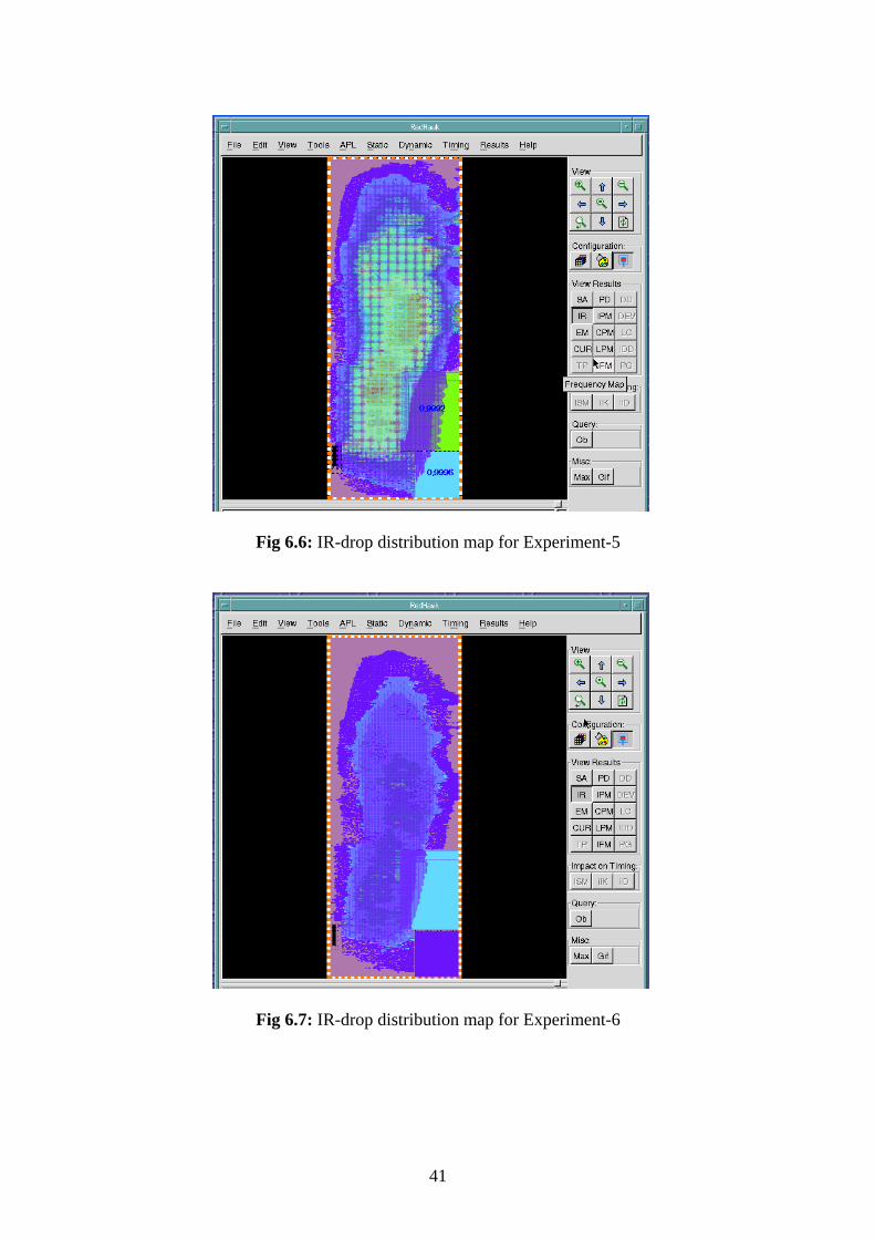
Fig 6.6: IR-drop distribution map for Experiment-5
Fig 6.7: IR-drop distribution map for Experiment-6
41

6.2 LEAKAGE POWER OPTIMIZATION: With the geometries shrinking leakage power is becoming a more significant
contributor to the total power consumption of the logic. By reducing the threshold voltage of
transistors we can get a faster switching logic. But the leakage power associated with the
lower vt cells is higher. One analysis done was to see the reduction of leakage power possible
by switching the stdcells with their high vt equivalents wherever faster switching logic was
not required. This had to be done while still respecting the timing constraints of the design.
Hence the experiment involved implementing the logic with low or high threshold cells as
required, doing a timing analysis to check if the timing constraints are met and making
corrections when required and so on.
Initial leakage power with only LVT cells: 4.112 mW
List of Experiments
Standard Cell Type
Leakage(mW)
Timing Violation (ns)
Leakage Power Savings (%)
Experiment-1 High-Vth 0.534 -1.900 87.02 Experiment-2 20% Low Vth 1.001 -0.685 75.66 Experiment-3 40% Low Vth 1.790 0.004 56.47 Experiment-4 60% Low Vth 2.331 0.054 43.32 Experiment-5 80% Low Vth 3.273 0.105 20.43
Table 6.2: Leakage power optimization
As can be seen from the table, the most optimum implementation is when 40% of the
cells are replaced with low Vth equivalents which results in 56.47% saving the leakage power
and still meets the timing requirements for the block.
6.3 MULTIPLE CLOCK TREE STRATEGIES: Clock nets are special nets in the design as they have very high fanout and need to be
routed all across the block. Also since the clock nets are driven by the high drive clock
buffers they are typically the crosstalk aggressors. Hence special routing rules are applied to
clock nets to minimize the degradation of clock signals within the design and also to reduce
the crosstalk effect of clock nets on the nearby signal nets. These special rules involve using
extra width and extra spacing for clock nets. The choice of layers used for routing also has a
significant effect on the available resources for signal nets to be routed as the clock nets
consume a significant portion of the available routing resources.
42
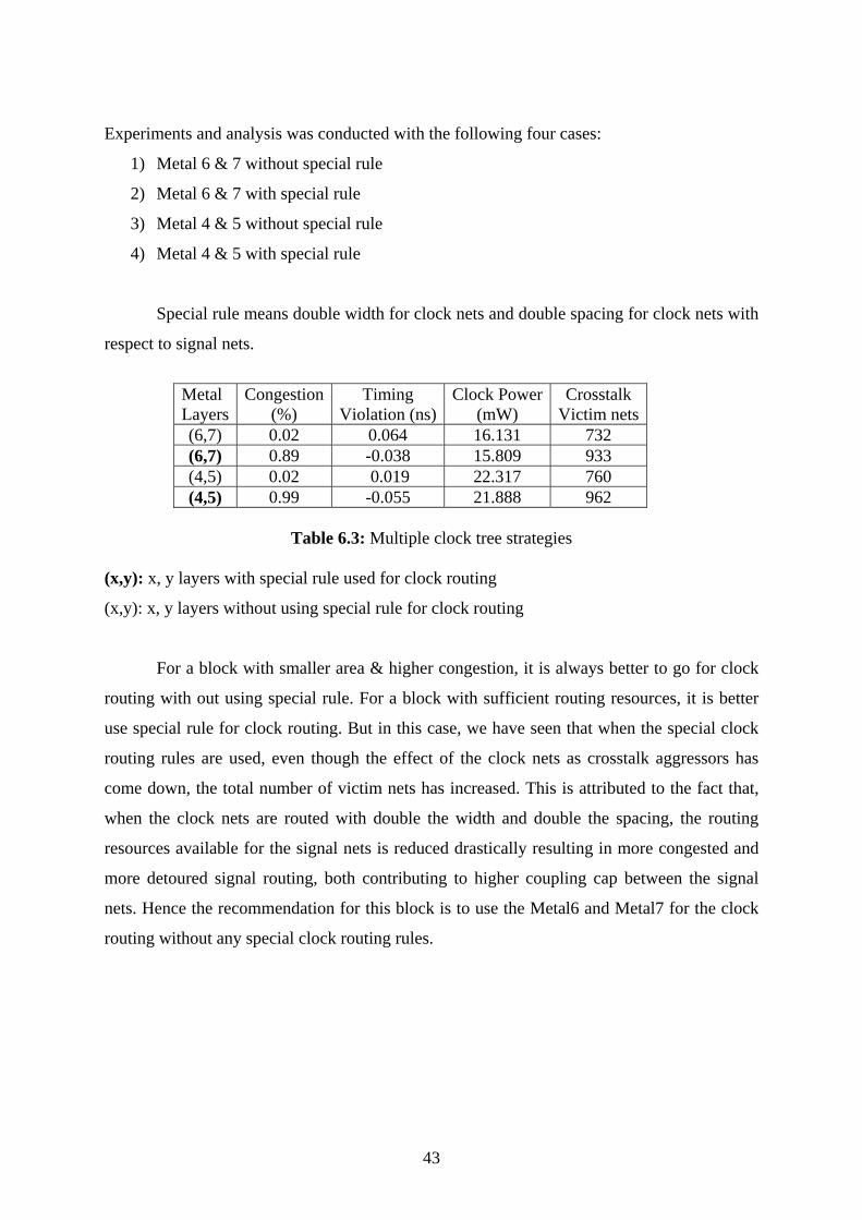
Experiments and analysis was conducted with the following four cases:
1) Metal 6 & 7 without special rule
2) Metal 6 & 7 with special rule
3) Metal 4 & 5 without special rule
4) Metal 4 & 5 with special rule
Special rule means double width for clock nets and double spacing for clock nets with
respect to signal nets.
Metal Layers
Congestion (%)
Timing Violation (ns)
Clock Power (mW)
Crosstalk Victim nets
(6,7) 0.02 0.064 16.131 732 (6,7) 0.89 -0.038 15.809 933 (4,5) 0.02 0.019 22.317 760 (4,5) 0.99 -0.055 21.888 962
Table 6.3: Multiple clock tree strategies
(x,y): x, y layers with special rule used for clock routing
(x,y): x, y layers without using special rule for clock routing
For a block with smaller area & higher congestion, it is always better to go for clock
routing with out using special rule. For a block with sufficient routing resources, it is better
use special rule for clock routing. But in this case, we have seen that when the special clock
routing rules are used, even though the effect of the clock nets as crosstalk aggressors has
come down, the total number of victim nets has increased. This is attributed to the fact that,
when the clock nets are routed with double the width and double the spacing, the routing
resources available for the signal nets is reduced drastically resulting in more congested and
more detoured signal routing, both contributing to higher coupling cap between the signal
nets. Hence the recommendation for this block is to use the Metal6 and Metal7 for the clock
routing without any special clock routing rules.
43

6.4 ADDING EXTRA METAL LAYERS FOR ROUTING:
Using an extra routing layer would add up to the total routing resources available for
establishing connectivity between standard cells within the same physical area. However
adding an extra layer adds to the cost of manufacturing and can be prohibitively high when
compared to the area reduction possible with each addition of layer. An analysis was done to
see the area reduction achievable by adding one more layer of routing. However, this is only
to collect the data as the costing part of the manufacturing involves multiple variables with
wide ranges and is beyond the scope of this thesis.
The following table summarizes the area, power and routing wire length distribution
for six and seven metal layer implementation of the block.
Wire length of metal layers (meters) No of
layers Area
(mm)^2 Power (mW)
TW (m) M1 M2 M3 M4 M5 M6 M7
6 1.951 295 7.444 0.344 1.752 2.227 2.646 0.426 0.048 ---- 7 1.498 260 6.676 0.131 1.261 1.713 2.046 1.420 0.049 0.055
Table 6.4: Adding extra metal layers for routing
6.5 DESIGN DEPENDANT FLOORPLANNING TECHNIQUES:
1. Region
2. Density screen
6.5.1 Region:
Regions are used to group the standard cell instances belong to same logic. The area
and shape of the region depends upon the standard cell count and distribution of that
particular logic in the block.
As seen from the below figures, the logic was distributed without the region constraint
which resulted in a wider distribution of the logic needing longer interconnects resulting in
routing congestion and more delay in the interconnect between the cells.
44
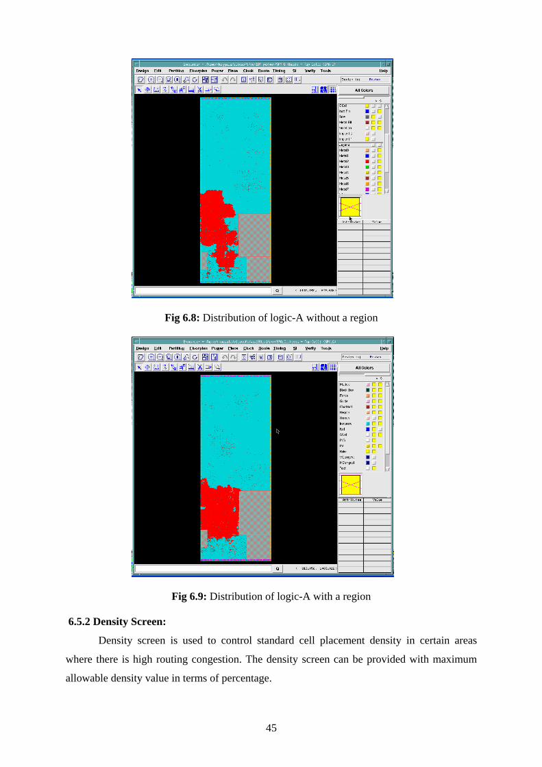
Fig 6.8: Distribution of logic-A without a region
Fig 6.9: Distribution of logic-A with a region 6.5.2 Density Screen:
Density screen is used to control standard cell placement density in certain areas
where there is high routing congestion. The density screen can be provided with maximum
allowable density value in terms of percentage.
45

Figure 6.10: Distribution of logic-B without a density screen
Figure 6.11: Distribution of logic-B with a density screen
The distribution of the logic was very compact without the density screen constraint
as can be seen in the Figure 6.10 .This was resulting in too many wires crossing a small
region resulting in routing congestion. With the density screen constraint introduced along
with the timing constraints, the tool moved away the non timing critical logic away from the
rest of the logic-B resulting in between routability while meeting the timing constraints.
46

Chapter 7
CONCLUSION
47

7. CONCLUSION
7.1 ACHIEVEMENT OF THE THESIS:
The experience from the different experiments conducted and the results analyzed
proves that the physical implementation is truly a balancing act of various parameters. Very
careful planning and visualization of the impact on other parameters is required before
choosing a strategy and while implementing it. Excessive optimization for one parameter
could result in the worsening and perhaps not meeting the requirements for others. The same
design could have various implementations, one of which would result in the minimum
power consumption, another which would operate the fastest and yet another which would
take the minimum area. The challenge is in meeting the specifications for all the parameters
and within the constraints of the design from various aspects in making it the most optimized
one.
The results of the various experiments carried out were summarized below,
From the power grid experiment, since the IR-drop limit within the block was set to
2mV, the Experiment-5 is recommended which results in a saving of almost 9% of the
overall routing resources of the design.
From the leakage power optimization experiment, the most optimum implementation
is when 40% of the cells are replaced with low Vth equivalents which results in
56.47% saving the leakage power and still meets the timing requirements for the
block.
From the multiple clock tree strategies experiment, the recommendation for this block
is to use the Metal6 and Metal7 layers for the clock routing without using special rule.
From the adding extra metal layers for routing experiment, using an extra routing
layer would add up to the total routing resources available for establishing
connectivity between standard cells within the same physical area. However adding
an extra layer adds to the cost of manufacturing and can be prohibitively high when
compared to the area reduction possible with each addition of layer.
From the floorplanning techniques experiment, using region and density screen
techniques, the design has improved from the routing congestion with meeting the
timing requirements.
48

7.2 SCOPE OF FUTURE WORK:
Various design techniques that could impact the area, crosstalk, power and
manufacturability could not be analyzed due to lack of tools and time. Some of these include:
Setting a max transition time constraint for all the cells in the design which would
strengthen the victim nets and reduce the crosstalk effects
Adopting different metal layers and combination of width and pitch for the power
mesh for optimizing the routing resources
Optimizing the clock skew for various clocks in the design resulting in more
optimized insertion of clock buffers which would result in lesser area and power
One of the area which is significant for the deep sub-micron technology is the yield in
manufacturability of a design. However, design technique to improve yield of the
design and analysis of their effectiveness makes an interesting study.
49

REFERENCES
1. Michael John, Sebastian Smith. Application-Specific Integrated Circuits. Pearson Education Press, 1997
2. Pran Kurup, Taher Abbasi, Ricky Bedi. It’s the Methodology. Library of congress
cataloging in publications data, 1998
3. Physical Design Tutorial. Magma Design Automation, 2003 http://www.vitalect.com/magma
4. Olivier Coudert. “Timing and design closure in physical design flows.” Quality
Electronic Design, 2002. Proceedings. International Symposium on 18-21 March 2002 Page(s):511- 516
5. Murat Becer, Ravi Vaidyanathan, Chanhee Oh, Rajendran Panda. “Crosstalk Noise
Control in an SoC Physical Design Flow.” Computer-Aided Design of Integrated Circuits and Systems, IEEE Transactions on Volume 23, Issue 4, April 2004 Page(s):488 – 497
6. S. Alwar, D. Blaauw, A. Dasgupta, A. Grinshpon, R. Levy, C. Oh, B. Orshav,
S. Sirichotiyakul, V. Zolotov. “Clarinet: a noise analysis tool for deep submicron design.” Proc. Design Automation Conf., June 2000, pp. 233–238.
7. M. Hashimoto, M. Takahashi, and H. Onodera. “Crosstalk noise optimization by post-
layout transistor sizing.” Proc. Int. Symp. Physical Design, 2002, pp. 126–130.
8. Kaijian Shi, Jason Binney. "Design Optimization Methodologies for Low- Leakage Power Designs in Sub-90nm Technology." Euro Design Con 2004
9. DiaaEldin Khalil, Yehea Ismail. “Optimum sizing of power grids for IR drop.”
Circuits and Systems, 2006. ISCAS 2006. Proceedings. 2006 IEEE International Symposium on 21-24 May 2006 Page(s):4 pp.
10. Rishi Bhooshan. “Novel and Efficient IR-Drop Models for Designing Power
Distribution Network for Sub-100nm Integrated Circuits.” Quality Electronic Design, 2007. ISQED '07. 8th International Symposium on March 2007 Page(s):287 - 292
11. Zahi Abuhamdeh, Philip Pears, Jeff Remmers, Alfred L. Crouch, Bob Hannagan.
“Characterize Predicted vs. Actual IR Drop in a Chip Using Scan Clocks.” Test Conference, 2006. ITC '06. IEEE International Oct. 2006 Page(s):1 - 8
12. Nobuyuki Nishiguchi. “An advance RTL to GDS2 design methodology for 90 nm and
below system LSIs to solve timing closure, signal integrity and design for manufacturing.” Circuits and Systems, 2005. ISCAS 2005. IEEE International Symposium on 23-26 May 2005 Page(s):5938 - 5941 Vol. 6
13. Granthana K Rangaswamy, Satish Prathaban. “Signal Integrity Analysis with Power
Delivery Network.” Signal Propagation on Interconnects, 2006. IEEE Workshop on May 2006 Page(s):205 - 207
50

14. Power grid verification. Cadence Design Systems, 2002 http://www.cadence.com/whitepapers/4101_PowerGridVerif_WP.pdf
15. Signal integrity closure. Cadence Design Systems, 2003
http://www.cadence.com/whitepapers/4496_SI_WP_Fnl.pdf
16. Noise-aware timing analysis. Cadence Design Systems, 2001 http://www.cadence.com/whitepapers/NoiseAware061301.pdf
17. Design planning strategies to improve physical design flows—Floorplanning and
Power planning. Synopsys, 2003 http://www.synopsys.com/sps/pdf/design_plan_wp.pdf
18. Routing requirements for the nanometer era. Cadence Design Systems, 2004
http://www.cadence.com/whitepapers/RoutingRequirements_WP.pdf
19. Enabling low power design within an RTL-to-GDSII implementation flow. Magma Design Automation, 2003 http://www.magma-da.com/c/@biAtic0XhY.Ig/Pages/WPLowPower.html
20. A practical methodology for calculating acceptable IR-drop targets in advanced
VDSM design. Synopsys, 2006 http://www.synopsys.com/sps/pdf/ir_drop.pdf
21. Design practices and strategies for efficient signal integrity closure. Synopsys, 2005
http://www.synopsys.com/sps/pdf/sic_wp.pdf
22. Power Management in Complex SoC Design. Synopsys, 2005 http://www.synopsys.com/sps/pdf/sps_pwr_mgnt_wp.pdf
23. Designing clock signals-predictability counts. Cadence Design Systems, 2001
http://www.cadence.com/whitepapers/4107_ClockSignal_WP.pdf
24. Documents provided by Ikanos Communications (India) Pvt Ltd
51