on the convergence of many-body excited state calculations for monolayer mos2
TRANSCRIPT

On the convergence of many-body excited state calculations for monolayer MoS2
Falco Huser∗ and Thomas OlsenCenter for Atomic-scale Materials Design (CAMD), Department of Physics
Technical University of Denmark, 2800 Kgs. Lyngby, Denmark
Kristian S. Thygesen†
Center for Atomic-scale Materials Design (CAMD), Department of PhysicsTechnical University of Denmark, 2800 Kgs. Lyngby, Denmark and
Center for Nanostructured Graphene (CNG)Technical University of Denmark,2800 Kgs. Lyngby, Denmark
(Dated: December 16, 2013)
We present first principles many-body calculations of the dielectric constant, quasiparticle bandstructure and optical absortion spectrum of monolayer MoS2. As the separation between the re-peated layers is increased, the dielectric function of the layer develops a strong q-dependence aroundq = 0. This implies that denser k-point grids are required to converge the band gap and excitonbinding energies when large supercells are used. In the limit of inifinite layer separation, here ob-tained using a truncated Coulomb interaction, a 45 × 45 k-point grid is needed to converge theG0W0 band gap and exciton energy to within 0.1 eV. We provide an extensive comparison withprevious studies and explain agreement and variations in the results. It is demonstrated that toocoarse k-point sampling and the interactions between the repeated layers have opposite effects onthe band gap and exciton energy, leading to a (partial) fortuitous error cancellation in the previouslypublished results.
PACS numbers: 71.20.Nr, 71.35.-y, 73.22.-f, 78.20.Bh, 78.60.LcKeywords: MoS2
I. INTRODUCTION
Atomically thin two-dimensional (2D) materials suchas graphene, hexagonal boron nitride, and transitionmetal dichalcogenides (TMDC) possess unique electronicand optical properties including high intrinsic carriermobilities,1–3 tunable band gaps,4,5 and strong light-matter interactions.6–9 These features, combined withthe possibility of engineering their electronic propertiesfurther via strain, alloying or stacking, make the 2D ma-terials ideal as building blocks for new opto-electronicstructures and devices with minimal sizes and perfor-mances surpassing present technologies.
After the intense focus on graphene, the TMDCs arenow attracting increasing interest.10 This stems mainlyfrom the greater variation in their electronic propertiesincluding both semiconducting and metallic behavior. Sofar, the most intensively studied single-layer TMDC isthe semiconductor MoS2. Nanostructured forms of MoS2
have previously been explored as potential catalysts fordesulferization of crude oil and more recently for (photo)-electrochemical hydrogen evolution.11–13 Bulk MoS2 iscomposed of two-dimensional sheets held together byweak van der Waals forces and individual sheets can beisolated by exfoliation techniques similar to those used toproduce graphene.1 Single layers of MoS2 therefore com-prise highly interesting two-dimensional systems with afinite band gap and have recently been proposed for nano-electronics applications.2
The optical properties of MoS2 have been thoroughlystudied experimentally.14–19 The absorption spectrum
shows two distinct low energy peaks at 1.88 eV and2.06 eV, which are denoted by A and B, respectively,20
and derive from direct transitions between a split valenceband and the conduction band at the K point of the Bril-louin zone. Their Rydberg satellites, Zeeman splitting,and dependence on crystal thickness have been investi-gated in detail.17 Recently, the quantum yield of lumi-nescence from MoS2 was shown to increase dramaticallywhen the sample thickness was changed from a few layersto a monolayer7,8 indicating a transition to a direct bandgap in the single layer.
In the past couple of years a number of theoreticalstudies of the electronic band structure and optical exci-tations in monolayer MoS2 have been published.4,21–26
These studies are based on many-body perturbationtheory in the GW approximation (mainly the non-selfconsistent G0W0 approach) for the band structureand the Bethe-Salpeter equation (BSE) with a staticallyscreened electron-hole interaction for the optical excita-tions. As is standard practice, the calculations have beenperformed on a supercell geometry where the MoS2 lay-ers have been separated by 10 − 20 A vacuum and theBrillouin Zone (BZ) sampled on grids ranging from 6× 6to 15 × 15. With these parameters G0W0 band gaps inthe range 2.6 − 3.0 eV, and G0W0-BSE exciton bindingenergies of 0.6 − 1.1 eV, have been reported. Moreover,both direct21–25 and indirect4 band gaps have been foundat the G0W0 level, while only direct gaps have been ob-tained with self-consistent GW21 and GW0.4,26 Whencomparing these values, it should be kept in mind thatboth size and nature of the band gap of MoS2 depends
arX
iv:1
311.
1384
v1 [
cond
-mat
.mtr
l-sc
i] 6
Nov
201
3

2
sensitively on the in-plane lattice parameter, a.4
One of the most fundamental quantities describing theelectronic structure of a material is the dielectric func-tion. The dielectric properties of atomically thin 2D ma-terials are quite different from their 3D counterparts.27
For example plasmons in 2D metals have acoustic dis-persion relations (ωp(q) → 0 as q → 0), and screening isgenerally much weaker leading to strong exciton bindingenergies in 2D semiconductors. Reported static dielec-tric constants for monolayer MoS2 obtained using thesupercell approach lie in the range 4.2 −7.6 (for in-planepolarization).21,24,28 These values have been used to ra-tionalize the exciton binding energy in MoS2 using thesimple Mott-Wannier model.
In this paper, we present an in-depth study of the di-electric function, quasiparticle band structure and ex-citonic states in monolayer MoS2. We focus on sepa-rating the spurious interlayer screening from the intrin-sic intralayer screening in supercell geometries, and theconsequences that the physics of screening in 2D hasfor the convergence of many-body excited state calcu-lations. The 3D macroscopic dielectric constant, as usedfor solids, converges to 1 for all q vectors in the limitof infinite separation of the layers and is thus meaning-less for a 2D material. We use an alternative approachto calculate the dielectric constant by averaging the totalfield over the material rather than the supercell. This 2Ddielectric constant shows strong q-dependence for smallwave vectors and becomes exactly 1 for q = 0. This prop-erty has important consequences for the k-point conver-gence of many-body calculations.
In general, the use of a truncated Coulomb interac-tion is essential to avoid interlayer screening which de-cays slowly with the layer separation, L. The interlayerscreening yields too large dielectric constant for wave vec-tors q < 1/L. As a consequence, the G0W0 band gapsand exciton energies are 0.5 eV too low on average forlayer separations of around 20 A. For larger layer separa-tions, the strong q-dependence of the dielectric constantfor small q implies that a k-point grid of at least 45× 45is required to converge band gaps and exciton energiesto 0.1 eV. For k-point grids below 15× 15 the band gapis at least 0.5 eV too large in the limit L → ∞. Thusthe effect of interlayer screening and too coarse k-pointgrids partially cancel out leading to reasonable values forthe band gap and exction binding energy with undercon-verged parameters as applied in previous studies.
The paper is organized as follows. In Sec. II we presentG0W0 band structures and study the convergence of thegap with respect to interlayer separation and k-pointsampling. In Sec. III we show calculations for the 2Ddielectric constant and explain the origin of the slow k-point convergence of the band gap. In Sec. IV we presentmany-body calculations of the lowest excitons and anal-yse their convergence with layer separation and k-pointsampling. Our conclusions are given in Sec. V.
II. QUASIPARTICLE BAND STRUCTURE
In this section we demonstrate that GW band struc-tures for monolayer MoS2 converge extremely slow withrespect to the interlayer separation. In order to obtainwell converged results (within 0.1 eV), the use of a trun-cated Coulomb interaction is inevitable, along with a k-point grid of around 45× 45. Previously reported calcu-lations with the full Coulomb interaction have employedonly separation between 10 and 20 A and used from 6×6to 12 × 12 k points. The resulting band structures are,however, somewhat saved by a fortunate error cancella-tion between the two effects.
A. Computational details
All our calculations have been performed with the pro-jector augmented wave method code GPAW.2943 TheKohn-Sham wave functions and energies of monolayerMoS2 were calculated in the local density approxima-tion (LDA) using a plane wave basis with cut-off energy400 eV. The 4s and 4p semicore electrons of Mo wereexplicitly included in all calculations. Unless otherwisestated the calculations have been performed for the ex-perimental lattice constant of 3.16 A. One-shot G0W0
calculations were performed using the LDA wave func-tions and eigenvalues to obtain the G0W0@LDA quasi-particle energies. A plane wave cut off of 50 eV and200 bands were used for the dielectric function, screenedinteraction and GW self-energy. Convergence with re-spect to these parameters has been checked very carefully.With these values band gaps were found to be convergedwithin around 10 meV. The plasmon pole approximationfor the dielectric function was found to yield QP energieswithin 0.1 eV of those obtained from full frequency de-pendence and was consequently used in all calculations.To avoid interaction between the periodically repeatedMoS2 sheets, we have applied a truncated Coulomb in-teraction of the form vc(r) = (1/r)θ(Rc − z), followingRefs. 30 and 31. For details on the implementation ofthe GW method in the GPAW code we refer to Ref. 32.We note that we have used a numerical averaging of thehead of the screened potential W00(q) for all wavevectorsq in the Brillouin zone (similar to Eq. 9 in Sec. III C).This was found to be crucial in all calculations with thefull 1/r Coulomb interaction.
B. Results
The band structure calculated using 45 × 45 k pointsand the truncated Coulomb interaction is shown in Fig.1. At the LDA level, we find a direct band gap at the Kpoint of 1.77 eV while the smallest indirect gap of 1.83 eVoccurs from Γ to a point along the Γ-K direction. Incontrast, G0W0 predicts an indirect gap of 2.58 eV andat direct gap at K of 2.77 eV.

3
FIG. 1: (Color online). Bandstructure of monolayer MoS2
calculated with LDA and G0W0@LDA using 45×45 k pointsand a truncated Coulomb interaction to avoid interaction be-tween periodically repeated layers. The valence band topshave been aligned.
FIG. 2: Definition of the interlayer separation, L.
In Fig. 3 we show the convergence of both the directand the indirect band gap with respect to the k-point gridfor a fixed interlayer separation of 23 A (see Fig. 2 forthe definition of L). It is clear that a very dense k-pointgrid is needed in order to obtain well-converged resultswith the truncated Coulomb interaction. For 45 × 45 kpoints, band gaps are converged within less than 0.1 eV,while this is already the case for 15 × 15 k points withthe bare Coulomb interaction. However, the calculatedvalues are too low. The slow convergence with respect tok points when the truncation is used will be discussed indetail in Sec. III C.
We see that results do not converge independently withrespect to the number of k points and the interlayer sep-
FIG. 3: (Color online). Direct (full symbols) and indirect(open symbols) G0W0 band gaps as function of the number ofk points in one of the in-plane directions for a layer separationof L = 23 A.
FIG. 4: (Color online). Direct G0W0 band gap plotted as afunction of interlayer distance for different k-point samplingswith the full 1/r interaction. Dotted lines serve as a guide forthe eye to extrapolate for L → ∞. They were obtained byfitting all values for L > 30 A, including the results with theCoulomb truncation, to a quadratic function. Dashed hori-zontal lines indicate the calculated values with the truncatedCoulomb interaction.
aration. In Fig. 4, we plot the L-dependence of thedirect band gap for different k-point samplings with thebare interaction. The k-point dependence becomes muchstronger for large L. For L→∞, the values are expectedto converge to the results calculated with the truncation(indicated by dotted lines). They seem to exhibit a linear1/L behaviour only for L > 50 A or very dense k-pointsamplings. Fig. 5 shows all results and interpolated val-ues in a contourplot as a function of 1/L and numberof k points. The effects of using more k points and in-creasing L are of different sign and partially cancel eachother. This is the reason, why different choices of thetwo parameters yield the same results. Especially, the

4
FIG. 5: (Color online). Contour plot of the direct G0W0
band gap as a function of the inverse interlayer distance andnumber of k points in one of the in-plane directions with thefull 1/r interaction. Contour lines are separated by 0.1 eV.Interpolation from splines was used.
band gaps calculated with 9 × 9 k points and L = 23 Aand 15× 15 k points and L = 43 A are the same as with45 × 45 k points and infinite L. This seems, however,conincidental and we do not expect it to be the case forother systems.
We note that all calculations have been performed witha single k point in the direction perpendicular to thelayer. This is, however, insufficient for small interlayerdistances. For L = 13 A, we find an increase of the bandgap of around 0.2 - 0.3 eV when at least 3 k points areused, for example. For L > 20 A or use of the truncation,this effect is negligible.
C. Comparison with previous work
In table I we show our converged results obtained withthe truncated Coulomb interaction and 45× 45 k pointstogether with previous G0W0 results from the literature.For each reference we show the values used for the lat-tice constant, the interlayer separation and the k-pointsampling. It can be seen that all the previous calcula-tions have used small layer separations and no trunca-tion method. As pointed out in the preceding discussion,this gives a fast k-point convergence. A properly con-verged calculation, however, requires larger separationsand thereby more k points. But as a consequence of acancellation of errors, a calculation with 19 A layer sepa-ration and 12× 12 k points yields almost the same bandgaps as our converged result (within 0.15 eV). We arethus led to conclude that the reasonable agreement be-tween our results and previous ones are to a large extentfortuitous.
Furthermore, the effect of strain can have a large im-
pact on the MoS2 band gap. As demonstrated in Ref.4, using 12 × 12 k points and 19 A layer separation, theG0W0 band gap for the experimental lattice constant of3.160 A is indirect. With a lattice constant of 3.190 A,corresponding to 1% strain, the gap changes to direct.The lowering of the direct band gap becomes even morepronounced for larger lattice constants. As can be seenfrom the table our converged results predict the sametrend, in particular the decrease of the direct gap as func-tion of strain, with our values for the direct gap beinggenerally 0.2 eV larger. We note that for 3.255 A, thesmallest indirect transition occurs from the Γ point atthe valence band to the K point at the conduction band.This is also in agreement with Ref. 4. In the partiallyself-consistent GW0 calculations of Ref. 26, the oppo-site trend was found, namely a transition from a directto indirect band gap for ∼ 5 % strain. However, a layerseparation of only 12 A and less than 9 k points in thein-plane directions were used.
In Ref. 22, the band gap was determined by extrap-olating from L = 20 A to infinite layer separation, un-der the assumption that the gap scales linearly with theinverse distance between the layers. The obtained val-ues for the direct and indirect band gaps are ∼ 3.0 and∼ 3.3 eV, respectively. This is consistent with our find-ings using the truncated Coulomb interaction, the samelattice constant of 3.18 A and the same (under-converged)k-point grid of 12× 12 as in Ref. 22.
From our studies, we conclude that the G0W0@LDAband gap of monolayer MoS2 is indirect with a value of2.6 eV while the direct gap is 2.8 eV, when the experimen-tal lattice constant of 3.16 A is used. The question of howwell the one-shot G0W0@LDA approximation describesthe true electronic structure of this system remains open.Partially self-consistent GW0
4 and fully self-consistentGW21 calculations have been shown to consistently yielddirect band gaps of 2.75 − 2.80 eV.
III. STATIC SCREENING
In this section we present a detailed investigation ofthe (static) dielectric properties of monolayer MoS2. Thisserves a dual purpose. First, it illustrates the origin of theslow convergence of the GW results presented in the pre-vious section (and the BSE results presented in the nextsection). Secondly, it shows that the usual definition ofthe macroscopic dielectric constant of a periodic solid isnot meaningful when applied to a 2D system representedin a periodic supercell. We discuss the difference betweenscreening in 2D and 3D which becomes particularly pro-nounced in the q → 0 limit with large consequences forthe calculation of optical excitations with static screeningof the electron-hole interaction (see next section).

5
TABLE I: Calculated G0W0 band gaps obtained in present work and compared with previous results from the literature. Allour calculations have been performed using a truncated Coulomb interaction.
Egap (eV)
Ref. starting point a (A) number of k-points layer separation (A) direct indirect
This work LDA 3.16 45× 45× 1 23 (truncated vc) 2.77 2.58This work LDA 3.19 45× 45× 1 23 (truncated vc) 2.65 2.57This work LDA 3.255 45× 45× 1 23 (truncated vc) 2.41 2.51Ref. 25 LDA 3.15 18× 18× 1 24 2.41 ∼ 2.40Ref. 4 PBE 3.16 12× 12× 1 19 ∼ 2.60 2.49Ref. 4 PBE 3.19 12× 12× 1 19 2.50 ∼ 2.55Ref. 4 PBE 3.255 12× 12× 1 19 2.19 2.19Ref. 21 LDA 3.16 8× 8× 2 19 2.96 –Ref. 22 PBE 3.18 12× 12× 1 20+1/L extrapolation 2.97 3.26Ref. 22 PBE 3.18 12× 12× 1 20 ∼ 2.60 ∼ 2.85Ref. 23 LDA 3.11 12× 12× 1 13 2.57 –Ref. 24 HSE 3.18 6× 6× 1 15 2.82 ∼ 3.00Ref. 33 PBE 3.19 15× 15× 1 15 2.66 –
A. 3D macroscopic dielectric constant
The microscopic dielectric function determines the re-lation between a weak external potential and the totalpotential in the material,
Vtot(r) =
∫dr′ ε−1(r, r′)Vext(r
′). (1)
For a periodic system the dielectric function can be con-veniently expressed in plane waves
ε−1(r, r′) =∑GG′
∑q
ei(G+q)rε−1GG′(q)e−i(G
′+q)r′ , (2)
where G is a reciprocal lattice vector, q belongs to the1. BZ. Within the random phase approximation (RPA)we have
εGG′(q, ω) = δGG′ − vc(q + G)χ0GG′(q, ω), (3)
where χ0 is the non-interacting density response func-tion. Here, vc can be the Fourier representation of eitherthe full or the truncated Coulomb interaction. For thecalculations in this section we have used a 50 eV cut-off for the reciprocal lattice vectors to account for localfield effects. The non-interacting response function, χ0,was constructed from local density approximation (LDA)wave functions and energies including states up to 50 eVabove the Fermi level. All calculations were performedwith the projector augmented wave method code GPAW.Details on the implementation of the dielectric functionin the GPAW code can be found in Ref. 34.
It follows from Eq. (2) that the total potential result-ing from a plane wave external potential V0e
iq·r has theform
Vtot(r) = Vq(r)eiq·r (4)
where Vq(r) is a lattice periodic function. We thus definethe macroscopic dielectric constant as
1
εM (q)≡ 〈Vq〉Ω
V0= ε−1
00 (q), (5)
where 〈. . .〉Ω denotes a spatial average over a unit cell.Note that in general εM (q, ω) 6= ε00(q, ω) because of localfield effects.35,36
To explicitly demonstrate that Eq. (5) does not ap-ply to low-dimensional materials, we have calculated themacroscopic dielectric constant as a function of the layerseparation, L. The results are shown in Fig. 6 for differ-ent values of the in-plane momentum transfer q. We alsoshow the dielectric constant corresponding to polariza-tion orthogonal to the layer. Clearly the macroscopic di-electric constant approaches unity for all q-vectors in thelimit of large interlayer separation. This occurs becausethe total field is averaged over an increasingly larger vac-uum region.
Previously reported values for the macroscopic di-electric constant of monolayer MoS2 lie in the range4 − 8 .21,24,28 In these calculations the MoS2 layers wereseparated by 10 − 20 A vacuum. As can be seen fromε‖(q = 0) in Fig. 6 this is consistent with our results.However, it should also be clear that numbers depend onthe distance between layers and in fact are not meaning-ful.
B. 2D macroscopic dielectric constant
For a 2D material, the average of the total potential inthe definition of the macroscopic dielectric constant mustbe confined to the region of the material. Since Eq. (4)still holds for a 2D material when q is confined to theplane of the material, we average the in-plane coordi-nates (r‖) over the unit cell area A and the out-of-plane

6
FIG. 6: (Color online). The 3D static macroscopic dielectricconstant 1/ε−1
00 (q) of monolayer MoS2 as a function of theinterlayer separation, L. ε‖ is the dielectric constant withpolarization parallel to the monolayer and ε⊥ is the dielectricconstant for polarization orthogonal to the layer.
coordinate (z) from z0 − d/2 to z0 + d/2 where z0 de-notes the center of the material and d its width. The 2Dmacroscopic dielectric constant then becomes
1
ε2DM (q‖)≡ 〈Vq〉A,d
V0
=2
d
∑G⊥
eiG⊥z0sin(G⊥d/2)
G⊥ε−1G0(q‖), (6)
where the sum is over all G with G‖ = 0. In this work
we have taken d = 6.15 A corresponding to the interlayerseparation in bulk MoS2. We shall return to the problemof chosing d below.
The results for the static dielectric constant evaluatedfrom Eq. (6) using the bare Coulomb interaction is shownin Fig. 7 for four different layer separations. The re-sult for L = d = 6.15 A coincides with the 3D dielectricconstant of bulk MoS2 given by Eq. (5). The result ob-tained with the truncated Coulomb interaction is shownin black; it represents the case of infinite layer separation.Before discussing the results, it is instructive to considerthe potential arising from a 2D charge density fluctuationof the form,
n(r) = n0eiq‖·r‖δ(z), (7)
The corresponding potential follows from Poisson’sequation44
φ(r) =n0
q‖e−iq‖·r‖e−q‖|z|. (8)
It follows that the potential perpendicular to the layerfalls off exponentially over a characteristic distance of1/q‖. This explains why in general ε2DM (q‖) coincideswith the isolated layer result for q‖ & 1/L.
The variation of ε2DM when the parameter d is changedby ±10% is indicated by the shaded region in Fig. 7.
FIG. 7: (Color online). Static macroscopic dielectric constantfor a single layer of MoS2 calculated along the Γ-K line. Thecalculations are performed using Eq. (6) with the microscopicdielectric constant, ε−1
GG′(q), evaluated from Eq. (3) with ei-ther the bare Coulomb interaction (dotted and dashed lines)or truncated Coulomb interaction (full black line). The greyarea represents the result obtained when the averaging regionperpendicular to the layer, d, is varied by ±10%. The dottedline corresponds to a layer separation of 6.15 A and thus co-incide with the dielectric constant of bulk MoS2. The curveshave been interpolated from a 32× 32 q-point mesh.
To the left of the maximum, ε2DM (q‖) is insensitive tod since the induced potential is more or less constantover the averaging region. To the right of the maximum,the variation in ε2DM (q‖) follows the ±10% variation ind. This is because for these wave vectors the inducedpotential has essentially vanished at the borders of theaveraging region. In general, increasing (decreasing) dwill decrease (increase) ε2DM (q‖) in the large wave vectorregion.
Another characteristic feature of the potential in Eq.(8) is the 1/q‖ scaling which should be compared with
the 1/q2 form of the Coulomb potential from a 3D chargeoscillation. Since the non-interacting response function,χ000(q), scales as ∼ q2 for q → 0 for both 2D and 3D sys-
tems, it follows from Eq. (3) that ε2DM (0) = 1, whilethis is in general not the case in 3D. In our calcula-tions, the effect of interlayer interactions is eliminatedby using a truncated Coulomb interaction of the formvc(r) = (1/r)θ(Rc − z). For qz = 0 and in the limitof small q‖, the Fourier representation of the truncated
Coulomb interaction becomes v2D(q) = 4πRc
|q| , i.e. it
scales as 1/q as the potential from the 2D charge den-sity wave ensuring the correct limit ε2DM (0) = 1.
Finally, we note that previous studies37,38 have em-ployed a strict 2D model for the dielectric function inthe small q limit of the form ε(q‖) = 1 + αq‖. This formis convenient as it leads to an analytical expression forthe screened interaction in 2D.27 Our definition differs bybeing a 3D (or quasi 2D) quantity valid for general q‖.

7
C. Screened interaction
In Fig. 8 we show ε−100 as a function of q‖ evaluated
with and without the truncated Coulomb interaction.For small q, the two curves differ significantly due tothe long range nature of the induced potential (8). Atlarge q (∼ K/2), the induced potential decays withinthe cutoff range for the truncated Coulomb interactionand therefore no difference can be seen between the twomethods. We emphasize that neither of the dielectricconstants shown in the figure can be interpreted as adielectric constant of monolayer MoS2, since they givethe average potential over the supercell and not over theMoS2 layer. In particular their value will be highly de-pendent on the size of the unit cell (in the limit of infinitelayer separation both will equal 1 for all q). Nevertheless,this quantity is a crucial ingredient of both the GW self-energy and the BSE kernel as it provides the screeningof the divergent term of the Coulomb interaction.
For q = 0 the Coulomb kernel diverges and we approx-imate W (q = 0) by the integral
W00(q = 0) =1
ΩΓ
∫ΩΓ
dq vc(q)ε−100 (q)
≈ 1
ΩΓε−100 (q = 0)
∫ΩΓ
dq vc(q), (9)
where ΩBZ is the Brillouin zone volume and ΩΓ is a smallvolume containing q = 0. In isotropic systems ε−1
00 (q) isusually constant in the vicinity of q = 0 and the approxi-mation works well. However, when ε−1 is evaluated withthe truncated Coulomb interaction, ε−1
00 acquires muchmore structure for small q as can be seen from Fig. 8.Thus, for coarse k-point samplings we will underestimatethe Γ-point screening since we simply use ε−1
00 (q = 0) = 1.The linear behavior of the screened interaction for
small q suggests that a better approximation forW00(q =0) would be
W00(q = 0) =1
ΩΓ
∫ΩΓ
dq vc(q)[1 + q · ∇qε
−100 (q)
∣∣∣q=0
].
(10)Since the dielectric matrix in RPA is εGG′(q) = 1 −vc(q)χ0
GG′(q), we can derive an analytic expression forthe first order Taylor expansion in q, and its inverse.These quantities can be evaluated with vanishing addi-tional cost, but we will leave the assessment of this ap-proximation to future work.
IV. OPTICAL ABSORPTION SPECTRUM
In this section we present many-body calculations ofthe optical absorption spectrum of monolayer MoS2 bysolving the Bethe-Salpeter Equation (BSE) under thestandard assumption of static screening of the electron-hole interaction. As for the GW band gap, we find thatthe use of a truncated Coulomb interaction is essential
FIG. 8: (Color online). The 3D static inverse dielectric con-stant ε−1
00 (q) of monolayer MoS2 calculated in the RPA fordifferent values of in-plane momentum transfer q along the Γ-K direction. The separation between layers is L = 20 A. Notethat neither of the quantities can be interpreted as the macro-scopic dielectric constant of the monolayer (this quantity isthe black curve in Fig. 7).
to avoid interlayer screening and obtain well convergedexciton binding energies. Furthermore, the very strongq-dependence of the 2D static dielectric function aroundq = 0, leads to very slow k-point convergence for theexciton binding energy.
In order to obtain an accurate absorption spectrum in-cluding excitonic effects we calculate the response func-tion from the Bethe-Salpeter Equation (BSE). Using thestandard assumption of a static dielectric screening of theelectron-hole (e-h) interaction, the BSE39 can be recastas an effective two-particle Hamiltonian,40 which is diag-onalized on a basis of electron-hole pairs. In this way theexcitonic eigenstates can be expressed as a linear combi-nation of single-particle transitions
|λ〉 =∑vck
Aλvck|vck〉, (11)
where v, c, and k denote valence band, conduction bandand Brillouin zone wave vector, respectively. The absorp-tion spectrum is proportional to the imaginary part ofthe macroscopic dielectric function, which in the Tamm-Dancoff approximation can be written
ε2(ω) =2π limq→0
vc(q)∑λ
δ(ω − Eλ)
×∣∣∣∣∑vck
Aλvck〈vk− q|e−iq·r|ck〉∣∣∣∣2, (12)
where Eλ are the eigenvalues associated with |λ〉.In all calculations we have included a single valence
band and a single conduction band in the BSE Hamilto-nian. We have tested that the first excitonic peak is com-pletely unaffected if we instead include 6 valence bandsand 4 conduction bands. This is also expected since the
8
highest (lowest) valence (conduction) band is well iso-lated from the remaining bands at K where the excitonis centered, see Fig. 1. For the screening we have in-cluded 65 bands in the evaluation of the response func-tion, which is sufficient for converged results. Increasingthe number of bands to 300 affects the position of thefirst exciton by less than 10 meV. The plane wave cutofffor the response function (local field effects) was set to50 eV and we checked that the excitonic binding energychanged by less than 10 meV when increasing the cutoffto 200 eV. The dependence on k-point sampling and in-terlayer separation will be examined below. Details onthe implementation of the BSE method in the GPAWcode can be found in Ref. 5.
A. Convergence tests
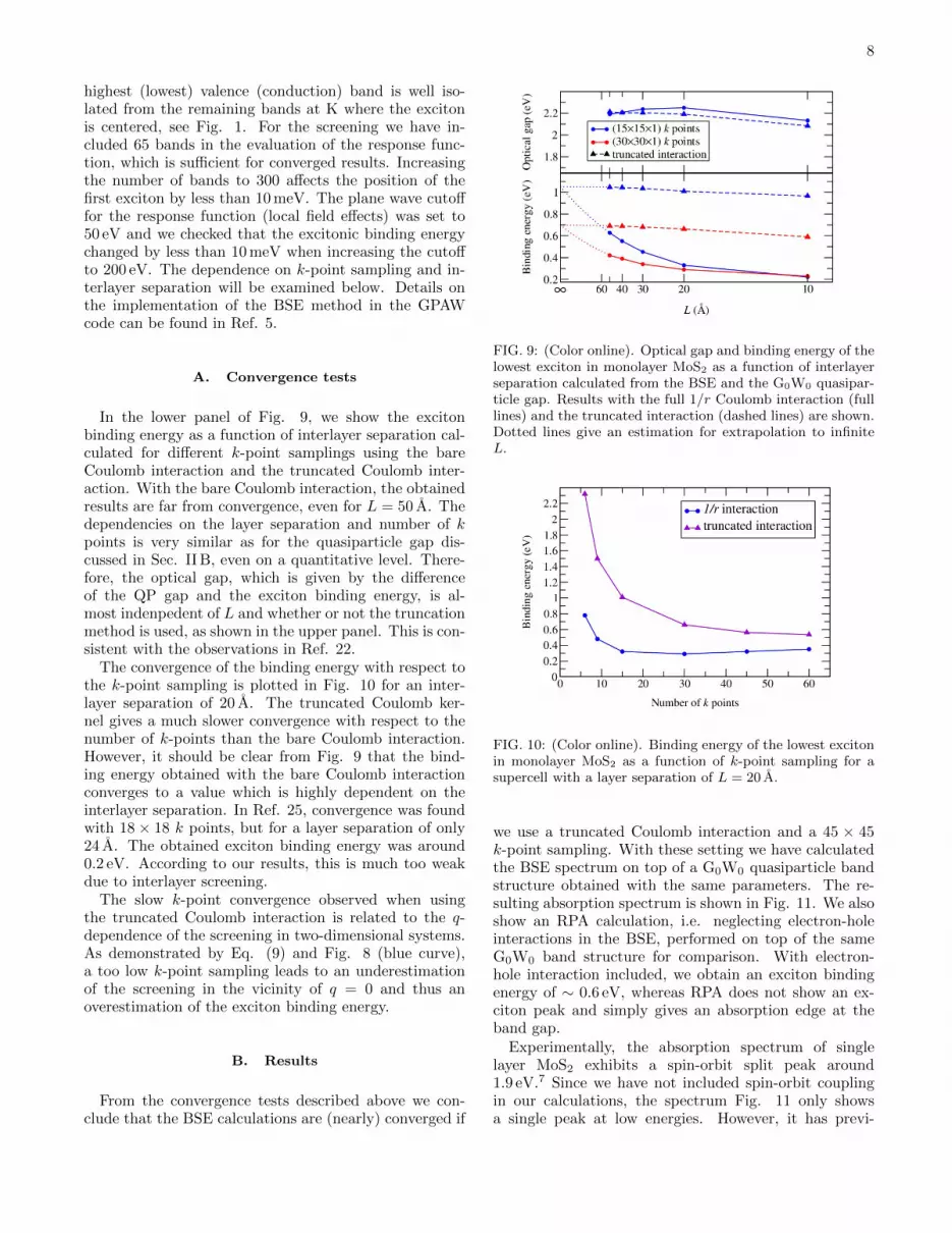
In the lower panel of Fig. 9, we show the excitonbinding energy as a function of interlayer separation cal-culated for different k-point samplings using the bareCoulomb interaction and the truncated Coulomb inter-action. With the bare Coulomb interaction, the obtainedresults are far from convergence, even for L = 50 A. Thedependencies on the layer separation and number of kpoints is very similar as for the quasiparticle gap dis-cussed in Sec. II B, even on a quantitative level. There-fore, the optical gap, which is given by the differenceof the QP gap and the exciton binding energy, is al-most indenpedent of L and whether or not the truncationmethod is used, as shown in the upper panel. This is con-sistent with the observations in Ref. 22.
The convergence of the binding energy with respect tothe k-point sampling is plotted in Fig. 10 for an inter-layer separation of 20 A. The truncated Coulomb ker-nel gives a much slower convergence with respect to thenumber of k-points than the bare Coulomb interaction.However, it should be clear from Fig. 9 that the bind-ing energy obtained with the bare Coulomb interactionconverges to a value which is highly dependent on theinterlayer separation. In Ref. 25, convergence was foundwith 18× 18 k points, but for a layer separation of only24 A. The obtained exciton binding energy was around0.2 eV. According to our results, this is much too weakdue to interlayer screening.
The slow k-point convergence observed when usingthe truncated Coulomb interaction is related to the q-dependence of the screening in two-dimensional systems.As demonstrated by Eq. (9) and Fig. 8 (blue curve),a too low k-point sampling leads to an underestimationof the screening in the vicinity of q = 0 and thus anoverestimation of the exciton binding energy.
B. Results
From the convergence tests described above we con-clude that the BSE calculations are (nearly) converged if
FIG. 9: (Color online). Optical gap and binding energy of thelowest exciton in monolayer MoS2 as a function of interlayerseparation calculated from the BSE and the G0W0 quasipar-ticle gap. Results with the full 1/r Coulomb interaction (fulllines) and the truncated interaction (dashed lines) are shown.Dotted lines give an estimation for extrapolation to infiniteL.
FIG. 10: (Color online). Binding energy of the lowest excitonin monolayer MoS2 as a function of k-point sampling for asupercell with a layer separation of L = 20 A.
we use a truncated Coulomb interaction and a 45 × 45k-point sampling. With these setting we have calculatedthe BSE spectrum on top of a G0W0 quasiparticle bandstructure obtained with the same parameters. The re-sulting absorption spectrum is shown in Fig. 11. We alsoshow an RPA calculation, i.e. neglecting electron-holeinteractions in the BSE, performed on top of the sameG0W0 band structure for comparison. With electron-hole interaction included, we obtain an exciton bindingenergy of ∼ 0.6 eV, whereas RPA does not show an ex-citon peak and simply gives an absorption edge at theband gap.
Experimentally, the absorption spectrum of singlelayer MoS2 exhibits a spin-orbit split peak around1.9 eV.7 Since we have not included spin-orbit couplingin our calculations, the spectrum Fig. 11 only showsa single peak at low energies. However, it has previ-

9
FIG. 11: (Color online). Absorption spectrum of single layerMoS2 calculated with the RPA and BSE using the G0W0
quasiparticle band structure. The calculation has been per-formed with a truncated Coulomb interaction to avoid inter-actions between repeated layers and with a 45 × 45 k-pointgrid.
ously been shown4,24 that the spin-orbit coupling doesnot have a large effect on the exciton binding energy andonly results in a split excitonic peak. The main peak inthe BSE@G0W0 spectrum is situated at 2.2 eV which is0.3 eV higher than the experimental value. At presentwe cannot say if this is due to an insufficient descriptionof the quasiparticle gap within G0W0 or underestima-tion of the exciton binding energy in BSE with a staticelectron-hole interaction.
From the above discussion it should be clear that itis extremely challenging to converge the exciton bindingenergy with respect to interlayer separation and k points.In general, the optical gap is much easier to converge withrespect to interlayer separation than either the quasipar-ticle gap or the exciton binding energy.22,41 Nevertheless,for many physical applications it is of importance to ob-tain accurate values for both the quasiparticle gap andthe exciton binding energy separately. In Ref. 22 the ex-citon binding energy was obtained by 1/L extrapolationof the quasiparticle gap calculated in a range of interlayerseparations between 10 and 20 A and assuming the samedependence for the exciton binding energy. Our resultsindicate that one should be cautious with such extrapola-tions. This is because the screening at different q-pointshas a very different dependence on interlayer separation,which results in different convergence behavior at differ-ent k-point samplings (see Fig. 9 full lines). The extrap-olation procedure may therefore not give reliable results,since higher k-point samplings are required at larger in-terlayer separation. We are aware that the convergenceissues may depend a lot on the implementation of theBSE method. However, we have previously performedthe same calculations with YAMBO42 code, which pro-
duced very similar convergence behavior for quasiparti-cle gap and exciton binding energy (also using truncatedCoulomb cutoff and 45× 45 k-point sampling).
V. CONCLUSIONS
We have presented a careful investigation of the di-electric properties, band gap and excitonic states ina two-dimensional semiconductor exemplified by mono-layer MoS2. We have demonstrated that the ”standard”macroscopic dielectric constant used for solids is not ap-plicable (meaningless) to supercells describing the 2Dmaterial as an infinite array of parallel sheets, and there-fore replaced it by a 2D version in which the induced fieldis averaged over the extent of the material rather thanover the entire supercell. We showed that the effect ofinterlayer screening leads to underestimation of the bandgap and exciton binding energy by up to more than 0.5 eVfor layer separations < 30 A. The reason for this is thatinterlayer screening affects ε(q) for q < 1/L where L isthe distance between layers in the supercell. Since it isthe small q limit of ε(q) that is most important for thescreened interaction W (q) = ε−1(q)/q2, the effect cannotbe neglected. Here we have circumvented the problemby using a truncated Coulomb interaction that explicitlycuts off the interaction between neighboring layers.
The properly defined 2D dielectric function ε2DM (q) hasa very sharp wave vector dependence for small q and sat-isfies ε2DM (0) = 1 in general. This has the consequencethat quasiparticle- and optical excitations obtained fromthe GW and Bethe-Salpeter Equation, respectively, re-quire much denser k-point grids than experience from3D systems would suggest. For MoS2 we find that a pre-cision of 0.2 eV requires k-point grids of at least 30× 30.Interestingly, the effect of interlayer screening and toosmall k-point grids have opposite effects on the band gapand exciton energies leading to fortuitous error cancella-tion. Our calculations applying the truncated Coulombinteraction and 45 × 45 k points give G0W0@LDA gapsof 2.77 eV (direct) and 2.58 eV (indirect) and binding en-ergy of the lowest exciton of 0.55 eV. This places the low-est exciton at ∼ 2.2 eV which is 0.3 eV higher than theexperimental result. This difference may be due to theG0W0@LDA approximation or the use of static screeningin the BSE.
VI. ACKNOWLEDGEMENT
KST acknowledges support from the Danish Coun-cil for Independent Research’s Sapere Aude Programthrough grant no. 11-1051390. The Center for Nanos-tructured Graphene (CNG) is sponsored by the DanishNational Research Foundation, Project DNRF58.

10
∗ Electronic address: [email protected]† Electronic address: [email protected] K. S. Novoselov, D. Jiang, F. Schedin, T. J. Booth, V. V.
Khotkevich, S. V. Morozov, and A. K. Geim, Proc. Natl.Acad. Sci. U.S.A. 102, 10451 (2005).
2 B. Radisavljevic, A. Radenovic, J. Brivio, V. Giacometti,and A. Kis, Nature Nanotechnology 6, 147 (2011).
3 K. Kaasbjerg, K. S. Thygesen, and K. W. Jacobsen,PHYSICAL REVIEW B 85, 115317 (2012).
4 H. Shi, H. Pan, Y.-W. Zhang, and B. I. Yakobsen, Phys.Rev. B 87, 155304 (2013).
5 J. Yan, K. W. Jacobsen, and K. S. Thygesen, PHYSICALREVIEW B 86, 045208 (2012).
6 L. Britnell, R. M. Ribeiro, A. Eckmann, R. Jalil, B. D.Belle, A. Mishchenko, Y. J. Kim, R. V. Gorbachev,T. Georgiou, S. V. Morozov, et al., SCIENCE 340, 1311(2013).
7 K. F. Mak, C. Lee, J. Hone, J. Shan, and T. F. Heinz,Phys. Rev. Lett. 105, 136805 (2010).
8 A. Splendiani, L. Sun, Y. Zhang, T. Li, J. Kim, C.-Y.Chim, G. Galli, and F. Wang, Nano Lett. 10, 1271 (2010).
9 M. Bernardi, M. Palummo, and J. C. Grossman, NanoLett. (to be published).
10 Q. H. Wang, K. Kalantar-Zadeh, A. Kis, J. N. Coleman,and M. S. Strano, Nature Nanotechnology 7, 699 (2012).
11 M. V. Bollinger, J. Lauritsen, K. W. Jacobsen, J. K.Nørskov, S. Helveg, and F. Besenbacher, Phys. Rev. Lett.87, 196803 (2001).
12 T. F. Jaramillo, K. P. Jørgensen, J. Bonde, J. H. Nielsen,S. Horch, and I. Chorkendorff, Science 317, 100 (2007).
13 X. Zong, H. Yan, G. Wu, G. Ma, F. Wen, L. Wang, andC. Li, J. Am. Chem. Soc. 130, 7176 (2008).
14 R. F. Frindt and A. D. Yoffe, Proc. R. Soc. Lond. A 273,69 (1963).
15 B. L. Evans and P. A. Young, Proc. R. Soc. Lond. A 284,402 (1965).
16 J. A. Wilson and A. D. Yoffe, Adv. Phys. 18, 193 (1969).17 R. A. Neville and B. L. Evans, Phys. Stat. Sol. B 73, 597
(1976).18 G. L. Frey, S. Elani, M. Homyonfer, Y. Feldman, and
R. Tenne, Phys. Rev. B 57, 6666 (1998).19 J. P. W. Newcomer and G. A. Samara, J. Appl. Phys. 81,
7934 (1997).20 R. Coehoorn, C. Haas, and R. A. de Groot, Phys. Rev. B
35, 6203 (1987).21 T. Cheiwchanchamnangij and W. R. L. Lambrecht, Phys.
Rev. B 85, 205302 (2012).22 H.-P. Komsa and A. V. Krasheninnikov, Phys. Rev. B 86,
241201 (2012).23 C. Ataca and S. Ciraci, The Journal of
Physical Chemistry C 115, 13303 (2011),
http://pubs.acs.org/doi/pdf/10.1021/jp2000442, URLhttp://pubs.acs.org/doi/abs/10.1021/jp2000442.
24 A. Ramasubramaniam, Phys. Rev. B 86, 115409 (2012).25 A. Molina-Sanchez, D. Sangalli, K. Hummer, A. Marini,
and L. Wirtz, Phys. Rev. B 88, 045412 (2013), URL http:
//link.aps.org/doi/10.1103/PhysRevB.88.045412.26 H. J. Conley, B. Wang, J. I. Ziegler, R. F. Haglund, S. T.
Pantelides, and K. I. Bolotin, Nano Lett. 13, 3626 (2013).27 L. V. Keldysh, JETP Lett. 29, 658 (1979).28 A. Molina-Sanchez and L. Wirtz, Phys. Rev. B 84, 155413
(2011).29 J. Enkovaara, C. Rostgaard, J. J. Mortensen, J. Chen,
M. Duak, L. Ferrighi, J. Gavnholt, C. Glinsvad,V. Haikola, H. A. Hansen, et al., Journal of Physics: Con-densed Matter 22, 253202 (2010), URL http://stacks.
iop.org/0953-8984/22/i=25/a=253202.30 C. A. Rozzi, D. Varsano, A. Marini, E. K. U. Gross, and
A. Rubio, Phys. Rev. B 73, 205119 (2006).31 S. Ismail-Beigi, Phys. Rev. B 73, 233103 (2006).32 F. Huser, T. Olsen, and K. S. Thygesen, Phys. Rev. B 87,
235132 (2013), URL http://link.aps.org/doi/10.1103/
PhysRevB.87.235132.33 D. Y., Y. Wang, J. Ni, L. Shi, S. Shi, and W. Tang, Physica
B 406, 2254 (2011).34 J. Yan, J. J. Mortensen, K. W. Jacobsen, and K. S.
Thygesen, Phys. Rev. B 83, 245122 (2011), URL http:
//link.aps.org/doi/10.1103/PhysRevB.83.245122.35 S. ADLER, PHYSICAL REVIEW 126, 413+ (1962), ISSN
0031-899X.36 N. Wiser, Phys. Rev. 129, 62 (1963), URL http://link.
aps.org/doi/10.1103/PhysRev.129.62.37 P. Cudazzo, I. V. Tokatly, and A. Rubio, Phys. Rev. B 84,
085406 (2011), URL http://link.aps.org/doi/10.1103/
PhysRevB.84.085406.38 T. C. Berkelbach, M. S. Hybertsen, and D. R. Reichman,
Phys. Rev. B 88, 045318 (2013), URL http://link.aps.
org/doi/10.1103/PhysRevB.88.045318.39 E. E. Salpeter and H. A. Bethe, Phys. Rev. 84, 1232
(1951).40 G. Strinati, Phys. Rev. B 29, 5718 (1984).41 L. Wirtz, A. Marini, and A. Rubio, Phys. Rev. Lett. 96,
126104 (2006).42 A. Marini, C. Hogan, M. Gruning, and D. Varsano, Comp.
Phys. Comm. 180, 1392 (2009).43 The gpaw code is available as a part of the CAMPOS soft-
ware: www.camd.dtu.dk/Software44 This is most easily seen by performing a 3D Fourier trans-
formation of δn, then multiplying by 1/q2 and Fouriertransforming back to real space.