non-destructive inspection of voids on power mosfet's
TRANSCRIPT
Universidad Nacional de ChimborazoNOVASINERGIA, 2019, Vol. 2, No. 1, diciembre-mayo, (40-48)ISSN: 2631-2654https://doi.org/10.37135/unach.ns.001.03.05Research Article
Non-destructive Inspection of Voids on Power MOSFET’sInspeccion no destructiva de vacıos en MOSFET de Potencia
Jose Brito del Pino 1*, Felipe Brito del Pino 2, Moshe Brito del Pino 1
1Facultad de Ingenierıa, Universidad Nacional de Chimborazo, Riobamba, Ecuador, 060108; [email protected] Department, Coorporacion Nacional de Telecomunicaciones, Riobamba, Ecuador, 060102;
[email protected]* Correspondence: [email protected]
Recibido 24 marzo 2019; Aceptado 24 mayo 2019; Publicado 06 junio 2019
Abstract: Voids can affect the normal function on Power Metal-Oxide-Semiconductor Field-Effect Transistors (MOSFET’s) if they are over 25% of the total area, this being animportant feature in the quality control of voids on the manufacturing process. The ex-perimental method was employed using the Scanning Electron Microscopy with EnergyDispersive Spectroscopy (SEM-EDS) and microtomography techniques. The scanningelectron microscopy with energy dispersive spectroscopy method permitted the quan-tification of the chemical and physical characteristics of the solder layer in each device.The microtomography method has been employed as a Non-Destructive Inspection(NDI) method on Power MOSFET’s to quantify the voids. The research methodologypermitted the quantification of the voids with the aim of inspecting the manufacturingimperfections which can influence the performance of the device. The object-orientedprogramming was developed using LabView software which allowed improving thevoids detection from an image with distortion, quantifying microvoids and macrovoids,locating in the solder layer using the voiding mass center and obtaining the statisticresult. The results of analyzing voids demonstrated that the technique and the method-ologies employed for this type of defect detection in Power MOSFET’s could representa suitable NDI tool for quality control.
Keywords: Power MOSFET’s, Quality Control, Software, Tomography, Voids.
Resumen: Los vacıos pueden afectar la funcion normal de los transistores de efecto de campoMetal-Oxide-Semiconductor (MOSFET) si son mas del 25 % del area total, siendo estauna caracterıstica importante en el control de calidad de los vacıos en el proceso defabricacion. El metodo experimental se empleo utilizando la microscopıa electronicade barrido con espectroscopia de dispersion de energıa (SEM-EDS) y la tecnica de mi-crotomografıa. El metodo de microscopıa electronica de barrido con espectroscopia dedispersion de energıa permitio la cuantificacion de las caracterısticas quımicas y fısicasde la capa de soldadura en cada dispositivo. El metodo de microtomografıa se ha uti-lizado como metodo de inspeccion no destructiva (NDI) en los MOSFET de potenciapara cuantificar los huecos. La metodologıa de investigacion permitio la cuantificacionde los vacıos con el objetivo de inspeccionar las imperfecciones de fabricacion que in-fluyen en el rendimiento del dispositivo. La programacion orientada a objetos se desar-rollo utilizando el software LabView que permite mejorar la deteccion de huecos desdeuna imagen con distorsion, cuantificar microvoides y macrovoides, la ubicacion en lacapa de soldadura utilizando el centro de masa de vaciado y su resultado estadıstico.Los resultados del analisis de vacıos demostraron que la tecnica y los metodos utiliza-dos para este tipo de deteccion de defectos en Power MOSFET podrıan representar unaherramienta NDI adecuada para el control de calidad.
Palabras clave: MOSFET de potencia, Control de Calidad, Software, Tomografıa, Vacıos.
http://novasinergia.unach.edu.ec
1 Introduction
Actually the technology of semiconductors has afast development with an improvement in the reli-ability and quality of its components. The PowerMOSFET transistors have their parameters of qual-ity, which can be identified on datasheets of manu-facture (Bajenescu & Bazu, 1999).The Power MOSFET device, called MDmesh (Mul-tiple Drain mesh), permits the best performance inthe power management, reduction of the size of thepackage, and the same conduction losses fabricatedwith a standard technology (Saggio et al., 2000).The Power MOSFET’s of ST’s MDmesh K5 se-ries had characteristics for increasing the efficiencyin applications such as LED lighting, metering, so-lar inverters, 3-phase auxiliary power supplies, andwelding (STLife-Augmented, 2017).The high lead (Pb) soldiers for power semiconduc-tor devices provide good heat dissipation of typi-cally 35 W/mK, is ductile and exhibits desirablethermal expansion properties that tolerate the sili-con (4.2 ppm/K), to avoid joint failure due to ther-mal cyclic stresses (Manikam et al., 2013). In ex-treme cases, too little solder may result in voided oropen circuits and too much solder may result in sol-der balling or short circuits (DirectFET-Technology,2017a). The void is defined such as a blow holein the solder joint or non-conductive cavities withinthe soldered joint and their excessive presence posesa significant reliability risk. The IPC-7095 standardspecifies a maximum allowable voiding area of 25%(Dusek et al., 2013; Busek et al., 2016). The inter-connect solder board joint-to-board is influenced forthe pad technology, the dimensions, metallization,and layout (DirectFET-Technology, 2017b). Thevolatile compounds from paste solder can be evapo-rated by the soldering process and gaseous compo-nents tend to leave the molten solder and some re-main inside the solder and create voids (Busek et al.,2016). The electronic assembly of semiconductordevices can have joint solder void problems thatwill influence not only the reliability of the solderjoint but also the electrical, mechanical and thermalproperties of the joint. (Ruifen et al., 2014). Ad-ditionally, the effects of the void on the electrother-mal behavior of Power MOSFET, which reduces theability of the die-attach solder layer to conduct heatfrom the silicon junction to the heat spreader, are areason for their study using scanning acoustic mi-croscopy, x-ray, and TEM techniques. (Katsis &Vanwyk, 2006; Tran et al., 2017a; Kim et al., 1999).The scanning electron microscopy has been able toshow the inner structure of field-effect transistors in
order of nanometers (Tulevski et al., 2006). Theelectron microscope has permitted the study of theinner cross-section of MOSFET for modelling viafinite volume simulation and the voids effects insidethe solder joints can be correlated to the commonapproach of effective thermal conductivity (Fladis-cher et al., 2018). Actually, there are studies foravoiding the voids on Power MOSFET’s as well asthe methods for the optimization of the join soldiersand the procedures for their evaluation (Tran et al.,2017b; Wild et al., 2017).
The x-ray technique is a method for determiningsolder voids, joints, bridging, missing parts, trenchstructures by analyzing the exposed silicon area toimprove the performance of devices. However otherdefects such as broken solder joints are not easilydetectable by x-rays (Ruifen et al., 2014; Saxena &Kumar, 2012; DirectFET-Technology, 2017b). Thex-ray method can detect some types of voids suchas macrovoids with a diameter varying between 100µm and 300 µm and microvoids with a diameter be-low 50 µm (Lang, 2017; Busek et al., 2016).
The x-ray scan and simulations of voids on theMOSFET grid with their physical and thermal pa-rameters have an impact on the operation of the de-vice considering that corner voids are more danger-ous than centre defects located below the center of aMOSFET chip and the voids spreading on the gridmesh solder which have less impact on the operationof the MOSFET (Chen et al., 2008).
Currently, there are commercial software pack-ages incorporated in computer tomography equip-ment for x-ray inspection, software for statisti-cal analysis, algorithms for improving void detec-tion and freeware for the manual analysis of voids(GEInspection-Technologies, 2017; Wild et al.,2017; Said et al., 2010; Easton et al., 2008).
There are processing image techniques for auto-mated void defect detection for poor contrast x-ray images which permits contrast enhancement andeliminates the false voids while true voids are notsignificantly affected (Ruifen et al., 2014).
Nowadays the image processing tools enable fastand accurate void segmentation in the die-attach re-gions on power transistor for means of X-ray mon-itoring of imperfect power transistor die soldering,permitting the determination of the most commonvoid parameters such as void area, void distributionand shape roundness (Sesek et al., 2019).
http://novasinergia.unach.edu.ec 41
2 Methodology
The investigation was made using a Power MOS-FET (N-channel STP20N95K5, STMicroelectron-ics) and using the SEM method as a preliminarytechnique and microtomography procedure as anNDI method.
2.1 Scanning Electron Microscopywith Energy DispersiveSpectroscopy
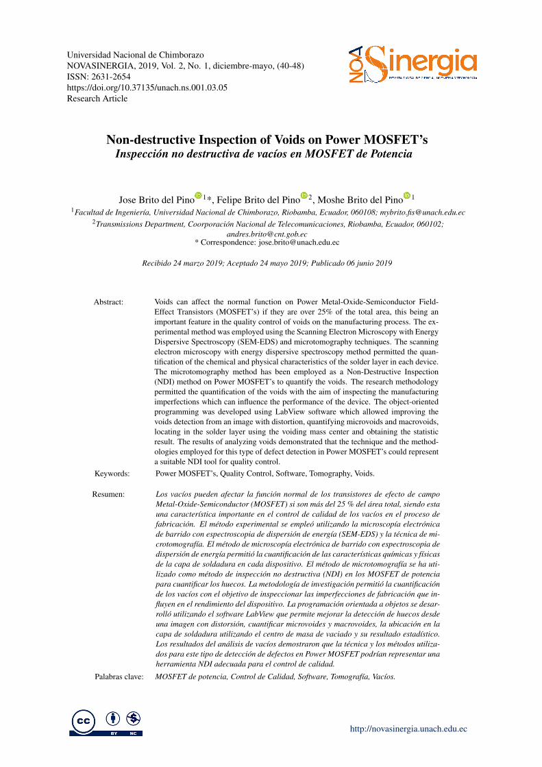
The unpacking of the Power MOSFET was carriedout by applying a heat gun to remove the exter-nal package, according to the manufacturer’s rec-ommendations. The preheating rate was 2C persecond until a temperature of 125C, was reached.Afterwards, the temperature was increased to 220Cduring 6 seconds for unpacking the device, consid-ering 260C is the maximum peak welding tem-perature for this device (STMicroelectronics, 2019),then the interior of the device was corroded usinghydrochloric acid diluted at 60% on distilled water(see figure 1).Scanning electron microscopy with energy disper-sive spectroscopy (SEM-EDS) for elemental analy-sis and surface morphology of solid materials, theSEM generates the microphotographs of the rough-ness, topography of the sample; the elemental anal-ysis is obtained by EDS, which facilitates the ele-mentary quantification of the sample (see figure 2)(Holt & Joy, 1989).
Figure 1: Inner structure of Power MOSFET after un-packing procedure. (a) The current Power MOSFET. (b)Power MOSFET without package, (1) Metallic drain, (2)Silicon layer, (3) Lead solder layer, (4) External package.
Figure 2: SEM-EDS results of inner structer of PowerMOSFET. (a) Silicon layer. (b) Nickel layer. (c) Carbonlayer. (d) Lead solder layer.
2.2 Microtomography Laboratory
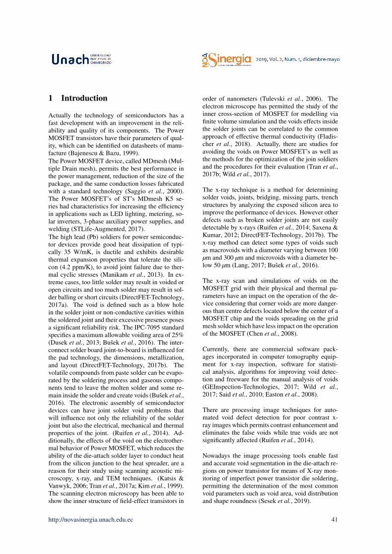
The micro Computed Tomography (µ-CT) scan wascarried out at the Microtomography Laboratory atthe University of Calabria, Italy. As in figure 3,the Microtomography experimental station consistsof three precision optical tables (Thorlabs modelB6090B), equipped with a microfocus X-ray source(Hamamatsu L12161-07) with a voltage range from0-150 kV and a variable focus mode which canreach 5 µm at 4 W on a small focus operation. Themotorized structure consists of two motion cradles(PI model WT-90), a rotator (PI model PRS-110),and two motors for linear translation (models PILS-180 and LS-270). It uses a flat panel detector(Hamamatsu C7942SK- 05) with a maximum valueof 150 kVp and a resolution of 5.4 Mpixels (pixelsize 50 x 50 µm). The control system permitted thesample-under-test (SUD) moving, using five highprecision stepper motors; the image acquisition bymeans of a flat panel detector, subsequently madethe 2D reconstruction using N-Recon and 3D imagereconstruction using the ImageJ freeware tool.
2.3 Microtomography Technique
The microtomography technique uses a cone-beamgeometry which is advantageous for obtaining di-rectly reconstructed 3D images from a set of 2Dprojections recorded by a detector (Machin &Webb, 1994; Turbell, 2017). The reconstructionprocess was made using phase retrieval to obtain a
http://novasinergia.unach.edu.ec 42
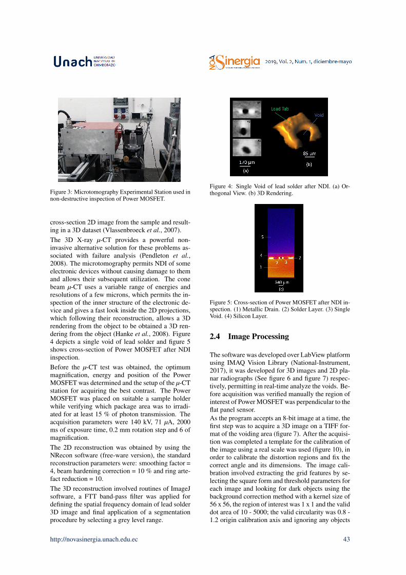
Figure 3: Microtomography Experimental Station used innon-destructive inspection of Power MOSFET.
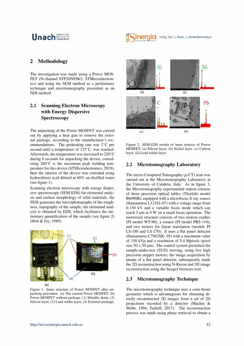
cross-section 2D image from the sample and result-ing in a 3D dataset (Vlassenbroeck et al., 2007).The 3D X-ray µ-CT provides a powerful non-invasive alternative solution for these problems as-sociated with failure analysis (Pendleton et al.,2008). The microtomography permits NDI of someelectronic devices without causing damage to themand allows their subsequent utilization. The conebeam µ-CT uses a variable range of energies andresolutions of a few microns, which permits the in-spection of the inner structure of the electronic de-vice and gives a fast look inside the 2D projections,which following their reconstruction, allows a 3Drendering from the object to be obtained a 3D ren-dering from the object (Hanke et al., 2008). Figure4 depicts a single void of lead solder and figure 5shows cross-section of Power MOSFET after NDIinspection.Before the µ-CT test was obtained, the optimummagnification, energy and position of the PowerMOSFET was determined and the setup of the µ-CTstation for acquiring the best contrast. The PowerMOSFET was placed on suitable a sample holderwhile verifying which package area was to irradi-ated for at least 15 % of photon transmission. Theacquisition parameters were 140 kV, 71 µA, 2000ms of exposure time, 0.2 mm rotation step and 6 ofmagnification.The 2D reconstruction was obtained by using theNRecon software (free-ware version), the standardreconstruction parameters were: smoothing factor =4, beam hardening correction = 10 % and ring arte-fact reduction = 10.The 3D reconstruction involved routines of ImageJsoftware, a FTT band-pass filter was applied fordefining the spatial frequency domain of lead solder3D image and final application of a segmentationprocedure by selecting a grey level range.
Figure 4: Single Void of lead solder after NDI. (a) Or-thogonal View. (b) 3D Rendering.
Figure 5: Cross-section of Power MOSFET after NDI in-spection. (1) Metallic Drain. (2) Solder Layer. (3) SingleVoid. (4) Silicon Layer.
2.4 Image Processing
The software was developed over LabView platformusing IMAQ Vision Library (National-Instrument,2017), it was developed for 3D images and 2D pla-nar radiographs (See figure 6 and figure 7) respec-tively, permitting in real-time analyze the voids. Be-fore acquisition was verified manually the region ofinterest of Power MOSFET was perpendicular to theflat panel sensor.As the program accepts an 8-bit image at a time, thefirst step was to acquire a 3D image on a TIFF for-mat of the voiding area (figure 7). After the acquisi-tion was completed a template for the calibration ofthe image using a real scale was used (figure 10), inorder to calibrate the distortion regions and fix thecorrect angle and its dimensions. The image cali-bration involved extracting the grid features by se-lecting the square form and threshold parameters foreach image and looking for dark objects using thebackground correction method with a kernel size of56 x 56, the region of interest was 1 x 1 and the validdot area of 10 - 5000; the valid circularity was 0.8 -1.2 origin calibration axis and ignoring any objects
http://novasinergia.unach.edu.ec 43
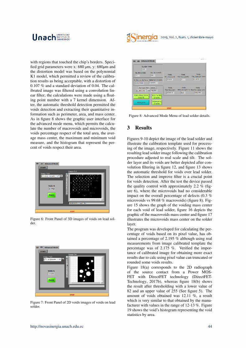
with regions that touched the chip’s borders. Speci-fied grid parameters were x: 680 µm, y: 680µm andthe distortion model was based on the polynomialK1 model, which permitted a review of the calibra-tion results as being acceptable, with a distortion of0.107 % and a standard deviation of 0.04. The cal-ibrated image was filtered using a convolution lin-ear filter; the calculations were made using a float-ing point number with a 7 kernel dimension. Af-ter, the automatic threshold detection permitted thevoids detection and extracting their quantitative in-formation such as perimeter, area, and mass center.As in figure 8 shows the graphic user interface forthe advanced mode menu, which permits the calcu-late the number of macrovoids and microvoids, thevoids percentage respect of the total area, the aver-age mass center, the maximum and minimum voidmeasure, and the histogram that represent the per-cent of voids respect their area.
Figure 6: Front Panel of 3D images of voids on lead sol-der.
Figure 7: Front Panel of 2D voids images of voids on leadsolder.
Figure 8: Advanced Mode Menu of lead solder details.
3 Results
Figures 9-10 depict the image of the lead solder andillustrate the calibration template used for process-ing of the image, respectively. Figure 11 shows theresulting lead solder image following the calibrationprocedure adjusted to real scale and tilt. The sol-der layer and its voids are better depicted after con-volution filtering in figure 12, and figure 13 showsthe automatic threshold for voids over lead solder.The selection and improve filter is a crucial pointfor voids detection. After the test the device passedthe quality control with approximately 2.2 % (fig-ure 6), where the microvoids had no considerableimpact on the overall percentage of defects (0.3 %microvoids vs 99.68 % macrovoids) (figure 8). Fig-ure 15 shows the graph of the voiding mass centerfor each void of lead solder, figure 16 depicts thegraphic of the macrovoids mass center and figure 17illustrates the microvoids mass center on the solderlayer.The program was developed for calculating the per-centage of voids based on its pixel value, has ob-tained a percentage of 2.195 % although using realmeasurements from image calibrated template thepercentage was of 2.175 %. Verified the impor-tance of calibrated image for obtaining more exactresults due to calc using pixel value can truncated orrounded some voids results.Figure 18(a) corresponds to the 2D radiographof the source contact from a Power MOS-FET with DirectFET technology (DirectFET-Technology, 2017b), whereas figure 18(b) showsthe result after thresholding with a lower value of82 and an upper value of 255 (See figure 5). Theamount of voids obtained was 12.11 %, a resultwhich is very similar to that obtained by the manu-facturer with values in the range of 12-13 %. Figure19 shows the void’s histogram representing the voidstatistics by area.
http://novasinergia.unach.edu.ec 44
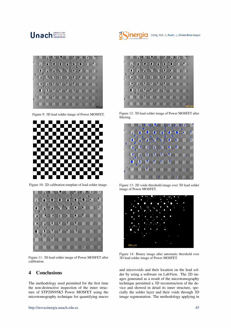
Figure 9: 3D lead solder image of Power MOSFET.
Figure 10: 2D calibration template of lead solder image.
Figure 11: 3D lead solder image of Power MOSFET aftercalibration.
4 Conclusions
The methodology used permitted for the first timethe non-destructive inspection of the inner struc-ture of STP20N95K5 Power MOSFET using themicrotomography technique for quantifying macro
Figure 12: 3D lead solder image of Power MOSFET afterfiltering.
Figure 13: 2D voids threshold image over 3D lead solderimage of Power MOSFET.
Figure 14: Binary image after automatic threshold over3D lead solder image of Power MOSFET.
and microvoids and their location on the lead sol-der by using a software on LabView. The 2D im-ages generated as a result of the microtomographytechnique permitted a 3D reconstruction of the de-vice and showed in detail its inner structure, spe-cially the solder layer and their voids through 3Dimage segmentation. The methodology applying in
http://novasinergia.unach.edu.ec 45
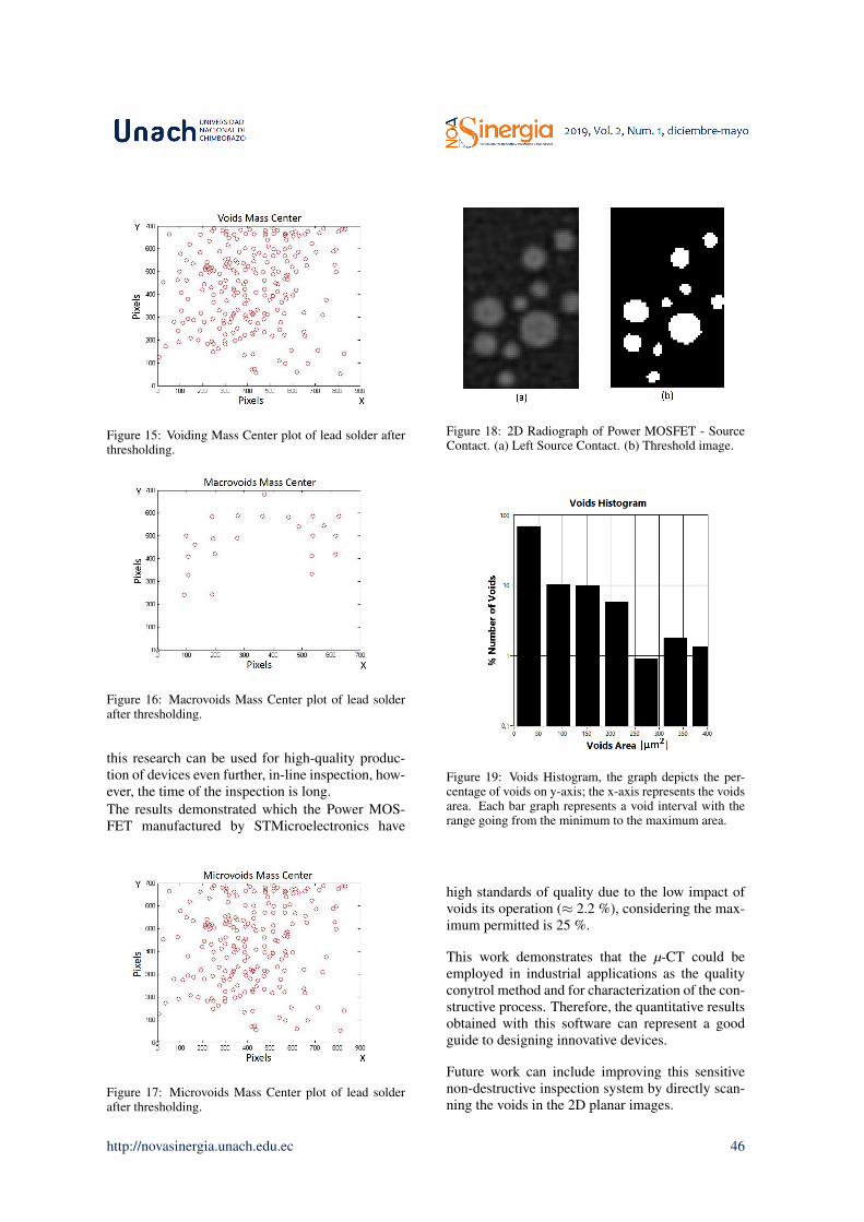
Figure 15: Voiding Mass Center plot of lead solder afterthresholding.
Figure 16: Macrovoids Mass Center plot of lead solderafter thresholding.
this research can be used for high-quality produc-tion of devices even further, in-line inspection, how-ever, the time of the inspection is long.The results demonstrated which the Power MOS-FET manufactured by STMicroelectronics have
Figure 17: Microvoids Mass Center plot of lead solderafter thresholding.
Figure 18: 2D Radiograph of Power MOSFET - SourceContact. (a) Left Source Contact. (b) Threshold image.
Figure 19: Voids Histogram, the graph depicts the per-centage of voids on y-axis; the x-axis represents the voidsarea. Each bar graph represents a void interval with therange going from the minimum to the maximum area.
high standards of quality due to the low impact ofvoids its operation (≈ 2.2 %), considering the max-imum permitted is 25 %.
This work demonstrates that the µ-CT could beemployed in industrial applications as the qualityconytrol method and for characterization of the con-structive process. Therefore, the quantitative resultsobtained with this software can represent a goodguide to designing innovative devices.
Future work can include improving this sensitivenon-destructive inspection system by directly scan-ning the voids in the 2D planar images.
http://novasinergia.unach.edu.ec 46
References
Bajenescu, T. & Bazu, M. (1999). Reliability of Elec-tronic Components: A Practical Guide to ElectronicSystem Manufacturing. New York: Springer-Verlag, 1edition. DOI 10.1007/978-3-642-58505-0.
Busek, D., Dusek, K., Ruzicka, D., Placek, M., Mach,P., Urbanek, J. & Stary, J. (2016). Flux effect on voidquantity and size in soldered joints. MicroelectronicsReliability, 60(Supplement C), 135–140.
Chen, L., Paulasto-Krockel, M., Frohler, U., Schweitzer,D. & Pape, H. (2008). Thermal impact of randomly dis-tributed solder voids on Rth-JC of MOSFETs,. 20082nd Electronics System-Integration Technology Con-ference.
DirectFET-Technology (2017a). DirectFET Tech-nology Inspection Application Note. Retrievedfrom http://www.irf.com/technical-info/appnotes/an-1080.pdf.
DirectFET-Technology (2017b). Recommendations forPrinted Circuit Board Assembly of Infineon SON Pack-ages. Retrieved from https://www.infineon.com/.
Dusek, K., Vlach, J., Brejcha, M., Hajkova, L., Pavel, Z.& Popısil, L. (2013). Influence of humidity on voidsformation inside the solder joint. Advanced Science,Engineering and Medicine, 5(6), 543–547.
Easton, J., Struk, P. & Rotella, A. (2008). Imaging andAnalysis of Void-Defects in Solder Joints Formed in Re-duced Gravity Using High-Resolution Computed To-mography,. 46th AIAA Aerospace Sciences Meetingand Exhibit.
Fladischer, K., Mitterhuber, L., Kraker, E., Ginter, D.,Rosc, J. & Magnien, J. (2018). A Close Look on Voidsin Solder Joints. 2018 24rd International Workshopon Thermal Investigations of ICs and Systems (THER-MINIC).
GEInspection-Technologies (2017). Solder joint inspec-tion and analysis. PCBA Brochure, Retrieved fromhttps://www.gemeasurement.com/.
Hanke, R., Fuchs, T. & Uhlmann, N. (2008). X-raybased methods for non-destructive testing and materialcharacterization. Nuclear Instruments and Methods inPhysics Research Section A, 591(1), 14–18.
Holt, D. & Joy, D. (1989). SEM Microcharacterization ofSemiconductors, volume 12. Academic Press Inc., SanDiego, CA 92101, 1 edition. An optional note.
Katsis, D. & Vanwyk, J. (2006). A thermal, mechanical,and electrical study of voiding in the solder die-attachof power mosfets. IEEE Transactions on Componentsand Packaging Technologies., 29(1), 127–136.
Kim, Y. C., Kim, J., Choy, J. H., Park, J. C. & Choi,H. M. (1999). Effects of cobalt silicidation and postan-nealing on void defects at the sidewall spacer edge ofmetal–oxide–silicon field-effect transistors. Appliedphysics letters, 75(9), 1270–1272.
Lang, D. (2017). AN-9037 - Assembly Guidelinesfor 8x8 MLP DriverMOS Packaging. Retrievedfrom http://www.onsemi.com/pub/Collateral/AN-9037.pdf.pdf.
Machin, K. & Webb, S. (1994). Cone-beam x-ray micro-tomography of small specimens. Physics in Medicine& Biology, 39(10), 1639.
Manikam, V. R., Paing, S. & Ang, A. (2013). Effects ofsoft solder materials and die attach process parame-ters on large power semiconductor dies joint reliabil-ity. 2013 IEEE 15th Electronics Packaging TechnologyConference (EPTC 2013).
National-Instrument (2017). IMAQ Vision forLabVIEW. Worldwide Technical Supportand Product Information, Retrieved fromhttp://www.ni.com/pdf/manuals/371007a.pdf.
Pendleton, T., Hunter, L. & Lau, S. H. (2008). Noninva-sive Failure Analysis of Passive Electronic Devices inWireless Modules Using X-ray Microtomography (Mi-croCT). Conference Proceedings from the 34th Inter-national Symposium for Testing and Failure Analysis.
Ruifen, Z., Tat, Y. K., Huei, Y. L. & Dexter, R. (2014).How to improve void performance in wafer bumping.2014 IEEE 16th Electronics Packaging TechnologyConference (EPTC).
Saggio, M., Fagone, D. & Musumeci, S. (2000).MDmeshTM: innovative technology for high voltagePower MOSFETs. 12th International Symposium onPower Semiconductor Devices ICs. Proceedings (Cat.No.00CH37094).
Said, A. F., Bennett, B. L., Karam, L. J. & Pettinato,J. (2010). Robust automatic void detection in solderballs,. 2010 IEEE International Conference on Acous-tics, Speech and Signal Processing.
Saxena, S. & Kumar, M. (2012). Advances in Microelec-tronics and Photonics, chapter 1, pp. 1–23. Nova Sci-ence Publishers Inc.
Sesek, A., Chambers, O. & Trontelj, J. (2019). Study onthe die-attach voids distribution with x-ray and imageprocessing techniques. ASME. J. Electron. Packag.,141(2), 1–7.
STLife-Augmented (2017). N-channel 950 V, 0.275 Ω
typ., 17.5 A MDmeshT M K5. Power MOSFETs inD2PAK, TO-220FP, TO-220 and TO-247, Retrievedfrom http://www.st.com.
STMicroelectronics (2019). Rectifiers thermal manage-ment, handling and mounting recommendations. Re-trieved from https://www.st.com/.
http://novasinergia.unach.edu.ec 47
Tran, S., Dupont, L. & Khatir, Z. (2017a). Evaluationof multi-void and drain metallization thickness effectson the electro thermal behavior of si mosfet under for-ward bias conditions. 2017 19th European Conferenceon Power Electronics and Applications (EPE’17 ECCEEurope), pp. 1–10.
Tran, S. H., Dupont, L. & Khatir, Z. (2017b). Electrother-mal evaluation of single and multiple solder void ef-fects on low-voltage si mosfet behavior in forward biasconditions. IEEE Transactions on Components, Pack-aging and Manufacturing Technology, 7(3), 396–404.
Tulevski, G. S., Nuckolls, C., Afzali, A., Graham, T. O.& Kagan, C. R. (2006). Device scaling in sub-100 nmpentacene field-effect transistors. Applied physics let-ters, 89(183101).
Turbell, H. (2017). Cone-Beam Reconstruction Using Fil-tered Backprojection. Retrieved from http://www.diva-portal.org/smash/get/diva2:302800/FULLTEXT01.pdf.
Vlassenbroeck, J., Dierick, M., Masschaele, B., Cnudde,V., Van Hoorebeke, L. & Jacobs, P. (2007). Softwaretools for quantification of x-ray microtomography atthe ugct. Nuclear Instruments and Methods in PhysicsResearch Section A: Accelerators, Spectrometers, De-tectors and Associated Equipment, 580(1), 442 – 445.
Wild, P., Grozinger, T., Lorenz, D. & Zimmermann, A.(2017). Void formation and their effect on reliabilityof lead-free solder joints on mid and pcb substrates.IEEE Transactions on Reliability, 66(4), 1229–1237.
http://novasinergia.unach.edu.ec 48