nanotwinning and structural phase transition in cds quantum dots
TRANSCRIPT
Kumar et al. Nanoscale Research Letters 2012, 7:584http://www.nanoscalereslett.com/content/7/1/584
NANO EXPRESS Open Access
Nanotwinning and structural phase transition inCdS quantum dotsPragati Kumar1*, Nupur Saxena2, Ramesh Chandra3, Vinay Gupta4, Avinash Agarwal1 and Dinakar Kanjilal2
Abstract
Nanotwin structures are observed in high-resolution transmission electron microscopy studies of cubic phase CdSquantum dots in powder form by chemical co-precipitation method. The deposition of thin films of nanocrystallineCdS is carried out on silicon, glass, and TEM grids keeping the substrates at room temperature (RT) and 200°C bypulsed laser ablation. These films are then subjected to thermal annealing at different temperatures. Glancing angleX-ray diffraction results confirm structural phase transitions after thermal annealing of films deposited at RT and200°C. The variation of average particle size and ratio of intensities in Raman peaks I2LO/I1LO with annealingtemperature are studied. It is found that electron-phonon interaction is a function of temperature and particle sizeand is independent of the structure. Besides Raman modes LO, 2LO and 3LO of CdS at approximately 302, 603, and903 cm−1 respectively, two extra Raman modes at approximately 390 and 690 cm−1 are studied for the first time.The green and orange emissions observed in photoluminescence are correlated with phase transition.
Keywords: CdS quantum dots, CdS thin films, Pulsed laser deposition, Phase transition, Raman scattering,Photoluminescence
PACS: 78.67.Hc, 64.70.Nd, 81.07.Ta
Background
Colloidal semiconductors' nanocrystals (NCs) have beenrigorously studied by various researchers because theirunique physical properties are a function of their particlesize. The bandgap observed in the absorption and emis-sion spectra of semiconductor quantum dots (QDs) areblueshifted due to confinement of charge carriers. Theoptical properties of nanoparticles can also be determinedby coupling of confined charges and confined phonons.The physical properties, especially the light emitting prop-erties, change drastically as the size of the semiconductormaterials become smaller. The optical and electrical prop-erties of semiconductor NCs for applications in optoelec-tronic devices [1,2] and biological fluorescence labeling[3,4] are affected by quantum confinement when theirtypical dimensions are equal to or smaller than the Bohrradius of exciton. Cadmium sulfide, with a bulk bandgapof approximately 2.42 eV (approximately 512 nm) andexciton Bohr radius of approximately 2.85 nm, is a candi-date for quantum-dot blue light-emitting diodes [5]. It can* Correspondence: [email protected] of Physics, Bareilly College, Bareilly, Uttar Pradesh 243005, IndiaFull list of author information is available at the end of the article
© 2012 Kumar et al.; licensee Springer. This is aAttribution License (http://creativecommons.orin any medium, provided the original work is p
also be used in photovoltaic devices. The microstructuralcharacterization of NCs or QDs with size comparable toBohr's exciton radius is useful to understand the lightemission mechanism. Recently, our group reported themost common microstructural defects, i.e., twin structure,stacking faults, and grain boundaries in CdS QDs forthe first time [6]. The surface and structural defects areexpected to have important effects on the physical proper-ties, particularly the optical properties of the QDs.Thin films of wide bandgap II-VI semiconductors are of
considerable interest as their emissions cover the techno-logically attractive blue and green spectral regions. Inparticular, CdS thin films attracted more attention be-cause their bandgap emission is expected to lie very closeto the highest sensitivity of the human eye, i.e., greenlight. The thin films of CdS quantum dots seek wideapplications in photonic devices like laser, LEDs, etc.Ullrich and his group demonstrated optically pumpedlaser action in pulsed laser deposition (PLD)-grown CdSthin films [7,8]. Artemyev [9] and Nanda et al. [10]reported electroluminescence and photocurrent studies indevices fabricated using CdS nanocrystals. Nizamoglu
n Open Access article distributed under the terms of the Creative Commonsg/licenses/by/2.0), which permits unrestricted use, distribution, and reproductionroperly cited.
Kumar et al. Nanoscale Research Letters 2012, 7:584 Page 2 of 7http://www.nanoscalereslett.com/content/7/1/584
et al. [11] fabricated white LEDs using CdS quantum dotshybridized on near-UV LEDs. Various methods have beenused by different researchers to synthesize CdS nano-crystals thin films [12-17]. It has been shown that PLDis a versatile technique to maintain stoichiometry of filmbecause of rapid temperature rise (>1011 K/s) produced byfocused pulsed laser beam on the target [14]. Growth ofhigh quality films at a relatively low substrate temperatureby PLD is possible because high-energy atoms and ions inthe laser-induced plasma plume create a higher surfacemobility [18]. A lot of work has been reported on PLDgrown CdS films investigating the effect of various para-meters such as substrates, substrate temperature, laserfluence, laser wavelength, etc. [14,19-26]. Still, there is aneed of further studies on PLD-grown films for the devel-opment of deeper understanding of their structures for fu-ture applications. To the best of our knowledge, the roomtemperature (RT) deposition of CdS thin film was neverreported before. The thermal annealing-induced phasetransition has been studied in thin films deposited by dif-ferent routes [27-29], but not studied in PLD-grown films.In this letter, we report on the studies of properties of
CdS thin films grown by PLD, keeping the substrates atRT and 200°C, and the annealing effects on the struc-tural and optical properties of the films. The variation ofaverage particle size and ratio of intensities of Ramanpeaks I2LO/I1LO are studied with respect to the annealingtemperature. It seems that electron-phonon interactionis a function of temperature and particle size, irrespect-ive of the structure. Two extra modes in Raman spectrahave been identified for the first time. These are verifiedby low frequency Raman studies.
MethodsThin films of CdS quantum dots are deposited by laserablation of a target prepared by pressing and sinteringthe chemically synthesized CdS QDs powder. The syn-thesis of CdS quantum dots in powder form is reportedelsewhere [6]. For PLD, using ultraviolet laser source, apulsed excimer KrF laser (Lambda Physik, Compex Pro201, Coherent Inc., CA, USA) operating at 248-nm wave-length has been used. The pulse width of 10 ns andenergy of 300 mJ per pulse have been used. The laserbeam with a repetition rate 10 Hz is focused onto a rotat-ing target mounted at an oblique angle of 30°. The dis-tance between target and substrate is kept as 5.5 cm.The films are deposited on single-crystal (111) n-typesilicon wafers, glass and carbon-coated Cu grids (forTEM) at two different temperatures: (1) RT and (2)200°C inside a clean stainless steel vacuum chamber witha background pressure of 5 × 10⁻⁶ mbar. The silicon andglass substrates are cleaned using a standard process thatinvolves boiling in trichloroethylene followed by rinsingwith deionized water. The CdS deposition rate in this
configuration is about 0.025 nm per pulse. The thicknessof deposited film is about 250 nm. To study the post-annealing effect on structural and optical properties ofthe films, thermal annealing is carried out at differenttemperatures 300°C to 450°C for 3 h in Ar environment.Glancing angle X-ray diffraction (GAXRD) studies
are carried out at an angle of 1° using Bruker D8 dif-fractometer (Bruker AXS GmbH, Germany; Cu Kα radi-ation, λ = 1.5406 Å) and micro-Raman spectroscopyusing Renishaw Invia Raman microscope (Renishaw plc,Gloucestershire, UK) with 514-nm excitation wavelengthof an Ar ion laser. The low frequency micro-Ramanscattering measurements were performed in the back-scattering geometry using a Jobin Yvon T64000 triplemonochromator (NJ, USA) with a Coherent INNOVA99 Ar+ laser (514.5 nm) equipped with a charge-coupleddevice detector. The samples are examined by transmissionelectron microscopy (TEM) and high resolution transmis-sion electron microscopy (HRTEM) using Tecnai G20-Stwin operating (FEI Company, Shanghai, China) at 200 kVwith point resolution of 1.44 Å, line resolution of 2.32 Å,and line-type super twin lenses. The films deposited onglass substrates are analyzed using UV-vis absorptionspectroscopy (Hitachi 3300 UV/visible spectrophotometer;Hitachi High-Technologies Corporation, Tokyo, Japan).Photoluminescence (PL) spectroscopy studies are carriedout at room temperature using HORIBA Jobin YvonLabRAM 800 HR (NJ, USA) with excitation wavelength at325nm from He-Cd laser.
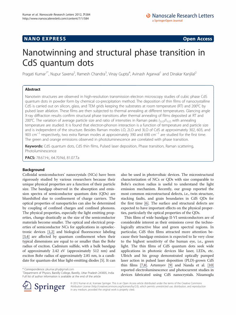
Results and discussionCdS quantum dots in powder form are characterizedusing high resolution transmission electron microscopyto study the microstructure and defects present in thedots. The existence of multi-twin structure can beclearly seen in Figure 1a. The twin structures exist withstacking fault and grain boundaries in chemically synthe-sized CdS QDs of average particle size of approximately2.7 nm [6]. CdS thin films are deposited by PLD using atarget prepared by these CdS quantum dots. TEM micro-graph of CdS thin film grown at RT is shown in Figure 1b.It exhibits uniformly distributed CdS nanoparticles ofaverage size of approximately 8.3 nm with a narrow sizedistribution, as shown in the inset of Figure 1b.Results of GAXRD scan of films deposited at two dif-
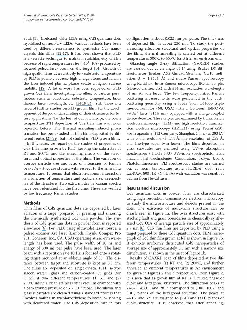
ferent temperatures, (1) RT and (2) 200°C, and furtherannealed at different temperatures in Ar environmentare given in Figures 2 and 3, respectively. From Figure 2,it is seen that as-grown film at RT is in mixed phase ofcubic and hexagonal structures. The diffraction peaks at24.67°, 26.60°, and 28.1° correspond to (100), (002) and(101) planes of the hexagonal structure. The peaks at44.15° and 52° are assigned to (220) and (311) planes ofcubic structure. It is observed that after annealing,
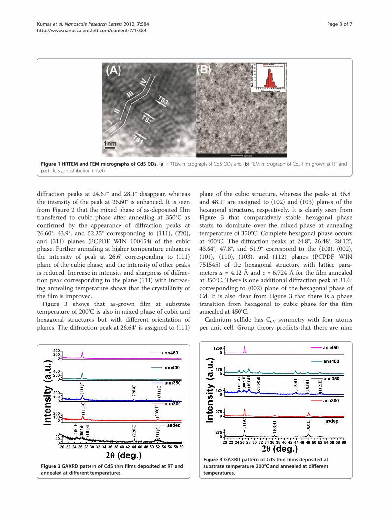
Figure 1 HRTEM and TEM micrographs of CdS QDs. (a) HRTEM micrograph of CdS QDs and (b) TEM micrograph of CdS film grown at RT andparticle size distribution (inset).
Kumar et al. Nanoscale Research Letters 2012, 7:584 Page 3 of 7http://www.nanoscalereslett.com/content/7/1/584
diffraction peaks at 24.67° and 28.1° disappear, whereasthe intensity of the peak at 26.60° is enhanced. It is seenfrom Figure 2 that the mixed phase of as-deposited filmtransferred to cubic phase after annealing at 350°C asconfirmed by the appearance of diffraction peaks at26.60°, 43.9°, and 52.25° corresponding to (111), (220),and (311) planes (PCPDF WIN 100454) of the cubicphase. Further annealing at higher temperature enhancesthe intensity of peak at 26.6° corresponding to (111)plane of the cubic phase, and the intensity of other peaksis reduced. Increase in intensity and sharpness of diffrac-tion peak corresponding to the plane (111) with increas-ing annealing temperature shows that the crystallinity ofthe film is improved.Figure 3 shows that as-grown film at substrate
temperature of 200°C is also in mixed phase of cubic andhexagonal structures but with different orientation ofplanes. The diffraction peak at 26.64° is assigned to (111)
Figure 2 GAXRD pattern of CdS thin films deposited at RT andannealed at different temperatures.
plane of the cubic structure, whereas the peaks at 36.8°and 48.1° are assigned to (102) and (103) planes of thehexagonal structure, respectively. It is clearly seen fromFigure 3 that comparatively stable hexagonal phasestarts to dominate over the mixed phase at annealingtemperature of 350°C. Complete hexagonal phase occursat 400°C. The diffraction peaks at 24.8°, 26.48°, 28.12°,43.64°, 47.8°, and 51.9° correspond to the (100), (002),(101), (110), (103), and (112) planes (PCPDF WIN751545) of the hexagonal structure with lattice para-meters a = 4.12 Å and c = 6.724 Å for the film annealedat 350°C. There is one additional diffraction peak at 31.6°corresponding to (002) plane of the hexagonal phase ofCd. It is also clear from Figure 3 that there is a phasetransition from hexagonal to cubic phase for the filmannealed at 450°C.Cadmium sulfide has C6V symmetry with four atoms
per unit cell. Group theory predicts that there are nine
Figure 3 GAXRD pattern of CdS thin films deposited atsubstrate temperature 200°C and annealed at differenttemperatures.
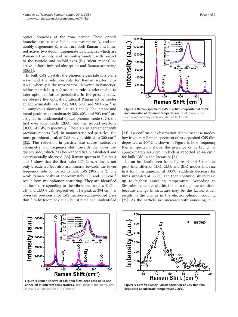
Figure 5 Raman spectra of CdS thin films deposited at 200°Cand annealed at different temperatures. Inset image is thenormalized intensity vs. Raman shift of 1LO mode.
Kumar et al. Nanoscale Research Letters 2012, 7:584 Page 4 of 7http://www.nanoscalereslett.com/content/7/1/584
optical branches at the zone center. These opticalbranches can be classified as one symmetric A1 and onedoubly degenerate E1 which are both Raman and infra-red active, two doubly degenerate E2 branches which areRaman active only, and two antisymmetric with respectto the twofold and sixfold axes (B1) ‘silent modes’ in-active in both infrared absorption and Raman scattering[30,31].In bulk CdS crystals, the phonon eigenstate is a plane
wave, and the selection rule for Raman scattering isq ≈ 0, where q is the wave vector. However, in nanocrys-talline materials, q ≈ 0 selection rule is relaxed due tointerruption of lattice periodicity. In the present study,we observe five optical vibrational Raman active modesat approximately 302, 390, 603, 690, and 903 cm−1 inall samples as shown in Figures 4 and 5. The intense andbroad peaks at approximately 302, 603, and 903 cm−1 areassigned to fundamental optical phonon mode (LO), thefirst over tone mode (2LO), and the second overtone(3LO) of CdS, respectively. These are in agreement withprevious reports [32]. In nanometer-sized particles, themost prominent peak of CdS may be shifted to 300 cm−1
[32]. The reduction in particle size causes noticeableasymmetry and frequency shift towards the lower fre-quency side, which has been theoretically calculated andexperimentally observed [33]. Raman spectra in Figures 4and 5 show that the first-order LO Raman line is notonly broadened but also asymmetric towards the lowerfrequency side compared to bulk CdS (305 cm−1). Theweak Raman peaks at approximately 390 and 690 cm−1
result from multiphonon scattering. They are identifiedas those corresponding to the vibrational modes 1LO +2E2 and 2LO + 2E2 respectively. The peak at 394 cm−1 isobserved previously for CdS microcrystallite-doped glassthin film by Jerominek et al., but it remained unidentified
Figure 4 Raman spectra of CdS thin films deposited at RT andannealed at different temperatures. Inset image is the normalizedintensity vs. Raman shift of 1LO mode.
[34]. To confirm our observation related to these modes,low frequency Raman spectrum of as-deposited CdS filmdeposited at 200°C is shown in Figure 6. Low frequencyRaman spectrum shows the presence of E2 branch atapproximately 43.3 cm−1 which is reported at 44 cm−1
for bulk CdS in the literature [31].It can be clearly seen from Figures 4 and 5 that the
peak intensities of 1LO, 2LO, and 3LO modes increasefirst for films annealed at 300°C, suddenly decrease forfilms annealed at 350°C, and then continuously increaseup to highest annealing temperature. According toSivasubramanian et al., this is due to the phase transitionbecause change in structure may be the factor, whichresults in the change in the electron-phonon coupling[35]. As the particle size increases with annealing, 2LO
Figure 6 Low frequency Raman spectrum of CdS thin filmdeposited at substrate temperature 200°C.
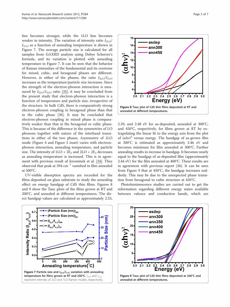
Figure 8 Tauc plot of CdS thin films deposited at RT andannealed at different temperatures.
Kumar et al. Nanoscale Research Letters 2012, 7:584 Page 5 of 7http://www.nanoscalereslett.com/content/7/1/584
line becomes stronger, while the 1LO line becomesweaker in intensity. The variation of intensity ratio I2LO/I1LO as a function of annealing temperature is shown inFigure 7. The average particle size is calculated for allsamples from GAXRD analysis using Debye Scherrer'sformula, and its variation is plotted with annealingtemperature in Figure 7. It can be seen that the behaviorof Raman intensities of the fundamental and its overtonefor mixed, cubic, and hexagonal phases are different.However, in either of the phases, the ratio I2LO/I1LOincreases as the temperature/particle size increases. Sincethe strength of the electron-phonon interaction is mea-sured by I2LO/I1LO ratio [35], it may be concluded fromthe present study that electron-phonon interaction is afunction of temperature and particle size, irrespective ofthe structure. In bulk CdS, there is comparatively strongelectron-phonon coupling in hexagonal phase than thatin the cubic phase [36]. It may be concluded thatelectron-phonon coupling in mixed phase is compara-tively weaker than that in the hexagonal or cubic phase.This is because of the difference in the symmetries of LOphonons together with nature of the interband transi-tions in either of the two phases. Asymmetry of 1LOmode (Figure 4 and Figure 5 inset) varies with electron-phonon interaction, annealing temperature, and particlesize. The intensity of 1LO + 2E2 and 2LO + 2E2 decreasesas annealing temperature is increased. This is in agree-ment with previous result of Jerominek et al. [34]. Theyobserved that peak at 394 cm−1 vanished in film annealedat 500°C.UV-visible absorption spectra are recorded for the
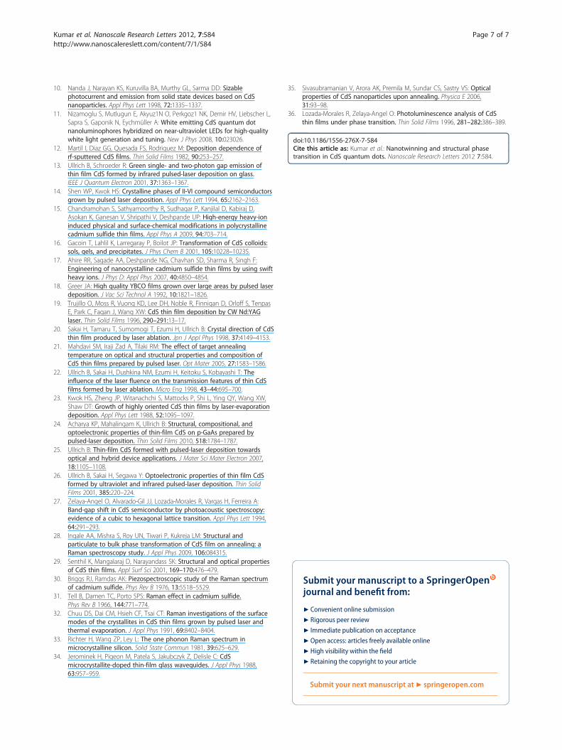
films deposited on glass substrate to study the annealingeffect on energy bandgap of CdS thin films. Figures 8and 9 show the Tauc plots of the films grown at RT and200°C, and annealed at different temperatures. The dir-ect bandgap values are calculated as approximately 2.55,
Figure 7 Particle size and I2LO/I1LO variation with annealingtemperature for films grown at RT and 200°C. I2LO and I1LOrepresent intensity of 2LO and 1LO Raman modes, respectively.
2.39, and 2.48 eV for as-deposited, annealed at 300°C,and 450°C, respectively, for films grown at RT by ex-trapolating the linear fit to the energy axis from the plotof (αhν)2 versus energy. The bandgap of as-grown filmat 200°C is estimated as approximately 2.46 eV andbecomes minimum for film annealed at 300°C. Furtherannealing results in increase in bandgap. It becomes nearlyequal to the bandgap of as-deposited film (approximately2.44 eV) for the film annealed at 400°C. These results arein agreement with previous report [36]. It can be seenfrom Figure 9 that at 450°C, the bandgap increases sud-denly. This may be due to the unexpected phase transi-tion from hexagonal to cubic structure at 450°C.Photoluminescence studies are carried out to get the
information regarding different energy states availablebetween valence and conduction bands, which are
Figure 9 Tauc plot of CdS thin films deposited at 200°C andannealed at different temperatures.
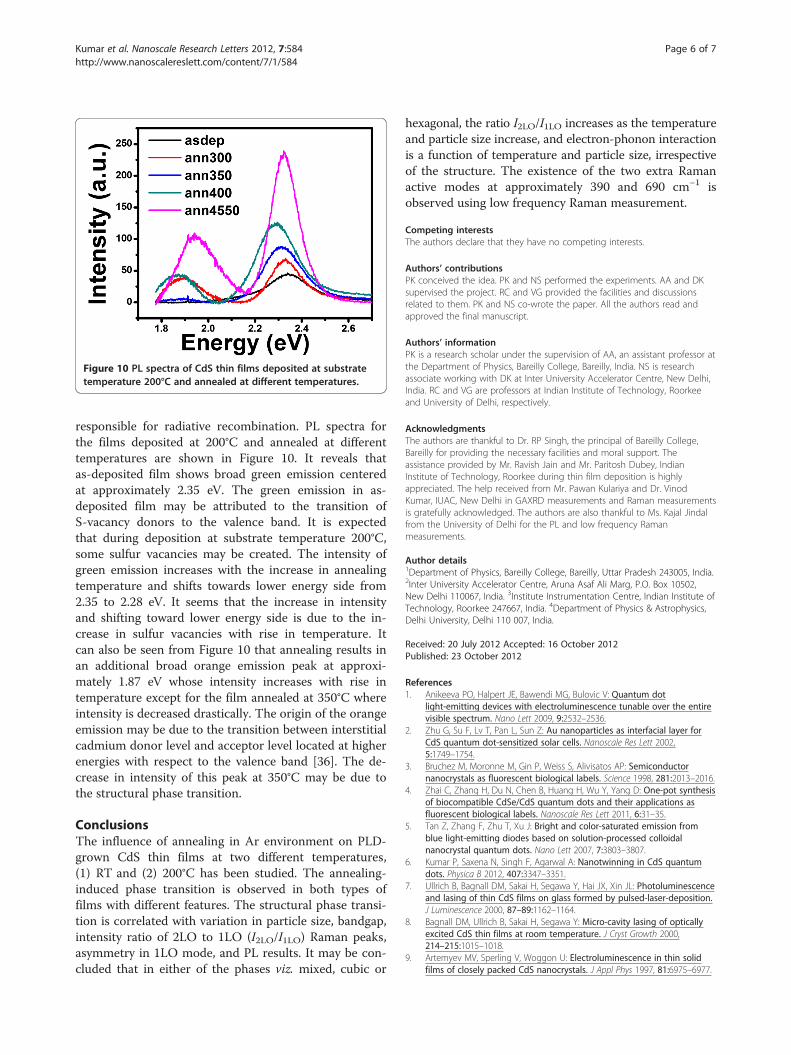
Figure 10 PL spectra of CdS thin films deposited at substratetemperature 200°C and annealed at different temperatures.
Kumar et al. Nanoscale Research Letters 2012, 7:584 Page 6 of 7http://www.nanoscalereslett.com/content/7/1/584
responsible for radiative recombination. PL spectra forthe films deposited at 200°C and annealed at differenttemperatures are shown in Figure 10. It reveals thatas-deposited film shows broad green emission centeredat approximately 2.35 eV. The green emission in as-deposited film may be attributed to the transition ofS-vacancy donors to the valence band. It is expectedthat during deposition at substrate temperature 200°C,some sulfur vacancies may be created. The intensity ofgreen emission increases with the increase in annealingtemperature and shifts towards lower energy side from2.35 to 2.28 eV. It seems that the increase in intensityand shifting toward lower energy side is due to the in-crease in sulfur vacancies with rise in temperature. Itcan also be seen from Figure 10 that annealing results inan additional broad orange emission peak at approxi-mately 1.87 eV whose intensity increases with rise intemperature except for the film annealed at 350°C whereintensity is decreased drastically. The origin of the orangeemission may be due to the transition between interstitialcadmium donor level and acceptor level located at higherenergies with respect to the valence band [36]. The de-crease in intensity of this peak at 350°C may be due tothe structural phase transition.
ConclusionsThe influence of annealing in Ar environment on PLD-grown CdS thin films at two different temperatures,(1) RT and (2) 200°C has been studied. The annealing-induced phase transition is observed in both types offilms with different features. The structural phase transi-tion is correlated with variation in particle size, bandgap,intensity ratio of 2LO to 1LO (I2LO/I1LO) Raman peaks,asymmetry in 1LO mode, and PL results. It may be con-cluded that in either of the phases viz. mixed, cubic or
hexagonal, the ratio I2LO/I1LO increases as the temperatureand particle size increase, and electron-phonon interactionis a function of temperature and particle size, irrespectiveof the structure. The existence of the two extra Ramanactive modes at approximately 390 and 690 cm−1 isobserved using low frequency Raman measurement.
Competing interestsThe authors declare that they have no competing interests.
Authors’ contributionsPK conceived the idea. PK and NS performed the experiments. AA and DKsupervised the project. RC and VG provided the facilities and discussionsrelated to them. PK and NS co-wrote the paper. All the authors read andapproved the final manuscript.
Authors’ informationPK is a research scholar under the supervision of AA, an assistant professor atthe Department of Physics, Bareilly College, Bareilly, India. NS is researchassociate working with DK at Inter University Accelerator Centre, New Delhi,India. RC and VG are professors at Indian Institute of Technology, Roorkeeand University of Delhi, respectively.
AcknowledgmentsThe authors are thankful to Dr. RP Singh, the principal of Bareilly College,Bareilly for providing the necessary facilities and moral support. Theassistance provided by Mr. Ravish Jain and Mr. Paritosh Dubey, IndianInstitute of Technology, Roorkee during thin film deposition is highlyappreciated. The help received from Mr. Pawan Kulariya and Dr. VinodKumar, IUAC, New Delhi in GAXRD measurements and Raman measurementsis gratefully acknowledged. The authors are also thankful to Ms. Kajal Jindalfrom the University of Delhi for the PL and low frequency Ramanmeasurements.
Author details1Department of Physics, Bareilly College, Bareilly, Uttar Pradesh 243005, India.2Inter University Accelerator Centre, Aruna Asaf Ali Marg, P.O. Box 10502,New Delhi 110067, India. 3Institute Instrumentation Centre, Indian Institute ofTechnology, Roorkee 247667, India. 4Department of Physics & Astrophysics,Delhi University, Delhi 110 007, India.
Received: 20 July 2012 Accepted: 16 October 2012Published: 23 October 2012
References1. Anikeeva PO, Halpert JE, Bawendi MG, Bulovic V: Quantum dot
light-emitting devices with electroluminescence tunable over the entirevisible spectrum. Nano Lett 2009, 9:2532–2536.
2. Zhu G, Su F, Lv T, Pan L, Sun Z: Au nanoparticles as interfacial layer forCdS quantum dot-sensitized solar cells. Nanoscale Res Lett 2002,5:1749–1754.
3. Bruchez M, Moronne M, Gin P, Weiss S, Alivisatos AP: Semiconductornanocrystals as fluorescent biological labels. Science 1998, 281:2013–2016.
4. Zhai C, Zhang H, Du N, Chen B, Huang H, Wu Y, Yang D: One-pot synthesisof biocompatible CdSe/CdS quantum dots and their applications asfluorescent biological labels. Nanoscale Res Lett 2011, 6:31–35.
5. Tan Z, Zhang F, Zhu T, Xu J: Bright and color-saturated emission fromblue light-emitting diodes based on solution-processed colloidalnanocrystal quantum dots. Nano Lett 2007, 7:3803–3807.
6. Kumar P, Saxena N, Singh F, Agarwal A: Nanotwinning in CdS quantumdots. Physica B 2012, 407:3347–3351.
7. Ullrich B, Bagnall DM, Sakai H, Segawa Y, Hai JX, Xin JL: Photoluminescenceand lasing of thin CdS films on glass formed by pulsed-laser-deposition.J Luminescence 2000, 87–89:1162–1164.
8. Bagnall DM, Ullrich B, Sakai H, Segawa Y: Micro-cavity lasing of opticallyexcited CdS thin films at room temperature. J Cryst Growth 2000,214–215:1015–1018.
9. Artemyev MV, Sperling V, Woggon U: Electroluminescence in thin solidfilms of closely packed CdS nanocrystals. J Appl Phys 1997, 81:6975–6977.
Kumar et al. Nanoscale Research Letters 2012, 7:584 Page 7 of 7http://www.nanoscalereslett.com/content/7/1/584
10. Nanda J, Narayan KS, Kuruvilla BA, Murthy GL, Sarma DD: Sizablephotocurrent and emission from solid state devices based on CdSnanoparticles. Appl Phys Lett 1998, 72:1335–1337.
11. Nizamoglu S, Mutlugun E, Akyuz1N O, Perkgoz1 NK, Demir HV, Liebscher L,Sapra S, Gaponik N, Eychmüller A: White emitting CdS quantum dotnanoluminophores hybridized on near-ultraviolet LEDs for high-qualitywhite light generation and tuning. New J Phys 2008, 10:023026.
12. Martil I, Diaz GG, Quesada FS, Rodriguez M: Deposition dependence ofrf-sputtered CdS films. Thin Solid Films 1982, 90:253–257.
13. Ullrich B, Schroeder R: Green single- and two-photon gap emission ofthin film CdS formed by infrared pulsed-laser deposition on glass.IEEE J Quantum Electron 2001, 37:1363–1367.
14. Shen WP, Kwok HS: Crystalline phases of II-VI compound semiconductorsgrown by pulsed laser deposition. Appl Phys Lett 1994, 65:2162–2163.
15. Chandramohan S, Sathyamoorthy R, Sudhagar P, Kanjilal D, Kabiraj D,Asokan K, Ganesan V, Shripathi V, Deshpande UP: High-energy heavy-ioninduced physical and surface-chemical modifications in polycrystallinecadmium sulfide thin films. Appl Phys A 2009, 94:703–714.
16. Gacoin T, Lahlil K, Larregaray P, Boilot JP: Transformation of CdS colloids:sols, gels, and precipitates. J Phys Chem B 2001, 105:10228–10235.
17. Ahire RR, Sagade AA, Deshpande NG, Chavhan SD, Sharma R, Singh F:Engineering of nanocrystalline cadmium sulfide thin films by using swiftheavy ions. J Phys D: Appl Phys 2007, 40:4850–4854.
18. Greer JA: High quality YBCO films grown over large areas by pulsed laserdeposition. J Vac Sci Technol A 1992, 10:1821–1826.
19. Trujillo O, Moss R, Vuong KD, Lee DH, Noble R, Finnigan D, Orloff S, TenpasE, Park C, Fagan J, Wang XW: CdS thin film deposition by CW Nd:YAGlaser. Thin Solid Films 1996, 290–291:13–17.
20. Sakai H, Tamaru T, Sumomogi T, Ezumi H, Ullrich B: Crystal direction of CdSthin film produced by laser ablation. Jpn J Appl Phys 1998, 37:4149–4153.
21. Mahdavi SM, Iraji Zad A, Tilaki RM: The effect of target annealingtemperature on optical and structural properties and composition ofCdS thin films prepared by pulsed laser. Opt Mater 2005, 27:1583–1586.
22. Ullrich B, Sakai H, Dushkina NM, Ezumi H, Keitoku S, Kobayashi T: Theinfluence of the laser fluence on the transmission features of thin CdSfilms formed by laser ablation. Micro Eng 1998, 43–44:695–700.
23. Kwok HS, Zheng JP, Witanachchi S, Mattocks P, Shi L, Ying QY, Wang XW,Shaw DT: Growth of highly oriented CdS thin films by laser-evaporationdeposition. Appl Phys Lett 1988, 52:1095–1097.
24. Acharya KP, Mahalingam K, Ullrich B: Structural, compositional, andoptoelectronic properties of thin-film CdS on p-GaAs prepared bypulsed-laser deposition. Thin Solid Films 2010, 518:1784–1787.
25. Ullrich B: Thin-film CdS formed with pulsed-laser deposition towardsoptical and hybrid device applications. J Mater Sci Mater Electron 2007,18:1105–1108.
26. Ullrich B, Sakai H, Segawa Y: Optoelectronic properties of thin film CdSformed by ultraviolet and infrared pulsed-laser deposition. Thin SolidFilms 2001, 385:220–224.
27. Zelaya-Angel O, Alvarado-Gil JJ, Lozada-Morales R, Vargas H, Ferreira A:Band-gap shift in CdS semiconductor by photoacoustic spectroscopy:evidence of a cubic to hexagonal lattice transition. Appl Phys Lett 1994,64:291–293.
28. Ingale AA, Mishra S, Roy UN, Tiwari P, Kukreja LM: Structural andparticulate to bulk phase transformation of CdS film on annealing: aRaman spectroscopy study. J Appl Phys 2009, 106:084315.
29. Senthil K, Mangalaraj D, Narayandass SK: Structural and optical propertiesof CdS thin films. Appl Surf Sci 2001, 169–170:476–479.
30. Briggs RJ, Ramdas AK: Piezospectroscopic study of the Raman spectrumof cadmium sulfide. Phys Rev B 1976, 13:5518–5529.
31. Tell B, Damen TC, Porto SPS: Raman effect in cadmium sulfide.Phys Rev B 1966, 144:771–774.
32. Chuu DS, Dai CM, Hsieh CF, Tsai CT: Raman investigations of the surfacemodes of the crystallites in CdS thin films grown by pulsed laser andthermal evaporation. J Appl Phys 1991, 69:8402–8404.
33. Richter H, Wang ZP, Ley L: The one phonon Raman spectrum inmicrocrystalline silicon. Solid State Commun 1981, 39:625–629.
34. Jerominek H, Pigeon M, Patela S, Jakubczyk Z, Delisle C: CdSmicrocrystallite-doped thin-film glass waveguides. J Appl Phys 1988,63:957–959.
35. Sivasubramanian V, Arora AK, Premila M, Sundar CS, Sastry VS: Opticalproperties of CdS nanoparticles upon annealing. Physica E 2006,31:93–98.
36. Lozada-Morales R, Zelaya-Angel O: Photoluminescence analysis of CdSthin films under phase transition. Thin Solid Films 1996, 281–282:386–389.
doi:10.1186/1556-276X-7-584Cite this article as: Kumar et al.: Nanotwinning and structural phasetransition in CdS quantum dots. Nanoscale Research Letters 2012 7:584.
Submit your manuscript to a journal and benefi t from:
7 Convenient online submission
7 Rigorous peer review
7 Immediate publication on acceptance
7 Open access: articles freely available online
7 High visibility within the fi eld
7 Retaining the copyright to your article
Submit your next manuscript at 7 springeropen.com