interference and interactions in open quantum dots
TRANSCRIPT

Interference and interactions in open quantum dots
This article has been downloaded from IOPscience. Please scroll down to see the full text article.
2003 Rep. Prog. Phys. 66 583
(http://iopscience.iop.org/0034-4885/66/4/204)
Download details:
IP Address: 137.108.145.45
The article was downloaded on 21/06/2013 at 03:04
Please note that terms and conditions apply.
View the table of contents for this issue, or go to the journal homepage for more
Home Search Collections Journals About Contact us My IOPscience

INSTITUTE OF PHYSICS PUBLISHING REPORTS ON PROGRESS IN PHYSICS
Rep. Prog. Phys. 66 (2003) 583–632 PII: S0034-4885(03)31847-0
Interference and interactions in open quantum dots
J P Bird1, R Akis1, D K Ferry1, A P S de Moura2, Y-C Lai1,2 and K M Indlekofer1
1 Nanostructures Research Group, Department of Electrical Engineering, Arizona StateUniversity, Tempe, AZ 85287-5706, USA2 Department of Mathematics, Arizona State University, Tempe, AZ 85287-1804, USA
Received 22 January 2003Published 14 March 2003Online at stacks.iop.org/RoPP/66/583
Abstract
In this report, we review the results of our joint experimental and theoretical studies of electron-interference, and interaction, phenomena in open electron cavities known as quantum dots.The transport through these structures is shown to be heavily influenced by the remnants of theirdiscrete density of states, elements of which remain resolved in spite of the strong couplingthat exists between the cavity and its reservoirs. The experimental signatures of this densityof states are discussed at length in this report, and are shown to be related to characteristicwavefunction scarring, involving a small number of classical orbits. A semiclassical analysisof this behaviour shows it to be related to the effect of dynamical tunnelling, in which electronsare injected into the dot tunnel through classically forbidden regions of phase space, to accessisolated regular orbits. The dynamical tunnelling gives rise to the formation of long-livedquasi-bound states in the open dots, and the many-body implications associated with electroncharging at these resonances are also explored in this report.
0034-4885/03/040583+50$90.00 © 2003 IOP Publishing Ltd Printed in the UK 583

584 J P Bird et al
Contents
PageNomenclature 585
1. Introduction 5862. Device fabrication and basic characteristics 588
2.1. Device fabrication 5882.2. Basic experimental observations 590
3. Transmission as a probe of the density of states 5933.1. The persistence of eigenstates in open quantum dots 5943.2. Experimental signatures of the open-dot spectrum 5983.3. Wavefunction scarring in open quantum dots 6043.4. Dynamical tunnelling and the semiclassical description of open quantum dots 6073.5. Open quantum-dot molecules 6113.6. Comparison with other studies 613
3.6.1. Other work on quantum dots 6133.6.2. Generic wave properties of open quantum dots 616
4. Decoherence and interactions in open quantum dots 6194.1. Dephasing in open dots 6194.2. Temperature-dependent transport and the signatures of interactions in
open dots 6214.2.1. Experimental observations 6214.2.2. Theoretical modelling 625
5. Conclusions 627Acknowledgments 629References 629

Interference and interactions in open quantum dots 585
Nomenclature
2DEG two-dimensional electron gasAd quantum-dot areaB magnetic fieldBc correlation magnetic fieldcn wavefunction expansion coefficientc+kσ /ckσ creation/annihilation operators
average level spacingE energyEF Fermi energyE0 resonance energyf (E) Fermi–Dirac distribution functionG quantum-dot conductanceγ logarithmic conductance prefactor energy width of interaction resonancek electron wavenumberl transport mean free pathL effective dot sizeλ Maslov indexλF Fermi wavelengthm∗ electron effective massµ two-dimensional electron gas mobilityµk electrochemical potential of mode with wavenumber k
N number of one-dimensional sub-bandsn quantum-dot eigenstate numbernb number of coherent skipping-orbit bouncesns two-dimensional electron gas carrier densityT0 activation temperatureφn closed-dot eigenfunctionsrc cyclotron radiusS classical-orbit actionSeff effective actionσ spin indexψ quantum-dot wavefunctionT temperatureT ∗ effective electron temperatureT0 activation temperatureτφ phase-breaking timeU , U ex Hartree, exchange potentialsVg gate voltageω orbit stability angle
586 J P Bird et al
1. Introduction
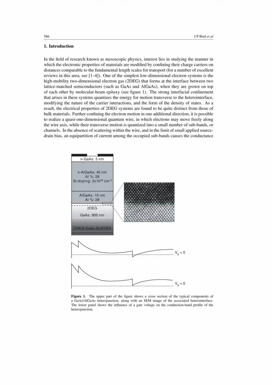
In the field of research known as mesoscopic physics, interest lies in studying the manner inwhich the electronic properties of materials are modified by confining their charge carriers ondistances comparable to the fundamental length scales for transport (for a number of excellentreviews in this area, see [1–4]). One of the simplest low-dimensional electron systems is thehigh-mobility two-dimensional electron gas (2DEG) that forms at the interface between twolattice-matched semiconductors (such as GaAs and AlGaAs), when they are grown on topof each other by molecular-beam epitaxy (see figure 1). The strong interfacial confinementthat arises in these systems quantizes the energy for motion transverse to the heterointerface,modifying the nature of the carrier interactions, and the form of the density of states. As aresult, the electrical properties of 2DEG systems are found to be quite distinct from those ofbulk materials. Further confining the electron motion in one additional direction, it is possibleto realize a quasi-one-dimensional quantum wire, in which electrons may move freely alongthe wire axis, while their transverse motion is quantized into a small number of sub-bands, orchannels. In the absence of scattering within the wire, and in the limit of small applied source-drain bias, an equipartition of current among the occupied sub-bands causes the conductance
n-GaAs: 5 nm
n-AlGaAs: 45 nmAl %: 28
Si-doping: 2x1018 cm-3
AlGaAs: 15 nmAl %: 28
GaAs: 800 nm
THICK GaAs BUFFER
2DEG
Vg = 0
Vg < 0
Figure 1. The upper part of the figure shows a cross section of the typical components ofa GaAs/AlGaAs heterojunction, along with an SEM image of the associated heterointerface.The lower panel shows the influence of a gate voltage on the conduction-band profile of theheterojunction.

Interference and interactions in open quantum dots 587
of such quantum point-contacts to be quantized according to [5]:
G = 2e2
hN, (1)
where N is the number of occupied channels and simply corresponds to the number of sub-bands whose threshold energies lie below the Fermi energy. In addition to the conductancequantization defined in equation (1), and dependent on the ratio of the wire dimensions tothe characteristic transport length scales, other phenomena that may occur in quantum wiresinclude universal conductance fluctuations, quenching of the Hall effect, and Luttinger-liquidbehaviour, all of which have been widely studied in recent years (for a thorough review ofmany of these topics, see [5]).
Quantum dots may be viewed as the ultimate limit of bandstructure engineering and arerealized when electron motion is confined in all three directions, on length scales comparableto the coherence length. An important result of this strong confinement is that the energyspectrum of the electrons is quantized into a discrete set of levels, that may be modified by theapplication of a magnetic field, or some appropriate gate voltage. The electrical properties ofthese artificial atoms are strongly influenced by the discrete form of their density of states [6,7]and there is much interest in their potential for application in a range of future technologies.Quantum dots have been proposed, for example, for use as qubits in quantum computing [8,9],and have been used to provide demonstrations of quantum-cellular automata [10] and single-photon detectors [11]. In these applications, a quantitative understanding of the details ofelectron transport in the dots is required, and it is this need that serves as the motivation forthis report, where we review our recent work in this particular problem.
When discussing transport through quantum dots, it is possible to identify two distinctregimes of behaviour, dependent on the strength of the coupling between the dot and its currentreservoirs. In weakly coupled quantum dots, current flow involves a process in which electronstunnel through the dot, and, at sufficiently low temperatures, the charging energy associatedwith the addition of a single electron to the dot can be very much larger than the thermal energy.In this so-called Coulomb-blockade regime, current flow occurs by the process of single-electron tunnelling, which is comprehensively reviewed in [3,6,7]. Of interest here, however,is the problem of transport in open quantum dots, in which the coupling between the dot and itsreservoirs is provided by means of quantum-point-contact leads, each of which supports at leastone propagating mode. The Coulomb-blockade effect is washed out in such structures [12,13],in which the transport instead is strongly influenced by the interference of electrons confinedwithin the dots. In this sense, these dots may be viewed as the quantum analog of classical wave-scattering systems, such as microwave cavities [14,15], fluid systems [16], and semiconductorlasers [17]. At the same time, the analysis of transport through these structures is particularlyamenable to semiclassical methods, in which path integrals over classical trajectories are usedto calculate their conductance (for a recent review, see [18]).
In this review, we consider the development of quantum-mechanical and semiclassicaldescriptions of transport in open quantum dots, whose predictions are consistent with eachother, and with the results of experimental studies. A crucial feature of these dots is found tobe a non-uniform broadening of their eigenstates, which arises when the dot is opened to itsreservoirs. Certain eigenstates of the initially-closed-dot are found to develop only a very smallbroadening as a result of this coupling, and therefore persist to give rise to measurable transportresults. These states correspond to the eigenfunctions of the original system which are scarredby the signature of periodic orbits, and which exhibit a weak overlap with the dot leads. If amagnetic field is applied perpendicular to the plane of the quantum dot, or its potential profileis modified by means of a suitable gate voltage, the discrete states may be swept past the Fermilevel, giving rise to reproducible oscillations in the conductance that may be observed at low

588 J P Bird et al
temperatures. An important feature of the wavefunction scars is that they recur periodicallyas the magnetic field, or the gate voltage, is varied, and our analysis shows that this behaviourgives rise to very specific frequency components in the associated conductance oscillations.A semiclassical analysis of this behaviour indicates that the scars are associated with thedynamical tunnelling of electrons through classically forbidden regions of phase space, ontoisolated periodic orbits. Quantization of the action associated with these orbits is shown togive rise to a series of resonance conditions, which account for the observed periodicity ofthe conductance oscillations seen in experiment. While it has been common in the literaturethus far to assume that the transport is dominated by chaotic trajectories, classically accessibleto electrons injected into the dot, our analysis demonstrates that the dominant mechanism isinstead very different.
In addition to considering the connection of the semiclassical and quantum-mechanicaldescriptions of transport in these structures, we also explore the importance of many-bodyeffects for transport. Experimental studies of the temperature-dependent transport in thesedots reveal evidence for behaviour, analogous to a metal–insulator transition, the characteristicsignature of which is a logarithmic variation of the conductance at low temperatures. Similarlogarithmic variations are a well-known signature of the Kondo effect, and we suggest thatsimilar physics may even be at play here. The point to note is that a general requirementfor the observation of the Kondo effect is the realization of some localized region of charge,which can interact with a continuum of states. In the open dots that we study, such localizedcharge should be realized by the isolated KAM islands which represent classically inaccessibleorbits. To explore the many-body consequences of this tunnelling, we therefore develop atheoretical model which is based upon the assumption that the electron-interaction strengthin the dots can be peaked at certain energies, corresponding to the resonant conditions forthe dynamical tunnelling. This model reveals the presence of low-temperature, interaction-induced, corrections to the conductance of the open dots.
The organization of this review is as follows. In the next section, we describe the fabricationof the quantum-dot devices, and describe the basic electrical characteristics. In section 3,we discuss the details of transport at very-low temperatures, where the influence of thermalsmearing and decoherence is minimal, and where the conductance can be viewed as providinga spectroscopy of the density of states of the open dot. It is here that we explore the quantum-mechanical and semiclassical interpretations of transport in these structures, emphasizing therole of non-uniform level broadening, introduced by the environmental coupling to the dots, andconsidering its connection to the issue of dynamical tunnelling. In section 4, we discuss howquantum effects in the transport are modified at higher temperatures, and present evidence fora metal–insulator transition that is seen in the conductance below a degree kelvin. We suggestthat this behaviour is associated with the increased importance of electron-interactions in thesestrongly confined structures, and present a many-body based transport model to account forour observations. Our conclusions are then discussed in section 5.
2. Device fabrication and basic characteristics
2.1. Device fabrication
For the transport studies that we discuss, the split-gate technique [19] is the approach of choicefor the fabrication of quantum dots, and the basic principles of this method are shown in figure 2.In this approach, metal gates with a fine-line pattern defined by electron-beam lithography areformed on the surface of a GaAs/AlGaAs heterojunction (figure 2, top). The application of anegative bias to the gates depletes the regions of electron gas underneath them, by raising the

Interference and interactions in open quantum dots 589
Figure 2. Top panel: scanning electron micrograph of a split-gate quantum dot with a 1 µm cavity.Lower panels: calculated potential profiles at two gate voltages. The gate voltage is more negativein the lowest panel.
local conduction-band edge above the Fermi level (see figure 1), thereby forming a quantumdot whose leads are defined by means of quantum-point-contacts (figure 2, top). The useof electron-beam lithography to define the gate pattern allows the realization of sub-micronsized dots, whose size is therefore comparable to the spatial extent of the short range potentialfluctuations in the underlying 2DEG [20]. The fluctuations are associated with the statisticaldistribution of donors in the AlGaAs layer, and numerical studies suggest that minimum-energy considerations may cause the ionization of these donors to order into a quasi-latticestructure [21]. In the presence of the resulting weak disorder, electronic motion within the dotsshould therefore be predominantly ballistic in nature, with large-angle scattering events beingrestricted to their confining walls. At least to first order, the dot geometry is determined by thelithographic pattern of the gates, and the great advantage of this technique is the in situ controlof the dot profile that can be achieved, simply by varying the gate voltage (Vg). These conceptsare illustrated in figure 2, where we show a pair of self-consistently computed [22] potentialprofiles for a split-gate dot. The two different profiles are computed for different values of thegate voltage, and from a comparison of these plots we see that the effect of making the gate

590 J P Bird et al
Table 1. Some key parameters for the different quantum-dots studied here.
ns µ l L EF λF /kB
(1015 m−2) (m2 Vs−1) (µm) (µm) (meV) (nm) (K) Nd
4.0–5.5 36–78 4–9 0.2–1.8 14–20 35–40 0.03–1 160–1800
ns: two-dimensional-electron-gas carrier density.µ: two-dimensional-electron-gas mobility.l: two-dimensional mean free path.L: effective dot size inferred from periodicity of Aharonov–Bohm oscillations in the edge stateregime.EF: two-dimensional-electron-gas Fermi energy.λF: two-dimensional-electron-gas Fermi wavelength./kB: quantum-dot average level spacing. ≡ 2πh2/m∗Ad, where Ad = L2 is the dot area.Nd: electron number in the dot. Nd ≡ nsL
2.
voltage more negative is to narrow the width of the point-contact leads, and to reduce the sizeof the central dot itself. This is basically a consequence of the increased fringing fields, whichdevelop around the gate edges as Vg is made more negative. Note from these plots how thesplit-gate approach gives rise to dots with soft walls.
In table 1, we summarize the material characteristics, and the device dimensions, of thevarious quantum-dot structures that we consider in this review. At the low temperatures thatwe consider here, the high mobility of the 2DEG sample ensures that the transport mean freepath is significantly larger than the size of the dots, indicating that transport within them shouldbe close to the ballistic limit. Another important feature to note is that the Fermi wavelengthof the electrons is typically of order 40 nm, and so can approach within an order of magnitudeof the dot size. We will see further below that this also has important consequences for thetransport behaviour exhibited by these structures. As can be seen in table 1, the electronnumber in these dots ranges from several thousand in the largest structures, to a few hundredin the smallest. Further below (section 4.2), we will consider the potential implications of themany-body interactions that arise between these electrons for the analysis of transport throughopen dots. Also shown in table 1 are typical values for the average level spacing (), whichmay be thought of as a rough measure of the characteristic level spacing in the dots.
2.2. Basic experimental observations
In figure 3, we show the results of measurements of the magneto–resistance of an open quantumdot, at a series of different gate voltages. (These measurements were performed with the samplemounted in a dilution refrigerator, and with the magnetic field applied perpendicular to theplane of the 2DEG.) The average dot resistance is less than 26 k in each of the curves,indicating that its leads support at least one propagating mode, and that it may be consideredto be open over the entire range of gate voltage shown. As expected, the average resistance ofthe dot increases as the gate voltage is made more negative, a trend which is accompanied bya dramatic evolution of the structure in the magneto–resistance. Dense fluctuations emerge atlow magnetic fields (<2 T), while isolated resonances develop at higher fields. This behaviourcan be seen more clearly in figure 4, in which we show a single magneto–resistance curve,measured at a fixed gate voltage. The insets to this figure serve to illustrate that the noise-likestructure in the magneto–resistance is, in fact, quite reproducible. In the high-field inset, theresistance clearly oscillates periodically with magnetic field, and the origin of this behaviour iswell understood [5]. At such high magnetic fields, the cyclotron radius of the electrons is verymuch smaller than the dot size and current is carried by a fixed number of edge states [23].

Interference and interactions in open quantum dots 591
0 1 2 3 4 50
10
20
30
40
50
60
70
80
90
RE
SIS
TAN
CE
(kO
HM
S)
MAGNETIC FIELD (TESLA)
Figure 3. Magneto–resistance of a 1 µm split-gate quantum dot, at a series of different gatevoltages. The gate voltage becomes more negative from front to back. The cryostat temperatureis 0.01 K.
10
20
30
40
50
60
0 1 2 3 4 5
RE
SIS
TAN
CE
(kO
HM
S)
MAGNETIC FIELD (TESLA)
Figure 4. Magneto–resistance of a 1 µm split-gate quantum dot, at a fixed gate voltage, showingthe detailed evolution of its structure with magnetic field.

592 J P Bird et al
These may be viewed as the quantum-mechanical analogue of classical skipping-orbits, andthe various features observed in the magneto–resistance in this regime can be ascribed to dot-induced interference of the edge states [24]. The periodic oscillations at high magnetic fields(>3 T) are understood to result from an Aharonov–Bohm effect, involving edge states trappedwithin the dot, and allow a reasonable estimate of the dot size to be obtained. This behaviourhas been discussed in detail in [25, 26], and will not be further considered here. Rather, wefocus on the behaviour observed at lower fields (<1 T), where the magnetic field providesonly a perturbation to the intrinsic electron dynamics in the dot. As can be seen in figure 4,the magneto–resistance in this regime shows dense fluctuations, which are dominated by asmall number of frequency components (see the low-field inset). While the detailed origin ofthese fluctuations will be discussed below, they may basically be understood to result from theinterference of electron partial waves that are generated when the electron is multiply scatteredfrom the walls of the dot. Typical of most interference effects (for a recent review, see [27]),the fluctuations are washed out when the temperature is increased above a few degrees kelvin,as we illustrate in figure 5.
Fluctuations in the resistance may also be generated by varying the voltage applied to thesplit gates of the dot, as we illustrate in figure 6. This shows the gate-voltage characteristic ofa typical dot, at two different temperatures and in the absence of any applied magnetic field.
20
40
60
80
100
-6 -4 -2 0 2 4 6
RE
SIS
TA
NC
E (
kOH
MS
)
MAGNETIC FIELD (TESLA)
0.36 K
0.15 K
0.05 K
0.26 K
0.48 K
4.2 K
0.08 K
0.65 K
1.4 K
0.85 K
Figure 5. Temperature dependence of the magneto–resistance of a 1 µm split-gate quantum dot.Successive curves are shifted upwards from each other.

Interference and interactions in open quantum dots 593
0
10
20
30
40
-2.4 -2 -1.6 -1.2 -0.8
RE
SIS
TAN
CE
(kO
HM
S)
GATE VOLTAGE (VOLTS)
0.01 K
1.6 K
Figure 6. Gate-voltage-dependent variation of the resistance of a 1-µm split-gate quantum dot, attwo different temperatures.
At 1.6 K, the resistance varies almost monotonically with gate voltage, and shows evidencefor plateau features related to conductance quantization in the point-contact leads. At 0.01 K,however, the resistance develops an oscillatory behaviour, and in the inset to figure 6 we showthe conductance fluctuations obtained by subtracting the background variation from the rawdata. Once again, there is clearly a dominant periodicity to these fluctuations, and in thesections that follow we provide a detailed interpretation of the origin of this behaviour.
3. Transmission as a probe of the density of states
In isolated quantum dots, containing just a few electrons, it is well known that the transport canbe strongly influenced by the discrete energy spectrum that is induced by confining electronsin the dot [6, 28–30]. When the dot is opened to its external reservoirs, however, it is often(wrongly) assumed that all details of this level spectrum are washed out completely. In thissection of our review, we demonstrate that the reproducible conductance fluctuations discussedabove provide a direct signature of those dot states that remain resolvable, even when the dotis very strongly coupled to its external reservoirs. Since this behaviour may seem surprisingto some, we also provide several examples to show that the persistence of eigenstates in thesedots can basically be viewed as a quantum-mechanical manifestation of the generic classicalphenomenon of wave trapping.

594 J P Bird et al
3.1. The persistence of eigenstates in open quantum dots
To clarify the statements made immediately above, we perform numerical studies of differentclosed-dot systems, and compare their resulting eigenfunctions with the wavefunction of theiropen counterparts [31]. The open system that we study is a hard-walled, stadium-shaped, dot,whose leads are positioned at opposite ends of the stadium (figures 7(e)–(h)). (The choice ofthis particular geometry is not critical to our conclusions. We have also performed calculationsusing self-consistently obtained dot profiles [32].) To study the connection of transport throughthe open dot to the eigenstates of its equivalent closed system, we calculate the eigenstates andeigenfunctions of the two closed dot shown in figures 7(a) and (b). The shape of the latter dot isperturbed by including a portion of the connecting leads in its geometry, and in the following,we make use of the ratio of the lead width (w) to the stadium height (h). In figures 7(c)and (d), we show eigenstates 128–136, and 134–142, of the standard, and perturbed, stadium,respectively. The energy range is roughly the same in these figures and the eigenstates werecomputed by solving a two-dimensional finite-difference Schrodinger equation with Dirichletboundary conditions. In figures 7(e)–(h), we show the results of calculations of the open dotunder a number of different conditions (the calculations are for the case of zero temperature, and
Figure 7. (a) Unperturbed stadium. (b) Perturbed stadium. (c) |(x, y)|2 vs x and y for eigenstates128 (top-left) through 136 (bottom-right) of the unperturbed stadium. (d) |(x, y)|2 vs x and y foreigenstates 134 (top-left) through 142 (bottom-right) of the perturbed stadium. (e) |(x, y)|2 foran open stadium with two modes passing through the leads at the energy of the 128th unperturbed-stadium eigenstate. ( f ) As in (e), but now the energy is set to that of the 136th eigenstate. (g) Asin (e), but with leads supporting 6 modes. (h) As in ( f ), but with 6 modes. Figure reproduced withpermission from [31]. Copyright, American Institute of Physics (2002).
Interference and interactions in open quantum dots 595
were obtained from a numerically stabilized variant of the scattering-matrix approach [33]).In figure 7(e), the dot leads support two sub-bands and the energy has been chosen to be equalto that of the 128th eigenstate of the unperturbed stadium. In this case, the wavefunction of theopen dot corresponds almost exactly to the isolated-dot eigenfunction (the latter of which isshown at top-left corner of figure 7(c)). Figure 7(g) is obtained at the same energy as figure 7(e),except that now the leads have been opened further to support six modes. In this case, it isclear that any correspondence between the wavefunctions of the open and closed systems hasbeen lost completely. In marked contrast with this behaviour, figures 7( f ) and (h) show thatthe 136th state of the unperturbed stadium (figure 7(c), bottom-right corner) survives, evenwhen the dot leads are opened to support six sub-bands. From these results, it is thereforeclear that the different eigenstates of the initially isolated dot develop a highly non-uniform(i.e. state-dependent) broadening when the dot is opened to the reservoirs.
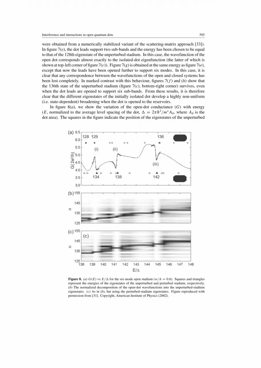
In figure 8(a), we show the variation of the open-dot conductance (G) with energy(E, normalized to the average level spacing of the dot, = 2πh2/m∗Ad, where Ad is thedot area). The squares in the figure indicate the position of the eigenstates of the unperturbed
Figure 8. (a) G(E) vs E/ for the six-mode open stadium (w/h = 0.6). Squares and trianglesrepresent the energies of the eigenstates of the unperturbed and perturbed stadium, respectively.(b) The normalized decomposition of the open-dot wavefunctions into the unperturbed-stadiumeigenstates. (c) As in (b), but using the perturbed-stadium eigenstates. Figure reproduced withpermission from [31]. Copyright, American Institute of Physics (2002).

596 J P Bird et al
stadium and we see that eleven such eigenvalues lie in the plotted energy range. In contrast,the conductance shows just three resonances, and the asymmetric lineshape of these features istypical of Fano resonances [34, 35]. Since the closed-dot eigenstates form an orthogonalbasis set, the open-dot wavefunction can be expressed as a linear combination of thesestates:
ψ =∑
n
cnφclosedn , cn = 〈ψ |φclosed
n 〉. (2)
In figure 8(b), the decomposition of the open-dot wavefunctions is plotted as a function ofthe unperturbed-stadium eigenstate number (n), and E/. The greyscale corresponds to|cn|2/|cn|2max, so that the peak value of each decomposition is normalized to unity. While formuch of the range shown, the open-dot wavefunctions involve a mixture of states, at theenergies where resonances (i) and (iii) occur the decompositions are dominated by just asingle eigenstate (n = 129 and 136, respectively). In contrast, the conductance resonancelabelled (ii) corresponds to a mixture of at least two states. Moreover, none of the unperturbed-stadium eigenvalues appear to line up with the position of this resonance. However, a logicalassumption is that the leads provide a perturbation to the stadium. We have therefore alsocomputed the eigenstates of the perturbed stadium, which are represented by triangles infigure 8(a). It is clear from this figure that the 138th level of this structure coincides withthe position of resonance (ii). The decomposition in terms of the perturbed-stadium basis setis shown in figure 8(c), where we see that all three conductance resonances are dominatedby the contribution of single eigenstates. Referring back to figures 7(c) and (d), we see thatstates 134 and 142 of the perturbed stadium bear a strong resemblance to states 129 and 136of the unperturbed stadium, and occur at similar energies. State 138 of the perturbed stadium,which coincides with resonance (ii) and which closely resembles the open-dot wavefunctionat this energy, has no ideal-stadium analogue in the energy range we have considered,however.
In figure 9, we show the decomposition in terms of the perturbed stadium, this timewithout normalization, however. The positions of the three resonant states are indicated, andit is evident that these states dominate the contribution, relative to all other states. On theeigenvalue axis, we have plotted the eigenenergies of the perturbed stadium relative to , sothat the spacing of successive levels is indicated on this axis. Significantly, we see that thewidth of the 134th state, as inferred from the breadth of the decomposition peak, is larger thanthe spacing between the 134th and 135th levels, and similar observations may be made for theother resonant states. Nonetheless, the decompositions remain dominated by the contributionof single eigenstates, indicating that the mere proximity of other levels in energy need not be anobstacle to resolving individual states. In fact, as shown in figure 10(a), even after performingthe summation
∑n |cn|2 over a total of 175 states, the contributions from states 134, 138 and
142 still dominate, being a factor of three above the background from all other states. Thissummation essentially represents the density of states of the open dot. To demonstrate thestability of these states, in figure 10(b), we plot
∑n |cn|2 vs E/ and w/h. As indicated by
the shading, the peaks persist over a wide range of lead opening. Also apparent in this plot arepeak contours that survive over only a much shorter range of w, before shifting dramaticallyto lower energy and disappearing.
A critical conclusion that can be drawn from the discussion above is that a highly non-uniform broadening of the eigenstates arises when a dot is opened to its reservoirs. Whilefor the majority of eigenstates the magnitude of this broadening exceeds the average levelspacing, a smaller subset of states are only weakly perturbed by the coupling. In the sectionthat follows, we consider the measurable transport results associated with this non-uniformbroadening.

Interference and interactions in open quantum dots 597
134
138 142
Figure 9. The perturbed-stadium decomposition coefficients |cn|2 vs E/ and En/. Figurereproduced with permission from [31]. Copyright, American Institute of Physics (2002).
Figure 10. (a)∑
n |cn|2 vs E/ (——, left scale) and G(E) vs E/ (- - - -, right scale) for thesix-mode open stadium. (b)
∑n |cn|2 indicated by the shading as a function of E/ and fractional
lead width, w/h. Figure reproduced with permission from [31]. Copyright, American Institute ofPhysics (2002).

598 J P Bird et al
3.2. Experimental signatures of the open-dot spectrum
While we have thus far considered the case where an energy variation is used to probe thedensity of states of open quantum dots, in experiment it is more typical to investigate howtheir conductance varies with magnetic field or gate voltage (figures 3–6). In this section,however, we demonstrate that the effect of these variations is essentially equivalent to sweepingenergy, since either the magnetic field or the gate voltage may be used to drive the density ofstates past the Fermi level, thereby modulating the conductance. To illustrate this point, infigure 11(a), we show the computed energy spectrum of a hard-walled, square dot [36]. Infigure 11(b), we show the numerically calculated magneto-conductance contour for the dot,in the case where current flow through it can occur by means of tunnel barriers that extenduniformly across its width. The greyscale in this figure shows the computed variation of dotconductance with magnetic field and energy [37], and, as one would expect in a resonant-tunnelling problem such as this, we see a clear correlation between points of high conductancein figure 11(b) and the discrete states in figure 11(a). There is a non-uniform amplitudevariation among the different tunnelling resonances, indicating that, even with the couplingprovided by uniform tunnel barriers, the influence of this coupling is different for different dotstates. In figure 11(c), we show the conductance contour obtained in the case where the dotleads have been opened to support four sub-bands. Instead of the simple conductance peaksobserved for the tunnelling case (figure 11(b)), the resonances found with the leads presenttend to exhibit a Fano-lineshape [34, 35], in which resonant transmission peaks are closelypaired with resonant minima (not shown). Furthermore, while the conductance of the isolateddot is strongly suppressed in situations where resonant tunnelling is not possible, the open dotexhibits more complicated behaviour. To illustrate this, in figure 11, we have drawn dottedlines at two strategically chosen values of the Fermi energy. The upper line coincides with anenergy for which the level spectrum is highly degenerate at zero field. In correspondence withthis, the tunnelling transport shows a resonant conductance peak. In figure 11(c), however, thezero-field conductance actually shows a minimum at this energy. The second dashed line in
15.5
14.0
FE
RM
I EN
ER
GY
(m
eV)
-0.1 0.1
MAGNETIC FIELD (TESLA)
-0.1 0.1 -0.1 0.1
(a) (b) (c)
MAGNETIC FIELD (TESLA)MAGNETIC FIELD (TESLA)
Figure 11. (a) The computed energy levels of a 0.3 µm hard-walled quantum dot of squaregeometry. (b) The tunnelling spectrum for the same dot. (c) The conductance contour for the dotwhen its leads are opened to support four propagating modes. In figures 1(b)–(d), conductance isplotted on a logarithmic scale and brighter regions correspond to points of higher conductance. Allcalculations were performed assuming a temperature of absolute zero.

Interference and interactions in open quantum dots 599
figure 11 is positioned at an energy for which no states exist at zero magnetic field, consistentwith which tunnelling through the isolated dot is strongly suppressed. In the open dot, however,these maxima are seen to be broadened out sufficiently so that a region of high conductance isactually obtained (figure 11(c)).
While the results of figure 11 were computed under the assumption of zero temperature,real experiments are performed at non-zero temperature, where energy averaging arises fromthermal smearing of reservoir states and electron dephasing in the dot (the latter of whicheffects will be discussed in further detail in section 4). To simulate the effect of this averagingon the transport measurements, we adopt the following approach. We first account forthermal smearing and dephasing by introducing an effective temperature (T ∗), whose choiceis determined empirically by comparison with experiment. The energy-averaged magneto-conductance may then be computed from a simple convolution of the zero-temperatureconductance with the derivative of the Fermi function:
Gav(B, EF, T ) =∫
G(B, E)
[−df (E − EF, T )
dE
]dE, (3)
where EF is the Fermi energy. For a demonstration of these concepts, in figure 12 we show theevolution of the magneto–resistance of another quantum dot with gate voltage. To realisticallymodel the transport through this dot, we calculate its profile self-consistently, and computeits energy-averaged magneto-conductance at several different values of EF. A comparison ofthe calculations with selected experimental curves is provided in figure 13, where we haveassumed that T ∗ = 0.3 K, which appears to provide the best agreement with the results ofexperiment. It is clear from these figures that our simulations are successful in reproducingthe main features of experiment. The discrepancy between the value of T ∗, and the cryostattemperature of 0.01 K, cannot be attributed to an inability to cool the electrons in the dotbelow 0.3 K. Later on in this review, we will discuss the observation of temperature-dependentresistance variations in these dots, which exhibit a consistent change at temperatures well below
RE
SIS
TAN
CE
(kO
HM
S)
MAGNETIC FIELD (TESLA)
RE
SIS
TAN
CE
(kO
HM
S)
MAGNETIC FIELD (TESLA)-0.4 -0.2 0 0.2 0.4
0
10
20
30
40
50
60
70
Figure 12. The measured variation of the low temperature (0.01 K) magneto–resistance of the0.4 µm quantum dot with gate voltage. These magneto–resistance measurements were taken attwenty two unequally spaced gate voltages ranging from −0.3610 to −0.4335 V. Figure reproducedwith permission from [36]. Copyright, American Physical Society (1999).

600 J P Bird et al
10
20
30
40
50
60
70
80
-0.5 0 0.510
20
30
40
50
60
70
80
-0.5 0 0.5
RE
SIS
TA
NC
E (
kOH
MS
)
5
10
15
20
25
30
35
-0.5 0 0.5
RE
SIS
TA
NC
E (
kOH
MS
)
MAGNETIC FIELD (TESLA)
6
8
10
12
14
16
18
-0.5 0 0.5
MAGNETIC FIELD (TESLA)
A
A A
A
B B
B B
B B
Figure 13. Selected magneto–resistance curves from figure 12 (——) are compared with theresults of simulations (- - - -). Upper left (experiment): Vg = −0.4295 V. Upper left (simulation):Vg = −1.05 V, EF = 15.75 meV. Upper right (experiment): Vg = −0.4260 V. Upper right(simulation): Vg = −1.05 V, EF = 16.1 meV. Lower left (experiment): Vg = −0.4000 V. Lowerleft (simulation): Vg = −0.922 V, EF = 15.1 meV. Lower right (experiment): Vg = −0.3885 V.Lower right (simulation): Vg = −0.922 V, EF = 15.5 meV. Figure reproduced with permissionfrom [36]. Copyright, American Physical Society (1999).
0.05 K [38–40]. Another contribution to T ∗ is from decoherence-induced broadening of thedot levels, and the magnitude of this effect is determined by the value of the phase-breakingtime (τφ). Essentially, this can be thought of as the average time over which the electron is ableto propagate within the dot, before its wave coherence is destroyed by scattering events [27].With a conservative estimate of 100 ps for this timescale (see section 4), however, we infer acorresponding level broadening (h/kBτφ) of roughly 0.1 K. It therefore seems that an additionalsource (or sources) of broadening contributes to the determination of T ∗. The source of this

Interference and interactions in open quantum dots 601
AB B A BB
A A
BB
MAGNETIC FIELD (TESLA)
EN
ER
GY
(m
eV)
0 0.5–0.5 0 0.5–0.5
16.33
15.83
16.78
15.28
16.00
15.50
15.35
14.85
Figure 14. The conductance is convoluted with the derivative of the Fermi function and thenplotted as a function of energy. The four figures correspond, in the same sequence, to the computedmagneto–resistance plots shown in figure 13, while the symbols A and B denote the major magneto–resistance features seen in figure 13. Figure reproduced with permission from [36]. Copyright,American Physical Society (1999).
additional broadening remains unclear, although it may be associated with the influence ofdisorder-induced electron scattering in the dot [41].
While the discussion above serves to demonstrate the ability of realistic modelling tocapture the key details of quantum-dot transport, we have not yet made clear the nature ofthe connection between the conductance curves in figures 3–6 and the density of states of theopen dot. As we have mentioned, the basic idea is that the magnetic field or gate voltagemay be used to sweep discrete dot states past the Fermi level, giving rise to an associatedmodulation of the conductance. The number of discrete dot states that contribute to theconductance at any magnetic field is therefore determined by the details of the density ofstates, and the width of the energy window over which energy averaging is effective. At thelow temperatures of interest here, the size of this window is relatively narrow and the magneto–resistance can exhibit features associated with the movement of specific dot eigenstates pastthe Fermi level. To illustrate these notions, we show in figure 14 the conductance contours thatwere used to calculate the magneto–resistance curves in figure 13. The contours were obtainedby convolving the magneto-conductance with the derivative of the Fermi function at a numberof different energies. Bright regions in the contours correspond to high conductance and, at thelow temperatures of interest here, only a narrow window contributes effectively to the energyaverage. An important feature of the contours is the series of bright and dark lines that passthrough the Fermi level at different magnetic fields. In figure 11, we saw that these lines tracethe evolution of the density of states as magnetic field and Fermi energy are varied. It is thepresence of these lines that sets the position and widths of the major magneto–resistance peaksseen in experiment and theory. The width of the central peak found in the lower left panelof figure 13 (marked A), for example, is set by a pair of resonance lines that bound the localconductance minimum in the centre of the lower left panel of figure 14. Examining the otherpanels in figure 14, it is evident that similar features limit the width of the central peak inall other cases depicted in figure 13. Similarly, the side-peaks seen in the upper two plots offigure 13 result from the presence of a low conductance region that is bounded by resonanceswhich cross the Fermi level near ±0.3 T (figure 14, upper two panels). Interestingly, theside-peaks are seen to be strongest in situations where the dot leads are configured to supportjust a few modes, a property that is apparent in both experiment and theory. The side-peaksmight be mistaken as arising from a classical magneto-focusing effect, in which the curvatureof electron motion induced by the magnetic field focuses electrons into the input or output

602 J P Bird et al
leads, at magnetic fields where the cyclotron radius is commensurate with the size of the dot.Such an effect can be ruled out here, however. First, we note that the magnetic field values atwhich the peaks occur do not correspond to any obvious commensurability condition in thedot. Second, the peaks wash out rapidly with increasing temperature (not shown here), whilefocusing-related features are known to persist to very much higher temperatures [42–45].
The influence on the conductance of the eigenstates of the open dot, as they cross theFermi level as the magnetic field is varied, is shown more clearly in figure 15. The upperpanel of this figure shows the computed conductance contour of an open dot and, in the middlepanel of figure 15, this contour is convoluted with the derivative of the Fermi function, to show
MAGNETIC FIELD (TESLA)
0.28 0.30 0.32 0.34
25
20
15
30
RE
SIS
TA
NC
E (
kΩ)
16.0
15.5
FE
RM
I EN
ER
GY
(m
eV)
15.5
16.0
FE
RM
I EN
ER
GY
(m
eV)
Ω)
16.0
Figure 15. Top: computed conductance contour of a 0.4 µm dot. Middle: the contour obtainedafter convolving the conductance with the derivative of the Fermi function, assuming an effectivetemperature of T ∗ = 0.3 K. Bottom: the energy-averaged magneto-conductance of the dot,computed assuming an effective temperature of T ∗ = 0.3 K. Figure reproduced with permissionfrom [36]. Copyright, American Physical Society (1999).

Interference and interactions in open quantum dots 603
GATE VOLTAGE (VOLTS)
14.5
14.1
14.5
14.1- 0.9- 1.2
EN
ER
GY
(m
eV
)E
NE
RG
Y (
meV
)
Figure 16. Upper plot: evolution of the closed-dot eigenstates with gate voltage for a dot of size0.4 µm. Lower plot: computed variation conductance with gate voltage and energy for the samedot. The greyscale varies from 0 to 2e2/h and the dashed line shows the Fermi energy. Figurereproduced with permission from [32]. Copyright, American Physical Society (1999).
the range of energies that effectively contribute to the conductance. Here, we focus on thedark striation that passes through the Fermi level over the magnetic field range between 0.3and 0.35 T. This striation represents the passage of a broad resonance past the Fermi level andit is easily seen that the magnetic field range over which the crossing occurs determines theeffective width of the resulting resistance peak.
While the discussion above focuses on the use of a magnetic field to probe the density ofstates of the open dots, we have also mentioned that a gate-voltage variation may be used toachieve essentially the same effect [32]. This idea is illustrated in figure 16, in the upper panel ofwhich we show the computed variation of the energy levels of an isolated dot with gate voltage.In these calculations, the variation of the quantum-dot profile with gate voltage is computedself-consistently, and the energy levels of the closed system are obtained by artificially closingthe leads at their narrowest points (see figure 16). As the gate voltage is made progressivelynegative, the levels shift upwards in energy, which is a direct consequence of the gate-voltageinduced decrease in the size of the dot (see figure 2). In the lower panel of figure 16, we showthe contour plot obtained by computing the variation of the conductance of the equivalentopen dot with gate voltage. Similar to our discussion of the magneto-conductance contours(figure 11), distinct lines can be seen running through this plot, and which clearly followthe motion of certain closed-dot states. Not all states give rise to a marked modulation ofthe conductance, however, and this is nothing more than a consequence of the non-uniformlevel broadening that we have shown to arise in the quantum-dot spectrum when the leadsare opened to the reservoirs. In experiment, of course, the variation of conductance with gatevoltage is measured at fixed Fermi energy, as indicated by the dotted line in the lower panel.As the gate voltage is used to drive successive dot states past this reference energy, oscillationsare observed in the conductance (figure 6). Similar to our discussion of figures 14 and 15,the lineshape of these oscillations is determined by the coupling-induced broadening of theoriginal dot states, and the range over which energy averaging is effective (i.e. temperature

604 J P Bird et al
and dephasing). In this sense, we see that the conductance fluctuations observed in figure 6may be viewed as arising from essentially the same phenomenon as those in figures 3–5.
3.3. Wavefunction scarring in open quantum dots
The central result of sections 3.1 and 3.2 is that the discrete states of an isolated dot arebroadened non-uniformly when its leads are opened to the reservoirs. For certain states, thisbroadening can be much smaller than the average level spacing, allowing them to give rise todirectly measurable transport results. While we have provided detailed numerical calculations,and experimental data, to support these arguments, we have not yet considered explicitly theorigin of the non-uniform broadening. This is easy to understand, however, if we consider thebehaviour shown in figures 7 and 9. Close inspection of these figures reveals that the strongestcorrespondence between the closed- and open-dot wavefunction arises when the latter show alarge buildup of probability density in regions located away from the leads. In other words,the robust states of these systems are those that couple only weakly to the leads, a result whichseems quite intuitive.
An interesting feature of those states that remain resolved in the open dot is that theirwavefunctions tend to be scarred [46, 14] by the remnants of a small number of semiclassicalorbits. The characteristic signature of the scarring is a buildup of probability density in thedot, which is organized along the path of particular classical orbits. This property can be seenin the wavefunctions of figures 7( f ) and (h), which show the signature of a trapped orbit thatbounces back and forth between the parallel faces of the dot. Since this mode couples onlyweakly to the leads, it is able to remain resolved in the open dot, even when its leads areopened to support many occupied sub-bands (figure 7(h)). An important feature of the scars,and one which we have demonstrated to have measurable transport results, is that they regularlyrecur as the magnetic field or gate voltage is varied [32,47–50]. This property is illustrated infigure 17, which shows the results of calculations of the wavefunction of a realistic quantumdot, at a series of different gate voltages. These plots were obtained by first of all calculatingself-consistently the potential profile of the dot, at each of the fifty gate voltages shown infigure 17 [51,52]. Using these profiles, the probability density in the dot was then determinedat each gate voltage. In most of the cases shown in figure 17, the probability density exhibitsan essentially random form, which rapidly evolves as the gate voltage is varied. In certaincases, however, the wavefunction is scarred by what appear to be whispering-gallery (W) andbouncing-ball orbits (B). When the gate voltage is varied over a much wider range than shownin figure 17, the scars recur periodically as we illustrate in figure 18. The upper two rows ofthis figure show the set of whispering-gallery scars, which recur at a frequency of 38 V−1 forthis dot, while the bottom two rows show variants of bouncing-ball scars. Both sets of thesescars recur at a frequency of 15 V−1, but are phase-shifted from each other by a fixed incrementof 20 mV.
In figure 19, we show the computed magneto–resistance of a square dot at 0 K [48]. Asthe magnetic field is varied, the resistance exhibits many resonances and, at the magneticfields indicated by the dotted lines, these are seen to be related to the presence of a diamond-like wavefunction scar. The scar recurs with an almost constant magnetic-field period of0.11 T, and the resonances in the conductance provide a measurable transport result associatedwith this recurrence. Of course, the calculations in figure 19 are performed for the caseof zero temperature, and it is not immediately obvious that the transport signatures of thewavefunction scars should remain observable under typical experimental conditions. For thisreason, in figure 20, we show a more realistic manifestation of the scarring behaviour. Thedot studied here is the same as that considered in figures 17 and 18, in which the gate voltage

Interference and interactions in open quantum dots 605
Figure 17. The calculated variation of the probability density as a function of gate voltage, forthe dot considered in figure 16. From top-left to bottom-right the gate voltage is stepped in 1 mVincrements between −0.900 and −0.851 V. Lighter regions correspond to higher probability density.
is varied to induce a modulation of the scarring patterns. In the upper inset to figure 20, weshow the measured conductance oscillations for the gate-voltage variation. The oscillationswere obtained by subtracting a slowly varying background (see, e.g. figure 6) from the overallconductance variation induced by the gate voltage [32]. Also shown in the same inset, arethe numerically computed conductance oscillations. The calculations are performed for agate voltage-dependent, self-consistent, dot profile, and properly account for the influence offinite temperature and dephasing [37, 48]. From a comparison of the two curves in the inset,it is clear the frequency content of the experimental oscillations is well reproduced by thecalculations. This is confirmed in the main panel of figure 20, where we plot the Fourierspectra of both sets of oscillations. The spectra exhibit a number of well-defined peaks, thelargest of which occurs at a frequency of 15 V−1. As we have discussed, this correspondsclosely to the frequency with which the two types of bouncing-ball scars (denoted by ‘1’and ‘2’ in figure 20) recur with gate voltage. We have mentioned already that these two

606 J P Bird et al
Figure 18. Recurring scars in the dot geometry of figure 16. Top two rows are whispering-gallery scars. For each of the three scar types, moving from left to right corresponds to moving toless-negative gate voltage.
0.06 T 0.17 T 0.28 T 0.39 T
0.1 0.2 0.3 0.4 0.5
-2.0
-1.0
0.0
1.0
0.0
δg(e
2 /h)
MAGNETIC FIELD (TESLA)
Figure 19. Recurring wavefunction scars and the magneto–resistance of a square-shaped quantumdot. The calculations are performed for a temperature of 0 K, using the method described in [48].
scars are shifted from each other by a fixed increment of 20 mV, and this appears to accountfor the common peak at 50 V−1 in both spectra. The other major peak in this figure occursat 38 V−1, in good agreement with the recurrence properties of the whispering-gallery scar,shown in the upper two rows of figure 18. Based on these observations (figures 18–20), we

Interference and interactions in open quantum dots 607
0 50 100 150 200
AM
PLIT
UD
E (
arb
. units
)
FREQUENCY (VOLTS-1)
1,2
3
1-2
-0.4
0
0.4
0.8
-1 -0.9 -0.8 -0.7 -0.6C
ON
DU
CTA
NC
E O
SC
ILLA
TIO
N (
e2 /h
)GATE VOLTAGE (VOLTS)
1 2
3
Figure 20. The upper curve in the inset shows the conductance oscillations generated in a dotof size 0.4 µm as a function of gate voltage (a slowly varying background has been subtractedfrom the overall conductance oscillation), while the lower curve shows the results of numericalcalculations. (The upper curve is offset by +0.6e2/h.) The main panel shows the Fourier spectraof measured and computed oscillations (- - - - is theory). Lower inset: recurring scars of this dot.The numbers here show the association between specific scars and Fourier peaks and dark regionscorrespond to high probability. Figure adapted from [32]. Copyright, American Physical Society(1999).
conclude that measurable transport results associated with the scars can indeed be observed inexperiment.
To summarize the main results of this section, we have seen that the robust states of opendots, that survive in the presence of strong coupling to the environment, correspond to thoseeigenstates of the closed system that are scarred by periodic orbits, which buildup probabilitydensity away from the leads. The scars recur periodically as the magnetic field or gate voltageis varied, and appear to give rise to associated transport results [32, 49, 50] (figures 4, 6 and20). In the following section, we consider how the scars may be accounted for within asemiclassical perspective. This discussion will show that the scars are consistent with theprocess of dynamical tunnelling, in which electrons tunnel through isolated regions of phasespace, into classically inaccessible orbits.
3.4. Dynamical tunnelling and the semiclassical description of open quantum dots
In a semiclassical description of transport in the dots, the objective is to describe their electricalcharacteristics by considering the interference of electron partial waves that propagate through

608 J P Bird et al
0.2 0.4 0.6
x (MICRONS)
v x/v
F
h
0
0.80.4
x (µm)
0.1
-0.1
0
Figure 21. Poincare section of motion calculated for the open quantum dot of figure 20. Thesection is taken along the dotted line in the upper inset. The lower inset shows an area of phasespace comparable in size to h.
the dot along different classical paths [53]. The starting point for such an analysis is theclassical phase space for electron motion in the dot, and in many studies in the literature it isoften typically assumed that this dynamics is fully hyperbolic (fully chaotic). In this situation,all orbits are unstable and all initial conditions escape from the dot in a finite time (except for aset of null measure). The Poincare section of motion in this case should therefore correspond toa dense set of points, with no evidence for any stable orbits. As we show in figure 21, however,the actual section of motion of these dots typically exhibits a mixed nature, with clear evidencefor the presence of Kolmogorov–Arnold–Moser (KAM) islands [54]. The nonhyperbolicnature of the dynamics appears to be a quite generic property of these dots [55–58]. The KAMisland in figure 21 is centred on a period-one orbit that bounces back and forth at the centreof the dot, just as we saw earlier in our discussion of wavefunction scarring in this structure(figures 17, 18 and 20). A crucial point to note, however, is that orbits such as this, within theKAM island, are classically inaccessible to electrons injected into the dot by its connectingleads.
The standard approach for relating the conductance of quantum dots to their classicaldynamics, involves expressing the quantum-mechanical transmission probability of the dotin terms of a uniform sum over all trajectories that connect the input and output leads [53].This approach therefore neglects any contribution to transport from isolated orbits, containedwithin KAM islands. In systems whose size is comparable to the de-Broglie wavelength (λF),however, it is now understood that the process of dynamical tunnelling can occur, in whichthe particle involved tunnels through the classically forbidden regions of phase space to accessisolated orbits [59–62]. While experimental demonstrations of this effect have recently beenprovided in microwave cavities [63], and in cold-atom systems [64,65], its role in transport inmesoscopic structures has not been widely considered. For dots with a typical size of a micronor less, we have seen that λF is typically within an order of magnitude of the dot size, and wehave therefore argued that the tunnelling effect cannot be neglected in such structures [54].
Since KAM separatrices are classically impenetrable, the classical dynamics within themmay be viewed as that of a closed system. Because of the dynamical tunnelling, however, thereis a probability that an incoming electron may tunnel onto the KAM island, when its energy

Interference and interactions in open quantum dots 609
and the system parameters are such that the semiclassical quantization condition is satisfiedfor a low-period stable orbit within the island. For a closed system, it is well known fromthe expansion of the Gutzwiller trace formula that each stable orbit generates a series of deltafunctions in the density of states, corresponding to energies for which the following resonancecondition holds [66]:
Seff = S +ω
2π
[m +
1
2
]+
λ
4π, m, n = 0, 1, 2, . . . . (4)
In this expression, Seff is the effective action of the orbit, ω is its stability angle, and λ is theMaslov index. S is the action along the classical orbit in units of the Planck constant:
S =∫
1
hp dq. (5)
For a closed system, and for each energy that satisfies equation (4), there is a delta function inthe density of states, corresponding to a discrete energy level. Our system is open, however,and just as an incoming electron may tunnel in, an electron within the island may also tunnelout, causing the associated energy level to develop a finite width. If the effective trappingtime within the orbit is much longer that required for the electron to undergo one period ofmotion, however, this broadening may be much smaller than the characteristic energy spacingbetween the different levels. In this situation, the dynamical tunnelling can be expected tocause a strong modulation of the conductance through the dot.
While it is our opinion that the dynamical tunnelling effect should be quite generic tomesoscopic structures, to provide a clear demonstration of its importance we consider itsrole in giving rise to the wavefunction scarring, found in figure 20. Consider first the casewhere m = 0. n may be viewed as a longitudinal quantum number, which counts the number ofwavefunction nodes along the orbit. For the KAM island shown in figure 21 there are infinitelymany periodic orbits, but only the lowest period ones are expected to remain resolved, since theothers should give rise to energy levels that are too closely spaced to be resolved. Clearly, themost important orbit in the island is the period-one bouncing-ball orbit, which corresponds tothe fixed point at the centre of the KAM island. We calculate Seff in equation (4) numerically,as a function of the gate voltage for this island, and compare to the experimental results [54].The result is plotted in figure 22, where we see that the points fall on reasonably straight lines,which corresponds to a periodic recurrence of the resonance, and a periodic oscillation in theconductance. Since a conductance resonance should occur each time Seff changes by one,the (absolute value of) the slope of the resulting straight line directly gives the semiclassicalprediction for the frequency of the associated conductance oscillations. We find this frequencyto be 16.4 V−1, in remarkably good agreement with the measured value of 15 V−1 for thebouncing-ball scar in figure 20. That is, the component of the conductance oscillations at thisfrequency appears to be related to recurring tunnelling resonances of the bouncing-ball orbit.
Now consider the general case, when m is any positive integer. The second term onthe right-hand side of equation (4) represents the quantization of the component of the motiontransverse to the periodic orbit. That is, for each value of n, there is actually a set of resonanceslabelled by m, similar to the vibrational band of a molecule. In figure 16, we saw that theenergy levels of the dot shift linearly with gate voltage, at least over the range considered here,and it is this property that gives rise to the linear variation of Seff in figure 22. Assumingsuch a variation of Seff , we can estimate the gate-voltage separation of two resonances withconsecutive transverse quantum numbers:
Vg = ω
2π
∣∣∣∣dSeff
dVg
∣∣∣∣−1
, (6)

610 J P Bird et al
0
10
20
30
40
0.6 0.7 0.8 0.9 1
Sef
f
-Vg (V)
Figure 22. Effective action vs the gate voltage, for the stable (•) and the unstable ( ) orbits. Thelower inset shows a pair of closely spaced concentrated wavefunctions corresponding to the stablebouncing-ball orbit. The upper inset shows a scar due to the unstable orbit. Figure reproducedwith permission from [54]. Copyright, American Physical Society (1999).
where we have assumed that the value of ω does not change much between resonances. This isactually quite reasonable, since, although ω does depend on n, its values are found numericallyto lie within the range between 1 and 2 rad. Using the value of dSeff/dVg determined fromfigure 22, equation (6) yields a value of Vg between 10 and 20 mV. Just as n counts thenumber of nodes along the orbit, m counts the number of nodes across it, so we expect that foreach value of n (corresponding to a fixed number of longitudinal nodes in the eigenfunction),there should be a set of scars having 0, 1, 2, . . . transversal nodes, separated by a gate-voltageinterval of 10–20 mV. Such behaviour is seen clearly in experiment, where two variants of thebouncing ball occur (labelled ‘1’ and ‘2’ in figure 20), and are shifted from each other by a fixedincrement of 20 mV. We stress that this phenomenon cannot be accounted for without invokingthe influence of dynamical tunnelling, since it requires that the electrons have access to thestable orbit, which is classically, and also semiclassically, forbidden. Scars correspondingto higher values of m are not observed in the quantum-mechanical calculations, presumablybecause they have a short life-time. As can be seen in figure 20, the m = 1 wavefunction (‘2’)has a wide lateral extent, which should increase even more as m is increased. For values ofm > 1, we therefore expect that the wavefunction will have a large overlap with regions ofphase space outside of the KAM island, and that the associated resonances will be very shortlived.
Although we have thus focused on the signatures of dynamical tunnelling due to stableorbits, unstable orbits are present in the system and may also contribute to the densityof states. The resonance condition for unstable periodic orbits is given by equation (4),without the ω term [66], so that these orbits do not give rise to the sub-band of resonancesassociated with different values of m. The scar corresponding to the main unstable orbit

Interference and interactions in open quantum dots 611
is the whispering-gallery scar, labelled ‘3’ in figure 20, and which recurs with a frequencyof approximately 38 V−1. In figure 22, we plot the variation of Seff with Vg for this orbit,and obtain a recurrence frequency of 36 V−1, in very good agreement with the experimentalobservation.
The main conclusion to be drawn from the discussion above is that usual semiclassicalapproaches to the description of transport, which consider only the contribution from classicallyaccessible trajectories, are insufficient to explain the observed characteristics of quantum dots.Instead, the quantum-mechanical tunnelling of electrons through KAM islands has to be takeninto account. The tunnelling may be mediated by stable, or unstable, periodic orbits, andgives rise to conductance oscillations whose characteristics agree well with the results ofexperiment. While we have focused on a specific experimental system, to demonstrate thekey principles of the tunnelling effect, our results are believed to be of general applicability tomesoscopic systems. Indeed, periodic conductance oscillations, with characteristics similarto those discussed here, have been observed in a number of different experimental studies ofopen dots [32, 49, 50].
3.5. Open quantum-dot molecules
In the preceding sections, we have focused on the development of consistent quantum-mechanical, and semiclassical, interpretations of the transport properties of open quantumdots. Another interesting question that arises, however, concerns the modifications to thetransport properties that arise, when several dots are coupled coherently to each other. It is thisproblem that we explore in this section, where we investigate the details of electron interferencein coupled quantum dots.
In figure 23, we show the magneto–resistance of a split-gate quantum-dot array, at severaldifferent values of its gate voltage [67]. The array consists of three identical, series-connected,dots (see the inset to figure 23), and its magneto–resistance is, in many ways, reminiscent ofthat exhibited by the single dots that we have discussed thus far. In figure 24, we show examplesof the magneto-conductance fluctuations exhibited by the array. The measurements shown inthe left-hand panel were obtained at six, closely-spaced, values of the gate voltage for whichthe average conductance of the array was close to 7e2/h. In contrast, the right-hand panelwas obtained with the conductance close to 3e2/h, and a comparison of the two plots revealsa striking difference in the frequency content of their fluctuations. In particular, reducing theaverage conductance of the array causes a suppression of the high-frequency components ofthe fluctuations. This evolution can be seen in more quantitative fashion in figure 25, wherewe use contours to plot the gate-voltage-dependent evolution of the fluctuation Fourier spectrain two different arrays. (These plots were constructed from measurements performed at fifty,equally spaced, gate voltages in each array.) As the gate voltage is made more negative, adamping of the high-frequency features in the contours occurs, consistent with the evolutionshown earlier in figure 24.
Since an important effect of the gate-voltage variation is to change the strength of theinter-dot coupling in the arrays, we have argued that the change in the frequency content ofthe fluctuations, shown in figures 24 and 25, is associated with this change in the couplingstrength [67]. We recall here that our investigations of open dots have revealed an intrinsicconnection between their conductance and their density of states. Given this connection, thebehaviour exhibited in figures 24 and 25 appears to indicate that the level spectrum ofthe arrays develops a finer structure as the inter-dot coupling is increased, and we believethat this effect results from a coupling-induced hybridization of the density of states in thearrays. Such hybridization behaviour has, in fact, been predicted numerically [68], as we

612 J P Bird et al
0
5
10
15
20
0 1 2 3 4 5
RE
SIS
TA
NC
E (
kO
HM
S)
MAGNETIC FIELD (TESLA)
0. 8 µm
Figure 23. The gate-voltage dependent evolution of the magneto–resistance of a three-dot quantum-dot array with dot dimensions of 0.6 × 1.0 µm2. The inset shows a scanning electron micrographof an array with a similar geometry to that studied here. Figure adapted from [67]. Copyright,American Physical Society (2001).
illustrate in figure 26. From left to right in this figure, we compare the computed magneto-conductance contour of a single dot, to the contours obtained in calculations for quantum-dot arrays, consisting of four, and ten, identical dots, respectively. Darker regions in thesecontours correspond to low conductance, and magnetic field and energy are plotted on thehorizontal, and vertical, axes, respectively. As the number of dots in the array is increased,we see from the contours that their features develop increasing fine structure, which directlyreflects the formation of superlattice states in the coupled systems [68]. The indication of theexperimental work here is that the extent of this hybridization can be sensitively controlled, byusing a gate voltage to vary the inter-dot coupling in the arrays. Support for this conclusionhas recently been provided by independent experimental work, in which the transportthrough a system of coupled dots with independently tunable inter-dot coupling strength wasinvestigated [69].

Interference and interactions in open quantum dots 613
-1
0
1
2
3
4
5
6
0 0.1 0.2 0.3 0.4 0.5
CO
ND
UC
TA
NC
E F
LU
CT
UA
TIO
N (
e2/h
)
0.1 0.2 0.3 0.4 0.5
7.1
7.0
7.3
7.4
7.8
7.6
3.0
2.9
3.1
3.3
3.4
3.3
MAGNETIC FIELD (TESLA) MAGNETIC FIELD (TESLA)
Figure 24. Conductance fluctuations measured in array with dot dimensions of 0.4 × 0.7 µm2.Successive curves differ by a gate-voltage increment of 10 mV and are shifted upwards by e2/h
for clarity. The average conductance in e2/h is indicated by the numbers on the left-hand side ofeach plot. Figure reproduced with permission from [67]. Copyright, American Physical Society(2001).
3.6. Comparison with other studies
3.6.1. Other work on quantum dots. In the preceding sections, we have developed adescription of transport in the open dots that may be understood consistently, using eithersemiclassical or quantum-mechanical concepts. The ability of this description to accuratelyaccount for the behaviour observed in experiment may be traced to the fact, that it is foundedon a proper treatment of the device-specific aspects of the transport. This should be contrastedwith a large number of studies in the literature, which assume a mathematically-convenient,yet physically-artificial, model for the transport. A typical assumption, in particular, is thatthe classical dynamics in the dots is fully chaotic, and therefore characterized by a singleescape rate. The advantage of such an assumption is that it allows the semiclassical expressionfor the dot conductance to be reduced to a simple analytic form [53]. It also allows one toestablish an analytic connection between the properties of the conductance fluctuations and theelectron phase-breaking time (τφ) [70,71]. An important consequence of the single escape rate,associated with the chaotic dynamics, is that one expects the discrete levels of the dot to developa uniform broadening due to its coupling to the reservoirs [70,71]. Moreover, for the open dotsof interest here, the magnitude of this broadening should always be larger than the averagelevel spacing, so that sharp features due to specific eigenstates are not expected to be resolvedin the transport. Although mathematically appealing, the problem with these arguments is thatthey are physically incorrect. As we have seen, opening the dot to its reservoirs gives rise toa highly non-uniform level broadening, allowing certain states of the closed system to remainresolved, and so to give rise to associated features in the conductance. From a semiclassical

614 J P Bird et al
-0.6
-1.1200
-0.6
-1.1
0 100
3000 150
GAT
E V
OLT
AG
E (
V)
MAGNETIC FREQUENCY (T-1)
7
2
4
1
AV
ER
AG
E C
ON
DU
CTA
NC
E (e
2/h)
Figure 25. Upper panel: Fourier contour plot constructed from the results of fifty magneto–resistance measurements of the array with dot dimensions of 0.4 × 0.7 µm2. The gate voltagewas incremented by 10 mV between successive measurements. Bottom panel: Fourier contourplot constructed from the results of fifty magneto–resistance measurements of the array with dotdimensions of 0.6 × 1.0 µm2. The gate voltage was incremented by 10 mV between successivemeasurements. A variation from red (dark) to blue (light) corresponds to a change in Fourieramplitude from 5 to 70, respectively.
Figure 26. Computed conductance contours for open arrays of one (left), four (middle) andten (right) quantum dots, respectively. Darker regions correspond to lower conductance, whilemagnetic field and Fermi energy are plotted on the horizontal and vertical axes, respectively. Themagnetic field range is −0.1 to 0.1 T, while the Fermi energy range is 12 to 15 meV.

Interference and interactions in open quantum dots 615
perspective, this behaviour may be attributed to the fact that the generic phase space for motionin these dots is mixed, rather than fully chaotic [55]. As we have been able to demonstrate,the eigenstates that remain resolved when the dot is open are associated with isolated periodicorbits, which can only be accessed by (classically forbidden) dynamical tunnelling. Transportthrough these orbits essentially involves a resonant-tunnelling process, which is exactly whysuch a large modulation of the conductance is found to arise from the contribution of individualorbits. Recall that in a double-barrier system, resonant tunnelling is most pronounced whenthe transmission probability of this individual barriers is small. This allows the tunnellingparticle to be efficiently trapped within the well, and to build up interference between itsmultiply scattered partial waves. In the problem of interest here, the probability to tunnelonto (or off) orbits within the KAM island should be small, since these orbits are classicallyinaccessible. At resonant energies that satisfy equation (4), an electron that tunnels onto theorbit will therefore undergo many traversals, before eventually escaping after a time, muchlonger than that required to transit directly across the ends of the dot. That is, the dynamicaltunnelling effectively enhances the trapping time within the dot, allowing the energy levelsassociated with the tunnelling orbits to remain resolved. (A similar picture has recently beendiscussed by Takagaki and Ploog [72], although these authors did not account for the influenceof tunnelling into classically inaccessible orbits.)
The connection between the density of states and the conductance of open dots has alsobeen appreciated by other authors. Persson et al [73] investigated the transport propertiesof circular dots, in both the open- and tunnelling-regimes, and related their observations tothe results of calculations of the eigenstates of the circular billiard. As such, they failedto appreciate the non-uniform nature of the level broadening, introduced by the couplingin the open regime. In later theoretical work, however, Zozoulenko and Berggren [74, 75]decomposed the wavefunction of an open square billiard and found this to be dominated by thecontribution from a small number of closed-dot states, consistent with the behaviour discussedhere. It is worth pointing out here that the closed-dot basis set of eigenstates used by theseauthors was that of a perfect square, and so did not account for the perturbing influence ofthe leads on the dot geometry, and it is for this reason that their wavefunction decompositionalways contained contributions from at least a number of states. As we saw in our discussionof figures 8 and 9, it is only when the influence of the leads is properly accounted for that thesingle-eigenstate nature of transport in the open dots is fully appreciated. In later experimentalwork, Zozoulenko et al [76] studied the magneto-transport in an open dot, and showed that thiscould be analysed in terms of conductance contours, similar to our discussion of figures 11–15.
One of the key findings of our work is that the transport through open quantum dots appearsto be dominated by the contribution from a small number of semiclassical orbits, which arethought to be accessed by dynamical tunnelling [32, 47–50, 54]. Transport results due toisolated orbits have also been reported by other authors. Some of the earliest observations ofperiodic magneto-conductance oscillations were reported in [77,78], although neither of thesestudies considered the origin of the observed behaviour in any detail. Christensson et al [79]observed evidence for periodic magneto-conductance oscillations, arising from a magneticallyfocused orbit, in their investigations of the transport in open triangular dots. In another studyof a triangular billiard, periodic conductance fluctuations were observed and were argued to beassociated with the contribution of a classically inaccessible orbit [80]. These results supportour assertion that the semiclassical description of transport in these systems is considerablymore complicated than conventional approaches would suggest.
While our discussion thus far has focused exclusively on the nature of transport inopen quantum dots, there is nonetheless a strong connection of our results to the issue oftransport in tunnel-coupled dots. As was mentioned in the introduction, current flow through

616 J P Bird et al
these structures is dominated by the effect of single-electron tunnelling. In semiconductorquantum dots, the separation between successive dot levels may be comparable to the Coulombcharging energy, and a strong variation of the tunnelling current is observed as the occupationnumber of the dot is varied [3, 6, 7]. Stopa [81], and more recently Silvestrov and Imry[82], have related this behaviour to strongly scarred wavefunction states of the dots thatmodulate the tunnel conductance, due to the very different overlap they exhibit with the leadregions.
3.6.2. Generic wave properties of open quantum dots. While our discussion thus far hasfocused on the semiclassical interpretation of transport in the open dots, there are manyaspects of this behaviour that may equivalently be viewed as manifestations of quite genericwave phenomena. A clear demonstration of the wave-mechanical character of transportin the dots is provided by analogue studies of the transmission properties of microwavecavities [15, 83]. The basis for such studies is provided by the exact correspondence betweenthe Schrodinger equation for a freely moving electron in a two-dimensional billiard, and theHelmholtz equations for a microwave resonator [14, 84]. According to this correspondence,the electric field within the classical resonator may be viewed as analogous to the wavefunctionof the quantum-mechanical system, while the Landauer–Buttiker formalism provides a directconnection between the transmission properties of the resonator and the conductance of the dot.In a recent study by Kim et al [15], the behaviour of an open cavity resonator was compareddirectly to the results of measurements of an open quantum dot. The results of their studyare shown in figure 27, where the frequency dependence of the transmission coefficient of themicrowave cavity and the magneto–resistance of the quantum dot are plotted. For the purposeof comparison, the abscissa axes of the two plots have been converted onto the so-calledWeyl axis, on which energy is normalized to the average level spacing () [15]. With thisnormalization, it is clear that the two plots of figure 27 exhibit strikingly similar behaviour,providing a clear demonstration of the fact that transmission through open quantum dots maybe viewed as a wave-mechanical process. Rastering an antenna over the area of the cavity,and measuring the resulting variation of the electrostatic potential, it is actually possible tomap out the wavefunction of the cavity [14, 85]. The results of the study of Kim et al areshown in figure 28, where we see clear evidence for wavefunction scarring, reminiscent ofthe behaviour found in the open dots (figures 17–20). Similar to behaviour exhibited by thedots, the scars were found to recur as the frequency was varied, in correspondence with thepresence of specific frequency components in the associated transmission fluctuations [15].Electromagnetic cavity resonators are also realized in vertical-cavity surface-emitting lasers(VCSELs), and Chen et al [17] have used such structures to explore field distributions nearthe lasing threshold. They find the presence of optical modes with strongly scarred fielddistributions, which they associate with the interference of a small number of eigenstates of aperfectly square cavity. The presumption here is that inevitable imperfections in the VCSELgeometry cause its eigenstates to correspond to a mixture of a small number of states of thepure square, just as we have discussed in the context of figures 7–9. In their report, Chen et alprovide support for this argument by constructing wavefunctions that are scarred by singleorbits, using superpositions of small numbers of basis states of the square.
In figure 10, we saw that, while increasing the width of the dot leads gave rise to strongbroadening of many of the dot eigenstates, a small group of states remained almost unaffectedby this process. Such behaviour is also observed in studies of microwave cavities, where it isreferred to as the phenomenon of resonance trapping (for a review see [86], [87]) (figure 29).Similar to the behaviour that we have discussed, it is found that opening the cavity gives rise toa non-uniform broadening of its eigenstates. In particular, as the width of the cavity opening

Interference and interactions in open quantum dots 617
16 cm
36 cm
26 cm 21 cm
3 cm16 cm
36 cm
21 cm
3 cm
400 nm
400 nm
100 nm
400 nm
400 nm
100 nm
0
0.1
0.2
0.3
70 80 90 100 110 120
TR
AN
SM
ISS
ION
ENERGY/∆
FREQUENCY (GHz)
8 9 10
0.4
0.6
0.8
1
1.2
1.4
1.6
0 10 20 30 40 50
MAGNETIC FIELD (TESLA)
0 0.2 0.4 0.6 0.8 1
CO
ND
UC
TAN
CE
(e
2 /h)
CYCLOTRON ENERGY/∆
∆ = 0.039 meV
Figure 27. Shown top-left are the dimensions of the microwave cavity resonator that is used tomodel the quantum dot, whose lithographic dimensions are shown in the top-right figure. Thedotted lines indicate schematically the shape of the actual quantum dot that is formed in the 2DEG.The bottom-left figure shows the variation of microwave transmission with frequency, while thebottom-right figure shows the measured magneto–resistance of the quantum dot. Figure reproducedwith permission from [15]. Copyright, American Physical Society (2002).
is increased, the lifetime broadening of certain eigenstates actually found to decrease. This isthe effect of resonance trapping, and evidence for this can even be seen in the lower panel offigure 10, in which the state at E/ ≈ 139 appears to become more clearly resolved as thewidth of the leads is increased.
While the quantum dots that we study are open systems, the scarred states that arise inthese structures may be viewed as analogous to standing-wave modes. The manner in whichsuch modes may be excited by an incoming wave is illustrated in figure 29, which essentiallyshows a set of snapshots of the wavefunction, taken at a series of different times subsequentto injection into the dot [41]. In the case considered here, the Fermi velocity of the electronsis such that the transit time across the dot is only of order a few picoseconds. As can be seenfrom figure 29, however, the scar is only built up when the electron remains trapped within thedot for sufficient time to be multiply scattered from its potential boundaries. This figure alsoprovides a clue as to the origin of the dynamical tunnelling that we have discussed. While thefinal scar appears to be decoupled from either of the leads, it is clear from this figure that theinitial diffraction of the electron, as it is injected into the dot, sets up the interference conditions

618 J P Bird et al
Figure 28. Examples of scars in the microwave cavity resonator. Figure adapted with permissionfrom [15]. Copyright, American Physical Society (2002).
Figure 29. Calculated probability density in a 0.3 µm quantum dot at a magnetic field of 0.28 T.Lighter regions correspond to enhanced probability density and calculations are performed fordifferent values of the phase-breaking time. From top-left to bottom-right, τφ = ∞, 500 ps, 100 ps,50 ps, 10 ps, and 1 ps, respectively. Viewed in reverse sequence, this figure may be considered asillustrating the time-dependent growth of the wavefunction scar within the quantum dot. Figurereproduced from [41].
that give rise to the formation of the scar. Such behaviour is well known from the study of thewave modes that arise in fluid systems containing arrays of cylinders [16], and is important inthe design of mechanical structures such as oil rigs, where one seeks to minimize the influenceof resonances due to such standing modes.

Interference and interactions in open quantum dots 619
Another interesting connection of this work has been noted by Kun et al [88] in theirstudies of hyperdeformed nuclear systems. In investigations of this type, the decay of nucleifrom some excited state is studied, as a function of the initial excitation energy. While it istypical to expect a Wigner-like distribution of intermediate states, experiment actually revealsthe existence of highly stable modes of motion in the intermediate system, which are excitedat quite specific energies. Clearly, there is a strong analogy here to the behaviour exhibited bythe open dots that we study, which exhibit long-lived quasi-bound states at certain values ofthe Fermi energy.
4. Decoherence and interactions in open quantum dots
In section 3, we explored the details of transport in open dots at low temperatures,where the discreteness of the level spectrum can be experimentally resolved. With increasingtemperature, however, we expect that electron phase-coherence will be suppressed, and thatthermal smearing of the energy levels will ultimately render them unobservable. Indeed, wehave already seen that the conductance fluctuations, associated with the discrete density ofstates, are typically washed out as the temperature is increased above a few degrees kelvin(figure 5). In this section of our review, we consider the factors that contribute to this thermalaveraging, and discuss how the temperature-dependent details of transport may be used toinfer important information on the behaviour of a key transport parameter, namely the electronphase-breaking time.
4.1. Dephasing in open dots
One of the key parameters for the discussion of transport in mesoscopic systems is the electronphase-breaking time (τφ), which may be thought of as the average time over which the electronis able to propagate as a coherent wave, before its phase evolution is disrupted though itsinteraction with its environment [27]. Among the possible sources of dephasing in condensed-matter systems include electron–electron, electron–phonon, and electron–photon, scattering,each of which mechanisms is expected to have a quite distinct dependence on energy. At thelow temperatures of interest here, it is usually assumed that the electron–electron interactionis the dominant source of decoherence, although the role of the electron–photon interactionhas recently attracted increasing attention [89]. Studies of the temperature dependence of thephase-breaking time provide a valuable means to investigate the relative importance of thesemechanisms, and to investigate how phase-coherence is modified by confining electrons inmesoscopic structures, such as quantum dots.
Among the experimental methods that have been employed to determine the value of τφ inquantum dots, Marcus and co-workers [70,71,90,91] have developed a number of approachesthat are based on an assumption of fully chaotic electron scattering in the dots. As we haveseen, however, the typical classical phase space in these dots is mixed, rather than fully chaotic,which is known to give rise to very different escape dynamics than that characteristic of chaoticscattering [55]. For this reason, we have used a different approach to determine the value ofthe phase-breaking time, which is based on the evolution of the magneto-conductance in thehigh-field, edge-state, regime [92–95]. The key observation in this regime is that the basicfield scale of the conductance fluctuations increases once the magnetic field is raised such thatthe cyclotron-orbit size fits within the dot (figure 30). At such magnetic fields, the fluctuationsin the conductance may be thought of as arising from the interference of different skipping-orbits, associated with the populated Landau levels of the sample. To compute the characteristicmagnetic flux enclosed by these skipping orbits, consider the area that a single orbit encloses

620 J P Bird et al
-0.4
0
0.4
0.8
0 0.5 1 1.5 2 2.5
FL
UC
TU
AT
ION
(e2 /
h)
MAGNETIC FIELD (TESLA)
0.08 K
0.67 K (+0.75)
Figure 30. Conductance fluctuations in a 1 µm quantum dot at two distinct temperatures (the highertemperature trace has been shifted upwards by 0.75e2/h for clarity). Figure reproduced withpermission from [92]. Copyright, American Physical Society (1995).
as it skips coherently along the walls of the dot [96]:
Aϕ = nbπr2
c
2= vFτϕrc, (7)
where nb is the number of bounces the electron makes before losing phase-coherence,rc = hkF/eB is the cyclotron radius, and vF is the Fermi velocity. From this definition, it ispossible to obtain a simple expression, relating the average period of the magneto-conductancefluctuations to the magnetic field:
Bc(B) = φo
Aϕ
= h
eAϕ
= 8π2m∗
hk2Fτϕ
B. (8)
The field scale here (Bc) is more rigorously defined as the correlation field of the conductancefluctuations, and may be obtained directly from their correlation function:
F(B) = 〈δg(B)δg(B + B)〉, F (Bc) ≡ 12F(0). (9)
According to equation (8), when the phase-breaking time is independent of magnetic field, Bc
is expected to increase linearly with the magnetic field. Such behaviour is indeed found inexperiment (figure 30), and, from the slope of the resulting straight line fit (figure 31, inset), itis possible to use equation (8) obtain an estimate for the phase-breaking time.
In figure 31, we show the measured temperature dependence of the phase-breaking time,obtained in studies of two different quantum dots using the approach of equation (8). Thereare several features of this figure that are worthy of comment. The first is that, at temperaturesaround a degree kelvin, the phase-breaking time increases with decreasing temperature, witha power-law form close to τφ ∝ T −1. As other authors have noted [71, 90], this variation isreminiscent of that predicted [97] for dephasing by electron–electron scattering with small-energy transfer in two-dimensional disordered systems. Whether this mechanism is responsiblefor the variation of τφ observed in the dots remains to be determined, however, althoughHuibers et al [90] have noted that the magnitude of τφ in these structures is inconsistentwith the predictions of this theory. As the temperature is lowered below a degree kelvin, itcan be seen in figure 31 that the variation of τφ deviates from a simple power-law form, andultimately saturates at the lowest temperatures. The origin of this saturation remains the source

Interference and interactions in open quantum dots 621
1
10
0 2
Bc
(mT
)
B (T)
Ro=5 kΩ
Ro=26 kΩ10
100
0.01 0.1 1 10
τ φ (
ps)
TEMPERATURE (KELVIN)
Figure 31. Main panel: measured variation of the phase-breaking time with temperature in a 1 µm() and a 0.6 µm (•) split-gate quantum dot. The inset shows the variation of Bc with magneticfield in a 0.4 µm dot at two different gate voltages.
of considerable debate in the literature, although in a recent study we were able to show thatthe details of the saturation are sensitive to the total electron number in the dot [94]. The otherfeature of figure 31 that is worth emphasizing is that the value of the phase-breaking timein the saturated regime is several orders of magnitude larger than the typical time requiredto ballistically traverse the length of the dot. As can be seen from figure 29, such long-termcoherence is crucial to the observation of effects associated with the wavefunction scarring.
4.2. Temperature-dependent transport and the signatures of interactions in open dots
The picture of transport that we have presented thus far is essentially based on a single-particledescription, which neglects the effects of complicated many-body interactions. While thiscertainly appears to provide a good description of transport in the open dots, we nonethelessnote that the dynamical-tunnelling behaviour that we have discussed implies the existence ofcertain resonant energies, at which electrons remain quasi-bound in the dot for very long times.For this reason, it might be expected that corrections to the single-particle transport shouldarise, due to charging of the dot associated with the formation of these resonant states. In thissection, we explore this possibility by discussing the results of studies of the temperature-dependent transport characteristics of the open dots, and present evidence for an enhancedelectron–electron interaction at low temperatures that is induced by the confining potential ofthe dots.
4.2.1. Experimental observations. To explore possible signatures of electron interactions intransport, we have investigated the temperature dependence of the conductance in open-dot

622 J P Bird et al
0
5
10
15
20
-1.2 -1 -0.8 -0.6 -0.4
RE
SIS
TAN
CE
(kO
HM
S)
GATE VOLTAGE (VOLTS)
8.5
11
0.01 0.1 1 10R
ES
ISTA
NC
E (
kOH
MS
)TEMPERATURE (KELVIN)
INSULATOR
METAL
Figure 32. Main panel: gate-voltage characteristic of a three-dot quantum-dot array. The smoothcurve was obtained at 3 K, while the fluctuating one was measured at 0.01 K. The left inset showsan SEM micrograph of a similar array. The right inset shows the variation of resistance withtemperature, measured at the two gate voltages indicated by arrows in the main panel. Figurereproduced with permission from [38]. Copyright, American Physical Society (2001).
systems [38–40, 98, 99]. The key observation in these studies is illustrated in figure 32, in themain panel of which we show the gate-voltage dependent variation of the resistance, measuredin a split-gate quantum-dot array at two different temperatures. As we have discussed already,the oscillations in the low temperature curve result as the gate-voltage variation sweeps thediscrete energy states of the open structure past the Fermi level. In the inset to figure 32, we showthe temperature-dependent variation of the resistance, obtained by setting the gate voltage tocorrespond to a local maximum or minimum in the low-temperature data (as indicated by thearrows in the main panel). The data sets in this inset show two distinct regimes of temperature-dependent behaviour, which have been found to be quite generic to all local maxima and minimain the low-temperature conductance. First, we note that both data sets show an initial increasein resistance, as the temperature is lowered to around a degree kelvin. At lower temperaturesthan this, however, a crossover to a logarithmic variation occurs, the sign of which is oppositefor the local resistance minimum and maximum. In this sense, the data of figure 32 appearto show evidence for a metal–insulator transition, which occurs at temperatures where thediscrete level spectrum of the dot should be resolved.
Based on studies of the temperature-dependent behaviour in several different devices, wehave suggested that the initial increase of the dot resistance with decreasing temperature is
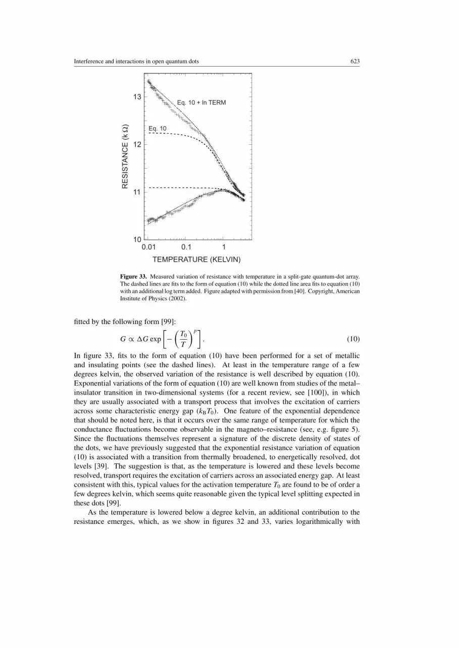
Interference and interactions in open quantum dots 623
10
11
12
13
0.01 0.1 1
RE
SIS
TAN
CE
(k
Ω)
TEMPERATURE (KELVIN)
Eq. 10
Eq. 10 + ln TERM
Figure 33. Measured variation of resistance with temperature in a split-gate quantum-dot array.The dashed lines are fits to the form of equation (10) while the dotted line area fits to equation (10)with an additional log term added. Figure adapted with permission from [40]. Copyright, AmericanInstitute of Physics (2002).
fitted by the following form [99]:
G ∝ G exp
[−
(T0
T
)p]. (10)
In figure 33, fits to the form of equation (10) have been performed for a set of metallicand insulating points (see the dashed lines). At least in the temperature range of a fewdegrees kelvin, the observed variation of the resistance is well described by equation (10).Exponential variations of the form of equation (10) are well known from studies of the metal–insulator transition in two-dimensional systems (for a recent review, see [100]), in whichthey are usually associated with a transport process that involves the excitation of carriersacross some characteristic energy gap (kBT0). One feature of the exponential dependencethat should be noted here, is that it occurs over the same range of temperature for which theconductance fluctuations become observable in the magneto–resistance (see, e.g. figure 5).Since the fluctuations themselves represent a signature of the discrete density of states ofthe dots, we have previously suggested that the exponential resistance variation of equation(10) is associated with a transition from thermally broadened, to energetically resolved, dotlevels [39]. The suggestion is that, as the temperature is lowered and these levels becomeresolved, transport requires the excitation of carriers across an associated energy gap. At leastconsistent with this, typical values for the activation temperature T0 are found to be of order afew degrees kelvin, which seems quite reasonable given the typical level splitting expected inthese dots [99].
As the temperature is lowered below a degree kelvin, an additional contribution to theresistance emerges, which, as we show in figures 32 and 33, varies logarithmically with

624 J P Bird et al
γ (e
2/h
)-0.08
0
0.08
2 3 4
0
0.04
0.08
0 0.5 1 1.5 2
MA
GN
ITU
DE
OF
γ (
e2 /h)
1/DOT SIZE (MICRONS-1)
CONDUCTANCE ( e2/h)
METALLIC
INSULATING
Figure 34. Main panel: magnitude of the parameter γ and its scaling as a function of inverse dotsize. Filled symbols correspond to metallic points while open symbols correspond to insulatingpoints. The square symbols represent data points obtained in the presence of a static perpendicularmagnetic field of 0.1 T. Inset: variation of γ for a number of different metallic (•) and insulating() states, obtained in measurements of a three-dot quantum-dot array. Figures reproduced withpermission from [38]. Copyright, American Physical Society (2002).
temperature. For a quantitative analysis of this dependence, we write the variation of theconductance at low-temperatures as G ∝ γ ln(T ). From studies of the temperature dependenceof the resistance of numerous metallic and insulating states, we have found the magnitude ofγ tobe essentially the same in both the metallic and the insulating regimes (see the inset of figure 34),and to be relatively insensitive to the average conductance (i.e. the gate voltage). We have foundevidence for a well-defined scaling of γ with dot size, however, which we illustrate in figure 34.In this figure, we plot the average values of γ , obtained from measurements made at morethan fifty different gate voltages in three different structures, as a function of inverse dot size.The additional point, at the origin of this figure, was obtained from measurements performedon a structure with its gates held grounded, in which case the relevant electron system is theheterojunction 2DEG. This situation essentially corresponds to the limit of infinite dot size,and in this case we find no evidence for a logarithmic variation [38, 99]. For the range of dotsizes considered here, the scaling in figure 34 appears to correspond to an inverse dependenceon dot size.
A clue as to the origin of the logarithmic term is provided by its insensitivity to theapplication of moderate magnetic fields. This property is apparent in figure 34, where weuse the open and filled square symbols to represent the average values of γ , determinedfrom temperature-dependent studies in the presence of a static magnetic field of 0.1 T. Themagnetic field was applied perpendicular to the plane of the 2DEG, and should be sufficiently

Interference and interactions in open quantum dots 625
large to break electron time-reversal symmetry. In spite of this, however, the data pointsplotted in figure 34 show that, at least within our experimental accuracy, the value of γ is notaffected by the breaking of this symmetry. Such invariance is reminiscent of the behaviourfound in studies of disordered films and wires, in which the conductance corrections dueto electron interactions are known to be insensitive to the presence of symmetry-breakingmagnetic fields (for an extensive review, see [101]). In fact, we have suggested that the size-dependent scaling of the logarithmic term in figure 34 is consistent with an effect in whichthe boundary interactions of the electrons act to amplify their mutual repulsion. While in anunconfined system the mutual repulsion between any two electrons will tend to drive themapart from each other, in a mesoscopic structure the carriers are reflected at the confiningboundaries and are forced to interact more strongly with each other. This boundary interactionshould become more important as the system size is reduced, and we expect that its relativeinfluence should scale in inverse proportion to the perimeter of the structure, which is actuallyconsistent with the scaling behaviour found in figure 34.
4.2.2. Theoretical modelling. The suggestion of the experimental studies in section 4.2.1 isthat the additional, logarithmic, term in the resistance arises from confinement-enhanced ofthe electron–electron interaction [38]. For this reason, we have formulated [40, 102] a many-body description of transport in open dots that is based on the idea of the Anderson system,in which a single impurity level with an on-site electron–electron interaction is coupled to aone-dimensional lead [103–107]. In our case, the single impurity is interpreted as the quantumdot, which is coupled to two quantum-point-contact leads. While the detailed formation ofthis model is described in [102], we obtain a many-body model for the interacting open systemby starting from the single-particle eigenbasis of the integral dot/lead system, assuming justone lateral mode. The propagating one-dimensional eigenstates of this system are identifiedby their wavenumber (k) in the point-contacts. At certain energies, we have seen (figure 8)that the transmission of this mode can exhibit a Fano-type resonance, reflecting the formationof a quasi-bound state, as we have discussed. In this situation, we assume that the resultingeffective-interaction matrix elements will also exhibit a resonance and the model Hamiltonianwhich should describe this interaction for one mode propagating through a single open dotmay be written as [102]:
H = −β
∑
k,σ
(εkσ − µk)c+kσ ckσ +
1
2
∑(kσ ) =(k′σ ′)
V(kσ)(k′σ ′)c+kσ ckσ c+
k′σ ′ck′σ ′
, (11)
where β = 1/kBT , µk is the electrochemical potential associated with the mode withwavenumber k, σ denotes the usual spin index, c+
kσ /ckσ are the usual creation/annihilationoperators, and εkσ denotes the single-particle dispersion relation. The applied voltagebetween the injecting electron reservoirs corresponds to the difference in chemical potentials,µk>0 − µk<0. For the effective-interaction matrix that enters the Hamiltonian, we employ thefollowing peaked expression in the vicinity of a resonance (E0):
V(kσ)(k′σ ′) ∝ (U − δσσ ′U ex)2
(εk − E0)2 + 2
2
(ε′k − E0)2 + 2
. (12)
Here, U and U ex are the Hartree and exchange terms, respectively, and 2 denotes the totalwidth of the interaction resonance, corresponding to the lifetime of the resonantly trappedcharge. Note here that screening within any particular mode is included explicitly in thismany-body Hamiltonian, whereas screening effects arising from propagating background

626 J P Bird et al
modes, and the environment, are assumed to be contained within the effective-interactionmatrix V .
To calculate transport properties from this model, we consider the diagonalnon-equilibrium (due the non-constant chemical potential) many-body density-matrix.For numerical reasons, the continuum of k-states is discretized in our simulations, and wefurther employ a mean-field approach for the calculation of occupation numbers for state-numbers larger than 16 (The discretization in k-space must be chosen such that the resultingenergy-spacing is small compared to kBT [102]). The current flowing through the system(and hence the conductance) can then be expressed in terms of the single-particle transmissionprobability (with its Fano-type resonance) and the occupation numbers [102]. In the insetto figure 35, we show the typical dependence of the conductance correction due to theinteraction (assuming unity transmission) with varying chemical potential and temperature.The conductance valley, apparent in this figure, can be understood as arising from a depletionof current-carrying k-states at energies below that at which the peaked interaction occurs.After the interaction has been overcome by the chemical potential, an enhanced densityof states contributes to the current, and a conductance peak now results. A systematicanalysis [102] leads us to define the characteristic energy scale kBT ∗
G,R = αG,R(V statetot )0.5,
with fitting parameters αG ≈ 0.55 and αR ≈ 0.31 for the conductance and resistancemaxima, respectively. V state
tot denotes the normalized interaction energy per state, and wenote that the temperature T ∗
G,R has a form reminiscent of an effective Kondo temperature.
0.01 0.1 1 10
RE
SIS
TAN
CE
(h/
2e2 )
T (K)
0.2
0.4
0.6
0.8
0.5
1.0
1.5
2.0
-20
24
6
CO
ND
UC
TAN
CE
(2e
2/h
)
CHEMICAL POTENTIAL (meV)
kB T/e (m
eV)
0
0.2
0.4
0.6
0.8
Figure 35. Computed temperature dependence of the resistance peak (upper curve) and valleyassociated with a specific peaked interaction. The calculation includes 128 k-states and the solidlines correspond to the case where interactions are included, while the dotted lines are for nointeraction. The inset shows the normalized conductance as a function of the chemical potentialµk (relative to E0) and the temperature T for = 0.4, U = 2.4, U ex = 0.6 (with a total number of12 k-states). Figure adapted with permission from [40]. Copyright, American Institute of Physics(2002).

Interference and interactions in open quantum dots 627
At high-temperatures (i.e. when T T ∗G,R), we find a modified Boltzmann law for the scaling
of the corrections to the local conductance and resistance peaks:
Gcorrpeak ∝ exp
[(T ∗
G
T
)2]
, Rcorrpeak ∝ exp
[(T ∗
R
T
)2]
. (13)
In the limited temperature range near T ≈ T ∗G,R , however, a conductance variation close to
ln T is found, similar to the behaviour found in experiment.To compare the predictions of this peaked-interaction model with experiment, we show
the results of a more realistic simulation in the main panel of figure 35, which now includesthe Fano-type resonance (figure 8) in the single-particle transmission probability. Here, wehave taken = 0.02 meV, U = 0.125 meV, and U ex = 0.5U , a parameter choice whichyields V state
tot ≈ 0.010 meV, T ∗G ≈ 95 mK and T ∗
R ≈ 53 mK. We have also assumed a Fano-liketransmission probability with a peak at Ep = , a zero at E0 = 0, a total amplitude prefactorof 0.5, and a background transmission of 0.5. Furthermore, we have assumed that we have onenon-resonant background mode (with a conductance of 2e2/h). The dotted curves in figure 34show the variation of the peak- and valley-resistance values as a function of the temperature,which were computed without the inclusion of any interaction terms (i.e. this figure shows thetemperature behaviour due to the single-particle Fano-resonance of the mode). The solid linesin the figure correspond to the situation where the peaked interaction term has been includedin the simulation. Clearly, the interaction yields an increased fluctuation amplitude, comparedto the single-particle behaviour. In the limited temperature range close to T ∗
G,R , one can see alog-like correction due to the peaked interaction, as a first-order correction beyond the single-particle case. The qualitative similarity with the experimental results of figure 33 is suggestive,and a further interesting observation is that the interaction corrections to the resistance valley(i.e. conduction peak) onset at higher temperatures than for the resistance peak, which canalso be seen in the experiment. The agreement between experiment and theory is by nomeans complete, however. While, for ease of implementation [102], we have investigated thebehaviour for a single propagating mode, in experiment one typically deals with structures inwhich many propagating modes, and temperature-dependent dephasing effects, are present.To conclusively associate the features observed in experiment with many-body effects, it willtherefore be necessary to extend this model to account for these differences. This having beensaid, however, we are encouraged by the fact that our rather simple model does indeed yieldinteraction-induced corrections to the conductance of open dots.
5. Conclusions
In this review, we have seen that the study of electron transport in open quantum dots yields arich variety of behaviour, an understanding of which requires a proper treatment of the wave-mechanical properties of the electron. At the same time, we have also seen that these structuresprovide an ideal system for investigating the semiclassical description of quantum systems.The starting point for the understanding of the transport properties of these devices is the non-uniform broadening of their energy levels, which is generated when the dot is opened to itsreservoirs by means of one-dimensional leads. Due to their weak overlap with the leads, a smallsubset of the closed-dot states develop only a weak broadening when the dot is opened, whilethe majority of states are broadened beyond recognition. By applying an external magneticfield, or by varying gate voltage and changing the size of the dot, the discrete states can be sweptpast the Fermi level, giving rise to an associated modulation of the conductance that is observedin experiment at sufficiently low temperatures. A characteristic feature of those eigenfunctionsthat persist when the dot is opened, is that they tend to be scarred by semiclassical orbits that

628 J P Bird et al
buildup probability in the wavefunction at regions located away from the leads. The scarringorbits are typically inaccessible to classical particles injected into the quantum dot, and wehave provided evidence that these orbits are accessed by the quantum-mechanical processknown as dynamical tunnelling. An important property of the scars is that they are found torecur regularly as the gate voltage or magnetic field is varied, and this property is understoodto follow from quantization of the associated semiclassical orbits. At the same time, we haveseen that the scars may equivalently be viewed as analogous to standing-wave modes of theelectron cavity, which are excited at specific magnetic fields, or gate voltages, when electronwaves are injected into the dot. Support for this notion is provided by the striking similaritiesrevealed in analogue studies of the microwave-transmission properties of macroscopic cavityresonators.
The description of transport we have developed here is quite distinct from that which hasgained wide acceptance in the literature, where it is typical to assume that the classical dynamicsof electrons in the dots is fully chaotic (hyperbolic). While the advantage of such an assumptionis that it reduces the semiclassical analysis of transport to an elegant analytical form, it shouldbe emphasized that such convenience is achieved at the cost of a realistic physical description.In particular, we have seen here, and other authors have shown [55–58], that the classicaldynamics of these dots is typically mixed, rather than fully chaotic. A characteristic featureof the mixed phase space is the presence of well-defined KAM islands, which correspondto periodic orbits separated from the chaotic sea by classically inaccessible regions of phasespace. In this review, we have provided strong evidence that the transport properties of thesedots can be dominated by the dynamical tunnelling of electrons onto the KAM islands. It isimportant to emphasize that no such behaviour is expected in fully chaotic systems, in whichall points in phase space are classically accessible. In spite of some widely referenced works,in which differences in the electrical properties were argued to arise for regular and chaoticcavities [77, 78], it is our standpoint that, at least under typical experimental conditions, itis impossible to realize fully chaotic dots. One widely studied indicator of the dynamics isthe zero-field peak in the magneto–resistance, which has been ascribed to a weak-localizationeffect [108]. The lineshape of this peak is predicted to be different for chaotic and regularcavities, and experimental support of these ideas was argued for in [78]. In numerical studies,however, we have found that the lineshape of this peak can have little to do with the underlyingclassical dynamics [109,110], and our basic viewpoint is that the transport properties of thesedots are, in fact, dominated by their regular orbits.
While strong support for the role of dynamical tunnelling in transport has been providedhere, the detailed mechanism that gives rise to this effect remains to be determined. In recentstudies of this effect in cold-atom systems, the tunnelling between different KAM islands wasargued to be mediated by the presence of the chaotic regions of phase space in which the islandsare embedded [65]. It is not clear, however, if such chaos-assisted tunnelling is relevant here,where the strong diffraction of electrons, that is generated as they are injected into the dot,must be taken into account [48]. The role of such diffraction effects has also been consideredby other authors [111], and an important task in future work will be to develop a descriptionof transport that properly accounts for the dynamical tunnelling.
While the split-gate dots on which we have focused are characterized by the presenceof soft walls, it should be noted that our conclusions are not restricted to such structures.In fact, similar behaviour to that discussed here has also been found in numerical studiesof hard-walled dots [41, 47, 48], and in microwave cavities [15], which may essentiallybe viewed as hard-walled due to the short skin depth at microwave frequencies. Regularconductance oscillations, with similar characteristics to those which we have discussed, havealso been found in experimental investigations of etched dots [112, 113], which are expected

Interference and interactions in open quantum dots 629
to exhibit much harder walls. These observations demonstrate that the key requirement forthe occurrence of dynamical tunnelling is the presence of a dot geometry that gives rise toclassically mixed dynamics. In this sense, it is not surprising that our observations shouldturn out to be so general, since mixed systems tend to be the rule in nature, rather than theexception.
In much of our discussion, we have essentially relied upon a single-particle treatment oftransport, which neglects the influence of many-body interactions (although we have includedself-consistency in our calculations of realistic device profiles). In spite of this, we have seenthat we have been able to account successfully for many details of the transport in the opendots. At the lowest experimental temperatures, however, we have observed a logarithmiccorrection to the conductance which we have suggested is associated with the influence ofelectron interactions. The magnitude of this term is insensitive to the application of modestmagnetic fields, and its amplitude increases inversely with dot size. In an attempt to account forthis behaviour, we have developed a many-body model of transport, based on the premise thatthe Coulomb interaction can be peaked at certain energies, which correspond to the formationof the scarred wavefunction states. While this model requires further refinement, it does atleast provide evidence for corrections to the conductance of open dots, arising from many-bodyinteractions. In this sense, the study of dynamical tunnelling in mesoscopic structures offersthe potential of observing new phenomena, associated with the many-body interactions thatarise during the tunnelling. We have considered, for example, the possibility that the dynamicaltunnelling might give rise to some sort of Kondo effect [114]. Quite generally, an importantrequirement for observation of the Kondo effect is the presence of a localized spin that is ableto interact with a reservoir of conducting electrons. In the particular system of interest here,we have seen that electrons may tunnel into isolated orbits, where they remain trapped for avery long time before ultimately escaping from the dot. These orbits may therefore be viewedas the analogue of the localized charge in the classic Kondo effect, and may interact with otherelectrons that are more freely transmitted through the dot. Indeed, the logarithmic variationthat we observe, of the dot conductance with temperature, is strikingly reminiscent of thatfound in the Kondo effect. Since Kondo physics has recently been proposed as the origin ofthe so-called ‘0.7 structure’ in quantum point contacts [115, 116], it only seems reasonable toalso consider its possible manifestations in open dots.
Acknowledgments
Much of the work discussed in this review was undertaken in collaboration with a number ofcolleagues. We would particularly like to acknowledge the valuable contributions made byA Andresen, N Aoki, Y Aoyagi, M Barth, J Cooper, M Elhassan, F Ge, K Ishibashi, Y-H Kim,L-H Lin, Y Ochiai, D P Pivin, Jr, C Prasad, A Shailos, H-J Stockmann, Y Takagaki, andD Vasileska. We would also like to express our appreciation for the financial support for thisresearch, which has been provided by the Office of Naval Research (JPB and DKF) and theDepartment of Energy (JPB).
References
[1] Datta S M 1995 Electronic Transport in Mesoscopic Systems (Cambridge: Cambridge University Press)[2] Kelly M J 1995 Low-Dimensional Semiconductors (Oxford: Oxford University Press)[3] Ferry D K and Goodnick S M 1997 Transport in Nanostructures (Cambridge: Cambridge University Press)[4] Davies J H 1998 The Physics of Low Dimensional Semiconductors (Cambridge: Cambridge University Press)[5] Beenakker C W J and van Houten H 1992 Solid State Phys. 44 1

630 J P Bird et al
[6] Kouwenhoven L P, Marcus C M, McEuen P L, Tarucha S, Westervelt R M and Wingreen N S 1997 MesoscopicElectron Transport ed L P Kouwenhoven et al NATO ASI, Ser. E, (Dordrecht: Kluwer)
[7] Bird J P (ed) 2003 Electron Transport in Quantum Dots (New York: Kluwer/Plenum) submitted[8] Burkard G, Loss D and DiVincenzo D P 1999 Phys. Rev. B 59 2070[9] Recher P, Sukhorukov E V and Loss D 2000 Phys. Rev. Lett. 85 1962
[10] Orlov A O, Amlani I, Bernstein G H, Lent C S and Snider G L 1977 Science 277 928[11] Komiyama S, Astafiev O, Antonov V, Hirai H and Kutsuwa T 2000 Nature 403 405[12] van der Vaart N C, Johnson A T, Kouwenhoven L P, Maas D J, de Jong W, de Ruyter van Steveninck M P,
van der Enden A and Harmans C J P M 1993 Physica B 189 99[13] Pasquier C, Meirav U, Williams F I B, Glatti D C, Jin Y and Etienne B 1993 Phys. Rev. Lett. 70 69[14] Stockmann H-J 1999 Quantum Chaos—An Introduction (Cambridge: Cambridge University Press)[15] Kim Y-H, Barth M, Stockmann H-J and Bird J P 2002 Phys. Rev. B 65 165317[16] Evans D V and Porter R 1999 J. Eng. Math. 35 149[17] Chen Y F, Huang K F and Lan Y P 2002 Phys. Rev. E 66 046215[18] Bird J P 1999 J. Phys.: Condens. Matter 11 R413[19] Thornton T J, Pepper M, Ahmed H, Andrews D and Davies G J 1986 Phys. Rev. Lett. 56 1198[20] Nixon J A and Davies J H 1990 Phys. Rev. B 41 7929[21] Stopa M 1996 Phys. Rev. B 53 9595[22] Vasileska D, Wybourne M N, Goodnick S M and Gunther A D 1998 Semicond. Sci. Technol. 13 A37[23] Buttiker M 1992 Semiconductors and Semimetals vol 35, ed M Reed (New York: Academic) pp 191–277[24] van Wees B J, Kouwenhoven L P, Harmans C J P M, Williamson J G, Timmering C E, Broekaart M E I,
Foxon C T and Harris J J 1989 Phys. Rev. Lett. 62 2523[25] Stopa M, Bird J P, Ishibashi K, Aoyagi Y and Sugano T 1996 Phys. Rev. Lett. 76 2145[26] Bird J P, Stopa M, Connolly K, Pivin D M Jr, Ferry D K, Akis R, Aoyagi Y and Sugano T 1997 Phys. Rev. B
56 7477[27] Lin J J and Bird J P 2002 J. Phys.: Condens. Matter 14 R501[28] McEuen L P, Foxman E B, Meirav U, Kastner M A, Meir Y, Wingreen N S and Wind S J 1991 Phys. Rev. Lett.
66 1926[29] Ashoori R C, Stormer H L, Weiner J S, Pfeiffer L N, Pearton S J, Baldwin K W and West K W 1992 Phys. Rev.
Lett. 68 3088[30] Tarucha S, Austing D G, Honda T, van der Hage R J and Kouwenhoven L P 1996 Phys. Rev. Lett. 77 3613[31] Akis R, Bird J P and Ferry D K 2002 Appl. Phys. Lett. 81 129[32] Bird J P, Akis R, Ferry D K, Vasileska D, Cooper J, Aoyagi Y and Sugano T 1999 Phys. Rev. Lett. 82 4691[33] Usuki T, Saito M, Takatsu M, Kiehl R A and Yokoyama N 1995 Phys. Rev. B 52 8244[34] Shao Z, Porod W and Lent C S 1994 Phys. Rev. B 49 7453[35] Gores J, Goldhaber-Gordon D, Heemeyer S, Kastner M A, Shtrikman H, Mahalu D and Meirav U 2000 Phys.
Rev. B 62 2188[36] Bird J P, Akis R and Ferry D K 1999 Phys. Rev. B 60 13676[37] Akis R, Bird J P, Vasileska D and Ferry D K 2003 Electron Transport in Quantum Dots ed J P Bird (New York:
Kluwer/Plenum) submitted[38] Shailos A et al 2001 Phys. Rev. B 63 241302[39] Shailos A 2001 Phys. Rev. B 64 193302[40] Indlekofer K M, Bird J P, Akis R, Ferry D K and Goodnick S M 2002 Appl. Phys. Lett. 81 3861[41] Akis R, Bird J P and Ferry D K 1996 J. Phys.: Condens. Matter 8 L667[42] Christensson L, Linke H, Omling P, Lindelof P E, Zozoulenko I V and Berggren K F 1998 Phys. Rev. B 57
12306[43] Bøggild P, Kristensen A, Bruus H, Reimann S M and Lindelof P E 1998 Phys. Rev. B 57 15408[44] Taylor R P, Sachrajda A S, Adams J A, Coleridge P T and Zawadzki P 1993 Phys. Rev. B 47 4458[45] Ye P D and Tarucha S 1999 Phys. Rev. B 59 9794[46] Heller E J 1984 Phys. Rev. Lett. 53 1515[47] Akis R, Ferry D K and Bird J P 1997 Phys. Rev. Lett. 79 123[48] Akis R, Ferry D K and Bird J P 1996 Phys. Rev. B 54 17705[49] Bird J P, Ferry D K, Akis R, Ishibashi K, Aoyagi Y, Sugano T and Ochiai Y 1996 Europhys. Lett. 35 529[50] Bird J P, Akis R, Ferry D K, Aoyagi Y and Sugano T 1997 J. Phys.: Condens. Matter 9 5935[51] Akis R, Bird J P, Ferry D K, Vasileska D, Cooper J, Aoyagi Y and Sugano T 2000 Physica E 7 740[52] Akis R, Bird J P, Ferry D K and Vasileska D 2000 Physica E 7 745[53] Jalabert R A, Baranger H U and Stone A D 1990 Phys. Rev. Lett. 65 2442[54] de Moura A P S, Lai Y-C, Akis R, Bird J P and Ferry D K 2002 Phys. Rev. Lett. 88 236804

Interference and interactions in open quantum dots 631
[55] Ketzmerick R 1996 Phys. Rev. B 54 10841[56] Micolich A P, Taylor R P, Newbury R, Bird J P, Wirtz R, Dettmann C P, Aoyagi Y and Sugano T 1998 J. Phys.:
Condens. Matter 10 1339[57] Sachrajda A S, Ketzmerick R, Gould C, Feng Y, Kelly P J, Delage A and Wasilewski Z 1998 Phys. Rev. Lett.
80 1948[58] Takagaki Y, Elhassan M, Shailos A, Prasad C, Bird J P, Ferry D K, Ploog K H, Lin L-H, Aoki N and Ochiai Y
2000 Phys. Rev. B 62 10255[59] Davis M J and Heller E J 1981 J. Chem. Phys. 75 246–54[60] Bohigas O, Tomsovic S and Ullmo D 1993 Phys. Rep. 223 43[61] Tomsovic S (ed) 1998 Tunneling in Complex Systems (Singapore: World Scientific)[62] Tomsovic S 2001 Phys. Scr. T 90 162[63] Dembowski C, Graf H-D, Heine A, Hofferbert R, Rehfeld H and Richter A 2000 Phys. Rev. Lett. 84 867[64] Hensinger W K 2001 Nature 412 52[65] Steck D A, Oskay W H and Raizen M G 2001 Science 293 274[66] Gutzwiller M C 1990 Chaos in Classical and Quantum Mechanics (New York: Springer)[67] Elhassan M et al 2001 Phys. Rev. B 64 085325[68] Akis R and Ferry D K 1999 Phys. Rev. B 59 7529[69] Aoki N, Oonishi D, Iwase Y, Ochiai Y, Ishibashi K, Aoyagi Y and Bird J P 2002 Appl. Phys. Lett. 80 2970[70] Marcus C M, Westervelt R M, Hopkins P F and Gossard A C 1993 Phys. Rev. B 48 2460[71] Clarke R M, Chan I H, Marcus C M, Duruoz C I, Harris J S Jr, Campman K and Gossard A C 1995 Phys. Rev.
B 52 2656[72] Takagaki Y and Ploog K H 2000 Phys. Rev. E 62 4804[73] Persson M, Pettersson J, von Sydow B, Lindelof P E, Kristensen A and Berggren K F 1995 Phys. Rev. B 52
8921[74] Zozoulenko I V, Schuster R, Berggren K F and Ensslin K 1997 Phys. Rev. B 55 R10209[75] Zozoulenko I V and Berggren K F 1997 Phys. Rev. B 56 6931[76] Zozoulenko I V, Sachrajda A S, Gould C, Berggren K-F, Zawadzki P, Feng Y and Wasilewski Z 1999 Phys.
Rev. Lett. 83 1838[77] Marcus C M, Rimberg A J, Westervelt R M, Hopkins P F and Gossard A C 1992 Phys. Rev. Lett. 69 506[78] Chang A M, Baranger H U, Pfeiffer L N and West K W 1994 Phys. Rev. Lett. 73 2111[79] Christensson L, Linke H, Omling P, Lindelof P E, Zozoulenko I V and Berggren K F 1998 Phys. Rev. B
57 12306[80] Bøggild P, Kristensen A, Bruus H, Reimann S M and Lindelof P E 1998 Phys. Rev. B 57 15408[81] Stopa M 1996 Phys. Rev. B 54 13767[82] Silvestrov P G and Imry Y 2000 Phys. Rev. Lett. 85 2565[83] Blomquist T, Schanze H, Zozoulenko I V and Stockmann H-J 2002 Phys. Rev. E 66 026217[84] Richter A 1999 Emerging applications of number theory The IMA Volumes in Mathematics and its Applications
vol 109, ed D A Hejhal (New York: Springer) pp 479–523[85] Kuhl U and Stockmann H-J 1998 Phys. Rev. Lett. 80 3232[86] Rotter I 1991 Rep. Prog. Phys. 54 635[87] Persson E, Rotter I, Stockmann H-J and Barth M 2000 Phys. Rev. Lett. 85 2478[88] Kun Yu S, Vagov A V and Vorov O K 1999 Phys. Rev. C 59 R585[89] Altshuler B L, Gershenson M E and Aleiner I L 1998 Physica E 3 58[90] Huibers A G, Switkes M, Marcus C M, Campman K and Gossard A C 1998 Phys. Rev. Lett. 81 200[91] Huibers A G, Folk J A, Patel S R, Marcus C M, Duruoz C I and Harris J S Jr 1999 Phys. Rev. Lett. 83 5090[92] Bird J P, Ishibashi K, Ferry D K, Ochiai Y, Aoyagi Y and Sugano T 1995 Phys. Rev. B 51 R18037[93] Bird J P, Micolich A P, Linke H, Ferry D K, Akis R, Ochiai Y, Aoyagi Y and Sugano T 1998 J. Phys.: Condens.
Matter 10 L55[94] Pivin D P Jr, Andresen A, Bird J P and Ferry D K 1999 Phys. Rev. Lett. 82 4687[95] Prasad C, Ferry D K, Shailos A, Elhassan M, Bird J P, Lin L-H, Aoki N, Ochiai Y, Ishibashi K and Aoyagi Y
2000 Phys. Rev. B 62 15356[96] Ferry D K, Edwards G, Yamamoto K, Ochiai Y, Bird J P, Ishibashi K, Aoyagi Y and Sugano T 1995 Japan. J.
Appl. Phys. 34 4338[97] Altshuler B L, Aronov A G and Khmelnitskii D E 1982 Phys. J. C 15 7367[98] Lin L-H 1999 Phys. Rev. B 60 R16299[99] Andresen A 1999 Phys. Rev. B 60 16050
[100] Abrahams E 1999 Ann. Phys. (Leipzig) 8 539[101] Lee P A and Ramakrishnan T V 1985 Rev. Mod. Phys. 57 287

632 J P Bird et al
[102] Indlekofer K M, Bird J P, Akis R, Ferry D K and Goodnick S M 2003 J. Phys.: Condens. Matter 15 147[103] Anderson P W 1961 Phys. Rev. 41 124[104] Ng T K and Lee P A 1988 Phys. Rev. Lett. 61 1768[105] Meir Y, Wingreen N S and Lee P A 1991 Phys. Rev. Lett. 66 3048[106] Meir Y, Wingreen N S and Lee P A 1993 Phys. Rev. Lett. 70 2601[107] Wingreen N S and Meir Y 1994 Phys. Rev. B 49 11040[108] Baranger H U, Jalabert R A and Stone A D 1993 Phys. Rev. Lett. 70 3876[109] Akis R, Ferry D K, Bird J P and Vasileska D 1999 Phys. Rev. B 60 2680[110] Akis R, Vasileska D, Ferry D K and Bird J P 1999 J. Phys.: Condens. Matter 11 4657[111] Blomquist T 2002 Phys. Rev. B 66 155316[112] Connolly K M, Pivin D P Jr, Ferry D K and Wieder H H 1996 Superlatt. Microstruct. 20 307[113] Ramamoorthy A, Akis R, Bird J P, Maemoto T, Ferry D K and Inoue M submitted[114] Bird J P et al 2002 Microelectron. Eng. 63 277[115] Cronenwett S M, Lynch H J, Goldhaber-Gordon D, Kouwenhoven L P, Marcus C M, Hirose K, Wingreen N S
and Umansky V 2002 Phys. Rev. Lett. 88 226805[116] Meir Y, Hirose K and Wingreen N S 2002 Phys. Rev. Lett. 89 196802