mrf5s4140hr3, mrf5s4140hsr3 465 mhz, 28 w avg., 28 v
TRANSCRIPT
ARCHIVEINFORMATION
ARCHIVEINFORMATION
MRF5S4140HR3 MRF5S4140HSR3
1RF Device DataFreescale Semiconductor
RF Power Field Effect TransistorsN--Channel Enhancement--Mode Lateral MOSFETsDesigned for broadband commercial and industrial applications with
frequencies from 400 to 500 MHz. The high gain and broadband performance ofthese devices make them ideal for large--signal, common--source amplifierapplications in 28--volt base station equipment.
• Typical Single--Carrier N--CDMA Performance @ 465 MHz: VDD = 28 Volts,IDQ = 1250 mA, Pout = 28 Watts Avg., IS--95 CDMA (Pilot, Sync, Paging,Traffic Codes 8 Through 13). Channel Bandwidth = 1.2288 MHz. PAR =9.8 dB @ 0.01% Probability on CCDF.Power Gain 21 dBDrain Efficiency 30%ACPR @ 750 kHz Offset --47.6 dBc in 30 kHz Bandwidth
• Capable of Handling 10:1 VSWR, @ 28 Vdc, 465 MHz, 140 Watts CWOutput Power
Features• Characterized with Series Equivalent Large--Signal Impedance Parameters• Internally Matched for Ease of Use• Qualified Up to a Maximum of 32 VDD Operation• Integrated ESD Protection• Lower Thermal Resistance Package• Low Gold Plating Thickness on Leads, 40μ″ Nominal.• RoHS Compliant• In Tape and Reel. R3 Suffix = 250 Units per 56 mm, 13 inch Reel.
Table 1. Maximum Ratings
Rating Symbol Value Unit
Drain--Source Voltage VDSS --0.5, +65 Vdc
Gate--Source Voltage VGS --0.5, +15 Vdc
Total Device Dissipation @ TC = 25°CDerate above 25°C
PD 4272.4
WW/°C
Storage Temperature Range Tstg -- 65 to +150 °C
Case Operating Temperature TC 150 °C
Operating Junction Temperature TJ 200 °C
Table 2. Thermal Characteristics
Characteristic Symbol Value (1,2) Unit
Thermal Resistance, Junction to CaseCase Temperature 73°C, 140 W CWCase Temperature 74°C, 28 W CW
RθJC0.410.47
°C/W
1. MTTF calculator available at http://www.freescale.com/rf. Select Tools/Software/Application Software/Calculators toaccess the MTTF calculators by product.
2. Refer to AN1955, Thermal Measurement Methodology of RF Power Amplifiers. Go to http://www.freescale.com/rf.Select Documentation/Application Notes -- AN1955.
Document Number: MRF5S4140HRev. 2, 5/2006
Freescale SemiconductorTechnical Data
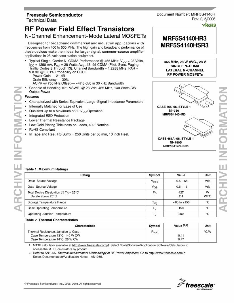
MRF5S4140HR3MRF5S4140HSR3
465 MHz, 28 W AVG., 28 VSINGLE N--CDMA
LATERAL N--CHANNELRF POWER MOSFETs
CASE 465A--06, STYLE 1NI--780S
MRF5S4140HSR3
CASE 465--06, STYLE 1NI--780
MRF5S4140HR3
© Freescale Semiconductor, Inc., 2006, 2010. All rights reserved.
ARCHIVEINFORMATION
ARCHIVEINFORMATION
2RF Device Data
Freescale Semiconductor
MRF5S4140HR3 MRF5S4140HSR3
Table 3. ESD Protection Characteristics
Test Methodology Class
Human Body Model (per JESD22--A114) 2 (Minimum)
Machine Model (per EIA/JESD22--A115) A (Minimum)
Charge Device Model (per JESD22--C101) IV (Minimum)
Table 4. Electrical Characteristics (TC = 25°C unless otherwise noted)
Characteristic Symbol Min Typ Max Unit
Off Characteristics
Zero Gate Voltage Drain Leakage Current(VDS = 65 Vdc, VGS = 0 Vdc)
IDSS 10 μAdc
Zero Gate Voltage Drain Leakage Current(VDS = 28 Vdc, VGS = 0 Vdc)
IDSS 1 μAdc
Gate--Source Leakage Current(VGS = 5 Vdc, VDS = 0 Vdc)
IGSS 1 μAdc
On Characteristics
Gate Threshold Voltage(VDS = 10 Vdc, ID = 400 μAdc)
VGS(th) 2 3 4 Vdc
Gate Quiescent Voltage(VDS = 28 Vdc, ID = 1250 mAdc, Measured in Functional Test)
VGS(Q) 3 4 5 Vdc
Drain--Source On--Voltage(VGS = 10 Vdc, ID = 2.42 Adc)
VDS(on) 0.1 0.2 0.3 Vdc
Forward Transconductance(VDS = 10 Vdc, ID = 3 Adc)
gfs 6.2 S
Dynamic Characteristics (1)
Reverse Transfer Capacitance(VDS = 28 Vdc ± 30 mV(rms)ac @ 1 MHz, VGS = 0 Vdc)
Crss 2.3 pF
Functional Tests (In Freescale Test Fixture, 50 ohm system) VDD = 28 Vdc, IDQ = 1250 mA, Pout = 28 W Avg. N--CDMA,f = 465 MHz, Single--Carrier N--CDMA, 1.2288 MHz Channel Bandwidth Carrier. ACPR measured in 30 kHz Channel Bandwidth @ ±750 kHzOffset. PAR = 9.8 dB @ 0.01% Probability on CCDF.
Power Gain Gps 20 21 23 dB
Drain Efficiency ηD 28.5 30 %
Adjacent Channel Power Ratio ACPR --47.6 --45 dBc
Input Return Loss IRL --14 --9 dB
1. Part internally input matched.
ARCHIVEINFORMATION
ARCHIVEINFORMATION
MRF5S4140HR3 MRF5S4140HSR3
3RF Device DataFreescale Semiconductor
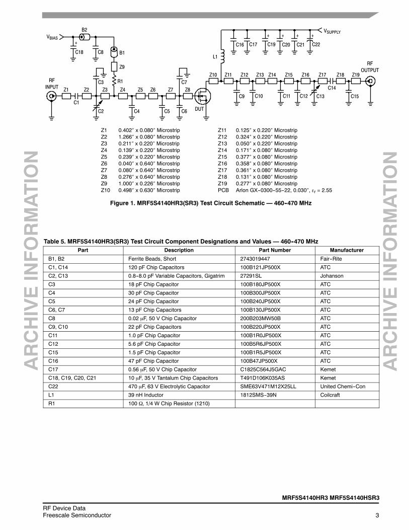
Figure 1. MRF5S4140HR3(SR3) Test Circuit Schematic 460--470 MHz
Z1 0.402″ x 0.080″ MicrostripZ2 1.266″ x 0.080″ MicrostripZ3 0.211″ x 0.220″ MicrostripZ4 0.139″ x 0.220″ MicrostripZ5 0.239″ x 0.220″ MicrostripZ6 0.040″ x 0.640″ MicrostripZ7 0.080″ x 0.640″ MicrostripZ8 0.276″ x 0.640″ MicrostripZ9 1.000″ x 0.226″ MicrostripZ10 0.498″ x 0.630″ Microstrip
Z11 0.125″ x 0.220″ MicrostripZ12 0.324″ x 0.220″ MicrostripZ13 0.050″ x 0.220″ MicrostripZ14 0.171″ x 0.080″ MicrostripZ15 0.377″ x 0.080″ MicrostripZ16 0.358″ x 0.080″ MicrostripZ17 0.361″ x 0.080″ MicrostripZ18 0.131″ x 0.080″ MicrostripZ19 0.277″ x 0.080″ MicrostripPCB Arlon GX--0300--55--22, 0.030″, εr = 2.55
Z1
RFINPUT
C1
C4
Z2 Z3 Z4 Z5 Z6
C5 DUT
Z8
Z10
C12
C14
RFOUTPUT
C2
Z7
Z11 Z12 Z13 Z16 Z17 Z18 Z19
C8
B2VBIAS
L1
C16 C17 C19 C20 C22
VSUPPLY+++
C9 C10 C15
Z15Z14
C13
C18
+
R1
C11
C3
C6
C7
C21
+
Z9
B1
Table 5. MRF5S4140HR3(SR3) Test Circuit Component Designations and Values 460--470 MHzPart Description Part Number Manufacturer
B1, B2 Ferrite Beads, Short 2743019447 Fair--Rite
C1, C14 120 pF Chip Capacitors 100B121JP500X ATC
C2, C13 0.8--8.0 pF Variable Capacitors, Gigatrim 27291SL Johanson
C3 18 pF Chip Capacitor 100B180JP500X ATC
C4 30 pF Chip Capacitor 100B300JP500X ATC
C5 24 pF Chip Capacitor 100B240JP500X ATC
C6, C7 13 pF Chip Capacitors 100B130JP500X ATC
C8 0.02 μF, 50 V Chip Capacitor 200B203MW50B ATC
C9, C10 22 pF Chip Capacitors 100B220JP500X ATC
C11 1.0 pF Chip Capacitor 100B1R0JP500X ATC
C12 5.6 pF Chip Capacitor 100B5R6JP500X ATC
C15 1.5 pF Chip Capacitor 100B1R5JP500X ATC
C16 47 pF Chip Capacitor 100B47JP500X ATC
C17 0.56 μF, 50 V Chip Capacitor C1825C564J5GAC Kemet
C18, C19, C20, C21 10 μF, 35 V Tantalum Chip Capacitors T491D106K035AS Kemet
C22 470 μF, 63 V Electrolytic Capacitor SME63V471M12X25LL United Chemi--Con
L1 39 nH Inductor 1812SMS--39N Coilcraft
R1 100 Ω, 1/4 W Chip Resistor (1210)
ARCHIVEINFORMATION
ARCHIVEINFORMATION
4RF Device Data
Freescale Semiconductor
MRF5S4140HR3 MRF5S4140HSR3
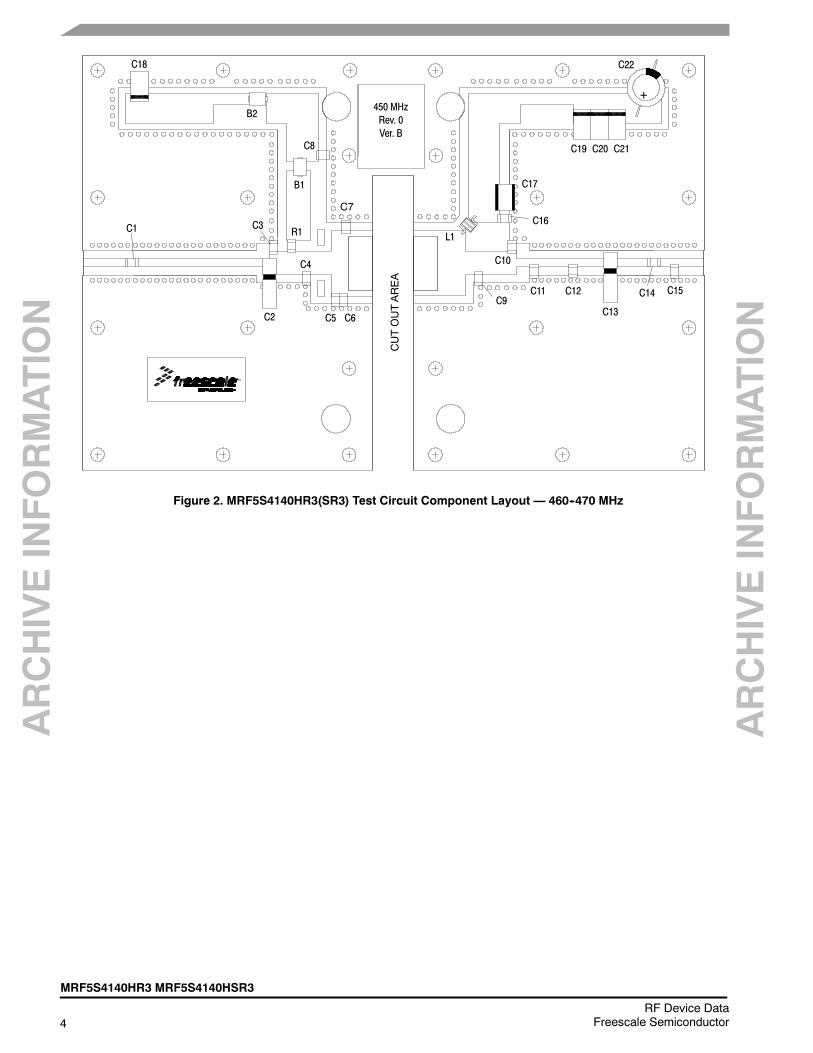
Figure 2. MRF5S4140HR3(SR3) Test Circuit Component Layout 460--470 MHz
+
C7
CUTOUTAREA
450 MHzRev. 0Ver. B
C18
B2
B1
C8
R1
C2 C5 C6
C4
C3C1
C22
C19 C20 C21
C17
C16
L1
C10
C9C11 C12
C13
C14 C15
ARCHIVEINFORMATION
ARCHIVEINFORMATION
MRF5S4140HR3 MRF5S4140HSR3
5RF Device DataFreescale Semiconductor
TYPICAL CHARACTERISTICS 460--470 MHz
--9
--1
--3
--5
--7
--13
Gps,POWER
GAIN(dB)
IRL,INPUTRETURNLOSS
(dB)
ACPR
(dBc),ALT1(dBc)
490430
IRL
Gps
ACPR
f, FREQUENCY (MHz)
Figure 3. Single--Carrier N--CDMA Broadband Performance@ Pout = 28 Watts Avg.
480470460450440--70
38
32
26
--40
--50
--55
ηD,DRAIN
EFFICIENCY(%)
ηD
--60
--45
29
35
21.5
21
20
19
18
17
16
17.5
18.5
19.5
20.5
ALT1
--12
--2
--4
--6
--10
--14
Gps,POWER
GAIN(dB)
IRL,INPUTRETURNLOSS
(dB)
ACPR
(dBc),ALT1(dBc)
490430
IRL
Gps
ACPR
f, FREQUENCY (MHz)
Figure 4. Single--Carrier N--CDMA Broadband Performance@ Pout = 56 Watts Avg.
480470460450440--60
55
45
35
--35
--45
--50
ηD,DRAIN
EFFICIENCY(%)
ηD
--55
--40
40
50
20.8
20.3
19.3
18.3
17.3
16.3
15.8
16.8
17.8
18.8
19.8
ALT1
Figure 5. Two--Tone Power Gain versusOutput Power
10017
23
6
IDQ = 1850 mA
1550 mA
Pout, OUTPUT POWER (WATTS) PEP
21
19
10 400
Gps,POWER
GAIN(dB)
650 mA
VDD = 28 Vdc, f1 = 465 MHz, f2 = 467.5 MHzTwo--Tone Measurements, 2.5 MHz Tone Spacing
950 mA
Figure 6. Third Order Intermodulation Distortionversus Output Power
--15
IDQ = 650 mA
Pout, OUTPUT POWER (WATTS) PEP
100
--20
--25
--35
--4510
INTERMODULATIONDISTORTION(dBc)
IMD,THIRDORDER
--10
950 mA
1850 mA
400
1550 mA
VDD = 28 Vdc, f1 = 465 MHz, f2 = 467.5 MHzTwo--Tone Measurements, 2.5 MHz Tone Spacing
22
20
18
1250 mA
--401250 mA
16.5 --65 --11
VDD = 28 Vdc, Pout = 28 W (Avg.)IDQ = 1250 mA, N--CDMA IS--95(Pilot, Sync, Paging, Traffic Codes8 Through 13)
--8
--30
VDD = 28 Vdc, Pout = 56 W (Avg.)IDQ = 1250 mA, N--CDMA IS--95(Pilot, Sync, Paging, Traffic Codes8 Through 13)
ARCHIVEINFORMATION
ARCHIVEINFORMATION
6RF Device Data
Freescale Semiconductor
MRF5S4140HR3 MRF5S4140HSR3
TYPICAL CHARACTERISTICS 460--470 MHz
Figure 7. Intermodulation Distortion Productsversus Output Power
100--60
--25
7th Order
Pout, OUTPUT POWER (WATTS) PEP
5th Order
3rd Order--35
--40
--45
--50
200
IMD,INTERMODULATIONDISTORTION(dBc)
VDD = 28 Vdc, IDQ = 1250 mA, f1 = 465 MHzf2 = 467.5 MHz, Two--Tone Measurements--30
10
Figure 8. Intermodulation Distortion Productsversus Tone Spacing
10--50
0
7th Order
TWO--TONE SPACING (MHz)
5th Order
3rd Order
--20
--30
--40
1 60
IMD,INTERMODULATIONDISTORTION(dBc)
--10
0.1
VDD = 28 Vdc, Pout = 100 W (PEP)IDQ = 1250 mA, Two--Tone Measurements(f1 + f2)/2 = Center Frequency of 465 MHz
Figure 9. Pulse CW Output Power versusInput Power
39
60P6dB = 53.57 dBm (227 W)
Pin, INPUT POWER (dBm)
VDD = 28 Vdc, IDQ = 1250 mAPulsed CW, 8 μsec(on), 1 msec(off)f = 465 MHz
56
52
44
403127 35
Actual
Ideal
48
19
P out,OUTPUTPOWER
(dBm
)
23
P3dB = 52.99 dBm (198 W)
P1dB = 52.21 dBm (166 W)
ACPR,ADJACENTCHANNEL
POWER
RATIO(dBc)
ALT1,CHANNEL
POWER
(dBc)
Figure 10. Single--Carrier N--CDMA ACPR, ALT1, Power Gainand Drain Efficiency versus Output Power
0 --75
Pout, OUTPUT POWER (WATTS) AVG.
50 --35
40 --43
30 --51
20 --59
--67
1 10
10
VDD = 28 Vdc, IDQ = 1250 mA, f = 465 MHzN--CDMA IS--95 (Pilot, Sync, PagingTraffic Codes 8 Through 13)
Gps
ηD,DRAINEFFICIENCY(%),Gps,POWER
GAIN(dB)
ηD
ACPR
ALT1
TC = --30_C
85_C
25_C --30_C
25_C
60
25_C
85_C
25_C--30_C
85_C
--55
ARCHIVEINFORMATION
ARCHIVEINFORMATION
MRF5S4140HR3 MRF5S4140HSR3
7RF Device DataFreescale Semiconductor
TYPICAL CHARACTERISTICS 460--470 MHz
ηD,DRAINEFFICIENCY(%)
Figure 11. Power Gain and Drain Efficiencyversus CW Output Power
18 0
Pout, OUTPUT POWER (WATTS) CW
26 80
24 60
23 50
30
20
2 10 100
20
VDD = 28 VdcIDQ = 1250 mAf = 465 MHz
Gps
Gps,POWER
GAIN(dB)
25
10
300
TC = --30_C
--30_C
25_C
85_C
22
21
40
85_C
Figure 12. Power Gain versus Output PowerPout, OUTPUT POWER (WATTS) CW
Gps,POWER
GAIN(dB)
VDD = 12 V 16 V
25017.5
21.5
0 20050
18
100 150
20
19
21IDQ = 1250 mAf = 465 MHz
20 V24 V
28 V
32 V
19
70
25_CηD
20.5
19.5
18.5

ARCHIVEINFORMATION
ARCHIVEINFORMATION
8RF Device Data
Freescale Semiconductor
MRF5S4140HR3 MRF5S4140HSR3
Zo = 2Ω
Zload
Zsource
f = 490 MHz
f = 440 MHz
f = 440 MHz
f = 490 MHz
VDD = 28 Vdc, IDQ = 1250 mA, Pout = 28 W Avg.
fMHz
ZsourceΩ
ZloadΩ
440 0.359 -- j1.19 1.35 -- j0.870
445 0.389 -- j1.11 1.31 -- j0.743
450 0.379 -- j1.03 1.34 -- j0.641
455 0.360 -- j0.959 1.32 -- j0.539
460 0.355 -- j0.873 1.31 -- j0.420
465 0.352 -- j0.773 1.30 -- j0.274
470 0.350 -- j0.710 1.29 -- j0.173
475 0.350 -- j0.628 1.28 -- j0.044
480 0.356 -- j0.540 1.29 + j0.090
485 0.355 -- j0.473 1.29 + j0.195
490 0.345 -- j0.388 1.28 + j0.313
Zsource = Test circuit impedance as measured fromgate to ground.
Zload = Test circuit impedance as measuredfrom drain to ground.
Figure 13. Series Equivalent Source and Load Impedance 460--470 MHz
Zsource Z load
InputMatchingNetwork
DeviceUnderTest
OutputMatchingNetwork
ARCHIVEINFORMATION
ARCHIVEINFORMATION
MRF5S4140HR3 MRF5S4140HSR3
9RF Device DataFreescale Semiconductor
Figure 14. MRF5S4140HR3(SR3) Test Circuit Schematic 420--430 MHz
Z1 0.402″ x 0.080″ MicrostripZ2 1.266″ x 0.080″ MicrostripZ3 0.211″ x 0.220″ MicrostripZ4 0.139″ x 0.220″ MicrostripZ5 0.239″ x 0.220″ MicrostripZ6 0.040″ x 0.640″ MicrostripZ7 0.080″ x 0.640″ MicrostripZ8 0.276″ x 0.640″ MicrostripZ9 1.000″ x 0.226″ MicrostripZ10 0.498″ x 0.630″ Microstrip
Z11 0.125″ x 0.220″ MicrostripZ12 0.324″ x 0.220″ MicrostripZ13 0.050″ x 0.220″ MicrostripZ14 0.171″ x 0.080″ MicrostripZ15 0.377″ x 0.080″ MicrostripZ16 0.358″ x 0.080″ MicrostripZ17 0.361″ x 0.080″ MicrostripZ18 0.131″ x 0.080″ MicrostripZ19 0.277″ x 0.080″ MicrostripPCB Arlon GX--0300--55--22, 0.030″, εr = 2.55
Z1
RFINPUT
C1
C4
Z2 Z3 Z4 Z5 Z6
C5 DUT
Z8
Z10
C12
C14
RFOUTPUT
C2
Z7
Z11 Z12 Z13 Z16 Z17 Z18 Z19
C8
B2VBIAS
L1
C16 C17 C19 C20 C22
VSUPPLY+++
C9 C10 C15
Z15Z14
C13
C18
+
R1
C11
C3
C6
C7
C21
+
Z9
B1
Table 6. MRF5S4140HR3(SR3) Test Circuit Component Designations and Values 420--430 MHzPart Description Part Number Manufacturer
B1, B2 Ferrite Beads, Short 2743019447 Fair--Rite
C1, C14 120 pF Chip Capacitors 100B121JP500X ATC
C2, C13 0.8--8.0 pF Variable Capacitors, Gigatrim 27291SL Johanson
C3 18 pF Chip Capacitor 100B180JP500X ATC
C4 39 pF Chip Capacitor 100B390JP500X ATC
C5 24 pF Chip Capacitor 100B240JP500X ATC
C6, C7 13 pF Chip Capacitors 100B130JP500X ATC
C8 0.02 μF, 50 V Chip Capacitor 200B203MW50B ATC
C9, C10 22 pF Chip Capacitors 100B220JP500X ATC
C11 1.0 pF Chip Capacitor 100B1R0JP500X ATC
C12 5.6 pF Chip Capacitor 100B5R6JP500X ATC
C15 1.5 pF Chip Capacitor 100B1R5JP500X ATC
C16 47 pF Chip Capacitor 100B47JP500X ATC
C17 0.56 μF, 50 V Chip Capacitor C1825C564J5GAC Kemet
C18, C19, C20, C21 10 μF, 35 V Tantalum Chip Capacitors T491D106K035AS Kemet
C22 470 μF, 63 V Electrolytic Capacitor SME63V471M12X25LL United Chemi--Con
L1 39 nH Inductor 1812SMS--39N Coilcraft
R1 100 Ω, 1/4 W Chip Resistor (1210)
ARCHIVEINFORMATION
ARCHIVEINFORMATION
10RF Device Data
Freescale Semiconductor
MRF5S4140HR3 MRF5S4140HSR3
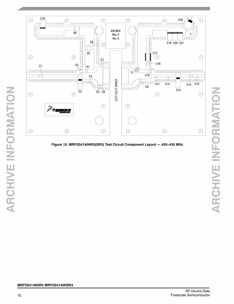
Figure 15. MRF5S4140HR3(SR3) Test Circuit Component Layout 420--430 MHz
CUTOUTAREA
450 MHzRev. 0Ver. A
C18
B2
B1
C8
R1
C2 C5 C6
C4
C3C1
C22
C19 C20 C21
C17
C16
L1C10
C9C11 C12
C13
C14 C15
+
--
C7
ARCHIVEINFORMATION
ARCHIVEINFORMATION
MRF5S4140HR3 MRF5S4140HSR3
11RF Device DataFreescale Semiconductor
TYPICAL CHARACTERISTICS 420--430 MHz
--11
--5
--8
--17
Gps,POWER
GAIN(dB)
IRL,INPUTRETURNLOSS
(dB)
ACPR
(dBc),ALT1(dBc)
440410
IRL
Gps
ACPR
f, FREQUENCY (MHz)
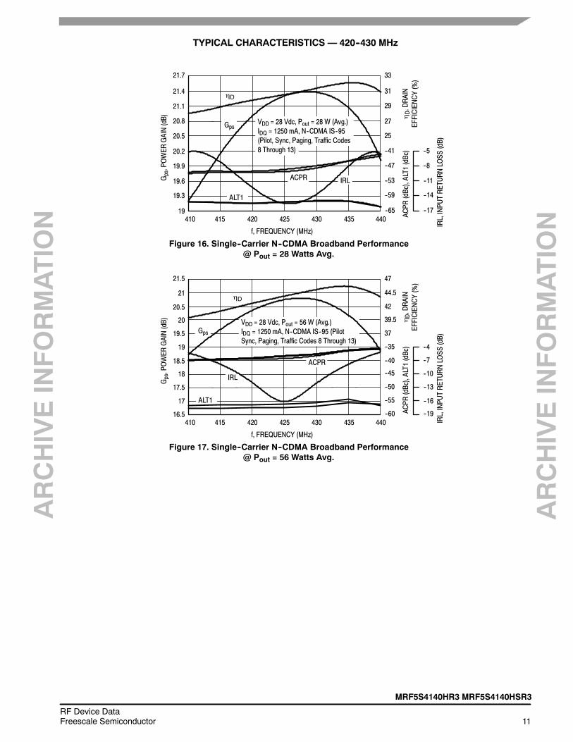
Figure 16. Single--Carrier N--CDMA Broadband Performance@ Pout = 28 Watts Avg.
435430425420415--65
33
29
25
--47
--53
ηD,DRAIN
EFFICIENCY(%)
ηD
--59
--41
27
31
21.7
21.4
20.8
20.2
19.9
19.3
19
19.6
20.5
21.1
ALT1 --14
VDD = 28 Vdc, Pout = 28 W (Avg.)IDQ = 1250 mA, N--CDMA IS--95(Pilot, Sync, Paging, Traffic Codes8 Through 13)
--13
--4
--7
--10
--19
Gps,POWER
GAIN(dB)
IRL,INPUTRETURNLOSS
(dB)
ACPR
(dBc),ALT1(dBc)
440410
IRL
Gps
ACPR
f, FREQUENCY (MHz)
Figure 17. Single--Carrier N--CDMA Broadband Performance@ Pout = 56 Watts Avg.
435430425420415--60
47
42
37
--35
--45
--50
ηD,DRAIN
EFFICIENCY(%)
ηD
--55
--40
39.5
44.5
21.5
21
20
19
18
17
16.5
17.5
18.5
19.5
20.5
ALT1 --16
VDD = 28 Vdc, Pout = 56 W (Avg.)IDQ = 1250 mA, N--CDMA IS--95 (PilotSync, Paging, Traffic Codes 8 Through 13)
ARCHIVEINFORMATION
ARCHIVEINFORMATION
12RF Device Data
Freescale Semiconductor
MRF5S4140HR3 MRF5S4140HSR3
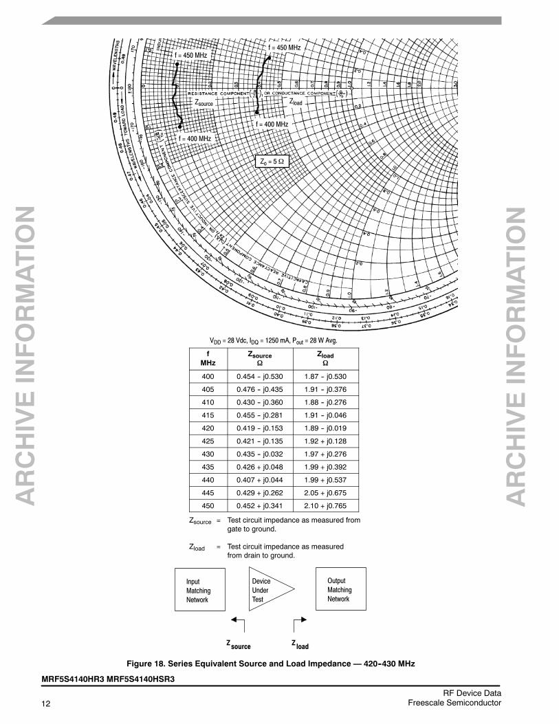
Zo = 5Ω
ZloadZsource
f = 450 MHz
f = 400 MHz
f = 450 MHz
f = 400 MHz
VDD = 28 Vdc, IDQ = 1250 mA, Pout = 28 W Avg.
fMHz
ZsourceΩ
ZloadΩ
400 0.454 -- j0.530 1.87 -- j0.530
405 0.476 -- j0.435 1.91 -- j0.376
410 0.430 -- j0.360 1.88 -- j0.276
415 0.455 -- j0.281 1.91 -- j0.046
420 0.419 -- j0.153 1.89 -- j0.019
425 0.421 -- j0.135 1.92 + j0.128
430 0.435 -- j0.032 1.97 + j0.276
435 0.426 + j0.048 1.99 + j0.392
440 0.407 + j0.044 1.99 + j0.537
445 0.429 + j0.262 2.05 + j0.675
450 0.452 + j0.341 2.10 + j0.765
Zsource = Test circuit impedance as measured fromgate to ground.
Zload = Test circuit impedance as measuredfrom drain to ground.
Figure 18. Series Equivalent Source and Load Impedance 420--430 MHz
Zsource Z load
InputMatchingNetwork
DeviceUnderTest
OutputMatchingNetwork
ARCHIVEINFORMATION
ARCHIVEINFORMATION
MRF5S4140HR3 MRF5S4140HSR3
13RF Device DataFreescale Semiconductor
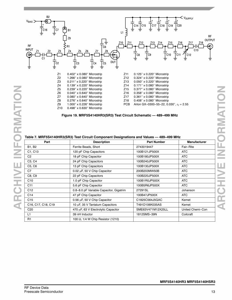
Figure 19. MRF5S4140HR3(SR3) Test Circuit Schematic 489--499 MHz
Z1 0.402″ x 0.080″ MicrostripZ2 1.266″ x 0.080″ MicrostripZ3 0.211″ x 0.220″ MicrostripZ4 0.139″ x 0.220″ MicrostripZ5 0.239″ x 0.220″ MicrostripZ6 0.040″ x 0.640″ MicrostripZ7 0.080″ x 0.640″ MicrostripZ8 0.276″ x 0.640″ MicrostripZ9 1.000″ x 0.226″ MicrostripZ10 0.498″ x 0.630″ Microstrip
Z11 0.125″ x 0.220″ MicrostripZ12 0.324″ x 0.220″ MicrostripZ13 0.050″ x 0.220″ MicrostripZ14 0.171″ x 0.080″ MicrostripZ15 0.377″ x 0.080″ MicrostripZ16 0.358″ x 0.080″ MicrostripZ17 0.361″ x 0.080″ MicrostripZ18 0.408″ x 0.080″ MicrostripPCB Arlon GX--0300--55--22, 0.030″, εr = 2.55
Z1
RFINPUT
C1
C3
Z2 Z3 Z4 Z5 Z6
C4 DUT
Z8
Z10
C11
C13
RFOUTPUT
Z7
Z11 Z12 Z13 Z16 Z17 Z18
C7
B2VBIAS
L1
C14 C15 C17 C18 C20
VSUPPLY+++
C8 C9
Z15Z14
C12
C16
+
R1
C10
C2 C5
C6
C19
+
Z9
B1
Table 7. MRF5S4140HR3(SR3) Test Circuit Component Designations and Values 489--499 MHzPart Description Part Number Manufacturer
B1, B2 Ferrite Beads, Short 2743019447 Fair--Rite
C1, C13 120 pF Chip Capacitors 100B121JP500X ATC
C2 18 pF Chip Capacitor 100B180JP500X ATC
C3, C4 24 pF Chip Capacitors 100B240JP500X ATC
C5, C6 13 pF Chip Capacitors 100B130JP500X ATC
C7 0.02 μF, 50 V Chip Capacitor 200B203MW50B ATC
C8, C9 22 pF Chip Capacitors 100B220JP500X ATC
C10 1.0 pF Chip Capacitor 100B1R0JP500X ATC
C11 5.6 pF Chip Capacitor 100B5R6JP500X ATC
C12 0.8--8.0 pF Variable Capacitor, Gigatrim 27291SL Johanson
C14 47 pF Chip Capacitor 100B47JP500X ATC
C15 0.56 μF, 50 V Chip Capacitor C1825C564J5GAC Kemet
C16, C17, C18, C19 10 μF, 35 V Tantalum Capacitors T491D106K035AS Kemet
C20 470 μF, 63 V Electrolytic Capacitor SME63V471M12X25LL United Chemi--Con
L1 39 nH Inductor 1812SMS--39N Coilcraft
R1 100 Ω, 1/4 W Chip Resistor (1210)
ARCHIVEINFORMATION
ARCHIVEINFORMATION
14RF Device Data
Freescale Semiconductor
MRF5S4140HR3 MRF5S4140HSR3
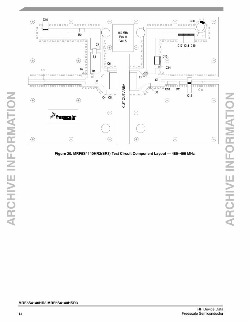
Figure 20. MRF5S4140HR3(SR3) Test Circuit Component Layout 489--499 MHz
CUTOUTAREA
450 MHzRev. 0Ver. A
C16
B2
B1
C7
R1
C4 C5
C3
C2C1
C20
C17 C18 C19
C15
C14
L1C9
C8C10 C11
C12
C13
+
--
C6
ARCHIVEINFORMATION
ARCHIVEINFORMATION
MRF5S4140HR3 MRF5S4140HSR3
15RF Device DataFreescale Semiconductor
TYPICAL CHARACTERISTICS 489--499 MHz
--11
--5
--8
--17
Gps,POWER
GAIN(dB)
IRL,INPUTRETURNLOSS
(dB)
ACPR
(dBc),ALT1(dBc)
510480
IRL
Gps
ACPR
f, FREQUENCY (MHz)
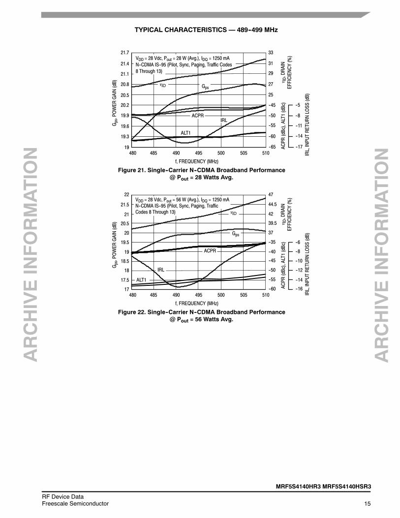
Figure 21. Single--Carrier N--CDMA Broadband Performance@ Pout = 28 Watts Avg.
505500495490485--65
33
29
25
--45
--55
--60
ηD,DRAIN
EFFICIENCY(%)
ηD
--50
27
31
21.7
21.4
20.8
20.2
19.9
19.3
19
19.6
20.5
21.1
ALT1 --14
VDD = 28 Vdc, Pout = 28 W (Avg.), IDQ = 1250 mAN--CDMA IS--95 (Pilot, Sync, Paging, Traffic Codes8 Through 13)
--12
--6
--8
--10
--16
Gps,POWER
GAIN(dB)
IRL,INPUTRETURNLOSS
(dB)
ACPR
(dBc),ALT1(dBc)
510480
f, FREQUENCY (MHz)
Figure 22. Single--Carrier N--CDMA Broadband Performance@ Pout = 56 Watts Avg.
505500495490485--60
47
42
37
--35
--45
--50
ηD,DRAIN
EFFICIENCY(%)
--55
--40
39.5
44.5
22
21.5
20.5
19.5
18.5
17.5
17
18
19
20
21
--14
IRL
Gps
ACPR
ηD
ALT1
VDD = 28 Vdc, Pout = 56 W (Avg.), IDQ = 1250 mAN--CDMA IS--95 (Pilot, Sync, Paging, TrafficCodes 8 Through 13)
ARCHIVEINFORMATION
ARCHIVEINFORMATION
16RF Device Data
Freescale Semiconductor
MRF5S4140HR3 MRF5S4140HSR3
Zo = 2ΩZload
Zsource
f = 519 MHz
f = 469 MHz
f = 469 MHz
f = 519 MHz
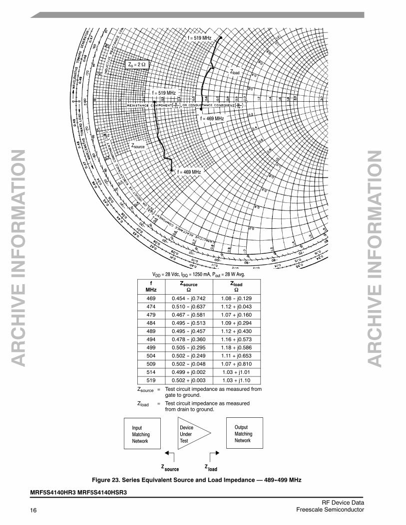
VDD = 28 Vdc, IDQ = 1250 mA, Pout = 28 W Avg.
fMHz
ZsourceΩ
ZloadΩ
469 0.454 -- j0.742 1.08 -- j0.129
474 0.510 -- j0.637 1.12 + j0.043
479 0.467 -- j0.581 1.07 + j0.160
484 0.495 -- j0.513 1.09 + j0.294
489 0.495 -- j0.457 1.12 + j0.430
494 0.478 -- j0.360 1.16 + j0.573
499 0.505 -- j0.295 1.18 + j0.586
504 0.502 -- j0.249 1.11 + j0.653
509 0.502 -- j0.048 1.07 + j0.810
514 0.499 + j0.002 1.03 + j1.01
519 0.502 + j0.003 1.03 + j1.10
Zsource = Test circuit impedance as measured fromgate to ground.
Zload = Test circuit impedance as measuredfrom drain to ground.
Zsource Z load
InputMatchingNetwork
DeviceUnderTest
OutputMatchingNetwork
Figure 23. Series Equivalent Source and Load Impedance 489--499 MHz
ARCHIVEINFORMATION
ARCHIVEINFORMATION
MRF5S4140HR3 MRF5S4140HSR3
17RF Device DataFreescale Semiconductor
TYPICAL CHARACTERISTICS
210
1011
TJ, JUNCTION TEMPERATURE (°C)
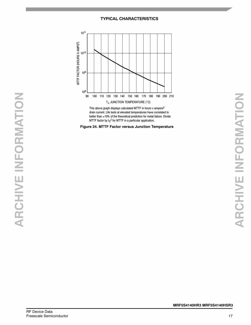
This above graph displays calculated MTTF in hours x ampere2
drain current. Life tests at elevated temperatures have correlated tobetter than ±10% of the theoretical prediction for metal failure. DivideMTTF factor by ID2 for MTTF in a particular application.
109
108
MTTFFACTOR(HOURSXAM
PS2 )
90 110 130 150 170 190100 120 140 160 180 200
1010
Figure 24. MTTF Factor versus Junction Temperature
ARCHIVEINFORMATION
ARCHIVEINFORMATION
18RF Device Data
Freescale Semiconductor
MRF5S4140HR3 MRF5S4140HSR3
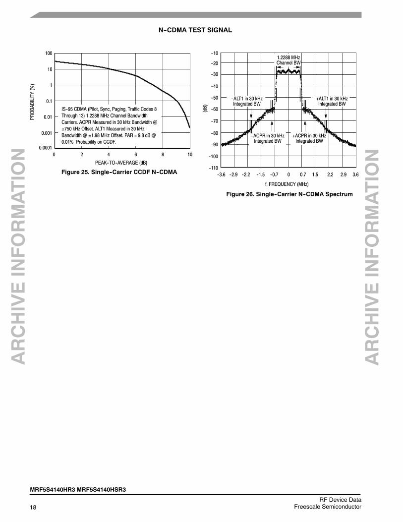
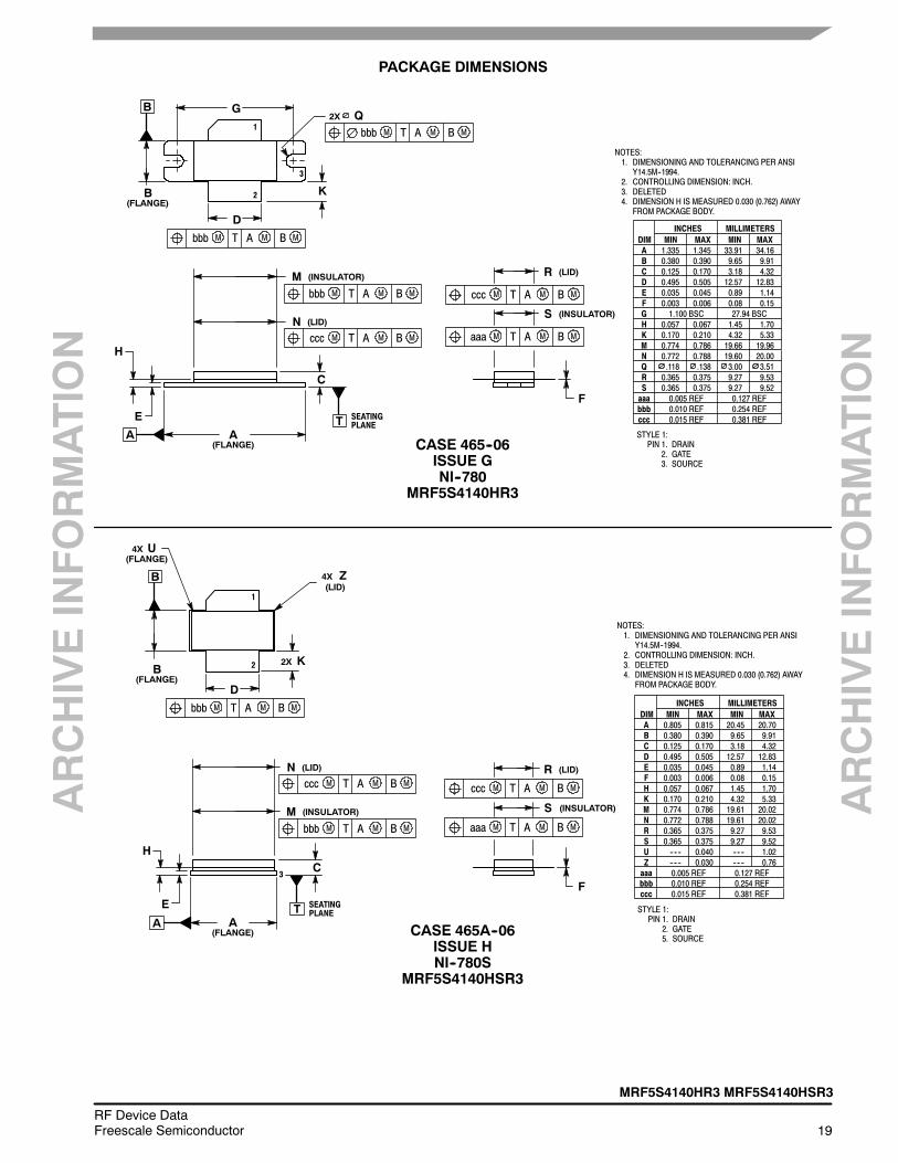
N--CDMA TEST SIGNAL
100.0001
100
0
PEAK--TO--AVERAGE (dB)
Figure 25. Single--Carrier CCDF N--CDMA
10
1
0.1
0.01
0.001
2 4 6 8
IS--95 CDMA (Pilot, Sync, Paging, Traffic Codes 8Through 13) 1.2288 MHz Channel BandwidthCarriers. ACPR Measured in 30 kHz Bandwidth @±750 kHz Offset. ALT1 Measured in 30 kHzBandwidth @ ±1.98 MHz Offset. PAR = 9.8 dB @0.01% Probability on CCDF.
PROBABILITY
(%)
.................
... ....... ......... ...... .................................
.
.......
...
......... ..... .............. ..... ... ... ..... . .... ..... .. ................ ..........................................
............... ........... ....... ................................ .... ......... ........... ... ... ... ............................... ............... .... .. .................... ..... .... ................... . .. . ..... .... .... .. ....... ......... .. ... ... .. . ....... ... .......... .. .. .. ..
... ...... ............ .. ....
.............. .... ............................................. .................................... ... .... .....
... .............. ....
.. ... ............... ....... .. ..... ....... ................. ....... ........... ... .
.............................. ........................................ ....................... ....... ............................ ....... ......................... ......... .
.................. .... ..............
......
....
..
..
..
....
....
..... ... ... .............. ...... ... ... .... .. ... .......... .. .... ................... ...... ..............
................
.................
............
.
. .. ............... ... .. . ...
.........................................................
.....
--60
--110
--10
(dB)
--20
--30
--40
--50
--70
--80
--90
--100
+ACPR in 30 kHzIntegrated BW
1.2288 MHzChannel BW
2.90.7 2.21.50--0.7--1.5--2.2--2.9--3.6 3.6
f, FREQUENCY (MHz)
Figure 26. Single--Carrier N--CDMA Spectrum
--ACPR in 30 kHzIntegrated BW
--ALT1 in 30 kHzIntegrated BW
+ALT1 in 30 kHzIntegrated BW
ARCHIVEINFORMATION
ARCHIVEINFORMATION
MRF5S4140HR3 MRF5S4140HSR3
19RF Device DataFreescale Semiconductor
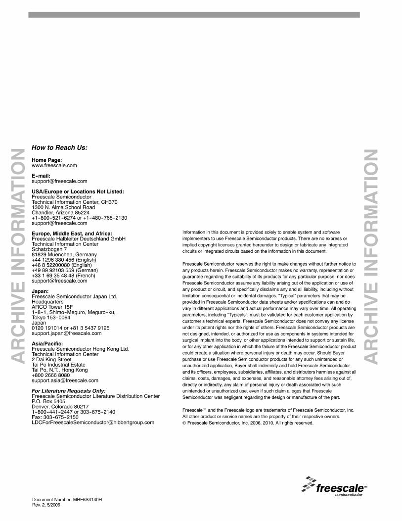
PACKAGE DIMENSIONS
CASE 465--06ISSUE GNI--780
MRF5S4140HR3
NOTES:1. DIMENSIONING AND TOLERANCING PER ANSI
Y14.5M--1994.2. CONTROLLING DIMENSION: INCH.3. DELETED4. DIMENSION H IS MEASURED 0.030 (0.762) AWAY
FROM PACKAGE BODY.
DIM MIN MAX MIN MAXMILLIMETERSINCHES
A 1.335 1.345 33.91 34.16B 0.380 0.390 9.65 9.91C 0.125 0.170 3.18 4.32D 0.495 0.505 12.57 12.83E 0.035 0.045 0.89 1.14F 0.003 0.006 0.08 0.15G 1.100 BSC 27.94 BSCH 0.057 0.067 1.45 1.70K 0.170 0.210 4.32 5.33
N 0.772 0.788 19.60 20.00Q .118 .138 3.00 3.51R 0.365 0.375 9.27 9.53
STYLE 1:PIN 1. DRAIN
2. GATE3. SOURCE
1
3
2
D
G
K
C
E
H
S
FS 0.365 0.375 9.27 9.52
M 0.774 0.786 19.66 19.96
aaa 0.005 REF 0.127 REFbbb 0.010 REF 0.254 REFccc 0.015 REF 0.381 REF
Q2X
MAMbbb B MT
MAMbbb B MT
B
B(FLANGE)
SEATINGPLANE
MAMccc B MT
MAMbbb B MT
A A(FLANGE)
T
N (LID)
M (INSULATOR)
MAMaaa B MT
(INSULATOR)
R
MAMccc B MT
(LID)
NOTES:1. DIMENSIONING AND TOLERANCING PER ANSI
Y14.5M--1994.2. CONTROLLING DIMENSION: INCH.3. DELETED4. DIMENSION H IS MEASURED 0.030 (0.762) AWAY
FROM PACKAGE BODY.
DIM MIN MAX MIN MAXMILLIMETERSINCHES
A 0.805 0.815 20.45 20.70B 0.380 0.390 9.65 9.91C 0.125 0.170 3.18 4.32D 0.495 0.505 12.57 12.83E 0.035 0.045 0.89 1.14F 0.003 0.006 0.08 0.15H 0.057 0.067 1.45 1.70K 0.170 0.210 4.32 5.33M 0.774 0.786 19.61 20.02
R 0.365 0.375 9.27 9.53
STYLE 1:PIN 1. DRAIN
2. GATE5. SOURCE
1
2
D
K
C
E
H
F3
U(FLANGE)4X
Z(LID)4X
bbb 0.010 REF 0.254 REFccc 0.015 REF 0.381 REF
aaa 0.005 REF 0.127 REF
S 0.365 0.375 9.27 9.52
N 0.772 0.788 19.61 20.02
U ------ 0.040 ------ 1.02Z ------ 0.030 ------ 0.76
MAMbbb B MT
B
B(FLANGE)
2X
SEATINGPLANE
MAMccc B MT
MAMbbb B MT
A A(FLANGE)
T
N (LID)
M (INSULATOR)
MAMccc B MT
MAMaaa B MT
R (LID)
S (INSULATOR)
CASE 465A--06ISSUE HNI--780S
MRF5S4140HSR3
ARCHIVEINFORMATION
ARCHIVEINFORMATION
20RF Device Data
Freescale Semiconductor
MRF5S4140HR3 MRF5S4140HSR3
Information in this document is provided solely to enable system and softwareimplementers to use Freescale Semiconductor products. There are no express orimplied copyright licenses granted hereunder to design or fabricate any integratedcircuits or integrated circuits based on the information in this document.
Freescale Semiconductor reserves the right to make changes without further notice toany products herein. Freescale Semiconductor makes no warranty, representation orguarantee regarding the suitability of its products for any particular purpose, nor doesFreescale Semiconductor assume any liability arising out of the application or use ofany product or circuit, and specifically disclaims any and all liability, including withoutlimitation consequential or incidental damages. Typical parameters that may beprovided in Freescale Semiconductor data sheets and/or specifications can and dovary in different applications and actual performance may vary over time. All operatingparameters, including Typicals, must be validated for each customer application bycustomers technical experts. Freescale Semiconductor does not convey any licenseunder its patent rights nor the rights of others. Freescale Semiconductor products arenot designed, intended, or authorized for use as components in systems intended forsurgical implant into the body, or other applications intended to support or sustain life,or for any other application in which the failure of the Freescale Semiconductor productcould create a situation where personal injury or death may occur. Should Buyerpurchase or use Freescale Semiconductor products for any such unintended orunauthorized application, Buyer shall indemnify and hold Freescale Semiconductorand its officers, employees, subsidiaries, affiliates, and distributors harmless against allclaims, costs, damages, and expenses, and reasonable attorney fees arising out of,directly or indirectly, any claim of personal injury or death associated with suchunintended or unauthorized use, even if such claim alleges that FreescaleSemiconductor was negligent regarding the design or manufacture of the part.
Freescalet and the Freescale logo are trademarks of Freescale Semiconductor, Inc.All other product or service names are the property of their respective owners.© Freescale Semiconductor, Inc. 2006, 2010. All rights reserved.
How to Reach Us:
Home Page:www.freescale.com
E--mail:[email protected]
USA/Europe or Locations Not Listed:Freescale SemiconductorTechnical Information Center, CH3701300 N. Alma School RoadChandler, Arizona 85224+1--800--521--6274 or [email protected]
Europe, Middle East, and Africa:Freescale Halbleiter Deutschland GmbHTechnical Information CenterSchatzbogen 781829 Muenchen, Germany+44 1296 380 456 (English)+46 8 52200080 (English)+49 89 92103 559 (German)+33 1 69 35 48 48 (French)[email protected]
Japan:Freescale Semiconductor Japan Ltd.HeadquartersARCO Tower 15F1--8--1, Shimo--Meguro, Meguro--ku,Tokyo 153--0064Japan0120 191014 or +81 3 5437 [email protected]
Asia/Pacific:Freescale Semiconductor Hong Kong Ltd.Technical Information Center2 Dai King StreetTai Po Industrial EstateTai Po, N.T., Hong Kong+800 2666 [email protected]
For Literature Requests Only:Freescale Semiconductor Literature Distribution CenterP.O. Box 5405Denver, Colorado 802171--800--441--2447 or 303--675--2140Fax: [email protected]
Document Number: MRF5S4140HRev. 2, 5/2006
Mouser Electronics
Authorized Distributor
Click to View Pricing, Inventory, Delivery & Lifecycle Information: NXP:
MRF5S4140HR3 MRF5S4140HSR3