mp unit 6 80386dx signals, bus cycles and 80387
TRANSCRIPT
MP UNIT 680386DX Signals, Bus Cycles and
80387 Coprocessor
Topics
• 80386DX Signals- Pin Diagram of 80386 anddescription.
• 80386DX Bus Cycles- System Clock, Bus States,Pipelined and Non-pipelined Bus Cycles.
• 80387 NDP- Numeric data processor
2R. V. Bidwe, PICT, Pune.
R. V. Bidwe, PICT, Pune. 3
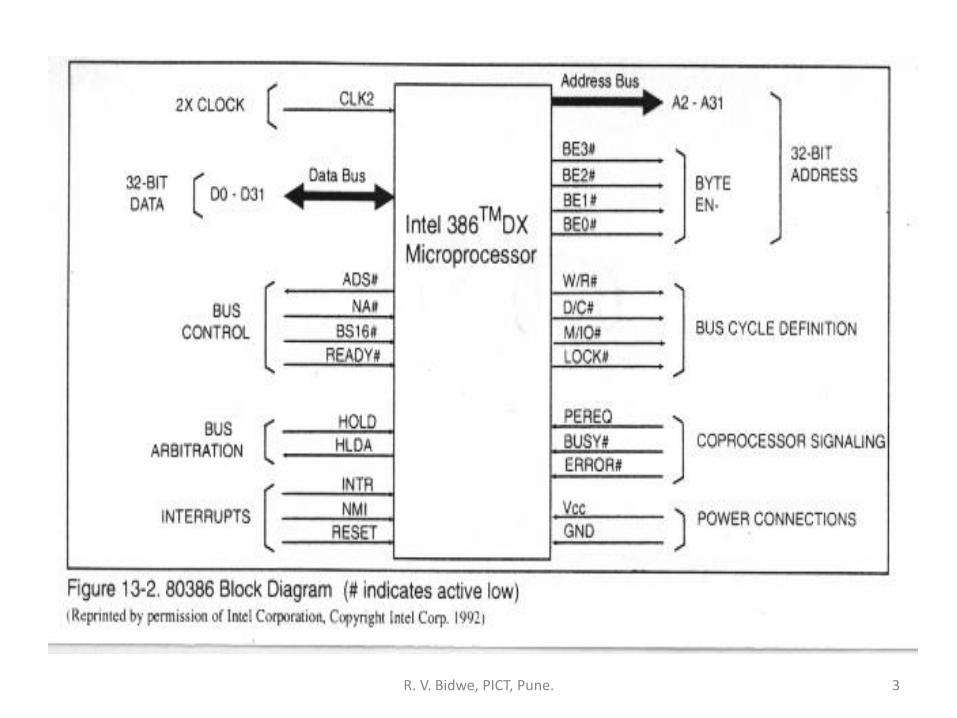
• CLK2: The input pin provides the basic systemclock timing for the operation of 80386.
• D0 – D31: These 32 lines act as bidirectional databus during different access cycles.
• A31 – A2: These are upper 30 bit of the 32- bitaddress bus.
• BE0 to BE3: (Active Low) The 32- bit data bussupported by 80386 and the memory system of80386 can be viewed as a 4-byte wide memoryaccess mechanism.
R. V. Bidwe, PICT, Pune. 4
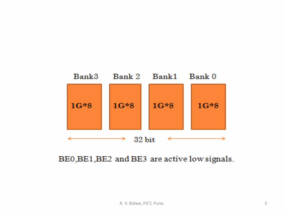
R. V. Bidwe, PICT, Pune. 5
Bus Control
ADS#: (Address Data Strobe) Active when issued a valid request.
The address status output pin indicates that theaddress bus and Bus Cycle Definition Pins( W/R#,D/C#, M/IO#, BE0# to BE3# ) are carrying therespective valid signals.
BS16#: The bus size – 16 input pin allows theinterfacing of 16 bit devices with the 32 bit wide80386 data bus.
R. V. Bidwe, PICT, Pune. 6
• READY#: The ready signals indicates to theCPU that the previous bus cycle has beenterminated and the bus is ready for the nextcycle. The signal is used to insert WAIT statesin a bus cycle and is useful for interfacing ofslow devices with CPU.
• NA#: Gives address of next instruction ifpipelining is enabled. If pipelining is notenabled, this pin is high, if instruction is inwaiting state.
R. V. Bidwe, PICT, Pune. 7
Bus Arbitration
• HOLD: The Bus hold input pin enables theother bus masters to gain control of thesystem bus if it is asserted.
• HLDA: The bus hold acknowledge outputindicates that a valid bus hold request hasbeen received and the bus has beenrelinquished by the CPU.
R. V. Bidwe, PICT, Pune. 8

Interrupts
• INTR: This interrupt pin is a mask-able interrupt,that can be masked using the IF of the flagregister.
• NMI: A valid request signal at the non-mask-ableinterrupt request input pin internally generates anon- mask-able interrupt of type 2.
• RESET: A high at this input pin suspends thecurrent operation and restart the execution fromthe starting location.
R. V. Bidwe, PICT, Pune. 9
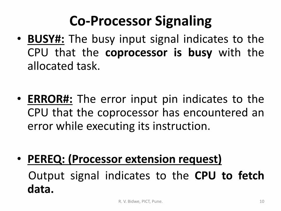
Co-Processor Signaling• BUSY#: The busy input signal indicates to the
CPU that the coprocessor is busy with theallocated task.
• ERROR#: The error input pin indicates to theCPU that the coprocessor has encountered anerror while executing its instruction.
• PEREQ: (Processor extension request)
Output signal indicates to the CPU to fetchdata.
R. V. Bidwe, PICT, Pune. 10
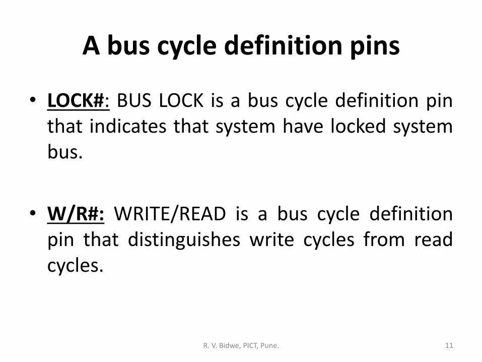
A bus cycle definition pins
• LOCK#: BUS LOCK is a bus cycle definition pinthat indicates that system have locked systembus.
• W/R#: WRITE/READ is a bus cycle definitionpin that distinguishes write cycles from readcycles.
R. V. Bidwe, PICT, Pune. 11
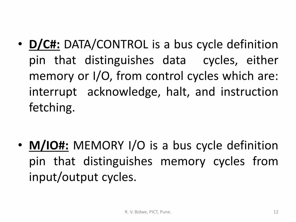
• D/C#: DATA/CONTROL is a bus cycle definitionpin that distinguishes data cycles, eithermemory or I/O, from control cycles which are:interrupt acknowledge, halt, and instructionfetching.
• M/IO#: MEMORY I/O is a bus cycle definitionpin that distinguishes memory cycles frominput/output cycles.
R. V. Bidwe, PICT, Pune. 12

Power Connection Pins
• VCC: These are system power supply lines.
• GND:
R. V. Bidwe, PICT, Pune. 13

Non-pipelined read & write cycles (No wait states)
14R. V. Bidwe, PICT, Pune.
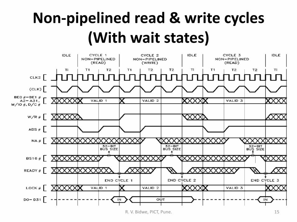
Non-pipelined read & write cycles (With wait states)
15R. V. Bidwe, PICT, Pune.
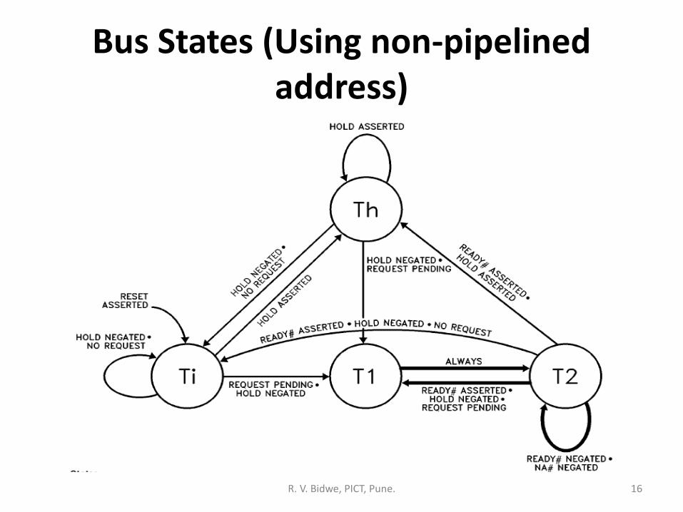
Bus States (Using non-pipelined address)
16R. V. Bidwe, PICT, Pune.
• T1: First clock of a non-pipelined bus cycle (Intel386DX drives new address and asserts ADS#)
• T2: subsequent clocks of a bus cycle when NA# hasnot been sampled asserted in the current bus cycle
• Ti: idle state
• Th: Hold acknowledge state (Intel386 DX assertsHLDA)
• The fastest bus cycle consists of two states: T1 andT2.
R. V. Bidwe, PICT, Pune. 17
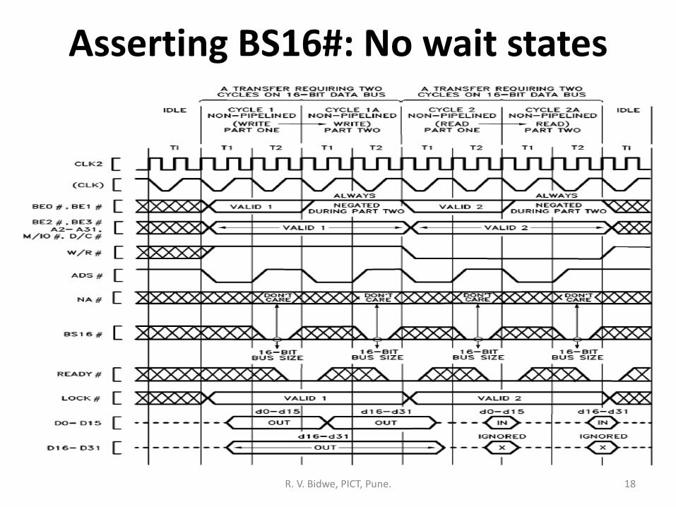
Asserting BS16#: No wait states
18R. V. Bidwe, PICT, Pune.
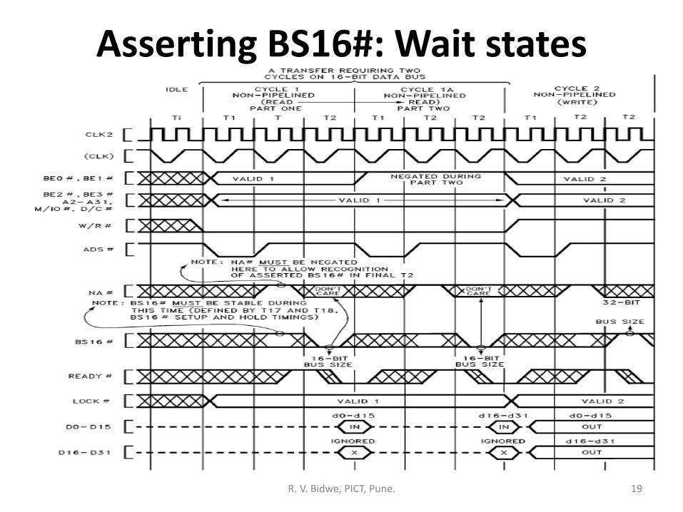
Asserting BS16#: Wait states
19R. V. Bidwe, PICT, Pune.
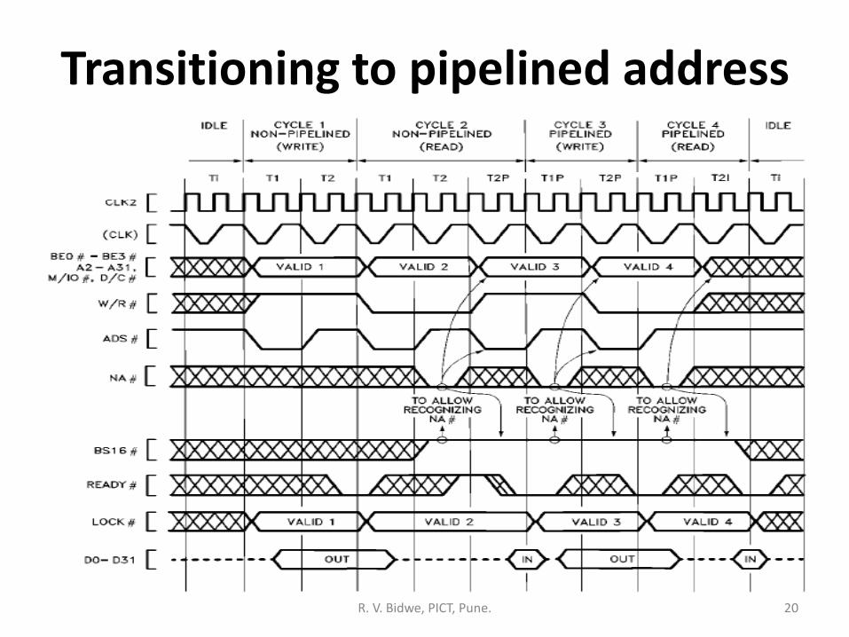
Transitioning to pipelined address
20R. V. Bidwe, PICT, Pune.
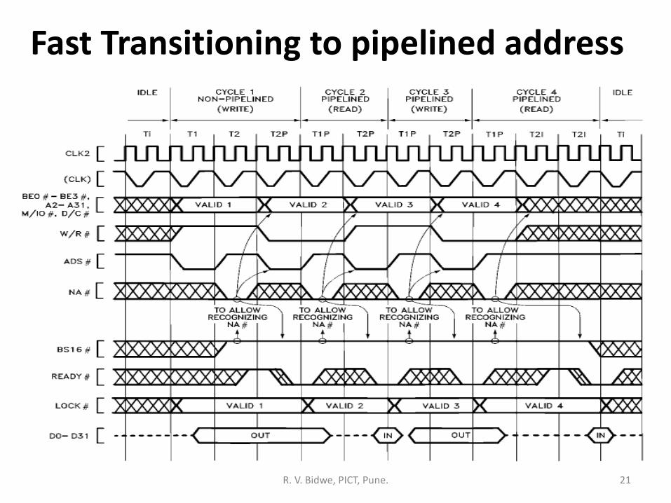
Fast Transitioning to pipelined address
21R. V. Bidwe, PICT, Pune.
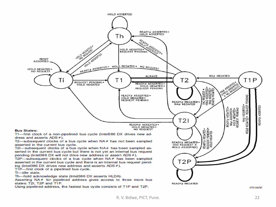
22R. V. Bidwe, PICT, Pune.
1. Processor Vs. Co-processor
• Difference between Processor and Co-processor
i. Functions and Features
ii. Instruction Set
iii. Register Organization
23R. V. Bidwe, PICT, Pune.
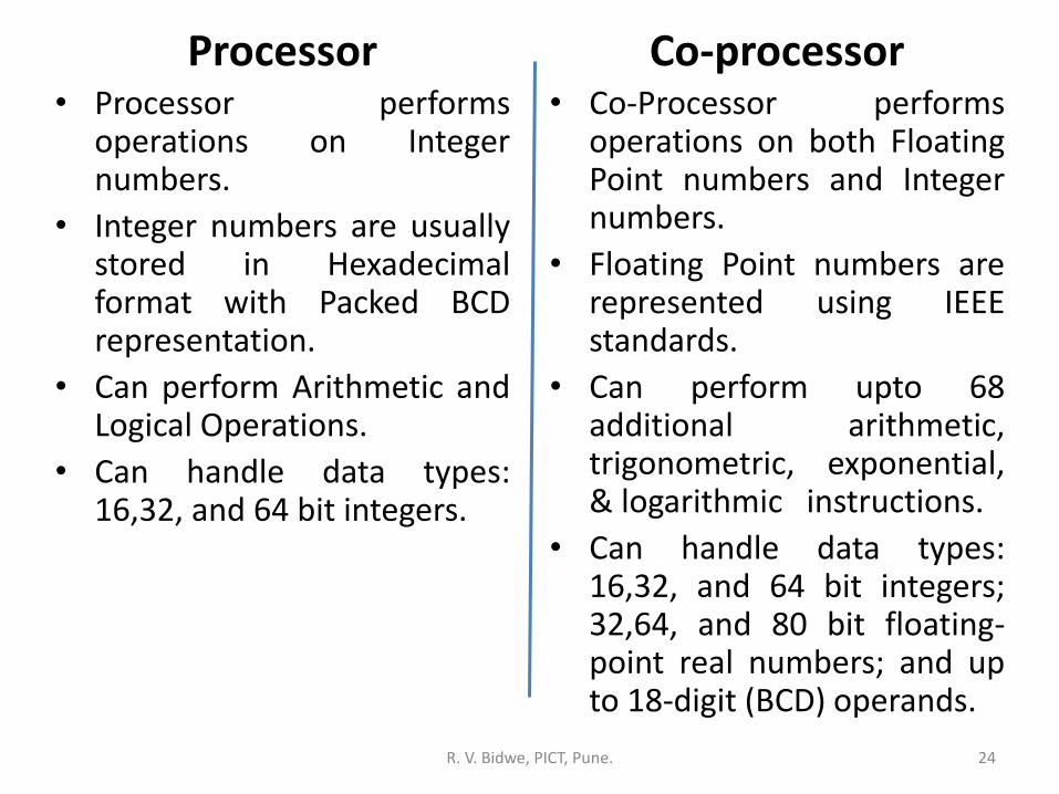
Processor• Processor performs
operations on Integernumbers.
• Integer numbers are usuallystored in Hexadecimalformat with Packed BCDrepresentation.
• Can perform Arithmetic andLogical Operations.
• Can handle data types:16,32, and 64 bit integers.
Co-processor• Co-Processor performs
operations on both FloatingPoint numbers and Integernumbers.
• Floating Point numbers arerepresented using IEEEstandards.
• Can perform upto 68additional arithmetic,trigonometric, exponential,& logarithmic instructions.
• Can handle data types:16,32, and 64 bit integers;32,64, and 80 bit floating-point real numbers; and upto 18-digit (BCD) operands.
R. V. Bidwe, PICT, Pune. 24
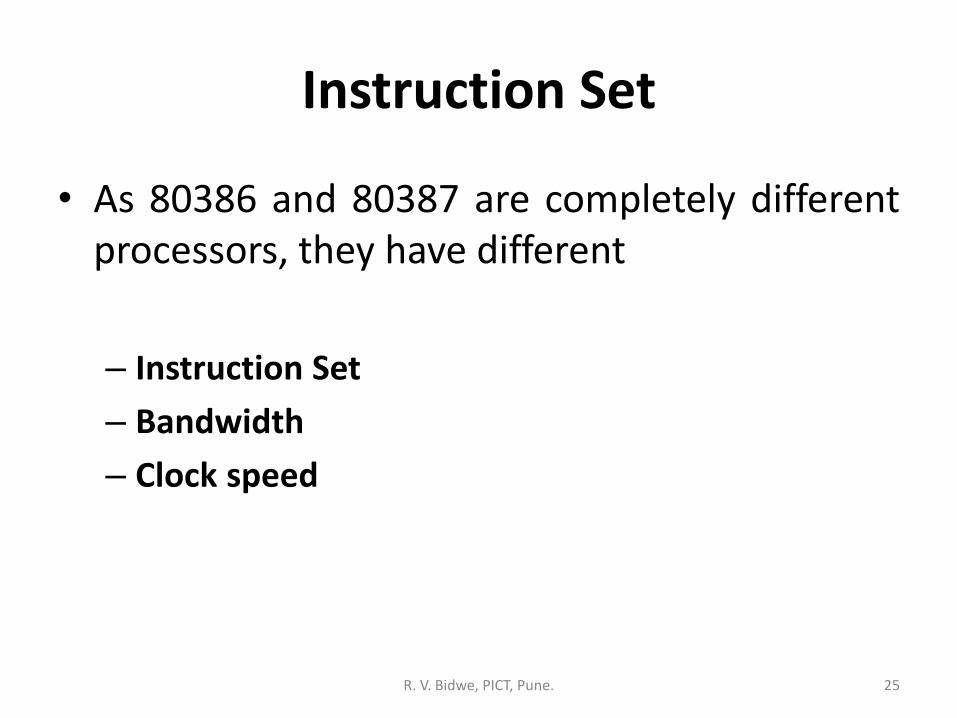
Instruction Set
• As 80386 and 80387 are completely differentprocessors, they have different
– Instruction Set
– Bandwidth
– Clock speed
25R. V. Bidwe, PICT, Pune.
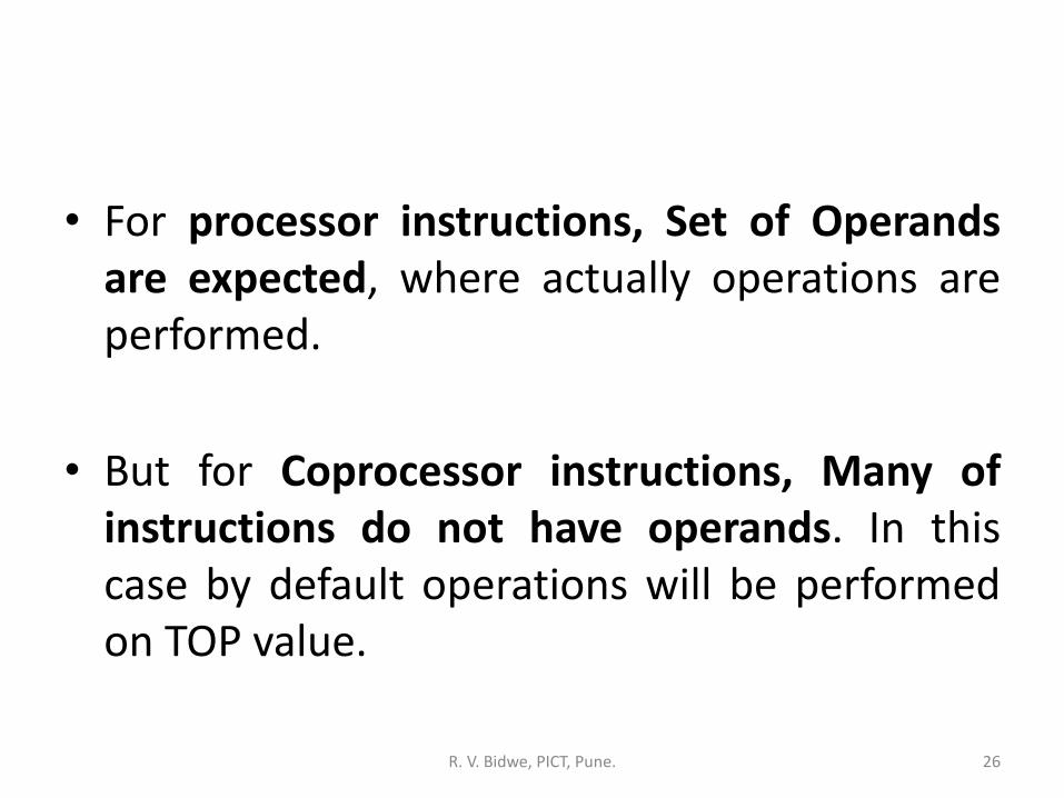
• For processor instructions, Set of Operandsare expected, where actually operations areperformed.
• But for Coprocessor instructions, Many ofinstructions do not have operands. In thiscase by default operations will be performedon TOP value.
R. V. Bidwe, PICT, Pune. 26
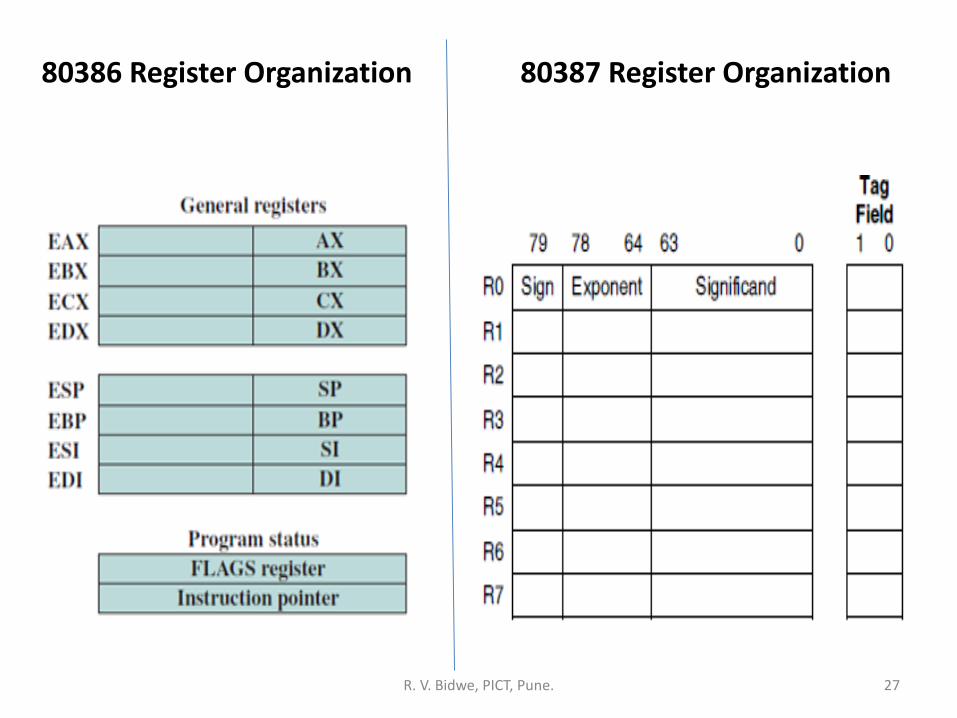
80386 Register Organization 80387 Register Organization
27R. V. Bidwe, PICT, Pune.
80387: NDP
• Control Register bits for Coprocessor support
• 80387 Register Stack
• Data Types
• Load and Store Instructions
• Trigonometric Instructions
• Interfacing signals of 80386DX with 80387.R. V. Bidwe, PICT, Pune. 28
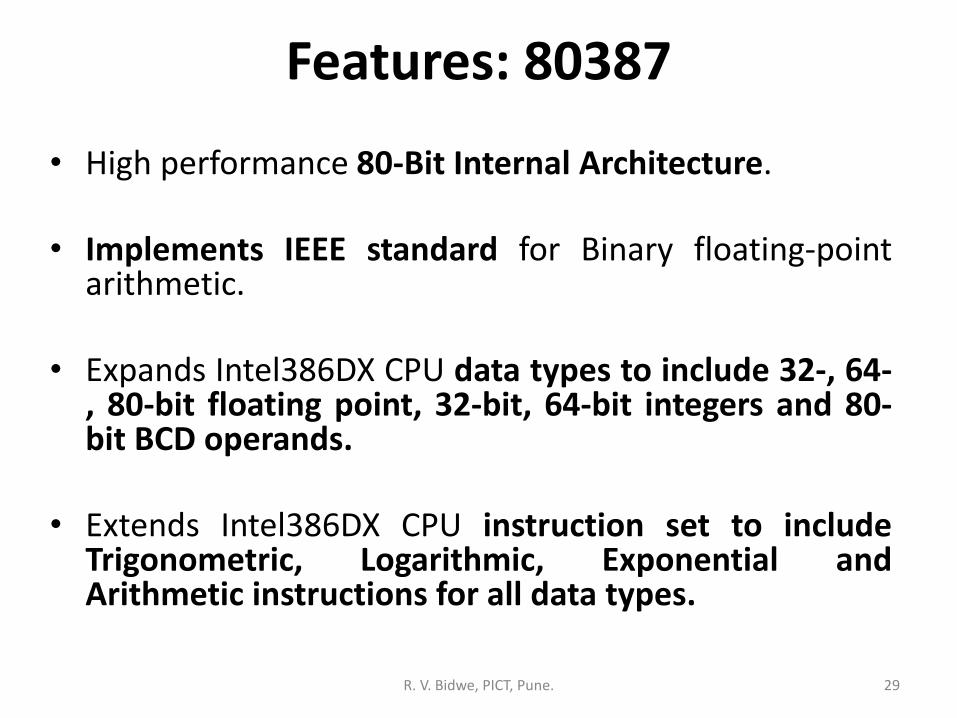
Features: 80387
• High performance 80-Bit Internal Architecture.
• Implements IEEE standard for Binary floating-pointarithmetic.
• Expands Intel386DX CPU data types to include 32-, 64-, 80-bit floating point, 32-bit, 64-bit integers and 80-bit BCD operands.
• Extends Intel386DX CPU instruction set to includeTrigonometric, Logarithmic, Exponential andArithmetic instructions for all data types.
29R. V. Bidwe, PICT, Pune.
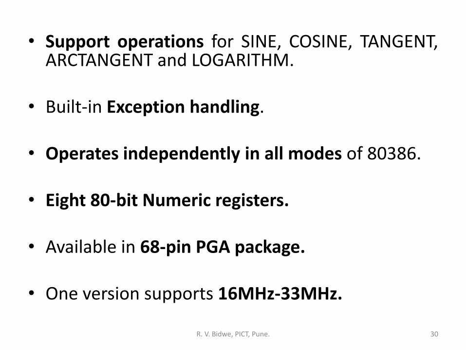
• Support operations for SINE, COSINE, TANGENT,ARCTANGENT and LOGARITHM.
• Built-in Exception handling.
• Operates independently in all modes of 80386.
• Eight 80-bit Numeric registers.
• Available in 68-pin PGA package.
• One version supports 16MHz-33MHz.
30R. V. Bidwe, PICT, Pune.
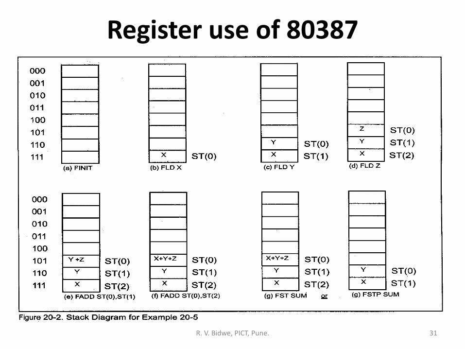
Register use of 80387
31R. V. Bidwe, PICT, Pune.
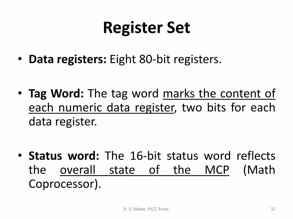
Register Set
• Data registers: Eight 80-bit registers.
• Tag Word: The tag word marks the content ofeach numeric data register, two bits for eachdata register.
• Status word: The 16-bit status word reflectsthe overall state of the MCP (MathCoprocessor).
R. V. Bidwe, PICT, Pune. 32
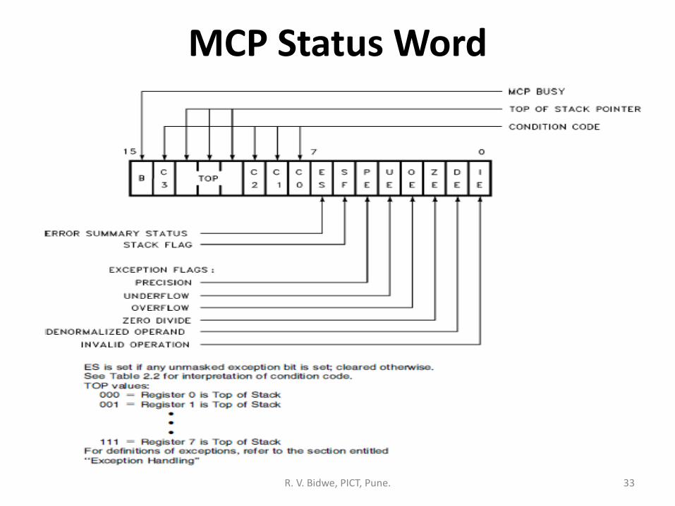
MCP Status Word
R. V. Bidwe, PICT, Pune. 33
• Bits 13 –11 (TOP) point to the Intel387 DX MCPregister that is the Current Top-of-stack.
• The four Numeric Condition Code Bits (C3–C0)are similar to the flags in a CPU; instructions thatperform arithmetic operations update these bitsto reflect the outcome.
• Bit 7 is the Error Summary (ES) Status Bit. This bitis set if any unmasked exception bit is set; it isclear otherwise. If this bit is set, the ERROR#signal is asserted
R. V. Bidwe, PICT, Pune. 34
• Bit 6 is the Stack Flag (SF). This bit is used todistinguish invalid operations due to stackoverflow or underflow from other kinds ofinvalid operations. When SF is set, bit 9 (C1)distinguishes between stack overflow (C1 = 1)and underflow (C1 = 0).
• Figure shows the six Exception Flags in bits 5– 0 of the status word. Bits 5 –0 are set toindicate that the MCP has detected anexception while executing an instruction.
R. V. Bidwe, PICT, Pune. 35
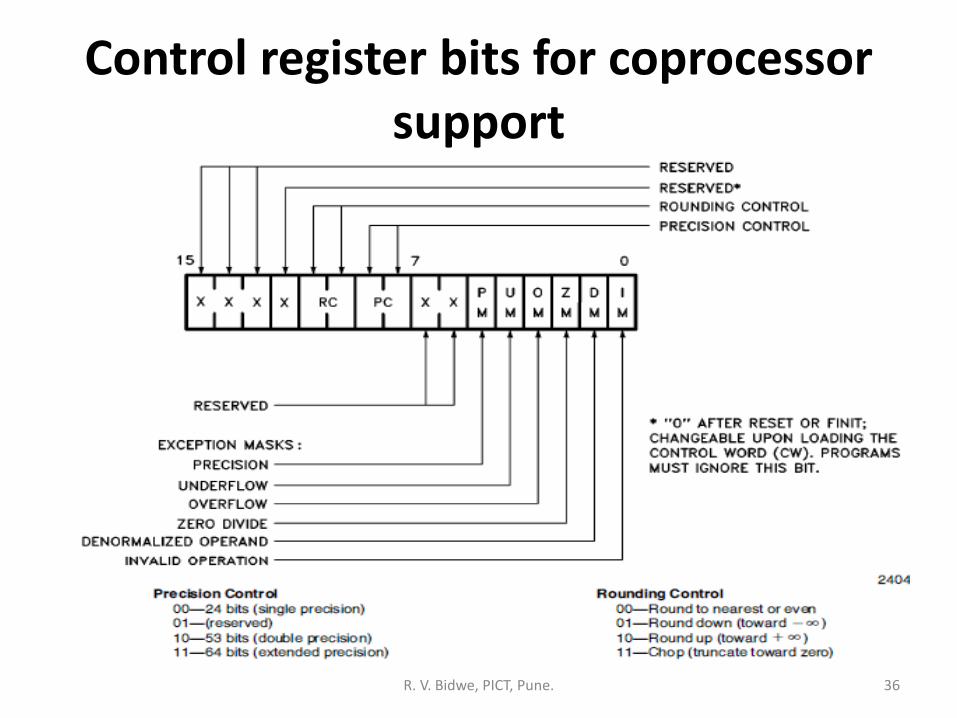
Control register bits for coprocessor support
R. V. Bidwe, PICT, Pune. 36

80387 Register Stack
R. V. Bidwe, PICT, Pune. 37
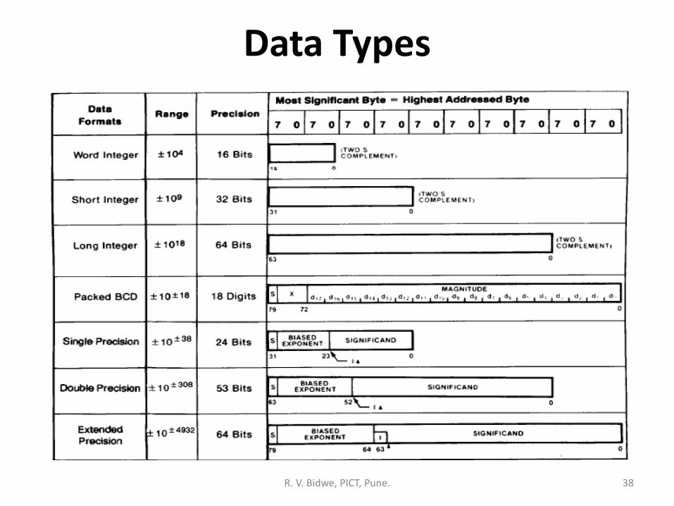
Data Types
R. V. Bidwe, PICT, Pune. 38
Instruction Set
1. Data transfer instructions
2. Non-transcendental instructions
3. Comparison instructions
4. Transcendental instructions
5. Constant instructions
6. Processor Control instructions
R. V. Bidwe, PICT, Pune. 39
• FINIT: (Initialize Floating Point Unit)
– Initialize FPU after checking for pending unmasked floating-point exceptions.
– Syntax: FINIT (no operand)
40R. V. Bidwe, PICT, Pune.
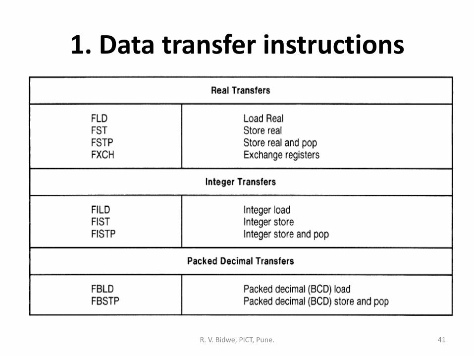
1. Data transfer instructions
R. V. Bidwe, PICT, Pune. 41
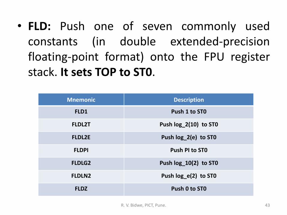
• FLD: Push one of seven commonly usedconstants (in double extended-precisionfloating-point format) onto the FPU registerstack. It sets TOP to ST0.
Mnemonic Description
FLD1 Push 1 to ST0
FLDL2T Push log_2(10) to ST0
FLDL2E Push log_2(e) to ST0
FLDPI Push PI to ST0
FLDLG2 Push log_10(2) to ST0
FLDLN2 Push log_e(2) to ST0
FLDZ Push 0 to ST0
43R. V. Bidwe, PICT, Pune.
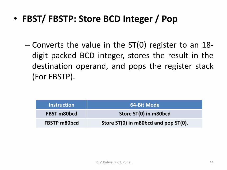
• FBST/ FBSTP: Store BCD Integer / Pop
– Converts the value in the ST(0) register to an 18-digit packed BCD integer, stores the result in thedestination operand, and pops the register stack(For FBSTP).
Instruction 64-Bit Mode
FBST m80bcd Store ST(0) in m80bcd
FBSTP m80bcd Store ST(0) in m80bcd and pop ST(0).
44R. V. Bidwe, PICT, Pune.
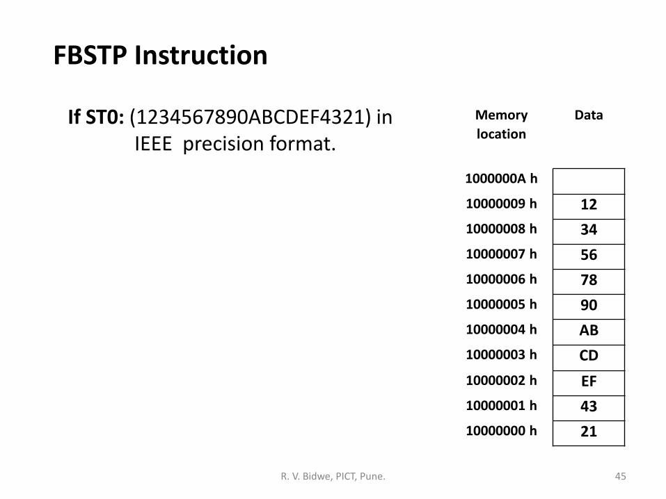
FBSTP Instruction
If ST0: (1234567890ABCDEF4321) in IEEE precision format.
Memory
location
Data
1000000A h
10000009 h 12
10000008 h 34
10000007 h 56
10000006 h 78
10000005 h 90
10000004 h AB
10000003 h CD
10000002 h EF
10000001 h 43
10000000 h 21
45R. V. Bidwe, PICT, Pune.
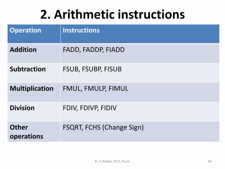
2. Arithmetic instructionsOperation Instructions
Addition FADD, FADDP, FIADD
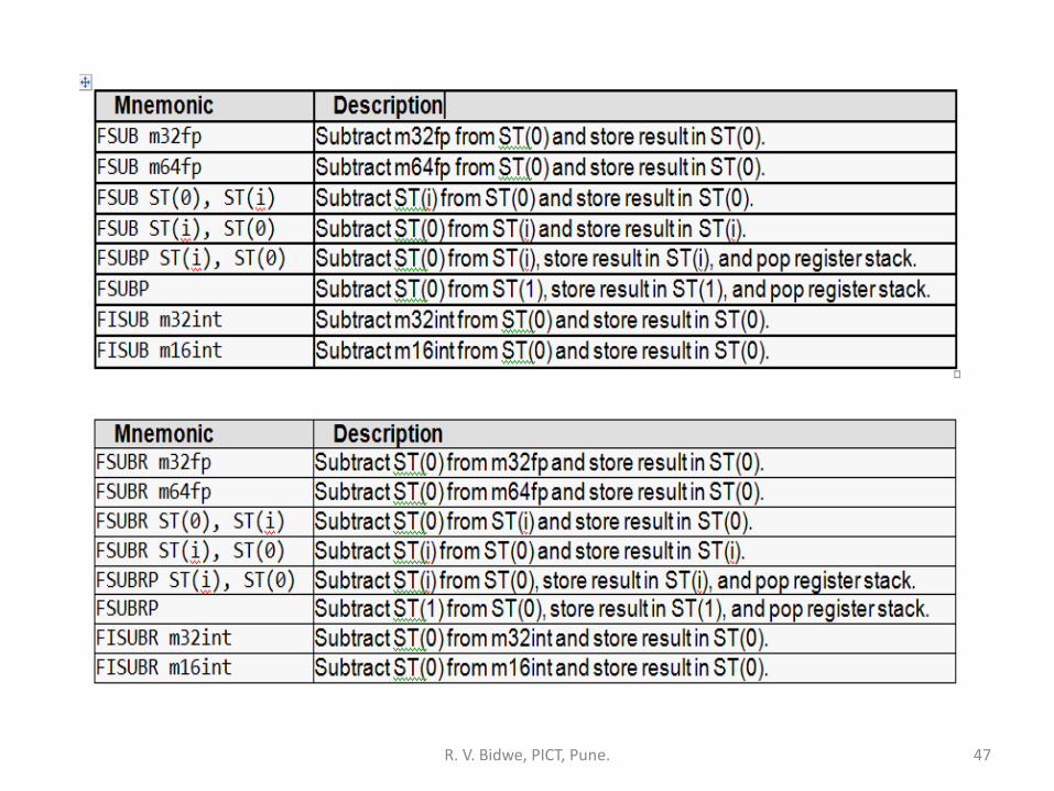
Subtraction FSUB, FSUBP, FISUB
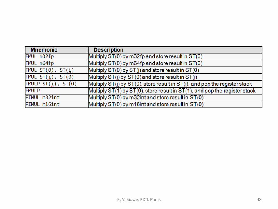
Multiplication FMUL, FMULP, FIMUL
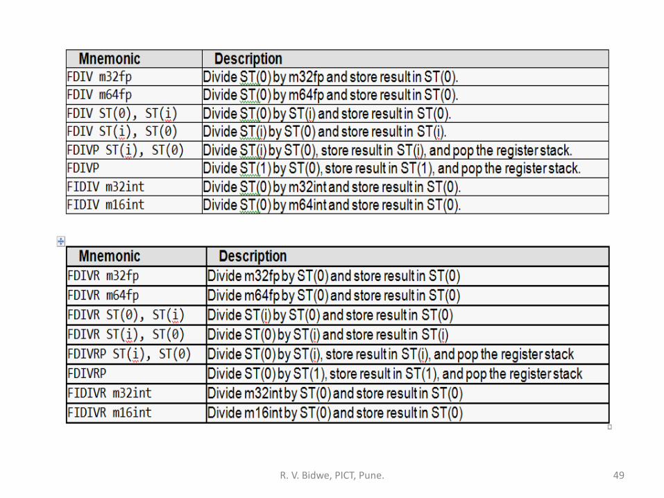
Division FDIV, FDIVP, FIDIV
Other operations
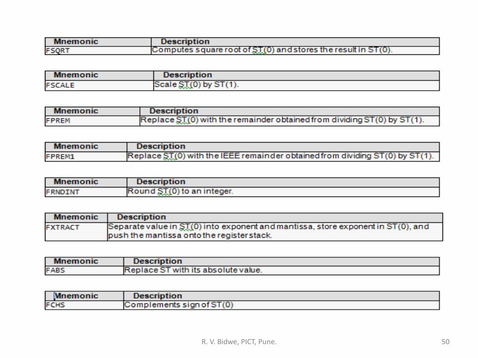
FSQRT, FCHS (Change Sign)
R. V. Bidwe, PICT, Pune. 46
R. V. Bidwe, PICT, Pune. 47
R. V. Bidwe, PICT, Pune. 48
R. V. Bidwe, PICT, Pune. 49
R. V. Bidwe, PICT, Pune. 50
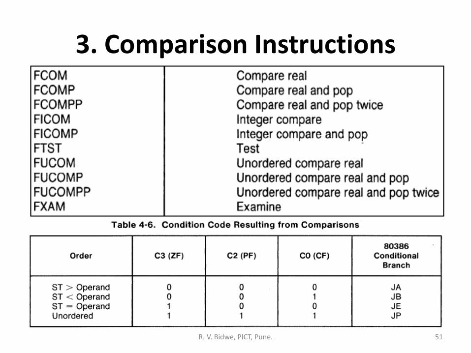
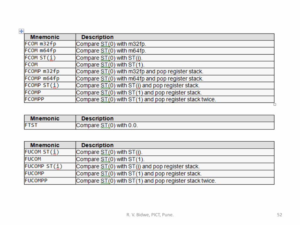
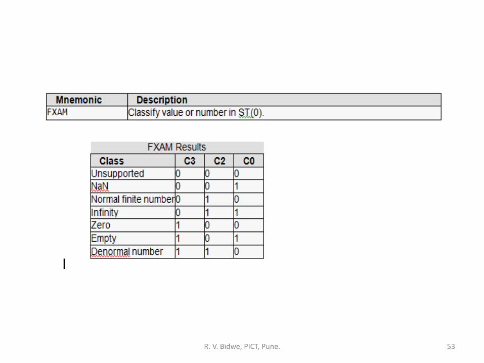
3. Comparison Instructions
R. V. Bidwe, PICT, Pune. 51
R. V. Bidwe, PICT, Pune. 52
R. V. Bidwe, PICT, Pune. 53
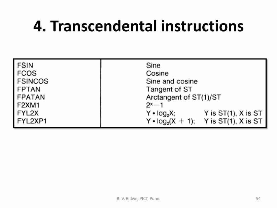
4. Transcendental instructions
R. V. Bidwe, PICT, Pune. 54
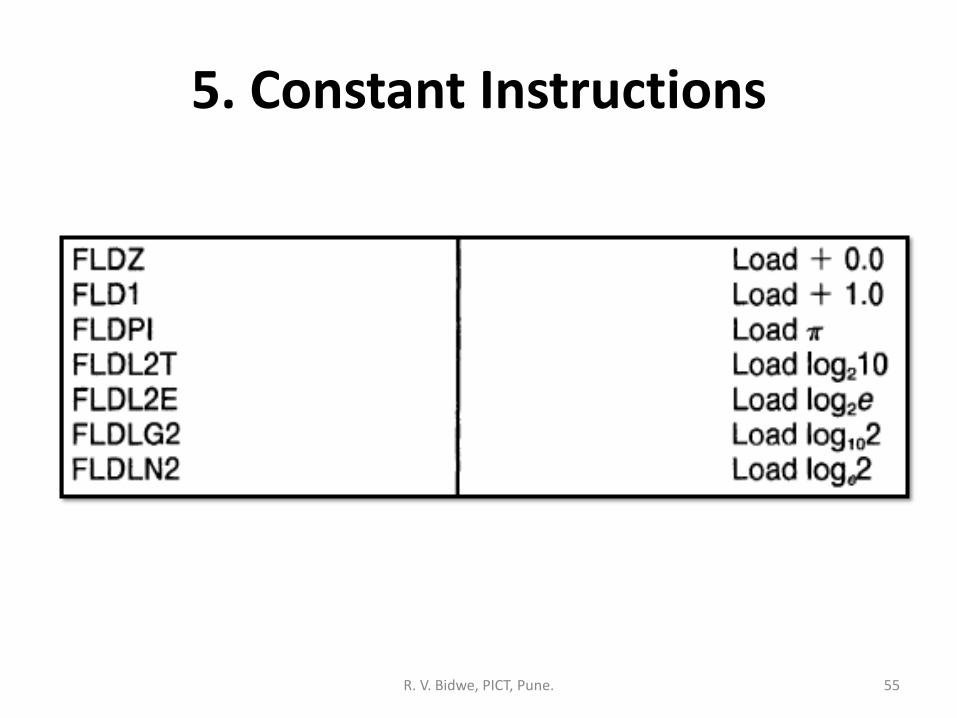
5. Constant Instructions
R. V. Bidwe, PICT, Pune. 55
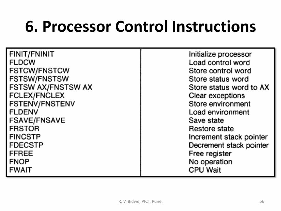
6. Processor Control Instructions
R. V. Bidwe, PICT, Pune. 56
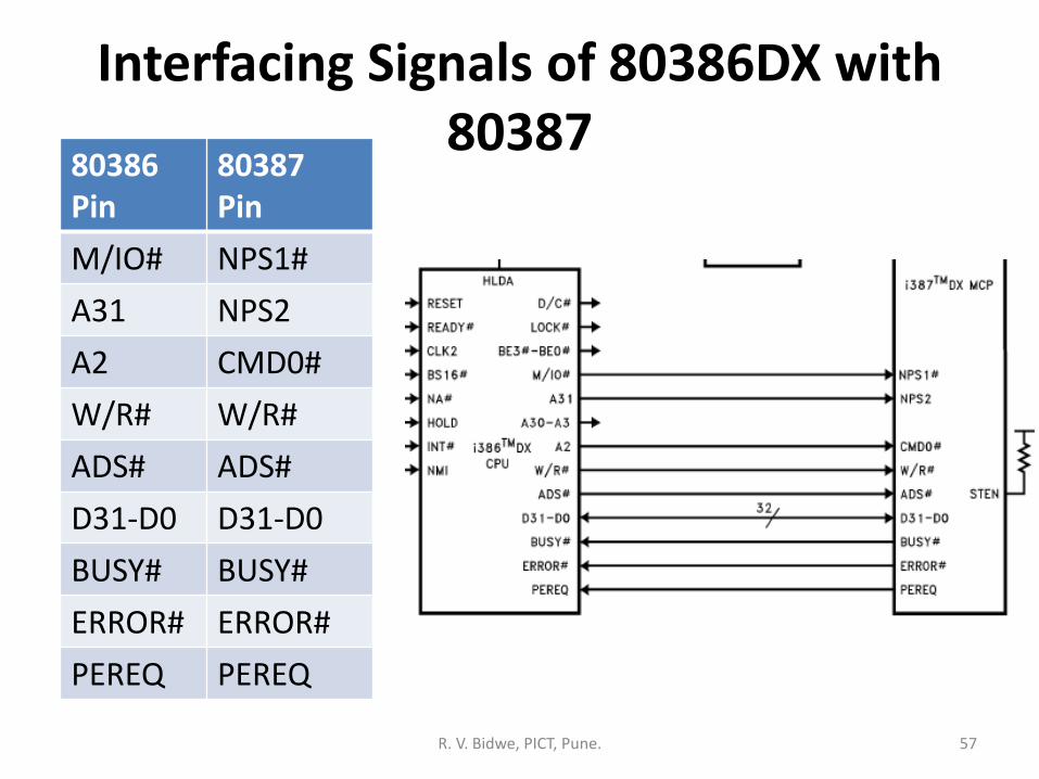
Interfacing Signals of 80386DX with 80387
R. V. Bidwe, PICT, Pune. 57
80386Pin
80387Pin
M/IO# NPS1#
A31 NPS2
A2 CMD0#
W/R# W/R#
ADS# ADS#
D31-D0 D31-D0
BUSY# BUSY#
ERROR# ERROR#
PEREQ PEREQ
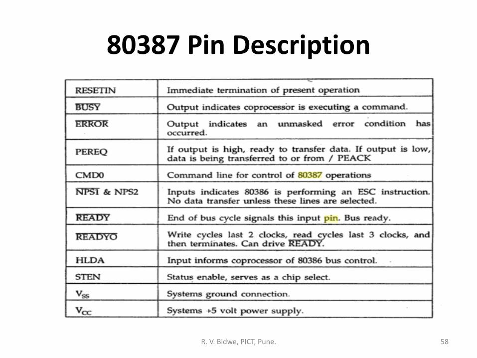
80387 Pin Description
R. V. Bidwe, PICT, Pune. 58