mode matching analysis of the coplanar microstripline on a layered dielectric substrate
TRANSCRIPT
MICROWAVE LABORATORY REPORT NO. 89-P-1
MODE MATCHING ANALYSISOF THE COPLANAR MICROSTRIP LINE
ONALAYERED DIELECTRIC SUBSTRATE
TECHNICAL REPORT
AFRODITI VENNIE FILIPPAS AND TATSUO ITOH
APRIL 1989
ARMY RESEARCH OFFICE TCONTRACT DAAL03-88-K-0005 C
u I'jN 1 1989
THE UNIVERSITY OF TEXAS
DEPARTMENT OF ELECTRICAL ENGINEERING
AUSTIN, TEXAS 78712
&~ p~k'i~.los ad "
UNCLA.SS I i'ILD FOlAS)) ,'} '('' - .'(0 RLI)J WCTION PURPOSESSECURITY CLASSIFICATION OF THIS PAGE
REPORT DOCUMENTATION PAGEIa. REPORT SECURITY CLASSIFICATION lb. RESTRICTIVE MARKINGS
Uncl assi fied2a. SECURITY CLASSIFICATION AUTHORITY 3 DISTRIBUTION/AVAILABILITY OF REPORT
2b. DECLASSiFICATION/DOWNGRADING SCHEDUL. Approved for public release;distribution unlimited.
4. PERFORMING ORGANIZATION REPORT NUMBER(S) S MONITORING ORGANIZATION REPORT NUMBER(S)
6a. NAME OF PERFORMING ORGANIZATION 6b OFFICE SYMBOL 7a. NAME OF MONITORING ORGANIZATION(If applicable)
University of Texas U. S. Army Research Office
6c. ADDRESS (City, State, and ZIP Code) 7b. ADDRESS (City, State, and ZIP Code)
Dept. of Electrical and Comp. Engrg. P. 0. Box 12211AUstin, Texas 78712 Rcsearch Triangle Park, NC 27709-2211
8a. NAME OF FUNDING/ SPONSORING 8b. OFFICE SYMBOL 9. PROCUREMENT INSTRUMENT IDENTIFICATION NUMBERORGANIZATION (If applicable)
U. S. Army Research Office 'P190940-00 S-8C. ADDRESS (City, State, and ZIP Code) 10 SOURCE OF FUNDING NUMBERS
P. 0. Box 12211 PROGRAM PROJECT TASK :WORK UNITELEMENT NO NO NO. ACCESSION NOResearch Triangle Park, NC 27709-2211
11 TITLE (include Security Classification)
Mode matching analysis of a coplanar microstrip line on a layered dielectrica ii a 4- v-= 4- a
12 PERSONAL AUTHOR(S)
Afroditi Vennie Filivpas and Tatsuo Itoh13a. TYPE OF REPORT t 13b. TIME COVERED 14. DATE OF REPORT (Year, Month, Oay),15 PAGE COUNTtechnical report FROM - TO -,I_ April 1989 8
-16 SUPPLEMENTARY NOTATION The view, opinions and/or findings contained in this report are thoseof lhe authqr($) and sh uld not be constugd as an qfficial Dqpartment of the Army position,7 COSATI CODES 18. ,IBJECT TERMS (Continue on reverse if necessary and identify by block number)
FIELD GROUP SUB-GROUP coupled microstrip line, coplanar, mode matching,modes, layered dielectric, propagation constant,characteristic impedance, conducting laver
9-; BSTP.ACT (Continue on reverse if necessary and identify by block number)In this project, mode matching was used to calculate the propagation constanand the characteristic impedance of a coplanar coupled microstrip line.The Striplines are considered to be perfect electric conductors of negligi-ble thickness, and are separated from the ground plane by three layers ofdielectric material. The layer with the higher dielectric constant issandwiched between two layers of lower dielectric constants, such that thefield is confined to this middle layer, which is called the iconductinglayer of the microstrip line. By confining the field to thi layer, lossesat th metal conductor are minimized.
I,/ /
20 DISTRIBUTION/AVAILABILITY OF ABSTRACT 21. ABSTRACT SECURITY CLASSIFICATIONOIUNCLASSIFIED/UNLIMITED 0 SAME AS RPT 0 DTIC USERS Urnc lass if iod
22a NAME OF RESPONSIBLE INDIVIDUAL 22b TELEPHONE (Include Area Code) 22c OFFICE SYMBOL
Tatsuo Itoh - (512) 471-107 2 1DO FORM 1473,84 MAR 83 APR edition may be used until exhausted SECURITY CLASSIFICATION OF THIS PAGE
All other editions are obsolete I ASS I] FD
MICROWAVE LABORATORY REPORT NO. 89-P-1
MODE MATCHING ANALYSISOF THE COPLANAR MICROSTRIP LINE
ONALAYERED DIELECTRIC SUBSTRATE
TECHNICAL REPORT
AFRODITI VENNIE FILIPPAS AND TATSUO ITOH
Accession --or -APRIL 1989 NTIs GRAi-
DTIC TABUnannounced DJustificatio
ByARMY RESEARCH OFFICE Distribut io/CONTRACT DAAL03-88-K0005 Availab'lity Codes
Avail and/or iDist Speoa2
THE UNIVERSITY OF TEXAS
DEPARTMENT OF ELECTRICAL ENGINEERING
AUSTIN, TEXAS 78712
Table of Contents
Introduction 1
Planar Transmission Media 1
Chapter 1. Mode Matching 3
Chapter 2. Analysis of the coupled microstrip line 5
2.1. Parallel-plate waveguides 5
2.2. Three-layer parallel-plate waveguide 8
2.3. Four-layer parallel-plate waveguide 17
Chapter 3. Coupled microstrip lines 22
3.1. Propagation constant 24
3.2. Characteristic Impedance 47
Chapter 4. Numerical Results 54
4.1. Convergence criteria 54
4.2. Program verification 57
4.3. Results-Design charts 59
Chapter 5. Conclusions 72
Appendix A. Notations 74
Appendix B. Field equation derivation 75
References 82
A a l i lI
Introduction.
Planar Transmission Media
Planar transmission media at millimeter wavelengthsprovide a reasonably good performance and lend themselves tomass production techniques. There are three categories underwhich such lines may be placed; planar and quasi-planar (i.e.microstrip line and its variations, and finline), dielectric guides(dielectric slab, image 'line, insular guide, inverted image line, etc.),and H-guides (groove guide, trough guide, etc.) [14].
At millimeter wavelengths, the most commonly usedplanar transmi-ssion lines are microstrip and microstrip-like(inverted and suspended) lines. These lines are suitable for the
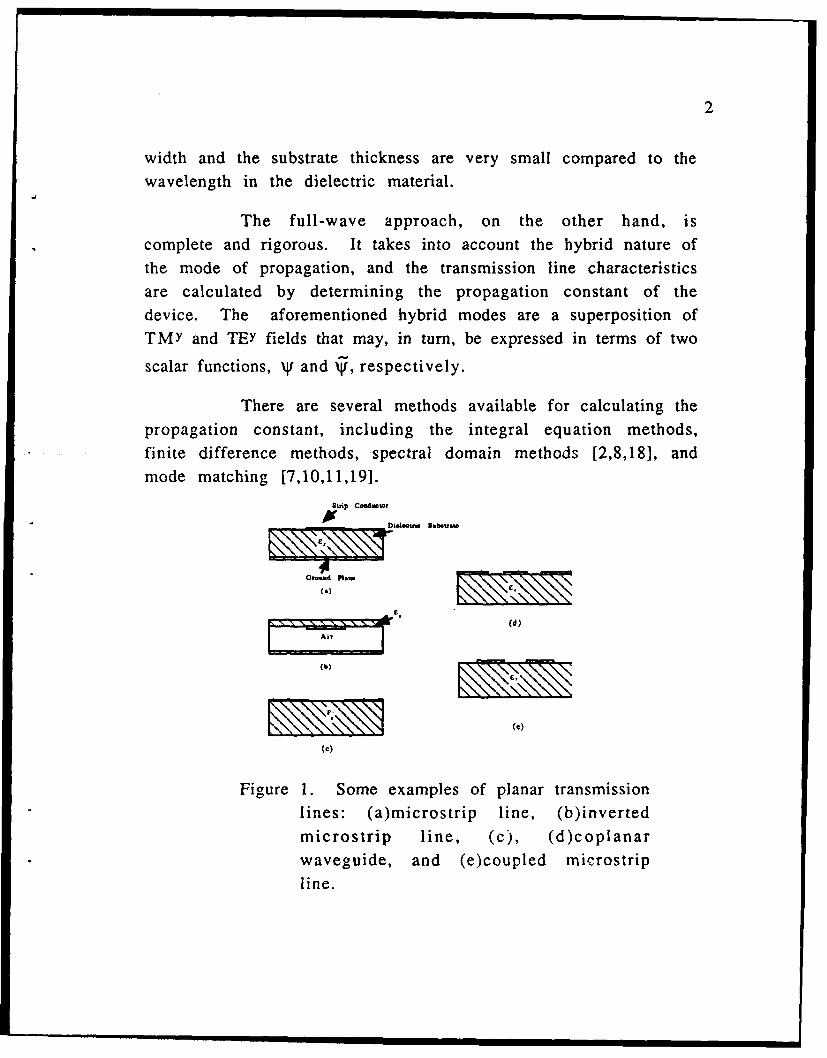
design of low-cost, mass-producible millimeter wave integratedcircuits. For microwave integrated circuits up to 110 GHz, themain contenders are microstrip, suspended microstrip, fin line and
image line. Some examples of these lines are presented in figure1.
Microstrip and microstrip-like transmission linesconsist mainly of a thin strip conductor on a homogeneous orinhomogeneous dielectric substrate that is backed by a groundplane of infinite conductivity. Many numerical and analyticaltechniques exist which are used to analyze the behavior of thesemedia [15]. One of the simplest of these methods is the quasi-
static approach [6]. This approach, however, has a limited rangeof validity, as the nature of the mode of propagation in this case isassumed to be pure TEM, and the transmission line characteristicsare calculated from the electrostatic mutual- and self capacitancesand inductances of the structure. The quasi-static analysis istherefore adequate for designing circuits only when the strip
mmmmm m m 1
2
width and the substrate thickness are very small compared to the
wavelength in the dielectric material.
The full-wave approach, on the other hand, iscomplete and rigorous. It takes into account the hybrid nature ofthe mode of propagation, and the transmission line characteristics
are calculated by determining the propagation constant of thedevice. The aforementioned hybrid modes are a superposition ofTMY and TEY fields that may, in turn, be expressed in terms of two
scalar functions, Xy and iq, respectively.
There are several methods available for calculating thepropagation constant, including the integral equation methods,finite difference methods, spectral domain methods [2,8,18], andmode matching [7,10,11,191.
Strip Co"utnwr
ADi~ootho Sabsaxt
Oromd Plow -CCM *;
(b) -(C)
Figure 1. Some examples of planar transmissionlines: (a)microstrip line, (b)inverted
microstrip line, (c), (d)coplanarwaveguide, and (e)coupled microstrip
line.
Chapter 1. Mode Matching.
Mode matching is one of the most frequently used
techniques for formulating boundary value problems. Its primary
advantage is that it does not generate spurious solutions. It does,however, have a relative convergence problem, so the accuracy ofthe results should be verified carefully. It is not a very efficientmethod, and not suitable for CAD packages, but it does afford an
exact solution within a logical margin of error.
Mode matching is used when the structure in question
can be identified as the junction of two or more regions, eachbelonging to a separable coordinate system. For a planar
structure, rectangular cartesian coordinates, which are a separable
system, are used to describe the structure. One otherconsideration in mode matching is that in each region, there mustexist a set of well-defined solutions of Maxwell's equations which
satisfy all the boundary conditions of the structure, except the
continuity conditions at the junctions between the regions. Thus,the separation of the structure into regions must be done in awell-defined and judicious manner such that a simple and well-
converging solution may be obtained.
The steps followed in the mode-matching procedure
are simple and straightforward. The first step is to define acertain set of normal basis functions for each region of the device,
and to expand the unknown fields in these regions with respect tothese normal functions. For the sake of simplicity, these basis
functions will be called "modes", although they do not satisfy the
source-free wave equation with all the boundary conditions. They
do, however, satisfy the wave equation in their respective regions,and they will be subject to the boundary conditions of those
regions. The functional forms of these modes are already known,
3
4
so the electric fields are now actually defined by the weight of
each mode. In this manner, the original problem reduces to that
of determining the set of modal coefficients associated with the
field expansions in the various regions. This procedure leads to aninfinite set of linear simultaneous equations for the unknownmodal coefficients. To obtain the exact solution to the problem at
hand, one must solve this infinite set of equations, a generally
impossible task. Approximation techniques, such as truncation or
iteration, must therefore be applied, and herein lies the difficulty
of mode matching. In a straightforward analysis, the number of
modes retained will determine the accuracy of the solution. More
modes would logically seem to provide a more accurate solution.However, computation time increases as the square of the numberof modes retained. This is one important factor which necessarilylimits the number of modes which can be retained in each region.Another source of numerical difficulties arises from the fact thatplanar structures such as the microstrip have geometricaldiscontinuities in the form of sharp edges. In this case, the fieldsmust be subjected to one more physical condition, known as the
edge condition, which states that the power of the electric and themagnetic fields at the edges must be finite. This extra condition isneeded so ihat a unique solution to Maxwell's equations may be
obtained. In mode matching, this condition translates into arelationship between the number of modes retained in each
region and the actual physical dimensions of the regions. This
relationship will become more clear as the analysis of the
particular device under consideration, the coplanar microstripline, progresses.
The mode matching technique may be extended to
include cases of continuous spectra. This work, however, will nottake such a case into consideration.
Chapter 2. Analysis of the Coupled MicrostripLine
2.1. Parallel-plate Waveguides
19
.. . . .. .
z
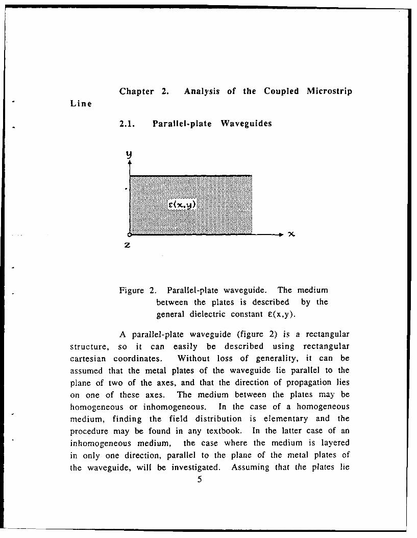
Figure 2. Parallel-plate waveguide. The medium
between the plates is described by thegeneral dielectric constant C(x,y).
A parallel-plate waveguide (figure 2) is a rectangular
structure, so it can easily be described using rectangularcartesian coordinates. Without loss of generality, it can be
assumed that the metal plates of the waveguide lie parallel to the
plane of two of the axes, and that the direction of propagation lies
on one of these axes. The medium between the plates may behomogeneous or inhomogeneous. In the case of a homogeneous
medium, finding the field distribution is elementary and the
procedure may be found in any textbook. In the latter case of an
inhomogeneous medium, the case where the medium is layered
in only one direction, parallel to the plane of the metal plates of
the waveguide, will be investigated. Assuming that the plates lie5
6
parallel ',r the x-z plane, and that the direction of propagation isalong Lhe z axis, TMY and TEY solutions to Maxwell's equationsmay be constructed. Using untilde'd variables to denote TMYquantities, and tilde'd variables to denote TEY quantities, the TMYfield components may be written as (see Appendix B) [13]:
2
Ex_ f(x,y) e jkz H, =j kzf(xy) ejk x
j co e(y) ax Dy
E, k k+T f(x,y) He H=0 (2.1.1)" j CO FE(y)
Ez= - kz a f(x,y) e-jkz Hz= a f(x,y) e-jk7z
oe(y) ay ax
where f(x,y) is the TMY scalar potential, e(y) is the y-dependentpermittivity, k 2= (o 2g OF,(y) is the wavenumber, and kz is the
propagation constant in the z direction [4,7,19].
For the TEY field components, the corresponding
equations are:
= - j kzf(XY) eik? H= 1 f(x,y) -jk?
Ey= 1 k2 + f(x,y) ejkz (2.1.2)
_____) kz f(x,y) jkjHe x y te TE sc(Aar o pyona
Here, f(x,y) is the TEY scalar potential.
7
In a parallel plate waveguide with the x dimension ofthe waveguide very large, or for high frequencies, the potentialfunctions for the TMY and the TEY fields may be assumed to be afunction of y only. So, the TMY potential may be written as:
f(x,y) = W(y) (2.1.3)
and the TEY potential function may be written as:
f(x,y) = V(y) (2.1.4)
Substituting (2.1.3) into equations (2.1.1) for the TMYfields will yield:
Ex =O H j k z,(y) e-j kj
E -1 (k2+ d x(y) ei j k 7z Hy =0 (2.1.5)Yj (0 E(y) 2
Ez= kz dqf(y) e-Jkz H z =C (y) dy
Similarly, substituting (2.1.4) into equations (2.1.2)for the TEY field components will yield:
E j=-J k(Y) e-Jkg x = 0
Ey 1 (k2 + 2)(y) e (2.1.6)JW4g0 dy]
Ez = 0H = - k d W(y) e-jkz
0 dy
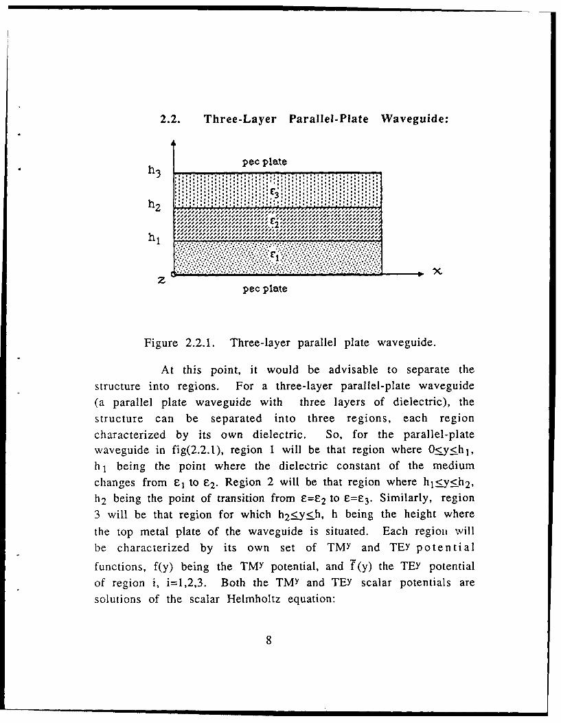
2.2. Three-Layer Parallel-Plate Waveguide:
pec plate
h 2
pec plate
Figure 2.2.1. Three-layer parallel plate waveguide.
At this point, it would be advisable to separate the
structure into regions. For a three-layer parallel-plate waveguide
(a parallel plate waveguide with three layers of dielectric), the
structure can be separated into three regions, each region
characterized by its own dielectric. So, for the parallel-platewaveguide in fig(2.2.1), region 1 will be that region where O2!.y .hj,
h,1 being the point where the dielectric constant of the mediumchanges from F-1 to F-2. Region 2 will be that region where hj1 !-,.y ! h2,h2 being the point of transition from =E2 to E=E3. Similarly, region3 will be that region for which hV .h, h being the height where
the top metal plate of the waveguide is situated. Each region will
be characterized by its own set of TMY and TEY potential
functions, f(y) being the TMY potential, and t(y) the TEY potentialof region i, i=1,2,3. Both the TMY and TEY scalar potentials are
solutions of the scalar Helmholtz equation:
8
9
2
d(y) + 2 X(y) = 02
dy (2.2.1)
a general and complete solution to the above equation being:
x(Y) = a I cos (ICy) + X2 sinf (icy) (2.2.2)
where a, and a 2 are constants which depend on the boundary andcontinuity conditions of the structure.
The function sinf(icy) is defined as sinf(Cy)=sin(icy)/xand its usefulness will be presented later on in this analysis.
The electric and magnetic fields must conform tocertain boundary and continuity conditions. These conditions willserve to specify the unknown variables C 1, oX2 , and iK in equation(2.2.2). The general solution to the scalar wave equation shownabove is modified such that these continuity conditions can beimplemented.
Substituting X(y) into the TMY equations, andapplying the conditions of zero tangential electric field on the pecplates will yield the general form for the potential for the TMYmodes of a three layer parallel-plate waveguide:
acos ( k y1 y) ;0.5 _y5 h1
(y)= b cos[ ky2h2-y)] ;h 1: y 5 h 2 (2.2.3)+ c sinf[ ky2(h2-y)]
d cos[ ky3(h-y)] ;h 2 -< y:5 h
10
Correspondingly, substituting the appropriatelymodified forms for the corresponding form for the TEY scalarpotential into the TEY field equations will yield:
asinf (kyly) 0. < h,
b cos[ ky2(h 2-y)] h1 - y < h2 (2.2.4)
+ c sinf[ ky2(hE-y)]
cos[ ky3(h-y)] ; h 2 5 y _ h
In general, the coefficients of the TMY and TEY scalarpotentials, as well as their corresponding eigenvalues, will not beidentically equal.
The continuity conditions between the differentregions state that the tangential fields at a dielectric discontinuitymust be continuous. Applying these conditions, and solving theresulting equations, will yield the eigenvalue equations for theTMY and TEY y-directed eigenvalues as well as the correspondingexpansion coefficients of the scalar potentials in equations (2.2.3)and (2.2.4). The system is underdetermined, so the fourexpansion coefficients in each case will be found within amultiplicative constant.
Following the procedure described above will yieldthe TMY eigenvalue equation for the three-layer parallel-platewaveguide:
k'tan(k 1h I) + kY tan[ky2(h2 -h I))+ -kY3tanh~ky3(h-h2j)e le 2e ( 2 .2 .5 )
kL-tan(kh1) -!tan[k 2(h2-h 1)] kI- a~k3 -
and the coefficients are:
1. ky3 real
cos[ky3(h-h )] k 3 ianry(2.2.6. a)
C - C3 ky3 sin[ky3(h-h 2)] ky3 real
-2 ky3 tan[ky3(h-h2)] ky3 imaginaryF-3 (2.2.6.b)
b = cos[ky3(h-h2 )] ky3 real1 . ky3 imaginary (2.2.6.c)
a=b cos [k y2(h 2 -h 1)] + c sinf[k y2(h 2-h 1)]
One other relationship of great importance in thisanalysis is the dispersion equation. This equation links theeigenvalues k.~, ky, and kz, with the wavenumber k in a certainmedium. The dispersion equation states that:
2 2 2 2 2
kx + ky+ kz=k =~ (o 1(y) (2.2.7)
for the TMY case, and correspondingly:
12
-2 -2 2 2 2kx + ky + kz =k =CO go0 (y) (2.2.8)
for the TEY case.
For the particular case of the three-layer parallel-plate waveguide, it has been assumed that kxi=0, i = 1, 2, and 3,
so the dispersion relations for the TMY and the TEY casecorrespondingly become:
k 2 2 2 2yi +kz i = o0 [/0(2.2.9)
and
-2 2 2 2ky + kz = ki = o) g t0e i (2.2.10)
k z being, of course, the propagation constant of the waveguide,and k the wavenumber. The z axis (and therefore, the directionof the propagation constant) are parallel to the planes of thediscontinuities, and so continuity forces kz to be the same inevery region. This gives rise to a very useful relationshipbetween the eigenvalues in the y direction in each region. Thisrelationship is derived by subtracting the dispersion relationdefined in the one region from the corresponding equation in theother region. Thus, the dispersion relationships corresponding totwo neighboring regions of the waveguide reduce to:
2 2 2kyi - kyj =o gO~e 0- P) (2.2.11 )
and:
-2 -2 2kyi + kyj o go0(e -E) (2.2.12)
13
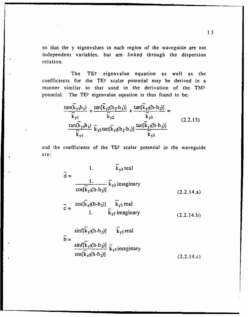
so that the y eigenvalues in each region of the waveguide are notindependent variables, but are linked through the dispersionrelation.
The TEY eigenvalue equation as well as thecoefficients for the TEY scalar potential may be derived in amanner similar to that used in the derivation of the TMY
potential. The TEY eigenvalue equation is thus found to be:ta~yh) tan [k y2(h 27h 1)] tan[ky3(h-h2)]
kyl_ ky2 _ky3 (..3
tan(kylh 1),, ktak2h-h) tan[ky3(h-h2)]
kyl ky3
and the coefficients of the TEY scalar potential in the waveguideare:
1. ky3 real
1. ky3 imaginarycos[ky3(h-h 2)] (2.2.14. a)
- cos[ky 3(h-h2)] ky3 realC-
1. ky3 imaginary (2.2.14.b)
sinf[ky3(h-h2)] ky3real
sinflky3(h-h2)] -ky3 imaginary
cos[ky3(h-h 2)] (2.2.14.c)
14
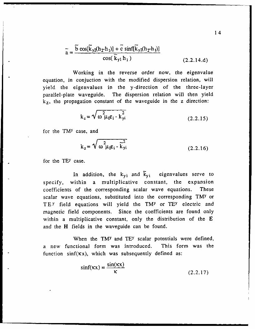
b cos[ky2(h2-hl)] + c sinf[ky 2(h 2-h 1)]a--cos( kyl hi I (2.2.14.d)
Working in the reverse order now, the eigenvalue
equation, in conjuction with the modified dispersion relation, will
yield the eigenvalues in the y-direction of the three-layer
parallel-plate waveguide. The dispersion relation will then yieldkz, the propagation constant of the waveguide in the z direction:
/2 2kz= OV oE i - kyi (2.2.15)
for the TMY case, and
(2 -2kz= o ei - kyi (2.2.16)
for the TEY case.
In addition, the ky i and ky i eigenvalues serve to
specify, within a multiplicative constant, the expansion
coefficients of the corresponding scalar wave equations. These
scalar wave equations, substituted into the corresponding TMY or
TEY field equations will yield the TMY or TEY electric and
magnetic field components. Since the coefficients are found only
within a multiplicative constant, only the distribution of the E
and the H fields in the waveguide can be found.
When the TMY and TEY scalar potentials were defined,
a new functional form was introduced. This form was the
function sinf(icx), which was subsequently defined as:
sinflcx) - sinicx)K(2.2.17)
15
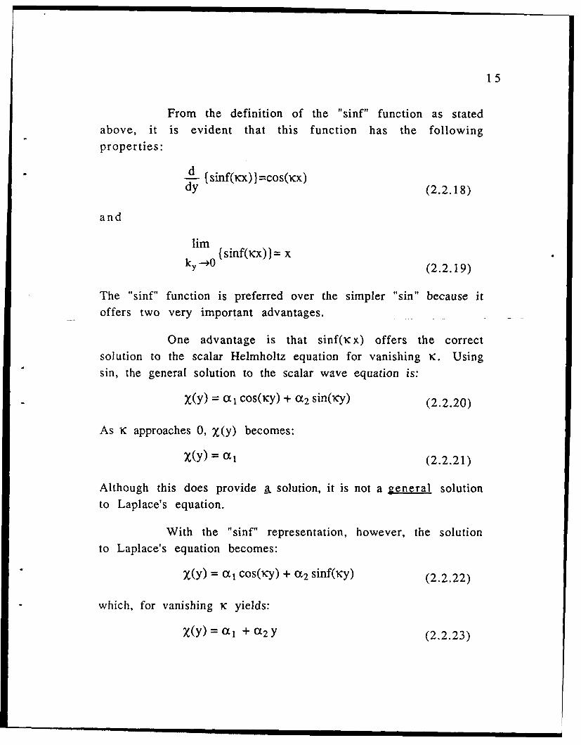
From the definition of the "sinf" function as statedabove, it is evident that this function has the followingproperties:
d { sinf( x)}=cos(cx)dy (2.2.18)
and
limki ~{sinf(Kx)}= xky ---40 (2.2.19)
The "sinf" function is preferred over the simpler "sin" because itoffers two very important advantages.
One advantage is that sinf(Kx) offers the correctsolution to the scalar Helmholtz equation for vanishing K. Usingsin, the general solution to the scalar wave equation is:
X(Y) = C I cos(Ky) + a 2 sin(icy) (2.2.20)
As K approaches 0, X(y) becomes:
X(Y) = (x 1 (2.2.21)
Although this does provide a solution, it is not a general solutionto Laplace's equation.
With the "sinf" representation, however, the solutionto Laplace's equation becomes:
X(Y) = aI cos(Cy) + a 2 sinf(cy) (2.2.22)
which, for vanishing Kc yields:
X(Y) = Ctl + ct2 y (2.2.23)
16
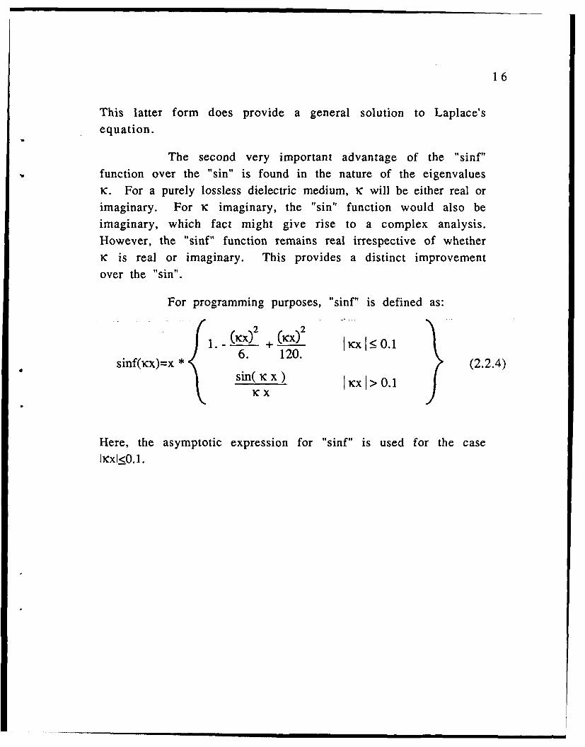
This latter form does provide a general solution to Laplace's
equation.
The second very important advantage of the "sinf"function over the "sin" is found in the nature of the eigenvaluesic. For a purely lossless dielectric medium, Kc will be either real orimaginary. For KC imaginary, the "sin" function would also beimaginary, which fact might give rise to a complex analysis.However, the "sinf" function remains real irrespective of whether'K is real or imaginary. This provides a distinct improvement
over the "sin".
For programming purposes, "sinf" is defined as:
. x ) 2 ( x ) 2
sinf(icx)=x *6. 120. (2.2.4)sin( cx) IKXI> 0.1
KX
Here, the asymptotic expression for "sinf" is used for the caseII:xI<0.1.
2.3. Four-layer parallel-plate waveguide:
h pec platei/f /f/ li /If li - i -fe toof/
.e *. %% 11 . % % % % . .S S .. S .
ilet./ to li0. i-d-- i i--
e#ooteift hI Oll1f/ lI Ill o,2:Illi10Al lif/1.1 f Ie'S S' lool eel too Allot' SS .S S' ' ' 'S S.S' ' '
------- ------ - i /---- ------ ------- -- i-- -
parallel-plate davdgude may beiwritten as:
adjl coIdly 0/ii/i. 5 y 5/ h,/l/ddd
b ~. co~y(r) h, *. :5 h
W..) +. .. .ifk2h ) (2..1
d cos~ky3(3.....h2....Y.!5..
+__e ________________
fzo~y(-) 35Y:1e7pat
18
The eigenvalue equation is found using the same procedure
that was described for the three-layer parallel-plate waveguide.
The TMY eigenvalue equation is therefore:
kY tan(k yh 1) + k y2 tan[ky2(h 2-h1)]
+ y-3 tan[ky3(h3_h2)] + k_._ tan[ky4(h-h3)]=F3 E4
kY tan(kylh1) 62 tan[ky2(h2_h1)] k y3 tan[ky3(h3-h2)] +
61 ky2 E3
. tan(k yh 1) -__2_ tan[ky2(h2.h 1)] ky4 tan[ky4(h-b)] +Ek - C4
ky-_ tan(kylhl) --- tan[ky3(h3-h2)] .-4 tan[ky4(h-h3)] +E1 k y3 F-4
ky--2 tan[ky2(h2-h I) - - tan[ky3(h3-h2)] ky4 tan[kyn(h-h3)]
F2 ky3 C4 (2.3.2)
The coefficients which serve to define the TMY scalar potential of
the waveguide are, within a multiplicative constant:
1. ;ky4 realf1.
cosI~ky 4(h-h3 I k C)iainr (2.3.3. a)
_C3ky smtfky4(h-h 3] ;ky4 reale E2
63 ky4 tank 4(h-h] k 4 imaginaryC2 (2.3.3.b)
d k cos[ky4(h-h3)] ; k y4 real1. ky4imaginary (2.3.3.c)
19
c = d cos[ky3(h3-h2 )] + e sinffky3(h3-h2)] (2.3.3.d)
b= -d 1- ky3 sin[ky3(h 3-h2)] + e - cos[ky3(h 3-h2)]63 -3 (2.3.3.e)
b cos[ky2(h2-h 1)] + c sinf[k 2(h2-h 1)]cos(kylh ) (2.3.3. f)
The TEY scalar potential may be written as:
a cos(kylY) ; 0:< y <5h 1
b cos[ky2(h2-y)] ; hj!<y:5h2+ c sinf[ky2(h 2-y)]W(y) = (2.3.4)
dcos[ky3(h3-y)]
+ e sinf[ky3(h 3-y)]
f cos[ky4(h-y)] ; h3 !! y < h
Using this expression for the potential, the eigenvalue equation isfound to be:
20
*y ky4
tann ~ 3( yh 2)]) tan[k(hh ]+ ytnk2hh) +
iYI ky3(2.3.5)________) tan[ky4(h-h 3)]
tan(kyl Ih) ki 2tan~kk(h2-h1)]
tan[k, 2(h2-h IA~ ank 3 hr ) tan[ky4(h-h)]
iy2 k y4
The coefficients of the scalar potential are, within a multiplicativeconstant:
1. ;y 4 real
1. , ky4 imaginarycos[ky4(h-h)] (2.3.6. a)
- cos~k y4(h-h 3] ;ky4 real
1 . ;ky4imaginary(236b
- Sinf1iky4(h-h3) ky4 reald=tan[ky4(h-h3)] ; k 4 imaginary(236c
b=d COs~iyk3(h3-h2)] + e sinqik3('h 3-h )I (2.3.6.d)
21
c = -d ky3 sin[ky3(h3-h)] + e cos[ky3(h 3-h 2)] (2.3.6.e)
b cos[ky2(h2-hl)] + c sinf[ky2(h 2-hl)]a=cos(kylhl) (2.3.6.f)
Thus, so far, the TMY and TEY potential functions forthe three- and four-layer parallel-plate waveguides have beenderived. Their connection with the coupled microstrip line, whichis the main subject of this paper, will become apparent shortly.
Chapter 3. Coupled Microstrip Lines
Coupled microstrip lines are used in a number ofcircuit applications, principally as directional couplers, filters, anddelay lines. Mode matching will be used to calculate thepropagation constant of such a line.
A pair of microstrip-like transmission lines as shownin fig. (3.1) are known to have the property of a broadbanddirectional coupler when placed in parallel proximity to eachother. As a result of this proximity, a fraction of the powerpresent on the main line is coupled to the secondary line. Thepower coupled is a function of the physical dimensions of thestructure and the direction of propagation of the primary power.
|V4
Fiue.1. Thopldmcrsrpie
In geeral thecoupe le strctues:hw nfg
induces gthe 3.Tcouplwented twcotrsisin lne..h
properties of the coupled structures may be described in terms ofa suitable linear combination of these even and odd modes. For
22
23
geometrically symmetric structures, the geometrical plane ofsymmetry may also be thought of as an electrical plane ofsymmetry. The even mode has equal amplitude and equal phasecorrespondence with respect to this plane of symmetry, in whichcase this plane takes the form of an open circuit. In the even
mode case, therefore, the plane of symmetry takes the form of aperfect magnetic wall (pmc). The odd mode, on the other hand,has an equal amplitude 180 0 -out-of-phase correspondence withrespect to the plane of symmetry, so this plane acts like a shortcircuit and is simulated by a perfect electric conductor (pec) wall.Thus, the directional coupler can be treated as a two-portnetwork, and the total response can be obtained by superimposingthe responses calculated for the even and odd mode excitations.This reduces the problem to about half its original size, which is agreat advantage of symmetric structures.
24
3.1. Propagation Constant
The structure shown in figure (3.1) is symmetric with
respect to a plane drawn perpendicular to the x-y and x-z planes
and placed halfway between the two metal strips. Thus, the
structure under consideration is modified to that shown in figure(3.1.1).
h- top plate
pe¢ h
or -**"**3"
piC
zxWl W2
Figure 3.1.1. Symmetry as applied to thecoupled microstrip line
As was mentioned earlier, the left-most boundary
becomes either a pmc or a pec wall, according to whether the
search is conducted for the odd-mode or even-mode propagation
25
constant. There is no perpendicular boundary to the right of themicrostrip, so propagation in the positive x direction for large xmust take the form exp(-jkxx), such that there is an exponential
decay for x->co. This serves to put a lower bound on the searchfor kz, since this exponential decay is observed only for the casewhere k x is imaginary. The dispersion relation states that:
2 2 2 2 2kx+ky+kz=k -) g~0 OF-.1
so, for kx:
2 2 2 2kX-" = .) [to - ky- kz (3.1.2)
The condition for imaginary kx yields:
2 2 2(0 g.oe - ky _ k z < 0 (3.1.3)
or:
/2 2k -(3.1.4)
An upper bound may also be placed on kz , since it maynever be larger than the unbounded propagation constant in themedium with the highest relative dielectric constant. Thus:
kz < o5 / tIOinax(e' (3.1.5)
The structure must further be separated into regionsfor modal expansion. Two more bounding planes may be drawnparallel to the plane of symmetry, at each end of the metal strip.Also, since the structure must be bounded, a top plate must beplaced above the structure at such a distance that it does notinterfere with the computation of the propagation constant of theactual open structure (this top plate was also included in figure
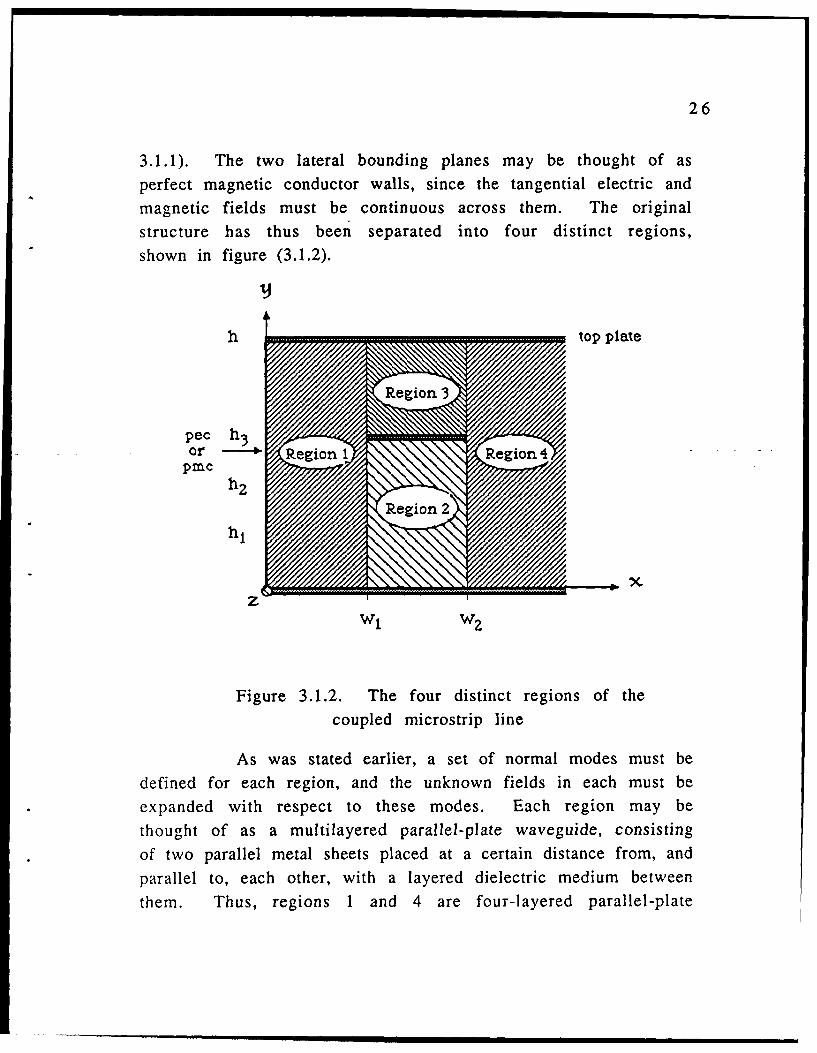
26
3.1.1). The two lateral bounding planes may be thought of as
perfect magnetic conductor walls, since the tangential electric and
magnetic fields must be continuous across them. The original
structure has thus been separated into four distinct regions,
shown in figure (3.1.2).
h top plate
~~onV
pec h13or -- Region 1 Region 4
piMCh2
wi w2
Figure 3.1.2. The four distinct regions of thecoupled microstrip line
As was stated earlier, a set of normal modes must be
defined for each region, and the unknown fields in each must be
expanded with respect to these modes. Each region may be
thought of as a multilayered parallel-plate waveguide, consisting
of two parallel metal sheets placed at a certain distance from, andparallel to, each other, with a layered dielectric medium between
them. Thus, regions 1 and 4 are four-layered parallel-plate
27
waveguides, region 2 is a three-layered parallel-plate waveguide,and region 3 is a one-layered parallel-plate waveguide. Thislatter case has been studied extensively in the literature, and hasnot been presented here. The normal modes for the three- andfour-layered parallel-plate waveguides have been defined inchapters 2.2 and 2.3, respectively. It now remains to establish theequations which define the electric field components with respectto these modes. Let it be noted that the following modalexpansions and field representations are not unique, but justconstitute one possible solution.
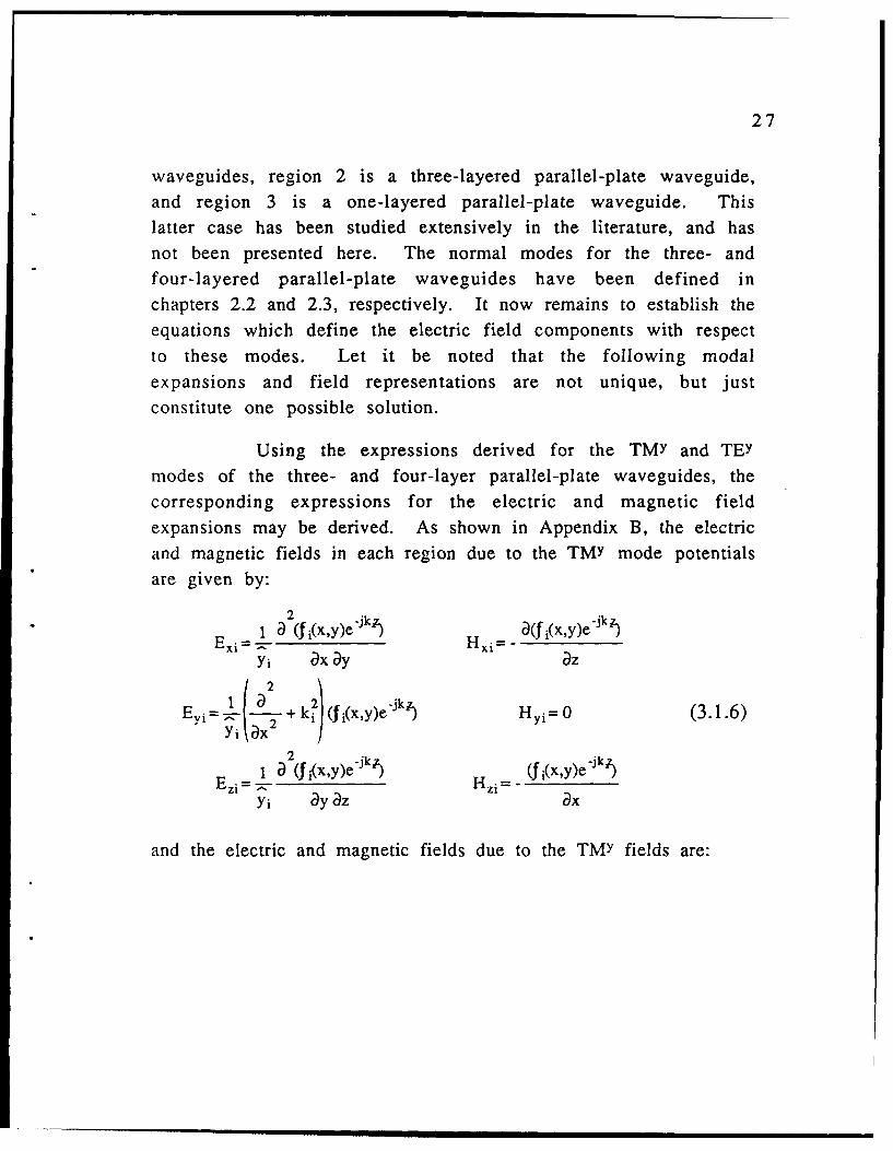
Using the expressions derived for the TMY and TEYmodes of the three- and four-layer parallel-plate waveguides, the
corresponding expressions for the electric and magnetic fieldexpansions may be derived. As shown in Appendix B, the electricand magnetic fields in each region due to the TMY mode potentials
are given by:
2 (fi(x,y)e'k (i(x,y)eJkJE xi = -.. H xi = - ,
Yi ax ay aZ
i + f ~~~xHi
a (f i(x,y)ek?' ) (Ji(x,y)e-k )Ezi = ^ Hzi = -Yi ay az ax
and the electric and magnetic fields due to the TMY fields are:
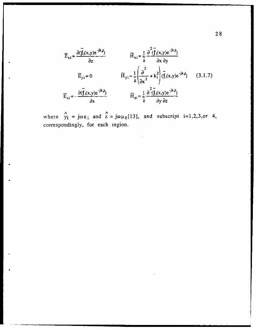
28
-k2- -jkl,alfi(x,y)e -JJ ~ - i~(f 1(x,y)e)
az z ax Dy2
E=Oi - + k2 (i(x,y)ek) (3.1.7)
D (f i(x,y)eijk) 14 a (fi(x,y)e&ik)ax z ay az
A Awhere yi = jocl and Z= jcoj~i[l3], and subscript i=1,2,3,or 4,
correspondingly, for each region.
29
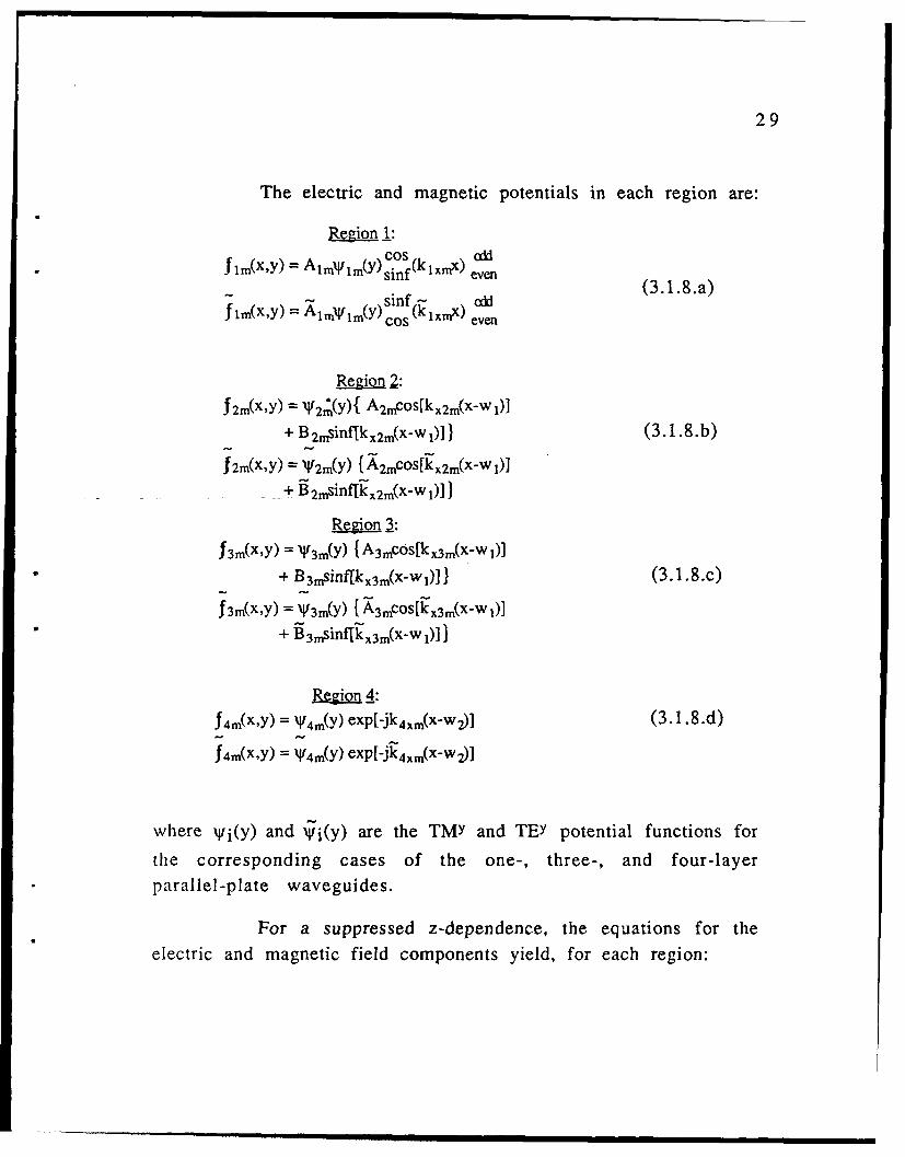
The electric and magnetic potentials in each region are:
Region 1:
flm(xY) = AlmNflm(Y)if(klxmx) evensinf eve(3.1.8.a)
flm(~y)-- inf - oddf 1mkxY) A= 4i m(Y) cos (k 1xmx) even
Re2ion 2:
f 2m(X,Y) = V2r(Y){ A2mCOS[kx 2m(X-W 1)1+ B 2msinf[k x2m(x-w )]} (3.1.8.b)
J 2m(X,Y) =V2m(Y) I X 2mCOS[kx 2m(X'W 01+ B 2 msinf[kx2 m(x-wl)]}
Region 3:
f 3 m(X,Y) = V3m(Y) { A3mcos[k, 3m(X-W 1)]+ B 3mSiflflkx 3m(X-W 1A 1 (3.1.8.c)
f3m(X,y) = V3(y) { A 3 mCOS[kx 3 m(X-W 1)]
+ B 3msinfkx3m(XW 1)]
egion 4:f4m(X,Y) = "V4m(Y) exp[-jk 4 xm(X-W 2)] (3.1.8.d)
f 4m(X,Y) = V4m(Y) exp[-jk 4 xm(x-w 2)]
where Wi(y) and ji(y) are the TMY and TEY potential functions for
the corresponding cases of the one-, three-, and four-layerparallel-plate waveguides.
For a suppressed z-dependence, the equations for theelectric and magnetic field components yield, for each region:
30
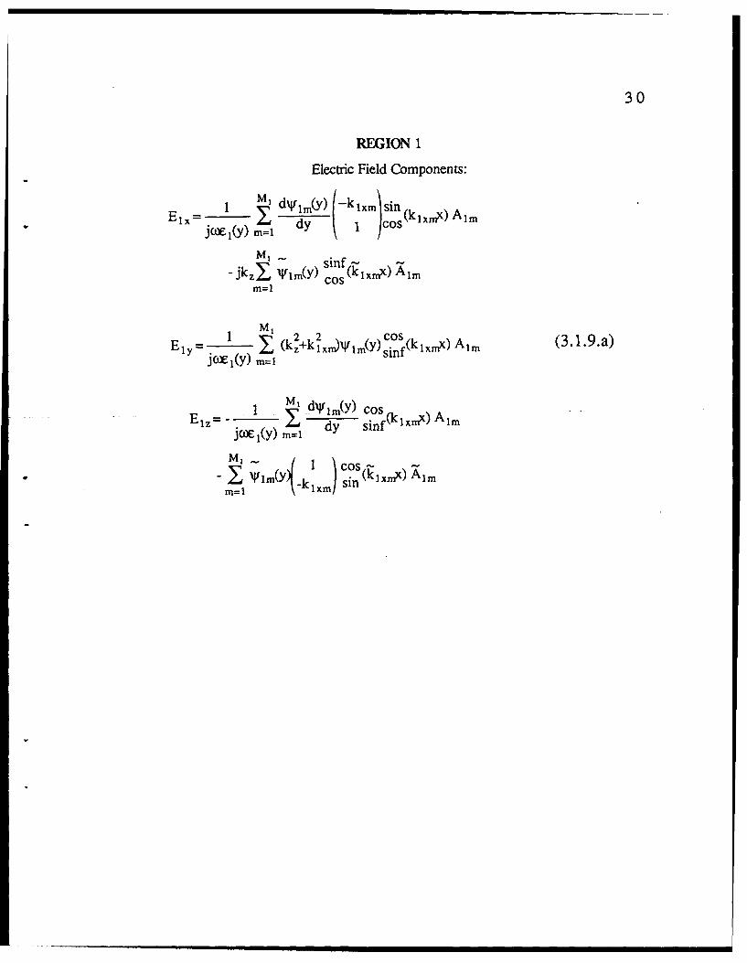
REGION 1
Electric Field Components:
1 1 d~4im(y) (kxm sinEl.=- YIkxlx l
jix 1(y) m=1 dy 1I O
M, ~sinfjkzyX 1'im(Y) Cs(klxmx) Alm
m=i
Ely= (k.29ka2(+klxmINlm(y) Cosf(klx) Alm(319a
j O) 1(y) m ,sn
M,El---4 1 1\Mo) s- -kxx l
I 'VIM(Y)Ik x) sin ( 1 X i
31
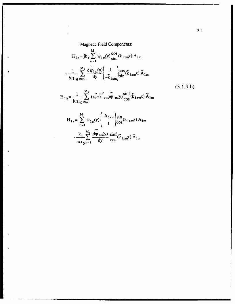
Magnetic Field Components:
Hix~jkz Y Vm(y) sjn(klxmx) Aim
+ 1 dl4imY 1 cos(km) XE~ dy 1x sinJWtJ m=l x
(3.1 .9.b)1 M 2 -2 sinf -
Hy= X (k +klxn)NVim(y) (kixn) Almj(09 0 m=1 zCos
Hlz= wiy Csn(klxmx) Alm
k ld'~fim(Y) sinf -lmx l
wg~oh1I dy Cos
32
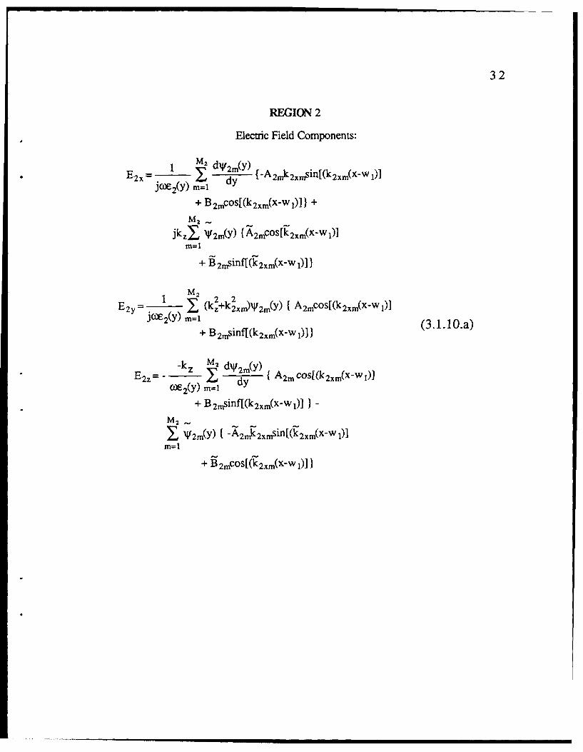
REGION 2
Electric Field Components:
*E 2 . M 2 dW42m(Y) IAm~mi[k,~- )
( Y ) d y { A k x n S f [ ( x m X )
+ B2m..cos[(k2xm,(X-W i)])+M 2 . .
jk,.Y NV2m(Y) {A 2 mCOS~k2 xm(XW)IM=1
+ 2 nsifllk 2xm,(X-W 0)
E~ jE(y) m= (k +kxn)V42m(Y) ( A2 mCOS(k (3.(1X1i))a+ B 2 mSifl1(k2 xm(xw 1)J) (..Oa
-k z M2 dNI2 m(Y) f A m 01k x( - )E2 ,,, z - dy ~AmO[kx(~)(t)6-2(y) m=1
+ B 2mnsjff[(k 2 xm(XWi 01-
M 2
X: Nf2m(Y) I A2 4 2 ,nsi[(k 2 xm(X-W 1)M=1
+ B 2mnCOS[(k2xm(X-W 0)
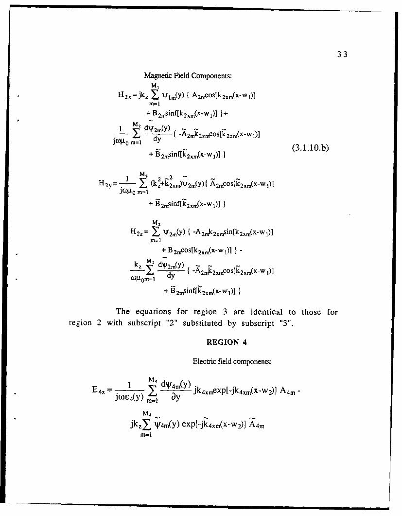
33
Magnetic Field Components:
H2 x=jkz Y, NVim(y) ( A 2 nc0s[k 2 xm(X-WI)]m=1
+ B 2 nif[k2 m(X-W0) 1+
1 2dV4 2m,(y)
Ecp0 = dy I A2mk2xmcos[k 2 xm(X-W i)
jC0M1+ ii 2 mSiflf[k 2 xm(X-W) 01 (3. 1. 1O.b)
H = Y, (kz+k2 xffNf 2m(Y) { A2 mcO5[k 2 xm(X-W 1)JW0t m=1
+ Bi2msiff 2 xm(X-W1)I
M 2
H2. I' 2m(Y) I -A2 4 2 xm5sfl[k 2xm(X-W1)]M=1
+ B2mCOS[k2xm(x-wl))
kzM2 dIJm)dVi~m1 d -A2niK2xmcOS~k2xm(XW 01]
+ 9 2mSinflfk 2 xm(X-W1)I
The equations for region 3 are identical to those forregion 2 with subscript "2" substituted by subscript "3"1.
REGION 4
Electric field components:
E~x1 M4 dWV~m(y) jk 4xmeXP[-jk 4xm(X-W2)] Am
M4m
jkz W44m(y) exp[-jk4xm(X-w 2)] A4mm=l
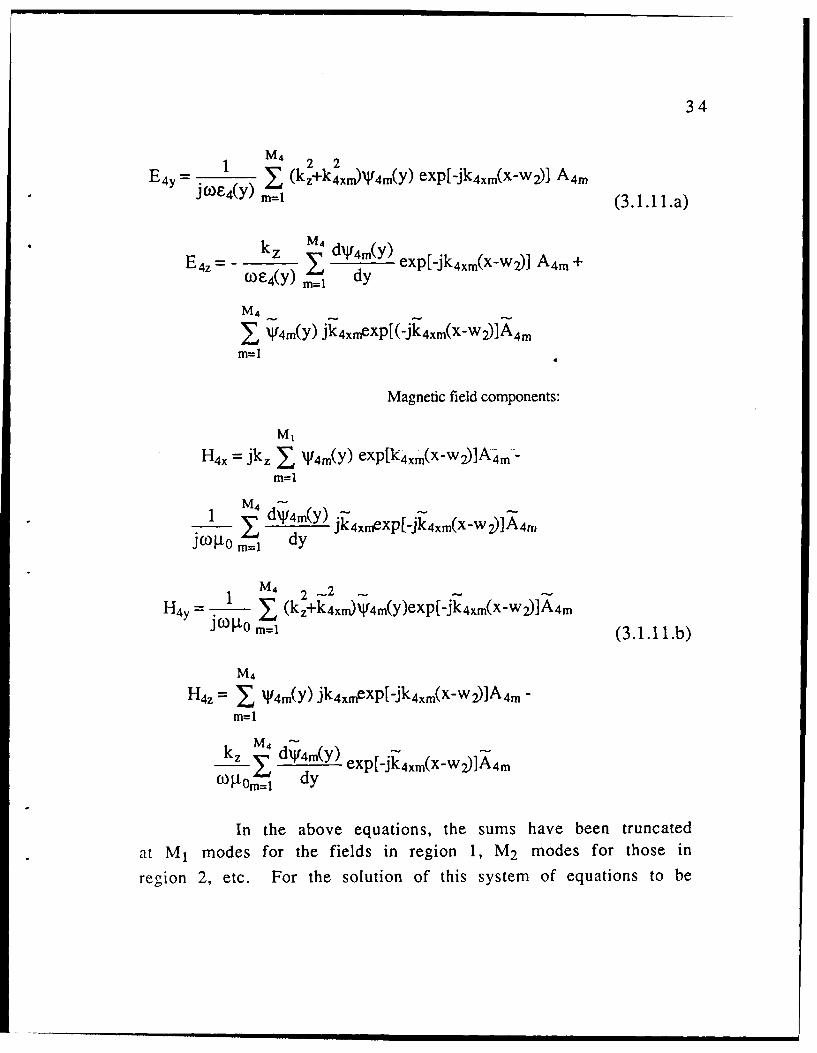
34
E~1 (k +k4 ip)W4m(y) exp[-jk4xm(X-W2Yl A4 .i(J)F-4Y) M=1(3. 1. 11. a)
E~z= z 114dIJ 4 (Y) exp[-jk 4xm,(X-w 2)] A4m, +=-()e-4 (Y) rn- dy
x V4m(y) jk4xre-XP[(-jk 4xrn(X-W 2)]A4m=4m
Magnetic field components:
Hx= jkz Y, W4m(y') exptk 4xm(x-w 2 lA 4m-M=1
E__ d4m,(Y) jk4xrrgXP[-jk 4xm(X-W 2)JA4njcPot rn=1 dy
H 1 M4 2 -2H4y E (kz+k4xri)14 4m(Y)exp[-jk 4xm(X-W 2)]A4n
H~ 1 xr4rn(Y) jk4xmeXPll-jk 4xm(X-W,)]A 4m -M=1
kz- dMy) exp[-jk 4xm(X-W 2)]A 4m
In the above equations, the sums have been truncated
at M, modes for the fields in region 1, M2 modes for those in
region 2, etc. For the solution of this system of equations to be
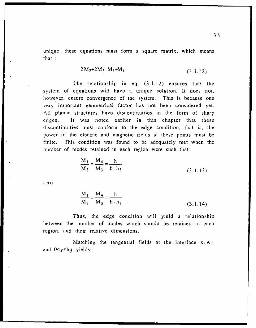
35
unique, these equations must form a square matrix, which meansthat :
2 M2+2M 3=M I+M4 (3.1.12)
The relationship in eq. (3.1.12) ensures that thesystem of equations will have a unique solution. It does not,however, ensure convergence of the system. This is because onevery important geometrical factor has not been considered yet.All planar structures have discontinuities in the form of sharpedges. It was noted earlier in this chapter that thesediscontinuities must conform to the edge condition, that is, the
power of the electric and magnetic fields at these points must befinite. This condition was found to be adequately met when thenumber of modes retained in each region were such that:
M 1 M 4 _ h
M 3 M 3 h-h 3 (3.1.13)
and
M 1 M 4 h
M 3 M 3 h-h 3 (3.1.14)
Thus, the edge condition will yield a relationship
between the number of modes which should be retained in eachregion, and their relative dimensions.
Matching the tangential fields at the interface x=w1and 0_yh3 yields:
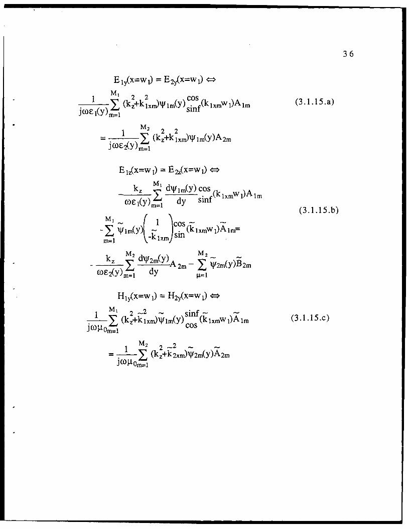
36
E Y(X=W 1) = E 2y(X=W 1)
,2 2 Cos(k )
jcOe- 2)I (zklmWm sinf 1 imw)Am (3.1.15. a)
1 M2 2 2I(kz+klxnmjJlm(y)A 2 m
E 12 x=w 1) = E 2(x=w 1) -
kNf m dkJ I my)o (kixm )Almm=1 (Yml y sif m
X ~ (3.1.15.)
- 1 M2 2 ) A -x I kztkxnV2m W)2my)m(j CO-2(y m 1 d
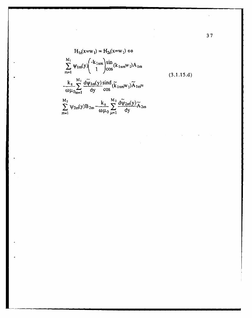
37H 2x~w 1) = H~z(x=w 1) ~
k dW 1,1(y) SindZ I dy COS (klxmw)Alinf
X V2 m(Y)B32m kz Nfmy;2
38
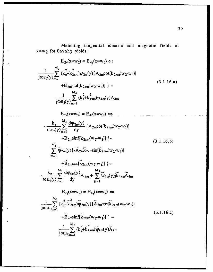
Matching tangential electric and magnetic fields atx=w2 for O:5y:h3 yields:
E2$x=w 2) = E4$X=W 2) 4--
jOF = (kz+k 2xm)XV2m(Y) [A 2mCOSlk 2 .m( W27W 01
+B 2 nmsiff[k 2 xm(W 2 -W I) (3.1.16.a)
1 4 2 2E(kz+k4 xm)~f4m(y)A 4 m
E~z(x.=w 2)-=.E-4 x=w2) 4 -
kM 2kz dWmy)fA 2 mCO5[k2 xm(WZ-Wi)1
coE 2(y)M1j dy
M,+B 2 m inf[k 2xm(W-W1) I- (3.1.16.b)
W M2m(Y) f1 -A2 mk2 xffnSif[k 2xm(W zW 1A]m=1
+B2mCOS[i2xm(W-1W )I
k 4dxV4M(v') A M4-
EZ- I '' 4m + 2. V4m(y)jk4xmA4m(o) - 4 (y) m = dy j=
H2 IX=W2 ) = H4 X=W2) *
j(40= (k z+k2xO) \2m(Y) I A 2rnCOS[k 2xm( W2 W 01JJCOJL~mI(3.1.16.c)
+B2m-,Siffk2xm(WT-WIl
1 M4 2 -2i()LO= (kz+k 4xft11 4 my)A 4m
39
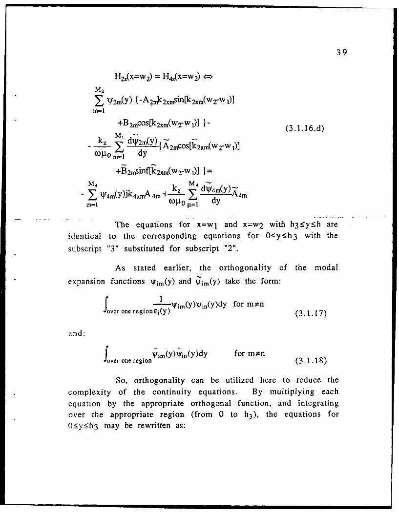
Ha(x=w2) = H4 (x=w) 4
M 2
Y XV2m(Y) {-A 2mk2xmSink 2xm(W 2"W 1)]m=1
+B 2mCOS[k2xm(W2-W) I- (3.1.16.d)
M1 d 2m(Y) {2rnCOS[2xm(WTW1)]kzm1 dy
+B 2mSinf[k2xm(W2Wl)] I =M4 + zM4
- W W4m(Y)jk 4xnA4m Z dI4m(Y)Aftm=l (o0t0 go dy
The equations for x=wi and x=w2 with h3_<y_<h are
identical to the corresponding equations for 0_y<_h3 with the
subscript "3" substituted for subscript "2".
As stated earlier, the orthogonality of the modal
expansion functions x im(y) and 'jtim(y) take the form:
f I Virn(Y)Vin(Y)dy for man
over one region Ei(y) (3.1.17)
and:
lover one region i m f( orin(y)dy (3.1.18)
So, orthogonality can be utilized here to reduce the
complexity of the continuity equations. By multiplying each
equation by the appropriate orthogonal function, and integrating
over the appropriate region (from 0 to h3), the equations for
0_<yh3 may be rewritten as:
40
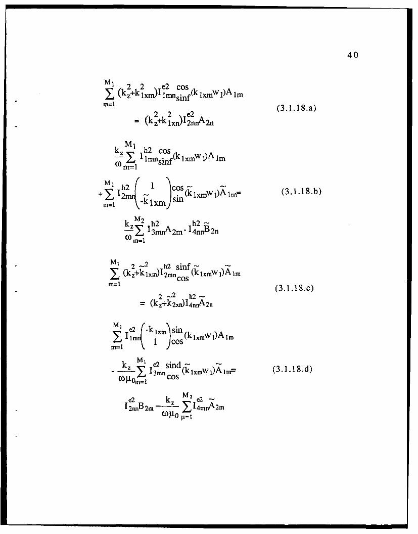
M'2 2 e2 cosI (kz+k lxr m llnflf (k lxmw i)Ailm
Ml2 2 e2 (3.1.18.a)
(k= ln)2n~
MI1z I h2 cos k x w Al
Om=l 1msn
M ' h2 1 osy (3 1 1 8 .b)
M=l
k M2 Ih2 h2-xY I3;nA2m-14nnB2fl
M, 2 - h2 sinf -
2 -2 h2 -=(kz+k2xn)I4 nnA2n
I el{k1x Cs(k ixmwi)Aim
II3mn (kixmwlvinr 3i.8d(O)XOmi Cos
e2 kz 2 -I2nnB 2m -XIl4mnA 2m
O)01O
41
(2 2 e2 nOl2.(2WO
+B2 nSinffk 2 xn(W 2 -WlO] I (3.1.18.e)M42 2 e2
Y, (kz+k 4 xrp)IimnA 4 m
k M2 h2-y 1 3mn IA 2mCOSlk 2xm(W 2 Wl)]+B2mSiffk2xm(WZ-WI)] I -
0 m~l
h2 (3118fJ4nnfAlk~{ n~~x(W 1)]+B2nCOS[k 2xn(WZ-W 1)] 3. 1
kM h2 y lh2I ImnA4m + , 2mnJk4xfl4ml
2 -2 h2-(k~~n ~nA2Xcosrk 2xn(W 2-W )]+B2nsinf[k 2 xn(W 2-W ' -(..1Ig
M4 2 - h2 -I (kz+k 4xOnI 2nrnA4 m
M=l
e212nn { A 2 nk2xrrSiflk 2 xf(W2W)]+B 2 nCoslk 2xn(W 27W I)] I
k z I e2 -
1 14m.{ A2iCOS[k 2xm( WZ-W )]+B 2 n-sinlf[k2xm(W-W I)I = (3. 1.18 8)('410 m=l
M 4 e 2 + -k z 4 i 2 rI 1 Imnik4xmA 4m - : I3mnmm=l W9
where:
42
h3h
I n~o-,1 dW1m(Y)VnYd 1o d~(YV m~yd
-W d Y Vin(Y)d y = 8Y
h3 I~y d my)h I W mY
I3mn--=f Fi-i(y)Wd in(Y)dy = LNIe(y) dy Wn( Y)d
ei h3 1 - d i (Y__ _ _ _ _
5mn~ -- IVimY)V~(Y ~ d 0 4(I4m(Y)dymn0 POD) d iYJ (y) d
h3 1 dvlm(y) I 3 d 44m(Y)le- In~(Y)d f XV jin(Y)d y6m 0f e(y) d y e(y) dy
hi mY)~in(Y~dY Vi(= y JmYNi(~
1 O mn 8 (y) dyey) d
I2mnfo Wim(Y)Vin(Y)dy = f Nf4m(Y)Vin(Y)d y
h3 1 d~fim(y) -hd~~mY
Jo~f 8,(y) d y Vifn(Y)YJ 0 ( 4 (~
43
where i=2,3, for regions 2 and 3, correspondingly. Thus, anidentical set of equations as those derived for h<_y<_h3 may be
derived for the case h3 <y5h. For this case, it is sufficient to
substitute i=3 instead of 2 in the superscript in the
orthogonalization integrals, and substitute 3 for 2 in the subscript
of the remaining functions.
By developing the above equations further, the finalform of the set of eigenvalue equations is derived for 0<y_<h3:
MM h2 e2 1k, h2 COS 2 2 '3pilmp icos
lnlnsinf(k Ixmw I)-(kz+k T e2 Jsinf(klxmw l) Alm+
CO m=1 {K zz+K2x12pp}
h2 ( 1 ")COSl. .(kz+klxrn) sinf .WW
m 1ixmW) 2 ... . lxmW)k 2 xnFOtI 2 xn(W2-W )} Alrnrn=1 kim)sin 2 -2 COS
2 ' 1 -11 I2 m n A 4 mO0 (3.1.1 9. a)
2,2 2e2 lx in k xm I)- ( z+k1~ Ix)coS kx cos[k2 xn(W27WI)I Alim,
{M(kzkxm) Sih2 1 (km- 2 (3..1} a
1 fi I2 COsinfkx 2 2 "w eh2 ]-m=m M)l (kz+k2xn)
NI4 M e2 2
Se2 -kmOsin () 2.os...b)
3m n1co (k l xmw l ) zkln 2 -2 h2f S kxW-l)]A1j
m=l P(k kz+k2xpp
M, 2 2.2 .h
(kz+k4xm) e2 1 .,m_ 3119b
e' I 1i1il m l l mill (3119b
44
M1 22
M, (kz+kxm) e2 COS- e2 lmnsfS(k l xmwl)Almr +
m=l (kz+k2xr)
14pn 2rap e2~ sinfljl 2 xn(W2_ iV')]A 4 m=0
I (kzk~xpIapp(3.1. 19.c)
M, 2 (ke+kil,) h2 sinfi x ,"-
2m 2 212mnos (KixmWl)/Irn-
m== (kz+k2xr)
kM4 2= 23pe2 h2snf[k 2 x(W 2-w )]-h2nnkx( 1 \A4m
1 (kz+k4x os 2 x( ) +JmSinf[f2xn(W2Wl)]4= 0
10 2mn 2 2
m=l (kz+k2 xn)
(3.1.19.d)
As before, substituting the corresponding variables forregion 3 will yield the corresponding equations for h3 _y<h.
The above set of equations may be expressed as a
homogeneous matrix equation [A]x=0, where [A] is the matrix of
the coefficients of Aimo, Aim, A4m, and A4m x is the vector
containing Aim, Aim, A4m, andA4 m. This homogeneous equation
has a nontrivial solution only for the case det(A )=O. The
coefficients of the matrix [A] have only one unknown variable, kz.
so solving the equation det(A )=O yields the solution for the
MI 2zIjI
45
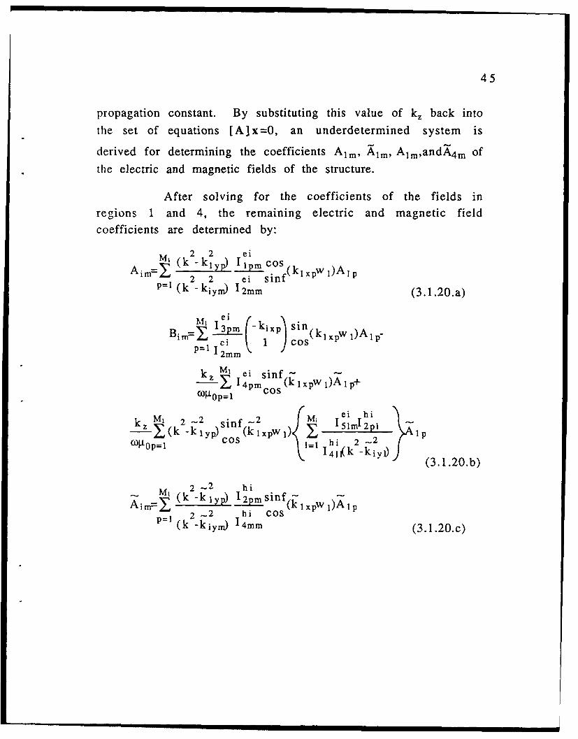
propagation constant. By substituting this value of k, back into
the set of equations [A]x=O, an underdetermined system is
derived for determining the coefficients Ai, Aim, Alm,andA4m Ofthe electric and magnetic fields of the structure.
After solving for the coefficients of the fields inregions 1 and 4, the remaining electric and magnetic fieldcoefficients are determined by:
MI 2 2 ei
AimXY ( k -k, p)_I Ipm Cos (k, xpw )A I2 2 ei sinf l
P=I (k -kjyrp) 12mm (3.1.20.a)
MelM1 3p f- sin (k p A, i
Bim pp~) Cos
k ~ k MI 2e i 2 ei hi
0 4 ~Op ~ O os~ 1= hi2S..
I 2 -2 hii h
A i nEX (k -klyp) I 2 pmsinf (k jx~ )AlpP 2_j2 h i COS
pI(k kiyn1 14mm (3.1 .20.c)
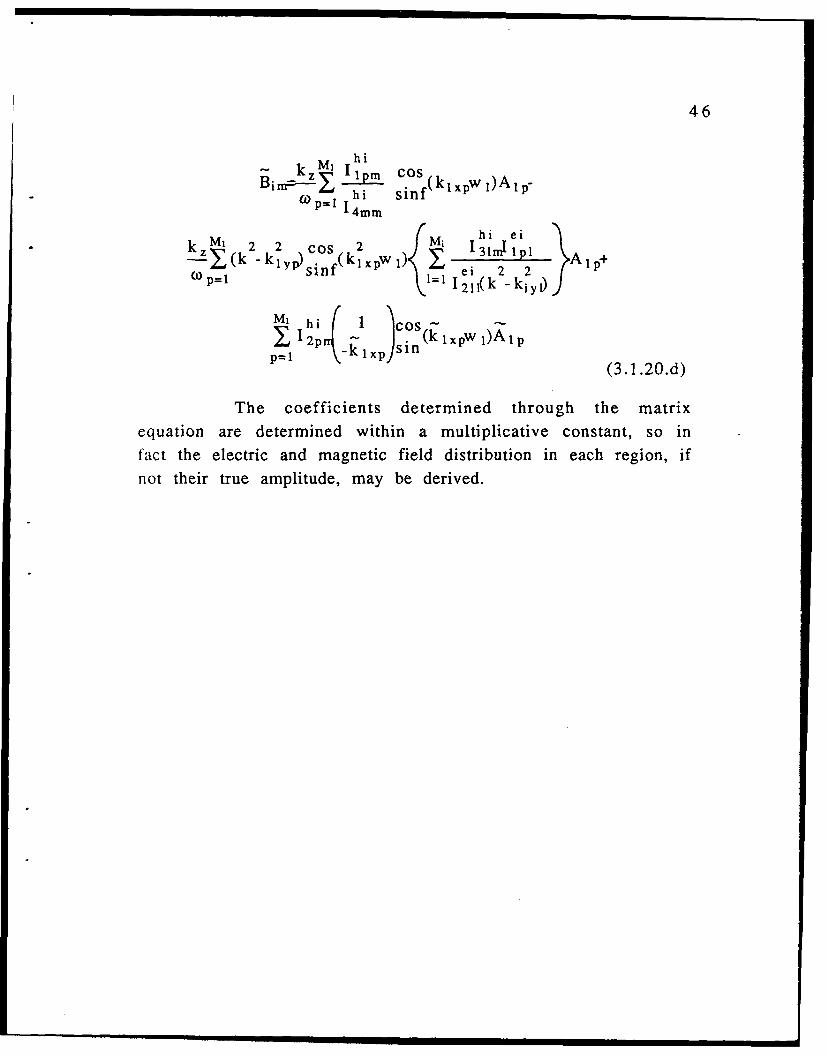
46
k M1 1 hi
B k Z p (k IP os 1k. w1)A1i-hi sinftO-- 4mm
k MI 2 2 COS 2 hi ei
1 sinf ei 2 2 A[ta) p l 1=1I211(k -kiyl)
MI hi (I iCos~MI hi k 1 sinS(i. 1) ,1X' 2pnl _ )lp~n\ lp
P=I XP)(3.1.20.d)
The coefficients determined through the matrixequation are determined within a multiplicative constant, so infact the electric and magnetic field distribution in each region, ifnot their true amplitude, may be derived.
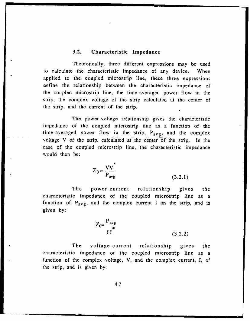
3.2. Characteristic Impedance
Theoretically, three different expressions may be usedto calculate the characteristic impedance of any device. Whenapplied to the coupled microstrip line, these three expressionsdefine the relationship between the characteristic impedance ofthe coupled microstrip line, the time-averaged power flow in thestrip, the complex voltage of the strip calculated at the center ofthe strip, and the current of the strip.
The power-voltage relationship gives the characteristicimpedance of the coupled microstrip line as a function of thetime-averaged power flow in the strip, Pavg, and the complexvoltage V of the strip, calculated at the center of the strip. In thecase of the coupled microstrip line, the characteristic impedancewould then be:
I *
vvPavg (3.2.1)
The power-current relationship gives thecharacteristic impedance of the coupled microstrip line as afunction of Pavg, and the complex current I on the strip, and isgiven by:
ZO avgII (3.2.2)
The voltage-current relationship gives thecharacteristic impedance of the coupled microstrip line as afunction of the complex voltage, V, and the complex current, I, ofthe strip, and is given by:
47
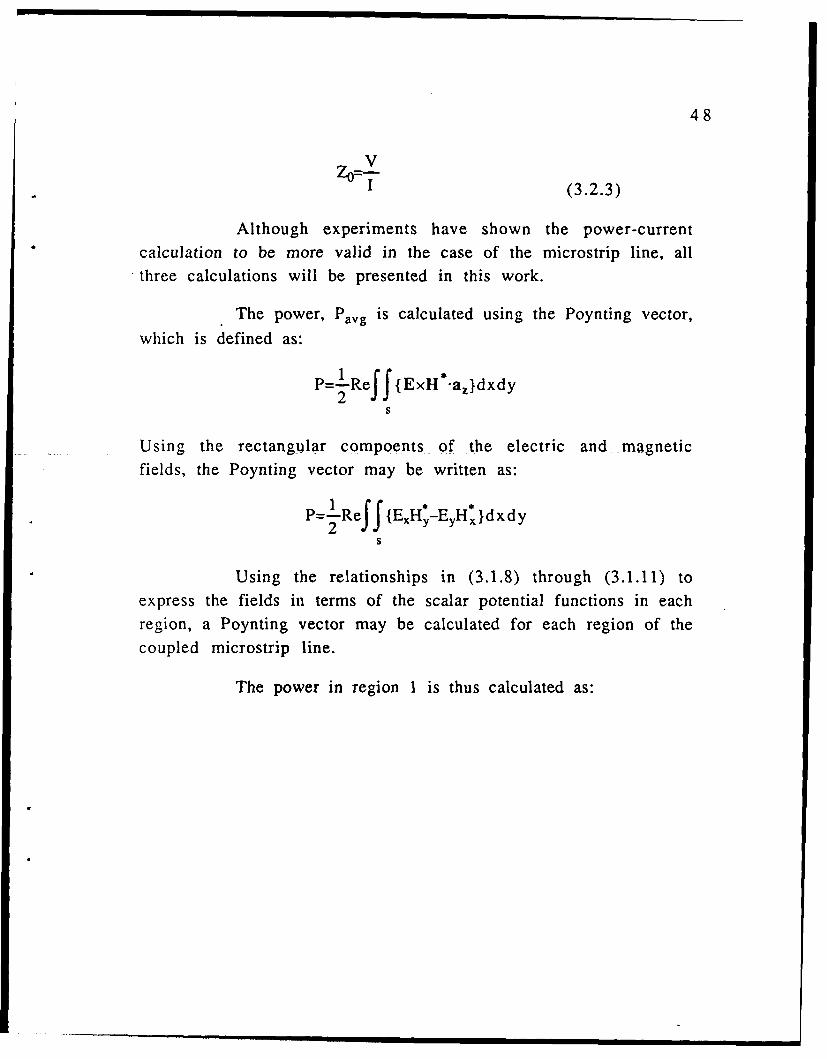
48
V°- (3.2.3)
Although experiments have shown the power-currentcalculation to be more valid in the case of the microstrip line, allthree calculations will be presented in this work.
The power, Pavg is calculated using the Poynting vector,which is defined as:
P=-LRe {ExH*-azldxdy
S
Using the rectangular compoents of the electric and magneticfields, the Poynting vector may be written as:
P=-LRe t ExH;-EyHxldxdy
S
Using the relationships in (3.1.8) through (3.1.11) toexpress the fields in terms of the scalar potential functions in eachregion, a Poynting vector may be calculated for each region of the
coupled microstrip line.
The power in region 1 is thus calculated as:
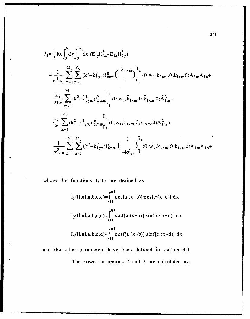
49
P,=-2Refod Yf dx (E,,H*.-E,,H*,)
M1 ~ 0 M1 ixn12~ W (k 4yn)~n 6 1Ow imOkx,)i~n
I0 m=1 n=1
1zM 2- 12 -2
-OWk klym)I5mnm (O,wi,klxm,O,klxm,O)Aim +gm=1 11
kz M 2 2 M~le m 11(O,Wi,klxm,O,klxm,O)A m +CO I (k -kiym511m+
M=1 12
M1 M1 1 11X2_~nIn 2 )l (O,Wi,klxm,O,klxn,O)AiMAin
(.0o1 m=1 n=1 -k1 xn 12
where the functions 11-13 are defined as:
I3(l1Iul,a,b,c,d)=jU sf[a(x-b)]-sinf[c-(x-d)]-dx
and the other parameters have been defined in section 3.1.
The power in regions 2 and 3 are calculated as:
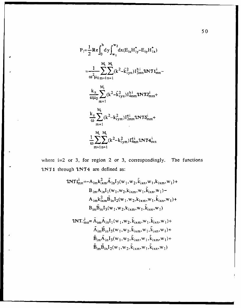
50
Pj=-LRefdyJ dx(Ei,,H* -EiyH*
LX (k2_ h i
02 P0m=ln= 1
LE(k kyn)~imLNiTim+
k 4E k2 - 2 ei~~~l .dym 2mm'T3mm+
M= 1
m~ln=l
where i=2 or 3, for region 2 or 3, correspondingly. The functions
I:NTI through INT4 are defined as:
INT~nn=Aim kl~mA inI3(Wl,W 2 ,kixn,Wl,kixm,wl)+
B imA in' 1(w1 ,w2,kjxm,w 1,kixn,w 1 )-
imxm inl2(WliW 2 ,kixm,wI ,kixn,Wl)+
Bim~n13 (wI ,W2 ,kjxm,wjiixn,w0)
1T.'mn=Aim Ai1l(Wl,w2,kixm,wl,kixn,Wl)+
AimBinl 3 (W ,W 2 , kjxm,w 1' nl)
BimA 1nI 3 (wl1,w 2 , kixn,Wl1'kjxm,wl 1
BimBinI2(w 1,w2,kixm,wj,kixn,wI)
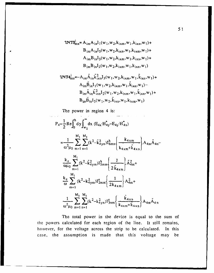
51
ThNTZn=AimAinI l(wl,W2,kixm,wi,kixn,Wl)+
B imAin13(W 1,W2,kixnW I kixm,wi1)+
AimB* in 3 (W 1,W2,kixm,w I kixn,w 0+
B imBin12(W 1,W2,kixm,wi,kixn,Wi1)
1'NT4~n=-AimAinkixn13(W l,w2,kixm,wil,kixn,wl0+
Ajjinl1 (W T,W2,kjxm,wj 1kjxn,W 0-
Bjm~kjnkixnI2(W 1,W2,kjxm,w 1,kixn,WI)+
BjmBinI3(W 1 Wkxn ,kixm,w 1)
The power in region 4 is:
P 4 =-Reldyldx (ExH4-~-*x2 JO w 2
2_M2 fm k4,xm ]2 1 (k k yn)1n. 6 A 4mA 4 n-
(0 k' M=1 n=1 I.k4xm+k4xnJ
M 1 2 2 I{ 2 k4 xm}kz ( 22 y)emm{2 x}4
~ (k 1 ynIAnm+c ~ _ky 2o m= 4m Am~
The total power in the device is equal to the sum ofthe powers calculated for each regyion of the line. It still remains,however, for the voltage across the strip to be calculated. In this
case, the assumption is made that this voltage may be
52
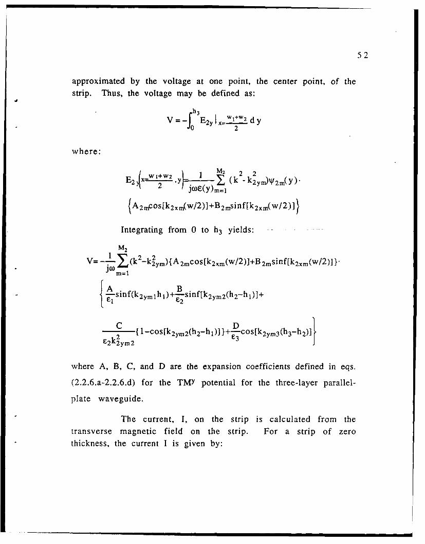
approximated by the voltage at one point, the center point, of thestrip. Thus, the voltage may be defined as:
where:
E ____ Y Y, (k k 2 Yf)XV2 m(y).
(A 2 rCOS[k 2 xm( W/2))+B 2 msinf[k 2xm( w/2)]
Integrating from 0 to h3 yields: -
V= LY, (k 2 -k ym) {A 2mc05s[k 2xm(w/2)1+13 2msinf[k2xm(w/2)]1
{ Lsff(k 2 ymI h I ) +sinf[k 2 ym 2 (h 2 - h01+
C 1 -cos[k 2 ym 2 (h 2 hi)] }+-aco s[kym h-2)e2k2ym2
where A, B, C, and D are the expansion coefficients defined in eqs.
(2.2.6.a-2.2.6.d) for the TMY potential for the three-layer parallel-
plate waveguide.
The current, 1, on the strip is calculated from thetransverse magnetic field on the strip. For a strip of zerothickness, the current I is given by:
53
Ifstri .H transversc d S
W2 + Wi
M2
I{jikzd-(A 2m-siff(k2xm-w)+2-B 2 mnslff 2(k2xm-W/2)I+M=1
1d-[A 2 m-(1 cos(k2 x-W))-B 2 m-slff(k2 xW) }
1{j-k~cos [k 3 ym(h-h3 )][A 3m-siff(k 3xm-w)+m= 1
2-B3 m-sinf 2 (k3 xmw/2)+--COSlk3 ym'(hh 3 )1-Jco
IA 3 m'(1 -COS(k 3 xmw))-B 3 m *sif(k 3 xm'W)I
The equations are now all in place to complete theanalysis of the three-layered coupled microstrip line through thecalculation of the propagation constant and the characteristicimpedance of the line.
54
Chapter 4. Numerical Results
The formulas derived for the calculation of thepropagation constant and the characteristic impedance of the
coupled microstrip line were implemented in Fortran 77. TheFortran program was run in double precision on the VAX or in
single precision on the CRAY, with the same results. Somecharacteristic results are presented in this chapter.
4.1. Convergence Criteria
The exact electric and magnetic field representation
for each region of the waveguide described in this thesis was
given by an infinite sum of expansion functions, which werecharacteristic for each region of the device. Due to subsequent
truncation of each infinite sum, the propagation constant whichwas derived for this structure was not exact, and the errorpresent in the calculation not exactly known. However, as was
presented in chapter 2, care was taken so that the relativenumber of expansion functions retained for each region was suchthat the truncation of the infinite series would lead to a
convergent system. The accuracy of the results was determinedvia convergene plots, such as those shown in figs. (4.1.1) and
(4.1.2). In these plots, the normalized propagation constant wasplotted against the number of modes, M2 , retained in region 2 for
the calculation of that particular value for the propagationconstant. As M2 increases, the value of the normalized
propagation constant converges to a particular value. So, aftersetting a certain error bracket as acceptable, the minimum M2
required to calculate the propagation constant within that error
bracket is found from the convergence plots, and thecorresponding normalized propagation constant is accepted as thesolution.
55
This test cannot, however, be conducted for each datapoint, as the time taken to do this would be prohibitive. Theprocedure followed is to calculate the smallest M2 which satisfies
the convergence conditions at the extreme data points. Thesepoints in this particular case would be smalles and largeststructure size, and lowest and highest frequency. It is safe toaccept that this M2 will then satisfy the same convergence criteria
for any other point within the boundaries set by these extremepoints.
The error bracket for the convergence plots are 0.5%for the propagation constant, and 1.5% for the characteristicimpedance.
3.8 , ,
3.7
3.6
3.5
3.4 "
3.30 2 4 6 8 10
# modes
Figure 4.1.1. Convergence plot of the even modepropagation constant versus the number of modes retained inregion 2.
Another important numerical consideration, which hasbeen touched only briefly so far, is the height at which the topplate must be placed, such that it does not perturb the solution. It
56
was suggested in [191 that placing the top plate at a height double
the height at which the metal strips are placed, would be enough
to ensure an unperturbed solution. This is the height used for all
the calculations. The same program was run for greater heights,but it was deduced that this only added unnecessarily to the
computation time, without producing more accurate results.
3.8
3.7
3.6
3.5
3.4
3.3 -
3.20 2 4 6 8 10
# modes
Figure 4.1.2. Convergence plot of the odd modepropagation constant versus the number of modes retained in
region 2.
4.2. Program Verification
The accuracy of the programs was verified byselecting the permittivities of the dielectrics and the geometry of
the structure such that it would be reduced to structures for
which results were available. Both the propagation constant
calculation and the characteristic impedance calculations for the
single-layer, coupled microstrip line were verified against the
results obtained by [2]. The calculation of the propagation
constant for the single-line case was achieved by placing the
striplines at a sufficiently large distance from each other. The
results obtained for this case for the single-layer case were
verified against [2], and for the multiple-layer case against [19 (p.
57)]. The calculation of the propagation constant for the three-
layer coupled microstrip line was verified with [19 (p. 57)].
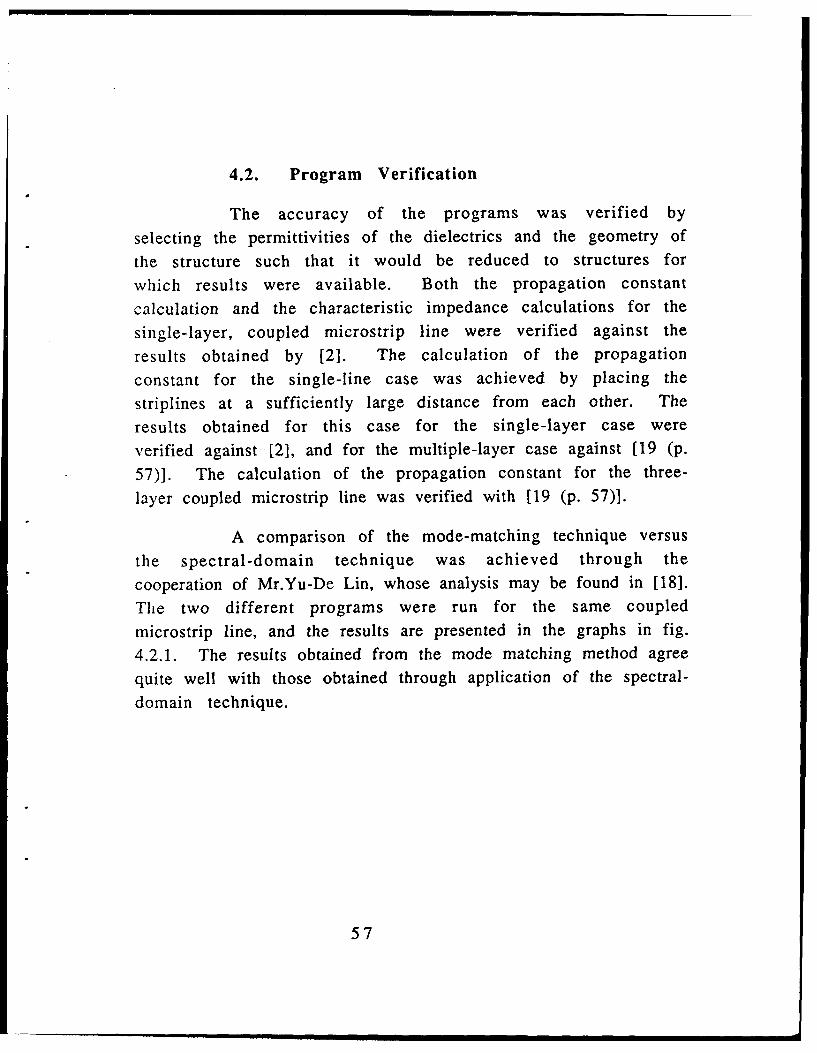
A comparison of the mode-matching technique versus
the spectral-domain technique was achieved through the
cooperation of Mr.Yu-De Lin, whose analysis may be found in [18].
The two different programs were run for the same coupled
microstrip line, and the results are presented in the graphs in fig.
4.2.1. The results obtained from the mode matching method agree
quite well with those obtained through application of the spectral-
domain technique.
57
58
3.4
eve mde- mode machngeve mod
-spectral domain
5 8 .8mm
2.8.9
2.60 10 20
Frequency (GHz)
400
Z- mode matchingII
300een mode
200
100 •odd
mode
010 10 20
Frequency (GHz)
Figure 4.2.1. Propagation constant and characteristicimpedance (power-current relationship) verification for the
coupled microstrip line.
4.3. Results-Design Charts
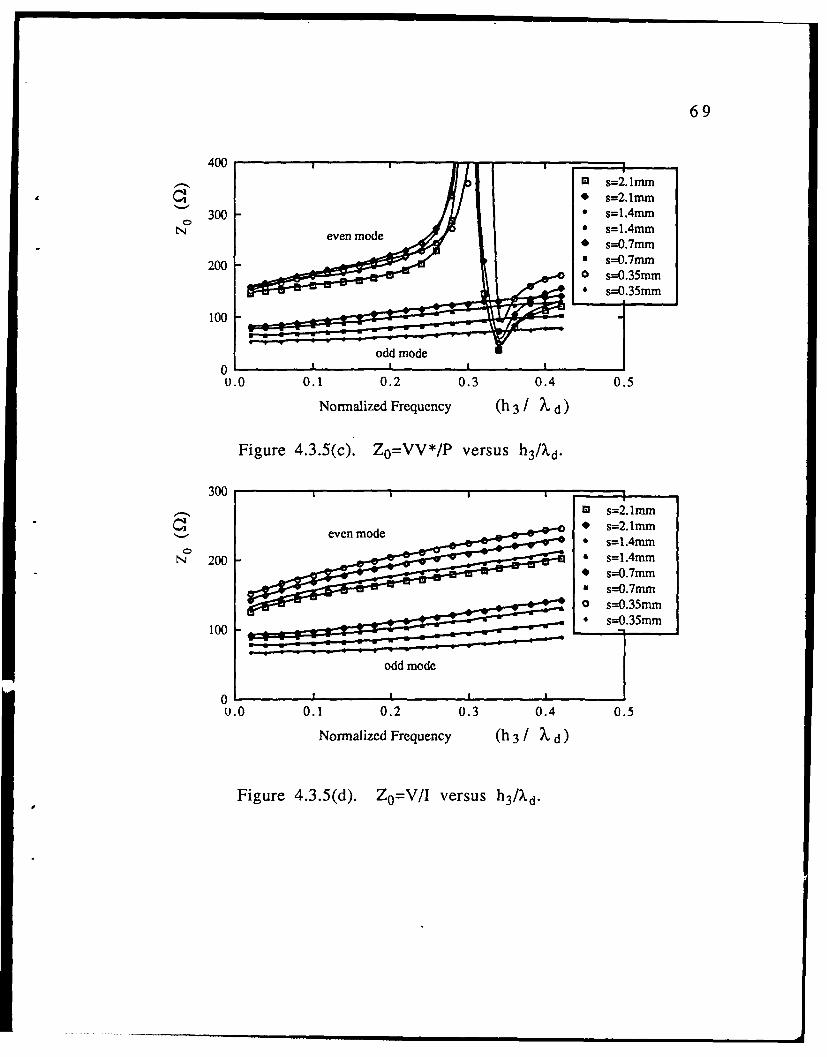
The program was run for several cases of coupledmicrostrip lines. Each graph shows a family of curves, calculatedfor a specific microstrip width and dielectric layering, but fordifferent strip separations, or for a variable dielectric constant inthe conducting layer. In each case, for wider strip separation, theresults converge to the case of a single microstrip line. Also, inthe case of a variable dielectric constant value in the conductinglayer, the results converge to the single-layer solution when thedielectric constant of the conducting layer approaches the value ofthe dielectric constant of the insulating layers.
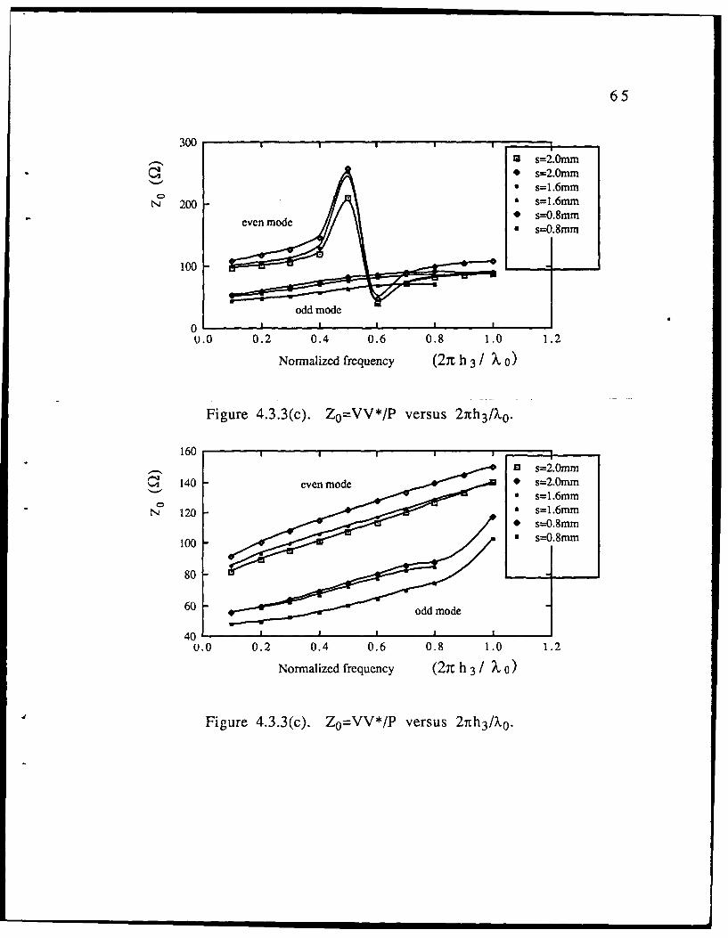
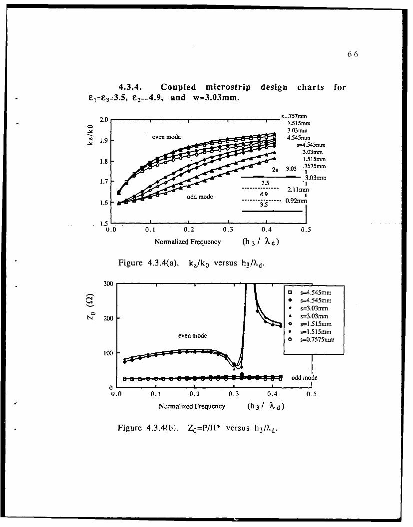
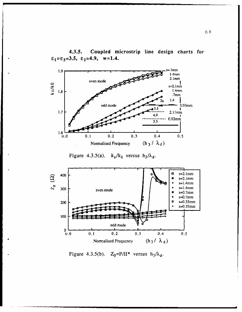
Many curves were graphed versus a normalizedfrequency, where the normalization took the form 27th 3/X0 , where X0
is the free-space wavelength, The characteristic impedances,however,which are calculated using the power-voltage, Z0 =V.V*/P,and the power-current, Z0=P/I.I*, expressions, exhibit discontinuities
at regular intervals, which seem to correspond approximately to thefrequency where h3=n)Ld/4, where n=1,2,3,etc., and Xd is the free-
space wavelength in a medium of relative dielectric constant equal tothe relative dielectric constants of the layered medium. Thisbehavior is more evident where the characteristic impedance isplotted against h3/)Ld. As the relative dielectric constant of the
middle layer is increased with respect to the outer layers, thisdiscontinuity becomes more pronounced, as may be witnessed in figs.4.3.2(b), and (c). This behavior seems to signify the "turning on" ofhigher-order modes, which introduce a numerical instability aroundthat region of frequencies. In figs. 4.3.6(b), and (c), the characteristicimpedances are plotted over a wider range of normalized
frequencies, and the almost "periodic" behavior of thesediscontinuities is more evident. The calculation of Z0 using Z0=V/Idoes not exhibit any discontinuous behavior.
59
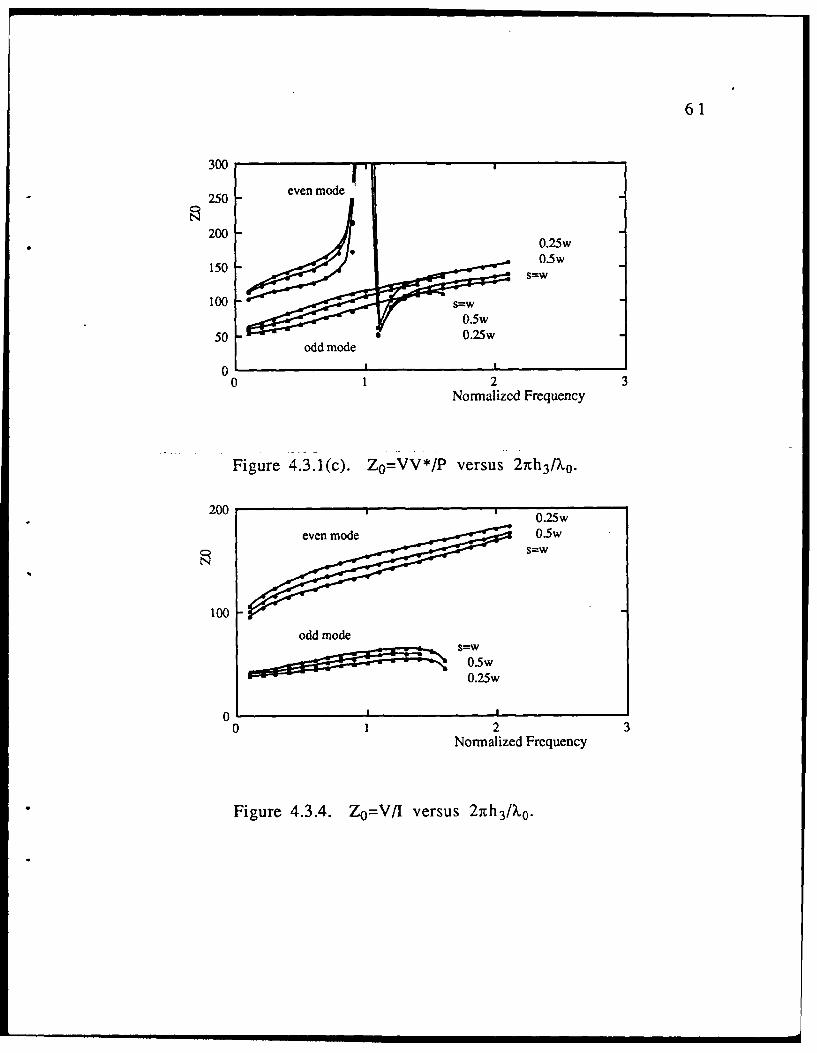
60(
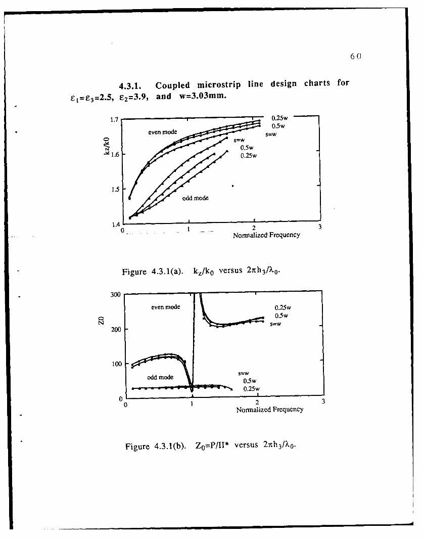
4.3.1. Coupled microstrip line design charts for
EI=E3=2.5, E2=3.9, and w=3.O3mm.
1.70.5evenmode0.5w
S s=W
0.5
1.5
1.410 -2
3Normalized Frequency
Figure 4.3.1(a). kz/ko versus 21ch 3/Xo0.
300 -
even mode 0.25w
0.5
200 S=
100
odd mode 0.W
V" 0.25w
0 12 3Normalized, Frequency
Figure 4.3.1(b). Z0 =P/II* versus 2hfO
61
300
250 - even mode
200 -I02515 -j 0.5w
00.5w
50 4 .25odd modeJ
00 12 3
Normalized Frequency
Figure 4.3.1(c). Z0 =VV*/P versus 27ch 3I10.
200 0.25wevenmode0.5w
100
odd mode~ S=w
0.5w0.25w
0 p -0 12 3
Normalized Frequency
Figure 4.3.4. Z0=V/I versus 2nh3P/. 0.
62
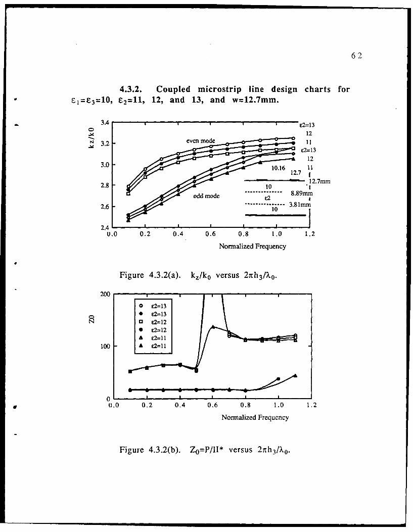
4.3.2. Coupled microstrip line design charts foreI=e-3 =1O, E2 =119 12, and 13, and w=12.7mm.
a 3.4 E 2-13
N .2even mode 12
E2--1312
3.0 1.61
22.78
2.67m
0.0 0.2 0.4 0.6 0.8 1.0 1.2
Normalized Frequency
Figure 4.3.2(a). kz/ko versus 21ch 3 AX0 .
200
* E2--1313 E2-12* E2--12
100- A E2--11
0 T
*0.0 0.2 0.4 0.6 0.8 1.0 1.2
Normalized Frequcncy
Figure 4.3.2(b). Z0=P/III versus 27Eh 31X0O.
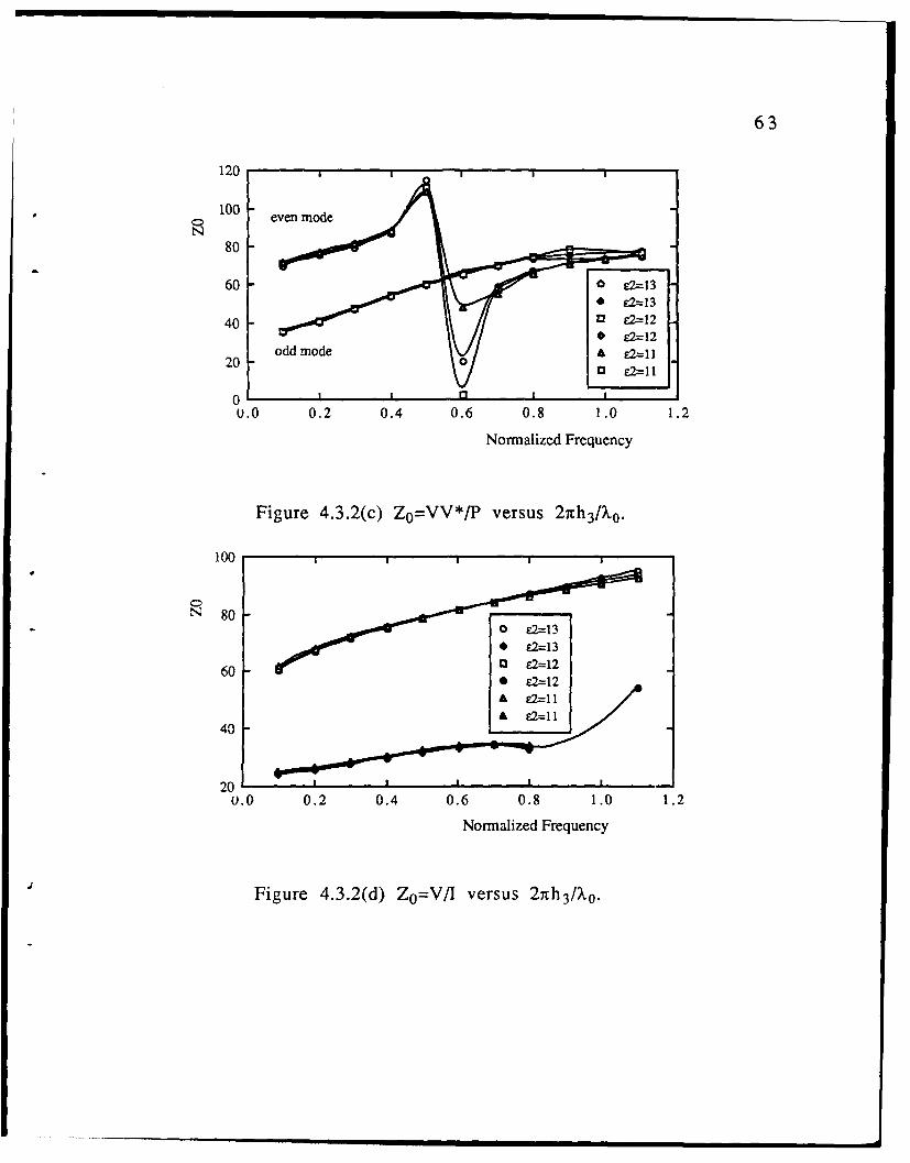
63
100 evnmd
80
60 0E-1
4013 E-1
20 odmoe0AE-I
01U.0 0.2 0.4 0.6 0.8 1.0 1.2
Normnalized Frequency
Figure 4.3.2(c) ZO=VV*/P versus 2irh3IXO.
100 1
N 0
60 0E-1
40
0.0 0.2 0.4 0.6 0.8 1.0 1.2
Normalized Frequency
Figure 4.3.2(d) Z0 =V/I versus 27rh 3/k0 .
64
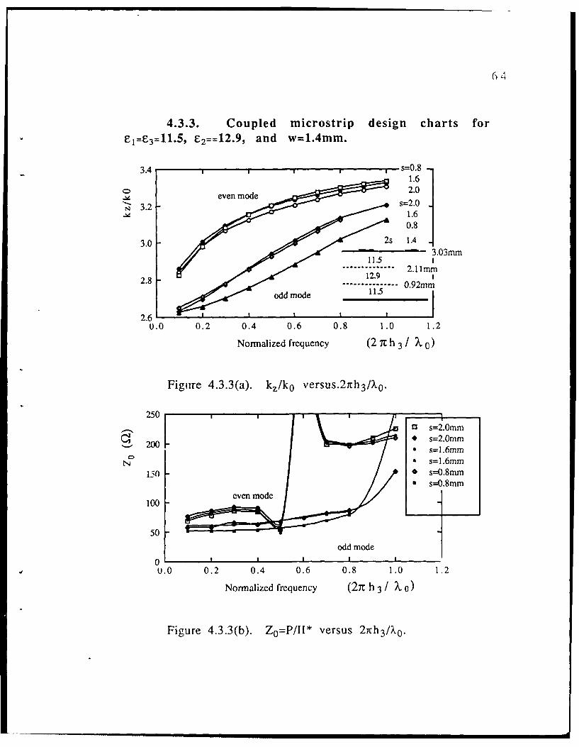
4.3.3. Coupled microstrip design charts forEl=Fs3=11.5, F,2==12.9, and w=1.4mm.
3.4 S=0.81.62.0
3.2 -s=2.01.60.8
3.03m
........... 2.11 mm2.8 -1.
0.0 0.2 0.4 0.6 0.8 1.0 1.2
Normalized frequency (27cth3~/ % 0
Figtire 4.3.3(a). kz/k 0 versus.21rh 3/XO.
250 ~I a S=2.ommI- * s=2.Omm~- 200 *s=1.6mm
N * s=1.6mm1;()* s=-0.8mm
*s=-0.8mm
50I0 1 1
0.0 0.2 0.4 0.6 0.8 1.0 1.2
Normalized frequency (27C h 3 0 )
Figure 4.3.3(b). Z0=PIII* versus 2irh 3/?k0.
65
300M S=2.ornm* s=2.Omm0 s=1.6mm
20a s=1.6mm,200 * s=-0.8mm
even mode *s=-0.8mm
100L
odd mode0 1 L - I - - IU.0 0.2 0.4 0.6 0.8 1.0 1.2
Normalized frequency (2% h3~/ X O)
Figure 4.3.3(c). Z0=VV*/P versus 2nth3fX0.
160 -10 s=2.Omm
O~140 even mode *s=2.0mmn*s=1 .6mm
N 120s=1.6mm* S=0.8mm
100 *S=-0.8mm
80
60
0.0 0.2 0.4 0.6 0.8 1.0 1.2
Normalized frequency (27C h 3 X 0)
Figure 4.3.3(c). Z0=VV*/P versus 2nth3/X0.
66
4.3.4. Coupled microstrip design charts for*E1 =E3=3.5, e2==4.9, and w=3.03mm.
2.0 s=.757mm
Q 0 1.515mm14 3.03mmN 1.9 even mode 4.545mm
s=4"545mm3.03mm
1.8 1.5 15mm2S 3.03 7575rnim
~I3.03mm
1.7 3.5 1.............. 2.11m
od mode 6.91.6 ....... 3.5 ..... 0.92mm
1.5 1 1 1 1
0.0 0.1 0.2 0.3 0.4 0.5
Normalized Frequency (h 3 / Xd)
Figure 4.3.4(a). kz/ko versus h3/Xd.
300
* s=4.545mm* s--4.545mrn0 s=3.03mm
, 200 a s=3.03mm
Q s=1.515mme s=1.515mmo s=0.7575mm
100_
a 00090@="L1I1 odd mode0 I I I I0.0 0.1 0.2 0.3 0.4 0.5
N,;rmalized Frequency (h 3 / X d)
Figure 4.3.4(bi. Zo=P/II* versus h3/kd.
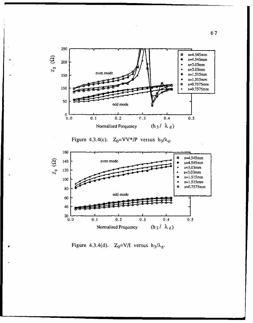
67
250- _______
M s--4.545mm* s=-4.545mm
200* s=3.03mm
0a s=3.O3num
150 -even mode * s=1.515mni
100 -s077m
50-
U.0 0.1 0.2 C.3 0.4 0.5
Normalized Frequency (h 3 / Xd)
Figure 4.3.4(c). Z0=VV*/P versus h3/)Xd.
160__a s=4.545mm
140 -*vnmd s--4.545mm*s=3.03mm
o 120 's=3.03mm
100 s=1.515mm
80 -0 s=-0.7575mm
60
40
200.0 0.1 0.2 0.3 0.4 0.5
Normalized Frequency (h 3 / X d)
Figure 4.3.4(d). Z0=V/I versus h3/kd.
68
4.3.5. Coupled microstrip line design charts forCl=C3 =15s E2 =4.9, w=1.4.
1.9 s-.7mm1.4mm
even mode 21u
s=2.lmn
1.8 .m
1.7.4
1.6 ..... 21 m
0.0 0.1 0.2 0.3 0.4 0.5
Normalized Frequency (h 3 / X d)
Figure 4.3.5(a). kz/ko versus h3/Xd.
~40000 im,
N 300 -ee oes07m
200-0 -03m
100
0.0 0.1 0.2 0.3 0.4 0.5
Normalized Frequency (h3~/ X d)
Figure 4.3.5(b). Z0 =P/I"* versus h3/kd.
69
400
0 s=2.lmm.
300 s=1.4mm.even mode £s=.4nm
* s=0.7mm
200- 0.m
100
U.0 0.1 0.2 0.3 0.4 0.5
Normalized Frequency (h3 X ~d)
Figure 4.3.5(c). Zo=VV*/P versus h3/Xd.
300 S-i I m m
even mod s=2.mni
N 200 =.m
100
0U.0 0.1 0.2 0.3 0.4 0.5
Normalized Frequency (h3 X ~d)
Figure 4.3.5(d). Z0 = V/I versus h3/Xd.
70(
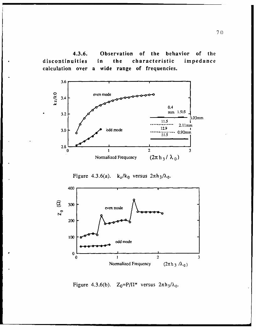
4.3.6. Observation of the behavior of thediscontinuities in the characteristic impedancecalculation over a wide range of frequencies.
3.6
- 3.4
0.4
3.2 - mm 1.515
3.0 .odd mode 12.91.......... ............... 0.92mmn
2.8 1
0 12 3
Normalized Frequency (27c h 3 0 )
Figure 4.3.6(a). kz/ko versus 27rh3/X0o.
400
~300-evnmd
200
00 1 2 3
Normalized Frequency (27E h 3 /X 0)
Figure 4.3.6(b). Z0=P/Il* versus 27th 3IXQ.
71
200
"V"even mode° 150
100 d.
o 0
50odd mode
0 1, - 1 -
0 1 2 3Normalized Frequency (27t h 3 / 0)
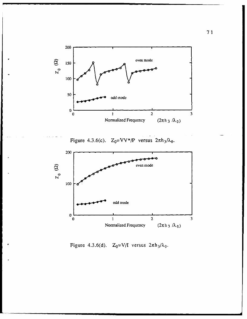
Figure 4.3.6(c). Zo=VV*/P versus 2nh 3 /Lo.
200 a
00 dN
Sodd mode
0
0 1 2 3Normalized Frequency (2nth 3 /A 0)
Figure 4.3.6(d). Zo=V/I versus 21h3/?o.
Chapter 5. Conclusions
In this thesis, it was shown how a quasi-planarstructure like the coupled microstrip line on a layered dielectric
substrate, could be analyzed using a variation of the modematching technique.
Mode matching is a powerful tool for analyzing planarand even quasi-planar structures. The results obtained throughmode matching have a high degree of accuracy, especially thepropagation constant. This technique, however, is unsuitable forCAD packages, as it is very inefficient. It is also susceptible tonumerical errors, as the system which is solved to calculate the
field coefficients is defined by a singular matrix. It should benoted, as a matter of fact, that this singularity condition has
actually been imposed on the matrix, in order to solve for thepropagation constant.
The behavior of the even and odd mode propagation
constants of the coupled microstrip line on a layered substratedoes not differ from that of its single substrate counterpart,except for a slight increase of kz/ko with an increase in the
conducting layer dielectric constant with respect to the insulatinglayer dielectric constants, as can be seen in fig. 4.3.2(a). As far asthe impedance is concerned, it does not seem to change noticeablywith the change in dielectric constants. The change becomes morenoticeable, however, at higher frequencies. The effect of thediscontinuity becomes much more noticeable for a higherconducting layer dielectric constant. Its position does not changemuch, however, as the values used for the dielectric constantswere of the same order of magnitude.
The impedance curves seem to be relatively flatbetween singularities. The discontinuities themselves follow a
72
73
very consistent pattern which seems to be dictated by therelationship used to calculate the impedance (power-voltage, orpower-current). Irrespective of the relationship used to calculateZ0 , however, the first singularity occurs at the same normalizedfrequency, h 3/Xd=_0. 2 5 . This seems to be indicative of a cutofffrequency, above which higher order modes start propagating,and around which the calculations of the characteristic impedancebecome numerically unstable. It is not practical, in any case, tofabricate microstrip devices of the order of magnitude of Xd/ 4 , so
only the portion of the curve before the discontinuity occurs issignificant.
Appendix A. Notation
A consistent notation scheme is used throughout the
text where subscripts and superscripts are used to denote region,
direction, dielectric, mode number, mode type, or to differentiate
between two similar functions.
A variable "z" may take the form Zabm where "a"
would be the cartesian coordinate (x, y, or z), "b" would be aregion number (1, 2, 3, or 4), and "m" would be the mode number.
A function "f" may take the form fbcramn where "a"
would be a function number, "m", and "n" would be mode
numbers, and "c" would be the region number: c=2 means the
inner product was performed with respect to a normal mode ofregion 2, and c=3 means the inner product was performed with
respect to a normal mode of region 3. Superscript "b" is used onlyin the orthogonalization integrals: b=e means the inner productwas performed with respect to a TM mode, and b=h means theinner product was performed with respect to a TE mode.
The following general notation was used to build the
desired variables:
Symbol Interpretation
__ permittivity9.
permeability
k propagation consta tE electric fieldH magnetic field
A tilde over any of the above variables would denoteTE quantities, whereas no tilde would denote TM quantities.
74
Appendix B. Derivation of Field Equations
A wave is a field that is a function of both time andspace. Electric and magnetic fields that vary in time and spaceare governed by physical laws which are expressed in fourequations, known as Maxwell's equations. For a wave travellingin a medium characterized by a certain permittivity, e, and acertain permeability, pt, These equations are:
D HVxE= -pV x H =F D-- + J
VD p
V. B=O (B.1)
The electromagnetic field equations above areexpressed in terms of six quantities:
E, the electric intensity (in volts per meter)
H, the magnetic intensity (in amperes per meter)
D, the electric flux density (in coulombs per meter)
B, the magnetic flux density (in coulombs per square meter)
J, the electric current density (in amperes per square meter)
p, the electric charge density (in coulombs per square meter)
The boldface script is used to denote complex quantities.
The ultimate sources of an electromagnetic field arethe current J, and the charge p.
75
76
The continuity equation, which is based on theprinciple of conservation of charge, is implicit in equations (B.1),
and simply states that:
SV J=_Pa t (B.2)
Maxwell's equations are complemented by the so-called constitutive relationships, which incorporate thecharacteristics of the medium in which the field exists. Theseequations define the electric flux density, D, the magnetic fluxdensity, B, and the current density, J, with respect to the electric,E, and magnetic, H, intensities.
D=D(E,H)B=B(E,H)
J= J(E, H) (B.3)
Maxwell's equations along with the constitutiverelationships serve to fully describe a wave travelling in a known
mne di um.
In a source free, linear medium, the constitutiverelationships take the form:
D= EB=p.H
J = 0 (B.4)
Here, e and . are constants, where , is the capacitivityor permittivity, and . is the permeabillity of the medium. Using-0 and go to denote the corresponding variables in vacuum, for aperfect dielectric (Y=0), one has E=CrC0 , where Er is the dielectricconstant, or the relative capacitivity, of the medium, and g=pt 0 for
most linear matter.
77
The present analysis will be concerned only withsource free, linear problems, where the wave has a steady-statesinusoidal time dependence. In this case, the complex fieldequations read:
-VxE=z(cm)H
V xH=y (o)3) EV.D=O
V. B =0 (B.5)
A Awhere y(w)=jco, and z(O)=j3O1.t0 in nonmagnetic material.
The above representation of the field equations givesrise to the definition of the parameter k, the wavenumber of themedium. The wavenumber is defined as:
k = -y(ct) z(cO) (B.6)
The physical meaning of the wavenumber is that 1/kis the velocity of propagation of an electromagnetic disturbance inan open space filled with perfect dielectric material withpermittivity e and permeabillity 0.
Taking the curl of equations (B.5), and using the aboverepresentation of k, the complex wave equations become:
VxVxE -k 2E=0
V x V x H- k H=O (B.7)
In these equations, it is implicit that:
V.E=O and V.H=O (B.8)
78
so that a simplified form for the vector wave equations may bederived:
V2E +k 2 E = 0 (B.9)
and:
V2 H+k 2 H=O (B. 10)
The geometry of planar structures allows us to workwith rectangular cartesian coordinates. In this case, therectangular components of E and H satisfy the complex scalarwave equation:
2 k2
V 2E i +k E=0i=x,y,z
2 k2
V Hi+k 2 Hi=O (B.1 1)
To construct a pliable solution to the above equations,
the field is expressed as a magneti- vector potential A and anelectric vector potential F, as shown below:
E=-VxF+.IVxVxAy
E= VxA+I-VxVxFz (B.12)
These expressions for E and H give rise to a very
useful classification of the solutions of the wave equation. In thisclassification, axial uniformity (the cross-sectional shapes of thewavcguide do not vary in the direction of propagation) isassumed. In addition, this classification is for fields conforming tothe homogeneous vector Helmholtz equations (source free
79
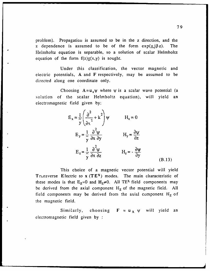
problem). Propagation is assumed to be in the z direction, and thez dependence is assumed to be of the form exp(+j 3z). The
Helmholtz equation is separable, so a solution of scalar Helmholtz
equation of the form f(zg(x,y) is sought.
Under this classification, the vector magnetic andelectric potentials, A and F respectively, may be assumed to bedirected along one coordinate only.
Choosing A=uixV where xV is a scalar wave potential (a
solution of the scalar Helmholtz equation), will yield anelectromagnetic field given by:
;2
E 1±Ey y Jx y bz
2Ez_ a W'l HZ=- aya x Dz Dy
- 1 '(B.13)
This choice of a magnetic vector potential will yieldTransverse Electric to x (TEx) modes. The main characteristic ofthese modes is that Ez=O and Hz*O. All TEx field components maybe derived from the axial component Hz of the magnetic field. Allfield components may be derived from the axial component Hz of
the magnetic field.
Similarly, choosing F = u x xV will yield an
electromagnetic field given by
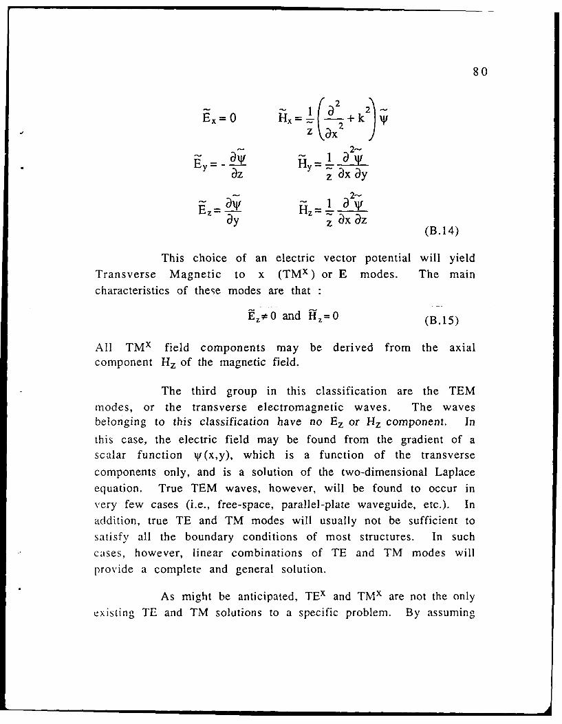
80
2-
z (B.14)
This choice of an electric vector potential will yieldTransverse Magnetic to x (TMX) or E modes. The main
characteristics of these modes are that"
_~ =.
'ZO and Hz=O (B.15)
All TMx field components may be derived from the axialcomponent Hz of the magnetic field.
The third group in this classification are the TEMmodes, or the transverse electromagnetic waves. The wavesbelonging to this classification have no Ez or Hz component. In
this case, the electric field may be found from the gradient of ascalar function xV(x,y), which is a function of the transverse
components only, and is a solution of the two-dimensional Laplaceequation. True TEM waves, however, will be found to occur invery few cases (i.e., free-space, parallel-plate waveguide, etc.). Inaddition, true TE and TM modes will usually not be sufficient tosatisfy all the boundary conditions of most structures. In suchcases, however, linear combinations of TE and TM modes willprovide a complete and general solution.
As might be anticipated, TEx and TMx are not the onlyexisting TE and TM solutions to a specific problem. By assuming
81
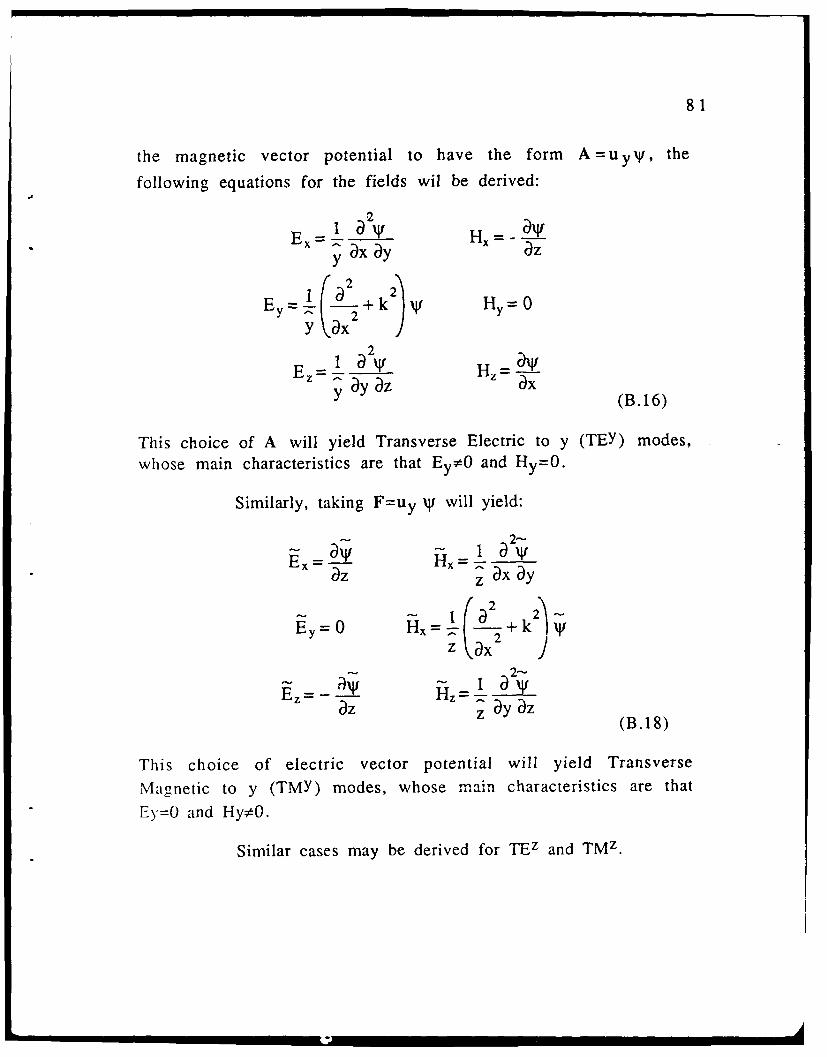
the magnetic vector potential to have the form A=uyv, the
following equations for the fields wil be derived:.2
Ex= - bllx H - - j
y ax ay
E -- +k H H= 0
- 1 b2 ' z '1E =- I y b =f H x
(B.16)
This choice of A will yield Transverse Electric to y (TEY) modes,whose main characteristics are that Ey#O and Hy=0.
Similarly, taking F=uy xV will yield:
2-
Fwx bH - 1 a2V
Ex= fx =(B.18)
This choice of electric vector potential will yield Transverse
Magnetic to y (TMY) modes, whose i n characteristics are thatEy=O and Hy2+.
Similar cases may be derived for TEz and TMz.
M neic to I ITY moes whs m-.: chrceitc are Ithat
References
[1] Herbert J. Carlin, and Pier P. Civalleri, "A Coupled-Line Model for Dispersion in Parallel-Coupled Microstrips",IEEETrans. Microwave Theory Tech., pp.444-446, May 1975.
[2] Jeffrey B. Knorr, and Ahmet Tufekcioglou,
"Spectral-Domain Calculation of Microstrip CharacteristicImpedance", IEEE Trans. Microwave Theory Tech., vol. MTT-23,no.9, pp.725-728, September 1975.
[3] E. Yamashuti, and K. Atsuki, "Analysis of
Microstrip-Like Transmission Lines by Nonuniform Discretizationof Integral Equations", IEEE Trans. Microwave Theory Tech., vol.MTT-24, no.4, pp.195-200, April 1976.
[4] Klaus Solbach, and Ingo Wolff, "TheElectromagnetic Fields and the Phase Constants of Dielectric Image
Lines", IEEE Trans. Microwave Theory Tech., vol. MTT-26, no.4,
pp.266-275, April 1978.
[5] D. Mirshikar-Syahkal, and Brian Davies, "Accurate
Solution of Microstrip and Coplanar Structures for Dispersion andfor Dielectric and Conductor Losses", IEEE Trans. Microwave
Theory Tech., vol. MTT-27, no.7, pp.694-699, July 1979.
[6] Arne Brejning Dalby, "Interdigital MicrostripCircuit Parameters Using Empirical Formulas and Simplified
Model", IEEE Trans. Microwave Theory Tech., vol. MTT-27, no.8,
pp.74 4 -752, August 1979.
[81 Raj Mittra, Yun-Li Hou, and Vahraz Jamnejad,"Analysis of Open Dielectric Waveguides Using Mode-MatchingTechnique and Variational Methods", IEEE Trans. Microwave
Theory Tech., vol. MTT-28, no.1, pp.36-43, January 1980.82
83
[9] S.-J. Peng, and A. A. Oliner, "Guidance and LeakageProperties of a Class of Open Dielectric Waveguides: Part I-
Mathematical Formulations", IEEE Trans. Microwave Theory Tech.,vol. MTT-29, no.9, pp.843-854, September 1981.
[10] Ulrich Crombach, "Analysis of Single and CoupledRectangular Dielectric Waveguides", IEEE Trans. Microwave TheoryTech., vol. MTT-29, no.9, pp.870-874, September 1981.
[111 Yoshiro Fukuoka, Yi-Chi Shih, and Tatsuo Itoh,"Analysis of Slow-Wave Coplanar Waveguide for MonolithicIntegrated Circuits", IEEE Trans. Microwave Theory Tech., vol.
MTT-31, no.7, pp.567-573, July 1983.
[12] J. R. Brews, "Characteristic Impedance ofMicrostrip Lines", IEEE Trans. Microwave Theory Tech., vol. MTT-
35, no.1, pp.30-34, January 1987.
[13] R. F. Harrington, "Time-Harmonic ElectromagneticFields", New York, McGraw-Hill, 1961.
[141 R. E. Collin, "Foundations for MicrowaveEngineering", New York, McGraw-Hill., 1966.
[15] R. Mittra, and S. W. Lee, "Analytic Techniques inthe Theory of Guided Waves", New York, Macmillan, 1971.
[16] S. J. Leon, "Linear Algebra with Applications",New York, Macmillan, 1980.
[17] S. Ramo, J. Whinnery, and J. Van Duzer, "Fieldsand Waves in Communications Electronics", New York, John Wiley
and Sons, 1984.
84
[18] Yu-De Lin, "Metal-Insulator-SemiconductorCoupled Microstrip Lines", Master's Thesis, University of Texas,Austin, TX, 1987.
[19] Brian Young, "Analysis and design of MicroslabWaveguide';, Dissertation, University of Texas, Austin, TX, 1987.
45
.. . . .. a