mismatch-error noise-shaping based digital multiphase modulator
TRANSCRIPT
IEEE TRANSACTIONS ON POWER ELECTRONICS, VOL. 27, NO. 4, APRIL 2012 2055
Mismatch-Error Shaping-Based DigitalMultiphase Modulator
Miguel Rodrıguez, Student Member, IEEE, Pablo F. Miaja, Student Member, IEEE,Javier Sebastian, Senior Member, IEEE, and Dragan Maksimovic, Senior Member, IEEE
Abstract—This paper introduces a digital multiphase modula-tor (MPM) using mismatch-error shaping techniques based on adigital-to-analog converter view of multiphase power converters.The proposed modulator has relatively simple implementation re-quiring no explicit pulsewidth modulation and generates controlpulses for any number of phases using a single, low-frequencyclock. Advantages and disadvantages of the mismatch-error shap-ing MPM are examined through analysis, simulations, and exper-imental results. The proposed MPM is particularly well suited formultilevel envelope-tracking amplifiers supplying power to linearRF power amplifiers. Results are shown for an experimental eight-phase buck converter in an envelope-tracking application.
Index Terms—Digital-analog conversion, digital control, noiseshaping, switched-mode power supply.
I. INTRODUCTION
THE majority of nonisolated applications, where step-downdc–dc conversion is required, make use of the synchronous
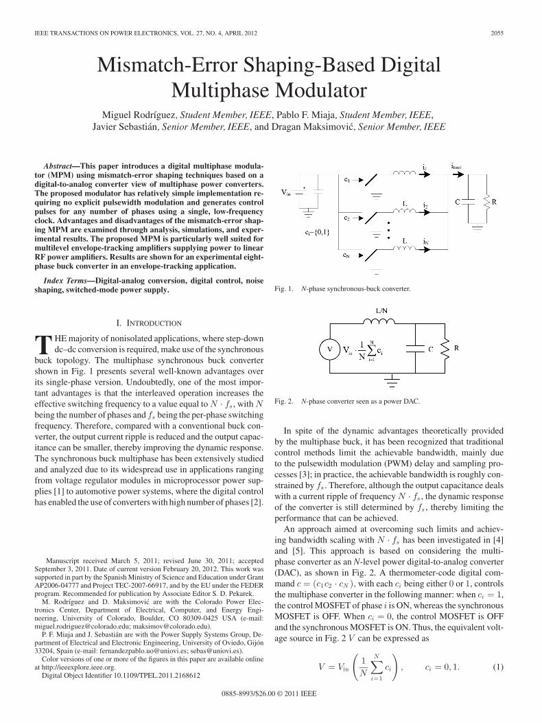
buck topology. The multiphase synchronous buck convertershown in Fig. 1 presents several well-known advantages overits single-phase version. Undoubtedly, one of the most impor-tant advantages is that the interleaved operation increases theeffective switching frequency to a value equal to N · fs , with Nbeing the number of phases and fs being the per-phase switchingfrequency. Therefore, compared with a conventional buck con-verter, the output current ripple is reduced and the output capac-itance can be smaller, thereby improving the dynamic response.The synchronous buck multiphase has been extensively studiedand analyzed due to its widespread use in applications rangingfrom voltage regulator modules in microprocessor power sup-plies [1] to automotive power systems, where the digital controlhas enabled the use of converters with high number of phases [2].
Manuscript received March 5, 2011; revised June 30, 2011; acceptedSeptember 3, 2011. Date of current version February 20, 2012. This work wassupported in part by the Spanish Ministry of Science and Education under GrantAP2006-04777 and Project TEC-2007-66917, and by the EU under the FEDERprogram. Recommended for publication by Associate Editor S. D. Pekarek.
M. Rodrıguez and D. Maksimovic are with the Colorado Power Elec-tronics Center, Department of Electrical, Computer, and Energy Engi-neering, University of Colorado, Boulder, CO 80309-0425 USA (e-mail:[email protected]; [email protected]).
P. F. Miaja and J. Sebastian are with the Power Supply Systems Group, De-partment of Electrical and Electronic Engineering, University of Oviedo, Gijon33204, Spain (e-mail: [email protected]; [email protected]).
Color versions of one or more of the figures in this paper are available onlineat http://ieeexplore.ieee.org.
Digital Object Identifier 10.1109/TPEL.2011.2168612
Fig. 1. N-phase synchronous-buck converter.
Fig. 2. N-phase converter seen as a power DAC.
In spite of the dynamic advantages theoretically providedby the multiphase buck, it has been recognized that traditionalcontrol methods limit the achievable bandwidth, mainly dueto the pulsewidth modulation (PWM) delay and sampling pro-cesses [3]; in practice, the achievable bandwidth is roughly con-strained by fs . Therefore, although the output capacitance dealswith a current ripple of frequency N · fs , the dynamic responseof the converter is still determined by fs , thereby limiting theperformance that can be achieved.
An approach aimed at overcoming such limits and achiev-ing bandwidth scaling with N · fs has been investigated in [4]and [5]. This approach is based on considering the multi-phase converter as an N-level power digital-to-analog converter(DAC), as shown in Fig. 2. A thermometer-code digital com-mand c = (c1c2 · cN ), with each ci being either 0 or 1, controlsthe multiphase converter in the following manner: when ci = 1,the control MOSFET of phase i is ON, whereas the synchronousMOSFET is OFF. When ci = 0, the control MOSFET is OFFand the synchronous MOSFET is ON. Thus, the equivalent volt-age source in Fig. 2 V can be expressed as
V = Vin
(1N
N∑i=1
ci
), ci = 0, 1. (1)
0885-8993/$26.00 © 2011 IEEE
2056 IEEE TRANSACTIONS ON POWER ELECTRONICS, VOL. 27, NO. 4, APRIL 2012
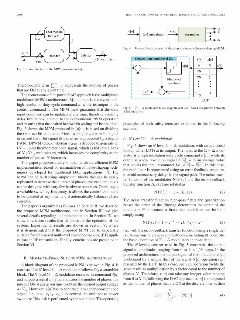
Fig. 3. Architecture of the MPM proposed in [6].
Therefore, the term∑N
i=1 ci represents the number of phasesthat are ON at any given time.
The cornerstone of the power DAC approach is the multiphasemodulator (MPM) architecture [6]; its input is a conventional,high resolution duty cycle command d, while its output is thecontrol command c. The MPM must guarantee that the dutyinput command can be updated at any time, therefore avoidingdelay limitations inherent to the conventional PWM operationand ensuring that the desired bandwidth scaling can be obtained.Fig. 3 shows the MPM proposed in [6]: it is based on dividingthe (n + m)-bit command d into two signals, the m-bit signaldLSB and the n-bit signal dMSB . dLSB is processed by a digitalPWM (DPWM) block, whereas dMSB is decoded to generate an(N − 1)-bit thermometer code signal, which is fed into a bankof N (N :1) multiplexers, which increases the complexity as thenumber of phases N increases.
This paper proposes a very simple, hardware-efficient MPMimplementation based on mismatch-error noise-shaping tech-niques developed for traditional DAC applications [7]. TheMPM can be built using simple unit blocks that can be easilyreplicated to increase the number of phases, and each unit blockcan be designed with very few hardware resources. Operating ata variable switching frequency, it allows the control commandto be updated at any time, and it automatically balances phasecurrents.
The paper is organized as follows. In Section II, we describethe proposed MPM architecture, and in Section III, we giveseveral details regarding its implementation. In Section IV, weshow simulation results that demonstrate the operation of thesystem. Experimental results are shown in Section V, whereit is demonstrated that the proposed MPM can be especiallysuitable for step-based multilevel envelope-tracking (ET) appli-cations in RF transmitters. Finally, conclusions are presented inSection VI.
II. MISMATCH-ERROR SHAPING MPM ARCHITECTURE
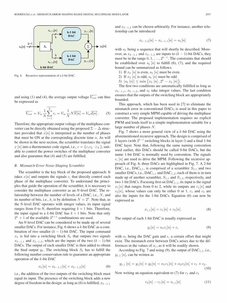
A block diagram of the proposed MPM is shown in Fig. 4. Itconsists of an N-level Σ − Δ modulator followed by a scramblerblock. The N-level Σ − Δ modulator receives the command d[n]and outputs a signal x[n] that indicates the number of phases thatmust be ON at any given time to obtain the desired output voltaged · Vin . However, x[n] has to be turned into a thermometer codesignal, i.e., c = {c1c2 · cN } to control the multiphase powerswitches: This task is performed by the scrambler. The operating
Fig. 4. General block diagram of the proposed mismatch-error shaping MPM.
Fig. 5. Σ − Δ modulator block diagram and LUT-based assignment betweenS [n] and x [n].
principles of both subsystems are explained in the followingsections.
A. N-Level Σ − Δ modulator
Fig. 5 shows an N-level Σ − Δ modulator, with an additionallookup table (LUT) at its output. The input to the Σ − Δ mod-ulator is a high resolution duty cycle command d [n], while itsoutput is a low resolution signal S [n], with an average valuethat equals the input command, i.e., d[n] = S[n]. In this case,the modulator is represented using an error-feedback structure,to avoid unnecessary delays in the signal path. The noise trans-fer function of the modulator NTF (z) and the error-feedbacktransfer function Hef (z) are related as
NTF (z) = 1 − Hef (z) . (2)
The noise transfer function high-pass filters the quantizationnoise; the order of the filtering determines the order of themodulator. For instance, a first-order modulator can be builtsimply using
NTF (z) = 1 − z−1 ⇒ Hef (z) = z−1 (3)
i.e., with the error-feedback transfer function being a single de-lay. Numerous references and textbooks, including [8], describethe basic operation of Σ − Δ modulators in more detail.
The N-level quantizer used in Fig. 5 constrains the outputsignal to amplitudes ranging from 0 to 1 in 1/N steps. In theproposed architecture, the output signal of the modulator x [n]is obtained by a simple shift of the signal S [n] operation rep-resented by the LUT. In this case, such an operation yields thesame result as multiplication by a factor equal to the number ofphases N . Therefore, x [n] can take any integer value rangingfrom 0 to N. If, following the DAC approach, x [n] is interpretedas the number of phases that are ON at the discrete time n, then
x[n] =N∑
i=1
ci = NS[n] (4)
RODRIGUEZ et al.: MISMATCH-ERROR SHAPING-BASED DIGITAL MULTIPHASE MODULATOR 2057
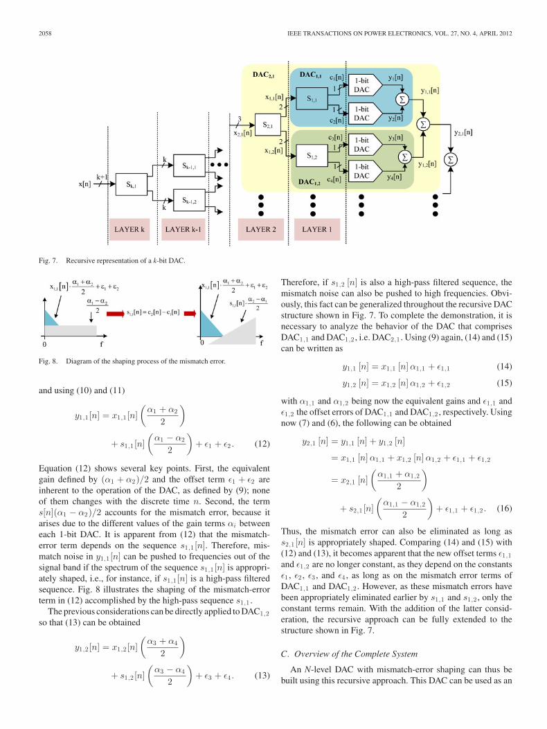
Fig. 6. Recursive representation of a k-bit DAC.
and using (1) and (4), the average output voltage Vout can thusbe expressed as
Vout = Vin1N
N∑i=1
ci = Vin1N
NS[n] = Vind[n] . (5)
Therefore, the appropriate output voltage of the multiphase con-verter can be directly obtained using the proposed Σ − Δ struc-ture provided that x[n] is interpreted as the number of phasesthat must be ON at the corresponding discrete time n. As willbe shown in the next section, the scrambler translates the signalx [n] into a thermometer code signal, i.e., c = {c1c2 · cN }, suit-able to control the power switches of the multiphase converterand also guarantee that (4) and (5) are fulfilled.
B. Mismatch-Error Noise-Shaping Scrambler
The scrambler is the key block of the proposed approach: Ittakes x[n] and outputs the signals ci that directly control eachphase of the multiphase converter. To understand the princi-ples that guide the operation of the scrambler, it is necessary toconsider the multiphase converter as an N-level DAC. The re-lationship between the number of levels of a DAC, i.e., N , andits number of bits, i.e., k, is by definition N = 2k . Note that, asthe N-level DAC operates with integer values, its input signalranges from 0 to N, therefore requiring k + 1 bits. Therefore,the input signal to a k-bit DAC has k + 1 bits. Note that only2k + 1 of the available 2k+1 combinations are used.
An N-level DAC can be considered to be made up of severalsmaller DACs. For instance, Fig. 6 shows a k-bit DAC as a com-bination of two smaller (k − 1)-bit DAC. The input commandxk is fed into a switching block Sk that outputs two signalsxk−1,1 and xk−1,2 , which are the inputs of the two (k − 1)-bitDACs. The output of each smaller DAC is then added to obtainthe final output yk . The switching block Sk has to fulfill thefollowing number conservation rule to guarantee an appropriateoperation of the k-bit DAC
xk [n] = xk−1,1 [n] + xk−1,2 [n] (6)
i.e., the addition of the two outputs of the switching block mustequal its input. The presence of the switching block adds a newdegree of freedom in the design: as long as (6) is fulfilled, xk−1,1
and xk−1,2 can be chosen arbitrarily. For instance, another rela-tionship can be introduced
xk−1,2 [n] − xk−1,1 [n] = sk [n] (7)
with sk being a sequence that will shortly be described. More-over, as xk−1,1 and xk−1,2 are inputs to (k − 1)-bit DACs, theymust be in the range 0, 1, . . . , 2k−1 . The constraints that shouldbe established over sk [n] to fulfill (6), (7), and the requiredbound can be summarized as follows.
1) If xk [n] is even, sk [n] must be even.2) If xk [n] is odd, sk [n] must be odd.3) |sk [n]| ≤ min
{xk [n] , 2k − xk [n]
}.
The first two conditions are automatically fulfilled as long asxk−1,1 , xk−1,2 , and sk take integer values. The last conditionensures that the outputs of the switching block are appropriatelybounded.
This approach, which has been used in [7] to eliminate themismatch error in conventional DACs, is used in this paper toconstruct a very simple MPM capable of driving the multiphaseconverter. The proposed implementation requires no explicitPWM and lends itself to a simple implementation suitable for alarge number of phases N .
Fig. 7 shows a more general view of a k-bit DAC using theaforementioned recursive approach. The design is comprised ofk layers (with 2k−l switching blocks in layer l) and a final 1-bitDAC layer. Note that, following the same naming conventionused earlier, this DACs should be called 0-bit DACs, but thename 1-bit DAC is normally used by convention. The signalsci [n] are used to drive the MPM. Following the recursive ap-proach of Fig. 6, three DACs are highlighted in Fig. 7. A 2-bitDAC, i.e., DAC2,1 , is comprised of a scrambler S2,1 and twosmaller DACs, i.e., DAC1,1 and DAC1,2 ; each of them is in turnmade up of another scrambler, S1,1 and S1,2 , respectively, andtwo 1-bit DACs. Focusing first on DAC1,1 , its input is the signalx1 [n] that ranges from 0 to 2, while its outputs are c1 [n] andc2 [n], whose values can only be either 0 or 1. c1 and c2 arealso the inputs for the 1-bit DACs. Equation (6) can now beexpressed as
x1,1 [n] = c1 [n] + c2 [n]. (8)
The output of each 1-bit DAC is usually expressed as
yi [n] = αici [n] + εi (9)
with αi being the DAC gain and εi a certain offset that mightexist. The mismatch error between DACs arises due to the dif-ferences in the values of αi , as it will be readily shown.
According to Fig. 7 and using (9), the output of DAC1,1 , i.e.,y1,1 [n], can be written as
y1,1 [n] = y1 [n] + y2 [n] = α1c1 [n] + α2c2 [n] + ε1 + ε2 .(10)
Now writing an equation equivalent to (7) for c1 and c2
c2 [n] − c1 [n] = s1,1 [n] (11)
2058 IEEE TRANSACTIONS ON POWER ELECTRONICS, VOL. 27, NO. 4, APRIL 2012
Fig. 7. Recursive representation of a k-bit DAC.
Fig. 8. Diagram of the shaping process of the mismatch error.
and using (10) and (11)
y1,1 [n] = x1,1 [n](
α1 + α2
2
)
+ s1,1 [n](
α1 − α2
2
)+ ε1 + ε2 . (12)
Equation (12) shows several key points. First, the equivalentgain defined by (α1 + α2)/2 and the offset term ε1 + ε2 areinherent to the operation of the DAC, as defined by (9); noneof them changes with the discrete time n. Second, the terms[n](α1 − α2)/2 accounts for the mismatch error, because itarises due to the different values of the gain terms αi betweeneach 1-bit DAC. It is apparent from (12) that the mismatch-error term depends on the sequence s1,1 [n]. Therefore, mis-match noise in y1,1 [n] can be pushed to frequencies out of thesignal band if the spectrum of the sequence s1,1 [n] is appropri-ately shaped, i.e., for instance, if s1,1 [n] is a high-pass filteredsequence. Fig. 8 illustrates the shaping of the mismatch-errorterm in (12) accomplished by the high-pass sequence s1,1 .
The previous considerations can be directly applied to DAC1,2so that (13) can be obtained
y1,2 [n] = x1,2 [n](
α3 + α4
2
)
+ s1,2 [n](
α3 − α4
2
)+ ε3 + ε4 . (13)
Therefore, if s1,2 [n] is also a high-pass filtered sequence, themismatch noise can also be pushed to high frequencies. Obvi-ously, this fact can be generalized throughout the recursive DACstructure shown in Fig. 7. To complete the demonstration, it isnecessary to analyze the behavior of the DAC that comprisesDAC1,1 and DAC1,2 , i.e. DAC2,1 . Using (9) again, (14) and (15)can be written as
y1,1 [n] = x1,1 [n] α1,1 + ε1,1 (14)
y1,2 [n] = x1,2 [n] α1,2 + ε1,2 (15)
with α1,1 and α1,2 being now the equivalent gains and ε1,1 andε1,2 the offset errors of DAC1,1 and DAC1,2 , respectively. Usingnow (7) and (6), the following can be obtained
y2,1 [n] = y1,1 [n] + y1,2 [n]
= x1,1 [n] α1,1 + x1,2 [n] α1,2 + ε1,1 + ε1,2
= x2,1 [n](
α1,1 + α1,2
2
)
+ s2,1 [n](
α1,1 − α1,2
2
)+ ε1,1 + ε1,2 . (16)
Thus, the mismatch error can also be eliminated as long ass2,1 [n] is appropriately shaped. Comparing (14) and (15) with(12) and (13), it becomes apparent that the new offset terms ε1,1and ε1,2 are no longer constant, as they depend on the constantsε1 , ε2 , ε3 , and ε4 , as long as on the mismatch error terms ofDAC1,1 and DAC1,2 . However, as these mismatch errors havebeen appropriately eliminated earlier by s1,1 and s1,2 , only theconstant terms remain. With the addition of the latter consid-eration, the recursive approach can be fully extended to thestructure shown in Fig. 7.
C. Overview of the Complete System
An N-level DAC with mismatch-error shaping can thus bebuilt using this recursive approach. This DAC can be used as an
RODRIGUEZ et al.: MISMATCH-ERROR SHAPING-BASED DIGITAL MULTIPHASE MODULATOR 2059
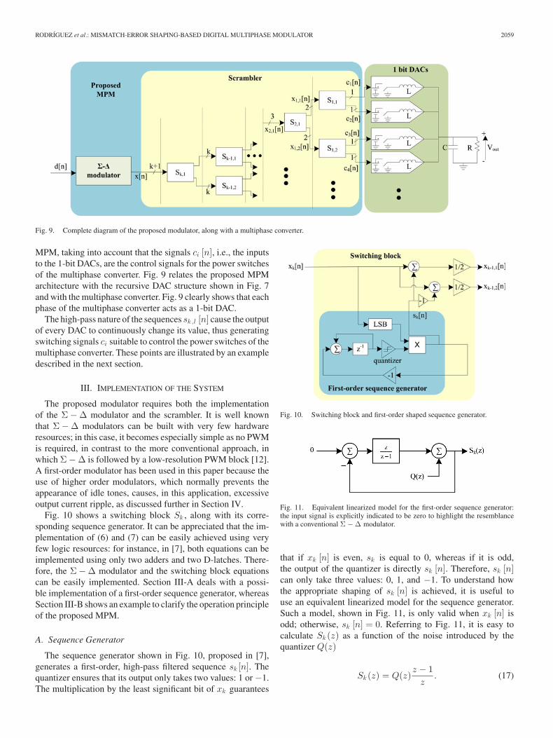
Fig. 9. Complete diagram of the proposed modulator, along with a multiphase converter.
MPM, taking into account that the signals ci [n], i.e., the inputsto the 1-bit DACs, are the control signals for the power switchesof the multiphase converter. Fig. 9 relates the proposed MPMarchitecture with the recursive DAC structure shown in Fig. 7and with the multiphase converter. Fig. 9 clearly shows that eachphase of the multiphase converter acts as a 1-bit DAC.
The high-pass nature of the sequences sk,l [n] cause the outputof every DAC to continuously change its value, thus generatingswitching signals ci suitable to control the power switches of themultiphase converter. These points are illustrated by an exampledescribed in the next section.
III. IMPLEMENTATION OF THE SYSTEM
The proposed modulator requires both the implementationof the Σ − Δ modulator and the scrambler. It is well knownthat Σ − Δ modulators can be built with very few hardwareresources; in this case, it becomes especially simple as no PWMis required, in contrast to the more conventional approach, inwhich Σ − Δ is followed by a low-resolution PWM block [12].A first-order modulator has been used in this paper because theuse of higher order modulators, which normally prevents theappearance of idle tones, causes, in this application, excessiveoutput current ripple, as discussed further in Section IV.
Fig. 10 shows a switching block Sk , along with its corre-sponding sequence generator. It can be appreciated that the im-plementation of (6) and (7) can be easily achieved using veryfew logic resources: for instance, in [7], both equations can beimplemented using only two adders and two D-latches. There-fore, the Σ − Δ modulator and the switching block equationscan be easily implemented. Section III-A deals with a possi-ble implementation of a first-order sequence generator, whereasSection III-B shows an example to clarify the operation principleof the proposed MPM.
A. Sequence Generator
The sequence generator shown in Fig. 10, proposed in [7],generates a first-order, high-pass filtered sequence sk [n]. Thequantizer ensures that its output only takes two values: 1 or −1.The multiplication by the least significant bit of xk guarantees
Fig. 10. Switching block and first-order shaped sequence generator.
Fig. 11. Equivalent linearized model for the first-order sequence generator:the input signal is explicitly indicated to be zero to highlight the resemblancewith a conventional Σ − Δ modulator.
that if xk [n] is even, sk is equal to 0, whereas if it is odd,the output of the quantizer is directly sk [n]. Therefore, sk [n]can only take three values: 0, 1, and −1. To understand howthe appropriate shaping of sk [n] is achieved, it is useful touse an equivalent linearized model for the sequence generator.Such a model, shown in Fig. 11, is only valid when xk [n] isodd; otherwise, sk [n] = 0. Referring to Fig. 11, it is easy tocalculate Sk (z) as a function of the noise introduced by thequantizer Q(z)
Sk (z) = Q(z)z − 1
z. (17)
2060 IEEE TRANSACTIONS ON POWER ELECTRONICS, VOL. 27, NO. 4, APRIL 2012
Fig. 12. Four-level DAC structure MPM with a four-phase buck converter.
Therefore, Sk (z) is a first-order, high-pass filtered versionof Q(z) (which is usually assumed to be approximately whitenoise), and the appropriate high-pass shaping is achieved. Theresemblance with a conventional Σ − Δ modulator becomesnow apparent from Fig. 11.
The idle-tone phenomenon that appears in first-order Σ − Δmodulators can also appear in this sequence generator. Higherorder filtered sequences (or modifications of the first-order gen-erator, as proposed in [7]) can be used to eliminate these tones.Regarding the logic resources required for its implementation,using VHDL and without any hardware optimization procedure,each complete switching block can be synthesized using only 1accumulator, 1 comparator, 6 adders/substractors, and about 20logic gates.
Finally, since the same structure can be used for every switch-ing block, the recursive approach enables the number of phasesto be arbitrarily increased.
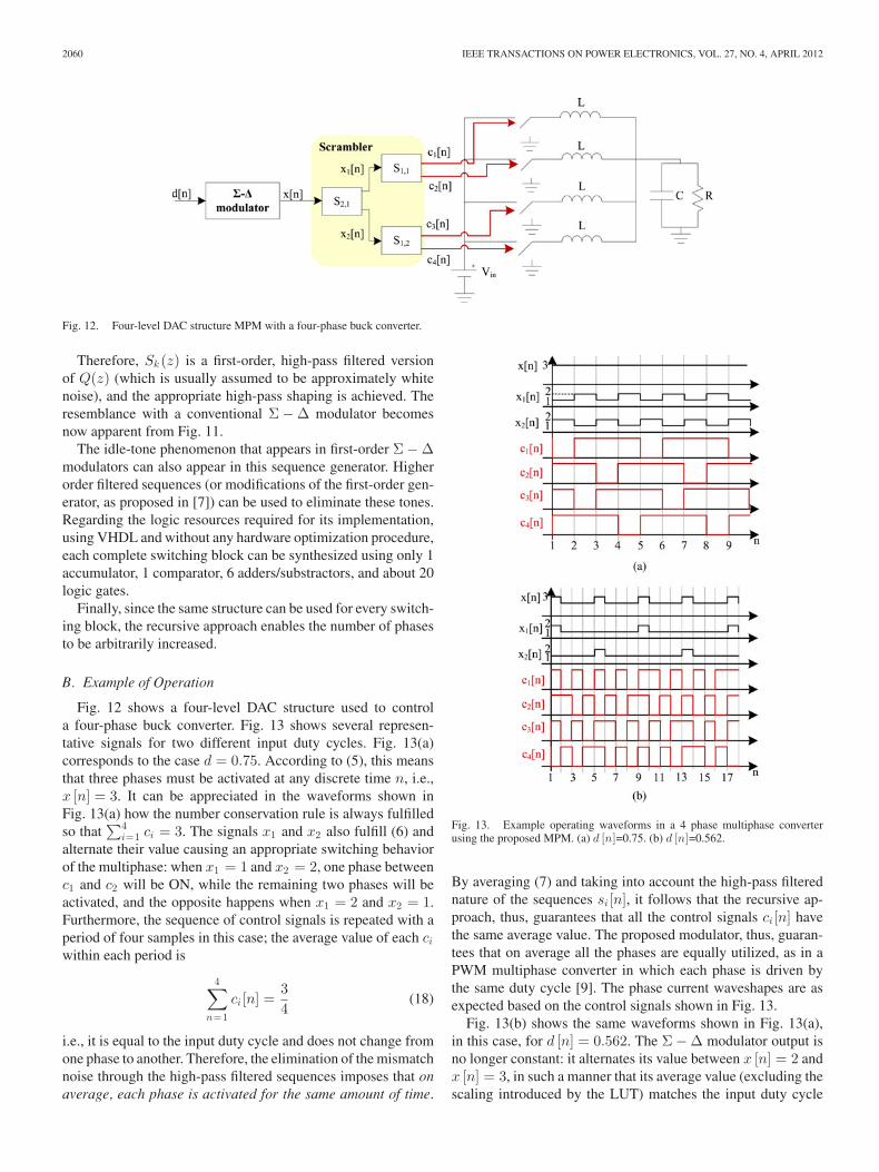
B. Example of Operation
Fig. 12 shows a four-level DAC structure used to controla four-phase buck converter. Fig. 13 shows several represen-tative signals for two different input duty cycles. Fig. 13(a)corresponds to the case d = 0.75. According to (5), this meansthat three phases must be activated at any discrete time n, i.e.,x [n] = 3. It can be appreciated in the waveforms shown inFig. 13(a) how the number conservation rule is always fulfilledso that
∑4i=1 ci = 3. The signals x1 and x2 also fulfill (6) and
alternate their value causing an appropriate switching behaviorof the multiphase: when x1 = 1 and x2 = 2, one phase betweenc1 and c2 will be ON, while the remaining two phases will beactivated, and the opposite happens when x1 = 2 and x2 = 1.Furthermore, the sequence of control signals is repeated with aperiod of four samples in this case; the average value of each ci
within each period is
4∑n=1
ci [n] =34
(18)
i.e., it is equal to the input duty cycle and does not change fromone phase to another. Therefore, the elimination of the mismatchnoise through the high-pass filtered sequences imposes that onaverage, each phase is activated for the same amount of time.
Fig. 13. Example operating waveforms in a 4 phase multiphase converterusing the proposed MPM. (a) d [n]=0.75. (b) d [n]=0.562.
By averaging (7) and taking into account the high-pass filterednature of the sequences si [n], it follows that the recursive ap-proach, thus, guarantees that all the control signals ci [n] havethe same average value. The proposed modulator, thus, guaran-tees that on average all the phases are equally utilized, as in aPWM multiphase converter in which each phase is driven bythe same duty cycle [9]. The phase current waveshapes are asexpected based on the control signals shown in Fig. 13.
Fig. 13(b) shows the same waveforms shown in Fig. 13(a),in this case, for d [n] = 0.562. The Σ − Δ modulator output isno longer constant: it alternates its value between x [n] = 2 andx [n] = 3, in such a manner that its average value (excluding thescaling introduced by the LUT) matches the input duty cycle
RODRIGUEZ et al.: MISMATCH-ERROR SHAPING-BASED DIGITAL MULTIPHASE MODULATOR 2061
command. The signals ci generated by the MPM again fulfillthe number conservation rule, activating the appropriate numberof phases at every time. Furthermore, the sequence of controlsignals is repeated with a period of 16 samples in this case; theaverage value of each ci within each period is
16∑n=1
ci [n] =916
= 0.5625 (19)
i.e., it is again equal to the duty cycle command and does notchange among the phases. In this case, however, the behavioris very different to what would have been obtained using aconventional phase-shifted PWM. Note that according to thedescribed operation, the maximum possible switching frequencyequals one-half of the clock frequency, and it is obtained whenduty cycle command equals 0.5.
IV. SIMULATION RESULTS
Two synchronous buck multiphase converters, with N =4 and N = 16 phases, respectively, were simulated usingSimulink. The most important parameters, see Fig. 1, were:Vin = 12 V, C = 0.4 μF, L = 5.6 μH, and R = 1 Ω. A single,2 MHz clock was used for the entire system and MOSFET ON-resistances and series resistances of the inductances and capac-itance were included in the model. A first-order modulator anda first-order sequence generator were used.
A. Conventional Power Supply Operation
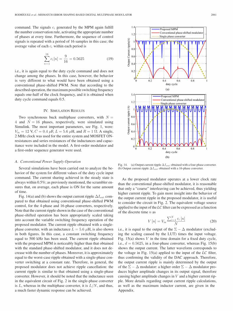
Several simulations have been carried out to analyze the be-havior of the system for different values of the duty cycle inputcommand. The current sharing achieved in the steady state isalways within 0.5%; as previously mentioned, the scrambler en-sures that, on average, each phase is ON for the same amountof time.
Fig. 14(a) and (b) shows the output current ripple ΔIout com-pared to that obtained using conventional phase-shifted PWMcontrol, for the 4-phase and 16-phase converters, respectively.Note that the current ripple shown in the case of the conventionalphase-shifted operation has been appropriately scaled takinginto account the variable switching frequency operation of theproposed modulator. The current ripple obtained with a single-phase converter, with an inductance L = 5.6 μH, is also shownin both figures. In this case, a constant switching frequencyequal to 500 kHz has been used. The current ripple obtainedwith the proposed MPM is noticeably higher than that obtainedwith the standard phase-shifted modulator, and it does not de-crease with the number of phases. Moreover, it is approximatelyequal to the worst-case ripple obtained with a single-phase con-verter switching at a constant rate. Therefore, in general, theproposed modulator does not achieve ripple cancellation: thecurrent ripple is similar to that obtained using a single-phaseconverter. However, it should be noted that the inductance seenin the equivalent circuit of Fig. 2 in the single-phase converteris L, whereas in the multiphase converter, it is L/N , and thus,a much faster dynamic response can be achieved.
Fig. 14. (a) Output current ripple ΔIout obtained with a four-phase converter.(b) Output current ripple ΔIout obtained with a 16-phase converter.
As the proposed modulator operates at a lower clock ratethan the conventional phase-shifted modulator, it is reasonablethat only a “coarse” interleaving can be achieved, thus yieldinghigher current ripple. To gain more insight into the behavior ofthe output current ripple in the proposed modulator, it is usefulto consider the circuit in Fig. 2. The equivalent voltage sourceapplied to the input of the LC filter can be expressed as a functionof the discrete time n as
V [n] = Vin
∑Ni=1 ci [n]
N(20)
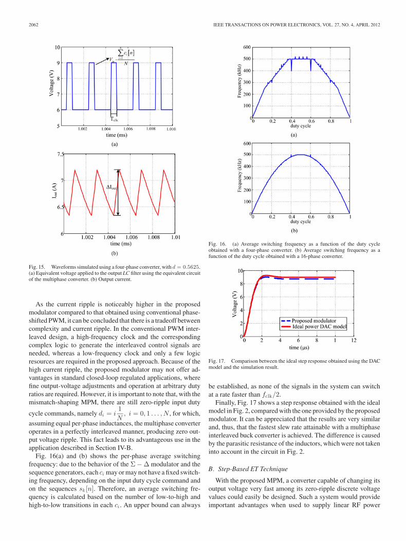
i.e., it is equal to the output of the Σ − Δ modulator (exclud-ing the scaling caused by the LUT) times the input voltage.Fig. 15(a) shows V in the time domain for a fixed duty cycle,i.e., d = 0.5625, in a four-phase converter, whereas Fig. 15(b)shows the output current. The latter waveform corresponds tothe voltage in Fig. 15(a) applied to the input of the LC filter,thus confirming the validity of the DAC approach. Therefore,the output current ripple is mainly determined by the outputof the Σ − Δ modulator: a higher order Σ − Δ modulator pro-duces higher amplitude changes in its output signal, thereforecausing higher amplitude changes in V and a higher current rip-ple. More details regarding output current ripple calculations,as well as the maximum inductor current, are given in theAppendix.
2062 IEEE TRANSACTIONS ON POWER ELECTRONICS, VOL. 27, NO. 4, APRIL 2012
Fig. 15. Waveforms simulated using a four-phase converter, with d = 0.5625.(a) Equivalent voltage applied to the output LC filter using the equivalent circuitof the multiphase converter. (b) Output current.
As the current ripple is noticeably higher in the proposedmodulator compared to that obtained using conventional phase-shifted PWM, it can be concluded that there is a tradeoff betweencomplexity and current ripple. In the conventional PWM inter-leaved design, a high-frequency clock and the correspondingcomplex logic to generate the interleaved control signals areneeded, whereas a low-frequency clock and only a few logicresources are required in the proposed approach. Because of thehigh current ripple, the proposed modulator may not offer ad-vantages in standard closed-loop regulated applications, wherefine output-voltage adjustments and operation at arbitrary dutyratios are required. However, it is important to note that, with themismatch-shaping MPM, there are still zero-ripple input duty
cycle commands, namely di = i1N
, i = 0, 1 . . . , N , for which,
assuming equal per-phase inductances, the multiphase converteroperates in a perfectly interleaved manner, producing zero out-put voltage ripple. This fact leads to its advantageous use in theapplication described in Section IV-B.
Fig. 16(a) and (b) shows the per-phase average switchingfrequency: due to the behavior of the Σ − Δ modulator and thesequence generators, each ci may or may not have a fixed switch-ing frequency, depending on the input duty cycle command andon the sequences sk [n]. Therefore, an average switching fre-quency is calculated based on the number of low-to-high andhigh-to-low transitions in each ci . An upper bound can always
Fig. 16. (a) Average switching frequency as a function of the duty cycleobtained with a four-phase converter. (b) Average switching frequency as afunction of the duty cycle obtained with a 16-phase converter.
Fig. 17. Comparison between the ideal step response obtained using the DACmodel and the simulation result.
be established, as none of the signals in the system can switchat a rate faster than fclk/2.
Finally, Fig. 17 shows a step response obtained with the idealmodel in Fig. 2, compared with the one provided by the proposedmodulator. It can be appreciated that the results are very similarand, thus, that the fastest slew rate attainable with a multiphaseinterleaved buck converter is achieved. The difference is causedby the parasitic resistance of the inductors, which were not takeninto account in the circuit in Fig. 2.
B. Step-Based ET Technique
With the proposed MPM, a converter capable of changing itsoutput voltage very fast among its zero-ripple discrete voltagevalues could easily be designed. Such a system would provideimportant advantages when used to supply linear RF power
RODRIGUEZ et al.: MISMATCH-ERROR SHAPING-BASED DIGITAL MULTIPHASE MODULATOR 2063
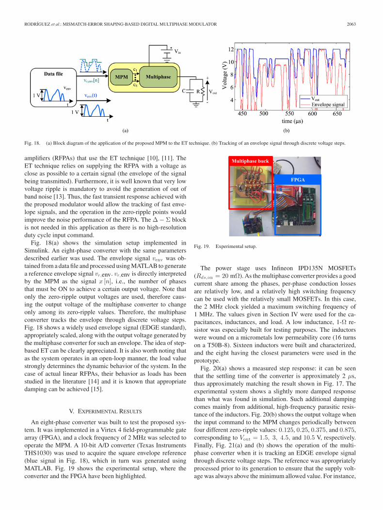
Fig. 18. (a) Block diagram of the application of the proposed MPM to the ET technique. (b) Tracking of an envelope signal through discrete voltage steps.
amplifiers (RFPAs) that use the ET technique [10], [11]. TheET technique relies on supplying the RFPA with a voltage asclose as possible to a certain signal (the envelope of the signalbeing transmitted). Furthermore, it is well known that very lowvoltage ripple is mandatory to avoid the generation of out ofband noise [13]. Thus, the fast transient response achieved withthe proposed modulator would allow the tracking of fast enve-lope signals, and the operation in the zero-ripple points wouldimprove the noise performance of the RFPA. The Δ − Σ blockis not needed in this application as there is no high-resolutionduty cycle input command.
Fig. 18(a) shows the simulation setup implemented inSimulink. An eight-phase converter with the same parametersdescribed earlier was used. The envelope signal venv was ob-tained from a data file and processed using MATLAB to generatea reference envelope signal vr,env. vr,env is directly interpretedby the MPM as the signal x [n], i.e., the number of phasesthat must be ON to achieve a certain output voltage. Note thatonly the zero-ripple output voltages are used, therefore caus-ing the output voltage of the multiphase converter to changeonly among its zero-ripple values. Therefore, the multiphaseconverter tracks the envelope through discrete voltage steps.Fig. 18 shows a widely used envelope signal (EDGE standard),appropriately scaled, along with the output voltage generated bythe multiphase converter for such an envelope. The idea of step-based ET can be clearly appreciated. It is also worth noting thatas the system operates in an open-loop manner, the load valuestrongly determines the dynamic behavior of the system. In thecase of actual linear RFPAs, their behavior as loads has beenstudied in the literature [14] and it is known that appropriatedamping can be achieved [15].
V. EXPERIMENTAL RESULTS
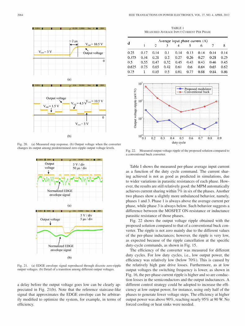
An eight-phase converter was built to test the proposed sys-tem. It was implemented in a Virtex 4 field-programmable gatearray (FPGA), and a clock frequency of 2 MHz was selected tooperate the MPM. A 10-bit A/D converter (Texas InstrumentsTHS1030) was used to acquire the square envelope reference(blue signal in Fig. 18), which in turn was generated usingMATLAB. Fig. 19 shows the experimental setup, where theconverter and the FPGA have been highlighted.
Fig. 19. Experimental setup.
The power stage uses Infineon IPD135N MOSFETs(Rds,on = 20 mΩ). As the multiphase converter provides a goodcurrent share among the phases, per-phase conduction lossesare relatively low, and a relatively high switching frequencycan be used with the relatively small MOSFETs. In this case,the 2 MHz clock yielded a maximum switching frequency of1 MHz. The values given in Section IV were used for the ca-pacitances, inductances, and load. A low inductance, 1-Ω re-sistor was especially built for testing purposes. The inductorswere wound on a micrometals low permeability core (16 turnson a T50B-8). Sixteen inductors were built and characterized,and the eight having the closest parameters were used in theprototype.
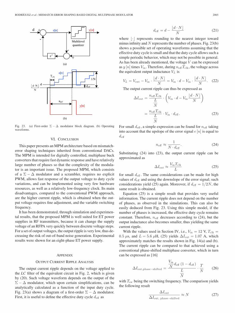
Fig. 20(a) shows a measured step response: it can be seenthat the settling time of the converter is approximately 2 μs,thus approximately matching the result shown in Fig. 17. Theexperimental system shows a slightly more damped responsethan what was found in simulation. Such additional dampingcomes mainly from additional, high-frequency parasitic resis-tance of the inductors. Fig. 20(b) shows the output voltage whenthe input command to the MPM changes periodically betweenfour different zero-ripple values: 0.125, 0.25, 0.375, and 0.875,corresponding to Vout = 1.5, 3, 4.5, and 10.5 V, respectively.Finally, Fig. 21(a) and (b) shows the operation of the multi-phase converter when it is tracking an EDGE envelope signalthrough discrete voltage steps. The reference was appropriatelyprocessed prior to its generation to ensure that the supply volt-age was always above the minimum allowed value. For instance,
2064 IEEE TRANSACTIONS ON POWER ELECTRONICS, VOL. 27, NO. 4, APRIL 2012
Fig. 20. (a) Measured step response. (b) Output voltage when the converterchanges its output among predetermined zero-ripple output voltage levels.
Fig. 21. (a) EDGE envelope signal reproduced through discrete zero-rippleoutput voltages. (b) Detail of a transition among different output voltages.
a delay before the output voltage goes low can be clearly ap-preciated in Fig. 21(b). Note that the reference staircase-likesignal that approximates the EDGE envelope can be arbitrar-ily modified to optimize the system, for example, in terms ofefficiency.
TABLE 1MEASURED AVERAGE INPUT CURRENT PER PHASE
Fig. 22. Measured output voltage ripple of the proposed solution compared toa conventional buck converter.
Table I shows the measured per-phase average input currentas a function of the duty cycle command. The current shar-ing achieved is not as good as predicted in simulations, dueto wider variations in parasitic resistances of each phase. How-ever, the results are still relatively good: the MPM automaticallyachieves current sharing within 7% in six of the phases. Anothertwo phases show a slightly more unbalanced behavior, namely,phases 1 and 3. Phase 1 is always above the average current perphase, while phase 3 is always below. Such behavior suggests adifference between the MOSFET ON-resistance or inductanceparasitic resistance of those phases.
Fig. 22 shows the output voltage ripple obtained with theproposed solution compared to that of a conventional buck con-verter. The ripple is not zero mainly due to the different valuesof the per-phase inductances; however, the ripple is very low,as expected because of the ripple cancellation at the specificduty-cycle commands, as shown in Fig. 15.
The efficiency of the converter was measured for differentduty cycles. For low duty cycles, i.e., low output power, theefficiency was relatively low (below 70%). This is caused bythe relatively high gate drive losses. Furthermore, as at lowoutput voltages the switching frequency is lower, as shown inFig. 16, the per-phase current ripple is higher and so are conduc-tion losses in the semiconductors and the output inductances. Adifferent control strategy could be adopted to increase the effi-ciency at low output power, for instance, using only half of thephases to generate fewer voltage steps. The efficiency at higheroutput power was above 90%, reaching nearly 95% at 90 W. Noforced cooling or heat sinks were needed.
RODRIGUEZ et al.: MISMATCH-ERROR SHAPING-BASED DIGITAL MULTIPHASE MODULATOR 2065
Fig. 23. (a) First-order Σ − Δ modulator block diagram. (b) Operatingwaveforms.
VI. CONCLUSION
This paper presents an MPM architecture based on mismatch-error shaping techniques inherited from conventional DACs.The MPM is intended for digitally controlled, multiphase buckconverters that require fast dynamic response and have relativelylarge number of phases so that the complexity of the modula-tor is an important issue. The proposed MPM, which consistsof a Σ − Δ modulator and a scrambler, requires no explicitPWM, allows fast response of the output voltage to duty cyclevariations, and can be implemented using very few hardwareresources, as well as a relatively low-frequency clock. Its maindisadvantages, compared to the conventional PWM approach,are the higher current ripple, which is obtained when the out-put voltage requires fine adjustment, and the variable switchingfrequency.
It has been demonstrated, through simulation and experimen-tal results, that the proposed MPM is well suited for ET powersupplies in RF transmitters, because it can change the supplyvoltage of an RFPA very quickly between discrete voltage steps.For a set of output voltages, the output ripple is very low, thus de-creasing the risk of out-of-band noise generation. Experimentalresults were shown for an eight-phase ET power supply.
APPENDIX
OUTPUT CURRENT RIPPLE ANALYSIS
The output current ripple depends on the voltage applied tothe LC filter of the equivalent circuit in Fig. 2, which is givenby (20). Such voltage waveform depends on the output of theΣ − Δ modulator, which upon certain simplifications, can beanalytically calculated as a function of the input duty cycle.Fig. 23(a) shows a diagram of a first-order Σ − Δ modulator.First, it is useful to define the effective duty cycle deff as
deff = d − �d · N�N
(21)
where �·� represents rounding to the nearest integer towardminus infinity and N represents the number of phases. Fig. 23(b)shows a possible set of operating waveforms assuming that theeffective duty cycle is small and that the duty cycle allows such asimple periodic behavior, which may not be possible in general.As has been already mentioned, the voltage V can be expressedas y [n] times Vin . Therefore, during noff Tclk , the voltage acrossthe equivalent output inductance VL is
VL = Vout − Vin · �d · N�N
= Vin · d − Vin · �d · N�N
. (22)
The output current ripple can thus be expressed as
ΔIout =noff Tclk
L
N
·(
Vin · d − Vin�d · N�
N
)
=noff Tclk
L
N
· Vin · deff . (23)
For small deff , a simple expression can be found for noff takinginto account that the upslope of the error signal e [n] is equal todeff
noff ≈ 1N · deff
. (24)
Substituting (24) into (23), the output current ripple can beapproximated as
ΔIout ≈VinTclk
L(25)
for small deff . The same considerations can be made for highvalues of deff and using the downslope of the error signal; suchconsiderations yield (25) again. Moreover, if deff = 1/2N , thesame result is obtained.
Equation (25) is a simple result that provides very usefulinformation. The current ripple does not depend on the numberof phases, as observed in the simulations. This can also beeasily deduced from Fig. 23. Using this simple model, if thenumber of phases is increased, the effective duty cycle remainsconstant. Therefore, noff decreases according to (24), but theoutput inductance also becomes smaller, thus yielding the samecurrent ripple.
With the values used in Section IV, i.e., Vin = 12 V, Tclk =0.5 μs, and L = 5.6 μH, (25) yields ΔIout = 1.07 A, whichapproximately matches the results shown in Fig. 14(a) and (b).The current ripple can be compared to that achieved using aconventional phase-shifted multiphase converter, which in turncan be expressed as [16]
ΔIout,phase−shifted =
Vin
Ndeff (1 − deff )
L
N
· T
N(26)
with Tsw being the switching frequency. The comparison yieldsthe following result
ΔIout
ΔIout, phase−shifted≈ N (27)
2066 IEEE TRANSACTIONS ON POWER ELECTRONICS, VOL. 27, NO. 4, APRIL 2012
i.e., the output current ripple using the proposed modulator is Ntimes higher than that in a conventional phase-shifted N-phaseconverter. Such a result again matches the differences observedin Fig. 14(a) and (b).
The previous considerations can also be applied to determinethe maximum per-phase current. According to Fig. 23, for highvalues of the duty cycle, the output of the Σ − Δ modulator
y[n] will alternate its value between 1 and 1 − 1N
. Taking into
account the averaging properties of the Σ − Δ modulator, it canbe assumed that most of the time, y[n] takes a value equal to
1, whereas the minimum amount of time that it outputs 1 − 1N
is Tclk . Therefore, one of the phases is turned OFF during Tclk ,and its current ripple ΔIphase can be approximated as
ΔIphase =Vout,maxTclk
L(28)
with Vout,max being the maximum output voltage, which can beapproximated by Vin . Then, the peak inductor current Iphase,maxis
Iphase,max ≈ Io,max
N+
VinTclk
2L(29)
with Io,max being the maximum output current.Finally, it is worth pointing out that both (25) and (29) have
been obtained assuming that the Σ − Δ modulator operates ina very simple manner. This is not generally true due to theinherent nonlinear behavior of Σ − Δ modulators. Thus, theresults presented in this Appendix are intended to serve as aguide to approximately calculate the output current ripple in theproposed MPM.
REFERENCES
[1] X. Zhou, X. Zhang, J. Liu, P. L. Wong, J. Chen, H. P. Wu, L. Amoroso, F.C. Lee, and D. Y. Chen, “Investigation of candidate VRM topologies forfuture microprocessors,” in Proc. IEEE Appl. Power Electron. Conf., Feb.1998, pp. 145–150.
[2] O. Garcıa, P. Zumel, A. de Castro, and J. A. Cobos, “Automotive dc–dcbidirectional converter made with many interleaved buck stages,” IEEETrans. Power Electron., vol. 21, no. 3, pp. 578–586, May 2006.
[3] Y. Qiu, M. Xu, K. Yao, J. Sun, and F. C. Lee, “The multifrequency small-signal model for buck and multiphase interleaving buck converters,” inProc. IEEE Appl. Power Electron. Conf., Feb. 2005, pp. 392–398.
[4] X. Zhang, Y. Zhang, R. Zane, and D. Maksimovic, “Design and imple-mentation of a wide-bandwidth digitally controlled 16-phase converter,”in Proc. IEEE Control Model. Power Electron., Jul. 2006, pp. 106–111.
[5] Y. Zhang, X. Zhang, R. Zane, and D. Maksimovic, “Wide-bandwidthdigital multi-phase controller,” in Proc. IEEE Power Electron. Spec. Conf.,Jun. 2006, pp. 3101–3107.
[6] T. Carosa, R. Zane, and D. Maksimovic, “Scalable digital multiphasemodulator,” IEEE Trans. Power Electron., vol. 23, no. 4, pp. 2201–2205,Jul. 2008.
[7] I. Galton, “Spectral shaping of circuit errors in digital-to-analog convert-ers,” IEEE Trans. Circuits Syst. II, Analog Digital Signal Process., vol. 44,no. 10, pp. 808–817, Oct. 1997.
[8] R. Schreier and G. Temes, Understanding Delta-Sigma Data Converters.Piscataway, NJ: IEEE Press/Wiley, 2004.
[9] A. V. Peterchev, J. Xiao, and S. R. Sanders, “Architecture and IC imple-mentation of a digital VRM controller,” IEEE Trans. Power Electron.,vol. 18, no. 1, pp. 356–364, Jan. 2003.
[10] G. Hanington, P. Chen, P. Asbeck, and L. Larson, “High–efficiency poweramplifier using dynamic power-supply voltage for CDMA applications,”IEEE Trans. Microw. Theory Tech., vol. 47, no. 8, pp. 1471–1476, Aug.1999.
[11] P. Midya, K. Haddad, L. Connell, S. Bergsted, and B. Roeckner, “Track-ing power converter for supply modulation of RFPA,” in Proc. IEEEPower Electron. Spec. Conf., Vancouver, Canada, Jul. 17–22, 2001, pp.1540–1545.
[12] Z. Lukic and A. Prodic, “Multibit sigma-delta PWM digital controller ICfor dc–dc converters operating at switching frequencies beyond 10 MHz,”IEEE Trans. Power Electron., vol. 22, no. 5, pp. 1693–1707, Sep. 2007.
[13] J. Stauth and S. Sanders, “Power supply rejection for RF amplifiers: Theoryand measurements,” IEEE Trans. Microw. Theory Tech., vol. 55, no. 10,pp. 2043–2052, Oct. 2007.
[14] M. Hoyerby and M. Andersen, “TEDS base-station power amplifier usinglow-noise envelope tracking power supply,” IEEE Trans. Microw. TheoryTech., vol. 57, no. 7, pp. 1687–1693, Jul. 2009.
[15] M. Rodrıguez, P. F. Miaja, A. Rodrıguez, and J. Sebastian, “Multiple-inputbuck converter optimized for accurate envelope tracking in RF poweramplifiers,” in Proc. IEEE Appl. Power Electron. Conf., Feb. 2010, pp.715–722.
[16] O. Garcıa, A. de Castro, P. Zumel, and J. Cobos, “Digital-control basedsolution to the effect of nonidealities of the inductors in multiphase con-verters,” IEEE Trans. Power Electron., vol. 22, no. 6, pp. 2155–2163,Nov. 2007.
Miguel Rodrıguez (S’06) was born in Gijon, Spain, in 1982. He received theM.S. and the Ph.D. degrees in telecommunication engineering from the Univer-sity of Oviedo, Gijon, Spain, in 2006 and 2011, respectively.
Since January 2011, he has been a Research Associate at the ColoradoPower Electronics Center, Department of Electrical, Computer, and Energy En-gineering, University of Colorado, Boulder. His research interests include dc/dcconversion, digital control of switched converters, and power-supply systemsfor RF amplifiers.
Pablo F. Miaja (S’08) was born in Oviedo, Spain, in 1984. He received the M.S.degree in telecommunication engineering from the University of Oviedo, Gijon,Spain, in 2007. He is currently working toward the Ph.D. degree at the PowerSupply Systems Group, Department of Electrical and Electronic Engineering,University of Oviedo, Gijon, Spain, under a grant from the Spanish Ministry ofScience and Technology to study dc–dc converters to feed RFPAs.
His research interests include dc–dc converters, digital control of switchingpower supplies, and techniques to increase the efficiency of RFPAs, such as ET.
Javier Sebastian (M’87–SM’11) was born in Madrid, Spain, in 1958. He re-ceived the M.Sc. degree from the Polytechnic University of Madrid, Madrid,Spain, in 1981, and the Ph.D. degree from the University of Oviedo, Gijon,Spain, in 1985.
He was an Assistant Professor and an Associate Professor with both thePolytechnic University of Madrid and the University of Oviedo. Since 1992,he has been a Professor with the University of Oviedo. His research interestsinclude switching-mode power supplies, modeling of dc-to-dc converters, low-output-voltage dc-to-dc converters, and high-power-factor rectifiers.
Dragan Maksimovic (M’89–SM’04) received the B.S. and M.S. degrees inelectrical engineering from the University of Belgrade, Yugoslavia, in 1984 and1986, respectively, and the Ph.D. degree from the California Institute of Tech-nology, Pasadena, in 1989.
From 1989 to 1992, he was with the University of Belgrade, Serbia (Yu-goslavia). Since 1992, he has been with the Department of Electrical, Computerand Energy Engineering, University of Colorado, Boulder, where he is cur-rently a Professor and the Director of the Colorado Power Electronics Center.His current research interests include mixed-signal integrated circuit design forcontrol of power electronics, digital control techniques, and energy efficiencyand renewable energy applications of power electronics.
Prof. Maksimovic received the 1997 NSF CAREER Award, the IEEE PowerElectronics Society Transactions Prize Paper Award in 1997, the IEEE PowerElectronics Society Prize Letter Awards in 2009 and 2010, the Holland Excel-lence in Teaching Awards in 2004 and 2011, and the University of ColoradoInventor of the Year Award in 2006.