minimization and transformation of sequential machines
TRANSCRIPT

Department of Electronics and Communication Engineering, VBIT
Minimization and Transformation
of Sequential Machines
P.VIDYA SAGAR ( ASSOCIATE PROFESSOR)
https://potharajuvidyasagar.wordpress.com
Department of Electronics and Communication Engineering, VBIT
http
s:/
/poth
ara
juvid
yasagar.w
ord
pre
ss.c
om
Department of Electronics and Communication Engineering, VBIT
http
s:/
/poth
ara
juvid
yasagar.w
ord
pre
ss.c
om
Sequential logic circuits
➢ The main characteristic of combinational logic circuits is that their output values depend on
their present input values.
➢ Sequential logic circuits differ from combinational logic circuits because they contain memory
elements so that their output values depend on both present and past input values
➢ Sequential circuits can be Asynchronous or synchronous.
➢ Asynchronous sequential circuits change their states and output values whenever a change
in input values occurs.
➢ Synchronous sequential circuits change their states and output values at fixed points of
time, i.e. clock signals.
VIDYA SAGAR P2
Department of Electronics and Communication Engineering, VBIT
http
s:/
/poth
ara
juvid
yasagar.w
ord
pre
ss.c
om
Department of Electronics and Communication Engineering, VBIT
http
s:/
/poth
ara
juvid
yasagar.w
ord
pre
ss.c
om
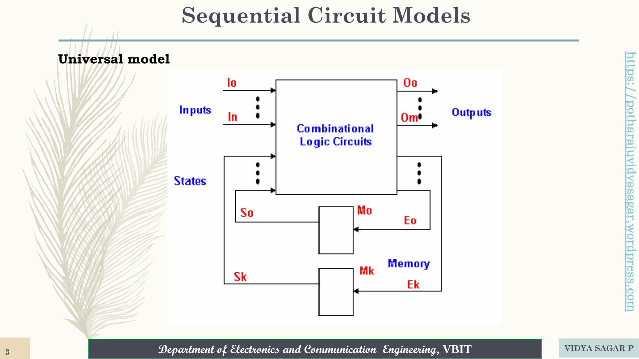
Sequential Circuit Models
Universal model
VIDYA SAGAR P3
Department of Electronics and Communication Engineering, VBIT
http
s:/
/poth
ara
juvid
yasagar.w
ord
pre
ss.c
om
Department of Electronics and Communication Engineering, VBIT
http
s:/
/poth
ara
juvid
yasagar.w
ord
pre
ss.c
om
Combinational
CircuitMemory
Elements
Inputs Outputs
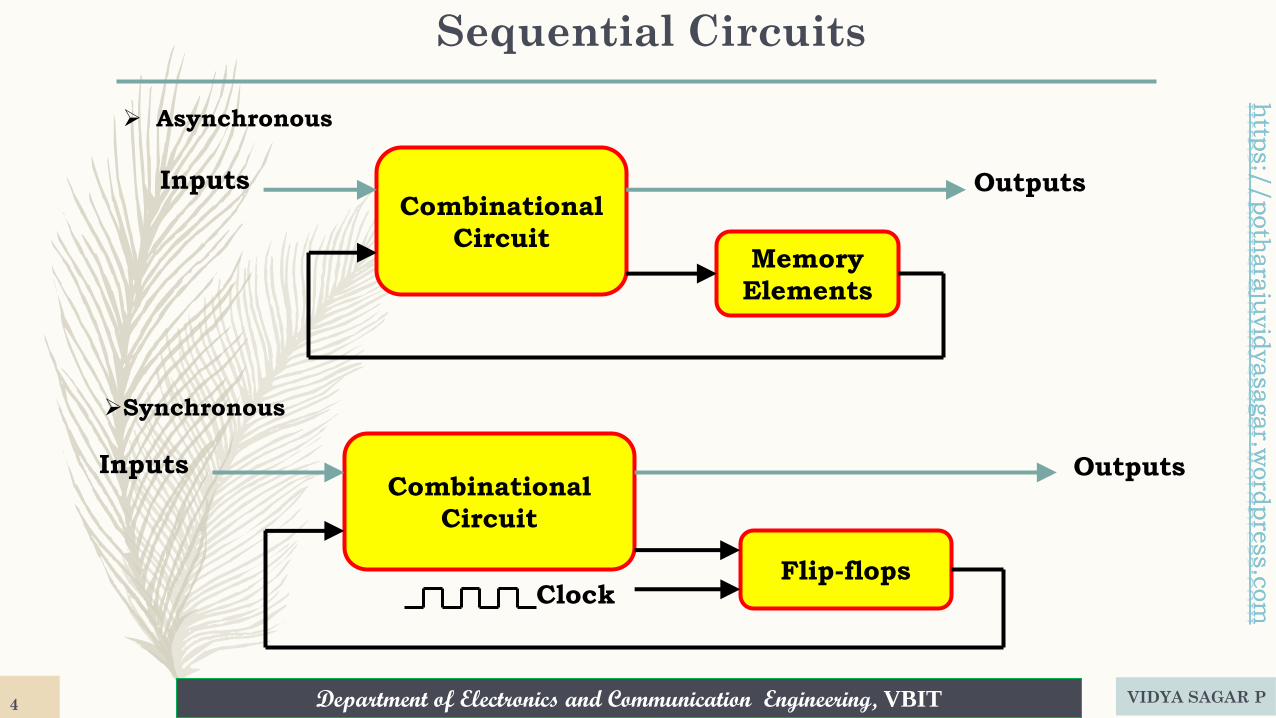
➢ Asynchronous
Combinational
Circuit
Flip-flops
Inputs Outputs
Clock
➢Synchronous
Sequential Circuits
VIDYA SAGAR P4
Department of Electronics and Communication Engineering, VBIT
http
s:/
/poth
ara
juvid
yasagar.w
ord
pre
ss.c
om
Department of Electronics and Communication Engineering, VBIT
http
s:/
/poth
ara
juvid
yasagar.w
ord
pre
ss.c
om
Synchronous Sequential Circuit
➢ The change of internal state occurs in response to the synchronized clock pulses.
➢ Input changes occur between clock pulses
➢ Data are read during the clock pulse
➢ It is supposed to wait long enough after the external input changes for all flip-flop inputs to
reach a steady value before applying the new clock pulse
➢ Unsuitable Situations:
➢ Inputs change at any time and cannot be synchronized with a clock
➢ Circuit is large, Clock skew can not be avoided
➢ High performance design
VIDYA SAGAR P5
Department of Electronics and Communication Engineering, VBIT
http
s:/
/poth
ara
juvid
yasagar.w
ord
pre
ss.c
om
Department of Electronics and Communication Engineering, VBIT
http
s:/
/poth
ara
juvid
yasagar.w
ord
pre
ss.c
om
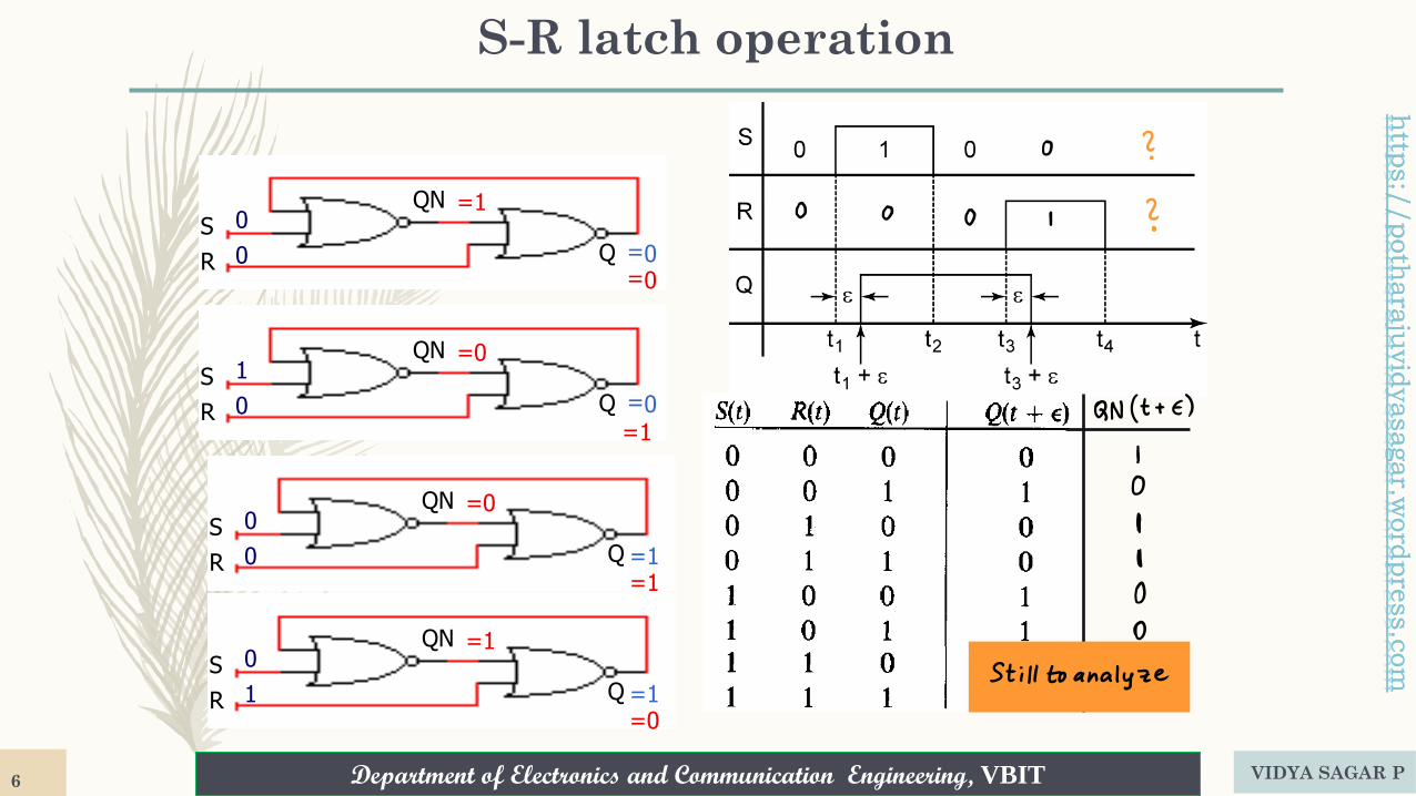
S-R latch operation
VIDYA SAGAR P6
S
R
QN
Q
0
0
0=
=1
S
R
QN
Q
1
00=
=0
=1
0=S
R
QN
Q
0
0 =1
=0
=1
S
R
QN
Q
0
1 =1
=1
=0
Department of Electronics and Communication Engineering, VBIT
http
s:/
/poth
ara
juvid
yasagar.w
ord
pre
ss.c
om
Department of Electronics and Communication Engineering, VBIT
http
s:/
/poth
ara
juvid
yasagar.w
ord
pre
ss.c
om
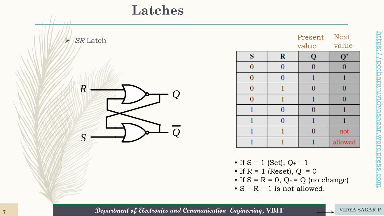
Latches
➢ SR Latch
R
S
Q
Q
• If S = 1 (Set), Q+ = 1
• If R = 1 (Reset), Q+ = 0
• If S = R = 0, Q+ = Q (no change)
• S = R = 1 is not allowed.
Present
value
Next
value
VIDYA SAGAR P7
Department of Electronics and Communication Engineering, VBIT
http
s:/
/poth
ara
juvid
yasagar.w
ord
pre
ss.c
om
Department of Electronics and Communication Engineering, VBIT
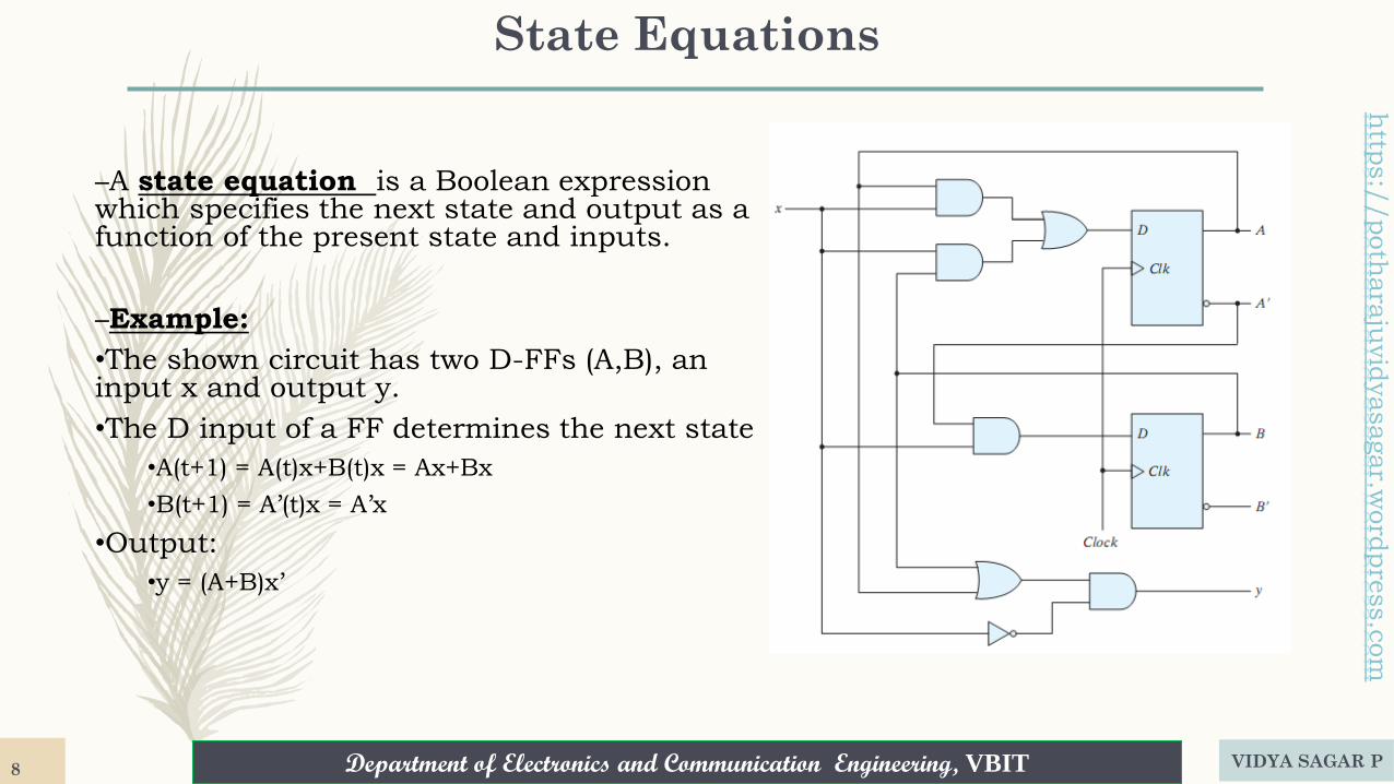
State Equations
–A state equation is a Boolean expression which specifies the next state and output as a function of the present state and inputs.
–Example:
•The shown circuit has two D-FFs (A,B), an input x and output y.
•The D input of a FF determines the next state
•A(t+1) = A(t)x+B(t)x = Ax+Bx
•B(t+1) = A’(t)x = A’x
•Output:
•y = (A+B)x’
VIDYA SAGAR P8
Department of Electronics and Communication Engineering, VBIT
http
s:/
/poth
ara
juvid
yasagar.w
ord
pre
ss.c
om
Department of Electronics and Communication Engineering, VBIT
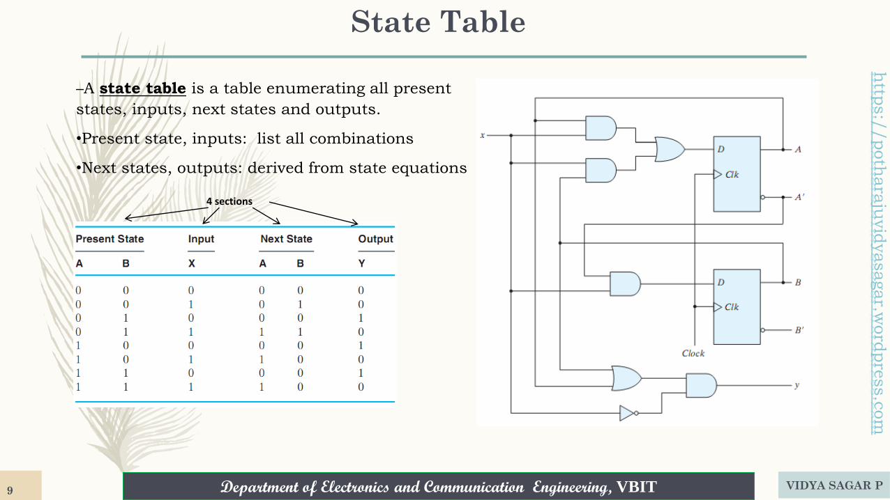
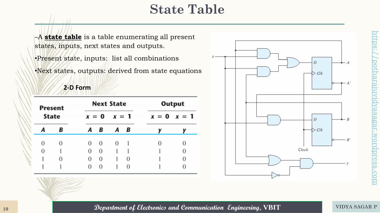
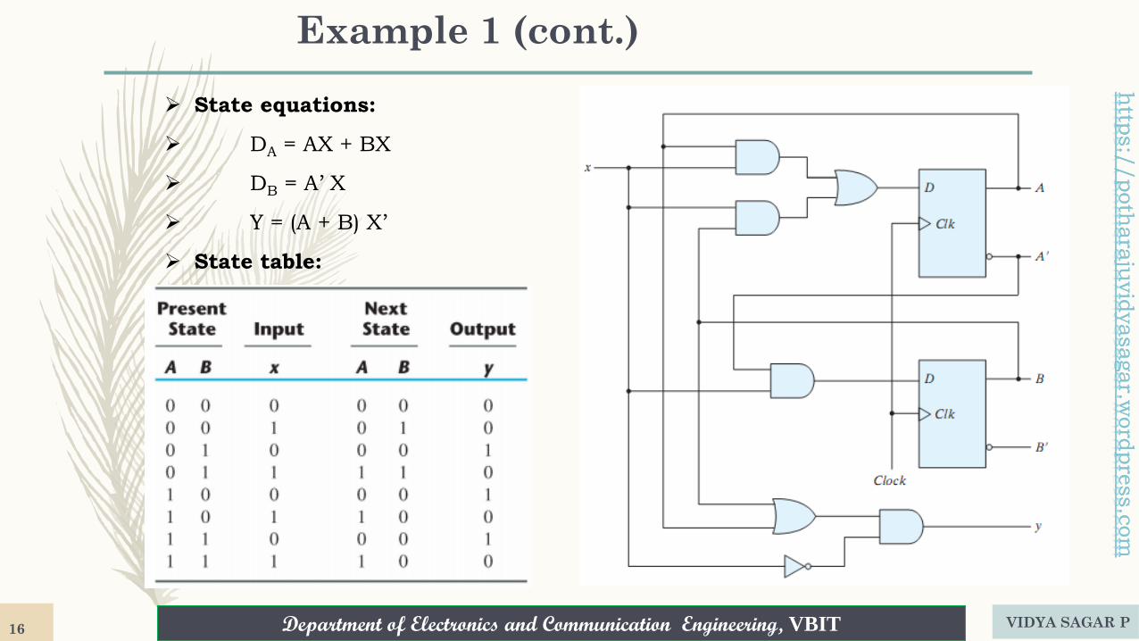
State Table
–A state table is a table enumerating all present
states, inputs, next states and outputs.
•Present state, inputs: list all combinations
•Next states, outputs: derived from state equations
4 sections
VIDYA SAGAR P9
Department of Electronics and Communication Engineering, VBIT
http
s:/
/poth
ara
juvid
yasagar.w
ord
pre
ss.c
om
Department of Electronics and Communication Engineering, VBIT
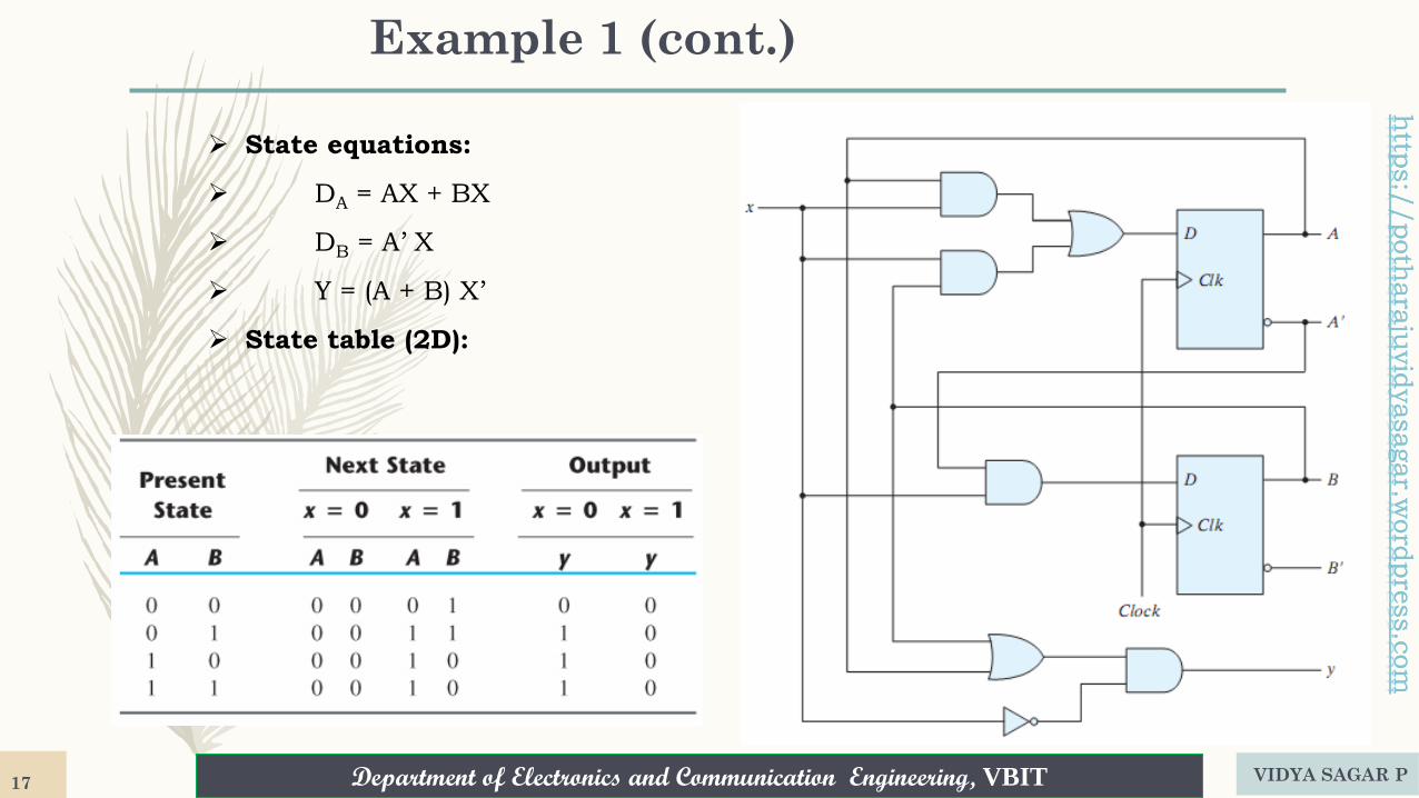
State Table
2-D Form
–A state table is a table enumerating all present
states, inputs, next states and outputs.
•Present state, inputs: list all combinations
•Next states, outputs: derived from state equations
VIDYA SAGAR P10
Department of Electronics and Communication Engineering, VBIT
http
s:/
/poth
ara
juvid
yasagar.w
ord
pre
ss.c
om
Department of Electronics and Communication Engineering, VBIT
http
s:/
/poth
ara
juvid
yasagar.w
ord
pre
ss.c
om
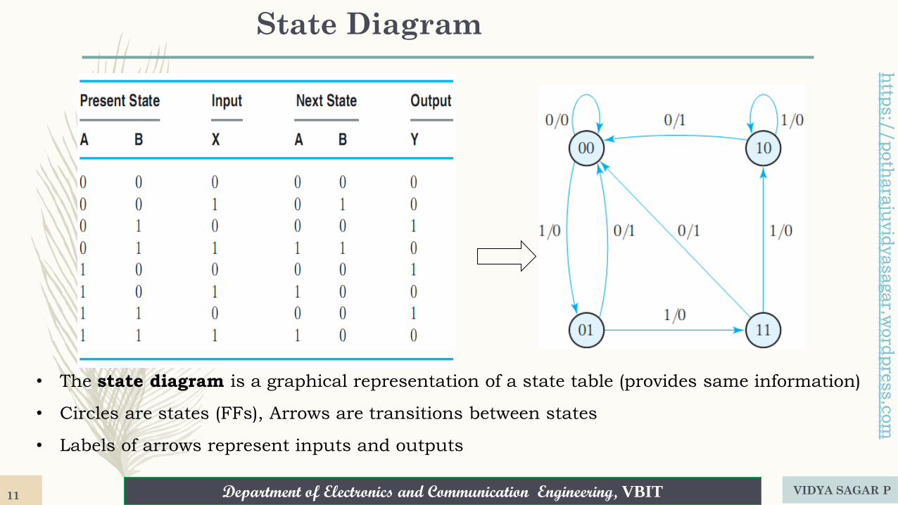
State Diagram
• The state diagram is a graphical representation of a state table (provides same information)
• Circles are states (FFs), Arrows are transitions between states
• Labels of arrows represent inputs and outputs
VIDYA SAGAR P11
Department of Electronics and Communication Engineering, VBIT
http
s:/
/poth
ara
juvid
yasagar.w
ord
pre
ss.c
om
Department of Electronics and Communication Engineering, VBIT
http
s:/
/poth
ara
juvid
yasagar.w
ord
pre
ss.c
om
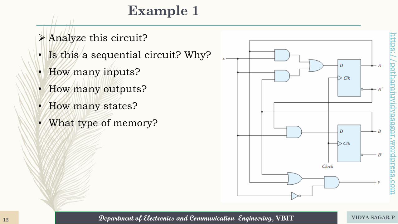
Example 1
➢ Analyze this circuit?
• Is this a sequential circuit? Why?
• How many inputs?
• How many outputs?
• How many states?
• What type of memory?
VIDYA SAGAR P12
Department of Electronics and Communication Engineering, VBIT
http
s:/
/poth
ara
juvid
yasagar.w
ord
pre
ss.c
om
Department of Electronics and Communication Engineering, VBIT
http
s:/
/poth
ara
juvid
yasagar.w
ord
pre
ss.c
om
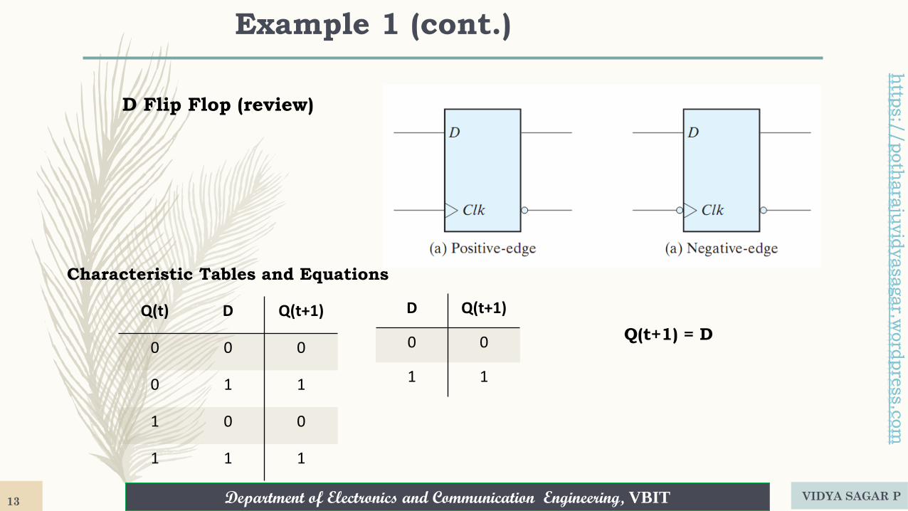
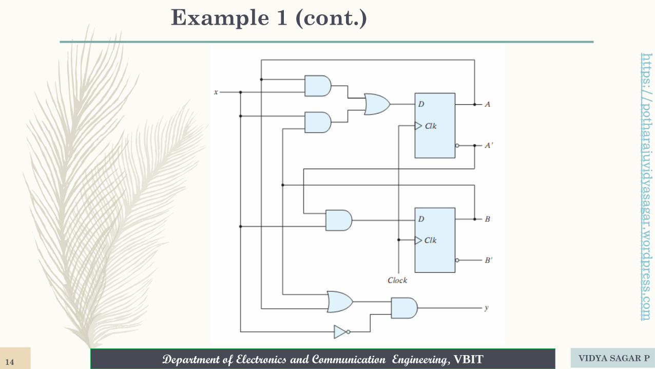
Example 1 (cont.)
Q(t) D Q(t+1)
0 0 0
0 1 1
1 0 0
1 1 1
D Q(t+1)
0 0
1 1
Q(t+1) = D
Characteristic Tables and Equations
D Flip Flop (review)
VIDYA SAGAR P13
Department of Electronics and Communication Engineering, VBIT
http
s:/
/poth
ara
juvid
yasagar.w
ord
pre
ss.c
om
Department of Electronics and Communication Engineering, VBIT
http
s:/
/poth
ara
juvid
yasagar.w
ord
pre
ss.c
om
Example 1 (cont.)
VIDYA SAGAR P14
Department of Electronics and Communication Engineering, VBIT
http
s:/
/poth
ara
juvid
yasagar.w
ord
pre
ss.c
om
Department of Electronics and Communication Engineering, VBIT
http
s:/
/poth
ara
juvid
yasagar.w
ord
pre
ss.c
om
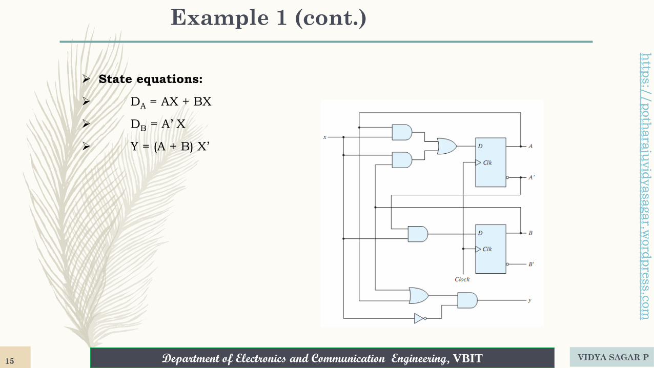
Example 1 (cont.)
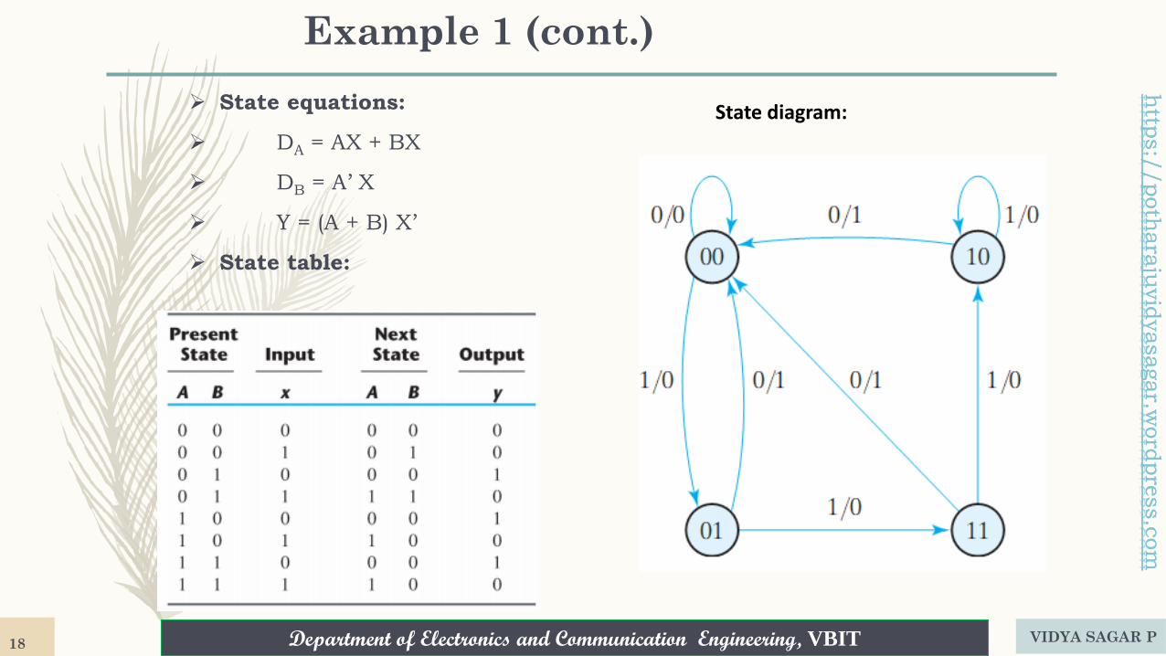
➢ State equations:
➢ DA = AX + BX
➢ DB = A’ X
➢ Y = (A + B) X’
VIDYA SAGAR P15
Department of Electronics and Communication Engineering, VBIT
http
s:/
/poth
ara
juvid
yasagar.w
ord
pre
ss.c
om
Department of Electronics and Communication Engineering, VBIT
http
s:/
/poth
ara
juvid
yasagar.w
ord
pre
ss.c
om
Example 1 (cont.)
➢ State equations:
➢ DA = AX + BX
➢ DB = A’ X
➢ Y = (A + B) X’
➢ State table:
VIDYA SAGAR P16
Department of Electronics and Communication Engineering, VBIT
http
s:/
/poth
ara
juvid
yasagar.w
ord
pre
ss.c
om
Department of Electronics and Communication Engineering, VBIT
http
s:/
/poth
ara
juvid
yasagar.w
ord
pre
ss.c
om
Example 1 (cont.)
➢ State equations:
➢ DA = AX + BX
➢ DB = A’ X
➢ Y = (A + B) X’
➢ State table (2D):
VIDYA SAGAR P17
Department of Electronics and Communication Engineering, VBIT
http
s:/
/poth
ara
juvid
yasagar.w
ord
pre
ss.c
om
Department of Electronics and Communication Engineering, VBIT
http
s:/
/poth
ara
juvid
yasagar.w
ord
pre
ss.c
om
Example 1 (cont.)
➢ State equations:
➢ DA = AX + BX
➢ DB = A’ X
➢ Y = (A + B) X’
➢ State table:
State diagram:
VIDYA SAGAR P18
Department of Electronics and Communication Engineering, VBIT
http
s:/
/poth
ara
juvid
yasagar.w
ord
pre
ss.c
om
Department of Electronics and Communication Engineering, VBIT
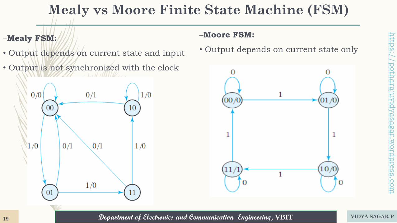
Mealy vs Moore Finite State Machine (FSM)
–Mealy FSM:
• Output depends on current state and input
• Output is not synchronized with the clock
–Moore FSM:
• Output depends on current state only
VIDYA SAGAR P19
Department of Electronics and Communication Engineering, VBIT
http
s:/
/poth
ara
juvid
yasagar.w
ord
pre
ss.c
om
Department of Electronics and Communication Engineering, VBIT
http
s:/
/poth
ara
juvid
yasagar.w
ord
pre
ss.c
om
Sequential network as FSM (finite state machines)
➢ State minimization
➢ DEFINITION OF 1-SUCCESSOR : If the machine moves from state Si to state Sv when input
w = 1, then we say that Sv is a 1-successor of Si
➢ DEFINITION OF 0-SUCCESSOR : If the machine moves from state Sj to state Su when input
w = 0, then we say that Su is a 0-successor of Si
➢ DEFINITION: Two states Si and Sj are said to be equivalent if and only if for every input
sequence , the same output sequence will be produced regardless of whether Si or Sj are
the initial states.
➢ IF STATES Si AND Sj ARE EQUIVALENT, THEN THEIR
➢ CORRESPONDING K-SUCCESSORS (FOR ALL K) ARE THE SAME OR ARE ALSO
EQUIVALENT.
VIDYA SAGAR P20
Department of Electronics and Communication Engineering, VBIT
http
s:/
/poth
ara
juvid
yasagar.w
ord
pre
ss.c
om
Department of Electronics and Communication Engineering, VBIT
http
s:/
/poth
ara
juvid
yasagar.w
ord
pre
ss.c
om
State equivalence and machine minimization
➢ In constructing the state diagram (or table) for a finite-state machine, it often happens that the
diagram contains redundant states, i.e., states whose functions can be accomplished by other
states. We note that the number of memory elements required for the realization of a machine
is directly related to the number of states. (Recall that, for an n-state machine, k = log2 n state
variables are needed for an assignment.) Consequently, the minimization of the number of
states does reduce the complexity and cost of the realization in many cases.
➢ It is, therefore, desirable to develop techniques for transforming a given machine into another
machine that has no redundant states, such that both have the same terminal behavior.
VIDYA SAGAR P21
Department of Electronics and Communication Engineering, VBIT
http
s:/
/poth
ara
juvid
yasagar.w
ord
pre
ss.c
om
Department of Electronics and Communication Engineering, VBIT
http
s:/
/poth
ara
juvid
yasagar.w
ord
pre
ss.c
om
Equivalent State & distinguishable Definitions
➢ Two states are equivalent if their response for each possible input sequence is an identical
output sequence.
➢ Alternatively, two states are equivalent if their outputs produced for each input symbol is
identical and their next states for each input symbol are the same or equivalent.
➢ Two states that are not equivalent are distinguishable
➢ Two states, Si and Sj , of a machine M are distinguishable if and only if there exists at least
one finite input sequence that, when applied to M, causes different output sequences
depending on whether Si or Sj is the initial state.
➢ The sequence that distinguishes these states is called a distinguishing sequence for the pair
(Si, Sj ).
VIDYA SAGAR P22
Department of Electronics and Communication Engineering, VBIT
http
s:/
/poth
ara
juvid
yasagar.w
ord
pre
ss.c
om
Department of Electronics and Communication Engineering, VBIT
http
s:/
/poth
ara
juvid
yasagar.w
ord
pre
ss.c
om
(machine minimization)State Reduction:
➢ The three main methods of state reduction include:
➢ 1. row matching,
➢ 2. implication charts, and
➢ 3. Successive partitioning.
1.Row matching, which is the easiest of the three, works well for state transition tables which
have an obvious next state and output equivalences for each of the present states. This method
will generally not give the most simplified state machine available, but its ease of use and
consistently fair results is a good reason to pursue the method. The implication chart uses a
graphical grid to help find any implications or equivalences and is a great systematic approach to
reducing state machines. Successive partitioning is almost a cross between row matching and
implication chart where both a graphical table and equivalent matching is used.
➢ Each of these methods will, in most cases, reduce a state machine into a smaller number of
states. Keep in mind that one method may result in a simpler state machine than another.
VIDYA SAGAR P23
Department of Electronics and Communication Engineering, VBIT
http
s:/
/poth
ara
juvid
yasagar.w
ord
pre
ss.c
om
Department of Electronics and Communication Engineering, VBIT
http
s:/
/poth
ara
juvid
yasagar.w
ord
pre
ss.c
om
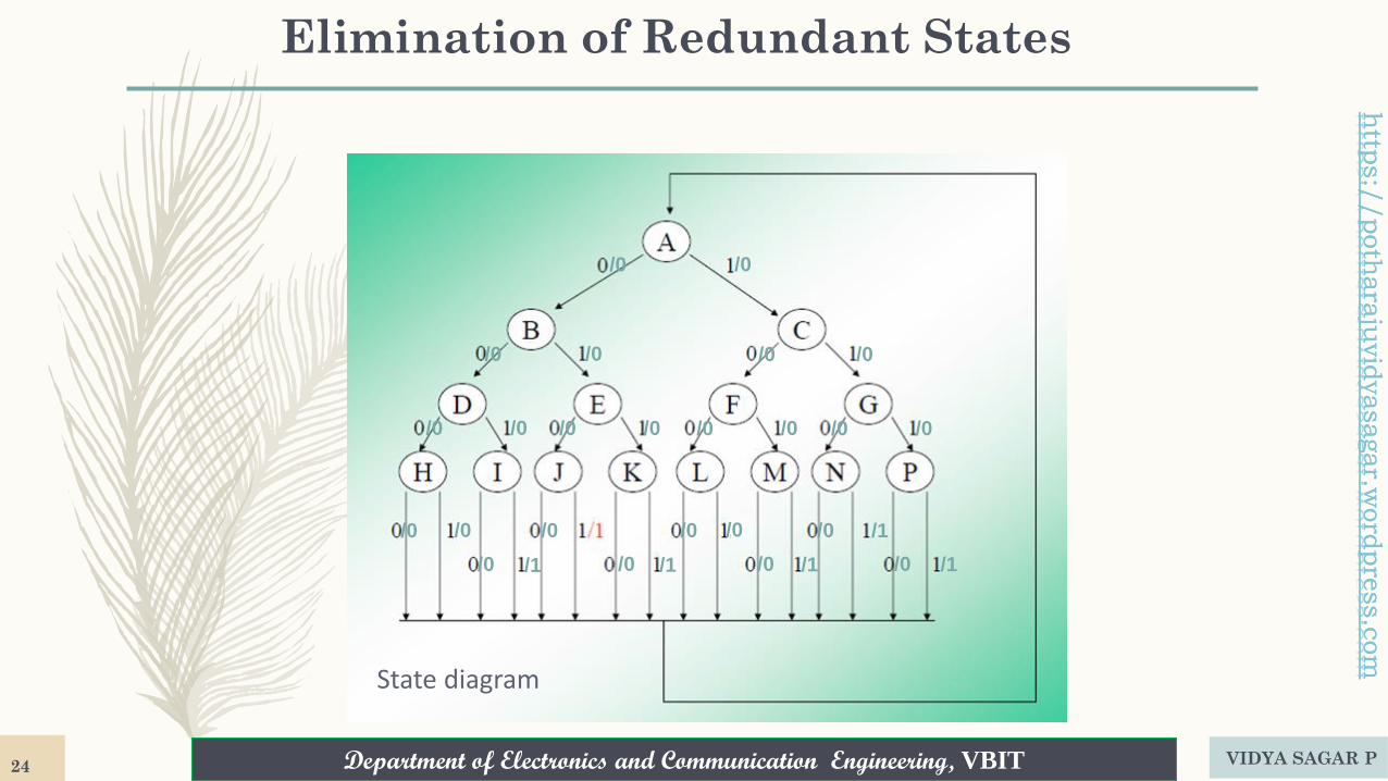
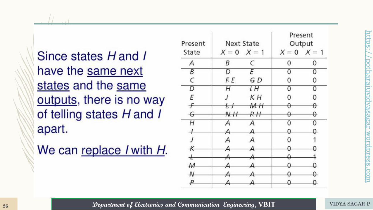
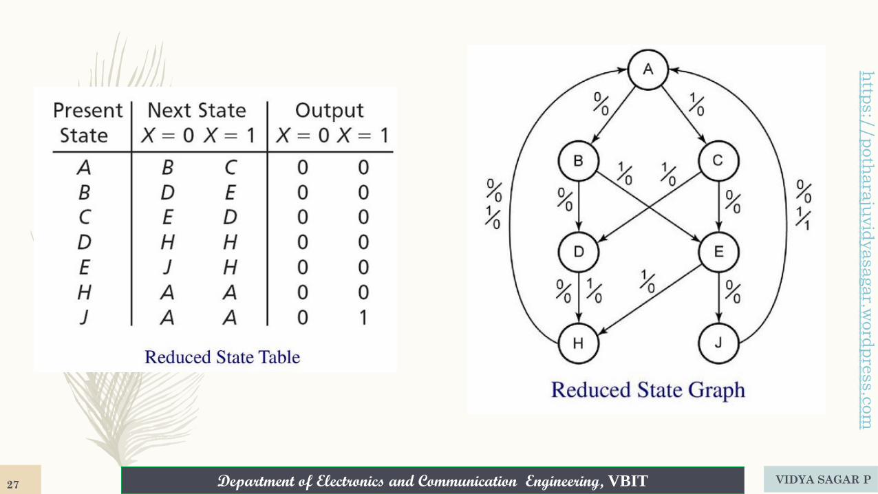
Elimination of Redundant States
/0 /0 /0 /0
/0 /0 /0 /0
/0
/1 /1 /1 /1
/1
/0 /0 /0 /0 /0 /0 /0 /0
/0 /0/0 /0
/0 /0
State diagram
/0
VIDYA SAGAR P24
Department of Electronics and Communication Engineering, VBIT
http
s:/
/poth
ara
juvid
yasagar.w
ord
pre
ss.c
om
Department of Electronics and Communication Engineering, VBIT
http
s:/
/poth
ara
juvid
yasagar.w
ord
pre
ss.c
om
Elimination of Redundant States
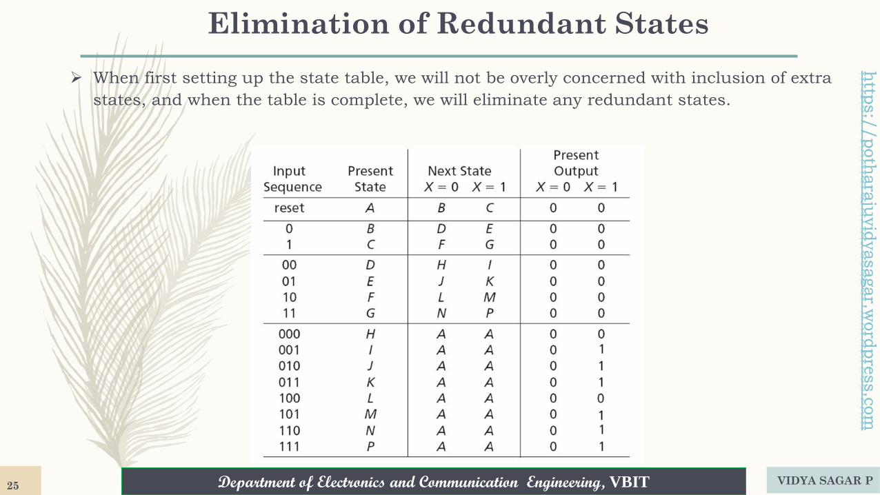
➢ When first setting up the state table, we will not be overly concerned with inclusion of extra
states, and when the table is complete, we will eliminate any redundant states.
VIDYA SAGAR P25
Department of Electronics and Communication Engineering, VBIT
http
s:/
/poth
ara
juvid
yasagar.w
ord
pre
ss.c
om
Department of Electronics and Communication Engineering, VBIT
http
s:/
/poth
ara
juvid
yasagar.w
ord
pre
ss.c
om
VIDYA SAGAR P26
Department of Electronics and Communication Engineering, VBIT
http
s:/
/poth
ara
juvid
yasagar.w
ord
pre
ss.c
om
VIDYA SAGAR P27
Department of Electronics and Communication Engineering, VBIT
http
s:/
/poth
ara
juvid
yasagar.w
ord
pre
ss.c
om
Department of Electronics and Communication Engineering, VBIT
http
s:/
/poth
ara
juvid
yasagar.w
ord
pre
ss.c
om
Implication Table
➢ Two states are equivalent if their response for each possible input sequence is an identical
output sequence.
➢ Alternatively, two states are equivalent if their outputs produced for each input symbol is
identical and their next states for each input symbol are the same or equivalent.
➢ Two states that are not equivalent are distinguishable
➢ The checking of each pair of states for possible equivalence in a table with a large number of
states can be done systematically on an Implication Table.
➢ The Implication Table is a chart that consists of squares, one for every possible pair of states.
VIDYA SAGAR P28
Department of Electronics and Communication Engineering, VBIT
http
s:/
/poth
ara
juvid
yasagar.w
ord
pre
ss.c
om
Department of Electronics and Communication Engineering, VBIT
http
s:/
/poth
ara
juvid
yasagar.w
ord
pre
ss.c
om
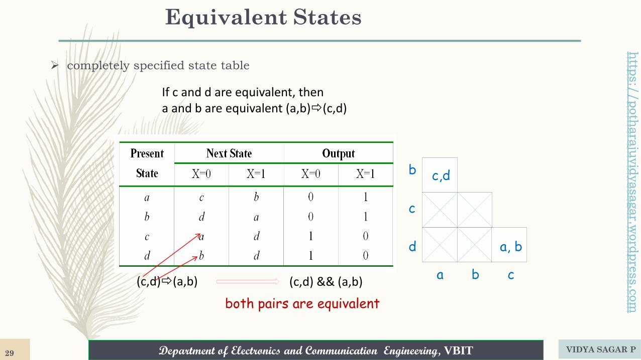
Equivalent States
➢ completely specified state table
If c and d are equivalent, thena and b are equivalent (a,b)(c,d)
(c,d)(a,b) (c,d) && (a,b)a b c
b
c
d
c,d
a, b
both pairs are equivalent
VIDYA SAGAR P29
Department of Electronics and Communication Engineering, VBIT
http
s:/
/poth
ara
juvid
yasagar.w
ord
pre
ss.c
om
Department of Electronics and Communication Engineering, VBIT
http
s:/
/poth
ara
juvid
yasagar.w
ord
pre
ss.c
om
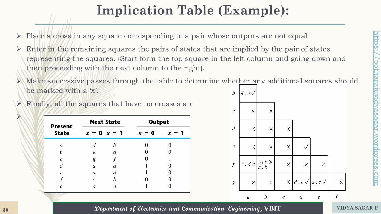
Implication Table (Example):
➢ Place a cross in any square corresponding to a pair whose outputs are not equal
➢ Enter in the remaining squares the pairs of states that are implied by the pair of states
representing the squares. (Start form the top square in the left column and going down and
then proceeding with the next column to the right).
➢ Make successive passes through the table to determine whether any additional squares should
be marked with a ‘x’.
➢ Finally, all the squares that have no crosses are
➢ recorded with check marks.
VIDYA SAGAR P30
Department of Electronics and Communication Engineering, VBIT
http
s:/
/poth
ara
juvid
yasagar.w
ord
pre
ss.c
om
Department of Electronics and Communication Engineering, VBIT
http
s:/
/poth
ara
juvid
yasagar.w
ord
pre
ss.c
om
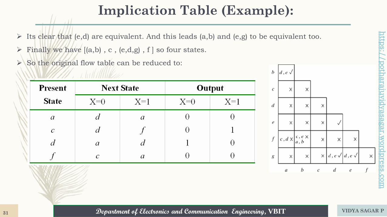
Implication Table (Example):
➢ Its clear that (e,d) are equivalent. And this leads (a,b) and (e,g) to be equivalent too.
➢ Finally we have [(a,b) , c , (e,d,g) , f ] so four states.
➢ So the original flow table can be reduced to:
VIDYA SAGAR P31
Department of Electronics and Communication Engineering, VBIT
http
s:/
/poth
ara
juvid
yasagar.w
ord
pre
ss.c
om
Department of Electronics and Communication Engineering, VBIT
http
s:/
/poth
ara
juvid
yasagar.w
ord
pre
ss.c
om
Partitioning Minimization Procedure
Successive partitioning➢ PROCEDURE:
➢ 1) all states belong to the initial partition p1
➢ 2) p1 is partitioned in blocks such that the states in each block generate the same output.
➢ 3) continue to perform new partitions by testing whether the k-successors of the states in
each block are contained in one block. Those states whose k-successors are in different
blocks cannot be in one block.
➢ 4) prcedure ends when a new partition is the same as the previous partition
VIDYA SAGAR P32
Department of Electronics and Communication Engineering, VBIT
http
s:/
/poth
ara
juvid
yasagar.w
ord
pre
ss.c
om
Department of Electronics and Communication Engineering, VBIT
http
s:/
/poth
ara
juvid
yasagar.w
ord
pre
ss.c
om
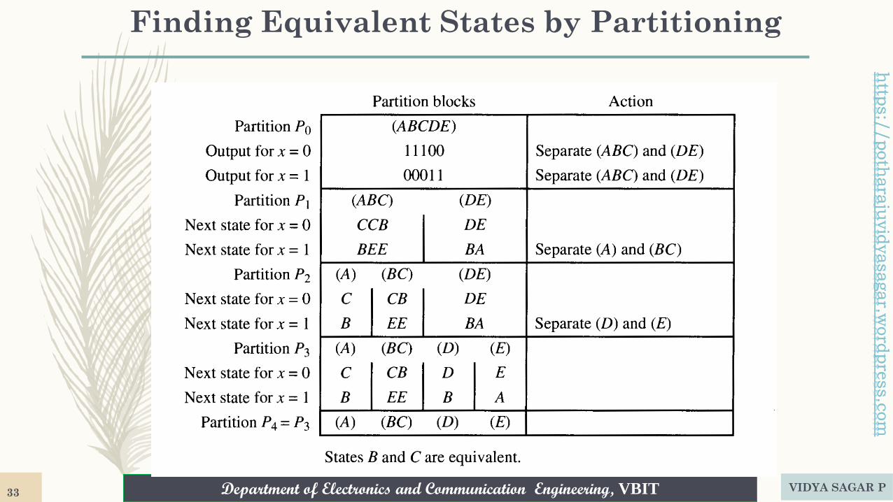
Finding Equivalent States by Partitioning
VIDYA SAGAR P33
Department of Electronics and Communication Engineering, VBIT
http
s:/
/poth
ara
juvid
yasagar.w
ord
pre
ss.c
om
Department of Electronics and Communication Engineering, VBIT
http
s:/
/poth
ara
juvid
yasagar.w
ord
pre
ss.c
om
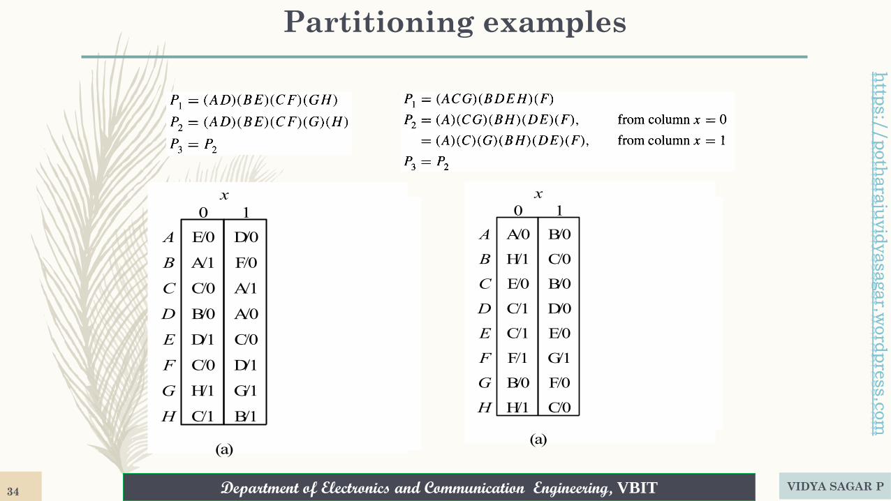
Partitioning examples
(a)
(b)
x
0 1
E/0
A/1
C/0
B/0
D/1
C/0
H/1
C/1
D/0
F/0
A/1
A/0
C/0
D/1
G/1
B/1
A'
B'
C'
D'
E'
B'/0
A'/1
C'/0
E'/1
C'/1
A'/0
C'/0
A'/1
D'/1
B'/1
0 1
xA
B
C
D
E
F
G
H
(a)
(b)
x
0 1
A/0
H/1
E/0
C/1
C/1
F/1
B/0
H/1
B/0
C/0
B/0
D/0
E/0
G/1
F/0
C/0
A'
B'
C'
D'
E'
F'
A'/0
B'/1
F'/0
E'/0
E'/1
C'/1
E'/0
D'/1
E'/0
B'/0
C'/0
F'/0
0 1
x
A
B
C
D
E
F
G
H
VIDYA SAGAR P34
Department of Electronics and Communication Engineering, VBIT
http
s:/
/poth
ara
juvid
yasagar.w
ord
pre
ss.c
om
Department of Electronics and Communication Engineering, VBIT
http
s:/
/poth
ara
juvid
yasagar.w
ord
pre
ss.c
om
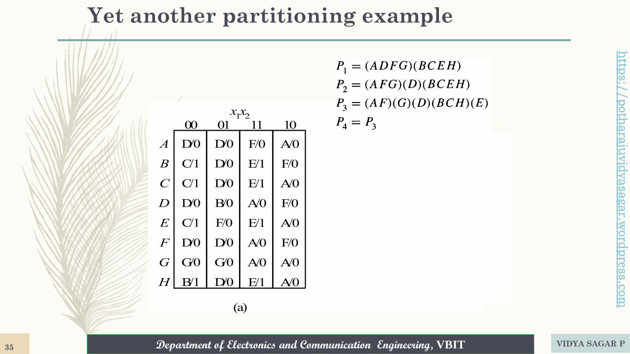
Yet another partitioning example
(a)
(b)
x1x2
00 01
D/0
C/1
C/1
D/0
C/1
D/0
G/0
B/1
D/0
D/0
D/0
B/0
F/0
D/0
G/0
D/0
A'
B'
C'
D'
E'
C'/0
B'/1
C'/0
B'/1
E'/0
C'/0
C'/0
B'/0
A'/0
E'/0
00 01
x1x2A
B
C
D
E
F
G
H
11 10
11 10F/0
E/1
E/1
A/0
E/1
A/0
A/0
E/1
A/0
F/0
A/0
F/0
A/0
F/0
A/0
A/0
A'/0
D'/1
A'/0
D'/1
A'/0
A'/0
A'/0
A'/0
A'/0
A'/0
VIDYA SAGAR P35
Department of Electronics and Communication Engineering, VBIT
http
s:/
/poth
ara
juvid
yasagar.w
ord
pre
ss.c
om
Department of Electronics and Communication Engineering, VBIT
http
s:/
/poth
ara
juvid
yasagar.w
ord
pre
ss.c
om
Incompletely specified circuits: partition method
➢ The partitioning minimization procedure which was applied to completely specified state tables
can also be applied to incompletely specified state tables.
➢ To perform the partitioning process, we can assume that the unspecified outputs have a
specific value.
➢ The partitioning method is equally applicable to Mealy type FSMs in the same way as for
Moore-type FSMs.
VIDYA SAGAR P36
Department of Electronics and Communication Engineering, VBIT
http
s:/
/poth
ara
juvid
yasagar.w
ord
pre
ss.c
om
Department of Electronics and Communication Engineering, VBIT
http
s:/
/poth
ara
juvid
yasagar.w
ord
pre
ss.c
om
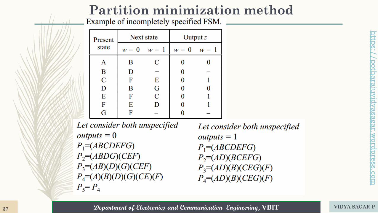
Partition minimization method
VIDYA SAGAR P37
Department of Electronics and Communication Engineering, VBIT
http
s:/
/poth
ara
juvid
yasagar.w
ord
pre
ss.c
om
Department of Electronics and Communication Engineering, VBIT
http
s:/
/poth
ara
juvid
yasagar.w
ord
pre
ss.c
om
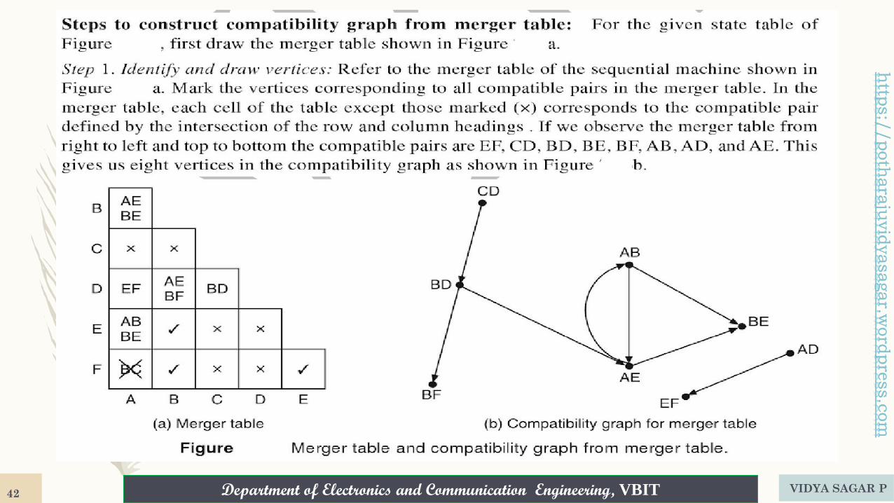
Merger Chart Methods: Merger graphs
VIDYA SAGAR P38
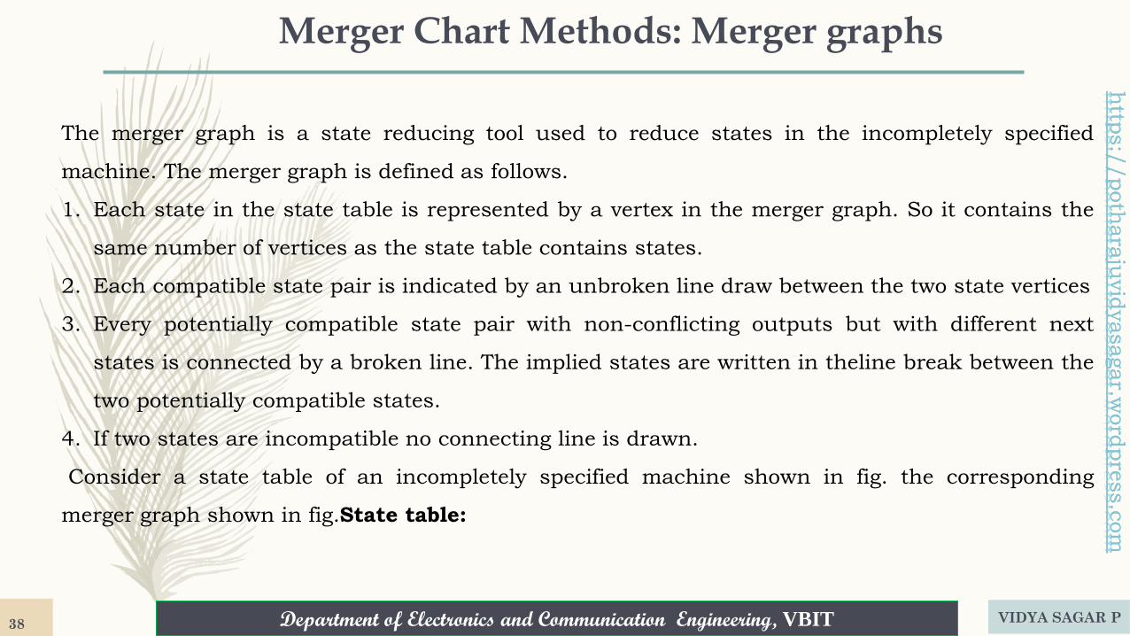
The merger graph is a state reducing tool used to reduce states in the incompletely specified
machine. The merger graph is defined as follows.
1. Each state in the state table is represented by a vertex in the merger graph. So it contains the
same number of vertices as the state table contains states.
2. Each compatible state pair is indicated by an unbroken line draw between the two state vertices
3. Every potentially compatible state pair with non-conflicting outputs but with different next
states is connected by a broken line. The implied states are written in theline break between the
two potentially compatible states.
4. If two states are incompatible no connecting line is drawn.
Consider a state table of an incompletely specified machine shown in fig. the corresponding
merger graph shown in fig.State table:
Department of Electronics and Communication Engineering, VBIT
http
s:/
/poth
ara
juvid
yasagar.w
ord
pre
ss.c
om
Department of Electronics and Communication Engineering, VBIT
http
s:/
/poth
ara
juvid
yasagar.w
ord
pre
ss.c
om
VIDYA SAGAR P39
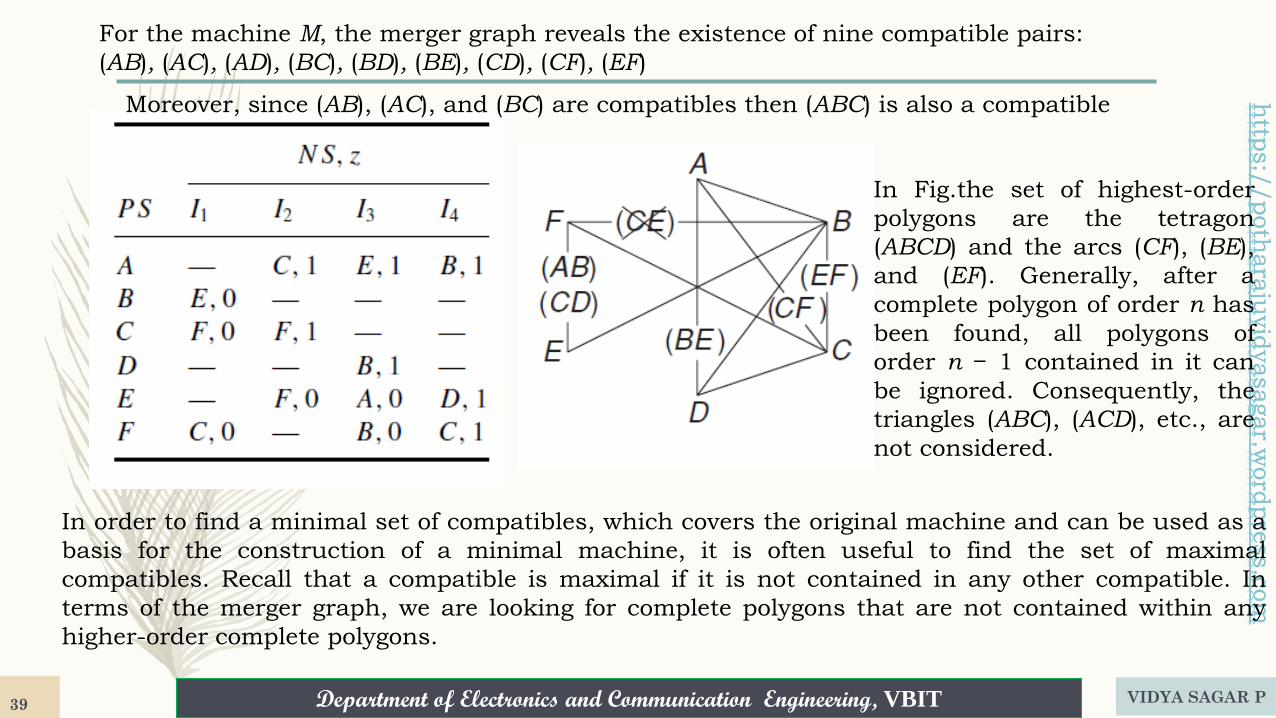
For the machine M, the merger graph reveals the existence of nine compatible pairs:
(AB), (AC), (AD), (BC), (BD), (BE), (CD), (CF), (EF)
Moreover, since (AB), (AC), and (BC) are compatibles then (ABC) is also a compatible
In order to find a minimal set of compatibles, which covers the original machine and can be used as a
basis for the construction of a minimal machine, it is often useful to find the set of maximal
compatibles. Recall that a compatible is maximal if it is not contained in any other compatible. In
terms of the merger graph, we are looking for complete polygons that are not contained within any
higher-order complete polygons.
In Fig.the set of highest-order
polygons are the tetragon
(ABCD) and the arcs (CF), (BE),
and (EF). Generally, after a
complete polygon of order n has
been found, all polygons of
order n − 1 contained in it can
be ignored. Consequently, the
triangles (ABC), (ACD), etc., are
not considered.
Department of Electronics and Communication Engineering, VBIT
http
s:/
/poth
ara
juvid
yasagar.w
ord
pre
ss.c
om
Department of Electronics and Communication Engineering, VBIT
http
s:/
/poth
ara
juvid
yasagar.w
ord
pre
ss.c
om
The closed sets of compatibles
➢ Consider the set of compatibles {(ABCD), (EF)} of machine M. Since this is the minimal number
of compatibles covering all the states of M, it defines a lower bound on the number of states in
the minimal machine that covers M. However, if we select the maximal compatible (ABCD) to
be a state in the reduced machine, its I2- and I3-successors, (CF) and (BE), respectively, must
also be selected. Since none of these compatible pairs is contained in the above set the lower
bound cannot be achieved, and the set of maximal compatibles {(ABCD), (EF)} cannot be used
to define the states of a minimal machine that covers M. {(ABCD), (BE), (CF), (EF)}.
closed covering
➢ set of compatibles (for a machine M) is said to be closed if, for every compatible contained in
the set, all its implied compatibles are also contained in the set. A closed set of compatibles
that contains all the states of M is called a closed covering.
➢ Example For M6, the set {(AD), (BE), (CD)} is closed. The set {(AB),(CD), (EF)} is a closed
covering.
VIDYA SAGAR P40
Department of Electronics and Communication Engineering, VBIT
http
s:/
/poth
ara
juvid
yasagar.w
ord
pre
ss.c
om
Department of Electronics and Communication Engineering, VBIT
http
s:/
/poth
ara
juvid
yasagar.w
ord
pre
ss.c
om
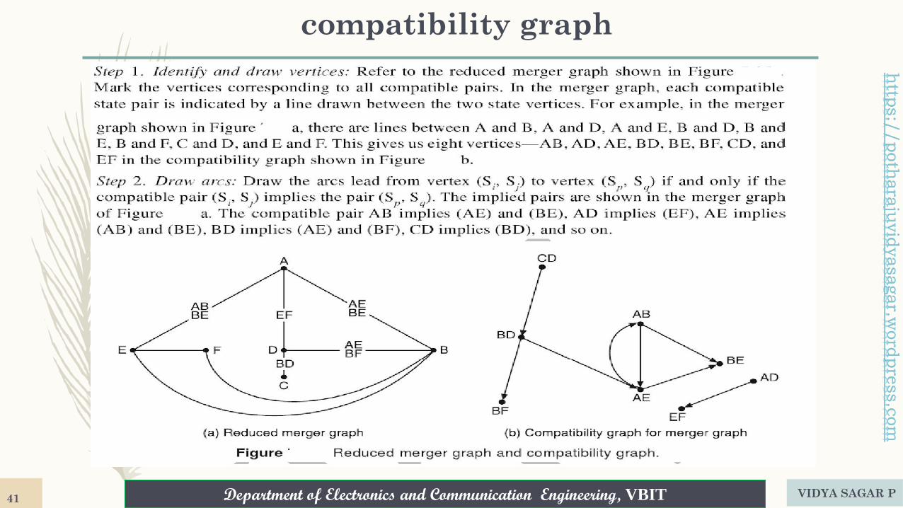
compatibility graph
VIDYA SAGAR P41
Department of Electronics and Communication Engineering, VBIT
http
s:/
/poth
ara
juvid
yasagar.w
ord
pre
ss.c
om
Department of Electronics and Communication Engineering, VBIT
http
s:/
/poth
ara
juvid
yasagar.w
ord
pre
ss.c
om
VIDYA SAGAR P42
Department of Electronics and Communication Engineering, VBIT
http
s:/
/poth
ara
juvid
yasagar.w
ord
pre
ss.c
om
Department of Electronics and Communication Engineering, VBIT
http
s:/
/poth
ara
juvid
yasagar.w
ord
pre
ss.c
om
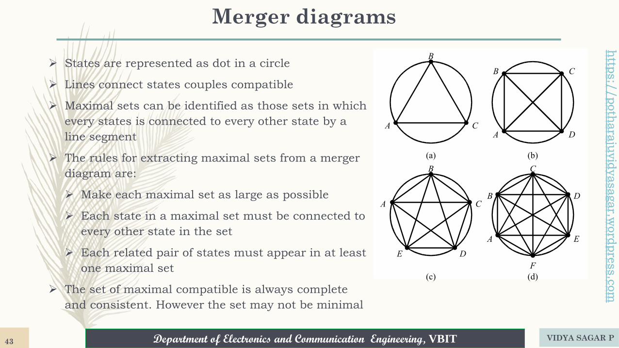
Merger diagrams
➢ States are represented as dot in a circle
➢ Lines connect states couples compatible
➢ Maximal sets can be identified as those sets in which
every states is connected to every other state by a
line segment
➢ The rules for extracting maximal sets from a merger
diagram are:
➢ Make each maximal set as large as possible
➢ Each state in a maximal set must be connected to
every other state in the set
➢ Each related pair of states must appear in at least
one maximal set
➢ The set of maximal compatible is always complete
and consistent. However the set may not be minimal
B
CA
(a) (b)
(c) (d)
A
B
D
C
A
E
C
D
B
B
A
D
E
C
F
VIDYA SAGAR P43
Department of Electronics and Communication Engineering, VBIT
http
s:/
/poth
ara
juvid
yasagar.w
ord
pre
ss.c
om
Department of Electronics and Communication Engineering, VBIT
http
s:/
/poth
ara
juvid
yasagar.w
ord
pre
ss.c
om
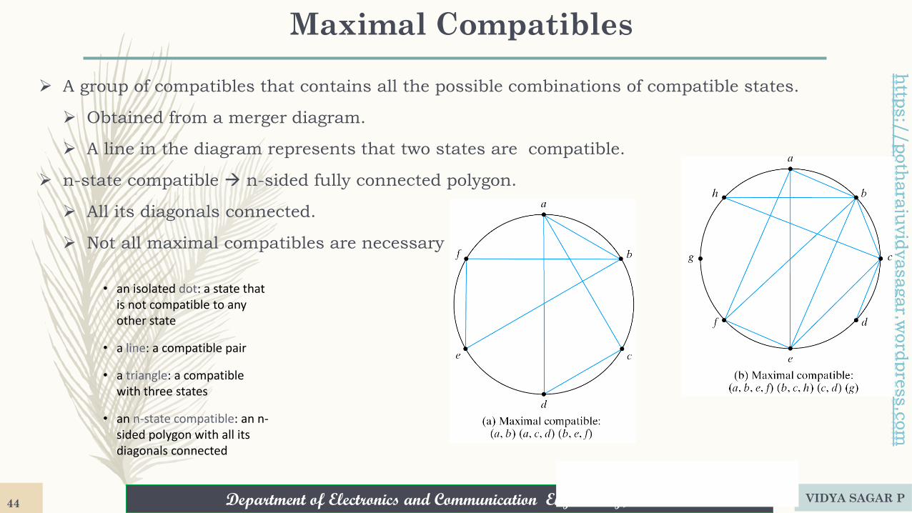
Maximal Compatibles
➢ A group of compatibles that contains all the possible combinations of compatible states.
➢ Obtained from a merger diagram.
➢ A line in the diagram represents that two states are compatible.
➢ n-state compatible → n-sided fully connected polygon.
➢ All its diagonals connected.
➢ Not all maximal compatibles are necessary
VIDYA SAGAR P44
• an isolated dot: a state that is not compatible to any other state
• a line: a compatible pair
• a triangle: a compatible with three states
• an n-state compatible: an n-sided polygon with all its diagonals connected
Department of Electronics and Communication Engineering, VBIT
http
s:/
/poth
ara
juvid
yasagar.w
ord
pre
ss.c
om
Department of Electronics and Communication Engineering, VBIT
http
s:/
/poth
ara
juvid
yasagar.w
ord
pre
ss.c
om
Closed Covering Condition
➢ The condition that must be satisfied for row merging is that the set of chosen compatibles
must:
➢ Cover all states.
➢ Be closed: ( the closure condition is satisfied if there are no implied states or if the implied
states are included within a set)
➢ In the first example, the maximal compatibles are (a, b) (a, c, d), (b , e , f)
➢ If we remove (a, b), we get a set of two compatibles: (a, c, d), (b, e , f):
➢ All the six states are included in this set.
➢ There are no implied states for (a,c); (a,d);(c,d);(b,e);(b,f) and (e,f) [you can check the
implication table] . The closer condition is satisfied
➢ The original primitive flow table can be merged into two rows, one for each of the compatibles.
VIDYA SAGAR P45
Department of Electronics and Communication Engineering, VBIT
http
s:/
/poth
ara
juvid
yasagar.w
ord
pre
ss.c
om
Department of Electronics and Communication Engineering, VBIT
http
s:/
/poth
ara
juvid
yasagar.w
ord
pre
ss.c
om
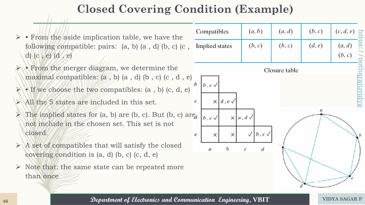
Closed Covering Condition (Example)
➢ • From the aside implication table, we have the
following compatible: pairs: (a, b) (a , d) (b, c) (c ,
d) (c , e) (d , e)
➢ • From the merger diagram, we determine the
maximal compatibles: (a , b) (a , d) (b , c) (c , d , e)
➢ • If we choose the two compatibles: (a , b) (c, d, e)
➢ All the 5 states are included in this set.
➢ The implied states for (a, b) are (b, c). But (b, c) are
not include in the chosen set. This set is not
closed.
➢ A set of compatibles that will satisfy the closed
covering condition is (a, d) (b, c) (c, d, e)
➢ Note that: the same state can be repeated more
than once
VIDYA SAGAR P46
Department of Electronics and Communication Engineering, VBIT
http
s:/
/poth
ara
juvid
yasagar.w
ord
pre
ss.c
om
Department of Electronics and Communication Engineering, VBIT
http
s:/
/poth
ara
juvid
yasagar.w
ord
pre
ss.c
om
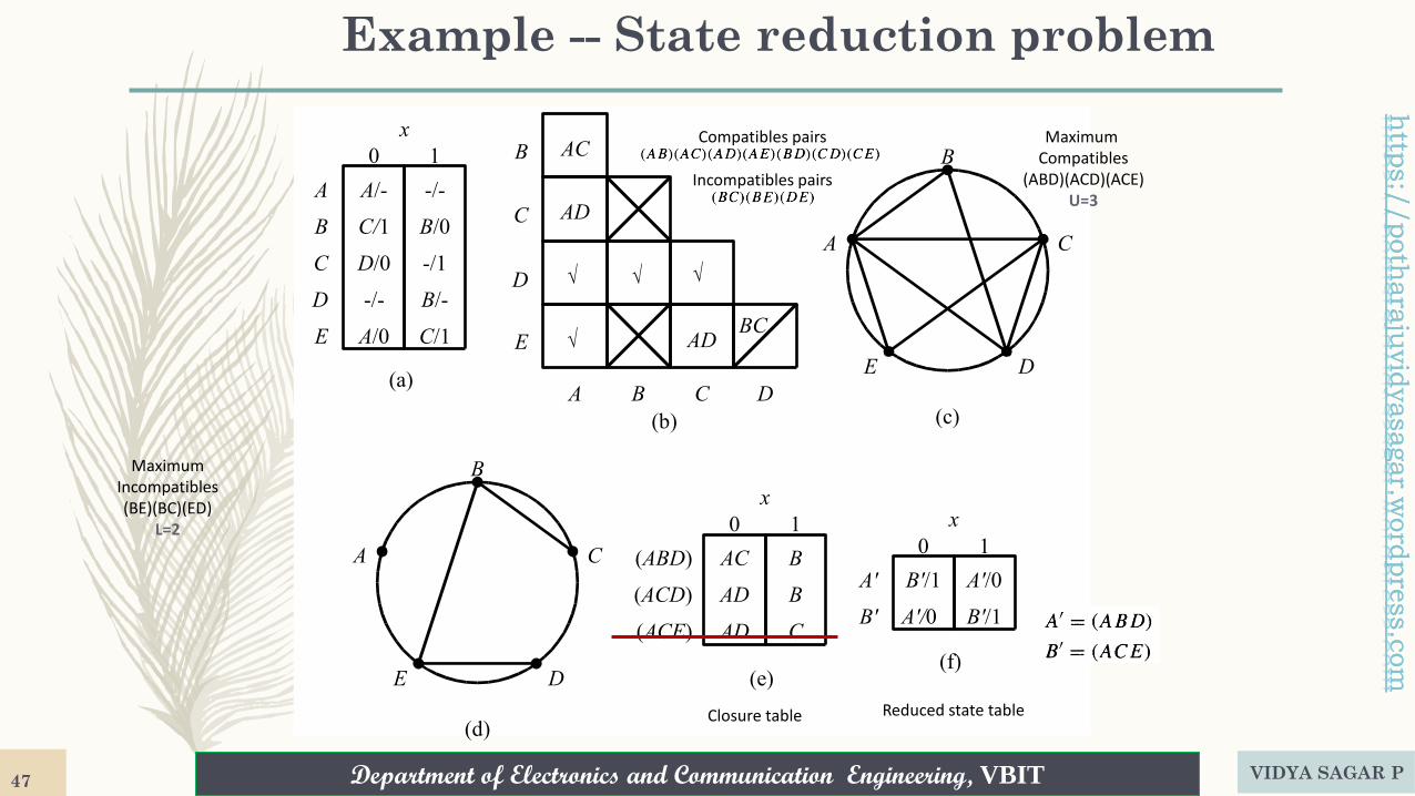
Example -- State reduction problem
(d)
A
E
C
D
B
(c)
A
E
C
D
B
(b)
B
B C DA
C
D
E
AC
AD
BCAD
x
0 1
(a)
A
B
C
D
E
x
0 1 x
0 1
A/-
C/1
D/0
-/-
A/0
-/-
B/0
-/1
B/-
C/1
(e)
(ABD)
(ACD)
(ACE)
AC
AD
AD
B
B
C
(f)
A'
B'
B'/1
A'/0
A'/0
B'/1
Ö Ö Ö
Ö
Closure table Reduced state table
Compatibles pairs
Incompatibles pairs
Maximum Compatibles
(ABD)(ACD)(ACE)U=3
Maximum Incompatibles(BE)(BC)(ED)
L=2
VIDYA SAGAR P47
Department of Electronics and Communication Engineering, VBIT
http
s:/
/poth
ara
juvid
yasagar.w
ord
pre
ss.c
om
Department of Electronics and Communication Engineering, VBIT
http
s:/
/poth
ara
juvid
yasagar.w
ord
pre
ss.c
om
Asynchronous Sequential Circuits
VIDYA SAGAR P48
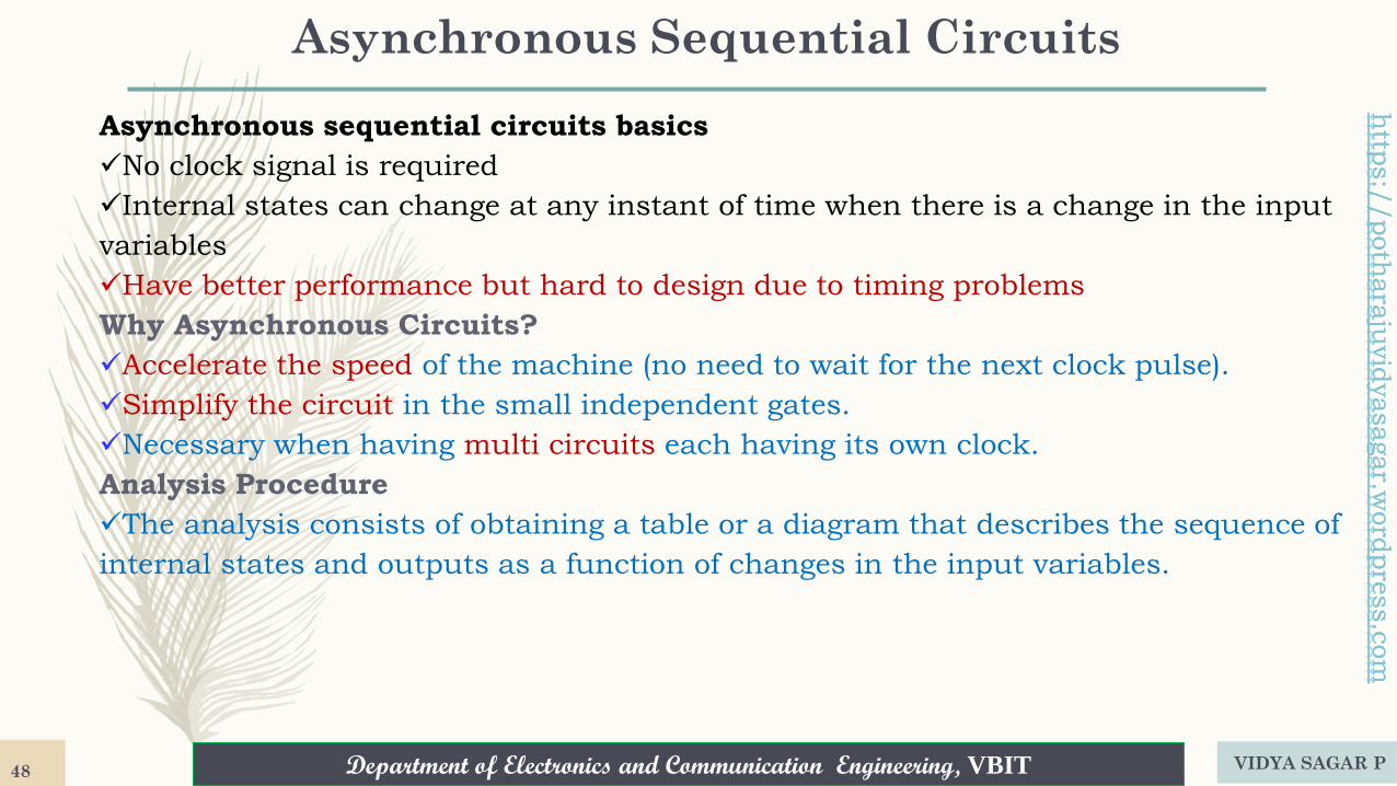
Asynchronous sequential circuits basics
✓No clock signal is required
✓Internal states can change at any instant of time when there is a change in the input
variables
✓Have better performance but hard to design due to timing problems
Why Asynchronous Circuits?
✓Accelerate the speed of the machine (no need to wait for the next clock pulse).
✓Simplify the circuit in the small independent gates.
✓Necessary when having multi circuits each having its own clock.
Analysis Procedure
✓The analysis consists of obtaining a table or a diagram that describes the sequence of
internal states and outputs as a function of changes in the input variables.
Department of Electronics and Communication Engineering, VBIT
http
s:/
/poth
ara
juvid
yasagar.w
ord
pre
ss.c
om
Department of Electronics and Communication Engineering, VBIT
http
s:/
/poth
ara
juvid
yasagar.w
ord
pre
ss.c
om
Transition Table
➢ Transition table is useful to analyze an asynchronous circuit from the circuit diagram.
Procedure to obtain transition table:
➢ 1. Determine all feedback loops in the circuits
➢ 2. Mark the input (yi) and output (Yi) of each feedback loop
➢ 3. Derive the Boolean functions of all Y’s
➢ 4. Plot each Y function in a map and combine all maps into one table (flow table)
➢ 5. Circle those values of Y in each square that are equal to the value of y in the same row
VIDYA SAGAR P49
Department of Electronics and Communication Engineering, VBIT
http
s:/
/poth
ara
juvid
yasagar.w
ord
pre
ss.c
om
Department of Electronics and Communication Engineering, VBIT
http
s:/
/poth
ara
juvid
yasagar.w
ord
pre
ss.c
om
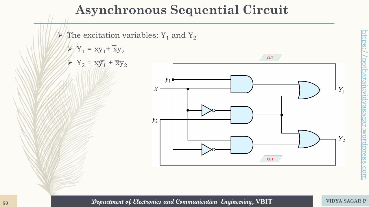
Asynchronous Sequential Circuit
➢ The excitation variables: Y1 and Y2
➢ Y1 = xy1+ xy2
➢ Y2 = xy1 + xy2
CUT
CUT
VIDYA SAGAR P50
Department of Electronics and Communication Engineering, VBIT
http
s:/
/poth
ara
juvid
yasagar.w
ord
pre
ss.c
om
Department of Electronics and Communication Engineering, VBIT
http
s:/
/poth
ara
juvid
yasagar.w
ord
pre
ss.c
om
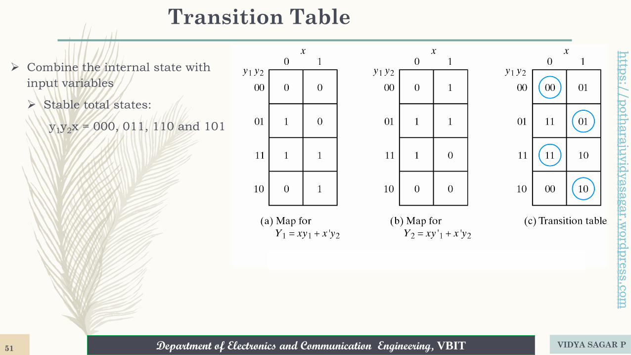
Transition Table
➢ Combine the internal state with
input variables
➢ Stable total states:
y1y2x = 000, 011, 110 and 101
VIDYA SAGAR P51
Department of Electronics and Communication Engineering, VBIT
http
s:/
/poth
ara
juvid
yasagar.w
ord
pre
ss.c
om
Department of Electronics and Communication Engineering, VBIT
http
s:/
/poth
ara
juvid
yasagar.w
ord
pre
ss.c
om
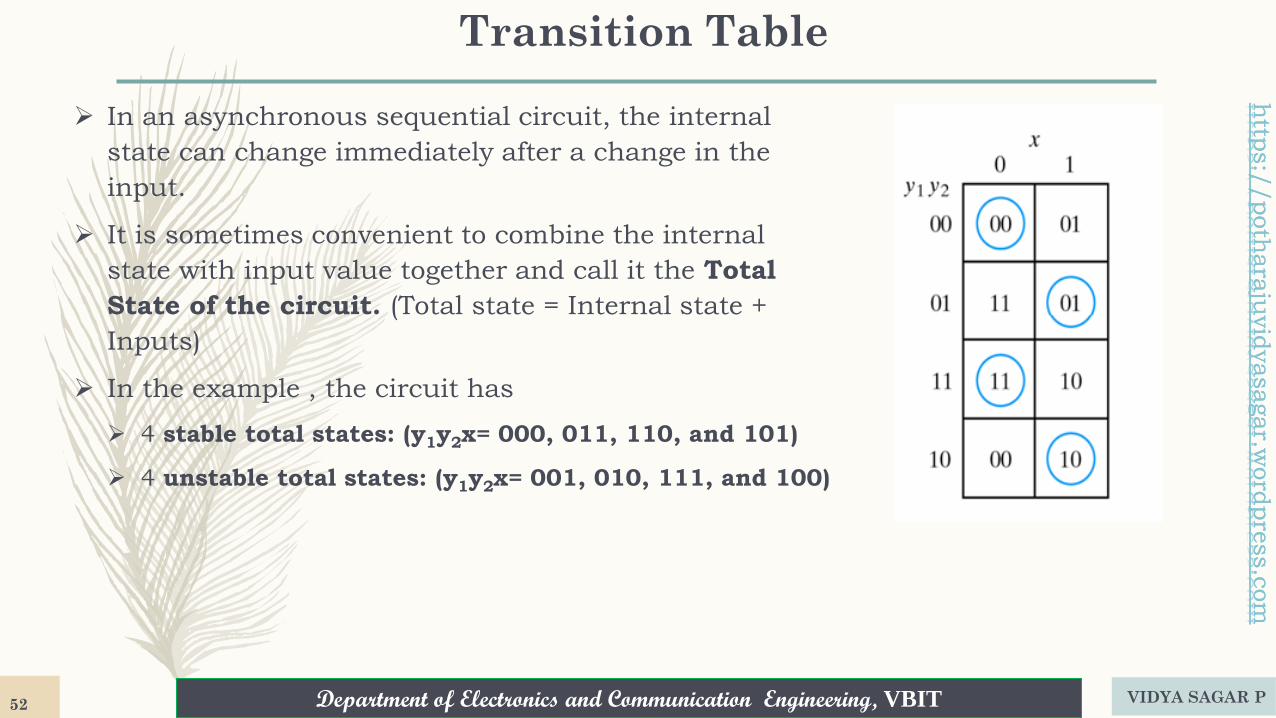
Transition Table
➢ In an asynchronous sequential circuit, the internal
state can change immediately after a change in the
input.
➢ It is sometimes convenient to combine the internal
state with input value together and call it the Total
State of the circuit. (Total state = Internal state +
Inputs)
➢ In the example , the circuit has
➢ 4 stable total states: (y1y2x= 000, 011, 110, and 101)
➢ 4 unstable total states: (y1y2x= 001, 010, 111, and 100)
VIDYA SAGAR P52
Department of Electronics and Communication Engineering, VBIT
http
s:/
/poth
ara
juvid
yasagar.w
ord
pre
ss.c
om
Department of Electronics and Communication Engineering, VBIT
http
s:/
/poth
ara
juvid
yasagar.w
ord
pre
ss.c
om
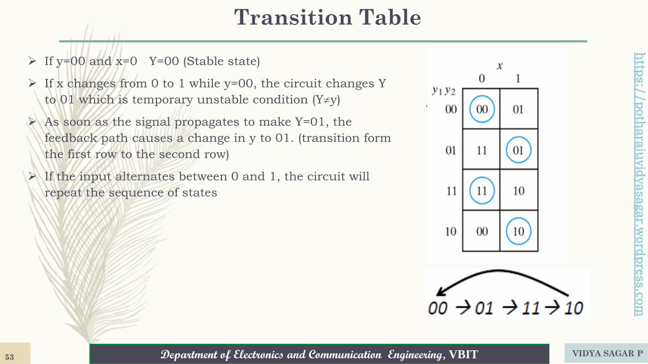
Transition Table
➢ If y=00 and x=0 Y=00 (Stable state)
➢ If x changes from 0 to 1 while y=00, the circuit changes Y
to 01 which is temporary unstable condition (Yy)
➢ As soon as the signal propagates to make Y=01, the
feedback path causes a change in y to 01. (transition form
the first row to the second row)
➢ If the input alternates between 0 and 1, the circuit will
repeat the sequence of states
VIDYA SAGAR P53
Department of Electronics and Communication Engineering, VBIT
http
s:/
/poth
ara
juvid
yasagar.w
ord
pre
ss.c
om
Department of Electronics and Communication Engineering, VBIT
http
s:/
/poth
ara
juvid
yasagar.w
ord
pre
ss.c
om
Flow Table
➢ A flow table is similar to a transition table except that the internal state are symbolized with
letters rather than binary numbers.
➢ It also includes the output values of the circuit for each stable state.
VIDYA SAGAR P54
Department of Electronics and Communication Engineering, VBIT
http
s:/
/poth
ara
juvid
yasagar.w
ord
pre
ss.c
om
Department of Electronics and Communication Engineering, VBIT
http
s:/
/poth
ara
juvid
yasagar.w
ord
pre
ss.c
om
Flow Table: Example 2
➢ Two states, two inputs, one output.
VIDYA SAGAR P55
a
b
,0 a a ,0 a ,0
a ,0 a ,0 b ,1
b ,0
b ,0
x1 x2
00 01 11 10
➢ Each row has more than one stable state.
➢ If x1 = 0, state is a.
➢ If x1x2 = 00 → x1x2 = 10, then state becomes b.
➢ For x1x2 = 11, state is either a or b.
➢ If previously in x1x2 = 01, keeps state a,
➢ If previously in x1x2 = 10, keeps state b.
➢ Reminder: cannot go from 00 to 11.
Department of Electronics and Communication Engineering, VBIT
http
s:/
/poth
ara
juvid
yasagar.w
ord
pre
ss.c
om
Department of Electronics and Communication Engineering, VBIT
http
s:/
/poth
ara
juvid
yasagar.w
ord
pre
ss.c
om
Flow Table
➢ In order to obtain the circuit described
by a flow table, it is necessary to
convert the flow table into a transition
table from which we can derive the logic
diagram.
➢ This can be done through the
assignment of a distinct binary value to
each state.
VIDYA SAGAR P56
Department of Electronics and Communication Engineering, VBIT
http
s:/
/poth
ara
juvid
yasagar.w
ord
pre
ss.c
om
Department of Electronics and Communication Engineering, VBIT
http
s:/
/poth
ara
juvid
yasagar.w
ord
pre
ss.c
om
Race condition➢ Two or more binary state variables will change value when one input variable changes.
➢ Cannot predict state sequence if unequal delay is encountered.
➢ Non-critical race: The final stable state does not depend on the change order of state variables
➢ Critical race: The change order of state variables will result in different stable states. Must be
avoided !!
VIDYA SAGAR P57
Department of Electronics and Communication Engineering, VBIT
http
s:/
/poth
ara
juvid
yasagar.w
ord
pre
ss.c
om
Department of Electronics and Communication Engineering, VBIT
http
s:/
/poth
ara
juvid
yasagar.w
ord
pre
ss.c
om
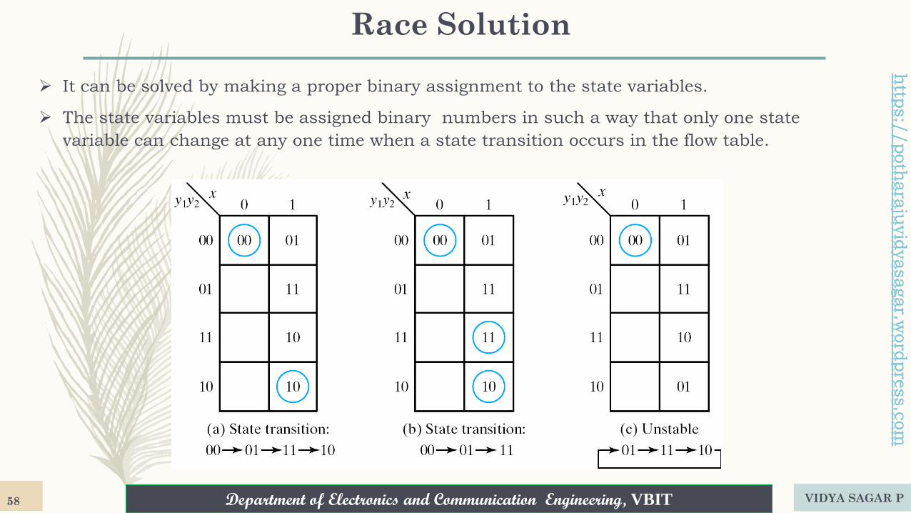
Race Solution
➢ It can be solved by making a proper binary assignment to the state variables.
➢ The state variables must be assigned binary numbers in such a way that only one state
variable can change at any one time when a state transition occurs in the flow table.
VIDYA SAGAR P58
Department of Electronics and Communication Engineering, VBIT
http
s:/
/poth
ara
juvid
yasagar.w
ord
pre
ss.c
om
Department of Electronics and Communication Engineering, VBIT
http
s:/
/poth
ara
juvid
yasagar.w
ord
pre
ss.c
om
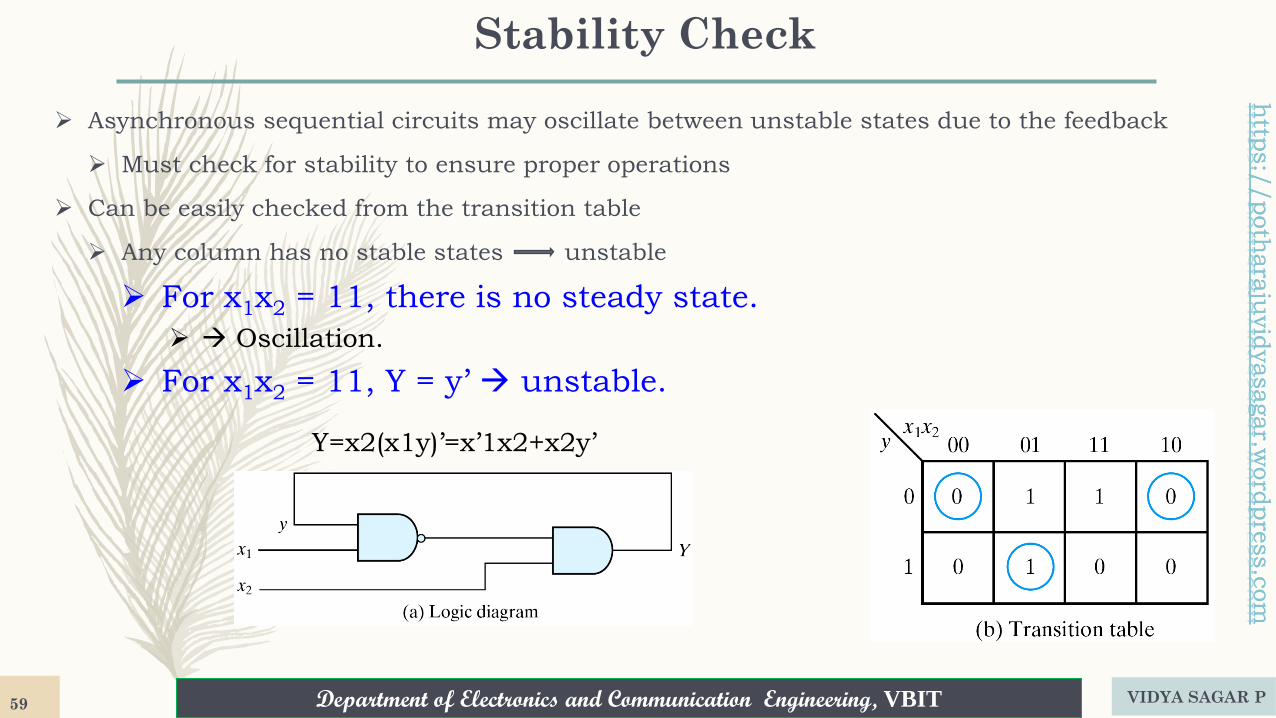
Stability Check
➢ Asynchronous sequential circuits may oscillate between unstable states due to the feedback
➢ Must check for stability to ensure proper operations
➢ Can be easily checked from the transition table
➢ Any column has no stable states unstable
VIDYA SAGAR P59
Y=x2(x1y)’=x’1x2+x2y’
➢ For x1x2 = 11, there is no steady state.
➢ → Oscillation.
➢ For x1x2 = 11, Y = y’ → unstable.
Department of Electronics and Communication Engineering, VBIT
http
s:/
/poth
ara
juvid
yasagar.w
ord
pre
ss.c
om
Department of Electronics and Communication Engineering, VBIT
http
s:/
/poth
ara
juvid
yasagar.w
ord
pre
ss.c
om
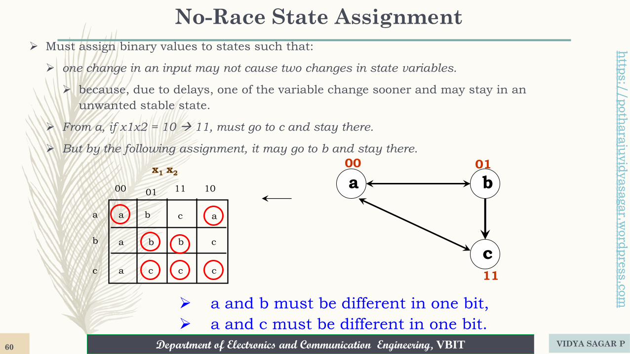
No-Race State Assignment
➢ Must assign binary values to states such that:
➢ one change in an input may not cause two changes in state variables.
➢ because, due to delays, one of the variable change sooner and may stay in an
unwanted stable state.
➢ From a, if x1x2 = 10 → 11, must go to c and stay there.
➢ But by the following assignment, it may go to b and stay there.
VIDYA SAGAR P60
a
b
a b
x1 x2
00 01 11 10
c a
a b c b
c a c c c
a b
c
➢ a and b must be different in one bit,
➢ a and c must be different in one bit.
00 01
11
Department of Electronics and Communication Engineering, VBIT
http
s:/
/poth
ara
juvid
yasagar.w
ord
pre
ss.c
om
Department of Electronics and Communication Engineering, VBIT
http
s:/
/poth
ara
juvid
yasagar.w
ord
pre
ss.c
om
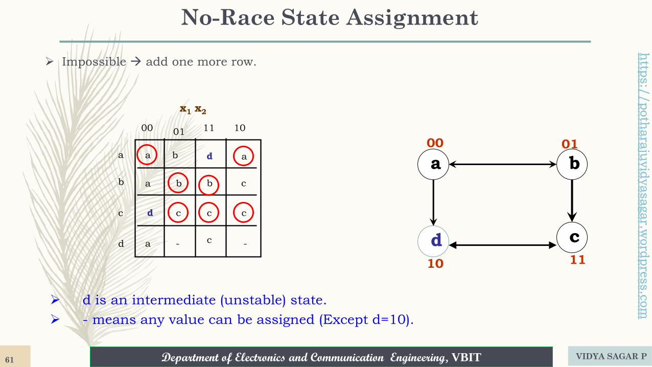
No-Race State Assignment
➢ Impossible → add one more row.
VIDYA SAGAR P61
a
b
a b
x1 x2
00 01 11 10
d a
a b c b
c c c c
a b
c
00 01
11
d c d
10
d
a - -
➢ d is an intermediate (unstable) state.
➢ - means any value can be assigned (Except d=10).
Department of Electronics and Communication Engineering, VBIT
http
s:/
/poth
ara
juvid
yasagar.w
ord
pre
ss.c
om
Department of Electronics and Communication Engineering, VBIT
http
s:/
/poth
ara
juvid
yasagar.w
ord
pre
ss.c
om
Example 2
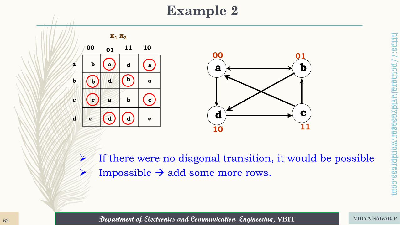
VIDYA SAGAR P62
➢ If there were no diagonal transition, it would be possible
➢ Impossible → add some more rows.
a
b
a b
x1 x2
00 01 11 10
d a
a b b
c c b c
d c
a
c d
d
d
a b
c
00 01
11
d
10
Department of Electronics and Communication Engineering, VBIT
http
s:/
/poth
ara
juvid
yasagar.w
ord
pre
ss.c
om
Department of Electronics and Communication Engineering, VBIT
http
s:/
/poth
ara
juvid
yasagar.w
ord
pre
ss.c
om
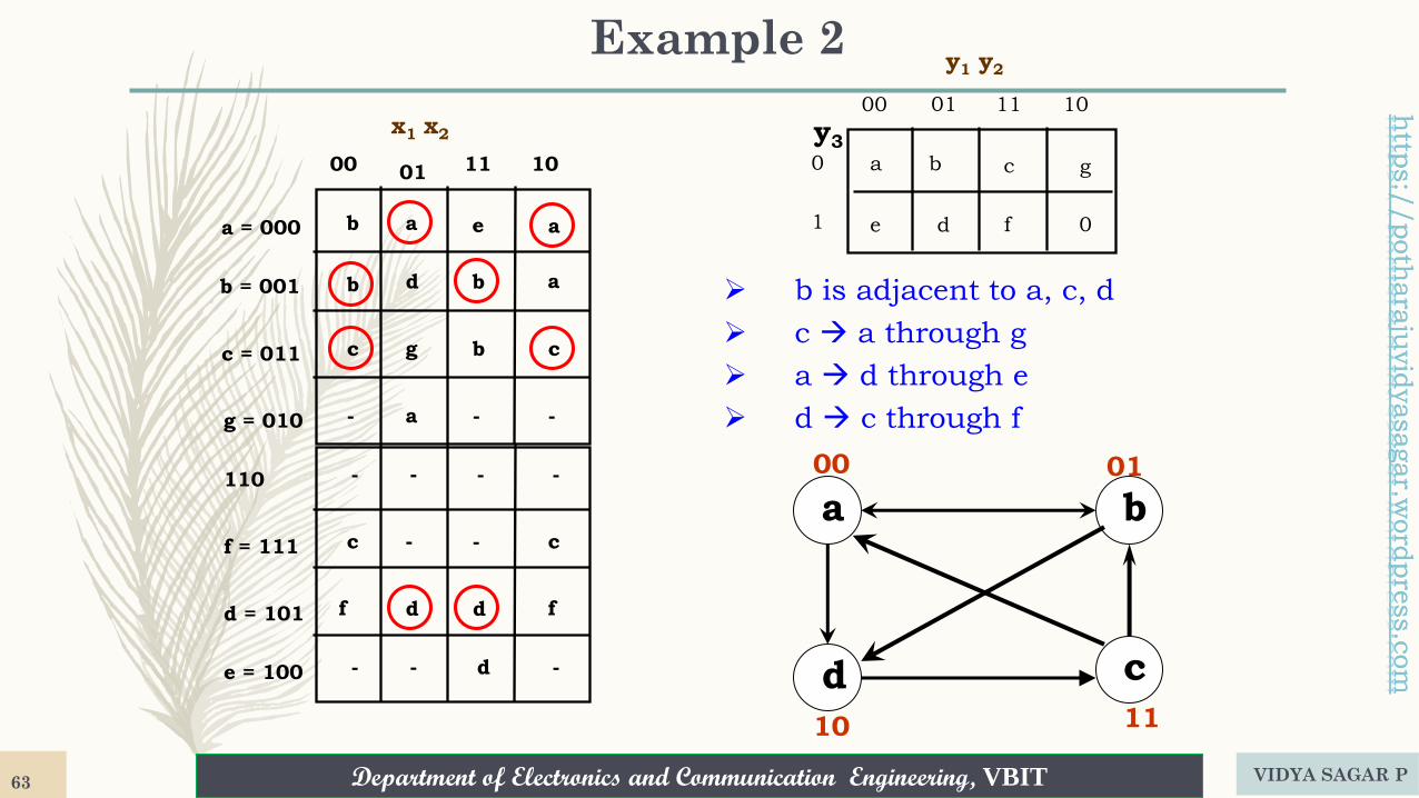
Example 2
VIDYA SAGAR P63
a
b = 001
a = 000 b
x1 x2
00 01 11 10
e a
a b b
c = 011 c b c
g = 010
g
d
f f d d
110
f = 111
d = 101
e = 100
- - -a
- - --
c - c -
- d --
a
1
0 b
y1 y2
00 01 11 10
y3
c g
e f 0 d
➢ b is adjacent to a, c, d
➢ c → a through g
➢ a → d through e
➢ d → c through f
a b
c
00 01
11
d
10
Department of Electronics and Communication Engineering, VBIT
http
s:/
/poth
ara
juvid
yasagar.w
ord
pre
ss.c
om
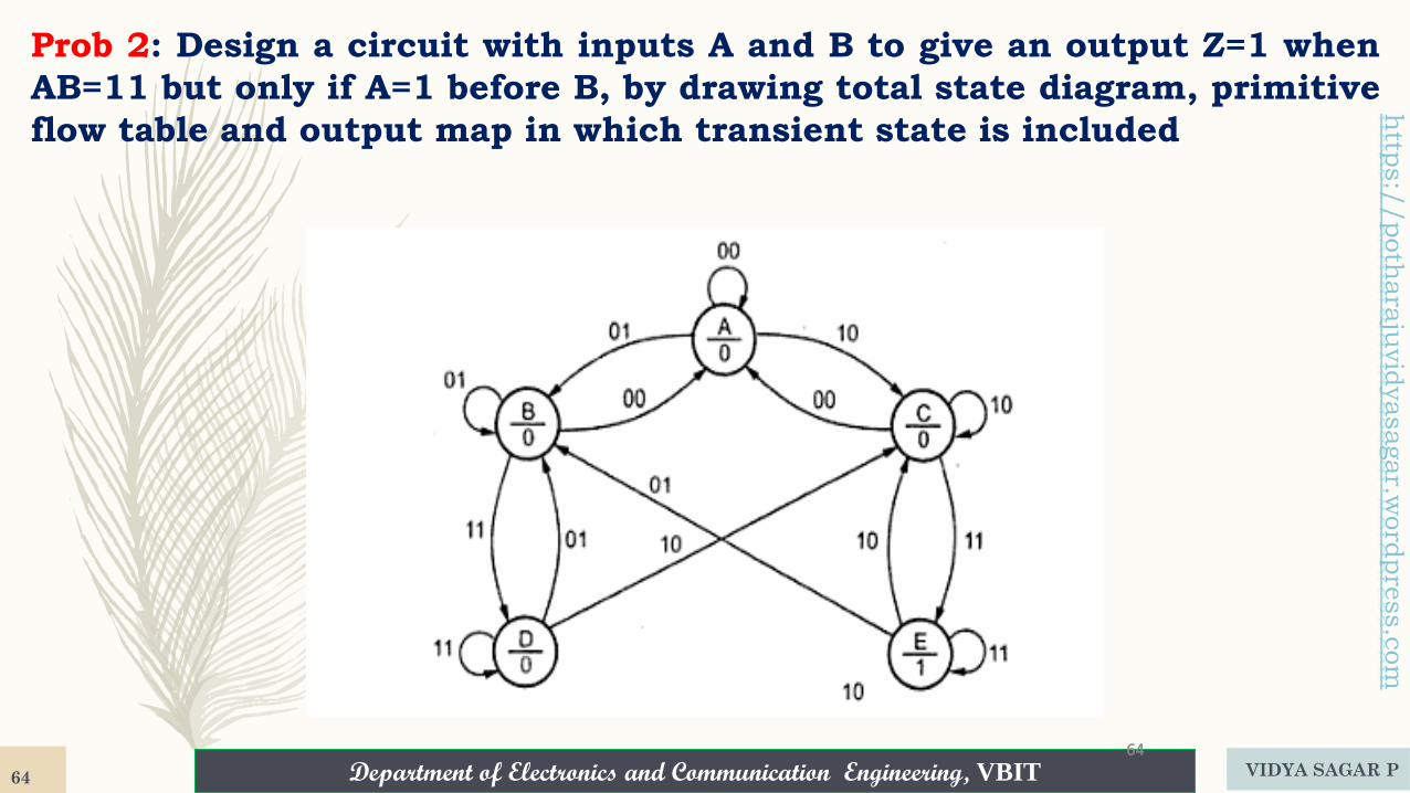
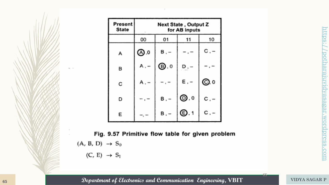
Prob 2: Design a circuit with inputs A and B to give an output Z=1 when
AB=11 but only if A=1 before B, by drawing total state diagram, primitive
flow table and output map in which transient state is included
6464VIDYA SAGAR P64
Department of Electronics and Communication Engineering, VBIT
http
s:/
/poth
ara
juvid
yasagar.w
ord
pre
ss.c
om
6565VIDYA SAGAR P65
Department of Electronics and Communication Engineering, VBIT
http
s:/
/poth
ara
juvid
yasagar.w
ord
pre
ss.c
om
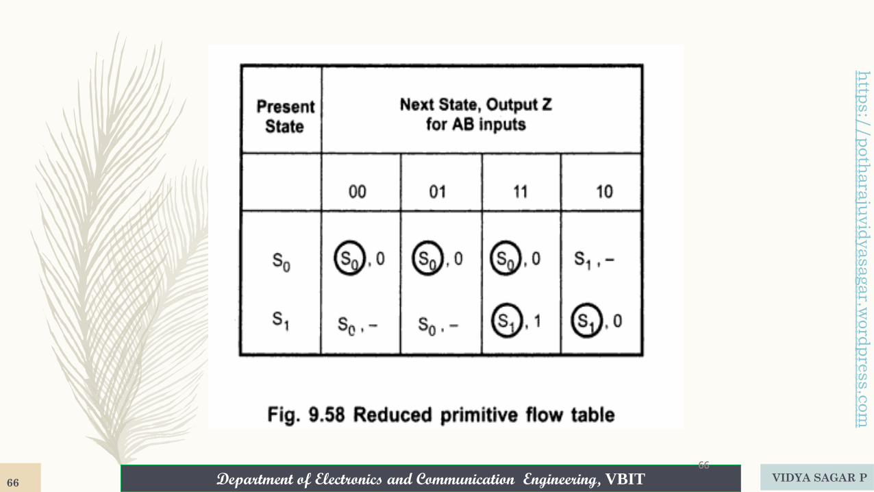
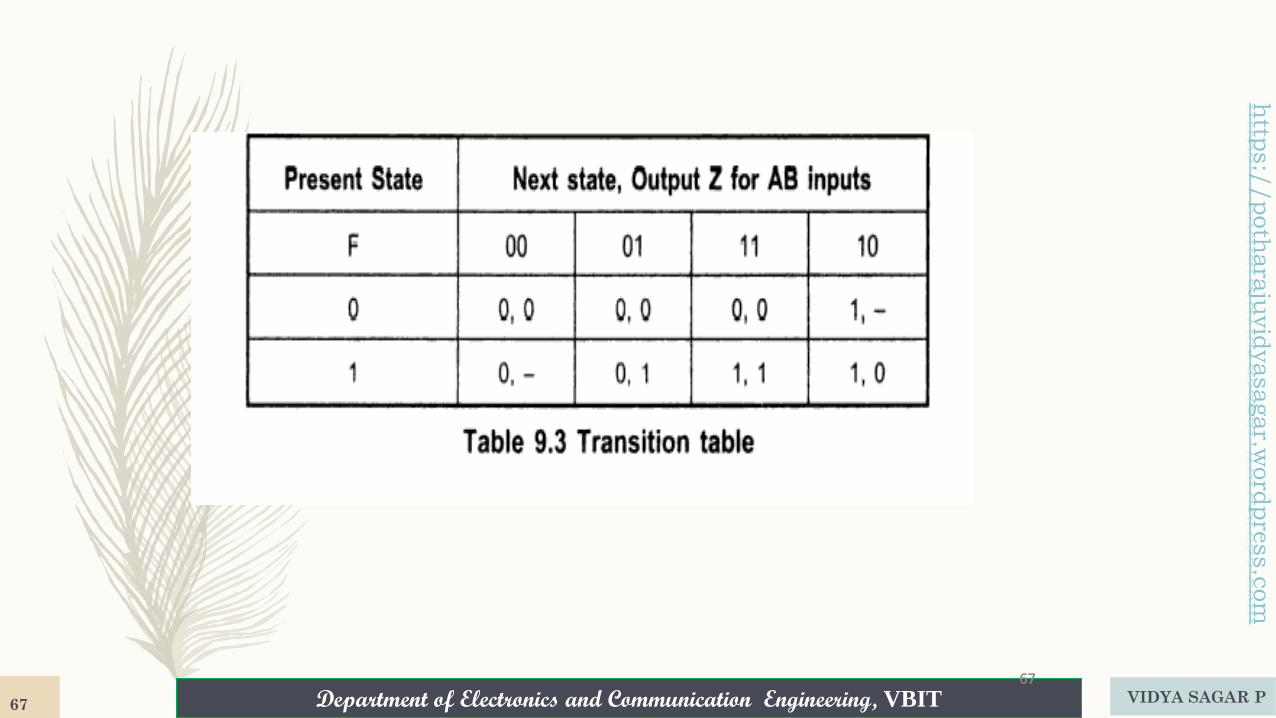
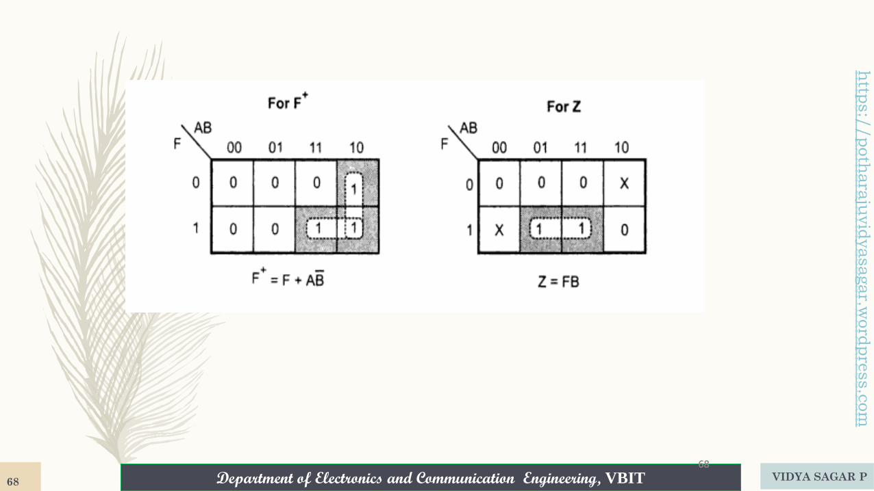
6666VIDYA SAGAR P66
Department of Electronics and Communication Engineering, VBIT
http
s:/
/poth
ara
juvid
yasagar.w
ord
pre
ss.c
om
6767VIDYA SAGAR P67
Department of Electronics and Communication Engineering, VBIT
http
s:/
/poth
ara
juvid
yasagar.w
ord
pre
ss.c
om
6868VIDYA SAGAR P68
Department of Electronics and Communication Engineering, VBIT
http
s:/
/poth
ara
juvid
yasagar.w
ord
pre
ss.c
om
Department of Electronics and Communication Engineering, VBIT
http
s:/
/poth
ara
juvid
yasagar.w
ord
pre
ss.c
om
Merging of the Flow Table
➢ The state table may be incompletely specified: combinations of inputs or input sequences
may never occur (Some next states and outputs are don’t care).
➢ Primitive flow tables are always incompletely specified
➢ Several synchronous circuits also have this property
➢ Incompletely specified states are not “equivalent” as in completely specified circuits. Instead,
we are going to find “compatible” states
➢ Two states of a incompletely specified circuit are compatible if they have the same output and
compatible next states whenever specified.
➢ Three procedural steps:
➢ Determine all compatible pairs by using the implication table
➢ Find the maximal compatibles by using a merger diagram
➢ Find a minimal closed collection of compatible that covers all states and is closed
VIDYA SAGAR P69
Department of Electronics and Communication Engineering, VBIT
http
s:/
/poth
ara
juvid
yasagar.w
ord
pre
ss.c
om
Department of Electronics and Communication Engineering, VBIT
http
s:/
/poth
ara
juvid
yasagar.w
ord
pre
ss.c
om
State Assignment
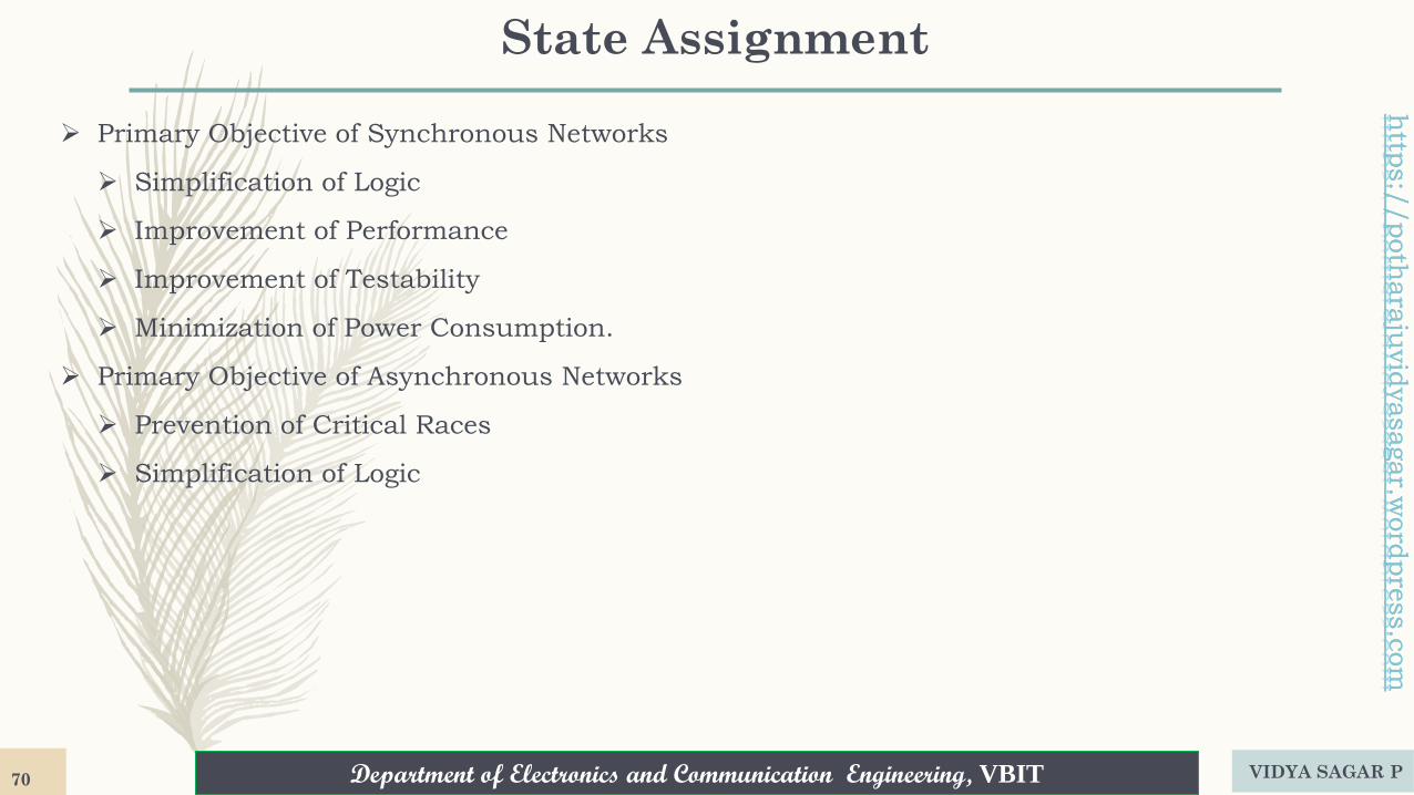
➢ Primary Objective of Synchronous Networks
➢ Simplification of Logic
➢ Improvement of Performance
➢ Improvement of Testability
➢ Minimization of Power Consumption.
➢ Primary Objective of Asynchronous Networks
➢ Prevention of Critical Races
➢ Simplification of Logic
VIDYA SAGAR P70
Department of Electronics and Communication Engineering, VBIT
http
s:/
/poth
ara
juvid
yasagar.w
ord
pre
ss.c
om
Department of Electronics and Communication Engineering, VBIT
http
s:/
/poth
ara
juvid
yasagar.w
ord
pre
ss.c
om
Race-Free State Assignment
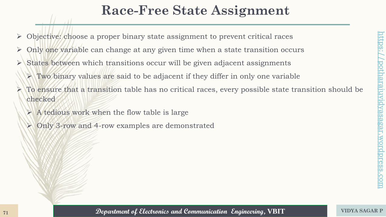
➢ Objective: choose a proper binary state assignment to prevent critical races
➢ Only one variable can change at any given time when a state transition occurs
➢ States between which transitions occur will be given adjacent assignments
➢ Two binary values are said to be adjacent if they differ in only one variable
➢ To ensure that a transition table has no critical races, every possible state transition should be
checked
➢ A tedious work when the flow table is large
➢ Only 3-row and 4-row examples are demonstrated
VIDYA SAGAR P71
Department of Electronics and Communication Engineering, VBIT
http
s:/
/poth
ara
juvid
yasagar.w
ord
pre
ss.c
om
Department of Electronics and Communication Engineering, VBIT
http
s:/
/poth
ara
juvid
yasagar.w
ord
pre
ss.c
om
3‐Row Flow‐Table Example
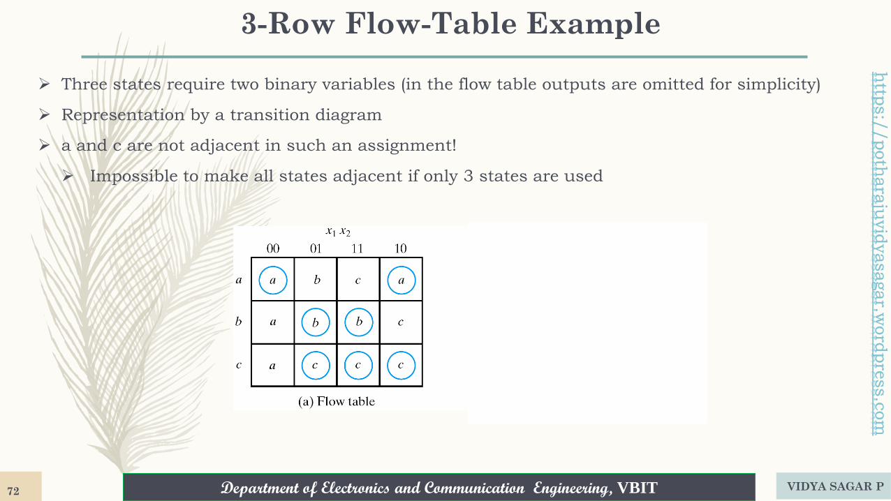
➢ Three states require two binary variables (in the flow table outputs are omitted for simplicity)
➢ Representation by a transition diagram
➢ a and c are not adjacent in such an assignment!
➢ Impossible to make all states adjacent if only 3 states are used
VIDYA SAGAR P72
Department of Electronics and Communication Engineering, VBIT
http
s:/
/poth
ara
juvid
yasagar.w
ord
pre
ss.c
om
Department of Electronics and Communication Engineering, VBIT
http
s:/
/poth
ara
juvid
yasagar.w
ord
pre
ss.c
om
3‐Row Flow‐Table Example
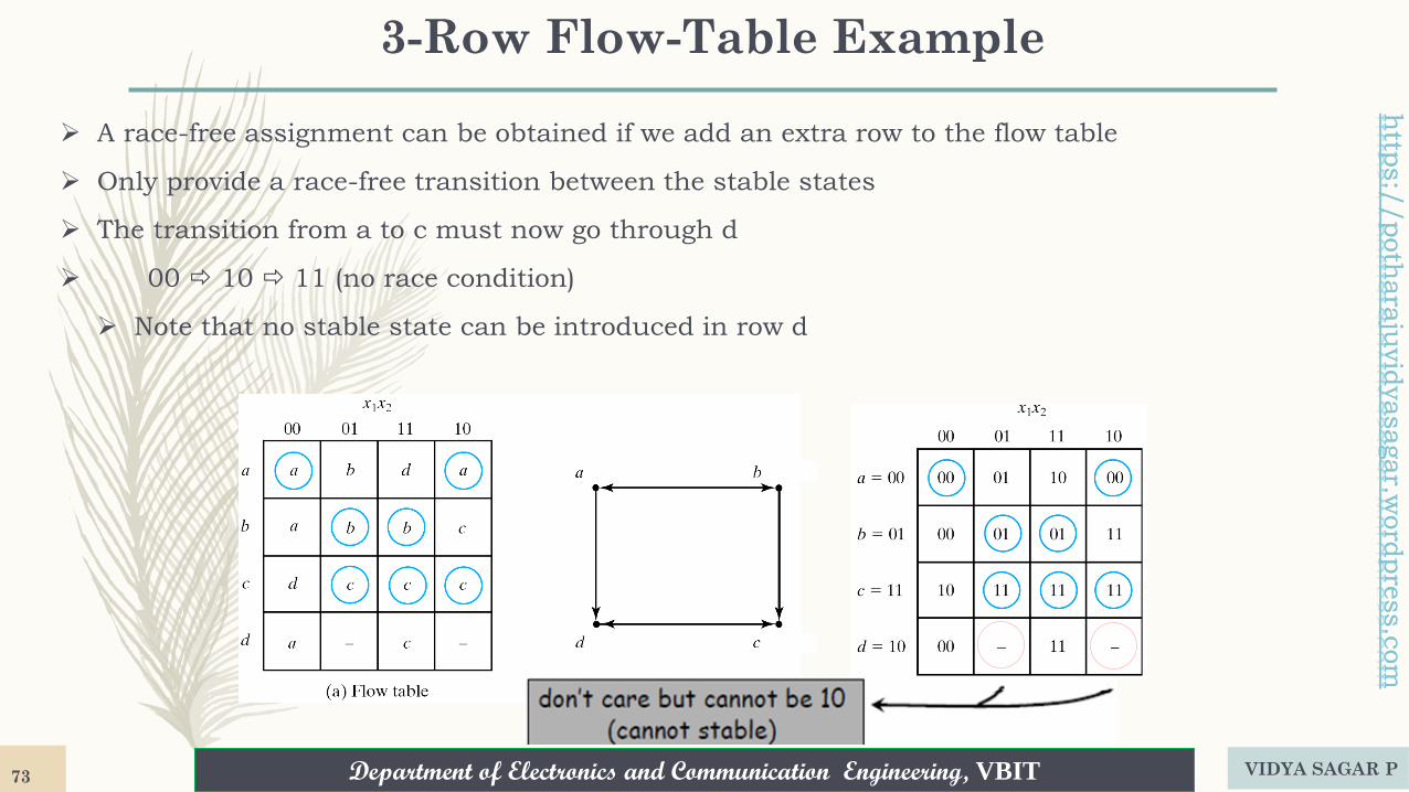
➢ A race-free assignment can be obtained if we add an extra row to the flow table
➢ Only provide a race-free transition between the stable states
➢ The transition from a to c must now go through d
➢ 00 10 11 (no race condition)
➢ Note that no stable state can be introduced in row d
VIDYA SAGAR P73
Department of Electronics and Communication Engineering, VBIT
http
s:/
/poth
ara
juvid
yasagar.w
ord
pre
ss.c
om
Department of Electronics and Communication Engineering, VBIT
http
s:/
/poth
ara
juvid
yasagar.w
ord
pre
ss.c
om
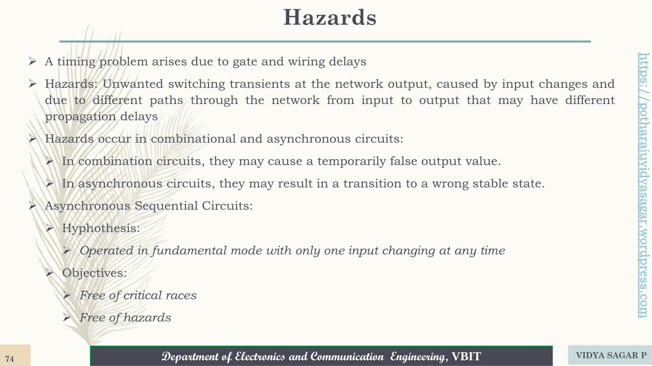
Hazards
➢ A timing problem arises due to gate and wiring delays
➢ Hazards: Unwanted switching transients at the network output, caused by input changes and
due to different paths through the network from input to output that may have different
propagation delays
➢ Hazards occur in combinational and asynchronous circuits:
➢ In combination circuits, they may cause a temporarily false output value.
➢ In asynchronous circuits, they may result in a transition to a wrong stable state.
➢ Asynchronous Sequential Circuits:
➢ Hyphothesis:
➢ Operated in fundamental mode with only one input changing at any time
➢ Objectives:
➢ Free of critical races
➢ Free of hazards
VIDYA SAGAR P74
Department of Electronics and Communication Engineering, VBIT
http
s:/
/poth
ara
juvid
yasagar.w
ord
pre
ss.c
om
Department of Electronics and Communication Engineering, VBIT
http
s:/
/poth
ara
juvid
yasagar.w
ord
pre
ss.c
om
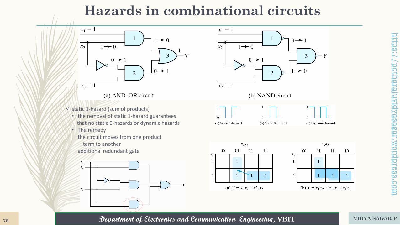
Hazards in combinational circuits
VIDYA SAGAR P75
✓ static 1-hazard (sum of products)• the removal of static 1-hazard guarantees
that no static 0-hazards or dynamic hazards• The remedy
the circuit moves from one productterm to another
additional redundant gate
Department of Electronics and Communication Engineering, VBIT
http
s:/
/poth
ara
juvid
yasagar.w
ord
pre
ss.c
om
Department of Electronics and Communication Engineering, VBIT
http
s:/
/poth
ara
juvid
yasagar.w
ord
pre
ss.c
om
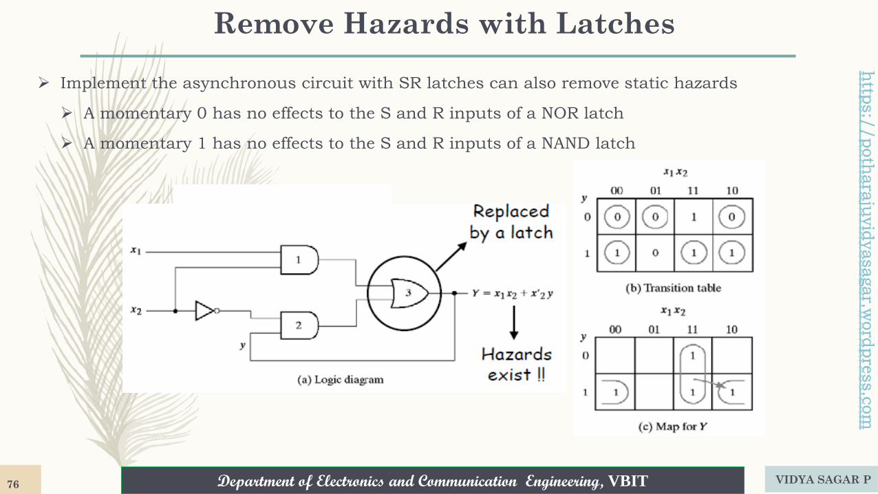
Remove Hazards with Latches
➢ Implement the asynchronous circuit with SR latches can also remove static hazards
➢ A momentary 0 has no effects to the S and R inputs of a NOR latch
➢ A momentary 1 has no effects to the S and R inputs of a NAND latch
VIDYA SAGAR P76
Department of Electronics and Communication Engineering, VBIT
http
s:/
/poth
ara
juvid
yasagar.w
ord
pre
ss.c
om
Department of Electronics and Communication Engineering, VBIT
http
s:/
/poth
ara
juvid
yasagar.w
ord
pre
ss.c
om
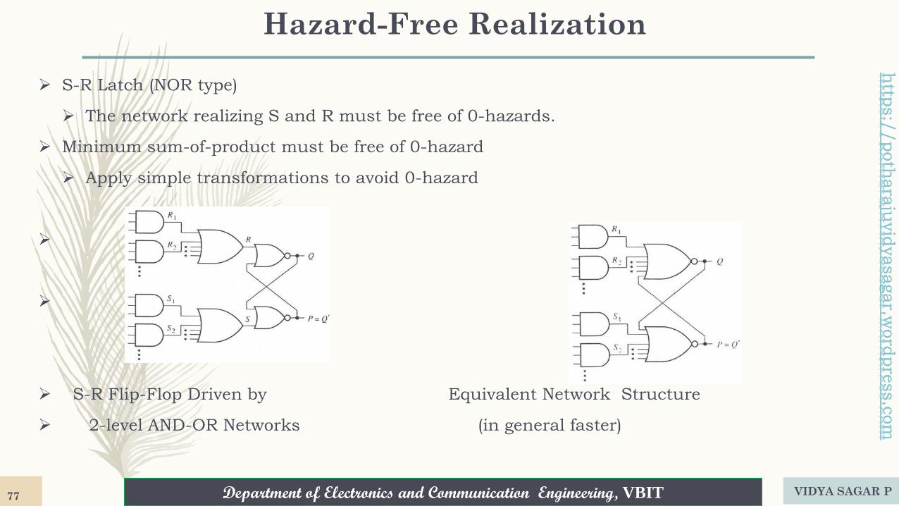
Hazard-Free Realization
➢ S-R Latch (NOR type)
➢ The network realizing S and R must be free of 0-hazards.
➢ Minimum sum-of-product must be free of 0-hazard
➢ Apply simple transformations to avoid 0-hazard
➢
➢
➢ S-R Flip-Flop Driven by Equivalent Network Structure
➢ 2-level AND-OR Networks (in general faster)
VIDYA SAGAR P77
Department of Electronics and Communication Engineering, VBIT
http
s:/
/poth
ara
juvid
yasagar.w
ord
pre
ss.c
om
Department of Electronics and Communication Engineering, VBIT
http
s:/
/poth
ara
juvid
yasagar.w
ord
pre
ss.c
om
Example
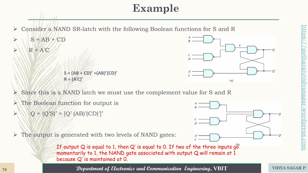
➢ Consider a NAND SR‐latch with the following Boolean functions for S and R
➢ S = AB + CD
➢ R = A’C
➢ Since this is a NAND latch we must use the complement value for S and R
➢ The Boolean function for output is
➢ Q = (Q’S)’ = [Q’ (AB)’(CD)’]’
➢ The output is generated with two levels of NAND gates:
VIDYA SAGAR P78
S = (AB + CD)’ =(AB)’(CD)’R = (A’C)’
If output Q is equal to 1, then Q′ is equal to 0. If two of the three inputs go momentarily to 1, the NAND gate associated with output Q will remain at 1 because Q′ is maintained at 0.
Department of Electronics and Communication Engineering, VBIT
http
s:/
/poth
ara
juvid
yasagar.w
ord
pre
ss.c
om
Department of Electronics and Communication Engineering, VBIT
http
s:/
/poth
ara
juvid
yasagar.w
ord
pre
ss.c
om
Essential Hazards
➢ Besides static and dynamic hazards, another type of hazard in asynchronous circuits is called:
Essential Hazard
➢ It is caused by unequal delays along two or more paths that originate from the same input
➢ Cannot be corrected by adding redundant gates
➢ Can only be corrected by adjusting the amount of delay in the affected path
➢ Each feedback path should be examined carefully !!
VIDYA SAGAR P79