microstructural origins of localization in ingan quantum wells
TRANSCRIPT
Microstructural origins of localisation in InGaN quantum wells
R.A. Oliver1, S.E. Bennett1, T. Zhu1, D.J. Beesley1, M.J. Kappers1, D.W. Saxey2, A.
Cerezo2, C.J. Humphreys1
1 Department of Materials Science and Metallurgy, University of Cambridge,
Pembroke Street, Cambridge, CB2 3QZ, UK
2 Department of Materials, University of Oxford, Parks Road, Oxford, OX1 3PH, UK
Abstract
The startling success of GaN-based light emitting diodes despite the high density of
dislocations found in typical heteroepitaxial material has been attributed to localisation of
carriers at non-uniformities in the quantum wells which form the active region of such
devices. Here, we review the different possible structures within the quantum wells which
could act as localisation sites, at length scales ranging from the atomic to the tens of
nanometre range. In some quantum wells several localisation mechanisms could be
operational, but the challenge remains to optimise the quantum wells' structure to achieve
improved quantum efficiencies, particularly at high excitation powers.
Keywords
GaN; InGaN; quantum wells; localisation; transmission electron microscopy; atom probe
tomography; spinodal decomposition
Confidential: not for distribution. Submitted to IOP Publishing for peer review 14 May 2010

PACS codes
68.37.-d, 68.65.Fg, 81.07.St, 78.55.Cr, 81.05.Ea III-V
1. Introduction
Light emitting diodes (LEDs) based on gallium nitride (GaN) are increasingly ubiquitous, in
everyday objects such as televisions and mobile phones. However, their most crucial
component, the active region of the device from which the light is actually emitted, remains
poorly understood, with its very structure a matter for debate. In this paper, we seek to
review current understanding of the micro- and nano-scale structure of the quantum wells
(QWs) which form the active region of almost all LEDs, and to delineate the potential impact
of that structure on device efficiency. In so doing, we will have to address controversies over
the best ways to characterise such structures.
The challenges in understanding the behaviour of GaN-based LEDs arise from the fact that
most such devices are grown heteroepitaxially on substrates such as sapphire, silicon carbide
or silicon. The lattice parameter mismatch between the GaN and the substrate results in the
presence of a high density of threading dislocations (more than 1010 cm-3 in early devices
[1]). It should be noted that although these threading dislocations arise as a consequence of
the lattice parameter mismatch, they do not necessarily relieve the misfit strain between the
epitaxial layer and the sample, and their mechanism of formation is a subject of ongoing
debate [2, 3, 4]. Irrespective of their origin, however, the success of GaN-based LEDs is
rather surprising in the context of such high defect densities, since in other, more
conventional optoelectronic semiconductors, such as GaAs, defect densities a million times
lower would be expected to lead to excessive non-radiative recombination, generation of heat
and speedy device failure [5].
The suggestion thus arises that in GaN-based LEDs some feature of the micro- or nano-
structure is preventing carriers from diffusing to dislocation cores and recombining non-
radiatively. Here we will focus on the highly efficient GaN-based LEDs which emit visible
light and employ one or more indium gallium nitride (InGaN) QWs in their active region, one
purpose of which is to provide a narrow spatial region with reduced bandgap, in which both
electrons and holes are trapped, increasing the probability that they will meet and recombine.
Hence, it is the small-scale structure of the InGaN QW, and its potential role in localising the
carriers, preventing their diffusion to dislocations, which will most concern us. The reader
should be aware that this review focuses solely on polar structures grown on the (0001) plane
of GaN. Assessment of the impact of the small scale structure non- and semi-polar QWs is
an interesting topic, but has not yet received much attention from researchers.
Localisation in InGaN QWs has been postulated to occur on a range of different length scales
- ranging from the single or few atom scale, through the few nanometre scale to structures
with extents up to tens of nanometres. We will review each of these different length scales.
However, it should be noted that postulated mechanisms at the single or few atom level in
InGaN should be relevant to all indium-containing nitride QWs, regardless of their broader
microstructure. Mechanisms of localisation at this near-atomic level will be assessed briefly
in Section 2. Section 3 will then assess postulated microstructures which might lead to
localisation at the few nanometre scale such as local variations in composition or QW
thickness. Lastly, Section 4 will cover observations of microstructural changes on longer
length scales (tens of nanometres to a few hundred nanometres) which could alter carrier
localisation or otherwise prevent carrier diffusion to dislocation cores. It should be noted that
here we are using the term "microstructure" to indicate all aspects of small-scale structure
which may be assessed using a variety of microscopes, not just structures on the micron
scale.
2. Localisation at the atomic scale
Much of the discussion about localisation in InGaN QWs has been driven by considerations
of experimental data - data concerning either QW microstructure or optical properties.
However, the driving force for consideration of the potential role of single atoms or few-atom
structures comes not from experiment, but from elegant theoretical studies employing large
supercell empirical pseudopotential calculations. Bellaiche et al. [6] used this approach to
suggest that in InGaN strong localisation of the hole around indium sites may occur even in
the case of an entirely random alloy of InN and GaN. Whilst Bellaiche et al. [6] modelled
zincblende InGaN, rather than the wurtzite structure which is more commonly grown, Wang
[7] soon performed similar calculations for wurtzite material, and predicted hole localisation
on chains of atoms containing two adjacent indium atoms (i.e. -In-N-In- chains).
Whilst these theoretical contributions are undoubtedly thought-provoking, some comparisons
of their predictions with experiment may reduce our confidence in them. For example,
Bellaiche et al. [6] predict a bandgap bowing parameter in excess of 5 eV for the GaN-InN
alloy system, and suggest that this very large value is a consequence of the localisation of
holes at Indium sites. However, whilst this calculated value was in reasonably good
agreement with experimental values available at the time, more recently a reassessment of the
band gap of InN [8], and subsequent new measurements of the bowing parameter, suggest
much smaller values, typically around 1.4 eV [9].
Wang's more extensive study [7] aimed to predict how the photoluminescence spectra of
InGaN QWs might vary with the indium content of the QW as a consequence of the
calculated localisation phenomena. The theory predicted a decrease in the observed
linewidth as the indium content increased from zero towards 50%. However, experimental
observations yield an opposite trend [10]. For example green-emitting QWs typically contain
a higher proportion of indium and exhibit a larger photoluminescence linewidth than similar
blue-emitting structures. This discrepancy suggests that whilst Wang's theory may be
relevant to the localisation process in InGaN QWs, it does not tell the whole story.
Nonetheless, there is some experimental data which supports the suggestion that localisation
of the hole occurs on an atomic or a near-atomic scale. Most notably, Chichibu et al [11]
showed that positron annihilation spectroscopy provides evidence for localisation of holes on
a very small length scale, and suggested that this localisation arose at -In-N-In- chains.
Additionally, Graham et al. [12] compared resonantly-excited photoluminescence spectra
recorded at low temperature from InGaN/GaN multiple quantum wells (MQWs) with the
results of a theoretical model which included the deformation potential coupling of carriers to
an effectively continuous distribution of longitudinal acoustic phonon modes. Based on this
analysis, they found an in-plane localisation length scale of about 2.5 Å, which is compatible
with the localisation of holes on -In-N-In- chains [12].
In discussing the concept of localisation at the near-atomic scale, most authors [6, 7, 11]
suggest that if the hole is localised at an -In-N-In- chain, the electron will also be localised
due to the formation of a bound excitonic state. However, some experimental analysis by
Kalliakos et al. [13] contradicts this suggestion. Kalliakos et al. [13] studied low-
temperature photoluminescence spectra from InGaN/GaN QWs in detail, comparing the
intensity of the observed phonon replicas and the main emission peak, and calculating the
Huang-Rhys factor, S. They were unable to fit the resulting data to an excitonic model of the
electron and hole in the InGaN, and instead suggested that a model similar to a donor-
acceptor pair (DAP) picture was more suitable [13]. This would suggest that the electron and
the hole are localised separately, at spatially distinct locations in the quantum well.
Hence, a picture of localisation in InGaN quantum wells involving holes trapped at randomly
formed -In-N-In- chains does not appear to account for all the experimental observations,
although there is certainly some evidence that near-atomic scale localisation is a contributory
factor. However, the question of the localisation of the electron is apparently left
outstanding. Kalliakos et al. [13] suggest that the electron and hole are localised at spatially
separate locations, but the theoretical studies do not suggest that the electron would be
localised at -In-N-In- chains unless it were bound to a localised hole. Hence, the nature of
electron localisation sites remains mysterious, and provides us an impetus to turn to
microstructural characterisation of InGaN QWs, to look for non-uniformities in the quantum
well at above the single atom level which might solve this puzzle.
3. Localisation at the nanometre scale
In considering possible microstructural origins of localisation at the nanometre scale, two
main candidates emerge: non-random variations in the composition of the InGaN QW,
within the plane of the well, often referred to as indium clustering, and variations in the
thickness of the InGaN QW. We will address each of these in turn.
3.1 Indium clustering
The formation of non-random "clusters" of indium in InGaN quantum wells was suggested
by Narukawa et al. [14], not long after the first nitride-based blue-violet laser diodes (LDs)
were introduced [15]. In transmission electron microscopy (TEM) images of InGaN QWs in
such an LD structure, small (2 - 5 nm) regions of strain contrast were observed. These
features were interpreted as being indium-rich regions which had self-assembled in the
quantum well, possibly by spinodal decomposition. Energy dispersive X-ray analysis also
suggested an increased indium content in these dot-like regions. Subsequent studies by
Gerthsen et al. [16] using digital analysis of the lattice fringe spacings in high resolution
TEM images suggested that the indium content in these regions (given here as the value of x
in InxGa1-xN) could be greater than 80%. Such regions of increased indium content – and
hence reduced bandgap – would be expected to localise carriers in the quantum well, and
indeed theoretical calculations by Kent and Zunger [17] (again using the large supercell
empirical pseudopotential method) indicate that both electrons and holes would be localised
at these types of non-random compositional fluctuations.
Hence, the idea that nanoscale indium-rich regions localised both the electron and hole in
InGaN quantum wells, preventing carrier diffusion to dislocations, appeared to solve the
mystery surrounding GaN-based LEDs. Gradually, however, problems with this hypothesis
started to emerge. Firstly, it was not clear how these regions of very high indium content had
formed. Narukawa et al. [14] initially suggested that a notionally barrierless phase separation
mechanism called spinodal decomposition was responsible, basing this suggestion on a
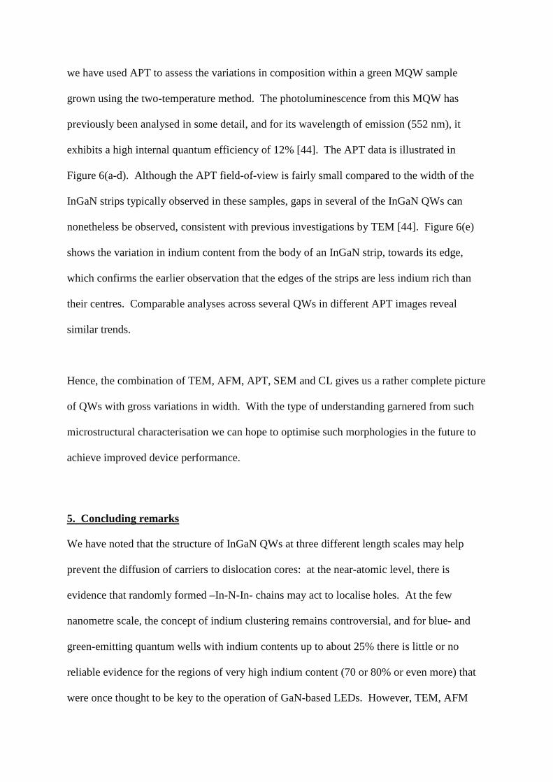
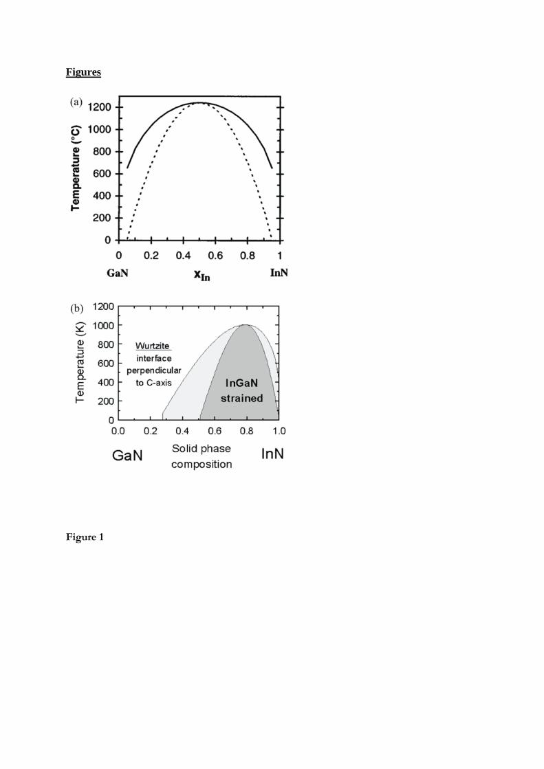
theoretical phase diagram calculated by Ho and Stringfellow [18] for the InN-GaN alloy
system in the zincblende structure. This diagram does suggest that for typical InGaN growth
temperatures of 700 to 800 °C, alloys containing more than about 20% indium would be
within the spinode. These indium levels are found in blue- and green-emitting quantum
wells, so the spinodal decomposition concept initially appears relevant.
However, the phase diagram Ho and Stringfellow [18] calculated is a chemical spinode,
which does not take into account the coherency strains associated with the formation of
interfaces between indium- and gallium-rich regions. The coherent spinode, influenced by
these strains, would be expected to be shifted to lower temperatures [19], making spinodal
decomposition at relevant growth temperatures less likely. Additionally, the Ho and
Stringfellow phase diagram [18] is for relaxed, bulk-like InGaN, whereas InGaN in QWs is
biaxially strained. Calculations by Karpov [20] for the phase diagram of biaxially strained
InGaN suggested a spinode shifted to much lower temperatures and higher indium contents
than those predicted by Ho and Stringfellow. The Ho and Stringfellow [18] phase diagram
and the Karpov [20] phase diagram are displayed in Figure 1 for comparison. (More recent
work by Liu and Zunger also supports the suggestion that spinodal decomposition may be
suppressed by epitaxial strain [21]). For the Karpov phase diagram, even QW material in
green LEDs (which might be grown at 700 °C, and contain about 25% indium) would be
outside not only the region within which the barrierless spinodal decomposition process
occurs, but outside the broader region for which phase separation may occur by the slower
nucleation and growth mechanism. In fact, according to Karpov’s calculations [20], InGaN
in QWs in blue, green and UV LEDs should be a random alloy. Some experimental support
for the suppression of decomposition by epitaxial strain is provided by the work of Rao et al.
[22] who studied InGaN epilayers more than 200 nm thick in TEM, and observed phase
separation resulting in indium rich regions on a scale of 10 - 20 nm in relaxed regions of their
films. However, regions of the films close to the InGaN/GaN interface, which were coherent
with the substrate, did not show any evidence of phase separation. (Phase separation in thick,
relaxed InGaN epilayers has been described in various publications (for example ref. [23]).
However, we will not review this phenomenon extensively here since such thick InGaN
layers have little relevance to the active region of most current LEDs).
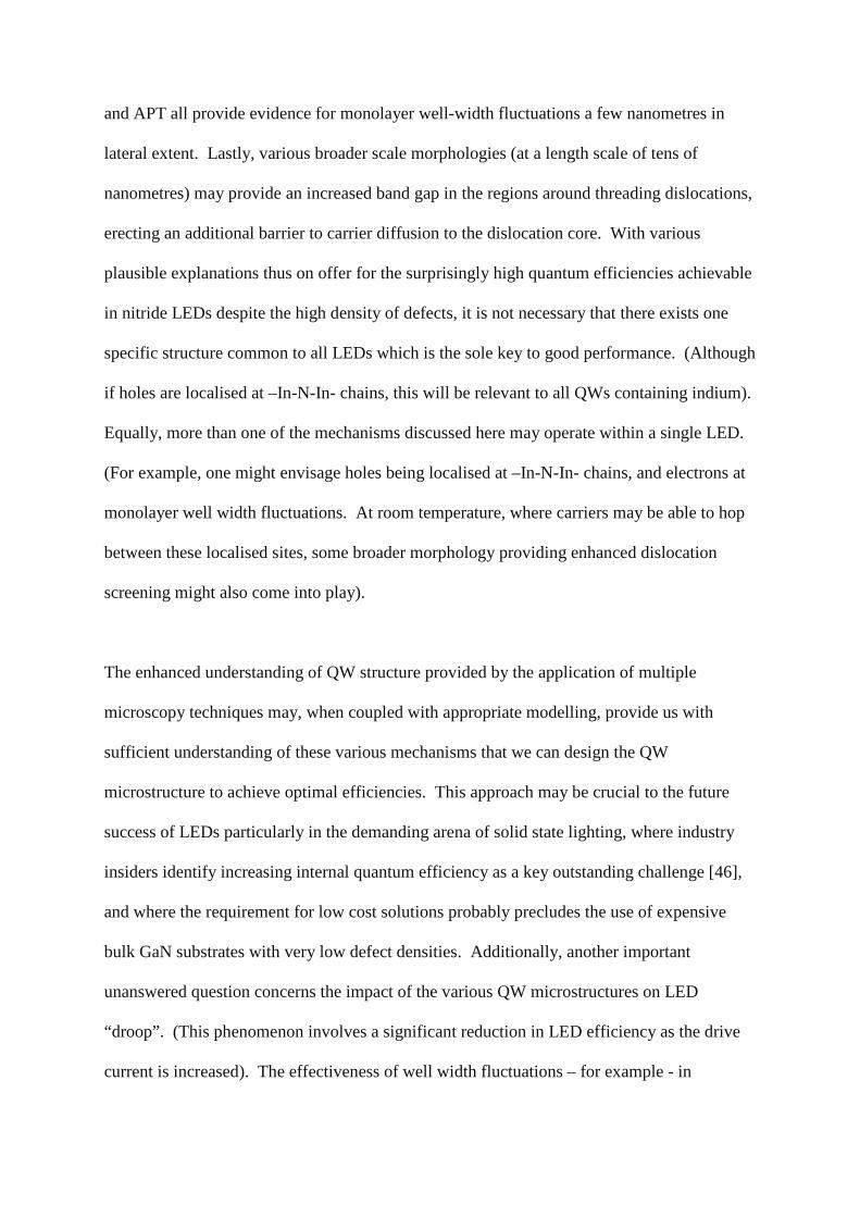
A significant concern about the TEM methods used to detect apparently indium-rich clusters
in InGaN QWs was raised by Smeeton et al. [24, 25] and O’Neill et al. [26]. Both sets of
authors observed that in TEM images of InGaN QWs which had not been exposed to the
electron beam prior to the image being recorded, the QWs appeared rather uniform.
However, continued exposure to the electron beam led to the appearance of locally strained
regions very similar to those observed by Narukawa et al. [14]. An example of this effect is
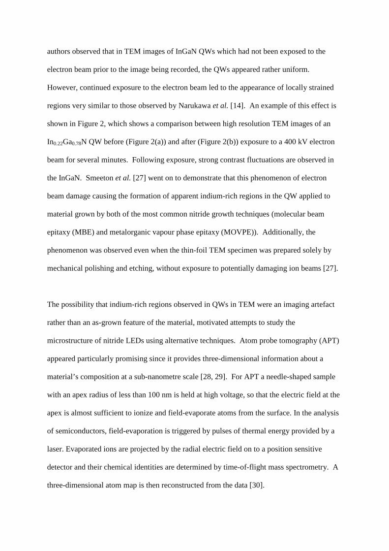
shown in Figure 2, which shows a comparison between high resolution TEM images of an
In0.22Ga0.78N QW before (Figure 2(a)) and after (Figure 2(b)) exposure to a 400 kV electron
beam for several minutes. Following exposure, strong contrast fluctuations are observed in
the InGaN. Smeeton et al. [27] went on to demonstrate that this phenomenon of electron
beam damage causing the formation of apparent indium-rich regions in the QW applied to
material grown by both of the most common nitride growth techniques (molecular beam
epitaxy (MBE) and metalorganic vapour phase epitaxy (MOVPE)). Additionally, the
phenomenon was observed even when the thin-foil TEM specimen was prepared solely by
mechanical polishing and etching, without exposure to potentially damaging ion beams [27].
The possibility that indium-rich regions observed in QWs in TEM were an imaging artefact
rather than an as-grown feature of the material, motivated attempts to study the
microstructure of nitride LEDs using alternative techniques. Atom probe tomography (APT)
appeared particularly promising since it provides three-dimensional information about a
material’s composition at a sub-nanometre scale [28, 29]. For APT a needle-shaped sample
with an apex radius of less than 100 nm is held at high voltage, so that the electric field at the
apex is almost sufficient to ionize and field-evaporate atoms from the surface. In the analysis
of semiconductors, field-evaporation is triggered by pulses of thermal energy provided by a
laser. Evaporated ions are projected by the radial electric field on to a position sensitive
detector and their chemical identities are determined by time-of-flight mass spectrometry. A
three-dimensional atom map is then reconstructed from the data [30].
Having first developed a technique for the preparation of appropriate needle-shaped samples
from GaN/sapphire wafers in the focused ion beam microscope (FIB) [31], Galtrey et al. [32]
were able to record the first APT data from a nitride semiconductor. The initial data set
recorded from a blue-emitting MQW sample, showed a region of about 20 nm × 20 nm in
lateral extent, containing four quantum wells, one of which had been damaged in the sample
preparation process. Following improvements to the sample preparation technique and
employing the local electrode atom probe (LEAP) which has an enhanced field of view,
significantly larger regions of both blue- and green-emitting MQW samples were analysed.
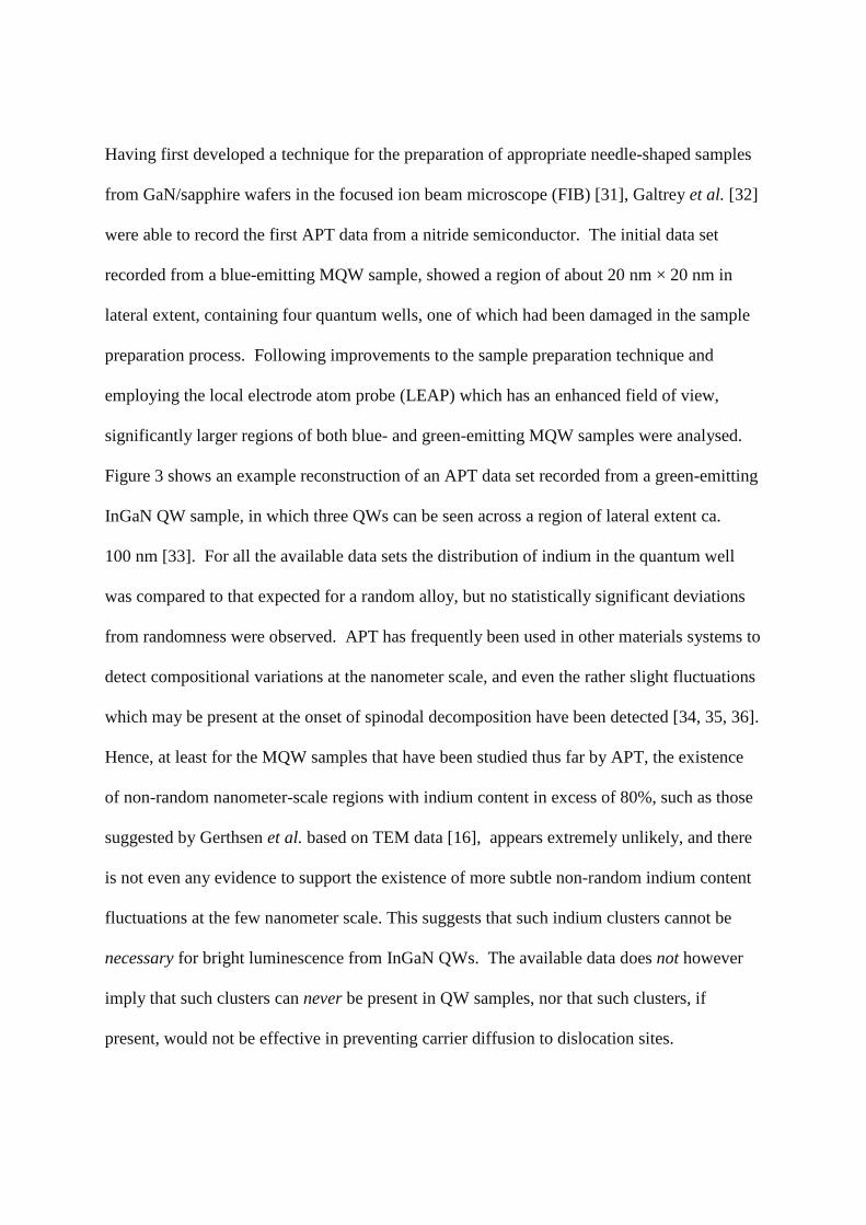
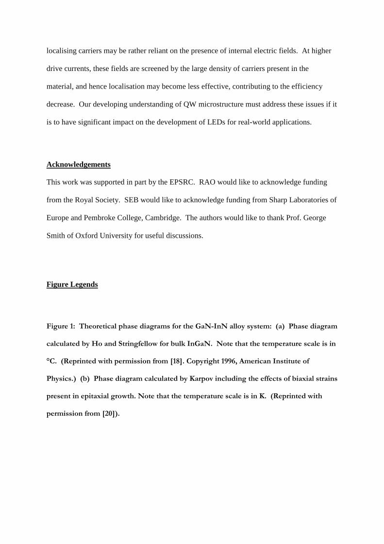
Figure 3 shows an example reconstruction of an APT data set recorded from a green-emitting
InGaN QW sample, in which three QWs can be seen across a region of lateral extent ca.
100 nm [33]. For all the available data sets the distribution of indium in the quantum well
was compared to that expected for a random alloy, but no statistically significant deviations
from randomness were observed. APT has frequently been used in other materials systems to
detect compositional variations at the nanometer scale, and even the rather slight fluctuations
which may be present at the onset of spinodal decomposition have been detected [34, 35, 36].
Hence, at least for the MQW samples that have been studied thus far by APT, the existence
of non-random nanometer-scale regions with indium content in excess of 80%, such as those
suggested by Gerthsen et al. based on TEM data [16], appears extremely unlikely, and there
is not even any evidence to support the existence of more subtle non-random indium content
fluctuations at the few nanometer scale. This suggests that such indium clusters cannot be
necessary for bright luminescence from InGaN QWs. The available data does not however
imply that such clusters can never be present in QW samples, nor that such clusters, if
present, would not be effective in preventing carrier diffusion to dislocation sites.
Since Narukawa et al. [14] initially used TEM to attempt to image indium clustering in
InGaN QWs, the application of TEM to these materials has been substantially refined,
perhaps most notably by Bartel et al. [37], who have made every effort to optimize the
preparation of their thin foil TEM samples and to minimize the extent of electron-beam
damage by using short exposure times. They have also very carefully assessed the impact of
noise in the TEM in defining detection limits for indium concentration fluctuations. Their
resulting high-resolution images appear qualitatively rather different to those seen in earlier
studies, with the quantum wells looking rather uniform to the naked eye with an absence of
blotchy strain contrast. However, digital analysis of lattice parameter variations within the
quantum well can pick up subtleties that the eye would miss. Bartel et al. [37] used this
approach to perform a statistical comparison of their data with that expected if the QWs were
a random alloy (similar to the approach used to analyse APT data). The analysis here is
somewhat hampered by the difficulty of quantifying the exact thickness of the TEM foils
used, so that in some cases the data had to be compared to the results expected for a random
alloy for various thicknesses of TEM foil and then suggestions made as to which thickness
was most realistic. However, for samples where it was possible to measure the foil thickness,
Bartel et al. [37] reported deviations from randomness for QWs with indium contents of 25%
or more. The blue- and green-emitting samples studied by Galtrey et al. [33] had indium
contents of 18% and 25% respectively so that there is some cross-over in the compositions of
the quantum wells found to be random by APT and those found to exhibit some deviation
from randomness in theTEM studies by Bartel et al. [37]. This discrepancy has been the
source of ongoing controversy.
In considering the differences between the two data sets, however, it should be noted that
samples of the same average composition grown by different methods can differ either subtly
or sometimes substantially, as Bartel et al. [37] note in their discussion of X-ray diffraction
data pertaining to phase separation in InGaN. Additionally, whilst Bartel et al. [37] do not
directly quantify the local indium contents associated with the fluctuations they observe in
QWs, it seems unlikely that the subtle variations seen in their data relate to areas a few
nanometers in lateral extent containing up to 80% indium. Related studies on thick InGaN
epilayers suggest deviations in indium content of around ±10% on length scales a few
nanometers [37]. The impact of such variations on electron and hole localization has not yet
been thoroughly modeled.
Overall, state-of-the art experimental data suggest that InGaN quantum wells of the
compositions typically found in blue- and green-emitting LEDs do not contain gross indium
clusters with an indium content of around 80%. Instead, the InGaN in QWs is either a
random alloy, or in some samples may contain subtle non-random variations in composition.
If InGaN is a random alloy, localization of holes may still occur at randomly formed –In-N-
In- chains. The impact of slight non-random indium content fluctuations on localization has
not yet been quantified.
3.2 Monolayer well-width fluctuations
The concept of indium clustering has been quite extensively studied. The possibility of slight
(1 or 2 monolayer ) fluctuations in the QW’s width has received far less attention. Such
monolayer well-width fluctuations can localise carriers in GaAs-based QWs, with quantum
dot-like optical behaviour being observed in such samples at low temperatures [38]. This is
due to the reduction of the impact of quantum confinement on the electron and hole energy
levels as the QW width increases. This change in potential is fairly slight and only a little
thermal energy is needed for the carriers to escape from the local minima. However, in
InGaN QWs, an additional effect alters the local potential landscape: the high piezoelectric
constants of the wurtzite nitrides lead to significant band-bending in strained quantum wells,
and as the well thickness increases, so does the impact of this band-bending. For example,
for a 3.3 nm thick QW containing 25% indium, Graham et al. [39] calculated that an increase
in thickness of just 1 monolayer should decrease the transition energy by 58 meV. This
suggests that monolayer well-width fluctuations in InGaN could localise carriers at room
temperature.
Both TEM and APT have been used to observe such monolayer width fluctuations in InGaN
QWs. Scanning transmission electron microscopy high angle annular dark field (STEM-
HAADF) images show that the lower interface of an InGaN/GaN quantum well (i.e. the
interface where InGaN was grown on GaN) appears abrupt, whereas the upper interface (the
interface where GaN was grown on InGaN) appears rough [39]. APT similarly reveals a
difference in roughness between the upper and lower QW interfaces [33], with the upper
interface being characterised by one or two monolayer high islands a few nanometres in
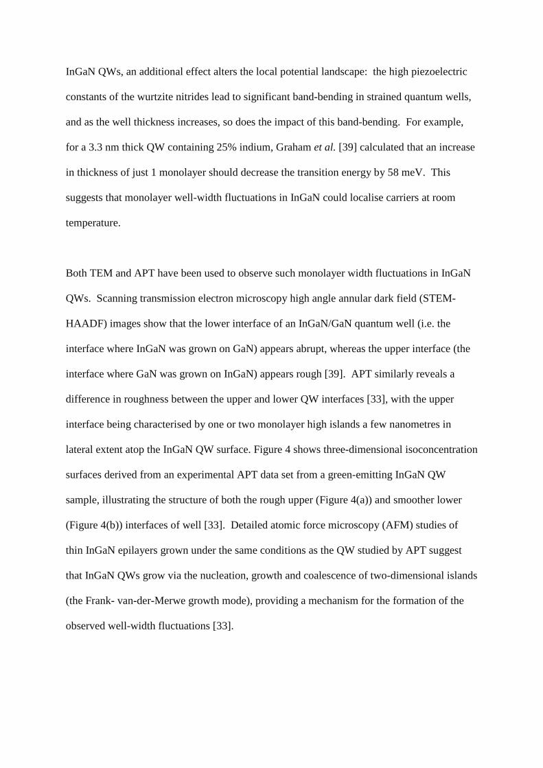
lateral extent atop the InGaN QW surface. Figure 4 shows three-dimensional isoconcentration
surfaces derived from an experimental APT data set from a green-emitting InGaN QW
sample, illustrating the structure of both the rough upper (Figure 4(a)) and smoother lower
(Figure 4(b)) interfaces of well [33]. Detailed atomic force microscopy (AFM) studies of
thin InGaN epilayers grown under the same conditions as the QW studied by APT suggest
that InGaN QWs grow via the nucleation, growth and coalescence of two-dimensional islands
(the Frank- van-der-Merwe growth mode), providing a mechanism for the formation of the
observed well-width fluctuations [33].
The impact of such monolayer well-width fluctuations on carrier localisation has not been
studied in detail theoretically, and may not be easily addressed using currently available large
supercell empirical pseudopotential models, most of which are for zincblende-structure
InGaN and which do not include quantum well interfaces or the effects of strain. However,
this area appears ripe for further theoretical exploration to guide potential experimental
optimisation of QW interface structure.
4. The impact of broader scale microstructure
When considering the potential impact of broader-scale microstructure (that is microstructure
on the tens of nanometre scale, rather than the few nanometre scale) on luminescence from
QWs, it is perhaps less appropriate to use the term “localisation” than when describing
smaller-scale structure. Whilst many of the broader scale structures which have been
observed in InGaN QWs may act to keep carriers away from dislocation sites, they do not do
so by trapping the carrier in a small, nanometre-scale area. Instead, they provide a region of
increased bandgap around the dislocation, providing a barrier to carrier diffusion to the
dislocation, but not necessarily preventing the carriers from moving around freely in other
regions of the QW. Since low temperature optical measurements [12], and positron
annihilation spectroscopy [11], have suggested very short localisation length scales in InGaN,
such “dislocation screening” is unlikely to be the only mechanism influencing carrier
diffusion in InGaN QWs, However, reports of very high internal quantum efficiencies in
quantum wells in which microstructural characterisation suggests that dislocation screening is
occurring [40, 41] suggest that it could be an important contributory factor.
The microstructures which have been suggested to lead to dislocation screening are diverse.
Hangleiter et al. [40] suggested that the formation of V-pits around dislocations during MQW
growth leads to the formation of thinner regions of QW on the V-pit walls, hence providing a
region of higher potential around the dislocation. Grandjean et al. [42], on the other hand,
suggested that step-pinning by dislocations leads to locally thinner QWs around dislocations
even in the absence of notable V-pits, again providing a barrier to carrier diffusion to
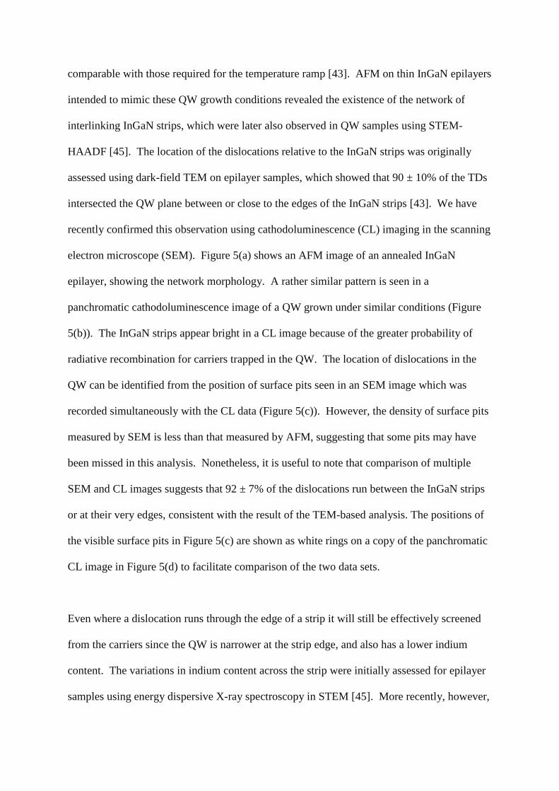
dislocation cores. Van der Laak et al. [43] noted the presence of gross fluctuations in QW
width in commercial LEDs on a lateral length scale of tens of nanometres. (By gross here,
we imply fluctuations in the QW width of several monolayers, rather than the one to two
monolayer fluctuations discussed in the previous section. In fact, the QW width was observed
to drop to nothing, leaving a gap in the QW, filled with GaN, at several locations). They
showed that such “gappy” QWs consist of a network of interlinking InGaN strips separated
by troughs filled with GaN. The majority of threading dislocations were observed to pass
through the gaps in the QW or through the very edges of the InGaN strips where the QW
thickness and indium content were both found to be lower [43]. Hence, the QW morphology
again provides a local potential barrier around the dislocation core. We will discuss this last
case in a little more detail to illustrate the ways in which multiple microstructural
characterisation techniques can be brought together to provide an enhanced understanding of
this type of quantum structure.
Van der Laak et al. [43] suggested that the network structures they observed in InGaN QWs
arose as a consequence of a two-temperature MOVPE growth method, in which the InGaN
QW is grown at a lower temperature than the GaN barrier, and is left exposed to a flow of
NH3 and N2 during the temperature ramp which is thus required. Such two-temperature
growth has been observed to provide high internal quantum efficiencies in both green- and
near-ultra-violet-emitting QWs [41, 44]. Similar gross well-width fluctuations were also
observed in QWs which had been annealed at their growth temperature for durations
comparable with those required for the temperature ramp [43]. AFM on thin InGaN epilayers
intended to mimic these QW growth conditions revealed the existence of the network of
interlinking InGaN strips, which were later also observed in QW samples using STEM-
HAADF [45]. The location of the dislocations relative to the InGaN strips was originally
assessed using dark-field TEM on epilayer samples, which showed that 90 ± 10% of the TDs
intersected the QW plane between or close to the edges of the InGaN strips [43]. We have
recently confirmed this observation using cathodoluminescence (CL) imaging in the scanning
electron microscope (SEM). Figure 5(a) shows an AFM image of an annealed InGaN
epilayer, showing the network morphology. A rather similar pattern is seen in a
panchromatic cathodoluminescence image of a QW grown under similar conditions (Figure
5(b)). The InGaN strips appear bright in a CL image because of the greater probability of
radiative recombination for carriers trapped in the QW. The location of dislocations in the
QW can be identified from the position of surface pits seen in an SEM image which was
recorded simultaneously with the CL data (Figure 5(c)). However, the density of surface pits
measured by SEM is less than that measured by AFM, suggesting that some pits may have
been missed in this analysis. Nonetheless, it is useful to note that comparison of multiple
SEM and CL images suggests that 92 ± 7% of the dislocations run between the InGaN strips
or at their very edges, consistent with the result of the TEM-based analysis. The positions of
the visible surface pits in Figure 5(c) are shown as white rings on a copy of the panchromatic
CL image in Figure 5(d) to facilitate comparison of the two data sets.
Even where a dislocation runs through the edge of a strip it will still be effectively screened
from the carriers since the QW is narrower at the strip edge, and also has a lower indium
content. The variations in indium content across the strip were initially assessed for epilayer
samples using energy dispersive X-ray spectroscopy in STEM [45]. More recently, however,
we have used APT to assess the variations in composition within a green MQW sample
grown using the two-temperature method. The photoluminescence from this MQW has
previously been analysed in some detail, and for its wavelength of emission (552 nm), it
exhibits a high internal quantum efficiency of 12% [44]. The APT data is illustrated in
Figure 6(a-d). Although the APT field-of-view is fairly small compared to the width of the
InGaN strips typically observed in these samples, gaps in several of the InGaN QWs can
nonetheless be observed, consistent with previous investigations by TEM [44]. Figure 6(e)
shows the variation in indium content from the body of an InGaN strip, towards its edge,
which confirms the earlier observation that the edges of the strips are less indium rich than
their centres. Comparable analyses across several QWs in different APT images reveal
similar trends.
Hence, the combination of TEM, AFM, APT, SEM and CL gives us a rather complete picture
of QWs with gross variations in width. With the type of understanding garnered from such
microstructural characterisation we can hope to optimise such morphologies in the future to
achieve improved device performance.
5. Concluding remarks
We have noted that the structure of InGaN QWs at three different length scales may help
prevent the diffusion of carriers to dislocation cores: at the near-atomic level, there is
evidence that randomly formed –In-N-In- chains may act to localise holes. At the few
nanometre scale, the concept of indium clustering remains controversial, and for blue- and
green-emitting quantum wells with indium contents up to about 25% there is little or no
reliable evidence for the regions of very high indium content (70 or 80% or even more) that
were once thought to be key to the operation of GaN-based LEDs. However, TEM, AFM
and APT all provide evidence for monolayer well-width fluctuations a few nanometres in
lateral extent. Lastly, various broader scale morphologies (at a length scale of tens of
nanometres) may provide an increased band gap in the regions around threading dislocations,
erecting an additional barrier to carrier diffusion to the dislocation core. With various
plausible explanations thus on offer for the surprisingly high quantum efficiencies achievable
in nitride LEDs despite the high density of defects, it is not necessary that there exists one
specific structure common to all LEDs which is the sole key to good performance. (Although
if holes are localised at –In-N-In- chains, this will be relevant to all QWs containing indium).
Equally, more than one of the mechanisms discussed here may operate within a single LED.
(For example, one might envisage holes being localised at –In-N-In- chains, and electrons at
monolayer well width fluctuations. At room temperature, where carriers may be able to hop
between these localised sites, some broader morphology providing enhanced dislocation
screening might also come into play).
The enhanced understanding of QW structure provided by the application of multiple
microscopy techniques may, when coupled with appropriate modelling, provide us with
sufficient understanding of these various mechanisms that we can design the QW
microstructure to achieve optimal efficiencies. This approach may be crucial to the future
success of LEDs particularly in the demanding arena of solid state lighting, where industry
insiders identify increasing internal quantum efficiency as a key outstanding challenge [46],
and where the requirement for low cost solutions probably precludes the use of expensive
bulk GaN substrates with very low defect densities. Additionally, another important
unanswered question concerns the impact of the various QW microstructures on LED
“droop”. (This phenomenon involves a significant reduction in LED efficiency as the drive
current is increased). The effectiveness of well width fluctuations – for example - in
localising carriers may be rather reliant on the presence of internal electric fields. At higher
drive currents, these fields are screened by the large density of carriers present in the
material, and hence localisation may become less effective, contributing to the efficiency
decrease. Our developing understanding of QW microstructure must address these issues if it
is to have significant impact on the development of LEDs for real-world applications.
Acknowledgements
This work was supported in part by the EPSRC. RAO would like to acknowledge funding
from the Royal Society. SEB would like to acknowledge funding from Sharp Laboratories of
Europe and Pembroke College, Cambridge. The authors would like to thank Prof. George
Smith of Oxford University for useful discussions.
Figure Legends
Figure 1: Theoretical phase diagrams for the GaN-InN alloy system: (a) Phase diagram
calculated by Ho and Stringfellow for bulk InGaN. Note that the temperature scale is in
°C. (Reprinted with permission from [18]. Copyright 1996, American Institute of
Physics.) (b) Phase diagram calculated by Karpov including the effects of biaxial strains
present in epitaxial growth. Note that the temperature scale is in K. (Reprinted with
permission from [20]).
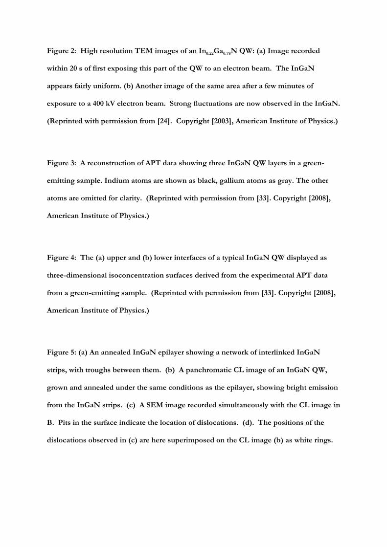
Figure 2: High resolution TEM images of an In0.22Ga0.78N QW: (a) Image recorded
within 20 s of first exposing this part of the QW to an electron beam. The InGaN
appears fairly uniform. (b) Another image of the same area after a few minutes of
exposure to a 400 kV electron beam. Strong fluctuations are now observed in the InGaN.
(Reprinted with permission from [24]. Copyright [2003], American Institute of Physics.)
Figure 3: A reconstruction of APT data showing three InGaN QW layers in a green-
emitting sample. Indium atoms are shown as black, gallium atoms as gray. The other
atoms are omitted for clarity. (Reprinted with permission from [33]. Copyright [2008],
American Institute of Physics.)
Figure 4: The (a) upper and (b) lower interfaces of a typical InGaN QW displayed as
three-dimensional isoconcentration surfaces derived from the experimental APT data
from a green-emitting sample. (Reprinted with permission from [33]. Copyright [2008],
American Institute of Physics.)
Figure 5: (a) An annealed InGaN epilayer showing a network of interlinked InGaN
strips, with troughs between them. (b) A panchromatic CL image of an InGaN QW,
grown and annealed under the same conditions as the epilayer, showing bright emission
from the InGaN strips. (c) A SEM image recorded simultaneously with the CL image in
B. Pits in the surface indicate the location of dislocations. (d). The positions of the
dislocations observed in (c) are here superimposed on the CL image (b) as white rings.
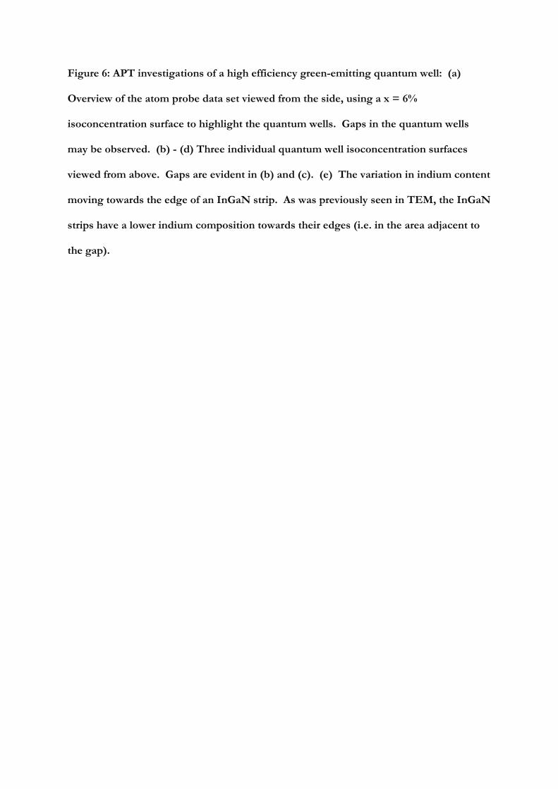
Figure 6: APT investigations of a high efficiency green-emitting quantum well: (a)
Overview of the atom probe data set viewed from the side, using a x = 6%
isoconcentration surface to highlight the quantum wells. Gaps in the quantum wells
may be observed. (b) - (d) Three individual quantum well isoconcentration surfaces
viewed from above. Gaps are evident in (b) and (c). (e) The variation in indium content
moving towards the edge of an InGaN strip. As was previously seen in TEM, the InGaN
strips have a lower indium composition towards their edges (i.e. in the area adjacent to
the gap).
Figures
Figure 1
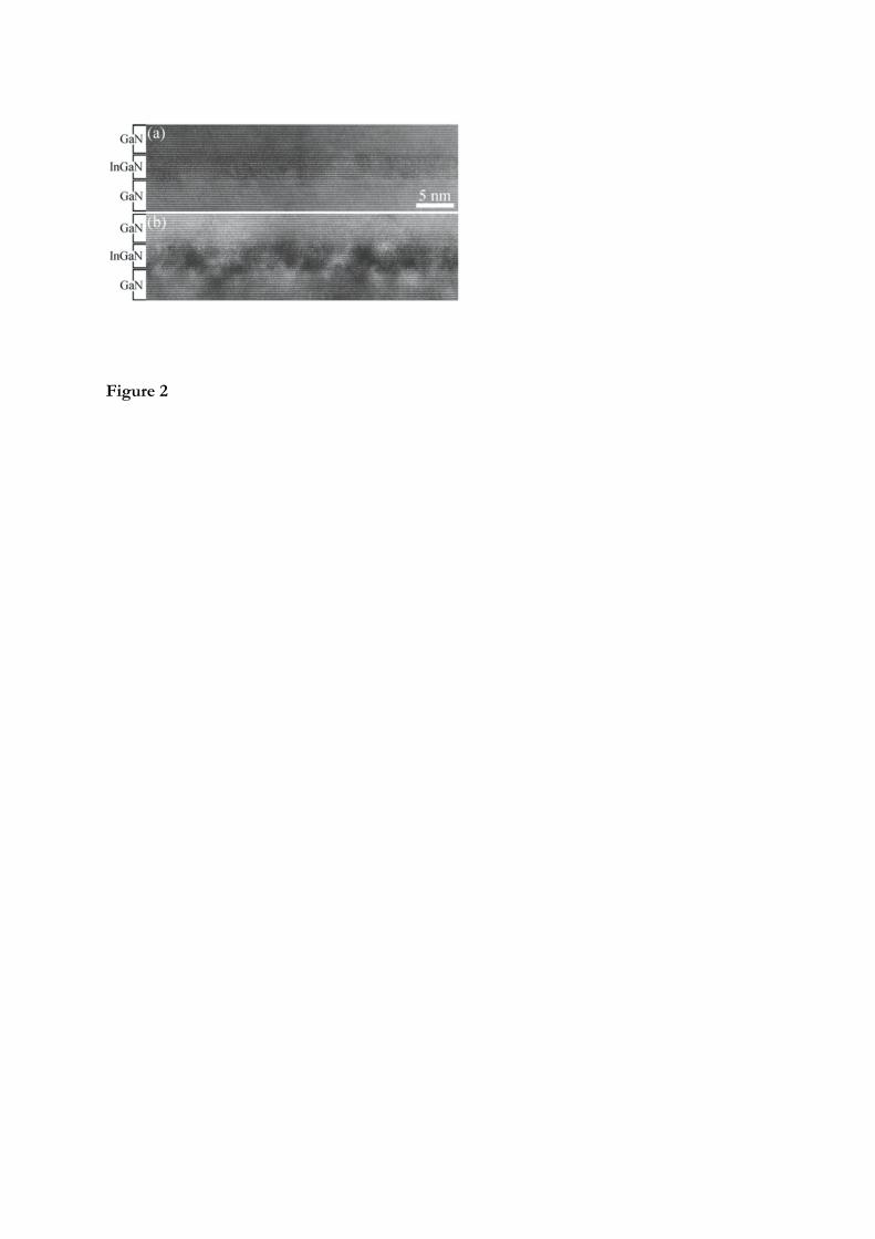
Figure 2
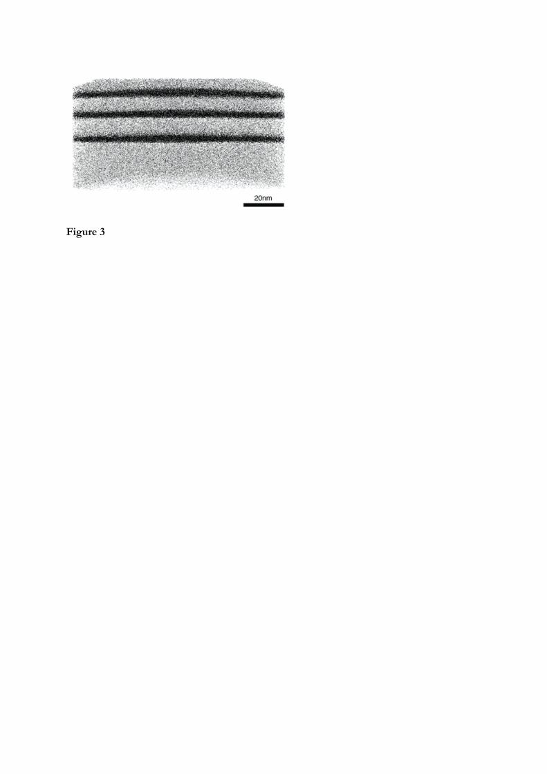
Figure 3
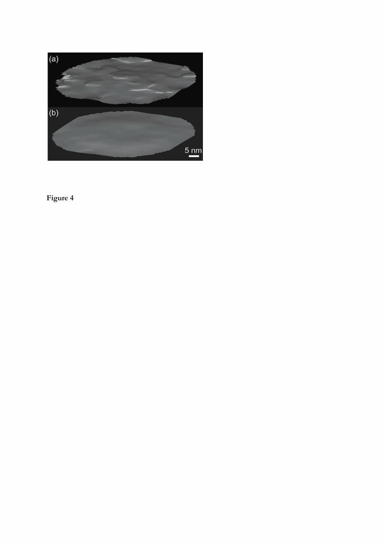
Figure 4
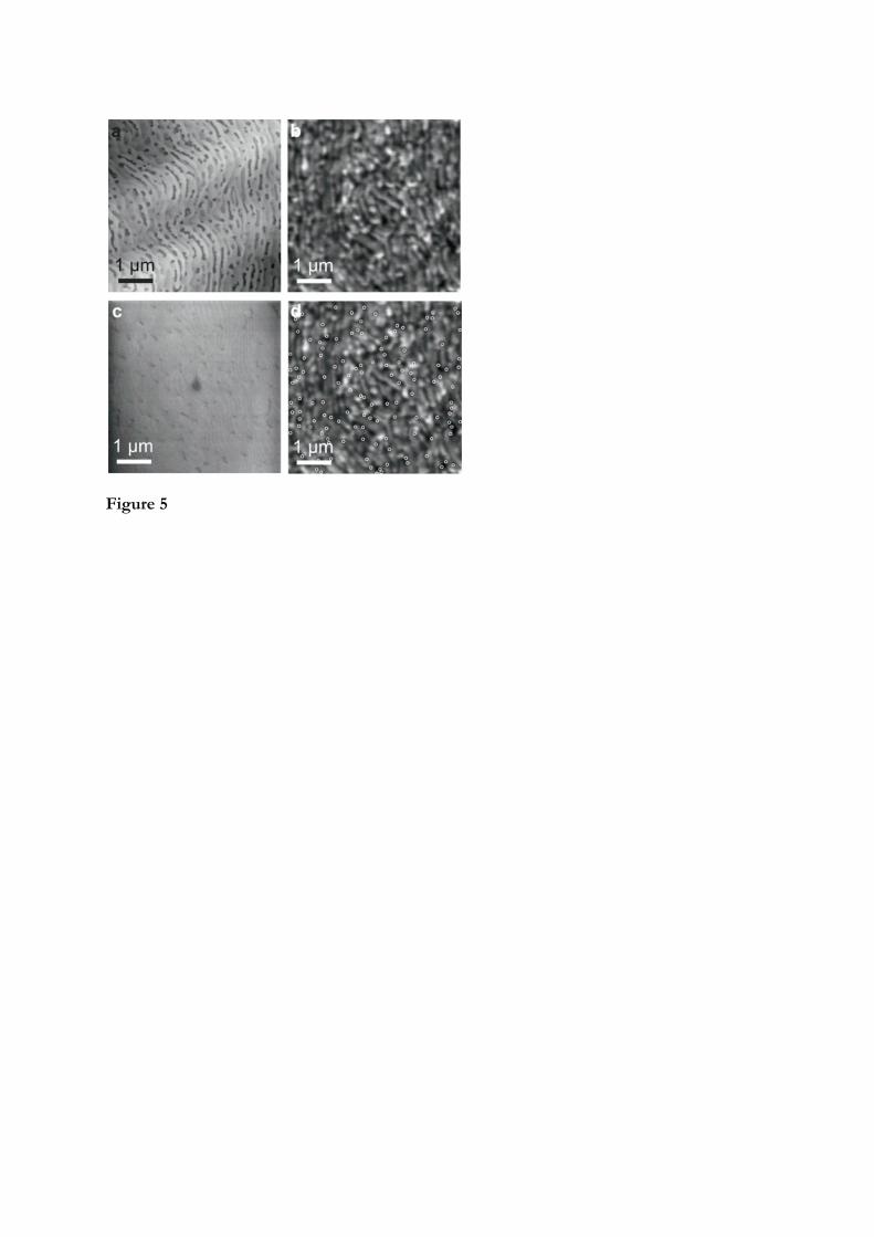
Figure 5
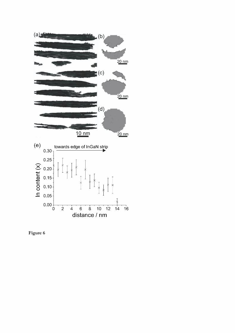
Figure 6
References
1 Nakamura S 1998 Science 2812 Ning X J, Chien F R, Pirouz P, Yang J W and Asif Khan M 1996 J. Mater. Res. 11 5803 Oliver R A, Kappers M J and Humphreys C J Appl. Phys. Lett. 89 0119144 Moram M A, Oliver R A, Kappers M J and Humphreys C J 2009 Adv. Mat. 21 39415 Herzog A H, Keune D L and Craford M G 1972 J. Appl. Phys. 43 6006 Bellaiche L, Mattila T; Wang L W, Wei S H and Zunger A 1999 Appl. Phys. Lett. 74 18427 Wang L W 2001 Phys. Rev. B 63 2451078 Wu J, Walukiewicz W, Yu K M, Ager J W, Haller E E, Lu H, Schaff W J, Saito Y and Nanishi Y 2002 Appl.Phys. Lett. 80 39679 Wu J 2009 J. Appl. Phys. 106 01110110 Shan W,Walukiewicz W, Haller E E, Little B D, Song J J, McCluskey M D, Johnson N M, Feng Z C,Schurman M and Stall R A 1998 J. Appl. Phys. 84, 4452.11 Chichibu S F, Uedono A, Onuma T, Haskell B A, Chakraborty A, Koyama T, Fini P T, Keller S, Denbaars SP, Speck J S, Mishra U K, Nakamura S, Yamaguchi S, Kamiyama S, Amano H, Akasaki I, Han J and Sota T2006 Nature Materials 5 81012 Graham D M, Dawson P, Godfrey M J, Kappers M J and Humphreys C J 2006 Appl. Phys. Lett. 89 21190113 Kalliakos S, Zhang B, Taliercio T, Lefebvre P, Gil B, Grandjean N, Damilano B and Massies J 2002 Appl.Phys. Lett. 80 42814 Narukawa Y, Kawakami Y, Funato M, Fujita S, Fujita S and Nakamura S 1997 Appl. Phys. Lett. 70 98115 Nakamura S, Senoh M, Nagahama S, Iwasa N, Yamada T, Matsushita T, Kiyoku H and Sugimoto Y 1996Jpn. J. Appl. Phys. 35 L7416 Gerthsen D, Hahn E, Neubauer B, Rosenauer A, Schön, Heuken M and Rizzi A 2000 phys. stat. sol. (a) 17714517 Kent P R C and Zunger A 2001 Appl. Phys. Lett. 79 197718 Ho I-h and Stringfellow G B 1996 Appl. Phys. Lett. 69 270119 Porter D A and Easterling K E 1981 Phase Transformations in Metals and Alloys 2nd Edition (London:Chapman and Hall) p31320 Karpov S Y 1998 MRS Internet Journal of Nitride Semiconductor Research 3 1621 Liu J Z and Zunger A 2008 Phys. Rev. B 77 20520122 Rao M, Kim D and Mahajan S 2004 Appl. Phys. Lett. 85 196123 Westmeyer A N and Mahajan S 2001 Appl. Phys. Lett. 79 271024 Smeeton T M, Kappers M J, Barnard J S, Vickers M E and Humphreys C J 2003phys. stat. sol. (c) 7 29725 Smeeton T M, Kappers M J, Barnard J S, Vickers M E and Humphreys C J 2003 Appl. Phys. Lett. 83 541926 O’Neill J P, Ross I M, Cullis A G, Wang T and Parbrook P J 2003 Appl. Phys. Lett. 83 196527 Smeeton T M, Humphreys C J, Barnard J S and Kappers M J 2006 J. Mater. Sci. 41 272928 Cerezo A, Godfrey T J and Smith G D W 1988 Rev. Sci. Inst. 59 86229 Miller M K, Cerezo A, Hetherington M G and Smith G D W 1996 Atom probe field ion microscopy (Oxford:Oxford University Press)30 Kelly T F and Miller M K 2007 Rev. Sci. Instrum. 78 03110131 Galtrey M J, Oliver R A, Kappers M J, Humphreys C J, Stokes D J, Clifton P H and Cerezo A 2007 SpringerProceedings in Physics 120 16132 Galtrey M J, Oliver R A, Kappers M J, Humphreys C J, Stokes D J, Clifton P H and Cerezo A 2007 Appl.Phys. Lett. 90 06190333 Galtrey M J, Oliver R A, Kappers M J, Humphreys C J, Clifton P, Larson D, Saxey D, Cerezo A 2008 J.Appl. Phys. 104 01352434 Miller M K, Hyde J M, Hetherington M G, Cerezo A, Smith G D W and Elliott C M 1995 Acta Metall. Mater.43 338535 Hyde J M, Miller M K, Hetherington M G, Cerezo A, Smith G D W and Elliott C M 1995 Acta Metall.Mater.43 340336 Hyde J M, Miller M K, Hetherington M G, Cerezo A, Smith G D W and Elliott C M 1995 Acta Metall. Mater.43 341537 Bartel T P, Specht P, Ho J C and Kisielowski C 2007 Phil. Mag. 87 198338 Phillips R T, Steffan A G, Newton S R, Reinecke T L, Kotlyar R 2003 phys. stat. sol. b 238 60139 Graham D M, Soltani-Vala A, Dawson P, Godfrey M J, Smeeton T M, Barnard J S, Kappers M J, HumphreysC J and Thrush E J 2005 J. Appl. Phys. 97 10350840 Hangleiter A, Hitzel F, Netzel C, Fuhrmann D, Rossow U, Ade G, and Hinze P 2005 Phys. Rev. Lett. 95127402

41 Galtrey M J, Oliver R A, Kappers M J, McAleese C M, Zhu D, Humphreys C J, Clifton P H, Larson D J andCerezo A 2008 Appl. Phys. Lett. 92 04190442 Grandjean N, Feltin E, Butté R, Carlin J-F, Sonderegger S, Deveaud B and Ganière J-D 2007 Phil. Mag. 87206743 van der Laak N K, Oliver R A, Kappers M J and Humphreys C J 2007 Appl. Phys. Lett. 90 121911.44 Costa P M F J, Datta R, Kappers M J, Vickers M E, Humphreys C J, Graham D M, Dawson P, Godfrey M J,Thrush E J and Mullins J T 2006 phys. stat. sol. (a) 203 172945 van der Laak N K, Oliver R A, Kappers M J and Humphreys C J 2007 J. Appl. Phys. 102 013513.46 Krames M R, Shchekin O B, Mueller-Mach R, Mueller G O, Zhou L, Harbers G and Craford M G 2007Journal of Display Technology 3 160