microstructural and crystallographic aspects of thin film recording media
TRANSCRIPT
Abstract-- Various aspects of the structure of thin filmlongitudinal recording media are presented and discussed.In particular we discuss the role that the various layers ofthin film media play in controlling the microstructure andmagnetic properties of the magnetic layer. These includethe grain size of the films, the texture of the films, the roleof the intermediate layer and the role of chemicalsegregation.
Index Terms--epitaxy, magnetic recording media, micro-structure, stacking faults, texture.
I. INTRODUCTION
S the areal density of recording media increases itbecomes more important to understand salient features ofthe microstructure of the recording media. In particular
the size, orientation and perfection of the magnetic grains playan ever increasing role in determining the magnetic propertiesof thin film media.
II. GRAIN SIZE
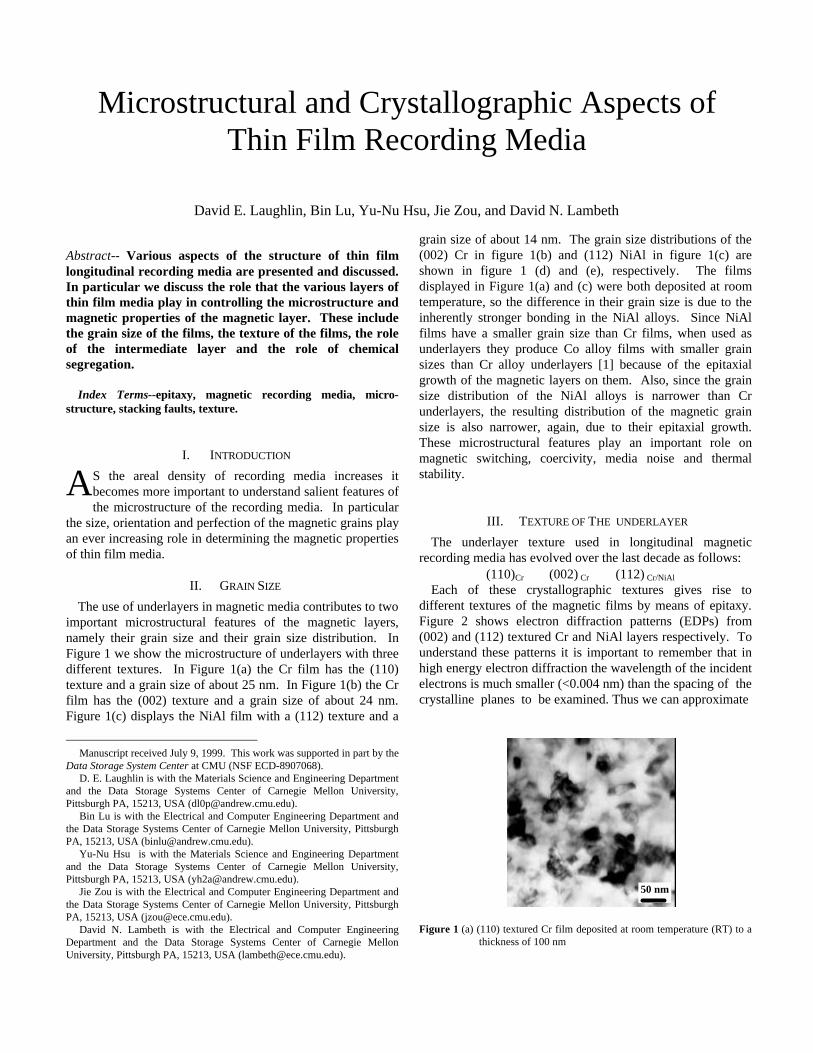
The use of underlayers in magnetic media contributes to twoimportant microstructural features of the magnetic layers,namely their grain size and their grain size distribution. InFigure 1 we show the microstructure of underlayers with threedifferent textures. In Figure 1(a) the Cr film has the (110)texture and a grain size of about 25 nm. In Figure 1(b) the Crfilm has the (002) texture and a grain size of about 24 nm.Figure 1(c) displays the NiAl film with a (112) texture and a
Manuscript received July 9, 1999. This work was supported in part by the
Data Storage System Center at CMU (NSF ECD-8907068).D. E. Laughlin is with the Materials Science and Engineering Department
and the Data Storage Systems Center of Carnegie Mellon University,Pittsburgh PA, 15213, USA ([email protected]).
Bin Lu is with the Electrical and Computer Engineering Department andthe Data Storage Systems Center of Carnegie Mellon University, PittsburghPA, 15213, USA ([email protected]).
Yu-Nu Hsu is with the Materials Science and Engineering Departmentand the Data Storage Systems Center of Carnegie Mellon University,Pittsburgh PA, 15213, USA ([email protected]).
Jie Zou is with the Electrical and Computer Engineering Department andthe Data Storage Systems Center of Carnegie Mellon University, PittsburghPA, 15213, USA ([email protected]).
David N. Lambeth is with the Electrical and Computer EngineeringDepartment and the Data Storage Systems Center of Carnegie MellonUniversity, Pittsburgh PA, 15213, USA ([email protected]).
grain size of about 14 nm. The grain size distributions of the(002) Cr in figure 1(b) and (112) NiAl in figure 1(c) areshown in figure 1 (d) and (e), respectively. The filmsdisplayed in Figure 1(a) and (c) were both deposited at roomtemperature, so the difference in their grain size is due to theinherently stronger bonding in the NiAl alloys. Since NiAlfilms have a smaller grain size than Cr films, when used asunderlayers they produce Co alloy films with smaller grainsizes than Cr alloy underlayers [1] because of the epitaxialgrowth of the magnetic layers on them. Also, since the grainsize distribution of the NiAl alloys is narrower than Crunderlayers, the resulting distribution of the magnetic grainsize is also narrower, again, due to their epitaxial growth.These microstructural features play an important role onmagnetic switching, coercivity, media noise and thermalstability.
III. TEXTURE OF THE UNDERLAYER
The underlayer texture used in longitudinal magneticrecording media has evolved over the last decade as follows:
(110)Cr ⇒ (002) Cr ⇒ (112) Cr/NiAl
Each of these crystallographic textures gives rise todifferent textures of the magnetic films by means of epitaxy.Figure 2 shows electron diffraction patterns (EDPs) from(002) and (112) textured Cr and NiAl layers respectively. Tounderstand these patterns it is important to remember that inhigh energy electron diffraction the wavelength of the incidentelectrons is much smaller (<0.004 nm) than the spacing of thecrystalline planes to be examined. Thus we can approximate
Figure 1 (a) (110) textured Cr film deposited at room temperature (RT) to athickness of 100 nm
Microstructural and Crystallographic Aspects ofThin Film Recording Media
David E. Laughlin, Bin Lu, Yu-Nu Hsu, Jie Zou, and David N. Lambeth
A
50 nm
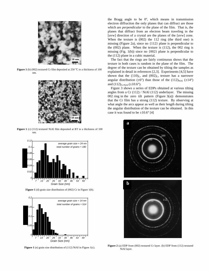
Figure 1 (b) (002) textured Cr film deposited at 250 oC to a thickness of 100nm.
Figure 1 (c) (112) textured NiAl film deposited at RT to a thickness of 100nm.
Figure 1 (d) grain size distribution of (002) Cr in Figure 1(b).
Figure 1 (e) grain size distribution of (112) NiAl in Figure 1(c).
the Bragg angle to be 0º, which means in transmissionelectron diffraction the only planes that can diffract are thosewhich are perpendicular to the plane of the film. That is, theplanes that diffract from an electron beam traveling in the[uvw] direction of a crystal are the planes of the [uvw] zone.When the texture is (002) the 112 ring (the third one) ismissing (Figure 2a), since no {112} plane is perpendicular tothe (002) plane. When the texture is (112), the 002 ring ismissing (Fig. 1(b)) since no {002} plane is perpendicular tothe (112) plane in a cubic material.
The fact that the rings are fairly continuous shows that thetexture in both cases is random in the plane of the film. Thedegree of the texture can be obtained by tilting the samples asexplained in detail in references [2,3]. Experiments [4,5] haveshown that the (110)Cr and (002)Cr texture has a narrowerangular distribution (±6°) than those of the (112)NiAl (±14°)and (112)Cr/NiAl (±10.6°).
Figure 3 shows a series of EDPs obtained at various tiltingangles from a Cr (112) / NiAl (112) underlayer. The missing002 ring in the zero tilt pattern (Figure 3(a)) demonstratesthat the Cr film has a strong (112) texture. By observing atwhat angle the arcs appear as well as their length during tiltingthe angular distribution of the texture can be obtained. In thiscase it was found to be ±10.6° [4]
Figure 2 (a) EDP from (002) textured Cr layer. (b) EDP from (112) texturedNiAl layer.
50 nm
50 nm
0
0.02
0.04
0.06
0.08
0.1
0.12
7 13 20 26 33 39 46 53 59Grain Size (nm)
average grain size = 24 nmtotal number of grains = 180
0
0.05
0.1
0.15
0.2
7 13 20 26 33 39 46 53 59Grain Size (nm)
average grain size = 14 nm
total number of grains = 514
110200
a
110 112
b
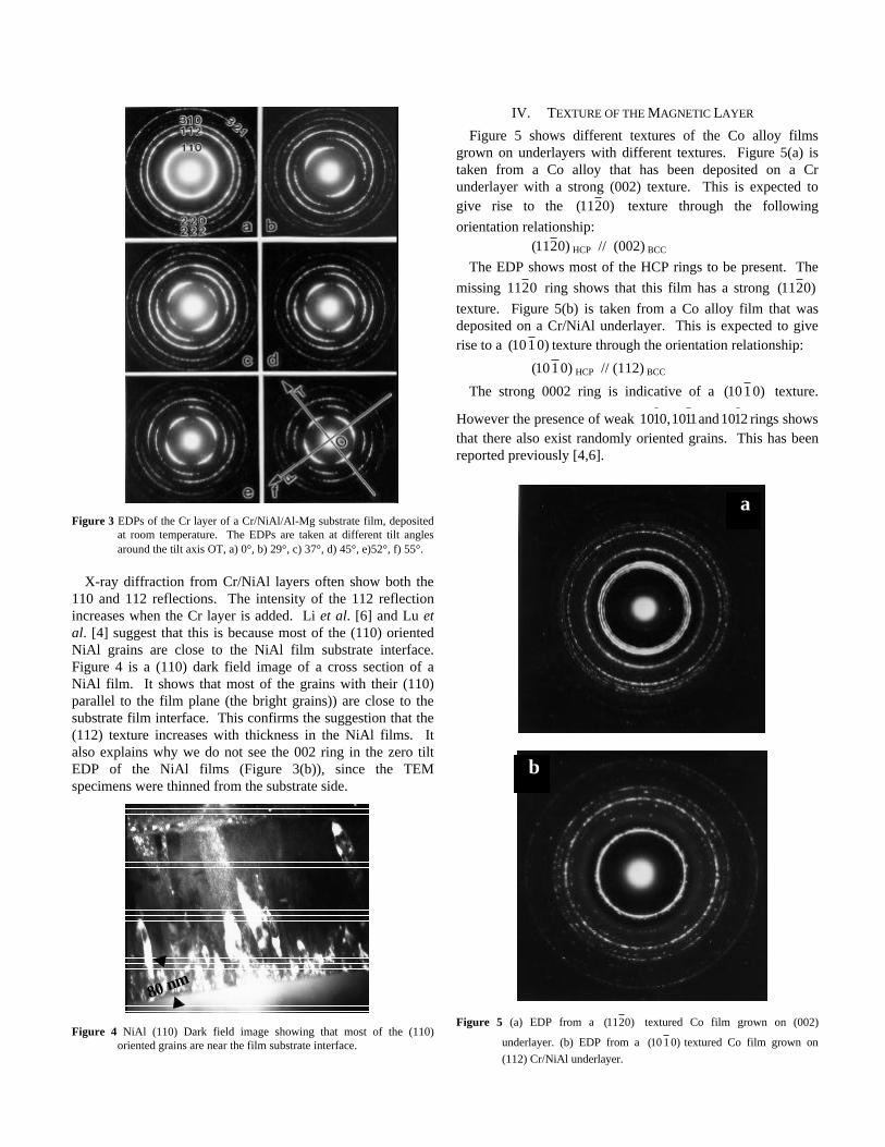
Figure 3 EDPs of the Cr layer of a Cr/NiAl/Al-Mg substrate film, depositedat room temperature. The EDPs are taken at different tilt anglesaround the tilt axis OT, a) 0°, b) 29°, c) 37°, d) 45°, e)52°, f) 55°.
X-ray diffraction from Cr/NiAl layers often show both the110 and 112 reflections. The intensity of the 112 reflectionincreases when the Cr layer is added. Li et al. [6] and Lu etal. [4] suggest that this is because most of the (110) orientedNiAl grains are close to the NiAl film substrate interface.Figure 4 is a (110) dark field image of a cross section of aNiAl film. It shows that most of the grains with their (110)parallel to the film plane (the bright grains)) are close to thesubstrate film interface. This confirms the suggestion that the(112) texture increases with thickness in the NiAl films. Italso explains why we do not see the 002 ring in the zero tiltEDP of the NiAl films (Figure 3(b)), since the TEMspecimens were thinned from the substrate side.
Figure 4 NiAl (110) Dark field image showing that most of the (110)oriented grains are near the film substrate interface.
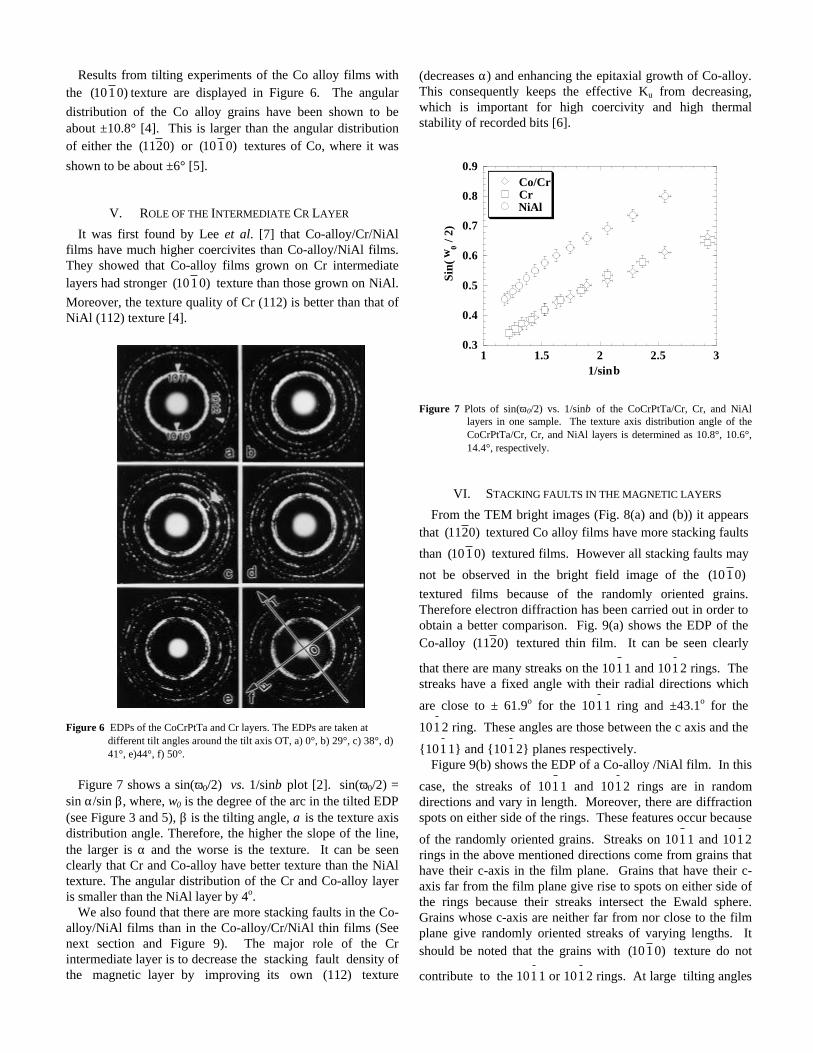
IV. TEXTURE OF THE MAGNETIC LAYER
Figure 5 shows different textures of the Co alloy filmsgrown on underlayers with different textures. Figure 5(a) istaken from a Co alloy that has been deposited on a Crunderlayer with a strong (002) texture. This is expected togive rise to the )0211( texture through the followingorientation relationship:
)0211( HCP // (002) BCC
The EDP shows most of the HCP rings to be present. Themissing 0211 ring shows that this film has a strong )0211(texture. Figure 5(b) is taken from a Co alloy film that wasdeposited on a Cr/NiAl underlayer. This is expected to giverise to a )0110( texture through the orientation relationship:
)0110( HCP // (112) BCC
The strong 0002 ring is indicative of a )0110( texture.
However the presence of weak 2110 and 1110 0,110 rings showsthat there also exist randomly oriented grains. This has beenreported previously [4,6].
Figure 5 (a) EDP from a )0211( textured Co film grown on (002)
underlayer. (b) EDP from a )0110( textured Co film grown on(112) Cr/NiAl underlayer.
80 nm
a
b
Results from tilting experiments of the Co alloy films withthe )0110( texture are displayed in Figure 6. The angulardistribution of the Co alloy grains have been shown to beabout ±10.8° [4]. This is larger than the angular distributionof either the )0211( or )0110( textures of Co, where it wasshown to be about ±6° [5].
V. ROLE OF THE INTERMEDIATE CR LAYER
It was first found by Lee et al. [7] that Co-alloy/Cr/NiAlfilms have much higher coercivites than Co-alloy/NiAl films.They showed that Co-alloy films grown on Cr intermediatelayers had stronger )0110( texture than those grown on NiAl.Moreover, the texture quality of Cr (112) is better than that ofNiAl (112) texture [4].
Figure 6 EDPs of the CoCrPtTa and Cr layers. The EDPs are taken atdifferent tilt angles around the tilt axis OT, a) 0°, b) 29°, c) 38°, d)41°, e)44°, f) 50°.
Figure 7 shows a sin(ω0/2) vs. 1/sinβ plot [2]. sin(ω0/2) =sin α/sin β, where, ω0 is the degree of the arc in the tilted EDP(see Figure 3 and 5), β is the tilting angle, α is the texture axisdistribution angle. Therefore, the higher the slope of the line,the larger is α and the worse is the texture. It can be seenclearly that Cr and Co-alloy have better texture than the NiAltexture. The angular distribution of the Cr and Co-alloy layeris smaller than the NiAl layer by 4o.
We also found that there are more stacking faults in the Co-alloy/NiAl films than in the Co-alloy/Cr/NiAl thin films (Seenext section and Figure 9). The major role of the Crintermediate layer is to decrease the stacking fault density ofthe magnetic layer by improving its own (112) texture
(decreases α) and enhancing the epitaxial growth of Co-alloy.This consequently keeps the effective Ku from decreasing,which is important for high coercivity and high thermalstability of recorded bits [6].
Figure 7 Plots of sin(ω0/2) vs. 1/sinβ of the CoCrPtTa/Cr, Cr, and NiAl
layers in one sample. The texture axis distribution angle of theCoCrPtTa/Cr, Cr, and NiAl layers is determined as 10.8°, 10.6°,14.4°, respectively.
VI. STACKING FAULTS IN THE MAGNETIC LAYERS
From the TEM bright images (Fig. 8(a) and (b)) it appearsthat )0211( textured Co alloy films have more stacking faults
than )0110( textured films. However all stacking faults may
not be observed in the bright field image of the )0110(textured films because of the randomly oriented grains.Therefore electron diffraction has been carried out in order toobtain a better comparison. Fig. 9(a) shows the EDP of theCo-alloy )0211( textured thin film. It can be seen clearly
that there are many streaks on the 101 1 and 101 2 rings. Thestreaks have a fixed angle with their radial directions which
are close to ± 61.9o for the 101 1 ring and ±43.1o for the
101 2 ring. These angles are those between the c axis and the
{101 1} and {101 2} planes respectively.Figure 9(b) shows the EDP of a Co-alloy /NiAl film. In this
case, the streaks of 101 1 and 101 2 rings are in randomdirections and vary in length. Moreover, there are diffractionspots on either side of the rings. These features occur because
of the randomly oriented grains. Streaks on 101 1 and 101 2rings in the above mentioned directions come from grains thathave their c-axis in the film plane. Grains that have their c-axis far from the film plane give rise to spots on either side ofthe rings because their streaks intersect the Ewald sphere.Grains whose c-axis are neither far from nor close to the filmplane give randomly oriented streaks of varying lengths. Itshould be noted that the grains with )0110( texture do not
contribute to the 101 1 or 101 2 rings. At large tilting angles
0.3
0.4
0.5
0.6
0.7
0.8
0.9
1 1.5 2 2.5 3
Co/CrCrNiAl
Sin(
/ 2)
ω0
1/sinβ
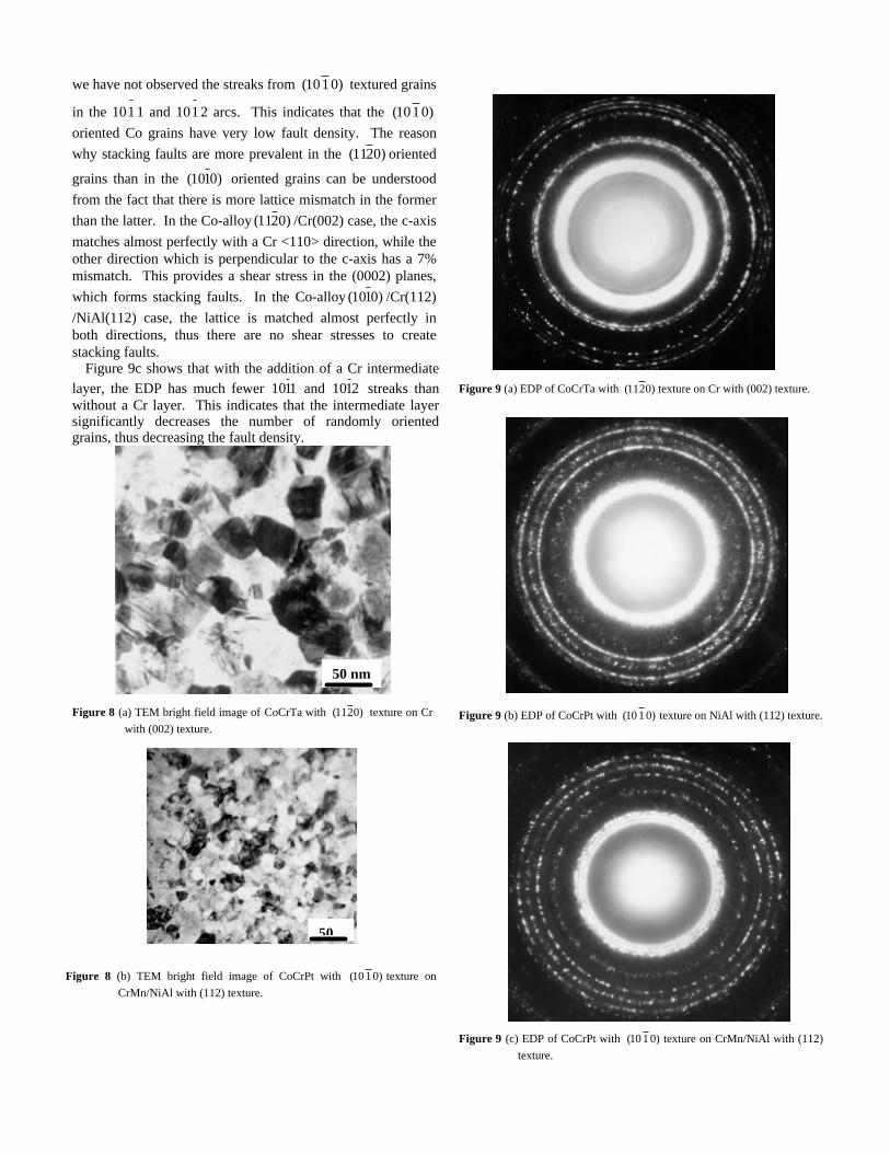
we have not observed the streaks from )0110( textured grains
in the 101 1 and 101 2 arcs. This indicates that the )0110(oriented Co grains have very low fault density. The reasonwhy stacking faults are more prevalent in the )0211( oriented
grains than in the )0110( oriented grains can be understoodfrom the fact that there is more lattice mismatch in the formerthan the latter. In the Co-alloy )0211( /Cr(002) case, the c-axismatches almost perfectly with a Cr <110> direction, while theother direction which is perpendicular to the c-axis has a 7%mismatch. This provides a shear stress in the (0002) planes,which forms stacking faults. In the Co-alloy )0110( /Cr(112)/NiAl(112) case, the lattice is matched almost perfectly inboth directions, thus there are no shear stresses to createstacking faults.
Figure 9c shows that with the addition of a Cr intermediatelayer, the EDP has much fewer 1110 and 2110 streaks thanwithout a Cr layer. This indicates that the intermediate layersignificantly decreases the number of randomly orientedgrains, thus decreasing the fault density.
Figure 8 (a) TEM bright field image of CoCrTa with )0211( texture on Crwith (002) texture.
Figure 8 (b) TEM bright field image of CoCrPt with )0110( texture onCrMn/NiAl with (112) texture.
Figure 9 (a) EDP of CoCrTa with )0211( texture on Cr with (002) texture.
Figure 9 (b) EDP of CoCrPt with )0110( texture on NiAl with (112) texture.
Figure 9 (c) EDP of CoCrPt with )0110( texture on CrMn/NiAl with (112)texture.
50 nm
50
VII. CHEMICAL SEGREGATION
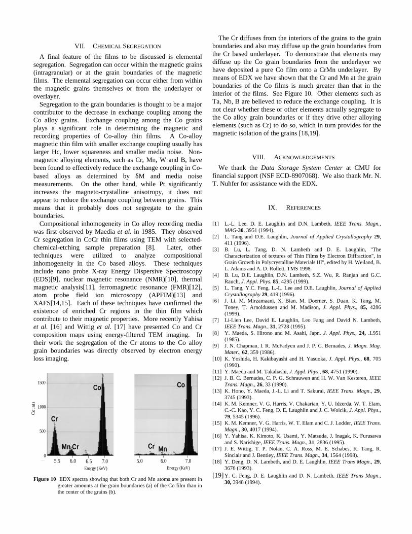
A final feature of the films to be discussed is elementalsegregation. Segregation can occur within the magnetic grains(intragranular) or at the grain boundaries of the magneticfilms. The elemental segregation can occur either from withinthe magnetic grains themselves or from the underlayer oroverlayer.
Segregation to the grain boundaries is thought to be a majorcontributor to the decrease in exchange coupling among theCo alloy grains. Exchange coupling among the Co grainsplays a significant role in determining the magnetic andrecording properties of Co-alloy thin films. A Co-alloymagnetic thin film with smaller exchange coupling usually haslarger Hc, lower squareness and smaller media noise. Non-magnetic alloying elements, such as Cr, Mn, W and B, havebeen found to effectively reduce the exchange coupling in Co-based alloys as determined by δM and media noisemeasurements. On the other hand, while Pt significantlyincreases the magneto-crystalline anisotropy, it does notappear to reduce the exchange coupling between grains. Thismeans that it probably does not segregate to the grainboundaries.
Compositional inhomogeneity in Co alloy recording mediawas first observed by Maedia et al. in 1985. They observedCr segregation in CoCr thin films using TEM with selected-chemical-etching sample preparation [8]. Later, othertechniques were utilized to analyze compositionalinhomogeneity in the Co based alloys. These techniquesinclude nano probe X-ray Energy Dispersive Spectroscopy(EDS)[9], nuclear magnetic resonance (NMR)[10], thermalmagnetic analysis[11], ferromagnetic resonance (FMR)[12],atom probe field ion microscopy (APFIM)[13] andXAFS[14,15]. Each of these techniques have confirmed theexistence of enriched Cr regions in the thin film whichcontribute to their magnetic properties. More recently Yahisaet al. [16] and Wittig et al. [17] have presented Co and Crcomposition maps using energy-filtered TEM imaging. Intheir work the segregation of the Cr atoms to the Co alloygrain boundaries was directly observed by electron energyloss imaging.
Figure 10 EDX spectra showing that both Cr and Mn atoms are present ingreater amounts at the grain boundaries (a) of the Co film than inthe center of the grains (b).
The Cr diffuses from the interiors of the grains to the grainboundaries and also may diffuse up the grain boundaries fromthe Cr based underlayer. To demonstrate that elements maydiffuse up the Co grain boundaries from the underlayer wehave deposited a pure Co film onto a CrMn underlayer. Bymeans of EDX we have shown that the Cr and Mn at the grainboundaries of the Co films is much greater than that in theinterior of the films. See Figure 10. Other elements such asTa, Nb, B are believed to reduce the exchange coupling. It isnot clear whether these or other elements actually segregate tothe Co alloy grain boundaries or if they drive other alloyingelements (such as Cr) to do so, which in turn provides for themagnetic isolation of the grains [18,19].
VIII. ACKNOWLEDGEMENTS
We thank the Data Storage System Center at CMU forfinancial support (NSF ECD-8907068). We also thank Mr. N.T. Nuhfer for assistance with the EDX.
IX. REFERENCES
[1] L.-L. Lee, D. E. Laughlin and D.N. Lambeth, IEEE Trans. Magn.,MAG-30, 3951 (1994).
[2] L. Tang and D.E. Laughlin, Journal of Applied Crystallography 29,411 (1996).
[3] B. Lu, L. Tang, D. N. Lambeth and D. E. Laughlin, "TheCharacterization of textures of Thin Films by Electron Diffraction", inGrain Growth in Polycrystalline Materials III", edited by H. Weiland, B.L. Adams and A. D. Rollett, TMS 1998.
[4] B. Lu, D.E. Laughlin, D.N. Lambeth, S.Z. Wu, R. Ranjan and G.C.Rauch, J. Appl. Phys. 85, 4295 (1999).
[5] L. Tang, Y.C. Feng, L.-L. Lee and D.E. Laughlin, Journal of AppliedCrystallography 29, 419 (1996).
[6] J. Li, M. Mirzamaani, X. Bian, M. Doerner, S. Duan, K. Tang, M.Toney, T. Arnoldussen and M. Madison, J. Appl. Phys., 85, 4286(1999).
[7] Li-Lien Lee, David E. Laughlin, Leo Fang and David N. Lambeth,IEEE Trans. Magn., 31, 2728 (1995).
[8] Y. Maeda, S. Hirono and M. Asahi, Japn. J. Appl. Phys., 24, .L951(1985).
[9] J. N. Chapman, I. R. McFadyen and J. P. C. Bernades, J. Magn. Mag.Mater., 62, 359 (1986).
[10] K. Yoshida, H. Kakibayashi and H. Yasuoka, J. Appl. Phys., 68, 705(1990).
[11] Y. Maeda and M. Takahashi, J. Appl. Phys., 68, 4751 (1990).[12] J. B. C. Bernades, C. P. G. Schrauwen and H. W. Van Kesteren, IEEE
Trans. Magn., 26, 33 (1990).[13] K. Hono, Y. Maeda, J.-L. Li and T. Sakurai, IEEE Trans. Magn., 29,
3745 (1993).[14] K. M. Kemner, V. G. Harris, V. Chakarian, Y. U. Idzerda, W. T. Elam,
C.-C. Kao, Y. C. Feng, D. E. Laughlin and J. C. Woicik, J. Appl. Phys.,79, 5345 (1996).
[15] K. M. Kemner, V. G. Harris, W. T. Elam and C. J. Lodder, IEEE Trans.Magn., 30, 4017 (1994).
[16] Y. Yahisa, K. Kimoto, K. Usami, Y. Matsuda, J. Inagak, K. Furusawaand S. Narishige, IEEE Trans. Magn., 31, 2836 (1995).
[17] J. E. Wittig, T. P. Nolan, C. A. Ross, M. E. Schabes, K. Tang, R.Sinclair and J. Bentley, IEEE Trans. Magn., 34, 1564 (1998).
[18] Y. Deng, D. N. Lambeth, and D. E. Laughlin, IEEE Trans Magn., 29,3676 (1993).
[19] Y. C. Feng, D. E. Laughlin and D. N. Lambeth, IEEE Trans Magn.,30, 3948 (1994).
Co
Cr
Mn Cr
Co
Cr Mn0
500
1000
1500
Cou
nts
5.5 6.0 6.5 7.0Energy (KeV)
5.0 6.0 7.0Energy (KeV)