microresonators as promising building blocks for vlsi photonics
TRANSCRIPT
Microresonators as promising building blocks forVLSI photonics
Alfred Driessen, Ronald Dekker, Mart B.J. Diemeer, Douwe H.Geuzebroek, Hugo J.W.M. Hoekstra, Edwin J. Klein and Arne LeinseIntegrated Optical Microsystems, MESA+ Institute, University of
Twente,P.O. Box 217, 7500 AE Enschede, The Netherlands
ABSTRACT
In the last years much effort has been taken to arrive at optical integratedcircuits with high complexity and advanced functionality. For this aim highindex contrast structures are employed that allow for a large number offunctional elements within a given chip area: VLSI photonics. It is shown thatoptical microresonators can be considered as promising basic building blocks forfiltering, amplification, modulation, switching and sensing. Active functionscan be obtained by monolithic integration or a hybrid approach using materialswith thermo-, electro- and opto-optic properties and materials with opticalgain. Examples are mainly taken from work at MESA+.
Keywords: Integrated optics, optical microresonator, optical filter, opticaladd-drop node, optical modulator, optical sensor
1. INTRODUCTION
After several years of declining activities in the field of opticalcommunications new optimistic voices can be heard triggered by the massiveintroduction of broadband access. Europe, the Middle East and Africa spent $ 3.2bn in optical networking over the year 2004, an increase of 53% with respect to20031. This increase demonstrates that the up to now installed opticalcommunication hardware is not sufficient and new investments are done. Looking ahead in time, let’s say 5 to 10 years, optical techniques will notonly be used in the core-network but also in the METRO- and Access networks. Theoptical systems and devices needed for this will operate at several Gbit/s andwill be compact to allow complex optical routing and data processing.Reliability will be an important issue as no trained personnel is available in ahome or small enterprise environment. These optical systems will be low-cost, asthe end user can not share costs, and can be classified as consumer photonics.The only answer to these challenges will be mass-produced very large scaleintegrated (VLSI) photonics in close analogy with the electronic VLSI electroniccircuits.
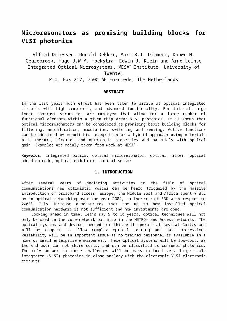
waveguidingprinciple
indexcontrast
bend-radius
opticalfeedback
fiber-chipcoupling
density[functions/cm2]
indexguiding
low, Δn ~0.01
5 mm too slow easy 1
indexguiding
high, Δn~0.07
500μm
resonator easy with smallcore fiber
25
indexguiding
very high, Δn ~0.5
10 μm micro-resonator
difficult, taperstructures needed
1 000
indexguiding
ultra-high,Δn ~2
1 μm micro-resonator
very difficult 100 000
Braggreflection(PBS)
ultra-high,Δn ~2
1 μm micro-resonator
very difficult 100 000
Table 1: Characteristics of waveguide structures with increasing index contrast.
For high integration, the single functional elements in photonic devicesshould be small. In electronic ICs a state-of-the-art transistor has a diameterof 50 nm, in optical devices a lower limit is given by the relatively largewavelength of light in the order of 1000 nm. Another size limitation is given bythe inherent losses of small-radius bends. Only by working with high indexcontrast waveguides, these losses can be reduced to an acceptable minimum. Table1 gives the characteristics of waveguide structures with increasing indexcontrast. Packaging and fiber-chip coupling (giving rise to 70 to 80% of thetotal costs of an integrated optical device) is increasingly difficult with highcontrast structures. With increasing density of optical functions on a chip, thecost per functional element, however, is rapidly decreasing. The waveguiding principle considered here is total internal reflection on asingle interface called index guiding. In the last decade another approach basedon photonic band gap structures (PBS) is intensively studied. Index guidingstructures are more close to market as an evolutionary path can be followed incontrast to PBSs that are only possible at ultra-high index contrast. It shouldalso be mentioned that the structures in the three lowest rows in Table 1, withcritical dimensions in the nanometer range, fall within the realm ofnanophotonics. The desired photonic components have to be compact, allowing activefunctions like switching and amplification and will make use of nanotechnology.Similar to the transistor in the electronic world one would like to have also abasic building block in photonics. Structures with optical feedback, for exampleresonators, could fulfill this role. In the following we will concentrate onmicroresonators2,3,4 based on high index contrast waveguiding structures and willshow that they are promising building blocks for VLSI photonics. In section 2 wegive an overview of the basic principles of microresonators. Thereafter an
overview of the results is presented obtained in the EC-funded European IST NAISproject. In the 4th section a few examples are given of microresonators in newapplication fields: light sources and optical sensing. Finally a summary withshort conclusions are given. The examples presented are mainly taken from ownwork often carried out in cooperation with others.
2 BASIC PRINCIPLES OF MICRORESONATORS
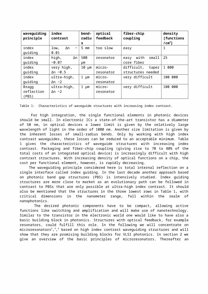
An optical microresonator is an integrated optics structure with opticalfeedback that allows a variety of functions like wavelength filter, opticalswitch or optical transistor5. Fig.1.a) gives a top view of such a device withtwo adjacent single mode port waveguides. Light enters at Iin and couples in partto the resonator. The rest of the power goes to Ithrough. Within the ring resonatorthe light propagates in a whispering gallery mode and couples partly to theoutput waveguide Idrop. After further propagation within the ring the lightcouples partly to Ithrough. Depending on the phase of the light after a roundtripconstructive or destructive interference will occur within the ring or Ithrough. Inthe case of constructive interference the resonator is on-resonance and thelight coupled to Ithrough has a phase shift of 180º with respect to Iin. Fig.1.b)gives schematically the resulting normalized spectral response of a loss-less,symmetric resonator to a constant power input signal with changing wavelength oralternatively changing phase in the resonator or changing effective index. Thepower Ithrough is always equal to Iin with exception near to the resonance, in thatcase Idrop = Iin.
a) b)FIGURE 1: Microresonator with two adjacent waveguides serving as in- and output port; a)topview; b) schematic spectral response to a constant input intensity.
The performance of the microresonator is characterized by its Lorentzianlineshape of the resonance lines in the drop port that allows for a small 3dBbandwidth Δλ3dB but admits a poor rejection in the off-resonance condition. Thisbecomes especially clear in a dB plot, see Fig.2. Also shown are the free
intensit y
[ a.u.]
phase [a.u.]orw avelength [a.u.]oreffective index [a.u.]
intensit y
[ a.u.]
phase [a.u.]orw avelength [a.u.]oreffective index [a.u.]

spectral range (FSR) and the cross-talk level of -24 dB. A relative measure forthe selectivity of the resonator is the finesse F = FSR/ Δλ3dB. The qualityfactor Q is given by Q = λ/Δλ3dB, the cavity ring-down time τcav = λ Q/2πc and theaverage number of roundtrips m of photons in a resonator m = F/2π.
w avelength [nm ]1550 1560
F S R
-3d B
P/P
[dB]
thro
ugh
inP
/P [d
B]dr
opin
Figure 2: Example of the power in the dropand through port of a loss-lessmicroresonator with F ~ 100 as a function ofwavelength.
Figure 3: Finesse (logarithmic sale),normalized drop power and normalized cavitypower as a function of the field couplingconstant κ for a microresonator of radius25 μm.
For the design of a microresonator the field coupling constant κ between theport waveguides and the ringresonator plays an essential role. In a loss-lessresonator with an infinite unloaded finesse the port waveguides introduce theload determined only by the coupling constant(s) κ. If the resonator has a
1 S. Téral, Fibre System Europe, June 2005, p 8.2 see, for example, D.J.W. Klunder, E. Krioukov, F.S. Tan, T. van der Veen, H.F. Bulthuis, G. Sengo, C. Otto, H.J.W.M. Hoekstra and A. Driessen, “Vertically and laterallywaveguide-coupled cylindrical microresonators in Si3N4 on SiO2 technology”, Appl. Phys. B.73, 603-608 (2001).3 B.E. Little, H.A. Haus, J.S. Foresi, L.C. Kimerling, E.P. Ippen and D.J. Ripin, “Wavelength switching and routing using absorption and resonance”, IEEE Phot. Techn. Letters, 10, 816-818 (1998).4 For an overview, see F. Michelotti, A. Driessen and M. Bertolotti (eds.) Microresonators as building blocks for VLSI photonics, AIP Conf. Proc. Vol. 709, 451 p. (2004).5 see for more details, D.J.W. Klunder, Photon Physics in Integrated Optics Microresonators, Pd.D. thesis, University of Twente, 135 p (2002).
certain propagation loss α, the resulting finesse, the normalized power in thedrop channel Pdrop/Pin and the normalized power in the cavity waveguide Pcav/Pin arelargely varying functions of κ, see Fig. 3. For wavelength selectivity thefinesse is the most relevant parameter and accordingly small coupling constantsshould be chosen. With regard to the drop efficiency even small losses willreduce Pdrop completely for a weakly coupled resonator. Therefore highly coupledstructures should be employed, which have, however, a reduced F and wavelengthselectivity. For applications where high cavity fields are desired, e.g. all-optical data processing, Pcav shows a maximum at low losses and small κ.
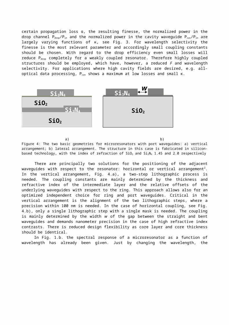
a) b)Figure 4: The two basic geometries for microresonators with port waveguides: a) verticalarrangement; b) lateral arrangement. The structure in this case is fabricated in silicon-based technology, with the index of refraction of SiO2 and Si3N4 1.45 and 2.0 respectively
There are principally two solutions for the positioning of the adjacentwaveguides with respect to the resonator: horizontal or vertical arrangement2.In the vertical arrangement, Fig. 4.a), a two-step lithographic process isneeded. The coupling constants are mainly determined by the thickness andrefractive index of the intermediate layer and the relative offsets of theunderlying waveguides with respect to the ring. This approach allows also for anoptimized independent choice for ring and port waveguides. Critical in thevertical arrangement is the alignment of the two lithographic steps, where aprecision within 100 nm is needed. In the case of horizontal coupling, see Fig.4.b), only a single lithographic step with a single mask is needed. The couplingis mainly determined by the width w of the gap between the straight and bentwaveguides and demands nanometer precision in the case of high refractive indexcontrasts. There is reduced design flexibility as core layer and core thicknessshould be identical. In Fig. 1.b. the spectral response of a microresonator as a function ofwavelength has already been given. Just by changing the wavelength, the
Si3N4
SiO2
w
SiO2
Si3N4
Si3N4
SiO2
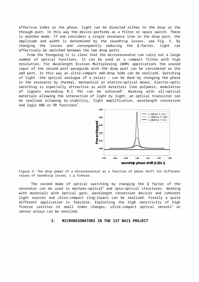
effective index or the phase, light can be directed either to the drop or thethrough port. In this way the device performs as a filter or space switch. Thereis another mode. If one considers a single resonance line in the drop port, theamplitude and width is determined by the roundtrip losses, see Fig. 5. Bychanging the losses and consequently reducing the Q-factor, light caneffectively be switched between the two drop ports. From the foregoing it is clear that the microresonator can carry out a largenumber of optical functions. It can be used as a compact filter with highresolution. For Wavelength Divison Multiplexing (WDM) applications the unusedinput of the second port waveguide with the drop port can be considered as theadd port. In this way an ultra-compact add-drop node can be realized. Switchingof light -the optical analogue of a relais - can be done by changing the phasein the resonator by thermal, mechanical or electro-optical means. Electro-opticswitching is especially attractive as with materials like polymers, modulationof signals exceeding 0.1 THz can be achieved6. Working with all-opticalmaterials allowing the interaction of light by light, an optical transistor canbe realized allowing bi-stability, light amplification, wavelength conversionand logic AND or OR functions7.
roundtrip phase shift [1/(2π)]0.94 0.96 0.98 1.00 1.02 1.04 1.06
Powe
r dropp
ed
0.00
0.01
0.02
0.03
0.04
0.05
~5dB/cm : F~272~10dB/cm : F~150~20dB/cm : F~81
roundtrip phase shift [1/(2π)]0.94 0.96 0.98 1.00 1.02 1.04 1.06
Powe
r dropp
ed
0.00
0.01
0.02
0.03
0.04
0.05
~5dB/cm : F~272~10dB/cm : F~150~20dB/cm : F~81
Figure 5: The drop power of a microresonator as a function of phase shift for differentvalues of roundtrip losses, c.q finesse..
The second mode of optical switching by changing the Q factor of theresonator can be used in mechano-optical8 and opto-optical structures. Workingwith materials with optical gain, wavelength conversion devices and coherentlight sources and ultra-compact ring-lasers can be realized. Finally a quitedifferent application is feasible. Exploiting the high sensitivity of highfinesse cavities to small index changes, ultra-compact optical sensors9 orsensor arrays can be realized.
3. MICRORESONATORS IN THE IST NAIS PROJECT
In the recently finished EC-IST funded NAIS (Next Generation Active IntegratedOptic Subsystem) project10 a number of European academic and industrial groupsfrom 7 countries collaborated to apply active and passive microresonators in anoptical transceiver for the access network. In the following three results arepresented: (i) a compact wavelength-selective switch; (ii) a high-speedmicrorsonator-based electro-optic modulator, (iii) an ultra-compactreconfigurable add-drop multiplexer.
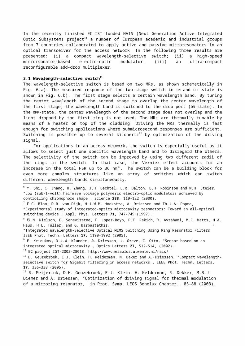
3.1 Wavelength-selective switch11 The wavelength-selective switch is based on two MRs, as shown schematically inFig. 6.a). The measured response of the two-stage switch in ON and OFF state isshown in Fig. 6.b). The first stage selects a certain wavelength band. By tuningthe center wavelength of the second stage to overlap the center wavelength ofthe first stage, the wavelength band is switched to the drop port (ON-state). Inthe OFF-state, the center wavelength of the second stage does not overlap and thelight dropped by the first ring is not used. The MRs are thermally tunable bymeans of a heater on top of the cladding. Driving the MRs thermally is fastenough for switching applications where submicrosecond responses are sufficient.Switching is possible up to several kilohertz12 by optimization of the drivingsignal. For applications in an access network, the switch is especially useful as itallows to select just one specific wavelength band and to disregard the others.The selectivity of the switch can be improved by using two different radii ofthe rings in the switch. In that case, the Vernier effect accounts for anincrease in the total FSR up to 36 nm13. The switch can be a building block foreven more complex structures like an array of switches which can switchdifferent wavelength bands simultaneously.6 Y. Shi, C. Zhang, H. Zhang, J.H. Bechtel, L.R. Dalton, B.H. Robinson and W.H. Steier, “Low (sub-1-volt) halfwave voltage polymeric electro-optic modulators achieved by controlling chromophore shape”, Science 288, 119-122 (2000).7 F.C. Blom, D.R. van Dijk, H.J.W.M. Hoekstra, A. Driessen and Th.J.A. Popma, “Experimental study of integrated-optics microcavity resonators: Toward an all-optical switching device”, Appl. Phys. Letters 71, 747-749 (1997).8 G.N. Nielson, D. Seneviratne, F. Lopez-Royo, P.T. Rakich, Y. Avrahami, M.R. Watts, H.A.Haus, H.L. Tuller, and G. Barbastathis, “Integrated Wavelength-Selective Optical MEMS Switching Using Ring Resonator Filters” IEEE Phot. Techn. Letters 17, 1190-1992 (2005).9 E. Krioukov, D.J.W. Klunder, A. Driessen, J. Greve, C. Otto, “Sensor based on an integrated optical microcavity”, Optics Letters 27, 512-514, (2002).10 EC project IST-2002-28018, http://www.mesaplus.utwente.nl/nais/11 D. Geuzebroek, E.J. Klein, H. Kelderman, N. Baker and A. Driessen, “Compact wavelength-selective switch for Gigabit filtering in access networks”, IEEE Phot. Techn. Letters, 17, 336-338 (2005).12 R. Meijerink, D.H. Geuzebroek, E.J. Klein, H. Kelderman, R. Dekker, M.B.J. Diemer and A. Driessen, “Optimization of driving signal for thermal modulation of a microring resonator,” in Proc. Symp. LEOS Benelux Chapter., 85-88 (2003).
a) b) c)Figure 6: Wavelength selective switch based on 2 MRs; a) schematic view; b) measured response of switch: solid line: ON-state; dashed line: OFF-state; c) microscope photograph of a realized switch
An MR-based switch has been realized in SiO2–Si3N4 technology14. The switchwas made out of two MRs which are vertically coupled to the port waveguides. Theport and ring waveguide dimensions are 2 × 0.14 μm2 and 2.5 × 0.18 μm2,respectively. The vertical separation between port and waveguide is 1 μm. Omega-shaped chromium heaters were applied on top of the device. The measured spectralresponses of the switch in both the ON and OFF states are shown in Fig. 6.b). Theresponses are normalized to the measured power in the through port of the devicewhile OFF-resonance and give, consequently, the on-chip IL in the drop port. Theswitch has a measured ON–OFF ratio of 12 dB and a channel separation better than20 dB. The on-chip IL in the drop port of the switch is around 6 dB. The devicewas switched between ON and OFF using 225 mW of electrical power. This implies ashift in center wavelength of 6.5 pm/mW. Fig. 6.c) shows a photograph of arealized switch. The two omega-shaped heaters on top of the two rings and theport waveguides are clearly visible. The size of the switch itself is about 200× 200 μm2 excluding the pads to wire the heaters. Also, single rings with the same specification have been characterized. Themeasured responses were fitted to analytical models to extract the loss in thering and the coupling constants. The loss inside the ring was found to be about5 dB/cm, corresponding to 0.16 dB/round-trip. The measured field couplingconstants of 0.6 are in good agreement with the designed values. The propagation
13 D.H. Geuzebroek, E.J. Klein, H. Kelderman, F.S. Tan, D.J.W. Klunder and A.Driessen., “Thermally tuneable, wide FSR switch based on micro-ring resonators,”in Proc. Symp. IEEE/LEOS Benelux,Chapter, 155-158 (2002).14 K. Worhoff, L.T.H. Hilderink, A. Driessen and P.V. Lambeck., “Silicon oxynitride—A versatile material for integrated optics applications,” J. Electrochem. Soc., vol. 149, no. 8, F85–F91 (2002).
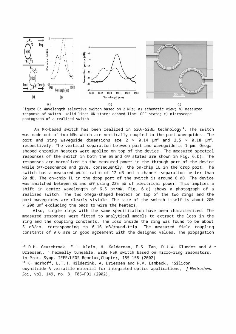
losses inside the straight waveguides are lower than 1 dB/cm. The on-chip IL inthe drop port of a single ring is about 3 dB which is in accordance with the 6-dB IL in the switch. Gigabit/s measurements on single rings with similar dimensions wereperformed with a LiNbO Mach–Zehnder modulator driven by a 10-Gb/s pseudorandombinary sequence generator to see the influence of the filter on the modulatednonreturn-to-zero (NRZ) signal. The group delay of the ring was measured byusing the phase-shift method15. At resonance, the measured relative group delayis 7 ps, as is shown in Fig. 7. The measured 10-Gb/s modulation signal with abit length of 100 ps is shown in the inlay of Fig. 5 where the eye responses areshown. The top eye diagram is obtained directly after the modulator, the bottomone after being filtered by the ring. The ring does not degrade the modulatedsignal significantly as could be expected since the bandwidth was designed to be50 GHz and the maximum group delay difference is much smaller than the durationof a single bit. The measured Q factor of the eye diagram of the filtered signalis about 7.5, leading to a theoretical bit-error rate of < 10-12. The powerpenalty due to the single ring is 3 dB, since only the IL is of influence giventhis bit rate. As the complete wavelength selective switch is made out of twomicrorings, its group delay is twice the amount of the single ring, i.e. 14 psat resonance.
Figure 7: Measured and simulated groupdelay of a single MR. Also shown are the EYEdiagrams of 10 Gbit/s NRZ signals of modulator output (top) and after being filtered bythe MR (bottom).
3.2 High-speed microresonator-based electro-optic modulator16
In section 1.1 has already been explained that by changing the optical pathwithin the ring its resonance wavelengths can be shifted and, both in the16 A. Leinse, M.B.J. Diemeer, A. Rousseau and A. Driessen , “A novel high speed polymeric eo modulator based on a combination of a micro-ring resonator and an MZI”, IEEE Photon. Technol. Lett., to be published, Oct. (2005).

through- and drop port, an amplitude as well as phase modulation can begenerated. For high-speed applications this change can be induced by an electricfield obtained by sandwiching the MR between two electrodes. Because of theirhigh electro-optic coefficients, polymers are very suitable for this type ofdevices17. One of the problems in realizing such a device in a vertical couplingarrangement is the position of the MR relative to the two port waveguides. Thisposition determines the amount of light that couples from the waveguides to thering (and vice versa) at both the through- and drop port side (the couplingconstants). These coupling constants are critical parameters determining thespectral behavior. Coupling the MR to a single waveguide simplifies thefabrication process because there is only one coupling constant involved. Inaddition, the spectral behavior of the MR is less sensitive to changes in thissingle coupling constant. In an ideal lossless ring the through port spectrumhas no resonance dips because no light is coupled to the drop port waveguide. Inorder to use a MR coupled to a single waveguide, the phase change around aresonance wavelength can be used. Fig. 8 shows schematically the output spectrumand the phase response of a slightly lossy MR around a resonance wavelength (r).
Figure 8: Output power and phase response of the through port waveguide around aresonance wavelength
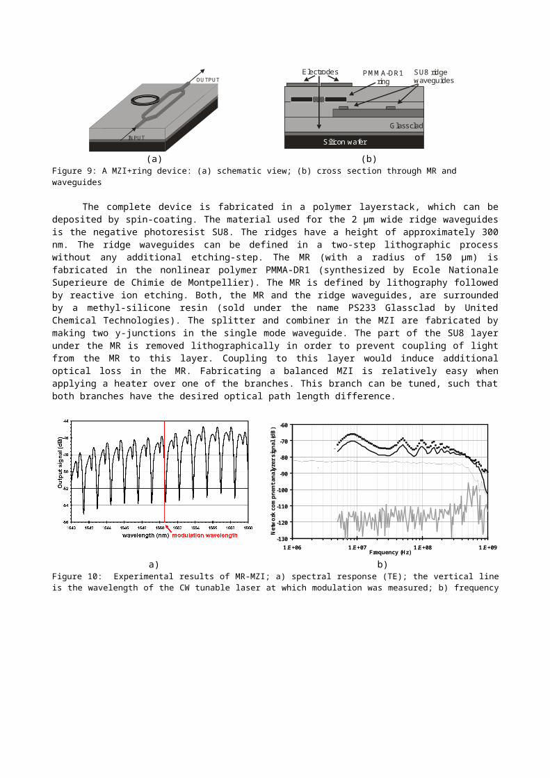
This phase response can conveniently be converted to an intensity modulationby combination with a Mach Zehnder Interferometer (MZI). When switching betweenthe on-resonance and off-resonance condition, the difference between the twobranches of the MZI can switch from to 0. This combination between a MR andMZI is shown (including a cross section through MR and waveguides) in Fig. 9.
15 D. Marcuse, Principles of Optical Fiber Measurements, New York, Academic Press, (1981).17 Rabiei P, Steier WH, Cheng Zhang, Dalton LR. “Polymer Micro-Ring filters and modulators”, J. of Lightw. Techn., 20, 1968-1975, (2002).
OU TPUT
INPUT
Glassclad
SU8 ridgewaveguides
PM M A-DR1ring
Electrodes
Silicon wafer
(a) (b)Figure 9: A MZI+ring device: (a) schematic view; (b) cross section through MR and waveguides
The complete device is fabricated in a polymer layerstack, which can bedeposited by spin-coating. The material used for the 2 µm wide ridge waveguidesis the negative photoresist SU8. The ridges have a height of approximately 300nm. The ridge waveguides can be defined in a two-step lithographic processwithout any additional etching-step. The MR (with a radius of 150 µm) isfabricated in the nonlinear polymer PMMA-DR1 (synthesized by Ecole NationaleSuperieure de Chimie de Montpellier). The MR is defined by lithography followedby reactive ion etching. Both, the MR and the ridge waveguides, are surroundedby a methyl-silicone resin (sold under the name PS233 Glassclad by UnitedChemical Technologies). The splitter and combiner in the MZI are fabricated bymaking two y-junctions in the single mode waveguide. The part of the SU8 layerunder the MR is removed lithographically in order to prevent coupling of lightfrom the MR to this layer. Coupling to this layer would induce additionaloptical loss in the MR. Fabricating a balanced MZI is relatively easy whenapplying a heater over one of the branches. This branch can be tuned, such thatboth branches have the desired optical path length difference.
-130
-120
-110
-100
-90
-80
-70
-60
1.E+06 1.E+07 1.E+08 1.E+09Frequency (Hz)
Network compn
ent analyzer s
ignal (dB
)
123
4
a) b)Figure 10: Experimental results of MR-MZI; a) spectral response (TE); the vertical lineis the wavelength of the CW tunable laser at which modulation was measured; b) frequency
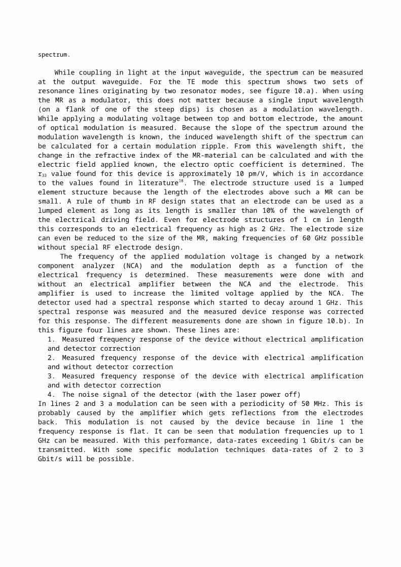
spectrum.
While coupling in light at the input waveguide, the spectrum can be measuredat the output waveguide. For the TE mode this spectrum shows two sets ofresonance lines originating by two resonator modes, see figure 10.a). When usingthe MR as a modulator, this does not matter because a single input wavelength(on a flank of one of the steep dips) is chosen as a modulation wavelength.While applying a modulating voltage between top and bottom electrode, the amountof optical modulation is measured. Because the slope of the spectrum around themodulation wavelength is known, the induced wavelength shift of the spectrum canbe calculated for a certain modulation ripple. From this wavelength shift, thechange in the refractive index of the MR-material can be calculated and with theelectric field applied known, the electro optic coefficient is determined. Ther33 value found for this device is approximately 10 pm/V, which is in accordanceto the values found in literature18. The electrode structure used is a lumpedelement structure because the length of the electrodes above such a MR can besmall. A rule of thumb in RF design states that an electrode can be used as alumped element as long as its length is smaller than 10% of the wavelength ofthe electrical driving field. Even for electrode structures of 1 cm in lengththis corresponds to an electrical frequency as high as 2 GHz. The electrode sizecan even be reduced to the size of the MR, making frequencies of 60 GHz possiblewithout special RF electrode design. The frequency of the applied modulation voltage is changed by a networkcomponent analyzer (NCA) and the modulation depth as a function of theelectrical frequency is determined. These measurements were done with andwithout an electrical amplifier between the NCA and the electrode. Thisamplifier is used to increase the limited voltage applied by the NCA. Thedetector used had a spectral response which started to decay around 1 GHz. Thisspectral response was measured and the measured device response was correctedfor this response. The different measurements done are shown in figure 10.b). Inthis figure four lines are shown. These lines are:
1. Measured frequency response of the device without electrical amplificationand detector correction2. Measured frequency response of the device with electrical amplificationand without detector correction3. Measured frequency response of the device with electrical amplificationand with detector correction4. The noise signal of the detector (with the laser power off)
In lines 2 and 3 a modulation can be seen with a periodicity of 50 MHz. This isprobably caused by the amplifier which gets reflections from the electrodesback. This modulation is not caused by the device because in line 1 thefrequency response is flat. It can be seen that modulation frequencies up to 1GHz can be measured. With this performance, data-rates exceeding 1 Gbit/s can betransmitted. With some specific modulation techniques data-rates of 2 to 3Gbit/s will be possible.
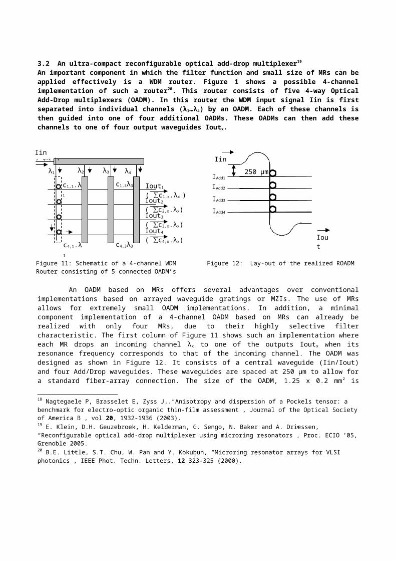
3.2 An ultra-compact reconfigurable optical add-drop multiplexer19 An important component in which the filter function and small size of MRs can beapplied effectively is a WDM router. Figure 1 shows a possible 4-channelimplementation of such a router20. This router consists of five 4-way OpticalAdd-Drop multiplexers (OADM). In this router the WDM input signal Iin is firstseparated into individual channels (λ1…λ4) by an OADM. Each of these channels isthen guided into one of four additional OADMs. These OADMs can then add thesechannels to one of four output waveguides Ioutx.
Figure 11: Schematic of a 4-channel WDM Router consisting of 5 connected OADM’s
Figure 12: Lay-out of the realized ROADM
An OADM based on MRs offers several advantages over conventionalimplementations based on arrayed waveguide gratings or MZIs. The use of MRsallows for extremely small OADM implementations. In addition, a minimalcomponent implementation of a 4-channel OADM based on MRs can already berealized with only four MRs, due to their highly selective filtercharacteristic. The first column of Figure 11 shows such an implementation whereeach MR drops an incoming channel λx to one of the outputs Ioutx when itsresonance frequency corresponds to that of the incoming channel. The OADM wasdesigned as shown in Figure 12. It consists of a central waveguide (Iin/Iout)and four Add/Drop waveguides. These waveguides are spaced at 250 μm to allow fora standard fiber-array connection. The size of the OADM, 1.25 x 0.2 mm2 is
18 Nagtegaele P, Brasselet E, Zyss J,.“Anisotropy and dispersion of a Pockels tensor: a benchmark for electro-optic organic thin-film assessment”, Journal of the Optical Societyof America B , vol 20, 1932-1936 (2003).19 E. Klein, D.H. Geuzebroek, H. Kelderman, G. Sengo, N. Baker and A. Driessen, “Reconfigurable optical add-drop multiplexer using microring resonators”, Proc. ECIO ’05,Grenoble 2005.20 B.E. Little, S.T. Chu, W. Pan and Y. Kokubun, “Microring resonator arrays for VLSI photonics”, IEEE Phot. Techn. Letters, 12 323-325 (2000).
c1,1.λ1
c4,1.λ1
Iin
Iout
250 μmIAdd1
IAdd2
IAdd3
IAdd4
Iout1 ( c∑ 1,x.λx )Iout2 ( c∑ 2,x.λx)Iout3 ( c∑ 3,x.λx)Iout4 ( c∑ 4,x.λx)
λ1
Iin ( λ∑ x )
λ3 λ4
c4,3λ3
λ2
c1,3λ3

mainly determined by this spacing. A single MR is located at each intersectionof central- and add-drop waveguides. The cross-grid waveguide approach21, inwhich the two waveguides that couple to the MR cross each other, leads to somecrosstalk but is also the most efficient geometry for the OADM. Each of the fourMRs can be thermally tuned by a heater. The heater is omega-shaped for highpower efficiency. The MR has a radius of 50 µm, a height of 190 nm and a widthof 2.5 μm, giving an Neff=1.517 (TE @1550 nm) .The 50 µm radius was chosenbecause it gives a FSR that is smaller than the thermal tuning range, allowingfull FSR tuning. In addition, it allows for a MR that is nearly phase matched tothe port waveguides. The MR is vertically coupled to these port waveguides whichare 2 μm wide, 140 nm high and have a Neff=1.505 (TE@1550 nm). Both the MR andthe port waveguides are designed for TE operation.
a) b)Figure 13: Fabricated ROADM, a) top view (field of view 1,3 ×0.5 mm2), b) fiber pigtaileddevice
The ROADM was fabricated by depositing 140 nm LPCVD Si3N4 on top of 8 μmthermally grown SiO2. The Si3N4 waveguides were then etched using reactive ionetching (RIE). A 1 μm TEOS separation layer was applied next. The ringresonators were then defined by depositing 190 nm Si3N4 and RIE. A 4 µm thicklayer of PECVD SiO2 was deposited next. The device was then annealed at 1150°C.Subsequently the 200 nm thick Chromium heaters were defined using lift-off.
21 S.T.Chu, B.E. Little, W.G. Pan, T. Kaneko, S. Sato and Y. Kokubun, “An Eight Channel Add-Drop Filter Using Vertically Coupled Microring Resonators over a Cross Grid”, IEEE Phot. Techn. Letters, 11, 691-693 (1999).
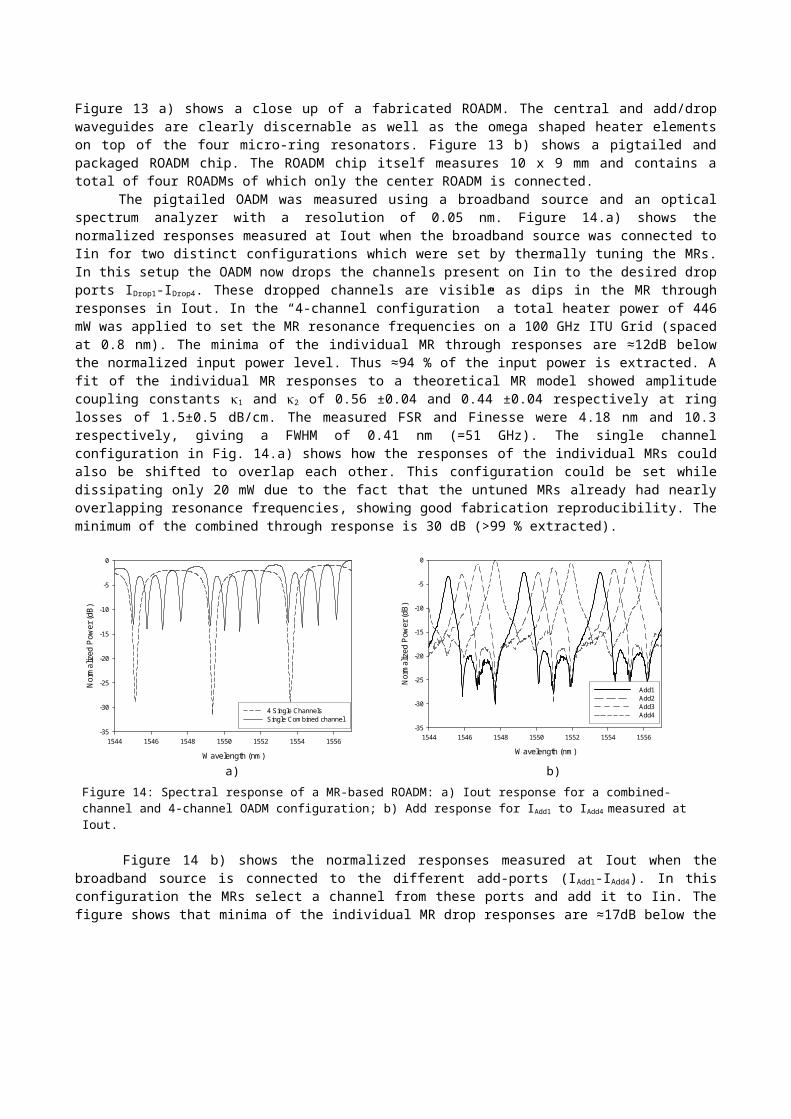
Figure 13 a) shows a close up of a fabricated ROADM. The central and add/dropwaveguides are clearly discernable as well as the omega shaped heater elementson top of the four micro-ring resonators. Figure 13 b) shows a pigtailed andpackaged ROADM chip. The ROADM chip itself measures 10 x 9 mm and contains atotal of four ROADMs of which only the center ROADM is connected. The pigtailed OADM was measured using a broadband source and an opticalspectrum analyzer with a resolution of 0.05 nm. Figure 14.a) shows thenormalized responses measured at Iout when the broadband source was connected toIin for two distinct configurations which were set by thermally tuning the MRs.In this setup the OADM now drops the channels present on Iin to the desired dropports IDrop1-IDrop4. These dropped channels are visible as dips in the MR throughresponses in Iout. In the “4-channel configuration” a total heater power of 446mW was applied to set the MR resonance frequencies on a 100 GHz ITU Grid (spacedat 0.8 nm). The minima of the individual MR through responses are ≈12dB belowthe normalized input power level. Thus ≈94 % of the input power is extracted. Afit of the individual MR responses to a theoretical MR model showed amplitudecoupling constants 1 and 2 of 0.56 ±0.04 and 0.44 ±0.04 respectively at ringlosses of 1.5±0.5 dB/cm. The measured FSR and Finesse were 4.18 nm and 10.3respectively, giving a FWHM of 0.41 nm (=51 GHz). The single channelconfiguration in Fig. 14.a) shows how the responses of the individual MRs couldalso be shifted to overlap each other. This configuration could be set whiledissipating only 20 mW due to the fact that the untuned MRs already had nearlyoverlapping resonance frequencies, showing good fabrication reproducibility. Theminimum of the combined through response is 30 dB (>99 % extracted).
W avelength (nm )1544 1546 1548 1550 1552 1554 1556
Normalized Po
wer (dB
)
-35
-30
-25
-20
-15
-10
-5
0
4 Single ChannelsSingle Com bined channel
W avelength (nm )1544 1546 1548 1550 1552 1554 1556
Normalized Po
wer (dB
)
-35
-30
-25
-20
-15
-10
-5
0
Add1Add2Add3Add4
a) b)Figure 14: Spectral response of a MR-based ROADM: a) Iout response for a combined-channel and 4-channel OADM configuration; b) Add response for IAdd1 to IAdd4 measured at Iout.
Figure 14 b) shows the normalized responses measured at Iout when thebroadband source is connected to the different add-ports (IAdd1-IAdd4). In thisconfiguration the MRs select a channel from these ports and add it to Iin. Thefigure shows that minima of the individual MR drop responses are ≈17dB below the
normalized output power level (≈89% of input power dropped). The effects of theadjacent MRs on an add channel can also be observed, for instance in the addresponse of the first resonator. Here the three MRs that follow the first MRdrop power from the main channel which shows up as dips in the Iout response. The OADM could be reconfigured in <1 ms due to the fast thermal tuningresponse of the MRs. A single MR has a linear tuning response and has a maximumtuning range (without heater damage) of ≈4.3 nm at a power dissipation of 380mW, yielding a thermally induced wavelength shift of 11 pm/mW of dissipatedheater power. The device shows no measurable thermal crosstalk due to the smallheater area, wide (≈150 μm) heater separation and the high thermal conductivity(161 W/m/K) of the silicon substrate.
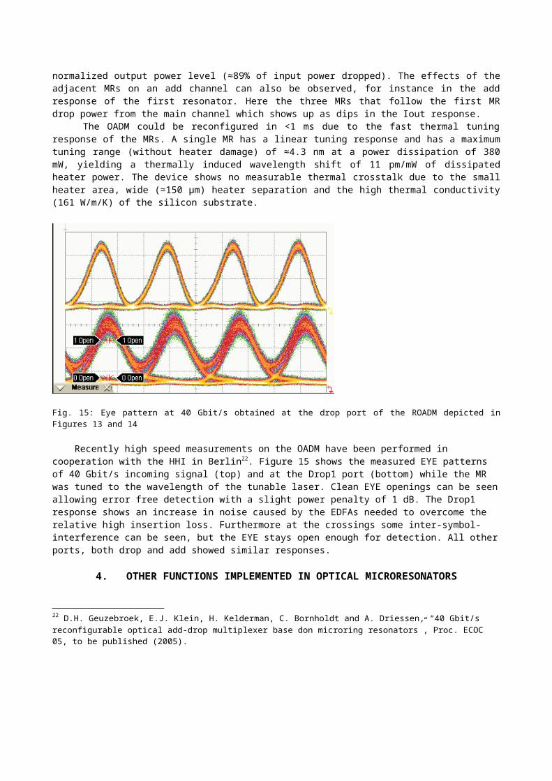
Fig. 15: Eye pattern at 40 Gbit/s obtained at the drop port of the ROADM depicted inFigures 13 and 14
Recently high speed measurements on the OADM have been performed in cooperation with the HHI in Berlin22. Figure 15 shows the measured EYE patterns of 40 Gbit/s incoming signal (top) and at the Drop1 port (bottom) while the MR was tuned to the wavelength of the tunable laser. Clean EYE openings can be seenallowing error free detection with a slight power penalty of 1 dB. The Drop1 response shows an increase in noise caused by the EDFAs needed to overcome the relative high insertion loss. Furthermore at the crossings some inter-symbol-interference can be seen, but the EYE stays open enough for detection. All otherports, both drop and add showed similar responses.
4. OTHER FUNCTIONS IMPLEMENTED IN OPTICAL MICRORESONATORS
22 D.H. Geuzebroek, E.J. Klein, H. Kelderman, C. Bornholdt and A. Driessen, “40 Gbit/s reconfigurable optical add-drop multiplexer base don microring resonators”, Proc. ECOC 05, to be published (2005).

In the foregoing section MRs were applied as optical filters, modulators andROADM. In the following two other applications, light generation and opticalsensing, will be addressed to demonstrate their potential as building blocks forVLSI photonics.
4.1 Lightsources based on microresonatorsWith the availability of convenient optical active materials it isstraightforward to apply microring resonators as ultra-compact ring lasers. Thegroups of Vahala and Polman demonstrated Er-doped silica laser with ultralowthreshold pumplaser power below 10 μW23. The laser consists of a microtoroidresonator with a diameter of 40 μm with ultra-smooth sidewalls. These wereobtained by surface tension induced smoothening of a silica disk irradiated byan intense CO2 laser. For applications as lightsource in VLSI photonics a morecontrolled process including photolithographically defined port waveguides ishighly desirable. In our group Dekker et al.24 work with rare earth-doped nanoparticlesdispersed in polymers with very promising properties for amplification in activeintegrated optical devices. Especially the rare earths neodymium and erbium areof great interest, because they emit in the second and third window of opticalcommunication systems, respectively. It has been reported that LaF3 is a verygood host for rare earth incorporation and because of its low phonon energy itexhibits a wide transparency band from 0.2 to 11 μm. Polymer waveguide materialshave the advantage of being low-cost and tunable in many ways with respect totheir properties and ways of processing. To overcome the insolubility problem ofinorganic rare earth salts in polymers, Stouwdam et al.25 developed neodymiumdoped LaF3 nanoparticles with organic ligands that do dissolve well in polymers.By combining the broad range of attractive polymer properties and the relativelylong lifetime of rare earth dopants in inorganic nanoparticles, a considerableamount of flexibility regarding materials properties can be achieved.
23 A. Polman, B. Min, J. Kalkman, T.J. Kippenberg and KJ Vahala, “Ultra low-threshold erbium-implanted toroidal microlaser on silicon”, Appl. Phys. Letters 84, 1037-1039 (2004).24 R. Dekker, D.J.W. Klunder, A. Borreman, M.B.J. Diemeer, K. Wörhoff, and A. Driessen, J.W. Stouwdam and F.C.J.M. van Veggel “Stimulated emission and optical gain in LaF3 :Nd nanoparticle-dopedpolymer-based waveguides”, Appl. Phys. Letters, 85, 6104-6106 (2004).25 J.W. Stouwdam, G.A. Hebbink, J. Huskens, and F.C.J.M. van Veggel, “Lanthanide-doped nanoparticles with excellent luminescent properties in organic media”, Chem. Mater. 15, 4604-4616 (2003).
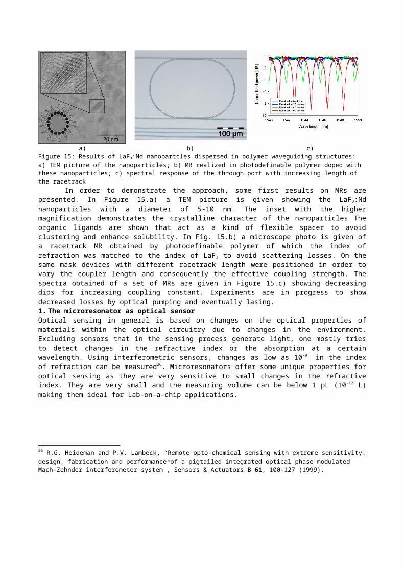
a) b) c)Figure 15: Results of LaF3:Nd nanopartcles dispersed in polymer waveguiding structures: a) TEM picture of the nanoparticles; b) MR realized in photodefinable polymer doped with these nanoparticles; c) spectral response of the through port with increasing length of the racetrack In order to demonstrate the approach, some first results on MRs arepresented. In Figure 15.a) a TEM picture is given showing the LaF3:Ndnanoparticles with a diameter of 5-10 nm. The inset with the highermagnification demonstrates the crystalline character of the nanoparticles Theorganic ligands are shown that act as a kind of flexible spacer to avoidclustering and enhance solubility. In Fig. 15.b) a microscope photo is given ofa racetrack MR obtained by photodefinable polymer of which the index ofrefraction was matched to the index of LaF3 to avoid scattering losses. On thesame mask devices with different racetrack length were positioned in order tovary the coupler length and consequently the effective coupling strength. Thespectra obtained of a set of MRs are given in Figure 15.c) showing decreasingdips for increasing coupling constant. Experiments are in progress to showdecreased losses by optical pumping and eventually lasing.1. The microresonator as optical sensorOptical sensing in general is based on changes on the optical properties ofmaterials within the optical circuitry due to changes in the environment.Excluding sensors that in the sensing process generate light, one mostly triesto detect changes in the refractive index or the absorption at a certainwavelength. Using interferometric sensors, changes as low as 10-9 in the indexof refraction can be measured26. Microresonators offer some unique properties foroptical sensing as they are very sensitive to small changes in the refractiveindex. They are very small and the measuring volume can be below 1 pL (10-12 L)making them ideal for Lab-on-a-chip applications.
26 R.G. Heideman and P.V. Lambeck, “Remote opto-chemical sensing with extreme sensitivity:design, fabrication and performance of a pigtailed integrated optical phase-modulated Mach-Zehnder interferometer system”, Sensors & Actuators B 61, 100-127 (1999).
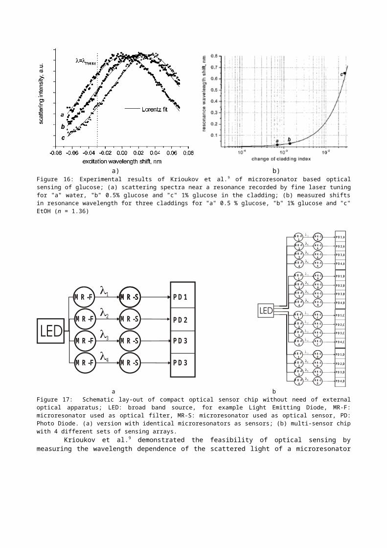
a) b)Figure 16: Experimental results of Krioukov et al.9 of microresonator based opticalsensing of glucose; (a) scattering spectra near a resonance recorded by fine laser tuningfor "a" water, "b" 0.5% glucose and "c" 1% glucose in the cladding; (b) measured shiftsin resonance wavelength for three claddings for "a" 0.5 % glucose, "b" 1% glucose and "c"EtOH (n = 1.36)
M R -F 1
2
3
4
M R -F
M R -S
M R -F
M R -F
M R -S
M R -S
M R -S
M R -S
P D 1
P D 2
P D 3
P D 3
M R -F 1
1
2
3
4
M R -S A
M R -S A
M R -S A
M R -S A
M R -F 4
M R -F 3
M R -F 2
P D 1,A
P D 2,A
P D 3,A
P D 4,A
M R -F 1
1
2
3
4
M R -S B
M R -S B
M R -S B
M R -S B
M R -F 4
M R -F 3
M R -F 2
P D 1,B
P D 2,B
P D 3,B
P D 4,B
M R -F 1
1
2
3
4
M R -S C
M R -S C
M R -S C
M R -S C
M R -F 4
M R -F 3
M R -F 2
P D 1,C
P D 2,C
P D 3,C
P D 4,C
M R -F 1
1
2
3
4
M R -S D
M R -S D
M R -S D
M R -S D
M R -F 4
M R -F 3
M R -F 2
P D 1,D
P D 2,D
P D 3,D
P D 4,D
a bFigure 17: Schematic lay-out of compact optical sensor chip without need of externaloptical apparatus; LED: broad band source, for example Light Emitting Diode, MR-F:microresonator used as optical filter, MR-S: microresonator used as optical sensor, PD:Photo Diode. (a) version with identical microresonators as sensors; (b) multi-sensor chipwith 4 different sets of sensing arrays. Krioukov et al.9 demonstrated the feasibility of optical sensing bymeasuring the wavelength dependence of the scattered light of a microresonator
that - for a small wavelength range - is proportional to the light power insidethe resonator. In a practical design that power could be much easier bedetermined by measuring the intensity at the drop port. For the proof ofprinciple they immersed the microresonator in glucose solution of variousconcentrations. Fig. 16 gives the result for pure water and a 0.5 and 1% glucosesolution. In their not yet optimized set-up refractive index changes well below10-4 could be detected. Working with high finesse resonators and advanced curvefitting, detection of changes as low as 10-9 becomes feasible. With furtherreduction of the resonator diameter the measuring volume could be even largerreduced so that single or at least few molecule detection would be possible. Ina second paper Krioukov et al.27 demonstrated the use of optical microresonatorsfor enhanced optical spectroscopy and sensing. Also here the small sensingvolume make this kind of sensors attractive devices for high-sensitivity sensingand detection down to the single molecule level.
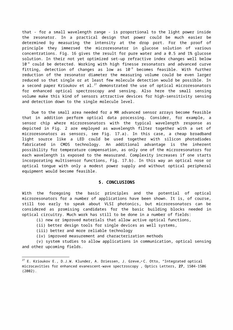
Due to the small area needed for a MR advanced sensor arrays become feasiblethat in addition perform optical data processing. Consider, for example, asensor chip where microresonators with the typical wavelength response asdepicted in Fig. 2 are employed as wavelength filter together with a set ofmicroresonators as sensors, see Fig. 17.a). In this case, a cheap broadbandlight source like a LED could be used together with silicon photodiodesfabricated in CMOS technology. An additional advantage is the inherentpossibility for temperature compensation, as only one of the microresonators foreach wavelength is exposed to the measurand. Complexity increases if one startsincorporating multisensor functions, Fig. 17.b). In this way an optical nose oroptical tongue with only a modest power supply and without optical peripheralequipment would become feasible.
5. CONCLUSIONS
With the foregoing the basic principles and the potential of opticalmicroresonators for a number of applications have been shown. It is, of course,still too early to speak about VLSI photonics, but microresonators can beconsidered as promising candidates for the basic building blocks needed inoptical circuitry. Much work has still to be done in a number of fields:
(i) new or improved materials that allow active optical functions, (ii) better design tools for single devices as well systems, (iii) better and more reliable technology (iv) improved measurement and characterization methods(v) system studies to allow applications in communication, optical sensing
and other upcoming fields.
27 E. Krioukov E., D.J.W. Klunder, A. Driessen, J. Greve, C. Otto, “Integrated optical microcavities for enhanced evanescent-wave spectroscopy”, Optics Letters, 27, 1504-1506 (2002).

In this way the potential of nanophotonics can be gradually exploited resultingin complex, mass-produced and low-cost optical circuits The examples presented have mostly be taken from work carried out at the IOMSgroup of the MESA+ institute of the University of Twente, often in collaborationwith other MESA+ groups.
ACKNOWLEDGMENTS
The authors would like to thank Anton J.F. Hollink, Henry Kelderman, Paul V.Lambeck, Gabriel Sengo, Henk van Wolferen and Kerstin Wörhoff for theircontribution in the research described in this paper. Financial support is acknowledged of the Dutch Science Foundations FOM, STWand BSIK Freeband and the EC project NAIS.
REFERENCES