microprocessor and microcontrollers unit-i
TRANSCRIPT
Microprocessor and Microcontrollers
UNIT-I: Introduction to Microprocessors
1. Introduction and evolution of microprocessors
2. Architecture of 8085 processor
3. Pin configuration of 8085
4. Bus organization
5. Basic instruction sets.
1. INTRODUCTION TO MICROPROCESSOR AND MICROCOMPUTER
ARCHITECTURE:
A microprocessor is a programmable electronics chip that has computing and decision
making capabilities similar to central processing unit of a computer. Any microprocessor-
based systems having limited number of resources are called microcomputers. Nowadays,
microprocessor can be seen in almost all types of electronics devices like mobile phones,
printers, washing machines etc.
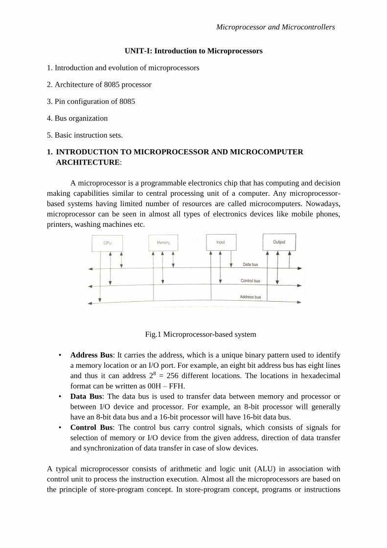
Fig.1 Microprocessor-based system
• Address Bus: It carries the address, which is a unique binary pattern used to identify
a memory location or an I/O port. For example, an eight bit address bus has eight lines
and thus it can address 28 = 256 different locations. The locations in hexadecimal
format can be written as 00H – FFH.
• Data Bus: The data bus is used to transfer data between memory and processor or
between I/O device and processor. For example, an 8-bit processor will generally
have an 8-bit data bus and a 16-bit processor will have 16-bit data bus.
• Control Bus: The control bus carry control signals, which consists of signals for
selection of memory or I/O device from the given address, direction of data transfer
and synchronization of data transfer in case of slow devices.
A typical microprocessor consists of arithmetic and logic unit (ALU) in association with
control unit to process the instruction execution. Almost all the microprocessors are based on
the principle of store-program concept. In store-program concept, programs or instructions
Microprocessor and Microcontrollers
are sequentially stored in the memory locations that are to be executed. To do any task using
a microprocessor, it is to be programmed by the user. So the programmer must have idea
about its internal resources, features and supported instructions. Each microprocessor has a
set of instructions, a list which is provided by the microprocessor manufacturer. The
instruction set of a microprocessor is provided in two forms: binary machine code and
mnemonics.
Microprocessor communicates and operates in binary numbers 0 and 1. The set of
instructions in the form of binary patterns is called a machine language and it is difficult for
us to understand. Therefore, the binary patterns are given abbreviated names, called
mnemonics, which forms the assembly language. The conversion of assembly-level language
into binary machine-level language is done by using an application called assembler.
Evolution of Microprocessors
4-bit Microprocessors
The first microprocessor was introduced in 1971 by Intel Corp. It was named Intel 4004 as it
was a 4 bit processor. It was a processor on a single chip. It could perform simple arithmetic
and logic operations such as addition, subtraction, boolean AND and boolean OR. It had a
control unit capable of performing control functions like fetching an instruction from
memory, decoding it, and generating control pulses to execute it. It was able to operate on 4
bits of data at a time. This first microprocessor was quite a success in industry. Soon other
microprocessors were also introduced. Intel introduced the enhanced version of 4004, the
4040.
8-bit Microprocessors
The first 8 bit microprocessor which could perform arithmetic and logic operations on 8 bit
words was introduced in 1973 again by Intel. This was Intel 8008 and was later followed by
an improved version, Intel 8088. Some other 8 bit processors are Zilog-80 and Motorola
M6800.
16-bit Microprocessors
The 8-bit processors were followed by 16 bit processors. They are Intel 8086 and 80286.
32-bit Microprocessors
The 32 bit microprocessors were introduced by several companies but the most popular one is
Intel 80386.
Pentium Series
Instead of 80586, Intel came out with a new processor namely Pentium processor. Its
performance is closer to RISC performance. Pentium was followed by Pentium Pro CPU.
Pentium Pro allows multiple CPUs in a single system in order to achieve multiprocessing.
The MMX extension was added to Pentium Pro and the result was Pentiuum II.
Microprocessor and Microcontrollers
The Pentium III provided high performance floating point operations for certain types of
computations by using the SIMD extensions to the instruction set. These new instructions
makes the Pentium III faster than high-end RISC CPUs.
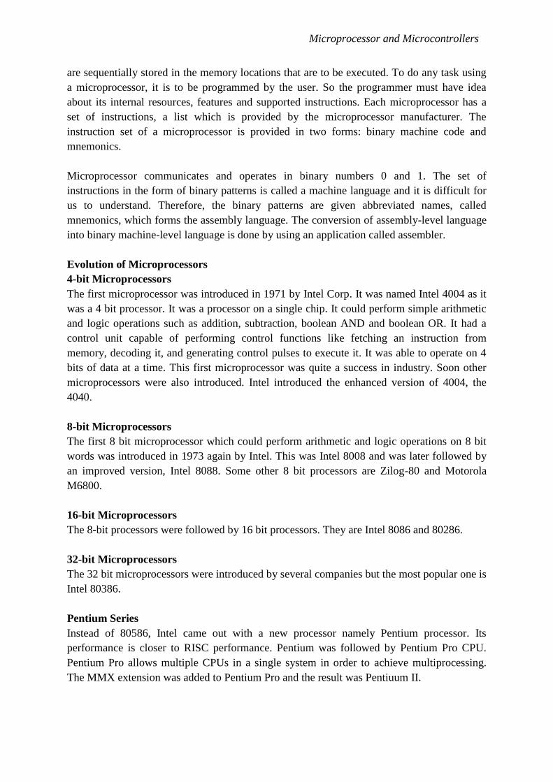
2. ARCHITECTURE OF 8085 MICROPROCESSOR
The 8085 microprocessor is an 8-bit processor available as a 40-pin IC package and uses +5
V for power. It can run at a maximum frequency of 3 MHz. Its data bus width is 8-bit and
address bus width is 16-bit, thus it can address 216 = 64 KB of memory. The internal
architecture of 8085 is shown is Fig. 2.
Fig. 2 Internal Architecture of 8085
Based on architecture:
Reduced Instruction Set Computer (RISC) processors
Complex Instruction Set Computer (CISC) processors
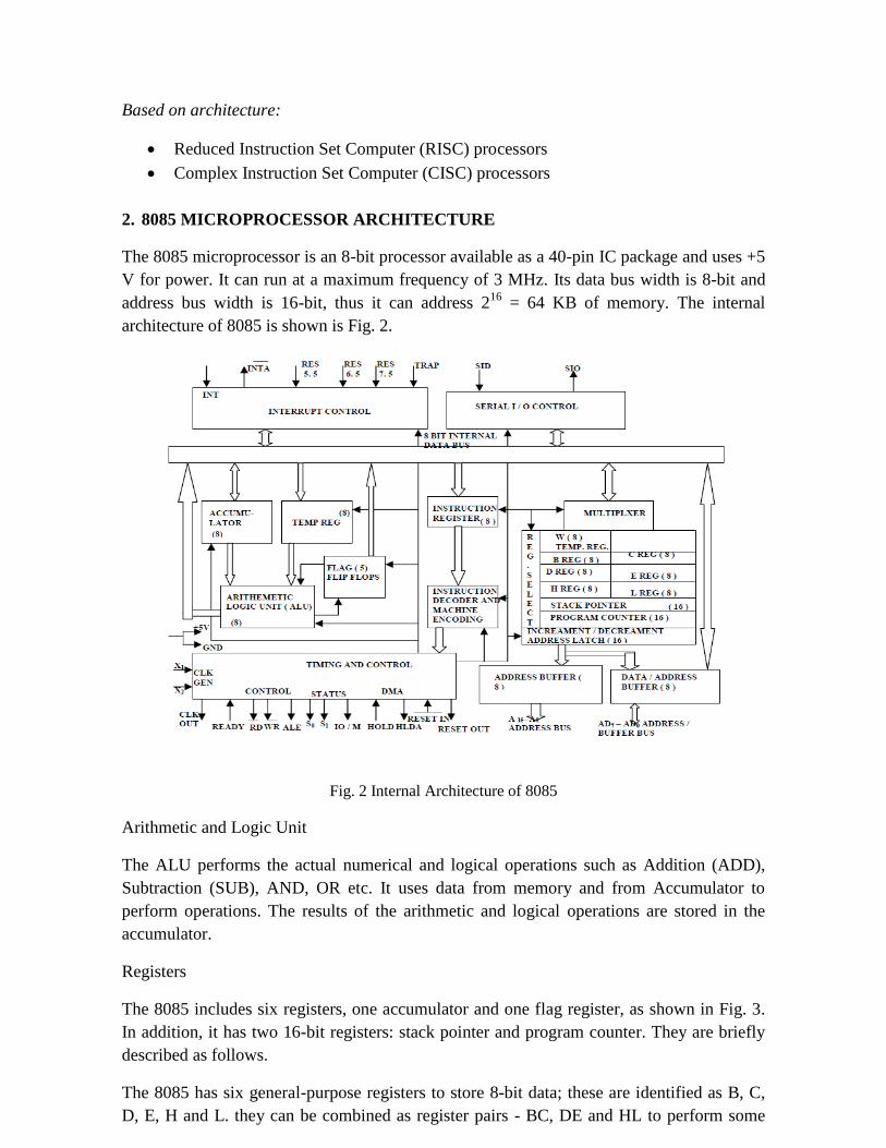
2. 8085 MICROPROCESSOR ARCHITECTURE
The 8085 microprocessor is an 8-bit processor available as a 40-pin IC package and uses +5
V for power. It can run at a maximum frequency of 3 MHz. Its data bus width is 8-bit and
address bus width is 16-bit, thus it can address 216
= 64 KB of memory. The internal
architecture of 8085 is shown is Fig. 2.
Fig. 2 Internal Architecture of 8085
Arithmetic and Logic Unit
The ALU performs the actual numerical and logical operations such as Addition (ADD),
Subtraction (SUB), AND, OR etc. It uses data from memory and from Accumulator to
perform operations. The results of the arithmetic and logical operations are stored in the
accumulator.
Registers
The 8085 includes six registers, one accumulator and one flag register, as shown in Fig. 3.
In addition, it has two 16-bit registers: stack pointer and program counter. They are briefly
described as follows.
The 8085 has six general-purpose registers to store 8-bit data; these are identified as B, C,
D, E, H and L. they can be combined as register pairs - BC, DE and HL to perform some
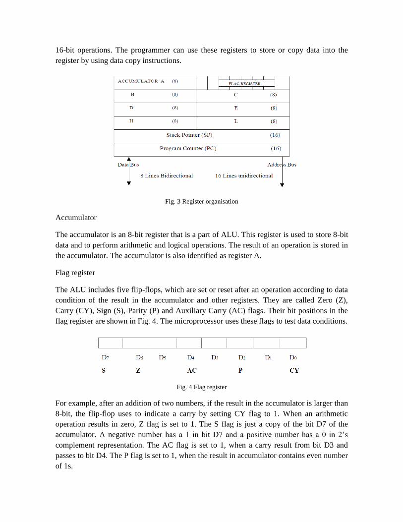
16-bit operations. The programmer can use these registers to store or copy data into the
register by using data copy instructions.
Fig. 3 Register organisation
Accumulator
The accumulator is an 8-bit register that is a part of ALU. This register is used to store 8-bit
data and to perform arithmetic and logical operations. The result of an operation is stored in
the accumulator. The accumulator is also identified as register A.
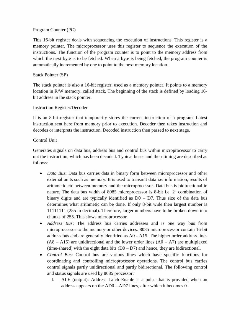
Flag register
The ALU includes five flip-flops, which are set or reset after an operation according to data
condition of the result in the accumulator and other registers. They are called Zero (Z),
Carry (CY), Sign (S), Parity (P) and Auxiliary Carry (AC) flags. Their bit positions in the
flag register are shown in Fig. 4. The microprocessor uses these flags to test data conditions.
Fig. 4 Flag register
For example, after an addition of two numbers, if the result in the accumulator is larger than
8-bit, the flip-flop uses to indicate a carry by setting CY flag to 1. When an arithmetic
operation results in zero, Z flag is set to 1. The S flag is just a copy of the bit D7 of the
accumulator. A negative number has a 1 in bit D7 and a positive number has a 0 in 2’s
complement representation. The AC flag is set to 1, when a carry result from bit D3 and
passes to bit D4. The P flag is set to 1, when the result in accumulator contains even number
of 1s.
Program Counter (PC)
This 16-bit register deals with sequencing the execution of instructions. This register is a
memory pointer. The microprocessor uses this register to sequence the execution of the
instructions. The function of the program counter is to point to the memory address from
which the next byte is to be fetched. When a byte is being fetched, the program counter is
automatically incremented by one to point to the next memory location.
Stack Pointer (SP)
The stack pointer is also a 16-bit register, used as a memory pointer. It points to a memory
location in R/W memory, called stack. The beginning of the stack is defined by loading 16-
bit address in the stack pointer.
Instruction Register/Decoder
It is an 8-bit register that temporarily stores the current instruction of a program. Latest
instruction sent here from memory prior to execution. Decoder then takes instruction and
decodes or interprets the instruction. Decoded instruction then passed to next stage.
Control Unit
Generates signals on data bus, address bus and control bus within microprocessor to carry
out the instruction, which has been decoded. Typical buses and their timing are described as
follows:
Data Bus: Data bus carries data in binary form between microprocessor and other
external units such as memory. It is used to transmit data i.e. information, results of
arithmetic etc between memory and the microprocessor. Data bus is bidirectional in
nature. The data bus width of 8085 microprocessor is 8-bit i.e. 28 combination of
binary digits and are typically identified as D0 – D7. Thus size of the data bus
determines what arithmetic can be done. If only 8-bit wide then largest number is
11111111 (255 in decimal). Therefore, larger numbers have to be broken down into
chunks of 255. This slows microprocessor.
Address Bus: The address bus carries addresses and is one way bus from
microprocessor to the memory or other devices. 8085 microprocessor contain 16-bit
address bus and are generally identified as A0 - A15. The higher order address lines
(A8 – A15) are unidirectional and the lower order lines (A0 – A7) are multiplexed
(time-shared) with the eight data bits (D0 – D7) and hence, they are bidirectional.
Control Bus: Control bus are various lines which have specific functions for
coordinating and controlling microprocessor operations. The control bus carries
control signals partly unidirectional and partly bidirectional. The following control
and status signals are used by 8085 processor:
I. ALE (output): Address Latch Enable is a pulse that is provided when an
address appears on the AD0 – AD7 lines, after which it becomes 0.
II. RD (active low output): The Read signal indicates that data are being read
from the selected I/O or memory device and that they are available on the
data bus.
III. WR (active low output): The Write signal indicates that data on the data bus
are to be written into a selected memory or I/O location.
IV. MIO/ (output): It is a signal that distinguished between a memory operation
and an I/O operation. When MIO/ = 0 it is a memory operation and MIO/ =
1 it is an I/O operation.
V. S1 and S0 (output): These are status signals used to specify the type of
operation being performed; they are listed in Table 1.
Table 1 Status signals and associated operations
S1 S0 States
0 0 Halt
0 1 Write
1 0 Read
1 1 Fetch
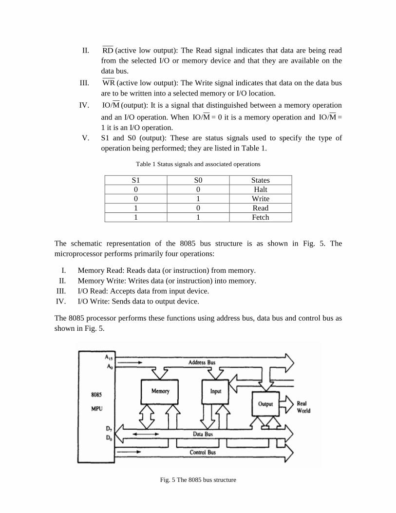
The schematic representation of the 8085 bus structure is as shown in Fig. 5. The
microprocessor performs primarily four operations:
I. Memory Read: Reads data (or instruction) from memory.
II. Memory Write: Writes data (or instruction) into memory.
III. I/O Read: Accepts data from input device.
IV. I/O Write: Sends data to output device.
The 8085 processor performs these functions using address bus, data bus and control bus as
shown in Fig. 5.
Fig. 5 The 8085 bus structure
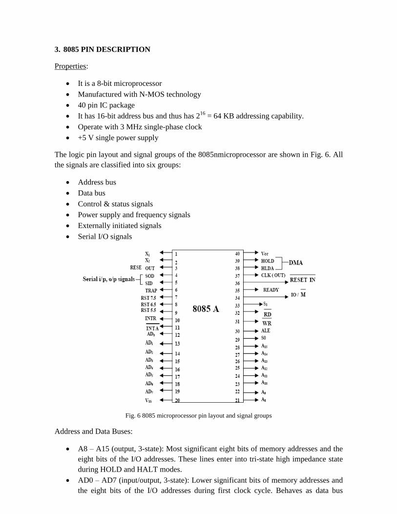
3. 8085 PIN DESCRIPTION
Properties:
It is a 8-bit microprocessor
Manufactured with N-MOS technology
40 pin IC package
It has 16-bit address bus and thus has 216
= 64 KB addressing capability.
Operate with 3 MHz single-phase clock
+5 V single power supply
The logic pin layout and signal groups of the 8085nmicroprocessor are shown in Fig. 6. All
the signals are classified into six groups:
Address bus
Data bus
Control & status signals
Power supply and frequency signals
Externally initiated signals
Serial I/O signals
Fig. 6 8085 microprocessor pin layout and signal groups
Address and Data Buses:
A8 – A15 (output, 3-state): Most significant eight bits of memory addresses and the
eight bits of the I/O addresses. These lines enter into tri-state high impedance state
during HOLD and HALT modes.
AD0 – AD7 (input/output, 3-state): Lower significant bits of memory addresses and
the eight bits of the I/O addresses during first clock cycle. Behaves as data bus
during third and fourth clock cycle. These lines enter into tri-state high impedance
state during HOLD and HALT modes.
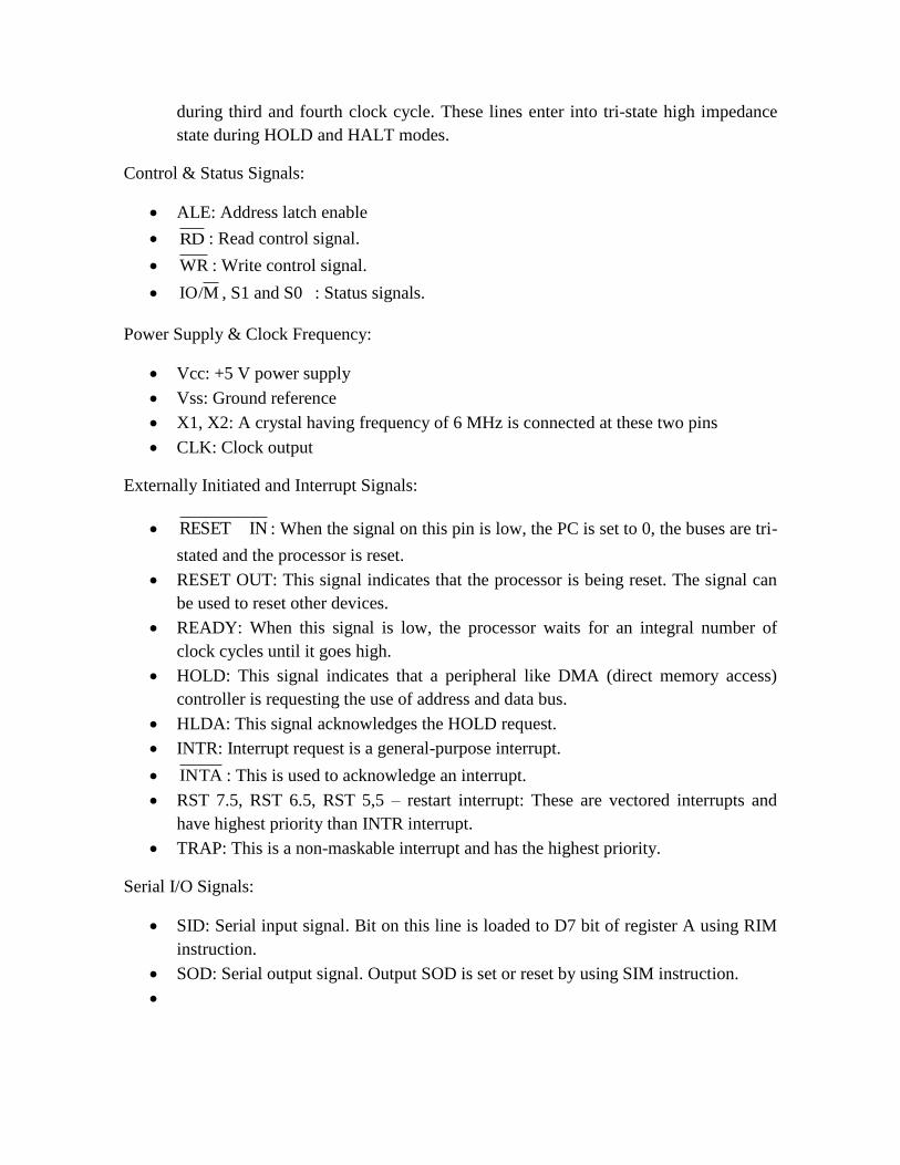
Control & Status Signals:
ALE: Address latch enable
RD : Read control signal.
WR : Write control signal.
MIO/ , S1 and S0 : Status signals.
Power Supply & Clock Frequency:
Vcc: +5 V power supply
Vss: Ground reference
X1, X2: A crystal having frequency of 6 MHz is connected at these two pins
CLK: Clock output
Externally Initiated and Interrupt Signals:
INRESET : When the signal on this pin is low, the PC is set to 0, the buses are tri-
stated and the processor is reset.
RESET OUT: This signal indicates that the processor is being reset. The signal can
be used to reset other devices.
READY: When this signal is low, the processor waits for an integral number of
clock cycles until it goes high.
HOLD: This signal indicates that a peripheral like DMA (direct memory access)
controller is requesting the use of address and data bus.
HLDA: This signal acknowledges the HOLD request.
INTR: Interrupt request is a general-purpose interrupt.
INTA : This is used to acknowledge an interrupt.
RST 7.5, RST 6.5, RST 5,5 – restart interrupt: These are vectored interrupts and
have highest priority than INTR interrupt.
TRAP: This is a non-maskable interrupt and has the highest priority.
Serial I/O Signals:
SID: Serial input signal. Bit on this line is loaded to D7 bit of register A using RIM
instruction.
SOD: Serial output signal. Output SOD is set or reset by using SIM instruction.

4. INSTRUCTION SET AND EXECUTION IN 8085
Based on the design of the ALU and decoding unit, the microprocessor manufacturer
provides instruction set for every microprocessor. The instruction set consists of both
machine code and mnemonics.
An instruction is a binary pattern designed inside a microprocessor to perform a specific
function. The entire group of instructions that a microprocessor supports is called
instruction set. Microprocessor instructions can be classified based on the parameters such
functionality, length and operand addressing.
Classification based on functionality:
I. Data transfer operations: This group of instructions copies data from source to
destination. The content of the source is not altered.
II. Arithmetic operations: Instructions of this group perform operations like addition,
subtraction, increment & decrement. One of the data used in arithmetic operation is
stored in accumulator and the result is also stored in accumulator.
III. Logical operations: Logical operations include AND, OR, EXOR, NOT. The
operations like AND, OR and EXOR uses two operands, one is stored in
accumulator and other can be any register or memory location. The result is stored
in accumulator. NOT operation requires single operand, which is stored in
accumulator.
IV. Branching operations: Instructions in this group can be used to transfer program
sequence from one memory location to another either conditionally or
unconditionally.
V. Machine control operations: Instruction in this group control execution of other
instructions and control operations like interrupt, halt etc.
Classification based on length:
I. One-byte instructions: Instruction having one byte in machine code. Examples are
depicted in Table 2.
I. Two-byte instructions: Instruction having two byte in machine code. Examples are
depicted in Table 3
II. Three-byte instructions: Instruction having three byte in machine code. Examples
are depicted in Table 4.
Table 2 Examples of one byte instructions
Opcode Operand Machine code/Hex code
MOV A, B 78
ADD M 86
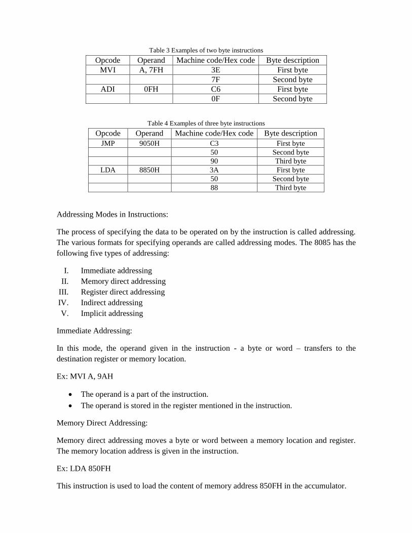
Table 3 Examples of two byte instructions
Opcode Operand Machine code/Hex code Byte description
MVI A, 7FH 3E First byte
7F Second byte
ADI 0FH C6 First byte
0F Second byte
Table 4 Examples of three byte instructions
Opcode Operand Machine code/Hex code Byte description
JMP 9050H C3 First byte
50 Second byte
90 Third byte
LDA 8850H 3A First byte
50 Second byte
88 Third byte
Addressing Modes in Instructions:
The process of specifying the data to be operated on by the instruction is called addressing.
The various formats for specifying operands are called addressing modes. The 8085 has the
following five types of addressing:
I. Immediate addressing
II. Memory direct addressing
III. Register direct addressing
IV. Indirect addressing
V. Implicit addressing
Immediate Addressing:
In this mode, the operand given in the instruction - a byte or word – transfers to the
destination register or memory location.
Ex: MVI A, 9AH
The operand is a part of the instruction.
The operand is stored in the register mentioned in the instruction.
Memory Direct Addressing:
Memory direct addressing moves a byte or word between a memory location and register.
The memory location address is given in the instruction.
Ex: LDA 850FH
This instruction is used to load the content of memory address 850FH in the accumulator.
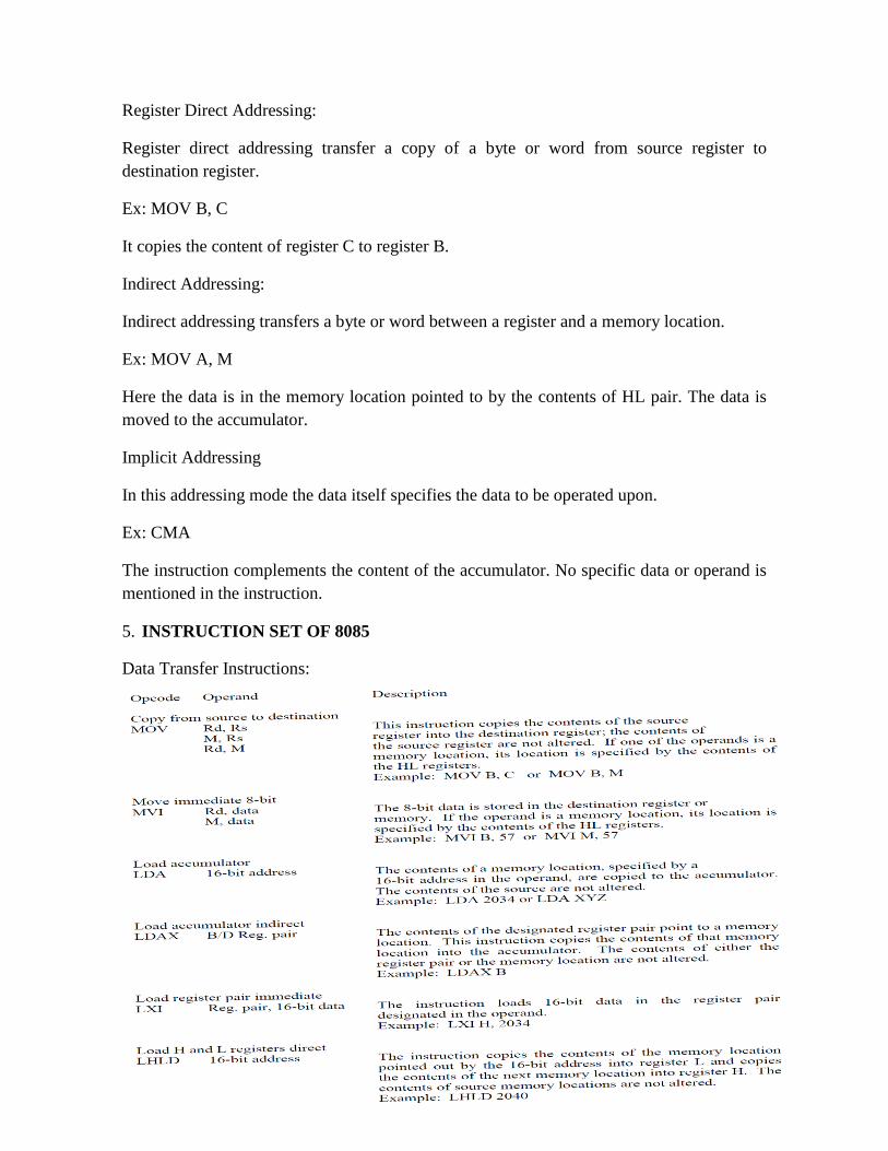
Register Direct Addressing:
Register direct addressing transfer a copy of a byte or word from source register to
destination register.
Ex: MOV B, C
It copies the content of register C to register B.
Indirect Addressing:
Indirect addressing transfers a byte or word between a register and a memory location.
Ex: MOV A, M
Here the data is in the memory location pointed to by the contents of HL pair. The data is
moved to the accumulator.
Implicit Addressing
In this addressing mode the data itself specifies the data to be operated upon.
Ex: CMA
The instruction complements the content of the accumulator. No specific data or operand is
mentioned in the instruction.
5. INSTRUCTION SET OF 8085
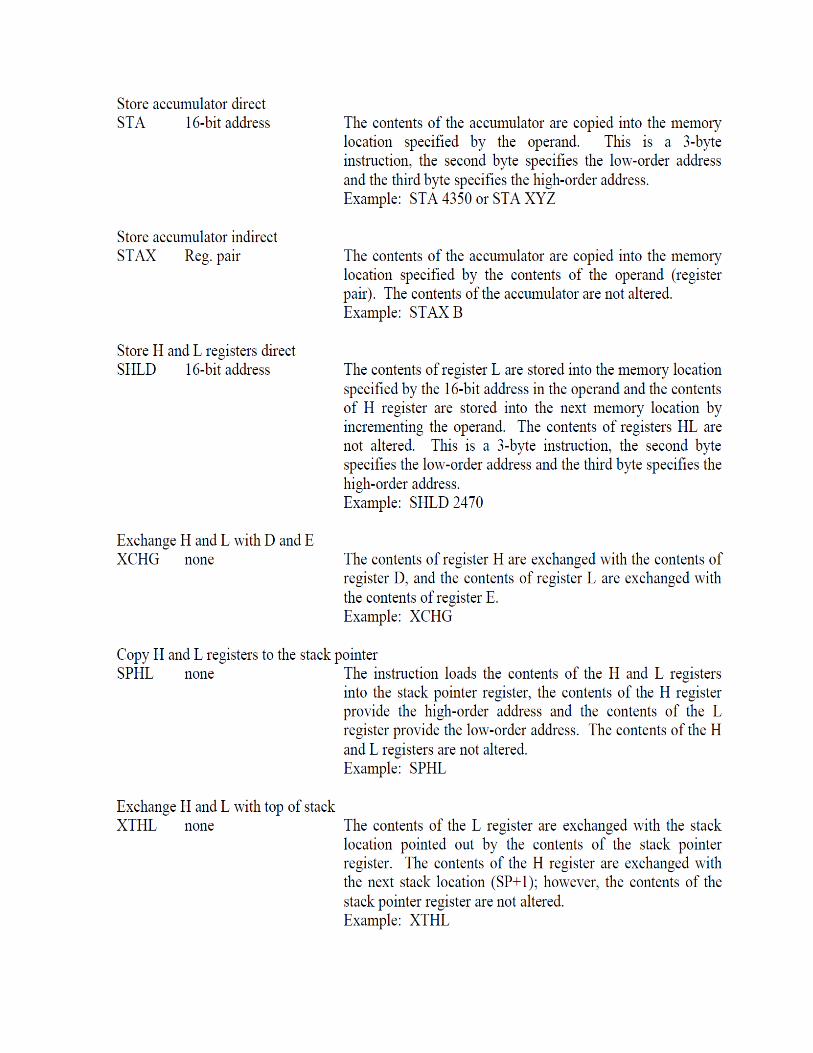
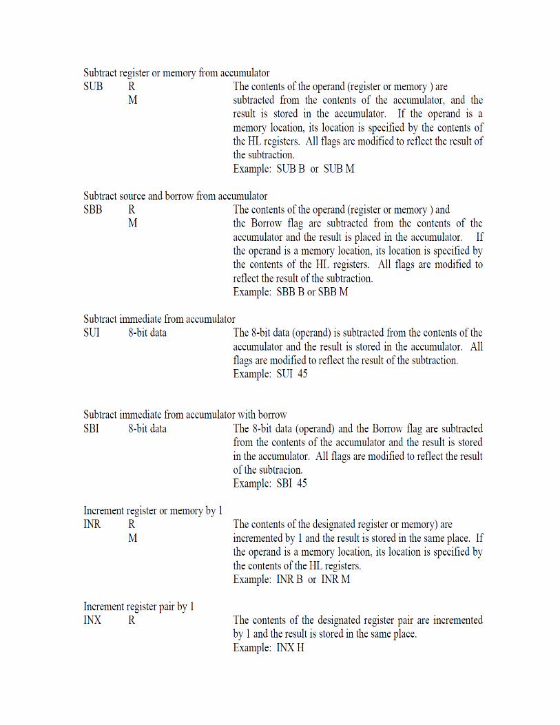
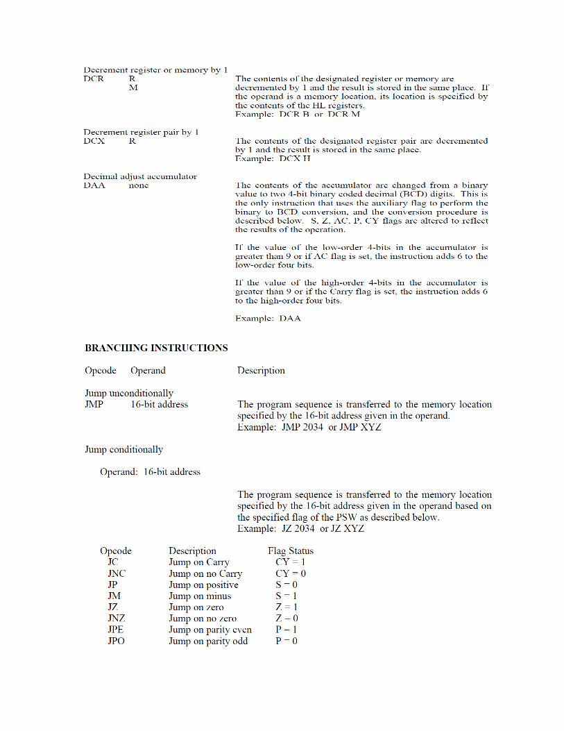
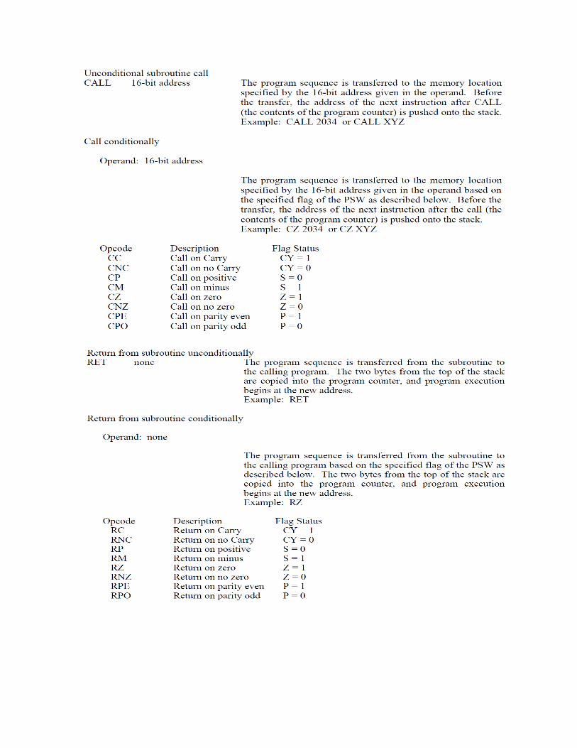
Data Transfer Instructions:
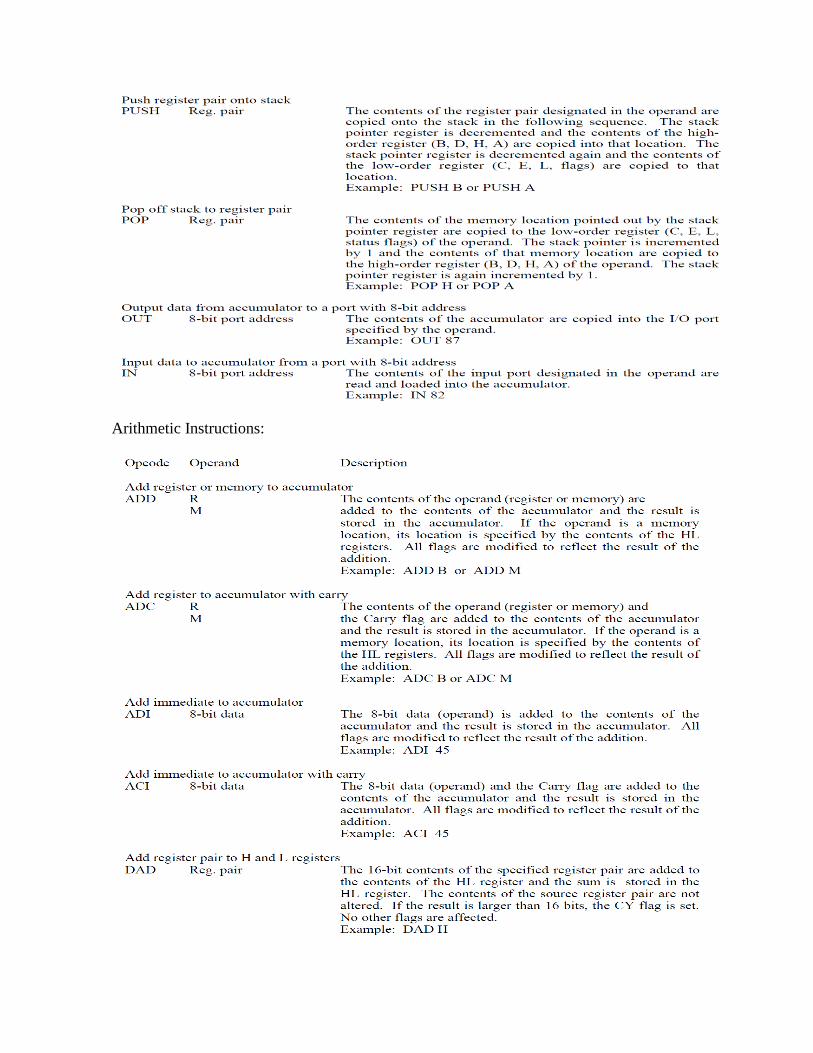
Arithmetic Instructions:
6. INSTRUCTION EXECUTION AND TIMING DIAGRAM:
Each instruction in 8085 microprocessor consists of two part- operation code (opcode) and
operand. The opcode is a command such as ADD and the operand is an object to be
operated on, such as a byte or the content of a register.
Instruction Cycle: The time taken by the processor to complete the execution of an
instruction. An instruction cycle consists of one to six machine cycles.
Machine Cycle: The time required to complete one operation; accessing either the memory
or I/O device. A machine cycle consists of three to six T-states.
T-State: Time corresponding to one clock period. It is the basic unit to calculate execution
of instructions or programs in a processor.
To execute a program, 8085 performs various operations as:
Opcode fetch
Operand fetch
Memory read/write
I/O read/write
External communication functions are:
Memory read/write
I/O read/write
Interrupt request acknowledge
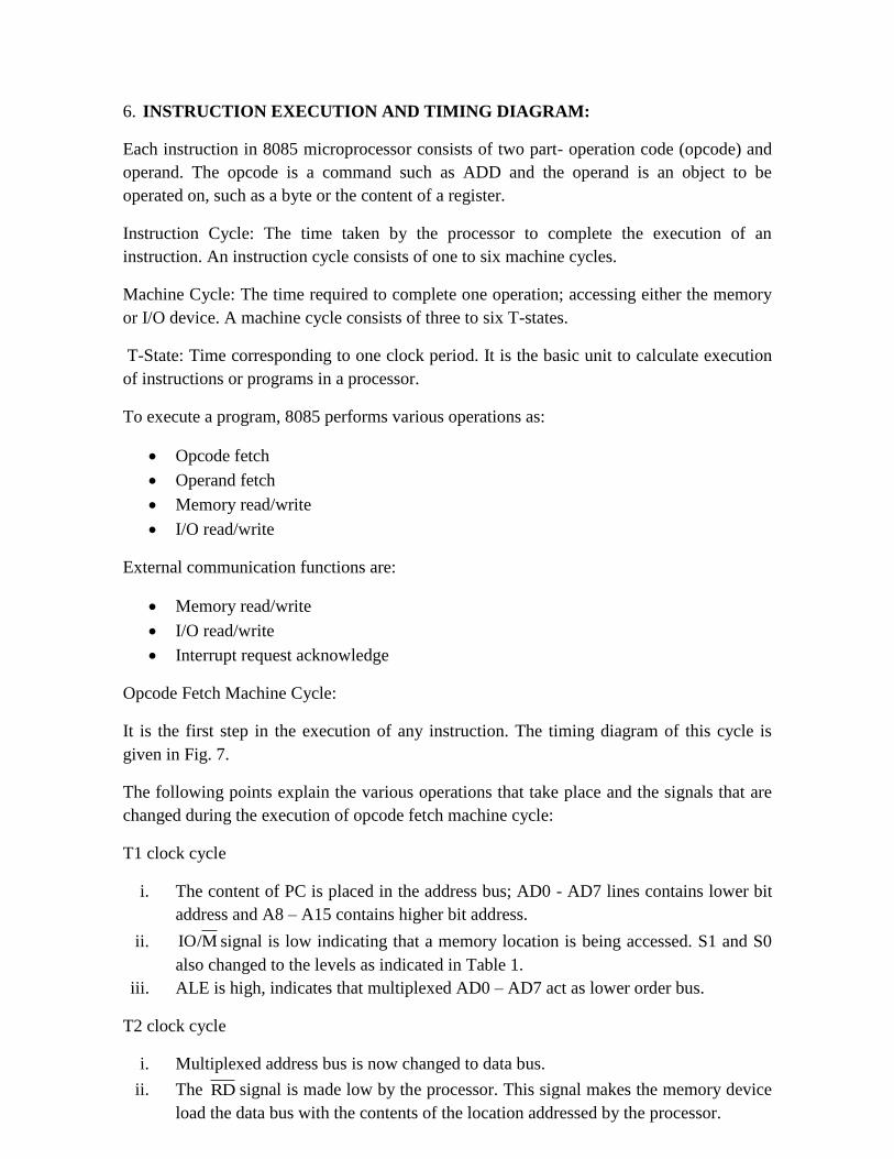
Opcode Fetch Machine Cycle:
It is the first step in the execution of any instruction. The timing diagram of this cycle is
given in Fig. 7.
The following points explain the various operations that take place and the signals that are
changed during the execution of opcode fetch machine cycle:
T1 clock cycle
i. The content of PC is placed in the address bus; AD0 - AD7 lines contains lower bit
address and A8 – A15 contains higher bit address.
ii. MIO/ signal is low indicating that a memory location is being accessed. S1 and S0
also changed to the levels as indicated in Table 1.
iii. ALE is high, indicates that multiplexed AD0 – AD7 act as lower order bus.
T2 clock cycle
i. Multiplexed address bus is now changed to data bus.
ii. The RD signal is made low by the processor. This signal makes the memory device
load the data bus with the contents of the location addressed by the processor.
T3 clock cycle
i. The opcode available on the data bus is read by the processor and moved to the
instruction register.
ii. The RD signal is deactivated by making it logic 1.
T4 clock cycle
i. The processor decode the instruction in the instruction register and generate the
necessary control signals to execute the instruction. Based on the instruction further
operations such as fetching, writing into memory etc takes place.
Fig. 7 Timing diagram for opcode fetch cycle
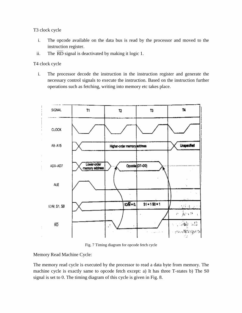
Memory Read Machine Cycle:
The memory read cycle is executed by the processor to read a data byte from memory. The
machine cycle is exactly same to opcode fetch except: a) It has three T-states b) The S0
signal is set to 0. The timing diagram of this cycle is given in Fig. 8.
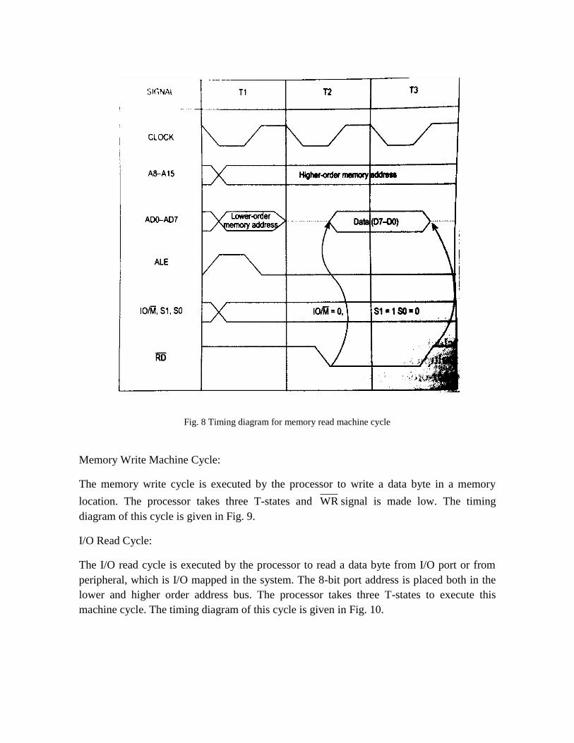
Fig. 8 Timing diagram for memory read machine cycle
Memory Write Machine Cycle:
The memory write cycle is executed by the processor to write a data byte in a memory
location. The processor takes three T-states and WR signal is made low. The timing
diagram of this cycle is given in Fig. 9.
I/O Read Cycle:
The I/O read cycle is executed by the processor to read a data byte from I/O port or from
peripheral, which is I/O mapped in the system. The 8-bit port address is placed both in the
lower and higher order address bus. The processor takes three T-states to execute this
machine cycle. The timing diagram of this cycle is given in Fig. 10.
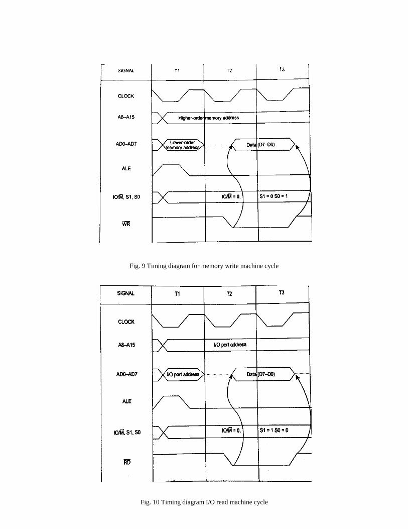
Fig. 9 Timing diagram for memory write machine cycle
Fig. 10 Timing diagram I/O read machine cycle
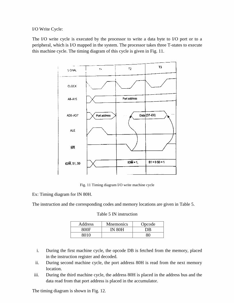
I/O Write Cycle:
The I/O write cycle is executed by the processor to write a data byte to I/O port or to a
peripheral, which is I/O mapped in the system. The processor takes three T-states to execute
this machine cycle. The timing diagram of this cycle is given in Fig. 11.
Fig. 11 Timing diagram I/O write machine cycle
Ex: Timing diagram for IN 80H.
The instruction and the corresponding codes and memory locations are given in Table 5.
Table 5 IN instruction
Address Mnemonics Opcode
800F IN 80H DB
8010 80
i. During the first machine cycle, the opcode DB is fetched from the memory, placed
in the instruction register and decoded.
ii. During second machine cycle, the port address 80H is read from the next memory
location.
iii. During the third machine cycle, the address 80H is placed in the address bus and the
data read from that port address is placed in the accumulator.
The timing diagram is shown in Fig. 12.

Fig. 12 Timing diagram for the IN instruction
7. 8085 INTERRUPTS
Interrupt Structure:
Interrupt is the mechanism by which the processor is made to transfer control from its
current program execution to another program having higher priority. The interrupt signal
may be given to the processor by any external peripheral device.
The program or the routine that is executed upon interrupt is called interrupt service routine
(ISR). After execution of ISR, the processor must return to the interrupted program. Key
features in the interrupt structure of any microprocessor are as follows:
i. Number and types of interrupt signals available.
ii. The address of the memory where the ISR is located for a particular interrupt signal.
This address is called interrupt vector address (IVA).
iii. Masking and unmasking feature of the interrupt signals.
iv. Priority among the interrupts.
v. Timing of the interrupt signals.
vi. Handling and storing of information about the interrupt program (status
information).
Types of Interrupts:
Interrupts are classified based on their maskability, IVA and source. They are classified as:
i. Vectored and Non-Vectored Interrupts
Vectored interrupts require the IVA to be supplied by the external device that
gives the interrupt signal. This technique is vectoring, is implemented in
number of ways.
Non-vectored interrupts have fixed IVA for ISRs of different interrupt
signals.
ii. Maskable and Non-Maskable Interrupts
Maskable interrupts are interrupts that can be blocked. Masking can be done
by software or hardware means.
Non-maskable interrupts are interrupts that are always recognized; the
corresponding ISRs are executed.
iii. Software and Hardware Interrupts
Software interrupts are special instructions, after execution transfer the
control to predefined ISR.
Hardware interrupts are signals given to the processor, for recognition as an
interrupt and execution of the corresponding ISR.
Interrupt Handling Procedure:
The following sequence of operations takes place when an interrupt signal is recognized:
i. Save the PC content and information about current state (flags, registers etc) in the
stack.
ii. Load PC with the beginning address of an ISR and start to execute it.
iii. Finish ISR when the return instruction is executed.
iv. Return to the point in the interrupted program where execution was interrupted.
Interrupt Sources and Vector Addresses in 8085:
Software Interrupts:
8085 instruction set includes eight software interrupt instructions called Restart (RST)
instructions. These are one byte instructions that make the processor execute a subroutine at
predefined locations. Instructions and their vector addresses are given in Table 6.
Table 6 Software interrupts and their vector addresses
Instruction Machine hex code Interrupt Vector Address
RST 0 C7 0000H
RST 1 CF 0008H
RST 2 D7 0010H
RST 3 DF 0018H
RST 4 E7 0020H
RST 5 EF 0028H
RST 6 F7 0030H
RST 7 FF 0032H
The software interrupts can be treated as CALL instructions with default call locations. The
concept of priority does not apply to software interrupts as they are inserted into the
program as instructions by the programmer and executed by the processor when the
respective program lines are read.
Hardware Interrupts and Priorities:
8085 have five hardware interrupts – INTR, RST 5.5, RST 6.5, RST 7.5 and TRAP. Their
IVA and priorities are given in Table 7.
Table 7 Hardware interrupts of 8085
Interrupt Interrupt vector
address
Maskable or non-
maskable
Edge or level
triggered
priority
TRAP 0024H Non-makable Level 1
RST 7.5 003CH Maskable Rising edge 2
RST 6.5 0034H Maskable Level 3
RST 5.5 002CH Maskable Level 4
INTR Decided by hardware Maskable Level 5
Masking of Interrupts:
Masking can be done for four hardware interrupts INTR, RST 5.5, RST 6.5, and RST 7.5.
The masking of 8085 interrupts is done at different levels. Fig. 13 shows the organization of
hardware interrupts in the 8085.
Fig. 13 Interrupt structure of 8085
The Fig. 13 is explained by the following five points:
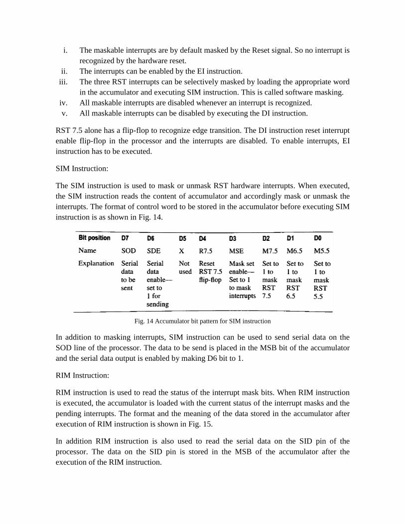
i. The maskable interrupts are by default masked by the Reset signal. So no interrupt is
recognized by the hardware reset.
ii. The interrupts can be enabled by the EI instruction.
iii. The three RST interrupts can be selectively masked by loading the appropriate word
in the accumulator and executing SIM instruction. This is called software masking.
iv. All maskable interrupts are disabled whenever an interrupt is recognized.
v. All maskable interrupts can be disabled by executing the DI instruction.
RST 7.5 alone has a flip-flop to recognize edge transition. The DI instruction reset interrupt
enable flip-flop in the processor and the interrupts are disabled. To enable interrupts, EI
instruction has to be executed.
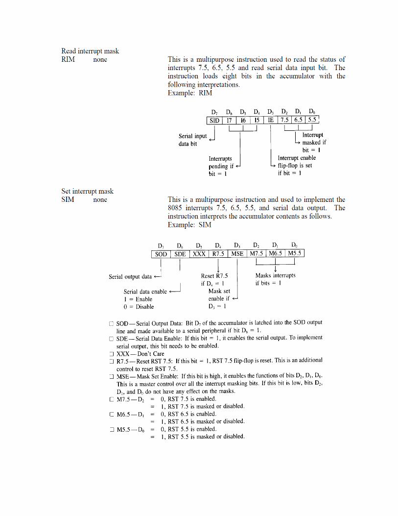
SIM Instruction:
The SIM instruction is used to mask or unmask RST hardware interrupts. When executed,
the SIM instruction reads the content of accumulator and accordingly mask or unmask the
interrupts. The format of control word to be stored in the accumulator before executing SIM
instruction is as shown in Fig. 14.
Fig. 14 Accumulator bit pattern for SIM instruction
In addition to masking interrupts, SIM instruction can be used to send serial data on the
SOD line of the processor. The data to be send is placed in the MSB bit of the accumulator
and the serial data output is enabled by making D6 bit to 1.
RIM Instruction:
RIM instruction is used to read the status of the interrupt mask bits. When RIM instruction
is executed, the accumulator is loaded with the current status of the interrupt masks and the
pending interrupts. The format and the meaning of the data stored in the accumulator after
execution of RIM instruction is shown in Fig. 15.
In addition RIM instruction is also used to read the serial data on the SID pin of the
processor. The data on the SID pin is stored in the MSB of the accumulator after the
execution of the RIM instruction.
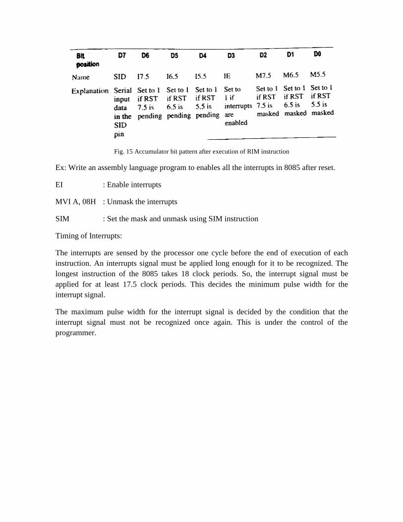
Fig. 15 Accumulator bit pattern after execution of RIM instruction
Ex: Write an assembly language program to enables all the interrupts in 8085 after reset.
EI : Enable interrupts
MVI A, 08H : Unmask the interrupts
SIM : Set the mask and unmask using SIM instruction
Timing of Interrupts:
The interrupts are sensed by the processor one cycle before the end of execution of each
instruction. An interrupts signal must be applied long enough for it to be recognized. The
longest instruction of the 8085 takes 18 clock periods. So, the interrupt signal must be
applied for at least 17.5 clock periods. This decides the minimum pulse width for the
interrupt signal.
The maximum pulse width for the interrupt signal is decided by the condition that the
interrupt signal must not be recognized once again. This is under the control of the
programmer.
QUESTIONS:
1. What is the function of a microprocessor in a system?
2. Why is the data bus in 8085 bidirectional?
3. How does microprocessor differentiate between data and instruction? 4. How long would the processor take to execute the instruction LDA
1753H if the T-state duration is 2μs?
5. Draw the timing diagram of the instruction LDAX B.
6. Sketch and explain the various pins of the 8085.
7. Explain direct addressing mode of 8085 with an example?
8. Draw and explain the timing diagram of the instruction IN 82H.
9. What is meant by ‘priority of the interrupts’? Explain the operation of
the interrupts structure of the 8085, with the help of a circuit diagram.
10. Explain the bit pattern for SIM instruction. Write the assembly language
program lines to enable all the interrupts in the 8085 after reset.
11. Write the logical instructions which affect and which does not affect flags in 8085.
12. Write an ALP in 8085 MPU to reject all the negative readings and add all
the positive reading from a set of ten reading stored in memory
locations starting at XX60H. When the sum exceeds eight bits produce
output FFH to PORT1 to indicate overload otherwise display the sum.
13. Write an ALP in 8085 to eliminate the blanks (bytes with zero value)
from a string of eight data bytes. Use two memory pointers: one to get a
byte and the other to store the byte.
14. Design an up-down counter to count from 0 to 9 and 9 to 0
continuously with a 1.5 second delay between each count, and display
the count at one of the output ports.
MODULE: 2
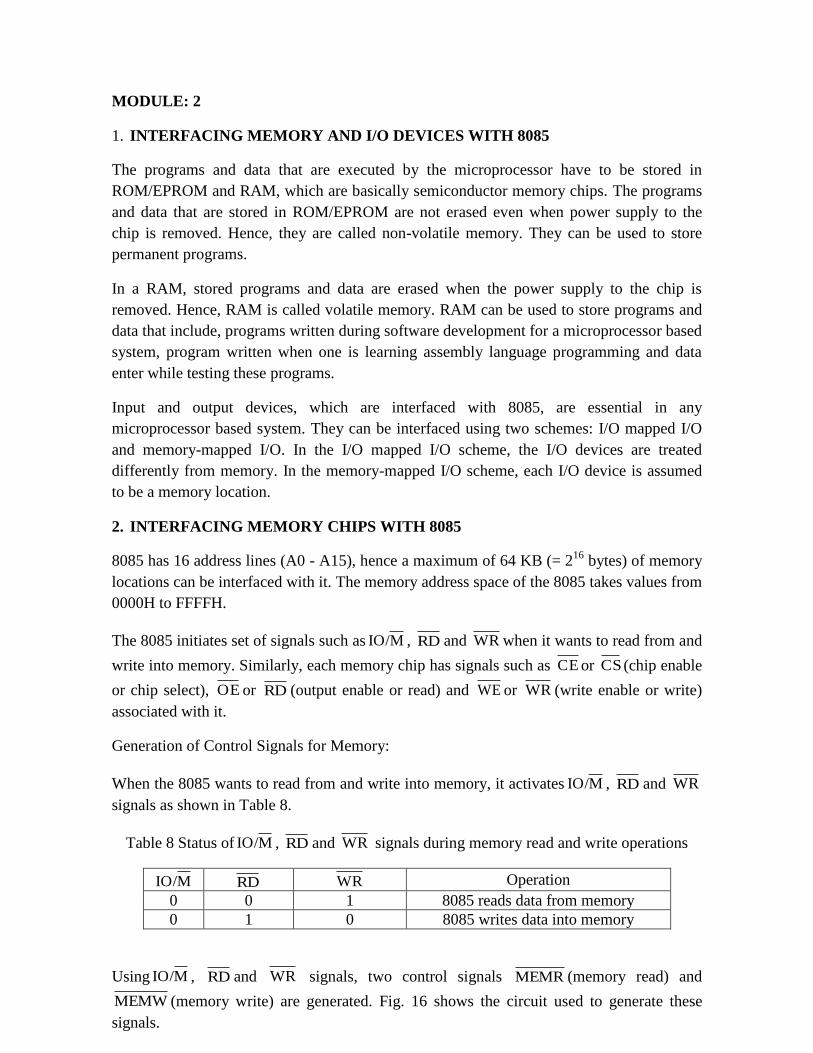
1. INTERFACING MEMORY AND I/O DEVICES WITH 8085
The programs and data that are executed by the microprocessor have to be stored in
ROM/EPROM and RAM, which are basically semiconductor memory chips. The programs
and data that are stored in ROM/EPROM are not erased even when power supply to the
chip is removed. Hence, they are called non-volatile memory. They can be used to store
permanent programs.
In a RAM, stored programs and data are erased when the power supply to the chip is
removed. Hence, RAM is called volatile memory. RAM can be used to store programs and
data that include, programs written during software development for a microprocessor based
system, program written when one is learning assembly language programming and data
enter while testing these programs.
Input and output devices, which are interfaced with 8085, are essential in any
microprocessor based system. They can be interfaced using two schemes: I/O mapped I/O
and memory-mapped I/O. In the I/O mapped I/O scheme, the I/O devices are treated
differently from memory. In the memory-mapped I/O scheme, each I/O device is assumed
to be a memory location.
2. INTERFACING MEMORY CHIPS WITH 8085
8085 has 16 address lines (A0 - A15), hence a maximum of 64 KB (= 216
bytes) of memory
locations can be interfaced with it. The memory address space of the 8085 takes values from
0000H to FFFFH.
The 8085 initiates set of signals such as MIO/ , RD and WR when it wants to read from and
write into memory. Similarly, each memory chip has signals such as CE or CS (chip enable
or chip select), OE or RD (output enable or read) and WE or WR (write enable or write)
associated with it.
Generation of Control Signals for Memory:
When the 8085 wants to read from and write into memory, it activates MIO/ , RD and WR
signals as shown in Table 8.
Table 8 Status of MIO/ , RD and WR signals during memory read and write operations
MIO/ RD WR Operation
0 0 1 8085 reads data from memory
0 1 0 8085 writes data into memory
Using MIO/ , RD and WR signals, two control signals MEMR (memory read) and
MEMW (memory write) are generated. Fig. 16 shows the circuit used to generate these
signals.
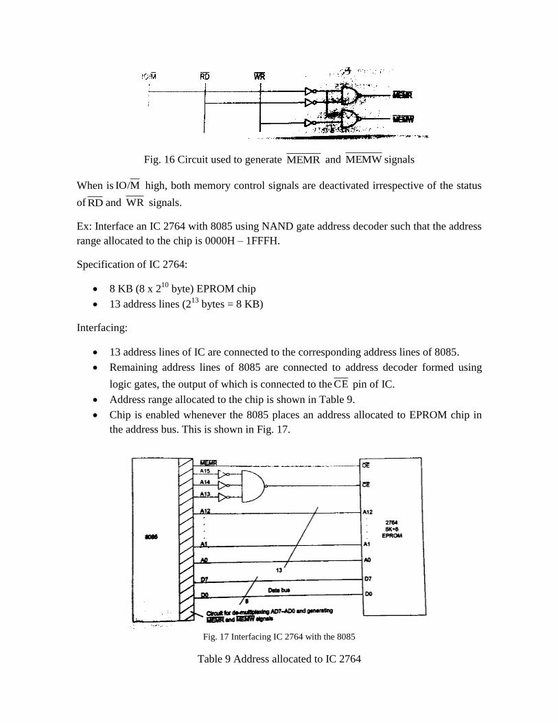
Fig. 16 Circuit used to generate MEMR and MEMW signals
When is MIO/ high, both memory control signals are deactivated irrespective of the status
of RD and WR signals.
Ex: Interface an IC 2764 with 8085 using NAND gate address decoder such that the address
range allocated to the chip is 0000H – 1FFFH.
Specification of IC 2764:
8 KB (8 x 210
byte) EPROM chip
13 address lines (213
bytes = 8 KB)
Interfacing:
13 address lines of IC are connected to the corresponding address lines of 8085.
Remaining address lines of 8085 are connected to address decoder formed using
logic gates, the output of which is connected to the CE pin of IC.
Address range allocated to the chip is shown in Table 9.
Chip is enabled whenever the 8085 places an address allocated to EPROM chip in
the address bus. This is shown in Fig. 17.
Fig. 17 Interfacing IC 2764 with the 8085
Table 9 Address allocated to IC 2764
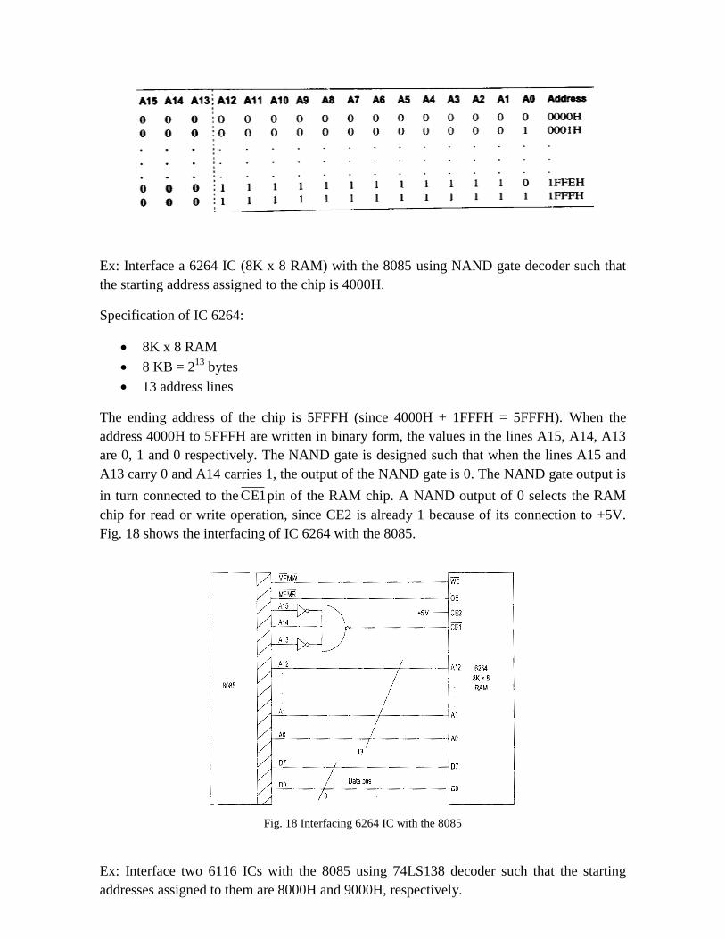
Ex: Interface a 6264 IC (8K x 8 RAM) with the 8085 using NAND gate decoder such that
the starting address assigned to the chip is 4000H.
Specification of IC 6264:
8K x 8 RAM
8 KB = 213
bytes
13 address lines
The ending address of the chip is 5FFFH (since 4000H + 1FFFH = 5FFFH). When the
address 4000H to 5FFFH are written in binary form, the values in the lines A15, A14, A13
are 0, 1 and 0 respectively. The NAND gate is designed such that when the lines A15 and
A13 carry 0 and A14 carries 1, the output of the NAND gate is 0. The NAND gate output is
in turn connected to the CE1pin of the RAM chip. A NAND output of 0 selects the RAM
chip for read or write operation, since CE2 is already 1 because of its connection to +5V.
Fig. 18 shows the interfacing of IC 6264 with the 8085.
Fig. 18 Interfacing 6264 IC with the 8085
Ex: Interface two 6116 ICs with the 8085 using 74LS138 decoder such that the starting
addresses assigned to them are 8000H and 9000H, respectively.
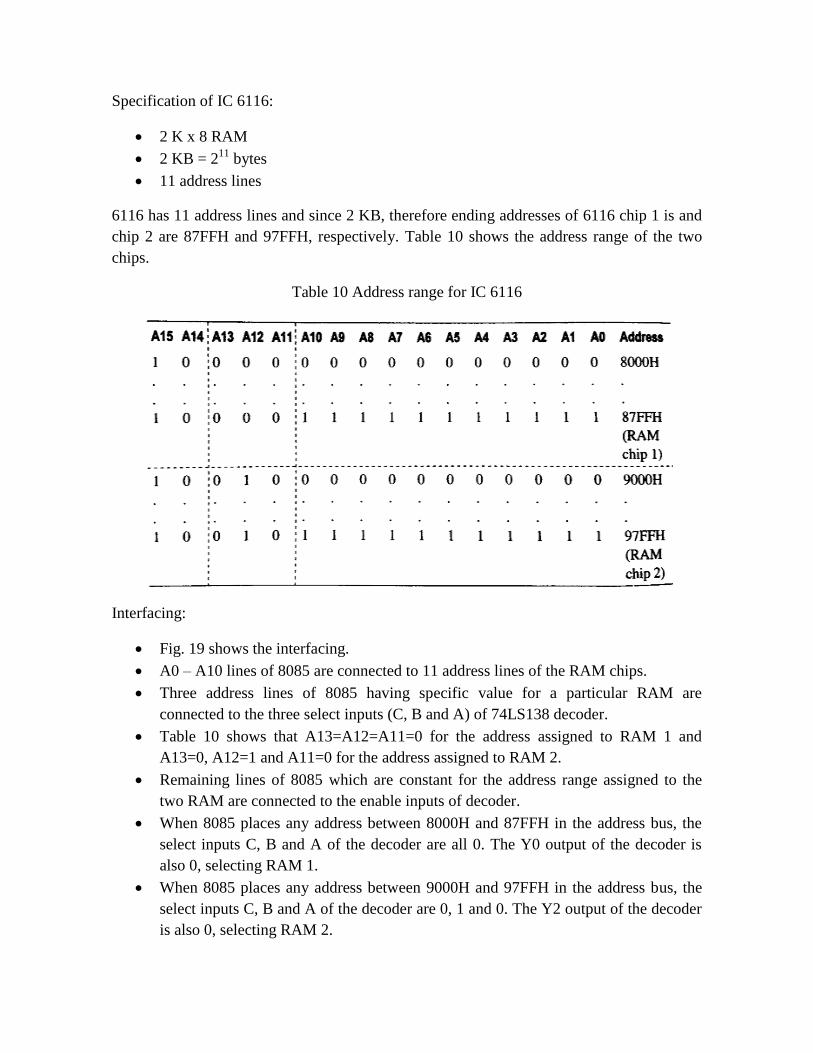
Specification of IC 6116:
2 K x 8 RAM
2 KB = 211
bytes
11 address lines
6116 has 11 address lines and since 2 KB, therefore ending addresses of 6116 chip 1 is and
chip 2 are 87FFH and 97FFH, respectively. Table 10 shows the address range of the two
chips.
Table 10 Address range for IC 6116
Interfacing:
Fig. 19 shows the interfacing.
A0 – A10 lines of 8085 are connected to 11 address lines of the RAM chips.
Three address lines of 8085 having specific value for a particular RAM are
connected to the three select inputs (C, B and A) of 74LS138 decoder.
Table 10 shows that A13=A12=A11=0 for the address assigned to RAM 1 and
A13=0, A12=1 and A11=0 for the address assigned to RAM 2.
Remaining lines of 8085 which are constant for the address range assigned to the
two RAM are connected to the enable inputs of decoder.
When 8085 places any address between 8000H and 87FFH in the address bus, the
select inputs C, B and A of the decoder are all 0. The Y0 output of the decoder is
also 0, selecting RAM 1.
When 8085 places any address between 9000H and 97FFH in the address bus, the
select inputs C, B and A of the decoder are 0, 1 and 0. The Y2 output of the decoder
is also 0, selecting RAM 2.
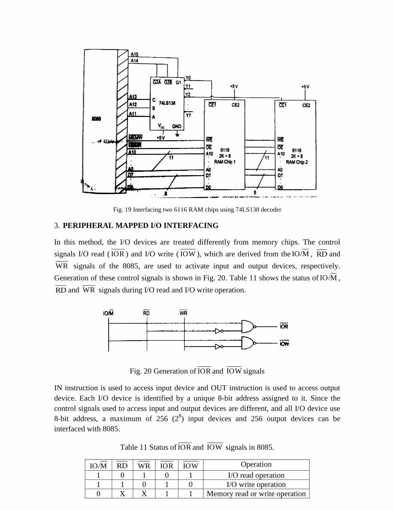
Fig. 19 Interfacing two 6116 RAM chips using 74LS138 decoder
3. PERIPHERAL MAPPED I/O INTERFACING
In this method, the I/O devices are treated differently from memory chips. The control
signals I/O read ( IOR ) and I/O write ( IOW ), which are derived from the MIO/ , RD and
WR signals of the 8085, are used to activate input and output devices, respectively.
Generation of these control signals is shown in Fig. 20. Table 11 shows the status of MIO/ ,
RD and WR signals during I/O read and I/O write operation.
Fig. 20 Generation of IOR and IOW signals
IN instruction is used to access input device and OUT instruction is used to access output
device. Each I/O device is identified by a unique 8-bit address assigned to it. Since the
control signals used to access input and output devices are different, and all I/O device use
8-bit address, a maximum of 256 (28) input devices and 256 output devices can be
interfaced with 8085.
Table 11 Status of IOR and IOW signals in 8085.
MIO/ RD WR IOR IOW Operation
1 0 1 0 1 I/O read operation
1 1 0 1 0 I/O write operation
0 X X 1 1 Memory read or write operation
Ex: Interface an 8-bit DIP switch with the 8085 such that the address assigned to the DIP
switch if F0H.
IN instruction is used to get data from DIP switch and store it in accumulator. Steps
involved in the execution of this instruction are:
i. Address F0H is placed in the lines A0 – A7 and a copy of it in lines A8 – A15.
ii. The IOR signal is activated ( IOR = 0), which makes the selected input device to
place its data in the data bus.
iii. The data in the data bus is read and store in the accumulator.
Fig. 21 shows the interfacing of DIP switch.
A7 A6 A5 A4 A3 A2 A1 A0
1 1 1 1 0 0 0 0 = F0H
A0 – A7 lines are connected to a NAND gate decoder such that the output of NAND gate is
0. The output of NAND gate is ORed with the IOR signal and the output of OR gate is
connected to 1G and 2G of the 74LS244. When 74LS244 is enabled, data from the DIP
switch is placed on the data bus of the 8085. The 8085 read data and store in the
accumulator. Thus data from DIP switch is transferred to the accumulator.
Fig. 21 interfacing of 8-bit DIP switch with 8085
4. MEMORY MAPPED I/O INTERFACING
In memory-mapped I/O, each input or output device is treated as if it is a memory location.
The MEMR and MEMW control signals are used to activate the devices. Each input or
output device is identified by unique 16-bit address, similar to 16-bit address assigned to
memory location. All memory related instruction like LDA 2000H, LDAX B, MOV A, M
can be used.
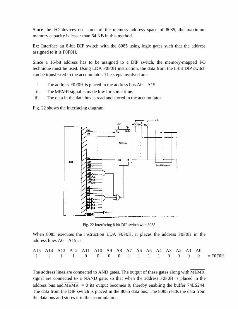
Since the I/O devices use some of the memory address space of 8085, the maximum
memory capacity is lesser than 64 KB in this method.
Ex: Interface an 8-bit DIP switch with the 8085 using logic gates such that the address
assigned to it is F0F0H.
Since a 16-bit address has to be assigned to a DIP switch, the memory-mapped I/O
technique must be used. Using LDA F0F0H instruction, the data from the 8-bit DIP switch
can be transferred to the accumulator. The steps involved are:
i. The address F0F0H is placed in the address bus A0 – A15.
ii. The MEMR signal is made low for some time.
iii. The data in the data bus is read and stored in the accumulator.
Fig. 22 shows the interfacing diagram.
Fig. 22 Interfacing 8-bit DIP switch with 8085
When 8085 executes the instruction LDA F0F0H, it places the address F0F0H in the
address lines A0 – A15 as:
A15 A14 A13 A12 A11 A10 A9 A8 A7 A6 A5 A4 A3 A2 A1 A0
1 1 1 1 0 0 0 0 1 1 1 1 0 0 0 0 = F0F0H
The address lines are connected to AND gates. The output of these gates along with MEMR
signal are connected to a NAND gate, so that when the address F0F0H is placed in the
address bus and MEMR = 0 its output becomes 0, thereby enabling the buffer 74LS244.
The data from the DIP switch is placed in the 8085 data bus. The 8085 reads the data from
the data bus and stores it in the accumulator.
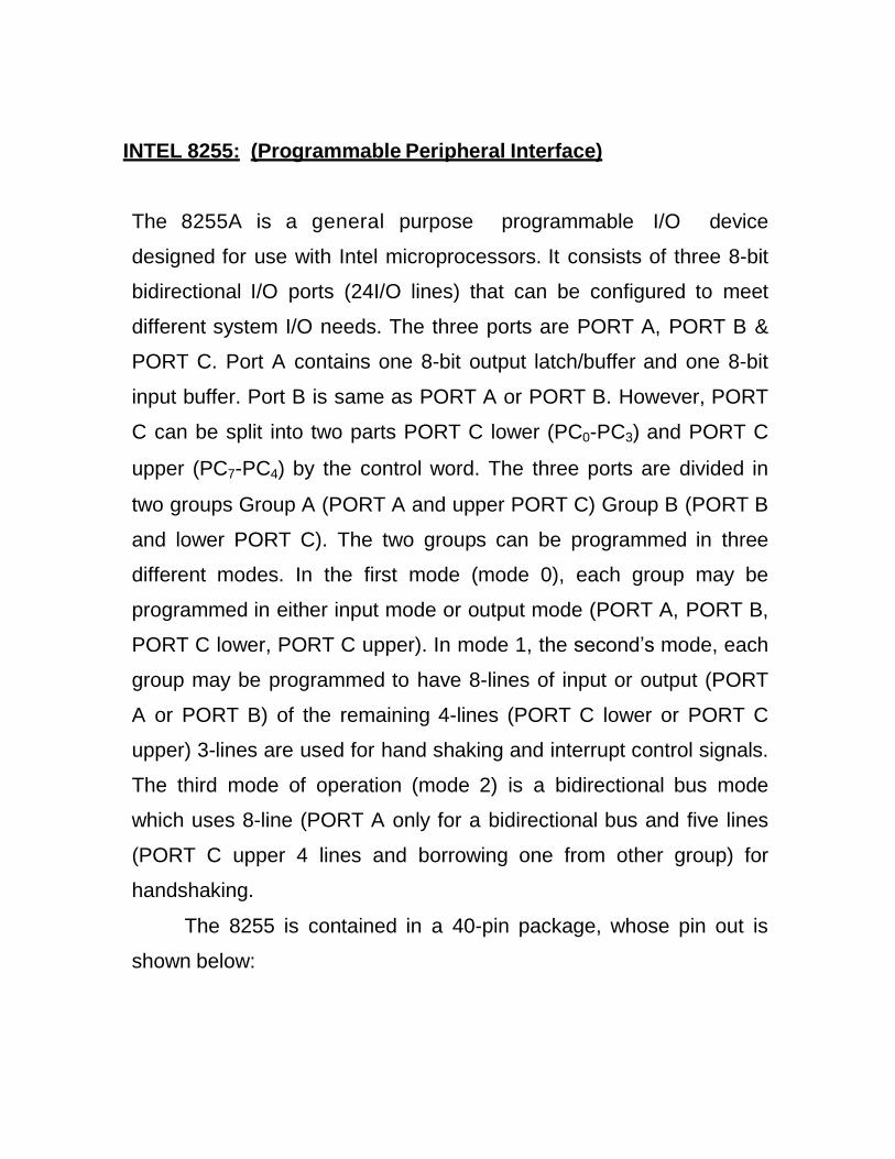
INTEL 8255: (Programmable Peripheral Interface)
The 8255A is a general purpose programmable I/O device
designed for use with Intel microprocessors. It consists of three 8-bit
bidirectional I/O ports (24I/O lines) that can be configured to meet
different system I/O needs. The three ports are PORT A, PORT B &
PORT C. Port A contains one 8-bit output latch/buffer and one 8-bit
input buffer. Port B is same as PORT A or PORT B. However, PORT
C can be split into two parts PORT C lower (PC0-PC3) and PORT C
upper (PC7-PC4) by the control word. The three ports are divided in
two groups Group A (PORT A and upper PORT C) Group B (PORT B
and lower PORT C). The two groups can be programmed in three
different modes. In the first mode (mode 0), each group may be
programmed in either input mode or output mode (PORT A, PORT B,
PORT C lower, PORT C upper). In mode 1, the second’s mode, each
group may be programmed to have 8-lines of input or output (PORT
A or PORT B) of the remaining 4-lines (PORT C lower or PORT C
upper) 3-lines are used for hand shaking and interrupt control signals.
The third mode of operation (mode 2) is a bidirectional bus mode
which uses 8-line (PORT A only for a bidirectional bus and five lines
(PORT C upper 4 lines and borrowing one from other group) for
handshaking.
The 8255 is contained in a 40-pin package, whose pin out is
shown below:
PIN Names
RESET – Reset input
- Chip selected
- Read input
- Write input
A0 A1 – Port Address
PA7 – PA0 – PORT A
PB7 – PB0 – PORT B
PC7 – PC0 – PORT C
VCC - +5v
The block diagram is shown below: GND - Ground
Functional Description:
This support chip is a general purpose I/O component to interface
peripheral equipment to the microcomputer system bus. It is
programmed by the system software so that normally no external
logic is necessary to interface peripheral devices or structures.
Data Bus Buffer:
It is a tri-state 8-bit buffer used to interface the chip to the system
data bus. Data is transmitted or received by the buffer upon execution
of input or output instructions by the CPU. Control words and status
information are also transferred through the data bus buffer. The data
lines are connected to BDB of p.
Read/Write and logic control:
The function of this block is to control the internal operation of the
device and to control the transfer of data and control or status words.
It accepts inputs from the CPU address and control buses and in turn
issues command to both the control groups.
Chip Select:
A low on this input selects the chip and enables the communication
between the 8255 A & the CPU. It is connected to the output of
address decode circuitry to select the device when it (Read). A
low on this input enables the 8255 to send the data or status
information to the CPU on the data bus.
(Write):
A low on this input pin enables the CPU to write data or control words
into the 8255 A.
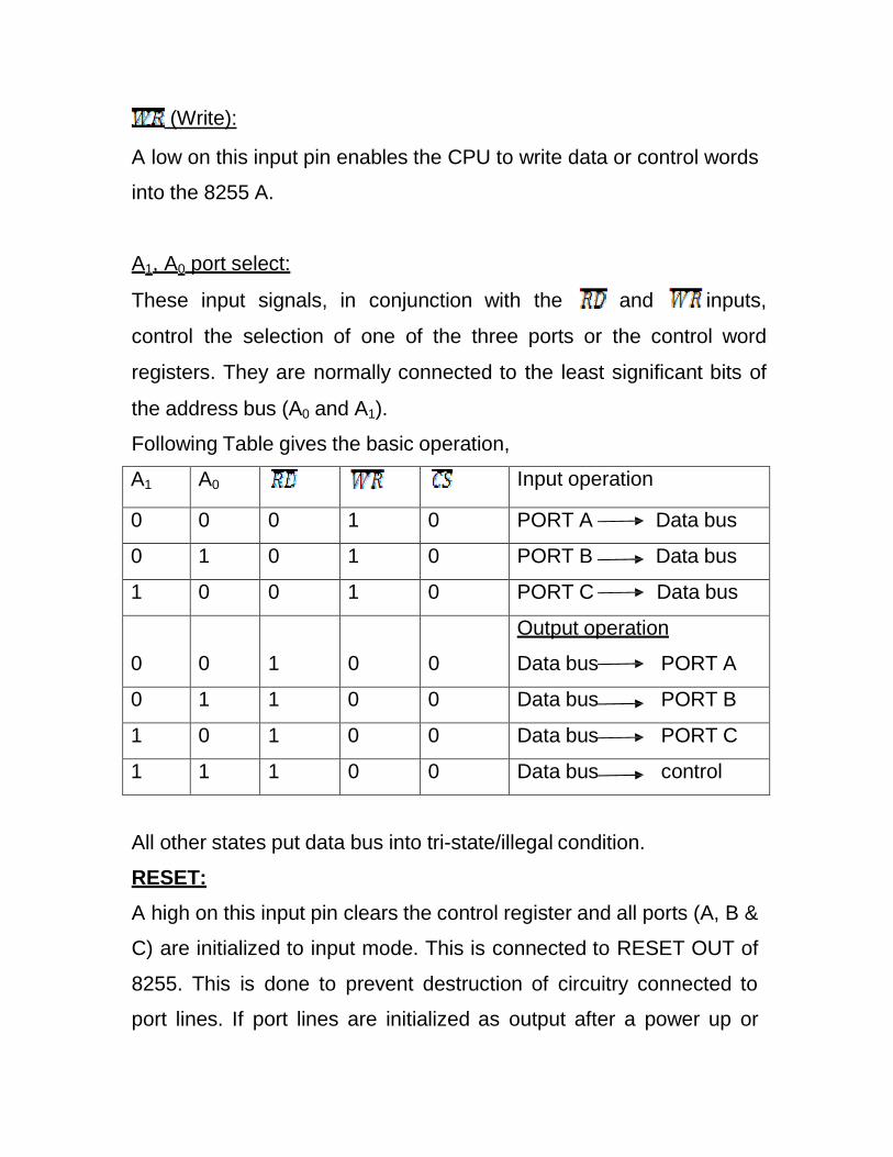
A1, A0 port select:
These input signals, in conjunction with the and inputs,
control the selection of one of the three ports or the control word
registers. They are normally connected to the least significant bits of
the address bus (A0 and A1).
Following Table gives the basic operation,
A1 A0
Input operation
0 0 0 1 0 PORT A Data bus
0 1 0 1 0 PORT B Data bus
1 0 0 1 0 PORT C Data bus
0
0
1
0
0
Output operation
Data bus PORT A
0 1 1 0 0 Data bus PORT B
1 0 1 0 0 Data bus PORT C
1 1 1 0 0 Data bus control
All other states put data bus into tri-state/illegal condition.
RESET:
A high on this input pin clears the control register and all ports (A, B &
C) are initialized to input mode. This is connected to RESET OUT of
8255. This is done to prevent destruction of circuitry connected to
port lines. If port lines are initialized as output after a power up or
reset, the port might try to output into the output of a device
connected to same inputs might destroy one or both of them.
PORTs A, B and C:
The 8255A contains three 8-bit ports (A, B and C). All can be
configured in a variety of functional characteristic by the system
software.
PORTA:
One 8-bit data output latch/buffer and one 8-bit data input latch.
PORT B:
One 8-bit data output latch/buffer and one 8-bit data input buffer.
PORT C:
One 8-bit data output latch/buffer and one 8-bit data input buffer (no
latch for input). This port can be divided into two 4-bit ports under the
mode control. Each 4-bit port contains a 4-bit latch and it can be used
for the control signal outputs and status signals inputs in conjunction
with ports A and B.
Group A & Group B control:
The functional configuration of each port is programmed by the
system software. The control words outputted by the CPU configure
the associated ports of the each of the two groups. Each control block
accepts command from Read/Write content logic receives control
words from the internal data bus and issues proper commands to its
associated ports.
Control Group A – Port A & Port C upper
Control Group B – Port B & Port C lower
The control word register can only be written into No read operation if
the control word register is allowed.
Operation Description:
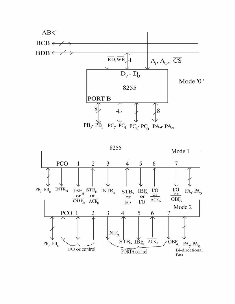
Mode selection:
There are three basic modes of operation that can be selected by the
system software.
Mode 0: Basic Input/output
Mode 1: Strobes Input/output
Mode 2: Bi-direction bus.
When the reset input goes HIGH all poets are set to mode’0’ as input
which means all 24 lines are in high impedance state and can be
used as normal input. After the reset is removed the 8255A remains
in the input mode with no additional initialization. During the execution
of the program any of the other modes may be selected using a
single output instruction.
The modes for PORT A & PORT B can be separately defined, while
PORT C is divided into two portions as required by the PORT A and
PORT B definitions. The ports are thus divided into two groups Group
A & Group B. All the output register, including the status flip-flop will
be reset whenever the mode is changed. Modes of the two group
may be combined for any desired I/O operation e.g. Group A in mode
‘1’ and group B in mode ‘0’.
The basic mode definitions with bus interface and the mode definition
format are given in fig (a) & (b),
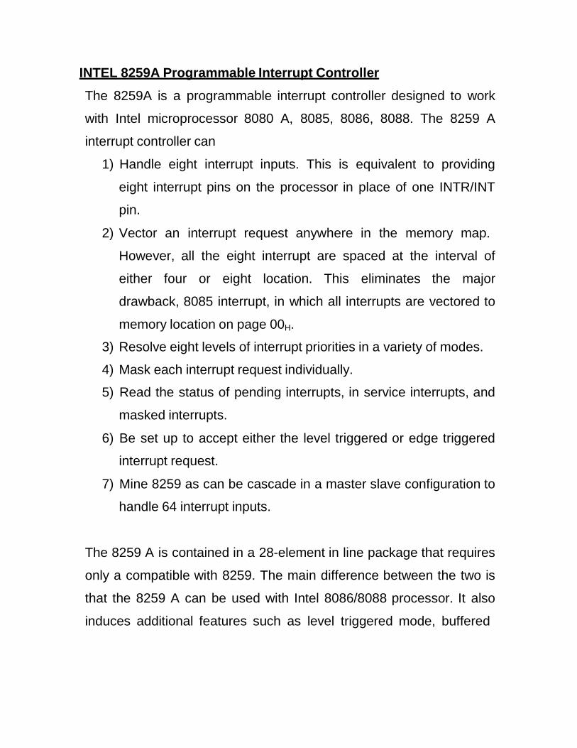
INTEL 8259A Programmable Interrupt Controller
The 8259A is a programmable interrupt controller designed to work
with Intel microprocessor 8080 A, 8085, 8086, 8088. The 8259 A
interrupt controller can
1) Handle eight interrupt inputs. This is equivalent to providing
eight interrupt pins on the processor in place of one INTR/INT
pin.
2) Vector an interrupt request anywhere in the memory map.
However, all the eight interrupt are spaced at the interval of
either four or eight location. This eliminates the major
drawback, 8085 interrupt, in which all interrupts are vectored to
memory location on page 00H.
3) Resolve eight levels of interrupt priorities in a variety of modes.
4) Mask each interrupt request individually.
5) Read the status of pending interrupts, in service interrupts, and
masked interrupts.
6) Be set up to accept either the level triggered or edge triggered
interrupt request.
7) Mine 8259 as can be cascade in a master slave configuration to
handle 64 interrupt inputs.
The 8259 A is contained in a 28-element in line package that requires
only a compatible with 8259. The main difference between the two is
that the 8259 A can be used with Intel 8086/8088 processor. It also
induces additional features such as level triggered mode, buffered
mode and automatic end of interrupt mode. The pin diagram and
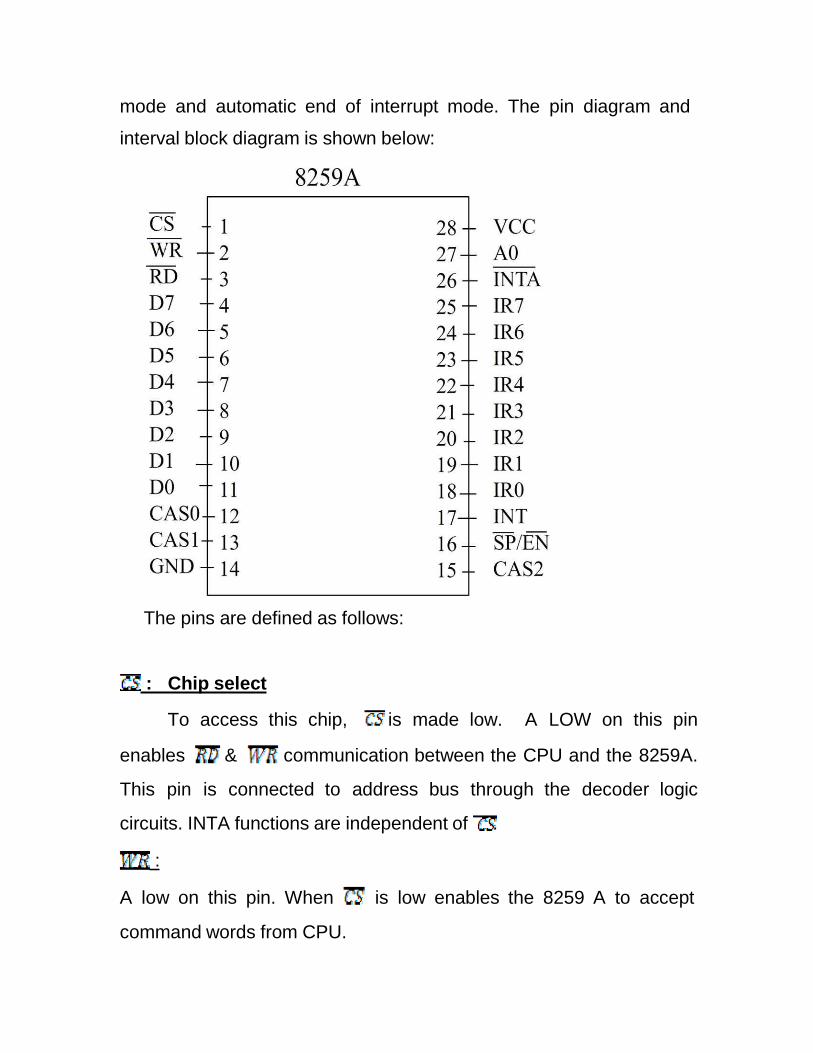
interval block diagram is shown below:
The pins are defined as follows:
: Chip select
To access this chip, is made low. A LOW on this pin
enables & communication between the CPU and the 8259A.
This pin is connected to address bus through the decoder logic
circuits. INTA functions are independent of .
:
A low on this pin. When is low enables the 8259 A to accept
command words from CPU.
:
A low on this pin when is low enables these 8259 A to release
status on to the data bus for the CPU. The status in dudes the
contents of IMR, ISR or TRR register or a priority level.
D7-D0:
Bidirectional data bus control status and interrupt in a this bus. This
bus is connected to BDB of 8085.
CAS0-CAS2:
Cascade lines: The CAS lines form a private 8259A bus to control a
multiple 8259A structure ie to identify a particular slave device. These
pins are outputs of a master 8259A and inputs for a slave 8259A.
/ : Salve program/enable buffer:
This is a dual function pin. It is used as an input to determine whether
the 8259A is to a master ( / = 1) or as a slave ( / = 0). It is
also used as an output to disable the data bus transceivers when
data are being transferred from the 8259A to the CPU. When in
buffered mode, it can be used as an output and when not in the
buffered mode it is used as an input.
INT:
This pin goes high whenever a valid interrupt request is asserted. It is
used to interrupt the CPU, thus it is connected to the CPU’s interrupt
pin (INTR).
:
Interrupt: Acknowledge. This pin is used to enable 8259A interrupt
vector data on the data bus by a sequence of interrupt request pulses
issued by the CPU.
IR0-IR7:
Interrupt Requests: Asynchronous interrupt inputs. An interrupt
request is executed by raising an IR input (low to high), and holding it
high until it is acknowledged. (Edge triggered mode).or just by a high
level on an IR input (levels triggered mode).
A0:
A0 address line: This pin acts in conjunction with the , &
pins. It is used by the 8259A to send various command words
from the CPU and to read the status. If is connected to the
CPU A0 address line. Two addresses must be reserved in the I/O
address space for each 8259 in the system.
Functional Description:
The 8259 A has eight interrupt request inputs, TR2 IR0. The 8259 A
uses its INT output to interrupt the 8085A via INTR pin. The 8259A
receives interrupt acknowledge pulses from the at its input.
Vector address used by the 8085 A to transfer control to the service
subroutine of the interrupting device, is provided by the 8259 A on the
data bus. The 8259A is a programmable device that must be
initialized by command words sent by the. After initialization the 8259
A mode of operation can be changed by operation command words
from the.
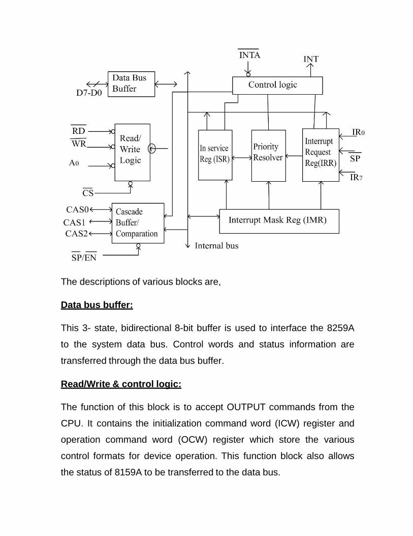
The descriptions of various blocks are,
Data bus buffer:
This 3- state, bidirectional 8-bit buffer is used to interface the 8259A
to the system data bus. Control words and status information are
transferred through the data bus buffer.
Read/Write & control logic:
The function of this block is to accept OUTPUT commands from the
CPU. It contains the initialization command word (ICW) register and
operation command word (OCW) register which store the various
control formats for device operation. This function block also allows
the status of 8159A to be transferred to the data bus.
Interrupt request register (IRR):
IRR stores all the interrupt inputs that are requesting service.
Basically, it keeps track of which interrupt inputs are asking for
service. If an interrupt input is unmasked, and has an interrupt signal
on it, then the corresponding bit in the IRR will be set.
Interrupt mask register (IMR):
The IMR is used to disable (Mask) or enable (Unmask) individual
interrupt inputs. Each bit in this register corresponds to the interrupt
input with the same number. The IMR operation on the IRR. Masking
of higher priority input will not affect the interrupt request lines of
lower priority. To unmask any interrupt the corresponding bit is set ‘0’.
In service register (ISR):
The in service registers keeps tracks of which interrupt inputs are
currently being serviced. For each input that is currently being
serviced the corresponding bit will be set in the in service register.
Each of these 3-reg can be read as status reg.
Priority Resolver:
This logic block determines the priorities of the set in the IRR. The
highest priority is selected and strobed into the corresponding bit of
the ISR during pulse.
Cascade buffer/comparator:
This function blocks stores and compare the IDS of all 8259A’s in the
reg. The associated 3-I/O pins (CAS0-CAS2) are outputs when
8259A is used a master. Master and are inputs when 8259A is used as
a slave. As a master, the 8259A sends the ID of the interrupting slave
device onto the cas2-cas0. The slave thus selected will send its pre-
programmed subroutine address on to the data bus during the next
one or two successive pulses.
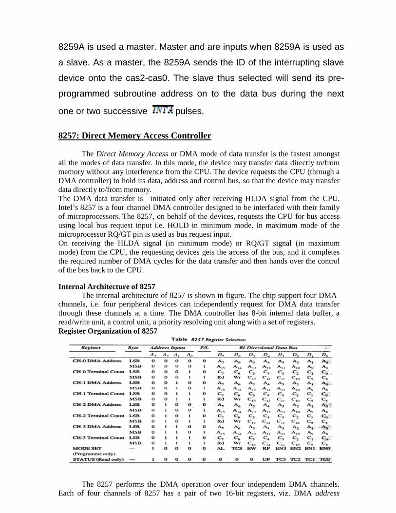
8257: Direct Memory Access Controller
The Direct Memory Access or DMA mode of data transfer is the fastest amongst
all the modes of data transfer. In this mode, the device may transfer data directly to/from
memory without any interference from the CPU. The device requests the CPU (through a
DMA controller) to hold its data, address and control bus, so that the device may transfer
data directly to/from memory.
The DMA data transfer is initiated only after receiving HLDA signal from the CPU.
Intel’s 8257 is a four channel DMA controller designed to be interfaced with their family
of microprocessors. The 8257, on behalf of the devices, requests the CPU for bus access
using local bus request input i.e. HOLD in minimum mode. In maximum mode of the
microprocessor RQ/GT pin is used as bus request input.
On receiving the HLDA signal (in minimum mode) or RQ/GT signal (in maximum
mode) from the CPU, the requesting devices gets the access of the bus, and it completes
the required number of DMA cycles for the data transfer and then hands over the control
of the bus back to the CPU.
Internal Architecture of 8257 The internal architecture of 8257 is shown in figure. The chip support four DMA
channels, i.e. four peripheral devices can independently request for DMA data transfer
through these channels at a time. The DMA controller has 8-bit internal data buffer, a
read/write unit, a control unit, a priority resolving unit along with a set of registers. Register Organization of 8257
The 8257 performs the DMA operation over four independent DMA channels.
Each of four channels of 8257 has a pair of two 16-bit registers, viz. DMA address
register and terminal count register.
There are two common registers for all the channels, namely, mode set register and status
register. Thus there are a total of ten registers. The CPU selects one of these ten registers
using address lines Ao-A3. Table shows how the Ao-A3 bits may be used for selecting
one of these registers.
DMA Address Register
Each DMA channel has one DMA address register. The function of this register is to store the address of the starting memory location, which will be accessed by the DMA
channel. Thus the starting address of the memory block which will be accessed by the
device is first loaded in the DMA address register of the channel.
The device that wants to transfer data over a DMA channel, will access the block of the
memory with the starting address stored in the DMA Address Register.
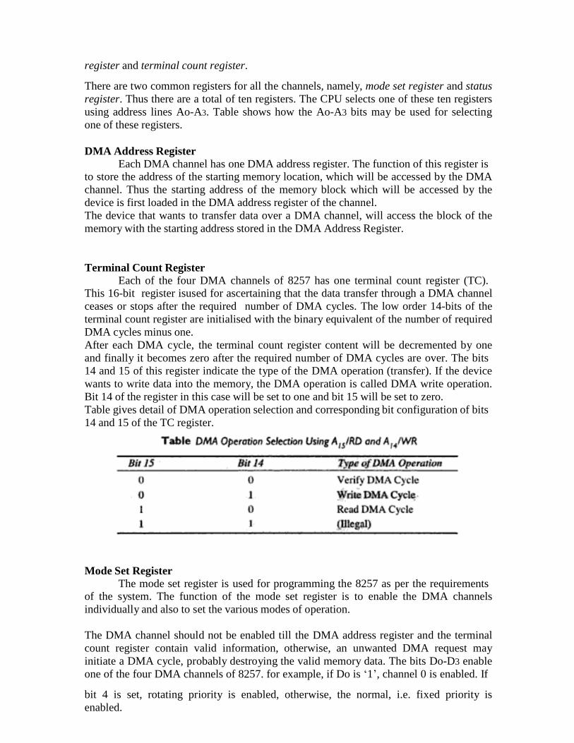
Terminal Count Register Each of the four DMA channels of 8257 has one terminal count register (TC).
This 16-bit register isused for ascertaining that the data transfer through a DMA channel
ceases or stops after the required number of DMA cycles. The low order 14-bits of the
terminal count register are initialised with the binary equivalent of the number of required
DMA cycles minus one.
After each DMA cycle, the terminal count register content will be decremented by one
and finally it becomes zero after the required number of DMA cycles are over. The bits
14 and 15 of this register indicate the type of the DMA operation (transfer). If the device
wants to write data into the memory, the DMA operation is called DMA write operation.
Bit 14 of the register in this case will be set to one and bit 15 will be set to zero.
Table gives detail of DMA operation selection and corresponding bit configuration of bits
14 and 15 of the TC register.
Mode Set Register The mode set register is used for programming the 8257 as per the requirements
of the system. The function of the mode set register is to enable the DMA channels
individually and also to set the various modes of operation.
The DMA channel should not be enabled till the DMA address register and the terminal
count register contain valid information, otherwise, an unwanted DMA request may
initiate a DMA cycle, probably destroying the valid memory data. The bits Do-D3 enable
one of the four DMA channels of 8257. for example, if Do is ‘1’, channel 0 is enabled. If
bit 4 is set, rotating priority is enabled, otherwise, the normal, i.e. fixed priority is
enabled.
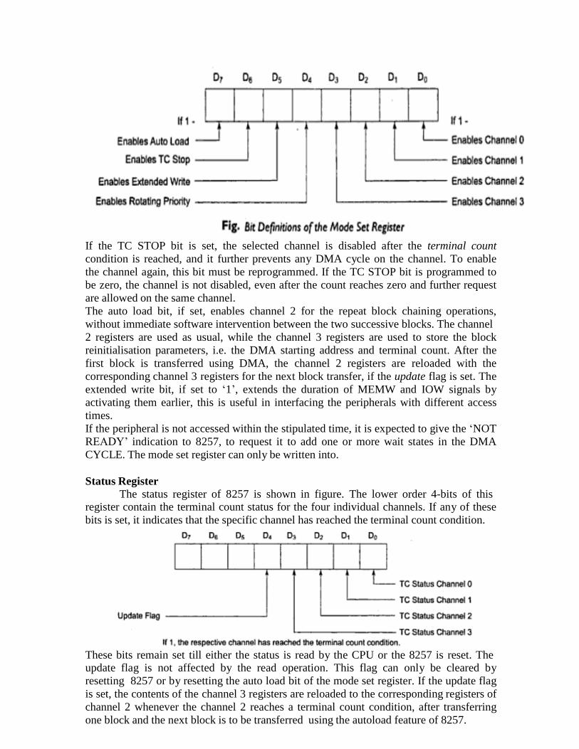
If the TC STOP bit is set, the selected channel is disabled after the terminal count
condition is reached, and it further prevents any DMA cycle on the channel. To enable
the channel again, this bit must be reprogrammed. If the TC STOP bit is programmed to
be zero, the channel is not disabled, even after the count reaches zero and further request
are allowed on the same channel.
The auto load bit, if set, enables channel 2 for the repeat block chaining operations,
without immediate software intervention between the two successive blocks. The channel
2 registers are used as usual, while the channel 3 registers are used to store the block
reinitialisation parameters, i.e. the DMA starting address and terminal count. After the
first block is transferred using DMA, the channel 2 registers are reloaded with the
corresponding channel 3 registers for the next block transfer, if the update flag is set. The
extended write bit, if set to ‘1’, extends the duration of MEMW and IOW signals by
activating them earlier, this is useful in interfacing the peripherals with different access
times.
If the peripheral is not accessed within the stipulated time, it is expected to give the ‘NOT
READY’ indication to 8257, to request it to add one or more wait states in the DMA
CYCLE. The mode set register can only be written into.
Status Register
The status register of 8257 is shown in figure. The lower order 4-bits of this register contain the terminal count status for the four individual channels. If any of these
bits is set, it indicates that the specific channel has reached the terminal count condition.
These bits remain set till either the status is read by the CPU or the 8257 is reset. The update flag is not affected by the read operation. This flag can only be cleared by
resetting 8257 or by resetting the auto load bit of the mode set register. If the update flag
is set, the contents of the channel 3 registers are reloaded to the corresponding registers of
channel 2 whenever the channel 2 reaches a terminal count condition, after transferring
one block and the next block is to be transferred using the autoload feature of 8257.
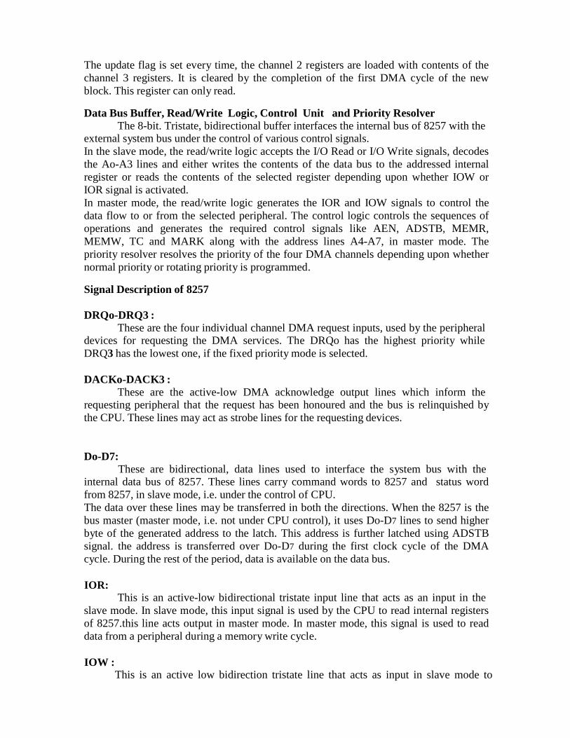
The update flag is set every time, the channel 2 registers are loaded with contents of the
channel 3 registers. It is cleared by the completion of the first DMA cycle of the new
block. This register can only read.
Data Bus Buffer, Read/Write Logic, Control Unit and Priority Resolver The 8-bit. Tristate, bidirectional buffer interfaces the internal bus of 8257 with the
external system bus under the control of various control signals.
In the slave mode, the read/write logic accepts the I/O Read or I/O Write signals, decodes
the Ao-A3 lines and either writes the contents of the data bus to the addressed internal
register or reads the contents of the selected register depending upon whether IOW or
IOR signal is activated.
In master mode, the read/write logic generates the IOR and IOW signals to control the
data flow to or from the selected peripheral. The control logic controls the sequences of
operations and generates the required control signals like AEN, ADSTB, MEMR,
MEMW, TC and MARK along with the address lines A4-A7, in master mode. The
priority resolver resolves the priority of the four DMA channels depending upon whether
normal priority or rotating priority is programmed.
Signal Description of 8257
DRQo-DRQ3 : These are the four individual channel DMA request inputs, used by the peripheral
devices for requesting the DMA services. The DRQo has the highest priority while
DRQ3 has the lowest one, if the fixed priority mode is selected.
DACKo-DACK3 :
These are the active-low DMA acknowledge output lines which inform the requesting peripheral that the request has been honoured and the bus is relinquished by
the CPU. These lines may act as strobe lines for the requesting devices.
Do-D7: These are bidirectional, data lines used to interface the system bus with the
internal data bus of 8257. These lines carry command words to 8257 and status word
from 8257, in slave mode, i.e. under the control of CPU.
The data over these lines may be transferred in both the directions. When the 8257 is the
bus master (master mode, i.e. not under CPU control), it uses Do-D7 lines to send higher
byte of the generated address to the latch. This address is further latched using ADSTB
signal. the address is transferred over Do-D7 during the first clock cycle of the DMA
cycle. During the rest of the period, data is available on the data bus.
IOR: This is an active-low bidirectional tristate input line that acts as an input in the
slave mode. In slave mode, this input signal is used by the CPU to read internal registers
of 8257.this line acts output in master mode. In master mode, this signal is used to read
data from a peripheral during a memory write cycle.
IOW : This is an active low bidirection tristate line that acts as input in slave mode to
load the contents of the data bus to the 8-bit mode register or upper/lower byte of a 16-bit
DMA address register or terminal count register. In the master mode, it is a control output
that loads the data to a peripheral during DMA memory read cycle (write to peripheral).
CLK: This is a clock frequency input required to derive basic system timings for the
internal operation of 8257.
RESET :
This active-high asynchronous input disables all the DMA channels by clearing the mode register and tristates all the control lines.
Ao-A3:
These are the four least significant address lines. In slave mode, they act as input which select one of the registers to be read or written. In the master mode, they are the
four least significant memory address output lines generated by 8257.
CS: This is an active-low chip select line that enables the read/write operations
from/to 8257, in slave mode. In the master mode, it is automatically disabled to prevent
the chip from getting selected (by CPU) while performing the DMA operation.
A4-A7 :
This is the higher nibble of the lower byte address generated by 8257 during the master mode of DMA operation.
READY:
This is an active-high asynchronous input used to stretch memory read and write cycles of 8257 by inserting wait states. This is used while interfacing slower peripherals..
HRQ: The hold request output requests the access of the system bus. In the non-
cascaded 8257 systems, this is connected with HOLD pin of CPU. In the cascade mode,
this pin of a slave is connected with a DRQ input line of the master 8257, while that of
the master is connected with HOLD input of the CPU.
HLDA :
The CPU drives this input to the DMA controller high, while granting the bus to the device. This pin is connected to the HLDA output of the CPU. This input, if high,
indicates to the DMA controller that the bus has been granted to the requesting peripheral
by the CPU.
MEMR:
This active –low memory read output is used to read data from the addressed memory locations during DMA read cycles.
MEMW :
This active-low three state output is used to write data to the addressed memory
location during DMA write operation.
ADST :
This output from 8257 strobes the higher byte of the memory address generated by the DMA controller into the latches.
AEN: This output is used to disable the system data bus and the control the bus driven
by the CPU, this may be used to disable the system address and data bus by using the
enable input of the bus drivers to inhibit the non-DMA devices from responding during
DMA operations. If the 8257 is I/O mapped, this should be used to disable the other I/O
devices, when the DMA controller addresses is on the address bus.
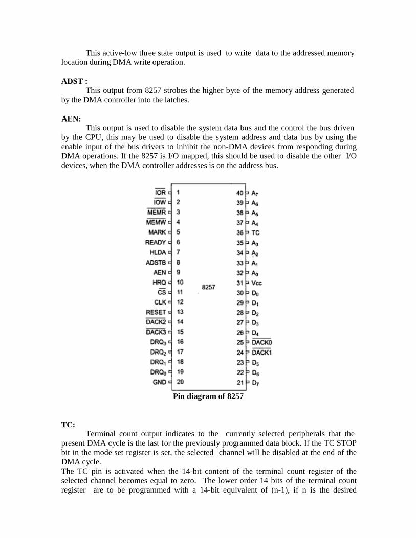
Pin diagram of 8257
TC: Terminal count output indicates to the currently selected peripherals that the
present DMA cycle is the last for the previously programmed data block. If the TC STOP
bit in the mode set register is set, the selected channel will be disabled at the end of the
DMA cycle.
The TC pin is activated when the 14-bit content of the terminal count register of the
selected channel becomes equal to zero. The lower order 14 bits of the terminal count
register are to be programmed with a 14-bit equivalent of (n-1), if n is the desired

number of DMA cycles.
MARK :
The modulo 128 mark output indicates to the selected peripheral that the current
DMA cycle is the 128th
cycle since the previous MARK output. The mark will be activated after each 128 cycles or integral multiples of it from the beginning if the data block (the first DMA cycle), if the total number of the required DMA cycles (n) is completely divisible by 128.
Vcc : This is a +5v supply pin required for operation of the circuit.
GND : This is a return line for the supply (ground pin of the IC).
Interfacing 8257 with 8086 Once a DMA controller is initialised by a CPU property, it is ready to take control of the system bus on a DMA request, either from a peripheral or itself (in case of memory-to-
memory transfer). The DMA controller sends a HOLD request to the CPU and waits for
the CPU to assert the HLDA signal. The CPU relinquishes the control of the bus before
asserting the HLDA signal.
A conceptual implementation of the system is shown in Figure
UNIT-1 INTRODUCTION TO 8086 ECE DEPARTMENT
MICROPROCESSORS AND MICROCONTROLLERS Page 4
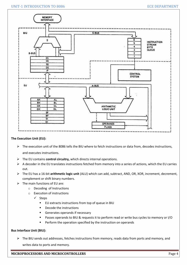
The Execution Unit (EU):
The execution unit of the 8086 tells the BIU where to fetch instructions or data from, decodes instructions,
and executes instructions.
The EU contains control circuitry, which directs internal operations.
A decoder in the EU translates instructions fetched from memory into a series of actions, which the EU carries
out.
The EU has a 16-bit arithmetic logic unit (ALU) which can add, subtract, AND, OR, XOR, increment, decrement,
complement or shift binary numbers.
The main functions of EU are:
o Decoding of Instructions
o Execution of instructions
Steps
EU extracts instructions from top of queue in BIU
Decode the instructions
Generates operands if necessary
Passes operands to BIU & requests it to perform read or write bus cycles to memory or I/O
Perform the operation specified by the instruction on operands
Bus Interface Unit (BIU):
The BIU sends out addresses, fetches instructions from memory, reads data from ports and memory, and
writes data to ports and memory.
UNIT-1 INTRODUCTION TO 8086 ECE DEPARTMENT
MICROPROCESSORS AND MICROCONTROLLERS Page 5
In simple words, the BIU handles all transfers of data and addresses on the buses for the execution unit.
8086 HAS PIPELINING ARCHITECTURE:
While the EU is decoding an instruction or executing an instruction, which does not require use of the buses,
the BIU fetches up to six instruction bytes for the following instructions.
The BIU stores these pre-fetched bytes in a first-in-first-out register set called a queue.
When the EU is ready for its next instruction from the queue in the BIU. This is much faster than sending out
an address to the system memory and waiting for memory to send back the next instruction byte or bytes.
Except in the case of JMP and CALL instructions, where the queue must be dumped and then reloaded starting
from a new address, this pre-fetch and queue scheme greatly speeds up processing.
Fetching the next instruction while the current instruction executes is called pipelining.
Register organization:
8086 has a powerful set of registers known as general purpose registers and special purpose registers.
All of them are 16-bit registers.
General purpose registers:
o These registers can be used as either 8-bit registers or 16-bit registers.
o They may be either used for holding data, variables and intermediate results temporarily or for other
purposes like a counter or for storing offset address for some particular addressing modes etc.
Special purpose registers:
o These registers are used as segment registers, pointers, index registers or as offset storage registers
for particular addressing modes.
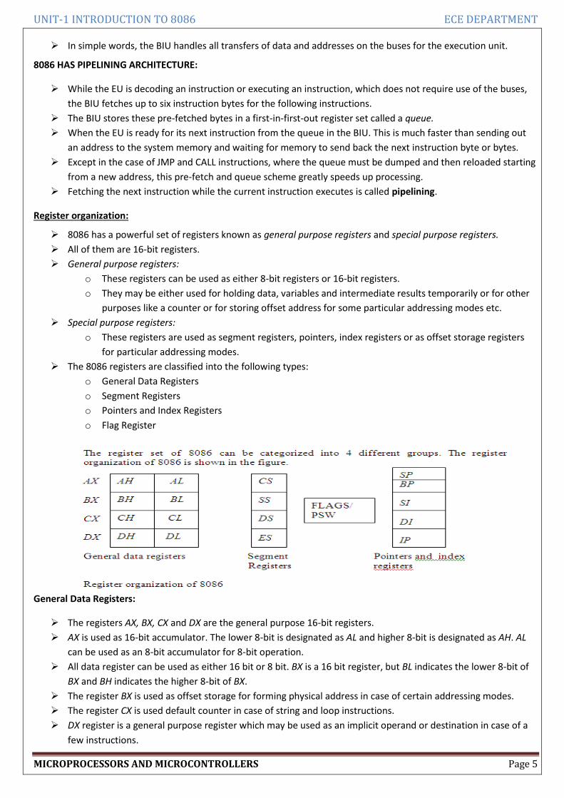
The 8086 registers are classified into the following types:
o General Data Registers
o Segment Registers
o Pointers and Index Registers
o Flag Register
General Data Registers:
The registers AX, BX, CX and DX are the general purpose 16-bit registers.
AX is used as 16-bit accumulator. The lower 8-bit is designated as AL and higher 8-bit is designated as AH. AL
can be used as an 8-bit accumulator for 8-bit operation.
All data register can be used as either 16 bit or 8 bit. BX is a 16 bit register, but BL indicates the lower 8-bit of
BX and BH indicates the higher 8-bit of BX.
The register BX is used as offset storage for forming physical address in case of certain addressing modes.
The register CX is used default counter in case of string and loop instructions.
DX register is a general purpose register which may be used as an implicit operand or destination in case of a
few instructions.
UNIT-1 INTRODUCTION TO 8086 ECE DEPARTMENT
MICROPROCESSORS AND MICROCONTROLLERS Page 6
Segment Registers:
There are 4 segment registers. They are:
o Code Segment Register(CS)
o Data Segment Register(DS)
o Extra Segment Register(ES)
o Stack Segment Register(SS)
The 8086 architecture uses the concept of segmented memory. 8086 able to address a memory capacity of 1 megabyte and it is byte organized. This 1 megabyte memory is divided into 16 logical segments. Each segment contains 64 kbytes of memory.
Code segment register (CS): is used for addressing memory location in the code segment of the memory, where the executable program is stored.
Data segment register (DS): points to the data segment of the memory where the data is stored. Extra Segment Register (ES) : also refers to a segment in the memory which is another data segment in the
memory. Stack Segment Register (SS): is used for addressing stack segment of the memory. The stack segment is that
segment of memory which is used to store stack data. While addressing any location in the memory bank, the physical address is calculated from two parts:
Physical address= segment address + offset address
The first is segment address, the segment registers contain 16-bit segment base addresses, related to different
segment.
The second part is the offset value in that segment.
Pointers and Index Registers:
The index and pointer registers are given below:
o IP—Instruction pointer-store memory location of next instruction to be executed
o BP—Base pointer
o SP—Stack pointer
o SI—Source index
o DI—Destination index
The pointers registers contain offset within the particular segments.
o The pointer register IP contains offset within the code segment.
o The pointer register BP contains offset within the data segment.
o Thee pointer register SP contains offset within the stack segment.
The index registers are used as general purpose registers as well as for offset storage in case of indexed, base
indexed and relative base indexed addressing modes.
The register SI is used to store the offset of source data in data segment.
The register DI is used to store the offset of destination in data or extra segment.
The index registers are particularly useful for string manipulation.
8086 flag register and its functions:
The 8086 flag register contents indicate the results of computation in the ALU. It also contains some flag bits
to control the CPU operations.
A 16 bit flag register is used in 8086. It is divided into two parts .
o Condition code or status flags
o Machine control flags
The condition code flag register is the lower byte of the 16-bit flag register. The condition code flag register is
identical to 8085 flag register, with an additional overflow flag.
UNIT-1 INTRODUCTION TO 8086 ECE DEPARTMENT
MICROPROCESSORS AND MICROCONTROLLERS Page 7
The control flag register is the higher byte of the flag register. It contains three flags namely direction flag (D),
interrupt flag (I) and trap flag (T).
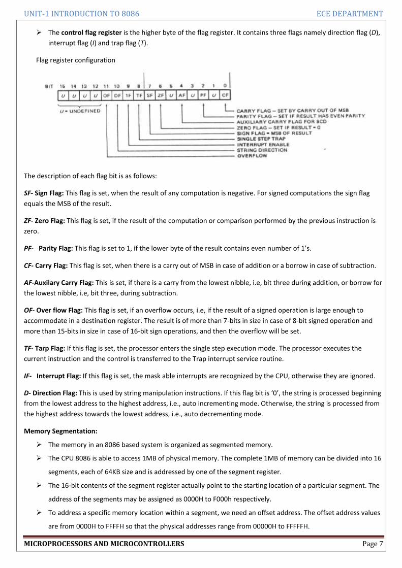
Flag register configuration
The description of each flag bit is as follows:
SF- Sign Flag: This flag is set, when the result of any computation is negative. For signed computations the sign flag
equals the MSB of the result.
ZF- Zero Flag: This flag is set, if the result of the computation or comparison performed by the previous instruction is
zero.
PF- Parity Flag: This flag is set to 1, if the lower byte of the result contains even number of 1’s.
CF- Carry Flag: This flag is set, when there is a carry out of MSB in case of addition or a borrow in case of subtraction.
AF-Auxilary Carry Flag: This is set, if there is a carry from the lowest nibble, i.e, bit three during addition, or borrow for
the lowest nibble, i.e, bit three, during subtraction.
OF- Over flow Flag: This flag is set, if an overflow occurs, i.e, if the result of a signed operation is large enough to
accommodate in a destination register. The result is of more than 7-bits in size in case of 8-bit signed operation and
more than 15-bits in size in case of 16-bit sign operations, and then the overflow will be set.
TF- Tarp Flag: If this flag is set, the processor enters the single step execution mode. The processor executes the
current instruction and the control is transferred to the Trap interrupt service routine.
IF- Interrupt Flag: If this flag is set, the mask able interrupts are recognized by the CPU, otherwise they are ignored.
D- Direction Flag: This is used by string manipulation instructions. If this flag bit is ‘0’, the string is processed beginning
from the lowest address to the highest address, i.e., auto incrementing mode. Otherwise, the string is processed from
the highest address towards the lowest address, i.e., auto decrementing mode.
Memory Segmentation:
The memory in an 8086 based system is organized as segmented memory.
The CPU 8086 is able to access 1MB of physical memory. The complete 1MB of memory can be divided into 16
segments, each of 64KB size and is addressed by one of the segment register.
The 16-bit contents of the segment register actually point to the starting location of a particular segment. The
address of the segments may be assigned as 0000H to F000h respectively.
To address a specific memory location within a segment, we need an offset address. The offset address values
are from 0000H to FFFFH so that the physical addresses range from 00000H to FFFFFH.
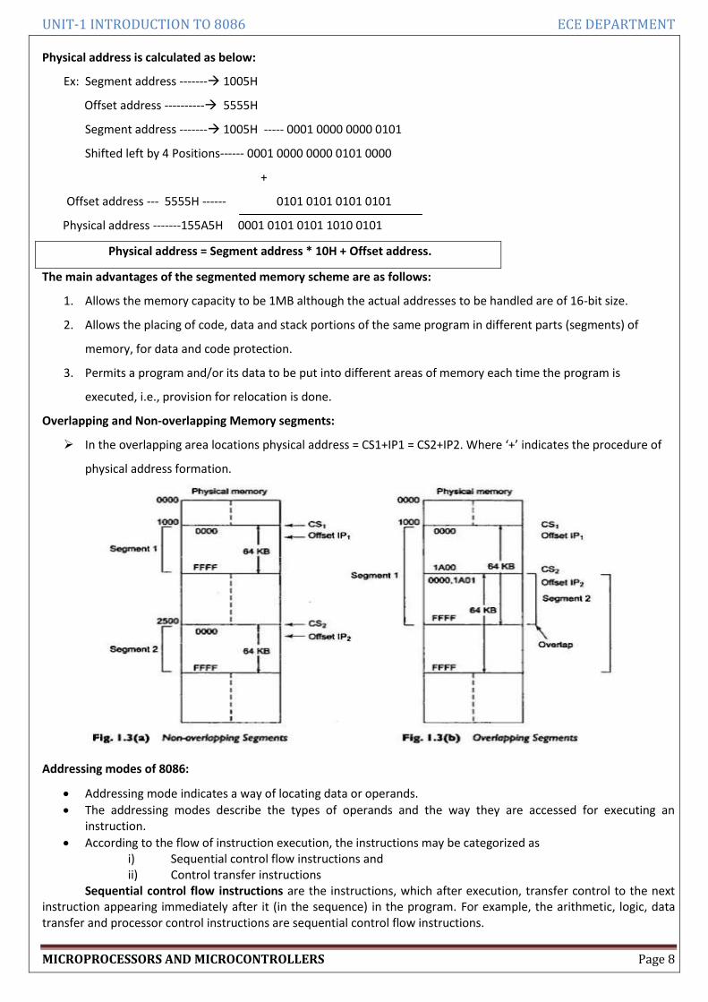
UNIT-1 INTRODUCTION TO 8086 ECE DEPARTMENT
MICROPROCESSORS AND MICROCONTROLLERS Page 8
Physical address is calculated as below:
Ex: Segment address ------- 1005H
Offset address ---------- 5555H
Segment address ------- 1005H ----- 0001 0000 0000 0101
Shifted left by 4 Positions------ 0001 0000 0000 0101 0000
+
Offset address --- 5555H ------ 0101 0101 0101 0101
Physical address -------155A5H 0001 0101 0101 1010 0101
Physical address = Segment address * 10H + Offset address.
The main advantages of the segmented memory scheme are as follows:
1. Allows the memory capacity to be 1MB although the actual addresses to be handled are of 16-bit size.
2. Allows the placing of code, data and stack portions of the same program in different parts (segments) of
memory, for data and code protection.
3. Permits a program and/or its data to be put into different areas of memory each time the program is
executed, i.e., provision for relocation is done.
Overlapping and Non-overlapping Memory segments:
In the overlapping area locations physical address = CS1+IP1 = CS2+IP2. Where ‘+’ indicates the procedure of
physical address formation.
Addressing modes of 8086:
Addressing mode indicates a way of locating data or operands.
The addressing modes describe the types of operands and the way they are accessed for executing an instruction.
According to the flow of instruction execution, the instructions may be categorized as i) Sequential control flow instructions and ii) Control transfer instructions
Sequential control flow instructions are the instructions, which after execution, transfer control to the next instruction appearing immediately after it (in the sequence) in the program. For example, the arithmetic, logic, data transfer and processor control instructions are sequential control flow instructions.
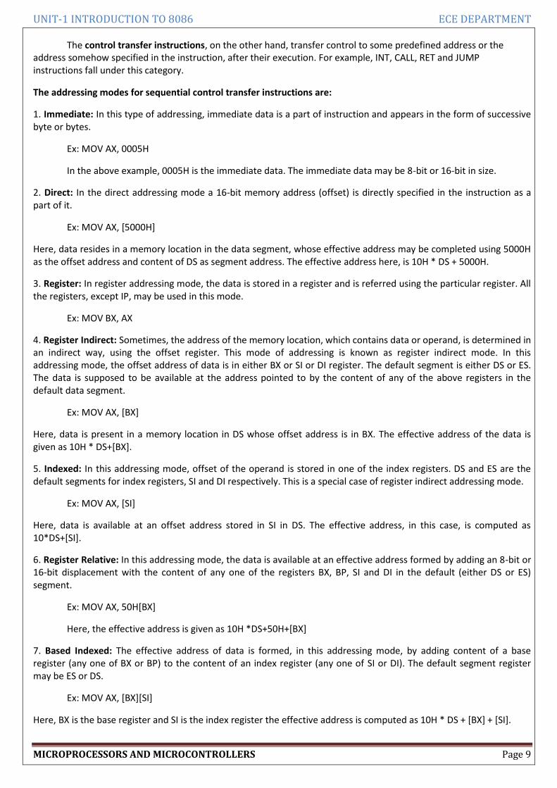
UNIT-1 INTRODUCTION TO 8086 ECE DEPARTMENT
MICROPROCESSORS AND MICROCONTROLLERS Page 9
The control transfer instructions, on the other hand, transfer control to some predefined address or the address somehow specified in the instruction, after their execution. For example, INT, CALL, RET and JUMP instructions fall under this category.
The addressing modes for sequential control transfer instructions are:
1. Immediate: In this type of addressing, immediate data is a part of instruction and appears in the form of successive byte or bytes.
Ex: MOV AX, 0005H
In the above example, 0005H is the immediate data. The immediate data may be 8-bit or 16-bit in size.
2. Direct: In the direct addressing mode a 16-bit memory address (offset) is directly specified in the instruction as a part of it.
Ex: MOV AX, [5000H]
Here, data resides in a memory location in the data segment, whose effective address may be completed using 5000H as the offset address and content of DS as segment address. The effective address here, is 10H * DS + 5000H.
3. Register: In register addressing mode, the data is stored in a register and is referred using the particular register. All the registers, except IP, may be used in this mode.
Ex: MOV BX, AX
4. Register Indirect: Sometimes, the address of the memory location, which contains data or operand, is determined in an indirect way, using the offset register. This mode of addressing is known as register indirect mode. In this addressing mode, the offset address of data is in either BX or SI or DI register. The default segment is either DS or ES. The data is supposed to be available at the address pointed to by the content of any of the above registers in the default data segment.
Ex: MOV AX, [BX]
Here, data is present in a memory location in DS whose offset address is in BX. The effective address of the data is given as 10H * DS+[BX].
5. Indexed: In this addressing mode, offset of the operand is stored in one of the index registers. DS and ES are the default segments for index registers, SI and DI respectively. This is a special case of register indirect addressing mode.
Ex: MOV AX, [SI]
Here, data is available at an offset address stored in SI in DS. The effective address, in this case, is computed as 10*DS+[SI].
6. Register Relative: In this addressing mode, the data is available at an effective address formed by adding an 8-bit or 16-bit displacement with the content of any one of the registers BX, BP, SI and DI in the default (either DS or ES) segment.
Ex: MOV AX, 50H[BX]
Here, the effective address is given as 10H *DS+50H+[BX]
7. Based Indexed: The effective address of data is formed, in this addressing mode, by adding content of a base register (any one of BX or BP) to the content of an index register (any one of SI or DI). The default segment register may be ES or DS.
Ex: MOV AX, [BX][SI]
Here, BX is the base register and SI is the index register the effective address is computed as 10H * DS + [BX] + [SI].
UNIT-1 INTRODUCTION TO 8086 ECE DEPARTMENT
MICROPROCESSORS AND MICROCONTROLLERS Page 10
8. Relative Based Indexed: The effective address is formed by adding an 8 or 16-bit displacement with the sum of the contents of any one of the base register (BX or BP) and any one of the index register, in a default segment.
Ex: MOV AX, 50H [BX] [SI]
Here, 50H is an immediate displacement, BX is base register and SI is an index register the effective address of data is computed as
10H * DS + [BX] + [SI] + 50H
For control transfer instructions, the addressing modes depend upon whether the destination is within the same segment or different one. It also depends upon the method of passing the destination address to the processor.
Basically, there are two addressing modes for the control transfer instructions, intersegment addressing and intrasegment addressing modes.
If the location to which the control is to be transferred lies in a different segment other than the current one, the mode is called intersegment mode.
If the destination location lies in the same segment, the mode is called intrasegment mode.
Intersegment direct
Intersegment
Modes for control Intersegment indirect
Transfer instructions Intrasegment direct
Intrasegment
Intrasegment indirect
Addressing modes for Control Transfer Instructions
9. Intrasegment Direct Mode: In this mode, the address to which the control is to be transferred lies in the same segment in which the control transfer instruction lies and appears directly in the instruction as an immediate displacement value. In this addressing mode, the displacement is computed relative to the content of the instruction pointer IP.
The effective address to which the control will be transferred is given by the sum of 8 or 16-bit displacement and current content of IP. In the case of jump instruction, if the signed displacement (d) is of 8-bits (i.e –128<d<+128) we term it as short jump and if it is of 16-bits (i.e-32, 768<d<+32,768) it is termed as long jump.
10. Intrasegment Indirect Mode: In this mode, the displacement to which the control is to be transferred, is in the same segment in which the control transfer instruction lies, but it is passed to the instruction indirectly. Here, the branch address is found as the content of a register or a memory location. This addressing mode may be used in unconditional branch instructions.
11. Intersegment Direct: In this mode, the address to which the control is to be transferred is in a different segment. This addressing mode provides a means of branching from one code segment to another code segment. Here, the CS and IP of the destination address are specified directly in the instruction.
12. Intersegment Indirect: In this mode, the address to which the control is to be transferred lies in a different segment and it is passed to the instruction indirectly, i.e contents of a memory block containing four bytes, i.e IP (LSB), IP(MSB), CS(LSB) and CS (MSB) sequentially. The starting address of the memory block may be referred using any of the addressing modes, except immediate mode.
UNIT-1 INTRODUCTION TO 8086 ECE DEPARTMENT
MICROPROCESSORS AND MICROCONTROLLERS Page 12
DS : [BX + SI]
10H*DS 10000
[BX] +2000
[SI] +3000
_______
15000H – Effective address
_______
v. Relative based index: MOV AX, 5000[BX][SI]
DS : [BX+SI+5000]
10H*DS 10000
[BX] +2000
[SI] +3000
+5000
___________
1A000H – Effective address
____________
Pin Diagram of 8086:
Signal description of 8086:
The 8086 is a 16-bit microprocessor. This microprocessor operates in single processor or multiprocessor
configurations to achieve high performance.
The pin configuration of 8086 is shown in the figure. Some of the pins serve a particular function in minimum
mode (single processor mode) and others function in maximum mode (multiprocessor mode).
The 8086 signals are categorized into 3 types:
1. Common signals for both minimum mode and maximum mode.
2. Special signals which are meant only for minimum mode
3. Special signals which are meant only for maximum mode
Common Signals for both Minimum mode and Maximum mode:
7 0AD AD : The address/ data bus lines are the multiplexed address data bus and contain the right most eight bit of
memory address or data. The address and data bits are separated by using ALE signal.
15 8AD AD : The address/data bus lines compose the upper multiplexed address/data bus. This lines contain address
bit 15 8A A or data bus 15 8D D . The address and data bits are separated by using ALE signal.
19 6 18 3/ /A S A S The address/status bus bits are multiplexed to provide address signals 19 16A A and also status bits
6 3S S . The address bits are separated from the status bits using the ALE signals. The status bit 6S is always a logic 0,
bit 5S indicates the condition of the interrupt flag bit. The 4S and 3S indicate which segment register is presently
being used for memory access.
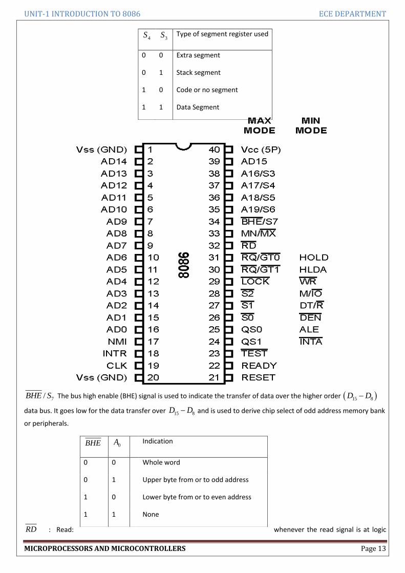
UNIT-1 INTRODUCTION TO 8086 ECE DEPARTMENT
MICROPROCESSORS AND MICROCONTROLLERS Page 13
7/BHE S The bus high enable (BHE) signal is used to indicate the transfer of data over the higher order 15 8D D
data bus. It goes low for the data transfer over 15 8D D and is used to derive chip select of odd address memory bank
or peripherals.
RD : Read: whenever the read signal is at logic
4S 3S
Type of segment register used
0 0 Extra segment
0 1 Stack segment
1 0 Code or no segment
1 1 Data Segment
BHE 0A
Indication
0 0 Whole word
0 1 Upper byte from or to odd address
1 0 Lower byte from or to even address
1 1 None
UNIT-1 INTRODUCTION TO 8086 ECE DEPARTMENT
MICROPROCESSORS AND MICROCONTROLLERS Page 14
0, the data bus receives the data from the memory or I/O devices connected to the system
READY: This is the acknowledgement from the slow devices or memory that they have completed the data transfer
operation. This signal is active high.
INTR: Interrupt Request: Interrupt request is used to request a hardware interrupt of INTR is held high when interrupt
enable flag is set, the 8086 enters an interrupt acknowledgement cycle after the current instruction has
completed its execution.
TEST : This input is tested by “WAIT” instruction. If the TEST input goes low; execution will continue. Else the
processor remains in an idle state.
NMI- Non-maskable Interrupt: The non-maskable interrupt input is similar to INTR except that the NMI interrupt does
not check for interrupt enable flag is at logic 1, i.e, NMI is not maskable internally by software. If NMI is
activated, the interrupt input uses interrupt vector 2.
RESET: The reset input causes the microprocessor to reset itself. When 8086 reset, it restarts the execution from
memory location FFFF0H. The reset signal is active high and must be active for at least four clock cycles.
CLK: Clock input: The clock input signal provides the basic timing input signal for processor and bus control operation.
It is asymmetric square wave with 33% duty cycle.
VCC (+5V): Power supply for the operation of the internal circuit
GND: Ground for the internal circuit
/MN MX : The minimum/maximum mode signal to select the mode of operation either in minimum or maximum
mode configuration. Logic 1 indicates minimum mode.
Minimum mode Signals: The following signals are for minimum mode operation of 8086.
/M IO - Memory/IO /M IO signal selects either memory operation or I/O operation. This line indicates that the
microprocessor address bus contains either a memory address or an I/O port address. Signal high at this pin
indicates a memory operation. This line is logically equivalent to 2S in maximum mode.
INTA - Interrupt acknowledge: The interrupt acknowledge signal is a response to the INTR input signal. The INTA
signal is normally used to gate the interrupt vector number onto the data bus in response to an interrupt
request.
ALE- Address Latch Enable: This output signal indicates the availability of valid address on the address/data bus, and is
connected to latch enable input of latches.
/DT R : Data transmit/Receive: This output signal is used to decide the direction of date flow through the bi-
directional buffer. / 1DT R Indicates transmitting and / 0DT R indicates receiving the data.
DEN Data Enable: Data bus enable signal indicates the availability of valid data over the address/data lines.
𝑊𝑅 Write: whenever the write signal is at logic 0, the data bus transmits the data to the memory or I/O devices
connected to the system.
HOLD: The hold input request a direct memory access (DMA). If the hold signal is at logic 1, the micro process stops its
normal execution and places its address, data and control bus at the high impedance state.
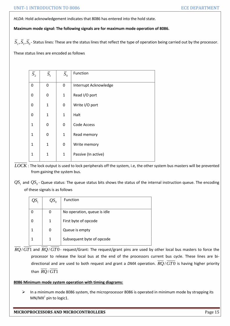
UNIT-1 INTRODUCTION TO 8086 ECE DEPARTMENT
MICROPROCESSORS AND MICROCONTROLLERS Page 15
HLDA: Hold acknowledgement indicates that 8086 has entered into the hold state.
Maximum mode signal: The following signals are for maximum mode operation of 8086.
2 1 0, ,S S S - Status lines: These are the status lines that reflect the type of operation being carried out by the processor.
These status lines are encoded as follows
2S 1S
0S Function
0 0 0 Interrupt Acknowledge
0 0 1 Read I/O port
0 1 0 Write I/O port
0 1 1 Halt
1 0 0 Code Access
1 0 1 Read memory
1 1 0 Write memory
1 1 1 Passive (In active)
LOCK : The lock output is used to lock peripherals off the system, i.e, the other system bus masters will be prevented
from gaining the system bus.
1QS and 0QS - Queue status: The queue status bits shows the status of the internal instruction queue. The encoding
of these signals is as follows
1QS 0QS Function
0 0 No operation, queue is idle
0 1 First byte of opcode
1 0 Queue is empty
1 1 Subsequent byte of opcode
/ 1RQ GT and / 0RQ GT - request/Grant: The request/grant pins are used by other local bus masters to force the
processor to release the local bus at the end of the processors current bus cycle. These lines are bi-
directional and are used to both request and grant a DMA operation. / 0RQ GT is having higher priority
than / 1RQ GT
8086 Minimum mode system operation with timing diagrams:
In a minimum mode 8086 system, the microprocessor 8086 is operated in minimum mode by strapping its
MN/MX| pin to logic1.