materials science 98
TRANSCRIPT

Springer Series in
materials science 98

Springer Series in
materials scienceEditors: R. Hull R. M. Osgood, Jr. J. Parisi H. Warlimont
The Springer Series in Materials Science covers the complete spectrum of materials physics,including fundamental principles, physical properties, materials theory and design. Recognizingthe increasing importance of materials science in future device technologies, the book titles in thisseries ref lect the state-of-the-art in understanding and controlling the structure and propertiesof all important classes of materials.
88 Introductionto Wave Scattering, Localizationand Mesoscopic PhenomenaBy P. Sheng
89 Magneto-ScienceMagnetic Field Effects on Materials:Fundamentals and ApplicationsEditors: M. Yamaguchi and Y. Tanimoto
90 Internal Friction in Metallic MaterialsA Reference BookBy M.S. Blanter, I.S. Golovin,H. Neuhauser, and H.-R. Sinning
91 Time-dependent Mechanical Propertiesof Solid BodiesBy W. Grafe
92 Solder Joint TechnologyMaterials, Properties, and ReliabilityBy K.-N. Tu
93 Materials for TomorrowTheory, Experiments and ModellingEditors: S. Gemming, M. Schreiberand J.-B. Suck
94 Magnetic NanostructuresEditors: B. Aktas, L. Tagirov,and F. Mikailov
95 Nanocrystalsand Their Mesoscopic OrganizationBy C.N.R. Rao, P.J. Thomasand G.U. Kulkarni
96 GaN ElectronicsBy R. Quay
97 Multifunctional Barriersfor Flexible StructureTextile, Leather and PaperEditors: S. Duquesne, C. Magniez,and G. Camino
98 Physics of Negative Refractionand Negative Index MaterialsOptical and Electronic Aspectsand Diversified ApproachesEditors: C.M. Krowne and Y. Zhang
99 Self-Organized Morphologyin Nanostructured MaterialsEditors: K. Al-Shamery and J. Parisi
100 Self Healing MaterialsAn Alternative Approachto 20 Centuries of Materials ScienceEditor: S. van der Zwaag
101 New Organic Nanostructuresfor Next Generation DevicesEditors: K. Al-Shamery, H.-G. Rubahn,and H. Sitter
102 Photonic Crystal FibersProperties and ApplicationsBy F. Poli, A. Cucinotta,and S. Selleri
103 Polarons in Advanced MaterialsEditor: A.S. Alexandrov
Volumes 40–87 are listed at the end of the book.

C.M. Krowne Y. Zhang (Eds.)
Physicsof Negative Refractionand Negative Index MaterialsOptical and Electronic Aspectsand Diversified Approaches
123
With 228 Figures

Dr. Clifford M. KrowneCode 6851, Microwave Technology BranchElectronics Science and Technology Division, Naval Research LaboratoryWashington, DC 20375-5347, USAE-mail: [email protected]
Dr. Yong ZhangMaterials Science Center, National Renewable Energy Laboratory (NREL)1617 Cole Blvd., Golden, CO 80401, USAE-mail: Yong [email protected]
Series Editors:
Professor Robert HullUniversity of VirginiaDept. of Materials Science and EngineeringThornton HallCharlottesville, VA 22903-2442, USA
Professor R. M. Osgood, Jr.Microelectronics Science LaboratoryDepartment of Electrical EngineeringColumbia UniversitySeeley W. Mudd BuildingNew York, NY 10027, USA
Professor Jürgen ParisiUniversitat Oldenburg, Fachbereich PhysikAbt. Energie- und HalbleiterforschungCarl-von-Ossietzky-Strasse 9–1126129 Oldenburg, Germany
Professor Hans WarlimontInstitut fur Festkorper-und Werkstofforschung,Helmholtzstrasse 2001069 Dresden, Germany
ISSN 0933-033X
ISBN 978-3-540-72131-4 Springer Berlin Heidelberg New York
Library of Congress Control Number: 2007925169
All rights reserved.No part of this book may be reproduced in any form, by photostat, microfilm, retrieval system, or any othermeans, without the written permission of Kodansha Ltd. (except in the case of brief quotation for criticism orreview.)This work is subject to copyright. All rights are reserved, whether the whole or part of the material isconcerned, specif ically the rights of translation, reprinting, reuse of illustrations, recitation, broadcasting,reproduction on microf ilm or in any other way, and storage in data banks. Duplication of this publication orparts thereof is permitted only under the provisions of the German Copyright Law of September 9, 1965, inits current version, and permission for use must always be obtained from Springer. Violations are liable toprosecution under the German Copyright Law.
Springer is a part of Springer Science+Business Media.
© Springer-Verlag Berlin Heidelberg 2007
The use of general descriptive names, registered names, trademarks, etc. in this publication does not imply,even in the absence of a specif ic statement, that such names are exempt from the relevant protective laws andregulations and therefore free for general use.
Typesetting: Data prepared by SPI Kolam using a Springer TEX macro packageCover: eStudio Calamar Steinen
Printed on acid-free paper SPIN: 11810377 57/3180/SPI 5 4 3 2 1 0
Preface
There are many potentially interesting phenomena that can be obtained withwave refraction in the “wrong” direction, what is commonly now referred toas negative refraction. All sorts of physically new operations and devices cometo mind, such as new beam controlling components, reflectionless interfaces,flat lenses, higher quality lens or “super lenses,” reversal of lenses action,new imaging components, redistribution of energy density in guided wavecomponents, to name only a few of the possibilities. Negative index materialsare generally, but not always associated with negative refracting materials,and have the added property of having the projection of the power flow orPoynting vector opposite to that of the propagation vector. This attributeenables the localized wave behavior on a subwavelength scale, not only insidelenses and in the near field outside of them, but also in principle in the far fieldof them, to have field reconstruction and localized enhancement, somethingnot readily found in ordinary matter, referred to as positive index materials.
Often investigators have had to create, even when using positive indexmaterials, interfaces based upon macroscopic or microscopic layers, or evenheterostructure layers of materials, to obtain the field behavior they are seek-ing. For obtaining negative indices of refraction, microscopic inclusions ina host matrix material have been used anywhere from the photonic crystalregime all the way into the metamaterial regime. These regimes take onefrom the wavelength size on the order of the separation between inclusions tothat where many inclusions are sampled by a wavelength of the electromag-netic field. Generally in photonic crystals and metamaterials, a Brillouin zonein reciprocal space exists due to the regular repetitive pattern of unit cellsof inclusions, where each unit cell contains an arrangement of inclusions, inanalogy to that seen in natural materials made up of atoms. Only here, thearrangements consist of artificial “atoms” constituting an artificial lattice.
The first two chapters of this book (Chaps. 1 and 2) address the use of uni-form media to generate the negative refraction, and examine what happens
VI Preface
to optical waves in crystals, electron waves in heterostructures, and guidedwaves in bicrystals. The first chapter also contrasts the underlying physicsin various approaches adopted or proposed for achieving negative refractionand examines the effects of anisotropy, as does the second chapter for nega-tive index materials (left-handed materials). Obtaining left-handed materialbehavior by utilizing a permeability tensor modification employing magneticmaterial inclusions is investigated in Chap. 3. Effects of spatial dispersionin the permittivity tensor can be important to understanding excitonic–electromagnetic interactions (exciton–polaritons) and their ability to generatenegative indices and negative refraction. This and other polariton issues arediscussed in Chap. 4.
The next group of chapters, Chaps. 5 and 6, in the book looks at neg-ative refraction in photonic crystals. This includes studying the effects inthe microwave frequency regime on such lattices constructed as flat lenses orprisms, in two dimensional arrangements of inclusions, which may be of dielec-tric or metallic nature, immersed in a dielectric host medium, which could beair or vacuum. Even slight perturbations or crystalline disorder effects can bestudied, as is done in Chap. 7 on quasi-crystals. Analogs to photonic fields doexist in mechanical systems, and Chap. 8 examines this area for acoustic fieldswhich in the macroscopic sense are phonon fields on the large scale.
Finally, the last group of chapters investigates split ring resonator andwire unit cells to make metamaterials for creation of negative index materials.Chapter 9 does this as well as treating some of the range between metamateri-als and photonic crystals by modeling and measuring split ring resonators andmetallic disks. Chapter 10 looks at the effects of the split ring resonator andwire unit cells on left-handed guided wave propagation, finding very low lossfrequency bands. Designing and fabricating split ring resonator and wire unitcells for lens applications is the topic of Chap. 11. This chapter has extensivemodeling studies of various configurations of the elements and arrangementsof their rectangular symmetry system lattice. The last chapter in this groupand of the book, Chap. 12, delves into the area of nonlinear effects, expectedwith enhanced field densities in specific areas of the inclusions. For example,field densities may be orders of magnitude higher in the vicinity of the gaps inthe split rings, than elsewhere, and it is here that a material could be pushedinto its nonlinear regime.
The chapters here all report on recent research within the last few years,and it is expected that the many interesting fundamental scientific discoveriesthat have occurred and the applications which have resulted from them onnegative index of refraction and negative index materials, will have a profoundeffect on the technology of the future. The contributors to this book preparedtheir chapters coming from very diversified backgrounds, and as such, providethe reader with unique perspectives toward the subject matter. Althoughthe chapters are presented in the context of negative refraction and related

Preface VII
phenomena, the contributions should be found relevant to broad areas infundamental physics and material science beyond the original context of theresearch. We expect this area to continue to yield new discoveries, applications,and insertion into devices and components as time progresses.
Washington and Golden, June 2007 Clifford M. KrowneYong Zhang
Contents
1 Negative Refraction of Electromagneticand Electronic Waves in Uniform MediaY. Zhang and A. Mascarenhas . . . . . . . . . . . . . . . . . . . . . . . . . . . . . . . . . . . . . 11.1 Introduction . . . . . . . . . . . . . . . . . . . . . . . . . . . . . . . . . . . . . . . . . . . . . . . 1
1.1.1 Negative Refraction . . . . . . . . . . . . . . . . . . . . . . . . . . . . . . . . . . 11.1.2 Negative Refraction with Spatial Dispersion . . . . . . . . . . . . . 31.1.3 Negative Refraction with Double Negativity . . . . . . . . . . . . . 41.1.4 Negative Refraction Without Left-Handed Behavior . . . . . . 51.1.5 Negative Refraction Using Photonic Crystals . . . . . . . . . . . . . 61.1.6 From Negative Refraction to Perfect Lens . . . . . . . . . . . . . . . 6
1.2 Conditions for Realizing Negative Refractionand Zero Reflection . . . . . . . . . . . . . . . . . . . . . . . . . . . . . . . . . . . . . . . . . 8
1.3 Conclusion . . . . . . . . . . . . . . . . . . . . . . . . . . . . . . . . . . . . . . . . . . . . . . . . 15References . . . . . . . . . . . . . . . . . . . . . . . . . . . . . . . . . . . . . . . . . . . . . . . . . . . . . . 16
2 Anisotropic Field Distributionsin Left-Handed Guided Wave Electronic Structuresand Negative Refractive Bicrystal HeterostructuresC.M. Krowne . . . . . . . . . . . . . . . . . . . . . . . . . . . . . . . . . . . . . . . . . . . . . . . . . . . . 192.1 Anisotropic Field Distributions in Left-Handed Guided
Wave Electronic Structures . . . . . . . . . . . . . . . . . . . . . . . . . . . . . . . . . . 192.1.1 Introduction . . . . . . . . . . . . . . . . . . . . . . . . . . . . . . . . . . . . . . . . . 192.1.2 Anisotropic Green’s Function Based Upon
LHM or DNM Properties . . . . . . . . . . . . . . . . . . . . . . . . . . . . . . 212.1.3 Determination of the Eigenvalues and Eigenvectors
for LHM or DNM . . . . . . . . . . . . . . . . . . . . . . . . . . . . . . . . . . . . 322.1.4 Numerical Calculations of the Electromagnetic Field
for LHM or DNM . . . . . . . . . . . . . . . . . . . . . . . . . . . . . . . . . . . . 422.1.5 Conclusion . . . . . . . . . . . . . . . . . . . . . . . . . . . . . . . . . . . . . . . . . . 65
2.2 Negative Refractive Bicrystal Heterostructures . . . . . . . . . . . . . . . . . 662.2.1 Introduction . . . . . . . . . . . . . . . . . . . . . . . . . . . . . . . . . . . . . . . . . 662.2.2 Theoretical Crystal Tensor Rotations . . . . . . . . . . . . . . . . . . . 67
X Contents
2.2.3 Guided Stripline Structure . . . . . . . . . . . . . . . . . . . . . . . . . . . . 672.2.4 Beam Steering and Control Component Action . . . . . . . . . . . 672.2.5 Electromagnetic Fields . . . . . . . . . . . . . . . . . . . . . . . . . . . . . . . . 692.2.6 Surface Current Distributions . . . . . . . . . . . . . . . . . . . . . . . . . . 702.2.7 Conclusion . . . . . . . . . . . . . . . . . . . . . . . . . . . . . . . . . . . . . . . . . . 72
References . . . . . . . . . . . . . . . . . . . . . . . . . . . . . . . . . . . . . . . . . . . . . . . . . . . . . . 72
3 “Left-Handed” Magnetic Granular CompositesS.T. Chui, L.B. Hu, Z. Lin and L. Zhou . . . . . . . . . . . . . . . . . . . . . . . . . . . . 753.1 Introduction . . . . . . . . . . . . . . . . . . . . . . . . . . . . . . . . . . . . . . . . . . . . . . . 753.2 Description of “Left-Handed” Electromagnetic Waves:
The Effect of the Imaginary Wave Vector . . . . . . . . . . . . . . . . . . . . . . 763.3 Electromagnetic Wave Propagations
in Homogeneous Magnetic Materials . . . . . . . . . . . . . . . . . . . . . . . . . . 783.4 Some Characteristics of Electromagnetic Wave Propagation
in Anisotropic “Left-Handed” Materials . . . . . . . . . . . . . . . . . . . . . . . 803.4.1 “Left-Handed” Characteristic of Electromagnetic
Wave Propagation in Uniaxial Anisotropic “Left-Handed”Media . . . . . . . . . . . . . . . . . . . . . . . . . . . . . . . . . . . . . . . . . . . . . . 80
3.4.2 Characteristics of Refraction of ElectromagneticWaves at the Interfaces of Isotropic Regular Mediaand Anisotropic “Left-Handed” Media . . . . . . . . . . . . . . . . . . 85
3.5 Multilayer Structures Left-Handed Material:An Exact Example . . . . . . . . . . . . . . . . . . . . . . . . . . . . . . . . . . . . . . . . . 88
References . . . . . . . . . . . . . . . . . . . . . . . . . . . . . . . . . . . . . . . . . . . . . . . . . . . . . . 93
4 Spatial Dispersion, Polaritons, and Negative RefractionV.M. Agranovich and Yu.N. Gartstein . . . . . . . . . . . . . . . . . . . . . . . . . . . . . . 954.1 Introduction . . . . . . . . . . . . . . . . . . . . . . . . . . . . . . . . . . . . . . . . . . . . . . . 954.2 Nature of Negative Refraction: Historical Remarks . . . . . . . . . . . . . . 97
4.2.1 Mandelstam and Negative Refraction . . . . . . . . . . . . . . . . . . . 974.2.2 Cherenkov Radiation . . . . . . . . . . . . . . . . . . . . . . . . . . . . . . . . . 100
4.3 Maxwell Equations and Spatial Dispersion . . . . . . . . . . . . . . . . . . . . . 1024.3.1 Dielectric Tensor . . . . . . . . . . . . . . . . . . . . . . . . . . . . . . . . . . . . . 1024.3.2 Isotropic Systems with Spatial Inversion . . . . . . . . . . . . . . . . . 1054.3.3 Connection to Microscopics . . . . . . . . . . . . . . . . . . . . . . . . . . . . 1064.3.4 Isotropic Systems Without Spatial Inversion . . . . . . . . . . . . . 110
4.4 Polaritons with Negative Group Velocity . . . . . . . . . . . . . . . . . . . . . . 1114.4.1 Excitons with Negative Effective Mass
in Nonchiral Media . . . . . . . . . . . . . . . . . . . . . . . . . . . . . . . . . . . 1114.4.2 Chiral Systems in the Vicinity of Excitonic Transitions . . . . 1144.4.3 Chiral Systems in the Vicinity of the Longitudinal
Frequency . . . . . . . . . . . . . . . . . . . . . . . . . . . . . . . . . . . . . . . . . . . 1164.4.4 Surface Polaritons . . . . . . . . . . . . . . . . . . . . . . . . . . . . . . . . . . . . 118
4.5 Magnetic Permeability at Optical Frequencies . . . . . . . . . . . . . . . . . . 1214.5.1 Magnetic Moment of a Macroscopic Body . . . . . . . . . . . . . . . 122
Contents XI
4.6 Related Interesting Effects . . . . . . . . . . . . . . . . . . . . . . . . . . . . . . . . . . . 1274.6.1 Generation of Harmonics from a Nonlinear Material
with Negative Refraction . . . . . . . . . . . . . . . . . . . . . . . . . . . . . . 1274.6.2 Ultra-Short Pulse Propagation in Negative
Refraction Materials . . . . . . . . . . . . . . . . . . . . . . . . . . . . . . . . . . 1284.7 Concluding Remarks . . . . . . . . . . . . . . . . . . . . . . . . . . . . . . . . . . . . . . . . 129References . . . . . . . . . . . . . . . . . . . . . . . . . . . . . . . . . . . . . . . . . . . . . . . . . . . . . . 130
5 Negative Refraction in Photonic CrystalsW.T. Lu, P. Vodo, and S. Sridhar . . . . . . . . . . . . . . . . . . . . . . . . . . . . . . . . . 1335.1 Introduction . . . . . . . . . . . . . . . . . . . . . . . . . . . . . . . . . . . . . . . . . . . . . . . 1335.2 Materials with Negative Refraction . . . . . . . . . . . . . . . . . . . . . . . . . . . 1345.3 Negative Refraction in Microwave Metallic Photonic Crystals . . . . 135
5.3.1 Metallic PC in Parallel-Plate Waveguide . . . . . . . . . . . . . . . . 1355.3.2 Numerical Simulation of TM Wave Scattering . . . . . . . . . . . . 1405.3.3 Metallic PC in Free Space . . . . . . . . . . . . . . . . . . . . . . . . . . . . . 1415.3.4 High-Order Bragg Waves at the Surface
of Metallic Photonic Crystals . . . . . . . . . . . . . . . . . . . . . . . . . . 1445.4 Conclusion and Perspective . . . . . . . . . . . . . . . . . . . . . . . . . . . . . . . . . . 145References . . . . . . . . . . . . . . . . . . . . . . . . . . . . . . . . . . . . . . . . . . . . . . . . . . . . . . 146
6 Negative Refraction and Subwavelength Focusingin Two-Dimensional Photonic CrystalsE. Ozbay and G. Ozkan . . . . . . . . . . . . . . . . . . . . . . . . . . . . . . . . . . . . . . . . . . . 1496.1 Introduction . . . . . . . . . . . . . . . . . . . . . . . . . . . . . . . . . . . . . . . . . . . . . . . 1496.2 Negative Refraction and Subwavelength Imaging
of TM Polarized Electromagnetic Waves . . . . . . . . . . . . . . . . . . . . . . . 1506.3 Negative Refraction and Point Focusing
of TE Polarized Electromagnetic Waves . . . . . . . . . . . . . . . . . . . . . . . 1546.4 Negative Refraction and Focusing Analysis
for a Metallodielectric Photonic Crystal . . . . . . . . . . . . . . . . . . . . . . . 1576.5 Conclusion . . . . . . . . . . . . . . . . . . . . . . . . . . . . . . . . . . . . . . . . . . . . . . . . 162References . . . . . . . . . . . . . . . . . . . . . . . . . . . . . . . . . . . . . . . . . . . . . . . . . . . . . . 163
7 Negative Refraction and Imagingwith QuasicrystalsX. Zhang, Z. Feng, Y. Wang, Z.-Y. Li, B. Cheng and D.-Z. Zhang . . . . . 1677.1 Introduction . . . . . . . . . . . . . . . . . . . . . . . . . . . . . . . . . . . . . . . . . . . . . . . 1677.2 Negative Refraction by High-Symmetric Quasicrystal . . . . . . . . . . . 1687.3 Focus and Image by High-Symmetric
Quasicrystal Slab . . . . . . . . . . . . . . . . . . . . . . . . . . . . . . . . . . . . . . . . . . . 1727.4 Negative Refraction and Focusing of Acoustic
Wave by High-Symmetric QuasiperiodicPhononic Crystal . . . . . . . . . . . . . . . . . . . . . . . . . . . . . . . . . . . . . . . . . . . 179
7.5 Summary . . . . . . . . . . . . . . . . . . . . . . . . . . . . . . . . . . . . . . . . . . . . . . . . . . 180References . . . . . . . . . . . . . . . . . . . . . . . . . . . . . . . . . . . . . . . . . . . . . . . . . . . . . . 181
XII Contents
8 Generalizing the Concept of Negative Mediumto Acoustic WavesJ. Li, K.H. Fung, Z.Y. Liu, P. Sheng and C.T. Chan . . . . . . . . . . . . . . . . . 1838.1 Introduction . . . . . . . . . . . . . . . . . . . . . . . . . . . . . . . . . . . . . . . . . . . . . . . 1838.2 A Simple Model . . . . . . . . . . . . . . . . . . . . . . . . . . . . . . . . . . . . . . . . . . . . 1868.3 An Example of Negative Mass . . . . . . . . . . . . . . . . . . . . . . . . . . . . . . . 1908.4 Acoustic Double-Negative Material . . . . . . . . . . . . . . . . . . . . . . . . . . . 193
8.4.1 Construction of Double-Negative Materialby Mie Resonances . . . . . . . . . . . . . . . . . . . . . . . . . . . . . . . . . . . 197
8.5 Focusing Effect Using Double-NegativeAcoustic Material . . . . . . . . . . . . . . . . . . . . . . . . . . . . . . . . . . . . . . . . . . 205
8.6 Focusing by Uniaxial Effective Medium Slab . . . . . . . . . . . . . . . . . . . 205References . . . . . . . . . . . . . . . . . . . . . . . . . . . . . . . . . . . . . . . . . . . . . . . . . . . . . . 215
9 Experiments and Simulations of Microwave NegativeRefraction in Split Ring and Wire Array Negative IndexMaterials, 2D Split-Ring Resonator and 2D Metallic DiskPhotonic CrystalsF.J. Rachford, D.L. Smith and P.F. Loschialpo . . . . . . . . . . . . . . . . . . . . . . 2179.1 Introduction . . . . . . . . . . . . . . . . . . . . . . . . . . . . . . . . . . . . . . . . . . . . . . . 2179.2 Theory . . . . . . . . . . . . . . . . . . . . . . . . . . . . . . . . . . . . . . . . . . . . . . . . . . . . 2199.3 FDTD Simulations in an Ideal Negative Index Medium . . . . . . . . . . 2209.4 Simulations and Experiments with Split-Ring Resonators
and Wire Arrays . . . . . . . . . . . . . . . . . . . . . . . . . . . . . . . . . . . . . . . . . . . 2239.5 Split-Ring Resonator Arrays as a 2D Photonic Crystal . . . . . . . . . . 2269.6 Hexagonal Disk Array 2D Photonic Crystal Simulations:
Focusing . . . . . . . . . . . . . . . . . . . . . . . . . . . . . . . . . . . . . . . . . . . . . . . . . . 2319.7 Modeling Refraction Through the Disk Medium . . . . . . . . . . . . . . . . 2369.8 Hexagonal Disk Array Measurements – Transmission
and Focusing . . . . . . . . . . . . . . . . . . . . . . . . . . . . . . . . . . . . . . . . . . . . . . 2409.9 Hexagonal Disk Array Measurements – Refraction . . . . . . . . . . . . . . 2429.10 Conclusions . . . . . . . . . . . . . . . . . . . . . . . . . . . . . . . . . . . . . . . . . . . . . . . . 248References . . . . . . . . . . . . . . . . . . . . . . . . . . . . . . . . . . . . . . . . . . . . . . . . . . . . . . 248
10 Super Low Loss Guided Wave Bands Using Split RingResonator-Rod Assemblies as Left-Handed MaterialsC.M. Krowne . . . . . . . . . . . . . . . . . . . . . . . . . . . . . . . . . . . . . . . . . . . . . . . . . . . . 25110.1 Introduction . . . . . . . . . . . . . . . . . . . . . . . . . . . . . . . . . . . . . . . . . . . . . . . 25110.2 Metamaterial Representation . . . . . . . . . . . . . . . . . . . . . . . . . . . . . . . . 25210.3 Guiding Structure . . . . . . . . . . . . . . . . . . . . . . . . . . . . . . . . . . . . . . . . . . 25510.4 Numerical Results . . . . . . . . . . . . . . . . . . . . . . . . . . . . . . . . . . . . . . . . . . 25710.5 Conclusions . . . . . . . . . . . . . . . . . . . . . . . . . . . . . . . . . . . . . . . . . . . . . . . . 258References . . . . . . . . . . . . . . . . . . . . . . . . . . . . . . . . . . . . . . . . . . . . . . . . . . . . . . 259
Contents XIII
11 Development of Negative Index of RefractionMetamaterials with Split Ring Resonatorsand Wires for RF Lens ApplicationsC.G. Parazzoli, R.B. Greegor and M.H. Tanielian . . . . . . . . . . . . . . . . . . . . 26111.1 Electromagnetic Negative Index Materials . . . . . . . . . . . . . . . . . . . . . 261
11.1.1 The Physics of NIMs . . . . . . . . . . . . . . . . . . . . . . . . . . . . . . . . . 26211.1.2 Design of the NIM Unit Cell . . . . . . . . . . . . . . . . . . . . . . . . . . . 26411.1.3 Origin of Losses in Left-Handed Materials . . . . . . . . . . . . . . . 26611.1.4 Reduction in Transmission Due to Polarization Coupling . . 27011.1.5 The Effective Medium Limit . . . . . . . . . . . . . . . . . . . . . . . . . . . 27211.1.6 NIM Indefinite Media and Negative Refraction . . . . . . . . . . . 272
11.2 Demonstration of the NIM Existence Using Snell’s Law . . . . . . . . . 27711.3 Retrieval of εeff and µeff from the Scattering Parameters . . . . . . . . 281
11.3.1 Homogeneous Effective Medium . . . . . . . . . . . . . . . . . . . . . . . . 28211.3.2 Lifting the Ambiguities . . . . . . . . . . . . . . . . . . . . . . . . . . . . . . . 28311.3.3 Inversion for Lossless Materials . . . . . . . . . . . . . . . . . . . . . . . . 28611.3.4 Periodic Effective Medium . . . . . . . . . . . . . . . . . . . . . . . . . . . . . 28711.3.5 Continuum Formulation . . . . . . . . . . . . . . . . . . . . . . . . . . . . . . . 288
11.4 Characterization of NIMs . . . . . . . . . . . . . . . . . . . . . . . . . . . . . . . . . . . . 28911.4.1 Measurement of NIM Losses . . . . . . . . . . . . . . . . . . . . . . . . . . . 28911.4.2 Experimental Confirmation of Negative Phase Shift
in NIM Slabs . . . . . . . . . . . . . . . . . . . . . . . . . . . . . . . . . . . . . . . . 29011.5 NIM Optics . . . . . . . . . . . . . . . . . . . . . . . . . . . . . . . . . . . . . . . . . . . . . . . . 295
11.5.1 NIM Lenses and Their Properties . . . . . . . . . . . . . . . . . . . . . . 29511.5.2 Aberration Analysis of Negative Index Lenses . . . . . . . . . . . . 296
11.6 Design and Characterization of Cylindrical NIM Lenses . . . . . . . . . 29911.6.1 Cylindrical NIM Lens in a Waveguide . . . . . . . . . . . . . . . . . . . 300
11.7 Design and Characterization of Spherical NIM Lenses . . . . . . . . . . . 30511.7.1 Characterization of the Empty Aperture . . . . . . . . . . . . . . . . 30511.7.2 Design and Characterization of the PIM lens . . . . . . . . . . . . . 30711.7.3 Design and Characterization of the NIM Lens . . . . . . . . . . . . 30811.7.4 Design and Characterization of the GRIN Lens . . . . . . . . . . 31111.7.5 Comparison of Experimental Data
for Empty Aperture, PIM, NIM, and GRIN Lenses . . . . . . . 31411.7.6 Comparison of Simulated and Experimental Aberrations
for the PIM, NIM, and GRIN Lenses . . . . . . . . . . . . . . . . . . . 31711.7.7 Weight Comparison Between the PIM, NIM,
and GRIN Lenses . . . . . . . . . . . . . . . . . . . . . . . . . . . . . . . . . . . . 32711.8 Conclusion . . . . . . . . . . . . . . . . . . . . . . . . . . . . . . . . . . . . . . . . . . . . . . . . 327References . . . . . . . . . . . . . . . . . . . . . . . . . . . . . . . . . . . . . . . . . . . . . . . . . . . . . . 328
12 Nonlinear Effects in Left-Handed MetamaterialsI.V. Shadrivov and Y.S. Kivshar . . . . . . . . . . . . . . . . . . . . . . . . . . . . . . . . . . . 33112.1 Introduction . . . . . . . . . . . . . . . . . . . . . . . . . . . . . . . . . . . . . . . . . . . . . . . 331
XIV Contents
12.2 Nonlinear Response of Metamaterials . . . . . . . . . . . . . . . . . . . . . . . . . 33312.2.1 Nonlinear Magnetic Permeability . . . . . . . . . . . . . . . . . . . . . . . 33412.2.2 Nonlinear Dielectric Permittivity . . . . . . . . . . . . . . . . . . . . . . . 33612.2.3 FDTD Simulations of Nonlinear Metamaterial . . . . . . . . . . . 33712.2.4 Electromagnetic Spatial Solitons . . . . . . . . . . . . . . . . . . . . . . . 340
12.3 Kerr-Type Nonlinear Metamaterials . . . . . . . . . . . . . . . . . . . . . . . . . . 34312.3.1 Nonlinear Surface Waves . . . . . . . . . . . . . . . . . . . . . . . . . . . . . . 34312.3.2 Nonlinear Pulse Propagation and Surface-Wave Solitons . . 34912.3.3 Nonlinear Guided Waves in Left-Handed Slab Waveguide . . 351
12.4 Second-Order Nonlinear Effects in Metamaterials . . . . . . . . . . . . . . . 35512.4.1 Second-Harmonics Generation . . . . . . . . . . . . . . . . . . . . . . . . . 35512.4.2 Enhanced SHG in Double-Resonant Metamaterials . . . . . . . 36312.4.3 Nonlinear Quadratic Flat Lens . . . . . . . . . . . . . . . . . . . . . . . . . 367
12.5 Conclusions . . . . . . . . . . . . . . . . . . . . . . . . . . . . . . . . . . . . . . . . . . . . . . . . 369References . . . . . . . . . . . . . . . . . . . . . . . . . . . . . . . . . . . . . . . . . . . . . . . . . . . . . . 370
Index . . . . . . . . . . . . . . . . . . . . . . . . . . . . . . . . . . . . . . . . . . . . . . . . . . . . . . . . . . 373

List of Contributors
Vladimir M. AgranovichThe University of Texas at DallasNanoTech InstituteRichardson, TX 75083-0688 USA
and
Institute of SpectroscopyRussian Academy of SciencesTroitsk, Moscow obl. 142190, [email protected]
Che Ting ChanPhysics DepartmentHong Kong University of Scienceand TechnologyClear Water Bay, Hong Kong, [email protected]
Bingying ChengInstitute of PhysicsChinese Academy of SciencesBeijing 100080
Siu-Tat ChuiDepartment of Physicsand AstronomyUniversity of DelawareNewark, DE 19716, [email protected]
Zhifang FengInstitute of PhysicsChinese Academy of SciencesBeijing 100080
K.H. FungPhysics DepartmentHong Kong University of Scienceand TechnologyClear Water Bay, Hong Kong, China
Yuri N. GartsteinDepartment of PhysicsThe University of Texas at DallasRichardson, Texas 75083, USA
Robert B. GreegorBoeing Phantom WorksSeattle, WA [email protected]
L.B. HuBartol Research Instituteand Department of Physicsand AstronomyUniversity of DelawareNewark, DE 19711, USA

XVI List of Contributors
Yuri S. KivsharNonlinear Physics Centre and Centerfor Ultra-High Bandwidth Devicesfor Optical Systems (CUDOS)Research School of Physical Sciencesand EngineeringAustralian National UniversityCanberra, ACT 0200, [email protected]
Clifford M. KrowneMicrowave Technology BranchElectronics Science and TechnologyDivisionNaval Research LaboratoryWashington, DC [email protected]
Jensen LiPhysics DepartmentHong Kong University of Scienceand TechnologyClear Water Bay, Hong Kong, China
Zhi-Yuan LiInstitute of PhysicsChinese Academy of SciencesBeijing 100080
Zifang LinBartol Research Instituteand Department of Physicsand AstronomyUniversity of DelawareNewark, DE 19711, USA
Z.Y. LiuPhysics DepartmentWuhan UniversityWuhan, China
Peter F. LoschialpoNaval Research LaboratoryWashington, DC 20375
Wentao LuDepartment of Physicsand Electronic MaterialsResearch InstituteNortheastern UniversityBoston, MA 02115, [email protected]
Angelo MascarenhasMaterials Science CenterNational Renewable EnergyLaboratory (NREL)1617 Cole Blvd.Golden, CO 80401, USA
Ekmel OzbayNanotechnology Research CenterDepartment of Physicsand Department of Electricaland Electronics EngineeringBilkent UniversityBilkent, 06800 Ankara, [email protected]
Gonca OzkanNanotechnology Research CenterBilkent UniversityBilkent 06800, Ankara, Turkey
Claudio G. ParazzoliBoeing Phantom WorksSeattle, WA 98124
Frederic RachfordMaterial Science and TechnologyDivisionNaval Research LaboratoryWashington, DC [email protected]
Ilya V. ShadrivovNonlinear Physics CentreResearch School of Physical Sciencesand EngineeringAustralian National UniversityCanberra ACT 0200, Australia

List of Contributors XVII
Ping ShengPhysics DepartmentHong Kong University of Scienceand TechnologyClear Water Bay, Hong Kong, China
Douglas L. SmithNaval Research LaboratoryWashington, DC 20375
Srinivas SridharVice Provost for ResearchDirector, Electronic MaterialsResearch InstituteArts and Sciences DistinguishedProfessor of PhysicsNortheastern University360 Huntington Avenue,Boston, MA 02115, [email protected]
Minas H. TanielianBoeing Phantom WorksSeattle, WA 98124
P. VodoDepartment of Physicsand Electronic MaterialsResearch InstituteNortheastern UniversityBoston, MA 02115, USA
Yiquan WangInstitute of PhysicsChinese Academy of SciencesBeijing 100080
Dao-Zhong ZhangInstitute of PhysicsChinese Academy of SciencesBeijing 100080
Xiangdong ZhangBeijing Normal UniversityBeijing 100875, [email protected]
Yong ZhangMaterials Science CenterNational Renewable EnergyLaboratory (NREL)1617 Cole Blvd.Golden, CO 80401Yong [email protected]
Lei ZhouBartol Research Instituteand Department of Physicsand AstronomyUniversity of DelawareNewark, DE 19711, USA
1
Negative Refraction of Electromagneticand Electronic Waves in Uniform Media
Y. Zhang and A. Mascarenhas
Summary. We discuss various schemes that have been used to realize negativerefraction and zero reflection, and the underlying physics that dictates each scheme.The requirements for achieving both negative refraction and zero reflection areexplicitly given for different arrangements of the material interface and differentstructures of the electric permittivity tensor ε. We point out that having a left-handed medium is neither necessary nor sufficient for achieving negative refraction.The fundamental limitations are discussed for using these schemes to construct aperfect lens or “superlens,” which is the primary context of the current interest inthis field. The ability of an ideal “superlens” beyond diffraction-limit “focusing” iscontrasted with that of a conventional lens or an immersion lens.
1.1 Introduction
1.1.1 Negative Refraction
Recently, negative refraction has attracted a great deal of attention, largelydue to the realization that this phenomenon could lead to the developmentof a perfect lens (or superlens) [1]. A perfect lens is supposed to be able tofocus all Fourier components (i.e., the propagating and evanescent modes)of a two-dimensional (2D) image without missing any details or losing anyenergy. Although such a lens has yet to be shown possible either physicallyand practically, the interest has generated considerable research in electromag-netism and various interdisciplinary areas in terms of fundamental physics andmaterial sciences [2–4]. Negative refraction, as a physical phenomenon, mayhave much broader implications than making a perfect lens. Negative refrac-tion achieved using different approaches may involve very different physicsand may find unique applications in different technology areas. This chapterintends to offer some general discussion that distinguishes the underlyingphysics of various approaches, bridges the physics of different disciplines(e.g., electromagnetism and electronic properties of the material), and pro-vides some detailed discussions for one particular approach, that is, negative
2 Y. Zhang and A. Mascarenhas
refraction involving uniform media with conventional dielectric properties. Byuniform medium we mean that other than the microscopic variation on theatomic or molecular scale the material is spatially homogeneous.
The concept of negative refraction was discussed as far back as 1904 bySchuster in his book An Introduction to the Theory of Optics [5]. He indicatedthat negative dispersion of the refractive index, n, with respect to the wave-length of light, λ, i.e., dn/dλ < 0, could lead to negative refraction when lightenters such a material (from vacuum), and the group velocity, vg, is in theopposite direction to the wave (or phase) velocity, vp. Although materials withdn/dλ < 0 were known to exist even then (e.g., sodium vapor), Schuster statedthat “in all optical media where the direction of the dispersion is reversed,there is a very powerful absorption, so that only thicknesses of the absorb-ing medium can be used which are smaller than a wavelength of light. Underthese circumstances it is doubtful how far the above results have any applica-tion.” With the advances in material sciences, researchers are now much moreoptimistic 100 years later. Much of the intense effort in demonstrating a “poorman’s” superlens is directed toward trying to overcome Schuster’s pessimisticview by using the spectral region normally having strong absorption and/orthin-film materials with film thicknesses in the order of (or even a fraction of)the wavelength of light [2]. However, with regard to the physics of refraction,for a “lens” of such thickness, one may not be well justified in viewing thetransmission as refraction, because of various complications (e.g., the ambi-guity in defining the layer parameters [6] and the optical tunnel effect [7]).
The group velocity of a wave, vg(ω,k) = dω/dk, is often used to describethe direction and the speed of its energy propagation. For an electromagneticwave, strictly speaking, the energy propagation is determined by the Poyntingvector S. In certain extreme situations, the directions of vg and S could evenbe reversed [8]. However, for a quasimonochromatic wave packet in a mediumwithout external sources and with minimal distortion and absorption, thedirection of S does coincide with that of vg [9]. For simplicity, we will focuson the simpler case, where the angle between vg and wave vector k is ofsignificance in distinguishing two types of media: when the angle is acute ork · vg > 0, it is said to be a right-handed medium (RHM); when the angle isobtuse or k · vg < 0, it is said to be a left-handed medium (LHM) [10]. If oneprefers to define the direction of the energy flow to be positive, an LHM canbe referred to as a material with a negative wave velocity, as Schuster did inhis book. A wave with k · vg < 0 is also referred to as a backward wave (withnegative group velocity), in that the direction of the energy flow is oppositeto that of the wave determined by k [11, 12]. Lamb was perhaps the first tosuggest a one-dimensional mechanical device that could support a wave witha negative wave velocity [13], as mentioned in Schuster book [5]. Examples ofexperimental demonstrations of backward waves can be found in other reviewpapers [4, 14]. Unusual physical phenomena are expected to emerge either inan individual LHM (e.g., a reversal of the group velocity and a reversal ofDoppler shift) or jointly with an RHM (e.g., negative refraction that occurs
1 Negative Refraction of Electromagnetic and Electronic Waves 3
at the interface of an LHM and RHM) [10]. The effect that has received mostattention lately is the negative refraction at the interface of an RHM andLHM, which relies on the property k · vg < 0 in the LHM.
There are a number of ways to realize negative refraction [4]. Most waysrely on the above-mentioned LH behavior, i.e., k · vg < 0, although LHbehavior is by no means necessary or even sufficient to have negativerefraction. Actually, LH behavior can be readily found for various typesof wave phenomena in crystals. Examples may include the negative disper-sion of frequency ω(k) for phonons and of energy E(k) for electrons; however,they are inappropriate to be considered as uniform media and thus to discussrefraction in the genuine sense, because the wave propagation in such media isdiffractive in nature. For a simple electromagnetic wave, it is not trivial to finda crystal that exhibits LH behavior. By “simple electromagnetic wave,” werefer to the electromagnetic wave in the transparent spectral region away fromthe resonant frequency of any elementary excitation in the crystal. In thiscase, the light–matter interaction is mainly manifested as a simple dielectricfunction ε(ω), as in the situation often discussed in crystal optics [15], whereε(ω) is independent of k.
1.1.2 Negative Refraction with Spatial Dispersion
The first scheme to be discussed for achieving negative refraction relies onthe k dependence of ε to produce the LH behavior. The dependence of ε(k)or n(λ) is generally referred to as spatial dispersion [16, 17], meaning thatthe dielectric parameter varies spatially. Thus, this scheme may be calledthe spatial-dispersion scheme. The negative refraction originally discussed bySchuster in 1904 could be considered belonging to this scheme, although theconcept of spatial dispersion was only introduced later [17] and discussed ingreater detail in a book by Agranovich and Ginzburg, Spatial Dispersion inCrystal Optics and the Theory of Excitons [9]. If one defines vp = ω/k = c/n,and assumes n > 0, then according to Schuster, vg is related to vp by [5]
vg = vp − λdvp
dλ, (1.1)
and the condition for having a negative wave velocity is given as λ dvp/dλ >vp, which is equivalent to dn/dλ < −n/λ < 0. Negative group velocity andnegative refraction were specifically associated with spatial dispersion byGinzburg and Agranovich [9, 17]. Recently, a generalized version of this con-dition has been given by Agranovich et al. [18]. In their three-fields (E,D,B)approach, with a generalized permittivity tensor ε(ω,k) (see the chapterof Agranovich and Gartstein for more details), the time-averaged Poyntingvector in an isotropic medium is given as
S =c
8πRe(E∗xB) − ω
16π∇kε(ω,k)E∗E, (1.2)
4 Y. Zhang and A. Mascarenhas
where the direction of the first term coincides with that of k, and that of thesecond term depends on the sign of ∇kε(ω,k), which could lead to the reversalof the direction of S with respect to k under certain conditions. If permeabilityµ = 1 is assumed, the condition can be simplified to dε/dk > 2ε/k > 0 (here,ε is the conventional permittivity or dielectric constant), which is essentiallythe same as that derived from (1.1). Spatial dispersion is normally very weakin a crystal, because it is characterized by a parameter a/λ, where a is thelattice constant of the crystal and λ is the wavelength in the medium. How-ever, when the photon energy is near that of an elementary excitation (e.g.,exciton, phonon, or plasmon) of the medium, the light–matter interactioncan be so strong that the wave is neither pure electromagnetic nor electronic,but generally termed as a polariton [19, 20]. Thus, the spatial dispersion isstrongly enhanced, as a result of coupling of two types of waves that normallybelong to two very different physical scales. With the help of the polaritoneffect and the negative exciton dispersion dE(k)/dk < 0, one could, in princi-ple, realize negative refraction for the polariton wave inside a crystal if thedamping is not too strong [21]. Because damping or dissipation is inevitablenear the resonance, similar to the case of sodium vapor noted by Schuster [5],a perfect lens is practically impossible with this spatial-dispersion scheme.
It is worth mentioning that the damping could actually provide anotherpossibility to induce k · vg < 0 for the polariton wave in a crystal, eventhough in such a case the direction of vg may not be exactly the same asthat of S. In the spatial-dispersion scheme, the need to have dE(k)/dk < 0is based on the assumption of the ideal polariton model, i.e., with vanishingdamping. However, with finite damping, even with the electronic dispersiondE(k)/dk > 0, one may still have one polariton branch exhibiting dω/dk < 0near the frequency window ∆LT, splitting the longitudinal and transversemode, and thus, causing the exhibiting of LH behavior [7].
1.1.3 Negative Refraction with Double Negativity
Mathematically, the simplest way to produce LH behavior in a medium isto have both ε < 0 and µ < 0, as pointed out by Pafomov [22]. Doublenegativity, by requiring energy to flow away from the interface and into themedium, also naturally leads to a negative refractive index n = −√
εµ, thusfacilitating negative refraction at the interface with an RHM, as discussed byVeselago [10]. At first glance, this double-negativity scheme would seem to bemore straightforward than the spatial-dispersion scheme. However, ε < 0 isonly known to occur near the resonant frequency of a polariton (e.g., plasmon,optical phonon, exciton). Without damping and spatial dispersion, the spec-tral region of ε < 0 is totally reflective for materials with µ > 0. µ < 0 is alsoknown to exist near magnetic resonances, but is not known to occur in thesame material and the same frequency region where ε < 0 is found. Indeed,if in the same material and spectral region one could simultaneously haveε < 0 and µ < 0 yet without any dissipation, the material would then turn
1 Negative Refraction of Electromagnetic and Electronic Waves 5
transparent. In recent years, metamaterials have been developed to extendmaterial response and thus allow effective ε and µ to be negative in an over-lapped frequency region [3]. The hybridization of the metamaterials with,respectively, εeff < 0 and µeff < 0 has made it possible to realize double nega-tivity or neff < 0 in a small microwave-frequency window, and to demonstratenegative refraction successfully [23]. However, damping or dissipation near theresonant frequency still remains a major obstacle for practical applications ofmetamaterials. There is a fundamental challenge to find any natural materialwith nonunity µ at optical frequencies or higher, because of the ambiguity indefying µ at such frequencies [18,24]. Although there have been a few demon-strations of metamaterials composed of “artificial atoms” exhibiting nonunityor even negative effective µ and negative effective refractive index at opticalfrequencies [25–29], no explicit demonstration of negative refraction or imag-ing has been reported, presumably because of the relative large loss existed insuch materials. Thus, the double-negativity scheme essentially faces the samechallenge that the spatial-dispersion scheme does in realizing the dream ofmaking a perfect lens.
1.1.4 Negative Refraction Without Left-Handed Behavior
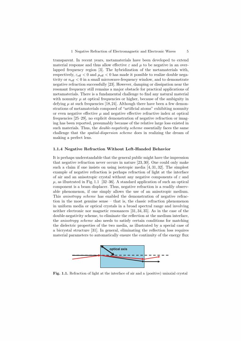
It is perhaps understandable that the general public might have the impressionthat negative refraction never occurs in nature [23, 30]. One could only makesuch a claim if one insists on using isotropic media [4, 31, 32]. The simplestexample of negative refraction is perhaps refraction of light at the interfaceof air and an anisotropic crystal without any negative components of ε andµ, as illustrated in Fig. 1.1 [32–36]. A standard application of such an opticalcomponent is a beam displacer. Thus, negative refraction is a readily observ-able phenomenon, if one simply allows the use of an anisotropic medium.This anisotropy scheme has enabled the demonstration of negative refrac-tion in the most genuine sense – that is, the classic refraction phenomenonin uniform media or optical crystals in a broad spectral range and involvingneither electronic nor magnetic resonances [31, 34, 35]. As in the case of thedouble-negativity scheme, to eliminate the reflection at the medium interface,the anisotropy scheme also needs to satisfy certain conditions for matchingthe dielectric properties of the two media, as illustrated by a special case ofa bicrystal structure [31]. In general, eliminating the reflection loss requiresmaterial parameters to automatically ensure the continuity of the energy flux
optical axis
Fig. 1.1. Refraction of light at the interface of air and a (positive) uniaxial crystal
6 Y. Zhang and A. Mascarenhas
along the interface normal [32]. Generalization has been discussed for theinterface of two arbitrary uniaxially anisotropic media [33, 37, 38]. Note thatnegative refraction facilitated by the anisotropy scheme does not involve anyLH behavior and thus cannot be used to make a flat lens, in contrast tothat suggested by Veselago, using a double-negativity medium [10], whichis an important distinction from the other schemes based on negative groupvelocity. However, one could certainly envision various important applicationsother than the flat lens.
1.1.5 Negative Refraction Using Photonic Crystals
The last scheme we would like to mention is the photonic crystal scheme.Although it is diffractive in nature, one may often consider the electromagneticwaves in a photonic crystal as waves with new dispersion relations, ωn(k),where n is the band index, and k is the wave vector in the first Brillouin zone.For a three-dimensional (3D) or 2D photonic crystal [39, 40], the direction ofthe energy flux, averaged over the unit cell, is determined by the group velocitydωn(k)/dk, although that might not be generally true for a 1D photonic crys-tal [40]. If the dispersion is isotropic, the condition q·dωn(q)/dq < 0, where qis the wave vector measured from a local extremum, must be satisfied to haveLH behavior. Similar to the situations for the spatial-dispersion and double-negativity schemes, q·dωn(q)/dq < 0 also allows the occurrence of negativerefraction at the interface of air and photonic crystal as well as the imagingeffect with a flat photonic slab [4,41–44]. However, similar to the situation forthe anisotropy scheme, one may also achieve negative refraction with positive,but anisotropic, dispersions [40]. Because of the diffractive nature, the phasematching at the interface of the photonic crystal often leads to complications,such as the excitation of multiple beams [40,45].
1.1.6 From Negative Refraction to Perfect Lens
Although the possibility of making a flat lens with the double-negativitymaterial was first discussed by Veselago [10], the noted unusual feature alone,i.e., a lens without an optical axis, would not have caused it to receive suchbroad interest. It was Pendry who suggested perhaps the most unique aspectof the double-negativity material – the potential for realizing a perfect lensbeyond negative refraction [1] – compared to other schemes that can alsoachieve negative refraction. Apparently, not all negative refractions are equal.To make Pendry’s perfect lens, in addition to negative refraction, one alsoneeds (1) zero dissipation, (2) amplification of evanescent waves, and (3)matching of the dielectric parameters between the lens and air. Exactly zerodissipation is physically impossible for any real material. For an insulatorwith an optical bandgap, one normally considers that there is no absorptionfor light with energy below the bandgap, if the crystal is perfect (e.g., free ofdefects). However, with nonlinear optical effects taken into account, there will
1 Negative Refraction of Electromagnetic and Electronic Waves 7
always be some finite absorption below the bandgap due to harmonic transi-tions [46]. Although it is typically many orders of magnitude weaker than theabove-bandgap linear absorption, it will certainly make the lens imperfect.Therefore, a perfect lens may simply be a physically unreachable singularitypoint. For the schemes working near the resonant frequencies of one kind orthe other, the dissipation is usually strong, and thus more problematic toallow such a lens to be practically usable.
Mathematically, double-negativity material is the only one, among all theschemes mentioned above, that automatically provides a correct amount ofamplification for each evanescent wave [1]. Unfortunately, this scheme becomesproblematic at high frequencies because of the ambiguity in defining nonunityµ at high frequencies [18, 24]. The other schemes – spatial dispersion andphotonic crystals – may also amplify the evanescent components when theeffective refractive index neff < 0, but typically with some complications(e.g., the amplification magnitude might not be exactly correct or the res-olution is limited by the periodicity of the photonic crystal) [47,48].
One important requirement of negative refraction for making a perfectlens is matching the dielectric parameters (“impedances”) of the two mediato eliminate reflection, as well as aberration [49], for instance, n1 = −n2
for the double-negativity scheme. In addition to the limitation caused byfinite damping, another limitation faced by both the spatial-dispersion anddouble-negativity schemes is frequency dispersion, which prohibits the match-ing condition of the dielectric parameters to remain valid in a broad frequencyrange. For the spatial-dispersion scheme, the frequency dispersion ε(ω) isapparent [9]. It is less trivial for the double-negativity scheme, but it waspointed out by Veselago that “the simultaneous negative values of ε and µcan be realized only when there is frequency dispersion,” in order to avoid theenergy becoming negative [10]. For the photonic crystal, the effective indexis also found to depend on frequency. Therefore, even for the ideal case ofvanishing damping, the matching condition can be found at best for discretefrequencies, using any one of the three schemes discussed above.
However, even with the practical limitations on the three aspects – damp-ing, incorrect magnitude of amplification, and dielectric mismatch – one canstill be hopeful of achieving a finite improvement in “focusing” light beyondthe usual diffraction limit [50], in addition to the benefits of having a flat lens.A widely used technique, an immersion lens [51], relies on turning as manyevanescent waves as possible into propagating waves inside the lens, and itrequires either the source or image to be in the near-field region. Comparedto this immersion lens, the primary advantage of the “superlens” seems tobe the ability to achieve subwavelength focusing with both the source andimage at far field. An immersion lens can readily achieve ∼ λ/4 resolutionat ∼200 nm in semiconductor photolithography [52]. With a solid immersionlens, even better resolution has been achieved (e.g., ∼0.23λ at λ = 436 nm [53],∼λ/8 at λ = 515 nm [54]). Thus far, using negative refraction, there haveonly been a few experimental demonstrations of non-near-field imaging with
8 Y. Zhang and A. Mascarenhas
improved resolution (e.g., 0.4λ image size at 1.4λ away from the lens [55],using a 2D quasicrystal with λ = 25mm; 0.36λ image size at 0.6λ away fromthe lens [56], using a 3D photonic crystal with λ = 18.3 mm). In addition,plasmonic systems (e.g., ultra thin metal film) have also be used for achievingsubwavelength imaging in near field [57, 58], although not necessarily relatedto negative refraction.
Some further discussion is useful on the meaning of “focusing” as used byPendry for describing the perfect lens [1]. The focusing power of a lens usuallyrefers to the ability to provide an image smaller than the object. What thehypothetical flat lens can do is exactly reproduce the source at the image site,or equivalently, spatially translate the source by a distance of 2d, where dis the thickness of the slab. Thus, mathematically, a δ-function source willgive rise to a δ-function image, without being subjected to the diffractionlimit of a regular lens, i.e., λ/2 [59]. And such a “superlens” can, in principle,resolve two objects with any nonzero separation, overcoming the Rayleighcriterion of 0.61λ for the resolving power of a regular lens [59]. However, whatthis “superlens” cannot do is focus an object greater than λ to an imagesmaller than λ; thus, it cannot bring a broad beam to focus for applicationssuch as photolithography, whereas a regular lens or an immersion lens can, inprinciple, focus an object down to the diffraction limit λ/2 or λ/(2n) (n is therefractive index of the lens material). Therefore, it might not be appropriateto call such optical device of no magnification a “lens,” though it is indeedvery unique. One could envision using the “superlens” to map or effectivelytranslate a light source, while retaining its size that is already below thediffraction limit to begin with.
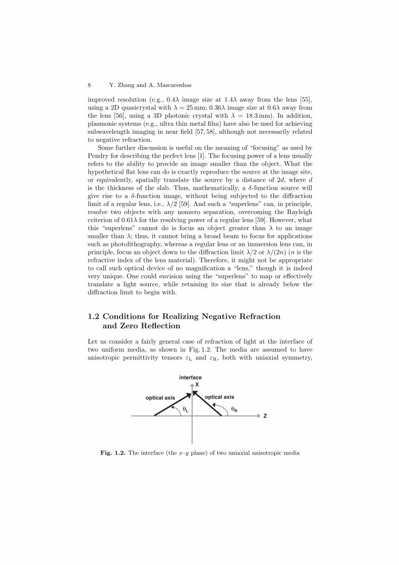
1.2 Conditions for Realizing Negative Refractionand Zero Reflection
Let us consider a fairly general case of refraction of light at the interface oftwo uniform media, as shown in Fig. 1.2. The media are assumed to haveanisotropic permittivity tensors εL and εR, both with uniaxial symmetry,
interface
Z
optical axis optical axis
θL θR
X
Fig. 1.2. The interface (the x–y plane) of two uniaxial anisotropic media
1 Negative Refraction of Electromagnetic and Electronic Waves 9
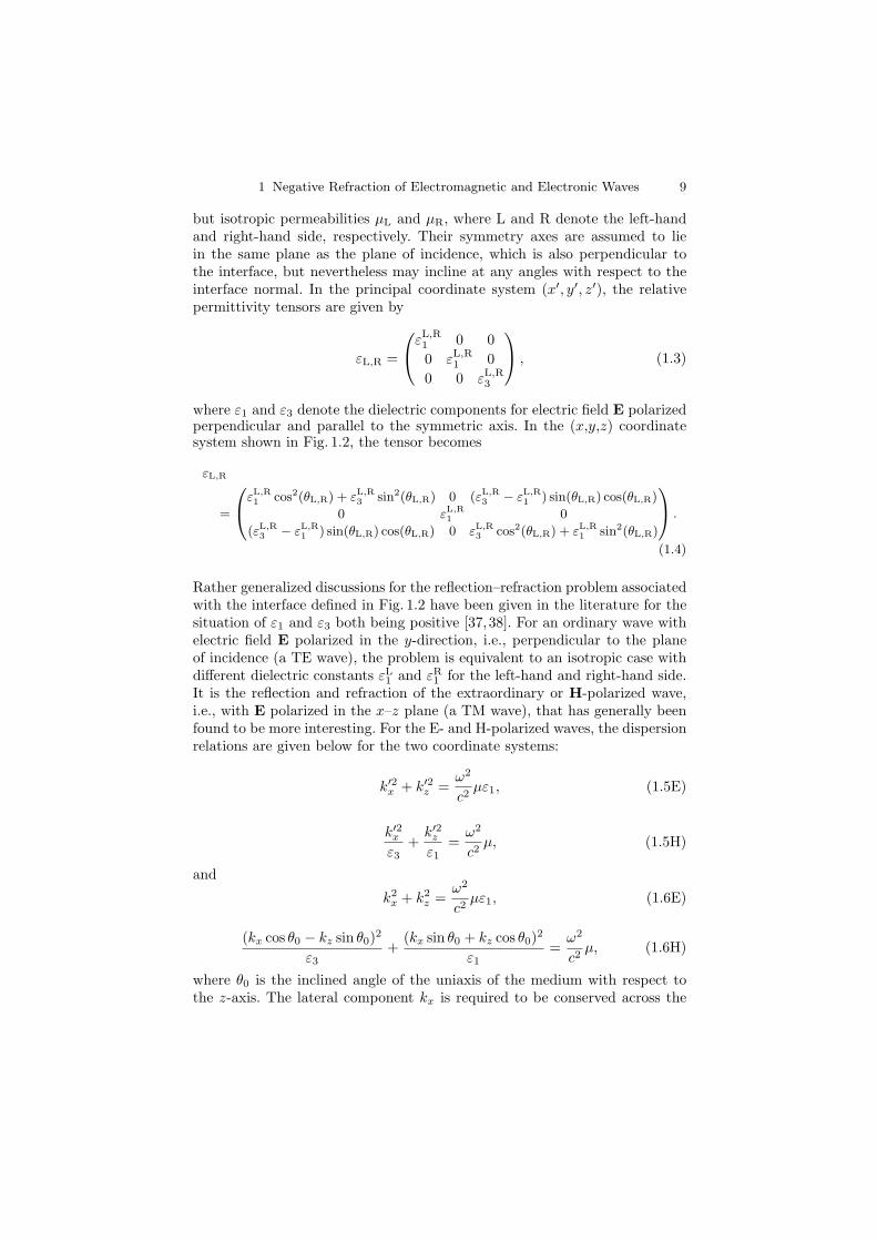
but isotropic permeabilities µL and µR, where L and R denote the left-handand right-hand side, respectively. Their symmetry axes are assumed to liein the same plane as the plane of incidence, which is also perpendicular tothe interface, but nevertheless may incline at any angles with respect to theinterface normal. In the principal coordinate system (x′, y′, z′), the relativepermittivity tensors are given by
εL,R =
⎛⎝
εL,R1 0 00 εL,R
1 00 0 εL,R
3
⎞⎠ , (1.3)
where ε1 and ε3 denote the dielectric components for electric field E polarizedperpendicular and parallel to the symmetric axis. In the (x,y,z) coordinatesystem shown in Fig. 1.2, the tensor becomes
εL,R
=
⎛⎝
εL,R1 cos2(θL,R) + εL,R
3 sin2(θL,R) 0 (εL,R3 − εL,R
1 ) sin(θL,R) cos(θL,R)
0 εL,R1 0
(εL,R3 − εL,R
1 ) sin(θL,R) cos(θL,R) 0 εL,R3 cos2(θL,R) + εL,R
1 sin2(θL,R)
⎞⎠ .
(1.4)
Rather generalized discussions for the reflection–refraction problem associatedwith the interface defined in Fig. 1.2 have been given in the literature for thesituation of ε1 and ε3 both being positive [37,38]. For an ordinary wave withelectric field E polarized in the y-direction, i.e., perpendicular to the planeof incidence (a TE wave), the problem is equivalent to an isotropic case withdifferent dielectric constants εL
1 and εR1 for the left-hand and right-hand side.
It is the reflection and refraction of the extraordinary or H-polarized wave,i.e., with E polarized in the x–z plane (a TM wave), that has generally beenfound to be more interesting. For the E- and H-polarized waves, the dispersionrelations are given below for the two coordinate systems:
k′2x + k′2
z =ω2
c2µε1, (1.5E)
k′2x
ε3+
k′2z
ε1=
ω2
c2µ, (1.5H)
and
k2x + k2
z =ω2
c2µε1, (1.6E)
(kx cos θ0 − kz sin θ0)2
ε3+
(kx sin θ0 + kz cos θ0)2
ε1=
ω2
c2µ, (1.6H)
where θ0 is the inclined angle of the uniaxis of the medium with respect tothe z-axis. The lateral component kx is required to be conserved across the
10 Y. Zhang and A. Mascarenhas
interface and the two solutions for kz (of ±) are found to be (with k in theunit of ω/c) the following:
k±z = ±
√µε1 − k2
x, (1.7E)
k±z =
kxδ ± 2√
γ(βµ − k2x)
2β, (1.7H)
where γ = ε1ε3, β = ε1 sin2 θ0+ε3 cos2 θ0, δ = sin(2θ0)(ε1−ε3). The Poyntingvector S = E∗ × H, corresponding to k±
z , can be given as
S±x = |Ey|2
kx
cµµ0, (1.8E)
S±x = |Hy|2
2γkx ∓ δ√
γ(βµ − k2x)
2cε0βγ, (1.8H)
and
S±z = ± |Ey|2
√µε1 − k2
x
cµµ0, (1.9E)
S±z = ± |Hy|2
√γ(βµ − k2
x)cε0γ
, (1.9H)
where Ey and Hy are the y components of E and H, respectively. If theincident beam is assumed to arrive from the left upon the interface (i.e., energyflows along the +z direction), one should choose from (1.7) the solution thatcan give rise to a positive Sz. Note that (1.8) and (1.9) are valid for eitherside of the interface, and positive as well as negative ε1, ε3, and µ. With theseequations, we can conveniently discuss the conditions for realizing negativerefraction and zero reflection. Note that for the E-polarized wave, the signof k·S is only determined by that of ε1, since k·S = |Ey|2ωε0ε1; for the H-polarized wave, it is only determined by µ, since k·S = |Hy|2ωµ0µ.
Since Sz is always required to be positive, the condition to realize negativerefraction is simply to request a sign change of Sx across the interface. Forrealizing zero reflection, if one can assure the positive component of Sz to becontinuous across the interface, the reflection will automatically be eliminated.Therefore, one does not need to consider explicitly the reflection [32].
If both media are isotropic, i.e., ε1 = ε3 = ε, we have Sx ∝ kx/µand S±
z ∝ ±√
µε − k2x/µ for the E-polarized wave, Sx ∝ kx/ε and S±
z ∝±√
ε2(εµ − k2x)/ε2 for the H-polarized wave. To have negative refraction for
both of the polarizations, the only possibility is to have ε and µ changingsign simultaneously. To have zero reflection for any kx, the conditions become|εL| = |εR| and |µL| = |µR|, and (εµ)L = (εµ)R. Since εµ > 0 is necessary forthe propagating wave, the conditions become εL = −εR and µL = −µR, asderived by Veselago [10]. It is interesting to note that if one of the media is
1 Negative Refraction of Electromagnetic and Electronic Waves 11
replaced with a photonic crystal with a negative effective refractive index, the“impedance” matching conditions become much more restrictive. In has beenfound that to minimize the reflection the surrounding medium has to have apair of specific ε and µ for a given photonic crystal [60] and the values couldeven depend on the surface termination of the photonic crystal [61].
If the media are allowed to be anisotropic, several ways exist to achievenegative refraction, even if we limit ourselves to µ being isotropic. For theE-polarized wave, since Sx ∝ kx/µ, negative refraction requires µ < 0 onone side, assuming µR < 0 (the left-hand side is assumed to have everythingpositive). In the meantime, because Sz ∝ ±
√µε1 − k2
x/µ, one also needs tohave εR
1 < 0 to make the wave propagative. Thus, with εR1 < 0 and µR < 0
while keeping εR3 > 0, one can have negative refraction, and zero reflection
for the E-polarized wave occurring for any kx when µR = −µL and (ε1µ)L =(ε1µ)R. This situation is similar to the isotropic case with ε = ε1, althoughthere will be no negative refraction for the H-polarized wave.
For the H-polarized wave, if both media are allowed to be anisotropicbut the symmetry axes are required to be normal to the interface (i.e., θL =θR = 0), we have Sx ∝ kx/ε3 and Sz ∝ ±
√ε1ε3(ε3µ − k2
x)/(ε1ε3) > 0.Negative refraction requires ε3 < 0 on one side, again assumed to be theright-hand side (the left-hand side is assumed to have everything positive).If ε1 < 0, then µR < 0 is also needed to have a propagating wave; we haveSR
z ∝√
εR1 εR
3 (εR3 µR − k2
x)/(εR1 εR
3 ), and the conditions for zero reflection are(ε1ε3)L = (ε1ε3)R and (ε3µ)L = (ε3µ)R. If εR
1 > 0, then µR > 0 is necessaryto have a propagating wave; we have SR
z ∝ −√
εR1 εR
3 (εR3 µR − k2
x)/(εR1 εR
3 ), butzero reflection is not possible except for kx = 0 and when (ε1ε3)L = |ε1ε3|Rand |ε3µ|L = |ε3µ|R. The results for θL = θR = 90 can be obtained by simplyreplacing ε3 with ε1 in the results for θL = θR = 0. Similar or somewhatdifferent cases have been discussed in the literature for either θL = θR = 0
or θL = θR = 90, leading to the conclusion that at least one component ofeither ε or µ tensor needs to be negative to realize negative refraction [62–66].
However, the relaxation on the restriction of the optical axis orientations,allowing 0 < θL < 90 and 0 < θR < 90, makes negative refraction and zeroreflection possible even if both ε and µ tensors are positive definite. When ε ispositive definite, we have γ > 0 and β > 0, and in this case µ > 0 is necessaryto have propagating modes. The condition for zero reflection can be readilyfound to be γL = γR, and (βµ)L = (βµ)R. For the case of the interface beingthat of a pair of twinned crystals [31], these requirements are automaticallysatisfied for any angle of incidence. The twinned structure assures that thezero-reflection condition is valid for any wavelength, despite the existence ofdispersion; however, for the more-general case using two different materials,the condition can at best be satisfied at discrete wavelengths because thedispersion effect may break the matching condition, similar to the case ofε = µ = −1. The negative-refraction condition can be derived from (1.8H)(since γ > 0, S+
x should be used). Note that S+x = 0 at kx0 = δ
√βµ/
√4γ + δ2.
If kLx0 < kR
x0(kLx0 > kR
x0), Sx changes sign across the interface or negative
12 Y. Zhang and A. Mascarenhas
refraction occurs in the region kLx0 < kx < kR
x0(kRx0 < kx < kL
x0). For the crys-tal twin with θL = π/4 and θR = −π/4, kL
x0 = −kRx0 = (ε1−ε3)/
√2(ε1 + ε3)).
When ε3 > ε1 (i.e., positive birefringence) in the region of kLx0 < kx < kR
x0,SL
x > 0 and SRx < 0. For any given θL, ε1, and ε3, the maximum bending of
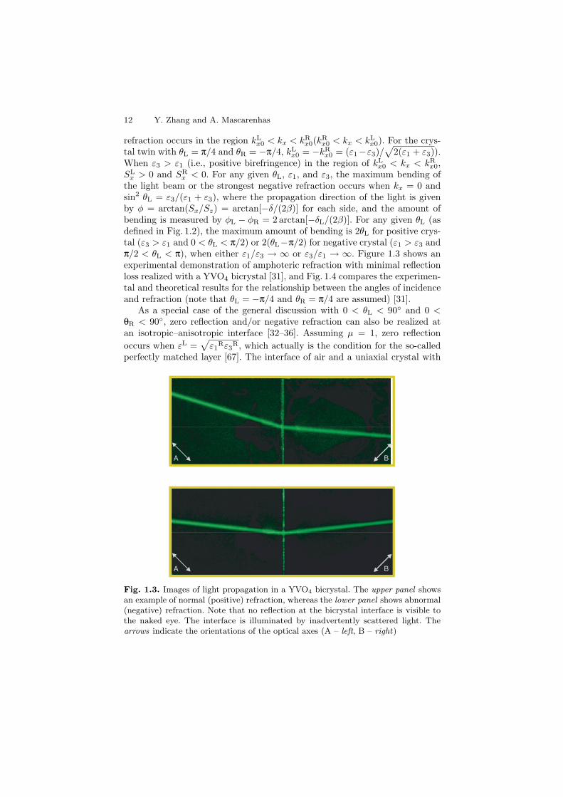
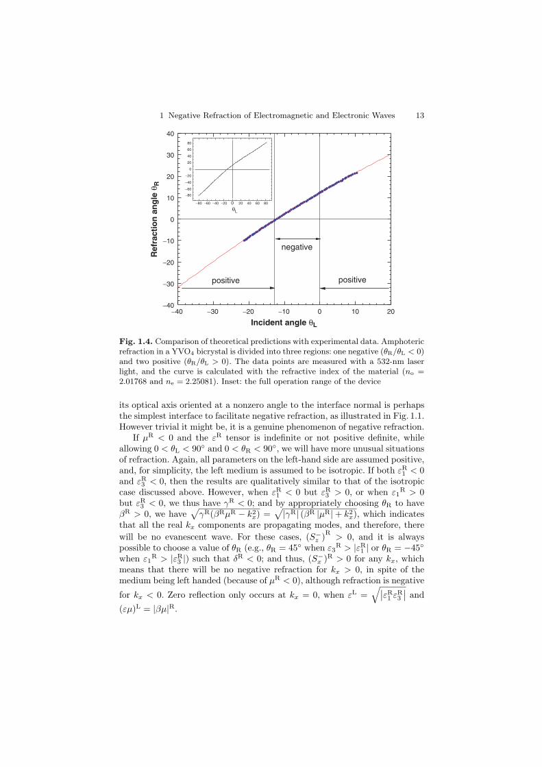
the light beam or the strongest negative refraction occurs when kx = 0 andsin2 θL = ε3/(ε1 + ε3), where the propagation direction of the light is givenby φ = arctan(Sx/Sz) = arctan[−δ/(2β)] for each side, and the amount ofbending is measured by φL − φR = 2 arctan[−δL/(2β)]. For any given θL (asdefined in Fig. 1.2), the maximum amount of bending is 2θL for positive crys-tal (ε3 > ε1 and 0 < θL < π/2) or 2(θL−π/2) for negative crystal (ε1 > ε3 andπ/2 < θL < π), when either ε1/ε3 → ∞ or ε3/ε1 → ∞. Figure 1.3 shows anexperimental demonstration of amphoteric refraction with minimal reflectionloss realized with a YVO4 bicrystal [31], and Fig. 1.4 compares the experimen-tal and theoretical results for the relationship between the angles of incidenceand refraction (note that θL = −π/4 and θR = π/4 are assumed) [31].
As a special case of the general discussion with 0 < θL < 90 and 0 <θR < 90, zero reflection and/or negative refraction can also be realized atan isotropic–anisotropic interface [32–36]. Assuming µ = 1, zero reflectionoccurs when εL =
√ε1
Rε3R, which actually is the condition for the so-called
perfectly matched layer [67]. The interface of air and a uniaxial crystal with
BA
BA
Fig. 1.3. Images of light propagation in a YVO4 bicrystal. The upper panel showsan example of normal (positive) refraction, whereas the lower panel shows abnormal(negative) refraction. Note that no reflection at the bicrystal interface is visible tothe naked eye. The interface is illuminated by inadvertently scattered light. Thearrows indicate the orientations of the optical axes (A – left, B – right)
1 Negative Refraction of Electromagnetic and Electronic Waves 13
−40 −30 −20 −10 0 10 20−40
−30
−20
−10
0
10
20
30
40
−80 −60 −40 −20 20 40 60 800
−80
−60
−40
−20
0
20
40
60
80
negative
positive
Ref
ract
ion
an
gle
θR
Incident angle θL
positive
θL
Fig. 1.4. Comparison of theoretical predictions with experimental data. Amphotericrefraction in a YVO4 bicrystal is divided into three regions: one negative (θR/θL < 0)and two positive (θR/θL > 0). The data points are measured with a 532-nm laserlight, and the curve is calculated with the refractive index of the material (no =2.01768 and ne = 2.25081). Inset: the full operation range of the device
its optical axis oriented at a nonzero angle to the interface normal is perhapsthe simplest interface to facilitate negative refraction, as illustrated in Fig. 1.1.However trivial it might be, it is a genuine phenomenon of negative refraction.
If µR < 0 and the εR tensor is indefinite or not positive definite, whileallowing 0 < θL < 90 and 0 < θR < 90, we will have more unusual situationsof refraction. Again, all parameters on the left-hand side are assumed positive,and, for simplicity, the left medium is assumed to be isotropic. If both εR
1 < 0and εR
3 < 0, then the results are qualitatively similar to that of the isotropiccase discussed above. However, when εR
1 < 0 but εR3 > 0, or when ε1
R > 0but εR
3 < 0, we thus have γR < 0; and by appropriately choosing θR to haveβR > 0, we have
√γR(βRµR − k2
x) =√|γR| (βR |µR| + k2
x), which indicatesthat all the real kx components are propagating modes, and therefore, therewill be no evanescent wave. For these cases, (S−
z )R > 0, and it is alwayspossible to choose a value of θR (e.g., θR = 45 when ε3
R > |εR1 | or θR = −45
when ε1R > |εR
3 |) such that δR < 0; and thus, (S−x )R > 0 for any kx, which
means that there will be no negative refraction for kx > 0, in spite of themedium being left handed (because of µR < 0), although refraction is negative
for kx < 0. Zero reflection only occurs at kx = 0, when εL =√∣∣εR
1 εR3
∣∣ and
(εµ)L = |βµ|R.
14 Y. Zhang and A. Mascarenhas
In summary, having an LHM is neither a necessary nor a sufficient con-dition for achieving negative refraction. The left-handed behavior does notalways lead to evanescent wave amplification. It may not always be possibleto match the material parameters to eliminate the interface reflection withan LHM. The double-negativity lens proposed by Veselago and Pendry repre-sents the most-stringent material requirement to achieve negative refraction,zero reflection, and evanescent wave amplification. For a uniform medium,the left-handed behavior can only be obtained with at least one componentof the ε or µ tensor being negative: ε1 for the E-polarized wave and µ1 for theH-polarized wave, if limited to materials with uniaxial symmetry [63]. How-ever, once one of the components of either the ε or µ tensor becomes negativeso as to have left-handed behavior, then at least one of the components of theother tensor needs to be negative to have propagating modes in the medium,and possibly to have evanescent wave amplification (as discussed above forthe H-polarized wave and in the literature for the E-polarized wave [65]).
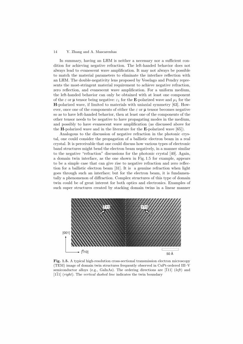
Analogous to the discussion of negative refraction in the photonic crys-tal, one could consider the propagation of a ballistic electron beam in a realcrystal. It is perceivable that one could discuss how various types of electronicband structures might bend the electron beam negatively, in a manner similarto the negative “refraction” discussions for the photonic crystal [40]. Again,a domain twin interface, as the one shown in Fig. 1.5 for example, appearsto be a simple case that can give rise to negative refraction and zero reflec-tion for a ballistic electron beam [31]. It is a genuine refraction when lightgoes through such an interface; but for the electron beam, it is fundamen-tally a phenomenon of diffraction. Complex structures of this type of domaintwin could be of great interest for both optics and electronics. Examples ofsuch super structures created by stacking domain twins in a linear manner
[001]
[110]
[111][111]
50 Å
Fig. 1.5. A typical high-resolution cross-sectional transmission electron microscopy(TEM) image of domain twin structures frequently observed in CuPt-ordered III–Vsemiconductor alloys (e.g., GaInAs). The ordering directions are [111] (left) and[111] (right). The vertical dashed line indicates the twin boundary
1 Negative Refraction of Electromagnetic and Electronic Waves 15
(a) (b)
[001]
[110]
40Å
Fig. 1.6. High-resolution cross-sectional TEM images of ordered GaInP alloys: (a)double-variant ordered structure with quasiperiodic stacking of domain twins alongthe [001] direction, and (b) single-variant ordered domain
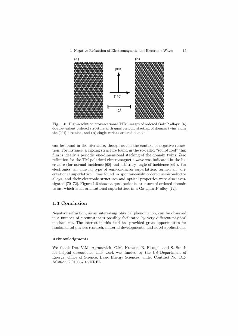
can be found in the literature, though not in the context of negative refrac-tion. For instance, a zig-zag structure found in the so-called “sculptured” thinfilm is ideally a periodic one-dimensional stacking of the domain twins. Zeroreflection for the TM polarized electromagnetic wave was indicated in the lit-erature (for normal incidence [68] and arbitrary angle of incidence [69]). Forelectronics, an unusual type of semiconductor superlattice, termed an “ori-entational superlattice,” was found in spontaneously ordered semiconductoralloys, and their electronic structures and optical properties were also inves-tigated [70–72]. Figure 1.6 shows a quasiperiodic structure of ordered domaintwins, which is an orientational superlattice, in a Ga1−xInxP alloy [72].
1.3 Conclusion
Negative refraction, as an interesting physical phenomenon, can be observedin a number of circumstances possibly facilitated by very different physicalmechanisms. The interest in this field has provided great opportunities forfundamental physics research, material developments, and novel applications.
Acknowledgments
We thank Drs. V.M. Agranovich, C.M. Krowne, B. Fluegel, and S. Smithfor helpful discussions. This work was funded by the US Department ofEnergy, Office of Science, Basic Energy Sciences, under Contract No. DE-AC36-99GO10337 to NREL.
16 Y. Zhang and A. Mascarenhas
References
1. J.B. Pendry, Phys. Rev. Lett. 85, 3966 (2000)2. J.B. Pendry, Science 305, 788 (2005)3. J.B. Pendry, D.R. Smith, Phys. Today 57, 37 (2004)4. Y. Zhang, A. Mascarenhas, Mod. Phys. Lett. B 18 (2005)5. A. Schuster, An Introduction to the Theory of Optics (Edward Arnold,
London, 1904)6. E.I. Rashba, J. Appl. Phys. 79, 4306 (1996)7. C.F. Klingshirn, Semiconductor Optics (Springer, Berlin Heidelberg
New York, 1995)8. G. Dolling, C. Enkrich, M. Wegener, C.M. Soukoulis, S. Linden, Science 312,
892 (2006)9. V.M. Agranovich, V. L. Ginzburg, Spatial Dispersion in Crystal Optics and the
Theory of Excitons (Wiley, London, 1966)10. V.G. Veselago, Sov. Phys. Usp. 10, 509 (1968)11. A.I. Viktorov, Physical Principles of the Use of Ultrasonic Raleigh and Lamb
Waves in Engineering (Nauka, Russia, 1966)12. P.V. Burlii, I.Y. Kucherov, JETP Lett. 26, 490 (1977)13. H. Lamb, Proc. London Math. Soc. Sec. II 1, 473 (1904)14. C.M. Krowne, Encyclopedia of Rf and Microwave Engineering, vol. 3 (Wiley,
New York, 2005), p. 230315. M. Born, E. Wolf, Principles of Optics (Cambridge University Press, Cambridge,
1999)16. J. Neufeld, R.H. Ritchie, Phys. Rev. 98, 1955 (1955)17. V.L. Ginzburg, JETP 34, 1096 (1958)18. V.M. Agranovich, Y.R. Shen, R.H. Baughman, A.A. Zakhidov, Phys. Rev. B
69, 165112 (2004)19. M. Born, K. Huang, Dynamical Theory of Crystal Lattices (Clarendon,
Oxford, 1954)20. J.J. Hopfield, Phys. Rev. 112, 1555 (1958)21. V.M. Agranovich, Y.R. Shen, R.H. Baughman, A.A. Zakhidov, J. Lumin. 110,
167 (2004)22. V.E. Pafomov, Sov. Phys. JETP 36, 1321 (1959)23. R.A. Shelby, D.R. Smith, S. Schultz, Science 292, 77 (2001)24. L.D. Landau, E.M. Lifshitz, L.P. Pitaevskii, Electrodynamics of Continuous
Media (Butterworth-Heinemann, Oxford, 1984)25. C. Enkrich, M. Wegener, S. Linden, S. Burger, L. Zschiedrich, F. Schmidt,
J.F. Zhou, T. Koschny, C.M. Soukoulis, Phys. Rev. Lett. 95 (2005)26. A.N. Grigorenko, A.K. Geim, H.F. Gleeson, Y. Zhang, A.A. Firsov,
I.Y. Khrushchev, J. Petrovic, Nature 438, 335 (2005)27. S. Zhang, W.J. Fan, N.C. Panoiu, K.J. Malloy, R.M. Osgood, S.R.J. Brueck,
Phys. Rev. Lett. 95 (2005)28. S. Linden, C. Enkrich, M. Wegener, J.F. Zhou, T. Koschny, C.M. Soukoulis,
Science 306, 1351 (2004)29. V.M. Shalaev, W.S. Cai, U.K. Chettiar, H.K. Yuan, A.K. Sarychev,
V.P. Drachev, A.V. Kildishev, Opt. Lett. 30, 3356 (2005)30. J.B. Pendry, Science 306, 1353 (2004)31. Y. Zhang, B. Fluegel, A. Mascarenhas, Phys. Rev. Lett. 91, 157404 (2003)32. Y. Zhang, A. Mascarenhas, in Mat. Res. Soc. Symp. Proc., vol. 794 (MRS Fall
Meeting, Boston, 2003), p. T10.1

1 Negative Refraction of Electromagnetic and Electronic Waves 17
33. L.I. Perez, M.T. Garea, R.M. Echarri, Opt. Commun. 254, 10 (2005)34. X.L. Chen, H. Ming, D. YinXiao, W.Y. Wang, D.F. Zhang, Phys. Rev. B 72,
113111 (2005)35. Y.X. Du, M. He, X.L. Chen, W.Y. Wang, D.F. Zhang, Phys. Rev. B 73,
245110 (2006)36. Y. Lu, P. Wang, P. Yao, J. Xie, H. Ming, Opt. Commun. 246, 429 (2005)37. Z. Liu, Z.F. Lin, S.T. Chui, Phys. Rev. B 69, 115402 (2004)38. Y. Wang, X.J. Zha, J.K. Yan, Europhys. Lett. 72, 830 (2005)39. K. Sakoda, Optical Properties of Photonic Crystals (Springer, Berlin Heidelberg
New York, 2001)40. S. Foteinopoulou, C.M. Soukoulis, Phys. Rev. B 72, 165112 (2005)41. M. Notomi, Phys. Rev. B 62, 10696 (2000)42. P.V. Parimi, W.T.T. Lu, P. Vodo, S. Sridhar, Nature 426, 404 (2003)43. C. Luo, S.G. Johnson, J.D. Joannopoulos, J.B. Pendry, Phys. Rev. B 65,
201104 (2002)44. E. Cubukcu, K. Aydin, E. Ozbay, S. Foteinopoulou, C.M. Soukoulis, Nature
423, 604 (2003)45. A.B. Pippard, The Dynamics of Conduction Electrons (Gordon and Breach,
New York, 1965)46. Y.R. Shen, The Principles of Nonlinear Optics (Wiley, New York, 1984)47. L. Silvestri, O.A. Dubovski, G.C. La Rocca, F. Bassani, V.M. Agranovich, Nuovo
Cimento Della Societa Italiana Di Fisica C-Geophysics and Space Physics 27,437 (2004)
48. C. Luo, S.G. Johnson, J.D. Joannopoulos, J.B. Pendry, Phys. Rev. B 68,45115 (2003)
49. A.L. Pokrovsky and A.L. Efros, Phys. B 338, 333 (2003)50. D.R. Smith, D. Schurig, M. Rosenbluth, S. Schultz, S.A. Ramakrishna,
J.B. Pendry, Appl. Phys. Lett. 82, 1506 (2003)51. I. Ichimura, S. Hayashi, G.S. Kino, Appl. Opt. 36, 4339 (1997)52. http://www.semiconductor-technology.com/features/section290/53. S.M. Mansfield, G.S. Kino, Appl. Phys. Lett. 57, 2615 (1990)54. I. Smolyaninov, J. Elliott, A.V. Zayats, C.C. Davis, Phys. Rev. Lett. 94 (2005)55. Z.F. Feng, X.D. Zhang, Y.Q. Wang, Z.Y. Li, B.Y. Cheng, D.Z. Zhang, Phys.
Rev. Lett. 94 (2005)56. Z. Lu, J.A. Murakowski, C.A. Schuetz, S. Shi, G.J. Schneider, D.W. Prather,
Phys. Rev. Lett. 95, 153901 (2005)57. N. Fang, H. Lee, C. Sun, X. Zhang, Science 308, 534 (2005)58. D.O.S. Melville, R.J. Blaikie, Opt. Express 13, 2127 (2005)59. J.M. Vigoureux, D. Courjon, Appl. Opt. 31, 3170 (1992)60. A.L. Efros, A.L. Pokrovsky, Solid State Commun. 129, 643 (2004)61. T. Decoopman, G. Tayeb, S. Enoch, D. Maystre, B. Gralak, Phys. Rev. Lett.
97 (2006)62. I.V. Lindell, S.A. Tretyakov, K.I. Nikoskinen, S. Ilvonen, Microw. Opt. Technol.
Lett. 31, 129 (2001)63. L.B. Hu, S.T. Chui, Phys. Rev. B 66, 085108 (2002)64. L. Zhou, C.T. Chan, P. Sheng, Phys. Rev. B 68, 115424 (2003)65. D.R. Smith, D. Schurig, Phys. Rev. Lett. 90, 077405 (2003)66. T. Dumelow, J.A.P. da Costa, V.N. Freire, Phys. Rev. B 72 (2005)67. S.D. Gedney, IEEE Trans. Antennas Propagat. 44, 1630 (1996)

18 Y. Zhang and A. Mascarenhas
68. A. Lakhtakia, R. Messier, Opt. Eng. 33, 2529 (1994)69. G.Y. Slepyan, A.S. Maksimenko, Opt. Eng. 37, 2843 (1998)70. Y. Zhang, A. Mascarenhas, Phys. Rev. B 55, 13100 (1997)71. Y. Zhang, A. Mascarenhas, S.P. Ahrenkiel, D.J. Friedman, J. Geisz, J.M. Olson,
Solid State Commun. 109, 99 (1999)72. Y. Zhang, B. Fluegel, S.P. Ahrenkiel, D.J. Friedman, J. Geisz, J.M. Olson,
A. Mascarenhas, Mat. Res. Soc. Symp. Proc. 583, 255 (2000)
2
Anisotropic Field Distributionsin Left-Handed Guided Wave ElectronicStructures and Negative Refractive BicrystalHeterostructures
C.M. Krowne
Summary. Effect of anisotropy in the physical tensor description of the negativeindex of refraction material acting as a substrate is found on the electromagneticfield distributions. This is done for the case of a microstrip structure whose con-figuration is commonly used in microwave and millimeter wave integrated circuits.These ab initio studies have been done self-consistently with a computer code usinga full-wave integral equation numerical method based upon a generalized anisotropicGreen’s function utilizing appropriate boundary conditions. Field distributions areprovided over two decades of frequency in the cross-section of the uniform guidedwave structure, from 0.2 to 20 GHz. It is found that modifying the tensor can allowcontrol because the wave changes volumetrically, or switches from volumetric tosurface, in its distribution of fields. It has also been discovered that heterostruc-ture bicrystal arrangements lead to field asymmetry in guided wave structures. Astudy is conducted over a range of nominal permittivity values to see if the effectis present in widely varying dielectric materials. Marked shifts of the field distribu-tion occurs in some cases, and this can be the basis of an all electronic device thatprovides beam steering or a device that gives directional action. Such all electronicdevices could be fixed or even constructed as control components using materialswith electrostatically controllable permittivity. Distributions have been obtained todemonstrate the effect using an anisotropic Green’s function solver.
2.1 Anisotropic Field Distributions in Left-HandedGuided Wave Electronic Structures
2.1.1 Introduction
Although considerable physics has been learned about the dispersion behav-ior and electromagnetic fields for propagation down guided wave microstripstructures loaded with DNM (double-negative materials with simultaneousnegative permittivity and permeability) which are also referred to LHM (left-handed materials for the left-handed orientation of the electric, magnetic, andpropagation phase constant) [1, 2] nothing is known about what happens to
20 C.M. Krowne
the field distributions as anisotropy is introduced. This is an extremely inter-esting area since maintenance of isotropy has been recognized to be essentialfor 3D imaging possibilities [3, 4], and such isotropy should also be neces-sary for arbitrary field contouring or arrangement of fields in small electronicdevices which are created especially to employ the unique properties of DNM.It should also be noted here that these materials can be referred to as NIRM(negative index of refraction materials) or NIM (negative index materials).Furthermore, because the essential property of these materials is oppositeorientations of the phase velocity and the Poynting vector (giving the powerflow direction), they may be referred to as alternatively as negative phasevelocity materials (NPV materials or simply NPVM) [5].
Because we are not going to further examine 3D imaging issues, but 3Dbehavior of fields in electronic devices, we will restrict the use of notationwhen referring to these materials as DNM or NPVM. Although maintainingisotropy for many integrated circuit applications may be desirable as men-tioned above, it may also be desirable to introduce anisotropy [6, 7], or atleast find it acceptable to have some anisotropy in certain device configura-tions, where because of the particular applications, the effective dimensions ofthe device is reduced from 3D to 2D or even 1D. This is not some idle specu-lation, as quasilumped element realizations using distributed and/or lumpedsections have been used to make components employing backward wave behav-ior, one of the hallmarks of DNM or NPVM [8–11]. Thus, whether or not wewant to examine what the effect is of some deviation from isotropy, or wish tointentionally introduce anisotropy, it would be very instructive to undertakesuch an investigation.
In pursuing this quest, the backdrop of already studied field distributionsfor isotropic DNM in the C-band, X-band, Ka and V-bands, and W-bandbroadcast frequency regions gives us some basis upon which to begin thesestudies. In the C-band region, electromagnetic field line plots of Et and Ht
for the transverse fields in the cross-section perpendicular to the propagationdirection were provided at 5 GHz [2]. Also given were simultaneous magni-tude and arrow vector distributions plots for E/Et and H/Ht at the samefrequency. Finally, a Poynting vector distribution plot Pz was provided at5 GHz. In the X-band region, electromagnetic field line plots of Et and Ht
were provided at 10 GHz [12]. Also given were simultaneous magnitude andarrow vector distributions plots for E/Et and H/Ht at the same frequency.Finally, a Poynting vector distribution plot Pz was provided at 10 GHz. Inthe overlap region between the Ka and V-bands, electromagnetic field plotsof simultaneous magnitude and arrow vector distributions plots for E/Et andH/Ht were given at 40 GHz [12,13]. Simultaneous line and magnitude distri-bution plots for E/Et and H/Ht were also provided at 40 GHz [12]. Lastly, aPoynting vector distribution plot Pz was provided at the same frequency [12].
Sections 2.1.2 and 2.1.3 cover, respectively, the governing equations/acquisition of the anisotropic Green’s function, and use of basis currentfunctions/determination of the propagation constant and electromagnetic
2 Anisotropic Field Distributions 21
fields, for the guided wave microstrip structure with anisotropic DNM. Witha complete development in hand, numerical calculations are performed inSect. 2.1.4 for a microstrip structure at three frequencies offset from eachother by decade steps. Each study is begun by first examining an isotropictensor to provide a reference standard for looking at the effects of introducinganisotropy through a permittivity tensor. Once the electromagnetic distribu-tions have been obtained for the isotropic case, distributions for anisotropy arecalculated. This process of first finding the isotropic result, then proceedingon to the anisotropic situation, is done at each frequency.
2.1.2 Anisotropic Green’s Function Based UponLHM or DNM Properties
Maxwell’s time varying equations describe the electromagnetic field behaviorin a medium if they are combined with constitutive relationships embeddingthe physical properties of the medium in them. Maxwell’s two curl equationsare
∇× E(t,x) = −∂B(t,x)∂t
, ∇× H(t,x) =∂D(t,x)
∂t+ J(t,x). (2.1)
Constitutive relationships are
D(t,x) = ¯εE(t,x) + ¯ρH(t,x), B(t,x) = ¯ρ′E(t,x) + ¯µH(t,x). (2.2)
Here x = (x1, x2, x3) = (x, y, z). Most general NPV medium can have allconstitutive tensors in (2.2) nonzero, including the magnetoelectric or opti-cal activity tensors ¯ρ and ¯ρ′, as they are sometimes called. The formulationis therefore kept general in order to retain the most flexibility for studyingmaterials with widely varying physical properties. Because many problems areoften transparent in the frequency domain, and because nonharmonic prob-lems can be resolved into a superposition of time-harmonic components, weelect to study here time harmonic electromagnetic wave propagation throughthe solid state LHM–RHM structure (RHM, right-handed medium or ordinarymedium). Taking the time harmonic variation to be of a form eiωt, Maxwell’sequation become
∇× E(x) = −iωB(x), ∇× H(x) = iωD(x) + J(x) (2.3)
with the constitutive relationships dropping the explicit t-dependence
D(x) = ¯ε(ω)E(x) + ¯ρ(ω)H(x), B(x) = ¯ρ′(ω)E(x) + ¯µ(ω)H(x). (2.4)
Dependence of the constitutive parameters on radian frequency is a well-recognized fact and that is why explicit variation on ω is shown. However, forthe study to be conducted here at specific frequencies, we do not need to call
22 C.M. Krowne
out this dependence explicitly. We will be setting for, example ¯ε(ω) = v forω = ωv. Therefore, we set
D(x) = ¯εE(x) + ¯ρH(x), B(x) = ¯ρ′E(x) + ¯µH(x) (2.5)
and understand it means (2.2).Curl equations (2.1) may be combined into a single sourceless governing
equation [14],LT(x)VL(x) = iωVR(x), (2.6)
where the matrix partial differential operator acting on the E–H column vec-tor is
LT(x) =[
0 Lq(x)−Lq(x) 0
], (2.7)
where the quadrant operator is
Lq(x) =
⎡⎢⎢⎢⎢⎢⎢⎢⎣
0 − ∂
∂z
∂
∂y
∂
∂z0 − ∂
∂x
− ∂
∂y
∂
∂x0
⎤⎥⎥⎥⎥⎥⎥⎥⎦
. (2.8)
Current J effects are introduced later through a Green’s function process [see(2.80)]. Vectors in (2.6) are
VL(x) =
⎡⎢⎢⎢⎢⎢⎢⎣
Ex
Ey
Ez
Hx
Hy
Hz
⎤⎥⎥⎥⎥⎥⎥⎦
=[EH
], VR(x) =
⎡⎢⎢⎢⎢⎢⎢⎣
Dx
Dy
Dz
Bx
By
Bz
⎤⎥⎥⎥⎥⎥⎥⎦
=[DB
]. (2.9)
Restricting ourselves to a guided wave structure with the wave traveling in auniform cross-section in the z-direction, that is the wave has the form eiωt−γz,γ = γ(ω), simplifies (2.6)–(2.8) to
LT(x, y)VL(x, y) = iωVR(x, y), (2.10)
LT(x, y) =[
0 Lq(x, y)−Lq(x, y) 0
], (2.11)
Lq(x, y) =
⎡⎢⎢⎢⎢⎢⎣
0 γ∂
∂y
−γ 0 − ∂
∂x
− ∂
∂y
∂
∂x0
⎤⎥⎥⎥⎥⎥⎦
. (2.12)
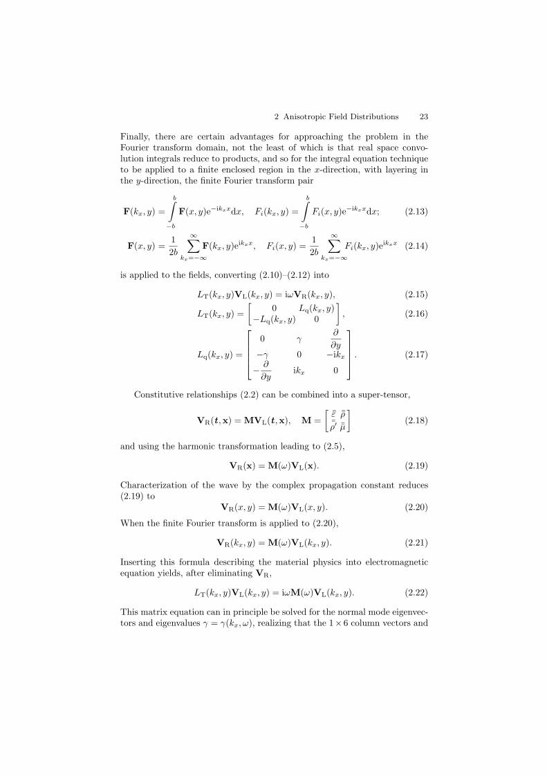
2 Anisotropic Field Distributions 23
Finally, there are certain advantages for approaching the problem in theFourier transform domain, not the least of which is that real space convo-lution integrals reduce to products, and so for the integral equation techniqueto be applied to a finite enclosed region in the x-direction, with layering inthe y-direction, the finite Fourier transform pair
F(kx, y) =
b∫
−b
F(x, y)e−ikxxdx, Fi(kx, y) =
b∫
−b
Fi(x, y)e−ikxxdx; (2.13)
F(x, y) =12b
∞∑kx=−∞
F(kx, y)eikxx, Fi(x, y) =12b
∞∑kx=−∞
Fi(kx, y)eikxx (2.14)
is applied to the fields, converting (2.10)–(2.12) into
LT(kx, y)VL(kx, y) = iωVR(kx, y), (2.15)
LT(kx, y) =[
0 Lq(kx, y)−Lq(kx, y) 0
], (2.16)
Lq(kx, y) =
⎡⎢⎢⎢⎣
0 γ∂
∂y−γ 0 −ikx
− ∂
∂yikx 0
⎤⎥⎥⎥⎦ . (2.17)
Constitutive relationships (2.2) can be combined into a super-tensor,
VR(t ,x) = MVL(t ,x), M =[ ¯ε ¯ρ
¯ρ′ ¯µ
](2.18)
and using the harmonic transformation leading to (2.5),
VR(x) = M(ω)VL(x). (2.19)
Characterization of the wave by the complex propagation constant reduces(2.19) to
VR(x, y) = M(ω)VL(x, y). (2.20)
When the finite Fourier transform is applied to (2.20),
VR(kx, y) = M(ω)VL(kx, y). (2.21)
Inserting this formula describing the material physics into electromagneticequation yields, after eliminating VR,
LT(kx, y)VL(kx, y) = iωM(ω)VL(kx, y). (2.22)
This matrix equation can in principle be solved for the normal mode eigenvec-tors and eigenvalues γ = γ(kx, ω), realizing that the 1× 6 column vectors and
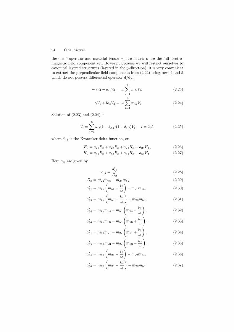
24 C.M. Krowne
the 6 × 6 operator and material tensor square matrices use the full electro-magnetic field component set. However, because we will restrict ourselves tocanonical layered structures (layered in the y-direction), it is very convenientto extract the perpendicular field components from (2.22) using rows 2 and 5which do not possess differential operator d/dy:
−γV4 − ikxV6 = iω6∑
i=1
m2iVi, (2.23)
γV1 + ikxV3 = iω6∑
i=1
m5iVi. (2.24)
Solution of (2.23) and (2.24) is
Vi =6∑
j=1
aij(1 − δ2,j)(1 − δ5,j)Vj , i = 2, 5, (2.25)
where δi,j is the Kronecker delta function, or
Ey = a21Ex + a23Ez + a24Hx + a26Hz, (2.26)Hy = a51Ex + a53Ez + a54Hx + a56Hz. (2.27)
Here aij are given by
aij =a′
ij
Da, (2.28)
Da = m22m55 − m25m52, (2.29)
a′21 = m25
(m51 +
iγω
)− m21m55, (2.30)
a′23 = m25
(m53 −
kx
ω
)− m23m55, (2.31)
a′24 = m25m54 − m55
(m24 −
iγω
), (2.32)
a′26 = m25m56 − m55
(m26 +
kx
ω
), (2.33)
a′51 = m52m21 − m22
(m51 +
iγω
), (2.34)
a′53 = m52m23 − m22
(m53 −
kx
ω
), (2.35)
a′54 = m52
(m24 −
iγω
)− m22m54, (2.36)
a′56 = m52
(m26 +
kx
ω
)− m22m56. (2.37)
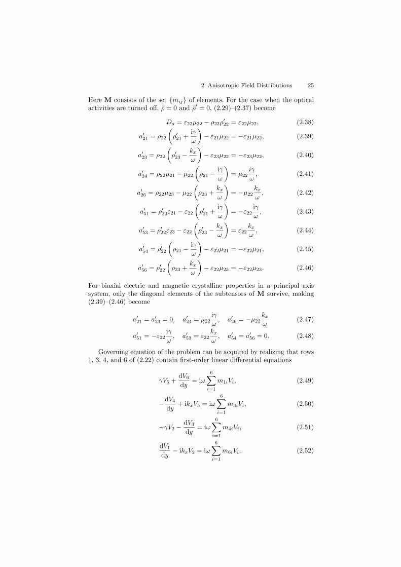
2 Anisotropic Field Distributions 25
Here M consists of the set mij of elements. For the case when the opticalactivities are turned off, ¯ρ = 0 and ¯ρ′ = 0, (2.29)–(2.37) become
Da = ε22µ22 − ρ22ρ′22 = ε22µ22, (2.38)
a′21 = ρ22
(ρ′21 +
iγω
)− ε21µ22 = −ε21µ22, (2.39)
a′23 = ρ22
(ρ′23 −
kx
ω
)− ε23µ22 = −ε23µ22, (2.40)
a′24 = ρ22µ21 − µ22
(ρ21 −
iγω
)= µ22
iγ
ω, (2.41)
a′26 = ρ22µ23 − µ22
(ρ23 +
kx
ω
)= −µ22
kx
ω, (2.42)
a′51 = ρ′22ε21 − ε22
(ρ′21 +
iγω
)= −ε22
iγω
, (2.43)
a′53 = ρ′22ε23 − ε22
(ρ′23 −
kx
ω
)= ε22
kx
ω, (2.44)
a′54 = ρ′22
(ρ21 −
iγω
)− ε22µ21 = −ε22µ21, (2.45)
a′56 = ρ′22
(ρ23 +
kx
ω
)− ε22µ23 = −ε22µ23. (2.46)
For biaxial electric and magnetic crystalline properties in a principal axissystem, only the diagonal elements of the subtensors of M survive, making(2.39)–(2.46) become
a′21 = a′
23 = 0, a′24 = µ22
iγω
, a′26 = −µ22
kx
ω(2.47)
a′51 = −ε22
iγω
, a′53 = ε22
kx
ω, a′
54 = a′56 = 0. (2.48)
Governing equation of the problem can be acquired by realizing that rows1, 3, 4, and 6 of (2.22) contain first-order linear differential equations
γV5 +dV6
dy= iω
6∑i=1
m1iVi, (2.49)
−dV4
dy+ ikxV5 = iω
6∑i=1
m3iVi, (2.50)
−γV2 −dV3
dy= iω
6∑i=1
m4iVi, (2.51)
dV1
dy− ikxV2 = iω
6∑i=1
m6iVi. (2.52)
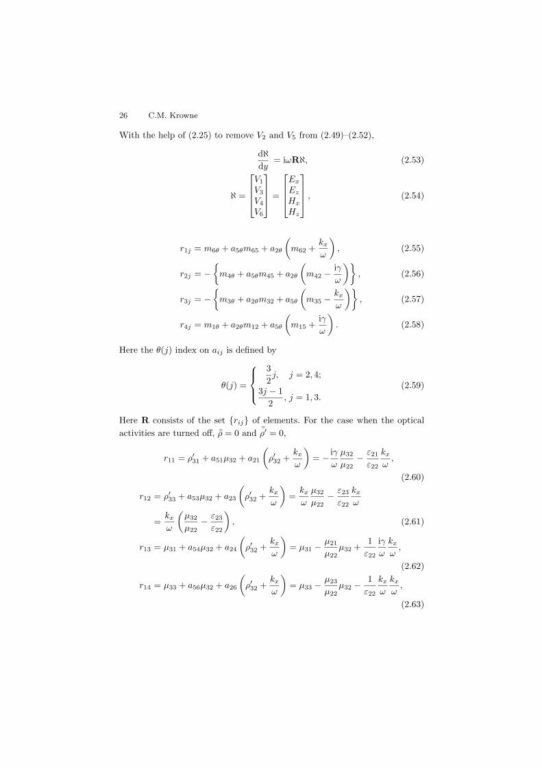
26 C.M. Krowne
With the help of (2.25) to remove V2 and V5 from (2.49)–(2.52),
dℵdy
= iωRℵ, (2.53)
ℵ =
⎡⎢⎢⎣
V1
V3
V4
V6
⎤⎥⎥⎦ =
⎡⎢⎢⎣
Ex
Ez
Hx
Hz
⎤⎥⎥⎦ , (2.54)
r1j = m6θ + a5θm65 + a2θ
(m62 +
kx
ω
), (2.55)
r2j = −
m4θ + a5θm45 + a2θ
(m42 −
iγω
), (2.56)
r3j = −
m3θ + a2θm32 + a5θ
(m35 −
kx
ω
), (2.57)
r4j = m1θ + a2θm12 + a5θ
(m15 +
iγω
). (2.58)
Here the θ(j) index on aij is defined by
θ(j) =
⎧⎪⎨⎪⎩
32j, j = 2, 4;
3j − 12
, j = 1, 3.
(2.59)
Here R consists of the set rij of elements. For the case when the opticalactivities are turned off, ¯ρ = 0 and ¯ρ′ = 0,
r11 = ρ′31 + a51µ32 + a21
(ρ′32 +
kx
ω
)= − iγ
ω
µ32
µ22− ε21
ε22
kx
ω,
(2.60)
r12 = ρ′33 + a53µ32 + a23
(ρ′32 +
kx
ω
)=
kx
ω
µ32
µ22− ε23
ε22
kx
ω
=kx
ω
(µ32
µ22− ε23
ε22
), (2.61)
r13 = µ31 + a54µ32 + a24
(ρ′32 +
kx
ω
)= µ31 −
µ21
µ22µ32 +
1ε22
iγω
kx
ω,
(2.62)
r14 = µ33 + a56µ32 + a26
(ρ′32 +
kx
ω
)= µ33 −
µ23
µ22µ32 −
1ε22
kx
ω
kx
ω,
(2.63)
2 Anisotropic Field Distributions 27
r21 = −
ρ′11 + a51µ12 + a21
(ρ′12 −
iγω
)=
iγω
µ12
µ22− ε21
ε22
iγω
=iγω
(µ12
µ22− ε21
ε22
), (2.64)
r22 = −
ρ′13 + a53µ12 + a23
(ρ′12 −
iγω
)= −kx
ω
µ12
µ22− ε23
ε22
iγω
, (2.65)
r23 = −
µ11 + a54µ12 + a24
(ρ′12 −
iγω
)= −µ11 +
µ21
µ22µ12 +
1ε22
iγω
iγω
,
(2.66)
r24 = −
µ13 + a56µ12 + a26
(ρ′12 −
iγω
)= −µ13 +
µ23
µ22µ12 −
1ε22
kx
ω
iγω
,
(2.67)
r31 = −
ε31 + a21ε32 + a51
(ρ32 −
kx
ω
)= −ε31 +
ε21
ε22ε32 −
1µ22
iγω
kx
ω,
(2.68)
r32 = −
ε33 + a23ε32 + a53
(ρ32 −
kx
ω
)= −ε33 +
ε23
ε22ε32 +
1µ22
kx
ω
kx
ω,
(2.69)
r33 = −
ρ31 + a24ε32 + a54
(ρ32 −
kx
ω
)= − iγ
ω
ε32
ε22− µ21
µ22
kx
ω, (2.70)
r34 = −
ρ33 + a26ε32 + a56
(ρ32 −
kx
ω
)=
kx
ω
ε32
ε22− µ23
µ22
kx
ω
=kx
ω
(ε32
ε22− µ23
µ22
), (2.71)
r41 = ε11 + a21ε12 + a51
(ρ12 +
iγω
)= ε11 −
ε21
ε22ε12 −
1µ22
iγω
iγω
, (2.72)
r42 = ε13 + a23ε12 + a53
(ρ12 +
iγω
)= ε13 −
ε23
ε22ε12 +
1µ22
kx
ω
iγω
, (2.73)
r43 = ρ11 + a24ε12 + a54
(ρ12 +
iγω
)=
iγω
ε12
ε22− µ21
µ22
iγω
=iγω
(ε12
ε22− µ21
µ22
), (2.74)
r44 = ρ13 + a26ε12 + a56
(ρ12 +
iγω
)= −kx
ω
ε12
ε22− µ23
µ22
iγω
. (2.75)
28 C.M. Krowne
For biaxial electric and magnetic crystalline properties in a principal axissystem, only the diagonal elements of the subtensors of M survive again [seea′
ij in (2.47) and (2.48)], making (2.60)–(2.75) become
r11 = 0, r12 = 0, r13 =1
ε22
iγω
kx
ω, r14 = µ33 −
1ε22
kx
ω
kx
ω; (2.76)
r21 = 0, r22 = 0, r23 = −µ11 +1
ε22
iγω
iγω
, r24 = − 1ε22
kx
ω
iγω
; (2.77)
r31 = − 1µ22
iγω
kx
ω, r32 = −ε33 +
1µ22
kx
ω
kx
ω, r33 = 0, r34 = 0; (2.78)
r41 = ε11 −1
µ22
iγω
iγω
, r42 =1
µ22
kx
ω
iγω
, r43 = 0, r44 = 0. (2.79)
The Green’s function problem is posed by placing a Dirac delta forcingfunction
Jsδ(x) = (x + z)δ(x − x′) (2.80)
on the strip conductor (could be an ordinary metal, a low-temperature super-conductor, a medium-temperature MgB2 superconductor, or a ceramic per-ovskite high-temperature superconductor HTSC, for example) and solving thepartial differential equation system in space subject to appropriate boundaryand interfacial conditions. Figure 2.1 shows an example structure with twolayers, one interface and one strip conductor (this particular structure will benumerically studied in Sect. 2.1.4). Equation (2.80) says that a surface currentof unit delta magnitude is impressed in the x- and z-directions. This is consis-tent with the strip having width w in the x-direction, infinitesimal extent in
2b
h2
h1
RHM
LHM
[ε]RHM
[ε]LHM
xy
w
Fig. 2.1. Cross-sectional diagram of the double-layered structure, with the stripsandwiched between the upper RLM and the lower LHM substrate, which is gener-ally a principal axis biaxial LHM crystal for this study. Propagation is perpendicularto the cross-section
2 Anisotropic Field Distributions 29
the y-direction, and extending infinitely in the z-direction corresponding to auniform cross-section. Because we have Fourier transformed the problem intothe spectral domain, the impressed delta current now appears as
Jsδ(kx) = (x + z)
b∫
−b
δ(x − x′)e−ikxx′dx′ = (x + z)e−ikxx′
, (2.81)
where 2b is the finite width of the enclosure bounding the x extent. Of course,the actual current is a continuous superposition of weighted contributions overthe strip width,
Js(x) =
w/2∫
−w/2
[Jsx(x′)x + Jsz(x′)z] δ(x − x′)dx =
w/2∫
−w/2
Js(x′)δ(x − x′)dx.
(2.82)
Here we have used the fact that current exists only on the strip. Equation(2.82) merely states that scanning the extent of the strip (with the deltafunction) will reproduce the correct current distribution function. Now onecan state that (2.3) and (2.19) having assumed a time-harmonic variation, or(2.10) and (2.20) assuming a z-directed propagation constant also, form a com-plete set of partial differential equations subject to the interfacial conditions
y ×(H+ − H−) = Js(x), (2.83)
E+t = E−
t (2.84)
and boundary conditions
Ey(x, y) = Ez(x, y) = 0, x = ±b; (2.85)Ex(x, y) = Ez(x, y) = 0, y = 0, hT. (2.86)
Equation (2.83), which arose from curl equation (2.3), says that the tangentialH field above the interface minus that below is related to the surface currentat that interface. If we take this interface to be where there are conductorstrips, Js(x) = 0, but at other interfaces without strips, Js(x) = 0 and tan-gential H field continuity occurs. Equation (2.84) assures tangential electricfield E continuity at any interface. Equation (2.85) enables the finite Fouriertransform, and (2.86) constrains the device to be fully enclosed with actual(or computational) walls, where hT is the total vertical structure thickness.
In the Green’s function construction, (2.80) is impressed on the systemthrough (2.83) which creates the field solution
¯G(x, y;x′) = FL [δ(x − x′)] . (2.87)
Here the system linear operator FL takes the delta function δ(x− x′) appliedin either the x or z directions and determines the field component responses,
30 C.M. Krowne
making a two-indexed tensor (dyadic) of size 6 × 2. Multiply (2.87) on theright by Js(x′) and integrate, and because FL is a linear operator, the currentvector along with the integral operator may be pulled inside it, giving
b∫
−b
¯G(x, y;x′) · Js(x′)dx′ = FL
⎡⎣
b∫
−b
Js(x′)δ(x − x′)dx′
⎤⎦ . (2.88)
The left-hand side is the field solution of the problem F(x, y), and because theargument of the linear operator by (2.82) is the total vector surface current,(2.88) yields
F(x, y) = FL [Js(x)] . (2.89)
Therefore, with knowledge of ¯G(x, y;x′), the field solution is immediatelyknown,
F(x, y) =
b∫
−b
¯G(x, y;x′) · Js(x′)dx′. (2.90)
Considering Js as a form of a field, as well as F being a field, makes (2.90) anintegral equation of the homogeneous Fredholm type of the second kind [15].Neither Js nor F are known. They must be found by solving (2.90), with theunderstanding that the kernel ¯G(x, y;x′) can be acquired before finding theunknowns. Because we will be working in the spectral domain, the integralequation of the problem (2.90) must be converted to this domain also. Beforewe do this, note that if the delta function sources were anywhere in the cross-section, it would be written as δ(ρ− ρ′), implying then by extension of (2.87)with it being operated on by FL, that the spatial Green’s function will alsobe a function of ρ − ρ′, where ρ = xx + yy. That is,
¯G(ρ − ρ′) = FL[δ(ρ − ρ′)]. (2.91)
Equation (2.90) would then be written as
F(x, y) =
b∫
−b
dx′hT∫
0
dy′ ¯G(ρ − ρ′) · Js(ρ′). (2.92)
This integral equation is very general and can be solved for any number ofinterfacial layers with conductor strips. However, because later in the paper weare restricting ourselves to the guiding of waves in a multilayered structurewith one interface containing a guiding conductor, it is only the form of (2.92)which is instructive – it is a multidimensional convolution integral. In (2.92)the differential integration element ρdθ dρ was not used in order to explicitlyindicate the cross-sectional dimensions. Clearly, as before, the kernel ¯G(ρ−ρ′)can be acquired, and (2.92) solved for the unknown fields. However, there are
2 Anisotropic Field Distributions 31
several ways to find the entire field solution, and one effective way, whichdoes not require obtaining the dyadic Green’s function over the whole cross-sectional spatial domain, uses the fact that the strip is a perfect conductorwith
Et(x, y) = 0 : |x| < w, y = yI. (2.93)
Here w is the physical width of the strip , and yI its location along the y-axis. A smaller piece of the ¯G must be used, ¯G
xz
EJ , which relates the drivingsurface current to the two tangential electric field components. At the y = yI
interface, (2.92) is cast into the form
E(x, yI) =
b∫
−b
¯Gxz
EJ(x − x′; yI) · Js(x′)dx′. (2.94)
Forms (2.92) and (2.94) of the integral equation are convolution integrals of thekernel and the driving surface current. They both have the wonderful propertythat transformation into the spectral domain for, respectively, 2D and 1Dremoves the integral operation. The solution procedure employed requires usto take a finite Fourier transform of (2.94),
b∫
−b
E(x)e−ikxxdx =
b∫
−b
e−ikxxdx
⎧⎨⎩
b∫
−b
¯Gxz
EJ(x − x′) · Js(x′)dx′
⎫⎬⎭
=
b∫
−b
⎧⎨⎩
b∫
−b
¯Gxz
EJ(x − x′)e−ikxxdx
⎫⎬⎭ · Js(x′)dx′
=
b∫
−b
⎧⎨⎩
b∫
−b
¯Gxz
EJ(x′′)e−ikx(x′+x′′)dx′′
⎫⎬⎭ · Js(x′)dx′
=
b∫
−b
⎧⎨⎩
b∫
−b
¯Gxz
EJ(x′′)e−ikxx′′dx′′
⎫⎬⎭ · Js(x′)e−ikxx′
dx′
=
⎧⎨⎩
b∫
−b
¯Gxz
EJ(x′′)e−ikxx′′dx′′
⎫⎬⎭ ·
⎧⎨⎩
b∫
−b
Js(x′)e−ikxx′dx′
⎫⎬⎭
= ¯Gxz
EJ(kx) · Js(kx)(2.95)
orE(kx) = ¯G
xz
EJ(kx) · Js(kx). (2.96)

32 C.M. Krowne
In (2.95) x′′ = x− x′ , dx′′ = dx, led to the third step, and (2.13) to the finalstep. ¯G
xz
EJ is given by [16]
Gxx(kx, γ) =P
(1)13
[P
(21)24 P
(2)14 − P
(21)14 P
(2)24
]
P(21)14 P
(21)23 − P
(21)13 P
(21)24
+P
(1)14
[P
(21)13 P
(2)24 − P
(21)23 P
(2)14
]
P(21)14 P
(21)23 − P
(21)13 P
(21)24
,
(2.97)
Gxz(kx, γ) =P
(1)13
[P
(21)24 P
(2)13 − P
(21)14 P
(2)23
]
P(21)14 P
(21)23 − P
(21)13 P
(21)24
−P
(1)14
[P
(21)13 P
(2)23 − P
(21)23 P
(2)13
]
P(21)14 P
(21)23 − P
(21)13 P
(21)24
,
(2.98)
Gzx(kx, γ) =P
(1)23
[P
(21)24 P
(2)14 − P
(21)14 P
(2)24
]
P(21)14 P
(21)23 − P
(21)13 P
(21)24
+P
(1)24
[P
(21)13 P
(2)24 − P
(21)23 P
(2)14
]
P(21)14 P
(21)23 − P
(21)13 P
(21)24
,
(2.99)
Gzz(kx, γ) =P
(1)23
[P
(21)24 P
(2)13 − P
(21)14 P
(2)23
]
P(21)14 P
(21)23 − P
(21)13 P
(21)24
−P
(1)24
[P
(21)13 P
(2)23 − P
(21)23 P
(2)13
]
P(21)14 P
(21)23 − P
(21)13 P
(21)24(2.100)
with
P (1) = P (1)(h1), P (2) = P (2)(h2), P (21) = P (2)(h2)P (1)(h1), (2.101)
P (y) = eiωRy, (2.102)
where hi is the thickness of the ith layer. Note that R is the same matrixoperator first introduced in (2.53), governing the field behavior variation inthe y direction. It contains both the physical properties of the LHM (or RHM)and the electromagnetic field equations.
2.1.3 Determination of the Eigenvalues and Eigenvectorsfor LHM or DNM
Formulas (2.97)–(2.100) were found utilizing (2.53) which has a solution inthe ith layer of
ℵi = ℵ(yi) = P (i)(yi)ℵi(hTi) (2.103)
using the global y coordinate. It is very convenient to convert to the localcoordinates y′ where for the ith layer now the local coordinate (h0 ≡ 0) is
y′i = yi − hTi ; hTi =
i−1∑k=0
hk (2.104)
with hTi being the total thickness of all the layers prior to the ith layer. Inthe local coordinate system, (2.103) appears as
2 Anisotropic Field Distributions 33
ℵi = ℵ(y′i) = P (i)(y′
i)ℵi(0). (2.105)
This equation is applied repeatedly to each layer throughout the structure,being careful to impose (2.83)–(2.86) in the spectral domain:
y ×[H+(kx, y) − H−(kx, y)
]= Js(kx), y = yI; (2.106)
E+t (kx, y) = E−
t (kx, y), y = hi + hTi =i∑
k=0
hk (2.107)
and boundary conditions
Ex(kx, y) = Ez(kx, y) = 0, y = 0, hT. (2.108)
Boundary condition on the side walls (2.85) get converted to the spectraldomain in a process which generates the discretization of kx. The detailedderivation will be given since the whole technique hinges on it.
By (2.14), the spatial electric field components Ey,z are expressed as
Ey,z(x, y) =12b
∞∑kx=−∞
Ey,z(kx, y)eikxx. (2.109)
Consider first the case where Ey,z(x, y) has even symmetry with respect to thex-axis. (Symmetry choices will be covered in more detail after the derivationof the discretization kx values.) For even symmetry,
Ey,z(x, y) = Ey,z(−x, y). (2.110)
Invoking (2.109), this becomes
12b
∞∑kx=−∞
Ey,z(kx, y)eikxx =12b
∞∑kx=−∞
Ey,z(kx, y)e−ikxx
=12b
−∞∑kx=+∞
Ey,z(−kx, y)eikxx,
(2.111)
12b
∞∑kx=−∞
[Ey,z(kx, y) − Ey,z(−kx, y)]eikxx = 0. (2.112)
Equation (2.112) is true for any x if the bracketed term is zero, namely that
Ey,z(kx, y) = Ey,z(−kx, y). (2.113)
34 C.M. Krowne
Now we must insert this back into the expansion (2.109), obtaining
Ey,z(x, y)
=12b
∞∑kx=−∞
Ey,z(kx, y)eikxx
=12b
0−∑kx=−∞
Ey,z(kx, y)eikxx + Ey,z(0, y) +12b
∞∑kx=0+
Ey,z(kx, y)eikxx
=12b
0+∑kx=+∞
Ey,z(−kx, y)e−ikxx + Ey,z(0, y) +12b
∞∑kx=0+
Ey,z(kx, y)eikxx
=12b
∞∑kx=0+
Ey,z(kx, y)e−ikxx + Ey,z(0, y) +12b
∞∑kx=0+
Ey,z(kx, y)eikxx
=12b
∞∑kx=0+
Ey,z(kx, y)[e−ikxx + eikxx
]+ Ey,z(0, y)
=1b
∞∑kx=0+
Ey,z(kx, y) cos (kxx) + Ey,z(0, y). (2.114)
In (2.114), (2.113) was used for the third step. Imposition of boundary con-dition (2.85) forces (2.114) to obey
1b
∞∑kx=0+
Ey,z(kx, y) cos (kxx) + Ey,z(0, y) = 0 (2.115)
orcos (kxb) = 0, Ey,z(0, y) = 0. (2.116)
The first constraint in (2.116) restricts kx to
kx =2n − 1
2bπ, n = 0,±1,±2, . . . (2.117)
showing that kx = 0, allowing us to drop the second (2.116) constraint. Forodd symmetry,
Ey,z(x, y) = −Ey,z(−x, y). (2.118)
Invoking (2.109), this becomes
12b
∞∑kx=−∞
Ey,z(kx, y)eikxx = − 12b
∞∑kx=−∞
Ey,z(kx, y)e−ikxx
= − 12b
−∞∑kx=+∞
Ey,z(−kx, y)eikxx,
(2.119)
2 Anisotropic Field Distributions 35
12b
∞∑kx=−∞
[Ey,z(kx, y) + Ey,z(−kx, y)]eikxx = 0. (2.120)
Equation (2.112) is true for any x if the bracketed term is zero, namely that
Ey,z(kx, y) = −Ey,z(−kx, y). (2.121)
Now we must insert this back into the expansion (2.109), obtaining
Ey,z(x, y)
=12b
∞∑kx=−∞
Ey,z(kx, y)eikxx
=12b
0−∑kx=−∞
Ey,z(kx, y)eikxx + Ey,z(0, y) +12b
∞∑kx=0+
Ey,z(kx, y)eikxx
=12b
0+∑kx=+∞
Ey,z(−kx, y)e−ikxx + Ey,z(0, y) +12b
∞∑kx=0+
Ey,z(kx, y)eikxx
= − 12b
∞∑kx=0+
Ey,z(kx, y)e−ikxx + Ey,z(0, y) +12b
∞∑kx=0+
Ey,z(kx, y)eikxx
=12b
∞∑kx=0+
Ey,z(kx, y)[−e−ikxx + eikxx
]+ Ey,z(0, y)
=ib
∞∑kx=0+
Ey,z(kx, y) sin(kxx) + Ey,z(0, y).
(2.122)
In (2.122), (2.121) was used in the third step. Imposition of boundary condi-tion (2.85) forces (2.122) to obey
± ib
∞∑kx=0+
Ey,z(kx, y) sin(kxb) + Ey,z(0, y) = 0 (2.123)
orsin(kxb) = 0, Ey,z(0, y) = 0. (2.124)
The first constraint in (2.124) restricts kx to
kx =n
bπ, n = 0,±1,±2, . . . . (2.125)
Since the first constraint allows kx = 0, technically the first summation in(2.123) does not have n = 0 in its domain, but by widening its domain
36 C.M. Krowne
to cover kx = 0, the second constraint may be dropped. That is, (2.123)becomes
± ib
∞∑kx=0
Ey,z(kx, y) sin (kxb) = 0 (2.126)
and rule (2.125) is exact.Next we treat the origin of the symmetry choices. Go to the harmonic
equations (2.3), using ∇×F = εijk∇iEj xk to expand them out by componentsfor the doubly biaxial case (biaxial for ¯ε and ¯µ with principal axes in thecoordinate directions), find
∂Hz
∂y− ∂Hy
∂z= iωεxxEx + Jx,
∂Hx
∂z− ∂Hz
∂x= iωεyyEy,
∂Hy
∂x− ∂Hx
∂y= iωεzzEz + Jz; (2.127)
∂Ez
∂y− ∂Ey
∂z= −iωµxxHx,
∂Ex
∂z− ∂Ez
∂x= −iωµyyHy,
∂Ey
∂x− ∂Ex
∂y= −iωµzzHz. (2.128)
Setting Jz(x, y) even for the impressed current, we find that (2.127) requiresthat Ez(x, y) is even, Hy(x, y) is odd, and Hx(x, y) is even in its third equation;Hz(x, y) is odd and Ey(x, y) is even in its second equation; and Ex(x, y) is oddand Jx(x, y) is odd in its first equation. These selections are consistent with(2.128). For Jz(x, y) odd, all of the selections are reversed. To see that greatcare must be exercised in this process, look at the ferrite spin system which forprincipal axes (defined by three orthogonal bias fields) in the three coordinatedirections, ¯µ is given by [17] (see also [18] for a magnetized semiconductorwith similar permittivity tensor)
¯µ(H0x) =
⎡⎣
µe 0 00 µ −iκ0 iκ µ
⎤⎦ , ¯µ(H0y) =
⎡⎣
µ 0 iκ0 µe 0
−iκ 0 µ
⎤⎦ , ¯µ(H0z) =
⎡⎣
µ −iκ 0iκ µ 00 0 µe
⎤⎦ .
(2.129)
Now for (2.3) with the static bias field H0x in (2.129), (2.127) is still valid forthe permittivity biaxial, but (2.128) is changed to
∂Ez
∂y− ∂Ey
∂z= −iωµeHx,
∂Ex
∂z− ∂Ez
∂x= −iωµHy − κHz,
∂Ez
∂y− ∂Ey
∂z= −iωµHz − κHy. (2.130)
Again imposing Jz(x, y) even, the same results are obviously seen from (2.127)for the electrically biaxial ferrite case, with these selections being now consis-tent also with (2.130). With the bias field being H0y, (2.128) changes to
2 Anisotropic Field Distributions 37
∂Ez
∂y− ∂Ey
∂z= −iωµHx − κHz,
∂Ex
∂z− ∂Ez
∂x= −iωµeHy,
∂Ez
∂y− ∂Ey
∂z= −iωµHz − κHx. (2.131)
Utilizing the choices found from (2.127) for Jz(x, y) even makes (2.131) sym-metry wise inconsistent, as can be easily verified by inspection. This meansthat for the H0y bias case, all of the fields must be a superposition of both sym-metries. Finally for the third tensor permeability in (2.129), (2.128) changes to
∂Ez
∂y− ∂Ey
∂z= −iωµHx − κHy,
∂Ex
∂z− ∂Ez
∂x= −iωµHy − κHx,
∂Ez
∂y− ∂Ey
∂z= −iωµeHz. (2.132)
This last case for H0z bias also has the symmetry inconsistency between(2.127) and curl equation (2.132) with the magnetic constitutive information,requiring all fields to be a superposition of both symmetry types.
The surface currents which drive the problem self-consistently, can be cho-sen in a number of ways, it only being necessary to prepare complete sets ofbasis functions which are used to construct them. They are selected in the realspace domain to display some advantageous property, for example, edge sin-gularity behavior due to charge repulsion. For the complete set of cosinusoidalbasis functions modified by the edge condition, we have for a strip with evenmode symmetry (determined by the z-component symmetry as just discussedabove)
Jzm(x) = ξem(x) =
⎧⎪⎨⎪⎩
cos(π
x
w[m − 1]
)√
1 − (x/w)2, |x| ≤ w
0, w < |x|(2.133)
Jxm(x) = ηem(x) =
⎧⎪⎨⎪⎩
sin(π
x
wm)
√1 − (x/w)2
, |x| ≤ w
0, w < |x|(2.134)
and for odd mode symmetry,
Jzm(x) = ξom(x) =
⎧⎪⎨⎪⎩
sin(π
2x
w[2m − 1]
)√
1 − (x/w)2, |x| ≤ w
0, w < |x|(2.135)
Jxm(x) = ηom(x) =
⎧⎪⎨⎪⎩
cos(π
2x
w[2m − 1]
)√
1 − (x/w)2, |x| ≤ w
0, w < |x|. (2.136)

38 C.M. Krowne
Superposition of the complete set forms the total surface current (and consti-tutes the moment method when unknown currents/fields are expanded usingbasis sets and then inner products with weights are then taken on the structuregoverning equation to derive a linear system to be solved).
Jxe(x) =nx∑
m=1
aemηem(x), Jze(x) =nz∑
m=1
bemξem(x); (2.137)
Jxo(x) =nx∑
m=1
aomηom(x), Jzo(x) =nz∑
m=1
bomξom(x). (2.138)
Fourier transforming (2.137) and (2.138) according to (2.13) gives
Jxe(n) =nx∑
m=1
aemηem(n), Jze(n) =nz∑
m=1
bemξem(n); (2.139)
Jxo(n) =nx∑
m=1
aomηom(n), Jzo(n) =nz∑
m=1
bomξom(n) (2.140)
with
ξem(n) = ξem(kx[n]) =πw
2J0(kxw+[m−1]π)+J0(kxw−[m−1]π), (2.141)
ηem(n) = ηem(kx[n]) = − iπw
2J0(kxw + mπ) − J0(kxw − mπ), (2.142)
ξom(n) = ξom(kx[n])
= − iπw
2
J0
(kxw + [2m − 1]
π
2
)− J0
(kxw − [2m − 1]
π
2
),
(2.143)ηom(n) = ηom(kx[n])
=πw
2
J0
(kxw + [2m − 1]
π
2
)+ J0
(kxw − [2m − 1]
π
2
).
(2.144)
An exact solution is obtained only when nx and nz → ∞. However, a finitenumber of them may be used, depending on the propagating eigenmode mod-eled, to find a reasonably accurate numerical result. In (2.141)–(2.144), J0
denotes the Bessel function of the first kind.Eigenvalues γ and eigenvectors of the propagating problem can now be
found from (2.96), the interfacial strip equation (drop all interfacial indexesand use subscripts to label elements),
Ex(n, γ) = Gxx(γ, n)Jx(n, γ) + Gxz(γ, n)Jz(n, γ),Ez(n, γ) = Gzx(γ, n)Jx(n, γ) + Gzz(γ, n)Jz(n, γ) (2.145)
2 Anisotropic Field Distributions 39
by substituting for the surface currents using expressions (2.139) or (2.140)depending upon the mode symmetry to be studied. (We drop the explicitmode symmetry type notation since we will only treat one or the other typeof pure symmetry solution here.)
Ex(n, γ) = Gxx(γ, n)nx∑i=1
aiηi(n) + Gxz(γ, n)nz∑i=1
biξi(n),
Ez(n, γ) = Gzx(γ, n)nx∑i=1
aiηi(n) + Gzz(γ, n)nz∑i=1
biξi(n). (2.146)
Next multiply the first equation of (2.146) by ηj and the second by ξj , thensumming over the spectral index n (this is the inner product part of themoment method)
∞∑n=−∞
ηj(n)Ex(n, γ) =∞∑
n=−∞
[ηj(n)Gxx(γ, n)
nx∑i=1
ai(n)ηi(n)
]
+∞∑
n=−∞
[ηj(n)Gxz(γ, n)
nz∑i=1
bi(n)ξi(n)
],
∞∑n=−∞
ξj(n)Ez(n, γ) =∞∑
n=−∞
[ξj(n)Gzx(γ, n)
nx∑i=1
ai(n)ηi(n)
]
+∞∑
n=−∞
[ξj(n)Gzz(γ, n)
nz∑i=1
bi(n)ξi(n)
].
(2.147)
Interchanging the order of the basis function and spectral summations in(2.147),
∞∑n=−∞
ηj(n)Ex(n, γ) =nx∑i=1
ai(n)
[ ∞∑n=−∞
ηj(n)Gxx(γ, n)ηi(n)
]
+nz∑i=1
bi(n)
[ ∞∑n=−∞
ηj(n)Gxz(γ, n)ξi(n)
],
∞∑n=−∞
ξj(n)Ez(n, γ) =nx∑i=1
ai(n)
[ ∞∑n=−∞
ξj(n)Gzx(γ, n)ηi(n)
]
+nz∑i=1
bi(n)
[ ∞∑n=−∞
ξj(n)Gzz(γ, n)ξi(n)
].
(2.148)
40 C.M. Krowne
Examine the left-hand sides of this paired set of equations (2.148):[−1 11 −1
] ∞∑n=−∞
ηe,o;j
ξe,o;j
(n)Ex,z(n, γ)
=∞∑
n=−∞
η∗
j
ξ∗j
(n)Ex,z(n, γ)
=∞∑
n=−∞
⎡⎣
b∫
−b
ηj
ξj
(x)e−ikxxdx
⎤⎦∗
Ex,z(n, γ)
=∞∑
n=−∞
b∫
−b
η∗
j
ξ∗j
(x)eikxxdxEx,z(n, γ)
=∞∑
n=−∞
b∫
−b
ηj
ξj
(x)eikxxdxEx,z(n, γ)
=
b∫
−b
ηj
ξj
(x)
[ ∞∑n=−∞
Ex,z(n, γ)eikxx
]dx
= 2b
b∫
−b
ηj
ξj
(x)Ex,z(x, γ)dx
= 0, (2.149)
where the first and second rows in the left-hand side matrix corresponds,respectively, to even and odd symmetry. Right-hand equalities in thefirst, second, fourth, sixth, and last lines used, respectively, (2.141)–(2.144),(2.13), (2.133)–(2.136), (2.14), and (2.92) with (2.133)–(2.136). Equation(2.149) amounts to a Parseval theorem [19] for the problem at hand.Enlisting this theorem, (2.148) can be rewritten asnx∑i=1
ai(n)
[ ∞∑n=−∞
ηj(n)Gxx(γ, n)ηi(n)
]+
nz∑i=1
bi(n)
[ ∞∑n=−∞
ηj(n)Gxz(γ, n)ξi(n)
]= 0,
nx∑i=1
ai(n)
[ ∞∑n=−∞
ξj(n)Gzx(γ, n)ηi(n)
]+
nz∑i=1
bi(n)
[ ∞∑n=−∞
ξj(n)Gzz(γ, n)ξi(n)
]= 0.
(2.150)
Since (2.150) is true for any jth basis test function, it may be condensed intothe form
nx∑i=1
ai(n)Xjixx(γ) +
nz∑i=1
bi(n)Xjixz(γ) = 0, j = 1, 2, . . . nx,
nx∑i=1
ai(n)Xjizx(γ) +
nz∑i=1
bi(n)Xjizz(γ) = 0, j = 1, 2, . . . nz, (2.151)
2 Anisotropic Field Distributions 41
where (this is referred to as the Galerkin technique since ηi, ξi = ηj , ξj)
Xjixx(γ) =
∞∑n=−∞
ηj(n)Gxx(γ, n)ηi(n),
Xjixz(γ) =
∞∑n=−∞
ηj(n)Gxz(γ, n)ξi(n),
Xjizx(γ) =
∞∑n=−∞
ξj(n)Gzx(γ, n)ηi(n),
Xjizz(γ) =
∞∑n=−∞
ξj(n)Gzz(γ, n)ξi(n).
(2.152)
In matrix form, (2.151) appears as[Xxx Xxz
Xzx Xzz
] [ab
]= 0, X
[ab
]= 0, Xv = 0;
X =[Xxx Xxz
Xzx Xzz
], v =
[ab
].
(2.153)
Once system of equations (2.153) is solved, vector v containing the coefficientsneeded to construct the surface current, and from them the electromagneticfield, is known, which is the problem eigenvector. The eigenvalue, γ, is deter-mined from this system also (from the determinant of X being set to zero).From (2.137) and (2.138), the total vector surface current is obtained. Definingαn = kx(n),
J(x, y) =12b
nmax∑n=−nmax
J(n; y)eiαnx. (2.154)
Once the total surface current is available, the total eigenvector field solutionfollows from ¯G(ρ − ρ′) in (2.92) [12],
E(x, y) =12b
nmax∑n=−nmax
E(n; y)eiαnx, H(x, y) =12b
nmax∑n=−nmax
H(n; y)eiαnx.
(2.155)Spectral expansion is truncated at the same maximum number of terms n =nmax for all vector components. Basis function summation limits nx and nz
for the x and z components (m = mmax) [see (2.139) and (2.140) for thesurface current expansion] can be truncated at different values. Current andfields are real physical quantities, so they must be converted through
Jp(x, y, z) = Re[J(x, y)eiωt−γz], Ep(x, y, z) = Re[E(x, y)eiωt−γz],
Hp(x, y, z) = Re[H(x, y)eiωt−γz], (2.156)
42 C.M. Krowne
which reasserts both the time and z-dependence down the guiding struc-ture. At a particular z plane, say z = 0, we may drop out the explicitz-dependence. And if we do not wish to watch the time evolution of theharmonic wave, which is sufficient for plotting purposes, we may further sett = 0, and write (2.156) as
Jp(x, y) = Re[J(x, y)], Ep(x, y) = Re[E(x, y)], Hp(x, y) = Re[H(x, y)].(2.157)
2.1.4 Numerical Calculations of the Electromagnetic Fieldfor LHM or DNM
To enable us to assess the effect of varying the anisotropy on the propagationconstant and the field patterns, we will study the single biaxial crystal case,which has the anisotropy in the permittivity. The permeability will be leftalone, set to a scalar value of u = −2.5 (relative to the free space value). Tofurther simplify the interpretation, the electric crystalline properties will bechosen with principle axis orientation. Thus the material tensors are
¯ε =
⎡⎣
εxx 0 00 εyy 00 0 εzz
⎤⎦ , ¯µ =
⎡⎣
µxx 0 00 µyy 00 0 µzz
⎤⎦ = µ
⎡⎣
1 0 00 1 00 0 1
⎤⎦ . (2.158)
The structure to be modeled is a single microstrip guided wave device(Fig. 2.1), with the wave propagating in the z-direction, with the cross-sectionof the device being uniform in every xy-planar cut. Substrate material is theLHM (NIM or NPV) with h1 = 5mm, which rests over a ground plane,above it is a conductor strip of perfect conductivity with insignificant thick-ness and width w =5mm, and then above it is placed an overlayer of RHMwith unity permittivity and permeability with h2 = 20mm (perfect air orvacuum). This stacking is done in the y-direction. Initially we start out witha nominal permittivity value of εn = −2.5 (relative to the free space value)making (µn = −2.5)
¯ε =
⎡⎣
εn 0 00 εn 00 0 εn
⎤⎦ , ¯µ = µn
⎡⎣
1 0 00 1 00 0 1
⎤⎦ . (2.159)
For the nominal values of this device, we are looking at the lowest order modepossible. Spectral terms in (2.152), and in (2.154) and (2.155), are summedto n= nmax = 200, and the basis function limits are set nx = nz =1. Furtherterms in the expansion are not expected to have a large effect on either thecurrent or field distribution because this number of basis functions is enoughto capture the current variation for the lowest order mode which is symmetric.Another salutary effect of being able to use so few basis function terms is thatunwanted higher order modes would not be available to create the surface
2 Anisotropic Field Distributions 43
current which excites the structure. Nevertheless, for each propagation con-stant γ eigenvalue found below, other higher order solutions were found (up tosix in some situations) to verify that our γ was the desired one. We will pickout three frequencies to study spanning two decades, each frequency within arange. In the 0.1–0.3 GHz range, we select 0.2 GHz, which lies within a rangepossessing imaginary propagation constants with the phase value β (relativeto the free space value) varying from 3.5 to 4.5 [nominal case of (2.159)].An order of magnitude higher is the next frequency value at 2.0 GHz, whichlies within the 0.3–10 GHz range, whose propagation constants γ are complex(γ = α + iβ) with α varying in value from 1.7 to 0.35 and β varying over4.0 to 0.8 [nominal case of (2.159)]. Finally, the last frequency chosen is yetone more order of magnitude higher at 20 GHz, in the frequency range 10–40 GHz, where again γ = iβ giving pure phase behavior with β varying from2.0 to 2.5 [nominal case of (2.159)]. None of the γ vs. f variations is linearin any of these three ranges. All results displayed below were done by par-titioning the structure into 45 divisions per layer vertically, and 90 divisionshorizontally, producing a mesh with grid points having field values calculatedat each of them. Field mesh values were then sent through another processingstep to produce the magnitude field distributions. Arrow distributions wereproduced in the second processing stage by attaching arrows to a courser gridpoint mesh created from the first meshing scheme, which was on the order of20 × 20 in size.
Figure 2.2a–d shows the electric field magnitude E =[
3∑i=1
E2i
]1/2
at f =
0.2GHz for
¯ε(a) =
⎡⎣
εn 0 00 εn 00 0 εn
⎤⎦ , ¯ε(b) =
⎡⎣
εn 0 00 2εn 00 0 εn
⎤⎦ , ¯ε(c) =
⎡⎣
εn 0 00 2εn 00 0 2εn
⎤⎦ ,
¯ε(d) =
⎡⎣
2εn 0 00 2εn 00 0 εn
⎤⎦ . (2.160)
Notice that the first tensor ¯ε(a) case represents isotropy so that any devi-ation from the distributions shown for it, the cases ¯ε(b)–¯ε(d), indicate theeffect of anisotropy. With mostly phase behavior except for the last case,complex propagation constant is for these four cases α(a), β(a) = 0, 3.753;α(b), β(b) = 6.261 × 10⁻⁴, 5.910; α(c), β(c) = 8.112 × 10⁻⁴, 5.960;α(d), β(d) = 0.7835, 7.456. Surface current expansion coefficients (com-plex, x and z components [see (2.139)]) for the cases are, respectively,ae1, be1 = (0,−7.859 × 10⁻⁴); (1, 0), (0,−2.159 × 10⁻³); (1, 0),(−3.171 × 10⁻⁶,−2.202 × 10⁻³); (1, 0), (−8.875 × 10⁻⁵,−1.133 ×10⁻³); (1, 0). Very little change in the electric magnitude distribution occursuntil we get to case (d), which has a rather noticeable increase in intensityabove the interface, and the shape of the distribution changed or enlarged
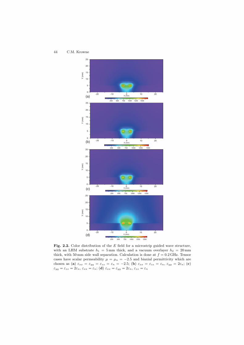
44 C.M. Krowne
25
(a)
(b)
(c)
(d)
20
15
10Y (
mm
)
5
0−20 −10
250 500 750 1000 1250 1500
0X (mm)
10 20
25
20
15
10Y (
mm
)
5
0−20 −10
250 500 750 1000 1250 1500
0X (mm)
10 20
25
20
15
10Y (
mm
)
5
0−20 −10
250 500 750 1000 1250 1500
0X (mm)
10 20
25
20
15
10Y (
mm
)
5
0−20 −10
250 500 750 1000 1250 1500
0X (mm)
10 20
Fig. 2.2. Color distribution of the E field for a microstrip guided wave structure,with an LHM substrate h1 = 5 mm thick, and a vacuum overlayer h2 = 20mmthick, with 50 mm side wall separation. Calculation is done at f = 0.2 GHz. Tensorcases have scalar permeability µ = µn = −2.5 and biaxial permittivity which arechosen as (a) εxx = εyy = εzz = εn = −2.5; (b) εxx = εzz = εn, εyy = 2εn; (c)εyy = εzz = 2εn, εxx = εn; (d) εxx = εyy = 2εn, εzz = εn
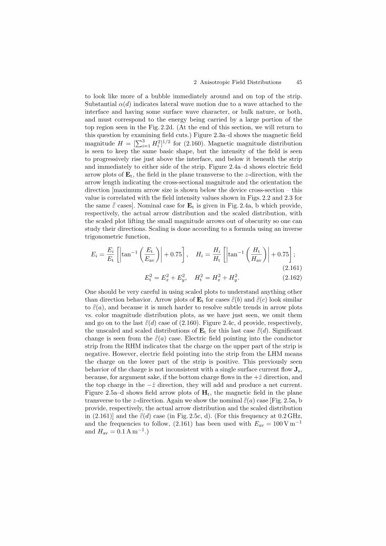
2 Anisotropic Field Distributions 45
to look like more of a bubble immediately around and on top of the strip.Substantial α(d) indicates lateral wave motion due to a wave attached to theinterface and having some surface wave character, or bulk nature, or both,and must correspond to the energy being carried by a large portion of thetop region seen in the Fig. 2.2d. (At the end of this section, we will return tothis question by examining field cuts.) Figure 2.3a–d shows the magnetic fieldmagnitude H = [
∑3i=1 H2
i ]1/2 for (2.160). Magnetic magnitude distributionis seen to keep the same basic shape, but the intensity of the field is seento progressively rise just above the interface, and below it beneath the stripand immediately to either side of the strip. Figure 2.4a–d shows electric fieldarrow plots of Et, the field in the plane transverse to the z-direction, with thearrow length indicating the cross-sectional magnitude and the orientation thedirection [maximum arrow size is shown below the device cross-section – thisvalue is correlated with the field intensity values shown in Figs. 2.2 and 2.3 forthe same ¯ε cases]. Nominal case for Et is given in Fig. 2.4a, b which provide,respectively, the actual arrow distribution and the scaled distribution, withthe scaled plot lifting the small magnitude arrows out of obscurity so one canstudy their directions. Scaling is done according to a formula using an inversetrigonometric function,
Ei =Ei
Et
[∣∣∣∣tan−1
(Et
Eav
)∣∣∣∣ + 0.75]
, Hi =Hi
Ht
[∣∣∣∣tan−1
(Ht
Hav
)∣∣∣∣ + 0.75]
;
(2.161)E2
t = E2x + E2
y , H2t = H2
x + H2y . (2.162)
One should be very careful in using scaled plots to understand anything otherthan direction behavior. Arrow plots of Et for cases ¯ε(b) and ¯ε(c) look similarto ¯ε(a), and because it is much harder to resolve subtle trends in arrow plotsvs. color magnitude distribution plots, as we have just seen, we omit themand go on to the last ¯ε(d) case of (2.160). Figure 2.4c, d provide, respectively,the unscaled and scaled distributions of Et for this last case ¯ε(d). Significantchange is seen from the ¯ε(a) case. Electric field pointing into the conductorstrip from the RHM indicates that the charge on the upper part of the strip isnegative. However, electric field pointing into the strip from the LHM meansthe charge on the lower part of the strip is positive. This previously seenbehavior of the charge is not inconsistent with a single surface current flow Js,because, for argument sake, if the bottom charge flows in the +z direction, andthe top charge in the −z direction, they will add and produce a net current.Figure 2.5a–d shows field arrow plots of Ht, the magnetic field in the planetransverse to the z-direction. Again we show the nominal ¯ε(a) case [Fig. 2.5a, bprovide, respectively, the actual arrow distribution and the scaled distributionin (2.161)] and the ¯ε(d) case (in Fig. 2.5c, d). (For this frequency at 0.2 GHz,and the frequencies to follow, (2.161) has been used with Eav = 100V m−1
and Hav = 0.1Am−1.)
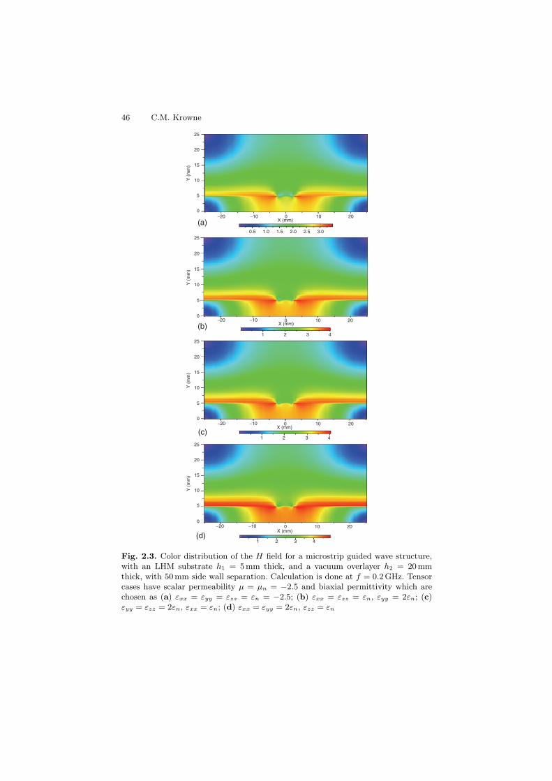
46 C.M. Krowne
25
(a)
(b)
(c)
(d)
20
15
10
5
0−20 −10 0
X (mm)
Y (
mm
)
10 20
25
20
15
10
5
0−20 −10 0
X (mm)
1 2
0.5 1.0 1.5 2.0 2.5 3.0
3 4
Y (
mm
)
10 20
25
20
15
10
5
0−20 −10 0
X (mm)
1 2 3 4
Y (
mm
)
10 20
25
20
15
10
5
0−20 −10 0
X (mm)
1 2 3 4
Y (
mm
)
10 20
Fig. 2.3. Color distribution of the H field for a microstrip guided wave structure,with an LHM substrate h1 = 5 mm thick, and a vacuum overlayer h2 = 20mmthick, with 50 mm side wall separation. Calculation is done at f = 0.2 GHz. Tensorcases have scalar permeability µ = µn = −2.5 and biaxial permittivity which arechosen as (a) εxx = εyy = εzz = εn = −2.5; (b) εxx = εzz = εn, εyy = 2εn; (c)εyy = εzz = 2εn, εxx = εn; (d) εxx = εyy = 2εn, εzz = εn
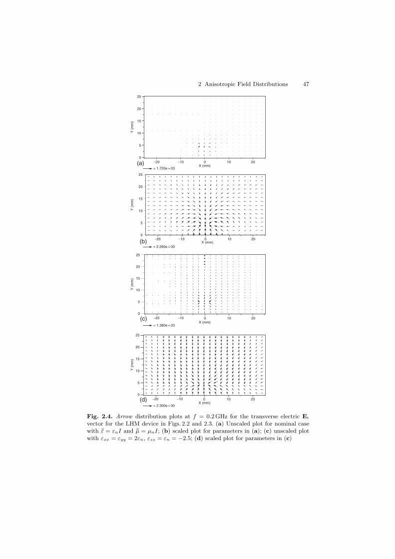
2 Anisotropic Field Distributions 47
25
20
15
10
5
0
(a)
(b)
(c)
(d)
−20
= 1.720e + 03
= 2.260e + 00
−10 10 200X (mm)
Y (
mm
)
25
20
15
10
5
0−20 −10 10 200
X (mm)
Y (
mm
)
= 1.380e + 03
25
20
15
10
5
0−20 −10 10 200
X (mm)
Y (
mm
)
= 2.300e + 00
25
20
15
10
5
0−20 −10 10 200
X (mm)
Y (
mm
)
Fig. 2.4. Arrow distribution plots at f = 0.2 GHz for the transverse electric Et
vector for the LHM device in Figs. 2.2 and 2.3. (a) Unscaled plot for nominal casewith ¯ε = εnI and ¯µ = µnI; (b) scaled plot for parameters in (a); (c) unscaled plotwith εxx = εyy = 2εn, εzz = εn = −2.5; (d) scaled plot for parameters in (c)
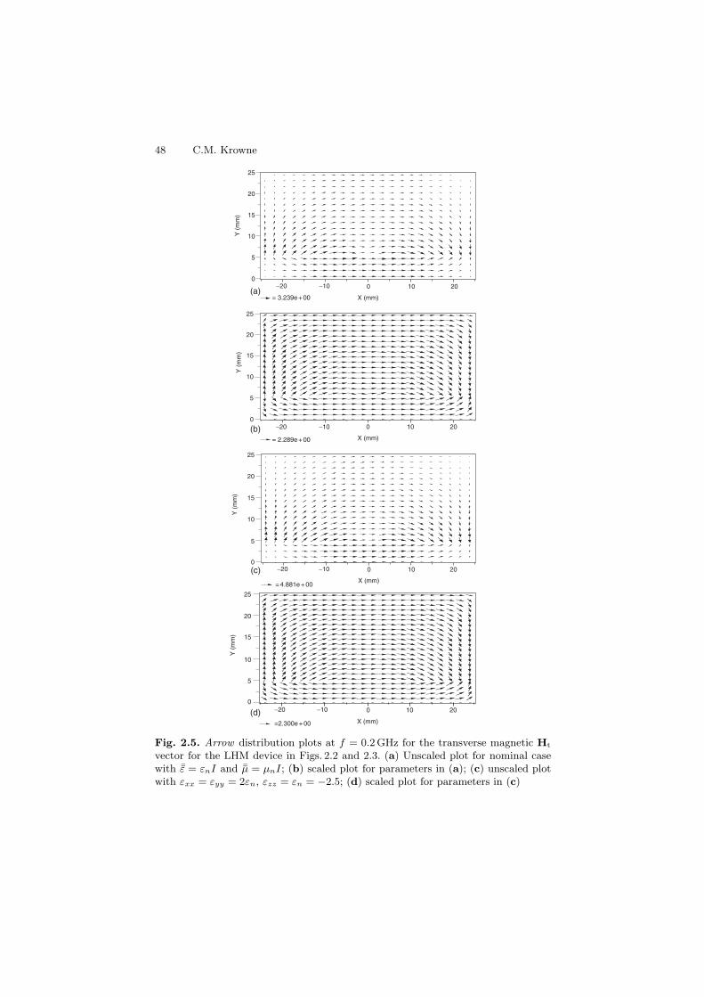
48 C.M. Krowne
25
20
15
10
5
0
(a)−20
= 3.239e + 00
−10 10 200
X (mm)
Y (
mm
)
(b)= 2.289e + 00
25
20
15
10
5
0−20 −10 10 200
X (mm)
Y (
mm
)
(c)
= 4.881e + 00
25
20
15
10
5
0−20 −10 10 200
X (mm)
Y (
mm
)
(d)=2.300e + 00
25
20
15
10
5
0−20 −10 10 200
X (mm)
Y (
mm
)
Fig. 2.5. Arrow distribution plots at f = 0.2 GHz for the transverse magnetic Ht
vector for the LHM device in Figs. 2.2 and 2.3. (a) Unscaled plot for nominal casewith ¯ε = εnI and ¯µ = µnI; (b) scaled plot for parameters in (a); (c) unscaled plotwith εxx = εyy = 2εn, εzz = εn = −2.5; (d) scaled plot for parameters in (c)
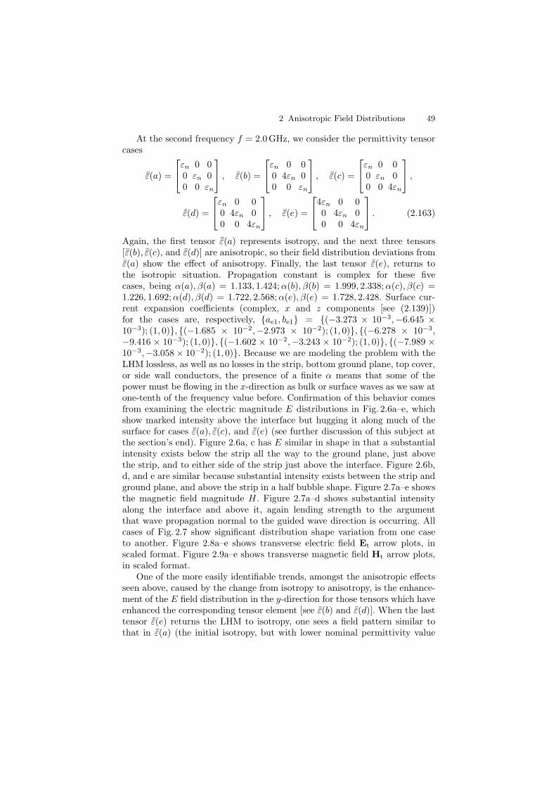
2 Anisotropic Field Distributions 49
At the second frequency f = 2.0GHz, we consider the permittivity tensorcases
¯ε(a) =
⎡⎣
εn 0 00 εn 00 0 εn
⎤⎦ , ¯ε(b) =
⎡⎣
εn 0 00 4εn 00 0 εn
⎤⎦ , ¯ε(c) =
⎡⎣
εn 0 00 εn 00 0 4εn
⎤⎦ ,
¯ε(d) =
⎡⎣
εn 0 00 4εn 00 0 4εn
⎤⎦ , ¯ε(e) =
⎡⎣
4εn 0 00 4εn 00 0 4εn
⎤⎦ . (2.163)
Again, the first tensor ¯ε(a) represents isotropy, and the next three tensors[¯ε(b), ¯ε(c), and ¯ε(d)] are anisotropic, so their field distribution deviations from¯ε(a) show the effect of anisotropy. Finally, the last tensor ¯ε(e), returns tothe isotropic situation. Propagation constant is complex for these fivecases, being α(a), β(a) = 1.133, 1.424;α(b), β(b) = 1.999, 2.338;α(c), β(c) =1.226, 1.692;α(d), β(d) = 1.722, 2.568;α(e), β(e) = 1.728, 2.428. Surface cur-rent expansion coefficients (complex, x and z components [see (2.139)])for the cases are, respectively, ae1, be1 = (−3.273 × 10⁻³,−6.645 ×10⁻³); (1, 0), (−1.685 × 10⁻²,−2.973 × 10⁻²); (1, 0), (−6.278 × 10⁻³,−9.416 × 10⁻³); (1, 0), (−1.602 × 10⁻²,−3.243 × 10⁻²); (1, 0), (−7.989 ×10⁻³,−3.058 × 10⁻²); (1, 0). Because we are modeling the problem with theLHM lossless, as well as no losses in the strip, bottom ground plane, top cover,or side wall conductors, the presence of a finite α means that some of thepower must be flowing in the x-direction as bulk or surface waves as we saw atone-tenth of the frequency value before. Confirmation of this behavior comesfrom examining the electric magnitude E distributions in Fig. 2.6a–e, whichshow marked intensity above the interface but hugging it along much of thesurface for cases ¯ε(a), ¯ε(c), and ¯ε(e) (see further discussion of this subject atthe section’s end). Figure 2.6a, c has E similar in shape in that a substantialintensity exists below the strip all the way to the ground plane, just abovethe strip, and to either side of the strip just above the interface. Figure 2.6b,d, and e are similar because substantial intensity exists between the strip andground plane, and above the strip in a half bubble shape. Figure 2.7a–e showsthe magnetic field magnitude H. Figure 2.7a–d shows substantial intensityalong the interface and above it, again lending strength to the argumentthat wave propagation normal to the guided wave direction is occurring. Allcases of Fig. 2.7 show significant distribution shape variation from one caseto another. Figure 2.8a–e shows transverse electric field Et arrow plots, inscaled format. Figure 2.9a–e shows transverse magnetic field Ht arrow plots,in scaled format.
One of the more easily identifiable trends, amongst the anisotropic effectsseen above, caused by the change from isotropy to anisotropy, is the enhance-ment of the E field distribution in the y-direction for those tensors which haveenhanced the corresponding tensor element [see ¯ε(b) and ¯ε(d)]. When the lasttensor ¯ε(e) returns the LHM to isotropy, one sees a field pattern similar tothat in ¯ε(a) (the initial isotropy, but with lower nominal permittivity value
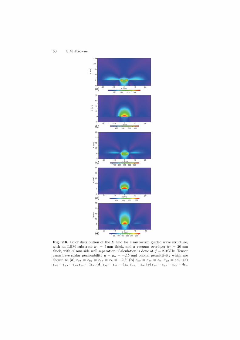
50 C.M. Krowne
25
20
15
10
5
0−20 −10
125 250 375 500
125 250 375 500 625
0X (mm)
Y (
mm
)
10 20
25
20
15
10
5
0−20 −10
200 400 600 800
0X (mm)
Y (
mm
)
10 20
25
20
15
10
5
0−20 −10 0
X (mm)
Y (
mm
)
10 20
125 250 375 500
50 100 150 200 250 300
25
20
15
10
5
0−20 −10 0
X (mm)
Y (
mm
)
10 20
25
20
15
10
5
0−20 −10 0
X (mm)
Y (
mm
)
10 20
(a)
(b)
(c)
(d)
(e)
Fig. 2.6. Color distribution of the E field for a microstrip guided wave structure,with an LHM substrate h1 = 5 mm thick, and a vacuum overlayer h2 = 20mmthick, with 50 mm side wall separation. Calculation is done at f = 2.0 GHz. Tensorcases have scalar permeability µ = µn = −2.5 and biaxial permittivity which arechosen as (a) εxx = εyy = εzz = εn = −2.5; (b) εxx = εzz = εn, εyy = 4εn; (c)εxx = εyy = εn, εzz = 4εn; (d) εyy = εzz = 4εn, εxx = εn; (e) εxx = εyy = εzz = 4εn
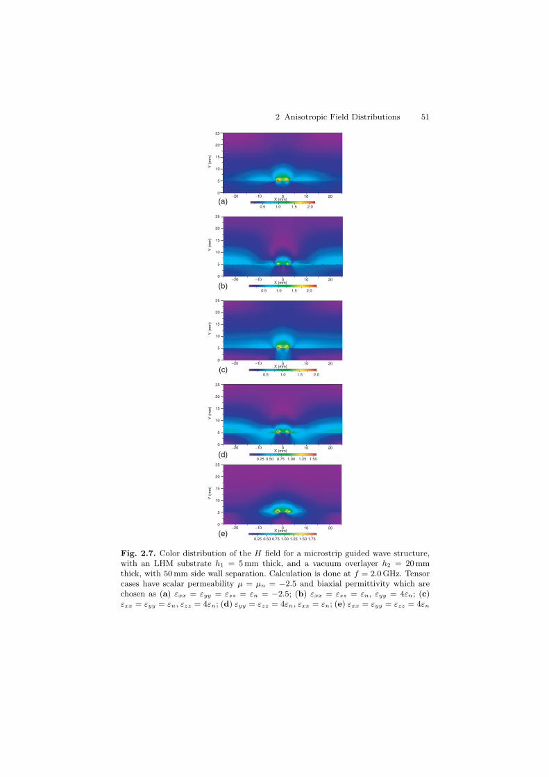
2 Anisotropic Field Distributions 51
−20 −10 0 10 20
25
20
15
10
5
0
X (mm)
Y (
mm
)0.5 1.0 1.5 2.0
−20 −10 0 10 20
25
20
15
10
5
0
X (mm)
Y (
mm
)
0.5 1.0 1.5 2.0
−20 −10 0 10 20
25
20
15
10
5
0
X (mm)
Y (
mm
)
0.5 1.0 1.5 2.0
−20 −10 0 10 20
25
20
15
10
5
0
X (mm)
Y (
mm
)
0.25 0.50 0.75 1.00 1.25 1.50
0.25 0.50 0.75 1.00 1.25 1.50 1.75
−20 −10 0 10 20
25
20
15
10
5
0
X (mm)
Y (
mm
)
(a)
(b)
(c)
(d)
(e)
Fig. 2.7. Color distribution of the H field for a microstrip guided wave structure,with an LHM substrate h1 = 5 mm thick, and a vacuum overlayer h2 = 20mmthick, with 50 mm side wall separation. Calculation is done at f = 2.0 GHz. Tensorcases have scalar permeability µ = µn = −2.5 and biaxial permittivity which arechosen as (a) εxx = εyy = εzz = εn = −2.5; (b) εxx = εzz = εn, εyy = 4εn; (c)εxx = εyy = εn, εzz = 4εn; (d) εyy = εzz = 4εn, εxx = εn; (e) εxx = εyy = εzz = 4εn
52 C.M. Krowne
(c) −20 −10 0 10 20
25
20
15
10
5
0
X (mm)
Y (
mm
)
= 2.173e+00
−20 −10 0 10 20
25
20
15
10
5
0
X (mm)
Y (
mm
)
= 1.796e+00(e)
−20 −10 0 10 20
25
20
15
10
5
0
(a)X (mm)
Y (
mm
)
= 2.151e+00
(b) −20 −10 0 10 20
25
20
15
10
5
0
X (mm)
Y (
mm
)
= 2.210e+00
(d) −20 −10 0 10 20
25
20
15
10
5
0
X (mm)
Y (
mm
)
= 2.000e+00
Fig. 2.8. Arrow distribution plots at f = 2.0 GHz for the transverse electric Et
vector for the LHM device in Figs. 2.2 and 2.3. All plots are scaled – tensor caseshave scalar permeability µ = µn = −2.5 and biaxial permittivity which are chosen as(a) εxx = εyy = εzz = εn = −2.5; (b) εxx = εzz = εn, εyy = 4εn; (c) εxx = εyy = εn,εzz = 4εn; (d) εyy = εzz = 4εn, εxx = εn; (e) εxx = εyy = εzz = 4εn
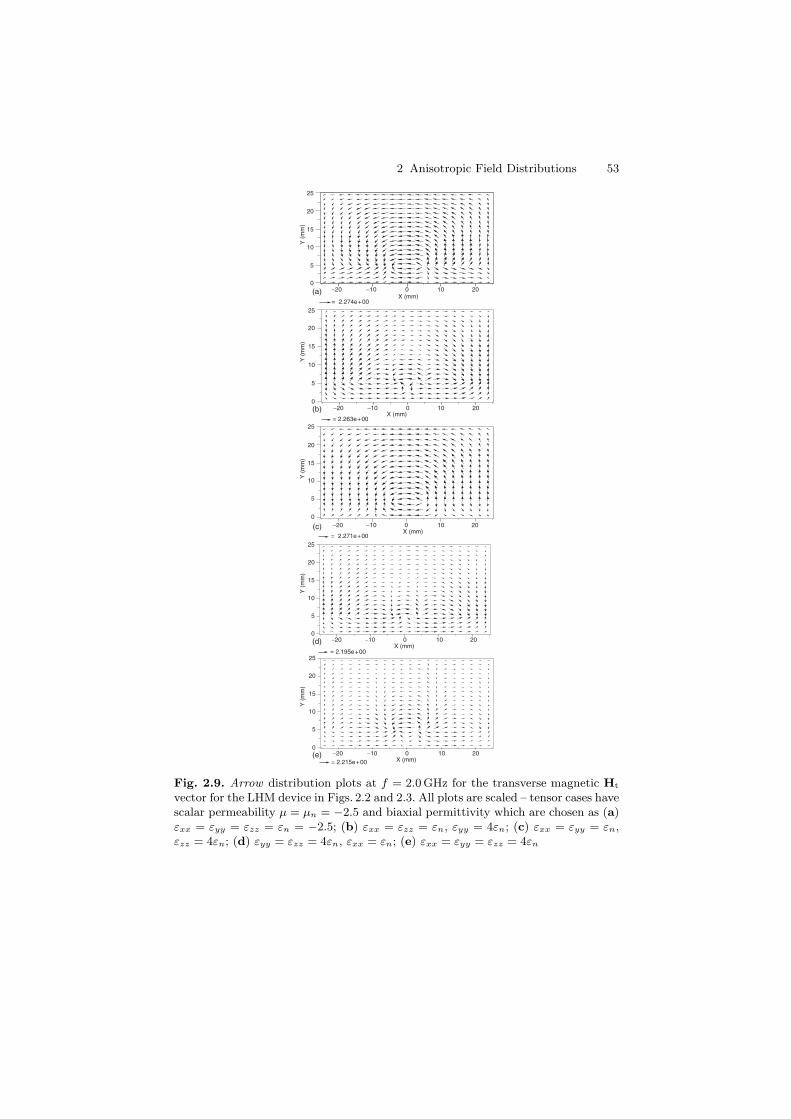
2 Anisotropic Field Distributions 53
25
20
15
10
5
0
X (mm)
Y (
mm
)
= 2.195e+0025
20
15
10
5
0
Y (
mm
)
= 2.215e+00
−20 −10 0 10 20
−20 −10 0 10 20
X (mm)−20 −10 0 10 20
25
20
15
10
5
0
X (mm)
Y (
mm
)
= 2.271e+00
−20 −10 0 10 20
25
20
15
10
5
0
(a)
(b)
(c)
(d)
(e)
X (mm)Y
(m
m)
= 2.274e+00
−20 −10 0 10 20
25
20
15
10
5
0
X (mm)
Y (
mm
)
= 2.263e+00
Fig. 2.9. Arrow distribution plots at f = 2.0 GHz for the transverse magnetic Ht
vector for the LHM device in Figs. 2.2 and 2.3. All plots are scaled – tensor cases havescalar permeability µ = µn = −2.5 and biaxial permittivity which are chosen as (a)εxx = εyy = εzz = εn = −2.5; (b) εxx = εzz = εn, εyy = 4εn; (c) εxx = εyy = εn,εzz = 4εn; (d) εyy = εzz = 4εn, εxx = εn; (e) εxx = εyy = εzz = 4εn
54 C.M. Krowne
than the final tensor), but with the added effect of enhanced E field behaviorin the y-direction above the strip, as seen in the intervening anisotropic cases.
To gain some idea of the vast differences between LHM and RHM sub-strates affecting the field distribution, the last figure after the LHM figures(Figs. 2.2–2.16), Fig. 2.17 gives the electric field distributions for an RHMsubstrate with the same nominal permittivity magnitude value as the LHM,making its εn = 2.5 (µ = 1.0 nonmagnetic) at f = 2.0GHz. Again five ten-sors are treated as in (2.163) (here the multiplicative factor used was 2). Onenotes that in all the cases shown, ¯ε(a)–¯ε(e), the primary feature is the pre-ponderance of electric field magnitude in the RHM substrate and below themetal strip. Secondary feature, arising from the presence of the inflated ytensor element εyy, is the notch effect, that is, the appearance of a dimple ornotch between the edges of the strip above the substrate corresponding to afield magnitude reduction, which is also associated with enhancement of thefield magnitude below the interface under the strip. Comparison of the casesin Fig. 2.17 with those in Fig. 2.6 shows that an LHM substrate allows vastchanges in the field distributions, and that its anisotropy directly affects thefield distribution.
Finally, at the third frequency f = 20GHz, we consider the permittivitytensor cases
¯ε(a) =
⎡⎣
εn 0 00 εn 00 0 εn
⎤⎦ , ¯ε(b) =
⎡⎣
εn 0 00 4εn 00 0 εn
⎤⎦ , ¯ε(c) =
⎡⎣
εn 0 00 4εn 00 0 4εn
⎤⎦ ,
¯ε(d) =
⎡⎣
4εn 0 00 4εn 00 0 εn
⎤⎦ , ¯ε(e) =
⎡⎣
4εn 0 00 4εn 00 0 4εn
⎤⎦ . (2.164)
As in the previous frequency cases, here again one starts out withisotropy, and finishes with isotropy for this frequency as in the last case.Deviation from these two bounding cases demonstrates the effects ofanisotropy. Propagation constant reverts back to a pure phase charac-teristic for all but the second and third cases in these five cases, beingβ(a) = 2.394; α(b), β(b) = 1.324 × 10⁻³, 3.653; α(c), β(c) = 1.630 × 10−3,3.721; β(d) = 3.699; β(e) = 3.730. Surface current expansion coefficients(complex, x and z components [see (2.139)]) for the cases are, respec-tively, ae1, be1 = (0,−0.5338); (1, 0), (1.110 × 10⁻³,−0.4390); (1, 0),(−2.505× 10⁻³,−0.2248); (1, 0), ((1, 0); (0, 0.5368), (0,−0.5371); (1, 0).All of the electric magnitudes E look different from each other as seen inFig. 2.10a–e. But some of the overall trends can be discerned. For exam-ple, below the interface intensity maxima and minima occur periodically.This x-variation must be due to the effective wavelength in that direc-tion. Although it must be determined numerically, and its value found bycounting two successive maxima and minima in the plot, an estimate canbe calculated as λ = λ0/
√εxx = 15mm/
√εxx at 20 GHz. For cases (a)
and (d),√
εxx(a) =√
εn =√
2.5 = 1.58 making λ(a) = 9.5mm, and
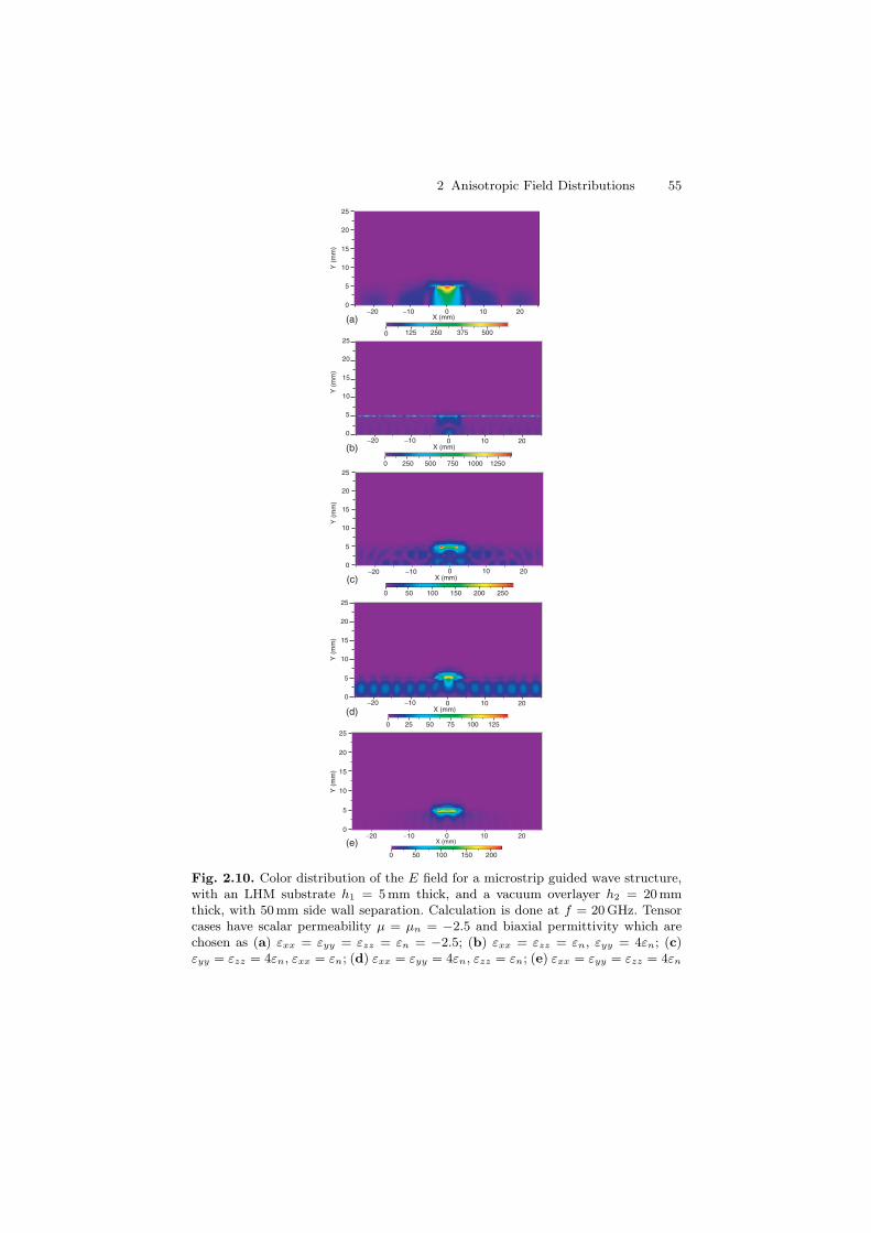
2 Anisotropic Field Distributions 55
−20 −10 0 10 20
25
20
15
10
5
0
(a)
(b)
(c)
(d)
(e)
X (mm)
Y (
mm
)0 125 250 375 500
−20 −10 0 10 20
25
20
15
10
5
0
X (mm)
Y (
mm
)
0 250 500 750 1000 1250
−20 −10 0 10 20
25
20
15
10
5
0
X (mm)
Y (
mm
)
0 50 100 150 200 250
−20 −10 0 10 20
25
20
15
10
5
0
X (mm)
Y (
mm
)Y
(m
m)
0 25 50 75 100 125
−20 −10 0 10 20
25
20
15
10
5
0
X (mm)
0 50 100 150 200
Fig. 2.10. Color distribution of the E field for a microstrip guided wave structure,with an LHM substrate h1 = 5 mm thick, and a vacuum overlayer h2 = 20mmthick, with 50mm side wall separation. Calculation is done at f = 20 GHz. Tensorcases have scalar permeability µ = µn = −2.5 and biaxial permittivity which arechosen as (a) εxx = εyy = εzz = εn = −2.5; (b) εxx = εzz = εn, εyy = 4εn; (c)εyy = εzz = 4εn, εxx = εn; (d) εxx = εyy = 4εn, εzz = εn; (e) εxx = εyy = εzz = 4εn
56 C.M. Krowne
√εxx(d) =
√4εn = 2
√2.5 = 3.16 making λ(d) = 4.75mm. This translates
into about five periods for case (a) and 10.5 periods for case (d) in the2b = 50mm width. Inspection of Fig. 2.10a, d shows that the actual numberis slightly less, roughly 3.25 and 7.5. All cases except (b) have the largestintensity around the strip, with significant field below the strip for cases(a) and (d), with case (a) being much more than case (d). Cases (c)–(e) inFig. 2.10 have some field just above the strip. Finally, case (b) in Fig. 2.10has only a remnant of a field around the strip, but very noticeable field alongthe interface, extending all the way to both side walls. Case (b) in Fig. 2.10appears to be a clear example of a surface wave, although it is not obviousbased upon the α/β ratio being so small. However, this could occur if thesurface wave is predominantly in the same direction as the guided wave,the z-direction (see section end for more discussion). Figure 2.11a–e showsthe magnetic field magnitude H, and like the E field plots the periodicityvariation along the x-direction is seen here also, as well as all cases havingsignificant field around the strip. Surface wave characteristic is again clearlydemonstrated in Fig. 2.11b. Figure 2.12a–e shows transverse electric field Et
arrow plots, in scaled format. We notice that in all cases except ¯ε(b), thearrows immediately above and below the strip point in or out, indicatingopposite charges on the two sides of the conductor strip, an observation madeearlier in regard to behavior at f = 0.2GHz. However, for ¯ε(b),Et arrowspoint upward above and below the strip, indicating positive charge on bothsides of the conductor. Figure 2.13a–e shows transverse magnetic field Ht
arrow plots, in scaled format. As seen for the previous frequency case, tensorelement enhancement of the y element tends to push the E field distributionto being just below the strip or above the strip. However, at this frequency,the bubble shape is more squished in appearance.
In order to discern the field variation in the LHM structure in anotherway, other than the cross-sectional 2D visualization techniques already cov-ered, simple cuts for specific x or y values may be taken. Here an x cut atx = 15mm will be done, purposely with x = 0 to avoid going through thestrip, with the interval broken into 100 points. One case is chosen from eachfrequency previously studied, to illustrate the cross-sectional field componentvariations against x. The cases are ¯ε(d) for f = 0.2GHz, ¯ε(c) for f = 2GHz,and ¯ε(b) for f = 20GHz. All results are for nx = nz = 1, n = 200, except forFigs. 2.14a and 2.15a done with nx = nz = 5, n = 600 to capture the interfacialEx continuity better and for Fig. 2.16c to capture the interfacial Hx continuitybetter (see Table 2.1 for the surface current coefficients used for these excep-tions). At f = 0.2GHz (Fig. 2.14), other than the sign switches in Ey and Hy
which occur because of continuity of normal components of D or B across theinterface at x = 15mm (magnitude and sign of the difference in values of thenormal electric field component on either side of the interface is controlled byεtopEytop = εLHMEyLHM, or the permittivity ratio 1/2εn = −1/5; magnitudeand sign of the difference in values of the normal magnetic field componenton either side of the interface is controlled by µtopHytop = µLHMHyLHM,
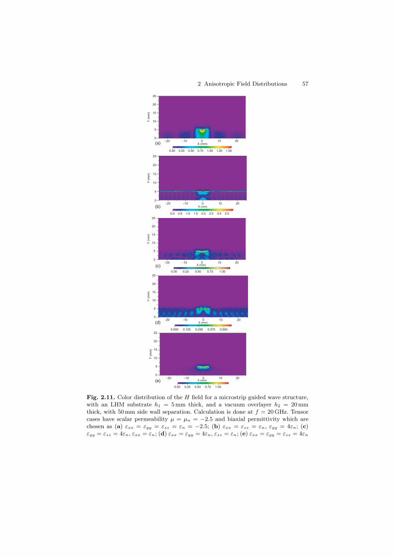
2 Anisotropic Field Distributions 57
−20 −10 0 10 20
25
20
15
10
5
0
(a)
(b)
(c)
(d)
(e)
X (mm)Y
(m
m)
0.00 0.25 0.50 0.75 1.00 1.25 1.50
−20 −10 0 10 20
25
20
15
10
5
0
X (mm)
Y (
mm
)
0.0 0.5 1.0 1.5 2.0 2.5 3.0 3.5
−20 −10 0 10 20
25
20
15
10
5
0
X (mm)
Y (
mm
)
0.00 0.25 0.50 0.75 1.00
−20 −10 0 10 20
25
20
15
10
5
0
X (mm)
Y (
mm
)
0.000 0.125 0.250 0.375 0.500
−20 −10 0 10 20
25
20
15
10
5
0
X (mm)
Y (
mm
)
0.00 0.25 0.50 0.75 1.00
Fig. 2.11. Color distribution of the H field for a microstrip guided wave structure,with an LHM substrate h1 = 5 mm thick, and a vacuum overlayer h2 = 20mmthick, with 50mm side wall separation. Calculation is done at f = 20 GHz. Tensorcases have scalar permeability µ = µn = −2.5 and biaxial permittivity which arechosen as (a) εxx = εyy = εzz = εn = −2.5; (b) εxx = εzz = εn, εyy = 4εn; (c)εyy = εzz = 4εn, εxx = εn; (d) εxx = εyy = 4εn, εzz = εn; (e) εxx = εyy = εzz = 4εn
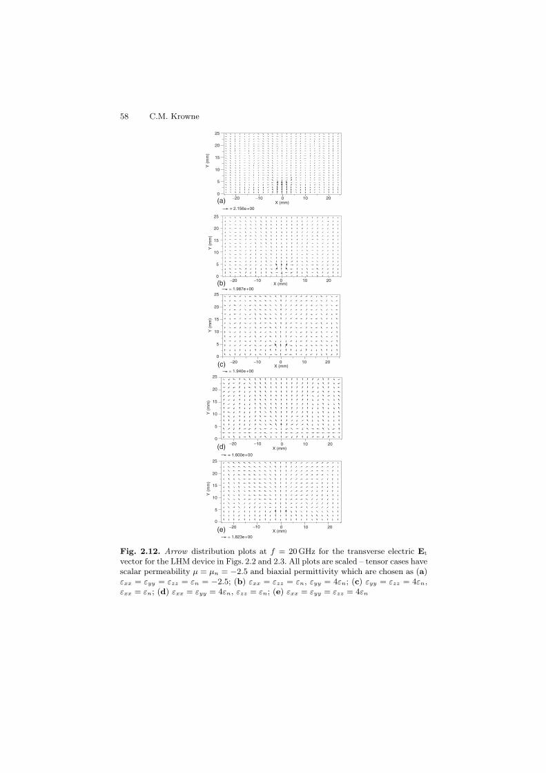
58 C.M. Krowne
−20 −10 0 10 20
25
20
15
10
5
0
(a)
(b)
(c)
(d)
(e)
X (mm)Y
(m
m)
= 2.156e+00
−20 −10 0 10 20
25
20
15
10
5
0
X (mm)
Y (
mm
)
= 1.987e+00
−20 −10 0 10 20
25
20
15
10
5
0
X (mm)
Y (
mm
)
−20 −10 0 10 20
25
20
15
10
5
0
X (mm)
Y (
mm
)
−20 −10 0 10 20
25
20
15
10
5
0
X (mm)
Y (
mm
)
= 1.940e+00
= 1.600e+00
= 1.823e+00
Fig. 2.12. Arrow distribution plots at f = 20GHz for the transverse electric Et
vector for the LHM device in Figs. 2.2 and 2.3. All plots are scaled – tensor cases havescalar permeability µ = µn = −2.5 and biaxial permittivity which are chosen as (a)εxx = εyy = εzz = εn = −2.5; (b) εxx = εzz = εn, εyy = 4εn; (c) εyy = εzz = 4εn,εxx = εn; (d) εxx = εyy = 4εn, εzz = εn; (e) εxx = εyy = εzz = 4εn
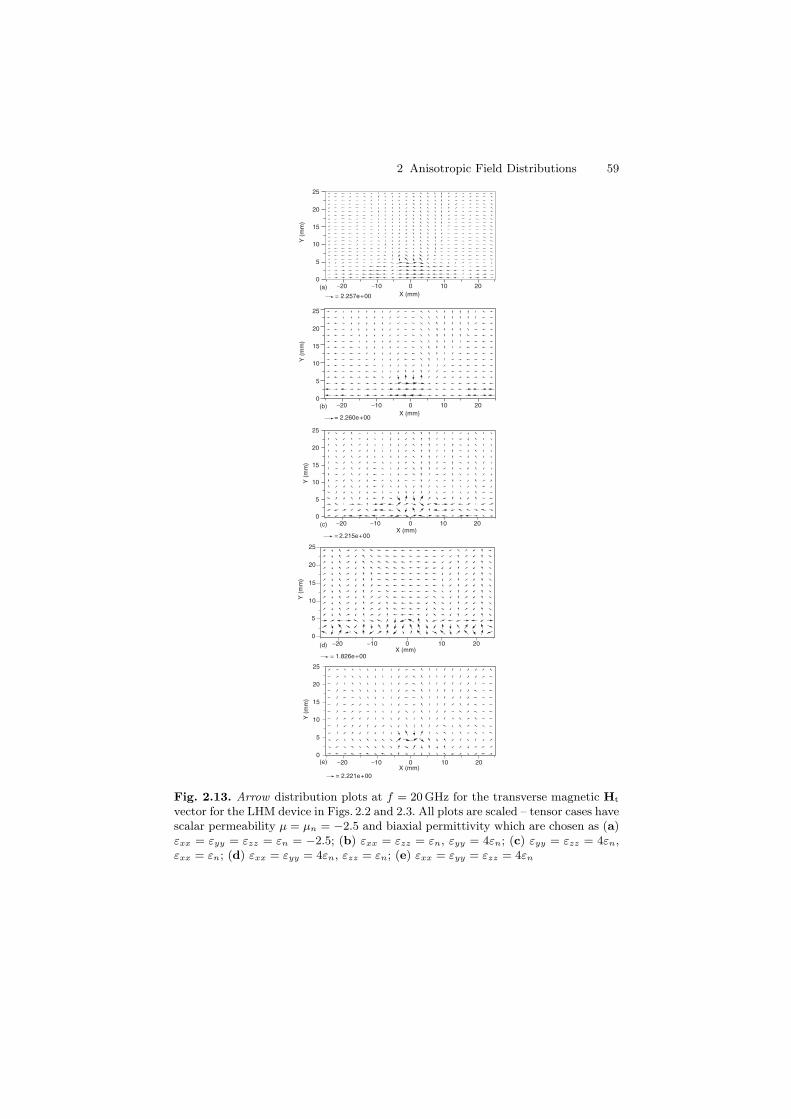
2 Anisotropic Field Distributions 59
−20 −10 0 10 20
25
20
15
10
5
0(a)
(b)
(c)
(d)
(e)
X (mm)Y
(m
m)
−20 −10 0 10 20
25
20
15
10
5
0
X (mm)
Y (
mm
)= 2.257e+00
= 2.260e+00
−20 −10 0 10 20
25
20
15
10
5
0
X (mm)
Y (
mm
)
= 2.215e+00
−20 −10 0 10 20
25
20
15
10
5
0
X (mm)
Y (
mm
)
= 2.221e+00
−20 −10 0 10 20
25
20
15
10
5
0
X (mm)
Y (
mm
)
= 1.826e+00
Fig. 2.13. Arrow distribution plots at f = 20GHz for the transverse magnetic Ht
vector for the LHM device in Figs. 2.2 and 2.3. All plots are scaled – tensor cases havescalar permeability µ = µn = −2.5 and biaxial permittivity which are chosen as (a)εxx = εyy = εzz = εn = −2.5; (b) εxx = εzz = εn, εyy = 4εn; (c) εyy = εzz = 4εn,εxx = εn; (d) εxx = εyy = 4εn, εzz = εn; (e) εxx = εyy = εzz = 4εn
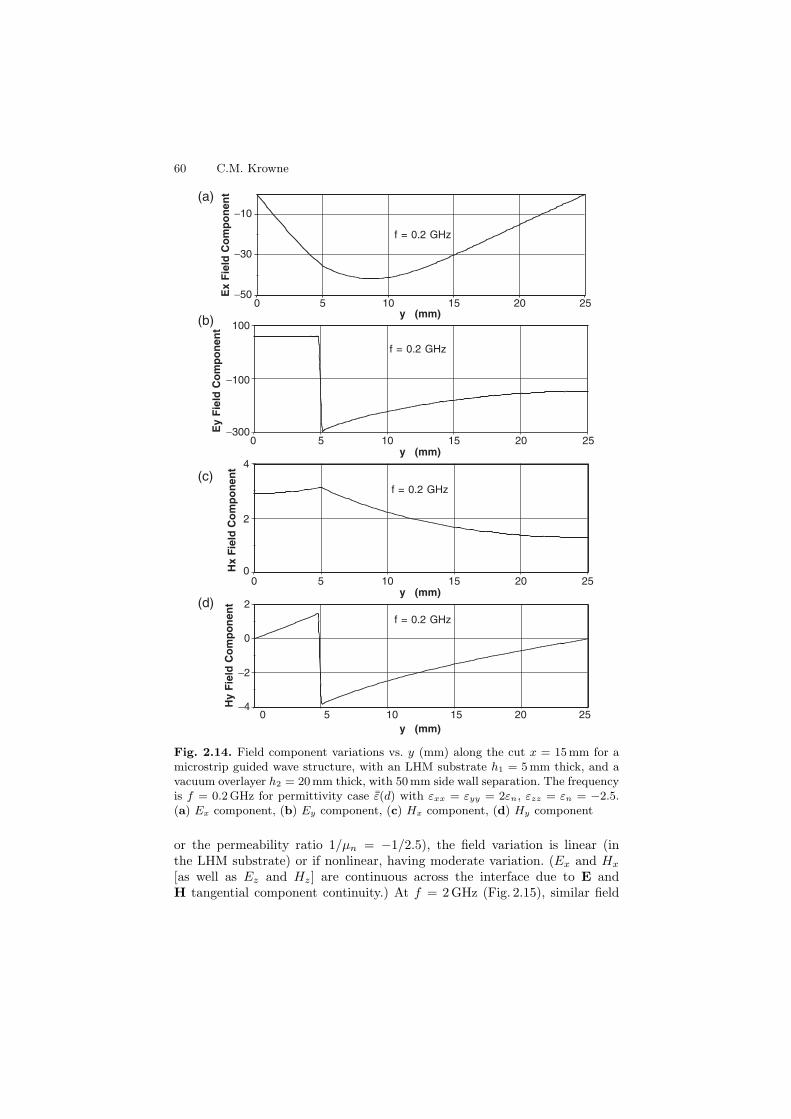
60 C.M. Krowne
−50
−30
−10
0 5 10 15 20 25y (mm)
f = 0.2 GHz
−300
−100
100
0 5 10 15 20 25y (mm)
f = 0.2 GHz
0
2
4
0 5 10 15 20 25y (mm)
−4
−2
0
2
0 5 10 15 20 25y (mm)
(c)
(d)
f = 0.2 GHz
f = 0.2 GHz
Hx
Fie
ld C
om
po
nen
t H
y F
ield
Co
mp
on
ent
Ey
Fie
ld C
om
po
nen
tE
x F
ield
Co
mp
on
ent(a)
(b)
Fig. 2.14. Field component variations vs. y (mm) along the cut x = 15mm for amicrostrip guided wave structure, with an LHM substrate h1 = 5 mm thick, and avacuum overlayer h2 = 20 mm thick, with 50 mm side wall separation. The frequencyis f = 0.2 GHz for permittivity case ¯ε(d) with εxx = εyy = 2εn, εzz = εn = −2.5.(a) Ex component, (b) Ey component, (c) Hx component, (d) Hy component
or the permeability ratio 1/µn = −1/2.5), the field variation is linear (inthe LHM substrate) or if nonlinear, having moderate variation. (Ex and Hx
[as well as Ez and Hz] are continuous across the interface due to E andH tangential component continuity.) At f = 2GHz (Fig. 2.15), similar field
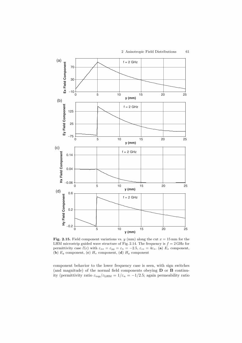
2 Anisotropic Field Distributions 61
−0.06
0.04
0.14
0 5 10 15 20 25
−75
25
125
0 5 10 15 20 25
−0.2
0.2
0.6
0 5 10 15 20 25
(b)
(a)
f = 2 GHz
f = 2 GHz
f = 2 GHz
−10
30
70
0 5 10 15 20y (mm)
y (mm)
y (mm)
y (mm)
25
f = 2 GHzE
y F
ield
Co
mp
on
ent
Ex
Fie
ld C
om
po
nen
tH
x F
ield
Co
mp
on
ent
(c)
Hy
Fie
ld C
om
po
nen
t
(d)
Fig. 2.15. Field component variations vs. y (mm) along the cut x = 15mm for theLHM microstrip guided wave structure of Fig. 2.14. The frequency is f = 2 GHz forpermittivity case ¯ε(c) with εxx = εyy = εn = −2.5, εzz = 4εn. (a) Ex component,(b) Ey component, (c) Hx component, (d) Hy component
component behavior to the lower frequency case is seen, with sign switches(and magnitude) of the normal field components obeying D or B continu-ity (permittivity ratio εtop/εLHM = 1/εn = −1/2.5; again permeability ratio
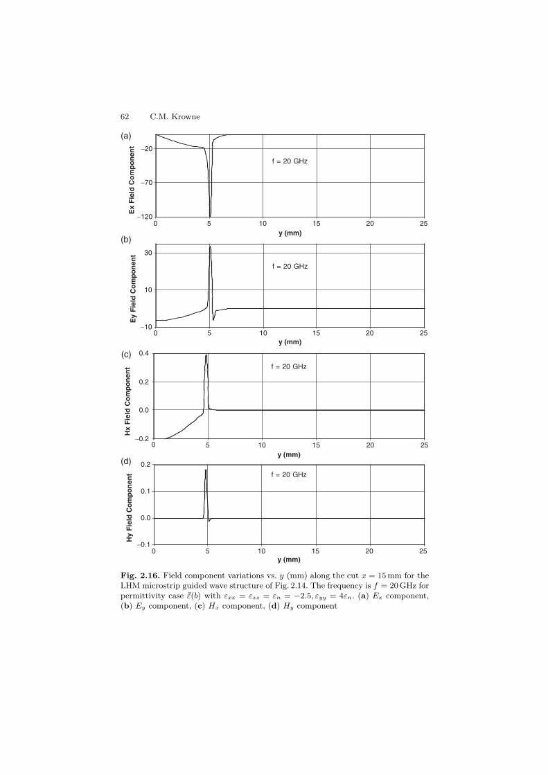
62 C.M. Krowne
−0.2
0.0
0.2
0.4
0 5 10 15 20 25
−0.1
0.0
0.1
0.2
0 5 10 15 20 25
−10
10
30
0 5 10 15 20 25
−120
−70
−20
0 5 10 15y (mm)
y (mm)
y (mm)
y (mm)
20 25
(b)
(d)
f = 20 GHz
f = 20 GHz
f = 20 GHz
f = 20 GHz
Ex
Fie
ld C
om
po
nen
tE
y F
ield
Co
mp
on
ent
Hx
Fie
ld C
om
po
nen
t(a)
(c)
Hy
Fie
ld C
om
po
nen
t
Fig. 2.16. Field component variations vs. y (mm) along the cut x = 15mm for theLHM microstrip guided wave structure of Fig. 2.14. The frequency is f = 20GHz forpermittivity case ¯ε(b) with εxx = εzz = εn = −2.5, εyy = 4εn. (a) Ex component,(b) Ey component, (c) Hx component, (d) Hy component
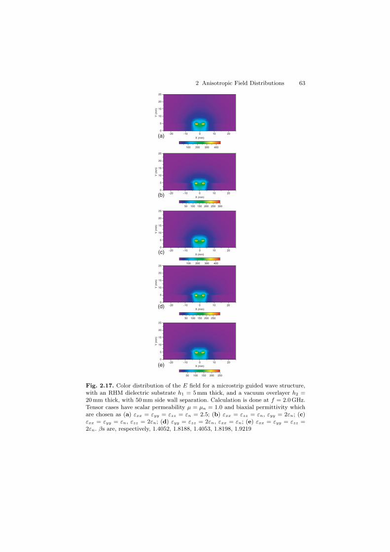
2 Anisotropic Field Distributions 63
−20 −10 0 10 20
25
20
15
10
5
0
X (mm)
Y (
mm
)
50 100 150 200 250 300
−20 −10 0 10 20
25
20
15
10
5
0
(a)
(b)
(c)
(d)
(e)
X (mm)
Y (
mm
)
100 200 300 400
−20 −10 0 10 20
25
20
15
10
5
0
X (mm)
Y (
mm
)
100 200 300 400
−20 −10 0 10 20
25
20
15
10
5
0
X (mm)
X (mm)
Y (
mm
)
50 100 150 200 250
−20 −10 0 10 20
25
20
15
10
5
0
Y (
mm
)
50 100 150 200 250
Fig. 2.17. Color distribution of the E field for a microstrip guided wave structure,with an RHM dielectric substrate h1 = 5 mm thick, and a vacuum overlayer h2 =20 mm thick, with 50 mm side wall separation. Calculation is done at f = 2.0 GHz.Tensor cases have scalar permeability µ = µn = 1.0 and biaxial permittivity whichare chosen as (a) εxx = εyy = εzz = εn = 2.5; (b) εxx = εzz = εn, εyy = 2εn; (c)εxx = εyy = εn, εzz = 2εn; (d) εyy = εzz = 2εn, εxx = εn; (e) εxx = εyy = εzz =2εn. βs are, respectively, 1.4052, 1.8188, 1.4053, 1.8198, 1.9219
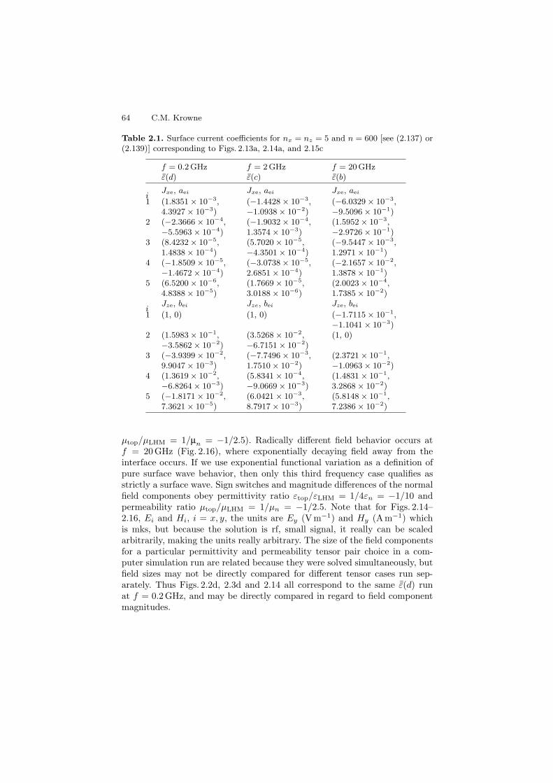
64 C.M. Krowne
Table 2.1. Surface current coefficients for nx = nz = 5 and n = 600 [see (2.137) or(2.139)] corresponding to Figs. 2.13a, 2.14a, and 2.15c
f = 0.2 GHz f = 2 GHz f = 20 GHz¯ε(d) ¯ε(c) ¯ε(b)
iJxe, aei Jxe, aei Jxe, aei
1 (1.8351 × 10−3,4.3927 × 10−3)
(−1.4428 × 10⁻³,−1.0938 × 10⁻²)
(−6.0329 × 10⁻³,−9.5096 × 10⁻¹)
2 (−2.3666 × 10⁻⁴,−5.5963 × 10⁻⁴)
(−1.9032 × 10−4,1.3574 × 10−3)
(1.5952 × 10⁻³,−2.9726 × 10⁻¹)
3 (8.4232 × 10−5,1.4838 × 10−4)
(5.7020 × 10⁻⁵,−4.3501 × 10⁻⁴)
(−9.5447 × 10−3,1.2971 × 10−1)
4 (−1.8509 × 10⁻⁵,−1.4672 × 10⁻⁴)
(−3.0738 × 10−5,2.6851 × 10−4)
(−2.1657 × 10−2,1.3878 × 10−1)
5 (6.5200 × 10−6,4.8388 × 10−5)
(1.7669 × 10−5,3.0188 × 10−6)
(2.0023 × 10−4,1.7385 × 10−2)
iJze, bei Jze, bei Jze, bei
1 (1, 0) (1, 0) (−1.7115 × 10⁻¹,−1.1041 × 10⁻³)
2 (1.5983 × 10⁻¹,−3.5862 × 10⁻²)
(3.5268 × 10⁻²,−6.7151 × 10⁻²)
(1, 0)
3 (−3.9399 × 10−2,9.9047 × 10−3)
(−7.7496 × 10−3,1.7510 × 10−2)
(2.3721 × 10⁻¹,−1.0963 × 10⁻²)
4 (1.3619 × 10⁻²,−6.8264 × 10⁻³)
(5.8341 × 10⁻⁴,−9.0669 × 10⁻³)
(1.4831 × 10−1,3.2868 × 10−2)
5 (−1.8171 × 10−2,7.3621 × 10−5)
(6.0421 × 10−3,8.7917 × 10−3)
(5.8148 × 10−1,7.2386 × 10−2)
µtop/µLHM = 1/µn = −1/2.5). Radically different field behavior occurs atf = 20GHz (Fig. 2.16), where exponentially decaying field away from theinterface occurs. If we use exponential functional variation as a definition ofpure surface wave behavior, then only this third frequency case qualifies asstrictly a surface wave. Sign switches and magnitude differences of the normalfield components obey permittivity ratio εtop/εLHM = 1/4εn = −1/10 andpermeability ratio µtop/µLHM = 1/µn = −1/2.5. Note that for Figs. 2.14–2.16, Ei and Hi, i = x, y, the units are Ey (V m−1) and Hy (A m−1) whichis mks, but because the solution is rf, small signal, it really can be scaledarbitrarily, making the units really arbitrary. The size of the field componentsfor a particular permittivity and permeability tensor pair choice in a com-puter simulation run are related because they were solved simultaneously, butfield sizes may not be directly compared for different tensor cases run sep-arately. Thus Figs. 2.2d, 2.3d and 2.14 all correspond to the same ¯ε(d) runat f = 0.2GHz, and may be directly compared in regard to field componentmagnitudes.
2 Anisotropic Field Distributions 65
2.1.5 Conclusion
In this Section a complete treatment of the theoretical process for modelinganisotropic left-handed materials (LHM) in guided wave structures has beengiven. With that formulation, a specific structure had been chosen to study,the single microstrip guided wave device loaded with LHM. Three frequencybands were identified to study, and calculations done at three frequency pointswithin those bands. Field magnitude color distribution plots have been pro-duced for electric E and magnetic H fields. Also, arrow plots have been gen-erated. We have identified propagation of guided waves with and without thegeneration of surface waves. The surface wave is coupled to the guided waveand extracts energy from the guided wave and results in both a real part ofthe propagation constant and a concomitant field distribution showing side-way extraction of energy. Use of LHM substrates produces field distributionsconsiderably different from ordinary media (right-handed materials, RHM),and it has been shown here that anisotropy can have a significant effect onthose distributions. Not studied here explicitly, but known for the nominalstructure considered in this paper, backward waves occur (propagation alongthe z-axis) over part of the frequency spectrum (in regions of the 0.3–10 and30–40 GHz bands), by examining the dispersion diagram. Such LHM charac-ter of the whole device itself may be of great interest for devices in electroniccircuits.
Also seen here is that anisotropy introduced through specific tensor ele-ments can have identifiable aspects displayed in the electromagnetic field dis-tributions. For example, transverse plane anisotropy produces different resultsthan longitudinal anisotropy, and examination of the electric field magnitudedistribution shows this behavior. All the field distributions produced in thisresearch on anisotropy were done against a backdrop of isotropy for the initialtensors describing the physical properties of the LHM. The ability to redis-tribute the volumetric fields of a bulk-like wave, or convert a volumetric waveinto a surface wave, as found here suggests potential LHM device applications.It may be possible to introduce a new class of control components based upondistortion of the LHM permittivity tensor. Such LHM tensor distortion couldbe produced by stress or strain, or through an analogy to ferroelectric behav-ior in materials, for example. Much of the work reported in this section may befound, although with less complete derivations of the theoretical background,in [20]. Also, related material may be found in [21].
Closely tied in with our study here, the negative refractive property ofLHMs has also been examined, as covered in Sect. 2.2, in a related class ofanisotropic crystals in regard to guided wave propagation in microwave struc-tures which produce newly found asymmetric redistributions of fields. Inter-esting device applications may result, and this demonstrates that the study ofanisotropy in negative refractive materials may be just at its beginning. Moreinteresting physics is expected to be discovered, with other applications.
66 C.M. Krowne
2.2 Negative Refractive Bicrystal Heterostructures
2.2.1 Introduction
Recently it has been shown that a bicrystalline pair of materials leads tofield asymmetry [22, 23]. This was accomplished by realizing that a similararrangement consisting of two crystals, properly oriented with respect to eachother, provides a structure capable of producing negative refraction for somedirections of the incoming wave in an optical scattering numerical and experi-mental test [24,25]. Field asymmetry arises from some properties of the brokensymmetry, only available by using a heterostructure. The simplest arrange-ment is the bicrystal pair, with the crystals chosen as uniaxial, possessing twoordinary principal axes, and one extraordinary principal axis. Although theoriginal discovery of field asymmetric was for nominal values of permittivityε = 5, there is no reason why the effect cannot be found in other crystallinematerials. It is only necessary to utilize the uniaxial properties of the crystal.
In fact, it is this universality of the effect, which leads us to the nextconclusion, that it is possible to produce the effect starting with isotropiccrystals if they are ferroelectric. Logic is as follows. Start with a ferroelectriccrystal which is isotropic. Apply a static electric bias field E0 in some direction,and increase the field until the desired reduction in permittivity occurs inthe bias direction. The artificially induced preferred direction becomes theextraordinary direction and is a principal axis direction. Permittivity tensorelement in that direction is the extraordinary permittivity diagonal value εe.Two other principal axis directions, normal to this preferred biased direction,become the ordinary directions and in those directions is the unbiased originalpermittivity, equal to the ordinary permittivity εo.
Ferroelectric behavior of permittivity change is based upon a phase tran-sition, going from a cubic to tetragonal atomic crystalline arrangement, whichtakes the crystal from a paraelectric state to a ferroelectric state. This is whyferroelectric materials are so attractive for electronic applications, becausehuge percentage changes in the dielectric constant may be made.
So two possibilities exist. The first one is simply to acquire uniaxialcrystals, properly orient their crystalline planes (to be covered in detail inSect. 2.2.2), and build the structure to provide a fixed given asymmetry.Second possibility, is to work with a ferroelectric crystalline system, and imple-ment biasing configurations dc isolated from the rf characteristics of the elec-tromagnetic structure, allowing variable asymmetry. First structure realizeddoes not need any external static electric field biasing. Second structure real-ized requires biasing configurations, and is more complicated, but has thetremendous quality of being a variable control component. The second struc-ture, creates what is termed a negative crystal [26], because the extraordinarypermittivity value is deflated compared to the ordinary permittivity value.
2 Anisotropic Field Distributions 67
2.2.2 Theoretical Crystal Tensor Rotations
Bicrystal layering which produces the effect has two adjacent layers with oppo-site rotations of the principal cross-sectional axes, the rotation angles denotedby θ, where the positive angle corresponds to a counterclockwise rotation ofthe cross-sectional xy axes about the z-axis [see Fig. 2.1a]. Electromagneticwaves propagate down the z-axis, the longitudinal axis of the uniform guid-ing structure. To utilize the negative refractive property, the guiding metal isplaced between the two crystals. In such an arrangement, one crystal is thebottom substrate, the other crystal the superstrate on top. Treatment of thetensors of the crystals is given in [17,23]. Here θ = ±45 is selected.
2.2.3 Guided Stripline Structure
Structure to be studied numerically here is a single stripline configurationwith bounding vertical walls and a ground plane and a top cover. Althoughresults will be obtained for the symmetric geometric placement of the stripwith respect to all the bounding walls, better to unambiguously show thatany asymmetry of the fields must come from the crystalline properties ofthe bi-layer arrangement, there is no reason in principle why, for example,each crystal layer cannot be of unequal thickness, causing the field to beunsymmetric in the vertical direction. Figure 2.18 shows a cross-sectionaldrawing of the structure. For calculations to be done in Sect. 2.2.4, we takew = hT = hB = 5mm, b = 50mm, making hTOTAL = hT + hB = 10mm.b/w = 10. Cross-hatching in Fig. 2.18a is meant to show the crystalline planes,and parallel to and normal to them indicates principal axis directions for eachone of the crystals. Strip thickness is taken to be vanishing small.
2.2.4 Beam Steering and Control Component Action
Beam steering can be enabled by taking advantage of the asymmetric electro-magnetic field distribution with controllable asymmetry utilizing ferroelec-tric crystals. Isolator action can be enabled by inserting a lossy strip, asecond strip, beside the symmetrically located guiding strip, so that it isoff – centered and positioned correctly so as to attenuate the wave when thedirection is reversed from the low loss direction (Fig. 2.18b). This concept iswell known, and is referred to as the field displacement effect, and has beenwidely employed in nonreciprocally based isolation devices, often utilizing fer-rite material [27].
If the field displacement effect is employed in the bicrystal heterostructure,a device can be built without the need of magnets. Even for the bicrystalheterostructure with tuning capability based upon ferroelectric materials [28–30], only electric fields are used to bias the device. (See Fig. 2.18, top crystal,which shows biasing dc circuit.) A special advantage may accrue to usingferroelectric materials, in that even for the situation where one has amorphous
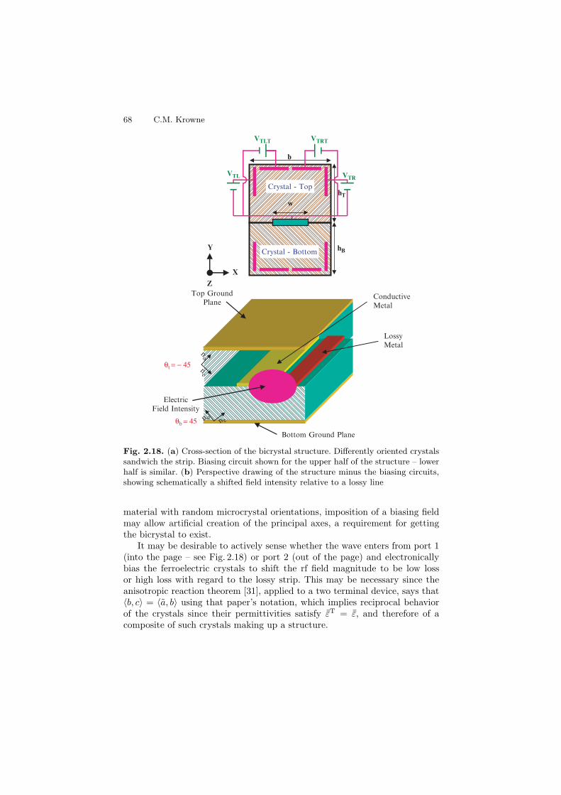
68 C.M. Krowne
VTLT VTRT
Crystal - Top
b
hT
hB
w
VTRVTL
Crystal - BottomY
X
Z
n en o
ne
no
Lossy Metal
θb = 45
θt = − 45
Bottom Ground Plane
ConductiveMetal
Top Ground Plane
Electric Field Intensity
Fig. 2.18. (a) Cross-section of the bicrystal structure. Differently oriented crystalssandwich the strip. Biasing circuit shown for the upper half of the structure – lowerhalf is similar. (b) Perspective drawing of the structure minus the biasing circuits,showing schematically a shifted field intensity relative to a lossy line
material with random microcrystal orientations, imposition of a biasing fieldmay allow artificial creation of the principal axes, a requirement for gettingthe bicrystal to exist.
It may be desirable to actively sense whether the wave enters from port 1(into the page – see Fig. 2.18) or port 2 (out of the page) and electronicallybias the ferroelectric crystals to shift the rf field magnitude to be low lossor high loss with regard to the lossy strip. This may be necessary since theanisotropic reaction theorem [31], applied to a two terminal device, says that〈b, c〉 = 〈a, b〉 using that paper’s notation, which implies reciprocal behaviorof the crystals since their permittivities satisfy ¯εT = ¯ε, and therefore of acomposite of such crystals making up a structure.
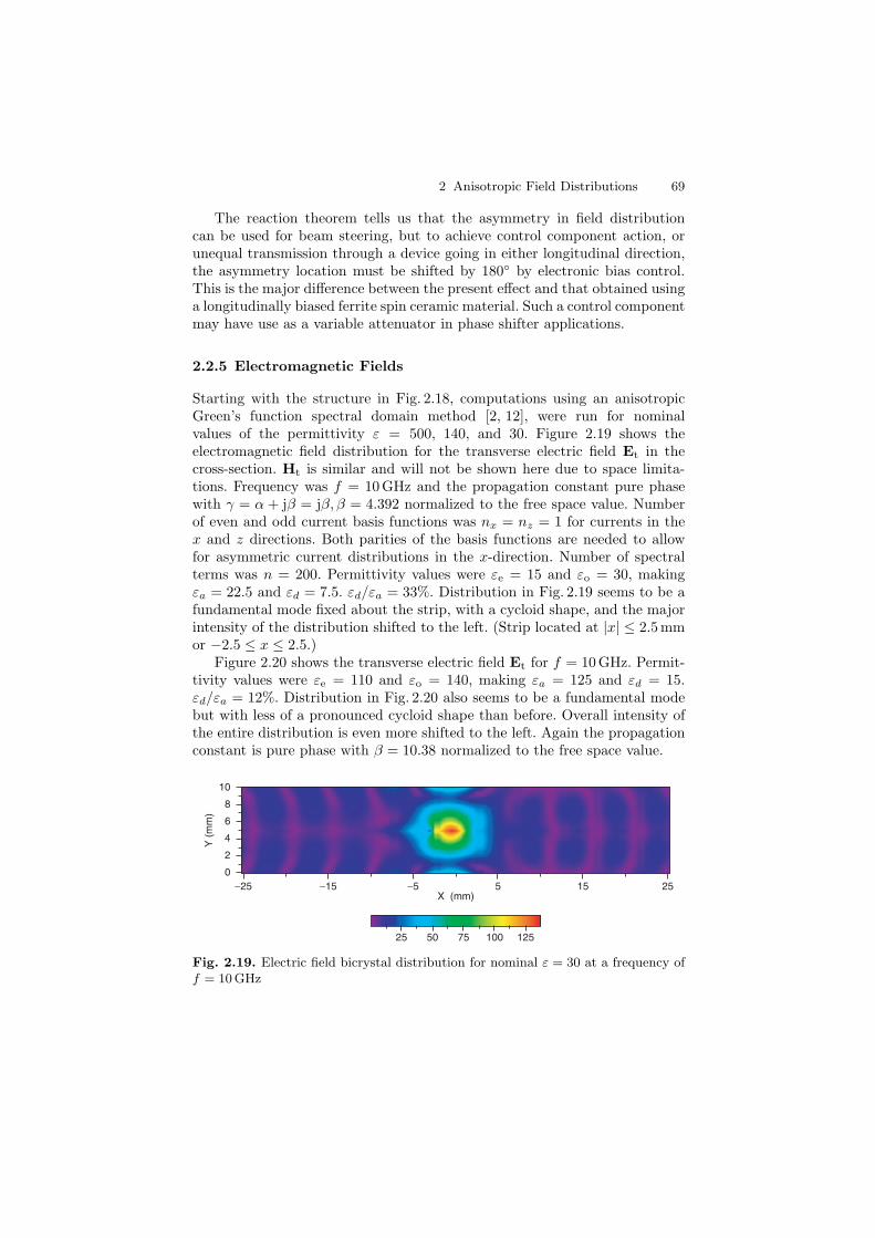
2 Anisotropic Field Distributions 69
The reaction theorem tells us that the asymmetry in field distributioncan be used for beam steering, but to achieve control component action, orunequal transmission through a device going in either longitudinal direction,the asymmetry location must be shifted by 180 by electronic bias control.This is the major difference between the present effect and that obtained usinga longitudinally biased ferrite spin ceramic material. Such a control componentmay have use as a variable attenuator in phase shifter applications.
2.2.5 Electromagnetic Fields
Starting with the structure in Fig. 2.18, computations using an anisotropicGreen’s function spectral domain method [2, 12], were run for nominalvalues of the permittivity ε = 500, 140, and 30. Figure 2.19 shows theelectromagnetic field distribution for the transverse electric field Et in thecross-section. Ht is similar and will not be shown here due to space limita-tions. Frequency was f = 10GHz and the propagation constant pure phasewith γ = α + jβ = jβ, β = 4.392 normalized to the free space value. Numberof even and odd current basis functions was nx = nz = 1 for currents in thex and z directions. Both parities of the basis functions are needed to allowfor asymmetric current distributions in the x-direction. Number of spectralterms was n = 200. Permittivity values were εe = 15 and εo = 30, makingεa = 22.5 and εd = 7.5. εd/εa = 33%. Distribution in Fig. 2.19 seems to be afundamental mode fixed about the strip, with a cycloid shape, and the majorintensity of the distribution shifted to the left. (Strip located at |x| ≤ 2.5mmor −2.5 ≤ x ≤ 2.5.)
Figure 2.20 shows the transverse electric field Et for f = 10 GHz. Permit-tivity values were εe = 110 and εo = 140, making εa = 125 and εd = 15.εd/εa = 12%. Distribution in Fig. 2.20 also seems to be a fundamental modebut with less of a pronounced cycloid shape than before. Overall intensity ofthe entire distribution is even more shifted to the left. Again the propagationconstant is pure phase with β = 10.38 normalized to the free space value.
−25 −15 −5 5 15 25
10
8
6
4
2
0
X (mm)
Y (
mm
)
25 50 75 100 125
Fig. 2.19. Electric field bicrystal distribution for nominal ε = 30 at a frequency off = 10GHz
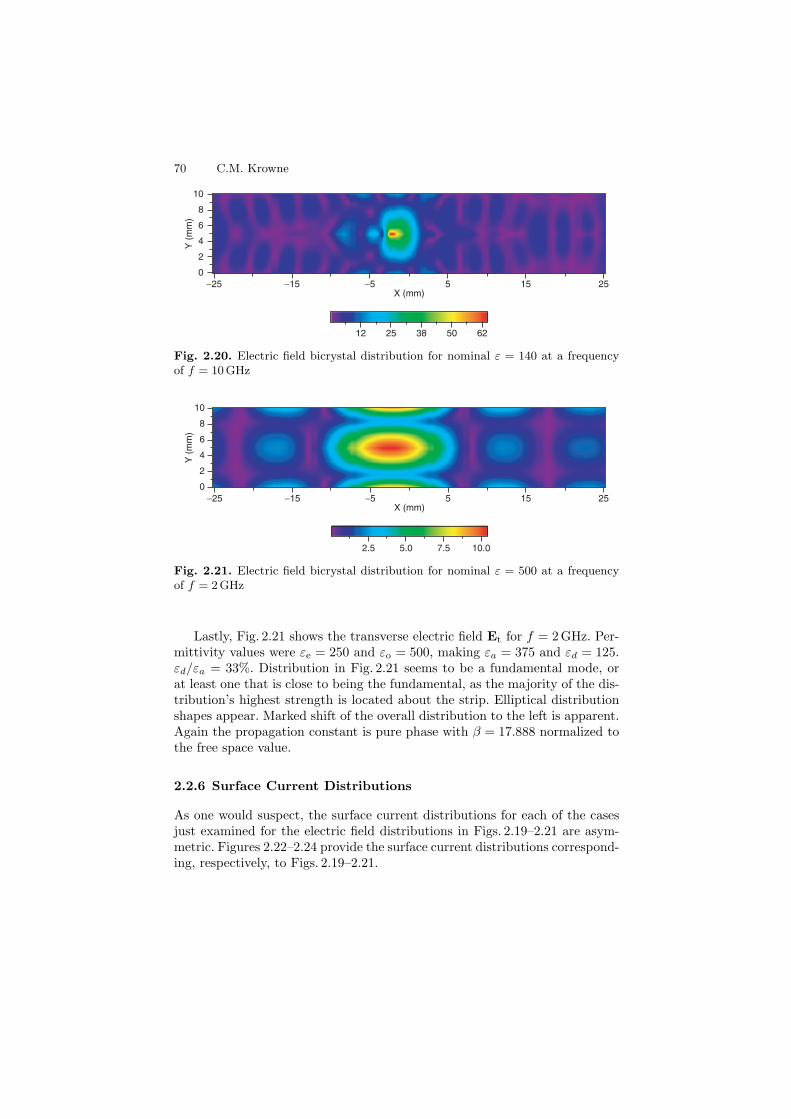
70 C.M. Krowne
−25 −15 −5 5 15 25
10
8
6
4
2
0
X (mm)
Y (
mm
)
12 25 38 50 62
Fig. 2.20. Electric field bicrystal distribution for nominal ε = 140 at a frequencyof f = 10GHz
−25 −15 −5 5 15 25
10
8
6
4
2
0
X (mm)
Y (
mm
)
2.5 5.0 7.5 10.0
Fig. 2.21. Electric field bicrystal distribution for nominal ε = 500 at a frequencyof f = 2GHz
Lastly, Fig. 2.21 shows the transverse electric field Et for f = 2GHz. Per-mittivity values were εe = 250 and εo = 500, making εa = 375 and εd = 125.εd/εa = 33%. Distribution in Fig. 2.21 seems to be a fundamental mode, orat least one that is close to being the fundamental, as the majority of the dis-tribution’s highest strength is located about the strip. Elliptical distributionshapes appear. Marked shift of the overall distribution to the left is apparent.Again the propagation constant is pure phase with β = 17.888 normalized tothe free space value.
2.2.6 Surface Current Distributions
As one would suspect, the surface current distributions for each of the casesjust examined for the electric field distributions in Figs. 2.19–2.21 are asym-metric. Figures 2.22–2.24 provide the surface current distributions correspond-ing, respectively, to Figs. 2.19–2.21.
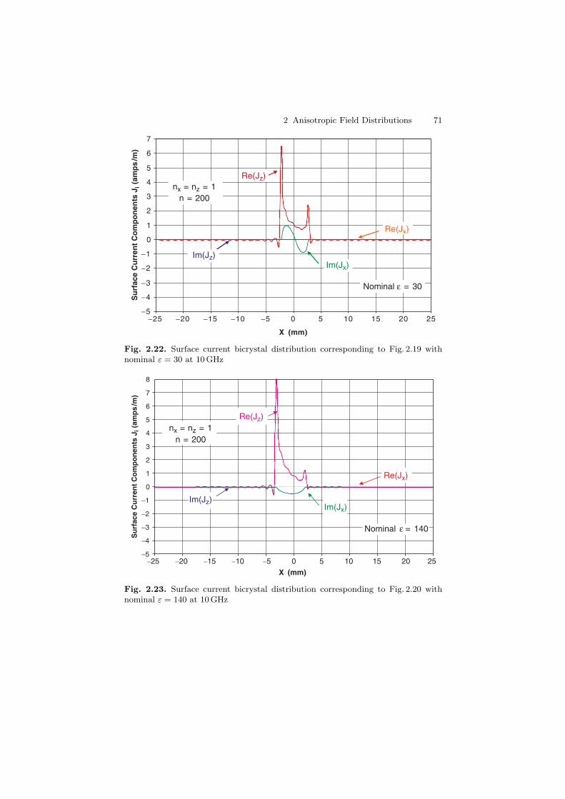
2 Anisotropic Field Distributions 71
−5
−4
−3
−2
−1
0
1
2
3
4
5
6
7
−25 −20 −15 −10 −5 0 5 10 15 20 25
X (mm)
Su
rfac
e C
urr
ent
Co
mp
on
ents
Ji (
amp
s /m
)
Nominal ε = 30
Re(Jx)
nx = nz = 1n = 200
Im(Jz)
Re(Jz)
Im(Jx)
Fig. 2.22. Surface current bicrystal distribution corresponding to Fig. 2.19 withnominal ε = 30 at 10 GHz
−5
−4
−3
−2
−1
0
1
2
3
4
5
6
7
8
−25 −20 −15 −10 −5 0 5 10 15 20 25
X (mm)
Im(Jx)Im(Jz)
Re(Jz)
Nominal ε = 140
Su
rfac
e C
urr
ent
Co
mp
on
ents
Ji (
amp
s /m
)
Re(Jx)
nx = nz = 1 n = 200
Fig. 2.23. Surface current bicrystal distribution corresponding to Fig. 2.20 withnominal ε = 140 at 10 GHz
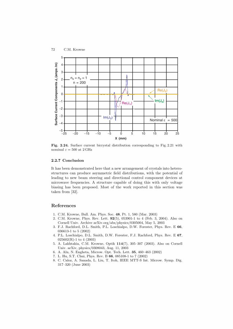
72 C.M. Krowne
−5
−4
−3
−2
−1
0
1
2
3
4
5
−25 −20 −15 −10 −5 0 5 10 15 20 25
X (mm)
nx = nz = 1 n = 200
Im(Jx)Im(Jx)
Im(Jz)
Re(Jx)
Nominal ε = 500
Su
rfac
e C
urr
ent
Co
mp
on
ents
Ji (
amp
s /m
)
Re(Jz)
Fig. 2.24. Surface current bicrystal distribution corresponding to Fig. 2.21 withnominal ε = 500 at 2 GHz
2.2.7 Conclusion
It has been demonstrated here that a new arrangement of crystals into hetero-structures can produce asymmetric field distributions, with the potential ofleading to new beam steering and directional control component devices atmicrowave frequencies. A structure capable of doing this with only voltagebiasing has been proposed. Most of the work reported in this section wastaken from [32].
References
1. C.M. Krowne, Bull. Am. Phys. Soc. 48, Pt. 1, 580 (Mar. 2003)2. C.M. Krowne, Phys. Rev. Lett. 92(5), 053901-1 to 4 (Feb. 3, 2004). Also on
Cornell Univ. Archive arXiv.org/abs/physics/0305004, May 5, 20033. F.J. Rachford, D.L. Smith, P.L. Loschialpo, D.W. Forester, Phys. Rev. E 66,
036613-1 to 5 (2002)4. P.L. Loschialpo, D.L. Smith, D.W. Forester, F.J. Rachford, Phys. Rev. E 67,
025602(R)-1 to 4 (2003)5. A. Lakhtakia, C.M. Krowne, Optik 114(7), 305–307 (2003). Also on Cornell
Univ. arXiv, physics/0308043, Aug. 11, 20036. A. Alu, N. Engheta, Microw. Opt. Tech. Lett. 35, 460–463 (2002)7. L. Hu, S.T. Chui, Phys. Rev. B 66, 085108-1 to 7 (2002)8. C. Caloz, A. Sanada, L. Liu, T. Itoh, IEEE MTT-S Int. Microw. Symp. Dig.
317–320 (June 2003)
2 Anisotropic Field Distributions 73
9. R. Islam, G.V. Eleftheriades, IEEE MTT-S Int. Microw. Symp. Dig. 321–324(June 2003)
10. I.-H. Lin, C. Caloz, T. Itoh, IEEE MTT-S Int. Microw. Symp. Dig. 325–328(June 2003)
11. H. Okabe, C. Caloz, T. Itoh, IEEE MTT-S Int. Microw. Symp. Dig. 329–332(June 2003)
12. C.M. Krowne, IEEE Trans. Microw. Theory Tech. 51, 2269–2283 (Dec. 2003)13. C.M. Krowne, M. Daniel, IEEE Int. Microw. Symp. Dig. 309–312 (June 2003)14. C.M. Krowne, IEEE Trans. Microw. Theory Tech. 32, 1617–1625 (Dec. 1984)15. P.M. Morse, H. Feshbach, Methods of Theoretical Physics, repr. 1978
(McGraw-Hill, New York, 1953)16. A.A. Mostafa, C.M. Krowne, K.A. Zaki, IEEE Trans. Microw. Theory Tech. 35,
1399–1407 (Dec. 1987)17. C.M. Krowne, Microw. Opt. Technol. Letts. 28(1), 63–69 (Jan. 5, 2001)18. C.M. Krowne, Theoretical considerations for full-wave electromagnetic-media
interactions in layered structures with ferroelectric or ferromagnetic materials,Invited paper, Proc. SPIE (Soc. Photo-Optical Instrum. Eng.), Complex Medi-ums, Microwave Materials 4097, 70–84 (July 30, 2000)
19. C.M. Krowne, A.A. Mostafa, K.A. Zaki, IEEE Trans. Microw. Theory Tech. 36,1850–1860 (Dec. 1988)
20. C.M. Krowne, J. Appl. Phys. 99, 044914-1 to 19 (15 Feb. 2006). Also on CornellUniv. Archive, arXiv.org/abs/physics/cond-mat/0406219
21. C.M. Krowne, Encyclopedia of RF and Microwave Engineering, vol. 3 (Wiley,New York, 2005), pp. 2303–2320
22. C.M. Krowne, Bull. Am. Phys. Soc. 49, Pt. 2, 928 (Mar. 2004)23. C.M. Krowne, Phys. Rev. Lett. 93(5), 053902–1 to 4 (July 2004)24. Y. Zhang, B. Fluegel, A. Mascarenhas, Bull. Am. Phys. Soc. 49, Pt. 2, 928
(Mar. 2004)25. Y. Zhang, B. Fluegel, A. Mascarenhas, Phys. Rev. Lett. 91, 157404-1 to 4 (Oct.
2003)26. J.F. Nye, Physical Properties of Crystals (Oxford University Press, Oxford,
1979). First published 195727. F.J. Rosenbaum, Advances Microwaves, vol. 8 (Academic, New York, 1974), pp.
203–29428. M.E. Lines, A.M. Glass, Principles and Applications of Ferroelectrics and
Related Materials (Clarendon, Oxford, 2001). First published 197729. K. Uchino, Ferroelectric Devices (Dekker, New York, 2000)30. C.M. Krowne, M. Daniel, S.W. Kirchoefer, J.M. Pond, IEEE Trans. Microw.
Theory Tech. 50(2), 537–548 (Feb. 2002)31. C.M. Krowne, IEEE Trans. Antennas Propagat. 32, 1224–1230 (Nov. 1984)32. C.M. Krowne, Appli. Phys. Lett. 91, 022902 (2007).
3
“Left-Handed” Magnetic Granular Composites
S.T. Chui, L.B. Hu, Z. Lin and L. Zhou
Summary. We investigate the possibility of preparing left-handed materials inmetallic magnetic granular composites. Based on the effective medium approxima-tion, we show that by incorporating metallic magnetic nanoparticles into an appro-priate insulating matrix and controlling the directions of magnetization of metallicmagnetic components and their volume fraction, it may be possible to prepare acomposite medium which is left handed for electromagnetic waves propagating insome special direction and polarization in a frequency region near the ferromag-netic resonance frequency. This composite may be easier to make on an industrialscale. In addition, its physical properties may be easily tuned by rotating the mag-netization locally. The anisotropic characteristics of this material is discussed. Theexactly solvable example of the multilayer system is used to illustrate the results ofthe effective medium calculation.
3.1 Introduction
In classical electrodynamics, the response (typically frequency dependent) ofa material to electric and magnetic fields is characterized by two fundamentalquantities, the permittivity ε and the permeability µ. The permittivity relatesthe electric displacement field D to the electric field E through D = εE, andthe permeability µ relates the magnetic fields B and H by B = µH. If wedo not take losses into account and treat ε and µ as real numbers, according toMaxwell’s equations, electromagnetic waves can propagate through a materialonly if the index of refraction n, given by (εµ)1/2, is real.
Although all our everyday transparent materials have both positive ε andpositive µ, from the theoretical point of view, in a medium with ε and µboth negative, the index of refraction is also real and electromagnetic wavescan also propagate through, moreover, if such media exist, the propagation ofwaves through them should give rise to several peculiar properties. This wasfirst pointed out by Veselago over 30 years ago [1,1–4]. For example, the crossproduct of E and H for a plane wave in regular media gives the direction ofboth propagation and energy flow, and the electric field E, the magnetic field
76 S.T. Chui et al.
H, and the wave vector k form a right-handed triplet of vectors. In contrast,in a medium with ε and µ both negative, E × H for a plane wave still givesthe direction of energy flow, but the wave itself (that is, the phase velocity)propagates in the opposite direction, i.e., wave vector k lies in the oppositedirection of E ×H for propagating waves. In this case, electric field E, mag-netic field H, and wave vector k form a left-handed triplet of vectors. Recently,progress has been achieved in preparing a “left-handed” material artificially.Following the suggestion of Pendry [1], Smith and coworkers reported that amedium made up of an array of conducting nonmagnetic split ring resonatorsand continuous thin wires can have both an effective negative permittivity εand negative permeability µ for electromagnetic waves propagating in somespecial direction and special polarization at microwave frequencies [6]. Thisis the one of the first experimental realizations of an artificial preparationof a left-handed material. Motivated by this progress, we have investigatedthe possibility of preparing left-handed materials in another type of system-metallic magnetic granular composites. The idea is that, by incorporatingmetallic ferromagnetic nanoparticles into an appropriate insulating matrixand controlling the directions of magnetization of metallic magnetic particlesand their volume fraction, it may be possible to achieve a composite mediumthat has simultaneously negative ε and negative µ. This idea was based onthe fact that on the one hand, the permittivity of metallic particles is auto-matically negative at frequencies less than the plasma frequency, and on theother hand, the effective permeability of ferromagnetic materials for electro-magnetic waves propagating in some particular direction and polarization canbe negative at a frequency in the vicinity of the ferromagnetic resonance fre-quency ω0, which is usually in the frequency region of microwaves. So, if wecan prepare a composite medium in which one component is both metallicand ferromagnetic and other component insulating, and we can control thedirections of magnetization of metallic magnetic particles and their volumefraction, it may be possible to achieve a left-handed composite medium forelectromagnetic waves propagating in some special direction and polarization.This composite may be easier to make on an industrial scale. In addition,its physical properties may be easily tuned by rotating the magnetizationlocally.
3.2 Description of “Left-Handed” ElectromagneticWaves: The Effect of the Imaginary Wave Vector
To illustrate the above idea more clearly, we have performed calculations basedon the effective medium theory (Bruggeman) [7]. Let us consider an idealizedmetallic magnetic granular composite consisting of two types of spherical par-ticles, in which one type of particles are metallic ferromagnetic grains of radiusR1, the other type are non-magnetic dielectric (insulating) grains of radius R2.Each grain is assumed to be homogeneous. The directions of magnetization
3 “Left-Handed” Magnetic Granular Composites 77
of all metallic magnetic grains are assumed to be in the same direction. Inlength scales much larger than the grain sizes, the composite can be consi-dered as a homogeneous magnetic system. The permittivity and permeabilityof nonmagnetic dielectric grains are both scalars, and will be denoted as ε1and µ1. The permittivity of metallic magnetic grains will be denoted as ε2and will be taken to have a Drude form: ε2 = 1 − ω2
p/ω(ω + i/τ), where ωp
is the plasma frequency of the metal and τ is a relaxation time. Such a formof ε is representative of a variety of metal composites [8]. The permeability ofmetallic magnetic grains are second-rank tensors and will be denoted as µ2,which can be derived from the Landau–Lifschitz equations [9]. Assuming thatthe directions of magnetization of all magnetic grains are in the direction ofthe z-axis, µ2 will have the following form [9]:
µ2 =
⎡⎣
µa −iµ′ 0iµ′ µa 00 0 1
⎤⎦ , (3.1)
where
µa = 1 +ωm(ω0 − iαω)
(ω0 − iαω)2 − ω2, (3.2)
µ′ = − ωmω
(ω0 − iαω)2 − ω2, (3.3)
ω0 = γH0 is the ferromagnetic resonance frequency, H0 is the effective mag-netic field in magnetic particles and is a sum of the external magnetic field,the effective anisotropy field and the demagnetization field; ωm = γM0, whereγ is the gyromagnetic ratio, M0 is the saturation magnetization of magneticparticles; α is the magnetic damping coefficient; ω is the frequency of incidentelectromagnetic waves. We shall only consider incident electromagnetic wavespropagating in the direction of the magnetization. This is the most interest-ing case in the study of magneto-optical effects in ferromagnetic materials.We also assume that the grain sizes are much smaller compared with thecharacteristic wavelength λ, and consequently, electromagnetic waves in thecomposite can be treated as propagating in a homogeneous magnetic system.According to Maxwell’s equations, electromagnetic waves propagating in thedirection of magnetization in a homogeneous magnetic material is either posi-tive or negative transverse circularly polarized. If the composite can truly betreated as a homogeneous magnetic system in the case of grain sizes muchsmaller than the characteristic wavelength, electric and magnetic fields in thecomposite should also be either positive or negative circularly polarized andcan be expressed as :
E(r, t) = E(±)0 eikz−βz−iωt, (3.4)
H(r, t) = H(±)0 eikz−βz−iωt, (3.5)
where E(±)0 = x∓iy, H
(±)0 = x∓iy, k = Real[keff ] is the effective wave number,
β = Im[keff ] is the effective damping coefficient caused by the eddy current,
78 S.T. Chui et al.
keff = k + iβ is the effective propagation constant. In (3.4) and (3.5) the signsof k and β can both be positive or negative depending on the directions of thewave vector and the energy flow. For convenience we assume that the directionof energy flow is in the positive direction of the z-axis, i.e., we assume β > 0in (3.4) and (3.5), but the sign of k still can be positive or negative. In thiscase, if k > 0, the phase velocity and energy flow are in the same directions,and from Maxwell’s equation, one can see that the electric and magnetic fieldE and H and the wave vector k will form a right-handed triplet of vectors.This is the usual case for right-handed materials. In contrast, if k < 0, thephase velocity and energy flow are in opposite directions, and E, H, and kwill form a left-handed triplet of vectors. This is just the peculiar case forleft-handed materials. So, for incident waves of a given frequency ω, we candetermine whether wave propagations in the composite is right handed or lefthanded through the relative sign changes of k and β. We have determined theeffective propagation constant keff = k + iβ by means of the effective mediumapproximation [7].
3.3 Electromagnetic Wave Propagationsin Homogeneous Magnetic Materials
The details of various kinds of effective medium approximations have beendiscussed in a series of references [8,10–13], here we only list the main points.First, if the composite can truly be considered as a homogeneous magneticsystem in the case of grain sizes much smaller than the characteristic wave-length, then for waves (positive or negative circularly polarized) propagatingthrough the composite in the direction of magnetization, their propagationscan be described by an effective permittivity εeff and an effective permeabilityµeff , which satisfy the following relations
∫D(r, ω)eikeffzdr = εeff
∫E(r, ω)eikeffzdr, (3.6)
∫B(r, ω)eikeffzdr = µeff
∫H(r, ω)eikeffzdr, (3.7)
where keff and ω are related by keff = ω[εeffµeff ]1/2. Although these relationsare simple and in principle exact, it is very difficult to calculate the inte-grals in them because the fields in the composite are spatially varying in arandom way. One therefore must resort to various types of approximations.The simplest approximation is the effective medium approximation. In thisapproximation, we calculate the fields in each grain as if the grain wereembedded in an effective medium of dielectric constant εeff and magneticpermeability µeff . Consider, for example, the ith grain. Under the embeddingassumption, the electric and magnetic fields incident on the grain are theform of (3.4) and (3.5):
3 “Left-Handed” Magnetic Granular Composites 79
Einc = E(±)0 eikeffz−iωt, (3.8)
H inc = H(±)0 eikeffz−iωt, (3.9)
where E(±)0 = x ∓ iy and H
(±)0 = x ∓ iy, corresponding to the positive(+)
or negative(−) circularly polarized waves. If the fields inside the grain canbe found, then the inside fields can be used to calculate the integral over thegrain volume
Ii =∫
vi
Ei(r, ω)eikeffzdr/vi, (3.10)
J i =∫
vi
Hi(r, ω)eikeffzdr/vi, (3.11)
which is required to find the integral in (3.6) and (3.7). For the positive ornegative circularly polarized incident waves described by (3.8) and (3.9), theintegral Ii and J i can be written as
Ii = (x ∓ iy)Ii, (3.12)J i = (x ∓ iy)Ji, (3.13)
where Ii and Ji are scalars. If Ii and Ji can be found, then from (3.6) and(3.7), the effective permittivity εeff and effective permeability µeff can becalculated by
εeff =f1ε1I1 + f2ε2I2
f1I1 + f2I2, (3.14)
µeff =f1µ1J1 + f2µ
(±)2 J2
f1J1 + f2J2, (3.15)
where f1 and f2 are the volume fractions of the two types of grains, µ1
is the permeability of nonmagnetic dielectric grains, µ(+)2 = µa − µ′ and
µ(−) = µa + µ′ (see 3.1–3.3) are the effective permeability of magnetic grainsfor positive and negative circularly polarized waves, respectively. As for thecalculation of Ii and Ji, we can follow the method of expanding interior andexterior fields in a multipole series and matching the boundary conditions [14].After the coefficients of the multipole expansion of interior and exterior fieldsare obtained by matching the boundary conditions, Ii and Ji can be foundand subsequently be substituted into (3.14) and (3.15). Since this methodis standard, we shall not present the details. In the final results, (3.14) and(3.15) reduce to one self-consistent equation:
∑i=1,2
fi
∞∑l=1
(2l + 1)[(µs/µeff)keffψ′
l(kiRi)ψl(keffRi) − kiψl(kiRi)ψ′l(keffRi)
(µs/µeff)keffψ′l(kiRi)ζl(keffRi) − kiψl(kiRi)ζ ′l(keffRi)
+kiψ
′l(kiRi)ψl(keffRi) − (µs/µeff)keffψl(kiRi)ψ′
l(keffRi)kiψ′
l(kiRi)ζl(keffRi) − (µs/µeff)keffψl(kiRi)ζ ′l(keffRi)
]= 0, (3.16)
80 S.T. Chui et al.
where Ri is the radius of the ith type of grains, and
k1 = ω[ε1µ1]1/2, (3.17)
k2 = ω[ε2µ(±)2 ]1/2, (3.18)
ψl(x) = xjl(x), (3.19)
ζl(x) = xh(1)l (x), (3.20)
jl(x) and hl(x) are the usual spherical Bessel and Hankel functions. Equa-tion (3.16) determines the effective product of (εµ)eff , or equivalently keff .This equation was solved numerically [7]. It was found that the relative signsbetween the real and the imaginary part of the wave vector changes sign nearthe FMR frequency.
3.4 Some Characteristics of ElectromagneticWave Propagation in Anisotropic“Left-Handed” Materials
Both our system and that previously studied by the UCSD group areanisotropic in nature. Veselago’s original paper and recent theoretical worksdiscussed only the characteristics of electromagnetic wave propagation inisotropic “left-handed” media. In classical electrodynamics, it is well knownthat the electrodynamic properties of anisotropic materials are significantlydifferent from that of isotropic materials. The simplest and most commonform of anisotropy is the uniaxial anisotropy. In this section, we shall showthat the characteristics of electromagnetic wave propagation in uniaxialanisotropic “left-handed” media are also significantly different from that inisotropic “left-handed” media.
3.4.1 “Left-Handed” Characteristic of ElectromagneticWave Propagation in Uniaxial Anisotropic“Left-Handed” Media
For isotropic materials, the permittivity and permeability are both scalars,and if the permittivity and permeability of an isotropic medium are bothnegative, electromagnetic wave propagation in such a medium would be “left-handed” for any propagation direction. For anisotropic materials, one or bothof the permittivity and permeability are second-rank tensors. In this section,we shall discuss in what conditions electromagnetic wave propagation in uni-axially anisotropic media shall be “left-handed.” For clarity, we first considerthe case that one of the permittivity and permeability is uniaxially anisotropicbut the other is isotropic. We assume that the permittivity is isotropic andthe permeability is uniaxially anisotropic. In this case, the permittivity is ascalar (denoted as ε) and the permeability is a second-rank tensor (denotedas µ). For uniaxial anisotropy, µ can be expressed as [10]:
3 “Left-Handed” Magnetic Granular Composites 81
µ =
⎡⎣
µ⊥ 0 00 µ⊥ 00 0 µz
⎤⎦ . (3.21)
Consider the propagation of a plane wave of frequency ω with E =E0eik·r−iωt, H = H0eik·r−iωt, Maxwell’s equations becomes
k × E = ωµ · H, (3.22)k × H = −ωεE. (3.23)
Substituting (3.21) into (3.22) and (3.23), one can see that there are two typesof linearly polarized plane waves, namely the E-polarized and H-polarizedplane waves. The E-polarized plane waves satisfy the conditions k ·E = 0 andEz = 0, the H-polarized waves satisfy the conditions k · H = 0 and Hz = 0.Assuming that the wave vector is in the x–z plane, then for the E-polarizedplane waves one gets
E = E0yeik·r−iωt, (3.24)
H =[−E0kz
ωµ⊥x +
E0kx
ωµzz]
eik·r−iωt, (3.25)
where x, y, and z are unit vectors along the x-, y-, and z-axis. Similarly, theH-polarized waves can be expressed as
H = H0yeik·r−iωt, (3.26)
E =[H0kz
ωεx − H0kx
ωεz]
eik·r−iωt. (3.27)
The dispersion relation for the E-polarized waves is determined by
k2x
µz+
k2z
µ⊥= ω2ε (3.28)
and the dispersion relation for the H-polarized waves is given by
k2 = ω2εµ⊥. (3.29)
The energy density current S and its inner product with the wave vector kare given by
S =12E∗ × H
=|E0|2kx
2ωµzx +
|E0|2kz
2ωµ⊥z, (3.30)
k · S =12ωε|E0|2 (3.31)
82 S.T. Chui et al.
for E-polarized plane waves, and
S =|H0|2kx
2ωεx +
|H0|2kz
2ωεz, (3.32)
k · S =12ωµ⊥|H0|2 (3.33)
for H-polarized waves. From (3.24) to (3.32), we can get the followingconclusions:
1. From (3.29), we can see that the propagation of the H-polarized wavesrequires the ε and µ⊥ must have same sign. If ε and µ⊥ are both nega-tive, for any propagation direction, the energy density current S of theH-polarized waves shall be in the exact opposite direction of the wave vec-tor k, and E, H, and k shall form a left-handed triplet of vectors. Thiscan be seen from (3.26) and (3.27) and (3.32) and (3.33). So, if ε and µ⊥are both negative, the H-polarized waves shall be “left-handed” for anypropagation direction. An interesting fact is that µz including its sign hasno effect on the propagation and the “left-handed” characteristic of theH-polarized waves.
2. If ε is and µ⊥ are both negative, in the direction of the z-axis, theE-polarized waves are exactly “left-handed” if the wave vector k is in thedirection of the z-axis, as can be seen from (3.24) and (3.25) and (3.30)and (3.31). But if the wave vector k is not in the direction of the z-axis, theE-polarized waves cannot be exactly “left-handed” but be approximately“left-handed,” in the sense that the energy density current S could be inbackward but not the exact opposite direction of the wave vector, i.e., theangle between the directions of energy flow and wave vector k is largerthan π/2 but smaller than π, and E, H, and k form an approximatebut not a strict “left-handed” triplet of vectors. Unlike the H-polarizedwaves, µz including its sign have effects on the propagation of the E-polarized waves. From (3.28), (3.30), and (3.31), we can see that if ε < 0,µ⊥ < 0, and µz < 0, the E-polarized waves can propagate in any directionand be approximately “left-handed.” If ε < 0, µ⊥ < 0, and µz > 0, theE-polarized waves could propagate and be approximately “left-handed”if the angle θ between the wave vector and the z-axis is smaller thanarctan(|µz/µ⊥|). If θ > arctan(|µz/µ⊥|), the E-polarized waves could notpropagate since in this case the wave vector k is imaginary.
3. If ε < 0 but µ⊥ > 0, the wave vector of the H-polarized waves shall beimaginary for any propagation direction [see (3.29)] no matter what signµz has, hence the H-polarized waves cannot propagate in any direction. Forthe E-polarized waves, if µz > 0, the wave vector is also imaginary as canbe seen from (3.28), and hence the E-polarized waves cannot propagate inany direction. If µz < 0, the E-polarized waves can propagate if the angle
3 “Left-Handed” Magnetic Granular Composites 83
between the wave vector and the z-axis is larger than arctan(|µz/µ⊥|).In this case the waves are approximately “left-handed” since the anglebetween the directions of energy flow and wave vector k is larger thanπ/2.
4. If µ⊥ < 0 and ε > 0, the H-polarized waves cannot propagate in anydirection. For the E-polarized waves, if µz > 0, the E-polarized waves canpropagate if the angle between the wave vector and the z-axis is smallerthan arctan(|µz/µ⊥|). In this case, the waves are not “left-handed” sincethe angle between the directions of energy flow and wave vector k islarger than π/2.
5. Similar results as shown in (1)–(4) can also be obtained in the case thatthe permittivity is uniaxial anisotropic and the permeability is isotropic.From these results, we can see that for anisotropic materials, the propaga-tion and the “left-handed” characteristic of electromagnetic waves do notrequire all elements of the permittivity and the permeability tensors to beof the same sign. This is an important difference between isotropic andanisotropic media. For isotropic media, the propagation of electromagneticwaves require the permittivity and permeability to have the same signsand the media is left-handed only if the permittivity and permeability areboth negative.
Next, we discuss the more complicated case that both the permittivity andpermeability exhibit uniaxial anisotropy. In this case, the permittivity is alsoa second-rank tensor having the similar form as µ:
ε =
⎡⎣
ε⊥ 0 00 ε⊥ 00 0 εz
⎤⎦ . (3.34)
Following the same procedure as above, one can see that in this case thereare also two types of linearly polarized plane waves, i.e., the E-polarized andthe H-polarized plane waves. The E-polarized plane waves also satisfy thecondition k ·E = 0 and Ez = 0, the H-polarized plane waves satisfy k ·H = 0and Hz = 0. The dispersion relation for the E-polarized waves is determined by
k2x
µz+
k2z
µ⊥= ω2ε⊥, (3.35)
the dispersion relation for the H-polarized waves is determined by
k2x
εz+
k2z
ε⊥= ω2µ⊥. (3.36)
The energy current density S and its inner product with the wave vector kare given by
S =|E0|2kx
2ωµzx +
|E0|2kz
2ωµ⊥z, (3.37)
84 S.T. Chui et al.
k · S =12ωε⊥|E0|2 (3.38)
for E-polarized plane waves, and
S =|H0|2kx
2ωεzx +
|H0|2kz
2ωε⊥z, (3.39)
k · S =12ωµ⊥|H0|2 (3.40)
for H-polarized waves. From (3.35) and (3.36), we can get the followingconclusions:
1. If the wave vector k is in the direction of the z-axis, the propagation ofboth the E- and H-polarized waves require the product of ε⊥ and µ⊥ to bepositive. In this case, if ε⊥ < 0 and µ⊥ < 0, both the E- and H-polarizedwaves are “left-handed,” and εz and µz do not have effect on the “left-handed” characteristic of both the E- and H-polarized waves.
2. If the propagation is not in the direction of the z-axis, both the E-polarizedand H-polarized waves cannot be exactly “left-handed” since in this casethe energy flow cannot be in the exact opposite direction of the wavevector if µ⊥ = µz and ε⊥ = εz. But if some conditions are satisfied, thewave propagation can be approximately “left-handed,” i.e., the directionof energy flow is in the backward but not exactly opposite direction ofwave vector.
3. The necessary condition for the E-polarized waves being approximately“left-handed” is that ε⊥ < 0 but it is not necessary that µ⊥ and µz areboth negative, and εz has no effect on the propagation of the E-polarizedwaves. If µ⊥ and µz are both negative, the E-polarized waves are approx-imately “left-handed” no matter what the angle between k and the z-axisis. If µ⊥ < 0 and µz > 0, the E-polarized waves can propagate only ifthe angle between k and the z-axis is smaller than arctan(|µz/µ⊥), or elsethe wave vector is imaginary and the E-polarized waves cannot propagate.Similarly, if µ⊥ > 0 and µz < 0, the E-polarized waves can propagate alsoonly if the angle between k and the z-axis is smaller arctan(|µz/µ⊥).
4. The necessary condition for the H-polarized waves being approximately“left-handed” is that µ⊥ < 0 but it is not necessary that ε⊥ and εz are bothnegative. If ε⊥ and εz are both negative, the H-polarized waves are approx-imately “left-handed” no matter what the angle between k and the z-axisis. If ε⊥ < 0 and εz > 0, the H-polarized waves can propagate only if theangle between k and the z-axis is smaller than arctan(|εz/ε⊥), or else thewave vector is imaginary and the E-polarized waves cannot propagate.Similarly, if ε⊥ > 0 and εz < 0, the E-polarized waves can propagate alsoonly if the angle between k and the z-axis is smaller arctan(|εz/ε⊥).
3 “Left-Handed” Magnetic Granular Composites 85
3.4.2 Characteristics of Refraction of ElectromagneticWaves at the Interfaces of Isotropic Regular Mediaand Anisotropic “Left-Handed” Media
When a beam of light passes from one regular medium into a second regu-lar medium, the ray undergoes refraction at the interface between the twomedia, and the refracted ray should bent toward the normal of the inter-face but never emerge on the same side of the normal as the incident ray(Snell’s law). Veselago predicted that if the second medium is an isotropic“left-handed” medium, the refracted ray should lie on the same side of thenormal of the interface as the incident ray due to the “left-handed” character-istic of the refracted waves in the second medium [2]. This anomalous refrac-tion is one of the most interesting peculiar properties of isotropic “left-handed”media and has been verified experimentally very recently [6]. It has been shownthat this anomalous refraction could lead to some strange optics [1,17,28]. Inthis section, we discuss the characteristics of refraction when a beam of lightpassing from one isotropic regular medium into another uniaxial anisotropic“left-handed” medium. In what follows we shall only discuss the case thatboth the permittivity and the permeability of the second medium are uniax-ially anisotropic with the forms of (3.21) and (3.34). The results for the casethat either the permittivity or the permeability is isotropic can be obtainedsimilarly.
Before we discuss whether the refraction is ordinary or anomalous, weshall first discuss under what conditions the incident waves shall be refractedor totally reflected in the case that some of the elements of the permittivityand(or) permeability tensors of the second medium are negative. In the follow-ing we denote the permittivity and permeability of the isotropic regular mediaas ε1 and µ1(both positive) and denote the wave vectors of the incident wavesas k = kxx + kzz and the incident angles as θ. The wave vectors of therefracted waves are denoted as k′ = k′
xx + k′zz and the refraction angles with
respect to the surface normal are denoted as φ. The refracted waves satisfy thefollowing boundary conditions whether or not the second medium is regularor “left-handed”
n × E1 = n × E2, n · D1 = n · D2, (3.41)n × H1 = n × H2, n · B1 = n · B2. (3.42)
It follows from (3.41) and (3.42) that the refracted waves shall maintain thesame polarization (E or H) as the incident waves, and the x and y componentsof the wave vector of the refracted waves is equal to that of the incident waves,i.e, k′
x = kx. Then from (3.35) and (3.36), the z component of the wave vectorof the refracted waves can be obtained by
k′ 2z = ω2ε⊥µ⊥ − µ⊥
µzk2
x (3.43)
86 S.T. Chui et al.
for E-polarized incident waves, and
k′ 2z = ω2ε⊥µ⊥ − ε⊥
εzk2
x (3.44)
for H-polarized incident waves. One necessary condition for the occurrence ofrefraction is that k′
z must be real, or else the incident waves shall be totallyreflected. This requires that the incident angle θ = tan−1 kx/kz should satisfythe following inequality
µ⊥µz
sin2 θ <ε⊥µ⊥ε1µ1
(3.45)
for E-polarized incident waves, and
ε⊥εz
sin2 θ <ε⊥µ⊥ε1µ1
(3.46)
for H-polarized incident waves. From (3.43) and (3.44), we can see that:
1. For E-polarized incident waves, if µ⊥/µz is positive, the occurrence ofrefraction requires that ε⊥µ⊥ is also positive and the incident angle θ mustbe smaller than a critical angle θc = arcsin
√ε⊥µz
ε1µ1, or else the incident
waves shall be totally reflected. If µ⊥/µz is negative, ε⊥µ⊥ can be eitherpositive or negative. In this case, if ε⊥µ⊥ is positive, for any incident angle,the incident waves shall be refracted. If ε⊥µ⊥ is negative, the incident
angle θ must be larger than arcsin√
|ε⊥µz|ε1µ1
, or else the incident wavesshall be totally reflected.
2. For H-polarized incident waves, if ε⊥/εz is positive, the occurrence ofrefraction requires that ε⊥µ⊥ is also positive and the incident angle θ mustbe small than θc = arcsin
√µ⊥εz
ε1µ1, or else the incident ray shall be totally
reflected. If ε⊥/εz is negative, ε⊥µ⊥ can be either positive or negative. Inthis case, if ε⊥µ⊥ is positive, refraction will occur for any incident angle.If ε⊥µ⊥ is negative, the occurrence of refraction shall require the incident
angle θ must be larger than arcsin√
|µ⊥εz|ε1µ1
.3. From these results, we can see that in the case that some of the elements
of the permittivity and(or) permeability tensors of the second mediumare negative, the incident waves may be totally reflected if the incidentangle is smaller but not larger than a critical incident angle. This is a veryinteresting peculiar characteristic which should never occur if the secondmedia are regular materials.
Now we discuss under what conditions anomalous refraction shall occur.For a plane incident wave, whether the refraction is ordinary or anomalousdepends on the direction of energy flow of the refracted waves, or equiva-lently, the signs of the x and z components of energy density current S ofthe refracted waves. Causality requires that in the second medium, energycurrent should be transmitted away from the interface of two media but never
3 “Left-Handed” Magnetic Granular Composites 87
toward the interface. This requires that in the second medium the z compo-nent of energy density current S must be always positive, and in order to keepthe sign of Sz always negative, the z components of the wave vectors of therefracted waves can be either positive or negative and shall be determined bythe signs of ε⊥ and µ⊥, as can be seen from (3.37) and (3.39). Unlike the zcomponent of energy current density S, the x component of energy densitycurrent S of the refracted waves need not necessarily be negative. Since Sz
is always positive, if Sx > 0, the refracted ray shall lie on the opposite sideof the normal of the interface of two media as incident ray and the refractionshall be ordinary. If Sx < 0, the refracted ray shall lie on the opposite sideof the normal of the interface of two media as incident ray and the refractionshall be anomalous. Considering that the x components of the wave vectors ofthe refracted waves always maintain the same direction as the incident wavesdue to the boundary condition, then from (3.37)-(3.40), we can obtain thefollowing conclusions:
1. For E-polarized incident waves, the occurrence of anomalous refractionrequires that µz < 0 but does not necessarily require that other elementsof the permittivity and(or) permeability tensors are also negative. From(3.37, we can see that if µz > 0, then Sx > 0, and the refracted ray shalllie on the opposite side of the normal of the interface of two media; ifµz < 0, then Sx < 0, and the refracted ray shall lie on the same side of thenormal of the interface. In the case that the second medium is anisotropic,the system is not “left-handed” even if the refraction is anomalous, as isdescribed in the previous section. For example, if µz < 0 and ε⊥ > 0, thenfrom (3.37) and (3.38), we can see that Sx < 0 and k · S > 0. In thiscase the refraction is anomalous but the refracted ray is not “left-handed”since in this case the energy flow is the forward but not the backwarddirection of the wave vector.
2. For H-polarized incident waves, the occurrence of anomalous refractionrequires that εz < 0 but the other elements of the permittivity and(or)permeability tensors need not be also negative. From (3.39), we can seethat if εz < 0, then Sx < 0, and the refracted ray shall lie on the sameside of the normal of the interface of two media. Like E-polarized incidentwaves, in the case that the second medium is anisotropic, the refractedwaves are not necessarily “left-handed” even if the refraction is anomalous.For example, if εz < 0 and µ⊥ > 0, from (3.39)-(3.40), we can see thatSx < 0 but k · S > 0. In this case the refraction is anomalous but therefracted waves are not “left-handed.”
3. If the incident rays are not either E-polarized or H-polarized, there shallbe two refracted rays with different propagation directions, and one rayis E-polarized and the other ray is H-polarized. In this case, if µz and εz
are both negative, the two refracted rays shall both lie on the same sideof the normal of the interface as the incident rays. If one of µz and εz isnegative, one refracted ray shall lie on the opposite side of the normal of
88 S.T. Chui et al.
the interface but the other refracted ray shall lie on the same side of thenormal as incident ray. If µz and εz are both positive, the two refractedrays shall both lie on the opposite site of the normal of the interface oftwo media as the incident ray.
3.5 Multilayer Structures Left-Handed Material:An Exact Example
In this section, we examine ferromagnet insulator multilayer structures as left-handed materials. In multilayer structures, the propagation of electromagneticwaves can be exactly analytically calculated. This will provide us with someassessment of different approximations that has been used in this area.
We found that when the wave vector is parallel (perpendicular) to thelayers, the square of the phase velocity is inversely proportional to 〈µ〉a〈ε〉h(〈ε〉a〈µ〉a), where the angular brackets with subscripts a, h stand for the arith-metic and the harmonic mean, respectively. Different averages of ε and µ comeinto play. For example: 〈ε〉a = cmεm + ciεi, 1/〈ε〉h = cm/εm + ci/εi where cj
stands for the volume fraction of component j. 〈ε〉a is of the same orderof magnitude of the metal dielectric constant, whereas 〈ε〉h is of the order ofmagnitude of the insulator dielectric constant. These two are very different.The different averages of the dielectric constant obtained here in the longwavelength limit is very similar to the “form birefringence” discussed by Bornand Wolf [18]. The form birefringence focuses on the dielectric constants only.Here we have included the magnetic susceptibility at the same time. We nowexplain our results in detail.
We begin by considering the propagation of electromagnetic waves in themultilayer structure consisting of periodic arrays of two materials of thick-nesses dm, di with d = dm + di. The dielectric constant and the magneticpermeability of the two components are denoted by εm, µm (εi, µi). Thereare two types of eigenstates for Maxwell’s equation: the H (E) polarizationwhere the macroscopic magnetic field H (electric field E) is perpendicularto the wave vector and parallel to the layers. Our goal is to derive the dis-persion relationships of the radiation for these two polarizations in the longwavelength limit. For the H (E) polarization we denote the direction of H(E) as the y-direction and the normal to the multilayers as the x-direction.Any wavevector k can be decomposed into a component perpendicular to theplanes and a component parallel to the planes. The wave vector is in the xzplane with k = (kx, 0, kz). There is no y component because the wave vectoris perpendicular to the direction of H (E). The frequency of the radiation willbe denoted by ω. We define a “vacuum wave vector” k0 = ω/c where c is thespeed of light.
To calculate the dispersion we solve Maxwell’s equation in each of thecomponents separately. The solution is then matched across the bound-ary [19,20]. The solution of Maxwell’s equation in each region j = m, i can be
3 “Left-Handed” Magnetic Granular Composites 89
written in separable form as Ezj = Vj(x) exp(ikzz), Hyj = Xj(x) exp(ikzz)for the H polarization and Hzj = Vj(x) exp(ikzz), Eyj = Xj(x) exp(ikzz) forthe E polarization. The wave vector kz, the component of the wave vectorparallel to the planes, is the same in both regions. The functions V , X arelinear combinations of plane wave solutions. Xj = Aj cos(pjx
′)+Bj sin(pjx′),
Vj = i[−pjAj sin(pjx′) + pjBj cos(pjx
′)]/(k0τj), where pj = (εjµjk20 − k2
z)0.5.τj = εj (−µj) for the H (E) polarization. x′ = x for 0 < x < dm, x′ = x− dm
for dm < x < di+dm. The constant coefficients Aj , Bj can be determined fromthe continuity of the tangential components of E and H across the bound-aries and the “periodic boundary condition”: E(x + d) = exp(ikxd)E(x),H(x + d) = exp(ikxd)H(x). Across the first interface, we get from thecontinuity conditions
[Xm(x = dm)Vm(x = dm)
]= T(pm, dm, τm)
[Xm(x = 0)Vm(x = 0)
],
where
T(p, d, τ) =
⎡⎣
cos(pd) −i sin(pd)τk0/p
−i sin(pd)p/τk0 cos(pd)
⎤⎦ .
From the “periodic boundary condition,” we get[
Xi(d)Vi(d)
]= exp[i dkx]
[Xi(0)Vi(0)
]= T(pi, di, τi)
[Xi(dm)Vi(dm)
]
= T(pi, di, τi)[
Xm(dm)Vm(dm)
].
From the above equations, we obtain an eigenvalue problem:[
Xi(0)Vi(0)
]= exp[−i dkx]T(pi, di, τi)T(pm, dm, τm)
[Xi(0)Vi(0)
].
Simplifying the algebra [21], we obtain finally the eigenvalue equation
cos(kxd) = cos φi cos φm
− 0.5[κpi/pm + pm/(piκ)] sin φi sinφm, (3.47)
where φj = pjdj , κ = τm/τi. The corresponding eigenvector is given by
Am = 1, (3.48)
Bm = iW0τmk0/pm, (3.49)
whereW0 = [exp(ikxd) − M ]/N.
M = cos(φm) cos(φi) − pmτi sin(φi) sin(φm)/(τmpi),
N = ik0[cos(φm) sin(φi)τi/pi + cos(φi) sin(φm)τm/pm].
90 S.T. Chui et al.
Ai = U1, (3.50)
Bi = iW1τik0/pi, (3.51)
where U1 = cos(pmdm) + iW0τmk0 sin(pmdm)/pm, W1 = V0 cos(pmdm) +ipm sin(pmdm)/(τmk0).
We next examine these results in the long wavelength limit with pjdj 1.Using the approximation cos(x) ≈ 1 − x2/2, sin(x) ≈ x we get from (3.47)after some algebra
k2z(di
√κ + dm/
√κ) + (kxd)2/(di/
√κ + dm
√κ)
= k20(µiεidi
√κ + µmεmdm/
√κ). (3.52)
Putting in the expression for κ and simplifying, we get for the H polarization
k2z/〈ε〉h + k2
x/〈ε〉a = k20〈µ〉a, (3.53)
where the angular brackets with a subscript “a” stands for the arithmeticmean: 〈ε〉a = (dmεm + diεi)/d, 〈µ〉a = (dmµm + diµi)/d. Similarly, angu-lar brackets with a subscript “h” stands for the harmonic mean: 1/〈ε〉h =(dm/εm + di/εi)/d.
For the E polarization, one interchanges ε with µ. From (3.53), we get thelong wavelength dispersion:
k2z/〈µ〉h + k2
x/〈µ〉a = k20〈ε〉a. (3.54)
The system is also anisotropic. The real part of 〈ε〉a is negative. In this longwavelength limit the corresponding eigenvector becomes
Am = 1, Bm = iV0τmk0/pm, (3.55)
where V0 = [1+ikxd−M ]/N . M = 1−(pmdm)2/2−(pidi)2/2−p2mτididm/τm,
N = ik0[1 − (pmdm)2/2]diτi + [1 − (pidi)2/2]dmτm. V0 = kx/[k0 < τ >a].Bm = ikxτm/[pm < τ >a].
Ai = U1, Bi = iV1τik0/pi, where U1 = 1 − (pmdm)2/2 + iV0τmk0dm,V1 = V0[1− (pmdm)2/2]+ip2
mdm/(τmk0) V1 = kx/[k0 < τ >a] U1 = 1, Ai = 1,Bi = ikxτi/[pi < τ >a]. To summarize
Xm = cos(pmx) + ikxτm sin(pmx)/[pm〈τ〉a], (3.56)
Xi = cos(pix′) + ikxτi sin(pix
′)/[pi〈τ〉a]. (3.57)
We next look at the Poynting vector of the system. We first discuss thecase of the H polarization. We get,
Hj = H0yeikzz−iωtXj(x), (3.58)
Ej = H0
[kz
k0εjxXj(x) + i
1k0εj
zX ′j(x)
]eikzz−iωt (3.59)
3 “Left-Handed” Magnetic Granular Composites 91
The corresponding Poynting vector Sj = Ej ×H∗j is given by (as usual [22],
it is the real part of this expression that is of interest)
Sj = H20
(−
iX∗j X ′
j
2k0εjx +
|Xj |2kz
2k0εjz)
,
Xj is a function of the spatial variable x. We calculate the mean Poyntingvector by averaging expressions involving Xm, X ′
m (Xi, X ′i) in the interval
0 < x < dm (dm < x < d + m + di). From (3.53) and (3.57), we can calculatethe averages of expressions involving the function X: 〈|X|2〉 = 1, 〈X∗X ′〉 =ikxτ/〈τ〉a,
The Poynting vector in the corresponding region is
Sj = H20
(kx
2k0〈ε〉ax +
kz
2k0εjz)
,
Averaging over the two types of layers, we get
S = H20
(kx
2k0〈ε〉ax +
kz
2k0〈ε〉hz)
. (3.60)
This Poynting vector is parallel (antiparallel) to the normal of the constantω contour, ∂ω/∂k, if 〈µ〉a is positive (negative). If the imaginary part of thesusceptibilities are small so that the wave vector is mostly real, the dot productof the wave vector and the Poynting vector is given by
k∗ · S ≈ 12k0〈µ〉a|H0|2. (3.61)
Thus if we can find a material with a negative average 〈µ〉a, Real[k∗ · S] < 0,the system will be left handed. This may be achievable with ferromagneticmaterials above the ferromagnetic resonance frequency. We shall come backto this point later.
We next discuss the case of the E polarization. The electric and magneticfields are given by
Ej = E0yeikzz−iωtXj(x), (3.62)
Hj = E0
[− kz
k0µjxXj(x) − i
1k0µj
zX ′j(x)
]eikzz−iωt. (3.63)
The Poynting vector is now given by
Sj = E20
(−
iX∗j X ′
j
2k0µjx +
|Xj |2kz
2k0µjz)
.
Substituting in the average of the function Xj , we get
Sj = E20
(kx
2k0〈µ〉ax +
kz
2k0µjz)
.
92 S.T. Chui et al.
Averaging over the two components we get
S = |E0|2(
kx
2k0〈µ〉ax +
kz
2k0〈µ〉hz)
, (3.64)
k∗ · S =12k0〈ε〉a|E0|2. (3.65)
The Poynting vector is again anisotropic. The same results are obtained if oneapproximates the multilayer system as an anisotropic homogeneous system[23]. If the imaginary part 〈ε〉a is small Re[k∗ · S] < 0.
We close with a discussion of how to make 〈µ〉a negative. The obviouschoice is to use a ferromagnetic metal as one of the components of themultilayer system [7, 24, 25]. When the magnetization is aligned along thez-direction, the magnetic susceptibility of a ferromagnet is a tensor given by(3.1)–(3.3). It is still possible to solve Maxwell’s equations for the multilayersystem analytically. The results are algebraically complicated and not veryilluminating physically. Here we consider the case when the remanent magne-tization of the ferromagnet is zero. The system consists of domains with themagnetization forced by the shape anisotropy to lie in the yz plane but other-wise randomly oriented. For frequencies of the order of GHz, the domain sizeis usually much less than the wavelength. The magnetic susceptibility can beobtained by averaging µF over the different orientations of the magnetizationsof the domains. The resulting magnetic susceptibility becomes diagonal butanisotropic [26]:
µM=0 =
⎡⎣
µd 0 00 µyz 00 0 µyz
⎤⎦ , (3.66)
where µyz = (µd+1)/2. It is still possible to solve analytically Maxwell’s equa-tion. For the H polarization, the magnetic susceptibility µm is now replacedby µyz. Above the ferromagnetic resonance frequency ω0, if µd becomes neg-ative enough that 〈µ〉a is also negative, then the system can be considered aleft-handed material.
For the E polarization,
E = E0yeikzz−iωtX(x), (3.67)
H = E0
[− kz
k0µdxX(x) − i
1k0µyz
zX ′(x)]
eikzz−iωt. (3.68)
Now pm = (k20εmµyz − k2
zµyz/µd)0.5, τm = µyz. The functional form for thedispersion, (3.54), remains the same except now the different averages of themagnetic susceptibilities involve different components of the tensor: 1/〈µ〉h =ci/µi+cm/µd; 〈µ〉a = ciµi+cmµyz. The conclusions reached previously remainqualitatively unchanged.
In this paper we have assumed that kjdj 1. Typically, in multilayersdj can easily be made to be of the order of 10 A. kj is of the order of
3 “Left-Handed” Magnetic Granular Composites 93
2π(ε)0.5/(wavelength). For microwaves with wavelengths of the order of milli-meters (106 A), ε is of the order of 105 [27], no matter what the angle ofincidence is, the largest value of kd ≈ 10−2. For infrared radiation, the wave-length is of the order of micrometer (104 A) and ε is of the order of 10. Again,for all possible angle of incidence, the largest possible kd ≈ 10−3. Thus atdifferent frequencies our condition can be easily satisfied. The transmissionin these types of systems can be estimated from the reflectivity previouslycalculated [20]. In the infrared, for a Cu–Ge system, the reflectivity can bemade as low as 10%. For a thin enough system, a high transmission of 90%can be obtained. Typical interface roughness is of the order of Angstroms,whereas the wavelengths of interest is more than thousands of Angstroms.The interface roughness is much less than a wavelength.
STC is partly supported by the NSF, ZL, and LZ are partly supported bythe Chinese NSF.
References
1. J.B. Pendry, A.J. Holden, W.J. Stewart, I. Youngs, Phys. Rev. Lett. 76,4773 (1996)
2. R.H. Ritchie, A. Howie, Philos. Mag. A 44, 931 (1981)3. T.L. Ferrell, P.M. Echenique, Phys. Rev. Lett. 55, 1526 (1985)4. A.W. Howie, C.A. Walsh, Microsc. Microanal. Microstruct. 2, 171 (1991)5. V.G. Veselago, Sov. Phys. Usp. 10, 509 (1968)6. D.R. Smith, W.J. Padilla, D.C. Vier, S.C. Nemet-Nasser, S. Schultz, Phys. Rev.
Lett. 67, 3578 (2000)7. S.T. Chui, L.B. Hu, Phys. Rev. B 65, 144407 (2002)8. R. Burridge, S. Childress, G. papanicolaou (eds.), Macroscopic Properties of
Disordered Media (Springer, Berlin Heidelberg New York, 1982)9. C.P. Slichter, Principle of Magnetic Resonance (Springer, Berlin Heidelberg
New York, 1978)10. J.C. Garland, D.B. Tanner (eds.), Electrical Transport and Optical Properties
of Inhomogeneous Media (American Institute of Physics, New York, 1978)11. D. Stroud, F.P. Pan, Phys. Rev. B 20, 455 (1979)12. P. Sheng, Phys. Rev. Lett 45, 60 (1980)13. W. Lamb, D.M. Wood, N.W. Ashcroft, Phys. Rev. B 21, 2248 (1980)14. H.C. Van de Hulst, Light Scattering by Small Particles, chap. 9 (Dover,
New York, 1981); J.D. Jackson, Classical Electrodynamics, 2nd ed. (Wiley,New York, 1975)
15. L.D. Landau, E.M. Lifshitz, Electrodynamics of Continuous Media, chap. 11(Pergamon, Oxford, 1960)
16. J.B. Pendry, Phys. Rev. Lett. 85, 3966 (2000)17. D.R. Smith, N. Kroll, Phys. Rev. Lett. 85, 2933 (2000)18. M. Born, E. Wolf, Principles of Optics, 7th edn. (Cambridge University Press,
Cambridge, 1999), p. 83719. P. Sheng, R.S. Stepleman, P.N. Sanda, Phys. Rev. B 26, 2907 (1982)20. S.T. Chui, M.Y. Zhou, P. Sheng, Z. Chen, J. Appl. Phys. 69, 3366 (1989)

94 S.T. Chui et al.
21. Define a matrix U = T (pi, di, τi)T (pm, dm, τm). One can show by direct com-putation that the determinant of the matrix U is 1. The eigenvalue equationdet(U −λ) = 0 reduces to a quadratic equation λ2 − 2zλ+1 = 0, where z is theright-hand side of Eq. (1). The solution of this equation is λ = z ± (z2 − 1)0.5.If one calls z = cos kl, then λ = exp(±ikl), as claimed
22. J.D. Jackson, Classical Electrodynamics, section 6.9, 3rd edn. (Wiley,New York, 1999)
23. L.B. Hu, S.T. Chui, Phys. Rev. B 66, 085108 (2002); L. Zhou, C.T. Chan,P. Sheng, Phys. Rev. B 68, 115424 (2003)
24. R.X. Wu, X.K. Zhang, Z.F. Lin, S.T. Chui, J.Q. Xiao, J. Magn. Magn. Mater.271(2–3), 180–183 (2004)
25. S.T. Chui, L.B. Hu, Z.F. Lin, Phys. Lett. A 319, 85 (2003)26. This result is obtained from the condition that the matrix becomes diagonal
and the trace of the submatrix is invariant under rotation.27. M.A. Ordal et al., Appl. Opt. 22, 1099 (1983)
4
Spatial Dispersion, Polaritons, and NegativeRefraction
V.M. Agranovich and Yu.N. Gartstein
Summary. Negative refraction occurs at an interface as a natural consequenceof negative group velocity waves in one of the interfacing media. We briefly com-ment on the history of this understanding of the phenomenon. Several physicalsystems are discussed that may be capable of exhibiting normal electromagneticwaves (polaritons) with negative group velocities at optical frequencies. These sys-tems are analyzed in a unified way on the basis of a framework provided by spatialdispersion. This framework utilizes the notion of the generalized dielectric tensorεij(ω, k) representing the electromagnetic response of the medium to perturbationsof frequency ω and wave vector k. Polaritons with negative group velocity can occurin the medium (whether in natural materials or in artificial metamaterials) whenspatial dispersion is strong enough. Our examples include both chiral and nonchi-ral systems, and bulk and surface polariton waves. We also discuss the relationshipbetween the spatial dispersion approach and the more familiar description based onthe dielectric permittivity ε(ω) and magnetic permeability µ(ω).
4.1 Introduction
In this chapter the phenomenon of negative refraction (NR) is discussed interms of the dispersion ω(k) of polaritons, namely normal electromagneticwaves propagating in the medium. Our focus will be on the case of a macro-scopically uniform and isotropic medium with negligible dissipation, wherethe basic physics is especially transparent. In this context, “macroscopically”means on the scale of the wavelength λ of the waves in the medium. In anisotropic medium, the frequency ω of the wave is a function of the magnitudek = |k| of the wave vector k and, therefore, the group velocity of the wavepacket
vg =dω(k)
dk=
k
k
dω(k)dk
(4.1)
is directed along either k or −k depending on the sign of dω(k)/dk. Thelatter direction is the case of “negative group velocity” (NGV), dω(k)/dk < 0,
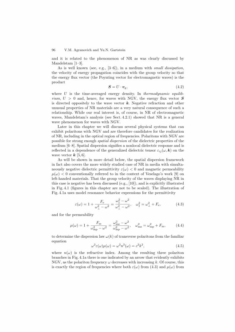
96 V.M. Agranovich and Yu.N. Gartstein
and it is related to the phenomenon of NR as was clearly discussed byMandelstam [1–3].
As is well known (see, e.g., [3–6]), in a medium with small dissipation,the velocity of energy propagation coincides with the group velocity so thatthe energy flux vector (the Poynting vector for electromagnetic waves) is theproduct
S = U · vg, (4.2)
where U is the time-averaged energy density. In thermodynamic equilib-rium, U > 0 and, hence, for waves with NGV, the energy flux vector Sis directed oppositely to the wave vector k. Negative refraction and otherunusual properties of NR materials are a very natural consequence of such arelationship. While our real interest is, of course, in NR of electromagneticwaves, Mandelstam’s analysis (see Sect. 4.2.1) showed that NR is a generalwave phenomenon for waves with NGV.
Later in this chapter we will discuss several physical systems that canexhibit polaritons with NGV and are therefore candidates for the realizationof NR, including in the optical region of frequencies. Polaritons with NGV arepossible for strong enough spatial dispersion of the dielectric properties of themedium [6–8]. Spatial dispersion signifies a nonlocal dielectric response and isreflected in a dependence of the generalized dielectric tensor εij(ω,k) on thewave vector k [5, 6].
As will be shown in more detail below, the spatial dispersion frameworkin fact also covers the more widely studied case of NR in media with simulta-neously negative dielectric permittivity ε(ω) < 0 and magnetic permeabilityµ(ω) < 0 conventionally referred to in the context of Veselago’s work [9] onleft-handed materials. That the group velocity of the waves displaying NR inthis case is negative has been discussed (e.g., [10]), and is explicitly illustratedin Fig. 4.1 (figures in this chapter are not to be scaled). The illustration ofFig. 4.1a uses model resonance behavior expressions for the permittivity
ε(ω) = 1 +Fe
ω2⊥ − ω2
=ω2‖ − ω2
ω2⊥ − ω2
, ω2‖ = ω2
⊥ + Fe, (4.3)
and for the permeability
µ(ω) = 1 +Fm
ω2mp − ω2
=ω2
mz − ω2
ω2mp − ω2
, ω2mz = ω2
mp + Fm, (4.4)
to determine the dispersion law ω(k) of transverse polaritons from the familiarequation
ω2ε(ω)µ(ω) = ω2n2(ω) = c2k2, (4.5)
where n(ω) is the refractive index. Among the resulting three polaritonbranches in Fig. 4.1a there is one indicated by an arrow that evidently exhibitsNGV, as the polariton frequency ω decreases with increasing k. Of course, thisis exactly the region of frequencies where both ε(ω) from (4.3) and µ(ω) from
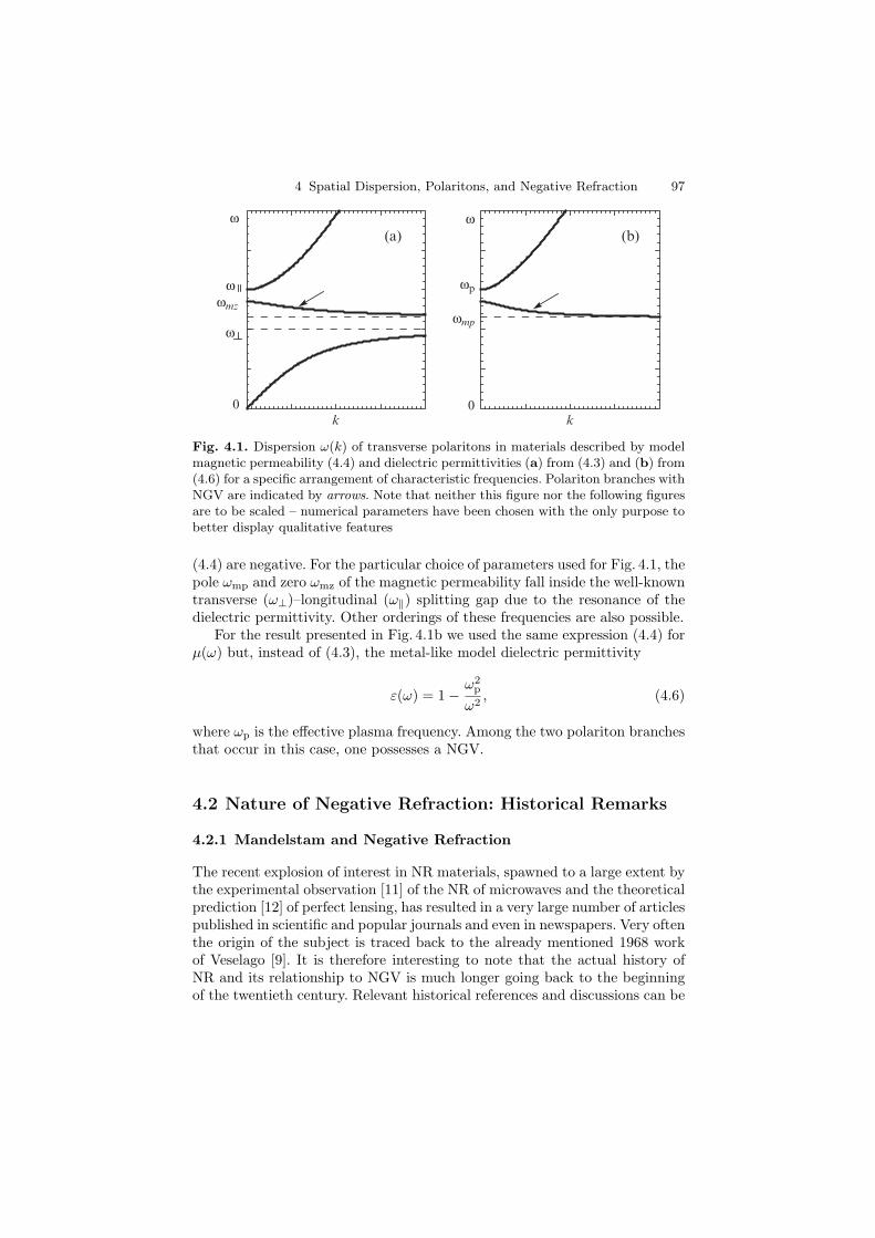
4 Spatial Dispersion, Polaritons, and Negative Refraction 97
ω
ω
ω ωp
ω
ωmpωmz
k k
(a) (b)
0 0
Fig. 4.1. Dispersion ω(k) of transverse polaritons in materials described by modelmagnetic permeability (4.4) and dielectric permittivities (a) from (4.3) and (b) from(4.6) for a specific arrangement of characteristic frequencies. Polariton branches withNGV are indicated by arrows. Note that neither this figure nor the following figuresare to be scaled – numerical parameters have been chosen with the only purpose tobetter display qualitative features
(4.4) are negative. For the particular choice of parameters used for Fig. 4.1, thepole ωmp and zero ωmz of the magnetic permeability fall inside the well-knowntransverse (ω⊥)–longitudinal (ω‖) splitting gap due to the resonance of thedielectric permittivity. Other orderings of these frequencies are also possible.
For the result presented in Fig. 4.1b we used the same expression (4.4) forµ(ω) but, instead of (4.3), the metal-like model dielectric permittivity
ε(ω) = 1 −ω2
p
ω2, (4.6)
where ωp is the effective plasma frequency. Among the two polariton branchesthat occur in this case, one possesses a NGV.
4.2 Nature of Negative Refraction: Historical Remarks
4.2.1 Mandelstam and Negative Refraction
The recent explosion of interest in NR materials, spawned to a large extent bythe experimental observation [11] of the NR of microwaves and the theoreticalprediction [12] of perfect lensing, has resulted in a very large number of articlespublished in scientific and popular journals and even in newspapers. Very oftenthe origin of the subject is traced back to the already mentioned 1968 workof Veselago [9]. It is therefore interesting to note that the actual history ofNR and its relationship to NGV is much longer going back to the beginningof the twentieth century. Relevant historical references and discussions can be
98 V.M. Agranovich and Yu.N. Gartstein
found in [13, 14]. A brief account of the history of NGV is also given in [15]referring to early discussions by Lamb [16] and von Laue [17]. It appears thatSchuster [18] was the first to discuss implications of NGV for optical refraction.
A deep understanding of the essence of the phenomenon of NR demon-strated by Mandelstam in the 1940s [1,2] influenced a lot of subsequent studiesperformed in the former Soviet Union. The forefather of a remarkable Moscowphysical school [19], Mandelstam gave a series of informal courses of lecturesthat started in the 1930s and continued for many years. The lectures coveredmany important and subtle topics in optics, relativity and quantum mechan-ics, and were famous for their in-depth analysis. They were well attended notonly by students but also by many senior professors. Thanks to lecture notestaken by Mandelstam’s collaborators Rytov and Leontovich, the lectures werethen published as part of Mandelstam’s Complete Works [1] and, much later,separately [3].
It is in one of his 1944 lectures on the theory of oscillations [1] thatMandelstam gave a detailed analysis of negative refraction as it occurs ata plane interface with a medium supporting waves with NGV. As neither ofthe publications [1, 3] has been translated from the original Russian, we willnow provide the reader with an excerpt from Mandelstam’s lecture. After dis-cussing conditions under which the group velocity does represent the velocityof energy propagation, Mandelstam continues:
“Let these conditions be satisfied and, hence, the energy propagates withthe group velocity. But we know that the group velocity can be negative. Thismeans that the group (and the energy) propagates in the direction opposite tothe propagation direction of the phase of the wave. Is this possible in reality?
In 1904, Lamb invented some artificial mechanical models of one-dimensional “media” in which the group velocity can be negative. He himselfprobably did not think that his examples may have physical applications. Itturns out, however, that there exist real media where the phase and the groupvelocities are directed opposite to each other in some frequency regions. Thishappens for the so-called “optical” branches of the vibrational spectrum ofthe crystal lattice considered by Born. The existence of situations like thisallows one to look from a different angle at such seemingly well-known pheno-mena as reflection and refraction of a plane wave at the interface betweentwo nonabsorbing media. While traditional discussions of this process do noteven mention the notion of the group velocity, the way it occurs significantlydepends on the sign of the group velocity.
Indeed, what is the idea behind the derivation of Fresnel’s formulae?One considers a sinusoidal plane wave incident at angle ϕ on the interface
plane y = 0:Einc = ei[ωt−k(x sin ϕ+y cos ϕ)],
and, in addition, two other waves: reflected
Erefl = ei[ωt−k(x sin ϕ′−y cos ϕ′)]
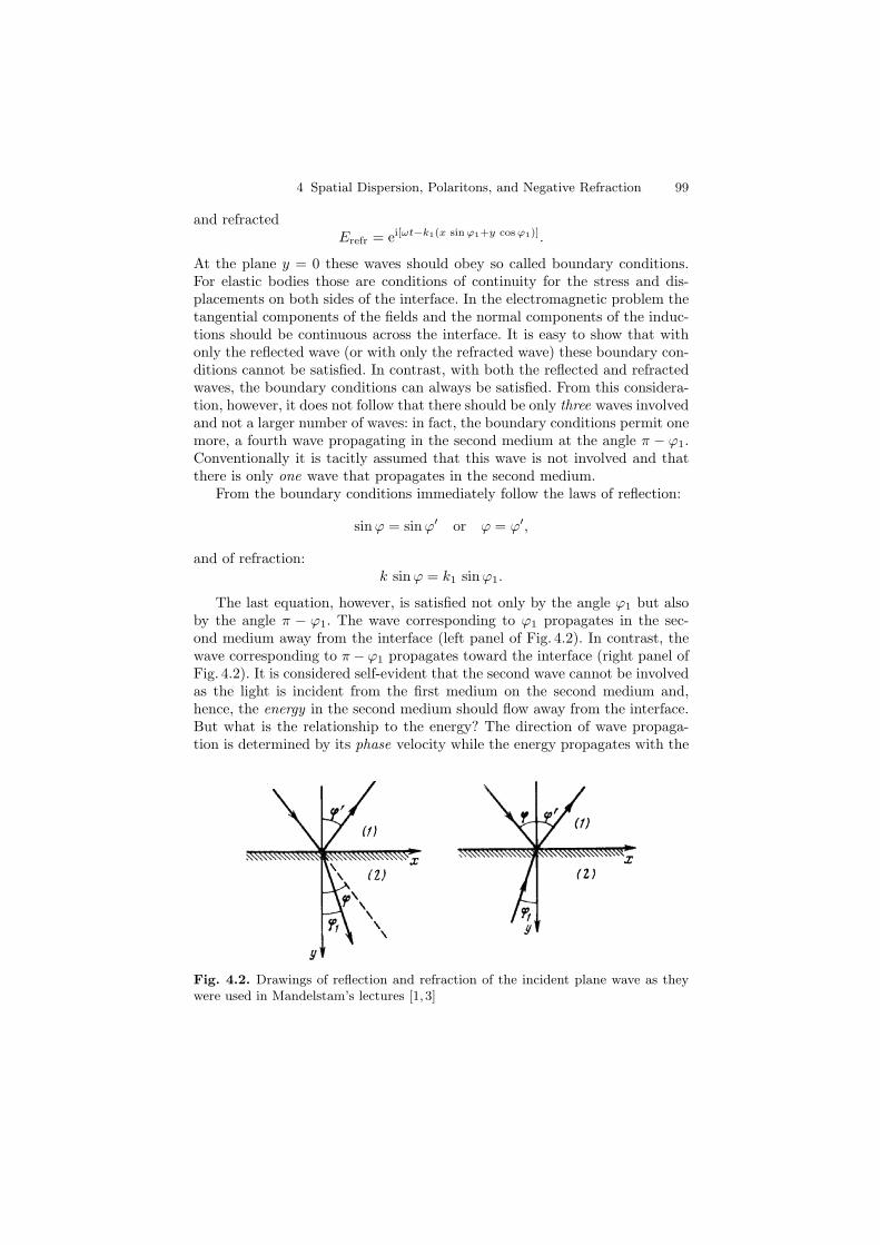
4 Spatial Dispersion, Polaritons, and Negative Refraction 99
and refractedErefr = ei[ωt−k1(x sin ϕ1+y cos ϕ1)].
At the plane y = 0 these waves should obey so called boundary conditions.For elastic bodies those are conditions of continuity for the stress and dis-placements on both sides of the interface. In the electromagnetic problem thetangential components of the fields and the normal components of the induc-tions should be continuous across the interface. It is easy to show that withonly the reflected wave (or with only the refracted wave) these boundary con-ditions cannot be satisfied. In contrast, with both the reflected and refractedwaves, the boundary conditions can always be satisfied. From this considera-tion, however, it does not follow that there should be only three waves involvedand not a larger number of waves: in fact, the boundary conditions permit onemore, a fourth wave propagating in the second medium at the angle π − ϕ1.Conventionally it is tacitly assumed that this wave is not involved and thatthere is only one wave that propagates in the second medium.
From the boundary conditions immediately follow the laws of reflection:
sin ϕ = sin ϕ′ or ϕ = ϕ′,
and of refraction:k sin ϕ = k1 sinϕ1.
The last equation, however, is satisfied not only by the angle ϕ1 but alsoby the angle π − ϕ1. The wave corresponding to ϕ1 propagates in the sec-ond medium away from the interface (left panel of Fig. 4.2). In contrast, thewave corresponding to π −ϕ1 propagates toward the interface (right panel ofFig. 4.2). It is considered self-evident that the second wave cannot be involvedas the light is incident from the first medium on the second medium and,hence, the energy in the second medium should flow away from the interface.But what is the relationship to the energy? The direction of wave propaga-tion is determined by its phase velocity while the energy propagates with the
Fig. 4.2. Drawings of reflection and refraction of the incident plane wave as theywere used in Mandelstam’s lectures [1, 3]
100 V.M. Agranovich and Yu.N. Gartstein
group velocity. A leap of logic is thus made here which goes undetected justbecause we are used to the notion that the directions of the energy and ofthe phase propagation coincide. If these directions indeed coincide, i.e., if thegroup velocity is positive, then everything is correct. If, however, we have thecase of negative group velocity, quite a realistic case as I have already dis-cussed, then everything changes. Still requiring that the energy in the secondmedium flows away from the interface, we conclude that the phase in thiscase should propagate toward the interface and, therefore, the refracted wavewould propagate at the angle π−ϕ1 (as shown on the right panel of Fig. 4.2).However unusual, there is, of course, nothing surprising in this conclusionsince the phase velocity does not say anything yet about the direction of theenergy propagation.”
The above remarks by Mandelstam made more than 60 years ago actuallyexplain the physical origin and the nature of negative refraction. It is instruc-tive that in his explanation of the nature of NR, Mandelstam speaks in termsof the wave vector, group velocity, and causality principle and not in terms ofthe quite popular nowadays negative refractive index. It follows from the samecausality that the intensity of the wave propagating away from the interfacecan only decay in the medium in thermodynamic equilibrium. This rule def-initely determines the sign of the imaginary part of the refractive index and,thereby, the sign of its real part, as both would result simultaneously fromthe sign in the expression n(ω) = ±
√ε(ω)µ(ω) following from (4.5).
The relationship of NR to a negative group velocity as discussed byMandelstam clearly identifies NR as a general wave phenomenon, and alsoindicates a way of looking at candidate NR materials through the dispersionω(k) of the waves they can support. It is worth noting here, however, thatthe notion of waves with NGV has a broader scope and would not be alwaysapplicable to the phenomenon of NR.
As far as we know, Sivukhin [20] and Pafomov [21] were the first to notethat in a medium with simultaneously negative ε(ω) < 0 and µ(ω) < 0 thePoynting vector S and wave vector k are directed opposite to each other and,thus, the group velocity in this case is negative. The importance of the notionof the group velocity for crystal optics has been extensively explored in themonograph [6], and NR occurring at an interface with a chiral medium wasexplicitly indicated already in its 1966 edition accompanied by the now sofamiliar picture of Fig. 4.2 (see p. 252 of [6]).
4.2.2 Cherenkov Radiation
Negative group velocity waves can lead to a peculiar nature of some otherelectromagnetic phenomena such as the Cherenkov and Doppler effects (seethe discussion in [22]). In particular, as was understood a long time ago [23],Cherenkov radiation in media with NGV waves would have an “unusual”directional behavior. This can be readily seen from the theory of Cherenkovradiation (e.g., [5, 22, 24]) and from the sign of the group velocity. Suppose a
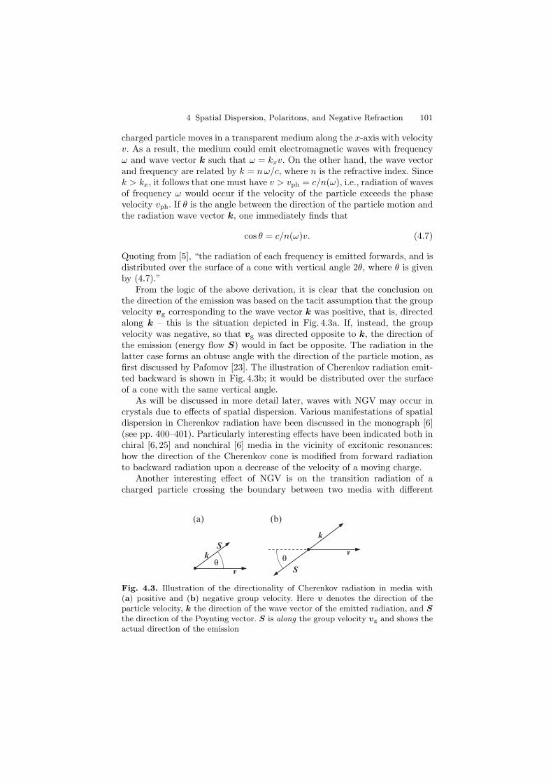
4 Spatial Dispersion, Polaritons, and Negative Refraction 101
charged particle moves in a transparent medium along the x-axis with velocityv. As a result, the medium could emit electromagnetic waves with frequencyω and wave vector k such that ω = kxv. On the other hand, the wave vectorand frequency are related by k = nω/c, where n is the refractive index. Sincek > kx, it follows that one must have v > vph = c/n(ω), i.e., radiation of wavesof frequency ω would occur if the velocity of the particle exceeds the phasevelocity vph. If θ is the angle between the direction of the particle motion andthe radiation wave vector k, one immediately finds that
cos θ = c/n(ω)v. (4.7)
Quoting from [5], “the radiation of each frequency is emitted forwards, and isdistributed over the surface of a cone with vertical angle 2θ, where θ is givenby (4.7).”
From the logic of the above derivation, it is clear that the conclusion onthe direction of the emission was based on the tacit assumption that the groupvelocity vg corresponding to the wave vector k was positive, that is, directedalong k – this is the situation depicted in Fig. 4.3a. If, instead, the groupvelocity was negative, so that vg was directed opposite to k, the direction ofthe emission (energy flow S) would in fact be opposite. The radiation in thelatter case forms an obtuse angle with the direction of the particle motion, asfirst discussed by Pafomov [23]. The illustration of Cherenkov radiation emit-ted backward is shown in Fig. 4.3b; it would be distributed over the surfaceof a cone with the same vertical angle.
As will be discussed in more detail later, waves with NGV may occur incrystals due to effects of spatial dispersion. Various manifestations of spatialdispersion in Cherenkov radiation have been discussed in the monograph [6](see pp. 400–401). Particularly interesting effects have been indicated both inchiral [6, 25] and nonchiral [6] media in the vicinity of excitonic resonances:how the direction of the Cherenkov cone is modified from forward radiationto backward radiation upon a decrease of the velocity of a moving charge.
Another interesting effect of NGV is on the transition radiation of acharged particle crossing the boundary between two media with different
θk
S
v
θ
k
S
v
(a) (b)
Fig. 4.3. Illustration of the directionality of Cherenkov radiation in media with(a) positive and (b) negative group velocity. Here v denotes the direction of theparticle velocity, k the direction of the wave vector of the emitted radiation, and Sthe direction of the Poynting vector. S is along the group velocity vg and shows theactual direction of the emission
102 V.M. Agranovich and Yu.N. Gartstein
dielectric constants (see, e.g., [5, 22]). The important role of the sign ofthe group velocity for the transition radiation and features of the “inverse”Doppler effect were originally clarified in papers by Frank [26], Barsukov [27],and Pafomov [21].
4.3 Maxwell Equations and Spatial Dispersion
4.3.1 Dielectric Tensor
Macroscopic Maxwell equations forming the basis of electrodynamics of con-tinuous media [5] are derived by averaging microscopic electromagnetic fields,charge and current densities, and have to be supplemented by constitutivematerial relations between the averaged fields that are determined by theresponse of the medium to the fields. Following Landau and Lifshitz [5] (seealso [6,28,29]), we find it more appropriate for our goals to use a (very generalfor nonferromagnetic bodies) spatial dispersion approach utilizing only threemacroscopic fields: E,D,B while the fourth field H is set equal to B anddoes not appear in the formalism. This framework assumes that the resultsof the averaging of all induced microscopic currents are absorbed in the defi-nition of the field D. The macroscopic Maxwell equations for monochromaticplane waves in this approach take the following form:
ck × E = ωB
ck × B = −ωD
k · D = 0k · B = 0,
(4.8)
while the material relation between the components of the fields D and E insuch waves is given by
Di = εij(ω,k)Ej . (4.9)
The generalized dielectric tensor εij(ω,k) in (4.9) can depend not only onthe frequency ω but also on the wave vector k. The latter dependence wouldsignify spatial dispersion that is the fact that the electric induction D at agiven spatial point is affected by the electric field E not only at the same spa-tial point (local medium response) but also by the electric field in some neigh-borhood (nonlocal response). The tensor εij(ω,k) describes both dielectricand magnetic responses of the medium, the latter through a natural accountof the response to spatial derivatives of E (see below in greater detail). Spa-tial dispersion comes in addition to the more familiar temporal, or frequencyω, dispersion of the response. Ordinarily spatial dispersion effects are muchweaker than those from frequency dispersion but they can lead to qualitativelynew phenomena like additional electromagnetic waves. The consideration ofspatial dispersion is simplified if the relevant parameter ka ∼ a/λ is small,

4 Spatial Dispersion, Polaritons, and Negative Refraction 103
where a is the characteristic microscopic length or the mean free path of chargecarriers. The smallness of ka allows one in many cases to use only the firstterms (linear and/or quadratic) in the expansion of the tensor εij(ω,k) or ofthe inverse tensor ε−1
ij (ω,k) in powers of the components of the wave vectork [5, 6]
εij(ω,k) = εij(ω) + iγijl(ω)k l + αijlm(ω)k lkm, (4.10)
ε−1ij (ω,k) = ε−1
ij (ω) + iδijl(ω)k l + βijlm(ω)k lkm. (4.11)
The various tensors appearing in expansions (4.10) and (4.11) reflect the sym-metries of the system under consideration. They also satisfy the Onsager prin-ciple of symmetry of kinetic coefficients [5, 6, 28, 29] which, in the absence ofa static magnetic field, states that
εij(ω,k) = εji(ω,−k). (4.12)
In systems with inversion symmetry, the second terms of the expansions (pro-portional to the first power of k l) vanish.
Maxwell equations (4.8) immediately lead to the D–E relationship:
D =c2k2
ω2
[E − k(k · E)
k2
]. (4.13)
Taken together, (4.13) and (4.9) determine the dispersion relations ω(k) forthe electromagnetic waves propagating in the medium with a given dielectrictensor εij(ω,k).
The time-averaged energy density and the Poynting vector in the E,D,Bapproach discussed are found via an analysis of wave packets [5, 6] and aregiven, respectively, by
U =1
16π
[∂(ωεij)
∂ωEiE
∗j + |B|2
](4.14)
andS =
c
8πRe(E∗ × B) − ω
16π
∂εij
∂kE∗
i Ej , (4.15)
where E∗ stands for the complex conjugate of the field E and Re denotes thereal part. Expressions (4.14) and (4.15) satisfy energy conservation (no dissi-pation). Equation (4.15) features an additional (second) term [30,31] entirelydue to spatial dispersion, which in fact plays a crucial role for waves withNGV described within the framework we use.
It is important to note that the fields D and H (= B) of the spatial dis-persion approach are, in general, different from the D and H fields employedin the more familiar “symmetric” approach based on an explicit considerationof all four fields E,D,B,H. To clearly delineate this difference and illus-trate relationships, we will denote here the D and H fields of the symmetricapproach by D′ and H ′, respectively. With the set of four fields, Maxwellequations for plane waves read
104 V.M. Agranovich and Yu.N. Gartstein
ck × E = ωB
ck × H ′ = −ωD′
k · D′ = 0k · B = 0 ,
(4.16)
where spatially local and isotropic material relations are assumed to hold forthe two pairs of the fields:
D′ = ε(ω)E, B = µ(ω)H ′. (4.17)
We will be referring to the framework of (4.17) as the ε(ω)–µ(ω) description.In both sets of (4.8) and (4.16), no explicit separation has been made ofthe macroscopic current due to free charges: free charges are assumed to betreated on the same footing with bound charges in the term ∂D/∂t in thetime-dependent Maxwell equations. With this assumption, the sets (4.8) and(4.16) are applicable to both dielectrics and conductors.
To cast (4.16) in the form of (4.8), let us add c [1− 1/µ(ω)]k×B to bothsides of the second line in (4.16) and introduce new (combination) fields
D = D′ − c
ω
(1 − 1
µ(ω)
)k × B (4.18)
and
H = H ′ +(
1 − 1µ(ω)
)B. (4.19)
This transformation of the fields obviously preserves the form of the secondand third lines in (4.16): ck × H = −ωD and k · D = 0. Using the materialrelations (4.17) in the definitions (4.18) and (4.19) of the new fields yields“new” material relations:
H = B (4.19a)
and
D = ε(ω)E − c
ω
(1 − 1
µ(ω)
)k × B
= ε(ω)E − c2
ω2
(1 − 1
µ(ω)
)k × (k × E). (4.20)
In obtaining (4.20) the first Maxwell equation from set (4.16) has been used,signifying an inherent relationship of the time-dependent magnetic field tospatial derivatives of the electric field. Given (4.19a), we end up with (4.8)employing the newly defined field D. Thus the description of the electromag-netic behavior of the system provided by (4.16) and (4.17) of the symmetricapproach is equivalent to the description provided by (4.8) of the E,D,Bframework where the material relation has the form of (4.20). Equation (4.20)is a particular case of the general linear material relation (4.9) displaying a
4 Spatial Dispersion, Polaritons, and Negative Refraction 105
specific type of spatial dispersion whenever µ(ω) deviates from unity. Thespatial dispersion of εij(ω,k) in this case is a result of absorbing a purelymagnetic response of the system in the field D – local responses for the twofields in (4.17) have been converted into a nonlocal response of a single field.Of course, relation (4.9) can in general describe other types of spatial disper-sion (k-dependence) due to different physical reasons, some of which will bediscussed in this chapter.
The reader interested in various viewpoints, arguments, and details relatedto a comparison of the E,D,B and E,D,B,H approaches to macroscopicelectrodynamics, may find useful discussions in books [28,29], reviews [32–34],and a recent paper [8].
4.3.2 Isotropic Systems with Spatial Inversion
With account of spatial dispersion, the dielectric response should be describedby a tensor even in isotropic systems, as the vector k selects a certain direction.So for an isotropic medium possessing inversion symmetry (a nongyrotropicor nonchiral medium), the general form of the dielectric tensor is [5]
εij(ω,k) = ε⊥(ω, k)[δij −
kikj
k2
]+ ε‖(ω, k)
kikj
k2, (4.21)
where the transverse ε⊥(ω, k) and longitudinal ε‖(ω, k) dielectric functionsnow depend on k only through its magnitude k, and provide a completedescription of this medium. In accordance with (4.13) and (4.9), the dispersionω(k) of transverse (E ⊥ k) polaritons is then found from
ω2ε⊥(ω, k) = c2k2, (4.22)
while the equationε‖(ω, k) = 0 (4.23)
determines the dispersion of longitudinal (E ‖ k, D = 0, B = 0) waves.It can be shown [5] that the ε(ω)–µ(ω) description of this medium would
then correspond only to the limiting k → 0 behavior in the full spatial dis-persion framework:
ε(ω) = ε⊥(ω, 0) = ε‖(ω, 0) (4.24)
and
1 − 1µ(ω)
= limk→0
ω2[ε⊥(ω, k) − ε‖(ω, k)
]c2k2
. (4.25)
Consistently with (4.24) and (4.25), the material relation (4.20) we derivedin the field conversion procedure is equivalent to a particular choice of thetransverse function,
ε⊥(ω, k) = ε(ω) +c2k2
ω2
[1 − 1
µ(ω)
], (4.26)
106 V.M. Agranovich and Yu.N. Gartstein
while the longitudinal function ε‖(ω, k) = ε(ω) displays no spatial dispersion.Using (4.26) in dispersion equation (4.22) for transverse polaritons wouldmake (4.22) identical to (4.5) derived in the ε(ω)–µ(ω) description. This againdemonstrates that results derivable for transverse waves in the ε(ω)–µ(ω)framework are recovered in the spatial dispersion approach for a specific k-dependence (∝ k2) in ε⊥(ω, k). Even within the k2-accuracy, however, onehas to be aware of the following.
In the isotropic system under consideration, the response tensor αijlm
of (4.10) is in general characterized by two independent parameters. Theseparameters (a and b) can, for instance, be chosen via the representation
αijlm = a δijδlm +b
2(erilerjm + erimerjl) , (4.27)
where eril denotes the antisymmetric unit tensor of rank three. Equation(4.27) is written explicitly symmetric in both the first (ij) and second (lm)pairs of indices, and it leads to
ε⊥(ω, k) = ε(ω) + [a(ω) + b(ω)]k2, ε‖(ω, k) = ε(ω) + a(ω)k2 (4.28)
in expansions for the transverse and longitudinal dielectric functions. Thecorresponding material relation (4.9), as follows from (4.10) and (4.27), is
D = [ε(ω) + a(ω)k2]E + b(ω)k × (E × k). (4.29)
Equations (4.20), (4.28), and (4.29) make it clear that the parameter b(ω)can be loosely thought of as quantifying spatial dispersion due to a “magneticresponse” of the system: It is related to the magnetic permeability (see (4.20)and (4.25)) through ω2b(ω)/c2 = 1−1/µ(ω). The parameter a(ω), on the otherhand, would then quantify spatial dispersion due to an “electric response.”This latter dispersion could not be properly taken into account within theε(ω)–µ(ω) description, as both types of responses contribute similarly to thedispersion of transverse polaritons [(4.28) and (4.22)] but only the electricresponse affects the longitudinal waves [(4.28) and (4.23)]. Particularly note-worthy is that polaritons with NGV and subsequent negative refraction mayoccur in systems with µ(ω) = 1 (i.e., with b(ω) = 0) if the response coefficienta(ω) has an appropriate frequency behavior.
4.3.3 Connection to Microscopics
The dielectric tensor εij(ω,k) describes the response of the medium to electro-magnetic perturbations of arbitrary frequencies ω and wave vectors k. As such,it has certain well-known analytic properties and can, in principle, be derivedfrom a microscopic description of elementary excitations of the medium bythe use of various methods; see, e.g., [6, 28, 35–37] for discussions of manyimportant aspects. Our limited illustration here follows the derivation in [6]where more details can be found.
4 Spatial Dispersion, Polaritons, and Negative Refraction 107
Consider a crystalline medium of volume V containing N electrons ofcharge e and mass m. The ground state |0〉 of this system is being per-turbed by the external vector potential A(r, t) = A0 ei(k·r−ωt) + c.c. tothe time-dependent state |0〉. The corresponding perturbing electric fieldE = −(1/c)∂A/∂t is characterized by the amplitude E0 = i(ω/c)A0. Inthe linear approximation, the perturbation operator is then
Hint = F e−iωt + F †eiωt, F = − icω
M(k) · E0, (4.30)
whereM(k) = − e
2mc
∑α
(pα eik·rα
+ eik·rα
pα) (4.31)
comprises effects on all electrons, with rα the coordinate of the αth electronand pα = −i∂/∂rα its momentum operator.
As a result of the perturbation (4.30), an electric current will be inducedin the system, whose average induced current density is
J(r, t) =e
2
⟨0|
∑α
(vαδ(r − rα) + δ(r − rα)vα) |0⟩
, (4.32)
where mvα = pα − (e/c)A(rα, t) and only terms linear in A are supposed tobe retained. One applies the ordinary first-order time-dependent perturbationtheory to evaluate (4.32) in terms of the ground state |0〉 and various excitedstates |n〉 of the unperturbed system. These “bare” excited states, which wewill be calling excitons, have excitation energies ωn and are assumed to havebeen calculated without account of the macroscopic electromagnetic field (inthe terminology of [6], these are “mechanical excitons”). Restricting ourselvesto the same Fourier harmonics, one then finds J = J0ei(k·r−ωt) + c.c., wherethe amplitude J0 of the induced current determines the conductivity tensorσ via its relationship to the amplitude of the perturbing electric field:
J0i = σij(ω,k)E0j . (4.33)
The dielectric tensor is related to the conductivity tensor in (4.33) in a stan-dard way:
εij(ω,k) = δij +4πiω
σij(ω,k). (4.34)
Collecting all the terms contributing to (4.34), one ends up with the followingexpression for the dielectric tensor:
εij(ω,k) =(
1 − 4πe2N
mω2V
)δij
− 4πc2
ω2V
∑n
[Mn∗
i (k)Mnj (k)
ω − ωn−
Mni (−k)Mn∗
j (−k)ω + ωn
], (4.35)
108 V.M. Agranovich and Yu.N. Gartstein
where Mni (k) are the Cartesian components of the matrix elements of the
vector operator (4.31):
Mn(k) = 〈n|M(k)|0〉. (4.36)
By using Onsager relation (4.12), one can further explicitly symmetrize expres-sion (4.35): εij(ω,k) → [εij(ω,k) + εji(ω,−k)] /2.
It is instructive to look now at the microscopic origin of expressions like(4.26) and (4.28) in isotropic systems with inversion, for which we expand thematrix elements (4.36) in powers of the components of the wave vector k:
Mni (k) = Pn
i + ik lXnil + · · · (4.37)
A set of atoms or molecules can be a useful, although not necessary, modelpicture of the system (for an extensive relevant discussion of molecular tran-sitions, see, e.g., [38,39]). In accordance with (4.28) and (4.35), the dielectricpermittivity ε(ω) is determined by the Mn(k = 0) elements
Pni = − e
mc
∑α
〈n|pαi |0〉 , (4.38)
yielding4πc2
ω2V
∑n
ωn
(Pn∗
i Pnj + Pn
i Pn∗j
)
ω2n − ω2
(4.39)
in the second line of (4.35). Transitions with nonzero Pni are electric-dipole
allowed transitions (otherwise called E1 transitions) and only they contributeto ε(ω).
Equation (4.39) can be transformed employing the quantum-mechanicalrelationships
〈n|pαi |0〉 = imωn〈n|rα
i |0〉 (4.40)
and∑nαβ
mωn
(〈0|rα
i |n〉〈n|rβj |0〉 + 〈0|rβ
j |n〉〈n|rαi |0〉
)= Nδij . (4.41)
The sum rule, (4.41), of course, follows immediately from the commutator[rα
i , pβj ] = iδαβδij using the completeness of the set of states |n〉 and (4.40).
Sinceω2
n
ω2n − ω2
= 1 +ω2
ω2n − ω2
,
one can use the sum rule (4.41) to conveniently separate from (4.39) theterm (4πe2N/mω2V )δij , which exactly cancels the diamagnetic contributionin the first line of (4.35). In isotropic systems, the rest of (4.39) would also beproportional to δij so that the resulting permittivity is
ε(ω) = 1 +∑en
Fen
ω2en − ω2
, (4.42)
4 Spatial Dispersion, Polaritons, and Negative Refraction 109
where we have used the index en to emphasize that the actual summationis over electric-dipole allowed transitions only. The corresponding transitionfrequencies are denoted by ωen while the “oscillator strengths” Fen, in accor-dance with (4.41), satisfy the sum rule
∑en Fen = ω2
p, where the plasma
frequency is ωp =(4πe2N/mV
)1/2. In the vicinity of a single resonance freq-uency ω⊥, (4.42) exhibits the behavior
ε(ω) = εb +Fe
ω2⊥ − ω2
= εbω2‖ − ω2
ω2⊥ − ω2
, ω2‖ = ω2
⊥ + Fe/εb, (4.43)
where the background constant εb comes from other allowed transitions(εb = 1 in (4.3)).
A qualitatively different contribution to the dielectric tensor comes fromelectric-dipole forbidden transitions. In expansion (4.37) of the matrix ele-ments the first term for these transitions vanishes. It is the second term with
Xnil = − e
2mc
∑α
〈n|pαi rα
l + rαl pα
i |0〉 (4.44)
that is responsible now for the transition intensity. It is useful to distinguishthe magnetic-dipole transitions (M1 transitions) that would be caused by theantisymmetric magnetic-dipole combination
rαl pα
i − rαi pα
l (4.45)
in the brackets of (4.44). The actual combination in those brackets differs from(4.45) by
pαi rα
l + rαi pα
l . (4.46)
The combination in (4.46) is well known to correspond to electric-quadrupoletransitions (E2 transitions). The difference of the magnetic-dipole and electric-quadrupole transitions is reflected in the symmetry of the tensor Xn
il : thetensor is antisymmetric, X
n(m)il = −X
n(m)li , for the former; but symmetric,
Xn(q)il = X
n(q)li , for the latter. As follows from (4.35) and (4.37), both types of
transitions can contribute to the tensor αijlm (4.27) via the following term:
4πc2
ω2V
∑n
ωn
(Xn∗
il Xnjm + Xn∗
jl Xnim
)
ω2n − ω2
. (4.47)
One notes, however, that, because of their symmetry, purely magnetic-dipolecombinations like X
n(m)∗il X
n(m)jm in (4.47) contribute only to the magnetic-
response coefficient b(ω) in (4.27). On the other hand, the electric-quadrupolecombinations like X
n(q)∗il X
n(q)jm can contribute to both response coefficients
a(ω) and b(ω) in (4.27). (For examples of other symmetry applications see,e.g., [6]; for a general discussion of the electric quadrupole polarization inmacroscopic electrodynamics see [24].)
110 V.M. Agranovich and Yu.N. Gartstein
Equation (4.47) explicitly shows that magnetic-dipole and electric-quadrupole transitions (and, in general, their mix) can lead to contributions ofthe same type to the transverse dielectric function ε⊥(ω, k), of the general form
c2k2
ω2
∑fn
Ffn
ω2fn − ω2
, (4.48)
as follows from (4.27), (4.28), and (4.47). We used the index fn in (4.48) toindicate that the sum is over electric-dipole forbidden transitions with fre-quencies ωfn and intensities determined by the parameters Ffn. Combininga contribution from a single isolated resonance of frequency ωf in (4.48) with(4.43) leads to
ε⊥(ω, k) = εb +Fe
ω2⊥ − ω2
+c2k2
ω2
Ff
ω2f − ω2
. (4.49)
The general behavior featured in (4.49) arises from the interplay of two res-onances: one, which is electric-dipole allowed (frequency ω⊥), and the other,which is electric-dipole forbidden (frequency ωf). This is the interplay thatcan lead to polaritons with NGV as shown in Fig. 4.1a. One easily finds from(4.26), (4.3), and (4.4) that this is indeed the case by associating [1 − 1/µ(ω)]in (4.26) with Ff/(ω2
f − ω2) in (4.49). For the model expression (4.4), thecorrespondence is that the zero ωmz of the magnetic permeability µ(ω) is thefrequency ωf of the forbidden transition, while the parameter Fm = Ff .
(We note that, of course, contributions ∝ k2 in (4.28) can also comethrough corrections to matrix elements from electric-dipole allowed transi-tions; they are, however, of no interest for the discussion at hand.)
The derivation leading to (4.49) also indicates that the strength of the for-bidden electronic transitions in atomic/molecular materials is generally muchweaker than the strength of the electric-dipole allowed transitions. Assuming,e.g., that the allowed and forbidden transitions in (4.49) arise from the samemolecular species, one can estimate the matrix elements (4.40) and (4.44),leading to
Ff
Fe∼ 1
c2
ω3f a4
ω⊥a2∼ v2
c2 1, (4.50)
where a is the characteristic molecular size and v a typical electron velocity(ω⊥ ∼ ωf). In this regard, we recall that Fe/εb determines the magnitude ofthe ω‖ − ω⊥ splitting in Fig. 4.1a, while Ff = Fm defines the frequency widthof the polariton branch with NGV.
4.3.4 Isotropic Systems Without Spatial Inversion
In media with broken spatial inversion symmetry (gyrotropic or chiral media)the tensors γijl and δijl [from (4.10) and (4.11)] do not vanish, and spatialdispersion manifests itself already in terms of the first-order smallness with
4 Spatial Dispersion, Polaritons, and Negative Refraction 111
respect to the wave vector k. Important features of the polariton dispersionin such media can be readily delineated even if only these linear terms areretained [6,40]. In isotropic systems the general tensors γijl and δijl reduce tothe unit antisymmetric tensor and the expansions take the forms
εij(ω,k) = ε(ω) δij + i γ(ω)eijlk l, (4.51)
ε−1ij (ω,k) =
1ε(ω)
δij + i δ(ω)eijlk l. (4.52)
As discussed later, (4.51) is appropriate to use in the vicinity of the longi-tudinal frequency ω‖: ε(ω‖) = 0, while (4.52) is useful in the vicinity of theresonance frequency ω⊥: 1/ε(ω⊥) = 0.
Once again, it is instructive to see the microscopic origin of the behaviorin (4.51). For a set of chiral molecules, for instance, it is well known (see,e.g., [37–39]) that optical activity results from transitions to states |n〉 withnonvanishing matrix elements of both types (4.38) and (4.44). Using expansion(4.37) in (4.35), one indeed easily finds a microscopic representation of thetensor γijl in (4.10) as
4πc2
ω2V
∑n
ωn
(Pn
i Xn∗jl − Pn
j Xn∗il + c.c.
)
ω2n − ω2
. (4.53)
In isotropic systems it is only the antisymmetric magnetic-dipole Xn(m)il
matrix elements that actually contribute to (4.53), whose tensor structurereduces to the antisymmetric tensor in (4.51). The microscopic meaning ofδ(ω) in (4.52) will be addressed in Sect. 4.4.2.
4.4 Polaritons with Negative Group Velocity
As has already been mentioned, it is the second term in expression (4.15)for the Poynting vector S that explicitly shows how spatial dispersion can“invert” the direction of energy propagation with respect to the wave vectork. Indeed the first term in (4.15) in an isotropic medium is a vector directedalong k. For the group velocity to become negative, the second term has to bealong −k and larger in magnitude. This, in particular, implies that the spatialdispersion ∂ε⊥(ω, k)/∂k should be strong enough. This is precisely the caseoccurring in the situation of (4.49) below the forbidden frequency ωf . In whatfollows we will discuss several other instances of substantial spatial dispersionof the dielectric function leading to polaritons with negative group velocitiesin potentially broader regions of frequency ω.
4.4.1 Excitons with Negative Effective Mass in Nonchiral Media
Pekar [41] was the first to suggest in 1957 that spatial dispersion of the dielec-tric function near the excitonic resonance could lead to the appearance of an
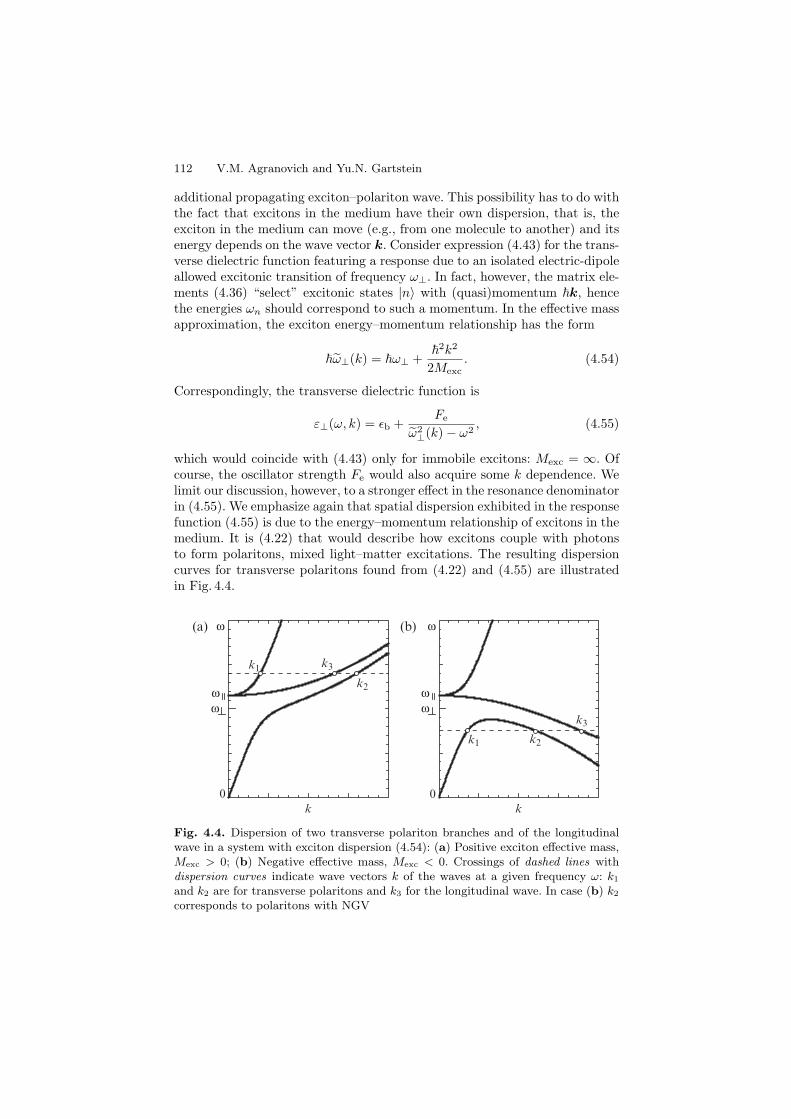
112 V.M. Agranovich and Yu.N. Gartstein
additional propagating exciton–polariton wave. This possibility has to do withthe fact that excitons in the medium have their own dispersion, that is, theexciton in the medium can move (e.g., from one molecule to another) and itsenergy depends on the wave vector k. Consider expression (4.43) for the trans-verse dielectric function featuring a response due to an isolated electric-dipoleallowed excitonic transition of frequency ω⊥. In fact, however, the matrix ele-ments (4.36) “select” excitonic states |n〉 with (quasi)momentum k, hencethe energies ωn should correspond to such a momentum. In the effective massapproximation, the exciton energy–momentum relationship has the form
ω⊥(k) = ω⊥ +
2k2
2Mexc. (4.54)
Correspondingly, the transverse dielectric function is
ε⊥(ω, k) = εb +Fe
ω2⊥(k) − ω2
, (4.55)
which would coincide with (4.43) only for immobile excitons: Mexc = ∞. Ofcourse, the oscillator strength Fe would also acquire some k dependence. Welimit our discussion, however, to a stronger effect in the resonance denominatorin (4.55). We emphasize again that spatial dispersion exhibited in the responsefunction (4.55) is due to the energy–momentum relationship of excitons in themedium. It is (4.22) that would describe how excitons couple with photonsto form polaritons, mixed light–matter excitations. The resulting dispersioncurves for transverse polaritons found from (4.22) and (4.55) are illustratedin Fig. 4.4.
ω
ωω
ωω
ω
k
(a) (b)
k1
k2
k3
k1 k2
k3
k0 0
Fig. 4.4. Dispersion of two transverse polariton branches and of the longitudinalwave in a system with exciton dispersion (4.54): (a) Positive exciton effective mass,Mexc > 0; (b) Negative effective mass, Mexc < 0. Crossings of dashed lines withdispersion curves indicate wave vectors k of the waves at a given frequency ω: k1
and k2 are for transverse polaritons and k3 for the longitudinal wave. In case (b) k2
corresponds to polaritons with NGV
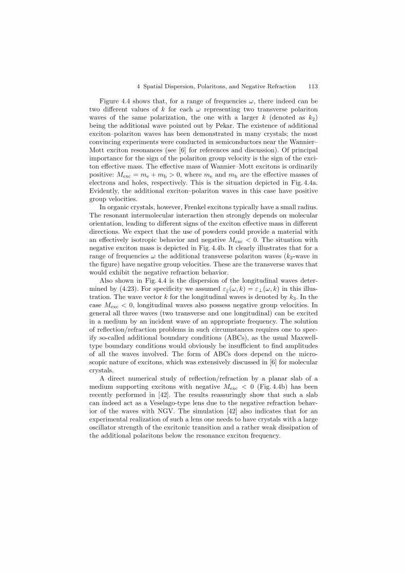
4 Spatial Dispersion, Polaritons, and Negative Refraction 113
Figure 4.4 shows that, for a range of frequencies ω, there indeed can betwo different values of k for each ω representing two transverse polaritonwaves of the same polarization, the one with a larger k (denoted as k2)being the additional wave pointed out by Pekar. The existence of additionalexciton–polariton waves has been demonstrated in many crystals; the mostconvincing experiments were conducted in semiconductors near the Wannier–Mott exciton resonances (see [6] for references and discussion). Of principalimportance for the sign of the polariton group velocity is the sign of the exci-ton effective mass. The effective mass of Wannier–Mott excitons is ordinarilypositive: Mexc = me + mh > 0, where me and mh are the effective masses ofelectrons and holes, respectively. This is the situation depicted in Fig. 4.4a.Evidently, the additional exciton–polariton waves in this case have positivegroup velocities.
In organic crystals, however, Frenkel excitons typically have a small radius.The resonant intermolecular interaction then strongly depends on molecularorientation, leading to different signs of the exciton effective mass in differentdirections. We expect that the use of powders could provide a material withan effectively isotropic behavior and negative Mexc < 0. The situation withnegative exciton mass is depicted in Fig. 4.4b. It clearly illustrates that for arange of frequencies ω the additional transverse polariton waves (k2-wave inthe figure) have negative group velocities. These are the transverse waves thatwould exhibit the negative refraction behavior.
Also shown in Fig. 4.4 is the dispersion of the longitudinal waves deter-mined by (4.23). For specificity we assumed ε‖(ω, k) = ε⊥(ω, k) in this illus-tration. The wave vector k for the longitudinal waves is denoted by k3. In thecase Mexc < 0, longitudinal waves also possess negative group velocities. Ingeneral all three waves (two transverse and one longitudinal) can be excitedin a medium by an incident wave of an appropriate frequency. The solutionof reflection/refraction problems in such circumstances requires one to spec-ify so-called additional boundary conditions (ABCs), as the usual Maxwell-type boundary conditions would obviously be insufficient to find amplitudesof all the waves involved. The form of ABCs does depend on the micro-scopic nature of excitons, which was extensively discussed in [6] for molecularcrystals.
A direct numerical study of reflection/refraction by a planar slab of amedium supporting excitons with negative Mexc < 0 (Fig. 4.4b) has beenrecently performed in [42]. The results reassuringly show that such a slabcan indeed act as a Veselago-type lens due to the negative refraction behav-ior of the waves with NGV. The simulation [42] also indicates that for anexperimental realization of such a lens one needs to have crystals with a largeoscillator strength of the excitonic transition and a rather weak dissipation ofthe additional polaritons below the resonance exciton frequency.

114 V.M. Agranovich and Yu.N. Gartstein
4.4.2 Chiral Systems in the Vicinity of Excitonic Transitions
Chiral (gyrotropic) systems, well known for the phenomena of optical activ-ity and circular dichroism, naturally lend themselves as candidate media tosupport polaritons with NGV in certain regions of frequency ω. We start ourdiscussion from the case of a frequency region in the vicinity of the excitontransition frequency ω⊥. As the transition frequency corresponds to the poleof the dielectric permittivity ε(ω), a more convenient way to consider thisregion is by using the expansion (4.52) for the inverse dielectric tensor. Theinverse dielectric function vanishes at the transition frequency: ε−1(ω⊥) = 0,making clear the qualitative importance of the next, spatially dispersive, termin that expansion.
Equation (4.52) corresponds to the material relation
E =1
ε(ω)D + i δ(ω)D × k (4.56)
between the E and D fields, where the parameter δ(ω) defines the “strength”of the chirality. Relation (4.56) combined with the wave equation (4.13) fortransverse waves leads to the equation
(ω2
c2k2
)D =
1ε(ω)
D + i δ(ω)D × k , (4.57)
whose nontrivial solutions describe transverse polaritons in this system.These solutions are known to correspond to circularly polarized waves: e.g.,Dy/Dx =±i for waves propagating in the z-direction. The polariton disper-sion ω(k) is determined from the condition that the determinant of the systemof equations (4.57) vanishes:
(1
ε(ω)− ω2
c2k2
)2
= δ2(ω)k2 (4.58)
or, for waves of different circular polarizations,
1ε(ω)
− ω2
c2k2= ±|δ(ω)|k. (4.58a)
Figure 4.5a illustrates the two branches of the transverse polariton dispersionresulting from (4.58a) when the model dielectric function ε(ω) of (4.43) anda constant δ(ω) = δ are used.
Qualitatively (see [6,43]) this two-branch polariton spectrum can be under-stood as being due to the dispersion of excitons, that is, due to the fact that theexciton energies themselves can depend on the wave vector k, similarly to theeffect we discussed in Sect. 4.4.1 in connection with (4.54). In a chiral medium,however, electric-dipole active excitons (or optical phonons) would have theirdispersion split into two branches corresponding to the two different circular
4 Spatial Dispersion, Polaritons, and Negative Refraction 115
ω
ω
ω
ω
k
(a) (b)
k1
k2 k3
k
k1
k2
k1
k2
0
Fig. 4.5. Dispersion branches of transverse polaritons in chiral media. Note dis-tinctly different ranges of frequencies (and wave vectors) in panels (a) and (b).Shown in (a) is a range around the frequency ω⊥ and below, a neighborhood ofω‖ would be above this plot. Shown in (b) is a range around the frequency ω‖ andabove, a neighborhood of ω⊥ would be below this plot. The crossing of dashed lineswith dispersion curves show allowed values k of the wave vector at a given frequencyω. Both panels feature polaritons with NGV
polarizations. One can easily see the connection by analyzing a region of ω inthe vicinity of the resonance frequency ω⊥ where the inverse permittivity canbe linearly approximated by
ε−1(ω) A⊥(ω⊥ − ω), A⊥ = 2ω⊥/Fe, (4.59)
as follows from the model expression (4.43). Using the approximation (4.59)in (4.58a) one rewrites the latter as A⊥(ω⊥ − ω ∓ |δ|k/A⊥) = ω2/c2k2, whichis exactly the transverse polariton dispersion equation that would be obtainedfor excitons possessing their own dispersion law
ω⊥(k) = ω⊥ ∓ |δ|A⊥
k. (4.60)
One can compare (4.60) with (4.54). The linear behavior in (4.60) repre-sents the first terms of the k-expansion of the exciton dispersion in the chiralmedium with the chirality parameter δ determining the splitting effect in thevicinity of the resonance. When these dispersing excitons couple with light oftwo different circular polarizations, they form two of the polariton branchesdisplayed in Fig. 4.5a. The first experimental observation of this branchingand of a linear dependence of the frequency of dipole-active excitations on thewave vector was made for optical phonons propagating along the optical axisin quartz [44].
As is evident in Fig. 4.5a, the lower polariton branch features waves withnegative group velocity whose wave vector is denoted by k3. It is also trans-parent that there would be two other waves excited at the same frequency
116 V.M. Agranovich and Yu.N. Gartstein
ω whose wave vectors are denoted by k1 and k2. The relative amplitudes ofthese three waves depend on the matching of the incident wave vector to thewave vectors of the individual waves. An experimental realization of nega-tive refraction due to k3-waves again necessitates a large oscillator strength ofthe excitonic transition as well as a large rotatory power and a rather smalldissipation of the additional polaritons below the resonance frequency.
4.4.3 Chiral Systems in the Vicinity of the Longitudinal Frequency
A “chiral route” to negative refraction has been specifically emphasized byPendry [45] recently in a different frequency region: that in the vicinity of thelongitudinal frequency ω‖. Related is the theoretical work on negative refrac-tion in chiral materials with certain material parameters [46, 47], includingdemonstrations of focusing for circularly polarized waves [48,49]. Our consid-eration is based on the spatial dispersion approach. For more details we referthe reader to paper [50].
As the longitudinal frequency corresponds to the zero of the dielectric per-mittivity ε(ω), it is appropriate to use now expansion (4.51) of the dielectrictensor. Once again, the vanishing of ε(ω‖) makes it clear that the next, spa-tially dispersive, term in that expansion is going to be qualitatively important.With the model dielectric permittivity (4.43),
ω‖ =√
ω2⊥ + Fe/εb,
and ε(ω) behaves linearly as
ε(ω) A‖(ω − ω‖), A‖ = 2ε2bω‖/Fe, (4.61)
in the immediate vicinity of the frequency ω‖.Equation (4.51) corresponds to the material relation
D = ε(ω)E + iγ(ω)E × k (4.62)
between the fields. Now it is the parameter γ(ω) that determines the magni-tude of the chirality. The wave equation (4.13) then requires that transversepolaritons satisfy the equation
(c2k2
ω2
)E = ε(ω)E + i γ(ω)E × k. (4.63)
Of course, one can draw parallels between (4.63) and (4.57). Nontrivial solu-tions of (4.63) are circularly polarized waves whose dispersion has to be deter-mined from
ε(ω) − c2k2
ω2= ±|γ(ω)|k, (4.64)
the plus and minus signs corresponding to waves of opposite handedness.Figure 4.5b illustrates the transverse polariton dispersion in this case in the
4 Spatial Dispersion, Polaritons, and Negative Refraction 117
region of frequencies around and above ω‖ resulting from (4.64) when usingthe model dielectric function ε(ω) of (4.43) and a model dependence of γ(ω) =γ1/(ω2 − ω2
⊥).The qualitative nature of the polariton spectrum in Fig. 4.5b is easily
understood when using the linear approximation (4.61) in the dispersion equa-tion (4.64), which immediately yields polariton dispersion curves in the formof “displaced parabolas”:
ω±(k) ω‖ +c2
A‖ω2‖k2 ± γ
A‖k, (4.65)
where γ = γ(ω‖). As is evident in (4.65) and in Fig. 4.5b, for each frequency ω,where waves can exist there are two types of solutions with k-values denotedby k1 and k2 such that k1 ≤ k2. For frequencies ω > ω‖, k1- and k2-wavesbelong to different polarization branches (ω+(k) and ω−(k)), while for ω < ω‖,they belong to the same branch: ω−(k) for γ > 0. The latter has a minimumof ω−(kmin) = ω‖−∆ (the minimum of the allowed frequencies for the propa-gating waves) achieved at k = kmin (ω2
‖/2c2)γ. The depth of this minimum
∆ = ω‖ − ω−(kmin) γ2ω2‖/4A‖c
2, (4.66)
strongly depends not only on ω‖ and γ but also on the value of A‖. Clearly,it is the part ω−(k < kmin) of the polariton spectrum, that is, k1-waves atω < ω‖, that exhibits negative group velocities as the frequency in that partdecreases with growing k1. All other parts of the spectrum in (4.65) correspondto polaritons with positive group velocities. At the bottom of the allowedfrequency range ω‖−∆, the wave vectors k1 = k2 = kmin, and the polariton’sgroup velocity vanishes.
It is interesting to note that, similarly to the case illustrated in Fig. 4.1, thenegative group velocity waves in Fig. 4.5b appear in the region of frequenciesthat would be forbidden for electromagnetic waves – in the absence of themagnetic resonance in the system of Fig. 4.1 and in the absence of chirality inthe system we consider now. In the former case, however, waves of arbitrarypolarization have negative group velocities, while the chiral system supportsnegative group velocities for circularly polarized waves of one handedness only,waves of the other handedness have positive group velocities.
As left- and right-hand polarized waves propagate with different phasevelocities, a linearly polarized light wave will experience a rotation of its planeof polarization. It is quantified by parameter ρ giving the rotation of thepolarization plane per unit length of ray passage. It is useful to note that anexact (for unspecified ω−dependences of ε(ω) and γ(ω)) relationship followsfrom (4.64) for the difference between wave vector magnitudes at the samefrequency ω > ω‖:
k2 − k1 = γ(ω)ω2/c2. (4.67)
118 V.M. Agranovich and Yu.N. Gartstein
Its exact counterpart for frequencies ω < ω‖ relates the sum of wave vectormagnitudes at the same frequency:
k2 + k1 = γ(ω)ω2/c2. (4.68)
Equations (4.67) and (4.68) then lead [50] to the same result
ρ =γ(ω)ω2
2c2
in a given chiral medium both below and above the frequency ω‖. Measuringρ thus provides experimental access to the chirality parameter γ(ω).
Dissipation can have a substantial detrimental effect on the possibilityof realizing negative refraction conditions. A quantitative illustration for thecase we consider now follows from the physically transparent statement thatthe dispersion of the waves shown in Fig. 4.5b retains its physical significanceonly if the minimum depth ∆ in (4.66) is large enough in comparison withthe dissipative width Γ of transverse electromagnetic waves in the region offrequencies around ω‖. As we have discussed in [50] for several examples, thisrestriction in fact leads to quite demanding requirements on the “allowed”magnitudes of gyrotropy (chirality) and dissipation.
We have shown [50] that ordinary specular reflection can be useful inexperimental studies of candidate chiral materials: The interesting regionof frequencies around ω‖ would be directly detectable in features of thefrequency-dependent pattern of the reflection of linearly polarized incidentlight.
4.4.4 Surface Polaritons
Negative group velocity waves can also occur in two-dimensional wave prop-agation. We consider here an example of surface polariton waves in near res-onance with modes of the surface transition layer. It is known that a surfacetransition layer (e.g., a thin film on a substrate) can drastically alter thedispersion of surface polaritons when the latter resonate with vibrational orelectronic excitations of the layer [51]. If chosen properly, the transition layercan give rise to surface polariton dispersion curves exhibiting regions of neg-ative group velocities.
Consider a system composed of a thin film of thickness d a (where a isthe lattice constant) and dielectric function ε(ω), that is sandwiched betweentwo semi-infinite media of dielectric functions ε1(ω) > 0 and ε2(ω) < 0.Surface polaritons in this system exist in a certain frequency range, and theirdispersion curve ω(k) is determined by the equation [51]
κ1
ε1+
κ2
ε2+ k2p +
κ1
ε1
κ2
ε2q = 0. (4.69)
Here k is the magnitude of the two-dimensional wave vector of the surfacepolaritons along the interface, which is assumed to be planar-isotropic. Theparameters in (4.69) are defined as
4 Spatial Dispersion, Polaritons, and Negative Refraction 119
κi =
√k2 − ω2
c2εi, i = 1, 2,
q = (ε − ε2) d, p =(
1ε− 1
ε2
)d,
and kd 1 has been assumed. For d = 0, the parameters p and q vanish, and(4.69) reduces to the familiar equation for the dispersion of surface polaritonsat a single interface between two semi-infinite media. The effect we describeis due to the thin film, that is, due to d = 0. However, since kd 1, itis clear that the terms proportional to d in (4.69) should become especiallysignificant for frequency regions where either the dielectric function ε(ω) 0(longitudinal resonance) or its inverse ε−1(ω) 0 (transverse resonance).Often it is the former region where the effect of a thin film on the surfacepolariton dispersion of the substrate is much stronger.
To explicitly illustrate a significant effect of a thin film overlayer on surfacepolaritons near a resonance, let us consider the case of a thin film of metalcovering a metal substrate. Then ε1 = 1 and one can approximate the opticalresponse of both metals by the Drude model expressions:
ε(ω) = 1 −ω2
p
ω2, ε2(ω) = 1 −
ω22p
ω2. (4.70)
In the absence of the thin film, the surface plasmon–polaritons of the substratewould exist in the frequency range
0 < ω < ω2p/√
2.
Let us now choose conditions such that ωp ω2p so that a longitudinalresonance would be occurring at frequencies ω ωp. This is a resonancebetween the surface polaritons of the substrate and the plasmons of the thinmetal film.
An illustrative example of the resulting dispersion of polaritons in thissystem is shown in Fig. 4.6 for the ratio (ω2p/ωp)2 = 15.2 and a film thicknessd representative of experiments [52] where an aluminum substrate is coatedby a silver film. As a consequence of the resonance, the polariton spectrumin Fig. 4.6 is split into two branches with a frequency gap appearing betweenthem. Evidently, the lower branch of the polariton spectrum exhibits twomodes for a given frequency ω. It is the modes with the larger k (denoted byk2) that are additional surface polariton waves possessing NGV. The origin ofthe apparently linear negative slope can be readily revealed by the followinganalysis.
Indeed, for the conditions ω ωp ω2p, the magnitudes of the dielectricfunctions (4.70) would satisfy
−ε2(ω) 1, |ε(ω)| 1.
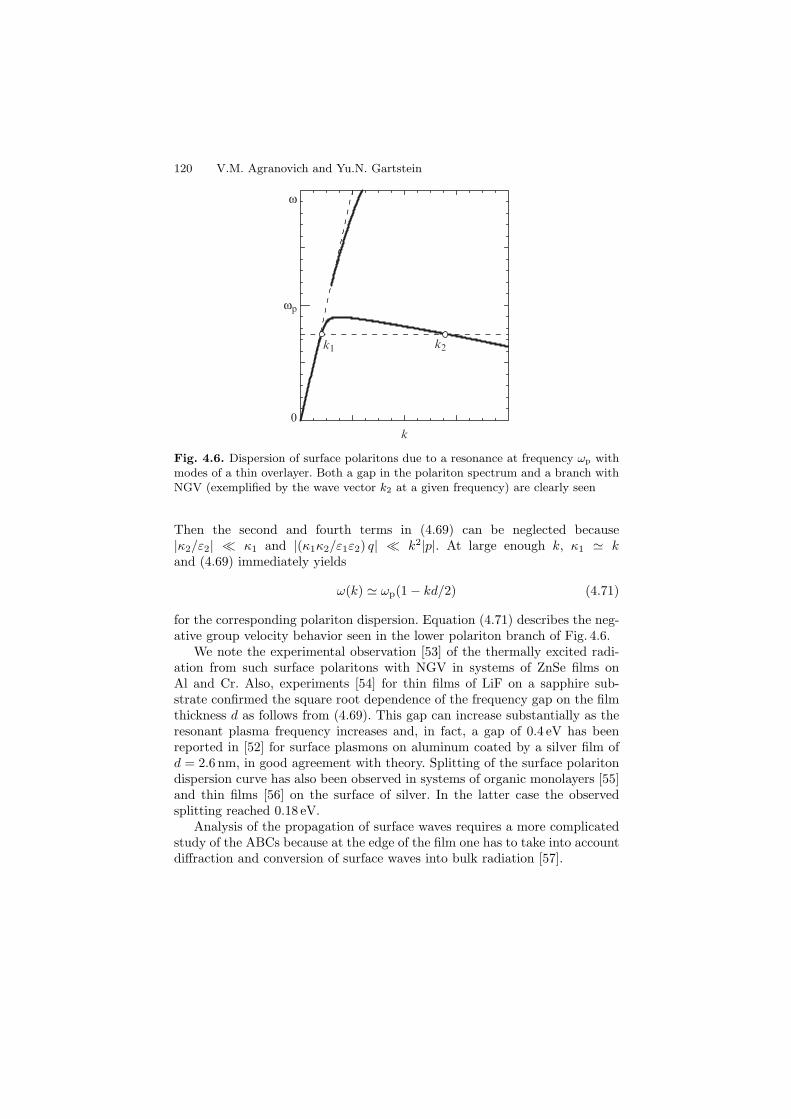
120 V.M. Agranovich and Yu.N. Gartstein
ωp
ω
k
k1 k2
0
Fig. 4.6. Dispersion of surface polaritons due to a resonance at frequency ωp withmodes of a thin overlayer. Both a gap in the polariton spectrum and a branch withNGV (exemplified by the wave vector k2 at a given frequency) are clearly seen
Then the second and fourth terms in (4.69) can be neglected because|κ2/ε2| κ1 and |(κ1κ2/ε1ε2) q| k2|p|. At large enough k, κ1 kand (4.69) immediately yields
ω(k) ωp(1 − kd/2) (4.71)
for the corresponding polariton dispersion. Equation (4.71) describes the neg-ative group velocity behavior seen in the lower polariton branch of Fig. 4.6.
We note the experimental observation [53] of the thermally excited radi-ation from such surface polaritons with NGV in systems of ZnSe films onAl and Cr. Also, experiments [54] for thin films of LiF on a sapphire sub-strate confirmed the square root dependence of the frequency gap on the filmthickness d as follows from (4.69). This gap can increase substantially as theresonant plasma frequency increases and, in fact, a gap of 0.4 eV has beenreported in [52] for surface plasmons on aluminum coated by a silver film ofd = 2.6 nm, in good agreement with theory. Splitting of the surface polaritondispersion curve has also been observed in systems of organic monolayers [55]and thin films [56] on the surface of silver. In the latter case the observedsplitting reached 0.18 eV.
Analysis of the propagation of surface waves requires a more complicatedstudy of the ABCs because at the edge of the film one has to take into accountdiffraction and conversion of surface waves into bulk radiation [57].
4 Spatial Dispersion, Polaritons, and Negative Refraction 121
4.5 Magnetic Permeability at Optical Frequencies
In Sect. 4.3 of this chapter we have already discussed certain aspects of thecorrespondence between two approaches used in the electrodynamics of contin-uous media. In this section, we continue with a more detailed look at the notionof magnetic permeability µ(ω) used in the standard, symmetric, approachemploying all four fields E,D,B,H. The Maxwell equations for plane wavesin this approach are given by (4.16), and material relations by (4.17). As noambiguity will arise, the notation D and H is now restored for the fields ofthe symmetric approach:
D = ε(ω)E, B = µ(ω)H. (4.72)
The use of (4.72) with the Maxwell equations leads to the standard dispersionlaw (4.5) for plane waves propagating in a spatially uniform medium.
Our aim will be to discuss conditions under which the magnetic perme-ability µ(ω) in (4.72) may retain its traditional direct physical meaning inthe description of a continuous material. An analysis of this question for nat-ural materials has been provided in Landau and Lifshitz’s textbook [5] withthe conclusion that “unlike ε(ω), the magnetic permeability µ(ω) ceases tohave any physical meaning at relatively low frequencies.” We therefore feelthat the issue is relevant as the quest for natural and artificial negativelyrefracting materials moves into the optical domain.
As is well known, a macroscopic description involves spatial averagingand, therefore, necessitates that a microscopic length (there can be more thanone such length) characterizing the medium, a, is much smaller than thelength of the spatial variation of macroscopic electromagnetic fields, that is,the wavelength λ for the electromagnetic waves in the medium. For naturalmaterials, a is ordinarily of an atomic/molecular size, such as a crystal latticeconstant, or of the order of the mean free path of charge carriers.
In many recent papers sparked by Pendry’s work [58] (for references toearlier studies, see [13]), macroscopic Maxwell equations have been used tostudy wave propagation and negative refraction in artificial periodic or amor-phous structures (metamaterials) that are composites consisting of variousobjects such as nonoverlapping split-ring resonators, small metallic or dielec-tric spheres, rods, pillars, etc. The geometrical sizes of these constituentobjects, so to say artificial “molecules,” and corresponding lattice constants(establishing the length scale a) can be hundreds of times larger than in nat-ural materials. As an example, we will mention here the structure of pairs ofgold nanopillars with various geometrical elements measuring 80–200 nm stud-ied in [59] within the range of vacuum wavelengths from 400 to 700 nm. Inanother example of recent work [60], a doubly periodic array of pairs of parallelgold nanorods has been used, with the rods measuring 780×220×50 nm withthe illuminating light wavelength between 500 and 2,000 nm. The structuresused in [59,60] have been developed with the goal to fabricate metamaterialswith a negative index of refraction at optical frequencies.
122 V.M. Agranovich and Yu.N. Gartstein
One could distinguish two different ways to analyze properties of the com-posite. As the size of the objects is much larger than actual atomic sizes,each of the objects would be describable within the framework of the ordi-nary macroscopic theory by appropriate choices for ε(ω) and µ(ω). Wavepropagation in the composite can then be studied by applying the Maxwellboundary conditions on the objects’ surfaces within, e.g., the finite-differencetime domain (FDTD) method of computational electrodynamics [61]. Evi-dently in this powerful straightforward approach there is no need to evaluateeffective material constants of the metamaterial, while the ordinary ε(ω) andµ(ω) would be spatially variable. Any restriction on the meaning of µ(ω) herewould be the same as for natural materials.
A different but conceptually and analytically attractive way is to performa “secondary averaging” over the composite’s structure, and to use the pictureof an effectively uniform medium, which would be applicable so long as λ a,with the corresponding effective medium permittivity and permeability. Wewill be commenting on the applicability of the notion of an effective µ(ω) inthis case.
4.5.1 Magnetic Moment of a Macroscopic Body
As analyzed by Landau and Lifshitz [5], a difficulty with the physical meaningof µ(ω) at higher frequencies has to do with the fact that one may not be ableto “measure” permeability by measuring the total induced magnetic momentof a macroscopic body. In the case of static fields, it is this total magneticmoment per unit volume that corresponds to the magnetization M :
M = (B − H)/4π, (4.73)
and allows one to introduce the permeability µ as a well-defined systemresponse coefficient via (4.72). In the case of time-dependent fields, how-ever, the total induced magnetic moment is contributed to not only by themagnetization (4.73) but also by the time-dependent dielectric polarizationP = (D − E)/4π. The induced current density J = 〈ρv〉, as a result of spa-tial averaging of the microscopic current density ρv due to all charges in thesystem, now consists of two parts:
J = c∇× M +∂P
∂t. (4.74)
A microscopic picture for this splitting of the induced current density usingpositions and velocities of charged particles in the medium is explicitly dis-cussed, e.g., in [24, 38]. Equation (4.74) also follows directly from the macro-scopic Maxwell equations. Indeed, consider the standard form
∇× H =1c
∂D
∂t(4.75)
4 Spatial Dispersion, Polaritons, and Negative Refraction 123
that leads to the second line of (4.16) for plane waves. On the other hand, theexact microscopic Maxwell equation reads
∇× b =4π
cρv +
1c
∂e
∂t, (4.76)
where microscopic field values are denoted by lower-case characters. Spatialaveraging yields B = 〈b〉, E = 〈e〉, and, hence, for (4.76):
∇× B =4π
cJ +
1c
∂E
∂t. (4.77)
Subtracting (4.75) from (4.77) and using the definitions of M and P resultsin (4.74). We recall that the macroscopic current due to free charge carriersin conductors has been included in ∂P /∂t.
As the total induced current (4.74) consists of two parts, so does the totalinduced magnetic moment
M tot =12c
∫(r × J)dV
of a macroscopic body:
M tot = M tot1 + M tot
2 , (4.78)
whereM tot
1 =∫
M dV (4.79)
and
M tot2 =
12c
∫ (r × ∂P
∂t
)dV. (4.80)
The association of the magnetization M with the magnetic moment of a unitvolume of the body thus depends on the possibility to neglect in (4.78) thecontribution (4.80) from the time-dependent dielectric polarization. Only thencould the permeability µ(ω) be “measured” separately to retain its traditionalphysical meaning as an independent system response coefficient related to themagnetic moment induced by the applied magnetic field according to (4.72)and (4.73). Another way to put it is the requirement of a physically meaningfulseparation of the magnetic current c∇×M from the total induced current Jin (4.74); see, e.g., [28] for estimates of various physical contributions to thetotal induced current.
By using the Maxwell equation (4.75) and the definitions of M and P ,one can, for instance, immediately evaluate the relative contributions to theinduced current (4.74) taking place in the fields of a monochromatic electro-magnetic wave. For the magnetic current to dominate,
|c∇× M | ∣∣∣∣∂P
∂t
∣∣∣∣ ,
124 V.M. Agranovich and Yu.N. Gartstein
would then require
R(ω) =∣∣∣∣ε(ω) [µ(ω) − 1]
ε(ω) − 1
∣∣∣∣ 1. (4.81)
An electromagnetic wave, however, does not provide the most favorableconditions for separating the magnetic effect, as the electric field in the wave isrelatively strong. Following Landau and Lifshitz [5], one would, instead, placea small macroscopic body in a time-dependent (monochromatic) magneticfield produced by some external current density Jext. For an explicit analytictreatment, let us take a cylindrical sample of length L and radius l thatis positioned coaxially within a solenoid driven by an external current. Thesmallness of the sample in this geometry means
l λ. (4.82)
The sample, however, should still be macroscopic, that is, be much larger thanthe microscopic length scale a,
l a, (4.83)
for the very notion of (an effective) macroscopic permeability to be valid.With (4.82) satisfied, the magnetic field in the sample is mostly produced
by the external current. Let H be the magnitude of that uniform field. Itleads to the uniform magnetization M = [µ(ω) − 1]H/4π of the sample andits contribution (4.79)
M tot1 =
∣∣ l2L [µ(ω) − 1]H/4∣∣ (4.84)
to the total magnetic moment. The time-dependent magnetic field would alsoinduce an electric field in the sample according to the Maxwell equation
∇× E = −1c
∂B
∂t.
In our geometry the magnitude of this “circular” field varies with the distancex from the cylinder axis as E = |ωµ(ω)Hx/2c|. The magnitude of the dielectricpolarization current density is therefore |∂P/∂t| =
∣∣ω2µ(ω)[ε(ω) − 1]Hx/8πc∣∣,
making the second contribution (4.80) to the total magnetic moment equal to
M tot2 =
∣∣ l4Lω2µ(ω)[ε(ω) − 1]H/32c2∣∣ . (4.85)
For the magnetization contribution to dominate:∣∣M tot
1
∣∣ ∣∣M tot2
∣∣ ,Equations (4.84) and (4.85) now require
8c2
ω2l2
∣∣∣∣∣1 − 1
µ(ω)
ε(ω) − 1
∣∣∣∣∣ 1. (4.86)
4 Spatial Dispersion, Polaritons, and Negative Refraction 125
Using, instead of the frequency ω, the corresponding wavelength λ(ω) =2πc/ω
√εµ for plane waves in the medium, criterion (4.86) can be rewritten as
2π2
R(ω)(
λ(ω)l
)2
1, (4.87)
which is “weaker” than (4.81) by virtue of the condition (4.82). Frequencysegments where condition (4.82) is not met should be excluded from theabove consideration. Needless to say, the numerical coefficients in (4.86) and(4.87) are affected by the particular shape of the sample considered.
It is instructive to recognize that inequalities (4.81) and (4.86) would alsofollow naturally from a comparison of the medium response contributions tothe transverse dielectric function in (4.26). Since the quantity ε⊥(ω, k) − 1 isproportional to the generalized dielectric susceptibility, one clearly sees twocontributions to it in (4.26): One is the dielectric term ∝ [ε(ω) − 1], and theother, ∝ k2, which determines the magnetic effect. The inequalities discussedabove arise from the requirement that the latter contribution be larger thanthe former. The magnitude of the magnetic term, however, depends on thewave vector k. For a given frequency ω, inequality (4.81) would follow if, in(4.26), one uses the wave vector k that the transverse electromagnetic wavewould have in this medium. Inequality (4.86), on the other hand, would followif one takes wave vectors k ∼ 1/l, of the order of the inverse sample size.
For inequality (4.86) to be better satisfied, the size l of the sample can bemade as small as possible but still consistent with it comfortably remainingmacroscopic, (4.83). Evidently, the smaller the microscopic scale a, the smallerl could be. The smallest magnitudes of a are of atomic/molecular sizes featuredby natural materials. The presence of the factor ω2 in the denominator of thecombination in criterion (4.86) clearly shows that, while this criterion is safelysatisfied at low enough frequencies, it becomes in general harder and harderto meet as the frequency ω increases. Of course, the criterion would alsoreflect the details of the frequency dispersions of ε(ω) and µ(ω): using themodel behavior in (4.3) and (4.4), for instance, would make the LHS of (4.86)equal to
8c2
ω2l2Fm
Fe
∣∣∣∣ω2⊥ − ω2
ω2mz − ω2
∣∣∣∣ . (4.88)
The magnitude of expression (4.88) is enhanced in a narrow region aroundthe zero-permeability frequency ωmz, which would in reality be substantiallymitigated by dissipation. Apart from that, the overall scale of expression (4.88)is determined by the factor
c2
ω2l2Fm
Fe∼ ω2
⊥ω2
a2
l2→ a2
l2(for ω ∼ ω⊥), (4.89)
where the estimate has been made by using (4.50) for natural atomic or mole-cular materials with ω⊥ ∼ ωmz. These molecular transition frequencies ω⊥ are
126 V.M. Agranovich and Yu.N. Gartstein
in the range of optical frequencies. In view of condition (4.83), it is then clearfrom (4.89) that at optical frequencies ω ∼ ω⊥, inequality (4.86) cannot, ingeneral, be satisfied in such materials. A measurement of the total magneticmoment of a macroscopic body in this frequency region would have a substan-tial contribution from polarization currents, (4.80), and, therefore, would notyield “independent” information on the magnetization M (except, perhaps,in some frequency intervals).
It seems reasonable to assume that an estimate similar to (4.89) would alsobe valid for a metamaterial built of small (a λ) plasmonic structures, pro-vided that the electric and magnetic resonance frequencies are of the order ofωp, while the quantity equivalent to Fm/Fe is of the order of ω2
pa2/c2. Resultsfor various structural shapes suggested in the literature could be verified withrespect to conditions like (4.86) to establish the range of frequencies where thepermeability µ(ω) retains its traditional physical meaning in a description of amacroscopic sample. Given the increased (in comparison with atomic) lengthscale a in metamaterials (tens and hundred(s) of nanometers), it is obvious,however, that the range of frequencies ω where one could have a reasonablysatisfied ordering
a l λ(ω), (4.90)
would in general move to lower frequencies as the size a grows. In fact, it ispossible that in metamaterials with larger a, the ordering (4.90) could notbe established in a wide range of frequencies while the wavelength λ is stillappreciably larger than a. Then the solenoidal setup to measure permeabilitybecomes useless and one essentially is left with a criterion like (4.81). We arenot aware of a better configuration to “measure” permeability.
As long as λ(ω) a, natural or metamaterials can, of course, still bedescribed as continuous uniform bodies. The spatial dispersion approach usingthe tensor εij(ω,k) then presents itself as a flexible way of providing sucha description, including at frequencies where µ(ω) would lose its physicalsignificance and where magnetic effects would be indistinguishable from thespatial dispersion of dielectric effects. In the spatial dispersion frameworkone considers the total induced current without (artificially or arbitrarily)breaking it into parts – in the absence of a physically meaningful way tomeasure/address all the contributions separately. This framework allows oneto analyze various material relations in a unified fashion. The overall responseof the system in the spatial dispersion approach is described by as manyphenomenological constants as are required by the symmetry of the systemunder consideration and by the “type” of the spatial dispersion. From ourdiscussion in Sect. 4.3, it should be clear that, whenever spatial dispersion isrestricted to the ∝ k2 terms as in (4.28), a description of transverse polaritonsin an isotropic medium requires only two phenomenological parameters ateach frequency ω, that is, only two coefficients in the expansion of ε⊥(ω, k)in powers of k. The coefficient in front of k2 can then be formally postulatedto be related to µ(ω) as in (4.26), independently of the physical origin of this

4 Spatial Dispersion, Polaritons, and Negative Refraction 127
coefficient. The standard expression (4.5) for the refractive index then alsofollows. This is the case where the phenomenology of the ε(ω)–µ(ω) formalismis adequate. One could then use this phenomenology to extract informationon the so defined “effective” µ(ω) from data on the refractive index n(ω) andseparate measurements of ε(ω).
With structural sizes a in metamaterials becoming comparable with thewavelength λ in the medium, the continuum electrodynamics analysis of wavepropagation in a composite as in a uniform body ceases to be possible, andone has to resort to descriptions using spatially variable (position-dependent)material response functions.
As more actual data on ε(ω) and µ(ω) in 3D metamaterials become avail-able, it will be interesting to analyze those data from the standpoint of thediscussion in this section.
4.6 Related Interesting Effects
4.6.1 Generation of Harmonics from a Nonlinear Materialwith Negative Refraction
Generation of harmonics in media with a negative group velocity can havefeatures that are worthwhile to discuss and investigate. Here we, following [7],will just give a brief qualitative account of one of these interesting effects.Consider a semi-infinite medium that supports negative refraction in somefrequency range. Ordinarily one should expect that the spectral width ∆ω ofthis range is relatively narrow: ∆ω ω. Suppose a laser beam of frequencyωl is incident on the medium from vacuum, where ωl is within the range∆ω. Then the frequencies of the second (2ωl) and higher harmonics will fallinto regions of the spectrum where the medium supports waves with positivegroup velocities. Optical nonlinear susceptibilities χ(2), χ(3), . . ., determine thesources of harmonics generation and, in the simplest approximation, suchsources depend only on the incoming refracted wave. As the latter wave is inthe frequency range of negative refraction, its wave vector k is directed fromthe bulk of the medium toward its surface, as depicted in Fig. 4.7a. Then thewave vector of the source, for instance of the second harmonic (SH), is 2k andis also directed toward the vacuum–medium interface. The transmitted waveat frequency 2ωl, on the other hand, will have its wave vector directed fromthe interface into the bulk of the medium. Therefore, the wave vectors of thesource of the harmonic and of this transmitted wave will be strongly phasemismatched and these waves will interact only weakly. This mismatch willthen cause the dominant part of the energy from the source of the SH to betransferred to the reflected second harmonic propagating in vacuum away fromthe interface, as schematically shown in Fig. 4.7a. This effect could provide foran effective “quadratic mirror” that reflects the SH component generated byan incident laser beam in a medium with negative refraction. Details of the

128 V.M. Agranovich and Yu.N. Gartstein
∆Ω
∆ω
S
incidentreflected
refracted
NRM
∆ω
ω
2ω
3ω
Sωk
S2ω
S3ω
(a) (b)
Fig. 4.7. Schematic illustrations for the effects discussed in Sect. 4.6. (a) Harmonicsgeneration. The incident wave frequency ω falls within a narrow window ∆ω offrequencies for negative group velocity waves in the medium. The energy transferredto higher harmonics at 2ω and 3ω will mostly propagate (Poynting vector S) in thereflection mode. (b) An ultra-short pulse (∆Ω > ∆ω) incident on a NRM leads totwo refracted pulses of different spectral contents
corresponding calculations can be found in [7, 62]. (For a discussion of thegeneration of acoustic wave harmonics in one-dimensional phononic crystalswith negative refraction, see [63].) Experimental studies of nonlinear effectsare only in their beginning; we can mention paper [64] where an enhancementhas been found of the intensity of the reflected SH in nonlinear left-handedtransmission line media. Other nonlinear properties of artificial left-handedmaterials have been discussed in [65–67].
4.6.2 Ultra-Short Pulse Propagation in NegativeRefraction Materials
Ultra-short pulses are currently available in a wide range of frequencies fromTHz to far UV. An interesting manifestation of negative refraction may occurwhen the spectral width ∆Ω of a pulse is appreciably larger than the spec-tral width ∆ω of the window where waves with negative group velocity existin a negative refraction material (NRM). Qualitatively, one can think of theultra-short pulse decomposed into frequency Fourier components, and canthen follow the propagation of each component and compose the componentsback after the propagation. With ∆Ω ∆ω, the pulse incident on the NRMis expected to split into three outgoing pulses with different spectral contentas schematically shown in Fig. 4.7b. The reflected pulse would approximatelyhave the spectral content of the incident pulse. The two transmitted pulseswould have both different propagation directions and different spectral con-tents. A central part of the pulse spectrum (of width ∆ω) experiences negativerefraction at the interface, but the “side” frequency components outside of the∆ω window propagate according to the rules of ordinary “positive” refraction.A spectroscopic study can therefore be used for the determination of the fre-quency interval ∆ω.
4 Spatial Dispersion, Polaritons, and Negative Refraction 129
Interesting effects can also be expected for harmonics generation and wavemixing with ultra-short pulses – the harmonics would also propagate in anunusual way. As only some part of the spectrum of the input or output experi-ences negative refraction, the output pulses in transmission and reflection canbe drastically different in terms of the energy, pulse shape, spectral compo-sition, and direction, from those expected in an ordinary nonlinear medium.The details are complicated, and depend on the spectral contents of the ultra-short pulse and the NRM.
4.7 Concluding Remarks
In writing this chapter we have been very pleased to have an opportunityto pay our respect to L. I. Mandelstam who clearly analyzed how negativerefraction occurs at an interface as a consequence of negative group velocitywaves in one of the interfacing media [1–3]. Realizing that negative groupvelocity is at the heart of negative refraction, one finds it quite useful tolook at various factors that may affect the dispersion law ω(k) of the wavespropagating in the medium.
A natural and flexible way to analyze such factors for electromagneticwaves in effectively uniform media is within the spatial dispersion frameworkutilizing the notion of the generalized dielectric tensor εij(ω,k) representingthe electromagnetic response of the medium to perturbations of frequency ωand wave vector k. Normal waves (polaritons) with negative group velocity canoccur in the medium (whether in natural or in artificial metamaterials) whenspatial dispersion (k-dependence of the dielectric tensor) is strong enough.One particular situation of this kind (corresponding to spatial dispersion ∝ k2)is more familiar as the case of simultaneously negative dielectric susceptibilityε(ω) and magnetic permeability µ(ω). The spatial dispersion approach assistsin substantiating the description of such a situation at optical frequencieswhen µ(ω) loses its traditional physical meaning, and even when no magnetic-dipole type response takes place in the medium.
Within the framework of the tensor εij(ω,k) one can analyze in a uni-fied fashion more complex types of material relations and the resulting qual-itatively new effects, such as additional polariton waves. We have used thisapproach in this chapter to discuss several physical systems that may be capa-ble of exhibiting polaritons with negative group velocity at optical frequencies.Our examples included both chiral and nonchiral systems, and bulk and sur-face polariton waves. We hope these examples will be helpful in identifyingappropriate candidate media for experimental studies.
In order to focus on the physical origin of the negative group velocitypolaritons in these systems, we left out many important issues that affectthe possibility of practical realizations. One of these is the attenuation ofwaves due to dissipation, which, of course, is a common problem for differentfrequency regions. Crystals with sharp and strong excitonic resonances could
130 V.M. Agranovich and Yu.N. Gartstein
therefore be good candidates among natural materials. Another problem is thelow efficiency of utilization of additional polariton waves due to wave vectormismatch. Certain schemes, however, have been developed to improve thisefficiency for positive group velocity waves, and such schemes are likely to bealso useful for negative refraction.
Acknowledgments
This work was supported by AFOSR grant FA 9550-05-1-0409. VMA alsothanks the Russian Foundation of Basic Research and the Ministry of Scienceand Technology of the Russian Federation for partial support. The authorsare grateful to R.H. Baughman, A.A. Zakhidov, and especially Y.R. Shen forcollaboration and discussion of various problems of negative refraction, andalso to V.L. Ginzburg, C.M. Krowne, A.A. Maradudin, and Y. Zhang forreading the manuscript and making many useful suggestions.
References
1. L.I. Mandelstam, Complete Works, vol. 5 (USSR Academy of Sciences, Moscow,1950), Lectures given on 26 February 1940 and on 5 May 1944
2. L.I. Mandelstam, Zh. Eksp. Teor. Fiz., 15, 475 (1945)3. L.I. Mandelstam, Lectures on Optics, Relativity and Quantum Mechanics
(Nauka, Moscow, 1972)4. L. Brillouin, Wave Propagation and Group Velocity (Academic, New York,
1960)5. L.D. Landau, E.M. Lifshitz, Electrodynamics of Continuous Media
(Butterworth-Heinemann, Oxford, 1984)6. V.M. Agranovich, V.L. Ginzburg, Crystal Optics with Spatial Dispersion, and
Excitons (Springer, Berlin Heidelberg New York, 1984)7. V.M. Agranovich, Y.R. Shen, R. Baughman, A.A. Zakhidov, Phys. Rev. B, 69,
165112 (2004)8. V.M. Agranovich, Y.R. Shen, R. Baughman, A.A. Zakhidov, J. Lumin. 110,
167 (2004)9. V.G. Veselago, Sov. Phys. Uspekhi 10, 509 (1968)
10. A.L. Pokrovsky, A.L. Efros, Solid State Commun. 124, 283 (2002)11. R.A. Shelby, D.R. Smith, S. Schultz, Science 292, 77 (2001)12. J.B. Pendry, Phys. Rev. Lett. 85, 3966 (2000)13. A. Moroz, http://www.wave-scattering.com/negative.html14. A. Boardman, N. King, L. Velasco, Electromagnetics 25, 365 (2005)15. K.T. McDonald, Am. J. Phys. 69, 607 (2001)16. H. Lamb, Proc. Lond. Math. Soc. 1, 473 (1904)17. M. Laue, Ann. Phys. (Leipzig) 18, 523 (1905)18. A. Schuster, An Introduction to the Theory of Optics (Edward Arnold, London,
1904)19. E.L. Feinberg, Phys. Uspekhi 45, 81 (2002)20. D.V. Sivukhin, Opt. Spektrosk. 3, 308 (1957)

4 Spatial Dispersion, Polaritons, and Negative Refraction 131
21. V.E. Pafomov, Sov. Phys. JETP 9, 1321 (1959)22. V.L. Ginzburg, Applications of Electrodynamics in Theoretical Physics and
Astrophysics (Gordon and Breach, New York, 1989), Chap. 723. V.E. Pafomov, Sov. Phys. JETP 5, 307 (1957)24. J.D. Jackson, Classical Electrodynamics (Wiley, New York, 1975)25. V.M. Agranovich, V.E. Pafomov, A.A. Rukhadze, Sov. Phys. JETP 9, 160
(1959)26. I.M. Frank, Sov. Phys. JETP 9, 580 (1959)27. K.A. Barsukov, Sov. Phys. JETP 9, 1052 (1959)28. Yu.A. Il’inskii, L.V. Keldysh, Electromagnetic Response of Material Media
(Plenum, New York, 1994)29. D.B. Melrose, R.C. McPhedran, Electromagnetic Processes in Dispersive Media
(Cambridge University Press, Cambridge, 1991)30. S.M. Rytov, Zh. Eksp. Teor. Fiz. 17, 930 (1947)31. M.E. Gertsenshtein, Zh. Eksp. Teor. Fiz. 26, 680 (1954)32. A.A. Golubkov, V.A. Makarov, Phys. Uspekhi 38, 325 (1995)33. A.P. Vinogradov, Phys. Uspekhi 45, 331 (2002)34. D. Bedeaux, M. Osipov, J. Vlieger, J. Opt. Soc. Am. A 12, 2431 (2004)35. L. Keldysh, D. Kirzhnitz, A. Dolgov (eds.), The Dielectric Function of Con-
densed Systems (North-Holland, Amsterdam, 1989)36. G.D. Mahan, Many-Particle Physics (Kluwer, New York, 2000)37. Y. Toyozawa, Optical Processes in Solids (Cambridge University Press,
Cambridge, 2003)38. D.P. Craig, T. Thirunamachandran, Molecular Quantum Electrodynamics (Aca-
demic, London, 1984)39. L.D. Barron, Molecular Light Scattering and Optical Activity (Cambridge Uni-
versity Press, Cambridge, 2004)40. V.L. Ginzburg, Sov. Phys. JETP 7, 1096 (1958)41. S.I. Pekar, Sov. Phys. JETP 6, 785 (1958)42. L. Silvestri, O.A. Dubovski, G.C. La Rocca, F. Bassani, V.M. Agranovich,
Nuovo Cimento Soc. Ital. Fis. C 27, 437 (2004)43. V.M. Agranovich, Sov. Phys. Uspekhi 3, 427 (1961)44. V.S. Pine, G. Dresselhaus, Phys. Rev. 188, 1489 (1969)45. J.B. Pendry, Science 306, 1353 (2004)46. S. Tretyakov, I. Nefedov, A. Sihvola, S. Maslovski, C. Simovski, J. Electromagn.
Waves Appl. 17, 695 (2003)47. T.G. Mackay, Microw. Opt. Technol. Lett. 45, 120 (2005)48. Y. Jin, S. He, Opt. Express 13, 4974 (2005)49. C. Monzon, D.W. Forester, Phys. Rev. Lett. 95, 123904 (2005)50. V.M. Agranovich, Yu.N. Gartstein, A.A. Zakhidov, Phys. Rev. B 73, 045114
(2006)51. V.M. Agranovich, in Surface Polaritons, ed. by V.M. Agranovich, D.L. Mills
(North-Holland, Amsterdam, 1982), p. 18752. T. Lopez-Rios, F. Abeles, G. Vuye, J. Physique 39, 645 (1978)53. E.A. Vinogradov, T.A. Leskova, Phys. Rep. 194, 273 (1990)54. V.A. Yakovlev, G.N. Zhizhin, Opt. Commun. 15, 293 (1975)55. I. Pockrand, A. Brillante, D. Mobius, J. Chem. Phys. 77, 6289 (1982)56. J. Bellessa, C. Bonnand, J.C. Plenet, J. Mugnier, Phys. Rev. Lett. 93, 036404
(2004)

132 V.M. Agranovich and Yu.N. Gartstein
57. V.M. Agranovich, T.A. Leskova, Prog. Surf. Sci. 29, 169 (1988)58. J.B. Pendry, Phys. Rev. Lett. 85, 3965 (2000)59. A.N. Grigorenko, A.K. Geim, H.F. Gleeson, Y. Zhang, A.A. Firsov,
I.Y. Khrushchev, J. Petrovic, Nature 438, 355 (2005)60. V.M. Shalaev, W. Cai, U. Chettiar, H.K. Yuan, A.K. Sarychev, V.P. Drachev,
V. KIldishev, Opt. Lett. 30, 3356 (2005)61. A. Taflove, Computational Electrodynamics: The Finite-Difference Time-
Domain Method (Artech House, Boston, 1995)62. I.V. Shadrivov, A.A. Zharov, Yu.S. Kivshar, arXiv:physics/0506092 (2005)63. O.S. Tarasenko, S.V. Tarasenko, V.M. Yurchenko, JETP Lett. 80, 484 (2004)64. A.B. Kozyrev, H. Kim, A. Karbassi, D.W. van der Weide, Appl. Phys. Lett.
87, 121109 (2005)65. M. Lapin, M. Gorkunov, K.H. Rinhofer, Phys. Rev. E 67, 065601 (2003)66. A.A. Zharov, I.V. Shadrivov, Yu.S. Kivshar, Phys. Rev. Lett. 91, 037401 (2003)67. S. O’Brien, D. McPeake, S.A. Ramakrishna, J.B. Pendry, Phys. Rev. B 69,
241101(R) (2004)
5
Negative Refraction in Photonic Crystals
W.T. Lu, P. Vodo, and S. Sridhar
Summary. The phenomenon of negative refraction (NR) by 2D photonic crystals(PCs) is demonstrated in microwave experiments. NR by PCs is observed in 2Dparallel-plate waveguide and in 3D free space measurements. Results are in excellentagreement with band structure calculation and numerical simulation.
5.1 Introduction
The optical properties of isotropic materials that are transparent to electro-magnetic (EM) waves can be characterized by a refractive index n. Given thedirection of the incident beam θ1 at the interface of vacuum and the mate-rial, the direction θ2 of the outgoing beam can be determined using Snell’slaw, sin θ1 = n sin θ2. All naturally available transparent materials possessa positive refractive index, n > 0. Although we do know that materials withnegative permittivity (ε) or negative permeability (µ) are available but do notallow light transmission, it was Veselago who in 1968 realized that double neg-ative indices media with ε, µ < 0 are consistent with Maxwell’s equations [1].This idea was largely ignored till 2001 when it was demonstrated that certaincomposite metamaterials refract microwaves negatively (θ2 < 0, θ1 > 0) andconsequently a negative index of refraction n < 0 can be assigned to suchmaterials [2].
Negative refractive index materials (NIM) exhibit some unusual propaga-tion characteristics of EM waves. The most striking property is that of left-handed electromagnetism (LHE). Since for a plane wave, the electric field Eand the magnetic field H are related to each other through H = (c/µω)k×Eand E = −(c/εω)k × H, thus E, H, and k form a left-handed triplet in aNIM. Consequently the Poynting vector S = E × H is antiparallel to thewave vector k, so that S · k < 0. A material possessing simultaneously nega-tive permittivity ε < 0 and permeability µ < 0 can be shown to necessarilyhave n ≡ √
ε√
µ < 0 [1]. NIM are also referred to as left-handed meta-materials (LHM). In contrast E, H, k form a right-handed set corresponding
134 W.T. Lu et al.
to right-handed electromagnetism (RHE), and S·k > 0 for conventional n > 0materials.
The negative refraction (NR) of EM waves allows new approaches to con-trol EM wave propagation, such as flat lens imaging [3] and planoconcavelens focusing [4]. These demonstrations of principles open the door for newapproaches to a variety of applications from microwave to optical frequencies.
In this chapter, we first discuss the types of materials exhibiting NR.Then we focus on NR by PCs in microwave experiments. NR is reportedin microwave experiments for metallic PCs in parallel-plate waveguide and infree space. We finally conclude with some remarks on applications of NR.
5.2 Materials with Negative Refraction
Currently all the materials showing NR have periodic structures. Dependingon the ratio of the wavelength to the lattice constant and the underlyingmechanism, these materials are loosely classified as two types of NIM.
The first type of NIM is the so-called metamaterial [2,5,6]. In these mate-rials, the wavelength is much larger than the lattice constant. It is this typeof artificial materials which initiated the whole field of NR. The prototypemetamaterial consists of periodic split-ring resonators which lead to negativeµ and periodic metallic wires which lead to negative ε. Since the metamaterialis operated near the magnetic resonance, high loss is expected. The push forthis material to higher frequencies may be limited to the THz range [7–9].The physics behind this limit is that any material will have µ→ 1 since theelectrons will not keep pace with the frequency of visible light [10], thus thesplit-ring resonators will cease to function at optical frequencies due to shrink-ing sizes. Also the metallic wires should be dense enough to give negativepermittivity, otherwise the effective permittivity will be positive in the visiblespectrum.
NR has also been shown in a network of LC circuits at microwave fre-quencies [11, 12]. This system also belongs to the class of metamaterials.NR is achieved through a high-pass LC network which supports backwardwaves, that is the Poynting vector is antiparallel to the wave vector. Materi-als supporting backward waves including NIM are also called backward-wavemedia [13]. This approach is inherently limited to RF and microwave fre-quencies. However, this transmission line concept has been used by Enghetaet al. [14] to design NR materials in optics.
The second type of NIM is the photonic crystal (PC). PCs provide anotherway to manipulate EM waves [15]. A PC is an artificial periodic structure [16],usually made of a dielectric or metal, designed to control photons similar to theway a solid-state crystal controls electrons. It has since been proposed that NRcan be achieved in PCs with lattice constant comparable to the wavelength[17, 18]. Locally both ε, µ > 0 everywhere in a PC. The physical principlesthat allow NR in the PC [19–22] arise from the dispersion characteristics
5 Negative Refraction in Photonic Crystals 135
of wave propagation in a periodic medium, and are very different from thatof the metamaterial in [2]. To have the desired dispersion characteristics forNR, large dielectric constant contrast is required which poses no problem onthe availability of materials even in visible frequency range. Thus there is nofundamental limit on pushing NR in PC toward the visible. NR by PC hasbeen recently reported in infrared spectral range [23].
Recently NR was also shown in anisotropic media, such as uniaxial crys-tals [24]. This type of material occurs naturally. The mechanism of NR inanisotropic media [24–26] is that the wave vector and group velocity are notparallel to each other. Thus with an appropriate orientation of surface cut,the parallel components of the wave vector and the group velocity will haveopposite sign. This is similar to the PCs with certain designed wave vector–frequency dispersion relation. But NR in uniaxial crystals can be achievedonly within certain small range of angles [27].
The most striking consequence of NR is the possible existence of “Per-fect lens” [28], although causality and dissipation do pose some restriction[10, 29, 30] on the NIM. All of the above types of materials have been shownexperimentally to have NR and planoconcave lens focusing [4]. Flat lens imag-ing using PC was first demonstrated in microwave experiments [3, 31] andpreliminary results showed flat lens imaging in metamaterial and LC cir-cuits [6, 12] as well. However, the uniaxial materials cannot lead to flat lensfocusing due to the lack of all-angle negative refraction [18].
5.3 Negative Refraction in MicrowaveMetallic Photonic Crystals
In this section we present experimental evidence of NR in metallic PCs. Twokinds of microwave experiments were performed on PC prisms. One where thePC prisms were placed in a parallel-plate waveguide (PPW) with only trans-verse magnetic (TM) wave excitation and the other in free space for bothTM and transverse electric (TE) microwaves. Parallel theoretical and numer-ical investigations of the band structure and simulations of wave propagationthrough the PC prisms were performed and exceptionally good agreement wasfound with the experimental results.
5.3.1 Metallic PC in Parallel-Plate Waveguide
In these experiments, the microwave metallic PC was an array of cylindricalcopper rods of height d = 1.26 cm and radius r = 0.63 cm forming a triangularlattice. The lattice constant a is such that r/a = 0.2. Refraction measurementsare carried out in a PPW made of a pair of metallic plates. The excitationin the PPW is only TM mode up to a cutoff frequency c/2d 12 GHz suchthat the electric field E is parallel to and constant along the rod axis. Acoax-to-waveguide adaptor is employed to couple microwave radiation into
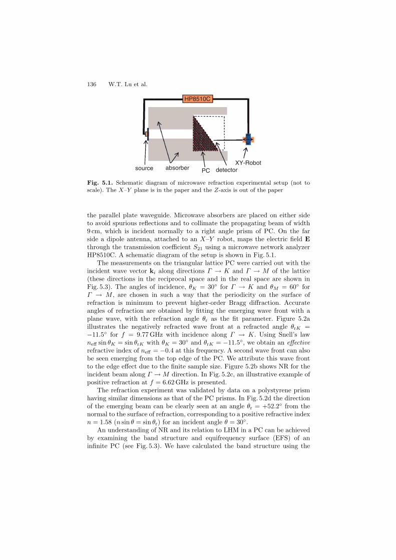
136 W.T. Lu et al.
HP8510C
source absorber detectorPCXY-Robot
Fig. 5.1. Schematic diagram of microwave refraction experimental setup (not toscale). The X–Y plane is in the paper and the Z-axis is out of the paper
the parallel plate waveguide. Microwave absorbers are placed on either sideto avoid spurious reflections and to collimate the propagating beam of width9 cm, which is incident normally to a right angle prism of PC. On the farside a dipole antenna, attached to an X–Y robot, maps the electric field Ethrough the transmission coefficient S21 using a microwave network analyzerHP8510C. A schematic diagram of the setup is shown in Fig. 5.1.
The measurements on the triangular lattice PC were carried out with theincident wave vector ki along directions Γ → K and Γ → M of the lattice(these directions in the reciprocal space and in the real space are shown inFig. 5.3). The angles of incidence, θK = 30 for Γ → K and θM = 60 forΓ → M , are chosen in such a way that the periodicity on the surface ofrefraction is minimum to prevent higher-order Bragg diffraction. Accurateangles of refraction are obtained by fitting the emerging wave front with aplane wave, with the refraction angle θr as the fit parameter. Figure 5.2aillustrates the negatively refracted wave front at a refracted angle θrK =−11.5 for f = 9.77 GHz with incidence along Γ → K. Using Snell’s lawneff sin θK = sin θrK with θK = 30 and θrK = −11.5, we obtain an effectiverefractive index of neff = −0.4 at this frequency. A second wave front can alsobe seen emerging from the top edge of the PC. We attribute this wave frontto the edge effect due to the finite sample size. Figure 5.2b shows NR for theincident beam along Γ → M direction. In Fig. 5.2c, an illustrative example ofpositive refraction at f = 6.62 GHz is presented.
The refraction experiment was validated by data on a polystyrene prismhaving similar dimensions as that of the PC prisms. In Fig. 5.2d the directionof the emerging beam can be clearly seen at an angle θr = +52.2 from thenormal to the surface of refraction, corresponding to a positive refractive indexn = 1.58 (n sin θ = sin θr) for an incident angle θ = 30.
An understanding of NR and its relation to LHM in a PC can be achievedby examining the band structure and equifrequency surface (EFS) of aninfinite PC (see Fig. 5.3). We have calculated the band structure using the
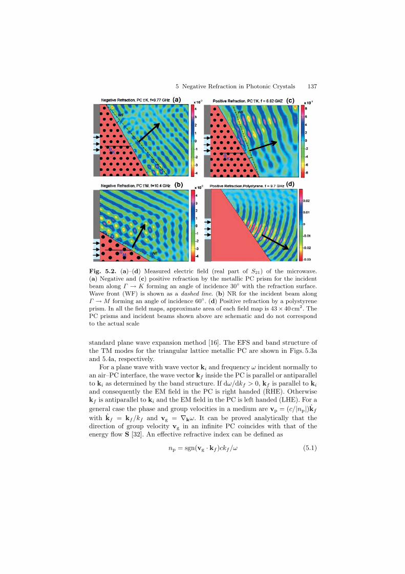
5 Negative Refraction in Photonic Crystals 137
Fig. 5.2. (a)–(d) Measured electric field (real part of S21) of the microwave.(a) Negative and (c) positive refraction by the metallic PC prism for the incidentbeam along Γ → K forming an angle of incidence 30 with the refraction surface.Wave front (WF) is shown as a dashed line. (b) NR for the incident beam alongΓ → M forming an angle of incidence 60. (d) Positive refraction by a polystyreneprism. In all the field maps, approximate area of each field map is 43× 40 cm2. ThePC prisms and incident beams shown above are schematic and do not correspondto the actual scale
standard plane wave expansion method [16]. The EFS and band structure ofthe TM modes for the triangular lattice metallic PC are shown in Figs. 5.3aand 5.4a, respectively.
For a plane wave with wave vector ki and frequency ω incident normally toan air–PC interface, the wave vector kf inside the PC is parallel or antiparallelto ki as determined by the band structure. If dω/dkf > 0, kf is parallel to ki
and consequently the EM field in the PC is right handed (RHE). Otherwisekf is antiparallel to ki and the EM field in the PC is left handed (LHE). For ageneral case the phase and group velocities in a medium are vp = (c/|np|)kf
with kf = kf/kf and vg = ∇kω. It can be proved analytically that thedirection of group velocity vg in an infinite PC coincides with that of theenergy flow S [32]. An effective refractive index can be defined as
np = sgn(vg · kf )ckf/ω (5.1)
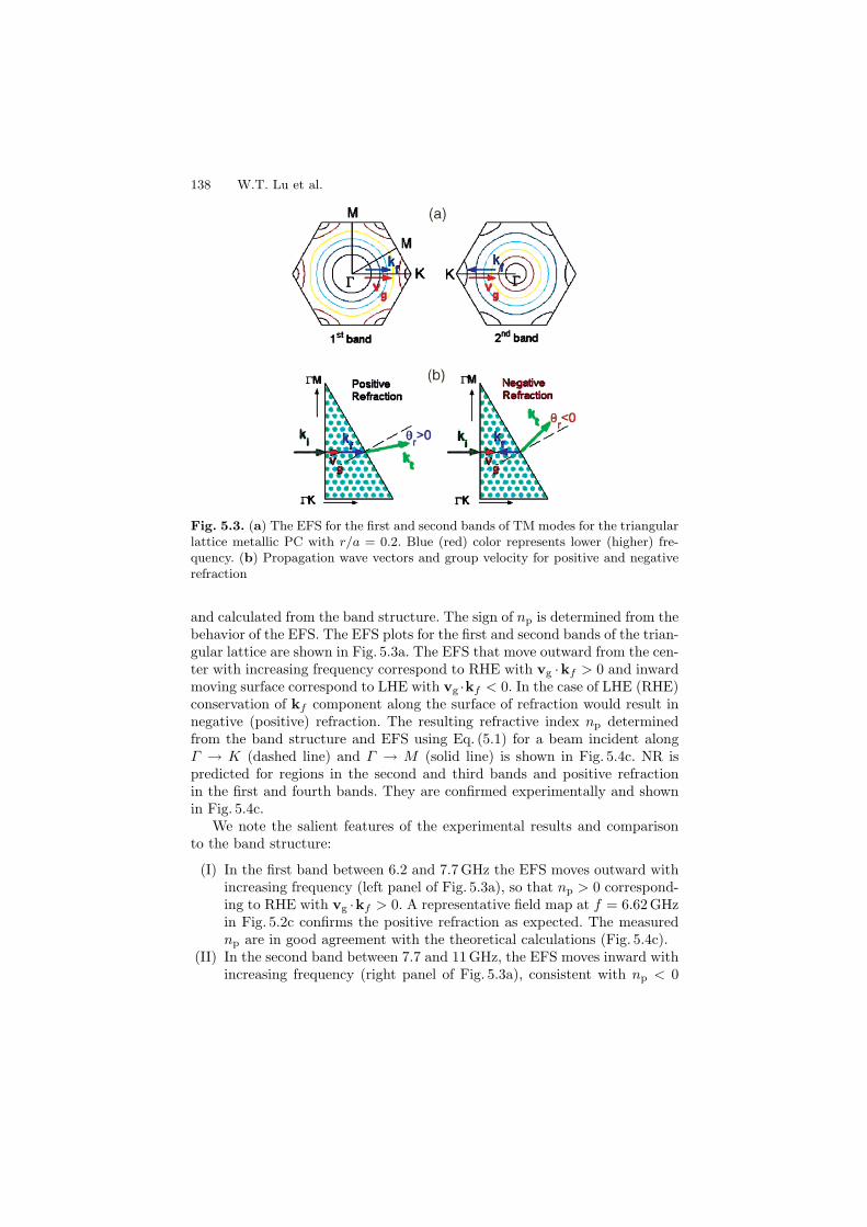
138 W.T. Lu et al.
Fig. 5.3. (a) The EFS for the first and second bands of TM modes for the triangularlattice metallic PC with r/a = 0.2. Blue (red) color represents lower (higher) fre-quency. (b) Propagation wave vectors and group velocity for positive and negativerefraction
and calculated from the band structure. The sign of np is determined from thebehavior of the EFS. The EFS plots for the first and second bands of the trian-gular lattice are shown in Fig. 5.3a. The EFS that move outward from the cen-ter with increasing frequency correspond to RHE with vg ·kf > 0 and inwardmoving surface correspond to LHE with vg ·kf < 0. In the case of LHE (RHE)conservation of kf component along the surface of refraction would result innegative (positive) refraction. The resulting refractive index np determinedfrom the band structure and EFS using Eq. (5.1) for a beam incident alongΓ → K (dashed line) and Γ → M (solid line) is shown in Fig. 5.4c. NR ispredicted for regions in the second and third bands and positive refractionin the first and fourth bands. They are confirmed experimentally and shownin Fig. 5.4c.
We note the salient features of the experimental results and comparisonto the band structure:
(I) In the first band between 6.2 and 7.7 GHz the EFS moves outward withincreasing frequency (left panel of Fig. 5.3a), so that np > 0 correspond-ing to RHE with vg ·kf > 0. A representative field map at f = 6.62 GHzin Fig. 5.2c confirms the positive refraction as expected. The measurednp are in good agreement with the theoretical calculations (Fig. 5.4c).
(II) In the second band between 7.7 and 11 GHz, the EFS moves inward withincreasing frequency (right panel of Fig. 5.3a), consistent with np < 0
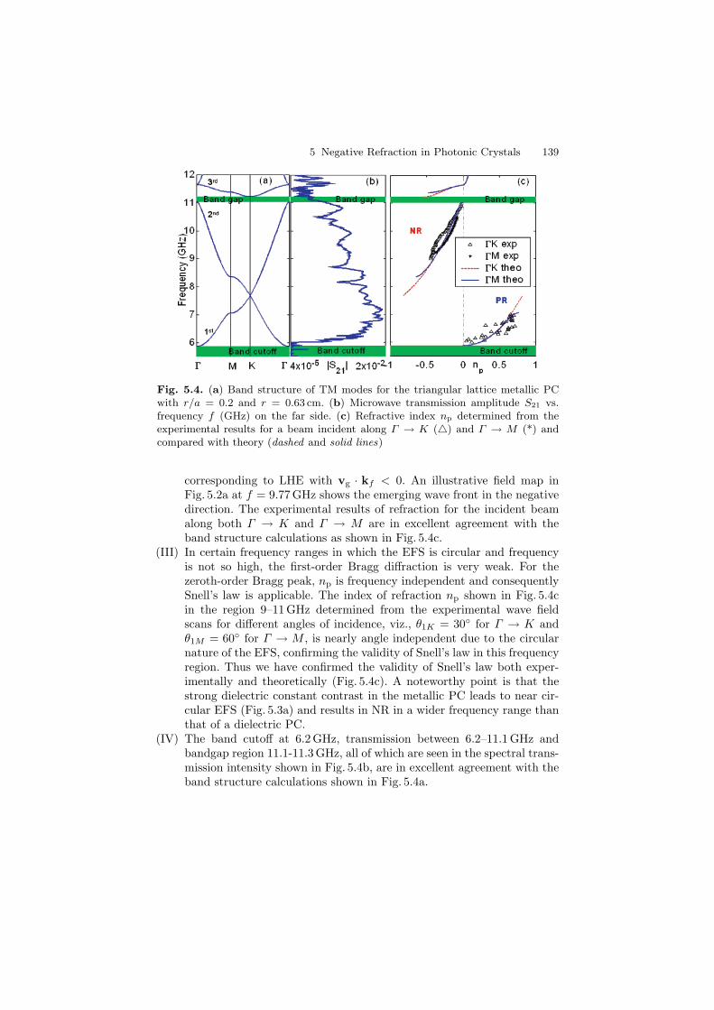
5 Negative Refraction in Photonic Crystals 139
Fig. 5.4. (a) Band structure of TM modes for the triangular lattice metallic PCwith r/a = 0.2 and r = 0.63 cm. (b) Microwave transmission amplitude S21 vs.frequency f (GHz) on the far side. (c) Refractive index np determined from theexperimental results for a beam incident along Γ → K () and Γ → M (*) andcompared with theory (dashed and solid lines)
corresponding to LHE with vg · kf < 0. An illustrative field map inFig. 5.2a at f = 9.77 GHz shows the emerging wave front in the negativedirection. The experimental results of refraction for the incident beamalong both Γ → K and Γ → M are in excellent agreement with theband structure calculations as shown in Fig. 5.4c.
(III) In certain frequency ranges in which the EFS is circular and frequencyis not so high, the first-order Bragg diffraction is very weak. For thezeroth-order Bragg peak, np is frequency independent and consequentlySnell’s law is applicable. The index of refraction np shown in Fig. 5.4cin the region 9–11 GHz determined from the experimental wave fieldscans for different angles of incidence, viz., θ1K = 30 for Γ → K andθ1M = 60 for Γ → M , is nearly angle independent due to the circularnature of the EFS, confirming the validity of Snell’s law in this frequencyregion. Thus we have confirmed the validity of Snell’s law both exper-imentally and theoretically (Fig. 5.4c). A noteworthy point is that thestrong dielectric constant contrast in the metallic PC leads to near cir-cular EFS (Fig. 5.3a) and results in NR in a wider frequency range thanthat of a dielectric PC.
(IV) The band cutoff at 6.2 GHz, transmission between 6.2–11.1 GHz andbandgap region 11.1-11.3 GHz, all of which are seen in the spectral trans-mission intensity shown in Fig. 5.4b, are in excellent agreement with theband structure calculations shown in Fig. 5.4a.
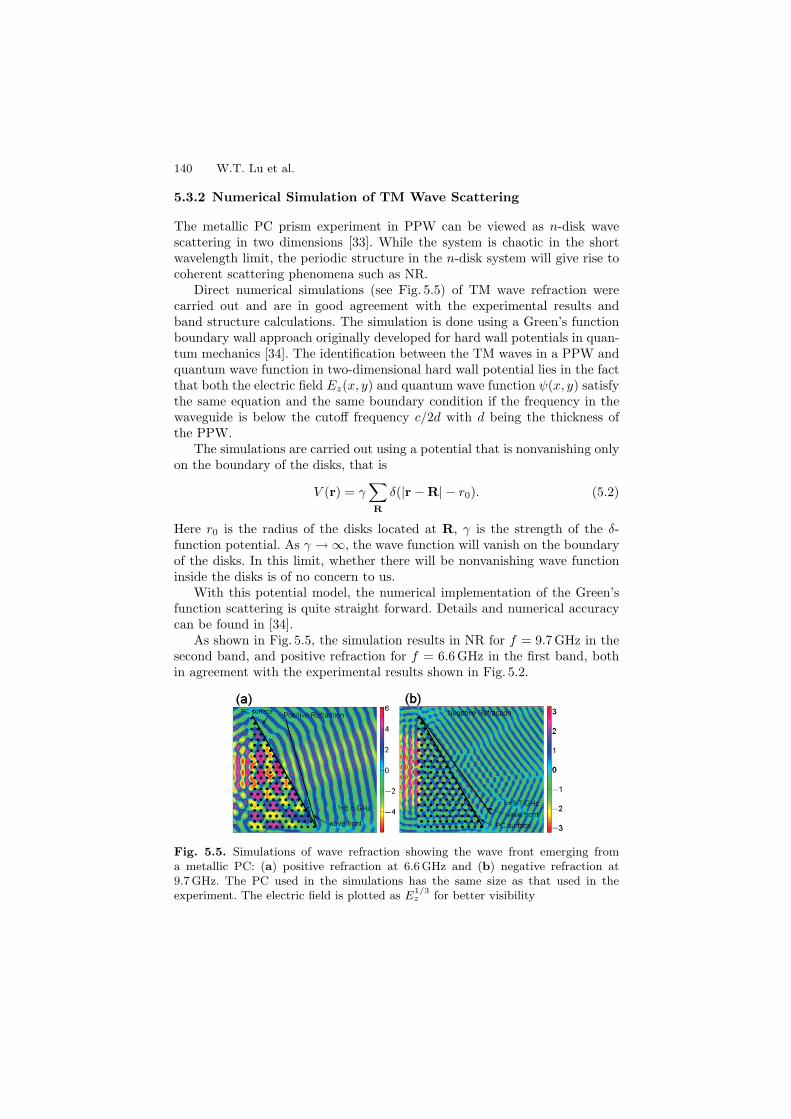
140 W.T. Lu et al.
5.3.2 Numerical Simulation of TM Wave Scattering
The metallic PC prism experiment in PPW can be viewed as n-disk wavescattering in two dimensions [33]. While the system is chaotic in the shortwavelength limit, the periodic structure in the n-disk system will give rise tocoherent scattering phenomena such as NR.
Direct numerical simulations (see Fig. 5.5) of TM wave refraction werecarried out and are in good agreement with the experimental results andband structure calculations. The simulation is done using a Green’s functionboundary wall approach originally developed for hard wall potentials in quan-tum mechanics [34]. The identification between the TM waves in a PPW andquantum wave function in two-dimensional hard wall potential lies in the factthat both the electric field Ez(x, y) and quantum wave function ψ(x, y) satisfythe same equation and the same boundary condition if the frequency in thewaveguide is below the cutoff frequency c/2d with d being the thickness ofthe PPW.
The simulations are carried out using a potential that is nonvanishing onlyon the boundary of the disks, that is
V (r) = γ∑R
δ(|r − R| − r0). (5.2)
Here r0 is the radius of the disks located at R, γ is the strength of the δ-function potential. As γ → ∞, the wave function will vanish on the boundaryof the disks. In this limit, whether there will be nonvanishing wave functioninside the disks is of no concern to us.
With this potential model, the numerical implementation of the Green’sfunction scattering is quite straight forward. Details and numerical accuracycan be found in [34].
As shown in Fig. 5.5, the simulation results in NR for f = 9.7 GHz in thesecond band, and positive refraction for f = 6.6 GHz in the first band, bothin agreement with the experimental results shown in Fig. 5.2.
Fig. 5.5. Simulations of wave refraction showing the wave front emerging froma metallic PC: (a) positive refraction at 6.6 GHz and (b) negative refraction at9.7 GHz. The PC used in the simulations has the same size as that used in theexperiment. The electric field is plotted as E
1/3z for better visibility
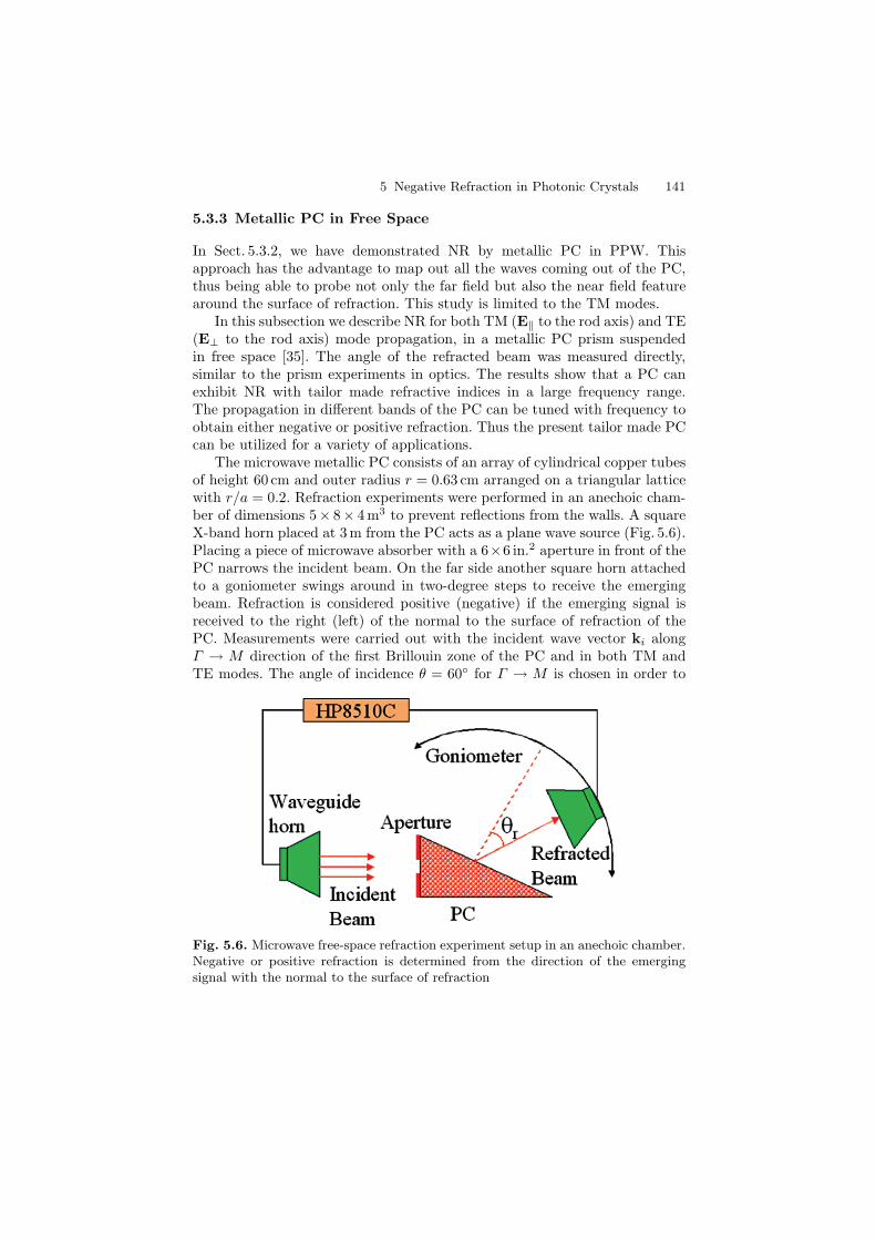
5 Negative Refraction in Photonic Crystals 141
5.3.3 Metallic PC in Free Space
In Sect. 5.3.2, we have demonstrated NR by metallic PC in PPW. Thisapproach has the advantage to map out all the waves coming out of the PC,thus being able to probe not only the far field but also the near field featurearound the surface of refraction. This study is limited to the TM modes.
In this subsection we describe NR for both TM (E‖ to the rod axis) and TE(E⊥ to the rod axis) mode propagation, in a metallic PC prism suspendedin free space [35]. The angle of the refracted beam was measured directly,similar to the prism experiments in optics. The results show that a PC canexhibit NR with tailor made refractive indices in a large frequency range.The propagation in different bands of the PC can be tuned with frequency toobtain either negative or positive refraction. Thus the present tailor made PCcan be utilized for a variety of applications.
The microwave metallic PC consists of an array of cylindrical copper tubesof height 60 cm and outer radius r = 0.63 cm arranged on a triangular latticewith r/a = 0.2. Refraction experiments were performed in an anechoic cham-ber of dimensions 5× 8× 4 m3 to prevent reflections from the walls. A squareX-band horn placed at 3 m from the PC acts as a plane wave source (Fig. 5.6).Placing a piece of microwave absorber with a 6×6 in.2 aperture in front of thePC narrows the incident beam. On the far side another square horn attachedto a goniometer swings around in two-degree steps to receive the emergingbeam. Refraction is considered positive (negative) if the emerging signal isreceived to the right (left) of the normal to the surface of refraction of thePC. Measurements were carried out with the incident wave vector ki alongΓ → M direction of the first Brillouin zone of the PC and in both TM andTE modes. The angle of incidence θ = 60 for Γ → M is chosen in order to
Fig. 5.6. Microwave free-space refraction experiment setup in an anechoic chamber.Negative or positive refraction is determined from the direction of the emergingsignal with the normal to the surface of refraction
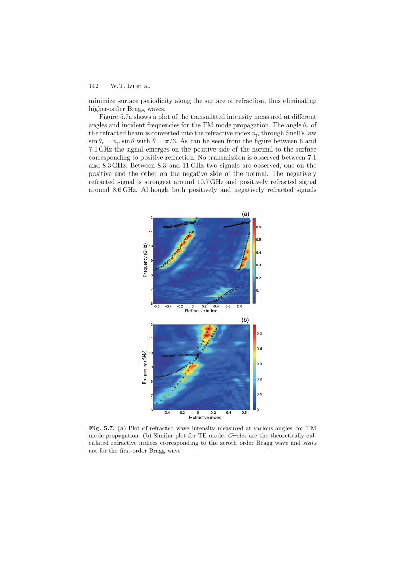
142 W.T. Lu et al.
minimize surface periodicity along the surface of refraction, thus eliminatinghigher-order Bragg waves.
Figure 5.7a shows a plot of the transmitted intensity measured at differentangles and incident frequencies for the TM mode propagation. The angle θr ofthe refracted beam is converted into the refractive index np through Snell’s lawsin θr = np sin θ with θ = π/3. As can be seen from the figure between 6 and7.1 GHz the signal emerges on the positive side of the normal to the surfacecorresponding to positive refraction. No transmission is observed between 7.1and 8.3 GHz. Between 8.3 and 11 GHz two signals are observed, one on thepositive and the other on the negative side of the normal. The negativelyrefracted signal is strongest around 10.7 GHz and positively refracted signalaround 8.6 GHz. Although both positively and negatively refracted signals
Fig. 5.7. (a) Plot of refracted wave intensity measured at various angles, for TMmode propagation. (b) Similar plot for TE mode. Circles are the theoretically cal-culated refractive indices corresponding to the zeroth order Bragg wave and starsare for the first-order Bragg wave
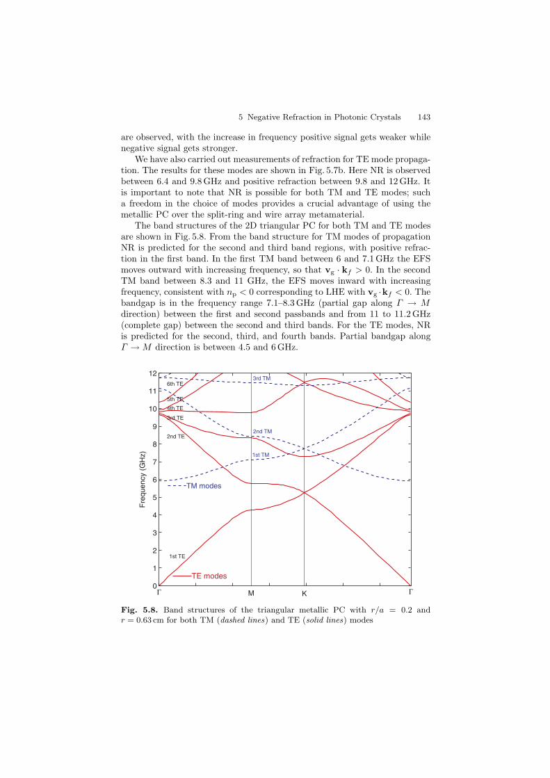
5 Negative Refraction in Photonic Crystals 143
are observed, with the increase in frequency positive signal gets weaker whilenegative signal gets stronger.
We have also carried out measurements of refraction for TE mode propaga-tion. The results for these modes are shown in Fig. 5.7b. Here NR is observedbetween 6.4 and 9.8 GHz and positive refraction between 9.8 and 12 GHz. Itis important to note that NR is possible for both TM and TE modes; sucha freedom in the choice of modes provides a crucial advantage of using themetallic PC over the split-ring and wire array metamaterial.
The band structures of the 2D triangular PC for both TM and TE modesare shown in Fig. 5.8. From the band structure for TM modes of propagationNR is predicted for the second and third band regions, with positive refrac-tion in the first band. In the first TM band between 6 and 7.1 GHz the EFSmoves outward with increasing frequency, so that vg · kf > 0. In the secondTM band between 8.3 and 11 GHz, the EFS moves inward with increasingfrequency, consistent with np < 0 corresponding to LHE with vg ·kf < 0. Thebandgap is in the frequency range 7.1–8.3 GHz (partial gap along Γ → Mdirection) between the first and second passbands and from 11 to 11.2 GHz(complete gap) between the second and third bands. For the TE modes, NRis predicted for the second, third, and fourth bands. Partial bandgap alongΓ → M direction is between 4.5 and 6 GHz.
0
1
2
3
4
5
6
7
8
9
10
11
12
Γ
Fre
quen
cy (
GH
z)
TE modes
TM modes
1st TE
2nd TE2nd TM
1st TM
3rd TE
4th TE
5th TE
3rd TM
ΓM K
6th TE
Fig. 5.8. Band structures of the triangular metallic PC with r/a = 0.2 andr = 0.63 cm for both TM (dashed lines) and TE (solid lines) modes
144 W.T. Lu et al.
In Fig. 5.7a, b the refractive indices np defined in (5.1) and determinedfrom the band structure are plotted with experimental data. The close matchbetween the theory and experiments is striking. All the predicted featuresincluding bandgap, negative and positive refraction are observed in the experi-ments. The degeneracy observed in the case of TE modes is due to multiplebands for a single frequency, which results in multiple propagation k vectors.It is an interesting observation that different intensities are associated withdifferent propagation vectors for TE modes. For these modes with Γ → Mpropagation, as shown in Fig. 5.7, it can be seen that the higher the slope ofthe curve the more intense the beam.
A particular feature of interest is the bandwidth for NR and LHE. FromFig. 5.8 it can be deduced that the bandwidth for TE modes is 42% and for TMmodes 27%. In comparison, a relatively weakly modulated dielectric PC has abandwidth estimated to be 6.3% which is very narrow and the experimentallyobtained bandwidth for metamaterials [2,5] to date is only 10%. The presentbandwidths for both TE and TM modes are higher than that in metamaterial.Bandwidth puts stringent restrictions on the tunability and functional rangeof the devices based on the LHM. In particular in our recent work we haveshown that in the LHM, EM wave propagation is slow with group velocity of0.02c, where c is the speed of light in vacuum. This slow group velocity [36]combined with large bandwidth can be used for designing a delay line filterwith a large passband.
In the case of TE modes, for an incident angle of 60, the refractive indexis found to vary from 0 to −0.48, which is a 200% change for a frequencychange of 42%. Such a large dn/dω results in a large dφ/dω which can beused in designing ultrasensitive phase shifters.
5.3.4 High-Order Bragg Waves at the Surfaceof Metallic Photonic Crystals
In this subsection we will discuss in detail the situation for all orders of Braggdiffraction and show that even with the presence of high-order Bragg diffrac-tion, the appearance of NR is unambiguous and the direction of the Braggwave beam determined from theory matches well with the experimental obser-vation.
At the second interface between the PC prism and the air, the wavespenetrate into the air through all orders of Bragg waves. The parallel andvertical components of the mth-order Bragg wave vector along the surface are
kt‖m = kf sin θ + 2mπ/as, kt⊥m =√
ω2/c2 − k2t||m. (5.3)
Here kf is the wave number in the PC and as is the surface periodicity. For theband with NR, kf is negative. The electric field of the outgoing waves fromthis interface can thus be written as a summation over all orders of Braggwave ktm

5 Negative Refraction in Photonic Crystals 145
Ezt = a0eikt0·r + a1eikt1·r + · · · . (5.4)
Depending on the as and the incident angle θ, only the first few Bragg waveswill have real kt⊥m and can propagate. The refracted angle can be obtainedfrom θr = arctan(kt‖/kt⊥) for each beam. In all of the prescribed experiments,the surface periodicity is as = 3.15 cm.
Let us first consider the TM modes. For the incident beam along the Γ →Kdirection, θ = π/6. In the first band, if the frequency is below 7.12 GHz, onlythe zeroth-order Bragg wave will propagate in the air. For the incident beamalong the Γ → M direction, θ = π/3, the first-order Bragg diffraction willbe suppressed for frequency below 6.70 GHz in the first band. For the secondband along either Γ → K or Γ → M direction, the zeroth- and the first-orderBragg diffraction will propagate. Even if present, the first-order Bragg waveis much weaker than the zeroth-order Bragg wave as can be seen in Figs. 5.2a,b, 5.5b, and 5.7a. Thus we were able to determine np which corresponds tothe zeroth-order Bragg wave. The measured angles for the first-order Braggwaves match perfectly with the theory as shown in Fig. 5.7a.
For the TE modes with incident beam along Γ → M direction, one has θ =π/3. For all the first three bands which are below 9.52 GHz, only the zeroth-order Bragg wave will propagate. For frequencies above 9.52 GHz, higher-orderBragg diffraction will be present. This can be clearly seen in Fig. 5.7b.
5.4 Conclusion and Perspective
In this chapter, NR was demonstrated experimentally for both TM and TEmode propagation in metallic PCs. Two approaches were used, one was mea-suring the energy beam direction and the other by mapping out the electricfield with magnitude and phase to determine the wave front of the refractedbeam. Thus the verification of NR is unambiguous. A major feature is theextraordinary level of control exemplified by the convergence between theexperimental data, band structure calculations, and simulations. The ease andlow cost of fabrication of the metallic PC compared with a dielectric PCand metamaterials makes them ideal for a wide range of applications. Pre-cise control over the geometry, choice of mode, and scalability to submicrondimensions of PCs show promise for applications from microwave to opticalfrequencies. This means that a variety of tailor-made structures are feasibleto be designed and constructed.
Numerous possibilities open up by the present results. For applicationssuch as imaging, one requires index matching between the negative indexmaterial and surroundings accompanied by negligible losses. These require-ments are more easily met with PCs than with metamaterials. Metallic PCoffers additional advantages of the high dielectric constant contrast comparedwith dielectric PC and low attenuation compared with metamaterial. Further-more the microwave PC can be easily scaled to 3D [37,38], and to optical fre-quencies which is highly unlikely with metamaterials [2]. Thus the advantages
146 W.T. Lu et al.
of NR and LHE, such as imaging by flat lenses, planoconcave lens focusing,beam steerers, couplers, and others, are feasible with PCs from microwaveto optical frequencies. With large group dispersion [39], slow light [36], andnonlinear properties [40] in PCs, the all-optical circuits computer is closer tobecoming a reality.
NR provides a new arena for physics and technology to emerge and enhanceeach other. New ideas of NR [41,42] continue to emerge in this expanding fieldof physics. Though Pendry’s perfect lens is an ideal limit and may never berealized due to loss [30], the poor man’s lens using the near field of metallicthin film has produced improved subwavelength imaging [43, 44]. This mayenhance the performance of lithography [45]. Optical components utilizingNR are expected to have several advantages. Examples are flat lenses withoutoptical axis [28,31], subwavelength resolution imaging [46], and improved lensperformance due to reduced aberrations [47,48]. In addition light weight andcompact structures offer additional advantages in a variety of applications.
Acknowledgment
This work was supported by the National Science Foundation and the AirForce Research Laboratories, Hanscom, MA.
References
1. V. Veselago, Sov. Phys. Usp. 10, 509 (1968)2. R.A. Shelby, D.R. Smith, S. Schultz, Science 292, 77 (2001)3. P.V. Parimi, W.T. Lu, P. Vodo, S. Sridhar, Nature (London) 426, 404 (2003)4. P. Vodo, P.V. Parimi, W.T. Lu, S. Sridhar, Appl. Phys. Lett. 86, 201108 (2005)5. C.G. Parazzoli, R.B. Greegor, K. Li, B.E.C. Koltenbah, M. Tanielian, Phys.
Rev. Lett. 90, 107401 (2003)6. A.A. Houck, J.B. Brock, I.L. Chuang, Phys. Rev. Lett. 90, 137401 (2003);
J.B. Brock, A.A. Houck, I.L. Chuang, Appl. Phys. Lett. 85, 2472 (2004)7. C. Enkrich, M. Wegener, S. Linden, S. Burger, L. Zschiedrich, F. Schmidt,
J.F. Zhou, Th. Koschny, C.M. Soukoulis, Phys. Rev. Lett. 95, 203901 (2005)8. J. Zhou, Th. Koschny, M. Kafesaki, E.N. Economou, J.B. Pendry,
C.M. Soukoulis, Phys. Rev. Lett. 95, 223902 (2005)9. W.J. Padilla, A.J. Taylor, C. Highstrete, M. Lee, R.D. Averitt, Phys. Rev. Lett.
96, 107401 (2006)10. L. Landau, I.M. Lifshitz, Electrodynamics of Continuous Media, 2nd edn.
(Elsevier, Amsterdam, 1984)11. G.V. Eleftheriades, A.K. Iyer, P.C. Kremer, IEEE Trans. Microw. Theory Tech.
50, 2702 (2002)12. A. Grbic, G.V. Eleftheriades, Phys. Rev. Lett. 92, 117403 (2004); J. Appl. Phys.
98, 043106 (2005)13. I.V. Lindell, S.A. Tretyakov, K.I. Nikoskines, S. Ilvonen, Microw. Opt. Tech.
Lett. 31, 129 (2001)14. N. Engheta, A. Salandrino, A. Alu, Phys. Rev. Lett. 95, 095504 (2005)
5 Negative Refraction in Photonic Crystals 147
15. J.D. Joannopoulos, P.R. Villeneuve, S. Fan, Nature 386, 143 (1997)16. J.D. Joannopoulos, R.D. Meade, J.N. Winn, Photonic Crystals: Molding the
Flow of Light (Princeton University Press, Princeton, 1995)17. M. Notomi, Phys. Rev. B 62, 10696 (2000); Opt. Quant. Electron. 34, 133
(2002)18. C. Luo, S.G. Johnson, J.D. Joannopoulos, J.B. Pendry, Phys. Rev. B 65, 201104
(2002)19. S. Foteinopoulou, E.N. Economou, C.M. Soukoulis, Phys. Rev. Lett. 90, 107402
(2003)20. S. Foteinopoulou, C.M. Soukoulis, Phys. Rev. B 67, 235107 (2003)21. E. Cubukcu, K. Aydin, E. Ozbay, S. Foteinopoulou, C.M. Soukoulis, Nature
423, 604 (2003)22. P.V. Parimi, W.T. Lu, P. Vodo, J. Sokoloff, J.S. Derov, S. Sridhar, Phys. Rev.
Lett. 92, 127401 (2004)23. A. Berrier, M. Mulot, M. Swillo, M. Qiu, L. Thyln, A. Talneau, S. Anand, Phys.
Rev. Lett. 93, 073902 (2004)24. Y. Zhang, B. Fluegel, A. Mascarenhas, Phys. Rev. Lett. 91, 157404 (2003)25. Z. Liu, Z. Lin, S.T. Chui, Phys. Rev. B 69, 115402 (2004)26. X.L. Chen, M. He, Y. Du, W.Y. Wang, D.F. Zhang, Phys. Rev. B 72, 113111
(2005)27. H. Kosaka, T. Kawashima, A. Tomita, M. Notomi, T. Tamamura, T. Sato,
S. Kawakami, Phys. Rev. B 58, R10096 (1998)28. J.B. Pendry, Phys. Rev. Lett. 85, 3966 (2000)29. D.R. Smith, N. Kroll, Phys. Rev. Lett. 85, 2933 (2000)30. N. Garcia, M. Nieto-Vesperinas, Phys. Rev. Lett. 88, 207403 (2002)31. W.T. Lu, S. Sridhar, Opt. Express 13, 10673 (2005)32. K. Sakoda, Optical Properties of Photonic Crystal (Springer, Berlin Heidelberg
New York, 2001)33. W. Lu, L. Viola, K. Pance, M. Rose, S. Sridhar, Phys. Rev. E 61, 3652 (2000)34. M.G.E. Da Luz, A.S. Lupu-Sax, E.J. Heller, Phys. Rev. E 56, 2496 (1997)35. P. Vodo, P.V. Parimi, W.T. Lu, S. Sridhar, R. Wing, Appl. Phys. Lett. 85, 1858
(2004)36. E. Di Gennaro, P.V. Parimi, W.T. Lu, S. Sridhar, J.S. Derov, B. Turchinetz,
Phys. Rev. B 72, 033110 (2005)37. D.F. Sievenpiper, M.E. Sickmiller, E. Yablonovitch, Phys. Rev. Lett. 76, 2480
(1996)38. C. Luo, S.G. Johnson, J.D. Joannopoulos, Appl. Phys. Lett. 81, 2352 (2002)39. M. Notomi, K. Yamada, A. Shinya, J. Takahashi, C. Takahashi, I. Yokohama,
Phys. Rev Lett. 87, 253902 (2001)40. M. Soljacic, J.D. Joannnopoulos, Nat. Mater. 3, 211 (2004)41. V.A. Podolskiy, E.E. Narimanov, Phys. Rev. B 71, 201101 (2005)42. H. Shin, S. Fan, Phys. Rev. Lett. 96, 073907 (2006)43. W.T. Lu, S. Sridhar, Microw. Opt. Tech. Lett. 39, 282 (2003)44. N. Fang, H. Lee, C. Sun, X. Zhang, Science 308, 534 (2005)45. D.O.S. Melville, R.J. Blaikie, C.R. Wolf, Appl. Phys. Lett. 84, 4403 (2004)46. C. Luo, S.G. Johnson, J.D. Joannopoulos, J.B. Pendry, Phys. Rev. B 68, 045115
(2003)47. D. Schurig, D.R. Smith, Phys. Rev. E 70, 065601 (2004)48. J. Chen, C. Radu, A. Puri, Appl. Phys. Lett. 88, 071119 (2006)
6
Negative Refraction and SubwavelengthFocusing in Two-Dimensional PhotonicCrystals
E. Ozbay and G. Ozkan
Summary. We experimentally and theoretically demonstrate negative refractionand focusing on electromagnetic (EM) waves by using two-dimensional photoniccrystal slabs at microwave frequencies. Negative refraction is observed both fortransverse magnetic (TM) and transverse electric (TE) polarized incident EM waves.Gaussian beam shifting method is used to verify negative refractive index. Subwave-length imaging and flat lens behavior of photonic crystals are successfully demon-strated. We have been able to overcome the diffraction limit and focus the EMwaves to a spot size of 0.21λ. Metallodielectric photonic crystals are employedto increase the range of angles of incidence that results in negative refraction.Experimental results and theoretical calculations are in good agreement throughoutthe work.
6.1 Introduction
Materials which possess negative index of refraction have become a remarkableresearch area in recent years [1–10]. One approach taken is to construct a com-posite metamaterial [2–5] consisting of two components which have a negativepermittivity [11] (ε(ω) < 0) and negative permeability [12] (µ(ω) < 0) simul-taneously over a certain frequency range, respectively, so that the resultingindex of refraction of the effective medium becomes neff =
√ε√
µ < 0 [6–10].Such structures are able to behave like a perfect lens, where both the propa-gating and evanescent waves contribute to the focusing [13]. Another path isrevealed by the photonic crystals (PCs), where the band structure can leadto negative dispersion for electromagnetic (EM) waves.
Photonic crystals are periodic dielectric or metallic structures that havephotonic bands exhibiting arbitrarily different dispersions for the propaga-tion of EM waves, and band gaps, where the propagation is prohibited atcertain range of wavelengths [14–18]. In this respect, there is a close analogybetween a photon in a photonic crystal, and an electron in a semiconduc-tor. Based on these properties, photonic crystals provide a medium where thepropagation of light can be modified virtually in any way in a controllable
150 E. Ozbay and G. Ozkan
manner [19–31]. Their application potential covers the existing electromag-netic technologies for improvement, and extends beyond for advancement.From the fundamental physics point of view, photonic crystals provide accessto novel and unusual optical properties. It has been theoretically shown thatphotonic crystals may possess negative refraction although they have a peri-odically modulated positive permittivity and permeability of unity [32–35].Cubukcu et al. has been first to demonstrate negative refraction phenomenonin two-dimensional (2D) PCs in the microwave region [36]. Further experi-mental studies proved that carefully designed PCs are candidates for obtain-ing negative refraction at microwave [37] and infrared [38] frequency regimes.Superprism effect is another exciting property arising from photonic crystals[39,40]. Subwavelength imaging and resolution [41] and flat lens behavior [42]of PCs have been experimentally demonstrated. Extensive numerical [43–46]and experimental studies [47–52] helped to have a better understanding ofnegative refraction, focusing, and subwavelength imaging in photonic crystalstructures.
In this chapter, we review certain recent studies on the negative refrac-tion and imaging of EM waves by photonic crystal slabs in the microwavefrequency regime. We first report on the negative refraction and the sub-wavelength imaging with transverse magnetic (TM) polarized EM waves.Then we show that it is also possible to have negative refraction with trans-verse electric (TE) polarized EM waves. Fifth band of the photonic crystalis utilized for purpose of achieving negative refraction. A spectral negativerefraction and focusing behavior will be provided. Finally we demonstrate ametallodielectric PC that possesses negative refraction and imaging througha slab. Throughout the work two basic mechanisms arising from the bandstructure of PCs are employed to obtain negative refraction. We found thatfocusing abilities of a PC slab can surpass that of conventional (i.e., positiverefractive) materials, providing both subwavelength imaging and true flat lensbehavior.
6.2 Negative Refraction and Subwavelength Imagingof TM Polarized Electromagnetic Waves
Refraction is perhaps one of the most basic topics of electromagnetic phenom-ena, whereby when a beam of radiation is incident on an interface between twomedia at an arbitrary angle, the direction of propagation of the transmittedbeam is altered by an amount related to the indices of refraction of the twomedia. Although all of the known naturally occurring materials exhibit posi-tive indices of refraction, the possibility of materials with negative refractiveindex has been explored theoretically by Victor Veselago [1]. In his semi-nal work, he concluded that such materials did not violate any fundamentalphysical laws. These materials were termed left-handed materials (LHMs),
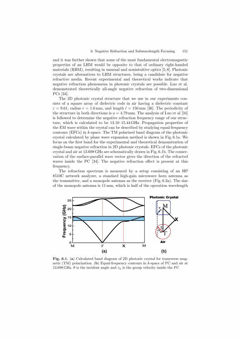
6 Negative Refraction and Subwavelength Focusing 151
and it was further shown that some of the most fundamental electromagneticproperties of an LHM would be opposite to that of ordinary right-handedmaterials (RHM), resulting in unusual and nonintuitive optics [5,8]. Photoniccrystals are alternatives to LHM structures, being a candidate for negativerefractive media. Recent experimental and theoretical works indicate thatnegative refraction phenomena in photonic crystals are possible. Luo et al.demonstrated theoretically all-angle negative refraction of two-dimensionalPCs [34].
The 2D photonic crystal structure that we use in our experiments con-sists of a square array of dielectric rods in air having a dielectric constantε = 9.61, radius r = 1.6mm, and length l = 150mm [36]. The periodicity ofthe structure in both directions is a = 4.79mm. The analysis of Luo et al [34]is followed to determine the negative refraction frequency range of our struc-ture, which is calculated to be 13.10–15.44 GHz. Propagation properties ofthe EM wave within the crystal can be described by studying equal-frequencycontours (EFCs) in k-space. The TM polarized band diagram of the photoniccrystal calculated by plane wave expansion method is shown in Fig. 6.1a. Wefocus on the first band for the experimental and theoretical demonstration ofsingle-beam negative refraction in 2D photonic crystals. EFCs of the photoniccrystal and air at 13.698 GHz are schematically drawn in Fig. 6.1b. The conser-vation of the surface-parallel wave vector gives the direction of the refractedwaves inside the PC [34]. The negative refraction effect is present at thisfrequency.
The refraction spectrum is measured by a setup consisting of an HP8510C network analyzer, a standard high-gain microwave horn antenna asthe transmitter, and a monopole antenna as the receiver (Fig. 6.2a). The sizeof the monopole antenna is 11 mm, which is half of the operation wavelength
Fig. 6.1. (a) Calculated band diagram of 2D photonic crystal for transverse mag-netic (TM) polarization. (b) Equal-frequency contours in k-space of PC and air at13.698 GHz. θ is the incident angle and vg is the group velocity inside the PC
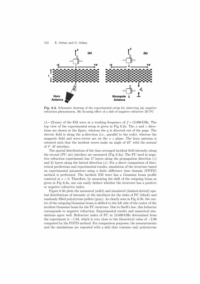
152 E. Ozbay and G. Ozkan
Fig. 6.2. Schematic drawing of the experimental setup for observing (a) negativerefraction phenomenon, (b) focusing effect of a slab of negative refractive 2D PC
(λ∼ 22mm) of the EM wave at a working frequency of f =13.698GHz. Thetop view of the experimental setup is given in Fig. 6.2a. The x and z direc-tions are shown in the figure, whereas the y is directed out of the page. Theelectric field is along the y-direction (i.e., parallel to the rods), whereas themagnetic field and wave-vector are on the x–z plane. The horn antenna isoriented such that the incident waves make an angle of 45 with the normalof Γ–M interface.
The spatial distributions of the time-averaged incident field intensity alongthe second (PC–air) interface are measured (Fig. 6.3a). The PC used in nega-tive refraction experiments has 17 layers along the propagation direction (z)and 21 layers along the lateral direction (x). For a direct comparison of theo-retical predictions and experimental results, simulation of the structure basedon experimental parameters using a finite difference time domain (FDTD)method is performed. The incident EM wave has a Gaussian beam profilecentered at x = 0. Therefore, by measuring the shift of the outgoing beam asgiven in Fig. 6.3a, one can easily deduce whether the structure has a positiveor negative refractive index.
Figure 6.3b plots the measured (solid) and simulated (dashed-dotted) spa-tial distributions of intensity at the interfaces for the slabs of PC (black) andrandomly filled polystyrene pellets (gray). As clearly seen in Fig. 6.3b, the cen-ter of the outgoing Gaussian beam is shifted to the left side of the center of theincident Gaussian beam for the PC structure. Due to Snell’s law, this behaviorcorresponds to negative refraction. Experimental results and numerical sim-ulations agree well. Refractive index of PC at 13.698 GHz determined fromthe experiment is −1.94, which is very close to the theoretical value of −2.06computed by the FDTD method. For comparison purposes, the measurementsand the simulations are repeated with a slab that contains only polystyrene
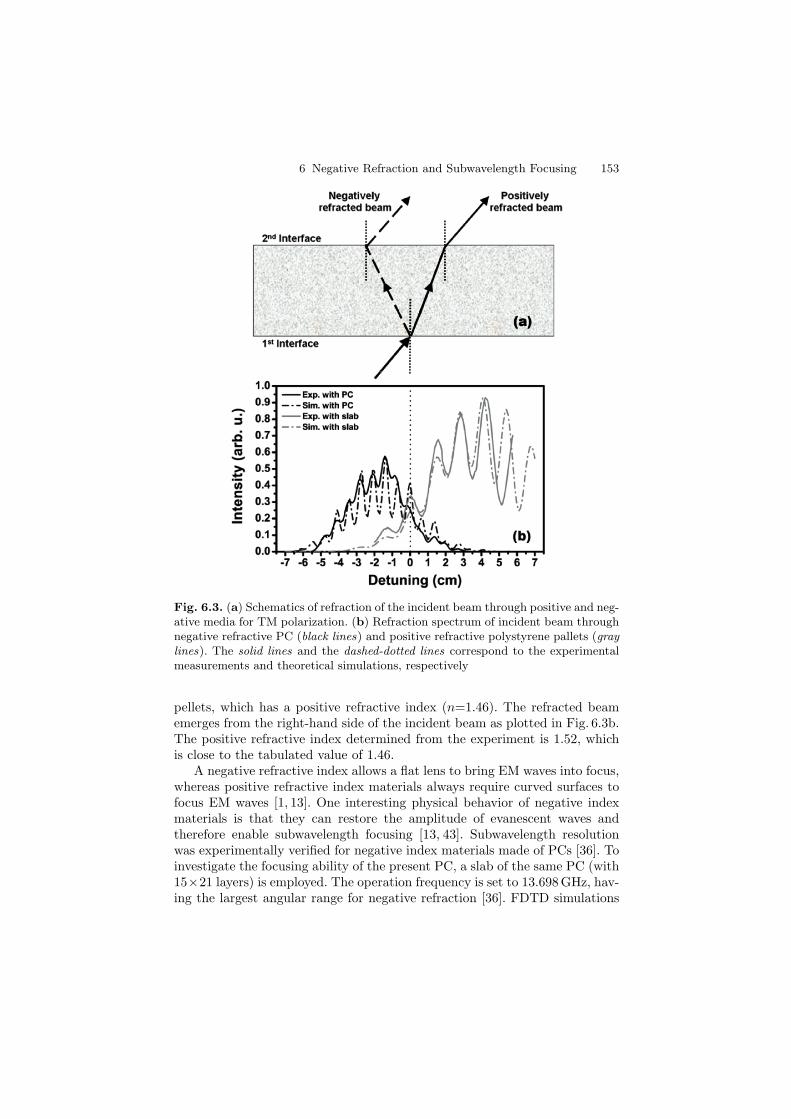
6 Negative Refraction and Subwavelength Focusing 153
Fig. 6.3. (a) Schematics of refraction of the incident beam through positive and neg-ative media for TM polarization. (b) Refraction spectrum of incident beam throughnegative refractive PC (black lines) and positive refractive polystyrene pallets (graylines). The solid lines and the dashed-dotted lines correspond to the experimentalmeasurements and theoretical simulations, respectively
pellets, which has a positive refractive index (n=1.46). The refracted beamemerges from the right-hand side of the incident beam as plotted in Fig. 6.3b.The positive refractive index determined from the experiment is 1.52, whichis close to the tabulated value of 1.46.
A negative refractive index allows a flat lens to bring EM waves into focus,whereas positive refractive index materials always require curved surfaces tofocus EM waves [1, 13]. One interesting physical behavior of negative indexmaterials is that they can restore the amplitude of evanescent waves andtherefore enable subwavelength focusing [13, 43]. Subwavelength resolutionwas experimentally verified for negative index materials made of PCs [36]. Toinvestigate the focusing ability of the present PC, a slab of the same PC (with15×21 layers) is employed. The operation frequency is set to 13.698 GHz, hav-ing the largest angular range for negative refraction [36]. FDTD simulations
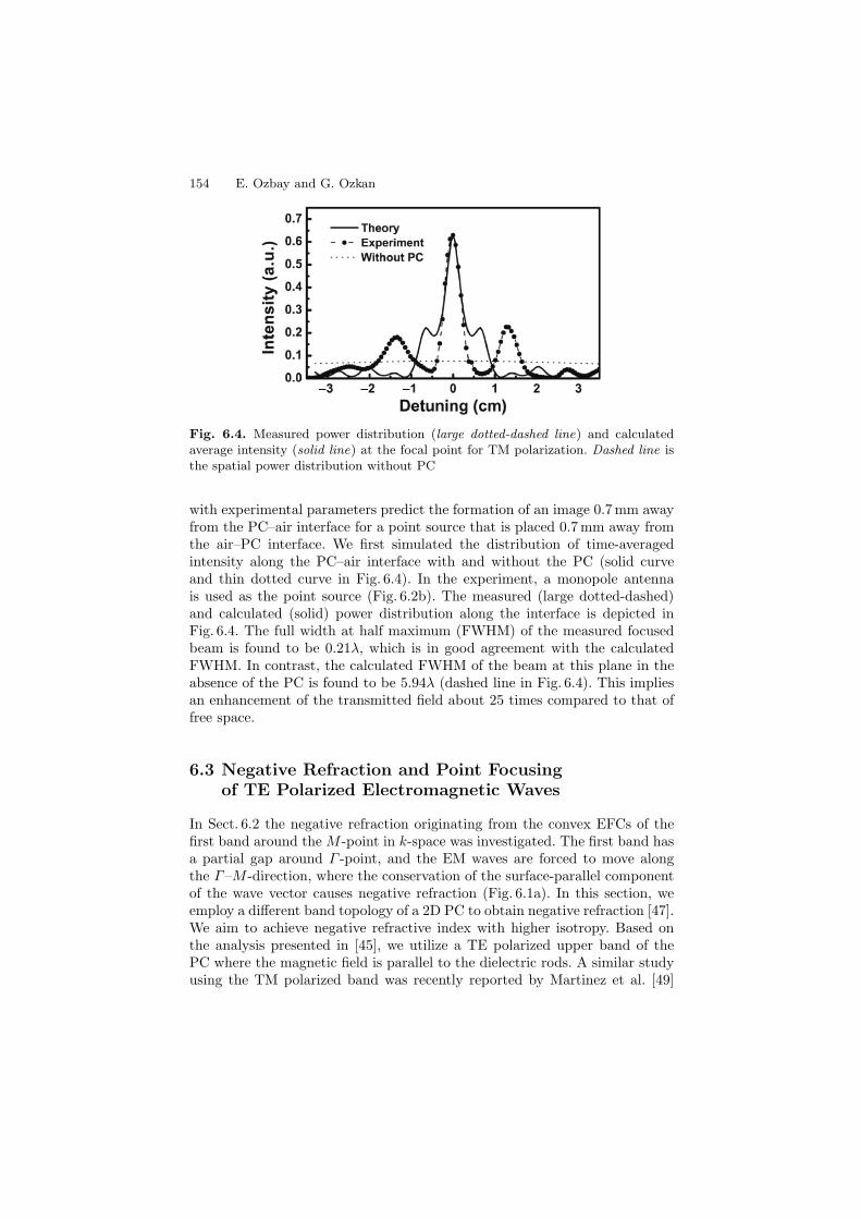
154 E. Ozbay and G. Ozkan
Fig. 6.4. Measured power distribution (large dotted-dashed line) and calculatedaverage intensity (solid line) at the focal point for TM polarization. Dashed line isthe spatial power distribution without PC
with experimental parameters predict the formation of an image 0.7 mm awayfrom the PC–air interface for a point source that is placed 0.7 mm away fromthe air–PC interface. We first simulated the distribution of time-averagedintensity along the PC–air interface with and without the PC (solid curveand thin dotted curve in Fig. 6.4). In the experiment, a monopole antennais used as the point source (Fig. 6.2b). The measured (large dotted-dashed)and calculated (solid) power distribution along the interface is depicted inFig. 6.4. The full width at half maximum (FWHM) of the measured focusedbeam is found to be 0.21λ, which is in good agreement with the calculatedFWHM. In contrast, the calculated FWHM of the beam at this plane in theabsence of the PC is found to be 5.94λ (dashed line in Fig. 6.4). This impliesan enhancement of the transmitted field about 25 times compared to that offree space.
6.3 Negative Refraction and Point Focusingof TE Polarized Electromagnetic Waves
In Sect. 6.2 the negative refraction originating from the convex EFCs of thefirst band around the M -point in k-space was investigated. The first band hasa partial gap around Γ -point, and the EM waves are forced to move alongthe Γ–M -direction, where the conservation of the surface-parallel componentof the wave vector causes negative refraction (Fig. 6.1a). In this section, weemploy a different band topology of a 2D PC to obtain negative refraction [47].We aim to achieve negative refractive index with higher isotropy. Based onthe analysis presented in [45], we utilize a TE polarized upper band of thePC where the magnetic field is parallel to the dielectric rods. A similar studyusing the TM polarized band was recently reported by Martinez et al. [49]
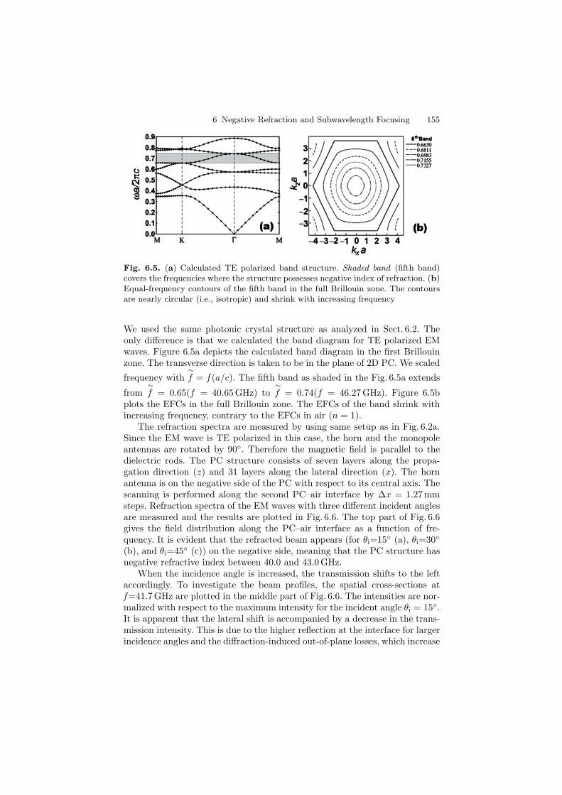
6 Negative Refraction and Subwavelength Focusing 155
Fig. 6.5. (a) Calculated TE polarized band structure. Shaded band (fifth band)covers the frequencies where the structure possesses negative index of refraction. (b)Equal-frequency contours of the fifth band in the full Brillouin zone. The contoursare nearly circular (i.e., isotropic) and shrink with increasing frequency
We used the same photonic crystal structure as analyzed in Sect. 6.2. Theonly difference is that we calculated the band diagram for TE polarized EMwaves. Figure 6.5a depicts the calculated band diagram in the first Brillouinzone. The transverse direction is taken to be in the plane of 2D PC. We scaled
frequency with∼f = f(a/c). The fifth band as shaded in the Fig. 6.5a extends
from∼f = 0.65(f = 40.65GHz) to
∼f = 0.74(f = 46.27GHz). Figure 6.5b
plots the EFCs in the full Brillouin zone. The EFCs of the band shrink withincreasing frequency, contrary to the EFCs in air (n = 1).
The refraction spectra are measured by using same setup as in Fig. 6.2a.Since the EM wave is TE polarized in this case, the horn and the monopoleantennas are rotated by 90. Therefore the magnetic field is parallel to thedielectric rods. The PC structure consists of seven layers along the propa-gation direction (z) and 31 layers along the lateral direction (x). The hornantenna is on the negative side of the PC with respect to its central axis. Thescanning is performed along the second PC–air interface by ∆x = 1.27mmsteps. Refraction spectra of the EM waves with three different incident anglesare measured and the results are plotted in Fig. 6.6. The top part of Fig. 6.6gives the field distribution along the PC–air interface as a function of fre-quency. It is evident that the refracted beam appears (for θi=15 (a), θi=30
(b), and θi=45 (c)) on the negative side, meaning that the PC structure hasnegative refractive index between 40.0 and 43.0 GHz.
When the incidence angle is increased, the transmission shifts to the leftaccordingly. To investigate the beam profiles, the spatial cross-sections atf =41.7 GHz are plotted in the middle part of Fig. 6.6. The intensities are nor-malized with respect to the maximum intensity for the incident angle θi = 15.It is apparent that the lateral shift is accompanied by a decrease in the trans-mission intensity. This is due to the higher reflection at the interface for largerincidence angles and the diffraction-induced out-of-plane losses, which increase
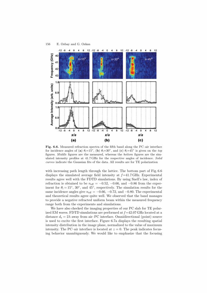
156 E. Ozbay and G. Ozkan
Fig. 6.6. Measured refraction spectra of the fifth band along the PC–air interfacefor incidence angles of (a) θi=15, (b) θi=30, and (c) θi=45 is given on the topfigures. Middle figures are the measured, whereas the bottom figures are the sim-ulated intensity profiles at 41.7 GHz for the respective angles of incidence. Solidcurves indicate the Gaussian fits of the data. All results are for TE polarization
with increasing path length through the lattice. The bottom part of Fig. 6.6displays the simulated average field intensity at f =41.7 GHz. Experimentalresults agree well with the FDTD simulations. By using Snell’s law, index ofrefraction is obtained to be neff = −0.52, −0.66, and −0.86 from the exper-iment for θi = 15, 30, and 45, respectively. The simulation results for thesame incidence angles give neff = −0.66, −0.72, and −0.80. The experimentaland theoretical results agree quite well. We observed that the band managesto provide a negative refracted uniform beam within the measured frequencyrange both from the experiments and simulations.
We have also checked the imaging properties of our PC slab for TE polar-ized EM waves. FDTD simulations are performed at f =42.07 GHz located at adistance ds = 2λ away from air–PC interface. Omnidirectional (point) sourceis used to excite the first interface. Figure 6.7a displays the resulting spatialintensity distribution in the image plane, normalized to the value of maximumintensity. The PC–air interface is located at z = 0. The peak indicates focus-ing behavior unambiguously. We would like to emphasize that the focusing
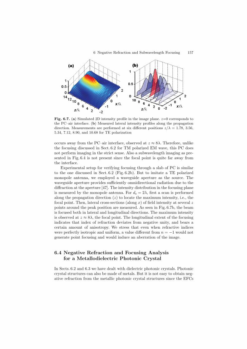
6 Negative Refraction and Subwavelength Focusing 157
Fig. 6.7. (a) Simulated 2D intensity profile in the image plane. z=0 corresponds tothe PC–air interface. (b) Measured lateral intensity profiles along the propagationdirection. Measurements are performed at six different positions z/λ = 1.78, 3.56,5.34, 7.12, 8.90, and 10.68 for TE polarization
occurs away from the PC–air interface, observed at z ≈ 8λ. Therefore, unlikethe focusing discussed in Sect. 6.2 for TM polarized EM wave, this PC doesnot perform imaging in the strict sense. Also a subwavelength imaging as pre-sented in Fig. 6.4 is not present since the focal point is quite far away fromthe interface.
Experimental setup for verifying focusing through a slab of PC is similarto the one discussed in Sect. 6.2 (Fig. 6.2b). But to imitate a TE polarizedmonopole antenna, we employed a waveguide aperture as the source. Thewaveguide aperture provides sufficiently omnidirectional radiation due to thediffraction at the aperture [47]. The intensity distribution in the focusing planeis measured by the monopole antenna. For ds = 2λ, first a scan is performedalong the propagation direction (z) to locate the maximum intensity, i.e., thefocal point. Then, lateral cross-sections (along x) of field intensity at several zpoints around the peak position are measured. As seen in Fig. 6.7b, the beamis focused both in lateral and longitudinal directions. The maximum intensityis observed at z ≈ 8λ, the focal point. The longitudinal extent of the focusingindicates that index of refraction deviates from negative unity, and bears acertain amount of anisotropy. We stress that even when refractive indiceswere perfectly isotropic and uniform, a value different from n = −1 would notgenerate point focusing and would induce an aberration of the image.
6.4 Negative Refraction and Focusing Analysisfor a Metallodielectric Photonic Crystal
In Sects. 6.2 and 6.3 we have dealt with dielectric photonic crystals. Photoniccrystal structures can also be made of metals. But it is not easy to obtain neg-ative refraction from the metallic photonic crystal structures since the EFCs

158 E. Ozbay and G. Ozkan
of the metallic PCs are larger than the EFCs of air. Luo et al. theoreticallydemonstrated that it is indeed possible to obtain all-angle negative refractionby embedding metallic rods into a high-dielectric constant medium [44]. Themain idea for using a medium with high dielectric permittivity is to increasethe effective index of the photonic crystal. The advantage is that the EFCswill be lowered in frequency but the area occupied by EFCs in k space will notchange. Following this basic idea, we used a different approach for constructingthe PC structure. Instead of embedding metallic rods into a high-dielectricmedium, we combined dielectric rods and metallic rods together to form ametallodielectric PC. Metallodielectric PC could be considered as a metallicPC with a periodic dielectric perturbation. Positive dielectric constant is anattractive perturbation and causes lowering the frequency of the bands [50].
The metallodielectric photonic crystal is a square lattice of metallic anddielectric rods where the basis of the PC consists of a metallic and a dielectricrod placed along the diagonal of the square unit cell as given in the inset ofFig. 6.8b. Cylindrical alumina rods with a radius of 1.55 mm are used as thedielectric rods with ε = 9.61. The metallic rods are made of aluminum andhave a radius of 1.5 mm. Both the metallic and dielectric rods have a heightof 150 mm.
We have computed the band diagrams of the metallic photonic crystal(Fig. 6.8a) and metallodielectric photonic crystal (Fig. 6.8b) for TM polar-ized EM waves. The radius of the dielectric rod is 0.136a, and the radius
Fig. 6.8. (a) Calculated TM-polarized bands for the metallic photonic crystal, and(b) the metallodielectric crystal. (c) Equal-frequency contours (solid curves) areshown for the metallodielectric PC. Dotted circle is the free-space equal-frequencycontour at 9.5 GHz. Free-space wave vector (black dashed arrow), free-space groupvelocity (black solid arrow), wave vector of the refracted waves in the PC (whitedashed arrow), group velocity inside the PC (white solid arrow) are drawn
6 Negative Refraction and Subwavelength Focusing 159
of the metallic rod is 0.14a, where a is the lattice constant and is equal to11.0 mm. Lattice constant is taken to be same in both structures. By compar-ing Fig. 6.8a and b we can conclude that the bands of the metallodielectric pho-tonic crystal are lowered in frequency compared to the bands of the metallicphotonic crystal.
Equal-frequency contours of the metallodielectric PC for TM polarizationover the first Brillouin zone is plotted in Fig. 6.8c. The dotted circle is theEFC of air. The PC surface is aligned such that the normal vector to the air–PC interface is along the ΓM direction. Since the surface-parallel componentof the wave vector is conserved, the wave vectors of the refracted beam caneasily be obtained, as given in the figure. The group velocity of the incidentwaves and the group velocity of the transmitted waves fall on opposite sidesof the surface normal. Therefore the incident waves are negatively refracted[34]. For the plotted EFCs, the magnitude of the largest surface-parallel wavevector component in air is smaller than the largest surface-parallel wave vectorcomponent in the photonic crystal. The range of incidence angles that arenegatively refracted can be increased by lowering the bands without modifyingthe lattice parameters [50].
The electric field intensities are measured along the PC–air interface todemonstrate the negative refraction experimentally. The measurement methodis same with the measurements indicated in the previous sections (Fig. 6.2a).Waves that are positively refracted are expected to emerge from the positiveside of the surface, whereas negatively refracted waves are to emerge from thenegative side. Measurement results for incidence angles of θi=15, 25, 35,and 45 are provided in Fig. 6.9a–d, respectively. Between the frequencies9.20 and 10.30 GHz waves exit from the negative side of the PC meaning thatEM waves are negatively refracted by the PC in this frequency range. Up to9.20 GHz the waves are positively refracted.
We have also performed FDTD simulations to see how the EM wave isrefracted by the metallodielectric PC. We have sent an incident Gaussianbeam to the air–PC interface and calculated electric field intensities insideand outside the PC at 9.70 GHz. The simulation results for two different inci-dent angles θi=15 (Fig. 6.10a) and θi=45 (Fig. 6.10b) clearly show that thenegative refraction takes place at this frequency. The effect of reflection isalso clear in this picture. For higher incident angle the intensity (therefore thetransmission) is lower due to the high reflections from the air–PC interface.Note that 9.70 GHz is in the negative refraction frequency regime as calculatedfrom the EFCs (Fig. 6.8c).
We have compared the experimental and theoretical results of the val-ues of refractive indices at θi=25 incidence angle in Fig. 6.11. Between9.00 and 9.19 GHz the refractive indices are found to be positive. Around9.20 GHz there is an abrupt change in the values and the sign of the indexof refraction. In the close vicinity of 9.20 GHz the indices of refraction arefound to be high, +18 and −12 due to the flatness of EFS contours around9.20 GHz (Fig. 6.8c). The refractive indices are negative in the frequency range
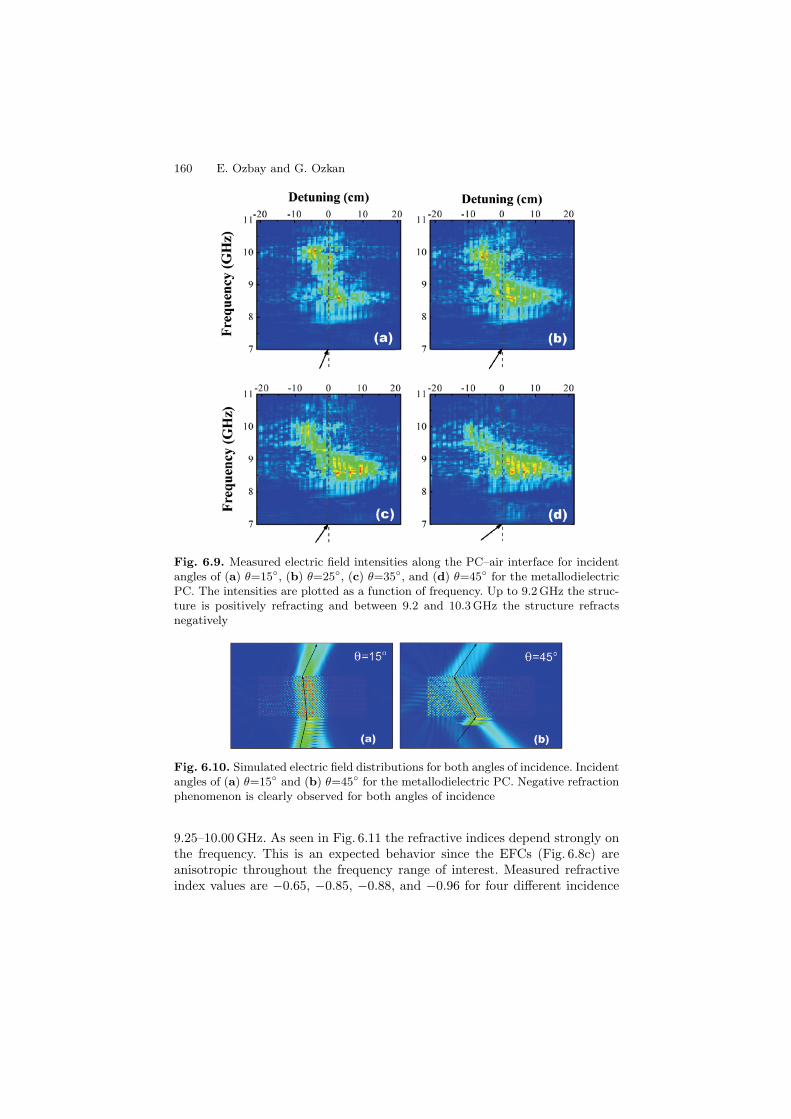
160 E. Ozbay and G. Ozkan
Fig. 6.9. Measured electric field intensities along the PC–air interface for incidentangles of (a) θ=15, (b) θ=25, (c) θ=35, and (d) θ=45 for the metallodielectricPC. The intensities are plotted as a function of frequency. Up to 9.2 GHz the struc-ture is positively refracting and between 9.2 and 10.3 GHz the structure refractsnegatively
Fig. 6.10. Simulated electric field distributions for both angles of incidence. Incidentangles of (a) θ=15 and (b) θ=45 for the metallodielectric PC. Negative refractionphenomenon is clearly observed for both angles of incidence
9.25–10.00 GHz. As seen in Fig. 6.11 the refractive indices depend strongly onthe frequency. This is an expected behavior since the EFCs (Fig. 6.8c) areanisotropic throughout the frequency range of interest. Measured refractiveindex values are −0.65, −0.85, −0.88, and −0.96 for four different incidence
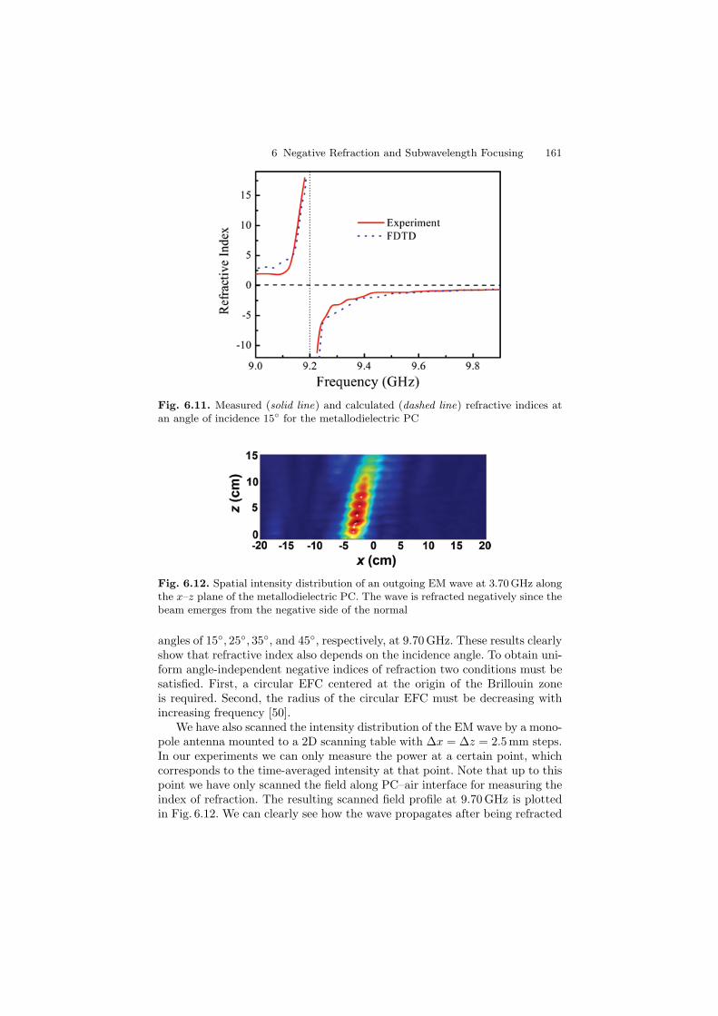
6 Negative Refraction and Subwavelength Focusing 161
Fig. 6.11. Measured (solid line) and calculated (dashed line) refractive indices atan angle of incidence 15 for the metallodielectric PC
Fig. 6.12. Spatial intensity distribution of an outgoing EM wave at 3.70 GHz alongthe x–z plane of the metallodielectric PC. The wave is refracted negatively since thebeam emerges from the negative side of the normal
angles of 15, 25, 35, and 45, respectively, at 9.70 GHz. These results clearlyshow that refractive index also depends on the incidence angle. To obtain uni-form angle-independent negative indices of refraction two conditions must besatisfied. First, a circular EFC centered at the origin of the Brillouin zoneis required. Second, the radius of the circular EFC must be decreasing withincreasing frequency [50].
We have also scanned the intensity distribution of the EM wave by a mono-pole antenna mounted to a 2D scanning table with ∆x = ∆z = 2.5mm steps.In our experiments we can only measure the power at a certain point, whichcorresponds to the time-averaged intensity at that point. Note that up to thispoint we have only scanned the field along PC–air interface for measuring theindex of refraction. The resulting scanned field profile at 9.70 GHz is plottedin Fig. 6.12. We can clearly see how the wave propagates after being refracted
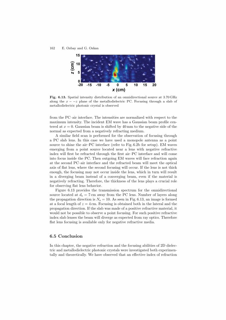
162 E. Ozbay and G. Ozkan
Fig. 6.13. Spatial intensity distribution of an omnidirectional source at 3.70 GHzalong the x − −z plane of the metallodielectric PC. Focusing through a slab ofmetallodielectric photonic crystal is observed
from the PC–air interface. The intensities are normalized with respect to themaximum intensity. The incident EM wave has a Gaussian beam profile cen-tered at x = 0. Gaussian beam is shifted by 40 mm to the negative side of thenormal as expected from a negatively refracting medium.
A similar field scan is performed for the observation of focusing througha PC slab lens. In this case we have used a monopole antenna as a pointsource to shine the air–PC interface (refer to Fig. 6.2b for setup). EM wavesemerging from a point source located near a lens with negative refractiveindex will first be refracted through the first air–PC interface and will comeinto focus inside the PC. Then outgoing EM waves will face refraction againat the second PC–air interface and the refracted beam will meet the opticalaxis of flat lens, where the second focusing will occur. If the lens is not thickenough, the focusing may not occur inside the lens, which in turn will resultin a diverging beam instead of a converging beam, even if the material isnegatively refracting. Therefore, the thickness of the lens plays a crucial rolefor observing flat lens behavior.
Figure 6.13 provides the transmission spectrum for the omnidirectionalsource located at ds = 7 cm away from the PC lens. Number of layers alongthe propagation direction is Nz = 10. As seen in Fig. 6.13, an image is formedat a focal length of z = 4 cm. Focusing is obtained both in the lateral and thepropagation direction. If the slab was made of a positive refractive material, itwould not be possible to observe a point focusing. For such positive refractiveindex slab lenses the beam will diverge as expected from ray optics. Thereforeflat lens focusing is available only for negative refractive media.
6.5 Conclusion
In this chapter, the negative refraction and the focusing abilities of 2D dielec-tric and metallodielectric photonic crystals were investigated both experimen-tally and theoretically. We have observed that an effective index of refraction
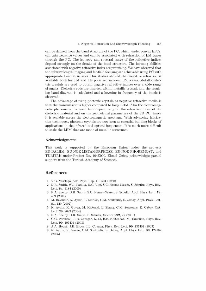
6 Negative Refraction and Subwavelength Focusing 163
can be defined from the band structure of the PC, which, under convex EFCs,can take negative values and can be associated with refraction of EM wavesthrough the PC. The isotropy and spectral range of the refractive indicesdepend strongly on the details of the band structure. The focusing abilitiesassociated with negative refractive index are promising. We have observed thatthe subwavelength imaging and far-field focusing are achievable using PC withappropriate band structures. Our studies showed that negative refraction isavailable both for TM and TE polarized incident EM waves. Metallodielec-tric crystals are used to obtain negative refractive indices over a wide rangeof angles. Dielectric rods are inserted within metallic crystal, and the result-ing band diagram is calculated and a lowering in frequency of the bands isobserved.
The advantage of using photonic crystals as negative refractive media isthat the transmission is higher compared to lossy LHM. Also the electromag-netic phenomena discussed here depend only on the refractive index of thedielectric material and on the geometrical parameters of the 2D PC, henceit is scalable across the electromagnetic spectrum. With advancing fabrica-tion techniques, photonic crystals are now seen as essential building blocks ofapplications in the infrared and optical frequencies. It is much more difficultto scale the LHM that are made of metallic structures.
Acknowledgments
This work is supported by the European Union under the projectsEU-DALHM, EU-NOE-METAMORPHOSE, EU-NOE-PHOREMOST, andTUBITAK under Project No. 104E090. Ekmel Ozbay acknowledges partialsupport from the Turkish Academy of Sciences.
References
1. V.G. Veselago, Sov. Phys. Usp. 10, 504 (1968)2. D.R. Smith, W.J. Padilla, D.C. Vier, S.C. Nemat-Nasser, S. Schultz, Phys. Rev.
Lett. 84, 4184 (2000)3. R.A. Shelby, D.R. Smith, S.C. Nemat-Nasser, S. Schultz, Appl. Phys. Lett. 78,
489 (2001)4. M. Bayindir, K. Aydin, P. Markos, C.M. Soukoulis, E. Ozbay, Appl. Phys. Lett.
81, 120 (2002)5. K. Aydin, K. Guven, M. Kafesaki, L. Zhang, C.M. Soukoulis, E. Ozbay, Opt.
Lett. 29, 2623 (2004)6. R.A. Shelby, D.R. Smith, S. Schultz, Science 292, 77 (2001)7. C.G. Parazzoli, R.B. Greegor, K. Li, B.E. Koltenbah, M. Tanielian, Phys. Rev.
Lett. 90, 107401 (2003)8. A.A. Houck, J.B. Brock, I.L. Chuang, Phys. Rev. Lett. 90, 137401 (2003)9. K. Aydin, K. Guven, C.M. Soukoulis, E. Ozbay, Appl. Phys. Lett. 86, 124102
(2005)

164 E. Ozbay and G. Ozkan
10. K. Aydin, I. Bulu, E. Ozbay, Opt. Express 13, 8753 (2005)11. J.B. Pendry, A.J. Holden, D.J. Robbins, W.J. Stewart, J. Phys. Condens. Matter
10, 4785 (1998)12. J.B. Pendry, A.J. Holden, D.J. Robbins, W.J. Stewart, IEEE Trans. Microw.
Theory Tech. 47, 2075 (1999)13. J.B. Pendry, Phys. Rev. Lett. 85, 3966 (2000)14. E. Yablonovitch, Phys. Rev. Lett. 58, 2059 (1987)15. S. John, Phys. Rev. Lett. 58, 2486 (1987)16. J.D. Joannopoulos, R.D. Meade, J.N. Winn, Photonic Crystals: Molding the
Flow of Light (Princeton University Press, Princeton, NJ, 1995)17. C.M. Soukoulis (ed.), Photonic Crystals and Light Localization in the 21st Cen-
tury (Kluwer, Norwell, MA, 2001)18. K. Sakoda, Optical Properties of Photonic Crystals (Springer, Berlin Heidelberg
New York, 2001)19. E. Ozbay, G. Tuttle, R. Biswas, K.M. Ho, J. Bostak, D.M. Bloom, Appl. Phys.
Lett. 65, 1617 (1994)20. E. Ozbay, B. Temelkuran, Appl. Phys. Lett. 69, 743 (1996)21. A. Mekis, J.C. Chen, I. Kurland, S. Fan, P.R. Villeneuve, and J.D. Joannapoulos,
Phys. Rev. Lett. 77, 3787 (1996)22. P.R. Villeneuve, D.S. Abrams, S. Fan, J.D. Joannopoulos, Opt. Lett. 21, 2017
(1996)23. B. Temelkuran, E. Ozbay, J.P. Kavanaugh, G. Tuttle, K.M. Ho, Appl. Phys.
Lett. 72, 2376 (1998)24. H. Kosaka, T. Kawashima, A. Tomita, M. Notomi, T. Tamamura, T. Sato, S.
Kawakamib, Appl. Phys. Lett. 74, 1370 (1999)25. M. Bayindir, E. Ozbay, Phys Rev. B 62, R2247 (2000)26. M. Loncar, D. Nedeljkovic, T. Doll, J. Vuckovic, A. Scherer, T.P. Pearsall, Appl.
Phys. Lett. 77, 1937 (2000)27. S. Noda, M. Yokoyama, M. Imada, A. Chutinan, M. Mochizuki, Science 293,
1123 (2001)28. M. Bayindir, S. Tanriseven, E. Ozbay, Appl. Phys. A-Mater. Sci. Process. 72,
117 (2001)29. E. Ozbay, M. Bayindir, I. Bulu, E. Cubukcu, IEEE J. Quantum Electron. 38,
837 (2002)30. S. Enoch, B. Gralak, G. Tayeb, Appl. Phys. Lett. 81, 1588 (2002)31. M.F. Yanik, S. Fan, Phys. Rev. Lett. 92, 083901 (2004)32. B. Gralak, S. Enoch, G. Tayeb, J. Opt. Soc. Am. A 17, 1012 (2000)33. M. Notomi, Phys. Rev. B 62, 10696 (2000)34. C. Luo, S.G. Johnson, J.D. Joannopoulos, J.B. Pendry, Phys. Rev. B 65, 201104
(2002)35. S. Foteinopoulou, E.N. Economou, C.M. Soukoulis, Phys. Rev. Lett. 90, 107402
(2003)36. E. Cubukcu, K. Aydin, E. Ozbay, S. Foteinopoulou, C.M. Soukoulis, Nature
423, 604 (2003)37. P.V. Parimi, W.T. Lu, P. Vodo, J. Sokoloff, J.S. Derov, S. Sridhar, Phys. Rev.
Lett. 92, 127401 (2004)38. A. Berrier, M. Mulot, M. Swillo, M. Qiu, L. Thylen, A. Talneau, S. Anand,
Phys. Rev. Lett. 93, 073902 (2004)39. H. Kosaka, T. Kawashima, A. Tomita, M. Notomi, T. Tamamura, T. Sato, S.
Kawakami, Phys. Rev. B 58, R10096 (1998)

6 Negative Refraction and Subwavelength Focusing 165
40. S. Foteinopoulou, C.M. Soukoulis, Phys. Rev. B 67, 235107 (2003)41. E. Cubukcu, K. Aydin, E. Ozbay, S. Foteinopoulou, C.M. Soukoulis, Phys. Rev.
Lett. 91, 207401 (2003)42. P.V. Parimi, W.T. Lu, P. Vodo, S. Sridhar, Nature 426, 404 (2003)43. C. Luo, S.G. Johnson, J.D. Joannopoulos, J.B. Pendry, Phys. Rev. B 68, 045115
(2003)44. C. Luo, S.G. Johnson, J.D. Joannopoulos, J.B. Pendry, Opt. Express 11, 746
(2003)45. S. Foteinopoulou, C.M. Soukoulis, Phys. Rev. B 72, 165112 (2005)46. R. Moussa, S. Foteinopoulou, L. Zhang, G. Tuttle, K. Guven, E. Ozbay, C.M.
Soukoulis, Phys. Rev. B 71, 085106 (2005)47. K. Guven, K. Aydin, K.B. Alici, C.M. Soukoulis, E. Ozbay, Phys. Rev. B 70,
205125 (2004)48. E. Ozbay, K. Guven, E. Cubukcu, K. Aydin, B.K. Alici, Mod. Phys. Lett. B 18,
1275 (2004)49. A. Martınez, H. Mıguez, A. Griol, J. Martı, Phys. Rev. B 69, 165119 (2004)50. I. Bulu, H. Caglayan, E. Ozbay, Phys. Rev. B 72, 045125 (2005)51. P. Vodo, P.V. Parimi, W.T. Lu, S. Sridhar, R. Wing, Appl. Phys. Lett. 85, 1858
(2005)52. P. Vodo, P.V. Parimi, W.T. Lu, S. Sridhar, Appl. Phys. Lett. 86, 201108 (2005)
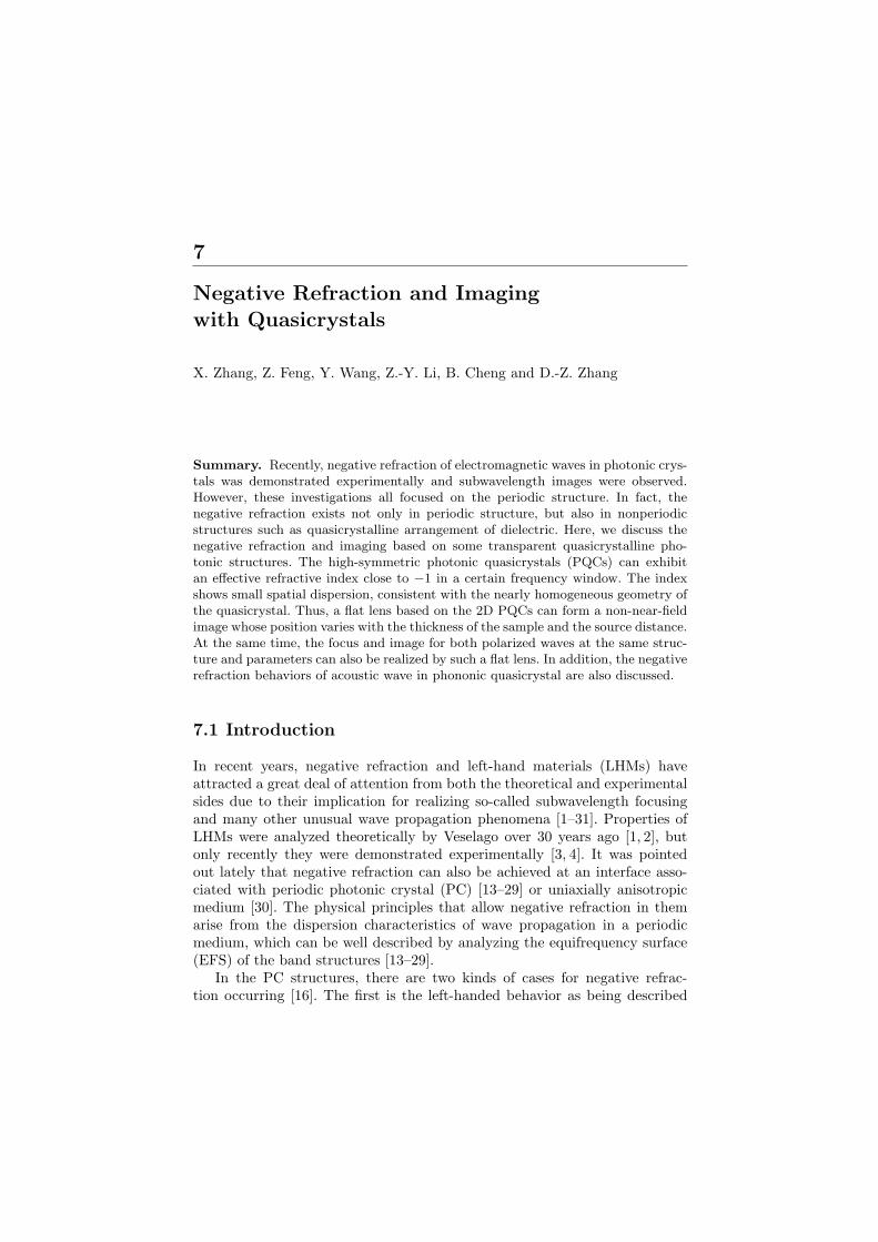
7
Negative Refraction and Imagingwith Quasicrystals
X. Zhang, Z. Feng, Y. Wang, Z.-Y. Li, B. Cheng and D.-Z. Zhang
Summary. Recently, negative refraction of electromagnetic waves in photonic crys-tals was demonstrated experimentally and subwavelength images were observed.However, these investigations all focused on the periodic structure. In fact, thenegative refraction exists not only in periodic structure, but also in nonperiodicstructures such as quasicrystalline arrangement of dielectric. Here, we discuss thenegative refraction and imaging based on some transparent quasicrystalline pho-tonic structures. The high-symmetric photonic quasicrystals (PQCs) can exhibitan effective refractive index close to −1 in a certain frequency window. The indexshows small spatial dispersion, consistent with the nearly homogeneous geometry ofthe quasicrystal. Thus, a flat lens based on the 2D PQCs can form a non-near-fieldimage whose position varies with the thickness of the sample and the source distance.At the same time, the focus and image for both polarized waves at the same struc-ture and parameters can also be realized by such a flat lens. In addition, the negativerefraction behaviors of acoustic wave in phononic quasicrystal are also discussed.
7.1 Introduction
In recent years, negative refraction and left-hand materials (LHMs) haveattracted a great deal of attention from both the theoretical and experimentalsides due to their implication for realizing so-called subwavelength focusingand many other unusual wave propagation phenomena [1–31]. Properties ofLHMs were analyzed theoretically by Veselago over 30 years ago [1, 2], butonly recently they were demonstrated experimentally [3, 4]. It was pointedout lately that negative refraction can also be achieved at an interface asso-ciated with periodic photonic crystal (PC) [13–29] or uniaxially anisotropicmedium [30]. The physical principles that allow negative refraction in themarise from the dispersion characteristics of wave propagation in a periodicmedium, which can be well described by analyzing the equifrequency surface(EFS) of the band structures [13–29].
In the PC structures, there are two kinds of cases for negative refrac-tion occurring [16]. The first is the left-handed behavior as being described
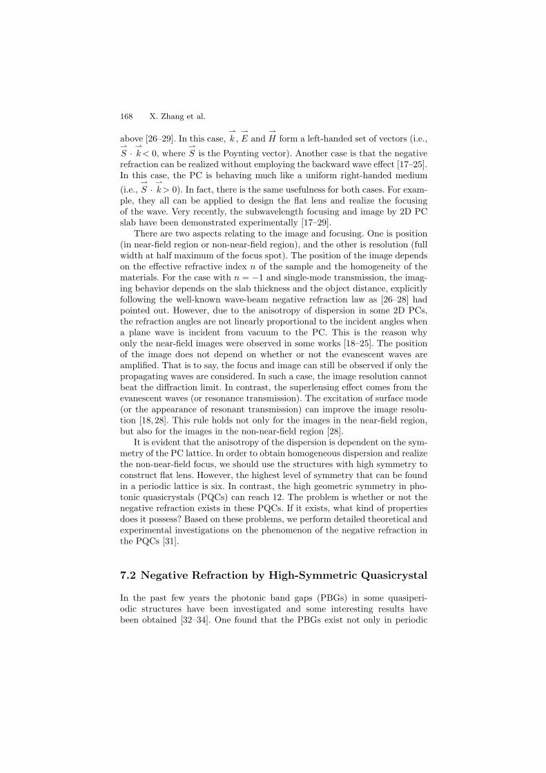
168 X. Zhang et al.
above [26–29]. In this case,
k ,
E and
H form a left-handed set of vectors (i.e.,
S ·
k< 0, where
S is the Poynting vector). Another case is that the negativerefraction can be realized without employing the backward wave effect [17–25].In this case, the PC is behaving much like a uniform right-handed medium
(i.e.,
S ·
k> 0). In fact, there is the same usefulness for both cases. For exam-ple, they all can be applied to design the flat lens and realize the focusingof the wave. Very recently, the subwavelength focusing and image by 2D PCslab have been demonstrated experimentally [17–29].
There are two aspects relating to the image and focusing. One is position(in near-field region or non-near-field region), and the other is resolution (fullwidth at half maximum of the focus spot). The position of the image dependson the effective refractive index n of the sample and the homogeneity of thematerials. For the case with n = −1 and single-mode transmission, the imag-ing behavior depends on the slab thickness and the object distance, explicitlyfollowing the well-known wave-beam negative refraction law as [26–28] hadpointed out. However, due to the anisotropy of dispersion in some 2D PCs,the refraction angles are not linearly proportional to the incident angles whena plane wave is incident from vacuum to the PC. This is the reason whyonly the near-field images were observed in some works [18–25]. The positionof the image does not depend on whether or not the evanescent waves areamplified. That is to say, the focus and image can still be observed if only thepropagating waves are considered. In such a case, the image resolution cannotbeat the diffraction limit. In contrast, the superlensing effect comes from theevanescent waves (or resonance transmission). The excitation of surface mode(or the appearance of resonant transmission) can improve the image resolu-tion [18, 28]. This rule holds not only for the images in the near-field region,but also for the images in the non-near-field region [28].
It is evident that the anisotropy of the dispersion is dependent on the sym-metry of the PC lattice. In order to obtain homogeneous dispersion and realizethe non-near-field focus, we should use the structures with high symmetry toconstruct flat lens. However, the highest level of symmetry that can be foundin a periodic lattice is six. In contrast, the high geometric symmetry in pho-tonic quasicrystals (PQCs) can reach 12. The problem is whether or not thenegative refraction exists in these PQCs. If it exists, what kind of propertiesdoes it possess? Based on these problems, we perform detailed theoretical andexperimental investigations on the phenomenon of the negative refraction inthe PQCs [31].
7.2 Negative Refraction by High-Symmetric Quasicrystal
In the past few years the photonic band gaps (PBGs) in some quasiperi-odic structures have been investigated and some interesting results havebeen obtained [32–34]. One found that the PBGs exist not only in periodic
7 Negative Refraction and Imaging with Quasicrystals 169
(a)
(c)
(b)
(d)
Fig. 7.1. Schemes of the basic quasicrystal structures. (a) 12-fold quasicrystal with arandom square–triangle tiling system. (b) 12-fold quasicrystal with a general rotatedsymmetry. (c) tenfold quasicrystal. (d) eightfold quasicrystal
structures, but also in some quasiperiodic structures. In contrast to the PBGs,in this chapter we investigate the transport properties of electromagnetic wavein the band region of the high-symmetric PQC. According to the level of sym-metry, the PQCs can be divided into fivefold, eightfold, tenfold, and 12-foldstructures. Figure 7.1a, b describes two kinds of structure with 12-fold sym-metry. The PQC structures with eightfold and tenfold symmetry are shownin Fig. 7.1c, d, respectively.
We first consider the 12-fold PQC based on a random square–triangle tilingsystem which is shown in the Fig. 7.1a. We have fabricated the 12-fold PQCsamples. The samples consist of a number of dielectric cylinders with dielectricconstant 8.6 and radii 3.0 mm embedded in a styrofoam template with a latticeconstant of a = 10mm. In order to gain understanding of the band andgap regions for the electromagnetic wave transport in such a quasiperiodicstructure, we first explore the transmission spectrum. A rectangular sample110 mm thick and 400 mm wide was made for microwave measurements. Themeasurements were carried out in a wide scattering chamber by using anHP8757E scalar network analyzer and an HP8364A series synthesized sweeper,which was similar to our previous experimental setup [34]. The measuredtransmission data for the above sample are plotted in Fig. 7.2 by the dottedline. In all our measurements the electric field is kept parallel to the cylinders.The wave incident on the cylinders with normal direction, and the lengths ofthe cylinders are 100 times as big as their radii. Thus, such a system can betheoretically regarded as a two-dimensional PC consisting of infinite-lengthcylinders embodied in the styrofoam background. The solid line represents thenumerical results obtained by the multiple-scattering method [23,28].
170 X. Zhang et al.
10 12 14−80
−70
−60
−50
−40
−30
−20
−10
0
10
Tra
nsm
issi
on(d
B)
Frequency (GHZ)
2 4 6 8
Fig. 7.2. The measured (dotted lines) and calculated (solid lines) transmissioncoefficients for the 12-fold quasicrystal with a random square–triangle tiling system.The lattice constant of the system is a = 10mm. The radii and the dielectric constantof the dielectric cylinder are 3.0 mm and 8.6, respectively
The multiple-scattering method is best suited for a finite collection of cylin-ders with a continuous incident wave of fixed frequency. For circular cylinders,the scattering property of the individual cylinder can be obtained analyti-cally, relating the scattered fields to the incident fields. The total field, whichincludes the incident plus the multiple-scattered field, can then be obtainedby solving a linear system of equations, whose size is proportional to the num-ber of cylinders in the system. Both the near-field and the far-field radiationpatterns can be obtained straightforwardly. So, such a method is a very effi-cient way of handling the scattering problem of a finite sample containingcylinders of circular cross-sections, which should be regarded as exact numer-ical simulation. Comparing the solid line with the dotted line, we find thatexcellent agreement between the measured and calculated results is apparent.Both results show one gap and two bands between the frequency f = 5.0and 14 GHz. Because we aim at the refraction feature of wave transport inthe quasicrystal structure, in the following we focus our measurement on theband region.
To study the refraction behavior of wave transport through thequasicrystal–air interface, we have fabricated some wedge samples withdifferent shapes characterized by the wedge angle θ0. In experiment, all thewedge samples always have the left surface kept perpendicular to the incidentdirection in order to avoid multiple refraction. A θ0 = 30 wedge sampleis schematically shown in the inset of Fig. 7.3a. When a slit wave beam of
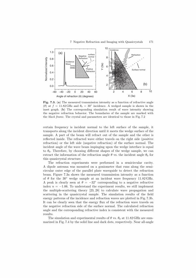
7 Negative Refraction and Imaging with Quasicrystals 171
−60 −40 −20 0 20 40 60
0.0
0.2
0.4
0.6
0.8
1.0 (a)
Nor
mal
ized
inte
nsity
Angle of refraction (θ) (degrees)
surface normal
Incidence Wave
Negative Refraction
PositiveRefraction
2 4 6 8 10
2
4
6
8
10
(b)
Surface normal
Refraction
Incidence
X (3a)
Y (
3a)
Fig. 7.3. (a) The measured transmission intensity as a function of refractive angle(θ) at f = 11.82 GHz and θ0 = 30 incidence. A wedged sample is shown in theinset graph. (b) The corresponding simulation result of wave intensity showingthe negative refraction behavior. The boundaries of the sample are marked withthe black frame. The crystal and parameters are identical to those in Fig. 7.2
certain frequency is incident normal to the left surface of the sample, ittransports along the incident direction until it meets the wedge surface of thesample. A part of the beam will refract out of the sample and the other isreflected inside. The refracted wave either travels on the right side (positiverefraction) or the left side (negative refraction) of the surface normal. Theincident angle of the wave beam impinging upon the wedge interface is equalto θ0. Therefore, by choosing different shapes of the wedge sample, we canextract the information of the refraction angle θ vs. the incident angle θ0 forthis quasicrystal structure.
The refraction experiments were performed in a semicircular cavity.A dipole antenna was mounted on a goniometer that runs along the semi-circular outer edge of the parallel plate waveguide to detect the refractionbeam. Figure 7.3a shows the measured transmission intensity as a functionof θ for the 30 wedge sample at an incident wave frequency 11.82 GHz.A peak is clearly seen at θ = −32 corresponding to a negative refractiveindex n = −1.06. To understand the experiment results, we still implementthe multiple-scattering theory [23, 28] to calculate wave propagation andscattering in the quasicrystal sample. The simulation results of the fieldenergy patterns of the incidence and refraction waves are plotted in Fig. 7.3b.It can be clearly seen that the energy flux of the refraction wave travels onthe negative refraction side of the surface normal. The calculated refractionangle and the corresponding refractive index is consistent with the measuredresults.
The simulation and experimental results of θ vs. θ0 at 11.82 GHz are sum-marized in Fig. 7.4 by the solid line and dark dots, respectively. Near all-angle
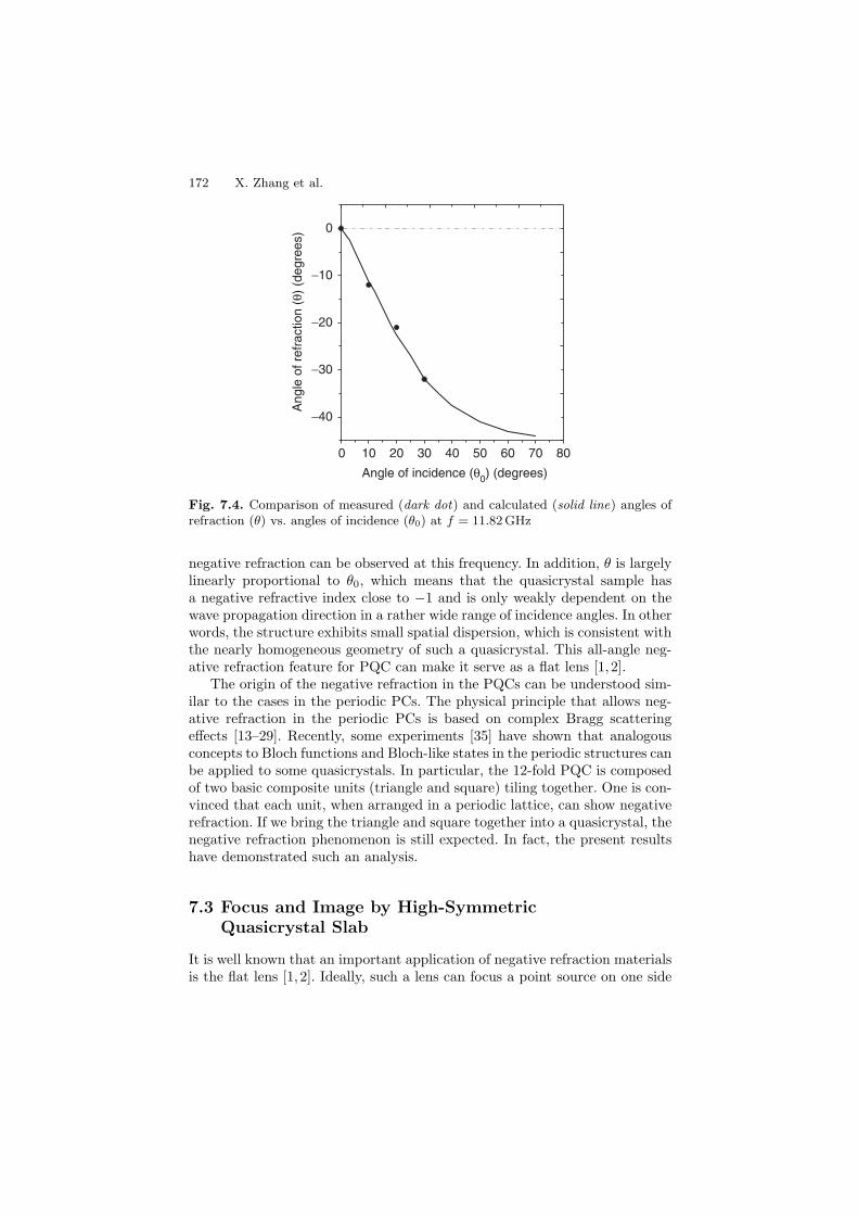
172 X. Zhang et al.
−40
−30
−20
−10
0
Ang
le o
f ref
ract
ion
(θ)
(deg
rees
)
Angle of incidence (θ0) (degrees)
0 10 20 30 40 50 60 70 80
Fig. 7.4. Comparison of measured (dark dot) and calculated (solid line) angles ofrefraction (θ) vs. angles of incidence (θ0) at f = 11.82 GHz
negative refraction can be observed at this frequency. In addition, θ is largelylinearly proportional to θ0, which means that the quasicrystal sample hasa negative refractive index close to −1 and is only weakly dependent on thewave propagation direction in a rather wide range of incidence angles. In otherwords, the structure exhibits small spatial dispersion, which is consistent withthe nearly homogeneous geometry of such a quasicrystal. This all-angle neg-ative refraction feature for PQC can make it serve as a flat lens [1, 2].
The origin of the negative refraction in the PQCs can be understood sim-ilar to the cases in the periodic PCs. The physical principle that allows neg-ative refraction in the periodic PCs is based on complex Bragg scatteringeffects [13–29]. Recently, some experiments [35] have shown that analogousconcepts to Bloch functions and Bloch-like states in the periodic structures canbe applied to some quasicrystals. In particular, the 12-fold PQC is composedof two basic composite units (triangle and square) tiling together. One is con-vinced that each unit, when arranged in a periodic lattice, can show negativerefraction. If we bring the triangle and square together into a quasicrystal, thenegative refraction phenomenon is still expected. In fact, the present resultshave demonstrated such an analysis.
7.3 Focus and Image by High-SymmetricQuasicrystal Slab
It is well known that an important application of negative refraction materialsis the flat lens [1, 2]. Ideally, such a lens can focus a point source on one side
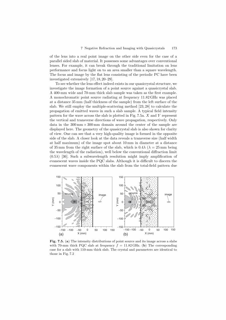
7 Negative Refraction and Imaging with Quasicrystals 173
of the lens into a real point image on the other side even for the case of aparallel sided slab of material. It possesses some advantages over conventionallenses. For example, it can break through the traditional limitation on lensperformance and focus light on to an area smaller than a square wavelength.The focus and image by the flat lens consisting of the periodic PC have beeninvestigated extensively [17,18,20–29].
To see whether the lens effect indeed exists in our quasicrystal structure, weinvestigate the image formation of a point source against a quasicrystal slab.A 400-mm wide and 70-mm thick slab sample was taken as the first example.A monochromatic point source radiating at frequency 11.82 GHz was placedat a distance 35 mm (half thickness of the sample) from the left surface of theslab. We still employ the multiple-scattering method [23, 28] to calculate thepropagation of emitted waves in such a slab sample. A typical field intensitypattern for the wave across the slab is plotted in Fig. 7.5a. X and Y representthe vertical and transverse directions of wave propagation, respectively. Onlydata in the 300 mm× 300 mm domain around the center of the sample aredisplayed here. The geometry of the quasicrystal slab is also shown for clarityof view. One can see that a very high-quality image is formed in the oppositeside of the slab. A closer look at the data reveals a transverse size (half widthat half maximum) of the image spot about 10 mm in diameter at a distanceof 35 mm from the right surface of the slab, which is 0.4λ (λ = 25 mm beingthe wavelength of the radiation), well below the conventional diffraction limit(0.5λ) [36]. Such a subwavelength resolution might imply amplification ofevanescent waves inside the PQC slabs. Although it is difficult to discern theevanescent wave components within the slab from the total-field pattern due
−150
−100
−50
150
100
50
0
−150 −100 −50 150100500
imagesource
(a) X (mm)
Y (
mm
)
−150
−100
−50
150
100
50
0
−150 −100 −50 150100500
imagesource
(b) X (mm)
Y (
mm
)
Fig. 7.5. (a) The intensity distributions of point source and its image across a slabswith 70-mm thick PQC slab at frequency f = 11.82 GHz. (b) The correspondingcase for a slab with 110-mm thick slab. The crystal and parameters are identical tothose in Fig. 7.2
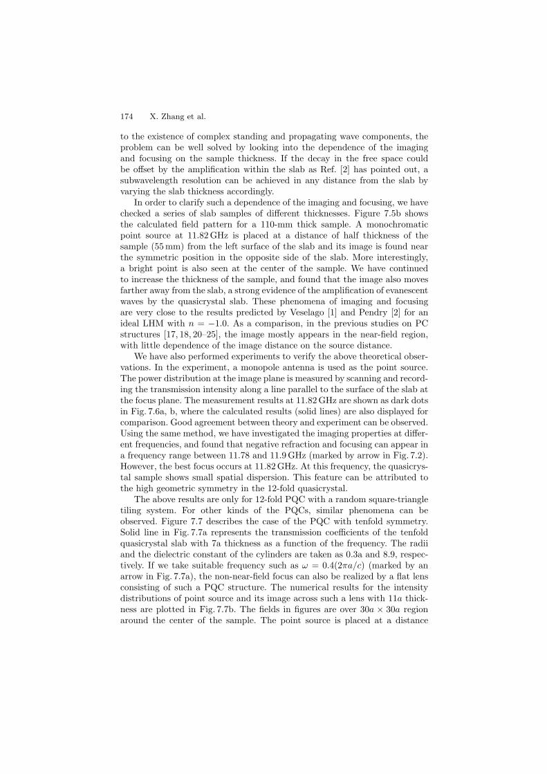
174 X. Zhang et al.
to the existence of complex standing and propagating wave components, theproblem can be well solved by looking into the dependence of the imagingand focusing on the sample thickness. If the decay in the free space couldbe offset by the amplification within the slab as Ref. [2] has pointed out, asubwavelength resolution can be achieved in any distance from the slab byvarying the slab thickness accordingly.
In order to clarify such a dependence of the imaging and focusing, we havechecked a series of slab samples of different thicknesses. Figure 7.5b showsthe calculated field pattern for a 110-mm thick sample. A monochromaticpoint source at 11.82 GHz is placed at a distance of half thickness of thesample (55 mm) from the left surface of the slab and its image is found nearthe symmetric position in the opposite side of the slab. More interestingly,a bright point is also seen at the center of the sample. We have continuedto increase the thickness of the sample, and found that the image also movesfarther away from the slab, a strong evidence of the amplification of evanescentwaves by the quasicrystal slab. These phenomena of imaging and focusingare very close to the results predicted by Veselago [1] and Pendry [2] for anideal LHM with n = −1.0. As a comparison, in the previous studies on PCstructures [17, 18, 20–25], the image mostly appears in the near-field region,with little dependence of the image distance on the source distance.
We have also performed experiments to verify the above theoretical obser-vations. In the experiment, a monopole antenna is used as the point source.The power distribution at the image plane is measured by scanning and record-ing the transmission intensity along a line parallel to the surface of the slab atthe focus plane. The measurement results at 11.82 GHz are shown as dark dotsin Fig. 7.6a, b, where the calculated results (solid lines) are also displayed forcomparison. Good agreement between theory and experiment can be observed.Using the same method, we have investigated the imaging properties at differ-ent frequencies, and found that negative refraction and focusing can appear ina frequency range between 11.78 and 11.9 GHz (marked by arrow in Fig. 7.2).However, the best focus occurs at 11.82 GHz. At this frequency, the quasicrys-tal sample shows small spatial dispersion. This feature can be attributed tothe high geometric symmetry in the 12-fold quasicrystal.
The above results are only for 12-fold PQC with a random square-triangletiling system. For other kinds of the PQCs, similar phenomena can beobserved. Figure 7.7 describes the case of the PQC with tenfold symmetry.Solid line in Fig. 7.7a represents the transmission coefficients of the tenfoldquasicrystal slab with 7a thickness as a function of the frequency. The radiiand the dielectric constant of the cylinders are taken as 0.3a and 8.9, respec-tively. If we take suitable frequency such as ω = 0.4(2πa/c) (marked by anarrow in Fig. 7.7a), the non-near-field focus can also be realized by a flat lensconsisting of such a PQC structure. The numerical results for the intensitydistributions of point source and its image across such a lens with 11a thick-ness are plotted in Fig. 7.7b. The fields in figures are over 30a × 30a regionaround the center of the sample. The point source is placed at a distance
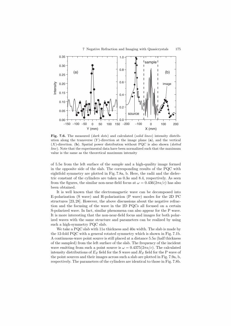
7 Negative Refraction and Imaging with Quasicrystals 175
−150 −100 −50 0 50 100 1500.00
0.05
0.10
0.15
0.20
0.25
0.30
0.35
(a) (b)
Inte
nsity
Y (mm)
−200 −100 0 100 2000.0
0.2
0.4
0.6
0.8
1.0
image
source
sample
X (mm)
Fig. 7.6. The measured (dark dots) and calculated (solid lines) intensity distrib-ution along the transverse (Y )-direction at the image plane (a), and the vertical(X)-direction. (b). Spatial power distribution without PQC is also shown (dottedline). Note that the experimental data have been normalized such that the maximumvalue is the same as the theoretical maximum intensity
of 5.5a from the left surface of the sample and a high-quality image formedin the opposite side of the slab. The corresponding results of the PQC witheightfold symmetry are plotted in Fig. 7.8a, b. Here, the radii and the dielec-tric constant of the cylinders are taken as 0.3a and 8.4, respectively. As seenfrom the figures, the similar non-near-field focus at ω = 0.436(2πa/c) has alsobeen obtained.
It is well known that the electromagnetic wave can be decomposed intoE-polarization (S wave) and H-polarization (P wave) modes for the 2D PCstructures [23, 28]. However, the above discussions about the negative refrac-tion and the focusing of the wave in the 2D PQCs all focused on a certainS-polarized wave. In fact, similar phenomena can also appear for the P wave.It is more interesting that the non-near-field focus and images for both polar-ized waves with the same structure and parameters can be realized by usingsuch a high-symmetry PQC slab.
We take a PQC slab with 11a thickness and 40a width. The slab is made bythe 12-fold PQC with a general rotated symmetry which is shown in Fig. 7.1b.A continuous-wave point source is still placed at a distance 5.5a (half thicknessof the sampled) from the left surface of the slab. The frequency of the incidentwave emitting from such a point source is ω = 0.4375(2πa/c). The calculatedintensity distributions of EZ field for the S wave and HZ field for the P wave ofthe point sources and their images across such a slab are plotted in Fig. 7.9a, b,respectively. The parameters of the cylinders are identical to those in Fig. 7.8b.
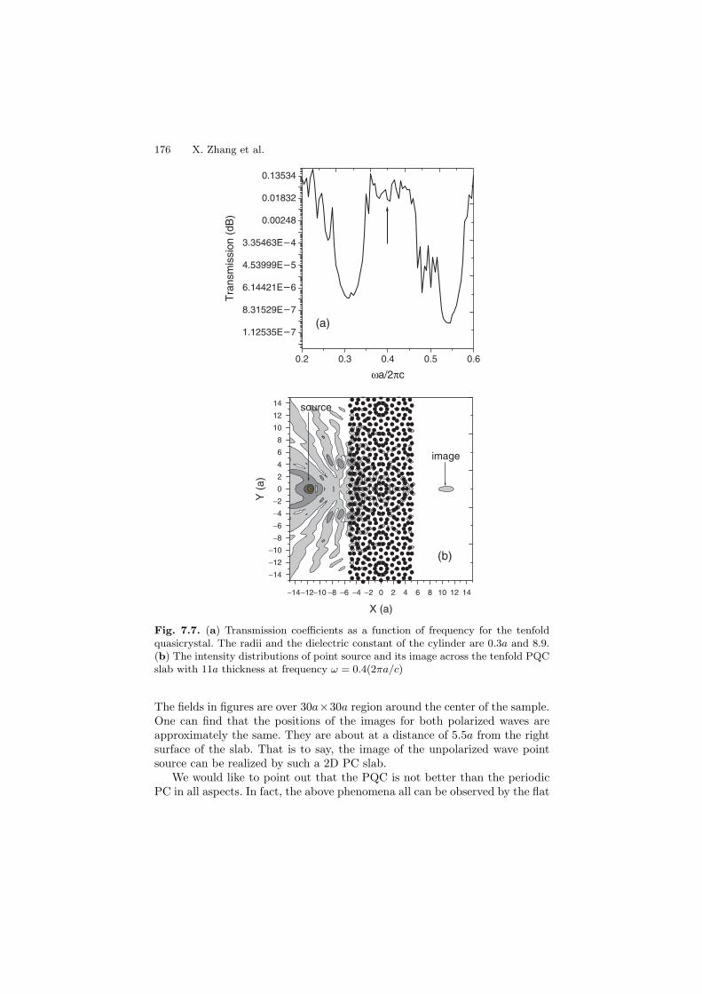
176 X. Zhang et al.
0.2 0.3 0.4 0.5 0.6
1.12535E27
8.31529E27
6.14421E26
4.53999E25
3.35463E24
0.00248
0.01832
0.13534
Tra
nsm
issi
on (
dB)
ωa/2πc
(a)
source
(b)
image
−14
−12
−10
−8
−6
−4
−2
0
2
4
6
8
10
12
14
Y (
a)
X (a)
−12−10 −8 −6 −4 −2 0 2 4 6 8 10 12 14−14
Fig. 7.7. (a) Transmission coefficients as a function of frequency for the tenfoldquasicrystal. The radii and the dielectric constant of the cylinder are 0.3a and 8.9.(b) The intensity distributions of point source and its image across the tenfold PQCslab with 11a thickness at frequency ω = 0.4(2πa/c)
The fields in figures are over 30a×30a region around the center of the sample.One can find that the positions of the images for both polarized waves areapproximately the same. They are about at a distance of 5.5a from the rightsurface of the slab. That is to say, the image of the unpolarized wave pointsource can be realized by such a 2D PC slab.
We would like to point out that the PQC is not better than the periodicPC in all aspects. In fact, the above phenomena all can be observed by the flat
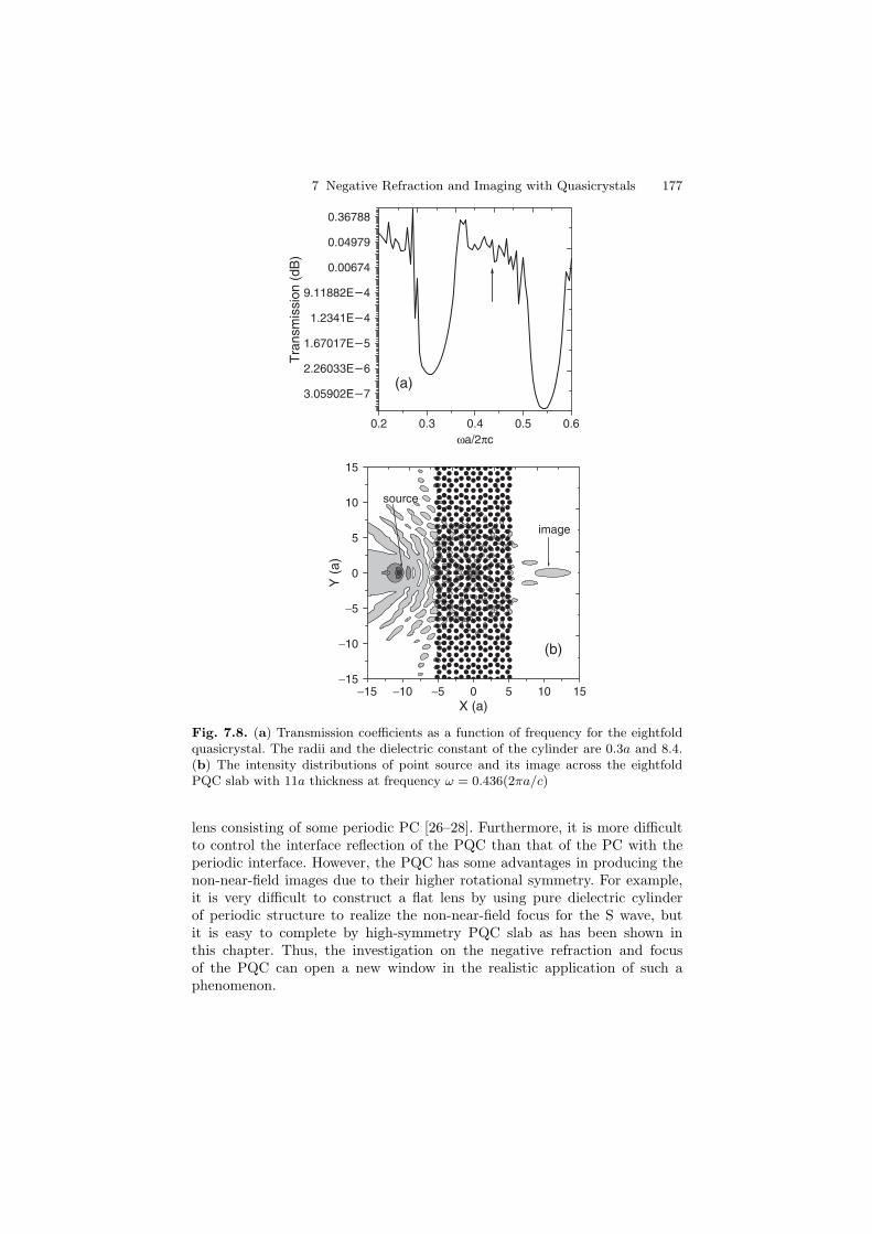
7 Negative Refraction and Imaging with Quasicrystals 177
0.2 0.3 0.4 0.5 0.6
3.05902E27
2.26033E26
1.67017E25
1.2341E24
9.11882E24
0.00674
0.04979
0.36788
(a)
Tra
nsm
issi
on (
dB)
ωa/2πc
(b)
image
source
−15 −10 −5 0 5 10 15−15
−10
−5
0
5
10
15
Y (
a)
X (a)
Fig. 7.8. (a) Transmission coefficients as a function of frequency for the eightfoldquasicrystal. The radii and the dielectric constant of the cylinder are 0.3a and 8.4.(b) The intensity distributions of point source and its image across the eightfoldPQC slab with 11a thickness at frequency ω = 0.436(2πa/c)
lens consisting of some periodic PC [26–28]. Furthermore, it is more difficultto control the interface reflection of the PQC than that of the PC with theperiodic interface. However, the PQC has some advantages in producing thenon-near-field images due to their higher rotational symmetry. For example,it is very difficult to construct a flat lens by using pure dielectric cylinderof periodic structure to realize the non-near-field focus for the S wave, butit is easy to complete by high-symmetry PQC slab as has been shown inthis chapter. Thus, the investigation on the negative refraction and focusof the PQC can open a new window in the realistic application of such aphenomenon.
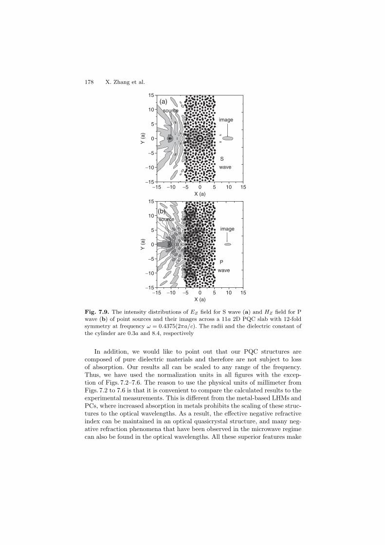
178 X. Zhang et al.
S
wave
image
source
−15 −10 −5 0 5 10 15−15
−10
−5
0
5
10
15(a)
Y (
a)
X (a)
−15 −10 −5 0 5 10 15−15
−10
−5
0
5
10
15
P
wave
source
image
(b)
Y (
a)
X (a)
Fig. 7.9. The intensity distributions of EZ field for S wave (a) and HZ field for Pwave (b) of point sources and their images across a 11a 2D PQC slab with 12-foldsymmetry at frequency ω = 0.4375(2πa/c). The radii and the dielectric constant ofthe cylinder are 0.3a and 8.4, respectively
In addition, we would like to point out that our PQC structures arecomposed of pure dielectric materials and therefore are not subject to lossof absorption. Our results all can be scaled to any range of the frequency.Thus, we have used the normalization units in all figures with the excep-tion of Figs. 7.2–7.6. The reason to use the physical units of millimeter fromFigs. 7.2 to 7.6 is that it is convenient to compare the calculated results to theexperimental measurements. This is different from the metal-based LHMs andPCs, where increased absorption in metals prohibits the scaling of these struc-tures to the optical wavelengths. As a result, the effective negative refractiveindex can be maintained in an optical quasicrystal structure, and many neg-ative refraction phenomena that have been observed in the microwave regimecan also be found in the optical wavelengths. All these superior features make
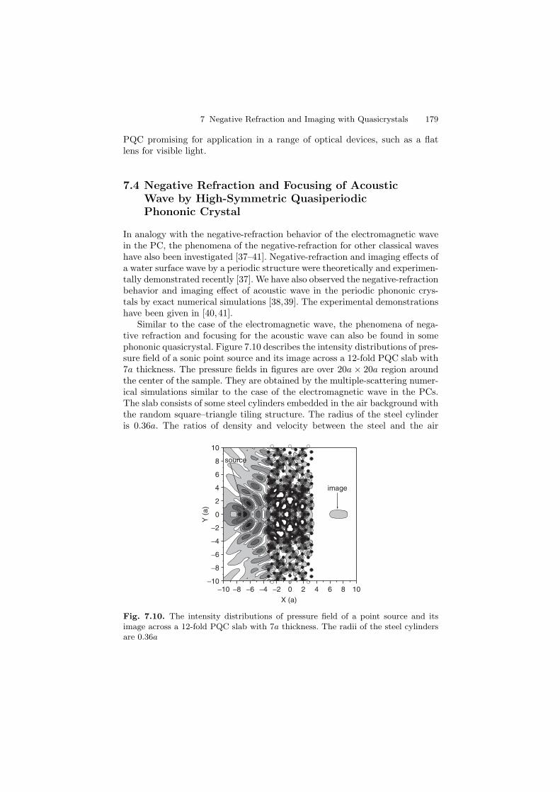
7 Negative Refraction and Imaging with Quasicrystals 179
PQC promising for application in a range of optical devices, such as a flatlens for visible light.
7.4 Negative Refraction and Focusing of AcousticWave by High-Symmetric QuasiperiodicPhononic Crystal
In analogy with the negative-refraction behavior of the electromagnetic wavein the PC, the phenomena of the negative-refraction for other classical waveshave also been investigated [37–41]. Negative-refraction and imaging effects ofa water surface wave by a periodic structure were theoretically and experimen-tally demonstrated recently [37]. We have also observed the negative-refractionbehavior and imaging effect of acoustic wave in the periodic phononic crys-tals by exact numerical simulations [38,39]. The experimental demonstrationshave been given in [40,41].
Similar to the case of the electromagnetic wave, the phenomena of nega-tive refraction and focusing for the acoustic wave can also be found in somephononic quasicrystal. Figure 7.10 describes the intensity distributions of pres-sure field of a sonic point source and its image across a 12-fold PQC slab with7a thickness. The pressure fields in figures are over 20a × 20a region aroundthe center of the sample. They are obtained by the multiple-scattering numer-ical simulations similar to the case of the electromagnetic wave in the PCs.The slab consists of some steel cylinders embedded in the air background withthe random square–triangle tiling structure. The radius of the steel cylinderis 0.36a. The ratios of density and velocity between the steel and the air
image
source
−10 −8 −6 −4 −2 0 2 4 6 8 10−10
−8
−6
−4
−2
0
2
4
6
8
10
Y (
a)
X (a)
Fig. 7.10. The intensity distributions of pressure field of a point source and itsimage across a 12-fold PQC slab with 7a thickness. The radii of the steel cylindersare 0.36a
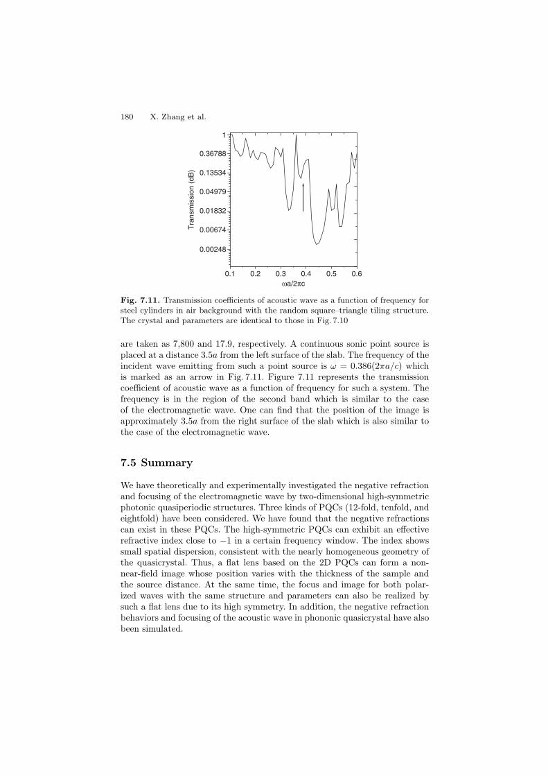
180 X. Zhang et al.
0.1 0.2 0.3 0.4 0.5 0.6
0.00248
0.00674
0.01832
0.04979
0.13534
0.36788
1
Tra
nsm
issi
on (
dB)
ωa/2πc
Fig. 7.11. Transmission coefficients of acoustic wave as a function of frequency forsteel cylinders in air background with the random square–triangle tiling structure.The crystal and parameters are identical to those in Fig. 7.10
are taken as 7,800 and 17.9, respectively. A continuous sonic point source isplaced at a distance 3.5a from the left surface of the slab. The frequency of theincident wave emitting from such a point source is ω = 0.386(2πa/c) whichis marked as an arrow in Fig. 7.11. Figure 7.11 represents the transmissioncoefficient of acoustic wave as a function of frequency for such a system. Thefrequency is in the region of the second band which is similar to the caseof the electromagnetic wave. One can find that the position of the image isapproximately 3.5a from the right surface of the slab which is also similar tothe case of the electromagnetic wave.
7.5 Summary
We have theoretically and experimentally investigated the negative refractionand focusing of the electromagnetic wave by two-dimensional high-symmetricphotonic quasiperiodic structures. Three kinds of PQCs (12-fold, tenfold, andeightfold) have been considered. We have found that the negative refractionscan exist in these PQCs. The high-symmetric PQCs can exhibit an effectiverefractive index close to −1 in a certain frequency window. The index showssmall spatial dispersion, consistent with the nearly homogeneous geometry ofthe quasicrystal. Thus, a flat lens based on the 2D PQCs can form a non-near-field image whose position varies with the thickness of the sample andthe source distance. At the same time, the focus and image for both polar-ized waves with the same structure and parameters can also be realized bysuch a flat lens due to its high symmetry. In addition, the negative refractionbehaviors and focusing of the acoustic wave in phononic quasicrystal have alsobeen simulated.
7 Negative Refraction and Imaging with Quasicrystals 181
Acknowledgments
This work was supported by the National Key Basic Research Special Founda-tion of China at No. 2001CB610402, 2004CB719804 and the National NaturalScience Foundation of China at No. 10374009. The project was supported byNCET.
References
1. V.G. Veselago, Sov. Phys. Usp. 10, 509 (1968)2. J.B. Pendry, Phys. Rev. Lett. 85, 3966 (2000)3. R.A. Shelby, D.R. Smith, S. Schultz, Science 292, 77 (2001)4. D.R. Smith, W.J. Padilla, D.C. View, S.C. Nemat-Nasser, S. Schultz, Phys. Rev.
Lett. 84, 4184 (2000); D.R. Smith, N. Kroll, Phys. Rev. Lett. 84, 2933 (2000)5. P. Markos, C.M. Soukoulis, Phys. Rev. E 65, 036622 (2002); Phys. Rev. B 65,
033401 (2002)6. J. Pacheco Jr., T.M. Grzegorczyk, B.L. Wu, Y. Zhang, J.A. Kong, Phys. Rev.
Lett. 89, 257401 (2002)7. R. Marques, J. Martel, F. Mesa, F. Medina, Phys. Rev. Lett. 89, 183901 (2002)8. S. Foteinopoulou, E.N. Economou, C.M. Soukoulis, Phys. Rev. Lett. 90, 107402
(2003)9. D.R. Smith, D. Schurig, Phys. Rev. Lett. 90, 077405 (2003)
10. A.A. Houck, J.B. Brock, I.L. Chuang, Phys. Rev. Lett. 90, 137401 (2003)11. C.G. Parazzoli, R.B. Greegor, K. Li, B.E.C. Koltenbah, M. Tanielian, Phys.
Rev. Lett. 90, 107401 (2003)12. A. Grbic, G.V. Eleftheriades, Phys. Rev. Lett. 92, 117403 (2004)13. H. Kosaka, T. Kawashima, A. Tomita, M. Notomi, T. Tamamura, T. Sato,
S. Kawakami, Phys. Rev. B 58, 10096 (1998)14. M. Notomi, Phys. Rev. B 62, 10696 (2000)15. B. Gralak, S. Enoch, G. Tayeb, J. Opt. Soc. Am. A 17, 1012 (2000)16. S. Foteinopoulou, C.M. Soukoulis, Phys. Rev. B 67, 235107 (2003)17. C. Luo, S.G. Johnson, J.D. Joannopoulos, J.B. Pendry, Phys. Rev. B 65, 201104
(2002); Opt. Express 11, 746 (2003); C. Luo, S.G. Johnson, J.D. Joannopoulos,Appl. Phys. Lett. 83, 2352 (2002)
18. C. Luo, S.G. Johnson, J.D. Joannopoulos, J.B. Pendry, Phys. Rev. B 68, 045115(2003)
19. E. Cubukcu, K. Aydin, E. Ozbay, S. Foteinopoulou, C.M. Soukoulis, Nature(London) 423, 604 (2003)
20. P.V. Parimi, W.T. Lu, P. Vodo, S. Sridhar, Nature 426, 404 (2003)21. E. Cubukcu, K. Aydin, E. Ozbay, S. Foteinopoulou, C.M. Soukoulis, Phys. Rev.
Lett. 91, 207401 (2003)22. Z.Y. Li, L.L. Lin, Phys. Rev. B 68, 245110 (2003)23. X. Zhang, Phys. Rev. B 70, 205102 (2004); Appl. Phys. Lett. 86, 121103 (2005)24. S.L. He, Z.C. Ruan, L. Chen, J. Shen, Phys. Rev. B 70, 115113 (2004)25. P. Belov, C. Simovski, P. Ikonen, Phys. Rev. B 71, 193105 (2005)26. X. Wang, Z.F. Ren, K. Kempa, Opt. Express 12, 2919 (2004); Phys. Rev. B 71,
085101 (2005)

182 X. Zhang et al.
27. X. Hu, C.T. Chan, Appl. Phys. Lett. 85, 1520 (2004)28. X. Zhang, Phys. Rev. B 70, 195110 (2004); Phys. Rev. B 71, 235103 (2005);
Phys. Rev. E 71, 037601 (2005); Phys. Rev. B 71, 165116 (2005)29. A. Berrier, M. Mulot, M. Swillo, M. Qiu, L. Thylen, A. Talneau, S. Anand,
Phys. Rev. Lett. 93, 073902 (2004)30. Y. Zhang, B. Fluegel, A. Mascarenhas, Phys. Rev. Lett. 91, 157404 (2003);
Z. Liu, Z. Lin, S.T. Chui, Phys. Rev. B 69, 115402 (2004)31. Z. Feng, X. Zhang, Y.Q. Wang, Z.Y. Li, B.Y. Cheng, D.Z. Zhang, Phys. Rev.
Lett. 94, 247402 (2005)32. M.E. Zoorob, M.D.B. Chartton, G.J. Parker, J.J. Baumberg, M.C. Nettl, Nature
(London) 404, 740 (2000)33. X. Zhang, Z.Q. Zhang, C.T. Chan, Phys. Rev. B 63, 081105 (2001)34. C. Jin, B. Cheng, B. Man, Z. Li, D.Z. Zhang, S. Ban, B. Sun, Appl. Phys. Lett.
75, 1848 (1999)35. E. Rotenberg, W. Theis, K. Horn, P. Gille, Nature (London) 406, 602 (2000)36. M. Born, E. Wolf, Principles of Optics, chapter VIII, 7th edn. (Cambridge
University Press, Cambridge, 1999), p. 46237. X. Hu, Y. Shen, X. Liu, R. Fu, J. Zi, Phys. Rev. E 69, 030201 (2004)38. X. Zhang, Z. Liu, Appl. Phys. Lett. 85, 341 (2004)39. C. Qiu, X. Zhang, Z. Liu, Phys. Rev. B 71, 054302 (2005)40. S. Yang, J.H. Page, Z. Liu, M.L. Cowan, C.T. Chan, P. Sheng, Phys. Rev. Lett.
93, 024301 (2004)41. L. Feng, X.-P. Liu, Y.-B. Chen, Z.-P. Huang, Y.-W. Mao, Y.-F. Chen, J. Zi,
Y.-Y. Zhu, Phys. Rev. B 72, 033108 (2005)
8
Generalizing the Concept of Negative Mediumto Acoustic Waves
J. Li, K.H. Fung, Z.Y. Liu, P. Sheng and C.T. Chan
Summary. Electromagnetic metamaterials are artificial materials exhibiting simul-taneously negative permeability and permittivity, and the “double negativity” givesrise to many interesting phenomena such as negative refraction, backward wavesand superlensing effects. We will see that the concept can be extended to acousticwaves. We will show the existence of acoustic metamaterial, in which both theeffective density and bulk modulus are simultaneously negative at some particularfrequency range, in the sense of an effective medium. Such a double negative acousticsystem is an acoustic analog of Veselogo’s medium in electromagnetism, and sharesmany novel consequences such as negative refractive index, flat slab focusing andsuper-resolution. The double negativity in acoustics is derived from low frequencyresonances, as in the case of electromagnetism, but the negative density and modu-lus can come from a single resonance structure, as distinct from electromagnetism inwhich the negative permeability and negative permittivity originates from differentresonance mechanisms.
8.1 Introduction
Novel concepts of “negative” media, having negative refraction and/or “doublenegativity” [1] and their physical consequences and plausible applications aredrawing excitement from researchers in many fields. In the past few years,considerable progress has been made on realizing such materials for electro-magnetic (EM) waves [2]. Since the concepts of negative refraction, negativeconstitutive relationships, and “double negativity” originate from electromag-netics, we will use EM waves to qualify these concepts before discussingacoustic waves. For EM waves, we know that the electric permittivity (ε)and magnetic permeability (µ) dictate the response of a medium to externalEM fields and these constitutive parameters collectively govern the propaga-tion of EM waves. In particular, the refractive index (n) is given by n2 = εµ.If either ε or µ is negative, then n becomes imaginary and the wave cannotpropagate. If, however, both ε and µ are simultaneously negative [1] (dou-ble negativity), then waves can propagate through the media, but with a
184 J. Li et al.
negative n and hence the phenomenon of negative refraction. Many amaz-ing effects, such as Doppler shifts with reversed signs, backward Cherenkovradiation [1], and superlensing effects [3] are consequences of double negativ-ity. These “double-negative” media are characterized by the phenomenon thatthe Poynting vector and the wavevector are in opposite directions (S ·k < 0),and they are also called backward wave media. For EM waves, negative ε canbe found in natural materials, but negative µ has to be made artificially usingresonating units that respond to magnetic fields. The realization of negativeeffective µ using “split ring” type resonators [4] leads to realization of “doublenegativity” in EM wave experimentally [5], and those materials are frequentlycalled metamaterials. For EM waves, these “Veselago” media are sometimescalled left-handed media (LHM) since the E,H,k forms a left-handed set,but the term “double negative” medium is more informative.
We will see that such concepts can be generalized to other kinds of classicalwaves such as acoustic waves [6]. For acoustic waves traveling with a wavevector k inside a homogeneous medium, the refractive index n is given by
k = |n|ω with n2 =ρ
κ, (8.1)
where ρ and κ are the mass density and the bulk modulus of the medium,respectively. Therefore, in order to have propagating plane waves inside themedium, we should intuitively have either both positive ρ and κ or simulta-neously negative ρ and κ. Moreover, the time-averaged Poynting vector for apropagating plane wave is given by
S =i
2ωρψ∇ψ∗ =
|ψ|2 k
2ωρ, (8.2)
where ψ is the pressure. Now, if we can have a “negative” medium in acousticwaves, a negative effective ρ means that we have a backward wave in whichS and k should point in the opposite directions. And simultaneous negativityin κ and ρ ensures the existence of propagating waves. Although the analogybetween acoustic and EM waves can be made, the realization of such “nega-tive” acoustic wave is in fact less obvious than EM waves. For EM waves, atleast negative ε can be found in nature. It is the negative µ that has to bemade artificially. For acoustic waves, neither negative ρ nor negative κ can befound in naturally occurring materials. They have to be derived from artifi-cial resonances through composite materials. Physically, this means that themedium displays anomalous response at some frequencies such that it expandsupon compression (negative modulus) and accelerates to the left when beingpushed to the right (negative density). We need to show that negative effectivedensity and negative effective modulus are “allowable,” at least mathemati-cally, and we need to give explicit configurations and perform calculations toshow that they indeed have the “negative” backward wave properties. Thisis not an easy task because (even for composite materials) the effective bulkmodulus and density are normally bounded by the Hashin and Shtrikman
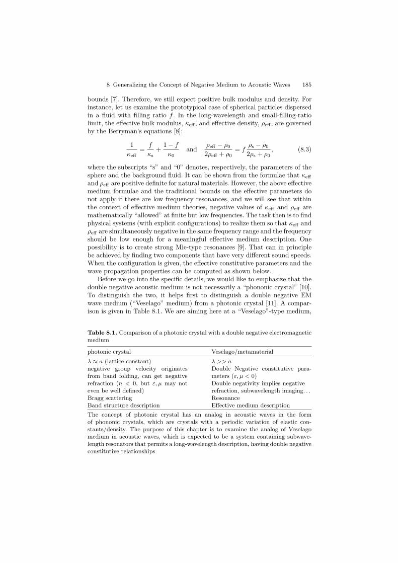
8 Generalizing the Concept of Negative Medium to Acoustic Waves 185
bounds [7]. Therefore, we still expect positive bulk modulus and density. Forinstance, let us examine the prototypical case of spherical particles dispersedin a fluid with filling ratio f . In the long-wavelength and small-filling-ratiolimit, the effective bulk modulus, κeff , and effective density, ρeff , are governedby the Berryman’s equations [8]:
1κeff
=f
κs+
1 − f
κ0and
ρeff − ρ0
2ρeff + ρ0= f
ρs − ρ0
2ρs + ρ0, (8.3)
where the subscripts “s” and “0” denotes, respectively, the parameters of thesphere and the background fluid. It can be shown from the formulae that κeff
and ρeff are positive definite for natural materials. However, the above effectivemedium formulae and the traditional bounds on the effective parameters donot apply if there are low frequency resonances, and we will see that withinthe context of effective medium theories, negative values of κeff and ρeff aremathematically “allowed” at finite but low frequencies. The task then is to findphysical systems (with explicit configurations) to realize them so that κeff andρeff are simultaneously negative in the same frequency range and the frequencyshould be low enough for a meaningful effective medium description. Onepossibility is to create strong Mie-type resonances [9]. That can in principlebe achieved by finding two components that have very different sound speeds.When the configuration is given, the effective constitutive parameters and thewave propagation properties can be computed as shown below.
Before we go into the specific details, we would like to emphasize that thedouble negative acoustic medium is not necessarily a “phononic crystal” [10].To distinguish the two, it helps first to distinguish a double negative EMwave medium (“Veselago” medium) from a photonic crystal [11]. A compar-ison is given in Table 8.1. We are aiming here at a “Veselago”-type medium,
Table 8.1. Comparison of a photonic crystal with a double negative electromagneticmedium
photonic crystal Veselago/metamaterial
λ ≈ a (lattice constant) λ >> anegative group velocity originatesfrom band folding, can get negativerefraction (n < 0, but ε, µ may noteven be well defined)
Double Negative constitutive para-meters (ε, µ < 0)Double negativity implies negativerefraction, subwavelength imaging. . .
Bragg scattering ResonanceBand structure description Effective medium description
The concept of photonic crystal has an analog in acoustic waves in the formof phononic crystals, which are crystals with a periodic variation of elastic con-stants/density. The purpose of this chapter is to examine the analog of Veselagomedium in acoustic waves, which is expected to be a system containing subwave-length resonators that permits a long-wavelength description, having double negativeconstitutive relationships
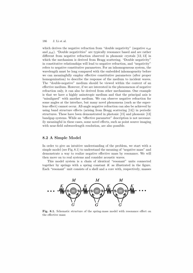
186 J. Li et al.
which derives the negative refraction from “double negativity” (negative κeff
and ρeff). “Double negativities” are typically resonance based and are ratherdifferent from negative refraction observed in phononic crystals [12, 13] inwhich the mechanism is derived from Bragg scattering. “Double negativity”in constitutive relationships will lead to negative refraction, and “negativity”refers to negative constitutive parameters. For an inhomogeneous system, thewavelength must be long compared with the embedded inhomogeneity beforewe can meaningfully employ effective constitutive parameters (after properhomogenization) to describe the response of the medium to incident waves.The “double-negative” medium should be viewed within the context of aneffective medium. However, if we are interested in the phenomenon of negativerefraction only, it can also be derived from other mechanisms. One exampleis that we have a highly anisotropic medium and that the principal axis is“misaligned” with another medium. We can observe negative refraction forsome angles at the interface, but many novel phenomena (such as the super-lens effect) cannot occur. All-angle negative refraction can also be achieved byusing band structure effects (arising from Bragg scattering [14]) in periodicstructures. These have been demonstrated in photonic [15] and phononic [13]bandgap systems. While an “effective parameter” description is not necessar-ily meaningful in these cases, some novel effects, such as point source imagingwith near-field subwavelength resolution, are also possible.
8.2 A Simple Model
In order to give an intuitive understanding of the problem, we start with asimple model (see Fig. 8.1) to understand the meaning of “negative mass” anddemonstrate a way to realize negative effective mass by resonance. We willthen move on to real systems and consider acoustic waves.
This model system is a chain of identical “resonant” units connectedtogether by springs with a spring constant K as illustrated in the figure.Each “resonant” unit consists of a shell and a core with, respectively, masses
Fig. 8.1. Schematic structure of the spring-mass model with resonance effect onthe effective mass
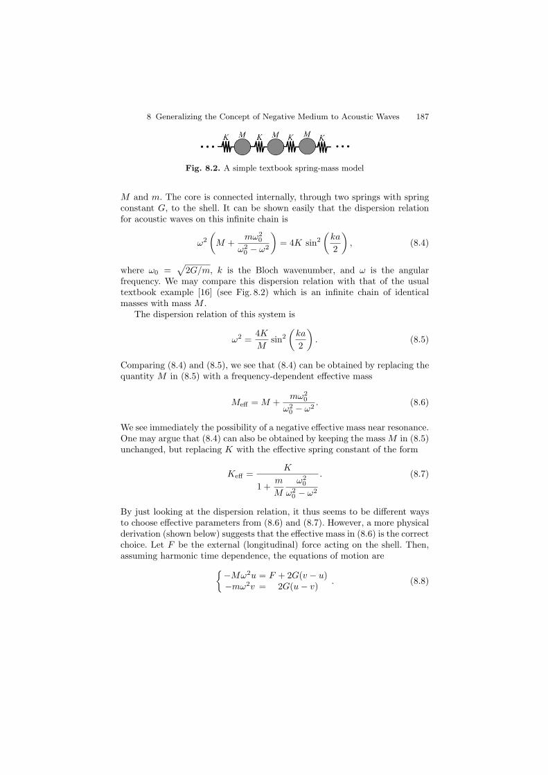
8 Generalizing the Concept of Negative Medium to Acoustic Waves 187
Fig. 8.2. A simple textbook spring-mass model
M and m. The core is connected internally, through two springs with springconstant G, to the shell. It can be shown easily that the dispersion relationfor acoustic waves on this infinite chain is
ω2
(M +
mω20
ω20 − ω2
)= 4K sin2
(ka
2
), (8.4)
where ω0 =√
2G/m, k is the Bloch wavenumber, and ω is the angularfrequency. We may compare this dispersion relation with that of the usualtextbook example [16] (see Fig. 8.2) which is an infinite chain of identicalmasses with mass M .
The dispersion relation of this system is
ω2 =4K
Msin2
(ka
2
). (8.5)
Comparing (8.4) and (8.5), we see that (8.4) can be obtained by replacing thequantity M in (8.5) with a frequency-dependent effective mass
Meff = M +mω2
0
ω20 − ω2
. (8.6)
We see immediately the possibility of a negative effective mass near resonance.One may argue that (8.4) can also be obtained by keeping the mass M in (8.5)unchanged, but replacing K with the effective spring constant of the form
Keff =K
1 +m
M
ω20
ω20 − ω2
. (8.7)
By just looking at the dispersion relation, it thus seems to be different waysto choose effective parameters from (8.6) and (8.7). However, a more physicalderivation (shown below) suggests that the effective mass in (8.6) is the correctchoice. Let F be the external (longitudinal) force acting on the shell. Then,assuming harmonic time dependence, the equations of motion are
−Mω2u = F + 2G(v − u)−mω2v = 2G(u − v) . (8.8)
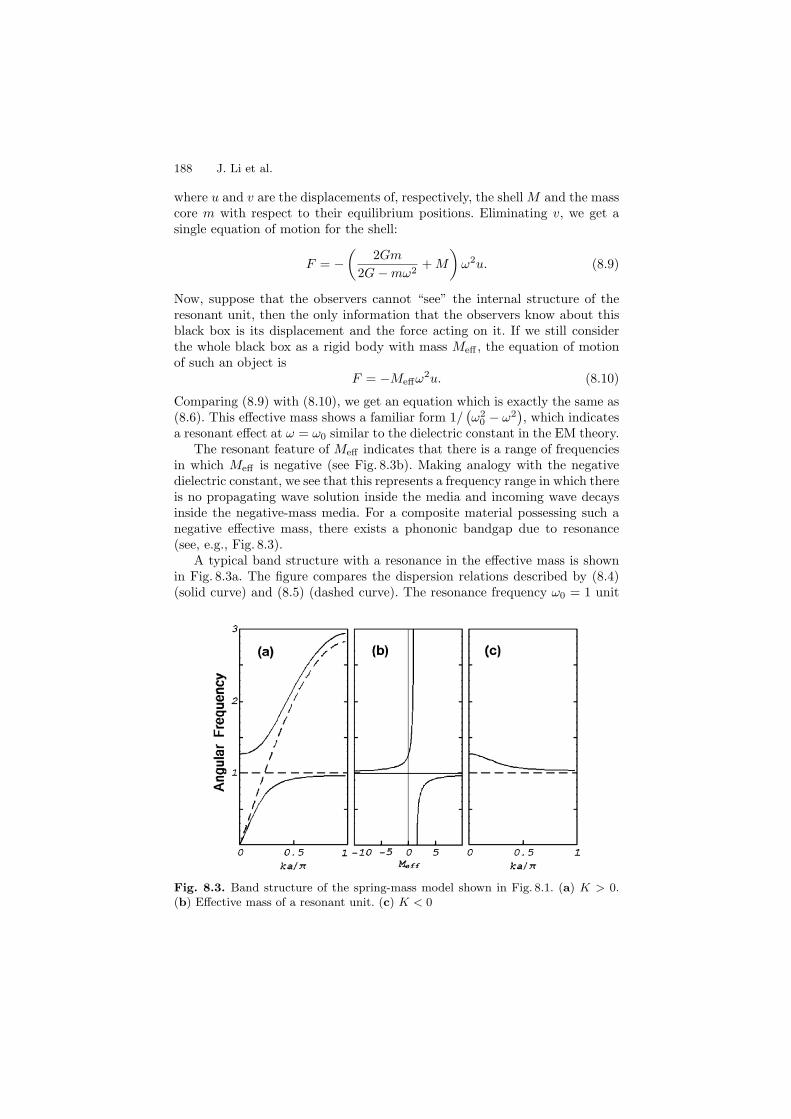
188 J. Li et al.
where u and v are the displacements of, respectively, the shell M and the masscore m with respect to their equilibrium positions. Eliminating v, we get asingle equation of motion for the shell:
F = −(
2Gm
2G − mω2+ M
)ω2u. (8.9)
Now, suppose that the observers cannot “see” the internal structure of theresonant unit, then the only information that the observers know about thisblack box is its displacement and the force acting on it. If we still considerthe whole black box as a rigid body with mass Meff , the equation of motionof such an object is
F = −Meffω2u. (8.10)
Comparing (8.9) with (8.10), we get an equation which is exactly the same as(8.6). This effective mass shows a familiar form 1/
(ω2
0 − ω2), which indicates
a resonant effect at ω = ω0 similar to the dielectric constant in the EM theory.The resonant feature of Meff indicates that there is a range of frequencies
in which Meff is negative (see Fig. 8.3b). Making analogy with the negativedielectric constant, we see that this represents a frequency range in which thereis no propagating wave solution inside the media and incoming wave decaysinside the negative-mass media. For a composite material possessing such anegative effective mass, there exists a phononic bandgap due to resonance(see, e.g., Fig. 8.3).
A typical band structure with a resonance in the effective mass is shownin Fig. 8.3a. The figure compares the dispersion relations described by (8.4)(solid curve) and (8.5) (dashed curve). The resonance frequency ω0 = 1 unit
Fig. 8.3. Band structure of the spring-mass model shown in Fig. 8.1. (a) K > 0.(b) Effective mass of a resonant unit. (c) K < 0
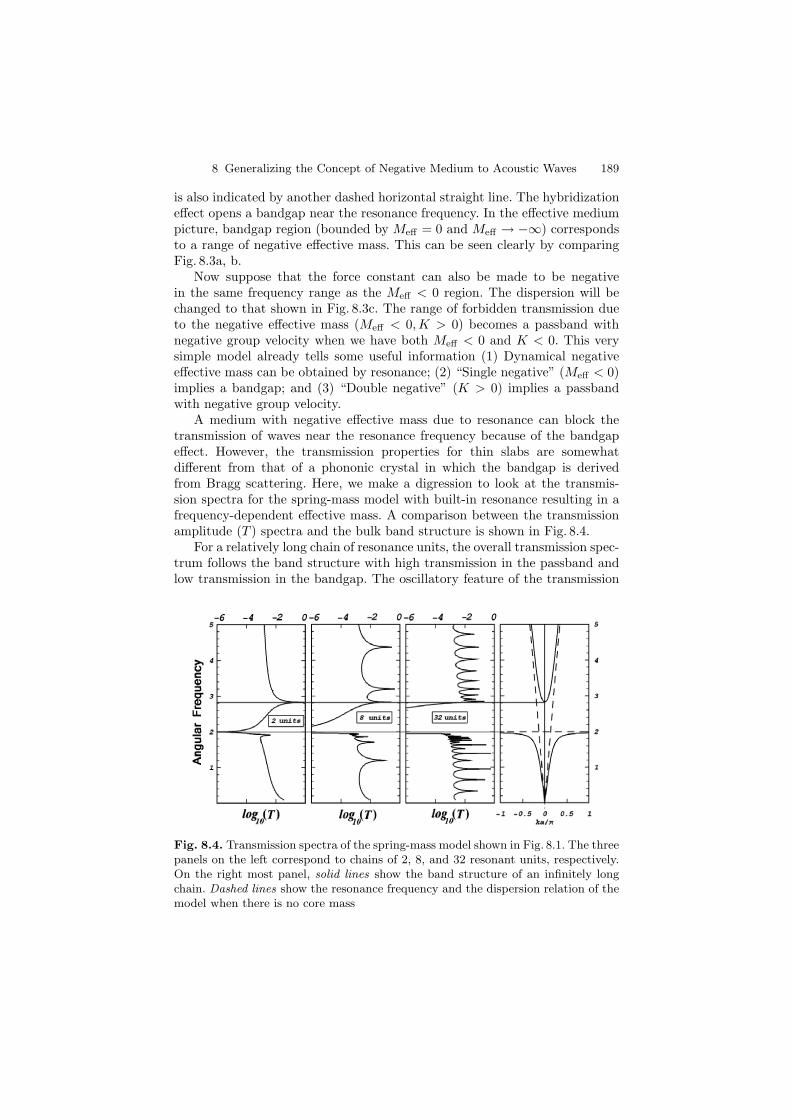
8 Generalizing the Concept of Negative Medium to Acoustic Waves 189
is also indicated by another dashed horizontal straight line. The hybridizationeffect opens a bandgap near the resonance frequency. In the effective mediumpicture, bandgap region (bounded by Meff = 0 and Meff → −∞) correspondsto a range of negative effective mass. This can be seen clearly by comparingFig. 8.3a, b.
Now suppose that the force constant can also be made to be negativein the same frequency range as the Meff < 0 region. The dispersion will bechanged to that shown in Fig. 8.3c. The range of forbidden transmission dueto the negative effective mass (Meff < 0,K > 0) becomes a passband withnegative group velocity when we have both Meff < 0 and K < 0. This verysimple model already tells some useful information (1) Dynamical negativeeffective mass can be obtained by resonance; (2) “Single negative” (Meff < 0)implies a bandgap; and (3) “Double negative” (K > 0) implies a passbandwith negative group velocity.
A medium with negative effective mass due to resonance can block thetransmission of waves near the resonance frequency because of the bandgapeffect. However, the transmission properties for thin slabs are somewhatdifferent from that of a phononic crystal in which the bandgap is derivedfrom Bragg scattering. Here, we make a digression to look at the transmis-sion spectra for the spring-mass model with built-in resonance resulting in afrequency-dependent effective mass. A comparison between the transmissionamplitude (T ) spectra and the bulk band structure is shown in Fig. 8.4.
For a relatively long chain of resonance units, the overall transmission spec-trum follows the band structure with high transmission in the passband andlow transmission in the bandgap. The oscillatory feature of the transmission
Fig. 8.4. Transmission spectra of the spring-mass model shown in Fig. 8.1. The threepanels on the left correspond to chains of 2, 8, and 32 resonant units, respectively.On the right most panel, solid lines show the band structure of an infinitely longchain. Dashed lines show the resonance frequency and the dispersion relation of themodel when there is no core mass
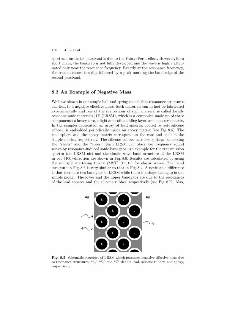
190 J. Li et al.
spectrum inside the passband is due to the Fabry–Perot effect. However, for ashort chain, the bandgap is not fully developed and the wave is highly atten-uated only near the resonance frequency. Exactly at the resonance frequency,the transmittance is a dip, followed by a peak marking the band-edge of thesecond passband.
8.3 An Example of Negative Mass
We have shown in our simple ball-and-spring model that resonance structurescan lead to a negative effective mass. Such materials can in fact be fabricatedexperimentally and one of the realizations of such material is called locallyresonant sonic materials [17] (LRSM), which is a composite made up of threecomponents: a heavy core, a light and soft cladding layer, and a passive matrix.In the samples fabricated, an array of lead spheres, coated by soft siliconerubber, is embedded periodically inside an epoxy matrix (see Fig. 8.5). Thelead sphere and the epoxy matrix correspond to the core and shell in thesimple model, respectively. The silicone rubber acts like springs connectingthe “shells” and the “cores.” Such LRSM can block low frequency soundwaves by resonance-induced sonic bandgaps. An example for the transmissionspectra (air–LRSM–air) and the elastic wave band structure of the LRSMin bcc (100)-direction are shown in Fig. 8.6. Results are calculated by usingthe multiple scattering theory (MST) [18, 19] for elastic waves. The bandstructure in Fig. 8.6 is very similar to that in Fig. 8.4. A noticeable differenceis that there are two bandgaps in LRSM while there is a single bandgap in oursimple model. The lower and the upper bandgaps are due to the resonancesof the lead spheres and the silicone rubber, respectively (see Fig. 8.7). Also,
Fig. 8.5. Schematic structure of LRSM which possesses negative effective mass dueto resonance structures. “L,” “S,” and “E” denote lead, silicone rubber, and epoxy,respectively
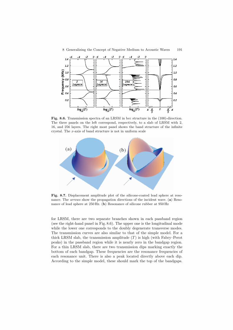
8 Generalizing the Concept of Negative Medium to Acoustic Waves 191
Fig. 8.6. Transmission spectra of an LRSM in bcc structure in the (100)-direction.The three panels on the left correspond, respectively, to a slab of LRSM with 2,16, and 256 layers. The right most panel shows the band structure of the infinitecrystal. The x-axis of band structure is not in uniform scale
Fig. 8.7. Displacement amplitude plot of the silicone-coated lead sphere at reso-nance. The arrows show the propagation directions of the incident wave. (a) Reso-nance of lead sphere at 250Hz. (b) Resonance of silicone rubber at 950 Hz
for LRSM, there are two separate branches shown in each passband region(see the right-hand panel in Fig. 8.6). The upper one is the longitudinal modewhile the lower one corresponds to the doubly degenerate transverse modes.The transmission curves are also similar to that of the simple model. For athick LRSM slab, the transmission amplitude (T ) is high (with Fabry–Perotpeaks) in the passband region while it is nearly zero in the bandgap region.For a thin LRSM slab, there are two transmission dips marking exactly thebottom of each bandgap. These frequencies are the resonance frequencies ofeach resonance unit. There is also a peak located directly above each dip.According to the simple model, these should mark the top of the bandgaps.
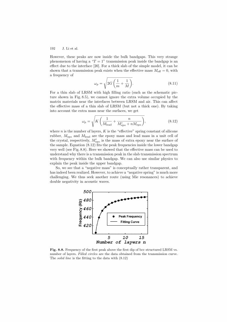
192 J. Li et al.
However, these peaks are now inside the bulk bandgaps. This very strangephenomenon of having a “T = 1” transmission peak inside the bandgap is aneffect due to the interface [20]. For a thick slab of the simple model, it can beshown that a transmission peak exists when the effective mass Meff = 0, witha frequency of
ωp =
√2G
(1m
+1M
). (8.11)
For a thin slab of LRSM with high filling ratio (such as the schematic pic-ture shown in Fig. 8.5), we cannot ignore the extra volume occupied by thematrix materials near the interfaces between LRSM and air. This can affectthe effective mass of a thin slab of LRSM (but not a thick one). By takinginto account the extra mass near the surfaces, we get
ωp =
√K
(1
Mlead+
n
M ′epo + nMepo
), (8.12)
where n is the number of layers, K is the “effective” spring constant of siliconerubber, Mepo and Mlead are the epoxy mass and lead mass in a unit cell ofthe crystal, respectively, M ′
epo is the mass of extra epoxy near the surface ofthe sample. Equation (8.12) fits the peak frequencies inside the lower bandgapvery well (see Fig. 8.8). Here we showed that the effective mass can be used tounderstand why there is a transmission peak in the slab transmission spectrumwith frequency within the bulk bandgap. We can also use similar physics toexplain the peak inside the upper bandgap.
So, we see that a “negative mass” is conceptually rather transparent, andhas indeed been realized. However, to achieve a “negative spring” is much morechallenging. We thus seek another route (using Mie resonances) to achievedouble negativity in acoustic waves.
Fig. 8.8. Frequency of the first peak above the first dip of bcc structured LRSM vs.number of layers. Filled circles are the data obtained from the transmission curve.The solid line is the fitting to the data with (8.12)
8 Generalizing the Concept of Negative Medium to Acoustic Waves 193
8.4 Acoustic Double-Negative Material
We now generalize the concept of double negativity in electromagnetic wavesto acoustic waves by using Mie resonances. The acoustic wave equation (withtime dependence e−iωt) is written as [21]
∇ · u +1
κ(r)ψ = 0,
∇ψ − ρ(r)ω2u = 0.
(8.13)
The first equation is the continuity equation where ψ is the pressure field(deviation from equilibrium), u is the displacement field, and κ is the position-dependent bulk modulus. The second equation is the Newton’s second lawwhere ρ is the position-dependent density. Suppose we have a closed regionV of constant bulk modulus and constant density, by integrating (8.13), weobtain
∆V =∮
u · dA = − 1κ
∫ψ dV ,
F = −∫
ψ dA = −ρω2
∫u dV ,
(8.14)
where ∆V is the volume dilation and F is the total force on the volumeV . Therefore, we see that a negative bulk modulus means that the volumeexpands when the system is pressed, and a negative density means that thevolume element accelerates to the opposite direction of the total force.
To make the mathematics tractable, the composite material is assumedto be of the form of small particles dispersed in a homogeneous backgroundmaterial. The ratio κ/ρ is different from the background value κ0/ρ0 only inthe regions of the particles. By defining the secondary source functions Q andP , the wave equation can be written with respect to the background by
∇ · u +1κ0
ψ = −Q (r)ω2
=(
1κ0
− 1κ (r)
)ψ,
1ρ0
∇ψ − ω2u = P (r) =(
1ρ0
− 1ρ (r)
)∇ψ.
(8.15)
The fields outside a particular particle can be expanded by partial waves inresponse to the incident wave so that the particle can be regarded effectivelyas a point particle. Up to the dipole approximation, the secondary sources areapproximated by their monopolar (Q) and dipolar (P ) contributions as
Q(r) ≈∑R
qRδ(r − R),
P (r) ≈∑R
pRδ(r − R),(8.16)
194 J. Li et al.
where R are the position vectors of the particles. On the other hand, for thescattering problem of a single isotropic particle up to the dipole approxima-tion, the induced sources at the particles are related to the local fields by
κ0qR
ω2V=
3ik3
0r30
D0ψlocal,R,
ρ0pR
3V=
3ik3
0r30
D1(∇ψ)local,R,
(8.17)
where k0 = ω√
ρ0/κ0 is the wave number in the background medium andV = 4πr3
0/3 is defined as the average volume occupied by one particle. If theparticles are arranged in a lattice, it is the volume of one primitive unit cell.D0 and D1 are the scattering coefficients of the particle in the partial waveexpansion of angular momentum L = 0 and L = 1. On the other hand, thelocal field at each particle is related to the macroscopic field by
ψlocal,R ≈ 〈ψ〉 (R),
(∇ψ)local,R ≈ 〈∇ψ〉 (R) − ρ0pR
3V,
(8.18)
where the angle brackets denote spatial averaging. It is the series expansion ofthe local field in frequency with only the static term being kept for simplicity.For a periodic lattice of the particles, we should also keep the third orderterm, which is usually called “radiative correction.” For a disordered system,the third order term vanishes due to the incoherent addition of the scatteredfields from the particles [22,23].
By substituting (8.17) and (8.18) into (8.16) and applying spatial averag-ing, we obtain
〈P 〉 =(
1ρ0
− 1ρeff
)〈∇ψ〉,
〈Q〉ω2
=(
1κeff
− 1κ0
)〈ψ〉,
(8.19)
where the effective density and bulk modulus are given by
− 1 +κ0
κeff=
3ik3
0r30
D0,
ρeff − ρ0
2ρeff + ρ0=
3ik3
0r30
D1.
(8.20)
By putting (8.19) back into the spatially averaged version of (8.15), we finallyobtain the macroscopic wave equation
∇ · 〈u〉 +1
κeff〈ψ〉 = 0,
〈∇ψ〉 − ρeffω2〈u〉 = 0.
(8.21)
8 Generalizing the Concept of Negative Medium to Acoustic Waves 195
It has the same form as the microscopic equation, and we need negative effec-tive bulk modulus together with negative effective density to have a propa-gating plane wave whose energy and phase are propagating in the oppositedirections. Note that the imaginary part of the effective density and bulkmodulus accounts for both the dissipative loss and the diffusive scatteringloss in the system. If the system is periodic, adding the radiative correctionin (8.18) gives
− 1 +κ0
κeff=
3ik3
0r30
D0
1 + D0,
ρeff − ρ0
2ρeff + ρ0=
3ik3
0r30
D1
1 + D1.
(8.22)
In this case, we note that the right-hand sides of (8.22) and hence the effectivedensity and bulk modulus remain purely real for nonabsorbing system.
We note that in the case of anisotropic particles, the macroscopic acousticwave equation should be written as
∇ · 〈u〉 +1
κeff〈ψ〉 = 0,
〈∇ψ〉− ↔ρ eff ω2〈u〉 = 0,
(8.23)
since the dipolar scattering coefficient is a tensor rather than a scalar.The effective-medium formulae can also be derived by using the techniques
commonly used in the coherent potential approach (CPA). This method ismore elegant in the sense that we need not define the sources and set upthe somewhat tedious homogenization scheme step by step as above. In thespirit of a single-site mean-field theory, the inhomogeneity is represented bya single spherical particle dispersed in a background fluid of volume equal tothe average volume a single particle occupies. It is represented by a sphereof radius r0 in Fig. 8.9 and it shares the same center with the particle. The“coated sphere,” which represents the inhomogeneous media, is further embed-ded in an effective medium which carries effective parameters that representthe bulk homogenized medium. The self-consistency we require is that theinhomogeneity embedded within the effective medium generates no scatter-ing. In the following we will demonstrate this self-consistency can be fulfilledif we expand the scattering in the lowest order of frequency and (8.20) and(8.22) can be derived using the CPA method.
Inside the layer of the background medium, the pressure field can bewritten as
ψ(r) =∑L,m
(a(0)LmjL(k0r) + b
(0)LmhL(k0r)
)YLm(r), (8.24)
where jL(x)/hL(x) is the spherical Bessel/Hankel function and YLm(r) arethe spherical harmonics. The pressure field in the effective medium can be
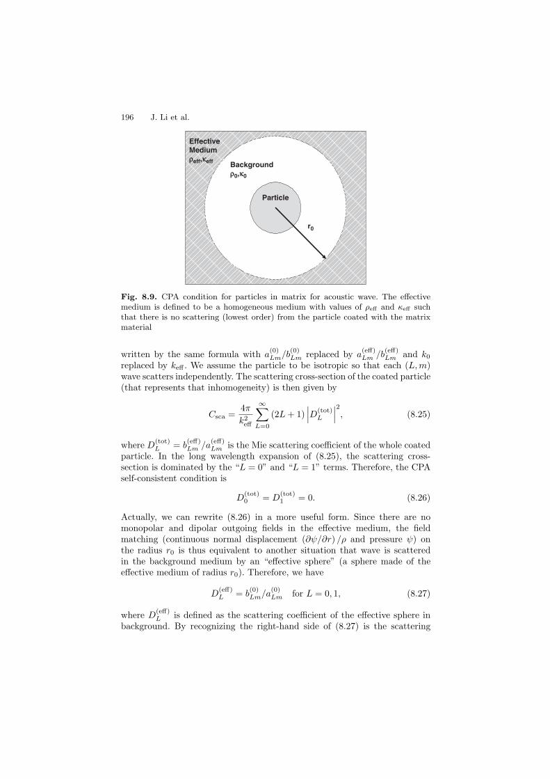
196 J. Li et al.
EffectiveMediumreff,keff
r0
Particle
Backgroundr0,k0
Fig. 8.9. CPA condition for particles in matrix for acoustic wave. The effectivemedium is defined to be a homogeneous medium with values of ρeff and κeff suchthat there is no scattering (lowest order) from the particle coated with the matrixmaterial
written by the same formula with a(0)Lm/b
(0)Lm replaced by a
(eff)Lm /b
(eff)Lm and k0
replaced by keff . We assume the particle to be isotropic so that each (L,m)wave scatters independently. The scattering cross-section of the coated particle(that represents that inhomogeneity) is then given by
Csca =4π
k2eff
∞∑L=0
(2L + 1)∣∣∣D(tot)
L
∣∣∣2
, (8.25)
where D(tot)L = b
(eff)Lm /a
(eff)Lm is the Mie scattering coefficient of the whole coated
particle. In the long wavelength expansion of (8.25), the scattering cross-section is dominated by the “L = 0” and “L = 1” terms. Therefore, the CPAself-consistent condition is
D(tot)0 = D
(tot)1 = 0. (8.26)
Actually, we can rewrite (8.26) in a more useful form. Since there are nomonopolar and dipolar outgoing fields in the effective medium, the fieldmatching (continuous normal displacement (∂ψ/∂r) /ρ and pressure ψ) onthe radius r0 is thus equivalent to another situation that wave is scatteredin the background medium by an “effective sphere” (a sphere made of theeffective medium of radius r0). Therefore, we have
D(eff)L = b
(0)Lm/a
(0)Lm for L = 0, 1, (8.27)
where D(eff)L is defined as the scattering coefficient of the effective sphere in
background. By recognizing the right-hand side of (8.27) is the scattering
8 Generalizing the Concept of Negative Medium to Acoustic Waves 197
coefficient of the central particle in background, the CPA self-consistent con-dition now becomes
D(eff)0 = D0 and D
(eff)1 = D1. (8.28)
In the limit keffr0, k0r0 1, we can approximate D(eff)0 and D
(eff)1 by
1
D(eff)0
≈ 3ik3
0r30
κeff
−κeff + κ0− 1
1
D(eff)1
≈ 3ik3
0r30
2ρeff + ρ0
ρeff − ρ0− 1.
(8.29)
The term “−1” in the two right-hand sides of (8.29) is the radiative correction[24]. Combining (8.28) and (8.29) gives (8.22) while combining (8.28) and(8.29) without the radiative correction gives (8.20).
If the particles are made from a homogeneous material (a fluid particle)such that the long-wavelength limit is valid within this particle (ksrs 1where ks is the wave number of the particle and rs is the radius of it), (8.20)and (8.22) reduce to the familiar Berryman formula (8.3).
If the particle is a solid particle, in the limit ksrs 1 and qsrs 1 whereqs is the wave number of shear wave within the particle, (8.20) and (8.22) stillreduce to (8.3). In such a case,
κs = λs + 2µs/3, (8.30)
where λs, µs are the Lame constants of the particle with µs (also denoted asthe shear modulus) being zero for fluid and nonzero for solid.
8.4.1 Construction of Double-Negative Materialby Mie Resonances
For EM waves, we are familiar with the notion that double-negative meta-materials can be constructed from a combination of “plasmonic wires” whichgive negative effective ε and “split rings” that give negative effective µ. Thus,two different types of structures are needed to give two different types ofresonances. In fact, there is another strategy to realize double negativity. Res-onances can be derived from the Mie resonances from one single structure.In the absence of Mie resonances, the effective medium formula is well rep-resented by (8.3) for a small filling ratio of spherical particles dispersed ina background fluid. (We note that for solid particles in a solid matrix, thedensity should be volume averaged.) The formulae imply that the effectivebulk modulus and the effective density can only be positive in the absenceof resonances. In fact, we can obtain the physical properties of the mediumby considering the effective sphere introduced in the last section. For ease indiscussion, let us ignore the radiative correction, which is usually small. Then,it is easy to find the relationship between the local and the macroscopic fields,and (8.21) can be written as
198 J. Li et al.
ρ0ω2〈u〉 =
3ρ0
2ρeff + ρ0(∇ψ)local =
ρ0
ρeff〈∇ψ〉,
κ0∆V
V= − κ0
κeffψlocal = − κ0
κeff〈ψ〉.
(8.31)
Without resonance, the fractional volume dilation ∆V/V always has the samesign as −ψlocal if κeff > 0 while the displacement 〈u〉 is bounded by 0 and3(∇ψ)local/
(ρ0ω
2)
if ρeff > 0. We say that the medium can only have apositive monopolar and a bounded positive dipolar response to the local field.
However, due to the possibility of high contrast in sound speed or in den-sity between different materials, we may be able to work in a frequency regimewhere the wavelength in the background fluid is much longer than the aver-age interparticle distance but the wavelength within the particle is comparableto its size. This allows for the possibility of Mie resonances at very low fre-quencies. In such a case, the system can still be homogenized to an effectivemedium and the corresponding analytical formulae for low filling ratio of par-ticles should be (8.20). In general, a higher sound speed contrast between theparticle and the background pushes the Mie resonances to lower frequenciesand ensures a good effective medium description. In fact, the displacementand the volume dilation of the medium and the particles are linked by spatialaveraging on the structural unit:
ρ0ω2〈u〉 ≈ fρ0ω
2us + (1 − f)(∇ψ)local,
κ0∆V
V≈ fκ0
(∆V
V
)
s
+ (1 − f)(−ψlocal),(8.32)
where (∆V/V )s is the fractional volume dilation of the particle, us is thedisplacement of the particle, and f is the volume filling ratio of the par-ticle. Through Mie resonances, the particle can have a negative response((∆V/V )s,−ψlocal having opposite sign). If it is negative enough to compen-sate for the background, we can have a negative medium response (∆V/V and−ψlocal having opposite sign) and it gives us negative effective bulk modulusaccording to (8.31). For the dipolar response, we have two scenarios. The firstcorresponds to the case ρeff < −ρ0/2. From (8.31), we see that the local fieldand the macroscopic field are in the same direction and both are opposite tothe 〈u〉, and from (8.32), we must have a negative particle response (us and(∇ψ)local in opposite sign) which is large enough to compensate the back-ground so that 〈u〉 and (∇ψ)local point in the opposite directions. The secondscenario corresponds to −ρ0/2 < ρeff < 0. Here, the local field points to theopposite direction to the macroscopic field. Note that in both scenarios, us
and 〈∇ψ〉 point in opposite directions.To give a concrete example, let us consider a system of rubber spherical
particles suspended in water. The rubber spheres have a low filling ratio of0.1 such that (8.20) is reasonably accurate. We have ignored the shear waveinside the particles due to the high velocity contrast [25] for simplicity andthe main features remain the same if we include the shear wave within the
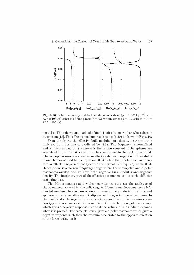
8 Generalizing the Concept of Negative Medium to Acoustic Waves 199
0.02 0.00 2000 0 −2000 4000 2000 04 2 0 −2 −40.00
0.01
0.02
0.03
0.04
0.05
ω a
/(2π
c)
Re[k0 / keff]Re[reff /
r0] Im[reff / r0] Im[k0 /
keff]
Fig. 8.10. Effective density and bulk modulus for rubber (ρ = 1, 300 kg m−3, κ =6.27 × 10⁵ Pa) spheres of filling ratio f = 0.1 within water (ρ = 1, 000 kg m−3, κ =2.15 × 10⁹ Pa)
particles. The spheres are made of a kind of soft silicone rubber whose data istaken from [18]. The effective medium result using (8.20) is shown in Fig. 8.10.
From the figure, the effective bulk modulus and density near the staticlimit are both positive as predicted by (8.3). The frequency is normalizedand is given as ωa/(2πc) where a is the lattice constant if the spheres areassembled into an fcc lattice and c is the sound speed in the background fluid.The monopolar resonance creates an effective dynamic negative bulk modulusabove the normalized frequency about 0.035 while the dipolar resonance cre-ates an effective negative density above the normalized frequency about 0.04.Hence, there is a narrow frequency range where the monopolar and dipolarresonances overlap and we have both negative bulk modulus and negativedensity. The imaginary part of the effective parameters is due to the diffusivescattering loss.
The Mie resonances at low frequency in acoustics are the analogue ofthe resonances created by the split-rings and bars in an electromagnetic left-handed medium. In the case of electromagnetic metamaterial, the bars andsplit-rings create negative electric dipolar and magnetic dipolar responses. Inthe case of double negativity in acoustic waves, the rubber spheres createtwo types of resonances at the same time. One is the monopolar resonancewhich gives a negative response such that the volume of the medium expandswhen it is pressed. The same structure gives a dipolar resonance which gives anegative response such that the medium accelerates to the opposite directionof the force acting on it.
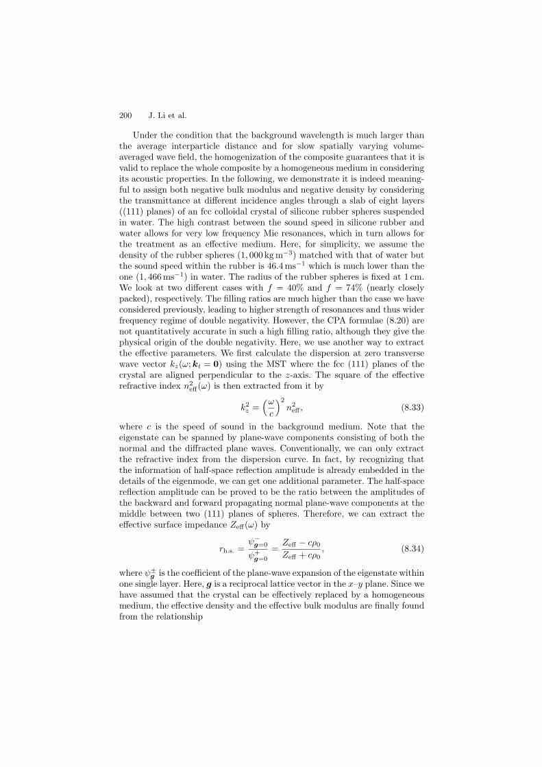
200 J. Li et al.
Under the condition that the background wavelength is much larger thanthe average interparticle distance and for slow spatially varying volume-averaged wave field, the homogenization of the composite guarantees that it isvalid to replace the whole composite by a homogeneous medium in consideringits acoustic properties. In the following, we demonstrate it is indeed meaning-ful to assign both negative bulk modulus and negative density by consideringthe transmittance at different incidence angles through a slab of eight layers((111) planes) of an fcc colloidal crystal of silicone rubber spheres suspendedin water. The high contrast between the sound speed in silicone rubber andwater allows for very low frequency Mie resonances, which in turn allows forthe treatment as an effective medium. Here, for simplicity, we assume thedensity of the rubber spheres (1, 000 kg m−3) matched with that of water butthe sound speed within the rubber is 46.4ms−1 which is much lower than theone (1, 466ms−1) in water. The radius of the rubber spheres is fixed at 1 cm.We look at two different cases with f = 40% and f = 74% (nearly closelypacked), respectively. The filling ratios are much higher than the case we haveconsidered previously, leading to higher strength of resonances and thus widerfrequency regime of double negativity. However, the CPA formulae (8.20) arenot quantitatively accurate in such a high filling ratio, although they give thephysical origin of the double negativity. Here, we use another way to extractthe effective parameters. We first calculate the dispersion at zero transversewave vector kz(ω;kt = 0) using the MST where the fcc (111) planes of thecrystal are aligned perpendicular to the z-axis. The square of the effectiverefractive index n2
eff(ω) is then extracted from it by
k2z =
(ω
c
)2
n2eff , (8.33)
where c is the speed of sound in the background medium. Note that theeigenstate can be spanned by plane-wave components consisting of both thenormal and the diffracted plane waves. Conventionally, we can only extractthe refractive index from the dispersion curve. In fact, by recognizing thatthe information of half-space reflection amplitude is already embedded in thedetails of the eigenmode, we can get one additional parameter. The half-spacereflection amplitude can be proved to be the ratio between the amplitudes ofthe backward and forward propagating normal plane-wave components at themiddle between two (111) planes of spheres. Therefore, we can extract theeffective surface impedance Zeff(ω) by
rh.s. =ψ−
g=0
ψ+g=0
=Zeff − cρ0
Zeff + cρ0, (8.34)
where ψ±g is the coefficient of the plane-wave expansion of the eigenstate within
one single layer. Here, g is a reciprocal lattice vector in the x–y plane. Since wehave assumed that the crystal can be effectively replaced by a homogeneousmedium, the effective density and the effective bulk modulus are finally foundfrom the relationship
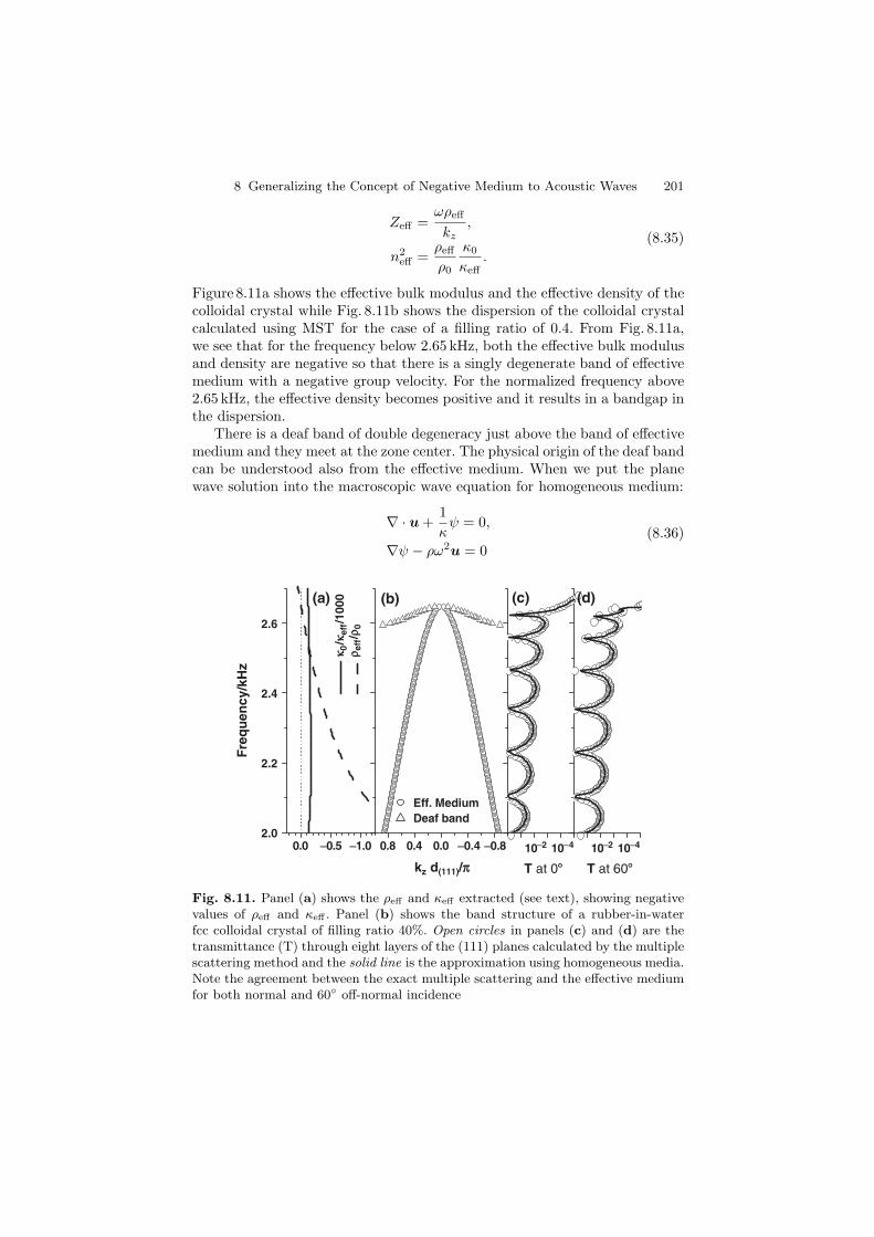
8 Generalizing the Concept of Negative Medium to Acoustic Waves 201
Zeff =ωρeff
kz,
n2eff =
ρeff
ρ0
κ0
κeff.
(8.35)
Figure 8.11a shows the effective bulk modulus and the effective density of thecolloidal crystal while Fig. 8.11b shows the dispersion of the colloidal crystalcalculated using MST for the case of a filling ratio of 0.4. From Fig. 8.11a,we see that for the frequency below 2.65 kHz, both the effective bulk modulusand density are negative so that there is a singly degenerate band of effectivemedium with a negative group velocity. For the normalized frequency above2.65 kHz, the effective density becomes positive and it results in a bandgap inthe dispersion.
There is a deaf band of double degeneracy just above the band of effectivemedium and they meet at the zone center. The physical origin of the deaf bandcan be understood also from the effective medium. When we put the planewave solution into the macroscopic wave equation for homogeneous medium:
∇ · u +1κ
ψ = 0,
∇ψ − ρω2u = 0(8.36)
10-2 10- 4 10-2 10- 42.0
2.2
2.4
2.6
0.0 -0.5 -1.0 0.8 0.4 0.0 -0.4 -0.8
Eff. Medium Deaf band
(d)(c)(b)
T at 608 T at 08 kz d(111)/p
(a)
Fre
qu
ency
/kH
z
k 0/k
eff/
1000
r eff
/r0
Fig. 8.11. Panel (a) shows the ρeff and κeff extracted (see text), showing negativevalues of ρeff and κeff . Panel (b) shows the band structure of a rubber-in-waterfcc colloidal crystal of filling ratio 40%. Open circles in panels (c) and (d) are thetransmittance (T) through eight layers of the (111) planes calculated by the multiplescattering method and the solid line is the approximation using homogeneous media.Note the agreement between the exact multiple scattering and the effective mediumfor both normal and 60 off-normal incidence
202 J. Li et al.
−1.0 −0.8 −0.6 −0.4 −0.2 0.0 0.2 0.4 0.6 0.8 1.0−1.0
−0.8
−0.6
−0.4
−0.2
0.0
0.2
0.4
0.6
0.8
1.0x
/ a
z / a−1.0 −0.8 −0.6 −0.4 −0.2 0.0 0.2 0.4 0.6 0.8 1.0
−1.0
−0.8
−0.6
−0.4
−0.2
0.0
0.2
0.4
0.6
0.8
1.0
x / a
z / a
Fig. 8.12. Pressure field at 2.64679 kHz on the z–x plane of (a) a normal longitu-dinal mode and (b) one of the two transverse modes of the deaf band. White/blackregion denotes positive/negative values
we obtain the expected longitudinal mode where the displacement vector (thepolarization of the mode) is parallel with the wave vector and the dispersion isk2 = ω2ρ/κ. We also get two extra transverse modes when the effective densityis zero. In this case, the macroscopic pressure field is zero, the displacementvector and the wave vector are arbitrary as long as they are perpendicular toeach other. Therefore, it should be a dispersion-less flat band at the frequencyof zero effective density. It becomes slightly dispersive away from the BrillouinZone center as shown in Fig. 8.11 due to the spatial dispersion effect in thecolloidal crystal. Figure 8.12a, b shows, respectively, the pressure field on thez–x plane of the longitudinal mode and the transverse mode of x-polarizationat 2.647 kHz. It verifies the prediction from the effective medium theory asthe longitudinal mode shows that the pressure field has the p-like orbitalsaligning in the z-direction while the p-like orbitals align in the x-direction forthe transverse mode of x-polarization.
In fact, from symmetry analysis, the deaf band has a Λ3 symmetry. Thisdeaf band cannot be excited by a normally incident wave [26], which has aΛ1 symmetry and it couples weakly even to an incident wave of an obliqueincidence angle. Also, any state of Λ3 symmetry contributes zero macroscopicpressure field as expected from effective medium theory. Since we know thatthis deaf band does not couple with incident wave and it is not the expectedlongitudinal mode, we do not use the deaf band in calculating the effectiveparameters. It avoids ambiguity in calculating effective parameters in the fre-quency regime where the normal longitudinal band and the deaf band overlap.
In Fig. 8.11c, d, we compare, respectively, the transmittance at normalincidence and 60 off normal incidence across the eight layers of particlescalculated by MST and the one calculated by replacing the colloidal crystalwith our effective medium of the same thickness. We found that the effectivemedium results agree very well with the results from the MST. Therefore, itdemonstrated the usefulness of the negative effective bulk modulus and density
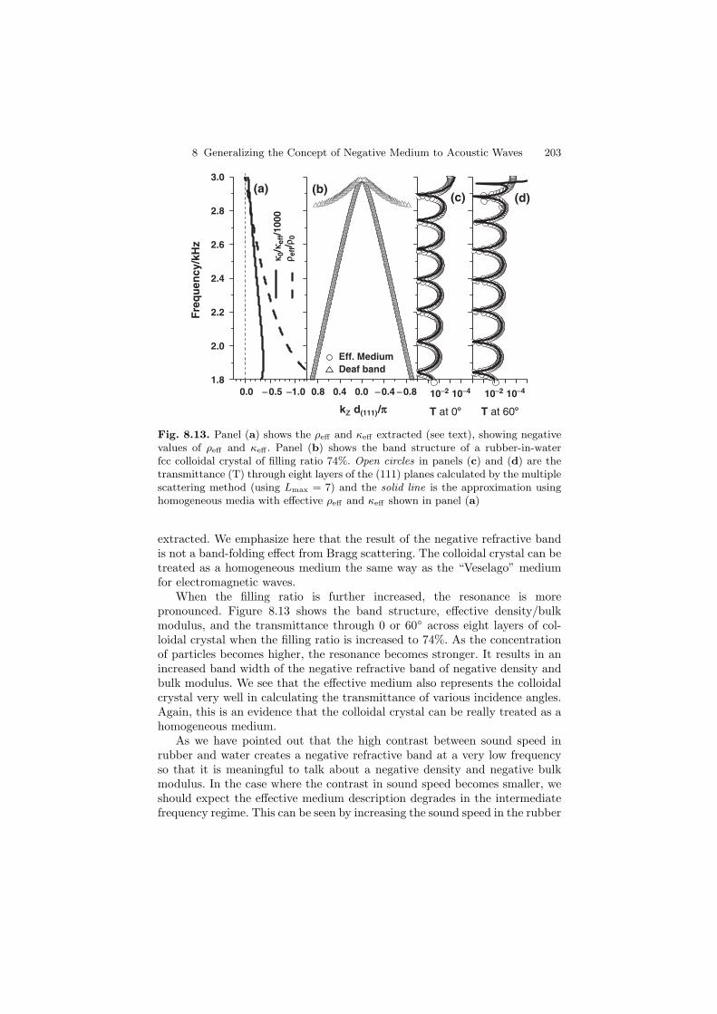
8 Generalizing the Concept of Negative Medium to Acoustic Waves 203
10-2 10-4 10-2 10-40.0 - 0.5 -1.0 0.8 0.4 0.0 - 0.4 - 0.8
Eff. Medium Deaf band
(d)(c)(b)
T at 608 T at 08 kz d(111) /p
(a)F
req
uen
cy/k
Hz
k 0/k
eff/1
000
r eff/r
0
1.8
2.0
2.2
2.4
2.6
2.8
3.0
Fig. 8.13. Panel (a) shows the ρeff and κeff extracted (see text), showing negativevalues of ρeff and κeff . Panel (b) shows the band structure of a rubber-in-waterfcc colloidal crystal of filling ratio 74%. Open circles in panels (c) and (d) are thetransmittance (T) through eight layers of the (111) planes calculated by the multiplescattering method (using Lmax = 7) and the solid line is the approximation usinghomogeneous media with effective ρeff and κeff shown in panel (a)
extracted. We emphasize here that the result of the negative refractive bandis not a band-folding effect from Bragg scattering. The colloidal crystal can betreated as a homogeneous medium the same way as the “Veselago” mediumfor electromagnetic waves.
When the filling ratio is further increased, the resonance is morepronounced. Figure 8.13 shows the band structure, effective density/bulkmodulus, and the transmittance through 0 or 60 across eight layers of col-loidal crystal when the filling ratio is increased to 74%. As the concentrationof particles becomes higher, the resonance becomes stronger. It results in anincreased band width of the negative refractive band of negative density andbulk modulus. We see that the effective medium also represents the colloidalcrystal very well in calculating the transmittance of various incidence angles.Again, this is an evidence that the colloidal crystal can be really treated as ahomogeneous medium.
As we have pointed out that the high contrast between sound speed inrubber and water creates a negative refractive band at a very low frequencyso that it is meaningful to talk about a negative density and negative bulkmodulus. In the case where the contrast in sound speed becomes smaller, weshould expect the effective medium description degrades in the intermediatefrequency regime. This can be seen by increasing the sound speed in the rubber
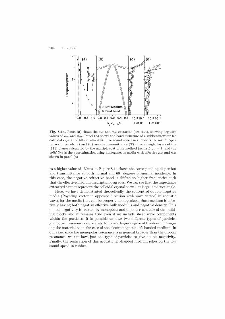
204 J. Li et al.
10-2 10-4 10-2 10-4
7
8
9
0.0 -0.5 -1.0 0.8 0.4 0.0 -0.4 -0.8
Eff. MediumDeaf band
(d)(c)(b)
T at 60T at 0kz d(111)/p
(a)
Fre
qu
ency
/kH
z
k 0/k
eff/
100
r eff/r
0
Fig. 8.14. Panel (a) shows the ρeff and κeff extracted (see text), showing negativevalues of ρeff and κeff . Panel (b) shows the band structure of a rubber-in-water fcccolloidal crystal of filling ratio 40%. The sound speed in rubber is 150 ms−1. Opencircles in panels (c) and (d) are the transmittance (T) through eight layers of the(111) planes calculated by the multiple scattering method (using Lmax = 7) and thesolid line is the approximation using homogeneous media with effective ρeff and κeff
shown in panel (a)
to a higher value of 150ms−1. Figure 8.14 shows the corresponding dispersionand transmittance at both normal and 60 degrees off-normal incidence. Inthis case, the negative refractive band is shifted to higher frequencies suchthat the effective medium description degrades. We can see that the impedanceextracted cannot represent the colloidal crystal so well at large incidence angle.
Here, we have demonstrated theoretically the concept of double-negativemedia (Poynting vector in opposite direction with wave vector) in acousticwaves for the media that can be properly homogenized. Such medium is effec-tively having both negative effective bulk modulus and negative density. Thisdouble negativity is created by monopolar and dipolar resonance of the build-ing blocks and it remains true even if we include shear wave componentswithin the particles. It is possible to have two different types of particlesgiving two resonances separately to have a larger degree of freedom in design-ing the material as in the case of the electromagnetic left-handed medium. Inour case, since the monopolar resonance is in general broader than the dipolarresonance, we can have just one type of particles to give double negativity.Finally, the realization of this acoustic left-handed medium relies on the lowsound speed in rubber.
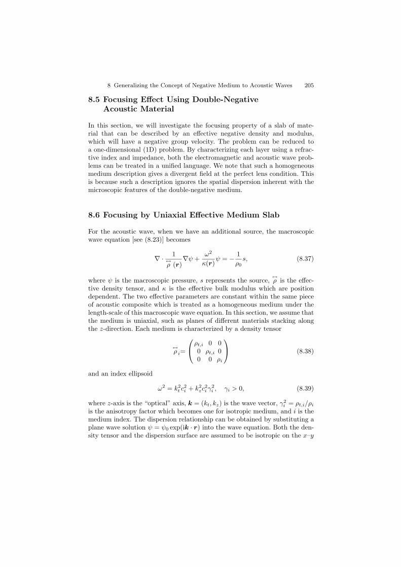
8 Generalizing the Concept of Negative Medium to Acoustic Waves 205
8.5 Focusing Effect Using Double-NegativeAcoustic Material
In this section, we will investigate the focusing property of a slab of mate-rial that can be described by an effective negative density and modulus,which will have a negative group velocity. The problem can be reduced toa one-dimensional (1D) problem. By characterizing each layer using a refrac-tive index and impedance, both the electromagnetic and acoustic wave prob-lems can be treated in a unified language. We note that such a homogeneousmedium description gives a divergent field at the perfect lens condition. Thisis because such a description ignores the spatial dispersion inherent with themicroscopic features of the double-negative medium.
8.6 Focusing by Uniaxial Effective Medium Slab
For the acoustic wave, when we have an additional source, the macroscopicwave equation [see (8.23)] becomes
∇ · 1↔ρ (r)
∇ψ +ω2
κ(r)ψ = − 1
ρ0s, (8.37)
where ψ is the macroscopic pressure, s represents the source,↔ρ is the effec-
tive density tensor, and κ is the effective bulk modulus which are positiondependent. The two effective parameters are constant within the same pieceof acoustic composite which is treated as a homogeneous medium under thelength-scale of this macroscopic wave equation. In this section, we assume thatthe medium is uniaxial, such as planes of different materials stacking alongthe z-direction. Each medium is characterized by a density tensor
↔ρ i=
⎛⎝
ρt,i 0 00 ρt,i 00 0 ρi
⎞⎠ (8.38)
and an index ellipsoid
ω2 = k2t c2
i + k2zc2
i γ2i , γi > 0, (8.39)
where z-axis is the “optical” axis, k = (kt, kz) is the wave vector, γ2i = ρt,i/ρi
is the anisotropy factor which becomes one for isotropic medium, and i is themedium index. The dispersion relationship can be obtained by substituting aplane wave solution ψ = ψ0 exp(ik · r) into the wave equation. Both the den-sity tensor and the dispersion surface are assumed to be isotropic on the x–y

206 J. Li et al.
plane. On a planar interface between two mediums, the boundary condition(which is already embedded in (8.37) is the continuity of
ψ and z · 1↔ρ∇ψ =
1ρ
∂ψ
∂z. (8.40)
In this section, we would like to solve the Green’s function satisfying(∇ · 1
↔ρ (r)
∇ +ω2
κ(r)
)G(r, r′) = − 1
ρ0δ(r − r′), (8.41)
where the source is situated at r′ = z′z within the region of backgroundmedium of (isotropic) density ρ0 and sound speed c. Since the transverse wavevector is conserved across the planar interfaces, it is convenient to expand theGreen’s function as
G(r, r′) =∫
dkt
(2π)2eikt·rg(kt; z, z′), (8.42)
where the z-axis is along the normal direction of the interface, and t labelsthe vectors parallel to the interface. This expansion decouples the probleminto a 1D problem, where g(kt; z, z′) is the 1D Green’s function for waves ata fixed transverse wave vector, satisfying
(ρ(z)
ddz
1ρ(z)
ddz
+ k2z(z)
)g(kt ; z, z′) = −δ(z − z′). (8.43)
In a source-free region, this equation becomes the 1D wave equation
− Z
nz
ddz
(1
Znz
ddz
g(kt ; z, z′))
=(ω
c
)2
g(kt ; z, z′), (8.44)
where the acoustic surface impedance and the refractive index are defined by
Z =ωρ
kz,
nz =ckz
ω.
(8.45)
The sign of kz is determined by the sign of impedance which is conventionallytaken to be positive here similar to the case of electromagnetic wave.
We now first consider the focusing effect of a single interface separating anordinary isotropic medium (medium 1), such as air on the left and a uniaxialdouble-negative medium (medium 2) on the right, as shown in Fig. 8.15. Theinterface is located at z = 0. Medium 2 has a negative group velocity inthe sense that the dispersion surface (an ellipsoid) shrinks when frequencyincreases. The optical axes of the two media are both aligned to the z-axis.
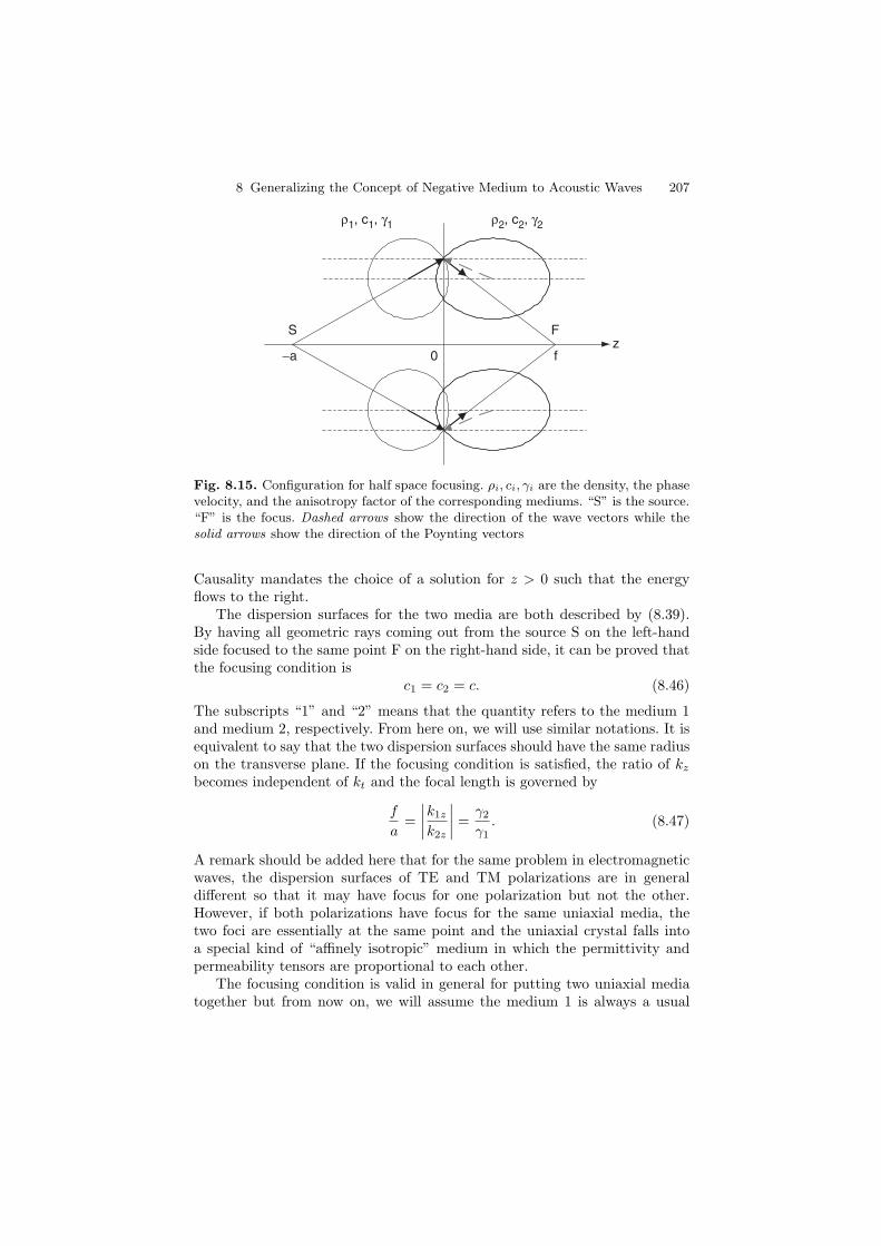
8 Generalizing the Concept of Negative Medium to Acoustic Waves 207
S F
ρ1, c1, γ1 ρ2, c2, γ2
f−a 0z
Fig. 8.15. Configuration for half space focusing. ρi, ci, γi are the density, the phasevelocity, and the anisotropy factor of the corresponding mediums. “S” is the source.“F” is the focus. Dashed arrows show the direction of the wave vectors while thesolid arrows show the direction of the Poynting vectors
Causality mandates the choice of a solution for z > 0 such that the energyflows to the right.
The dispersion surfaces for the two media are both described by (8.39).By having all geometric rays coming out from the source S on the left-handside focused to the same point F on the right-hand side, it can be proved thatthe focusing condition is
c1 = c2 = c. (8.46)
The subscripts “1” and “2” means that the quantity refers to the medium 1and medium 2, respectively. From here on, we will use similar notations. It isequivalent to say that the two dispersion surfaces should have the same radiuson the transverse plane. If the focusing condition is satisfied, the ratio of kz
becomes independent of kt and the focal length is governed by
f
a=
∣∣∣∣k1z
k2z
∣∣∣∣ =γ2
γ1. (8.47)
A remark should be added here that for the same problem in electromagneticwaves, the dispersion surfaces of TE and TM polarizations are in generaldifferent so that it may have focus for one polarization but not the other.However, if both polarizations have focus for the same uniaxial media, thetwo foci are essentially at the same point and the uniaxial crystal falls intoa special kind of “affinely isotropic” medium in which the permittivity andpermeability tensors are proportional to each other.
The focusing condition is valid in general for putting two uniaxial mediatogether but from now on, we will assume the medium 1 is always a usual
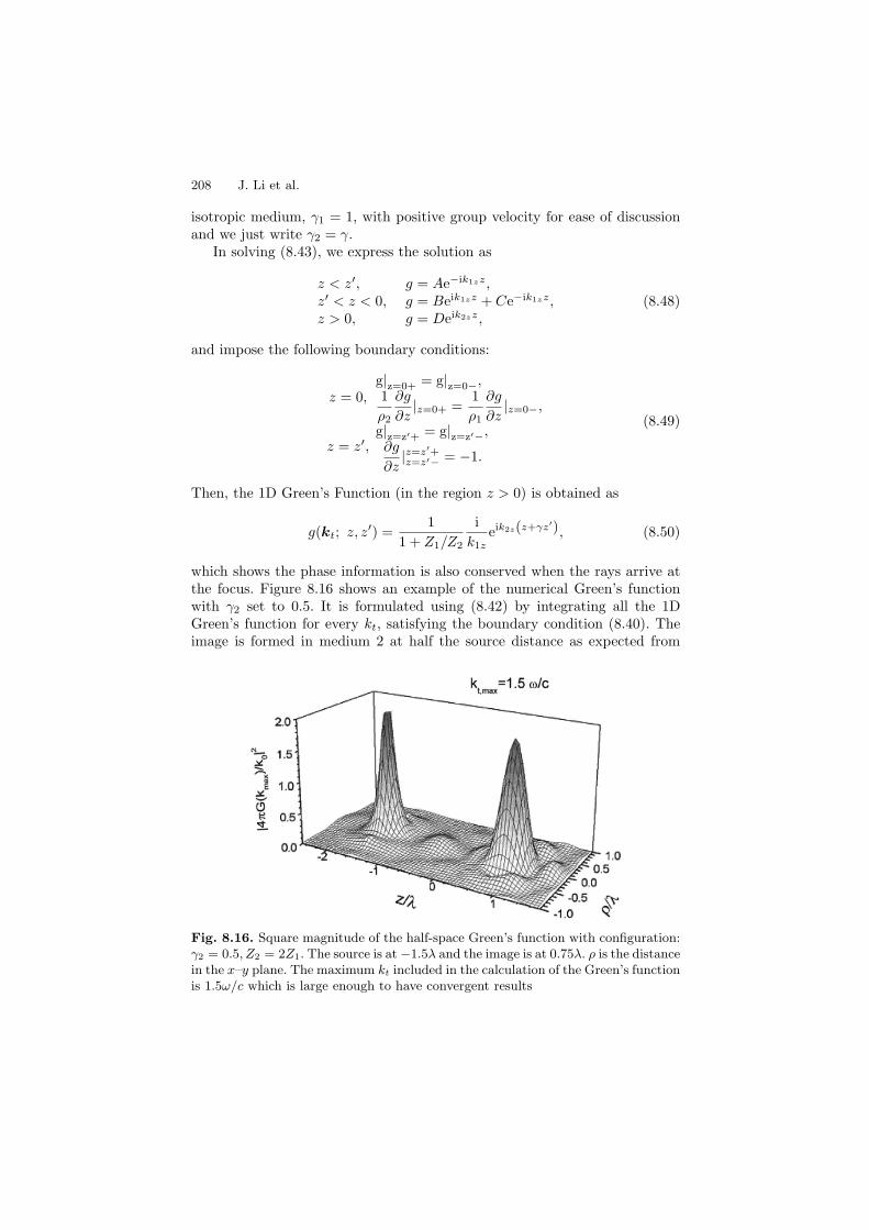
208 J. Li et al.
isotropic medium, γ1 = 1, with positive group velocity for ease of discussionand we just write γ2 = γ.
In solving (8.43), we express the solution as
z < z′, g = Ae−ik1zz,z′ < z < 0, g = Beik1zz + Ce−ik1zz,z > 0, g = Deik2zz,
(8.48)
and impose the following boundary conditions:
z = 0,g|z=0+ = g|z=0−,1ρ2
∂g
∂z|z=0+ =
1ρ1
∂g
∂z|z=0−,
z = z′,g|z=z′+ = g|z=z′−,∂g
∂z|z=z′+z=z′− = −1.
(8.49)
Then, the 1D Green’s Function (in the region z > 0) is obtained as
g(kt; z, z′) =1
1 + Z1/Z2
ik1z
eik2z(z+γz′), (8.50)
which shows the phase information is also conserved when the rays arrive atthe focus. Figure 8.16 shows an example of the numerical Green’s functionwith γ2 set to 0.5. It is formulated using (8.42) by integrating all the 1DGreen’s function for every kt, satisfying the boundary condition (8.40). Theimage is formed in medium 2 at half the source distance as expected from
Fig. 8.16. Square magnitude of the half-space Green’s function with configuration:γ2 = 0.5, Z2 = 2Z1. The source is at −1.5λ and the image is at 0.75λ. ρ is the distancein the x–y plane. The maximum kt included in the calculation of the Green’s functionis 1.5ω/c which is large enough to have convergent results
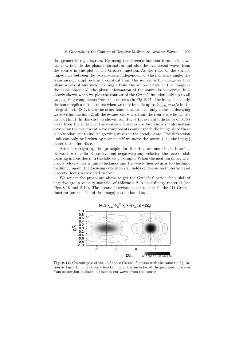
8 Generalizing the Concept of Negative Medium to Acoustic Waves 209
the geometric ray diagram. By using the Green’s function formulation, wecan now include the phase information and also the evanescent waves fromthe source in the plot of the Green’s function. As the ratio of the surfaceimpedance between the two media is independent of the incidence angle, thetransmission amplitude is a constant from the source to the image so thatplane waves of any incidence angle from the source arrive at the image atthe same phase. All the phase information of the source is conserved. It isclearly shown when we plot the contour of the Green’s function only up to allpropagating components from the source as in Fig. 8.17. The image is exactlythe same replica of the source when we only include up to kt,max = ω/c in theintegration in (8.42). On the other hand, since we can only choose a decayingwave within medium 2, all the evanescent waves from the source are lost in thefar field limit. In this case, as shown from Fig. 8.16, even at a distance of 0.75λaway from the interface, the evanescent waves are lost already. Informationcarried by the evanescent wave components cannot reach the image since thereis no mechanism to induce growing waves in the steady state. The diffractionlimit can only be broken by near field if we move the source (i.e., the image)closer to the interface.
After investigating the principle for focusing on one single interfacebetween two media of positive and negative group velocity, the case of slabfocusing is considered in the following example. When the medium of negativegroup velocity has a finite thickness and the wave then returns to the samemedium 1 again, the focusing condition still holds on the second interface anda second focus is expected to form.
We repeat the procedure above to get the Green’s function for a slab ofnegative group velocity material of thickness d in an ordinary material (seeFigs. 8.18 and 8.19). The second interface is set to z = 0, the 1D Green’sfunction (on the side of the image) can be found as
Fig. 8.17. Contour plot of the half-space Green’s function with the same configura-tion as Fig. 8.16. The Green’s function here only includes all the propagating wavesfrom source but excludes all evanescent waves from the source
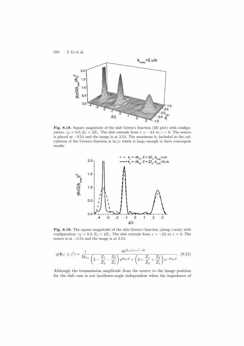
210 J. Li et al.
Fig. 8.18. Square magnitude of the slab Green’s function (3D plot) with configu-ration: γ2 = 0.5, Z2 = 2Z1. The slab extends from z = −2λ to z = 0. The sourceis placed at −3.5λ and the image is at 2.5λ. The maximum kt included in the cal-culation of the Green’s function is 2ω/c which is large enough to have convergentresults
Fig. 8.19. The square magnitude of the slab Green’s function (along z-axis) withconfiguration: γ2 = 0.5, Z2 = 2Z1. The slab extends from z = −2λ to z = 0. Thesource is at −3.5λ and the image is at 2.5λ
g(kt; z, z′) =i
2k1z
4eik1z(z−z′−d)
(2 − Z1
Z2− Z2
Z1
)eik2zd +
(2 +
Z1
Z2+
Z2
Z1
)e−ik2zd
. (8.51)
Although the transmission amplitude from the source to the image positionfor the slab case is not incidence-angle independent when the impedance of
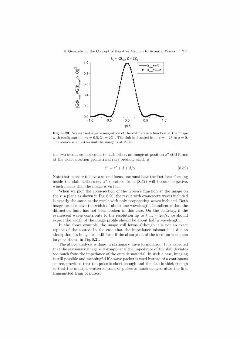
8 Generalizing the Concept of Negative Medium to Acoustic Waves 211
Fig. 8.20. Normalized square magnitude of the slab Green’s function at the imagewith configuration: γ2 = 0.5, Z2 = 2Z1. The slab is situated from z = −2λ to z = 0.The source is at −3.5λ and the image is at 2.5λ
the two media are not equal to each other, an image at position z′′ still formsat the exact position geometrical rays predict, which is
z′′ = z′ + d + d/γ. (8.52)
Note that in order to have a second focus, one must have the first focus forminginside the slab. Otherwise, z′′ obtained from (8.52) will become negative,which means that the image is virtual.
When we plot the cross-section of the Green’s function at the image onthe x–y plane as shown in Fig. 8.20, the result with evanescent waves includedis exactly the same as the result with only propagating waves included. Bothimage profiles have the width of about one wavelength. It indicates that thediffraction limit has not been broken in this case. On the contrary, if theevanescent waves contribute to the resolution up to kmax = 2ω/c, we shouldexpect the width of the image profile should be about half a wavelength.
In the above example, the image still forms although it is not an exactreplica of the source. In the case that the impedance mismatch is due toabsorption, an image can still form if the absorption of the medium is not toolarge as shown in Fig. 8.21.
The above analysis is done in stationary wave formulation. It is expectedthat the stationary image will disappear if the impedance of the slab deviatestoo much from the impedance of the outside material. In such a case, imagingis still possible and meaningful if a wave packet is used instead of a continuoussource, provided that the pulse is short enough and the slab is thick enoughso that the multiple-scattered train of pulses is much delayed after the firsttransmitted train of pulses.
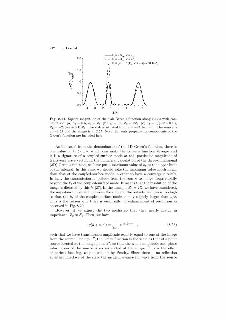
212 J. Li et al.
Fig. 8.21. Square magnitude of the slab Green’s function along z-axis with con-figuration: (a) γ2 = 0.5, Z2 = Z1; (b) γ2 = 0.5, Z2 = 2Z1; (c) γ2 = 1/(−2 + 0.1i),Z2 = −2/(−2 + 0.1i)Z1. The slab is situated from z = −2λ to z = 0. The source isat −3.5λ and the image is at 2.5λ. Note that only propagating components of theGreen’s function are included here
As indicated from the denominator of the 1D Green’s function, there isone value of kt > ω/c which can make the Green’s function diverge andit is a signature of a coupled-surface mode at this particular magnitude oftransverse wave vector. In the numerical calculation of the three-dimensional(3D) Green’s function, we have put a maximum value of kt as the upper limitof the integral. In this case, we should take the maximum value much largerthan that of the coupled-surface mode in order to have a convergent result.In fact, the transmission amplitude from the source to image drops rapidlybeyond the kt of the coupled-surface mode. It means that the resolution of theimage is dictated by this kt [27]. In the example Z2 = 2Z1 we have considered,the impedance mismatch between the slab and the outside medium is too highso that the kt of the coupled-surface mode is only slightly larger than ω/c.This is the reason why there is essentially no enhancement of resolution asobserved in Fig. 8.20.
However, if we adjust the two media so that they nearly match inimpedance, Z2 ≈ Z1. Then, we have
g(kt; z, z′) =i
2k1zeik1z(z−z′′), (8.53)
such that we have transmission amplitude exactly equal to one at the imagefrom the source. For z > z′′, the Green function is the same as that of a pointsource located at the image point z′′, so that the whole amplitude and phaseinformation of the source is reconstructed at the image. This is the effectof perfect focusing, as pointed out by Pendry. Since there is no reflectionat either interface of the slab, the incident evanescent wave from the source

8 Generalizing the Concept of Negative Medium to Acoustic Waves 213
Fig. 8.22. Square magnitude of the slab Green’s function (the transverse plane atimage) with configuration: γ2 = 0.5, Z2 = Z1. The slab is situated from z = −2λ toz = 0. The source is at −3.5λ and the image is at 2.5λ
directly triggers a surface mode on the second interface. This surface modeprovides a mechanism which is not available in half-space configuration toamplify the evanescent wave within the slab to compensate exactly the decayin the region between the source and the first interface and the region betweenthe second interface and the image. When we plot the Green’s function onthe transverse plane at the image point as shown in Fig. 8.22, the Green’sfunction on the transverse plane at the location of the image becomes sharperand sharper as the maximum value of kt increases. However, as kt > ω/c,a surface mode of larger amplitude is required to compensate the decay ofthe evanescent wave. Therefore, as shown in Fig. 8.23, the field between thefirst and second focus in fact increases without bound if we increase kt,max
to infinity. In this case, several assumptions (such as ignoring nonlocal effectsand ignoring nonlinear effects) actually breaks down, and it can be shownthat such a final state requires a very long time [28] to establish in practiceeven if we assume the effective medium description remains valid.
Finally, we calculate the field pattern using multiple point sources insteadof only one. As shown in Fig. 8.24, we purposely only integrate up to allpropagating wave components in the Green’s function, and we see that thesame image shape forms. The image formed outside has the same aspect ratioand is fully restored as the source although the image within the slab can beelongated or compressed in the z-direction depending on the anisotropy factor.
In this section, we investigated the focusing problem of double negativeacoustic media with a negative refraction index. Two cases are analyzed withthe Green’s function method, one involves only one interface, and another is aslab with finite thickness. For the former, acoustic waves from a point sourceoutside the crystal can be focused to a diffraction-limited spot inside this
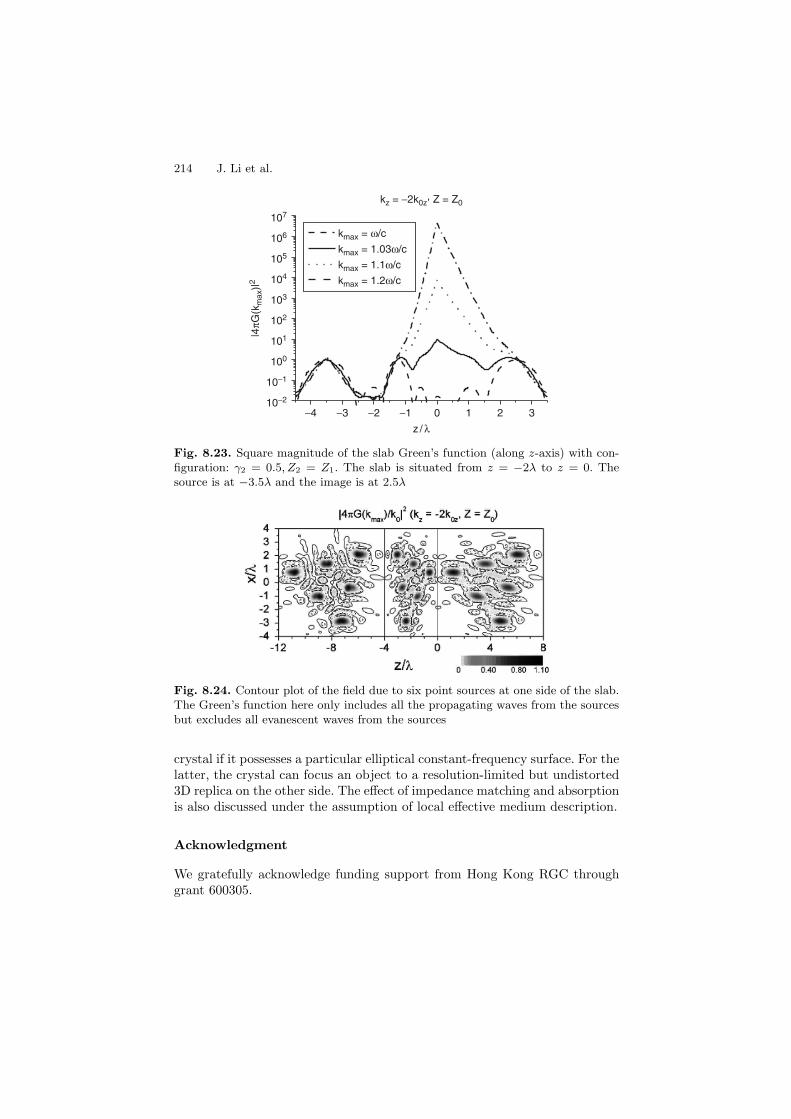
214 J. Li et al.
−4 −3 −2 −1 0 1 2 310−2
10−1
100
101
102
103
104
105
106
107
kz = −2k0z, Z = Z0
|4πG
(km
ax)|
2
z / λ
kmax = ω/c
kmax = 1.03ω/c
kmax = 1.1ω/c
kmax = 1.2ω/c
Fig. 8.23. Square magnitude of the slab Green’s function (along z-axis) with con-figuration: γ2 = 0.5, Z2 = Z1. The slab is situated from z = −2λ to z = 0. Thesource is at −3.5λ and the image is at 2.5λ
Fig. 8.24. Contour plot of the field due to six point sources at one side of the slab.The Green’s function here only includes all the propagating waves from the sourcesbut excludes all evanescent waves from the sources
crystal if it possesses a particular elliptical constant-frequency surface. For thelatter, the crystal can focus an object to a resolution-limited but undistorted3D replica on the other side. The effect of impedance matching and absorptionis also discussed under the assumption of local effective medium description.
Acknowledgment
We gratefully acknowledge funding support from Hong Kong RGC throughgrant 600305.
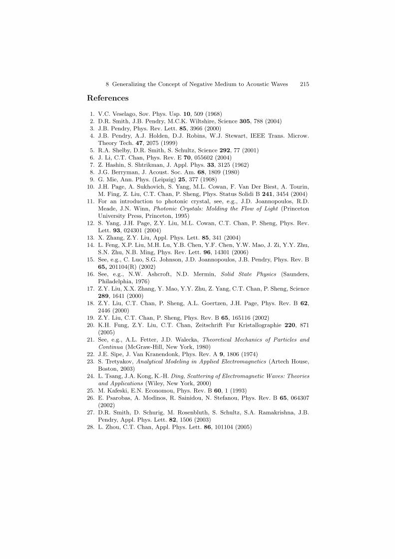
8 Generalizing the Concept of Negative Medium to Acoustic Waves 215
References
1. V.C. Veselago, Sov. Phys. Usp. 10, 509 (1968)2. D.R. Smith, J.B. Pendry, M.C.K. Wiltshire, Science 305, 788 (2004)3. J.B. Pendry, Phys. Rev. Lett. 85, 3966 (2000)4. J.B. Pendry, A.J. Holden, D.J. Robins, W.J. Stewart, IEEE Trans. Microw.
Theory Tech. 47, 2075 (1999)5. R.A. Shelby, D.R. Smith, S. Schultz, Science 292, 77 (2001)6. J. Li, C.T. Chan, Phys. Rev. E 70, 055602 (2004)7. Z. Hashin, S. Shtrikman, J. Appl. Phys. 33, 3125 (1962)8. J.G. Berryman, J. Acoust. Soc. Am. 68, 1809 (1980)9. G. Mie, Ann. Phys. (Leipzig) 25, 377 (1908)
10. J.H. Page, A. Sukhovich, S. Yang, M.L. Cowan, F. Van Der Biest, A. Tourin,M. Fing, Z. Liu, C.T. Chan, P. Sheng, Phys. Status Solidi B 241, 3454 (2004)
11. For an introduction to photonic crystal, see, e.g., J.D. Joannopoulos, R.D.Meade, J.N. Winn, Photonic Crystals: Molding the Flow of Light (PrincetonUniversity Press, Princeton, 1995)
12. S. Yang, J.H. Page, Z.Y. Liu, M.L. Cowan, C.T. Chan, P. Sheng, Phys. Rev.Lett. 93, 024301 (2004)
13. X. Zhang, Z.Y. Liu, Appl. Phys. Lett. 85, 341 (2004)14. L. Feng, X.P. Liu, M.H. Lu, Y.B. Chen, Y.F. Chen, Y.W. Mao, J. Zi, Y.Y. Zhu,
S.N. Zhu, N.B. Ming, Phys. Rev. Lett. 96, 14301 (2006)15. See, e.g., C. Luo, S.G. Johnson, J.D. Joannopoulos, J.B. Pendry, Phys. Rev. B
65, 201104(R) (2002)16. See, e.g., N.W. Ashcroft, N.D. Mermin, Solid State Physics (Saunders,
Philadelphia, 1976)17. Z.Y. Liu, X.X. Zhang, Y. Mao, Y.Y. Zhu, Z. Yang, C.T. Chan, P. Sheng, Science
289, 1641 (2000)18. Z.Y. Liu, C.T. Chan, P. Sheng, A.L. Goertzen, J.H. Page, Phys. Rev. B 62,
2446 (2000)19. Z.Y. Liu, C.T. Chan, P. Sheng, Phys. Rev. B 65, 165116 (2002)20. K.H. Fung, Z.Y. Liu, C.T. Chan, Zeitschrift Fur Kristallographie 220, 871
(2005)21. See, e.g., A.L. Fetter, J.D. Walecka, Theoretical Mechanics of Particles and
Continua (McGraw-Hill, New York, 1980)22. J.E. Sipe, J. Van Kranendonk, Phys. Rev. A 9, 1806 (1974)23. S. Tretyakov, Analytical Modeling in Applied Electromagnetics (Artech House,
Boston, 2003)24. L. Tsang, J.A. Kong, K.-H. Ding, Scattering of Electromagnetic Waves: Theories
and Applications (Wiley, New York, 2000)25. M. Kafeski, E.N. Economou, Phys. Rev. B 60, 1 (1993)26. E. Psarobas, A. Modinos, R. Sainidou, N. Stefanou, Phys. Rev. B 65, 064307
(2002)27. D.R. Smith, D. Schurig, M. Rosenbluth, S. Schultz, S.A. Ramakrishna, J.B.
Pendry, Appl. Phys. Lett. 82, 1506 (2003)28. L. Zhou, C.T. Chan, Appl. Phys. Lett. 86, 101104 (2005)
9
Experiments and Simulations of MicrowaveNegative Refraction in Split Ring and WireArray Negative Index Materials, 2D Split-RingResonator and 2D Metallic Disk PhotonicCrystals
F.J. Rachford, D.L. Smith and P.F. Loschialpo
Summary. In this chapter, we describe a series of simulations and experimentson composites displaying negative refraction. The materials consist of both splitring resonator/wire structures and 2D photonic crystals. The finite difference timedomain simulations were found to closely correspond to our microwave frequencymeasurements. Our exploration of photonic structures evolved from the serendip-itous experimental observation that our early split ring resonators exhibited pla-nar slab focusing in the absence of a wire grid. Although split ring resonator/wiregrid composites were shown to display negative index behavior over a vary narrowband-pass, the photonic crystal structures display negative phase propagation andnegative refraction over a much larger frequency band.
9.1 Introduction
Our group at the Naval Research Laboratory initiated a program of mea-surement, simulation, and analytic analysis of composite materials havinga negative index (NIM) soon after the pioneering publications of Smithet al. [1–4]. Smith et al. performed microwave transmission measurementscombining two artificial media devised by Pendry [5–7]: A conducting wirearray to introduce a controllable composite plasma frequency and negativepermittivity in the microwave region and a double-split-ring resonator (SRR)array to provide a sharp narrow band negative permeability at a limitedfrequency band above the SRR resonance. Ideally the composite geometry isarranged so that the plasma frequency and the magnetic antiresonance (thefrequency where the permeability recrosses zero above magnetic resonance)coincide. These structured composites were predicted to exhibit a (mean field)negative refractive index over a narrow frequency band above the SRR reso-nance [8–10]. Prism refraction [11] and planar slab focusing experiments haveconfirmed the existence of negative refraction for the SRR/wire compositesin a narrow frequency band.
218 F.J. Rachford et al.
These early publications demonstrated that composites of split-ringresonators (SRRs) and wires could realize Veselogo’s [12] prediction thata medium with simultaneous negative permittivity and permeability will pro-duce a “left-handed” material with unusual refractive properties. Critiquesand controversy [13–16] ensued after the initial work leading us to a detailedinvestigation of the effect. In this chapter, we present results of accurate finitedifference time domain (FDTD) simulations and experiments. The FDTDwork employed idealized but causal constitutive parameters with Lorentzianfrequency and Drude type frequency dependences as well as detailed metal-lic SRR and wire structure representations and detailed photonic crystalconstructs. The experimental work investigated these SRR/wire structuresand metallic disk photonic crystal assemblies.
In the course of our investigations we noted that some of our compos-ites displayed negative refraction at frequencies above the plasma frequencyand also in structures without wire arrays to provide a negative permittivity.FDTD and experimental work indicated that these structures were acting asnegatively refracting photonic crystals. Notomi [17] and others [18–23] havealso shown that photonic crystals can evidence negative refraction near thebandgap edge. Recent simulations and experiments have indicated that focus-ing by planar slabs [24] and other manifestations of negative refractive indexcan be observed in photonic crystals at microwave frequencies. In addition,other unusual refractive phenomena such as superprism effects [25] have alsobe seen in PC materials.
We find that arrays of Pendry type SRRs without wires displayed refractionand focusing indicative of negative index behavior with GHz wide bandwidths[26]. Replacing SRRs with metal disks having the same outside diameter andarrayed on the same scale also displayed focusing and refraction associatedwith negative index behavior over the same wide frequency band. We fol-low the displacement of the focus with increasing frequency from near fieldto more than ten wavelengths behind the arrays. FDTD simulations [27] ofhexagonal disk arrays and hexagonal annulus arrays display similar behaviorand demonstrate that wave propagation in our structures is refractive ratherthan diffractive in nature. Although the metallic structures described in thiswork are on the order of a third of a free space wavelength, the FDTD simula-tion of the wave propagation in the composite does not display multiple beamformation or coherent scattering characteristic of a diffractive medium butshows a continuous propagation in the medium that can be accurately char-acterized by an anisotropic index of refraction. Close inspection of the electricand magnetic fields in proximity to the small structures of the metallic ringsand disks shows very complicated behavior. Averaging the fields on a coarserscale we find a regular progression of electromagnetic amplitude and phase.It is in this sense that we can assign an index and an averaged permittivityand permeability to these media. Experimentally, we derive estimates of theeffective index of refraction for the disk array from the displacement of an offnormal microwave beam emerging from the stack.
9 Experiments and Simulations of Microwave Negative Refraction 219
In this chapter we first examine negative refraction in an idealized NIM.Then we review simulations and measurements on a SRR/wire composite.This led to the observation that a hexagonal SRR array can act as a neg-atively refracting 2D photonic crystal. Replacing the SRR constructs withmetal disks of the same outer diameter reduced the complexity of the trans-mission spectrum and enabled detailed simulations of negative refraction inthese 2D structures. Measurements then confirmed simulations and led toestimates for the frequency-dependent index.
9.2 Theory
The Pendry wire array plasma frequency for a wire array suspended in freespace is given by
fp =c
a
√2π ln
(a
r
) , (9.1)
where a is the wire lattice spacing and r is the wire radius. The double-split-ring resonance frequency (free space) is given by
fo =c
2π
√√√√√3
πεr3 ln(
2w
d
) , (9.2)
with being the ring layer spacing, w the width of the rings, d is the gap widthbetween inner and outer rings, r is the inner ring radius, ε is the permittivityof the inter-ring gap, and c is the velocity of light. In a medium the effectivespacing of the array and the self-inductance of the array are affected by theindex and local permeability. Similarly the resonant frequency of the SRRsmodified by the local values of µ and ε: In practice the plasma frequencyand SRR resonance in string wire structures are strongly influenced by theinteraction between the wire array and the SRRs and cannot be accuratelycalculated with simple modifications to the Pendry formulae.
In Smith’s first realization of the wire/split-ring (WSR) medium the three-dimensional orthogonally interpenetrating Pendry wire array is replaced bya monodirectional square lattice array of wires separated from the SRRs byfree space. As long as the microwave radiation transmitted through this wireassembly is confined to propagation in the plane normal to the wire axis withelectric polarization along the wire axis there will be a plasma resonance andthe plasma frequency should be approximated by (9.1).
Smith’s split-ring structures were first created as stacked planar squarearrays [1] and later as two orthogonal stacked arrays [4]. The wire axes werestructured to lie parallel to the split-ring array plane. The combined WSRstacks were confined in a parallel plate transmission line and measurementswere limited to a small portion of a waveguide band. They reported negative
220 F.J. Rachford et al.
index for a narrow transmission peak identified with the split-ring resonancein their composite. In fact the first realization of the SRR/wire mediumemployed large diameter wires that were capacitively tuned by varying thespacing of their ends from the top face of the parallel plate waveguide contain-ing the structure and propagating microwave fields [28]. The Pendry formulaewere only used as first estimates of the fp and fo, and the structure wastuned experimentally.
Here we first study idealized functional permittivity and permeability inthe double negative regime and then proceed to analysis and experiments onsimple SRR/wire array structures and eventually to photonic crystals con-structed of SRR structures and simple metal disks.
9.3 FDTD Simulations in an Ideal NegativeIndex Medium
Initial realizations of NIM composite materials have employed metallicelements imbedded in dielectric that are often a substantial fraction of afree space wavelength. In most cases the structures are inherently anisotropicand lossy and in some cases, diffractive effects and impedance boundary mis-matches obscure the negative index of refraction [29–32]. To answer severalfundamental issues we ran FDTD simulations involving idealized isotropicfully causal representations of permittivity and permeability. We choose thetime step for all FDTD simulations in this paper to satisfy the Courant–Friederichs–Lewy condition [33]:
c∆t =1√(
1∆x
)2 +(
1∆y
)2
+(
1∆z
)2
, (9.3)
where c is the velocity of light ∆t is the time step, ∆x, ∆y, and ∆z are thesimulation grid increments.
We set µ = ε = −1 to eliminate boundary impedance mismatches. Neg-ative permittivity or permeability requires strong dispersion which we modelusing the same Lorentzian form and parameters for both:
F (f) = 1 +K − 1
1 − i(
fG
f2o
)−
(f
fo
)2 , (9.4)
where µ(f) = ε(f) = F (f) and µdc = εdc = K. The FDTD code [27] used toperform the numerical experiments was validated extensively with laboratoryexperiments some of which are described below. In the following simulationsthe code employs perfectly matched layer [34] type of absorbing boundariesin the dimensions of finite extent and periodic boundary conditions in thedimensions of infinite extent.
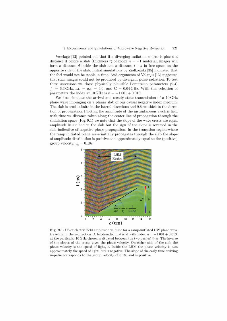
9 Experiments and Simulations of Microwave Negative Refraction 221
Veselago [12] pointed out that if a diverging radiation source is placed adistance d before a slab (thickness t) of index n = −1 material, images willform a distance d inside the slab and a distance t − d in free space on theopposite side of the slab. Initial simulations by Ziolkowski [35] indicated thatthe foci would not be stable in time. And arguments of Valanju [13] suggestedthat such images could not be produced by divergent pulse radiation. To testthese assertions we chose physically plausible Lorentzian parameters (9.4)fo = 6.3GHz, εdc = µdc = 4.0, and G = 0.04GHz. With this selection ofparameters the index at 10 GHz is n = −1.001 + 0.013i.
We first simulate the arrival and steady state transmission of a 10 GHzplane wave impinging on a planar slab of our causal negative index medium.The slab is semi-infinite in the lateral directions and 9.8 cm thick in the direc-tion of propagation. Plotting the amplitude of the instantaneous electric fieldwith time vs. distance taken along the center line of propagation through thesimulation space (Fig. 9.1) we note that the slope of the wave crests are equalamplitude in air and in the slab but the sign of the slope is reversed in theslab indicative of negative phase propagation. In the transition region wherethe ramp initiated plane wave initially propagates through the slab the slopeof amplitude distribution is positive and approximately equal to the (positive)group velocity, vg = 0.18c.
Fig. 9.1. Color electric field amplitude vs. time for a ramp-initiated CW plane wavetraveling in the z-direction. A left-handed material with index n = −1.001 + 0.013iat the particular 10 GHz chosen is situated between the two dashed lines. The inverseof the slopes of the crests gives the phase velocity. On either side of the slab thephase velocity is the speed of light, c. Inside the LHM the phase velocity is alsoapproximately the speed of light, but is negative. The slope of the early time arrivingimpulse corresponds to the group velocity of 0.18c and is positive
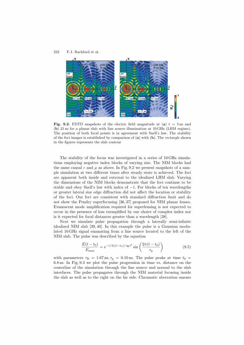
222 F.J. Rachford et al.
Fig. 9.2. FDTD snapshots of the electric field magnitude at (a) t = 5 ns and(b) 21 ns for a planar slab with line source illumination at 10 GHz (LHM regime).The position of both focal points is in agreement with Snell’s law. The stabilityof the foci images is established by comparison of (a) with (b). The rectangle shownin the figures represents the slab contour
The stability of the focus was investigated in a series of 10 GHz simula-tions employing negative index blocks of varying size. The NIM blocks hadthe same causal ε and µ as above. In Fig. 9.2 we present snapshots of a sam-ple simulation at two different times after steady state is achieved. The fociare apparent both inside and external to the idealized LHM slab. Varyingthe dimensions of the NIM blocks demonstrate that the foci continue to bestable and obey Snell’s law with index of −1. For blocks of ten wavelengthsor greater lateral size edge diffraction did not affect the location or stabilityof the foci. Our foci are consistent with standard diffraction limit and donot show the Pendry superfocusing [36, 37] proposed for NIM planar lenses.Evanescent mode amplification required for superlensing is not expected tooccur in the presence of loss exemplified by our choice of complex index noris it expected for focal distances greater than a wavelength [38].
Next we simulate pulse propagation through a laterally semi-infiniteidealized NIM slab [39, 40]. In this example the pulse is a Gaussian modu-lated 10 GHz signal emanating from a line source located to the left of theNIM slab. The pulse was described by the equation
E(t − t0)Emax
= e−1/2((t−t0)/τB)2 sin(
2π(t − t0)τp
)(9.5)
with parameters τB = 1.67 ns, τp = 0.10 ns. The pulse peaks at time t0 =6.8 ns. In Fig. 9.3 we plot the pulse progression in time vs. distance on thecenterline of the simulation through the line source and normal to the slabinterfaces. The pulse propagates through the NIM material focusing insidethe slab as well as to the right on the far side. Chromatic aberration smears
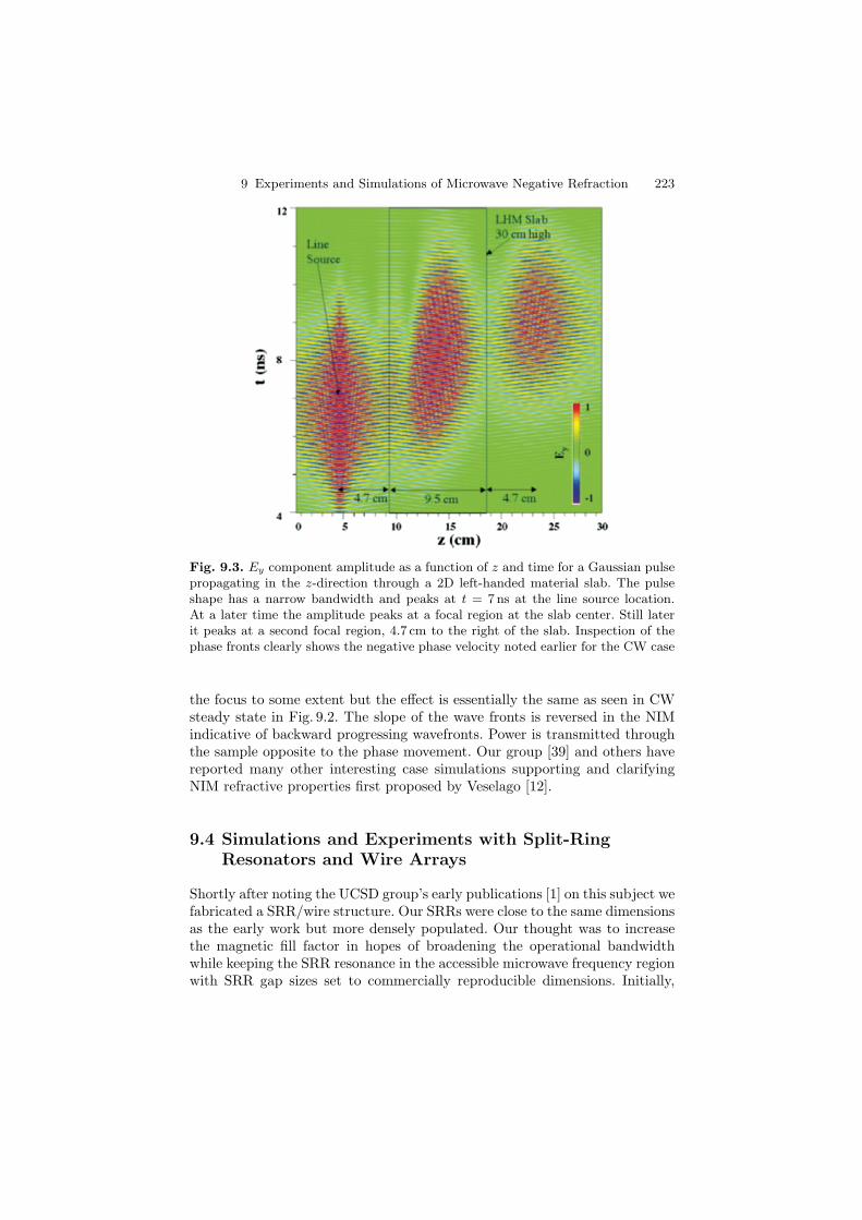
9 Experiments and Simulations of Microwave Negative Refraction 223
Fig. 9.3. Ey component amplitude as a function of z and time for a Gaussian pulsepropagating in the z-direction through a 2D left-handed material slab. The pulseshape has a narrow bandwidth and peaks at t = 7 ns at the line source location.At a later time the amplitude peaks at a focal region at the slab center. Still laterit peaks at a second focal region, 4.7 cm to the right of the slab. Inspection of thephase fronts clearly shows the negative phase velocity noted earlier for the CW case
the focus to some extent but the effect is essentially the same as seen in CWsteady state in Fig. 9.2. The slope of the wave fronts is reversed in the NIMindicative of backward progressing wavefronts. Power is transmitted throughthe sample opposite to the phase movement. Our group [39] and others havereported many other interesting case simulations supporting and clarifyingNIM refractive properties first proposed by Veselago [12].
9.4 Simulations and Experiments with Split-RingResonators and Wire Arrays
Shortly after noting the UCSD group’s early publications [1] on this subject wefabricated a SRR/wire structure. Our SRRs were close to the same dimensionsas the early work but more densely populated. Our thought was to increasethe magnetic fill factor in hopes of broadening the operational bandwidthwhile keeping the SRR resonance in the accessible microwave frequency regionwith SRR gap sizes set to commercially reproducible dimensions. Initially,
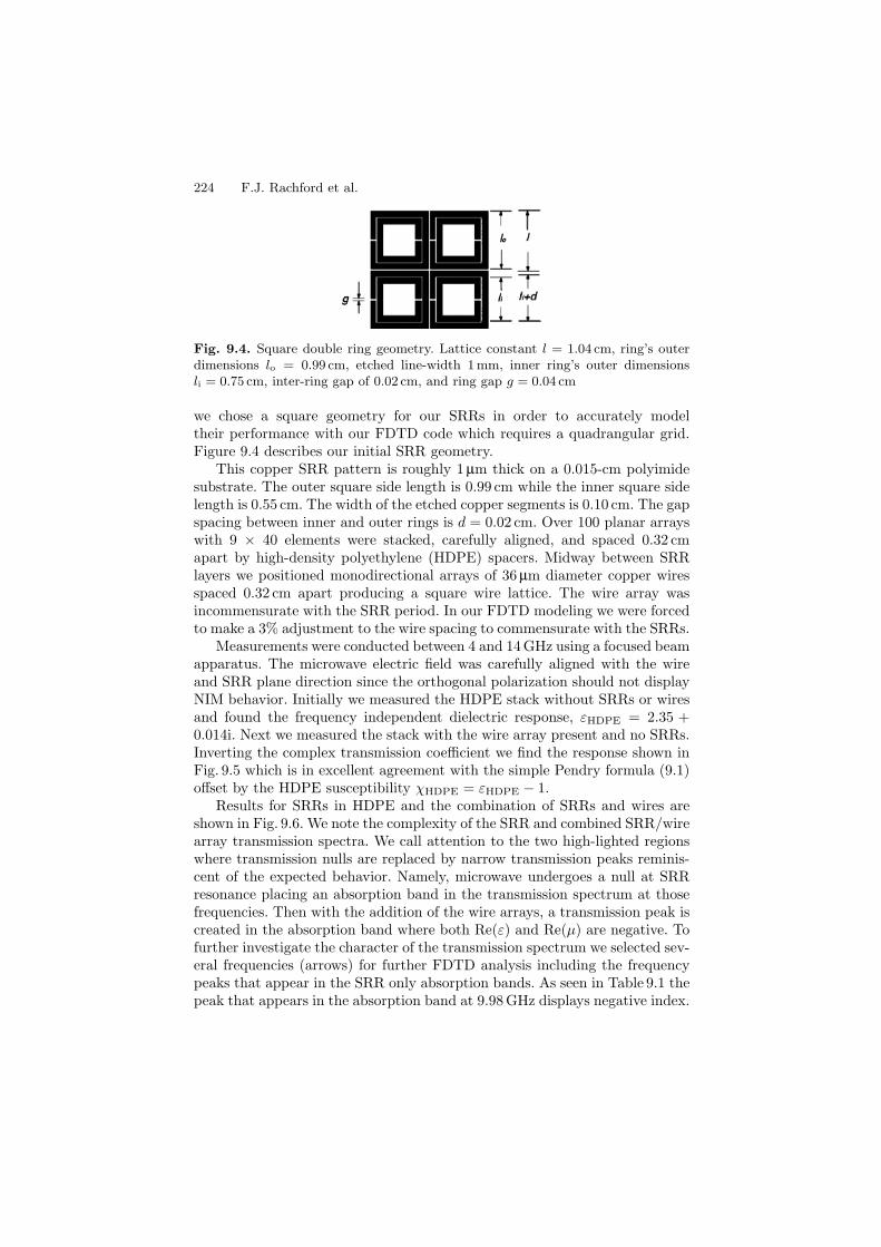
224 F.J. Rachford et al.
Fig. 9.4. Square double ring geometry. Lattice constant l = 1.04 cm, ring’s outerdimensions lo = 0.99 cm, etched line-width 1mm, inner ring’s outer dimensionsli = 0.75 cm, inter-ring gap of 0.02 cm, and ring gap g = 0.04 cm
we chose a square geometry for our SRRs in order to accurately modeltheir performance with our FDTD code which requires a quadrangular grid.Figure 9.4 describes our initial SRR geometry.
This copper SRR pattern is roughly 1 µm thick on a 0.015-cm polyimidesubstrate. The outer square side length is 0.99 cm while the inner square sidelength is 0.55 cm. The width of the etched copper segments is 0.10 cm. The gapspacing between inner and outer rings is d = 0.02 cm. Over 100 planar arrayswith 9 × 40 elements were stacked, carefully aligned, and spaced 0.32 cmapart by high-density polyethylene (HDPE) spacers. Midway between SRRlayers we positioned monodirectional arrays of 36 µm diameter copper wiresspaced 0.32 cm apart producing a square wire lattice. The wire array wasincommensurate with the SRR period. In our FDTD modeling we were forcedto make a 3% adjustment to the wire spacing to commensurate with the SRRs.
Measurements were conducted between 4 and 14 GHz using a focused beamapparatus. The microwave electric field was carefully aligned with the wireand SRR plane direction since the orthogonal polarization should not displayNIM behavior. Initially we measured the HDPE stack without SRRs or wiresand found the frequency independent dielectric response, εHDPE = 2.35 +0.014i. Next we measured the stack with the wire array present and no SRRs.Inverting the complex transmission coefficient we find the response shown inFig. 9.5 which is in excellent agreement with the simple Pendry formula (9.1)offset by the HDPE susceptibility χHDPE = εHDPE − 1.
Results for SRRs in HDPE and the combination of SRRs and wires areshown in Fig. 9.6. We note the complexity of the SRR and combined SRR/wirearray transmission spectra. We call attention to the two high-lighted regionswhere transmission nulls are replaced by narrow transmission peaks reminis-cent of the expected behavior. Namely, microwave undergoes a null at SRRresonance placing an absorption band in the transmission spectrum at thosefrequencies. Then with the addition of the wire arrays, a transmission peak iscreated in the absorption band where both Re(ε) and Re(µ) are negative. Tofurther investigate the character of the transmission spectrum we selected sev-eral frequencies (arrows) for further FDTD analysis including the frequencypeaks that appear in the SRR only absorption bands. As seen in Table 9.1 thepeak that appears in the absorption band at 9.98 GHz displays negative index.
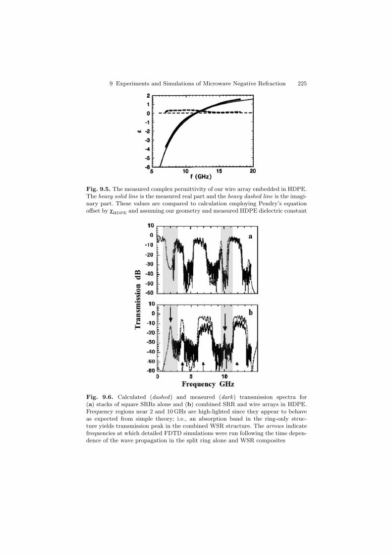
9 Experiments and Simulations of Microwave Negative Refraction 225
Fig. 9.5. The measured complex permittivity of our wire array embedded in HDPE.The heavy solid line is the measured real part and the heavy dashed line is the imagi-nary part. These values are compared to calculation employing Pendry’s equationoffset by χHDPE and assuming our geometry and measured HDPE dielectric constant
Fig. 9.6. Calculated (dashed) and measured (dark) transmission spectra for(a) stacks of square SRRs alone and (b) combined SRR and wire arrays in HDPE.Frequency regions near 2 and 10GHz are high-lighted since they appear to behaveas expected from simple theory; i.e., an absorption band in the ring-only struc-ture yields transmission peak in the combined WSR structure. The arrows indicatefrequencies at which detailed FDTD simulations were run following the time depen-dence of the wave propagation in the split ring alone and WSR composites
226 F.J. Rachford et al.
Table 9.1. Index of refraction at frequencies indicated in Fig. 9.6
F (GHz) n
1.96 −3.63.57 1.66.93 1.09.98 −1.411.90 −0.9
These indices were deduced from analysis of single frequency FDTD simulations ofthis structure. The transmission peak at 9.98 GHz corresponds to the transmissionpeak appearing when wires are added to the SRR in HDPE stack
However, the progression of wavefronts in the simulated stack at 11.9 GHz alsoappears to show negative index. More confounding, transmission at frequen-cies below 9.98 GHz is strong and displays a positive index behavior. Whereasfor the wires alone in HDPE, both measurement and simulation show stronglydecreasing microwave transmission as frequency is reduced below 10 GHz, as isexpected for a composite with negative permittivity and positive permeability.Clearly, though the simple model may explain the 9.98 GHz peak, it cannotadequately account for the wider frequency observations. It is notable that theearly experiments were all restricted to narrow frequency band observations.In the following sections we explore structures without wire arrays and findthat our SRR arrays can form negatively refracting photonic crystals.
9.5 Split-Ring Resonator Arrays as a 2D PhotonicCrystal
As part of a program to measure SRR/wire composites, we measured arraysof SRRs without wires. Much to our surprise at the time, we found wide bandfocusing of divergent X-band radiation by a slab of stacked hexagonal SRRarrays on FR4 circuit board. At the time such focusing effects were toutedas a hallmark of negative index behavior in SRR/wire composite structures.The SRR structure had dimensions summarized in Fig. 9.7.
Approximately 120 10 × 46 × 0.32 cm3 circuit boards were stacked andmicrowave transmission was measured in a focused beam quasioptical fixtureover several microwave waveguide bands. The electric field polarizationimpinging on the stacked SRR arrays was parallel to the plane of the hexag-onal disk arrays.
In Fig. 9.8 we display the calculated (dots) transmission intensity of aplane wave propagating through our 4 in. thick array of hexagonal SRRs (seeFig. 9.7) vs. frequency at X-band. The calculation was performed using aFDFT code. We note two transmission peaks in this frequency band. The cal-culated response is very sensitive to the geometry and the griding in theFDTD calculation. Measured transmission (line) also shows two peaks in this
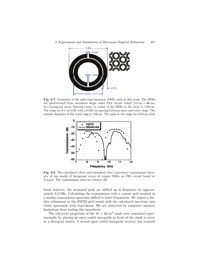
9 Experiments and Simulations of Microwave Negative Refraction 227
Fig. 9.7. Geometry of the split-ring resonator (SRR) used in this work. The SRRsare photoetched from metalized single sided FR4 circuit board (10 cm × 46 cm)in a hexagonal array. Spacing center to center of the SRRs in the array is 1.06 cm.The rings are 0.1 cm wide with a 0.025 cm spacing between inner and outer rings. Theoutside diameter of the outer ring is 1.00 cm. The gaps in the rings are 0.04 cm wide
Fig. 9.8. The calculated (dots) and measured (line) microwave transmission inten-sity of our stacks of hexagonal arrays of copper SRRs on FR4 circuit board atX-band. The transmission units are relative dB
band, however, the measured peak are shifted up in frequency by approxi-mately 0.5 GHz. Calculating the transmission with a coarser grid resulted ina similar transmission spectrum shifted to lower frequencies. We expect a fur-ther refinement in the FDTD grid would shift the calculated spectrum intocloser agreement with experiment. We are restricted by computer memorylimitations from testing this hypothesis.
The refractive properties of the 10 × 46 cm2 stack were examined exper-imentally by placing an open ended waveguide in front of the stack to serveas a divergent source. A second open ended waveguide receiver was scanned
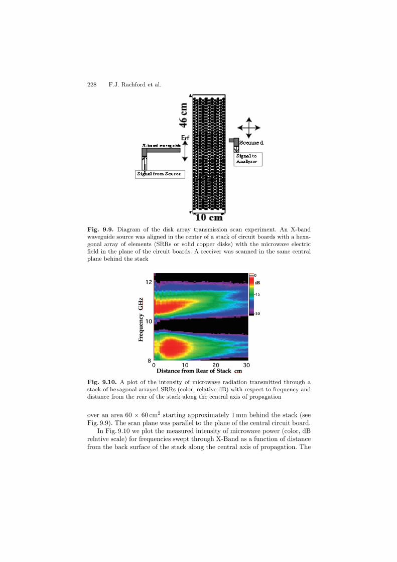
228 F.J. Rachford et al.
Fig. 9.9. Diagram of the disk array transmission scan experiment. An X-bandwaveguide source was aligned in the center of a stack of circuit boards with a hexa-gonal array of elements (SRRs or solid copper disks) with the microwave electricfield in the plane of the circuit boards. A receiver was scanned in the same centralplane behind the stack
Fig. 9.10. A plot of the intensity of microwave radiation transmitted through astack of hexagonal arrayed SRRs (color, relative dB) with respect to frequency anddistance from the rear of the stack along the central axis of propagation
over an area 60 × 60 cm2 starting approximately 1 mm behind the stack (seeFig. 9.9). The scan plane was parallel to the plane of the central circuit board.
In Fig. 9.10 we plot the measured intensity of microwave power (color, dBrelative scale) for frequencies swept through X-Band as a function of distancefrom the back surface of the stack along the central axis of propagation. The

9 Experiments and Simulations of Microwave Negative Refraction 229
Fig. 9.11. Analysis of the focus of microwave radiation at 8.616 GHz by the stackof SRRs on FR4 circuit board. A well-defined focus occurs approximately 5–6 cmbehind the stack. A contour plot in dB (relative) of the transmitted power vs.distance down range and cross range is shown with cuts taken along the centraldirection of propagation and laterally across the focus. The horizontal and verticalcuts through the focus are shown in the left and bottom plots. The cuts plot thepower (linear scale relative) vs. distance across the focus. In the direction normal tothe scan plane the radiation falls off as 1/r2 as expected for radiation from positiveindex material. The power vs. lateral distance plot has been fitted to a Gaussian.The Gaussian width is 1.275 or 2.0 cm full width at half maximum (FWHM). Thefree space wavelength at 6.616 GHz is 3.48 cm. The receiver aperture is 1 cm
experimental geometry is shown in Fig. 9.9. The transmission displays twointensity peaks. The lower peak, from ∼8.2 to ∼9.6 GHz shows focusing thatremains spatially stationary, centered approximately 6 cm from the rear of theSRR stack. The upper band extends from ∼10.5 to 11 GHz and also displaysfocusing though not as apparent on this color scale. Radiation in the planenormal to the circuit boards diverges uniformly, as expected for microwavesemergent from a positive index slab.
Examining the transmission in detail in the center of the lower transmissionband (8.616 GHz), we plot (Fig. 9.11) the transmission intensity in the X/Yplane behind the stack (5 dB contours). A focus is seen some 4–6 cm behindthe stack. Lateral (cross range) and down range cuts through the data are
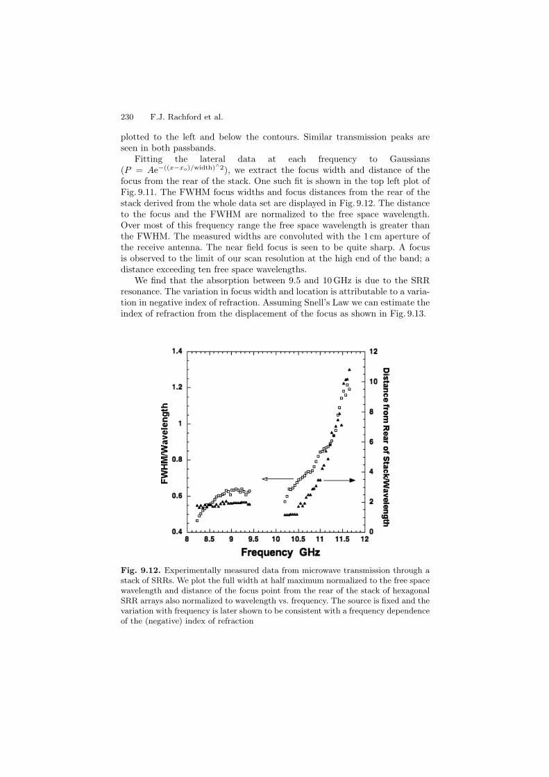
230 F.J. Rachford et al.
plotted to the left and below the contours. Similar transmission peaks areseen in both passbands.
Fitting the lateral data at each frequency to Gaussians(P = Ae−((x−xo)/width)∧2), we extract the focus width and distance of thefocus from the rear of the stack. One such fit is shown in the top left plot ofFig. 9.11. The FWHM focus widths and focus distances from the rear of thestack derived from the whole data set are displayed in Fig. 9.12. The distanceto the focus and the FWHM are normalized to the free space wavelength.Over most of this frequency range the free space wavelength is greater thanthe FWHM. The measured widths are convoluted with the 1 cm aperture ofthe receive antenna. The near field focus is seen to be quite sharp. A focusis observed to the limit of our scan resolution at the high end of the band; adistance exceeding ten free space wavelengths.
We find that the absorption between 9.5 and 10 GHz is due to the SRRresonance. The variation in focus width and location is attributable to a varia-tion in negative index of refraction. Assuming Snell’s Law we can estimate theindex of refraction from the displacement of the focus as shown in Fig. 9.13.
Fig. 9.12. Experimentally measured data from microwave transmission through astack of SRRs. We plot the full width at half maximum normalized to the free spacewavelength and distance of the focus point from the rear of the stack of hexagonalSRR arrays also normalized to wavelength vs. frequency. The source is fixed and thevariation with frequency is later shown to be consistent with a frequency dependenceof the (negative) index of refraction
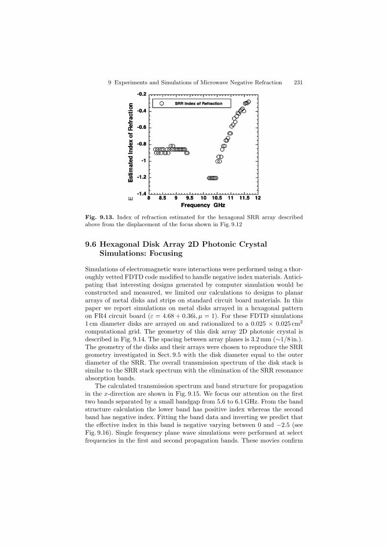
9 Experiments and Simulations of Microwave Negative Refraction 231
Fig. 9.13. Index of refraction estimated for the hexagonal SRR array describedabove from the displacement of the focus shown in Fig. 9.12
9.6 Hexagonal Disk Array 2D Photonic CrystalSimulations: Focusing
Simulations of electromagnetic wave interactions were performed using a thor-oughly vetted FDTD code modified to handle negative index materials. Antici-pating that interesting designs generated by computer simulation would beconstructed and measured, we limited our calculations to designs to planararrays of metal disks and strips on standard circuit board materials. In thispaper we report simulations on metal disks arrayed in a hexagonal patternon FR4 circuit board (ε = 4.68 + 0.36i, µ = 1). For these FDTD simulations1 cm diameter disks are arrayed on and rationalized to a 0.025 × 0.025 cm2
computational grid. The geometry of this disk array 2D photonic crystal isdescribed in Fig. 9.14. The spacing between array planes is 3.2 mm (∼1/8 in.).The geometry of the disks and their arrays were chosen to reproduce the SRRgeometry investigated in Sect. 9.5 with the disk diameter equal to the outerdiameter of the SRR. The overall transmission spectrum of the disk stack issimilar to the SRR stack spectrum with the elimination of the SRR resonanceabsorption bands.
The calculated transmission spectrum and band structure for propagationin the x-direction are shown in Fig. 9.15. We focus our attention on the firsttwo bands separated by a small bandgap from 5.6 to 6.1 GHz. From the bandstructure calculation the lower band has positive index whereas the secondband has negative index. Fitting the band data and inverting we predict thatthe effective index in this band is negative varying between 0 and −2.5 (seeFig. 9.16). Single frequency plane wave simulations were performed at selectfrequencies in the first and second propagation bands. These movies confirm
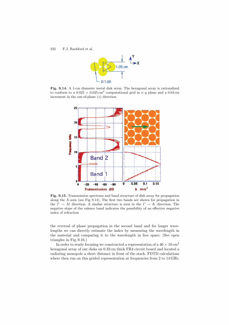
232 F.J. Rachford et al.
Fig. 9.14. A 1-cm diameter metal disk array. The hexagonal array is rationalizedto conform to a 0.025 × 0.025 cm2 computational grid in x–y plane and a 0.04 cmincrement in the out-of-plane (z) direction
Fig. 9.15. Transmission spectrum and band structure of disk array for propagationalong the X-axis (see Fig. 9.14). The first two bands are shown for propagation inthe Γ → M direction. A similar structure is seen in the Γ → K direction. Thenegative slope of the valence band indicates the possibility of an effective negativeindex of refraction
the reversal of phase propagation in the second band and for longer wave-lengths we can directly estimate the index by measuring the wavelength inthe material and comparing it to the wavelength in free space. (See opentriangles in Fig. 9.16.)
In order to study focusing we constructed a representation of a 46 × 10 cm2
hexagonal array of our disks on 0.32 cm thick FR4 circuit board and located aradiating monopole a short distance in front of the stack. FDTD calculationswhere then run on this grided representation at frequencies from 2 to 14 GHz.
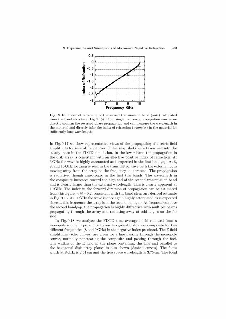
9 Experiments and Simulations of Microwave Negative Refraction 233
Fig. 9.16. Index of refraction of the second transmission band (dots) calculatedfrom the band structure (Fig. 9.15). From single frequency propagation movies wedirectly confirm the reversed phase propagation and can measure the wavelength inthe material and directly infer the index of refraction (triangles) in the material forsufficiently long wavelengths
In Fig. 9.17 we show representative views of the propagating rf electric fieldamplitudes for several frequencies. These snap shots were taken well into thesteady state in the FDTD simulation. In the lower band the propagation inthe disk array is consistent with an effective positive index of refraction. At6 GHz the wave is highly attenuated as is expected in the first bandgap. At 8,9, and 10 GHz focusing is seen in the transmitted wave with the external focusmoving away from the array as the frequency is increased. The propagationis radiative, though anisotropic in the first two bands. The wavelength inthe composite increases toward the high end of the second transmission bandand is clearly larger than the external wavelength. This is clearly apparent at10 GHz. The index in the forward direction of propagation can be estimatedfrom this figure: n ∼= −0.2, consistent with the band structure derived estimatein Fig. 9.16. At 11 GHz the wave is once again highly attenuated as is expectedsince at this frequency the array is in the second bandgap. At frequencies abovethe second bandgap, the propagation is highly diffractive with multiple beamspropagating through the array and radiating away at odd angles on the farside.
In Fig. 9.18 we analyze the FDTD time averaged field radiated from amonopole source in proximity to our hexagonal disk array composite for twodifferent frequencies (8 and 9 GHz) in the negative index passband. The E fieldamplitudes (solid curves) are given for a line passing through the monopolesource, normally penetrating the composite and passing through the foci.The widths of the E field in the plane containing this line and parallel tothe hexagonal disk array planes is also shown (dashed curves). The focuswidth at 8 GHz is 2.61 cm and the free space wavelength is 3.75 cm. The focal
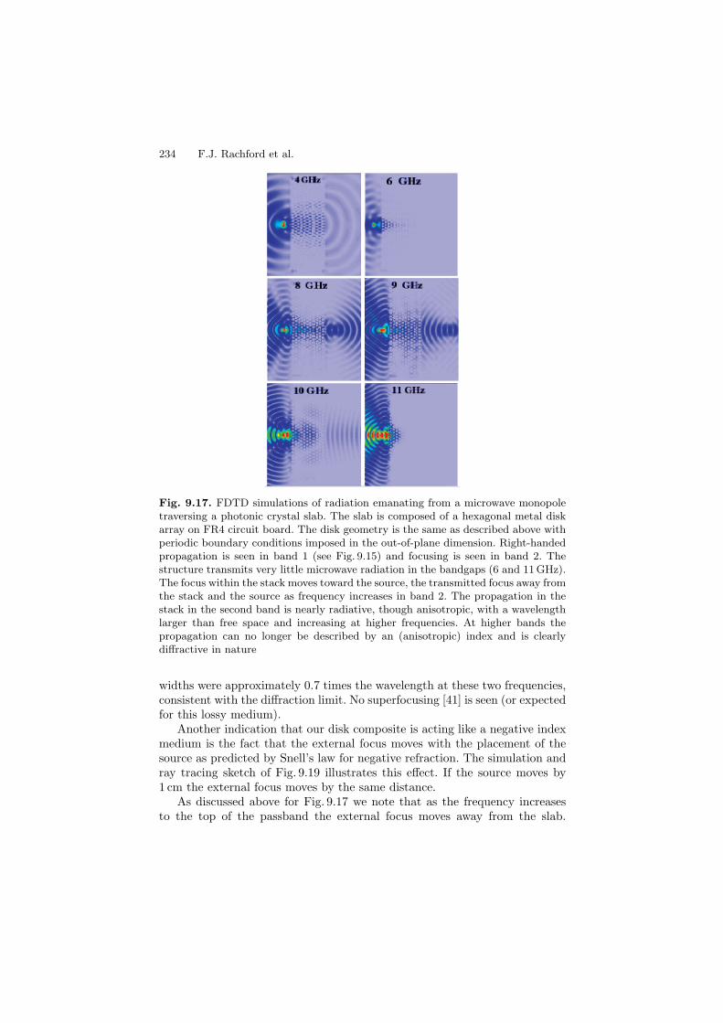
234 F.J. Rachford et al.
Fig. 9.17. FDTD simulations of radiation emanating from a microwave monopoletraversing a photonic crystal slab. The slab is composed of a hexagonal metal diskarray on FR4 circuit board. The disk geometry is the same as described above withperiodic boundary conditions imposed in the out-of-plane dimension. Right-handedpropagation is seen in band 1 (see Fig. 9.15) and focusing is seen in band 2. Thestructure transmits very little microwave radiation in the bandgaps (6 and 11 GHz).The focus within the stack moves toward the source, the transmitted focus away fromthe stack and the source as frequency increases in band 2. The propagation in thestack in the second band is nearly radiative, though anisotropic, with a wavelengthlarger than free space and increasing at higher frequencies. At higher bands thepropagation can no longer be described by an (anisotropic) index and is clearlydiffractive in nature
widths were approximately 0.7 times the wavelength at these two frequencies,consistent with the diffraction limit. No superfocusing [41] is seen (or expectedfor this lossy medium).
Another indication that our disk composite is acting like a negative indexmedium is the fact that the external focus moves with the placement of thesource as predicted by Snell’s law for negative refraction. The simulation andray tracing sketch of Fig. 9.19 illustrates this effect. If the source moves by1 cm the external focus moves by the same distance.
As discussed above for Fig. 9.17 we note that as the frequency increasesto the top of the passband the external focus moves away from the slab.
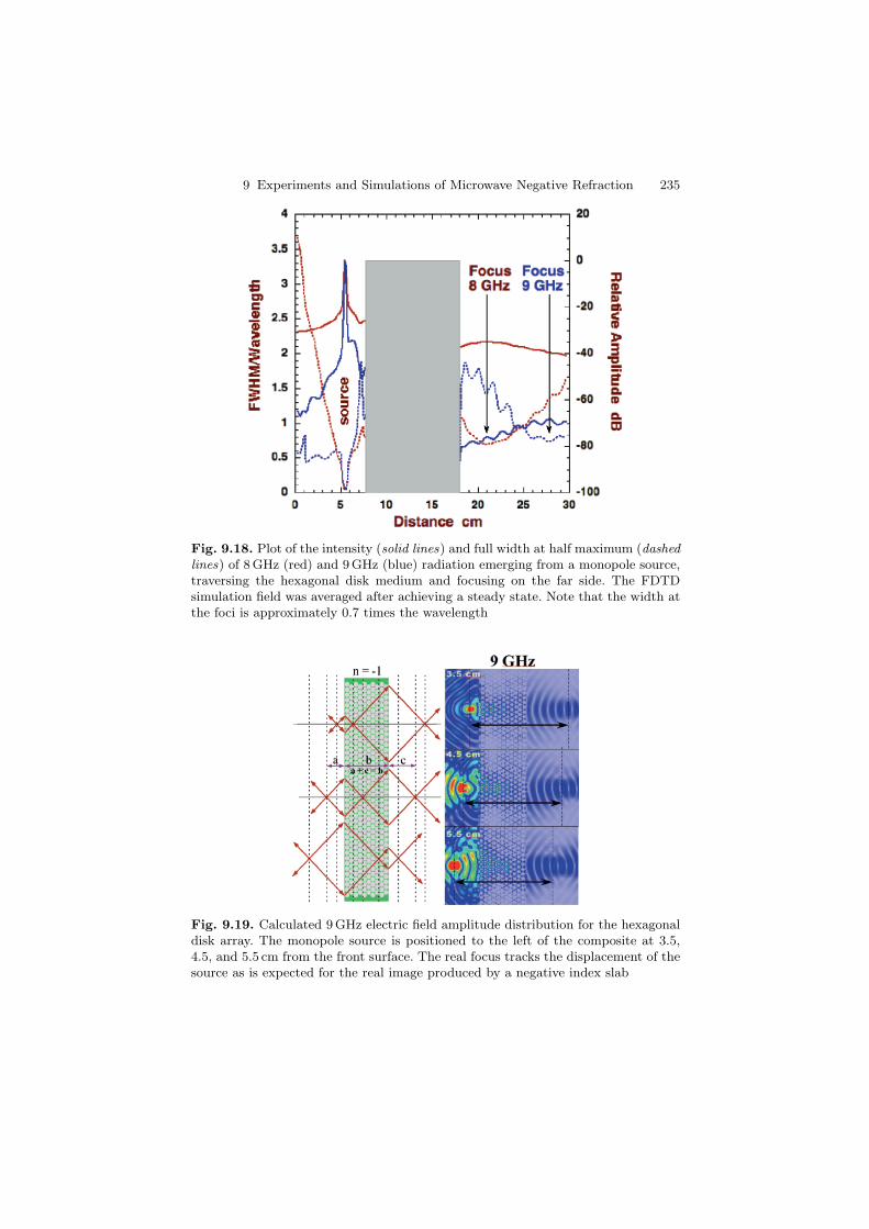
9 Experiments and Simulations of Microwave Negative Refraction 235
Fig. 9.18. Plot of the intensity (solid lines) and full width at half maximum (dashedlines) of 8GHz (red) and 9 GHz (blue) radiation emerging from a monopole source,traversing the hexagonal disk medium and focusing on the far side. The FDTDsimulation field was averaged after achieving a steady state. Note that the width atthe foci is approximately 0.7 times the wavelength
Fig. 9.19. Calculated 9 GHz electric field amplitude distribution for the hexagonaldisk array. The monopole source is positioned to the left of the composite at 3.5,4.5, and 5.5 cm from the front surface. The real focus tracks the displacement of thesource as is expected for the real image produced by a negative index slab
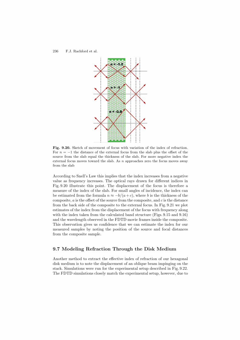
236 F.J. Rachford et al.
Fig. 9.20. Sketch of movement of focus with variation of the index of refraction.For n = −1 the distance of the external focus from the slab plus the offset of thesource from the slab equal the thickness of the slab. For more negative index theexternal focus moves toward the slab. As n approaches zero the focus moves awayfrom the slab
According to Snell’s Law this implies that the index increases from a negativevalue as frequency increases. The optical rays drawn for different indices inFig. 9.20 illustrate this point. The displacement of the focus is therefore ameasure of the index of the slab. For small angles of incidence, the index canbe estimated from the formula n ≈ −b/(a+ c), where b is the thickness of thecomposite, a is the offset of the source from the composite, and c is the distancefrom the back side of the composite to the external focus. In Fig. 9.21 we plotestimates of the index from the displacement of the focus with frequency alongwith the index taken from the calculated band structure (Figs. 9.15 and 9.16)and the wavelength observed in the FDTD movie frames inside the composite.This observation gives us confidence that we can estimate the index for ourmeasured samples by noting the position of the source and focal distancesfrom the composite sample.
9.7 Modeling Refraction Through the Disk Medium
Another method to extract the effective index of refraction of our hexagonaldisk medium is to note the displacement of an oblique beam impinging on thestack. Simulations were run for the experimental setup described in Fig. 9.22.The FDTD simulations closely match the experimental setup, however, due to
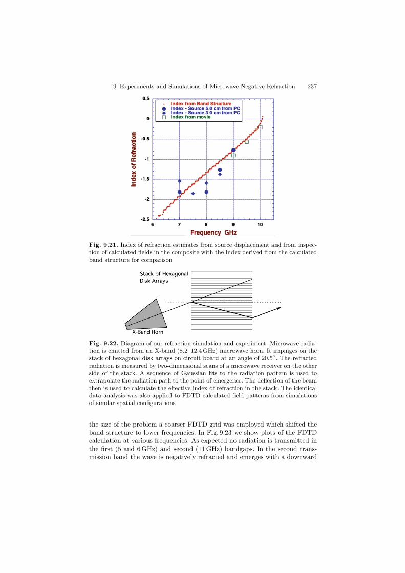
9 Experiments and Simulations of Microwave Negative Refraction 237
Fig. 9.21. Index of refraction estimates from source displacement and from inspec-tion of calculated fields in the composite with the index derived from the calculatedband structure for comparison
Fig. 9.22. Diagram of our refraction simulation and experiment. Microwave radia-tion is emitted from an X-band (8.2–12.4 GHz) microwave horn. It impinges on thestack of hexagonal disk arrays on circuit board at an angle of 20.5. The refractedradiation is measured by two-dimensional scans of a microwave receiver on the otherside of the stack. A sequence of Gaussian fits to the radiation pattern is used toextrapolate the radiation path to the point of emergence. The deflection of the beamthen is used to calculate the effective index of refraction in the stack. The identicaldata analysis was also applied to FDTD calculated field patterns from simulationsof similar spatial configurations
the size of the problem a coarser FDTD grid was employed which shifted theband structure to lower frequencies. In Fig. 9.23 we show plots of the FDTDcalculation at various frequencies. As expected no radiation is transmitted inthe first (5 and 6 GHz) and second (11 GHz) bandgaps. In the second trans-mission band the wave is negatively refracted and emerges with a downward
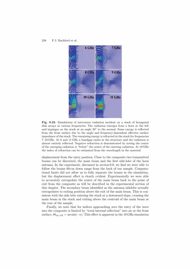
238 F.J. Rachford et al.
Fig. 9.23. Simulations of microwave radiation incident on a stack of hexagonaldisk arrays at various frequencies. The radiation emerges from a horn at the leftand impinges on the stack at an angle 20 to the normal. Some energy is reflectedfrom the front surface due to the angle and frequency-dependent effective surfaceimpedance of the stack. The remaining energy is refracted in the stack for frequencies7–10 GHz. At 6 and 11GHz a bandgap exists in the structure and the radiation isalmost entirely reflected. Negative refraction is demonstrated by noting the centerof the emerging radiation is “below” the center of the entering radiation. At 10 GHzthe index of refraction can be estimated from the wavelength in the material
displacement from the entry position. Close to the composite two transmittedbeams can be discerned, the main beam and the first side-lobe of the hornantenna. In the experiment, discussed in section 9.9, we find we were able tofollow the beams 60 cm down range from the back of our sample. Computa-tional limits did not allow us to fully separate the beams in the simulation,but the displacement effect is clearly evident. Experimentally we were ableto accurately extrapolate the center of the main beam back to the point ofexit from the composite as will be described in the experimental section ofthis chapter. The secondary beam identified as the antenna sidelobe actuallyextrapolates to exiting position above the exit of the main beam. This is con-sistent with the side lobe entering the stack at a downward slope, crossing themain beam in the stack and exiting above the centroid of the main beam atthe rear of the sample.
Finally, we note that for indices approaching zero the entry of the waveinto the composite is limited by “total internal reflection” into air at the frontsurface, Θint refl = arcsin(−n). This effect is apparent in the 10 GHz simulation
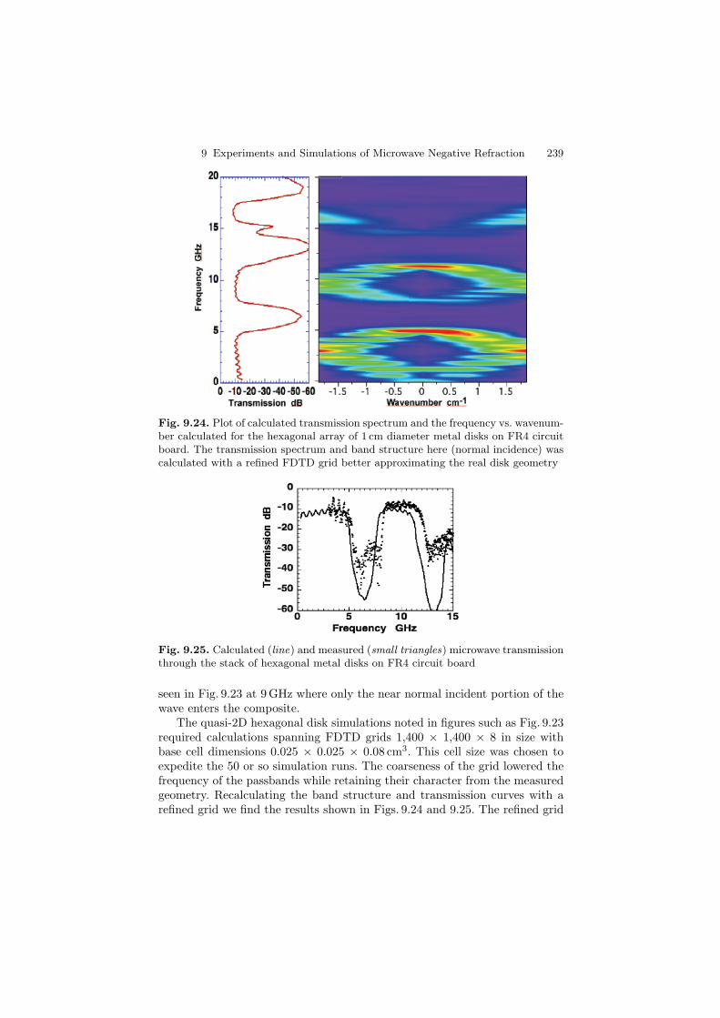
9 Experiments and Simulations of Microwave Negative Refraction 239
Fig. 9.24. Plot of calculated transmission spectrum and the frequency vs. wavenum-ber calculated for the hexagonal array of 1 cm diameter metal disks on FR4 circuitboard. The transmission spectrum and band structure here (normal incidence) wascalculated with a refined FDTD grid better approximating the real disk geometry
Fig. 9.25. Calculated (line) and measured (small triangles) microwave transmissionthrough the stack of hexagonal metal disks on FR4 circuit board
seen in Fig. 9.23 at 9 GHz where only the near normal incident portion of thewave enters the composite.
The quasi-2D hexagonal disk simulations noted in figures such as Fig. 9.23required calculations spanning FDTD grids 1,400 × 1,400 × 8 in size withbase cell dimensions 0.025 × 0.025 × 0.08 cm3. This cell size was chosen toexpedite the 50 or so simulation runs. The coarseness of the grid lowered thefrequency of the passbands while retaining their character from the measuredgeometry. Recalculating the band structure and transmission curves with arefined grid we find the results shown in Figs. 9.24 and 9.25. The refined grid
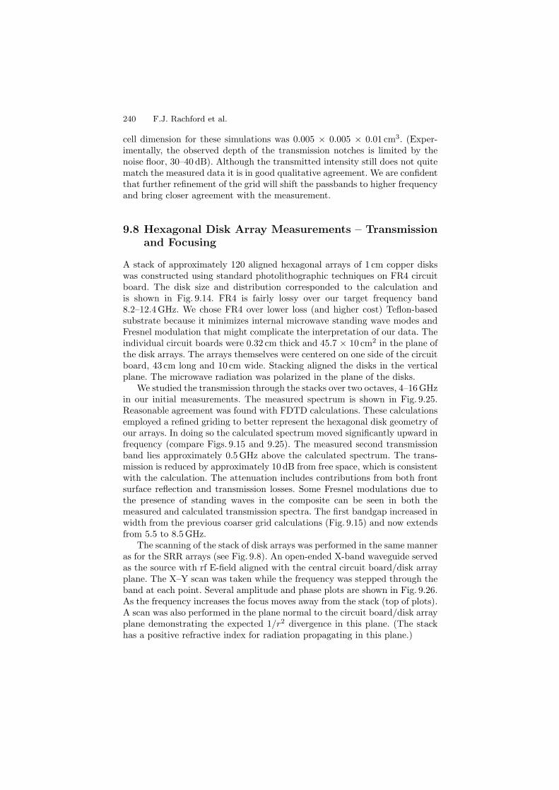
240 F.J. Rachford et al.
cell dimension for these simulations was 0.005 × 0.005 × 0.01 cm3. (Exper-imentally, the observed depth of the transmission notches is limited by thenoise floor, 30–40 dB). Although the transmitted intensity still does not quitematch the measured data it is in good qualitative agreement. We are confidentthat further refinement of the grid will shift the passbands to higher frequencyand bring closer agreement with the measurement.
9.8 Hexagonal Disk Array Measurements – Transmissionand Focusing
A stack of approximately 120 aligned hexagonal arrays of 1 cm copper diskswas constructed using standard photolithographic techniques on FR4 circuitboard. The disk size and distribution corresponded to the calculation andis shown in Fig. 9.14. FR4 is fairly lossy over our target frequency band8.2–12.4 GHz. We chose FR4 over lower loss (and higher cost) Teflon-basedsubstrate because it minimizes internal microwave standing wave modes andFresnel modulation that might complicate the interpretation of our data. Theindividual circuit boards were 0.32 cm thick and 45.7 × 10 cm2 in the plane ofthe disk arrays. The arrays themselves were centered on one side of the circuitboard, 43 cm long and 10 cm wide. Stacking aligned the disks in the verticalplane. The microwave radiation was polarized in the plane of the disks.
We studied the transmission through the stacks over two octaves, 4–16 GHzin our initial measurements. The measured spectrum is shown in Fig. 9.25.Reasonable agreement was found with FDTD calculations. These calculationsemployed a refined griding to better represent the hexagonal disk geometry ofour arrays. In doing so the calculated spectrum moved significantly upward infrequency (compare Figs. 9.15 and 9.25). The measured second transmissionband lies approximately 0.5 GHz above the calculated spectrum. The trans-mission is reduced by approximately 10 dB from free space, which is consistentwith the calculation. The attenuation includes contributions from both frontsurface reflection and transmission losses. Some Fresnel modulations due tothe presence of standing waves in the composite can be seen in both themeasured and calculated transmission spectra. The first bandgap increased inwidth from the previous coarser grid calculations (Fig. 9.15) and now extendsfrom 5.5 to 8.5 GHz.
The scanning of the stack of disk arrays was performed in the same manneras for the SRR arrays (see Fig. 9.8). An open-ended X-band waveguide servedas the source with rf E-field aligned with the central circuit board/disk arrayplane. The X–Y scan was taken while the frequency was stepped through theband at each point. Several amplitude and phase plots are shown in Fig. 9.26.As the frequency increases the focus moves away from the stack (top of plots).A scan was also performed in the plane normal to the circuit board/disk arrayplane demonstrating the expected 1/r2 divergence in this plane. (The stackhas a positive refractive index for radiation propagating in this plane.)
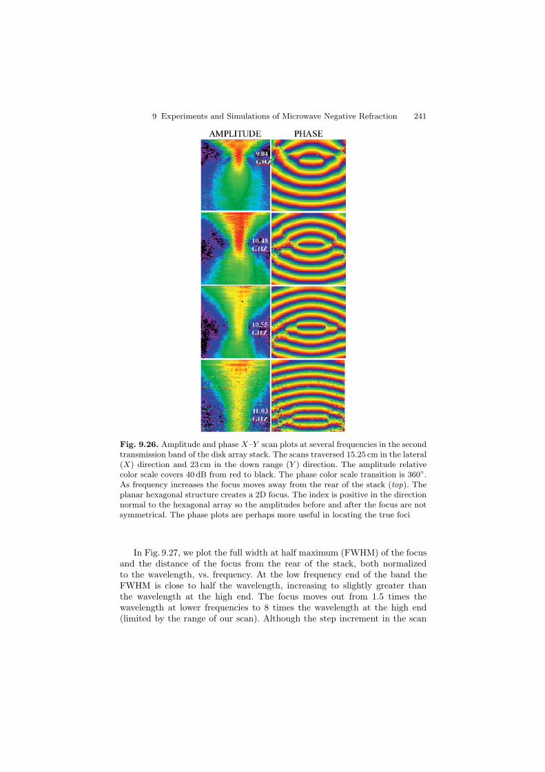
9 Experiments and Simulations of Microwave Negative Refraction 241
Fig. 9.26. Amplitude and phase X–Y scan plots at several frequencies in the secondtransmission band of the disk array stack. The scans traversed 15.25 cm in the lateral(X) direction and 23 cm in the down range (Y ) direction. The amplitude relativecolor scale covers 40 dB from red to black. The phase color scale transition is 360.As frequency increases the focus moves away from the rear of the stack (top). Theplanar hexagonal structure creates a 2D focus. The index is positive in the directionnormal to the hexagonal array so the amplitudes before and after the focus are notsymmetrical. The phase plots are perhaps more useful in locating the true foci
In Fig. 9.27, we plot the full width at half maximum (FWHM) of the focusand the distance of the focus from the rear of the stack, both normalizedto the wavelength, vs. frequency. At the low frequency end of the band theFWHM is close to half the wavelength, increasing to slightly greater thanthe wavelength at the high end. The focus moves out from 1.5 times thewavelength at lower frequencies to 8 times the wavelength at the high end(limited by the range of our scan). Although the step increment in the scan
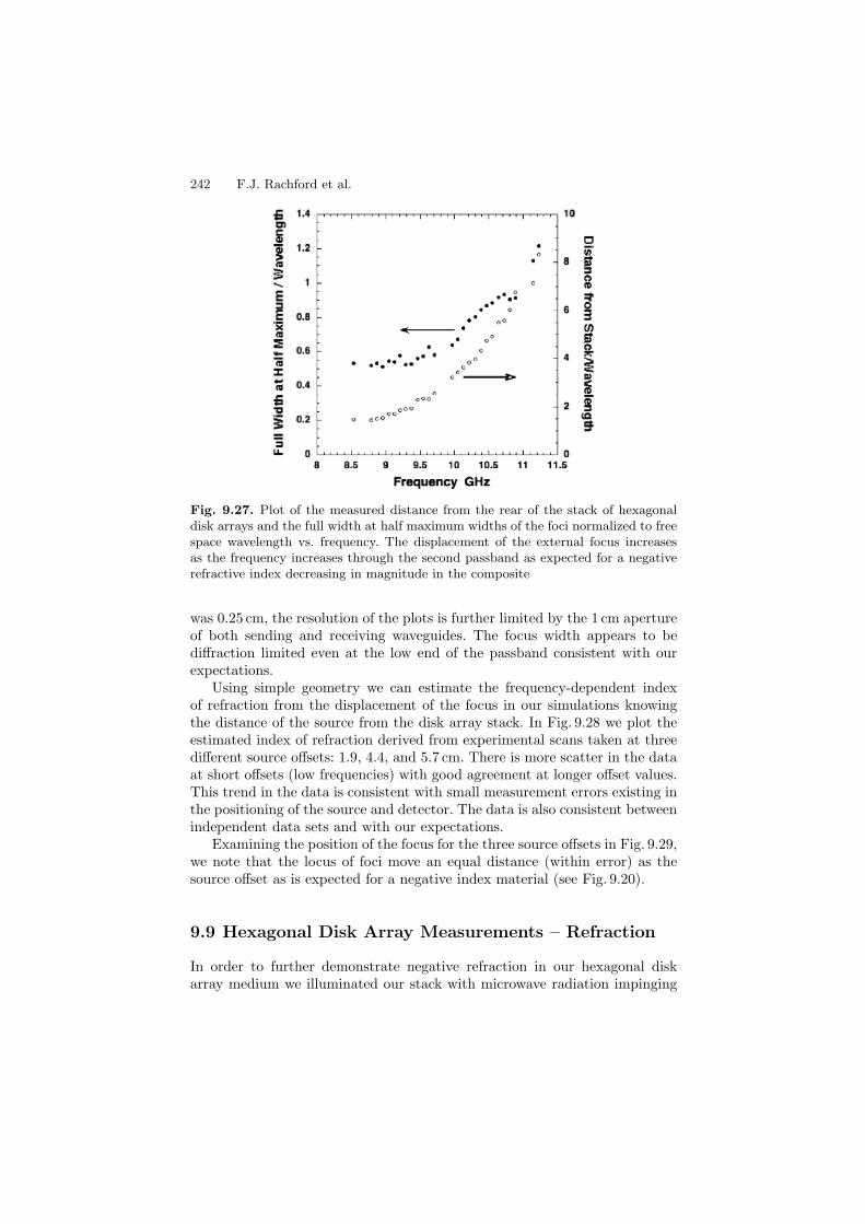
242 F.J. Rachford et al.
Fig. 9.27. Plot of the measured distance from the rear of the stack of hexagonaldisk arrays and the full width at half maximum widths of the foci normalized to freespace wavelength vs. frequency. The displacement of the external focus increasesas the frequency increases through the second passband as expected for a negativerefractive index decreasing in magnitude in the composite
was 0.25 cm, the resolution of the plots is further limited by the 1 cm apertureof both sending and receiving waveguides. The focus width appears to bediffraction limited even at the low end of the passband consistent with ourexpectations.
Using simple geometry we can estimate the frequency-dependent indexof refraction from the displacement of the focus in our simulations knowingthe distance of the source from the disk array stack. In Fig. 9.28 we plot theestimated index of refraction derived from experimental scans taken at threedifferent source offsets: 1.9, 4.4, and 5.7 cm. There is more scatter in the dataat short offsets (low frequencies) with good agreement at longer offset values.This trend in the data is consistent with small measurement errors existing inthe positioning of the source and detector. The data is also consistent betweenindependent data sets and with our expectations.
Examining the position of the focus for the three source offsets in Fig. 9.29,we note that the locus of foci move an equal distance (within error) as thesource offset as is expected for a negative index material (see Fig. 9.20).
9.9 Hexagonal Disk Array Measurements – Refraction
In order to further demonstrate negative refraction in our hexagonal diskarray medium we illuminated our stack with microwave radiation impinging
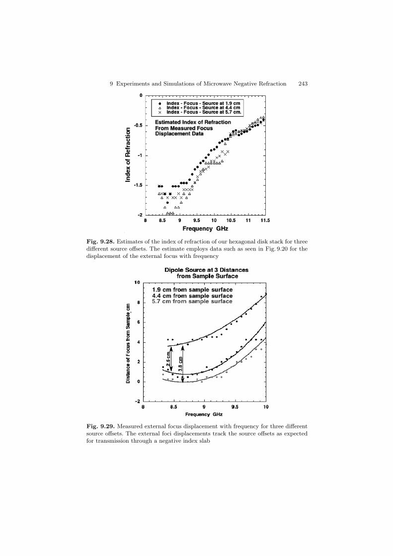
9 Experiments and Simulations of Microwave Negative Refraction 243
Fig. 9.28. Estimates of the index of refraction of our hexagonal disk stack for threedifferent source offsets. The estimate employs data such as seen in Fig. 9.20 for thedisplacement of the external focus with frequency
Fig. 9.29. Measured external focus displacement with frequency for three differentsource offsets. The external foci displacements track the source offsets as expectedfor transmission through a negative index slab
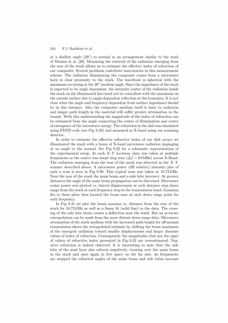
244 F.J. Rachford et al.
at a shallow angle (20) to normal in an arrangement similar to the workof Moussa et al. [20]. Measuring the centroid of the radiation emerging fromthe rear of the stack allows us to estimate the effective index of refraction ofour composite. Several problems contribute inaccuracies in this measurementscheme. The radiation illuminating the composite comes from a microwavehorn in close proximity to the stack. The wavefront is spherical with themaximum occurring at the 20 incident angle. Since the impedance of the stackis expected to be angle dependent, the intensity center of the radiation insidethe stack on the illuminated face need not be coincident with the maximum onthe outside surface due to angle-dependent reflection at the boundary. It is notclear what the angle and frequency-dependent front surface impedance shouldbe in this instance. Also the composite medium itself is lossy to radiationand longer path length in the material will suffer greater attenuation in thetransit. With this understanding the magnitude of the index of refraction canbe estimated from the angle connecting the center of illumination and centerof emergence of the microwave energy. The refraction in the slab was simulatedusing FDTD code (see Fig. 9.23) and measured in X-band using our scanningdetector.
In order to estimate the effective refractive index of our disk arrays weilluminated the stack with a beam of X-band microwave radiation impingingat an angle to the normal. See Fig. 9.22 for a schematic representation ofthe experimental setup. At each X–Y location, data was taken at multiplefrequencies as the source was swept step wise (∆f = 84MHz) across X-Band.The radiation emerging from the rear of the stack was detected in the X–Yscanner described above. A microwave power (dB relative) intensity plot ofsuch a scan is seen in Fig. 9.30. This typical scan was taken at 10.72 GHz.Near the rear of the stack the main beam and a side lobe intersect. At greaterdistances the angle of the main beam propagation can be discerned. Microwavescalar power was plotted vs. lateral displacement at each distance step downrange from the stack at each frequency step in the transmission band. Gaussianfits to these plots then located the beam max at each down range point foreach frequency.
In Fig. 9.31 we plot the beam maxima vs. distance from the rear of thestack for 10.72 GHz as well as a linear fit (solid line) to the data. The cross-ing of the side lobe beam causes a deflection near the stack. But an accurateextrapolation can be made from the more distant down range data. Microwaveattenuation of the stack medium with the increased path length for off-normaltransmission skews the extrapolated estimate by shifting the beam maximumof the emergent radiation toward smaller displacements and larger absolutevalues of index of refraction. Consequently the magnitudes (but not the sign)of values of refractive index presented in Fig. 9.32 are overestimated. Neg-ative refraction is indeed observed. It is interesting to note that the sidelobe of the send horn also refracts negatively, crossing over the main beamin the stack and once again in free space on the far side. As frequenciesare stepped the refracted angles of the main beam and side lobes increase
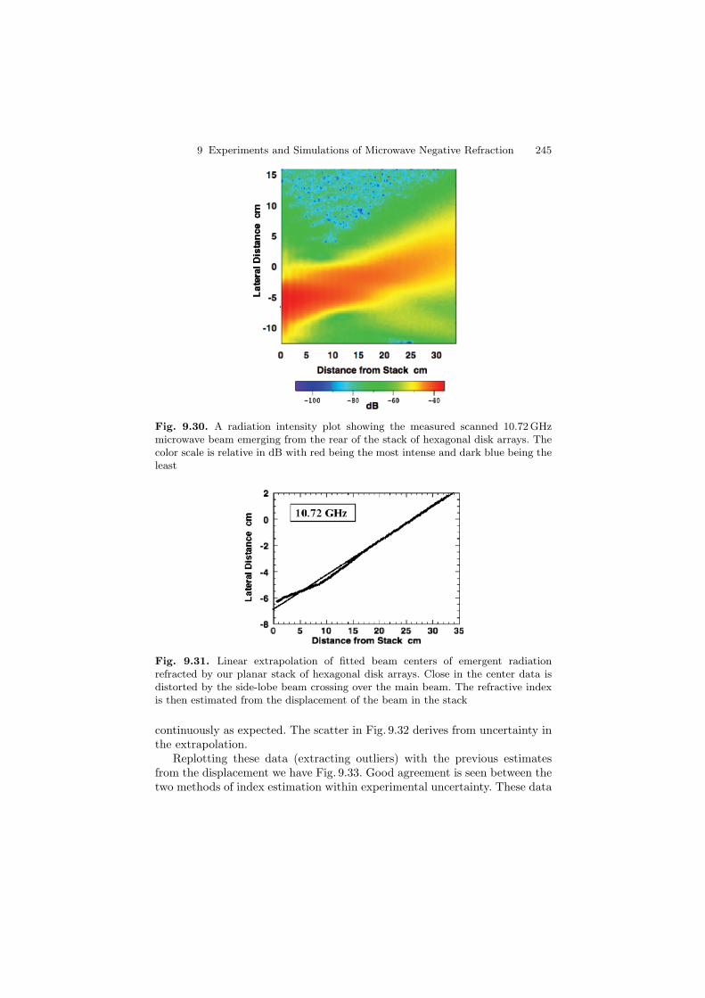
9 Experiments and Simulations of Microwave Negative Refraction 245
Fig. 9.30. A radiation intensity plot showing the measured scanned 10.72 GHzmicrowave beam emerging from the rear of the stack of hexagonal disk arrays. Thecolor scale is relative in dB with red being the most intense and dark blue being theleast
Fig. 9.31. Linear extrapolation of fitted beam centers of emergent radiationrefracted by our planar stack of hexagonal disk arrays. Close in the center data isdistorted by the side-lobe beam crossing over the main beam. The refractive indexis then estimated from the displacement of the beam in the stack
continuously as expected. The scatter in Fig. 9.32 derives from uncertainty inthe extrapolation.
Replotting these data (extracting outliers) with the previous estimatesfrom the displacement we have Fig. 9.33. Good agreement is seen between thetwo methods of index estimation within experimental uncertainty. These data
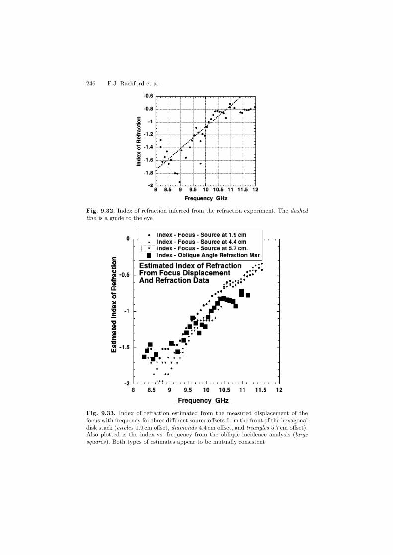
246 F.J. Rachford et al.
Fig. 9.32. Index of refraction inferred from the refraction experiment. The dashedline is a guide to the eye
Fig. 9.33. Index of refraction estimated from the measured displacement of thefocus with frequency for three different source offsets from the front of the hexagonaldisk stack (circles 1.9 cm offset, diamonds 4.4 cm offset, and triangles 5.7 cm offset).Also plotted is the index vs. frequency from the oblique incidence analysis (largesquares). Both types of estimates appear to be mutually consistent
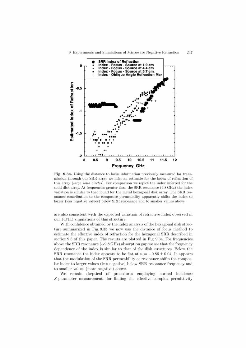
9 Experiments and Simulations of Microwave Negative Refraction 247
Fig. 9.34. Using the distance to focus information previously measured for trans-mission through our SRR array we infer an estimate for the index of refraction ofthis array (large solid circles). For comparison we replot the index inferred for thesolid disk array. At frequencies greater than the SRR resonance (9.8 GHz) the indexvariation is similar to that found for the metal hexagonal disk array. The SRR res-onance contribution to the composite permeability apparently shifts the index tolarger (less negative values) below SRR resonance and to smaller values above
are also consistent with the expected variation of refractive index observed inour FDTD simulations of this structure.
With confidence obtained by the index analysis of the hexagonal disk struc-ture summarized in Fig. 9.33 we now use the distance of focus method toestimate the effective index of refraction for the hexagonal SRR described insection 9.5 of this paper. The results are plotted in Fig. 9.34. For frequenciesabove the SRR resonance (∼9.8GHz) absorption gap we see that the frequencydependence of the index is similar to that of the disk structures. Below theSRR resonance the index appears to be flat at n = −0.86 ± 0.04. It appearsthat the modulation of the SRR permeability at resonance shifts the compos-ite index to larger values (less negative) below SRR resonance frequency andto smaller values (more negative) above.
We remain skeptical of procedures employing normal incidenceS-parameter measurements for finding the effective complex permittivity
248 F.J. Rachford et al.
and permeability of the disk or SRR media. The S-parameter to constituentparameter inversion routines are very sensitive to phase offsets. Choosing aneffective front reflection plane and even effective thickness are not straight-forward for such composite media with elements a third of the free spacewavelength. It is remarkable that coherent radiative transmission is observedover the entire second transmission band.
Comparing the SRR and disk array results, it appears that the X-bandnegatively refracting regions in the SRR are related to the second band inthe disks with a ring absorptive resonance splitting this negative refractiontransmission band.
9.10 Conclusions
We have observed broadband focusing in photonic bandgap arrays of SRRsand disks. FDTD simulations demonstrate focusing similar to the observeddata for the disk arrays. Griding compromises required to execute large scalesimulations caused frequency shifts for the calculated transmission spectraof both the disk and SRR arrays and prevented implementation of FDTDrefraction simulations for the SRR arrays where very fine scale resolution isnecessary due to the small capacitive gaps between rings. The main featuresof the observed data are reproduced including the progression of the focusfrom the rear of the stack and a steady reduction in the amplitude of thenegative refractive index as frequency is increased. Broad band negative indexof refraction is demonstrated in hexagonal SRR and disk arrays.
Acknowledgments
The authors are grateful for the technical advice and support for the workby Dr. Donald Forester. This work was performed under contract from theDARPA DSO office, Dr. Valerie Browning program manager.
References
1. D.R. Smith, W.J. Padilla, D.C. Vier, S.C. Nemat-Nasser, S. Schultz, Phys. Rev.Lett. 84, 4184 (2000)
2. D.R. Smith, D.C. Vier, N. Kroll, S. Schultz, Appl. Phys. Lett. 77, 2246 (2000)3. D.R. Smith, N. Kroll, Phys. Rev. Lett. 85, 2933 (2000)4. R.A. Shelby, D.R. Smith, S. Schultz, Science 77, 292 (2001)5. J.B. Pendry, A.J. Holden, W.J. Stewart, I. Youngs, Phys. Rev. Lett. 76, 4773
(1996)6. J.B. Pendry, A.J. Holden, D.J. Robbins, W.J. Stewart, J. Phys.: Condens.
Matter 10, 4785 (1998)

9 Experiments and Simulations of Microwave Negative Refraction 249
7. J.B. Pendry, A.J. Holden, D.J. Robbins, W.J. Stewart, IEEE Trans. Microw.Theory Tech. 47, 2075 (1999)
8. D.R. Smith, N. Kroll, Phys. Rev. Lett. 85, 2933 (2000)9. J.B. Pendry, Phys. Rev. Lett. 85, 3966 (2000)
10. F.J. Rachford, D.L. Smith, P.F. Loschialpo, D.W. Forester, Phys. Rev. E 66,036613 (2002)
11. C.G. Parazzoli, R.B. Greegor, K. Li, B.E.C. Koltenbah, M. Tanielian, Phys.Rev. Lett. 90, 107401 (2003)
12. V.G. Veselago, Sov. Phys. Usp. 10, 509 (1968)13. P.M. Valanju, R.M. Walser, A.P. Valanju, Phys. Rev. Lett. 88, 187401 (2002)14. S.R.W. Ziolkowski, E. Heyman, Phys. Rev. E 64, 056625 (2001)15. S. Foteinopoulou, E.N. Economou, C.M. Soukoulis, Phys. Rev. Lett. 90, 107402
(2003)16. D.R. Smith, D. Schurig, J.B. Pendry, Phys. Rev. Lett. 81, 2713 (2002)17. M. Notomi, Phys. Rev. B 62, 10696 (2000)18. S. Foteinopoulou, C.M. Soukoulis, Phys. Rev. B 67, 235107 (2003)19. S. Foteinopoulou, C.M. Soukoulis, Phys. Rev. B 72, 165112 (2005)20. R. Moussa, S. Foteinopoulou, L. Zhang, G. Tuttle, K. Guven, E. Ozbay,
C.M. Soukoulis, Phys. Rev. B 71, 085106 (2005)21. A.L. Efros, A.L. Pokrovsky, arXiv, Cornell University, Ithaca, NY, 29 Aug 2003,
http: arxiv.org/cond-mat/030861122. P.V. Parimi, W.T. Lu, P. Vodo, S. Sridha, Nature 426, 404 (2003)23. P.V. Parimi, W.T. Lu, P. Vodo, J. Sokoloff, J.S. Derov, S. Sridhar, Phys. Rev.
Lett. 92, 127401 (2004)24. E. Cubukcu, K. Aydin, E. Ozbay, S. Foteinopoulou, C.M. Soukouli, Nature 423,
604 (2003)25. H. Kosaka, T. Kawashima, A. Tomita, M. Notomi, T. Tamamura, T. Sato,
S. Kawakami, J. Lightwave Technol. 17, 2032 (1999)26. F.J. Rachford, D. Smith, P. Loschialpo, first DARPA Meta-materials PI Meeting
presentation and conference CD June 2001, North Conway, NH27. Finite Difference Time Domain simulations were performed using the program
MAXTDA written at Georgia Tech Research Institute, Atlanta, GA, USA.MAXTDA was recently modified by GTRI to include the causal Lorentzianfunctional
28. D.R. Smith, Private communication29. A.A. Houck, J.B. Brock, I.L. Chuang, Phys. Rev. Lett. 90, 137401 (2003)30. D.R. Smith, P. Kolinko, D. Schurig, J. Opt. Soc. Am. B 21, 1032 (2004)31. D.R. Smith, P.M. Rye, J.J. Mock, D.C. Vier, A.F. Starr, Phys. Rev. Lett. 93,
137405 (2004)32. Boeing DARPA Metamaterials Program Review, Hanscom AFB (2004)33. B. D’Acunto, Computational Methods for PDE in Mechanics (World Scientific,
Singapore, 2004), p. 19234. J. Berenger, J. Comput. Phys. 114, 185 (1994)35. R.W. Ziolkowski, Opt. Express 11, 662 (2003)36. J.B. Pendry, Phys. Rev. Lett. 85, 3966 (2000)37. J.B. Pendry, S.A. Ramakrishna, J. Phys.: Condens. Matter 14, 8463 (2002)38. D.R. Smith, D. Schurig, M. Rosenbluth, S. Schultz, Appl. Phys. Lett. 82, 1506
(2003)

250 F.J. Rachford et al.
39. P.F. Loschialpo, D.L. Smith, D.W. Forester, F.J. Rachford, J. Schelleng, Phys.Rev. E 67, 025602 (2003)
40. P.F. Loschialpo, D.W. Forester, D.L. Smith, F.J. Rachford, C. Monzon, Phys.Rev. E 70, 036605 (2004)
41. E. Cubukcu, K. Aydin, E. Ozbay, S. Foteinopoulou, C. M. Soukoulis, Phys. Rev.Lett. 91, 207401 (2003)
10
Super Low Loss Guided Wave BandsUsing Split Ring Resonator-Rod Assembliesas Left-Handed Materials
C.M. Krowne
Summary. SRR metamaterial is used as a substrate material in a microstrip guidedwave structure to determine what the effect is of a material with potentially exces-sive dispersion or loss or both. A Green’s function method readily incorporates themetamaterial permittivity and permeability tensor characteristics. Ab initio calcula-tions are performed to obtain the dispersion diagrams of several complex propagationconstant modes of the structure. Analytical analysis is done for the design and inter-pretation of the results, which demonstrate remarkable potential for realistic use inhigh frequency electronics while using the LHM for possible field reconfigurations.Bands of extremely low loss appear for several of the lowest order modes operatingin the millimeter wavelength regime.
10.1 Introduction
It has been shown that very unusual field patterns occur for guided propa-gating waves in microstrip left-handed material (LHM) structures compatiblewith microwave integrated circuit technology [1]. Like for focusing, the mostarbitrary control of the field pattern obtains when the substrate material canbe isotropic, and then modified from isotropy to anisotropy to enhance certainfeatures [2] if desired. For lenses, lack of isotropy can be disastrous, leading toserious wave distortion, and this holds true when studying LHM lenses. Forthe above reasons, only isotropic substrates will be analyzed in what follows.One of the looming major questions remaining to be answered using LHMs, iswhat effect does the substrate loss or dispersion have on the characteristics ofguided wave propagation while reconfiguring the electromagnetic fields? Forlow loss or dispersion, or nondispersive LHMs, one can examine the dispersiondiagram in [1] which was used to extract isolated eigenvalue points for mak-ing distribution plots. Of course, the use of such ideal crystalline substratesto make nondispersive devices is the goal, as in the negative refractive (NR)heterostructure bicrystal device creating field asymmetry [3] (such negativerefraction without negative effective index has been studied in dielectric [4]and metal [5] photonic crystals in contrast to the more intensively studied

252 C.M. Krowne
cases of NR in LHM in dielectric photonic crystals [6]). However, significantdispersion may be present, even if the loss is low, in substrates fabricated fromordinary dielectric host right-handed materials (RHMs) with dielectric RHMinclusions, as in photonic crystals [7]. Finally, the use of metallic inclusions,such as split ring-rod combinations (SRRs) [8], may be used, which may havevery sizable loss and dispersion.
Here it is shown, contrary to prevailing wisdom in the microwave com-munity about the use of metallic inclusions and supported by the substan-tial losses seen in measurements on SRR prisms and other structures in thephysics community [9–19], that even with extremely dispersive metamateri-als, with potential for huge losses, a frequency band (or bands) may be foundwhere the propagation is predominantly lossless, the wave behavior is back-ward (left-handed guided wave of reduced dimensionality), and the slow wavephase characteristic comparable to an RHM. This is nothing short of remark-able, and below we will design the metamaterial, highlighting its physics, andselecting reasonable values with which realistic simulations could be done. Thelow loss bands are a result of the 3D guided wave problem being reduced to asingle 1D propagation direction, which apparently can be optimized, whereasthe 3D lens focusing problem requires a multiplicity of propagation direc-tions, all acting in 3D, which makes the acquisition of low loss propagationmuch harder.
10.2 Metamaterial Representation
Effective permittivity ε(ω) [20] and permeability µ(ω) [21] of the metamaterialcan be represented by
ε(ω) = 1 − ωpe2 − ωoe
2
ω2 − ωoe2 + iωΓe
(10.1)
µ(ω) = 1 − Fω2
ω2 − ωom2 + iωΓm
. (10.2)
Here ωpe, ωoe, and ωom are the effective plasma, and electric and magneticresonance radian frequencies. Γe and Γm are the loss widths in s−1. Real partεr(ω) of ε(ω) is
εr(ω) =
(ω2 − ωpe
2) (
ω2 − ωoe2)
+ ω2Γe2
(ω2 − ωoe2)2 + ω2Γe
2. (10.3)
As long as we are not too close to resonance, measured against the line widthΓe, i.e., |ω2 − ωoe
2| ωΓe (10.3) reduces to
εr(ω) = 1 − ωpe2 − ωoe
2
ω2 − ωoe2
= 1 − ωpe2
ω2(10.4)
10 Super Low Loss Guided Wave Bands 253
the last equality arising from having continuous rods making ωoe = 0. For adesired εr(ω) at a specific frequency (10.3) may be inverted to yield
ωpe =√(
ω2 + Γe2)[1 − εr(ω)]
≈ ω√
1 − εr(ω). (10.5)
So if we wish to have εr(ω) = −2.5 at f = 80 GHz, then ωpe = ω√
3.5 =150GHz by evaluating (10.5).
Imaginary part εi(ω) of ε(ω) is
εi(ω) =ωΓe
(ωpe
2 − ωoe2)
(ω2 − ωoe2)2 + ω2Γe
2(10.6)
Again for ωoe = 0, (10.6) becomes
εi(ω) =Γeωpe
2
ω(ω2 + Γe
2) ≈ Γe
ω
(ωpe
ω
)2
. (10.7)
Since ωpe has independence from rod metal electron carrier density, given by
ωpe2 =
2πc02
a2 ln (a/re)(10.8)
for a chosen lattice spacing a to wire radius re ratio, a/re, a can be solved forin (10.8)
a2 =2πc0
2
ωpe2 ln (a/re)
. (10.9)
Setting a/re = 109.3, inserting the free space light velocity c0 and ωpe, we findthat a = 0.690mm corresponding to re = 6.313 µm. With this same latticespacing to wire radius ratio, one can determine Γe as
Γe =ε0
π
(a
re
)2ωpe
2
σr. (10.10)
One notices that the line width does indeed depend on the carrier densitythrough metallic rod conductivity σr, and this is where potentially one can suf-fer tremendous ohmic losses, the bane of physicists and engineers trying eitherto reduce SRR based structure losses or circuit losses. If we use aluminum ashad Pendry, taking σr = σAl = 3.65 × 10⁷ Ω−1 m−1, Γe = 0.1305GHz. OnceΓe is known, by (10.7) the frequency variation of the imaginary part of thepermittivity is fixed.
Turning our attention to the effective permeability, real part µr(ω) ofµ(ω) is
µr(ω) =
(ω2 − ωom
2 − Fω2) (
ω2 − ωom2)
+ ω2Γm2
(ω2 − ωom2)2 + ω2Γm
2. (10.11)
254 C.M. Krowne
For a desired µr(ω) at a specific frequency (10.11) produces an equation forthe magnetic resonance frequency
(ω2 − ωom
2)2
(µr − 1) + Fω2(ω2 − ωom
2)
+ ω2Γm2 (µr − 1) = 0. (10.12)
This is a quadratic equation in ω2 − ωom2 and so will generate a solution for
ωom once the correct root is determined since the squared root is displacedfrom the desired squared resonance value. As long as we are not too close toresonance, measured against the line width Γm, i.e., |ω2 − ωom
2| ωΓm, wemay reduce (10.11) directly with the result
µr(ω) = 1 − ω2F
ω2 − ωom2. (10.13)
For a desired µr(ω) at a specific frequency, (10.13) may be inverted to yieldthe magnetic resonance frequency
ωom = ω
√1 − F
1 − µr(ω). (10.14)
So if we wish to have µr(ω) = −2.5 at f = 80 GHz, then ωom = ω√
0.8564 =74.03GHz by evaluating (10.14), using a value of F = 0.5027 obtained fromusing the ratio of cylinder radius to lattice spacing
F = π(rm
a
)2
. (10.15)
The F value quoted makes rm 40% of a, i.e., rm/a = 2/5, giving rm =0.2761mm. For the sheets split on cylinders model, effective magnetic reso-nance frequency
ωom =
√3dc0
2
π2rm3
(10.16)
can be inverted to find concentric cylinder spacing d,
d =π2ωom
2rm3
3c02 . (10.17)
Inserting in the values already calculated, we find that d = 0.1668 mm. Thismodel is like the SRR in that d will be like the gap in the split ring, and thering radius is like the cylinder radius. Clearly the gap in the split ring has acapacitance dependent on the specific edge cross-section presented to the gap,whereas very short height cylinders look like rings with overlapping surfaceshaving length 2πrm, and one only needs to adjust the parameters to make onemodel equivalent to the other.
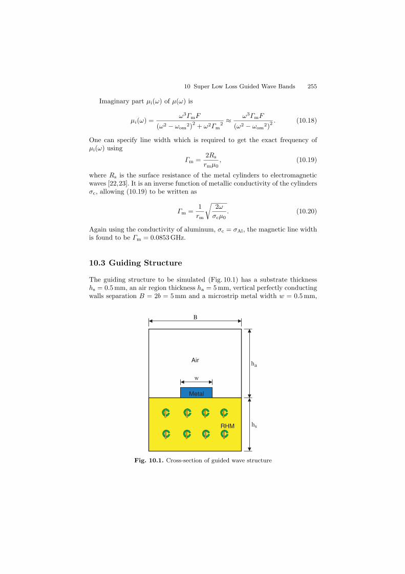
10 Super Low Loss Guided Wave Bands 255
Imaginary part µi(ω) of µ(ω) is
µi(ω) =ω3ΓmF
(ω2 − ωom2)2 + ω2Γm
2≈ ω3ΓmF
(ω2 − ωom2)2
. (10.18)
One can specify line width which is required to get the exact frequency ofµi(ω) using
Γm =2Rs
rmµ0, (10.19)
where Rs is the surface resistance of the metal cylinders to electromagneticwaves [22,23]. It is an inverse function of metallic conductivity of the cylindersσc, allowing (10.19) to be written as
Γm =1rm
√2ω
σcµ0. (10.20)
Again using the conductivity of aluminum, σc = σAl, the magnetic line widthis found to be Γm = 0.0853GHz.
10.3 Guiding Structure
The guiding structure to be simulated (Fig. 10.1) has a substrate thicknesshs = 0.5 mm, an air region thickness ha = 5 mm, vertical perfectly conductingwalls separation B = 2b = 5 mm and a microstrip metal width w = 0.5mm,
Metal
Air
RHM
B
ha
hs
w
Fig. 10.1. Cross-section of guided wave structure
256 C.M. Krowne
as in [1]. Certainly the lateral dimension of the structure B is substantiallygreater than the lattice spacing (B/a = 7.25), one requirement for the meta-material to be used in our simulation. The longitudinal direction, for a uniformguiding structure, as this is, is taken as infinite, and automatically satisfies themetamaterial size requirement (i.e., L a, L → ∞). However, the substratethickness is on the order of lattice spacing, which is not ideal, but we neverthe-less accept it for purposes of needing some roughly useable value in order toperform simulations in what follows. Finally, the electromagnetic wavelengthto lattice spacing ratio λ/a = 5.43, is substantial. Because of the logarithmicrelationship entailed in solving for re in (10.9) once a has been selected, anoticeable reduction in a by small integer factors can have drastic affects onre, reducing by many orders of magnitude its size, moving from the µm rangeto the nm range, something still possible using conductive carbon nanotubes.
In the above calculations, we have been careful not to assume the metalsof the split rings (or cylinders) are the same, σc = σr. In fact, one may bemade out of gold, and the other out of aluminum, platinum, silver, or copperto name a few common metals. Range of conductivities of these metals is from1.02 × 107 to 6.17 × 10⁷ Ω−1 m−1 [20].
Also of interest for the effective permittivities and permeabilities, are theircrossover frequencies. From (10.3), the electric crossover frequency ωeco whichsatisfies εr(ω) = 0, obeys
ω4 − ω2(ωpe
2 + ωoe2 + Γe
2)
+ ωpe2ωoe
2 = 0. (10.21)
When ωoe = 0, which is our present case, it is easier to examine the numeratorof (10.3) directly, than to solve (10.21), yielding
ωeco =√
ωpe2 − Γe
2 ≈ ωpe. (10.22)
From (10.11), the magnetic crossover frequency ωmco which satisfiesµr(ω) = 0, obeys
ω4(1 − F ) + ω2[ωom
2(F − 2) + Γ 2m
]+ ωom
4 = 0. (10.23)
One of the solutions gives a value close to the resonance frequency when theline width is small, as we have seen it is for our case. For that limiting case,(10.23) considerably simplifies, and one may also readily find the solution byworking with (10.11) directly, finding
ωmco =ωom√1 − F
. (10.24)
Placing the values already calculated into the right-hand side of (10.24),ωmco = 104.98 GHz.
10 Super Low Loss Guided Wave Bands 257
10.4 Numerical Results
For the LHM/NPV structure (NPV = negative phase velocity), in the lim-iting case of Γe → 0 and Γm → 0, two γ solutions exist which haveα = 0, and β = β/k0 = 1.177647 and 1.786090 (quoted values for num-ber of current basis functions nx and nz = 1 and spectral expansion termsn = 200). One corresponds to a forward wave for nondispersive intrinsic LHMs(β = β/k0 = 1.78609) where the product of the integrated Poynting vector(net power through the cross-section) and phase vector in the z-direction is∮
Pz • βz dA > 0 (dA is the differential cross-sectional element) or equiva-lently vgl · vpl > 0. The other solution is a backward wave for nondispersiveintrinsic LHMs (β = β/k0 = 1.177647) where the product of the integratedPoynting vector and the phase vector in the z-direction is
∮Pz • βz dA < 0
or equivalently vgl · vpl < 0. Here vgl and vpl are, respectively, the groupand phase longitudinal velocities. These modes are referred to as fundamentalmodes in the sense that as ω → 0, a solution exists.
As damping loss is turned on and becomes finite, only the larger guidedwave eigenvalue solution will exist, and the smaller guided wave solution willcease to exist. One of the effects of utilizing a highly dispersive SRR like sub-strate is that it converts the forward wave nondispersive solution into a back-ward wave (at least up to 93 GHz, then it becomes a slightly forward wave until103 GHz). The fundamental mode is shown in Fig. 10.2 (labeled R1: light blueα = α/k0 and green β = β/k0 curves), not extending beyond either 74 GHzon the low end or 105 GHz on the high end because sg[εr(ω)]sg[µr(ω)] = −1,and that product causes evanescent propagation to occur where β is extremelytiny. Below fom and above fmco, µr > 0 and εr < 0. However, betweenthese critical frequency points, sg[εr(ω)] sg[µr(ω)] = +1 and the wave prop-agates with µr < 0 and εr < 0. Out of the range plotted, above the electriccross-over frequency feco (near fpe for low loss) where effective permittivityεr = 0, sg[εr(ω)] sg[µr(ω)] = +1 will occur again, with µr > 0 and εr > 0 thistime, being completely reversed from the region between fom and fmco.
Results for the two other modes R2 (dark blue α = α/k0 and orangeβ = β/k0 curves) and R3 (dark magenta α = α/k0 and red β = β/k0 curves)are also shown in Fig. 10.2. They clearly have much higher attenuation thanthe fundamental mode. These modes do show forward wave behavior wherethe curve slopes go positive near 77.7 GHz and persist to 80 GHz.
The dispersion curves for the LHM/NPV substrate are plotted for themodes in Fig. 10.2 using nx = nz = 5 and n = 500 with frequency incrementsof ∆f = 0.0025GHz between eigenvalue points (only small differences withsolutions at nx = nz = 9 and n = 900 and nx = nz = 1 and n = 100 have beenfound, on the order of less than a few tenths of a percent). At 80 GHz for thefundamental mode, γ = (α, β) = (0.0320222, 1.79365) for nx = nz = 1 andn = 100, whereas for nx = nz = 9 and n = 900, γ = (0.0322745, 1.79116). Cal-culated values used the parameter settings mentioned above at room tempera-ture, but note that Γe and Γm could be reduced further using superconductive
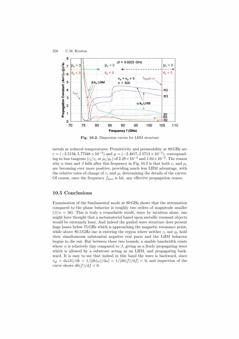
258 C.M. Krowne
Fig. 10.2. Dispersion curves for LHM structure
metals at reduced temperatures. Permittivity and permeability at 80 GHz areε = (−2.5156, 5.77348× 10⁻³) and µ = (−2.4817, 2.5713× 10⁻²), correspond-ing to loss tangents (εi/εr or µi/µr) of 2.28×10⁻³ and 1.04×10⁻². The reasonwhy α rises and β falls after this frequency in Fig. 10.2 is that both εr and µr
are becoming ever more positive, providing much less LHM advantage, withthe relative rates of change of εr and µr determining the details of the curves.Of course, once the frequency fmco is hit, any effective propagation ceases.
10.5 Conclusions
Examination of the fundamental mode at 80 GHz shows that the attenuationcompared to the phase behavior is roughly two orders of magnitude smaller(β/α = 56). This is truly a remarkable result, since by intuition alone, onemight have thought that a metamaterial based upon metallic resonant objectswould be extremely lossy. And indeed the guided wave structure does presenthuge losses below 75 GHz which is approaching the magnetic resonance point,while above 80.5 GHz one is entering the region where neither εr nor µr holdtheir simultaneous substantial negative real parts and the LHM behaviorbegins to die out. But between these two bounds, a sizable bandwidth existswhere α is relatively tiny compared to β, giving us a freely propagating wavewhich is allowed by a substrate acting as an LHM, and propagating back-ward. It is easy to see that indeed in this band the wave is backward, sincevgl = dω(k)/dk = 1/[dk(ω)/dω] = 1/[dk(f)/df ] < 0, and inspection of thecurve shows dk(f)/df < 0.
10 Super Low Loss Guided Wave Bands 259
Even the higher order modes R2 and R3 have low loss bands, but they aremuch smaller than the fundamental mode, existing between 75 and 76.7 GHz(R2) and 77.5 GHz (R3).
Results from this chapter are taken from [24], where a discussion of theGreen’s function methodology is presented, along with graphs of effectivepermittivity ε(ω) and permeability µ(ω) of the SRR metamaterial.
References
1. C.M. Krowne, Phys Rev. Lett. 92, 053901 (2004)2. C.M. Krowne, arXiv.org/abs/cond-mat/0406219 (June 10, 2004)3. C.M. Krowne, Phys Rev. Lett. 93, 053902 (2004) γs in this work were α = 0 and
β(unrotated-stripline) = 2.30195 (nx = nz = 1, n = 200); β(rotated-stripline)= 2.24643 (nx = nz = 1, n = 200) and 2.24623 (nx = nz = 5, n = 500) allasymmetric basis set; β(rotated-microstrip) = 2.11530 asymmetric basis and2.11604 symmetric basis (nx = nz = 1, n = 200)
4. C. Luo, S.G. Johnson, J.D. Joannopoulos, J.B. Pendry, Phys. Rev. B 65, 201104(2002)
5. C. Luo, S.G. Johnson, J.D. Joannopoulos, J.B. Pendry, Opt. Express 11, 746(2003)
6. S. Foteinopoulou, C.M. Soukoulos, Phys. Rev. B 67, 235107 (2003)7. P.V. Parimi, W.T. Lu, P. Vodo, S. Sridhar, Nature 426, 404 (2003)8. R.A. Shelby, D.R. Smith, S. Schultz, Science 292, 77 (2001)9. P. Markos, I. Rousochatzakis, C.M. Soukoulis, Phys. Rev. E 66, 045601 (2002)
10. N.C. Panoiu, R.M. Osgood Jr., Phys. Rev. E 68, 016611 (2003)11. J.O. Dimmock, Opt. Express 11, 2397 (2003)12. N.C. Panoiu, R.M. Osgood Jr., Opt. Commun. 223, 331 (2003)13. P. Markos, C.M. Soukoulis, Phys. Status Solidi (a) 197, 595 (2003)14. P. Markos, C.M. Soukoulis, Opt. Express 11, 649 (2003)15. R.B. Greegor, C.G. Parazzoli, K. Li, B.E.C. Koltenbah, M. Tanielian, Opt.
Express 11, 688 (2003)16. P. Markos, C.M. Soukoulis, Phys. Rev. E 65, 036622 (2002)17. D.R. Smith, S. Schultz, P. Markos, C.M. Soukoulis, Phys. Rev. B 65, 195104
(2002)18. L. Ran, J. Huangfu, H. Chen, Y. Li, X. Zhang, K. Chen, J.A. Kong, Phys. Rev.
B 70, 073102 (2004)19. K.J. Webb, M. Yang, D.W. Ward, K.A. Nelson, Phys. Rev. E 70, 035602 (R)
(2004)20. J. Pendry, A.J. Holden, W.J. Stewart, I. Young, Phys Rev. Lett. 76, 4773 (1996)21. J.B. Pendry, A.J. Holden, D.J. Robbins, W.J. Stewart, IEEE Trans. Microw.
Theory Tech. 47, 2075 (1999)22. S. Ramo, J.R. Whinnery, T. Van Duzer, Fields and Waves in Communication
Electronics (Wiley, New York, 1967)23. C.M. Krowne, Int. J. Numer. Model.: Electr. Networks, Dev. Fields 12, 399
(1999)24. C.M. Krowne, IET Proc. Microwaves, Antennas & Propag. 1 (2007)
11
Development of Negative Index of RefractionMetamaterials with Split Ring Resonatorsand Wires for RF Lens Applications
C.G. Parazzoli, R.B. Greegor and M.H. Tanielian
Summary. Metamaterials are engineered ring and wire composites whose responseto an incident electromagnetic wave can be described by an effective negative dielec-tric permittivity ε and magnetic permeability µ. Simultaneous negative ε and µwithin a given frequency band of a metamaterial gives rise to a negative index ofrefraction n. This has been demonstrated via a Snell’s law experiment. The electro-magnetic properties of many metamaterial structures in the microwave region areinvestigated through numerical simulations and experiments. A negative index ofrefraction, n, allows lenses with reduced primary (Seidel) aberrations compared toequivalent positive index lens. This is demonstrated both for cylindrical lenses andspherical lenses, as well as for the gradient index lenses. Detailed field maps of thefocal region of the metamaterials lenses are made and compared to a comparablepositive index of refraction lens.
This chapter discusses the properties of negative index materials (NIMs),derived from numerical simulations, and compares them with experimentaldata for a Snell’s law wedge and numerous lenses operating in the radio fre-quency (RF) range. Both cylindrical and spherical lenses are discussed. Specif-ically in Sect. 11.1, we discuss the physics of NIMs. In Sect. 11.2, we presentthe details of a Snell’s law experiment that proves the existence of a negativerefractive index. In Sect. 11.3 we describe the retrieval of the effective ε andµ from the scattering parameters. In Sect. 11.4, we discuss the testing of NIMstructures. In Sect. 11.5 the optical properties of NIM lenses are discussed.In Sects. 11.6 and 11.7 the design, test and characterization of NIM lensesare elucidated.
11.1 Electromagnetic Negative Index Materials
The word meta is a Greek word meaning beyond. Metamaterials are artificialstructures or composites with properties that are not found or are beyondnaturally occurring materials or compounds. In 1968, Victor Veselago [1]
262 C.G. Parazzoli et al.
described in a seminal paper the properties of materials where both theirelectrical permittivity ε and magnetic permeability µ are negative. The pre-sence of simultaneous negative ε and µ gives rise to a negative refractive index.It reverses the Doppler shift and the Cerenkov effect. In 1996, John Pendrysuggested a method of effectively obtaining negative permittivity by using anarray of thin parallel wires. He did also suggest [2] an approach to obtain aneffective negative permeability by using split ring resonator (SRR) patterns.In 2000, physicists at the University of California San Diego [3] demonstratedexperimentally for the first time that a sample composed of wires and SRRseffectively displayed a negative index of refraction over a limited frequencyrange. This negative index material will be referred to as an NIM.
11.1.1 The Physics of NIMs
All known electromagnetic phenomena in a medium are described by theelectric field E, the magnetic induction B, and the two auxiliary fields, D,the electric displacement, and H, the magnetic intensity, which describethe macroscopic response of the medium to the applied external fields. Weassume harmonic time dependence for the electromagnetic field exp (−iωt) =exp (−ikoct). Here ko is the free-space wave number. The constitutive relationsare B = µ(ω)H and D = ε(ω)E, where µ is the magnetic permeability dyadicand ε is the electric permittivity dyadic. With these assumptions Maxwell’sequations read as
∇× H + ikoεE = 0, (11.1)∇× E − i koµH = 0, (11.2)∇ · (ε E) = 0, (11.3)∇ · (µ H) = 0. (11.4)
The detailed properties of a medium’s electromagnetic response are thus con-tained in µ and ε, which we refer to as the material parameters. The range ofpossible values for these material parameters is limited by fundamental lawssuch as causality or thermodynamics, and it is broader than the range of nat-urally occurring materials. Natural occurring materials do not cover the fullpossible range, but new engineered materials do. When a material exhibitsεeff , µeff < 0 in a frequency band, it is referred to as a left-handed material(LHM) or NIM. The development of NIMs opens up a new region of parameterspace for effective material parameters, as shown in Fig. 11.1. The lower leftquadrant is where NIMs reside. NIMs are of particular interest, as a reversalin electromagnetic wave phase velocity takes place.
In an isotropic NIM the index of refraction n, is negative. The quantitativestatement of refraction is contained in Snell’s law, which has the simple form
n1 sin(θI) = n2 sin(θR). (11.5)
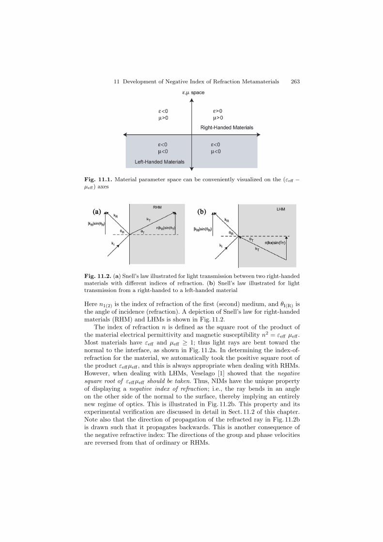
11 Development of Negative Index of Refraction Metamaterials 263
Fig. 11.1. Material parameter space can be conveniently visualized on the (εeff −µeff) axes
Fig. 11.2. (a) Snell’s law illustrated for light transmission between two right-handedmaterials with different indices of refraction. (b) Snell’s law illustrated for lighttransmission from a right-handed to a left-handed material
Here n1(2) is the index of refraction of the first (second) medium, and θI(R) isthe angle of incidence (refraction). A depiction of Snell’s law for right-handedmaterials (RHM) and LHMs is shown in Fig. 11.2.
The index of refraction n is defined as the square root of the product ofthe material electrical permittivity and magnetic susceptibility n2 = εeff µeff .Most materials have εeff and µeff ≥ 1; thus light rays are bent toward thenormal to the interface, as shown in Fig. 11.2a. In determining the index-of-refraction for the material, we automatically took the positive square root ofthe product εeffµeff , and this is always appropriate when dealing with RHMs.However, when dealing with LHMs, Veselago [1] showed that the negativesquare root of εeffµeff should be taken. Thus, NIMs have the unique propertyof displaying a negative index of refraction; i.e., the ray bends in an angleon the other side of the normal to the surface, thereby implying an entirelynew regime of optics. This is illustrated in Fig. 11.2b. This property and itsexperimental verification are discussed in detail in Sect. 11.2 of this chapter.Note also that the direction of propagation of the refracted ray in Fig. 11.2bis drawn such that it propagates backwards. This is another consequence ofthe negative refractive index: The directions of the group and phase velocitiesare reversed from that of ordinary or RHMs.
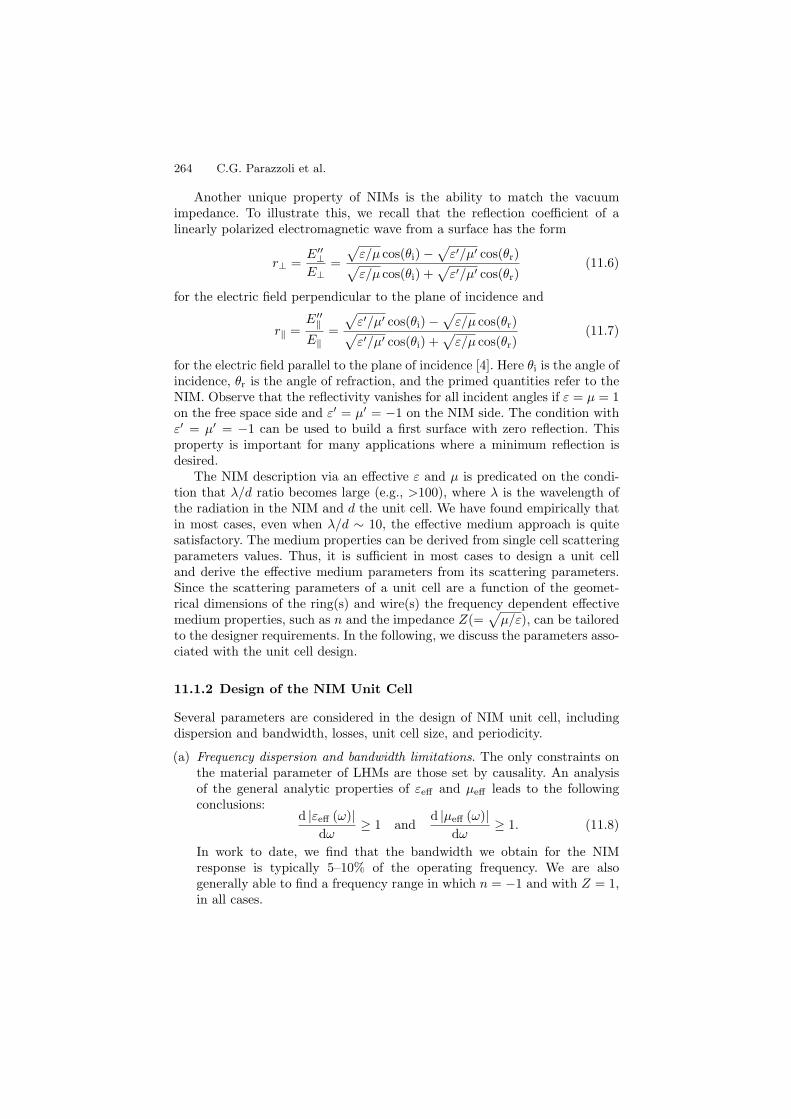
264 C.G. Parazzoli et al.
Another unique property of NIMs is the ability to match the vacuumimpedance. To illustrate this, we recall that the reflection coefficient of alinearly polarized electromagnetic wave from a surface has the form
r⊥ =E′′
⊥E⊥
=
√ε/µ cos(θi) −
√ε′/µ′ cos(θr)√
ε/µ cos(θi) +√
ε′/µ′ cos(θr)(11.6)
for the electric field perpendicular to the plane of incidence and
r‖ =E′′
‖E‖
=
√ε′/µ′ cos(θi) −
√ε/µ cos(θr)√
ε′/µ′ cos(θi) +√
ε/µ cos(θr)(11.7)
for the electric field parallel to the plane of incidence [4]. Here θi is the angle ofincidence, θr is the angle of refraction, and the primed quantities refer to theNIM. Observe that the reflectivity vanishes for all incident angles if ε = µ = 1on the free space side and ε′ = µ′ = −1 on the NIM side. The condition withε′ = µ′ = −1 can be used to build a first surface with zero reflection. Thisproperty is important for many applications where a minimum reflection isdesired.
The NIM description via an effective ε and µ is predicated on the condi-tion that λ/d ratio becomes large (e.g., >100), where λ is the wavelength ofthe radiation in the NIM and d the unit cell. We have found empirically thatin most cases, even when λ/d ∼ 10, the effective medium approach is quitesatisfactory. The medium properties can be derived from single cell scatteringparameters values. Thus, it is sufficient in most cases to design a unit celland derive the effective medium parameters from its scattering parameters.Since the scattering parameters of a unit cell are a function of the geomet-rical dimensions of the ring(s) and wire(s) the frequency dependent effectivemedium properties, such as n and the impedance Z(=
√µ/ε), can be tailored
to the designer requirements. In the following, we discuss the parameters asso-ciated with the unit cell design.
11.1.2 Design of the NIM Unit Cell
Several parameters are considered in the design of NIM unit cell, includingdispersion and bandwidth, losses, unit cell size, and periodicity.
(a) Frequency dispersion and bandwidth limitations. The only constraints onthe material parameter of LHMs are those set by causality. An analysisof the general analytic properties of εeff and µeff leads to the followingconclusions:
d |εeff (ω)|dω
≥ 1 andd |µeff (ω)|
dω≥ 1. (11.8)
In work to date, we find that the bandwidth we obtain for the NIMresponse is typically 5–10% of the operating frequency. We are alsogenerally able to find a frequency range in which n = −1 and with Z = 1,in all cases.
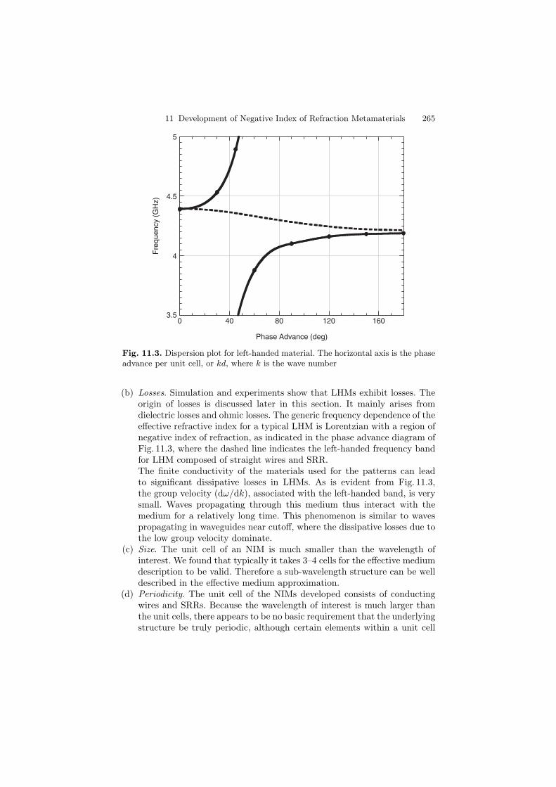
11 Development of Negative Index of Refraction Metamaterials 265
3.5
4
4.5
5
0 40 80 120 160
Fre
quen
cy (
GH
z)
Phase Advance (deg)
Fig. 11.3. Dispersion plot for left-handed material. The horizontal axis is the phaseadvance per unit cell, or kd, where k is the wave number
(b) Losses. Simulation and experiments show that LHMs exhibit losses. Theorigin of losses is discussed later in this section. It mainly arises fromdielectric losses and ohmic losses. The generic frequency dependence of theeffective refractive index for a typical LHM is Lorentzian with a region ofnegative index of refraction, as indicated in the phase advance diagram ofFig. 11.3, where the dashed line indicates the left-handed frequency bandfor LHM composed of straight wires and SRR.The finite conductivity of the materials used for the patterns can leadto significant dissipative losses in LHMs. As is evident from Fig. 11.3,the group velocity (dω/dk), associated with the left-handed band, is verysmall. Waves propagating through this medium thus interact with themedium for a relatively long time. This phenomenon is similar to wavespropagating in waveguides near cutoff, where the dissipative losses due tothe low group velocity dominate.
(c) Size. The unit cell of an NIM is much smaller than the wavelength ofinterest. We found that typically it takes 3–4 cells for the effective mediumdescription to be valid. Therefore a sub-wavelength structure can be welldescribed in the effective medium approximation.
(d) Periodicity. The unit cell of the NIMs developed consists of conductingwires and SRRs. Because the wavelength of interest is much larger thanthe unit cells, there appears to be no basic requirement that the underlyingstructure be truly periodic, although certain elements within a unit cell
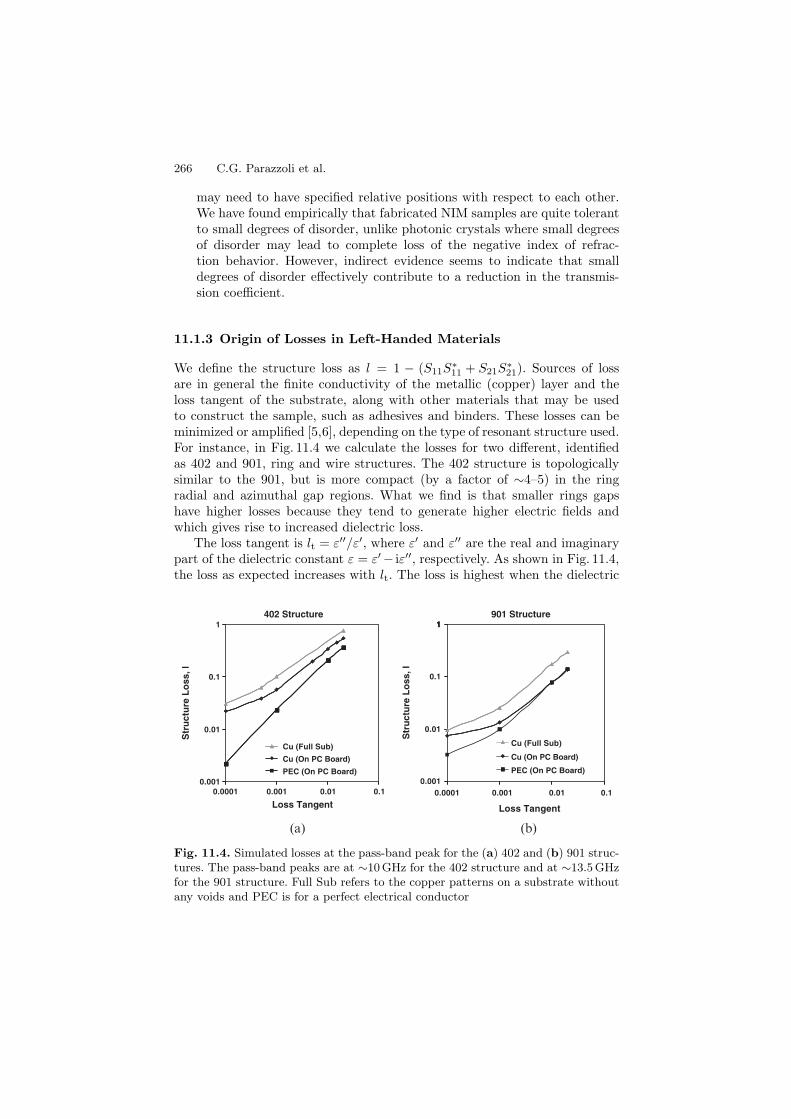
266 C.G. Parazzoli et al.
may need to have specified relative positions with respect to each other.We have found empirically that fabricated NIM samples are quite tolerantto small degrees of disorder, unlike photonic crystals where small degreesof disorder may lead to complete loss of the negative index of refrac-tion behavior. However, indirect evidence seems to indicate that smalldegrees of disorder effectively contribute to a reduction in the transmis-sion coefficient.
11.1.3 Origin of Losses in Left-Handed Materials
We define the structure loss as l = 1 − (S11S∗11 + S21S
∗21). Sources of loss
are in general the finite conductivity of the metallic (copper) layer and theloss tangent of the substrate, along with other materials that may be usedto construct the sample, such as adhesives and binders. These losses can beminimized or amplified [5,6], depending on the type of resonant structure used.For instance, in Fig. 11.4 we calculate the losses for two different, identifiedas 402 and 901, ring and wire structures. The 402 structure is topologicallysimilar to the 901, but is more compact (by a factor of ∼4–5) in the ringradial and azimuthal gap regions. What we find is that smaller rings gapshave higher losses because they tend to generate higher electric fields andwhich gives rise to increased dielectric loss.
The loss tangent is lt = ε′′/ε′, where ε′ and ε′′ are the real and imaginarypart of the dielectric constant ε = ε′− iε′′, respectively. As shown in Fig. 11.4,the loss as expected increases with lt. The loss is highest when the dielectric
0.001
0.01
0.1
1
0.0001 0.001 0.01 0.1
Loss Tangent
Str
uct
ure
Lo
ss, l
Cu (Full Sub)
Cu (On PC Board)
PEC (On PC Board)0.001
0.01
0.1
1
0.0001 0.001 0.01 0.1
Loss Tangent
Str
uct
ure
Lo
ss, l
Cu (Full Sub)
Cu (On PC Board)
PEC (On PC Board)
402 Structure 901 Structure11
(a) (b)
Fig. 11.4. Simulated losses at the pass-band peak for the (a) 402 and (b) 901 struc-tures. The pass-band peaks are at ∼10GHz for the 402 structure and at ∼13.5 GHzfor the 901 structure. Full Sub refers to the copper patterns on a substrate withoutany voids and PEC is for a perfect electrical conductor

11 Development of Negative Index of Refraction Metamaterials 267
completely fills the cell. This corresponds to the upper curves (triangles).The loss decreases when the conductive elements are deposited on a thinner0.025 cm substrate (PC board) as shown by the middle curves (diamonds).When the copper losses are omitted from the simulation, the results for athin PC board substrate are given by the lower curves (squares). The copperconductive losses dominate, as expected, at low values of the dielectric losstangent. The trends exhibited by these simulations have also been observedin our experiments.
As mentioned earlier, dielectric losses are concentrated in the high fieldregions. These numerical simulations are shown in Fig. 11.5. It is obvious fromthese results that the small gaps concentrate the fields more. It is also notice-able that the losses are limited to narrow regions surrounding the gaps. The402 structure, which has an azimuthal gap 4.6 times smaller than the 901structure, has a maximum power loss density ∼17 times higher. Therefore,one possibility in the fabrication would be to remove the dielectric in theregion of high fields in order to significantly reduce the loss.
901402
42.9e7
28.6e7 1.56e7
0.56e7
27.4e7 2.50e7
27.8e7 1.90e7
17.0e7 1.15e7
(a) (b)
Fig. 11.5. Simulated power loss density in gray scale (a) the 402 structure and (b)the 901 structure. The numbers in the diagram indicate the maximum power lossdensity at the highlighted x = constant plane indicated. Note that the power lossdensity is greatest in the regions of the azimuthal gaps, and the structure with thesmallest gaps (402) has the highest power loss density
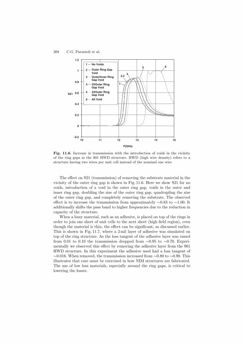
268 C.G. Parazzoli et al.
−0.2
0.2
0.4
0.6
0.8
1
1.2
10 11 12 13 14 15
F(GHz)
S21
No Voids
Outer Ring Gap VoidOuter/Inner RingGap Void
2XOuter RingGap Void
4XOuter RingGap Void
All Void
1
2
3
4
5
6
0
1
2,3
65
4
Fig. 11.6. Increase in transmission with the introduction of voids in the vicinityof the ring gaps in the 901 HWD structure. HWD (high wire density) refers to astructure having two wires per unit cell instead of the nominal one wire
The effect on S21 (transmission) of removing the substrate material in thevicinity of the outer ring gap is shown in Fig. 11.6. Here we show S21 for novoids, introduction of a void in the outer ring gap, voids in the outer andinner ring gap, doubling the size of the outer ring gap, quadrupling the sizeof the outer ring gap, and completely removing the substrate. The observedeffect is to increase the transmission from approximately ∼0.83 to ∼1.00. Itadditionally shifts the pass band to higher frequencies due to the reduction incapacity of the structure.
When a lossy material, such as an adhesive, is placed on top of the rings inorder to join one sheet of unit cells to the next sheet (high field region), eventhough the material is thin, the effect can be significant, as discussed earlier.This is shown in Fig. 11.7, where a 2 mil layer of adhesive was simulated ontop of the ring structure. As the loss tangent of the adhesive layer was raisedfrom 0.01 to 0.10 the transmission dropped from ∼0.95 to ∼0.70. Experi-mentally we observed this effect by removing the adhesive layer from the 901HWD structure. In this experiment the adhesive used had a loss tangent of∼0.016. When removed, the transmission increased from ∼0.80 to ∼0.90. Thisillustrates that care must be exercised in how NIM structures are fabricated.The use of low loss materials, especially around the ring gaps, is critical tolowering the losses.
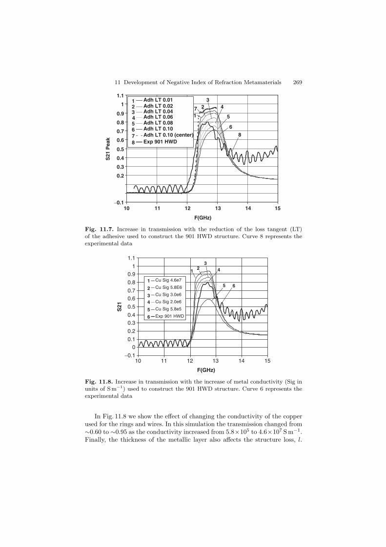
11 Development of Negative Index of Refraction Metamaterials 269
−0.1
0.2
0.3
0.4
0.5
0.6
0.7
0.8
0.9
1
1.1
10 11 12 13 14 15
F(GHz)
S21
Pea
k
Adh LT 0.01Adh LT 0.02Adh LT 0.04Adh LT 0.06Adh LT 0.08Adh LT 0.10Adh LT 0.10 (center)Exp 901 HWD
12345678
1
23
4
5
6
7
8
Fig. 11.7. Increase in transmission with the reduction of the loss tangent (LT)of the adhesive used to construct the 901 HWD structure. Curve 8 represents theexperimental data
−0.1
00.1
0.2
0.30.4
0.5
0.60.7
0.8
0.91
1.1
10 11 12 13 14 15
F(GHz)
S21
Cu Sig 4.6e7
Cu Sig 5.8E6
Cu Sig 3.0e6
Cu Sig 2.0e6
Cu Sig 5.8e5
Exp 901 HWD
1
2
3 4
5
6
2
6
3
5
41
Fig. 11.8. Increase in transmission with the increase of metal conductivity (Sig inunits of Sm−1) used to construct the 901 HWD structure. Curve 6 represents theexperimental data
In Fig. 11.8 we show the effect of changing the conductivity of the copperused for the rings and wires. In this simulation the transmission changed from∼0.60 to ∼0.95 as the conductivity increased from 5.8×10⁵ to 4.6×10⁷ S m−1.Finally, the thickness of the metallic layer also affects the structure loss, l.
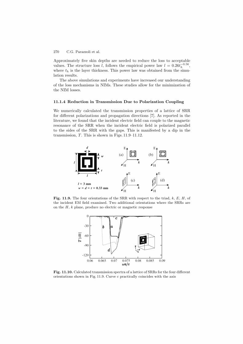
270 C.G. Parazzoli et al.
Approximately five skin depths are needed to reduce the loss to acceptablevalues. The structure loss l, follows the empirical power law l = 0.26t−0.56
h ,where th is the layer thickness. This power law was obtained from the simu-lation results.
The above simulations and experiments have increased our understandingof the loss mechanisms in NIMs. These studies allow for the minimization ofthe NIM losses.
11.1.4 Reduction in Transmission Due to Polarization Coupling
We numerically calculated the transmission properties of a lattice of SRRfor different polarizations and propagation directions [7]. As reported in theliterature, we found that the incident electric field can couple to the magneticresonance of the SRR when the incident electric field is polarized parallelto the sides of the SRR with the gaps. This is manifested by a dip in thetransmission, T . This is shown in Figs. 11.9–11.12.
d
w
t
l
l = 3 mmw = d = t = 0.33 mm
l k k
kk
E
E
E
E
H H
HH
(a) (b)
(c) (d)
Fig. 11.9. The four orientations of the SRR with respect to the triad, k, E, H, ofthe incident EM field examined. Two additional orientations where the SRRs areon the H, k plane, produce no electric or magnetic response
Fig. 11.10. Calculated transmission spectra of a lattice of SRRs for the four differentorientations shown in Fig. 11.9. Curve c practically coincides with the axis
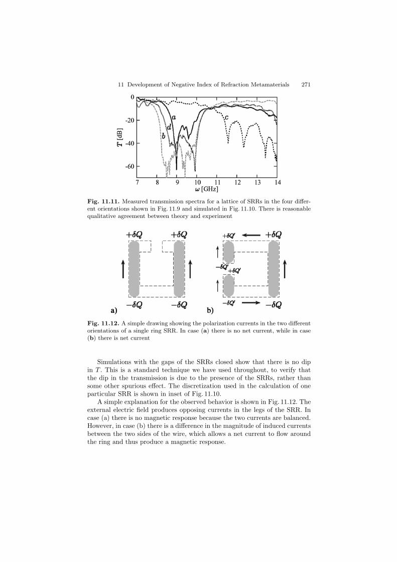
11 Development of Negative Index of Refraction Metamaterials 271
Fig. 11.11. Measured transmission spectra for a lattice of SRRs in the four differ-ent orientations shown in Fig. 11.9 and simulated in Fig. 11.10. There is reasonablequalitative agreement between theory and experiment
Fig. 11.12. A simple drawing showing the polarization currents in the two differentorientations of a single ring SRR. In case (a) there is no net current, while in case(b) there is net current
Simulations with the gaps of the SRRs closed show that there is no dipin T . This is a standard technique we have used throughout, to verify thatthe dip in the transmission is due to the presence of the SRRs, rather thansome other spurious effect. The discretization used in the calculation of oneparticular SRR is shown in inset of Fig. 11.10.
A simple explanation for the observed behavior is shown in Fig. 11.12. Theexternal electric field produces opposing currents in the legs of the SRR. Incase (a) there is no magnetic response because the two currents are balanced.However, in case (b) there is a difference in the magnitude of induced currentsbetween the two sides of the wire, which allows a net current to flow aroundthe ring and thus produce a magnetic response.
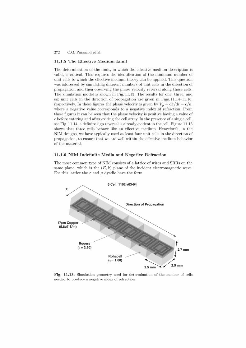
272 C.G. Parazzoli et al.
11.1.5 The Effective Medium Limit
The determination of the limit, in which the effective medium description isvalid, is critical. This requires the identification of the minimum number ofunit cells to which the effective medium theory can be applied. This questionwas addressed by simulating different numbers of unit cells in the direction ofpropagation and then observing the phase velocity reversal along those cells.The simulation model is shown in Fig. 11.13. The results for one, three, andsix unit cells in the direction of propagation are given in Figs. 11.14–11.16,respectively. In these figures the phase velocity is given by Vp = dz/dt = c/n,where a negative value corresponds to a negative index of refraction. Fromthese figures it can be seen that the phase velocity is positive having a value ofc before entering and after exiting the cell array. In the presence of a single cell,see Fig. 11.14, a definite sign reversal is already evident in the cell. Figure 11.15shows that three cells behave like an effective medium. Henceforth, in theNIM designs, we have typically used at least four unit cells in the direction ofpropagation, to ensure that we are well within the effective medium behaviorof the material.
11.1.6 NIM Indefinite Media and Negative Refraction
The most common type of NIM consists of a lattice of wires and SRRs on thesame plane, which is the (E, k) plane of the incident electromagnetic wave.For this lattice the ε and µ dyadic have the form
6 Cell, 1102rr03-04
2.7 mm
2.5 mm2.5 mm
Rogers (ε = 2.20)
Rohacell (ε = 1.08)
17µm Copper(5.8e7 S/m)
E
Direction of Propagation
Fig. 11.13. Simulation geometry used for determination of the number of cellsneeded to produce a negative index of refraction
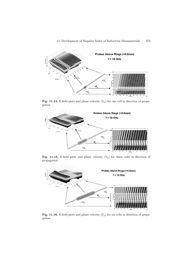
11 Development of Negative Index of Refraction Metamaterials 273
Fig. 11.14. E-field plots and phase velocity (Vp) for one cell in direction of propa-gation
Fig. 11.15. E-field plots and phase velocity (Vp) for three cells in direction ofpropagation
Fig. 11.16. E-field plots and phase velocity (Vp) for six cells in direction of propa-gation
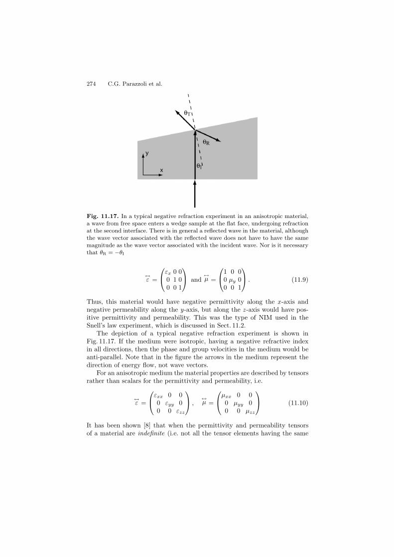
274 C.G. Parazzoli et al.
Fig. 11.17. In a typical negative refraction experiment in an anisotropic material,a wave from free space enters a wedge sample at the flat face, undergoing refractionat the second interface. There is in general a reflected wave in the material, althoughthe wave vector associated with the reflected wave does not have to have the samemagnitude as the wave vector associated with the incident wave. Nor is it necessarythat θR = −θI
↔ε =
⎛⎝
εx 0 00 1 00 0 1
⎞⎠ and
↔µ =
⎛⎝
1 0 00 µy 00 0 1
⎞⎠ . (11.9)
Thus, this material would have negative permittivity along the x -axis andnegative permeability along the y-axis, but along the z -axis would have pos-itive permittivity and permeability. This was the type of NIM used in theSnell’s law experiment, which is discussed in Sect. 11.2.
The depiction of a typical negative refraction experiment is shown inFig. 11.17. If the medium were isotropic, having a negative refractive indexin all directions, then the phase and group velocities in the medium would beanti-parallel. Note that in the figure the arrows in the medium represent thedirection of energy flow, not wave vectors.
For an anisotropic medium the material properties are described by tensorsrather than scalars for the permittivity and permeability, i.e.
↔ε =
⎛⎝
εxx 0 00 εyy 00 0 εzz
⎞⎠ ,
↔µ =
⎛⎝
µxx 0 00 µyy 00 0 µzz
⎞⎠ (11.10)
It has been shown [8] that when the permittivity and permeability tensorsof a material are indefinite (i.e. not all the tensor elements having the same
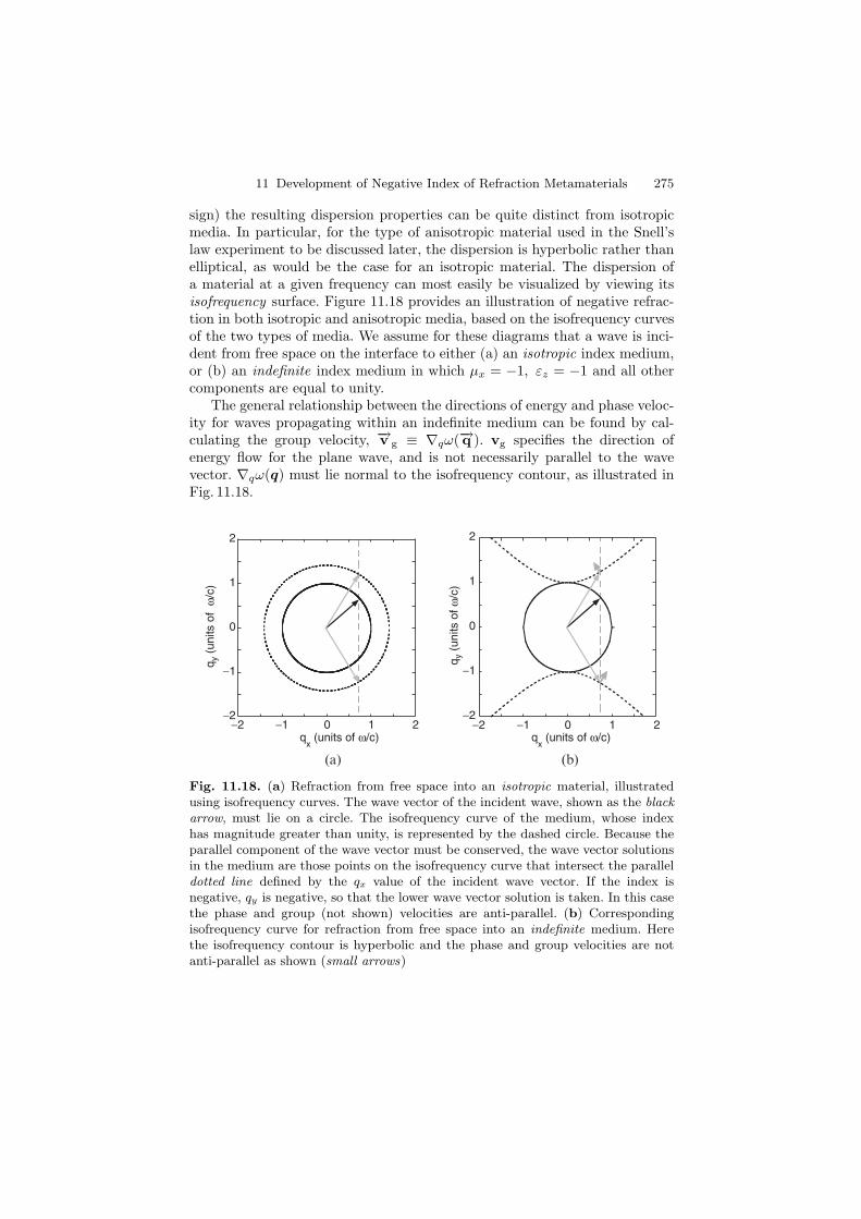
11 Development of Negative Index of Refraction Metamaterials 275
sign) the resulting dispersion properties can be quite distinct from isotropicmedia. In particular, for the type of anisotropic material used in the Snell’slaw experiment to be discussed later, the dispersion is hyperbolic rather thanelliptical, as would be the case for an isotropic material. The dispersion ofa material at a given frequency can most easily be visualized by viewing itsisofrequency surface. Figure 11.18 provides an illustration of negative refrac-tion in both isotropic and anisotropic media, based on the isofrequency curvesof the two types of media. We assume for these diagrams that a wave is inci-dent from free space on the interface to either (a) an isotropic index medium,or (b) an indefinite index medium in which µx = −1, εz = −1 and all othercomponents are equal to unity.
The general relationship between the directions of energy and phase veloc-ity for waves propagating within an indefinite medium can be found by cal-culating the group velocity, −→v g ≡ ∇qω(−→q ). vg specifies the direction ofenergy flow for the plane wave, and is not necessarily parallel to the wavevector. ∇qω(q) must lie normal to the isofrequency contour, as illustrated inFig. 11.18.
−2
−1
0
1
2
−2 −1 0 1 2
q y (
units
of
ω/c
)
qx (units of ω/c)
q y (
units
of ω
/c)
qx (units of ω/c)
−2
−1
0
1
2
−2 −1 0 1 2
(a) (b)
Fig. 11.18. (a) Refraction from free space into an isotropic material, illustratedusing isofrequency curves. The wave vector of the incident wave, shown as the blackarrow, must lie on a circle. The isofrequency curve of the medium, whose indexhas magnitude greater than unity, is represented by the dashed circle. Because theparallel component of the wave vector must be conserved, the wave vector solutionsin the medium are those points on the isofrequency curve that intersect the paralleldotted line defined by the qx value of the incident wave vector. If the index isnegative, qy is negative, so that the lower wave vector solution is taken. In this casethe phase and group (not shown) velocities are anti-parallel. (b) Correspondingisofrequency curve for refraction from free space into an indefinite medium. Herethe isofrequency contour is hyperbolic and the phase and group velocities are notanti-parallel as shown (small arrows)
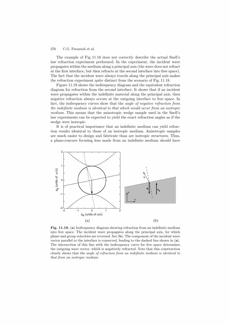
276 C.G. Parazzoli et al.
The example of Fig. 11.18 does not correctly describe the actual Snell’slaw refraction experiment performed. In the experiment, the incident wavepropagates within the medium along a principal axis (the wave does not refractat the first interface, but then refracts at the second interface into free space).The fact that the incident wave always travels along the principal axis makesthe refraction experiment quite distinct from the scenario of Fig. 11.18.
Figure 11.19 shows the isofrequency diagram and the equivalent refractiondiagram for refraction from the second interface. It shows that if an incidentwave propagates within the indefinite material along the principal axis, thennegative refraction always occurs at the outgoing interface to free space. Infact, the isofrequency curves show that the angle of negative refraction fromthe indefinite medium is identical to that which would occur from an isotropicmedium. This means that the anisotropic wedge sample used in the Snell’slaw experiments can be expected to yield the exact refraction angles as if thewedge were isotropic.
It is of practical importance that an indefinite medium can yield refrac-tion results identical to those of an isotropic medium. Anisotropic samplesare much easier to design and fabricate than are isotropic structures. Thus,a plano-concave focusing lens made from an indefinite medium should have
−2−2 −1 0 1 2
−1
0
1
2
q y (
units
of
ω/c
)
qx (units of ω/c)
(a) (b)
Fig. 11.19. (a) Isofrequency diagram showing refraction from an indefinite mediuminto free space. The incident wave propagates along the principal axis, for whichphase and group velocities are reversed. See (b). The component of the incident wavevector parallel to the interface is conserved, leading to the dashed line shown in (a).The intersection of this line with the isofrequency curve for free space determinesthe outgoing wave vector, which is negatively refracted. Note that this constructionclearly shows that the angle of refraction from an indefinite medium is identical tothat from an isotropic medium
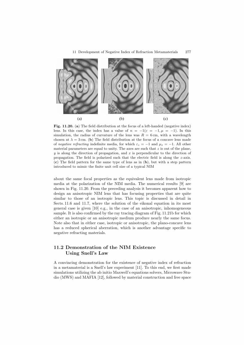
11 Development of Negative Index of Refraction Metamaterials 277
Fig. 11.20. (a) The field distribution at the focus of a left-handed (negative index)lens. In this case, the index has a value of n = −1(ε = −1, µ = −1). In thissimulation, the radius of curvature of the lens was R = 6 cm, with a wavelengthchosen at λ = 3 cm. (b) The field distribution at the focus of a concave lens madeof negative refracting indefinite media, for which εz = −1 and µx = −1. All othermaterial parameters are equal to unity. The axes are such that z is out of the plane,y is along the direction of propagation, and x is perpendicular to the direction ofpropagation. The field is polarized such that the electric field is along the z -axis.(c) The field pattern for the same type of lens as in (b), but with a step patternintroduced to mimic the finite unit cell size of a typical NIM
about the same focal properties as the equivalent lens made from isotropicmedia at the polarization of the NIM media. The numerical results [9] areshown in Fig. 11.20. From the preceding analysis it becomes apparent how todesign an anisotropic NIM lens that has focusing properties that are quitesimilar to those of an isotropic lens. This topic is discussed in detail inSects. 11.6 and 11.7, where the solution of the eikonal equation in its mostgeneral case is given [10] e.g., in the case of an anisotropic, inhomogeneoussample. It is also confirmed by the ray tracing diagram of Fig. 11.21b for whicheither an isotropic or an anisotropic medium produce nearly the same focus.Note also that in either case, isotropic or anisotropic, the plano-concave lenshas a reduced spherical aberration, which is another advantage specific tonegative refracting materials.
11.2 Demonstration of the NIM ExistenceUsing Snell’s Law
A convincing demonstration for the existence of negative index of refractionin a metamaterial is a Snell’s law experiment [11]. To this end, we first madesimulations utilizing the ab initio Maxwell’s equations solvers, Microwave Stu-dio (MWS) and MAFIA [12], followed by material construction and free space
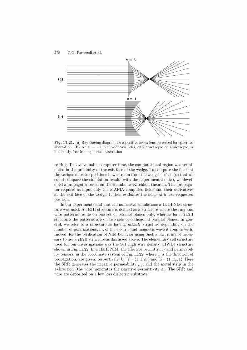
278 C.G. Parazzoli et al.
Fig. 11.21. (a) Ray tracing diagram for a positive index lens corrected for sphericalaberration. (b) An n = −1 plano-concave lens, either isotropic or anisotropic, isinherently free from spherical aberration
testing. To save valuable computer time, the computational region was termi-nated in the proximity of the exit face of the wedge. To compute the fields atthe various detector positions downstream from the wedge surface (so that wecould compare the simulation results with the experimental data), we devel-oped a propagator based on the Helmholtz–Kirchhoff theorem. This propaga-tor requires as input only the MAFIA computed fields and their derivativesat the exit face of the wedge. It then evaluates the fields at a user-requestedposition.
In our experiments and unit cell numerical simulations a 1E1H NIM struc-ture was used. A 1E1H structure is defined as a structure where the ring andwire patterns reside on one set of parallel planes only, whereas for a 2E2Hstructure the patterns are on two sets of orthogonal parallel planes. In gen-eral, we refer to a structure as having mEmH structure depending on thenumber of polarizations, m, of the electric and magnetic wave it couples with.Indeed, for the verification of NIM behavior using Snell’s law, it is not neces-sary to use a 2E2H structure as discussed above. The elementary cell structureused for our investigations was the 901 high wire density (HWD) structureshown in Fig. 11.22. In a 1E1H NIM, the effective permittivity and permeabil-ity tensors, in the coordinate system of Fig. 11.22, where x is the direction ofpropagation, are given, respectively, by
↔ε = (1, 1, εz) and
↔µ= (1, µy, 1). Here
the SRR generates the negative permeability µy, and the metal strip in thez -direction (the wire) generates the negative permittivity εz. The SRR andwire are deposited on a low loss dielectric substrate.
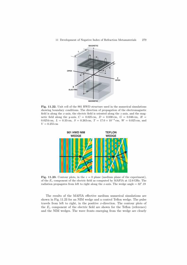
11 Development of Negative Index of Refraction Metamaterials 279
L
MAGNETIC
OPEN
ELECTRIC
MAGNETIC
XOPEN
Y
Z
GD
C
W
TH
S
V
Z
Fig. 11.22. Unit cell of the 901 HWD structure used in the numerical simulationsshowing boundary conditions. The direction of propagation of the electromagneticfield is along the x -axis, the electric field is oriented along the z -axis, and the mag-netic field along the y-axis. C = 0.025 cm, D = 0.030 cm, G = 0.046 cm, H =0.0254 cm, L = 0.33 cm, S = 0.263 cm, T = 17.0 × 10⁻⁴ cm, W = 0.025 cm, andV = 0.255 cm
901 HWD NIMWEDGE
TEFLONWEDGE
−34.0˚
48.2˚
Fig. 11.23. Contour plots, in the z = 0 plane (medium plane of the experiment),of the Ez component of the electric field as computed by MAFIA at 12.6 GHz. Theradiation propagates from left to right along the x -axis. The wedge angle = 32.19
The results of the MAFIA effective medium numerical simulations areshown in Fig. 11.23 for an NIM wedge and a control Teflon wedge. The pulsetravels from left to right, in the positive x -direction. The contour plots ofthe Ez component of the electric field are shown for the Teflon (reference)and the NIM wedges. The wave fronts emerging from the wedge are clearly
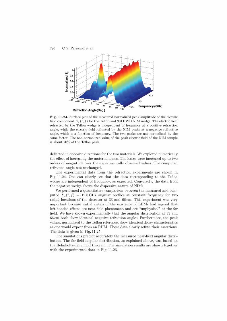
280 C.G. Parazzoli et al.
Fig. 11.24. Surface plot of the measured normalized peak amplitude of the electricfield component Ez (r, f) for the Teflon and 901 HWD NIM wedge. The electric fieldrefracted by the Teflon wedge is independent of frequency at a positive refractionangle, while the electric field refracted by the NIM peaks at a negative refractiveangle, which is a function of frequency. The two peaks are not normalized by thesame factor. The non-normalized value of the peak electric field of the NIM sampleis about 20% of the Teflon peak
deflected in opposite directions for the two materials. We explored numericallythe effect of increasing the material losses. The losses were increased up to twoorders of magnitude over the experimentally observed values. The computedrefracted angle was unchanged.
The experimental data from the refraction experiments are shown inFig. 11.24. One can clearly see that the data corresponding to the Teflonwedge are independent of frequency, as expected. Conversely, the data fromthe negative wedge shows the dispersive nature of NIMs.
We performed a quantitative comparison between the measured and com-puted Ez(r, f) = 12.6GHz angular profiles at constant frequency for tworadial locations of the detector at 33 and 66 cm. This experiment was veryimportant because initial critics of the existence of LHMs had argued thatleft-handed effects are near-field phenomena and are “unphysical” at the farfield. We have shown experimentally that the angular distribution at 33 and66 cm both show identical negative refraction angles. Furthermore, the peakvalues, normalized to the Teflon reference, show identical decay characteristicsas one would expect from an RHM. These data clearly refute their assertions.The data is given in Fig. 11.25.
The simulations predict accurately the measured near-field angular distri-bution. The far-field angular distribution, as explained above, was based onthe Helmholtz–Kirchhoff theorem. The simulation results are shown togetherwith the experimental data in Fig. 11.26.
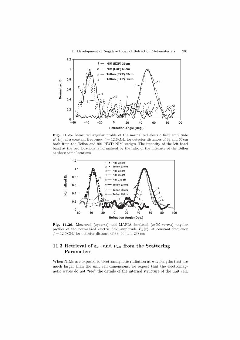
11 Development of Negative Index of Refraction Metamaterials 281
0
0.2
0.4
0.6
0.8
1
1.2
-60 -40 -20 0 20 40 60 80 100
Refraction Angle (Deg.)
No
rmal
ized
ENIM (EXP) 33cm
NIM (EXP) 66cm
Teflon (EXP) 33cm
Teflon (EXP) 66cm
1
2
3
4
2
43
12 1
22
2
Fig. 11.25. Measured angular profile of the normalized electric field amplitudeEz (r), at a constant frequency f = 12.6 GHz for detector distances of 33 and 66 cmboth from the Teflon and 901 HWD NIM wedges. The intensity of the left-handband at the two locations is normalized by the ratio of the intensity of the Teflonat those same locations
0
0.2
0.4
0.6
0.8
1
1.2
-60 -40 -20 0 20 40 60 80 100
Refraction Angle (Deg.)
No
rmal
ized
Ez
NIM 33 cm
Teflon 33 cm
NIM 33 cm
NIM 66 cm
NIM 238 cm
Teflon 33 cm
Teflon 66 cm
Teflon 238 cm
1
2
3
4
5
6
7
8
5
1
1 1
4 3
2
6 7
8 6 7
8
2
3
Fig. 11.26. Measured (squares) and MAFIA-simulated (solid curves) angularprofiles of the normalized electric field amplitude Ez (r), at constant frequencyf = 12.6 GHz for detector distance of 33, 66, and 238 cm
11.3 Retrieval of εeff and µeff from the ScatteringParameters
When NIMs are exposed to electromagnetic radiation at wavelengths that aremuch larger than the unit cell dimensions, we expect that the electromag-netic waves do not “see” the details of the internal structure of the unit cell,
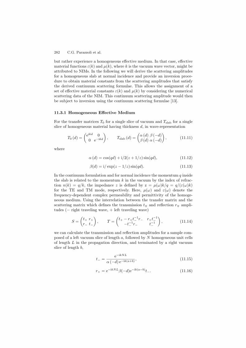
282 C.G. Parazzoli et al.
but rather experience a homogeneous effective medium. In that case, effectivematerial functions ε(k) and µ(k), where k is the vacuum wave vector, might beattributed to NIMs. In the following we will derive the scattering amplitudesfor a homogeneous slab at normal incidence and provide an inversion proce-dure to obtain material constants from the scattering amplitudes that satisfythe derived continuum scattering formulae. This allows the assignment of aset of effective material constants ε(k) and µ(k) by considering the numericalscattering data of the NIM. This continuum scattering amplitude would thenbe subject to inversion using the continuum scattering formulae [13].
11.3.1 Homogeneous Effective Medium
For the transfer matrices T0 for a single slice of vacuum and Tslab for a singleslice of homogeneous material having thickness d, in wave-representation
T0 (d) =(
eikd 00 e−ikd
), Tslab (d) =
(α (d) β (−d)β (d) α (−d)
), (11.11)
where
α (d) = cos(qd) + i/2(z + 1/z) sin(qd), (11.12)
β(d) = i/ exp(z − 1/z) sin(qd). (11.13)
In the continuum formulation and for normal incidence the momentum q insidethe slab is related to the momentum k in the vacuum by the index of refrac-tion n(k) = q/k, the impedance z is defined by z = µ(ω)k/q = q/(ε(ω)k)for the TE and TM mode, respectively. Here, µ(ω) and ε(ω) denote thefrequency-dependent complex permeability and permittivity of the homoge-neous medium. Using the interrelation between the transfer matrix and thescattering matrix which defines the transmission t∓ and reflection r∓ ampli-tudes (− right traveling wave, + left traveling wave)
S =(
t+ r+
r− t−
), T =
(t+ − r+t−1
− r− r+t−1−
−t−1− r− t−1
−
), (11.14)
we can calculate the transmission and reflection amplitudes for a sample com-posed of a left vacuum slice of length a, followed by N homogeneous unit cellsof length L in the propagation direction, and terminated by a right vacuumslice of length b,
t− =e−ikNL
α (−d) e−ik(a+b), (11.15)
r+ = e−ikNLβ(−d)e−ik(a−b)t−. (11.16)
11 Development of Negative Index of Refraction Metamaterials 283
It is convenient to introduce the normalized scattering amplitudes T and Rwhich, after N unit cells, take the form
T = −t−eikNL = α−1(−d)eik(a+b) (11.17)
R = β(−d)e−ik(a−b)T (11.18)
Now we can resolve the above scattering formulae with given amplitudes Tand R obtained from the simulation (or measurement) of an NIM with respectto the material parameters, impedance z(ω), and index of refraction n(ω). Ifthe solutions are (virtually) independent on the length of the sample, thoseparameters define the homogeneous effective medium (HEM) representation(or approximation) of the respective NIM. Then we have
zeff(ω) = ±√
(1 + R)2 − T 2
(1 − R)2 − T 2, (11.19)
neff(ω) = ± 1kL
cos−1
(1 − R2 + T 2
2T
)+
2π
kLm (11.20)
with m an integer. Note that we obtain zeff and neff from the scatteringamplitudes only, up to a common sign and the real part of the effectiveindex of refraction, Reneff only as a residue class. The relative sign of zeff
and neff is fixed by T and R. For known neff(ω) and zeff(ω) the effectivepermeability and permittivity are defined as µeff(ω) = neff(ω)zeff(ω) andεeff(ω) = neff(ω)/zeff(ω).
11.3.2 Lifting the Ambiguities
As shown above, the n(k, d) and z(k, d) obtained from the inversion of thetransmission and reflection amplitudes are subject to certain degree of ambi-guity. In general, this is the most information one can get from scattering dataat normal incidence. However, one can exploit other available information torule out some of the possible solutions obtained above. In the following, wediscuss several of these possibilities.
Causality Arguments
The physical solutions we seek are a subset of the solutions of the Maxwell’sequations that obey certain constraints. First of all, our NIMs at best absorbenergy from the electromagnetic field penetrating it, i.e., they are passive.This requires that the imaginary part of n to be non-negative, Imn(k, d) ∼ 0.Further, the reflected power on a single interface cannot exceed the incidentpower. Therefore the real part of z has to be also non-negative, Re z(k, d) ∼ 0.These two conditions determine the remaining common sign in the inversionabove, rendering z(k, d) and Imn(k, d) unambiguous.
284 C.G. Parazzoli et al.
Length Independence
Now we are left with the ambiguity of the real part of n only. The solutionsof the retrieval for the index of refraction constitute a residue class n(k, d)( mod 2π/(kd)). As we have to eventually deal with data from numericalsimulations and experimental measurements, we can safely assume that allnumbers we will encounter are rational (complex). The main problem withthe ambiguity of the real part of n(k, d) is that the distance between twopossible solutions (branches in k) gets rapidly smaller if the system lengthincreases, rendering the selection of the “actual” n(k, d) by external criteriavirtually impossible for long systems. On the other hand, we need systemlengths comparable to the applied radiation wavelength, in order to expect abehavior of an effective medium rather than a single layer of scatterers. Fora homogeneous slab, n(k) is clearly independent of the length of the slab.For the effective material we expect the same, at least asymptotically forsufficiently large lengths. Therefore, we consider the transmission data fordifferent system lengths as simultaneous determinations of a single n(k). Thisleads to a set of simultaneous congruences with different moduli,
n(k) = n1
(mod
2π
kd1
)= n2
(mod
2π
kd2
)= · · · = nN
(mod
2π
kdN
). (11.21)
We assume the lengths di to have a greatest common divisor d =gcdd1, d2, . . . ,dN, i.e. that any available di is an integral multiple of d,we then multiply each equation in (11.21) with kd/(2π) and introduce theabbreviation x = kd n(k)/(2π). Thus we get a system
x(k) ≡ xi(k) · · ·
(mod
d
di
)· · · | · · · di/d, . . . i = 1 · · ·N
. (11.22)
By multiplication with some common multiple q of the di/d we find equivalentsimultaneous congruences with integer moduli,
qx(k) ≡ qxi(k) . . .
(mod
qd
di
). (11.23)
Because the assumption of a length independent n(k) guarantees the existenceof a solution of (11.22), we know from the (rational) Chinese remainder theo-rem that this solution is some unique residue class qx(k)( mod lcmqd/di),where lcm is the lowest common multiplier. The theorem further provides analgorithm to effectively compute this solution. Since d|di we have qd/di|qfor every i, hence lcmqd/di|q. However, this does imply lcmqd/di ≡q, independent on the actual choice of the set of lengths d1, . . . , dN.Therefore the solutions of (11.21) are given as a unique residue class n(k)(mod 2π m/(kd)) with m = lcmqd/di/q ≡ 1. Clearly, the least ambiguousn(k) that could be extracted from the set di of system lengths would besome n(k)(mod2π/(kd)). How can we choose q and the set di to obtain
11 Development of Negative Index of Refraction Metamaterials 285
m = 1? Because q has to be a common multiple of the di/d, the lcmdi/d iscertainly a good choice. Then we may choose the di/d to be pairwise coprime,which renders their lcm simply their product. Further, the lcm of all the prod-ucts qd/dj =
∏i=j
(di/d) = q becomes just∏i
(di/d) = q and therefore we get
m = 1.As we see, in order to get the maximum information from the length
dependence of the scattering data, it is already sufficient to choose two coprimedi/d with minimal d, e.g., two successive multiples pd and (p + 1)d for some0 < p ∈ N and minimal d. As we may always assume rational data, includinglengths, the gcd d is always guaranteed to exist, and if we have a smallestlength step for the scattering data, which we certainly have for numerical dataobtained from a lattice version of the transfer matrix algorithm, this lengthstep is a lower bound for any gcd d above. Even worse, in most realistic casesof NIMs the length step has to be assumed to be the length of the unit cell inthe propagation direction. However, since in those cases the wavelength alsohas to be larger than the unit cell, 2π/(kd) ≈ λ/d would maintain the orderO(1). We can summarize that exploiting the length independence of n(k) forour systems, we can reach the theoretical least ambiguity
n(k) = n(k)(
mod2π
kd
)(11.24)
with d being the length of the unit cell in the propagation direction. The onlyway to remove this remaining ambiguity using the length independence wouldbe to either use irrational ratios of lengths or to approach d ∈ 0. Both arevirtually impossible since the sample can only have an integral number of unitcells.
Frequency Dependence
A second expected physical property of n(k) that we may exploit is itscontinuity between resonances. Suppose that ∆n(k) is an upper bound∣∣∣∂n(k)
∂k
∣∣∣ and for any given k we would be able to resolve n(k) as a residueclass n(k)( mod h(k)). Then we may choose for each interval where ∆n(k) isfinite a frequency discretization ki ∈ Q|i = 1 · · ·Nk, such that 2 |ki+1 − ki|∆n(ki+1, ki) < min |h(ki+1)| , |h(ki)| 2|ki+1−ki| for every two ki+1, ki fromthis discretization and further ∆n(ki+1, ki) = maxki<k<ki+1 ∆n(k). This waythe upper bound ∆n(k) guarantees that if we choose a certain representativeof the residue class n(ki)(mod h(ki)) for one particular kj from the discretiza-tion, we would have a unique continuation to all other ki within the interval.Thus the ambiguity of n(k) is further reduced from independent residueclasses n(ki)(mod h(ki)) for each ki to the functional residue class n(k)(mod h(k)) of piecewise continuous functions of k, interpolating the n(ki).
We now have a set of branches of a continuous n(k) in each of the intervalswhich differ by an integral multiple of the function h(k) and fixing one point
286 C.G. Parazzoli et al.
in the interval would make n(k) inside the whole interval unambiguous. Note,however, that this exploitation of the knowledge for several frequencies cannotreduce the residue class n(k)( mod h(k)) for any given k. In practice, weusually “reverse” this method, which means that we make an educated guessfor a discretization and derive an error upper bound for those “jumps” in n(k)we might miss. With some experience, this works reasonably well, providedwe choose the frequencies dense enough, near the resonances. From analyticmodels for our systems, we know in most cases how many (few) continuousintervals we expect. Apart from this, resonances will also have a signature inthe unambiguous function z(k). The frequency continuation method can beused concurrently with the length independence described above. The onlyremaining problem is that we need to know the “actual” n(k) at least for onepoint inside each interval.
Information from Analytical Models
If we know from analytic models what kind of asymptotics or frequency depen-dence of n(k) we would expect, we may use this information to further restrictthe ambiguity of n(k). Most useful is such information around resonances inn(k), where the common continuity of this function is destroyed and the con-tinuation method above inevitably looses coherence between the branchesright and left of the resonance. For instance, when we calculate the dielectricfunction α(k) and the permeability µ(k) from n(k) and z(k), the character ofthe resonances is well known from analytical models. On the other hand, itdepends on the choice of the branches for n(k) right and left from the reso-nance. This can introduce some connection between the intervals used above.
11.3.3 Inversion for Lossless Materials
Under certain conditions we do not need the complete information from thecomplex scattering amplitudes to do the retrieval. For lossless materials, wecan assume n, z to be real or purely imaginary if we exclude the isolatedspecial cases n = 0 and z = 0. Note that this is a stronger demand than theno-loss condition |T |2 + |R|2 = 1 for a particular T and R. Then the index ofrefraction n is only related to the real part of the transmission amplitude
n = ± 1kd
cos−1(Re 1/T ) (11.25)
z =
√w ± 1w ∓ 1
, w =
√sin2(arg T )1 − |T |2
(11.26)
With the usual convention arg(z) ∈ (−π/2, π/2) we fix the positive sign andthe branch-cut for the square root but we still have two solutions for z whichare mutually reciprocal. As a consequence we could not distinguish the trans-posed pairs (µ, α) and (α, µ) in the µ, α space. This ambiguity of z could
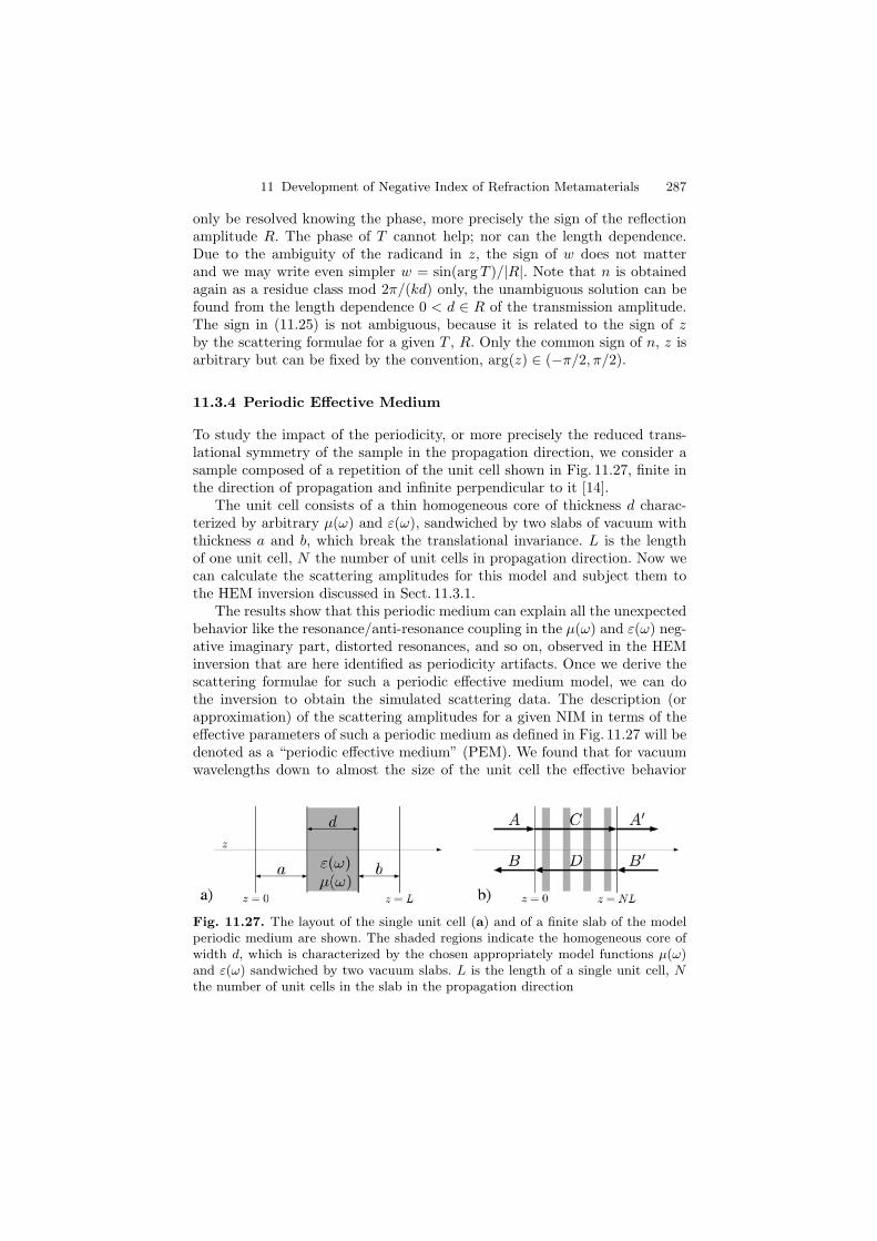
11 Development of Negative Index of Refraction Metamaterials 287
only be resolved knowing the phase, more precisely the sign of the reflectionamplitude R. The phase of T cannot help; nor can the length dependence.Due to the ambiguity of the radicand in z, the sign of w does not matterand we may write even simpler w = sin(arg T )/|R|. Note that n is obtainedagain as a residue class mod 2π/(kd) only, the unambiguous solution can befound from the length dependence 0 < d ∈ R of the transmission amplitude.The sign in (11.25) is not ambiguous, because it is related to the sign of zby the scattering formulae for a given T , R. Only the common sign of n, z isarbitrary but can be fixed by the convention, arg(z) ∈ (−π/2, π/2).
11.3.4 Periodic Effective Medium
To study the impact of the periodicity, or more precisely the reduced trans-lational symmetry of the sample in the propagation direction, we consider asample composed of a repetition of the unit cell shown in Fig. 11.27, finite inthe direction of propagation and infinite perpendicular to it [14].
The unit cell consists of a thin homogeneous core of thickness d charac-terized by arbitrary µ(ω) and ε(ω), sandwiched by two slabs of vacuum withthickness a and b, which break the translational invariance. L is the lengthof one unit cell, N the number of unit cells in propagation direction. Now wecan calculate the scattering amplitudes for this model and subject them tothe HEM inversion discussed in Sect. 11.3.1.
The results show that this periodic medium can explain all the unexpectedbehavior like the resonance/anti-resonance coupling in the µ(ω) and ε(ω) neg-ative imaginary part, distorted resonances, and so on, observed in the HEMinversion that are here identified as periodicity artifacts. Once we derive thescattering formulae for such a periodic effective medium model, we can dothe inversion to obtain the simulated scattering data. The description (orapproximation) of the scattering amplitudes for a given NIM in terms of theeffective parameters of such a periodic medium as defined in Fig. 11.27 will bedenoted as a “periodic effective medium” (PEM). We found that for vacuumwavelengths down to almost the size of the unit cell the effective behavior
Fig. 11.27. The layout of the single unit cell (a) and of a finite slab of the modelperiodic medium are shown. The shaded regions indicate the homogeneous core ofwidth d, which is characterized by the chosen appropriately model functions µ(ω)and ε(ω) sandwiched by two vacuum slabs. L is the length of a single unit cell, Nthe number of unit cells in the slab in the propagation direction
288 C.G. Parazzoli et al.
of our NIMs can be decomposed into a “well-behaving” effective responseof the resonances and a contribution of periodic structures described by thePEM.
11.3.5 Continuum Formulation
Using the interrelation between the transfer matrix and the scattering matrix,we obtain the (normalized) transmission and reflection amplitudes T and Rafter N unit cells, corresponding to those simulated for the real NIM
T =[α(−d)e−ik(a+b)UN−1(p) − UN−2(p)
]−1
(11.27)
R = β(−d)e−ik(a−b)UN−1(p)T. (11.28)
Here, Un(z) = sin[(n + 1) cos−1 z
]/(1−z2)1/2 are the Chebyshev polynomials
of the second kind, taken at the argument p = cos(qd) cos[k(L − d)] − 12 (z +
1/z) sin(qd) sin[k(L − d)].The wave vector q = n(ω) k and the impedance z(ω) refer to the homo-
geneous core of the unit cell. We will now discuss what happens if we try toapproximate the explicit periodic medium discussed earlier by a homogeneouseffective medium. This corresponds to our previous attempts to describe theperiodic NIMs by a homogeneous effective medium. We can show that if ahomogeneous approximation is possible for a single unit cell of the periodicmedium, then it holds for any number of unit cells and vice versa. Therefore,it is sufficient to consider a single unit cell. Furthermore, such a description asa homogeneous medium is only possible for a − b = 0. This implies that onlyNIMs that are inversion invariant in the propagation direction may possessa well-defined HEM approximation. In terms of the (normalized) scatteringamplitudes T and R, for the single unit cell we then have the conditions
α−1(−d)eik(L−d) = T = α−1eff (−L), (11.29)
β(−d)T = R = βeff(−L)T. (11.30)
We already know how to invert the right-hand side of these equations. Thisis just what we did in the retrieval procedure for the HEM in the previ-ous section. Defining renormalized scattering amplitudes T ′ = T e−ik(L−d)
and R′ = R e−ik(L−d), we could apply the same procedure to the left-handside. Inserting the renormalized transmission and reflection amplitudes (11.29,11.30) for a single unit cell into the inverted scattering formulae and using pdefined above we obtain
neff = ± 1kL
cos−1[p(n, z; k)] +2π
kLm (11.31)
with m an integer. The problem with the signs of neff and zeff , as well as withthe ambiguity of Reneff is similar, and can be resolved the same way as for the
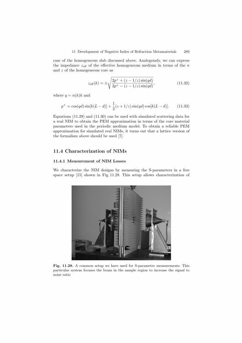
11 Development of Negative Index of Refraction Metamaterials 289
case of the homogeneous slab discussed above. Analogously, we can expressthe impedance zeff of the effective homogeneous medium in terms of the nand z of the homogeneous core as
zeff(k) = ±√
2p+ + (z − 1/z) sin(qd)2p+ − (z − 1/z) sin(qd)
, (11.32)
where q = n(k)k and
p+ = cos(qd) sin[k(L − d)] +12(z + 1/z) sin(qd) cos[k(L − d)]. (11.33)
Equations (11.29) and (11.30) can be used with simulated scattering data fora real NIM to obtain the PEM approximation in terms of the core materialparameters used in the periodic medium model. To obtain a reliable PEMapproximation for simulated real NIMs, it turns out that a lattice version ofthe formalism above should be used [7].
11.4 Characterization of NIMs
11.4.1 Measurement of NIM Losses
We characterize the NIM designs by measuring the S-parameters in a freespace setup [15] shown in Fig. 11.28. This setup allows characterization of
Fig. 11.28. A common setup we have used for S-parameter measurements. Thisparticular system focuses the beam in the sample region to increase the signal tonoise ratio
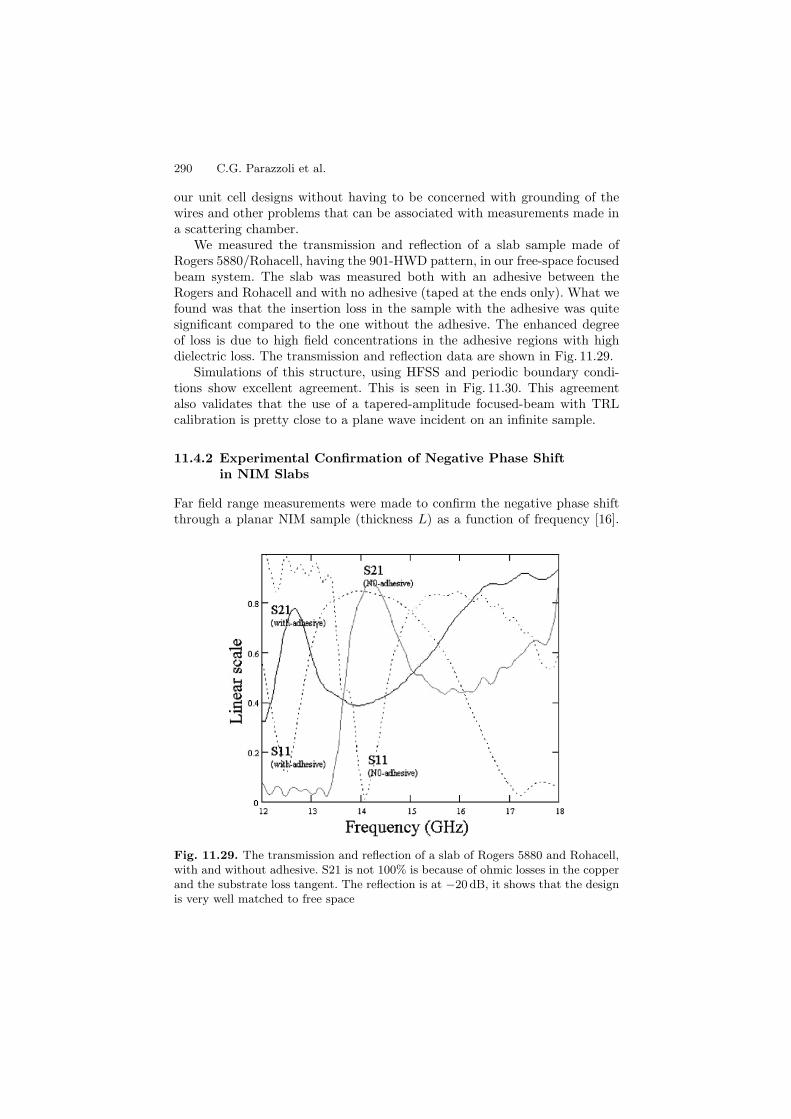
290 C.G. Parazzoli et al.
our unit cell designs without having to be concerned with grounding of thewires and other problems that can be associated with measurements made ina scattering chamber.
We measured the transmission and reflection of a slab sample made ofRogers 5880/Rohacell, having the 901-HWD pattern, in our free-space focusedbeam system. The slab was measured both with an adhesive between theRogers and Rohacell and with no adhesive (taped at the ends only). What wefound was that the insertion loss in the sample with the adhesive was quitesignificant compared to the one without the adhesive. The enhanced degreeof loss is due to high field concentrations in the adhesive regions with highdielectric loss. The transmission and reflection data are shown in Fig. 11.29.
Simulations of this structure, using HFSS and periodic boundary condi-tions show excellent agreement. This is seen in Fig. 11.30. This agreementalso validates that the use of a tapered-amplitude focused-beam with TRLcalibration is pretty close to a plane wave incident on an infinite sample.
11.4.2 Experimental Confirmation of Negative Phase Shiftin NIM Slabs
Far field range measurements were made to confirm the negative phase shiftthrough a planar NIM sample (thickness L) as a function of frequency [16].
Fig. 11.29. The transmission and reflection of a slab of Rogers 5880 and Rohacell,with and without adhesive. S21 is not 100% is because of ohmic losses in the copperand the substrate loss tangent. The reflection is at −20 dB, it shows that the designis very well matched to free space
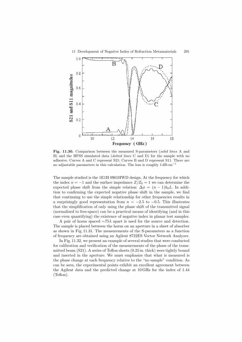
11 Development of Negative Index of Refraction Metamaterials 291
Fig. 11.30. Comparison between the measured S-parameters (solid lines A andB) and the HFSS simulated data (dotted lines C and D) for the sample with noadhesive. Curves A and C represent S21; Curves B and D represent S11. There areno adjustable parameters in this calculation. The loss is roughly 1 dB cm−1
The sample studied is the 1E1H 0901HWD design. At the frequency for whichthe index n = −1 and the surface impedance Z/Z0 = 1 we can determine theexpected phase shift from the simple relation: ∆φ = (n − 1)k0L. In addi-tion to confirming the expected negative phase shift in the sample, we findthat continuing to use the simple relationship for other frequencies results ina surprisingly good representation from n = −2.5 to −0.5. This illustratesthat the simplification of only using the phase shift of the transmitted signal(normalized to free-space) can be a practical means of identifying (and in thiscase even quantifying) the existence of negative index in planar test samples.
A pair of horns spaced ∼75λ apart is used for the source and detection.The sample is placed between the horns on an aperture in a sheet of absorberas shown in Fig. 11.31. The measurements of the S-parameters as a functionof frequency are obtained using an Agilent 8722ES Vector Network Analyzer.
In Fig. 11.32, we present an example of several studies that were conductedfor calibration and verification of the measurements of the phase of the trans-mitted beam (S21). A series of Teflon sheets (0.25 in. thick) were tightly boundand inserted in the aperture. We must emphasize that what is measured isthe phase change at each frequency relative to the “no sample” condition. Ascan be seen, the experimental points exhibit an excellent agreement betweenthe Agilent data and the predicted change at 10 GHz for the index of 1.44(Teflon).
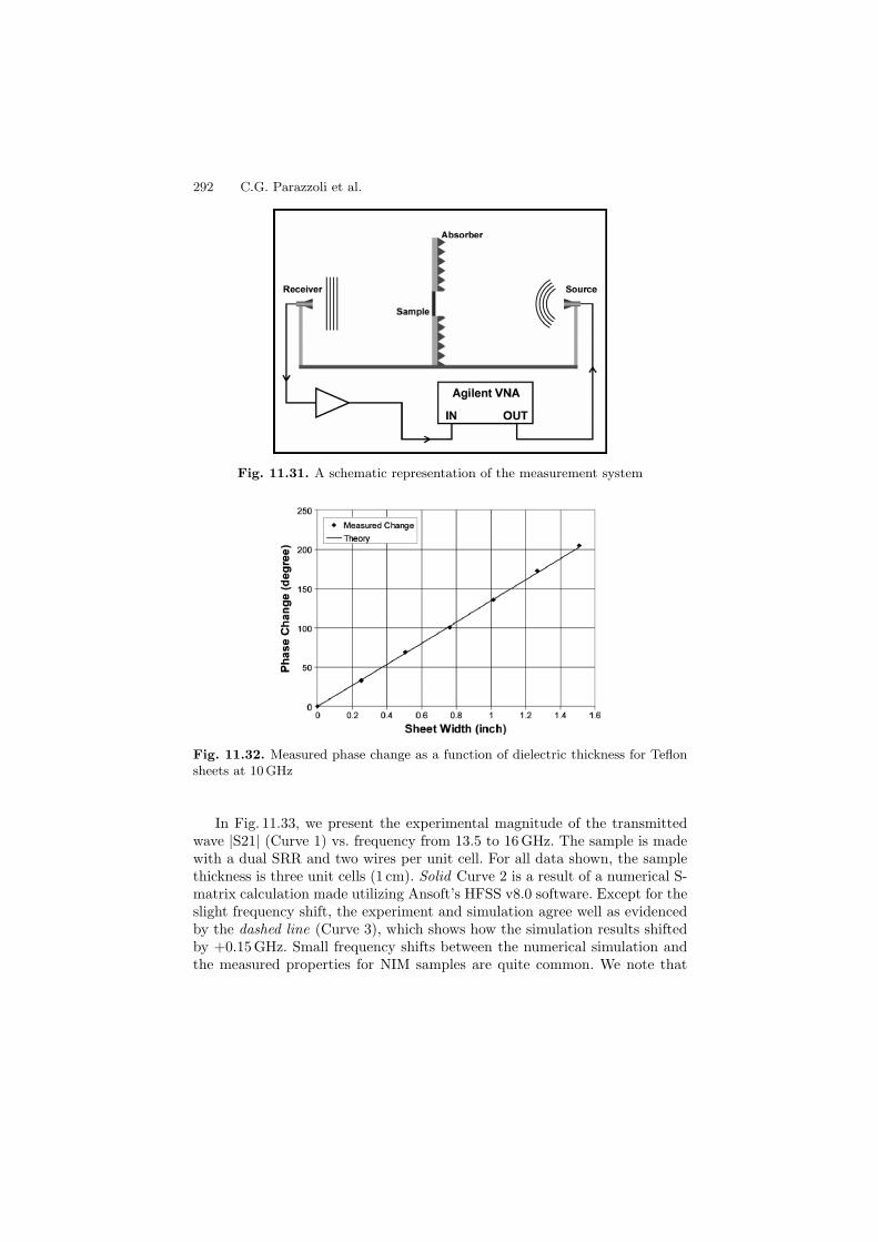
292 C.G. Parazzoli et al.
Fig. 11.31. A schematic representation of the measurement system
Fig. 11.32. Measured phase change as a function of dielectric thickness for Teflonsheets at 10GHz
In Fig. 11.33, we present the experimental magnitude of the transmittedwave |S21| (Curve 1) vs. frequency from 13.5 to 16 GHz. The sample is madewith a dual SRR and two wires per unit cell. For all data shown, the samplethickness is three unit cells (1 cm). Solid Curve 2 is a result of a numerical S-matrix calculation made utilizing Ansoft’s HFSS v8.0 software. Except for theslight frequency shift, the experiment and simulation agree well as evidencedby the dashed line (Curve 3), which shows how the simulation results shiftedby +0.15GHz. Small frequency shifts between the numerical simulation andthe measured properties for NIM samples are quite common. We note that
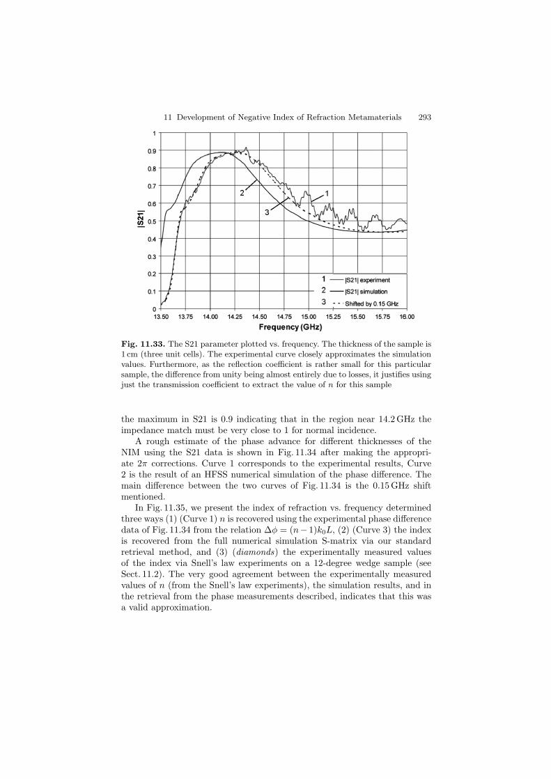
11 Development of Negative Index of Refraction Metamaterials 293
Fig. 11.33. The S21 parameter plotted vs. frequency. The thickness of the sample is1 cm (three unit cells). The experimental curve closely approximates the simulationvalues. Furthermore, as the reflection coefficient is rather small for this particularsample, the difference from unity being almost entirely due to losses, it justifies usingjust the transmission coefficient to extract the value of n for this sample
the maximum in S21 is 0.9 indicating that in the region near 14.2 GHz theimpedance match must be very close to 1 for normal incidence.
A rough estimate of the phase advance for different thicknesses of theNIM using the S21 data is shown in Fig. 11.34 after making the appropri-ate 2π corrections. Curve 1 corresponds to the experimental results, Curve2 is the result of an HFSS numerical simulation of the phase difference. Themain difference between the two curves of Fig. 11.34 is the 0.15 GHz shiftmentioned.
In Fig. 11.35, we present the index of refraction vs. frequency determinedthree ways (1) (Curve 1) n is recovered using the experimental phase differencedata of Fig. 11.34 from the relation ∆φ = (n− 1)k0L, (2) (Curve 3) the indexis recovered from the full numerical simulation S-matrix via our standardretrieval method, and (3) (diamonds) the experimentally measured valuesof the index via Snell’s law experiments on a 12-degree wedge sample (seeSect. 11.2). The very good agreement between the experimentally measuredvalues of n (from the Snell’s law experiments), the simulation results, and inthe retrieval from the phase measurements described, indicates that this wasa valid approximation.

294 C.G. Parazzoli et al.
Fig. 11.34. Phase shift differences of S21 vs. frequency, which includes the 2πcorrection. The experimental data are represented by Curve 1, whereas Curve 2 isbased on simulations using HFSS
Fig. 11.35. Estimated values of the index of refraction n as a function of frequency,from the phase advance data
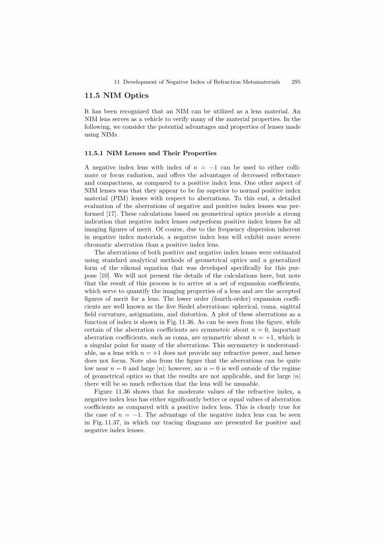
11 Development of Negative Index of Refraction Metamaterials 295
11.5 NIM Optics
It has been recognized that an NIM can be utilized as a lens material. AnNIM lens serves as a vehicle to verify many of the material properties. In thefollowing, we consider the potential advantages and properties of lenses madeusing NIMs.
11.5.1 NIM Lenses and Their Properties
A negative index lens with index of n = −1 can be used to either colli-mate or focus radiation, and offers the advantages of decreased reflectanceand compactness, as compared to a positive index lens. One other aspect ofNIM lenses was that they appear to be far superior to normal positive indexmaterial (PIM) lenses with respect to aberrations. To this end, a detailedevaluation of the aberrations of negative and positive index lenses was per-formed [17]. These calculations based on geometrical optics provide a strongindication that negative index lenses outperform positive index lenses for allimaging figures of merit. Of course, due to the frequency dispersion inherentin negative index materials, a negative index lens will exhibit more severechromatic aberration than a positive index lens.
The aberrations of both positive and negative index lenses were estimatedusing standard analytical methods of geometrical optics and a generalizedform of the eikonal equation that was developed specifically for this pur-pose [10]. We will not present the details of the calculations here, but notethat the result of this process is to arrive at a set of expansion coefficients,which serve to quantify the imaging properties of a lens and are the acceptedfigures of merit for a lens. The lower order (fourth-order) expansion coeffi-cients are well known as the five Siedel aberrations: spherical, coma, sagittalfield curvature, astigmatism, and distortion. A plot of these aberrations as afunction of index is shown in Fig. 11.36. As can be seen from the figure, whilecertain of the aberration coefficients are symmetric about n = 0, importantaberration coefficients, such as coma, are symmetric about n = +1, which isa singular point for many of the aberrations. This asymmetry is understand-able, as a lens with n = +1 does not provide any refractive power, and hencedoes not focus. Note also from the figure that the aberrations can be quitelow near n = 0 and large |n|; however, an n = 0 is well outside of the regimeof geometrical optics so that the results are not applicable, and for large |n|there will be so much reflection that the lens will be unusable.
Figure 11.36 shows that for moderate values of the refractive index, anegative index lens has either significantly better or equal values of aberrationcoefficients as compared with a positive index lens. This is clearly true forthe case of n = −1. The advantage of the negative index lens can be seenin Fig. 11.37, in which ray tracing diagrams are presented for positive andnegative index lenses.
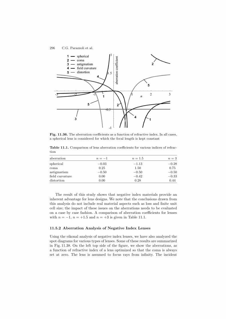
296 C.G. Parazzoli et al.
Fig. 11.36. The aberration coefficients as a function of refractive index. In all cases,a spherical lens is considered for which the focal length is kept constant
Table 11.1. Comparison of lens aberration coefficients for various indices of refrac-tion
aberration n = −1 n = 1.5 n = 3
spherical −0.03 −1.13 −0.28coma 0.25 1.50 0.75astigmatism −0.50 −0.50 −0.50field curvature 0.00 −0.42 −0.33distortion 0.00 0.28 0.44
The result of this study shows that negative index materials provide aninherent advantage for lens designs. We note that the conclusions drawn fromthis analysis do not include real material aspects such as loss and finite unitcell size; the impact of these issues on the aberrations needs to be evaluatedon a case by case fashion. A comparison of aberration coefficients for lenseswith n = −1, n = +1.5 and n = +3 is given in Table 11.1.
11.5.2 Aberration Analysis of Negative Index Lenses
Using the eikonal analysis of negative index lenses, we have also analyzed thespot diagrams for various types of lenses. Some of these results are summarizedin Fig. 11.38. On the left top side of the figure, we show the aberrations, asa function of refractive index of a lens optimized so that the coma is alwaysset at zero. The lens is assumed to focus rays from infinity. The incident
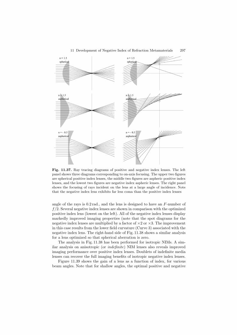
11 Development of Negative Index of Refraction Metamaterials 297
Fig. 11.37. Ray tracing diagrams of positive and negative index lenses. The leftpanel shows three diagrams corresponding to on-axis focusing. The upper two figuresare spherical positive index lenses, the middle two figures are aspheric positive indexlenses, and the lowest two figures are negative index aspheric lenses. The right panelshows the focusing of rays incident on the lens at a large angle of incidence. Notethat the negative index lens exhibits far less coma than the positive index lenses
angle of the rays is 0.2 rad., and the lens is designed to have an F -number off/2. Several negative index lenses are shown in comparison with the optimizedpositive index lens (lowest on the left). All of the negative index lenses displaymarkedly improved imaging properties (note that the spot diagrams for thenegative index lenses are multiplied by a factor of ×2 or ×3. The improvementin this case results from the lower field curvature (Curve 3) associated with thenegative index lens. The right-hand side of Fig. 11.38 shows a similar analysisfor a lens optimized so that spherical aberration is zero.
The analysis in Fig. 11.38 has been performed for isotropic NIMs. A sim-ilar analysis on anisotropic (or indefinite) NIM lenses also reveals improvedimaging performance over positive index lenses. Doublets of indefinite medialenses can recover the full imaging benefits of isotropic negative index lenses.
Figure 11.39 shows the gain of a lens as a function of index, for variousbeam angles. Note that for shallow angles, the optimal positive and negative
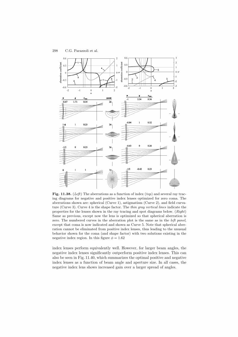
298 C.G. Parazzoli et al.
Fig. 11.38. (Left) The aberrations as a function of index (top) and several ray trac-ing diagrams for negative and positive index lenses optimized for zero coma. Theaberrations shown are: spherical (Curve 1), astigmatism (Curve 2), and field curva-ture (Curve 3). Curve 4 is the shape factor. The thin gray vertical lines indicate theproperties for the lenses shown in the ray tracing and spot diagrams below. (Right)Same as previous, except now the lens is optimized so that spherical aberration iszero. The numbered curves in the aberration plot is the same as in the left panel,except that coma is now indicated and shown as Curve 5. Note that spherical aber-ration cannot be eliminated from positive index lenses, thus leading to the unusualbehavior shown for the coma (and shape factor) with two solutions existing in thenegative index region. In this figure φ = 1.62
index lenses perform equivalently well. However, for larger beam angles, thenegative index lenses significantly outperform positive index lenses. This canalso be seen in Fig. 11.40, which summarizes the optimal positive and negativeindex lenses as a function of beam angle and aperture size. In all cases, thenegative index lens shows increased gain over a larger spread of angles.
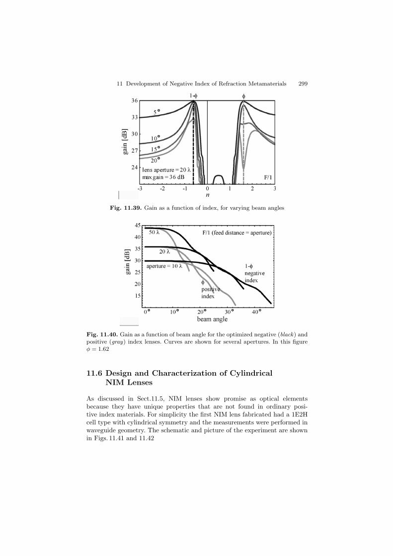
11 Development of Negative Index of Refraction Metamaterials 299
Fig. 11.39. Gain as a function of index, for varying beam angles
Fig. 11.40. Gain as a function of beam angle for the optimized negative (black) andpositive (gray) index lenses. Curves are shown for several apertures. In this figureφ = 1.62
11.6 Design and Characterization of CylindricalNIM Lenses
As discussed in Sect.11.5, NIM lenses show promise as optical elementsbecause they have unique properties that are not found in ordinary posi-tive index materials. For simplicity the first NIM lens fabricated had a 1E2Hcell type with cylindrical symmetry and the measurements were performed inwaveguide geometry. The schematic and picture of the experiment are shownin Figs. 11.41 and 11.42
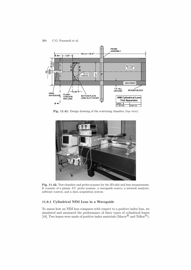
300 C.G. Parazzoli et al.
Fig. 11.41. Design drawing of the scattering chamber (top view)
Fig. 11.42. Test-chamber and probe-scanner for the 2D-slab and lens measurement.It consists of a planar XY probe scanner, a waveguide source, a network analyzer,software control, and a data acquisition system
11.6.1 Cylindrical NIM Lens in a Waveguide
To assess how an NIM lens compares with respect to a positive index lens, wesimulated and measured the performance of three types of cylindrical lenses[18]. Two lenses were made of positive index materials (Macor R© and Teflon R©),
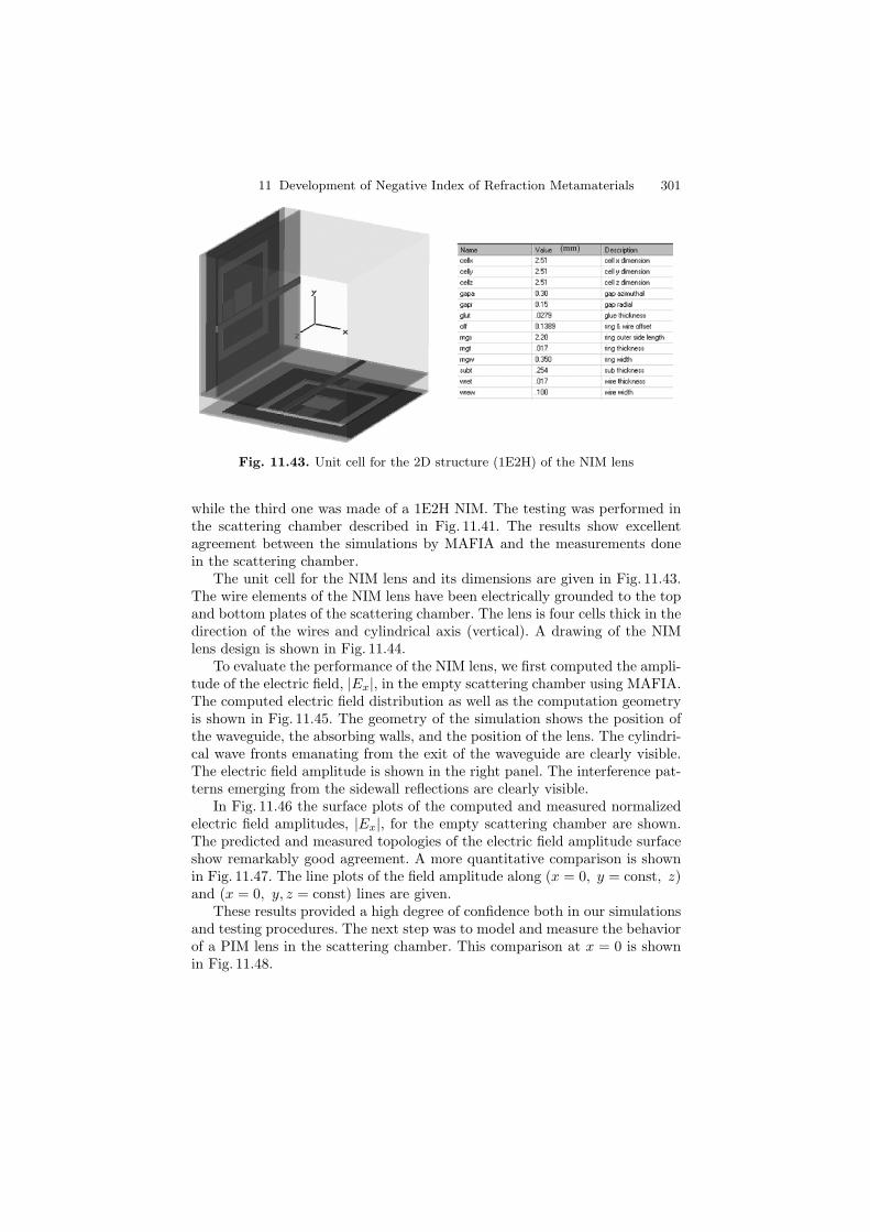
11 Development of Negative Index of Refraction Metamaterials 301
Fig. 11.43. Unit cell for the 2D structure (1E2H) of the NIM lens
while the third one was made of a 1E2H NIM. The testing was performed inthe scattering chamber described in Fig. 11.41. The results show excellentagreement between the simulations by MAFIA and the measurements donein the scattering chamber.
The unit cell for the NIM lens and its dimensions are given in Fig. 11.43.The wire elements of the NIM lens have been electrically grounded to the topand bottom plates of the scattering chamber. The lens is four cells thick in thedirection of the wires and cylindrical axis (vertical). A drawing of the NIMlens design is shown in Fig. 11.44.
To evaluate the performance of the NIM lens, we first computed the ampli-tude of the electric field, |Ex|, in the empty scattering chamber using MAFIA.The computed electric field distribution as well as the computation geometryis shown in Fig. 11.45. The geometry of the simulation shows the position ofthe waveguide, the absorbing walls, and the position of the lens. The cylindri-cal wave fronts emanating from the exit of the waveguide are clearly visible.The electric field amplitude is shown in the right panel. The interference pat-terns emerging from the sidewall reflections are clearly visible.
In Fig. 11.46 the surface plots of the computed and measured normalizedelectric field amplitudes, |Ex|, for the empty scattering chamber are shown.The predicted and measured topologies of the electric field amplitude surfaceshow remarkably good agreement. A more quantitative comparison is shownin Fig. 11.47. The line plots of the field amplitude along (x = 0, y = const, z)and (x = 0, y, z = const) lines are given.
These results provided a high degree of confidence both in our simulationsand testing procedures. The next step was to model and measure the behaviorof a PIM lens in the scattering chamber. This comparison at x = 0 is shownin Fig. 11.48.
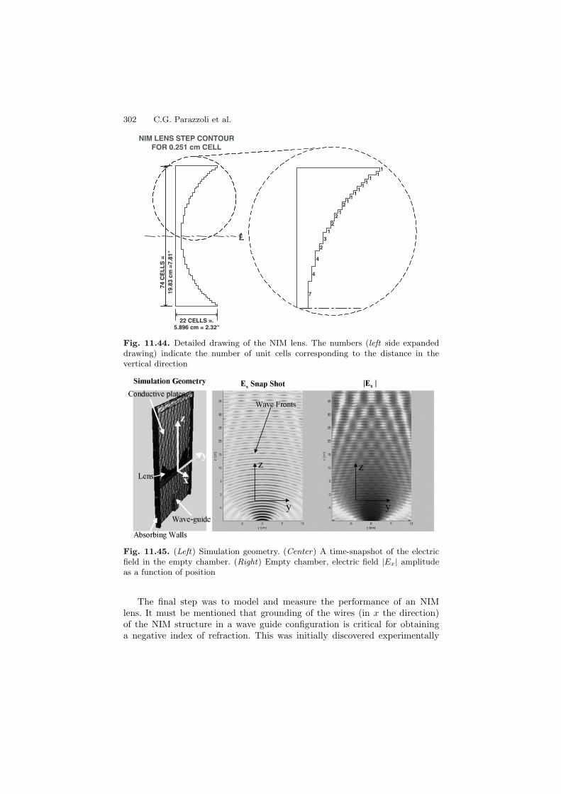
302 C.G. Parazzoli et al.
NIM LENS STEP CONTOUR FOR 0.251 cm CELL
7
4
4
2
31
22
21
11
11
11
11
1
22 CELLS =. 5.896 cm = 2.32"
74 C
EL
LS
=19
.83
cm =
7.81
"
Lc
Fig. 11.44. Detailed drawing of the NIM lens. The numbers (left side expandeddrawing) indicate the number of unit cells corresponding to the distance in thevertical direction
Fig. 11.45. (Left) Simulation geometry. (Center) A time-snapshot of the electricfield in the empty chamber. (Right) Empty chamber, electric field |Ex| amplitudeas a function of position
The final step was to model and measure the performance of an NIMlens. It must be mentioned that grounding of the wires (in x the direction)of the NIM structure in a wave guide configuration is critical for obtaininga negative index of refraction. This was initially discovered experimentally
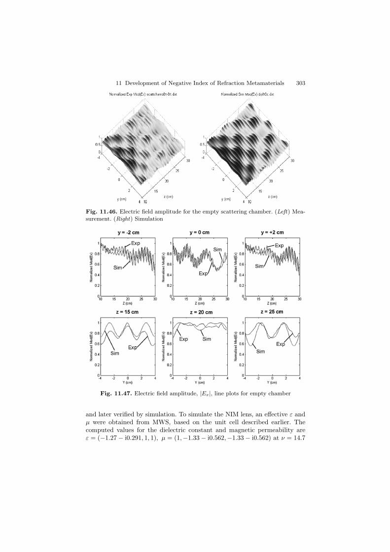
11 Development of Negative Index of Refraction Metamaterials 303
Fig. 11.46. Electric field amplitude for the empty scattering chamber. (Left) Mea-surement. (Right) Simulation
Fig. 11.47. Electric field amplitude, |Ex|, line plots for empty chamber
and later verified by simulation. To simulate the NIM lens, an effective ε andµ were obtained from MWS, based on the unit cell described earlier. Thecomputed values for the dielectric constant and magnetic permeability areε = (−1.27 − i0.291, 1, 1), µ = (1,−1.33 − i0.562,−1.33 − i0.562) at ν = 14.7
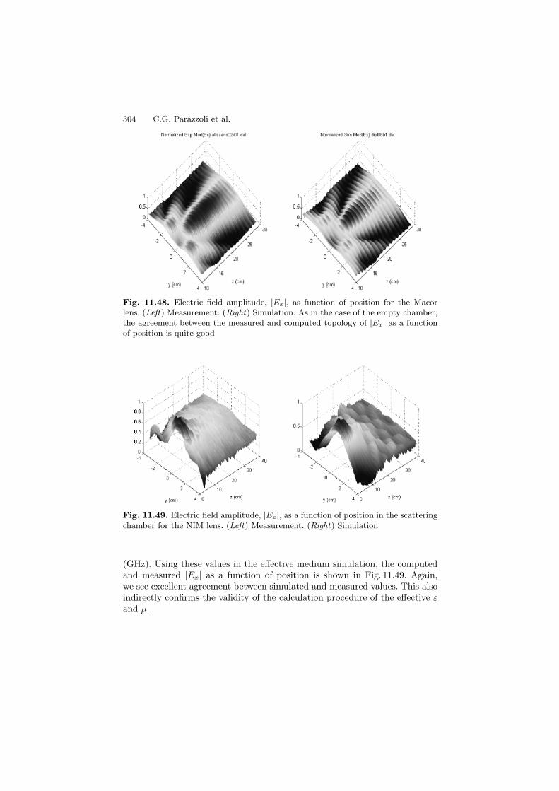
304 C.G. Parazzoli et al.
Fig. 11.48. Electric field amplitude, |Ex|, as function of position for the Macorlens. (Left) Measurement. (Right) Simulation. As in the case of the empty chamber,the agreement between the measured and computed topology of |Ex| as a functionof position is quite good
Fig. 11.49. Electric field amplitude, |Ex|, as a function of position in the scatteringchamber for the NIM lens. (Left) Measurement. (Right) Simulation
(GHz). Using these values in the effective medium simulation, the computedand measured |Ex| as a function of position is shown in Fig. 11.49. Again,we see excellent agreement between simulated and measured values. This alsoindirectly confirms the validity of the calculation procedure of the effective εand µ.
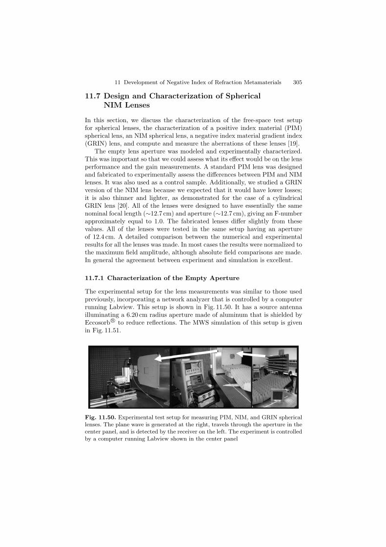
11 Development of Negative Index of Refraction Metamaterials 305
11.7 Design and Characterization of SphericalNIM Lenses
In this section, we discuss the characterization of the free-space test setupfor spherical lenses, the characterization of a positive index material (PIM)spherical lens, an NIM spherical lens, a negative index material gradient index(GRIN) lens, and compute and measure the aberrations of these lenses [19].
The empty lens aperture was modeled and experimentally characterized.This was important so that we could assess what its effect would be on the lensperformance and the gain measurements. A standard PIM lens was designedand fabricated to experimentally assess the differences between PIM and NIMlenses. It was also used as a control sample. Additionally, we studied a GRINversion of the NIM lens because we expected that it would have lower losses;it is also thinner and lighter, as demonstrated for the case of a cylindricalGRIN lens [20]. All of the lenses were designed to have essentially the samenominal focal length (∼12.7 cm) and aperture (∼12.7 cm), giving an F-numberapproximately equal to 1.0. The fabricated lenses differ slightly from thesevalues. All of the lenses were tested in the same setup having an apertureof 12.4 cm. A detailed comparison between the numerical and experimentalresults for all the lenses was made. In most cases the results were normalized tothe maximum field amplitude, although absolute field comparisons are made.In general the agreement between experiment and simulation is excellent.
11.7.1 Characterization of the Empty Aperture
The experimental setup for the lens measurements was similar to those usedpreviously, incorporating a network analyzer that is controlled by a computerrunning Labview. This setup is shown in Fig. 11.50. It has a source antennailluminating a 6.20 cm radius aperture made of aluminum that is shielded byEccosorb R© to reduce reflections. The MWS simulation of this setup is givenin Fig. 11.51.
Fig. 11.50. Experimental test setup for measuring PIM, NIM, and GRIN sphericallenses. The plane wave is generated at the right, travels through the aperture in thecenter panel, and is detected by the receiver on the left. The experiment is controlledby a computer running Labview shown in the center panel
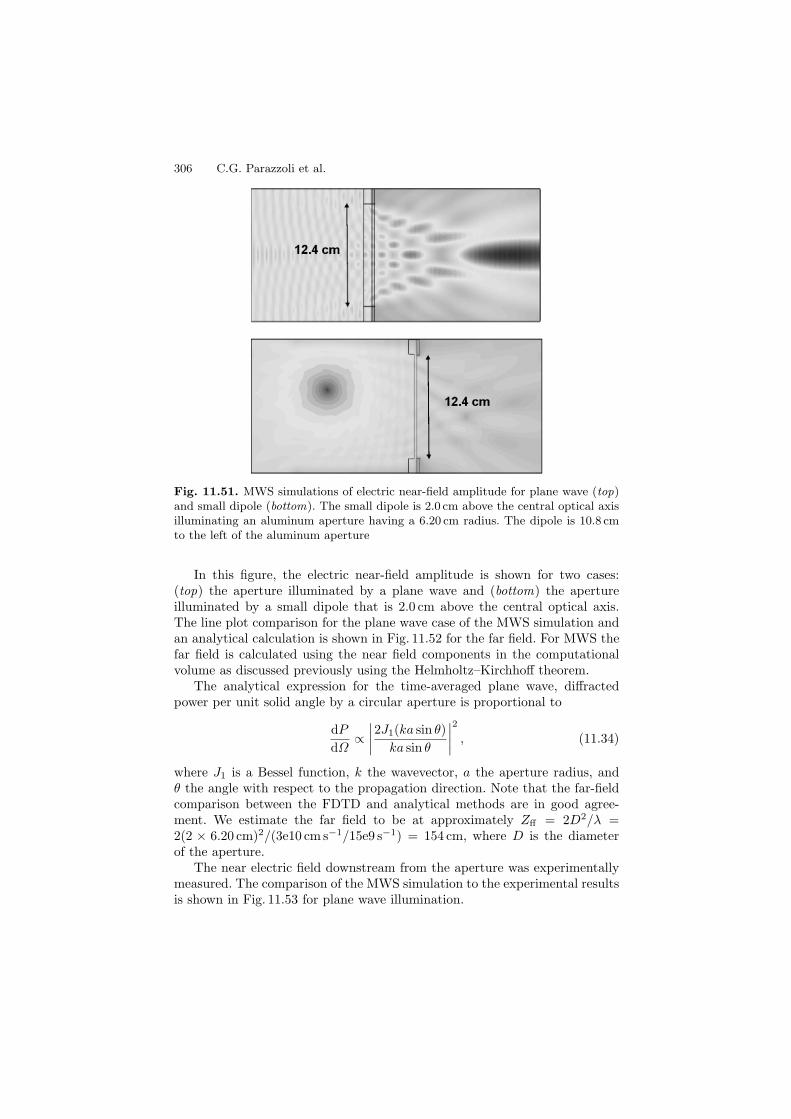
306 C.G. Parazzoli et al.
Fig. 11.51. MWS simulations of electric near-field amplitude for plane wave (top)and small dipole (bottom). The small dipole is 2.0 cm above the central optical axisilluminating an aluminum aperture having a 6.20 cm radius. The dipole is 10.8 cmto the left of the aluminum aperture
In this figure, the electric near-field amplitude is shown for two cases:(top) the aperture illuminated by a plane wave and (bottom) the apertureilluminated by a small dipole that is 2.0 cm above the central optical axis.The line plot comparison for the plane wave case of the MWS simulation andan analytical calculation is shown in Fig. 11.52 for the far field. For MWS thefar field is calculated using the near field components in the computationalvolume as discussed previously using the Helmholtz–Kirchhoff theorem.
The analytical expression for the time-averaged plane wave, diffractedpower per unit solid angle by a circular aperture is proportional to
dP
dΩ∝
∣∣∣∣2J1(ka sin θ)
ka sin θ
∣∣∣∣2
, (11.34)
where J1 is a Bessel function, k the wavevector, a the aperture radius, andθ the angle with respect to the propagation direction. Note that the far-fieldcomparison between the FDTD and analytical methods are in good agree-ment. We estimate the far field to be at approximately Zff = 2D2/λ =2(2 × 6.20 cm)2/(3e10 cm s−1/15e9 s−1) = 154 cm, where D is the diameterof the aperture.
The near electric field downstream from the aperture was experimentallymeasured. The comparison of the MWS simulation to the experimental resultsis shown in Fig. 11.53 for plane wave illumination.
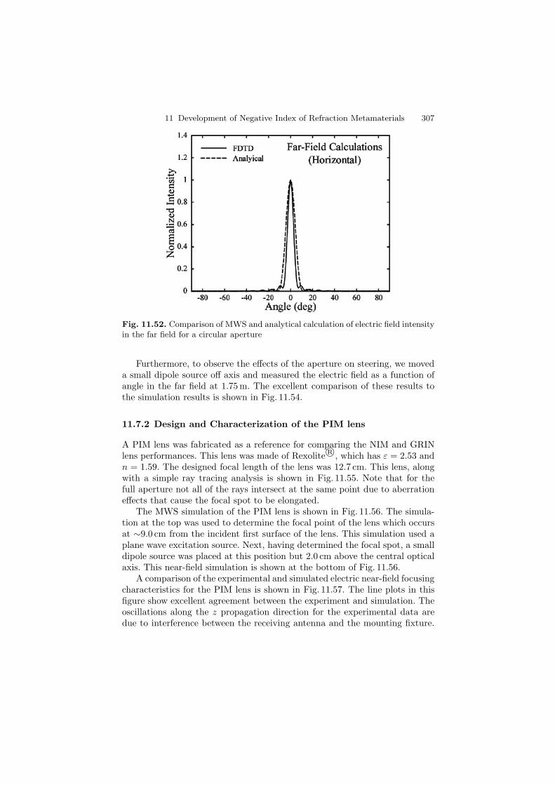
11 Development of Negative Index of Refraction Metamaterials 307
Fig. 11.52. Comparison of MWS and analytical calculation of electric field intensityin the far field for a circular aperture
Furthermore, to observe the effects of the aperture on steering, we moveda small dipole source off axis and measured the electric field as a function ofangle in the far field at 1.75 m. The excellent comparison of these results tothe simulation results is shown in Fig. 11.54.
11.7.2 Design and Characterization of the PIM lens
A PIM lens was fabricated as a reference for comparing the NIM and GRINlens performances. This lens was made of Rexolite R©, which has ε = 2.53 andn = 1.59. The designed focal length of the lens was 12.7 cm. This lens, alongwith a simple ray tracing analysis is shown in Fig. 11.55. Note that for thefull aperture not all of the rays intersect at the same point due to aberrationeffects that cause the focal spot to be elongated.
The MWS simulation of the PIM lens is shown in Fig. 11.56. The simula-tion at the top was used to determine the focal point of the lens which occursat ∼9.0 cm from the incident first surface of the lens. This simulation used aplane wave excitation source. Next, having determined the focal spot, a smalldipole source was placed at this position but 2.0 cm above the central opticalaxis. This near-field simulation is shown at the bottom of Fig. 11.56.
A comparison of the experimental and simulated electric near-field focusingcharacteristics for the PIM lens is shown in Fig. 11.57. The line plots in thisfigure show excellent agreement between the experiment and simulation. Theoscillations along the z propagation direction for the experimental data aredue to interference between the receiving antenna and the mounting fixture.
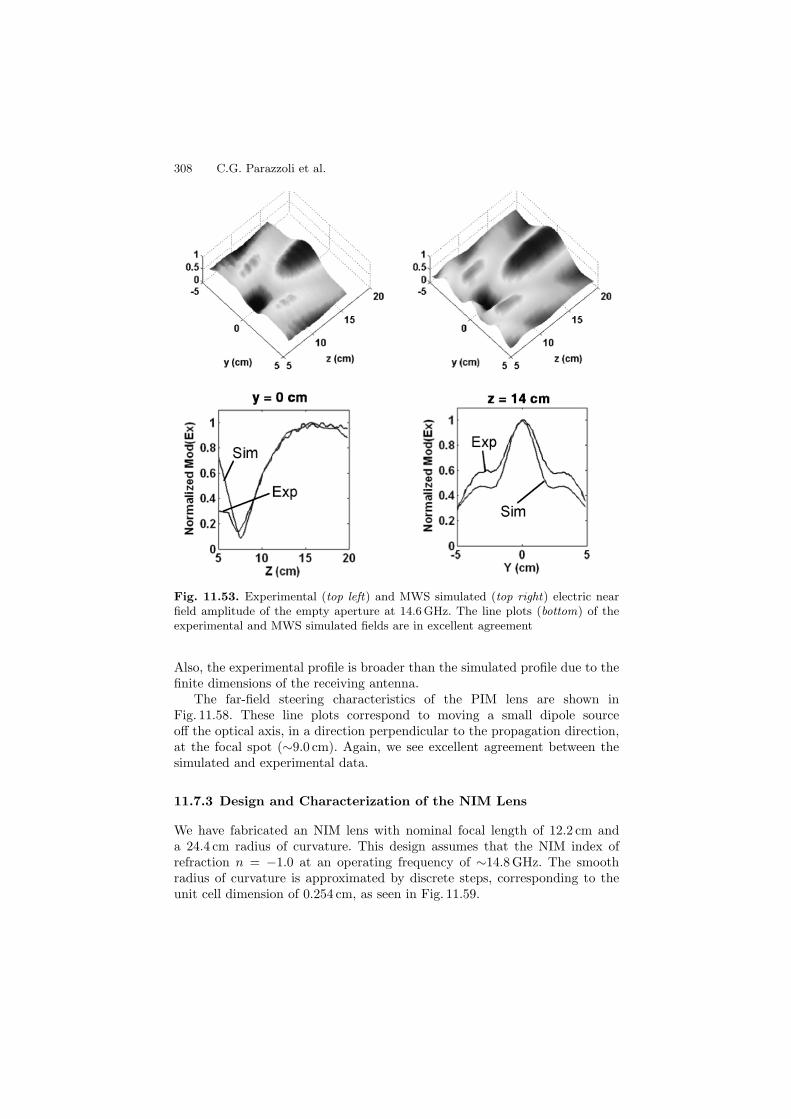
308 C.G. Parazzoli et al.
Fig. 11.53. Experimental (top left) and MWS simulated (top right) electric nearfield amplitude of the empty aperture at 14.6 GHz. The line plots (bottom) of theexperimental and MWS simulated fields are in excellent agreement
Also, the experimental profile is broader than the simulated profile due to thefinite dimensions of the receiving antenna.
The far-field steering characteristics of the PIM lens are shown inFig. 11.58. These line plots correspond to moving a small dipole sourceoff the optical axis, in a direction perpendicular to the propagation direction,at the focal spot (∼9.0 cm). Again, we see excellent agreement between thesimulated and experimental data.
11.7.3 Design and Characterization of the NIM Lens
We have fabricated an NIM lens with nominal focal length of 12.2 cm anda 24.4 cm radius of curvature. This design assumes that the NIM index ofrefraction n = −1.0 at an operating frequency of ∼14.8 GHz. The smoothradius of curvature is approximated by discrete steps, corresponding to theunit cell dimension of 0.254 cm, as seen in Fig. 11.59.
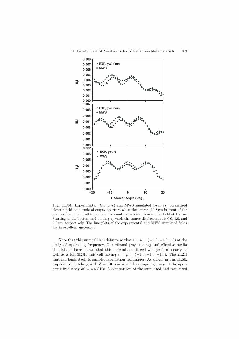
11 Development of Negative Index of Refraction Metamaterials 309
0.000
0.001
0.002
0.003
0.004
0.005
0.006
0.007
0.008
|Ex|
MWSEXP, y=2.0cm
MWSEXP, y=2.0cm
0.000
0.001
0.002
0.003
0.004
0.005
0.006
0.007
|Ex|
0.000
0.001
0.002
0.003
0.004
0.005
0.006
0.007
-20 -10 0
Receiver Angle (Deg.)
10 20
|Ex|
EXP, y=0.0MWS
Fig. 11.54. Experimental (triangles) and MWS simulated (squares) normalizedelectric field amplitude of empty aperture when the source (10.8 cm in front of theaperture) is on and off the optical axis and the receiver is in the far field at 1.75 m.Starting at the bottom and moving upward, the source displacement is 0.0, 1.0, and2.0 cm, respectively. The line plots of the experimental and MWS simulated fieldsare in excellent agreement
Note that this unit cell is indefinite so that ε = µ = (−1.0,−1.0, 1.0) at thedesigned operating frequency. Our eikonal (ray tracing) and effective mediasimulations have shown that this indefinite unit cell will perform nearly aswell as a full 3E3H unit cell having ε = µ = (−1.0,−1.0,−1.0). The 2E2Hunit cell lends itself to simpler fabrication techniques. As shown in Fig. 11.60,impedance matching with Z = 1.0 is achieved by designing ε = µ at the oper-ating frequency of ∼14.8GHz. A comparison of the simulated and measured
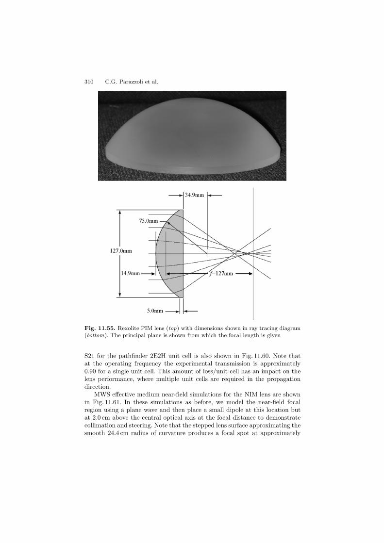
310 C.G. Parazzoli et al.
Fig. 11.55. Rexolite PIM lens (top) with dimensions shown in ray tracing diagram(bottom). The principal plane is shown from which the focal length is given
S21 for the pathfinder 2E2H unit cell is also shown in Fig. 11.60. Note thatat the operating frequency the experimental transmission is approximately0.90 for a single unit cell. This amount of loss/unit cell has an impact on thelens performance, where multiple unit cells are required in the propagationdirection.
MWS effective medium near-field simulations for the NIM lens are shownin Fig. 11.61. In these simulations as before, we model the near-field focalregion using a plane wave and then place a small dipole at this location butat 2.0 cm above the central optical axis at the focal distance to demonstratecollimation and steering. Note that the stepped lens surface approximating thesmooth 24.4 cm radius of curvature produces a focal spot at approximately
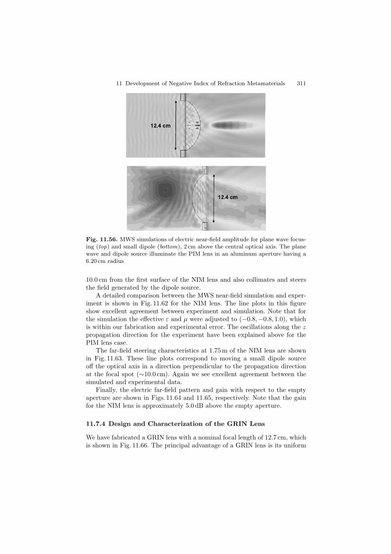
11 Development of Negative Index of Refraction Metamaterials 311
Fig. 11.56. MWS simulations of electric near-field amplitude for plane wave focus-ing (top) and small dipole (bottom), 2 cm above the central optical axis. The planewave and dipole source illuminate the PIM lens in an aluminum aperture having a6.20 cm radius
10.0 cm from the first surface of the NIM lens and also collimates and steersthe field generated by the dipole source.
A detailed comparison between the MWS near-field simulation and exper-iment is shown in Fig. 11.62 for the NIM lens. The line plots in this figureshow excellent agreement between experiment and simulation. Note that forthe simulation the effective ε and µ were adjusted to (−0.8,−0.8, 1.0), whichis within our fabrication and experimental error. The oscillations along the zpropagation direction for the experiment have been explained above for thePIM lens case.
The far-field steering characteristics at 1.75 m of the NIM lens are shownin Fig. 11.63. These line plots correspond to moving a small dipole sourceoff the optical axis in a direction perpendicular to the propagation directionat the focal spot (∼10.0 cm). Again we see excellent agreement between thesimulated and experimental data.
Finally, the electric far-field pattern and gain with respect to the emptyaperture are shown in Figs. 11.64 and 11.65, respectively. Note that the gainfor the NIM lens is approximately 5.0 dB above the empty aperture.
11.7.4 Design and Characterization of the GRIN Lens
We have fabricated a GRIN lens with a nominal focal length of 12.7 cm, whichis shown in Fig. 11.66. The principal advantage of a GRIN lens is its uniform
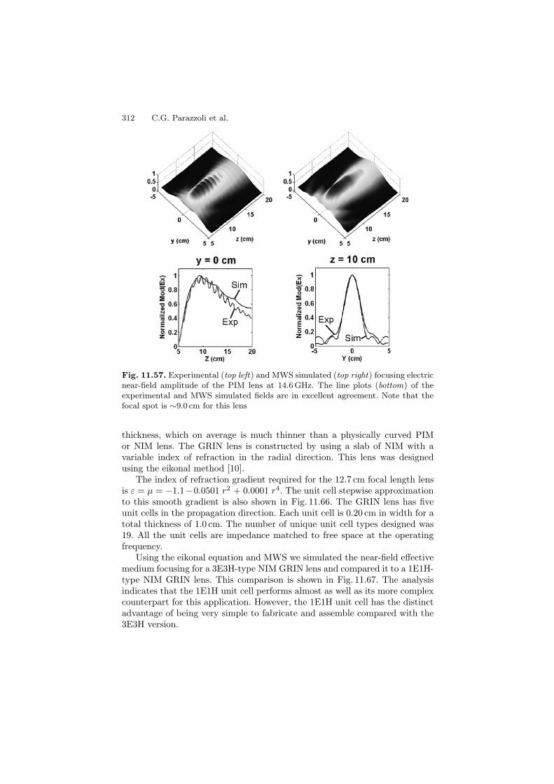
312 C.G. Parazzoli et al.
Fig. 11.57. Experimental (top left) and MWS simulated (top right) focusing electricnear-field amplitude of the PIM lens at 14.6 GHz. The line plots (bottom) of theexperimental and MWS simulated fields are in excellent agreement. Note that thefocal spot is ∼9.0 cm for this lens
thickness, which on average is much thinner than a physically curved PIMor NIM lens. The GRIN lens is constructed by using a slab of NIM with avariable index of refraction in the radial direction. This lens was designedusing the eikonal method [10].
The index of refraction gradient required for the 12.7 cm focal length lensis ε = µ = −1.1−0.0501 r2 + 0.0001 r4. The unit cell stepwise approximationto this smooth gradient is also shown in Fig. 11.66. The GRIN lens has fiveunit cells in the propagation direction. Each unit cell is 0.20 cm in width for atotal thickness of 1.0 cm. The number of unique unit cell types designed was19. All the unit cells are impedance matched to free space at the operatingfrequency.
Using the eikonal equation and MWS we simulated the near-field effectivemedium focusing for a 3E3H-type NIM GRIN lens and compared it to a 1E1H-type NIM GRIN lens. This comparison is shown in Fig. 11.67. The analysisindicates that the 1E1H unit cell performs almost as well as its more complexcounterpart for this application. However, the 1E1H unit cell has the distinctadvantage of being very simple to fabricate and assemble compared with the3E3H version.
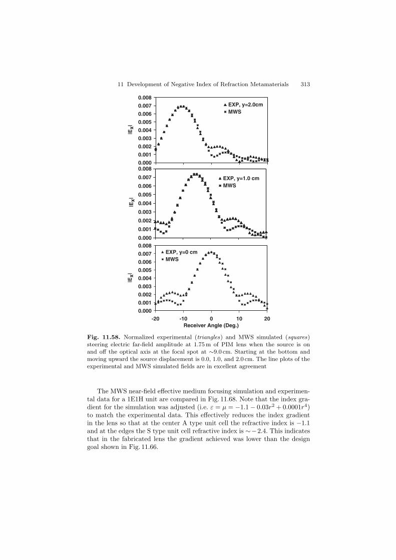
11 Development of Negative Index of Refraction Metamaterials 313
0.000
0.001
0.002
0.003
0.004
0.005
0.006
0.007
0.008
|Ex|
EXP, y=2.0cmMWS
0.000
0.001
0.002
0.003
0.004
0.005
0.006
0.007
0.008
|Ex|
EXP, y=1.0 cmMWS
0.000
0.001
0.002
0.003
0.004
0.005
0.006
0.007
0.008
-20 -10 0 10 20Receiver Angle (Deg.)
|Ex|
EXP, y=0 cmMWS
Fig. 11.58. Normalized experimental (triangles) and MWS simulated (squares)steering electric far-field amplitude at 1.75 m of PIM lens when the source is onand off the optical axis at the focal spot at ∼9.0 cm. Starting at the bottom andmoving upward the source displacement is 0.0, 1.0, and 2.0 cm. The line plots of theexperimental and MWS simulated fields are in excellent agreement
The MWS near-field effective medium focusing simulation and experimen-tal data for a 1E1H unit are compared in Fig. 11.68. Note that the index gra-dient for the simulation was adjusted (i.e. ε = µ = −1.1 − 0.03r2 + 0.0001r4)to match the experimental data. This effectively reduces the index gradientin the lens so that at the center A type unit cell the refractive index is −1.1and at the edges the S type unit cell refractive index is ∼−2.4. This indicatesthat in the fabricated lens the gradient achieved was lower than the designgoal shown in Fig. 11.66.
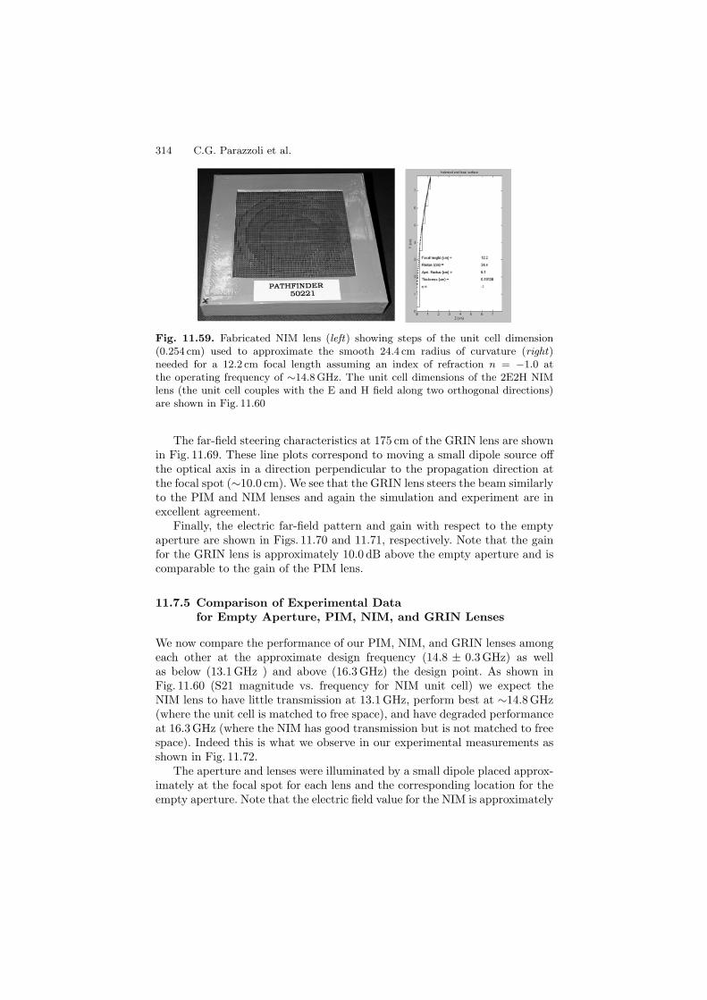
314 C.G. Parazzoli et al.
Fig. 11.59. Fabricated NIM lens (left) showing steps of the unit cell dimension(0.254 cm) used to approximate the smooth 24.4 cm radius of curvature (right)needed for a 12.2 cm focal length assuming an index of refraction n = −1.0 atthe operating frequency of ∼14.8 GHz. The unit cell dimensions of the 2E2H NIMlens (the unit cell couples with the E and H field along two orthogonal directions)are shown in Fig. 11.60
The far-field steering characteristics at 175 cm of the GRIN lens are shownin Fig. 11.69. These line plots correspond to moving a small dipole source offthe optical axis in a direction perpendicular to the propagation direction atthe focal spot (∼10.0 cm). We see that the GRIN lens steers the beam similarlyto the PIM and NIM lenses and again the simulation and experiment are inexcellent agreement.
Finally, the electric far-field pattern and gain with respect to the emptyaperture are shown in Figs. 11.70 and 11.71, respectively. Note that the gainfor the GRIN lens is approximately 10.0 dB above the empty aperture and iscomparable to the gain of the PIM lens.
11.7.5 Comparison of Experimental Datafor Empty Aperture, PIM, NIM, and GRIN Lenses
We now compare the performance of our PIM, NIM, and GRIN lenses amongeach other at the approximate design frequency (14.8 ± 0.3GHz) as wellas below (13.1 GHz ) and above (16.3 GHz) the design point. As shown inFig. 11.60 (S21 magnitude vs. frequency for NIM unit cell) we expect theNIM lens to have little transmission at 13.1 GHz, perform best at ∼14.8GHz(where the unit cell is matched to free space), and have degraded performanceat 16.3 GHz (where the NIM has good transmission but is not matched to freespace). Indeed this is what we observe in our experimental measurements asshown in Fig. 11.72.
The aperture and lenses were illuminated by a small dipole placed approx-imately at the focal spot for each lens and the corresponding location for theempty aperture. Note that the electric field value for the NIM is approximately
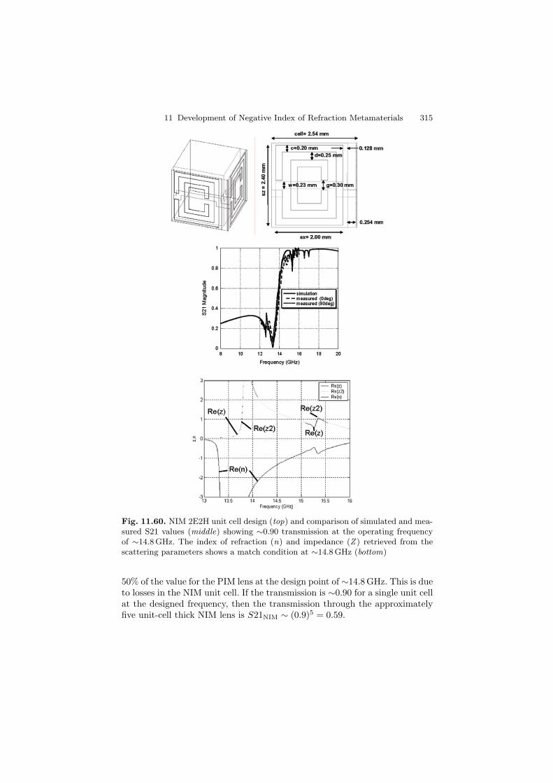
11 Development of Negative Index of Refraction Metamaterials 315
Fig. 11.60. NIM 2E2H unit cell design (top) and comparison of simulated and mea-sured S21 values (middle) showing ∼0.90 transmission at the operating frequencyof ∼14.8 GHz. The index of refraction (n) and impedance (Z ) retrieved from thescattering parameters shows a match condition at ∼14.8 GHz (bottom)
50% of the value for the PIM lens at the design point of ∼14.8GHz. This is dueto losses in the NIM unit cell. If the transmission is ∼0.90 for a single unit cellat the designed frequency, then the transmission through the approximatelyfive unit-cell thick NIM lens is S21NIM ∼ (0.9)5 = 0.59.

316 C.G. Parazzoli et al.
Fig. 11.61. MWS simulations of electric near-field amplitude for plane wave focus-ing (top) and small dipole (bottom) 2.0 cm above the central optical axis. The planewave and dipole sources illuminate the NIM lens in an aluminum aperture having a6.20 cm radius
For the PIM lens the transmission is much higher. For this case S11PIM =Er/Eo ∼ (n− 1)/(n+1) = (1.59− 1.00)/(1.59+1.00) = 0.23, where Eo is theincident field, Er is the reflected field, and n is the refractive index of Rexolite.For one interface S21PIM = (1−S112)1/2 = (1−0.232)1/2 = 0.97, that becomes0.94 for two interfaces, so we expect that S21NIM/S21PIM∼0.59/0.94 = 0.63which is approximately what we observe experimentally. The experimentalvalue (∼0.50) is probably lower due to fabrication tolerances and the result-ing increased impedance mismatch. We note however, that the FWHM ofthe NIM lens (∼12.5) is smaller than the GRIN lens (∼14) and PIM lens(∼15) which is consistent with the aberration analysis discussed in the nextsection.
The GRIN lens exhibits a normalized electric far-field value that is approx-imately 75% that of the PIM lens. This is higher than the NIM lens due to thelower losses of the 1E1H unit cell structure. The GRIN lens FWHM maximum(∼14) is smaller than the PIM lens but larger than the NIM lens. The exper-imental gain with respect to the empty aperture is shown in Fig. 11.73. Here,we see that the gain for the PIM is ∼10 dB at each frequency 13.1, 14.8, and16.3 GHz, whereas the gain for the NIM is ∼−30.0, 5.0, and 3.0 dB, respec-tively. The GRIN lens gain is ∼9.0 dB at ∼14.8GHz, which is only slightlyless than the PIM lens.
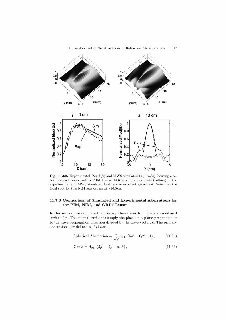
11 Development of Negative Index of Refraction Metamaterials 317
Fig. 11.62. Experimental (top left) and MWS simulated (top right) focusing elec-tric near-field amplitude of NIM lens at 14.6 GHz. The line plots (bottom) of theexperimental and MWS simulated fields are in excellent agreement. Note that thefocal spot for this NIM lens occurs at ∼10.0 cm
11.7.6 Comparison of Simulated and Experimental Aberrations forthe PIM, NIM, and GRIN Lenses
In this section, we calculate the primary aberrations from the known eikonalsurface ζ10. The eikonal surface is simply the phase in a plane perpendicularto the wave propagation direction divided by the wave vector, k. The primaryaberrations are defined as follows:
Spherical Aberration =1√2A040
(6ρ4 − 6ρ2 + 1
), (11.35)
Coma = A031
(3ρ3 − 2ρ
)cos (θ) , (11.36)
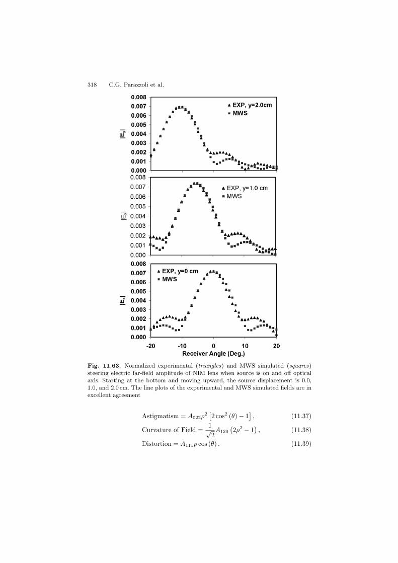
318 C.G. Parazzoli et al.
Fig. 11.63. Normalized experimental (triangles) and MWS simulated (squares)steering electric far-field amplitude of NIM lens when source is on and off opticalaxis. Starting at the bottom and moving upward, the source displacement is 0.0,1.0, and 2.0 cm. The line plots of the experimental and MWS simulated fields are inexcellent agreement
Astigmatism = A022ρ2[2 cos2 (θ) − 1
], (11.37)
Curvature of Field =1√2A120
(2ρ2 − 1
), (11.38)
Distortion = A111ρ cos (θ) . (11.39)
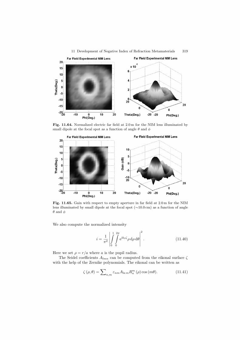
11 Development of Negative Index of Refraction Metamaterials 319
Fig. 11.64. Normalized electric far field at 2.0 m for the NIM lens illuminated bysmall dipole at the focal spot as a function of angle θ and φ
Fig. 11.65. Gain with respect to empty aperture in far field at 2.0 m for the NIMlens illuminated by small dipole at the focal spot (∼10.0 cm) as a function of angleθ and φ
We also compute the normalized intensity
i =1π2
∣∣∣∣∣∣
1∫
0
2π∫
0
eik0ζρdρdθ
∣∣∣∣∣∣
2
. (11.40)
Here we set ρ = r/a where a is the pupil radius.The Seidel coefficients Almn can be computed from the eikonal surface ζ
with the help of the Zernike polynomials. The eikonal can be written as
ζ (ρ, θ) =∑
n,mεnmAln mRm
n (ρ) cos (mθ). (11.41)
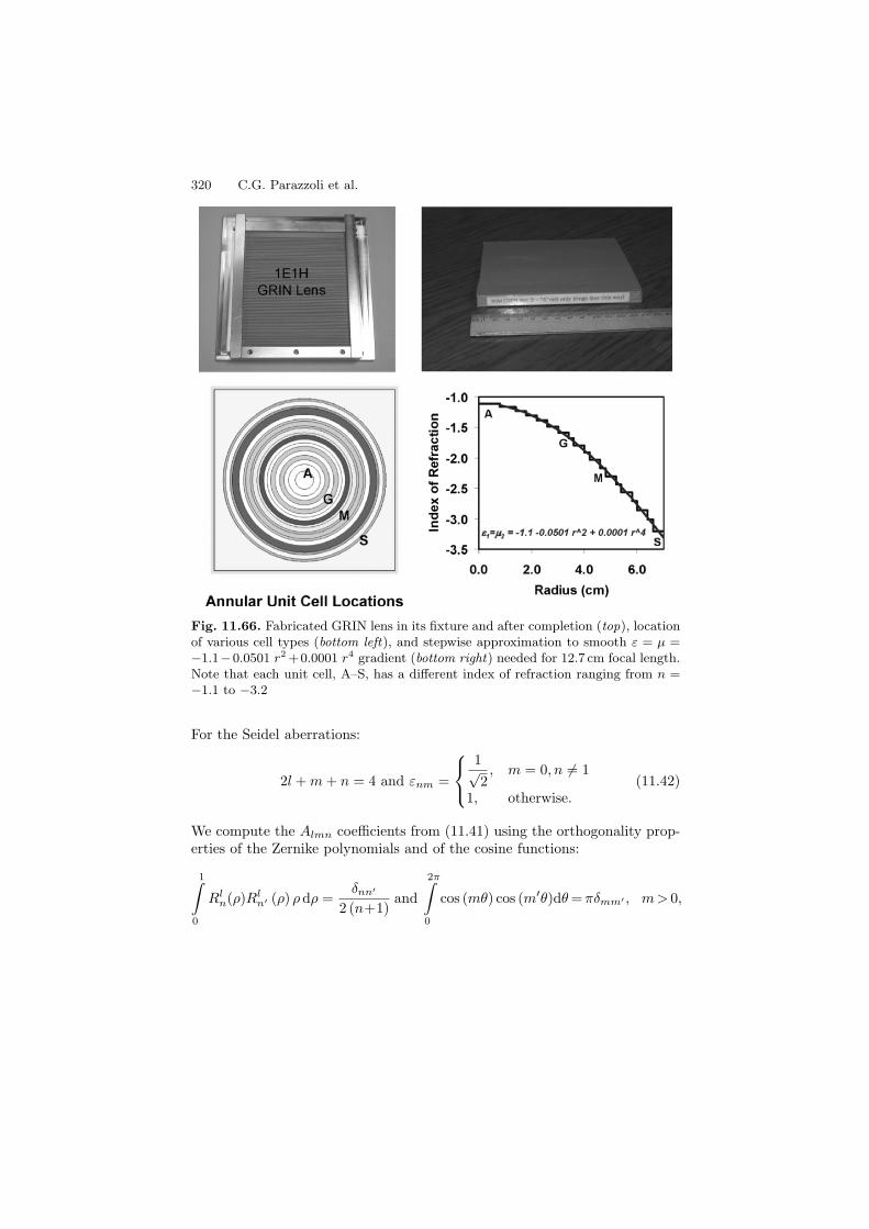
320 C.G. Parazzoli et al.
Fig. 11.66. Fabricated GRIN lens in its fixture and after completion (top), locationof various cell types (bottom left), and stepwise approximation to smooth ε = µ =−1.1−0.0501 r2 +0.0001 r4 gradient (bottom right) needed for 12.7 cm focal length.Note that each unit cell, A–S, has a different index of refraction ranging from n =−1.1 to −3.2
For the Seidel aberrations:
2l + m + n = 4 and εnm =
⎧⎨⎩
1√2, m = 0, n = 1
1, otherwise.(11.42)
We compute the Almn coefficients from (11.41) using the orthogonality prop-erties of the Zernike polynomials and of the cosine functions:
1∫
0
Rln(ρ)Rl
n′ (ρ) ρdρ =δnn′
2 (n+1)and
2π∫
0
cos (mθ) cos (m′θ)dθ = πδmm′ , m> 0,
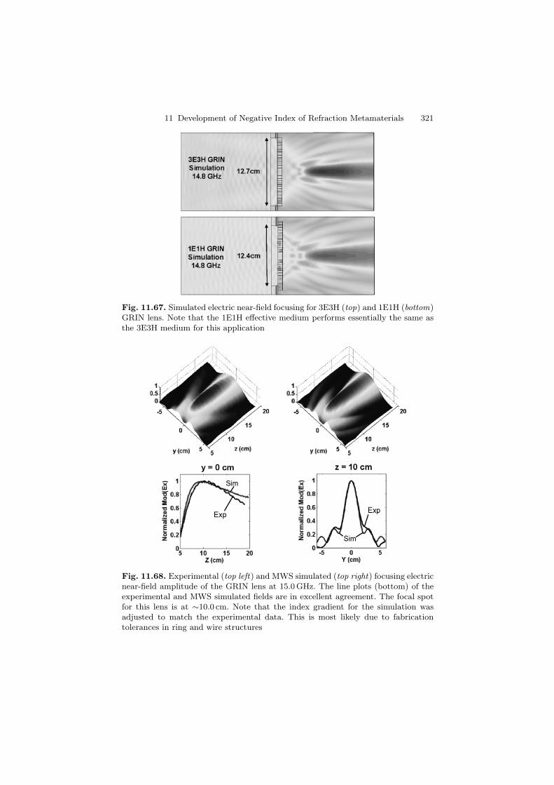
11 Development of Negative Index of Refraction Metamaterials 321
Fig. 11.67. Simulated electric near-field focusing for 3E3H (top) and 1E1H (bottom)GRIN lens. Note that the 1E1H effective medium performs essentially the same asthe 3E3H medium for this application
Fig. 11.68. Experimental (top left) and MWS simulated (top right) focusing electricnear-field amplitude of the GRIN lens at 15.0 GHz. The line plots (bottom) of theexperimental and MWS simulated fields are in excellent agreement. The focal spotfor this lens is at ∼10.0 cm. Note that the index gradient for the simulation wasadjusted to match the experimental data. This is most likely due to fabricationtolerances in ring and wire structures
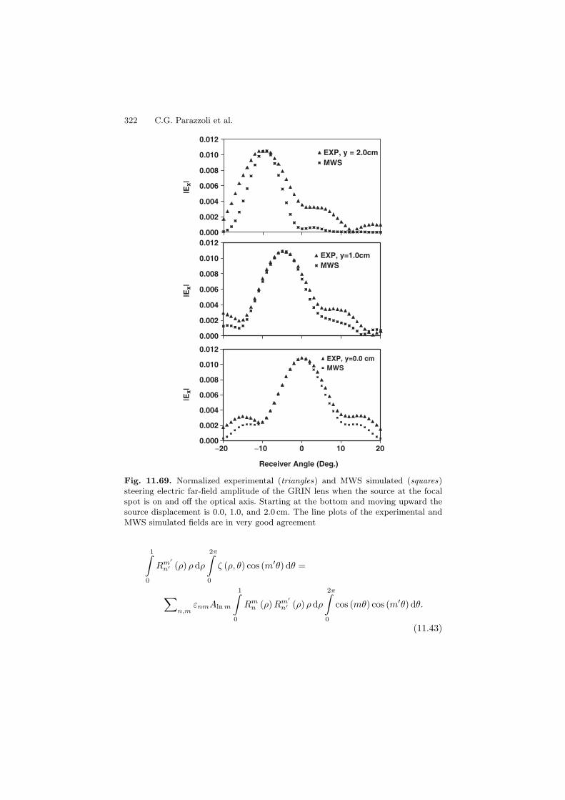
322 C.G. Parazzoli et al.
0.000
0.002
0.004
0.006
0.008
0.010
0.012
|Ex|
|E
x|
|Ex|
EXP, y = 2.0cmMWS
0.000
0.002
0.004
0.006
0.008
0.010
0.012
EXP, y=1.0cmMWS
0.000
0.002
0.004
0.006
0.008
0.010
0.012
−20 −10 0 10 20
Receiver Angle (Deg.)
EXP, y=0.0 cmMWS
Fig. 11.69. Normalized experimental (triangles) and MWS simulated (squares)steering electric far-field amplitude of the GRIN lens when the source at the focalspot is on and off the optical axis. Starting at the bottom and moving upward thesource displacement is 0.0, 1.0, and 2.0 cm. The line plots of the experimental andMWS simulated fields are in very good agreement
1∫
0
Rm′
n′ (ρ) ρdρ
2π∫
0
ζ (ρ, θ) cos (m′θ) dθ =
∑n,m
εnmAln m
1∫
0
Rmn (ρ) Rm′
n′ (ρ) ρdρ
2π∫
0
cos (mθ) cos (m′θ) dθ.
(11.43)
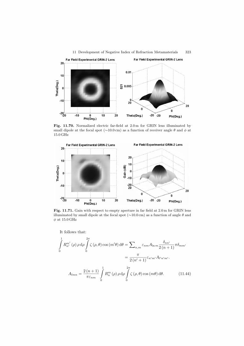
11 Development of Negative Index of Refraction Metamaterials 323
Fig. 11.70. Normalized electric far-field at 2.0 m for GRIN lens illuminated bysmall dipole at the focal spot (∼10.0 cm) as a function of receiver angle θ and φ at15.0 GHz
Fig. 11.71. Gain with respect to empty aperture in far field at 2.0 m for GRIN lensilluminated by small dipole at the focal spot (∼10.0 cm) as a function of angle θ andφ at 15.0 GHz
It follows that:1∫
0
Rm′
n′ (ρ) ρdρ
2π∫
0
ζ (ρ, θ) cos (m′θ) dθ =∑
n,mεnmAln m
δnn′
2 (n + 1)πδmm′
=π
2 (n′ + 1)εn′m′Al′n′m′ .
Almn =2 (n + 1)
πεnm
1∫
0
Rmn (ρ) ρdρ
2π∫
0
ζ (ρ, θ) cos (mθ) dθ. (11.44)
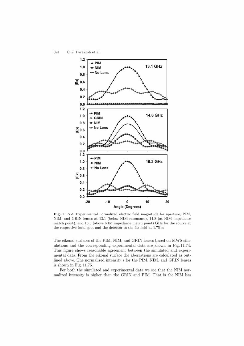
324 C.G. Parazzoli et al.
Fig. 11.72. Experimental normalized electric field magnitude for aperture, PIM,NIM, and GRIN lenses at 13.1 (below NIM resonance), 14.8 (at NIM impedancematch point), and 16.3 (above NIM impedance match point) GHz for the source atthe respective focal spot and the detector in the far field at 1.75 m
The eikonal surfaces of the PIM, NIM, and GRIN lenses based on MWS sim-ulations and the corresponding experimental data are shown in Fig. 11.74.This figure shows reasonable agreement between the simulated and experi-mental data. From the eikonal surface the aberrations are calculated as out-lined above. The normalized intensity i for the PIM, NIM, and GRIN lensesis shown in Fig. 11.75.
For both the simulated and experimental data we see that the NIM nor-malized intensity is higher than the GRIN and PIM. That is the NIM has
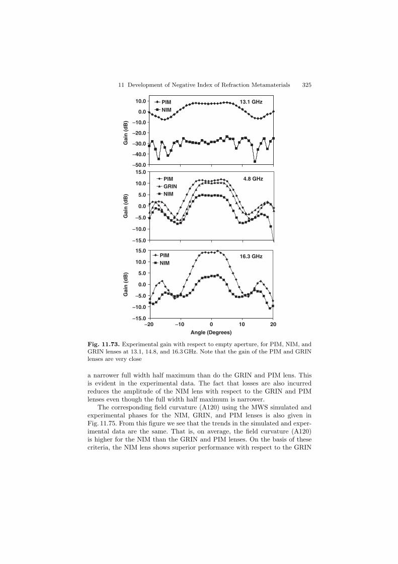
11 Development of Negative Index of Refraction Metamaterials 325
-50.0
-40.0
-30.0
-20.0
-10.0
0.0
10.0
Gai
n (
dB
)
PIMNIM
-15.0
-10.0
-5.0
0.0
5.0
10.0
15.0
-20 -10 0 10 20
Angle (Degrees)
Gai
n (
dB
)
PIMNIM
-15.0
-10.0
-5.0
0.0
5.0
10.0
15.0
Gai
n (
dB
)
PIMGRINNIM
13.1 GHz
4.8 GHz
16.3 GHz
Fig. 11.73. Experimental gain with respect to empty aperture, for PIM, NIM, andGRIN lenses at 13.1, 14.8, and 16.3 GHz. Note that the gain of the PIM and GRINlenses are very close
a narrower full width half maximum than do the GRIN and PIM lens. Thisis evident in the experimental data. The fact that losses are also incurredreduces the amplitude of the NIM lens with respect to the GRIN and PIMlenses even though the full width half maximum is narrower.
The corresponding field curvature (A120) using the MWS simulated andexperimental phases for the NIM, GRIN, and PIM lenses is also given inFig. 11.75. From this figure we see that the trends in the simulated and exper-imental data are the same. That is, on average, the field curvature (A120)is higher for the NIM than the GRIN and PIM lenses. On the basis of thesecriteria, the NIM lens shows superior performance with respect to the GRIN
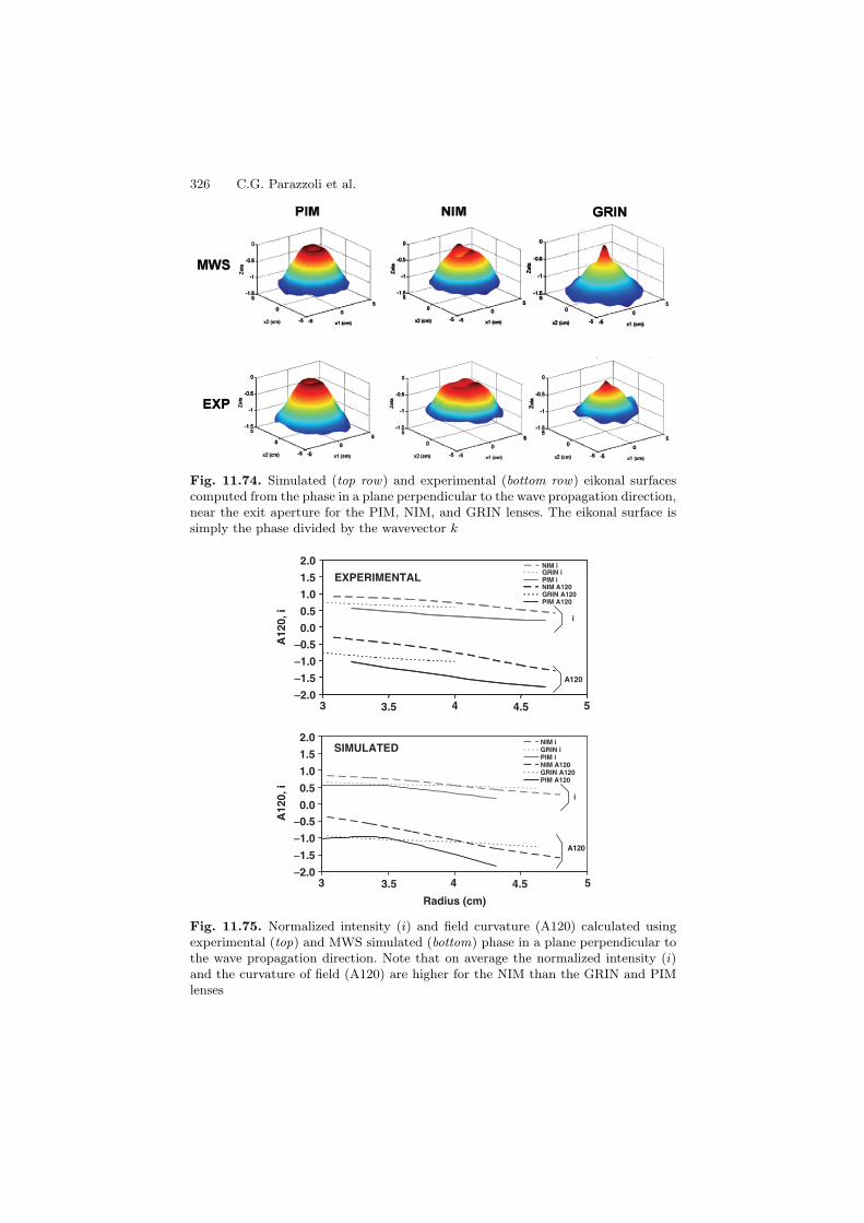
326 C.G. Parazzoli et al.
Fig. 11.74. Simulated (top row) and experimental (bottom row) eikonal surfacescomputed from the phase in a plane perpendicular to the wave propagation direction,near the exit aperture for the PIM, NIM, and GRIN lenses. The eikonal surface issimply the phase divided by the wavevector k
-2.0
-1.5
-1.0
-0.5
0.0
0.5
1.0
1.5
2.0
3 3.5 4 4.5 5
NIM iGRIN iPIM iNIM A120GRIN A120PIM A120
EXPERIMENTAL
-2.0
-1.5
-1.0
-0.50.0
0.5
1.0
1.5
2.0
3 3.5 4 4.5 5
Radius (cm)
NIM iGRIN iPIM iNIM A120GRIN A120PIM A120
SIMULATED
A120
i
A120
i
A12
0, i
A12
0, i
Fig. 11.75. Normalized intensity (i) and field curvature (A120) calculated usingexperimental (top) and MWS simulated (bottom) phase in a plane perpendicular tothe wave propagation direction. Note that on average the normalized intensity (i)and the curvature of field (A120) are higher for the NIM than the GRIN and PIMlenses
11 Development of Negative Index of Refraction Metamaterials 327
and PIM lenses. Again it must be recognized that these criteria do not includelosses. Of course, it may be possible to improve the performance of the GRINand PIM lenses by adjusting the index gradient and using aspherical surfaces.If losses are included then, the PIM and GRIN lenses show favorable perfor-mances over the NIM lenses. Also, we note that much of the difference betweenthe simulated and experimental aberrations is due to coupling between theexperimental probe and the lens/setup.
11.7.7 Weight Comparison Between the PIM, NIM,and GRIN Lenses
We compared the weight of three types of NIM lenses as another metric oftheir physical properties. The respective weights are given below:
PIM 323.8 gNIM Pathfinder Spherical Lens with 3-cell-thick bottom layer 229.5 gNIM Pathfinder Spherical Lens with 1-cell-thick bottom layer 142.2 gGRIN Lens 75.4 g
This data shows the obvious weight advantage of NIM lenses due to theirhoneycomb like fabrication structure.
11.8 Conclusion
Major advances in NIMs were made in (1) their design, such that they have adesired value for n and Z, (2) their characterization both in waveguides andfree space, both in the near field and at far field, (3) the design of novel NIMoptics, namely lenses, both with physical curvature and gradient index, (4)the characterization of such NIM lenses and in comparison with conventionalPIM lenses, and (5) demonstrating that negative index lenses have inherentlylower aberrations than their corresponding PIMs. NIMs can be made withproperties that are attractive for practical applications, such as low loss andbandwidth of the order of 8–10% of the center frequency. Most of the workcarried out has been in the microwave region but it is clear that many of theconcepts used are applicable to other frequency domains.
Acknowledgements
The authors would like to acknowledge the contributions of the many indi-viduals who helped in this effort. From the Boeing team, Ben Koltenbah,and later Tai Lam for the numerical simulations and theoretical calculationsrelated to various NIM structures and lenses; Mark Thompson, Art Vetter,and Kin Li for metamaterial testing; Jean Nielsen for fabrication of the unit
328 C.G. Parazzoli et al.
cell structures and lenses. From the Duke University team, David Smith andDave Schurig for their many contributions to general NIM physics and lensproperties. From the University of California at San Diego, Dave Vier for hisdetailed designs of unit cell structures and Sheldon Schultz for technical adviceand experimental suggestions. From Iowa State University, Costas Soukoulis,Thomas Koschny, Lei Zhang, and Stavroula Foteinopoulou for analyzing someof the fundamental physics of NIMs and their implications. The authors wouldlike to extend special thanks to Valerie Browning at DARPA for continuousencouragement, advice, and support during this effort that was supportedunder contract MDA972-01-2-0016.
References
1. V.G. Veselago, Sov. Phys. Usp. 10, 509 (1968)2. J.B. Pendry, A.J. Holden, D.J. Robbins, W.J. Stewart. IEEE Trans. Microw.
Theory Tech. 47, 2075 (1999)3. D.R. Smith, W. Padilla, D.C. Vier, S.C. Nemat-Nasser, S. Schultz, Phys. Rev.
Lett. 84, 4184 (2000)4. J.D. Jackson, Classical Electrodynamics, 3rd edn. (1999)5. R.B. Greegor, C.G. Parazzoli, K. Li, M.H. Tanielian, Appl. Phys. Lett. 82(14),
2356 (2003)6. R.B. Greegor, C.G. Parazzoli, K. Li, B.E.C. Kotlenbah, M.H. Tanielian, Opt.
Express 11(7), 688 (2003)7. P. Markos, C.M. Soukoulis, Phys. Rev. B. 65, 033401 (2002); Phys. Rev. E 65,
036622 (2002)8. D.R. Smith, D. Schurig, Phys. Rev. Lett. 90, 77405 (2003); D.R. Smith,
P. Kolinko, D. Schurig, J. Opt. Soc. B 21, 1032 (2004)9. P. Kolinko, D.R. Smith, Opt. Express 11, 640 (2003)
10. C.G. Parazzoli, B.E.C. Koltenvbah, R.B. Greegor, T.A. Lam, M.H. Tanielian,J. Opt. Soc. Am. B 23, 439 (2006)
11. C.G. Parazzoli, R.B. Greegor, K. Li, B.E.C. Koltenbah, M.H. Tanielian, Phys.Rev. Lett. 90(10), 107401 (2003)
12. MWS and MAFIA are commercial software packages available from CST13. P. Markos, C.M. Soukoulis, Opt. Express 11, 649 (2003); T. Koschny, M. Kafe-
saki, E.N. Economou, C.M. Soukoulis, Phys. Rev. Lett. 93, 107402 (2004)14. T. Koschny, P. Markos, D.R. Smith, C.M. Soukoulis, Phy. Rev. E 68, 065602(R)
(2003); T. Koschny, P. Markos, E.N. Economou, D.R. Smith, D.C. Vier,C.M. Soukoulis, Phys. Rev. B 71, 245105 (2005)
15. K. Li, S.J. McLean, R.B. Greegor, C.G. Parazzoli, M.H. Tanielian, Appl. Phys.Lett. 82(15), 2535 (2003); R.B. Greegor, C.G. Parazzoli, K. Li, M.H. Tanielian,Appl. Phys. Lett. 82(14), 2356 (2003)
16. D. Vier, D.R. Fredkin, A. Simic, S. Schultz, M. Tanielian, Appl. Phys. Lett. 86,241908 (2005)
17. D. Schurig, D.R. Smith, Phys. Rev. E 70, 065601(2004)18. C.G. Parazzoli, R.B. Greegor, J.A. Nielsen, M.A. Thompson, K. Li, A.M. Vetter,
D.C. Vier, M.H. Tanielian, Appl. Phys. Lett. 84(17), 3232 (2004)

11 Development of Negative Index of Refraction Metamaterials 329
19. R.B. Greegor, C.G. Parazzoli, J.A. Nielsen, M.A. Thompson, M.H. Tanielian,D.C. Vier, S. Schultz, D.R. Smith, D. Schurig, Proceedings of the 2005 AntennaApplications Symposium, Monticello, Illinois, September 2005; R.B. Greegor,C.G. Parazzoli, J.A. Nielsen, M.A. Thompson, M.H. Tanielian, D.C. Vier, S.Schultz, D.R. Smith, D. Schurig, IET Microw. Antennas Propag. 1, 108 (2007)
20. R.B. Greegor, C.G. Parazzoli, J.A. Nielsen, M.A. Thompson, M.H. Tanielian,Appl. Phys. Lett. 87, 091114 (2005)
12
Nonlinear Effects in Left-HandedMetamaterials
I.V. Shadrivov and Y.S. Kivshar
Summary. We overview different types of nonlinear effects recently predicted formicrostructured metamaterials which exhibit left-handed properties and negativerefraction. We show that both magnetic and electric nonlinear response in suchmicrostructured composites can be enhanced significantly compared to bulk media,since local electric fields in metallic microresonators may become extremely strong.We predict that nonlinear properties of metamaterials can allow for various appli-cations, including a dynamic control and tunability of the electromagnetic proper-ties of the composite structures, second-harmonic generation, intensity-dependentswitches, and soliton generation.
12.1 Introduction
Novel types of microstructured materials that demonstrate many intriguingproperties for electromagnetic waves such as negative refraction have beendiscussed recently in many theoretical studies [1–4], and currently such mate-rials are being studied experimentally [5–7]. The simplest composite materialsof this type are created by a mesh of metallic wires and split-ring resonators(SRRs), and their unique properties are associated with negative real parts ofmagnetic permeability and dielectric permittivity for microwaves. Such com-posite materials are often referred to as left-handed materials (LHMs) or mate-rials with negative refractive index. Properties of LHMs were analyzed firsttheoretically by Veselago a long time ago [8], but such materials were demon-strated experimentally only recently. As was shown by Veselago [8], the LHMspossess a number of peculiar properties, including negative refraction for inter-face scattering, inverse light pressure, reverse Doppler and Vavilov–Cherenkoveffects, etc.
Since the first days of the extensive studies of metamaterials and theirproperties, attention of most of the researchers was focused on linear prop-erties of LHMs, when the parameters of the composites do not depend onthe intensity of the electromagnetic field. However, the future efforts in creat-ing tunable structures where, e.g., the field intensity can be used for dynamic
332 I.V. Shadrivov and Y.S. Kivshar
control of the transmission properties of the composite structure would requirethe study of nonlinear properties of such metamaterials, which may be quiteunusual. As we show in this chapter, this is because the fabricated meta-materials are composed of a mesh of conducting metallic components, namelywires and SRRs. The wires are used to provide negative dielectric permittivity,while SRRs give negative magnetic permeability. The dynamic control overmetamaterials properties is nontrivial since they possess left-handed proper-ties only in some finite frequency range, which is basically determined by thegeometry of the structure. The possibility to control the effective parametersof the metamaterial using nonlinearity has recently been suggested in [9, 10].The main reason for nontrivial behavior of nonlinear metamaterials is thatthe microscopic electric field in the vicinity of the metallic particles formingleft-handed structure can be much higher than the macroscopic electric fieldcarried by the propagating wave. This provides a simple physical mechanismfor enhancing nonlinear effects in LHMs. We believe our findings may stim-ulate the future experiments in this field, as well as the studies of nonlineareffects in photonic crystals, where the phenomenon of negative refraction isanalyzed now very intensively [11,12].
In this chapter, we demonstrate that the dominant nonlinear propertiesof metamaterials arise from the hysteresis-type dependence of the magneticpermeability on the magnetic field intensity in the electromagnetic wave prop-agating through the material. It allows changing the material properties fromleft- to right-handed and back. Using the finite-difference time-domain simula-tions, we study the wave scattering from a slab of a nonlinear LHM and discussa possibility of generation and propagation of spatiotemporal solitons in suchmaterials. We demonstrate also that the nonlinear left-handed metamateri-als can support both transverse electric- and transverse magnetic-polarizedself-trapped localized beams, spatial electromagnetic solitons. We also discussthe physical mechanisms and novel effects in the parametric processes suchas second-harmonic generation (SHG), which can take place in metamateri-als. We demonstrate a novel type of the exact spatiotemporal phase matchingbetween the backward propagating wave of the fundamental frequency (FF)and the forward propagating wave of the second harmonic (SH). We showthat this novel parametric process can convert a surface of the left-handedmetamaterial into an effective mirror totally reflecting the SHs generated byan incident wave. We derive and analyze theoretically the coupled-mode equa-tions for a semi-infinite nonlinear metamaterial and a metamaterial slab of afinite thickness, and reveal the existence of multistable nonlinear effects. Wealso suggest the way to further enhance the SHG in metamaterials, by using adouble-resonant metamaterial. We introduce somewhat exotic concept of non-linear lens, which is capable of creating image of the source of electromagneticwaves being opaque at the FF, but transparent for the SH field.
This chapter is organized as follows. In Sect. 12.2, we present an overviewof some nonlinear properties of left-handed metamaterials for the example ofa lattice of SRRs and wires embedded in a nonlinear dielectric. Further in

12 Nonlinear Effects in Left-Handed Metamaterials 333
this section, we demonstrate the numerical model for the simulation of thenonlinear metamaterial by means of the finite-difference time-domain (FDTD)method. In particular, we study the wave scattering by a slab of a nonlinearcomposite structure. We also discuss the structure of electromagnetic solitonssupported by the nonlinear LHMs with hysteresis-type nonlinear response.In Sect. 12.3, we discuss the metamaterials with Kerr-like nonlinear response,and study nonlinear surface waves as well as band-gap structures with LHMs.In Sect. 12.4, we study second-order nonlinear effects in metamaterials, suchas SHG. We show the possibility of the nontrivial phase-matching which ispossible in metamaterials, allowing for the creation of the SH reflecting mirror.We also suggest a way to enhance the efficiency of SHG by means of double-resonant metamaterials.
12.2 Nonlinear Response of Metamaterials
We consider a three-dimensional composite structure in the form of a cubiclattice of conducting wires and SRRs. We assume that the unit-cell size dcell ofthe structure is much smaller than the wavelength of the electromagnetic wavepropagating in the material, for simplicity, we choose the single-ring geometryof a lattice of SRRs. The results obtained for this case are qualitatively similarto those obtained in more involved cases of double SRRs near low-frequencyresonance, for which the currents in both rings of the double SRR are in-phase.
The negative real part of the effective dielectric permittivity of such acomposite structure appears due to the metallic wires whereas a negativemagnetic permeability becomes possible due to the SRR lattice. As a result,these materials demonstrate the properties of negative refraction in a finitefrequency range, i.e., ω0 < ω < min(ωp, ω‖m), where ω0 is the eigenfrequencyof the array of SRRs, ω‖m is some characteristic frequency, which we call thefrequency of the longitudinal magnetic plasmon, ωp is the effective plasmafrequency, and ω is the angular frequency of the propagating electromagneticwaves, (E ,H) ∼ (E,H) exp (iωt). The SRR can be described as an effectiveLC oscillator (see, e.g., [13]) with capacitance of the SRR gap, as well as aneffective inductance and resistance.
If we embed the structure in a nonlinear dielectric, we expect it to exhibitquite unusual properties. The nonlinearity here must become complex in thesense that both the dielectric permittivity and the magnetic permeability willchange with the variation of the external electromagnetic fields. Nonlineardielectric response is determined by the bulk of the nonlinear dielectric, andfrequency-dependant contribution will be provided by wires. Since we assumethat the nonlinear dielectric does not possess magnetic properties itself, itseems that the magnetic response of the composite will still be determined bythe array of SRRs. However, the response of the SRRs depends on the field pat-tern in the vicinity of the resonators, which, in turn, depends on the properties
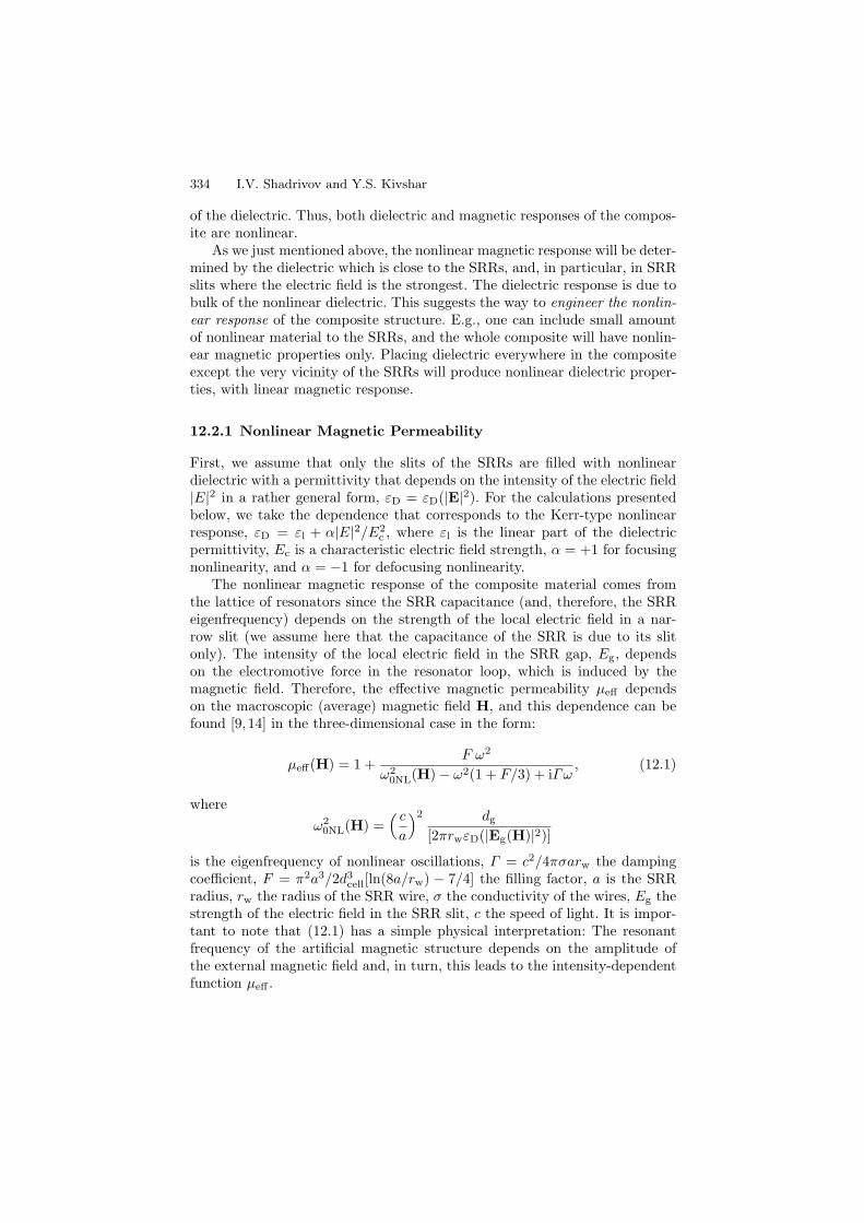
334 I.V. Shadrivov and Y.S. Kivshar
of the dielectric. Thus, both dielectric and magnetic responses of the compos-ite are nonlinear.
As we just mentioned above, the nonlinear magnetic response will be deter-mined by the dielectric which is close to the SRRs, and, in particular, in SRRslits where the electric field is the strongest. The dielectric response is due tobulk of the nonlinear dielectric. This suggests the way to engineer the nonlin-ear response of the composite structure. E.g., one can include small amountof nonlinear material to the SRRs, and the whole composite will have nonlin-ear magnetic properties only. Placing dielectric everywhere in the compositeexcept the very vicinity of the SRRs will produce nonlinear dielectric proper-ties, with linear magnetic response.
12.2.1 Nonlinear Magnetic Permeability
First, we assume that only the slits of the SRRs are filled with nonlineardielectric with a permittivity that depends on the intensity of the electric field|E|2 in a rather general form, εD = εD(|E|2). For the calculations presentedbelow, we take the dependence that corresponds to the Kerr-type nonlinearresponse, εD = εl + α|E|2/E2
c , where εl is the linear part of the dielectricpermittivity, Ec is a characteristic electric field strength, α = +1 for focusingnonlinearity, and α = −1 for defocusing nonlinearity.
The nonlinear magnetic response of the composite material comes fromthe lattice of resonators since the SRR capacitance (and, therefore, the SRReigenfrequency) depends on the strength of the local electric field in a nar-row slit (we assume here that the capacitance of the SRR is due to its slitonly). The intensity of the local electric field in the SRR gap, Eg, dependson the electromotive force in the resonator loop, which is induced by themagnetic field. Therefore, the effective magnetic permeability µeff dependson the macroscopic (average) magnetic field H, and this dependence can befound [9,14] in the three-dimensional case in the form:
µeff(H) = 1 +F ω2
ω20NL(H) − ω2(1 + F/3) + iΓω
, (12.1)
whereω2
0NL(H) =( c
a
)2 dg
[2πrwεD(|Eg(H)|2)]is the eigenfrequency of nonlinear oscillations, Γ = c2/4πσarw the dampingcoefficient, F = π2a3/2d3
cell[ln(8a/rw) − 7/4] the filling factor, a is the SRRradius, rw the radius of the SRR wire, σ the conductivity of the wires, Eg thestrength of the electric field in the SRR slit, c the speed of light. It is impor-tant to note that (12.1) has a simple physical interpretation: The resonantfrequency of the artificial magnetic structure depends on the amplitude ofthe external magnetic field and, in turn, this leads to the intensity-dependentfunction µeff .
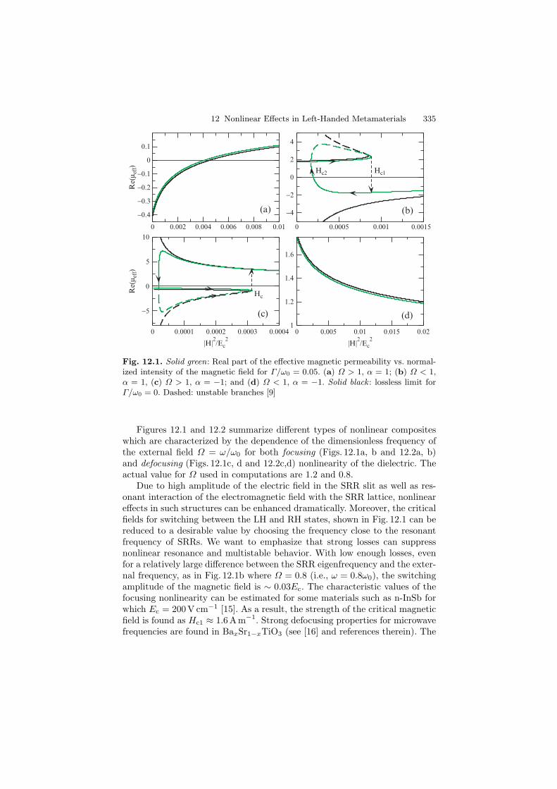
12 Nonlinear Effects in Left-Handed Metamaterials 335
0 0.005 0.01 0.015 0.02
|H|2/Ec
2
1
1.2
1.4
1.6
0 0.0001 0.0002 0.0003 0.0004
|H|2/Ec
2
−5
0
5
10
Re(
µ eff)
0 0.0005 0.001 0.0015
−4
−2
0
2
4
0 0.002 0.004 0.006 0.008 0.01
−0.4
−0.3
−0.2
−0.1
0
0.1
Re(
µ eff)
(a) (b)
(c) (d)
Hc1Hc2
Hc
Fig. 12.1. Solid green: Real part of the effective magnetic permeability vs. normal-ized intensity of the magnetic field for Γ/ω0 = 0.05. (a) Ω > 1, α = 1; (b) Ω < 1,α = 1, (c) Ω > 1, α = −1; and (d) Ω < 1, α = −1. Solid black : lossless limit forΓ/ω0 = 0. Dashed: unstable branches [9]
Figures 12.1 and 12.2 summarize different types of nonlinear compositeswhich are characterized by the dependence of the dimensionless frequency ofthe external field Ω = ω/ω0 for both focusing (Figs. 12.1a, b and 12.2a, b)and defocusing (Figs. 12.1c, d and 12.2c,d) nonlinearity of the dielectric. Theactual value for Ω used in computations are 1.2 and 0.8.
Due to high amplitude of the electric field in the SRR slit as well as res-onant interaction of the electromagnetic field with the SRR lattice, nonlineareffects in such structures can be enhanced dramatically. Moreover, the criticalfields for switching between the LH and RH states, shown in Fig. 12.1 can bereduced to a desirable value by choosing the frequency close to the resonantfrequency of SRRs. We want to emphasize that strong losses can suppressnonlinear resonance and multistable behavior. With low enough losses, evenfor a relatively large difference between the SRR eigenfrequency and the exter-nal frequency, as in Fig. 12.1b where Ω = 0.8 (i.e., ω = 0.8ω0), the switchingamplitude of the magnetic field is ∼ 0.03Ec. The characteristic values of thefocusing nonlinearity can be estimated for some materials such as n-InSb forwhich Ec = 200V cm−1 [15]. As a result, the strength of the critical magneticfield is found as Hc1 ≈ 1.6Am−1. Strong defocusing properties for microwavefrequencies are found in BaxSr1−xTiO3 (see [16] and references therein). The
336 I.V. Shadrivov and Y.S. Kivshar
0 0.005 0.01 0.015 0.02|H|2/Ec2
−0.12
−0.1
−0.08
−0.06
−0.04
−0.02
0
0 0.0001 0.0002 0.0003 0.0004|H|2/Ec2
−3
−2
−1
0
Im (µ e
ff)
0 0.0005 0.001 0.0015−6
−5
−4
−3
−2
−1
0
0 0.002 0.004 0.006 0.008 0.01−0.2
−0.15
−0.1
−0.05
0Im
(µ e
ff)
(a) (b)
(c) (d)
Fig. 12.2. Imaginary part of the effective magnetic permeability vs. intensity of themagnetic field for γ = 0.05. (a) Ω > 1, α = 1; (b) Ω < 1, α = 1, (c) Ω > 1, α = −1;and (d) Ω < 1, α = −1. Dashed curves show the branches of unstable solutions [9]
critical nonlinear field of a thin film of this material is Ec = 4 × 10⁴ V cm−1,and the corresponding field of the transition from the LH to RH state (seeFig. 12.1c) can be found as Hc ≈
√0.003 × 4 × 102/3CGS = 183Am−1.
The unique possibility of strongly enhanced effective nonlinearities (com-pared to the nonlinearities in dielectrics) in left-handed metamaterialsrevealed here may lead to an essential revision of the concepts based onthe linear theory, since the electromagnetic waves propagating in such mate-rials always have a finite amplitude. At the same time, the engineering ofnonlinear composite materials may open up a number of their novel appli-cations such as frequency multipliers, beam spatial spectrum transformers,switchers, limiters, etc.
12.2.2 Nonlinear Dielectric Permittivity
Now we analyze the dielectric properties of the composite. We suppose thatcontribution to the dielectric function given by the array of wires is muchstronger then that from SRRs. In this case, we can obtain the following expres-sion for the effective nonlinear dielectric permittivity [9]:
εeff
(|E|2
)= εD
(|E|2
)−
ω2p
ω(ω − iγε), (12.2)
12 Nonlinear Effects in Left-Handed Metamaterials 337
where ωp ≈ (c/d)[2π/ ln (d/r)]1/2 is the effective plasma frequency, andγε = c2/2σS ln (d/r), S is an effective wire cross-section. The second termon the right-hand side of (12.2) is in complete agreement with the earlierresult obtained by Pendry and co-authors [1]. One should note that the lowlosses case, i.e., γε ω, corresponds to the condition δ r, i.e, when thewires are thick with respect to the skin-layer depth.
12.2.3 FDTD Simulations of Nonlinear Metamaterial
To verify the specific features of the left-handed metamaterials introduced bytheir nonlinear response, in this section we study the scattering of electromag-netic waves from the nonlinear metamaterial discussed above. In particular,we perform the FDTD numerical simulations of the plane wave interactionwith a slab of LHM of a finite thickness [17].
Following [17], we study the temporal dynamics of the wave scatteringby a finite slab of nonlinear metamaterial. For simplicity, we consider aone-dimensional problem that describes the interaction of the plane waveincident at the normal angle from air on a slab of metamaterial of a finitethickness. We consider two types of nonlinear effects (i) nonlinearity-inducedsuppression of the wave transmission when initially transparent LHM becomesopaque with the growth of the input amplitude, and (ii) nonlinearity-inducedtransparency when an opaque metamaterial becomes left-handed (and there-fore transparent) with the growth of the input amplitude. The first case cor-responds to the dependence of the effective magnetic permeability on theexternal field shown in Fig. 12.1a, c, when initially negative magnetic perme-ability (we consider ε < 0 in all frequency range) becomes positive with thegrowth of the magnetic field intensity. The second case corresponds to themultivalued dependence shown in Fig. 12.1b.
In all numerical simulations, we use linearly growing amplitude of theincident field within the first 50 periods, that becomes constant afterwards.The slab thickness is selected as 1.3λ0 where λ0 is a free-space wavelength.For the parameters we have chosen, the metamaterial is left-handed in thelinear regime for the frequency range from f1 = 5.787 GHz to f2 = 6.05 GHz.
Our simulations show that for the incident wave with the frequency f0 =5.9 GHz (i.e., inside the left-handed transmission band), electromagnetic fieldreaches a steady-state independently of the sign of the nonlinearity. In thelinear regime, the effective parameters of the metamaterial at the frequencyf0 are: ε = −1.33−0.01i and µ = −1.27−0.3i; this allows excellent impedancematching with surrounding air. The scattering results in a vanishing reflectioncoefficient for small incident intensities.
Reflection and transmission coefficients are qualitatively different for twodifferent types of infilling nonlinear dielectric. For the defocusing nonlinear-ity, the reflection coefficient varies from low to high values when the incidentfield exceeds some threshold value. Such a sharp transition can be explainedin terms of the hysteresis behavior of the magnetic permeability shown in
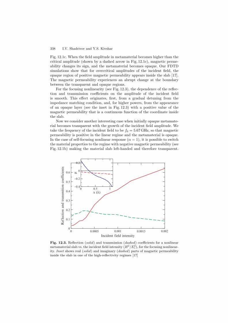
338 I.V. Shadrivov and Y.S. Kivshar
Fig. 12.1c. When the field amplitude in metamaterial becomes higher than thecritical amplitude (shown by a dashed arrow in Fig. 12.1c), magnetic perme-ability changes its sign, and the metamaterial becomes opaque. Our FDTDsimulations show that for overcritical amplitudes of the incident field, theopaque region of positive magnetic permeability appears inside the slab [17].The magnetic permeability experiences an abrupt change at the boundarybetween the transparent and opaque regions.
For the focusing nonlinearity (see Fig. 12.3), the dependence of the reflec-tion and transmission coefficients on the amplitude of the incident fieldis smooth. This effect originates, first, from a gradual detuning from theimpedance matching condition, and, for higher powers, from the appearanceof an opaque layer (see the inset in Fig. 12.3) with a positive value of themagnetic permeability that is a continuous function of the coordinate insidethe slab.
Now we consider another interesting case when initially opaque metamate-rial becomes transparent with the growth of the incident field amplitude. Wetake the frequency of the incident field to be f0 = 5.67 GHz, so that magneticpermeability is positive in the linear regime and the metamaterial is opaque.In the case of self-focusing nonlinear response (α = 1), it is possible to switchthe material properties to the regime with negative magnetic permeability (seeFig. 12.1b) making the material slab left-handed and therefore transparent.
0 0.0005 0.001 0.0015 0.002
Incident field intensity
0
0.1
0.2
0.3
0.4
0.5
0.6
Ref
lect
ion
and
tran
smitio
n co
effici
ents
0 0.5 1x (λ)
−0.4
−0.2
0
0.2
µ
Fig. 12.3. Reflection (solid) and transmission (dashed) coefficients for a nonlinearmetamaterial slab vs. the incident field intensity (H2/E2
c ), for the focusing nonlinear-ity. Inset shows real (solid) and imaginary (dashed) parts of magnetic permeabilityinside the slab in one of the high-reflectivity regimes [17]

12 Nonlinear Effects in Left-Handed Metamaterials 339
0 200 400 600 800Time (periods)
0
2e−06
4e−06In
tens
ity
−1 −0.5 0 0.5 1 1.50
1e−05
2e−05
Inte
nsity
−1 −0.5 0 0.5 1 1.5x (λ)x (λ)
0
1e−05
2e−05
(a)
(b) (c)
Magnetic field Electric field
Fig. 12.4. (a) Reflected (solid) and incident (dashed) wave intensity, (H2/E2c ), for
small amplitudes of the incident wave (i.e., in the linear regime). (b,c) Distributionof the magnetic and electric fields at the end of simulation time; the metamaterialis shaded [17]
Moreover, one can expect the formation of self-focused localized states insidethe composite, the effect which was previously discussed for the interac-tion of the intense electromagnetic waves with over-dense plasma [18–20].Figure 12.4a shows the temporal evolution of the incident and reflected waveintensities for small input intensities – this case corresponds to the linearregime. The reflection coefficient reaches a steady-state after approximately100 periods. The spatial distribution of the electric and magnetic fields at theend of simulation time is shown in Fig. 12.4b, c, respectively.
In a strongly nonlinear regime, we observe the effect of the dynamicalself-modulation of the reflected electromagnetic wave that results from theperiodic generation of the self-localized states inside the metamaterial (seeFig. 12.5). Such localized states resemble temporal solitons, which transfer theenergy away from the interface. Figure 12.5c shows an example when twolocalized states enter the metamaterial. These localized states appear on thejumps of the magnetic permeability and, as a result, we observe a change ofthe sign of the electric field derivative at the maximum of the soliton intensity,and subsequent appearance of transparent regions in the metamaterial. Unlikeall previous cases, the field structure in this regime does not reach any steady-state for high enough intensities of the incident field.
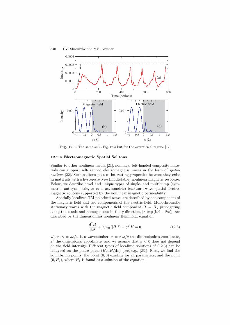
340 I.V. Shadrivov and Y.S. Kivshar
0 200 400 600 800Time (periods)
0
0.0001
0.0002
0.0003
0.0004
Inte
nsity
−1 −0.5 0 0.5 1 1.50
0.001
Inte
nsity
−1 −0.5 0 0.5 1 1.50
0.001
(a)
(b) (c)
Magnetic field Electric field
x (λ) x (λ)
Fig. 12.5. The same as in Fig. 12.4 but for the overcritical regime [17]
12.2.4 Electromagnetic Spatial Solitons
Similar to other nonlinear media [21], nonlinear left-handed composite mate-rials can support self-trapped electromagnetic waves in the form of spatialsolitons [22]. Such solitons possess interesting properties because they existin materials with a hysteresis-type (multistable) nonlinear magnetic response.Below, we describe novel and unique types of single- and multihump (sym-metric, antisymmetric, or even asymmetric) backward-wave spatial electro-magnetic solitons supported by the nonlinear magnetic permeability.
Spatially localized TM-polarized waves are described by one component ofthe magnetic field and two components of the electric field. Monochromaticstationary waves with the magnetic field component H = Hy propagatingalong the z-axis and homogeneous in the y-direction, [∼ exp (iωt − ikz)], aredescribed by the dimensionless nonlinear Helmholtz equation
d2H
dx2+ [εµeff(|H|2) − γ2]H = 0, (12.3)
where γ = kc/ω is a wavenumber, x = x′ω/c the dimensionless coordinate,x′ the dimensional coordinate, and we assume that ε < 0 does not dependon the field intensity. Different types of localized solutions of (12.3) can beanalyzed on the phase plane (H,dH/dx) (see, e.g., [23]). First, we find theequilibrium points: the point (0, 0) existing for all parameters, and the point(0,H1), where H1 is found as a solution of the equation
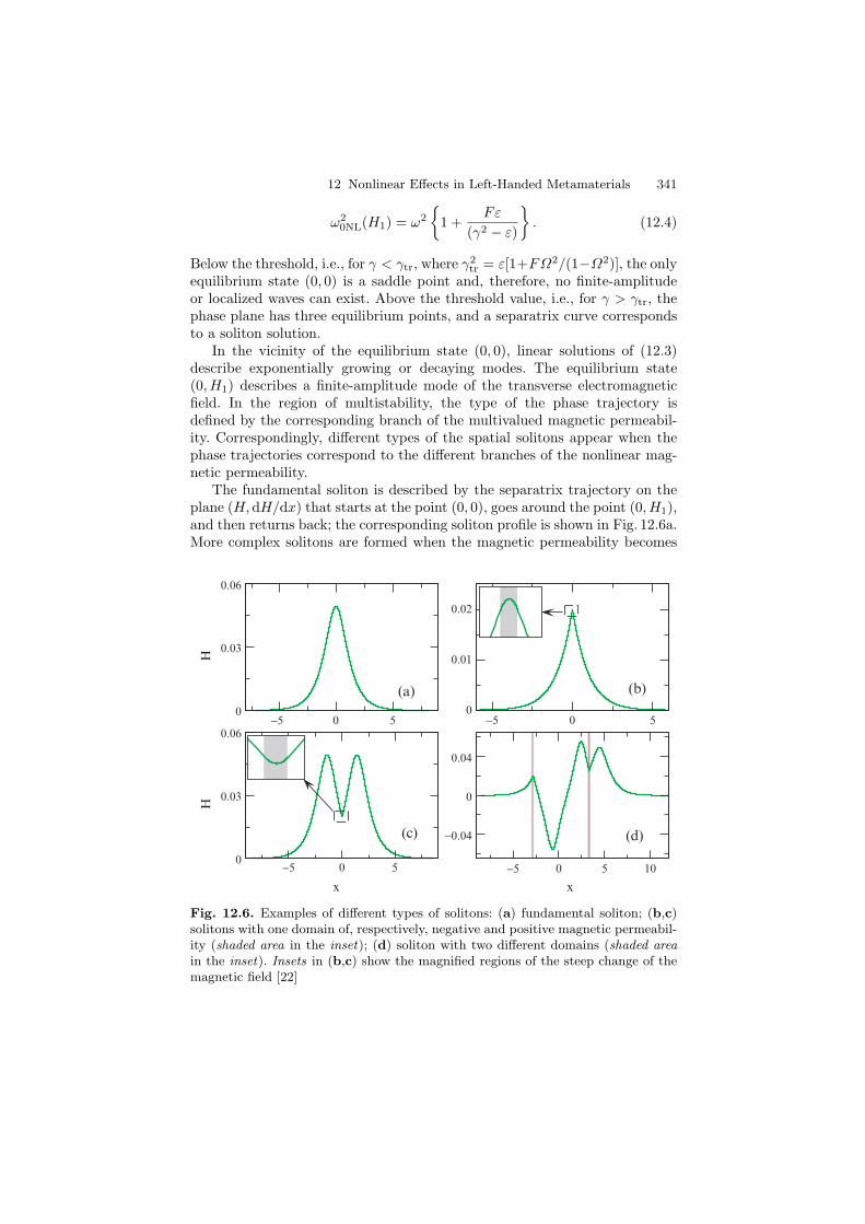
12 Nonlinear Effects in Left-Handed Metamaterials 341
ω20NL(H1) = ω2
1 +
Fε
(γ2 − ε)
. (12.4)
Below the threshold, i.e., for γ < γtr, where γ2tr = ε[1+FΩ2/(1−Ω2)], the only
equilibrium state (0, 0) is a saddle point and, therefore, no finite-amplitudeor localized waves can exist. Above the threshold value, i.e., for γ > γtr, thephase plane has three equilibrium points, and a separatrix curve correspondsto a soliton solution.
In the vicinity of the equilibrium state (0, 0), linear solutions of (12.3)describe exponentially growing or decaying modes. The equilibrium state(0,H1) describes a finite-amplitude mode of the transverse electromagneticfield. In the region of multistability, the type of the phase trajectory isdefined by the corresponding branch of the multivalued magnetic permeabil-ity. Correspondingly, different types of the spatial solitons appear when thephase trajectories correspond to the different branches of the nonlinear mag-netic permeability.
The fundamental soliton is described by the separatrix trajectory on theplane (H,dH/dx) that starts at the point (0, 0), goes around the point (0,H1),and then returns back; the corresponding soliton profile is shown in Fig. 12.6a.More complex solitons are formed when the magnetic permeability becomes
−5 0 50
0.03
0.06
H
−5 0 50
0.01
0.02
−5 0 5
x
0
0.03
0.06
H
−5 0 5 10
x
−0.04
0
0.04
(a) (b)
(c) (d)
Fig. 12.6. Examples of different types of solitons: (a) fundamental soliton; (b,c)solitons with one domain of, respectively, negative and positive magnetic permeabil-ity (shaded area in the inset); (d) soliton with two different domains (shaded areain the inset). Insets in (b,c) show the magnified regions of the steep change of themagnetic field [22]
342 I.V. Shadrivov and Y.S. Kivshar
multivalued and is described by several branches. Then, soliton solutions areobtained by switching between the separatrix trajectories corresponding todifferent (upper and lower) branches of magnetic permeability. Continuity ofthe tangential components of the electric and magnetic fields at the boundariesof the domains with different values of magnetic permeability implies thatboth H and dH/dx should be continuous. As a result, the transitions betweendifferent phase trajectories should be continuous.
Figure 12.6b, c shows two examples of more complex solitons correspond-ing to a single jump to the lower branch of µeff(H) (see Fig. 12.1c) and to theupper branch of µeff(H), respectively. The insets show the magnified domainsof a steep change of the magnetic field. Both the magnetic field and its deriv-ative, proportional to the tangential component of the electric field, are con-tinuous. The shaded areas show the domains where the value of magneticpermeability changes. Figure 12.6d shows an example of more complicatedmultihump soliton which includes two domains of the effective magnetic per-meability, one described by the lower branch, and the other one – by the upperbranch. In a similar way, we can find more complicated solitons with differentnumber of domains of the magnetic permeability.
We note that some of the phase trajectories have discontinuity of thederivative at H = 0 caused by infinite values of the magnetic permeability atthe corresponding branch of µeff(H). This is because we use a lossless modelof left-handed nonlinear composites for the analysis of the soliton solutions.In more realistic models that include losses, the region of multistability doesnot extend to the point H = 0, and in this limit the magnetic permeabilityremains a single-valued function of the magnetic field [9].
For the multivalued nonlinear magnetic response, the domains withdifferent values of magnetic permeability “excited” by the spatial solitoncan be viewed as the effective induced left-handed waveguides which makepossible the existence of single- and multihump solitons. Due to the existenceof such domains, the solitons can be not only symmetric, but also antisym-metric and even asymmetric. Formally, the size of an effective domain canbe much smaller than the wavelength and, therefore, there exists an applica-bility limit for the obtained results to describe nonlinear waves in realisticstructures.
When the infilling dielectric of the structure displays self-focusingnonlinear response, and we consider frequencies Ω = ω/ω0 < 1, then wecan find dark solitons in such a system, i.e., localized dips on the finite-amplitude background wave [21]. Similar to bright solitons, there exist bothfundamental dark solitons and dark solitons with domains of different valuesof magnetic permeability. For self-defocusing nonlinearity and Ω < 1, mag-netic permeability is a single-valued function, and such a nonlinear responsecan support dark solitons as well, whereas for self-focusing dielectric, we haveΩ > 1 and no dark solitons can exist.
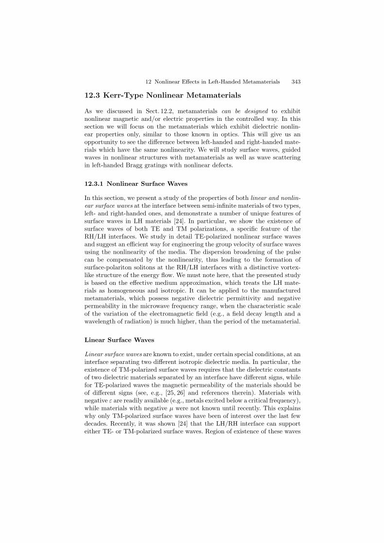
12 Nonlinear Effects in Left-Handed Metamaterials 343
12.3 Kerr-Type Nonlinear Metamaterials
As we discussed in Sect. 12.2, metamaterials can be designed to exhibitnonlinear magnetic and/or electric properties in the controlled way. In thissection we will focus on the metamaterials which exhibit dielectric nonlin-ear properties only, similar to those known in optics. This will give us anopportunity to see the difference between left-handed and right-handed mate-rials which have the same nonlinearity. We will study surface waves, guidedwaves in nonlinear structures with metamaterials as well as wave scatteringin left-handed Bragg gratings with nonlinear defects.
12.3.1 Nonlinear Surface Waves
In this section, we present a study of the properties of both linear and nonlin-ear surface waves at the interface between semi-infinite materials of two types,left- and right-handed ones, and demonstrate a number of unique features ofsurface waves in LH materials [24]. In particular, we show the existence ofsurface waves of both TE and TM polarizations, a specific feature of theRH/LH interfaces. We study in detail TE-polarized nonlinear surface wavesand suggest an efficient way for engineering the group velocity of surface wavesusing the nonlinearity of the media. The dispersion broadening of the pulsecan be compensated by the nonlinearity, thus leading to the formation ofsurface-polariton solitons at the RH/LH interfaces with a distinctive vortex-like structure of the energy flow. We must note here, that the presented studyis based on the effective medium approximation, which treats the LH mate-rials as homogeneous and isotropic. It can be applied to the manufacturedmetamaterials, which possess negative dielectric permittivity and negativepermeability in the microwave frequency range, when the characteristic scaleof the variation of the electromagnetic field (e.g., a field decay length and awavelength of radiation) is much higher, than the period of the metamaterial.
Linear Surface Waves
Linear surface waves are known to exist, under certain special conditions, at aninterface separating two different isotropic dielectric media. In particular, theexistence of TM-polarized surface waves requires that the dielectric constantsof two dielectric materials separated by an interface have different signs, whilefor TE-polarized waves the magnetic permeability of the materials should beof different signs (see, e.g., [25, 26] and references therein). Materials withnegative ε are readily available (e.g., metals excited below a critical frequency),while materials with negative µ were not known until recently. This explainswhy only TM-polarized surface waves have been of interest over the last fewdecades. Recently, it was shown [24] that the LH/RH interface can supporteither TE- or TM-polarized surface waves. Region of existence of these waves
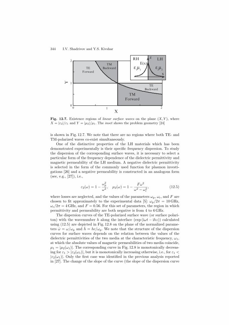
344 I.V. Shadrivov and Y.S. Kivshar
0 2X
0
1
2
YTM
Backward
TE Backward
TE Forward
TM Forward
RH LH
x
zE(x)
ε1µ1 ε2µ2
1
Fig. 12.7. Existence regions of linear surface waves on the plane (X, Y ), whereX = |ε2|/ε1 and Y = |µ2|/µ1. The inset shows the problem geometry [24]
is shown in Fig. 12.7. We note that there are no regions where both TE- andTM-polarized waves co-exist simultaneously.
One of the distinctive properties of the LH materials which has beendemonstrated experimentally is their specific frequency dispersion. To studythe dispersion of the corresponding surface waves, it is necessary to select aparticular form of the frequency dependence of the dielectric permittivity andmagnetic permeability of the LH medium. A negative dielectric permittivityis selected in the form of the commonly used function for plasmon investi-gations [26] and a negative permeability is constructed in an analogous form(see, e.g., [27]), i.e.,
ε2(ω) = 1 −ω2
p
ω2, µ2(ω) = 1 − Fω2
ω2 − ω2r
, (12.5)
where losses are neglected, and the values of the parameters ωp, ωr, and F arechosen to fit approximately to the experimental data [5]: ωp/2π = 10 GHz,ωr/2π = 4 GHz, and F = 0.56. For this set of parameters, the region in whichpermittivity and permeability are both negative is from 4 to 6 GHz.
The dispersion curves of the TE-polarized surface wave (or surface polari-ton) with the wavenumber h along the interface (exp (iωt − ihz)) calculatedusing (12.5) are depicted in Fig. 12.8 on the plane of the normalized parame-ters ω = ω/ωp and h = hc/ωp. We note that the structure of the dispersioncurves for surface waves depends on the relation between the values of thedielectric permittivities of the two media at the characteristic frequency, ω1,at which the absolute values of magnetic permeabilities of two media coincide,µ1 = |µ2(ω1)|. The corresponding curve in Fig. 12.8 is monotonically decreas-ing for ε1 > |ε2(ω1)|, but it is monotonically increasing otherwise, i.e., for ε1 <|ε2(ω1)|. Only the first case was identified in the previous analysis reportedin [27]. The change of the slope of the curve (the slope of the dispersion curve
12 Nonlinear Effects in Left-Handed Metamaterials 345
0.5 1 1.5 2h
0.45
0.46
0.47
0.48
0.49
0.5
ω
ε1 = 5
ε1 = 2
ε1 = 3.5
Fig. 12.8. Dispersion curves of the TE-polarized surface waves, for different valuesof ε1, shown for the normalized values ω = ω/ωp are h = hc/ωp. Dotted curvesmarks the dependence h = ω
√ε2µ2. Dashed line is the critical frequency ω1 [24]
represents the group velocity) with the variation of the dielectric permittivityof the RH medium can be used for group velocity engineering [24].
The critical value of dielectric permittivity |ε2(ω1)| for the case of a non-magnetic RH medium (µ1 = 1) is found from the dispersion relations for thesurface waves, and it has the form [24]
εc = |ε2(ω1)| =(
1 − F
2
)(ωp
ωr
)2
− 1. (12.6)
For the parameters specified above, this critical value is εc = 3.5.The change of the dispersion curve from monotonically increasing to
monotonically decreasing, shown in Fig. 12.8, is connected with a change inthe direction of the total power flow in the wave, as discussed later.
Nonlinear LH/RH Interface
Nonlinear surface waves at an interface separating two conventional dielectricmedia have been analyzed extensively for several decades starting from thepioneering paper [28]. In brief, one of the major findings of those studies isthat the TE-polarized surface waves can exist at the interface separating twoRH media provided that at least one of these is nonlinear, but that no surfacewaves exist in the linear limit.
In this section, we study TE-polarized nonlinear surface waves assumingthat both media are nonlinear, i.e., they display a Kerr-type nonlinearity intheir dielectric properties, namely
εNL1,2 = ε1,2 + α1,2|E|2, (12.7)
where the first term characterizes the linear properties, i.e., those in the limitof vanishing wave amplitude.
346 I.V. Shadrivov and Y.S. Kivshar
For a conventional (or right-handed) dielectric medium, positive α1
corresponds to a self-focusing nonlinear material, while negative α1 character-izes defocusing effects in the beam propagation. However, this classificationbecomes reversed in the case of LH materials and, for example, a self-focusingLH medium corresponds to negative α2. Indeed, taking into account rela-tion (12.7), we write the equation for the case of the TE-polarized wave innonlinear media as follows:
∂2E
∂z2+
∂2E
∂x2+
(ω
c
)2 (εµ + µα|E|2
)E = 0. (12.8)
According to (12.8), the sign of the product µα determines the type of nonlin-ear self-action effects which occur. Therefore, in an LH medium with negativeµ2 all nonlinear effects are opposite to those in RH media with positive µ1, forthe same α. Later, we assume for definiteness that both LH and RH materialspossess self-focusing properties, i.e., α1 > 0 and α2 < 0.
We look for the stationary solutions of (12.8) in the form E1,2(x, z) =Ψ1,2(x) exp (ihz). Then, the profiles of the spatially localized wave envelopesΨ1,2(x) are found as [29]
Ψ1,2(x) =(
η1,2
√2/α1,2µ1,2
)sech[η1,2(x − x1,2)], (12.9)
where η1,2 = κ1,2c/ω are normalized transverse wave numbers, x1,2 are centersof the sech-functions which should be chosen to satisfy the continuity of thetangential components of the electric and magnetic fields at the interface.
The total energy flow in the mode along the interface in this wave can bewritten in the form
P = P0γ
[η1α2µ2
α1µ21
+η2
µ2+
η1
µ1
(1 − α2µ2
α1µ1
)tanh (η1x1)
], (12.10)
where P0 = c2/4πωα2µ2, and γ = hc/ω is the normalized wave number. Wenow consider the surface waves in the nondegenerate case when only α1 = |α2|.The dependence of the normalized energy flux P/P0 on the parameter γ isshown in Fig. 12.9 for the cases when linear waves are forward or backward,respectively. Corresponding transverse wave structures (electric field ampli-tudes) are shown in the insets.
Nonlinear LH/Linear RH Interface
Next, we consider surface waves propagating along an interface between alinear RH and a nonlinear LH media (see the inset in Fig. 12.10) having a non-linear coefficient α2 which is negative and, thus, displaying the self-focusingproperties. The transverse structure of the stationary surface wave has theform:
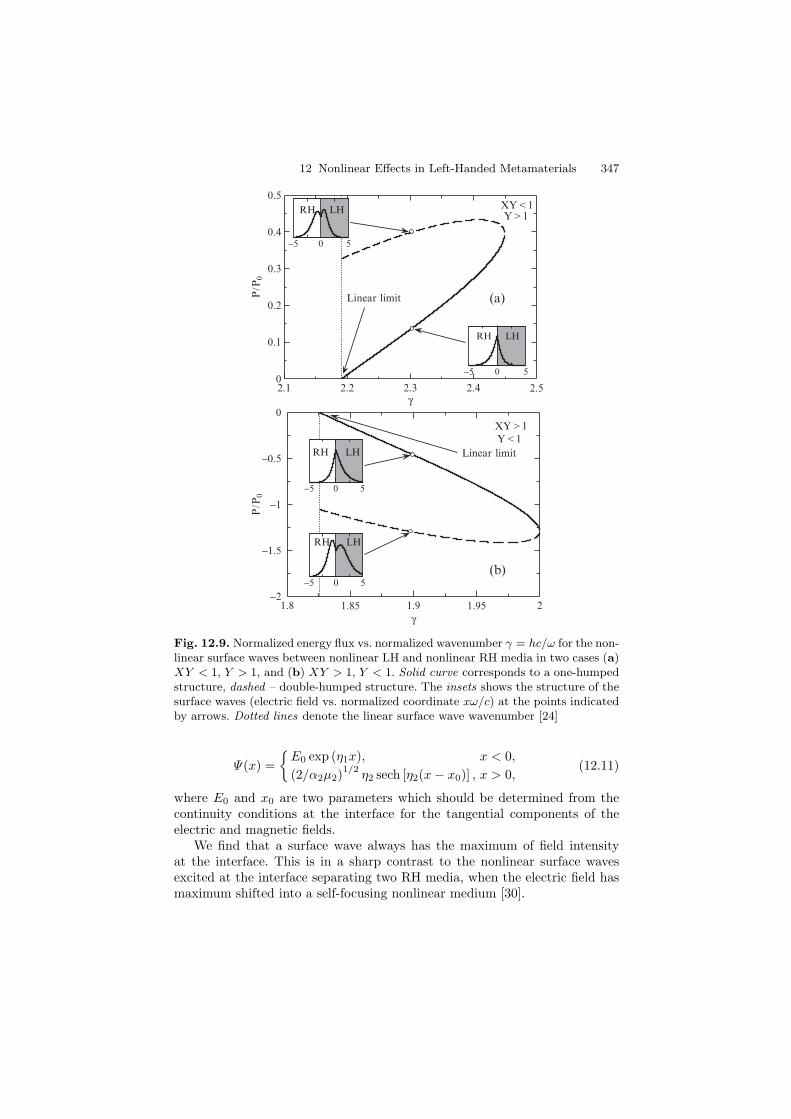
12 Nonlinear Effects in Left-Handed Metamaterials 347
2.1 2.2 2.3 2.4 2.5γ
0
0.1
0.2
0.3
0.4
0.5
P / P
0
−5 0 5
−5 0 5
XY < 1Y > 1
RH LH
RH LH
(a)Linear limit
1.8 1.85 1.9 1.95 2γ
−2
−1.5
−1
−0.5
0
P / P
0
−5 0 5
−5 0 5
XY > 1Y < 1
RH LH
RH LH
(b)
Linear limit
Fig. 12.9. Normalized energy flux vs. normalized wavenumber γ = hc/ω for the non-linear surface waves between nonlinear LH and nonlinear RH media in two cases (a)XY < 1, Y > 1, and (b) XY > 1, Y < 1. Solid curve corresponds to a one-humpedstructure, dashed – double-humped structure. The insets shows the structure of thesurface waves (electric field vs. normalized coordinate xω/c) at the points indicatedby arrows. Dotted lines denote the linear surface wave wavenumber [24]
Ψ(x) =
E0 exp (η1x), x < 0,
(2/α2µ2)1/2
η2 sech [η2(x − x0)] , x > 0,(12.11)
where E0 and x0 are two parameters which should be determined from thecontinuity conditions at the interface for the tangential components of theelectric and magnetic fields.
We find that a surface wave always has the maximum of field intensityat the interface. This is in a sharp contrast to the nonlinear surface wavesexcited at the interface separating two RH media, when the electric field hasmaximum shifted into a self-focusing nonlinear medium [30].
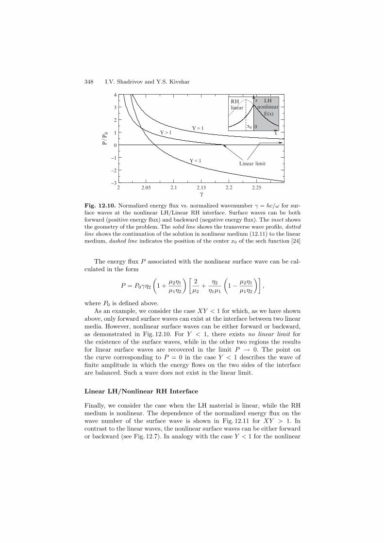
348 I.V. Shadrivov and Y.S. Kivshar
2 2.05 2.1 2.15 2.2 2.25γ
−3
−2
−1
0
1
2
3
4
P / P
0 x
z LH nonlinear
RH linear
E(x)
0x0Y = 1Y > 1
Y < 1 Linear limit
Fig. 12.10. Normalized energy flux vs. normalized wavenumber γ = hc/ω for sur-face waves at the nonlinear LH/Linear RH interface. Surface waves can be bothforward (positive energy flux) and backward (negative energy flux). The inset showsthe geometry of the problem. The solid line shows the transverse wave profile, dottedline shows the continuation of the solution in nonlinear medium (12.11) to the linearmedium, dashed line indicates the position of the center x0 of the sech function [24]
The energy flux P associated with the nonlinear surface wave can be cal-culated in the form
P = P0γη2
(1 +
µ2η1
µ1η2
)[2µ2
+η2
η1µ1
(1 − µ2η1
µ1η2
)],
where P0 is defined above.As an example, we consider the case XY < 1 for which, as we have shown
above, only forward surface waves can exist at the interface between two linearmedia. However, nonlinear surface waves can be either forward or backward,as demonstrated in Fig. 12.10. For Y < 1, there exists no linear limit forthe existence of the surface waves, while in the other two regions the resultsfor linear surface waves are recovered in the limit P → 0. The point onthe curve corresponding to P = 0 in the case Y < 1 describes the wave offinite amplitude in which the energy flows on the two sides of the interfaceare balanced. Such a wave does not exist in the linear limit.
Linear LH/Nonlinear RH Interface
Finally, we consider the case when the LH material is linear, while the RHmedium is nonlinear. The dependence of the normalized energy flux on thewave number of the surface wave is shown in Fig. 12.11 for XY > 1. Incontrast to the linear waves, the nonlinear surface waves can be either forwardor backward (see Fig. 12.7). In analogy with the case Y < 1 for the nonlinear
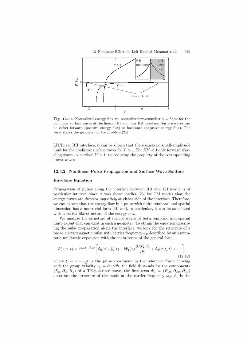
12 Nonlinear Effects in Left-Handed Metamaterials 349
642 8γ
0
P / P
0 x
z LH linear
RH nonlinear
E(x)
0Y = 1
Y > 1
Y < 1
Linear limit
Fig. 12.11. Normalized energy flux vs. normalized wavenumber γ = hc/ω for thenonlinear surface waves at the linear LH/nonlinear RH interface. Surface waves canbe either forward (positive energy flux) or backward (negative energy flux). Theinset shows the geometry of the problem [24]
LH/linear RH interface, it can be shown that there exists no small-amplitudelimit for the nonlinear surface waves for Y > 1. For XY < 1 only forward trav-eling waves exist when Y > 1, reproducing the property of the correspondinglinear waves.
12.3.2 Nonlinear Pulse Propagation and Surface-Wave Solitons
Envelope Equation
Propagation of pulses along the interface between RH and LH media is ofparticular interest, since it was shown earlier [25] for TM modes that theenergy fluxes are directed oppositely at either side of the interface. Therefore,we can expect that the energy flow in a pulse with finite temporal and spatialdimension has a nontrivial form [31] and, in particular, it can be associatedwith a vortex-like structure of the energy flow.
We analyze the structure of surface waves of both temporal and spatialfinite extent that can exist in such a geometry. To obtain the equation describ-ing the pulse propagation along the interface, we look for the structure of abroad electromagnetic pulse with carrier frequency ω0 described by an asymp-totic multiscale expansion with the main terms of the general form
Ψ(z, x, t) = eiω0t−ih0z
[Ψ0(x)A(ξ, t) − iΨ1(x)
∂A(ξ, t)∂ξ
+ Ψ2(x, ξ, t) + · · ·]
,
(12.12)where ξ = z − vgt is the pulse coordinate in the reference frame movingwith the group velocity vg = ∂ω/∂h, the field Ψ stands for the components(Ey,Hx,Hz) of a TE-polarized wave, the first term Ψ0 = (Ey0,Hx0,Hz0)describes the structure of the mode at the carrier frequency ω0, Ψ1 is the
350 I.V. Shadrivov and Y.S. Kivshar
first-order term of the asymptotic series which can be found as Ψ1 = ∂Ψ0/∂h,and Ψ2 is the second-order term. Here A is the pulse envelope, h0 is the wavenumber corresponding to the carrier frequency ω0. Substituting (12.12) into(12.8) and using the Fredholm alternative theorem [32], one can obtain theequation for the evolution of the field envelope
i∂A
∂t+
δ
2∂2A
∂ξ2− ω2(h)|A2|A = 0, (12.13)
where the coefficient δ = ∂2ω/∂h2 stands for the group-velocity dispersion(GVD) which determines the pulse broadening and can be calculated fromthe dispersion relations, ω2(h) =
(∂ωNL/∂A2
)|A=0 is the effective nonlinear
coefficient calculated with the help of the nonlinear dispersion relation. Thenonlinear Schrodinger (NLS) equation has a solution in the form of a brightsoliton localized at the interface, provided the GVD (δ) has the oppositesign to the sign of the nonlinear coefficient (ω2) (see, e.g., [21] and referencestherein). The existence of the surface polariton solitons has been predicted ina number of structures supporting nonlinear guided waves (see, e.g., [33] andreferences therein).
The effective nonlinear coefficient for the case of an interface between thenonlinear LH medium and the linear RH medium, can be found in the form
ω2(h) = − αµ1κ1κ2ω2
4hc2(ε2µ2 − ε1µ1)dω
dh. (12.14)
The signs of the group velocity dω/dh and of the parameter δ can be deter-mined from the Fig. 12.8. As a result, for any reasonable values of dielectricpermittivity and magnetic permeability of the RH medium, there exists arange of frequencies for which ω2 · δ < 0, indicating the possibility of excitingsurface polariton solitons.
To study the energy flow in such a surface-polariton soliton, we use theasymptotic expansions (12.12) for the field components, and we obtain theenergy flow structure described by their components
Sz =c2h0
8πω0µE2
0 |A|2 , (12.15)
Sx =c2
8πω0µ
[∂E0
∂h
∂E0
∂x− E0
(∂2E0
∂h∂x− vgr
ω0
∂E0
∂x
)]Re
(A
∂A∗
∂ξ
), (12.16)
The structure of the Poynting vector in the surface-wave pulse is shown inFig. 12.12, where it is clearly seen that the energy rotates in the localizedregion creating a vortex-type energy distribution in the wave. The differencebetween the Poynting vector |Sz| integrated over the RH medium and thatcalculated for the LH medium determines the resulting group velocity of thesurface wave packet.
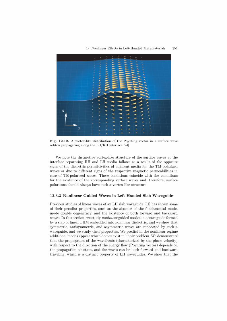
12 Nonlinear Effects in Left-Handed Metamaterials 351
X
Z
Fig. 12.12. A vortex-like distribution of the Poynting vector in a surface wavesoliton propagating along the LH/RH interface [24]
We note the distinctive vortex-like structure of the surface waves at theinterface separating RH and LH media follows as a result of the oppositesigns of the dielectric permittivities of adjacent media for the TM-polarizedwaves or due to different signs of the respective magnetic permeabilities incase of TE-polarized waves. These conditions coincide with the conditionsfor the existence of the corresponding surface waves and, therefore, surfacepolaritons should always have such a vortex-like structure.
12.3.3 Nonlinear Guided Waves in Left-Handed Slab Waveguide
Previous studies of linear waves of an LH slab waveguide [31] has shown someof their peculiar properties, such as the absence of the fundamental mode,mode double degeneracy, and the existence of both forward and backwardwaves. In this section, we study nonlinear guided modes in a waveguide formedby a slab of linear LHM embedded into nonlinear dielectric, and we show thatsymmetric, antisymmetric, and asymmetric waves are supported by such awaveguide, and we study their properties. We predict in the nonlinear regimeadditional modes appear which do not exist in linear problem. We demonstratethat the propagation of the wavefronts (characterized by the phase velocity)with respect to the direction of the energy flow (Poynting vector) depends onthe propagation constant, and the waves can be both forward and backwardtraveling, which is a distinct property of LH waveguides. We show that the
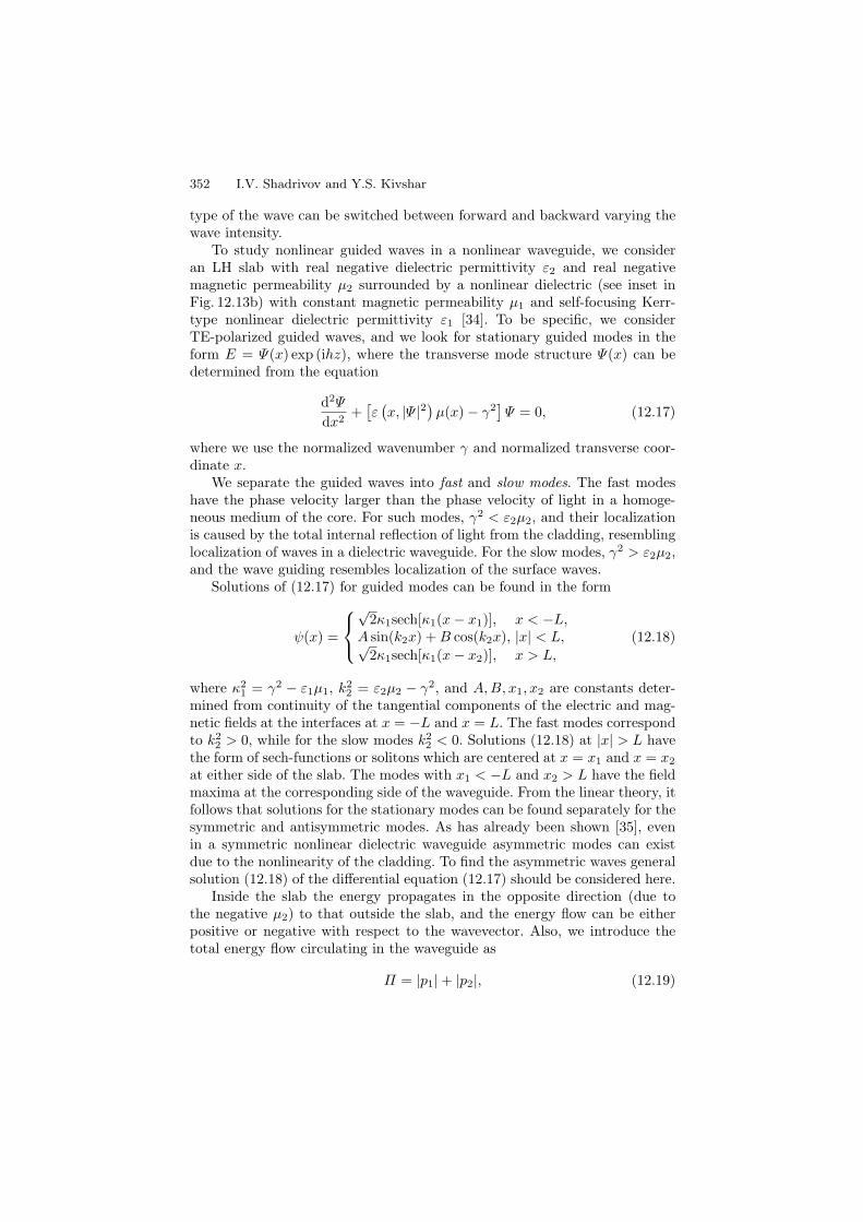
352 I.V. Shadrivov and Y.S. Kivshar
type of the wave can be switched between forward and backward varying thewave intensity.
To study nonlinear guided waves in a nonlinear waveguide, we consideran LH slab with real negative dielectric permittivity ε2 and real negativemagnetic permeability µ2 surrounded by a nonlinear dielectric (see inset inFig. 12.13b) with constant magnetic permeability µ1 and self-focusing Kerr-type nonlinear dielectric permittivity ε1 [34]. To be specific, we considerTE-polarized guided waves, and we look for stationary guided modes in theform E = Ψ(x) exp (ihz), where the transverse mode structure Ψ(x) can bedetermined from the equation
d2Ψ
dx2+
[ε(x, |Ψ |2
)µ(x) − γ2
]Ψ = 0, (12.17)
where we use the normalized wavenumber γ and normalized transverse coor-dinate x.
We separate the guided waves into fast and slow modes. The fast modeshave the phase velocity larger than the phase velocity of light in a homoge-neous medium of the core. For such modes, γ2 < ε2µ2, and their localizationis caused by the total internal reflection of light from the cladding, resemblinglocalization of waves in a dielectric waveguide. For the slow modes, γ2 > ε2µ2,and the wave guiding resembles localization of the surface waves.
Solutions of (12.17) for guided modes can be found in the form
ψ(x) =
⎧⎨⎩
√2κ1sech[κ1(x − x1)], x < −L,
A sin(k2x) + B cos(k2x), |x| < L,√2κ1sech[κ1(x − x2)], x > L,
(12.18)
where κ21 = γ2 − ε1µ1, k2
2 = ε2µ2 − γ2, and A,B, x1, x2 are constants deter-mined from continuity of the tangential components of the electric and mag-netic fields at the interfaces at x = −L and x = L. The fast modes correspondto k2
2 > 0, while for the slow modes k22 < 0. Solutions (12.18) at |x| > L have
the form of sech-functions or solitons which are centered at x = x1 and x = x2
at either side of the slab. The modes with x1 < −L and x2 > L have the fieldmaxima at the corresponding side of the waveguide. From the linear theory, itfollows that solutions for the stationary modes can be found separately for thesymmetric and antisymmetric modes. As has already been shown [35], evenin a symmetric nonlinear dielectric waveguide asymmetric modes can existdue to the nonlinearity of the cladding. To find the asymmetric waves generalsolution (12.18) of the differential equation (12.17) should be considered here.
Inside the slab the energy propagates in the opposite direction (due tothe negative µ2) to that outside the slab, and the energy flow can be eitherpositive or negative with respect to the wavevector. Also, we introduce thetotal energy flow circulating in the waveguide as
Π = |p1| + |p2|, (12.19)
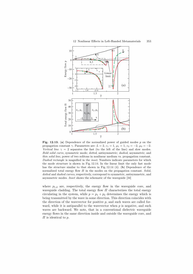
12 Nonlinear Effects in Left-Handed Metamaterials 353
1 1.5 2γ
−30
−20
−10
0
10
Ene
rgy
f low
p
1.2 1.4 1.6
−4
−2
0
2
1
8,3 4
9
2,7
6
5
(a)
Linear limit
83
1 1.5 2γ
0
10
20
30
40
50
Tot
al e
nerg
y f l
ow Π
x
z
L−L
ε1, µ1 ε1, µ1ε2 µ2
(b)
Fig. 12.13. (a) Dependence of the normalized power of guided modes p on thepropagation constant γ. Parameters are: L = 2, ε1 = 1, µ1 = 1, ε2 = −2, µ2 = −2.Vertical line γ = 2 separates the fast (to the left of the line) and slow modes.Bold solid curve, symmetric mode; dotted, antisymmetric; dashed, asymmetric; andthin solid line, power of two solitons in nonlinear medium vs. propagation constant.Dashed rectangle is magnified in the inset. Numbers indicate parameters for whichthe mode structure is shown in Fig. 12.14. In the linear limit the only fast modehas the structure similar to that shown in Fig. 12.14 (4). (b) Dependence of thenormalized total energy flow Π in the modes on the propagation constant. Solid,dotted and dashed curves, respectively, correspond to symmetric, antisymmetric, andasymmetric modes. Inset shows the schematic of the waveguide [34]
where p1,2 are, respectively, the energy flow in the waveguide core, andwaveguide cladding. The total energy flow Π characterizes the total energycirculating in the system, while p = p1 + p2 determines the energy which isbeing transmitted by the wave in some direction. This direction coincides withthe direction of the wavevector for positive p, and such waves are called for-ward, while it is antiparallel to the wavevector when p is negative, and suchwaves are backward. We note, that in a conventional dielectric waveguideenergy flows in the same direction inside and outside the waveguide core, andΠ is identical to p.
354 I.V. Shadrivov and Y.S. Kivshar
Nonlinear dispersion diagrams are shown for both fast and slow modes inFig. 12.13. The continuous dependence γ(p) is a result of the intensity depen-dent index of refraction of the waveguide cladding. Parameters in the figureare chosen in such a way that only one fast mode (close to the point 4) existsin the linear case (at low intensities; for the solution of the linear problemand for the choice of parameters see, e.g., [31]). Figure 12.13b confirms thatthere is a single mode in the linear regime, which is characterized by a van-ishingly small total energy flow. Thin solid curves in Fig. 12.13a, b shows thepower of two solitons in a homogeneous nonlinear cladding vs. the propaga-tion number. The mode structures are shown in Fig. 12.14, where each plotdemonstrates the transverse wave profile corresponding to the numbered pointin Fig. 12.13a.
The modes with the parameters close to the thin solid line (points 1, 5, 6in Fig. 12.13a) resembles two in-phase and out-of-phase solitons at either sideof the waveguide. Closer to the thin solid line the soliton centers in the non-linear media move further away from the waveguide. The symmetry breakingbifurcation appears on the symmetric mode branch. The asymmetric modecurve in the fast region ends in the symmetric mode branch (see Fig. 12.13a),while in the slow wave region the asymmetric mode disappears, when theamplitude of the wave at one interface becomes the same as the amplitude ofthe soliton on the other side of the waveguide. Two structures (points 2, 7 inFig. 12.14) obtained at the same value of the propagation constant show thepoint of the symmetry breaking, where a slight asymmetry can be seen in the
−10 10 100 0
−0.5
0
0.5
ψ
−10 0 10−2
0
2
−2
0
2
X
−2
0
2
−10
−10 10 100 0 −10 0 10−10
−10 10 100 0 −10 0 10−10
0
3
6
X
0
1
2
3
X
0
3
6
ψ
−1
0
ψ
0
1
2
1 2 3
45 6
7 8 9
Fig. 12.14. Mode structure calculated for the parameters in Fig. 12.13a, b [34]
12 Nonlinear Effects in Left-Handed Metamaterials 355
mode structure shown in the example 7 in Fig. 12.14. Symmetric and asym-metric modes can be both forward and backward traveling (p > 0 and p < 0,respectively). We note, that in contrast with nonlinear dielectric waveguidesthere is no threshold value of the mode power p transmitted in some partic-ular direction for the asymmetric modes. However, it is the total energy Π,which determines the power of the source needed to excite the wave, and theasymmetric modes have a threshold value of Π (see Fig. 12.13b).
For the parameters indicated in Fig. 12.13, only one fast symmetric guidedmode exists in the linear limit and the linear mode has a transverse structuresimilar to the one shown in Fig. 12.14 (4), while in the nonlinear regime themodes with zero, one and two nodes appear (see Fig. 12.14). At the intersectionof the curves on the nonlinear dispersion diagram with p = 0 axes, apart fromthe linear limit, the energy flow inside the waveguide core exactly compen-sates that outside the core due to the structure of such modes. We note here,that with increasing the waveguide thickness, one more symmetry breakingpoint appears on the antisymmetric mode branch, when the slab parameter Lexceeds some threshold value. Moreover, more high-order modes can be sup-ported by the structure, and the nonlinear dispersion diagram becomes morecomplicated.
The presented nonlinear characteristics of the nonlinear waves in an LHwaveguide surrounded by a Kerr-like nonlinear medium show the generalnonlinear properties of the low-order fast and slow modes, which are qual-itatively similar in other parameter regions.
12.4 Second-Order Nonlinear Effects in Metamaterials
Inclusion of elements with nonsymmetric current–voltage characteristics suchas diodes into the SRRs will result in a quadratic nonlinear response of themetamaterial [10]. This quadratic nonlinearity is responsible for the recentlyanalyzed parametric processes such as the SHG [34,36] and three-wave mixing[37]. In particular, the first analysis of SHG from a semi-infinite left-handedmedium has been briefly presented by Agranovich et al. [36], who employedthe nonlinear optics approach.
12.4.1 Second-Harmonics Generation
In this section we consider the problem of SHG during the scattering froma semi-infinite left-handed medium (or a slab of the LHM of a finite extent)and demonstrate the possibility of the exact phase-matching, quite specificfor the harmonic generation by the backward waves. With this condition, wedemonstrate that exact phase matching between a backward propagating waveof the FF and the forward propagating wave at the SH is indeed possible.
First, we will describe our model including both the electric and magneticresponses. Then, we analyze quadratic nonlinearity and the SHG process in
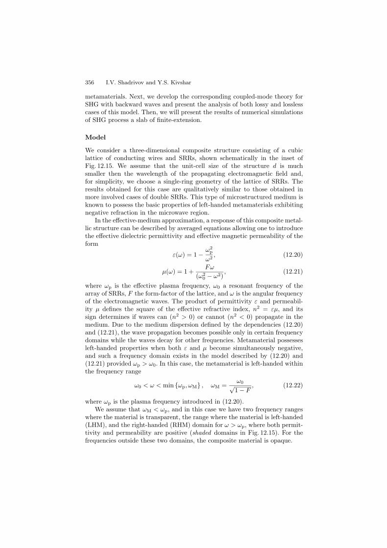
356 I.V. Shadrivov and Y.S. Kivshar
metamaterials. Next, we develop the corresponding coupled-mode theory forSHG with backward waves and present the analysis of both lossy and losslesscases of this model. Then, we will present the results of numerical simulationsof SHG process a slab of finite-extension.
Model
We consider a three-dimensional composite structure consisting of a cubiclattice of conducting wires and SRRs, shown schematically in the inset ofFig. 12.15. We assume that the unit-cell size of the structure d is muchsmaller then the wavelength of the propagating electromagnetic field and,for simplicity, we choose a single-ring geometry of the lattice of SRRs. Theresults obtained for this case are qualitatively similar to those obtained inmore involved cases of double SRRs. This type of microstructured medium isknown to possess the basic properties of left-handed metamaterials exhibitingnegative refraction in the microwave region.
In the effective-medium approximation, a response of this composite metal-lic structure can be described by averaged equations allowing one to introducethe effective dielectric permittivity and effective magnetic permeability of theform
ε(ω) = 1 −ω2
p
ω2, (12.20)
µ(ω) = 1 +Fω
(ω20 − ω2)
, (12.21)
where ωp is the effective plasma frequency, ω0 a resonant frequency of thearray of SRRs, F the form-factor of the lattice, and ω is the angular frequencyof the electromagnetic waves. The product of permittivity ε and permeabil-ity µ defines the square of the effective refractive index, n2 = εµ, and itssign determines if waves can (n2 > 0) or cannot (n2 < 0) propagate in themedium. Due to the medium dispersion defined by the dependencies (12.20)and (12.21), the wave propagation becomes possible only in certain frequencydomains while the waves decay for other frequencies. Metamaterial possessesleft-handed properties when both ε and µ become simultaneously negative,and such a frequency domain exists in the model described by (12.20) and(12.21) provided ωp > ω0. In this case, the metamaterial is left-handed withinthe frequency range
ω0 < ω < min ωp, ωM , ωM =ω0√1 − F
, (12.22)
where ωp is the plasma frequency introduced in (12.20).We assume that ωM < ωp, and in this case we have two frequency ranges
where the material is transparent, the range where the material is left-handed(LHM), and the right-handed (RHM) domain for ω > ωp, where both permit-tivity and permeability are positive (shaded domains in Fig. 12.15). For thefrequencies outside these two domains, the composite material is opaque.
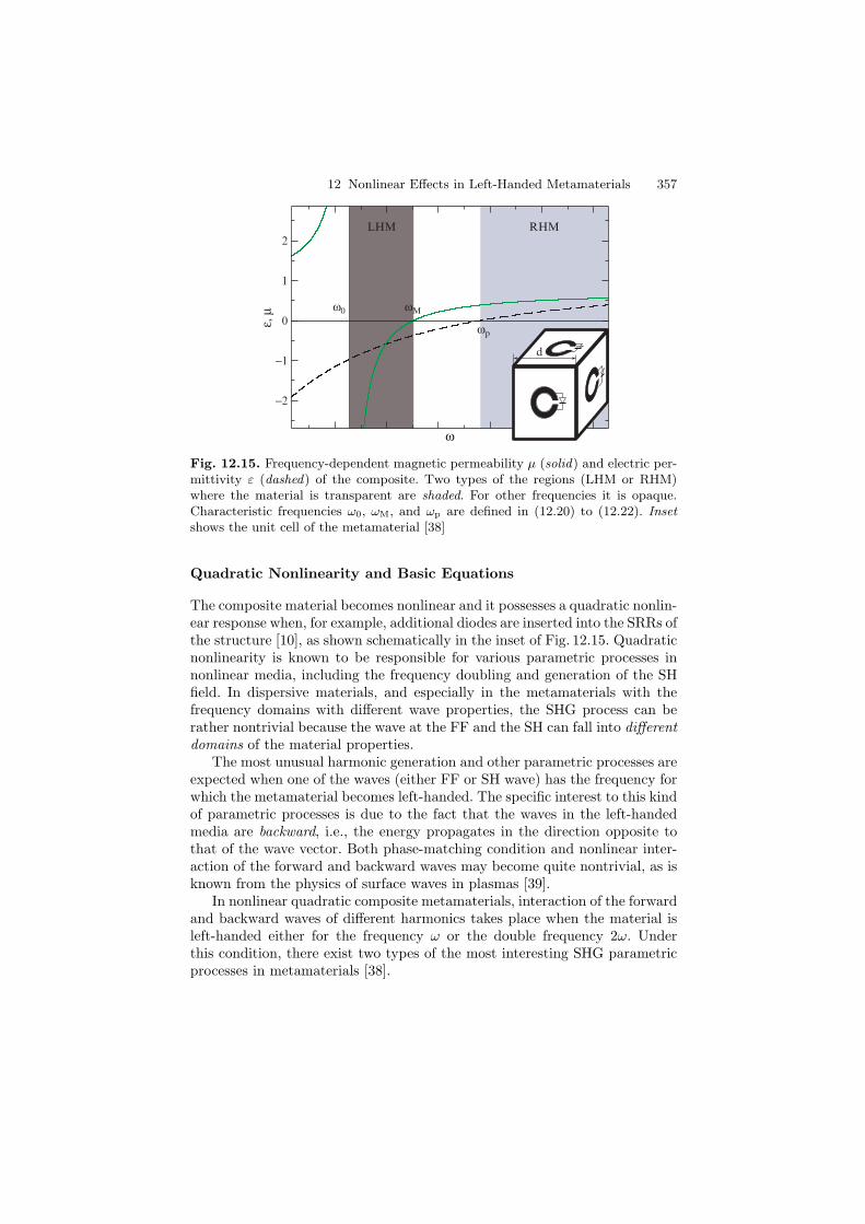
12 Nonlinear Effects in Left-Handed Metamaterials 357
ω
−2
−1
0
1
2
ε, µ ω0 ωM
ωp
LHM RHM
d
Fig. 12.15. Frequency-dependent magnetic permeability µ (solid) and electric per-mittivity ε (dashed) of the composite. Two types of the regions (LHM or RHM)where the material is transparent are shaded. For other frequencies it is opaque.Characteristic frequencies ω0, ωM, and ωp are defined in (12.20) to (12.22). Insetshows the unit cell of the metamaterial [38]
Quadratic Nonlinearity and Basic Equations
The composite material becomes nonlinear and it possesses a quadratic nonlin-ear response when, for example, additional diodes are inserted into the SRRs ofthe structure [10], as shown schematically in the inset of Fig. 12.15. Quadraticnonlinearity is known to be responsible for various parametric processes innonlinear media, including the frequency doubling and generation of the SHfield. In dispersive materials, and especially in the metamaterials with thefrequency domains with different wave properties, the SHG process can berather nontrivial because the wave at the FF and the SH can fall into differentdomains of the material properties.
The most unusual harmonic generation and other parametric processes areexpected when one of the waves (either FF or SH wave) has the frequency forwhich the metamaterial becomes left-handed. The specific interest to this kindof parametric processes is due to the fact that the waves in the left-handedmedia are backward, i.e., the energy propagates in the direction opposite tothat of the wave vector. Both phase-matching condition and nonlinear inter-action of the forward and backward waves may become quite nontrivial, as isknown from the physics of surface waves in plasmas [39].
In nonlinear quadratic composite metamaterials, interaction of the forwardand backward waves of different harmonics takes place when the material isleft-handed either for the frequency ω or the double frequency 2ω. Underthis condition, there exist two types of the most interesting SHG parametricprocesses in metamaterials [38].
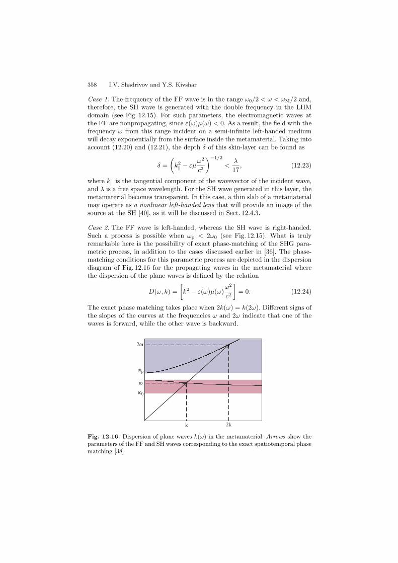
358 I.V. Shadrivov and Y.S. Kivshar
Case 1. The frequency of the FF wave is in the range ω0/2 < ω < ωM/2 and,therefore, the SH wave is generated with the double frequency in the LHMdomain (see Fig. 12.15). For such parameters, the electromagnetic waves atthe FF are nonpropagating, since ε(ω)µ(ω) < 0. As a result, the field with thefrequency ω from this range incident on a semi-infinite left-handed mediumwill decay exponentially from the surface inside the metamaterial. Taking intoaccount (12.20) and (12.21), the depth δ of this skin-layer can be found as
δ =(
k2‖ − εµ
ω2
c2
)−1/2
<λ
17, (12.23)
where k‖ is the tangential component of the wavevector of the incident wave,and λ is a free space wavelength. For the SH wave generated in this layer, themetamaterial becomes transparent. In this case, a thin slab of a metamaterialmay operate as a nonlinear left-handed lens that will provide an image of thesource at the SH [40], as it will be discussed in Sect. 12.4.3.
Case 2. The FF wave is left-handed, whereas the SH wave is right-handed.Such a process is possible when ωp < 2ω0 (see Fig. 12.15). What is trulyremarkable here is the possibility of exact phase-matching of the SHG para-metric process, in addition to the cases discussed earlier in [36]. The phase-matching conditions for this parametric process are depicted in the dispersiondiagram of Fig. 12.16 for the propagating waves in the metamaterial wherethe dispersion of the plane waves is defined by the relation
D(ω, k) =[k2 − ε(ω)µ(ω)
ω2
c2
]= 0. (12.24)
The exact phase matching takes place when 2k(ω) = k(2ω). Different signs ofthe slopes of the curves at the frequencies ω and 2ω indicate that one of thewaves is forward, while the other wave is backward.
k 2k
ω
2ω
ωp
ω0
Fig. 12.16. Dispersion of plane waves k(ω) in the metamaterial. Arrows show theparameters of the FF and SH waves corresponding to the exact spatiotemporal phasematching [38]
12 Nonlinear Effects in Left-Handed Metamaterials 359
To study the SHG process in metamaterials we consider a composite struc-ture created by arrays of wires and SRRs. To generate a nonlinear quadraticresponse of the metamaterial, we assume that each SRR contains a diode, asdepicted schematically in the inset of Fig. 12.15. The diode is described by thecurrent–voltage dependence,
I =U
Rd
(1 +
U
Uc
), (12.25)
where Uc and Rd are the parameters of the diode, and U the voltage on thediode. Equation (12.25) is valid provided U Uc, and it represents two termsof the Taylor expansion series of the realistic (and more complex) current–voltage characteristics of the diode.
Following the standard procedure, we consider two components of theelectromagnetic field at the FF ω and its SH 2ω, assuming that all othercomponents are not phase matched and therefore they give no substantialcontribution into the nonlinear parametric interaction. Subsequently, we writethe general coupled-mode equations describing the simultaneous propagationof two harmonics in the dispersive metamaterial as follows:
∆H1 + ε(ω)µ(ω)ω2
c2H1 = −σ1H∗
1H2,
∆H2 + 4ε(2ω)µ(2ω)ω2
c2H2 = −σ2H2
1, (12.26)
where the indices “1,” “2” denote the FF and SH fields, respectively; ∆ is aLaplacian, and other parameters are defined as follows:
σ1 = κ/2R(ω), σ2 = κ/R∗(ω),
κ =6π
(πa2
)3
d3c5
[ω4
0ω2
UcRdR(ω)R(2ω)
], (12.27)
where R(ω) = ω20ω2 + iγω, the asterisk stands for the complex conjugation, a
and d are, respectively, the radius of the SRRs and the period of the metama-terial, and γ is the damping coefficient of the SRR. For simplicity, we assumethat both FF and SH waves are of the same polarization, and therefore theycan be described by only one component of the magnetic field. In this case,(12.26) become scalar. In the derivation of (12.26) we take into account theLorentz–Lorenz relation between the microscopic and macroscopic magneticfields [41]. Also, it is assumed that the diode resistance Rd is much largerthan the impedance of the SRR slit, i.e., Rd 1/ωC, so that the resonantproperties of the composite are preserved.
SHG in Semi-Infinite Metamaterial
First, we consider a semi-infinite left-handed medium and the SHG processfor the wave scattering at the surface. We assume that a TM-polarized FF
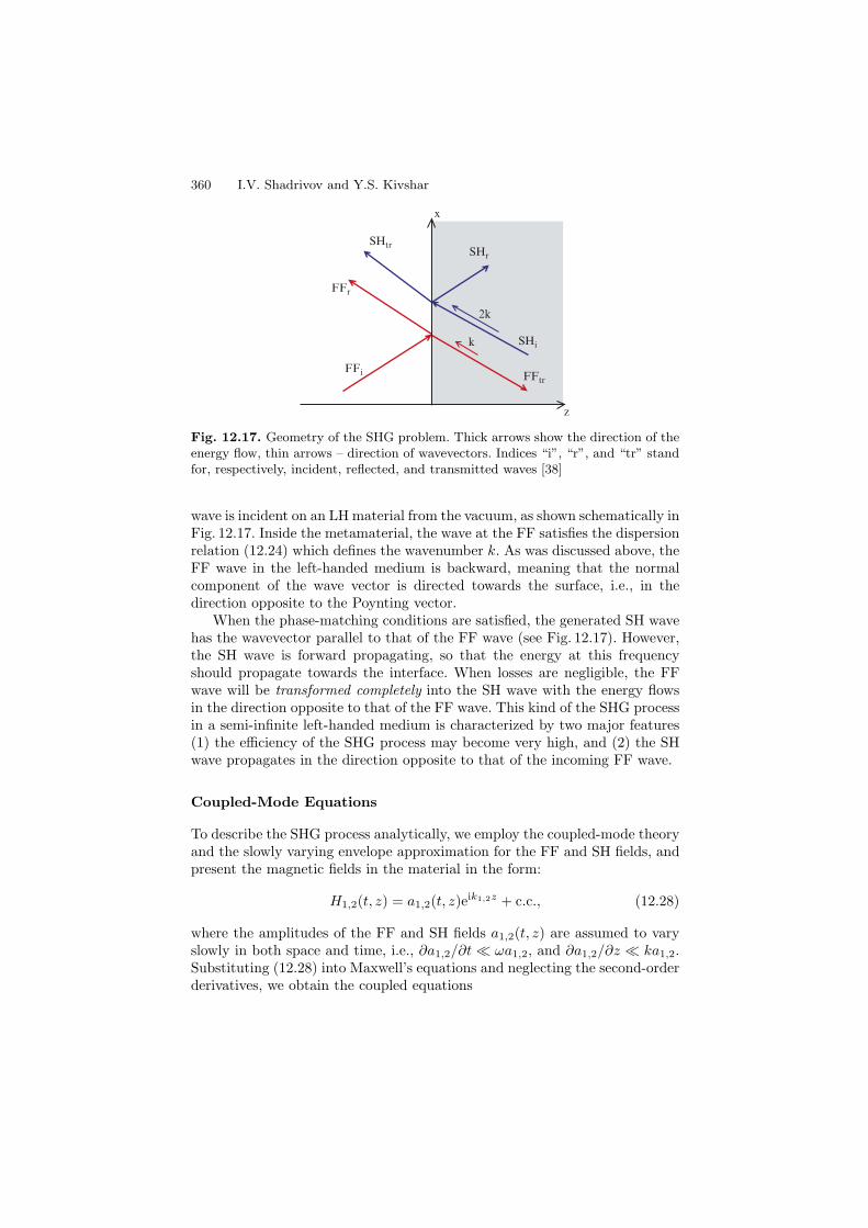
360 I.V. Shadrivov and Y.S. Kivshar
FFi
FFr
FFtr
SHi
SHr
SHtr
k
2k
x
z
Fig. 12.17. Geometry of the SHG problem. Thick arrows show the direction of theenergy flow, thin arrows – direction of wavevectors. Indices “i”, “r”, and “tr” standfor, respectively, incident, reflected, and transmitted waves [38]
wave is incident on an LH material from the vacuum, as shown schematically inFig. 12.17. Inside the metamaterial, the wave at the FF satisfies the dispersionrelation (12.24) which defines the wavenumber k. As was discussed above, theFF wave in the left-handed medium is backward, meaning that the normalcomponent of the wave vector is directed towards the surface, i.e., in thedirection opposite to the Poynting vector.
When the phase-matching conditions are satisfied, the generated SH wavehas the wavevector parallel to that of the FF wave (see Fig. 12.17). However,the SH wave is forward propagating, so that the energy at this frequencyshould propagate towards the interface. When losses are negligible, the FFwave will be transformed completely into the SH wave with the energy flowsin the direction opposite to that of the FF wave. This kind of the SHG processin a semi-infinite left-handed medium is characterized by two major features(1) the efficiency of the SHG process may become very high, and (2) the SHwave propagates in the direction opposite to that of the incoming FF wave.
Coupled-Mode Equations
To describe the SHG process analytically, we employ the coupled-mode theoryand the slowly varying envelope approximation for the FF and SH fields, andpresent the magnetic fields in the material in the form:
H1,2(t, z) = a1,2(t, z)eik1,2z + c.c., (12.28)
where the amplitudes of the FF and SH fields a1,2(t, z) are assumed to varyslowly in both space and time, i.e., ∂a1,2/∂t ωa1,2, and ∂a1,2/∂z ka1,2.Substituting (12.28) into Maxwell’s equations and neglecting the second-orderderivatives, we obtain the coupled equations
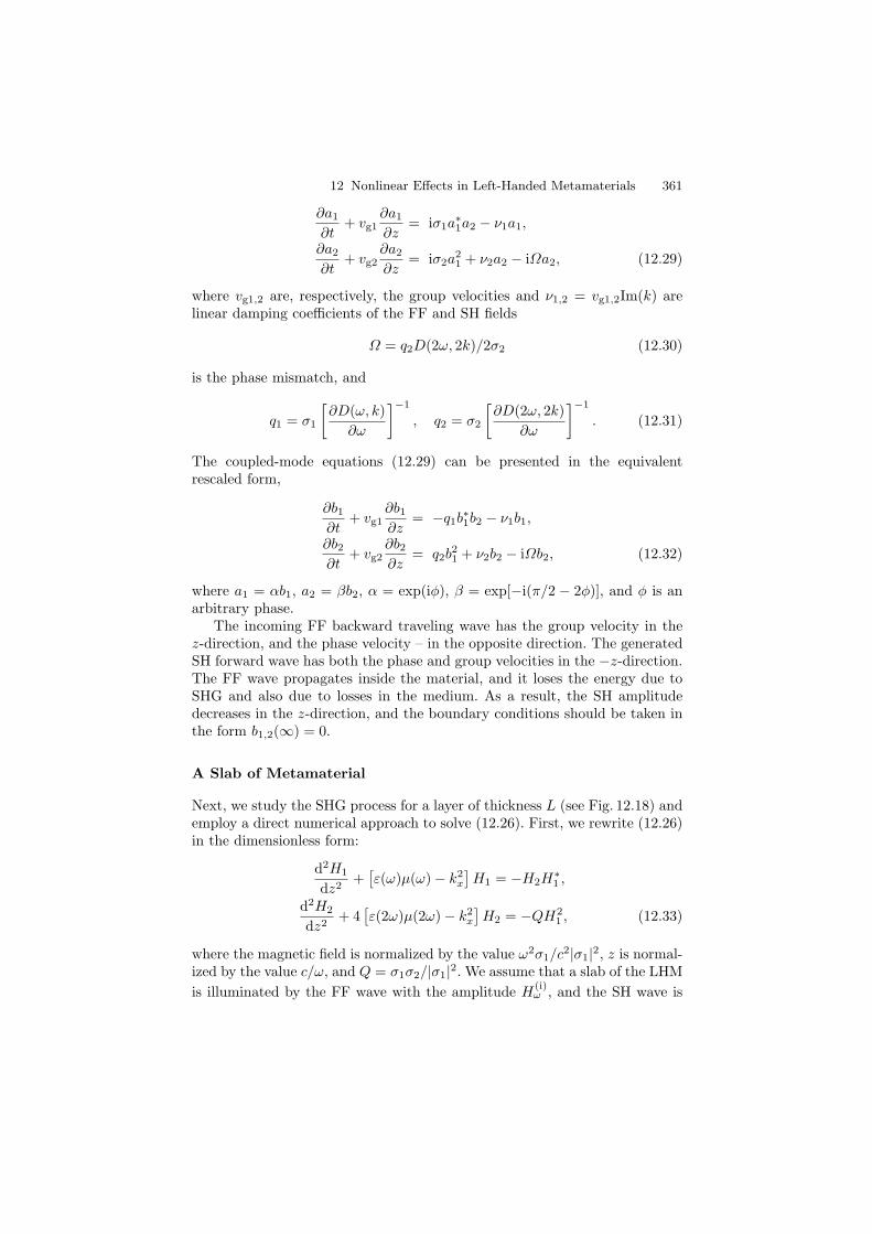
12 Nonlinear Effects in Left-Handed Metamaterials 361
∂a1
∂t+ vg1
∂a1
∂z= iσ1a
∗1a2 − ν1a1,
∂a2
∂t+ vg2
∂a2
∂z= iσ2a
21 + ν2a2 − iΩa2, (12.29)
where vg1,2 are, respectively, the group velocities and ν1,2 = vg1,2Im(k) arelinear damping coefficients of the FF and SH fields
Ω = q2D(2ω, 2k)/2σ2 (12.30)
is the phase mismatch, and
q1 = σ1
[∂D(ω, k)
∂ω
]−1
, q2 = σ2
[∂D(2ω, 2k)
∂ω
]−1
. (12.31)
The coupled-mode equations (12.29) can be presented in the equivalentrescaled form,
∂b1
∂t+ vg1
∂b1
∂z= −q1b
∗1b2 − ν1b1,
∂b2
∂t+ vg2
∂b2
∂z= q2b
21 + ν2b2 − iΩb2, (12.32)
where a1 = αb1, a2 = βb2, α = exp(iφ), β = exp[−i(π/2 − 2φ)], and φ is anarbitrary phase.
The incoming FF backward traveling wave has the group velocity in thez-direction, and the phase velocity – in the opposite direction. The generatedSH forward wave has both the phase and group velocities in the −z-direction.The FF wave propagates inside the material, and it loses the energy due toSHG and also due to losses in the medium. As a result, the SH amplitudedecreases in the z-direction, and the boundary conditions should be taken inthe form b1,2(∞) = 0.
A Slab of Metamaterial
Next, we study the SHG process for a layer of thickness L (see Fig. 12.18) andemploy a direct numerical approach to solve (12.26). First, we rewrite (12.26)in the dimensionless form:
d2H1
dz2+
[ε(ω)µ(ω) − k2
x
]H1 = −H2H
∗1 ,
d2H2
dz2+ 4
[ε(2ω)µ(2ω) − k2
x
]H2 = −QH2
1 , (12.33)
where the magnetic field is normalized by the value ω2σ1/c2|σ1|2, z is normal-ized by the value c/ω, and Q = σ1σ2/|σ1|2. We assume that a slab of the LHMis illuminated by the FF wave with the amplitude H
(i)ω , and the SH wave is
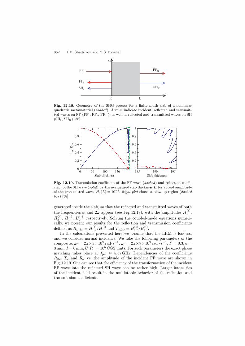
362 I.V. Shadrivov and Y.S. Kivshar
FFr
0
SHr
FFiFFtr
SHtr
L
x
z
Fig. 12.18. Geometry of the SHG process for a finite-width slab of a nonlinearquadratic metamaterial (shaded). Arrows indicate incident, reflected and transmit-ted waves on FF (FFi, FFr, FFtr), as well as reflected and transmitted waves on SH(SHr, SHtr) [38]
0 50 100 150Slab thickness
0
0.2
0.4
0.6
0.8
1
Tω, R
2ω
185 190 195Slab thickness
0
0.2
0.4
0.6
0.8
1
Fig. 12.19. Transmission coefficient of the FF wave (dashed) and reflection coeffi-cient of the SH wave (solid) vs. the normalized slab thickness L, for a fixed amplitudeof the transmitted wave, H1(L) = 10−2. Right plot shows a blow up region (dashedbox ) [38]
generated inside the slab, so that the reflected and transmitted waves of boththe frequencies ω and 2ω appear (see Fig. 12.18), with the amplitudes H
(t)1 ,
H(t)2 , H
(r)1 , H
(r)2 , respectively. Solving the coupled-mode equations numeri-
cally, we present our results for the reflection and transmission coefficientsdefined as Rω,2ω = H
(r)1,2/H
(i)1 and Tω,2ω = H
(t)1,2/H
(i)1 .
In the calculations presented here we assume that the LHM is lossless,and we consider normal incidence. We take the following parameters of thecomposite: ω0 = 2π×5×109 rad·s−1, ωp = 2π×7×109 rad · s−1, F = 0.3, a =3 mm, d = 6 mm, UcRd = 105 CGS units. For such parameters the exact phasematching takes place at fpm ≈ 5.37 GHz. Dependencies of the coefficientsR2ω, Tω and Rω vs. the amplitude of the incident FF wave are shown inFig. 12.19. One can see that the efficiency of the transformation of the incidentFF wave into the reflected SH wave can be rather high. Larger intensitiesof the incident field result in the multistable behavior of the reflection andtransmission coefficients.
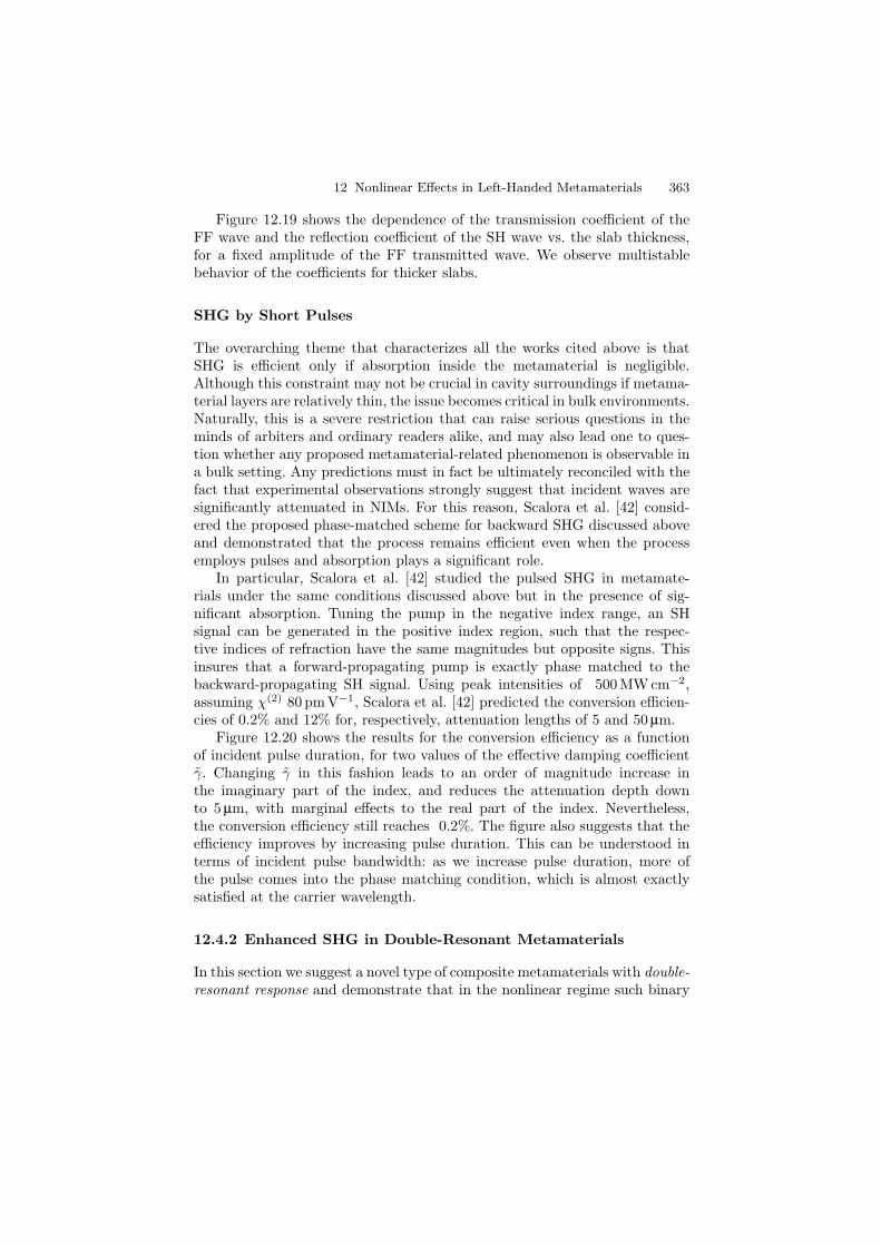
12 Nonlinear Effects in Left-Handed Metamaterials 363
Figure 12.19 shows the dependence of the transmission coefficient of theFF wave and the reflection coefficient of the SH wave vs. the slab thickness,for a fixed amplitude of the FF transmitted wave. We observe multistablebehavior of the coefficients for thicker slabs.
SHG by Short Pulses
The overarching theme that characterizes all the works cited above is thatSHG is efficient only if absorption inside the metamaterial is negligible.Although this constraint may not be crucial in cavity surroundings if metama-terial layers are relatively thin, the issue becomes critical in bulk environments.Naturally, this is a severe restriction that can raise serious questions in theminds of arbiters and ordinary readers alike, and may also lead one to ques-tion whether any proposed metamaterial-related phenomenon is observable ina bulk setting. Any predictions must in fact be ultimately reconciled with thefact that experimental observations strongly suggest that incident waves aresignificantly attenuated in NIMs. For this reason, Scalora et al. [42] consid-ered the proposed phase-matched scheme for backward SHG discussed aboveand demonstrated that the process remains efficient even when the processemploys pulses and absorption plays a significant role.
In particular, Scalora et al. [42] studied the pulsed SHG in metamate-rials under the same conditions discussed above but in the presence of sig-nificant absorption. Tuning the pump in the negative index range, an SHsignal can be generated in the positive index region, such that the respec-tive indices of refraction have the same magnitudes but opposite signs. Thisinsures that a forward-propagating pump is exactly phase matched to thebackward-propagating SH signal. Using peak intensities of 500 MW cm−2,assuming χ(2) 80 pm V−1, Scalora et al. [42] predicted the conversion efficien-cies of 0.2% and 12% for, respectively, attenuation lengths of 5 and 50 µm.
Figure 12.20 shows the results for the conversion efficiency as a functionof incident pulse duration, for two values of the effective damping coefficientγ. Changing γ in this fashion leads to an order of magnitude increase inthe imaginary part of the index, and reduces the attenuation depth downto 5 µm, with marginal effects to the real part of the index. Nevertheless,the conversion efficiency still reaches 0.2%. The figure also suggests that theefficiency improves by increasing pulse duration. This can be understood interms of incident pulse bandwidth: as we increase pulse duration, more ofthe pulse comes into the phase matching condition, which is almost exactlysatisfied at the carrier wavelength.
12.4.2 Enhanced SHG in Double-Resonant Metamaterials
In this section we suggest a novel type of composite metamaterials with double-resonant response and demonstrate that in the nonlinear regime such binary
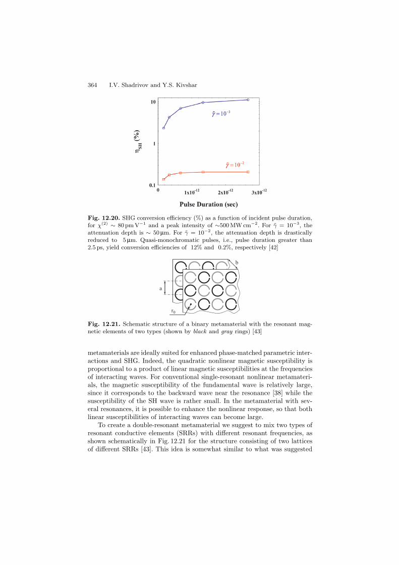
364 I.V. Shadrivov and Y.S. Kivshar
Fig. 12.20. SHG conversion efficiency (%) as a function of incident pulse duration,for χ(2) ∼ 80 pm V−1 and a peak intensity of ∼500 MW cm−2. For γ = 10−3, theattenuation depth is ∼ 50 µm. For γ = 10−2, the attenuation depth is drasticallyreduced to 5 µm. Quasi-monochromatic pulses, i.e., pulse duration greater than2.5 ps, yield conversion efficiencies of 12% and 0.2%, respectively [42]
a
r0
b
Fig. 12.21. Schematic structure of a binary metamaterial with the resonant mag-netic elements of two types (shown by black and gray rings) [43]
metamaterials are ideally suited for enhanced phase-matched parametric inter-actions and SHG. Indeed, the quadratic nonlinear magnetic susceptibility isproportional to a product of linear magnetic susceptibilities at the frequenciesof interacting waves. For conventional single-resonant nonlinear metamateri-als, the magnetic susceptibility of the fundamental wave is relatively large,since it corresponds to the backward wave near the resonance [38] while thesusceptibility of the SH wave is rather small. In the metamaterial with sev-eral resonances, it is possible to enhance the nonlinear response, so that bothlinear susceptibilities of interacting waves can become large.
To create a double-resonant metamaterial we suggest to mix two types ofresonant conductive elements (SRRs) with different resonant frequencies, asshown schematically in Fig. 12.21 for the structure consisting of two latticesof different SRRs [43]. This idea is somewhat similar to what was suggested
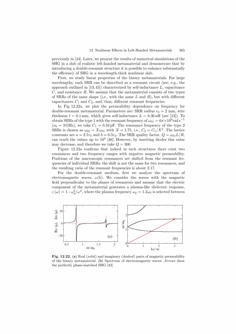
12 Nonlinear Effects in Left-Handed Metamaterials 365
previously in [44]. Later, we present the results of numerical simulations of theSHG in a slab of realistic left-handed metamaterial and demonstrate that byintroducing a double-resonant structure it is possible to enhance substantiallythe efficiency of SHG in a wavelength-thick nonlinear slab.
First, we study linear properties of the binary metamaterials. For largewavelengths, each SRR can be described as a resonant circuit (see, e.g., theapproach outlined in [13,45]) characterized by self-inductance L, capacitanceC, and resistance R. We assume that the metamaterial consists of two typesof SRRs of the same shape (i.e., with the same L and R), but with differentcapacitances C1 and C2, and, thus, different resonant frequencies.
In Fig. 12.22a, we plot the permeability dependence on frequency fordouble-resonant metamaterial. Parameters are: SRR radius r0 = 2 mm, wirethickness l = 0.1mm, which gives self-inductance L = 8.36 nH (see [13]). Toobtain SRRs of the type 1 with the resonant frequency of ω01 = 6π×109rad s−1
(ν0 = 3GHz), we take C1 = 0.34 pF. The resonance frequency of the type 2SRRs is chosen as ω02 = Xω01 with X = 1.75, i.e., C2 = C1/X2. The latticeconstants are a = 2.1r0 and b = 0.5r0. The SRR quality factor, Q = ω01L/R,can reach the values up to 103 [46]. However, by inserting diodes this valuemay decrease, and therefore we take Q = 300.
Figure 12.22a confirms that indeed in such structures there exist tworesonances and two frequency ranges with negative magnetic permeability.Positions of the macroscopic resonances are shifted from the resonant fre-quencies of individual SRRs; the shift is not the same for two resonances, andthe resulting ratio of the resonant frequencies is about 2.17.
For the double-resonant medium, first we analyze the spectrum ofelectromagnetic waves, ω(k). We consider the waves with the magneticfield perpendicular to the planes of resonators and assume that the electriccomponent of the metamaterial generates a plasma-like dielectric response,ε (ω) = 1−ω2
p/ω2, where the plasma frequency ωp = 1.2ω0 is selected between
0.5 1 1.5 2ω / ω0
−20
0
20
Re
(µ),
Im (
µ)
(a)
0 1 2 3kc / ω
0
1
2
ω / ω
0
(b)
Fig. 12.22. (a) Real (solid) and imaginary (dashed) parts of magnetic permeabilityof the binary metamaterial. (b) Spectrum of electromagnetic waves. Arrows showthe perfectly phase-matched SHG [43]
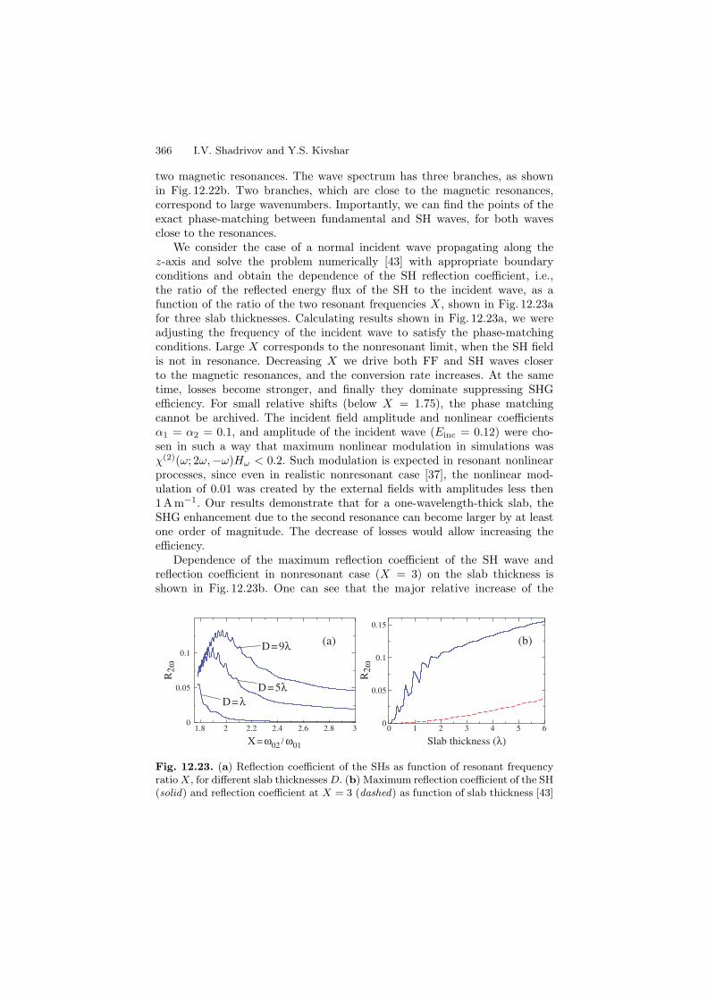
366 I.V. Shadrivov and Y.S. Kivshar
two magnetic resonances. The wave spectrum has three branches, as shownin Fig. 12.22b. Two branches, which are close to the magnetic resonances,correspond to large wavenumbers. Importantly, we can find the points of theexact phase-matching between fundamental and SH waves, for both wavesclose to the resonances.
We consider the case of a normal incident wave propagating along thez-axis and solve the problem numerically [43] with appropriate boundaryconditions and obtain the dependence of the SH reflection coefficient, i.e.,the ratio of the reflected energy flux of the SH to the incident wave, as afunction of the ratio of the two resonant frequencies X, shown in Fig. 12.23afor three slab thicknesses. Calculating results shown in Fig. 12.23a, we wereadjusting the frequency of the incident wave to satisfy the phase-matchingconditions. Large X corresponds to the nonresonant limit, when the SH fieldis not in resonance. Decreasing X we drive both FF and SH waves closerto the magnetic resonances, and the conversion rate increases. At the sametime, losses become stronger, and finally they dominate suppressing SHGefficiency. For small relative shifts (below X = 1.75), the phase matchingcannot be archived. The incident field amplitude and nonlinear coefficientsα1 = α2 = 0.1, and amplitude of the incident wave (Einc = 0.12) were cho-sen in such a way that maximum nonlinear modulation in simulations wasχ(2)(ω; 2ω,−ω)Hω < 0.2. Such modulation is expected in resonant nonlinearprocesses, since even in realistic nonresonant case [37], the nonlinear mod-ulation of 0.01 was created by the external fields with amplitudes less then1 A m−1. Our results demonstrate that for a one-wavelength-thick slab, theSHG enhancement due to the second resonance can become larger by at leastone order of magnitude. The decrease of losses would allow increasing theefficiency.
Dependence of the maximum reflection coefficient of the SH wave andreflection coefficient in nonresonant case (X = 3) on the slab thickness isshown in Fig. 12.23b. One can see that the major relative increase of the
1.8 2 2.2 2.4 2.6 2.8 3
X = ω02 / ω01
0
0.05
0.1
R2ω
R2ω
(a)D = 9λ
D = 5λD = λ
0 1 2 3 4 5 6
Slab thickness (λ)
0
0.05
0.1
0.15
(b)
Fig. 12.23. (a) Reflection coefficient of the SHs as function of resonant frequencyratio X, for different slab thicknesses D. (b) Maximum reflection coefficient of the SH(solid) and reflection coefficient at X = 3 (dashed) as function of slab thickness [43]
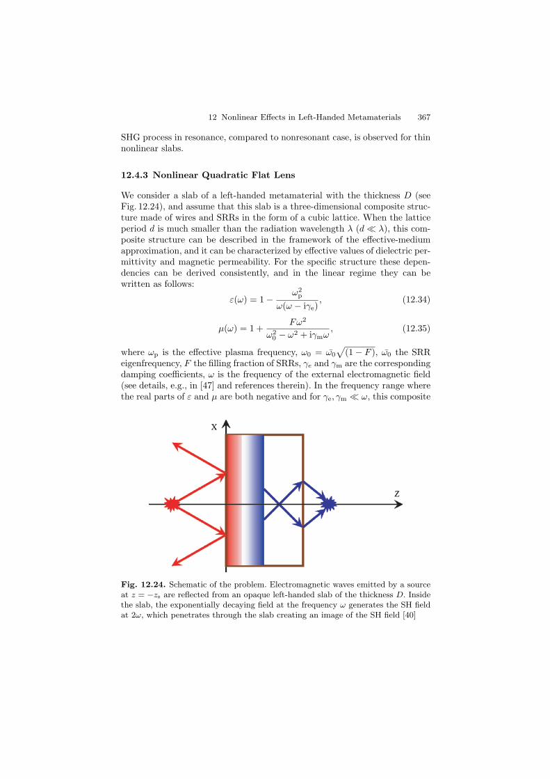
12 Nonlinear Effects in Left-Handed Metamaterials 367
SHG process in resonance, compared to nonresonant case, is observed for thinnonlinear slabs.
12.4.3 Nonlinear Quadratic Flat Lens
We consider a slab of a left-handed metamaterial with the thickness D (seeFig. 12.24), and assume that this slab is a three-dimensional composite struc-ture made of wires and SRRs in the form of a cubic lattice. When the latticeperiod d is much smaller than the radiation wavelength λ (d λ), this com-posite structure can be described in the framework of the effective-mediumapproximation, and it can be characterized by effective values of dielectric per-mittivity and magnetic permeability. For the specific structure these depen-dencies can be derived consistently, and in the linear regime they can bewritten as follows:
ε(ω) = 1 −ω2
p
ω(ω − iγe), (12.34)
µ(ω) = 1 +Fω2
ω20 − ω2 + iγmω
, (12.35)
where ωp is the effective plasma frequency, ω0 = ω0
√(1 − F ), ω0 the SRR
eigenfrequency, F the filling fraction of SRRs, γe and γm are the correspondingdamping coefficients, ω is the frequency of the external electromagnetic field(see details, e.g., in [47] and references therein). In the frequency range wherethe real parts of ε and µ are both negative and for γe, γm ω, this composite
Fig. 12.24. Schematic of the problem. Electromagnetic waves emitted by a sourceat z = −zs are reflected from an opaque left-handed slab of the thickness D. Insidethe slab, the exponentially decaying field at the frequency ω generates the SH fieldat 2ω, which penetrates through the slab creating an image of the SH field [40]
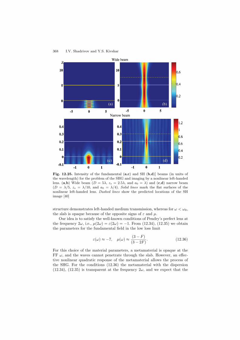
368 I.V. Shadrivov and Y.S. Kivshar
Fig. 12.25. Intensity of the fundamental (a,c) and SH (b,d)] beams (in units ofthe wavelength) for the problem of the SHG and imaging by a nonlinear left-handedlens. (a,b) Wide beam (D = 5λ, zs = 2.5λ, and a0 = λ) and (c,d) narrow beam(D = λ/5, zs = λ/10, and a0 = λ/4). Solid lines mark the flat surfaces of thenonlinear left-handed lens. Dashed lines show the predicted locations of the SHimage [40]
structure demonstrates left-handed medium transmission, whereas for ω < ω0,the slab is opaque because of the opposite signs of ε and µ.
Our idea is to satisfy the well-known conditions of Pendry’s perfect lens atthe frequency 2ω, i.e., µ(2ω) = ε(2ω) = −1. From (12.34), (12.35) we obtainthe parameters for the fundamental field in the low loss limit
ε(ω) ≈ −7, µ(ω) ≈ (3 − F )(3 − 2F )
. (12.36)
For this choice of the material parameters, a metamaterial is opaque at theFF ω, and the waves cannot penetrate through the slab. However, an effec-tive nonlinear quadratic response of the metamaterial allows the process ofthe SHG. For the conditions (12.36) the metamaterial with the dispersion(12.34), (12.35) is transparent at the frequency 2ω, and we expect that the
12 Nonlinear Effects in Left-Handed Metamaterials 369
SH field can propagate through the slab creating an image of the source behindthe slab.
Using the so-called undepleted pump approximation, we can obtain theequation for the TM-polarized SH field H
(2ω)y (x, z) inside the slab, which has
the form well known in the theory of the SHG (see, e.g., [48])
∆H(2ω)y + K2(2ω)H(2ω)
y = −16πk20ε(2ω)M (2ω)
NL , (12.37)
where ∆ is the Laplacian acting in the space (x, z), K2(2ω) = 4k20ε(2ω)µ(2ω),
k0 = ω/c is the free-space wavenumber, c is the speed of light and M(2ω)NL is
the nonlinear magnetization of the unit volume of the metamaterial at thefrequency 2ω, which appears due to the nonlinear magnetic momentum ofSRR, MNL. We find [40] that the squared field at the FF acts as an effectivesource for generating the SH and, as a result, the image of the squared fieldis reproduced by the nonlinear left-handed lens. This image appears at thepoint zim = D− zs, this result coincides with the corresponding result for thelinear lens [49].
When the source contains the spatial scales smaller than the wavelength,the imaging properties of the nonlinear lens depend strongly on the slab thick-ness D. Intensity distribution of the magnetic field in the fundamental andSH fields are shown in Fig. 12.25a–d for (a,b) large and (c,d) small (comparedto the radiation wavelength) size of the source, respectively.
12.5 Conclusions
We have described several nonlinear effects recently predicted for microstruc-tured metamaterials which exhibit left-handed properties and negative refrac-tion. We believe that nonlinear properties of metamaterials can allow for muchbroader scope of future applications of such materials, including a dynamiccontrol and tunability of the electromagnetic properties of the compositestructures, SHG, intensity-dependent switches, and generation of self-localizedpulses and beams.
Acknowledgments
During last years we have been collaborating with a number of people on theprojects involving the theoretical studies of left-handed metamaterials andnegative refraction, and we would like to thank all of them and especiallythose who made major contribution to the results reviewed in this chapter.In particular, we thank Alexander Zharov, Nina Zharova, Maxim Gorkunov,Andrey Sukhorukov, Costas Soukoulis, Allan Boardman, and Peter Egan. Thiswork has been supported by a Discovery grant of the Australian ResearchCouncil.

370 I.V. Shadrivov and Y.S. Kivshar
References
1. J.B. Pendry, A.J. Holden, W.J. Stewart, I. Youngs, Phys. Rev. Lett. 76, 4773(1996)
2. J.B. Pendry, A.J. Holden, D.J. Robbins, W.J. Stewart, IEEE Trans. Microw.Theory Tech. 47, 2075 (1999)
3. P. Markos, C.M. Soukoulis, Phys. Rev. E 65, 036622 (2002)4. P. Markos, C.M. Soukoulis, Phys. Rev. B 65, 033401 (2002)5. D.R. Smith, W.J. Padilla, D.C. Vier, S.C. Nemat Nasser, S. Schultz, Phys. Rev.
Lett. 84, 4184 (2000)6. M. Bayindir, K. Aydin, E. Ozbay, P. Markos, C.M. Soukoulis, Appl. Phys. Lett.
81, 120 (2002)7. C.G. Parazzoli, R.B. Greegor, K. Li, B.E.C. Koltenbah, M. Tanielian, Phys.
Rev. Lett. 90, 107401 (2003)8. V.G. Veselago, Usp. Fiz. Nauk 92, 517 (1967) (in Russian) [English translation:
Phys. Usp. 10, 509–514 (1968)]9. A.A. Zharov, I.V. Shadrivov, Yu.S. Kivshar, Phys. Rev. Lett. 91, 037401 (2003)
10. M. Lapine, M. Gorkunov, K.H. Ringhofer, Phys. Rev. E 67, 065601 (2003)11. C. Luo, S.G. Johnson, J.D. Joannopoulos, Appl. Phys. Lett. 81, 2352 (2002)12. C. Luo, S.G. Johnson, J.D. Joannopoulos, J.B. Pendry, Phys. Rev. B 65, 201104
(2002)13. M. Gorkunov, M. Lapine, E. Shamonina, K.H. Ringhofer, Eur. Phys. J. B 28,
263 (2002)14. I.V. Shadrivov, A.A. Zharov, N.A. Zharov, Yu.S. Kivshar, Radio Sci. 40, RS3S90
(2005)15. A.M. Belyantsev, V.A. Kozlov, V.I. Piskaryov, Infrared Phys. 21, 79 (1981)16. H. Li, A.L. Roytburd, S.P. Alpay, T.D. Tran, L. Salamanca Riba, R. Ramesh,
Appl. Phys. Lett. 78, 2354 (2001)17. N.A. Zharova, I.V. Shadrivov, A.A. Zharov, Yu.S. Kivshar, Opt. Express 13,
1291 (2005)18. K. Zauer, L.M. Gorbunov, Fiz. Plazmy 3, 1302 (1977) (in Russian)19. A.A. Zharov, A.K. Kotov, Fiz. Plazmy 10, 615 (1984)20. A.V. Kochetov, A.M. Feigin, Fiz. Plazmy 14, 716 (1988)21. Yu.S. Kivshar, G.P. Agrawal, Optical Solitons: From Fibers to Photonic Crystals
(Academic, San Diego, 2003)22. I.V. Shadrivov, Yu.S. Kivshar, J. Opt. A 7, S68 (2005)23. V.B. Gil’denburg, A.V. Kochetov, A.G. Litvak, A.M. Feigin, Zh. Eksp. Teor.
Fiz. 84, 48 (1983)24. I.V. Shadrivov, A.A. Sukhorukov, Yu.S. Kivshar, A.A. Zharov, A.D. Boardman,
P. Egan, Phys. Rev. E 69, 16617 (2004)25. J. Nkoma, R. Loudon, D.R. Tilley, J. Phys. C 7, 3547 (1974)26. A.D. Boardman (ed.), Electromagnetic Surface Modes (Wiley, New York, 1982)27. R. Ruppin, Phys. Lett. A 277, 61 (2000)28. A.G. Litvak, V.A. Mironov, Izv. Vyssh. Uchebn. Zaved. Radiofiz. 11, 1911
(1968) (in Russian)29. V.E. Zakharov, A.B. Shabat, JETP 34, 62 (1972)30. A.D. Boardman, P. Egan, IEEE J. Quantum Electron. 21, 1701 (1985)31. I.V. Shadrivov, A.A. Sukhorukov, Yu.S. Kivshar, Phys. Rev. E 67, 057602
(2003)
12 Nonlinear Effects in Left-Handed Metamaterials 371
32. G.A. Korn, T.M. Korn, Mathematical Handbook for Scientists and Engineers(McGraw-Hill, New York, 1968)
33. A.D. Boardman, G.S. Cooper, A.A. Maradudin, T.P. Shen, Phys. Rev. B 34,8273 (1986)
34. I.V. Shadrivov, Photon. Nanostruct.: Fundam. Appl. 2, 175 (2004)35. N.N. Akhmediev, Zh. Eksp. Teor. Fiz. 83, 545 (1982) (in Russian)
[akhmediev:1982-299:jetp]36. V.M. Agranovich, Y.R. Shen, R.H. Baughman, A.A. Zakhidov, Phys. Rev. B
69, 165112 (2004)37. M. Lapine, M. Gorkunov, Phys. Rev. E 70, 66601 (2004)38. I.V. Shadrivov, A.A. Zharov, Yu.S. Kivshar, J. Opt. Soc. Am. B 23, 529 (2006)39. A.A. Zharov, Fiz. Plazmy 17, 20 (1991)40. A.A. Zharov, N.A. Zharova, I.V. Shadrivov, Yu.S. Kivshar, Appl. Phys. Lett.
87, 091104 (2005)41. L.D. Landau, E.M. Lifshitz, Electrodynamics of Continuous Media (Pergamon,
Oxford, 1963)42. M. Scalora, G. DAguanno, M. Bloemer, M. Centini, D. Ceglia, de, N. Mattiucci,
Y. Kivshar, Opt. Express 14, 4746 (2006)43. M.V. Gorkunov, I.V. Shadrivov, Yu.S. Kivshar, Appl. Phys. Lett. 88, 71912
(2006)44. H. Chen, L. Ran, J. Huangfu, X. Zhang, K. Chen, T.M. Grzegorczyk, J.A. Kong,
J. Appl. Phys. 96, 5338 (2004)45. R. Marques, F. Medina, R. Rafii El Idrissi, Phys. Rev. B 65, 144440 (2002)46. R.A. Shelby, D.R. Smith, S. Schultz, Science 292, 77 (2001)47. I.V. Shadrivov, N.A. Zharova, A.A. Zharov, Yu.S. Kivshar, Phys. Rev. E 70,
046615 (2004)48. Y.R. Shen, The Principles of Nonlinear Optics (Wiley, New York, 1984)49. J.B. Pendry, Phys. Rev. Lett. 85, 3966 (2000)

Index
E, D, B and E, D, B, H approaches,105
E, D, B approach, 103ε(ω)–µ(ω) description, 104YVO4 bicrystal, 12(GRIN) lens, 305(PIM) lenses, 295Cerenkov effect, 262
aberration, 7, 317absorber, 136, 141absorption, 230acoustic waves, 183, 184additional boundary conditions, 113additional exciton–polariton waves, 113All-angle-negative-refraction, 135alumina, 158amphoteric refraction, 13angular, 153anisotropic, 83anisotropic index of refraction, 218anisotropic medium, 274anisotropy, 19, 20, 157anisotropy scheme, 5anomalous, 86antenna, 157antiresonance, 217arithmetic mean, 90arrow distributions, 43artificial resonances, 184
backward wave, 2, 134ballistic electron beam, 14band structure, 231
bandgap, 139, 143bandwidth limitations, 264basis current functions, 20basis function, 39basis function limits, 42basis sets, 38beam, 154Bessel function, 306biaxial, 25biaxial crystal, 42bicrystal heterostructure, 67boundary condition, 89Bragg diffraction, 136, 139, 144, 145Bragg wave, 142, 144, 145Brillouin, 155Brillouin zone, 141broken spatial inversion, 110
calculated transmission spectrum, 231Chebyshev polynomials, 288Cherenkov, 100Cherenkov cone, 101Cherenkov radiation, 100Chinese remainder theorem, 284chiral, 110Chiral (gyrotropic) systems, 114chiral route to negative refraction, 116chirality parameter, 118chromatic aberration, 222circular, 161circular dichroism, 114composite, 76conductivity, 269

374 Index
constitutive parameters, 21continuous rods, 253Courant–Friederichs–Lewy condition,
220Cu–Ge, 93Cylindrical NIM Lenses, 299
damping, 77deaf band, 201dielectric functions, 105dielectric tensor, 96, 102dipolar resonance, 199dipole approximation, 193, 194disk array, 218dispersion, 134, 135, 146, 149dispersion behavior, 19dispersion diagrams, 251dispersion law, 129dispersion relations, 103dispersion surface, 206, 207dispersive metamaterials, 252displacement of the focus, 236displacement of the source, 235dissipation, 118distance of focus method, 247distributions, 19domain twin interface, 14Doppler, 100Doppler shift, 262double negativity, 183, 184double-negativity scheme, 4double-split-ring, 219double-split-ring resonator, 217
E-polarized, 81effective index of refraction, 218, 247effective magnetic resonance frequency,
254effective medium, 122, 264, 265, 272effective medium approximation, 78Effective permittivity, 252effective plasma, 252effective refractive index, 136, 137, 200effective-medium formulae, 195EFS, 137–139, 143eigenvalues, 38eigenvectors, 38eikonal equation, 277, 295eikonal surface ζ, 317
electric crossover frequency, 256electric magnitude distribution, 43electric permittivity, 183electric resonance, 252electric-dipole allowed transitions, 108electric-dipole forbidden transitions,
109electric-quadrupole transitions, 109electromagnetic field, 19EM, 162energy current density, 83energy flux, 346–349, 366energy–momentum relationship of
excitons, 112equal-frequency, 151equations, 21evanescent propagation, 257evanescent waves, 209even mode, 37exciton effective mass, 113excitonic transitions, 114excitons, 107excitons with negative effective mass,
111extraordinary, 9
fabrication, 163FDTD, 156, 244FDTD simulations, 220, 337ferroelectric, 66ferromagnetic resonance, 77field asymmetry, 19field distributions, 20field patterns, 251finite difference time domain, 218, 226flat lens, 149, 150FMR, 80focus, 167, 172, 174, 177, 180, 241focus distances, 230focus width, 230, 233, 242focusing, 162, 168, 174, 222, 231, 232focusing by planar slabs, 218Frenkel excitons, 113frequencies, 252frequency dispersion, 264frequency-dependent effective mass, 187frequency-dependent index, 219Fresnel modulation, 240fundamental mode, 257, 258

Index 375
Galerkin technique, 41
gap, 254
Gaussian, 152
generation of harmonics, 127
geometry of the split-ring resonator, 227
geometry of this disk array, 231
governing equations, 20
Green’s function, 19, 29, 206
Green’s function method, 251
GRIN Lens, 311
group longitudinal velocities, 257
group velocity, 2, 135, 137, 138, 144,159, 265, 275
guided propagating waves, 251
guided wave device, 42
guided wave structures, 19
guiding structure, 255
gyrotropic, 110
H-polarized, 81
harmonic mean, 90
Helmholtz–Kirchhoff theorem, 278, 280
heterostructure bicrystal, 19
hexagonal annulus arrays, 218
hexagonal array, 239
hexagonal arrays of 1 cm copper disks,240
hexagonal disk array measurements –refraction, 242
hexagonal disk arrays, 218, 226
higher order modes, 259
Homogeneous Effective Medium, 282
horn, 155
hysteresis, 332, 333, 337, 340
Ideal Negative Index Medium, 220
idealized NIM, 219
image, 162, 168, 172–174, 176, 179, 180,221
image resolution, 168
immersion lens, 7
indefinite index medium, 275
Indefinite Media, 272
index, 152–156
index of refraction, 233, 237, 262
index of refraction from the displace-ment of the focus, 242
integral equation of the homogeneousFredholm type of the second kind,30
interplay of two resonances, 110inverse tensor, 103isotropic, 21isotropic index medium, 275isotropic systems, 105isotropy, 49, 154
L. I. Mandelstam, 96, 97lattice, 159left- and right-hand polarized waves,
117left-handed, 133, 137, 150left-handed electromagnetism (LHE),
133, 137, 143, 144, 146left-handed material (LHM), 133, 136,
144, 262left-handed medium (LHM), 2line width, 253locally resonant sonic materials, 190longitudinal, 105, 157longitudinal frequency, 116Lorentzian, 220loss tangent, 258, 266loss widths, 252Losses, 265, 289
macroscopic Maxwell equations, 102magnetic crossover frequency, 256magnetic line width, 255magnetic magnitude distribution, 45magnetic permeability, 96, 121, 183magnetic resonance, 252magnetic-dipole transitions, 109magnitude field distributions, 43Maxwell’s, 21Maxwell’s equations, 262measurements, 224metallic, 157metallic conductivity, 255Metallodielectric, 149metamaterial, 121, 149, 252microstrip, 19microstrip guided wave structure, 251microstrip left-handed material, 251microwave, 133–137, 139, 141, 145, 146Mie resonances, 192

376 Index
millimeter wavelength, 251molecular transitions, 108monopolar resonance, 199monopole, 157monopole source, 233movement of focus, 236multilayer, 88multiple scattering theory, 190
negative dielectric permittivity, 96negative effective density, 184negative effective mass, 188, 189negative effective modulus, 184negative group velocity, 95negative index material (NIM), 133–135,
142negative index of refraction, 133, 263negative index passband, 233negative phase velocity, 20, 290negative refraction (NR), 1, 10, 95,
133–136, 138–141, 143–146,148–152, 154, 167, 168, 171, 172,174, 175, 178–180, 244
NIM Lens, 295, 308NIM Optics, 295nonlinear
dielectric permittivity, 336effects, 330–337magnetic response, 333, 334, 340, 342metamaterial, 332, 333resonance, 333–335response, 333–334response, Kerr-type, 334, 343, 345,
352, 355nonlinear lens, 367–368nonlinear material with negative
refraction, 127nonlinear optical effects, 6nonlinearity, 333nonlocal dielectric response, 96normal waves, 129
odd mode, 37omnidirectional, 156Onsager principle of symmetry of
kinetic coefficients, 103Onsager relation, 108optical activity, 25, 114optical activity tensors, 21
optical branches, 98optical frequencies, 121optical nonlinear susceptibilities, 127ordinary wave, 9orientational superlattice, 15oscillator strengths, 109
parallel plate waveguide (PPW),133–135, 140
Parseval theorem, 40partial waves, 193perfect lens, 1perfectly matched layer, 220Periodic Effective Medium, 287permeability, 133, 252permittivity, 133, 134, 158permittivity tensor, 8, 21, 49phase longitudinal velocities, 257phase velocity, 272photonic crystal, 148–151, 167, 226
metallic, 135photonic crystal (PC), 134, 135, 141,
218photonic crystal scheme, 6photonic crystal simulations, 231photonic crystal slab, 234physical meaning, 121PIM lens, 301, 307PIM, NIM, and GRIN Lenses, 314planar slab focusing, 217plasma frequency, 109, 217, 219point sources, 213polariton, 4, 95polaritons with negative group velocity,
111Polarization Coupling, 270polystyrene, 152positive index, 226, 233Poynting vector, 2, 10, 91, 96, 133, 134,
257principal axis system, 28prism, photonic crystal, 136, 137, 144propagation, 149–152propagation constant, 42, 69pulse, 222
quadratic nonlinearity, 357quasicrystal, 168–170, 172, 176, 177,
179, 180

Index 377
randomly oriented, 92reflection, 7, 155refraction, 85, 86, 151refraction of our hexagonal disk, 236refraction through the disk medium,
236refractive index, 133, 136, 138, 139, 141,
142, 144refractive index, negative, 133resolution, 211resonance frequency, 219retrieval, 281, 286right-handed, 133, 137right-handed electromagnetism (RHE),
134, 137, 138right-handed materials, 263right-handed medium (RHM), 2
S-parameter, 247sculptured thin film, 15second harmonics generation, SHG,
355–357enhanced, 363pulses, 363
Siedel aberrations, 295slab, 221Snell, 156Snell’s law, 133, 136, 139, 142, 222, 230,
234, 236, 262, 276, 277soliton
bright, 342, 350dark, 342spatial, 340–342temporal, 339
sonic bandgaps, 190spatial, 152spatial dispersion, 3, 96, 102, 205spatial dispersion approach, 102spatial dispersion framework, 129spatial dispersion of dielectric effects,
126spatial electric field components, 33spatial inversion, 105spatial-dispersion scheme, 3spectral, 150spectral domain, 29, 33spectral summations, 39spherical harmonics, 195Spherical NIM Lenses, 305
split ring, 254
split ring-rod, 252
split-ring resonators, 223
square double ring geometry, 224
SRR resonance, 230
stability of the focus, 222
stripline, 67
structure loss, 266
subwavelength, 148–150
sum rule, 108
superfocusing, 222, 234
superprism, 150
surface currents, 37
surface impedance, 206
surface polaritons, 118
surface transition layer, 118
surface wave, 56
linear, 343, 344
nonlinear, 343, 345–349
symmetric approach, 103
symmetry breaking, 354, 355
TE, 163
tensor, 80
thermodynamic equilibrium, 96
time-dependent dielectric polarization,123
TM, 163
total eigenvector field solution, 41
total induced current, 123
total induced magnetic moment, 122
total vector surface current, 41
totally reflected, 86
transmission, 239, 240
transmission and focusing, 240
transmission displays, 229
transmission spectra, 224
transverse, 105
transverse (ω⊥)–longitudinal (ω‖)splitting gap, 97
transverse electric (TE), 135, 141, 143,145
transverse magnetic (TM), 135, 138,140–143
transverse polaritons, 96
triangular lattice, 135–139, 141
triangular PC, 143

378 Index
ultra-short pulses, 128
uniaxial symmetry, 8
uniform media, 2, 8
vector potential, 107
velocity of energy propagation, 96
volumetric fields, 65
wave, 9wavelength, 151wire array, 217, 223wire radius re, 253with negative group velocity, 129
Zernike polynomials, 319zero reflection, 10, 14

Springer Series in
materials scienceEditors: R. Hull R. M. Osgood, Jr. J. Parisi H. Warlimont
40 Reference Materialsin Analytical ChemistryA Guide for Selection and UseEditor: A. Zschunke
41 Organic Electronic MaterialsConjugated Polymers and LowMolecular Weight Organic SolidsEditors: R. Farchioni and G. Grosso
42 Raman Scatteringin Materials ScienceEditors: W. H. Weber and R. Merlin
43 The Atomistic Natureof Crystal GrowthBy B. Mutaftschiev
44 Thermodynamic Basisof Crystal GrowthP–T–X Phase Equilibriumand Non-StoichiometryBy J. Greenberg
45 ThermoelectricsBasic Principlesand New Materials DevelopmentsBy G. S. Nolas, J. Sharp,and H. J. Goldsmid
46 Fundamental Aspectsof Silicon OxidationEditor: Y. J. Chabal
47 Disorder and Orderin StronglyNonstoichiometric CompoundsTransition Metal Carbides,Nitrides and OxidesBy A. I. Gusev, A. A. Rempel,and A. J. Magerl
48 The Glass TransitionRelaxation Dynamicsin Liquids and Disordered MaterialsBy E. Donth
49 Alkali HalidesA Handbook of Physical PropertiesBy D. B. Sirdeshmukh, L. Sirdeshmukh,and K. G. Subhadra
50 High-Resolution Imagingand Spectrometry of MaterialsEditors: F. Ernst and M. Ruhle
51 Point Defects in Semiconductorsand InsulatorsDetermination of Atomicand Electronic Structurefrom Paramagnetic HyperfineInteractionsBy J.-M. Spaeth and H. Overhof
52 Polymer Filmswith Embedded Metal NanoparticlesBy A. Heilmann
53 Nanocrystalline CeramicsSynthesis and StructureBy M. Winterer
54 Electronic Structure and Magnetismof Complex MaterialsEditors: D.J. Singh andD. A. Papaconstantopoulos
55 QuasicrystalsAn Introduction to Structure,Physical Properties and ApplicationsEditors: J.-B. Suck, M. Schreiber,and P. Haussler
56 SiO2 in Si MicrodevicesBy M. Itsumi
57 Radiation Effectsin Advanced Semiconductor Materialsand DevicesBy C. Claeys and E. Simoen
58 Functional Thin Filmsand Functional MaterialsNew Concepts and TechnologiesEditor: D. Shi
59 Dielectric Properties of Porous MediaBy S.O. Gladkov
60 Organic PhotovoltaicsConcepts and RealizationEditors: C. Brabec, V. Dyakonov, J. Parisiand N. Sariciftci
61 Fatigue in Ferroelectric Ceramicsand Related IssuesBy D.C. Lupascu
62 EpitaxyPhysical Principlesand Technical ImplementationBy M.A. Herman, W. Richter, and H. Sitter

Springer Series in
materials scienceEditors: R. Hull R. M. Osgood, Jr. J. Parisi H. Warlimont
63 Fundamentalsof Ion-Irradiated PolymersBy D. Fink
64 Morphology Control of Materialsand NanoparticlesAdvanced Materials Processingand CharacterizationEditors: Y. Waseda and A. Muramatsu
65 Transport Processesin Ion-Irradiated PolymersBy D. Fink
66 Multiphased Ceramic MaterialsProcessing and PotentialEditors: W.-H. Tuan and J.-K. Guo
67 NondestructiveMaterials CharacterizationWith Applications to Aerospace MaterialsEditors: N.G.H. Meyendorf, P.B. Nagy,and S.I. Rokhlin
68 Diffraction Analysisof the Microstructure of MaterialsEditors: E.J. Mittemeijer and P. Scardi
69 Chemical–Mechanical Planarizationof Semiconductor MaterialsEditor: M.R. Oliver
70 Applications of the Isotopic Effectin SolidsBy V.G. Plekhanov
71 Dissipative Phenomenain Condensed MatterSome ApplicationsBy S. Dattagupta and S. Puri
72 Predictive Simulationof Semiconductor ProcessingStatus and ChallengesEditors: J. Dabrowski and E.R. Weber
73 SiC Power MaterialsDevices and ApplicationsEditor: Z.C. Feng
74 Plastic Deformationin Nanocrystalline MaterialsBy M.Yu. Gutkin and I.A. Ovid’ko
75 Wafer BondingApplications and TechnologyEditors: M. Alexe and U. Gosele
76 Spirally Anisotropic CompositesBy G.E. Freger, V.N. Kestelman,and D.G. Freger
77 Impurities Confinedin Quantum StructuresBy P.O. Holtz and Q.X. Zhao
78 Macromolecular NanostructuredMaterialsEditors: N. Ueyama and A. Harada
79 Magnetism and Structurein Functional MaterialsEditors: A. Planes, L. Manosa,and A. Saxena
80 Micro- and Macro-Properties of SolidsThermal, Mechanicaland Dielectric PropertiesBy D.B. Sirdeshmukh, L. Sirdeshmukh,and K.G. Subhadra
81 Metallopolymer NanocompositesBy A.D. Pomogailo and V.N. Kestelman
82 Plastics for Corrosion InhibitionBy V.A. Goldade, L.S. Pinchuk,A.V. Makarevich and V.N. Kestelman
83 Spectroscopic Properties of Rare Earthsin Optical MaterialsEditors: G. Liu and B. Jacquier
84 Hartree–Fock–Slater Methodfor Materials ScienceThe DV–X Alpha Method for Designand Characterization of MaterialsEditors: H. Adachi, T. Mukoyama,and J. Kawai
85 Lifetime SpectroscopyA Method of Defect Characterizationin Silicon for Photovoltaic ApplicationsBy S. Rein
86 Wide-Gap ChalcopyritesEditors: S. Siebentritt and U. Rau
87 Micro- and Nanostructured GlassesBy D. Hulsenberg and A. Harnisch