magazine - search the history of over 642 billion web pages
TRANSCRIPT

J²B Synthesizer
An open-minded digital music platform
Experimenter’s Function Generator T-Board Wireless EveryCircuit App Sounding Logic Probe/Tester From 8 to 32 bits: ARM Microcontrollers for Beginners (1)
USBprog 5.0 VariLab 402 (3) Stepper or Servo Drive for Vintage Dials Video over Fiber Digi-Disco 1978 CC2-eBoB EveryCircuit App Bluetooth Thermometer
With Free Live Webinar
SUPER-SIZE WINTER EDITION132 pages of inspiring diy electronics
www.elektor-magazine.com
January & February 2015 | No. 457 + 458
magazine

www.picotech.com/PS301ENTER HERE:
ALL MODELS INCLUDE FULL SOFTWARE AND 5 YEAR WARRANTY. SOFTWARE INCLUDES MEASUREMENTS, SPECTRUM ANALYZER, SDK, ADVANCED TRIGGERS, COLOR PERSISTENCE, SERIAL DECODING (CAN, LIN, RS232, I²C, I²S, FLEXRAY, SPI),
MASKS, MATH CHANNELS, ALL AS STANDARD, WITH FREE UPDATES.
WINPicoScope®5000 SeriesFLEXIBLE RESOLUTION OSCILLOSCOPEPICOSCOPE 5000 SERIES FLEXIBLE RESOLUTION OSCILLOSCOPES HAVE SELECTABLE 8 TO 16-BIT RESOLUTION AND SAMPLING SPEEDS TO 1GS/S.
Modern electronic devices process a variety of high-speed and high-resolution signals. Being able to detect and characterise small signals in the presence of larger ones is key to verification of next-generation electronic designs. The precision of an oscilloscope is determined by its resolution and its accuracy. Here are characteristics of different resolution oscilloscopes:
The top waveform in the screenshot, captured with 8 bits resolution and zoomed in by 64x shows up the limitations of 8–bit resolution. The same signal captured with PicoScope set to 12–bit resolution shows characteristics of the signal that were invisible in 8–bit mode.
Oscilloscope resolution
Number of levels
Smallest change that can be detected (of full range)
Maximum dynamic range
8 Bits 256 0.39% (4,000 ppm) 48 dB
10 Bits 1,024 0.097% (976 ppm) 60 dB
12 Bits 4,096 0.024% (244 ppm) 72 dB
14 Bits 16,384 0.0061% (610 ppm) 84 dB
16 Bits 65,536 0.0015% (15 ppm) 96 dB
WIN
Untitled-1 1 08/12/14 07:52

ew15_207x276_Elektor_engl.indd 1 08.12.14 15:39Untitled-3 1 09/12/14 09:18
mag
azin
e
4 | January & February 2015 | www.elektor-magazine.com
8 electronica 2014 ImpressionsThe hectic at the Elektor booth captured in words and pictures.
News
Projects
10 J2B SynthesizerBased on Soulsby’s Atmegatron concept, this synthesizer is built around an ATmega328 8-bit AVR microcontroller from Atmel, the same that is at the heart of the Arduino Uno board. We wouldn’t say this synthesizer sounds musical in the first place—it can, but also expect unpolished sounds.
22 Experimenter’s Function GeneratorThe DIY instrument described here employs Elektor’s Platino board as
low, especially with the SAM D20 Xplained board.
48 T-Board WirelessAdding a wireless module to a proj-ect can come in handy when you’re working on a circuit design, for example on a breadboard. For this we have developed a convenient T-Board that is suitable for various types of wireless module.
51 Better Accuracy from the LM317Get the good old LM317 to produce a very accurate output voltage.
56 Stepper or Servo Drive for Vintage DialsWhat’s stopping you from equipping old needle-pointer instruments with state of the art innards? By doing so you combine functionality with aesthetics.
56 GestIC & 3D Touchpad Workbook (2)One of the nerdiest games out there is 2048. Using the Microchip
Contents
the brains, and was co-inspired by another Elektor blockbuster publication, the insightful AVR SDR project series printed back in 2012. It is usable for applications like signal tracing, clocking of MCU and digital circuits, basic audio filter & loudspeaker testing, tuning, you name it.
30 VariLab 402 (3)In this closing installment we look at software structure and the way it got designed, also in relation to design choices. The final assembly of the PSU is also discussed.
38 From 8 to 32 bits: ARM Microcontrollers for Beginners (1)There’s nothing frightening or daunting about microcontrollers
with an ARM architecture. Those with a little expe-rience with 8-bit devices will find this new course
exciting and easy to fol-
1 Kboards at
an Elektorized
price
Visit Elektor @
Nurnberg, Germany February 24-26
Hall 5, Booth 288
www.elektor-magazine.com | January & February 2015 | 5
MGC3110 we get to play 2048 on the Raspberry Pi.
58 CC2-eBoBLike so many modern components the wonderful ChipCap2 humidity and temperature sensor is a night-mare to solder. Here’s help.
64 Bluetooth Low Energy Wireless ThermometerHere we link Laird’s BT600 ther-mometer to our iPhones and smart-phones—wirelessly of course!
72 The Art of Bulb PlantingHere’s a few novel uses for the high-ly underrated and almost forgotten incandescent lamp, a.k.a. bulb.
76 Video over FiberDo consider using optic fiber instead of coax for cable runs lon-ger than about 300 feet.
84 USBProg 5.0This extremely versatile program-mer is fully open source and has a
120 Retronics: Digi-Disco (1978)Reminiscences of a TTL user doing a great job entertaining Highschool kids in the late 1970s. Series Edi-tor: Jan Buiting.
124 HexadokuThe Original Elektorized Sudoku.
125 Gerard’s Columns: Crackpots versus Iconoclasts
130 Upcoming in ElektorA sneak preview of articles on the Elektor publication schedule.
Magazine
92 Microchip Hillstar DevKit WalkaroundFrom opening the box to a fully working gesture control system.
94 CRIS-AMP Audio SystemExploring an audio amplifier project presented on the elektor-labs website.
96 The Programmer @ Elektor LabsElektor Labs firmly answers FAQ #23b: what programmer are u using?
Labs
90 DesignSpark Tips & TricksWe look at multiple devices inside components, like logic ICs.
97 Transistor TetrodesWeird Components—the series
DesignSpark
110 EveryCircuit AppDesign and analyze electronics without touching a soldering iron.
Review
116 News & New Products
Industry
web interface.
89 Tristate Level ShifterConvert 3.6 volts swing to 5 volts.
98 USB Chipcard ReaderThis absolute bare bones interface allows a PC RS232 port to talk USB to chipcards.
101 DIY LED FlashlightThis flashlight is fun to build and more energy efficient than anything off the shelf.
104 BeepFor logic high/low checks sounds are easier to interpret than rolling digits on the DVM.
108 Tiny Test Transmitter for FMAn usual and dirt cheap approach to making an FM transmitter
108 FM Synchro ReceiverDitto, for the associated receiver.
113 RTC Modules from Micro CrystalRemarkably, these RTC chips have the xtal on-chip.
January & February 2015Volume 41 – No. 457 + 458

•Community
6 | January & February 2015 | www.elektor-magazine.com
Volume 41, No. 457 + 458 January & February 2015
ISSN 1947-3753 (USA / Canada distribution)ISSN 1757-0875 (UK / ROW distribution)www.elektor.com, www.elektor-magazine.com
Elektor Magazine, English edition is published 6 times a year by
Elektor International Media78 York StreetLondon W1H 1DP, UKPhone: (+44) (0)20 7692 8344
Head Office:Elektor International Media b.v.PO Box 11NL-6114-ZG SusterenThe NetherlandsPhone: (+31) 46 4389444Fax: (+31) 46 4370161
USA / Canada Memberships:Elektor USAP.O. Box 462228Escondido, CA 92046Phone: 800-269-6301E-mail: [email protected]: www.elektor.com/member
UK / ROW Memberships:Please use London addressE-mail: [email protected]: www.elektor.com/member
Advertising & Sponsoring:Johan DijkPhone: +31 6 15894245E-mail: [email protected]
www.elektor.com/advertisingAdvertising rates and terms available on request.
Copyright NoticeThe circuits described in this magazine are for domestic and edu-cational use only. All drawings, photographs, printed circuit board layouts, programmed integrated circuits, disks, CD-ROMs, DVDs, software carriers, and article texts published in our books and magazines (other than third-party advertisements) are copyright Elektor International Media b.v. and may not be reproduced or transmitted in any form or by any means, including photocopy-ing, scanning and recording, in whole or in part without prior written permission from the Publisher. Such written permission must also be obtained before any part of this publication is stored in a retrieval system of any nature. Patent protection may exist in respect of circuits, devices, components etc. described in this magazine. The Publisher does not accept responsibility for fail-ing to identify such patent(s) or other protection. The Publisher disclaims any responsibility for the safe and proper function of reader-assembled projects based upon or from schematics, descriptions or information published in or in relation with Elek-tor magazine.
© Elektor International Media b.v. 2015Printed in the USA Printed in the Netherlands
The TeamEditor-in-Chief: Jan Buiting
Publisher / President: Don Akkermans
Membership Manager: Raoul Morreau
Client Executive: Cindy Tijssen
International Editorial Staff: Harry Baggen, Jaime González-Arintero, Denis Meyer, Jens Nickel
Laboratory Staff: Thijs Beckers, Ton Giesberts, Luc Lemmens, Clemens Valens, Jan Visser
Graphic Design & Prepress: Giel Dols
Online Manager: Daniëlle Mertens
surprising electronics
Although the compound term “surprising electronics” appears a lot in promotional material Elektor sends out by the K’s to readers, members and clients, I have to reveal that it was coined by marketing staff rather than anyone on the editorial or lab teams. That’s not because the latter take a dim view of their own productions. Rather, these kind folks have a remarkable aptitude to smiling, politely nodding, and gently shifting their chairs whenever the latest in electronics is revealed with a fanfare. Some roll their eyes; others make small notes on the backs of datasheets. They never get out their credit card right there and then.In fact it’s not easy to surprise an electronic engineer as you intend to because he or she has a natural tendency to deeply investigate, analyze and then surprise the non-initiated with acute but slowly formulated findings of the tech kind. Sometimes though real surprise is expressed, not at some fantastic spec or novelty of a design as the marcom folks had hoped, but at the backwardness of the design or some other shortcoming like an unlikely MTBF for a hard disk, a poorly written manual, a typo, or marginal capacitance derating at 71.560 Celsius.I am accustomed to light and humorous misgivings about the oldest equipment and parts that appear in the magazine, specifically on the Retronics pages. This month’s well intended attempt at reliving “old grot” appears on pages 120-122. Much to my surprise though another author, Peter E. Tiefenthaler this month should be credited with picturing and cheerfully using the oldest gear in this edition: look on page 72, where next to an antediluvian ohm meter, unusual applications of the humble incan-descent lamp are discussed. Try that with an LED and a DMM and you are in for a real surprise.
Enjoy reading this double edition,
Jan Buiting
Editor-in-Chief
Elektor International Media

www.elektor-magazine.com | January & February 2015 | 7
Anaren
www.anaren.com . . . . . . . . . . . . . . . . . . 37
Batronix
www.batronix.com/go/48 . . . . . . . . . . . . 21
DLP Design www.dlpdesign.com . . . . . . . . . . . . . . . . 83
Embedded World 2015 www.embedded-world.de . . . . . . . . . . . . .3
Front Panel Express www.frontpanelexpress.com . . . . . . . . . . 83
Labcenter www.labcenter.com. . . . . . . . . . . . . . . . 132
Microchip www.microchip.com/get/eu3DTouchPad . 131
Pico
www.picotech.com/PS301 . . . . . . . . . . . . .2
Reichelt www.reichelt.com . . . . . . . . . . . . . . . . . . 75
Saelig www.saelig.com . . . . . . . . . . . . . . . . . . . 83
Not a supporting company yet?Contact Johan Dijk ([email protected], Phone +31 615 894 245,
to reserve your own space in Elektor Magazine, Elektor•POST or Elektor.com
Our Network
Connects You To
Supporting Companies
United KingdomDon Akkermans+44 20 7692 [email protected]
USADon Akkermans+1 [email protected]
GermanyFerdinand te Walvaart+49 241 88 [email protected]
FranceDenis Meyer+31 46 [email protected]
NetherlandsFerdinand te Walvaart+31 46 43 89 [email protected]
SpainJaime González-Arintero +34 6 16 99 74 [email protected]
ItalyMaurizio del Corso+39 [email protected]
SwedenDon Akkermans+31 46 43 89 [email protected]
BrazilDon Akkermans+31 46 43 89 [email protected]
PortugalDon Akkermans+31 46 43 89 [email protected]
IndiaSunil D. Malekar+91 [email protected]
RussiaNataliya Melnikova+7 (965) 395 33 [email protected]
TurkeyZeynep Köksal+90 532 277 48 [email protected]
South AfricaJohan Dijk+31 6 1589 [email protected]
ChinaJohn [email protected]

•News
8 | January & February 2015 | www.elektor-magazine.com
Last November electronica, the world’s largest electronics fair, celebrated its 50th anniversary. Of course Elektor had a presence at the show, with a booth considerably larger than usual. Thanks to renowned companies such as Rohde & Schwarz, National Instruments, and Conrad our ‘Maker Space’ was outfitted with state of the art oscil-loscopes, power supplies, soldering stations, and many other tools. After some hesitation (because of the hot soldering irons) the Munich show orga-nizers also gave their OK, enabling Elektor staffers and visitors to get hands-on with soldering work
on all four days. Both our coffee and our famous GoodieBag went down well with the crowd. Sadly because of technical problems our Wi-Fi router gave less than consistent operation — we hope that in two years we get an opportunity to opti-mize everything again!
The free seminars held at the booth were defi-nitely highlights of the day, ranging from ret-ro-electronics to modern measurement and pro-gramming. On Wednesday evening, visitors even had an opportunity to participate in a live web-
Impr ssions

electronica Impressions
www.elektor-magazine.com | January & February 2015 | 9
cast on oscilloscopes and power supplies. The company iFixit gave rare glimpses inside tablet computers, and showed how to repair consumer electronics with cleverly made tools. On Thursday there was a dual seminar on parallel program-ming with XMOS processors. A dozen or more software enthusiasts grabbed the opportunity to instantly expand their knowledge using a theo-retical introduction and practical programming exercises.Many younger electronics fans made it to our booth on the last day of the show, the “student
day”. The studies of budding engineers are often a little heavy on theory – hence many students took the opportunity to talk shop with the guys from Elektor Labs, or to improve their soldering skills. Not only students though—our delightful Floor Managers, Chantalle and Julia also enjoyed build-ing a triangular-shaped LED Xmas Tree board!
(140466)

•Projects
10 | January & February 2015 | www.elektor-magazine.com
By Clemens Valens (Elektor.Labs)
J²B SynthesizerAn open-minded digital music platform
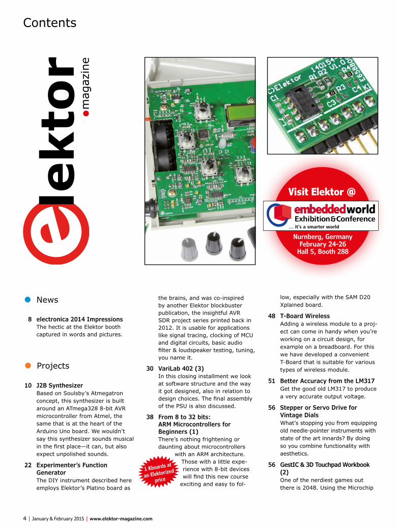
This project was born after I discovered the Atmegatron music synthesizer from Soulsby Synthesizers [1]. This synthesizer is built around an ATmega328 8-bit AVR microcontroller from Atmel, the same that is at the heart of the Arduino Uno board. The design of the Atmegatron presents several interesting aspects that at-tracted my attention and that ultimately resulted in the project described below.
Specifications• Monophonic 9-bit synthesizer• 32 waveforms + user defined• 15 filter types• 2 envelope generators• LFO with 16 waveforms• 15-pattern arpeggiator• 16 patch memories
• 6 live controls• MIDI • Patch saving/loading over MIDI• NXP LPC1347 32-bit ARM Cortex-M3
microcontroller• 2 output channels• Open Source & Open Hardware design
J2B Synthesizer
www.elektor-magazine.com | January & February 2015 | 11
First of all, before diving into the project, let me issue a warning to those of you mainly inter-ested in how the sound synthesis comes about within the synthesizer’s sound engine. Below is a description of the process of porting the Atmeg-atron to my own hardware platform. The sound engine proper will be described succinctly. If this is your only interest, have a look at Figure 2 and then read the source code [2] instead of this article.
AtmegatronYou are still around. In the Atmegatron (Fig-ure 1) the microcontroller unit (MCU) basically does everything, from synthesizing the sound to interacting with the user. It can also talk to other equipment through a Musical Instrument Digital Interface (MIDI) port. All this fits in the 32 KB program memory of the MCU, which I think is quite an achievement, especially considering the software got written as an Arduino sketch in C/C++, and Arduino can introduce quite a lot of overhead. The software is published with an open-source license and can be downloaded for free. Unfortunately the hardware design of the Atmegatron is closed (although it can be quite easily reconstructed from studying the software).
Another interesting feature is that the Atmega-tron was designed with live performance in mind and for this it is equipped with six potentiometer controls enabling you to modify ten sound param-eters on the fly. Together with a function selector and a function value encoder the synthesizer has eight controls. To top it off, a pushbutton selects between two modes (green or red). LEDs are used to show the mode and the values—there is no alphanumerical display.For those who like “sounds with a bite” as opposed to the sweet and smooth sounds usually produced by the well-established commercial products it is interesting to know that the Atmegatron features several algorithms to create ugly and distorted
sounds. It should therefore not be compared to the synthesizers manufactured by the big guns; it has its very distinct sound instead.The synthesizer uses the MCU’s pulsewidth mod-ulation (PWM) module to produce sounds. The functionality of the external digital-to-analog converter (DAC) can therefore be limited to an anti-aliasing filter.An open-source sound engine controlled by eight rotary controls (six potentiometers and two rotary encoders) and fitting in 32 KB made triggered me to find out if the lot could be ported to the Elek-tor J²B controller board I published a few years ago [3]. J²B was designed around an LPC1343, a 32-bit ARM Cortex-M3 MCU from NXP. Like the ATmega328 it has 32 KB of program memory and all the other peripherals used by the synthesizer, including excellent PWM capabilities. Furthermore, the J²B board supports up to nine rotary encod-ers, or eight plus a pushbutton, which is perfect for this job. What’s missing though is an EEPROM to store its sound presets, but there are ways around that.The Atmegatron uses bicolor LEDs to show val-ues, positions and modes without the need for an alphanumerical display. The J²B board does have an LCD, you can even choose between three sizes, so I decided to replace the LEDs by an LCD-based human-machine interface.
Figure 1. The Atmegatron was at the origin of this project.
From: Elektor Academy & element14
Presenter: Clemens Valens
Date: January 22, 4 pm CET
Sign up: www.elektor.com/webinar
Free
live webinar
on the J2B
Synthesizer

•Projects
12 | January & February 2015 | www.elektor-magazine.com
Typical pitfalls encountered during this stage are inconsequent data type usage in the software itself and incompatible data types between com-pilers (AVR GCC for Arduino versus ARM GCC for Eclipse/LPCXpresso). Both problems lead to similar bugs: data overflow (variables that no longer fit in the memory space reserved for them) and unintended sign conversions (negative numbers that flip positive and vice versa). Such problems can be easily avoided by rigid use of well-defined data types that clearly indicate their size in bits and being signed or not. For exam-ple, use uint8_t for an 8-bit unsigned integer value instead of unsigned char. Use int16_t or int32_t instead of int, because the size of int is highly platform dependent. Better still, use data types that show what kind of data they hold. For instance, create a data type sample_t and use it only to hold sample values and stick to that throughout the code. More difficult porting situations arise from differ-ences between the hardware platforms. Timers are relatively easy peripherals to port because setting them up is more or less similar on most MCUs. All you need is a good understanding of how the timer is supposed to work. But what if the target platform does not have the func-
tion used by the source platform? Or what if peripherals behave slightly differently? This turned out to be the case for the PWM module of the LPC1343 that does not quite work in the same way as the PWM module of the ATmega328 and that resulted in distorted sound. Let me explain.On the AVR the PWM mod-ule continuously compares a counter to a threshold and sets its output accordingly. This determines the PM sig-nal’s duty-cycle. When the counter value is equal to or higher than the threshold the PWM output is low (or high, depending on how you con-figure it), when the counter value is lower than the threshold the PWM output
is high. If, in this case, you move the threshold below the
counter value, the PWM output will immediately go low. The C-like pseudocode looks like this:
The porting effort boiled down to three main tasks:1. Porting the Arduino sketch for the ATmega328
to an Eclipse/LPCXpresso project for the LPC1343;
2. Replacing the six analog pots by six digital rotary encoders;
3. Replacing the bicolor LEDs by an LCD.
Task 1Porting microcontroller code can be more or less daunting depending on how the original soft-ware was written. A well-structured project is much easier to port than spaghetti code. Also the hardware abstraction level determines the portability of code. Code that calls functions to modify registers and peripherals is much easier to port than lines that interact directly with the hardware whenever they need to. Furthermore, one file that groups all these functions is eas-ier to handle than code having these functions all over the place. Luckily the Atmegatron code is well structured, well documented and utterly portable and I could do a large part of it while watching a Bruce Willis movie on TV. Most of the work involved creating header files needed for the Eclipse/LPCXpresso C project (Arduino sketches can be written without such header files).
J2B Synthesizer
www.elektor-magazine.com | January & February 2015 | 13
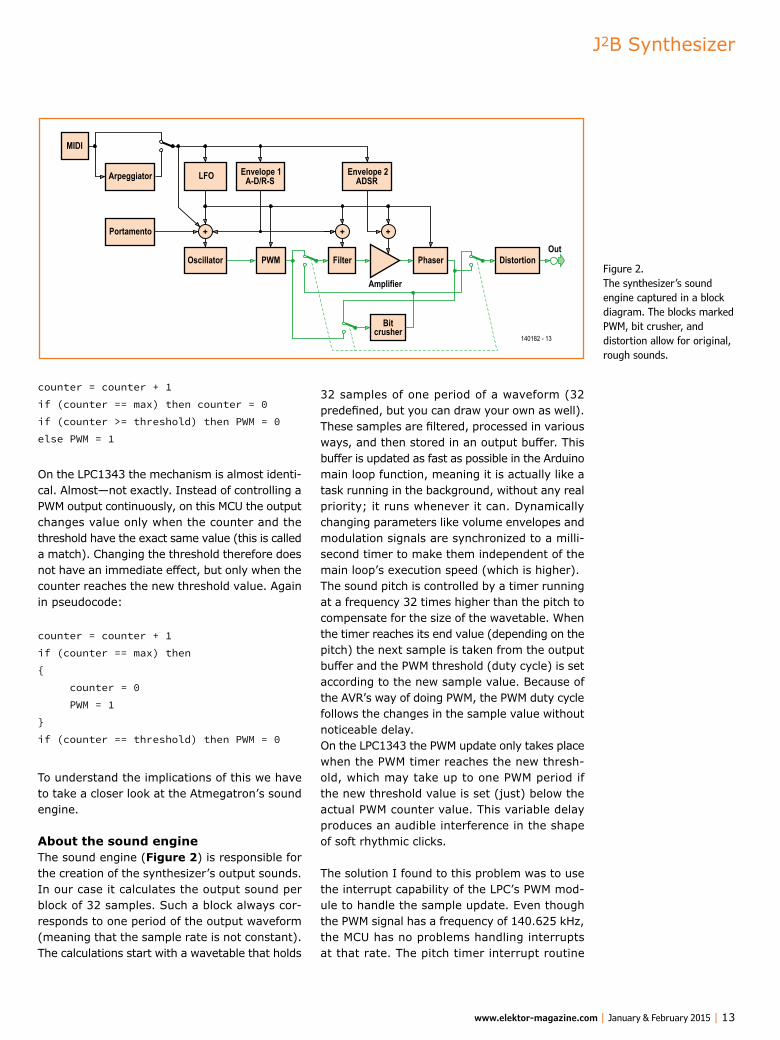
32 samples of one period of a waveform (32 predefined, but you can draw your own as well). These samples are filtered, processed in various ways, and then stored in an output buffer. This buffer is updated as fast as possible in the Arduino main loop function, meaning it is actually like a task running in the background, without any real priority; it runs whenever it can. Dynamically changing parameters like volume envelopes and modulation signals are synchronized to a milli-second timer to make them independent of the main loop’s execution speed (which is higher).The sound pitch is controlled by a timer running at a frequency 32 times higher than the pitch to compensate for the size of the wavetable. When the timer reaches its end value (depending on the pitch) the next sample is taken from the output buffer and the PWM threshold (duty cycle) is set according to the new sample value. Because of the AVR’s way of doing PWM, the PWM duty cycle follows the changes in the sample value without noticeable delay.On the LPC1343 the PWM update only takes place when the PWM timer reaches the new thresh-old, which may take up to one PWM period if the new threshold value is set (just) below the actual PWM counter value. This variable delay produces an audible interference in the shape of soft rhythmic clicks.
The solution I found to this problem was to use the interrupt capability of the LPC’s PWM mod-ule to handle the sample update. Even though the PWM signal has a frequency of 140.625 kHz, the MCU has no problems handling interrupts at that rate. The pitch timer interrupt routine
counter = counter + 1if (counter == max) then counter = 0if (counter >= threshold) then PWM = 0else PWM = 1
On the LPC1343 the mechanism is almost identi-cal. Almost—not exactly. Instead of controlling a PWM output continuously, on this MCU the output changes value only when the counter and the threshold have the exact same value (this is called a match). Changing the threshold therefore does not have an immediate effect, but only when the counter reaches the new threshold value. Again in pseudocode:
counter = counter + 1if (counter == max) then counter = 0 PWM = 1if (counter == threshold) then PWM = 0
To understand the implications of this we have to take a closer look at the Atmegatron’s sound engine.
About the sound engineThe sound engine (Figure 2) is responsible for the creation of the synthesizer’s output sounds. In our case it calculates the output sound per block of 32 samples. Such a block always cor-responds to one period of the output waveform (meaning that the sample rate is not constant). The calculations start with a wavetable that holds
Amplifier
140182 - 13
Filter
MIDI
Phaser
Bitcrusher
OutPWMOscillator
LFO Envelope 1A-D/R-S
Envelope 2ADSR
Portamento
Arpeggiator
DistortionFigure 2. The synthesizer’s sound engine captured in a block diagram. The blocks marked PWM, bit crusher, and distortion allow for original, rough sounds.
•Projects
14 | January & February 2015 | www.elektor-magazine.com
was due in part to the LPCXpresso hardware abstraction library for the LPC1343 and in part to the newlib library included by default in an LPCXpresso project. Besides being the standard C library, it also provides printf-like debug support, even in Release mode, which you can remove if you don’t need it. The option is hard to find, but can be worth the trouble of searching. Go to the project’s properties and expand “C/C++ Build” followed by “Settings”. Then select “Managed Linker Script” in the list under “Tool Settings” to get access to the library (you may have to expand the “MCU Linker” item first). After a bit of experimentation I found that the library “Redlib (none)” gave good results, as good as any other “(none)” library. This trick freed up a good deal of memory, but I still had to implement EEPROM support and a part of the user interface. Anyway, this basically completed Task 1.
Task 2Replacing potentiometers by rotary encoders may seem trivial, but in reality it is not. Rotary encod-ers do not have the same feel as a potentiometer being turned from min to max with a fast finger movement. By contrast, rotary encoders allow very precise control of a parameter, but without trickery you will need many rotations to cover the parameter’s full range. Some sort of acceler-ation mechanism is needed to get the ‘pot feel’ without losing the encoder’s precision.To get this right I decided to take an engineering approach—usually I am more the trial-and-er-ror kind of person—so I hooked up the oscillo-scope to my favorite rotary encoder (24 detents/rotation) and started measuring rotation speeds. From this I learned that if you spin this encoder as fast as you can, pulse rates of up to about 100 Hz are a reality. My goal was to go through the range of 0 to 255 in one quick spin instead of ten full rotations and now aware of the pos-sible pulse rates I could design an algorithm for measuring the rate, and compute an accelera-tion factor from it. The result is pretty good and I am quite satisfied with the way the accelerated digital controls turned out.
Task 3The third task was to replace the bicolor LEDs by an alphanumeric LCD. I could have kept the LEDs but that would have meant adding port expanders to the MCU and my objective was to stay as close as possible to the J²B board. The
still cycles through the sample output buffer as before, but instead of updating the PWM threshold directly with the new sample a variable is used for intermediate storage. The PWM interrupt rou-tine reads the intermediate variable and employs it to update the PWM duty cycle. Now the PWM update is neatly synchronized to the PWM signal itself and the clicks are eliminated.
Low on memoryWhen my porting activities neared completion I ran into another problem: not enough memory. Surprising, as the AVR and the LPC have the same amount of program memory space (32 KB) and actually I had expected the LPC code to be more memory efficient, especially since it is compiled as so-called thumb code which is meant to save program space. Possibly the Arduino compiler is really good? Or the AVR is really code effi-cient? Anyway, the excess weight of my porting
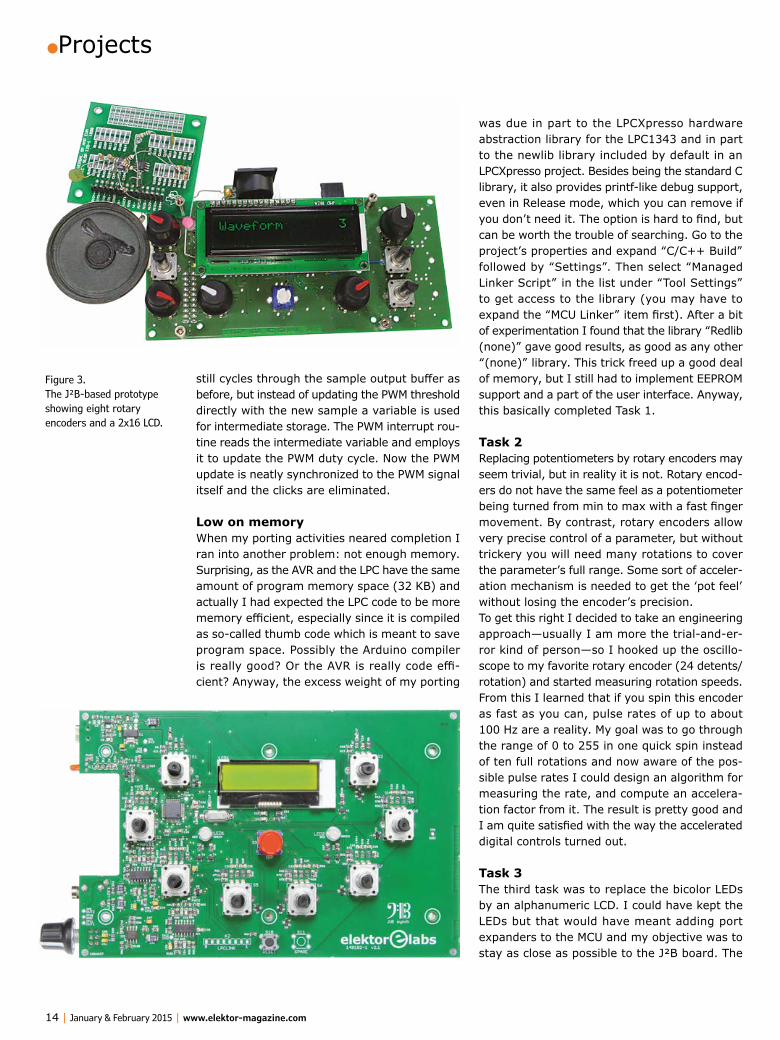
Figure 3. The J²B-based prototype showing eight rotary encoders and a 2x16 LCD.
J2B Synthesizer
www.elektor-magazine.com | January & February 2015 | 15
me with a cut-off frequency of 15 kHz (my ears don’t hear anything above that). That took me about 30 seconds. The rest of the board took a bit longer but about ten days later (i.e. the PCB manufacturing time) I could start assembling my new prototype.Unfortunately it dawned upon me that my hard-ware approach was a disaster. There were too many connections to make between the J²B board and the second PCB and, to make things worse, most of the connections were almost inaccessi-ble. After some silly efforts I decided to give up.I now had an unusable mechanical design with a slight memory problem. This made me think. To get things right I should forget about the J²B board and completely redo the design. But, if I had to redo it all, then why stick to the LPC1343? Since this MCU family appeared a few years ago it a new device had emerged, the LPC1347, which not only offers twice the memory size (64 KB) but also incorporates a 4 KB EEPROM. It still had the excellent built-in USB bootloader, so why not switch to the new 1347?
advantage of an LCD is the ability to supply more information which saves the user from memoriz-ing the user manual. Having eight rotary encoders on the J²B board implies the use of a 2x16 LCD, otherwise there is not enough room to fit everything on the board (see Figure 3). Coming up with good texts for the display is one of the hardest parts, but not as hard as finding a good way to display the values or positions of the six live controls. The easy way is of course to display two rows of three values but then the relation between the position of the value on the display and the corresponding encoder is not very clear. After a lot of thinking I finally found a pleasing solution, I believe, in the form of small slider icons. A standard LCD allows up to eight 5 x 7 custom characters, and that is just enough to create a 7-position vertical slider. Spread out over two rows (two characters, one above the other) you get 14 positions and by adding a special 0 and Maximum character a 16-position slider is created.A special algorithm detects if the user uses a live control or the function/value encoders so the software can switch automatically between two pages and show relevant information when it is needed.To handle the red and green modes of the Atmeg-atron I simply added a bicolor LED, although I would have preferred to use the LCD module’s backlight for this.
On to the hardwareOnce I had a working albeit not fully functional prototype running on my J²B board (Figure 3) it was time to turn to the hardware design of the synthesizer. I wanted to use the J²B board as the brains, but during experimentation it had become obvious that the position of the encoders on the board was not sufficiently ergonomic—they were too close together. Since I had to design an add-on board for the anti-aliasing filter, the MIDI interface and the headphone amplifier, with an EEPROM on it as well, I decided to design a larger motherboard that would hold the encoders too and ready to take the J²B board as a daughter-board. On the motherboard there would be more than enough room to allow the use of through-hole parts from the Elektor Labs Preferred Parts (ELPP) library as much as possible.Designing this board didn’t take long. For the anti-aliasing filter Microchip’s free FilterLab utility kindly calculated a fifth-order Chebychev filter for
A note about sound qualityThe Atmegatron was designed as a lo-fi 8-bit synthesizer; it has no pretention of being a high quality music synthesizer and it sounds that way. It is capable of aggressive and ugly sounds thanks to its special distortion algorithms and it generates all kinds of computerish beeps. It sounds a bit like a Casio keyboard from the 80’s on steroids. Having that said, it offers some excellent sounds and lots of playing fun. The arpeggiator is a nice feature to have. For the J²B port I improved the sound quality a bit, literally, because the LPC1347 has 16-bit PWM whereas the Atmegatron only has 8 (the 16-bit PWM mode of the AVR is too slow for this application). This allowed me to increase the PWM depth by one bit, so now it is a 9-bit synthesizer. I also more than doubled the PWM frequency so that anti-aliasing filtering (5th order instead of 3rd order on the Atmegatron) is better, improving sound quality further.There are still lots of possibilities left for sound quality improvements. The sound engine algorithms tend to truncate their outputs to eight bits. Having a 32-bit MCU this is a bit of a shame. The wavetables could be longer. Filtering now uses floating point arithmetic, which is OK, but time and memory consuming. Moving to fixed-point filters would free up a lot of processing power for other sound algorithms.Another interesting extension would be to add virtual synthesizer capabilities using the USB port, and/or MIDI over USB.The J²B synthesizer is an inexpensive platform that allows you to experiment with computer based sound synthesis directly on the instrument. Prog’n’Play is the word.
•Projects
16 | January & February 2015 | www.elektor-magazine.com
X1
12MHzC20
18p
C17
18p
C16
100n
C18
10n
C22
100n
C23
10n
+3V3
PIO0_1/CLKOUT/CT32B0_MAT2/USB_FTOGGLE
SWCLK/PIO0_10/SCK0/CT16B0_MAT2
PIO0_16/AD5/CT32B1_MAT3/WAKEUP
PIO0_22/AD6/CT16B1_MAT1/MISO1
SWDIO/PIO0_15/AD4/CT32B1_MAT2
PIO0_9/MOSI0/CT16B0_MAT1/SWO
TRST/PIO0_14/AD3/CT32B1_MAT1
PIO1_15/DCD/CT16B0_MAT2/SCK1
TMS/PIO0_12/AD1/CT32B1_CAP0TDO/PIO0_13/AD2/CT32B1_MAT0
PIO1_13/DTR/CT16B0_MAT0/TXDPIO1_14/DSR/CT16B0_MAT1/RXD
TDI/PIO_11/AD0/CT32B0_MAT3
PIO1_23/CT16B1_MAT1/SSEL1
PIO0_21/CT16B1_MAT0/MOSI1
PIO0_2/SSEL0/CT16B0_CAP0
PIO1_28/CT32B0_CAP0/SCLK
PIO0_8/MISO0/CT16B0_MAT0
PIO1_29/SCK0/CT32B0_CAP1
PIO1_26/CT32B0_MAT2/RXDPIO1_27/CT32B0_MAT3/TXD
PIO0_6/USB_CONNECT/SCK0
PIO0_17/RTS/CT32B0_MAT0PIO0_18/RXD/CT32B0_MAT0PIO0_19/TXD/CT32B0_MAT1
PIO1_16/RI/CT16B0_CAP0
PIO1_25/CT32B0_MAT1
PIO0_20/CT16B1_CAP0
PIO1_24/CT32B0_MAT0
PIO1_19/DTR/SSEL1
PIO1_21/DCD/MISO1PIO1_20/DSR/SCK1
PIO1_22/RI/MOSI1
PIO0_3/USB-VBUS
RESET/PIO0_0
LPC1347FBD48
PIO0_23/AD7
PIO0_4/SCLPIO0_5/SDA
PIO0_7/CTS
XTALOUT
PIO1_31
USB_DM
XTALIN
USB_DP
IC2
VDDVDD
VSS VSS
44
1920
41
10141516222327
2928
323334353940454647
173042
1326381821
111224
2531
36374348
5
3
8
6 7
4
9
2
1
R94
100k
R13
100k
R15
NC
R33
4k7
R34
4k7
R59
100k
+3V3
RESETS9/ISP
S3AUSB_VBUS
SCLSDA
USB_CONNECTS4A
RED_LED2RED_LED1/SWO
GREEN_LED2/SWCLKS3BS4B
PWM1S5B
PWM2/SWDIOS6BS5A
GREEN_LED1S6AS7AS8AS7BS8B
S1AS1BS2AS2BROW0ROW1ROW2COL0FX32-1COL1
MIDI_LEDCOL2
TXDRXDLCD_RSTLCD_BL
K4
12345
Mini USB-B shielded
R433R
R333R
C4
18p
C8
18p
R161k
5
T1
BSS84P
USB_CONNECT
R17
1M
+3V3
R1
0R
C2
NC
D10
MBR0540T1G
L1
BLM21AG601SN1D
+5V
F-1515622
+5V
TP1
USB_DMUSB_DP
TP5
+5V
R2
100k
C1
100n
C3
100u6V3
R141k
LD1117S33IC1
C5
10u6V3
C11
10u6V3
+5V +3V3
TP2
TP3
USB_VBUS
C35
10u6V3
C41
10u6V3
C43
10n
+3V3
R510k
R610k
R9
10k
R11
10k
R710k
R810k
R10
10k
R12
10k
C6
10n
C9
10n
C7
10n
C10
10n
R2110k
R2410k
R29
10k
R31
10k
C12
10n
C13
10n
R23NC
R18
NC
R22
0R
S1 S2 S3
R4810k
R5110k
R53
10k
R58
10k
C26
10n
C27
10n
R50NC
R43
NC
R49
0R
S4
+3V3
D1BAT54
D2BAT54
D4BAT54
D5BAT54
COL0 COL1 COL2
COL0
ROW0 ROW0 ROW0
ROW1
S1A S1B S2A S2B S3A S3B
S4A S4BR63
10kR66
10k
R71
10k
R74
10k
C31
10n
C32
10n
R65NC
R61
NC
R64
0R
S5
R6710k
R7010k
R72
10k
R75
10k
C33
10n
C34
10n
R69NC
R62
NC
R68
0R
S6D7
BAT54D8
BAT54COL1 COL2ROW1 ROW1
S5A S5B S6A S6B
R4410k
R4710k
R52
10k
R57
10k
C24
10n
C25
10n
R46NC
R42
NC
R45
0R
S7
R2510k
R2810k
R30
10k
R32
10k
C14
10n
C15
10n
R27NC
R19
NC
R26
0R
S8D6
BAT54D3
BAT54COL0 COL1ROW2 ROW2
S7A S7B S8A S8B
+3V3
+3V3
D9BAT54
S11
SPARE
S9
ISP/MODE
S10
RESET
COL2 ROW2
S9/ISP
RESET
(optional)
IC3.C
9
10
8IC3.D
13
12
14IC3.A
2
3
1
R563k3
R40180R
R418k2
R54270R
R60820R
R801k
R78100R
R736k8
C38
220n
C28
15n
R3982k
R556k8
C30
680p
C29
680p
C39
680p
TP6
TP8
IC3.B
6
5
7
R77
100k
R79
100k
+3V3
C42
10u6V3 P1.A
10k log
IC4.C
9
10
8IC4.D
13
12
14IC4.A
2
3
1
R873k3
R83180R
R818k2
R85270R
R89820R
R1011k
R97100R
R936k8
C53
220n
C44
15n
R8282k
R866k8
C46
680p
C45
680p
C54
680p
TP7
IC4.B
6
5
7
R99
100k
R98
100k
+3V3
C55
10u6V3 P1.B
10k log
TP12
C51
10u6V3
C50
10u6V3
R95
NC
MONO
IC5.A
2
3
1
IC5.B6
57
R963k3
R1003k3
R903k3
R883k3
C40
100u6V3
C37
100u6V3
R8410R
L3
BLM21AG601SN1D
R7610R
L2
BLM21AG601SN1D
TP11
TP9
K3TBRS
R91
10k
R92
10k
+5V
C47
10u6V3
IC58
4
C52
100u6V3
C48
100n
+5V
TP10
IC311
4 C36
100n
+3V3
IC411
4 C49
100n
+3V3
88k73k48 8k45
1k1732R
88k73k48 8k45
1k1732R
TP4 IC3 = MCP6004IC4 = MCP6004IC5 = TDA1308
Jack stereo 3.5mm
PWM1
PWM2
FX32-1
K212345678
LPC-Link
+3V3
PWM2/SWDIOGREEN_LED2/SWCLK
RED_LED1/SWO
RESET
+5V
K1
1234
+5V
+5VMIDI_IN
MIDI_OUT0V
RXD
TXD
MIDI
R102
270R
LED3
MIDI_LED
LED1
R36
220R
R35
270R
T4
BSS84P
T3
BSS84P
+5V
LED2
R38
220R
R37
270R
T6
BSS84P
T5
BSS84P
+5V
GREEN_LED1 RED_LED2
RED_LED1/SWO GREEN_LED2/SWCLK
MCCOG21605B6W-SPTLYI
LCD1
2x 16
VOUT
LED–
LED+
VDD
VSS
SDASCLRST
C– C+
4
5
1 2 3 K A
678
C21
1u
+3V3
+3V3
T2
BSS84P
SDASCL
RESET
R20
47R
LCD_BL
C19
1u
+5V
140182 - 11
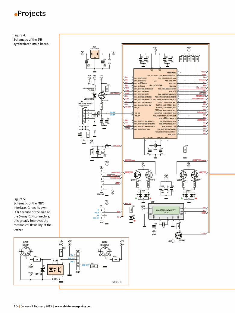
Figure 4. Schematic of the J2B synthesizer’s main board.
K202
2
3 1
5 4
MIDI OUTK203
2
3 1
5 4
MIDI IN
CNY17-3
IC2015
4
1
2
6D1
BAT54
R203220R
TP201
TP202
R204
1k
+5V
R201220R
MIDI_IN
MIDI_OUT
R202220R
+5V+5V
140182 - 12
+5V
GND
K201432
1
MIDI
Figure 5. Schematic of the MIDI interface. It has its own PCB because of the size of the 5-way DIN connectors, this greatly improves the mechanical flexibility of the design.

J2B Synthesizer
www.elektor-magazine.com | January & February 2015 | 17
X1
12MHzC20
18p
C17
18p
C16
100n
C18
10n
C22
100n
C23
10n
+3V3
PIO0_1/CLKOUT/CT32B0_MAT2/USB_FTOGGLE
SWCLK/PIO0_10/SCK0/CT16B0_MAT2
PIO0_16/AD5/CT32B1_MAT3/WAKEUP
PIO0_22/AD6/CT16B1_MAT1/MISO1
SWDIO/PIO0_15/AD4/CT32B1_MAT2
PIO0_9/MOSI0/CT16B0_MAT1/SWO
TRST/PIO0_14/AD3/CT32B1_MAT1
PIO1_15/DCD/CT16B0_MAT2/SCK1
TMS/PIO0_12/AD1/CT32B1_CAP0TDO/PIO0_13/AD2/CT32B1_MAT0
PIO1_13/DTR/CT16B0_MAT0/TXDPIO1_14/DSR/CT16B0_MAT1/RXD
TDI/PIO_11/AD0/CT32B0_MAT3
PIO1_23/CT16B1_MAT1/SSEL1
PIO0_21/CT16B1_MAT0/MOSI1
PIO0_2/SSEL0/CT16B0_CAP0
PIO1_28/CT32B0_CAP0/SCLK
PIO0_8/MISO0/CT16B0_MAT0
PIO1_29/SCK0/CT32B0_CAP1
PIO1_26/CT32B0_MAT2/RXDPIO1_27/CT32B0_MAT3/TXD
PIO0_6/USB_CONNECT/SCK0
PIO0_17/RTS/CT32B0_MAT0PIO0_18/RXD/CT32B0_MAT0PIO0_19/TXD/CT32B0_MAT1
PIO1_16/RI/CT16B0_CAP0
PIO1_25/CT32B0_MAT1
PIO0_20/CT16B1_CAP0
PIO1_24/CT32B0_MAT0
PIO1_19/DTR/SSEL1
PIO1_21/DCD/MISO1PIO1_20/DSR/SCK1
PIO1_22/RI/MOSI1
PIO0_3/USB-VBUS
RESET/PIO0_0
LPC1347FBD48
PIO0_23/AD7
PIO0_4/SCLPIO0_5/SDA
PIO0_7/CTS
XTALOUT
PIO1_31
USB_DM
XTALIN
USB_DP
IC2
VDDVDD
VSS VSS
44
1920
41
10141516222327
2928
323334353940454647
173042
1326381821
111224
2531
36374348
5
3
8
6 7
4
9
2
1
R94
100k
R13
100k
R15
NC
R33
4k7
R34
4k7
R59
100k
+3V3
RESETS9/ISP
S3AUSB_VBUS
SCLSDA
USB_CONNECTS4A
RED_LED2RED_LED1/SWO
GREEN_LED2/SWCLKS3BS4B
PWM1S5B
PWM2/SWDIOS6BS5A
GREEN_LED1S6AS7AS8AS7BS8B
S1AS1BS2AS2BROW0ROW1ROW2COL0FX32-1COL1
MIDI_LEDCOL2
TXDRXDLCD_RSTLCD_BL
K4
12345
Mini USB-B shielded
R433R
R333R
C4
18p
C8
18p
R16
1k5
T1
BSS84P
USB_CONNECT
R17
1M
+3V3
R1
0R
C2
NC
D10
MBR0540T1G
L1
BLM21AG601SN1D
+5V
F-1515622
+5V
TP1
USB_DMUSB_DP
TP5
+5V
R2
100k
C1
100n
C3
100u6V3
R141k
LD1117S33IC1
C5
10u6V3
C11
10u6V3
+5V +3V3
TP2
TP3
USB_VBUS
C35
10u6V3
C41
10u6V3
C43
10n
+3V3
R510k
R610k
R9
10k
R11
10k
R710k
R810k
R10
10k
R12
10k
C6
10n
C9
10n
C7
10n
C10
10n
R2110k
R2410k
R29
10k
R31
10k
C12
10n
C13
10n
R23NC
R18
NC
R22
0R
S1 S2 S3
R4810k
R5110k
R53
10k
R58
10k
C26
10n
C27
10n
R50NC
R43
NC
R49
0R
S4
+3V3
D1BAT54
D2BAT54
D4BAT54
D5BAT54
COL0 COL1 COL2
COL0
ROW0 ROW0 ROW0
ROW1
S1A S1B S2A S2B S3A S3B
S4A S4BR63
10kR66
10k
R71
10k
R7410
k
C31
10n
C32
10n
R65NC
R61
NC
R64
0R
S5
R6710k
R7010k
R72
10k
R75
10k
C33
10n
C34
10n
R69NC
R62
NC
R68
0R
S6D7
BAT54D8
BAT54COL1 COL2ROW1 ROW1
S5A S5B S6A S6B
R4410k
R4710k
R52
10k
R57
10k
C24
10n
C25
10n
R46NC
R42
NC
R45
0R
S7
R2510k
R2810k
R30
10k
R32
10k
C14
10n
C15
10n
R27NC
R19
NC
R26
0R
S8D6
BAT54D3
BAT54COL0 COL1ROW2 ROW2
S7A S7B S8A S8B
+3V3
+3V3
D9BAT54
S11
SPARE
S9
ISP/MODE
S10
RESET
COL2 ROW2
S9/ISP
RESET
(optional)
IC3.C
9
10
8IC3.D
13
12
14IC3.A
2
3
1
R563k3
R40180R
R418k2
R54270R
R60820R
R801k
R78100R
R736k8
C38
220n
C28
15n
R3982k
R556k8
C30
680p
C29
680p
C39
680p
TP6
TP8
IC3.B
6
5
7
R77
100k
R79
100k
+3V3
C42
10u6V3 P1.A
10k log
IC4.C
9
10
8IC4.D
13
12
14IC4.A
2
3
1
R873k3
R83180R
R818k2
R85270R
R89820R
R1011k
R97100R
R936k8
C53
220n
C44
15n
R8282k
R866k8
C46
680p
C45
680p
C54
680p
TP7
IC4.B
6
5
7
R99
100k
R98
100k
+3V3
C55
10u6V3 P1.B
10k log
TP12
C51
10u6V3
C50
10u6V3
R95
NC
MONO
IC5.A
2
3
1
IC5.B6
57
R963k3
R1003k3
R903k3
R883k3
C40
100u6V3
C37
100u6V3
R8410R
L3
BLM21AG601SN1D
R7610R
L2
BLM21AG601SN1D
TP11
TP9
K3TBRS
R91
10k
R92
10k
+5V
C47
10u6V3
IC58
4
C52
100u6V3
C48
100n
+5V
TP10
IC311
4 C36
100n
+3V3
IC411
4 C49
100n
+3V3
88k73k48 8k45
1k1732R
88k73k48 8k45
1k1732R
TP4 IC3 = MCP6004IC4 = MCP6004IC5 = TDA1308
Jack stereo 3.5mm
PWM1
PWM2
FX32-1
K212345678
LPC-Link
+3V3
PWM2/SWDIOGREEN_LED2/SWCLK
RED_LED1/SWO
RESET
+5V
K1
1234
+5V
+5VMIDI_IN
MIDI_OUT0V
RXD
TXD
MIDI
R102
270R
LED3
MIDI_LED
LED1
R36
220R
R35
270R
T4
BSS84P
T3
BSS84P
+5V
LED2
R38
220R
R37
270R
T6
BSS84P
T5
BSS84P
+5V
GREEN_LED1 RED_LED2
RED_LED1/SWO GREEN_LED2/SWCLK
MCCOG21605B6W-SPTLYI
LCD1
2x 16
VOUT
LED–
LED+
VDD
VSS
SDASCLRST
C– C+
4
5
1 2 3 K A
678
C21
1u
+3V3
+3V3
T2
BSS84P
SDASCL
RESET
R20
47R
LCD_BL
C19
1u
+5V
140182 - 11
•Projects
18 | January & February 2015 | www.elektor-magazine.com
LED. During the code porting I had also discov-ered that the Atmegatron is equipped with an LED to indicate MIDI activity (I overlooked it in the user manual), so I added one too (three four ;-) ). Since the LPC1347 (but also the LPC1343) has several channels per PWM timer I decided to add a second anti-aliasing filter to allow for two-channel operation. After all, we are using a 32-bit Cortex-M3 running at 72 MHz and there should be some processing power left, so why not push it a bit?
The circuitLooking at the schematics of the synthesizer (Fig-ure 4) you will see no surprises. I managed to use all the available I/O ports. The eight rotary encoders take up 16 I/O ports, two per encoder. The bunch of resistors surrounding the six live controls serve the purpose of flexibility. Indeed, by using the right resistance values it becomes possible to replace such a rotary encoder by a potentiometer because one side of these encod-ers is connected to an input of the MCU’s ana-
Mk.IIMy new design (V2 or Mk.II) is therefore based on an LPC1347 and is SMD throughout (except for the connectors, encoders and LEDs). Out of symmetry considerations I added a second bicolor
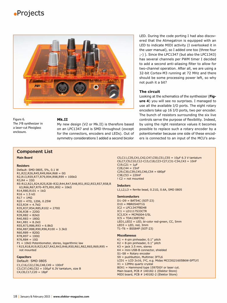
Figure 6. The J²B synthesizer in a laser-cut Plexiglass enclosure.
Component List Main Board
ResistorsDefault: SMD 0805, 5%, 0.1 WR1,R22,R26,R45,R49,R64,R68 = 0ΩR2,R13,R59,R77,R79,R94,R98,R99 = 100kΩR3,R4 = 33Ω R5-R12,R21,R24,R25,R28–R32,R44,R47,R48,R51,R52,R53,R57,R58,R
63,R66,R67,R70–R75,R91,R92 = 10kΩR14,R80,R101 = 1kΩR16 = 1.5 kΩR17 = 1MΩR20 = 47Ω, 1206, 0.25WR33,R34 = 4.7kΩR35,R37,R54,R85,R102 = 270ΩR36,R38 = 220ΩR39,R82 = 82kΩR40,R83 = 180ΩR41,R81 = 8.2kΩR55,R73,R86,R93 = 6.8kΩR56,R87,R88,R90,R96,R100 = 3.3kΩR60,R89 = 820ΩR78,R97 = 100ΩR76,R84 = 10ΩP1 = 10kΩ Potentiometer, stereo, logarithmic law ! R15,R18,R19,R23,R27,R42,R43,R46,R50,R61,R62,R65,R69,R95 =
not mounted
CapacitorsDefault: SMD 0805C1,C16,C22,C36,C48,C49 = 100nFC3,C37,C40,C52 = 100µF 6.3V tantalum, size BC4,C8,C17,C20 = 18pF
C5,C11,C35,C41,C42,C47,C50,C51,C55 = 10µF 6.3 V tantalumC6,C7,C9,C10,C12-C15,C18,C23-C27,C31-C34,C43 = 10nFC19,C21 = 1µFC28,C44 = 15nFC29,C30,C39,C45,C46,C54 = 680pFC38,C53 = 220nF! C2 = not mounted
InductorsL1,L2,L3 = ferrite bead, 0.21Ω, 0.6A, SMD 0805
SemiconductorsD1–D9 = BAT54C (SOT-23)D10 = MBR0540T1GIC2 = LPC1347FBD48IC1 = LD1117S33CTRIC3,IC4 = MCP6004-I/SLIC5 = TDA1308T/N2LED1,LED2 = LED, bi-color red-green, CC, 5mmLED3 = LED, red, 3mmT1–T6 = BSS84P (SOT-23)
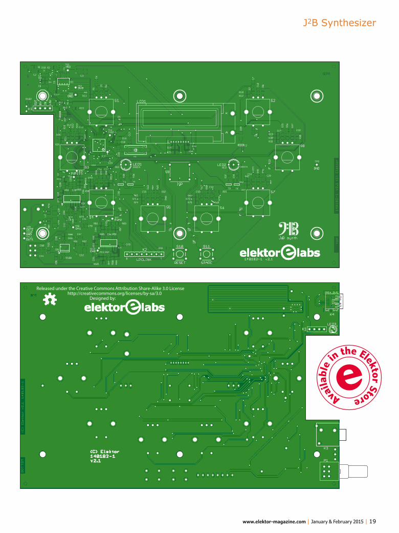
MiscellaneousK1 = 4-pin pinheader, 0.1” pitchK2 = 8-pin pinheader, 0.1” pitchK3 = jack 3.5 mm, stereoK4 = mini USB-B connector, shieldedS1–S8 = Rotary encoderS9 = pushbutton, Multimec 3FTL6LCD1 = LCD 2x16, I²C, e.g. Midas MCCOG21605B6W-SPTLYIX1 = 12MHz quartz crystal BOX1 = Hammond type 1597DGY or laser cut.Main board, PCB # 140182-1 (Elektor Store)MIDI board, PCB # 140182-2 (Elektor Store)
J2B Synthesizer
www.elektor-magazine.com | January & February 2015 | 19
18
•Projects
20 | January & February 2015 | www.elektor-magazine.com
E12 values can be used to obtain the required non-standard values. Two opamps remain unused, one per channel. The filter outputs pass through volume potentiometers that are isolated by two capacitors from any DC voltage to avoid crackling noises. Hi-end audio fans may frown on this, but it is good enough for this application. A stereo headphone amplifier makes sure that enough output power is available for most applications.
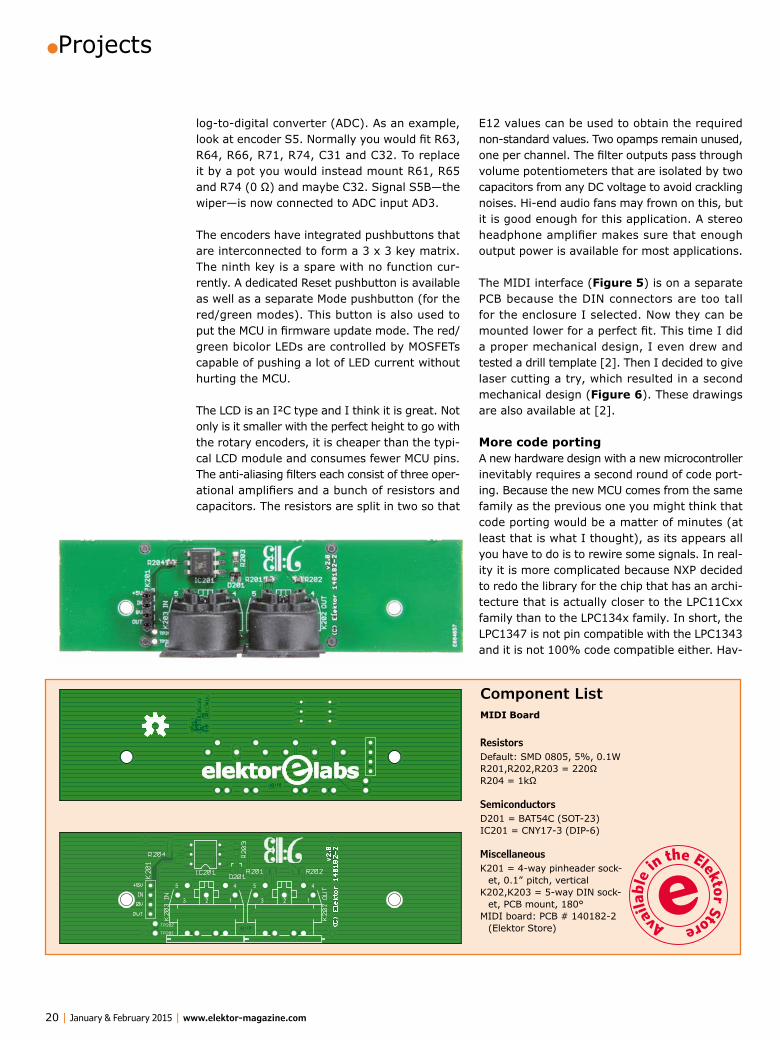
The MIDI interface (Figure 5) is on a separate PCB because the DIN connectors are too tall for the enclosure I selected. Now they can be mounted lower for a perfect fit. This time I did a proper mechanical design, I even drew and tested a drill template [2]. Then I decided to give laser cutting a try, which resulted in a second mechanical design (Figure 6). These drawings are also available at [2].
More code portingA new hardware design with a new microcontroller inevitably requires a second round of code port-ing. Because the new MCU comes from the same family as the previous one you might think that code porting would be a matter of minutes (at least that is what I thought), as its appears all you have to do is to rewire some signals. In real-ity it is more complicated because NXP decided to redo the library for the chip that has an archi-tecture that is actually closer to the LPC11Cxx family than to the LPC134x family. In short, the LPC1347 is not pin compatible with the LPC1343 and it is not 100% code compatible either. Hav-
log-to-digital converter (ADC). As an example, look at encoder S5. Normally you would fit R63, R64, R66, R71, R74, C31 and C32. To replace it by a pot you would instead mount R61, R65 and R74 (0 Ω) and maybe C32. Signal S5B—the wiper—is now connected to ADC input AD3.
The encoders have integrated pushbuttons that are interconnected to form a 3 x 3 key matrix. The ninth key is a spare with no function cur-rently. A dedicated Reset pushbutton is available as well as a separate Mode pushbutton (for the red/green modes). This button is also used to put the MCU in firmware update mode. The red/green bicolor LEDs are controlled by MOSFETs capable of pushing a lot of LED current without hurting the MCU.
The LCD is an I²C type and I think it is great. Not only is it smaller with the perfect height to go with the rotary encoders, it is cheaper than the typi-cal LCD module and consumes fewer MCU pins. The anti-aliasing filters each consist of three oper-ational amplifiers and a bunch of resistors and capacitors. The resistors are split in two so that
Component ListMIDI Board
ResistorsDefault: SMD 0805, 5%, 0.1WR201,R202,R203 = 220ΩR204 = 1kΩ
SemiconductorsD201 = BAT54C (SOT-23)IC201 = CNY17-3 (DIP-6)
MiscellaneousK201 = 4-way pinheader sock-
et, 0.1” pitch, verticalK202,K203 = 5-way DIN sock-
et, PCB mount, 180°MIDI board: PCB # 140182-2
(Elektor Store)

J2B Synthesizer
ing gotten this far I just bit the bullet and started sifting through the code to fix the compatibility issues.
Do it yourselfThe LPCXpresso/Eclipse software project of the synthesizer con-sists of three sub-proj-ects, one for the chip library, one for the board library and one for the synthesizer application itself. This is a bit more complicated than nec-essary, but that is how it is. You can import the package as a zip file (i.e. without unpacking it first). After successful compilation you will find a BIN file in the Release folder of the synthesizer project. To program the MCU with it all you have to do is to connect the synthesizer to a free USB port on a computer running Windows while keeping the red/green Mode pushbutton pressed (the synthesizer should be unpowered—the PC will provide power). If all is well Windows should detect a USB thumb drive of 64 KB with one file on it. Delete this file and copy the BIN file on the drive. If you have access to the Reset button, press it—if not, switch off the power to the synthesizer and then switch it back on. The display should now greet you with the message “J2B Synthesizer” in a large font. When it vanishes the synthesizer is ready for use. Connect a MIDI keyboard and headphones and start playing.
It’s all openThis project is 100% open source and open hardware. All design files, hardware, software, and mechanical, are available free of charge at [2]. I invite you to have a look at it and try to improve the synthesizer; there are lots of opportunities on all fronts. If you build your own, please send me a photograph or add one in a contribution to the project web page [2].
User ManualThe good thing of porting the Atmegatron instead of developing a new one from scratch is that we can profit from the User Manual and the Librarian utility cre-ated for the Atmegatron. This saved me a lot of writing. Download it from [1] and read it carefully, it is comprehensive. The J²B synthesizer has all of the original controls except for the tone control. The pushbuttons of the six live controls that are nonexistent on the Atmegatron allow you to quickly reset the value of the parameter that they control.
(140182-I)
Web Links
[1] Atmegatron: http://soulsbysynths.com/
[2] Project downloads: www.elektor-magazine.com/140182
[3] J²B: Universal MMI Module using ARM Cortex-M3. Elektor September 2011, www.elektor-magazine.com/110274; www.elektor-labs.com/node/3832
Batronix
Attractive prices Expert advice Large selection in stock 30 day trial period Money back guarantee EU wide free shipping
for most products
NEW
Rigol DS1000E Oscilloscopes2 channels, 50/100 MHz, 1 GSa/s sample rate, 1 million measurement points memory, USB, LAN, easy measurement features,3 years warranty
Batronix [email protected] Lise-Meitner-Str. 1-7 www.batronix.com24223 Schwentinental Germany
Use our special offers now:www.batronix.com/go/48
UNBEATABLEat price-performance ratio.
from € 239,- netincl. EU wide free shipping
Rigol DS1000Z Oscilloscopes4 channels, 50-100 MHz, 1 GSa/s sample rate, 12 million measurement points memory, USB, LAN, professional measure & analyse features, opt. built-in waveform generator,3 years warranty
from € 299,- netincl. EU wide free shipping
Make your LIVE easier.
with BATRONIX satisfaction- guarantee
Leading TECHNOLOGY
Adve
rtise
men
t
22 | January & February 2015 | www.elektor-magazine.com
A function generator supplies periodic signals of different shapes, across certain ranges in terms of frequency and amplitude. In friendly coex-istence with a multimeter, a power supply and an oscilloscope the function generator is vital to anyone serious about designing, making and even sharing electronics which is what Elektor is all about. The DIY instrument described here
employs Elektor’s Platino board [1] as the brains, and was co-inspired by another Elektor block-buster publication, the insightful AVR SDR proj-ect series printed back in 2012 [2].
The ingredientsViewed as a building block, the Platino controller board requires a minimum of add-ons to make digital-and-analog hybrids come alive without running into design issues, enormous BOMs and other complexities. Unsurprisingly in 2015 our Platino-based Experimenter’s Function Generator has two major aspects: hardware and software. Both are mutually responsible for the stability and accuracy of the output signals. The heart of the project is an ATMEGA1284P microcontroller running dedicated firmware. The hardware then, consists of two sections: Platino MCU board with LCD, and the Signal Generator Add-on Board, where “generator” is slightly off the Latin mark as nothing is being ‘generated’ per se; the Pla-tino does all that.
Platino MCU board with LCDTogether with the add-on board the Platino board with its ATMega1284P MCU controls and gener-
By Sunil Malekar (Elektor Labs India)
Experimenter’s Function GeneratorPlatino’d for squarewave, sine, sawtooth, noise, and more
This Function Generator was designed
to meet not too ambitious applications
and should make a valuable asset in your
workspace, at home, or in the lab. Firm-
ly based on Elektor’s ‘Platino’ controller
concept, it is usable for applications like
signal tracing, clocking of MCU and digital
circuits, basic audio filter & loudspeaker
testing, tuning, you name it.
Specifications & Features• ATMEGA1284P microcontroller on Platino board• 20 x 4 LCD Display• DC Input: 18–20 VDC• Standard BNC type connectors for outputs / input• Outputs:
- Clock, max. 10 MHz, 5 V / 3.3 V switchable - Sine, Square, Triangular, Sawtooth, Inverted Sawtooth, Pulse, Arbitrary and
Random (Noise), max. 100 kHz, max approx. 5 V into 50 Ω• Input: Frequency Modulation (125 kHz ±50 Hz for SDR)• Controls: rotary encoder control with pushbutton, Back button• Setup Mode for Arbitrary and Clock mode• Normal Mode for other output waveforms• Waveform Amplitude, Frequency, Offset adjustable in real time• One calibration setting
Experimenter’s Function Generator
www.elektor-magazine.com | January & February 2015 | 23
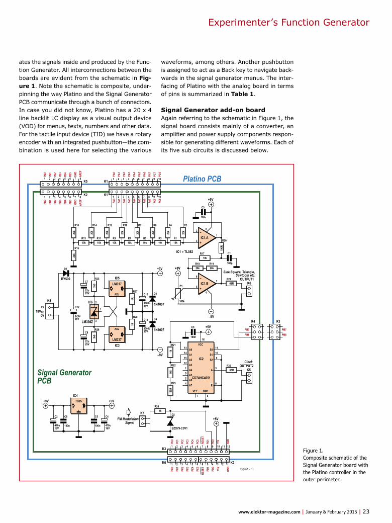
ates the signals inside and produced by the Func-tion Generator. All interconnections between the boards are evident from the schematic in Fig-ure 1. Note the schematic is composite, under-pinning the way Platino and the Signal Generator PCB communicate through a bunch of connectors.In case you did not know, Platino has a 20 x 4 line backlit LC display as a visual output device (VOD) for menus, texts, numbers and other data. For the tactile input device (TID) we have a rotary encoder with an integrated pushbutton—the com-bination is used here for selecting the various
waveforms, among others. Another pushbutton is assigned to act as a Back key to navigate back-wards in the signal generator menus. The inter-facing of Platino with the analog board in terms of pins is summarized in Table 1.
Signal Generator add-on boardAgain referring to the schematic in Figure 1, the signal board consists mainly of a converter, an amplifier and power supply components respon-sible for generating different waveforms. Each of its five sub circuits is discussed below.
Platino PCB
Signal GeneratorPCB
LM317IC5
ADJ
LM337IC3
ADJ
R27
1R
R28
1R
R25
3k9
R26
3k9
LM336Z
IC6 2
3
1
C8
22u25V
C7
22u25V
C12
470u35V
C10
1000u35V
C11
1000u35V
D3
1N4007
D4
1N4007
D1
BY500
K8+V
18VDC0V
+9V
–9V
7805IC4
C2
470u16V
C6
100n
C4
470u16V
C5
100n
+5V+9V
K7
R241k
D2
BZX79-C5V1
CD74HC4051
IC2
GNDVEE
VCC1110
12151413
16
A0A1A2A3A4A5A6A7
S0S1S2
A
E
9
6
3
4251
87
+5VC9
100n
R21
1k
R22
1k8
R23
120R
R3068R K5
R16
20k
R15
20k
R1310k
R1110k
R910k
R710k
R110k
R310k
R510k
R14
20k
R12
20k
R10
20k
R8
20k
R6
20k
R4
20k
R2
20k
IC1.A
2
3
1
IC1.B
IC1 = TL082
6
5
7
R1820k
R1920k
K6R29
68R
R20
100R
C1
100p
R1710k
P1
100k
+9V
C3
100n
–9V
+9V
8
4
K1 101 2 3 4 5 6 7 8 9
K3 10 11 121 2 3 4 5 6 7 8 9
+5V
K4
K21 2 3 4 5 6 7 8
K3
K1 101 2 3 4 5 6 7 8 9K51 2 3 4 5 6 7 8
K2123456K6 1 2 3 4 5 6130407 - 11
PA0
PA1
PA2
PA3
PA4
PA5
PA6
PA7
PC7
PC6
PA0
PA1
PA2
PA3
PA4
PA5
PA6
PA7
PC7
PC6
PB0
PB1
PB2
PB3
PB4
PB5
GND
AREF
PB0
PB1
PB2
PB3
PB4
PB5
GND
AREF
PB7PB6
PB7PB6
PC0
PC1
PC2
PC3
PC4
PD1
PD0
PC5
RESE
T
+5V
GND
PC0
PC1
PC2
PC3
PC4
PD1
PD0
PC5
RESE
T
+5V
GND
FM ModulationSignal
OUTPUT2Clock
OUTPUT1
Sine,Square, Triangle,Sawtooth etc.
Figure 1. Composite schematic of the Signal Generator board with the Platino controller in the outer perimeter.
24 | January & February 2015 | www.elektor-magazine.com
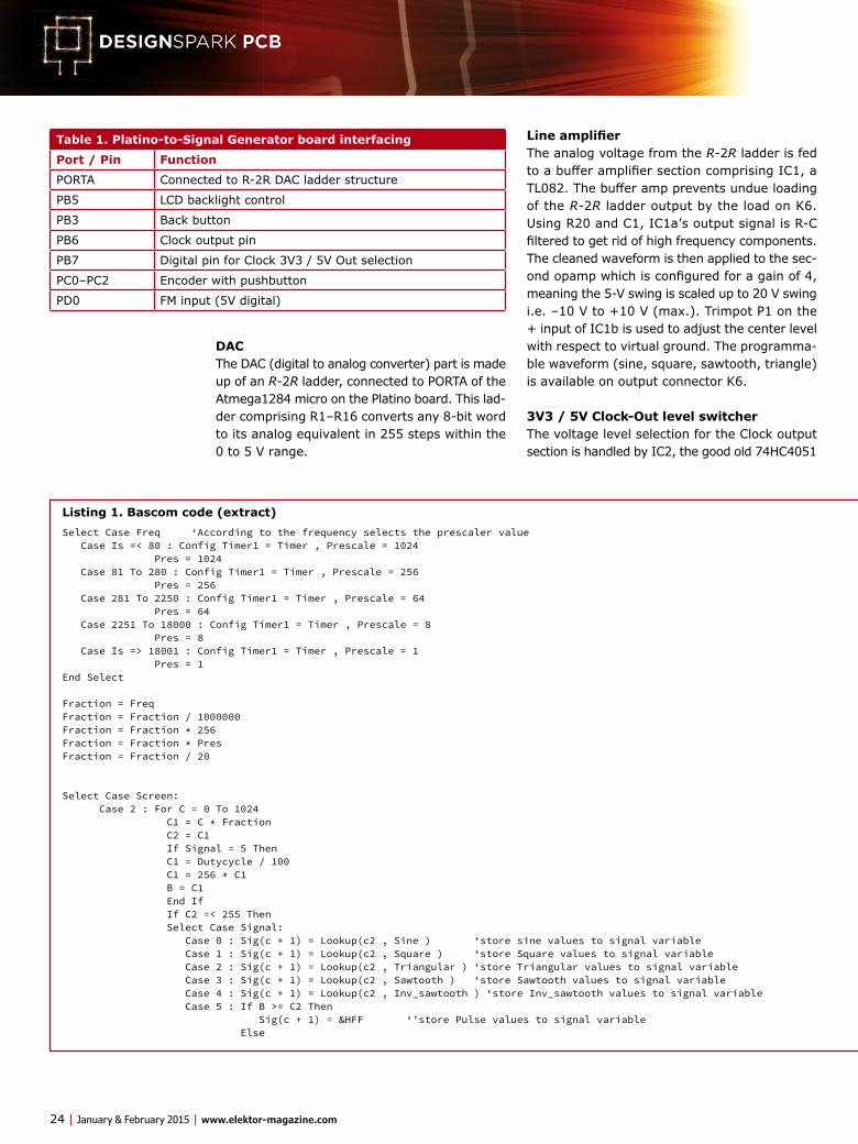
Line amplifierThe analog voltage from the R-2R ladder is fed to a buffer amplifier section comprising IC1, a TL082. The buffer amp prevents undue loading of the R-2R ladder output by the load on K6. Using R20 and C1, IC1a’s output signal is R-C filtered to get rid of high frequency components. The cleaned waveform is then applied to the sec-ond opamp which is configured for a gain of 4, meaning the 5-V swing is scaled up to 20 V swing i.e. –10 V to +10 V (max.). Trimpot P1 on the + input of IC1b is used to adjust the center level with respect to virtual ground. The programma-ble waveform (sine, square, sawtooth, triangle) is available on output connector K6.
3V3 / 5V Clock-Out level switcherThe voltage level selection for the Clock output section is handled by IC2, the good old 74HC4051
DACThe DAC (digital to analog converter) part is made up of an R-2R ladder, connected to PORTA of the Atmega1284 micro on the Platino board. This lad-der comprising R1–R16 converts any 8-bit word to its analog equivalent in 255 steps within the 0 to 5 V range.
Table 1. Platino-to-Signal Generator board interfacing
Port / Pin Function
PORTA Connected to R-2R DAC ladder structure
PB5 LCD backlight control
PB3 Back button
PB6 Clock output pin
PB7 Digital pin for Clock 3V3 / 5V Out selection
PC0–PC2 Encoder with pushbutton
PD0 FM input (5V digital)
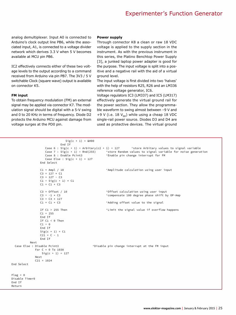
Listing 1. Bascom code (extract)
Select Case Freq ‘According to the frequency selects the prescaler value Case Is =< 80 : Config Timer1 = Timer , Prescale = 1024 Pres = 1024 Case 81 To 280 : Config Timer1 = Timer , Prescale = 256 Pres = 256 Case 281 To 2250 : Config Timer1 = Timer , Prescale = 64 Pres = 64 Case 2251 To 18000 : Config Timer1 = Timer , Prescale = 8 Pres = 8 Case Is => 18001 : Config Timer1 = Timer , Prescale = 1 Pres = 1End Select
Fraction = FreqFraction = Fraction / 1000000Fraction = Fraction * 256Fraction = Fraction * PresFraction = Fraction / 20
Select Case Screen: Case 2 : For C = 0 To 1024 C1 = C * Fraction C2 = C1 If Signal = 5 Then C1 = Dutycycle / 100 C1 = 256 * C1 B = C1 End If If C2 =< 255 Then Select Case Signal: Case 0 : Sig(c + 1) = Lookup(c2 , Sine ) ‘store sine values to signal variable Case 1 : Sig(c + 1) = Lookup(c2 , Square ) ‘store Square values to signal variable Case 2 : Sig(c + 1) = Lookup(c2 , Triangular ) ‘store Triangular values to signal variable Case 3 : Sig(c + 1) = Lookup(c2 , Sawtooth ) ‘store Sawtooth values to signal variable Case 4 : Sig(c + 1) = Lookup(c2 , Inv_sawtooth ) ‘store Inv_sawtooth values to signal variable Case 5 : If B >= C2 Then Sig(c + 1) = &HFF ‘’store Pulse values to signal variable Else
Experimenter’s Function Generator
www.elektor-magazine.com | January & February 2015 | 25
Power supplyThrough connector K8 a clean or raw 18 VDC voltage is applied to the supply section in the instrument. As with the previous instrument in this series, the Platino Benchtop Power Supply [3], a junked laptop power adapter is good for the purpose. The input voltage is split into a pos-itive and a negative rail with the aid of a virtual ground level.The input voltage is first divided into two ‘halves’ with the help of resistors R25, R26 and an LM336 reference voltage generator, IC6.Voltage regulators IC3 (LM337) and IC5 (LM317) effectively generate the virtual ground rail for the power section. They allow the programma-ble waveform to swing almost between –9 V and +9 V (i.e. 18 Vpp) while using a cheap 18 VDC single-rail power source. Diodes D3 and D4 are used as protective devices. The virtual ground
analog demultiplexer. Input A0 is connected to Arduino’s clock output line PB6, while the asso-ciated input, A1, is connected to a voltage divider network which derives 3.3 V when 5 V becomes available at MCU pin PB6.
IC2 effectively connects either of these two volt-age levels to the output according to a command received from Arduino via pin PB7. The 3V3 / 5 V switchable Clock (square wave) output is available on connector K5.
FM inputTo obtain frequency modulation (FM) an external signal may be applied via connector K7. The mod-ulation signal should be digital with a 5-V swing and 0 to 20 KHz in terms of frequency. Diode D2 protects the Arduino MCU against damage from voltage surges at the PD0 pin.
Sig(c + 1) = &H00 End If Case 6 : Sig(c + 1) = Arbitary(c2 + 1) + 127 ‘store Arbitary values to signal variable Case 7 : Sig(c + 1) = Rnd(255) ‘store Random values to signal variable for noise generation Case 8 : Enable Pcint3 ‘Enable pin change interrupt for FM Case Else : Sig(c + 1) = 127 End Select
C1 = Ampl / 10 ‘Amplitude calculation using user input C3 = 127 * C1 C3 = 127 - C3 C1 = Sig(c + 1) * C1 C1 = C1 + C3
C3 = Offset / 10 ‘Offset calculation using user input C3 = -1 * C3 ‘compensate 180 degree phase shift by OP-Amp C3 = C3 * 127 C1 = C1 + C3 ‘Adding offset value to the signal
If C1 > 255 Then ‘Limit the signal value if overflow happens C1 = 255 End If If C1 < 0 Then C1 = 0 End If Sig(c + 1) = C1 C21 = C - 1 End If Next Case Else : Disable Pcint3 ‘Disable pin change interrupt at the FM input For C = 0 To 1030 Sig(c + 1) = 127 Next C21 = 1024End Select
Flag = 0Disable Timer0End IfReturn

26 | January & February 2015 | www.elektor-magazine.com
of the source code is given in Listing 1 and the AVR fuse settings everyone keeps asking about are evident from Figure 2.Unsurprisingly a Platino board was used to develop the project from scratch to publication here. The software part is divided into two main sections discussed below.
Normal ModeIn Normal Mode you select various output wave-form signals and for each signal you can change the parameters like amplitude, frequency, offset etc. and view the output in real time using the rotary encoder and the Back pushbutton on the Platino board.Normal mode also encompasses the FM feature, in which a square wave is generated according to the input value: if a logic High is detected on the PD8 pin of the MCU then the output will be 125 kHz +50 Hz and if a Low is detected the output will be 125 KHz –50 Hz. This feature is provided for Software Defined Radio (SDR) experiments.
Setup ModeIn Setup mode there are two options:1. Arbitrary mode: the user can enter values of his/her choice. Then he/she can select the arbi-trary signal from the Normal Mode and generate a custom signal. 2. Clock mode: In this mode the user can select the frequency of the clock that is additionally pro-duced side by side with the main output signal.
The frequency generation is done on the basis of time indexing, meaning a timer value is set on the
rail for the opamps is available at the junction of resistor R27 and R28. The +9 V voltage is also applied to a 7805 reg-ulator (IC4) which supplies the necessary reg-ulated voltage to the microcontroller and other components operating off the +5 V supply rail.In case a 20-VDC input voltage is applied, the divided voltage with reference to virtual ground will swing between –10 and +10 V (max.).
SoftwareThe software for the project was written in BAS-COM AVR for the ATMEGA1284P microcontroller. The source code and all other ingredients to bake this embedded cake at home are available for free downloading by all readers [4]. A snippet
PLATINO
D7
D6
D5
D4ERS
VC
C
0V 0VVO
4B
P5
BP
3B
P
6B
P7
BP
5B
PMO
SI
OSI
MK
CS
PB
5
PC
5
BACKLIGHT
BUZZER
PC
4
PB
4
40
RE
SE
T
28
PB0 PC0S1
S2
PB1
PC
1 PB
2
PC2
S3 S4PB
3
PC
3
XTA
L1
PB
6
PB
7
XTA
L2
PB
5
PC
7
A K
6S5SS2S1 S4S3
IC2
JP10
JP8
JP9
K9
X1
JP11JP12
JP13
JP4 JP5
JP6JP7
S5A
S2A
S1A
S4A
S3A
S6A
JP1
JP3 S5C
S2C
S1C
S4C
S3C
S6C
S5B
S2B
S1B
S4B
S3B
S6B
D1
JP14
Figure 2. OMG it’s the ATMEGA1284AP Programming Fuse Settings. Now I can program my own controller and avoid buying one from the Elektor Store.
Figure 3. Configuring Platino for this specific application.
Table 2. Platino ‘jumper’ (solder bridge) settings
Jumper Pin
JP4 PB0
JP5 PB1
JP6 PB2
JP7 PB3
JP11 PB7
JP12 PB6

Experimenter’s Function Generator
www.elektor-magazine.com | January & February 2015 | 27
Figure 4. Printed circuit board component overlay. It’s all through-hole electronics 2day.
Component ListSignal Generator Board
ResistorsDefault: 5%, 0.25WR1,R3,R5,R7,R9,R11,R13,R17 = 10kΩR2,R4,R6,R8,R10,R12,R14,R15,R16,R18,R19 = 20kΩR20 = 100ΩR21,R24 = 1kΩR22 = 1.8kΩR23 = 120ΩR25,R26 = 8.2kΩR27,R28 = 1Ω 2WR29,R30 = 10Ω 1%P1 = 100kΩ multiturn trimpot, vertical
CapacitorsC1 = 100pFC2,C4 = 470µF 16V radialC3,C5,C6,C9 = 100nF radialC7,C8 = 22µF 25V radialC10,C11 = 1000µF 63V radialC12 = 470µF 35V radial
SemiconductorsIC1 = TL082ACPIC2 = (CD)74HC4051IC3 = LM337KCSE3IC4 = MC7805IC5 = LM317TGIC6 = LM336BZ-5.0D1 = BY500-800-E3/4D2 = BZX79-C51D3,D4 = 1N4007
MiscellaneousK1 = 10-way pinheader socket strip, SIL, straightK2 = 8-way pinheader socket strip, SIL, straightK3 = 12-way pinheader socket strip, SIL, straightK4 = 6-way (2x3) pinheader socket, double rowK5,K6,K7 = 2-way pinheader, vertical, 0.1” pitch K8 = 2-way PCB screw terminal block, 0.2” pitchIC socket, DIP-16IC socket, DIP-8PCB no. 130407-1
Component ListPlatino Configuration*
ResistorsDefault: 5% 0.25WR3 = 47ΩR4,R5,R6,R7,R10,R12 = 10kΩR11 = 4.7kΩP1 = 10kΩ, trimpot, horizontal
CapacitorsC1,C2 = 22pF, 50V, C0G/NP0, 0.1” pitchC5,C6 = 100nF, 50V, X7R, 0.2” pitch
SemiconductorsIC1 = ATMEGA1284P-PU, programmedT1 = BC547C
InductorsL1 = 10µH
MiscellaneousIC socket, DIP-40LCD1 = LCD, 4x20, 5V, with backlightS5A = rotary encoder with pushbuttonX1 = 20MHz quartz crystal, CL= 18pFK1,K2,K5 = 40-pin SIL pinheader, verticalK4 = 80-pin double-row pinheader, verticalK9 = 36-way pinheader receptacle (socket), SIL,
verticalS4A = pushbutton
*Please refer to ref. [3] for full description of Platino.

28 | January & February 2015 | www.elektor-magazine.com
printed separately.Carefully inspect all your soldering and assembly work before you apply power. When everything is in order, apply power from the 18 VDC adapter through connector K8.
Before selecting a waveform, the instrument needs calibrating by adjusting trimpot P1 for 0 V on K6. This is a onetime adjustment.
The signal generator is designed to fit exactly to the back of Platino and gets plugged onto it via connectors K1, K2, K3 and K4. A Bopla enclosure is used hold the complete assembly. In line with the Platino’d instrument series, the construction method of the Function Genera-tor involves stacking three boards: LCD—Pla-tino—Analog Board (Figure 5); and mounting the three-board assembly vertically behind the aluminum front panel as pictured in Figure 6. The panel holds three BNC sockets: Wave out (F1 Out), Clock out (F2 Out), and FM in (MOD in).
On today’s menu: wavesThe instrument menu and the method of select-ing waveforms, levels and frequencies should be
basis of the frequency selected. This timer value is then used as an index to find the frequency to be output from a lookup table. The timer value is also used to determine the speed and period of the signal to be generated.
Construction and testingFirst build the Platino with its LCD, rotary encoder with integrated pushbutton and one additional pushbutton (‘Back’ button), ATMEGA1284P MCU and all other components, then ‘jumper’ it as listed up in Table 2. You do it with solder bridges—see the Platino original article [3] and Figure 3.
The signal generator board has through-hole parts only so construction should be easy. Its component layout and the associated parts list are given in Figure 4. Note the use of a dou-ble-sided through plated board with parts fitted at both sides. When in doubt about fitting any of the parts, take guidance from the photographs at various places our graphics staff deemed fit-ting for these pages. Also note the customiz-
ing of Platino in terms of com-ponents, hence the parts list is
Figure 5. (a) The three-board stacked assembly, top to bottom: LCD, Platino, Signal Generator board, (b) the same boards, separately.
a b
Previously on this Series
To showcase the flexibility of Elektor’s ‘Platino’ microcontroller board in combination with BASCOM, a line of Platino-based DIY test equipment for the electronics lab is being designed by Elektor Labs India. The Experimenter’s Function Generator described on these here pages is the second instrument in the series; first was the Experimenter’s Power Supply from the April 2014 edition. Stay tuned 4 more.

Experimenter’s Function Generator
www.elektor-magazine.com | January & February 2015 | 29
intuitive using Platino’s rotary encoder with inte-grated pushbutton, and the Back button. Wave parameters may be changed in real time. Wher-ever you are in the menu, the Back key allows you to return to the previous screen. Figure 7 shows a random compilation of screen texts. The Clock output voltage can be set to either 5 V or 3.3 V in the Clock mode tab within Setup mode.Finally, a selection of waveforms produced by the instrument is shown in Figure 8.
(130407) Figure 6. Method of mounting the three-board assembly in the Bopla enclosure.
Figure 7. A selection of messages and menus that appear on the LCD.
Figure 8. Waveforms and purposed noise produced by the Experimenter’s Function Generator.
Web Links
[1] Platino: Elektor October 2011, www.elektor-magazine.com/100892
[2] AVR SDR series: Elektor March through September 2012, www.elektor-magazine.com/100180 (starter article)
[3] Platino PSU: Elektor April 2014, www.elektor-magazine.com/130406
[4] Project downloads: www.elektor-magazine.com/130407

•Projects
30 | January & February 2015 | www.elektor-magazine.com
Let’s begin with one of the key issues facing every designer at the start of a new project: selecting the microcontroller.
The right microcontrollerChoosing the right microcontroller for a project is always a tricky business. What we actually wanted to use for this project was a microcon-troller with built-in A/D and D/A converters so the control loops could be made as fast as pos-sible. Although an external D/A converter would be a possible alternative (most microcontrollers have integrated A/D converters), that causes an extra delay in the generation of the control sig-nals. Particularly for current limiting you always want to respond as fast as possible, preferably before a transistor or some other component starts sending smoke signals.
Another requirement was that we wanted to be able to control the power supply over a serial USB link, so a microcontroller with a built-in USB port would be convenient. Here again alternative solutions are conceivable in the form of appli-cation-specific ICs, but they don’t come cheap, so there is good reason to look for a suitable ready-made solution.
With regard to the number of I/O pins we did not have any particularly demanding wishes, as long as we had enough pins to handle an LCD module, two rotary encoders, an LED, a buzzer and a pushbutton. The ATXmega128A4-AU from Atmel meets all of these requirements and has the added advantage that it has so much onboard memory that even the most gluttonous program-mer should not come up short.
Programming with Atmel StudioThe software project for the ATXmega128A4-AU is set up in Atmel Studio 6, Atmel’s free software development environment, and uses the Atmel Software Framework (ASF) library. Although the library is not essential for this project, it saves a lot of programming and debugging effort. Among other things, the ASF library contains drivers for the USB serial port (Communication Device Class or CDC), the rotary encoders (QDEC), the A/D converter (ADC) and its counterpart D/A converter (DAC), the EEPROM memory and the timers. Drivers are actually available for most of the peripheral devices of the microcontroller.The ASF library is a huge disorganized collection of routines intended to support Atmel’s large number of development, evaluation and demo boards and the microcontrollers mounted on those
By Clemens Valens (Elektor Labs)
VariLab 402 (3)Software and construction
In this third and last article for this project we look at the soft-ware structure and describe how it was developed, including the related design choices. After this we describe the final assembly of the power supply.
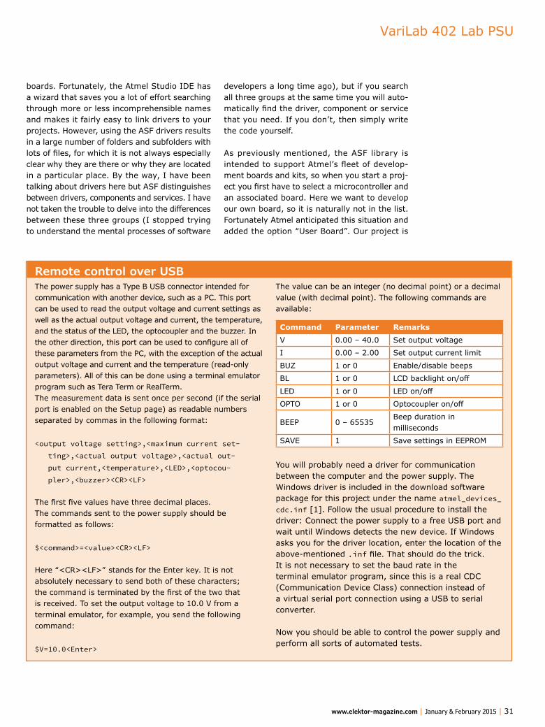
VariLab 402 Lab PSU
www.elektor-magazine.com | January & February 2015 | 31
boards. Fortunately, the Atmel Studio IDE has a wizard that saves you a lot of effort searching through more or less incomprehensible names and makes it fairly easy to link drivers to your projects. However, using the ASF drivers results in a large number of folders and subfolders with lots of files, for which it is not always especially clear why they are there or why they are located in a particular place. By the way, I have been talking about drivers here but ASF distinguishes between drivers, components and services. I have not taken the trouble to delve into the differences between these three groups (I stopped trying to understand the mental processes of software
developers a long time ago), but if you search all three groups at the same time you will auto-matically find the driver, component or service that you need. If you don’t, then simply write the code yourself.
As previously mentioned, the ASF library is intended to support Atmel’s fleet of develop-ment boards and kits, so when you start a proj-ect you first have to select a microcontroller and an associated board. Here we want to develop our own board, so it is naturally not in the list. Fortunately Atmel anticipated this situation and added the option “User Board”. Our project is
Remote control over USBThe power supply has a Type B USB connector intended for communication with another device, such as a PC. This port can be used to read the output voltage and current settings as well as the actual output voltage and current, the temperature, and the status of the LED, the optocoupler and the buzzer. In the other direction, this port can be used to configure all of these parameters from the PC, with the exception of the actual output voltage and current and the temperature (read-only parameters). All of this can be done using a terminal emulator program such as Tera Term or RealTerm.The measurement data is sent once per second (if the serial port is enabled on the Setup page) as readable numbers separated by commas in the following format:
<output voltage setting>,<maximum current set-ting>,<actual output voltage>,<actual out-put current,<temperature>,<LED>,<optocou-pler>,<buzzer><CR><LF>
The first five values have three decimal places.The commands sent to the power supply should be formatted as follows:
$<command>=<value><CR><LF>
Here “<CR><LF>” stands for the Enter key. It is not absolutely necessary to send both of these characters; the command is terminated by the first of the two that is received. To set the output voltage to 10.0 V from a terminal emulator, for example, you send the following command:
$V=10.0<Enter>
The value can be an integer (no decimal point) or a decimal value (with decimal point). The following commands are available:
Command Parameter Remarks
V 0.00 – 40.0 Set output voltage
I 0.00 – 2.00 Set output current limit
BUZ 1 or 0 Enable/disable beeps
BL 1 or 0 LCD backlight on/off
LED 1 or 0 LED on/off
OPTO 1 or 0 Optocoupler on/off
BEEP 0 – 65535Beep duration in milliseconds
SAVE 1 Save settings in EEPROM
You will probably need a driver for communication between the computer and the power supply. The Windows driver is included in the download software package for this project under the name atmel_devices_cdc.inf [1]. Follow the usual procedure to install the driver: Connect the power supply to a free USB port and wait until Windows detects the new device. If Windows asks you for the driver location, enter the location of the above-mentioned .inf file. That should do the trick.It is not necessary to set the baud rate in the terminal emulator program, since this is a real CDC (Communication Device Class) connection instead of a virtual serial port connection using a USB to serial converter.
Now you should be able to control the power supply and perform all sorts of automated tests.
•Projects
32 | January & February 2015 | www.elektor-magazine.com
The interrupt-driven loop is executed every 100 µs (10 kHz), based on the system tick (Sys-Tick). It first measures the output voltage and current and then checks whether or not current limiting should be activated. If current limiting is necessary, this loop temporarily ignores the fact that it is interrupt driven and proceeds to reduce the output voltage as quickly as possible to the point where the output current is at or just below the maximum level. Everything else is suspended while this is happening (it may be necessary to reduce the output voltage all the way to zero), and then life returns to normal.A 1 kHz loop and a 100 Hz loop are derived from the 10 kHz loop. The 1 kHz loop services the buzzer (on or off) and ensures that changes to the desired output voltage and maximum current are sent to the two DACs. The 100 kHz loop looks after the rotary encoders, checks the pushbutton and reads the temperature sensor.
These three loops set flags that are processed by the background loop. One of these flags indicates that the power supply is in current limit mode. The background loop checks this flag periodically and translates the flag status into visual and acoustic signals. Although this more complicated than strictly necessary, it allows the acoustic and visual signals to be made a bit more pleasant. In this era of highly polished graphic apps and touch screens, that’s about the least you can do to meet user expectations. When the power supply suddenly starts beeping (a series of three beeps) and the LCD lights up, you know that cur-rent limiting has taken over.Another flag indicates whether the user has turned a knob or pushed a button. This flag is necessary to inform the background loop that a new value has been set or a different screen has been selected. When the user changes a set-ting, such as the output voltage, they most likely expect the power supply to remember the new setting even after it has been switched off. For-tunately this is possible thanks to the EEPROM in the microcontroller. Writing data to the EEPROM is relatively slow, so we do that at our convenience in the background loop instead of the 10 kHz loop.This also applies to updating the display. LCDs are fairly slow, and writing a full screen takes much too long to be executed in an interrupt service routine. This job is therefore delegated to the background loop. The display is refreshed very 100 ms. Incidentally, this period is a compromise
therefore based on this User Board. We could have chosen an Atmel board instead with the same microcontroller type and then modified the files, but that would have probably cost us more effort in the end than it saved. By the way, we didn’t do anything at all with the User Board files, but they come with the package.All of the ASF files in the project are located in a subfolder with the suitable name “ASF”. A header file (ASF.h) is placed in the SRC folder for the project, where the IDE also puts the main.c file. This header file pools all the header files of the various ASF drivers, so you don’t have to worry about which files you need to include in your code. A simple #include ASF.h statement is sufficient for any code that wants to use the ASF functions.Our own C files are located in the SRC folder, and our header files are located in the INC folder. There is a pair of C and header files for each peripheral. For example, for the buzzer there is a buzzer.c file and a buzzer.h file. There are also files for the user interface and a number of support files. File names and variable names are generally prefixed by the name of the file where they are defined. To cite the buzzer exam-ple again, the function buzzer_beep(uint16_t ms) is located in the buzzer.c file. Its prototype (declaration) is located in buzzer.h.
As you can see from the above, the program is written in C. I could have used C++ instead, but I chose C because it’s easier to understand. For most things it doesn’t make much difference whether you use C or C++, but for the user inter-face I would have preferred to use C++. The resulting C code uses (or misuses) C++ meth-ods and would have been a lot simpler in C++.
Software designAnother recurrent question is whether or not to use a real time operating system (RTOS). A few years ago RTOSs were fairly exotic, but now you virtually trip over them everywhere. The open-source FreeRTOS is an obvious choice and is avail-able for our microcontroller. The downside of an RTOS is that it adds another library to the proj-ect and that task handling is often not so easy to understand. I therefore chose a sort of hybrid approach with a loop that handles low-urgency tasks in a fixed sequence and an interrupt-driven loop that handles time-dependent tasks. In a manner of speaking, there are two tasks: a back-ground task and a foreground task.
VariLab 402 Lab PSU
www.elektor-magazine.com | January & February 2015 | 33
several internal voltages and the temperature reading.That makes five pages in total. Actually there are six, since the Calibration page is divided into two
between refresh speed and ease of reading. The display becomes jittery if the refresh speed is too high, especially with a variable load.The background loop also maintains a seconds counter based on the 100 ms screen update loop. It is used to send measured values and settings to the serial port (USB) once per second. This counter also ensures that the settings are not written to the EEPROM too frequently. When the user is adjusting a setting, it is not necessary to store all the intermediate values in the EEPROM. We wait until the user has not changed any of the settings for at least 10 seconds before assum-ing that they are stable and can be stored in the EEPROM. This also helps to prolong the life of the EEPROM.I don’t want to go into the details here of how the background loop generates beep tones, but I do want to mention that the background loop also looks after the processing of commands received via the serial port.As you can see from all the above, the software for the power supply handles a surprisingly large number of tasks, especially for a power supply – and I haven’t even mentioned screen handling or calibration yet, because that’s what I intend to do next.
User interfaceThe user interface for the power supply is dis-tributed over several pages (see Figures 1 to 6). The first thing you see after switching on the power supply is the “splash screen”. Actually this should probably be called the start-up screen, since there aren’t any images splashed on the screen. The start-up screen shows the software ID (Elektor project 120437) and version num-ber (1.0). After a few seconds it is replaced by the home screen with the usual power supply parameters (output voltage, current limit, etc.). If you press both rotary encoder knobs at the same time, the Setup page opens. Here you can configure various parameters, such as whether or not you want to hear beeps and how long the display backlight stays on. The latter option is mainly intended to reduce the load on the back-light power source, since it doesn’t have much power to spare. From this page you can go in three different directions: to the Calibration page by pressing the left rotary encoder knob, to the Status page by pressing the right rotary encoder knob, or back to the main page by pressing the pushbutton. On the Status page you can view
Figures 1 to 6. The various menus displayed on the LCD: (1) Start-up screen; (2) Home page; (3) Setup, (4) Calibration 1; (5) Calibration 2; (6) Status.
1
2
3
4
5
6
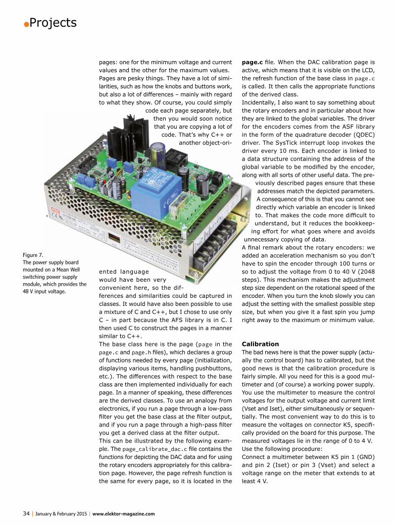
•Projects
34 | January & February 2015 | www.elektor-magazine.com
page.c file. When the DAC calibration page is active, which means that it is visible on the LCD, the refresh function of the base class in page.c is called. It then calls the appropriate functions of the derived class.Incidentally, I also want to say something about the rotary encoders and in particular about how they are linked to the global variables. The driver for the encoders comes from the ASF library in the form of the quadrature decoder (QDEC) driver. The SysTick interrupt loop invokes the driver every 10 ms. Each encoder is linked to a data structure containing the address of the global variable to be modified by the encoder, along with all sorts of other useful data. The pre-
viously described pages ensure that these addresses match the depicted parameters. A consequence of this is that you cannot see directly which variable an encoder is linked to. That makes the code more difficult to understand, but it reduces the bookkeep-
ing effort for what goes where and avoids unnecessary copying of data.
A final remark about the rotary encoders: we added an acceleration mechanism so you don’t have to spin the encoder through 100 turns or so to adjust the voltage from 0 to 40 V (2048 steps). This mechanism makes the adjustment step size dependent on the rotational speed of the encoder. When you turn the knob slowly you can adjust the setting with the smallest possible step size, but when you give it a fast spin you jump right away to the maximum or minimum value.
CalibrationThe bad news here is that the power supply (actu-ally the control board) has to calibrated, but the good news is that the calibration procedure is fairly simple. All you need for this is a good mul-timeter and (of course) a working power supply. You use the multimeter to measure the control voltages for the output voltage and current limit (Vset and Iset), either simultaneously or sequen-tially. The most convenient way to do this is to measure the voltages on connector K5, specifi-cally provided on the board for this purpose. The measured voltages lie in the range of 0 to 4 V.Use the following procedure:Connect a multimeter between K5 pin 1 (GND) and pin 2 (Iset) or pin 3 (Vset) and select a voltage range on the meter that extends to at least 4 V.
pages: one for the minimum voltage and current values and the other for the maximum values.Pages are pesky things. They have a lot of simi-larities, such as how the knobs and buttons work, but also a lot of differences – mainly with regard to what they show. Of course, you could simply
code each page separately, but then you would soon notice that you are copying a lot of
code. That’s why C++ or another object-ori-
ented language would have been very convenient here, so the dif-ferences and similarities could be captured in classes. It would have also been possible to use a mixture of C and C++, but I chose to use only C – in part because the AFS library is in C. I then used C to construct the pages in a manner similar to C++.The base class here is the page (page in the page.c and page.h files), which declares a group of functions needed by every page (initialization, displaying various items, handling pushbuttons, etc.). The differences with respect to the base class are then implemented individually for each page. In a manner of speaking, these differences are the derived classes. To use an analogy from electronics, if you run a page through a low-pass filter you get the base class at the filter output, and if you run a page through a high-pass filter you get a derived class at the filter output.This can be illustrated by the following exam-ple. The page_calibrate_dac.c file contains the functions for depicting the DAC data and for using the rotary encoders appropriately for this calibra-tion page. However, the page refresh function is the same for every page, so it is located in the
Figure 7. The power supply board mounted on a Mean Well switching power supply module, which provides the 48 V input voltage.
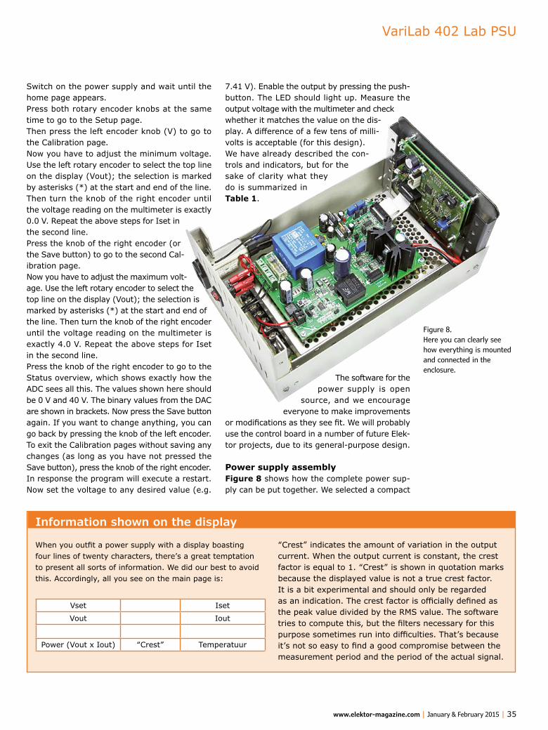
VariLab 402 Lab PSU
www.elektor-magazine.com | January & February 2015 | 35
7.41 V). Enable the output by pressing the push-button. The LED should light up. Measure the output voltage with the multimeter and check whether it matches the value on the dis-play. A difference of a few tens of milli-volts is acceptable (for this design).We have already described the con-trols and indicators, but for the sake of clarity what they do is summarized in Table 1.
The software for the power supply is open
source, and we encourage everyone to make improvements
or modifications as they see fit. We will probably use the control board in a number of future Elek-tor projects, due to its general-purpose design.
Power supply assemblyFigure 8 shows how the complete power sup-ply can be put together. We selected a compact
Switch on the power supply and wait until the home page appears.Press both rotary encoder knobs at the same time to go to the Setup page.Then press the left encoder knob (V) to go to the Calibration page.Now you have to adjust the minimum voltage. Use the left rotary encoder to select the top line on the display (Vout); the selection is marked by asterisks (*) at the start and end of the line. Then turn the knob of the right encoder until the voltage reading on the multimeter is exactly 0.0 V. Repeat the above steps for Iset in the second line.Press the knob of the right encoder (or the Save button) to go to the second Cal-ibration page.Now you have to adjust the maximum volt-age. Use the left rotary encoder to select the top line on the display (Vout); the selection is marked by asterisks (*) at the start and end of the line. Then turn the knob of the right encoder until the voltage reading on the multimeter is exactly 4.0 V. Repeat the above steps for Iset in the second line.Press the knob of the right encoder to go to the Status overview, which shows exactly how the ADC sees all this. The values shown here should be 0 V and 40 V. The binary values from the DAC are shown in brackets. Now press the Save button again. If you want to change anything, you can go back by pressing the knob of the left encoder.To exit the Calibration pages without saving any changes (as long as you have not pressed the Save button), press the knob of the right encoder. In response the program will execute a restart.Now set the voltage to any desired value (e.g.
Information shown on the display
When you outfit a power supply with a display boasting four lines of twenty characters, there’s a great temptation to present all sorts of information. We did our best to avoid this. Accordingly, all you see on the main page is:
Vset Iset
Vout Iout
Power (Vout x Iout) “Crest” Temperatuur
“Crest” indicates the amount of variation in the output current. When the output current is constant, the crest factor is equal to 1. “Crest” is shown in quotation marks because the displayed value is not a true crest factor. It is a bit experimental and should only be regarded as an indication. The crest factor is officially defined as the peak value divided by the RMS value. The software tries to compute this, but the filters necessary for this purpose sometimes run into difficulties. That’s because it’s not so easy to find a good compromise between the measurement period and the period of the actual signal.
Figure 8. Here you can clearly see how everything is mounted and connected in the enclosure.

•Projects
36 | January & February 2015 | www.elektor-magazine.com
Make openings in the front panel for the dis-play and the USB-B connector (make sure the USB connector will not touch the enclosure after installation) and holes for the LED, the two rotary encoders, the pushbutton and the two banana jacks. Then mount the control board on the back side of the front panel. Use a length of 14-con-ductor flat cable with a pair of insulation-dis-placement headers to connect the two boards together. Temperature sensor IC5 can be left on the PCB to measure the average tempera-ture inside the enclosure. However, you can also mount it directly on the heat sink for T4 on the power supply board and connect it to the control board with three lengths of insulated wire. Finally, connect the output jacks to connector K2 on the power supply board with a pair of short, thick wires (2.5 mm2 / AWG #12 or #14). Keep these wires close together and pass them through a large ferrite bead to block high-frequency noise emission from the power supply.After connecting everything and double-checking the connections, you can switch on the power and calibrated the power supply using the procedure described above.
After that the power supply is ready for use. We hope you enjoy using it on your own bench!
(140431-I)
Web Link
[1] www.elektor-magazine.com/140373
enclosure which has just enough room to mount the Mean Well power supply module (see Part 1) on the bottom of the enclosure. The enclosure in the photos is a Hammond type 1401A (dimen-sions 127x152x254 mm / 5x6x10 in). We moved the front and rear panels of the enclosure a bit further to the outside to make more room inside the enclosure.
The power supply board can be mounted on top of the Mean Well module with a few standoffs. With a bit of luck you can use the ventilation holes in the top cover of the Meal Well module for this purpose. Make openings in the rear panel for an AC power entry module and a power switch. For the AC power entry module you should use a type with a built-in line filter, since that will block a lot of interference. Connect the ground terminal of the line filter (protective ground) to the enclosure. Connect the output terminals of the AC power entry module to the power switch with short wires, and connect the other terminals of switch to connector K4. Connect the Mean Well power supply module to connector K5 with short insulated wires. This way the Mean Well power supply module and the power transformer on the power supply board are energized at the same time by the power switch. All wiring connected to the AC power entry module must be double insulated. Wire the 48 V output of the Mean Well power supply module to connector K1 on the power supply board.
Table 1. User interface functions
Home page Setup page Calibration pages Status page
Left rotary encoder
Output voltage Parameter selection Parameter selection –
Right rotary encoder
Current limit Parameter value Parameter value –
Pushbutton of left rotary encoder
Backlight briefly on Selects the Setup page if pressed simultaneously with the right rotary encoder pushbutton
Go to Calibration page Go to previous page Go to Home page
Pushbutton of right rotary encoder
Backlight briefly on Selects the Setup page if pressed simultaneously with the left rotary encoder pushbutton
Go to Status page Go to next page Go to Home page
Pushbutton Enables output Go to Home page Go to Home page
• The LED indicates that the output is enabled.• The buzzer emits one beep in recognition of a user action. A (repeated) series of three beeps indicates that current limiting
is active.

Evolve to app-based control with AIR for Wiced Smart!
Get “mobile smart”in 3 easy steps:
Get your AIR for Wiced Smart dev kit at your distributor of choice. (See our website for a current list.)
Develop your wireless link and basic app using our exclusive Atmosphere development tool.
With our AIR for Wiced Smart module on board, proceed in record time to a prototype and final, mobile-app development!
If you’re ready to evolve from fixed control panels populated with dials, buttons, keypads, and LCD displays to mobile-app based control of your embedded product – check out Anaren’s AIR for Wiced Smart module, featuring Broadcom’s Wiced Smart Bluetooth® chip (BCM20737). Not only does our small-footprint, SMT, and pre-certified all-in-one module save you the time, effort, and trouble of designing your own radio... It’s supported by our industry-exclusive Atmosphere development ecosystem that lets you develop your basic embedded code and app code in one, easy-to-use development tool – for a far speedier product development cycle and time-to-market. Follow the steps at left to jointhe evolution, right now! www.anaren.com/AIRforWiced
800-411-6596In Europe: 44-2392-232392
Get your AIR for Wiced dev kit at your
distributor of choice. (See our website for a current list.)
Develop your wireless link and basic app using
our exclusive Atmospheredevelopment tool.
With our AIR for Wiced Smart module on board,
AIR for Wiced
Learn more
1905
Today
1945
2005
JOIN THEEVOLUTION.
Smart module on board, proceed in record time to a prototype and final, mobile-app development!
link and basic app usingAtmosphere
development tool.
With our AIR for Wiced Smart module on board,
link and basic app usingAtmosphere
• The latest on electronics andinformation technology
• Videos, hints, tips, offers and more• Exclusive bi-weekly project for
GREEN and GOLD members only• Elektor behind the scenes• In your email inbox each Friday
Take out a FREE membership to Elektor.POST
Register today at www.elektor.com/newsletterwww.elektor.com/newsletterwww.elektor.com/newsletterwww.elektor.com/newsletter
Untitled-1 1 12/12/14 09:31
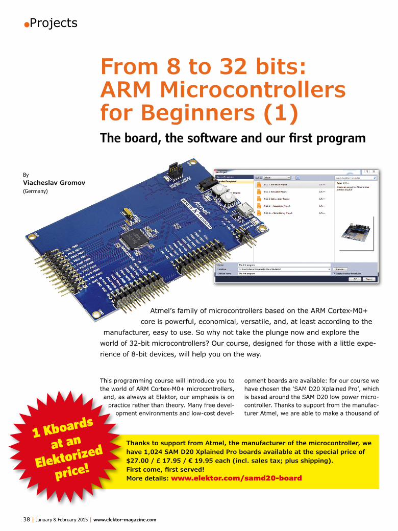
•Projects
38 | January & February 2015 | www.elektor-magazine.com
This programming course will introduce you to the world of ARM Cortex-M0+ microcontrollers, and, as always at Elektor, our emphasis is on
practice rather than theory. Many free devel-opment environments and low-cost devel-
opment boards are available: for our course we have chosen the ‘SAM D20 Xplained Pro’, which is based around the SAM D20 low power micro-controller. Thanks to support from the manufac-turer Atmel, we are able to make a thousand of
By Viacheslav Gromov (Germany)
From 8 to 32 bits: ARM Microcontrollers for Beginners (1)The board, the software and our first program
Atmel’s family of microcontrollers based on the ARM Cortex-M0+ core is powerful, economical, versatile, and, at least according to the
manufacturer, easy to use. So why not take the plunge now and explore the world of 32-bit microcontrollers? Our course, designed for those with a little expe-rience of 8-bit devices, will help you on the way.
Thanks to support from Atmel, the manufacturer of the microcontroller, we have 1,024 SAM D20 Xplained Pro boards available at the special price of $27.00 / £ 17.95 / € 19.95 each (incl. sales tax; plus shipping). First come, first served!More details: www.elektor.com/samd20-board
1 Kboards
at an
Elektorized
price!
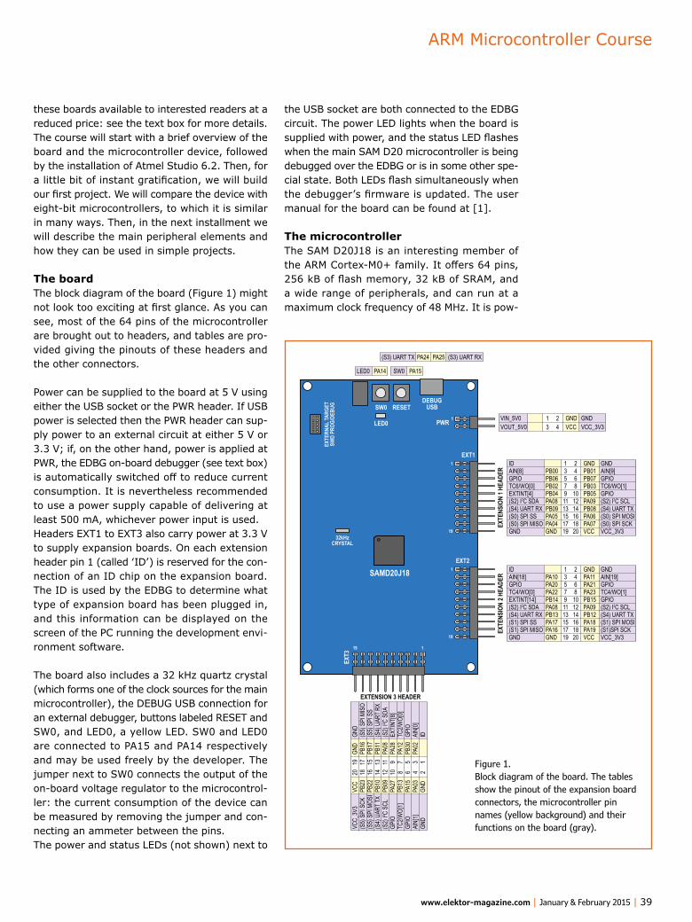
ARM Microcontroller Course
www.elektor-magazine.com | January & February 2015 | 39
these boards available to interested readers at a reduced price: see the text box for more details.The course will start with a brief overview of the board and the microcontroller device, followed by the installation of Atmel Studio 6.2. Then, for a little bit of instant gratification, we will build our first project. We will compare the device with eight-bit microcontrollers, to which it is similar in many ways. Then, in the next installment we will describe the main peripheral elements and how they can be used in simple projects.
The boardThe block diagram of the board (Figure 1) might not look too exciting at first glance. As you can see, most of the 64 pins of the microcontroller are brought out to headers, and tables are pro-vided giving the pinouts of these headers and the other connectors.
Power can be supplied to the board at 5 V using either the USB socket or the PWR header. If USB power is selected then the PWR header can sup-ply power to an external circuit at either 5 V or 3.3 V; if, on the other hand, power is applied at PWR, the EDBG on-board debugger (see text box) is automatically switched off to reduce current consumption. It is nevertheless recommended to use a power supply capable of delivering at least 500 mA, whichever power input is used.Headers EXT1 to EXT3 also carry power at 3.3 V to supply expansion boards. On each extension header pin 1 (called ‘ID’) is reserved for the con-nection of an ID chip on the expansion board. The ID is used by the EDBG to determine what type of expansion board has been plugged in, and this information can be displayed on the screen of the PC running the development envi-ronment software.
The board also includes a 32 kHz quartz crystal (which forms one of the clock sources for the main microcontroller), the DEBUG USB connection for an external debugger, buttons labeled RESET and SW0, and LED0, a yellow LED. SW0 and LED0 are connected to PA15 and PA14 respectively and may be used freely by the developer. The jumper next to SW0 connects the output of the on-board voltage regulator to the microcontrol-ler: the current consumption of the device can be measured by removing the jumper and con-necting an ammeter between the pins.The power and status LEDs (not shown) next to
the USB socket are both connected to the EDBG circuit. The power LED lights when the board is supplied with power, and the status LED flashes when the main SAM D20 microcontroller is being debugged over the EDBG or is in some other spe-cial state. Both LEDs flash simultaneously when the debugger’s firmware is updated. The user manual for the board can be found at [1].
The microcontrollerThe SAM D20J18 is an interesting member of the ARM Cortex-M0+ family. It offers 64 pins, 256 kB of flash memory, 32 kB of SRAM, and a wide range of peripherals, and can run at a maximum clock frequency of 48 MHz. It is pow-
1
1
19
1
19
EXT2
EXT3
EXT1135791113151719
PB00PB06PB02PB04PA08PB09PA05PA04GND
ID AIN[8]GPIOTC6/WO[0]EXTINT[4](S2) I2C SDA(S4) UART RX(S0) SPI SS(S0) SPI MISOGND
2468101214161820
GNDPB01PB07PB03PB05PA09PB08PA06PA07VCC
GNDAIN[9]GPIOTC6/WO[1]GPIO(S2) I2C SCL(S4) UART TX(S0) SPI MOSI(S0) SPI SCKVCC_3V3
EXTE
NSIO
N 1 H
EADE
R
RESETDEBUG
USB
PWR
32kHzCRYSTAL
EXTE
RNAL
TARG
ETSW
D PR
OG/D
EBUG SW0
LED0
SAMD20J18
119
135791113151719
PA10PA20PA22PB14PA08PB13PA17PA16GND
ID AIN[18]GPIOTC4/WO[0]EXTINT[14](S2) I2C SDA(S4) UART RX(S1) SPI SS(S1) SPI MISOGND
2468101214161820
GNDPA11PA21PA23PB15PA09PB12PA18PA19VCC
GNDAIN[19]GPIOTC4/WO[1]GPIO(S2) I2C SCL(S4) UART TX(S1) SPI MOSI(S1)SPI SCKVCC_3V3
EXTE
NSIO
N 2 H
EADE
R
20 18 16 14 12 10 8 6 4 2
VCC
PB23
PB22
PB10
PB09
PA27
PB13
PA15
PA03
GND
VCC_
3V3
(S5)
SPI S
CK(S
5) SP
I MOS
I(S
4) UA
RT TX
(S2)
I2 C SC
LGP
IOTC
2/WO[
1]GP
IOAI
N[1]
GND
19 17 15 13 11 9 7 5 3 1
GND
PB16
PB17
PB11
PA08
PA28
PA12
PB30
PA02
GND
(S5)
SPI M
ISO
(S5)
SPI S
S(S
4) UA
RT R
X(S
2) I2 C
SDA
EXTIN
T[8]
TC2/W
O[0]
GPIO
AIN[
0]ID
EXTENSION 3 HEADER
(S3) UART TX (S3) UART RXPA24 PA25
LED0 PA14 SW0 PA15
VIN_5V0 GNDGNDVOUT_5V0 VCC_3V3VCC
1 23 4
Figure 1. Block diagram of the board. The tables show the pinout of the expansion board connectors, the microcontroller pin names (yellow background) and their functions on the board (gray).
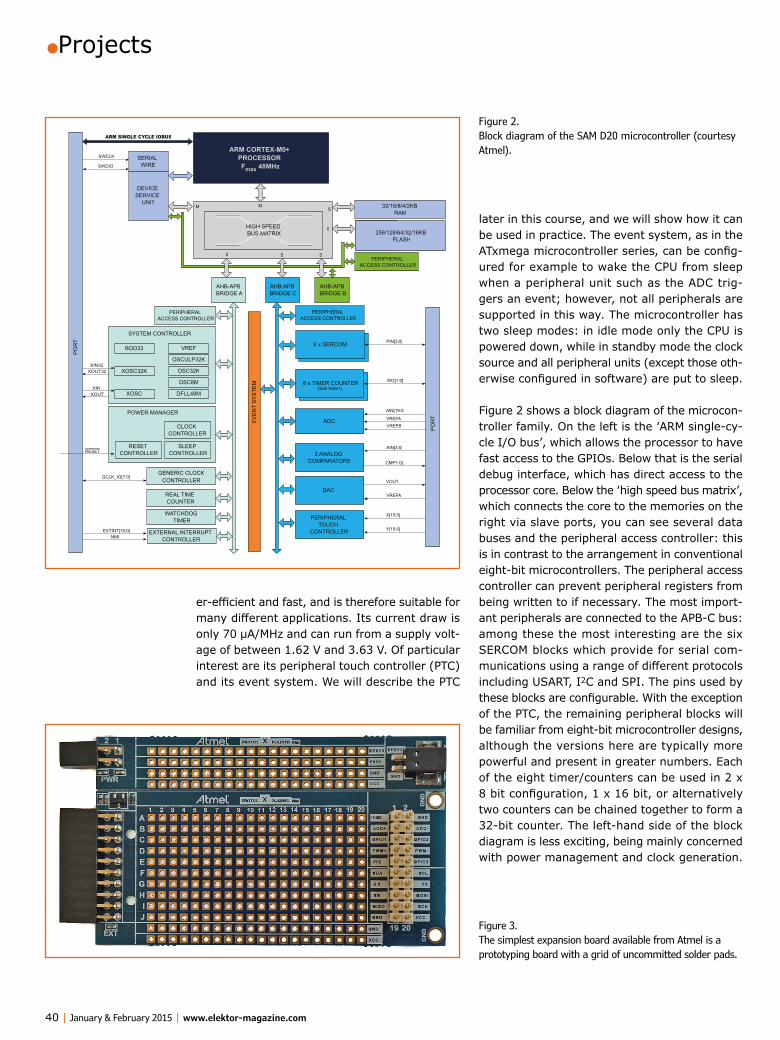
•Projects
40 | January & February 2015 | www.elektor-magazine.com
later in this course, and we will show how it can be used in practice. The event system, as in the ATxmega microcontroller series, can be config-ured for example to wake the CPU from sleep when a peripheral unit such as the ADC trig-gers an event; however, not all peripherals are supported in this way. The microcontroller has two sleep modes: in idle mode only the CPU is powered down, while in standby mode the clock source and all peripheral units (except those oth-erwise configured in software) are put to sleep.
Figure 2 shows a block diagram of the microcon-troller family. On the left is the ‘ARM single-cy-cle I/O bus’, which allows the processor to have fast access to the GPIOs. Below that is the serial debug interface, which has direct access to the processor core. Below the ‘high speed bus matrix’, which connects the core to the memories on the right via slave ports, you can see several data buses and the peripheral access controller: this is in contrast to the arrangement in conventional eight-bit microcontrollers. The peripheral access controller can prevent peripheral registers from being written to if necessary. The most import-ant peripherals are connected to the APB-C bus: among these the most interesting are the six SERCOM blocks which provide for serial com-munications using a range of different protocols including USART, I2C and SPI. The pins used by these blocks are configurable. With the exception of the PTC, the remaining peripheral blocks will be familiar from eight-bit microcontroller designs, although the versions here are typically more powerful and present in greater numbers. Each of the eight timer/counters can be used in 2 x 8 bit configuration, 1 x 16 bit, or alternatively two counters can be chained together to form a 32-bit counter. The left-hand side of the block diagram is less exciting, being mainly concerned with power management and clock generation.
er-efficient and fast, and is therefore suitable for many different applications. Its current draw is only 70 μA/MHz and can run from a supply volt-age of between 1.62 V and 3.63 V. Of particular interest are its peripheral touch controller (PTC) and its event system. We will describe the PTC
6 x SERCOM
8 x Timer Counter
REAL TIME COUNTER
AHB-APB BRIDGE C
M
SHIGH SPEED BUS MATRIX
PO
RT
PO
RT
WATCHDOG TIMER
SERIAL WIRESWDIO
NVM CONTROLLER
256/128/64/32/16KB FLASH
S
ARM CORTEX-M0+ PROCESSOR Fmax 48MHz
SWCLK
DEVICE SERVICE
UNIT
AHB-APB BRIDGE A
ADC
AIN[19:0]
VREFA
AIN[3:0]
S
32/16/8/4/2KB RAM
M
RESET CONTROLLER
SLEEP CONTROLLER
CLOCK CONTROLLER
POWER MANAGER
RESET
8 x TIMER COUNTER
EV
EN
T S
YS
TEM
S
6 x SERCOM
2 ANALOG COMPARATORS
SYSTEM CONTROLLER
XOUTXIN
XOUT32XIN32
OSCULP32K
OSC32K
OSC8M
DFLL48M
BOD33
XOSC32K
XOSC
VREF
GENERIC CLOCK
X[15:0]
Y[15:0]
PERIPHERAL TOUCH
CONTROLLER
PERIPHERAL ACCESS CONTROLLER
AHB-APB BRIDGE B
VREFA
VOUT
DAC
EXTERNAL INTERRUPT CONTROLLER
PERIPHERAL ACCESS CONTROLLER
PERIPHERAL ACCESS CONTROLLER
EXTINT[15:0]NMI
GCLK_IO[7:0]
S
PIN[3:0]
WO[1:0]
VREFB
(See Note1)
CMP1:0]
ARM SINGLE CYCLE IOBUS
CONTROLLER
Figure 2. Block diagram of the SAM D20 microcontroller (courtesy Atmel).
Figure 3. The simplest expansion board available from Atmel is a prototyping board with a grid of uncommitted solder pads.

ARM Microcontroller Course
www.elektor-magazine.com | January & February 2015 | 41
We will look in more detail at the possibilities offered by the various peripheral blocks in the next installment in this series, and show step by step how they are configured and used in prac-tice. The data sheet for the device, which runs to some 700 pages, can be found at [3].
The expansion boardsAtmel has developed several expansion boards for the Xplained Pro board. They are designed to help developers new to the device rapidly get to the point of having a working prototype, and to help them learn about the microcontroller. The expansion boards conveniently plug directly into the headers on the main circuit board. Each expan-sion board includes an ATSHA204 ‘CryptoAuthen-tication’ chip, which provides information to the EDBG chip on the Xplained Pro board, for example regarding the allowable supply voltage range and maximum current consumption. This information is then passed on to Atmel Studio, which allows the development environment to offer links to data sheets, libraries and example programs.
If you want to build your own expansion board and connect it to the Xplained Pro board, the PROTO1 Xplained Pro [4] (Figure 3) provides the answer. It includes a total of 200 solder pads for prototyping and is connected to headers EXT1 and PWR. On the right the same pins are brought out in a different order to provide a connection for an ‘Xplained Top Module’. A groove allows the upper part of the board, which includes the power supply connections, to be broken off if it is not wanted.
The expansion board shown in Figure 4, the IO1 Xplained Pro [5], is designed to help developers understand the most important peripheral blocks of the microcontroller. It includes an LED, a light sensor, a low-pass filter to allow testing of the PWM and ADC blocks, a 12-bit temperature sensor with 8 kB of EEPROM connected over an I2C bus, and a microSD card socket, connected over an SPI bus. A microSD card is included with the board. A couple of spare pins are also brought out.If you wish to output something to a display, you
Figure 6. The two QTouch boards will be used in a later installment of this series.
Figure 4. Universal expansion board for testing and training.
Figure 5. OLED display expansion board for more advanced projects.

•Projects
42 | January & February 2015 | www.elektor-magazine.com
can use the OLED1 Xplained Pro [6] expansion board: see Figure 5. The board is fitted with a 128-by-32 pixel OLED display with an SPI inter-face. The board also provides three LEDs and three buttons. This board is designed to be con-nected to header EXT3.
A special feature of the SAM D20, like certain other microcontrollers by the same manufacturer, is the PTC. Atmel offers a kit (Figure 6) called the QT1 Xplained Pro [7] comprising two expansion boards. Externally the two boards appear identi-cal, but they use different touch detection tech-nologies: ‘QTouch self capacitance’ and ‘QTouch mutual capacitance’. We will examine the exact differences between these technologies and their advantages and disadvantages in a later install-ment of this series. Each board includes a touch
Debugging and the EDBGThe idea of using a debugger to seek out and eradicate software bugs is not very widespread in the world of eight-bit microcontrollers, and so we shall say a few words about the process here.
Two components are essential to the debugging process: a software tool, forming part of the development environment, and the debugger itself, a hardware bridge between the PC and the target microcontroller system. The debugger can be used to examine and alter variables, memory contents, and often even processor registers during program execution. Breakpoints can be set to halt execution at certain points in the code so that the status of the hardware can be examined. These facilities make it easier and quicker to find bugs, even when the microcontroller is built in to a functioning prototype, as long as the debugger remains connected to it [9].The EDBG (Embedded Debugger) is a feature not only of all boards in the Xplained Pro series, but is also frequently
found on AVR boards. It takes the form of debug hardware, specially developed by Atmel for its development kits, integrated onto the board. As well as offering facilities for programming and debugging the connected microcontroller, it has an extra feature that will come in very handy later on: the Data Gateway Interface, which provides a bridge between the PC and several of the interfaces and GPIOs on the microcontroller. While the microcontroller is running, the state of selected GPIOs can be viewed and data can be received over selected interfaces: this can make development much easier. On the SAM D20 Xplained Pro board this interface is connected to the SPI pins of SERCOM5, the I2C pins of SERCOM2 and GPIO pins PA27, PA28, PA20 and PA21.
The debugger chip also controls the status LEDs and reads ID codes from the expansion boards. And finally, the EDBG can also emulate a COM port over USB, as it is connected to the UART pins of SERCOM3 on the SAM D20 [2].
Figure 7. Click on the upper icon if you wish to install Atmel Studio on a computer that does not have a permanent Internet connection (all screenshots courtesy Atmel).
Figure 8. At this point you should either click on ‘Create an account’ or enter your personal details.
ARM Microcontroller Course
www.elektor-magazine.com | January & February 2015 | 43
wheel, a slider and two buttons, as well as ten yellow LEDs and one RGB LED.
The development environmentAtmel microcontrollers can be programmed and debugged using a suitable programmer/debugger and Atmel Studio. This integrated development environment (IDE) is free, comes directly from the manufacturer, and provides many useful func-tions: it is therefore an ideal tool with which to start. You may even already be familiar with it.
In order to install the most recent version (ver-sion 6.2), go to [8] and click on the CD icon labeled ‘Atmel Studio 6.2 sp1 (build 1502) Installer’ (see Figure 7). A window will appear as shown in Figure 8, in which you must either create an account or provide details to continue as a guest before downloading the software. It is advisable to create an account, as registration will be required again at various points later in this course. If you already have an Atmel account you can log in using the button at the top right. A link will now appear which, when clicked, will start the download. When the browser pops up a message asking if you wish only to download the program or if you wish to run it automati-cally, it is best to select the latter option. After a pause a Windows security message will appear: click on ‘Always trust software from Atmel Nor-way’ and then click on the ‘Install’ button. If you do not have Microsoft’s .NET framework or Visual Studio installed on your machine, Atmel Studio will prompt you to install them: follow the instructions provided. In both cases you will need to accept the license terms, and in both cases you should install the full versions of the programs. You should use the suggested instal-lation paths unless you have a reason to change them. The InstallShield Wizard will then pres-ent a window suggesting the installation of the USB driver, which you should accept by clicking ‘Install’ (see Figure 9).
After accepting the license in the next window (Figure 10) installation of the driver will begin, which can take a couple of minutes. Then, with any luck, a message will appear confirming successful installation of the driver. Again, you should confirm this.Installation of Atmel Studio itself can now begin. In the first window (Figure 11) click on ‘Next’; in the second, accept the license and again click on
Figure 9. Atmel Studio requires the installation of the USB driver.
Figure 10. Read the license text carefully before accepting it.
Figure 11. The main part of the installation process begins.
Figure 12. You cannot proceed further until you have accepted the license.

•Projects
44 | January & February 2015 | www.elektor-magazine.com
‘Next’ (Figure 12). In the next step (Figure 13) select the installation path for Atmel Studio. If you wish to use a different path from the one sug-gested, click on ‘Browse...’. Then click on ‘Next’.The last step in the installation process is a sum-mary of what will be installed and where. Con-firm the details by clicking ‘Next’. It will now take some time for installation to complete (Fig-ure 14). Tick the check box (before clicking on ‘Finish’) if you do not have any other platforms installed on your machine that use files with the same conventional extensions as those listed. The InstallShield Wizard will now disappear and the icon shown in Figure 15 should appear on your desktop. It is now a good idea to reboot the machine to ensure that it is in a clean state.
Our first programThe development board is connected to the PC using a USB-A to USB-B male-to-male cable. The device manager should automatically recognize the device and install the driver that was included with Atmel Studio. If the device manager fails to find the driver, you must tell it the necessary path by hand.Now we launch Atmel Studio for the first time by double-clicking on its icon on the desktop. After a brief delay the welcome window should appear. You will see a message like the one shown in Figure 16, which invites you to update some of the tools.Among these is the Atmel Software Framework (ASF) which we will be making heavy use of in this series. So click on ‘Update’, which will take you to the ‘Extension Manager’ (Figure 17), where the necessary updates can be carried out one by one.At the outset we recommended that you register on the Atmel website so that you can install the updates. Since the installation process for updates can vary, we will not describe it in detail here. Depending on the individual update, you will need to respond to security messages, accept licenses, and link the downloaded update with Atmel Stu-dio. The simplest and most stress-free approach is always to accept default options recommended by the installation program. Once all the updates are done, close the Extension Manager and fol-low its recommendation to restart Atmel Studio.And now finally we can make a start on our first project! The first thing to do is to become famil-iar with the IDE. Having restarted Atmel Studio, select the start page at the top of the screen and click on ‘New Project...’, which will begin the
Figure 13. The suggested installation path is normally appropriate.
Figure 14. The installation is complete!
Figure 15. The Atmel Studio 6.2 icon.
Figure 16. These updates should definitely be installed.
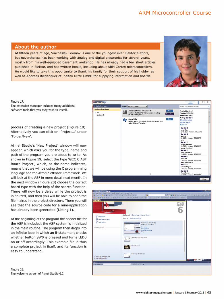
ARM Microcontroller Course
www.elektor-magazine.com | January & February 2015 | 45
process of creating a new project (Figure 18). Alternatively you can click on ‘Project...’ under ‘Folder/New’.
Atmel Studio’s ‘New Project’ window will now appear, which asks you for the type, name and path of the program you are about to write. As shown in Figure 19, select the type ‘GCC C ASF Board Project’, which, as the name indicates, means that we will be using the C programming language and the Atmel Software Framework. We will look at the ASF in more detail next month. In the next window (Figure 20) choose the correct board type with the help of the search function.There will now be a delay while the project is initialized, and then you will be able to open the file main.c in the project directory. There you will see that the source code for a mini-application has already been generated (Listing 1).
At the beginning of the program the header file for the ASF is included; the ASF system is initialized in the main routine. The program then drops into an infinite loop in which an if-statement checks whether button SW0 is pressed and turns LED0 on or off accordingly. This example file is thus a complete project in itself, and its function is easy to understand.
Figure 17. The extension manager includes many additional software tools that you may wish to install.
Figure 18. The welcome screen of Atmel Studio 6.2.
About the authorAt fifteen years of age, Viacheslav Gromov is one of the youngest ever Elektor authors, but nevertheless has been working with analog and digital electronics for several years, mostly from his well-equipped basement workshop. He has already had a few short articles published in Elektor, and has written books, including about ARM Cortex microcontrollers.He would like to take this opportunity to thank his family for their support of his hobby, as well as Andreas Riedenauer of Ineltek Mitte GmbH for supplying information and boards.
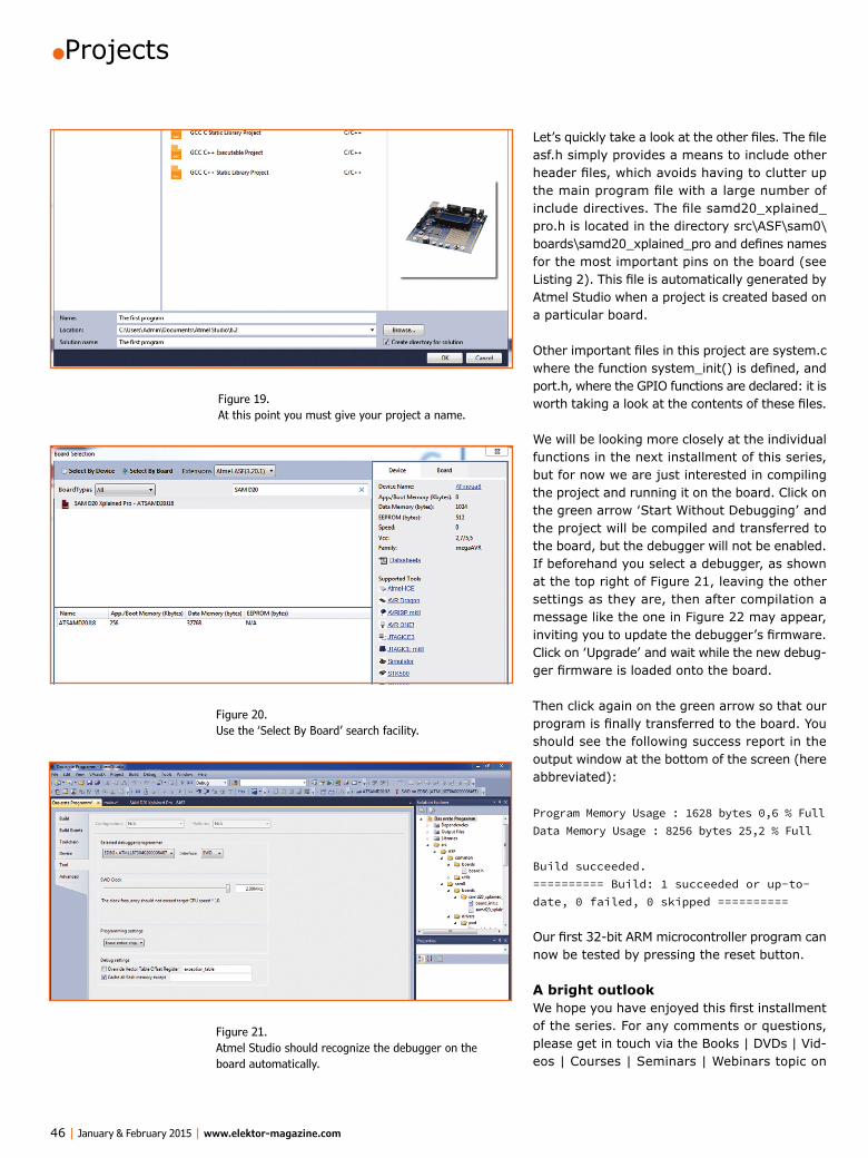
•Projects
46 | January & February 2015 | www.elektor-magazine.com
Let’s quickly take a look at the other files. The file asf.h simply provides a means to include other header files, which avoids having to clutter up the main program file with a large number of include directives. The file samd20_xplained_pro.h is located in the directory src\ASF\sam0\boards\samd20_xplained_pro and defines names for the most important pins on the board (see Listing 2). This file is automatically generated by Atmel Studio when a project is created based on a particular board.
Other important files in this project are system.c where the function system_init() is defined, and port.h, where the GPIO functions are declared: it is worth taking a look at the contents of these files.
We will be looking more closely at the individual functions in the next installment of this series, but for now we are just interested in compiling the project and running it on the board. Click on the green arrow ‘Start Without Debugging’ and the project will be compiled and transferred to the board, but the debugger will not be enabled. If beforehand you select a debugger, as shown at the top right of Figure 21, leaving the other settings as they are, then after compilation a message like the one in Figure 22 may appear, inviting you to update the debugger’s firmware. Click on ‘Upgrade’ and wait while the new debug-ger firmware is loaded onto the board.
Then click again on the green arrow so that our program is finally transferred to the board. You should see the following success report in the output window at the bottom of the screen (here abbreviated):
Program Memory Usage : 1628 bytes 0,6 % FullData Memory Usage : 8256 bytes 25,2 % Full
Build succeeded.========== Build: 1 succeeded or up-to-date, 0 failed, 0 skipped ==========
Our first 32-bit ARM microcontroller program can now be tested by pressing the reset button.
A bright outlookWe hope you have enjoyed this first installment of the series. For any comments or questions, please get in touch via the Books | DVDs | Vid-eos | Courses | Seminars | Webinars topic on
Figure 19. At this point you must give your project a name.
Figure 20. Use the ‘Select By Board’ search facility.
Figure 21. Atmel Studio should recognize the debugger on the board automatically.
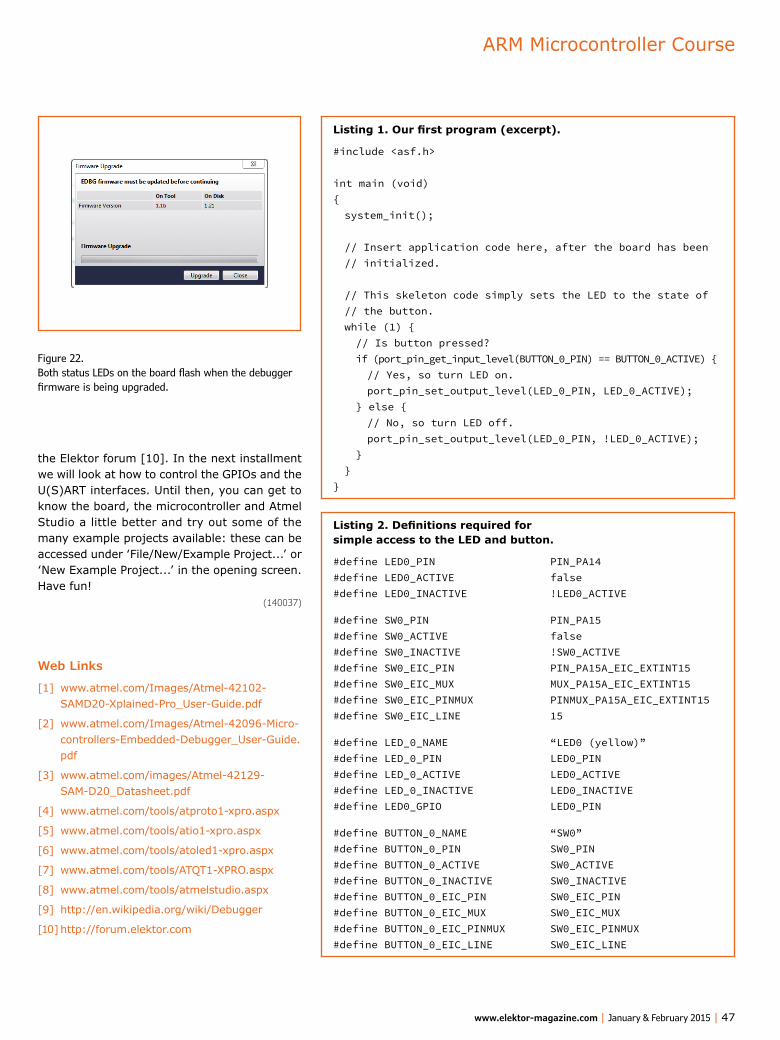
ARM Microcontroller Course
www.elektor-magazine.com | January & February 2015 | 47
the Elektor forum [10]. In the next installment we will look at how to control the GPIOs and the U(S)ART interfaces. Until then, you can get to know the board, the microcontroller and Atmel Studio a little better and try out some of the many example projects available: these can be accessed under ‘File/New/Example Project...’ or ‘New Example Project...’ in the opening screen. Have fun!
(140037)
Web Links
[1] www.atmel.com/Images/Atmel-42102-SAMD20-Xplained-Pro_User-Guide.pdf
[2] www.atmel.com/Images/Atmel-42096-Micro-controllers-Embedded-Debugger_User-Guide.pdf
[3] www.atmel.com/images/Atmel-42129-SAM-D20_Datasheet.pdf
[4] www.atmel.com/tools/atproto1-xpro.aspx
[5] www.atmel.com/tools/atio1-xpro.aspx
[6] www.atmel.com/tools/atoled1-xpro.aspx
[7] www.atmel.com/tools/ATQT1-XPRO.aspx
[8] www.atmel.com/tools/atmelstudio.aspx
[9] http://en.wikipedia.org/wiki/Debugger
[10] http://forum.elektor.com
Listing 2. Definitions required for simple access to the LED and button.
#define LED0_PIN PIN_PA14#define LED0_ACTIVE false#define LED0_INACTIVE !LED0_ACTIVE
#define SW0_PIN PIN_PA15#define SW0_ACTIVE false#define SW0_INACTIVE !SW0_ACTIVE#define SW0_EIC_PIN PIN_PA15A_EIC_EXTINT15#define SW0_EIC_MUX MUX_PA15A_EIC_EXTINT15#define SW0_EIC_PINMUX PINMUX_PA15A_EIC_EXTINT15#define SW0_EIC_LINE 15
#define LED_0_NAME “LED0 (yellow)”#define LED_0_PIN LED0_PIN#define LED_0_ACTIVE LED0_ACTIVE#define LED_0_INACTIVE LED0_INACTIVE#define LED0_GPIO LED0_PIN
#define BUTTON_0_NAME “SW0”#define BUTTON_0_PIN SW0_PIN#define BUTTON_0_ACTIVE SW0_ACTIVE#define BUTTON_0_INACTIVE SW0_INACTIVE#define BUTTON_0_EIC_PIN SW0_EIC_PIN#define BUTTON_0_EIC_MUX SW0_EIC_MUX#define BUTTON_0_EIC_PINMUX SW0_EIC_PINMUX#define BUTTON_0_EIC_LINE SW0_EIC_LINE
Listing 1. Our first program (excerpt).
#include <asf.h>
int main (void) system_init();
// Insert application code here, after the board has been // initialized.
// This skeleton code simply sets the LED to the state of // the button. while (1) // Is button pressed? if (port_pin_get_input_level(BUTTON_0_PIN) == BUTTON_0_ACTIVE) // Yes, so turn LED on. port_pin_set_output_level(LED_0_PIN, LED_0_ACTIVE); else // No, so turn LED off. port_pin_set_output_level(LED_0_PIN, !LED_0_ACTIVE);
Figure 22. Both status LEDs on the board flash when the debugger firmware is being upgraded.
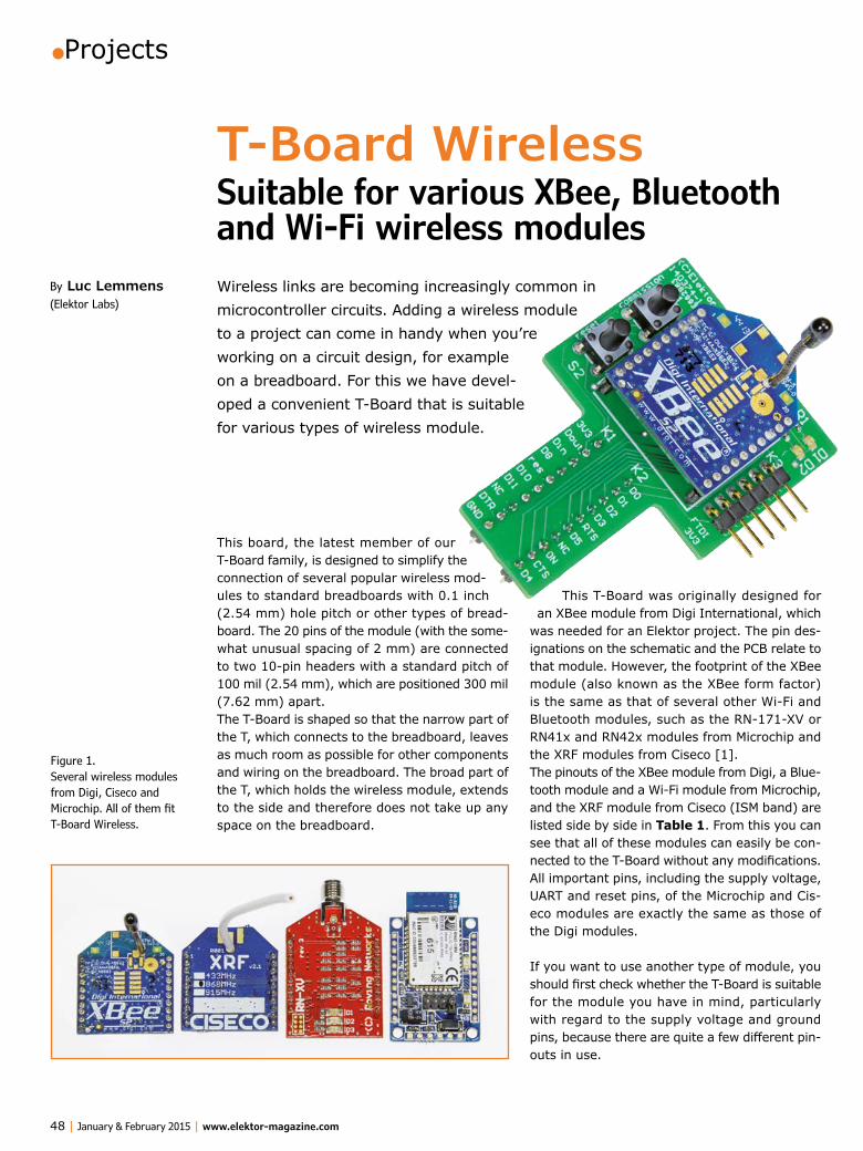
•Projects
48 | January & February 2015 | www.elektor-magazine.com
This board, the latest member of our T-Board family, is designed to simplify the connection of several popular wireless mod-ules to standard breadboards with 0.1 inch (2.54 mm) hole pitch or other types of bread-board. The 20 pins of the module (with the some-what unusual spacing of 2 mm) are connected to two 10-pin headers with a standard pitch of 100 mil (2.54 mm), which are positioned 300 mil (7.62 mm) apart.The T-Board is shaped so that the narrow part of the T, which connects to the breadboard, leaves as much room as possible for other components and wiring on the breadboard. The broad part of the T, which holds the wireless module, extends to the side and therefore does not take up any space on the breadboard.
This T-Board was originally designed for an XBee module from Digi International, which
was needed for an Elektor project. The pin des-ignations on the schematic and the PCB relate to that module. However, the footprint of the XBee module (also known as the XBee form factor) is the same as that of several other Wi-Fi and Bluetooth modules, such as the RN-171-XV or RN41x and RN42x modules from Microchip and the XRF modules from Ciseco [1]. The pinouts of the XBee module from Digi, a Blue-tooth module and a Wi-Fi module from Microchip, and the XRF module from Ciseco (ISM band) are listed side by side in Table 1. From this you can see that all of these modules can easily be con-nected to the T-Board without any modifications. All important pins, including the supply voltage, UART and reset pins, of the Microchip and Cis-eco modules are exactly the same as those of the Digi modules.
If you want to use another type of module, you should first check whether the T-Board is suitable for the module you have in mind, particularly with regard to the supply voltage and ground pins, because there are quite a few different pin-outs in use.
By Luc Lemmens (Elektor Labs)
T-Board WirelessSuitable for various XBee, Bluetooth and Wi-Fi wireless modulesWireless links are becoming increasingly common in microcontroller circuits. Adding a wireless module to a project can come in handy when you’re working on a circuit design, for example on a breadboard. For this we have devel-oped a convenient T-Board that is suitable for various types of wireless module.
Figure 1. Several wireless modules from Digi, Ciseco and Microchip. All of them fit T-Board Wireless.

T-Board Wireless
www.elektor-magazine.com | January & February 2015 | 49
The circuitThere aren’t very many components other than the wireless module on the T-Board PCB (see the schematic diagram in Figure 2). The MOD1, K1 and K2 connectors are necessary due to the non-standard pin pitch of the wireless modules. Other components on the board include a con-nector for a USB/TTL interface cable with 3.3-V signal levels (K3), a 3.3 V voltage regulator (IC1 with decoupling capacitors C1 and C2), two push-buttons (S1 and S2) and LEDs for special func-tions (D1 and D2).
As you can see from the schematic diagram, the two pins of the XBee module marked ‘NC’ (not connected) are routed to the connectors for plugging the T-Board into a breadboard. That’s because some modules from other manufactur-ers do have functions assigned to these pins.The two pushbuttons S1 and S2 (labeled “Reset” and “Commissioning”) are not necessary in nor-mal use. The Reset button is sometimes neces-sary for downloading firmware to the flash mem-ory, and when you are developing new applica-tions you will most likely run into situations where this button comes in handy. The Commissioning button is used with the XBee module for network diagnosis and configuration. That’s also not an everyday activity, but it’s always nice to have available. For more information about this, see the Digi International application notes and data sheets [2].
LED D1 (RSSI) can be used as a signal strength indicator for the most recently received data packet. This option is enabled by default in the Digi modules, and it can be switched on or off using the XCTU software. LED D2, which is called “Associate LED” in the Digi documentation, pro-vides network status and diagnostic information in combination with the Commissioning button. With the Ciseco XRF module, D1 blinks once per second when the module is working properly and D2 lights up when a data packet is sent.
Figure 3 shows the circuit board layout of T-Board Wireless. The voltage regulator, capac-itors, resistors and LEDs are all SMDs. The cho-sen package size is large enough to make hand soldering reasonably easy. T-Board Wireless is also available fully assembled from the Elektor Store (order number 140374-91). If all the com-ponents except the wireless module are omitted
VCC1
DOUT2
DIN3
DIO84
RESET5
RSSI6
DIO117
DTR9NC8
GND10 DIO4 11CTS 12
ON/SLEEP 13NC 14
DIO5 15RTS 16
DIO3 17DIO2 18DIO1 19DIO0 20
Mod1
XBee
K1 K2
K3
S2R2
330R
D2
3
2
1
IC1XC6206P332P
C1
1u
C2
1u
S1R1
330R
D1
CTS
RXDTXD
RTS
3V3
3V3
5V
FTDI
3V3 c
able
reset commissioning
140374 - 11
Figure 2. The circuit consists of a wireless module, a voltage regulator and a few passive components.
Table 1. Pinouts of several wireless modules.
Pin no.Digi XBee XBee
Ciseco XRF ISM (868 MHz)
RN171XV WiFi
RN42XV Bluetooth
1 3.3 V 3.3 V 3.3 V 3.3 V
2 Dout Dout Dout Dout
3 Din Din Din Din
4 DIO8 RTS GPIO8 GPIO7
5 #reset #reset #reset #reset
6 RSSI P1_7 GPIO5 GPIO6
7 DIO11 P1_6 GPIO7 GPIO9
8 NC P1_5 GPIO9 GPIO4
9 DTR P1_4 GPIO1 GPIO11
10 GND GND GND GND
11 DIO4 P0_1 GPIO14 GPIO8
12 CTS CTS RTS RTS
13 on/#sleep on/#sleep GPIO4 GPIO2
14 NC NC NC NC
15 DIO5 P0_7 GPIO6 GPIO5
16 RTS P2_0 CTS CTS
17 DIO3 P2_1 Sensor5 GPIO3
18 DIO2 P2_2 GPIO3 GPIO7
19 DIO1 P2_3 Sensor3 AIO0
20 DIO0 P0_5 Sensor2 AIO1
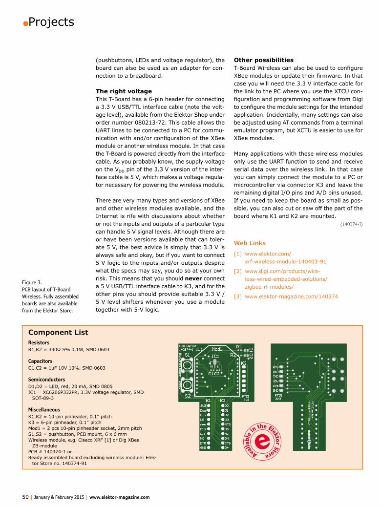
•Projects
50 | January & February 2015 | www.elektor-magazine.com
Other possibilitiesT-Board Wireless can also be used to configure XBee modules or update their firmware. In that case you will need the 3.3 V interface cable for the link to the PC where you use the XTCU con-figuration and programming software from Digi to configure the module settings for the intended application. Incidentally, many settings can also be adjusted using AT commands from a terminal emulator program, but XCTU is easier to use for XBee modules.
Many applications with these wireless modules only use the UART function to send and receive serial data over the wireless link. In that case you can simply connect the module to a PC or microcontroller via connector K3 and leave the remaining digital I/O pins and A/D pins unused. If you need to keep the board as small as pos-sible, you can also cut or saw off the part of the board where K1 and K2 are mounted.
(140374-I)
Web Links
[1] www.elektor.com/xrf-wireless-module-140403-91
[2] www.digi.com/products/wire-less-wired-embedded-solutions/zigbee-rf-modules/
[3] www.elektor-magazine.com/140374
(pushbuttons, LEDs and voltage regulator), the board can also be used as an adapter for con-nection to a breadboard.
The right voltageThis T-Board has a 6-pin header for connecting a 3.3 V USB/TTL interface cable (note the volt-age level), available from the Elektor Shop under order number 080213-72. This cable allows the UART lines to be connected to a PC for commu-nication with and/or configuration of the XBee module or another wireless module. In that case the T-Board is powered directly from the interface cable. As you probably know, the supply voltage on the VDD pin of the 3.3 V version of the inter-face cable is 5 V, which makes a voltage regula-tor necessary for powering the wireless module.
There are very many types and versions of XBee and other wireless modules available, and the Internet is rife with discussions about whether or not the inputs and outputs of a particular type can handle 5 V signal levels. Although there are or have been versions available that can toler-ate 5 V, the best advice is simply that 3.3 V is always safe and okay, but if you want to connect 5 V logic to the inputs and/or outputs despite what the specs may say, you do so at your own risk. This means that you should never connect a 5 V USB/TTL interface cable to K3, and for the other pins you should provide suitable 3.3 V / 5 V level shifters whenever you use a module together with 5-V logic.
Component ListResistorsR1,R2 = 330Ω 5% 0.1W, SMD 0603
CapacitorsC1,C2 = 1µF 10V 10%, SMD 0603
SemiconductorsD1,D2 = LED, red, 20 mA, SMD 0805IC1 = XC6206P332PR, 3.3V voltage regulator, SMD
SOT-89-3
MiscellaneousK1,K2 = 10-pin pinheader, 0.1” pitchK3 = 6-pin pinheader, 0.1” pitchMod1 = 2 pcs 10-pin pinheader socket, 2mm pitchS1,S2 = pushbutton, PCB mount, 6 x 6 mmWireless module, e.g. Ciseco XRF [1] or Dig XBee
ZB-modulePCB # 140374-1 orReady assembled board excluding wireless module: Elek-
tor Store no. 140374-91
Figure 3. PCB layout of T-Board Wireless. Fully assembled boards are also available from the Elektor Store.

LM317 Tweak
www.elektor-magazine.com | January & February 2015 | 51
Voltage regulators have been indispensable in modern electronic circuits for several decades. They are available in many types and sizes, with either fixed or adjustable output voltages.One of the oldest voltage regulators still in pro-duction is the LM317, which was introduced back in 1971 by National Semiconductor. While the present-day implementations of the LM317 are likely to have a modified version of the original chip design, the characteristics, pin-out and phys-ical dimensions continue to remain the same.The output voltage of the LM317 is easily set with the aid of two resistors connected to the Adjust pin (Figure 1). The input voltage may go up to a maximum of 40 V and the IC can deliver more than 2 amps, provided that the difference between the input and output voltages is less than 15 V.
With the LM317 it is possible to set the output voltage very accurately, provided you first take the effort to measure the internal reference voltage of the IC. This will be, depending on the manu-facturer, between 1.2 and 1.3 V. To measure the actual reference voltage the LM317 to be used has to be plugged into a breadboard first, accord-ing the schematic of Figure 2. R1 may have a value between 240 and 470 Ω. Connect a voltage between 3 and 10 V to the input (in any case more than 3 V, the minimal voltage differential between input and output to ensure that the LM317 oper-ates properly). Now measure the voltage at the output of the regulator using a multimeter. This is the internal reference voltage. The author has measured, among others, the following values with types from various manufacturers: ST317: 1.249 V, UA317: 1.275 V, SSS317: 1.231 V.
In addition, you have to take into account that a current of about 50 µA will be sourced from the Adjust pin and this will therefore also flow through resistor R2 of the voltage divider in Figure 1. This value too can differ from one manufacturer to another, so check the datasheet of the rele-vant manufacturer.
When we take all this into account, we can calcu-late the component values for the desired output voltage using the following formulas:
R2theoretical = (Uout / Uref – 1) × R1R2adjust = (Uout – Uref) / Iadjust
R2tot = R2theoretical × R2adjust / (R2theoretical + R2adjust)
Of course, you could use a trimpot for R2 and adjust it until the desired output voltage has been obtained, but using this calculation you can mount the correct fixed resistor on the circuit board right away. This same calculation can also be used with the negative version, the LM337.
All the calculations here assume that the operat-ing temperature of the IC is reasonably constant. Both Uref and Iadjust drift somewhat with large changes in temperature, while the output voltage also varies a little with different load currents.
(140341-I)
Based on idea from Peter Krueger (Germany)
Better Accuracy from the LM317
LM317IC1
ADJ
C1
100n
C2
1u
R1330R
R2
LM317IC1
ADJR1
330R
Figure 1. The standard application circuit for the LM317 voltage regulator.
Figure 2. By connecting the Adjust pin to ground we can measure the internal reference voltage at the output.
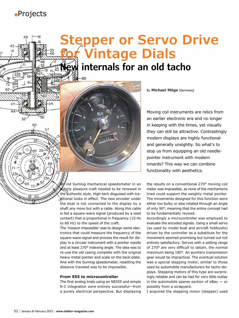
•Projects
52 | January & February 2015 | www.elektor-magazine.com
An old Sumlog mechanical speedometer in an elderly pleasure craft needed to be renewed in the authentic style. High-tech disguised with tra-ditional looks in effect. The new encoder under the boat is not connected to the display by a shaft any more but with a cable. Along this cable is fed a square-wave signal (produced by a reed contact) that is proportional in frequency (10 Hz to 60 Hz) to the speed of the craft.The ‘mission impossible’ was to design some elec-tronics that could measure the frequency of the square-wave signal and process the result for dis-play in a circular instrument with a pointer needle and at least 270° indexing angle. The idea was to re-use the old casing complete with the original heavy metal pointer and scale on the back-plate. And with the Sumlog speedometer, resetting the distance traveled was to be impossible.
From 555 to microcontrollerThe first analog trials using an NE555 and simple R-C integration were entirely successful—from a purely electrical perspective. But displaying
the results on a conventional 270° moving coil meter was impossible, as none of the mechanisms tried could support the weighty metal pointer. The movements designed for this function were either too bulky or else rotated through an angle of only 90°, meaning that the entire concept had to be fundamentally revised.Accordingly a microcontroller was employed to evaluate the encoded signals. Using a small servo (as used by model boat and aircraft hobbyists) driven by the controller as a substitute for the movement seemed promising but turned out not entirely satisfactory. Servos with a setting range of 270° are very difficult to obtain, the normal maximum being 180°. An auxiliary transmission gear would be impractical. The eventual solution was a special stepping motor, similar to those used by automobile manufacturers for tacho dis-plays. Stepping motors of this type are surpris-ingly reliable and can be had for very little outlay in the automobile spares section of eBay — or possibly from a scrapyard.I acquired the stepping motor (stepper) used
By Michael Möge (Germany)
Stepper or Servo Drive for Vintage DialsNew internals for an old tacho
Moving coil instruments are relics from an earlier electronic era and no longer in keeping with the times, yet visually they can still be attractive. Contrastingly modern displays are highly functional and generally unsightly. So what’s to stop us from equipping an old needle-pointer instrument with modern innards? This way we can combine functionality with aesthetics.

Vintage Dial Driver
www.elektor-magazine.com | January & February 2015 | 53
for this project on eBay [1]. This did not turn through 360° but through 315° from end stop to end stop, in 1260 steps. The end stops are solid, with a large setting and holding torque, although unfortunately there is no feedback for indicating the position of the pointer. At startup, regardless of the actual position of the pointer, the stepper simply rotates by 1260 steps to the left, as far as the end stop. About 0.5 s of stepping zeroes it definitively. The stepper is operated in eight phases by two solenoid coils under direct control of an ATtiny2313 from Atmel.The hardware in Figure 1 is extremely straight-forward and arranged so that either one servo (with 180° indexing) or the stepper (with 315° indexing) can be operated. Next to the ATtiny2313 we have the usual reset arrangements and the crystal plus R6 and C2, which form a simple R-C input filter for the sensor input. According to your requirements either the magnet coil of the stepping motor or the servo can be connected direct to the processor.Instead of the special steppers you might also
consider a ‘normal’ small bipolar stepping motor, if the zero point was defined by a rigid mechan-ical end stop. A stepping motor without its drive mechanism and 1.8° steps resolves the 315° indexing angle in 175 steps. As a rule the strength developed is so great that the drive current of the magnet can be reduced significantly. All the same, direct drive of the magnets by the con-troller is not standard practice.Note that we need to indicate not only speed but also the distance covered. For this we employ an electromagnetic counter, producing a reading that is non-transient and cannot be reset. The pulses from the encoder are totaled in the pro-cessor and when these reach a predefined count, a 10-ms pulse is output to PB1. Counter mecha-nisms for 5 V DC are virtually unobtainable and most electromechanical meters [2] operate within a DC range of 10–30 V. Accordingly we amplify the pulses from the controller using the circuitry based around T1 and T2. The counter used here is a 24-V model, although in some cases different mechanisms could be driven either directly by
X1
6MHzC4 C3
18p 18p
R21k
C1
100n
R1
47k
1k 2k7
2k2
10k
4k7
4k7
D4
C5
1u10V
100u10V
47u16V
Servo
Stepper
M
M
IC278L05
12
3
C6D1
ZPD4
V7
C2
10n
R6
R8
ATtiny2313
PB6(MISO)
PD3(INT1)
PB1(AIN1)
PB0(AIN0)
PD2(INT0)
PB5(MOSI)
PB7(SCK)
PB3(OC1A)
PD0(RXD)PD1(TXD)
PD6(ICP)PD5(T1)PD4(T0)
RESET
XTAL1XTAL2
IC1
PB4PB2
VCC
GND10
20
1918
13
12
14
15
1617
11987
1
5
236
4
Sensor
Counter
GND
GND
R4
R5
R3
R7
D3
24V
Switec MS X25
D2
1N4148
1N4148
T1
T2
BC107
BC177
C7
+12V
140280 - 11
1N4148
245679010
Figure 1. A servo mechanism or a stepping motor can be connected to the controller.
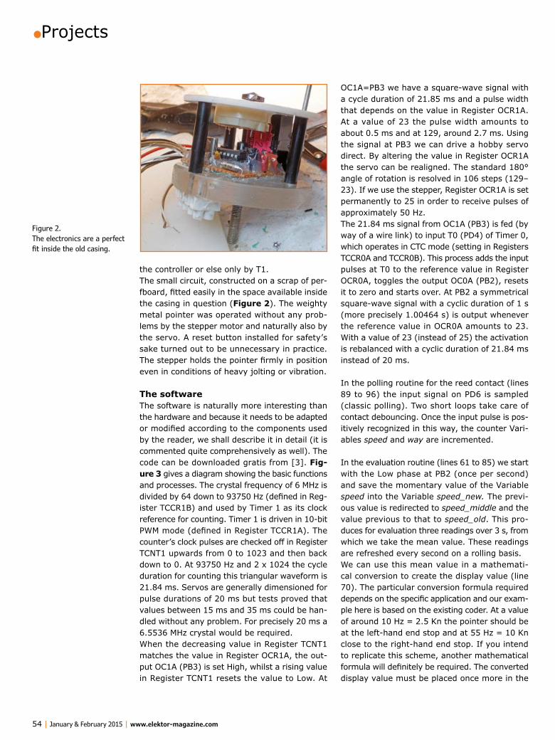
•Projects
54 | January & February 2015 | www.elektor-magazine.com
OC1A=PB3 we have a square-wave signal with a cycle duration of 21.85 ms and a pulse width that depends on the value in Register OCR1A. At a value of 23 the pulse width amounts to about 0.5 ms and at 129, around 2.7 ms. Using the signal at PB3 we can drive a hobby servo direct. By altering the value in Register OCR1A the servo can be realigned. The standard 180° angle of rotation is resolved in 106 steps (129–23). If we use the stepper, Register OCR1A is set permanently to 25 in order to receive pulses of approximately 50 Hz.The 21.84 ms signal from OC1A (PB3) is fed (by way of a wire link) to input T0 (PD4) of Timer 0, which operates in CTC mode (setting in Registers TCCR0A and TCCR0B). This process adds the input pulses at T0 to the reference value in Register OCR0A, toggles the output OC0A (PB2), resets it to zero and starts over. At PB2 a symmetrical square-wave signal with a cyclic duration of 1 s (more precisely 1.00464 s) is output whenever the reference value in OCR0A amounts to 23. With a value of 23 (instead of 25) the activation is rebalanced with a cyclic duration of 21.84 ms instead of 20 ms.
In the polling routine for the reed contact (lines 89 to 96) the input signal on PD6 is sampled (classic polling). Two short loops take care of contact debouncing. Once the input pulse is pos-itively recognized in this way, the counter Vari-ables speed and way are incremented.
In the evaluation routine (lines 61 to 85) we start with the Low phase at PB2 (once per second) and save the momentary value of the Variable speed into the Variable speed_new. The previ-ous value is redirected to speed_middle and the value previous to that to speed_old. This pro-duces for evaluation three readings over 3 s, from which we take the mean value. These readings are refreshed every second on a rolling basis.We can use this mean value in a mathemati-cal conversion to create the display value (line 70). The particular conversion formula required depends on the specific application and our exam-ple here is based on the existing coder. At a value of around 10 Hz = 2.5 Kn the pointer should be at the left-hand end stop and at 55 Hz = 10 Kn close to the right-hand end stop. If you intend to replicate this scheme, another mathematical formula will definitely be required. The converted display value must be placed once more in the
the controller or else only by T1.The small circuit, constructed on a scrap of per-fboard, fitted easily in the space available inside the casing in question (Figure 2). The weighty metal pointer was operated without any prob-lems by the stepper motor and naturally also by the servo. A reset button installed for safety’s sake turned out to be unnecessary in practice. The stepper holds the pointer firmly in position even in conditions of heavy jolting or vibration.
The softwareThe software is naturally more interesting than the hardware and because it needs to be adapted or modified according to the components used by the reader, we shall describe it in detail (it is commented quite comprehensively as well). The code can be downloaded gratis from [3]. Fig-ure 3 gives a diagram showing the basic functions and processes. The crystal frequency of 6 MHz is divided by 64 down to 93750 Hz (defined in Reg-ister TCCR1B) and used by Timer 1 as its clock reference for counting. Timer 1 is driven in 10-bit PWM mode (defined in Register TCCR1A). The counter’s clock pulses are checked off in Register TCNT1 upwards from 0 to 1023 and then back down to 0. At 93750 Hz and 2 x 1024 the cycle duration for counting this triangular waveform is 21.84 ms. Servos are generally dimensioned for pulse durations of 20 ms but tests proved that values between 15 ms and 35 ms could be han-dled without any problem. For precisely 20 ms a 6.5536 MHz crystal would be required.When the decreasing value in Register TCNT1 matches the value in Register OCR1A, the out-put OC1A (PB3) is set High, whilst a rising value in Register TCNT1 resets the value to Low. At
Figure 2. The electronics are a perfect fit inside the old casing.
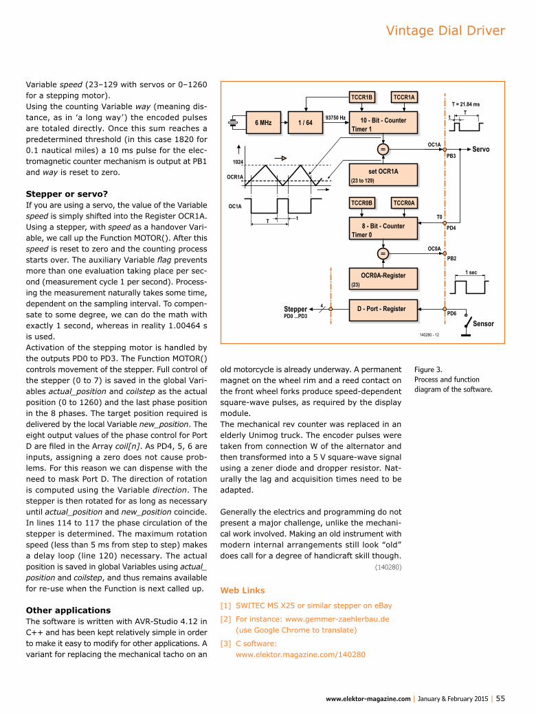
Vintage Dial Driver
www.elektor-magazine.com | January & February 2015 | 55
old motorcycle is already underway. A permanent magnet on the wheel rim and a reed contact on the front wheel forks produce speed-dependent square-wave pulses, as required by the display module.The mechanical rev counter was replaced in an elderly Unimog truck. The encoder pulses were taken from connection W of the alternator and then transformed into a 5 V square-wave signal using a zener diode and dropper resistor. Nat-urally the lag and acquisition times need to be adapted.
Generally the electrics and programming do not present a major challenge, unlike the mechani-cal work involved. Making an old instrument with modern internal arrangements still look “old” does call for a degree of handicraft skill though.
(140280)
Web Links
[1] SWITEC MS X25 or similar stepper on eBay
[2] For instance: www.gemmer-zaehlerbau.de (use Google Chrome to translate)
[3] C software: www.elektor.magazine.com/140280
Variable speed (23–129 with servos or 0–1260 for a stepping motor).Using the counting Variable way (meaning dis-tance, as in ‘a long way’) the encoded pulses are totaled directly. Once this sum reaches a predetermined threshold (in this case 1820 for 0.1 nautical miles) a 10 ms pulse for the elec-tromagnetic counter mechanism is output at PB1 and way is reset to zero.
Stepper or servo?If you are using a servo, the value of the Variable speed is simply shifted into the Register OCR1A. Using a stepper, with speed as a handover Vari-able, we call up the Function MOTOR(). After this speed is reset to zero and the counting process starts over. The auxiliary Variable flag prevents more than one evaluation taking place per sec-ond (measurement cycle 1 per second). Process-ing the measurement naturally takes some time, dependent on the sampling interval. To compen-sate to some degree, we can do the math with exactly 1 second, whereas in reality 1.00464 s is used.Activation of the stepping motor is handled by the outputs PD0 to PD3. The Function MOTOR() controls movement of the stepper. Full control of the stepper (0 to 7) is saved in the global Vari-ables actual_position and coilstep as the actual position (0 to 1260) and the last phase position in the 8 phases. The target position required is delivered by the local Variable new_position. The eight output values of the phase control for Port D are filed in the Array coil[n]. As PD4, 5, 6 are inputs, assigning a zero does not cause prob-lems. For this reason we can dispense with the need to mask Port D. The direction of rotation is computed using the Variable direction. The stepper is then rotated for as long as necessary until actual_position and new_position coincide. In lines 114 to 117 the phase circulation of the stepper is determined. The maximum rotation speed (less than 5 ms from step to step) makes a delay loop (line 120) necessary. The actual position is saved in global Variables using actual_position and coilstep, and thus remains available for re-use when the Function is next called up.
Other applicationsThe software is written with AVR-Studio 4.12 in C++ and has been kept relatively simple in order to make it easy to modify for other applications. A variant for replacing the mechanical tacho on an
Figure 3. Process and function diagram of the software.
6 MHz
TCCR1B
1 / 64 10 - Bit - CounterTimer 1
set OCR1A(23 to 129)
93750 Hz
OC1A
TT = 21.84 ms
t
PB3Servo
Sensor
Stepper
T0
PD4
PB2
PD6
140280 - 12
TCCR1A
TCCR0B
8 - Bit - CounterTimer 0
OCR0A-Register(23)
PD0 ...PD3
4
OC0A
OC1A
OCR1A
1024
TCCR0A
D - Port - Register
T t
1 sec

•Projects
56 | January & February 2015 | www.elektor-magazine.com
This month we carry on with connecting the MGC3130 touch & gesture controller IC to the Raspberry Pi. And play the extremely nerdy game called 2048 (yes that’s 211).If you are new to this series there are three points to observe:
1. this is a Workbook, meaning we use jottings and succinct language;
2. the hardware referred to is available exclu-sively through the Elektor Store, see [1];
3. it’s useful to read up a previous article [2] and installment 1 [3].
IngredientsStart by reviewing the hardware connections as detailed in the previous installment [3]. Table 1 recaps the I/O pin mapping you should have.Make sure you have
1. the latest Raspbian, i.e. Raspbian Debian Wheezy, Version: September 2014, Release date: 2014-09-09.
2. Python program: 2048_with_Hillstar_Gesture_Port.py (with a bug fix of the port mapping). Get it at [4].
3. MGC3130 FW + Parameterization: Hillstar Ges-ture Port V1.2.4 to Raspberry Pi Demo 2048.enz (note version 1.2.4). Get it at [4].
Python preppingYou can immediately start using the IDLE Inte-grated Development Environment (IDE) which includes the Tkinter GUI toolkit.
The Raspbian installation provides IDLE for Python 2.7 and Python 3. Our GestIC demo is based on Python 2.7. Start the IDE in a Linux terminal as root to get a quick access to the GPIO hardware, see Figure 1.
# sudo idle
The first Python program can be directly executed from the shell like so:
>>> print “Hello Python”
Accessing the RPi’s GPIOs is as easy as that. Load the pre-installed GPIO Python module, initialize the pins and read the signals into your program, see Listing 1.
Listing 1>>> import RPi.GPIO as GPIO>>> GPIO.setmode(GPIO.BCM)>>>>>> GPIO.setup(17, GPIO.IN, pull_up_down = GPIO.PUD_DOWN)>>> GPIO.setup(18, GPIO.IN, pull_up_down = GPIO.PUD_DOWN)>>>>>> while true:>>> if GPIO.input(17)==1:>>> print “GPIO 17 is HIGH”>>> elif GPIO.input(18)==1:>>> print “GPIO 18 is HIGH”
If the Hardware is correctly set up, the program will print a line every time a flicking gesture was performed, like in Figure 2.
2048 4 RPi2048 is a puzzle challenge created in March 2014 by 19 year old Italian web developer Gabriele Cirulli. The challenge is to slide prenumbered tiles on a 4 x 4 grid in such a way as to create a tile with the number 2048. Gabriele’s game attracted 4 million visitors in less than a week. You can look up the rules at [5]. In fact 2014 is not the limit; Elektor readers should be able to reach the highest possible tile, 131,072 or 217.The Python version we used for our RPi imple-mentation was published in Hrvoje’s Blog [6]
By Thomas Lindner and Hung Nguyen (Microchip GestIC® Team, Germany)
GestIC & 3D Touchpad Workbook (2)Flick to win 2048 on the RPi
GestIC & 3D Touchpad Workbook
www.elektor-magazine.com | January & February 2015 | 57
and we combined it with the Gesture inputs from the MGC3130 sensor.Now let’s combine all parts. The complete code can be downloaded from the Elektor web page for this installment [4]. Copy the file to the RPi and open it from the IDLE Python shell, see Figure 3.The file opens in an editor window and you can execute the program by selecting “Run” in the menu or just press F5. Play the game with flick-ing gestures in the four cardinal directions over the Hillstar electrode. It’s fun—see Figure 4.
In the pipelineNext time we will play 2048 with the ready-made 3D Touchpad also included in the Elektor/Microchip special offer [1]. We’ll also delve into the USB interface and the 3DTouchpad Software development kit (SDK), and into using the 3D Touchpad on Rpi’s USB port.
(140513)
Web Links
[1] Microchip Hillstar GestIC dev kit and 3D Touchpad product bundle: www.elektor.com/microchip-dm160218-hillstar-development-kit-and-dm160225-3d-touchpad
[2] Add 3D Sensing to your Micro or PC. Elektor November 2014.
[3] GestIC & 3D Touchpad Workbook (1). Elektor December 2014.
[4] 2048 Game on Rpi patched for MGC3130: www.elektor-magazine.com/140513
[5] 2048 Game history and rules: http://en.wikipedia.org/wiki/2048_%28video_game%29
[6] Hrvoje’s Blog: http://blog.hrvoje.org/blog/2014/09/20/a-simple-2048-clone-in-python
Table 1.
MGC3130 RPi Mapped Gesture
EIO1 GPIO17 ç Flick EastàWest
EIO2 GPIO18 é Flick SouthàNorth
EIO3 GPIO25 è Flick WestàEast
EIO6 GPIO23 ê Flick NorthàSouth
1
2
3
4
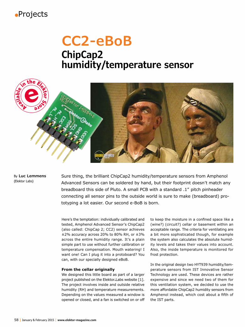
•Projects
58 | January & February 2015 | www.elektor-magazine.com
Here’s the temptation: individually calibrated and tested, Amphenol Advanced Sensor’s ChipCap2 (also called: ChipCap 2; CC2) sensor achieves ±2% accuracy across 20% to 80% RH, or ±3% across the entire humidity range. It’s a plain simple part to use without further calibration or temperature compensation. Mouth watering! I want one! Can I plug it into a protoboard? You can, with our specially designed eBoB.
From the cellar originallyWe designed this little board as part of a larger project published on the Elektor.Labs website [1]. The project involves inside and outside relative humidity (RH) and temperature measurements. Depending on the values measured a window is opened or closed, and a fan is switched on or off
to keep the moisture in a confined space like a (wine?) (circuit?) cellar or basement within an acceptable range. The criteria for ventilating are a bit more sophisticated though, for example the system also calculates the absolute humid-ity levels and takes their values into account. Also, the inside temperature is monitored for frost protection.
In the original design two HYT939 humidity/tem-perature sensors from IST Innovative Sensor Technology are used. These devices are rather expensive and since we need two of them for this ventilation system, we decided to use the more affordable ChipCap2 humidity sensors from Amphenol instead, which cost about a fifth of the IST parts.
By Luc Lemmens (Elektor Labs)
CC2-eBoBChipCap2 humidity/temperature sensor
Sure thing, the brilliant ChipCap2 humidity/temperature sensors from Amphenol Advanced Sensors can be soldered by hand, but their footprint doesn’t match any breadboard this side of Pluto. A small PCB with a standard .1” pitch pinheader connecting all sensor pins to the outside world is sure to make (breadboard) pro-totyping a lot easier. Our second e-BoB is born.

ChipCap2 humidity/temperature sensor
www.elektor-magazine.com | January & February 2015 | 59
Since both brands of sensor can be connected to the I2C bus—and at first glance even look com-patible with the same default I2C address, com-mands etc.—it appears that both sensors can be used in our ventilation system with trifling software changes. However, we haven’t studied the HYT939 in detail (yet).
Analog and digital interfacingThe ChipCap2 can be used either in I2C mode (type CC2D like in our application) or in Pulse Density mode (PDM; type CC2A), in which case two separate pins—after some passive filtering—provide analog temperature and humidity sig-nals. See Table 1 for all available versions. Our breakout board layout is designed for both the analog and the digital versions of these sensors–though some components must be changed—but here we will focus mainly on I2C, i.e. the CC2D.
Sensor pad descriptionsPower pads (not: pins) VDD and VSS (pins 7 and 6) are used for connecting a supply voltage in the 2.7 V to 5.5 V range depending on the exact version of the CC2. The pads should be decou-pled with a 220-nF capacitor (.22 µF in the US). VCORE is an internal voltage of the CC2 and should only be connected to a 100-nF (.1 µF) decoupling capacitor to ground.
Sensor data gets transferred in and out of the device through the SDA pad (3), while the com-munication between ChipCap2 and the microcon-troller (MCU) is synchronized through the SCL pad (4). ChipCap2 has an internal temperature-com-pensated oscillator that provides a timebase for all operations, and uses an I²C-compatible com-
munication protocol with support for 100 kHz to 400 kHz bit rates. External pull-up resistors are required to pull the drive signal High.The alarm outputs (pads 1 and 8) can be used to monitor whether the sensor reading has exceeded or dropped below pre-programmed relative humidity values. The alarm can be used to drive an open-drain load connected to VDD, or it can function as a full push-pull driver. If a high-voltage application is required, external devices can be controlled with the Alarm pins, as demonstrated in Figure 1.
The two alarm outputs can be used simultane-ously, and these alarms can be used in combina-tion with the I2C. Thresholds at which these alarm pins are activated or deactivated can be set, the output pin configuration (e.g. open drain, push-pull) and active output level can be set in the
ChipCap2 (CC2) SpecificationsSensor: Relative Humidity (RH%)• Resolution: 14 bit (0.01%RH)• Accuracy: ±2.0 %RH (20–80%RH)• Repeatability: ±0.2 %RH• Hysteresis: ±2.0 %RH• Linearity: <2.0 %RH• Response time: 7.0 sec (τ 63%)• Temp Coefficient: Max 0.13 %RH/°C
(at 10–60°C, 10–90%RH)• Operating Range: 0–100 %RH
(Non-Condensing)
• Long Term Drift: <0.5 %RH/yr (Normal condition)
Sensor: Temperature (°C)• Resolution: 14 bit (0.01°C)• Accuracy: ±0.3°C• Repeatability: ±0.1°C• Response time: 5.0 sec (τ 63%)• Operating range: –40 to 125°C• Long term drift: <0.05°C/yr
(Normal condition)
Table 1. CC2 (ChipCap2) part number list
Part number Description
CC2A25 analog, 2%, 5V
CC2A23 analog, 2%, 3.3V
CC2D23S digital, sleep mode, 2%, 3.3V
CC2D25S digital, sleep mode, 2%, 5V
CC2D23 digital, 2%, 3.3V
CC2D25 digital, 2%, 5V
CC2D35 digital, 3%, 5V
CC2A33 analog, 3%, 3.3V
CC2D33S digital, sleep mode, 3%, 3.3V
CC2D35S digital, sleep mode, 3%, 5V
CC2D33 digital, 3%, 3.3V
CC2A35 analog, 3%, 5V
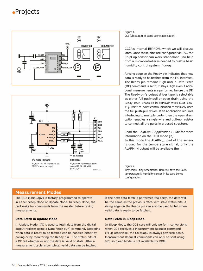
•Projects
60 | January & February 2015 | www.elektor-magazine.com
CC2A’s internal EEPROM, which we will discuss later. Once these pins are configured via I2C, the ChipCap sensor can work standalone—no help from a microcontroller is needed to build a basic humidity control system, hooray.
A rising edge on the Ready pin indicates that new data is ready to be fetched from the I2C interface. The Ready pin remains High until a Data Fetch (DF) command is sent; it stays High even if addi-tional measurements are performed before the DF. The Ready pin’s output driver type is selectable as either full push-pull or open drain using the Ready_Open_Drain bit in EEPROM word Cust_Con-fig. Point-to-point communication most likely uses the full push-pull driver. If an application requires interfacing to multiple parts, then the open drain option enables a single wire and pull-up resistor to connect all the parts in a bused structure.
Read the ChipCap 2 Application Guide for more information on the PDM mode [2].In this mode the ALARM_L pad of the sensor is used for the temperature signal, only the ALARM_H output will be available then.
12V
VDD
VDD
5
6
7
8
VCORE
GND
VDD
ALARM_HIGH
4
3
2
1
SDA
HUMIDIFIER
SCL
PDM_H
ALARM_LOW
12V
DEHUMIDIFIER
PDM_T 1
PDM_H 2SDA 3SCL 4
VCORE5
VSS6
VDD7
ALARM_H 8
IC1
CC2C1
100n
C2
220n
R1
10k
R2
10k
VDD
K1
SCLGNDVDD
SDAEOCAL_HAL_L
R30R
R40R
10V
C3
10u10V
C4
10u
* *
* = not mounted
R1, R2 = 10k: I2C internal pull up R1, R2 = 0R: PDM outputs activeI2C mode (default):
PDM-T = alarm low output
PDM mode:
replace R3, R4 0R 6k8place C3, C4 140154 - 11
Figure 1. CC2 (ChipCap2) in stand-alone application.
Figure 2. Tiny chips—tiny schematics! Here we have the CC2A temperature & humidity sensor in its bare bones configuration.
Measurement ModesThe CC2 (ChipCap2) is factory-programmed to operate in either Sleep Mode or Update Mode. In Sleep Mode, the part waits for commands from the master before taking measurements.
Data Fetch in Update Mode
In Update Mode, I2C is used to fetch data from the digital output register using a Data Fetch (DF) command. Detecting when data is ready to be fetched can be handled either by polling or by monitoring the Ready pin. The status bits of a DF tell whether or not the data is valid or stale. After a measurement cycle is complete, valid data can be fetched.
If the next data fetch is performed too early, the data will be the same as the previous fetch with stale status bits. A rising edge on the Ready pin can also be used to tell when valid data is ready to be fetched.
Data Fetch in Sleep Mode
In Sleep Mode, the CC2 core will only perform conversions when CC2 receives a Measurement Request command (MR); otherwise, the ChipCap2 is always powered down. Measurement Request commands can only be sent using I2C, so Sleep Mode is not available for PDM.
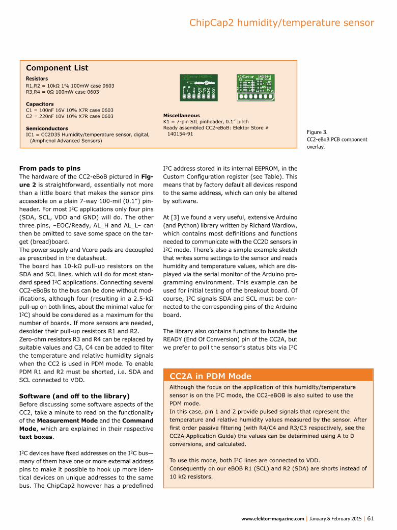
ChipCap2 humidity/temperature sensor
www.elektor-magazine.com | January & February 2015 | 61
I2C address stored in its internal EEPROM, in the Custom Configuration register (see Table). This means that by factory default all devices respond to the same address, which can only be altered by software.
At [3] we found a very useful, extensive Arduino (and Python) library written by Richard Wardlow, which contains most definitions and functions needed to communicate with the CC2D sensors in I2C mode. There’s also a simple example sketch that writes some settings to the sensor and reads humidity and temperature values, which are dis-played via the serial monitor of the Arduino pro-gramming environment. This example can be used for initial testing of the breakout board. Of course, I2C signals SDA and SCL must be con-nected to the corresponding pins of the Arduino board.
The library also contains functions to handle the READY (End Of Conversion) pin of the CC2A, but we prefer to poll the sensor’s status bits via I2C
From pads to pinsThe hardware of the CC2-eBoB pictured in Fig-ure 2 is straightforward, essentially not more than a little board that makes the sensor pins accessible on a plain 7-way 100-mil (0.1”) pin-header. For most I2C applications only four pins (SDA, SCL, VDD and GND) will do. The other three pins, –EOC/Ready, AL_H and AL_L– can then be omitted to save some space on the tar-get (bread)board.The power supply and Vcore pads are decoupled as prescribed in the datasheet. The board has 10-kΩ pull-up resistors on the SDA and SCL lines, which will do for most stan-dard speed I2C applications. Connecting several CC2-eBoBs to the bus can be done without mod-ifications, although four (resulting in a 2.5-kΩ pull-up on both lines, about the minimal value for I2C) should be considered as a maximum for the number of boards. If more sensors are needed, desolder their pull-up resistors R1 and R2.Zero-ohm resistors R3 and R4 can be replaced by suitable values and C3, C4 can be added to filter the temperature and relative humidity signals when the CC2 is used in PDM mode. To enable PDM R1 and R2 must be shorted, i.e. SDA and SCL connected to VDD.
Software (and off to the library)Before discussing some software aspects of the CC2, take a minute to read on the functionality of the Measurement Mode and the Command Mode, which are explained in their respective text boxes.
I2C devices have fixed addresses on the I2C bus—many of them have one or more external address pins to make it possible to hook up more iden-tical devices on unique addresses to the same bus. The ChipCap2 however has a predefined
Component ListResistorsR1,R2 = 10kΩ 1% 100mW case 0603R3,R4 = 0Ω 100mW case 0603
CapacitorsC1 = 100nF 16V 10% X7R case 0603C2 = 220nF 10V 10% X7R case 0603
SemiconductorsIC1 = CC2D35 Humidity/temperature sensor, digital,
(Amphenol Advanced Sensors)
MiscellaneousK1 = 7-pin SIL pinheader, 0.1” pitchReady assembled CC2-eBoB: Elektor Store #
140154-91 Figure 3. CC2-eBoB PCB component overlay.
CC2A in PDM ModeAlthough the focus on the application of this humidity/temperature sensor is on the I2C mode, the CC2-eBOB is also suited to use the PDM mode. In this case, pin 1 and 2 provide pulsed signals that represent the temperature and relative humidity values measured by the sensor. After first order passive filtering (with R4/C4 and R3/C3 respectively, see the CC2A Application Guide) the values can be determined using A to D conversions, and calculated.
To use this mode, both I2C lines are connected to VDD. Consequently on our eBOB R1 (SCL) and R2 (SDA) are shorts instead of 10 kΩ resistors.

•Projects
62 | January & February 2015 | www.elektor-magazine.com
perform this task. The result is available at [4]. Note that the power supply pin of the breakout board must be connected to an Arduino digital output (PB0) pin, which is controlled by software. In this sketch two constants are defined:
to determine if humidity and temperature values are ready to be read.Unfortunately this library does not support re-pro-gramming the I2C address, that’s why we wrote a simple sketch (CC2A_set_I2C_address.ino) to
Command ModeCommand Mode commands (see Table 2) are only supported for the I2C protocol. ChipCap2 sensors have internal EEPROM for storing parameters associated with the alarm pads (like thresholds, pin configuration), Ready pad configuration, Command Window length and the I2C address of the sensor. After power up there is a short time interval (Command Window) during which this mode can be activated by sending a Start Command Mode instruction. After that the user can access the EEPROM address range from 0x16 to 0x1F (see Table 3) until a Start Normal Mode command is
issued, which—as the name suggests—returns the sensor to normal operation.It is important to note that changing EEPROM parameters—or at least entering the Command Mode—must be done immediately after power up of your circuit. As an alternative the VDD pin of the sensor can be switched by software if you connect it to a port pin of a microcontroller for example, in which case the sensor can be reset any time you need to alter its configuration during program execution. Consult Table 4 if you want to deeply customize the operation of the CC2.
Table 2. Command List and Encodings
Command Byte 8 Command Bits (Hex)
Third and Fourth Bytes 16 Data Bytes (Hex)
DescriptionResponse
Time
0x16 to 0x1F 0x0000EEPROM Read of addresses 0x16 to 0x1FAfter this command has been sent and executed, a data fetch must be performed.
100 µs
0x56 to 0x5F 0xYYYY (Y=data)Write to EEPROM addresses 0x16 to 0x1FThe 2 bytes of data sent will be written to the address specified in the 6 LSBs of the command byte.
12 µs
0x80 0x0000Start_NormEnds Command Mode and transitions to the Normal Operation Mode
0xA0 0x0000Start_CMStart Command Mode: used to enter the command interpreting mode. Start_CM is only valid during the power-on command window.
100 µs
Table 3. EEPROM address range (section)
EEPROM Word Bit Range IC Default Name Description and Notes
16HEX 13:0 0x3FFF PDM_Clip_High PDM high clipping limit
17HEX 13:0 0x0000 PDM_Clip_Low PDM low clipping limit
18HEX 13:0 0x3FFF Alarm_High_On High alarm on trip point
19HEX 13:0 0x3FFF Alarm_High_Off High alarm off trip point
1AHEX 13:0 0x0000 Alarm_Low_On Low alarm on trip point
1BHEX 13:0 0x0000 Alarm_Low_Off Low alarm off trip point
1CHEX 15:0 0x0028 Cust_Config Customer Configuration
1DHEX 15:0 0x0000 Reserved Reserved Word: Do Not Change
1EHEX 15:0 0x0000 Cust_ID2 Customer ID byte 2
1FHEX 15:0 0x0000 Cust_ID3 Customer ID byte 3
ChipCap2 humidity/temperature sensor
www.elektor-magazine.com | January & February 2015 | 63
settings of the alarm pins of the sensor. These set-tings will be reset to factory default by this sketch.It certainly is a good idea to put a small sticker with the new I2C address on the backside of the CC2-EBoB!
(140154)
1. CURRENT_I2C_ADDRESS = 0x28 (factory default!)2. NEW_I2C_ADDRESS = 0x22 (or any other unique
value between 0x00 and 0x7f)
The sketch changes the address by simply writing to EEPROM address 0x1C, the Custom Configura-tion Register of the CC2D. Note that we are writ-ing to a 16-bit register and that the I2C address is found in the lower seven bits of this word. All higher bits are zeroes by factory default, most of them are assigned to special user configurable
Table 4. Cust_Config Bit Assignments
Bit Range IC Default Name Description and Notes
6:0 0101000 Device_ID I2C slave address
8:7 00 Alarm_Low_Cfg
Configure the Alarm_Low output pin:
Bits Description
7Alarm Polarity 0 = Active High 1 = Active Low
8Output Configuration 0 = Full Push-Pull 1 = Open Drain
10:9 00 Alarm_High_Cfg
Configure the Alarm_High output pin:
Bits Description
9Alarm Polarity 0 = Active High 1 = Active Low
10Output Configuration 0 = Full Push-Pull 1 = Open Drain
12 0 Ready_Open_DrainReady pin is: 0 = Full Push-Pull 1 = Open Drain
13 0 Fast_StartupSets the Command Window Lenght: 0 = 10 ms Command Window 1 = 3 ms Command Window
15:14 00 Reserved Do Not Change – must leave factory settings
Web Links
[1] Basement Ventilation: www.elektor-labs.com/project/basement-ventilation-system-control-unit-140432.14275.html
[2] ChipCap2 Application Guide: www.digikey.com/document-redirector?doc=http://www.digikey.com/Web%20Export/Supplier%20Content/GESensing_45/PDF/ge-sensing-chipcap2-application-guide.pdf
[3] Arduino & Python libraries: https://github.com/circuitsforfun/ChipCap2
[4] Project support page: www.elektor-magazine.com/140154

•Projects
64 | January & February 2015 | www.elektor-magazine.com
I’m very keen on Bluetooth, and this thermom-eter gives me a good excuse to use the latest version of it, which is of interest because the current required is much less than for the pre-vious Bluetooth standards (2.0 and 1.0) — with which the BLE mode is therefore not compatible.
Bluetooth in BASICThe BL600-SA’s smartBASIC programming lan-guage (event-oriented) simplifies the inclusion of Bluetooth by making it easier not only to manage
sensors connected directly to the module, but also to transmit the measured values to any Bluetooth v4.0 receiver (touch phone or tablet, computer, bridge, etc.) So it’s now almost child’s play (for big kids!) to communicate by radio with small portable devices, powered by AAA or button cells.The ‘A’ in the module’s reference number indi-cates that its antenna is built in.
Remarkable for its low consumption, the BL600-SA module is based on the nRFS1822 chipset from
Bluetooth Low Energy Wireless Thermometerremote temperature display on your smartphone
This outdoor thermometer in a waterproof case uses Bluetooth Low Energy 4.0 (BLE) to communicate with a modern touch-screen phone: iPhone 4S (or later), Android 4.3 (or later), by means of a self-contained BL600-SA module designed by Laird. There are no (other) active components—everything is in the mini-mod-ule which is programmed in… BASIC!
Acknowledgements: Philippe and Laird Technologies support
By Jennifer Aubinais (France)[email protected]
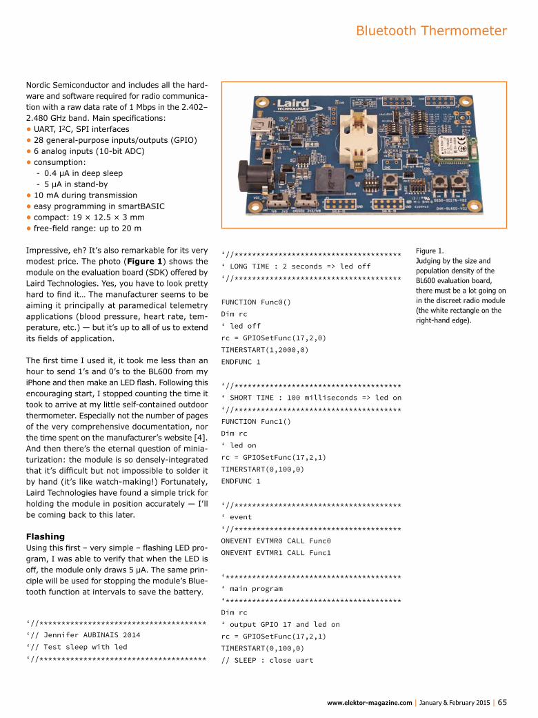
Bluetooth Thermometer
www.elektor-magazine.com | January & February 2015 | 65
Nordic Semiconductor and includes all the hard-ware and software required for radio communica-tion with a raw data rate of 1 Mbps in the 2.402–2.480 GHz band. Main specifications: • UART, I2C, SPI interfaces • 28 general-purpose inputs/outputs (GPIO)• 6 analog inputs (10-bit ADC)• consumption:
- 0.4 µA in deep sleep - 5 µA in stand-by
• 10 mA during transmission• easy programming in smartBASIC • compact: 19 × 12.5 × 3 mm• free-field range: up to 20 m
Impressive, eh? It’s also remarkable for its very modest price. The photo (Figure 1) shows the module on the evaluation board (SDK) offered by Laird Technologies. Yes, you have to look pretty hard to find it… The manufacturer seems to be aiming it principally at paramedical telemetry applications (blood pressure, heart rate, tem-perature, etc.) — but it’s up to all of us to extend its fields of application.
The first time I used it, it took me less than an hour to send 1’s and 0’s to the BL600 from my iPhone and then make an LED flash. Following this encouraging start, I stopped counting the time it took to arrive at my little self-contained outdoor thermometer. Especially not the number of pages of the very comprehensive documentation, nor the time spent on the manufacturer’s website [4]. And then there’s the eternal question of minia-turization: the module is so densely-integrated that it’s difficult but not impossible to solder it by hand (it’s like watch-making!) Fortunately, Laird Technologies have found a simple trick for holding the module in position accurately — I’ll be coming back to this later.
FlashingUsing this first – very simple – flashing LED pro-gram, I was able to verify that when the LED is off, the module only draws 5 µA. The same prin-ciple will be used for stopping the module’s Blue-tooth function at intervals to save the battery.
‘//************************************** ‘// Jennifer AUBINAIS 2014 ‘// Test sleep with led ‘//**************************************
‘//************************************** ‘ LONG TIME : 2 seconds => led off ‘//**************************************
FUNCTION Func0() Dim rc ‘ led off rc = GPIOSetFunc(17,2,0) TIMERSTART(1,2000,0) ENDFUNC 1
‘//************************************** ‘ SHORT TIME : 100 milliseconds => led on ‘//************************************** FUNCTION Func1() Dim rc ‘ led on rc = GPIOSetFunc(17,2,1) TIMERSTART(0,100,0) ENDFUNC 1
‘//************************************** ‘ event ‘//************************************** ONEVENT EVTMR0 CALL Func0 ONEVENT EVTMR1 CALL Func1
‘**************************************** ‘ main program ‘**************************************** Dim rc ‘ output GPIO 17 and led on rc = GPIOSetFunc(17,2,1) TIMERSTART(0,100,0) // SLEEP : close uart
Figure 1. Judging by the size and population density of the BL600 evaluation board, there must be a lot going on in the discreet radio module (the white rectangle on the right-hand edge).

•Projects
66 | January & February 2015 | www.elektor-magazine.com
come back to this in a moment.The supply is via the BL600’s SIO_19 pin in order to reduce the consumption to 5 µA in stand-by mode. In deep-sleep mode, the consumption drops to 0.4 µA – but it can only be woken up again by resetting the module or by a change of state on an input. While in stand-by mode, soft-ware interrupts allow Bluetooth communication to be re-established briefly, just long enough to see if anyone is trying to connect. I arbitrarily chose a sleep period of 500 ms (configured in the TIMERSTART function). When the connection is established, the consumption during trans-mission is 10 mA.
Connector K2 is used for possible updating of the BL600’s firmware via a special JTAG interface. In principle, this function is not needed for this project (but you never know…). Connector K1 lets you program the BL600 from a PC via a 3.3 V serial interface. The FT232R BOB [6] offered by Elektor in the e-shop is perfect for this purpose.
uartclose() rc = GPIOSetFunc(21,2,1) ‘// TX rc = GPIOSetFunc(23,2,0) ‘// RTS WAITEVENT
CircuitIt won’t take us long to go through the cir-cuit. To measure the temperature, I’m using the BL600-SA ADC (MOD1 on the diagram in Figure 2) with an NTC thermistor connected to K3. It can be remoted if necessary — the length of the lead is not critical. The measurement is made with the help of a potential divider using a known resistance: R1 = 10 kΩ 0.1 %. The equation for the temperature as a function of the value of the NTC is a logarithmic function that exceeds the BL600’s calculation capacity. So this calculation, which requires a data table (temperatures, resistances, thermal coefficient alpha) provided by the thermistor manufacturer [10], will be performed on and by the smart-phone and an iOS or Android application. I’ll
BL600-SA
SIO_
1AIN
SIO_
2AIN
SIO_
3AIN
SIO_
4AIN
SIO_
5AIN
SIO_
6AIN
SIO_10SIO_11SIO_12
SIO_13SIO_14SIO_15SIO_16
SIO_17SIO_18SIO_19
TXRXRTSCTSSIO_25
SIO_28SIO_29SIO_30
SIO_
7
SIO_0 SIO_9
SIO_
8
RESET
MOD1
VCC
GND
GND
GND
GND
GNDGND
GND
GND
GND44 13
10 11 12
14151617181920212223
NC
24252627
NC
2829
NC30313233343536
123456
RXTXCTSRTSVCCGND
37
NC38
NC3940414243
1 2 43 5 6 7 8 9
K1
VCC
K3
R1
10k
0%1
R4
1k
LED1
JP2
R3
150R
S1
RESET
K2
10
1 23 45 67 89
R2
12k
VCC
VCC
JP1
1
2
C1
100n
R5
10k
VCC
R6
10k
C3
100n140190 - 11
BT1
CR17345Lithium
3V
C2
100n
NTC
−ϑ
AAuuttoo
RRUUNN
Figure 2. Circuit diagram of the BT thermometer using the BL600-SA. In the Laird family, the BL600 only supports the LE (low energy) mode, while the BT900 handles both conventional BT and BLE — but it is even smaller and so more difficult to solder!

Bluetooth Thermometer
www.elektor-magazine.com | January & February 2015 | 67
I use an alpha α(%/K) coefficient that varies according to the temperature ranges laid down by the manufacturer [1] (Table 1), yielding the following equation:
RT = RTx ⋅eαx100
⋅ Tx( )2⋅ 1T− 1Tx
⎛⎝⎜
⎞⎠⎟
⎡⎣⎢
⎤⎦⎥
RT: resistance at TRTx: resistance at Tx in the tableTx: temperature in K lower than the measure-ment temperature found in the tableT: measurement temperature in K (Tx < T < Tx+1)
αx: thermal coefficient at Tx
From this same equation, the temperature cal-culation, applying the thermal coefficient αx, will give:
T = 1100
αx ⋅ Tx( )2⋅ ln RT
RTx⎛⎝⎜
⎞⎠⎟+ 1Tx
The LED serves two functions:
• debugging (with jumper): it flashes all the time and shows the Bluetooth stand-by and module connection modes
• normal (no jumper): it flashes briefly during initialization to indicate that the thermome-ter has started up correctly
In my initial tests, the data transmission was truncated: I had to choose between waking the module up for longer or transmitting less data. In order to save the battery, I chose the second solution. Example of data sequence communi-cated by the module via Bluetooth:
PW3012V853C433 PW: supply voltage (battery) to be displayed in the applicationV: supply voltage to voltage divider C: voltage at divider junction R1 / NTC i.e. a corresponding temperature after calculation of 24.3 °C [see Calculations paragraph below]
Calculations Without going into details, we shall note that the calculation of the thermistor value is achieved by measuring the voltage on a divider.
R1
RxR
VCC
Vx
Vx =Vcc ×
RRxR + Rx
R1+ RRxR + Rx
⎛
⎝
⎜⎜⎜
⎞
⎠
⎟⎟⎟
Rx =Vx R1R
Vcc R −Vx R1+ R( )
.
.
.
For the temperature, I’m not going to settle for a simple equation between thermistor and tem-perature by applying a beta coefficient as is usu-ally done:
Rctn = R25 × eβ× 1
T− 1298
⎛⎝⎜
⎞⎠⎟
R25: resistance value at 25 °CT: calculated temperature in Kβ: NTC beta coefficientRntc: NTC value at the calculation temperature
Table 1.
R/T No 4901
T (ºC)B25/100 = 3950 K
RT/R25 α (%/K)
–30.0 16.915 6.1
–25.0 12.555 5.9
–20.0 9.4143 5.7
–15.0 7.1172 5.5
–10.0 5.4308 5.4
–5.0 4.1505 5.2
0.0 3.2014 5.0
5.0 2.5011 4.9
10.0 1.9691 4.7
15.0 1.5618 4.6
20.0 1.2474 4.5
25.0 1.0000 4.3
30.0 0.808 4.2
35.0 0.6569 4.1
40.0 0.5372 4.0
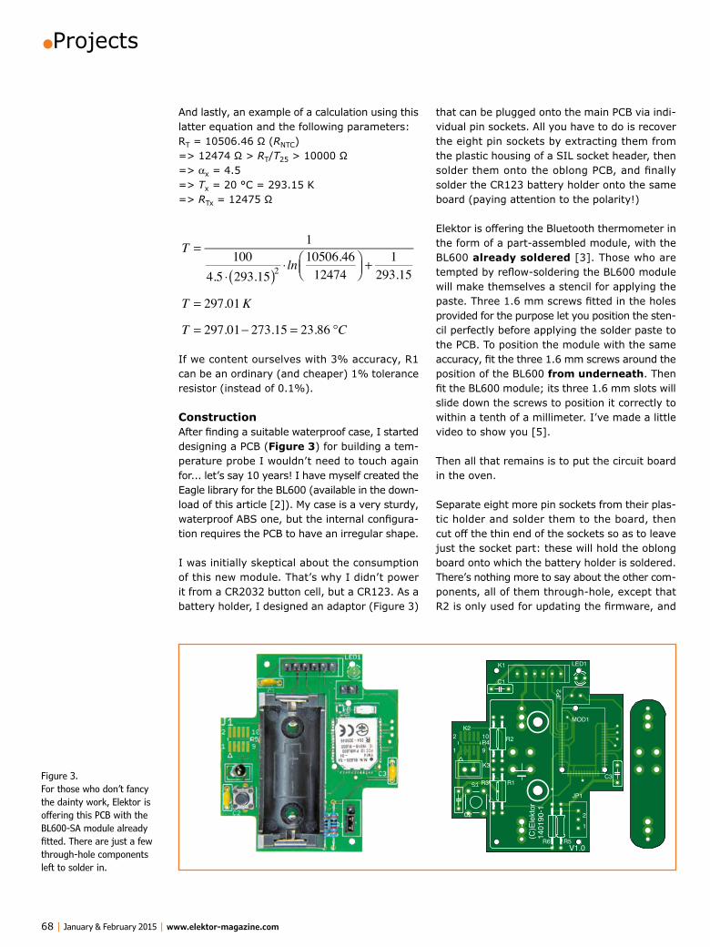
•Projects
68 | January & February 2015 | www.elektor-magazine.com
that can be plugged onto the main PCB via indi-vidual pin sockets. All you have to do is recover the eight pin sockets by extracting them from the plastic housing of a SIL socket header, then solder them onto the oblong PCB, and finally solder the CR123 battery holder onto the same board (paying attention to the polarity!)
Elektor is offering the Bluetooth thermometer in the form of a part-assembled module, with the BL600 already soldered [3]. Those who are tempted by reflow-soldering the BL600 module will make themselves a stencil for applying the paste. Three 1.6 mm screws fitted in the holes provided for the purpose let you position the sten-cil perfectly before applying the solder paste to the PCB. To position the module with the same accuracy, fit the three 1.6 mm screws around the position of the BL600 from underneath. Then fit the BL600 module; its three 1.6 mm slots will slide down the screws to position it correctly to within a tenth of a millimeter. I’ve made a little video to show you [5].
Then all that remains is to put the circuit board in the oven.
Separate eight more pin sockets from their plas-tic holder and solder them to the board, then cut off the thin end of the sockets so as to leave just the socket part: these will hold the oblong board onto which the battery holder is soldered. There’s nothing more to say about the other com-ponents, all of them through-hole, except that R2 is only used for updating the firmware, and
And lastly, an example of a calculation using this latter equation and the following parameters:RT = 10506.46 Ω (RNTC)=> 12474 Ω > RT/T25 > 10000 Ω=> αx = 4.5=> Tx = 20 °C = 293.15 K=> RTx = 12475 Ω
T = 1100
4.5 ⋅ 293.15( )2⋅ ln 10506.46
12474⎛⎝⎜
⎞⎠⎟ +
1293.15
T = 297.01K
T = 297.01− 273.15 = 23.86 °C
If we content ourselves with 3% accuracy, R1 can be an ordinary (and cheaper) 1% tolerance resistor (instead of 0.1%).
ConstructionAfter finding a suitable waterproof case, I started designing a PCB (Figure 3) for building a tem-perature probe I wouldn’t need to touch again for... let’s say 10 years! I have myself created the Eagle library for the BL600 (available in the down-load of this article [2]). My case is a very sturdy, waterproof ABS one, but the internal configura-tion requires the PCB to have an irregular shape.
I was initially skeptical about the consumption of this new module. That’s why I didn’t power it from a CR2032 button cell, but a CR123. As a battery holder, I designed an adaptor (Figure 3)
Figure 3. For those who don’t fancy the dainty work, Elektor is offering this PCB with the BL600-SA module already fitted. There are just a few through-hole components left to solder in.
MOD1
K1
K3
JP2
JP1
V1.0
(C)E
lekt
or14
0190
-1
1
2
2
1
10
9
K2
C1
C2
C3
R5R6
R2
R3
R4
R1
LED1
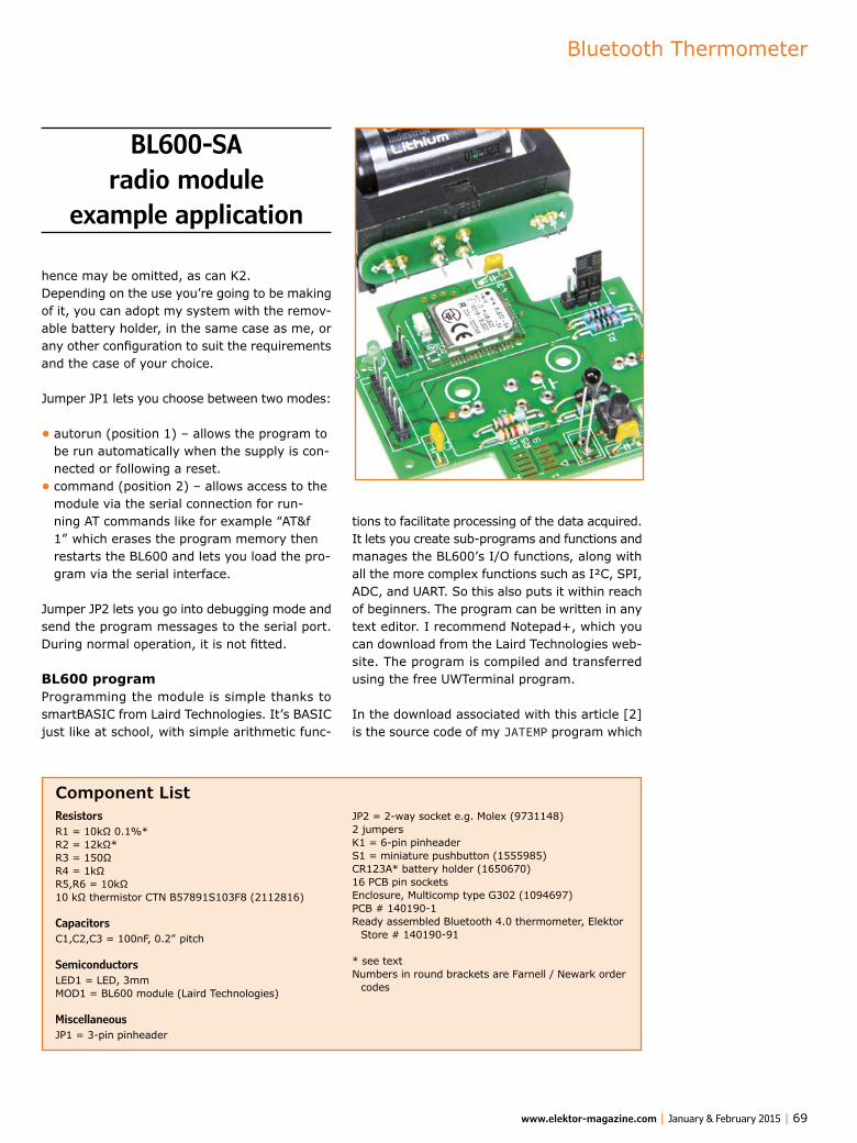
Bluetooth Thermometer
www.elektor-magazine.com | January & February 2015 | 69
tions to facilitate processing of the data acquired. It lets you create sub-programs and functions and manages the BL600’s I/O functions, along with all the more complex functions such as I²C, SPI, ADC, and UART. So this also puts it within reach of beginners. The program can be written in any text editor. I recommend Notepad+, which you can download from the Laird Technologies web-site. The program is compiled and transferred using the free UWTerminal program.
In the download associated with this article [2] is the source code of my JATEMP program which
hence may be omitted, as can K2.Depending on the use you’re going to be making of it, you can adopt my system with the remov-able battery holder, in the same case as me, or any other configuration to suit the requirements and the case of your choice.
Jumper JP1 lets you choose between two modes:
• autorun (position 1) – allows the program to be run automatically when the supply is con-nected or following a reset.
• command (position 2) – allows access to the module via the serial connection for run-ning AT commands like for example “AT&f 1” which erases the program memory then restarts the BL600 and lets you load the pro-gram via the serial interface.
Jumper JP2 lets you go into debugging mode and send the program messages to the serial port. During normal operation, it is not fitted.
BL600 programProgramming the module is simple thanks to smartBASIC from Laird Technologies. It’s BASIC just like at school, with simple arithmetic func-
Component ListResistorsR1 = 10kΩ 0.1%*R2 = 12kΩ* R3 = 150Ω R4 = 1kΩ R5,R6 = 10kΩ 10 kΩ thermistor CTN B57891S103F8 (2112816)
CapacitorsC1,C2,C3 = 100nF, 0.2” pitch
SemiconductorsLED1 = LED, 3mm MOD1 = BL600 module (Laird Technologies)
MiscellaneousJP1 = 3-pin pinheader
JP2 = 2-way socket e.g. Molex (9731148) 2 jumpersK1 = 6-pin pinheaderS1 = miniature pushbutton (1555985)CR123A* battery holder (1650670)16 PCB pin socketsEnclosure, Multicomp type G302 (1094697)PCB # 140190-1Ready assembled Bluetooth 4.0 thermometer, Elektor
Store # 140190-91
* see textNumbers in round brackets are Farnell / Newark order
codes
BL600-SA radio module
example application
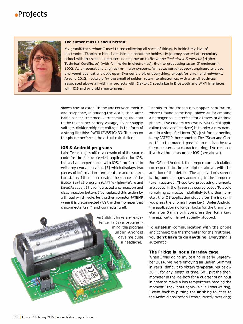
•Projects
70 | January & February 2015 | www.elektor-magazine.com
Thanks to the French developpez.com forum, where I found some help, above all for creating a homogeneous interface for all sizes of Android phones. I’ve created my own BL600 Serial appli-cation (code and interface) but under a new name and in a simplified form [8], just for connecting to my JATEMP thermometer. The “Scan and Con-nect” button made it possible to receive the raw thermometer data character string; I’ve replaced it with a thread as under iOS (see above).
For iOS and Android, the temperature calculation corresponds to the description above, with the addition of the details. The application’s screen background changes according to the tempera-ture measured. These two processing elements are coded in the jatemp.c source code. To avoid remaining connected indefinitely to the thermom-eter, the iOS application stops after 5 mins (or if you press the phone’s Home key). Under Android, the application no longer looks for the thermom-eter after 5 mins or if you press the Home key; the application is not actually stopped.
To establish communication with the phone and connect the thermometer for the first time, you don’t have to do anything. Everything is automatic.
The Fridge is not a Faraday cageWhen I was doing my testing in early Septem-ber 2014, we were enjoying an Indian Summer in Paris: difficult to obtain temperatures below 20 °C for any length of time. So I put the ther-mometer in the ice-bow for a quarter of an hour in order to make a low temperature reading the moment I took it out again. While I was waiting, I went back to putting the finishing touches to the Android application I was currently tweaking;
shows how to establish the link between module and telephone, initializing the ADCs, then after half a second, the module transmitting the data to the telephone: battery voltage, divider supply voltage, divider midpoint voltage, in the form of a string like this: PW3012V853C433. The app on the phone performs the actual calculation.
iOS & Android programsLaird Technologies offers a download of the source code for the BL600 Serial application for iOS, but as I am experienced with iOS, I preferred to write my own application [7] which displays two pieces of information: temperature and connec-tion status. I then incorporated the sources of the BL600 Serial program (UARTPeripherial.c and DataClass.c). I haven’t created a connection and disconnection button. I’ve replaced this action by a thread which looks for the thermometer JATEMP when it is disconnected (it’s the thermometer that disconnects itself) and connects itself.
As I didn’t have any expe-rience in Java program-
ming, the program under Android
gave me quite a headache.
The author tells us about herself
My grandfather, whom I used to see collecting all sorts of things, is behind my love of electronics. Thanks to him, I am intrepid about the hobby. My journey started at secondary school with the school computer, leading me on to Brevet de Technicien Supérieur [Higher Technical Certificate] (with full marks in electronics), then to graduating as an IT engineer in 1992. As an operations engineer on major systems, Windows server support engineer, and vba and vbnet applications developer, I’ve done a bit of everything, except for Linux and networks.Around 2012, nostalgia for the smell of solder: return to electronics, with a small business associated above all with my projects with Elektor. I specialize in Bluetooth and Wi-Fi interfaces with iOS and Android smartphones.

Bluetooth Thermometer
www.elektor-magazine.com | January & February 2015 | 71
how surprised I was to see the temperature dis-played by the Android phone quickly dropping! To check, I went to try the same test in my neigh-bor’s ice-box, where I also watched live as the temperature dropped to 4 °C. I deduced from this that the door seal allows the Bluetooth sig-nal to pass (a characteristic of refrigerators that domestic appliance manufacturers would do well to mention in their data sheets).
ConclusionI hope I’ve convinced you of the interest of the BL600 and maybe even to try the adventure with the reflow oven, or even hand soldering, if you have dainty fingers.For implementing an application based on the BL600 module, the drawback of the miniaturiza-tion of the contacts is more than made up for by the advantages of very easy construction and by the simplicity of its smartBASIC language and of the programming via the module’s UART interface. And that’s only the beginning… In the meantime, Laird Technologies is offering the BL620, which is the BL600 master: the same hardware but new firmware, capable of communicating with other BL600 modules. This opens up new prospects that Elektor and I will be sure to invite you to explore with us in the near future.
[140190]
Web Links
[1] www.lairdtech.com/Products/Embedded-Solutions/Bluetooth-Radio-Modules/BL600- Series/
[2] www.elektor-magazine.com/140190
[3] www.elektor.com/bluetooth-thermometer
[4] https://laird-ews-support.desk.com/?b_id=1945
[5] www.youtube.com/watch?v=0YlKxtYwQiE
[6] www.elektor.com/ft232r-usb-serial-bridge-bob-110553-91
[7] https://appsto.re/fr/XTwnV.i
[8] https://play.google.com/store/apps/details?id=com.JA.bletemperature&hl=fr
[9] www.aubinais.net
[10] EPCOS NTC www.epcos.com/inf/50/db/ntc_13/NTC_Leaded_disks_S891.pdf www.epcos.com/blob/531152/download/2/pdf-standardizedrt.pdf
NTC Thermistors / General technical information: www.physics.queensu.ca/~robbie/ENPH354/NTC-Thermistors-Technote.pdf
Figure 4. The thermometer application on the screen of iOS and Android touch phones.
Figure 5. The author’s prototype, in a waterproof case and fitted with a sturdy screwed hook.
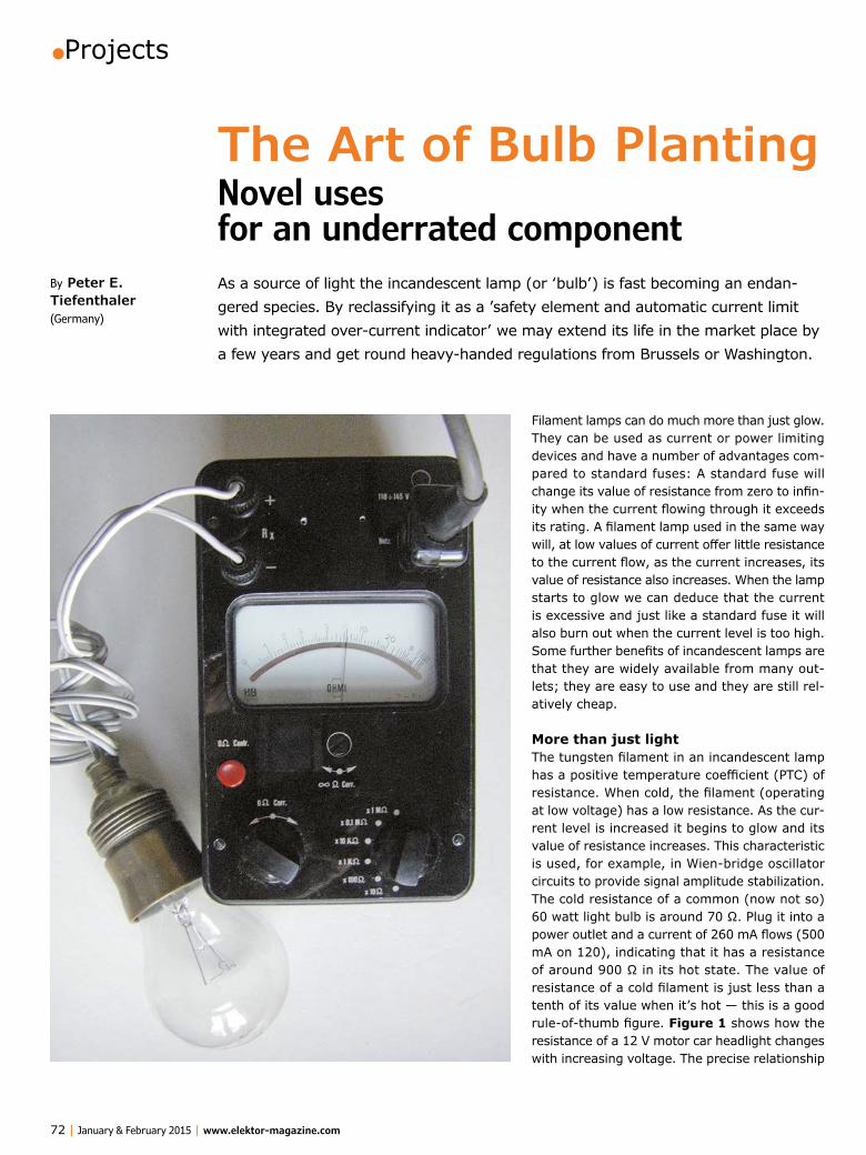
•Projects
72 | January & February 2015 | www.elektor-magazine.com
Filament lamps can do much more than just glow. They can be used as current or power limiting devices and have a number of advantages com-pared to standard fuses: A standard fuse will change its value of resistance from zero to infin-ity when the current flowing through it exceeds its rating. A filament lamp used in the same way will, at low values of current offer little resistance to the current flow, as the current increases, its value of resistance also increases. When the lamp starts to glow we can deduce that the current is excessive and just like a standard fuse it will also burn out when the current level is too high. Some further benefits of incandescent lamps are that they are widely available from many out-lets; they are easy to use and they are still rel-atively cheap.
More than just lightThe tungsten filament in an incandescent lamp has a positive temperature coefficient (PTC) of resistance. When cold, the filament (operating at low voltage) has a low resistance. As the cur-rent level is increased it begins to glow and its value of resistance increases. This characteristic is used, for example, in Wien-bridge oscillator circuits to provide signal amplitude stabilization.The cold resistance of a common (now not so) 60 watt light bulb is around 70 Ω. Plug it into a power outlet and a current of 260 mA flows (500 mA on 120), indicating that it has a resistance of around 900 Ω in its hot state. The value of resistance of a cold filament is just less than a tenth of its value when it’s hot — this is a good rule-of-thumb figure. Figure 1 shows how the resistance of a 12 V motor car headlight changes with increasing voltage. The precise relationship
By Peter E. Tiefenthaler (Germany)
The Art of Bulb PlantingNovel uses for an underrated componentAs a source of light the incandescent lamp (or ‘bulb’) is fast becoming an endan-gered species. By reclassifying it as a ’safety element and automatic current limit with integrated over-current indicator’ we may extend its life in the market place by a few years and get round heavy-handed regulations from Brussels or Washington.
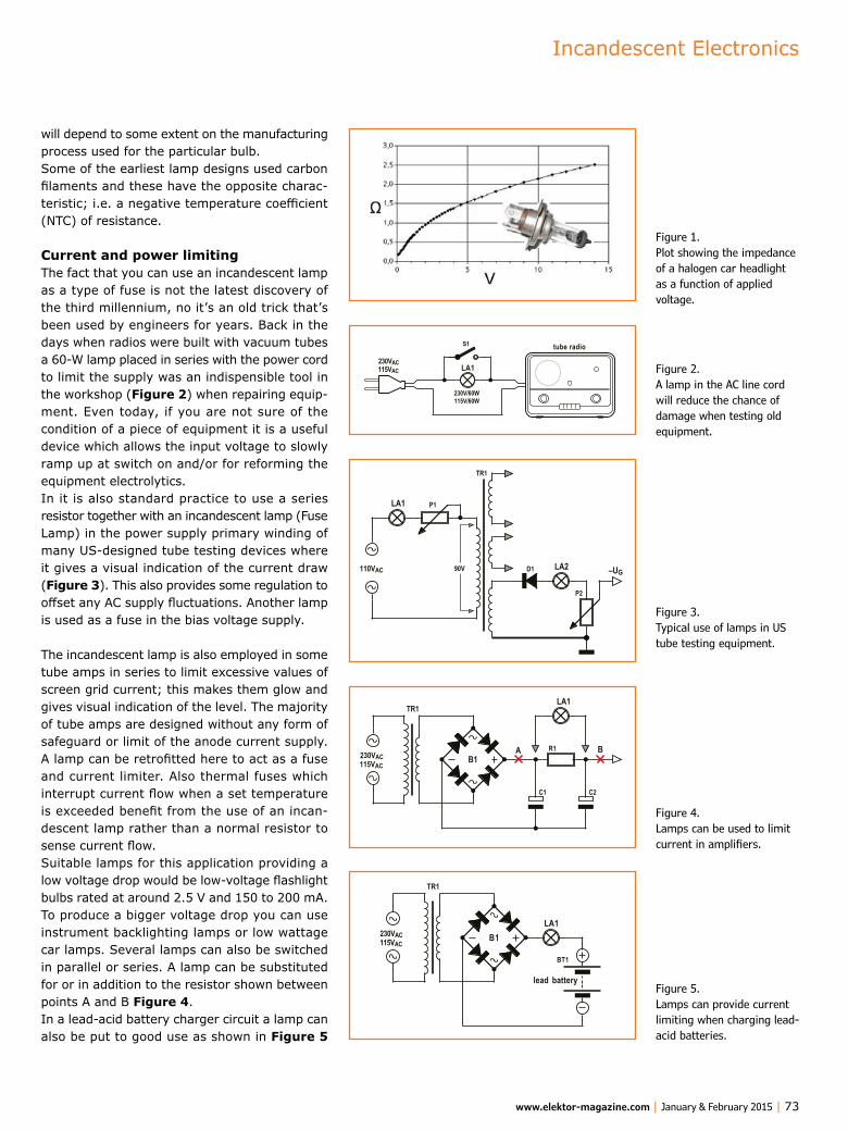
Incandescent Electronics
www.elektor-magazine.com | January & February 2015 | 73
will depend to some extent on the manufacturing process used for the particular bulb.Some of the earliest lamp designs used carbon filaments and these have the opposite charac-teristic; i.e. a negative temperature coefficient (NTC) of resistance.
Current and power limitingThe fact that you can use an incandescent lamp as a type of fuse is not the latest discovery of the third millennium, no it’s an old trick that’s been used by engineers for years. Back in the days when radios were built with vacuum tubes a 60-W lamp placed in series with the power cord to limit the supply was an indispensible tool in the workshop (Figure 2) when repairing equip-ment. Even today, if you are not sure of the condition of a piece of equipment it is a useful device which allows the input voltage to slowly ramp up at switch on and/or for reforming the equipment electrolytics.In it is also standard practice to use a series resistor together with an incandescent lamp (Fuse Lamp) in the power supply primary winding of many US-designed tube testing devices where it gives a visual indication of the current draw (Figure 3). This also provides some regulation to offset any AC supply fluctuations. Another lamp is used as a fuse in the bias voltage supply.
The incandescent lamp is also employed in some tube amps in series to limit excessive values of screen grid current; this makes them glow and gives visual indication of the level. The majority of tube amps are designed without any form of safeguard or limit of the anode current supply. A lamp can be retrofitted here to act as a fuse and current limiter. Also thermal fuses which interrupt current flow when a set temperature is exceeded benefit from the use of an incan-descent lamp rather than a normal resistor to sense current flow.Suitable lamps for this application providing a low voltage drop would be low-voltage flashlight bulbs rated at around 2.5 V and 150 to 200 mA. To produce a bigger voltage drop you can use instrument backlighting lamps or low wattage car lamps. Several lamps can also be switched in parallel or series. A lamp can be substituted for or in addition to the resistor shown between points A and B Figure 4.In a lead-acid battery charger circuit a lamp can also be put to good use as shown in Figure 5
LA1
tube radioS1
230V/60W115V/60W
230VAC115VAC
LA1 P1
P2
LA2D190V
TR1
–UG110VAC
TR1
B1A B
LA1
230VAC115VAC
C1 C2
R1
TR1
B1LA1
BT1
lead battery
230VAC115VAC
Figure 1. Plot showing the impedance of a halogen car headlight as a function of applied voltage.
Figure 2. A lamp in the AC line cord will reduce the chance of damage when testing old equipment.
Figure 3. Typical use of lamps in US tube testing equipment.
Figure 4. Lamps can be used to limit current in amplifiers.
Figure 5. Lamps can provide current limiting when charging lead-acid batteries.
•Projects
74 | January & February 2015 | www.elektor-magazine.com
where it will provide some degree of charge cur-rent stabilization.A lamp can also as a simple method to reduce the of supply voltage level; an appropriately rated lamp could, for example, be wired in series with the power cord to allow 110 V equipment to operate from a 230 V mains supply although the switch-on surge may be unacceptable (a small step-down transformer or a variac is the proper method, Ed.).
Lamps & LoudspeakersThe filament lamp can be used as a life insurance device for expensive loudspeakers units and is both low-cost and simple to install. A lamp placed in series with the amplifier output (Figure 6) will prevent the speaker from being overloaded. This also has the added benefit of promoting har-mony in the household because chillaxing teen-agers sometimes like to stream their latest tunes through the family sound reproduction equipment.The electrical resistance of a cold filament will be negligible at low volume levels where it will only be dissipating milliwatts of energy. As the volume is increased and the output signal level increases the lamp dissipates more energy and begins to reduce the output signal level to the speakers. At the same time the amp sees increased load resistance which also reduces output power. This compressing and limiting effect is only noticeable at high volume levels.
To sum up, the effect of the lamp in the signal chain is not audible. Only at higher signal levels can you start to notice it and this then it gives a certain degree of reassurance that it is actually doing its job. A slight degradation in sound qual-ity is perhaps preferable to the possible expense of a new speaker system.
The vintage circuit in Figure 7 shows that a (standard) low-voltage lamp has also been employed in the output stage of this valve ampli-fier to limit the power.
In PA stacks, lamps are often used in series to protect sensitive tweeters (Figure 8). For the same reason it’s good practice to wire one in series with the general purpose loudspeaker used on the test bench. To work out an appropriate lamp rating we can apply the rule of thumb used above (Zhot:Zcold = 10:1). A 12-V car festoon lamp rated at 5 W is useful for speakers produc-
LA1A1
LS1
LA1
LS1
tweeter
L1
LS2
bass
L2
C2
C1
Figure 6. Lamps can protect loudspeakers.
Figure 8. A lamp can provide protection for sensitive tweeters.
Figure 7. A section from an original tube amp (RIM Gigant) circuit. A lamp is used here as a power limiter.

Incandescent Electronics
www.elektor-magazine.com | January & February 2015 | 75
Figure 4 in a power supply made up of silicon diodes to simulate the softer characteristics of a power supply with tube rectifiers. Incidentally the filament lamp will produce the required volt-age drop when a silicon bridge is substituted for tube rectifiers in the power supply of a vintage tube amp.
To give a transistor amplifier a tube amp sound you can insert a lamp between the amp output and the loudspeaker. To make the effect even more pronounced replace the emitter resistors in a conventional transistor output stage with small filament lamps (Figure 10). Now when the amp is overdriven, the resulting distortion is much less harsh and the sound quality is remi-niscent of a tube amp.
(140188)
ing low levels of sound whereas for HiFi equip-ment something like a 6-V 5-W lamp would be more suitable.
Electric guitars and their amps only really start to ‘sing’ when the volume knob is wound up close to 11. Such performances are seldom greeted by spontaneous applause from the neighborhood when your front room is the only available prac-tice space. In this case we can make use of a ‘power soak’ or ‘dummy load’. This consists of a network of power resistors, coils and capaci-tors to simulate the loudspeaker impedance and absorb the majority of power delivered by the amp. The small amount of power left over drives the speaker at low volume but the sound you hear is of the amp driving hard with all its attendant distortion effects. You can use an appropriately rated lamp as the load in this application (LA2 in Figure 8); the resulting sound together with the compression effect described above is both full and realistic.
Tube-ify it!Incandescent lamps and vacuum tubes are both made up of hollow glass envelopes. Although this is in no way sufficient technical justification to use them, it is possible with the help of a lamp to make a transistor amp sound more like a valve amp. First of all we can use a lamp as shown in
LA1A1
LS1LA2
LA3
LS1
LA1
LA2
T1
T2
V+
V–
Figure 9. LA2 used as a Power Soak for guitar amp.
Figure 10. Tube-ifying a transistor amplifier.
Professional Quality @ Discount Prices!
More than 45 years of experience | 24-hour shipping | More than 50,000 products
2 W / 170 lmat www.reichelt.com
+49 (0)4422 955-360
400 LED bulbs
GB 30588
Prices in € incl. statutory VAT, plus shipping costs | reichelt elektronik, Elektronikring 1, 26452 Sande (Germany)
3.60You will nd more than
Advertisement

•Projects
76 | January & February 2015 | www.elektor-magazine.com
When the optical f iber became really useful in the early 1980’s, people started digitizing video to convey it via the “new connection method”. Because of the very non-linear properties of the transmis-sion by fiber optics, the signal has to be digital. i.e. consisting of ones and zeroes.
Thin cable, big advantageSending video over coax cable is quite difficult and in practice the maximum length covered is about 300 feet (100 meters). Even at that dis-tance the colors of a composite video signal start to deteriorate. With fiber optic cable no such problems occur and you can cover many miles without running into distortion.
Video ADC/DAC’ing on a shoestringSo why does every TV, camera etc. have com-
posite video connectivity and not fiber optic? The answer is the complexity of digitiz-ing the video signal, which invariably
needs fast A/D and D/A conver-tors. These devices sadly are
power hungry and expensive. Fortunately there is an cheap and easy way to
digitize video without doing any A/D conversion. Everybody knows what it is—PWM. With PWM you translate the instantaneous voltage of an analog signal into a pulsewidth. The pulsewidth is a finite time and can be expressed in seconds or fractions of a second.The Nyquist Sampling Theorem rules that the frequency of the PWM signal is kept constant and has to be at least twice the maximum bandwidth of the signal that you want to convert. The min-imum bandwidth for composite video is about 5.5 MHz, hence the minimum PWM frequency
By Jake van der Peyl (New Zealand)
Video Over FiberBy experiment – and on a budget
Here we explore how a bunch of low cost commonly avail-able components make a system for conveying video and
sound over a fiber optic cable with virtually no loss or distortion. It puts all things
coax to shame for runs longer than about 300 feet.
Video Over Fiber
www.elektor-magazine.com | January & February 2015 | 77
would be of the order of 11 MHz.The next problem is: find a very fast PWM circuit. The theory is quite simple. First you generate a triangular voltage. Then you put your video on one input of a fast comparator and your triangle voltage on the other input. The output of the com-parator then supplies your PWM signal. That’s it!
TransmitterThe schematic of the experimental video-over-fi-ber transmitter appears in Figure 1. Some of its design principles will be discussed below.First, back to the triangle voltage from the pre-vious section. Of course it will have to be very linear, besides having to extend on both sides outside the video signal. A special case of the tri-angle voltage is the sawtooth voltage as used in analog oscilloscopes. A sawtooth is much easier to make than a pure triangular wave shape. The simplest form of the sawtooth generator consists of a capacitor, a constant current source and a switch—see Figure 2.
For practical reasons we are limiting our supply voltage to 5 volts. It is also more convenient to move to a higher frequency as it relaxes the requirements on the filter after the PWM signal is received—plus it will also improve the quality of the signal. Let’s go to 20 MHz giving a period of 50 nanoseconds (ns).
For the switch we could use a MOSFET or a bipo-lar transistor. Both have their disadvantages: a MOSFET has too much capacitance and a tran-sistor takes time to recover from saturation. A good solution is to employ open collector tech-nology. The preferred logic is LVC being very fast, 5-volt tolerant and capable of high output currents (32 mA). A configurable logic LVC Schmitt trigger gate is used for generating the switching signal.Using a 5-volt supply voltage the sawtooth can reach 3 volts before the Schmitt trigger switches. In the Video Transmitter an R-C combination (R1-C1) gives a pulsewidth of 10 ns which is enough to completely discharge a 22 pF capacitor (C8).
U4
BCV62C
3
2
4
1
R4
1k1
Q1
BFT92U22 4
5
3
74LVC1G07
U33 1
5
2MAX4090
L1
1uH
U1
2
16 43
&
5
74LVC1G98
C1
10p
R3
75R
R1
1k
C6
22p
C2
10n
C4
10n
J3-AAUDIO
MCP1700-500E2E/TTU7
C10
10u10V
C14
10u10V
C13
100n
C7
10n
MCP1700-500E2E/TTU6
C12
1u
J21
2
+6V
GND
C3
100n
R2
75R
J3-BVIDEO
U54
31
5
2
ADCMP600
C5
10n
C9
10n
Q2
BFR540
L2
1uH
R5
39R
R6
2k2
C8
10n
C11
10n
HFBR1414Z
J1
3
2 OPTICALFIBER
5V
5V
3 2
1
3 2
1
130316 - 14
Figure 1. Schematic of the video transmitter for fiber optic links.
+5V
Figure 2. Let’s generate a sawtooth waveform.
•Projects
78 | January & February 2015 | www.elektor-magazine.com
Ideally this should be equal to the output cur-rent of the constant current source. In our circuit 2.67 mA flows, as evidenced by measuring with a multi-meter across C6. The value is about 0.4 mA lower than expected. Not way off, but caused by the difference between the transistors.We can now calculate the sum of all the capac-itance parallel to, and including C6. We use the formula for charging a capacitor with a constant current:
Q = I × t = C × VC = I × t / VC = (2.67×10–3 x 40×10–9) / 3C = 35.6 pF.
So the sum of all the extra capacitance in parallel with C6 is 13.6 pF. C6 itself has a tolerance of 5%, which is achievable using COG/NP0 dielec-tric. It turns out that the circuit is quite repeat-able meaning every one you build should operate close to 20 MHz.
Back to Figure 1, the video signal first reaches a buffer amplifier. This amplifier adjusts the level of the video so that the most negative part of the video (the sync tips) start at 0.4 V, which is above the bottom of the sawtooth. The top of the video signal reaches about 2 V, which is well under the 3-V amplitude of the sawtooth.
The comparator in position U5 is very fast with a delay of just 4 ns. The delays for the positive and negative signal excursions are about the same, so the distortion is minimal. If you apply this signal to a filter designed to remove the 20
The capacitor has 50–10 = 40 ns to ramp up from 0 to 3 volts. So at 3 volts, the constant current source should remain well out of saturation.The simplest low saturation current source con-sists of two PNP transistors connected in the configuration pictured in Figure 3. It has several serious disadvantages. For one, the hfe of the two transistors can be very different even if they con-sist of a double transistor like the BCV62C. Sec-ond, they have far too much stray capacitance.
The solution is the configuration with an extra RF transistor shown in Figure 4. This configuration is called: The Wilson Current Mirror. It is more accurate and has a much lower output capaci-tance (about 3 pF). You can read up on the Wilson Current Mirror in Wikipedia [1]. The saturation voltage is about 3.6 V, which is well above 3 V. By adapting R (that’s R4+R3 in our TX) we can adjust the sawtooth frequency to 20 MHz. The current through R is:
IR = Vsat / R
which for our practical transmitter circuit works out as
3.6 / (1100 + 75) = 3.06 mA
+5V
IoutR
+5V
Iout
R
Figure 3. The ‘textbook’ constant current source has a few disadvantages depending on your requirements.
Figure 4. Due to an extra RF transistor the Wilson Current Mirror is a nearly ideal current source.
The optical transmitter used here is the HFBR1414Z from Avago (formerly Hewlett Packard). This is a vintage LED type with very poor efficiency, mainly because it is very difficult to bundle the light of LEDs so that a reasonable amount gets coupled into the fiber. About 60 mA is needed to drive the LED.Optical transmitters for coupling to a fiber connector are also called: TOSA for: Transmitter Optical Sub-Assembly. Unsurprisingly a receiver unit is called: ROSA.It is quite hard to couple the fiber to the light source. A 3D manipulator is used while constantly measuring the light coming out of the fiber. After that the connector is fixed in the right place.
Of course a laser would do a much better job. The Vertical Cavity Surface Emitting Laser (VCSEL) went through a long development period starting before 1990. Nowadays they are quite cheap and don’t have the disadvantages of the FP lasers.So why not use a VCSEL here? It’s because all the cheap VSCEL’s are made in a TOSA called… LC-TOSA.LC is one of the 20 or so optical fiber connectors on the market. The LC connector is specially developed for high density patch-panels. So all you have to do is buy the cheap LC-TOSA and LC-ROSA parts and LC patch-cords and you’re done. You will find that you can push them together and they fit, but there is nothing to keep them together. Obviously, a
The Optical Transmitter and Receiver

Video Over Fiber
www.elektor-magazine.com | January & February 2015 | 79
AudioIf you vary the PWM frequency a little the circuit continues to work okay. Consequently we can modulate the frequency without interference on the video. It turns out that you can modulate the frequency by about ±10% with impunity, meaning from about 18 to 22 MHz. This can be exploited to modulate sound (audio). At the receiver side you can extract the audio signal with a phase locked loop (PLL). The frequency is modulated onto the drive current supplied by the constant current source.This is also the reason that the power supply has
MHz component, you recover your original video signal. It does indeed do that.
All we have to do now is to put the PWM signal in an optical transmitter and couple it to a length of optical fiber. At the other side we have a fast optical receiver that converts the optical signal back to electrical. Fiber optic transmitters and receivers have delays measured in picoseconds (ps). So they are of no concern to us. The opti-cal signal is infrared with a wavelength of 850 nanometers (nm; 10-9 meters). This wave length is mostly used for this sort of application.
plastic bracket is called for to keep them together but sadly nobody makes it because those components are used in a standard module called SFP (Small Form-factor Pluggable). Manufacturers makes their own systems to hold them together, and often a bracket is used. The bracket is part of the SFP housing.We don’t want to use an SFP module—it would be expensive, bulky and unnecessary. So I hope some kind Elektor readers will come up with a bracket.The modern VCSEL’s operate at 6 mA. At 6 mA, they give more optical output power than an LED at 60 mA. Avago makes a 850-nm VCSEL with an ST connector. The ST connector is what we use here. This unit is about 10 times
the price of an LC-TOSA. The ST connector is much bigger than the LC connector; it is a bayonet type connector like BNC. The LC connector by contrast has the feel of the modular RJ-45 telephone connector, see photograph.
The Optical Transmitter and Receiver
The Fiber CableMaterials• Silica glass: Silica is Silicon-dioxide (SiO2). The damping
can be as low as 0.2 dB per km at 1300 nm. The silica has to be very pure, but thanks to the semiconductor industry it is possible.
• Plastic: Plastic Optical Fiber (POF) used to be acrylic (PMMA). These cables were mostly used as patch cables for short distances. Nowadays, perfluorinated polymers are used, so that high bandwidth can be achieved for distances of 1 km and more.
Modes• Multimode: multimode optical fiber is used for short
distances mostly inside buildings. It is called multimode because the light can travel different distances through the fiber caused by different reflection angles. The light inside the fiber reflects from the boundary between the core and the cladding of the core. This type of fiber is called step index fiber. The way to mitigate this problem
is the use of graded index fiber. With graded index fiber the step between refractive indices of core and cladding is gradual. This increases the usefulness of multimode cable a lot. Graded index is also used for the new “plastic” cable (GIPOF).
• Single mode: with Single Mode the light has only one way to travel through the fiber. The fiber core is much thinner (8 micron). The cladding is 125 micron. At 1300 nm to 1500 nm long distances can be achieved at high bandwidth. This system also has many disadvantages. It is much harder to get sufficient power into the fiber because of the small aperture, and the ROSA’s and TOSA’s have far higher requirements in terms of manufacturing and assembly accuracy.

•Projects
80 | January & February 2015 | www.elektor-magazine.com
to be stable and accurate. We start off by using a 6-volt regulated supply voltage on J2-1. Two 5-volt regulators U6 and U7 are used along with two LC filters to keep the supply rail as clean as possible. Any noise or hum will be modulated as frequency and inevitably appear on the PLL out-put of the receiver. For that reason we also use wideband FM. The supply of the constant current source has to be safeguarded from PWM signals too because these would directly affect the shape of the sawtooth. Both the transmitter and the receiver are built using surface mount parts with a ground plane at one side of the board. On a circuit like this long tracks are a no-no because of the 20-MHz signals.
The ReceiverLet’s look at Figure 5. The optical signal arrives at then receiver on J2. From there it goes to another fast comparator, U3. Comparing the sig-nals at the output of comparator U5 in the trans-mitter with those at the receiver comparator, U3, we find them identical with a delay of 8 ns + 5 ns per meter of fiber cable, approximately.The PWM signal then goes to the filter IC, U6. This IC cannot run off 5 volts, so it has its own 3.3-V regulator, U5. The MAX9502M (U6) is a lowpass filter with a –3 dB roll off of 7 MHz and a slope of 30 dB per octave. This is crucial because of the strong 20-MHz component. The IC also has a DC restoration circuit, but this is not in action because it was never made for a PWM signal. To prevent clipping at the output, the PWM signal is attenuated 5 times at the input. The MAX9502M has 12 dB amplification; the MAX9502G has 6 dB amplification and if used requires R4 to be increased to 1 kΩ.
PLL circuit U7 is designed for 5-V operation and conveniently U3 and U4 are also using 5 volts. The maximum frequency of the 74HCT9046 (U7) is about 15 MHz and therefore the PWM signal has to be divided first, here by a D-flip-flop type 74LVC1G74 (U4). At 10 MHz the frequency is still quite high for this PLL, but it works okay.The D-flip-flop acts on the positive transitions of the PWM signal. The negative transitions have the PWM modulation and cannot be used. There is an IC in SO-8 housing containing two D-flip-flops: TI’S V SN74LVC2G80DCT. That would bring the frequency down to 5 MHz. A divider with D-flip-flops is made by connecting the Q output to the D input. The Q output of the first flip-flop
Questions, questions• How linear is the transfer function of video channel and the sound
channel? The video transfer is good enough for video. It is basically linear, but not good enough for accurate DC measurements. If you go to much lower PWM frequencies, you could probably make it to 0.1% linearity. But temperature drift of the constant current source would spoil it. The sound channel is basically nonlinear. At the input, the period time is modulated in a linear way. At the receiver side, the output voltage is a linear function of the frequency, which is the inverse. At small deviations, it would be very close to linear, but for reasons already explained, I had to go for about ±10%. So this is a compromise.
• How high can you go with the PWM frequency? There is no theoretical limit. I think 40 MHz is possible.
• Who is likely to use this? It is hard to answer that. I think everywhere, where you want to transport composite video over more than 300 feet. That could include big buildings, remote monitoring and places where no wireless is possible like underground or underwater. It could be used for traffic inspection cameras along busy roads. If you made dedicated ICs for this job, it could be used for every composite video connection.
Design considerationsWhen I first read about video transmission over fiber optic cable in the beginning of the eighties my reaction was: Why make it so complicated? Just use fast PWM. My work was always going in different directions, so I never tried building it. I am now semi-retired, so now I had time to build it. Of course I looked on the internet to see if anybody else had tried this, but I did not find anything.The design goal was very simple: Build a composite video PWM system that does not visibly change the quality of the composite video. I was using my camcorder as the video source and look on my 40 inch TV for the fine details and colors of the video signal. As far as I can judge there is no difference in quality. So that design goal was met. When I was building it, I realized that I could modulate FM for the sound. That was a bonus.The scope that I use is a 100-MHz Tektronix TDS 1012. If examine the 20-MHz sawtooth, I use a short piece of tinned copper wire with a loop, to stick my probe in for earth (the poor man’s probe adaptor). The saw-tooth has some non-linearity at the beginning, but this is outside the video.Fist I built the saw-tooth generator. It took about four designs until I had the right one. Then, I built a board with saw-tooth generator, comparator and video filter.I got really neat video out of it. After that, I just had to add the optical parts and the sound processing parts. It was a real fun project.Why has nobody else tried it? I really don’t know. Maybe people think that everything is done that can be done.

Video Over Fiber
www.elektor-magazine.com | January & February 2015 | 81
Audio and Video inputs on the input board. If you increase the value of R6 from 3.6 kΩ to 3.9 kΩ, the output voltage of the PLL and of course the Audio Out will rise by 1 volt.
It is important for the PWM frequency to be close to 20 MHz, so that all the receiver boards are interchangeable.
The values of C9 and R10 (the feedback loop) were found by connecting a square wave to the audio input on the transmitter board and looking at under- and over-shoot on the audio output of the receiver.
Experimental buildThe PCB layouts for the transmitter and the receiver as designed by the author are printed in Figure 6 and Figure 7 respectively for guid-ance and inspiration rather than providing an exact method of how it should be done. The PCB
is connected to the clock input (CLK) of the sec-ond one. You can use this if you want to explore how high you can go with the PWM frequency.The 74HCT9046 PLL is made by NXP (formerly Philips Semiconductors). It is an improvement over previous PLL’s type 4046. The VCO part has two options. The first option is to control the fre-quency with one resistor. This would give only a small output signal. The second possibility is to have an offset frequency and vary the frequency around the base frequency. In our case the base frequency is 10 MHz.
The frequency sweep is ±1 MHz. The 10 MHz base frequency is set with R7. The ±1 MHz deviation is set with R8. It is possible that R7 has to be adapted slightly if the unmodulated frequency is more than 0.5 MHz off.
The voltage at the Audio Out connector should be 2.5 V without any signal source connectors to the
HFBR2416Z
J2 6
2
71 43
5 8OPTICALFIBER
C3
10n U34
31
5
2
ADCMP600R1
1k
R2
1k
74LVC1G74U4CLK
GND
VCC
120MHz
10MHz
4
2D
7
S
5
3
Q
Q
6
R
8
MCP1700-500E2E/TT
U1
C2
10u10V
C1
1u
J11
2
+6V
GND
5V
MCP1700-500E2E/TTU2
C4
1u
3 2
1
3 2
1
MCP1700-330E2E/TTU5
C7
1u
3 2
1
C5
10n
U6
MAX9502M
1 54
2
3R3
2k2R4
470R
C6
10n
R875R
J3-BVIDEO
U84
31
2
5
130316 - 15
MCP6L01R
C10
10n
L2
1uH
J3-AAUDIO
C8
100p
R6
3k6
R7
22k
R10
3k9
C9
1n
R5
39k
R9
47k
74HCT9046
COMP_IN PCP-OUTPC2-OUT
VCO-OUT
DEM-OUT
PH-COMP
SIG_IN
VCO_IN
U7
INHGND GND
VCC
C1A
C1B
VCO
16
14
RB 1513
10
R111
R212
3
5
2
1 8
496
7
5V 3V3
VideoFilter
PLL
Figure 5. Schematic of the experimental fiber optic receiver for video and audio.

•Projects
82 | January & February 2015 | www.elektor-magazine.com
placing of components. Solder paste gets applied with a syringe, then the components before sol-dering them in a frying-pan on maximum heat with a lid on top. After putting the boards in, the lid is left off long enough to be able to see the solder paste melt. The board is removed from the pan with big long-nose pliers.
The assembly and testing of these little boards closed off an interesting experiment in trans-mitting video and sound over fiber optics at low cost, without specialist ICs or professional equip-ment—we hope you found it inspiring.
(130316)
design files are available for free downloading at [2]. The assembled boards in the photographs are early prototypes and differ slightly from the final designs represented by Figures 6 and 7.Pad sizes, component placement and track rout-ing will certainly not be optimal but the pro-totypes worked and were successfully demon-strated to Elektor editors during the author’s visit to Holland.
Both board layouts were made using PADS from Mentor Graphics. The films were printed with a laser printer. The boards are from double-sided resist-coated PCB material. The author’s etchant is ammonium persulphate heated to 50 °C.A binocular microscope is in use for pasting and
Web Links
[1] Wilson Current Mirror: http://en.wikipedia.org/wiki/Wilson_current_mirror
[2] PCB design files (Mentor Graphics PADS format): www.elektor-magazine.com/130316
Figure 6. Transmitter board component layout printed at 150% of actual size (author’s design).
Figure 7. Receiver board component layout printed at 150% of actual (author’s design).

www.dlpdesign.com
Add USB to your next project.It's easier than you might think!USB
Standard 18-pin DIP interface; 0.6x1.26-inch footprint
HIGH-SPEEDDLP-USB1232H: USB 2.0 UART/FIFO
Royalty-free, robust USB drivers
DLP-IO8-G
No in-depth knowledge of USB required
8-Channel Data Acquisition
8 I/Os: Digital I/OAnalog InTemperature
USB Port PoweredSingle-Byte Commands
Only
DLP-IOR44-Channel Relay Cable
DLP-TH1bTemp/Humidity Cable
DLP-RFID1HF RFID Reader/Writer
DLP-FPGAUSB-to-Xilinx FPGA Module
$29.95!
Only $28.95!Multipurpose: 7 interfaces
480Mb/s
Further Information and Ordering at www.elektor.com/retronics Further Information and Ordering at www.elektor.com/retronicswww.elektor.com/retronicswww.elektor.com/retronicswww.elektor.com/retronics
Retronics80 tales of electronics bygonesThis book is a compilation of about 80 Retronics installments published in Elektor magazine between 2004 and 2012. The stories cover vintage test equipment, prehistoric computers, long forgotten components, and Elektor blockbuster projects, all aiming to make engineers smile, sit up, object, drool, or experience a whiff of nostalgia.
193 pages • ISBN 978-1-907920-18-9£26.95 • €29.95 • US $41.00
10% OFF for GREEN and GOLD Members
NOSTALGIA
FrontPanelExpress.com1(800)FPE-9060
Cost effective prototypes and production runs with no setup charges
Powder-coated and anodized finishes in various colors
Select from aluminum, acrylic or provide your own material
Standard lead time in 5 days or express manufacturing in 3 or 1 days
Only $90.24with custom
logo engraving
You design it to your specifications using
our FREE CAD software, Front Panel Designer
We machine it and ship to you a
professionally finished product,no minimum quantity required
The Convenient All-in-One Solution for Custom-Designed Front Panels & Enclosures
FREE Software
Untitled-1 1 12/12/14 09:46
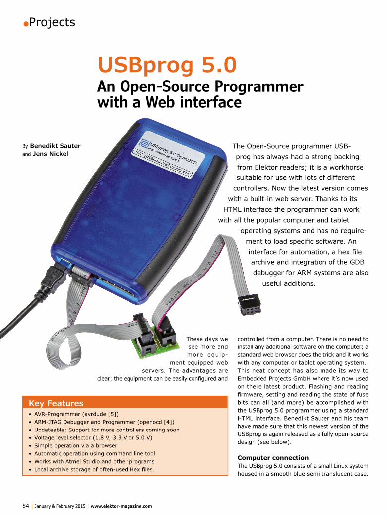
•Projects
84 | January & February 2015 | www.elektor-magazine.com
These days we see more and more equip-
ment equipped web servers. The advantages are
clear; the equipment can be easily configured and
controlled from a computer. There is no need to install any additional software on the computer; a standard web browser does the trick and it works with any computer or tablet operating system.This neat concept has also made its way to Embedded Projects GmbH where it’s now used on there latest product. Flashing and reading firmware, setting and reading the state of fuse bits can all (and more) be accomplished with the USBprog 5.0 programmer using a standard HTML interface. Benedikt Sauter and his team have made sure that this newest version of the USBprog is again released as a fully open-source design (see below).
Computer connectionThe USBprog 5.0 consists of a small Linux system housed in a smooth blue semi translucent case.
USBprog 5.0An Open-Source Programmer with a Web interface
The Open-Source programmer USB-prog has always had a strong backing from Elektor readers; it is a workhorse suitable for use with lots of different
controllers. Now the latest version comes with a built-in web server. Thanks to its
HTML interface the programmer can work with all the popular computer and tablet
operating systems and has no require-ment to load specific software. An interface for automation, a hex file archive and integration of the GDB debugger for ARM systems are also
useful additions.
Key Features• AVR-Programmer (avrdude [5])• ARM-JTAG Debugger and Programmer (openocd [4])• Updateable: Support for more controllers coming soon• Voltage level selector (1.8 V, 3.3 V or 5.0 V)• Simple operation via a browser• Automatic operation using command line tool• Works with Atmel Studio and other programs• Local archive storage of often-used Hex files
By Benedikt Sauter and Jens Nickel

USBProg 5.0
www.elektor-magazine.com | January & February 2015 | 85
The system connects to a computer via a USB cable which also supplies power to the system. A network interface is emulated via the USB port; in Mac and Linux systems the device is found and connected automatically. A DHCP server run-ning on the USBprog assigns an IP address to the computer. Now the browser has access to the programmer using the IP address 10.0.0.1.The first time the system runs in Windows the usual new device driver dialog will pop up. You are given the option to manually select a driver. Choose ‘Network adapters’ as the device type. A list of manufacturers now appears; select ‘Mic-rosoft Corporation’ and ‘Remote NDIS Compat-ible Device’.
For ARM and AVROnce the network connection has been estab-lished you can use your computer’s browser (http://10.0.0.1) to communicate with the pro-grammer software where the first page is shown in Figure 1. Now you can connect the USBprog to the target processor and the target will be supplied with power. ARM processors and Atmel microcontrollers are currently supported and PIC controllers will soon added to the list, the firm-ware update is already underway.
For AVR-Controller based systems there is a rib-bon cable terminated in the standard 10-way ISP-female IDC connector (Figure 2) which plugs into the 10-way pin header in the target system. A small adapter PCB allows connection of a standard six-way ISP header. Some soldering is necessary here to fit the pin headers to the adapter board but it shouldn’t prove too challenging.
A second adapter board allows connection of a 20-way JTAG header to the 10-way ISP connec-tor for debugging and flashing ARM-based sys-tems. This adapter board will also require some soldering.
In addition, the updateable programmer is equipped with a 14-way Gnublin/EEC connector which we will make use of later to control the familiar Gnublin expansion boards - using the web user-interface of course.
Manual OperationNow with the user-interface displayed in the browser you can begin by first entering the ‘Pro-cessor Type’ in the field along top of the page.
To make selections such as the ATmega328P (Arduino Uno [1]) or ATmega328 (T-Board 28 [2]) it is only necessary to enter the first couple of characters. Using the radio buttons over on the right you can then select the voltage used in the target processor environment.Now you can select ‘Read Signature’ to read the controllers signature or use the buttons to read the state of the fuses. After a few seconds a
Figure 1. The programmer can be controlled from an HTML-based interface that runs in any browser.
Figure 2. The USBprog 5.0 connections. To the right a 14-pin Gnublin/EEC connector; A future firmware update will allow control of Gnublin expansion boards.
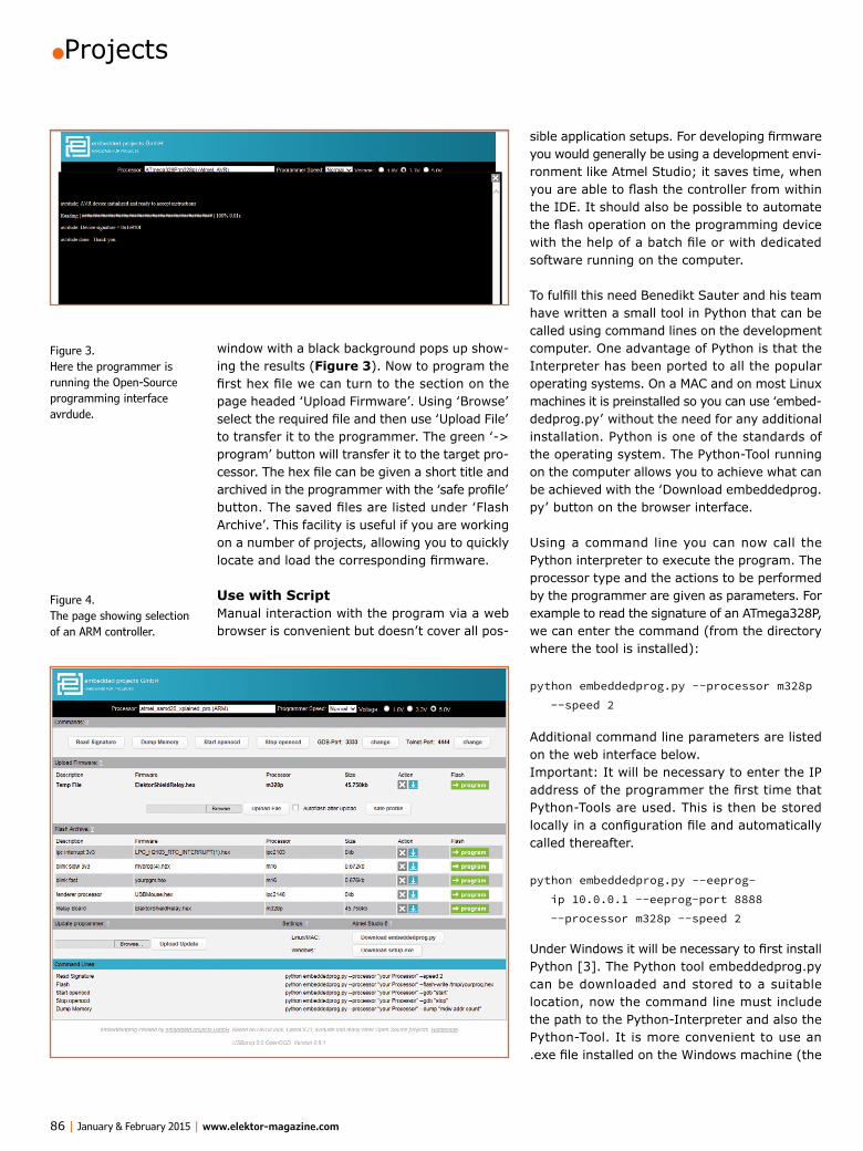
•Projects
86 | January & February 2015 | www.elektor-magazine.com
sible application setups. For developing firmware you would generally be using a development envi-ronment like Atmel Studio; it saves time, when you are able to flash the controller from within the IDE. It should also be possible to automate the flash operation on the programming device with the help of a batch file or with dedicated software running on the computer.
To fulfill this need Benedikt Sauter and his team have written a small tool in Python that can be called using command lines on the development computer. One advantage of Python is that the Interpreter has been ported to all the popular operating systems. On a MAC and on most Linux machines it is preinstalled so you can use ‘embed-dedprog.py’ without the need for any additional installation. Python is one of the standards of the operating system. The Python-Tool running on the computer allows you to achieve what can be achieved with the ‘Download embeddedprog.py’ button on the browser interface.
Using a command line you can now call the Python interpreter to execute the program. The processor type and the actions to be performed by the programmer are given as parameters. For example to read the signature of an ATmega328P, we can enter the command (from the directory where the tool is installed):
python embeddedprog.py --processor m328p --speed 2
Additional command line parameters are listed on the web interface below.Important: It will be necessary to enter the IP address of the programmer the first time that Python-Tools are used. This is then be stored locally in a configuration file and automatically called thereafter.
python embeddedprog.py --eeprog-ip 10.0.0.1 --eeprog-port 8888 --processor m328p --speed 2
Under Windows it will be necessary to first install Python [3]. The Python tool embeddedprog.py can be downloaded and stored to a suitable location, now the command line must include the path to the Python-Interpreter and also the Python-Tool. It is more convenient to use an .exe file installed on the Windows machine (the
window with a black background pops up show-ing the results (Figure 3). Now to program the first hex file we can turn to the section on the page headed ‘Upload Firmware’. Using ‘Browse’ select the required file and then use ‘Upload File’ to transfer it to the programmer. The green ‘-> program’ button will transfer it to the target pro-cessor. The hex file can be given a short title and archived in the programmer with the ‘safe profile’ button. The saved files are listed under ‘Flash Archive’. This facility is useful if you are working on a number of projects, allowing you to quickly locate and load the corresponding firmware.
Use with ScriptManual interaction with the program via a web browser is convenient but doesn’t cover all pos-
Figure 3. Here the programmer is running the Open-Source programming interface avrdude.
Figure 4. The page showing selection of an ARM controller.
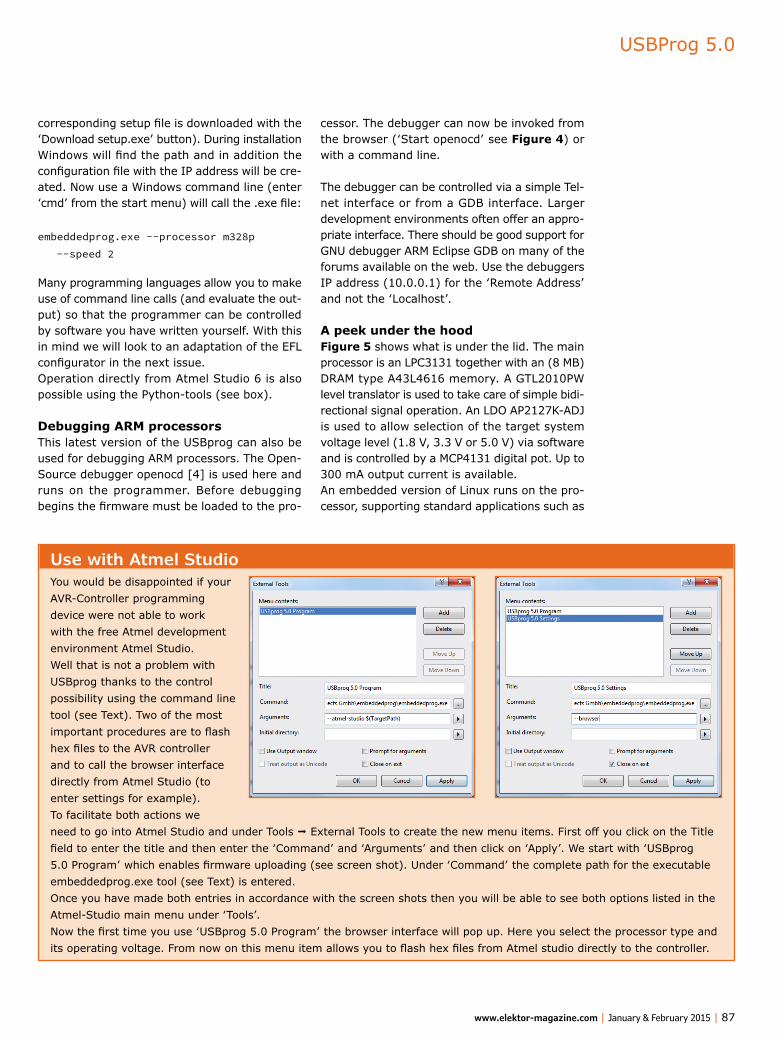
USBProg 5.0
www.elektor-magazine.com | January & February 2015 | 87
cessor. The debugger can now be invoked from the browser (‘Start openocd’ see Figure 4) or with a command line.
The debugger can be controlled via a simple Tel-net interface or from a GDB interface. Larger development environments often offer an appro-priate interface. There should be good support for GNU debugger ARM Eclipse GDB on many of the forums available on the web. Use the debuggers IP address (10.0.0.1) for the ‘Remote Address’ and not the ‘Localhost’.
A peek under the hoodFigure 5 shows what is under the lid. The main processor is an LPC3131 together with an (8 MB) DRAM type A43L4616 memory. A GTL2010PW level translator is used to take care of simple bidi-rectional signal operation. An LDO AP2127K-ADJ is used to allow selection of the target system voltage level (1.8 V, 3.3 V or 5.0 V) via software and is controlled by a MCP4131 digital pot. Up to 300 mA output current is available.An embedded version of Linux runs on the pro-cessor, supporting standard applications such as
corresponding setup file is downloaded with the ‘Download setup.exe’ button). During installation Windows will find the path and in addition the configuration file with the IP address will be cre-ated. Now use a Windows command line (enter ‘cmd’ from the start menu) will call the .exe file:
embeddedprog.exe --processor m328p --speed 2
Many programming languages allow you to make use of command line calls (and evaluate the out-put) so that the programmer can be controlled by software you have written yourself. With this in mind we will look to an adaptation of the EFL configurator in the next issue.Operation directly from Atmel Studio 6 is also possible using the Python-tools (see box).
Debugging ARM processorsThis latest version of the USBprog can also be used for debugging ARM processors. The Open-Source debugger openocd [4] is used here and runs on the programmer. Before debugging begins the firmware must be loaded to the pro-
Use with Atmel StudioYou would be disappointed if your AVR-Controller programming device were not able to work with the free Atmel development environment Atmel Studio. Well that is not a problem with USBprog thanks to the control possibility using the command line tool (see Text). Two of the most important procedures are to flash hex files to the AVR controller and to call the browser interface directly from Atmel Studio (to enter settings for example).To facilitate both actions we need to go into Atmel Studio and under Tools ª External Tools to create the new menu items. First off you click on the Title field to enter the title and then enter the ‘Command’ and ‘Arguments’ and then click on ‘Apply’. We start with ‘USBprog 5.0 Program’ which enables firmware uploading (see screen shot). Under ‘Command’ the complete path for the executable embeddedprog.exe tool (see Text) is entered.Once you have made both entries in accordance with the screen shots then you will be able to see both options listed in the Atmel-Studio main menu under ‘Tools’.Now the first time you use ‘USBprog 5.0 Program’ the browser interface will pop up. Here you select the processor type and its operating voltage. From now on this menu item allows you to flash hex files from Atmel studio directly to the controller.

•Projects
88 | January & February 2015 | www.elektor-magazine.com
Update using the web interfaceThe web interface has an upload update option that allows the programmer’s firmware to be kept up to date with the latest release. You can download the latest version of the software (a compressed file) from the USBprog website [7]. The new update can then be integrated via the web browser interface. The files are extracted to the programming adapter and copied to the correct location in the operating system.
(140285)
Web Links
[1] www.elektor.com/arduino-uno
[2] www.elektor.com/t-board-28-130581-93
[3] https://www.python.org
[4] www.openocd.org
[5] www.nongnu.org/avrdude
[6] https://github.com/embeddedprojects/usbprog5
[7] http://usbprog5.embedded-projects.net
avrdude (for programming Atmel processors [5]). The central component here is the server writ-ten in Python, which supplies the Web interface used by the Lighttpd web server. In addition it provides a web service for control of the pro-grammer, which in turn communicates with the Python-Tools on the computer. All of the source files are available from GitHub [6].
USBprog 5.0USBprog 5.0 is available from the Elektor Store. There are
two variants available; the first version consists of the fully populated PCB while the second includes a fully populated
PCB together with a protective case, adapters (connectors require mounting) and flatcable. You can find more information at:
www.elektor.com/usbprog5
Figure 5. An LPC3131 processor running Linux is at the heart of the programmer.
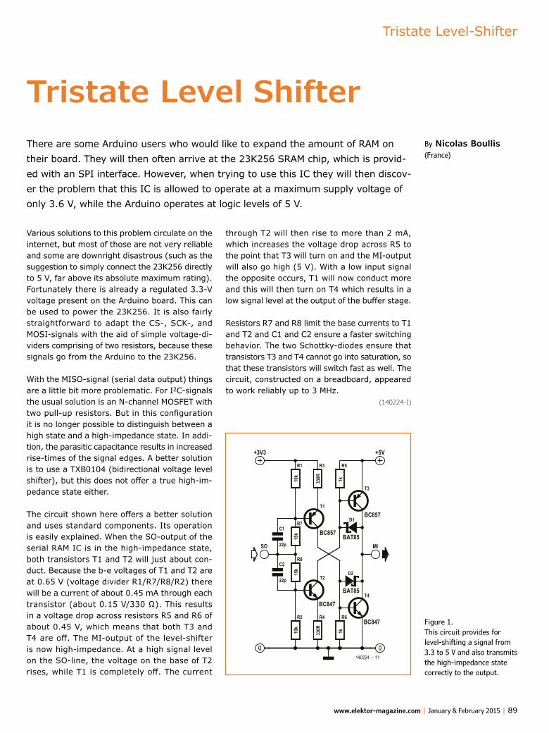
Tristate Level-Shifter
www.elektor-magazine.com | January & February 2015 | 89
Various solutions to this problem circulate on the internet, but most of those are not very reliable and some are downright disastrous (such as the suggestion to simply connect the 23K256 directly to 5 V, far above its absolute maximum rating).Fortunately there is already a regulated 3.3-V voltage present on the Arduino board. This can be used to power the 23K256. It is also fairly straightforward to adapt the CS-, SCK-, and MOSI-signals with the aid of simple voltage-di-viders comprising of two resistors, because these signals go from the Arduino to the 23K256.
With the MISO-signal (serial data output) things are a little bit more problematic. For I2C-signals the usual solution is an N-channel MOSFET with two pull-up resistors. But in this configuration it is no longer possible to distinguish between a high state and a high-impedance state. In addi-tion, the parasitic capacitance results in increased rise-times of the signal edges. A better solution is to use a TXB0104 (bidirectional voltage level shifter), but this does not offer a true high-im-pedance state either.
The circuit shown here offers a better solution and uses standard components. Its operation is easily explained. When the SO-output of the serial RAM IC is in the high-impedance state, both transistors T1 and T2 will just about con-duct. Because the b-e voltages of T1 and T2 are at 0.65 V (voltage divider R1/R7/R8/R2) there will be a current of about 0.45 mA through each transistor (about 0.15 V/330 Ω). This results in a voltage drop across resistors R5 and R6 of about 0.45 V, which means that both T3 and T4 are off. The MI-output of the level-shifter is now high-impedance. At a high signal level on the SO-line, the voltage on the base of T2 rises, while T1 is completely off. The current
through T2 will then rise to more than 2 mA, which increases the voltage drop across R5 to the point that T3 will turn on and the MI-output will also go high (5 V). With a low input signal the opposite occurs, T1 will now conduct more and this will then turn on T4 which results in a low signal level at the output of the buffer stage.
Resistors R7 and R8 limit the base currents to T1 and T2 and C1 and C2 ensure a faster switching behavior. The two Schottky-diodes ensure that transistors T3 and T4 cannot go into saturation, so that these transistors will switch fast as well. The circuit, constructed on a breadboard, appeared to work reliably up to 3 MHz.
(140224-I)
By Nicolas Boullis (France)
Tristate Level ShifterThere are some Arduino users who would like to expand the amount of RAM on their board. They will then often arrive at the 23K256 SRAM chip, which is provid-ed with an SPI interface. However, when trying to use this IC they will then discov-er the problem that this IC is allowed to operate at a maximum supply voltage of only 3.6 V, while the Arduino operates at logic levels of 5 V.
T2
BC847T4
BC847
T1
BC857
T3
BC857
R1
10k
R2
10k
R3
330R
R4
330R
R5
1k
D1
BAT85
D2
BAT85
R6
1k
+3V3 +5V
SO MI
140224 - 11
R7
15k
R8
15k
C1
22p
C2
22p
Figure 1. This circuit provides for level-shifting a signal from 3.3 to 5 V and also transmits the high-impedance state correctly to the output.
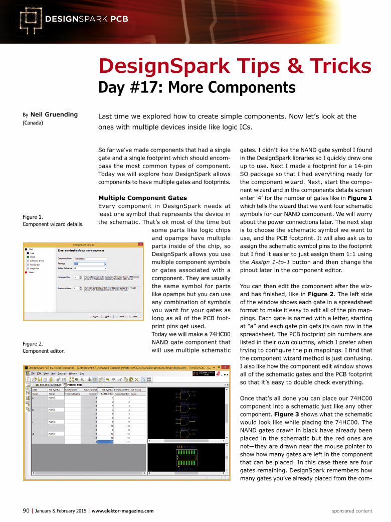
90 | January & February 2015 | www.elektor-magazine.com sponsored content
So far we’ve made components that had a single gate and a single footprint which should encom-pass the most common types of component. Today we will explore how DesignSpark allows components to have multiple gates and footprints.
Multiple Component GatesEvery component in DesignSpark needs at least one symbol that represents the device in the schematic. That’s ok most of the time but
some parts like logic chips and opamps have multiple parts inside of the chip, so DesignSpark allows you use multiple component symbols or gates associated with a component. They are usually the same symbol for parts like opamps but you can use any combination of symbols you want for your gates as long as all of the PCB foot-print pins get used.Today we will make a 74HC00 NAND gate component that will use multiple schematic
gates. I didn’t like the NAND gate symbol I found in the DesignSpark libraries so I quickly drew one up to use. Next I made a footprint for a 14-pin SO package so that I had everything ready for the component wizard. Next, start the compo-nent wizard and in the components details screen enter ‘4’ for the number of gates like in Figure 1 which tells the wizard that we want four schematic symbols for our NAND component. We will worry about the power connections later. The next step is to choose the schematic symbol we want to use, and the PCB footprint. It will also ask us to assign the schematic symbol pins to the footprint but I find it easier to just assign them 1:1 using the Assign 1-to-1 button and then change the pinout later in the component editor.
You can then edit the component after the wiz-ard has finished, like in Figure 2. The left side of the window shows each gate in a spreadsheet format to make it easy to edit all of the pin map-pings. Each gate is named with a letter, starting at “a” and each gate pin gets its own row in the spreadsheet. The PCB footprint pin numbers are listed in their own columns, which I prefer when trying to configure the pin mappings. I find that the component wizard method is just confusing. I also like how the component edit window shows all of the schematic gates and the PCB footprint so that it’s easy to double check everything.
Once that’s all done you can place our 74HC00 component into a schematic just like any other component. Figure 3 shows what the schematic would look like while placing the 74HC00. The NAND gates drawn in black have already been placed in the schematic but the red ones are not—they are drawn near the mouse pointer to show how many gates are left in the component that can be placed. In this case there are four gates remaining. DesignSpark remembers how many gates you’ve already placed from the com-
By Neil Gruending (Canada)
DesignSpark Tips & TricksDay #17: More ComponentsLast time we explored how to create simple components. Now let’s look at the ones with multiple devices inside like logic ICs.
Figure 2. Component editor.
Figure 1. Component wizard details.
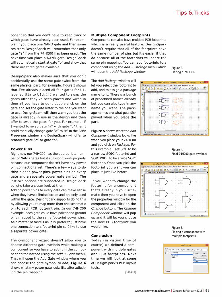
Tips & Tricks
www.elektor-magazine.com | January & February 2015 | 91 sponsored content
ponent so that you don’t have to keep track of which gates have already been used. For exam-ple, if you place one NAND gate and then some resistors DesignSpark will remember that only gate “a” from the 74HC00 has been used. The next time you place a NAND gate DesignSpark will automatically start at gate “b” and show that there are three gates available.
DesignSpark also makes sure that you don’t accidentally use the same gate twice from the same physical part. For example, Figure 3 shows that I’ve already placed all four gates for U1, labelled U1a to U1d. If I wanted to swap the gates after they’ve been placed and wired in then all you have to do is double click on the gate and set the gate letter to the one you want to use. DesignSpark will then warn you that the gate is already in use in the design and then offer to swap the gates for you. For example: if I wanted to swap gate “a” with gate “c” then I could manually change gate “a” to “c” in the Gate Properties window and DesignSpark will offer to renamed gate “c” to gate “a”.
Power PinsRight now our 74HC00 has the appropriate num-ber of NAND gates but it still won’t work properly because our component doesn’t have any power pin connections yet. There’s a few ways to do this: hidden power pins, power pins on every gate and a separate power gate symbol. The last two options are supported in DesignSpark so let’s take a closer look at them.Adding power pins to every gate can make sense when they have a limited scope and are only used within the gate. DesignSpark supports doing this by allowing you to map more than one schematic pin to each PCB footprint pin. In our 74HC00 example, each gate could have power and ground pins mapped to the same footprint power pins. As a matter of taste I usually prefer to just have one connection to a footprint pin so I like to use a separate power gate.
The component wizard doesn’t allow you to choose different gate symbols while making a component so you have to add it in the compo-nent editor instead using the Add ª Gate menu. That will open the Add Gate window where you can choose the gate symbol to add; Figure 4 shows what my power gate looks like after adjust-ing the pin mapping.
Multiple Component FootprintsComponents can also have multiple PCB footprints which is a really useful feature. DesignSpark doesn’t require that all of the footprints have the same number of pins but it’s easier if they do because all of the footprints will share the same pin mapping. You can add footprints to a component using the Add ª Package menu which will open the Add Package window.
The Add Package window will let you select the footprint to add, and to assign a package name to it. There’s a bunch of predefined names already but you can also type in any name you want. The pack-age names are what gets dis-played when you place the part.
Figure 5 shows what the Add Component window looks like when you place your 74HC00 and you click on Package. For this example I set SOL to be a narrow SOIC footprint and SOIC WIDE to be a wide SOIC footprint. Once you pick the footprint you want you can place it just like before.
If you want to change the footprint for a component that’s already in your sche-matic then you have to open the properties window for the component and click on the Change button. The Change Component window will pop up and it will let you choose the new PCB footprint you would like.
ConclusionToday (in virtual time of course) we defined a com-ponent with multiple gates and PCB footprints. Next time we will look at some of DesignSpark’s PCB layout tools.
(140419)
Figure 5. Placing a component with multiple footprints.
Figure 4. Final 74HC00 gate symbols.
Figure 3. Placing a 74HC00.
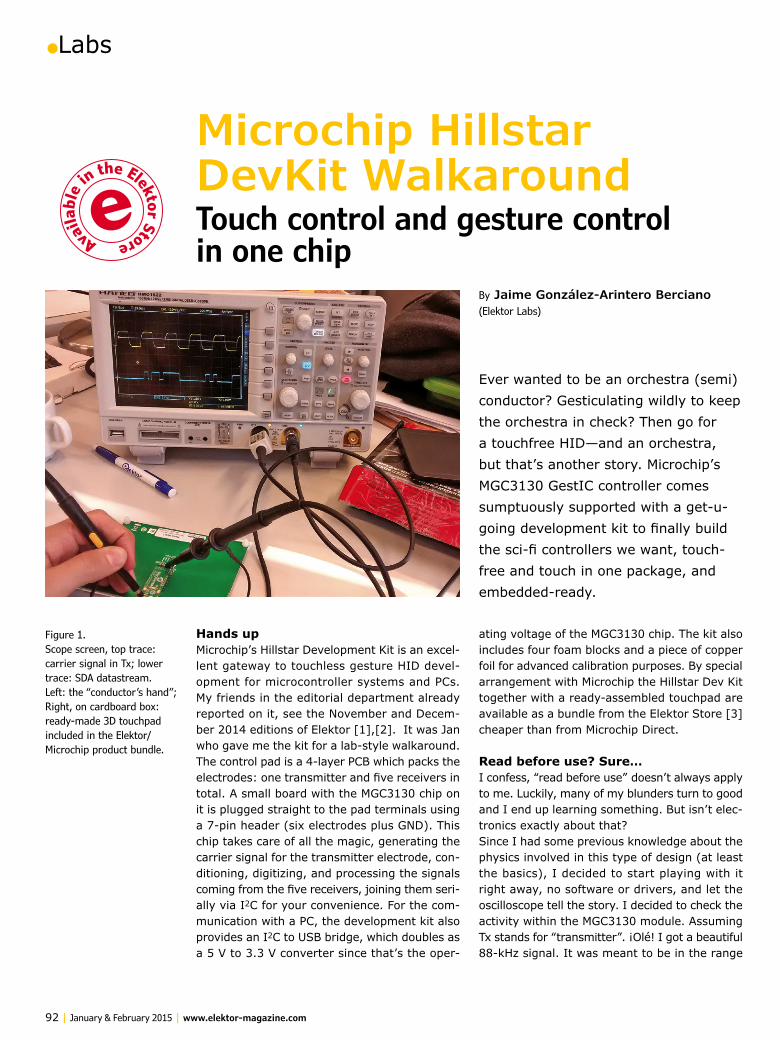
•Labs
92 | January & February 2015 | www.elektor-magazine.com
Hands upMicrochip’s Hillstar Development Kit is an excel-lent gateway to touchless gesture HID devel-opment for microcontroller systems and PCs. My friends in the editorial department already reported on it, see the November and Decem-ber 2014 editions of Elektor [1],[2]. It was Jan who gave me the kit for a lab-style walkaround.The control pad is a 4-layer PCB which packs the electrodes: one transmitter and five receivers in total. A small board with the MGC3130 chip on it is plugged straight to the pad terminals using a 7-pin header (six electrodes plus GND). This chip takes care of all the magic, generating the carrier signal for the transmitter electrode, con-ditioning, digitizing, and processing the signals coming from the five receivers, joining them seri-ally via I2C for your convenience. For the com-munication with a PC, the development kit also provides an I2C to USB bridge, which doubles as a 5 V to 3.3 V converter since that’s the oper-
ating voltage of the MGC3130 chip. The kit also includes four foam blocks and a piece of copper foil for advanced calibration purposes. By special arrangement with Microchip the Hillstar Dev Kit together with a ready-assembled touchpad are available as a bundle from the Elektor Store [3] cheaper than from Microchip Direct.
Read before use? Sure…I confess, “read before use” doesn’t always apply to me. Luckily, many of my blunders turn to good and I end up learning something. But isn’t elec-tronics exactly about that?Since I had some previous knowledge about the physics involved in this type of design (at least the basics), I decided to start playing with it right away, no software or drivers, and let the oscilloscope tell the story. I decided to check the activity within the MGC3130 module. Assuming Tx stands for “transmitter”. ¡Olé! I got a beautiful 88-kHz signal. It was meant to be in the range
By Jaime González-Arintero Berciano (Elektor Labs)
Microchip Hillstar DevKit WalkaroundTouch control and gesture control in one chip
Ever wanted to be an orchestra (semi)conductor? Gesticulating wildly to keep the orchestra in check? Then go for a touchfree HID—and an orchestra, but that’s another story. Microchip’s MGC3130 GestIC controller comes sumptuously supported with a get-u-going development kit to finally build the sci-fi controllers we want, touch-free and touch in one package, and embedded-ready.
Figure 1. Scope screen, top trace: carrier signal in Tx; lower trace: SDA datastream. Left: the “conductor’s hand”; Right, on cardboard box: ready-made 3D touchpad included in the Elektor/Microchip product bundle.
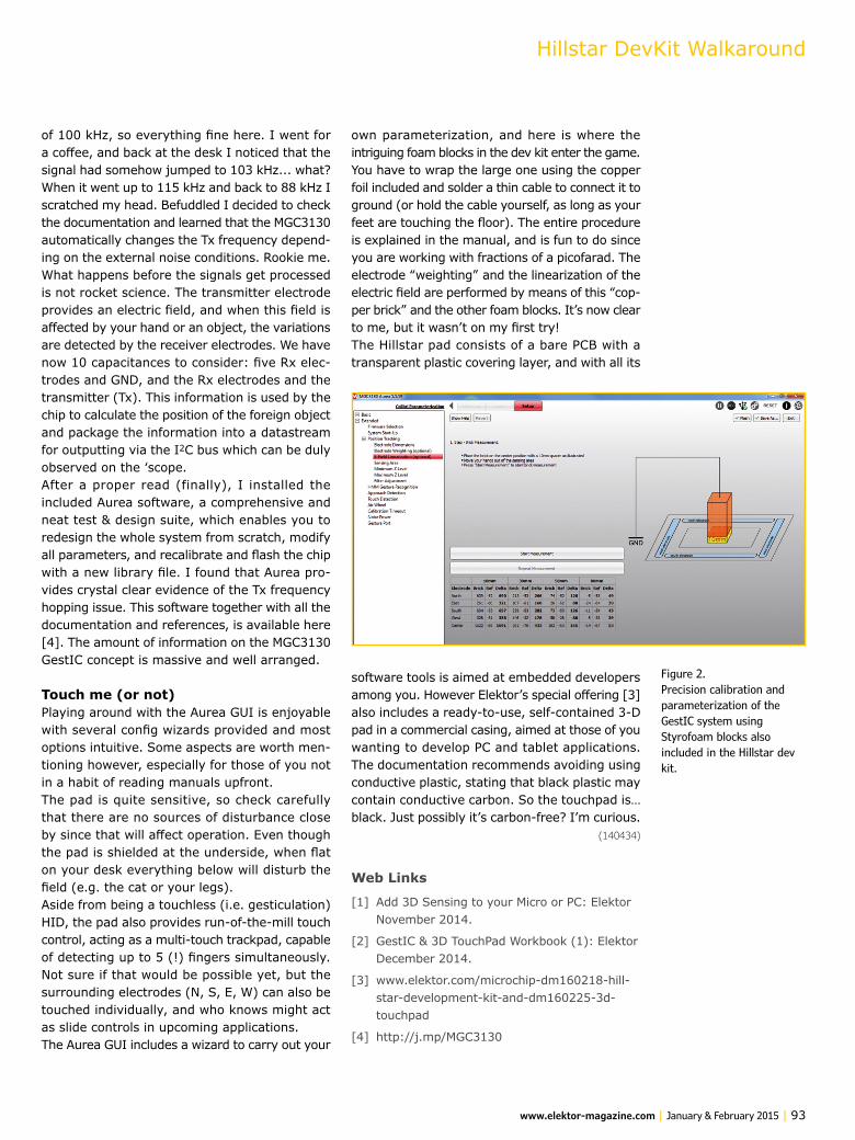
Hillstar DevKit Walkaround
www.elektor-magazine.com | January & February 2015 | 93
of 100 kHz, so everything fine here. I went for a coffee, and back at the desk I noticed that the signal had somehow jumped to 103 kHz... what? When it went up to 115 kHz and back to 88 kHz I scratched my head. Befuddled I decided to check the documentation and learned that the MGC3130 automatically changes the Tx frequency depend-ing on the external noise conditions. Rookie me.What happens before the signals get processed is not rocket science. The transmitter electrode provides an electric field, and when this field is affected by your hand or an object, the variations are detected by the receiver electrodes. We have now 10 capacitances to consider: five Rx elec-trodes and GND, and the Rx electrodes and the transmitter (Tx). This information is used by the chip to calculate the position of the foreign object and package the information into a datastream for outputting via the I2C bus which can be duly observed on the ‘scope.After a proper read (finally), I installed the included Aurea software, a comprehensive and neat test & design suite, which enables you to redesign the whole system from scratch, modify all parameters, and recalibrate and flash the chip with a new library file. I found that Aurea pro-vides crystal clear evidence of the Tx frequency hopping issue. This software together with all the documentation and references, is available here [4]. The amount of information on the MGC3130 GestIC concept is massive and well arranged.
Touch me (or not)Playing around with the Aurea GUI is enjoyable with several config wizards provided and most options intuitive. Some aspects are worth men-tioning however, especially for those of you not in a habit of reading manuals upfront.The pad is quite sensitive, so check carefully that there are no sources of disturbance close by since that will affect operation. Even though the pad is shielded at the underside, when flat on your desk everything below will disturb the field (e.g. the cat or your legs). Aside from being a touchless (i.e. gesticulation) HID, the pad also provides run-of-the-mill touch control, acting as a multi-touch trackpad, capable of detecting up to 5 (!) fingers simultaneously. Not sure if that would be possible yet, but the surrounding electrodes (N, S, E, W) can also be touched individually, and who knows might act as slide controls in upcoming applications.The Aurea GUI includes a wizard to carry out your
own parameterization, and here is where the intriguing foam blocks in the dev kit enter the game. You have to wrap the large one using the copper foil included and solder a thin cable to connect it to ground (or hold the cable yourself, as long as your feet are touching the floor). The entire procedure is explained in the manual, and is fun to do since you are working with fractions of a picofarad. The electrode “weighting” and the linearization of the electric field are performed by means of this “cop-per brick” and the other foam blocks. It’s now clear to me, but it wasn’t on my first try!The Hillstar pad consists of a bare PCB with a transparent plastic covering layer, and with all its
software tools is aimed at embedded developers among you. However Elektor’s special offering [3] also includes a ready-to-use, self-contained 3-D pad in a commercial casing, aimed at those of you wanting to develop PC and tablet applications. The documentation recommends avoiding using conductive plastic, stating that black plastic may contain conductive carbon. So the touchpad is… black. Just possibly it’s carbon-free? I’m curious.
(140434)
Web Links
[1] Add 3D Sensing to your Micro or PC: Elektor November 2014.
[2] GestIC & 3D TouchPad Workbook (1): Elektor December 2014.
[3] www.elektor.com/microchip-dm160218-hill-star-development-kit-and-dm160225-3d-touchpad
[4] http://j.mp/MGC3130
Figure 2. Precision calibration and parameterization of the GestIC system using Styrofoam blocks also included in the Hillstar dev kit.

•Labs
94 | January & February 2015 | www.elektor-magazine.com
SurrounDo-It-YourselfThis DIY project in the making was designed to ‘fill’ a mid-sized room of about 60 sq. ft. (20 m2), by means of 6 speakers and a subwoofer. Indeed, this is a 6.1 system—not that common, you may have expected to see ‘7’. However, the constel-lation consists of 2 x 15 watts amps for the front speakers, 2 x 15 W amps for the side speakers (left, right), 2 x 4 W amps for the rear speakers, and a 30 W monoblock amp for the subwoofer. For 60 sq. ft. room, this should be more than enough for most occasions, including “highly-demand-ing applications” like parties. The clever thing about this setup is that the speaker configura-tion employs 4 circuits only that are combined and “repeated” accordingly, and 2 additional (optional) small add-ons for the subwoofer, not forgetting and a switching circuit to automatically turn the system on or off.Standard laptop power supplies are used (24 V and 12 V), meaning we can solve the problem with a
few bucks and a quick visit to the thrift shop, or just looking around at home in the kid’s cupboards.
One size fits... mostFor practical reasons we will be commenting in depth on the most used amplifier, the 15-watts unit, but the entire project with full descriptions, annotations, pictures, specs, and circuit boards is waiting for you at the Elektor Labs website [1].
This design is used for the front and side speakers: 4x in total, and thus, it’s repeated 4 times. The fairly simple Class-AB amp (Figure 1) is entirely based on discrete components. T1 together with R1-R2-R3 sets the operating point of the whole circuit, and isolates the differential amp formed by T2 and T3 from the input. The high-impedance differential amp relies on a current source (T4, R8, C5, C9, D2, D3, and R13), which in turn com-bines the input signal with the feedback signal. This provides a broad bandwidth and minimizes
Design: Juan Cantón (Mexico)
Report: Jaime González-Arintero Berciano (Elektor Labs)
CRIS-AMP Audio Systemwatts-up for smartphones and laptopsAside from being a quality design, the CRIS-AMP makes an excellent project to learn or hone your skills within different areas of analog electronics. It’s relatively easy to replicate, without the need to deal with SMT or esoteric components. Ev-ery module is designed as an independent PCB, ready for re-use in your own build.
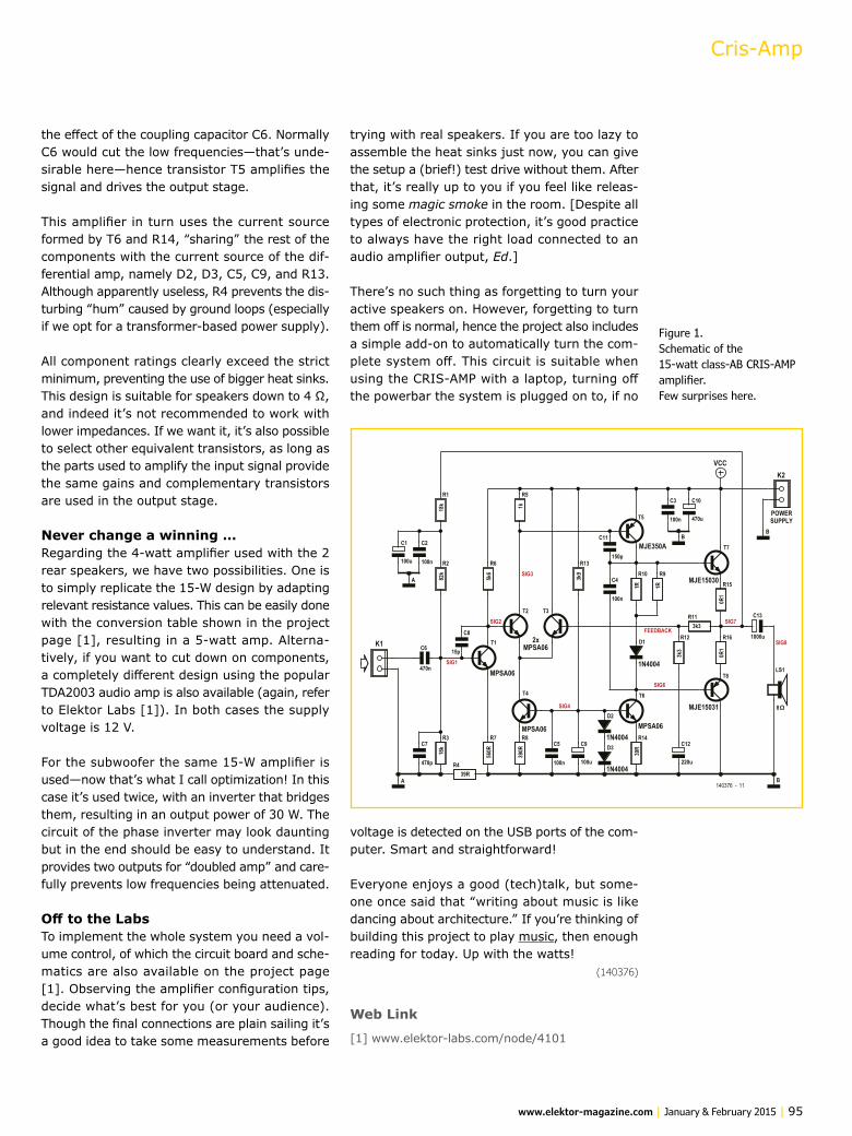
Cris-Amp
www.elektor-magazine.com | January & February 2015 | 95
the effect of the coupling capacitor C6. Normally C6 would cut the low frequencies—that’s unde-sirable here—hence transistor T5 amplifies the signal and drives the output stage.
This amplifier in turn uses the current source formed by T6 and R14, “sharing” the rest of the components with the current source of the dif-ferential amp, namely D2, D3, C5, C9, and R13. Although apparently useless, R4 prevents the dis-turbing “hum” caused by ground loops (especially if we opt for a transformer-based power supply).
All component ratings clearly exceed the strict minimum, preventing the use of bigger heat sinks. This design is suitable for speakers down to 4 Ω, and indeed it’s not recommended to work with lower impedances. If we want it, it’s also possible to select other equivalent transistors, as long as the parts used to amplify the input signal provide the same gains and complementary transistors are used in the output stage.
Never change a winning …Regarding the 4-watt amplifier used with the 2 rear speakers, we have two possibilities. One is to simply replicate the 15-W design by adapting relevant resistance values. This can be easily done with the conversion table shown in the project page [1], resulting in a 5-watt amp. Alterna-tively, if you want to cut down on components, a completely different design using the popular TDA2003 audio amp is also available (again, refer to Elektor Labs [1]). In both cases the supply voltage is 12 V.
For the subwoofer the same 15-W amplifier is used—now that’s what I call optimization! In this case it’s used twice, with an inverter that bridges them, resulting in an output power of 30 W. The circuit of the phase inverter may look daunting but in the end should be easy to understand. It provides two outputs for “doubled amp” and care-fully prevents low frequencies being attenuated.
Off to the LabsTo implement the whole system you need a vol-ume control, of which the circuit board and sche-matics are also available on the project page [1]. Observing the amplifier configuration tips, decide what’s best for you (or your audience). Though the final connections are plain sailing it’s a good idea to take some measurements before
trying with real speakers. If you are too lazy to assemble the heat sinks just now, you can give the setup a (brief!) test drive without them. After that, it’s really up to you if you feel like releas-ing some magic smoke in the room. [Despite all types of electronic protection, it’s good practice to always have the right load connected to an audio amplifier output, Ed.]
There’s no such thing as forgetting to turn your active speakers on. However, forgetting to turn them off is normal, hence the project also includes a simple add-on to automatically turn the com-plete system off. This circuit is suitable when using the CRIS-AMP with a laptop, turning off the powerbar the system is plugged on to, if no
voltage is detected on the USB ports of the com-puter. Smart and straightforward!
Everyone enjoys a good (tech)talk, but some-one once said that “writing about music is like dancing about architecture.” If you’re thinking of building this project to play music, then enough reading for today. Up with the watts!
(140376)
Web Link
[1] www.elektor-labs.com/node/4101
T1
MPSA06
T2 T3
MPSA062x
T4
MPSA06
T6
MPSA06
T5
MJE350A
T8
MJE15031
T7
MJE15030
R6
5k6
R2
82k
R1
18k
R3
18k
R5
1k
R8
390R
R10
1R
R9
1R
R439R
R113k3
R13
3k9
R7
560R
R12
3k3
R14
39R
R15
0R1
R16
0R1
C13
1000uD1
1N4004
C2
100n
C7
470p
C8
15p
C11
150p
C4
100n
C5
100n
C3
100n
C1
100u
C9
100u
C12
220u
C10
470u
C6
470n
D2
1N4004D3
1N4004
K1
K2
LS1
8
A
A
BB
B
SIG1
SIG2FEEDBACK
SIG3
SIG4
SIG6
SIG7
SIG8
VCC
POWERSUPPLY
140376 - 11
Figure 1. Schematic of the 15-watt class-AB CRIS-AMP amplifier. Few surprises here.
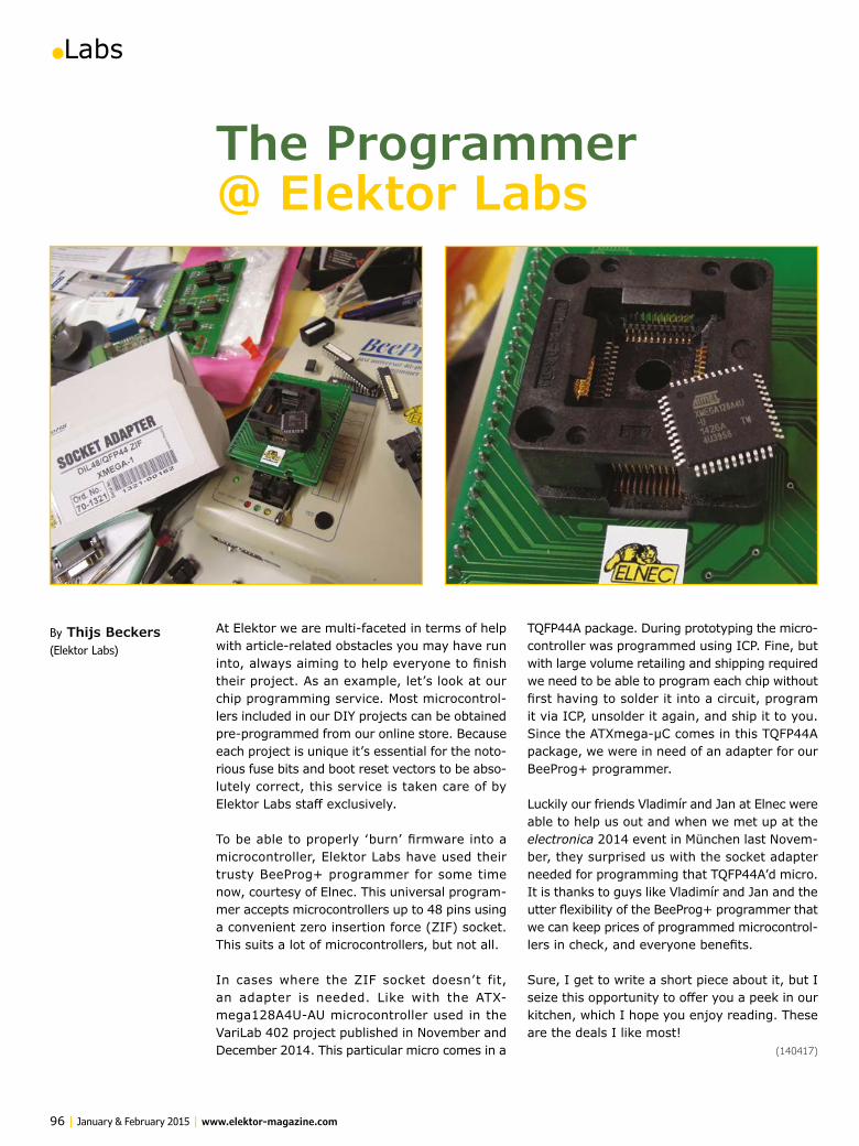
•Labs
96 | January & February 2015 | www.elektor-magazine.com
At Elektor we are multi-faceted in terms of help with article-related obstacles you may have run into, always aiming to help everyone to finish their project. As an example, let’s look at our chip programming service. Most microcontrol-lers included in our DIY projects can be obtained pre-programmed from our online store. Because each project is unique it’s essential for the noto-rious fuse bits and boot reset vectors to be abso-lutely correct, this service is taken care of by Elektor Labs staff exclusively.
To be able to properly ‘burn’ firmware into a microcontroller, Elektor Labs have used their trusty BeeProg+ programmer for some time now, courtesy of Elnec. This universal program-mer accepts microcontrollers up to 48 pins using a convenient zero insertion force (ZIF) socket. This suits a lot of microcontrollers, but not all.
In cases where the ZIF socket doesn’t fit, an adapter is needed. Like with the ATX-mega128A4U-AU microcontroller used in the VariLab 402 project published in November and December 2014. This particular micro comes in a
TQFP44A package. During prototyping the micro-controller was programmed using ICP. Fine, but with large volume retailing and shipping required we need to be able to program each chip without first having to solder it into a circuit, program it via ICP, unsolder it again, and ship it to you. Since the ATXmega-µC comes in this TQFP44A package, we were in need of an adapter for our BeeProg+ programmer.
Luckily our friends Vladimír and Jan at Elnec were able to help us out and when we met up at the electronica 2014 event in München last Novem-ber, they surprised us with the socket adapter needed for programming that TQFP44A’d micro. It is thanks to guys like Vladimír and Jan and the utter flexibility of the BeeProg+ programmer that we can keep prices of programmed microcontrol-lers in check, and everyone benefits.
Sure, I get to write a short piece about it, but I seize this opportunity to offer you a peek in our kitchen, which I hope you enjoy reading. These are the deals I like most!
(140417)
By Thijs Beckers (Elektor Labs)
The Programmer @ Elektor Labs

Weird Components
www.elektor-magazine.com | January & February 2015 | 97
We’ve all used n-p-n and p-n-p bipolar transistors with three connections but I had never heard of transistor tetrodes until I was researching this article. Transistor tetrodes have four leads and come in different variations. Remarkably they have two control elements instead of one, that’s two base (b) connections for bipolar transistors and two gate (G) connections for MOSFETs, as indicated by the circuit symbols in Figure 1. Let’s take a closer look at them and see what makes them special.A tetrode in electronics is any device that has four active electrodes but usually the term refers to tetrode vacuum tubes which have two grids instead of one. The extra grid, called the screen grid, lowers the interplate capacitance when compared to a conventional triode tube which increases the tube’s frequency range. Transistor tetrode aren’t an exact replacement for tetrode vacuum tubes but they also are made to reduce parasitic capacitance and increase their operat-ing frequency range. A bipolar transistor tetrode is made by adding another base connection on the opposite side of the silicon like the left side of Figure 2. The right side image shows how a dual-gate MOSFET is constructed.I’ve mentioned capacitance quite a bit but why does it matter? Well, designing amplifiers using discrete transistors is always a constant battle to get enough bandwidth, gain and input to out-put isolation. One of the reasons why this can be a challenge is the Miller Effect and how it can affect an amplifier. The Miller Effect is when an amplifier’s input to output capacitance is ampli-fied by the amplifier gain which will then increase its equivalent input capacitance. In transistor amplifiers, it’s usually the parasitic capacitance inherent to the transistor that must be overcome if you want to maximize the amplifier bandwidth.
One way to minimize the Miller Effect is to use two transistors to make a cascode amplifier like in Figure 3. One transistor is used as a transcon-ductance amplifier which is then followed by a current buffer transistor. Having two amplifier stages helps to minimize the Miller Effect by iso-lating the amplifier input capacitance of the lower
transistor from the buffer stage. And it turns out that transistor tetrodes are an excellent choice for small-signal cascode amplifiers that also need high frequency bandwidth.
The most common type transistor tetrode is the dual gate MOSFET which has some other inter-esting uses in RF circuits. Famous ones from the 1980s and ranking high in RF Design’s Hall of Fame are the European BF96x/BF98x series, and from the US, the 40673 and 3N211. For example, a simple FET mixer will connect the local mixer output and the RF output to the gate of a FET using some extra components to iso-late the mixer from the RF. A dual gate MOSFET can eliminate those isolation components, with its gates already isolated from each other. Dual gate MOSFETs also work well in automatic gain control (AGC) circuits because you can bias one gate and feed the signal to the other. Then the bias voltage can be the control input and control the overall transistor gain.
I hadn’t heard of transistor tetrodes before today, but they are definitely a very interesting and weird component, especially with their uses in RF circuitry. Maybe you will find a use for them in your next project.
(140418)
By Neil Gruending (Canada)
Transistor TetrodesWeird Component # 11
B1 B2
C
E
G2G1
D
S
RD
V+
V–
Vin
Vout
Figure 1. Transistor tetrode schematic symbols.
Figure 2. Tetrode transistor construction.
Figure 3. Cascode amplifier.
Emitter Collector
Base
b2
N-Type N-Type
Single-CrystalGermanium Bar
P-Type
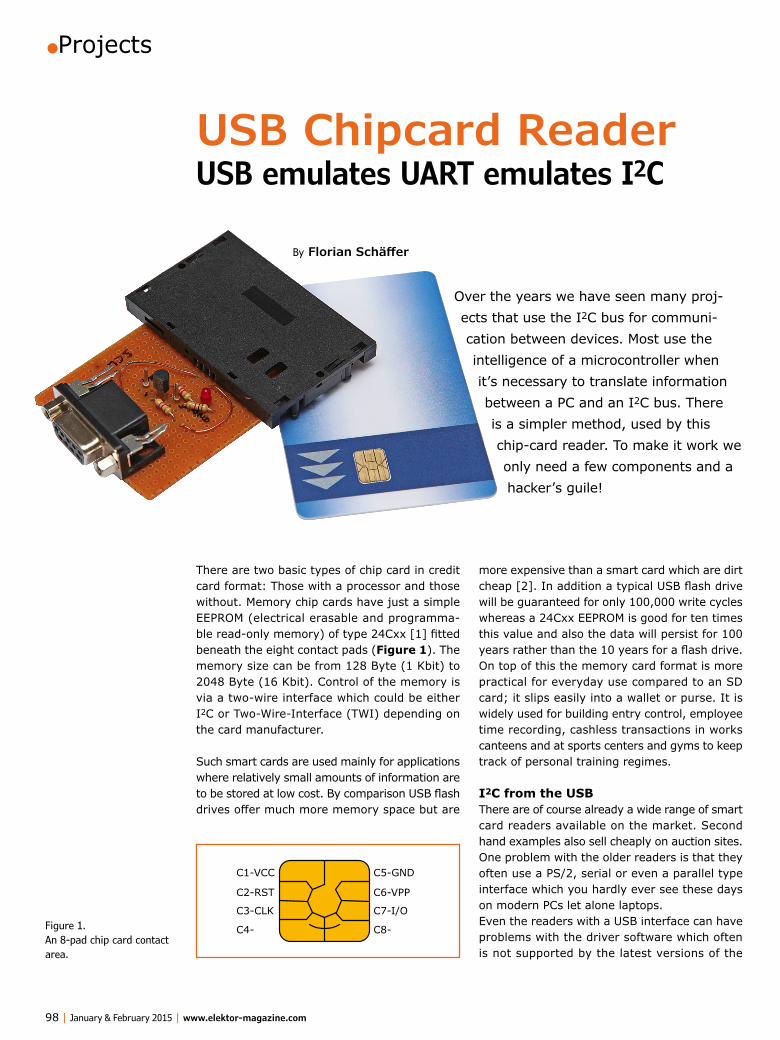
•Projects
98 | January & February 2015 | www.elektor-magazine.com
There are two basic types of chip card in credit card format: Those with a processor and those without. Memory chip cards have just a simple EEPROM (electrical erasable and programma-ble read-only memory) of type 24Cxx [1] fitted beneath the eight contact pads (Figure 1). The memory size can be from 128 Byte (1 Kbit) to 2048 Byte (16 Kbit). Control of the memory is via a two-wire interface which could be either I2C or Two-Wire-Interface (TWI) depending on the card manufacturer.
Such smart cards are used mainly for applications where relatively small amounts of information are to be stored at low cost. By comparison USB flash drives offer much more memory space but are
more expensive than a smart card which are dirt cheap [2]. In addition a typical USB flash drive will be guaranteed for only 100,000 write cycles whereas a 24Cxx EEPROM is good for ten times this value and also the data will persist for 100 years rather than the 10 years for a flash drive. On top of this the memory card format is more practical for everyday use compared to an SD card; it slips easily into a wallet or purse. It is widely used for building entry control, employee time recording, cashless transactions in works canteens and at sports centers and gyms to keep track of personal training regimes.
I2C from the USBThere are of course already a wide range of smart card readers available on the market. Second hand examples also sell cheaply on auction sites. One problem with the older readers is that they often use a PS/2, serial or even a parallel type interface which you hardly ever see these days on modern PCs let alone laptops.Even the readers with a USB interface can have problems with the driver software which often is not supported by the latest versions of the
By Florian Schäffer
USB Chipcard ReaderUSB emulates UART emulates I2C
Over the years we have seen many proj-ects that use the I2C bus for communi-cation between devices. Most use the intelligence of a microcontroller when it’s necessary to translate information between a PC and an I2C bus. There is a simpler method, used by this chip-card reader. To make it work we only need a few components and a hacker’s guile!
C1-VCC
C2-RST
C3-CLK
C4-
C5-GND
C6-VPP
C7-I/O
C8-Figure 1. An 8-pad chip card contact area.
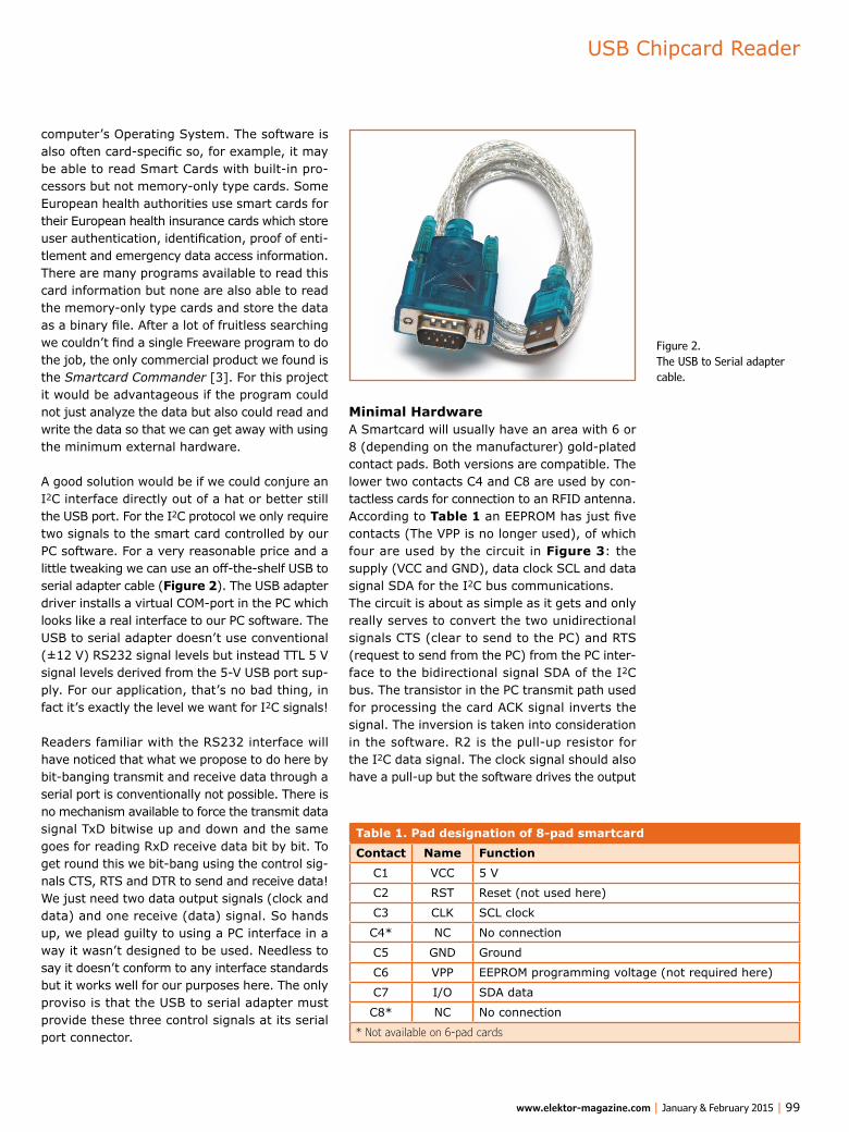
USB Chipcard Reader
www.elektor-magazine.com | January & February 2015 | 99
computer’s Operating System. The software is also often card-specific so, for example, it may be able to read Smart Cards with built-in pro-cessors but not memory-only type cards. Some European health authorities use smart cards for their European health insurance cards which store user authentication, identification, proof of enti-tlement and emergency data access information. There are many programs available to read this card information but none are also able to read the memory-only type cards and store the data as a binary file. After a lot of fruitless searching we couldn’t find a single Freeware program to do the job, the only commercial product we found is the Smartcard Commander [3]. For this project it would be advantageous if the program could not just analyze the data but also could read and write the data so that we can get away with using the minimum external hardware.
A good solution would be if we could conjure an I2C interface directly out of a hat or better still the USB port. For the I2C protocol we only require two signals to the smart card controlled by our PC software. For a very reasonable price and a little tweaking we can use an off-the-shelf USB to serial adapter cable (Figure 2). The USB adapter driver installs a virtual COM-port in the PC which looks like a real interface to our PC software. The USB to serial adapter doesn’t use conventional (±12 V) RS232 signal levels but instead TTL 5 V signal levels derived from the 5-V USB port sup-ply. For our application, that’s no bad thing, in fact it’s exactly the level we want for I2C signals!
Readers familiar with the RS232 interface will have noticed that what we propose to do here by bit-banging transmit and receive data through a serial port is conventionally not possible. There is no mechanism available to force the transmit data signal TxD bitwise up and down and the same goes for reading RxD receive data bit by bit. To get round this we bit-bang using the control sig-nals CTS, RTS and DTR to send and receive data! We just need two data output signals (clock and data) and one receive (data) signal. So hands up, we plead guilty to using a PC interface in a way it wasn’t designed to be used. Needless to say it doesn’t conform to any interface standards but it works well for our purposes here. The only proviso is that the USB to serial adapter must provide these three control signals at its serial port connector.
Minimal HardwareA Smartcard will usually have an area with 6 or 8 (depending on the manufacturer) gold-plated contact pads. Both versions are compatible. The lower two contacts C4 and C8 are used by con-tactless cards for connection to an RFID antenna. According to Table 1 an EEPROM has just five contacts (The VPP is no longer used), of which four are used by the circuit in Figure 3: the supply (VCC and GND), data clock SCL and data signal SDA for the I2C bus communications.The circuit is about as simple as it gets and only really serves to convert the two unidirectional signals CTS (clear to send to the PC) and RTS (request to send from the PC) from the PC inter-face to the bidirectional signal SDA of the I2C bus. The transistor in the PC transmit path used for processing the card ACK signal inverts the signal. The inversion is taken into consideration in the software. R2 is the pull-up resistor for the I2C data signal. The clock signal should also have a pull-up but the software drives the output
Figure 2. The USB to Serial adapter cable.
Table 1. Pad designation of 8-pad smartcard
Contact Name Function
C1 VCC 5 V
C2 RST Reset (not used here)
C3 CLK SCL clock
C4* NC No connection
C5 GND Ground
C6 VPP EEPROM programming voltage (not required here)
C7 I/O SDA data
C8* NC No connection
* Not available on 6-pad cards
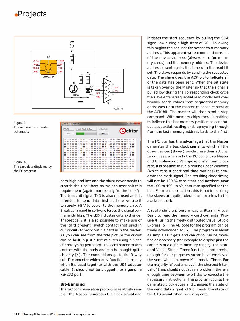
•Projects
100 | January & February 2015 | www.elektor-magazine.com
initiates the start sequence by pulling the SDA signal low during a high state of SCL. Following this begins the request for access to a memory address. This apparent write command consists of the device address (always zero for mem-ory cards) and the memory address. The device address is sent again, this time with the read bit set. The slave responds by sending the requested data. The slave uses the ACK bit to indicate all of the data has been sent. When the bit state is taken over by the Master so that the signal is pulled low during the corresponding clock cycle the slave enters ‘sequential read mode’ and con-tinually sends values from sequential memory addresses until the master releases control of the ACK bit. The master will then send a stop command. With memory chips there is nothing to indicate the last memory position so continu-ous sequential reading ends up cycling through from the last memory address back to the first.
The I2C bus has the advantage that the Master generates the bus clock signal to which all the other devices (slaves) synchronize their actions. In our case when only the PC can act as Master and the slaves don’t impose a minimum clock rate, it is possible to run a routine under Windows (which cant support real-time routines) to gen-erate the clock signal. The resulting clock timing will not be 100 % consistent and nowhere near the 100 to 400 kbit/s data rate specified for the bus. For most applications this is not important; the slaves are quite tolerant and work with the available clock.
A really simple program was written in Visual Basic to read the memory card contents (Fig-ure 4) using the freely distributed Visual Studio Express [5]. The VB code for the program can be freely downloaded at [6]. The program is about as simple as it gets and can of course be modi-fied as necessary (for example to display just the contents of a defined memory range). The stan-dard Visual Studio Timer function is not precise enough for our purposes so we have employed the somewhat unknown Multimedia-Timer. For the majority of systems even the shortest inter-val of 1 ms should not cause a problem, there is enough time between two ticks to execute the necessary instructions. The program counts the generated clock edges and changes the state of the send data signal RTS or reads the state of the CTS signal when receiving data.
both high and low and the slave never needs to stretch the clock here so we can overlook this requirement (again, not exactly ‘to the book’).The transmit signal TxD is also not used as it is intended to send data, instead here we use it to supply +5 V to power to the memory chip. A Break command in software forces the signal per-manently high. The LED indicates data exchange. Theoretically it is also possible to make use of the ‘card present’ switch contact (not used in our circuit) to work out if a card is in the reader.As you can see from the title picture the circuit can be built in just a few minutes using a piece of prototyping perfboard. The card reader makes contact with the pads and can be bought quite cheaply [4]. The connections go to the 9-way sub-D connector which only functions correctly when it’s used together with the USB adapter cable. It should not be plugged into a genuine RS-232 port!
Bit-BangingThe I2C communication protocol is relatively sim-ple; The Master generates the clock signal and
K1
K2
12345
6789
+5V
R3
1kLED1
2mA
R1
2k2
T1
BC547
R2
4k7
TXDDTRGND
RTSCTS
140070 - 11
C5-GNDC6-NCC7-I/OC8-NC
C1-VCCC2-RSTC3-CLKC4-NC
CHIPCARD
Figure 3. The minimal card reader schematic.
Figure 4. The card data displayed by the PC program.

www.elektor-magazine.com | January & February 2015 | 101
DIY LED Flashlight
an I2C interface so a PC status display (e.g. to display Tweets) can be relatively quickly assem-bled. Keep in mind here that the Client cannot play the role of a Master.
(140070)
In addition to reading out the card data as described here there are many other applica-tions that the design could be used for. Data stored on the card can of course be modified by writing to the card. It can also be used to communicate with other I2C devices such as the DS1621 temperature sensor with integrated A/D converter. Many types of LCD module also have
By Wolfgang Schmidt (Germany)
DIY LED FlashlightBetter than off the shelf?Question: Why bother making something you can buy ready-made at a fraction of the cost?Answer: First off it’s fun and secondly it runs more efficiently than a mass-produced equivalent from Asia.
Technical Data• Efficient DIY LED flashlight• Input voltage range from 1 to 3 V• Up to 78.8% efficiency• Constant brightness with input down to 1.2 V
Web Links
[1] ATMEL Data sheet AT24Cxx, www.atmel.com/Images/doc0180.pdf
[2] Smartcards: http://www.reichelt.de/Chipkarten/CHIPKARTE-256B/3/index.html?&ACTION=3&LA=2&ARTICLE=37015&GROUPID=5967&artnr=CHIPKARTE+256B
[3] Smart card Commander: www.chipdrive.de
[4] Smart card reader: http://uk.farnell.com/amphenol/c702-10m008-230-40/smart-card-c702-wiping-xxs/dp/1849551
[5] Visual Studio Express: www.visualstudio.com/downloads/download-visual-studio-vs#d-express-windows-desktop
[6] www.elektor-magazine.com/140070
As a member of the genus homo electronicus the author has an aversion to buying any electronic product that he can better make himself. Take for example the humble LED flashlight, enter that
phrase into the search engine on a well known internet auction site and you can waste an hour scrolling through all the items on offer. Some for less than a couple of dollars including battery,
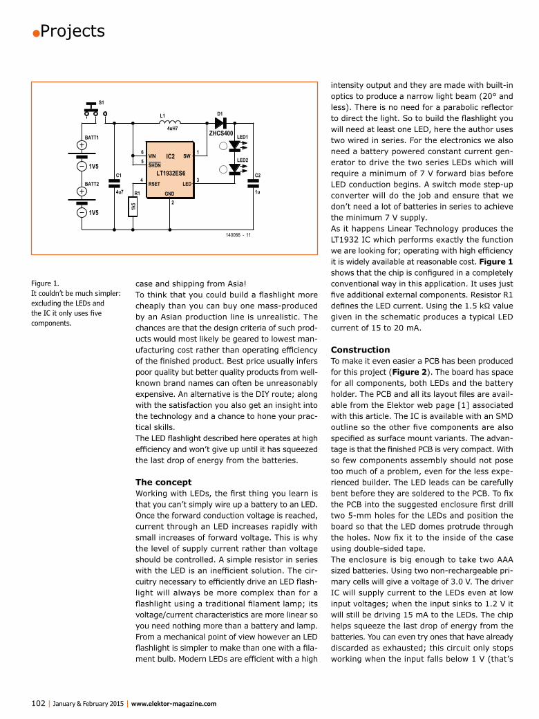
•Projects
102 | January & February 2015 | www.elektor-magazine.com
case and shipping from Asia!To think that you could build a flashlight more cheaply than you can buy one mass-produced by an Asian production line is unrealistic. The chances are that the design criteria of such prod-ucts would most likely be geared to lowest man-ufacturing cost rather than operating efficiency of the finished product. Best price usually infers poor quality but better quality products from well-known brand names can often be unreasonably expensive. An alternative is the DIY route; along with the satisfaction you also get an insight into the technology and a chance to hone your prac-tical skills.The LED flashlight described here operates at high efficiency and won’t give up until it has squeezed the last drop of energy from the batteries.
The conceptWorking with LEDs, the first thing you learn is that you can’t simply wire up a battery to an LED. Once the forward conduction voltage is reached, current through an LED increases rapidly with small increases of forward voltage. This is why the level of supply current rather than voltage should be controlled. A simple resistor in series with the LED is an inefficient solution. The cir-cuitry necessary to efficiently drive an LED flash-light will always be more complex than for a flashlight using a traditional filament lamp; its voltage/current characteristics are more linear so you need nothing more than a battery and lamp.From a mechanical point of view however an LED flashlight is simpler to make than one with a fila-ment bulb. Modern LEDs are efficient with a high
intensity output and they are made with built-in optics to produce a narrow light beam (20° and less). There is no need for a parabolic reflector to direct the light. So to build the flashlight you will need at least one LED, here the author uses two wired in series. For the electronics we also need a battery powered constant current gen-erator to drive the two series LEDs which will require a minimum of 7 V forward bias before LED conduction begins. A switch mode step-up converter will do the job and ensure that we don’t need a lot of batteries in series to achieve the minimum 7 V supply.As it happens Linear Technology produces the LT1932 IC which performs exactly the function we are looking for; operating with high efficiency it is widely available at reasonable cost. Figure 1 shows that the chip is configured in a completely conventional way in this application. It uses just five additional external components. Resistor R1 defines the LED current. Using the 1.5 kΩ value given in the schematic produces a typical LED current of 15 to 20 mA.
ConstructionTo make it even easier a PCB has been produced for this project (Figure 2). The board has space for all components, both LEDs and the battery holder. The PCB and all its layout files are avail-able from the Elektor web page [1] associated with this article. The IC is available with an SMD outline so the other five components are also specified as surface mount variants. The advan-tage is that the finished PCB is very compact. With so few components assembly should not pose too much of a problem, even for the less expe-rienced builder. The LED leads can be carefully bent before they are soldered to the PCB. To fix the PCB into the suggested enclosure first drill two 5-mm holes for the LEDs and position the board so that the LED domes protrude through the holes. Now fix it to the inside of the case using double-sided tape.The enclosure is big enough to take two AAA sized batteries. Using two non-rechargeable pri-mary cells will give a voltage of 3.0 V. The driver IC will supply current to the LEDs even at low input voltages; when the input sinks to 1.2 V it will still be driving 15 mA to the LEDs. The chip helps squeeze the last drop of energy from the batteries. You can even try ones that have already discarded as exhausted; this circuit only stops working when the input falls below 1 V (that’s
BATT1
1V5
BATT2
1V5
C1
4u7
LT1932ES6RSET
SHDNIC2
LED
GND
VIN SW5
1
2
3
6
4
S1
D1
ZHCS400
L1
4uH7
C2
1u
LED1
LED2
R1
1k5
140066 - 11
Figure 1. It couldn’t be much simpler: excluding the LEDs and the IC it only uses five components.

www.elektor-magazine.com | January & February 2015 | 103
DIY LED Flashlight
is used in the position shown in the schematic; if it is fitted in series with the LEDs it will cause the IC’s output voltage to rise to a level (15 to 20 times the battery voltage) at switch off. This could damage the IC.Just to be thorough the author tested the effi-ciency of the prototype. The circuit achieves an efficiency of 78.8 % when operating from a 3 V supply. This is almost precisely the figure given in the IC’s data sheet operating with a 4.7 µH coil. Even when the supply drops to 1.2 V you can expect a respectable 69.3 %.
(140066)
Web Link
[1] www.elektor-magazine.com/140066
0.5 V per battery!). This energy scrounging fea-ture can however be a disadvantage if you use rechargeable batteries; NiCd and NiMH should not be allowed to discharge down to this voltage level.
That just about wraps it up for this circuit. Per-haps it is worth saying it is advisable to use LEDs with the highest Candela output you can find. The ones used by the author here were not expen-sive but they produce a very bright beam. Some LEDs allow a continuous current rating of 30 mA, in this case you can change the value of R1 to 750 Ω. The IC is capable of driving more than two series-connected LEDs. With four LEDs in series the minimum supply voltage is around 2 V. It is important to ensure that the on/off switch
Figure 2. Component placement using the Elektor PCB.
Component ListResistorsR1 = 1.5kΩ, SMD 0805
CapacitorsC1 = 4.7µF, multilayer, SMD 0805C2 = 2.2µF, multilayer, SMD 0805
InductorsL1 = 4.7µH, SMD 1812
SemiconductorsD1 = ZHS400, Schottky diodeLED1,LED2 = LED, white, 5mm
(e.g. Reichelt 5-25000 WS)IC1 = LT1932ES6
MiscellaneousS1 = switch, PCB mount, verticalBattery holder for 2 AAA cellsEnclosure (e.g. Hammond 15930)PCB # 140066-1

•Projects
104 | January & February 2015 | www.elektor-magazine.com
For sure a common digital multimeter can be used too, but it’s a pain to watch its dis-play all the time to see your mea-surement results. It’s even harder when you have to keep a probe tip lodged on a small pin. Do the zero
volts on that DMM display mean that the level of the sig-
nal under test (SUT) is low, or is it because the test probe slipped off the pin
and has gone unconnected? Woes like these triggered us to develop the logic probe presented in this article.
By Clemens Valens (Elektor.Labs)
BeepThe sounding logic probe/tester
Even if you have an upmarket logic analyzer and are completely at ease with its operation, you are unlikely to use it to debug simple circuits like Arduino and Raspberry Pi add-on boards. That’s where Beep comes in.
4040N
IC1
Q12Q11Q10
CLK
RST
VDD
VSS
13
10
151412
Q1Q2Q3Q4
Q9
Q5Q6Q7Q8
11
16
4235679
1
8
SW1.B
7
5
8
6
SW1.A
3
1
4
2
IC2.E11 121
IC2.F
14 151
IC2.C7 61
IC2.D
9 101
IC2.B
IC2.A
5 41
3 21
IC3.C89
10&
R51k
C6
330n
C7
100n
IC3.B56
4&
R410k
C5
470n
R610k
C4
82p
R3
2M2
R2
1M
R1
2M2
IC3.A12
3&
JP112
JP212
R70R
C2
4u750V
C3
4u750V
C1
4u750V
BZ1
V+
1
8IC2 IC3
14
7
V+
IC2 = 4050NIC3 = 4093N
VDDGND
Power Supply
Signal
IC3.D
13 12
11
&
140410 - 11
Figure 1. Beep’s schematic. R7 is zero ohms and represents a wire bridge.
Beep Logic Tester
www.elektor-magazine.com | January & February 2015 | 105
The sound of logic‘Beep’, as we nicknamed our logic probe, is a simple tool that employs sounds to indicate sig-nal levels so you can use it without having to look up from your work. Beep will produce a low frequency sound if the SUT has a low level and a high frequency sound when the SUT’s level is high. When the SUT is undefined because it is tri-stated (i.e. in high-impedance output mode) an unconnected input, or because the output is of the open collector type and is missing a pull-up resistor, Beep will remain silent. Many circuits also contain signals that change level (very) fre-quently, too often for our human ears to hear, and so Beep has been empowered to make such signals audible as well.
Oscillate and divideHow can Beep do all this without a microcontrol-ler? Easy, thanks to two oscillators and a fre-quency divider. One oscillator (IC3B, R4, C5) is responsible for the low-frequency sound; the other (IC3C, R5, C6) generates the high-fre-quency sound. The frequencies are determined by the values of R4/C5 (low) and R5/C6 (high). Since the SUT cannot be high and low at the same time only one oscillator can be active at any time hence the oscillators’ outputs can be connected in parallel to drive the buzzer.The choice of the oscillator depends on the SUT connected to pin 1 of JP2. When its level is low the level on the Enable pin (8) of IC3C will be low too, consequently IC3C’s output will be a steady
high (that’s how a NAND gate works, Schmitt-trig-ger inputs or not) and the oscillator is blocked. The output of IC3A will be high too analogous to IC3C. Its input pin 2 will not be exactly at 0 V, but it will be low enough for the gate to decide that its output should be high. Contrary to IC3C, IC3B sees a high level on its Enable pin (5) and so this oscillator is free to operate. A low-fre-quency sound will be heard.The opposite happens when the SUT represents a high level. Now both inputs of IC3A will be high, causing its output to go low, effectively blocking the low-frequency oscillator IC3B. The Enable pin (8) of IC3C on the other hand will be high and the oscillator starts producing a high-fre-quency sound.When Beep encounters an unconnected input, a tri-stated (i.e. high-impedance) output or an open-collector output without a pull-up resistor, the SUT will not have enough power to force Beep’s high-impedance input (due to the high values of R1, R2 and R3) to a well-defined low or high level. Because of the voltage levels cre-ated by the voltage divider ladder R1, R2 and R3 the inputs of IC3A will both be high and IC3C’s Enable pin will be deemed low. Now both oscil-lators are disabled and Beep will remain silent.When the SUT isn’t a steady level, i.e. it’s alter-nating between high and low, the oscillators will be activated alternatively resulting in a two-tone sound. As the SUT frequency increases the two-tone sound changes faster until a point is reached where the oscillators can no longer follow the
Oscillator operationConsider the oscillator IC3B, R4, C5 and assume pin 5 of IC3B is a steady high level. At power-up C5 will be discharged keeping IC3B’s input pin 6 low. Because IC3B is a NAND gate, its output will be high (Table 1) consequently R4 will charge C5. When the increasing voltage on C5 exceeds a certain threshold, IC3B will ‘finds’ its input pin 6 logic high. Now both inputs are high and so IC3B’s output will toggle to low, causing R4 to start discharging C5. When the decreasing voltage on C5 drops below a certain threshold, IC3B considers its input pin 6 to be low and we are back where we started. The cycle is closed and the oscillator is oscillating. The frequency of the oscillator depends on the values of the
resistor and the capacitor, as well as on the low and high thresholds of the gate.Because of the NAND function of IC3B, when its input pin 5 has a steady low level its output cannot become low. The oscillator is effectively disabled.
Table 1. Truth table of a NAND (not-AND; inverted AND) gate
Input A (pin 5)
Input B (pin 6)
Output (pin 4)
0 0 1
0 1 1
1 0 1
1 1 0
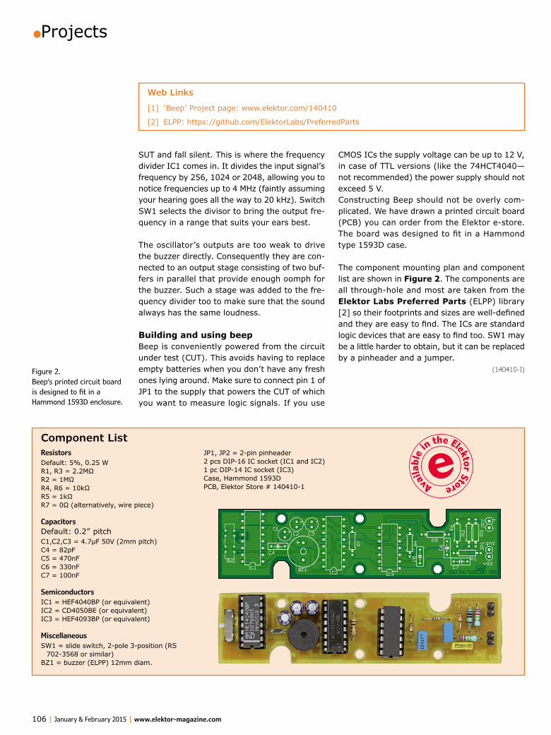
•Projects
106 | January & February 2015 | www.elektor-magazine.com
CMOS ICs the supply voltage can be up to 12 V, in case of TTL versions (like the 74HCT4040—not recommended) the power supply should not exceed 5 V.Constructing Beep should not be overly com-plicated. We have drawn a printed circuit board (PCB) you can order from the Elektor e-store. The board was designed to fit in a Hammond type 1593D case.
The component mounting plan and component list are shown in Figure 2. The components are all through-hole and most are taken from the Elektor Labs Preferred Parts (ELPP) library [2] so their footprints and sizes are well-defined and they are easy to find. The ICs are standard logic devices that are easy to find too. SW1 may be a little harder to obtain, but it can be replaced by a pinheader and a jumper.
(140410-I)
SUT and fall silent. This is where the frequency divider IC1 comes in. It divides the input signal’s frequency by 256, 1024 or 2048, allowing you to notice frequencies up to 4 MHz (faintly assuming your hearing goes all the way to 20 kHz). Switch SW1 selects the divisor to bring the output fre-quency in a range that suits your ears best.
The oscillator’s outputs are too weak to drive the buzzer directly. Consequently they are con-nected to an output stage consisting of two buf-fers in parallel that provide enough oomph for the buzzer. Such a stage was added to the fre-quency divider too to make sure that the sound always has the same loudness.
Building and using beepBeep is conveniently powered from the circuit under test (CUT). This avoids having to replace empty batteries when you don’t have any fresh ones lying around. Make sure to connect pin 1 of JP1 to the supply that powers the CUT of which you want to measure logic signals. If you use
Component ListResistorsDefault: 5%, 0.25 WR1, R3 = 2.2MΩR2 = 1MΩR4, R6 = 10kΩR5 = 1kΩR7 = 0Ω (alternatively, wire piece)
CapacitorsDefault: 0.2” pitchC1,C2,C3 = 4.7µF 50V (2mm pitch)C4 = 82pFC5 = 470nFC6 = 330nFC7 = 100nF
SemiconductorsIC1 = HEF4040BP (or equivalent)IC2 = CD4050BE (or equivalent)IC3 = HEF4093BP (or equivalent)
MiscellaneousSW1 = slide switch, 2-pole 3-position (RS
702-3568 or similar)BZ1 = buzzer (ELPP) 12mm diam.
JP1, JP2 = 2-pin pinheader2 pcs DIP-16 IC socket (IC1 and IC2)1 pc DIP-14 IC socket (IC3)Case, Hammond 1593DPCB, Elektor Store # 140410-1
Figure 2. Beep‘s printed circuit board is designed to fit in a Hammond 1593D enclosure.
+
Web Links
[1] ‘Beep’ Project page: www.elektor.com/140410
[2] ELPP: https://github.com/ElektorLabs/PreferredParts

An EIM Promotion•
advertorial www.elektor-magazine.com | January & February 2015 | 107
I met Hanno Sander in 2008 at the Embedded Systems Conference in San Jose, CA. At the time, Sander was at Parallax’s booth demonstrating a Propeller-based, two-wheeled balancing robot. When I saw his interesting balance bot design and his engaging way of explaining design to interested engineers, I knew that Sander would be an excellent resource for future Circuit Cel-lar content. I was right. Several months after the conference, we published an article he wrote about the balancing robot project in the March 2009 edition of Circuit Cellar. Today, Sander runs OneRobot with the aim of “building high-qual-ity, aff ordable products by pushing off -the-shelf components to their limits.”
The future is nowWhen it comes to robotics, the future is now. With the ever-increasing demand for robotics applications—from home control systems to ani-matronic toys to unmanned planet rovers—it’s an exciting time to be a roboticist, whether you’re a weekend DIYer, a computer science student, or a professional engineer. It doesn’t matter whether you’re building a line-fol-lowing robot toy or tasked with designing a mobile system for an extraterrestrial exploratory mission: the more you know about advanced robotics technol-ogies, the more you’ll succeed at your workbench. Advanced Control Robotics is intended to help roboticists of various skill levels take their designs to the next level with microcontrollers and the know-how to implement them eff ectively.
Theory & best practicesAdvanced Control Robotics simplifi es the theory and best practices of advanced robot technolo-gies. You’re taught basic embedded design the-
ory and presented handy code samples, essential schematics, and valuable design tips (from construction to debugging).
Learn then designThe principles described and topics presented in Advanced Control Robotics are immedi-ately applicable. With the book at your side, you’ll be innovat-ing in no time. Sander covers:• Control Robotics: robot
actions, servos, and stepper motors
• Embedded Technology: microcontrollers and peripherals
• Programming Languages: machine level (Assembly), low level (C/BASIC/Spin), and human (12Blocks)
• Control Structures: functions, state machines, multiprocessors, and events
• Visual Debugging: LED/speaker/gauges, PC-based development environments, and test instruments
• Output: sounds and synthesized speech• Sensors: compass, encoder, tilt, proximity,
artifi cial markers, and audio• Control Loop Algorithms: digital control, PID,
and fuzzy logic• Communication Technologies: infrared,
sound, and XML-RPC over HTTP• Projects: line following with vision and pat-
tern tracking
Are you ready to start learning and innovating? Order your copy of Advanced Control Robotics today!
Get Started withAdvanced Control Robotics
Title: Advanced Control Robotics Author: Hanno Sander Pages: 160Publisher: Elektor International Media – ISBN: 978-0-96301-333-0 – Year: 2014 Purchase: www.elektor.com/advanced-control-robotics
ory and presented handy code samples, essential schematics, and valuable design tips (from construction to debugging).
Learn then designThe principles described and topics presented in Advanced Control Robotics are immedi-ately applicable. With the book at your side, you’ll be innovat-ing in no time. Sander covers:
Control Robotics: robot actions, servos, and stepper
Embedded Technology: microcontrollers and
Advanced Control
By CJ Abate
EIMpromo Adv-Robotics.indd 107 12/12/14 09:52

•Projects
108 | January & February 2015 | www.elektor-magazine.com
T i ny u l t r a - l ow power FM transmit-ters for testing VHF receivers are hardly rocket science. This design is notable, being easy on the pocket and not only simple but also sta-ble, because the frequency is crys-tal controlled.
The so-called capacitive three-point oscillator shown in Figure 1 uses a common-base circuit and oscillates at the natural frequency of the quartz crystal used for stabilization. It is designed to be synchronized by audio signals within a defined lock-in range. Within this range it follows every frequency variation of the control signal. The pull-in range can be extended if you switch a resistor in parallel with the resonant circuit.The oscillator operates consistently on its natural frequency and given amplitude. The pull-in range corresponds exactly to the audio drive signal, with any interfering amplitude modulation on either flank of the lock-in range being effectively truncated. The result is frequency modulation!
The audio frequency used to modulate the mini-transmitter is coupled into the common-base circuit at extremely low impedance (3.3 to 4.7 Ω), via the emitter resistor. The value of this resistor is of significance for the ‘emphasis’ in the modulation of the VHF transmitter. High frequencies are over-emphasized, so that when demodulated on normal VHF receivers, the upper end of the audio spectrum is attenuated and thus corrected, with the range up to about 15 kHz sounding properly balanced.Understandably the oscillator has very restricted RF output power, lying somewhere in the picowatt (pW) region. The common-base circuit behaves very stably and is therefore not significantly ‘hand-sensitive’, making it unnecessary to provide any shielding. A VHF FM broadcast receiver standing in close proximity will pick up frequency-modulated overtones of the crystal frequency from the weak radiation without difficulty.
Incidentally in this circuit you can substitute an NPN RF transistor for the PNP example without any other changes. All you need do is reverse the polarity of C2 and the supply voltage UB. For stable oscillation both P1 and C1 need to be adjusted to match L1 and X1.
(140467)
By Hans-Norbert Gerbig (Germany)
Tiny Test Transmitter for FM Uses a capacitive three-point oscillator
T1
Audio In
BF451 C1
<10p
R1
10k
R23R3
C2
2u216V
X1
10MHz...25MHz
P1
2k2
UB
R3680R
L1
0uH22
Feedback
140467 - 11
0
+1V2...+2V4
By Hans-Norbert Gerbig (Germany)
FM Synchro ReceiverAlso with a capacitive three-point oscillator
Small VHF receivers needn‘t employ complex FM demodulation circuitry nor be double super-hets. Using a capacitive three-point oscillator in common-base mode as the synchro demodulator makes things a lot easier.
This ‘VHF radio’ with its synchro FM demodula-tor exploits the same principle as used in the FM synchro transmitter described elsewhere in this edition. The whole caboodle looks more compli-

FM Receiver
www.elektor-magazine.com | January & February 2015 | 109
cated than it actually is, which is fundamentally nothing more than a ‘driven’ or ‘pulled’ crystal oscillator. This is seen in the right-hand half of the circuitry of Figure 1 built around T1. On the left-hand side we have just the audio frequency amplification and equalization.
Synchro demodulatorA sinewave oscillator is synchronized in a pull-in range (spectrally to the right and left of the natu-ral frequency) by a frequency supplied externally. In this region it follows in step with every fre-quency variation (AF and RF) of the control signal.The oscillator comprises the PNP transistor T1 in common-base mode. RF feedback is provided here by C2. The frequency of oscillation is set by the inductance of L1 and the value of varicap diode D1 adjusted by P1. The pull-in range gets broader (and the selectivity correspondingly nar-rower), the more effectively the resonant circuit is damped (detuned). Detuning is achieved using resistor R2 connected in parallel with the tuned circuit. Without R2 fitted the receiver is highly selective; with the resistor the pull-in range is made broader.
CharacteristicsIn the circuit shown here the characteristics of a driven oscillator are fully apparent: its out-
put voltage is very consistent and superimposed interference is suppressed. Furthermore the oscil-lator synchronizes exclusively to the frequency of the strongest transmitter. Other reception fre-quencies of lesser amplitude, even if they occur on the same channel, cannot upset or disturb the oscillator and therefore have no effect on the demodulator. Weaker transmitters are thus suppressed entirely, even if their field strength amounts to 70 % of the field strength of the desired transmitter. This results in unusually good selectivity.The proportional audio oscillations are extracted at the emitter of the RF transistor T1. Resistor R5 and capacitors C4 and C7 act as a low-pass filter to remove any remaining RF components. C7 has a second function, to cancel out the typ-ical emphasis of the upper frequency spectrum of the audio signals of an FM transmitter.The common-base circuit, as with the capac-itive three-point oscillator transmitter, is ade-quately lacking in feedback and consequently barely hand-sensitive. There is no need to shield the oscillator therefore.T2 and T3 produce simple amplification of the audio signals. At their output users can connect a small integrated final stage or even some high-impedance headphones or earbuds directly.
(140468)
R1100k
P1
100k
C1
4n7
D1
BB521 R2
10k
R3
47k
R5
3k3
R4
6k8
P2
100k
Feedback
R7
47k
R8
470R
R9
6k8
R10
2k2
T1
BF451L1
damping, optional
100nHC4
330p
C3
1p
C2
27p
C51u
C7
22n/33n
C6
2u2
T2
T3
BC550B/CR647k
C8
100nC910u
16V
16V
16V
16V
C10
47u
2x
+6V...+9VUB
Audio Out
ANT1
140468 - 11
* *
*
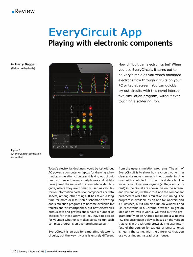
•Review
110 | January & February 2015 | www.elektor-magazine.com
Today’s electronics designers would be lost without AC power, a computer or laptop for drawing sche-matics, simulating circuits and laying out circuit boards. In recent years smartphones and tablets have joined the ranks of the computer-aided bri-gade, where they are primarily used as calcula-tors or information portals for components or data sheets, among other things. It has taken a long time for more or less usable schematic drawing and simulation programs to become available for tablets and/or smartphones, but now electronics enthusiasts and professionals have a number of choices for these activities. You have to decide for yourself whether it makes sense to run such complex programs on a smartphone screen.
EveryCircuit is an app for simulating electronic circuits, but the way it works is entirely different
from the usual simulation programs. The aim of EveryCircuit is to show how a circuit works in a clear and simple manner without burdening the user with a whole lot of technical details. The waveforms of various signals (voltage and cur-rent) in the circuit are shown live on the screen, and you can adjust the circuit and the component parameters while the simulation is running. The program is available as an app for Android and iOS devices, but it can also run on Windows and Linux systems in a Chrome browser. To get an idea of how well it works, we tried out the pro-gram briefly on an Android tablet and a Windows PC. The description below is based on the version that runs in the Chrome browser. The user inter-face of the version for tablets or smartphones is nearly the same, with the difference that you use your fingers instead of a mouse.
By Harry Baggen (Elektor Netherlands)
EveryCircuit AppPlaying with electronic components
How difficult can electronics be? When you use EveryCircuit, it turns out to be very simple as you watch animated electrons flow through circuits on your PC or tablet screen. You can quickly try out circuits with this novel interac-tive simulation program, without ever touching a soldering iron.
Figure 1. An EveryCircuit simulation on an iPad.

EveryCircuit App
www.elektor-magazine.com | January & February 2015 | 111
A trial version of EveryCircuit is available [1], which is handy if you want to first try it yourself. However, the drawing area for the schematic is severely limited in the trail version and only allows six or so components to be placed. This restriction is removed when you purchase a license code (good for one year), which is available in the Elektor Store [2]. Then you have access to the user community and can store schematics in the cloud, which makes them available on multiple devices (e.g. tablet and PC). You can keep your circuit diagrams private or share them with the community so they are available to everyone. A large number of circuits are now available from the community.
Using the programThe first thing you notice after starting up the program is that the user interface is very sparse. Since there isn’t any user guide (at least not yet), it takes a bit of time to figure out how everything works. A toolbar with component icons is located at the top. It includes the most common types, such as voltage and current sources, resistors, transformers, transistors, switches, logic gates and even a 555 timer IC. There is no library of type numbers, but the properties of individual components placed in the circuit can be adjusted.When you click a component icon, the compo-nent appears in the drawing window and can be
dragged to the right place. After that you can draw connecting lines by clicking on the leads of two components. When you select a component, several icons are shown on the bar at the bottom of the screen. You can use them to rotate, flip or delete the component or adjust its properties. When you click the wrench icon, all possible set-tings of the component are displayed and you can adjust them using a knob on the right. You can also use the eye icon to select the waveform you want to see during the simulation. When you do this with a component, the current waveform is shown, and if you click on a connection the voltage waveform is shown. If you click again on the selected component or on a blank area in the drawing area, two triangles marked “t” and “f” appear at the bottom (the latter only with the registered version). They stand for the two sim-ulation options: transient and frequency. Click-ing one of these symbols starts the simulation. If you select frequency analysis you see a Bode chart, very much like other simulation programs. What’s especially interesting with EveryCircuit is the transient analysis function, since it allows you to observe the behavior of the circuit and view the currents flowing through the components. If you simply select a voltage source, a resistor and an LED and connect them together, you can see right away how much current is flowing through the component and the voltage drop over the
Figure 2. The EveryCircuit start page in the Chrome browser. Example circuits and circuits from other users are shown on the left, the schematic window with the simulation waveforms is in the middle, and the current project and its description are on the right.
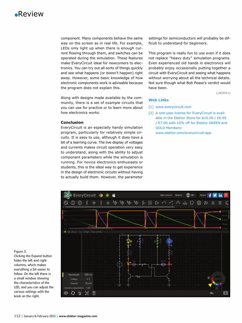
•Review
112 | January & February 2015 | www.elektor-magazine.com
settings for semiconductors will probably be dif-ficult to understand for beginners.
This program is really fun to use even if it does not replace “heavy duty” simulation programs. Even experienced old hands in electronics will probably enjoy occasionally putting together a circuit with EveryCircuit and seeing what happens without worrying about all the technical details. Not sure though what Bob Pease’s verdict would have been.
(140334-I)
Web Links
[1] www.everycircuit.com
[2] A one-year license for EveryCircuit is avail-able in the Elektor Store for $10.00 / £6.95 / €7.00 with 10% off for Elektor GREEN and GOLD Members: www.elektor.com/everycircuit-app
component. Many components behave the same way on the screen as in real life. For example, LEDs only light up when there is enough cur-rent flowing through them, and switches can be operated during the simulation. These features make EveryCircuit ideal for newcomers to elec-tronics. You can try out all sorts of things quickly and see what happens (or doesn’t happen) right away. However, some basic knowledge of how electronic components work is advisable because the program does not explain this.
Along with designs made available by the com-munity, there is a set of example circuits that you can use for practice or to learn more about how electronics works.
ConclusionEveryCircuit is an especially handy simulation program, particularly for relatively simple cir-cuits. It is easy to use, although it does have a bit of a learning curve. The live display of voltages and currents makes circuit operation very easy to understand, along with the ability to adjust component parameters while the simulation is running. For novice electronics enthusiasts or students, this is the ideal way to get experience in the design of electronic circuits without having to actually build them. However, the parameter
Figure 3. Clicking the Expand button hides the left and right columns, which makes everything a bit easier to follow. On the left there is a small window showing the characteristics of the LED, and you can adjust the various settings with the knob on the right.
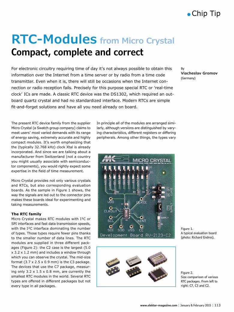
www.elektor-magazine.com | January & February 2015 | 113
•Chip Tip
The present RTC device family from the supplier Micro Crystal (a Swatch group company) claims to meet users’ most varied demands with its range of energy saving, extremely accurate and highly compact modules. It’s worth emphasizing that the (typically 32.768 kHz) clock Xtal is already incorporated. And since we are talking about a manufacturer from Switzerland (not a country you might usually associate with semiconduc-tor components), you would rightly expect some expertise in the field of time measurement.
Micro Crystal provides not only various crystals and RTCs, but also corresponding evaluation boards. As the sample in Figure 1 shows, the way the signals are led out to the connector pins makes these boards ideal for experimenting and taking measurements.
The RTC familyMicro Crystal makes RTC modules with I²C or SPI interfaces and fast data transmission speeds, with the I²C interface dominating the number of types. Those types require fewer pins thanks to the smaller number of data lines. The RTC modules are supplied in three different pack-ages (Figure 2): the C2 case is the largest (5.0 x 3.2 x 1.2 mm) and includes a window through which you can observe the crystal. The mid-size format (3.7 x 2.5 x 0.9 mm) is the C3 package. The devices that use the C7 package, measur-ing only 3.2 x 1.5 x 0.8 mm, are currently the smallest RTC modules in the world. Several RTC types are offered in different packages but not every type in all packages.
In principle all of the modules are arranged simi-larly, although versions are distinguished by vary-ing characteristics, different registers or differing peripherals. Among other things, the types vary
By Viacheslav Gromov (Germany)
RTC-Modules from Micro CrystalCompact, complete and correctFor electronic circuitry requiring time of day it’s not always possible to obtain this information over the Internet from a time server or by radio from a time code transmitter. Even when it is, there will still be occasions when the Internet con-nection or radio reception fails. Precisely for this purpose special RTC or ‘real-time clock’ ICs are made. A classic RTC device was the DS1302, which required an out-board quartz crystal and had no standardized interface. Modern RTCs are simple fit-and-forget solutions and have all you need already on board.
Figure 2. Size comparison of various RTC packages. From left to right: C7, C3 and C2.
Figure 1. A typical evaluation board (photo: Richard Endres).
•Chip Tip
114 | January & February 2015 | www.elektor-magazine.com
or the ‘Self-Recovery System’. The last-named occurs when the internal State Machine hangs up. There are two Timer Registers, one each for the LSB and the MSB. These make use of a 16-bit downwards counter, the timing of which is set down in the Control Registers. Here too is where you can indicate whether the Timer should be recharged automatically following the (possi-ble) Interrupt on reaching the final value of ‘0’. Most Interrupts need to be enabled in the Con-trol Registers. Alternatively there are also Flags that show whether the event has already taken place. These need to be reset again after every event, even if the Interrupts are not activated. There are also Flags that indicate which event triggered the Interrupt. These must be reset fol-lowing an Interrupt, in order that the INT pin is also set back to a logic ‘1’.
In the Power Control block we have an elaborate system that recognizes certain defined voltage levels and, depending on these, (for example) switches the internal resistance between VDD and VBACKUP. In this way an optional Gold Cap connected to VBACKUP is recharged again. If the supply voltage should fall below 2.1 V (VLOW1), CLKOUT, the temperature sensor and the write facility to the Register are deactivated. The I²C interface still remains active, albeit with reduced speed.
Booting up and in useAfter connecting the supply voltage and perform-ing the Power-On Reset that follows, most func-tions such as the Alarm or the Timer are not yet active. The manufacturer recommends that after each Power-On Reset you also perfume a Sys-
in current consumption and level of accuracy. Table 1 provides an overview of these variations. The ‘Voltage’ column begins with the lowest value at which the time keeping function alone will operate. The interface and built-in temperature sensor are available only at higher voltages. Spe-cial functions relating to accuracy of the time were not considered.
Inner workingsThe internal elements of the RTC modules are explained next, using the type RV-3029, which provides an I²C interface, as our example. In the block diagram in Figure 3 you can see the tem-perature sensor mentioned already. It is not for assessing the ambient temperature but performs the vital function of temperature compensation for maintaining the crystal frequency. For this the manufacturer uses special registers to file the correctional data relating to the crystal in question. Users can of course overwrite this but they need to know exactly what they are doing.
At upper left we find the crystal oscillator, fol-lowed by the divider for the temperature com-pensation logic, which increments the Seconds Register directly. All register values are held in BCD format. The Hours Register includes an extra bit for selecting either 12 or 24-hour mode. The block labeled ‘Output Control’ supplies the out-put, according to how CLKOE is set, with a clock pulse CLKOUT. The frequency output ranges from 1 to 32.768 Hz and is declared in the EEPROM Control Register using bits FD1 and FD0.When an Interrupt occurs, a logical ‘0’ appears on the INT pin. An Interrupt can be triggered by either the Timer, the Alarm, the Power Control
Table 1. Data for the various RTC modules.
Type and package designation
Accuracy (25°C)
Interface Voltage Current Characteristics
RV4162-C7 ±20 ppm I2C 1.0 - 4.4 V 350 nA Submin. package
RV8523-C3 ±20 ppm I2C 1.2 - 5.5 V 130 nA Low current
RV8564-C2/C3 ±20 ppm I2C 1.2 - 5.5 V 250 nA Standard
RV3029-C2/C3 ±3 ppm I2C 1.3 - 5.5 V 800 nA Extremely accurate
RV1805-C3 ±20 ppm I2C 1.5 - 3.6 V 50 nA Very low current
RV8803-C7 ±10 ppm I2C 1.5 - 5.5 V 250 nA Submin. package
RV2123-C2/C3 ±20 ppm SPI 1.1 - 5.5 V 130 nA Low current
RV049-C2/C3 ±3 ppm SPI 1.3 - 5.5 V 800 nA Extremely accurate

Microcrystal RTC Modules
www.elektor-magazine.com | January & February 2015 | 115
tem Reset (with the help of the SysR bits in the Control Reset Register). Next you should spec-ify, using the Control Register, which events can trigger an Interrupt and which peripherals should be active. It’s important to provide a 10-nF filter capacitor close to the IC on the supply voltage rails. You can find detailed information on use and operation in the extremely comprehensive Application Manual [1].
(130580)
Web Link
[1] www.microcrystal.com/index.php/products/real-time-clocks
OUTPUTCONTROL
OSC
I2C-BUS
2-wire
Serial
Interface
DIVIDER and
TEMPERATURE COMPENSATION
LOGIC
SYSTEMCONTROL
LOGIC
TEMPERATURE SENSOR
32.768 kHzXtal
CLKOUT
CLKOE
INT
SCL
VDD
VSS
POWER CONTROL
VBACKUP
SDA
On / OFF Ctrl
Status
29
00
Year AlarmMonth Alarm
Weekday AlarmDay AlarmHour Alarm
Minutes Alarm
YearMonth
WeekdayDate
HoursMinutesSeconds
IRQ FlagsIRQ Ctrl
User EEPROM
User RAM
Temperature °KTimer HighTimer Low
Seconds Alarm
User RAM
2820
Xtal T0 TempXtal Temp-Coef
EE Ctrl2 Bytes
388 Byte
Xtal Deviation
3F
Rst Ctrl
30
08
10
18
Figure 3. Block diagram of RTC module RV-3029 (source: datasheet).
Computing power and global interconnectivity are pushing tech innovation into overdrive. Pioneering technologies and creative workarounds affect even the couch potato 24/7. Tech the Future reports on technology strides that shape the future — yours included.
Follow Tech the Future
www.techthefuture.com
Fascinated by technology’s impact on the future?Check out Tech the Future!
Advertisement

•Industry
116 | January & February 2015 | www.elektor-magazine.com
Bluetooth CoinsEM Microelectronic’s COiN is a versatile, high performance, low power solution that can be deployed any, where iBeacon™ technology is used, but which also supports wireless sensor networking and many other applications over Bluetooth® Smart (Bluetooth with a Low Energy Core Configuration) wireless communications. Due to its unique design, COiN consumes less than 20 μA average in a typical application, resulting in more than 18 months’ operation from a single CR2032 battery, which is included in the beacon. COiN also contains a built-in pushbutton switch, thus
Phoenard Prototyping PlatformOn the Atmel booth we once again ran into the guys that came up with the Phoenard, the all-in-one Arduino-compatible prototyping gadget as they like to call it. (We had met them previously at the Maker Faire in Rome.)
The Phoenard is a prototyping platform that looks like a gamepad. Besides being an Arduino Mega clone — the Phoenard also has an Atmel ATmega2560 8-bit AVR microcontroller under the hood — its extra features like a touchscreen, an SD card and Bluetooth allow you to use it as a sort of simple tablet too. The Phoenard is an Arduino-compatible hand-held device with an SD card on which applications (sketches in Arduino speak) can be stored. With the PC-based Phoenard Operating Environment (OE) the sketches can be modified and organized and icons can be drawn and attributed so that the sketches can be accessed easily using the touch-screen. This is very similar to, say, an iPad with iTunes, but cheaper and developed for makers. Programming the Phoenard is easy as Arduino programming (it even has an on-board programming course), using it is easy too; everything is designed to be easy and open. It is a sort of entry level development platform for people who
are interested in tablet and smartphone programming but who lack the skill, patience and/or money to get an app in the Apple store. The Phoenard has attracted a lot of attention over the last months — it even won several prestigious awards — and by the time of publishing this edition the Phoenard team should have completed their successful crowdfunding campaign on Kickstarter.
www.phoenard.com
Face Recognition goes EmbeddedFace and gesture recognition functionality can be added to any embedded system for medical, industrial control, digital advertising, security and other applications, following the launch by Omron Electronic Components Europe of a Human Vision Component (HVC) module. The module handles all the complexity of seeing and recognizing faces, bodies and gestures, all the integrator needs to do is read the data output and program the system to react appropriately. The new Omron HVC integrates ten key image sensing functions with a camera in a module sized just 60 x 40 mm. Developers can detect a human face, hand or body, and implement face recognition, gender detection, age estimation, mood estimation, facial pose estimation, gaze estimation, and blink estimation. In each case the module returns a value together with a degree of certainty, allowing the programmer to config-ure the response appropriately for each individual application. HVC is designed in
a very compact configuration and can be easily integrated into an established system or implemented as part of a new design. Key features of the module include speed and consistency of response, and the distance over which it can take readings. For example, HVC can capture, detect and recognize a face over a distance of 1.3 m in 1.1 s and will provide a confidence level with its reading. Blink and gaze estimation takes under 1 s. The module can evaluate the subject’s mood based on one of five expressions. It can also detect a human body up to 2.8 m away and a hand at a distance of 1.5 m. The detection angle of the module is specified as 49° horizontally and 37° vertically.
http://components.omron.eu/Product-details/HVC (140482-VIII)
seen @
electronica 2014

news & new products
www.elektor-magazine.com | January & February 2015 | 117
guaranteeing that your beacons have a full charge when they are deployed. Integrated red and green LEDs provide users with feedback about the device’s operating mode. Just click and stick! The COiN’s integrated printed circuit antenna not only minimizes cost, but maximizes communication range. At the 0 dBm output power setting, EM Microelectronic’s beacons can be detected 75 meters away by an iPhone® 5S, and at maximum output power, that distance extends up to 120 meters. Due to COiN’s optimized circuit architecture, it is completely immune to over-the-air attacks, meaning that a well-placed beacon is very secure. It cannot be “hacked” or modified unless the perpetrator has complete physical possession of the device. COiN is shipped pre-programmed, complete with a Renata CR2032 battery and a weatherproof plastic enclosure for easy deployment, making it suitable for use at outdoor music festivals, sporting events and arenas, and anywhere a beacon is required to withstand the elements. Though COiN is available in-stock pre-pro-grammed and with a standard housing, the standard COiN hardware and firmware are easily modified to fit most applications. At the most basic level, COiN firmware can easily be modified to change the UUID, MAJOR ID, MINOR ID, output power, and beacon interval. These changes are useful for adapting the beacon for whatever smartphone software appli-cation/API is being used, segregating beacon populations and sub-populations, and for optimizing battery lifetime based on the desired use case. Should more extensive firmware modifications be desired, EM offers a complete development kit. The COiN Development Kit includes five (5) COiN beacons, programming board and programming cable and is fully com-patible with EM’s line of software development tools for the EM6819; EM’s ultra-low power microcontroller. Using these tools, customers have complete control over the firmware and can create their own Bluetooth Smart advertising packets and transmit real-time sensor data such as temperature, light level, battery voltage, or other physical phenomena.
www.emmicroelectronic.com
seen @
electronica 2014
Dual Analog iOS Oscilloscope Upgraded to Lightning ConnectorOscium’s iMSO-204L dual analog iOS oscilloscope transforms the iPad, iPhone, and iPod touch into an ultra-portable, two-channel oscil-loscope. Since Apple changed their connector, Oscium has been working to bring native compatibility to our customers. iMSO-204L is the solution to the connector change. It represents the third generation of handheld engineering tools from Oscium. iMSO-204L has the follow-ing characteristics:2 Analog + 4 Digital Channels, 50 MSPS, 5 MHz Bandwidth, 200ns/div-10s/div. Oscium revolutionized test and measurement when introducing the first oscilloscope with a capacitive touchscreen.
Oscium has paved the way for a truly intuitive experience. iMSO2 software features include the following:• Waveforms can be paused and zoomed• Single-shot waveform capture• While zooming the horizontal and vertical scales, immediate feedback is provided• AirPlay compatibility (oscilloscope display can be mirrored onto com-patible projectors). Perfect for live demonstrations in the classroom.iMSO-204 works with a free downloadable app available in the Apple App Store. Be sure to download the iMSO2 app with the iMSO-204L hardware.iMSO2 software is free in the Apple App Store. The iMSO2 app requires iOS version 5.0 or higher. Compatible products include: iPhone 5C, iPhone 5S, iPhone 5, iPad Mini, iPad Air, iPad 4, iPod touch [5th generation]. iMSO-204 hardware can be purchased for $399.97 from Oscium directly or from its partners.
www.oscium.com (140549-V)

118 | January & February 2015 | www.elektor-magazine.com
Compact Screw Terminal C’s with High Ripple Current CapabilityTDK Corporation presents three new series of EPCOS aluminum electrolytic capacitors with screw terminals. They are characterized by their high ripple current capability and simultaneously highly compact dimensions. The capaci-tors of the new B43703 series are designed for rated voltages from 350 V DC to 450 V DC and cover a capacitance range from 1500 µF to 22,000 µF. They are up to 20 percent smaller than those of the predecessor series at the same ripple current capability. The new types have diameters of 51.6 mm to 90.0 mm; their heights range from 80.7 mm to 197.0 mm.The new B43704* series offers not only a ripple current capability up to 25 percent higher than for the predeces-sor series, but also smaller dimensions. Their diameters are also between 51.6 mm and 90.0 mm with heights of between 80.7 mm and 221.0 mm. These capacitors are designed for rated voltages from 350 VDC to 550 VDC. Their capacitance extends from 820 µF to 22,000 µF.In the new B43705 series, the ripple current capability was increased by up to 40 percent compared with the pre-decessor series, while maintaining the same compact dimensions. These capacitors have diameters ranging from 51.6 mm to 90.0 mm and insertion heights from 80.7 mm to 221.0 mm. They are designed for rated voltages from 350 V DC to 450 V DC and their capacitance range extends from 1000 µF to 18,000 µF.All three new EPCOS series are designed for a maximum operating temperature of 85 °C and attain a useful life of 12,000 hours. The series are also offered in B43723, B43724 and B43725 versions. These types additionally have a
threaded stud on the base of the can for mounting the capacitors.The main applications of the new EPCOS aluminum electrolytic capacitors are converters in industrial electronics.
www.epcos.com (140482-VI)
100 Kwaveforms Per Second Barrier BrokenThe latest release of the PicoScope 6 software for PC oscilloscopes has a greatly improved continuous update rate of over 100,000 waveforms per second. This is faster than any other PC oscilloscope, and beats many expensive benchtop oscilloscopes too. As Managing Director Alan Tong explained, “When you are looking for an intermit-tent glitch, a faster waveform update rate lets you find it more quickly. PicoScope’s new fast persistence display mode can collect thousands of waveforms per second, overlaying them all with color-coding or intensity-grading
to show which areas are stable and which are intermittent. Faults that previously took minutes to find now appear within seconds.”The new fast persistence mode is available on all Pico oscilloscopes from the Pico-
Scope 3000 Series upwards with the PicoScope R6.10.2 beta software or later. Using dedicated hardware inside the scope, this mode can achieve update rates up to 120,000 waveforms per second on USB 3.0 deep mem-ory scopes such as the PicoScope 6000C/D Series. With USB 2.0 deep memory scopes the update rate can now reach 80,000 waveforms per second.Even faster capture rates are possible using rapid trig-ger mode, which collects bursts of up to 10,000 wave-forms at a rate of up to 1 million waveforms per second into segmented memory for later viewing. See our data sheets for the rapid triggering performance of individ-ual PicoScope models.All PicoScope users can download the latest software update free of charge from the picotech website. Even if you don’t have a PicoScope, you can download the software and run it in demo mode to find out how powerful it really is.
www.picotech.com (140549-I)

ArduinoNow Available @ Elektor!
Further Information and Ordering at www.elektor.com/development/arduino
£23.95 • € 27.50 • US $38.00
Features Microcontroller ATmega328 Operating Voltage 5V Input Voltage 7-12V (recommended)Input Voltage (limits) 6-20V Digital I/O Pins 14 (of which 6 provide PWM output) PWM Channels 6 Analog Input Pins 6 DC Current per I/O Pin 40 mA DC Current for 3.3V Pin 50 mA Flash Memory 32 KB (of which 0.5 KB used by bootloader)SRAM 2 KB EEPROM 1 KB Clock Speed 16 MHz
ARDUINO UNO REV.3The most popular board with its ATmega328 MCU
£21.95 • € 24.90 • US $34.00
Features Microcontroller ATmega32u4 Operating Voltage 5V Input Voltage 7-12V (recommended)Input Voltage (limits) 6-20V Digital I/O Pins 20 (of which 7 provide PWM
output) PWM Channels 7 Analog Input Pins 12 DC Current per I/O Pin 40 mA DC Current for 3.3V Pin 50 mA Flash Memory 32 KB (of which 4 KB used
by bootloader)SRAM 2.5 KB EEPROM 1 KB Clock Speed 16 MHz
ARDUINO LEONARDOEspecially good for USB applications
£46.95 • € 53.90 • US $73.00
Features Microcontroller ATmega328 Operating Voltage 5V Input Voltage 7-12V (recommended)Input Voltage (limits) 6-20V Digital I/O Pins 14 (of which 4 provide PWM
output) Arduino Pins reserved 10 to 13 used for SPI
4 used for SD card 2 W5100 interrupt (when bridged)
Analog Input Pins 6 DC Current per I/O Pin 40 mA DC Current for 3.3V Pin 50 mA Flash Memory 32 KB (of which 0.5 KB used
by bootloader)SRAM 2 KB EEPROM 1 KB Clock Speed 16 MHz
ARDUINO ETHERNETNetworking has never been easier
£46.95 • € 52.90 • US $72.00
Features Microcontroller ATmega2560 Operating Voltage 5V Input Voltage 7-12V(recommended) Input Voltage (limits) 6-20V Digital I/O Pins 54 (of which 15 provide
PWM output) Analog Input Pins 16 DC Current per I/O Pin 40 mA DC Current for 3.3V Pin 50 mA Flash Memory 256 KB (of which 8 KB used
by bootloader)SRAM 8 KB EEPROM 4 KB Clock Speed 16 MHz
ARDUINO MEGALike the Uno but with more memory and I/O
£46.95 • € 52.90 • US $72.00
Features Microcontroller AT91SAM3X8E Operating Voltage 3.3V Input Voltage 7-12V (recommended)Input Voltage (limits) 6-20V Digital I/O Pins 54 (of which 12 provide PWM
output) PWM Channels 12 Analog Input Pins 12 Analog Outputs Pins 2 (DAC) DC Current per I/O Pin 130 mA DC Current for 3.3V Pin 800 mA DC Current for 5V Pin 800 mA Flash Memory 512 KB (all available for the
user applications)SRAM 96 KB (two banks: 64KB and
32KB) Clock Speed 84 MHz
ARDUINO DUE32-bit power thanks to an ARM processor
Features AVR Arduino microcontroller Microcontroller ATmega32u4Operating Voltage 5VInput Voltage 5VDigital I/O Pins 20PWM Channels 7Analog Input Channels 12DC Current per I/O Pin 40 mADC Current for 3.3V Pin 50 mAFlash Memory 32 KB (of which 4 KB used
by bootloader)SRAM 2.5 KBEEPROM 1 KBClock Speed 16 MHz
Features Linux microprocessorProcessor Atheros AR9331Architecture MIPS @400 MHzOperating Voltage 3.3VEthernet IEEE 802.3 10/100Mbit/sWiFi IEEE 802.11b/g/nUSB Type-A 2.0 Host/DeviceCard Reader Micro-SD onlyRAM 64 MB DDR2Flash Memory 16 MBPoE compatible 802.3af card support
ARDUINO YÚNTwo processors
Now Available @ Elektor!
10% OFF for
GREEN and
GOLD Members
www.elektor.com/development/arduinowww.elektor.com/development/arduino
£60.95 • € 69.95 • US $95.00
140424 Arduino adv UK EL.indd 1 24-04-14 17:06
•Regulars
120 | January & February 2015 | www.elektor-magazine.com
Growing tired of working the lights by hand I started the design of the Digi–Disco, a light con-troller that uses sampled audio to drive lights with no manual switching. Except for occasionally changing the mode of operation, no interaction is needed after setup. But since I was a full-time college student construction could not start until summer break.
The designI wanted the controller to be as automatic as pos-sible so using the music that was being played to change light patterns seemed to be a reasonable approach. Also the disco music craze made light displays that moved back and forth, in a chasing fashion, very popular. So chaser light patterns were required for the most effect. In addition,
the lights had to be powerful enough to fill school gymnasiums with light. Each ‘gig’ that we did was at a different location which necessitated easy setup, disassembly and storage.Microcontrollers were not ubiquitous as they are now so I used discrete digital logic and ana-log components consisting of very common–in 1978–74xx series TTL ICs for the digital portion, bipolar ICs for analog and a 555 timer. Without eBay, Amazon or surplus websites of today I used devices that were already in my parts bin or available from local electronic shops, surplus stores or Radio Shack. Mail order was popular but was inconvenient and slow. My local Radio Shack, a quick bicycle ride away, was the source for the voltage comparators, enclosures, and tri-acs. CMOS digital logic and 74LS series TTL could have been used but they were not readily avail-able to me and were more expensive. The Digi-Disco was built in two pieces. One piece was a console, shown in Figures 1 and 2, which had most of the controller circuitry, selected the mode of operation and sampled the audio. The second piece was a remote box, shown in Fig-ure 3, which contained the triacs used to switch the lights and supplied power to the console. The console and the remote box were connected with an eleven conductor cable. The final ver-sion powered four light bars that consisted of six 75-watt color spot lights each. Each of the six spot lights were switched individually but in common between all four light bars. Two of the light bars were hung above the DJ stage with the other two light bars on either side of the stage sitting on top of the massive Voice of the Theater speakers we used for the sound system. The remote box was hung between the two light bars above the DJ stage; eight conductor cables were used to connect to the light bars. Consuming 1800 watts
By Dan Koellen (USA)
Digi-Disco 1978Dance till the 7406 explodesIt is spring 1978, “Burn Baby Burn, Disco Inferno” is blaring through a Highschool gymnasium full of kids dancing to the latest disco tunes. I am sitting on the stage next to the DJ checking sound levels and mashing mechanical switches struggling to make our gel lights change with the beat of the music.
Retronics invades elektor.tv
Using solid-state equipment Retronics’ very first video was recorded and is now posted at www.elektor.tv. Watch visitors to the electronica 2014 show in Munich confronted with the 1976 ElektorScope and a Rohde & Schwarz 1960’s tubed signal generator that gets opened up for inspection. More Retronics video clips and rare footage will be uploaded to elektor.tv in the near future.
www.elektor-magazine.com | January & February 2015 | 121
peak (16 Ap), not only did we completely fill a gymnasium with dancing light, a separate power circuit was required just for the lights.For easy set up and disassembly all connections were made with cables that plugged into the con-sole, remote box and light bars. The cables had different number of pins to prevent plugging in the wrong socket. And each light bar was color coded for orientation and light layout. The most difficult part of the set up was making sure the color sequence of the light bulbs was correct.
The circuitThe original hand drawn schematic is shown in Figure 4, no schematic drawing programs were available to college students at that time. All the circuitry in the schematic is in the console except for the remote box in the lower right with the triacs and power transformer. The audio was sampled directly from a speaker terminal and brought to the ‘audio input’ poten-tiometer and diode on the left side of the sche-matic. I used a 1N34A germanium diode for the lower Vf than a silicon diode, the 10-kΩ pot is used to adjust the level of the audio signal. The diode provides rectified audio, noted as A.R. in the schematic. The rectified audio is raw with no filtering, this seemed to work just fine for the effect that was sought after. I had thought about using an active rectifier and filtering but deemed it not needed.The rectified audio is used in two different parts of the circuit; one that changes the lights according to the amplitude of the audio and the other that advances a counter in response to the audio. In the middle of the schematic are LM339 (the build used Radio Shack’s version: RS339) voltage com-parators (IC3 and IC4), they are referenced to a resistor ladder so their outputs go low when the rectified audio exceeds the corresponding resistor ladder node. As the level of audio increases, the number of lights that turn on increases, like a large VU meter. The resistor ladder was designed for the best response to audio, not for precise measurement or constant load.For the chaser light effect a pulse generator, a 555 astable multivibrator, is used to clock the 74190 up/down decade counter. The BCD output of the decade counter is decoded to decimal by a 7442; as shown in the upper part of the sche-matic. The decade counter is advanced by pulses directly from the 555, pulses gated by the 7408 AND gate and voltage comparator or the output
of the comparator itself. The 74190 is a wonder-ful device for this application with its dedicated input for count direction and it is presettable; two characteristics the then widely used 7490 decade counter does not have. I was able to make the lights chase in three patterns: counting up from channel 1 to channel 6 resetting to chan-
Figure 1. The console manages the operation of the light show; the wear and tear seen here shows the console was used quite often. In the lower right corner, PHASE is the identity I used when working sound and lights for the dance gigs.
Figure 2. The circuitry contained in the console was built on a piece of perforated board. Black soot from the 7406’s catastrophic failure can be seen in the top center. To the left is the tube of replacement devices that was brought to each gig.
Figure 3. The remote box contained the triacs to switch the lights. At the bottom are the sockets for connection to the light bars; the console cable plugged into the socket on the bottom left. The transformer supplied stepped down AC to the console.

•Regulars
122 | January & February 2015 | www.elektor-magazine.com
TTL devices were very cheap. I decided to build the controller this way knowing that I would have to have a supply of replacement ICs on hand for quick replacement. Don’t do this with your designs—it is not safe or reliable. The 7406 driv-ers did catastrophically fail during the first gig the Digi-Disco was used. I found that avoiding songs with a lot of distortion and isolating the power feed for the lights from the sound system power avoided failure.
OperationThe Digi-Disco worked really well especially with Disco’s steady bass beat it was designed to take advantage of. It turned out to be easy to set up and take down. During operation I kept the counter in the up and down and gating mode for the majority of the time; the 555 was adjusted for a moderate speed of about 2 Hz. This made the lights dance in what looked like a random pattern that appeared to move with the beat of the music. When the DJ was talking the audio level mode (i.e. the VU meter) worked well and was a nice change of pace.The kids at the dances really liked the light show and word spread about the Digi-Disco. Because of this we were able to increase the number of gigs that we played and our fee also increased. And, best of all, no more mashing of mechanical switches; the Digi-Disco ran on its own very well with little operator interaction needed.
Compared to Digi-Disco, Elektor’s 1984 Pro-grammable Disco Array is much more advanced with its 32 light patterns in memory, CMOS ICs, 19-inch rack housing, and 7-segment readouts. The project was commemorated in Retronics, February 2008.
(140420)
nel 1; counting down from channel 6 to channel 1 resetting to channel 6; and counting up and down from channel 1 to channel 6 back down to channel 1 and repeating. The 7470 is a JK flip flop with preset and clear, which I used to set the direction of 74190 counting while loading either 0 or 5 depending on the count direction. For up and down counting the direction of counting was flipped at 0 and 5 so the next pulse advances in the opposite direction, the preset was not used.Since the rectified audio is always connected to both the analog level circuit and the digital counter circuit the mode of operation is selected by connecting the appropriate outputs to the 7408 (IC1 and IC2) and 7406 output drivers by the mode switch in the middle of the schematic. This allowed the mode of operation to be changed very quickly. The 7406 is a high voltage open collector invertor that can sink 40 mA. The triacs used to switch the lights commanded at least 50 mA of gate current to turn on. The driver had to sink that current when the triac is off so I soldered two 7406s piggy back to handle that much cur-rent (only a single device is shown in Figure 2). When the 7406 driver output was off (i.e. open) the gate current was sent over the eleven con-ductor cable to trigger the corresponding triac in the remote box.You may notice that the triacs are not electri-cally isolated. In 1978 opto-isolators were very expensive, especially for a college student, and
Retronics is a monthly section covering vintage electronics including legendary Elektor designs. Contributions, suggestions and requests are welcome; please telegraph [email protected]
Figure 4. The hand drawn schematic for the Digi-Disco. Phase Sound and Light Consultants was the entity identification I used at that time.
More 74xx TTL and 40xx CMOS!on the Elektor 1980s DVDwww.elektor.com/eighties (shortly)

Ordering Information
www.elektor-magazine.com | January & February 2015 | 123
ORDERING INFORMATIONTo order, contact customer service for your region:
USA / CANADAElektor US111 Founders Plaza, Suite 300East Hartford, CT 06108USAPhone: 860.289.0800E-mail: [email protected]
Customer service hours: Monday-Friday 8:30 AM-4:30 PM EST.
UK / ROWElektor International Media78 York StreetLondon W1H 1DPUnited KingdomPhone: (+44) (0)20 7692 8344E-mail: [email protected]
Customer service hours: Monday-Thursday 9:00 AM-5:00 PM CET.
PLEASE NOTE: While we strive to provide the best possible information in this issue, pricing and availability are subject to change without notice. To find out about current pricing and stock, please call or email customer service for your region.
COMPONENTSComponents for projects appearing in Elektor are usually available from certain advertisers in the magazine. If difficulties in obtaining components are suspected, a source willnormally be identified in the article. Please note, however, that the source(s) given is (are) not exclusive.
TERMS OF BUSINESSShipping Note: All orders will be shipped from Europe. Please allow 2–4 weeks for delivery.
ReturnsDamaged or miss-shipped goods may be returned for replacement or refund. All returns must have an RA #. Call or email customer service to receive an RA# before returning the merchandise and be sure to put the RA# on the outside of the package. Please save shipping materials for possible carrier inspection. Requests for RA# must be received 30 days from invoice.
PatentsPatent protection may exist with respect to circuits, devices, components, and items described in our books, magazines, online publications and presentations. Elektor accepts no responsibility or liability for failing to identify such patent or other protection.
CopyrightAll drawings, photographs, articles, printed circuit boards, programmed integrated circuits, discs, and software carriers published in our books and magazines (other than in third-party advertisements) are copyrighted and may not be reproduced (or stored in any sort of retrieval system) without written permission from Elektor. Notwithstanding, printed circuit boards may be produced for private and educational use without prior permission.
Limitation of liabilityElektor shall not be liable in contract, tort, or otherwise, for any loss or damage suffered by the purchaser whatsoever or howsoever arising out of, or in connection with, the supply of goods or services by Elektor other than to supply goods as described or, at the option of Elektor, to refund the purchaser any money paid with respect to the goods.
MEMBERSHIPSMembership renewals and change of address should be sent to the Elektor Membership Department for your region:
USA / CANADA UK / ROWElektor USA Elektor International MediaP.O. Box 462228 78 York StreetEscondido, CA 92046 London W1H 1DPPhone: 800-269-6301 United KingdomE-mail: [email protected] Phone: (+44) (0)20 7692 8344 E-mail: [email protected]
Do you want to become an Elektor GREEN or GOLD Member or does your current Membership expire soon?
Go to www.elektor.com/member.!
Ordering information EN.indd 123 12/12/14 09:54

•Regulars
124 | January & February 2015 | www.elektor-magazine.com
Hexadoku The Original Elektorized SudokuWelcome to the first Hexadoku installment of the year 2015. If you’ve not participated so far, now’s a good time to do so. Put the solder iron aside for an evening, get out a pencil and get cracking with this puzzle. Find the solution in the
gray boxes, submit it to us by email, and you automatically enter the prize draw for one of five Elektor book vouchers.
The Hexadoku puzzle employs numbers in the hexadecimal range 0 through F. In the diagram composed of 16 × 16 boxes, enter numbers such that all hexadecimal numbers 0 through F (that’s 0-9 and A-F) occur once only in each row, once in each column and in each of the 4×4 boxes (marked by the
thicker black lines). A number of clues are given in the puzzle and these determine the start situation.
Correct entries received enter a prize draw. All you need to do is send us the numbers in the gray boxes.
Solve Hexadoku and win!
Correct solutions received from the entire Elektor readership
automatically enter a prize draw for
five Elektor Book Vouchers worth $70.00 (£40.00 / €50.00) each,
which should encourage all Elektor readers to participate.
Participate!
Before March 1, 2015, supply your name, street address and the solution (the numbers in the gray boxes) by email to:
Prize winnersThe solution of the November 2014 Hexadoku is: 63D95.
The €50 / £40 / $70 book vouchers have been awarded to: Andrej Marn (Slovenia), Gerrit van Leeuwen (Netherlands), Jozef Bouwen (Belgium), and Francois Jongbloet (France)..
Congratulations everyone!
The competition is not open to employees of Elektor International Media, its business partners and/or associated publishing houses.
6 8 2 4 D B 3 5 C E 1 9 7 0 F A
C 5 0 7 A E F 2 B 6 D 3 1 8 4 9
1 9 3 A 0 6 4 7 F 2 5 8 B C D E
B D E F C 8 9 1 0 7 4 A 2 3 5 6
D 2 F 3 5 0 6 C A 9 7 1 8 E B 4
0 1 5 9 3 4 D A 2 8 E B F 6 7 C
4 7 6 E B F 8 9 D C 3 5 0 1 A 2
8 A B C 1 2 7 E 4 F 0 6 3 D 9 5
2 B 1 5 9 C 0 8 E D 6 F A 4 3 7
7 C 8 D E A 1 3 5 0 9 4 6 F 2 B
F E 9 6 2 D B 4 1 3 A 7 C 5 8 0
A 3 4 0 6 7 5 F 8 B 2 C D 9 E 1
E 0 A 1 F 9 C B 3 5 8 2 4 7 6 D
3 F 7 2 4 5 E D 6 1 B 0 9 A C 8
9 6 D B 8 3 A 0 7 4 C E 5 2 1 F
5 4 C 8 7 1 2 6 9 A F D E B 0 3
Gerard’s Columns
www.elektor-magazine.com | January & February 2015 | 125
By Gerard Fonte (USA)
When people challenge authority it isn’t always easy to determine if the ideas are
reasonable or not. Does dark matter really exist? Did life originate from spores in com-
et-dust that settled to earth over 3.5 billion years ago? Is climate change man-made? Was the Apollo 11
moon landing faked?
The Horse’s MouthProbably the first consideration is the source of the idea. If you actually know the person making the claims, you should have a pretty good idea if it’s reasonable or not. For example, cousin Bob is a down-to-earth student completing his BS degree in economics. While cousin Fred barely finished high-school and works in the mail-room of a local business. Both approach you for financial support in developing a new method of mining bit-coins. Who are you going to trust with your hard-earned cash?Most likely, you don’t know the principals personally. In this case, you can examine their reputation. It’s pretty obvious that more weight should usually be given to those who have experience or knowledge about the topic. However, there are exceptions to this rule. Biochemist, Linus Pauling was the only person to win two, unshared Nobel Prizes (the first at age thirty). But, in his sixties he began to promote the silly notion of mega-vitamin therapy for everything from colds to cancer. (Studies showed it didn’t work and too much of some vitamins can be unhealthy.) Nikola Tesla, father of AC power, (and also late in his life) claimed he could build a “death ray machine” that would down 10,000 enemy planes 200 miles away. And then there was that young, unknown Swiss patent examiner who had crazy ideas about the photoelectric effect and special relativity.Knowing a person’s affiliation can also give you clues. It was only a few years ago that the CEOs of all the major U.S. tobacco com-panies stated on TV and in front of a Senate panel that cigarettes didn’t cause cancer. Political, religious and business involvements (and other interests) can clearly warp a person’s lucidity.
Logic Doesn’t Apply HereOne huge indication that the idea is too far out is that the premise doesn’t make sense. Let’s start with “aliens exist”. Okay, the universe is a big place and there’s a very good chance that we are not alone. “Aliens have visited earth sometime in the past.” Less likely, but not totally unreasonable if aliens do exist. This is hard to prove or disprove. “Aliens visited earth 5000 years ago and built the Egyptian pyramids.” That rings the bell! Why would aliens come all the way across the gal-axy to build monuments on earth, made of stone? The more
someone tries to rationalize a reason, the more bizarre and convoluted the story gets. It simply isn’t reasonable.It’s a repeating theme. There’s the story that the World Trade Towers were destroyed in 2001 by nuclear reactors melting down in their basements. Let’s ignore the compelling visual evi-dence for the moment. How is it possible to secretly build two nuclear reactors in the basements of two of the most populous buildings in America without someone noticing? And why use nuclear reactors to destroy buildings anyway? Or was it just bad luck that they both melted down at virtually the same instant?“Global warming is a hoax created by a conspiracy of scien-tists.” How can anyone get American, Russian, Chinese, Israeli, Iranian, Indian and Pakistani scientists to cooperate on any-thing? If this truly was the case, we should immediately make that person the king of the world. There would be instant world peace, an end to hunger, and prosperity for all.
The Proof is in the PuddingOne characteristic of too-far-out ideas is the focus on a single, small aspect and blow it out of proportion. Another is the cre-ation of scientific sounding words. Then there are the factual errors (sometimes intentional), internal inconsistencies and conceptual mistakes. Oftentimes there is clear evidence of really bad thinking. Like logic that isn’t logical. In fact, there’s frequently an almost religious flavor to the discourse. That believing in the idea is an act of faith.Compare this to an unconventional idea that is grounded on reason and intelligence. The originator recognizes that the concept is different and addresses it directly. Often, side-by-side comparisons are made to the accepted theory showing strong and weak points of both. There is usually a profusion of factual evidence and academic references from a wide variety of sources. It is clear that substantial, high quality work was involved. This is the big reason why there are so many more crackpots than iconoclasts. It’s easy to spin a fantasy yarn about conspiracies. It’s very difficult to create something new and workable that others haven’t seen. True iconoclasts are rare.Billie Beane, 2003 manager of the Oakland Athletics baseball team, with Paul DePodesta, applied rigorous statistical analysis to create a winning team with a tiny payroll. While the movie “Moneyball” was somewhat dramatized, their impact on the game wasn’t. They literally changed how the game was played (at the front office). Now every baseball team places a much greater emphasis on numerical analysis when choosing players.Unusual ideas are often creative and fascinating. And, it’s easy to let your imagination take flight. Of course, there’s a big difference between entertainment and enlightenment. As practitioners of electronics it’s important to be able to sepa-rate science fiction from science fact.
(140515)
Crackpots versus Iconoclasts

1
2
3
4
5
1
3
2
4
•Store
126 | January & February 2015 | www.elektor-magazine.com
Includes 17 RPi Hardware Projects!Raspberry Pi Advanced Programming
This book starts with an introduction to the Rasp-berry Pi computer. The network interface of the RPi is explained in simple steps, demonstrating how the computer can be accessed remotely from a desk-top or a laptop computer. The remaining parts of the book cover the Python programming language, including advanced topics such as operating sys-tem calls, multitasking, interprocess synchroniza-tion and interprocess communication techniques. Network programming using UDP and TCP protocols is described (with examples). The Tkinter graphical user interface module (GUI) is described in detail with example widgets and programs. The last part of the book includes hardware projects based on using the advanced programming topics such as multitasking and interprocess communication techniques.358 pages • ISBN 978-1-907920-33-2£39.95 • € 44.95 • US $61.00
The Authority on Magnetics and InductorsTrilogy of Magnetics
A standard work in the hands of 15,000 design engi-neers, academics and researchers worldwide, Trilogy of Magnetics aims at familiarizing users with the char-
acteristics and applications of inductive components.The Trilogy comprises: Basic Principles, Components, and Applications. Highlights include calculation, dimen-sioning and construction of customer-specifi c trans-formers, an introduction to frequency compensation, Class-D amplifi er design and basic principles of Eth-ernet & Power-over-Ethernet. Furthermore Trilogy of Magnetics includes over 200 practical examples of fi lter circuits, audio & video circuits, interfaces, RF circuits, motor control units and SMPS. The book closes off with a keyword index and a summary of formulas.728 pages • ISBN 978-3-89929-157-5£42.95 • € 49.00 • US $67.00
The e-engineer’s delightUSB Hub feat. RS-232/RS-422/RS-485
This USB-to-serial converter allows you to connect two RS-232 and/or two RS-422/485 devices to your laptop or workstation through a standard USB (Universal Serial Bus) port. Thanks to the integrated USB hub the device does not ‘consume’ precious USB ports. Even better: It off ers you two extra USB ports! The device is compati-ble with new and legacy serial devices, and is perfect for instrumentation and manufacturing applications.Ready-built module Art.# 140033-91£95.95 • € 110.00 • US $149.00
110 Elektor Editions, Over 2500 ArticlesDVD Elektor 2000 through 2009
This DVD-ROM contains all circuits and projects pub-lished in Elektor magazine’s year volumes 2000 through 2009. The 2500+ articles are ordered chronologically by release date (month/year), and arranged in alphabet-ical order. A global index allows you to search specifi c content across the whole DVD. Every article is printable using a simple print function. This DVD is packed with ideas, circuits and projects that are ideal for any elec-tronics enthusiast, student or professional, regardless of whether they are at home or elsewhere.ISBN 978-1-907920-28-8£77.95 • € 89.00 • US $121.00
Fun to Build and Use ProjectsCreate 30 PIC Microcontroller Projects with Flowcode 6
This book covers the use of Flowcode® version 6, a state-of-the-art, all-graphical based code development tool, for the purpose of developing PIC microcontroller applications at speed and with unprecedented ease. Without exception, the 30 projects in the book are fun to build and use. A secret doorbell, a youth deterrent, GPS tracking, persistence of vision (POV), and an Internet webserver
4
3
1
2
15% DISCOUNTfor GREEN and GOLD Members!
www.elektor.com/rpi-book
Elektor Store EN 01-2015.indd 126 12/12/14 09:58
96
8
7
9
5
8
76
Books, CD-ROMs, DVDs, Kits & Modules
www.elektor-magazine.com | January & February 2015 | 127
are just a few examples of projects in the book waiting to be explored and mastered. This makes the publication a perfect source of projects constantly challenging your hardware and software skills as you progress, resulting in advanced microcontroller applications you can be proud of. All sources referred in the book are available for free download, including the support software.226 pages • ISBN 978-1-907920-30-1£30.95 • € 34.95 • US $48.00
Three Sizes for Cheap & Fast AVR PrototypingT-Boards
In response to the limitations posed by fi xed-design, Ardu-ino-style boards, Elektor has designed three mini-devel-opment boards that give developers more fl exibility while still hosting the microcontroller and its supporting com-ponents. We’re very excited to present the T-Boards! T-Boards are breadboard-friendly PCBs designed for sim-ple and swift microcontroller prototyping using an Atmel ATmega328, ATtiny24-44-84 and ATtiny25-45-85 micro-controllers. Additionally, each T-Boards has an integrated 3.3V and 5V-selectable power supply, which assists in reducing the number of required jumper wires and allows for experimenting with lower power usage. Programming the microcontroller can be done in-circuit (ICSP).Bundle of three boards Art.# 130581-94£33.95 • € 39.00 • US $53.00
Advanced Robot Technologies Made EasyAdvanced Control Robotics
It doesn’t matter if you’re building a line-follow-ing robot toy or tasked with designing a mobile system for an extraterrestrial exploratory mis-sion: the more you know about advanced robotics technologies, the better you’ll fare at your work-bench. Hanno Sander’s Advanced Control Robotics is intended to help roboticists of various skill lev-els take their designs to the next level with micro-controllers and the know-how to implement them eff ectively. Advanced Control Robotics simplifi es the theory and best practices of advanced robot tech-nologies. You’re taught basic embedded design the-ory and presented handy code samples, essential schematics, and valuable design tips (from con-struction to debugging).160 pages • ISBN 978-0-96301-333-0£34.95 • € 39.95 • US $54.00
Measurement and Control using your PCIO-Warrior Expension Board
Don’t throw out your old PCs and notebooks or leave them gathering dust in the basement! They can be a useful resource: by adding this universal interface card an old
PC can be pressed into service as a measurement and control hub. An IO-Warrior module on the I/F board takes care of USB communication, and source code is available that works with the free version of Visual Studio.Ready-built IO-Warrior56 moduleArt.# 130006-91 £34.95 • € 39.95 • $54.00
20 Amazing ProjectsRaspberry Pi Maker Kit
If you already own a Raspberry Pi and have done your fi rst electronic project then you are ready for this kit. It has all you need to bring 20 simple projects to life, including 62 parts and a 160 page handbook. Your Raspberry Pi is capable of more than you thought: Control your minicomputer by using spoons, dis-play your song titles on the LCD or build your own binary clock. With the graphic programming language Scratch this all can be done in a short time. Don’t worry. Programming skills are not needed. In case the ports at the GPIO aren’t enough, you will learn how to extend them.All-in-one kitArt.# 140539-91£69.95 • € 79.95 • US $108.00
8
5
also available as E-book
6 7
Elektor Store EN 01-2015.indd 127 12/12/14 09:58
10
12
11
13
10
11
12
13
14
•Store
128 | January & February 2015 | www.elektor-magazine.com
Explore the RPi in 45 Electronics ProjectsRaspberry Pi
This book addresses one of the strongest aspects of the Raspberry Pi: the ability to combine hands-on electronics and programming. No fewer than 45 excit-ing and compelling projects are discussed and elab-orated in detail. From a fl ashing lights to driving an electromotor; from processing and generating ana-log signals to a lux meter and a temperature control. We also move to more complex projects like a motor speed controller, a webserver with CGI, client-server applications and Xwindows programs. Each project has details of the way it got designed that way. The process of reading, building and programming not only provides insight into the Raspberry Pi, Python, and the electronic parts used, but also enables you to modify or extend the projects any way you like.288 pages • ISBN 978-1-907920-27-1£34.95 • € 39.95 • US $56.40
Android User Interface BuilderAndroid Breakout Board
The FTDI FT311D is a fl exible bridge that can inter-face your circuit to an Android smartphone or tablet. This Elektor Android Breakout Board off ers options for
seven digital outputs, four PWM outputs, asynchro-nous serial and I2C and SPI interfaces. The board is compatible with Android 3.1 (Honeycomb) or higher (Android Open Accessory Mode should be supported). Ready-built moduleArt.# 130516-91£26.95 • € 29.95 • US $41.00
Experience the Sounds of BatsDo-it-yourself Bat Detector
Who says you can’t hear bats? With this proper gizmo, you can–and much more! Build your own high-quality ultrasonic bat detector and experience these sounds for yourself! This kit for home assembly makes it an easy and fool-proof process. The printed circuit board comes with many SMD components premounted. All you have to do is solder in a few parts and connect the circuit board to the microphone, the loudspeaker and the controls. State of the art integrated circuits ensure high sensitivity and volume. Once you have assembled the bat detector, you can start exploring right away!All-in-one-kitArt.# 140259-91£26.95 • € 29.95 • US $41.00
Exclusive Product Bundlein Cooperation With Microchip
Gesture & Touch Control Development Kit
This bundle consists of the MGC3130 Hillstar Single Zone Development Kit, and the 3D Touchpad. The dev kit in the bundle serves the microcontroller fans among you, the 3D Touchpad, those of you into PC programming. The dev kit comprises an MGC3130 Module, an I2C to USB Bridge Module, a 4-layer Ref-erence Electrode, a ‘Hand Brick’ set (self-assembly, 4 foam blocks, 1 copper foil), and a USB cable for PC connection. The 3D Touchpad in the product bundle is a ready manufactured 3D Tracking and Gesture con-troller with mouse functionality included.Development KitArt.# 140423-91£108.95 • € 125.00 • US $169.00
MIFARE and Contactless Cards in ApplicationRFID
MIFARE is the most widely used RFID technology, and this book provides a practical and comprehensive intro-duction to it. Among other things, the initial chapters
10
12
13
Elektor Store EN 01-2015.indd 128 12/12/14 09:58
15
14 16
15
16
Books, CD-ROMs, DVDs, Kits & Modules
www.elektor-magazine.com | January & February 2015 | 129
cover physical fundamentals, relevant standards, RFID antenna design, security considerations and cryptog-raphy. The complete design of a reader’s hardware and software is described in detail. The reader’s fi rmware and the associated PC software support programming using any .NET language. The specially developed PC program, “Smart Card Magic.NET”, is a simple devel-opment environment that supports sending commands to a card at the click of a mouse, as well as the ability to create C# scripts. Alternatively, one may follow all of the examples using Visual Studio 2010 Express Edition. Finally, the major smart card reader API standards are introduced. The focus is on programming contactless smartcards using standard PC/SC readers using C/C++, Java and C#.484 pages • ISBN 978-1-907920-14-1£43.95 • € 49.90 • US $68.00
Arduino Extension ShieldThis shield intended to augment the Arduino Uno off ers starters a text display, LEDs and pushbuttons to provide a good basis for their projects. For expe-rienced users two extension connectors are provided which can be used to connect relay modules, wireless
modules and many other devices. This shield thus ameliorates the Arduino Uno’s most signifi cant short-comings on on-board peripherals.Ready-built moduleArt.# 140009-91£23.95 • € 26.95 • US $37.00
Ideal reading for students and engineersPractical Digital Signal Processing using Microcontrollers
This book on Digital Signal Processing (DSP) refl ects the growing importance of discrete time signals and their use in everyday microcontroller based systems. The author presents the basic theory of DSP with mini-mum mathematical treatment and teaches the reader how to design and implement DSP algorithms using popular PIC microcontrollers. The author’s approach is practical and the book is backed with many worked examples and tested and working microcontroller pro-grams. The book should be ideal reading for students at all levels and for the practicing engineers who may want to design and develop intelligent DSP based sys-tems. Undergraduate students should fi nd the theory
and the practical projects invaluable during their fi nal year projects. Similarly, postgraduate students should be able to develop advanced DSP based projects with the aid of the book.428 pages • ISBN 978-1-907920-21-9£43.95 • € 49.90 • US $68.00
Further Information and Ordering:
www.elektor.com/storeor contact customer service:
Elektor International Media78 York StreetLondon - W1H 1DPUnited KingdomPhone: +44 20 7692 8344E-mail: [email protected]
14
15
16
Elektor Store EN 01-2015.indd 129 12/12/14 09:58

•Magazine
130 | January & February 2015 | www.elektor-magazine.com
Next Edition: 2/2015, no. 459/460, March & April. Publication date: March 2, 2015. Content and article titles subject to change.
Experimenter’s Transistor TesterThis month’s Experimenter’s Function Gener-ator was the second e-lab instrument based around Elektor’s Platino control board. In the next edition we continue with a handy tran-sistor tester enabling all kinds of bipolar tran-sistors, JFETs and MOSFETs to be tested. The four-line LCD shows the pinout and various parameters for the semiconductor under test.
OTA OverdriveThe sound of an electric guitar is thin and its output signal just begs to be treated with all sorts of electrical and electronic devices and processes. Our OTA Overdrive employs selected germanium diodes and Operational Transconductance Amplifiers (OTAs) to gener-ate special guitar sounds. The circuit is built from discrete components and was designed to fit in a compact case.
BL600 e-BoBElektor’s series of break-out-boards or e-BoBs (handy small modules for use on a larger board or breadboard) is growing steadily. The newest member is the BL600 e-BoB, a small PCB with a Laird Technologies BL600-SA Blue-tooth module ready-soldered on it. The e-BoB module employs the Bluetooth Low Energy 4.0 standard, resulting in remarkably low energy consumption.
Check out
www.elektor-labs.comand join, share, participate!
See what’s brewing @ Elektor Labs 24/7
UPCOMING IN ELEKTOR

The Microchip name and logo, GestIC, and mTOUCH are registered trademarks of Microchip Technology Incorporated in the U.S.A. and other countries. All other trademarks mentioned herein are the property of their respective companies. ©2014 Microchip Technology Inc. All rights reserved. DS30010086A. ME1119Eng10.14
For more information: www.microchip.com/get/eu3DTouchPad
Microchip introduces the 3DTouchPad, a production-ready development kit and reference design which combines 2D tracking of up to ten fi ngers, with 3D air gesture recognition for fast development of advanced input sensing for PC peripherals and other applications.
Based on Microchip’s GestIC® technology, 3DTouchPad’s robust and innovative 3D gesture recognition technology off ers a detection range of up to 10 cm, whilst the highly responsive 2D projected-capacitive multi-touch input sensing supports up to 10 touch points and multi-fi nger surface gestures.
The integration of Microchip’s new MTCH65X high-voltage capacitive touchscreen line driver enables robust projected-capacitive touch performance as well as larger sensor sizes and a thicker cover material by increasing the Signal-to-Noise Ration (SNR).
As a plug-and-play PC peripheral, 3DTouchPad connects to a PC using a single USB cable and includes a free Graphical User Interface (GUI), Software Development Kit (SDK) and Application Programming Interface (API). It also off ers out-of-the-box driverless features to enhance the user experience for Windows® 7/8.X and MacOS®.
Looking to combine 2D multi-touch & 3D gesture recognition in one PC peripheral?Microchip’s 3DTouchPad gives you the fi rst 2D/3D input sensing Development Platform
KEY FACTS 3DTouchPad 2D/3D input- sensing Development Kit: DM160225
MTCH65X 2D projected- capacitive touchscreen line driver
GestIC® technology for advanced 3D gesture recognition
Untitled-1 1 10/12/14 14:31

Naamloos-6 1 12-12-13 12:45