ltc4000egn battery charger controller and powerpath
TRANSCRIPT
1dc1830babbf
DEMO MANUAL DC1830B-A/DC1830B-B
DESCRIPTION
LTC4000EGNBattery Charger Controller and
PowerPath Manager
Demonstration circuit 1830B is a battery charger control-ler and PowerPath™ manager featuring the LTC®4000. This board should be connected to a front end DC/DC power supply for a complete charger solution.
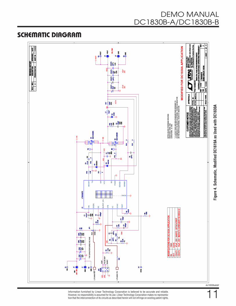
The DC1830B is customizable to handle a wide variety of applications with output voltages from 3V to 30V and out-put currents up to 6.5A with the PFETs supplied, and up to 60V and/or 13A with higher voltage rating and/or added PFETs. The reference design provided with DC1830A is targeted at 4-cell LiFePO4 (14.6V/5A) applications.
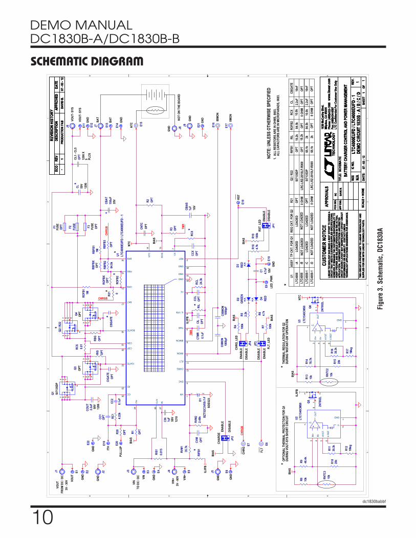
The DC1830B loop compensation values were proven with the LTC3845A buck-boost power converter shown and are typical for other applications. The output of this demo board was specifically tailored for a Tenergy 10A-hour battery, P/N 30207. Other voltages can be set by changing ROFB2 and RBFB2. The desired nominal volt-age can be accurately trimmed by using trim resistors ROFBX and RBFBX. For example, for 14.4V battery float voltage, change ROFB2 and RBFB2 to 86.6k, and add 7.5M at ROFBX and RBFBX for greater set point accuracy. Other parameters can be adjusted to suit specific applications with guidance provided in the LTC4000 data sheet. Table 2 provides a summary of parameter adjustments.
This circuit was designed to demonstrate the high levels of performance and small solution size attainable using
L, LT, LTC, LTM, Linear Technology and the Linear logo are registered trademarks and PowerPath is a trademark of Analog Devices, Inc. All other trademarks are the property of their respective owners.
PERFORMANCE SUMMARY
this part to control a switch mode power converter to form a battery charger, intelligent PowerPath manager, and power supply system. It produces a regulated 5A/14.6V battery charger output as well as a system output of up to 5.5A: suitable for a wide variety of portable applications including instruments, industrial equipment, power tools, and computers.
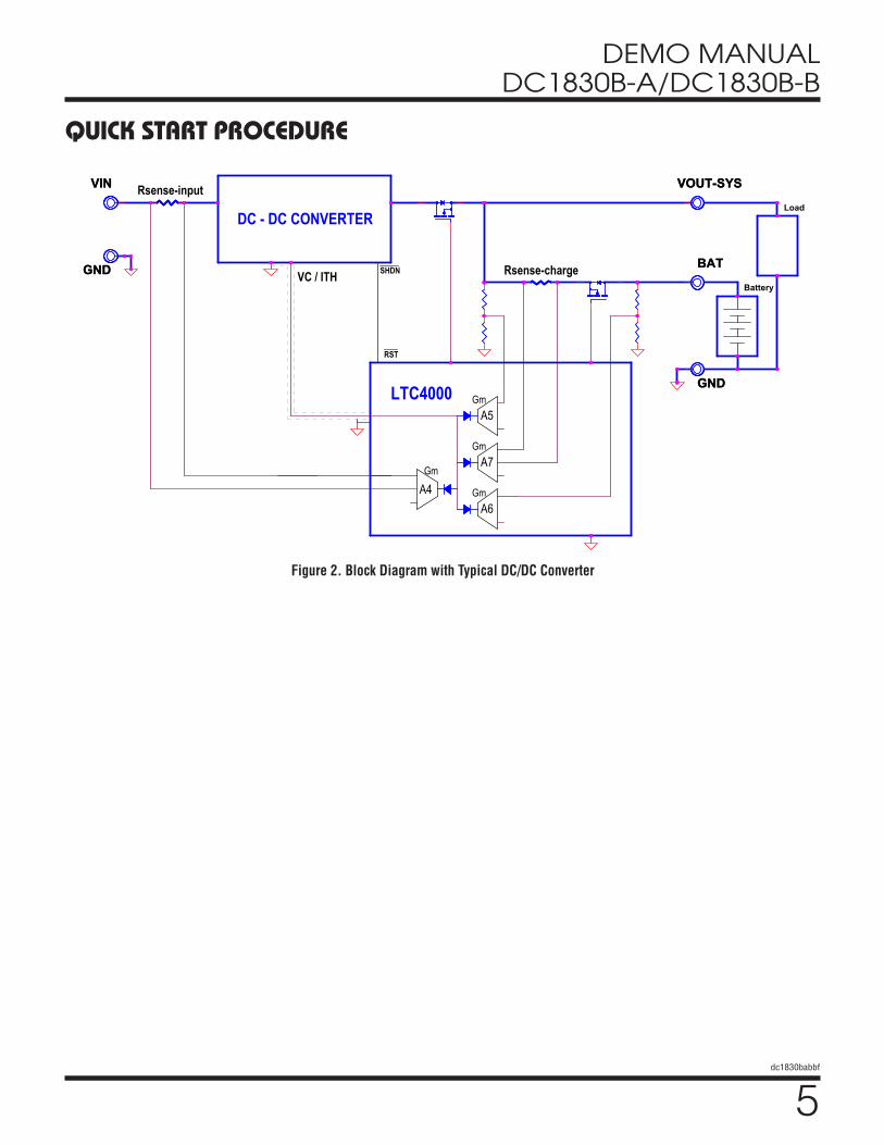
The DC1830B-A provides a solution complete with both battery charger control and PowerPath management. It includes a second PFET (Q2) between VOUT-SYS and BAT to provide instant-on functionality which keeps VOUT-SYS within a narrow range regardless of battery voltage, and disconnects the battery when it is fully charged and power is available from the front end DC/DC converter. Thermal regulation circuitry is also provided to limit the temperature of both PFETs. The DC1830B-B provides a simple battery-charger-controller only solution without the PowerPath manager. It deletes the second PFET and thermal regulation circuitry. In this case, the battery is always online and VOUT-SYS tracks BAT voltage.
Design files for this circuit board are available at http://www.linear.com/demo/DC1830B-A
Specifications are at TA = 25°C
SYMBOL PARAMETER CONDITIONS MIN TYP MAX UNITSVIN Input Supply Range This is the Input Voltage of the Front End DC/DC Supply 20 60 V
IIN Input Current Limit This is the Input Current Limit Set by the LTC4000 3 A
VFLOAT Battery Float Voltage 14.4 14.6 14.8 V
Output Regulation Line and Load (20V to 60V, 0A to 4.5A) ±0.005 %
IBAT Battery Charge Current 5 A
Battery Charge Current – Trickle 0.6 A
tT Charge Termination Time VBAT = VFLOAT 2.9 hours
VOUT-SYS System Output Voltage 12.3 14.6 15.5 V
IOUT-SYS System Output Current Range *Input Current Limited Below 35VIN 0 5.5* A
2dc1830babbf
DEMO MANUAL DC1830B-A/DC1830B-B
QUICK START PROCEDUREDemonstration circuit 1830 is offered for use in combina-tion with a front end DC/DC converter, and will need to be customized to suit the intended application. It has been supplied with components for a design as outlined in the performance summary, and tested in conjunction with the LTC3845A buck converter that it was tailored to. A sepa-rate demonstration board is available for the LTC4000/LTC3789 buck-boost combination, the DC1721A. The LTC4000 data sheet should be used for guidance in deter-mining circuit values for the application at hand. You may follow the design example on page 26 of the data sheet. Table 1 provides a summary of parameter adjustments.
NOTE: The PFETs supplied on this board are rated at 30V.
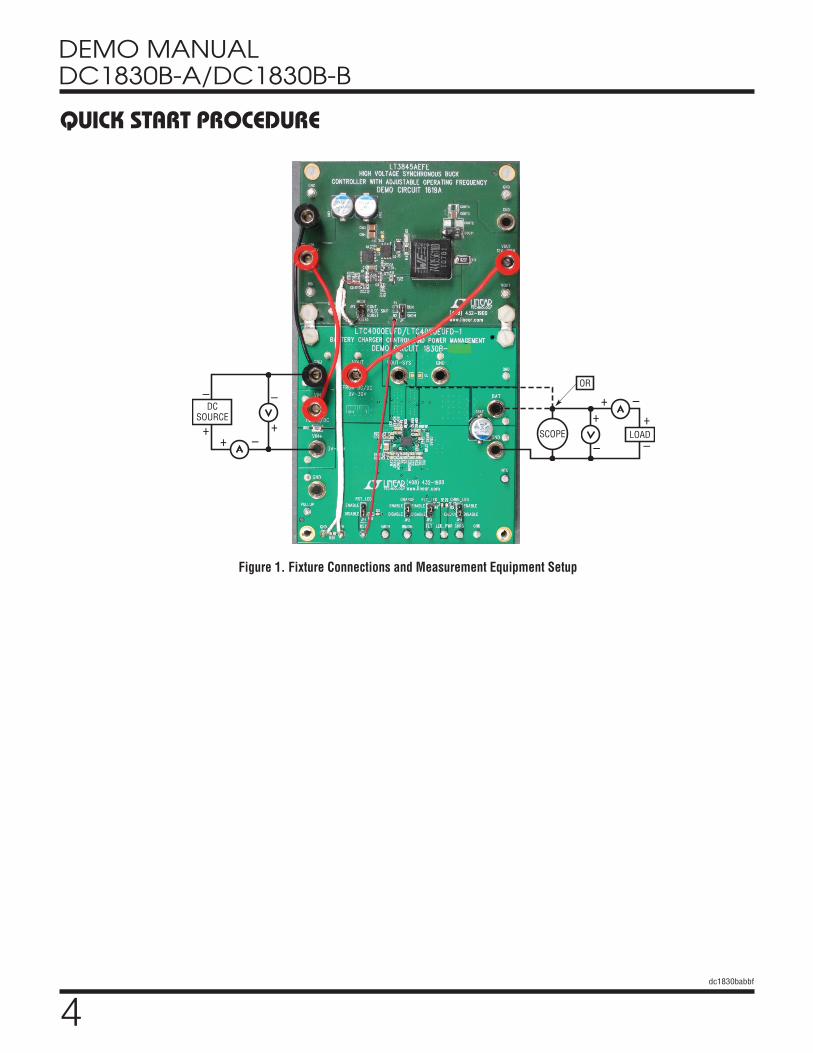
Once the circuit has been customized to suit the appli-cation at hand, it is easy to set up to evaluate the per-formance of the LTC4000 when combined with a suit-able switching power converter, such as the LTC3845A. voltages and currents cited in this procedure are for the design as delivered; if the design has been customized, substitute the appropriate values. Refer to Figure 1 for proper measurement equipment setup and follow the procedure below:
WARNING: BATTERIES ARE POTENTIALLY DANGEROUS HIGH ENERGY SOURCES. IMPROPER CONNECTION, OVERCHARGE, OR RAPID DISCHARGE COULD RESULT IN EXPLOSION AND/OR FIRE.
1. Set an input power supply that is capable of 60V and 3A, to 24V. Then turn off the supply.
2. With power off, connect the supply to the input ter-minals VIN and GND.
NOTE:
a. Input voltages lower than 20V can keep the con-verter from turning on due to the undervoltage lockout feature of the LTC4000.
b. If efficiency measurements are desired, refer to Figure 1 for the test setup.
3. Set CHARGE jumper to ENABLE.
4. Turn on the power at the input.
NOTE: Make sure that the input voltage never exceeds 60V.
5. Check for the proper BAT output voltage of 14.6V. Turn off the power at the input.
6. Now that the proper output voltage is established, connect a variable load capable of sinking 6A at 16V to the output terminals BAT and GND. Set the current for 0A.
7. Turn on the power at the input.
NOTE: If there is no output, temporarily disconnect the load to make sure that the load is not set too high.
8. Once the proper BAT output voltage is again estab-lished, adjust the load and/or source within the oper-ating range and observe the battery float voltage regu-lation, charge current, and other desired parameters.
9. Set the load to constant voltage mode to more easily observe charge current and trickle charge current.
NOTE: The following applies to the DC1830B-A.
NOTE: Operation in the instant-on region (VOUT < 12.5V) may engage thermal limit circuit to protect Q2 in the linear region.
NOTE: The optional thermal limit circuit for Q1 (Q5, RNTC3, R8 to 12, and U2) is included to protect Q1 in case of an extended short-circuit on VOUT-SYS under adverse thermal conditions (TA > 40°C). It may not be needed in applications with less severe thermal condi-tions, lower current available to VOUT-SYS, or where continuous short-circuit protection on VOUT-SYS is not required.
3dc1830babbf
DEMO MANUAL DC1830B-A/DC1830B-B
QUICK START PROCEDURE
Table 1. LTC4000 Charger Setup Parameters and Reference ValuesREFERENCE DESCRIPTION NOMINAL VALUE (V)* MIN/MAX CONDITIONS
IIL Input Current Regulation/Limit (50µA • RIL)/20 45/55 50mV max
ICL Charge Current Regulation/Limit (50µA • RCL)/20 45/55 50mV max
ICL Trickle Charge Current Regulation/Limit (5µA • RCL)/20 4.5/5.5
VBAT-FLOAT Battery Float Voltage 1.136V 1.125/1.147
VOUT System Voltage 1.193V 1.181/1.204 Charger Off
(Follows VBAT) Charger Float
(Follows VBAT) Charging at ICL, 0.86VBAT-FLOAT < VBAT < VBAT-FLOAT
0.86 • 1.136V 0.82/0.90 Instant-On, 0.68VBAT-FLOAT < VBAT < 0.86VBAT-FLOAT
0.86 • 1.136V 0.82/0.90 Instant-On, Trickle, VBAT < 0.68VBAT-FLOAT
VM Input Voltage Monitor/UVLO 1.193V 1.181/1.204 Falling, (40mV Hysteresis)
CX C/X Monitor/Charge Termination (5µA • RCX – 10mV)/20 4.5/5.5 Short TMR to BIAS for C/X Termination
TMR Charge Termination Timer 104S/nF 83/126
*Normalized to sense point
10. Turn off the power at the input.
11. Connect the output load and meters to the VOUT-SYS output.
12. Set CHARGE jumper to DISABLE.
13. Turn on the power at the input.
14. Once the proper VOUT-SYS is again established, adjust the load and/or source within the operating range and observe the output voltage regulation, rip-ple voltage, efficiency, input and output current limit, and other desired parameters.
4dc1830babbf
DEMO MANUAL DC1830B-A/DC1830B-B
QUICK START PROCEDURE
Figure 1. Fixture Connections and Measurement Equipment Setup
–
+
+ –
+ –
–
+
DCSOURCE +
–LOAD
OR
+
–SCOPE
5dc1830babbf
DEMO MANUAL DC1830B-A/DC1830B-B
5
5
4
4
3
3
2
2
1
1
D D
C C
B B
A A
10-36 VIN, STEP-UP/DOWN DC/DC CONVERTER
Rsense-input
LTC4000 SYSTEM CONTROL LOOPS
A5
A7
A6A4
Rsense-charge
DC - DC CONVERTER
VC / ITH
LTC4000 Gm
Gm
Gm
Gm
Battery
Load
RST
SHDN
SIZE
DATE:
IC NO. REV.
SHEET OF
TITLE:
APPROVALS
PCB DES.
APP ENG.
TECHNOLOGY Fax: (408)434-0507
Milpitas, CA 95035Phone: (408)432-1900
1630 McCarthy Blvd.
LTC Confidential-For Customer Use Only
CUSTOMER NOTICELINEAR TECHNOLOGY HAS MADE A BEST EFFORT TO DESIGN ACIRCUIT THAT MEETS CUSTOMER-SUPPLIED SPECIFICATIONS;HOWEVER, IT REMAINS THE CUSTOMER'S RESPONSIBILITY TOVERIFY PROPER AND RELIABLE OPERATION IN THE ACTUALAPPLICATION. COMPONENT SUBSTITUTION AND PRINTEDCIRCUIT BOARD LAYOUT MAY SIGNIFICANTLY AFFECT CIRCUITPERFORMANCE OR RELIABILITY. CONTACT LINEARTECHNOLOGY APPLICATIONS ENGINEERING FOR ASSISTANCE.
THIS CIRCUIT IS PROPRIETARY TO LINEAR TECHNOLOGY AND
SCHEMATIC
SUPPLIED FOR USE WITH LINEAR TECHNOLOGY PARTS. SCALE = NONE
www.linear.com
A3Friday, June 29, 2012 1 2
16.8V, 5A BATTERY CHARGER WITH HIGH EFFICIENCY,
AK
DAVID B.
N/ALTC4000EGN, LTC3789EGN
DEMO CIRCUIT 1721ASIZE
DATE:
IC NO. REV.
SHEET OF
TITLE:
APPROVALS
PCB DES.
APP ENG.
TECHNOLOGY Fax: (408)434-0507
Milpitas, CA 95035Phone: (408)432-1900
1630 McCarthy Blvd.
LTC Confidential-For Customer Use Only
CUSTOMER NOTICELINEAR TECHNOLOGY HAS MADE A BEST EFFORT TO DESIGN ACIRCUIT THAT MEETS CUSTOMER-SUPPLIED SPECIFICATIONS;HOWEVER, IT REMAINS THE CUSTOMER'S RESPONSIBILITY TOVERIFY PROPER AND RELIABLE OPERATION IN THE ACTUALAPPLICATION. COMPONENT SUBSTITUTION AND PRINTEDCIRCUIT BOARD LAYOUT MAY SIGNIFICANTLY AFFECT CIRCUITPERFORMANCE OR RELIABILITY. CONTACT LINEARTECHNOLOGY APPLICATIONS ENGINEERING FOR ASSISTANCE.
THIS CIRCUIT IS PROPRIETARY TO LINEAR TECHNOLOGY AND
SCHEMATIC
SUPPLIED FOR USE WITH LINEAR TECHNOLOGY PARTS. SCALE = NONE
www.linear.com
A3Friday, June 29, 2012 1 2
16.8V, 5A BATTERY CHARGER WITH HIGH EFFICIENCY,
AK
DAVID B.
N/ALTC4000EGN, LTC3789EGN
DEMO CIRCUIT 1721A
REVISION HISTORYDESCRIPTION DATEAPPROVEDECO REV
DAVID B.1ST PROTOTYPE1 08-20-10__
REVISION HISTORYDESCRIPTION DATEAPPROVEDECO REV
DAVID B.1ST PROTOTYPE1 08-20-10__
REVISION HISTORYDESCRIPTION DATEAPPROVEDECO REV
DAVID B.1ST PROTOTYPE1 08-20-10__
GNDGND
GNDGND
BATBAT
VINVIN VOUT-SYSVOUT-SYS
Figure 2. Block Diagram with Typical DC/DC Converter
QUICK START PROCEDURE
6dc1830babbf
DEMO MANUAL DC1830B-A/DC1830B-B
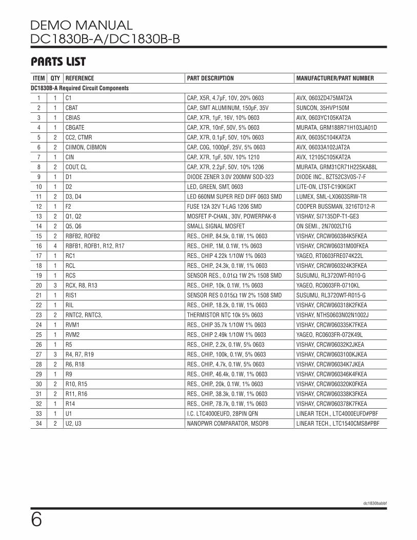
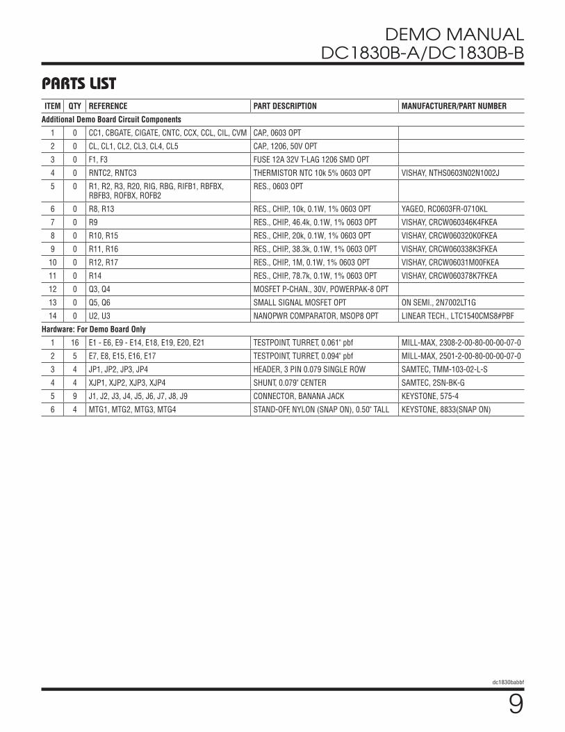
PARTS LISTITEM QTY REFERENCE PART DESCRIPTION MANUFACTURER/PART NUMBER
DC1830B-A Required Circuit Components
1 1 C1 CAP., X5R, 4.7µF, 10V, 20% 0603 AVX, 0603ZD475MAT2A
2 1 CBAT CAP., SMT ALUMINUM, 150µF, 35V SUNCON, 35HVP150M
3 1 CBIAS CAP., X7R, 1µF, 16V, 10% 0603 AVX, 0603YC105KAT2A
4 1 CBGATE CAP., X7R, 10nF, 50V, 5% 0603 MURATA, GRM188R71H103JA01D
5 2 CC2, CTMR CAP., X7R, 0.1µF, 50V, 10% 0603 AVX, 06035C104KAT2A
6 2 CIIMON, CIBMON CAP., C0G, 1000pF, 25V, 5% 0603 AVX, 06033A102JAT2A
7 1 CIN CAP., X7R, 1µF, 50V, 10% 1210 AVX, 12105C105KAT2A
8 2 COUT, CL CAP., X7R, 2.2µF, 50V, 10% 1206 MURATA, GRM31CR71H225KA88L
9 1 D1 DIODE ZENER 3.0V 200MW SOD-323 DIODE INC., BZT52C3V0S-7-F
10 1 D2 LED, GREEN, SMT, 0603 LITE-ON, LTST-C190KGKT
11 2 D3, D4 LED 660NM SUPER RED DIFF 0603 SMD LUMEX, SML-LX0603SRW-TR
12 1 F2 FUSE 12A 32V T-LAG 1206 SMD COOPER BUSSMAN, 3216TD12-R
13 2 Q1, Q2 MOSFET P-CHAN., 30V, POWERPAK-8 VISHAY, SI7135DP-T1-GE3
14 2 Q5, Q6 SMALL SIGNAL MOSFET ON SEMI., 2N7002LT1G
15 2 RBFB2, ROFB2 RES., CHIP., 84.5k, 0.1W, 1% 0603 VISHAY, CRCW060384K5FKEA
16 4 RBFB1, ROFB1, R12, R17 RES., CHIP., 1M, 0.1W, 1% 0603 VISHAY, CRCW06031M00FKEA
17 1 RC1 RES., CHIP 4.22k 1/10W 1% 0603 YAGEO, RT0603FRE074K22L
18 1 RCL RES., CHIP., 24.3k, 0.1W, 1% 0603 VISHAY, CRCW060324K3FKEA
19 1 RCS SENSOR RES., 0.01Ω 1W 2% 1508 SMD SUSUMU, RL3720WT-R010-G
20 3 RCX, R8, R13 RES., CHIP., 10k, 0.1W, 1% 0603 YAGEO, RC0603FR-0710KL
21 1 RIS1 SENSOR RES 0.015Ω 1W 2% 1508 SMD SUSUMU, RL3720WT-R015-G
22 1 RIL RES., CHIP., 18.2k, 0.1W, 1% 0603 VISHAY, CRCW060318K2FKEA
23 2 RNTC2, RNTC3, THERMISTOR NTC 10k 5% 0603 VISHAY, NTHS0603N02N1002J
24 1 RVM1 RES., CHIP 35.7k 1/10W 1% 0603 VISHAY, CRCW060335K7FKEA
25 1 RVM2 RES., CHIP 2.49k 1/10W 1% 0603 YAGEO, RC0603FR-072K49L
26 1 R5 RES., CHIP., 2.2k, 0.1W, 5% 0603 VISHAY, CRCW06032K2JKEA
27 3 R4, R7, R19 RES., CHIP., 100k, 0.1W, 5% 0603 VISHAY, CRCW0603100KJKEA
28 2 R6, R18 RES., CHIP., 4.7k, 0.1W, 5% 0603 VISHAY, CRCW06034K7JKEA
29 1 R9 RES., CHIP., 46.4k, 0.1W, 1% 0603 VISHAY, CRCW060346K4FKEA
30 2 R10, R15 RES., CHIP., 20k, 0.1W, 1% 0603 VISHAY, CRCW060320K0FKEA
31 2 R11, R16 RES., CHIP., 38.3k, 0.1W, 1% 0603 VISHAY, CRCW060338K3FKEA
32 1 R14 RES., CHIP., 78.7k, 0.1W, 1% 0603 VISHAY, CRCW060378K7FKEA
33 1 U1 I.C. LTC4000EUFD, 28PIN QFN LINEAR TECH., LTC4000EUFD#PBF
34 2 U2, U3 NANOPWR COMPARATOR, MSOP8 LINEAR TECH., LTC1540CMS8#PBF
7dc1830babbf
DEMO MANUAL DC1830B-A/DC1830B-B
PARTS LISTITEM QTY REFERENCE PART DESCRIPTION MANUFACTURER/PART NUMBER
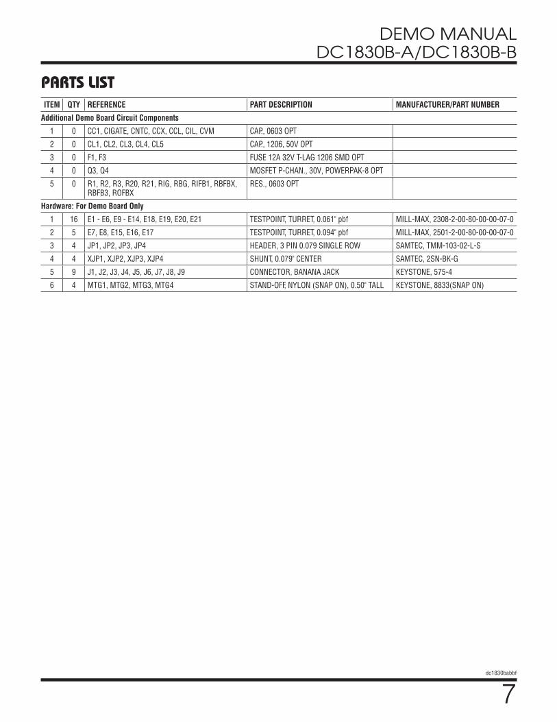
Additional Demo Board Circuit Components
1 0 CC1, CIGATE, CNTC, CCX, CCL, CIL, CVM CAP., 0603 OPT
2 0 CL1, CL2, CL3, CL4, CL5 CAP., 1206, 50V OPT
3 0 F1, F3 FUSE 12A 32V T-LAG 1206 SMD OPT
4 0 Q3, Q4 MOSFET P-CHAN., 30V, POWERPAK-8 OPT
5 0 R1, R2, R3, R20, R21, RIG, RBG, RIFB1, RBFBX, RBFB3, ROFBX
RES., 0603 OPT
Hardware: For Demo Board Only
1 16 E1 - E6, E9 - E14, E18, E19, E20, E21 TESTPOINT, TURRET, 0.061" pbf MILL-MAX, 2308-2-00-80-00-00-07-0
2 5 E7, E8, E15, E16, E17 TESTPOINT, TURRET, 0.094" pbf MILL-MAX, 2501-2-00-80-00-00-07-0
3 4 JP1, JP2, JP3, JP4 HEADER, 3 PIN 0.079 SINGLE ROW SAMTEC, TMM-103-02-L-S
4 4 XJP1, XJP2, XJP3, XJP4 SHUNT, 0.079" CENTER SAMTEC, 2SN-BK-G
5 9 J1, J2, J3, J4, J5, J6, J7, J8, J9 CONNECTOR, BANANA JACK KEYSTONE, 575-4
6 4 MTG1, MTG2, MTG3, MTG4 STAND-OFF, NYLON (SNAP ON), 0.50" TALL KEYSTONE, 8833(SNAP ON)
8dc1830babbf
DEMO MANUAL DC1830B-A/DC1830B-B
ITEM QTY REFERENCE PART DESCRIPTION MANUFACTURER/PART NUMBER
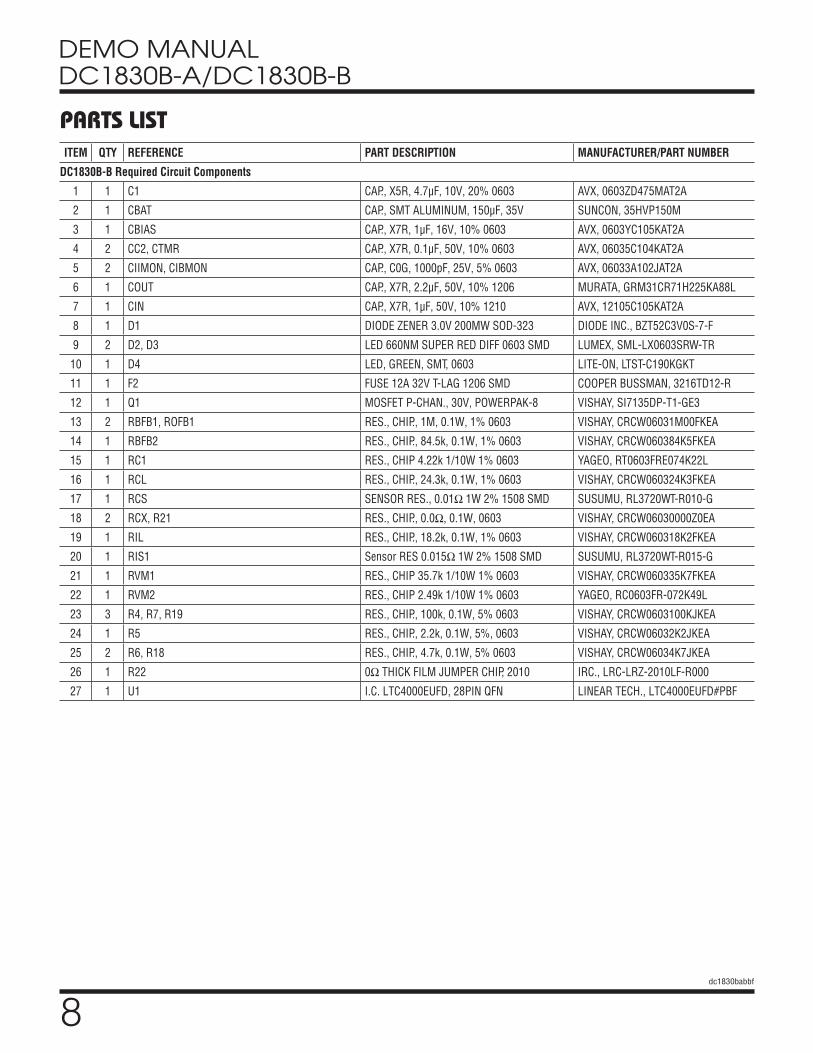
DC1830B-B Required Circuit Components
1 1 C1 CAP., X5R, 4.7µF, 10V, 20% 0603 AVX, 0603ZD475MAT2A
2 1 CBAT CAP., SMT ALUMINUM, 150µF, 35V SUNCON, 35HVP150M
3 1 CBIAS CAP., X7R, 1µF, 16V, 10% 0603 AVX, 0603YC105KAT2A
4 2 CC2, CTMR CAP., X7R, 0.1µF, 50V, 10% 0603 AVX, 06035C104KAT2A
5 2 CIIMON, CIBMON CAP., C0G, 1000pF, 25V, 5% 0603 AVX, 06033A102JAT2A
6 1 COUT CAP., X7R, 2.2µF, 50V, 10% 1206 MURATA, GRM31CR71H225KA88L
7 1 CIN CAP., X7R, 1µF, 50V, 10% 1210 AVX, 12105C105KAT2A
8 1 D1 DIODE ZENER 3.0V 200MW SOD-323 DIODE INC., BZT52C3V0S-7-F
9 2 D2, D3 LED 660NM SUPER RED DIFF 0603 SMD LUMEX, SML-LX0603SRW-TR
10 1 D4 LED, GREEN, SMT, 0603 LITE-ON, LTST-C190KGKT
11 1 F2 FUSE 12A 32V T-LAG 1206 SMD COOPER BUSSMAN, 3216TD12-R
12 1 Q1 MOSFET P-CHAN., 30V, POWERPAK-8 VISHAY, SI7135DP-T1-GE3
13 2 RBFB1, ROFB1 RES., CHIP., 1M, 0.1W, 1% 0603 VISHAY, CRCW06031M00FKEA
14 1 RBFB2 RES., CHIP., 84.5k, 0.1W, 1% 0603 VISHAY, CRCW060384K5FKEA
15 1 RC1 RES., CHIP 4.22k 1/10W 1% 0603 YAGEO, RT0603FRE074K22L
16 1 RCL RES., CHIP., 24.3k, 0.1W, 1% 0603 VISHAY, CRCW060324K3FKEA
17 1 RCS SENSOR RES., 0.01Ω 1W 2% 1508 SMD SUSUMU, RL3720WT-R010-G
18 2 RCX, R21 RES., CHIP., 0.0Ω, 0.1W, 0603 VISHAY, CRCW06030000Z0EA
19 1 RIL RES., CHIP., 18.2k, 0.1W, 1% 0603 VISHAY, CRCW060318K2FKEA
20 1 RIS1 Sensor RES 0.015Ω 1W 2% 1508 SMD SUSUMU, RL3720WT-R015-G
21 1 RVM1 RES., CHIP 35.7k 1/10W 1% 0603 VISHAY, CRCW060335K7FKEA
22 1 RVM2 RES., CHIP 2.49k 1/10W 1% 0603 YAGEO, RC0603FR-072K49L
23 3 R4, R7, R19 RES., CHIP., 100k, 0.1W, 5% 0603 VISHAY, CRCW0603100KJKEA
24 1 R5 RES., CHIP., 2.2k, 0.1W, 5%, 0603 VISHAY, CRCW06032K2JKEA
25 2 R6, R18 RES., CHIP., 4.7k, 0.1W, 5% 0603 VISHAY, CRCW06034K7JKEA
26 1 R22 0Ω THICK FILM JUMPER CHIP, 2010 IRC., LRC-LRZ-2010LF-R000
27 1 U1 I.C. LTC4000EUFD, 28PIN QFN LINEAR TECH., LTC4000EUFD#PBF
PARTS LIST
9dc1830babbf
DEMO MANUAL DC1830B-A/DC1830B-B
PARTS LISTITEM QTY REFERENCE PART DESCRIPTION MANUFACTURER/PART NUMBER
Additional Demo Board Circuit Components
1 0 CC1, CBGATE, CIGATE, CNTC, CCX, CCL, CIL, CVM CAP., 0603 OPT
2 0 CL, CL1, CL2, CL3, CL4, CL5 CAP., 1206, 50V OPT
3 0 F1, F3 FUSE 12A 32V T-LAG 1206 SMD OPT
4 0 RNTC2, RNTC3 THERMISTOR NTC 10k 5% 0603 OPT VISHAY, NTHS0603N02N1002J
5 0 R1, R2, R3, R20, RIG, RBG, RIFB1, RBFBX, RBFB3, ROFBX, ROFB2
RES., 0603 OPT
6 0 R8, R13 RES., CHIP., 10k, 0.1W, 1% 0603 OPT YAGEO, RC0603FR-0710KL
7 0 R9 RES., CHIP., 46.4k, 0.1W, 1% 0603 OPT VISHAY, CRCW060346K4FKEA
8 0 R10, R15 RES., CHIP., 20k, 0.1W, 1% 0603 OPT VISHAY, CRCW060320K0FKEA
9 0 R11, R16 RES., CHIP., 38.3k, 0.1W, 1% 0603 OPT VISHAY, CRCW060338K3FKEA
10 0 R12, R17 RES., CHIP., 1M, 0.1W, 1% 0603 OPT VISHAY, CRCW06031M00FKEA
11 0 R14 RES., CHIP., 78.7k, 0.1W, 1% 0603 OPT VISHAY, CRCW060378K7FKEA
12 0 Q3, Q4 MOSFET P-CHAN., 30V, POWERPAK-8 OPT
13 0 Q5, Q6 SMALL SIGNAL MOSFET OPT ON SEMI., 2N7002LT1G
14 0 U2, U3 NANOPWR COMPARATOR, MSOP8 OPT LINEAR TECH., LTC1540CMS8#PBF
Hardware: For Demo Board Only
1 16 E1 - E6, E9 - E14, E18, E19, E20, E21 TESTPOINT, TURRET, 0.061" pbf MILL-MAX, 2308-2-00-80-00-00-07-0
2 5 E7, E8, E15, E16, E17 TESTPOINT, TURRET, 0.094" pbf MILL-MAX, 2501-2-00-80-00-00-07-0
3 4 JP1, JP2, JP3, JP4 HEADER, 3 PIN 0.079 SINGLE ROW SAMTEC, TMM-103-02-L-S
4 4 XJP1, XJP2, XJP3, XJP4 SHUNT, 0.079" CENTER SAMTEC, 2SN-BK-G
5 9 J1, J2, J3, J4, J5, J6, J7, J8, J9 CONNECTOR, BANANA JACK KEYSTONE, 575-4
6 4 MTG1, MTG2, MTG3, MTG4 STAND-OFF, NYLON (SNAP ON), 0.50" TALL KEYSTONE, 8833(SNAP ON)
10dc1830babbf
DEMO MANUAL DC1830B-A/DC1830B-B
Figu
re 3
. Sch
emat
ic, D
C183
0A
SCHEMATIC DIAGRAM5 5
4 4
3 3
2 2
1 1
DD
CC
BB
AA
THER
MAL
REGU
LATI
ON F
OR Q
2 DU
RING
'INST
ANT-
ON' O
PERA
TION
OPTI
ONAL
THE
RMAL
PRO
TECT
ION
FOR
Q1
DURI
NG V
OUT-
SYS
SHOR
T CI
RCUI
T
GND
GND
GND
VOUT
VIN+
OPT
OPT
GND
CL1
- CL5
1206
X5 PL
CS
3V -
60V
FROM
DC
/ DC
**
NOTE
: UNL
ESS
OTHE
RWIS
E SP
ECIF
IED
1. A
LL R
ESIS
TORS
ARE
IN O
HMS,
0603
.
ALL
CAP
ACIT
ORS
ARE
IN M
ICRO
FARA
DS, 0
603.
*
NOT
ON T
HE B
OARD
OPT
NOT
LOAD
ED0 O
HM
REG
CKT.
FOR
Q2
OPT
SI71
35DP
*RO
FB2
10.0k
LOAD
EDOP
T2.2
uF0 O
HM
ASSY
CBGA
TELO
ADED
10nF
OPT
CLQ2
/ R22
NOT
LOAD
ED
R21
84.5k
RCX
TP C
KT. F
OR Q
1
-D
U1LT
C400
0
LTC4
000-
1LT
C400
0
LTC4
000-
1-C-A -B
*
SOD3
23
LRC-
LRZ-
2010
LF-R
000
LOAD
EDNO
T LO
ADED
LOAD
EDNO
T LO
ADED
OPT
0 OHM
SI71
35DP
84.5k OP
T10
.0k0 O
HMOP
T2.2
uFOP
T10
nFLR
C-LR
Z-20
10LF
-R00
0
/ R22
RIL
RIFB
1
68.1k
68.1k
OPT
OPT
18.2k
18.2k 2k 2k
TO D
C / D
C
ENAB
LEDI
SABL
E
DISA
BLE
ENAB
LEEN
ABLE
DISA
BLE
3V -
30V
BIAS
NTC
BIAS
BIAS
BIAS
IL/IF
B
IL/IF
B
BIAS
BIAS
BIAS
BIAS
IL/IF
B
NTC
SIZE
DATE
:
IC N
O.RE
V.
SHEE
TOF
TITL
E:
APPR
OVAL
S
PCB
DES.
APP
ENG.
TECHNOLO
GY
Fax:
(408
)434
-050
7
Milp
itas,
CA 95
035
Phon
e: (4
08)4
32-1
900
1630
McC
arth
y Blvd
.
LTC
Conf
iden
tial-F
or C
usto
mer
Use
Onl
y
CUST
OMER
NOT
ICE
LINE
AR T
ECHN
OLOG
Y HA
S MA
DE A
BES
T EF
FORT
TO
DESI
GN A
CIRC
UIT
THAT
MEE
TS C
USTO
MER-
SUPP
LIED
SPE
CIFI
CATI
ONS;
HOW
EVER
, IT R
EMAI
NS T
HE C
USTO
MER'
S RE
SPON
SIBI
LITY
TO
VERI
FY P
ROPE
R AN
D RE
LIAB
LE O
PERA
TION
IN T
HE A
CTUA
LAP
PLIC
ATIO
N. C
OMPO
NENT
SUB
STIT
UTIO
N AN
D PR
INTE
DCI
RCUI
T BO
ARD
LAYO
UT M
AY S
IGNI
FICA
NTLY
AFF
ECT
CIRC
UIT
PERF
ORMA
NCE
OR R
ELIA
BILI
TY. C
ONTA
CT L
INEA
RTE
CHNO
LOGY
APP
LICA
TION
S EN
GINE
ERIN
G FO
R AS
SIST
ANCE
.
THIS
CIR
CUIT
IS P
ROPR
IETA
RY T
O LI
NEAR
TEC
HNOL
OGY
AND
SCHE
MAT
IC
SUPP
LIED
FOR
USE
WIT
H LI
NEAR
TEC
HNOL
OGY
PART
S.SC
ALE
= NO
NE
www.
linea
r.com 1
DEMO
CIR
CUIT
1830
B - A
/ B / C
/ D1
1
BATT
ERY
CHAR
GER
CONT
ROL A
ND P
OWER
MAN
AGEM
ENT
N/A
LTC4
000E
UFD
/ LTC
4000
EUFD
- 1
NC DAVE
B.
07 -
03 -
12
REVI
SION
HIS
TORY
DESC
RIPT
ION
DATE
APPR
OVED
ECO
REV
DAVI
D B.
PROD
UCTI
ON F
AB-
107
- 03
- 12
REVI
SION
HIS
TORY
DESC
RIPT
ION
DATE
APPR
OVED
ECO
REV
DAVI
D B.
PROD
UCTI
ON F
AB-
107
- 03
- 12
REVI
SION
HIS
TORY
DESC
RIPT
ION
DATE
APPR
OVED
ECO
REV
DAVI
D B.
PROD
UCTI
ON F
AB-
107
- 03
- 12
RCX*
R21 0
Q3
4
5123
67 8
E16
IBM
ON
RBFB
11M
E8FL
T R11
38.3k
J9GN
D
R3 OPT
Q2*
4
5123
67 8
J7BA
T
CVM
OPT
R5 2.2k
CIL
OPT
CBIA
S1u
F16
V
COUT
2.2uF
1206
50V
R6 4.7k
E4
F2 FUSE
E22
GND
D3 RED
R9 46.4
k
E5
CIBM
ON10
00pF
E6
CCL
OPT
J6VO
UT- S
YS
C1 4.7uF
10V
E18RS
T
RIG
OPT
OPT
R19
100k
R8 10k
JP4
CHRG
_LED
RNTC
310
k
+CB
AT15
0uF
35V
RBFB
2
84.5
k
E10
GND
E12
E19
ITH
RIL*
F1 OPT
FUSE
R20
OPT
LTC4
000E
UFD
/ LTC
4000
EUFD
- 1
U1
VM1
RST2
IIMON3
IL / IFB4
ENC5
IBMON6
CX
7
CL8
TMR9
GND10
FLT11
CHRG12
BIAS
13
NTC
14
FBG15
BFB16
BAT17
BGATE18
CSN19
CSP20
OFB21
IGATE22
IID23
ITH
24
CC25
CLN
26
IN27
GND28
GND29
J1VO
UT
R12
1Meg
J3
VIN
Q1 Si71
35DP 4
5123
67 8
RC1
4.22
k
CIGA
TEOP
T
JP2
ENAB
LE
DISA
BLE
CHAR
GE
E17
IIMON
D1BZ
T52C
3V0S
-7-F
1 2
D2GR
EEN
CCX
OPT
Q6
2N70
02L
1
3 2
+ -
U3 LTC1
540C
MS8
GND1
V-2
IN+
3
IN-
4
HYS
T5
6 R
EF6
V+7
OU
T8
CC2
0.1uF
JP3
FLT_
LED
ROFB
XOP
T
RVM2
2.49
k
RBG
OPT
R1 OPT
F3 OPT
FUSE
RIS1
0.01
5
RNTC
210
k
Q4
4
5123
67 8
E9 LED_
PWR
RIFB
1*
D4 RED
CBGA
TE*
RCS
0.01
E14 GN
DE2
0PU
LLUP
E7CH
RG
J8
GND
RVM1
35.7
k
JP1
RST_
LED
E11
VOUT
- SYS
+ -
U2 LTC1
540C
MS8
GND1
V-2
IN+
3
IN-
4
HYS
T5
6 R
EF6
V+7
OU
T8
ROFB
2*
R4 100k
R15
20k
J5
GND
R2 OPT
E21 GN
D
RBFB
XOP
T
R18
4.7kRB
FB3
OPT
CC1
OPT
E15
NTC
R10
20k
E1
R13
10k
ROFB
11M
RCL
24.3
k
E13 BA
T
R7 100k
R14
78.7
k
R17
1Meg
CIN
1uF
1210
50V
CTMR
0.1uF
CL*
1206
50V
J4VI
N+
R16
38.3k
CNTC
OPT
J2GN
D
E3VI
N
Q5
2N70
02L
1
3 2
CIIM
ON10
00pF
E2
TMR
TMR
CHRGB
CHRG
B
CHRG
B
11dc1830babbf
DEMO MANUAL DC1830B-A/DC1830B-B
Information furnished by Linear Technology Corporation is believed to be accurate and reliable. However, no responsibility is assumed for its use. Linear Technology Corporation makes no representa-tion that the interconnection of its circuits as described herein will not infringe on existing patent rights.
Fig
ure
4. S
chem
atic
, Mod
ified
DC1
619A
as
Used
with
DC1
830A
SCHEMATIC DIAGRAM1 1
2 2
AA
BB
CONT
BURS
TPU
LSE
SKIP
RUN
SHDN
.
NOTE
S:UN
LESS
OTH
ERW
ISE
SPEC
IFIE
DRE
SIST
ORS:
OHM
S, 04
02CA
PACI
TORS
: uF
, 040
2
* 79V
CAP
ACIT
OR S
URGE
VOL
TAGE
* L1 L
AYOU
T PA
DS A
RE N
ON-S
TAND
ARD
PADS
DES
IGNE
D TO
ACCO
MMOD
ATE
THE
WUR
TH E
LEKT
RONI
C, 74
4355
6110
0 IND
UCTO
ROR
THE
WUR
TH E
LEKT
RONI
C, 74
4355
1151
INDU
CTOR
47uF
20v
10uF
25v
196K
0.01
4LT
C400
0 IT
H
LTC4
000
RST
MO
DIF
IED
FO
R D
C18
30A
APP
LIC
ATI
ON
MODI
FICA
TION
S FO
R DC
1830
A AP
PLIC
ATIO
NR4
19
6KR1
7
0.
014
COUT
1
47uF
, 20V
SAN
YO 2
0TQC
47MY
FCO
UT3
10
uF, 2
5V M
URAT
A GR
M32D
R71E
106K
A12
VFB
VS+
VFB
VCC
VCC
VOUT
BG
VOUT
VCC
TG
VIN
SW
REVI
SION
HIS
TORY
DESC
RIPT
ION
DATE
APPR
OVED
ECO
REV
MAR
TY M
.PR
ODUC
TION
FAB
-2
11-1
5-10
REVI
SION
HIS
TORY
DESC
RIPT
ION
DATE
APPR
OVED
ECO
REV
MAR
TY M
.PR
ODUC
TION
FAB
-2
11-1
5-10
REVI
SION
HIS
TORY
DESC
RIPT
ION
DATE
APPR
OVED
ECO
REV
MAR
TY M
.PR
ODUC
TION
FAB
-2
11-1
5-10
SIZE
DATE
:
IC N
O.RE
V.
SHEE
TOF
TITL
E:
APPR
OVAL
S
PCB
DES.
APP
ENG.
TEC
HN
OLO
GY
Fax:
(408
)434
-050
7
Milp
itas,
CA 95
035
Phon
e: (4
08)4
32-1
900
1630
McC
arth
y Blvd
.
LTC
Conf
iden
tial-F
or C
usto
mer
Use
Onl
y
CUST
OMER
NOT
ICE
LINE
AR T
ECHN
OLOG
Y HA
S MA
DE A
BES
T EF
FORT
TO
DESI
GN A
CIRC
UIT
THAT
MEE
TS C
USTO
MER-
SUPP
LIED
SPE
CIFI
CATI
ONS;
HOW
EVER
, IT R
EMAI
NS T
HE C
USTO
MER'
S RE
SPON
SIBI
LITY
TO
VERI
FY P
ROPE
R AN
D RE
LIAB
LE O
PERA
TION
IN T
HE A
CTUA
LAP
PLIC
ATIO
N. C
OMPO
NENT
SUB
STIT
UTIO
N AN
D PR
INTE
DCI
RCUI
T BO
ARD
LAYO
UT M
AY S
IGNI
FICA
NTLY
AFF
ECT
CIRC
UIT
PERF
ORMA
NCE
OR R
ELIA
BILI
TY. C
ONTA
CT L
INEA
RTE
CHNO
LOGY
APP
LICA
TION
S EN
GINE
ERIN
G FO
R AS
SIST
ANCE
.
THIS
CIR
CUIT
IS P
ROPR
IETA
RY T
O LI
NEAR
TEC
HNOL
OGY
AND
SCHE
MAT
IC
SUPP
LIED
FOR
USE
WIT
H LI
NEAR
TEC
HNOL
OGY
PART
S.SC
ALE
= NO
NE
www.
linea
r.com 2
DEMO
CIR
CUIT
1619
A1
2
HIGH
VOL
TAGE
SYN
CHRO
NOUS
BUC
K
N/A
LT38
45AE
FE
NC MAR
TY M
.
CONT
ROLL
ER W
ITH
ADJU
STAB
LE O
PERA
TING
FRE
QUEN
CY
11-1
5-10
CIN3
2.2uF
100V
1210
CIN3
2.2uF
100V
1210
C2 1500
pF
C2 1500
pF
R13
0R1
30
J2
20V
- 60V
VIN
J2
20V
- 60V
VIN
L1 10uH
*
L1 10uH
*
C9 220p
F10
0V12
06
C9 220p
F10
0V12
06
C1 0.47u
F
100V
1206
C1 0.47u
F
100V
1206
R12
0R1
20
R5 16.2K
1%R5 16.2K
1%
J4VO
UT
15V,
75W
J4VO
UT
15V,
75W
R8 100KR8 100K
R7 20K
R7 20K
E5GN
DE5
GND
COUT
4
1210
(OPT
)CO
UT4
1210
(OPT
)
E3SY
NCE3
SYNC
Q1 BSC1
23N0
8NQ1 BS
C123
N08N
R17
0.007
2512R17
0.007
2512
C7 1uF
16V
0603
C7 1uF
16V
0603
COUT
322
uF16
V12
10
COUT
322
uF16
V12
10
J1
GND
J1
GND
Q2 BSC1
23N0
8NQ2 BS
C123
N08N
+CO
UT2
(OPT
)+
COUT
2(O
PT)
BGBGC3 (O
PT)
C3 (OPT
)
C8 (OPT
)C8 (OPT
)
R414
3K
1%
R414
3K
1%
R10
4.99
R10
4.99
R1 1MR1 1M
CIN4
2.2uF
100V
1210
CIN4
2.2uF
100V
1210
E4VO
UTE4
VOUT
C515
00pF
C515
00pF
R3 5.1M
5%R3 5.1M
5%
D1 BAS5
21D1 BA
S521
JP2
MODE
JP2
MODE
R16
6.65
1206
R16
6.65
1206
JP1
JP1
R14
0R1
40
TGTG
C4 100p
FC4 10
0pF
R11 0R11 0
R9 49.9K
R9 49.9K
J3
GND
J3
GND
U1LT
3845
AEFE
U1LT
3845
AEFE
VFB
BU
RS
T_E
N
SS
SH
DN
VIN
BO
OS
T
TG SW
VC
C
VC
SY
NC
FSE
T
SGNDB
G
PG
ND
SE
NS
E-
SE
NS
E+
D3 1N41
48D3 1N
4148
R6 (OPT
)
R6 (OPT
)
E1VI
NE1
VIN
D2 B160
D2 B160
+CI
N233
uF63
V*
+CI
N233
uF63
V*
R15
0R1
50
+CI
N133
uF63
V*
+CI
N133
uF63
V*
10K
10K
E2GN
DE2GN
D
C6 0.1uF
16V
C6 0.1uF
16V
+CO
UT1
68uF
16V
+CO
UT1
68uF
16V
R2 97.6K
R2 97.6K
12dc1830babbf
DEMO MANUAL DC1830B-A/DC1830B-B
LINEAR TECHNOLOGY CORPORATION 2017
LT 0717 • PRINTED IN USA
DEMONSTRATION BOARD IMPORTANT NOTICE
Linear Technology Corporation (LTC) provides the enclosed product(s) under the following AS IS conditions:
This demonstration board (DEMO BOARD) kit being sold or provided by Linear Technology is intended for use for ENGINEERING DEVELOPMENT OR EVALUATION PURPOSES ONLY and is not provided by LTC for commercial use. As such, the DEMO BOARD herein may not be complete in terms of required design-, marketing-, and/or manufacturing-related protective considerations, including but not limited to product safety measures typically found in finished commercial goods. As a prototype, this product does not fall within the scope of the European Union directive on electromagnetic compatibility and therefore may or may not meet the technical requirements of the directive, or other regulations.
If this evaluation kit does not meet the specifications recited in the DEMO BOARD manual the kit may be returned within 30 days from the date of delivery for a full refund. THE FOREGOING WARRANTY IS THE EXCLUSIVE WARRANTY MADE BY THE SELLER TO BUYER AND IS IN LIEU OF ALL OTHER WARRANTIES, EXPRESSED, IMPLIED, OR STATUTORY, INCLUDING ANY WARRANTY OF MERCHANTABILITY OR FITNESS FOR ANY PARTICULAR PURPOSE. EXCEPT TO THE EXTENT OF THIS INDEMNITY, NEITHER PARTY SHALL BE LIABLE TO THE OTHER FOR ANY INDIRECT, SPECIAL, INCIDENTAL, OR CONSEQUENTIAL DAMAGES.
The user assumes all responsibility and liability for proper and safe handling of the goods. Further, the user releases LTC from all claims arising from the handling or use of the goods. Due to the open construction of the product, it is the user’s responsibility to take any and all appropriate precautions with regard to electrostatic discharge. Also be aware that the products herein may not be regulatory compliant or agency certified (FCC, UL, CE, etc.).
No License is granted under any patent right or other intellectual property whatsoever. LTC assumes no liability for applications assistance, customer product design, software performance, or infringement of patents or any other intellectual property rights of any kind.
LTC currently services a variety of customers for products around the world, and therefore this transaction is not exclusive.
Please read the DEMO BOARD manual prior to handling the product. Persons handling this product must have electronics training and observe good laboratory practice standards. Common sense is encouraged.
This notice contains important safety information about temperatures and voltages. For further safety concerns, please contact a LTC application engineer.
Mailing Address:
Linear Technology
1630 McCarthy Blvd.
Milpitas, CA 95035
Copyright © 2004, Linear Technology Corporation
Mouser Electronics
Authorized Distributor
Click to View Pricing, Inventory, Delivery & Lifecycle Information: Analog Devices Inc.:
DC1830B-A