low-power pulse-triggered flip-flop design with conditional pulse-enhancement scheme
TRANSCRIPT

International Journal of Research (IJR), Volume-1, Issue-4, May 2014, ISSN 2348-6848
Low-Power Pulse-Triggered Flip-Flop Design With Conditional Pulse-Enhancement Scheme
V.Thanikachalam1 & B.Karthick2
Abstract— In this paper, a novel low-power pulse-triggered flip-flop (FF) design is presented. First, the
pulse generation control logic, an AND func- tion, is removed from the critical path to facilitate a faster discharge oper- ation. A simple two-transistor AND gate design is used to reduce the circuit complexity. Second, a conditional pulse-enhancement technique is devised to speed up the discharge along the critical path only when needed. As a result, transistor sizes in delay inverter and pulse-generation circuit can be reduced for power saving. Various postlayout simulation results based on UMC CMOS 90-nm technology reveal that the proposed design features the best power-delay-product performance in seven FF designs under com- parison. Its maximum power saving against rival designs is up to 38.4%. Compared with the conventional transmission gate-based FF design, the average leakage power consumption is also reduced by a factor of 3.52.
Index Terms— Flip-flop, low power, pulse-triggered.
1 Departement of ECE, Bharath University, Tamilnadu, India, [email protected] 2 Departement of ECE, Bharath University, Tamilnadu, India, [email protected]
International Journal of Research (IJR), Volume-1, Issue-4, May 2014, ISSN 2348-6848
I. INTRODUCTION
Flip-flops (FFs) are the basic storage
elements used extensively in all kinds of digital designs. In particular, digital designs nowadays often adopt intensive pipelining techniques and employ many FF-rich modules. It is also estimated that the power consumption of the clock system, which consists of clock distribution networks and storage elements, is as high as 20%–45% of the total system power [1]. Pulse-triggered FF (P-FF) has been considered a popular alternative to the conventional master–slave-based FF in the applications of high-speed operations [2]–[5]. Besides the speed advantage, its circuit simplicity is also beneficial to lowering the power consumption of the clock tree system. A P-FF consists of a pulse generator for generating strobe signals and a latch for data storage. Since triggering pulses generated on the transition edges of the clock signal are very narrow in pulse width, the latch acts like an edge-triggered FF. The circuit complexity of a P-FF is simplified since only one latch, as opposed to two used in conventional master–slave configuration, is needed. P-FFs also allow time borrowing across clock cycle boundaries and feature a zero or even negative setup time. P-FFs are thus less sensitive to clock jitter. Despite these advantages, pulse generation circuitry requires delicate pulsewidth control in the face of process variation and the configuration of pulse clock distribution network [4].
Depending on the method of pulse
generation, P-FF designs can be classified as implicit or explicit [6]. In an implicit-type P-FF, the pulse generator is a built-in logic of the latch design, and no explicit pulse signals are generated. In an explicit-type P-FF, the designs of pulse generator and latch are separate. Implicit pulse generation is often con- sidered to be more power efficient than explicit pulse generation. This is because the former merely controls the discharging path while the latter needs to physically generate a pulse train. Implicit-type designs, however, face a lengthened discharging path in latch design, which leads to inferior timing characteristics. The situation deteriorates fur- ther when low-power techniques such as conditional capture, condi- tional precharge, conditional discharge, or conditional data mapping are applied [7]–[10]. As a consequence, the transistors of pulse gen- eration logic are often enlarged to assure that the generated pulses are sufficiently wide to trigger the data capturing of the latch. Explicit-type P-FF designs face a similar pulsewidth control issue, but the problem is further complicated in the presence of a large capacitive load, e.g., when one pulse generator is shared among several latches.
In this paper, we will present a novel low-power implicit-type P-FF design featuring a conditional pulse-enhancement scheme. Three ad- ditional transistors are employed to support this feature. In spite of a slight increase in total transistor count, transistors of the pulse genera- tion logic benefit from significant size reductions and the overall layout area is even slightly reduced. This gives rise to competitive power and power–delay–product

International Journal of Research (IJR), Volume-1, Issue-4, May 2014, ISSN 2348-6848
performances against other P-FF designs.
II. PROPOSED IMPLICIT-TYPE
P-FF DESIGN WITH PULSE CON ROL SCHEME
A. Conventional Implicit-Type P-FF Designs
Some conventional implicit-type P-FF designs, which are used as the reference designs in later performance comparisons, are first reviewed. A state-of-the-art P-FF design, named ip-DCO, is given in Fig. 1(a) [6]. It contains an AND logic-based
pulse generator and a semi-dynamic structured latch design. Inverters I5 and I6 are used to latch data and inverters I7 and I8 are used to hold the internal node . The pulse gen- erator takes complementary and delay skewed clock signals to generate a transparent window equal in size to the delay by inverters I1-I3. Two practical problems exist in this design. First, during the rising edge, nMOS transistors N2 and N3 are turned on. If data remains high, node will be discharged on every rising edge of the clock. This leads to a large switching power. The other problem is that node controls two larger MOS transistors (P2 and N5). The large capacitive load to node causes speed and power performance degradation.
Fig. 1. Conventional pulse-triggered FF designs. (a) ip-DCO [6]. (b) MHLLF [11]. (c) SCCER [12].
International Journal of Research (IJR), Volume-1, Issue-4, May 2014, ISSN 2348-6848
Data-to-Q (D-to-Q) delay during “0” to “1” transitions because node is not pre-discharged. Larger transistors N3 and N4 are required to enhance the discharging capability. Another drawback of this design is that node becomes floating when output Q and input Data both equal to “1”. Extra DC power emerges if node X is drifted from an intact “1”. Fig. 1(c) shows a refined low power P-FF design named SCCER using a conditional discharged technique [9], [12]. In this design, the keeper logic (back-to-back inverters I7 and I8 in Fig. 1(a)) is replaced by a weak pull up transistor P1 in conjunction with an inverter I2 to re- duce the load capacitance of node [12]. The discharge path contains nMOS transistors N2 and N1 connected in series. In order to eliminate superfluous switching at node , an extra nMOS transistor N3 is em- ployed. Since N3 is controlled by Q_fdbk, no discharge occurs if input data remains high. The worst case timing of this design occurs when input data is “1” and node is discharged through four transistors in series, i.e., N1 through N4, while combating with the pull up transistor P1. A powerful pull-down circuitry is thus needed to ensure node can be properly discharged. This implies wider N1 and N2 transistors and a longer delay from the delay inverter I1 to widen the discharge pulse width. B. Proposed P-FF Design
The proposed design, as shown in Fig. 2, adopts two measures to overcome the problems associated with existing P-FF designs. The first one is reducing the number of nMOS transistors stacked in the dis- charging path. The second one is supporting a mechanism to condi- tionally enhance the pull down strength when input data is “1.” Refer to Fig. 2, the upper part latch design is similar to the one employed in SCCER design [12]. As opposed to the transistor stacking design in Fig. 1(a) and (c), transistor N2 is removed from the discharging path. Transistor N2, in conjunction with an additional transistor N3, forms a two-input pass transistor logic (PTL)-based AND gate [13], [14] to control the discharge of transistor N1. Since the two inputs to the AND logic are mostly complementary (except during the transition edges of the clock), the output node
is kept at zero most of the time. When both input signals equal to “0” (during the falling edges of the clock), temporary floating at node is basically harmless. At the rising edges of the clock, both transistors N2 and N3 are turned on and collaborate to pass a weak logic high to node , which then turns on transistor N1 by a time span defined by the delay inverter I1. The switching power at node can be reduced due to a diminished voltage swing. Unlike the MHLLF design [11], where the discharge control signal is driven by a single transistor, parallel conduction of two nMOS transistors (N2 and N3) speeds up the operations of pulse generation. With this design measure, the number of stacked transistors along the discharging path is reduced and the sizes of transistors N1-N5 can be reduced also.
In this design, the longest discharging path is
formed when input data is “1” while the Qbar output is “1.” To enhance the discharging under this condition, transistor P3 is added. Transistor P3 is normally turned off because node is pulled high most of the time. It steps in when node is discharged to below the . This provides additional boost to node (from to ). The generated pulse is taller, which enhances the pull-down strength of transistor N1. After the rising edge of the clock, the delay inverter I1 drives node back to zero through transistor N3 to shut down the discharging path.
The voltage level of Node rises and turns off transistor P3 eventu- ally. With the intervention of P3, the width of the generated discharging pulse is stretched out. This means to create a pulse with sufficient width for correct data capturing, a bulky delay inverter design, which consti- tutes most of the power consumption in pulse generation logic, is no longer needed. It should be noted that this conditional pulse enhance- ment technique takes effects only when the FF output is subject to a data change from 0 to 1. The leads to a better power performance than those schemes using an indiscriminate pulsewidth enhancement ap- proach. Another benefit of this conditional pulse enhancement scheme is the reduction in leakage

International Journal of Research (IJR), Volume-1, Issue-4, May 2014, ISSN 2348-6848
power due to shrunken transistors in the crit- ical discharging path and in the delay inverter.
To demonstrate the superiority of the proposed
design, postlayout simulations on various P-FF designs were conducted to obtain their per- formance figures. These designs include the three P-FF designs shown in Fig. 1 (ip-DCO [6], MHLLF [11], SCCER [12]), another P-FF de- sign called conditional capture FF (CCFF) [7], and two other non- pulse-triggered FF designs, i.e., a sense-amplifier-based FF (SAFF) [2], and a conventional transmission gate-based FF (TGFF). The target technology is the UMC 90-nm CMOS process. The operating condi- tion used in simulations is 500 MHz/1.0 V. Since pulsewidth design is crucial to the correctness of data capturing as well as the power consumption, the pulse generator logic in all designs are first sized to function properly across process variation. All designs are further op- timized subject to the tradeoff between power and D-to-Q delay, i.e., minimizing the product of the two terms.
Fig. 3 shows the simulation setup model. To mimic the signal rise and fall time delays, input signals are generated through buffers. Con- sidering the loading effect of the FF to the previous stage and the clock tree, the power consumptions of the clock and data buffers are also in- cluded. The output of the FF is loaded with a 20-fF capacitor. An extra capacitance of 3 fF is also placed after the clock buffer. To illustrate the merits of the presented work, Fig. 4 shows the simulation wave- forms of the proposed P-FF design against the MHLLF design. In the
proposed design, pulses of node are generated on every rising edge of the clock. Due to the extra voltage boost from transistor P3, pulses generated to capture input data “1” are significantly enhanced in their heights and widths compared with the pulses generated for capturing data “0” (0.84 V versus 0.65 V in height and 141 ps versus 84 ps in width). In the MHLL design, there is no such differentiation in their pulse generation. In addition, no signal degradation occurs in the in- ternal node of the proposed design. In contrast, the internal node in MHLLF design is degraded when Q equals to “0” and data equals to “1”. Node Q thus deviates slightly from an intact value “0” and causes a DC power
consumption at the output stage. From Fig. 4, the height of its pulses at node Z is around 0.68 V. Furthermore, node is floating when clock equals “0” and its value drifts gradually.
To elaborate the power consumption behavior of these FF designs, five test patterns, each exhibiting a different data switching probability, are applied. Five of them are deterministic patterns with 0% (all-zero or all-one), 25%, 50%, and 100% data transition probabilities, respec- tively. The power consumption results are summarized in Table I. Due to a shorter discharging path and the employment of a conditional pulse enhancement scheme, the power consumption of the proposed design is the lowest in all test patterns. Take the test pattern with 50% data transition probability as an example, the power saving of proposed de- sign ranges from 38.4% (against the ip-DCO design) to 5.6% (against the TGFF design). This savings is even more pronounced when op- erating at lower data switching activities, where the power consump- tion of pulse generation circuitry dominates. Because of a redundant switching power consumption problem at an internal node, the ip-DCO design has the largest power consumption when data switching activity is 0% (all 1).
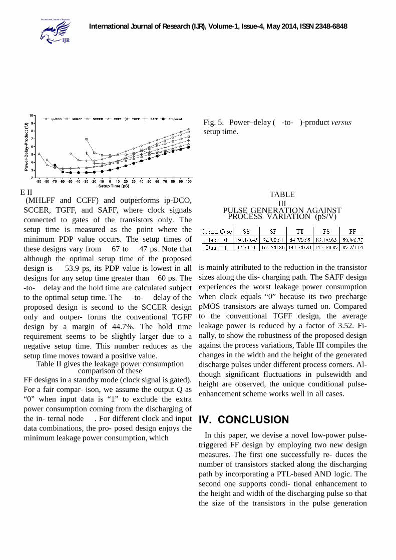
Fig. 5 shows the curves of power-delay-product (delay
from to ) versus setup time (for 50% data switching activity). The values of the proposed design are the smallest in all designs when the setup times are greater than 60 ps. Its minimum value occurs when the setup time is 53.9 ps and the corresponding -to- delay is 116.9 ps. The CCFF design is ranked in the second place in this evaluation with its optimal setup time as 67 ps. The setup time of the conventional TGFF design is always positive and has the smallest value when the setup time is 47 ps. In general, the MHLLF design has the worst performance due to the drawback of its latch structure. Fig. 6(a) shows the best performance of each design under different data switching activities. The proposed design takes the lead in all types of data switching activity. The SCCER and the CCFF designs almost tie in the second place. Fig. 6(b) shows the

International Journal of Research (IJR), Volume-1, Issue-4, May 2014, ISSN 2348-6848
performance of these designs at different process corners under the condition of 50% data switching activity. The performance edge of the proposed design is maintained as well. Notably, the MHLLF design has the worst performance especially at the SS process corner due to a large -to- delay and the poor driving capability of its pulse generation circuit. ower. Although the transistor count of the proposed design is not the lowest one, its actual layout area is the smaller than all but the TGFF
design. The MHLLF design exhibits the largest layout area because of an oversized pulse generation circuit. Following the measurement methods in [15], curves of -to- delay versus setup time and -to- delay versus hold time are simulated first. Setup time is defined as the point in the curve where -to- delay is the minimum. Hold time is measured at the point where the slope of the curve equals 1. The proposed design features the shortest minimum -to- delay. Its hold time is longer than other designs because the transistor (P3) for the pulse enhancement requires a prolonged availability of data input. The power drawn from the clock tree is calculated to evaluate the impact of FF loading on the clock jitter. Although the proposed FF design re- quires clock signal connected to the drain of transistor N2, the drawn current is not significant. Due to complementary switching behavior of N2 and N3, there exists no signal path from the entry of the clock signal to either or . The clock tree is only liable for charging/dis- charging node Z. The optimal PDP value of the proposed design is also
Fig. 2. Schematic of the proposed P-FF design with pulse control scheme.
III. SIMULATION RESULTS
Fig. 3. Simulation setup model.
Table I also summarizes some important performance indexes of these P-FF designs. These include transistor count, layout area, setup time, hold time, min -to- delay, optimal PDP, and the clock tree
International Journal of Research (IJR), Volume-1, Issue-4, May 2014, ISSN 2348-6848
Fig. 5. Power–delay ( -to- )-product versus setup time.
E II (MHLFF and CCFF) and outperforms ip-DCO, SCCER, TGFF, and SAFF, where clock signals connected to gates of the transistors only. The setup time is measured as the point where the minimum PDP value occurs. The setup times of these designs vary from 67 to 47 ps. Note that although the optimal setup time of the proposed design is 53.9 ps, its PDP value is lowest in all designs for any setup time greater than 60 ps. The -to- delay and the hold time are calculated subject to the optimal setup time. The -to- delay of the proposed design is second to the SCCER design only and outper- forms the conventional TGFF design by a margin of 44.7%. The hold time requirement seems to be slightly larger due to a negative setup time. This number reduces as the setup time moves toward a positive value.
Table II gives the leakage power consumption comparison of these
FF designs in a standby mode (clock signal is gated). For a fair compar- ison, we assume the output Q as “0” when input data is “1” to exclude the extra power consumption coming from the discharging of the in- ternal node . For different clock and input data combinations, the pro- posed design enjoys the minimum leakage power consumption, which
TABLE III
PULSE GENERATION AGAINST PROCESS VARIATION (pS/V)
is mainly attributed to the reduction in the transistor sizes along the dis- charging path. The SAFF design experiences the worst leakage power consumption when clock equals “0” because its two precharge pMOS transistors are always turned on. Compared to the conventional TGFF design, the average leakage power is reduced by a factor of 3.52. Fi- nally, to show the robustness of the proposed design against the process variations, Table III compiles the changes in the width and the height of the generated discharge pulses under different process corners. Al- though significant fluctuations in pulsewidth and height are observed, the unique conditional pulse-enhancement scheme works well in all cases.
IV. CONCLUSION In this paper, we devise a novel low-power pulse-
triggered FF design by employing two new design measures. The first one successfully re- duces the number of transistors stacked along the discharging path by incorporating a PTL-based AND logic. The second one supports condi- tional enhancement to the height and width of the discharging pulse so that the size of the transistors in the pulse generation

International Journal of Research (IJR), Volume-1, Issue-4, May 2014, ISSN 2348-6848
circuit can be kept minimum. Simulation results indicate that the proposed design excels rival designs in performance indexes such as power, -to- delay, and PDP. Coupled with these design merits is a longer hold-time require- ment inherent in pulse-
triggered FF designs. However, hold-time viola- tions are much easier to fix in circuit design compared with the failures in speed or power.
ACKNOWLEDGMENT The authors would like to thank National Chip
Implementation Center (CIC), Taiwan for technical support in simulations. The authors would also like to thank Y.-R. Cho and S.-W. Chen for their assistance in simulations and layouts.
International Journal of Research (IJR), Volume-1, Issue-4, May 2014, ISSN 2348-6848
REFERENCES [1] H. Kawaguchi and T. Sakurai, “A reduced clock-swing flip-flop
(RCSFF) for 63% power reduction,” IEEE J. Solid-State Circuits, vol. 33, no. 5, pp. 807–811, May 1998.
[2] A. G. M. Strollo, D. De Caro, E. Napoli, and N. Petra, “A novel high speed sense-amplifier-based flip-flop,” IEEE Trans. Very Large Scale Integr. (VLSI) Syst., vol. 13, no. 11, pp. 1266–1274, Nov. 2005.
[3] H. Partovi, R. Burd, U. Salim, F. Weber, L. DiGregorio, and D. Draper, “Flow-through latch and edge-triggered flip-flop hybrid elements,” in IEEE Tech. Dig. ISSCC, 1996, pp. 138–139.
[4] F. Klass, C. Amir, A. Das, K. Aingaran, C. Truong, R. Wang, A. Mehta,
R. Heald, and G. Yee, “A new family of semi-dynamic and dynamic flip flops with embedded logic for high-performance processors,” IEEE J. Solid-State Circuits, vol. 34, no. 5, pp. 712–716, May 1999.
[5] S. D. Naffziger, G. Colon-Bonet, T. Fischer, R. Riedlinger, T. J.
Sullivan, and T. Grutkowski, “The implementation of the Itanium 2 microprocessor,” IEEE J. Solid-State Circuits, vol. 37, no. 11, pp. 1448–1460, Nov. 2002.
[6] J. Tschanz, S. Narendra, Z. Chen, S. Borkar, M. Sachdev, and V. De, “Comparative delay and energy of single edge-triggered and dual edge triggered pulsed flip-flops for high-performance microprocessors,” in Proc. ISPLED, 2001, pp. 207–212.
[7] B. Kong, S. Kim, and Y. Jun, “Conditional-capture flip-flop for statis-
tical power reduction,” IEEE J. Solid-State Circuits, vol. 36, no. 8, pp. 1263–1271, Aug. 2001.
[8] N. Nedovic, M. Aleksic, and V. G.
Oklobdzija, “Conditional precharge techniques for power-efficient dual-edge clocking,” in Proc. Int. Symp. Low-Power Electron. Design, Monterey, CA, Aug. 12–14, 2002, pp. 56–59.
[9] P. Zhao, T. Darwish, and M. Bayoumi, “High-performance and low power conditional discharge flip-flop,” IEEE Trans. Very Large Scale Integr. (VLSI) Syst., vol. 12, no. 5, pp. 477–484, May 2004.
[10] C. K. Teh, M. Hamada, T. Fujita, H. Hara, N. Ikumi, and Y. Oowaki, “Conditional data mapping flip-flops for low-power and high-perfor- mance systems,” IEEE Trans. Very Large Scale Integr. (VLSI) Systems, vol. 14, pp. 1379–1383, Dec. 2006.
[11] S. H. Rasouli, A. Khademzadeh, A. Afzali-Kusha, and M. Nourani,
“Low power single- and double-edge-triggered flip-flops for high speed applications,” Proc. Inst. Electr. Eng.—Circuits Devices Syst., vol. 152, no. 2, pp. 118–122, Apr. 2005.
[12] H. Mahmoodi, V. Tirumalashetty, M. Cooke, and K. Roy, “Ultra low power clocking scheme using energy recovery and clock gating,” IEEE Trans. Very Large Scale Integr. (VLSI) Syst., vol. 17, pp. 33–44, Jan. 2009.
[13] P. Zhao, J. McNeely, W. Kaung, N. Wang, and Z. Wang, “Design of sequential elements for low power clocking system,” IEEE Trans. Very Large Scale Integr. (VLSI) Syst., to be published.
[14] Y.-H. Shu, S. Tenqchen, M.-C. Sun, and W.-S. Feng, “XNOR-based
double-edge-triggered flip-flop for two-phase pipelines,” IEEE Trans. Circuits Syst. II, Exp. Briefs, vol. 53, no. 2, pp. 138–142, Feb. 2006.
[15] V. G. Oklobdzija, “Clocking and clocked storage elements in a multi- giga-hertz environment,” IBM J. Res. Devel., vol. 47, pp. 567–584, Sep.
200.