chapter 7: sequential circuits - flip-flops registers flip flops, registers, and counters
TRANSCRIPT
1
CHAPTER 7:SEQUENTIAL CIRCUITS -FLIP-FLOPS REGISTERSFLIP FLOPS, REGISTERS, AND COUNTERS
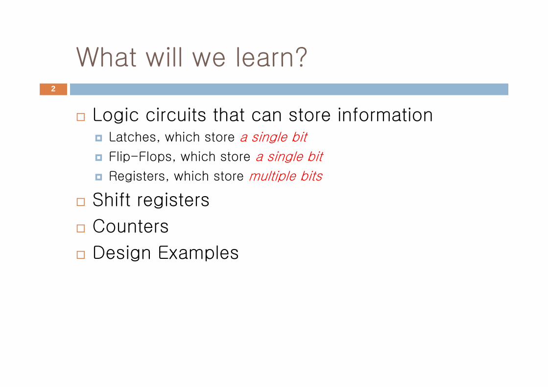
What will we learn?What will we learn?2
Logic circuits that can store informationLatches, which store a single bit
Flip-Flops, which store a single bit
Registers, which store multiple bits
Shift i tShift registers
Counters
Design Examples
Sequential CircuitsSequential Circuits3
Combinational Circuitscircuits without feedback
( )output = f (current inputs)
Sequential Circuitscircuits with feedback
output = f (current inputs, past inputs, past outputs)
how can we feed the past inputs and outputs into the circuits?
b i f b ildi “ ” i l i i ibasis for building “memory” into logic circuits
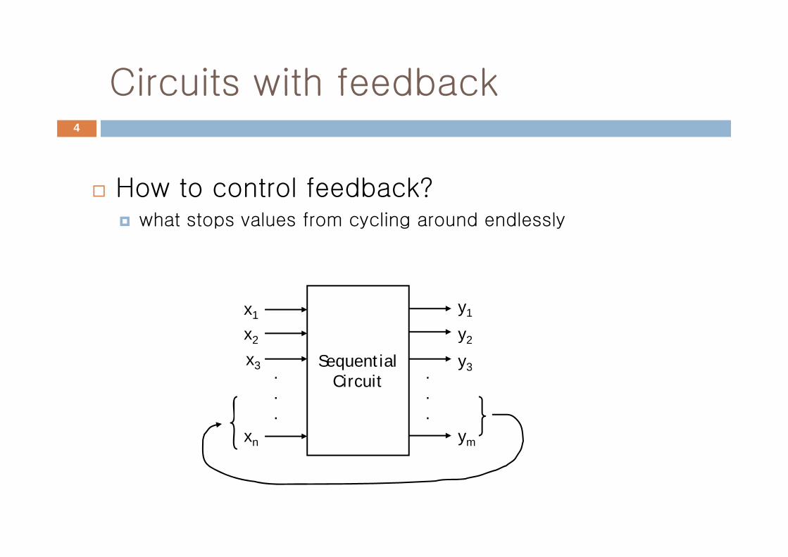
Circuits with feedbackCircuits with feedback4
How to control feedback?h t t l f li d dl lwhat stops values from cycling around endlessly
x1
x2
y1
y2
SequentialCircuit
2
x3
y2
y3..
.
.
xn ym
. .
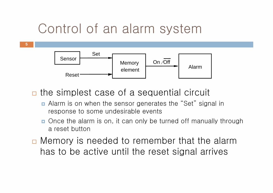
Control of an alarm systemControl of an alarm system5
S t
Memoryelement Alarm
Sensor
Reset
Set On Off ⁄
the simplest case of a sequential circuit
Reset
p qAlarm is on when the sensor generates the “Set” signal in response to some undesirable events
O h l i i l b d ff ll h hOnce the alarm is on, it can only be turned off manually through a reset button
Memory is needed to remember that the alarmMemory is needed to remember that the alarm has to be active until the reset signal arrives
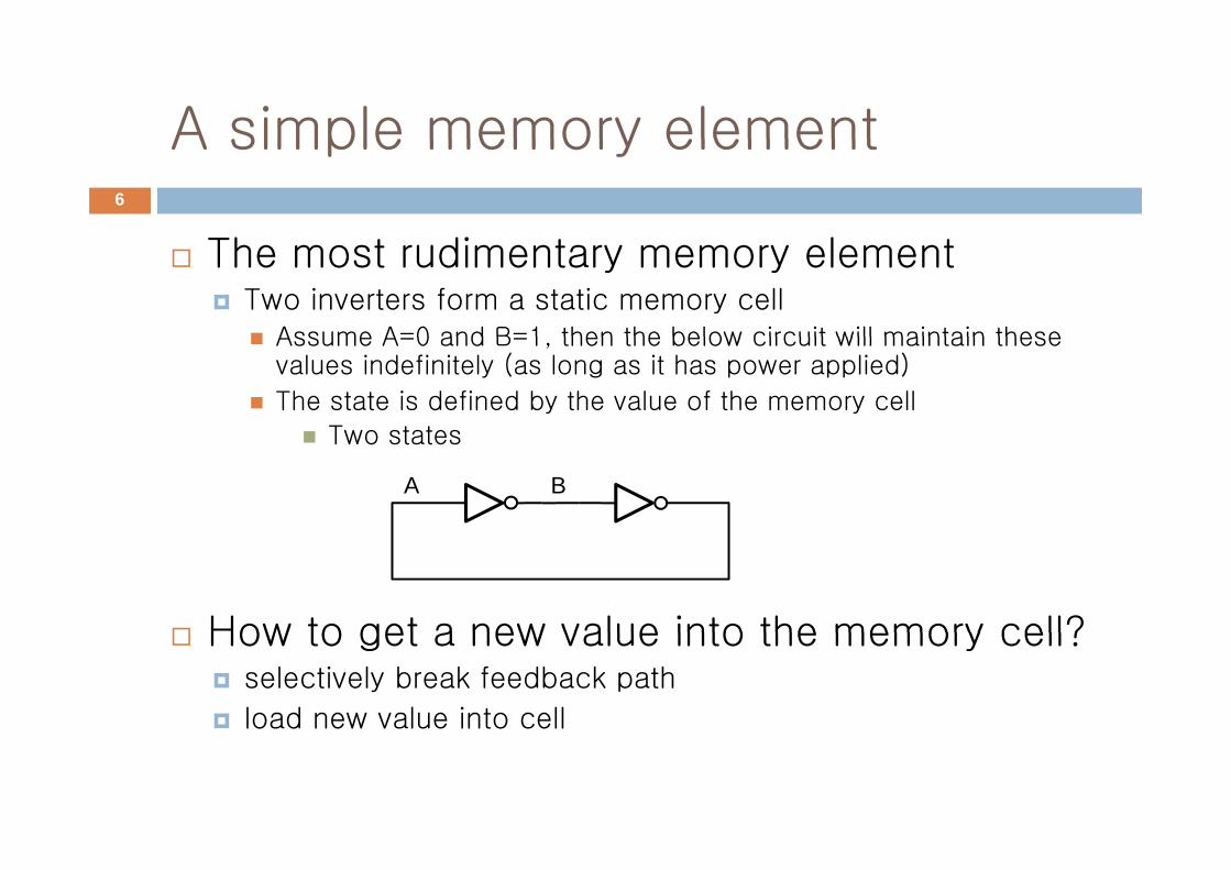
A simple memory elementA simple memory element6
Th di lThe most rudimentary memory element Two inverters form a static memory cell
Assume A=0 and B=1 then the below circuit will maintain theseAssume A=0 and B=1, then the below circuit will maintain these values indefinitely (as long as it has power applied)
The state is defined by the value of the memory cell
Two states
A B
Two states
How to get a new value into the memory cell?How to get a new value into the memory cell?selectively break feedback path
load new value into cell
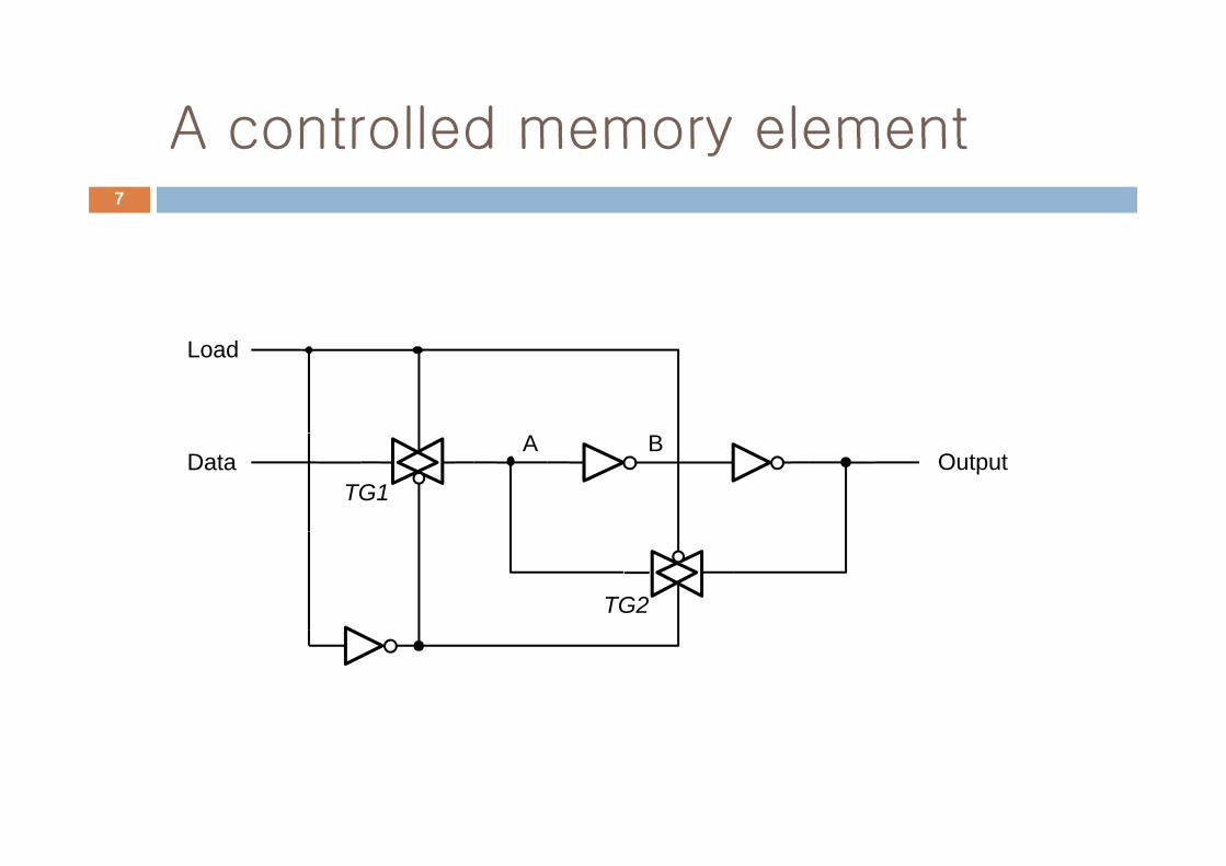
A controlled memory elementA controlled memory element7
Load
A B OutputData
TG1
TG2
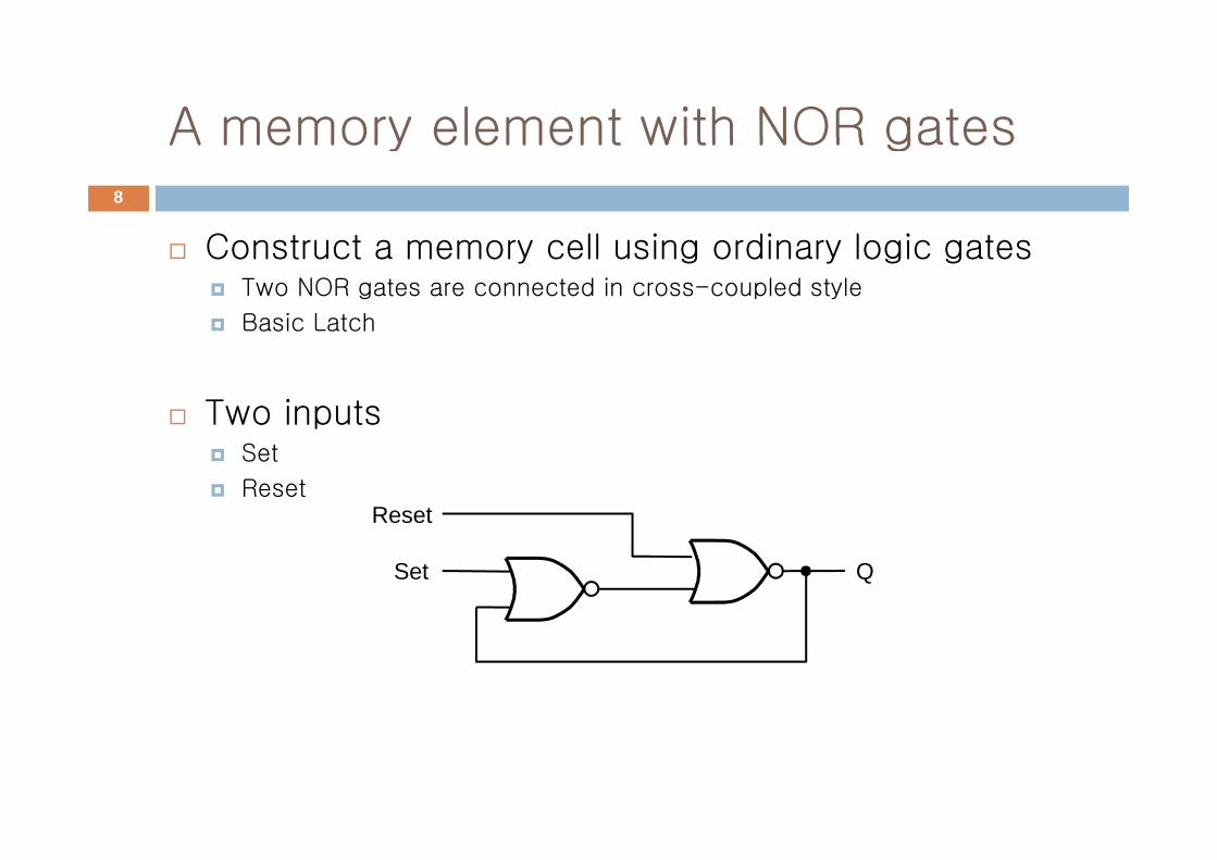
A memory element with NOR gatesA memory element with NOR gates8
C t t ll i di l i tConstruct a memory cell using ordinary logic gatesTwo NOR gates are connected in cross-coupled style
Basic Latch
Two inputs
Reset
Set
Reset
Set Q
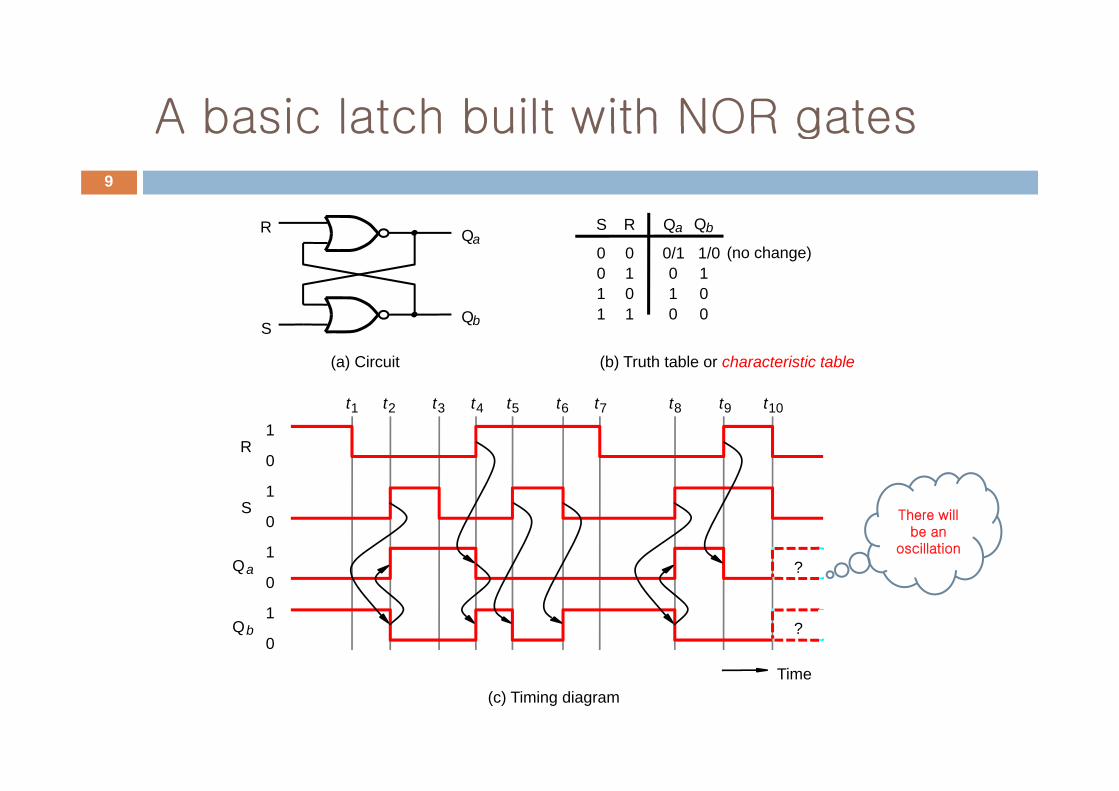
A basic latch built with NOR gatesA basic latch built with NOR gates9
S R Qa Qb
0 00 11 0
0/1 1/00 11 0
QaR
(no change)
1 1 0 0
(a) Circuit (b) Truth table or characteristic table
QbS
1
0
1
R
t1 t2 t3 t4 t5 t6 t7 t8 t9 t10
1
0
1
S
Qa ?
There will be an
oscillation
0
1
0Qb ?
Time(c) Timing diagram
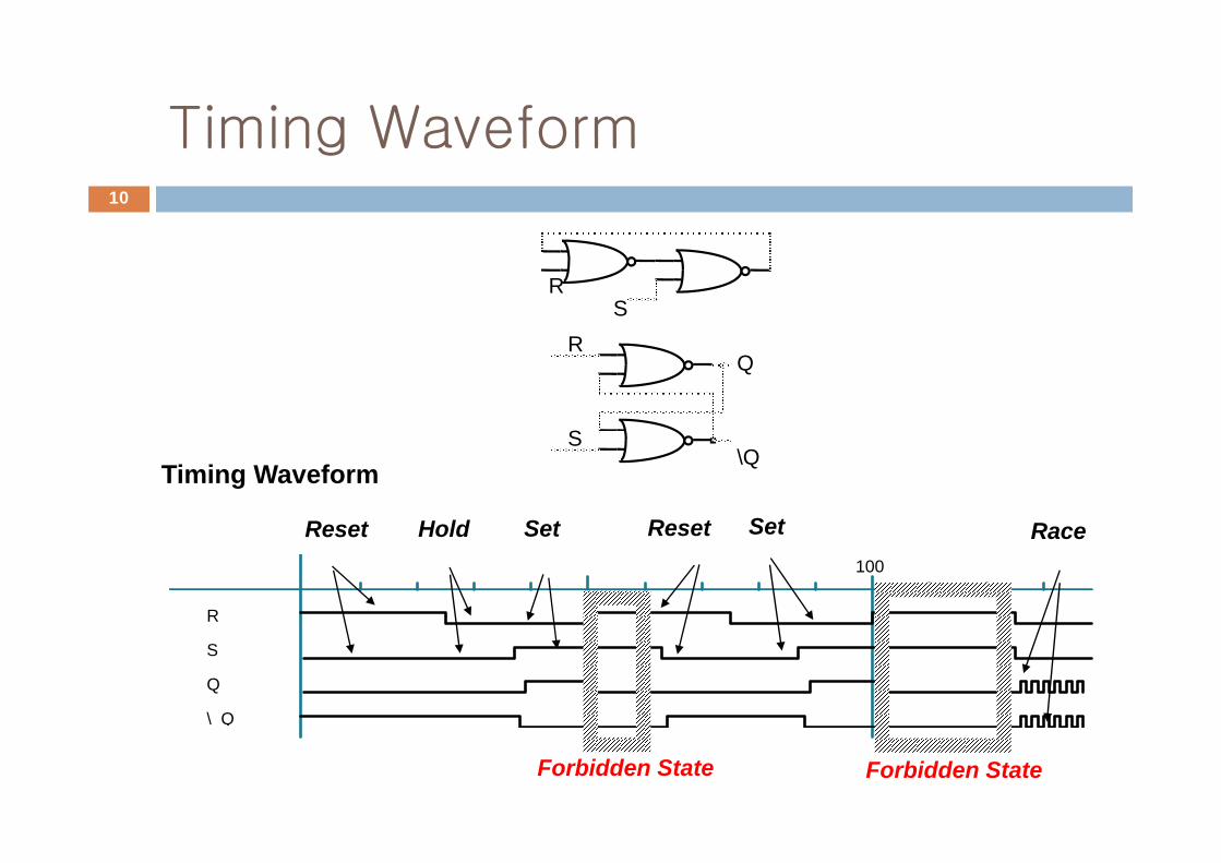
Timing WaveformTiming Waveform10
RS
R
S
Q
Timing Waveform
Reset Hold Set Reset Set Race
S\Q
100
R
Reset Hold Set Reset Set Race
S
Q
\ Q
Forbidden State Forbidden State
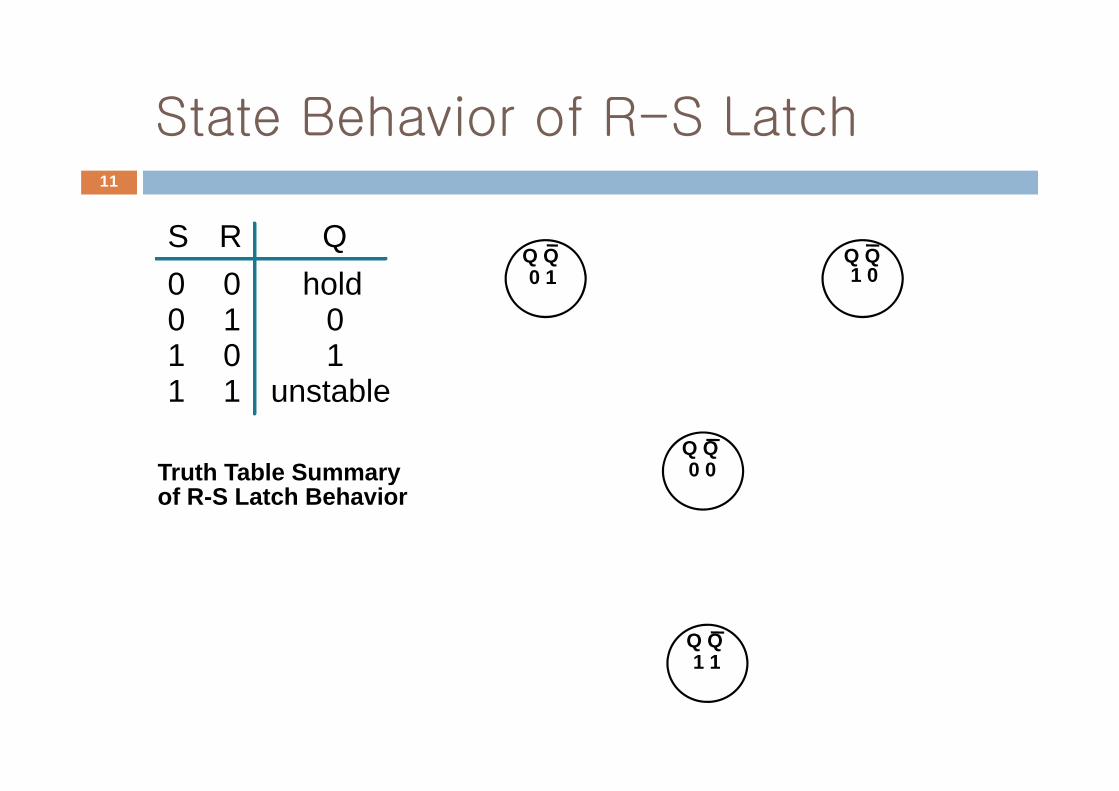
State Behavior of R-S LatchState Behavior of R S Latch11
Q hold
S 0
R 0
Q Q Q Q0 1 1 0
0 1
unstable
0 1 1
1 0 1
Truth Table Summary
unstable 1 1
Q Q0 0
of R-S Latch Behavior
Q Q1 11 1
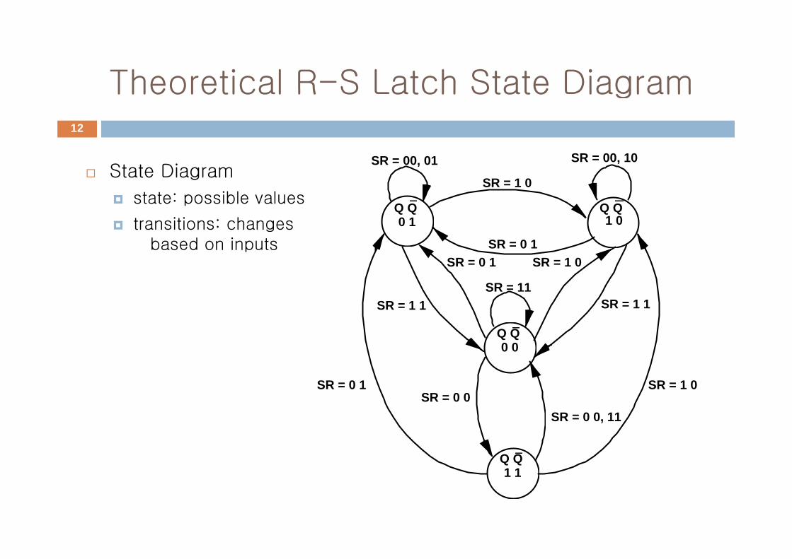
Theoretical R-S Latch State DiagramTheoretical R S Latch State Diagram12
Q Q Q Q1 0
SR = 1 0
SR = 00, 01 SR = 00, 10State Diagram
state: possible values
0 1 1 0
SR = 0 1SR = 0 1 SR = 1 0
transitions: changes based on inputs
Q Q0 0
SR = 1 1 SR = 1 1SR = 11
0 0
SR = 0 0SR = 1 0SR = 0 1
Q Q1 1
SR = 0 0, 11
1 1
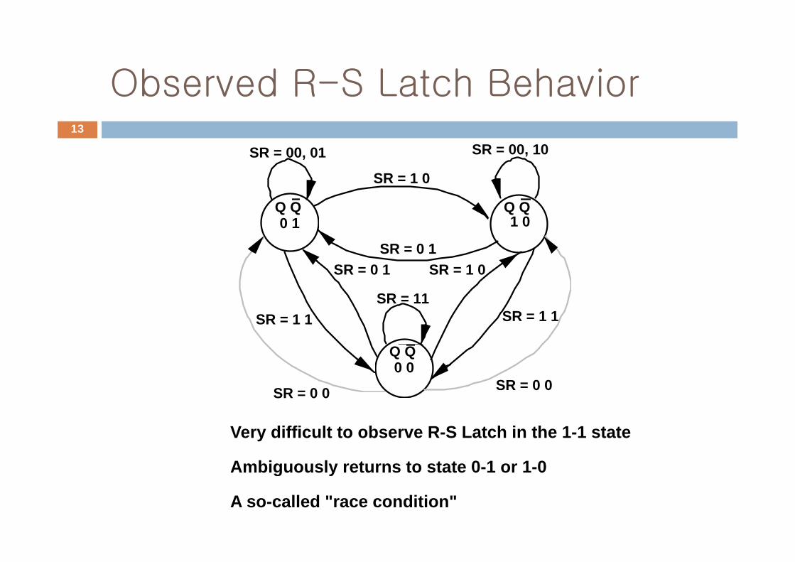
Observed R-S Latch Behavior
SR = 00 01 SR = 00, 10
Observed R S Latch Behavior13
Q Q Q Q1 0
SR = 1 0
SR = 00, 01 SR 00, 10
0 1 1 0
SR = 0 1SR = 0 1 SR = 1 0
SR = 1 1 SR = 1 1SR = 11
Q Q0 0
SR = 0 0 SR = 0 0
Very difficult to observe R-S Latch in the 1-1 state
Ambiguously returns to state 0-1 or 1-0Ambiguously returns to state 0 1 or 1 0
A so-called "race condition"
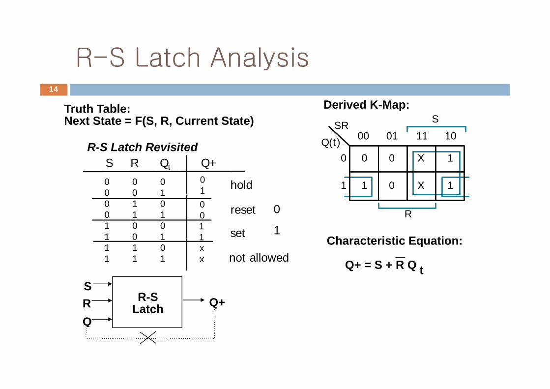
R-S Latch Analysis
T th T bl Derived K-Map:
R S Latch Analysis14
R-S Latch Revisited
Truth Table:Next State = F(S, R, Current State)
Derived K-Map:SR
00 01 11 10 Q ( t )
S
R S Latch Revisited0 0 X 1
1 0 X 1
0
1
S R Qt
0 0 00 0 1
Q+01 hold
Characteristic Equation:
R
0 0 10 1 00 1 11 0 01 0 1
0
1
0011
reset
set
S
Characteristic Equation:
Q+ = S + R Q t
1 0 11 1 01 1 1
1xx not allowed
SRQ
R-SLatch Q+
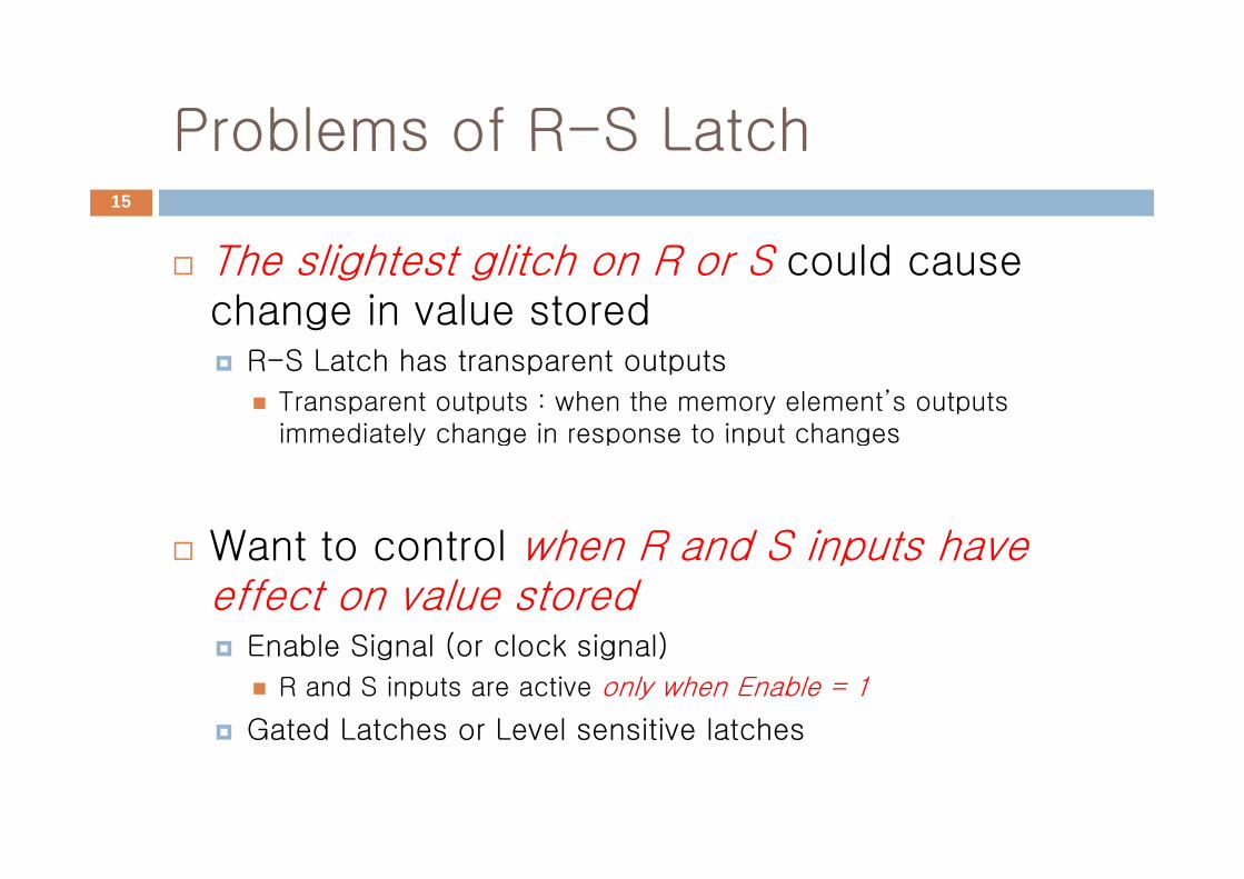
Problems of R-S LatchProblems of R S Latch15
The slightest glitch on R or S could cause change in value stored
R-S Latch has transparent outputs
Transparent outputs : when the memory element’s outputs immediately change in response to input changesimmediately change in response to input changes
Want to control when R and S inputs haveWant to control when R and S inputs have effect on value stored
E bl Si l ( l k i l)Enable Signal (or clock signal)
R and S inputs are active only when Enable = 1
Gated Latches or Level sensitive latchesGated Latches or Level sensitive latches
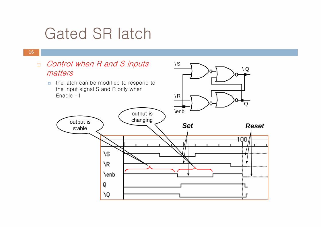
Gated SR latchGated SR latch
C t l h R d S i t
16
\ SControl when R and S inputs matters
the latch can be modified to respond to th i t i l S d R l h
\ S \ Q
the input signal S and R only when Enable =1 \ R
Q \enb output is
Set Reset
output is changingoutput is
stable
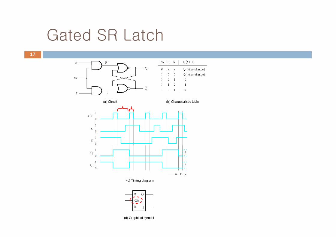
Gated SR LatchGated SR Latch17
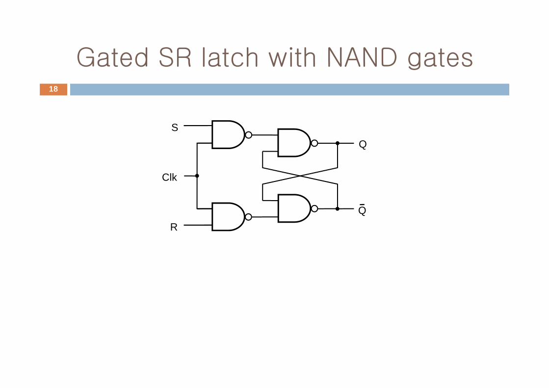
Gated SR latch with NAND gatesGated SR latch with NAND gates18
S Q
Clk
R Q
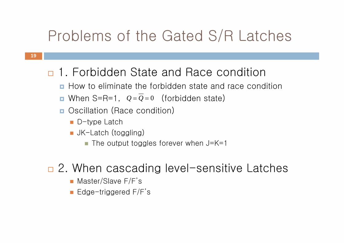
Problems of the Gated S/R LatchesProblems of the Gated S/R Latches19
1. Forbidden State and Race conditionHow to eliminate the forbidden state and race condition
When S=R=1, (forbidden state)
Oscillation (Race condition)
D-type Latch
0== QQ
D-type Latch
JK-Latch (toggling)
The output toggles forever when J=K=1
2. When cascading level-sensitive LatchesMaster/Slave F/F’s
Edge-triggered F/F’s
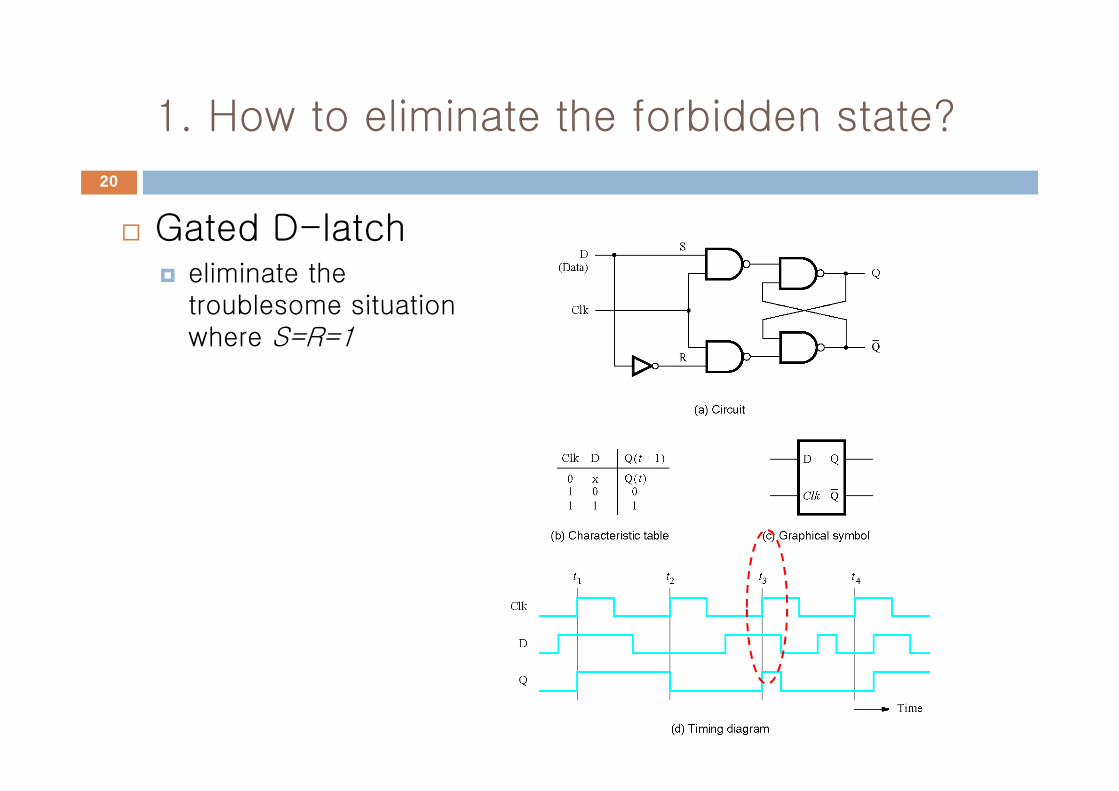
1 How to eliminate the forbidden state?1. How to eliminate the forbidden state?
20
G t d D l t hGated D-latcheliminate the troublesome situationtroublesome situation where S=R=1
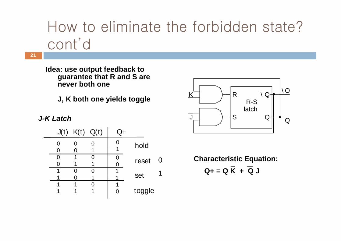
How to eliminate the forbidden state? ’cont’d
21
Idea: use output feedback toguarantee that R and S arenever both one
K R \ Q \ Q
J-K Latch
J, K both one yields toggle R-S latch
K
J S
R
Q
\ Q
QJ K Latch
J(t) K(t) Q(t)0 0 0
Q+01 hold
Q
Characteristic Equation:Q+ = Q K + Q J
0 0 10 1 00 1 11 0 0
0
1
1001
hold
reset
set1 0 11 1 01 1 1
1110 toggle
set
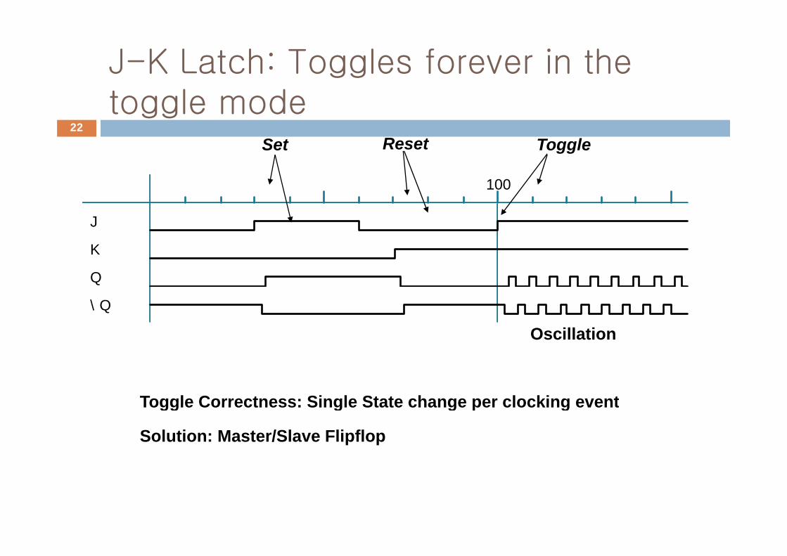
J-K Latch: Toggles forever in the
Set Reset Toggle
toggle mode22
100
gg
J
K
\ Q
Oscillation
Toggle Correctness: Single State change per clocking eventToggle Correctness: Single State change per clocking event
Solution: Master/Slave Flipflop
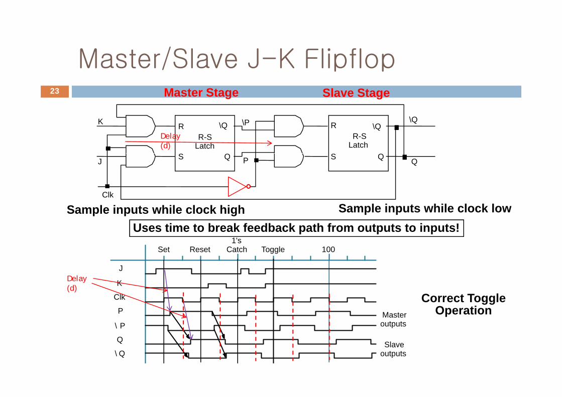
Master/Slave J-K FlipflopMaster Stage Slave Stage
Master/Slave J K Flipflop23
R-S Latch
R-S Latch
K R
S
\Q
Q
\P R
S
\Q
Q
\Q
Delay(d)
J S
Clk
Q P S Q Q
Sample inputs while clock high Sample inputs while clock lowUses time to break feedback path from outputs to inputs!
1's Set Reset T oggle Catch 100
J
K Delay(d)
Correct ToggleOperationMaster
outputs
Clk
P
\ P
(d)
Slave outputs
Q
\ Q
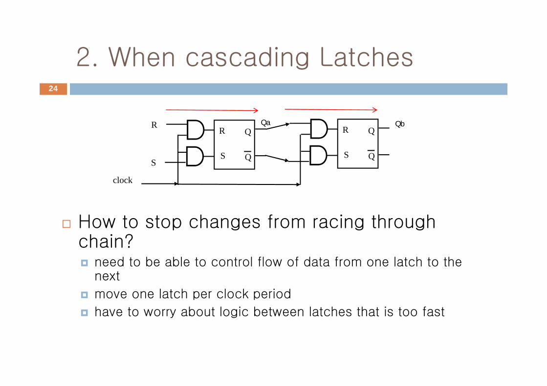
2 When cascading Latches2. When cascading Latches24
R QR R Q
Qa Qb
S QSS Q
clock
How to stop changes from racing through h i ?chain?need to be able to control flow of data from one latch to the next
move one latch per clock period
have to worry about logic between latches that is too fast
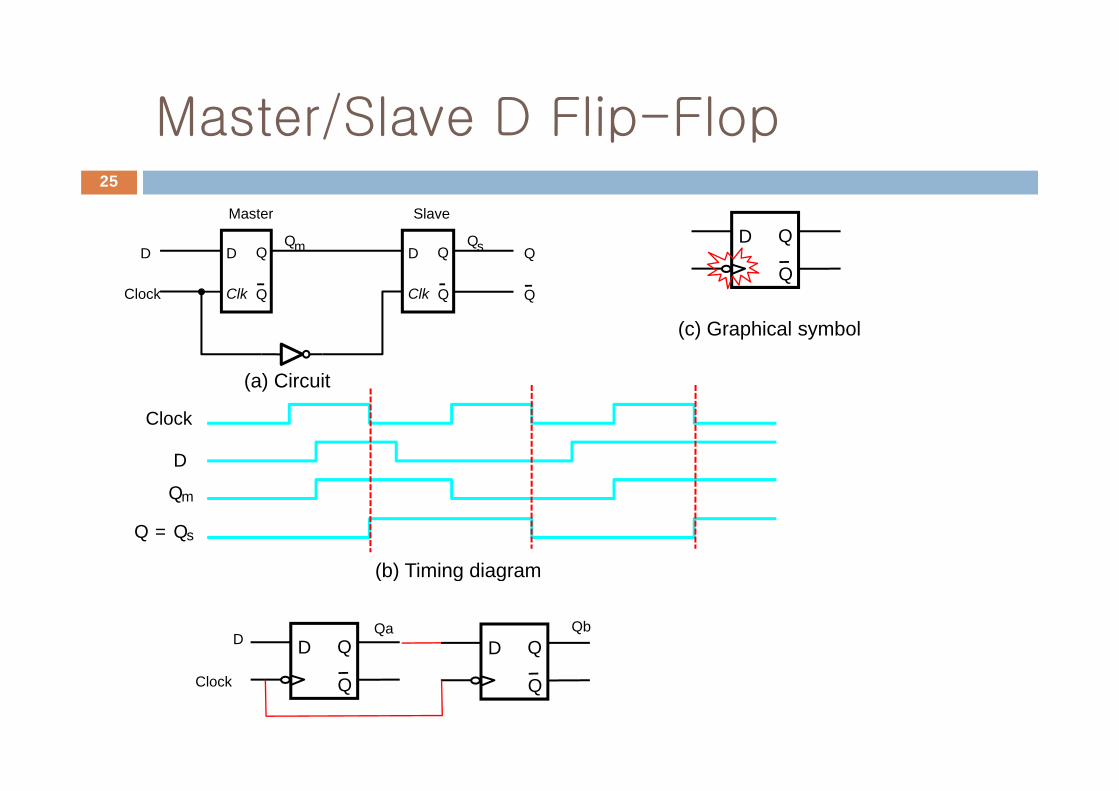
Master/Slave D Flip-FlopMaster/Slave D Flip Flop 25
Master SlaveD Q
Q D Q
Q
Master Slave
D
Clock
Q
Q
D Q
Q
Q m Q s
Clk Clk
(a) Circuit
(c) Graphical symbol
D
Clock
Q m
Q Q s =
(b) Timing diagram(b) Timing diagram
D Q D Q DQa Qb
Q Q Clock
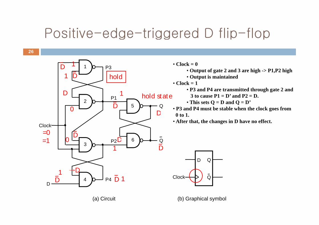
Positive-edge-triggered D flip-flopPositive edge triggered D flip flop26
1 P31 • Clock = 0• Output of gate 2 and 3 are high -> P1,P2 high• Output is maintained
• Clock = 1
D 1
hold1 D
P15
2 Q
• P3 and P4 are transmitted through gate 2 and3 to cause P1 = D’ and P2 = D.
• This sets Q = D and Q = D’• P3 and P4 must be stable when the clock goes from
1 hold stateD
DD0
Clock
6
0 to 1.• After that, the changes in D have no effect.
=01 D
D
D0 P2 6
3
D Q
Q
1=1 D
D0
D P4 Q Clock 4 DD 1
1 →D
(a) Circuit (b) Graphical symbol
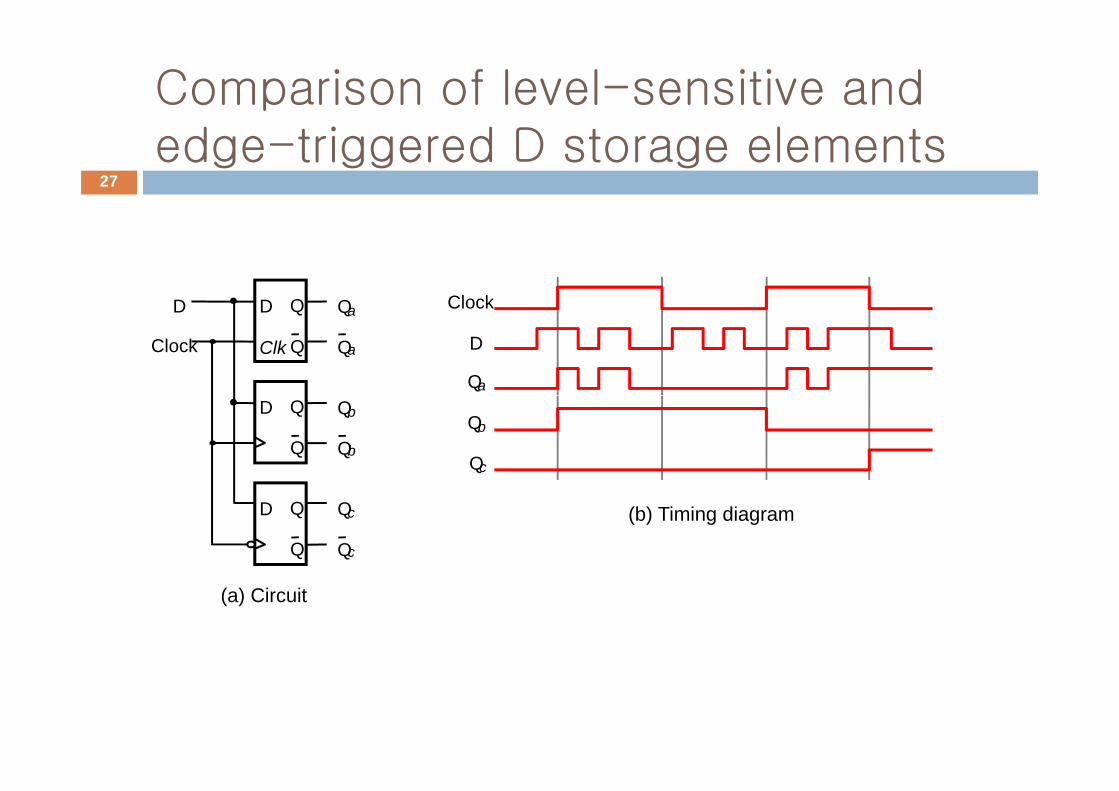
Comparison of level-sensitive and edge-triggered D storage elements
27
D QD Q ClockD Q
Q
D
Clock Q a
Q a
Clk D
Clock
Q a D Q
Q Q b
Q b Q b
Q c
D Q
Q Q c
Q c (b) Timing diagram
(a) Circuit
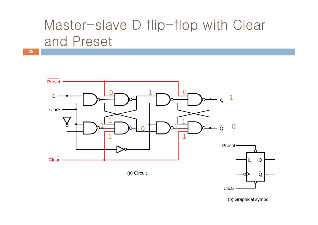
Master-slave D flip-flop with Clear and Preset
28
Preset
Q D
Clock
0 011
Q 1
1
11
10 1 0
D Q
Preset
Clear
11
Q
Clear
(a) Circuit
(b) Graphical symbol
Clear
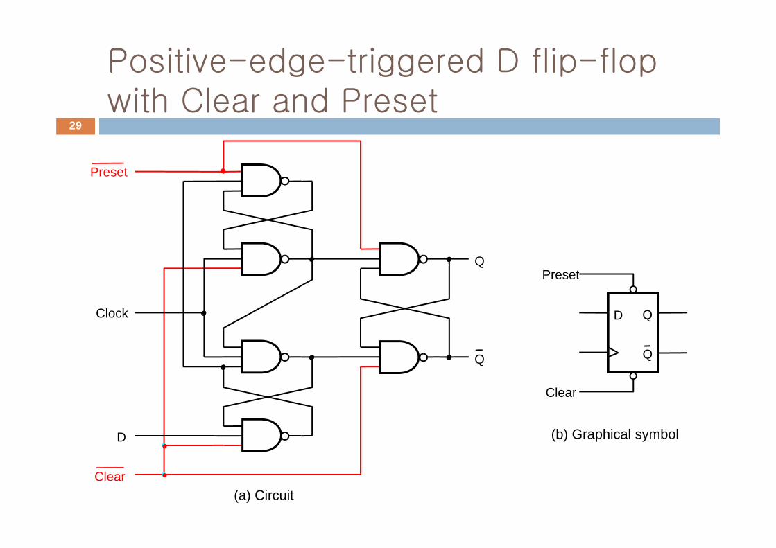
Positive-edge-triggered D flip-flop with Clear and Preset
29
Preset
PresetQ
Preset
D Q Clock
Clear
Q Q
(b) Graphical symbolD
Clear (a) Circuit
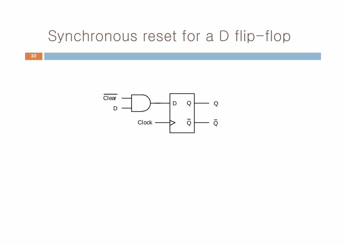
Synchronous reset for a D flip-flopSynchronous reset for a D flip flop30
D
Clock Q
QClear
D Q
QClock QQ
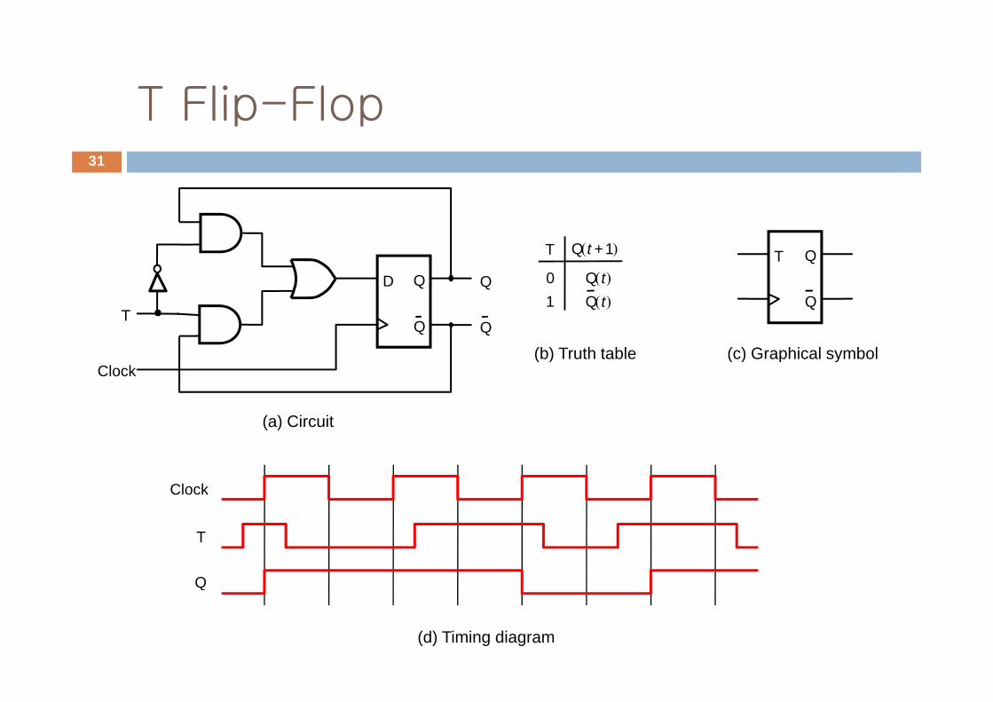
T Flip-FlopT Flip Flop31
T Q T Q t 1 + ( )
D Q
Q
Q
Q T
Q 0 1
Q t ( )
Q t ( )
(b) Truth table (c) Graphical symbolClock
(a) Circuit
(b) Truth table (c) Graphical symbol
Clock
T
Q
(d) Timing diagram
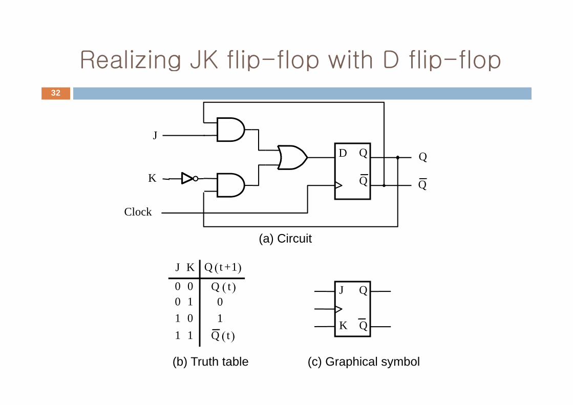
Realizing JK flip-flop with D flip-flopRealizing JK flip flop with D flip flop32
D Q Q
JD Q
Q
Q
QK
Clock
(a) Circuit
J Q
K
0
Q t 1+( )
Q t( )
J
0 Q
Q
1 000 111 Q t( )1
K
(b) Truth table (c) Graphical symbol
Q ( )
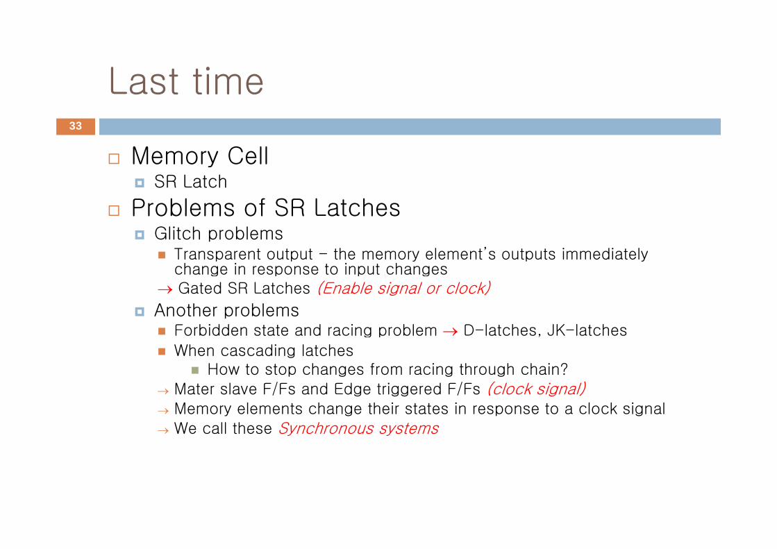
Last timeLast time33
M C llMemory CellSR Latch
Problems of SR LatchesProblems of SR LatchesGlitch problems
Transparent output - the memory element’s outputs immediately change in response to input changeschange in response to input changes
→ Gated SR Latches (Enable signal or clock)
Another problemsForbidden state and racing problem → D-latches, JK-latchesg p ,
When cascading latches How to stop changes from racing through chain?
→ Mater slave F/Fs and Edge triggered F/Fs (clock signal)→ Memory elements change their states in response to a clock signal→ We call these Synchronous systems
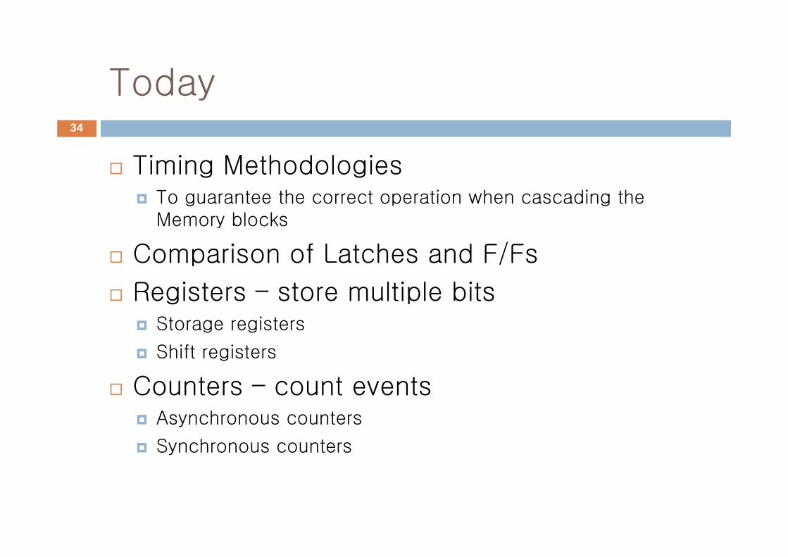
TodayToday34
Timing MethodologiesTo guarantee the correct operation when cascading the M bl kMemory blocks
Comparison of Latches and F/Fs
Registers – store multiple bitsStorage registers
Shift registers
Counters – count eventsAsynchronous counters
Synchronous counters
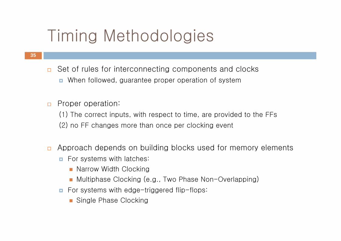
Timing MethodologiesTiming Methodologies35
Set of rules for interconnecting components and clocks
When followed, guarantee proper operation of system
Proper operation:
(1) The correct inputs, with respect to time, are provided to the FFs
(2) no FF changes more than once per clocking event
Approach depends on building blocks used for memory elementsApproach depends on building blocks used for memory elements
For systems with latches:
Narrow Width Clocking
Multiphase Clocking (e.g., Two Phase Non-Overlapping)
For systems with edge-triggered flip-flops:
Single Phase ClockingSingle Phase Clocking
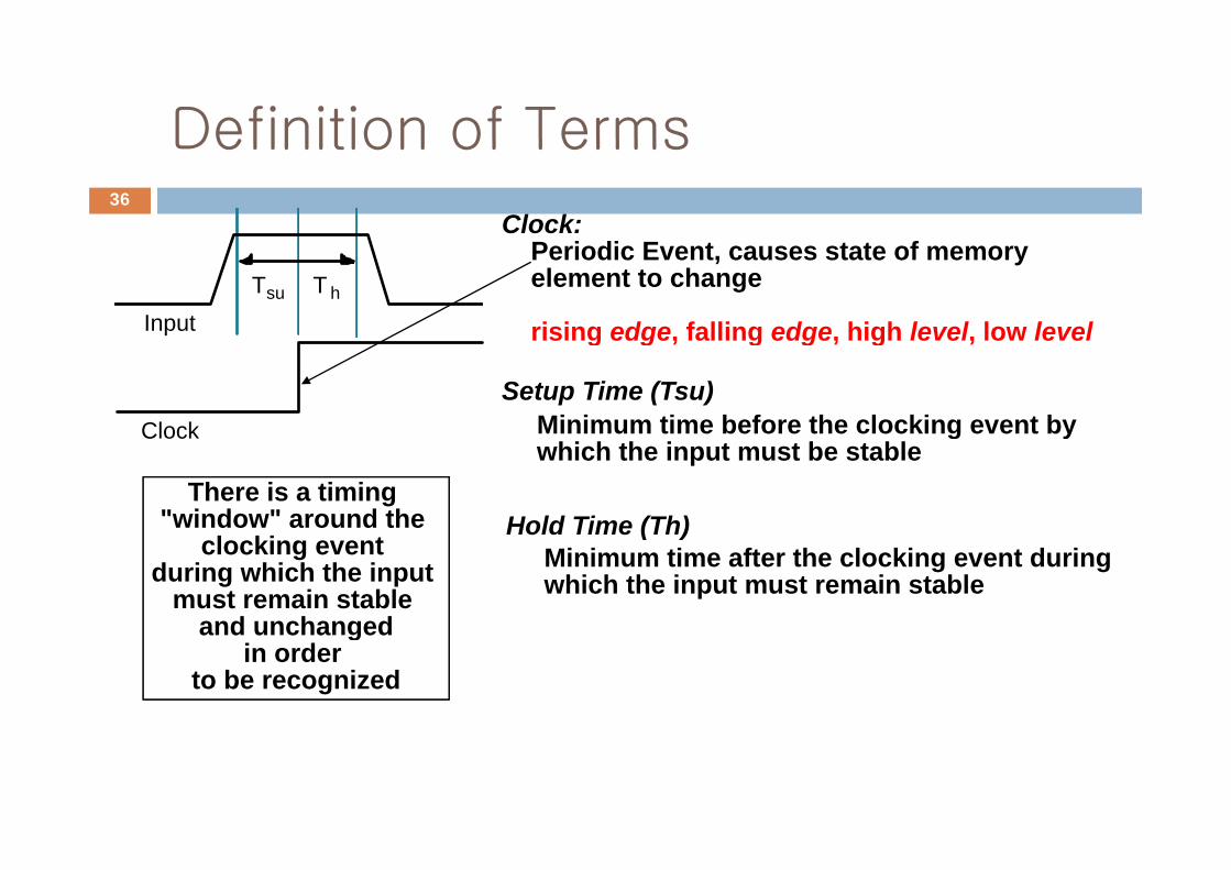
Definition of Terms
Clock:
Definition of Terms36
Input T su T h
Periodic Event, causes state of memoryelement to change
rising edge falling edge high level low level
ClockSetup Time (Tsu)
rising edge, falling edge, high level, low level
Minimum time before the clocking event by Clock
There is a timing "window" around the
g ywhich the input must be stable
Hold Time (Th)clocking event
during which the input must remain stable
and unchanged
Hold Time (Th)Minimum time after the clocking event during which the input must remain stable
and unchangedin order
to be recognized
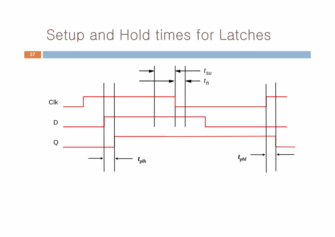
Setup and Hold times for LatchesSetup and Hold times for Latches37
t sut h
Clk
D
Q
tplhtphl
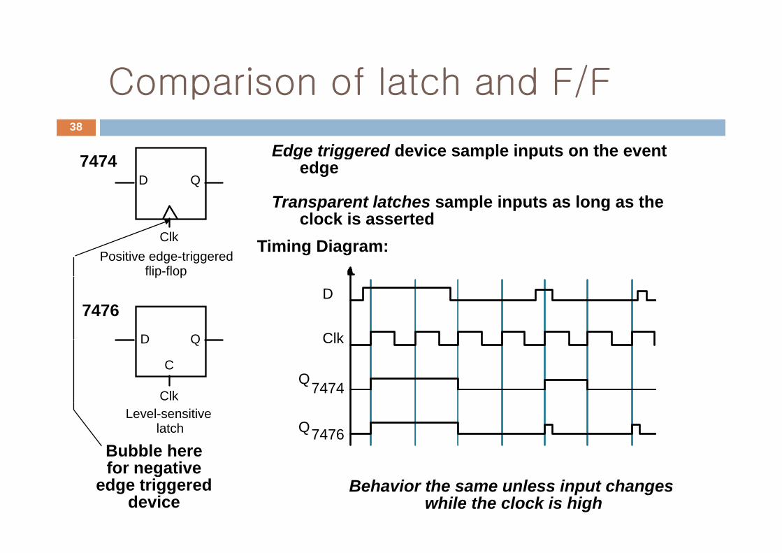
Comparison of latch and F/FComparison of latch and F/F38
Edge triggered device sample inputs on the event7474 Edge triggered device sample inputs on the eventedge
Transparent latches sample inputs as long as thel k i t d
D Q
Timing Diagram:clock is asserted
Positive edge-triggered flip-flop
Clk
7476
p p
D Q
D
ClkD Q
C
Clk
Clk
Q 7474
Bubble herefor negative
Level-sensitive latch Q 7476
for negativeedge triggered
deviceBehavior the same unless input changes
while the clock is high
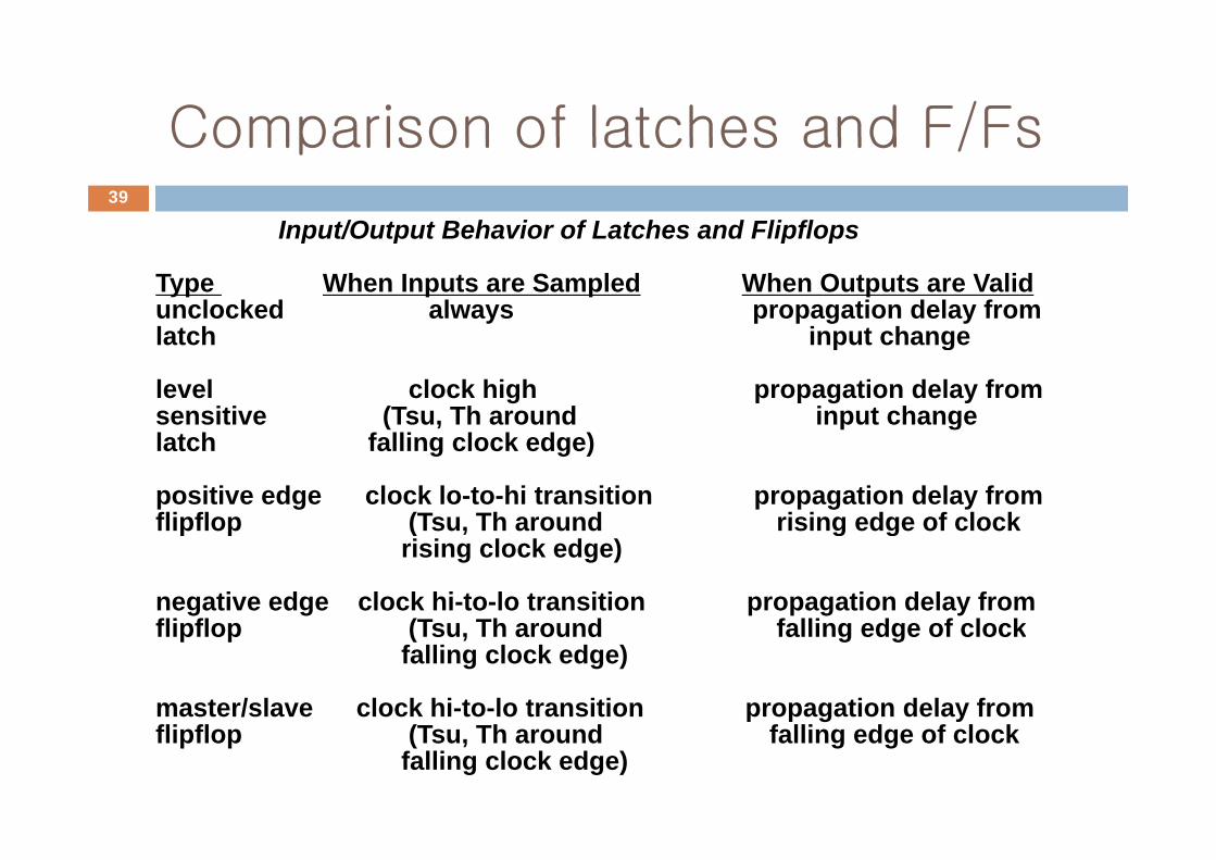
Comparison of latches and F/FsComparison of latches and F/Fs39
Input/Output Behavior of Latches and FlipflopsInput/Output Behavior of Latches and Flipflops
Type When Inputs are Sampled When Outputs are Validunclocked always propagation delay from latch input changelatch input change
level clock high propagation delay fromsensitive (Tsu, Th around input changelatch falling clock edge)
positive edge clock lo-to-hi transition propagation delay fromflipflop (Tsu, Th around rising edge of clockflipflop (Tsu, Th around rising edge of clock
rising clock edge)
negative edge clock hi-to-lo transition propagation delay fromflipflop (Tsu Th around falling edge of clockflipflop (Tsu, Th around falling edge of clock
falling clock edge)
master/slave clock hi-to-lo transition propagation delay fromflipflop (Tsu, Th around falling edge of clock
falling clock edge)
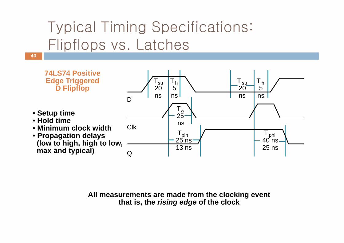
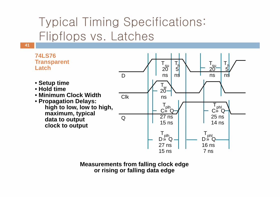
Typical Timing Specifications: Flipflops vs. Latches
40
74LS74 PositiveEdge Triggered
D FlipflopT su 20
T h 5
T su 20
T h 5
• Setup time• Hold time
D ns ns
T w 25
ns ns
Hold time• Minimum clock width• Propagation delays(low to high, high to low,
d t i l)
Clk ns T plh 25 ns 13 ns
T phl 40 ns 25 nsmax and typical) Q
13 ns 25 ns
All measurements are made from the clocking eventthat is, the rising edge of the clockthat is, the rising edge of the clock
Typical Timing Specifications: Flipflops vs. Latches
41
74LS7674LS76TransparentLatch
T su 20 ns
T h 5 ns
T su 20 ns
T h 5 nsD
• Setup time• Hold time• Minimum Clock Width
ns ns ns ns
T w 20 ns
D
Clk• Propagation Delays:
high to low, low to high,maximum, typicaldata to output
ns T plh
C » Q 27 ns 15
T phl C » Q 25 ns 14
Clk
Q data to outputclock to output 15 ns 14 ns
T plh D » Q 27
T phl D » Q 16
Measurements from falling clock edge
27 ns 15 ns
16 ns 7 ns
Measurements from falling clock edgeor rising or falling data edge
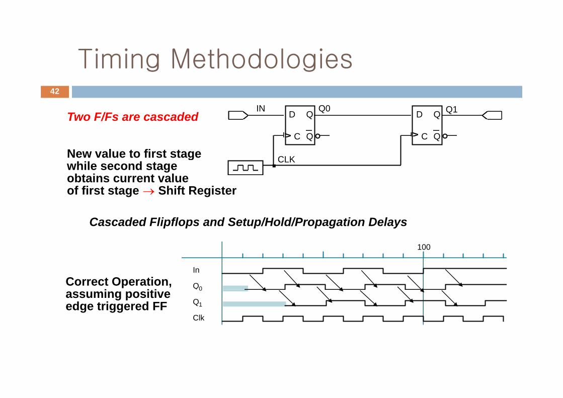
Timing MethodologiesTiming Methodologies42
IN Q0 Q1Two F/Fs are cascaded
New value to first stage
IN Q0 Q1D
C
Q
Q
D
C
Q
Q
New value to first stagewhile second stageobtains current valueof first stage → Shift Register
CLK
100
Cascaded Flipflops and Setup/Hold/Propagation Delays
In
Q 0
100
Correct Operation,i i i 0
Q 1
Clk
assuming positiveedge triggered FF
Cascaded Flipflops and / /Setup/Hold/Propagation Delays
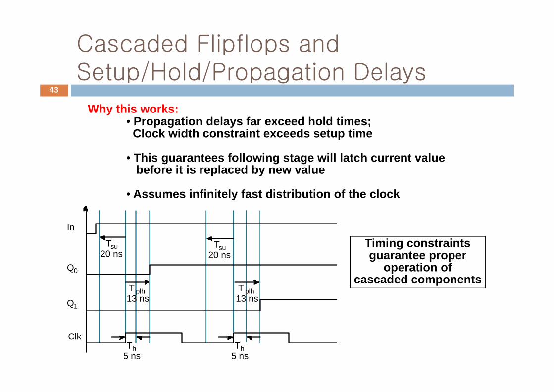
43
Why this works:Why this works:• Propagation delays far exceed hold times; Clock width constraint exceeds setup time
• This guarantees following stage will latch current valuebefore it is replaced by new value
• Assumes infinitely fast distribution of the clockAssumes infinitely fast distribution of the clock
Ti i t i tT
In
Timing constraintsguarantee proper
operation ofcascaded components
T su 20 ns
T
T su 20 ns
T
Q 0 p
T plh 13 ns
T plh 13 ns Q 1
T h 5 ns
T h 5 ns
Clk
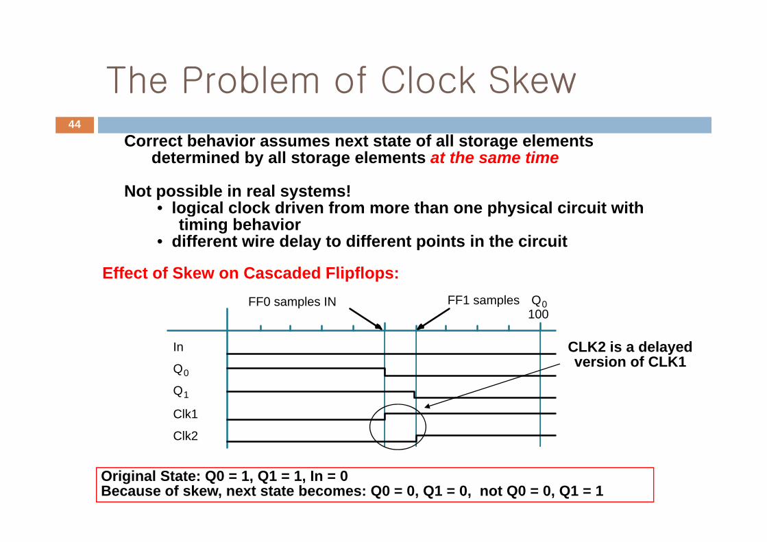
The Problem of Clock SkewThe Problem of Clock Skew44
Correct behavior assumes next state of all storage elementsgdetermined by all storage elements at the same time
Not possible in real systems!• logical clock driven from more than one physical circuit with• logical clock driven from more than one physical circuit with
timing behavior• different wire delay to different points in the circuit
Effect of Skew on Cascaded Flipflops:FF0 samples IN FF1 samples Q 0
100
Effect of Skew on Cascaded Flipflops:
In
Q 0
Q1
CLK2 is a delayedversion of CLK1
Q 1
Clk1
Clk2
Original State: Q0 = 1, Q1 = 1, In = 0Because of skew, next state becomes: Q0 = 0, Q1 = 0, not Q0 = 0, Q1 = 1
Design Strategies for Minimizing Clock Skew
45
Typical propagation delays for LS FFs: 13 ns
Need substantial clock delay (on the order of 13 ns) for skew to y ( )be a problem in this relatively slow technology
Nevertheless, the following are good design practices:
distribute clock signals in general direction of data flows
wire carrying the clock between two communicating componentswire carrying the clock between two communicating componentsshould be as short as possible
for multiphase clocked systems, distribute all clocks in similari th thi i i i th ibilit f lwire paths; this minimizes the possibility of overlap
for the non-overlap clock generate, use the phase feedbacksignals from the furthest point in the circuit to which the clockg pis distributed; this guarantees that the phase is seen as loweverywhere before it allows the next phase to go high
Choosing a FlipflopChoosing a Flipflop46
R S Clocked Latch:R-S Clocked Latch:used as storage element in narrow width clocked systemsits use is not recommended!however, fundamental building block of other flipflop types
J-K Flipflop: (historically popular, but now not used)versatile building blockcan be used to implement D and T FFsusually requires least amount of logic to implementusually requires least amount of logic to implement but has two inputs with increased wiring complexitybecause of 1's catching, never use master/slave J-K FFsedge-triggered varieties exist
D Flipflop:minimizes wires, much preferred in VLSI technologiessimplest design techniquebest choice for storage registersbest choice for storage registers
T Flipflops:don't really exist, constructed from J-K FFsusually best choice for implementing countersusually best choice for implementing counters
Preset and Clear inputs highly desirable!!
RegistersRegisters47
Collection of Flip-Flops with similar controls and logic
stored values somehow related
share clocks, reset, and set lines
i il l i t h tsimilar logic at each stage
Ex lExamplesstorage registers
shift registersshift registers
counters
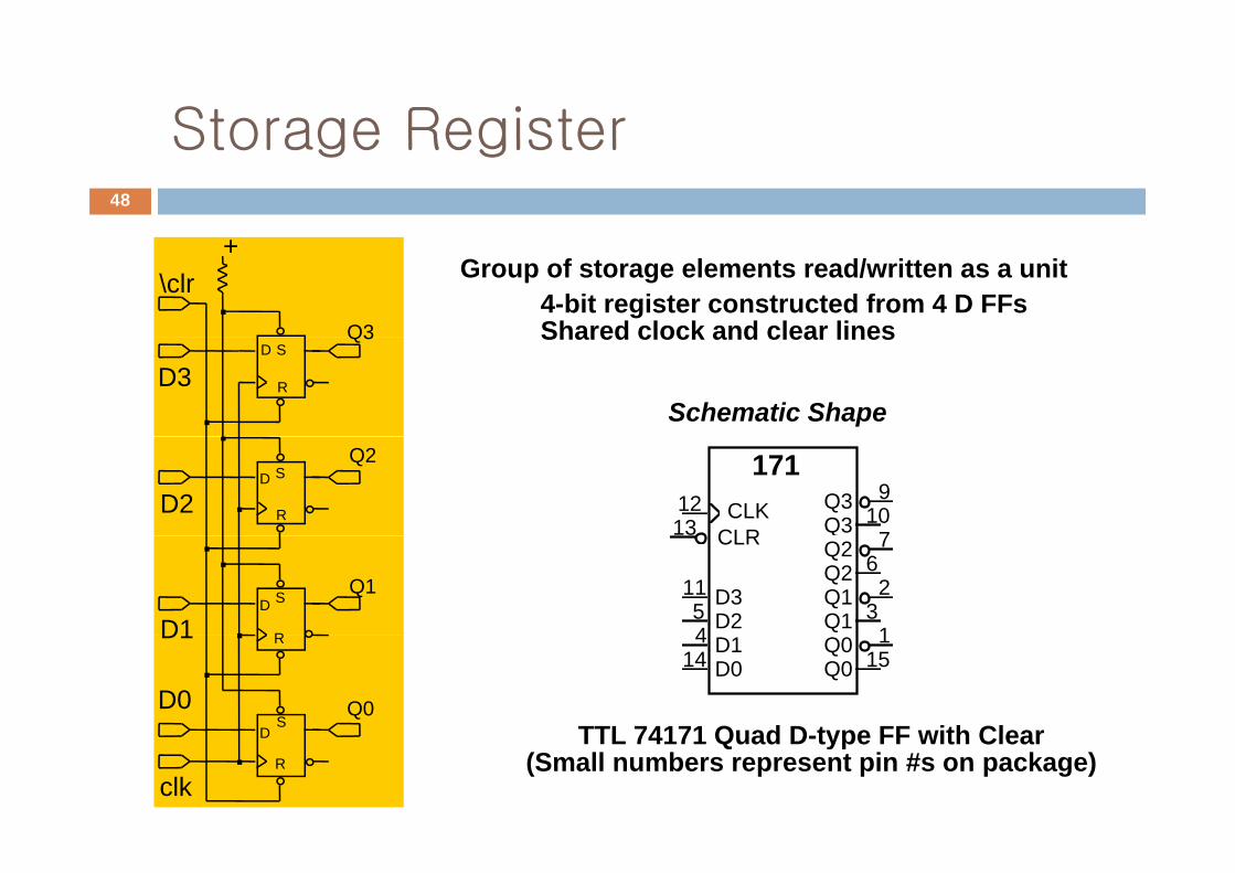
Storage RegisterStorage Register48
Group of storage elements read/written as a unit4-bit register constructed from 4 D FFsShared clock and clear lines
+\clr
Q3 Shared clock and clear lines
Schematic ShapeD3
Q3D
R
S
CLR
171CLK Q3
Q3 109
71312D2
Q2D
R
S
Q1
CLR
D3D2
Q1
Q2Q2
115
67
43
2
1D1
Q1D
R
S
TTL 74171 Quad D type FF with Clear
D1D0
Q0Q0
414 15
1D1
D0 Q0D
R
S TTL 74171 Quad D-type FF with Clear(Small numbers represent pin #s on package)
clk
D
R
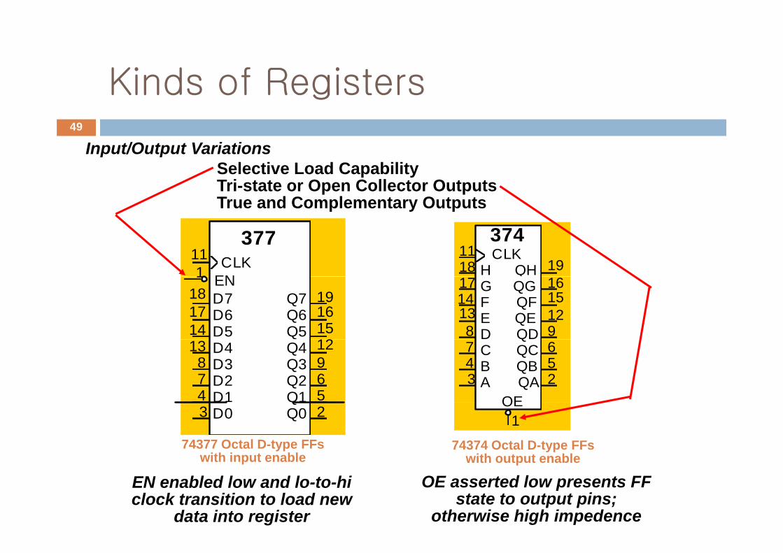
Kinds of RegistersKinds of Registers49
Input/Output VariationsInput/Output VariationsSelective Load CapabilityTri-state or Open Collector OutputsTrue and Complementary Outputs
377
ENCLK
111
H QH
3741118 19
CLK
D6Q5
EN
Q6Q7
D5
D7
1
141718
12151619
GFED
QGQFQEQD8
131417
9121516
D3Q2Q1
Q3Q4
D2D1
D4
478
13
56912 C
BA
QQCQBQA
OE347
256
74377 Octal D-type FFswith input enable
74374 Octal D-type FFswith output enable
QQ0D03 2
OE1
p
EN enabled low and lo-to-hi clock transition to load new
data into register
OE asserted low presents FF state to output pins;
otherwise high impedence
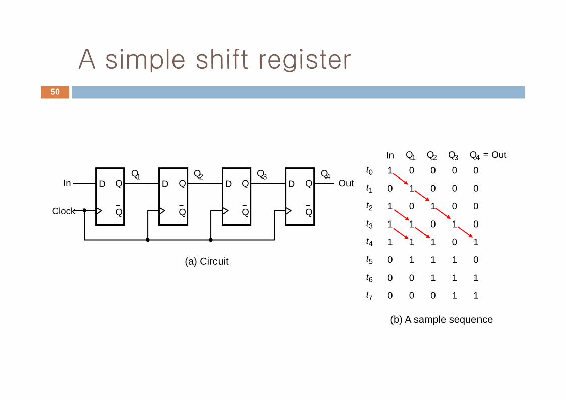
A simple shift registerA simple shift register50
Q Q Q Q Out=Int 0
t 1
1
0
0
1
0
0
0
0
0
0
Q 1 Q 2 Q 3 Q 4 Out = In
D Q D Q D Q D Q In Out Q 1 Q 2 Q 3 Q 4
t 2
t 3
t 4
1
1
1
0
1
1
1
0
1
0
1
0
0
0
1
Q Clock Q Q Q
4
t 5
t 6
0
0
1
0
1
1
1
1
0
1
(a) Circuit
t 7 0 0 0 1 1
(b) A sample sequence
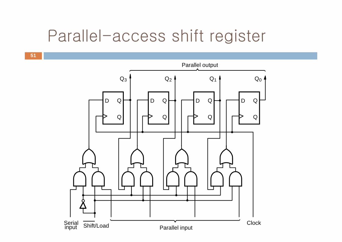
Parallel-access shift register
Parallel output
Parallel access shift register51
Q3 Q2 Q1 Q0
Parallel output
D Q
Q
D Q
Q
D Q
Q
D Q
Q
ClockParallel inputShift/LoadSerial
input
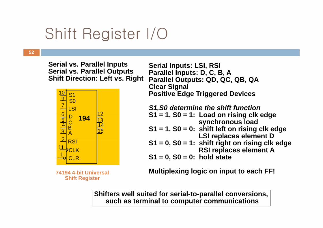
Shift Register I/O
S i l P ll l I t
Shift Register I/O52
Serial vs. Parallel InputsSerial vs. Parallel OutputsShift Direction: Left vs. Right
Serial Inputs: LSI, RSIParallel Inputs: D, C, B, AParallel Outputs: QD, QC, QB, QAClear SignalClear SignalPositive Edge Triggered Devices
S1,S0 determine the shift functionS1 = 1 S0 = 1: Load on rising clk edge
1097
6 12
S1S0LSI
S1 = 1, S0 = 1: Load on rising clk edgesynchronous load
S1 = 1, S0 = 0: shift left on rising clk edgeLSI replaces element D
65432
12
151413194D
CBARSI S1 = 0, S0 = 1: shift right on rising clk edge
RSI replaces element AS1 = 0, S0 = 0: hold state
2111
RSICLKCLR
74194 4-bit UniversalShift Register
Multiplexing logic on input to each FF!
Shift ll it d f i l t ll l iShifters well suited for serial-to-parallel conversions,such as terminal to computer communications
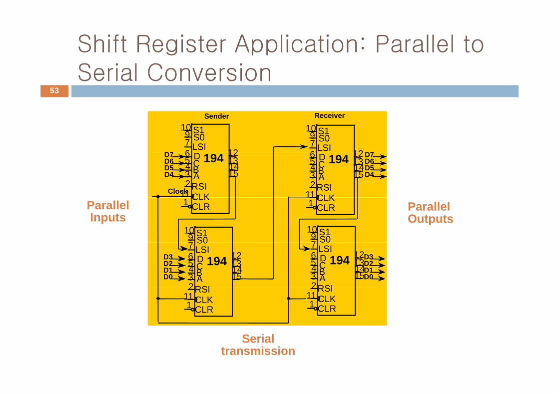
Shift Register Application: Parallel to Serial Conversion
53
D7
Sender Receiver
D7
10976 12
S1S0LSID
10976 12
S1S0LSI
D7D6D5D4
D7D6D5D4
Clock
65432
11
12
151413194D
CBARSICLK
65432
11
12
151413194D
CBARSICLKParallel
InputsParallelOutputs
1097
S1S0
1 CLKCLR 1 CLK
CLR
1097
S1S0
D3D2D1D0
D3D2D1D0
765432
12
151413194
S0LSIDCBARSI
765432
12
151413194
S0LSIDCBARSI 2
111
RSICLKCLR
2111
RSICLKCLR
Serialtransmission
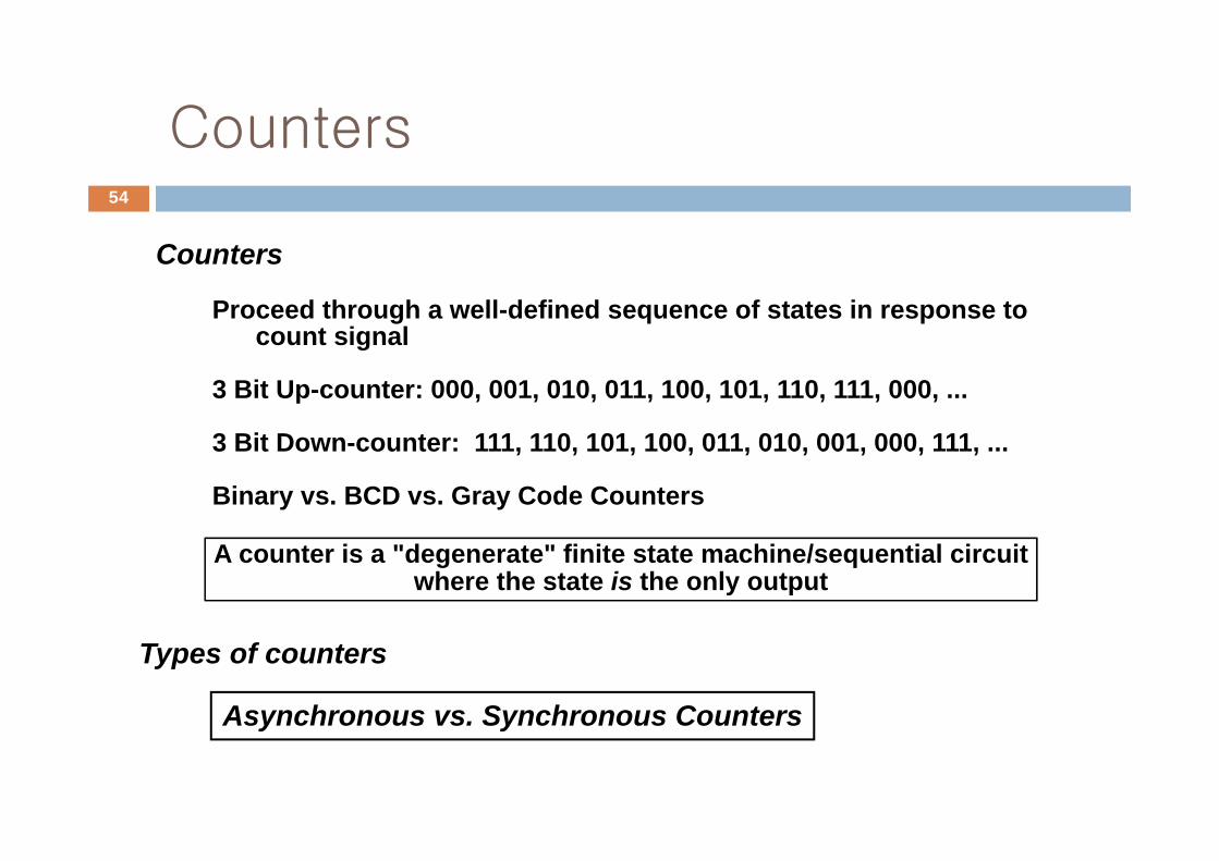
CountersCounters54
Counters
Proceed through a well-defined sequence of states in response to count signalcount signal
3 Bit Up-counter: 000, 001, 010, 011, 100, 101, 110, 111, 000, ...
3 Bit Down-counter: 111, 110, 101, 100, 011, 010, 001, 000, 111, ...
Binary vs. BCD vs. Gray Code Counters
A counter is a "degenerate" finite state machine/sequential circuitwhere the state is the only output
Types of counters
Asynchronous vs. Synchronous CountersAsynchronous vs. Synchronous Counters
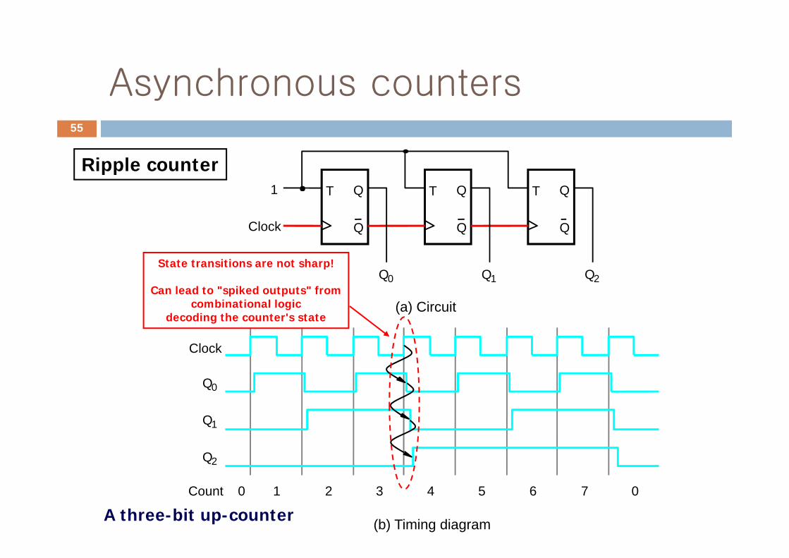
Asynchronous countersAsynchronous counters55
T Q T Q T Q 1
Ripple counter
Q Clock Q Q
Q 0 Q 1 Q 2State transitions are not sharp!
Q0 Q1 Q2
(a) Circuit Can lead to "spiked outputs" from
combinational logic decoding the counter's state
Clock
Q 0
Q 1
Q 2
Count 0 1 2 3 4 5 6 7 0
(b) Timing diagramA three-bit up-counter
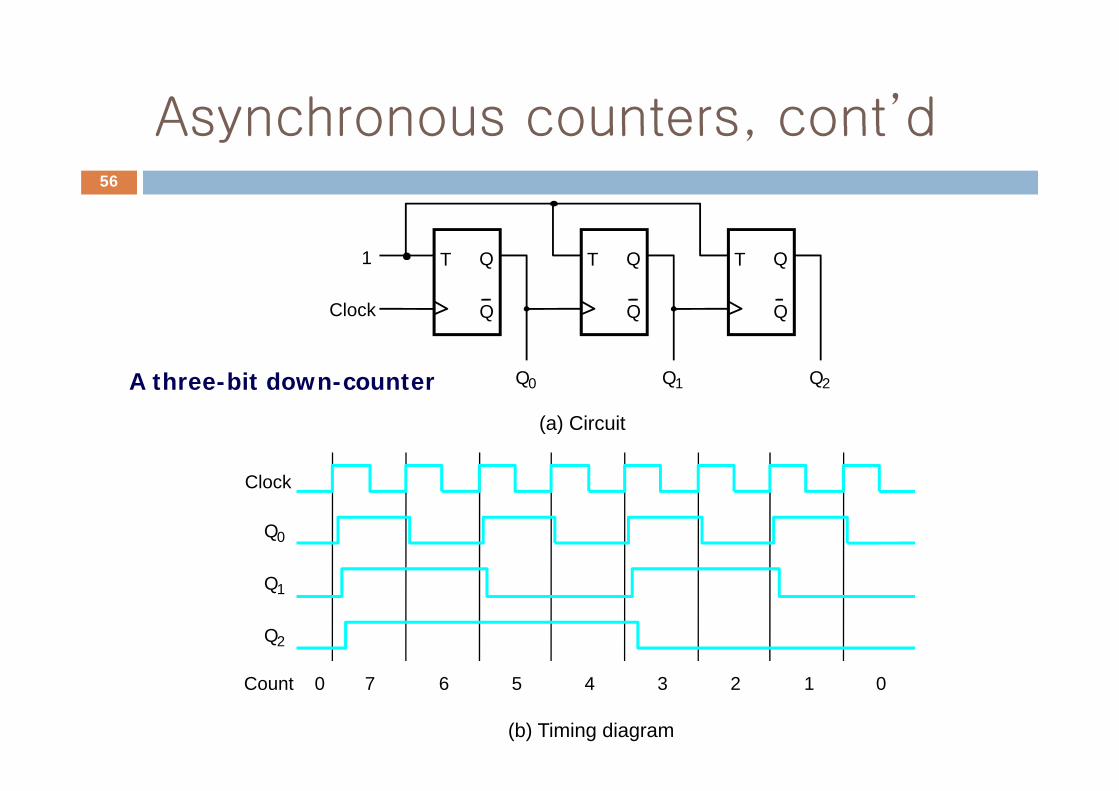
Asynchronous counters cont’dAsynchronous counters, cont d56
T Q
QCl k
T Q
Q
T Q
Q
1
Q Clock Q Q
Q 0 Q 1 Q 2 A three-bit down-counter
(a) Circuit
ClockClock
Q 0
Q 1
Q 2
Count 0 7 6 5 4 3 2 1 0
(b) Timing diagram
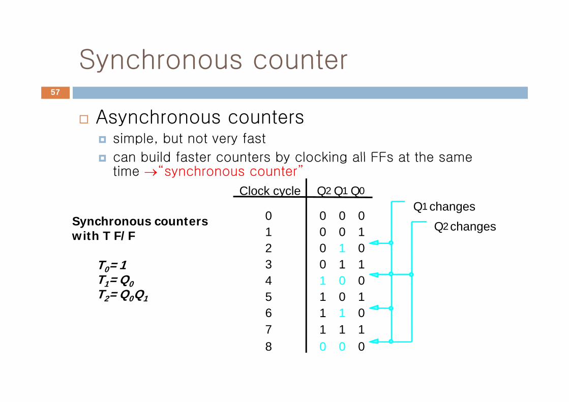
Synchronous counterSynchronous counter57
A hAsynchronous counterssimple, but not very fast
can build faster counters by clocking all FFs at the same
Clock cycle Q 2 Q1 Q0
can build faster counters by clocking all FFs at the same time →“synchronous counter”
0 0 1
0 1 0
0 1 2
0 0 0
Q 1 changes Q 2 changes Synchronous counters
with T F/F 1 1
0 1
2 3
0 0
0 1
4 5
0 0 1 1
T0=1T1=Q0T =Q Q 0
1 1 0
5 6
1 1 7
1 1 1
T2=Q0Q1
0 0 8 0
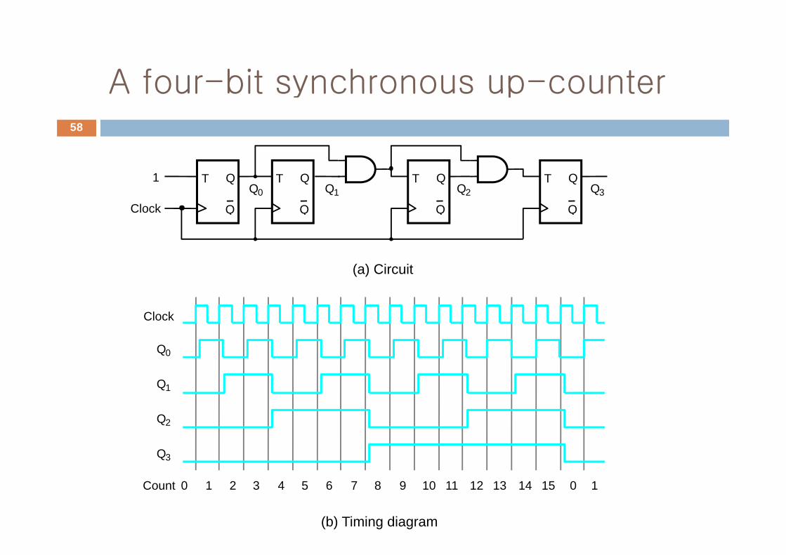
A four-bit synchronous up-counterA four bit synchronous up counter58
T Q
Q Clock
T Q
Q
T Q
Q
1 Q 0 Q 1 Q 2
T Q
Q
Q 3
(a) Circuit
Clock
Q 0
Q 1
Q 2
Q 3
Count 0 1 2 3 5 9 12 14 0
(b) Timing diagram
4 6 8 7 10 11 13 15 1
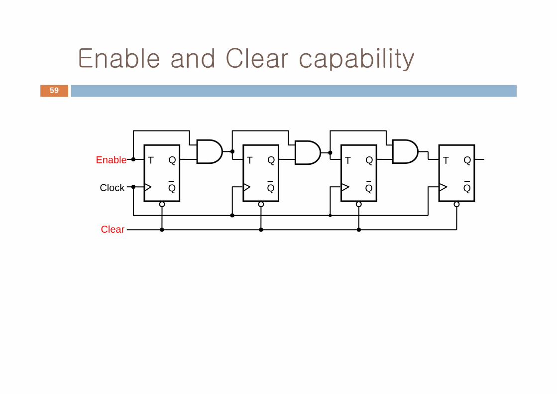
Enable and Clear capabilityEnable and Clear capability59
T Q
Q Clock
T Q
Q
Enable T Q
Q
T Q
Q
Clear
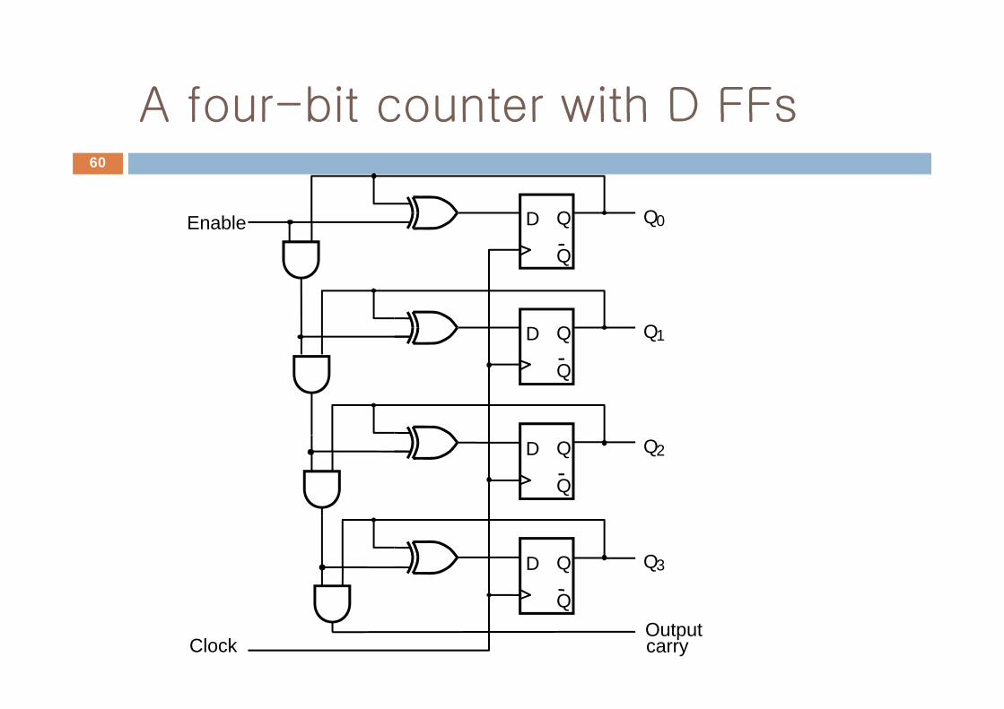
A four-bit counter with D FFsA four bit counter with D FFs60
Enable D Q
Q
Q0
D Q Q1
Q
D Q
Q
Q2
D Q
Q
Q3
Clock
QOutputcarry
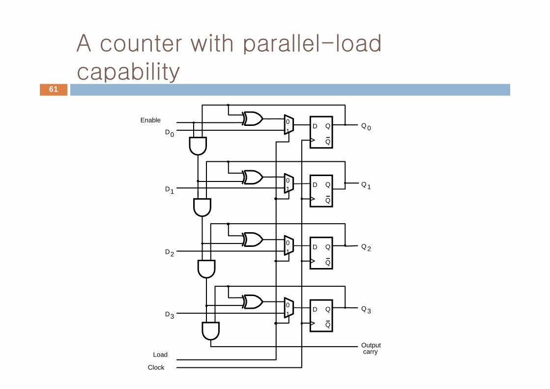
A counter with parallel-load capability
61
EnableD Q
Q
Q 0 D 0
0 1
D Q Q 1 D 1
0 1
Q
D Q
Q
Q 2 D 2
0 1
D Q
Q
Q 3 D 3
0 1
Q
Load
Clock
Outputcarry
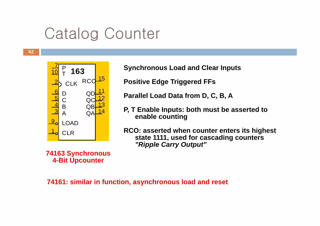
Catalog CounterCatalog Counter62
Synchronous Load and Clear Inputs
Positive Edge Triggered FFs163
RCO
PT
CLK2
710
15
Parallel Load Data from D, C, B, A
P, T Enable Inputs: both must be asserted toQAQBQCQD
ABCD
3456
14
1211
13p
enable counting
RCO: asserted when counter enters its higheststate 1111 used for cascading counters
QAA
LOAD
CLR
9
1
3 14
74163 Synchronous4-Bit Upcounter
state 1111, used for cascading counters"Ripple Carry Output"
74161: similar in function, asynchronous load and reset
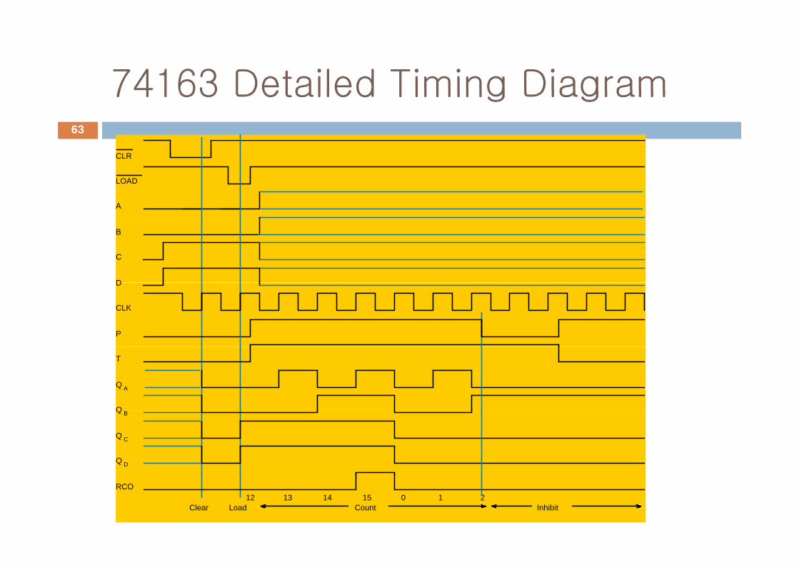
74163 Detailed Timing Diagram74163 Detailed Timing Diagram63
CLR
A
LOAD
CLR
B
C
D
CLK
D
P
T
Q A
QQ B
Q C
Q D
RCO 12 13 14 15 0 1 2
Clear Load Count Inhibit
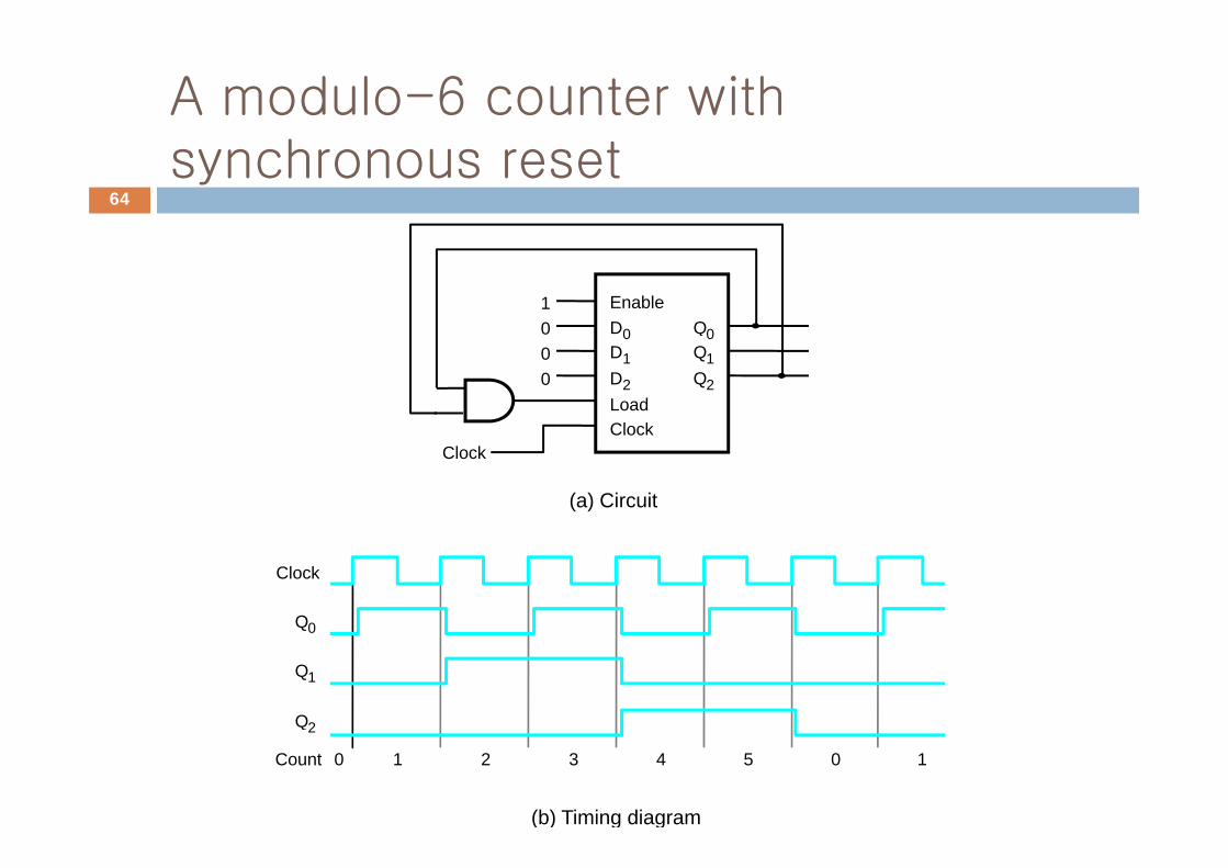
A modulo-6 counter with synchronous reset
64
EnableQ 0D 0
1 0 0
Q 1 Q 2
0 D 1 D 2 LoadClock
0 0
Clock Clock
(a) Circuit
Clock
Q 00
Q 1
Q 2
0 1 2 3 4 5 0 1 Count
2
(b) Timing diagram
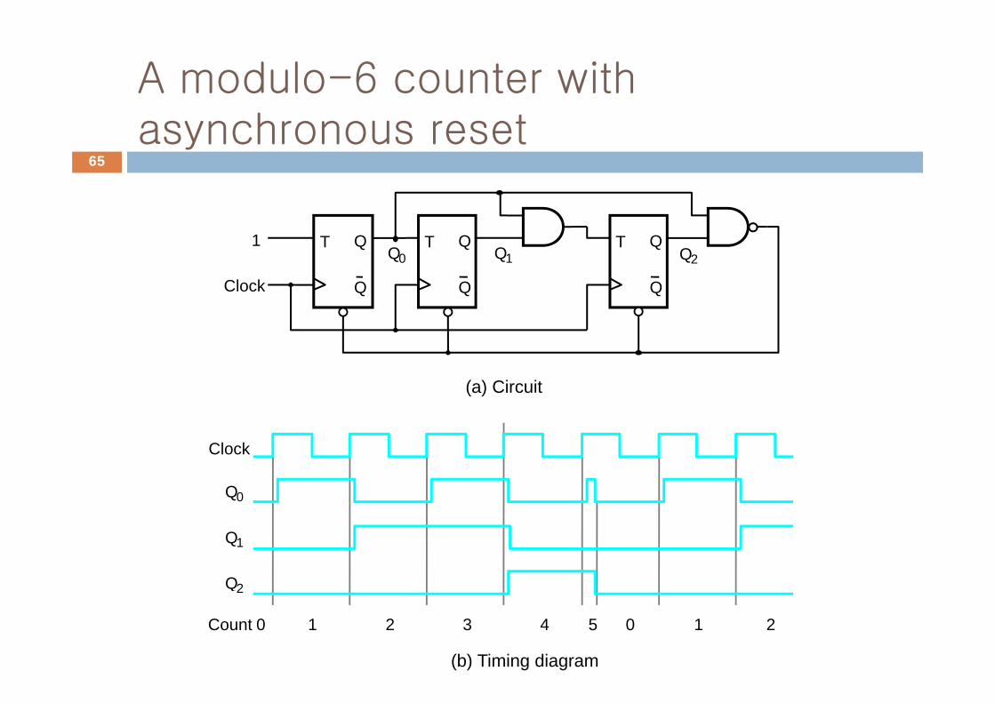
A modulo-6 counter with asynchronous reset
65
T Q T Q T Q 1 Q 0 Q 1 Q 2
Q Clock Q Q
(a) Circuit
Clock
Q 0
Q 1
Q 22
Count
(b) Timing diagram
0 1 2 3 4 5 0 1 2
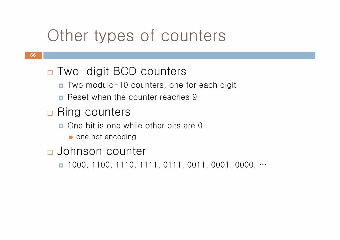
Other types of countersOther types of counters66
Two-digit BCD countersTwo modulo-10 counters, one for each digit
Reset when the counter reaches 9
Ring countersOne bit is one while other bits are 0
one hot encoding
J h tJohnson counter1000, 1100, 1110, 1111, 0111, 0011, 0001, 0000, …
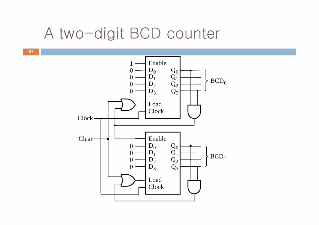
A two-digit BCD counter
E bl1
A two digit BCD counter67
EnableQ0Q1Q2
D0D1D2
1000 BCD0Q22
LoadClock
Q30 D3
ClockClock
EnableClear EnableQ0Q1Q2
D0D1D2
000 BCD1
Clear
LoadClock
Q30 D3
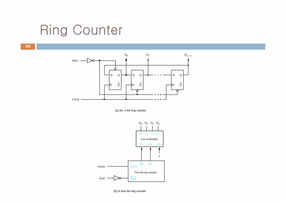
Ring CounterRing Counter68
Q0 Q1 Q 1?
D Q D Q D Q
Start
Q 0 Q 1 Q n 1 ?
Q
Clock
Q Q
Q 0 Q 1 Q 2 Q 3
(a) An n -bit ring counter
Q0
w 0 En
y 0
w 1
y 1 y 2 y 3
Q1 Q2 Q3
2-to-4 decoder
Clock
1
Q 1 Q 0 Clock
Start
Two-bit up-counter
Clear
(b) A four-bit ring counter
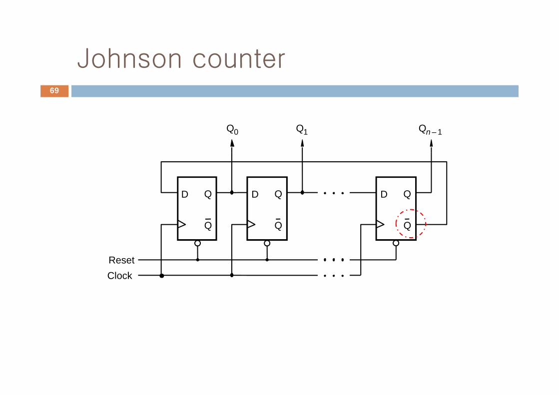
Johnson counterJohnson counter69
Q 0 Q 1 Q n 1 –
D Q D Q D Q D Q
Q
D Q
Q
D Q
Q
Clock Reset