laboratory e-manual final year b.tech. viii sem (ece
TRANSCRIPT
DEPARTMENT OF ELECTRONICS AND COMMUNICATION ENGINEERING
CTAE, MPUAT, UDAIPUR
DEPARTMENT OF
ELECTRONICS AND COMMUNICATION
ENGINEERING
COLLEGE OF TECHNOLGY AND ENGINEERING
MAHARANA PRATAP UNIVERSITY OF AGRICULTURE & TECHNOLGY, UDAIPUR
LABORATORY E-MANUAL
Final Year B.Tech. VIII SEM (ECE)
APRIL 2020

DEPARTMENT OF ELECTRONICS AND COMMUNICATION ENGINEERING
CTAE, MPUAT, UDAIPUR
Prepared By
Dr. Sunil Joshi
Mr Deep Manwar
Mr Lalit Verma
COLLEGE OF TECHNOLGYAND ENGINEERING MAHARANA PRATAP UNIVERSITY OF AGRICULTURE & TECHNOLGY,
UDAIPUR
DEPARTMENT OF ELECTRONICS AND COMMUNICATION ENGINEERING
LAB MANUAL
EC423 - VHDL
PREPARED BY
Mr. DEEP MANWAR
Dr. SUNIL JOSHI

VHDL Lab Manual
NAME OF EXPERIMENT
1. To develop VHDL code for Full Adder using Half Adder using simulation tool and verify the same on FPGA
board.
2. To develop the VHDL code for 16-to-1 Multiplexer using 4-to-1 Multiplexer using simulation tool and verify
the same on FPGA board.
3. To develop the VHDL code for BCD to 7-Segment display using simulation tool and verify the same on FPGA
board.
4. To develop the VHDL code for Encoders and Decoders using simulation tool and verify the same on FPGA
board.
5. To develop the VHDL code for 4-to-2 priority Encoder using simulation tool and verify the same on FPGA
board.
6. To develop the VHDL code for Code Converters using simulation tool and verify the same on FPGA board.
7. To develop the VHDL code for Flip-Flops using simulation tool and verify the same on FPGA board.
8. To develop the VHDL code for Shift Registers using simulation tool and verify the same on FPGA board.
9. To develop the VHDL code for Moore Machine using simulation tool and verify the same on FPGA board.
10. To develop the VHDL code for Mealy Machine using simulation tool and verify the same on FPGA board.
11. Appendix I (Contains some extra programs)
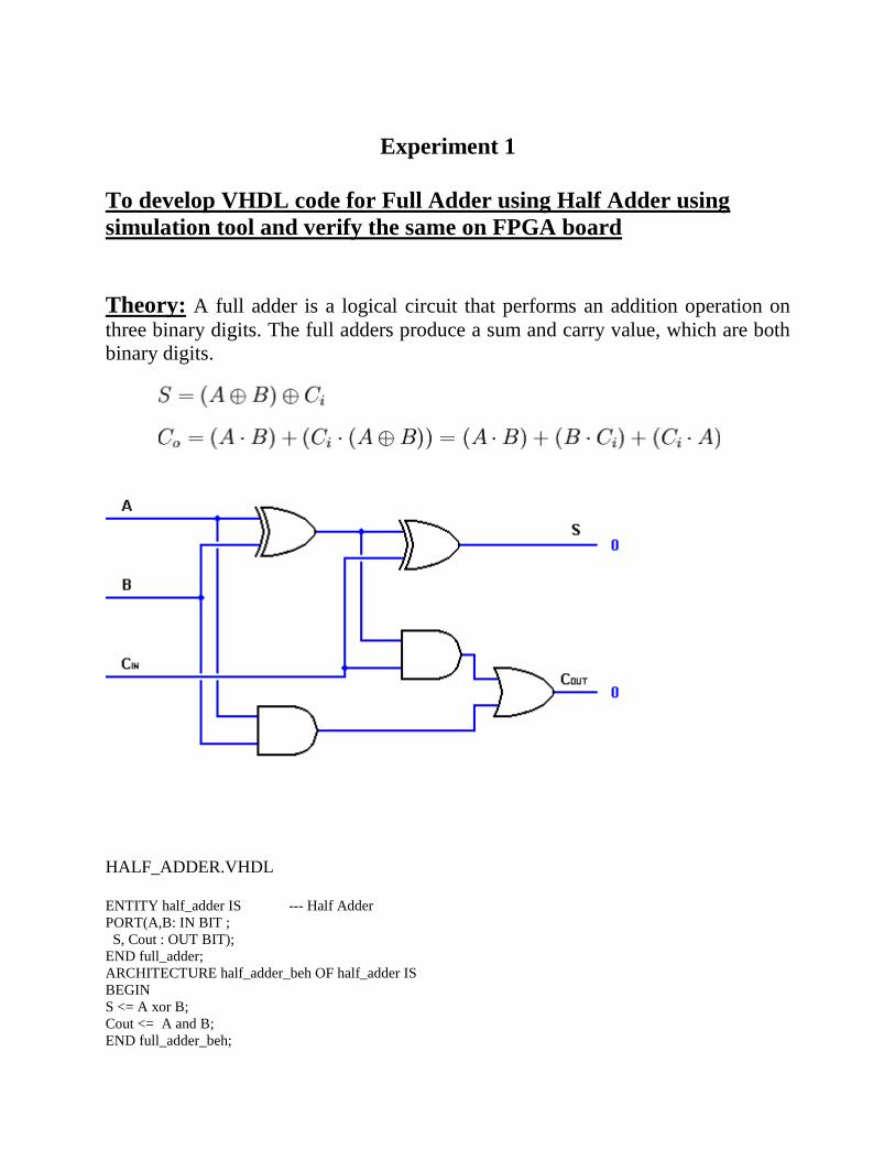
Experiment 1
To develop VHDL code for Full Adder using Half Adder using
simulation tool and verify the same on FPGA board
Theory: A full adder is a logical circuit that performs an addition operation on
three binary digits. The full adders produce a sum and carry value, which are both
binary digits.
HALF_ADDER.VHDL
ENTITY half_adder IS --- Half Adder
PORT(A,B: IN BIT ;
S, Cout : OUT BIT);
END full_adder;
ARCHITECTURE half_adder_beh OF half_adder IS
BEGIN
S <= A xor B;
Cout <= A and B;
END full_adder_beh;

or_gate.vhdl
ENTITY or_gate IS
PORT(A,B: IN BIT ;
C : OUT BIT);
END or_gate;
ARCHITECTURE or_gate_beh OF or_gate IS
BEGIN
C <= A or B;
END or_gate_beh;
FULL_ADDER.VHDL
ENTITY full_adder IS --- Full Adder
PORT(A,B,Cin: IN BIT ;
S, C : OUT BIT);
END full_adder;
ARCHITECTURE str OF full_adder IS
--component Declaration
Component half_adder IS
PORT(A,B: IN BIT ;
S, Cout : OUT BIT);
END Component;
Component or_gate IS
PORT(A,B: IN BIT ;
C : OUT BIT);
END Component;
signal s1,c2,c3:std_logic;
BEGIN
X1: half_adder port map(A,B,s1,c1);
X2: half_adder port map(s1,Cin,S,c2);
X3: or_gate port map(c1,c2,C);
END str;
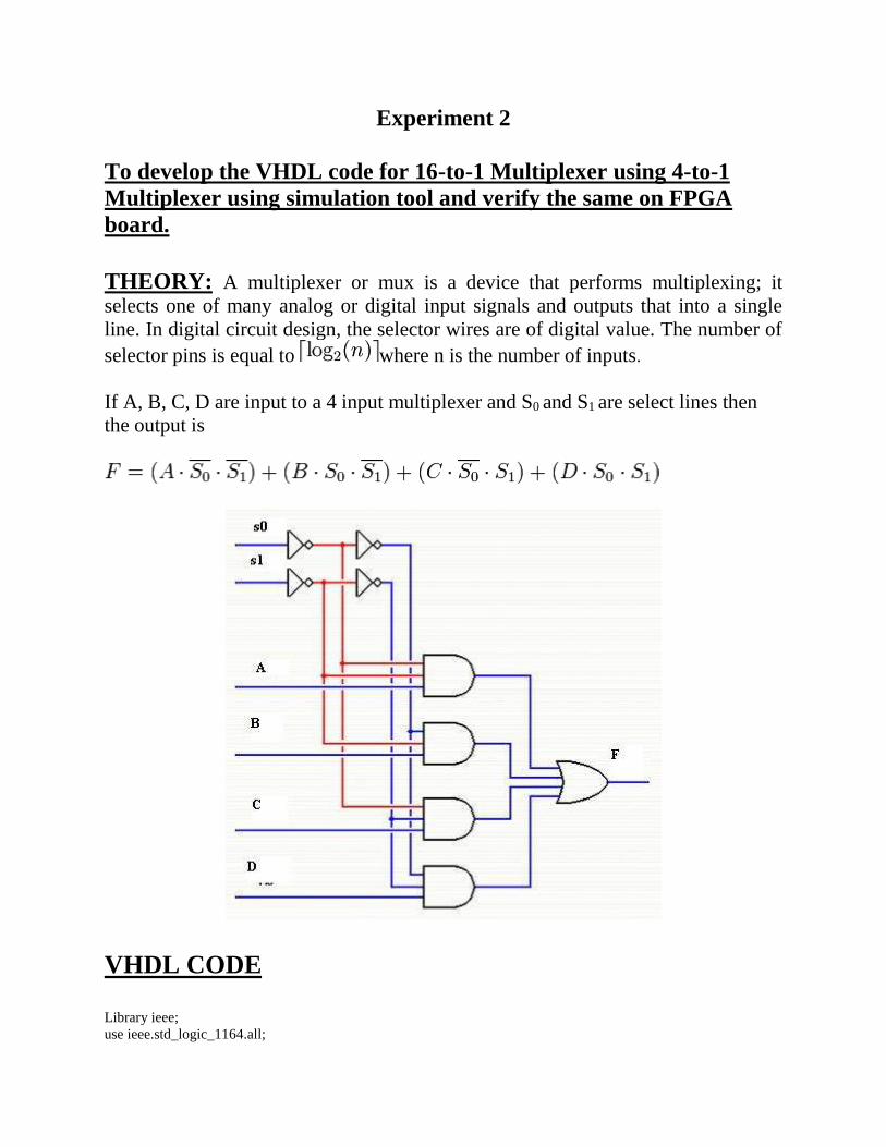
Experiment 2
To develop the VHDL code for 16-to-1 Multiplexer using 4-to-1
Multiplexer using simulation tool and verify the same on FPGA
board.
THEORY: A multiplexer or mux is a device that performs multiplexing; it
selects one of many analog or digital input signals and outputs that into a single
line. In digital circuit design, the selector wires are of digital value. The number of
selector pins is equal to where n is the number of inputs.
If A, B, C, D are input to a 4 input multiplexer and S0 and S1 are select lines then
the output is
VHDL CODE
Library ieee;
use ieee.std_logic_1164.all;

use ieee.std_logic_arith.all;
entity Deep_4x1mux is
port(a,b,c,d : in std_logic;
S0,s1 : in std_logic;
q : out std_logic);
end Deep_4x1mux;
Architecture Deep_4x1mux1 of Deep_4x1mux is
Begin
Process(a,b,c,d,s0,s1)
Begin
If s0 ='0' and s1 ='0' then q <= a;
Elsif s0 ='1' and s1 ='0' then q <= b;
elsif s0 ='0' and s1='1' then q <= c;
else q <=d;
end if;
End process;
End Deep_4x1mux1;
Main program
Library ieee;
use ieee.std_logic_1164.all;
use ieee.std_logic_arith.all;
entity Deep_16x1mux is
port(a:in std_logic_vector(15 downto 0);
s: in std_logic_vector(3 downto 0);
Z:out std_logic);
End Deep_16x1mux;
Architecture Deep_16x1mux1 of Deep_16x1mux is
signal z1,z2,z3,z4:std_logic;
component Deep_4x1mux is
port(a,b,c,d,s0,s1:in std_logic;
Q:out std_logic);
End component;
Begin
M1: Deep_4x1mux port map(a(0),a(1),a(2),a(3),s(0),s(1),z1);
m2: Deep_4x1mux port map(a(4),a(5),a(6),a(7),s(0),s(1),z2);
m3: Deep_4x1mux port map(a(8),a(9),a(10),a(11),s(0),s(1),z3);
m4: Deep_4x1mux port map(a(12),a(13),a(14),a(15),s(0),s(1),z4);
m5: Deep_4x1mux port map(z1,z2,z3,z4,s(2),s(3),z);
End Deep_16x1mux1;
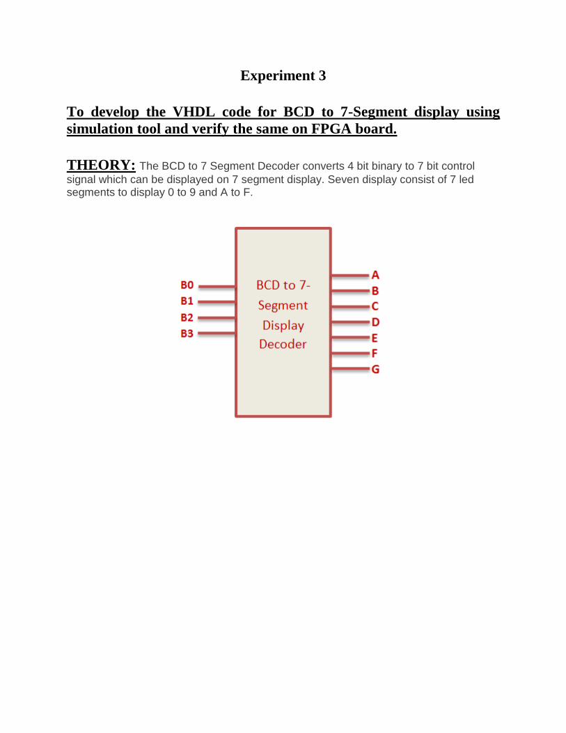
Experiment 3
To develop the VHDL code for BCD to 7-Segment display using
simulation tool and verify the same on FPGA board.
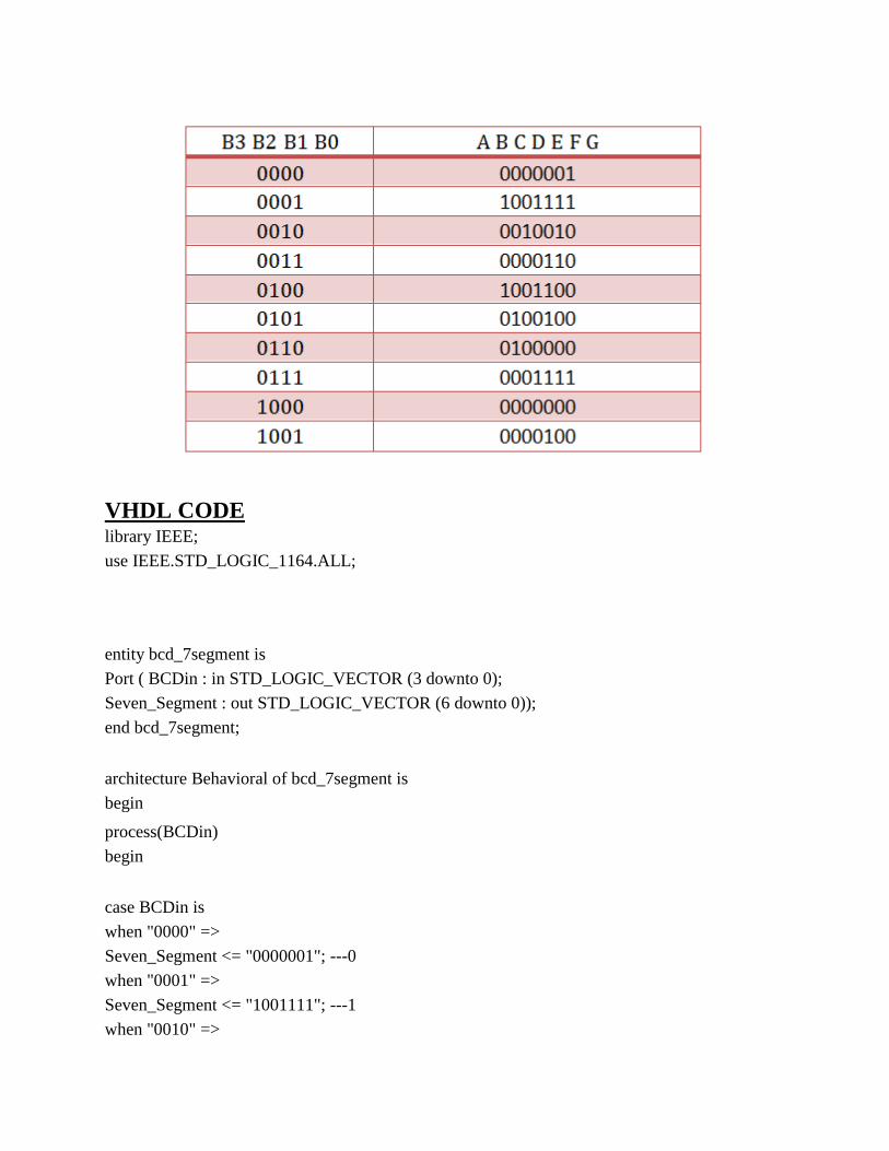
THEORY: The BCD to 7 Segment Decoder converts 4 bit binary to 7 bit control
signal which can be displayed on 7 segment display. Seven display consist of 7 led segments to display 0 to 9 and A to F.
VHDL CODE library IEEE;
use IEEE.STD_LOGIC_1164.ALL;
entity bcd_7segment is
Port ( BCDin : in STD_LOGIC_VECTOR (3 downto 0);
Seven_Segment : out STD_LOGIC_VECTOR (6 downto 0));
end bcd_7segment;
architecture Behavioral of bcd_7segment is
begin
process(BCDin)
begin
case BCDin is
when "0000" =>
Seven_Segment <= "0000001"; ---0
when "0001" =>
Seven_Segment <= "1001111"; ---1
when "0010" =>
Seven_Segment <= "0010010"; ---2
when "0011" =>
Seven_Segment <= "0000110"; ---3
when "0100" =>
Seven_Segment <= "1001100"; ---4
when "0101" =>
Seven_Segment <= "0100100"; ---5
when "0110" =>
Seven_Segment <= "0100000"; ---6
when "0111" =>
Seven_Segment <= "0001111"; ---7
when "1000" =>
Seven_Segment <= "0000000"; ---8
when "1001" =>
Seven_Segment <= "0000100"; ---9
when others =>
Seven_Segment <= "1111111"; ---null
end case;
end process;
end Behavioral;
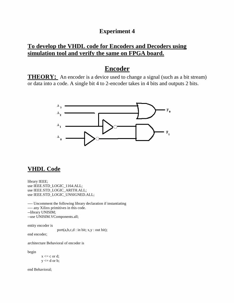
Experiment 4
To develop the VHDL code for Encoders and Decoders using
simulation tool and verify the same on FPGA board.
Encoder
THEORY: An encoder is a device used to change a signal (such as a bit stream)
or data into a code. A single bit 4 to 2-encoder takes in 4 bits and outputs 2 bits.
VHDL Code
library IEEE;
use IEEE.STD_LOGIC_1164.ALL;
use IEEE.STD_LOGIC_ARITH.ALL;
use IEEE.STD_LOGIC_UNSIGNED.ALL;
---- Uncomment the following library declaration if instantiating
---- any Xilinx primitives in this code.
--library UNISIM;
--use UNISIM.VComponents.all;
entity encoder is
port(a,b,c,d : in bit; x,y : out bit);
end encoder;
architecture Behavioral of encoder is
begin
x <= c or d;
y <= d or b;
end Behavioral;
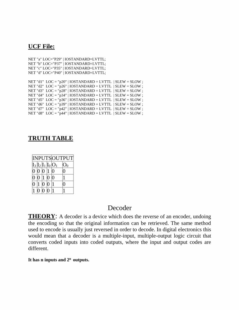
UCF File:
NET "a" LOC="P29" | IOSTANDARD=LVTTL;
NET "b" LOC="P37" | IOSTANDARD=LVTTL;
NET "c" LOC="P35" | IOSTANDARD=LVTTL;
NET "d" LOC="P40" | IOSTANDARD=LVTTL;
NET "d1" LOC = "p20" | IOSTANDARD = LVTTL | SLEW = SLOW ;
NET "d2" LOC = "p26" | IOSTANDARD = LVTTL | SLEW = SLOW ;
NET "d3" LOC = "p28" | IOSTANDARD = LVTTL | SLEW = SLOW ;
NET "d4" LOC = "p34" | IOSTANDARD = LVTTL | SLEW = SLOW ;
NET "d5" LOC = "p36" | IOSTANDARD = LVTTL | SLEW = SLOW ;
NET "d6" LOC = "p39" | IOSTANDARD = LVTTL | SLEW = SLOW ;
NET "d7" LOC = "p42" | IOSTANDARD = LVTTL | SLEW = SLOW ;
NET "d8" LOC = "p44" | IOSTANDARD = LVTTL | SLEW = SLOW ;
TRUTH TABLE
Decoder
THEORY: A decoder is a device which does the reverse of an encoder, undoing
the encoding so that the original information can be retrieved. The same method
used to encode is usually just reversed in order to decode. In digital electronics this
would mean that a decoder is a multiple-input, multiple-output logic circuit that
converts coded inputs into coded outputs, where the input and output codes are
different.
It has n inputs and 2n outputs.
INPUTS OUTPUT
I3 I2 I1 I0 O1 O0
0 0 0 1 0 0
0 0 1 0 0 1
0 1 0 0 1 0
1 0 0 0 1 1
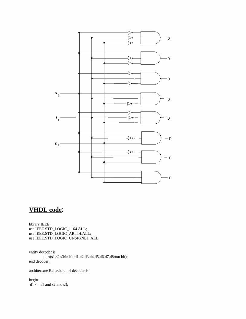
VHDL code:
library IEEE;
use IEEE.STD_LOGIC_1164.ALL;
use IEEE.STD_LOGIC_ARITH.ALL;
use IEEE.STD_LOGIC_UNSIGNED.ALL;
entity decoder is
port(s1,s2,s3:in bit;d1,d2,d3,d4,d5,d6,d7,d8:out bit);
end decoder;
architecture Behavioral of decoder is
begin
d1 <= s1 and s2 and s3;
d2 <= s1 and s2 and (not s3);
d3 <= s1 and (not s2) and s3;
d4 <= s1 and (not s2) and (not s3);
d5 <= (not s1) and s2 and s3;
d6 <= (not s1) and s2 and (not s3);
d7 <= (not s1) and (not s2) and s3;
d8 <= (not s1) and (not s2) and (not s3);
end Behavioral;
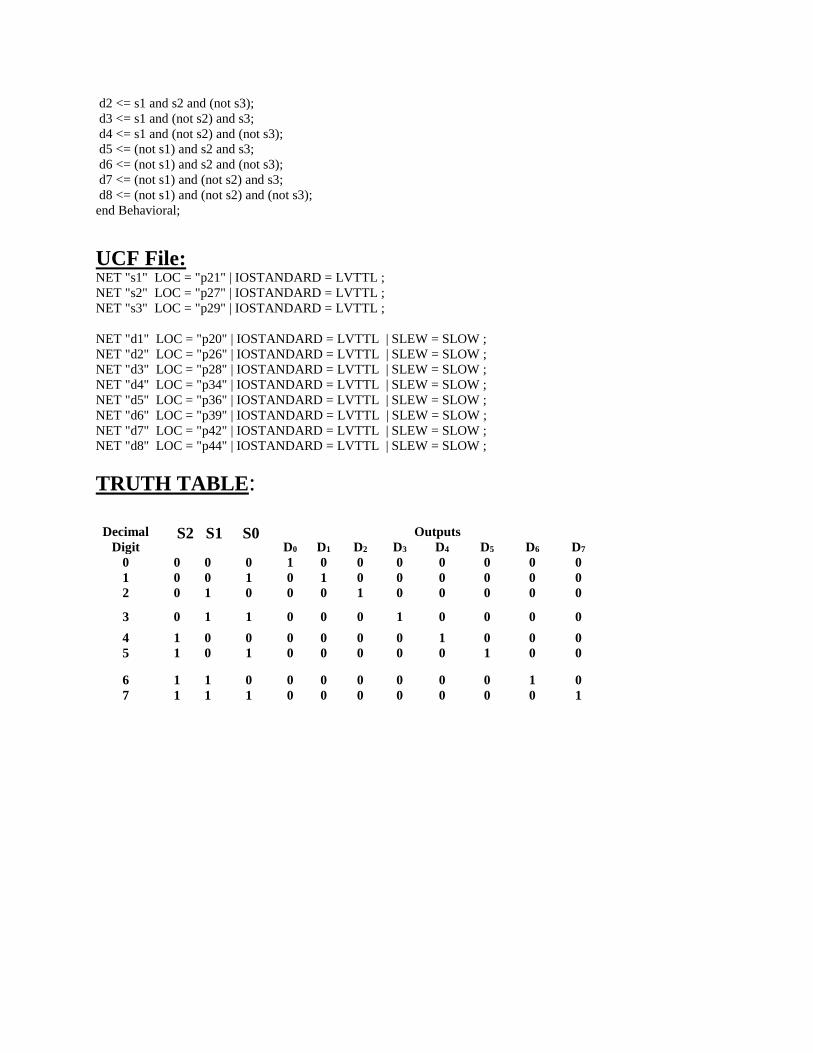
UCF File: NET "s1" LOC = "p21" | IOSTANDARD = LVTTL ;
NET "s2" LOC = "p27" | IOSTANDARD = LVTTL ;
NET "s3" LOC = "p29" | IOSTANDARD = LVTTL ;
NET "d1" LOC = "p20" | IOSTANDARD = LVTTL | SLEW = SLOW ;
NET "d2" LOC = "p26" | IOSTANDARD = LVTTL | SLEW = SLOW ;
NET "d3" LOC = "p28" | IOSTANDARD = LVTTL | SLEW = SLOW ;
NET "d4" LOC = "p34" | IOSTANDARD = LVTTL | SLEW = SLOW ;
NET "d5" LOC = "p36" | IOSTANDARD = LVTTL | SLEW = SLOW ;
NET "d6" LOC = "p39" | IOSTANDARD = LVTTL | SLEW = SLOW ;
NET "d7" LOC = "p42" | IOSTANDARD = LVTTL | SLEW = SLOW ;
NET "d8" LOC = "p44" | IOSTANDARD = LVTTL | SLEW = SLOW ;
TRUTH TABLE:
Decimal
Digit S2 S1 S0 Outputs
D0 D1 D2 D3 D4 D5 D6 D7 0 0 0 0 1 0 0 0 0 0 0 0 1 0 0 1 0 1 0 0 0 0 0 0 2 0 1 0 0 0 1 0 0 0 0 0
3 0 1 1 0 0 0 1 0 0 0 0
4 1 0 0 0 0 0 0 1 0 0 0 5 1 0 1 0 0 0 0 0 1 0 0
6 1 1 0 0 0 0 0 0 0 1 0 7 1 1 1 0 0 0 0 0 0 0 1
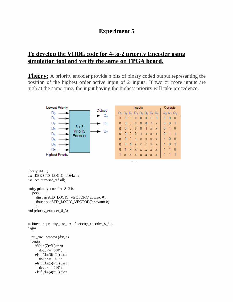
Experiment 5
To develop the VHDL code for 4-to-2 priority Encoder using
simulation tool and verify the same on FPGA board.
Theory: A priority encoder provide n bits of binary coded output representing the
position of the highest order active input of 2n inputs. If two or more inputs are
high at the same time, the input having the highest priority will take precedence.
library IEEE;
use IEEE.STD_LOGIC_1164.all;
use ieee.numeric_std.all;
entity priority_encoder_8_3 is
port(
din : in STD_LOGIC_VECTOR(7 downto 0);
dout : out STD_LOGIC_VECTOR(2 downto 0)
);
end priority_encoder_8_3;
architecture priority_enc_arc of priority_encoder_8_3 is
begin
pri_enc : process (din) is
begin
if (din(7)='1') then
dout <= "000";
elsif (din(6)='1') then
dout <= "001";
elsif (din(5)='1') then
dout <= "010";
elsif (din(4)='1') then

dout <= "011";
elsif (din(3)='1') then
dout <= "100";
elsif (din(2)='1') then
dout <= "101";
elsif (din(1)='1') then
dout <= "110";
elsif (din(0)='1') then
dout <= "111";
end if;
end process pri_enc;
end priority_enc_arc;
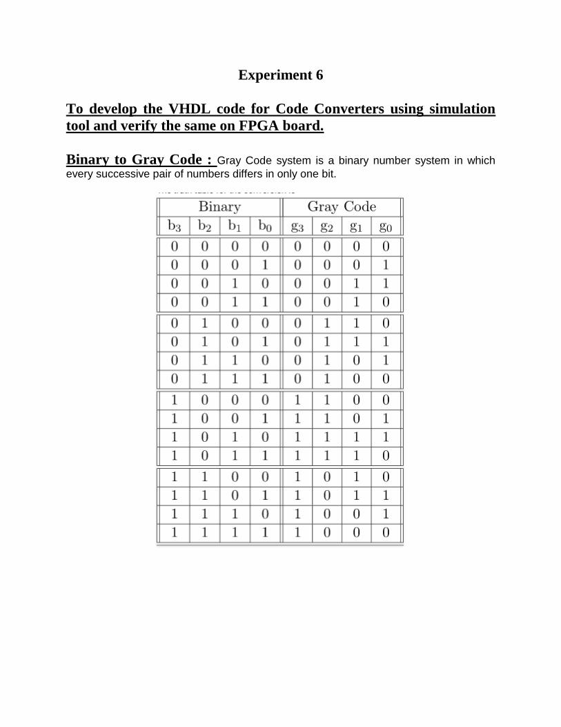
Experiment 6
To develop the VHDL code for Code Converters using simulation
tool and verify the same on FPGA board.
Binary to Gray Code : Gray Code system is a binary number system in which
every successive pair of numbers differs in only one bit.
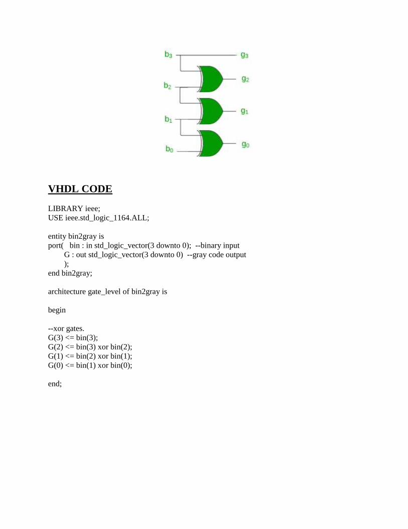
VHDL CODE
LIBRARY ieee;
USE ieee.std_logic_1164.ALL;
entity bin2gray is
port( bin : in std_logic_vector(3 downto 0); --binary input
G : out std_logic_vector(3 downto 0) --gray code output
);
end bin2gray;
architecture gate_level of bin2gray is
begin
--xor gates.
G(3) <= bin(3);
G(2) <= bin(3) xor bin(2);
G(1) <= bin(2) xor bin(1);
G(0) <= bin(1) xor bin(0);
end;
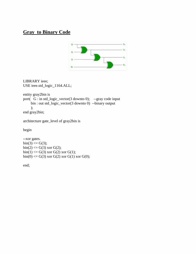
Gray to Binary Code
LIBRARY ieee;
USE ieee.std_logic_1164.ALL;
entity gray2bin is
port( G : in std_logic_vector(3 downto 0); --gray code input
bin : out std_logic_vector(3 downto 0) --binary output
);
end gray2bin;
architecture gate_level of gray2bin is
begin
--xor gates.
bin(3) <= G(3);
bin(2) <= G(3) xor G(2);
bin(1) <= G(3) xor G(2) xor G(1);
bin(0) <= G(3) xor G(2) xor G(1) xor G(0);
end;

Experiment 7
To develop the VHDL code for Flip-Flops using simulation tool and
verify the same on FPGA board.
THEORY: The D flip-flop tracks the input, making transitions with match those
of the input D. The D stands for "data"; this flip-flop stores the value that is on the
data line. It can be thought of as a basic memory cell. A D flip-flop can be made
from a set/reset flip-flop by tying the set to the reset through an inverter. The result
may be clocked.
VHDL CODE
use IEEE.STD_LOGIC_1164.ALL;
use IEEE.STD_LOGIC_ARITH.ALL;
use IEEE.STD_LOGIC_UNSIGNED.ALL;
entity dff is
port(D,CLK:in bit;
Q:out bit; QN:out bit:= '1');
end dff;
architecture Behavioral of dff is
begin
process(CLK)
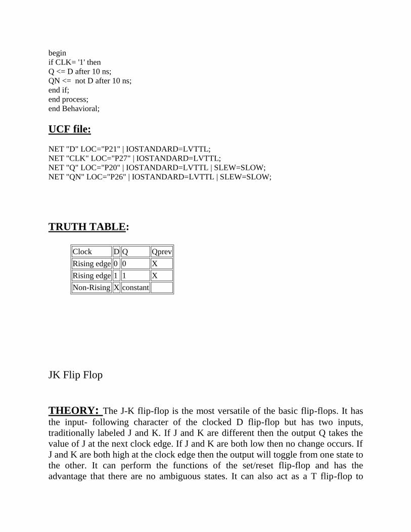
begin
if CLK= '1' then
Q <= D after 10 ns;
QN <= not D after 10 ns;
end if;
end process;
end Behavioral;
UCF file:
NET "D" LOC="P21" | IOSTANDARD=LVTTL;
NET "CLK" LOC="P27" | IOSTANDARD=LVTTL;
NET "Q" LOC="P20" | IOSTANDARD=LVTTL | SLEW=SLOW;
NET "QN" LOC="P26" | IOSTANDARD=LVTTL | SLEW=SLOW;
TRUTH TABLE:
Clock D Q Qprev
Rising edge 0 0 X
Rising edge 1 1 X
Non-Rising X constant
JK Flip Flop
THEORY: The J-K flip-flop is the most versatile of the basic flip-flops. It has
the input- following character of the clocked D flip-flop but has two inputs,
traditionally labeled J and K. If J and K are different then the output Q takes the
value of J at the next clock edge. If J and K are both low then no change occurs. If
J and K are both high at the clock edge then the output will toggle from one state to
the other. It can perform the functions of the set/reset flip-flop and has the
advantage that there are no ambiguous states. It can also act as a T flip-flop to
accomplish toggling action if J and K are tied together. This toggle application
finds extensive use in binary counters.
VHDL Code
library IEEE;
use IEEE.STD_LOGIC_1164.ALL;
use IEEE.STD_LOGIC_ARITH.ALL;
use IEEE.STD_LOGIC_UNSIGNED.ALL;
entity jkflipflop is
port (SN, RN, J,K, CLK:in bit; Q: inout bit; QN: out bit:='1');
end jkflipflop;
architecture Behavioral of jkflipflop is
begin
process (SN, RN, CLK)
begin
if RN='0' then Q<='0' after 10 ns;
elsif SN='0' then Q<='1' after 10 ns;
elsif CLK='0' and CLK'event then
Q<= (J and not Q) or (not K and Q) after 10 ns;
end if;
QN<= not Q;
end process;
end Behavioral;

UCF File
NET "J" LOC="P21" | IOSTANDARD=LVTTL;
NET "K" LOC="P27" | IOSTANDARD=LVTTL;
NET "SN" LOC="P29" | IOSTANDARD=LVTTL;
NET "RN" LOC="P35" | IOSTANDARD=LVTTL;
NET "CLK" LOC="P37" | IOSTANDARD=LVTTL;
NET "Q" LOC="P20" | IOSTANDARD=LVTTL | SLEW=SLOW;
NET "QN" LOC="P26" | IOSTANDARD=LVTTL | SLEW=SLOW;
TRUTH TABLE :
J K Qnext Comment
0 0 hold state
0 1 reset
1 0 set
1 1 toggle
T Flip Flop
THEORY: The T or "toggle" flip-flop changes its output on each clock edge,
giving an output which is half the frequency of the signal to the T input. It is useful
for constructing binary counters, frequency dividers, and general binary addition
devices. It can be made from a J-K flip-flop by tying both of its inputs high.
VHDL code:
Library IEEE;
use IEEE.STD_LOGIC_1164.ALL;
use IEEE.STD_LOGIC_ARITH.ALL;
use IEEE.STD_LOGIC_UNSIGNED.ALL;
entity tflip is
port (T, CLK:in bit; Q: inout bit; QN: out bit);
end tflip;
architecture Behavioral of tflip is
begin
process (CLK)
begin
if CLK='0' and CLK'event then
Q<= (T and not Q) or (not T and Q) after 10 ns;
end if;
QN<= not Q;
end process;
end Behavioral;
UCF File
NET "T" LOC="P21" | IOSTANDARD=LVTTL;
NET "CLK" LOC="P35" | IOSTANDARD=LVTTL;
NET "Q" LOC="P20" | IOSTANDARD=LVTTL | SLEW=SLOW;
NET "QN" LOC="P26" | IOSTANDARD=LVTTL | SLEW=SLOW;
TRUTH TABLE:
T Q Qnext Comment
0 0 0 Hold state
0 1 1 Hold state
1 0 1 Toggle
1 1 0 Toggle
Experiment 8
To develop the VHDL code for Shift Registers using simulation tool
and verify the same on FPGA board.
Theory: A register stores data i.e. logic levels, zeros and ones. A shift register has the capability of shifting the data stored in the register from left to right or right to left.
VHDL CODE
library IEEE;
use IEEE.STD_LOGIC_1164.ALL;
use IEEE.STD_LOGIC_UNSIGNED.ALL;
entity shift_register_top is
Port ( CLK : in STD_LOGIC;
D : in STD_LOGIC;
LED : out STD_LOGIC_VECTOR(7 downto 0));
end shift_register_top;
architecture Behavioral of shift_register_top is
signal clock_div : STD_LOGIC_VECTOR(4 downto 0);
signal shift_reg : STD_LOGIC_VECTOR(7 downto 0) := X"00";
begin
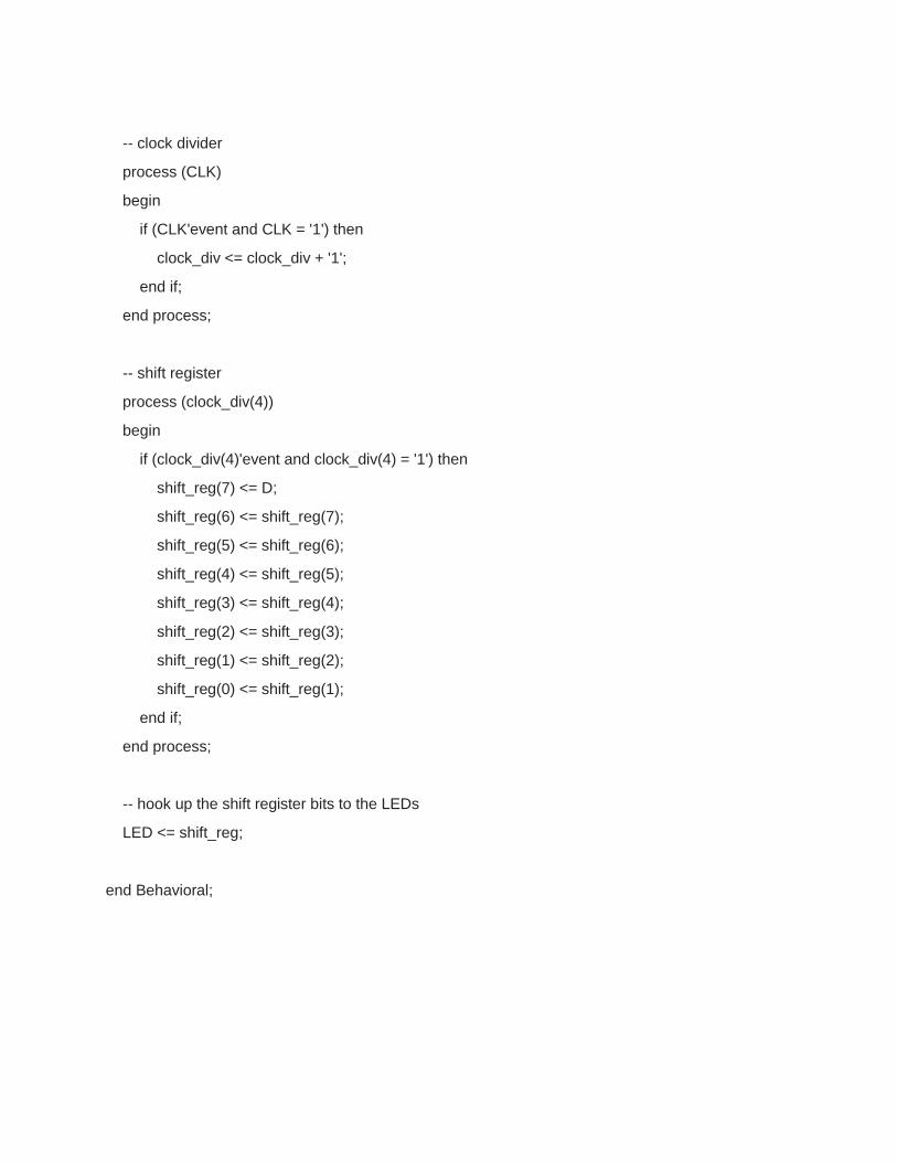
-- clock divider
process (CLK)
begin
if (CLK'event and CLK = '1') then
clock_div <= clock_div + '1';
end if;
end process;
-- shift register
process (clock_div(4))
begin
if (clock_div(4)'event and clock_div(4) = '1') then
shift_reg(7) <= D;
shift_reg(6) <= shift_reg(7);
shift_reg(5) <= shift_reg(6);
shift_reg(4) <= shift_reg(5);
shift_reg(3) <= shift_reg(4);
shift_reg(2) <= shift_reg(3);
shift_reg(1) <= shift_reg(2);
shift_reg(0) <= shift_reg(1);
end if;
end process;
-- hook up the shift register bits to the LEDs
LED <= shift_reg;
end Behavioral;
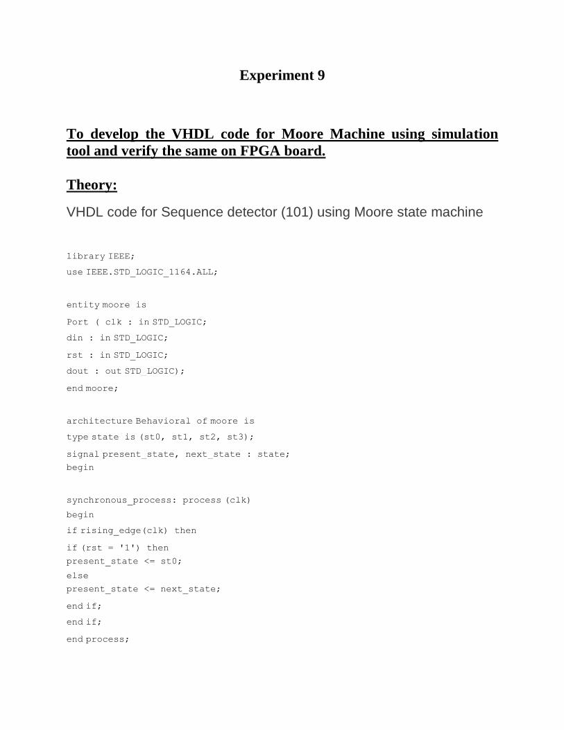
Experiment 9
To develop the VHDL code for Moore Machine using simulation
tool and verify the same on FPGA board.
Theory:
VHDL code for Sequence detector (101) using Moore state machine
library IEEE;
use IEEE.STD_LOGIC_1164.ALL;
entity moore is
Port ( clk : in STD_LOGIC;
din : in STD_LOGIC;
rst : in STD_LOGIC;
dout : out STD_LOGIC);
end moore;
architecture Behavioral of moore is
type state is (st0, st1, st2, st3);
signal present_state, next_state : state;
begin
synchronous_process: process (clk)
begin
if rising_edge(clk) then
if (rst = '1') then
present_state <= st0;
else
present_state <= next_state;
end if;
end if;
end process;
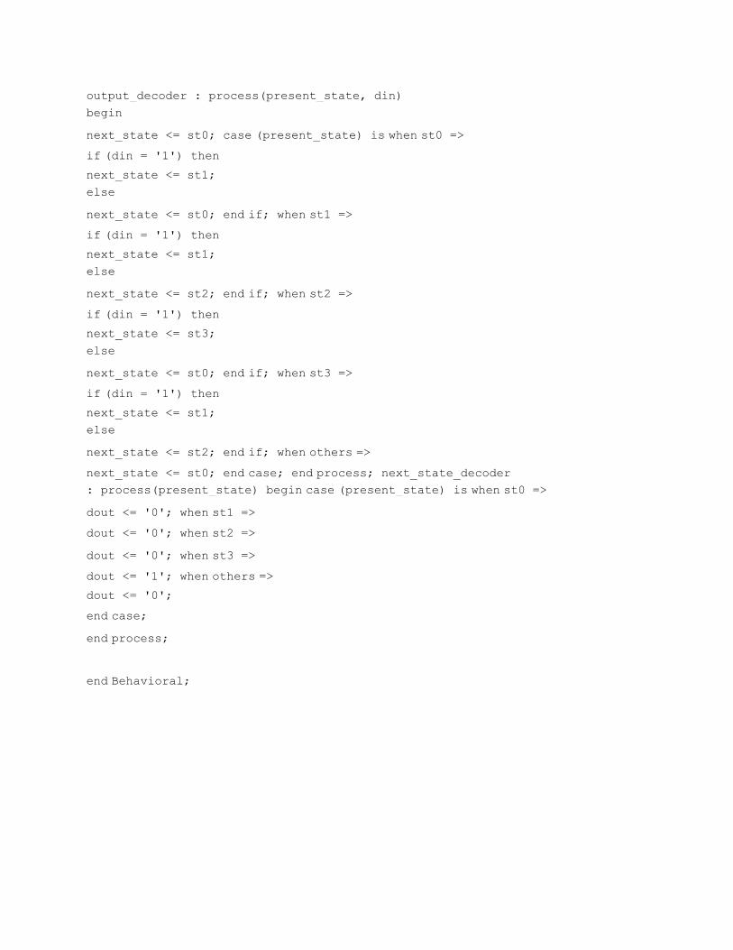
output_decoder : process(present_state, din)
begin
next_state <= st0; case (present_state) is when st0 =>
if (din = '1') then
next_state <= st1;
else
next_state <= st0; end if; when st1 =>
if (din = '1') then
next_state <= st1;
else
next_state <= st2; end if; when st2 =>
if (din = '1') then
next_state <= st3;
else
next_state <= st0; end if; when st3 =>
if (din = '1') then
next_state <= st1;
else
next_state <= st2; end if; when others =>
next_state <= st0; end case; end process; next_state_decoder
: process(present_state) begin case (present_state) is when st0 =>
dout <= '0'; when st1 =>
dout <= '0'; when st2 =>
dout <= '0'; when st3 =>
dout <= '1'; when others =>
dout <= '0';
end case;
end process;
end Behavioral;

Experiment 10
To develop the VHDL code for Mealy Machine using simulation tool
and verify the same on FPGA board.
Theory: Moore machines are finite state machines with output value and its output depends only on present state. library IEEE;
use IEEE.STD_LOGIC_1164.ALL;
entity mealy is
Port ( clk : in STD_LOGIC;
din : in STD_LOGIC;
rst : in STD_LOGIC;
dout : out STD_LOGIC);
end mealy;
architecture Behavioral of mealy is
type state is (st0, st1, st2, st3);
signal present_state, next_state : state;
begin
syncronous_process : process (clk)
begin
if rising_edge(clk) then
if (rst = '1') then
present_state <= st0;
else
present_state <= next_state;
end if;
end if;
end process;
next_state_and_output_decoder : process(present_state, din)
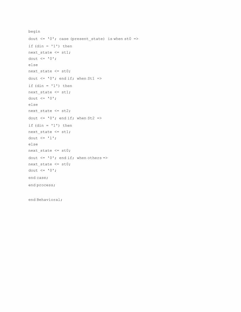
begin
dout <= '0'; case (present_state) is when st0 =>
if (din = '1') then
next_state <= st1;
dout <= '0';
else
next_state <= st0;
dout <= '0'; end if; when St1 =>
if (din = '1') then
next_state <= st1;
dout <= '0';
else
next_state <= st2;
dout <= '0'; end if; when St2 =>
if (din = '1') then
next_state <= st1;
dout <= '1';
else
next_state <= st0;
dout <= '0'; end if; when others =>
next_state <= st0;
dout <= '0';
end case;
end process;
end Behavioral;

Appendix I
To develop code for Full Adder and verify same on FPGA tool
THEORY: Mealy machines are also finite state machines with output value and its output depends on present state and current input symbol.
VHDL code :
library IEEE;
use IEEE.STD_LOGIC_1164.ALL;
use IEEE.STD_LOGIC_ARITH.ALL;
use IEEE.STD_LOGIC_UNSIGNED.ALL;
entity fadder is
port( a,b,cin : in bit; s,cout : out bit);
end fadder;
architecture Behavioral of fadder is
begin
s <= a xor b xor cin;
cout <= (a and b) or (a and cin) or (b and cin);
end Behavioral;
UCF file
NET "a" LOC="P21" | IOSTANDARD=LVTTL;
NET "b" LOC="P27" | IOSTANDARD=LVTTL;
NET "c" LOC="P29" | IOSTANDARD=LVTTL;
NET "cout" LOC="P26" | IOSTANDARD=LVTTL | SLEW=SLOW;
NET "s" LOC="P20" | IOSTANDARD=LVTTL | SLEW=SLOW;
TRUTH TABLE
Input Output

Cin B A S Cout
0 0 0 0 0
0 0 1 1 0
0 1 0 1 0
0 1 1 0 1
1 0 0 1 0
1 0 1 0 1
1 1 0 0 1
1 1 1 1 1
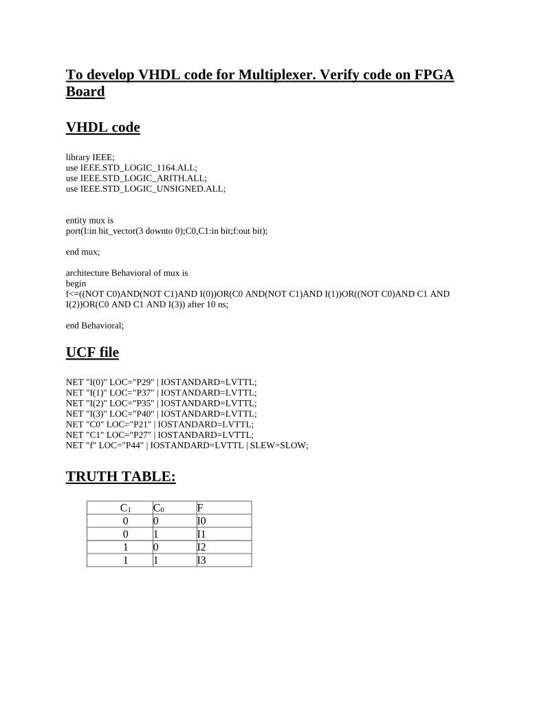
To develop VHDL code for Multiplexer. Verify code on FPGA
Board
VHDL code
library IEEE;
use IEEE.STD_LOGIC_1164.ALL;
use IEEE.STD_LOGIC_ARITH.ALL;
use IEEE.STD_LOGIC_UNSIGNED.ALL;
entity mux is
port(I:in bit_vector(3 downto 0);C0,C1:in bit;f:out bit);
end mux;
architecture Behavioral of mux is
begin
f<=((NOT C0)AND(NOT C1)AND I(0))OR(C0 AND(NOT C1)AND I(1))OR((NOT C0)AND C1 AND
I(2))OR(C0 AND C1 AND I(3)) after 10 ns;
end Behavioral;
UCF file
NET "I(0)" LOC="P29" | IOSTANDARD=LVTTL;
NET "I(1)" LOC="P37" | IOSTANDARD=LVTTL;
NET "I(2)" LOC="P35" | IOSTANDARD=LVTTL;
NET "I(3)" LOC="P40" | IOSTANDARD=LVTTL;
NET "C0" LOC="P21" | IOSTANDARD=LVTTL;
NET "C1" LOC="P27" | IOSTANDARD=LVTTL;
NET "f" LOC="P44" | IOSTANDARD=LVTTL | SLEW=SLOW;
TRUTH TABLE:
C1 C0 F
0 0 I0
0 1 I1
1 0 I2
1 1 I3
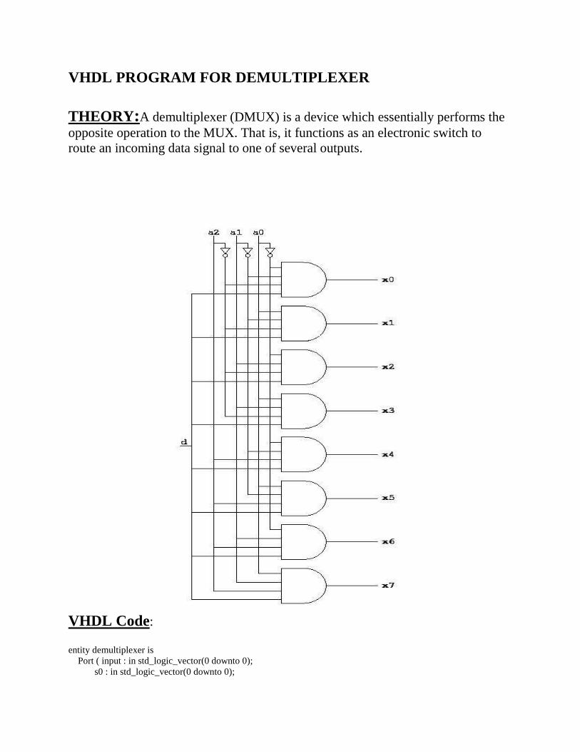
VHDL PROGRAM FOR DEMULTIPLEXER
THEORY:A demultiplexer (DMUX) is a device which essentially performs the
opposite operation to the MUX. That is, it functions as an electronic switch to
route an incoming data signal to one of several outputs.
VHDL Code:
entity demultiplexer is
Port ( input : in std_logic_vector(0 downto 0);
s0 : in std_logic_vector(0 downto 0);

s1 : in std_logic_vector(0 downto 0);
s2 : in std_logic_vector(0 downto 0);
o0 : out std_logic_vector(0 downto 0);
o1 : out std_logic_vector(0 downto 0);
o2 : out std_logic_vector(0 downto 0);
o3 : out std_logic_vector(0 downto 0);
o4 : out std_logic_vector(0 downto 0);
o5 : out std_logic_vector(0 downto 0);
o6 : out std_logic_vector(0 downto 0);
o7 : out std_logic_vector(0 downto 0));
end demultiplexer;
architecture Behavioral of demultiplexer is
begin
o0 <= (not s0 and not s1 and not s2 and input);
o1 <= ( s0 and not s1 and not s2 and input);
o2 <= ( not s0 and s1 and not s2 and input);
o3 <= ( s0 and s1 and not s2 and input);
o4 <= (not s0 and not s1 and s2 and input);
o5 <= ( s0 and not s1 and s2 and input);
o6 <= (not s0 and s1 and s2 and input);
o7 <= ( s0 and s1 and s2 and input);
end Behavioral;
TRUTH TABLE: A2 A1 A0 OUT
0 0 0 D0
0 0 1 D1
0 1 0 D2
0 1 1 D3
1 0 0 D4
1 0 1 D5
1 1 0 D6
1 1 1 D7

COLLEGE OF TECHNOLGY AND ENGINEERING MAHARANA PRATAP UNIVERSITY OF AGRICULTURE & TECHNOLGY, UDAIPUR
DEPARTMENT OF ELECTRONICS AND COMMUNICATION ENGINEERING
LAB MANUAL
Class IV Year.
Optical Communication
EC-422
Prepared by
Dr. Sunil Joshi
Mr Lalit Verma
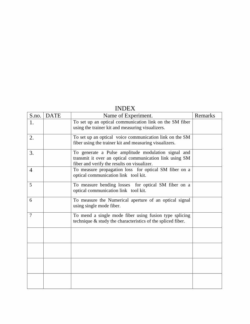
INDEX S.no. DATE Name of Experiment. Remarks
1. To set up an optical communication link on the SM fiber
using the trainer kit and measuring visualizers.
2. To set up an optical voice communication link on the SM
fiber using the trainer kit and measuring visualizers.
3. To generate a Pulse amplitude modulation signal and
transmit it over an optical communication link using SM
fiber and verify the results on visualizer.
4 To measure propagation loss for optical SM fiber on a
optical communication link tool kit.
5 To measure bending losses for optical SM fiber on a
optical communication link tool kit.
6 To measure the Numerical aperture of an optical signal
using single mode fiber.
7 To mend a single mode fiber using fusion type splicing
technique & study the characteristics of the spliced fiber.

As covered in the books.
SUBJECT INDEX:
1. Do’s & Don’ts in Laboratory. 2. Lab Exercises
1. ANALOG LINK USING OPTICAL FIBER.
2. VOICE LINK USING OPTICAL FIBER.
3. PAM SIGNAL TRANSMISION & RECEPTION
4. PROPAGATION LOSS MEASURMENT
5. BENDING LOSS MEASURMENT
6. NUMERICAL APERTURE
7. SPLICING & CHARACTERIZATION.

Dos and Don’ts in Laboratory :-
1. Do not handle any equipment before reading the instructions /Instruction manuals.
2. Read carefully the power ratings of the equipment before it is switched ON,
whether ratings 230 V/50 Hz or 115V/60 Hz. For Indian equipment, the power ratings are normally 230V/50Hz. If you have equipment with 115/60 Hz ratings, do not insert power plug, as our normal supply is 230V/50Hz, which will damage the equipment.
3. Observe type of sockets of equipment power to avoid mechanical damage. 4. Do not forcefully place connectors to avoid the damage. 5. Strictly observe the instructions given by the Subject Teacher/ Lab Instructor.
Instruction for Laboratory Teachers:-
1. Submission related to whatever lab work has been completed should be done during the next lab session.
2. Students should be instructed to switch on the power supply after getting the
checked by the lab assistant / teacher. After the experiment is over, the students must hand over the trainer kits, components, wires, CRO, CRO probe, etc. to the lab assistant/teacher.
3. The promptness of submission should be encouraged by way of marking
and evaluation patterns that will benefit the sincere students.
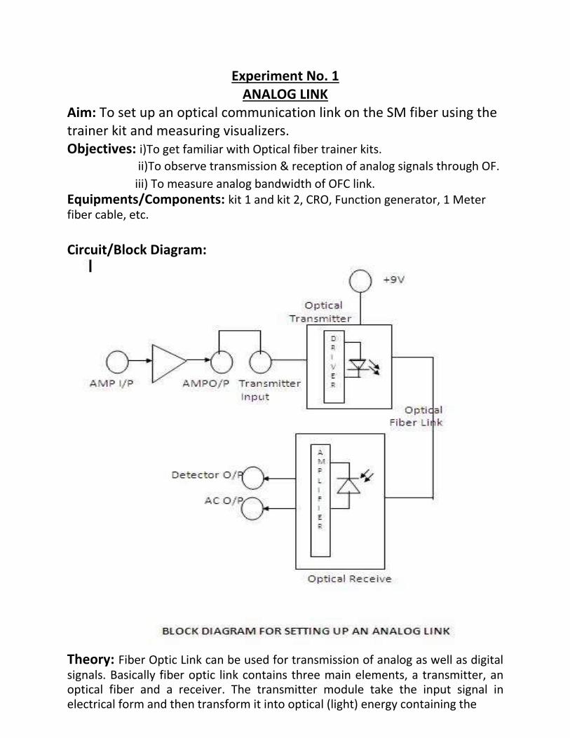
Experiment No. 1
ANALOG LINK
Aim: To set up an optical communication link on the SM fiber using the trainer kit and measuring visualizers. Objectives: i)To get familiar with Optical fiber trainer kits.
ii)To observe transmission & reception of analog signals through OF.
iii) To measure analog bandwidth of OFC link. Equipments/Components: kit 1 and kit 2, CRO, Function generator, 1 Meter fiber cable, etc.
Circuit/Block Diagram:
Theory: Fiber Optic Link can be used for transmission of analog as well as digital signals. Basically fiber optic link contains three main elements, a transmitter, an optical fiber and a receiver. The transmitter module take the input signal in electrical form and then transform it into optical (light) energy containing the
same information. The optical fiber is a medium which carries this energy to the receiver. At the receiver, light is converted back into electrical form with the same pattern as originally fed to the transmitter.
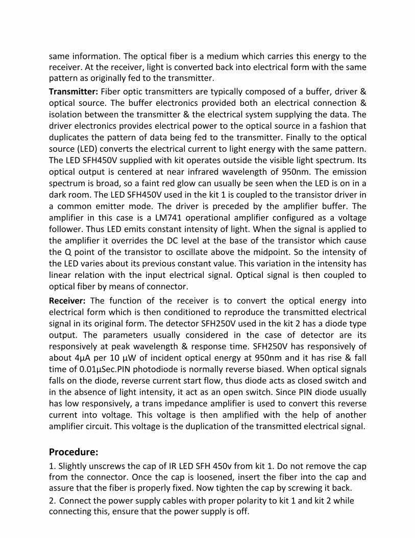
Transmitter: Fiber optic transmitters are typically composed of a buffer, driver & optical source. The buffer electronics provided both an electrical connection & isolation between the transmitter & the electrical system supplying the data. The driver electronics provides electrical power to the optical source in a fashion that duplicates the pattern of data being fed to the transmitter. Finally to the optical source (LED) converts the electrical current to light energy with the same pattern. The LED SFH450V supplied with kit operates outside the visible light spectrum. Its optical output is centered at near infrared wavelength of 950nm. The emission spectrum is broad, so a faint red glow can usually be seen when the LED is on in a dark room. The LED SFH450V used in the kit 1 is coupled to the transistor driver in a common emitter mode. The driver is preceded by the amplifier buffer. The amplifier in this case is a LM741 operational amplifier configured as a voltage follower. Thus LED emits constant intensity of light. When the signal is applied to the amplifier it overrides the DC level at the base of the transistor which cause the Q point of the transistor to oscillate above the midpoint. So the intensity of the LED varies about its previous constant value. This variation in the intensity has linear relation with the input electrical signal. Optical signal is then coupled to optical fiber by means of connector.
Receiver: The function of the receiver is to convert the optical energy into electrical form which is then conditioned to reproduce the transmitted electrical signal in its original form. The detector SFH250V used in the kit 2 has a diode type output. The parameters usually considered in the case of detector are its responsively at peak wavelength & response time. SFH250V has responsively of about 4µA per 10 µW of incident optical energy at 950nm and it has rise & fall time of 0.01µSec.PIN photodiode is normally reverse biased. When optical signals falls on the diode, reverse current start flow, thus diode acts as closed switch and in the absence of light intensity, it act as an open switch. Since PIN diode usually has low responsively, a trans impedance amplifier is used to convert this reverse current into voltage. This voltage is then amplified with the help of another amplifier circuit. This voltage is the duplication of the transmitted electrical signal.
Procedure:
1. Slightly unscrews the cap of IR LED SFH 450v from kit 1. Do not remove the cap from the connector. Once the cap is loosened, insert the fiber into the cap and assure that the fiber is properly fixed. Now tighten the cap by screwing it back. 2. Connect the power supply cables with proper polarity to kit 1 and kit 2 while connecting this, ensure that the power supply is off.
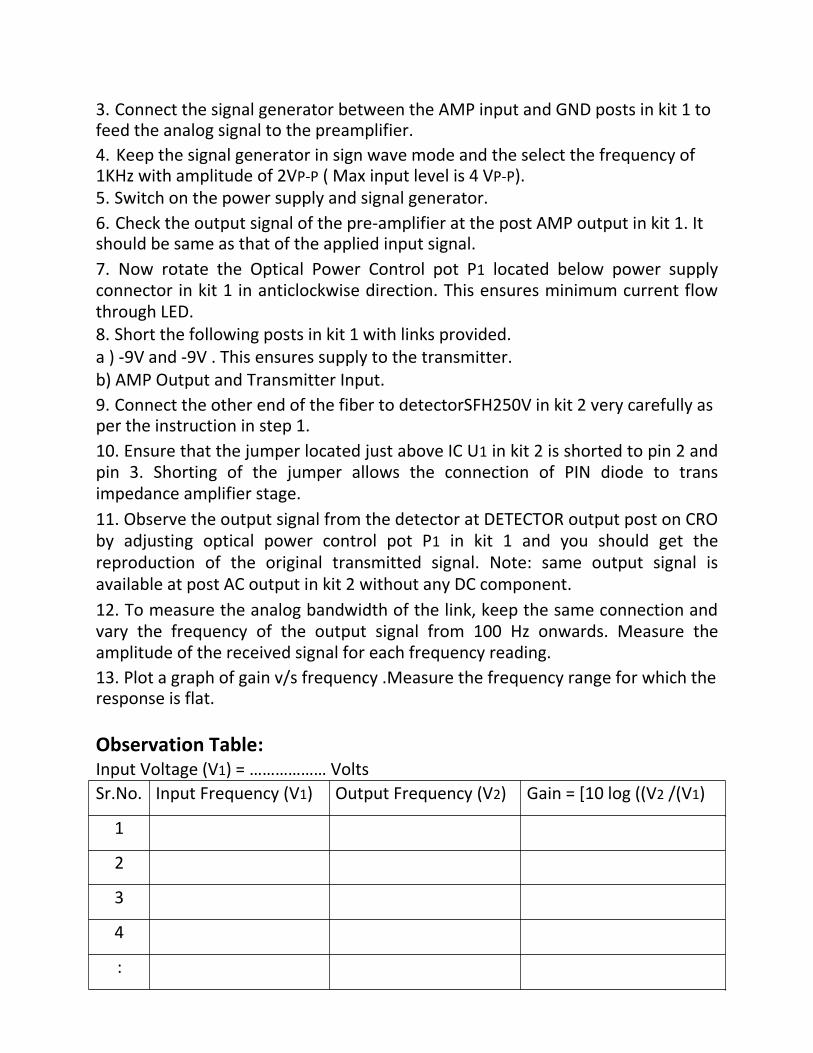
3. Connect the signal generator between the AMP input and GND posts in kit 1 to feed the analog signal to the preamplifier. 4. Keep the signal generator in sign wave mode and the select the frequency of 1KHz with amplitude of 2VP-P ( Max input level is 4 VP-P). 5. Switch on the power supply and signal generator. 6. Check the output signal of the pre-amplifier at the post AMP output in kit 1. It should be same as that of the applied input signal. 7. Now rotate the Optical Power Control pot P1 located below power supply connector in kit 1 in anticlockwise direction. This ensures minimum current flow through LED. 8. Short the following posts in kit 1 with links provided.
a ) -9V and -9V . This ensures supply to the transmitter. b) AMP Output and Transmitter Input.
9. Connect the other end of the fiber to detectorSFH250V in kit 2 very carefully as per the instruction in step 1. 10. Ensure that the jumper located just above IC U1 in kit 2 is shorted to pin 2 and pin 3. Shorting of the jumper allows the connection of PIN diode to trans impedance amplifier stage. 11. Observe the output signal from the detector at DETECTOR output post on CRO by adjusting optical power control pot P1 in kit 1 and you should get the reproduction of the original transmitted signal. Note: same output signal is available at post AC output in kit 2 without any DC component. 12. To measure the analog bandwidth of the link, keep the same connection and vary the frequency of the output signal from 100 Hz onwards. Measure the amplitude of the received signal for each frequency reading. 13. Plot a graph of gain v/s frequency .Measure the frequency range for which the response is flat.
Observation Table:
Input Voltage (V1) = ……………… Volts
Sr.No. Input Frequency (V1) Output Frequency (V2) Gain = [10 log ((V2 /(V1)
1
2
3
4
:

Calculations:
Bandwidth = f2 – f1 Hz
Result:
Conclusion:
Experiment No. 2
DIGITAL LINK
Aim: To set up an optical voice communication link on the SM fiber using the trainer kit and measuring visualizers.
Objectives: To observe transmission and reception of voice signals through OF.
Equipments/Components: kit 1 and kit 2, CRO, Microphone, Loudspeaker (or Function generator), 1 Meter fiber cable,etc.
Circuit/Block Diagram:
Theory: Fiber Optic Link can be used for transmission of digital as well as analog signals. Basically fiber optic link contains three main elements, a transmitter, an optical fiber and a receiver. The transmitter module take the input signal in electrical form and then transform it into optical (light) energy containing the
same information. The optical fiber is a medium which carries this energy to the receiver. At the receiver, light is converted back into electrical form with the same pattern as originally fed to the transmitter.
The detailed Theory of Fiber optic transmitters and Fiber optic receiver is as explained in Expt. No.-1.
Procedure :
1. Connect the dynamic microphone provided with the kit to the socket marked MIC Input in the audio preamplifier section of kit 1. 2. Connector speakers provided with the kit to the socket marked speaker in the audio amplifier section of kit 2. 3. Now in the above experiment of simple analog link, remove the signal generator output from AMP Input post and supply MIC output from MIC Output post in kit 1. 4. Similarly connect output signal of photo detector from post detector output to the post audio output. 5. Adjust optical fiber control post P1 in kit 1 and voice control post P1 in kit 2 to setup fiber optic audio link
Result:
Conclusion:
Experiment No. 3
PAM SIGNAL TRANSMISION & RECEPTION
Aim: To generate a Pulse amplitude modulation signal and transmit it over an optical communication link using SM fiber and verify the results on visualizer.
Objectives: i) To observe transmission and reception of PAM signals through OF.
ii)To represent modulating, carrier, PAM and demodulated signals graphically.
Equipments/ Components: kit No.1 & 2, CRO, Function Generator, 1 Meter Fiber Cable, etc.
Circuit/Block Diagram:
Theory: Pulse Amplitude Modulation is a technique of communication in which the high frequency square wave is modulated by the low frequency signal. The modulating signal is sampled by the pulses. The PAM signal is nothing but high frequency square wave in which the amplitude of each pulse is equal to that of the information signal at the respective sampling instant.
Procedure:
1. Concept the power supply cable with proper polarity to kit 1 & kit 2. while connecting this ensure that the power supply is off. 2. Connect the signal generator between the PAM input and GND post for PAM circuit in kit 1. 3. Keep the signal generator in sign wave mode and select the frequency = 1 KHz with amplitude = 1V P-P. 4. Switch on the power supply and signal generator. 5. Check that the clock circuit is properly working by connecting the oscilloscope probe at CLK output post. You will find the square wave output with frequency = 32KHz 6. Now observe the output waveform at post PAM output. You will find fantastic pattern of square wave whose amplitude ( i.e. pulse height) is varying according to the sine wave input. 7. Now vary the frequency of input sine wave. You will notice that at the output. The frequency is changing, still the output is pulse amplitude modulated. Further, increase the input frequency and notice the change. Try to understand why such angles are occurring in output waveform. 8. Slightly unscrew the cap of IR LED SFH 450V on kit 1. Do not remove the cap from the connector. Once the cap is loosened, insert the fiber into the cap and assure that the fiber is properly fixed. Now tighten the cap by screwing it back. Similarly connect the other end of fiber to detector SFH 250V on kit 2. 9. Connect output of PAM circuit at PAM output post to the AMP input post with the shorting links provided in kit 1. 10. Now establish the link between the posts marked as AMP output and transmitter input. Let the signal be transmitted through optical fiber. While doing this, please ensure that both the +9V posts are shorted by the shorting link. 11. Observe the output of the detector at detector output post in kit 2. Adjust the gain control pot P)below the power supply connector in kit 1 to obtain the same amplitude as the transmitted signal connect this output of receiver to the input of pulse amplitude demodulator circuit by shorting detector output post & PAM Input post in kit 2.
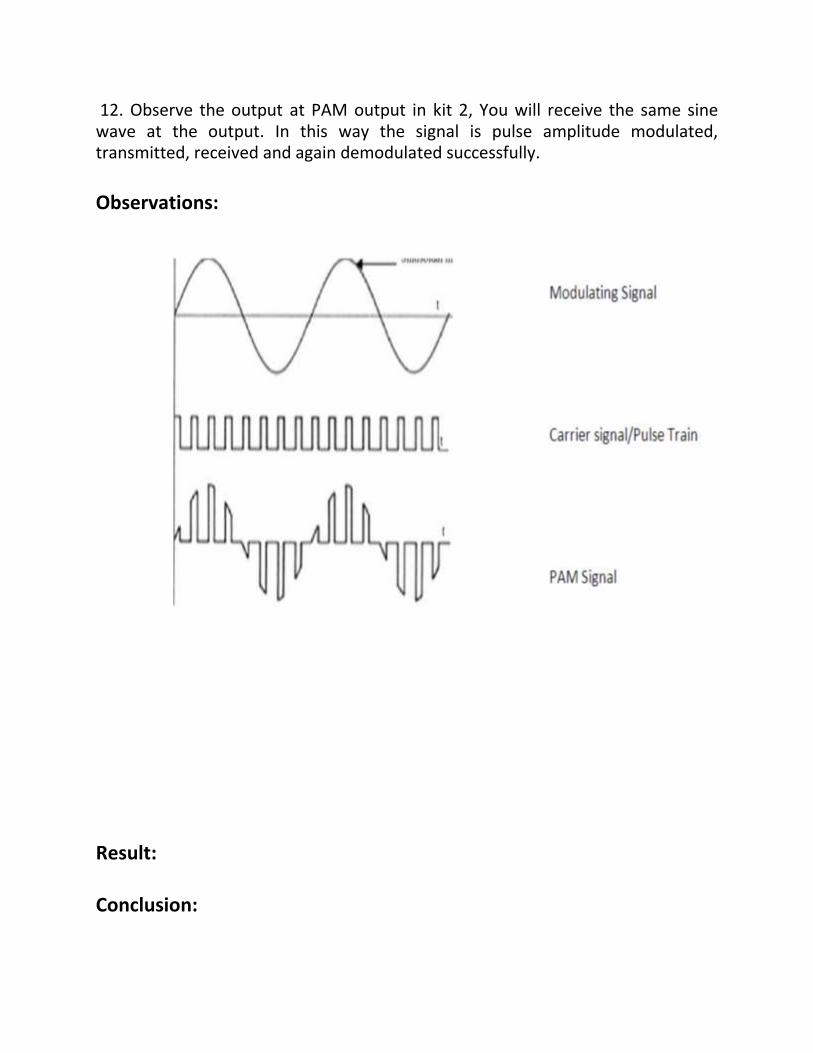
12. Observe the output at PAM output in kit 2, You will receive the same sine wave at the output. In this way the signal is pulse amplitude modulated, transmitted, received and again demodulated successfully.
Observations:
Result:
Conclusion:

Experiment No. 4
PROPAGATION LOSS MEASURMENT
Aim: To measure propagation loss for optical SM fiber on a optical communication link tool kit. Objectives: i) To observe transmission and reception of signals through OF using
two different lengths fiber. ii) To measure Propagation loss in neper/meter.
Equipments/Components: kit1, kit2, 1MHz Function Generator, 20 MHz Dual Trace Oscilloscope, 1 & 3 Meter Fiber Cable.
Circuit/Block Diagram:
Theory: Optical fibers are available in different variety of materials. These materials are usually selected by taking into account their absorption
characteristics for different wavelengths of light. In case of optical fiber, since the signal is transmitted in the form of light which is completely different in nature as that of electrons, one has to consider the interaction of matter with the radiation to study the losses in fiber. Losses are introduced in fiber due to various reasons. As light propagates from one end of fiber to another end, part of it is absorbed in the material exhibiting absorption loss. Also part of the light is reflected back or in some other directions from the impurity particles present in the material contributing to the loss of the signal at the other end of the fiber. In general terms it is known as propagation loss. Plastics fibers have higher loss of the order of 180 db/km. whenever the condition for angle of incidence of the incident light is violated the losses are introduced due to refraction of light. This occurs when fiber is subjected to bending. Lower the radius of curvature more is the loss. Other losses are due to the coupling of fiber at LED & photo detector ends.
Procedure:
1. Slightly unscrews the cap of IR LED SFH 450v from kit 1. Do not remove the cap from the connector. Once the cap is loosened, insert the fiber into the cap and assure that the fiber is properly fixed. Now tighten the cap by screwing it back. 2. Connect the power supply cables with proper polarity to kit 1 and kit 2 while connecting this, ensure that the power supply is off. 3. Connect the signal generator between the AMP input and GND posts in kit 1 to feed the analog signal to the preamplifier. 4. Keep the signal generator in sign wave mode and the select the frequency of 1KHz with amplitude of 2VP-P (Max input level is 4 VP-P). 5. Switch on the power supply and signal generator. 6. Check the output signal of the pre-amplifier at the post AMP output in kit 1. It should be same as that of the applied input signal. 7. Now rotate the Optical Power Control pot P1 located below power supply connector in kit 1 in anticlockwise direction. This ensures minimum current flow through LED. 8. Short the following posts in kit 1 with links provided. a) -9V and -9V . This ensures supply to the transmitter. b) AMP Output and Transmitter Input.
9. Connect the other end of the fiber to detectorSFH250V in kit 2 very carefully as per the instruction in step 1. 10. Ensure that the jumper located just above IC U1 in kit 2 is shorted to pin 2 and pin 3. Shorting of the jumper allows the connection of PIN diode to trans-impedance amplifier stage. 11. Observe the output signal from the detector at AC OUTPUT post in kit2 on CRO. Adjust optical power control pot P1 in kit1. You should get the reproduction
of original transmitted signal. Also adjust the amplitude of received signal as that of transmitted one. Mark this amplitude as V1.
12. Now replace 1m fiber by 3m fiber without changing settings of kit1 & kit2. Measure the amplitude of received signal again. You will notice that it is less than previous one. Mark this as V2. 13. If α is the attenuation/loss in the fiber then, we have,
V1/V2 = exp{-α(L1+L2)}
Where- α=neper/meter,
L1= Fiber length for V1,
L2= Fiber length for V2,
14. Calculate propagation loss α using above equation.
Observations:
i)The measured length of fiber, L1=------meter
ii)O/P voltage V1
for length of fiber, L1=------Volts
iii)The measured length of fiber, L2=------meter
iv)O/P voltage V2
for length of fiber, L2=------Volts
Calculations:
V1/V2 = exp{-α(L1+L2)}
Log10 (V1/V2)= -α(L1+L2)
Therefore -α= Log10 (V1/V2) /(L1+L2) neper/meter
= ------ neper/meter
Result:
Conclusion:
Experiment No. 5
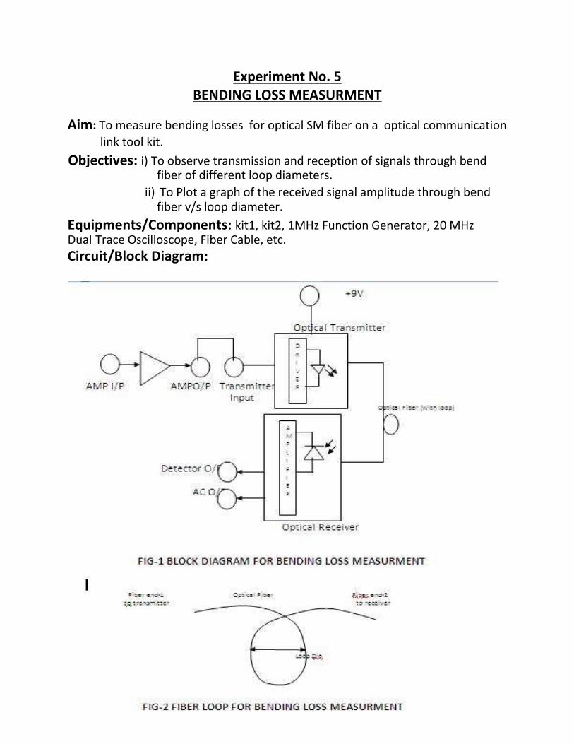
BENDING LOSS MEASURMENT
Aim: To measure bending losses for optical SM fiber on a optical communication
link tool kit.
Objectives: i) To observe transmission and reception of signals through bend fiber of different loop diameters.
ii) To Plot a graph of the received signal amplitude through bend fiber v/s loop diameter.
Equipments/Components: kit1, kit2, 1MHz Function Generator, 20 MHz Dual Trace Oscilloscope, Fiber Cable, etc.
Circuit/Block Diagram:
Theory: Optical fibers are available in different variety of materials. These materials are usually selected by taking into account their absorption characteristics for different wavelengths of light. In case of optical fiber, since the signal is transmitted in the form of light which is completely different in nature as that of electrons, one has to consider the interaction of matter with the radiation to study the losses in fiber. Losses are introduced in fiber due to various reasons. As light propagates from one end of fiber to another end, part of it is absorbed in the material exhibiting absorption loss. Also part of the light is reflected back or in some other directions from the impurity particles present in the material contributing to the loss of the signal at the other end of the fiber. In general terms it is known as propagation loss. Plastics fibers have higher loss of the order of 180 db/km. whenever the condition for angle of incidence of the incident light is violated the losses are introduced due to refraction of light. This occurs when fiber is subjected to bending. Lower the radius of curvature more is the loss. Other losses are due to the coupling of fiber at LED & photo detector ends.
Procedure:
1. Slightly unscrews the cap of IR LED SFH 450v from kit 1. Do not remove the cap from the connector. Once the cap is loosened, insert the fiber into the cap and assure that the fiber is properly fixed. Now tighten the cap by screwing it back. 2. Connect the power supply cables with proper polarity to kit 1 and kit 2 while connecting this, ensure that the power supply is off. 3. Connect the signal generator between the AMP input and GND posts in kit 1 to feed the analog signal to the preamplifier. 4. Keep the signal generator in sign wave mode and the select the frequency of 1KHz with amplitude of 2VP-P (Max input level is 4 VP-P). 5. Switch on the power supply and signal generator. 6. Check the output signal of the pre-amplifier at the post AMP output in kit 1. It should be same as that of the applied input signal. 7. Now rotate the Optical Power Control pot P1 located below power supply connector in kit 1 in anticlockwise direction. This ensures minimum current flow through LED. 8. Short the following posts in kit 1 with links provided. a) -9V and -9V . This ensures supply to the transmitter. b) AMP Output and Transmitter Input.
9. Connect the other end of the fiber to detectorSFH250V in kit 2 very carefully as per the instruction in step 1. 10 Ensure that the jumper located just above IC U1 in kit 2 is shorted to pin 2 and pin 3. Shorting of the jumper allows the connection of PIN diode to trans-impedance amplifier stage.
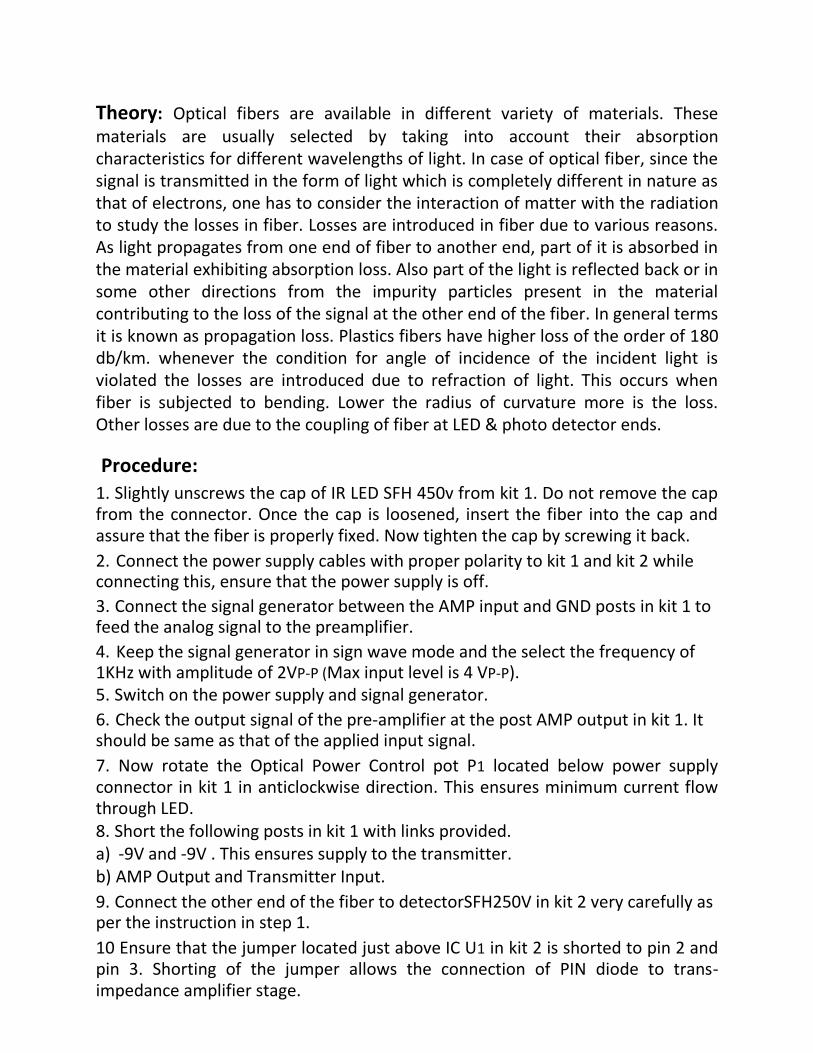
11.Observe the output signal on CRO at AC OUTPUT post in kit2. 12. Then bend the fiber in a loop. (as shown in fig-1) 13. Measure the amplitude/voltage of the received signal. 14. Keep reducing the diameter of fiber to about 2cm and take corresponding output voltage readings (Do not reduce loop diameter less than 2cm). 15. Plot a graph of the received signal amplitude v/s loop diameter.
Observation Table: Sr.No. Loop Diameter (cm) Output Voltage (Volts)
1
2
3
4
5
:
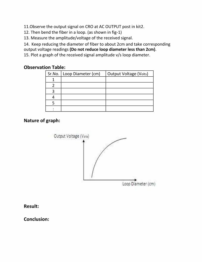
Nature of graph:
Result:
Conclusion:
Experiment No. 6
NUMERICAL APERTURE
Aim: To measure the Numerical aperture of an optical signal using single mode
fiber.
Objectives: i) To observe transmission of visible light signals through fiber.
ii) To measure optical power gathering capability of fiber in terms of numerical aperture.
Equipments/ Components: kit4, OF, Fiber holding fixture, Ruler, etc.
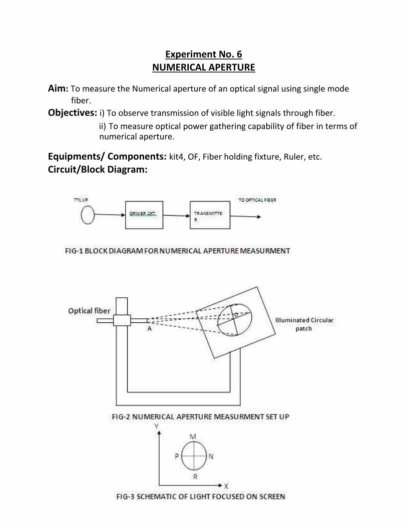
Circuit/Block Diagram:

Theory: Numerical aperture refers to the maximum angle at which the light incident on the fiber end is totally internally reflected and is transmitted properly along the fiber. The cone formed by the rotation of this angle along the axis of fiber is the cone of acceptance of fiber. The light ray should strike the fiber end within its cone of acceptance; else it is refracted out from fiber.
Procedure: 1. Slightly unscrews the cap of LED SFH 756V from kit 4. Do not remove the cap from the connector. Once the cap is loosened, insert the fiber into the cap and assure that the fiber is properly fixed. Now tighten the cap by screwing it back.
2. Now short the jumpers as shown in the jumper diagram. 3. Connect the power supply cables to kit 4 and switch on the power supply. 4. Apply TTL high i/p to the ED from Ext. TTL terminal as per Fig-1. 5. Insert the other end of fiber in to the fiber holding fixture. 6. Observe the illuminated circular patch of light on the screen (as shown in fig-2). 7. Measure the distance‘d’ between fiber end and surface (d=AO). 8. Then measure the major and minor axes of illumination (i.e.MR & PN as shown in Fig-3). 9. Calculate mean radius of illumination using formula, r=(MR+PN)/4.
10. Find the numerical aperture of the fiber using formula, NA= Sinθmax=r/d2+r2
Where θmax is the maximum angle at which the light incident is properly transmitted through the fiber.
Observation Table: Sr.No. Distance MR (cm) PN (cm) r=(MR+PN)/4 NA=Sinθmax
d=AO (cm) =r/d2 +r2
1
2
3
4
5
Calculations: i) r=(MR+PN)/4= ; NA=Sinθmax =r/d2
+r2=
ii) r=(MR+PN)/4= ; NA=Sinθmax =r/d2 +r2=
iii) r=(MR+PN)/4= ; NA=Sinθmax =r/d2 +r2=
iv) r=(MR+PN)/4= ; NA=Sinθmax =r/d2 +r2=
v) r=(MR+PN)/4= ; NA=Sinθmax =r/d2 +r2=
Result:
Conclusion:

Experiment No. 7
SPLICING & CONNECTERIZATION
Aim: To mend a single mode fiber using fusion type splicing technique & study
the characteristics of the spliced fiber. Objective: To know and apply the functioning and working of different splicing & connecterization tools in installation of OFC link.
EQUIPMENT Used: splice installation kit, Connector installation kit.
Theory:
SK-1000 splice installation kit: It is the process of joining two pieces of fiber together o a typical fiber optic link there are usually a number of splice points as it is typically not possible (or practical) to simply “pull” one long continuous fiber. Splice quality is absolutely critical, because each junction point on the link introduce some degree of optical power loss or attenuation. Splicing joins the two fibers together both optically and physically. There are essentially two different techniques that are currently in use, fusion and mechanical splicing.
Splice Installation kit sk-1000 contains all the tool and materials required mechanical splicing. The kit consists of following items. The purpose of this kit is to train the students in the technique of splicing. Before starting with the procedure, let us discuss in brief the operation and application of the above tools. OPTOSPLICE: It is a high performance, easy to install U.V. Curve Mechanical splice. The design employs a visible glass reinforced plastic housing. The molded-in- spring grabs the buffer retention, for tuning and curing. After curing the U.V. Adhesive ,it provides a thermal match for a long term stability over a wide temperature range.
UV BOND: It is used for joining and mounting fiber during the process of splicing.
It cures in seconds when exposed to UV light.
UV Lamp: It is used for curing the UV Adhesive. It has been provided with two “V” notched fiber guides. These guides serve as a means of holding the fiber in place as well as to elevate the UV Lamp above the work surface, permitting the fiber optic splice to be positioned within the bezel opening.
UV PROTECTIVE GOGGLES: During the process of curing of UV Adhesive, one should make it a point to wear UV protective Goggles. It gives protection to the eyes from UV light. For cleaning the goggles one can wash in mild soap and water, and then rinse in clean water. Do not use ammonia, alkaline cleaners, abrasive cleaning compounds or solvents. No-NIK BUFFER STRIPPER: It is to remove buffer coating from the optical fiber.
FIBER OPTIC MICROSCOPE: it is used to observe the tip of fiber. Please follow the following instruction for observing the fiber end(refer fig.) 1. Unfold the battery case so that the light will up.
2. To observe the tip of the bare fiber, set the fiber tip to the hood center. If the fiber is ST Connectorised replace the hood with the ST. Adaptor and held the ST Connector in the adaptor. 3. Look into ocular lens and adjust focus, turning the focus adjust knob.
BLADE & SCISSERS: They are used to remove the outer jacket and to cut the fibrous (Kevlar) material of the fiber. CK-1000 Connector installation kit:
In any fiber optic system, one will always find the need for splices and connectors. Splices are during installation and again during service, if the cables be damaged and fibers become broken. Connectors are invariably used to connect fiber to the terminal equipment. Each splice or connectors gives rise to additional attenuation and the need to minimize such loss requires a careful preparation of the ends of the fibers. Low loss is obtained only if the fiber end faces are clean, smooth and perpendicular to the fiber axis.
It is the process of terminating the fiber by a connector. Normally a source and detectors are mounted is a standard bulkhead, into which the fiber link of the system. Which is having the connectors at the end is plugged. Such an arrangement permits individual units and components to be tested separately and replaced if necessary.
Many different design of connector have been developed (fig.1). Most use a ferrule for fiber alignment, although some designs use three spheres to center the fiber and a double cone to align the connectors.
Connector Installation kit CK 1000 contains all the tools and materials required to terminate glass fiber with ST Connector. The kit consists of following items.
FIBER OPTIC STRIPPER: It is designed to remove the outside jacket of the fiber. To use it insert the fiber into the stripping hole of proper diameter. Close the tool and draw fiber through hole exerting steady pressure (refer fig.)
DIAMOND PEN SCRIBE: It is use to cut the glass fiber. Hold the diamond pen scribe perpendicularly to the fiber axis and slowly scribe it on the glass fiber without exerting any pressure.
FIBER OPTIC MICROSCOPE: It is used to observe the tip of fiber. Please follow the following instruction for observing the fiber end(refer fig.) 1. Unfold the battery case so that the light will up. 2. To observe the tip of the bare fiber, set the fiber tip to the hood center. If the fiber is ST Connectorised replace the hood with the ST Adaptor and held the ST connector in the adaptor. 3. Look into ocular lens and adjust focus, turning the focus adjust knob.
ST POLISHING TOOL: It helps to hold the ST Connectorised fiber at 90 while polishing on the lapping sheet.
LAPPING SHEET: The Lapping sheet comes with 5, 1 & 0.3 micron fine grain polishing paper. For polishing the fiber, rotate the ST polishing tool in the figure of eight on 5 micron paper and then on 1 micron and 0.3 micron polishing paper.
EPOXY: It is used for bonding the fiber inside the connector permanently. It consist of two part. Take equal amount of adhesive from each part on any clean, dry, flat surface. Mix it thoroughly so that the different colored part blend into a smooth uniform color. After applying allow it to cure for 4 hours. Cure may be accelerated by heat such as one hours at 140 F. Note that the mixed material must be used within 30minutes.
CRIMP TOOL: After the fiber has been bonded permanently to the connector, the back shell (crimp sleeve) of the connector is crimped using crimped using crimp tool. Select proper cavity diameter of crimp tool while crimping the connector.
BLADE & SCISSERS: They are used to remove the outer jacket and to cut the fibrous (Kevlar) material of the fiber.
COTTON SWAB AND TISSUE PAPER: They are used for cleaning purpose. For minimizing the loss, one should ensure that no dust particles are adhered to the bare fiber. Wipe the fiber with tissue paper moistened with alcohol to remove the impurities.
Conclusion:

3.Quiz /Viva/ Oral Question on the subject:-
Expt. No.-1 Analog Link
Q 1- What for optical fiber link is used?
Q 2. How optical signal is propagating through optical fiber?
Q 3. Which type of optical fiber we are using for practical or demonstration?
Q 4. What is full form of LED? What are the different types of radiation coming from LED?
Q 5. What is function of LED in optical trainer kits?
Q 6. Which LED (type and number) is used in transmitter kit(kit-1)?
Q 7. At what wavelength LED is used?
Q 8. What is function of detector in optical trainer kits?
Q 9. Which photo detector (type and number) is used in receiver kit(kit-2)?
Q 10. How much is responsivity of photo detector used?
Q 11. What different types of analog signals we are transmitting through optical fiber?
Q 12. How bandwidth of OFC link can be measured?
Q 13. How voltage gain can be calculated?
Q 14.Write the frequency range for which response of system is flat.
Q 15. Write analog bandwidth (measured) of OFC link.
Expt. No.-2 Voice Link
Q 1- What is objective/s of expt. No.-2 voice link?
Q 2. What is function of microphone used in kit-1? Q 3. Which type of microphone used in kit-1? Q 4. What is function of audio pre-amplifier circuit in kit-1? Q 5. What for loudspeaker is used in kit-2? Q 6. What is function of audio amplifier circuit in kit-2? Q 7. How alternately transmission and reception can be verified on same trainer kits? Q 8. Give audio frequency range ?
Q 9.State radio frequency range? Q 10.Which type of loudspeaker is used in kit-2?

Expt. No.-3 PAM SIGNAL TRANSMISION & RECEPTION
Q 1- What is objective/s of expt. No.-3 PAM signal transmission &
reception? Q 2. What is Pulse Amplitude Modulation? Q3-What are the different types of PAM? Q4-How PAM signal is generated? Q 5. What different signals required to generate PAM signal?
Q 6-What for clock/timing circuit in kit-1 is used? Q7-How much is the frequency of carrier signal generated? Q8-Represent graphically i/p modulating signal? Q9- Represent graphically i/p carrier signal? Q10- Represent graphically Pulse Amplitude modulated signal? Q11- Represent graphically Pulse Amplitude demodulated signal?
Expt. No.-4 PROPAGATION LOSS MEASURMENT
Q 1- What is objective/s of expt. No.-4 propagation loss measurement?
Q 2. What is propagation loss? Q3-What are the different types of losses occurred in optical fiber? Q4-What is unit of loss measurement? Q 5.Give the equation for calculation of propagation
loss? Q 6-What is relation between dB and neper? Q7- How is the variation of propagation loss as per expt. with respect to length of fiber?
Q8-How to minimize propagation loss?
Expt. No.-5 BENDING LOSS MEASURMENT
Q 1- What is objective/s of expt. No.-5 bending loss measurement? Q 2. What is bending loss in optical fiber? Q3-What are the different types of bending losses occurred? Q4-Give the causes of bending loss? Q5-How signal refraction occur due to micro bending loss? Q6- How signal refraction occur due to macro bending loss? Q 7.How is the variation of bending loss as per expt. with respect to loop diameter? Q 8-At what lower limit we can bend given fiber as per expt.? Q 9-How to minimize bending loss?

Expt. No.-6 NUMERICAL APERTURE
Q 1-What is numerical aperture(NA) of optical fiber ?
Q 2. What is objective/s of expt. No.-6 numerical aperture?
Q3-Whether NA is dimensionless quantity?
Q4-Broadly NA ranges from ---- to ---?
Q5-General range of NA is from ---- to ---?
Q6- What for NA measurement/calculation is required?
Q 7-How NA is measured theoretically? Give equation?
Q 8-State the equation relating NA and refractive indices of core and cladding of fiber?
Q 9- Which type of optical source is used in this expt.?
Q 10- How NA is measured practically? Give equation?
Expt. No.-7 SPLICING & CONNECTERIZATION
Q 1-What is splice or splicing in OFC?
Q 2. What are the different splicing techniques used in OFC?
Q 3-What is connector or connectorization in OFC?
Q 4. What are the different types of connectors used in OFC?
Q5-How optosplice is constructed
Q6- What for UV protective goggle is used?
Q 7-Which adhesive material is used in bonding fibers generally?
Q 8-Give the use of blade and scissers? Q 9- What for fiber optic stripper is used?
Q 10- How crimp tool is useful in splicing?
Expt. No.-8 EYE PATTERN MEASURMENT
Q 1-What is eye pattern or eye diagram?
Q 2Enlist the different basic equipment required for eye pattern measurment?
Q 3-in which domain the eye-pattern measurements is carried
out? Q 4. What are the key features of pattern generated?

4. Conduction of Viva-Voce Examinations:
Teacher should conduct oral exams of the students with full preparation.
Normally, the objective questions with guess are to be avoided. To make it
meaningful, the questions should be such that depth of the students in the
subject is tested. Oral examinations are to be conducted in cordial environment
amongst the teachers taking the examination. Teachers taking such examinations
should not have ill thoughts about each other and courtesies should be offered to
each other in case of difference of opinion, which should be critically suppressed
in front of the students.
5. Evaluation and marking system:
Basic honesty in the evaluation and marking system is absolutely essential and in
the process impartial nature of the evaluator is required in the examination
system to become. It is a primary responsibility of the teacher to see that right
students who are really putting up lot of hard work with right kind of intelligence
are correctly awarded.
The marking patterns should be justifiable to the students without any ambiguity
and teacher should see that students are faced with just circumstances.