is redundancy necessary to reduce delay?
TRANSCRIPT
IEEE TRANSACTIONS ON COMPUTER-AIDED DESIGN, VOL. IO, NO. 4, APRIL 1991 421
Is Redundancy Necessary to Reduce Delay? Kurt Keutzer, Member, IEEE, Sharad Malik, and Alexander Saldanha
Abstract-Logic optimization procedures principally attempt to op- timize three criteria: performance, area, and testability. The relation- ship between area optimization and testability has recently been ex- plored. As to the relationship between performance and testability, experience has shown that performance optimizations can, and do in practice, introduce single stuck-at-fault redundancies into designs. Are these redundancies necessary to increase performance or are they only an unnecessary by-product of performance optimization? In this paper we give a constructive resolution of this question in the form of an algorithm that takes as input a combinational circuit and returns an irredundant circuit that is as fast. We demonstrate the utility of this algorithm on a well-known circuit, the carry-skip adder, and present a novel irredundant design of that adder. As our algorithm may either increase or decrease circuit area, we leave unresolved the question as to whether every circuit has an irredundant circuit that is at least as fast and is of equal or lesser area.
1. INTRODUCTION
HE PARAMETERS of the objective function for logic op- T timization have evolved from area alone to area, delay, and testability. It is interesting to explore whether improving a cir- cuit with respect to any one of these objective functions implies diminishing the quality of the circuit as determined by the oth- ers. The relationship between area optimization and testability was explored in [2] where it was shown that a natural first-order optimization criterion of area minimization, primality and ir- redundancy, is equivalent to the most common optimization cri- terion of testability, single stuck-at-fault testability. The rela- tionship between area optimization and a stronger testability criterion, multifault testabiliy, was explored in [lo}. There it was shown that a natural second-order optimization criterion of area minimization, simultaneous primality and irredundancy , is equivalent to a more stringent optimization criterion of testa- bility, multiple stuck-at-fault testability. It was also shown that algebraic restructuring techniques used in logic optimization re- tain the property of multifault testability, although they may reduce single-fault testability.
The relationship between performance optimization and test- ability is not nearly as well understood. Timing optimizations aimed at reducing logic depth, such as those described in [23],
Manuscript received November 17, 1989. This work was supported in part by AT&T Bell Laboratories. The work of S. Malik was supported by DARPA under Grant N00039-C-87-0182. The work of A. Saldanha was supported by SRC under Grant 442427-52055 under Contract 90-DC-008. This paper was recommended by Associate Editor R. K. Brayton.
K. Keutzer was with the Computing Systems Research Laboratory, AT&T Bell Laboratories, Murray Hill, NJ. He is now with Synopsys Inc., Mountain View, CA 94043.
S. Malik was with the Electrical Engineering and Computer Sciences Department, University of California at Berkeley, Berkeley, CA. He is now with the Electrical Engineering Department, Princeton University, NJ 08544.
A. Saldanha is with the Electrical Engineering and Computer Sciences Department, University of California at Berkeley, Berkeley, CA 94720.
IEEE Log Number 9042078.
[ 121, may introduce stuck-at-fault redundancies’ into the de- sign. In almost all cases the straightforward removal of these redundancies does not affect the speed of the circuit. However, in the case of the carry-skip adder [ 131, in which an extra carry- chain is added to improve the speed, removing the attendant redundancy in the design slows the circuit down. Motivated by this example, Rudell [21] has posed the following question: ‘‘Given an area-delay curve for varying circuit implementations of a Boolean function, for each redundant circuit on the curve, does there exist another irredundant circuit at the same point on the curve?” In this paper we take a step toward resolving this issue by providing an algorithm which, given as input a com- binational circuit, returns an irredundant circuit with equal or less delay. In general we cannot guarantee that the area of the circuit will not increase after applying our algorithm (although it may decrease as well). Thus even for those users for whom area is of equal (or greater) importance than testability, it is worth applying the algorithm because, while it may increase area, it may decrease it as well. This algorithm may be gener- alized to sequential circuits by extracting the combinational portion from the sequential circuit since the cycle time of a syn- chronous sequential circuit is determined by the delay of the combinational portions between latches.
In the next section we provide some further context for this work, and in Section I11 we give an irredundant implementation of the carry-skip adder that is faster than the original redundant adder. Section IV provides definitions of terms we will be using in the paper and Section V is a review of our timing model. The algorithm is presented in detail in Section VI. In Section VI1 we formally prove that the algorithm is guaranteed not to in- crease delay under our timing model. Results of applying the algorithm to some benchmarks examples are presented in Sec- tion VIII.
11. REDUNDANCY REMOVAL AND DELAY We are concerned with removing redundancies, particularly
in the case where redundancies may have been introduced as a side-effect of performance optimization. To ensure that our re- dundancy removal procedure does not slow down the resulting circuit, we must be certain that our model of the delay of the circuit is at least as comprehensive as that used by the perfor- mance optimizer or the timing analysis tools that will be used to judge the final delay of the circuit. If we used a simplistic notion of delay, it would be trivial to remove redundancies in such a way that there was no increase in delay. In the remainder of this section we give the context for our treatment of delay. A full treatment of our timing model is given in Section V.
‘Throughout the paper we will use redundancy in the testing sense to mean stuck-at-fault redundancy. Computational redundancies may also be introduced to speedup a circuit, but these do not necessarily imply stuck- at-fault redundancies. It is interesting to note that by the note that by the year 1962 the term redundancy had already become hopelessly overloaded [81.
0278-0070/91/0400-0427$01 .OO 0 1991 lEEE

428 IEEE TRANSACTIONS ON COMPUTER-AIDED DESIGN. VOL. IO. NO. 4, APRIL 1991
The primary concern with respect to the temporal behavior of a circuit is to determine at what speed we may clock the circuit and still be certain that the logical behavior of the circuit is correct. Most often the clock speed is a system requirement that the integrated circuit is required to meet. There are a num- ber of ways of determining whether a design achieves a certain clock speed. The most accurate is to build the circuit and then test it at the required speed in its target environment. Because of the time and expense involved in the fabrication of a circuit, this option is rarely viable. Therefore, we would like to deter- mine as accurately as possible before fabrication, whether a cir- cuit meets its timing requirement. Thus the most commonly faced problem is to design a circuit such that the fabricated cir- cuit will achieve its timing requirement. One solution to this problem is to simulate the behavior of the circuit using an ac- curate simulator. Simulators such as SPICE [I] are able to very accurately model the temporal behavior of a circuit. Unfortu- nately, accurate simulation has two significant problems: it is computationally expensive and its utility is limited by the vector set that is applied. The first problem can be addressed by using less accurate but more computationally efficient algorithms. Unfortunately, in any simulation-based approach the final result is only as good as the vector set that is applied. Simulation of all possible input stimuli is never an option, and if there is one unsimulated input stimulus that could cause the circuit to go slower, then our simulation results may lead to the manufacture of a circuit that will not run at the required speed.
An approach that avoids the problem of vector dependency is to use static timing verifiers [ l l ] , [18]. In this approach the delay of a circuit is determined to be the longest path in the circuit. One problem with this approach is that there may not be any input stimulus that activates the longest path in the cir- cuit. Such paths are called false paths [3]. Thus static timing verifiers may be too pessimistic regarding the delay of the cir- cuit. A potential solution to this problem is to eliminate the statically unsensitizable paths from consideration in determin- ing the delay of the circuit; however, it has been shown that paths which are not statically sensitizable may still contribute to the delay of the circuit [ 5 ] , [16]. Thus simply eliminating these paths from consideration may result in too optimistic a notion of the delay of the circuit, and ultimately in a circuit that is slower than was required. In this paper we use a timing model similar to [16]. While this model cannot be considered to be as accurate as simulating a complete vector set with a tool such as [ 11, it makes the most accurate assumptions of the current gen- eration of timing verifiers.
111. EXAMPLE: CARRY-SKIP ADDER
We illustrate the relation between performance and testability with the example of a 2-b block of a carry-skip adder, shown in Fig. 1. The carry-skip adder uses a conventional ripple-carry adder (the output of gate 11 is the ripple-carry output) with an extra AND gate, 10, and a MUX added to each block. If all the propagate bits through a block are high (the outputs of gates 1 and 3 in the figure) then the carry-out of the block, c2, is equal to the carry-in to the block, CO. Otherwise, it is equal to the output of the ripple-carry adder. The multiplexer thus allows the carry to skip the ripple-carry chain when all the propagate bits are high. A carry-skip adder of n bits can be constructed by cascading a set of individual carry-skip adder blocks, such as Fig. 1, such that the sum of the block sizes is n . In general, the delay and area of a carry-skip adder depends on the size of the blocks and the number of bits in the adder.
a1
b l 1
Fig. 1 . 2-b carry-skip adder.
The extra AND gate and MUX of the carry-skip adder have a profound effect on the performance and testability of the circuit. Let us first consider its impact on the performance of the circuit. Assume the primary input CO arrives at time t = 5 gate delays and all the other primary inputs arrive at time t = 0. Let US
assign a gate delay of 1 for the AND and OR gates and gate delays of 2 for the XOR and MUX gates. By accurate timing analysis it can be shown that the path that determines the worst-case delay of c2 is the path from a0 to c2 through gates 1, 6, 7, 9, 11, and the MUX in Fig. 1. This is called the critical path and its output is available after 8 gate delays. The longest path in- cluding the late arriving input in the circuit is the path from CO to c2 through gates 6, 7, 9, 11, and the MUX (available after 11 gate delays). Note that the length of the longest path is the delay of a ripple-carry adder. Thus by adding the additional circuitry, the delay of the circuit has been reduced. As regards the testability, while a ripple-carry adder is fully testable, the carry-skip adder has a single redundancy in the circuit. In Fig. 1, the single stuck-at-0 fault on the output of the gate, 10, is not testable. This can be easily seen by the fact that the carry- skip adder becomes a logically equivalent ripple-carry adder in the presence of the fault. Thus in attempting to gain speed the testability of the circuit has been compromised.
There is a further problem with the carry-skip adder. Con- sider the case where the output of gate 10 is stuck-at-0, effec- tively reducing the circuit to a ripple-carry adder. The critical path is now the longest path in the circuit and its output is avail- able after 11 gate delays. If the clock had been set based on the the length of the original critical path (in the absence of faults), then the circuit will behave incorrectly when the single stuck fault exists. The example implies that to ensure correct func- tionality of the circuit, the design must undergo a speedtest in addition to the conventional stuck-at-fault testing and delay fault testing. The speedtest for a fault in the circuit involves finding a vector that distinguishes between the temporal behavior in the true and faulty circuits. This problem has not been tackled yet by researchers and determining vectors that can distinguish be- tween the temporal behavior of good and faulty circuits appears difficult. Reference [17] provides an initial treatment on the subject by introducing the notion of r-irredundant faults. This definition determines when a stuck fault will cause a circuit to yield an incorrect value at its outputs if sampled at time t = 7.
We are concerned with the critical path through the carry-out of the circuit, even though there is a path whose output is avail- able after 9 gate delays for the final sum bit in the block. This is because in an adder composed of blocks similar to that shown in Fig. 1, the critical path for the entire adder will be the path through the carry-out of each block.
Now consider the circuit shown in Fig. 2 that has been de- rived from the original carry-skip circuit in Fig. l by replacing

KEUTZER et al . : IS REDUNDANCY NECESSARY 'TO REDUCE DELAY? 429
SO
Fig. 2. Irredundant 2-b cam-skip adder.
the connection from the output of gate 7 to the input of gate 9 with the primary input connection bo. The two circuits have the same functional behavior and, as will be shown later, the new circuit is no slower than the original circuit. However, the new circuit is fully testable for all single stuck faults and conse- quently does not require a speedtest to ensure correct temporal behavior. Note that in this transformation there has been no area overhead incurred in obtaining the fully testable version of the carry-skip circuit.
In the sequel, we show that for every high performance cir- cuit with redundancies there always exists an equivalent irre- dundant circuit that is at least as fast as the original circuit. Consequently, no speedtest is required for the irredundant ver- sion of the circuit. An algorithm that realizes such an irredun- dant circuit is presented and proven to be correct.
IV. DEFINITIONS This section contains formal definitions for the terms we will
be referring to in the rest of the paper.
Dejinition 4.1: A combinational circuit (or network) is a directed acyclic graph composed of gates (or nodes) and con- nections (or edges) between gates. Each gate g has a delay d ( g ) and each connection c has a delay d( e ) assoicated with it.
We use a straightforward timing model here. However, the results of the paper do not depend on this particular model. We can show that they hold for models with separate rise and fall delays, different delays on each pin and slope delay models.
Dejinition 4.2: A path in a combinational circuit is an alter- nating sequence of connections and gates, { c,, go, c , , . * * , c,, g,, c, + , }, where connection c,, 1 5 i 5 n , connects the output of gate g, - I to an input of gate g,. The g,'s are referred to as gates along the path.
Defining a path as a sequence of connections and gates, rather than simply as a sequence of gates, will give us greater flexi- bility in modeling delay and will also allow us to unambigu- ously describe circuits in which there is more than one connec- tion from one gate to another.
Dejinition 4 .3 : If the output of a gate, g , , is connected to an input of gate, g,, g , is a fan in of g,. Gate g, is a fan out of gate g, . If there is a path from g, to g, then g, is a transitive fan in of g,.
Dejinition 4.4: A literal refers to a Boolean variable that ap- pears either in its complemented or uncomplemented form.
Dejinition 4.5: A cube is a product of literals: e.g., xJz. A minterm is a cube in which every variable in the Boolean func- tion appears.
Minterms and cubes may be used to represent the values of a set of input variables: e.g., xyz is shorthand for x = 1 , y = 0, and z = 1 . In this way there is a natural correspondence be- tween an input vector or input stimulus and a minterm. This correspondence may be extended to cubes where unspecified values in the function are assumed to be undefined values. Thus if a circuit C has inputs U , w, x , y , z then applying the cube xJz to C is shorthand for applying U = X , U = X , x = 1, y = 0, and z = 1. Here the value X denotes an unknown value.
Dejinition 4.6: The length of a path P = { col go, c l , . . . , c,, g,, e, + , } is defined as d ( P ) = E:=, d(g, ) + E::,,' d ( c , ).
Dejinition 4.7: An event is the transition from O( 1 ) to 1( 0) . Consider a sequence of events, { e,, e,, - , e, } occurring at gates {go , g , , . . . , g,} along a path, such that e, occurs as a result of event e, - , . The event e, is said to propagate along the path. If an event can propagate along a path, then the path is said to be sensitizable.
We defer the discussion of the conditions under which a path
Dejinition 4.8: The critical path is the longest sensitizable path in the circuit.
The delay of a circuit is the length of the critical path.
Dejinition 4.9: A controlling value at a gate input is the value that determines the value at the output of the gate inde- pendent of the other inputs. For example, 0 is a controlling value for an AND gate. A noncontrolling value at a gate input is the value which in not a controlling value for the gate. For exam- ple, 1 is a noncontrolling value for an AND gate.
Dejinition 4.10: Let P = { e,, go, . . . , e,, g,, c, + , } be a path. The inputs of g, other than c, are referred to as the side- inputs to P. A path that starts at a primary input and ends at a side-input of P is referred to as a side-path of P.
Dejinition 4.11: A path is said to be statically sensitizable if there exists an input cube which sets all the side-inputs to the path at noncontrolling values.
Dejinition 4.12: The depth of a circuit is the maximum number of gates along any path in the circuit.
is sensitizable until Section V.
v. COMPUTING THE DELAY OF A NETWORK We will be presenting a technique that guarantees that there
will be no performance degradation in obtaining an irredundant version of a given redundant circuit. What does it mean for a circuit to be slower or faster than another one? To answer this question we need to define what we mean by the delay of a circuit and show how this quantity is computed.
Given a circuit in a particular state, with some values of volt- ages on the wires in the circuit, a change in some of the inputs (an input event) can possibly result in the change in some of the outputs (an output event). The delay of this event is the time between the input event and the time the outputs of the circuit have settled to their final values. The delay of the circuit is the maximum value of the delay over all possible input events.
Unfortunately, in order to measure delay as defined above, we need to consider all possible input transitions under some assumptions about the electrical behavior of the circuit com- ponents. This is considered to be a formidable problem for most circuits. Let us take a step back and examine the motivation for determining the delay of a circuit. The delay determines the speed at which the circuit can be clocked. Hence, for correct functionality of the circuit it is permissible to approximate the delay by a quantity that is an upper bound on the true delay of

430 IEEE TRANSACTIONS ON COMPUTER-AIDED DESIGN, VOL. IO. NO. 4, APRIL 1991
the circuit. Pessimistic assumptions may be made to simplify the delay analysis since they ensure that the computed quantity is an upper bound on the delay. An upper bound on the true delay obtained by some approximation technique is referred to as the computed delay to distinguish it from the true delay.
Since the computed delay determines the clock cycle, it is essential that this bound be as tight as possible so as not to lose the available performance. Research in timing analysis (e.g., [5], [7], [16], [19]) has led to techniques for obtaining the com- puted delay as increasingly tighter upper bounds on the true delay.
Since it is practically impossible to determine the exact actual delay of a circuit, in order to prove the correctness of the al- gorithm in Section V, we need to take recourse to some tech- nique of determining the computed delay and then show that with respect to this technique, the final circuit is indeed no slower than the initial one. We would like to use the technique that yields the tightest upper bound since this gives us the com- puted delay that is closest to the true delay. In [16], delay is measured using the notion of viability. (The technique pre- sented in [7] is similar to this approach.) Here it was stated that the upper bound obtained on the true delay was tighter than that obtained in [5]. To the best of our understanding, viability anal- ysis provides the tightest upper bound on the delay among the approaches presented so far. Hence, we will be using this in our proofs.
5.1 Delay Computation Using Viability Analysis
We present a brief overview of the approach presented in [ 161. We use the notation delay ( q , c) for the computed value of
the delay of network q for primary input cube c. delay(q, - ) is the maximum value of delay ( 7 7 , c) over all input cubes. (This is the delay of the network.) We note that if delay ( q , c) = 1, then there must be some path of length 1 from a primary input to a primary output which was sensitizable, i.e., an event prop- agated down this path and reached the output after time 1. This leads us to examine the question: when is a path sensitizable? Let us consider a network comprised entirely of simple gates (AND, OR, and NOT gates). For a path, P , to be sensitizable, each side input to g, along P must have a noncontrolling value on it at the time the event reaches g, . To see why this must be the case, suppose some side-input has a controlling value on it when the event reaches g,. The controlling value would have already set the output value of the gate thus blocking further propagation of this event. Let 7, be the time of event e , . For a given input cube c, at g , , the side-inputs may be classified into two sets.
1) The set & of early arriving side-inputs. These inputs settle to their final value before 7,.
2) The set 6: of late arriving side-inputs. These inputs have not settled to their final value before 7,.
We know that at T, the values for the side-inputs in & are determined exactly by the input cube, c. However, the values for the side-inputs in d: are not determined only by c. These depend on the previous input cube that was applied, on c, as well as the electrical characteristics of the connections. A de- tailed analysis for all possible cases of previous and current in- put cubes and the electrical characteristics of the wires is, in general, considered to be too difficult. Instead all timing ana- lyzers make pessimistic assumptions to get around this prob- lem.
In [16], the notion of viability is introduced for this purpose.
Dejinition 5.1: A path is viable under input cube c if at each gate gi along the path, all the side-inputs in & have noncontrol- ling values on them. A path is viable if there exists some input cube under which it is viable.
This is a weaker condition than static sensitization since it makes no demands on the values of the side-inputs in C . As an immediate consequence of this, observe that if a path is stati- cally sensitizable then it is viable since all side-inputs have non- controlling values. The delay of the network is now computed as the length of the longest viable path. Note that this is more pessimistic than considering the longest sensitizable path. Vi- ability analysis makes the assumption that the late side-inputs have noncontrolling values on them at 7,. In effect, the late side- inputs are ignored, or using the terminology in [16] they are smoothed out2.
VI. IRREDUNDANT CIRCUITS WITHOUT PERFORMANCE PENALTY
In this section we give an algorithm for deriving an equiva- lent irredundant circuit that is at least as fast as a given redun- dant circuit.
6.1 Algorithm f o r Redundancy Removal with No Delay Increase
Consider a circuit that has some redundancy. What can be said about the change in delay of the circuit when an appropriate constant value is asserted on a redundant connection? While an answer to this question cannot be provided for an arbitrary cir- cuit, there is a particular circuit structure for which the effect of the change in delay by a redundancy removal can be pre- dicted.
Assume that a circuit is given such that the longest path P is not statically sensitizable. Additionally, assume that every gate along P has a fan-out of exactly one. This implies that a stuck- at-0 fault and a stuck-at-1 fault on the first edge of P are both untestable. Thus if we set the first edge of P to a constant value, the logical behavior of the circuit remains unchanged. More im- portantly, as is shown in Theorem 7.2, the delay of the resulting circuit also does not increase. Now consider the case where a circuit is given such that the longest path P is not statically sensitizable. Also assume that some gates along P have fan-out greater than one. In this case the fault effects of either of the two faults on the first edge does not propagate all the way along P . However, these faults may still be detected through some other path, and may, therefore, be testable. With the given cir- cuit structure we cannot assert a constant value on the first edge of P since that would change the logical functionality of the circuit. However, we can perform a duplication of some gates to ensure that all the gates along the longest path have a fan out of exactly one. This is achieved by duplicating all the gates along P up to the last gate that has multiple fan out. This du- plication retains the functionality of the circuit. As shown in Theorem 7.1 this duplication does not change the viability of any of the paths in the circuit, and hence, the delay of the circuit also remains unchanged. On this new circuit, we now check if the longest path could be responsible for determining the delay of the circuit. If we are willing to pay the computational ex- pense we may check to see if the longest path is viable using an algorithm described in [15]. Otherwise we may perform a
'The smoothing operator is defined in [ 161. It is used in the analysis of complex gates. For circuits with simple gates, smoothing an input of a gate is equivalent to assuming it to have the noncontrolling value for that gate.

KEUTZER er al.: IS REDUNDANCY NECESSARY TO REDUCE DELAY? 43 1
more common check to see if the path is statically sensitizable. If either of these conditions is true (viability or static sensiti- zation) then this path determines the delay of the circuit and the remaining redundancies may be removed in any order without increasing the delay of the circuit. If either of these conditions is not true, then this path is not statically sensitizable (since static sensitization implies viability), and therefore, the first edge on this path is not testable for either stuck at fault value. Thus it may be set to either constant value without changing the logic functionality of the circuit. We prefer to set it to the con- trolling value of the gate it feeds to, since this deletes this gate from the circuit. We also show that this does not increase the delay of the circuit. This procedure is then repeated on the re- sulting circuit.
In summary, the procedure obtains an irredundant implemen- tation of a given redundant circuit by an iterative loop of du- plications and redundancy removals which are proven not to increase the delay of the circuit.
The algorithm is presented in pseudocode in Fig. 3 . The cir- cuit on which the algorithm is preformed must be composed of only simple gates. This is to avoid the problem of internal fan out within complex gates that has to be considered while deter- mining the paths in the circuit. In converting a complex gate to an equivalent connection of simple gates, the last gate is as- signed a delay equal to the delay of the complex gate. The other gates are assigned delays of zero.
When a gate n is duplicated, the duplicate n' is assigned the same delay as n with the same fan in. The duplicate gate n' is said to correspond to the original gate n . The paths that include n' are said to correspond to the paths through n in the original circuit before duplication. If none of the longest paths in the circuit are statically sensitizable/viable, we pick one of the longest paths, say P, on which to operate for redundancy re- moval. If none of the gates in P has fan out greater than one, then the first edge of P is set to either 0 or 1. This is not done if any of the gates in P have more than a single fan out. In this case, the gate, n , in P that is closest to the output and that has multiple fanout is determined. Let e be the fan-out connection of n that is in P . All the gates between the first gate along P and n together with their fan-in connections are d~pl icated.~ Let n' be the duplicated gate corresponding to n . We remove edge e from the output of n and reconnect it to be the only fan out of n ' . Now the longest path P ' , corresponding to P , consists only of gates with a single fan out. If path P ' is not statically sen- sitizablehiable, then by setting the first edge P ' to either 0 or 1 and propagating this value as far as possible we obtain a log- ically equivalent circuit.
If at least one of the longest paths in the circuit is statically sensitizable/viable then the remaining redundancies are re- moved by using any redundancy removal scheme such as the one described in [ 2 2 ] . The redundancies are removed one at a time, and the remaining circuit redundancies must be recom- puted after each removal.
'Duplicating till the last node along P that has multiple fan out is only a sufficient condition. Let x be a node along P with the following property: x is the last node along P for which there is a path P ' through x such that the first edge of P is testable along P ' and P ' and P have the same set of gates and connections from the primary input up to x. Duplication of gates along P needs to be done only till gate x which may be less than duplicating all the gates up to the last multiple fan-out point. However, in order to determine x we need to check the testability of the first edge of P along all the paths it lies on. This is a formidable task, and hence, the duplication here is done till the last multiple fan-out point. This may be more than necessary but does not involve an expensive computation.
/* Circuit 7 has only simple gates. */ While (all longest paths in 7 are not statically sensitizable / viable) {
Choose a longest path P. Find n, the gate in P closest to the output that has fanout > 1. If n exists {
Let e be the fanout edge of n that is in P . Let 7" be the set of gates in P and their fanin connections
Duplicate qn to obtain 7;. Let gate n' in 7; correspond ton in 7. Change edge e to be the single fanout of n'. Call the path in 7' corresponding to P in 7, P'.
which lie between the primary input of P and e.
I Else P' is the same as P. If P' is not statically sensitizable {
Set first edge of P' to either constant 0 or 1. Propagate constant as far as possible, removing useless gates.
I 1 Remove remaining redundancies in any order.
Fig. 3. Algorithm for redundancy removal with no increase in delay.
The user may choose whether viability or static sensitization is used. Note that if a path is not viable then it is not statically sensitizable, but the converse is not true. The algorithm in Fig. 3 may use either the condition of static sensitizability of the longest path or the condition of viability. Both these conditions involve testing the satisfiability of Boolean expressions derived from the circuit, and hence, their theoretical complexity is the same. However, in terms of practical difficulty, viability com- putation is a little more difficult than computing static sensiti- zation. Thus it may be preferable to use static sensitization. The proofs still hold for viability analysis of delay estimation, even while using the static sensitization condition. In particular, the only penalty for this tradeoff occurs if an unnecessary duplica- tion is performed because a path is not statically sensitizable, but is viable.
6.2 Impact of Transformations on Delay We wish to show that the algorithm presented in Fig. 3 does
not result in an increase in the delay of the network. In this section we evaluate the impact of the transformations of the algorithm, in particular the duplication of subcircuits, on the delay of the resulting circuit. What we wish to argue in this section is that under a simple delay model, such as one used by a static timing analyzer, the delay of the circuit does not in- crease after running our algorithm. We leave it to Section VI1 to show that the delay does not increase in more sophisticated timing models.
In typical static delay models the delay through a gate is a function of the fan in of the gate, the individual delay of the gate, and the fan out of the gate. The delay of a path is a func- tion of the sum of the gate delays over the path. In the algorithm presented in Fig. 3 , we duplicate a subcircuit qn. For each path p in the resulting circuit there is a corresponding path ?r in the original. We wish to compare the delay of p relative to the delay of T . For each gate g: in p the individual gate delay and fan in are precisely the same for g: in p and the corresponding gate g, in T . Based on these considerations alone, the delay along p, being a function of sum of the delays of each g,' in p , is the same as the delay along ?r which is a function of sum of the delays of each g, in T .
There is one additional complication; the delay along an ar- bitrary path U is also a function of the fan out of each gate g in U . After duplication, any gate g which formerly fed a gate in qn now feeds a gate h in qn and a gate h' in the duplicated network q;. As a result the fan out of a node can be as much as doubled by a single step of the algorithm. As we have no nontrivial

432 IEEE TRANSACTIONS ON COMPUTER-AIDED DESIGN, VOL. 10, NO. 4, APRIL 1991
bound on the number of iterations required by our algorithm, we cannot prove relevant results on limiting fan out. Fortu- nately our interest is in the development of techniques for de- signing real circuits. Here it is relevant that the number of it- erations required by our algorithm is strongly related to the number of nonviable longest paths in the circuit. It is difficult to design a practical circuit such that there are no viable longest paths, because in this case each longest path must be individ- ually analyzed to certify that it is not responsible for the delay of the circuit. As a reflection of this we have only found one real family of circuits, the carry-skip adder, with stuck-at-fault redundancies and no viable longest path.
As it is expected that the number of nonviable longest paths in the circuit is small, it is expected that the number of required subcircuit duplications due to our algorithm will also be small, and so we take a practical technological approach to the fan-out problem. We assume here a CMOS technology and the use of custom design, standard cells or gate arrays. We choose to ad- dress any increase in fan out due to running our algorithm by transistor sizing in custom designs, and by cell selection in stan- dard cell or gate-array designs. In general if a gate g, in 7r fed k gates in qn then we need to suitably choose gate g,’ in p such that g,’ can drive a fan out of 2k gates in qh at the same speed that g, drove a fan out of k . An inspection of a typical standard cell library, such as the AT&T 1.25 p CMOS Library, shows that “high” and “super” powered versions of such gates are available that will accomplish this even for values of k up to 30. If a transistor sizing program such as TILOS [9] is used in a custom design methodology, then an even wider variety of techniques may be employed to drive the larger fan out of g,’. In the 2-b carry-skip adder, after removing redundancies, there is an increase in fan out of at most one for any gate, and no modification of the circuit is required to accommodate the higher fan out. It would be interesting to obtain a practical circuit for which these techniques are insufficient, if such a circuit exists. A final note is that while we increase the fan out of gates g feeding the network qn we decrease the fan out of gates in the network qn.
6.3 Algorithm on the Carry-Skip Circuit
We demonstrate the working of the algorithm on the 2-b carry-skip circuit. The algorithm in Fig. 3 applies for multiple output circuits, but for ease of exposition here we show it per- forming only on a single output circuit. This circuit corresponds to the subcircuit that implements the carry bit, c2, of the 2-b carry-skip adder in Fig. 1. The initial redundant circuit with only simple gates is shown in Fig. 4. It has a single redundancy and the output of the critical path is available after 8 gate delays through the carry-out bit, c2. The longest path P in the circuit in Fig. 4 is from the input CO along the unique path marked with a X to the output c2. We first determine if P is statically sen- sitizable. This means that all the side-inputs to P must be at noncontrolling values. This requires p0 and pl to be at value 1 at the two AND gates along P, but at least one ofpO andpl must be 0 for the MUX to sensitize P. Thus P is not statically sen- sitizable. None of the edges in P have fan out greater than 1, hence, no duplication is required. On setting the first edge of P to 0 we obtain the circuit shown in Fig. 5. The longest path in the resulting circuit is now statically sensitizable and the re- maining redundancies can be removed in any order. Thus by setting one of the two redundant connections marked with an x in Fig. 5 to 1 (both untestable for stuck-at-1 faults) we obtain the irredundant circuit in Fig. 6.
We would like to mention that if the algorithm is performed
R 1
7 Fig. 4. First intermediate 2-b carry-skip circuit.
0
w
1
b l - Fig. 5 . Second intermediate 2-b carry-skip circuit.
0
bo
c2
1
bl
w Fig. 6 . Final 2-b cany-skip circuit.
on the entire multiple output 2-b adder circuit then a different version of an irredundant circuit is obtained that has the same number of gates and is also no slower than the original circuit.
VII. CORRECTNESS OF THE ALGORITHM In Section VI-6.2 we made informal arguments regarding the
impact of the algorithm on delay, and we handled fan-out issues there. In this section we wish to more formally demonstrate that the procedure outlined in Section VI is correct. We first show that the duplication of gates, done so as to ensure that each gate along the longest path has a single fan out, does not increase the length or the fan in of the longest viable path.
Theorem 7.1: Let q be a circuit composed of simple gates. Let there exist a gate n with fan out > 1. Let e be one of the fan-out edges of n. Duplicate n to obtain n’ and replace e to be connected from n’ instead of n. Let the new circuit be V I . Then for every path, P’, in 7’ there is a unique corresponding path, P, in q of equal length. Moreover, delay ( q , c) = delay ( q ‘ , c) for all cubes c.
Pro05 For each gate and connection in 7’ the correspond- ing gate and connection in q have exactly the same delay. Hence, two corresponding paths P in q and P’ in q‘ have equal length. Also, the logic function computed (in terms of the pri- mary inputs of the circuit) at the output of each gate in q‘ is the same as that for the corresponding gate in q . Thus we see the same delay and logical functionality along the corresponding paths (and side-paths) in q in q ’ . Viability analysis uses only
KEUTZER et al . : IS REDUNDANCY NECESSARY TO REDUCE DELAY? 433
path lengths and function values computed along paths and these remain unchanged by the duplication process. Hence, the delay
H The theorem above can be applied repeatedly for each gate
that is duplicated. We are assured that at each step the circuit does not slow down.
Next, we examine the effects of setting the first edge of the longest path in a network to a constant value. Here, we assume that each gate along the longest path has a single fan out. For the purpose of the proofs below, we assume that if by deletion of some inputs, a multiple-input gate becomes a single-input gate, then this gate is not replaced by a wire. Instead, the delay on the gate and its input edge is reduced to zero to reflect the fact that it is equivalent to a wire. We use the additional term IO-path to mean a path that includes a primary input and a pri- mary output.
Theorem 7.2: Let q be a network and P be a longest path in the network with the property that all gates along P have fan out of 1. Let ef be the first edge of P. Let q’ be the network obtained after setting ef to a constant value (either 0 or 1) and propagating this value as far as possible. Let e, be the last edge along P till the constant value propagates and let p be the path from er to e,. Let q” be q - q’, i.e., the subnetwork deleted from q by propagating the constant value. e, is the output edge of this network.
1) Let v be the constant value that was propagated up to e,. Let e, be a fan in of gate g. Then g has more than one input and v is the noncontrolling value for g.
of q and q’ remain equal.
2) If a is an IO-path in q’ then a is an IO-path in q. 3) If ?r is viable under primary input cube c in q’ then it is
viable under c in q. Thus delay ( q , c) L delay ( q ‘ , c ) . Proof.
1) g must have more than one input or else the constant value would have propagated beyond g. Also, v must be the noncon- trolling value for g or else a constant value would have propa- gated beyond g.
2) q’ was obtained from q by deleting the network 7”. If a is an IO-path in q’, then it must at least be a path in q since q” cannot add any edges in the middle of a in q. We only need show that it is an IO-path. This must be true since 9’’ cannot add edges at the beginning of a either. This is because 1’’ ter- minates in a gate, g, with more than one input in q. Hence, no path starting with the fan-out edge of g can be an IO-path and we know that a is an IO-path in q‘.
3) delay ( q ’ , c) is determined by the length of the longest viable path in q’ under c. If this path is also viable under c in 1, then delay(q, c ) must be at least the length of this path. From 2) we know that a is an IO-path in 7. We just need to show that if it is viable under c in q’ then it is viable under c in 7.
If e, is neither a side-input nor in the transitive fan in of a side-input of ?r (this can happen only in networks with multiple primary outputs), then the gates and edges along a and its side- paths are the same in both q and 9’. Thus if a is viable under c in q’ then it is viable under c in q. If e, is a side-input or a transitive fan-in of a side-input to ?r then the logical function- ality of the side inputs of a is not the same in q and 7’. We prove this case by induction on the depth of q’.
Induction Basis: If depth = 1, then q’ is a single gate, g. a consists of an input edge to and the output edge of this gate. q consists of q“ connected to g by edge e,. e , is a side-input to a. For input cube c there are two possibilities.
Case 1: p is viable under c.
Since er is the first edge of a longest path in q , e, is a late side-input for a in q. Therefore, it is smoothed out in the via- bility analysis of a in 7. If a was viable under c in q’ , it is viable under c in q as no other side inputs besides e, have changed, and e, is smoothed out in the viability analysis of a in 1.
Case 2: p is not viable under c. Recall that if a path is not viable under a cube then it cannot
be statically sensitized by that cube. Therefore, as far as this cube is concerned, the output of p is independent of the value of ef and cannot change if we force er to a constant value. In particular we can force the constant value to be the same that was used to obtain 7’ from q. However, from l), we know that this results in a noncontrolling value at input e, of g. Thus this could not have changed the viability of a. If a was viable under c in q’ it is viable under c in q .
Induction Hypothesis: Assume the theorem statement is true for all networks with depth < k.
Induction Step: Let q‘ be a network of depth k. Case I: e, is a fan in of a gate along a in q . The proof for this case is similar to that for the basis case
explained above. Either 1) p is viable under c in which case e, is smoothed out in the viability analysis for a since it is a late side-input to a orp is not sensitized by c, in which case e, has the noncontrolling value for its fan-out gate, and thus cannot change the viability of a.
Case 2: e , does not fan out to a gate along a in q . There is some side-input x, to a gate h along a, such that e,
is in the transitive fan in of x. Let q, be the network rooted at x in q and let q: be the network rooted at x in 7’. Let P, be the part of P from efup to and including the output edge of x in q. For input cube c, one of the following must happen 1) P, is viable under c. Since, P is a longest path in q , P, is longer than any path that ends in h. Hence, x is smoothed out in the viability analysis of a. 2) P, is not viable under c. In this case P, is not sensitized by c. Therefore, as far as this input cube is concerned the first edge in P, (i.e., er) may be set to any value without changing the output of qx. (Recall that each gate in P, has fan out of exactly one.) In particular, let us set the value of er to the value it was set in order to obtain q’. This does not change the output of qx. This implies that q, (c ) = q: (c). Also we note that since q’ has depth k, q: has depth < k. From the induction hypothesis we know that delay (q,, c) 2 delay (v i , c). If x was smoothed out in the viability analysis of a in q’ , we know that in the viability analysis of a in q it will be smoothed out too, since qx is at least as slow as qi in responding to c. If x was not smoothed out in the viability analysis of ?r in q’, then, since qx ( c ) = q: (c) the static value of x is the same for c in q and
H
The two theorems presented in this section guarantee that for each iteration of the while loop in Fig. 3 we mantain the in- variant that the delay of the initial circuit is not increased. This is sufficient to guarantee that at the termination of the algorithm the final circuit is no slower than the one we started with.
9’. Thus the viability of a cannot be changed.
VIII. RESULTS
The algorithm described in Section VI has been implemented in the MIS-I1 logic synthesis system at the University of Cali- fornia, Berkeley [ 6 ] . We describe results obtained by running the algorithm on two classes of circuits: several carry-skip ad- ders with varying block sizes, and some optimized MCNC benchmark examples [ 141. Circuit size is measured by counting the number of simple gates. Though a unit gate delay model is

434 IEEE TRANSACTIONS ON COMPUTER-AIDED DESIGN, VOL. IO, NO. 4, APRIL 1991
used here, any other delay model including a library gate delay model may be used. The second column in the table indicates the number of redundancies in the initial circuit. The third and fourth columns show the size of the circuit before and after the algorithm described in this paper is applied. In the present im- plementation static sensitization is used instead of viability analysis.
We first describe the effect of the algorithm on carry-skip adders of various block sizes. Recall from Section I11 that a carry-skip adder of n bits can be constructed by cascading a set of individual carry-skip adder blocks such that the sum of the block sizes is n. Here we consider blocks of equal size. In the csa examples shown in Table I the first digit refers to the num- ber of bits in the adder and the second digit indicates the size of each block. For example, csu 8.4 indicates a 8-b carry-skip adder composed of two 4-b blocks. Each block of the adder initially contains two redundancies: one on the AND gate that feeds the MUX and one within the MUX itself.
For csa 2.2, the algorithm retums a circuit that is smaller than the original circuit. For CSQ 8.2, the irredundant circuit obtained is the same size as the redundant circuit. Note that a circuit size of 84 is possible but this was not discovered by the algorithm. For csa 4.4 the irredundant circuit is 3 gates larger than the initial circuit, and though a size of 86 gates is possible for csa 8.4, the algorithm retums an irredundant circuit with 87 gates. While there is slight increase in the area of the irredun- dant circuits over the initial redundant circuits it should be noted that the delay (using a unit gate delay model) decreases by 2 gate delays in all the carry-skip circuits.
The other examples in Table I are circuits from the MCNC benchmark set that have been optimized for delay using the tim- ing optimization commands in MIS-I1 on circuits that had been initially optimized for area. These circuits fall into two classes: in the first class are the examples for which the longest paths are not statically sensitizable; however, for all these examples there are no redundancies in the circuits, hence, the algorithm need not be used on them. This may appear counter-intuitive, but the explanation is that the tests for the faults on the first edge of each longest path sensitize paths other than any longest path by propagating the fault effect along another path. It is interesting to note that though the algorithm need not be applied to these irredundant circuits, when it is applied, it may result in a faster circuit than that supplied by the MIS-I1 timing opti- mization procedure, although at a further area penalty. In the second class are circuits for which the longest paths were al- ready statically sensitizable. Here all the circuits had redundan- cies in them, and the algorithm will remove them in any order since the delay of the circuit cannot increase.
IX. CONCLUSIONS In this paper we have explored the relationship between per-
formance and testability. Prior experience has shown that per- formance optimizations can introduce single stuck-at-fault re- dundancies into circuit designs. In the vast majority of cases the longest path in the circuit is sensitizable in spite of these redundancies, and because some longest path is also the critical path, the redundancies in the circuit may be removed in any manner without affecting the speed of the circuit. We know of one family of circuits, the carry-skip adders, which are con- structed in such a way that the longest path in the circuit is not sensitizable. Furthermore, for these circuits a straightforward redundancy removal approach will result in a slower, though irredundant, circuit. Thus there was some question whether for
TABLE I REDUNDANCY REMOVAL WITH No DELAY
INCREASE
Gates No.
Name Red. Initial Final
csa 2.2 2 22 21 csa 4 .4 2 40 43 csa 8.2 8 88 88 csa 8.4 4 80 87
5xp 1 clip duke2 f51m misexl misex2 rd73 sa02 z4m I
1 2 2
23 28
1 9 8 7
92 99
317 164 79 88 91
122 59
91 97
315 140 55 87 80
114 53
this class of circuits the redundancies were in fact necessary for performance. In this paper we have shown that even for these circuits redundancies are not necessary for performance, and we give an algorithm that removes redundancies from a circuit, while guaranteeing to retain, or improve, the speed of the cir- cuit. Applying this algorithm to the carry-skip adder produced a novel irredundant implementation of that circuit. We have ap- plied the algorithm on several other circuits as well and in all these cases the area decreased while guaranteeing no increase in the delay.
As previously mentioned, the application of any algorithm aimed directly at the identification and removal of stuck-at- faults, such as [4], will diminish the speed of circuits such as the carry-skip adder. It is also worth noting that techniques for removing untestable path-delay-faults, such as [20] are also likely to increase the delay of such circuits due to the fact that they radically change the structure of a circuit to bring it within the stringent condition of robust path-delay-fault testability. It would be interesting to discover if the techniques described in this paper could be generalized to the removal of path-delay- fault redundancies without degrading circuit performance.
ACKNOWLEDGMENT The helpful discussions with Robert Brayton, Tim Cheng,
Jack Fishbum, Rick McGeer, Rick Rudell, and Albert0 San- giovanni-Vincentelli are acknowledged.
REFERENCES
P. Antognetti and G . Massobrio, Semiconductor Device Model- ing with SPICE. K . Bartlett, R. Brayton, G. Hachtel, R. Jacoby, C . Morrison, R. Rudell, A . Sangiovanni-Vincentelli, and A . Wang,” Multi-level logic minimization using implicit don’t cares,” IEEE Trans. Computer-Aided Design, vol. 7 , pp. 723-740, June 1988. J . Benkoski, E. Meersch, L. Claesen, and H . D e Man,” Efficient algorithms for solving the false path problem in timing verifica- tion,” in Proc. Int. Con$ Computer-Aided Design, 1987. D . Brand, “Redundancy and don’t cares in logic synthesis,” IEEE Trans. Comput., vol C-32, Oct. 1983. D . Brand and V. Iyengar, “Timing analysis using functional analysis,” IEEE Trans. Comput., vol. 37, Oct. 1988. R. Brayton, R . Rudell, A . Sangiovanni-Vincentelli, and A . Wang,” MIS: A multiple-!eve1 logic optimization system,” IEEE Trans. Computer-Aided Design, vol. CAD-6, pp. 1062- 1081, Nov. 1987.
New York: McGraw Hill, 1988.
KEUTZER er al.: IS REDUNDANCY NECESSARY TO REDUCE DELAY? 435
[7] D. Du, S. Yen, and S. Ghanta, “On the general false path prob- lem in timing analysis,” in Proc. Design Automation Conf., 1989.
[8] L. Fein, “Redundancy-A misleading misnomer,” In Redun- dancy Techniques for Computing Systems. Spartan, 1962, pp. 1-8.
[9] J . Fishburn and A. Dunlop, “TILOS: A posynomial program- ming approach to transistor sizing,” in Proc. Int. Con$ Com- puterdided Design, 1985.
[lo] G. Hachtel, R. Jacoby, K. Keutzer, and C. Momson, “On prop- erties of algebraic transformations and the multifault testability of multilevel logic,” in Proc. In?. Conf. Computer-Aided De- sign, Nov. 1989.
[ l l ] N. Jouppi, “TV: An nMOS timing analyzer,” in Proc. Third Caltech VLSI Conf., 1983.
[12] K. Keutzer and M. Vancura, “Timing optimization in a logic synthesis system,” in Proc. Int. Workshop on Logic Synthesis. Amsterdam, The Netherlands: North-Holland, May 1988.
[13] M. Lehman and N. Burla, “Skip techniques for high-speed cany- propagation in binary arithmetic units,” IRE Trans. Electron. Comput., pp. 691-698, Dec. 1961.
[14] R. Lisanke, “Logic synthesis benchmark circuits for the Inter- national Workshop on Logic Synthesis,” May 1989.
[15] P. McGeer and R. Brayton, “Efficient algorithms for computing the longest viable path in a combinational network,” in Proc. Design Automation Conf., 1989.
[16] P. McGeer and R. Brayton, “Provably correct critical paths,” in Proc. Decennial Caltech VLSI Conf., 1989.
[I71 P. McGeer, R. Brayton, R. Rudell, and A. Sangio- vanni-Vincentelli, “Extended stuck-fault testability for combi- national networks,” in Proc. 6th MIT Conf on Advanced Re- search in VLSI.
[18] J. Ousterhout, “A switch-level timing verifier for digital MOS circuits,” IEEE Trans. Computer-Aided Design, vol. CAD-4, July 1985.
[19] S. Perremans, L. Claesen, and H. De Man, “Static timing anal- ysis of dynamically sensitizable paths,” in Proc. Design Auto- mation Conf., 1989.
[20] K. Roy, J. Abraham, K. De, and S. Lusky, “Synthesis of delay fault testable combinational logic,” in Proc. Int. Conf Com- puterdided Design, Nov. 1989.
Cambridge, MA: MIT, Apr. 1990.
[21] R. Rudell, Personal communication, June 1989. [22] M. Schulz and E. Auth, “Advanced automatic test pattern gen-
eration and redundancy identification techniques,” in Proc. Int. Fault Tolerant Computing Conf., June 1988.
[23] K. Singh, A. Wang, R. Brayton, and A Sangiovanni-Vincentelli, “Timing optimization of combinational logic,” in Proc. Int. Conf on Computer-Aided Design, 1988.
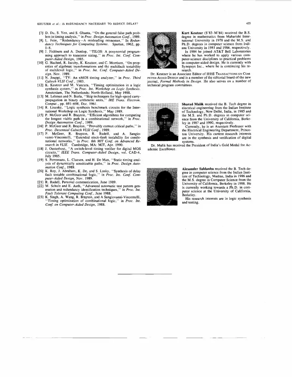
Kurt Keutzer (S’83-M’84) received the B.S. degree in mathematics from Maharishi Inter- national University in 1978 and the M.S. and Ph.D. degrees in computer science from Indi- ana University in 1981 and 1984, respectively.
In 1984 he joined AT&T Bell Laboratories where he has worked to apply various com- puter-science disciplines to practical problems in computer-aided design. He is currently with Synopsys Inc., where he is continuing his re- search.
Dr. Keutzer is an Associate Editor of IEEE TRANSACTIONS ON COM- PUTER-AIDED DESIGN and is a member of the editorial board of the new journal, Formal Methods in Design. He also serves on a number of technical program committees.
Sharad Malik received the B. Tech degree in electrical engineering from the Indian Institute of Technology, New Delhi, India, in 1985 and the M.S. and Ph.D. degrees in computer sci- ence from the University of California, Berke- ley in 1987 and 1990, respectively.
Currently, he is an Assistant Professor with the Electrical Engineering Department, Prince- ton University. His current research interests are in the synthesis and verification of digital systems.
Dr. Malik has received the President of India’s Gold Medal for Ac- ademic Excellence.
Alexander Saldanha received the B. Tech de- gree in computer science from the Indian Insti- tute of Technology, Madras, India in 1986 and the M.S. degree in Computer Science from the University of California, Berkeley in 1988. He is currently working towards a Ph.D. in com- puter science at the University of California, Berkeley.
His research interests are in logic synthesis and testing.