integrated dc-dc converter for photovoltaic
TRANSCRIPT

FEDERAL UNIVERSITY OF PAMPAGRADUATE PROGRAM IN ELECTRICAL ENGINEERING
LUIZ ANTÔNIO DA SILVA JÚNIOR
INTEGRATED DC-DC CONVERTER FOR PHOTOVOLTAIC ENERGYHARVESTING TARGETED TO INDOOR APPLICATIONS
Alegrete2020


LUIZ ANTÔNIO DA SILVA JÚNIOR
INTEGRATED DC-DC CONVERTER FOR PHOTOVOLTAIC ENERGYHARVESTING TARGETED TO INDOOR APPLICATIONS
Master’s Thesis submitted to the GraduateProgram in Electrical Engineering of FederalUniversity of Pampa in partial fulfillment ofthe requirements for the degree of Master inElectrical Engineering.
Supervisor: Alessandro Gonçalves GirardiCo-supervisor: Lucas Compassi Severo
FEDERAL UNIVERSITY OF PAMPAMaster Degree in Electrical Engineering
Graduate Program in Electrical Engineering
Alegrete2020

Ficha catalográfica elaborada automaticamente com os dados fornecidospelo(a) autor(a) através do Módulo de Biblioteca do
Sistema GURI (Gestão Unificada de Recursos Institucionais) .
Júnior, Luiz Antônio da Silva Integrated dc-dc converter for photovoltaic energy harvesting targeted to indoor applications / Luiz Antônio da Silva Júnior. 106 p.
Dissertação(Mestrado)-- Universidade Federal do Pampa, MESTRADO EM ENGENHARIA ELÉTRICA, 2020. "Orientação: Alessandro Gonçalves Girardi".
1. Conversor CC-CC. 2. Capacitor Chaveado. 3. Colheita de Energia em Ambiente Fechado. 4. Células Fotovoltaicas. 5. Circuitos de Ultrabaixa Potência. I. Título.
J953i


Luiz Antônio da Silva Junior
INTEGRATED DC-DC CONVERTER FOR PHOTOVOLTAIC ENERGY HARVESTING
TARGETED TO INDOOR APPLICATIONS
Master’s Thesis submitted to the Graduate Program in Electrical Engineering of Federal University of Pampa in partial fulfillment of the requirements for the degree of Master in Electrical Engineering.
Master’s Thesis defended and approved in Alegrete/RS, October 30th 2020. Examination board:
______________________________________________________ Prof. Dr. Alessandro Gonçalves Girardi
Supervisor UNIPAMPA
______________________________________________________ Prof. Dr. Lucas Compassi Severo
Co-supervisor UNIPAMPA
______________________________________________________ Prof. Dr. André Aita
UFSM
______________________________________________________ Prof. Dr. Hamilton Klimach
UFRGS
______________________________________________________ Prof. Dr. Guilherme Sebastião da Silva
UNIPAMPA

For the affection, dedication, and care that my parents gave me throughout my existence,I dedicate this work to them. With much gratitude.


"Nothing splendid has ever been achievedexcept by those who dared believe that
something inside of them wassuperior to circumstance."
(Bruce Barton)


ABSTRACT
Internet of Things (IoT) is a current great trend in which the number of connecteddevices to the Internet increases over years, thus facilitating the monitoring and controlof outdoor and indoor environments. In addition, the majority of electronic devices,mainly peripherals, are used most of the time indoors like office rooms, for example.These devices are usually power supplied by wiring or batteries. The use of wires cansometimes compromise the practicality of some electronic devices, and batteries must befrequently replaced or recharged. Energy harvesting is a great solution to overcome thisproblem, since the energy provided by the environment, such as lighting, can be harvestedby a photovoltaic (PV) cell in order to power supply electronic devices and IoT sensornodes. The power harvested by PV cells indoors is still quite limited, therefore energyharvesting systems in this type of environment are not widely exploited and target only lowpower applications. A PV cell may suffer shading caused by walls, furniture, and humanmovements. This requires an efficient conversion system that can adapt to the PV celloutput voltage variations. In this context, the present work aims to propose an integratedconversion system for indoor light energy harvesting to partially replace battery usage inelectronic devices and ultra-low-power (ULP) circuits. For the system block responsiblefor voltage conversion, we propose a reconfigurable DC-DC converter topology based onSwitched Capacitor (SC) capable to providing a range of voltage conversion ratios (VCRs).A systematic simulation-based method is also proposed in order to design the conversionsystem, including switches and capacitors sizes and switching frequency. Results show thatthe proposed DC-DC converter can adjust itself to achieve 19 different VCRs includingfractional, integers, step-down, follower, and step-up with an estimated peak chargingefficiency around 90%. In addition, the conversion system can be employed in a vastrange of duty-cycled ULP IoT applications. This is an important step towards a practicalself-powered indoor system for IoT applications.
Keywords: Switched Capacitor. DC-DC converter. Indoor Energy Harvesting. Photo-voltaic Cells. Electronic Devices. Internet of Things. Ultra-Low Power Circuits. Ultra-LowVoltage Circuits.


Conversor CC-CC Integrado para Colheita de Energia Fotovoltaica Voltada paraAplicações em Ambientes Fechados
RESUMO
Internet das Coisas é uma grande tendência atual na qual o número de dispositivosconectados à Internet aumenta ao longo dos anos, facilitando assim o monitoramento econtrole de ambientes abertos e fechados. Além disso, a maioria dos dispositivos eletrônicos,principalmente os periféricos, são usados na sua maior parte do tempo dentro de ambi-entes fechados como salas de escritórios, por exemplo. Esses dispositivos geralmente sãoalimentados utilizando fios ou baterias. A utilização de fios pode, às vezes, comprometera praticidade de alguns dispositivos eletrônicos, e baterias devem ser frequentementetrocadas ou recarregadas. A colheita de energia é uma ótima solução para resolver esteproblema, uma vez que a energia fornecida pelo ambiente, como, por exemplo, a iluminação,pode ser captada por uma célula fotovoltaica para alimentar dispositivos eletrônicos esensores para Internet das Coisas. A potência captada por células solares em ambientesfechados ainda é bastante limitada, desse modo sistemas para colheita de energia nestetipo de ambiente são pouco explorados e visam somente aplicações de ultra-baixa potência.Uma célula fotovoltaica ainda pode sofrer sombreamentos causados por paredes, móveis emovimentos humanos. Isso exige um sistema de conversão eficiente e que possa se adaptaràs variações de tensão de saída de uma célula fotovoltaica. Nesse contexto, o presentetrabalho visa propor um sistema integrado de conversão para colheita da energia da ilumi-nação em ambientes fechados para parcialmente substituir o uso da bateria em dispositivoseletrônicos e circuitos de ultrabaixa potência. Para o bloco do sistema responsável pelaconversão de tensão, foi proposta uma topologia reconfigurável de conversor CC-CC àcapacitores chaveados capaz de fornecer uma faixa de relações de conversão de tensão.Uma metodologia sistemática baseada em simulação elétrica também foi proposta com ointuito de projetar o sistema de conversão, incluindo os tamanhos das chaves, capacitorese a frequência de chaveamento. Resultados mostram que o conversor CC-CC propostopode se ajustar para fornecer 19 diferentes razões de conversão de tensão incluindo razõesde conversão fracionárias, inteiras, rebaixadoras, seguidora e elevadoras com um pico deeficiência de conversão estimado em torno de 90 %. Além do mais, o sistema de conversãopode ser empregado e vários circuitos de ultrabaixa potência que funcionam em ciclosalternados de operação, aplicados em dispositivos de Internet das Coisas. Esse é um passoimportante em direção a um sistema prático e autoalimentado empregado em ambientesfechados para aplicações de Internet das Coisas.
Palavras-chave: Capacitor Chaveado. Conversor CC-CC. Colheita de Energia em Ambi-ente Fechado. Células Fotovoltaicas. Dispositivos Eletrônicos. Internet das Coisas. Circuitosde Ultrabaixa Potência. Circuitos de Ultrabaixa Tensão.


LIST OF FIGURESFigure 1 – Diagram of a battery-less photovoltaic energy harvesting system. . . . . 23Figure 2 – Configuration of the indoor energy harvesting system using PV cell. . . 29Figure 3 – Fractional converter electrical circuit. . . . . . . . . . . . . . . . . . . . 33Figure 4 – Fractional 4/5 switched capacitor DC-DC converter operation: phase 1
(a) and phase 2 (b). . . . . . . . . . . . . . . . . . . . . . . . . . . . . . 34Figure 5 – Graphical representation of the potential efficiency improvement by
using the multi-topology approach. . . . . . . . . . . . . . . . . . . . . 36Figure 6 – Proposed basic multi-topology converter electrical circuit. . . . . . . . . 36Figure 7 – Phase 1 (a) and phase 2 (b) of the multi-topology converter operating
as a voltage doubler. . . . . . . . . . . . . . . . . . . . . . . . . . . . . 37Figure 8 – Doubler converter currents. . . . . . . . . . . . . . . . . . . . . . . . . 38Figure 9 – Doubler converter voltages. . . . . . . . . . . . . . . . . . . . . . . . . 39Figure 10 – Doubler converter switches signals. . . . . . . . . . . . . . . . . . . . . 40Figure 11 – Phase 1 (a) and phase 2 (b) of the multi-topology converter operating
as a voltage divider. . . . . . . . . . . . . . . . . . . . . . . . . . . . . 41Figure 12 – Voltage divider currents. . . . . . . . . . . . . . . . . . . . . . . . . . . 42Figure 13 – Voltage divider voltages. . . . . . . . . . . . . . . . . . . . . . . . . . . 42Figure 14 – Adder-subtractor converter electrical circuit . . . . . . . . . . . . . . . 43Figure 15 – Operation phase 1 (a) and phase 2 (b) of the Adder/Subtractor converter
working as voltage adder. . . . . . . . . . . . . . . . . . . . . . . . . . 44Figure 16 – Current of the converter adder mode. . . . . . . . . . . . . . . . . . . . 45Figure 17 – Voltages of the converter adder mode. . . . . . . . . . . . . . . . . . . 45Figure 18 – Switches signals of the converter adder mode. . . . . . . . . . . . . . . 46Figure 19 – Operation phase 1 (a) and phase 2 (b) of the Adder/Subtractor converter
working as voltage subtractor. . . . . . . . . . . . . . . . . . . . . . . . 47Figure 20 – Currents of the converter subtractor mode. . . . . . . . . . . . . . . . . 48Figure 21 – Voltages of the converter subtractorr mode. . . . . . . . . . . . . . . . 48Figure 22 – Diagram of the proposed multiple-VCR SC DC-DC converter system. . 49Figure 23 – Main voltages of the proposed converter system with VCR=0.75. . . . 51Figure 24 – Switches signals of the proposed converter system with VCR=0.75. . . 51Figure 25 – Main voltages of the proposed converter system with VCR=1.5. . . . . 52Figure 26 – Switches signals of the proposed converter system with VCR=1.5. . . . 52Figure 27 – Block diagram of the proposed digital control. . . . . . . . . . . . . . . 54Figure 28 – Flowchart of the digital control counter. . . . . . . . . . . . . . . . . . 55Figure 29 – Electrical schematic of the transmission gate used as switch: switch
turned on (a) and switch turned off (b). . . . . . . . . . . . . . . . . . 60

Figure 30 – Electrical simulations of the converter system block built with trans-mission gate switches varying Von for: VCR=0.5 (a), VCR=0.75 (b),VCR=4.5 (c), and VCR=8 (d). . . . . . . . . . . . . . . . . . . . . . . 61
Figure 31 – Electrical simulations of the converter system block built with n-typeMOSFET switches varying Von for: VCR=0.5 (a), VCR=0.75 (b),VCR=4.5 (c), and VCR=8 (d). . . . . . . . . . . . . . . . . . . . . . . 62
Figure 32 – Cross-coupled doubler circuit. . . . . . . . . . . . . . . . . . . . . . . . 63Figure 33 – Circuit diagram used to model the charging process of capacitor C after
switching (at t=0). . . . . . . . . . . . . . . . . . . . . . . . . . . . . . 63Figure 34 – Electrical simulations of the Adder/Subtractor module working as volt-
age adder with switches operating frequency of: 59 kHz (a), 590 kHz(b), and 5.9 MHz (c). . . . . . . . . . . . . . . . . . . . . . . . . . . . . 67
Figure 35 – Comparison between the output capacitor being charged by the addermode converter and its equivalent RC circuit for switching frequency of:59 kHz with Rout=3.28 MΩ (a), 590 kHz with Rout=347 kΩ (b), and5.9 MHz with Rout=165 kΩ (c). . . . . . . . . . . . . . . . . . . . . . . 68
Figure 36 – Relation between converterRout and switching frequency of the Adder/Subtractormodule working in adder mode. . . . . . . . . . . . . . . . . . . . . . . 69
Figure 37 – Ideal frequency versus flying capacitors value in the two operation modesof the Adder/Subtractor module. . . . . . . . . . . . . . . . . . . . . . 70
Figure 38 – Simulated conversion system efficiency ηCS in function of transistor gatewidth of switches. . . . . . . . . . . . . . . . . . . . . . . . . . . . . . . 72
Figure 39 – Ideal frequency versus switches gate width versus flying capacitor sizefor adder mode (a) and subtractor mode (b). . . . . . . . . . . . . . . . 73
Figure 40 – Converter output resistance versus gate width versus flying capacitorsize for adder mode (a) and subtractor mode (b). . . . . . . . . . . . . 74
Figure 41 – Maximum voltage in the output load capacitor versus gate width versusflying capacitor size for adder mode (a) and subtractor mode (b). . . . 75
Figure 42 – Converter charging efficiency versus gate width versus flying capacitorsize for adder mode (a) and subtractor mode (b). . . . . . . . . . . . . 76
Figure 43 – Flowchart of the converter system operation interacting with the appli-cation. . . . . . . . . . . . . . . . . . . . . . . . . . . . . . . . . . . . . 79
Figure 44 – Performance of the proposed DC-DC converter for the first design. . . . 81Figure 45 – Interaction between the digital control block and the first design of the
DC-DC converter considering three different simulations. . . . . . . . . 82Figure 46 – Performance of the proposed DC-DC converter for the second design. . 83Figure 47 – Top level BLE link layer packet. . . . . . . . . . . . . . . . . . . . . . . 83Figure 48 – Interaction between the digital control block and the second design of
the DC-DC converter considering three different simulations. . . . . . . 84

Figure 49 – Layout of the transmission gate switch that compose the proposedDC-DC converter. . . . . . . . . . . . . . . . . . . . . . . . . . . . . . . 85
Figure 50 – Layout of the proposed multiple-VCR SC DC-DC converter. . . . . . . 86Figure 51 – Post-layout simulation of the proposed DC-DC converter for the second
design. . . . . . . . . . . . . . . . . . . . . . . . . . . . . . . . . . . . . 87Figure 52 – Block diagram of the complete energy harvesting system. . . . . . . . . 89Figure 53 – Simple PV cell characterization circuit. . . . . . . . . . . . . . . . . . . 95Figure 54 – PV cell characterization circuit. . . . . . . . . . . . . . . . . . . . . . . 96Figure 55 – PV cell equivalent characterization circuit for the capacitor charging
phase. . . . . . . . . . . . . . . . . . . . . . . . . . . . . . . . . . . . . 96Figure 56 – Chosen PV cells for electrical characterization. . . . . . . . . . . . . . . 97Figure 57 – IxP curve for: Single 42x42 mm PV cell (a), Single 45x45 mm PV cell
(b), PV cells parallel connection (c), and PV cells series connection (d). 98Figure 58 – VxI curve for: Single 42x42 mm PV cell (a), Single 45x45 mm PV cell
(b), PV cells parallel connection (c), and PV cells series connection (d). 99Figure 59 – RxP curve for: Single 42x42 mm PV cell (a), Single 45x45 mm PV cell
(b), PV cells parallel connection (c), and PV cells series connection (d). 100Figure 60 – VxP curve for: Single 42x42 mm PV cell (a), Single 45x45 mm PV cell
(b), PV cells parallel connection (c), and PV cells series connection (d). 101


LIST OF TABLESTable 1 – Characteristics of the most common energy harvesting sources. . . . . . 22Table 2 – State-of-the-art adjustable or indoor light SC based converters. . . . . . 30Table 3 – Options of iVCR related to the number of flying capacitors. . . . . . . . 34Table 4 – Example of the implemented lookup table of the digital control block. . 57Table 5 – Maximum charging efficiency related to the initial capacitor voltage. . . 65Table 6 – Comparison with state-of-the-art harvesters DC-DC converters. . . . . . 87Table 7 – Comparison with indoor light harvesters DC-DC converters. . . . . . . . 88Table 8 – Estimated voltage conversion ratios. . . . . . . . . . . . . . . . . . . . . 102

CONTENTS
1 INTRODUCTION . . . . . . . . . . . . . . . . . . . . . . . . . . . 211.1 OBJECTIVES . . . . . . . . . . . . . . . . . . . . . . . . . . . . . . . 251.2 ORGANIZATION OF THE WORK . . . . . . . . . . . . . . . . . . 25
2 RELATED WORKS . . . . . . . . . . . . . . . . . . . . . . . . . . 272.1 INTEGRATED DC-DC CONVERTERS . . . . . . . . . . . . . . . . 272.2 CONCLUSION . . . . . . . . . . . . . . . . . . . . . . . . . . . . . . 30
3 PROPOSED SWITCHED CAPACITOR CONVERTER TOPOLOGY 313.1 CHARGE FLOW ANALYSIS WITH SSL IMPEDANCE . . . . . . 313.2 MULTI-TOPOLOGY CONVERTERS . . . . . . . . . . . . . . . . . 343.3 DOUBLER/DIVIDER MODULE . . . . . . . . . . . . . . . . . . . . 353.4 ADDER/SUBTRACTOR MODULE . . . . . . . . . . . . . . . . . . 413.5 MULTIPLE-VCR SC DC-DC CONVERTER . . . . . . . . . . . . . 493.6 CONTROL BLOCK AND COMPARATORS . . . . . . . . . . . . . 533.7 CONCLUSION . . . . . . . . . . . . . . . . . . . . . . . . . . . . . . 58
4 DESIGN METHOD . . . . . . . . . . . . . . . . . . . . . . . . . . 594.1 CONVERTER SYSTEM DESIGN METHOD . . . . . . . . . . . . 594.2 DESIGN METHOD INCLUDING CONVERTER ROUT ESTIMATION 714.3 CONCLUSION . . . . . . . . . . . . . . . . . . . . . . . . . . . . . . 77
5 RESULTS AND COMPARISON WITH OTHER WORKS . . . . . 795.1 SCHEMATIC SIMULATION RESULTS . . . . . . . . . . . . . . . . 795.1.1 DESIGN FOR LOW POWER CIRCUITS - DESIGN 1 . . . . . . . 795.1.2 DESIGN FOR LOW POWER CIRCUITS - DESIGN 2 . . . . . . . 815.2 LAYOUT AND POST-LAYOUT SIMULATIONS . . . . . . . . . . 845.3 COMPARISON WITH OTHER WORKS . . . . . . . . . . . . . . . 865.4 HARVESTING SYSTEM IMPLEMENTATION . . . . . . . . . . . 885.5 CONCLUSION . . . . . . . . . . . . . . . . . . . . . . . . . . . . . . 89
6 CONCLUSIONS AND SUGGESTIONS FOR FUTURE WORKS . 916.1 CONCLUSIONS . . . . . . . . . . . . . . . . . . . . . . . . . . . . . 916.2 FUTURE WORK . . . . . . . . . . . . . . . . . . . . . . . . . . . . . 92
APPENDIX 93
APPENDIX A – ELECTRICA CHARACTERIZATION OF PHO-TOVOLTAIC CELLS . . . . . . . . . . . . . . . 95

BIBLIOGRAPHY . . . . . . . . . . . . . . . . . . . . . . . . . . . 103
21
1 INTRODUCTIONInternet of Things (IoT) is a relatively new term and one of the most trend topics
of the present time. The Internet of Things is changing much about the world, from the waywe drive to how we make purchases and even for how we get supply energy for our homes.It refers to the interconnection of physical devices from micro-scale electronic circuits tolarge servers through the Internet. According to the latest research from Strategy Analytics(MERCER, 2019), the number of devices connected to the internet reached 22.0 billionworldwide at the end of 2018. The report also predicts that 38.6 billion devices will beconnected by 2025, and 50 billion by 2030.
Wireless Sensor Network (WSN) play a great role in the IoT concept because WSNsare responsible for monitoring and recording the physical conditions of the environmentwhere they are allocated, and organizing the collected data at a central location. Theyare widely used in many fields including agriculture, transportation, manufacturing, andhealthcare (DEMIR; AL-TURJMAN; MUHTAROĞLU, 2018).
There are two widespread ways of power supplying these sensors, by wiring orusing batteries. Both of these options may require the same costs as the installation ofthe sensors, once wiring demands some wires that need to be allocated from the energysupplier to the sensors, and batteries need frequent maintenance to be replaced. Also, theenergy capacity of the batteries is very limited in this scope (JUNG et al., 2014).
Apart from WSN, the predominant energy source of the most of electronic devicesare batteries. Even with the increase in the energy density of batteries by a factor of 3over the last 15 years, in several cases, their presence has a large impact, or even dominate,the size and operational cost (VULLERS et al., 2010).
The constant replacement of batteries can harm the environment due to toxicmetals such as cadmium, mercury, lead and lithium which some batteries contain andit can pose threats to health and environment if improperly disposed of. Even thoughbatteries represent less than one percent of total solid waste generated, they account fornearly two-thirds of the lead, ninety percent of the mercury, and over half of the cadmiumfound in the waste (PETERS et al., 2017).
There is a trend in which the number of electronic devices per person has beencontinuously increasing for decades. In addition, there is another and older trend that isthe human tendency of spending a larger amount of time in indoor environments, especiallybuildings (RANDALL, 2006).
The collection and use of ambient energy in the environment, called energy har-vesting or scavenging, is a good alternative in order to avoid the need for user interventionand extra wiring, and it assures that the product is available whenever required. In someapplications, this approach can even replace the battery usage (YU et al., 2018).
Energy can be harvested from different ambient sources, and the most commonlyused to generate electrical energy are solar, thermal, mechanical movement or vibration,

22 Chapter 1. Introduction
and ambient radio-frequency (RF) (HARB, 2011). In short, solar energy can be harvestedthrough photovoltaic (PV) panels being exposed to light. Thermoelectric generators (TEGs)are used to extract energy from temperature differences. The vibration or movement-basedenergy scavenging refers to electrostatic, electromagnetic, and piezoelectric sources. Inelectrostatic transducers, one electrode moves in relation to another electrode of a polarizedcapacitor, and the distance or overlap between these two electrodes causes a voltage changeacross the capacitor and results in a current flow in an external circuit. In piezoelectrictransducers, a voltage is generated in a piezoelectric capacitor by the deformations causedby vibrations or movement. In electromagnetic transducers, the relative motion of amagnetic mass with respect to a coil causes a change in the magnetic flux. This generatesan AC voltage across the coil. The RF energy available through public telecommunicationservices, such as GSM and WLAN frequencies, can also be harvested by an appropriateantenna. Alternatively, energy can be harvested using a dedicated RF source positionedclose to the sensor node, like RFID sensor networks. Table 1 presents the most usualenergy harvesting sources as well as some scenarios with the power which can be harvestedfrom each energy source (VULLERS et al., 2010).
Table 1 – Characteristics of the most common energy harvesting sources.
Source Source Power Harvested PowerAmbient LightIndoor 0.1 mW/cm2 10 µW/cm2
Outdoor 100 mW/cm2 10 mW/cm2
Thermal EnergyHuman 20 mW/cm2 30 µW/cm2
Industrial 100 mW/cm2 1–10 mW/cm2
Vibration/Motion
Human 0.5 m at 1 Hz1 m/s2 at 50 Hz 4 µW/cm2
Industrial 1 m at 5 Hz10 m/s2 at 1 kHz 100 µW/cm2
RFGSM Base Station 0.3 µW/cm2 0.1 µW/cm2
Source: From (VULLERS et al., 2010)
Observing the data presented in Table 1 it can be concluded that harvestingfrom ambient light is the best option for outdoor applications in terms of practicality andharvesting power since it is possible to harvest with a density up to 10 mW/cm2 witha density power source of 100 mW/cm2. Thermal energy performs in a similar way, butindustrial-scale temperature differences are not as available as sunlight. Even though indoorambient light source does not present a higher power density than other indoor sources,there are some advantages in performing indoor solar energy harvesting. In addition to theartificial lighting provided by the lamps, some extra energy may be harvested, at daylight,

23
from the natural solar radiance through the windows. Even a mixture of these two artificialand natural sources can be used to harvest energy. PV cells are cheap and easy to obtain.They can be built in many different sizes and shapes, and they also allow easy integrationwith electronic devices and peripherals. In addition, PV cells allow easily association inseries and parallel to provide more voltage or current to the load (MENG et al., 2016).
Even with lower energy harvesting capability in indoor environments, small PVcells can be also an alternative for ultra-low-power (ULP) IoT devices, which can beduty-cycled to reduce energy consumption. Figure 1 depicts a battery-less photovoltaicenergy harvesting system diagram. In this example, small PV cells are being used toharvest energy from artificial light and feed an ultra-low-power and ultra-low voltage (ULV)circuit application composed of a sensor - e.g. a temperature sensor - and a small memoryprocessor. This application operates as follows: the system wakes for a short period of timesufficient for the memory processor to read and save the sensor value, then sleeps again fora greater period of time. This circuit can be used to monitor the temperature over time.
Figure 1 – Diagram of a battery-less photovoltaic energy harvesting system.
Source: Author
Additionally, some ULP circuits, such as low energy RF transceivers, can operatewith ultra-low voltage (ULV) levels, around 0.4 V, close to the voltage range obtained byindoor small PV cells (Yu et al., 2017; Compassi-Severo; Van Noije, 2019). It is sufficient tosupply, for example, a ULV circuit targeted to a Bluetooth Low Energy (BLE) application(Compassi-Severo; Van Noije, 2019). These characteristics require the use of high-efficiencyDC-DC converters to perform the interface between the PV cell and the circuit. A smallPV cell with 16 cm2 can generate a few µW under artificial light, which is enough topower a small low-power transceiver during a period of time enough to generate a codedtone. Low-voltage circuits are particularly interesting applications of micro photovoltaicgeneration since the supply voltage is compatible with the voltage generated by small PVcells.
On the presented scope, this work focus on the use of solar energy harvesting asthe main energy source to partially or completely replace the extensive battery usage in
24 Chapter 1. Introduction
electronic devices and IoT sensors.In addition to the power source (ambient lighting) and transducers (PV cell),
another important component on the energy harvesting system of Fig. 1 is the DC-DCconverter. This circuit is responsible for adjusting the PV cell output to a voltage levelwhich is compatible with the application circuit. In a different approach, using a batteryto supply the application, the converter can also convert the PV cell voltage to a properlevel for charging the device battery.
According to (WENS; STEYAERT, 2011), there are three fundamental DC-DCconversion methods. The first and simplest of all is the conversion through linear voltageconverters using resistive dividers. In this case, only step-down conversions can be performedand the system efficiency is impaired because unused power is simply dissipated. Theother two mentioned methods are approaches that can improve the converter efficiencythrough the use of inductors or capacitors in the circuit. Inductive types of convertersutilize an LC tank to transfer energy from the input to the output. Capacitive typesof converters use only capacitors to perform the same task (STEYAERT et al., 2011).The latter presents a great advantage for chip integration since capacitors are easier tointegrate in conventional IC fabrication technologies than inductors (SANDERS et al.,2013). A very common capacitive type converter is the switched-capacitor (SC) - or chargepump (CP) - DC-DC converter, which uses only capacitors and switches to perform thevoltage conversion.
Whereas a topology of an inductive type of converter can easily provide anadjustable voltage conversion ratio (VCR), a capacitive converter topology presents thedisadvantage of providing a fixed VCR. A multiple-VCR DC-DC converter is necessary todynamically adjust the conversion ratio for maintaining a constant output voltage evenfor variable generated input voltage, which is the case of light energy harvesting basedon PV cells. Recalling the photovoltaic energy harvesting system from Fig. 1, the voltagegenerated by the PV cell may vary according to some factors such as illuminance level, thedistance between the lamp and the PV cell, and shadings caused by human movementsor furniture. To overcome this problem the DC-DC converter system must be able toreconfigure on-the-fly for adjusting the VCR to a required ratio, thus keeping the outputvoltage at a constant value (STEYAERT et al., 2011).
The main idea of this work is to propose a system able to provide a range ofvoltage conversion ratios through the combination of basic switched-capacitor convertertopologies, such as the voltage doubler and the voltage divider. The greatest advantage ofthis approach is the design simplicity of the converter blocks, in which the same topologycan be replicated several times to provide many voltage conversion ratios different fromeach other. In this work, a novel fully integrated multiple-VCR ULV SC DC-DC converteris proposed to be used with ULP devices powered by PV cells in indoor artificial lightenvironments. It is composed of reconfigurable modules for dealing with multiple VCRs

1.1. OBJECTIVES 25
while maintaining a fixed output voltage of 0.4 V. This voltage is compatible with eitherthe operating voltage level of many ULV circuits used in IoT applications and the voltageprovided by small PV cells at indoor.
A systematic simulation-based design method is presented for the converter, basedon fast and slow operation mode analysis to find ideal switching frequency and capacitorvalues to improve conversion efficiency. Both switching frequency and capacitor values areconsidered to allow circuit operation at the ULV range. The circuit can be fully integratedusing submicron low-cost CMOS fabrication processes.
1.1 OBJECTIVES
The present work has the main goal to propose and validate through electricalsimulations a switched-capacitor DC-DC converter for indoor energy harvesting systemsupplied by photovoltaic cells using ambient lighting as an alternative power source inorder to partially or completely replace battery usage of ULV and ULP applications. Thisenergy harvesting system will be suitable for low power applications present in conventionalrooms with lighting levels within the range required by the standard ISO 8995-1. Followingthis standard the illuminance in offices must range from 200 to 750 lux, depending on thetask (CIE, 2002).
Within the main goal of this work, there are also specific goals: the proposal of amethod for electric characterization of solar cells operating indoor; PV cells characterizationto provide an insight about the electrical quantities and limitations of the panels operatingonly under artificial lighting; proposal of a switched capacitor converter topology able tooffer a range of different voltage conversion ratios; electrical behavior simulation of theproposed topology to validate circuit operation; proposal of a systematic method to designthe conversion system; circuit design and optimization aiming maximum efficiency; andpost-layout simulation and validation of the conversion system.
1.2 ORGANIZATION OF THE WORK
The present work is organized as follows: Chapter 2 presents an overview ofthe DC-DC converters related works, showing different topologies, design approaches,and applications involving these converters. Chapter 3 deals with the basics about DC-DC converters focusing more on their modeling and behavior, in this chapter it is alsodiscussed the strategy to obtain a converter with a range of VCRs using only basicswitched-capacitor converter topologies, some electrical simulations are presented. Inchapter 4 it is presented the proposed systematic simulation-based design method used tosize flying capacitors, switches, and switching frequency of the proposed conversion system.Chapter 5 shows the main schematic simulation results of the proposed conversion systemfor two different designs and a comparison with other state-of-the-art related works. In

26 Chapter 1. Introduction
Chapter 6 it is presented some conclusions about the work done so far, and the tasks tobe performed for future work. Finally, a method for PV cell characterization and someelectrical characteristics curves of two small PV panels operating indoor are in AppendixA.
27
2 RELATED WORKSThis chapter presents a literature review about the works related to various
applications of DC-DC converters, including employed topologies. First, an overview willbe given on the main applications of DC-DC converters present in the literature. A greaterfocus will be given to applications involving energy harvesting, since they relate directlywith the scope of this work. In addition, it will be discussed some state-of-the-art worksrelated to topologies and approaches used to obtain many voltage conversion ratios usingswitched capacitor DC-DC converters.
2.1 INTEGRATED DC-DC CONVERTERS
DC-DC converters are widely used in different kinds of applications rangingfrom generating variable voltage supply for System-on-a-chip (SoC) to energy harvestingsystems.
In this context, there are some different DC-DC converter topologies applied in apower management unit (PMU) that converts a voltage supplied by a battery into a desiredfixed and smooth output voltage. It can also be used to provide multiple voltage domainsfor microprocessor and SoC designs and help to reduce power dissipation of the system.For these applications, Naidu and Kittur (2016) and Ghiasi et al. (2015) present differentswitched capacitor topologies but only to perform step-down conversions. Following thesame step-down approach, the work of Manohar and Balsara (2015) presents a partiallyintegrated buck DC-DC converter. Another approach is presented by Souvignet, Allardand Trochut (2016) in which a more versatile and fully integrated switched capacitorconverter is used to provide step-down and step-up conversions.
Fully integrated switched capacitor DC-DC converters are well suited for supplyingenergy-constrained processors since they can achieve high efficiency within digital CMOSprocesses. In a near threshold application scope, fully integrated step-down switchedcapacitor DC-DC converters that deliver near-threshold output voltages are presented inthe works of Turnquist et al. (2015) and Abdelfattah et al. (2015).
To extend the run time of a battery and micro-power medical applications, likemedical implantable devices, there are two important scopes in which DC-DC converterscan be employed. Therefore, Kim et al. (2016) presents a peak-current control noninvertingbuck–boost converter to extend the run time of a Ni–MH battery, and Miguez et al. (2016)introduces a micro-power inductive DC-DC step-down converter aimed to reduce thesupply voltage in a medical implantable device.
An energy harvester system is another way to include DC-DC converters, themain idea is to use a DC-DC converter to amplify or reduce the voltage harvested fromambient sources and apply it in other circuits or store it in a energy storage element. Inthe presented scope, Goeppert and Manoli (2016) designed an inductive DC-DC boostconverter for energy harvesting using temperature gradients exploitable by thermoelectric

28 Chapter 2. Related Works
generators. The work of Chowdary, Singh and Chatterjee (2016) presents the applicationof a DC-DC buck-boost inductor type converter in a modular power management systemthat can harvest energy from three sources simultaneously, such as solar, vibration andRF. The work of Mondal and Paily (2016) introduces an efficient on-chip inductor-lessswitching power converter for solar energy harvesting. It proposes a tree-topology chargepump circuit in order to amplify the voltage obtained through the PV cell and transferits energy to an energy buffer comprised of a supercapacitor or a rechargeable battery.Dini et al. (2015) uses a DC-DC buck-boost converter with an off-chip inductor as a fullyautonomous power converter integrated circuit (IC) for energy harvesting of multiple andmulti-type sources, such as piezoelectric, photovoltaic, thermoelectric, and RF transducers.A step-up switched capacitor has been included in an ultra-compact single-chip solar energyharvesting IC using parallel-connected photodiodes as on-chip solar cell for biomedicalimplant applications Chen et al. (2017). A batteryless solution is presented by Chen etal. (2018) using a DC-DC boost converter stepping-up architecture with a single off-chipinductor designed for thermoelectric energy harvesting application.
Considering an energy harvesting more specific scope, such as the scavenging of theenergy provided mainly by artificial lighting through small photovoltaic panels, the paperof Nasiri, Zabalawi and Mandic (2009) shows different power conversion circuit topologies,such as topologies composed of supercapacitors, rechargeable and nonrechargeable batteries.These circuits have the configuration presented in Fig. 2, and are designed for indoor energyharvesting using PV cells for low-power indoor devices like remote sensors, supervisoryand alarm systems, distributed controls, and data transfer system. A Single InductorDual-Input Dual-Output (SI-DIDO) topology is proposed by Meng et al. (2016) whichpresents a battery in its structure in order to supply the load together with a PV cell whenthe indoor environment is under-illuminated. A low-power-consumption boost converterwith maximum power point tracking algorithm for indoor photovoltaic energy harvestingis proposed and by Tsai, Wu and Wei (2017), this system is designed to transfer energyfrom a PV cell to a supercapacitor used as energy storage element. Finally, the work ofMondal and Paily (2017) presents a complete on-chip single stage tree-topology switchedcapacitor based power converter with a fixed voltage conversion ratio around 2.5 for anindoor PV harvester.
Regarding the methods for obtaining a converter system capable of providing arange of many different voltage conversion ratios, a fine-grained conversion ratio resolutionof Vin/2N , where Vin is the input voltage and N is the number of stages, is obtained byBang, Blaauw and Sylvester (2016) through a successive-approximation SC (SAR SC)DC–DC converter in which multiple stages of 2:1 SC converters are cascaded. A differentapproach is used in Wu et al. (2017) in which a moving-sum charge pump structure ispresented. This structure consists of a reduced Dickson charge pump to produce two tonine times Vin, a voltage mux to select four voltages from two to nine times according to

2.1. INTEGRATED DC-DC CONVERTERS 29
Figure 2 – Configuration of the indoor energy harvesting system using PV cell.
Source: Adapted from (NASIRI; ZABALAWI; MANDIC, 2009)
the conversion ratio, and a summing series parallel stage where the selected voltages onthe flying capacitors are placed in series and summed to charge the output node capacitor.Liu et al. (2016) presents an adjustable SC converter built by cascading three doublersswitched-capacitor converters and properly selecting their input connections through atwo-way demultiplexer and four-way demultiplexer, integral CRs as 1, 2, up to 8 canbe obtained. There are also fractional conversion ratios (CRs) which are realized by areconfigurable step-down charge pump with CRs as 1
3 and 23 . Its output is included in the
four-way demultiplexer and results in mixed CRs as 113 , 1
23 , up to 8. This SC converter is
applied in a hybrid system that can harvest energy from photovoltaic and thermoelectricgenerator transducers. The work of Jung et al. (2014) proposes a fully integrated energyharvester that maintains at least 35% end-to-end efficiency when harvesting from a 0.84mm2 solar cell in low light condition of 260 lux. The voltage conversion in this harvestingsystem is performed by a self-oscillating switched-capacitor in which DC-DC voltagedoublers are cascaded to form a complete harvester, with configurable overall conversionratio from 9 to 23. A more sophisticated and complex technique is used by Jiang et al.(2018) where an algorithmic voltage-feed-in (AVFI) topology is introduced in order tosystematically generate any arbitrary buck–boost rational ratio with optimal conductionloss while achieving reduced topology-level parasitic loss. The presented fully integratedswitched-capacitor power converter executes a total of 24 VCRs (11 buck and 13 boost)with wide-range efficient buck–boost operations.
Table 2 contains the main DC-DC converters mentioned above separated in termsof application at indoor solar harvesters or VCR adjustable converters. The converterspresented by Bang, Blaauw and Sylvester (2016) and Wu et al. (2017) have the largestnumber of available VCRs, 117 and 126, respectively. Even with a large number of availableVCRs, both converters focus on just one type of conversion step-down or step-up. This

30 Chapter 2. Related Works
Table 2 – State-of-the-art adjustable or indoor light SC based converters.(JUNG et al., 2014) (BANG et al., 2016) (LIU et al., 2016) (MONDAL et al., 2017) (WU et al., 2017) (JIANG et al., 2018)
ConverterTopology:
Cascaded1:2 SC
Cascaded2:1 SC
Combinationof SC
Capacitiveboost Dickson SC Algorithmic
voltage-feed-in SCConverterType: Step-up Step-down Step-up Step-up Step-up Step-down
and step-upImplementationComplexity: Low Low Medium Low Medium High
Numberof VCRs: 15 117 14 1 126 24
InputVoltage: 0.14 - 0.5 V 3.4 - 4.3 V 0.45 - 3 V 0.39 - 0.43 V 0.25 - 0.65 V 0.22 - 2.4 V
OutputVoltage: 2.2 - 5.2 V >0.45 V 3.3 V 1 V 3.8 - 4 V 0.85 - 1.2 V
Energy HarvestingSource: Indoor light N/A Indoor light and
thermoelectric Indoor light Indoor light N/A
Source: Author
is also the case of the works from Jung et al. (2014), Liu et al. (2016) and Mondal andPaily (2017). The converter presented by Jiang et al. (2018) is more versatile, being ableto perform both step-down and step-up conversions with a wide range of VCRs. On theother hand, the implementation complexity of this converter is quite high. The majority ofthe works which present converters with a goof number of available VCRs implement theconversion system by cascading or combining one or more SC converter topologies. Thistechnique is versatile and the implementation complexity is low or medium depending onthe overall conversion system structure.
2.2 CONCLUSION
In this chapter, it is presented a literature review about the works related tothe main applications of DC-DC converters and the different topologies presented. Amajor focus is given for DC-DC converters applied on the energy harvesting scope. Thereare several alternative energy sources used in the harvesting system, as well as manycircuit approaches to perform voltage conversions. The majority of the discussed paperspresented a rechargeable battery or other energy storage element in order to store theenergy provided by the alternative source and to assist in the energy supply for the load.This chapter also presents the main techniques and topologies for providing a convertersystem with many different voltage conversion ratios.

31
3 PROPOSED SWITCHED CAPACITOR CONVERTER TOPOLOGYThis chapter presents a simplified model to understand the operation of different
switched-capacitor converter topologies. A detailed explanation of the approach used toobtain an SC based topology capable of providing a range of different voltage conversionratios is given. In addition, this chapter shows electrical simulations of the proposed SCtopology in order to validate its operation. Finally, the construction details of the proposeddigital control system is presented.
3.1 CHARGE FLOW ANALYSIS WITH SSL IMPEDANCE
All DC-DC converter topologies have their own ideal voltage conversion ratio(iVCR), and it represents the maximum ratio between the output voltage and the inputvoltage of the power converter. This iVCR is the upper bound for the actual voltageconversion ratio (VCR) and the topology only operates at a theoretical 100% efficiencywhen the iVCR is reached. For a converter with an input voltage Vin, an output voltage Vout
and a common ground connection, the VCR is defined by (BREUSSEGEM; STEYAERT,2012):
V CR = Vout
Vin
(3.1)
A useful tool for identifying the role of the different components in the conversionblock is the charge flow analysis. This analysis can be combined with the slow-switchinglimit (SSL) impedance, which neglects the finite resistances of the switches, capacitors,and interconnects, in order to extract the charge flow vectors aj
c. These vectors play animportant role in the conversion block modeling and can be derived for any standardnon-degenerate two-phase SC converter (BREUSSEGEM; STEYAERT, 2012).
Charge flow vectors represent the charge flows that occur immediately after theclosing of the switches in each respective phase of the SC circuit. A charge flow vector iscomposed of elements that represent a specific capacitor or independent voltage source inthe circuit, and they show the charge flow into that component, normalized with respectto the output charge flow.
The charge flow vector is described generically by:
~vc(j) = [q(j)
out q(j)i ... q(j)
n q(j)in ]T/qout (3.2)
where n is the number of flying capacitors, q(j)i represents the amount of charge transferred
during state or phase j by capacitor i, qin refers to the input charge transferred to thesystem, and qout is the total amount of charge transferred to the load during a switchingperiod T.
The elements of the charge flow vector can be derived by inspection for everystate of the conversion period following the principles described below: Kirchhoff’s current
32 Chapter 3. Proposed Switched Capacitor Converter Topology
law in each node, which means the sum of charge flow elements must be equal to zero ineach circuit node. For every flying capacitor, the sum of both state’s charge flow elementsis equal to zero. The output capacitor Cout behaves as a voltage source with respect tothe remainder of the circuit. Also, the charge vector elements of both states of the flyingcapacitors have opposite signs, and the charge vector elements of the output sum to 1.Furthermore, the total output charge is the sum of the output charges in each phase,q
(1)out + q
(2)out = qout and the total input charge is the sum of the input charges in each phase,
q(1)in + q
(2)in = qin.The output power is equal to the input power (Pout = Pin) in steady-state for an
ideal converter. Also, if we integrate over a switching cycle, the output energy is equal tothe input energy (Eout = Ein). Considering the capacitor potential energy E = qV , theinput and output energy can be described as:
qoutVout = qinVin (3.3)
Rearranging Eq. 3.3, the ratio of the total input and output charge flow vectorelements represents the iVCR (N) of the topology:
N = qin
qout
(3.4)
Converters with fractional VCRs are required in certain applications to keep up afixed or constant output voltage at a given value even if the solar cell suffers variationslike load variation, variation in its polarization, illuminance levels, etc.
A straightforward way to implement a switched-capacitor DC-DC converter withfractional VCR is the fractional converter (MAKOWSKI; MAKSIMOVIC, 1995). Anexample of a fractional 4/5 switched-capacitor DC-DC converter is shown in Fig. 3. Thistopology has ten switches S1x , S2x , S3x , S4x , S5x , S6x , S7x , S8x , S9x , S10x , three flyingcapacitors Cfa , Cfb
and Cfc , and an output buffer capacitor Coutx . All capacitors have thesame value.
This fractional converter has two phases of operation. In the first operation phaseS1x , S2x , S3x , S4x and S5x switches are on and the other ones off. The opposite occursin the second operation phase. Fig. 4 shows the electrical diagrams for the fractionalconverter operation phases.
In addition, the charge flow vectors can be derived for each operation phase.Recalling the step of the charge flow analysis which the sum of both state’s charge flowelements is equal to zero for every flying capacitor. Based on this, the vector signal and thedirection of the charge flow can be arbitrarily defined. In this work, we choose to representthe vector element with a minus signal when the charge is flowing into the capacitor, andthe arrow representation in the diagram is going from the positive to the negative terminalof the capacitor. In the other case when the charge is coming out of the capacitor, the

3.1. CHARGE FLOW ANALYSIS WITH SSL IMPEDANCE 33
Figure 3 – Fractional converter electrical circuit.
Coutx
S1x
S2x
S3x
S5x
S4x
S6xS7x
VinxVoutx
Cfa
Cfb
Cfc
S8x
S9x
S10x
Source: Author
vector element is positive and the arrow representation in the diagram is going from thenegative to the positive terminal of the capacitor.
For the first operation phase:
~vfrac(1) = [q(1)
outxq
(1)Cfa
q(1)Cfb
q(1)Cfc
q(1)inx
] = [1515
15−25
25] (3.5)
For the second operation phase:
~vfrac(2) = [q(2)
outxq
(2)Cfa
q(2)Cfb
q(2)Cfc
q(2)inx
] = [45−15−15
25
25] (3.6)
The VCR can be obtained for this fractional DC-DC converter:
V CR = qin
qout
=25 + 2
515 + 4
5= 4
5 (3.7)
According to the Topology Occurrence Theorem (MAKOWSKI; MAKSIMOVIC,1995), which predicts the achievable iVCR given a certain number of flying capacitors, ifthe number of flying capacitors in the converter topology is limited to three, there aremany conversion ratios that can be achieved as shown in Table 3.
There are some drawbacks in implementing a fractional SC DC-DC converter.The iVCR of a fractional converter is hard to be determined by visual inspection and itssynthesis is non-methodological, that is, there is no sequence of steps to analyze and findthe iVCR topology (BREUSSEGEM; STEYAERT, 2012). Also, the increase in the numberof flying capacitors in the converter circuit results in an increase in its output impedance.If the application requires more than one fractional VCR, it will also be necessary to

34 Chapter 3. Proposed Switched Capacitor Converter Topology
Figure 4 – Fractional 4/5 switched capacitor DC-DC converter operation: phase 1 (a) andphase 2 (b).
CoutxS1x
S2x
S3x
S5x
S4x
S6xS7x
Vinx
Voutx
Cfa
Cfb
Cfc
S8x
S9x
S10x
+-
Phase 1
qCfb
(1)
qCfc
(1)
qCfa
(1)qoutx
(1)
qinx
(1)
(a)
CoutxS1x
S2x
S3x
S5x
S4x
S6x S7x
Voutx
Cfa
Cfb
Cfc
S8x
S9x
S10x
Vinx
+-
Phase 2
qinx
(2)
qCfa
(2)
qCfb
(2)
qCfc
(2)
qoutx
(2)
(b)
Source: Author
Table 3 – Options of iVCR related to the number of flying capacitors.
n flying capacitors iVCR1 1/2, 1, 22 1/3, 1/2, 2/3, 3/2, 1, 2, 3
3 1/5, 1/4, 1/3, 2/5, 1/2, 3/5, 2/3, 3/4,4/5, 1, 5/4, 4/3, 3/2, 5/3, 2, 5/2, 3, 4, 5
Source: From (BREUSSEGEM; STEYAERT, 2012)
implement another fractional converter topology to be cascaded. The implementation ofseveral cascaded topologies of fractional converters is impracticable to the project due toits high complexity.
3.2 MULTI-TOPOLOGY CONVERTERS
Sometimes more than one VCR, fractional or integer, is required and a singletopology is not suitable in this case. According to Breussegem and Steyaert (2012) topology

3.3. DOUBLER/DIVIDER MODULE 35
and iVCR are directly dependent, and this put constraints on the input-output voltagerange of the converter and the associated converter’s performance within this range. Multi-topology capacitive converters are a good alternative to increase the converter efficiencyover a broad range of conversion scenarios.
Multi-topology converters have a capacitor-switch array that is capable of switchingbetween both states or phases of the base topology and switching between differenttopologies. Each one of these topologies is adequate for a given conversion scenario andinput-output range.
As mentioned at the beginning of this chapter, a specific converter topology hasan upper bound for which conversion can be performed, the iVCR. Also, the efficiency hasan upper bound that corresponds to the ratio of the actual VCR and the iVCR:
V CR ≤ iV CR
η = V CR
iV CR
(3.8)
A single converter topology designed to operate at a certain conversion rate musthave its efficiency worsened if the circuit input or output voltage values change causingit to work with a conversion ratio different from its iVCR. In that case, the efficiency ofa capacitive converter can be improved with the use of a multi-topology converter. Asan example, Fig. 5 illustrates an efficiency graph in which a hypothetical converter isimplemented with three multiple topologies. In this graph, the gray line represents the idealefficiency ratings of three topologies (iVCR= 1, 3/4, and 1/2). In a separate configuration,each topology is designed to have a maximum VCR corresponding to the iVCR. In thiscase, each topology demonstrates a low efficiency η if the VCR deviates significantly fromiVCR. On the other hand, combining multiple topologies in a single structure can boostefficiency as depicted in a thick dark line of the graph. In this situation, the converterhas three ideal VCRs and can maintain its maximum efficiency when the required VCRchanges for a value equal to one of the converter iVCRs.
3.3 DOUBLER/DIVIDER MODULE
A basic multi-topology converter is presented in this work. It comprises a voltagedoubler and a voltage divider integrated in a single topology. So, with this basic multi-topology converter is possible to double the input voltage or divide it by two and present itat the converter output. The electrical diagram of the proposed multi-topology converteris presented in Fig. 6, it comprises of a single flying capacitor Cfly1 , a single output buffercapacitor Cout1 and six switches S1, S2, S3, S4, S5 and S6. The output capacitor Cout1 hasthe same value of Cfly1 .
The multi-topology converter can change between two topologies with differentiVCRs. Each topology has a combination of switches that must be turned on and off in

36 Chapter 3. Proposed Switched Capacitor Converter Topology
Figure 5 – Graphical representation of the potential efficiency improvement by using themulti-topology approach.
50%
60%
70%
80%
90%
100%
0.25 0.5 0.75 1
iVCR=0.5iVCR=0.75
iVCR=1
VCR
η
Source: Adapted from (BREUSSEGEM; STEYAERT, 2012)
Figure 6 – Proposed basic multi-topology converter electrical circuit.
Cout1
Cfly1
S1
S2
S3
S5 S4
Vin1 Vout1S6
Source: Author
order to get a certain iVCR.For the multi-topology converter to work like a Voltage Doubler, switch S2 is
always off and switch S6 is always on. So, this resulting topology has two working phasesas illustrated in Fig. 7. In phase 1, switches S1 and S4 are on and switches S3 and S5 areoff. In this phase, Cfly1 capacitor is charging with input voltage provided by Vin1 . Duringphase 2, the switches are configured in an opposite way of phase 1. In phase 2, Cfly1 isalready charged with Vin1 and this input voltage is connected in a way that the outputnode is twice Vin1 when Cout1 is fully charged.
The following charge flow vectors are derived for a single-stage voltage doubler

3.3. DOUBLER/DIVIDER MODULE 37
Figure 7 – Phase 1 (a) and phase 2 (b) of the multi-topology converter operating as avoltage doubler.
Cout1
Cfly1
S1
S2
S3
S5 S4
Vin1
Doubler mode: phase 1
S6
qCfly1
(1)
qout1
(1)
Vout1
+-
qin1
(1)
(a)
Cout1
Cfly1
S1
S2
S3
S5 S4
Vout1S6
Doubler mode: phase 2
Vin1
+-
qin1
(2) qCfly1
(2)qout1
(2)
(b)
Source: Author
for first and second operation phases, respectively:
~vdou(1) = [q(1)
out1 q(1)Cfly1
q(1)in1] = [0 − 1 1] (3.9)
~vdou(2) = [q(2)
out1 q(2)Cfly1
q(2)in1] = [1 1 1] (3.10)
The VCR can be obtained for this voltage doubler DC-DC converter as:
V CR = qin1
qout1= 1 + 1
0 + 1 = 2 (3.11)
The electrical simulation of this configuration was performed to better explainthe topology behavior. All electrical simulations that will be presented from now on inthis chapter were executed using ideal switches to validate the topologies operation andall topologies capacitors were set with 10 nF.

38 Chapter 3. Proposed Switched Capacitor Converter Topology
Figure 8 – Doubler converter currents.
0 50 100 150 200 250
Time [ s]
-600
-400
-200
0
200
400
600
Cu
rren
t [
A]
Icfly
1
Icout
1
Source: Author
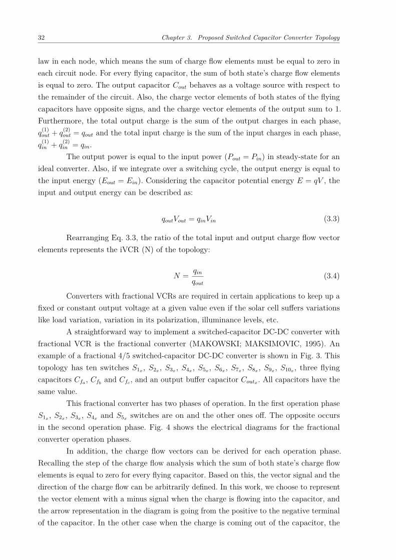
A voltage of 0.2 V with a small series resistance of 100 Ω was used as input. Fig.8 shows Cout1 and Cfly1 currents over the simulation period. It can be observed that thecurrents have high peaks in the first transient cycles and they tend to zero in steady-statewhen the capacitors are fully charged. Fig. 9 shows the capacitors voltages as well as theinput and output voltages. The output and Cout1 voltages are equal and their curves areoverlapped. In this figure, it can be observed that Cfly1 capacitor charges over the cycles,and when its voltage reaches 0.2 V the converter output presents twice the input voltage.Fig. 10 shows switches operating cycles. When S1 is on S3 if off, and vice versa. There is asmall delay in the moment that a switch turns off and the other turns on. This preventsthe signals overlapping which may cause undesired operation in the circuit.
3.3. DOUBLER/DIVIDER MODULE 39
Figure 9 – Doubler converter voltages.
0 50 100 150 200 250
Time [ s]
-0.1
0
0.1
0.2
0.3
0.4
Vo
ltag
e [V
]
Vcfly
1
Vout
1
Vin
1
Source: Author

40 Chapter 3. Proposed Switched Capacitor Converter Topology
Figure 10 – Doubler converter switches signals.
0 5 10 15 20 25 30 35 40 45 50
Time [ s]
Voff
Von
Voff
Von
Vo
ltag
e [V
]
VS
1
VS
3
Source: Author
For the multi-topology converter to work like a Voltage Divider, switch S5 isalways off during both operation phases. Then, the resulting topology also has two workingphases illustrated in Fig. 11. Phase 1 is set when switches S1 and S2 are on and S3 andS4 are off. In this scenario, Cfly1 and Cout1 are in series being charged with Vin1/2 each.In phase 2, the switches are also configured in the opposite way of phase 1. Here, bothcapacitors are already charged and connected in parallel, resulting in a Vout1 with half ofthe input voltage.
The charge flow vectors which represent the voltage divider in operation phases 1and 2 are presented below:
~vdiv(1) = [q(1)
out1 q(1)Cfly1
q(1)in1 ] = [12
−12
12] (3.12)
~vdiv(2) = [q(2)
out1 q(2)Cfly1
q(2)in1 ] = [12
12 0] (3.13)
The conversion ratio is then obtained as:
V CR = qin1
qout1=
12 + 012 + 1
2= 1
2 (3.14)
The electrical simulation of this configuration was performed in order to evaluatethe topology behavior. For the voltage divider simulation, an input voltage of 0.8 V wasapplied for a 100 Ω series resistance. The capacitors currents are equal in this topology, sojust Cfly1 is represented in Fig. 12. Once again, it can be noted that there is a high peakcurrent on the transient period denoting capacitors charging, and the currents tend tozero when the capacitors are already charged. Fig. 13 shows the topology voltages. As thecurrents, capacitor voltages are also equal with output voltage equal to them. The output

3.4. ADDER/SUBTRACTOR MODULE 41
Figure 11 – Phase 1 (a) and phase 2 (b) of the multi-topology converter operating as avoltage divider.
Cout1
Cfly1
S1
S2
S3
S5 S4
Vout1
S6
Vin1
+-
qin1
(1) qCfly1
(1)
qout1
(1)
Divider mode: phase 1
(a)
Cout1
Cfly1
S1
S2
S3
S5 S4
Vin1
Vout1
S6
+-
qin1
(2) qCfly1
(2)
qout1
(2)
Divider mode: phase 2
(b)
Source: Author
node increases over time and only reaches half of Vin1 when there is no high current peakon the capacitors. The switches signals are the same as the ones presented in Fig. 10.
3.4 ADDER/SUBTRACTOR MODULE
The idea is to create a system using the previously presented basic multi-topologyconverter as the main conversion block which is possible to get a range of fractionaland integer VCRs. The Doubler/Divider multi-topology converter output voltage canbe modeled as a power of two 2n, wherein a single module n can assume -1 or 1. Whenn = −1 the topology behaves as a Voltage Divider and n = 1 configures the moduleas a Voltage Doubler. The power of two conversion characteristic can be expanded bycascading the multi-topology converter. This is done by connecting the output of the firstconverter to the input of the second converter. For example, two single doubler modules in

42 Chapter 3. Proposed Switched Capacitor Converter Topology
Figure 12 – Voltage divider currents.
0 50 100 150 200 250
Time [ s]
0
0.5
1
1.5
I Cfl
y1
[m
A]
Source: Author
Figure 13 – Voltage divider voltages.
0 50 100 150 200 250
Time [ s]
0
0.2
0.4
0.6
0.8
Vo
ltag
e [V
]
Vcfly
1
Vin
1
Source: Author
sequence (forming a block), with n = 1 represents a 22 conversion, and the output voltagewill be four times the input voltage. This kind of approach only provides VCRs relatedto a power of two characteristic, so, in order to obtain intermediate VCRs, a two-inputAdder/Subtractor was also proposed. Thereby two, equal or different, input voltages canbe added or subtracted and with that, it is possible to combine two VCRs obtained fromthe multi-topology converter resulting in an intermediate voltage conversion ratio.
The electrical diagram of the proposed Adder/Subtractor converter is depicted inFig. 14. It has seven switches S7, S8, S9, S10, S11, S12, S13, two flying capacitors Cfly2 , Cfly3 ,and Cout2 represents the output load capacitor. Depending on the switches arrangement,

3.4. ADDER/SUBTRACTOR MODULE 43
this module can work as a two input adder or subtractor circuit. So the output voltage isequal to the addition or subtraction of both independent input voltages Vin2 and Vin3 .
Figure 14 – Adder-subtractor converter electrical circuit
Cfly2
S7
Vin2
Vout2
Vin3
S9 S11
S8 S10
S12
S13
Cfly3Cout2
Source: Author
Similarly to the Divider/Doubler module, the Adder/Subtractor also operatesin two phases. For the topology to work as a two-input adder, the first phase positivelycharges the flying capacitors with the voltages presented in its inputs, then switches S7,S8, and S11 are turned on and the other ones are turned off. In the second phase, bothcharged capacitors are connected in series and the energy is released to the output node.In this case, S12 and S13 are on and the remaining are off. Fig. 15 shows the electricaldiagrams of the two described working phases.
The charge flow analysis can also be used to derive the voltage conversion ratio ofthis conversion module. So, the following charge flow vectors are obtained for the voltageadder:
~vadd(1) = [q(1)
out2 q(1)Cfly2
q(1)Cfly3
q(1)in2 q
(1)in3 ]
= [0 − 1 − 1 qin2 qin3 ](3.15)
~vadd(2) = [q(2)
out2 q(2)Cfly2
q(2)Cfly3
q(2)in2 q
(2)in3 ]
= [1 1 1 0 0](3.16)
The VCR can be obtained summing ~vadd(1) and ~vadd
(2):
V CR = qin
qout2
= qin2 + qin3 + 0 + 01 + 0 = qin2 + qin3 (3.17)

44 Chapter 3. Proposed Switched Capacitor Converter Topology
Figure 15 – Operation phase 1 (a) and phase 2 (b) of the Adder/Subtractor converterworking as voltage adder.
Cfly2
S7
Vin2
Vout2
Vin3
S9 S11
S8 S10
S12
S13
Cfly3
Cout2
qout2
(1)qCfly2
(1)
qCfly3
(1)
+
-
+
-
qin2
(1)
qin3
(1)
Adder mode: phase 1
(a)
Cfly2
S7
Vout2
Vin3
S9 S11
S8 S10
S12
S13
Cfly3
Cout2
qout2
(2)qCfly2
(2)
qCfly3
(2)
Vin2
+
-
+
-
Adder mode: phase 2
qin2
(2)
qin3
(2)
(b)
Source: Author
An electrical simulation was performed using 0.1 V and 0.3 V as voltages inputswith no series resistance because in practice this module will be connected to the outputof the previous module. In this case, currents for the two flying capacitors, Cfly2 and Cfly3 ,are the same and Cfly2 current is represented in the graph of Fig. 16. It can be noted thatthe current presents high peaks of very short duration when the capacitors are charging inthe first cycles. This peak decreases over time and the current reaches zero when capacitorsare charged. Fig. 17 presents the voltages of the two inputs, flying capacitors, and thecircuit output. Cfly2 is charging with the 0.3 V voltage provided by Vin2 and Cfly3 ischarging with the 0.1 V voltage provided by Vin3 . The output voltage is the sum of thecharges in Cfly2 and Cfly3 , but this sum is only validated when the capacitors end thetransitory phase and start the steady-state, which happens after some simulations cycles.Fig. 18 shows the clock signals of switches S7 and S13. S7 is also representing S8 and S11,and S13 is also representing S12 . As shown in the multi-topology converter simulations,

3.4. ADDER/SUBTRACTOR MODULE 45
the switches have a small delay in the transition from on to off and vice-versa.
Figure 16 – Current of the converter adder mode.
0 50 100 150
Time [ s]
-1
-0.5
0
0.5
1
1.5
I Cfl
y2
[m
A]
Source: Author
Figure 17 – Voltages of the converter adder mode.
0 50 100 150
Time [ s]
-0.1
0
0.1
0.2
0.3
0.4
Vo
ltag
e [V
] VC
fly2
VC
fly3
Vin
2
Vin
3
Vout
2
Source: Author

46 Chapter 3. Proposed Switched Capacitor Converter Topology
Figure 18 – Switches signals of the converter adder mode.
0 5 10 15 20 25
Time [ s]
Voff
Von
Voff
Von
Vo
ltag
e [V
]
VS
7
VS
13
Source: Author
The subtractor circuit mode is very similar to the adder mode and it also hastwo phases of operation. In the first phase, capacitor Cfly2 is positively charged, and Cfly3
is negatively charged. In this case, S7, S9, and S10 are on and the other switches are off.Regarding switches configuration, the second phase is the same one presented in the addertopology case. Fig. 19 shows the electrical diagrams of the subtractor topology operationphases.
The charge flow vectors are derived for a single stage voltage subtractor asfollowing:
~vsub(1) = [q(1)
out2 q(1)Cfly2
q(1)Cfly3
q(1)in2 q
(1)in3 ]
= [0 − 1 1 qin2 − qin3 ](3.18)
~vsub(2) = [q(2)
out2 q(2)Cfly2
q(2)Cfly3
q(2)in2 q
(2)in3 ]
= [1 1 − 1 0 0](3.19)
The voltage conversion ratio can than be obtained for this voltage subtractorDC-DC module:
V CR = qin
qout2
= qin2 − qin3 + 0 + 01 + 0 = qin2 − qin3 (3.20)
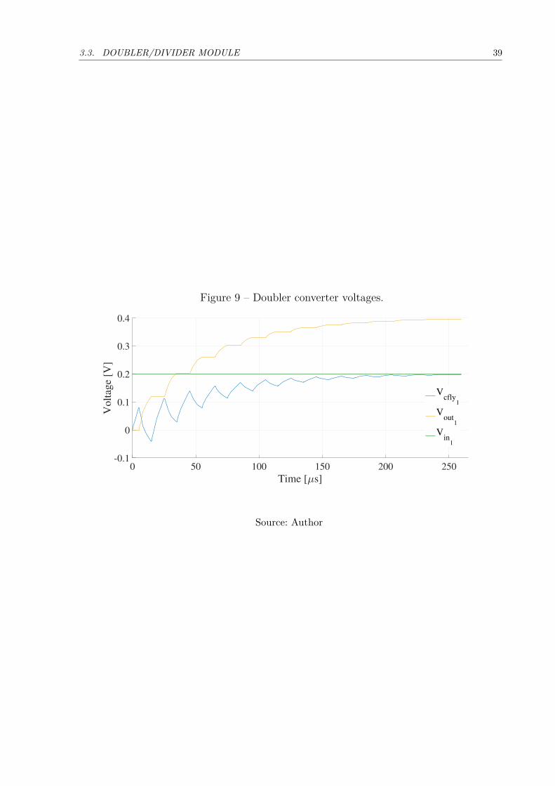
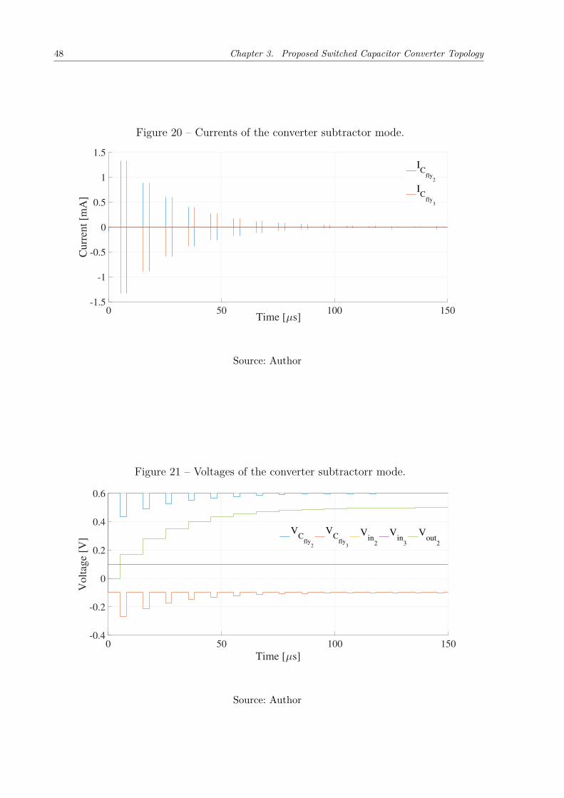
Electrical simulation was executed using 0.6 V and 0.1 V as voltages inputs withno series resistance. The flying capacitors currents have opposite signs and their behavioris the same as the current presented in the previous case, as can be seen in Fig. 20. Fig. 21

3.4. ADDER/SUBTRACTOR MODULE 47
Figure 19 – Operation phase 1 (a) and phase 2 (b) of the Adder/Subtractor converterworking as voltage subtractor.
Cfly2
S7
Vout2
Vin3
S9S11
S8 S10
S12
S13
Cfly3
Cout2
Vin2
+
-
+
-
qCfly2
(1)qCfly3
(1) qout2
(1)
qin2
(1)
qin3
(1)
Subtractor mode: phase 1
(a)
Cfly2
S7
Vout2
Vin3
S9 S11
S8 S10
S12
S13
Cfly3
Cout2
qout2
(2)qCfly2
(2)
qCfly3
(2)
Vin2
+
-
+
-
Subtractor mode: phase 2
qin2
(2)
qin3
(2)
(b)
Source: Author
presents the voltages of the two inputs, flying capacitors, and the circuit output. Cfly2 ischarging positively with the 0.6 V voltage provided by Vin2 and Cfly3 is charging negativelywith the 0.1 V voltage provided by Vin3 . Thus the supposed subtraction of the voltagesinputs occurs, but the validated value just appears in the output when the flying capacitorscomplete their charging. The switch signals are the same presented in Fig. 18, but in thiscase switch S7 is also representing S9 and S10.
48 Chapter 3. Proposed Switched Capacitor Converter Topology
Figure 20 – Currents of the converter subtractor mode.
0 50 100 150Time [ s]
-1.5
-1
-0.5
0
0.5
1
1.5
Cu
rren
t [m
A]
IC
fly2
IC
fly3
Source: Author
Figure 21 – Voltages of the converter subtractorr mode.
0 50 100 150
Time [ s]
-0.4
-0.2
0
0.2
0.4
0.6
Vo
ltag
e [V
]
VC
fly2
VC
fly3
Vin
2
Vin
3
Vout
2
Source: Author
3.5. MULTIPLE-VCR SC DC-DC CONVERTER 49
3.5 MULTIPLE-VCR SC DC-DC CONVERTER
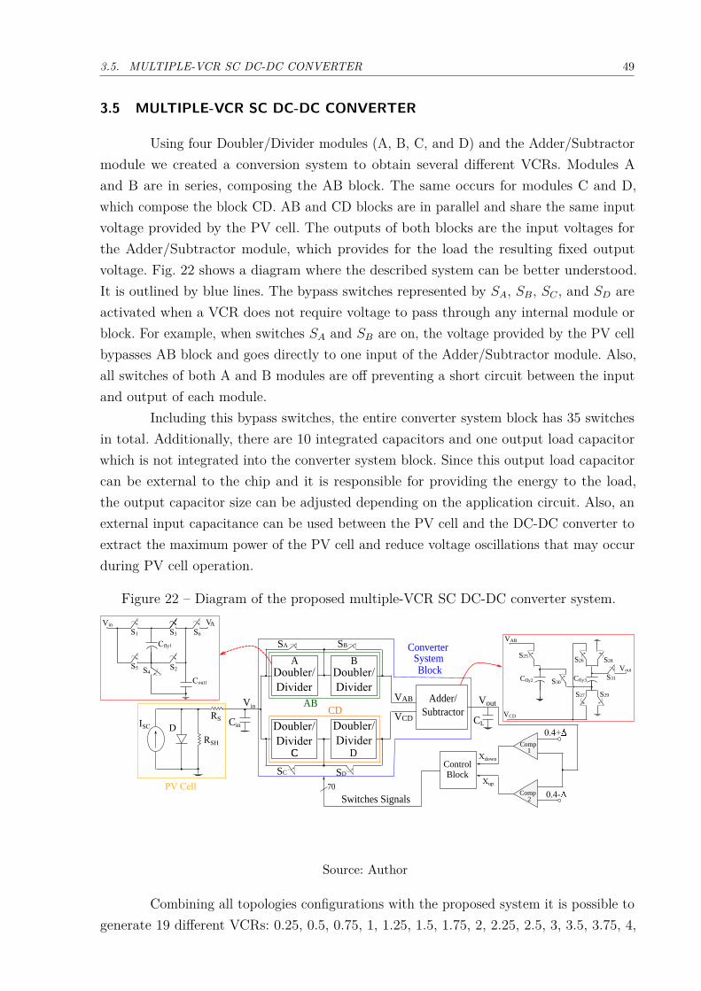
Using four Doubler/Divider modules (A, B, C, and D) and the Adder/Subtractormodule we created a conversion system to obtain several different VCRs. Modules Aand B are in series, composing the AB block. The same occurs for modules C and D,which compose the block CD. AB and CD blocks are in parallel and share the same inputvoltage provided by the PV cell. The outputs of both blocks are the input voltages forthe Adder/Subtractor module, which provides for the load the resulting fixed outputvoltage. Fig. 22 shows a diagram where the described system can be better understood.It is outlined by blue lines. The bypass switches represented by SA, SB, SC , and SD areactivated when a VCR does not require voltage to pass through any internal module orblock. For example, when switches SA and SB are on, the voltage provided by the PV cellbypasses AB block and goes directly to one input of the Adder/Subtractor module. Also,all switches of both A and B modules are off preventing a short circuit between the inputand output of each module.
Including this bypass switches, the entire converter system block has 35 switchesin total. Additionally, there are 10 integrated capacitors and one output load capacitorwhich is not integrated into the converter system block. Since this output load capacitorcan be external to the chip and it is responsible for providing the energy to the load,the output capacitor size can be adjusted depending on the application circuit. Also, anexternal input capacitance can be used between the PV cell and the DC-DC converter toextract the maximum power of the PV cell and reduce voltage oscillations that may occurduring PV cell operation.
Figure 22 – Diagram of the proposed multiple-VCR SC DC-DC converter system.
Adder/
SubtractorVin
Vout
CL
Doubler/
Divider
Doubler/
Divider
SC
C
BA
C D
SD
SA SB
ABCD
VAB
VCD
Cfly2
S25
VAB
Vout
VCD
S27 S29
S26 S28
S30S31Cfly3
Switches Signals
Converter System Block
Control
0.4+
0.4-
Block
A
70
Comp1
Comp2
Doubler/
Divider
Doubler/
Divider
Xdown
Xup
ISC D
RSH
RS
PV Cell
Cin
Source: Author
Combining all topologies configurations with the proposed system it is possible togenerate 19 different VCRs: 0.25, 0.5, 0.75, 1, 1.25, 1.5, 1.75, 2, 2.25, 2.5, 3, 3.5, 3.75, 4,

50 Chapter 3. Proposed Switched Capacitor Converter Topology
4.25, 4.5, 5, 6 and 8.The converter system block, outlined by blue lines in Fig. 22, can be easily
expanded in order to provide a wider range of VCRs. To accomplish this system expansion,more multi-topology converters can be cascaded in the main block, resulting in moreoptions of ratios with a power of two characteristics. In addition, more main blocks canbe added in parallel, and consequently, an Adder/Subtractor converter with more inputswill be able to combine more ratios. Finally, blocks with other single or multi-topologyconverters can be used in the system in order to offer more options of ratios for thecombinations. It is important to note that if the converter system is expanded its outputresistance and charge efficiency can be worsened.
As an example of the system operation, electrical simulations will be presentedfor two cases with different VCRs: 0.75 and 1.5.
One way to achieve a 0.75 VCR is setting the output of one cascaded Dou-bler/Divider block with a 0.5 ratio and the other cascaded block with a 0.25 ratio. For ABblock, considering the two cascaded multi-topology converters, just one Doubler/Dividermodule is configured as a voltage divider. The other module is off, and switch SB is on.The divider output presents a voltage equal to Vin/2 and the bypass switch replicates thisvoltage on the AB block output. The two Doubler/Divider modules in the CD block areboth configured as voltage dividers, thus this block output is Vin
14 . The 0.5 ratio in AB
block output and 0.25 ratio in CD block output are connected to the Adder/Subtractorconverter. The latter is configured as a two-input adder and adds the output ratios of ABand CD blocks. So, the output voltage on the load node is equal to 0.75Vin V.
A simulation example was executed using 0.533 V as input with a 100 Ω seriesresistance. Fig. 23 contains the system main voltages. VAB represents the AB block outputand VCD represents the CD block output. As previously mentioned, the AB block isconfigured as a voltage divider, thus its output is around 0.266 V after steady state. CDblock has two voltages dividers in sequence and its output is around 0.133 V. Finally, theAdder/Subtractor converter is adding these two output blocks voltages and the load nodehas a voltage of approximately 0.399 V which corresponds to the 0.75Vin ratio. Switchessignals are presented in Fig. 24. It can be observed that the switches for both the firstconverters blocks (S1A,S3A,S1C and S3C) are operating simultaneously, while switches forthe CD block second converter (S1D and S3D) only start operation when the second phaseof the previous block begins.
One of the approaches to get a 1.5 VCR is setting one of the blocks as a voltagedoubler and the other block as a voltage divider, and then subtracting their ratios. In thisexample, regarding the two cascaded Doubler/Divider modules on the AB block, moduleA is configured as voltage doubler topology and the other module is off with switch SB
on. The input voltage is doubled by the first converter and the bypass switch replicatesthe 2Vin voltage on AB block output. CD block has similar behavior, but the difference

3.5. MULTIPLE-VCR SC DC-DC CONVERTER 51
Figure 23 – Main voltages of the proposed converter system with VCR=0.75.
0 50 100 150 200 250 300
Time [ s]
0
0.05
0.1
0.15
0.2
0.25
0.3
0.35
0.4
0.45
0.50.54
Vo
ltag
e [V
]V
in
VAB
VCD
Vout
Source: Author
Figure 24 – Switches signals of the proposed converter system with VCR=0.75.
0 5 10 15 20 25 30 35
Time [ s]
Voff
Von
Voff
Von
Voff
Von
Voff
Von
Voff
Von
Voff
Von
Vo
ltag
e [V
]
VS
1A
VS
3A
VS
1C
VS
3C
VS
1D
VS
3D
Source: Author
is that its first Doubler/Divider module is configured as a voltage divider. So, CD blockoutput presents a voltage of Vin/2. These two voltages are subtracted by the subtractorconfiguration of the Adder/Subtractor converter, and the output voltage on the load nodeis equal to 1.5Vin V.
Another simulation example was performed with a voltage input equal to 0.3V with a 100 Ω series resistance. Fig. 25 presents the system’s main voltages and thenode names are the same as the previous simulations. As explained before, the AB blockis configured as a voltage doubler, thus its output is around 0.6 V after steady state.CD block operates in a similar way, but instead of a voltage doubler, the first module is

52 Chapter 3. Proposed Switched Capacitor Converter Topology
configured as a voltage divider. So, after steady-state, the voltage output on the CD blockis around 0.15 V. The Adder/Subtractor converter is subtracting these two output blocksvoltages and the load node has a voltage about 0.45 V which corresponds to the 1.5Vin
ratio. Fig. 26 shows the switches signals and can be noted that the switches for both firstblocks converters operate simultaneously since they are in parallel.
Figure 25 – Main voltages of the proposed converter system with VCR=1.5.
0 50 100 150 200 250 300 350 400
Time [ s]
-0.050
0.050.1
0.150.2
0.250.3
0.350.4
0.450.5
0.550.60.6
Vo
ltag
e [V
]
Vin
VAB
VCD
Vout
Source: Author
Figure 26 – Switches signals of the proposed converter system with VCR=1.5.
0 5 10 15 20 25 30 35Time [ s]
0
Voff
Von
Voff
Von
Voff
Von
Voff
Von
Vo
ltag
e [V
]
VS
1A
VS
3A
VS
1C
VS
3C
Source: Author

3.6. CONTROL BLOCK AND COMPARATORS 53
3.6 CONTROL BLOCK AND COMPARATORS
Figure 22 presents a control block that is used to configure the reconfigurablemodules in order to implement the desired VCR. The system can be automatically adjustedby sensing the output voltage and selecting the proper VCR for maintaining the outputfixed in 0.4 V. Two comparators (Comp1 and Comp2) sense if the output voltage level isabove or below 0.4 V and a digital control selects the switches signals to reduce or increasethe current VCR. A ∆ parameter is added (subtracted) to the reference voltages at theinput of comparators in order to implement hysteresis in the comparison function.
It is important to note that the design and physical implementation of the controlblock and comparators are outside the scope of this work, which is focused on developingthe DC-DC converter. The control block and comparators are essential modules to laterdemonstrate the behavior of the proposed converter. Then, a suggestion for a simple digitalcontrol will be presented and ideal comparators can be used to interact together with theproposed DC-DC converter to validate its operation.
A possible control block implementation consists basically of a digital 5 bitup/down the counter and a lookup table. Fig. 27 presents more details about the controlimplementation. Signals Xup, Xdown, clk1, rst and clk2 are the input of the digital control;Xdown and Xup are the comparison bits provided by comparators Comp1 and Comp2,respectively; clk1 is the clock signal responsible for controlling the speed increment anddecrement of the counter; rst is the signal used to reset the counter to its predefined initialvalue; and clk2 is the clock used to generate the conversion system switches signals. Thedigital control output provides switches signals that are connected to each switch of theconversion system. The control bus has 70 bits.
The counter is responsible for counting or selecting the voltage conversion ratio,and since there are 19 different values, 5 bits are necessary to count all VCRs. Thecount goes from the lowest to the highest VCR. In our implementation, binary value00001 represents VCR=0.25 (minimum) and 10011 represents VCR=8 (maximum). Valuesbetween this range represent intermediate VCRs, and values outside this range turnall switches off so that no VCR is configured. Counter increases or decreases based onthe comparison bits, Xup and Xdown, provided by the comparators. For example, if theconverter output voltage is greater than (0.4 + ∆) V, the counter will decrease by oneits count to decrease VCR; if the converter output voltage is smaller than (0.4 - ∆) V,the counter will increase by one its count to increase VCR; finally, if the converter outputvoltage is in the range of (0.4 ±∆) V, the counter keeps its value to maintain the currentVCR. Figure 28 shows a flowchart that explains in more detail the logic operating of the 5bit up/down counter.
At every transition of clk1 from low to high, a step of the flowchart of Fig. 28is executed. If the reset signal (rst) is high, then the counter (Countout) is reset to thepredefined initial value 00001 that represents the smaller available VCR (=0.25) for the

54 Chapter 3. Proposed Switched Capacitor Converter Topology
Figure 27 – Block diagram of the proposed digital control.
5 bit Up/Down Counter
LookUp Table
Countout 5
Address 6
Data 70
Xup Xdown clk1 rst clk2
S0 = Data[0] S0 = Data[1]
S34 = Data[68] S34 = Data[69]
Switches
Signals
Control
Block
S0 S0 S2 S2 S3 S3 S4 S4 S34 S34
Source: Author
conversion system. When rst is low then Countout value is verified to check if the counterachieved the lowest or the highest VCR. This measure serves to prevent the counter fromcontinuing to increase or decrease when a minimum or maximum value of VCR is reachedsince the counter can count more values than the number of available VCRs. So, when thecounter is representing the minimum VCR, flag minv goes high; and flag maxv goes highwhen the counter is at the maximum VCR. The next steps consist of checking the statesof the comparison bits (Xup and Xdown) and the mentioned flags to decide the action forthe counter. Xup and Xdown in low state indicates that the converter output voltage isin the range of 0.4 ±∆ V, so the counter does not change its value. When Xup is high,it means converter output voltage is smaller than 0.4 - ∆ V and the counter increments(increase VCR) only if the flag maxv is low. Otherwise the counter keeps the current value.Similarly, when Xdown is high the converter output voltage is greater than 0.4 + ∆ V.Then, the counter decrements (decrease VCR) only if flag minv is low. Otherwise, thecounter keeps its current value.
It is known that for each VCR there are different switches configuration that mustturn on and off in operating phases 1 and 2. In our implementation, each configuration ispreallocated and saved in a lookup table. The access address of this lookup table has 6bits. The 5 most significant bits represent the VCR informed by the counter (Countout),and the least significant bit represents the operation phase, 1 and 2, which is informedby an alternating clock signal called clk2. Phase 1 of operation is represented by clk2 = 0

3.6. CONTROL BLOCK AND COMPARATORS 55
Figure 28 – Flowchart of the digital control counter.
Countout = 00001 rst = 1?
Countout
=
00001?
Countout
=
10011?
Xup = 0
and
Xdown = 0?
Xup = 1
and
maxv = 0?
Xup = 1
and
maxv = 1?
Xdown = 1
and
minv = 0?
Xdown = 1
and
minv = 1?
minv = 1minv = 0
maxv = 1maxv = 0
Countout = Countout
Countout = Countout + 1
Countout = Countout - 1
Countout = Countout
Countout = Countout
Countout = Countout
yes
no
yesno
yesno
yes
no
yes no yes
no
yesnoyes
no
Source: Author
and phase 2 is represented by clk2 = 1. Table 4 shows the values contained in the lookuptable. In order to simplify the switches signals representation in Table 4, only one signalwas shown per switch, but in the implementation there are two signals where one isthe complement of the other. The switches signals control bus is composed as follows:S0S0S1S1S2S2S3S3...S34S34. This control bus represents the switches signals of Fig. 22. Theequivalence is defined as: from S0 to S5 represent switches S1 to S6 of the Doubler/DividerA module; from S6 to S11 represent switches S1 to S6 of the Doubler/Divider B module;

56 Chapter 3. Proposed Switched Capacitor Converter Topology
from S12 to S17 represent switches S1 to S6 of the Doubler/Divider C module; from S18 toS23 represent switches S1 to S6 of the Doubler/Divider D module; from S24 to S30 representswitches S7 to S13 of the Adder/Subtractor module; finally, from S31 to S34 represent thebypass switches SA to SD.

3.6. CONTROL BLOCK AND COMPARATORS 57
Table 4 – Example of the implemented lookup table of the digital control block.
Address Switches SignalsVCR Countout clk2 S0S1S2S3S4S5S6S7S8S9S10S11S12S13...S34
0.25 00001 0 000000001101110000001101101100010001 00000011000000110111000000000111000
0.50 00010 0 110000001101110000001101110010000001 00110111000000110111000000000110000
0.75 00011 0 000000000000110000001101101100011001 00000000000000110111000000000111100
1.00 00100 0 000000110000000000110000000001110101 00000000110100000000110111001001010
1.25 00101 0 000000000000110000001101110010011001 00000000000000110111000000000111100
1.50 00110 0 000000000000000000110000000001111101 00000000000000000000110111001001110
1.75 00111 0 000000100101110000001101101100010001 00000000101100110111000000000111000
2.00 01000 0 000000000000000000000000110010011111 00000000000000000000000000000111111
2.25 01001 0 000000100101110000001101110010010001 00000000101100110111000000000111000
2.50 01010 0 000000100101000000110000000001110101 00000000101100000000110111001001010
3.00 01011 0 000000000000000000100101110010011101 00000000000000000000101100000111110
3.50 01100 0 100101001011000000110000000001100101 00101110010100000000110110110000010
3.75 01101 0 100101001011110000001101101100000001 00101110010100110111000000000110000
4.00 01110 0 000000100101000000100101110010010101 00000000101100000000101100000111010
4.25 01111 0 100101001011110000001101110010000001 00101110010100110111000000000110000
4.50 10000 0 100101001011000000110000000001100101 00101110010100000000110111001000010
5.00 10001 0 100101001011000000000000110010000111 00101110010100000000000000000110011
6.00 10010 0 100101001011000000100101110010000101 00101110010100000000101100000110010
8.00 10011 0 100101001011100101001011110010000001 00101110010100101110010100000110000
Source: Author

58 Chapter 3. Proposed Switched Capacitor Converter Topology
3.7 CONCLUSION
This chapter presents a simplified model to understand the operation of theswitched-capacitor converter topologies. Some proposed structures of SC converters, suchas the voltage-doubler and the voltage-divider are introduced and their operation phasesexplained in terms of charge flow analysis. The chapter also presents the concept of multi-topology SC converters and their application to obtain more than one voltage conversionratio with a single topology. This concept is used to explain the operation of the proposedSC based topology capable of providing a range of different VCRs. In addition, this chapterpresents some electrical simulations validating the operation of the blocks which composethe converter system, as well as the operation of the complete converter system. Lastly, theoperation and construction details of the suggested digital control system are addressed inthe chapter.

59
4 DESIGN METHODThis chapter details the choices made for the practical implementation of the
proposed DC-DC conversion system. The systematic method based on electrical simulationsis proposed. It is used to design switches, capacitors, and operating frequency that composethe VCR adjustable switched-capacitor DC-DC converter.
4.1 CONVERTER SYSTEM DESIGN METHOD
According to Breussegem and Steyaert (2012), the design of a capacitive DC-DCconverter containing multiple topologies introduces some additional constraints comparedto single topologies. The author describes that the multiple topologies converter designshould include the influence of the additional idle switches (since multiple topologiesconverter requires more switches), meet the requirements for a set of operation points, andgive an optimum solution given a set of user constraints.
Following this idea, the single topology converter model is extended and a multi-objective algorithm is used for the purpose of optimizing the design. Beyond the multi-objective algorithm, it is necessary a complete mathematical modeling of the capacitiveconverter modules. Moreover, the modeling parameters presented by Breussegem andSteyaert (2012) can not be applied for the Adder/Subtractor converter module proposedin this work since its a two input converter topology.
On the other hand, we also propose a systematic design method based on electricalsimulations in order to provide a practical way to size capacitors, switches, and operatingfrequency. This method does not require the complete modeling of the switched-capacitorconverter modules.
The design of the proposed DC-DC converter includes the sizing of capacitorsand switches and the definition of optimal or ideal switches operating frequency. CMOStransmission gates are used for all switches of the proposed conversion system, and thedesign was performed in a CMOS 180 nm process. The transmission gate is implementedwith the bulk node of each transistor connected to the respective source node. Thisapproach can be implemented using a deep n-well transistor and avoids the use of largetransistors to compensate for the increase in the threshold voltage. Synopsys HSpice isused for all schematic electrical simulations.
The schematic of the transmission gate used as switches is denoted by the blacklines of Fig. 29. To turn a switch on it is necessary to apply a voltage VGN
of 0.8 V onthe MN transistor gate and VGP
= 0 V on the MP transistor gate as shown in Fig. 30a.On the other hand, to turn a switch off it is necessary to apply a voltage VGN
of 0 V onthe MN transistor gate and VGP
= 0.8 V on the MP transistor gate as shown in Fig. 30b.Since the transmission gate is built with two transistors, n-type and p-type, there aretwo opposite signals (VGN
and VGP) for each switch. The converter system block has 35
switches in total, so there are 70 bits in the control bus presented in Fig. 27.

60 Chapter 4. Design Method
Figure 29 – Electrical schematic of the transmission gate used as switch: switch turned on(a) and switch turned off (b).
VGN = 0.8 V
in out
VGP = 0 V
MN
MP
(a)
in
VGN = 0 V
out
VGP = 0.8 V
MN
MP
(b)
Source: Author
The transmission gates were chosen to implement the converter switches aftercomparing with n-type MOSFET switches with respect to the operation of the conversionsystem block charging the output load capacitor CL. For this comparison, electricalsimulations were executed using the converter system switches implemented only withtransmission gates and only with n-type MOSFETs. Four VCRs were simulated: 0.5 and0.75 to represent the situation when higher voltages are presented (Vin = 0.8 and 0.533V) on the converter system input, and 4.5 and 8 when lower voltages are presented (Vin
= 0.088 and 0.05 V). For a simpler representation, the voltage applied as VGNto turn
on the switches is named here as Von, and VGPis always the opposite voltage of VGN
asrepresented in Fig. 29. Three different voltages were used as Von for each VCR simulation:0.4, 0.8, and 1.6 V. These voltages represent the converter Vout, twice the converter Vout
and four times the converter Vout, respectively.The simulated curves for the transmission gate switches implementation are
presented in Fig. 30, and the simulated curves for n-type MOSFET switches implementationare presented in Fig. 31.
There is no relevant difference between the switches implementations when lowervoltages are presented as Vin and the system behaves as a step-up converter (VCR =4.5 and 8). In Figs. 31c, 31d, 32c, and 32d the curves for Von equal to 1.6 V (black line)and 0.8 V (red line) are almost overlapped. In this case a minimum Von voltage of 0.8 Vcharges the output load capacitor with the desired voltage of 0.4 V (or near to it) in bothimplementations.
A clearer difference between the two implementations appears, in the worst-casescenario, when higher voltages are presented as Vin and the system behaves as a step-down converter (VCR = 0.5 and 0.75). As observed in Figs. 32a and 32b, for the n-type

4.1. CONVERTER SYSTEM DESIGN METHOD 61
Figure 30 – Electrical simulations of the converter system block built with transmissiongate switches varying Von for: VCR=0.5 (a), VCR=0.75 (b), VCR=4.5 (c),and VCR=8 (d).
0 0.002 0.004 0.006 0.008 0.01 0.012 0.014 0.016 0.018 0.02
Time [s]
0
0.1
0.2
0.3
0.4
0.5
0.6
Vo
ut [
V]
Von
=1.6 V
Von
=0.8 V
Von
=0.4 V
(a)
0 0.002 0.004 0.006 0.008 0.01 0.012 0.014 0.016 0.018 0.02
Time [s]
0
0.05
0.1
0.15
0.2
0.25
0.3
0.35
0.4
Vo
ut [
V]
Von
=1.6 V
Von
=0.8 V
Von
=0.4 V
(b)
0 0.002 0.004 0.006 0.008 0.01 0.012 0.014 0.016 0.018 0.02
Time [s]
0
0.05
0.1
0.15
0.2
0.25
0.3
0.35
0.4
Vo
ut [
V]
Von
=1.6 V
Von
=0.8 V
Von
=0.4 V
(c)
0 0.002 0.004 0.006 0.008 0.01 0.012 0.014 0.016 0.018 0.02
Time [s]
0
0.05
0.1
0.15
0.2
0.25
0.3
0.35
0.4
VC
ou
t [V
]
Von
=1.6 V
Von
=0.8 V
Von
=0.4 V
(d)
Source: Author
MOSFET switches implementation a Von equal to 1.6 V is necessary to charge the outputload capacitor with 0.4 V mainly when the input voltage is 0.8 V (VCR = 0.5). Thiscan be confirmed by the fact that in this case, the VDS of the transistor that composesthe switch is large because Vin is higher, so VGS needs to be increased so that the switchoperates as expected. The transmission gate switches implementation maintains the sameperformance for the step-down VCRs, compared to step-up VCRs, to charge the outputload capacitor with a minimum Von voltage of 0.8 V as shown in Figs. 31a and 31b. Inthis worst-case scenario, transmission gates are better switch implementations as they donot need a higher Von voltage for proper operation. For this reason, transmission gateswere chosen to implement all converter system switches with Von equal to 0.8 V.
The final version of the energy harvesting system, which includes the convertersystem proposed by this work, needs to be as simple as possible and completely integrated.Using the converter output voltage itself as a signal to turn on/off switches is an interestingidea which avoids the need of an extra and dedicated circuit for providing the desiredvoltage to drive the switches.
Considering that after start-up, when the output load capacitor is already chargedwith 0.4 V, this voltage is used to supply the load and, additionally, it can be used to theclock generator circuit to provide signals to drive the switches. However, a voltage of 0.4 Vat the gate of the transistors is not sufficient for proper operation of the switches, especially

62 Chapter 4. Design Method
Figure 31 – Electrical simulations of the converter system block built with n-type MOSFETswitches varying Von for: VCR=0.5 (a), VCR=0.75 (b), VCR=4.5 (c), andVCR=8 (d).
0 0.002 0.004 0.006 0.008 0.01 0.012 0.014 0.016 0.018 0.02
Time [s]
0
0.05
0.1
0.15
0.2
0.25
0.3
0.35
0.4
Vo
ut [
V]
Von
=1.6 V
Von
=0.8 V
Von
=0.4 V
(a)
0 0.002 0.004 0.006 0.008 0.01 0.012 0.014 0.016 0.018 0.02
Time [s]
0
0.05
0.1
0.15
0.2
0.25
0.3
0.35
0.4
0.45
Vo
ut [
V]
Von
=1.6 V
Von
=0.8 V
Von
=0.4 V
(b)
0 0.002 0.004 0.006 0.008 0.01 0.012 0.014 0.016 0.018 0.02
Time [s]
0
0.05
0.1
0.15
0.2
0.25
0.3
0.35
0.4
Vo
ut [
V]
Von
=1.6 V
Von
=0.8 V
Von
=0.4 V
(c)
0 0.002 0.004 0.006 0.008 0.01 0.012 0.014 0.016 0.018 0.02
Time [s]
0
0.05
0.1
0.15
0.2
0.25
0.3
0.35
0.4
Vo
ut [
V]
Von
=1.6 V
Von
=0.8 V
Von
=0.4 V
(d)
Source: Author
in step down VCRs. This is due to the fact that in these cases VDS > VGS, impacting theoperation of the transistors as a switch. So, the output voltage of the converter must bedoubled to offer a voltage near to 0.8 V (steady-state) to properly control the switches.This can be accomplished with the aid of a voltage doubler circuit like the cross-coupleddoubler topology of Fig. 32, proposed by TianRui Ying, Wing-Hung Ki and Mansun Chan(2003). This circuit has a simple operation in which there are two pulsed input signals,φ1 and φ2, alternating between 0 and VDD V. They are complementary signals, so whenφ1 is equal to VDD, φ2 is equal to 0 V and vice versa. This controls the circuit so thatone side operates at a time and C1 and C2 capacitors are charged with VDD V. The CL1
capacitor is charged up in both phases with 2VDD because C1 and C2, charged with VDD,are placed in series with the VDD provided by the inverters. Also, in nodes A and B thereare complementary signals alternating between 2VDD and VDD.
By setting the VDD of this circuit as the output voltage of our proposed conversionsystem, it is possible to double the converter output voltage from 0.4 to 0.8 V in thesteady-state.
Considering a real capacitive DC-DC converter, the energy is transferred from theinput supply to the load by means of capacitors. Figure 33 shows a circuit diagram usedto model the charging process of capacitor C after switching (at t=0). This circuit can beused to model the energy transfer from a supply to a single capacitor. In order to simplify,

4.1. CONVERTER SYSTEM DESIGN METHOD 63
Figure 32 – Cross-coupled doubler circuit.
VDD
VDD VDD
M1 M2
M3 M4
2VDD
C1 C2CL1
1 2
VDD
0
VDD
0
A B
Source: Author
Figure 33 – Circuit diagram used to model the charging process of capacitor C afterswitching (at t=0).
+-
Vsup R
CVC (0)
Source: Author
the charging of a single capacitor is analyzed but the conclusions can be expanded foranalyzing the energy transfer between two capacitors.
A differential equation can be used to describe the process of charging a capacitor:
−Vsup +RCdVC
dt+ VC = 0 (4.1)
where C dVC
dtis the current flowing after the switch is closed.
Solving Eq. 4.1 for VC(t) and deriving the current through the capacitor IC(t),

64 Chapter 4. Design Method
the following equations are obtained:
VC(t) = Vsup − (Vsup − VC(0))e −tRC (4.2)
IC(t) = Vsup − VC(0)R
e−tRC (4.3)
The power transferred to the capacitor is:
PC(t) = VC(t)IC(t) = VsupVC(0)− V 2C(0)
Re
−tRC (4.4)
And the energy added to the capacitor in this process can be obtained:
EC =∫ ∞
0P (t)dt =
V 2sup − V 2
C(0)2 C (4.5)
Similarly the total energy delivered by the supply voltage source can be obtained:
Etot = Vsup(Vsup − VC(0))C (4.6)
There is a power loss caused by the resistive losses in R, so the total energydelivered by the supply source is higher than the energy stored in the capacitor. Thus,part of the energy is lost and this is quantified by the charging efficiency ηCcharge
presentedby Wens and Steyaert (2011):
ηCcharge= EC
Etot
= VC(0) + Vsup
Vsup
12 (4.7)
The equations presented previously were derived considering an infinite chargingperiod. In practice, it represents a good approximation as long as the capacitor voltage issettled within 10% of the charging voltage (BREUSSEGEM; STEYAERT, 2012).
Table 5 presents the maximum charging efficiency that can be obtained for differentvalues of the initial capacitor voltage. This table was built using Eq. 4.7 for some cases ofVC(0) as a percentage of Vsup. It can be noticed that charging efficiencies are higher whenthe initial voltage in the capacitor is near to the supply voltage.
So, using Eq. 4.7 the efficiency - and consequently the power loss - of a capacitiveconverter block can be estimated when considering the relation of the converter outputenergy and the energy delivered at its input. This estimation can be easily performedthrough electrical simulation considering the energy that is presented in the converterinput and the energy used to charge the load capacitor connected to the converter output.It is important to note that the maximum charging efficiency is limited by the initialvoltage presented in the capacitor. According to Table 5, considering the capacitor fullydischarged (VC(0) = 0V ), the maximum possible efficiency is limited to only 50% if thereis no power loss.
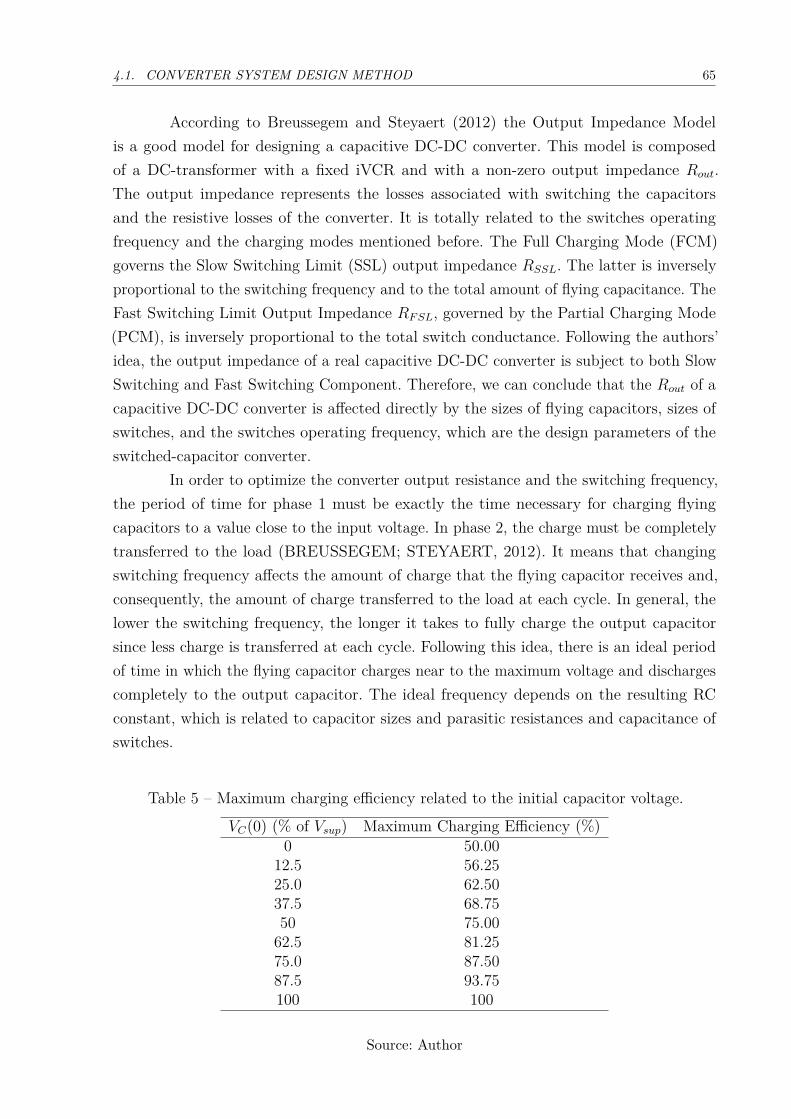
4.1. CONVERTER SYSTEM DESIGN METHOD 65
According to Breussegem and Steyaert (2012) the Output Impedance Modelis a good model for designing a capacitive DC-DC converter. This model is composedof a DC-transformer with a fixed iVCR and with a non-zero output impedance Rout.The output impedance represents the losses associated with switching the capacitorsand the resistive losses of the converter. It is totally related to the switches operatingfrequency and the charging modes mentioned before. The Full Charging Mode (FCM)governs the Slow Switching Limit (SSL) output impedance RSSL. The latter is inverselyproportional to the switching frequency and to the total amount of flying capacitance. TheFast Switching Limit Output Impedance RF SL, governed by the Partial Charging Mode(PCM), is inversely proportional to the total switch conductance. Following the authors’idea, the output impedance of a real capacitive DC-DC converter is subject to both SlowSwitching and Fast Switching Component. Therefore, we can conclude that the Rout of acapacitive DC-DC converter is affected directly by the sizes of flying capacitors, sizes ofswitches, and the switches operating frequency, which are the design parameters of theswitched-capacitor converter.
In order to optimize the converter output resistance and the switching frequency,the period of time for phase 1 must be exactly the time necessary for charging flyingcapacitors to a value close to the input voltage. In phase 2, the charge must be completelytransferred to the load (BREUSSEGEM; STEYAERT, 2012). It means that changingswitching frequency affects the amount of charge that the flying capacitor receives and,consequently, the amount of charge transferred to the load at each cycle. In general, thelower the switching frequency, the longer it takes to fully charge the output capacitorsince less charge is transferred at each cycle. Following this idea, there is an ideal periodof time in which the flying capacitor charges near to the maximum voltage and dischargescompletely to the output capacitor. The ideal frequency depends on the resulting RCconstant, which is related to capacitor sizes and parasitic resistances and capacitance ofswitches.
Table 5 – Maximum charging efficiency related to the initial capacitor voltage.
VC(0) (% of Vsup) Maximum Charging Efficiency (%)0 50.00
12.5 56.2525.0 62.5037.5 68.7550 75.0062.5 81.2575.0 87.5087.5 93.75100 100
Source: Author

66 Chapter 4. Design Method
As a practical example, electrical simulations were performed with the Adder/Subtractor module of Fig. 14 operating as a voltage adder. Two voltage sources of 0.2 Vare connected to both converter inputs (Vin2 = Vin3). Flying capacitors (Cfly2 and Cfly3)are set to 10 pF, the output load capacitor Cout2 is set to 250 pF, and switches are set tominimum size (W = 220 nm and L = 180 nm). Figure 34 shows the flying capacitors andthe output voltages for three simulations with distinct switches operating frequencies (59kHz, 590 kHz, and 5.9 MHz) that graphically exemplify the capacitor operation modesmodes
In Fig. 34a the switching frequency is 59 kHz. With this frequency, the flyingcapacitors charge with a voltage very close to the input value, but after reaching thisvoltage they take about 7 µs to transfer their charge to the output capacitor. This is anexample of the Full Charging Mode. This mode makes the charging of the output capacitorslower and the flying capacitors are unnecessarily idle during a large period of time.
The operating frequency is 5.9 MHz in the simulations of Fig. 34c. As can be noted,both flying capacitors discharge to the output capacitor before charging with a voltage veryclose to the input source. The sum of the voltages in capacitors Cfly2 and Cfly3 reachesapproximately 0.175 V, and then they transfer their charges to the output capacitor. Thisis an example of the Partial Charging Mode. In this charging mode, Cout2 charges faster,but it implies more switching losses, worsening the efficiency of the converter.
Finally, Fig. 34b presents a frequency of 590 kHz, close to the ideal operatingfrequency defined so far. In this case, both flying capacitors charge to the input voltage(or very near to it) and then discharge to the output capacitor, without relevant idletime. This is called the Boundary Charging Mode (BCM). It is very interesting for aswitching capacitor converter to operate in this charging mode because the converteroutput resistance will be near to the minimum possible value with a minimum switchingfrequency (BREUSSEGEM; STEYAERT, 2012).
The converter output resistance can also be estimated using electrical simulationsand Eq. 4.2. The voltage VC(t) is known in a transient analysis. Since Vsup is the voltagethat charges C (which represents the output load capacitor), VC(0) can be set to any valuebetween 0 and Vsup V. The only unknown variable left in the equation is the resistor R.So, we can solve Eq. 4.2 to R as:
R = −t · (C · ln(Vsup − VC(t)Vsup − VC(0)))−1 (4.8)
For the purpose of validating the estimation of the output resistance with thismethod, Fig. 35 presents the comparison between the output load capacitor charged by theadder converter and the output capacitor charged with the equivalent RC circuit, where Ris the estimated Rout and C is the output load capacitor. The same switching frequenciesof Fig. 34 are used here. Analyzing Fig. 35 we can observe that for a switching frequencyup to 590 kHz, Figs. 36a and 36b, the Rout estimation represents with very good precision

4.1. CONVERTER SYSTEM DESIGN METHOD 67
Figure 34 – Electrical simulations of the Adder/Subtractor module working as voltageadder with switches operating frequency of: 59 kHz (a), 590 kHz (b), and 5.9MHz (c).
0 2 4 6 8 10 12 14 16 18
Time [ s]
0
0.1
0.2
0.3
0.4
Volt
age
[V]
VCfly
2
+VCfly
3
VCfly
2
VCfly
3
Vout
2
7.05 s
(a)
0 2.5 0.5 7.5 1 1.25 1.5 1.75 2
Time [ s]
0
0.1
0.2
0.3
0.4
Volt
age
[V]
VCfly
2
+VCfly
3
VCfly
2
VCfly
3
Vout
2
(b)
0.05 0.1 0.15 0.2 0.05 0.1 0.15 0.2 0.05 0.1 0.15
Time [ s]
0
0.025
0.05
0.075
0.1
0.125
0.15
0.175
Volt
age
[V]
VCfly
2
+VCfly
3
VCfly
2
VCfly
3
Vout
2
(c)
Source: Author
the entire voltage charge of the output capacitor. In Fig.36c, which has a frequency inthe PCM region, there is only a small discrepancy in the initial charging of the outputcapacitor.

68 Chapter 4. Design Method
Figure 35 – Comparison between the output capacitor being charged by the adder modeconverter and its equivalent RC circuit for switching frequency of: 59 kHzwith Rout=3.28 MΩ (a), 590 kHz with Rout=347 kΩ (b), and 5.9 MHz withRout=165 kΩ (c).
0 1 2 3 4 5 6
Time [ms]
0
0.05
0.1
0.15
0.2
0.25
0.3
0.35
0.4
Vout 2
[V
]
Adder mode converter
Equivalent RC circuit
2.96 2.97 2.98 2.99 3 3.01 3.02 3.03 3.04 3.05 3.06
Time [ms]
0.388
0.3885
0.389
0.3895
0.39
0.3905
0.391
Vo
ut 2
[V
]
Adder mode converter
Equivalent RC circuit
(a)
(b)
(c)
Source: Author

4.1. CONVERTER SYSTEM DESIGN METHOD 69
Another electrical simulation of the Adder/Subtractor module, working in addermode and with the same configuration of simulations from Fig. 35, was performed tographically exemplify the relation between the converter output resistance and the switchesoperating frequency. Figure 36 shows the behavior of the converter output resistance Rout
over a switching frequency range of 59 kHz to 5.9 MHz. Rout was estimated using Eq.4.8 and electrical simulations. It is possible to note that when operating in FCM, Rout isgreatly reduced with the frequency increasing. In this case, Rout decreases from 3.28 M to347.7 kΩ when the switching frequency is varied from 59 k to 590 kHz. Nevertheless, inPCM, Rout only reduces from 347.7 k to 165.1 kΩ when switching frequency is varied from590 k to 5.90 MHz. The red dotted line in Fig. 36 represents the ideal frequency of 590kHz. This frequency demarcates the BCM region, which is the transition region betweenthe FCM to the PCM. It is advantageous to operate in BCM in order to minimize Rout
and the switching frequency.
Figure 36 – Relation between converter Rout and switching frequency of theAdder/Subtractor module working in adder mode.
0.05 0.5 1 1.5 2 2.5 3 3.5 4 4.5 5 5.5 6
Switching Frequency [MHz]
0.165
0.5
1
1.5
2
2.5
3
3.5
Rout [
M] Ideal Frequency
Source: Author
In the first version of our proposed design method, we included the sizing ofthe switches, capacitors, and switches operating frequency that make up the conversionsystem.
Regarding the conversion system proposed in Fig. 22 from Chapter 3, theAdder/Subtractor module is the last block in the charge path and it is responsiblefor charging the load capacitor. Then, the analysis for sizing flying capacitors mustbegin with this block. Varying the size of the two flying capacitors presented in theAdder/Subtractor module, the corresponding ideal operating frequency for each capacitorsize can be estimated.
Simulations were performed with the Adder/Subtractor module working in two

70 Chapter 4. Design Method
Figure 37 – Ideal frequency versus flying capacitors value in the two operation modes ofthe Adder/Subtractor module.
0 10 20 30 40 50 60 70 80 90 100
Flying Capacitor [pF]
102
103
104
105
106
107
108
Idea
l F
req
uen
cy [
Hz]
Adder
Subtractor
Flying Capacitor = 12 pF
Ideal Frequency = 46 kHz
Source: Author
operation modes (adder and subtractor modes). In each simulation, flying capacitors werevaried from 1 pF to 100 pF and the correspondent ideal frequency was obtained. Figure37 shows this relation for the two converter operation modes.
There is a trade-off between the capacitor value (and respective capacitor area- 2 fF / µm2 for MiM Cap in 180 nm node) and the ideal operating frequency. As thecapacitor value is reduced, the ideal operating frequency increases, which can cause moreswitching losses. On the other hand, if lower operating frequencies are used to minimizeswitching losses, larger capacitors are required, consuming more chip area.
The subtractor operation mode represents the worst-case scenario since the flyingcapacitors are related to lower ideal frequencies compared to the adder operation mode.With a lower switching frequency, it is possible to guarantee the operation of the converterin both Adder and Subtractor modes. This worst-case scenario can be used to choose avalue of capacitance for the flying capacitors that compose the Adder/Subtractor module.In order to achieve a capacitor value suitable for integration and with a slow switchingfrequency, we choose a capacitance of 12 pF, which corresponds to an ideal operatingfrequency of nearly 46 kHz.
The next step consists of sizing the flying capacitors of Doubler/Divider mod-

4.2. DESIGN METHOD INCLUDING CONVERTER ROUT ESTIMATION 71
ule, considering the previously selected switching frequency. Since the values for flyingcapacitors of Adder/Subtractor converter were already defined, simulations varying theflying capacitors of the previous blocks can be done for calculating conversion systemefficiency. Based on the relation of the amount of power/energy provided by the PV cellin the converter input, and the amount of power/energy used to charge the output loadcapacitor, it is possible to estimate, through electrical simulation, the conversion systemcharging efficiency ηCS as:
ηCS = Eout/Ein (4.9)
Equation 4.9 is based on Eq. 4.7, and since the simulated charging efficiencyconsiders the charging of the output load capacitor starting from 0 V, ηCS will be normalizedby the maximum achievable efficiency of 50% as explained before. It is important toemphasize that the converter efficiency considered in this work is the charging efficiencyconcept previously presented. Since the application circuit operation is duty-cycled andconsequently there is no load connected the entire time in the converter output, thisefficiency is estimated considering only the load capacitor connected all the time in theconverter output. And with that, we can get a sense of how much energy is lost only inthe converter block when energy is transferred from the solar cell to the capacitor.
By manually adjusting the size of the flying capacitors of the voltage Dou-bler/Divider module and checking the correspondent ηCS efficiency, capacitor valuesthat provided the best efficiency are 90 pF for the flying capacitors of blocks A and C,and 45 pF for the flying capacitors of blocks B and D.
The size of switches can be varied to refine efficiency improvement. In this case,the gate length of the transistors that compose switches is fixed to a minimum size (180nm in the target technology) and W is varied. In each simulation, the converter efficiencyis obtained. Fig. 38 shows the relationship between converter efficiency and gate widthof switches in a case where VCR = 1.25. It can be noticed that an improvement in theconverter efficiency can be reached with the increasing of the gate width until a certainvalue. After this, the efficiency is reduced caused by the parasitic elements of the transistors.So, for this VCR scenario and considering only the charging efficiency of CL, the bestvalue for gate width for all switches which results maximum efficiency is 6 µm.
4.2 DESIGN METHOD INCLUDING CONVERTER ROUT ESTIMATION
The proposed method can also include the estimation of the converter outputresistance Rout. The output resistance is an important parameter of the converter thatshows the limitations in terms of the application of this converter.
Once again, electrical simulations were performed using the Adder/Subtractormodule working in adder and subtractor mode and varying the size of the flying capacitors

72 Chapter 4. Design Method
Figure 38 – Simulated conversion system efficiency ηCS in function of transistor gate widthof switches.
Source: Author
from 1 to 150 pF operating with the ideal switching frequency for each capacitor size. Inthese new simulations, switches gate width was varied from 0.22 to 15 µm. This simulationapproach results in three-dimensional curves which relate flying capacitor size Cfly andswitches gate width Wtg with the specifications for the ideal frequency, converter outputresistance Rout, maximum voltage on the output load capacitor VCLmax and convertercharging efficiency ηC . It was used as an output load capacitor CL of 250 pF for bothAdder/Subtractor operation modes.
The adder operation mode is simulated using two ideal voltage sources of 0.2 Vas inputs, and the subctrator operation mode is simulated using an ideal voltage source of0.6 V in the first input and 0.2 V in the second input. Figure 39 presents the curve of theideal frequency related to switches gate width and flying capacitor sizes for both operationmodes. The trade-off shown before between capacitor size and switching frequency is alsopresented in these simulations. So, in order to use smaller flying capacitors, the convertermust operate with higher switching frequencies that may cause more switching losses. Onceagain, subtractor mode is related to smaller frequencies when comparing with the addermode. Also, the increase in the switches gate width does not cause a relevant variation inthe ideal frequency for Cfly higher than 25 pF. For capacitors larger than this value, anincrease in Wtg leads to a higher ideal frequency.
Figure 40 shows the curve of the converter output resistance Rout related withswitches gate width and flying capacitor sizes for both operation modes. At a first glance, itseems that Rout does not vary with Cfly and this is because the ideal frequency is adjustedfor each combination of Cfly and Wtg. The converter output resistance values are higherin the subtractor mode, but both operation modes present an equivalent Rout behavior.
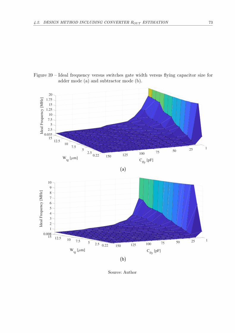
4.2. DESIGN METHOD INCLUDING CONVERTER ROUT ESTIMATION 73
Figure 39 – Ideal frequency versus switches gate width versus flying capacitor size foradder mode (a) and subtractor mode (b).
0.035
2.5
15
5
7.5
12.5
10
1.25
Idea
l F
req
uen
cy [
MH
z]
15
10
1.75
20
Wtg
[ m]
7.5 1255 50
Cfly
[pF]
2.5 750.22
100125150
(a)
0.008
1
2
3
15
4
5
6
7
Idea
l F
req
uen
cy [
MH
z] 8
9
10
12.5 10 1
Wtg
[ m]
7.5 2550
Cfly
[pF]
5 751002.5 0.22 125150
(b)
Source: Author

74 Chapter 4. Design Method
Figure 40 – Converter output resistance versus gate width versus flying capacitor size foradder mode (a) and subtractor mode (b).
150125
12.5
100
0.22
200
1002.5
Ro
ut [
k]
300
400
Cfly
[pF]
755
500
Wtg
[ m]
7.5 5010 2512.5 115
(a)
15015 12512.5 10010 75
Cfly
[pF]
7.5
Wtg
[ m]
50
2000
5
1500
25
Ro
ut [
k]
2.5
1000
1
500
0.2238
(b)
Source: Author

4.2. DESIGN METHOD INCLUDING CONVERTER ROUT ESTIMATION 75
The maximum voltage on the output load capacitor related with switches gatewidth and flying capacitor sizes for both operation modes is presented in Fig. 41. Bothoperation Adder/Subtractor modes were adjusted in the simulation to provide an outputvoltage of 0.4 V to charge CL. This is the maximum voltage on CL in almost all Cfly andWtg combinations. The maximum voltage on the output load capacitor becomes smallerthan 0.4 V for small Cfly and when Wtg increases. This can be explained by the parasiticcapacitance of the switch transistors that increase with the increasing in Wtg. When Cfly
is small, these parasitic capacitance impact more in the converter operation.
Figure 41 – Maximum voltage in the output load capacitor versus gate width versus flyingcapacitor size for adder mode (a) and subtractor mode (b).
0.340.22
0.36
2.5
VC
Lm
ax
[V
] 0.38
5
0.4
Wtg
[ m]
7.5 15012510 100
Cfly
[pF]
7512.5 502515 1
(a)
0.28
0.3
0.22
0.32
0.34
VC
max
[V
] 0.36
2.5
0.38
0.4
5
Wtg
[ m]
1507.5 12510 100
Cfly
[p F]
7512.5 502515 1
(b)
Source: Author
Finally, Fig. 42 presents the curve of the charging converter efficiency related toswitches gate width and flying capacitor sizes for both operation modes. It is possible to

76 Chapter 4. Design Method
see that the charging efficiency depends more on the Cfly size in both operation modes.This efficiency increases when Cfly decreases, and this can be explained because largercapacitors require more time to charge, impacting on the charging efficiency. In terms ofηC , it is not advantageous to operate with a converter implemented with small Cfly andlarge switches.
Figure 42 – Converter charging efficiency versus gate width versus flying capacitor size foradder mode (a) and subtractor mode (b).
6015
70
80
C [
%]
12.5
90
100
10 1
Wtg
[ m]
7.5 25505
Cfly
[pF]
752.5 1001250.22 150
(a)
20
30
15
40
50
60
70
C [
%]
12.5
80
90
10
Wtg
[ m]
7.5 15 2550
Cfly
[pF]
752.5 1001250.22 150
(b)
Source: Author
These simulated curves can be used to size all the proposed conversion system.As a practical example, a range can be delimited for Cfly, Wtg, and switching frequency ina way that there is some equivalence between the specifications in both Adder/Subtractoroperation modes. Based on this delimited range it is possible to choose values for Cfly,Wtg and switching frequency, and then simulate the entire conversion system to verify the

4.3. CONCLUSION 77
specifications. In this new conversion system design, we delimited Cfly in the range 20 -30 pF; Wtg in 3 - 7 µm; and the switching frequency in 1 - 10 MHz.
4.3 CONCLUSION
Details about the construction of the proposed DC-DC converter are addressedin this chapter. With that, it is possible to understand the decisions made about theimplementation of the system components and the operation of the DC-DC converter. Inaddition, a systematic method based on electrical simulation is proposed to be a goodstarting tip for the conversion system design including the sizing of capacitors, switches,and switching frequency. The proposed method is practical and avoids the use of complexequations that model the entire conversion system.


79
5 RESULTS AND COMPARISON WITH OTHER WORKSIn this chapter we present the simulation-based electrical characterization of
the proposed DC-DC converter considering two different designs targeted to differentapplications. Each design considers the sizing of the converter components differently inorder to fulfill the application constraints. A comparison of the proposed DC-DC converterwith other DC-DC converters in the literature is also addressed in this chapter. Finally,we present an implementation suggestion for the complete energy harvesting systemcontemplating the interaction between all blocks.
5.1 SCHEMATIC SIMULATION RESULTS
The flowchart of Fig. 43 exemplifies the proposed converter system operationinteracting with the application. It is important to note that the first step of the flowchartbegins after the converter start-up, and the start-up solution is beyond the scope of thiswork. Then, after start-up, the output load capacitor CL charges with a voltage in therange of 0.36 to 0.44 V (0.4± 10%). After that, the application system wakes up for ashort period and CL discharge ∆V providing the energy for the application circuit. Theapplication system sleeps again for a much greater period of time and CL recharge to thefull voltage value. In this kind of approach, there is no constant resistive load connectedall the time into the DC-DC converter output.
Figure 43 – Flowchart of the converter system operation interacting with the application.
CL charges
0.36 V VCL 0.44 V
Application system wakes up
CL discharges
Application system sleeps
CL recharges
Source: Author
5.1.1 DESIGN FOR LOW POWER CIRCUITS - DESIGN 1
The first design is intended to low power circuits such as the one composed of asensor and a small memory processor. This design is performed using the first version of

80 Chapter 5. Results and Comparison with Other works
the proposed method in Chapter 4. Recalling the method steps, the subtractor mode curvein Fig. 37 is used to start the conversion system design. Then, considering the trade-offbetween capacitor size and switching frequency we choose a design point where the flyingcapacitors of the Adder/Subtractor module were sized as 12 pF and the correspondentswitching frequency for all switches was 46 kHz. By manually varying the size of theremaining flying capacitors it is possible to find the combination that generates the bestefficiency. In this case, this combination was 45 pF for B and D modules, and 90 pF forA and C modules. In order to maximize converter efficiency and reduce chip area, allswitches were sized with a minimum gate length and gate width equal to 6 µm.
With all parameters already sized, it is possible to simulate the entire conversionsystem. Then, the conversion system was configured with a VCR of 1.25 that best matchthe voltage provided by the target PV cell. In addition, it was used Cin and CL equal to 1nF each.
Figure 44 shows the conversion system output voltage charging CL and the inputvoltage (Vin) provided by the PV cell. In this simulation it is possible to see the converterspecifications such as converter output resistance Rout=3.77 MΩ, maximum voltage onthe load capacitor VCLmax=0.3655 V, and the converter charging efficiency ηconv=94.2 %.This charging efficiency is considering only the losses in the SC DC-DC converter chargingthe output load capacitor with no constant resistive load.
This DC-DC converter can be employed in a generic system composed of a sensorand small memory processor. This system wakes up for 100 µs to read and save the sensorvalue, then sleeps for 1 minute. To allow this operation it is required a maximum outputconverter resistance of 8.44 MΩ and a CL of 17 nF.
Regarding the control part, the digital block was described in SistemVeriloghardware description language considering exactly the block diagram represented in Fig.27. After testing and validating the logic operation of the digital block, a logic synthesisusing Synopsys Design Compiler tool was performed in order to transform the SystemVerilogcircuit description into a circuit built with standard cell logic gates. With this synthesis, itis possible to estimate the digital block power consumption and gate area. The nominalVDD of the 180 nm node is 1.8 V and the results obtained with the logic synthesis arerelated to this nominal voltage. For this reason, the control block power consumption hasto be estimated with a VDD=0.8 V. Then, for this first design, the control block powerconsumption at VDD=0.8 V is estimated in 277.88 nW, and the gate area is around 2322µm2. It is important to clarify that the operation of the control block composed of standardcell logic gates was note tested with the VDD=0.8. The logic synthesis was performed toprovide an insight into the control power consumption.
With that it is possible to perform a mixed-signal simulation in order to evaluatethe interaction between the digital control block and the DC-DC converter. Figure 45shows the converter output voltage starting from 0 V and varying over time for a varying
5.1. SCHEMATIC SIMULATION RESULTS 81
Figure 44 – Performance of the proposed DC-DC converter for the first design.
0 0.005 0.01 0.015 0.02 0.025 0.03
time [s]
0
0.05
0.1
0.15
0.2
0.25
0.3
0.35
0.4
Volt
age
[V] V
CL
Vin
0.2958 V
0.3655 V
Source: Author
input voltage Vin = 0.32, 0.53 and 0.26 V (black line). This process is repeated for threecases: typical (TT) transistors and capacitors at 27o C (green line); worst case fast (FF)transistors and capacitors at a low temperature of -40o C (blue line); and worst case slow(SS) transistors and capacitors at a high temperature of 85o C (red line). The low andhigh temperature values represent the industrial range.
It is possible to notice the automatic reconfiguration of VCRs until Vout achievinga value inside the range 0.4 V ±∆. As previously mentioned, ∆ as defined as 10 % of thedesired 0.4 V. We used ideal comparators for sensing Vout level and generating signals Xup
and Xdown, which are the inputs of the control module (Fig. 22 from Chapter 3).Corners simulations presented the same functional behavior as the typical simula-
tion, adjusting Vout into the desired range, with small variations in terms of delay. In thefirst case, when Vin=0.32, all three simulations were set up with a VCR equal to 1.25. TheTT and FF simulations are overlapped and there is a small voltage discrepancy comparedto SS simulation. When Vin=0.53, TT and FF simulations were set with a step-down VCRof 0.75, and SS simulation kept the same VCR as the first case. TT and FF simulationsare close to each other and there is a large difference with respect to the SS simulation. Inthe last case, when Vin=0.26, all three simulations were set with a step-up VCR of 1.5.Once again, TT and FF simulation are overlapped.
5.1.2 DESIGN FOR LOW POWER CIRCUITS - DESIGN 2
The second converter design is targeted to a circuit with power dissipation of 1µW and using as reference the package slot of the Bluetooth Low Energy (BLE) standard.

82 Chapter 5. Results and Comparison with Other works
Figure 45 – Interaction between the digital control block and the first design of the DC-DCconverter considering three different simulations.
Source: Author
This design is performed using the upgraded method presented in Chapter 4. The methodprovides delimited ranges for the converter parameters. In this case, the delimited rangesare: 20 - 30 pF for Cfly, 3 - 7 µm for Wtg, and 1 - 10 MHz for switching frequency. Bychoosing, in these ranges, Cfly=25 pF, Wtg=6 µm and switching frequency of 5 MHz, it ispossible to simulate the entire conversion system to check converter performance.
The conversion system configuration is the same as presented in the first design.In this new design, the converter output resistance Rout is 34.54 kΩ, maximum voltage onthe load capacitor VCLmax is 0.3645 V, and the converter charging efficiency ηconv is 92.09%.This charging efficiency is considering only the losses in the SC DC-DC converter chargingthe output load capacitor with no constant resistive load. The curve for CL charging withthe voltage provided by the conversion system is presented on Fig. 46, and it is possibleto note capacitor CL charging with VCLmax . This figure also presents the input voltageprovided by the PV cell.
In order to use the proposed DC-DC converter using the package slot of the BLEstandard, it is necessary to choose a communication scenario and estimate the requiredparameters. The BLE Link Layer has only one packet format used for both advertisingchannel packets and data channel packets, as shown in Fig. 47 (MICROCHIP. . . , 2020).According with this, we have:
Packet = 1 + 4 + 2 +D[0 to 255] + 3 = 10 +D[0 to 255] bytes
For example, if it is intended to transmit 2 bytes of information - D = 2 -, the

5.1. SCHEMATIC SIMULATION RESULTS 83
Figure 46 – Performance of the proposed DC-DC converter for the second design.
0 50 100 150 200 250 300 350 400
time [ s]
0
0.05
0.1
0.15
0.2
0.25
0.3
0.35
0.4
Volt
age
[V]
VC
L
Vin
0.3645 V
0.2957 V
Source: Author
packet size is 12 bytes. Also, in the package slot the on time associated with that amount isTon=100 µs, and the off time is Toff = 625 µs - 100 µs = 525 µs. Ton represents the time theapplication is awake and Toff represents the time the application is asleep. So, consideringthat CL will charge with a voltage close to 0.4 V and considering that this capacitor willdischarge ∆V=0.1 V, if the power dissipation during Ton is 1 µW, this scenario requires aconverter output resistance that does not exceed 37.83 kΩ. This constraint makes possiblefor the DC-DC converter recharge CL near to 0.4 V during the period Toff . In this case, aload capacitor of 2.17 nF could be used as CL. Since the converter output resistance is34.54 kΩ in the new design, it is feasible to use the proposed DC-DC converter in thisapplication scenario.
Figure 47 – Top level BLE link layer packet.
Source: From (MICROCHIP. . . , 2020)
The logic synthesis of the control block for this new design was executed againsince the switching frequency is different. Even though the gate area remains the same, thedigital block power consumption is larger (25.18 µW). This happens because the switching

84 Chapter 5. Results and Comparison with Other works
frequency is much higher than in the first design. This shows that the digital block mustbe optimized in terms of power consumption. In this work the control block is being usedonly to show the functionality of the proposed DC-DC converter, so the improvement ofthis digital block is part of a future work.
It is important to notice that in this new design the converter gate area is reducedfrom 0.282 to 0.125 mm2, and the converter output resistance is also reduced from 3.77 Mto 34.54 kΩ. By the other side, the switching frequency increases, causing additional lossesin the control block. There is no major impact on the charging efficiency of the converter.
Once again, a mixed-signal simulation was executed in order to evaluate theinteraction between the digital control block and the new design of the DC-DC converter.The simulations setups were the same as before and the curves are presented in Fig. 48. Itis possible to observe the converter VCR adjusting so that the output voltage is withinthe desired voltage range. For the three cases of Vin all three simulations were set with thesame VCR: 1.25, 0.75 and 1.5 for Vin equal to 0.32, 0.53 and 0.26 V, respectively. Thevoltage values were also very close for all simulations.
Figure 48 – Interaction between the digital control block and the second design of theDC-DC converter considering three different simulations.
Source: Author
5.2 LAYOUT AND POST-LAYOUT SIMULATIONS
We chose the second design of the proposed converter to design its layout andvalidate its operation with post-layout simulations. The second design was chosen simplybecause the total flying capacitance and the associated converter Rout are smaller thanthe first design.

5.2. LAYOUT AND POST-LAYOUT SIMULATIONS 85
Figure 49 – Layout of the transmission gate switch that compose the proposed DC-DCconverter.
TGin TGout
TGclock
TGVDD
TGVSS
inverter
Source: Author
The implementation of the transmission gate switches that compose the proposedDC-DC converter considers insulated bulks connected to the source terminals of N-typeand P-type transistor. The layout of the switches was built using the deep N-well transistormodel available in the TSMC 180 nm PDK. Figure 49 shows the layout of the transmissiongate switch togheter with an inverter used to provide the complementary clock signalnecessary for the operation of the switches.

86 Chapter 5. Results and Comparison with Other works
Figure 50 – Layout of the proposed multiple-VCR SC DC-DC converter.
Doubler/
Divider
A
Doubler/
Divider
B
Doubler/
Divider
C
Doubler/
Divider
D
Adder/
Subtractor
inout
Source: Author
The converter modules that compose the multiple-VCR SC DC-DC converterhave two flying capacitors of 25 pF each. In this case, a layout of two MiM capacitorsusing interdigitated and common centroid layout techniques was designed in order to havea good circuit matching. With the layout of the switch and the layout of the capacitors itis possible to design the layout of the multiple-VCR SC DC-DC converter.
The layout of the multiple-VCR SC DC-DC converter, designed with Cadencetools, is shown in Fig. 50. The layout area is 452.26 µm x 916.38 µm, resulting in a totalarea of 0.4143 mm2.
Figure 51 shows the post-layout simulation of the proposed DC-DC converter andthe comparison with schematic simulation performance. This simulation was executed inCadence Spectre with the same configuration of Figs. 44 and 46. It is possible to note thatthe converter output voltage curve in the post-layout simulation is very similar to theschematic simulation curve. The difference in the maximum voltage is only 10.3 mV, andthis difference is due to the parasitic elements in the layout. In addition, the converteroutput resistance in the post-layout simulation is 32.43 kΩ and the converter chargingefficiency is 90.78 %. This results are close to the schematic simulation results of 34.54 kΩfor Rout and 92.09 % for ηconv.
5.3 COMPARISON WITH OTHER WORKS
Table 6 presents a comparison with state-of-the-art DC-DC converters used inenergy harvesting applications and implemented in a 180nm CMOS process. The proposed

5.3. COMPARISON WITH OTHER WORKS 87
Figure 51 – Post-layout simulation of the proposed DC-DC converter for the second design.
0 50 100 150 200 250 300 350 400
Time [ s]
0
0.05
0.1
0.15
0.2
0.25
0.3
0.35
0.4
Vo
ltag
e [V
]
Vin
Vout
(schematic)
Vout
(post-layout)
0.3744 V0.3641 V
0.3035 V
Source: Author
converter area is 0.414 mm2, which is almost twice the area achieved in (Chen et al.,2019) - which also uses SC approach - but smaller than the others. The advantage is theimplementation of more options of VCRs (19 against 4). The peak efficiency of 90.78 %is greater than the others, but this value is for the converter core only, not consideringlosses in the digital control module. Our approach achieves comparable performance evento not fully integrated converters in terms of input/output voltage ranges and operatingfrequency, while using artificial light as energy source.
Table 6 – Comparison with state-of-the-art harvesters DC-DC converters.This work (YU et al., 2018) (Cao et al., 2019) (Chen et al., 2019) (Bose; Anand; Johnston, 2019)
Technology 180 nm 180 nm 180 nm 180 nm 180 nmTopology SC based converter Boost Boost/Flyback SC based converter BoostEnergy source Artificial light Thermoelectric Thermoelectric Piezoelectric ThermoelectricOutput voltage 0.4 V 1.0 - 1.6 V 0.8 V 1 and 2 V N/AInput voltage 0.05 - 1.60 V 50 - 300 mV 50 - 300 mV N/A 50 - 100 mVNumber of VCRs 19 N/A N/A 4 N/AConverter peak efficiency 90.78 % (post-layout simulation) 60 %* 84 %* N/A 47 %*Fully integrated Yes No No Yes NoConverter area 0.414 mm2 0.549 mm2** 1.625 mm2** 0.200 mm2** 0.96 mm2**Operating frequency 5 MHz N/A N/A 200 Hz 25 kHz
*: measured; **: chip area.
Source: Author
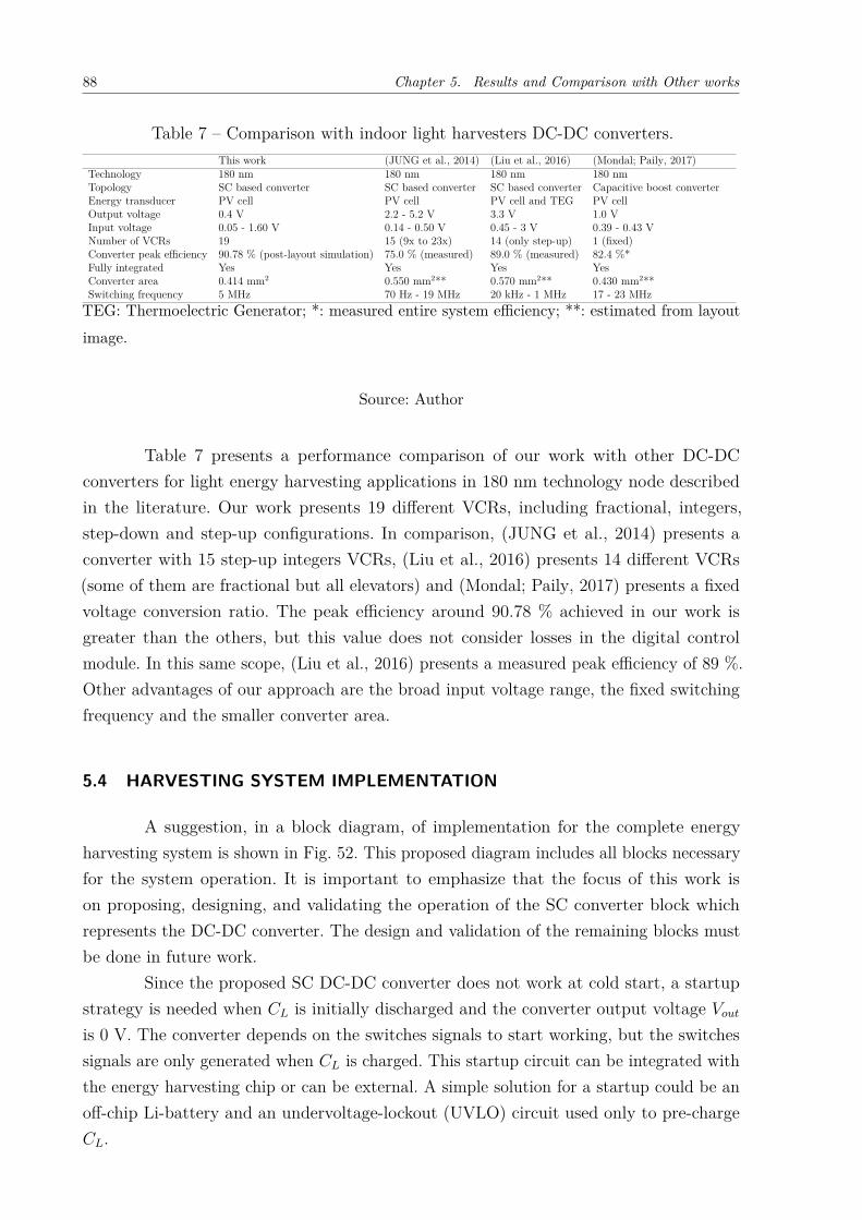
88 Chapter 5. Results and Comparison with Other works
Table 7 – Comparison with indoor light harvesters DC-DC converters.This work (JUNG et al., 2014) (Liu et al., 2016) (Mondal; Paily, 2017)
Technology 180 nm 180 nm 180 nm 180 nmTopology SC based converter SC based converter SC based converter Capacitive boost converterEnergy transducer PV cell PV cell PV cell and TEG PV cellOutput voltage 0.4 V 2.2 - 5.2 V 3.3 V 1.0 VInput voltage 0.05 - 1.60 V 0.14 - 0.50 V 0.45 - 3 V 0.39 - 0.43 VNumber of VCRs 19 15 (9x to 23x) 14 (only step-up) 1 (fixed)Converter peak efficiency 90.78 % (post-layout simulation) 75.0 % (measured) 89.0 % (measured) 82.4 %*Fully integrated Yes Yes Yes YesConverter area 0.414 mm2 0.550 mm2** 0.570 mm2** 0.430 mm2**Switching frequency 5 MHz 70 Hz - 19 MHz 20 kHz - 1 MHz 17 - 23 MHzTEG: Thermoelectric Generator; *: measured entire system efficiency; **: estimated from layoutimage.
Source: Author
Table 7 presents a performance comparison of our work with other DC-DCconverters for light energy harvesting applications in 180 nm technology node describedin the literature. Our work presents 19 different VCRs, including fractional, integers,step-down and step-up configurations. In comparison, (JUNG et al., 2014) presents aconverter with 15 step-up integers VCRs, (Liu et al., 2016) presents 14 different VCRs(some of them are fractional but all elevators) and (Mondal; Paily, 2017) presents a fixedvoltage conversion ratio. The peak efficiency around 90.78 % achieved in our work isgreater than the others, but this value does not consider losses in the digital controlmodule. In this same scope, (Liu et al., 2016) presents a measured peak efficiency of 89 %.Other advantages of our approach are the broad input voltage range, the fixed switchingfrequency and the smaller converter area.
5.4 HARVESTING SYSTEM IMPLEMENTATION
A suggestion, in a block diagram, of implementation for the complete energyharvesting system is shown in Fig. 52. This proposed diagram includes all blocks necessaryfor the system operation. It is important to emphasize that the focus of this work ison proposing, designing, and validating the operation of the SC converter block whichrepresents the DC-DC converter. The design and validation of the remaining blocks mustbe done in future work.
Since the proposed SC DC-DC converter does not work at cold start, a startupstrategy is needed when CL is initially discharged and the converter output voltage Vout
is 0 V. The converter depends on the switches signals to start working, but the switchessignals are only generated when CL is charged. This startup circuit can be integrated withthe energy harvesting chip or can be external. A simple solution for a startup could be anoff-chip Li-battery and an undervoltage-lockout (UVLO) circuit used only to pre-chargeCL.

5.5. CONCLUSION 89
Figure 52 – Block diagram of the complete energy harvesting system.
42x42 mm
PV
Cell
SC
Converter
Clock Gen
Ring Osc 1
Cross
Coup
DoublerClock Gen
Ring Osc 2
5 bit
Up/Down
Counter
ROM
Look Up
Table
Com
p 1
Com
p 2
Startup
CircuitVin
0.1V Vin 0.8V
@ 470 lux
Vout
CL
0.4V
VDD1 VDD1
0.8V
VDD2
VDD2
clk2
Address
VDD2
. . .
Sw
itches
Sig
nals
clk1
XupXdown
VDD1
ϕa
ϕa
VD
D2
VD
D2
Cin
70
Source: Author
In steady-state, when CL is charged with 0.4 V (o near to it), this voltage is alsoused as VDD1 to supply the first clock generator. The clock generator could be a ringoscillator based implementation, for example. This block generates a φa pulsed signalwhich is also inverted (φa). Both signals are used with VDD1 in the cross-coupled doublercircuit to double VDD1. This new doubled voltage is the VDD2 used to supply the remainingblocks. One of them is the second clock generator that generates clk2 signal configuredwith the switching frequency to turn on and off the switches.
The cross-coupled doubler output voltage is used to supply the comparators, Comp1 and Comp 2, as well as their inputs. Each comparator generates a bit that indicateswhether the voltage is within the desired range or not. These bits are used in the digitalcontrol to maintain, increase, or decrease the DC-DC converter VCR. The blocks thatcompose the digital control, discussed in details in Chapter 3, are also supplied by VDD2.The 5-bit counter receives the comparators bits and clk1 which can be an external signalused to control the speed at which the counter executes each step. This counter sends a5 bit address that, together with VDD2, are the lookup table inputs. Finally, the lookuptable provides the switches signals for each converter VCR.
5.5 CONCLUSION
The results of the proposed DC-DC converter electrical schematic are presentedin this chapter. We considered two different designs for two different applications showinga good versatility of the proposed converter. Layout and post-layout simulations werealso addressed and indicating that the post-layout converter performance is close to itsschematic performance. The proposed DC-DC converter was compared with other state-

90 Chapter 5. Results and Comparison with Other works
of-the-art DC-DC converters and it can be identified that the converter proposed by thiswork is competitive and promising for integration. Finally, it was given a suggestion forthe complete energy harvesting system implementation, contemplating the interactionbetween all the blocks responsible for the functioning of the harvesting system.
91
6 CONCLUSIONS AND SUGGESTIONS FOR FUTURE WORKS6.1 CONCLUSIONS
Various topologies of DC-DC converters can be used in applications ranging fromgenerating variable voltage supply for system-on-a-chip to energy harvesting systems.Energy harvesting is a promissing alternative to harness energy from the environment byusing natural energy sources as solar, thermal, vibration, and ambient radio-frequency.Inductive and capacitive types of converters are widely used as the main topology. However,complete single-chip integration is easier to be reached using capacitive converters. Themajority of the conversion systems focused on energy harvesting, mainly for indoor lighting,presented at least one energy storage element, such as a rechargeable battery, in theirtopology structures. Since capacitive converters are limited in terms of adjustment of thevoltage conversion ratio, reconfigurable topologies must be explored in order to provide acapacitive based conversion system with different VCRs.
After the study and electrical characterization of the PV cells, it was noticed thatthe operation with lower voltages is advantageous to provide higher power. The maximumobtained power of a small PV cell operating indoor only with artificial light is limited tosome dozens of µW.
A novel topology of a reconfigurable DC-DC converter based on a switched-capacitor was proposed for indoor PV cell energy harvesters. The conversion system is fullyintegrated and digitally adjustable, capable of providing 19 different VCRs, including step-down, step-up, fractional and integers conversion ratios. It is based on four Divider/Doublermodules and one Adder/Subtractor module arranged to offer VCRs from 0.25 to 8.
It was demonstrated that using only basic switched-capacitor topologies it is possi-ble to obtain a conversion system capable of providing a range of various voltage conversionratios. Also, the proposed system can be easily expanded to get other combinations ofVCRs.
It was also proposed a systematic simulation-based method suitable to design theDC-DC converter including the sizing of internal flying capacitors, switches, and switchingfrequency. With this approach, it was not necessary to use complex models to design theswitched capacitor converter modules. The proposed method was also upgraded to includethe estimation of the converter output resistance. With these methods, it was possibleto obtain two different design versions of the DC-DC converter aimed at two distinctapplications.
Post-layout results demonstrate that it is possible to achieve a conversion efficiencyof 90.78% for an output voltage around 0.4 V. Our results have also shown to be promisingand competitive in terms of input voltage range and converter area in comparison toother works described in the literature. This DC-DC converter can be applied for anultra-low-voltage sensor node system.

92 Chapter 6. Conclusions and Suggestions for Future Works
6.2 FUTURE WORK
The following suggestions for continuing this work are proposed here:Improvement in the design of the digital control block in order to reduce its power
consumption. Also, a physical synthesis of this digital control is needed to integrate it onchip.
Design, implementation and testing of the cross-coupled doubler circuit which isresponsible for doubling the DC-DC converter output voltage to supply the control block.
Design and implementation of the clock generators, both for the cross-coupleddoubler circuit, and for turning on and off the converter switches.
Proposal, design and implementation of the comparators responsible for sensing ifthe converter output voltage is within, below or above the desired range.
Proposal of a start-up method responsible for charging the output load capacitor,or just generating initial sufficient energy capable of waking the system so that it canoperate on its own.
Complete integration of the entire energy harvesting system blocks in order tovalidate its functionality. For a second version of the energy harvesting system it could beemployed a maximum power point tracking circuit to perform the matching between thePV cell and the DC-DC converter, and with that, be able to extract the maximum PVcell power to improve the overall energy harvesting system efficiency.

Appendix


95
APPENDIX A – ELECTRICAL CHARACTERIZATION OF PHOTOVOLTAICCELLS
This appendix presents a practical and systematic method for photovoltaic cellelectrical characterization operating indoor. A characterization example of two low costphotovoltaic (PV) cells is performed, and consequently, curves that represent the electricalbehavior of the cells are obtained. Hence, an understanding about PV cells operationcapacity when just artificial lighting is employed. Also, some examples of scenarios onvariations in PV cells operation are given, as well as some hypothetical voltage conversionratios for each case.
A very simple way to characterize a photovoltaic cell is connecting it in parallelwith a variable resistor, as depicted in Fig. 53.
Figure 53 – Simple PV cell characterization circuit.
PV
Cell
+
-
+
-
PV
Cell
PV
Cell V
I
R
Source: Author
A voltmeter is necessary to measure the variable resistor voltage drop, and thismeasure represents the PV cell output voltage. In order to obtain the PV cell outputcurrent, an ammeter can be connected in series with the variable resistor. This way, varyingthe resistor, it is possible to measure directly the output voltage and current of the PVcell. This approach presents a problem, for indoor conditions, where the PV cell outputvalues are very low compared to the outdoor condition, the ammeter internal resistancecan affect the measurements.
One way to mitigate this problem is using an ohmmeter to measure the resistancethat is being varied whit the variable resistor. With the resistance value and the voltagedrop, the current can be simply calculated by Ohm’s law. There is also a problem with thisapproach, when the resistance is adjusted, the variable resistor must be disconnected fromthe circuit in order to measure its resistance using the ohmmeter and connected again. Itconsists in a laborious process and almost impossible to perform if several measurementsneed to be executed.
A more elaborated circuit can be used to solve all these problems, the circuitdepicted in Fig. 54 can be used to facilitate and expedite the PV cell characterizationprocess (APOSTOLOU; VERWAAL; REINDERS, 2014).

96 APPENDIX A. Electrica Characterization of Photovoltaic Cells
Figure 54 – PV cell characterization circuit.
+
C1
Source: Author
Fig. 55 presents the equivalent circuit when the switch SW1 is opened.
Figure 55 – PV cell equivalent characterization circuit for the capacitor charging phase.
+
C1
Source: Author
This circuit emulate the variable resistor by using the charging of a capacitorwhich in DC can vary from a short circuit to an open circuit, that is, RC1DC
=∞− 0 Ω.There is a resistor R1 in series with the capacitor C1, so the equivalent resistance variationwill range from ∞ to R1 Ω:
R = R1 + VC
IC
(A.1)
With the aid of an oscilloscope the curves of the voltages V1 and V2 can beobtained. The current IC and the voltage VC can be obtained by the following relations:
IC = V2
R1(A.2)
VC = V1 − V2 (A.3)
Using V1 and IC that represents the PV cell output voltage and current, re-spectively, the PV cell output power P can be calculated by simply multiplying V1 byIC .

97
The equivalent resistance variation can be obtained by substituting Eq. A.2 andA.3 in Eq. A.1:
R = R1 + V1 − V2V2R1
(A.4)
Rearranging the terms in order to simplify Eq. A.4, the following relation can beobtained:
R = R1 · V1
V2(A.5)
Relating the resistance variation and the PV cell output power in one graph, R xP , we can discover which value of resistance provide the maximum output power. Throughthe maximum power transfer theorem we can find the PV cell internal resistance R0 simplyby matching it with the resistance that provides the maximum output power: R0 = RP max.
As an experiment example, the PV cell characterization was performed at nightin the university research room which is illuminated by an arrangement of six luminariescontaining two 32 W tubular fluorescent lamps each.
The flat surface of the test bench where the tests were performed is about 1.7maway from the luminaries.
A capacitor of 69µ F was used for C1 and the series resistor R1 was 1 kΩ,this value was chosen so that the V 2 voltage drop could be easily identified by theoscilloscope resolution. The constant R1C1 must be adjusted depending on the PV cell tobe characterized and the illuminance level employed.
Two distinct PV cell were tested, a 42x42 mm and a 45x45 mm PV cell depictedin Fig. 56. As well their parallel and series combinations.
Figure 56 – Chosen PV cells for electrical characterization.
Source: Author
According to (CIE, 2002) the illuminance in offices must range from 200 to 750lux, depending on the task. For example, a minimum illuminance of 200 lux is required forarchives storage and a minimum illuminance of 750 lux is required for technical drawing.
Two illuminance levels were applied in the tests, an intensity of 470 lux obtainedat the test bench level and an intensity of 700 lux that was obtained approximating thePV cell to the luminaries.

98 APPENDIX A. Electrica Characterization of Photovoltaic Cells
The curves obtained with the PV cell characterization were IxP, VxI, RxP andVxP. The tests were performed with a single 42x42 mm PV cell, a single 45x45 mm PVcell, their parallel connection and series connection. So, there are 16 curves in total.
Figure 57 shows the IxP curves for the single 42x42 mm PV cell, single 45x45 mmPV cell, PV cells parallel connection and PV cells series connection. For Figs. 57(a) and57(d) there is a complete quadratic relation between current and power. While for Figs.58b and 57(c), power increases linearly with the current until it saturates and reaches amaximum value. Observing Fig. 57(a) it can be noted that the maximum obtained poweris around 23 µW and its correspondent current is about 47 µA for a 470 lux of illuminance,for 700 lux the maximum power is around 42 µW with 69 µA of current. In Fig. 57(b)the maximum power for 470 lux is around 33.5µ W with a current of 102µ A, and for700 lux is about 63.5µ W with a current of 160.1µ A. For both tested cells, the obtainedpower almost doubled with an increase of approximately 50% in the illuminance level. Asit can be noted in Fig. 57(c), with the PV cells parallel connection, the maximum obtainedpower increased to 50.5µ W with a current of 125µ A for 470 lux, and to 99 µW with acurrent of 225.5µ A for 700 lux. The series connection maximum obtained power is around54.5µ W with 47µ A of current for 470 lux, and 90µ W with 83µ A of current for 700 lux.
Figure 57 – IxP curve for: Single 42x42 mm PV cell (a), Single 45x45 mm PV cell (b), PVcells parallel connection (c), and PV cells series connection (d).
0 25 50 75 100
I [ A]
0
10
20
30
40
P [
W]
470lux
700lux
(a)
0 25 50 75 100 125 150 175
I [ A]
0
15
30
45
60
P [
W]
470lux
700lux
(b)
0 50 100 150 200
I [ A]
0
25
50
75
100
P [
W]
470lux
700lux
(c)
0 25 50 75 100 125
I [ A]
0
25
50
75
100
P [
W]
470lux
700lux
(d)
Source: Author
Figure 58 shows the VxI curves for the single 42x42 mm PV cell, single 45x45mm PV cell, PV cells parallel connection and PV cells series connection. It can be noted

99
in all curves that there is a linear relation between the voltages and currents of the testedPV cells. In Fig. 58(b), 58(c) this linear relationship is more accentuated.
Figure 58 – VxI curve for: Single 42x42 mm PV cell (a), Single 45x45 mm PV cell (b),PV cells parallel connection (c), and PV cells series connection (d).
0 0.2 0.4 0.6 0.8 1
V [V]
0
25
50
75
100
I [
A]
470lux
700lux
(a)
0.2 0.3 0.4 0.5 0.6 0.7
V [V]
0
50
100
150
200
I [
A]
470lux
700lux
(b)
0.3 0.4 0.5 0.6 0.7 0.8
V [V]
0
50
100
150
200
I [
A]
470lux
700lux
(c)
0 0.5 1 1.5
V [V]
0
25
50
75
100
125I
[A
]470lux
700lux
(d)
Source: Author
Figure 59 presents the RxP curves for the single 42x42 mm PV cell, single 45x45mm PV cell, PV cells parallel connection and PV cells series connection. As expected, thecurves show that the power starts at a lower value, increases with the resistance increasing,reaches a maximum value and then decreases. The PV cell internal resistance can beestimated through this maximum power point. Observing Fig. 59(a), for the single 42x42mm PV cell the maximum power in 470 lux is around 23µ W with the correspondentresistance about 10k Ω, in 700 lux is 42µ W with a 9.5k Ω correspondent resistance. Thesingle 45x45 mm PV cell maximum power in Fig. 59(b) is nearly 33.5µ W with a 2.8kΩ correspondent resistance for 470 lux, and for 700 lux, the maximum power is close to63.5µ W with a 2.5k Ω correspondent resistance. Analyzing Fig. 59(c) it can be noted thatfor the parallel connection of the PV cells the maximum power is near to 51µ W with thecorrespondent resistance around 2.7k Ω in 470 lux. For 700 lux illuminance level, RxPcurve did not behave in the same way as the others, the power increasing followed by adecreasing over resistance can not be observed in this curve. But the maximum power ofthe PV cells parallel connection was already presented, its value is around 99µ W and thecorrespondent resistance is close to 2k Ω. Regarding the PV cells series connection, it canbe noticed in Fig. 59(d) that the maximum power for 470 lux is nearly 47µ W with a 16k

100 APPENDIX A. Electrica Characterization of Photovoltaic Cells
Ω correspondent resistance, and for 700 lux the maximum power is close to 90µ W with acorrespondent resistance approximately of 14k Ω. The PV cells series connection presentsa equivalent resistance which differs from the sum of the PV cells single resistances. Lastly,it can be also observed that the resistance of the same cell may change slightly with theilluminance level variation.
Figure 59 – RxP curve for: Single 42x42 mm PV cell (a), Single 45x45 mm PV cell (b),PV cells parallel connection (c), and PV cells series connection (d).
0 20 40 60 80
R [k ]
5
15
25
35
45
P [
W]
470lux
700lux
(a)
0 10 20 30 40
R [k ]
0
15
30
45
60
P [
W]
470lux
700lux
(b)
0 10 20 30 40
R [k ]
0
25
50
75
100
P [
W]
470lux
700lux
(c)
0 25 50 75 100
R [k ]
0
25
50
75
100
P [
W]
470lux
700lux
(d)
Source: Author
Figure 60 presents the VxP curves for the single 42x42 mm PV cell, single 45x45mm PV cell, PV cells parallel connection and PV cells series connection. The curvespresent a quadratic relation between PV cells voltage and power, but in Fig. 60(c) thischaracteristic is not so visibly exposed. Observing Fig. 60(a), it can be noted that the42x42 mm PV cell voltage for the maximum power is around 0.59 V in 470 lux and closeto 0.6 V in 700 lux. For the 45x45 mm PV cell the correspondent voltage for the maximumpower is nearly 0.33 V in 470 lux and about 0.39 V in 700 lux. The correspondent voltagefor the PV cells parallel connection maximum power is approximately 0.37 V in 470 luxand almost 0.45 V in 700 lux. Regarding the PV cell series connection, the correspondentvoltage for the maximum power is near to 0.93 V and around 1 V in 470 lux and 700 lux,respectively. It is interesting to note that, disregarding the configuration in series, all theother cases presented a maximum obtained power with correspondent voltages until 0.6 V,and low voltage applications may benefit greatly from this characteristic.
The PV cells characterization also showed that the maximum extracted power can

101
Figure 60 – VxP curve for: Single 42x42 mm PV cell (a), Single 45x45 mm PV cell (b),PV cells parallel connection (c), and PV cells series connection (d).
0 0.2 0.4 0.6 0.8 1
V [V]
5
15
25
35
45
P [
W]
470lux
700lux
(a)
0.2 0.4 0.6 0.8
V [V]
0
20
40
60
80
P [
W]
470lux
700lux
(b)
0.2 0.4 0.6 0.8
V [V]
0
25
50
75
100
P [
W]
470lux
700lux
(c)
0 0.25 0.5 0.75 1 1.25 1.5
V [V]
0
25
50
75
100
P [
W]
470lux
700lux
(d)
Source: Author
be increasing by connecting the PV cells in parallel or in series. If more current is needed,so a series connection is more appropriate. On the other hand, a parallel connection ismore adequate for providing a higher voltage.
Taking into account the maximum obtained power for the PV cells, their powerdensity can be estimated. For the 42x42 mm PV cell which has an area of 1764 mm2,power density is around 0.013µ W/mm2 in 470 lux, and approximately 0.024µ W/mm2 in700 lux of illuminance. For the 45x45 mm PV cell which has an area of 2025 mm2, powerdensity is about 0.016µ W/mm2 in 470 lux, and close to 0.031µ W/mm2 in 700 lux ofilluminance.
Considering an application where the PV cell will provide the power and also itsvoltage will be converted by an DC-DC converter, for example, some DC-DC converterinput voltages can be estimated with this characterization. Considering, as example, a42x42 mm PV cell minimum output power of 20µ W in 470 lux, the PV cell output voltageranges from 0.35 to 0.63 V. In 700 lux, PV cell output voltage ranges from 0.47 to 0.65 Vfor a minimum output power of 40µ W. Taking into account a 45x45mm PV cell minimumoutput power of 30µ W in 470 lux, the PV cell output voltage ranges from 0.24 to 0.41 V.In 700lux, PV cell output voltage ranges from 0.34 to 0.47 V for a minimum output powerof 60µ W.
If the mentioned application, for example, requires a DC-DC converter output

102 APPENDIX A. Electrica Characterization of Photovoltaic Cells
voltage from 0.4 to 0.5 V, some voltage conversion ratios were estimated as well, and Table8 presents them.
Table 8 – Estimated voltage conversion ratios.
PV cell DC-DC converter output voltage Voltage conversion ratio
42x42mm 0.4V 0.64 to 1.14 @470 lux0.61 to 0.85 @700 lux
0.5V 0.8 to 1.42 @470 lux0.77 to 1.06 @700 lux
45x45mm 0.4 V 0.97 to 1.66 @470 lux0.85 to 1.17 @700 lux
0.5V 1.22 to 2.08 @470 lux1.06 to 1.47 @700 lux
Source: Author

103
BIBLIOGRAPHYABDELFATTAH, M. et al. A fully-integrated switched capacitor voltage regulatorfor near-threshold applications. In: IEEE. Circuits and Systems (ISCAS), 2015 IEEEInternational Symposium on. [S.l.], 2015. p. 201–204. Cited on page 27.
APOSTOLOU, G.; VERWAAL, M.; REINDERS, A. Estimating the performance ofproduct integrated photovoltaic (pipv) cells under indoor conditions for the support ofdesign processes. In: IEEE. Photovoltaic Specialist Conference (PVSC), 2014 IEEE 40th.[S.l.], 2014. p. 0742–0747. Cited on page 95.
BANG, S.; BLAAUW, D.; SYLVESTER, D. A successive-approximation switched-capacitor dc-dc converter with resolution of vin/2N for a wide range of input and outputvoltages. IEEE Journal of Solid-State Circuits, v. 51, n. 2, p. 543–556, Feb 2016. ISSN0018-9200. Cited 2 times on pages 28 and 29.
Bose, S.; Anand, T.; Johnston, M. L. Integrated cold start of a boost converter at 57 mvusing cross-coupled complementary charge pumps and ultra-low-voltage ring oscillator.IEEE Journal of Solid-State Circuits, v. 54, n. 10, p. 2867–2878, Oct 2019. Cited on page87.
BREUSSEGEM, T. V.; STEYAERT, M. Cmos integrated capacitive dc-dc converters.[S.l.]: Springer Science & Business Media, 2012. Cited 8 times on pages 31, 33, 34, 36, 59,64, 65, and 66.
Cao, P. et al. 27.1 an 84hybrid converter with mppt and on-chip cold starter forthermoelectric energy harvesting. In: 2019 IEEE International Solid- State CircuitsConference - (ISSCC). [S.l.: s.n.], 2019. p. 420–422. Cited on page 87.
CHEN, M. et al. A batteryless single-inductor boost converter with 190 mv self-startupvoltage for thermal energy harvesting over a wide temperature range. IEEE Transactionson Circuits and Systems II: Express Briefs, p. 1–1, 2018. ISSN 1549-7747. Cited on page28.
Chen, Z. et al. 27.3 a piezoelectric energy-harvesting interface using split-phaseflipping-capacitor rectifier and capacitor reuse multiple-vcr sc dc-dc achieving 9.3×energy-extraction improvement. In: 2019 IEEE International Solid- State CircuitsConference - (ISSCC). [S.l.: s.n.], 2019. p. 424–426. Cited on page 87.
CHEN, Z. et al. A single-chip solar energy harvesting ic using integrated photodiodes forbiomedical implant applications. IEEE transactions on biomedical circuits and systems,IEEE, v. 11, n. 1, p. 44–53, 2017. Cited on page 28.
CHOWDARY, G.; SINGH, A.; CHATTERJEE, S. An 18 na, 87% efficient solar, vibrationand rf energy-harvesting power management system with a single shared inductor. IEEEJournal of Solid-State Circuits, IEEE, v. 51, n. 10, p. 2501–2513, 2016. Cited on page 28.
CIE, I. 8995, cie s 008/e, lighting for indoor work places. International Standard, 2002.Cited 2 times on pages 25 and 97.
Compassi-Severo, L.; Van Noije, W. A 0.4-v 10.9- µ w/pole third-order complex bpf forlow energy rf receivers. IEEE Transactions on Circuits and Systems I: Regular Papers,v. 66, n. 6, p. 2017–2026, June 2019. Cited on page 23.

104 Bibliography
DEMIR, S. M.; AL-TURJMAN, F.; MUHTAROĞLU, A. Energy scavenging methods forwban applications: a review. IEEE Sensors Journal, IEEE, v. 18, n. 16, p. 6477–6488,2018. Cited on page 21.
DINI, M. et al. A nanocurrent power management ic for multiple heterogeneous energyharvesting sources. IEEE Transactions on Power Electronics, IEEE, v. 30, n. 10, p.5665–5680, 2015. Cited on page 28.
GHIASI, R. R. et al. A 2: 1 switched-capacitor dc–dc converter for low power circuits.Analog Integrated Circuits and Signal Processing, Springer, v. 84, n. 2, p. 215–222, 2015.Cited on page 27.
GOEPPERT, J.; MANOLI, Y. Fully integrated startup at 70 mv of boost converters forthermoelectric energy harvesting. IEEE Journal of Solid-State Circuits, IEEE, v. 51, n. 7,p. 1716–1726, 2016. Cited on page 27.
HARB, A. Energy harvesting: State-of-the-art. Renewable Energy, Elsevier, v. 36, n. 10, p.2641–2654, 2011. Cited on page 22.
JIANG, Y. et al. Algorithmic voltage-feed-in topology for fully integrated fine-grainedrational buck–boost switched-capacitor dc-dc converters. IEEE Journal of Solid-StateCircuits, IEEE, v. 53, n. 12, p. 3455–3469, 2018. Cited 2 times on pages 29 and 30.
JUNG, W. et al. An ultra-low power fully integrated energy harvester based onself-oscillating switched-capacitor voltage doubler. IEEE Journal of Solid-State Circuits,IEEE, v. 49, n. 12, p. 2800–2811, 2014. Cited 4 times on pages 21, 29, 30, and 88.
KIM, J.-S. et al. High-efficiency peak-current-control non-inverting buck–boost converterusing mode selection for single ni–mh cell battery operation. Analog Integrated Circuitsand Signal Processing, Springer, v. 89, n. 2, p. 297–306, 2016. Cited on page 27.
Liu, X. et al. A highly efficient reconfigurable charge pump energy harvester with wideharvesting range and two-dimensional mppt for internet of things. IEEE Journal ofSolid-State Circuits, v. 51, n. 5, p. 1302–1312, May 2016. ISSN 1558-173X. Cited 3 timeson pages 29, 30, and 88.
MAKOWSKI, M. S.; MAKSIMOVIC, D. Performance limits of switched-capacitor dc-dcconverters. In: Proceedings of PESC ’95 - Power Electronics Specialist Conference. [S.l.:s.n.], 1995. v. 2, p. 1215–1221 vol.2. Cited 2 times on pages 32 and 33.
MANOHAR, S. K.; BALSARA, P. T. High efficiency dcm buck converter with dynamiclogic based adaptive switch-time control. Analog Integrated Circuits and Signal Processing,Springer, v. 84, n. 3, p. 455–469, 2015. Cited on page 27.
MENG, X. et al. An indoor solar energy harvesting system using dual mode sido converterwith fully digital time-based mppt. In: IEEE. Circuits and Systems (ISCAS), 2016 IEEEInternational Symposium on. [S.l.], 2016. p. 2354–2357. Cited 2 times on pages 23 and 28.
MERCER, D. Global Connected and IoT Device Forecast Update. [S.l.], 2019. Cited onpage 21.
MICROCHIP Developer Help. 2020. Available at: <https://microchipdeveloper.com/wireless:ble-link-layer-packet-types>. Cited 2 times on pages 82 and 83.

Bibliography 105
MIGUEZ, M. R. et al. Step down dc/dc converter for micro-power medical applications.Analog Integrated Circuits and Signal Processing, Springer, v. 89, n. 3, p. 531–539, 2016.Cited on page 27.
MONDAL, S.; PAILY, R. An efficient on-chip switched-capacitor-based power converterfor a microscale energy transducer. IEEE Transactions on Circuits and Systems II:Express Briefs, IEEE, v. 63, n. 3, p. 254–258, 2016. Cited on page 28.
Mondal, S.; Paily, R. Efficient solar power management system for self-powered iot node.IEEE Transactions on Circuits and Systems I: Regular Papers, v. 64, n. 9, p. 2359–2369,2017. Cited 3 times on pages 28, 30, and 88.
NAIDU, K. J.; KITTUR, H. M. A 90% efficiency, 250 mhz on-chip adaptive switchedcapacitor based dc–dc converter. Analog Integrated Circuits and Signal Processing,Springer, v. 89, n. 2, p. 451–460, 2016. Cited on page 27.
NASIRI, A.; ZABALAWI, S. A.; MANDIC, G. Indoor power harvesting using photovoltaiccells for low-power applications. IEEE Transactions on Industrial Electronics, IEEE, v. 56,n. 11, p. 4502–4509, 2009. Cited 2 times on pages 28 and 29.
PETERS, J. F. et al. The environmental impact of li-ion batteries and the role of keyparameters–a review. Renewable and Sustainable Energy Reviews, Elsevier, v. 67, p.491–506, 2017. Cited on page 21.
RANDALL, J. Designing indoor solar products: photovoltaic technologies for AES. [S.l.]:John Wiley & Sons, 2006. Cited on page 21.
SANDERS, S. R. et al. The road to fully integrated dc–dc conversion via theswitched-capacitor approach. IEEE Transactions on Power Electronics, IEEE, v. 28, n. 9,p. 4146–4155, 2013. Cited on page 24.
SOUVIGNET, T.; ALLARD, B.; TROCHUT, S. A fully integrated switched-capacitorregulator with frequency modulation control in 28-nm fdsoi. IEEE Transactions on PowerElectronics, IEEE, v. 31, n. 7, p. 4984–4994, 2016. Cited on page 27.
STEYAERT, M. et al. Dc-dc converters: From discrete towards fully integrated cmos.In: IEEE. Solid-State Device Research Conference (ESSDERC), 2011 Proceedings of theEuropean. [S.l.], 2011. p. 59–66. Cited on page 24.
TianRui Ying; Wing-Hung Ki; Mansun Chan. Area-efficient cmos charge pumps for lcddrivers. IEEE Journal of Solid-State Circuits, v. 38, n. 10, p. 1721–1725, 2003. Cited onpage 62.
TSAI, D.-L.; WU, H.-H.; WEI, C.-L. A low-power-consumption boost converter withmaximum power tracking algorithm for indoor photovoltaic energy harvesting. In: IEEE.Wireless Power Transfer Conference (WPTC), 2017 IEEE. [S.l.], 2017. p. 1–3. Cited onpage 28.
TURNQUIST, M. J. et al. A fully integrated self-oscillating switched-capacitor dc-dcconverter for near-threshold loads. In: IEEE. Solid-State Circuits Conference (A-SSCC),2015 IEEE Asian. [S.l.], 2015. p. 1–4. Cited on page 27.

106 Bibliography
VULLERS, R. J. et al. Energy harvesting for autonomous wireless sensor networks. IEEESolid-State Circuits Magazine, IEEE, v. 2, n. 2, p. 29–38, 2010. Cited 2 times on pages 21and 22.
WENS, M.; STEYAERT, M. Design and implementation of fully-integrated inductiveDC-DC converters in standard CMOS. [S.l.]: Springer Science & Business Media, 2011.Cited on page 24.
Wens, M.; Steyaert, M. S. J. A fully integrated cmos 800-mw four-phase semiconstanton/off-time step-down converter. IEEE Transactions on Power Electronics, v. 26, n. 2, p.326–333, 2011. Cited on page 64.
WU, X. et al. A 20-pw discontinuous switched-capacitor energy harvester for smart sensorapplications. IEEE Journal of Solid-State Circuits, IEEE, v. 52, n. 4, p. 972–984, 2017.Cited 2 times on pages 28 and 29.
YU, H. et al. A batteryless and single-inductor dc-dc boost converter for thermoelectricenergy harvesting application with 190mv cold-start voltage. In: 2018 IEEE InternationalSymposium on Circuits and Systems (ISCAS). [S.l.: s.n.], 2018. p. 1–4. ISSN 2379-447X.Cited 2 times on pages 21 and 87.
Yu, W. et al. 24.4 a 0.18v 382µw bluetooth low-energy (ble) receiver with 1.33nw sleeppower for energy-harvesting applications in 28nm cmos. In: 2017 IEEE InternationalSolid-State Circuits Conference (ISSCC). [S.l.: s.n.], 2017. p. 414–415. Cited on page 23.