instruction manual - cal.equipment tracker
TRANSCRIPT

2235OSCILLOSCOPE
SERVICE
INSTRUCTION MANUAL

WARN ING
7eIctroηά
THE FOLLOWIN G SERV ICI NG I NSTRUCTIONSARE FOR US E BY QUALI F I ED PERSONNEL ONLY .TO AVOID PERSONAL INJUR Y, DO NOT PER-FORM ANY SERV ICI NG OTHER THAN THAT CON-TAI NED IN OPERATI NG I N STRUCTIONS UNLESSYOU ARE QUA LI F I ED TO DO SO . REFER TO OP-ERATORS SAFETY SUMMARY A ND SERVICESAFETY SUMMARY PR IO R TO PERFORM I NGANY SERV IC E.
Tektron ixNational Marketing Cen terfor Product Order Information, call
1-800-426-2200 ext 41In Oregon call collect (503)627-9000 ext 41Tektronix National Mark eting Cente rP.O. Box 500 D/S Υ6-088, Beaverton, OR 97077
PLEASE CHECK FOR CHANGE INFORMATIONAT THE REAR O F TH IS MANUAL.
2235OSCILLOSCOPE
SERVICE
I NSTRUCTION MANUA LTektronix, Inc .Ρ .Ο . Box 500Beaverton, Oregon
97077
Serial Number
COMMITTEDTO EXCELLENCE
070-4206-00
First Printing DEC 1982Product Group 46
Revised MAY 1983

Copyrig h t ύ 1982 Tektronix, Inc . All rig hts reserved .Contents of this publication may not be reproduced in anyform without the written permission of Tektronix, Inc .
Products of Tektronix, I nc . and its subsidiaries are coveredby U .S . and foreign patents and/or pending patents .
TEKTRON IX, ΤΕΚ , SCOPE-MOBILE, and Ta areregistered t rademarks of Tekt ronix, I nc . TELEQU I PMENTis α registered trademark of Tektronix U .K . Limited .
Printed in U .S.A . Specification and price change privilegesare reserved .
INSTRUMENT SER IAL NUMBERS
Each i nstrument has α ser ial number on α panel i nsert, tag,or stamped on the chassis . The fi r st nu mber or letterdesignates the country of manufacture . The last five digitsof the serial number are assigned sequentially and areun ique to each instrument . Those manufactured in theUnited States have six un ique digits . The country ofmanufacture is identified as follows :
ΒΟΟΟΟΟΟ
Tektronix, I nc ., Beaverton , Oregon , USA100000
Tektronix G uernsey, Ltd ., Channel islands200000
Tektronix United K ingdom, Ltd ., London300000
Sony/Tektronix, Japan700000
Tektronix Holland , NV, Heerenveen ,The Netherlands

TABLE OF CONTENTS
2235 Service
LIST OF ILLUSTRATIONS
. . . . . . . . . . . . . . . . . . . .
iii
SECTION 3
THEORY OF OPERATIONLIST OF TABLES
. . . . . . . . . . . . . . . . . . . . . . . . . . .
iii
INTRODUCTION . . . . . . . .. . . . . . . .
3-1OPERATORS SAFETY SUMMARY
. . . . . . . . . . . . .
ί ν
GENERAL DESCRIPTION
. . . . . . . .
3-2SERVICING SAFETY SUMMARY . . . . . . . . . . . . . . .
ν
DETAILED CIRCUIT DESCRIPTION
3-3VERTICAL ATTENUATORS . . . . .
3-3SECTION 1
SPECIFICATION
Input Coupling . . . . . . . . . . . . .
3-3INTRODUCTION . . . . . . . . . . . . . . . .
1-1
Buffer Amplifier and GainACCESSORIES . . . . . . . . . . . . . . . . . 1-1
Switching Network . . . . . . . . . . 3-4PERFORMANCE CONDITIONS . . . .
1-1
Paraphase Amplifier . . . . . . . . .
3-4VERTICAL PREAMPLIFIERS
. . . 3-5SECTION 2
OPERATING INSTRUCTIONS
CHANNEL SWITCH ANDPREPARATION FOR USE
. . . . . . . .
2-1
VERTICAL OUTPUT
. . . . . . . . . .
3-5SAFETY . . . . . . . . . . . . . . . . . . . . 2-1
Delay Line Driver . . . . . . . . . . . 3-6LINE VOLTAGE
. . . . . . . . . . . . . .
2-1
Vertical Output Amplifier . . . . .
3-6POWER CORD . . . . . . . . . . . . . . . 2-1
Α/Β Sweep Separation Circuit . 3-7LINE FUSE . . . . . . . . . . . . . . . . . .
2-1
TRIGGER AMPLIFIERS ANDINSTRUMENT COOLING . . . . . . .
2-2
SWITCHING . . . . . . . . . . . . . . . . .
3-7CONTROLS,
CONNECTORS,
AND
Internal Trigger . . . . . . . . . . . . .
3-7INDICATORS . . . . . . . . . . . . . . . . . . .
2-2
Internal Trigger Amplifier
. . . . .
3-8POWER, DISPLAY, AND PROBE
Α External Trigger Amplifier . . .
3-8ADJUST
. . . . . . . . . . . . . . . . . . . .
2-2
Line Trigger Amplifier . . . . . . . .
3-8VERTICAL
. . . . . . . . . . . . . . . . . .
2-3
Α TRIGGER GENERATOR . . . . . .
3-9HORIZONTAL . . . . . . . . . . . . . . . .
2-4
Α Trigger Level Circuit . . . . . . .
3-9TRIGGER
. . . . . . . . . . . . . . . . . . .
2-6
Α Trigger Level Comparator
. .
3-9REAR PANEL . . . . . . . . . . . . . . . .
2-7
Α Schmitt Trigger and TVOPERATING CONSIDERATIONS . . .
2-8
Trigger Circuit
. . . . . . . . . . . . .
3-9GRATICULE . . . . . . . . . . . . . . . . .
2-8
Α SWEEP GENERATOR ANDGROUNDING . . . . . . . . . . . . . . . . 2-8
LOGIC . . . . . . . . . . . . . . . . . . . . . . 3-9SIGNAL CONNECTIONS . . . . . . .
2-8
Α M iller Sweep Generator . . . .
3-10INPUT COUPLING CAPACITOR
Α Sweep Logic
. . . . . . . . . . . .
3-11PRECHARGING . . . . . . . . . . . . . . 2-8
ALTERNATE Β SWEEP . . . . . . . . 3-11OPERATOR'S ADJUSTMENTS . . . .
2-9
Β M iller Sweep Generator . . . .
3-12INTRODUCTION
. . . . . . . . . . . . .
2-9
Β Trigger Level Comparator
. .
3-12TRACE ROTATION . . . . . . . . . . . .
2-9
Runs After Delay . . . . . . . . . . .
3-12PROBE COMPENSATION . . . . . .
2-9
Β Delay Time PositionOSCILLOSCOPE DISPLAYS . . . . . . 2-10
Comparator . . . . . . . . . . . . . . . 3-12INTRODUCTION
. . . . . . . . . . . . . 2-10
Β Sweep Logic
. . . . . . . . . . . . 3-12BASELINE TRACE . . . . . . . . . . . .
2-10
Alternate Display SwitchingSIGNAL DISPLAY
. . . . . . . . . . . . 2-11
Logic
. . . . . . . . . . . . . . . . . . . . 3-13MAGNIFIED-SWEEP DISPLAY
. .
2-11
Β Ζ-Axis Logic . . . . . . . . . . . . .
3-13DELAYED-SWEEP DISPLAY . . . . 2-11
HORIZONTAL . . . . . . . . . . . . . . . . 3-13DELAYED-SWEEP
Horizontal Preamplifier . . . . . . . 3-14MEASUREMENTS . . . . . . . . . . . .
2-11
Χ-Υ Amplifier
. . . . . . . . . . . . . .
3-14SINGLE-SWEEP DISPLAY . . . . . .
2-12
Horizontal Output Amplifier . . .
3-15Χ-Υ DISPLAY . . . . . . . . . . . . . . . . 2-12
Z-AXIS AMPLIFIER . . . . . . . . . . . 3-15TV SIGNAL DISPLAYS
. . . . . . . . 2-12
Dc Restorer . . . . . . . . . . . . . . . 3-16

2235 Service
Page
PageSECTION 3
THEORY OF OPERATION (cont)
SECTION 6
MAINTENANCE (cont)POWER SUPPLY AND PROBE
I NTRODUCTION
. . . . . . . . . . . . .
6-2ADJUST . . . . . . . . . . . . . . . . . . . .
3-17
GENERAL CARE . . . . . . . . . . . . .
6-2Power Input . . . . . . . . . . . . . . . 3-17
INSPECTION AND CLEANING
. .
6-2Preregulator . . . . . . . . . . . . . . . 3-17
LUBRICATION . . . . . . . . . . . . . . . 6-4Inverter . . . . . . . . . . . . . . . . . . . 3-18
SEMICONDUCTOR CHECKS . . . 6-4Crt Supply . . . . . . . . . . . . . . . . 3-18
PERIODIC READJUSTMENT
. . . 6-4Focus Circuit . . . . . . . . . . . . . .
3-18
TROUBLESHOOTING . . . . . . . . . . . .
6-5Low-Voltage Supplies
. . . . . . .
3-19
INTRODUCTION
. . . . . . . . . . . . .
6-5Probe Adjust
. . . . . . . . . . . . . .
3-19
TROUBLESHOOTING AIDS
. . . .
6-5TROUBLESHOOTINGEQUIPMENT . . . . . . . . . . . . . . . . 6-6
SECTION 4
PERFORMANCE CHECK
TROUBLESHOOTINGPROCEDURE
TECHNIQUES . . . . . . . . . . . . . . . 6-6INTRODUCTION . . . . . . . . . . . . . . . . 4-1
CORRECTIVE MAINTENANCE . . . . 6-10PURPOSE . . . . . . . . . . . . . . . . . . 4-1
INTRODUCTION . . . . . . . . . . . . . 6-10STRUCTURE . . . . . . . . . . . . . . . . 4-1
MAINTENANCE PRECAUTIONS .
6-10TEST EQUIPMENT . . . . . . . . . . . 4-1
OBTAINING REPLACEMENTLIMITS AND TOLERANCES . . . .
4-1
PARTS
. . . . . . . . . . . . . . . . . . . . .
6-10PREPARATION FOR CHECKS
. .
4-2
MAINTENANCE AIDS
. . . . . . . . .
6-10INTRODUCTION Τ0
I NTERCONNECTIONS . . . . . . . . . 6-10PERFORMANCE CHECK STEPS
4-3
TRANSISTORS ANDVERTICAL
. . . . . . . . . . . . . . . . . .
4-4
INTEGRATED CIRCUITS . . . . . . .
6-11HORIZONTAL . . . . . . . . . . . . . . . .
4-8
SOLDERING TECHNIQUES
. . . .
6-12TRIGGER
. . . . . . . . . . . . . . . . . . .
4-12
REMOVAL AND REPLACEMENTEXTERNAL Z-AXIS AND PROBE
I NSTRUCTIONS . . . . . . . . . . . . . .
6-13ADJUST . . . . . . . . . . . . . . . . . . . . 4-15
Cabinet . . . . . . . . . . . . . . . . . . . 6-13Cathode-Ray Tube . . . . . . . . . .
6-13SECTION 5
ADJUSTMENT PROCEDURE
Power-Supply Shield . . . . . . . .
6-14INTRODUCTION . . . . . . . . . . . . . . . .
5-1
Filter Circuit Board . . . . . . . . . .
6-14PURPOSE
. . . . . . . . . . . . . . . . . .
5-1
Alt Sweep Circuit Board
. . . . .
6-15STRUCTURE
. . . . . . . . . . . . . . . .
5-1
Attenuator Circuit Board
. . . . .
6-15TEST EQUIPMENT . . . . . . . . . . . 5-1
Timing Circuit Board . . . . . . . . 6-16LIMITS AND TOLERANCES
. . . .
5-1
Bottom Shield, Attenuator andADJUSTMENT INTERACTION
. .
5-1
Timing Circuit-Board Module . .
6-17PREPARATION FOR
Front-Panel Circuit Board
. . . .
6-17ADJUSTMENT . . . . . . . . . . . . . . . 5-1
Main Circuit Board . . . . . . . . . . 6-18INDEX TO ADJUSTMENT
REPACKAGING FOR SHIPMENT
6-20PROCEDURE STEPS
. . . . . . . . .
5-3
SELECTABLE COMPONENTS
. .
6-20POWER SUPPLY AND CRT DISPLAY 5-4VERTICAL . . . . . . . . . . . . . . . . . . . . .
5-6
SECTION 7
OPTIONSHORIZONTAL . . . . . . . . . . . . . . . . . . 5-14TRIGGER
. . . . . . . . . . . . . . . . . . . . .
5-20
SECTION 8
REPLACEABLE ELECTRICAL PARTSEXTERNAL Z-AXIS AND PROBE
SECTION 9
DIAGRAMSADJUST . . . . . . . . . . . . . . . . . . . . . . 5-24SECTION 10 REPLACEABLE MECHANICAL PARTS
SECTION 6
MAINTENANCE
AccessoriesSTATIC-SENSITIVE COMPONENTS
6-1PREVENTIVE MAINTENANCE . . . . . 6-2
CHANGE INFORMATION
ιι
TABLE OF CONTENTS (cont)

LIST OF ILLUSTRATIONSFigure
Page Figure
Page
The 2235 Oscillosco pe . . . . . . . . . . . . . . . .
vi
2-7
Rear-panel connector . . . . . . . . . . . . . . . . .
2-71-1
Maximum
input
voltage
vs.
frequency
2-8
Graticule measurement markings . . . . . . . .
2-8derating curve for CH 1 OR Χ, CH 2 OR Υ ,
2-9
Probe compensation . . . . . . . . . . . . . . . . . .
2-10and ΕΧ7 INPUT connectors . . . . . . . . . . . .
1-7
3-1
Block diagram of the Vertical Attenuators .
3-42-1
Voltage, power cord, and fuse data . . . . . .
2-1
3-2
Block diagram of the Channel Switching2-2
Fuse h older and power cord connector . . .
2-2
circuitry . . . . . . . . . . . . . . . . . . . . . . . . . . . .
3-62-3
Power, display, and probe adjust controls
3-3
Block diagram of the Α Sweep Generatorconnector and indicator . . . . . . . . . . . . . . . .
2-3
and Logic Circuitry
. . . . . . . . . . . . . . . . . . .
3-102-4
Vertical controls and connectors . . . . . . . . .
2-4
3-4
Block diagram of the Horizontal Amplifier
.
3-142-5
Horizontal controls
. . . . . . . . . . . . . . . . . . .
2-5
3-5
Simp lified diagram of the Dc Restorer2-6
Trigger controls, connector, and indicator
.
2-6
circuitry
. . . . . . . . . . . . . . . . . . . . . . . . . . . .
3-166-1
Multi-connector holder orientation
. . . . . . .
6-6
LIST OF TABLES
2235 Service
Table
Page Table
Page
1-1
Electrical Characte ristics . . . . . . . . . . . . . . .
1-2
5-4
Attenuator Compensation Adjustments . . .
5-91-2
Environmental Characteristics . . . . . . . . . . .
1-8
5-5
Settings for Bandwidth Checks
. . . . . . . . .
5-121-3
Physical Characte ristics
. . . . . . . . . . . . . . .
1-9
5-6
Settings fo r Timing Accuracy Checks . . . . .
5-174-1
Test Equipment Required
. . . . . . . . . . . . . .
4-2
5-7
Settings for Delay Time Accuracy Checks .
5-184-2
Deflection Accuracy Limits . . . . . . . . . . . . .
4-4
5-8
Switch Combinations for Α Triggering4-3
Settings for Bandwidth Checks
. . . . . . . . .
4-6
Checks . . . . . . . . . . . . . . . . . . . . . . . . . . . . .
5-214-4
Settings for Timing Accuracy Checks . . . . .
4-9
6-1
Relative Susceptibility to Static-Discharge4-5
Settings for Delay Time Accuracy Checks .
4-10
Damage . . . . . . . . . . . . . . . . . . . . . . . . . . . .
6-14-6
Switch Combinations for Α Trigge r ing
6-2
External Inspection Checklist . . . . . . . . . . .
6-3Checks . . . . . . . . . . . . . . . . . . . . . . . . . . . . . 4-12
6-3
Internal Inspection Checklist . . . . . . . . . . . . 6-35-1
Adjustment Interactions
. . . . . . . . . . . . . . .
5-2
6-4
Power Supply Limits and R ipple . . . . . . . . .
6-85-2
Power Supply Limits . . . . . . . . . . . . . . . . . .
5-4
6-5
M aintenance Aids . . . . . . . . . . . . . . . . . . . .
6-115-3
Deflection Accuracy Limits . . . . . . . . . . . . .
5-8
6-6
Trigger Bandwidth Alteration
. . . . . . . . . . .
6-20

2235 Service
Terms as Marked on Equ ipment
Symbols in This Manual
OPERATORS SAFETY SUMMARY
The general safety information in th is part of the summary is for both operating and servicing personnel. Specific warningsand cautions will be found throughout the manual where they apply and do not appear in th is summary.
Terms in Th is Manual
Grounding the ProductCAUTIONstatements
identify
cond itions or practices
This produ ct is grou nded through the grounding conductorthat coul d resu lt in damage to the equ ipment or otherof the power cord. To avoid electrical shock, pl ug theproperty .
power cord into α properly wi red recepta ble before con-necting to the product input or output terminals . Α
WARN ING statements identify conditions or practices
protective ground connection by way of the groundingthat could resu lt i n personal injury or loss of life .
conductor in the power cord is essential fo r safe operation .
CAUTION ind icates α personal injury hazard not imme-d iately accessi ble as one reads the mark ings, or α hazard toproperty, includ ing the equipment itself .
DANGER ind icates α personal injury hazard immediatelyaccessible as one reads the marking.
Th is symbol indicates wh ere applicablecautionary or other information is to befound. For maximum input voltage seeTable 1-1 .
Symbols as Marked on Equipment
114
DANGER - H igh voltage.
Ο
Protective ground (earth) terminal .
Danger Arising From Loss of GroundUpon loss of the protective-ground connection , all acces-sible conductive parts (incl ud ing knobs and controls th atmay appear to be insulating) can render an electric shock.
Use the Proper Power Cord
Use only the power cord and connector specifie d fo ryour p roduct .
Use only α power cord that is i n good conditio n.
For detailed information on power cords and connectorssee F ig ure 2-1 .
Use the Proper FuseTo avoid fire hazard , use only α fuse of the correct type,voltage rating and current rating as specified in the partslist for your p roduct.
ΑΤΤΕΝΤΙΟΝ - Refer to manual.To avoid explosion, do not operate this product in anexplosive atmosphere u nless it has been specifically cer-
Power Source
tified for such operation.
Do Not Operate in Explosive Atmospheres
Th is product is intended to operate from α power sourcethat does not apply more than 250 volts rms between th esupply conductors or between either supply conductor and
Do Not Remove Covers Or Panelsground . Α protective ground connection by way of the
To avoid personal i nj ury, do not remove the productgrou nding conductor in the power cord is essential for safe
covers or panels . Do not operate the p roduct with out theoperation.
covers and panels properly i nstalled.

SERVICING SAFETY SUMMARY
FOR QUALIFIED SERVICE PERSONNEL ONL YRefer also to thepreceding Operators Safety Summary.
Do Not Service Alone
Disconnect power before removing protective pan els, sol-
Do not perform internal se rvice or adjustment of th is prod-
dering, or replacing components .
uct unless another person capable of rendering first aid andresuscitation is presen t .
Power Source
2235 Service
Th is product is intended to operate from α power source
Use Ca reWhen Servicing W ith Power On
that does not apply more than 250 volts rms between thesupply conductors or between either supply conductor and
Dangerous voltages exist at seve ral points in th is product .
ground . Α protective ground connection by way of theTo avoid pe rson al injury, do not touch exposed connections
ground ing connecto r in the power cord is essential fo r safeor components wh ile power is on .
operation.

2235 Service
The 2235 Oscilloscope
ατο 6-ο 1

The instrument is shipped with the following standardaccessories :
SPECIFICATION
Section 1-2235 Service
I NTRODUCTION
PERFORMANCE CONDITIONS
The TEKTRONIX 2235 oscilloscope is α rugged , light-
The following electrical characteristics (Table 1-1) are ναΙ-weight, dual-channel, 100-MHz instrument that features α
id for the 2235 when it has been adjusted at an ambientb right, sharply defined trace on an 80- by 100-mm cathode-
temperature between +20°C and +30°C, has had α warm-ray tube (crt) . Its vertical system provides calibrated deflec-
up period of at least 20 minutes, and is operating at antion factors from 2 mV per division to 5 V per division .
ambient temperature between 0°C and +50°C (unless othTrigger circuits enable stable triggering over the full band-
erwise noted) .width of the vertical system . The horizontal system providescalibrated sweep speeds from 0.5 s perd ivision to 50 ns perdivision along with delayed-sweep features for accuraterelative-time measurements. Α Χ10 magnifie r extends the
Items listed in the "Performance Requirements" columnmaximum sweep speed to 5 ns per division .
are verifiable qualitative or quantitative limits, while itemslisted in the "Supplemental Information" column are eitherexplanatory notes, calibration setup descriptions, perfor
ACCESSORIES
mance characteristics for which no absolute limits are speci-fied, or characteristics that are impractical to check.
1 Operators Manual
2 Probe packages
Environmental characteristics are given in Table 1-2. The1 Service Manual
2235 meets the requirements of MIL-T-288000, paragraphs4.5.5.1 .3, 4.5 .5 .1 .4, and 4.5 .5 .1 .2 .2 for Type III, Class 5
For part numbers and further info rmation about both
equipment, except where otherwise noted.standard and optional accessories, refer to the "Optionsand Accessories" section (Section 5) of this manual . YourTektronix representative, local Tektronix Field Office, orTektronix product catalog can also provide accessories
Physical characteristics of the instrument are listed in Τα-information .
b le 1-3.

Specification-2235 Service
Deflection Factor
Range
Accuracy+15°C to +35°C0°C to +50°C
Step Response
Rise Time
Aberrations
Characteristics
2 mV per Division
2 mV per Division
Positive-Going Step2 mV per Division to 0.5 Vper Division1 V per Division to 5 V perDivision
Bandwidth (-3 dB)
0°C to +35°C5 mV per Division to 5 V perDivision2 mV per Division
+35°C to +50°C
5 mV per Division to 5 V perDivision .
2 mV per Division
AC Coupled Lower Limit
VERTICAL DEFLECTION SYSTEM
2 mV per division to 5 V per divisionin α 1-2-5 sequence
+2%.±3ο/ο . α
Range of VOLTS/DIV Variable Cont rol
Continuously variable betweensettings . Increases deflection factorby at least 2.5 to 1 .
0°C to +35°C5 mV per Division to 5 V per
3.5 ns or less .'Division
3.9 ns or less .a
+35°C to +50°C5 mV per Division to 5 V per
3.9 ns or less .'Division
4.4 ns or less .a
+4 ο/ο , -4%,4% ρ-ρ .
+12%, -12ο/ο , 12ο/ο ρ-ρ . α
Dc to at least 100 MHz.
Dc to at least 90 MHz.
Dc to at least 90 MHz.'
Dc to at least 80 MHz.'
10 Hz or less at -3 dB.a
'Perfo rmance Requi rement not checked in Service Manual .
Table 1-1Electrical Characteristics
Performance Requirements
Supplemental Information
5 mV per division to 5 V per divisiongain is adjusted with VOLTS/DIV switchset to 10 mV per division .2 mV per d ivision gain is adjustedwith VOLTS/DIV switch set to 2 mVper division
Rise time is calculated from the formula :
0.35Bandwidth (-3 dB)
Measured with 5-division referencesignal, centered vertically, from α50Ω source driving α 50 Ω coaxial cableterminated in 50 Ω at the input connectorwith the VOLTS/DIV Variable control inthe CAL detent.
Measu red with α vertically centered6-division reference signal from α 50 Ωsource driving α 50 Ω coaxial cablethat is terminated in 50 Ω , both atthe input connector and at the probeinput, with the VOLTS/DIV Variablecontrol in the CAL detent .

Bandwidth Limiter
Chop Mode Switching Rate
Input Characteristics
Resistance
Capacitance
DC Coupled
AC Coupled
Characteristics
Common-Mode Rejection Ratio(CMRR)
Input Current
Trace Shift with Attenuator Rotation
Trace Shift as VOLTS/DIVVariable Control is Rotated
Trace Shift with Invert
Channel Isolation
POSITION Control Range
Table 1-1 (cont)
Performance RequirementsS upplemental Information
VERTICAL DEFLECTION SYSTEM
Upper limits (-3 dB) bandpass at20 MHz ± 10%.
500 kHz ±30% . α
1 ΜΩ ±2%. α
20 pF ±2 ρF.α
Maximum Safe Input Voltage Α
~
See Figure 1-1 fo r derating curve.
400 V (dc + peak ac) Or 800 V ac ρ-ρto 10 kHz or less . α
400 V (dc + peak ac) Or 800 V ac ρ-ρto 10 kHz or less . α
At least 20 to 1 at 50 MHz.
1 .0 ηΑ Or less (0 .5 division trace shiftat 2 mV per division). α
0.75 division or less . α
1 .0 division or less . α
1 .5 division or less . α
8Performance Requ irement not checked in Service Manual.
Greater than 100 to 1 at 50 MHz.
At least ±11 d ivision from graticulecenter.
Specification-2235 Service
Checked at 10 mV per division forcommon-mode signals of 6 divisions orless with VOLTS/DIV Variable controladjusted for best CMRR at 50 kHz.
VOLTS/DIV Variable control in CALdetent.

Specification-2235 Service
Α TRIGGER Sensitivity
Ρ-Ρ AUTO and NORM/TV LINEModes
I nternalExternal
TV FIELD Mode
ΕΧΤ ΙΝΡUΤ
Input Resistance
Characteristics
Lowest Useable Frequency in Ρ-ΡAUTO Mode
Β TRIGGER Sensitivity (I nternal Only)
Maximum Input Voltage 2L
400V (dc + peak ac) or 800 V ac; ρ-ρat 10 kHz or less (see Fig ure 1-1) . α
Input CapacitanceAC Coupled
LEVEL Control Range
Α TRIGGER (NORM)
ΙΝΤ
ΕΧΤ , DC
ΕΧΤ, DC - 10
Β TRIGGER
Internal
VAR HOLDOFF Control
Trigger View System
Deflection Factor
Internal
Extern al
AC and DC
Accu racy
DC - 10
Delay Difference Between ΕΧΤINPUT and Either VerticalChannel
Performance Requ irements
Supplemental Info rmation
10 MHz
60 MHz
100 MHz
0.3 div
1.0 div
1.5 d iv35 mV
Ι
120 mV
200mV
20 Hz with 1 .0 division internalor 100 mV external .a
1 .0 division of composite sync.a
10 MHz L60 MHz _L100 MHz
0.3 div
1.0 d iv
1.5 div
1 ΜΩ ±2%. α
20 pF ±2.5 pF.a
°Performance Requirement not checked in Service Manual .
Table 1-1 (cont)
TRIGGER SYSTEM
10 Hz or less at lower -3 dB point .a
Can be set to any point of the tracethat can be d isplayed.a
At least
±1.6 V, 3.2 V ρ-p.
At least ±16 V, 32 V ρ-ρ.α
Can be set to any point of the tracethat can be displayed .α
Increases Α Sweep holdoff time by atleast α factor of 10 . α
Same as vertical .
100 mV per division.
1 V per division .
±20% .
Less than 2.0 ns.a
External trigger signal from α 50 Ωsource driving α 50 Ω coaxial cablete rminated in 50 Ω at the input connector.

Sweep Rate
Calibrated Range
Α Sweep
Accuracy
+15'C to +35°C
POSITION Control Range
Sweep Linearity
Variable Control Range
Sweep Length
Α/Β SWP SEP Range
Delay Time
Dial Control Range
J itter
Β Sweep
Characte ristics
0°C to +50°C
Differential Time MeasurementAccuracy
+15'C to +35'C
0°C to +50°C
HORIZONTAL DEFLECTION SYSTEM
0.5 s per division to 0.05 As perdivision in α 1-2-5 sequence. Χ10magnifier extends maximum sweepspeed to 5 ns per division.
50 ms per d ivision to 0.05 As perdivision in α 1-2-5 sequence .
X10magnifier extends maximum sweepspeed to 5 ns per division.
Unmagnified Magnified
Start of sweep to 10th division willposition past the center verticalgraticule li ne in Χ1 or 100th division inX1 0.
±5%.
'Performance Requirement not checked in Service Manual .
Table 1-1 (cont)
Performance Requ i rements
Supplemental Information
Continuously variable betweencali brated settings . Extends the Α andΒ sweep speeds by at least α factor of2.5 .
Greater than 10 division .
±3.5 d ivisions or greater.
Applies to 0.5 As per divisionand slower.
<0.5 +300 ns to >10 divisions .
One part or less in 20,000 (0.005%) ofthe maximum available delay time .
± 1 ο/ο +0.015 major dial division
±2 ο/ο +0.015 major dial division .'
Specification-2235 Service
Sweep accuracy applies over thecenter 8 d ivisions. Exclude the first25 ns of the sweep for magnifiedsweep speeds and anything beyondthe 100th magnified division .
L i nearity measured over any 2 of thecenter 8 d ivisions. W ith magnifier in Χ10,exclude the first 25 ns and anything pastthe 100th division.
Delay time is functional but notcalibrated at sweep settings above 0.5 Asper division .
Exclude delayed operation when Α and ΒSEC/DIV knobs are locked together atany sweep speed or when Α SEC/DIVswitch is at 0.5 As per division or faster.Accuracy applies over the Β DELAY TIMEPOSITION control range .

Specificatio n-2235 Service
Deflection Factors
Accuracy
Χ-Axis+15°C to +35°C
0°C to +50°C
Υ-Axis
Bandwidth (-3 dB)
Χ-AxisΥ-Axis
Phase Difference Between Χ- andΥ-Axis Amplifiers
Output Voltage of PROBE ADJUSTJack
Repetition Rate
Sensitivity
Characteristics
Maximum Safe Input Voltage
Input Resistance
10 kΩ ±10ο/ο .α
Line Voltage Ranges
Line Frequency
Maximum Power Consumption
Line Fuse
Display Area
Standard Phosphor
Nominal Accelerati ng Voltage
°Performance Requirement not checked in Service Manual .
Table 1-1 (cont)
Performance Requirements
Supplemental Information
Χ-Υ OPERATION (Χ 1 MAGNIFICATION)
Same as Vertical Deflection System(with VOLTS/DIV Variable controls inCAL detent).
±3%.
±4ο/ο . α
Same as Vertical Deflection System.a
Dc to at least 3 MHz.Same as Vertical Deflection System.a
±3 ο from do to 150 kHz.a
0.5 V ±5ο/ο .
1 kHz ±20ο/ο . α
5 V causes noticeable modulation .Positive-going input decreasesintensity .
30 V (dc + peak ac) or 30 VC ρ-ρ ac at1 kHz or less .a
90 V to 250 ν. α
48 Hz to 440 Hz.a
40 W (70 νΑ).α
POWER SOURCE
1 .0 Α, 250 V, slow-blow.
80 by 100 mm .a
Ρ31 . α
14 kV.a
PROBE ADJUST
Z-AXIS INPUT
CATHODE-RAY TUBE
Measured with α dc-coupled, 5-divisionreference signal .
Measured with α 5-divisionreference signal .
With dc-coupled inputs .
Useable frequency range isdo to 20 MHz.

VOL TS(DC PLUSPEAK AC)l
400
300
200
100
50
20
10
Specification-2235 Service
)2 .5 νl
10 KHz
50 KHz 100 ΚΗτ
500 ΚΗτ
1 MHz
100 MHzFREQUENCY
4207-28
Figu re 1-1 . Maximum inpu t voltage vs. frequency de rating curve for CH 1 OR Χ , CH 2 OR Υ , and ΕΧΤ INPUT connectors.

Specification-2235 Service
Temperature
Operating
Altitude
Operating
Humidity (Operating and Nonoperating)
Vibration (Operating)
Shock (Operating and Nonoperating)
EMI
Nonoperating
Nonoperating
Characteristics
Table 1-2Environmental Characteristics
The instrument meets the requirements of MIL-T-288000, paragraphs 4.5.5 .1 .3,4.5.5.1 .4, and 4.5.5.1 .2.2 for Type ΙΙ/, Class 5 equipmen t, excep t where other-wise noted.
0°C to +50°C (+320 F to +122°F).
Description
ΝΟΤΕ
-55°C to +75°C (-67° F to +167°F) . Tested to ΜΙL-Τ-288000 paragraphs4.5 .5 .1 .3 and 4.5 .5 .1 .4, except in 4.5 .5 .1 .3 steps 4 and 5 (0°C operating test) areperformed ahead of step 2 (-55°C nonoperating test). Equipment shall remainoff upon return to room ambient during step 6. Excessive condensation shall beremoved before operating during step 7.
To 4,500 m (15,000 ft) . Maximum operating temperature decreased 1 °C per1,000 ft above 5,000 ft .
Το 15,000 m (50,000 ft) .
5 cycles (120 hours) referenced to ΜΙ L-Τ-288000 paragraph 4.5 .5 .1 .2 .2 for TypeIII, Class 5 instruments . Operating and non-operating at 95% +0% to -5%relative humidity . Operating at +50°C and +30°C. Non-operating at +30°C to+60°C.
15 minutes along each of 3 major axes at α total displacementof 0.015 inch ρ-ρ(2 .4 g's at 55 Hz) with frequency varied from 10 Hz to 55 Hzto 10 Hz in 1-minutesweeps . Hold for 10 minutes at 55 Hz in each of the 3 major axes . All majorresonances must be above 55 Hz .
30 g's, half-sine, 11-ms duration, 3 shocks per axis each direction, for α total of18 shocks.
Meets radiated and conducted emission requirements per VDE 0871 Class Β.

Weight With Power Cord
With Cover, Probes, and Pouch
Without Cover, Probes, and Pouch
Domestic Shipping Weight
Height
With Feet and Handles
Width
With Handle
Without Handle
Depth
With Front Cover
Characteristics
Without Front Cover
With Handle Extended
Table 1-3Physical Characteristics
Specification-2235 Service
Description
7.1 kg (15.7 lb) .
6.1 kg (13.5 lb) .
8.2 kg (18.0 lb) .
137 mm (5.4 in) .
360 mm (14.2 in) .
327 mm (12.9 in) .
445 mm (17.5 in) .
440 mm (17.3 in) .
511 mm (20.1 in) .

OPERATING INSTRUCT IONS
SAFETY
Refer to the "Operators Safety Summary" at the front ofthis manual for power source, grounding, and other safetyconsiderations pertaining to the use of the 2235 . Beforeconnecting the instrument to α power source, carefully readthe following information about line voltage, power cord ,and fuse .
L INE VOLTAGE
This instrument is capable of continuous operation withinput voltages that range from 90 V to 250 V nominal atfrequencies from 48 Hz to 440 Hz .
POWER CORD
Α detachable three-wire power cord with α three-contactp lug is provided with each instrument to permit connectionto both the power source and protective ground . The pro-tective-ground contact in the plug connects (through theprotective-ground conductor) to the accessible metal partsof the instrument . For electrical-shock protection, insert thisplug only into α power-source outlet that has α properlygrounded protective-ground contact.
PREPARATION FOR USE
Plug
Line Reference OptionConfiguration Usage Voltage Standards Number
N orthANSI C73.11American
120V
ΝΕΜΑ 5-15-Ρ
Standard
120Α/
Ι
ΙIEC 83
Universal
Euro240V/10-16Α
UK240V/13Α
N orthAmerican240V/15Α
terclockwise to release it .
240V
240V
Section 2-2235 Service
CEE (7},II,IV.VIIIEC
133
Θ5 1363IEC 83
Α1
Α2
Austra ιian240Α/
240ν
AS C112
Α310Α
ANSI ς73 .2ρ240V
ΝΕΜΑ 6-15- Ρ
Α4IEC 83
Switzerland220Υ/ 2201 SEV Α56Α
Abbreviations :ANSI - American Natio nal Standards InstituteΑ5 - Standards Association of AustraliaΒ5 - British Standar ds InstitutionςΕΕ - International Commission on Rules for the
Approval of Electrical Eq ui pmentIEC - International Electrotechnical CommissionΝΕΜΑ - National Electrical Manufacturer's AssociationSEV - Sc hweizevischer Eιektrotechischer Vereiο
2931-21
Figure 2-1 . Voltage, power cord, an d fuse data.
Instruments are shipped with the required power cord asordered by the customer. Available power-cord informationis presented in Figure 2-1, and part numbers are listed on
1 . Unplug the power cord from the power-input source (it
the "Accessories" page at the back of this manual- Contact
applicable) .your Tektronix representative or local Tektronix Field Officefor additional power-cord information .
2. Press in and slightly rotate the fuse-holder cap coun-
L INE FUSE3. Pull the cap (with the attached fuse inside) out of the
The instrument fuse holder is located on the rear panel
fuse holder.(see Figure 2-2) and contains the line fuse. The followingprocedure can be used to verify that the proper fuse is installed or to install α replacement fuse .
4. V erify proper fuse value (see Figure 2-1) .

Operating I nstructions-2235 Service
CAUTIONFOR C σΝΤιΝυεσ FIRE PRCTECTIONREPLAC E ONLY WITH SPE CI F IE DTYPE AN Ο RATED FUSE . σ 1SCO NNECTPOW ER INPUT BEF ORE ΑΣΡιΑςιΝ G FU S E
L IN E VO LTA G E R AN GE
FUSE 250V
9015 ΟΥΑ [
ΙΑ SLOW
DO NOT REM O V ECOV E R . R EFER5 ERV I[I N G TOCOAL IF I EDΡΕΟS ΟΝΝ FL .
POWER
ΜΑ% WATTS 4 σ
ΜΑΧ VA 70
FF Ι1 45 - 440 Η ;
POWERCORD
L I N EFUSE
CAUTIONTO AVOID ELECTRICSHOCK THE POWERCORO PROTECTIVEGROUNDING CONDUC70π4111T BE CONNECTED
ι tρυΝυ .
ιαι L AXIS INPUTισχα Ρσs ιτινε GOINGΙΝΡυΤ O FCAEΑS ES
'-'- INTENSITY5 VOLT Ρ - Ρ CAUSES
' 1 N OTIC E A BLE: ΜΟσ U ΙΑΤΙΟΝ ΑΤ~ N OR M A L ΙΝΤΕΝ5 ΓΤΥ .°
-310V PEAK
4207-03
Figure 2-2. Fuse holder and power cord connecto r.
5. Reinstall the fuse (o r replacement fuse) and the fuse-holde r cap.
INSTRUMENT COOLI NG
Always maintain adequate instrument cooling. The venti-lation holes on both side of the equipment cabinet and onthe rear panel must remai n free of obstructions .
CONTROLS, CONNECTORS, AND INDICATORS
The following descri ptions are intended to familiarize the
4ΟFOCUS
Control-Adjusts
far
optimum
displayoperator with the location, operation, and function of the
d efi n ition.instrument's controls, connectors, and indicato rs.
POWER, DISPLAY, AND PROBE ADJUST
Refer to Figu re 2-3 fo r location of items 1 through 8.
Internal Graticule-Eliminates parallax viewing errorbetween the trace and graticule lines . Rise-time amp li-tude and measurement points are indicated at the leftedge of the gratic u le .
POWER Switch--Turns instrument power on and off.Press in for ON ; press again for OF F.
Ο Power Indicator-An LED that illuminates when pow-er is available to the instrument and the POWERswitch is set to ON (button in) .
2-2
PROBE ADJUST Connector-Provides an approxi-mately 0.5 V, negative-going, square-wave voltage (atapproximately 1 kH z) that permits an operator tocompensate voltage probes and the check operationof the oscilloscope vertical system . It is not intendedto verify the accuracy of the vertical gain or time-basecircuitry .
BEAM FI ND Switch-When held in, compresses thedisplay to within the graticule area and provides α visi-ble viewing inte nsity to aid in locating off-screendisplays .
TRACE ROTATION Control-Screwdriver adju st-ment used to align the crt trace with the horizontalgraticule lines .

Tddroni c 2235 , ο
ο οFigure 2-3 . Power, display, and probe adjust controls, connector , and indicator.
Α and Β INTENSITY Controls-Determine the bright-ness of the Α and the Β Sweep traces .
VERTICA L
Refer to Figure 2-4 for location of items 9 through 18 .
CH 1 VOLTSIDIV and CH 2 VOLTSIDIV Switches-Used to select the vertical deflection factor in α 1-2-5sequence . To obtain α calibrated deflection factor , theVOLTSIDIV variable control must be in the calibrated(CAL) detest (ful ly clockwise).
1Χ-I ndicates the deflection factor selected whenusing either α 1Χ probe or α coaxial cable.
10Χ PROBE-Indicates the deflection factor se-lected when using α 10Χ probe.
VOLTSIDIV Variable Controls-When rotated coun-terclockwise out of their calibrated detest positions,these controls provide continuously variable,uncalibrated deflection factors between the calibratedsettings of the VOLTSIDIV switches .
0 MHzOSCILLOSCOPE
Operating Instructions-2235 Service
οο
Figure 2-4. Vertical controls and connectors.
4207-04
4207-05

Operating Instructions-2235 Service
2-4
CH 1 OR Χ and CH 2 OR Υ Connecto rs-P rovide for
sweep. The switching rate is approximately 500application of external signals to the inputs of the ver-
kHz. Th is mode is usefu l for viewing both Channeltical deflection system or for an Χ-Υ display. In the Χ-
1 and Channel 2 input signals at sweep speedsΥ mode, the signal connected to the CH 1
OR
from 0.5 ms per division to 0.5 s per division.Χ connector provides horizontal deflection, and thesignal connected to the CH 2 OR Υ connector pro-
TRIG V I EW-Press in and h old this push button tovides vertical deflection .
display α sample of the signal present in the Α Trig-ger amplifier (for all Α SOURCE switch settings).All other signal displays are removed while theTRIG V IEW Push button is h eld in .Input Coupling (AC-GND-DC) Switches-Used to se-
lect themethod of coupling input signals to the verticaldeflection system . BW LIMIT-When pressed in, this push-button
switch limits the bandwidth of the vertical amplifierAC-Input signal is capacitively coupled to the ver-
and
the
Α
Trigger
system
to
approximatelytical amplifier. The do component of the input sig-
20 MHz. Push button must be pressed α secondηαΙ is blocked . Low-frequency limit (-3 Db point) is
time to release it and regain full 100 MHz bandapproximately 10 Hz.
width operatio n. Provides α method for reducinginterference from h igh-frequency signals when
GND-The input of the vertical amplifier is ground-
viewing low-frequency signals.ed to provide α zero (ground) reference-voltage dis-play (does not ground the input signal) . This switch15
POSITION Controls-Used to vertically positio n theposition allows precharging the input coupling
display on the crt . When the SEC/DIV switch is set tocapacitor.
Χ-Υ , the Channel 2 POSITION control moves the dis-play vertically (Y-axis), and the Horizontal POSITIONDC-All frequency components of the input signal
control moves the display horizontally (X-axis) .are coupled to the vertical deflection system .
16 GND Connecto r-Provides direct connection to the13 INVERT Switch-Inverts the Channel 2 display when
instrument chassis ground .button is pressed in . Push button must be pressed inα second time to release it and regain α noninverteddisplay .
17
SERIAL and Mod Slots-The SERIAL slot is imprint-ed with the instrument's serial number . The Mod slotcontains any option number that is installed in the14 VERTICAL MODE Switches-Two three-position
instrument .switches and two push-button switches are used toselect the mode of operation for the vertical amplifiersystem .
HORIZONTALCH 1-Selects only the Channel 1 input signal fordisplay.
Refer to Figure 2-5 for location of items 18 through 24.
BOTH-Selects both Channel 1 and Channel 2 in-
18 Α and Β SEC/DIV Switches-Used to select theput signals for d isplay. TheBOTH position must be
sweep speeds fo r the Α and Β Sweep Generator in αselected for either ADD, ALT, or CHOP Operation.
1-2-5 sequence . To obtain calibrated sweep speeds,the Α and Β SEC/DIV Variable control must be in the
CH 2-Selects only the Channel 2 input signal fo rcalibrated detent (fully clockwise).display .
Α SEC/DIV-The calibrated sweep speed isADD-Displays the algebraic sum of the Channel 1
shown between the two black lines on the clearand Channel 2 input signals.
plastic skirt . This switch also selects the delay timefor delayed-sweep operation when used in con-
ALT-Alternately displays Channel 1 and Channel
junction with the Β DELAY TIME POSITION2 input signals. The Alteration occurs du ring re-
control .trace at the end of each sweep. This mode is usefulfor viewing both input s'ιgnals at sweep speeds
Β SEC/DIV-The Β-Sweep speed is set by pullingfrom 0.05 Ειs per division to 0.2 ms per division .
out the (DLY'D SWEEP PULL) knob and rotating itclockwise to α setting opposite the white line
CHOP-The display switches between the Chan-
scribed on the knob. The Β Sweep circuit is usednel 1
and Channel 2 input signals during the
only fo r delayed-sweep operation.

10, POSITION
VER TICA L MODE --';TRIG WE-
AW LΙΜΙΤ
ALL
ALI
11
CH1 VOLTS/DΙΥ ιχνεκΤ CH 2 VOLTS/01V'Γσχ
εχσ~ ε
,_, � s~_rΡσσε "
Α and Β SECIDIV Variable Control -Provides contin-uously variable, uncalibrated Α Sweep speeds to atleast 2.5 times the calibrated setting . It extends theslowest sweep speed to at least 1 .25 s per division .
Χ10 Magnifier Switch-To i ncrease displayed sweepspeed by α factor of 10, p ull out the Αand Β SECIDIVVariable knob. The fastest sweep speed can be ex-tended to 5 ns per division . Push in the Α andΒ SECIDIV Variable knob to regain the Χ1 sweeps peed.
HORIZONTAL MODE Switch-This three-positionswitch determi nes the mode of operation fo r the hori-zontal deflection system .
Α-Horizontal deflectio n is provided by theΑ Sweep generator at α sweep speed determinedby the Α SECIDIV switch setting .
ALT-Alternates the horizontal displays betweenthe Α Sweep (with an intensified zone) and theΒ Delayed Sweep. The Α Sweep speed is deter-mined by the setting of the Α SECIDIV switch . TheΒ Sweep speed and the length of the intensifie dzone on the Α Sweep are both determined by theΒ SECIDIV switch setting .
Figure 2-5. Horizontal controls .
Operating Instructions-2235 Service
B--Horizontal deflection is provided by theΒ Sweep generator at α sweep speed determinedby the Β SECIDI V switch setting. The start of theΒ Sweep is delayed from the start of the Α Sweepby α time determined by the settings of both theΑ SECIDIV switch and the Β DELAY TIME POSI-TION control .
ΑΙΒ SWP SEP Control-Vertically positions theΒ Sweep trace with respect to the Α Sweep tracewhen ALT HORIZONTAL MODE is selected .
Β DELAY TIME POSITION Control-Selects theamount of delay time between the start of theΑ Sweep and the start of the Ι3 Sweep. Delay time isvariable from 0.5 times to 10 times the Α SECIDIVswitch setting .
POSITION Control-Horizontally positions both theΑ Sweep and the Β Sweep displays and horizontallypositions X-axis in the Χ-Υ mode.

Operating Instructions-2235 Service
TRIGGER
IN-When push button is pressed in, sweep is trig-gered from the negative-going slope of the trigger
Refer to Figure 2-6 for locations of items 25 through 34 .
signal .
TRIGGER Mode Switches-Three push-buttonswitches that determine the trigger mode for theΑ Sweep .
SGL SWP RESET-Press in the spring-returnpush button momentarily to arm the Α Sweep ci r-cuit fo r α single-sweep display . This mode operatesthe same as NORM, except only one sweep is d is-played for each trigger signal . Another sweep can-not be d isplayed u ntil the SGL SWP RESET Pushbutton is momentarily pressed in again to reset theΑ Sweep circuit. This mode is useful for displayingand photographing either nonrepetitiυe signals orsignals that cause unstable conventional displays(e .g ., signals that vary in amplitud e, shape, ortime).
Ρ-Ρ AUTO-TV LINE-Permits triggering on wave-forms having repetition rates of at least 20 Hz andtelevision lines . Sweep free-runs in the absence ofan adequate trigger signal or when the repetitionrate is below 20 Hz. The range of the Α TRIGGERLEVEL control is restricted to the peak-to-peakrange of the trigger signal .
NORM-Sweep is initiated when an adequate trig-ger signal is applied . In the absence of α triggersignal, no baseline trace wil l be present.
ι ιFA
:
4207-07
Figure 2-6. Trigger controls, connector, and indicator.
TV FIELD-Press in both Ρ-Ρ AUTO and NORM
29 Α SOURCE Switch-Determines the source of thepush buttons. Permits triggering on television field
trigger signal that is coupled to the inpu t of theΑ Trig-signals .
ger circuit .
ΙΝΤ-Permits triggering on signals that are appliedTRIG'D READY Indicator-T he LED i lluminates when
to the CH 1 OR Χ and CH 2 OR Υ input cοηπeε-either the Ρ-Ρ AUTO or the NORM Trigger Mode is
tors. The source of the internal signal is selected byse lected to indicate that the Α Sweep is triggered
the Α & Β ΙΝΤ switch .(TRIG'D). When the SGL SWP RESET button is mo-mentarily pressed in, the LED illuminates to indicate
LINE-Selects the power-source waveform as thethat the Α Trigger circuit is armed (READY) for α sin-
source of the trigger signal . This trigger source isgle-sweep display.
useful when vertical-input signals are time related(multiple or submultiple) to the frequency of thepower-source voltage-
Α TRIGGER LEVEL Control-Selects the amplitudepoint on the trigger signal at which the sweep is
ΕΧΤ-Permits triggering on signals applied to thetriggered .
ΕΧΤ INPUT connector.
28 SLOPE Switches-Select the slope of the signal that
30 Α & Β ΙΝΤ Switch-Se lects the source of the intern altriggers the sweep.
trigger signal when the Α SOURCE switch is set toINT.
OUT-When push button is released out, sweep istriggered from the positive-going slope of the trig-
CH 1-The signal applied to the CH 1 OR Χ inputger signal .
connector is the source of the trigger signal .

VERT MODE-The inte rnal trigge r source is deter-mined by the signals selected for display by theVERTICAL MODE switches .
CH 2-The sig n al applied to the CH 2 OR Υ inputconnector is the source of the trigger signal .
Α ΕΧΤ COUPLI NG Switch-Determines the methodused to couple external signals to the Α Trigger circuitfrom the ΕΧΤ I NPUT connector.
AC-Signals above 60 Hz are capacitively coupledto the input of the Α Trigger circuit . Any do compo-nents are blocked, and signals below 60 Hz areattenuated.
DC-All components of the signal are coupled tothe input of the Α Trigger circ uitry . This position isuseful fo r displaying low-frequency or low-repeti-tion-rate signals .
DC - 10-External trigger signals are attenuatedby α factor of 10 . All components of the signal arecoupled to the input of the Α Trigger circuit .
ΕΧΤ I NPUT Connector-Provides α means of intro-ducing external signals into the Α Trigger circuitthrough the Α ΕΧΤ COUPLING switch.
Β TRIGGER LEVEL Control-Selects the amplitudepoint on the trigge r signals at which the sweep is t rig-gered. When fully cloc kwise ; (β RUNS AFTER DLY),the Β Sweep circuit runs immediately following the de-lay time selected by the Α SECIDIV switch and theΒ D ELAY TIME POSITION control .
Refer to Figure 2-7 fo r location of item 35 .
Operating Inst ructions-2235 Service
REAR PANEL
ΕΧΤ Z-AXIS Connecto r-Provides α means of con-necting extern al signals to the Z-axis amplifier to in-tensity module the crt display. Applied signals do notaffect display waυeshape. Signals with fast rise timesand fall times provide the most abrupt intensitychange, and α 5 V ρ-ρ signal will produce noticeablemodulation . The Z-axis signals must be time-relatedto the display to obtain α stable presentation on thecrt .
CAUTION10
HCONTINUED FIRE PROTECTION
OFPLAC Ε ONLY VV'ΤΗ SPECI FI E D
TYPE AND RATE D FO$Ε . σΙ $CU NNEC7POWER I NPU T BEFO RE REP LACI N G FUSE
L IN E VO L TAG E RANGE
FUSE 2 50V
- ττσναε IAσα $ιαω
ιρNOT
κεΙ Vευ ~ εF R εε _,,5 ΕRV:CIN5 ΤΟo~A LF I FOΡε RSσΝΝει
POWER
Μακ WATTS 40
ΜΑ % 4 Α 70FRE O 48 - 440 Ητ
ιΧΓ Z AXIS INPUTισκιτ . POSITIVE LOUΙΝΡυΤ DECREASESΙΝτεΝ S ιτΥ5 40L 7 Ρ - Ρ C
ΑU$ E$
4OTIC EA BLE~ : MODULATION ATΝσαΜαι INTENSITY
~.ιΙΙωσ.-.,. ,κα
53 Ο4 PEAK
CAUTION`' TO AVOID FLECTRit,SH O LK, THE P OW ERCO R σ Ρ Rστε [ΤΙ 4ΕGROUNDING CONUUCTUF.'OUST BE CONNECTEDLfl coauwo
VΑR HOLDOFF control-Provides continuous controlof ha λdoff time between sweeps. Increases the holdoff
α2 ο7-οαtime by at least α factor of 10 . This contro l improvesthe abi l ity to trigger on aperiodic signals (such as com-plex digital waυeforms) .
F igure 2-7. Rear-panel connector.

Operating Instructions-2235 Service
The following basic operating information and techniquesshould be con sidered before attempting to make any mea-surements with your instrument.
The graticule is internally marked on the faceplate of thecrt to enable accurate measurements without parallax erro r(see Figu re 2-8) . It is marked with eight vertical and ten hori-zontal major divisions. Each major division is d ivided intofive subdivisions . The vertical deflection factors and horizon-tal timing are calibrated to the graticule so that accuratemeasurements can be made d irectly from the crt . Also, per-centage markers for the measurement of rise and fall timesare located on the left side of the graticule.
The most reliable signal measurements are made whenthe 2235 and the unit under test are connected by α com-mon reference (ground lead ), in add ition to the signal lead orprobe. The probe's ground lead provides the best groundingmethod for signal interconnection and ensures the maxi-mum amount of signal-lead shielding in the probe cable . Αseparate ground lead can also be connected from the unitunder test to the oscilloscope GND connector located onthe front panel .
Generally, probes offer the most convenient means of
When the input coupli ng switch is set to GN D, the inputconnecting an input signal to the instrument . They are
signal is connected to ground through the input couplingshielded to prevent pickup of electromagnetic interference,
capacitor in se ries with α 1
ΜΩ resistor to form αand the supplied 10Χ probe offers α high input impedance
precharging network. Th is network allows the input couplingthat minimizes circuit load ing . This allows the circuit under
capacitor to charge to the average dc-voltage level of thetest to operate with α minimum of change from its normal
signal applied to the probe. Thus any large voltagecond ition as measurements are being made.
transients that may accidentally be generated will not beapplied to the am plifie r input when the input coupling switchis moved from GND to AC . The precharging network also
Coaxial cables may also be used to connect signals to
provides α measure of protection to the external circuitry bythe input con nectors, but they may have considerable effect
reducing the current levels that can be drawn from the exon the accuracy of α displayed waveform . To maintain the
ternal ci rcuitry during capacitor charging.original frequency characteristics of an applied signal, onlyh igh-quality, low-loss coaxial cables should be used . Coaxi-al cables should be te rminated at both ends in thei r charac-
The following procedure should be used whenever theteristic impedance . If this is not possible, use suitable
probe tip is connected to α signal source having α differentimpedance-matching devices .
do level th an that previously applied , especially if the dc-
GRATICULE
GR OUNDI NG
OPERATING CONSIDERATIONS
I ST OR LEFT
11TH OR RIGHTVER TICAL
VERTICALGRATICULE
GRATIC ULELINE
LIN;E/
90
. . . . . .
RIS E AND
CENTERFALL TIME
CENTER
HORIZONTALMEASUREMENT VERTICAL GR ATICULEPERCENTAGE
LIN EMARKERS GRATICULE
LINE
Figure 2-8. Graticule measurement markings .
INPUT COUPLINGSIG NAL CONNECTIONS
CAPACITOR PRECHARGI NG
4207-09

level difference is more than 10 times the VOLTS/DIV3 . Connect the probe tip to the signal source and waitswitch setting :
several seconds for the input coupling capacitor to charge .
1 . Set the AC-GND-DC switch to GND.
4. Set the AC-GND-DC switch to AC . The display willremain on the screen, and the ac component of the signalcan be measured in the normal manner.
2. Insert the probe tip into the oscilloscope GND connec-tor and wait several seconds for the input coupling capacitorto discharge .
INTROD UCTION
Two adjustments should be performed before makingmeasurements with your oscilloscope : Trace Rotation andProbe Compensation . Before starting either of these ad just-ments, set the instrument controls and obtain α baselinetrace as described under " Baseline Trace" on the next page.Allow the instrument to warm up for at least 20 minuteswhen specified in the procedure.
TRACE ROTATION
1 . Use the Channel 1 POSITION control to move thebaseline trace to the center horizontal graticule line .
ΝΟΤΕ
Normally, theresulting trace will beparallel to thecen -ter horizontal graticule line, and the Trace Rotationadjustment should not be required.
2. If the resulting trace is not parallel to the center hori-zontal graticule line, use small flat-bit screwdriver to adju stthe TRACE ROTATION control and align the trace with thecenter horizontal graticule li ne.
PROBE COMPENSATION
OPERATOR'S ADJUSTMENTS
Operating Inst ructions-2235 Service
loscope probes before making measurements . Probecompensation is accomplished as follows:
1 . Connect the two 10Χ probes (supplied with the instru-ment) to the CH 1 and CH 2 input connectors .
2. Set both VOLTS/DIV switches to 0.1 (10Χ PROBE)and set both AC-GND-DC switches to DC .
3. Select CH 1 VERTICAL MODE and insert the tip of theChannel 1 probe into the PROBE ADJUST output jack.
4. Obtain α d isplay of the PROBE ADJUST signal (ap-proximately 1 kHz square-wave) by following steps 3through 6 under "Signal Display" on the next page .
5. Check the waveform presentation for overshoot androlloff (see Figure 2-9) . If necessary, adjust the probe com-pensation for flat tops on the waveforms. Refer to the in-structions supplied with the probe for details ofcompensation adjustment.
6. Disconnect the Channel 1 probe tip, select CH 2 VER-TICAL MODE, and connect the Channel 2 probe tip to thePROBE ADJUST Output jack.
Misadjustment of probe compensation is one of the
7 . Repeat steps 4 and 5 for the Channel 2 probe.source of measurement error. Most attenuator probes areequ ipped with α compensation adjustment. To ensure opti-mum measurement accuracy, always compensate the oscil-
8. Disconnect the Channel 2 probe tip .

Operating Instructions-2235 Service
, . .MEN
ENEWENNEENFIRM
RαιΝΕWιΕ~ . SATEDR COWιΜειειιιει ,#I
F ig ure 2-9. Probe compensation,
4207-11
INTROD UCTION
Horizontal
The procedure in this section will allow you to set up andoperate your inst rument to obtain the most common ly usedoscillosco pe display.
1 . Set the instrument front-panel controls as follows:
Display
INTENSITY
As desi redFOCUS
Best focused display
Vertical (Both Channels)
BASEL INE TRACE
POSITION
M idrangeVERTICAL MODE
CH 1ΒWLIMIT
Off (button out)VOLTSIDIV50mV OLTSIDIV Variable
CAL detentINVERT
Off (button out)AC-GND-DC AC
OSCILLOSCOPE DISPLAYS
ΑΙΒ SWP SEP
Off midrangePOSITION
M idrangeHORIZONTAL MODE
ΑΑ and Β SECIDIV0 .5 msSECIDIV Variable
CAL detentΧ10 Magn ifier
Off (knob in)Β DELAY TIME POSITION
Fully counterclockwise
Β TRIGGER
SLOPE
OUTLEVEL
Fully clockwise
Α TRIGGER
VAR HOLDOFF
NORMMode
Ρ-Ρ AUTOSLOPE
OUTLEVEL
MidrangeΑ&Β ΙΝΤ
VERT MODEΑ SOURCE
ΙΝΤΑ ΕΧΤ COUPLING
AC

2. Press in the POWER switch button (on) and allow the
3 . Pull out the SEC/DIV Variable knob (Χ10) to obtaininstrument to warm up or at least 20 minutes.
sweep magnification.
3. Ad just the Α INTENSITY control for desired display
4. Adjust the Horizontal POSITION control for precisebrightness.
positioning of the magnified display .
4. Adjust both the Vertical and Horizontal POSITION5 . To calculate the magnified sweep speed, divide thecontrols to center the trace on the screen.
Α SEC/DIV switch setting by 10 .
1 . Obtain α baseline trace.
SIGNAL DISPLAY
2 . Apply α signal to either vertical-channel inputconnector and set the VERTICAL MODE switch to display
2. Select ALT HORIZONTAL MOD E. Adjust the Α andthe channel used . To display two time-related input signal,
Β I NTEN SITY controls for desired display b rightness.use both vertical-channel input connectors and select BOTHVERTICAL MOD E ; then select either ALT or CHOP,depending on the frequency of input signals.
3 . Adjust the appropriate channel POSITION control andthe Α/Β SWP SEP control to display the Α trace above theΒ trace.
3 . Adjust the Α INTENSITY control for desired displaybrightness. If the display is not visible with the I NTENSITYcontrol at midrange, press the BEAM F IND push button and4 . Adj ust the Α INTENSITY control as needed to makehold it in while adjusting the appropriate VOLTS/DIV
the intensified zone distinguishable from the remainder ofswitch(es) to reduce the vertical display size . Center the
the display. Set the Β SEC/DIV switch until the intensifiedcompressed display within the graticule area using the
zone is the desired length.Vertical and Horizontal POSITION control, then release theBEAM FIND push button .
5. Adjust the Β DELAY TIME POSITION control to movethe intensified zone to cover that portion of the Α trace that
4. Adjust the ΑTRIGGER LEVELcontrol, if necessary, to
is to be displayed on the Β trace. The Β HORIZONTALobtain α stable d isplay.
MODE may be used to display the intensified portion of theΑ Sweep.
5. Set the appropriate VOLTS/DIV switches) andreadjust the Vertical and Horizontal POSITION controls tocenter the display within the graticule area .
6. Set the Α SEC/DIV switch to display several cycles ofthe d isplayed signal . Then adjust the FOC US control for thebest-defined display.
DELAYED-SWEEP MEASUREMENTS
1 . Obtain α Signal Display.
Operating Instructions-2235 Service
DELAYED-SWEEP DISPLAY
1 . Obtain α Signal Display.
2. Select ALT HORIZONTAL MODE. Adjust the Α andΒ I NTEN SITY controls for desired display brightness.
MAGNIFI ED-SWEEP DISPLAY3. Adjust the appropriate channel POSITION control and
1 . Obtain α Signal Display (see preceding instructions).
the Α/Β SWP SEP control to d isplay the Α trace above theΒ trace.
2. Ad just the Horizontal POSITION control to move thetrace area that is to be magnified to the center of the crt
4. Adjust the Α INTENSITY control as needed to makegraticule (0.5 division on each side of the center vertical
the intensified zone distinguishable from the remainder ofgraticule line). Change the Α SEC/DIV switch setting as
the display. Set the Β SEC/DIV switch until the intensifiedrequired.
zone is the desired length.

Operating Instructions-2235 Service
5. Adjust the Β DELAY TIME POSITION control to move
2 . Use equal-length coaxial cables, or the two 10Χthe intensified zone to the leading edge of the first pulse of
probes supplied with the instrument, to apply the horizontalinterest ; then fine adjust u ntil the rising portion is centered
signal (X-axis) to the CH 1 OR Χ input connector and toat any convenient vertical graticule line .
apply the vertical signal (Y-axis) to the CH 2 OR Υ inputconnector.
6. Record the Β DELAY TIME POSITION control d ialsetting .
3. Select Χ-Υ mode by rotating the Α SEC/DIV switch toits fully counterclockwise position .
7 . Adjust the Β DELAY TIME POSITION controlclockwise u ntil the rising portion of the second pulse of
4. Rotate the Α INTENSITY control clockwise until twointerest is positioned to the same vertical reference line
dots are displayed . The display can be positionedselected in step 5.
horizontally with the Horizontal POSITION control andvertically with the Channel 2 POSITION control.
8. Record the Β DELAY TIME POSITION control dialsetting.
NOTE
The display obtained when sinusoidal signals are
9. Use the following formula to calculate the time
applied to the Χ- and Υ-αχίs Is called α Lissajous
difference :
figure. This display Is commonly used to compare thefrequency and phase relationships of two inputsignals. The frequency relationship of the two input
Time
second
first
Α SEC/DIV
signals determines the pattern seen . The pattern will
Difference
=
dial
-
dial
switch setting
be stable only if α common divisor exists between the
(delayed sweep)
setting
setting
(delay time)
two frequencies.)
SI NGLE-SWEEP DISPLAY
1 . Obtain α Signal Display.
2 . For random signals, set the Α TRIGGER LEVELcontrol to trigger the sweep on α signal that isapproximately the same amplitude as the random signal .
3. Momentarily press in the Α TRIGGER SGL SWPRESET push button . If no trigger signal is present, theTRIG'D-READY light should illuminate to indicate that the ΑSweep Generator circuit is set to initiate α sweep when αtrigger signal is received . The next trigger pulse will initiatethe sweep, and α single trace will be displayed .
4. When the single sweep is triggered and the sweepcompleted, the Sweep-Logic circuitry is then locked out.Another sweep cannot be generated until the SGL SWPRESET push button is again pressed in to set the Α SweepGenerator to the READY condition .
TV SIGNAL DISPLAYSDisplaying α TV Line-rate Signal
1 . Display of the desired TV signal (see "Signal Display"procedure) .
2. Set the Α SEC/DIV control to 10 μs, and the Α & Β ΙΝΤswitch either to CH 1 or to CH 2, as appropriate for theapplied signal .
3. Set the Α TRIGGER SLOPE switch either for α posi-tive-going signal (lever up, if the applied TV signal syncpulses are positive-going) or for α negative-going signal (le-ver down, if the TV sync pulses are negative-going) .
4. Adjust the Α TRIGGER LEVEL control for α stabledisplay, and the Α INTENSITY control for desired displaybrightness . If necessary, adjust the VERTICAL VOLTS/DIVcontrol to obtain α trace having 5 divisions or greater ampli-tude with α stable display.
ΝΟΤΕ
To examineα TV Line-rate signal in more detail, eitherΧ-Υ DISPLAY
the Χ10 Magnifier or HORIZONTAL MODE functionsmay be employed as previously described in this
1 . Obtain α baseline trace.
manual.

Displaying α TV Field-rate Signal
1 . Obtain α Signal Display of the desired TV signal (see"Signal Display" procedure).
2. Set the following controls :
Α SEC/DIV2msΑ TRIGGER Mode
TV FIELD
NOTEΑ & Β ΙΝΤ
Either CH 1 or CH 2,appropriate
To examine α TV Field-rate signal in more detail, ei-ther the Χ10 Magnifier or HORIZONTAL MODE func
3. Perform Steps 3 and 4 under the preceding "Display-
tions may beemployed as previously described in theing α TV Line-rate Signal" procedure .
subsection of the manual.
4. To d isplay either F ield 1 or Field 2 individually at fastersweep rates (displays or less than one full field), set VERTI-CAL MODE to BOTH and ALT simultaneously . This syn-chronizes the Channel 1 display to one fiel d and the Channel2 display to the other field.
Operating Instructions-2235 Service
To change the field that is displayed, inte rrupt the trigge r-ing either by repeatedly setting the AC-GND-DC switch toGND or by disconnecting and reconnecting the signal fromthe input connector until the other field is displayed. To dis-play both fields simultaneously, apply the input signal toboth theCH 1 and CH 2 inputs, using either two probes, twocables, or α dual-input coupler .
5. To display α selected horizontal li ne, first trigger thesweep on α vertical (field rate) sync pulse, then use the de-layed sweep to delay out to that line for close examination.This procedure is useful for examining VITS signals.

THEORY OF OPERATION
INTRODUCTION
SECTION ORGANIZATIONI NTEGRATED CIRCUIT DESCRIPTIONS
This section of the manual contains α general summaryof instrument functions followed by α detailed description ofeach major circuit . Α basic block diagram, α detailed blockdiagram, and the schematic diagrams are located in thetabbed "Diagrams" section at the back of this manual . Theyare used to show the interconnections between parts of thecircuitry, to indicate circuit components, and to identify inter-relationships with the front-panel controls .
Digital Logic Conventions
Linear Devices
Section 3-2235 Service
Digital logic circuits perform many functions within theinstrument . Functions and operation of the logic circuits arerepresented by logic symbology and terminology. Most logicfunctions are described using the positive-logic convention .Positive logic is α system of notation whereby the more pos-itive of two levels is the TRUE (or 1) state; the more nega-tive level is the FALSE (or 0) state. In this logic descriptionthe TRUE state is referred to as HI, and the FALSE state isreferred to as LO. The specific voltages which constitute αHI or α LO state vary between specific devices. For specificdevice characteristics, refer to the manufacturer's databook.
The schematic diagram number associated with each de-scription is identified in the text and is shown on the block
The functioning of individual linear circuit devices in thisdiagrams. For best understanding of the circuit being de-
section use waveforms or other techniques such as voltagescribed, refer to the appropriate schematic diagram and the
measurement and simplified diagrams to illustrate theirtwo block diagrams .
operation.

Theory of Operation-2235 Service
NOTE
tions the Β trace with respect to the Α trace when Alt Hori-zontal Mode is selected .
When reading this genera/ circuit description of the2235 Oscilloscope, refer to the basic block diagram(Fίgure 9-4) and to the detailed block dίagram (Fίgure The Α Trigger circuitry uses either an Internal Trigger sig-9-5) located in the "Diagrams" section of this manual.
ηαΙ , an External Trigger signal, or α Line Trigger signal ob-/η Figures 9-4 and 9-5, thenumbereddiamondsymbol
tained from the ac power line to develop the gate signal forin eachmajor block refers to the appropriate schemat-
the Α Sweep Generator. The Β Trigger circuitry uses onlyis diagram number.
the Internal Trigger signal to gate the Β SweepGenerator. ΑΡ-Ρ Auto Trigger circuit ensures that the range of theΑ TRIGGER LEVEL control tracks the peak-to-peak ampli
Signals to be displayed on the crt are applied to either
tude of the trigger signal when either the Ρ-Ρ Auto or TVthe CH 1 OR Χ input connector or the CH 2 OR Υ input
Field trigger mode is selected . This allows triggering onconnector. These signals may be directly (DC) coupled to
most signals without needing to adjust the Α TRIGGERthe Attenuator circuit or ac (AC) coupled through an input-
LEVEL control . In Norm mode, the Α TRIGGER LEVEL con-coupling capacitor. The input signals may also be discon-
trol must be adjusted for the correct trigger signal level be-nected from the oscilloscope circuitry and the input
fore α sweep can be generated . When the TRIG VIEWattenuator grounded by setting the coupling switch to the
switch is activated, the signal appearing at the input of theGND position .
Α Trigger circuit is applied to the Delay Line Driver and d is-played on the crt .
The output signal from the Attenuator circuit is applied tothe Vertical Preamplifier for further amplification . Additional-
Α TV Field sync circuit provides stable triggering on tele-Ιγ , the Channel 2 Attenuator can invert the Channel 2 d is-
vision vertical-sync pulses . Triggering at the television lineplay on the crt . Trigger Pickoff Amplifiers in each channel
rate is accomplished when either Ρ-Ρ Auto or Norm mode issupply an internal trigger signal from either or both channels
selected .to the Internal Trigger Amplifier .
The Α Sweep Logic circuit controls sweep generationInput signals are selected for display by the Channel
and Ζ-Axis unblanking for the Α Sweep display . When theSwitching circuit under control of the front-panel VERTICAL
Α TRIGGER Mode switches are set to either Ρ-Ρ AUTO orMODE switches . The output signal from the Channel
TV FIELD and no trigger signal is present, the Auto BaselineSwitching circuit is applied to α Diode Gate circuit to enable
circuit causes the Sweep Logic circuit to produce α sweepeither the vertical or trigger view signal to drive the Delay
for reference purposes . In the NORM setting, the AutoLine Driver stage. This stage converts α current input to α
Baseline circuit is disabled and sweeps are inhibited until αvoltage output and provides an impedance match for the
trigger event occurs . This is useful for triggering on low-Delay Line. The Delay Line produces approximately 90 ns of
repetition-rate signals. The SGL SWP setting enables onlydelay in the vertical signal . This allows the Horizontal circuit-
one sweep to be generated after being reset. Following thery time to start the sweep so that the operator can see the
single sweep, the Α Trigger circuit is disabled until the SGLsignal that triggered the sweep.
SWP button is pressed again.
Final amplification of the vertical signal is performed by
The Α Sweep Logic circuit controls the operation of thethe Vertical Output Amplifier. This Amplifier supplies the sig-
Α Miller Sweep Generator circuit . The Sweep circuit pro-ηαΙ levels necessary for vertical deflection of the electron
duces α linear sweep output with α ramp time that is con-beam in the crt . The upper frequency response of the Ampli-
trolled by the Α SEC/DIV switch . The sweep signal isfier can be reduced by enabling the Bandwidth Limit circuit-
applied to the Horizontal Preamplifier for initial amplificationry . For locating the position of off-screen displays, the
and then to the Horizontal Output Amplifier to drive the crtdynamic range of the Amplifier can be limited with the Beam
horizontal deflection plates .Find circuitry . This circuitry also intensifies the trace andlimits horizontal deflection .
The Horizontal Preamplifier gain is increased by α factorof 10 when the
X10 M agnifier is used . Horizontal positioningThe Α/Β Sweep Separation circuitry supplies α dc-offset
of the display is accomplished in the Horizontal Preamplifiercurrent to the Vertical Output Amplifier which vertically posi-
circuit.
GENERAL DESCR IPTION

In the Χ-Υ mode of operation, the Channel 1 signal from
signal from the Chop Oscillator circuit blanks the crt displaythe Internal Trigger circuitry passes through the Χ-Υ Amplifi-
while switching between the vertical channels .
er to the Horizontal Preamplifier . In this operating mode, theChannel 1 Internal Trigger signal supplies the horizontal de-flection to the crt, and the M iller Sweep circuit is disabled to
The Dc Restorer circuit applies the output voltage of the
inhibit sweep generation .
Ζ-Axis Amplifier between the cathode and grid of the crt.High do potentials on these elements prohibit direct couplingto the crt .
The Alternate Β Sweep circuitry controls the Alt andΒ Horizontal mode displays and includes the Β M iller SweepGenerator and Β Sweep Logic circuitry . In addition to pro-
The Power Supply provides the necessary operating
viding the Β Sweep sawtooth waveform, signals are gener-
voltages for the instrument . Operating potentials are ob-
ated which control the display switching between the Α and
tained from α circuit composed of the Preregulator, Inverter
Β displays .
and
Transformer,
and
Rectifiers
and
F ilters .
ThePreregulator produces approximately +43 V do from the acpower line which is used to drive the 20 kHz Inverter stage.
The intensity levels of both the Α and Β Sweeps are set
The transformer secondary windings provide various ac lev-
by the front-panel Α and Β INTENSITY controls . These con-
els that are rectified and filtered to produce the operating
trols, along with signals from the Α and Β Sweep Logic
voltages . Α high-voltage multiplier circuit produces the ac-
circuits, determine the drive level to the Ζ-Axis Amplifier .
celerating, focus, and cathode potentials required by the crt .
The Ζ-Axis drive from both the Α Sweep Logic circuit and
Α front-panel PROBE ADJUST output is provided for use
the Alternate Β Sweep circuit is applied to the Ζ-Axis Ampli-
in
adjusting
probe compensation .
The voltage
at the
fier . The output signal from the Ζ-Axis Amplifier circuit sets
PROBE ADJUST connector is α negative-going square
the crt intensity . When using Chop Vertical mode, α blanking
wave that has α peak-to-peak amplitude of approximately0 .5 V and α repetition rate of approximately 1 kHz.
DETAILED CIRCUIT DESCRIPTION
VERTICAL ATTENUATORS
Input Coupling
Theory of Operation-2235 Service
The signal applied to the CH 1 OR Χ input connector canThe Channel 1 and Channel 2 Attenuator circuits, shown
beac coupled, do coupled, or disconnected from the input ofon Diagram 1, are identical with the exception of the addi-
the High-Impedance Input Attenuator circuit . Signals appliedtional Invert circuitry in the Channel 2 Paraphase Amplifier .
to the CH 1 OR Χ input connector are routed through resis-Therefore, only the Channel 1 Attenuator will be described
for R9100 to Input Coupling switch S1 . When S1 is set forand the Invert circuitry of Channel 2 will be discussed
do coupling, the Channel 1 signal is applied directly to theseparately .
input of the High-Impedance Attenuator stage. When accoupled, the input signal passes through dc-blocking capac-itor C2 . The blocking capacitor prevents the do component
The Attenuator circuit (see Figure 3-1) provides control of
of the input signal from being applied to the Attenuator cir-
input coupling, vertical deflection factor, and variable volts-
cuit . When switched into the signal path, attenuators ΑΤ 1
per-division gain . Input signals for crt vertical deflection may
and ΑΤ2 attenuate the input signal by factors of 100 and 10
be connected to the CH 1 OR Χ and the CH 2 OR Υ input
respectively . When S1 is set to GND, the direct signal pathconnectors . In the Χ-Υ mode of operation, the signal applied
is opened and the input of the Buffer Amplifier is connected
to the CH 1 OR Χ connector provides horizontal (X-Axis)
to ground . This provides α ground reference without the
deflection for the display, and the signal applied to the CH 2
need to disconnect the applied signal from the input connec-
OR Υ connector provides the vertical (Y-Axis) deflection for
tor. The coupling capacitor precharges through R4 to pre-the display.
vent large trace shifts when switching from GND to AC .

Theory of Operation-2235 Service
Buffer Amplifie r and Gain Switching Network
Paraphase Amplifier
The Buffer Amp lifier presents α h igh-impedance, low-ca-
The Paraphase Amplifier converts the single-ended sig-pacitance load to the signal from the High-Impedance Atten-
nal from the Gain Switching Network into α differential sig-uator and α low output impedance to the Gain Switching
ηαΙ for application to the Vertical Preamplifier. Included inNetwork. Α dual-path amplifier is used to combine h igh-dc
the circuitry is switching that provides extra gain for thestability with high-speed performance .
2mV position of the VOLTS/DIV switch, adjustments fo ramplifier do balance, and circuitry fo r the Variable Volts/Divfunction . Additionally, the Channel 2 Paraphase Amplifie r
In the slow path , the input signal is applied to both the
contains circuitry to invert the Channel 2 display .gate of source-followe r Q13 and the inverting input of U10through the divide-by-two network composed of R3 and R5.Transistor Q13 and emitte r-followe r Q18 isolate the input
The signal from the Gain Switching Network is applied tosignal from the loading of the Gain Switching Network. The
the base of one transistor in U30 . The other input transistordivider network at the output of the Amplifier (1146, 1347, and
is biased by the divider network composed of R30, R31, andR48) is connected to the other input of U 10 . Amplifier U10
R33 to α level that will produce α null between theoutputs ofcompares the two divider voltages and changes the conduc-
U30 (no trace shift on the crt screen) when the VOLTS/DIVtion level of current-source transistor 015 to correct for any
control is switched between 5 mV and 2 mV . Emitter currenterror at the source of 013. Capacitor C10 limits the band-
for the two inpu t transistors is supplied by R21, R22, R23,width of U10 so that the slow path responds only to fre-
and R25, with R29 serving as the gain-setting resistor be-quencies below 100 kHz.
tween the two emitters . In the 2 mV position, amplifier gainis increased by closing contact 15 of S10 to shunt R29 withR26 .
In the fast path , input signals are coupled through R6,C6, 013, and Q18 to the ci rcuit output . By ad justing R47,the gain in both paths is matched . Input offset voltage com-
The collecto r current through the two input transistorspensation for U 10 is provided by R10 to eliminate trace
serves as emitter current for the two d iffe rential output tran-shifts when switching between Volts/Div settings .
sistor pairs . Base-bias voltages fo r thetwo pairs are derivedfrom the divider network composed of R39, R41, R42, andR43 . Monolit hic IC U30 has matched transistor characteris
The Gain Switching Network divides down the Buffer
tics, so the ratio of currents in the two diodes connected toAmp lifier output signal for application to the Paraphase Am-
pin 11 determines the current ratios in the output transistorplifier and has an output impedance of 75 Ω for all Volts/Div
pairs. As VOLTS/DIV Variable potentiometer R43 is rotatedswitch settings . The particular Volts/Div switch setting will
from the calibrated to uncalibrated position, the conductiondetermine which contacts of S10 are closed and therefore
level of the transistors connected to R35 will increase . Sincewhether the Paraphase Amplifier will receive α - 1, - 2,
the transistor pair outputs are cross-wired, this increased4, or - 10 signal .
conduction will subtract from the signal produced by the
FROMVERT I CAL INPUT
COUPL I NG
ΗΙ GΗ-ΖATTENUATOR=1 , = 10,
=1 θ0
--a-
BUFFER AMPLSLOW PATHU 10 > Q15
BUFFER AMPLFAST PATHρ13, Q18
FREQUENCYGAI N BALANCE
R47
Figure 3-1 . Block diagram of the Vertical Attenuato r s.
GA I NSW I TCH I NG τ0NETWORK VERTICAL
=1 , =Ζ ,
PREAMP=4, +10
42θ6-1 θ

transistors connected to R38 and the overall gain of the
Channel 1 and Channel 2 output signals are then conductedAmplifier will decrease. Potentiometer R25 adjusts the bal-
to ground . Zener diode VR200 turns on and CR200 andance of the Amplifier so there is minimal do trace shift as the
CR201 become reverse biased . Trigger View transistorsVOLTS/DIV Variable control is rotated .
Q440 and Q441 are then coupled to the Delay Line Driverthrough forward-biased diodes CR202 and CR203. The crttrace will then be α display of the Α Trigger signal .
Incorporated in the Channel 2 Paraphase Amplifier is cir-cuitry to invert the polarity of the Channel 2 signal . WhenINVERT switch S90 is out, the transistor pairs in U80 arebiased as they are in U30 and there is no trace inversion.For the IN position of S90, connections to the bases of theoutput transistor pairs are reversed to produce an invertedChannel 2 trace. Potentiometer R75 is adjusted so thatthere is minimal do trace shift as the INVERT button ischanged between the IN and OUT positions .
Theory of Operation-2235 Service
CHANNEL SWITCH AND VERTICALOUTPUT
The Channel Switch circuitry, shown on Diagram 2, uti-lizes the front-panel VERTICAL MODE switches to selectthe crt display format . See Figure 3-2 for α block diagram ofthe circuit .
VERTICAL PREAMPLIFI ERS
When any display mode other than Χ-Υ is selected, theΧΥ line connected to S550 is at ground potential. VERTI
The Vertical Preamplifier, shown on Diagram 2, u tilizes
CAL MODE switches S545 and S550 control the connec-differential signal current from the Paraphase Amplifier to
tion between the ΧΥ line and the S andR inputs of U540Aproduce differential output current to drive the Delay Line
to obtain the various d isplay formats described below .Driver . Internal trigger signals for the Trigger circuitry arepicked-off and channel selection for crt display is controlledby the Channel Switch circuitry.
CHANNEL 1 DISPLAY ONLY. The CH 1 position of S550grounds theS input of U540A while theR input is held HI byR539 . This will produce α HI and α LO on the Q and Q
Common-base transistors Q102 and Q103 convert differ-
outputs respectively, and the Channel 1 Preamplifier signalential current from the Paraphase Amplifier into level-shiftedwilldrive the Delay Li ne Driver as described in the "Verticalvoltages that drive the bases of the input transistors of
Preamplifier" section. The Channel 2 Preamplifier will beU130 and the Internal Trigger circuit ry. Emitter current for
disabled .the inpu t transistors is supplied by Q114 and Q115, and thebase bias is adjusted by R 111 . The collector current of eachinput transistor of U130 serves as emitter current for two
CHANNEL 2 DISPLAY ONLY. The CH 2 position of S550d ifferential output transistor pairs . One of the collectors of
holds the R input of U540A LO through CR538 and theeach output pair is grounded and the other provides output
S input is held HI by R538. The outputs will then be Q LOdrive to the Delay Line Driver . The base voltages of the
and ?i HI to enable the Channel 2 Preamplifier signal to drivetransistors with grounded collecto rs are held at ground ρο-
the Delay Line Driver while the Channel 1 Preamplifier istential by R 136. The base voltages of the other transistors
disabled .are controlled by the Channel Switch and Trigger Viewcircuitry .
To display the ADD, ALT, or CHOP formats, S550 mustbe in the BOTH position to ground the Α, C, and F pins of
When Channel 1 is selected to d rive the Delay Line Driv-
S545.er, the Q output of U540A is HI . The transistors with theungrounded collectors will then be forward-biased and theChannel 1 signal will be conducted through to the Delay Li ne
ADDDISPLAY . In the ADD position of S545, both the SDriver . If Channel 1 is not selected, then the Q output of
andR inputs of U540A are held LO by CR534 and CR537.U540A is LO. The transistors with the ungrounded collec-
TheQ and Q outputs are then both HI and signal currentsto rs are then reverse-biased and the output signals will be
from the Channel 1 and Channel 2 Preamplifiers add togethconducted to ground by the other transistor p air. The gain of
er to drive the Delay L i ne Driver .the Preamplifier is set by adjusting R145 to determine howmuch signal current will be shunted between the two differ-ential outputs.
CHOP DISPLAY . In the CHOP position, the Chop Enableli ne is h eld LO keeping the Q output of U540B Hl . This en-ables multivibrator U537D to run at α frequency that is de
When TRIG V IEW push button S200 is pressed in,
termined by R544, R545, and C545 . The output of U537C,-8.6 V is applied to R138 and R188 to turn off the transis-
the inverted output of the multivibrator, is used to drivetors in U130 and U 180 with ungrounded collectors . Both the
U537A and U537B.

Theory of Operation-2235 Service
3-6
FROM CHANNEL 1ATTENUATOR
CHANNEL 1AMPL/SW Ι TCH
U13θ
D I ODESW I TCH I NG
CR200 , CR20 1 ,CR2θ2, CR2θ3
LOGICS55θ , U54ΘΑU5408, U537AU537C, U537D
FROM CHANNEL 2
CHANNEL 2ATTENUATOR
AhPUSWITCHU 180
Figure 3-2. Block diag ram of the Chann el Switch ing ci rcu itry .
α206-12
Coupling capacitor C547 and resistors R547 and R548
Delay L ine Driverform α d ifferentiating ci rcuit that produces positive- and neg-ative-going short-duration pulses . These pulses are inverted
The Delay Line Driver converts the signal current fromU537B to generate the Chop Blank signal utilized by the
the Vertical Preamplifiers or the Trigger View circuitry intoby
αbyAxis Amplifier .
signal voltage for input to the Delay Line . Transistors 0202,0203, Q206, and Q207 form α differential shunt-feedbackamplifier with the gain controlled by R216 and R217. Ampli
The Alt Sync signal applied to one input of U537A is HI
fier compensation is provided by C210 and R210 and outputexcept during Holdoff . This allows the output of U537C to
common-mode do stabilization by U225. Should the voltagebe inverted by U537A which drives the clock input of
at the junction of R222 and R223 deviate from zero, U225U540A . Since the Q output of U540A is connected back to
will sink or source base current to Q202 and Q203 throughthe D input and both the S and Rinputs are ΗΙ , the outputs
R202 and R203. This will return the outputs of the Delayof U540A will toggle with each clock input. The Delay Li ne
Line Driver to an average do value of zero volts. Delay L i neDriver will then be driven alternately by the Channel 1 and
DL210 provides α vertical signal delay of about 90 ns soChannel
2
Preamplifiers
at
α
rate
determined
by
that the Sweep Generator has sufficient time to produce αmultivibrator U537D .
sweep before the vertical signal that triggered the sweepreaches the crt deflection plates . This permits viewing theleading edge of the internal signal that originated the trigger
ALTERNATE DISPLAY . In the ALT position, the Chop
pulse .
Enable line is held HI and multivibrator U537D is disabled .The output of U537C will be LO and the Chop Blank signal
Vertical Output Amplifierfrom U537B will also be LO. Input signals to U537A will bethe LO from U537C and the Alt Sync signal from the Holdoff
The Vertical Output Amplifier provides final amplificationcircuitry in the Α Sweep Generator . The output of U537A
of the input signals for application to the vertical deflectionwill then be the inverted Alt Sync signal which clocks
plates of the crt . Signals from the Delay Line are applied to αU540A . This causes the outputs of U540A to toggle at the
differential amplifier composed of Q230 and Q231 with low-end of each sweep so that the Channel 1 and Channel 2
and h igh-frequency compensation provided by the RC net-Preamplifier signals will alternately drive the Delay Line
works connected between the emitters . Thermal compensa-Driver .
tion is provided by RT236, and overall gain is set by R233.

Theory of Operation-2235 Service
The output stage of the Amplifier utilizes two totem-pole
line. The Α&Β ΙΝΤ switch selects either Channel 1 or Chan-transistor p airs, 0254-Q256 and 0255-Q257, that convert
nel 2 as the trigger source, and the Α SOURCE switch sethe collector currents of Q230 and Q231 to proportional out-
lects between internal, line, or external trigger sources.put voltages . Resistors R256, R258, R257, and R259 serveas feedback elements and also as divider networks so thateach transistor in α p air drops h alf the final output voltage.
Internal TriggerThe Amplifier output signals are applied to the vertical de-flection plates of the crt to produce deflection of the crt
Signals from the Vertical Preamplifiers drive the Internal
beam .
Trigger Amplifier with channel selection determined by theVERTICAL and HORIZONTAL MODE switches .
BW LIMIT switch S226, C228 and C229, and α diodebridge consisting of CR226, CR227, CR228, and CR229,
Trigger pickoff from the Preamplifiers is accomplished by
are utilized to reduce the bandwidth of the Amplifier if de-
Q302 and Q303 for Channel 1, and 0327 and Q328 for
sired . W ith the bandwidth limit off, R226 is grounded and
Channel 2 . The circuitry associated with Channel 2 is the
the nonconducting diode bridge isolates C228 and C229 .
same as that for Channel 1 except that it does not have α
With bandwidth limit on, R226 is connected to the +8.6 V
trigger offset adjustment .
supply and the diode bridge conducts . The two capacitorsare no longer isolated and will attenuate high-frequencysignals.
Signals from the Channel 1 Preamplifier are applied to0302 and Q303 . These emitter-follower transistors eachdrive one input transistor in U310, and the collectors of the
BEAM FIND switch S390 adjusts output-amplifier bias-
U310 input transistors in turn supply emitter current to two
ing to limit the voltage swing at the crt plates . This keeps
current-steering transistors . The compensation and biasing
the vertical trace within the graticule area for locating off-
network connected to the emitters of the input transistors in
screen traces . W ith the switch in the normal out position,
U310 is fixed for Channel 2 but not for Channel 1 . Potenti-
the -8.6 V supply provides emitter current to the Amplifier
ometer R309 adjusts the emitter bias levels of the two input
output stage through R261 . When the BEAM FIND switch is
transistors so that do offsets between channels can be
in, the d irect -8.6 V supply to R261 is removed and emitter
matched.
current is now supplied through R261 and R262 in series .This reduces the amount of available emitter current and
The base bias voltages of one transistor in each outputlimits the Amplifier dynamic range .differential amplifier pair is fixed by the divider network com-posed of R321 and R322. The other base voltage is εοη
Α/Β Sweep Separation Circuit
trolled by the Ch 1 Trig li ne from the Trigger ChannelSwitch . When the Ch 1 Trig signal is HI, the transistors in
The circuit composed of Q283, Q284, Q285, and associ-
each output pair with the collectors connected together areated components provides α means of vertically positioning
biased on and the other transistors are off. The collectorthe Β trace with respect to the Α trace during Alt Horizontal
signal currents are equal in magnitude but opposite in polari-Mode displays . During the Β Sweep interval, the Sep signal
ty and signal cancellation occurs . If the Ch 1 Trig signal isfrom the Alternate Display Switching circuit is LO and Q283
LO, the other transistors in each pair will be biased on andis biased off . This allows Α/Β SWP SEP potentiometer
an output signal will bedeveloped across R314 and R315 toR280 to affect the bias on one side of α differential current
drive the Internal Trigger Amplifier .source composed of Q284 and Q285 . This supplies α dooffset current to the Vertical Output Amplifier and changesthe position of the Β trace on the crt screen .
Internal trigger channels are chosen by the Α&Β ΙΝΤswitch with the Α SOURCE switch set to INT. The ΙΝΤ posi-tion of S392 reverse biases CR393 and CR399 to prevent
During the Α Sweep interval, the Sep signal is HI and
external trigger signals or the line trigger signal from reach-Q283 is turned on . The base voltages of Q284 and Q285
ing the Α Trigger Generator. Signals from the Internal Trig-are then the same, and equal current is supplied to both
gerAmplifier are passed to the Α Trigger Generator throughsides of the Vertical Output Amplifier so that no offset of the
forward-biased CR372.Α trace occurs .
CHANNEL 1. For triggering from Channel 1, the Α&Β ΙΝΤswitch is set to CH 1 . The ΧΥ line connected to S555 will be
TRIGGER AMPL IF IERS AND SWITCH ING
at ground potential and one input of U555B will be held LOby CR556. The output of U555B will then also be LO and
The Trigger Amplifiers, shown on Diagram 3, provide sig-
the Channel 1 signal path through U310 will be enabled. Thenals to the Α Trigger Generator circuit from either the Verti-
Channel 2 signal path is disabled by the outputs of bothcal Preamplifiers, the ΕΧΤ INPUT connector, or the power
U555C and U565B being HI .
3-7

Theory of Operation-2235 Service
CHANNEL 2. For triggering from Channel 2, the Α&Β ΙΝΤ
Signal current is applied to the emitters of U350D andswitch is set to CH 2. One input each of U555C and U555D
U350E. The collector current of U350D is converted to αwill be LO and force both gate outputs LO. The LO from
voltage across feedback resistor R357 . The opposite-phaseU555C will enable the Channel 2 signal path through U335
collector current of U350E causes α voltage drop acrossand the HI outputs of U555B and U565C will disable the
R359 whic h adds to the voltage at the collector of U350C.Channel 1 path.
This voltage appears at the base of U350A which buffersand level shifts the signal back to 0 V . The emitter signal ofU350A drives the Χ-Axis Amplifier, the Β Trigger Generator,
VERT MODE. When the Α&Β ΙΝΤ switch is set to VERT
and the base of U350B. The emitter signal of U350B in turnMODE, trigger source selection is determined by the two
drives the Α Trigger Generator whenever CR372 is forwardVERTICAL MODE switches . For all VERTICAL MODE
biased.switch combinations except BOTH-CHOP, the V Mode Τline is HI . The inputs and outputs of U555B, U555C, andU555D will all be HI, and triggering selection will then bedetermined by the inputs of U565B and U565C that are con-trolled by U540A in the Channel Switch circuit .
Α External Trigger Amplifier
When Channel 1 is selected (VERTICAL MODE switchset to CH 1), the input to U565C will be HI . The gate outputwill be LO and the Channel 1 signal will be selected. The LOfrom the other output of U540A is applied to U565B andcauses the Ch 2 Trig line to go HI and the Channel 2 Triggersignal is disabled .
When Channel 2 is selected (VERTICAL MODE switchset to CH 2), the outputs of U540A, U565B, and U565C willbe the reverse of the states described for Channel 1 selec-tion . The Channel 2 signal will be selected and the Channel1 Trigger signal disabled.
When selecting ALT VERTICAL MOD E, the inputs ofU565B and U565C will toggle with each sweep. The outputsof the two gates will also toggle and the Trigger signalsource will alternate with the displayed channel .
In the ADD VERTICAL MODE position, both inputs toU565B and U565C will be HI and the gate outputs will beLO. Both Channel 1 and Channel 2 signal paths will be en-abled and thei r output current will be summed at the inputsof the Internal Trigger Amplifier to produce the internal trig-ger signal .
The CHOP VERTICAL MODE position grounds theV Mode Τ line and places α LO on an input of both U555Band U555C. The outputs of these two gates will then be LOand the signal to the Internal Trigger Amplifier will be thesame as for the ADD mode .
Internal Trigger Amplifier
The Internal Trigger Amplifier converts the d ifferential
Transformer Τ390 in the Power Supply provides α line-trigger signals from the Vertical Preamplifiers into α si ngle-
frequency signal through R397 to Q397 . Diode CR399 isended signal that drives the Χ-Axis Amplifier and the Α and
forward biased when S392 is in the LI NE positio n, and theΒ Trigger Generators .
emitter signals of Q397 will drive the Α Trigger Generator .
The Α External Trigger Amplifier buffers signals appliedto the ΕΧΤ INPUT connector to drive the Α Trigger Genera-tor. Input signal coupling is determined by Α ΕΧΤ CO U-PL ING switch S380 which selects AC, DC, or DC - 10coupling .
When S380 is in the AC position, the input signal is ac-coupled through C376. In the DC position , the input signal isconnected directly to the Amplifier . The DC - 10 positionattenuates the input signal by α factor of 10 through thecompensated divider composed of R377, R378, C380, andC381 .
The signal is then applied to the gate of Q382A. Thissource-follower drives emitter-follower transistor 0384which lowers the Amplifier output impedance . The two FETsare α matched p air, and since the gate and source of 0382Βare connected together, 0382Β will supply source currentfor Q382A such that there will be no voltage drop across thegate-source junction of Q382A. Protection-diode CR381clamps the signal at the gate of Q382A to about -9 V. TheAmplifier output will drive the Α Trigger Generator throughforward-biased CR393 whenever the Α SOURCE switch isset to EXT. When the Α SOURCE switch is not set to ΕΧΤ ,the base-emitter junction of 0384 will be reverse biased andthe Amplifier will be disabled .
Line Trigger Amplifier
The Line Trigger Amplifier supplies α line-frequency trig-ger signal to the Α Trigger Generator when the Α SOURCEswitch is in the L I NE position.

Α TRIGGER GENERATOR
biased on and U460A and U460D are biased off . For thenegative slope position, the transistors reverse states to in-
The Α Trigger Generator, shown on Diagram 3, supplies
vert the comparator outpu t polarity .trigger signals to the Α Sweep Generato r . Included in theΑ Trigger Generator circuit are the Ρ-Ρ Auto Trigger, AutoBaseline, and TV Triggering circuitry .
Α Schmitt Trigger and TV Trigger Circuit
This circuitry generates α signal that drives the Α TriggerLogic as α functio n of the Trigger Level Comparator outputsignal and the Α TRIGGER Mode switches .
The Α Trigger Level Circuit establishes voltages at theends of theΑ TRIGGER LEVEL potentiometer as α functionof the Α TRIGGER push button selection and trigge r signals
The output signals from the Α Trigger Level Comparatorselected by the Α SO URCE switch.
drive Q460 and Q463 . These transistors are configured as αcurrent mirror that converts the d ifferential output to α sin-gle-ended current to drive amplifier U480C . Slope Balance
In the Ρ-Ρ Auto and TV Field modes, 0413 is off and
potentiometer R471D corrects for do offsets between posi-CR414 and CR415 are reverse biased . Trigger signals se-
tive and negative slope. Shunt-feedback amplifier U480Clected by the Α SO URCE switch are applied to peak detec-
converts α current input to α voltage output to drive thetors consisting of Q420-Q422 and 0421-Q423. These peakinputof the Schmitt Trigger, U480D, through R469. Positivedetectors track do levels and have α high voltage transfer
feedback for the Schmitt Trigger is provided by potentiome-efficiency . The positive- and negative-peak signal levels
ter R479, and C479 reduces trigger j itter by increasing posi-stored by C414 and C415 are near the peak levels of the
tive feedback at h igher frequencies . The setting of R479trigger signal . Amplifiers U426A and U426B are configured
determines the circuit hysteresis.as voltage followers with transistors 0428 and Q429 in thefeedback loops. These transistors thermally compensate forQ420 and 0421 and level shift the amplifier outputs back to
When TV Field is not selected, the TV Trig Enable linethe original do levels of the input trigger signals. The output
connected to R402 and R473 is LO . Transistors 0402 andof U426A will be the positive peak voltage of the input trig-
Q403 are biased off and α LO is placed on one input ofger signal and the output of U426Bwill be the negative peak
U480A by R474. This LO input will cause U480A to invertvoltage. Potentiometers R434 and R435 adjust for do off-
the output from U480D . With Q403 off, α LO will be placedsets in the trigger ci rcuit ry.
on one input of U480B by R405 and U480B will also act asan inverter . The Α Trigger signal at the outpu t of U480B istherefore the same as the input signal to U480A.
In the Norm mode, +8.6 V is applied to the junction ofR411 and R414. Diode CR414 is forward biased, turning onQ413 which forward biases CR415. Input transistors Q420
When TV Field is selected, the TV Trig Enable line is HI .and Q421 are then biased off and no trigger signals will
The outputs of U480D will determine the conduction statesreach the Α Trigger Level ci rcuit . The inputs and outputs of
of 0402 and Q403, and the input of U480A connected toU426A and U426B will then be fixed voltages and indepen-
R473 will be HI . The output of U480A will be LO and U480Bdent of trigger-signal amplitude .
will invert the signal at its other input . Signals at the collec-tor of Q403 are filtered by C408, R405, and C405 to rejectTV video information and average the TV horizontal-sync
Α Trigger Level Comparatoι
pulses. Setting the trigger-level threshold near the center ofthe horizontal-sync-pulse swing establishes the untriggered
The Α Trigger Level Comparator compares signals se-
level. When the TV vertical-sync block occurs, the outpu t oflected by the Α TRIGGER SO URCE switch to α voltage set
the filter applied to U480B pin 7 rises to α level that willby the Α TRIGGER LEVEL control . Positive or negative
cause the Schmitt Trigger circuit to switch . Precise TV fieldslope trigge ring is selected by the Α TRIGGER SLOPE
synchronization is obtained as α result of this filtering action.switch.
The Α Trigger signal outpu t will be the inverse of the filtered
Α Trigger Level Circuit
signal appearing at U480B pin 7.
Theory of Operation-2235 Service
Transistors U460B and U460E compare the wiper volt-age on the Α TRIGGER LEVEL control to the input triggersignal, and the transistor with the h igher base voltage will
Α SWEEP GENERATOR AND LOGICconduct more of the available emitter current. The outputcollector currents supply emitter current to two transistor
The Α Sweep Generator and Logic circuitry, shown onp airs which serve as cross-wired switches that are biased
Diagram 4, produces α li nea r voltage ramp that is amplifiedon or off by the Α TRIGGER SLOPE switch. When S464 is
by the Horizontal Amplifier to provide horizontal deflectionset to the positive slope position, U460C and U460F are
of thecrt beam . The Sweep Generator circuits also produce

Theory of Operation-2235 Service
signals that are used to generate correct timing of the crt
Α sweep ramp is initiated when 0576 is biased off. Th isunblanking and intensity levels used for viewing the display.
will bias off Q701 and the timing capacitors can charge at αSee Figure 3-3 for the block diagram of the Α Sweep Gener-
rate dete rmined by timing resistors R701 and R702 and theator and Logic ci rcuitry .
position of Α S EC/DIV switch S701 . One end of timing resis-tor R701 is connected to the wiper of R721 and the otherend is connected to the inpu t of the M ille r integrator . Due to
The Sweep Logic circuitry controls the holdoff time,
feedback from the circu it output through the timing capaci-starts the sweep upon reception of α trigger signal, and ter-
tors, the integrator input voltage remains fixed and estab -minates the sweep at the proper sweep level. When using
lishes α constant voltage across the timing resistors. Th isΡ-Ρ Auto or TV F ield triggering, the Sweep Logic circu itry
constant voltage, wh ich produces α constant currentwill cause the Sweep Ge nerator to free run, producing α
t hrough the timing capacitors, resu lts in α linearly increasingbaseline t race if α trigger sign al is not received wij:h in α pre-
voltage at the output of the Α M iller Sweep circuit .determined time period .
Α Mille r Sweep Gene rator
The Α Miller Sweep Generator produces α linear voltageramp that drives the Horizon tal Amplifier . It produces th isramp by maintaining α constant curren t through timing ca-pacitors to obtain α linearly inc reasing voltage.
Field-effect transistors Q704A and 0704Β are matcheddevices with Q704B sou rcing current for 0704Α . Since thegate and source of Q704B are connected together, thesource current of Q704A will be of α magnitude such thatthere is no voltage drop across its gate-sou rce junction .
The Sec/Div Variab le circu itry utilizes an operational am-plifier to maintain α constan t reference voltage at one end of
When the sweep is not running, 0701 is biased on to
R721 independent of the circu it load . The voltage applied tohold the timing capacitors in α discharged state. The low
the timing resistors varies with the rotational position ofimpedance of Q701 in the feedback path holds the Α M iller
R721, the S EC/DIV Variable control. Α fixed do voltage isSweep output near ground potential . The voltage across
applied to the noninverting input of the operation al amp lifierQ701, in addition to the base-emitter voltage of Q706, pre-
and feedback resistors R717 and R718 establish doub levents saturation of the output device .
that voltage at the anode of VR720.
3- 1 0
TR IGGERSIGNALSFROM THE
Α SWEEPΑ TR IGGERA UTO
LOG I CCI RCU I TRY
Ι BASEL I NE
U532B ,U5Θ2Β , U5θ4Α ,
U5θ2Α ,Qςφ9
U5Φ6Α ,U5Θ6Β ,U506C HOLOOFF
U504BSI NGLESWEEPU532A
END-OF-SWEEPQ525
When the output reaches approximately 12 V, the SweepLogic circuitry will initiate the holdoff period in wh ich Q701 isturned on and the Α Sweep Generator is reset . Th is holdoffperiod is necessary so that the timing capacitors can be fullydischarged before another sweep starts . Capacitors C702and C703 are always in thecharging circuit and are used forh igh sweep speeds. Capacitor C701 Α in series with C701 Βare used for medium sweep speeds, and C701 Β is used forslow sweep speeds .
Α SWEEPGENERATOR
Q701, Q7Θ4Α ,0704B, 0706,
U715
Fig ure 3-3 . Bloc k diag ram of the Α Sweep Gene rator and Logic ci r cu it ry .
TOHOR I ZONTALAMPL I F I ER
42θ6-13

Α Sweep Logic
of U532D is held LO by R569 and the output will follow the
The Α Sweep Logic circuitry controls sweep generation,
signal provided by the Q output of U502. If trigger signals
as α function of incoming trigger signals and the Α Trigger
are being received by U502, the output of U532D will be HI
mode selected .
and cause the output of U532C to be LO . Flip-flop U506Awill respond to trigger signals as described in the "NORM"section. If trigger signals are not being received by U502,
Incoming trigger signals from the output of U480B will
the output of U532D will be LO. The output of U532C will
clock U502, α one-shot multivibrator, and cause the Q out-
then be the inverse of the input signal applied to p i n 11 sothat U506A will be reset when holdoff ends, causing α
put to go from LO to HI . If another trigger signal is not
sweep to be generated. With no new trigge r pulses beingreceived by U502 within α time period determined by the
applied to the circuitry, U506A will be continuously set andtime constant of R503 and C501, the Q output will returnthenreset in this manner to generate sweeps.LO. Whenever trigger signals are b eing received, the 0 out-put of U502 will bias on Q509 and illuminate TRIG'D LEDDS518 . The output state of U502 is used in the Auto Base-
SGLSWP. In the Sgl Swp mode, both the Ρ-Ρ AUTO andline circuit as described in the "P-Ρ AUTO and TV FI ELD"
NORM buttons are out. This results in α LO at the output ofsection .
U532C so that U506A is not held reset. Α LO is also oninput pin 4 of U532A.
NORM. When NORM Trigger mode is selected, input p in12 of U532D is held HI by S401 Β, causing the gate outputto also be HI . The output of U532C will then be LO andU506A will not be held reset. Inputp i n 4 of U532A is h eld HIby S401 C, causing the output to be LO which places α LOon the D input of U506A . Trigger signals received at theclock input of U506A will then clock this LO to the Q output .
During the previous holdoff period, U506A had been setby U532B so that the Q output went LO. This biased onQ576 and the Α M iller Sweep was prevented from running .Whenever U506A is clocked following holdoff by α triggersignal, the LO on the D input will be transferred to the Qoutput and the 0 output will go Hl . This will bias off 0576and the Α Miller Sweep will generate the sweep ramp asdescribed in the "Α M iller Sweep Generator" section. Whenthe ramp voltage is about 12 V, Q525 will be biased on . Theoutput of U532B will change from LO to HI, setting U506Aand biasing on 0576 . With Q576 conducting, h oldoff one-shot U504B will be triggered and the Α M iller Sweep Gener-ator will be reset to turn off Q525 .
Theory of Operation-2235 Service
During the previous holdoff period, U532B had resetU506B to cause the Q output to be LO. The D input ofU506A will therefore be HI and clock signals to the gate willkeep the Q output LO and the sweep disabled . When theSGL SWP button is pushed i n, the Q output of U504A willgo LO for α time period determined by the time constant ofR504 and C504 and then return HI . This ΗΙ will then clockthrough the ΗΙ on the D input of U506B to the Q output .Consequently the output of U532A will go LO and CR514will be reverse biased to bias on Q511 and light the READYLED. The next trigger pulse applied to the clock input ofU506A will then initiate α sweep as described previously . Atthe end of the sweep, U506B will again be reset, causingthe TRIG'D LED to go out and place α HI on the D input ofU506A . Α new sweep will not be initiated until the SGLSWPbutton is again pushed .
Χ-Y. In the Χ-Υ mode of operation, the ΧΥ li ne is LOwhich holds the input of U532B LO through CR518. Theoutput of U532B will hold U506A set and no sweeps can beinitiated .
With U504B triggered, the Q output changes from HI toLO and will stay LO for α time duration dete rmined by theVar Holdoff circuitry and the Α SEC/DIV switch position .
ALTERNATE Β SWEEPVAR HOLDO FF potentiometer R9521 determines theamount of charging current available to charge C518, C519
The Alternate Β Sweep circuitry, shown on Diagram 5,or C520 at pin 15 to the threshold voltage level on p in 14 .
produces α linear voltage ramp that is amplified by the H ori-During the time theQ output is LO, the set input of U506A is
zontal Amplifier to provide the Β Sweep horizontal deflec-held HI so that no trigger pulses can initiate α new sweep.
tion on the crt . The Alternate Β Sweep circuitry alsoWhen pin 15 of U504B reaches the threshold voltage on p in
produces the sweep-switching signals that control the dis-14, the i5 output goes HI to end the holdoff period and re-
play of the Α and Β Sweeps, and the gate signals used bylease U506A from the set condition. The circuit is then en-
the Intensity and Ζ-Axis circuits to establish the crtabled to generate another sweep once α trigger signal is
unblanking and intensity levels needed fo r producing bothagain applied to the clock input of U506A .
the Α Intensified and Β Sweep displays.
Ρ-Ρ AUTO and TV FIELD. When Ρ-Ρ Auto or TV Field is
The Β Sweep ramp is enabled by the Β Sweep Logicselected, the Auto Baseline configuration is enabled. Pin 12
circuit either immediately after the end of the established
3-1 1

Theory of Operation-2235 Service
delay time (Runs After Delay) or upon receipt of the first
tentiometer R6440. The output of the comparator is used totrigger signal after the delay time has elapsed. This delay
initiate α Β Sweep and to control the Β Ζ-Axis Logic circuittime is α function of the Β Delay Time Position Comparator
switching.circuit and the Α sweep.
The inputs to the comparator, U655, are the wiper volt-Β Miller Sweep Generator
age of R9644 and the Α Sweep voltage from the dividerThe Β M iller Sweep Generator is composed of 0709,
network composed of R651, R652, and R653. Input voltageranges to the comparator are determined by VR645 and
0710Α, 0710Β , Q712, and associated timing components.
R646 for the noninverting input and by R652 for the invert-This circuit produces the Β Sweep and functions in the
ing input. Delay Start potentiometer R646 is adjusted insame manner as the Α M iller Sweep Generator; see the
conjunction with potentiometer R652 to set the Β DELAY"Α M iller Sweep Generator" section for α description of cir-
TIME POSITION dial calibration .cuitry operation. The output at the collector of 0712 drivesthe Horizontal Amplifier and Q643 .
Β Trigger Level Comparator
The Β Trigger Level Comparator is composed of transis-tor array U605, U625C, Q619, and Q620 . This circuit deter-mines both the trigger level and slope at which theΒ triggering signal is produced. It functions in the samemanner as the Α Trigger Level Comparator with the exclu-sion of the TV Trigger and Trigger View circuitry. See the "ΑTrigger Level Comparator" section for α description of thecircuit operation. Buffering of the inverting and noninvertingoutputs of U625D is provided by U625A and U625B, andQ630 and 0631 level shift the signals to TTL levels . Thecircuit output at the collector of Q630 supplies trigger sig-nals to clock U670A.
Runs After Delay
The Runs After Delay circuit allows the Β Sweep Logic togenerate α Β Sweep independently of any Β Trigger signals.In the Runs After Delay mode, Β TRIGGER LEVEL controlR602 is rotated fully clockwise. This biases off 0637 andplaces α LO on the collector. Inverter U660D will then haveα HI output with resistor R640 providing positive feedback .The output of U660A will therefore be LO and U670A will beheld set with the Q output LO.
If the Β TRIGGER LEVEL control is not fully clockwise,0637 is biased on and the Β Sweep is in the triggeredmode . The output of U660D will be LO, the output of U660Awill be HI, and U670A will no longer be held set.
Operation of the Β Sweep Logic circuitry under both ofthese conditions is described in the "Β Sweep Logic"discussion .
Β Delay Time Position Comparator
The Β Delay Time Position Comparator circuit comparesthe amplitude of the Α Sweep sawtooth output voltage tothe do voltage level set by Β DELAY TIME POSITION ρο -
3- 1 2
The output of the comparator is enabled or disab led bythe strobe signal connected to p in 6. When the Α Only signalis HI, the comparator is enabled . When Α Only is LO, theoutput of the comparator is α high impedance and thereforeα HI is present on p in 9 of U680C .
Β Sweep LogicThe Β Sweep Logic circuitry utilizes signals from the as-
sociated Β Sweep circuitry to generate control signals forboth the Β M iller Sweep and the Β Ζ-Axis Switching Logiccircuits .
In the Runs After Delay mode, U660A places α LOon theS input of U670A . During the previous holdoff period,U680D p in 13 strobed LO. The output of the flip-flop com-posed of U680C and U680D went Hl and the output ofU660F went LO. W ith both the S and R inputs of U670ALO, the 0 output is HI to bias on 0709 and prevent theΒ Miller Sweep from running. Once the Α Sweep voltage atU655 pin 3 exceeds the voltage at pin 2, the comparatoroutput will go LO. The flip-flop composed of U680C andU680D will change output states and cause the R input of_U670A to be HI . The LO on the S input will then cause the0 output of U670A to go LO. This will shut off Q709 and theΒ M iller Sweep Generator will produce α linear ramp . If theramp voltage reaches about 12 V, sweep-end comparator0643 will turn on and cause the output of U665D to go HI .The Β Miller Sweep Generator will continue to run, but thetrace will be blanked because the Β Gate line is HI whichreverse biases CR817. Once the ramp is at approximately13 V, VR712 will conduct and prevent the voltage from in-creasing further .
The Β Sweep Generator will be reset for another sweepby one of two means. If the Α Sweep doesn't end before theΒ Sweep, the Generator will not be reset until the Alt Syncline goes from HI to LO to change the U680C-U680D flip-flipoutput states . The R input of U670A will then be LO, caus-ing the (λ output to be HI and reset the Generator. Depend-ing on the settings of the Α and Β SEC/DIV switches, the ΑSweep may end before the Β Sweep. If this occurs, the Alt

Sync li ne will go LO at the end of the Α Sweep and cause an
output states, two Α Sweeps are required to cause the flip-immediate resetting of the Generator. In either case, α new
flop output levels to switch. With this switching arrange-sweep will be initiated the next time the Α Sweep voltage at
ment, the crt will first display the two Α Intensified SweepsU655 pin 3 exceeds the voltage at pin 2.
and then the two Alternate Β Sweeps.
When not in the Runs After Delay mode, the output of
Β Ζ-Axis LogicU660A is HI and U670A has α HI on both the S and Dinputs . The circuitry connected to the R input of U670A
The Β Ζ-Axis Logic circuitry switches signal current lev-
functions as described above. When the output of U660Felsto drive the Ζ-Axis Amplifier for both the Β and the Α
goes HI, U670A is no longer held reset and the fi rst Β trigger
Intensified Sweep displays . The current supplied is summed
signal from the collector of Q630 will clock through the ΗΙ on
with the other signal inputs on the Ζ-Drive line .
the D input . The 0 outpu t of U670A will then go LO and αΒ Sweep will be initiated .
Alternate Display Switchi ng Logic
Theory of Operation-2235 Service
When the HORIZONTAL MODE switch is in the ALT po-sition, pin 5 of U665B is ΗΙ . The outputs of U670B and theΒGate signal from the output of U665D together with the INTENSITY controls determine the intensity of the Α and ΒSweeps.The Alternate Display Switching Logic circuitry controls
both the Horizontal Amplifier sweep switching and the Β Ζ-Axis Logic switching.
When the Α Sweep is displayed, the Q output of U670Bis HI and theU output is LO. Theseoutput levels will bias on
HORIZONTA L MOD E switch S648 selects the inpu t logic
Q680 and bias off 0685 . The emitter voltage of Q680 willlevels that are applied to the circuitry . In the Α Horizontal
reverse bias CR817 to prevent Ζ-Axis drive current fromMode, theS input of U670B is LO and theRinput is HI . This
flowing through the diode. With Q685 off, additional Ζ-Axisholds U670B set and allows only the Α Sweepto be passeddrivecurrent to intensify the Α Sweep will besupplied when-to the Horizontal Amplifier . In the Β Horizontal mode, the set
ever CR685 is biased off. Since input pin 5 of U665B is HI,input of U670B is HI and the reset input is LO to hold
the gate output and therefore the conduction state ofU670B reset and allow only the Β Sweep to reach the Hori-
CR685 is determined by U665B pin 4. Whenever the Βzontal Amplifier .
Sweep is running, the output of U665D will be LO. This willcause the output of U665B to also be LO and CR685 will bebiased off. If the Β Sweep is not running, the outpu t of
With S648 set to ALT, and for all settings of the VERTI-
U665B will be HI and CR685 will be biased on . This will biasCAL MOD E switches except BOTH-ALT, the V~lt signal αρ-
off CR816 and the Α Sweep will not be intensified .plied to U660E and the S and R inputs of U670B are all HI .The LO output of U660E causes the output of U680B to beHI, and whenever the Alt Sync signal applied to p i n 1 goes
If the outputs of U670B are set to display the Β SweepLO, the gate output will change from LO to HI and clock(Q LO and Q HI), 0680 will be biased off and Q685 will beU670B. The outputs of U670B will therefore toggle with
biased on . The emitter voltage of Q685 will reverse biaseach Alt Sync signal transition to alte rnately enable the Α
CR816 to prevent Ζ-Axis drive current from flowing throughand Β Sweeps to reach the Horizontal Amplifier . Whenever
the diode . With 0680 off, the Β Sweep will be displaye d ifthe Β Sweep is selected for the Horizontal Amplifier, the 0
CR680 is reverse biased . Whenever the Β Sweep is running,output of U670B will be HI . This HI is applied to U665C p in
the output of U665D is LO. Diode CR680 will then be re-9, and since pin 10 is also ΗΙ , the Sep signal from U665C
verse biased and Ζ-Axis drive current will flow throughwill be LO to enable the Α/Β Sweep Separation circuitry .
CR817. If the Β Sweep is not running, the output of U665Dis HI, forward biasing CR680 and therefore reverse biasingCR817. No Ζ-Axis drive cu rrent can then flow through
When the CH 1-BOTH-CH 2 VERTICAL MODE switch is
CR817.set to BOTH, the ADD-ALT-CHOP switch becomes func-tional . In the ALTVERTICAL MODE positio n, the V~lt signalis LO, the H alt signal is HI, and theCH 1 Selected signal is αTTL square wave that switches states at the end of the Α
HORIZONTALSweep . Input p i n 4 of U680B will be HI and the gate outputwill be the inverse of the CH 1 Selected signal . This output
The Horizontal Amplifier ci rcuit, shown on Diagram 6,signal is NANDed with the Alt Sync signal by U680A to
provides the output signals that d rive the horizontal crt de-cloc k U670B . Whenever the Alt Sync signal goes LO at the
flection plates. Signals applied to the Horizontal Preamplifie rend of α sweep and the Ch 1 Selected signal switches from
can come from either the Α or the Β Miller Sweep GeneratorLO to HI, U670B will be clocked. Since only positive transi-
(for sweep deflection) or from the ΧΥ Amplifier (when Χ-Υtions on the clock input will cause the flip-flop to change
display mode is selected). Sweep switching is under control

Theory of Operation-2235 Service
of the Alternate Display Switching Logic ci rcuit . See Figure
Horizontal
X10 Gain is set by the resistor network con3-4 for the block diagram of the Horizontal Amplifie r .
nected between pins 3 and 6 . When the
X10 M agnifier is on,S721 is closed and the timing adjustment is made usingR754. Magnifier registration is adjusted by R749 so that
The Horizontal POSITION control, Χ10 M agnifier circuit-
there is no horizontal trace shift when switching betweenry, and the horizontal portion of the Beam Find circuitry are
the
X10 Magnifier on and off positions.also contained in the Horizontal Amplifier circuit .
Horizontal Preamplifier The Χ-Υ Amplifier amplifies the Channel 1 signal from theThe Horizontal Preamplifier selects d isplay modes and
Internal Trigger ci rcuitry fo r application to the Horizontalamplifies input signals fo r application to the Horizontal Out-
Preamplifier .put Amplifier .
When the Χ-Υ mode is selected, 0737 is biased on toThe Α and Β Sweeps, selected by U670B in the Alte rnate
establish α HI on U760 p i n 12 so that the Α and Β SweepsSweep circuitry, are applied to the emitters of 0742 and
are disconnected from the Preamplifier outputs. TheΧΥ sig-Q732 respectively through gain potentiometers R740 and
ηαΙ line will be LO and Q756 will be biased off to enable theR730. The transistors are biased into the active or cutoff
Χ-Axis signal to drive the noninverting input of U758 . Theregions by the control voltage applied at the cathodes of
output of U758 will then be α function of the Χ-Axis signalCR732 and CR742. Switching between the Α and Β
and the Horizontal POSITION control wiper voltage. The Χ-Sweeps occurs within U760, with α negative input at p in 10
Axis signal gain is adjusted by R760 and the input voltageor 9 disconnecting the respective sweep from the rest of the
from the Horizontal POSITION control at p in 14 is discon-amplifier. The Horizontal POSITION control adjusts the crt
nected within U760 so that it does not affect the Preamplifi-trace position through p in 14 . Output bias current levels are
er output . The input signal at p in 11 from U758 will beset by R751 at pin 5andfrequency compensation forΧ-Axis
converted to α d ifferential output signal and applied to thesignals is provided by C751 connected to pin 13 .
Horizontal Output Amplifier.
FROM Α SWEEP
Α SWEEPGENERATOR
SWEEPFROM Β SWEEP
Β SWEEP
SW ITCH INGGENERATOR
Q732
FROM ALTERNATE
Α D I SP
Q742D ISPLAY
Β ρΙςρSW I TCH I NG LOGIC
X-AXIS X-AXISFROM Α TR I GGER
AMPLSIGNAL U758
ΗΟR ΙΖPREAMPU76θ
Χ-Υ Amplifier
FROM Α SEC/DI V
ΧΥ
ΧΥ
FROM
BEAMSW ITCH ~ ENABLE
Z-AXIS F I ND8737
AMPL
Fig ure 3-4 . Block diag ram of the Ho r izontal Amplifie r .
HOR IZOUTPUTAMPL
ρ77θ > Q78θQ775, Q779Q785, Q789
TO CRTHOR IZ
DEFLECT I ONPLATES
42θ6-11

When the Χ-Υ mode is not selected, Q756 is biased on
and Q829 with the portion through Q829 driving the shuntand the Χ-Axis signal is shunted to ground.
feedback output amplifier consisting of 0835, Q840, andQ845. The bias level of Q825 therefore determines theamount of emitter current available to Q829 . Feedback-re-
Horizontal Output Amp lifier
sistor R841 establishes the transresistance gain which con-
The Horizontal Output Amplifier provides final amplifica-
verts the input current to output voltage. Emitter-followe rQg35 is do coupled to Q840, and for low-speed signals
tion of the horizontal signal to d rive the horizontal crt deflec-
0845 acts as α current source . Fast transitions coupletion plates .
through C845, providing additional current gain throughQ845 for fast voltage swings at the output of the Amplifier.
Signals from the (+) and (-) sweepoutputs of U760 areused to drive two shunt-feedback amplifiers . Due to thefeedback, the input impedance of these amplifiers is low.The base voltages of Q770 and Q780 are at nearly thesamedo level due to forward-biased diodes CR765 and CR768between the two emitters .
Transistors Q770, Q775, and Q779 form α cascode-feed-back amp lifier fo r driving the right crt horizontal deflectionplate with R775 setting amplifier gain and C775 providingh ig h-frequency compensation . For low-speed signals, Q779serves as α current source for Q775, and at high sweeprates, the ramp is coupled through C779 to the emitter of0779 . This provides additional pull-up output current todrive the crt at h ig h sweep rates. The amplifier consisting of0780, 0785, and Q789 drives the left crt horizontal deflec-tion plate in the same manner as desc r ibed above with ze-ner diode VR782 level shifting the collector signal of Q780 .
The BEAM FIND function is implemented when S390 ispushed in to disconnect the cathode of CR764 from the-8.6 V supply . The voltage on the cathode of VR764 goespositive, causing CR780 and CR770 to be forward biased.Current from R764 causes the output common-mode volt-age of the two shunt-feedback amplifiers to be shifted nega-tive to reduce the available voltage swing at the crt plates .This prevents the trace from being deflected off-screenhorizontally .
Z-AXIS AMPL I F IER
Theory of Operation-2235 Service
External Ζ-Axis input voltages establish proportional in-pu t currents through R822 and R823, and Amp lifier sensitiv-ity is determined by the transresistance gain of theshunt-feedback amplifier . Diode CR823 protects the Ζ-AxisAmplifier if excessive signal levels are applied to the ΕΧΤ ΖAXIS INPUT connector.
The intensity of the crt display in the Α, Β, and Alt Hori-zontal modes is determined by the INTENSITY controls andassociated circuitry . The Α INTENSITY potentiomete r con-trols the base voltage of Q804 to determine the amount ofemitter current that will flow through the transistor andtherefore the level of the Ζ-Axis signal . L i kewise the Β IN-TENSITY potentiometer will control the base voltage ofQ814 and the intensity of the Β and Alt Sweep displays .
When only the Α Sweep is displayed, Q586 and CR583are biased off . The current through R818, as set by theΑ I NTEN SITY potentiometer, will flow through CR818 andQ825 to fix the voltage level at the Ζ-Axis Amplifier output .For α Β-only d isplay, Q586 is biased on to reverse biasCR818 and prevent Α-i ntensity current from reaching Q825 .Current determined by the base voltage of 0814 will flowthrough CR817 to Q825 and determine the Β Sweep inten-sity . For an alternating Α and Β display, Q586 will be biasedoff when the Α Sweep is d isplayed. During the portion of theΑ Sweep in which the Β Sweep runs, current from R816 isallowed to flow through CR816 by the Β Ζ-Axis Logic circuitto provide an intensified zone .
The Ζ-Axis Amplifier, shown on Diagram 7, controls the
When CHOP VERTICAL MOD E is selected, the Chopcrt intensity level via several input-signal sources. The effect
B lank signal is applied to the collector of 0825 throughof these input signals is either to increase or decrease trace
CR824 during the display-switching time . Signal cu rrent isintensity or to completely b la nk portions of the display . The
shunted away from CR825, and the forward bias of 0829Ζ-Drive signal current as determined by the Α and Β Ζ-Axis
increases to the blank ing level. When blanked, the output ofSwitching Logic and the input current from the ΕΧΤ Ζ AXIS
the Ζ-Axis Amplifier d rops to α level that reduces the crtI NPUT connector (if in use) are summed at the emitter of
beam current below viewing intensity during the chopcommon-base amplifie r 0825 and thereby determine the
switching transition .collecto r current of the stage. This transistor provides α low-impedance termination for the input signals and isolates thesignal sources from following stages of the Ζ-Axis Amplifier .
For an Χ-Υ d isplay, CR818, CR817, and CR816 are re-verse biased . The Χ signal is LO to reverse bias CR551and allow current in R820 to flow through CR820. The crt
Common-base transistor Q829 establishes α constant
intensity is then controlled by the Α INTENSITY potentiome-cu rrent through R832 . This current is divided between Q825
ter which sets the current in R820 through 0804 .

Theory of Operation-2235 Service
BEAM FIND switch S390 controls the base bias voltages
voltage will be clamped whenever the positive peaks reach αof Q825 and Q829 . When the BEAM FI ND button is out,
level that forward biases CR851 .-8.6 V is supplied to α base-biasing network. When thebutton is pushed in , the -8.6 V supply is removed and thevoltage at the anode of VR828 rises to about -5.6 V. This
The Ζ-Axis Amplifier output voltage, which varies be-turns off Q829 so that the amplifier outpu t voltage is deter-
tween +10 V and +75 V, is applied to the Dc Restorer atmined by R835 and the voltage at the BEAM F IND switch,
the anode of CR853. The ac-drive voltage will hold CR853as set by other parts of the Beam Find circuitry . The output
reverse biased until the voltage falls below theΖ-Axis Ampli-voltage of 0835 will then be at α fixed level so that the
fier output voltage level. At that point, CR853 becomes for-INTENSITY controls and the Ζ-Drive signal have no control
ward biased and clamps the j unction of CR851, CR853, andover the crt intensity. Α bright trace or dot will then be
R854 to the Ζ-Axis output level . Thus, the ac-drive voltagedisplayed.
is clamped at two levels to produce α square-wave signalwith α positive dc-offset level.
Dc RestorerThe Dc Restorer is referenced to the -2 kV crt cathode
The Dc Restorer circuit produces the crt control-grid bias
voltage through R858 and CR854. Initially, both C855 andand couples both do and ac components of the Ζ-Axis Am-
C854 will charge up to α level determined by the d ifferenceplifier output to the crt control grid. Direct coupling of the Ζ-
between the Ζ-Axis output voltage and the crt cathode volt-Axis Amplifier output to the crt control grid is not employed
age. Capacitor C855 charges from the Ζ-Axis outputdue to the high potential differences involved. Refer to Fig-
through R858, CR854, and CR855, to the crt cathode. Caure 3-5 during the following discussion .
pacitor C854 charges through R858, CR854, R854, andCR853 to the crt cathode.
Ac drive to the Dc Restorer circuit is obtained from pin 16of Τ948. The drive voltage has α peak amplitude of about
During the positive transitions of the ac d rive, from the± 100 V, α frequency of about 20 kHz, and is coupled into
lower clamped level toward the h igher clamped level, thethe Dc Restorer circuit through C853 and R853 . The cath-
charge on C854 increases due to the rising voltage. Theode of CR851 is biased by the voltage applied from the
voltage increase across C854 is equal to the amplitude ofwiper of Grid Bias potentiometer R851, and the ac-drive
the positive transition . The negative transition is coupled
+1 φφV
Z-AXISOUTPUT
+10V
+100V -0-
AC DR IVE -1 θθν -VOL TAGE FROMT940, PIN 15
CR851
C855
CR853 SΖ
CR855
- +85V
-+10V
R854 C854
CATHODE 8858
VOLTAGE~_SUPPLY(1--2kV )
CR854 SΖ
Ι
( "
) DS856
177
Fig ure 3-5. Simplified diagram Of the Dc Resto rer ci rcuit .
R 86φ5
_j"
Ι
CATHOD E6 .2Μ
C979
CONT ROL GRID
DS858
4206-14

through C854 to reverse bias CR854 and to forward bias
protected from large voltage transients by suppressorCR855. The increased charge of C854 is then transferred to
VR901 . Conducted interference originating within the powerC855 as C854 discharges toward the Ζ-Axis output level.
supply is attenuated by common-mode transforme r Τ901,Successive cycles of the ac input to the Dc Restorer will
differential-mode transformer Τ903, line filter FL9001, andcharge C855 to α voltage equal to the initial level p lus the
capacitors C900, C901, and C902 .amplitude of the clamped square-wave input .
The added charge on C855 determines the control-gridbias voltage. If more charge is added to that already presenton C855, the control grid becomes more negative and lesscrt writing-beam current will flow . Conversely, if less chargeis added, the control-grid voltage level will be closer to thecathode-voltage level and more crt writing-beam currentflows.
During periods that C854 is charging, the crt control-g ridvoltage is held constant by the long time-constant dischargepath of C855 through R860.
Fast-rise and fast-fall transitions of the Ζ-Axis output sig-nal are coupled to the crt control gr id through C855 to startthe crt writing-beam current toward the new intensity level.The Dc Restorer output level then follows theΖ-Axis output-voltage level to set the new bias voltage for the crt controlgrid.
Preregulator
Theory of Operation-2235 Service
The Preregulato r provides α regulated do output voltagefor use by the Inverter circuitry .
When the instrument is turned on, the voltage developedacross C906 will charge C925 through R926. When the volt-age has risen to α level h igh enough that U930 can reliablydrive 09070, U930 will receive operating supply voltagethrough Q930 . This level is set by zener d iode VR925 in theemitter of Q928 and by the voltage divide r consisting ofR925 and R927. The zener diode will keep Q928 off until thebase voltage reaches approximately 6.9 V. Then Q928 willbe biased into conduction and the resulting collecto r currentwill cause α voltage drop across R929. This voltage dropwill bias on Q930, and the positive feedback through R930will reinforce the turn-on of Q928 . Thus Q930 and Q928 willdrive each other into saturation very quickly . Once Q930 ison, U930 will begin to function.
Pulse-width modulato r U930 controls the output voltageNeon lamps DS858 and DS856 protect the crt from ex-
of the Preregulator by regulating the duty cycle of the pulsecessive grid-to-cathode voltage if the potential on either the
applied to the gate of Q9070. It utilizes an oscillator with thecontrol grid or the cathode is lost for any reason.
frequency determined by R919 and C919 (approximately60 kHz) and with α sawtooth output voltage at p i n 5. Thissawtooth voltage is compared internally with the output
POWER SUPPLY AND PROBE ADJUST
voltage produced by the two erro r amplifiers. Whenever thesawtooth voltage is greater than the error amplifie r outpu t
The Power Supply ci rcuit ry converts the ac power-line
voltage, Q9070 is biased on to supply current to both C940
voltage into the voltages needed for instrument operation. It
and the rest of the circuitry. The two error amplifiers main-
consists ο1 the Power Input, Preregulator, and Inverter ci r-
tain α constant output voltage and monitor the output cur-
cuits (which drive the primary of the powe r transformer) and
rent of the Preregulator. One input of each amplifier is
secondary circuits (which produce the necessary supply
connected through α divider network to the IC internal +5-V
voltages for the inst rument).
reference . The output voltage of the Preregulator is moni-tored by the voltage divider at p in 2. The voltage dropacross R907, produced by the Preregulator output current,
Power Input
is applied to the curre nt limit amplifier at p in 16 .
The Power Input circuit converts the ac power-line volt-age to filtered do for use by the Preregulator.
When the instrument is first turned on, the current limitamplifie r controls the conduction time of 09070. While
POWER switch S901 connects the ac power line through
Q9070 is conducting, the outpu t current increases until αfuse F9001 to the b ri dge rectifier composed of CR901,
sufficiently la rge voltage drop is developed across R907 toCR902, CR903, and CR904. The b ri dge full-wave rectifies
invoke the current-limit mode. The current limit amplifie rthe source voltage, and the output is filtered by C906. Input
holds the output current below the current-limit threshold ofsurge current at the time of instrument power-up is limited
approximately 1 Α. When the voltage across C940 reachesby thermistor RT901 . The thermistor resistance is moder-
approximately 43 V, the voltage amplifier starts controllingately h igh when the power is first turned on, but decreases
the duty cycle of 09070 and the Preregulator will not limitas the inpu t current warms the device. The instrument is
current unless there is excessive current demand .

Theory of Operation-2235 Service
W it h Q9070 off, C907 charges to the output voltage of
positive voltage from the lead of Τ944which is connected tothe Power Input circuit . When Q9070 turns on, current
the base of the conducting transistor and reinforce conduc-through the FET will come from the winding connected to
tion . Eventually Τ944 will saturate, and as the voltagepins 1 and 2 of Τ906 and from C907 . Current to C907 is
across Τ944 (and Τ948) begins to reverse, the conductingsupplied by the winding connected to pins 4 and 5 of Τ906.
transistor will cut off because of the drop in base drive . TheWhen U930 shuts off Q9070, the collapsing magnetic fieldot her transistor will not start conduction un til the voltage onwill raise the voltage at the anode of CR907. This diode then
the leads of Τ944 reverse enough to bias it on . This processbecomes forward biased and passes the currents supplied
will continue, and the saturation time of Τ944 p l us the tran-by C907 and the winding connected to pins 4and 5 of Τ906.
sistor-switching time will determine the frequency of InverterFor this part of the cycle, current to C907 will be supplied by
operation (typically 20 kHz) . After the initial Inverter start up,the winding connected to pins 1 and 2 of Τ906. This process
the switching transistors do not saturate ; they remain in thewill continue for each period of the oscillator, and the duty
active region during switching.cycle controlling the conduction period of Q9070 will be al-tered as necessary to maintain 43 V across C940 . To shutoff Q9070 during each oscillator period , 0908 is used to
Diodes CR946 and CR947 serve as α negative-peak de-discharge the gate-drain capacitance . Pin 10 of U930 goes
tector to generate α voltage for controlling the output of theLO, reverse biasing CR908 and turning on Q908 to shut off
error amplifier . Capacitor C943 charges to α voltage equalthe FET.
to the negative peak voltage at the collectors of 0946 andQ947, referenced to the Preregulator input voltage. Thisvoltage level is applied to the divider composed of R937,
Once the supply is running, power to U930 will be sup-
R938, and R939. The error amplifier, composed of 0938p lied from the winding connected to p i ns 6 and 7 of Τ906.
and 0939, is α d ifferential amplifier that compares the refer-Diode CR920 half-wave rectifies the voltage across pi ns 6
ence voltage of VR943 with the voltage on the wiper ofand 7 to keep filter capacitor C925 charged and to maintainpotentiometerR938. The current through Q939 will set thesupply voltage to U930 through Q930 .
base drive of Q944 and thereby control the voltage onC944 . This voltage will bias Q946 and Q947 to α level thatwill maintain the peak-to-peak input voltage of T948 . The
Instrument protection from excessive output voltage is
amplitude of the voltage across the transformer primarysupplied by silicon-controlled rectifier 0935 . Should the
winding, and thus that of the secondary voltages of Τ948, isPreregulator outpu t voltage exceed 51 V, zener diode
set by adjusting -8 .6 V Ad j potentiometer R938.VR935 will conduct, causing Q935 to also conduct . ThePreregulato r output current will then be shunted throughQ935, and the output voltage will very quickly go to zero .
At turn on, Q938 is biased off and Q939 is biased on . AllW ith the supply voltage of U930 no longerbeing provided by
the current of the error amplifier will then go through Q939the winding connected to pins 6 and 7 of Τ906, the
to bias on Q944 . Diode CR945 allows the base of Q944 toPreregulator will shut down and 0935 will be reset . The
go positive enough to initially turn on Q946 or Q947 . Thesupply will then attempt to power up, but may again shut
current through Q944 controls the base drive for Q946 anddown if the overvoltage condition is again reached . This se-
Q947. Base current provided by base-drive transformerquence
continues
until
the
overvoltage
conditionis
Τ944 will charge C944 negative with respect to the Invertercorrected . .
circuit floating ground (common) level.
InverterCrtSupply
The Inverter circuit changes the do voltage from the
High-voltage multiplier U975 u tilizes the 2-kV winding ofPreregulator to ac for use by the supplies that are connect-
Τ948 to generate 12 kV to drive the crt anode. It also usesed to the secondaries of Τ948.
an internal half-wave rectifier diode to produce -2 kV forthe crt cathode. The -2 kV supply is filtered by a low-passfilter composed of C975, C976, R976, R978, and C979 .
The output of the Preregulator circuit is applied to the
Neon lamp DS870 protects against excessive voltage be-center tap of Τ948. Power-switching transistors Q946 and
tween the crt heater and crt cathode by conducting if theQ947 alternate conducting current from the Preregulator
voltage exceeds approximately 75 V .output through the primary windings of Τ948. The transistorswitching action is controlled by Τ944, α saturating base-drive transformer .
Focus Circuit
Focus voltage is also developed from the -2 kV supplyWhen the instrument is first turned on, one of the switch-
via α voltage divider composed of R894, R892, FOCUS ρο -ing transistors will start to conduct and its collector voltage
tentiometer R893, R891, R890, R889, R888, and Q885 . Thewill drop toward thecommon voltage level. This will induce α
focus voltage tracks the Α-intensity level through the action

Theory of Operation-2235 Service
of Q885 . The emitter voltage of Q804, set by the Α ΙΝΤΕΝ-
V supply is produced by CR967, CR970, C968, R971, andSITY control, is app lied to the emitter of Q885 throughC970.R885. When the emitter voltage of 0804 changes, the cur-rent through Q885 changes proportionally and alters the
Probe Adjustvoltage at one end of FOCUS control R893.
The Probe Ad just circuitry, shown on diagram 6, utilizesα square-wave generator and α diode switching network to
Low-Voltage Supplies
produce α negative-goi ng square-wave signal at PROBEADJUST connector J9900 . Amplifier U985 is configured as
The low-voltage supplies utilize center-tapped secondary
α multivibrator with the time constant of R987 and C987windings of Τ948. The +100 V supply uses CR954 anddetermining the oscillation period. When the output of theCR955 for rectification and C954 for filtering . Diodes CR956
multivibrator is at the positive supply voltage, CR988 is for-and CR957 rectify ac from taps on the 100 V winding, and
ward biased. This reverse biases CR989 and the PROBEC956 filters the output to produce +30 V dc . The diode
ADJU ST connector signal is held at ground potential bybridge consisting of CR960, CR961, CR962, and CR963
R990. When the multivibrator output switches states and isproduces the +8.6 V and -8.6 V supplies . F iltering of the
at the negative supply voltage, CR988 is reverse biased.+8 .6 V is accomp lished by C960, C962, and L960; filtering
Diode CR989 will now be forward biased and the circuitof the -8 .6 V is done by C961, C963, and L961 . The +5.2
output signal be approximately -0.5 V.

PERFORMANCE CHECK PROCEDURE
INTRODUCTIONPURPOSE
TEST EQU IPMENT
Section 4-2235 Service
The "Performance Check Procedure" is used to verify the
The test equipment listed in Table 4-1 is α complete list ofPerformance Requirement statements listed in Table 1-1 . It
the equipment required to accomplish both the "Perfor-is the recommended acceptance check procedure for new
mance Check Procedure" in this section and the "Adju stinstruments.
ment Procedure" in Section 5 . To assure accuratemeasurments, it is important that test equipment used formaking these checks meet or exceed the specifications de-
I nstrument performance should be checked after every
scribed in Table 4-1 . When considering use of equipment2000 hours of operation or once each year, if used infre-
other than that recommended, u tilize the " Minimum Specifi-quently . Α more frequent interval may be necessary, if your
cation" column to determine whether available test equipinst rument is subjected to harsh environments or severe us-
ment will suffice .age. The results of these periodic checks will determine theneed for readjustment.
Each procedure in this section is written using the controland connector nomenclature imprinted on the "recommend
Selected procedures may also be used as preliminary
ed" test equ ipment . When substitute equ ipment is used,troubleshooting aids or to verify instrument performance af-
control settings stated in the test setup and in the procedureter repair or component replacement .
itself may need to be altered.
STRUCTURE
Detailed operating instructions for test equ ipment are notgiven in this procedure. If more operating informatio n is re
This procedure is structured into four major subsections,
quired, refer to the appropriate test-equipment instruction
each of whic h can be performed independently, to permit
manual .
checking individual portions of the instrument. At the begin-ning of each subsection there is an equipment-requi red listshowing only the test equipment necessary for performingthe steps in that subsection. In this list, the Item numberthat follows each piece of equipment corresponds to theItem number listed in Table 4-1 .
L I MITS AND TOLERANC ES
The tolerances given in this procedure are valid for anAlso at the beginning of each subsection is α list of all the
instrument that is operating in and has been previously cali-front-panel control settings required to prepare the instru-
brated in an ambient temperature between +20°C andment for performing Step 1 in that subsection. Each suc-
+30°C. The inst rument also must have had at least α 20-ceeding step within α particular subsection should then be
minute warm-up period. Refer to Table 1-1 for tolerancesperformed, both in the sequence presented and in its entire-
applicable to an inst rument that is operating outside thisty, to ensure that control-setting changes will be correct for
temperature range. All tolerances specified are for the in-ensuing steps.
strument only and do not include test-equipment error.

Performance Check Procedure-2235 Service
PREPARATION FOR CHECKS
Before performing any procedure in this section, set thePOWER switch to ON and allow α 20-minute warm-up
It is not necessary to remove the instrument cover to
period.accomplish any subsection in the "Performance Check Pro-cedure", since all checks are made using operator-accessi-ble front- and rear-panel controls and connectors.
The most accurate display ad justments are made with αTest equipment items 1 through 8 in Table 4-1 are re-
stable, well-focused , low-intensity display. Unless otherwisequired to accomplish the complete Performance Check
noted, adjust the INTENSITY, FOC US, and TRIGGER LEV-Procedure.
EL controls as needed to view the display .
Item No . andDescription
1 . Calibration Generator
2. Leveled Sine-WaveGenerator
3. Time-Mark Generator
4 . Cable (2 required)
5. Termination(2 required)
6. Dual-Input Coupler
7. 10Χ Atte nuator
Minimum
Examples of SuitableSpecificatio n
Purpose
Test Equipment
Standard-amplitude signal
Vertical and horizontal checks
TEKTRONIX PG 506levels : 10 mV to 50 V.
and adjustments.
Calibration Generator.aAccuracy: ±0.3%.
High-amplitude signal levels :1 V to 60 V.Repetition rate: 1 kHz.
Fast- rise signal level : 1V .Repetition rate : 1 MHzRise time : 1 ns or lessFlatness: ±0.5%.
Table 4-1Test Equipment Requ ired
Frequency : 250 kHz to above
Vertical, horizontal, and100 MHz. Output amplitude:
triggering checks andvariable from 10 mV to 5 V
adj ustments .ρ-p. Output impedance : 50 Ω .
Display adjustment and ΖReference frequency : 50 kHz.
Axis check.Amplitude accuracy : constantwithin 3% of referencefrequency as outputfrequency changes.
Marker outputs: 10 ns to
Horizontal checks and0.5 s. Marker accuracy :
adjustments .±0.1%. Trigger output: 1 ms
Display adjustment .to 0.1 μs, time-coincident withmarkers.
Impedance : 50Ω. Length: 42
Signal interconnection .in . Connectors : BNC .
Impedance: 50Ω.
Signal terminatio n.Connectors : BNC.
Connectors : BNC-Female-to-
Vertical checks andDual-BNC male .
~ adjustments
Ratio : 10Χ. Impedance : 50 Ω .
Vertical compensation andConnectors : BNC.
I t riggering checks.
TEKTRONIX SG 503 LeveledSine-Wave Generator .a
TEKTRONIX TG 501 Time-Mark Generator.a
Tektronix Part Number 012-0057-01 .
Tektronix Part Number 011-0049-01 .
Tektronix Part Number 067-0525-01 .
Tektronix Part Number 011-0059-02.

8. Τ-Connector
9. Adapter
Item No. andDescription
10 . Digital Voltmeter
11 . Test Oscilloscope with
Bandwidth : do to 10 MHz .
H oldoff check and generalincluded 10Χ Probe
Minimum deflection factor :
troubleshooting .5 mV/div . Accuracy : ±3%.
12 . DC Voltmeter
13 . Screwdriver
14 . Low-CapacitanceAlignment Tool
aRequi res α TM 500-se ries power-modu le mainframe.
Horizontal
Table 4-1 (cont)
M inimumSpecification
Purpose
Connectors : BNC.
I Signal inte rconnection .
Connectors : BNC-Male-to-
Signal inte rconnection .Miniature Probe Tip.
Range : 0 to 140 V . Dc
Power supply checks andvoltage accuracy : ±0.15% .
adjustment .4 1/2-digit display.
Vertical adjustment .
Range : 0 to 2500 V,
High-voltage power supplycalibrated to 1% accuracy at
check .-2000 V.
Length: 3-in shaft .
Adjust variable resistors .B it Size : 3/32 in .
Length: 1-in shaft .
Adjust variable capacitors.B it size : 3/32 in .
Performance Check Procedure-2235 Service
Examples of SuitableTest Equipment
Tektronix Part Number 103-0030-00.
Tektronix Part Number 013-0084-02.
TEKTRONIX DM
501A DigitalMultimeter.a
TEKTRONIX 2213Oscillosco pe.
Triplett Model 630-NA .
Xcelite R-3323.
J.F.D . Electronics Corp.Adjsutment Tool Number5284 .
INDEX TO PERFORMANCE
PageCHECK STEPS
4. Check Delay Jitter
. . . . . . . . . . . . . . . . . . . . . . . . 4-11Vertical
Page
5 . Check Position Range . . . . . . . . . . . . . . . . . . . . . 4-11
1 . Check Deflection Accuracy and Variable Range . 4-4
6. Check Χ Gain . . . . . . . . . . . . . . . . . . . . . . . . . . . . 4-11
2. Check Position Range . . . . . . . . . . . . . . . . . . . . . 4-4
7 . Check Χ Bandwidth . . . . . . . . . . . . . . . . . . . . . . . 4-11
3. Check Trigger View Gain . . . . . . . . . . . . . . . . . . . 4-5
8 . Check Sweep Length . . . . . . . . . . . . . . . . . . . . . . 4-11
4. Check Aberrations . . . . . . . . . . . . . . . . . . . . . . . . 4-5
Trigger5. Check Bandwidth . . . . . . . . . . . . . . . . . . . . . . . . . 4-56. Check Bandwidth Limit Operation . . . . . . . . . . . . 4-6
1 . Check Internal Triggering . . . . . . . . . . . . . . . . . . . 4-127. Check Common-Mode Rejection Ratio . . . . . . . . 4-6
2 . Check External Triggering . . . . . . . . . . . . . . . . . . 4-138. Check Channel Isolation
. . . . . . . . . . . . . . . . . . . 4-7
3. Check External Trigger Ranges . . . . . . . . . . . . . . 4-134. Check Single Sweep Operation . . . . . . . . . . . . . . 4-14
1 . Check Timing Accuracy and Linearity . . . . . . . . . 4-8
External Ζ-Axis and Probe Adjust
2. Check Variable Range and Sweep Separation . . 4-9
1 . Check External Ζ-Axis Operation
. . . . . . . . . . . . 4-153. Check Delay Time Dial Range and Accuracy
. . . 4-10
2. Check Probe Adjust Operation
. . . . . . . . . . . . . . 4-15

Performance Check Procedure-2235 Service
Equipment Required (see Table 4-1) :
Calibration Generator (Item 1)
50-Ω BNC Termination (Item 5)
Leveled Sine-Wave Generator (Item 2)
Dual-Input Coupler (Item 6)
50-Ω BNC Cable (Item 4)
10Χ Attenuator (Item 7)
INITIAL CONTROL SETTINGS
ε . Move the cable from the CH 1 OR Χ input connector tothe CH 2 OR Υ input connector. Set the VERTICAL MODE
Vertical (Both Channels)
switch to CH 2.POSITION
MidrangeVERTICAL MODE
CH 1BW LI MIT
On (button in)
Table 4-2VOLTS/DIV2mV
Deflection Accuracy LimitsVOLTS/DIV Variable
CAL detentI NVERT
Off (button out)
VOLTS/DIVSta ndard
Vertical
AccuracyAC-G ND-DC
DC
Switch~
Amplitude ~ Deflection~
LimitsSetting Signal (Divisions) (Divisions)
Horizontal
POSITION
MidrangeHORIZONTAL MODE
ΑΑ SEC/DIV0.2 msSEC/DIV Variable
CAL detentΧ10 Magnifier
Off (knob in)
Α TRIGGER
VAR HOLDOFF
NORMMode
Ρ-Ρ AUTOSLOPE
OUTLEVEL
M idrangeΑ&Β ΙΝΣ
VERT MODEΑ SOURCE
ΙΝΤΑ ΕΧΤ COUPLING
AC
PROCEDURE STEPS1 . Check Deflection Accuracy and Variable Range
α . Connect the standard-amplitude generator output viaα 50-Ω cable to the CH 1 OR Χ inpu t connector.
VERTICAL
2 mV
5 mV
10 mV
20 mV
50 mV
0.1 V
0.2 V
0.5 V
1 V2 V
5 V
10 mv
5
4.90 to 5.10
20 mV4
3.92 to 4.08
50 mV5
4.90 to 5.10
0.1 V
5
4.90 to 5.10
0.2 V
Ι
4
0.5 V
Ι
5
10 V Ι 5
20 V
Ι
4
d . Repeat part b using the Channel 2 controls.
3.92 to 4.08
4.90 to 5 .10
4.90 to 5 .10
3.92 to 4.08
4.90 to 5 .10
4.90 to 5.10
3.92 to 4.08
2. Check Position Rangeb. CHECK-Deflection accuracy is within the limits given
α , Set :in Table 4-2 for each CH 1 VOLTS/DIV switch setting andcorresponding standard-amplitude signal . When at the 20-
VOLTS/DIV (both)
50 mVmV VOLTS/DIV switch setting, rotate the CH 1 VOLTS/DIVAC-GND-DC (both)
ACVariable control fully counterclockwise and CHECK that thedisplay decreases to 2 divisions or less . Then return the CH1 VOLTS/DIV Variable control to the CAL detent and con-
b . Set the generator to produce α 0.5-V standard-ampli-tinue with the 50-mV check.
tude signal .

c. Ad just the CH 2 VO LTS/DIV Variab le control to pro-
Ι . Repeat parts b and c.duce α 4.4-divisio n display. Set the CH 2 VOLTS/DIV switchto 10 mV.
d . CHECK-The bottom and top of the trace may bepositio ned above and below the center horizontal graticuleli ne by rotating the Channel 2 POSITION control fully clock-
4. Check Aberrationswise and counterclockwise respectively .
α . Set:
3. Check Trigger View Gain
α . Set:
Vertical POSITION (both)
MidrangeVOLTS/DIV (both)
0.1 VVOLTS/DIV Variable (both)
CAL detent
b . While h olding in the TRIG V I EW button, use the ΑTRIGGER LEVEL control to vertically center the display .
c. CHECK-Display amplitude is 4 to 6 divisions whileh olding in the TRIG V I EW button .
d. Move thecable from the CH 1 OR Χ input connector tothe CH 2 OR Υ inpu t connector.
e. Repeat parts b and c.
f . Move the cable from the CH 2 OR Υ inpu t connector tothe ΕΧΤ INPUT connecto r . Set the Α SOURCE switch toEXT .
g. Repeat parts b and c.
h . Set the Α ΕΧΤ COUPLI NG switch to DC .
i . Repeat parts b and c.
j . Set the Α ΕΧΤ CO UPLI NG switch to DC _ 10 .5. Check Bandwidth
α . Set:
Performance Check Procedure-2235 Service
m. Disconnect the test equipment from the instrument.
BW LI MIT
Off (button out)e. Move the cable from the CH 2 OR Υ input connecto r to
VOLTS/DIV (both)
2 mVthe CH 1 OR Χ input connector and set the VERTICALAC-GND-DC (both)
DCMODE switch to CH 1 .
Α SEC/DIV0 .05 Ειs
f . Repeat parts c and d using the Channel 1 controls.
b. Connect the fast-rise, positive-going square-wave out-put via α 50-Ω cable, α 10Χ attenuator, and α 50-Ω termina-tion to the CH 1 OR Χ input connector .
c. Set the generator to produce α 1-MHz, 5-divisiondisplay.
d . CHECK-Display aberrations are within 4% (0 .2 divi-sion or less) .
e. Repeat part d for each of the following VOLTS/DIVswitch settings : 5 mV through 0.5 V . Adjust the generatoroutput and attach or remove the 10Χ attenuator as neces-sary to maintain α 5-division display at each VOLTS/DIVswitch setting .
f . Disconnect the cable from the CH 1 OR Χ input con-nector . Reconnect the 10Χ attenuator (if previously re-moved) and reduce the generator amplitude to minimum.
g. Connect the cable to the CH 2 OR Υ input connectorand set the VERTICAL MODE switch to CH 2.
h . Set the generato r to produce α 5-division display.
i . Repeat parts d and e u si ng the Channel 2 controls.
j . Disconnect the test equ ipment from the instrument.
VOLTS/DIV (both)
2mVk. Set the generator to produce α 5-V signal .
Α SEC/DIV20 Ειs
4-5

Performance Check Procedure-2235 Service
b. Connect the leveled sine-wave generator outpu t via α
e. Disconnect the test equipment from the instrument.50-Ω cable and α 50-Ω termination to the CH 2 OR Υ inputconnector.
c. Set the generator to produce α 50-kHz, 6-divisiondisplay.
d . CHECK-Display amplitude is 4.2 divisions or greateras the generator outpu t frequency is increased up to thevalue shown in Table 4-3 for the corresponding VOLTS/DIVswitch setting .
α . Set:
Table 4-3Settings for Bandwidth Checks
c. Set the generator to produce α 50-MHz, 6-divisiond isplay.
VOLTS/DIVSwitch Setting
2 mV
5mV to5 V
6. Check Bandwidth Limit Operation
GeneratorOutput Frequency
e. Repeat parts candd for all indicated CH 2 VOLTS/DIVswitch settings, up to the output-voltage upper limit of thesine-wave generator being used .
f. Move the cable from the CH 2 OR Υ input connector tothe CH 1 OR Χ input connector. Set the VERTICAL MODEswitch to CH 1 .
g. Repeat parts c and d for all indicated CH 1VOLTS/DIV switch settings, up to the output-voltage upperlimit of the sine-wave generator being used .
BW LI MIT
On (button in)CH 1 VOLTS/DIV10mVΑ SEC/DIV20μs
b . Set the generator to produce α 50-kHz, 6-divisiondisplay.
c. Increase the generator output frequency until the dis-play amplitude decreases to 4.2 d ivisions.
d. CHECK-Generator output frequency is between 18and 22 MHz.
7. Check Common-Mode Rejection Ratio
α . Set :
BW LI MIT
Off (button out)CH 2 VOLTS/DIV10 mVINVERT
On (button in)
b. Connect the leveled sine-wave generator output via α50-Ω cable, α 50-Ω termination, and α dual-inpu t coupler tothe CH 1 OR Χ and the CH 2 OR Υ input connectors .
d. Vertically center the display using the Channel 1 POSI-
90 MHz
ΤΙΟΝ control . Then set the VERTICAL MODE switch to CN2 and vertically center the display using the Channel 2 PO-
100 MHz
SITION control .
e. Set the VERTICAL MODE switches to BOTH andADD.
f. CHECK-Display amplitude is 0.6 division or less .
g. If the check in part f meets the requirement, skip topart ρ . If it does not, continue with part h .
h . Set the VERTICAL MODE switch to CH 1 .
i . Set the generator to produce α 50-kHz, 6-divisiondisplay.
j . Set the VERTICAL MOD E switch to BOTH .
k . Ad ju st the CH 1 or CH 2 VOLTS/DIV Variable controlfor minimum d isplay amplitude.
Ι . Set the VERTICAL MODE switch to CH 1 .
m. Set the generator to produce α 50-MHz, 6-divisiondisplay.
η . Set the VERTICAL MOD E switch to BOTH .

ο . CHECK-Display amplitude is 0.6 d ivision or less .
c. Set the generator to produce α 50-MHz, 5-divisiondisplay.
ρ . Disconnect the test equipment from the instrument .
8. Check Channel Isolation
α . Set:
Perfo rmance Check Procedure-2235 Service
d . Set the VERTICAL MODE switch to CH 2.
e. CHECK-Display amplitude is 0.05 division or less .
f . Move thecable from the CH 1 OR Χ input connector tothe CH 2 OR Υ input connector.
VERTICAL MODE
CH 1
g . Set:VOLTS/DIV (both)
1 VVOLTS/DIV Variable (bot h)
CAL detent
VERTICAL MODE
CH 1INVERT
Off (button out)
Channel 1 AC-GND-DC
GNDChannel 2 AC-GND-DC
GND
Channel 2 AC-GND-DC
DCΑ SEC/DIV0.1 us
h . CHECK-Display amplitude is 0.05 division or less .b. Connect the leveled sine-wave generator output via α
50-Ω cable and α 50-Ω termination to the CH 1 OR Χ inpu tconnector.
i . Disconnect the test equipment from the instrument .

Performance Check Procedure-2235 Service
Equi pment Required (see Table 4-1):
Calibration Generator (Item 1)
50-Ω BNC Cable (Item 4)
Leveled Sine-Wave Generator (item 2)
50-Ω BNC Termination (Item 5)
Time-Mark Generator (Item 3)
Vertical
POSITION (both)
MidrangeVERTICAL MODE
CH 1BW LI MIT
Off (button out)CH 1 VOLTS/DIV0.5 VCH 1 VOLTS/DIVVariable
CAL detentChannel 1 AC-GND-DC
DC
Horizontal
Β TRIGGER
POSITION
MidrangeHORIZONTAL MODE
ΑΑ SEC/DIV0.05 AsSEC/DIV Variable
CAL detentΧ10 Magnifier
Off (knob in)Β DELAY TIMEPOSITIO N
Fully counterclockwise
SLOPE
OUTLEVEL
Fully clockwise
Α TRIGGER
VAR HOLDOFF
NORMMode
NORMSLOPE
OUTLEVEL
MidrangeΑ&Β ΙΝΤ
VERT MODEΑ SO URCE
ΙΝΤΑ ΕΧΤ COUPLING
DC -- 10
HORIZONTAL
I NITIAL CONTROL SETTINGS
PROCEDURE STEPS1. Check Timing Accuracy and Linearity
α . Connect the time-mark generator output via α 50-Ωcable and α 50-Ω termination to the CH 1 OR Χ inputconnector.
b. Select 50-ns time markers from the time-markergenerator.
c. Adjust the Α TRIGGER LEVEL control for α stable,trigge red d isplay .
d. Use the Horizontal POSITION control to align the sec-ond time marker with the second vertical graticule line .
e. CHECK-Timing accuracy is within 2% (0.16 divisionat the 10th vertical graticule line), and li nearity is within 5%(0 .1 division over any 2 of the center 8 divisions) .

Table 4-4
i . U se the Horizontal POSITION control to align the firstSettings for Timing Accuracy Checks
time marker that is 25 ns beyond the start of the sweepwiththe second vertical graticule line .
Time-Mark Generator SettingSEC/DIV
Switch Setting
Normal
Χ10 Magnified
g. Set:
0.05 As
50 ns
10 ns0.1 As
0.1 AS
10 ns0.2 μs
0.2 As
20 ns0.5 As
0.5 μs
50 ns
1 μs
1 μs
0.1 μs2 μs
2 μs 0.2 μs5 μs
5 μs 0.5 μs
10 As
lops
1 AS20 As
20 As
2As50 As
50As
5As
0.1 ms
0.1 ms
10 As0 .2 ms
0.2 ms
20 As0 .5 ms
0.5 ms
50 As
1 ms
1 ms
0.1 ms2 ms
2 ms
0.2 ms5 ms
5 ms
0.5 ms
10 ms
10 ms
1 ms20 ms
20 ms
2 ms
2. Check Variable Range and Sweep Separation50 ms
50 ms
5ms
α . Set:
0.1 s0.2s0.5s
Α Sweep Only
0.1 s0.2s0.5s
ΝΟΤΕ
f. Repeat parts ε through e for the remaining Α SEC/DI Vand time-mark generator setting combinations shown in Ta-ble 4-4 under the " Normal" column .
Performance Check Procedure-2235 Service
j . CHECK-Timing accuracy is within 3% (0 .24 divisionat the 10th vertical graticule line), and linearity is within 5%(0 .1 division over any 2 of the center 8 divisions) . Excludeany portion of the sweep past the 100th magnified division .
k . Repeat parts i and j for the remaining Α SEC/DIV andtime-mark generator setting combinatio ns shown in Table4-4 under the " Χ10 Magnified" column.
Ι . Set:
HORIZONTAL MODE
ΒΑ SEC/DIV0 .1 AsΒ SEC/DIV0 .05 μsΧ10 M agnifier
Off (knob in)
m . Repeat parts b through k for the Β Sweep. Keep theΑ SEC/DIV switch one setting slower than the Β SEC/DIVswitch.
HORIZONTAL MODE
ΑΑ and Β SEC/DI V0 .2 ms
10 ms
SEC/DIV Variable
Fully counterclockwise20 ms
Χ 10 Magnifier
Off (knob in)50 ms
Α TRIGGER Mode
Ρ-Ρ AUTO
b . Select 0 .5-ms time markers from the time-markgenerator .
For checking the timing accuracy of the Α SECIDIVswitch settings from 50 ms to 0.5 s, watch the time
c. CHECK-Time markers are 1 division or less apart.marker tips only at the2ndand 10th vertical graticulelines while adjusting the Horizontal POSITION control.
d . Set:
Channel 1 AC-G ND-DC
GNDSEC/DIV Variable
CALdetentHORIZONTAL MODE
ALT
e. Use the Channel 1 POSITION control to set the ΑSweep at the center horizontal graticule line .
Α SEC/DIV0.05 μsΧ10 Magnifier
On (knob out)f . CHECK-The Β Sweep can be positioned more than
3.5 divisions above and below the Α Sweep when the Α/Βh . Select 10-ns time markers from the time-mark
SWP SEP control is rotated fully clockwise and counter-generator.
clockwise respectively .
4-9

Performance Check Procedure-2235 Service
3. Check Delay Time Dial Range and Accuracy
η . CHECK-The Β DELAY TIME POSITIO N dial settingis between 8 .905 and 9.095 .α . Set the Β DELAY TIME POSITION dial fully
counterclockwise .
b . Align the start of the Α Sweep with the 1st verticalgraticule line using the Horizontal POSITION control.
c. CHECK-Intensified portion of the trace starts within0.5 division of the start of the sweep.
Table 4-5Settings for Delay Time Accuracy Checks
d. Rotate the Β DELAY TIME POSITION control fullyclockwise .
e. CHECK-Intensified portion of the trace is past the11 th vertical graticule line .
f . Set:
Α and Β SEC/DIV0.5 AsΒ DELAY TIME POSITION
Fully counterclockwise
g. Align the start of the Α Sweep with the 1 st vertical
ρ . Set:graticule line using the Horizontal POSITION control .
h . CHECK-Intensified portion of the trace starts within1 .1 divisions of the start of the sweep.
i . Repeat parts d and e.
generator.
ο . Repeat parts Ι through η for the remaining Α and ΒSEC/DI V and time-mark generator setting combinatio nsshown in Table 4-5.
Α SEC/DIV
Β SEC/DIVTime-MarkSwitch Setting ~
Switch Setting
Generator Setting
0.5 As
0.05 As
0.5 As
5 μs 0.5 μs 5 μs
0.5 ms
50 As
0.5 ms
5 ms
0.5 ms
5 ms
0.5s
50 ms
0.5s
Α SEC/DIV0 .5 msΒ SEC/DIV50 μsΒ DELAY TIME POSITION1 .00
q. Select 0.5-ms time markers from the time-markgenerator.
j . Set :
r. Adju st the Horizontal POSITION control so that therising edge of the d isplayed time marker is aligned with the
Channel 1 AC-GND-DC
DC
center vertical graticule line .HORIZONTAL MODE
ΒΑ SEC/DI V0.5 AsΒ SEC/DIV0.05 As
s. Without changing the Horizontal POSITION cont rolΒ DELAY TIME POSITION1.00
setting, turn the Β DELAY TIME POSITION dial clockwiseto position the next time marker leading edge to the center
k.
Select 5-μs time markers from the time-markverticalgraticule line .
t. CHECK-The Β DELAY TIME POSITION dial settingΙ . Adjust the Horizontal POSITION control so that the topis 0.975 to 1 .025 greater than the previous setting .
of the first fully displayed time marker is aligned with thecenter vertical graticule line .
υ. Set the Β DELAY TIME POSITION dial to the exactinteger setting .
m. Without changing the Horizontal POSITION cont rolsetting, set the Β DELAY TIME POSITION dial to 9.00.Slightly readjust the Β DELAY TIME POSITION dial to align
ν . Repeat parts r through υ for each successive timethe top of the time marker with the center vertical graticule
marker up to the marker corresponding to the Β DELAYline .
TIME POSITION dial setting of 10.00.

α . Set :
Α SEC/DIV0.5 msΒ SEC/DIV0.5 μsΒ DELAY TIME POSITION10.00
α . Set:
HORIZONTAL MODE
ΑΑ SEC/DI V10AS
b. Select 10-Ειs time markers from the time-markgenerator.
c. CHECK-Start of the sweep can be positioned to theright of the center vertical graticule line by rotating the Hori-zontal POSITION control fully clockwise .
d. CHECK-The 11th time marker can be positioned tothe left of the center vertical graticule line by rotating theHorizontal POSITION control fully counterclockwise .
e. Select 50-μs time markers from the time-markgenerator.
f . Align the 3rd time marker with the center vertical grati-cule line using the Horizontal POSITION control .
g . Set the Χ10 Magnifier knob to On (knob out) .
6. Check Χ Gain
α . Set:
Perfo rmance Check Procedure-2235 Service
4. Check Delay Jitte r
j . Disconnect the test equipment from the instrument .
b. Select 50-μs time markers from the time-mark
CH 1 VOLTS/DIV10 mVgenerator.
Horizontal POSITION
MidrangeΑ SEC/DIV
Χ-ΥΧ10 Magnifier
Off (knob in)c. Rotate the Β DELAY TIME POSITION control counter-
clockwise to position α time marker within the graticule areafor each major dial division and CHECK that the jitter on the
b. Connect the standard-amplitude generator output vialeading edge of the time marker does not exceed 0.5 d ivi-
α 50-Ω cable to the CH 1 OR Χ input connector.sion . Disregard slow drift .
ε . Set the generator to produce α 50-mV signal . Vertically5. Check Position Range
center the trace using the Channel 1 POSITION control .
d. CHECK-Display is 4.85 to 5 .15 horizontal d ivisions.
e. Disconnect the test equipment from the inst rument.
7. Check Χ Bandwidth
α. Connect the leveled sine-wave generator output via α50-Ω cable and α 50-Ω termination to the CH 1 OR Χ inputconnector.
b . Set the generator to produce α 5-division horizontaldisplay at an output frequency of 50 kHz.
c. Increase the generator output frequency to 3 MHz.
d. CHECK-Display is at least 3.5 horizontal divisions.
e. Disconnect the test eq uipment from the instrument .
8. Check Sweep Lengthh . CHECK-Magnified time marker can be positioned tothe left of the center vertical graticule line by rotating the
α . Set the Α SEC/DIV control to 0.1 ms and position theHorizontal POSITION control fully counterclockwise .
start of the sweep at the first vertical graticule li ne using theHorizontal POSITION control.
i . CHECK-Start of the sweep can be positioned to theright of the center vertical graticule line by rotating the Hori-
b. CHECK-End of the sweep is to the right of the 11thzontal POSITION control fully clockwise .
vertical gratic ule line .

Performance Check Procedure-2235 Service
Vertical
POSITION (both)
MidrangeVERTICAL MODE
CH 1BW LIMIT
Off (button out)CH 1 VOLTS/DIV5 mVCH 2 VOLTS/DIV50mVVOLTS/DIV Variable(both)
CAL detentI NVERT
Off (button out)AC-GND-DC (both)
DC
Horizontal
POSITION
M idrangeHORIZONTAL MODE
Α
Α and Β SEC/DIV0 .2 μs
SEC/DIV Variable
CAL detent
Χ10 Magnifier
Off (knob in)Β DELAY TIMEPOSITION
Fully counterclockwise
Α TRIGGER
PROCEDURE STEPS
α. Connect the leveled sine-wave generator output via α50-S2 cable and α 50-Ω termination to the CH 1 OR Χ inputconnector .
VAR HOLDOFF
NORMMode
Ρ-Ρ AUTOSLOPE
OUTLEVEL
MidrangeΑ&Β ΙΝΤ
CH 1Α SOURCE
ΙΝΤΑ ΕΧΤ COUPLING
DC
1 . Check Internal Triggering
TRIGGER
Equipment Required (see Table 4-1):
Leveled Sine-Wave Generator (Item 2)
50-Ω BNC Termination (Item 5)
50-Ω BNC Cable (Item 4)
INITIAL CONTROL SETTINGS
ε . Set the CH 1 VOLTS/DIV switch to 50 mV .
d . CHECK-Stable display can be obtained by adjustingthe Α TR IGGER LEVEL control for each switch combinationgiven in Table 4-6 .
Table 4-6Switch Combinations for Α Triggering Checks
Α TRIGGER Mode
g. Set:
VERTICAL MODE
CH 2HORIZONTAL MODE
ΑΑ&Β ΙΝΤ
CH 2
i . Repeat parts d through f.
j . Set:
NORM
NORMΡ-Ρ AUTO
Ρ-Ρ AUTO
Α TRIGGER SLOPE
OUT
IN
IN
OUT
e. Set the HORIZONTAL MODE switch to Β.
Β TRIGGER
f. CHECK-Stable display can be obtained by adjusting
SLOPE
OUT
the Β TRIGGER LEVEL control in α position other than theLEVEL
Midrange
Β RUNS AFTER DLY position for both the OUT and INpositions of the Β TRIGGER SLOPE switch.
h . Move the cable from the CH 1 OR Χ input connector to
the CH 2 OR Υ input connector .
HORIZONTAL MODE
Α
b . Set the generator to produce α 10-MHz, 3-division
Α SEC/DIV0 .1 AS
display .
Χ 10 M agnifier
On (knob out)

k. Set the generator to produce α 60-MHz, 1 .0-divisio nc . Push in and hold the TRIG V I EW button .display.
Ι . Repeat parts d through f.
m . Set:
VERTICAL MODE
CH 1HORIZONTA L MODE
ΑΑ&Β ΙΝΤ
VERT MOD E
η . Move the cable from the CH 2 OR Υ input connector tothe CH 1 OR Χ input connector.
ο . Repeat parts d through f.
ρ . Set:
HORIZONTAL MODE
ΑΑ SEC/DIV0.05 As
i . Disconnect the test equipment from the instrument .
q . Set the generato r to produce α 100-ΜΗτ , 1 .5-divisiondisplay.
r. Repeat parts d through f.
s. Set :
VERTICAL MODE
CH 2HORIZONTAL MOD E
Α
t . Move the cable from the CH 1 OR Χ input connector tothe CH 2 OR Υ input connector.
υ . Repeat parts d through f .
ν . Disconnect the test equipment from the instrument .
2. Check External Triggering
α. Set:
Perfo rmance Check Procedure-2235 Service
d. CHECK-Stable display can be obtained by adjustingthe Α TR IGGER LEVEL control for each switch combinationgiven in Table 4-6. Then release the TRIG V I EW button.
e. Set the generator output voltage to 120 mV and thefrequency to 60 MHz. Set the Χ10 Magnifier to On (knobout) .
f . Repeat parts c and d.
g. Set the generator output voltage to 200 mV and thefrequency to 100 MH z .
h . Repeat parts ε and d .
3. Check External Trigger Ranges
α . Set:
CH 1 VOLTS/DIV0 .5 VΑ SEC/DIV20 μSΧ10 Magnifier
Off (knob in)Α TR IGGER Mode
NORM
b. Connect the leveled sine-wave generator output via α50-Ω cable, α 50-Ω termination, and α dual-input coupler toboth the CH 1 OR Χ and ΕΧΤ INPUT connectors .
c. Set the generator to produce α 50-kHz, 6 .4-divisiondisplay.
d. CHECK-Display is triggered along the enti re positiveslope of the waveform as the Α TR IGGER LEVEL control isrotated.
e. CHECK-Display is not triggered (no trace) at eitherVERTICAL MODE
CH 1
extreme of rotation .HORIZONTAL MODE
ΑΧ 10 Magnifier
Off (knob in)Α SOURCE
ΕΧΤ
f. Set the Α TR IGGER SLOPE button to IN .
b . Connect α 35-mV, 10-MHz leveled sine-wave signal
g . CHECK-Display is triggered along the entire negativevia α 50-Ω cable and α 50-Ω termination to the ΕΧΤ INPUT
slope of the waveform as the Α TRIGGER LEVEL control isconnector.
rotated .
4-13

Performance Check Procedure-2235 Service
h . CHECK-Display is not triggered (no trace) at either
e. CHECK-READY LED goes out and α single sweepextreme of rotation .
occurs .
4. Check Single Sweep Operation
α . Adjust the Α TRIGGER LEVEL control to obtain α sta-
NOTEb le display. The Α INTENSITYcontrol mayrequire adjustment to
observe the single-sweep trace.
b . Set:
Channel 1 AC-GND-DC
GND
f. Press in the SGL SWP button several times.Α SOURCE
ΙΝΤ
g. CHECK-Single-sweep trace occurs, and the READYc. Press in the SGL SWP button . The READY LED
LED illuminates b riefly every time the SGL SWP button isshould illuminate and remain on .
pressed in and released .
d. Set the Channel 1 AC-GND-DC switch to DC .
h. Disconnect the test equipment from the instrument .

EXTERNAL Z-AXIS AND PROBE ADJUST
Equipment Req uired (see Table 4-1) :
Leveled Sine-Wave Generator (Item 2)
BNC Τ-Connector (Item 8)
Two 50-Ω BNC Cables (Item 4)
10Χ Probe (provided with instrument)
50-Ω BNC Termination (Item 5)
Vertical
INITIAL CONTROL SETTINGS
connector . Then connect α 50-Ω cable and α 50-Ω termina-tion from the Τ-connector to the ΕΧΤ Ζ AXIS INPUT con-nector on the rear panel .
Channel 1 POSITION
MidrangeVERTICAL MODE
CH 1BW LIMIT
Off (button out)CH 1 VOLTS/DIV1 VCH 1 VOLTS/DIVVariable
CAL detentChannel 1 AC-GND-DC
DC
Horizontal
POSITION
MidrangeHORIZONTA L MODE
ΑΑ SEC/DIV20μsSEC/DIV Variable
CALdetentΧ10 Magnifier
Off (knob in)
Α TRIGGER
VAR HOLDOFF
NORMMode
Ρ-Ρ AUTOSLOPE
OUTLEVEL
MidrangeΑ&Β ΙΝΤ
VERT MODEΑ SOURCE
ΙΝΤ
PROCEDURE STEPS1 . Check External Ζ-Axis Operation
Perfo rmance Check Procedure-2235 Service
b . Set the generator to produce α 5-V , 50-kHz signal .
c. CHECK-For noticeable intensity modulation . Thepositive part of the sine wave should be of lower intensitythan the negative part .
d . Disconnect the test equipment from the instrument .
2. Check Probe Adjust Operation
α . Set:
CH 1 VOLTS/DIV10 mVΑ SEC/DIV0 .5 ms
b . Connect the 10Χ Probe to the CH 1 OR Χ input con-nector and insert the probe tip into the PROBE ADJU STjack on the instrument front panel . If necessary, adju st theprobe compensation for α flat-topped square-wave d isplay .
c. CHECK-Display amplitude is 4.75 to 5.25 divisions .
α . Connect the leveled sine-wave generator output via α50-Ω cable and α Τ-connecto r to the CH 1 OR Χ input con-
d. Disconnect the probe from the instrument .

ADJUSTMENT PROCEDURE
INTRODUCTIONPURPOSE
The "Adjustment Procedure" is α set of logically se-quenced instructions intended to return the instrument toconformance with the Performance Requirement state-ments listed in Table 1-1 . Adjustments contained in this pro-cedure should only be performed after checks from the"Performance Check Procedure" (Section 4) have indicatedα need for read justment or after repairs have been made tothe instrument .
STRUCTURE
LIMITS AND TOLERANCES
This procedure is structured into four major subsections,each of which can be performed independently to permitadjustment of individual sections of the instrument . For ex-
ample, if only the Vertical section fails to meet the Perfor-mance Requirements or has had repairs made, it can bereadjusted with little or no effect on other sections of the
instrument .
The Power Supply section, however, affects all othersections of the instrument. Therefore, if repairs or readjust-ments have been made that change the absolute value ofany of the supply voltages, theentire Adjustment Procedureshould be performed .
At the beginning of each subsection is α list of all thefront-panel control settings required to prepare the instru-ment for performing Step 1 in that subsection. Each suc-ceeding step within α subsection should be performed in
sequence and in its entirety to ensure that control settingswill be correct for ensuing steps. All steps within α subsec-tion should be completed.
TEST EQUIPMENT
Section 5-2235 Service
Table 4-1 . When considering use of equipment other thanthat recommended, utilize the " Minimum Specification" col-umn to determine whether available test equipment willsuffice .
Detailed operating instructions for test equipment are notgiven in this procedure. If more operating informatio n is re-quired, refer to the appropriate test-equipment instruction
manual.
The limits and tolerances stated in this procedure areinstrument specifications only if they are listed in the "Per-formance Requirements" column of Table 1-1 . Tolerancesgiven are applicable only to the instrument undergoing ad-justment and do not include test equipment error. Adjust-ment of the instrument must be accomplished at an ambienttemperature between +20°C and +30°C, and the instru-ment must have had α warm-up period of at least 20minutes.
ADJUSTMENT INTERACTION
Some adjustments interact with and affect other adj ust-ment settings . Table 5-1 identifies these interaction areas.Refer to this table if α p artial procedure is performed or if αcircuit requires readjustment due to α component replace-ment. To use Table 5-1, first find the adjustment that wasmade (extreme left column). Then move to the right, acrossthe row, until you come to α darkened square. From thedarkened square, move up the column to find the interactiveadjustment. Check the accuracy and, if necessary, read justthe adjustment .
The test equipment listed in Table 4-1 is α complete list of
PREPARATION FOR ADJUSTMENT
the equipment required to accomplish both the "Perfor-mance Check Procedure" in section 4 and the "Adjustment
The instrument cabinet must be removed to perform the
Procedure" in this section. To assure accurate measure-
Adjustment Procedure . See the "Cabinet" remove and ce-
ments, it is important that test equipment used for making
place instructions located in the " Maintenance" section of
these checks meet or exceed the specifications described in
the manual .

Adjustment Procedure-2235 Service
All test equipment items listed in Table 4-1 are required
an internal adjustment setting i f α Performance Characteris-to accomplish α complete Adjustment Procedure. At the be-
tic cannot be met with the original setting. If it is necessaryginning of each subsection there is an equipment-requiredto change the setting of an internal adjustment, check Tablelist showing only the test equipment necessary for perform-
5-1 for possible adjustment interactions .ing the steps in that subsection . In this list, the item numberfollowing each piece of equipment corresponds to the itemnumber listed in Table 4-1 .
Before performing any proced ure in this section, set thePOWER switch to ON and allow α 20-minute warm-upperiod .
Before performing this procedure, do not preset any in-ternal adjustments and do not change the -8 .6-V power-
Themost accurate display adjustments are made with αsupply adjustment . Altering this adjustment may necessitate
stable, well-focused, low-intensity display. Unless otherwiseα complete readjustment of the instrument, whereas only α
noted, adjust the INTENSITY, FOCUS, and TRIGGER LEV-partial adjustment might otherwise be required. Only change
EL controls as needed to view the d isplay .
Adjustments orReplacements Made
-8 .6V POWER SUPPLYTRACE ALIGNMENTGEOMETRY2/5mV DC BALANC ECH 1 VAR BALANC EMF /LF GAI N BA L δ FREQ COMPVERT ICAL GAI NATTENUATOR COMPDEL AY L I NE COMPHOR[ Ι? GA I NHORIZ Χ1 θ GA I NH I GH -SPEED TI M I N GTR I GG ER OFFSETTR IGGER SENSITI V ITYSLOPE BALANCECRT REPLACEMENT
Tab l e 5-1Adjustment Interactions
Adj ustmen τ s Affected
α
υε
zΟ
>υz
ωσ
ο rc Ηω τ δ z[~ υ
ω ωlL Η α z Η υα
υ υ-ω ω .ο ε ~zzJμ
υ υ
α (ι
cη -- --
ωz z z J ΣεΟ z-- εεσ~~ υω ααα z οσω -- υ -- -- z ιυ --W uΣ
J J Φ -- U U
α ω Η Η ¢ (Π (ρ ςJ -z
¢ α
¢
LL
υ of ω z z α_υ ΜΜ z υ Of ω z J ηυωωαΗΟΖτ -- Μα ¢ ω z0LOJ.-} υ rc¢JN -- υα ~ ω -- ω -- αΟααηαυδα J -- υχ -- οωεα ce m 1-τ
ω
(η -- ω ω
αωω > ω 2z r rυ (+.ι --~ ι
υυωαυε 1Ε -J ΗωαΝ -- -z ατ υυ 0-α Ο Ln
\ W Η J
W_ W υ J υ 0 ^ -- (DLC W \ τ W W F-- W Τ Ο Ο α W Γ-, C
J ΙΗ L7 Ν U Σ ~> ¢ σ U 2 Τ Σ Ο Τ ίΓ] Η Η (η d
MMEEMMMMMMMNM MEN
M EMMEMME NESS moon
ME MEMMEMEMEMEMEMEME MEMENNEEMEMMEME
NEON 0
M
MOMEMEMM
MOMEMEMMOMMEM -Now:ΜΕ"Μ"
ΜΜΟΟΜΜΕ:
42α6-2θ

Adjustment Procedure-2235 Service
INDEX TO ADJUSTMENT PROCEDURE
Horizontal
PageSTEPS
1 . Adjust Horizontal Amplifier Gain . . . . . . . . . . . . . 5-142 . Adjust Χ10 Horizontal Amplifier Gain
. . . . . . . . . 5-153 . Ad ju st Magnifier Registration
. . . . . . . . . . . . . . . 5-15Power Supply and CRT Display
Page
4 . Check Sweep Length
. . . . . . . . . . . . . . . . . . . . . 5-15
1 . Check/Adjust Power Supply DC Levels
. . . . . . . 5-4
5 . Check Position Range . . . . . . . . . . . . . . . . . . . . . 5-15
2. Check High-Voltage Supply . . . . . . . . . . . . . . . . . 5-5
6. Check Variable Range . . . . . . . . . . . . . . . . . . . . . 5-15
3. Adj ust CRT Grid Bias . . . . . . . . . . . . . . . . . . . . . 5-5
7 . Adjust Delay Dial Timing . . . . . . . . . . . . . . . . . . . 5-16
4. Adj ust Astigmatism . . . . . . . . . . . . . . . . . . . . . . . 5-5
8. Adjust High-Speed Timing . . . . . . . . . . . . . . . . . . 5-16
5. Adjust Trace Alignment . . . . . . . . . . . . . . . . . . . . 5-5
9. Adjust 5-ns Timing and Linearity . . . . . . . . . . . . . 5-1610 . Check Timing Accuracy and Linearity . . . . . . . . . 5-16
6. Adjust Geometry . . . . . . . . . . . . . . . . . . . . . . . . . 5-5
11 . Check Delay Time Dial Range and Accuracy . . . 5-17
Vertical
12. Check Delay J itter . . . . . . . . . . . . . . . . . . . . . . . . 5-1813 . Check Sweep Separation . . . . . . . . . . . . . . . . . . 5-19
1 . Ad just Attenuator Step Balance . . . . . . . . . . . . . 5-6
14. Adjust Χ Gain
. . . . . . . . . . . . . . . . . . . . . . . . . . . 5-192 . Ad just 2/5 mV DC Balance . . . . . . . . . . . . . . . . . 5-7
15. Check Χ Bandwidth . . . . . . . . . . . . . . . . . . . . . . . 5-193 . Adju st Channel 1 Variable Balance . . . . . . . . . . . 5-7
16. Check Α-Sweep Holdoff
. . . . . . . . . . . . . . . . . . . 5-194 . Ad just Channel 2 Invert Balance . . . . . . . . . . . . . 5-75. Ad just MF/LF Compensation and Gain Balance .5-76. Adj ust Vertical Gain . . . . . . . . . . . . . . . . . . . . . . . 5-87. Check Deflection Accuracy and Variable Range .5-8
Trigger8. Check Input Coup ling
. . . . . . . . . . . . . . . . . . . . . 5-89.
Adjust Attenuator Compensation
. . . . . . . . . . . . 5-9
1 .
Adjust Trigger Offset
. . . . . . . . . . . . . . . . . . . . . . 5-20
10 . Check Alternation Operation . . . . . . . . . . . . . . . . 5-10
2. Adjust Trigger Sensitivity . . . . . . . . . . . . . . . . . . . 5-20
11 . Check Chop Operation . . . . . . . . . . . . . . . . . . . . 5-10
3. Adjust Slope Balance
. . . . . . . . . . . . . . . . . . . . . 5-21
12 . Adjust High-Frequency Peaking Compensation ,
4. Adjust Ρ-Ρ Auto Trigger Centering . . . . . . . . . . . 5-21
Delay Li ne Compensation , and Channel 2 H igh-
5. Check Internal Trigge ring
. . . . . . . . . . . . . . . . . . 5-21
Frequency Compensation
. . . . . . . . . . . . . . . . . . 5-10
6. Check External Triggering . . . . . . . . . . . . . . . . . . 5-22
13 . Adjust 2-mV Peaking Compensation
. . . . . . . . . 5-11
7. Check External Trigge r Ranges
. . . . . . . . . . . . . 5-228
14 . Check Trigger View Gain
. . . . . . . . . . . . . . . . . . 5-11
. Check Single Sweep Operation
. . . . . . . . . . . . . 5-23
15 . Check Position Range . . . . . . . . . . . . . . . . . . . . . 5-1116 . Check Bandwidth Limit Operation
. . . . . . . . . . . 5-1217 . Check Bandwidth
. . . . . . . . . . . . . . . . . . . . . . . . 5-12
External Ζ-Axis and Probe Adjust18 . Check Channel Isolation . . . . . . . . . . . . . . . . . . . 5-1219 . Check Common-Mode Rejection Ratio . . . . . . . . 5-13
1 . Check External Ζ-Axis Operation . . . . . . . . . . . . 5-2420 . Check I nput Gate Current . . . . . . . . . . . . . . . . . . 5-13
2. Check Probe Adjust Operation . . . . . . . . . . . . . . 5-24

Ad justment Procedure-2235 Service
Horizontal
Α TRIGGER
VAR HOLDOFF
NORMMode
Ρ-Ρ AUTOSLOPE
OUTLEVEL
MidrangeΑ&Β ΙΝΤ
VERT MODEΑ SO URCE
ΙΝΤ
POWER SUPPLY AND CRT DISPLAY
Equipment Required (See Table 4-1):
Leveled Sine-Wave Generator (Item 2)
Digital Voltmeter (Item 10)
Time-Mark Generator (Item 3)
DC Voltmeter (item 12)
50-Ω BNC Cable (Item 4)
Screwdriver (Item 13)
50-Ω BNC Termination (Item 5)
at the back of this manual for location of test points andadjustments .
INITIAL CONTROL SETTINGS
α . Connect the digital voltmeter low lead to chassisground and connect the volts lead to the -8.6-V supply
Vertical
(ΤΡ961) .
POSITION (both)
M i drangeVERTICAL MODE
CH 1CH 1 VOLTS/DIV5 mVb . CHECK-Voltmeter reading is -8.56 to -8 .64 V. IfCH 1 VOLTS/DIV Variable
CAL detent
the reading is within these limits, skip to part d.Channel 1 AC-GND-DC
GND
c. ADJU ST-The -8.6 V Adj potentiometer (R938) fo r αPOSITION
Midrange
voltmeter reading of -8.6 V.HORIZONTAL MODE
ΑΑ SEC/DIV
Χ-ΥSEC/DIV Variable
CAL detentΧ10 Magnifier
Off (knob in)
d. CHECK-Voltage levels of the remaining power sup -plies listed in Table 5-2 are within the specified limits .
PROCEDURE STEPS
1 . Check/Adjust Power Supply DC Levels (R938)
ΝΟΤΕ
See
ADJUSTMENT LOCATIO NS 1
PowerSupply
-8.6 V+5.2 V+8.6 V+30 V+100 V
Table 5-2Power Supp ly Limits
TestPoint
ΤΡ961W968W960W956W954
Reading(Volts)
-8.56 to -8.64+5.04 to +5.36+8.43 to +8.77+29.1 to +30.9+97 .0 to +103.0
Review the information at the beginning of the Adjust-ment Procedure before starting this step.
e. Disconnect the test equipment from the instrument .

Adjustment Procedure-2235 Service
2. Check High-Voltage Supply
c. Set the generator to produce α 50-kH z, 4-divisiondisplay.
WARN I NG
Instrument must be turned off when removing or re-placing the crt cover and cap.
b. CHECK-Voltmeter reading is between -1900 V and-2100 V.
3. Adjust CRT Grid Bias (R851)
b . Adjust the front-panel FOCUS control to produce αwell-defined dot.
c. Rotate the Α INTENSITY control fullycounter clockwise .
e. Disconnect the 50-Ω termination from the ΕΧΤ Ζ AXISINPUT connector.
4. Adjust Astigmatism (R874)
α . Set:
Α INTENSITY
V isible displayCH 1 VOLTS/DIV
5 mVChannel 1 AC-GND-DC
DCΑ SEC/DIV5 μs
d . ADJUST-Astig (R874) and the front-panel FOCUScontrol for the best defined waveform.
e. Disconnect the test equipment from the instrument.
α . Remove the crt cover and cap and connect α do volt-
5. Adjust Trace Alignment
meter capable of measuring at least -2500 V between pin
α . Position the trace to the center horizontal graticule2 of the crt socket and chassis ground . Pin 2 of the crt is
line.negative with respect to the chassis.
b. ADJUST-The front-panel TRACE ROTATION con-trol for optimum alignment of the trace with the center hori-zontal graticule li ne.
c. Disconnect the voltmeter leads and replace the crt cap
6. Adjust Geometry (R870)
and cover.
α . Set:
CH 1 VOLTS/DIV50 mVΑ SEC/DIV0 .1 ms
α . Connect α 50-Ω termination to the ΕΧΤ Ζ AXIS I NPUTconnector located on the rear panel .
b . Connect 50-Ει s time markers from the time-mark gen-erator via α 50-Ω cable and α 50-Ω termination to the CH 1OR Χ input connector.
c. Adjust the Channel 1 POSITION control to position thebaseline part of the display below the bottom horizontalgraticule line .
d. Adjust the SEC/DIV Variable control for 5 markers perdivision .
d . ADJUST-Grid Bias (R851) for α visible dot. Thenback off the Grid Bias potentiometer until the dot justdisappears .
e. ADJUST-Geom (R870) for minimum curvature of thetime markers at the left and right edges of the graticule.
f . Set the Channel 1 AC-GND-DC switch to GND.
g. ADJUST-Geom (R870) for minimum curvature of thebaseline trace when positioned at the top and bottom hori-zontal graticule lines using the Channel 1 POSITIONcontrol.
h . Set the Channel 1 AC-GND-DC switch to DC .
i . Repeat parts e through h fo r optimum compromise be-b. Connect 50-As time markers from the time-mark gen-
tween the vertical and horizontal displays .erator via α 50-Ω cable and α 50-Ω termination to the CH 1OR Χ input connector.
j . Disconnect the test equipment from the instrument .

Adjustment Procedure-2235 Service
Equipment Required (See Table 4-1):
Calibration Generator (Item 1)
10Χ Attenuator (Item 7)
Leveled Sine-Wave Generator (Item 2)
Adapter (Item 9)
50-Ω BNC Cable (Item 4)
Screwdriver (Item 13)
50-Ω BNC Termination (Item 5)
Low-Capacitance Alignment Tool (Item 14)
Dual-Input Coupler (Item 6)
10Χ Probe (included with instrument)
IN ITIAL CONTROL SETTINGS
PROCEDURE STEPS
Vertical (Both Channels)
VERTICAL
See
ADJUSTMENT LOCATION S 1
and
ADJUSTMENT LOCATIONS 2
at the back of this manual for locations of test points and adjustments.
POSITION
Midrange
1 . Adjust Attenuator Step Balance (R10 and R60)VERTICAL MODE
CH 1BW LIMIT
On (button in)
α. Position the trace on the center horizontal graticuleVOLTS/DIV50mVlineusing the Channel 1 POSITION control.VOLTS/DIV Variable
CAL detentI NVERT
Off (button out)AC-GND-DC
GND
b . Set the CH 1 VOLTS/DIV switch to 5 mV .
Horizontal
c. ADJU ST-Ch 1 Step ΒαΙ (R10) to set the trace on the
POSITION
Midrange
center horizontal graticule li ne.
HORIZONTAL MODE
ΑΑ SEC/DI V0.5 ms
d . Set the CH 1 VOLTS/DIV switch to 50 mV.SEC/DIV Variable
CAL detentΧ 10 Magnifier
Off (knob in)
e. Repeat parts α through d until there is no trace shiftwhen changing the CH 1 VOLTS/DIV switch from 50 mV to5 mV.
VAR HOLDOFF
NORMMode
Ρ-Ρ AUTOSLOPE
OUT
f. Set the VERTICA L MODE switch to CH 2.LEVEL
MidrangeΑ&Β ΙΝΤ
VERT MODEΑ SOURCE
ΙΝΤ
g. Repeats parts α through e for Channel 2, adjustingΑ ΕΧΣ COUPLI NG
AC
Ch2 Step ΒαΙ (R60) in part c.
Α TRIGGER

Adjustment Procedure-2235 Service
2 . Adjust 2/5 mV DC Balance (R33 and R83)
b. Position the trace on the cente r horizontal graticule
α . Set the CH 2 VOLTS/DIV switch to 5 mV .
line using the Channel 2 POSITION control.
b . Position the trace on the center horizontal graticuleline using the Channel 2 POSITION control.
c. Set the CH 2 VOLTS/DIV switch to 2 mV.
d . ADJUST-Ch 2 2/5 mV Dc ΒαΙ (R83) to set the traceon the center horizontal graticule line .
e. Repeat parts α through d until there is no trace shiftwhen changing the CH 2 VOLTS/DIV switch from 5 mV to2 mV.
f. Set the VERTICAL MOD E switch to CH 1 .
g. Repeat parts α through e for Channel 1, adjusting Ch 12/5 mV Dc ΒαΙ (R33) in part d .
3. Adjust Channel 1 Variable Balance (1125)
α . Set both VOLTS/DIV switches to 10 mV.
b. Rotate the CH 1 VOLTS/DIV Variable control fullycounterclockwise .
c. Position the trace on the center horizontal graticule lineusing the Channel 1 POSITION control.
d. Rotate the CH 1 VOLTS/DIV Variable cont rol clock-wise to the CAL detent .
e. ADJUST-Ch 1 Var ΒαΙ (R25) to set the trace to thecenter horizontal graticule line.
f . Repeat parts b through e until there is no trace shiftbetween the fully clockwise and the fully counterclockwisepositio ns of the CH 1 VOLTS/DIV Variable control .
g. Return the CH 1 VOLTS/DIV Variable control to theCAL detent .
c. Set the INVERT button to On (button in) .
d . ADJUST-Ch 2 Invert ΒαΙ (R75) to set the trace to thecenter horizontal graticule line .
e. Set the INVERT button to Off (button out) .
f . Repeat parts b through e until there is no trace shiftwhen switching the I NVERT button between the On and Offpositions .
g. Repeat Steps 2 and 3 for Channel 1 until no furtherimprovement is noted .
h . Repeat Steps 2 and 4 for Channel 2 until no furtherimprovement is noted.
5. Adjust MF/LF Compensation and Gain Balance(C53, R97, C3, and R47).
α . Set :
VERTICAL MODE
CH 2VOLTS/DIV (both)
10mVAC-GND-DC (both)
DCΑ SEC/DIV20 ps
b. Connect the h igh-amplitude square wave output via α50-Ω cable, α 10Χ attenuator, and α 50-Ω termination to theCH 2 OR Υ input connector.
c. Set the generator to produce α 10-kHz, 5-divisiondisplay.
d. Set the top of the d isplay on the center horizontalgraticule line using the Channel 2 POSITION control .
e. ADJUST-Ch 2 MF/LF Comp (C53) and Ch 2 MF/LFGain ΒαΙ (R97) for the best front corner and flat top.
f . Move the cable from the CH 2 OR Υ input connector tothe CH 1 OR Χ input connector . Set the VERTICAL MODEswitch to CH 1 .
4. Adjust Channel 2 I nvert Balance (R75)
g. Set the top of the display on the center horizontalα . Set the VERTICAL MODE switch to CH 2.
graticule line using the Channel 1 POSITION control .
5-7

Adjustment Procedure-2235 Service
h . ADJU ST-Ch 1 MF/LF Comp (C3) and Ch 1 MF/LF
VOLTS/DIV switch. If trace shift is observed, repeat Step 2Gain ΒαΙ (R47) for the best front corner and flat top .
of this procedure.
i . Disconnect the test equipment from the instrument .
7. Check Deflection Accuracy and Variable Range
6. Adjust Vertical Gain (R145, R195, R76, and R26)
VERTICAL MODE
CH 1
α . Connectα 50-mV standard-amplitude signal via α 50-Ω
AC-GND-DC (both)
DC
cable to the CH 1 OR Χ input connecto r .
b. Set the Α SEC/DIV switch to 0.2 ms .
c. ADJUST-Ch 1 Gain (R 145) for an exact 5-divisiondisplay .
e. ADJUST-Ch 2 Gain (11195) for an exact 5-divisiondisplay.
f . Change the generator output to 10 mV and set bothVOLTS/DIV switches to 2 mV.
g. ADJUST-Ch 2 2-mV Gain ( R76) for an exact 5-divi-sion display.
h . Move the cable from the CH 2 OR Υ input connector tothe CH 1 OR Χ input connector. Set the VERTICAL MODEswitch to CH 1 .
i . ADJUST-Ch 1 2-mV Gain (R26) for an exact 5-divi-sion display .
1 V
j . Set both AC-GND-DC switches to GND .
5V
k. CHECK-That no trace shift occurs when switchingbetween the 5 mV and 2 mV positions of the CH 1VOLTS/DIV switch. If trace shift is observed, repeat Step 2of this procedure.
Ι . Set the VERTICAL MODE switch to CH 2.
α . Set :
b . CHECK-Deflection accuracy is within the limits givenin Table 5-3 for each CH 1 VOLTS/DIV switch setting andcorresponding standard-amplitude signal . When at the 20-mV VOLTS/DIV switch setting, rotate the CH 1 VOLTS/DIVVariable control fully counterclockwise and CHECK that thedisplay decreases to 2 divisions or less . Then return the CH1 VOLTS/DIV Variable control to the CAL detent and con-tinue with the 50-mV check.
d. Move the cable from the CH 1 OR Χ input connector tothe CH 2 OR Υ input connector. Set the VERTICAL MODEswitch to CH 2.
Table 5-3Deflection Accuracy Limits
VOLTS/DIV Standard Vertical AccuracySwitch Amplitude Deflection LimitsSetting Signal (Divisions) (Divisions)
2 mV
5 mV
10 mV
20 mV
50 mV
0.1 V
0.2 V
0.5 V
2 V
10 mV5
20 mV4
50 mV5
0.1 V
5
0.2 V
Ι
4
0.5 V
Ι
5
1 V Ι 5
2 V Ι 4
5 V Ι 5
10 V Ι 5
20 V
Ι
4
c. Move thecable from the CH 1 OR Χ input connector tothe CH 2 OR Υ input connector. Set the VERTICAL MOD Eswitch to CH 2.
d . Repeat part b using the Channel 2 controls.
m. CHECK-That no trace shift occurs when switching
8. Check Input Coupling
between the 5 mV and 2 mV positions of the CH 2
α . Set both VOLTS/DIV switches to 10 mV.
4.90 to 5.10
3.92 to 4.08
4.90 to 5.10
4.90 to 5.10
3.92 to 4.08
4.90 to 5.10
4.90 to 5.10
3.92 to 4.08
4.90 to 5.10
4.90 to 5.10
3.92 to 4.08

Adjustment Procedure-2235 Service
b . Set the calibration generator to produce α 20-mV
Table 5-4signal .
Attenuator Compensation Adjustments
c. Set the bottom of the signal on the center horizontalgraticule line using the Channel 2 POSITION control .
d. Set the Channel 2 AC-GND-DC switch to AC .
e. CHECK-Display is centered about the center hori-zontal graticule li ne.
f . Move the cable from the CH 2 OR Υ input connector tothe CH 1 OR Χ input connector. Set the VERTICAL MODEswitch to CH 1 .
g . Repeat parts c through e using theChannel 1 controls .
α . Set both AC-GND-DC switches to DC .
b. Connect the h igh-amplitude square wave output via α50-Ω termination, α probe-tip-to-BNC adapter, and the 10Χprobe to the CH 1 OR Χ input connector .
c. Set the generator to produce α 1-kHz, 5-division dis-play and compensate the probe using the probe compensa-tion adjustment (see the probe instruction manual) .
d . Set the CH 1 VOLTS/DIV switch to 0.1 V.
e. Replace the probe and probe-tip-to-BNC adapter withα 50-Ω cable .
f . Set the generator to produce α 5-division display.
ΝΟΤΕ
Adjustment
Ι
Channel 1
1
Channel 2
10Χ LF Comp
C12
C62
10Χ Input C
C11
C61
100Χ LF CompC5
C55
100Χ Input C
C4
C54
h . Replace the 50-Ω cable and 50-Ω termination with theprobe and probe-tip-to-BNC adapter.
i . Set the generator to produce α 5-division display.
j . ADJU ST-The 10Χ Input C capacitor for best flat top.h . Disconnect the test equipment from the instrument.
k . Repeat parts e through j un til no further improvement9. Adjust Attenuator Compensation (C12, C11, C5,
is noted .C4, C62, C61, C55, and C54)
Ι . Set the CH 1 VOLTS/DIV switch to 1 V .
m. Replace the probe and probe-tip-to-BNC adapter withthe 50-Ω cable and 50-Ω termination .
η. Set the generator to produce α 5-division d isplay.
ο . ADJUST-The 100Χ LF Comp capacitor for best frontcorner .
ρ . Replace the 50-Ω cable and 50-Ω terminatio n with theprobe and probe-tip-to-BNC adapter .
q . Set the generator to produce α 5-division display .
r . ADJUST-The 100Χ I nput C capacitor fo r best flattop.
Use Table 5-4 to identify the correct capacitor foreach channel adjustmen t.
s. Repeat parts m through r u ntil no further improvementis noted.
g. ADJUST-The 10Χ LF Comp capacitor for best frontcorner .
t. Set the VERTICAL MODE switch to CH 2.

Adjustment Procedure-2235 Service
b. Position the Channel 1 and Channel 2 traces about 2divisions apart using the Channel 1 and Channel 2 POSI-TION controls .
c. CHECK-Sweeps alte rnate for all the Α SEC/DIVswitch settings .
υ . Repeat parts b through s for Channel 2.
12. Adjust High-Frequency Compensation (C237),Delay Line Compensation ( R240 and R241), andChannel 2 High-Frequency Compensation (C180)
ν . Disconnect the test equipment from the instrument .α . Set:
10. Check Alternation Operation
α. Set:
VERTICA L MODEBOTHandALTAC-G ND-DC (both)
GNDΑ and Β SEC/DIV50msΑ&Β ΙΝΤ
CH 1
ΝΟΤΕ
At sweep speeds of 2 ms per division or faster, thetrace alternations occur too rapidly to be observed.
11 . Check Chop Operation
VERTICAL MODE
CH 1BW LI MIT
Off (button out)VOLTS/DIV (both)
10 mVAC-GND-DC (both)
DCΑ SEC/DIV0 .05 μsΑ SOURCE
ΙΝΤ
b. Connect the positive-going fast-rise square wave out-put via α 50-Ω cable, α 10Χ attenuator, and α 50-Ω termina-tion to the CH 1 OR Χ input connector.
c. Set the generator to produce α 1-MHz, 5-divisiondisplay.
d. Set the top of thedisplay to thecenter horizontal grati-cule line using the Channel 1 POSITION control.
e. ADJU ST-HF Peak Comp (C237) for 2% overshoot(0 .1 division) on the d isplayed signal .
f . ADJU ST-DL Compl (13240) and DL Comp2 ( R241)for best flat top on the front corner .
VERTICAL MODEBOTHand CHOPΑ SEC/DIV1AsΑ&Β ΙΝΤ
VERT MODEg . Repeat parts e and f until no further improvement isΑ SOURCE
ΕΧΤ
noted .
α . Set:
b. Connect the 10Χ probe to the ΕΧΤ I NPUT connector.
h . Set the CH 1 VOLTS/DIV switch to 5 mV.
c. Connect the 10Χ probe tip to ΤΡ537.
i . Set the generato r to produce α 5-division display.
d . CHECK-Period of one complete square-wave cycle
j . CHECK-Display aberrations are within ±4% (0.2 divi-is between 1 .6 and 2.6 horizontal divisions.
sion or less) .
e. Disconnect the 10Χ probe from ΤΡ537 and the ΕΧΤINPUT connector .
k . Repeat part j fo r each of the following CH 1VOLTS/DIV switch settings : 5 mV through 0.5 V . Adjust thegenerator output and add or remove the 10Χ attenuator as
f . CHECK-Two traces are visible fo r all Α SEC/DIVnecessary to maintain α 5-d ivision display at eachswitch settings .
VOLTS/DIV switch setting .

Ι . Move thecable from the CH 1 OR Χ input connector to
c. While h olding in the TRIG V I EW button, use the Αthe CH 2 OR Υ input connecto r . Set the VERTICAL MODE
TRIGGER LEVEL control to ve rtically center the display.switch to CH 2 .
d . CHECK-Display amplitude is 4 to 6 d ivisions whilem. Adjust the generator to produce α 5-division display.
h olding in the TRIG V I EW button .
η . Set thetop of the display to the center horizontal grati-
e. Move thecable from CH 1 OR Χ input connector to thecule line using the Channel 2 POSITION control .
CH 2 OR Υ input connector. Set the VERTICAL MODEswitch to CH 2.
ο . ADJU ST-Ch 2 High-Freq Comp (C180) for 2% over-shoot (0 .1 division) on the displayed signal .
f. Repeat parts ε and d .
ρ . Set the CH 2 VOLTS/DIV switch to 5 mV .
g. Move the cable from the CH 2 OR Υ input connector tothe ΕΧΤ INPUT connecto r . Set the Α SOURCE switch toEXT.
q . Repeat parts i through k for Channel 2.
13 . Adjust 2-mV Peaking Compensation (C76 andC26)
α . Set both VOLTS/DIV switches to 2 mV.
b . Set the generator to produce α 5-division display.
c. Set the top of the d isplay to the center horizontal grati-cule line using the Channel 2 POSITION control.
d. ADJU ST-Ch 2 2-mV Peak Comp (C76) for 2% over-shoot of the displayed signal .
e. Move the cable from the CH 2 OR Υ inpu t connector to
15. Check Position Rangethe CH 1 OR Χ input connector. Set the VERTICAL MODEswitch to CH 1 .
α . Set:
f . Repeat parts b through d for Channel 1, ad justing Ch 12-mV Peak Comp (C26) in part d.
g. Disconnect the test equipment from the instrument .
14 . Check T rigger View Gain
α . Set:
h . Repeat parts c and d.
j . Repeat parts c and d .
Adjustment Procedure-2235 Service
i . Set the Α ΕΧΤ COUPLI NG switch to DC .
k. Set the Α ΕΧΤ COUPLI NG switch to DC - 10 .
Ι . Set the generator to produce α 5-V signal .
m. Repeat parts c and d.
VOLTS/DIV (bot h)
50 mVAC-GND-DC (both)
ACΑ SOURCE
ΙΝΤ
b. Move the cable from the ΕΧΤ INPUT connector to theCH 1 OR Χ input connector.
c. Set the generator to produce α 0.5-V signal .
d. Ad just the CH 2 VOLTS/DIV Variable control to pro-VOLTS/DIV (both)
0.1 V
duce α 4.4-division display . Set the CH 2 VOLTS/DIV switchΑ SEC/DIV0.2 ms
to 10 mV.
b. Connect α 0 .5-V standard-amplitude signal via α 50-Ω
e. CHECK-The bottom and top of the trace may becable to the CH 1 OR Χ input connector.
positioned above and below the center horizontal graticule

Adjustment Procedure-2235 Service
line by rotating the Channel 2 POSITION control fully clock-
c. CHECK-Display amplitude is 4.2 divisions or greaterwise and counterclockwise respectively .
as the generator output frequency is increased up to thevalue shown in Table 5-5 for the corresponding VOLTS/DIVswitch setting.
f . Move the cable from the CH 2 OR Υ input connector tothe CH 1 OR Χ input connector . Set the VERTICAL MODEswitch to CH 1 .
Table 5-5Settings for Bandwidth Checks
e. Move the cable from the CH 1 OR Χ input connecto r to16 . Check Bandwidth Limit Operation
the CH 2 OR Υ input connector. Set the VERTICAL MODE
α. Set:
switch to CH 2 .
b . Connect the leveled sine-wave generator output via α50-Ω cable and α 50-Ω termination to the CH 1 OR Χ input
α . Set:connector.
c. Set the generator to produce α 50-kHz, 6-divisiondisplay .
d . Increase the generator output frequency until the dis-play amplitude decreases to 4 .2 divisions.
e. CHECK-Generator output frequency is between 18MHz and 22 MHz .
g. Repeat parts d and e using the Channel 1 controls .
h . Disconnect the test equipment from the instrument.
ΝΟΤΕ
Install theinstrument cabinet for the remaining verticalchecks and allow α 20-minute warm-up period beforecontinuing with the Adjustment Procedure. See the"Cabinet" remove and replace instructions located inthe "Maintenance" section of the manual.
BW LI MIT
Off (button out)VOLTS/DIV (both)
2mV
VOLTS/DIVSwitch Setting
2 mV
5mV to5 V
GeneratorOutput Frequency
90 MHz
100 MHz
d . Repeat parts b and c for all indicated CH 1VOLTS/DIV switch settings, up to the output-voltage upperlimit of the sine-wave generator being used .
Vertical POSITION (both)
MidrangeBW LIMIT
On (button in)
f. Repeat parts b and c for all indicated CH 2 VOLTS/DIVVOLTS/DIV Variable (both)
CAL detent
switch settings, up to the output-voltage upper limit of theAC-GND-DC (both)
DC
sine-wave generator being used.Α SEC/DIV20As
18. Check Channel Isolation
VOLTS/DIV (both)
1 VChannel 1 AC-GND-DC
GNDΑ SEC/DIV0 .1 AS
b. Set the generator to produce α 50-MHz, 5-divisiondisplay .
c. Set the VERTICAL MODE switch to CH 1 .
d . CHECK-Display amplitude is 0.05 d ivision or less .
17 . Check Bandwidth
e. Move thecable from the CH 2 OR Υ input connector toα . Set:
the CH 1 OR Χ inpu t connector .
f . Set:
VERTICAL MODE
CH 2b. Set the generator to produce α 50-kHz, 6-division
Channel 1 AC-GND-DC
DCd isplay .
Channel 2 AC-GND-DC
GND

Adjustment Procedure-2235 Service
g. CHECK-Display amplitude is 0.05 division or less .
k . Ad just the CH 1 or CH 2 VOLTS/DIV Variable controlfor minimum d isplay amplitude.
h . Disconnect the test equipment from the instrument .
19 . Check Common-Mode Rejection Ratio
α . Set:
VOLTS/DIV (both)
10 mVINVERT
On (button in)Channel 2 AC-GND-DC
DC
b. Connect the leveled sine-wave generator output via α50-Ω cable, α 50-Ω termination, and α dual-input coupler tothe CH 1 OR Χ and CH 2 OR Υ input connectors.
c. Set the gene rator to produce α 50-MHz, 6-divisiondisplay.
d . Vertically center the display using the Channel 2 POSI-TION control . Then set the VERTICAL MODE switch toCH 1 and vertically center the d isplay using the Channel 1POSITION control .
e. Set the VERTICAL MODE switches to BOTH andADD.
f . CHECK-Display amplitude is 0.6 division or less .
g . If the check in part f meets the requirement, skip topart ρ . If it does not, continue with part h .
h . Set the VERTICAL MOD E switch to CH 1 .
Ι . Set the VERTICAL MODE switch to CH 1 .
m. Set the generator to produce α 50-MHz, 6-divisiondisplay.
η . Set the VERTICAL MODE switch to BOTH .
ο . CHECK-Display amplitude is 0.6 division or less .
ρ . Disconnect the test equipment from the inst rument.
20. Check Input Gate Current
α. Set:
VERTICAL MODE
CH 1VOLTS/DIV (both)
2mVVOLTS/DIV Variable (both)
CAL detentAC-GND-DC (both)
GND
b. Position the trace on the center horizontal graticuleline using the Channel 1 POSITION control.
c. CHECK-For 0.1 d ivision or less trace shift while al-ternating the Channel 1 AC-GND-DC switch between theAC and GND positions.
d. Set the VERTICAL MODE switch to CH 2.
e. Repeat parts b and c u si ng the Channel 2 controls .
ΝΟΤΕ
i . Set the generator to produce α 50-kHz, 6-division
To con tinue with the Adjustment Procedure, removedisplay.
the instrument cabinet and allowα 20-minute time pe-riod to elapse before continuing with the AdjustmentProcedure . See the "Cabinet" removal instructions lo-
j . Set the VERTICAL MOD E switch to BOTH.
cated in the "Maintenance" section of the manual.

Adjustment Procedure-2235 Service
Equipment Required (see Table 4-1) :
Calibration Generator (Item 1)
50-Ω BNC Termination (Item 5)
Leveled Sine-Wave Generator (Item 2)
Test Oscilloscope (Item 11)
Time-Mark Generator (Item 3)
Screwdriver (Item 13)
50-Ω Cable (Item 4)
Low-Capacitance Alignment Tool (Item 14)
Vertical
1 . Adjust Horizontal Amp lifier Gain (R740 and
POSITION (both)
Midrange
R730)VERTICAL MOD E
CH 1
α . Connect 0.1-ms time markers from the time-markBW LIMIT
Off (button out)
generator via α 50-Ω cable and α 50-Ω te rmination to the CHCH 1 VOLTS/DIV0.5 V
1 OR Χ input connector .CH 1 VOLTS/DIV Variable
CAL detentChannel 1 AC-GND-DC
DCb. Align the first time marker with the fi rst (extreme left)
Horizontal
vertical graticule line using the Horizontal POSITIONcontrol .
POSITION
MidrangeHORIZONTAL MODE
ΑΑ and Β SEC/DIV0.1 msSEC/DIV Variable
CAL detentΧ10 M agnifier
Off (knob in)Β DELAY TIME POSITION
Fully counterclockwise
Β TRIGGER
SLOPE
OUTLEVEL
Fully clockwise
Α TRIGGER
See
ADJUSTMENT L OCATIONS 1
and
ADJUSTMENT LOCATIONS 3
at the back of the manual for test points and adjustments locations.
INITIAL CONTROL SETTINGS
PROCEDURE STEPS
VAR HOLDOFF
NORMMode
Ρ-Ρ AUTOSLOPE
OUTLEVEL
MidrangeΑ&Β ΙΝΤ
VERT M ODEΑ SOURCE
ΙΝΤ
HORIZONTAL
c. ADJU ST-Α Sweep Gain (R740) fo r 1 time markerper division over the center 8 divisions.
ΝΟΤΕ
When making timing measurements, use as α refer-ence the tips of the time markers positioned at thecenter horizontal graticule line.
d. Set the HORIZONTAL MODE switch to Β.
e. ADJU ST-Β Sweep Gain (R730) for 1 time markerper division .

2. Adj ust Χ10 Horizontal Amplifier Gain (R754)
5. Check Position Range
α . Set:
α . Set :
HORIZONTAL MODE
Α
Channel 1 AC-GND-DC
DCΧ10 Magnifier
On (knob out)
Α SEC/DIV10 AS
b . Select 10-As time markers from the time-mark
b . Select 10-μs time markers from the time-markgenerator.
generator.
c. Align the nearest time marker to the first vertical grati-
c. CHECK-Start of the sweep can be positioned to thecule li ne with the first graticule li ne.
right of the center vertical graticule line by rotating the H ori-zontal POSITION control fully clockwise .
d. ADJUST-X10 Gain (R754) for 1 time marker perd ivision.
d . CHECK-The 11th time marker can be positio ned tothe left of the center vertical graticule line by rotating theHorizontal POSITION control fully counterclockwise.
3 . Adjust Magnifie r Registration (R749)
α . Set the Α SEC/DIV switch to 0.2 ms .
b. Select 1-ms time markers from the time-markgenerator.
c. Position the middle time marker to the center verticalgraticule line using the Horizontal POSITION control.
d . Set the
X10 Magnifier to Off (knob in) .
e . ADJU ST-Mag Regis (R749) to positio n the middletime marker to the center vertical graticule li ne.
f. Set the Χ10 Magnifier to On (knob out) and CHECKfor no horizontal shift in the time marker.
g. Repeat parts ε through f until no further improvementis noted.
4 . Check Sweep Lengthα . Set :
Channel 1 AC-GND-DC
GNDΧ10 Magnifier
Off (knob in)
b . Position the start of the sweep at the first verticalgraticule li ne using the Horizontal POSITION control .
Adjustment Procedure-2235 Service
e. Select 50-μs time markers from the time-markgenerator.
f. Align the 3rd time marker with the center vertical grati-cule line using the Horizontal POSITION control .
g. Set the
X10 Magnifier to On (knob out) .
h . CHECK-Magnified time marker can be positio ned tothe left of the center vertical graticule li ne by rotati ng theHorizontal POSITION control fully counterclockwise .
i . CHECK-Start of the sweep can be positioned to theright of the center vertical graticule li ne by rotating the Hori-zontal POSITION control fully clockwise .
6 . Check Variable Range
α . Set:
Horizontal POSITION
MidrangeΑ SEC/DIV0 .2 msSEC/DIV Variable
Fully counterclockwiseΧ10 Magnifier
Off (knob in)
b. Select 0.5-ms time markers from the time-markgenerator.
c. CHECK-End of the sweep is to the right of the 11thvertical graticule li ne.
c. CHECK-Time markers are 1 division or less apart.
5- 1 5

Adjustment Procedure-2235 Service
7 . Adjust Delay Dial Timing (R646 and R652)
e. ADJU ST-Β H igh Speed Timing (C713) for 1 timeα . Set :
marker per division over the center 8 divisions.
b. Select 0.1-ms time markers from the time-markgene rator.
c. Adjust the Α/Β SWP SEP control to separate the Αand Β Sweeps.
d. ADJUST-Delay Start (R646) so that the 2nd Α-Sweep time marker is intensified and the Β-Sweep timemarker's rising edge starts at the beginning of the Β Sweep.
e. Set the Β DELAY TIME POSITION dial to 9.00.
f . ADJUST-Delay End (R652) so that the 10th Α-Sweep time marker is intensified and the Β-Sweep timemarker's risi ng edge starts at the beginning of the Β Sweep.
5-1 6
HORIZONTAL MODE
ALTΑ SEC/DIV0.1 msΒ SEC/DIV1 μsSEC/DIV Variable
CALdetentΒ DELAY TIME POSITION1.00
g. Set the Β DELAY TIME POSITION dial to 1 .00.
h . Repeat parts d throughg until no further improvementis noted.
8. Adjust High-Speed Timing (C703 and C713)
CH 1 VOLTS/DIV0 .5 νΧ10 Magnifier
Off (knob in)α . Set:
Α TRIGGER Mode
NORM
HORIZONTAL MODE
ΑΑ SEC/DIV0.1 μs
b . Select 0.1-As time markers from the time-markgenerator.
c. ADJUST-Α High Speed Timing (C703) for 1 timemarker per division over the center 8 divisions .
d. Set:
9 . Adjust 5-ns Timing and L inearity (C775 andC785)
α . Set :
CH 1 VOLTS/DIV0 .2 VHORIZONTA L MODE
ΑΑ SEC/DIV0 .05 μsΧ10 Magnifier
On (knob out)
b. Select 10-ns time markers from the time-markgenerator .
c. Align the time markers with the vertical graticule li nesusing the Horizontal POSITIO N control .
d . ADJUST-5-ns Timing (C775 and C785 alternately)for one time marker every 2 divisions over the center 8 d ivi-sions of the magnified sweep .
e. CHECK-Time markers between the 2nd and 4th ver-tical graticule lines should be aligned within 0.05 d ivision. Ifnot, α slight compromise between timing and linearityshould be made by readjusting the 5-ns Timing capacitors(C775 and C785).
10 . Check Timing Accuracy and L inearity
α . Set:
b. Select 50-ns time markers from the time-markergenerator.
c. Adjust the Α TRIGGER LEVEL control fo r α stable,triggered display.
d . U se the Horizontal POSITION control to align the sec-ond time marker with the second vertical graticule line .
HORIZONTAL MODE
Β
e. CHECK-Timing accuracy is within 2%ο (0.16 divisionΑ SEC/DIV0.2 μs
at the 10th vertical graticule line), and linearity is within 5%οΒ SEC/DIV0.1 AS
(0.1 division over any 2 of the center 8 divisions) .

Table 5-6
i . Use the Horizontal POSITION control to align the firstSettings for Timing Accuracy Checks
time marker that is 25 ns beyond the start of the sweep withthe second vertical graticule line .
0.1 s0.2s0.5s
Time-Mark Generator SettingSEC/DIV
j. CHECK-Timing accuracy is within 3% (0.24 division
Switch Setting
Normal
Χ 10 Magnified
at the 10th vertical graticule li ne), and li nearity is within 5°/ε(0 .1 division over any 2 of the center 8 divisions) . Exclude
0.05 As
50 ns
10 ns
any portion of the sweep past the 100th magnified division .0.1 As
0.1 As
10 ns0.2 μs
0.2 As
20 ns0.5 As
0.5 As
50 ns
k . Repeat parts i and j for the remaining Α SEC/DIV andtime-mark generator setting combinations shown in Table
1 As
1 As
0.1 As
5-6 under the "Χ 10 Magnified" column .2 As
2 As
0.2 As5 As
5 As
0.5 As
10 μs
10 AS
1 AS20 As
20 As
2 As
HORIZONTAL MOD E
Β
50 As
50 As
5 As
Α SEC/DIV0 .1 ASΒ SEC/DIV0 .05 As
0.1 ms
0.1 ms
10 As
Χ10 Magnifier
Off (knob in)0.2 ms
0.2 ms
20 As0.5 ms
0.5 ms
50 As
1 ms
1 ms
0.1 ms2 ms
2 ms
0.2 ms5 ms
5 ms
0.5 ms
10 ms
10 ms
1 ms20 ms
20 ms
2 ms
11 . Check Delay Time Dial Range and Accuracy50 ms
50 ms
5 ms
Α Sweep Only
0.1 s0.2s0.5s
NOTE
b. Align the start of the Α Sweep with the 1 st vertical
For checking the timing accuracy of the Α SEC/DlV
graticule line using the Horizontal POSITION control .
switch settings from 50 ms to 0.5 s, watch the timemarker tips only at the2ndand 10th vertical graticule
c. CHECK-Intensified portion of the trace starts withinlines while adjusting the Horizontal POSITION control.
0.5 division of the start of the sweep.
f. Repeat parts c through e for the remaining Α SEC/DIVand time-mark generator setting combinations shown in Ta-ble 5-6 under the" Normal" column .
g. Set the Χ10 Magnifier to On (knob out) .
Ι . Set:
m. Repeat parts b through k for the Β Sweep. Keep theΑ SEC/DIV switch one setting slower than the Β SEC/DIVswitch.
α . Set:
Adjustment Procedure-2235 Service
Channel 1 AC-GND-DC
GNDHORIZONTAL MODE
ALT10 ms
Α and Β SEC/DIV0 .2 ms20 ms
Χ10 Magnfier
Off (knob in)50 ms
Β DELAY TIME POSITION
Fully counterclockwiseΑ TRIGGER Mode
Ρ-Ρ AUTO
d . Rotate the Β DELAY TIME POSITION control fullyclockwise .
e. CHECK-I ntensified portion of the trace is past the11 th ve rtical graticule li ne.
f. Set:h . Select 50-ms time markers from thetime-mark gener-ator when checking the Α Sweep and 5-ms time markers
Α and Β SEC/DIV0 .5 Aswhen checking the Β Sweep.
Β DELAY TIME POSITION
Fully counterclockwise

Adjustment Procedure-2235 Service
g. Align the start of the Α Sweep with the 1 st vertical
ρ . Set:graticule line using the Horizontal POSITION cont rol .
h . CHECK-Intensifie d portion of the trace starts within1 .1 divisions of the start of the sweep.
5-1 8
i . Repeat parts d and e.
j . Set:
Channel 1 AC-G ND-DC
DCHORIZONTAL MODE
ΒΑ SEC/DIV0.5 μsΒ SEC/DIV0.05 μsΒ DELAY TIME POSITIO N1.00
k . Select 0.5-ps time markers from the time-markgenerator.
Ι . Adjust the Horizontal POSITION control so that thetop of the first fully displayed time marker is aligned with thecenter vertical graticule li ne.
m . W ithout changing the Horizontal POSITION controlsetting, set the Β DELAY TIME POSITION dial to 9.00.Slightly readju st the Β DELAY TIME POSITION dial to alignthe top of the time marker with the center vertical graticuleline .
η . CHECK-The Β DELAY TIME POSITION dial settingis between 8.905 and 9.095 .
ο . Repeat parts Ι through η for the remaining Α and Β
12 . Check Delay Jitte rS EC/DIV and time-mark generator setting combinatio nsshown in Table 5-7.
α . Set:
Table 5-7Settings for Delay Time Accuracy Checks
0.5 ps
0.05 μs
0.5 us
5 ps
0.5 us
5 μs
0.5 ms
50 μs
0.5 ms
5 ms
0.5 ms
5 ms
0.5 s
50 ms
0.5 s
Α SEC/DIV5 μsΒ SEC/DIV0 .5 μsΒ DELAY TIME POSITIO N1 .00
q . Select 5-μs time markers from the time-markgenerator.
r . Adj ust the Horizontal POSITION control so that therising edge of the displayed time marker is aligned with thecenter vertical graticule line .
s. W it hout changing the Horizontal POSITION controlsetting, turn the Β DELAY TIME POSITION dial clockwiseto position the next time marker leading edge to the centervertical graticule li ne.
t. CHECK-The Β DELAY TIME POSITION dial settingis 0.975 to 1 .025 greater than the previous setting.
υ . Set the Β DELAY TIME POSITION dial to the exactintege r setting .
ν . Repeat parts r through υ for each successive timemarker up to the marker co rresponding to the Β DELAYTIME POSITION d ial setting of 10.00 .
Α SEC/DIV0 .5 msΒ SEC/DIV0 .5 μsΒ DELAY TIME POSITION10 .00
b. Select 50-Ειs time markers from the time-markΑ SEC/DIV
Β SEC/DIVTime-Mark
generator.Switch Setting
Switch Setting
Generator Setting
c. Rotate the Β DELAY TIME POSITION dial counter-clockwise to position α time marker within the graticule areafor each major dial d ivision and CHECK that the jitter on theleading edge does not exceed 0.5 division . Disregard slowdrift .
d. Disconnect the test equipment from the inst rument.

13 . Check Sweep Separation
b. Set the generator to produce α 5-division horizontalα . Set: display at an output frequency of 50 kHz.
HORIZONTAL MODE
A LTΑ and Β SEC/DIV
0.5 ms
ε . Increase the generator output frequency to 3 MHz .
b. Use the Channel 1 POSITION control to set the ΑSweep at the center horizontal graticule line .
c. CHECK-The Β Sweep can be positioned more than3.5 divisions above and below the Α Sweep when the Α/ΒSWP SEP control is rotated fully clockwise and counter-clockwise respectively .
HORIZONTAL MODE
Α14 . Adjust Χ Gain (R760)
Α SEC/DIV
1 msα . Set:
VAR HOLDOFF
NORM
CH 1 VOLTS/DIV
10 mVΑ SEC/DIV
Χ-Υ
b. Connect the test oscilloscope and its 10Χ probe tip tothe front end of R707 (toward the front panel) which is locat-ed on the Timing circuit board .
b. Connect α 50-mV standard-amplitude signal via α50-Ω cable to the CH 1 or Χ input connector.
ε . ADJUST-Χ Gain (R760) for exactly 5-divisions ofhorizontal deflection .
d . Disconnect the test equipment from the instrument .
15 . Check Χ Bandwidth
Adjustment Procedure-2235 Service
d . CHECK-Display is at least 3.5 horizontal divisions .
e. Disconnect the test equipment from the instrument .
16 . Check Α-Sweep Holdoff
α. Set:
c. CHECK-The Α-Sweep holdoff is greater then 3 msbut less than 7 ms .
d. Rotate the VAR HOLDOFF control to the maximumclockwise position (MAX).
e. CHECK-The Α-Sweep holdoff has increased by αfactor of 10 or more .
α. Connect the leveled sine-wave generator output via α50-Ω cable and α 50-Ω termination to the CH 1 OR Χ input
f. Disconnect the test oscilloscope 10Χ probe fromconnector.
R707.

Adjustment Procedure-2235 Service
Equipment Required (see Table 4-1) :
Leveled Sine-Wave Generator (Item 2)
10Χ Attenuator (Item 7)
50-Ω BNC Cable (Item 4)
Digital Voltmeter (Item 12)
50-Ω BNC Termination (Item 5)
Screwdriver (Item 13)
Β TRIGGER
Α TRIGGER
TRIGGER
See
ADJUSTMENT LOCATIONS 1
at the back of this manual for test points and adjustment locations.
I NITIAL CONTROL SETTINGS
PROCEDURE STEPS
POSITION
MidrangeHORIZONTAL MODE
ΑΑ and Β SEC/DIV1msSEC/DIV Variable
CAL detentΧ 10 Magnifier
Off (knob in)Β DELAY TIME POSITION
Fully counterclockwise
SLOPE
OUTLEVEL
Midrange
1 . Adjust Trigger Offset (11309)Vertical (Both Channels)
α . Set the Channel 1 trace and the Channel 2 trace toPOSITION
Midrange
the center horizontal graticule li ne using the Channel 1 andVERTICAL MODEBOTH-ALT
Channel 2 POSITION controls.BW LIMIT
Off (button out)VOLTS/DIV0.5 VVOLTS/DIV Variable
CAL detent
b. Connect the digital voltmeter low lead to chassisI NVERT
Off (button out)
ground and the h igh (volts) lead to W4000-1 (Alt SweepAC-GND-DC
GND
Logic circuit board connector to the Main circuit board) .
c. CHECK-The offset voltage reading is less than 80Horizontal
mV . Note the reading for use in part e.
d. Set the Α&Β ΙΝΤ switch to CH 1 .
e. ADJUST-Trigger Offset (R309) so that the voltagereading is the same as that obtained in part c.
f . Set the Α&Β ΙΝΤ switch to CH 2.
g. Repeat parts ε through f until there is 1 mV or lessd ifference in the voltmeter readings between the CH 1 andCH 2 positions of the Α&Β ΙΝΤ switch.
VAR HOLDOFF
NORM
2. Adjust Trigger Sensitivity (R479)Mode
Ρ-Ρ AUTOSLOPE
OUT
α . Set:
LEVEL
Midrange
VERTICAL MODE
CH 1Α&Β ΙΝΤ
CH 2
CH 1 VOLTS/DIV0 .1 VΑ SOURCE
ΙΝΤ
AC-GND-DC (both)
ACΑ ΕΧΤ COUPLING
DC
Α SEC/DIV10 us

b. Connect the leveled sine-wave generator output via α
5. Check Internal Triggering50-Ω cable and α 50-Ω te rmination to the CH 1 OR Χ inputconnector.
α . Set:
CH 1 VOLTS/DIV5 mVCH 2 VOLTS/DIV50 mV
c. Set the generator to produce α 50-kHz, 2.2-division
Α and Β SEC/DIV0 .2 μsdisplay.
Α&Β ΙΝΤ
CH 1
d . Set the CH 1 VOLTS/DIV switch to 1 V.
b. Set the generator to produce α 10-MHz, 3-divisiond isplay.
e. ADJUST-Trigger Sensitivity (R479) while rotatingthe Α TR IGGER LEVEL control slowly so that the Α Trigge ris just able to be maintained .
α . Set the CH 1 VOLTS/DIV switch to 50 mV .
b . Set the generator to produce α 4-division display.
c. ADJU ST-Slope ΒαΙ (R471) for α downward verticalshift of 0.22-division at the start of the sweep when chang-
Α TRIGGER Modeing the Α TRIGGER SLOPE switch between the OUTand INpositions .
NORM
4. Adjust Ρ-Ρ Auto Trigger Cente ring (R434 andR435)
α . Set:
Α TRIGGER SLOPE
O UTΑ TRIGGER LEVEL
Fully clockwise
Adjustment Procedure-2235 Service
ε . Set the CH 1 VOLTS/DIV switch to 50 mV .
d . CHECK-Stable display can be obtained by adjustingthe ΑTRIGGER LEVEL control for each switch combination
3 . Adjust Slope Balance (R471)
given in Table 5-8 .
Table 5-8Switch Combinations for Α Triggering Checks
NORM
Ρ-Ρ AUTO
Ρ-Ρ AUTO
e. Set the HORIZONTAL MODE switch to Β.
b. Set the generator to produce α 50-kH z, 5-divisiondisplay.
f. CHECK-Stable d isplay can be obtained by adjustingthe Β TRIGGER LEVEL control in α position other than theΒ RUNS AFTER DLY positio n for both the OUT and IN
c. Set the CH 1 VOLTS/DIV switch to 0.5 V.
positions of the Β TR IGGER SLOPE switch.
d. ADJUST-(+) Auto (R434) so that the vertical dis-
g . Set:play just solidly triggers on the positive peak of the signal .
VERTICAL MODE
CH 2HORIZONTAL MOD E
Α
e. Set : Α&Β ΙΝΤ
CH 2
Α TRIGGER SLOPE
OUT
IN
IN
OUT
Α TRIGGER SLOPE
INΑ TRIGGER LEVEL
Fully counterclockwise
h . Move the cable from the CH 1 OR Χ input connectorto the CH 2 OR Υ input connector.
f . ADJUST-(-) Auto (R435) so that the display ju stsolidly triggers on the negative peak of the signal .
i . Repeat parts d through f .

Adjustment Procedure-2235 Service
j . Set:
HORIZONTAL MODE
ΑΑ SEC/DIV0.1 AS
Χ 10 Magnifier
On (knob out)
k. Set the generator to produce α 60-MHz, 1 .0-divisiondisplay.
Ι . Repeat parts d through f .
m. Set:
VERTICAL MODE
CH 1HORIZONTAL MODE
ΑΑ&Β ΙΝΤ
VERT MODE
η . Move the cable from the CH 2 OR Υ input connectorto the CH 1 OR Χ input connector.
ο . Repeat parts d through f.
ρ. Set:
HORIZONTAL MODE
ΑΑ SEC/DIV0.05 gs
q . Set the generator to produce α 100-MHz, 1 .5-divisiondisplay.
r . Repeat parts d through f .
s. Set:
6 . Check External Triggeri ng
α . Set:
VERTICAL MODE
CH 1HORIZONTAL MODE
ΑΧ10 Magnifier
Off (knob in)Α SOURCE
ΕΧΤ
b . Connect α 35-mV, 10-MHz leveled sine-wave signalvia α 50-Ω cable and α 50-Ω termination to the ΕΧΤ INPUTconnector.
c. Push in and hold the TRIG V I EW button.
d . CHECK-Stable display can beobtained by adju stingtheΑ TRIGGER LEVEL control for each switch combinationgiven in Table 5-8. Then release the TRIG V I EW button.
e. Set the generator output voltage to 120 mV and thefrequency to 60 MHz. Set the Χ10 M agnifier to On (knobout) .
f . Repeat parts c and d.
g. Set the generator output voltage to 200 mV and thefrequency to 100 MHz.
h . Repeat parts c and d .
i . Disconnect the test equipment from the instrument .
7. Check External Trigger RangesVERTICAL MODE
CH 2HORIZONTAL MODE
ΑCH 1 VOLTS/DIV0 .5 VΑ SEC/DIV20 ,usΧ10 M agnifierOff (knob in)
t . Move the cable from the CH 1 OR Χ input connector
Α TRIGGER Mode
NORMto the CH 2 OR Υ input connector.
α . Set:
b . Connect the leveled sine-wave generator output via α50-Ω cable, α 50-Ω termination, and α dual-inpu t coupler to
υ . Repeat parts d through f.
both the CH 1 OR Χ and ΕΧΤ I NPUT connectors.
ε . Set the generator to produce α 50-kHz, 6.4-divisionν . Disconnect the test equipment from the instrument .
display.

d . CHECK-Display is triggered along the entire positive
c. Press in the SGL SWP button . The READY LEDslope of the waveform as the Α TRIGGER LEVEL control is
should illuminate and remain on .rotated .
e . CHECK-Display is not triggered (no trace) at either
d . Set the Channel 1 AC-GND-DC switch to DC .
extreme of rotation .
f . Set the Α TRIGGER SLOPE button to IN .
g. CHECK-Display is triggered along the entire nega-tive slope of the waveform as the Α TRIGGER LEVEL con-trol is rotated.
h . CHECK-Display is not triggered (no trace) at eitherextreme of rotation .
8. Check Single Sweep Operation
α . Adjust theΑ TRIGGER LEVEL control to obtain α sta-ble display.
g . CHECK-Single-sweep trace occurs, and the READYLED illuminates briefly every time the SGL SWP button ispressed in and released .
b. Set:
Adjustment Procedure-2235 Service
e. CHECK-READY LED goes out and α single sweepoccurs .
ΝΟΤΕ
TheΑ INTENSITYcontrol may require adjustment toobserve the single-sweep trace.
f . Press in the SGL SWP button several times.
Channel 1 AC-GND-DC
GNDΑ SOURCE
ΙΝΤ
h . Disconnect the test equipment from the instrument .

Adjustment Procedure-2235 Service
Equipment Required (see Table 4-1):
Leveled Sine-Wave Generator (Item 2)
BNC Τ-Connector (Item 8)
Two 50-Ω BNC Cables (Item 4)
10Χ Probe (provided with instrument)
50-Ω BNC Termination (Item 5)
INITIAL CONTROL SETTINGS
connector. Then connect α 50-Ω cable and α 50-Ω termina-tion from the Τ-connector to the ΕΧΤ Ζ AXIS INPUT con-
Vertical
nector on the rear panel .Channel 1 POSITION
MidrangeVERTICA L MODE
CH 1BW LIMIT
Off (button out)CH 1 VOLTS/DIV1VCH 1 VOLTS/DIV Variable
CAL detentChannel 1 AC-GND-DC
DC
Horizontal
EXTERNAL Z-AXIS AND PROBE ADJUST
POSITION
MidrangeHORIZONTA L MODE
Α
d . Disconnect the test equipment from the instrument .Α SEC/DIV20μsSEC/DIV Variable
CAL detentΧ10 Magnifier
Off (knob in)
2. Check Probe Adjust Operation
Α TRIGGER
VAR HOLDOFF
NORMMode
Ρ-Ρ AUTOSLOPE
OUTLEVEL
MidrangeΑ&Β ΙΝΤ
VERT MODEΑ SO URCE
ΙΝΤ
PROCEDURE STEPS
1 . Check External Ζ-Axis Operation
b . Set the generator to produce α 5-V, 50-kHz signal .
c. CHECK-For noticeable intensity modulation . Thepositive part of the sine wave should be of lower intensitythan the negative part.
α . Set:
CH 1 VOLTS/DIV10 mVΑ SEC/DIV0 .5 ms
b. Connect the 10Χ Probe to the CH 1 OR Χ input con-nector and insert the probe tip into the PROBE ADJUSTjack on the instrument front panel . If necessary, adjust theprobe compensation for α flat-topped square-wave display.
c. CHECK-Display amplitude is 4.75 to 5.25 d ivisions.
α . Connect the leveled sine-wave generator output via α50-Ω cable and α Τ-connector to the CH 1 OR Χ input con-
d. Disconnect the probe from the instrument .

This section of the manual contains information for conducting preventive maintenance, troubleshooting, and correctivemaintenance on the 2235 Oscilloscope .
STATIC-SENSITIVE COMPONENTS
The following precautions are applicable when perform-
Table 6-1ing any maintenance involving internal access to the
Susceptibilityinstrument .
to Static Discharge Damage
CA U TION
Static discharge can damage any semiconductorcomponen t in th is instrument.
This instrument contains electrical components that aresusceptible to damage from static discharge. Table 6-1 liststhe relative susceptibility of various classes of semiconduc-tors . Static voltages of 1 kV to 30 kV are common in unpro-tected environments .
When performing maintenance observe the following pre-cautions to avoid component damage:
1 . Minimize handling of static-sensitive components .
4 . Nothing capable of generating or holding α staticcharge should be allowed on the work station surface.
5. Keep the component leads shorted together whenev-er possible.
MAINTENANCE
ECL
Semiconductor Classes
M OS or CMOS microcircuits ordiscretes, or linear microcircuitswith MOS inputs .
(Most Sensitive)
Schottky signal diodes
Schottky TTL
High-frequency bipolar transistors
JFETs
Linear microcircuits
Low-power Schottky TTL
TTL
(Least Sensitive)
Section 6-2235 Service
RelativeSusceptibility
Levelse
2
3
4
5
6
7
8
92. Transport and store static-sensitive components or
assemblies in their Original containers or on α metal rail .
avoltage equivalent for levels: (Voltage discharged from αLabel any package that contains static-sensitive compo-
100 pF capacitor through α resistance of 100Ω.)nents or assemblies .
1 = 100 to 500 ν
α = 500 ν
7 =400 to 1000 V(est.)2=200to500V 5=400to600V 6=900V3=250V
6=600to800V 9=1200V3. Discharge the static voltage from your body by wear-
ing α grounded antistatic wrist strap while handling thesecomponents . Servicing static-sensitive components or as-
7. Do not slide the components over any surface.semblies should be performed only at α static-free work sta-tion by qualified service personnel .
8. Avoid handling components in areas that have α flooror work-surface covering capable of generating α staticcharge .
9 . Use α soldering iron that is connected to earthground .
6. Pick up components by their bodies, never by their
10 . Use
only
approved
antistatic,
vacuum-typeleads.
desoldering tools for component removal.


Item
Cabinet and FrontPanel
Front-panel Controls
Connectors
Carrying Handle
Accessories
Resisto rs
Capacitors
Chassis
Item
Circuit Boards
Solder Connections
Wiring and Cables
Table 6-2External Inspection Checklist
Inspect For
Ι
Repair Action
Maintenance-2235 Service
Cracks, scratches, deformations, and damaged
Touch up paint and replace defective parts .hardware or gaskets.
Missing, damaged, or loose knobs, buttons, and
Repair or replace missing or defective items .controls .
Broken shells, cracked insulation , and deformed
Replace defective parts . Clean or wash out d irt.contacts . Dirt in connectors .
Correct operation .
Missing items or parts of items, bent pins,broken or frayed cables, and damagedconnectors .
Loose, broken, or corroded solder connections.
Clean solder corrosion with an eraser and flushBurned circuit boards. Burned, broken, orwit h isopropyl alcohol . Resolder defectivecracked circuit-run plating .
connections . Determine cause of burned itemsand repair. Repair defective circuit runs .
Burned, cracked, broken, or blistered.
Cold solder or rosin joints.
Ι Resolder joint and clean with isopropyl alcohol .
Damaged or leaking cases. Corroded solder on
Replace defective capacitors. Clean solderleads or terminals.
~ connections and flush with isopropyl alcohol .
Loose plugs or connectors . Burned, broken, orfrayed wiring .
Dents, deformations, and damaged hardware .
If any electrical component is replaced, conduct α Perfor-
CLEANING. To clean the interior, blow off dust with dry,mance Check of the affected circuit and of other closely
low-pressure air (approximately 9 psi) . Remove any remain-related circuit (see Section 4) . If repair or replacement work
ing dust with α soft brush or α cloth dampened with α solu-is done on any of the power supplies, conduct α complete
tion of mild detergent and water. Α cotton-tipped applicatorPerformance Check and, if so indicated, an instrument read-
is useful for cleaning in narrow spaces and on circuit boards .justment (see Section 5) .
CA U TION
To prevent damage from electrical arcing, ensure thatcircuit boards and components are dry before apply-ing power to theinstrumen t.
Table 6-3Intern al Inspection Checklist
Replace defective parts .
Replace damaged or missing items, frayedcables, and defective parts .
Inspect ForI
Repai r Action
Replace defective resistors. Check for cause ofburned component and repair as necessary.
Firmly seat connectors . Repair or replacedefective wires or cables.
Straighten, repai r , or replace defectivehardware .
If these methods do not remove all the dust or dirt, theinst rument may be spray washed using α solution of 5°/εmild detergent and 95% water as follows :
1 . Gain access to the parts to be cleaned (see " Removaland Replacement Instructions") .

Maintenance-2235 Service
2. Spray wash dirty parts with the detergent-and-water
Spray only for approximately five seconds, using ansolution ; then use clean water to thoroughly rinse them .
atomizing spray device .
SWITCH CONTACTS. The VOLTS/DIV and THE SEC/DIV Switches are mounted circuit-boards within the instru-ment . Care must be exercised to preserve the high-frequen-cy characteristics of these switches. Switch maintenance isseldom necessary, but if it is required, observe the followingprecautions .
1 . The VOLTS/DIV switches contain cam-actuatedcontacts .
b . Dry both the switch and the circuit board on which it is3. Dry all parts with low-pressure air .
mounted, using dry low-pressure air .
CAUTION
Most spray-type circuit coolants contain Freon 12 asα prop ellan t. Because many Freons adversely affectswitch contacts, do not use α spray-type coolants .
The only recommended circuit coolants for the volts-division attenuators are dry ice (CO ) and isopropylalcohol.
α . Use only isopropyl alcohol as α cleaning solution, es-pecially in the area of the vertical Attenuator circuitboard. Carbon-based solvents will damage the boardmaterial .
b. Apply the alcohol with α small, camel-hair brush. Donot use cotton-tipped applicators when cleaningcontacts .
c. Bake the switch and the circuit board in an oven at75°C (167°F) for 15 minutes to eliminate all moisture .
d . Spray α very small amount (only about α 1/2-secondsq uirt) of α recommended lubricant, such as No Noise,into the slots at the top of the switch housing.
e. Rotate the switch control knob about 180° and againspray α very small amount of lubricant into each slot .
LUBRICATION
Most of the potentiometers used in this instrument arepermanently sealed and generally do not require periodiclubrication . All switches, both rotary- and lever-type, are in-stalled with proper lubrication applied where necessary andwill rarely require any additional lubrication . Therefore, αregular periodic lubrication program for the instrument is notrecommended.
SEMICONDUCTOR CHECKSPeriodic checks of the transistors and other semiconduc-
tors in the oscilloscope are not recommended. The bestcheck of semi-conductor performance is actual operation inthe instrument .
PERIODIC READJUSTMENT
2. The SEC/DIV switch is comprised of rotary-activated
To ensure accurate measurements, check the perforcontacts .
r'rιance of this instrument after every 2000 hours of opera-tion, or if used infrequently, once each year . In addition,replacement of components may necessitate readjustment
CΑ υTi ON
of the affected circuits .
Use only hot deίonized or distilled water, 55°C
Complete Performance Check and Adjustment instruc-(131 OF), to clean the timing switch in this instrument.
tions are given in Sections 4 and 5. The Performance CheckTap water contains impurities which are left as residu-
Procedure can also be helpful in localizing certain trouble inals after evaporation.
the instrument . In some cases, minor problems may be re-vealed or corrected by readjustment . If only α partial adjust-
a. Spray hot water into the slots at the top of each
ment is performed, see the interaction, chart, Table 5-1, forswitch housing while rotating the switch control knob .
possible adjustment interactions with other circuits .

Preventive maintenance performed on α regular basis
An illustration depicting the location of α circu it boardwith in the inst rument is shown on the foldout page ad jacentshould reveal most potential problems before an instrument
to the circuit board illustration .malfunctions . However, shou ld troubleshooting be required ,the following informatio n is provided to facilitate location ofα fau lt . In addition , the mater ial presented in the "Theory ofOperation" and the "Diagrams" sections of this manu al may
Ci rcuit Board Interconnection Diag rambe h elpful wh ile troubles hooting.
Α circuit board cable dist r ibution diagram and connector-TROUBLESHOOTING AIDS
pin locato r tab le is provided in the "Diagrams" section to aidin tracing α sign al path or power source between boards. All
Schematic Diagrams
wi res, plug and jack numbers are shown along with wire orpin numbers.
Complete schematic diagrams are located on tabbedfoldou t pages in the "Diagrams" section. The portions ofcircuitry that are mounted on each ci rcu it board are en-closed with in heavy black lines . Also with in the black lines,near either the top or the bottom edge, are the assemb lynumber and name of the circuit board .
Componen t numbers and electrical values of compo-nents in th is instrument are shown on the schematic dia-grams. Refer to the first page of the "Diag rams" section fordefinitions of the reference designators and symbols used toiden tify components.
Ci rcu it Board Illust rationsCircuit board illust rations (showing the physical location
of each componen t) are provided for use in conjunction witheach schematic diagram . Each board illustration can befound on the back side of α foldout page, preceding theschematic diagram(s) to wh ich it relates . If more than onesc hematic diagram is associated with α particula r circuitboard , the board illust ration is located on α left-hand pagepreceding the diagram with which the board is fi rstassociated .
Also provided in the "Diagrams" section is an illust rationof the bottom side of the M ain circuit board . Th is drawingfacilitates troubleshooting by showing the connection padsand the location of components that are mounted on the topside of the board . Prob ing of Main board component signalsthat are inaccessib le from thetop side can be achieved with -ou t the necessity of disassembling portions of theinstrument .
TROUBLESHOOTING
INTRODUCTIONCi rcu it Board Locations
Power Distribution Diag ram
Troubleshooting Charts
Maintenance-2235 Service
Α Power Distribution diagram 8 is provided to aid in trou-bleshooting power-supply problems. Th is diagram showsservice jumpers used to remove power from the various cir-cuit boards. Excessive loading on α power supp ly by α ci r-cu it board can be isolated to the fau lty board bydisconnecting appropriate service jumpers.
Grid Coord inate SystemEach schematic diagram and circuit board illust ration has
α grid border along its left and top edges. Α table locatedadjacen t to each schematic diag ram lists the gr id coordi-nates of each component shown on that schematic . To aidin physically locating α component on the respective circu itboard , th is table also lists the ci rcu it-board grid coordinateof each component.
Adjacent to each circu it board illust ration is an alphanu-meric listing of every componen t mounted on that board . Αsecond column in th is listing identifies the schematic dia-gram in wh ich each component can be found . These compo-nent-locator tables are especially useful when more thanone schematic diagram is associated with α particular circuitboard .
The troubleshooting charts contained in the "Diagrams"Waveform test-point locations are also identified on the
section are to be used as an aid in locati ng malfunctioningcircuit board illustration by hexagonal-outlined numbers that
circuitry. To use the charts, begin with the Troubleshootingcorrespond to thewaveform numbers appearing on both the
Guide. Th is chart will h elp identify α particula r problem areaschematic diagram and the waveform illustration .
for further troubles hooting.

Maintenance--2235 Service
Note that some troubleshooting-procedure boxes on
brown-gray-green stripe combination, indicates Tektronixeach chart contain numbers along their lower edges. These
Part Number 152-0185-00) . The cathode and anode end s ofnumbers identify the applicable schematic diagram(s) to be
α metal-encased diode can be identified by the diode symbolused when performing the action specified in the box .
marked on its body.
Both General and Specific notes may be called out in thetroubleshooting-c hart boxes . These notes are located on
Semiconductor Lead Configurationsthe inner panels of the foldout pages . Specific Notes contain
Figure 9-2 in the "Diagrams" section shows the lead con-proced ures or add itional informatio n to be used in perform-
figurations for semiconductor devices used in the instru-ing the particular troubleshooting step called for in that box.
ment. These lead configurations and case styles are typicalGeneral Notes contain information that pertains to the over-
of those available at completion of the design of the instru-αΙΙ troubleshooting procedu re.
ment. Vendor changes and performance improvementchanges may result in changes of case styles or lead config
Some malfunctions, especially those involving multiple si-
urations . If the device in question does not appear to match
multaneous failures, may requi re more elaborate trouble-
the configu ration in Figure 9-2, examine the associated ci r-
shooting approaches with references to circuit descriptions
cuitry or consult α semiconductor manufacturer's datain the "Theory or Operation" section of this manual .
sheet.
Component Color Coding
I nformation regarding color codes and markings of resis-tors and capacitors is located in the color-coding ill ustration(Figure 9-1) at the beginning of the "Diagrams" section.
RESISTOR COLOR CODE. Resistors used in this instru-ment are carbon-film , composition, or precision metal-filmtypes. They are color coded with the ΕΙΑ colo r code ; howev-er, some metal-film resistors may have the value p rinted onthe body. The colo r code is inte rpreted by starting with thestrip that is nearest to one end of the resistor. Compositionresistors have four stripes ; these represent two significantfigures, α multiplier , and α tolerance value. Metal-film resis-tors have five stripes whic h represent three significant fig-ures, α multiplier, and α tolerance value.
CAPACITOR MARKINGS. Capacitance values of com-mon disc capacitors and smal l electrolytics are marked onthe side of the capacitor body. White ceramic capacitors arecolor code in picofarads, using α modified ΕΙΑ cod e-
Dipped tantalum capacitors are color coded in
microfarads . The color dot indicates both the positive leadand the voltage rating . Since these capacitors are easilydestroyed by reversed or excessive voltage, be careful toobserve the polarity and voltage rating.
Multi pin Connectors
M ultipin connecto r o rientation is indicated by two trian-gles : one on the holder and one on the ci rcuit board. Slotnumbers are usually molded into the holder . When α con-nection is made to circuit-board p ins, ensure that the trian-gle on the h older and the triangle on the circuit board arealigned with each other (see Figu re 6-1) .
tia -''h-1ι7 0,L6ρ
(0995-11) 2662-50
Figure β-1 . Multi-connector h older orientation .DIODE COLOR CODE . The cathode end of each glass-
encased diode is i ndicated by either α stripe, α series ofstripes, or α dot . For most silicon or germanium diodesmarked with α series of stripes, the color combination of the
TROUBLESHOOTING EQUIPMENTst r i pes identifies three d igits of the Tektronix Part Number,using the resisto r colo r-code system (e.g ., α d iode having
The equipment listed in Table 4-1, or equivalent equip -either α pin k or α blue strip at the cathode end, then α
meat, may be useful when troubles hooting this inst rument.

TROUBLESHOOTI NG TECHN IQUE
The following procedure is arranged in an order that en-ables checking simple trouble possibilities before requiringmore extensive troubleshooting . The first four checks en-sure proper control settings, connections, operation, andadjustment. If the trouble is not located by these checks, theremaining steps will aid in locating the defective component.When the defective component is located , replace it, usingthe appropriate replacement procedure given under "Cor-rective Maintenance" in this section.
CA U TIO N
Incorrect control settings can give α false indicatio n ofinstrument malfunction. If there is any question about thecorrect function or operation of any control, refer to eitherthe "Operating Instructions" (Section 2) in this manual or tothe instrument Operators Manual .
2. Check Associated Equipment
To avoid electrical shock, disconnect the instrumentfrom the power-input source before performing visualinspection.
3. Visual Check
WA RN I NG
WA RNING
Dangerous potentials exist at several points through-out this instrument. If it is operated with the cabinetremoved, do not touch exposed connections orcomponents.
4. Check Instrument Performance and Adjustment
Check the performance of either of those circuits wheretrouble appears to exist or the entire instrument . The appar-ent trouble may only be the result of misadjustment . Com-plete performance check and adjustment instructions aregiven in Sections 4 and 5 of this manual .
Before using any test equipment to make measure-ments on static-sensitive, current-sensitive, or volt-age-sensitive components or assemblies, ensure thatany voltage or curren t supplied by the test equipment
5. Isolate Trouble to α Circuitdoes not exceed the limits of the component to betested.
To isolate problems to α particular area, use the troublesymptom to help identify the circuit in which the trouble islocated. Refer to the troubleshooting charts in the "Dia-
1 . Check Control Settings
grams" section as an aid in locating α faulty circuit .
6. Check Power Supplies
WA RN ING
Maintenance-2235 Service
Before proceeding, ensure that any equ ipment used with
For safety reasons an isolation transformer must bethis instrument is operating co rrectly . Verify that input sig-
connected whenever troubleshooting is done in thenals are properly connected and that the inte rconnecting
Preregulator and the Inverter Power Supply sections.cables are not defective . Check the power-input-sourcevoltages .
Check the power supplies whenever trouble symptomsappear in more than one circuit . The correct output voltageand ripple for each supply should be measured between thesupply test point and chassis ground (see Table 6-4 andassociated circuit board ill ustration) . Voltages may be mea-sured either by an DMM or an oscillosco pe, while the ripp lemeasurements are accomplished only with an oscilloscope .Before checking power-supply circuitry set the Α INTENSI-TY control to minimum b rightness and the Α SEC/DIVswitch to Χ-Υ mode.
Perform α visual inspection. This check may reveal bro-ken connections or wires, damaged components, semiconductors not firmly mounted, damaged circuit boards, or
When measuring ripple, use α 1Χ p robe with α bayonetother clues.
signal tip attached to the probe tip to minimize st ray pickup.

Maintenance-2235 Service
Insert the bayonet sign al tip to the first test poin t indicatedin Tab le 6-4 and touch the bayonet ground tip to the chassisground near the test point. The ripple values listed in Table6-4 are based on α system limited in bandwidth to 30 kHz(greater bandwidth will result in h igher readings).
If power supply voltages and ripple are within the listedranges, the supply can be assumed to be operating correct-ly . If any are outside these ranges, the supply may be eithermisadjusted or operating incorrectly. Use the " Power Sup-ply, Display, and Ζ-Axis" section in the "Adjustment" proce-dure to adjust the -8.6 V supply .
Α defective component elsewhere in the instrument cancreate the appearance of α power-supply problem and mayalso affect the operation of other circuits .
-8.6 V
ΤΡ961
-8.56 to -8.64
1 .5+5.2 V
W968
+5.04 to +5.36
3.0+8.6 V
W960
+8.43 to +8.77
1 .5+30 V
W956
+29.1 to +30.9
20.0+100 V
W954
+97.0 to +103.0
40.0
7. Check Circuit Board Interconnections
After the trouble has been isolated to α particular circuit,again check for loose or broken connections and heat-dam-aged components .
8. Check Voltages and Waveforms
When troubleshooting transistors in the circuit with αvoltmeter, measure both the emitter-to-base and emitter-to
Often the defective component can be located by check-
collector voltages to determine whether they are consistenting the appropriate voltage or waveform in the ci rcuit . Typi- .
with normal ci rcuit voltages . Voltages across α transistorcal
voltages
are
listed
on
the
schematic
diagrams.
may vary with the type of device and its circuit function .Waveforms are shown adjacent to the schematics, andwaveform test points are indicated on both the schematicsand circuit board illustrations by hexagonal-outlined
Some of these voltage are predictable. The emitte r-to-numbers.
base voltage for α conducting silicon transistor will normally
NOTE
range from 0.6 to 0.8 V. The emitter-to-collector voltage forα saturated transistor is about 0.2 V. Because these values
Voltages and waveforms given on the schematic dia-
are small, the best way to check them is by connecting αgrams are not absolute andmay vary slightly between
sensitive voltmete r across the junction rather than compar-ίnstruments . To establish operating conditions similar
ing two voltages taken with respect to ground . If the formerto those used to obtain these readings, see the "Volt-
method is used, both leads of the voltmeter must be isolatedage and Waveform Setup" conditions in the "Dia-
from ground .grams" section for the preliminary equipment setup.Note the recommended test equipment, initial front-panel control settings, and cable-connection instruc-
If values less than these are obtained, either the device istions. The control-setting changes (from initial setup)
shorted or no current is flowing in the external circuit . Ifrequired to obtain the given waveforms and voltages
values exceed the emitte r-to-base values given , either theare located on the waveform-diagram page .
junction is reverse biased or the device is defective . Volt-
6-8
Table 6-4Power Supply Limits and Ripple
Power
Test
Reading
Ρ-Ρ R ippleSupply Point (Volts) (mV)
WA RN ING
To avoid electric shock, always disconnect the instru-ment from thepower input sourcebefore removing orreplacing components .
9. Check Individual Components
The following procedures describe methods of checkingindividual components . Two-lead components that are sol-dered in place are most accurately checked by fi rst discon-necting one end from the circuit board. This isolates themeasurement from the effects of surrounding ci rcuitry . SeeFigure 9-1 for value identification or Figure 9-2 for typicalsemiconductor lead configuration.
CA UTION
When checking semiconductors, observe the static-sensitive precautions located at the beginning of thissection.
TRANSISTORS. Α good check of transistor operation isactual performance under operating conditions. Α transistorcan most effectively be checked by substituti ng α knowngood component . However, be sure that circuit conditionsare not such that α replacement transistor might also bedamaged . If substitute transistors are not available, use αdynamic tester . Static-type testers are not recommended,since they do not check operation under simulated operat-ing conditions .

M aintenance-2235 Service
ages exceeding those given for typical emitter-to-collector
DIODES. Α diode can be checked for either an open or αvalues could indicate either α nonsaturated device operating
shorted condition by measuring the resistance between ter-normally or α defective (open-circuited) transistor. If the de-
minals with an ohmmeter set to α range having α low inter-vice is conducting, voltage will be developed across the re-
ηαΙ source current, such as the R Χ 1 kΩ range. The diodesistors in series with it ; if it is open, no voltage will be
resistance should be very h igh in one direction and very lowdeveloped across the resistors in series with it, unless cur-
when the meter leads are reversed.rent is being supplied by α parallel path.
When conducting, silicon diodes should have0.6 to 0.8 V
CA υτ10Ν
across their ju nctions, and schottky diodes should have 0.2to 0.4 V across their junctions . H igher readings indicate thatthey are either reverse biased or defective, depending on
When checking emitter-to-base junctions, do not use
polarity .an ohmmeter range that has either α high internal cur-rent or voltage. Hίgh current or high voltage can dam-age
the
transistor.
Reverse
biasing
the
RESISTORS. Check resistors with an ohmmeter . Referemitter-to-base junction with α high current may de-
to the " Replaceable Electrical parts" list for the tolerances ofgrade the transistor's current-transfer ratio (Beta).
resistors used in this instrument . Α resistor normally doesnot require replacement unless its measured value varieswidely from its specified value and tolerance.
Α transistor emitte r-to-base junction also can be checkedfor an open or shorted condition by measuring the resis-tance between terminals with an ohmmeter set to α range
I NDUCTORS. Check for open inductors by checking con-
having α low internal source current, such as the R Χ 1 kΩ
tinuity with an ohmmeter. Shorted or partially shorted induc-range. The junction resistance should be very h igh in one
tors can usually be found by checking the waveformdirection and very low when the meter leads are reversed.
response when high-frequency signals are passed throughthe circuit .
When troubleshooting α field-effect transistor, the volt-age across its elements can be checked in the same manner
CAPACITORS. Α leaky or shorted capacito r can best beas previously described for other transistors . However, re-
detected by checking resistance with an ohmmeter set tomember that in the normal depletion mode of operation, the
one of the h ighest ranges . Do not exceed the voltage ratinggate-to-source j unction is reverse biased ; in the enhanced
of the capacitor . The resistance reading should be h igh aftermode, the junction is forward biased.
the capacitor is charged to the output voltage of the ohm-meter. An open capacitor can be detected with α capaci-tance meter or bychecking whether the capacitor passes ac
INTEGRATED CIRCUITS. An integrated circuit (IC) can
signals .be checked with α voltmeter, test oscilloscope, or by directsubstitution . Α good understanding of circuit operation isessential to troubleshooting α circuit having an IC . Use care
10. Repair and Adjust the Circuitwhen checking voltages and waveforms around the IC sothat adjacent leads are not shorted together . The grabber
If any defective parts are located, follow the replacement
tip or an IC test clip provides α convenient means of clipping
procedures given under "Corrective Maintenance" in this
α test probe to an IC .
section. After any electrical component has been replaced,the performance for that particular circuit should bechecked, as well as the performance of other closely related
CΑ υ τ 1ΟΝ
circuits . Since the power supplies affect all circuits, perfor-mance of the entire instrument should be checked if workhas been done in any of the power supplies or if the power
When checking α diode, do not use an ohmmeter
transformer has been replaced. Readjustment of the affect-
range that has α high internal current. High current
ed circuitry may be necessary . Refer to the " Performance
can damage the diode. Checks on diodes can beper-
Check Procedure" and "Adjustment Procedure" (Sections 4
formed in much the same manner as on transistor
and 5) and to Table 5-1 (A djustment Inte ractions) .
emitter-to-base junctions ; use α dynamic tester, suchas the TEKTRONIX 576 Curve Tracer.

Maintenance-2235 Service
INTRODUCTION
ginning of the "Replaceable Electrical Parts" list . Most of themechanical parts used in this instrument were manufactured
Corrective maintenance consists of component replace-
by Tektronix, Inc. Order all special parts directly from yourment and instrument repair . This part of the manual
local Tektronix F ield Office or representative .describes special techniques and procedures required toreplace components in this instrument . If it is necessary toship your instrument to α Tektronix Service Center for repair
Ordering Partso r service, refer to the "Repackaging for Shipment"instructions at the end of this section.
When ordering replacement parts from Tektronix, Inc.,be sure to include all of the following information :
MAINTENANCE PRECAUTIONS
To reduce the possibility of personal injury or instrumentdamage, observe the following precautions .
1 . Disconnect the instrument from the ac power inputsource before removing or installing components .
2. Use care not to interconnect instrument groundswhich may be at difference potentials (cross grounding) .
Most electrical and mechanical parts can be obtainedthrough your local Tektronix Field Office or representative .However, many of the standard electronic components canusually be obtained from α local commercial source. Beforepurchasing or ordering α part from α source other thanTektronix, Inc., please check the "Replaceable ElectricalParts" list (Section 7) for the proper value, rating, tolerance,and description .
OBTAIN ING REPLACEMENT PARTS
ΝΟΤΕ
Physical size and shape of α component may affectinstrument performance, particularly at highfrequencies . Always use direct-replacementcomponen ts, unless it is known that α substitute willnotdegrade instrument performance .
Special Parts
CORRECTIVE MAINTENANCE
1 . Instrument type (include modification or optionnumbers) .
2. Instrument serial number .
3. Α description of the part (if electrical, include its com-ponent number).
4. Tektronix part number .
MAINTENANC E AIDS
The maintenance aids listed in Table 6-5 include itemsrequired for performing most of the maintenance procedureson this instrument . Equivalent product may be substitutedfor the examples given, provided their characteristics aresimilar .
INTERCONNECTIONS
Pin connectors are used to connect wires to the inter-connecting pins. They are grouped together and mounted inα plastic holder and should be removed, reinstalled, or re-placed as α unit . If an individual wire or connector in theassembly is faulty, the entire cable assembly should be re-placed . To provide correct orientation of this multipin con-nector when it is reconnected to its mating p ins, an arrow isstamped on the circuit board, and α matching arrow ismolded into the p lastic housing of the multipin connector.Be sure these arrows are aligned with each other when themultipin connector is reinstalled .
In addition to the standard electronic components, somespecial parts are used in this instrument. These parts are
NOTEmanufactured or selected by Tektronix, Inc. to meet specificperformance
requirements,
or
are
manufactured
for
The individual wires on the Front Panel & Filter circuitTektronix, Inc. in accordance with our specifications . The
boards to theMain circuit boardmaybe replaced in di-various manufacturers can be identified by referring to the
vidually. The pins from the Alternate SYNC Board"Cross Index-Mfr Code Number to Manufacturer" at the be-
may also be replaced individually.

1 . Soldering Iron
2. Torx Screwdrivers
3. Nutdrivers
Description
4 . Open-end wrench
5. Hex Wrenches
6. Long-nose Pliers
7. Diagonal Cutters
8. Vacuum SolderExtractor
9. Lubricant
10 . Pin-replaceme nt kit
11 . Isolatio n Transformer
12 . 1 Χ Probe
13 . Bayonet GroundAssembly
TRANSISTORS AND INTEGRATEDCIRCU ITS
Table 6-5Maintenance Aids
Specifications I Usage
15 to 25 W.
General soldering and
~ unsoldering.
Torx tips #Τ7, #Τ9, #Τ10,
Assembly and disassembly.
Tektronix Part Numbers#Τ15 and #Τ20 .
(#Τ7) 003-1293-00(#Τ9) 003-0965-00(#T1 0) 003-0814-00(#T1 5) 003-0966-00(#Τ20) 003-0866-00
1/4 inch, 5/16 inch, 1/2 inch, Ι Assembly and disassembly .and 9/16 inch
9/16 inch
I Assembly and disassembly.
0 .050 inch and 1/16 inch.
I Assembly and disassembly
Component removal andreplacement.
Component removal andreplacement.
No static charge retention
I
Unsoldering components .
No-Noise .
Ι Switch lubrication .
Transistors and i ntegrated circuits should not be re-placed unless they are actually defective. If unsoldered fromthe circuit board during routine maintenance, return them totheir original board locations. Unnecessary replacement ortransposing of semiconductor devices may affect the adju st-ment of the instrument . When α semiconductor is replaced,check theperformance of any instrument circuit that may beaffected .
Replace circuit boardconnector pins.
Isolate the instrument fromthe ac-power-source outlet .
Power supply ri pple check .
Signal interconnection .
M aintenance-2235 Service
Example
Antex Precision Model C.
Xcelite #8, #10, #16, and#18.
Allen Wrenches
Pace Model PC-10 .
Tektronix Part Number006-0442-02.
Tektronix Part Number040-0542-00.
Tektronix Part Number006-5953-00.
TEKTRONIX Ρ6101 Probe(1 Χ) . Part Number 010-6101-03 .
Tektronix Part Number013-0085-00.
Any replacement components should be of the originaltype or α direct replacement . Bend transistor leads to fittheir circuit board holes and cut the leads to the same lengthas the original component. See Figure 9-2 fo r typical lead-configuration illustrations .
To remove α soldered dual-in-line packaged (DI P) IC, donot heat adjacent conductors consecutively . Apply heat topins at alte rnate sides and ends of the IC as solder is re-moved. Allow α moment for the circuit board to cool beforeproceeding to the next pi n.


4. Insert the leads into the holes of the board so that the
To reinstall the cabinet, perform the following steps:replacement component is positioned the same as the origi-ηαΙ component. Most components should be firmly seated4 . Slide the chassis frame into the cabinet from the front
against the circuit board .
until the cabinet is fully into the front-panel groove and therear of the cabinet is fl ush with the rear of the chassis.
5. Touch the soldering iron to the connection and applyenough solder to make α firm solder joint. Do not move thecomponent while the solder hardens .
6. Cut off any excess lead protruding through the ci rcuitboard (if not clipped to size in step 3) .
7. Clean the area around the solder connection with anapproved flux-removing solvent . Be careful not to removeany of the pri nted information from the circuit board .
Maintenance-2235 Service
5. Align the rear-panel and the side mounting holes withthe screw holes in the chassis frame and reinstall the threescrews removed in step 2 .
CA UTION
To ensure that the cabinet is grounded to the instru-ment chassis, the screw at the right rear side of thecabinet must be tightly secured.
REMOVAL AND REPLACEMENT 6. Reconnect the power cord (reinstall the securingINSTRUCTIONS
clamp and screw removed in step 1 if applicable) .
The exploded view drawings in the "Replaceable Me-chanical Parts" list (Section 9) may be helpful d uring the
Cathode-Ray Tuberemoval and reinstallation of ind ividual subassemblies orcomponents. Circuit board and component locations areshown in the "Diagrams" section.
WARNING
Cabinet
Use care when handling α crt. Breakage of the crtmaycausehigh-velocity scattering of glass fragments(implosion) . Protective clothing and safety glasses
WARNING
should be worn. Avoid striking the crt on any objectwhich may cause it to crackor implode. When storingα crt, either place it in α protective carton or set it face
To avoid electric shock, disconnect the instrument
down on αsmooth surface in α protected location withfrom the ac-power-input source before removing or
α soft mat under the faceplate .replacing any component or assembly.
To remove the crt, perform the following steps :To remove the instrume nt cabinet, perform the following
steps :
1 . Disconnect four deflection-plate wires at the middle ofthe crt neck and unplug the Trace Rotation connector
1 . Disconnect the power cord from the instrument . For
( Ρ9006) from the Front-Panel ci rcuit board (note the connecinstruments with α power-cord securing clamp ; remove the
tion locations and wire colors for reinstallation reference).Phillips-head screw h olding the powe r-cord securing clampbefore disconnecting the power cord .
WARN ING
2 . Remove thescrew from the right-rear side of the cabi-net and two screws from the rear panel. Then remove the
The crt anode lead and the High- Voltage Multiplierrear panel .
output lead retain α high-voltage charge after the in-strument is turned off. To avoid electrical shock, dis-connect the High-Voltage Multiplier lead from the crt
3. Pull the front panel and attached chassis forward and
anode leadandgroundboth leads to the main ίnstru-out of the cabinet .
mentchassis.

M aintenance-2235 Service
2. Unplug the crt anode lead connector from the H igh-
1 . Remove thescrew from the plastic power-supply cov-Voltage M ultiplier lead located on left side of Power-Supply
er on the bottom section of the M ain circuit board. Pressshield and disc harge it to the chassis.
gently on the rear of the cover and slide it forward .
3. Remove two front panel screws that retain the plastic
2. Remove the screw securing the Power-Supply shieldcrt frame and light filter to the front panel . Remove the crt
to the Main circuit board (located at the bottom of the circuitframe and light filter from the inst rument.
board near the middle right side of the frame) .
4. With the rear of the instrument facing you, place the
3. Remove two screws securi ng the left rear of the Ροωfi ngers of both hands over the front edge of the front
er-Supply shield to the back of the chassis frame.subpanel . Then, using both thumbs, press forward gently onthe crt funnel near the front of the crt . When the crt basepins disengage from the socket, remove the crt and the crt
4. Remove the crt anode lead from the anode clip on theshield through the inst rument front subpanel . Place the crt insideof the Power-Supply shield .α safe place until it is ready to reinstall. If the plastic crtcorner pads fall out, save them for reinstallation .
5. Remove the crt socket cover and cap from the rear ofthe crt socket for reinstallation .
To reinstall the crt, perform the following steps:
5. Remove the screw from the front upper right-handcorner of the Power-Supply shield.
6. Lift the shield up and out of the chassis frame by re-moving the right rear corner first .
6. Reinstall any plastic crt corner pads that are out of
To reinstall the Power-Supply shield, perform the follow-place . Insert the crt, crt shield, anode lead, and Trace Rota-
ing steps:tion leads through the front-panel opening. Make sure allpi ns are straig ht and that the indexing keys on the crt base,
7. Insert the shield into the chassis frame. Make suresocket, and shield are aligned. Make sure that the ground
that the shield's right and back edges are in thei r chassisclip makes contact only with the outside of the crt shield .
frame guides, that the crt socket-wire assembly is in its cut-out, and that the Alt Sweep board is in its p lastic h older .
7. Push the crt base into the socket . Verify that the crtbase and socket are flush together as viewed from the rear
8. Reinstall the screw at the upper right-hand corner ofand that the crt is seated properly in the front-panel
the shield (removed in step 5) .opening .
8. Reinstall the crt socket cap and cover to the rear ofthe crt socket (removed in step 5) .
Power-Supply Shield
Filte r Circuit Board
6- 1 4
9. Reinstall the crt anode lead into the anode clip on theside of the Power-Supply shield (removed in step 4) .
10 . Reinstall two screws securing the shield to the back9. Reinstall the crt frame and light filter ; then secure
of the chassis frame (removed in step 3) .them with two front panel screws (removed in step 3) .
11 . Reinstall the screw holding the shield to the M ain10 . Reconnect the crt anode lead to the H igh-Voltage
circuit board at the right side of the frame (removed in stepMultiplier (disconnected in step 2) .
2).
11 . Reconnect the four deflection-plate wires and the
12. Reinstall the plastic power-supply cover on the botTrace Rotation connector (disconnected in step 1) .
tom of the Main circuit board and secureboth the shield andthe cover with one screw (removed in step 1) .
To remove the Power-Supply shield , perform the follow-
To remove the Filter circuit board, perform the followinging steps:
steps.

1 . Remove the Power-Supply shield (see the "Power-Supply Shield" removal procedure) .
2 . Remove the five wires to the Filte r circuit board byunsoldering two wires from the Main circuit board, two fromthe li ne filter, and one wire from the fuse holde r (pull theprotective cap completely off the fuse holder beforeunsoldering) .
3. Remove two screws securing the F ilter ci rcuit boardto the back of the chassis frame. Lift the Filter ci rcuit boardout of the instrument .
To reinstall the Filter circuit board , perform the followingsteps.
4 . Reinstall two screws securing the Filter circuit boardto the back of the chassis frame (removed in step 3) .
5. Resolder the five wires from the Filter circuit board tothe M ain circuit board, line filter, and fuse holder (unsoldered
in step 2) .
6. R einstall the Power-Supply shield (see the "Power-Supply Shield" reinstallation procedure).
Alt Sweep Circuit BoardTo remove the Alt Sweep circuit board, perform the fol-
lowing steps :
4. Reinstall the Alt Sweep circuit board into the p lasticholder attached to the Power-Supply shield .
Attenuator Circuit Board
Maintenance-2235 Service
To remove the Attenuator circuit board, perform the fol-lowing steps:
1 . Use α 1/16-inch Hex-key wrench to loosen the setscrews on both the CH 1 and the CH 2 VOLTS/DIV Variableknobs and remove the knobs.
2 . Set the CH 1 and the CH 2 VOLTS/DIV switches tothe same position . Note switch positions for reinstallationreference ; then remove the knobs by pulling them straightout from the front panel .
3. Place the instrument on its side and remove twoscrews securing the Attenuator board to the subpanel (lo-cated underneath the CH 1 and CH 2 input connectors).
4. U nsolder the resistors from the CH 1 and CH 2 inputconnectors .
5. Remove the following connectors from the Attenuatorcircuit board, noting their locations for reinstallationreference :
α . Ρ9103, α four-wire connector located behind the CH 1VOLTS/DIV switch assembly .
b . Ρ9108, α four-wire connector located behind the CH 2VOLTS/DIV switch assembly .
c. Ρ9091, α three-wire connector located between theChannel 1 and Channel 2 Variable potentiometers atthe rear of the Attenuator circuit board.
1 . Use α vacuum-desoldering tool to unsolder the 27p i ns (between the Alt Sweep ci rcuit board and the Main circuit board) from the Main ci rcuit board.
6. Remove four screws securing the Top shield to boththe Attenuator circuit board and the bottom shield .
2. Remove the Alt Sweep circuit board from the instru-ment by unclipping it from the plastic holder attached to the
7. Remove two screws and the ground strap from thePower-Supply shield .
rear of the Attenuator circuit board .
To reinstall the Alt Sweep circuit board, perform the fol-
8 . Pull the Attenuator board straight back from the frontlowing steps:
of the instrument until the circuit board interconnecting pi ns
3. Insert the 27 p i ns of the Alt Sweep circuit board into
are disengaged and the switch shafts are clear of both theFront-Panel circuit board and the two AC-GND-DC switch
the M ain ci rcuit board .
shafts (located between the front-panel and the subpanel .
To reinstall the Attenuator circuit board, perform the fol-lowing steps :
9. Insert the two VOLTS/DIV switch shafts and the AC-5. Resolder the 27 pins to the Main circuit board (unsol-
GND-DC switch shafts into the front panel holes . Ensuredered in step 1) .
that the interconnecting p ins are aligned with the Front-Pan-
6-1 5

Maintenance-2235 Service
el circuit board connectors and that the two resistors (sol-
3. Use α 1/16-inch Hex-key wrench to loosen two setdered to the bottom of the Attenuator circuit board) do not
screws securing the Α SEC/DIV dial to the shaft assembly .touch the Front-Panel ci rcuit board. Push the Attenuator cir-cuit board forward and, at thesame time press the front endof the board down slightly . Align the two AC-GND-DC
4. Remove the following connectors from the Timing ci rswitch shafts with the front-panel holes by moving either the
cuit board .Channel 1 or the Channel 2 AC-GND-DC switch knob.
α . Ρ9705, an eight-wire connector located at the rear ofthe Timing circuit board .
10 . Reinstall two screws and ground strap to the rear ofthe Attenuator ci rcuit board (removed in step 7) .
b. Ρ9700, α 10-wire connector located on the right edgeof the Timing circuit board.
11 . Replace the top shield and reinstall the four screwsand ground strap from the rear of the attenuator board to
5. Remove one screw at the rear of the Attenuator cirthe top shield (removed in step 6) .
cuit board (securing both the Attenuator and the Timing cir-cuit boards to the Bottom shield) .
12 . Reconnect three connectors to the Attenuator circuitboard disconnected in step 5.
6. Remove the remaining three screws securing theTim-ing circuit board to the Bottom shield .
13 . Place the instrument on its side and reinstall twosc rews to the subpanel (removed in step 4) .
7. Pull the Timing circuit board straig ht back from thefront of the instrument u ntil the ci rcuit board interconnectingp i ns are disengaged and the switch shaft is clear of the
14 . Resolder the resistors to the CH 1 and CH 2 input
Front-Panel circuit board .connectors (disconnected in step 3) .
To reinstall the Timing ci rcuit board , perform the follow-15 . R einstall the two VOLTS/DIV knobs at the positio ns
ing steps:noted in step 2.
8. Insert the SEC/DIV switch shaft through the hole inthe Front-Panel circuit board, ensuring that the inte ιcon
16 . Rotate the two Variable control shafts fully clock-
ηecting pins are aligned with the Front-Panel connectors.
wise to thei r cali brated detent positions.
Push the Timing circuit board forward into positio n.
17 . Reinstall the Variable knobs onto thei r shafts (withlettering horizontal and right-side up) and tighten the setscrews .
Timing Circuit BoardTo remove the Timing ci rcuit board, perform the following
steps.
1 . Use α 1/16-inch Hex-key wrench to loosen the setscrew of the SEC/DIV Variable knob.
9. Reinstall three screws securing the Timing ci rcuitboard to the bottom shield (removed in step 6) .
10. R ein stall the remaining screw at the rear of the At-tenuator circuit board securing both the Attenuator and theTiming circuit boards to the bottom shield (removed in step5) .
11 . Reconnect two connectors to the Timing ci rcuitboard (disconnected in step 4) .
12 . Reinstall the Α SEC/DIV dial in the positio n noted in2. Lock the Α and Β SEC/DIV knobs together and note
step 3 and secure it with two set screws .the position for reinstallation reference . Use α 1/4-inch nutdriver to remove the nut securing the Β SEC/DIV knob; pulloff the knob and collet from the shaft assembly .
13. Reinstall the collet and the Β SEC/DIV knob at theposition noted in step 2 and secure it with the nut .

Maintenance-2235 Service
14. R einstall the SEC/DI V Variable knob onto its shaft
reinstallation procedure and steps 11 through 14 of the(with lettering horizontal and right-side up) and tighten the
"Timing Circuit Board" reinstallation procedure .set screw.
Bottom Shield , Atten uator and Timing Circuit-Board Module
Removal of the module consisting of the Bottom shieldand the Attenuator and Timing circuit boards is accom-plished by the following steps:
1 . Perform steps 1 through 5 under the "Attenuator Cir-cuit Board" removal procedure .
2. Perform steps 1 through 4 under the "Timing CircuitBoard" removal .
3. Place the instrument on its side and remove fourscrews holding the Bottom shield to the Main circuit board.
4 . Pull the Bottom shield, along with the Attenuator andTiming circuit boards straight back from the front of the in-strument until the interconnecting pi ns on both circuitboards are disengaged and the switch shafts are clear ofthe holes in the Front-Panel circuit board ; then lift out theentire assembly through the top of the instrument .
5. If accessibility to the bottom of either the Attenuatoror the Timing circuit board is desired refer to steps 6 and 7of the "Attenuator Circuit Board" removal procedure and tosteps 5 and 6 of the "Timing Circuit Board" removalprocedure .
To reinstall the Bottom shield-Attenuator-Timing assem-bly, perform the following steps:
6. If one or both of the circuit boards was removed, rein-stall the ci rcuit board(s) to the Bottom shield by referring tosteps 10 and 11 of the "Attenuator Circuit Board"reinstallation procedure and to steps 9 and 10 of the "Tim-ing Circuit Board" reinstallation procedure .
7. Insert the three switch shafts through the holes inboth the Front-Panel ci rcuit board and the front panel (referto the "Attenuator Circuit Board " and the "Timing CircuitBoard" reinstallation procedures) .
8. Reinstall the four screws holding the Bottom shield tothe Main circuit board (removed in step 3) .
9. Complete reinstallation of the module by perfo rmingsteps 12 through 17 of the "Attenuator Circuit Board"
Front-Panel Circuit Board1 . Remove the crt (see the "Cathode-Ray Tube" removal
procedure) .
2. Remove the Bottom shield, Attenuator, and Timingcircuit-board module (see the preceding removal procedure) .
3. Remove the knobs from the following control shaftsby p ulling them straight out from the front panel :
α . Channel 1 and Channel 2 POSITION,
b . Α/Β SWP SEP,
c. Horizontal POSITION ,
d . Α TRIGGER LEVEL,
e. Β TRIGGER LEVEL.
4. U nsolder both the resistor to the ΕΧΤ INPUT centerconnector and the wire strap to the ΕΧΤ I NPUT ground lug.
5. Unsolder the single wire from the PROBE ADJU STconnector and the two wires from the VAR HOLDOFF con-trol (leading to the Front-Panel circuit board) .
6. Remove the following screws :
α . Three screws securing the upper part of the Front-Panel circuit board to the front panel .
b. Two recessed frame-securing screws at the left-rearcorner of the chassis frame.
c. Two screws holding the Main circuit board to thechassis frame.
d . One screw securing the delay line to the chassisframe on the left side of the instrument.
e. Two recessed frame-securi ng screws at the rightfront corner .
7. Pull the front-left frame assembly apart from the rear-right frame assembly .

Maintenance-2235 Service
8. Use α vacuum-desoldering tool to unsolder the 39wire straps from the Main circuit board (connecting to theFront-Panel circuit board).
9. Remove the Front-Panel circuit board from the instru-ment and clean the wire-strap holes on the Main circuitboard of any remaining solder .
To reinstall the Front-Panel circuit board, perform the fol-lowing steps:
10 . Insert and resolder the 39 wire straps on the Front-Panel circuit board into their corresponding holes in theM ain circuit board (unsoldered in step 8) .
11 . Align the two chassis frame assemblies disassem-bled in step 7, making sure the POWER switch extension-shaft button is properly placed in the front panel .
12 . Reinstall four chassis-frame securing screws, twoscrews securing the Main ci rcuit board to thechassis frame,and one screw securing the delay li ne to the chassis frame(removed in step 6, parts b through e).
13 . Push the Front-Panel circuit board forward and in-sert the control shafts, push buttons, and three-positionslide switches into their correspond ing front-panel holes .
14 . Reinstall three screws securing the Front-Panel cir-cuit board to the front-panel (removed in step 6, part α) .
15 . Resolder the single wire to the PROBE ADJU STconnector and the two wires to the VAR HOLDOFF control(unsoldered in step 5) .
6-18
NOTE
16. Resolder the resistor to the ΕΧΤ INPUT center con-At this point, any component on the Front-Panel cir-
nector and the wire strap to the ΕΧΤ I NPUT ground lugcuit board may be accessed for removal and replace-
(unsoldered in step 4) .
ment. Skip to step 11 of this procedure aftercomponent replacement. If circuit board replacement
17. Replace the front-panel knobs (removed in step 3) .is Intended, continue with the remaining disassemblysteps.
18 . Reinstall the Bottom shield, Attenuator, and Timingcircuit-board module (see the preceding reinstallationprocedure).
19 . Reinstall the crt (see the "Cathode-Ray Tube"reinstallation procedure) .
Main Circuit BoardAll components on the Main ci rcuit board are accessible
NOTE
either directly or by removing either the crt, the BottomIf α vacuum-desoldering tool is not available, lift each
shield, Attenuator, Timing circuit-board module, or the Ροω-strap out of the Main circuit board as the joint is
er-Supply shield. Removal of the Main ci rcuit board is re-heated.
quired only when it is necessary to replace the board with αnew one.
To remove the Main circuit board, perform the followingsteps:
1 . Disconnect the three-wire Β DELAY TIME POSITIONpotentiometer connector (Ρ4644) from the Main circuitboard (located in front of the Power-Supply shield).
2. Remove the Alt Sweep circuit board (see "Alt SweepCircuit Board" removal procedure) .
3. Remove the Power-Supply shield and plastic power-supply cover (see " Power-Supply Shield" removalprocedure) .
4 . Unsolder five wires from the F ilter circuit board (lead-ing to the Main circuit board).
5. Remove connectors from the Attenuator and Timingcircuit boards, noting their locations for reinstallationreference.
6. Remove the FOCUS control shaft assembly by pullingit straight out from the front panel.
REV ΜΑΥ 1983

7. Remove the POWER switch extension-shaft assem-
16 . Use α vacuum-desoldering tool to unsolder the 39bly by first pressing in the POWER button to the ON posi-
wire straps (connecting the Main circuit board to the Fronttion . Then insert α scribe (or similar tool) into the notch
Panel circuit board) from the M ain circuit board.between the end of the switch shaft and the end of theextension shaft and gently pry the connection apart. Pushthe extension shaft fo rward, then sideways, to clear the
NOTEswitch shaft . F inally, pull the extension shaft back and out ofthe instrument .
if α vacuum-desolderίng too/ is not available, lift eachwire strap out of theMain circuit board as the joint isheated. Use care to maintain, as nearly as possible,
8. Disconnect Ρ9001 and Ρ9002 from the rear of the
the original shape and spacing of the wire straps to
M ain circuit board near the fuse h older.facilitate rep/acing the circuit board.
9. Unsolder the rear-panel ΕΧΤ Ζ AXIS connector wirefrom the Main ci rcuit board.
10 . Remove two screws securing the power-supply tran-sistor heat-sink assembly (at the right side of the chassisframe.
Maintenance-2235 Service
17 . Push the wire-strap connection end of the M ain cir-cuit board down u ntil it is clear of all wire strap ends ; thenremove it through the bottom of the instrument frame. En-sure that the wire straps are not bent out of place.
To replace the M ain circuit board, use the followingprocedure :
18 . Place the Main ci rcuit board into the chassis frame,WARN ING
ensuring that the board is in the guides at the rear and rightside of the frame and that the 39 wire straps are insertedinto their corresponding holes .
The crt anode lead and the output terminal to theHigh-Voltage Multiplier will retain a high-voltagecharge after the instrument is turned off To avoid
19. Reinstall three screws securing the Main ci rcuitelectrical shock, ground the crt side of the anode lead
board to the chassis frame (removed in step 15).to the main instrument chassis.
20 . Resolder 39 wire straps to the M ain circuit board.11 . Disconnect the crt anode lead from the H igh-Voltage
M ultiplier anode lead by carefully pulling the anode plug outof the jack. Discharge the plug tip to the chassis.
21 . Reinstall three screws holding the bottom shield tothe M ain circuit board (removed in step 14).
12 . Unsolder two sets of crt socket wires from the M aincircuit board, noting wire color and position for reinstallation22 . Resolde r two sets of delay-line wires at the locationsreference .
noted in step 13 .
13 . Unsolder two sets of delay-line wires from the M ain23 . Resolder two sets of crt socket wires at the locacircuit board, noting wire color and positio n for reinstallationtions noted in step 12 .reference .
24 . Reconnect the crt anode lead to the High-Voltage14 : Remove three screws securing the Bottom shield to
M ultiplier anode lead (disconnect in step 11).the Main circuit board .
25 . Reinstall two securing screws in the power-supply15 . Remove three screws securing the Main circuit
transistor heat sink assembly (removed in step 10).board to the instrument chassis frame (one unde r the ΕΧΤ ΖAXIS connector and two along the left side of the M ain cir-cuit board) .
26. Insert and resolder the ΕΧΤ Ζ AXIS connector wireinto the Main circuit board (removed in step 9) .

Maintenance-2235 Service
27 . Reconnect Ρ9001 and Ρ9002 to the Main ci rcuit
that can be contacted . Include complete instrumen t serialboard (removed in step 8) .
number and α description of the service required .
28 . Inse r t the POWER switch extension-shaft assembly
Save and reuse the package in wh ich your in st rumentinto thefront panel (from the rear ) . Push the POWER switchwasshipped. If the original packaging is unfit for use or notto the ON lock position and align the extension shaft withavailable,repackage the instrument as follows:the switch shaft. Press them together gently un til they snapinto place .
Surround the instrument with polyethylene sheeting to pro-tect its fin ish . Obtain α carton of corrugated cardboard hav-ing α carton test strength of 275 pounds and having inside
29 . Reinstall the FOCUS control shaft assembly (re-
dimensions of no less than six inches more than the instru-
moved in step 6) .
ment dimensions . Cushion the instrument by tigh tly packingthree inches of dunnage or urethane foam between cartonand instrumen t, on all sides . Seal carton with shipping tape
30 . Reconnect the connectors to the Attenuato r and
or industrial stap ler .
Timing circuit boards (removed in step 5) .
SELECTABLE COMPONENTS31 . Resolder five wires from the Filte r ci rcu it board to
the Main circuit board (unsoldered in step 4) .
If desired, the trigger-system bandwidth of the oscillo-scope may be reduced from the normal 20 MHz to frequen-cies shown in Tab le 6-6. To alter the bandwidth , remove
32 . Reinstall the Power-Supply sh ield and plastic power-
C419 (compo nen t number Al C419 on Diagram 3) f rom thesupp ly cover (see " Power-Supp ly Sh ield " reinstallation
Main Circuit Board using the steps in the "Sold ering Techprocedure).
niques" part of the "M aintenance" section . The capacitorshould be α non-polarized type such as α disc-ceramic orequivalent .
33 . R ein stall the Alt Sweep circuit boa rd (see "AltSweep Circuit Board" reinstallation procedure).
34 . Reconnect the Β DELAY TIME POSITION potenti-ometer connector (Ρ9644) to the M ain ci rcu it board (discon-nected in step 1) .
REPACKAGING FOR SH IPMENT
Trigge r Bandwidth Alte ration
Trigge rBandwidth
20 MHz
10 MHz
5 MHz
1 MHz
Table 6-6
Capacito rValue
180 pF
390 pF750 pF
3300 pF
If the instrument is to be sh ipped to α Tektron ix Service
50 kH z
0.068 AFCenter for se rvice or rep air, attach α tag showing; owner(with address) and the name of an individual at your firm
10 kHz
0 .33 μF

OPTIONS
Section 7-2235 Service
There are currently no options for the 2235, except the optional power cords previously described in Section 2 .

Replacement parts are available from or through your local
Only the circuit number will appear on the diagrams andTektronix, Inc. Field Office or representative .
circuit board illustrations . Each diagram and circuit boardillustration is clearly marked with t he assembly number .
Changes to Tektronix instruments are sometimes made to
Assembly numbers are also marked on the mechanical explodedaccommodate improved components as they become available,
views located in the Mechanical Parts List . The componentand to give you the benefit of the latest circuit improvements
number is obtained by adding the assembly number prefix to thedeveloped in our engineering department. It is therefore impor-
circuit number .tant, when ordering p arts, to include the following information inyour order : Part number, instrument type or number, serial
The Electrical P arts L ist is d ivided and arranged bynumber, and modification number if applicable .
assemblies in numerical sequence (e .g ., assembly Α 1 with itssubassemblies and parts, precedes assembly Α2 with its sub-
If α p art you have ordered has been replaced with α new or
assemblies and parts) .improved part, your local Tektronix, Inc. Field Officeor represen-tative will contact you concerning any change in part number .
Chassis-mounted parts have no assembly number prefixand are located at the end of the Electrical Parts List .
Change information, if any, is located at the rear of thismanual .
L IST O F ASSEMBL I ES
Α list of assemblies can be found at the beginning of theElectrical Parts L ist . The assemblies are listed in numerical order.
Indicates part number to be used when ordering replaceWhen the complete component number ofα part isknown, this list
ment part from Tektronix .will identify the assembly in which the part is located.
C ROSS IND EX-MFR. COD E NUMBER TOMANUFACTURER
The M fr . Code Number to Manufacturer i ndex for theElectrical Parts L ist is located immediately after t his page. TheCross Index provides codes, names and addresses of manufac-turers of components listed in t he Electrical Parts L ist .
ABBREVIATIONSAbbreviations conform to American National Standard Y1 . 1 .
COMPONENT NUMBER (colum n one of t heE lectrical Parts List)
Α numbering method has been used to identify assemblies,subassemblies and parts. Examples of this numbering methoda nd typical expansions are illustrated by the following:
Example α.
component number
A23R1234
Α23
R1234
MFR. COD E (colum n six of the Electrical PartsAssembly number
Circwt number
Li st)
Read: R esistor 1234 of Assembly 23
Example b.
component number
Α23Α2R1234 Α23 Α2 R 1234Assembly
177-7 Subassembly
Ci rcuitnumber
number number
REPLAC EABLEELECTRICAL PARTSPARTS ORD ER ING I NFORMATION
Section 8-2235 Service
TEKTRONIX PA RT NO. (column two of theElectrical Parts L ist)
SER IAL/MOD EL NO. (colum ns t hree and fourof the Electrical Parts List)
Column three (3) indicates the serial number at which thepart was first used. Column four (4) indicates the serial numberatwhich the p art was removed . No serial number entered i ndicatespart is good for all serial numbers.
NAME & DESCRIPTION (column five of theElectrical Parts List)
In the Parts L ist, an Item Name is separated from thedescription by α colon ( :) . Because of space limitations, an ItemName may sometimes appear as incomplete. For further ItemName identification, theU.S . Federal Cataloging HandbookΗ6-1can be u tilized where possible.
Indicates the code number of the actual manufacturer of thepart. (Code to name and address cross reference can be foundimmediately after this page.)
MFR. PA RT NUMBER (colum n seven of theElect rical Parts List)
Read: Resistor 1234 of Subassembly 2 of Assembly 23
I ndicates actual manufact ur ers part number.

Replaceable Electrical Parts-2235 Service
CROSS INDEX-MFR. CODE NUMBER TO MANUFACTURER
M fr . Code
Manufacturer
Address
City, State, Zip
OOOFG
RIFA WORLD PRODUCTS INC.
7625 BUSH LAKE RDΡ.Ο. BOX 35263
MINNEAPOLIS, MN 55435
OOOFG
RIFA WORLD PRODUCTS INC.
7625 BUSH LAKE RDΡ . Ο. BOX 35263
MINNEAPOLIS, MN 55435
OOOFG
RIFA WORLD PRODUCTS INC.
7625 BUSH LAKE RDΡ . Ο. BOX 35263
MINNEAPOLIS, MN 55435OOOLI
TOPTRON CORP
TOKYO, JAPAN00853
SANGAMO ELECTRIC CO ., S. CAROLINA DIV.
Ρ Ο BOX 128
PICKENS, SC 2967101121
ALLEN-BRADLEY COMPANY
1201 2ND STREET SOUTH
MILWAUKEE, W I 5320401281
TRW ELECTRONIC COMPONENTS, SEMICONDUCTOR
14520 AVIATION BLVD .
LAWNDALE, CA 90260OPERATIONS
01295
TEXAS INSTRUMENTS, INC., SEMICONDUCTOR
ΡΟ BOX5012, 13500 Ν CENTRALGROUP
EXPRESSWAY
DALLAS, TX 7522202113
COILCRAFT INC.
1102 SILVER LAKE RD .
CARY, IL 6001302114
FERROXCUBE CORPORATION
PO BOX 359, MARION ROAD
SAUGERTIES, NY 1247702735
RCA CORPORATION, SOLID STATE DIVISION
ROUTE 202
SOMERVILLE, NY 0887603508
GENERAL ELECTRIC COMPANY, SEMI-CONDUCTORPRODUCTS DEPARTMENT
ELECTRONICS PARK
SYRACUSE, NY 1320104222
AVX CERAMICS, DIVISION OF AVX CORP .
ΡΟ BOX 867, 19TH AVE. SOUTH
MYRTLE BEACH, SC 2957704713
MOTOROLA, INC ., SEMICONDUCTOR PROD . DIV.
5005 Ε MCDOWELL RD,PO BOX 20923
PHOENIX, AZ 8503605245
CORCOM INC .
2635 Ν KILDARE AVENUE
CHICAGO, IL 6063907263
FAIRCHILD SEMICONDUCTOR, Α DIV. OFFAIRCHILD CAMERA AND INSTRUMENT CORP .
464 ELLIS STREET
MOUNTAIN VIEW, CA 9404208057
MAGNETICS DIV OF SPANG INDST. INC.
230ADRIAN RD .
MILLBRAE, CA 9403012697
CLAROSTAT MFG. CO ., INC.
LOWER WASHINGTON STREET
DOVER, NH 0382012969
UNITRODE CORPORATION
580PLEASANT STREET
WATERTOWN, MA 0217213511
AMPHENOL CARDRE DIV., BUNKER RAMO CORP.
LOS GATOS, CA 9503014433
ΙΤΤ SEMICONDUCTORS
3301 ELECTRONICS WAYΡ Ο BOX 3049
WEST PALM BEACH, FL 3340214552
MICRO SEMICONDUCTOR CORP .
2830 Ε FAIRVIEW ST .
SANTA ANA, CA 9270414752
ELECTRO CUBE INC .
1710 S. DEL MAR AVE .
SAN GABRIEL, CA 9177615238
ΙΤΤ SEMICONDUCTORS, Α DIVISION OF INTERNATIONAL TELEPHONE AND TELEGRAPH CORP.
Ρ.Ο. BOX 168,500 BROADWAY
LAWRENCE, MA 0184115454
RODAN INDUSTRIES, INC.
2905 BLUE STAR ST .
ANAHEIM, CA 9280618324
SIGNETICS CORP .
811 Ε. ARQUES
SUNNYVALE, CA 9408619396
ILLINOIS TOOL WORKS, INC. PAKTRON DIV.
900 FOLLIN LANE, SE
VIENNA, VA 2218020462
PREM ENTERPRISES, INC.
3519 Ν. CHAPEL HILL
MCHENRY, IL 6005020932
EMCON DIV OF ILLINOIS TOOL WORKS INC.
11620 SORRENTO VALLEY RDΡ Ο BOX 81542
SAN DIEGO, CA 9212122229
SOLITRON DEVICES, INC.,SEMICONDUCTOR GROUP
8808 BALBOA AVENUE
SAN DIEGO OPERS, CA 9212322526
BERG ELECTRONICS, INC.
YOUK EXPRESSWAY
NEW CUMBERLAND, PA 1707024546
CORNING GLASS WORKS, ELECTRONICCOMPONENTS DIVISION
550 HIGH STREET
BRADFORD, PA 1670126769
NCI INC.
5900 AUSTRALIAN AVENUE
WEST PALM BEACH, FL 3340727014
NATIONAL SEMICONDUCTOR CORP .
2900 SEMICONDUCTOR DR .
SANTACLARA, CA 9505131918
ΙΕΕ/SCHADOW INC .
8081 WALLACE ROAD
EDEN PRAIRIE, MN 5534332997
BOURNS, INC., TRIMPOT PRODUCTS DIV.
1200 COLUMBIA AVE.
RIVERSIDE, CA 9250750157
MIDWESTCOMPONENTS INC.
Ρ. Ο. BOX 7871981 PORT CITY BLVD .
MUSKEGON, MI 4944350434
HEWLETT-PACKARD COMPANY
640 PAGE MILL ROAD
PALO ALTO, CA 9430451642
CENTRE ENGINEERING INC.
2820 ΕCOLLEGE AVENUE
STATE COLLEGE, PA 1680151984
NEC AMERICA INC. RADIO ANDTRANSMISSION DIV.
2990 TELESTAR CT . SUITE 212
FALLS CHURCH, VA 2204253184
XCITON CORPORATION
5 HEMLOCK STREET
LΑΤΗΑΜ , NY 1211054473
MATSUSHITA ELECTRIC, CORP . OF AMERICA
1 PANASONIC WAY
SECAUCUS, NJ 0709454937
DEYOUNG MFG., INC.
PO BOX 1806, 1517 130TH AVE.
BELLEVUE, WA 9800955680
NICHICON/AMERICA/CORP.
6435 Ν PROESEL AVENUE
CHICAGO, IL 6064556289
SPRAGUE ELECTRIC CO .
87 MARSHALL ST .
NORTH ADAMS, MA 0124757668
R-OHM CORP .
16931 MILLIKEN AVE.
IRVINE, CA 9271359660
TUSONIX INC.
2155 Ν FORBES BLVD
TUCSON, AZ 8570571279
CAMBRIDGE THERMIONIC CORP.
445CONCORD AVE.
CAMBRIDGE, MA 0213871400
BUSSMAN MFG., DIVISION OF MCGRAW-EDISON CO .
2536 W. UNIVERSITY ST .
ST. LOUIS, MO 6310771590
CENTRALAB ELECTRONICS, DIV. OFGLOBE-UNION, INC.
ΡΟ BOX 858
FORT DODGE, IA 50501
8-2 REV ΜΑΥ 1983

Mfr . Code
ManufacturerAd dress
City, State, Zip
72982
ERIE TECHNOLOGICAL PRODUCTS, I NC.
644 W. 12TH ST .
ERIE, PA 1651273138
BECKMAN INSTRUMENTS, INC., HELIPOT DIV.
2500 HARBOR BLVD.FULLERTON, CA 9263473899
JFD ELECTRON ICS COMPONENTS CORP .
PINETREE ROAD
OXFORD, NC 2756575042
TRW ELECTRONIC COMPONENTS, I RC FIXEDRESISTORS, PHILADELPHIA DIVISION401 Ν. BROAD ST .
PHILADELPH IA, PA 1910877820
BENDIX CORP., THE, ELECTRICALCOMPONENTS DIVISION
SHERMAN AVE .
SIDNEY, NY 1383880009
TEKTRONIX, INC.
Ρ Ο BOX 500
BEAVERTON, OR 9707780031
ELECTRA-MID LAND CORP ., MEPCO DIV.
22 COLUMBIA ROAD
MORRISTOWN , NJ 0796082389
SWITCHCRAFT, INC.
5555 Ν . ELSTON AVE .
CHICAGO, IL 6063090201
MALLORY CAPACITOR CO ., DIV. OF3029Ε . WASHINGTON STREETΡ. R. MALLORYAND CO ., INC.
Ρ . Ο. BOX 372
INDIANAPOLIS, IN 4620691637
DALE ELECTRONICS, I NC.
Ρ. Ο. BOX 609
COLUMBUS, NE 68601CODE 96
733 NOT FOUND91637
DALE ELECTRONICS, INC.
Ρ . Ο. BOX 609
COLUMBU S, NE 68601
REV ΜΑΥ 1983
CROSS INDEX-MFR . CODE NUMBER TO MANUFACTURER
Replaceable Electrical Parts-2235 Service
8-3

Replaceable Electrical Parts-2235 Service
Tektronix
Serial/Model No .
MfrComponent No .
Part No .
E ff
Dscont
Name & DescriptionCode
Mfr Part Number
Α1
670-7614-00
CKT BOARD ASSY :MAIN80009
670-7614-00Α
672-1064-00
CKT BOARD ASSY:ATTENUATOR/TIMING,W/SHIELD
80009
672-1064-00Α2
670-7561-00
CKT BOARD ASSY:ATTENUATOR80009
670-7561-00Α3
670-7611-00
CKT BOARD ASSY : FRONT PANEL
80009
670-7611-00Α4
670-7613-00
CKT BOARD ASSY:TIMING
80009
670-7613-00Α5
670-7612-00
CKT BOARD ASSY:ALTERNATE SWEEP
80009
670-7612-00
Α6
670-7615-00
CKTBOARD ASSY :EM I FILTER BD
80009
670-7615-00
Α1
670-7614-00
CKT BOARD ASSYMAIN80009
670-7614-00
AIC114
281-0767-00
CAP.,FXD,CER DI :330 PF,20%,100V
12969
CGΒ331 ΜΕΧAlC115
281-0767-00
CAP., FXD,CER DI :330 PF,20%,100V
12969
CGB331 MEX
AIC116
281-0862-00
CAP., FXD,CER DI :0 .001 UF,+80-20%,100V
20932
401-ES-100AD102Zλ1C125
281-0772-00
CAP., FXD,CER DI :0 .0047UF,10%,100V
04222
GC701C472KAlC126
283-0114-00
CAP., FXD,CER DI :0 .0015UF,5%,200V
59660
805534Y5DO152JAlC130
283-0159-00
CAP., FXD,CER DI :18PF,5%,50V
51642
Τ150-050ΝΡ0180JAlC133
281-0785-00
CAP., FXD,CER DI :68PF,10%,100V
72982
8035D2AADCOG680KA1C164
281-0767-00
CAP., FXD,CER DI :330 PF,20%,100V
12969
CGB331MEX
AlC165
281-0767-00
CAP.,FXD,CER DI :330 PF,20%,100V
12969
CGΒ331ΜΕΧAlC175
281-0772-00
CAP.,FXD,CER DI :0 .0047UF,10%,100V
04222
GC701C472KAlC176
283-0114-00
CAP.,FXD,CER DI :0 .0015UF,5%,200V
59660
805534Y5DO152JAIC180
281-0140-00
CAP.,VAR,CER DI :5-25PF,100V
59660
518-023Α 5-25A1C198
281-0862-00
CAP.,FXD,CER DI :0 .001 UF,+80-20%,100V
20932
401-ES-100AD102ZΑ1C200
290-0136-00
CAP., FXD,ELCTLT:2 .2UF,20%,20V
56289
162D225XO020CD2
Α1C201
290-0136-00
CAP.,FXD,ELCTLT .2.2UF,20%,20V
56289
162D225XO020CD2AlC210
281-0500-00
CAP., FXD,CER DI :2 .2PF, +/-O.5 PF,500V
04222
7001-COJ-2R2DAlC215
281-0862-00
CAP., FXD,CER DI :0 .001 UF,±80-20%,t00V
20932
401-ES-100AD102ZAlC220
281-0772-00
CAP., FXD,CER DI :0 .0047UF,10%,100V
04222
GC701C472KAlC225
281-0862-00
CAP., FXD,CER DI :O.OOI UF,+80-20%,100V
20932
401-ES-100AD102ZAlC226
281-0862-00
CAP., FXD,CER DI :0.001 UF,+80-20%,100V
20932
401-ES-100AD102Z
A lC228
283-0665-00
CAP., FXD,MICA D:190 PF,1%,100V00853
D155F191 F0AlC229
283-0665-00
CAP.,FXD,MICA D:190PF,1%,100V00853
D155F191 FOAlC237
281-0140-00
CAP.,VAR,CER DI :5-25PF,100V59660
518-023Α 5-25AlC239
281-0776-00
CAP.,FXD,CER DI :120 PF,5%,100V04222
SR211A121 JAAAl C240
281-0511-00
CAP.,FXD,CER DI :22PF,+/-2 .2 PF,500V59660
301-000COG0220KAlC241
281-0777-00
CAP.,FXD,CER DI :51 PF,5%,100V04222
SR211A510JAA
A1C242
281-0812-00
CAP.,FXD,CER DI :1000PF,10%,100V72982
8035D9AADX7R102KAlC250
281-0768-00
CAP.,FXD,CER DI :470PF,20%,100V72982
8035D9AADW5R471MAlC251
281-0768-00
CAP.,FXD,CER DI :470PF,20%,100V72982
8035D9AADW5R471 MAlC255
281-0862-00
CAP., FXD,CER DI :0 .001UF,+80-20%,100V20932
401-ES-100AD102ZAlC262
281-0862-00
CAP., FXD,CER DI :0 .001 UF,+80-20%,100V20932
401-ES-100ΑΟ102ΖAlC274
281-0773-00
CAP., FXD,CER DI :0 .01 UF,10%,100V04222
SA201C103KAA
AlC281
281-0775-00
CAP., FXD,CER DI :O.1 UF,20%,50V04222
ΜΑ205Ε104ΜΑΑA lC292
290-0776-00
CAP.,FXD,ELCTLT:22UF,+50-10%,10V55680 ULA1A220TEAA lC312
281-0893-00
CAP.,FXD,CER DI :4 .7 PF,+/-O.5 PF ,100V04222
MA101A4R7DAAAlC337
281-0893-00
CAP.,FXD,CER DI :4 .7 PF,+/-0.5 PF,100V04222
MA101A4R7DAAAlC363
281-0862-00
CAP.,FXD,CER DI :0 .001 UF,+80-20%,100V20932
401-ES-100AD102ZAlC369
281-0862-00
CAP.,FXD,CER DI :0 .001 UF,+80-20%,100V20932
401-ES-100AD102Z
Α1C381
283-0663-00
CAP.,FXD,MICA D:16.8 PF,+/-O.5 PF,500V00853
D155C16R8D0AlC389
281-0773-00
CAP.,FXD,CER D1 :0 .01 UF,10%,100V04222
SA201C103KAAAlC390
281-0862-00
CAP.,FXD,CER DI :0 .001UF,+80-20%,100V20932
401-ES-100AD102ZAlC392
281-0862-00
CAP., FXD,CER DI :O .001UF,+80-20%,100V20932
401-ES-100AD102ZAlC396
283-0203-00
CAP., FXD,CER DI :0 .47UF,20%,50V72982
8131M058Z5UO474MAlC397
281-0773-00
CAP., FXD,CER DI :0 .01 UF,10%,100V04222
SA201C103KAA
8-4REV ΜΑΥ 1983

Replaceable Electrical Parts-2235 Service
Tektronix
Serial/Model No.
M frComponent No .
P art No .
Eff
Dscont
Name & Desc r iption
Code
M fr Part Number
Al C405
281-0773-00
CAP., FXD,CER DI :0 .01 UF,10%,100V
04222
SA201C103KAAAlC408
281-0773-00
CAP., FXD,CER DI :O .O1 U F,10%,100V
04222
SA201C103KAAAl C414
290-0246-00
CAP., FXD,ELCTLT:3 .3UF,10%,15V
56289
162D335X9015CD2AlC415
290-0246-00
CAP., FXD,ELCTLT:3 .3UF,10%,15V
56289
162D335X9015CD2AlC418
281-0862-00
CAP., FXD,CER DI :0 .001 UF,+80-20%,100V
20932
401-ES-100AD102ZAlC419
281-0851-00
CAP., FXD,CER DI :180PF,5%,t00VDC
20932
401EO100AD181J
AlC420
281-0773-00
CAP.,FXD,CER DI :0.01 UF,10%,100V
04222
SA201C103KAAAlC421
281-0773-00
CAP.,FXD,CER DI :0.01 UF,10%,100V
04222
SA201C103KAAAlC451
281-0772-00
CAP.,FXD,CER DI :0.0047UF,10%,100V
04222
GC701C472KAlC453
281-0862-00
CAP.,FXD,CER DI :0.001 UF,+80-20%,100V
20932
401-ES-100AD102ZAlC459
281-0862-00
CAP.,FXD,CER DI :0.001 UF,+80-20%,100V
20932
401-ES-100AD102ZAlC473
281-0862-00
CAP.,FXD,CER DI :O .001 UF,+80-20%,100V
20932
401-ES-100AD102Z
Al C479
281-0893-00
CAP.,FXD,CER D1 :4 .7 PF ,+/-O .5 PF,100V
04222
MA101A4R7DAAAlC480
281-0772-00
CAP.,FXD,CER DI :0 .0047UF,10%,100V
04222
GC701C472KAlC494
281-0773-00
CAP.,FXD,CER DI :0 .01 UF,10%,100V
04222
SA201C103KAAAl C499
281-0773-00
CAP.,FXD,CER DI :0 .01 UF,10%,100V
04222
SA201C103KAAΑ1 C501
290-0246-00
CAP.,FXD,ELCTLT:3 .3UF,10%,15V
56289
162D335X9015CD2Al C502
281-0773-00
CAP.,FXD,CER DI :0 .01 UF,10%,100V
04222
SA201C103KAA
AlC503
281-0775-00
CAP., FXD,CER DI :O .I UF,20%,50V
04222
ΜΑ205Ε104ΜΑΑAl C504
290-0246-00
CAP., FXD,ELCTLT:3.3UF,10%,15V
56289
162D335X9015CD2AlC505
290-0183-00
CAP.,FXD,ELCTLT :lUF,10%,35V
90201 TAC105K035PO2AlC506
281-0772-00
CAP., FXD,CER DI :0 .0047UF,10%,100V
04222
GC701C472KAlC507
290-0776-00
CAP., FXD, ELCTLT:22UF,+50-10%,10V
55680 ULAlA220TEAAlC517
281-0772-00
CAP., FXD,CER DI :0 .0047UF,10%,100V
04222
GC701C472K
AlC518
281-0852-00
CAP., FXD,CER DI :1800PF,10%,100VDC
04222
GC101C182KAA .AlC519
281-0775-00
CAP., FXD,CER DI :0 .1 UF,20%,50V
04222
ΜΑ205Ε104ΜΑΑΑ1 C520
290-0246-00
CAP., FXD,ELCTLT:3 .3 UF,10%,15V
56289
162D335X9015CD2AlC525
281-0895-00
CAP.,FXD,CER DI :6.8PF,t00WVDC
04222
MA101A6R8DAAAlC527
281-0797-00
CAP.,FXD,CER D1 :15PF,10%,100V
72982
8035D9AADCOG150KAlC531
281-0773-00
CAP.,FXD,CER DI :0.01 UF,10%,100V
04222
SA201C103KAA
AlC537
281-0775-00
CAP.,FXD,CER DI :O.l UF,20%,50V
04222
ΜΑ205Ε104ΜΑΑAlC538
281-0862-00
CAP.,FXD,CER DI :0.001 UF,+80-20%,100V
20932
401-ES-100AD102ZAlC539
281-0862-00
CAP.,FXD,CER DI :O .001 UF,+80-20%,100V
20932
401-ES-100AD102ZAlC540
290-0776-00
CAP.,FXD,ELCTLT:22UF,+50-10%,10V
55680 U LA1A220TEAΑlC545
283-0119-00
CAP.,FXD,CER DI :2200PF,5%,200V
59660
855-536Y5EO222JAlC547
281-0767-00
CAP.,FXD,CER DI :330 PF,20%,100V
12969
CGB331 MEX
AlC553
281-0775-00
CAP.,FXD,CER DI :0 .1 UF,20%,50V
04222
ΜΑ205Ε104ΜΑΑAlC561
281-0862-00
CAP.,FXD,CER DI :0 .001UF,+80-20%,100V
20932
401-ES-100AD102ZAlC565
281-0768-00
CAP.,FXD,CER DI :470PF,20%,100V
72982
8035D9AADW5R471 MAl C590
290-0136-00
CAP.,FXD,ELCTLT:2.2U F,20%,20V
56289
162D225XO020CD2AlC603
281-0862-00
CAP.,FXD,CER DI :0 .001UF,+80-20%,100V
20932
401-ES-100AD102ZAlC635
281-0826-00
CAP., FXD,CER DI :2200PF,5%,100V
12969
CGC222KEX
AlC646
290-0776-00
CAP., FXD,ELCTLT:22UF,+50-10%,10V
55680
ULAIA220T EAAlC647
281-0862-00
CAP., FXD,CER DI :0 .001UF,+80-20%,100V
20932
401-ES-100AD102ZAlC648
281-0862-00
CAP., FXD,CER DI :0 .001UF,+80-20%,100V
20932
401-ES-100AD102ZAlC649
281-0862-00
CAP., FXD,CER DI :0 .001 UF,+80-20%,100V
20932
401-ES-100AD102ZAlC673
281-0797-00
CAP., FXD,CER DI :15PF,10%,100V
72982
8035D9AAD000150KAlC762
281-0811-00
CAP., FXD,CER DI :10PF,10%,100V
72982
8035D2AADC1G100K
AlC764
281-0773-00
CAP.,FXD,CER DI :0 .01 UF,10%,100V
04222
SA201C103KAAAlC770
281-0775-00
CAP.,FXD,CER DI :O.1 UF,20%,50V
04222
ΜΑ205Ε104ΜΑΑAlC775
281-0214-00
CAP.,VAR,CER DI :0.5-3PF,400V
80031
2502AOR503VP02FOAlC777
281-0771-00
CAP.,FXD,CER DI :0.0022UF,20%,200V
56289
292C Z5U222M200BAlC779
285-1101-00
CAP.,FXD,PLSTC:0.022 UF,10%,200V
19396 223ΚΟ2ΡΤ485AlC780
281-0775-00
CAP.,FXD,CER DI :O.I UF,20%,50V
04222
ΜΑ205Ε104ΜΑΑ
REV ΜΑΥ 1983 8-5

Replaceable Electrical Parts-2235 Service
Tektronix
Serial/Model No .
M frComponent No .
Part No .
Eff
Dscont
Name & Descr iptionCo de
Mfr Part Number
AlC782
281-0775-00
CAP.,FXD,CER DI :0 .1 UF,20%,50V
04222
ΜΑ205Ε104ΜΑΑA1C785
281-0661-00
CAP.,FXD,CER DI :0 .8 PF ,+/ -0 .1 PF ,500V
04222
7001-COK-OR8BAlC787
281-0771-00
CAP.,FXD,CER DI :0 .0022UF,20%,200V
56289
292C Z51.1 222M20013AIC789
285-1101-00
CAP.,FXD,PLSTC:0 .022 UF,10%,200V
19396
223ΚΟ2ΡΤ485A1C796
281-0775-00
CAP.,FXD,CER DI :0 .1 UF,20%,50V
04222
ΜΑ205Ε104ΜΑΑAlC797
281-0775-00
CAP.,FXD,CER DI :0 .1 UF,20%,50V
04222
ΜΑ205Ε104ΜΑΑ
Al C799
283-0057-00
CAP.,FXD,CER DI :O .l UF,+80-20%,200V
56289
2C20Z5U 104Z200BAl CB24
281-0785-00
CAP.,FXD,CER DI :68PF,10%,100V
72982
8035D2AAD000680KAlCB25
281-0767-00
CAP.,FXD,CER DI :330 PF,20%,100V
12969
CGΒ331ΜΕΧAlCB28
281-0775-00
CAP.,FXD,CER DI :0 .1 UF,20%,50V
04222
ΜΑ205Ε104ΜΑΑAlC832
281-0775-00
CAP.,FXD,CER DI :0 .1 UF,20%,50V
04222
ΜΑ205Ε104ΜΑΑAlC835
281-0775-00
CAP.,FXD,CER DI :O .l UF,20%,50V
04222
ΜΑ205Ε104ΜΑΑ
A1C845
281-0771-00
CAP.,FXD,CER DI :0 .0022UF,20%,200V
56289
292C Z5U222M200BAlC847
283-0057-00
CAP.,FXD,CER DI :O .l UF,+80-20%,200V
56289
2c20Z5U104Z200BAlC849
283-0057-00
CAP.,FXD,CER DI :O .l UF,+80-20%,200V
56289
2C20Z5U1042200BAlC851
283-0057-00
CAP.,FXD,CER DI :O .l UF,+80-20%,200V
56289
2C20Z5U104Z200BAlC853
281-0791-00
CAP.,FXD,CER DI :270 PF,10%,100V
72982
8035D2AADX5R271 KAlC854
283-0279-00
CAP.,FXD,CER DI :0 .001 UF,20%,3000V
59660
878-530 Y5SO102M
AlC855
285-1255-00
CAP.,FXD,PLASTIC :0 .01UF,20%,3KV
56289
430Ρ582AlC871
283-0057-00
CAP.,FXD,CER DI :0 .1 UF,+80-20%,200V
56289
2C20Z5U1042200BAlC873
281-0775-00
CAP.,FXD,CER DI :0 .1 UF,20%,50V
04222
ΜΑ205Ε104ΜΑΑAlC875
281-0775-00
CAP.,FXD,CER DI :0 .1 UF,20%,50V
04222
ΜΑ205Ε104ΜΑΑAlC877
281-0775-00
CAP.,FXD,CER DI :0 .1 UF,20%,50V
04222
ΜΑ205Ε104ΜΑΑAlC879
283-0057-00
CAP.,FXD,CER DI :0 .1 UF,+80-20%,200V
56289
2C20Z5U104Z200B
AlC893
283-0279-00
CAP.,FXD,CER DI :O .OOI UF,20%,3000V
59660
878-530 Y5SO102MAlC904
285-1192-00
CAP.,FXD,PPR DI :0 .0022UF,20%,250VAC
OOOFG
ΡΜΕ271 Υ422AlC906
290-0978-00
CAP. ,FXD,ELCTLT:75UF,+50-10%,450V
56289
17D1149AlC907
285-0932-00
CAP.,FXD,PLSTC:I UF,10%,400V
14752 230Β1Ε105ΚAlC908
283-0481-00
CAP.,FXD,CER DI :220PF,10%,250 VAC
OOOLD
RK0611A1C917
281-0812-00
CAP.,FXD,CER DI :1000PF,10%,t00V
72982
8035D9AADX7R102K
A1C919
281-0852-00
CAP.,FXD,CER DI :1800PF,10%,t00VDC
04222
GC101C182KAA .AlC922
281-0775-00
CAP.,FXD,CER DI :O .l UF,20%,50V
04222
ΜΑ205Ε104ΜΑΑΑ10925
290-0973-00
CAP.,FXD,ELCTLT:1000F,20%,25 VDC
55680
ULB1 E101 MAlC940
290-0922-00
CAP.,FXD,ELCTLT:1000UF,+50-10%,50V
55680 ULB1 E102TFAANAAlC941
283-0423-00
CAP.,FXD,CER DI :0 .22UF,+80-20%,50V
04222
DG015E224ZAlC942
290-0768-00
CAP.,FXD,ELCTLT:10UF,+50-10%,100V
54473 ECE-AlOOV10L
AlC943
290-0768-00
CAP.,FXD, ELCTLT:10UF,+50-10%,100V54473 ECE-At00V10LAlC944
290-0183-00
CAP.,FXD,ELCTLT :I UF,10%,35V
90201 TAC105KO35PO2AlC945
281-0775-00
CAP.,FXD,CER DI :O .I UF,20%,50V04222
ΜΑ205Ε104ΜΑΑAlC954
290-0947-00
CAP.,FXD,ELCTLT:33UF,+50-10%,160V55680 UHC2C330TFAAlC956
290-0946-00
CAP.,FXD,ELCTLT:270UF,10+100%,40V90201 VPR271 Ν040Ε1 ElCAlC960
290-0945-00
CAP.,FXD,ELCTLT:840UF,10+100%,12V90201 VPR841 Ν012Ε1 ElC
AlC961
290-0945-00
CAP.,FXD,ELCTLT:840UF , l 0+100%,12V90201 VPR841 Ν012Ε1 ElCAlC962
290-0945-00
CAP.,FXD,ELCTLT:840UF,l0+100%,12V90201 VPR841 Ν012Ε1 ElCAlC963
290-0945-00
CAP.,FXD,ELCTLT:840UF,l0+100%,12V90201 VPR841 Ν012Ε1 ElCAlC968
290-0945-00
CAP., FXD,ELCTLT:840UF,l0+100%,12V90201 VPR841 Ν012Ε1 ElCAlC970
290-0945-00
CAP.,FXD,ELCTLT:840UF,l0+100%,12V90201 VPR841 Ν012Ε1 ElCAlC975
285-1255-00
CAP.,FXD,PLASTIC :0 .01 UF,20%,3KV56289 430Ρ582
AlC976
285-1255-00
CAP.,FXD,PLASTIC :0 .01 UF,20%,3ΚV
56289 430Ρ582AlC979
285-1255-00
CAP.,FXD,PLASTIC :O .O1 UF,20%,3KV
56289 430Ρ582AlC9272
281-0534-00
CAP.,FXD,CER DI :3 .3 PF, +/-0 .25PF,500V
04222
7001-COJ-3R3CAlC9273
281-0534-00
CAP.,FXD,CER DI :3 .3 PF, +/-0 .25PF,500V
04222
7001-COJ-3R3CAlCR133
152-0141-02
SEMICOND DEVICE : SILICON,30V,150MA
01295
1 N4152RAlCR183
152-0141-02
SEMICOND DEVICE : SILICON,30V,150MA
01295
1 N4152R
8-6
REV ΜΑΥ 1983

Replaceable Electrical Parts-2235 Service
Tekt ronix
Se r ial/Model No .
M fr
Component No .
Part No .
E ff
Dscont
Name & Desc riptionCode
M fr P art Numbe r
AlCR200
152-0141-02
SEM ICOND DEVICE :SILICON ,30V ,150MA
01295
1 N4152RAlCR201
152-0141-02
SEMICOND DEVICE :SILICON ,30V ,150MA
01295
1 N4152RAlCR202
152-0141-02
SEMICOND DEVICE :SILICON ,30V ,150MA
01295
1 N4152RAlCR203
152-0141-02
SEMICOND DEVICE :SILICON ,30V ,150MA
01295
1 N4152RAlCR226
152-0141-02
SEMICOND DEVICE :SILICON ,30V ,150MA
01295
1 N4152RAl CR227
152-0141-02
SEMICOND DEVICE : SILICON ,30V ,150MA
01295
1 N4152R
AlCR228
152-0141-02
SEMICOND DEVICE : SILICON ,30V ,150MA
01295
1 N4152RAlCR229
152-0141-02
SEMICOND DEVICE : SILICON ,30V ,150MA
01295
1 N4152RAlCR372
152-0141-02
SEMICOND DEVICE : SILICON ,30V ,150MA
01295
I N4152RAlCR381
152-0141-02
SEMICOND DEVICE : SILICON ,30V ,150MA
01295
1 N4152RAlCR393
152-0141-02
SEMICOND DEVICE : SI LICON ,30V ,150MA
01295
1 N4152RAl CR399
152-0141-02
SEMICOND DEVICE : SI LICON ,30V ,150MA
01295
1 N4152R
AlCR414
152-0141-02
SEMICON D DEVICE : SILICON ,30V ,150MA
01295
1N4152RAl CR415
152-0141-02
SEMICOND DEVICE :SI LICON ,30V ,150MA
01295
1N4152RAlCR503
152-0075-00
SEMICOND DEV ICE :GE ,25V ,40MA
14433
G866AlCR508
152-0141-02
SEMICOND DEVICE :SI LICON ,30V ,150MA
01295
1 N4152RAlCR509
152-0141-02
SEMICOND DEVICE :SI LICON ,30V ,150MA
01295
1 N4152RAlCR514
152-0141-02
SEM ICOND DEVICE :SI LICON ,30V ,150MA
01295
1 N4152R
AlCR518
152-0141-02
SEM ICOND DEVICE :SI LICON,30V ,150MA
01295
1 N4152RAlCR551
152-0141-02
SEMICOND DEVICE :SI LICON,30V ,150MA
01295
1 N4152RAlCR556
152-0141-02
SEMICOND DEVICE :SILICON,30V ,150MA
01295
1 N4152RAlCR583
152-0141-02
SEMICOND DEVICE :SILICON ,30V ,150MA
01295
1 N4152RAlCR712
152-0141-02
SEMICOND DEVICE :SILICON ,30V ,150MA
01295
1 N4152RAlCR764
152-0141-02
SEMICOND DEVICE :SILICON ,30V ,150MA
01295
1 N4152R
AlCR765
152-0141-02
SEMICOND DEVICE:SILICON ,30V ,150MA
01295
1 N4152RAlCR768
152-0141-02
SEMICOND DEVICE: SILICON ,30V ,150MA
01295
1 N4152RAlCR770
152-0141-02
SEMICOND DEVICE: SILICON ,30V ,150MA
01295
1 N4152RAlCR780
152-0141-02
SEMICOND DEVICE: SILICON ,30V ,150MA
01295
1 N4152RAlCR805
152-0141-02
SEMICOND DEVICE: SI LICON ,30V ,150MA
01295
1 N4152RAlCR818
152-0141-02
SEMICOND DEVICE: SI LICON ,30V ,150MA
01295
1 N4152R
AlCR820
152-0141-02
SEMICOND DEVICE : SI LICON ,30V ,150MA
01295
1 N4152RAlCR823
152-0141-02
SEMICOND DEVICE : SI LICON ,30V ,150MA
01295
1 N4152RAlCR824
152-0141-02
SEMICOND DEVICE :SI LICON ,30V ,150MA
01295
1 N4152RAlCR825
152-0141-02
SEMICOND DEVICE :SI LICON ,30V ,150MA
01295
1N4152RAlCR829
152-0141-02
SEMICOND DEVICE :SI LICON ,30V ,150MA
01295
1N4152RAlCR840
152-0141-02
SEMICOND DEVICE :SI LICON ,30V ,150MA
01295
1N4152R
AlCR845
152-0141-02
SEM ICOND DEVICE :SI LICON ,30V ,150MA
01295
1 N4152RAlCR851
152-0242-00
SEMICOND DEVICE :SILICON ,225V ,200MA
07263
FDH5004AlCR853
152-0242-00
SEMICOND DEVICE :SI LICON ,225V ,200MA
07263
FDH5004AlCR854
152-0242-00
SEMICOND DEVICE :SI LICON ,225V ,200MA
07263
FDH5004AlCR055
152-0242-00
SEMICOND DEVICE :SILICON ,225V ,200MA
07263
FDH5004AlCR879
152-0413-00
SEMICOND DEVICE :SILICON ,400V ,750MA
12969
UTR307
Al CR901
152-0040-00
SEMICOND DEVICE : SILICON ,600V ,1 Α
15238
LG109AlCR902
152-0040-00
SEMICOND DEVICE : SILICON ,600V ,1 Α
15238
LG109AlCR903
152-0040-00
SEMICOND DEVICE : SILICON ,600V ,1 Α
15238
LG109AlCR904
152-0040-00
SEMICOND DEVICE : SILICON ,600V ,1 Α
15238
LG109AlCR907
152-0808-00
SEMICOND DEV ICE,DI :RECTIF I ER ,SI,400V ,1 .OA
01281
DSR340OXAlCR908
152-0141-02
SEMICOND DEVICE: SI LICON ,30V,150MA
01295
1 N4152R
AlCR920
152-0061-00
SEMICOND DEVICE : SILICON, 175V ,100MA
07263
FDH2161AlCR945
152-0141-02
SEMICOND DEVICE :SI LICON ,30V ,150MA
01295
1 N4152RAlCR946
152-0414-00
SEMICOND DEVICE :SI LICON ,200V ,0.75A
12969
UTR308AlCR947
152-0414-00
SEMICOND DEVICE :SI LICON ,200V ,0.75A
12969
UTR308AlCR954
152-0413-00
SEMICOND DEVICE :SI LICON ,400V ,750MA
12969
UTR307AlCR955
152-0413-00
SEMICOND DEVICE :SI LICON ,400V ,750MA
12969
UTR307
REV ΜΑΥ 1983

Replaceable Electrical Parts-2235 Service
Tektronix
Serial/Model No.
MfrComponent No .
P art No .
E ff
Dscont
Name & Description
Code
Mfr P art Number
AlCR956
152-0414-00
SEMICOND DEVICE :SILICON,200V,0 .75A
12969
UTR308AlCR957
152-0414-00
SEMICOND DEVICE :SILICON,200V,0 .75A
12969
UTR308AlCR960
152-0414-00
SEMICOND DEVICE :SILICON,200V,0 .75A
12969
UTR308AlCR961
152-0414-00
SEMICOND DEVICE :SILICON,200V,0 .75A
12969
UTR308AlCR962
152-0414-00
SEMICOND DEVICE :SILICON,200V,0 .75A
12969
UTR308AICR963
152-0414-00
SEMICOND DEVICE :SILICON,200V,0 .75A
12969
UTR308
AlCR967
152-0581-00
SEMICOND DEVICE :SILICON,20V,1Α
04713
1 Ν5817AlCR970
152-0581-00
SEMICOND DEVICE :SILICON,20V,1Α
04713
1 Ν5817Al DS856
150-0035-00
LAMP,GLOW:90V,0.3MA,AID-T,WIRE LD
ΟΟΟ 1- Ι
JH005/3011JAAlDS858
150-0035-00
LAMP,GLOW:90V,0 .3MA,AID-T,WIRE LD
ΟΟΟ 1- Ι
JH005/3011JAAlDS870
150-0035-00
LAMP,GLOW:90V,0 .3MA,AID-T,WIRE LD
OOOLI
JH005/3011JAΑ1DS9150
150-1071-00
LTEMITTING DIO:GREEN,565NM,20MA ΜΑΧ
50434
OLMP-3531
Α l Ε200
276-0532-00
SHIELDING BEAD,:
02114
56-590-65/4Α6Al E201
276-0532-00
SHIELDING BEAD,:
02114
56-590-65/4Α6Al E272
276-0532-00
SHIELDING BEAD,:
02114
56-590-65/4Α6Α1 Ε590
276-0752-00
CORE,EM:FERRITE
OOOLC ΒΡ 53-ΒΗ3.ΤΧ10Α1 Ε907
276-0635-00
CORE,EM:TOROID,FERRITE
08057
7J-41405-TCA11-142
108-0420-00
COIL,RF:60NH
80009
108-0420-00
Α1 L143
108-0420-00
COIL,RF:60NH
80009
108-0420-00A11-192
108-0420-00
COIL,RF:60NH
80009 108-0420-00Α11-193
108-0420-00
COIL,RF:60NH
80009 108-0420-00Α1L960
108-1058-00
COIL,RF:FIXED, 10UH
02113
Β8724Α1L961
108-1058-00
COIL,RF:FIXED, 10UH
02113
88724Α 10102
151-0712-00
TRANSISTOR :SILICON,NPN
04713
SPS8223
A1Q103
151-0712-00
TRANSISTOR :SILICON,NPN
04713
SPS8223Α10114
151-0190-00
TRANSISTOR :SILICON,NPN
07263
S032677AIQ115
151-0190-00
TRANSISTOR :SILICON,NPN
07263
S032677A1Q152
151-0712-00
TRANSISTOR :SILICON,NPN
04713
SPS8223Α10153
151-0712-00
TRANSISTOR : SILICON,NPN
04713
SPS8223A1Q164
151-0190-00
TRANSISTOR : SILICON,NPN
07263
S032677
A1Q165
151-0190-00
TRANSISTOR : SILICON,NPN
07263
S032677Α10202
151-0212-00
TRANSISTOR : SILICON,NPN
04713
SRF 518AlQ203
151-0212-00
TRANSISTOR : SILICON,NPN
04713
SRF 518Α10206
151-0369-00
TRANSISTOR :SILICONRNP
01295
SKA6664AlQ207
151-0369-00
TRANSISTOR :SILICON,PNP
01295
SKA6664A1Q230
151-0271-00
TRANSISTOR :SILICON,ΡΝΡ
04713
SPS8236
ΑΙQ231
151-0271-00
TRANSISTOR :SILICON,PNP
04713
SPS8236AlQ254
151-0752-00
TRANSISTOR :SILICON,NPN
01281
LT4403AlQ255
151-0752-00
TRANSISTOR :SILICON,NPN
01281
LT4403A1Q256
151-0752-00
TRANSISTOR :SILICON,NPN
01281
LT4403Α10257
151-0752-00
TRANSISTOR :SILICON,NPN
01281
LT4403Al Q283
151-0736-00
TRANSISTOR :SILICON,NPN
04713
SPS8317
AlQ284
151-0712-00
TRANSISTOR :SILICON,NPN
04713
SPS8223Α10285
151-0712-00
TRANSISTOR : SILICON,NPN
04713
SPS8223Α1Q302
151-0711-01
TRANSISTOR :NPN,SI
04713
SPS8608MΑ10303
151-0711-01
TRANSISTOR :NPN,SI
04713
SPS8608MΑ10327
151-0711-01
TRANSISTOR :NPN,SI
04713
SPS8608MAlQ328
151-0711-01
TRANSISTOR :NPN,SI
04713
SPS8608M
Α10382
151-1042-00
SEMICOND DVC SΕWΑΤCΗΕD PAIR FET
01295
SKA5390AlQ384
151-0711-00
TRANSISTOR :SILICON,NPN
04713
SPS8224Α10397
151-0190-00
TRANSISTOR :SILICON,NPN
07263
S032677Α1 Q402
151-0276-00
TRANSISTOR :SILICONRNP
80009
151-0276-00Α10403
151-0276-00
TRANSISTOR :SILICON,PNP
80009
151-0276-00Α1Q413
151-0190-00
TRANSISTOR :SILICON,NPN
07263
S032677
8-αREV ΜΑΥ 1983

Replaceable Electrical Parts-2235 Service
Tektronix
Serial/Model No .
MfrComponent No .
Part No.
Eff
Dscont
Name & Desc riptionCode
Mfr Part Number
Α10419
151-0711-00
TRANSISTOR :SILICON,ΝΡΝ
04713
SPS8224Α10420
151-0711-00
TRANSISTOR :SI LICON,NPN
04713
SPS8224AlIQ421
151-0712-00
TRANSISTOR :SI LICON,NΡΝ
04713
SPS8223AIQ422
151-0199-00
TRANSISTOR:SILICON,PNP
04713 SPS6866KAlQ423
151-0424-00
TRANSISTOR :SI LICON,NΡΝ
04713
SPS8246AlQ428
151-0711-00
TRANSISTOR :SI LICON,NPN
04713
SPS8224
A1Q429
151-0712-00
TRANSISTOR :SI LICON,NPN
04713
SPS8223AlQ440
151-0711-00
TRANSISTOR :SI LICON,NΡΝ
04713
SPS8224AlQ441
151-0711-00
TRANSISTOR :SI LICON,NΡΝ
04713
SPS8224A1Q460
151-0712-00
TRANSISTOR :SI LICON,NΡΝ
04713
SPS8223AlQ463
151-0712-00
TRANSISTOR :SI LICON,NΡΝ
04713
SPS8223A1Q509
151-0188-00
TRANSISTOR :SI LICON,PNP
04713
SPS6868K
A1Q511
151-0188-00
TRANSISTOR :SI LICON,PNP
04713
SPS6868KAIQ525
151-0190-00
TRANSISTOR :SILICON,NPN
07263
S032677A1Q576
151-0199-00
TRANSISTOR :SILICONRNP
04713
SPS6866KA1Q578
151-0199-00
TRANSISTOR :SILICON,ΡΝΡ
04713
SPS6866KAlIQ586
151-0198-00
TRANSISTOR :SILICON ,NPN,SEL FROM MPS918
04713
SPS8802-1Al Q756
151-0190-00
TRANSISTOR :SILICON ,NPN
07263
S032677
AlQ770
151-0188-00
TRANSISTOR:SILICON ,PNP
04713 SPS6868KΑ10775
151-0347-00
TRANSISTOR:SILICON ,NPN
56289 2Ν5551A1Q779
151-0350-00
TRANSISTOR :SILICONRNP
04713
SPS6700AlQ780
151-0190-00
TRANSISTOR :SILICON,N ΡΝ
07263
S032677Α10785
151-0347-00
TRANSISTOR :SILICON,N ΡΝ
56289
2Ν5551AlQ789
151-0350-00
TRANSISTOR :SILICON,PNP
04713
SPS6700
A1Q804
151-0188-00
TRANSISTOR :SILICONRNP
04713
SPS6868KA1Q814
151-0188-00
TRANSISTOR :SILICON,PNP
04713
SPS6868KAl 0825
151-0424-00
TRANSISTOR :SILICON,NPN
04713
SPS8246Α10829
151-0199-00
TRANSISTOR :SILICON,PNP
04713
SPS6866KAlIQ835
151-0199-00
TRANSISTOR:SILICON,PNP
04713 SPS6866KΑ10840
151-0347-00
TRANSISTOR :SILICON,NPN
56289
2Ν5551
AlQ845
151-0350-00
TRANSISTOR : SILICON,PNP
04713
SPS6700A1Q885
151-0443-00
TRANSISTOR : SILICON,PNP
04713
SPS7950Α10908
151-0164-00
TRANSISTOR : SILICON,PNP
01295
SKB3334Α1Q928
151-0432-00
TRANSISTOR : SILICON,NΡΝ
27014
Τ07391 Ε2Α10930
151-0164-00
TRANSISTOR : SILICON,PNP
01295
SKB3334AlQ935
151-0506-00
SCR:SILICON
03508 C106B2X283
Α1Q938
151-0276-00
TRANSISTOR : SILICON,PNP
80009
151-0276-00Α1Q939
151-0276-00
TRANSISTOR : SILICON,PNP
80009
151-0276-00AlQ944
151-0432-00
TRANSISTOR :SILICON,NPN
27014 Τ07391Ε2AlQ946
151-0476-02
TRANSISTOR : SI LICON,NPN,SEL
04713
OBDΑ10947
151-0476-02
TRANSISTOR : SI LICON,NPN,SEL
04713
OBDA1Q9070
151-1151-00
TRANSISTOR :Ν-CHANNEL,SI
04713
ΜΡΤ3Ν40
Al R100
315-0430-00
RES.,FXD,CMPSN:430HM,5%,0.25W
01121 CB4305Al R101
315-0430-00
RES.,FXD,CMPSN:430HM,5%,0.25W
01121 CB4305Al R102
321-0155-00
RES.,FXD,FILM :402 ΟΗΜ,1%,0.125W
91637
MFF1816G402ROFAl R103
321-0155-00
RES.,FXD,FILM :402 ΟΗΜ,1%,0.125W
91637
MFF1816G402ROFA1 R104
321-0101-00
RES.,FXD,FILM :1100HM,1%,0.125W
91637 MFF1816G110ROFAI R105
321-0101-00
RES.,FXD,FILM :1100HM,1%,0.125W
91637 MFF1816G110ROF
A1 R106
321-0161-00
RES.,FXD,FILM :4640HM,1%,0.125W
91637 MFF1816G464ROFA1 R108
321-0223-00
RES.,FXD,FILM :2.05KΟΗΜ,1%,0.125W
91637
MFF1816G20500FA1 R109
321-0221-00
RES.,FXD,FILM :1 .96KΟΗΜ,1%,0.125W
91637
MFF1816G19600FA1 R114
321-0225-00
RES.,FXD,FILM :2 .15KΟΗΜ,1%,0.125W
91637
MFF1816G21500FA1 R115
321-0225-00
RES., FXD,FILM :2 .15KΟΗΜ,1%,0.125W
91637
MFF1816G21500FAl R120
321-0123-00
RES., FXD,FILM:187 ΟΗΜ,1%,0.125W
91637
MFF1816G187ROF
REV ΜΑΥ 1983 α -9

Replaceable Electrical Parts-2235 Service
Tektronix
Serial/Model No .
M frComponent No .
Part No .
E ff
Dscont
Name & DescriptionCode
Mfr P art Number
Al R121
321-0123-00
RES., FXD, FI LM:187 ΟΗΜ,1%,0.125W
91637
MFF1816G187ROFA1 R 122
315-0750-00
RES., FXD,CMPSN:750HM,5%,0.25W
01121 CB7505Α119125
315-0242-00
RES., FXD,CMPSN:2 .4K OHM,5%,0.25W
01121
CB2425A1 R126
315-0182-00
RES., FXD,CMPSN:1 .8K OHM,5%,0.25W
01121
CB1825A1 R130
315-0510-00
RES., FXD,CMPSN:51 OHM,5%,0.25W
01121
CB5105A1 R131
315-0510-00
RES., FXD,CMPSN:51 OHM,5%,0.25W
01121
CB5105
Al R132
315-0511-00
RES., FXD,CMPSN:510 OHM,5%,0.25W
01121
CB5115AI R133
315-0111-00
RES., FXD,CMPSN:1100HM,5%,0.25W
01121 C8 1115AI R135
315-0101-00
RES., FXD,CMPSN:1000HM,5%,0.25W
01121 CB1015A1 R136
315-0101-00
RES., FXD,CMPSN:1000HM,5%,0.25W
01121 CB1015A1 R138
315-0182-00
RES., FXD,CMPSN:1 .8K OHM,5%,0.25W
01121
CB1825A1 R139
315-0302-00
RES.,FXD,CMPSN:3K OHM,5%,0.25W
01121
CB3025
A1 R142
315-0101-00
RES.,FXD,CMPSN:1000HM,5%,0.25W
01121 CB1015A1 R143
315-0101-00
RES.,FXD,CMPSN:t000HM,5%,0.25W
01121 CB1015Α1 R144
315-0511-00
RES.,FXD,CMPSN:5100HM,5%,0.25W
01121 CB5115Α114145
311-1238-00
RES.,VAR,NONW IR:5K ΟΝΜ,10%,0 .50W
73138
72-27-0Α1 R150
315-0430-00
RES.,FXD,CMPSN:43 OHM,5%,0.25W
01121
CB4305Α1 R151
315-0430-00
RES.,FXD,CMPSN:43 OHM,5%,0.25W
01121
CB4305
Α119152
321-0155-00
RES.,FXD,FILM:402 ΟΗΜ,1%,0.125W
91637
MFF1816G402ROFA1 R153
321-0155-00
RES.,FXD,FILM:4020HM,1%,0.125W
91637 MFF1816G402ROFΑ119154
321-0101-00
RES., FXD,FILM:110 ΟΗΜ,1%,0.125W
91637
MFF1816G110ROFA1 R155
321-0101-00
RES.,FXD,FILM:1100HM,1%,0.125W
91637 MFF1816G110ROFA1 R156
321-0161-00
RES., FXD,FILM:4640HM,1%,0.125W
91637 MFF1816G464ROFA1 R158
321-0223-00
RES., FXD,FILM:2.05K 0ΗΜ,1%,0.125W
91637 MFF1816G20500 F
A1 R159
321-0221-00
RES., FXD,FILM :1 .96K ΟΗΜ ,1%,0.125W
91637
MFF1816G19600FA1 R164
321-0225-00
RES., FXD,FILM:2.15K ΟΗΜ ,1%,0.125W
91637
MFF1816G21500FA1 R165
321-0225-00
RES., FXD,FILM:2.15K ΟΗΜ ,1%,0.125W
91637
MFF1816G21500FΑ1 R170
321-0123-00
RES., FXD,FILM:1870ΗΜ ,1%,0.125W
91637 MFF1816G187ROFA1 R171
321-0123-00
RES., FXD,FILM:1870HM,1%,0.125W
91637 MFF1816G187ROFAl R172
315-0750-00
RES., FXD,CMPSN:750HM,5%,0.25W
01121 CB7505
Α1 R175
315-0242-00
RES., FXD,CMPSN:2 .4K OHM,5%,0.25W
01121
CB2425A1 R176
315-0182-00
RES., FXD,CMPSN:1 .8K ΟHΜ ,5%,0.25W
01121 CB1825A1 R180
315-0510-00
RES., FXD,CMPSN:51 OHM,5%,0.25W
01121
CB5105A1 R181
315-0510-00
RES., FXD,CMPSN:51 OHM,5%,0.25W
01121
C65105A1 R182
315-0511-00
RES., FXD,CMPSN:510 OHM,5%,0.25W
01121
CB5115A1 R183
315-0111-00
RES., FXD,CMPSN:1100HM,5%,0.25W
01121 CB1115
A1 R185
315-0101-00
RES., FXD,CMPSN:t000HM,5%,0.25W
01121 CB1015A1 R186
315-0101-00
RES., FXD,CMPSN:1000HM,5%,0.25W
01121 CB1015A1 R188
315-0182-00
RES., FXD,CMPSN:1 .8K OHM,5%,0.25W
01121
CB1825AlR189
315-0302-00
RES.,FXD,CMPSN:3K OHM,5%,0.25W
01121
CB3025A1R192
315-0101-00
RES., FXD,CMPSN:1000HM,5%,0.25W
01121 CB1015A1R193
315-0101-00
RES., FXD,CMPSN:1000HM,5%,0.25W
01121 CB1015
Α119194
315-0511-00
RES., FXD,CMPSN:510 0ΗΜ,5%,0.25W
01121
CB5115A1R195
311-1238-00
RES.,VAR,NONW IR:5K ΟΗΜ,10%,0 .50W
73138 72-27-0AllR200
315-0911-00
RES.,FXD,CMPSN:910 0ΝΜ ,5%,0.25W
01121
CB9115AIR202
321-0178-00
RES.,FXD,FILM :698 ΟΗΜ,1%,0.125W
91637
MFF1816G698ROFΑ 114203
321-0178-00
RES.,FXD,FILM :698 ΟΗΜ,1%,0.125W
91637
MFF1816G698ROFA1 R204
321-0089-00
RES.,FXD,FILM :82.5 ΟΗΜ,1%,0.125W
91637
MFF1816G82R50F
A1 R206
321-0139-00
RES.,FXD,FILM :2740HM,1%,0.125W
91637 MFF1816G274ROFA1 R207
321-0139-00
RES.,FXD,FILM :2740HM,1%,0.125W
91637 MFF1816G274ROFΑl R210
315-0431-00
RES.,FXD,CMPSN:430 OHM,5%,0.25W
01121
CB4315Α 114212
321-0086-00
RES.,FXD,FILM :76.8 0ΗΜ ,1%,0.125W
91637
MFF1816G76R80FAl R213
321-0086-00
RES.,FXD,FILM :76.8 ΟΗΜ,1%,0.125W
91637
MFF1816G76R80FA1 R215
321-0135-00
RES.,FXD,FILM :249 ΟΗΜ,1%,0.125W
91637
MFF1816G249ROF
REV ΜΑΥ 1983

Replaceable Electrical Parts-2235 Service
Tektronix
Serial/Model No .
MfrComponent No .
P art No .
E ff
Dscont
Name & DescriptionCo de
Mfr P art Number
Al R216
321-0163-00
RES.,FXD,FILM :487ONΜ ,1%,0.125W
91637
MFF1816G487ROFΑ 1 R217
321-0163-00
RES.,FXD,FILM :487 ΟΗΜ ,1%,0.125W
91637
MFF1816G487ROF
Al R218
321-0102-00
RES.,FXD,FILM :113ONΜ ,1%,0.125W
91637
MFF1816G113ROFAl R219
321-0102-00
RES .,FXD,FILM :113ONΜ ,1%,0.125W
91637
MFF1816G113ROFAl R220
307-0104-00
RES.,FXD,CMPSN:3.3ONΜ,5%,0.25W
01121
CB33G5Al R222
321-0318-00
RES.,FXD,FILM :20K ΟΗΜ,1%,0.125W
91637
MFF1816G20001 F
Al R223
321-0318-00
RES.,FXD,FILM:20K 0NΜ,1%,0.125W
91637
MFF1816G20001 FΑ1 R225
315-0103-00
RES.,FXD,CMPSN:10K ΟΗΜ,5%,0.25W
01121
CB1035All R226
315-0221-00
RES., FXD,CMPSN:220ONΜ,5%,0.25W
01121
CB2215Al R227
315-0221-00
RES., FXD,CMPSN:220OΗΜ ,5%,0.25W
01121
CB2215Al R230
321-0086-00
RES., FXD, FI LM:76.8 ΟΗΜ,1%,0.125W
91637
MFF1816G76R80FAl R231
321-0086-00
RES., FXD, FILM :76.8ONΜ,1%,0.125W
91637
MFF1816G76R80F
Al R233
321-0085-00
RES., FXD,FILM:75 ΟΗΜ,1%,0.125W
91637
MFF1816G75ROOFAl R234
315-0360-00
RES., FXD,CMPSN:36ONΜ,5%,0.25W
01121
CB3605Al R235
315-0360-00
RES., FXD,CMPSN:36OHΜ ,5%,0.25W
01121
CB3605Al R236
315-0751-00
RES., FXD,CMPSN:750 ΟΗΜ,5%,0.25W
01121
CB7515Al R239
315-0242-00
RES.,FXD,CMPSN:2 .4KΟΗΜ,5%,0.25W
01121
CB2425Al R240
311-1248-00
RES.,VAR,NONW IR:5000ΗΜ,10%,0.50W
73138
72-23-0
Al R241
311-1237-00
RES.,VAR,NONWIRA K ΟΗΜ,10%,O .50W
32997
3386Χ-ΤΟ7-102Α1 R242
315-0273-00
RES.,FXD,CMPSN:27K ΟΗΜ ,5%,0.25W
01121
CB2735Al R244
321-0172-00
RES.,FXD,FILM : 604ΟΗΜ,1%,0.125W
91637
MFF1816G604ROFAt R245
321-0172-00
RES.,FXD,FILM :604 ΟΗΜ,1%,0.125W
91637
MFF1816G604ROFAl R250
315-0221-00
RES.,FXD,CMPSN:220ONΜ,5%,0.25W
01121
CB2215Al R251
315-0221-00
RES.,FXD,CMPSN:220OΗΜ,5%,0.25W
01121
CB2215
Al R254
321-0110-00
RES.,FXD,FILM :137OΗΜ,1%,0.125W
91637
MFF1816G137ROFAl R255
321-0110-00
RES.,FXD,FILM :137ONΜ,1%,0.125W
91637
MFF1816G137ROFAl R256
322-0175-00
RES.,FXD,FILM :649 ΟΗΜ,1%,0.25W
75042
CEBTO-649OFAl R257
322-0175-00
RES.,FXD,FILM:649OΗΜ,1%,0.25W
75042 CEBTO-649OFAl R258
322-0180-00
RES., FXD,FILM:732ONΜ,1%,0.25W
75042
CEBTO-732OFAl R259
322-0180-00
RES., FXD,FI LM:732OΗΜ,1%,0.25W
75042
CEBTO-732OF
Al R261
323-0058-00
RES., FXD, FILM:39.2ONΜ,1%,0.5W
91637
CMF65-116GB9R20FAl R262
315-0151-00
RES., FXD,CMPSN:150ONΜ,5%,0.25W
01121
CB1515Α1 R266
323-0114-00
RES., FXD,FILM:150 ΟΗΜ,1%,0.50W
75042
CECTO-150OFAl R267
323-0114-00
RES., FXD,FILM:150ONΜ,1%,0.50W
75042
CECTO-150OFAt R268
323-0114-00
RES., FXD,FILM:150OΗΜ,1%,O.50W
75042
CECTO-150OFAl R269
323-0114-00
RES., FXD,FILM:150 ΟΗΜ,1%,0.50W
75042
CECTO-150OF
Al R270
323-0114-00
RES., FXD,FILM:150 ΟΗΜ,1%,0.50W
75042
CECTO-150OFAl R271
323-0114-00
RES., FXD,FILM:150ONΜ,1%,0.50W
75042
CECTO-150OFAt R279
315-0223-00
RES.,FXD,CMPSN:22K0ΗΜ,5%,0.25W
01121
CB2235All R281
315-0821-00
RES.,FXD,CMPSN :820 0ΗΜ,5%,0.25W
01121
CB8215Al R282
315-0752-00
RES.,FXD,CMPSN :7 .5KΟΗΜ,5%,0.25W
01121
CB7525Α1 R283
315-0471-00
RES.,FXD,CMPSN :470 ΟΗΜ ,5%,0.25W
01121
CB4715
Α18284
315-0621-00
RES.,FXD,CMPSN :620 ΟΗΜ ,5%,0.25W
01121
CB6215Al R285
315-0561-00
RES.,FXD,CMPSN:560 ΟΗΜ,5%,0.25W
01121
CB5615At R286
321-0068-00
RES.,FXD,FILM :49.9OΗΜ,1%,0.125W
91637
MFF1816G49R90FAl R287
321-0068-00
RES.,FXD,FILM :49.9ONΜ,1%,0.125W
91637
MFF1816G49R90FΑ1 Ρ288
315-0431-00
RES.,FXD,CMPSN:430 0ΝΜ,5%,0.25W
01121
CB4315Al R289
315-0431-00
RES.,FXD,CMPSN:430 ΟΗΜ,5%,0.25W
01121
CB4315
At R292
321-0179-00
RES., FXD,FILM:715 ΟΗΜ ,1%,0.125W
91637
MFF1816G715ROFΑ1 R293
315-0620-00
RES., FXD,CMPSN:62 ΟΗΜ,5%,0.25W
01121
CB6205Al R301
315-0221-00
RES., FXD,CMPSN:220OΗΜ ,5%,0.25W
01121
CB2215AI R302
315-0221-00
RES., FXD,CMPSN:220 ΟΗΜ,5%,0.25W
01121
CB2215Α1 R303
315-0221-00
RES., FXD,CMPSN:220 ΟΗΜ,5%,0.25W
01121
CB2215Α1 R304
315-0152-00
RES., FXD,CMPSN:1 .5K ΟΗΜ,5%,0.25W
01121
CB1525
REV ΜΑΥ 1983
8-11

Replaceable Elect rical Parts-2235 Service
Tektronix
Serial/Model No .
MfrComponent No .
Part No .
Eff
Dscont
Name & DescriptionCo de
Mfr Part Number
Al R305
315-0152-00
RES.,FXD,CMPSN:1 .5K ΟΗΜ ,5%,0.25W
01121
CB1525Al R306
315-0470-00
RES .,FXD,CMPSN:470HM,5%,0.25W
01121
CB4705Α111307
315-0470-00
RES.,FXD,CMPSN:47 ΟΗΜ,5%,0.25W
01121
C64705Al R309
311-1564-00
RES.,VAR,NONW IR:TRMR,5000HM ,0.5W
73138
91-86-0Al R310
321-0194-00
RES.,FXD,FILM :1 .02K ΟΗΜ,1%,0.125W
91637
MFF1816G10200FAl R311
321-0194-00
RES.,FXD,FILM :1 .02K ΟΗΜ,1%,0.125W
91637
MFF1816G10200F
Al R312
321-0098-00
RES.,FXD,FILM:1020HM,1%,0.125W
91637
MFF1816G102ROFAl R314
321-0170-00
RES.,FXD,FILM :5760HM,1%,0.125W
91637
MFF1816G576ROFAl R315
321-0170-00
RES.,FXD,FILM:5760HM,1%,0.125W
91637
MFF1816G576ROFAl R317
321-0209-00
RES., FXD,FILM :1 .47K ΟΗΜ,1%,0.125W
91637
MFF1816G14700 FΑΙ R318
321-0198-00
RES., FXD,FILM :1 .13K ΟHΜ,1%,0.125W
91637 MFF1816G1130OFAl R319
321-0213-00
RES., FXD,FILM :1 .62K ΟΗΜ,1%,0.125W
91637
MFF1816G16200F
Al R321
321-0208-00
RES.,FXD, FILM : 1 .43K ΟΗΜ ,1%,0.125W
91637
MFF1816G14300FAl R322
321-0241-00
RES., FXD, FI LM :3 .16K ΟΗΜ ,1%,0.125W
91637
MFF1816G31600FΑ1 R324
315-0101-00
RES., FXD,CMPSN:100 0ΗΜ ,5%,0. 25W01121
C81015Al R326
315-0221-00
RES., FXD,CMPSN:2200HM,5%,0.25W
01121
CB2215Al R327
315-0221-00
RES., FXD,CMPSN:2200HM,5%,0.25W
01121
CB2215Al R328
315-0221-00
RES., FXD,CMPSN:2200HM,5%,0.25W
01121
CB2215
Al R329
315-0152-00
RES., FXD,CMPSN:1 .5K ΟΗΜ ,5%,0.25W
01121
C81525Al R330
315-0152-00
RES., FXD,CMPSN:1 .5K ΟΗΜ ,5%,0.25W
01121
C61525Al R331
315-0470-00
RES., FXD,CMPSN:470HM,5%,0.25W
01121
CB4705Al R332
315-0470-00
RES., FXD,CMPSN:47 ΟΗΜ,5%,0.25W
01121
CB4705Al R335
321-0203-00
RES., FXD,FILM :1 .27K ΟΗΜ,1%,0.125W
91637
MFF1816G12700FAl R336
321-0203-00
RES.,FXD,FILM : 1 .27K ΟΗΜ,1%,0.125W
91637
MFF1816G12700F
Al R337
321-0098-00
RES.,FXD,FILM:102 ΟΗΜ,1%,0.125W
91637
MFF1816G102ROFAl R339
321-0170-00
RES.,FXD,FILM:5760HM,1%,0.125W
91637
MFF1816G576ROFAl R340
321-0170-00
RES.,FXD,FILM:5760HM,1%,0.125W
91637
MFF1816G576ROFAl R342
321-0209-00
RES.,FXD,FILM :1 .47K ΟΗΜ,1%,0.125W
91637
MFF1816G14700FAl R343
321-0198-00
RES.,FXD,FILM :1 .13K ΟΗΜ,1%,0.125W
91637
MFF1816G1130OFAl R344
321-0213-00
RES.,FXD,FILM :1 .62K ΟΗΜ,1%,0.125W
91637
MFF1816G16200F
A l R346
321-0208-00
RES.,FXD,FILM :1 .43K 0ΗΜ,1%,0.125W
91637 MFF1816G14300FAl R347
321-0241-00
RES., FXD,FILM :3 .16K 0ΗΜ,1%,0.125W
91637
MFF1816G31600FAl R349
315-0101-00
RES., FXD,CMPSN:100 ΟΗΜ,5%,0. 25W01121
CB1015Al R350
315-0470-00
RES., FXD,CMPSN:47 ΟΗΜ,5%,0.25W
01121
CB4705Al R351
315-0470-00
RES., FXD,CMPSN:470HM,5%,0.25W
01121
CB4705Al R352
321-0275-00
RES., FXD,FILM :7 .15K ΟΗΜ,1%,0.125W
91637
MFF1816G71500F
Al R353
321-0275-00
RES., FXD, FI LM :7 .15K 0ΗΜ,1%,0.125W
91637
MFF1816G71500FΑ1 R356
315-0622-00
RES., FXD,CMPSN:6.2K ΟΗΜ,5%,0.25W
01121
CB6225AlR357
321-0149-00
RES., FXD,FILM:3480HM,1%,0.125W
91637 MFF1816G348ROFAl R358
315-0101-00
RES., FXD,CMPSN:100 ΟΗΜ,5%,0. 25W01121
CΒ1015Al R359
321-0148-00
RES., FXD,FILM:3400HM ,1%,0.125W
91637
MFF1816G340ROFAl R360
321-0156-00
RES., FXD,FILM:412 ΟΗΜ ,1%,0.125W
91637
MFF1816G412ROF
ΑΙ R361
315-0101-00
RES., FXD,CMPSN:100 ΟΗΜ,5%,0. 25W01121
CB1015Al R363
315-0331-00
RES., FXD,CMPSN:3300HM,5%,0.25W
01121 CB3315Al R365
315-0620-00
RES., FXD,CMPSN:620HM,5%,0.25W
01121
CB6205Al R366
315-0202-00
RES.,FXD,CMPSN:2K ΟΗΜ ,5%,0.25W
01121
CB2025AI R367
315-0911-00
RES.,FXD,CMPSN:910 ΟΗΜ,5%,0.25W
01121
CB9115ΑΙ R369
315-0751-00
RES.,FXD,CMPSN:750 ΟΗΜ,5%,0.25W
01121
CB7515
Α1 R372
315-0220-00
RES.,FXD,CMPSN:22 ΟΗΜ ,5%,0.25W
01121
CB2205Al R374
315-0202-00
RES.,FXD,CMPSN :2K ΟΗΜ,5%,0.25W
01121
CB2025Al R381
321-0444-00
RES.,FXD,FILM:412K ΟΗΜ,1%,0.125W
91637
MFF1816G41202 FΑ1 R382
315-0470-00
RES.,FXD,CMPSN :47 ΟΗΜ,5%,0.25W
01121
CB4705Α1 R384
315-0121-00
RES.,FXD,CMPSN :120 ΟΗΜ,5%,0.25W
01121
CB1215Al R385
315-0130-00
RES.,FXD,CMPSN :130HM,5%,0.25W
01121
C81305
8- 1 2
REV ΜΑΥ 1983

Replaceable Electrical Parts-2235 Service
Tektronix
Serial/Model No .
MfrComponent No .
Part No .
E ff
Dscont
Name & DescriptionCo de
Mfr Part Number
Al R386
315-0911-00
RES., FXD,CMPSN:9100HM,5%,0.25W
01121
CB9115All R389
315-0100-00
RES., FXD,CMPSN:100HM,5%,0.25W
01121
CB1005Al R390
315-0101-00
RES., FXD,CMPSN:100 ΟΗΜ,5%,0. 25W01121
CB1015Al R392
315-0751-00
RES., FXD,CMPSN:750 ΟΗΜ,5%,0.25W
01121
CB7515At R393
315-0240-00
RES., FXD,CMPSN:24 ΟΗΜ,5%,0.25W
01121
CB2405Α1 R395
315-0911-00
RES., FXD,CMPSN:9100HM,5%,0.25W
01121 CB9115
Al R397
315-0200-00
RES., FXD,CMPSN:200HM,5%,0.25W
01121
CB2005At R398
315-0201-00
RES., FXD,CMPSN:2000HM,5%,0.25W
01121
CB2015Al R399
315-0751-00
RES., FXD,CMPSN:7500HM,5%,0.25W
01121
CB7515Α1 R402
315-0182-00
RES., FXD,CMPSN:1 .8K 0ΗΜ,5%,0.25W
01121 CB1825All R405
315-0752-00
RES., FXD,CMPSN:7 .5K ΟΗΜ,5%,0.25W
01121
CB7525Al R407
315-0752-00
RES., FXD,CMPSN:7 .5K ΟΗΜ ,5%,0.25W
01121
CB7525
At R408
315-0392-00
RES., FXD,CMPSN:3 .9K ΟΗΜ ,5%,0.25W
01121
CB3925Al R411
315-0103-00
RES.,FXD,CMPSN:10K ΟΗΜ ,5%,0.25W
01121
CB1035Α1 R412
315-0102-00
RES.,FXD,CMPSN:1 Κ ΟΗΜ,5%,0.25W
01121
CB1025At R413
315-0113-00
RES.,FXD,CMPSN:11 Κ 0ΗΜ ,5%,0.25W
01121
CB1135Al R414
315-0244-00
RES.,FXD,CMPSN:240K ΟΗΜ,5%,0.25W
01121
CB2445Al R415
315-0244-00
RES.,FXD,CMPSN:240KΟΗΜ,5%,0.25W
01121
CB2445
Al R416
315-0473-00
RES.,FXD,CMPSN:47K ΟΗΜ,5%,0.25W
01121
CB4735At R417
315-0473-00
RES.,FXD,CMPSN:47K ΟΗΜ,5%,0.25W
01121
CB4735Α1 R419
315-0182-00
RES.,FXD,CMPSN:1 .8K ΟΗΜ,5%,0.25W
01121
CB1825At R420
315-0101-00
RES.,FXD,CMPSN:1000HM ,5%,0.25W
01121
CB1015Al R421
315-0203-00
RES.,FXD,CMPSN:20K ΟΗΜ,5%,0.25W
01121
CB2035Al R422
315-0100-00
RES., FXD,CMPSN:100HM,5%,0.25W
01121
CB1005
Α1 R423
315-0100-00
RES.,FXD,CMPSN :100HM ,5%,0.25W
01121 CB1005Α1 R424
315-0203-00
RES.,FXD,CMPSN :20KΟΗΜ,5%,0.25W
01121 CB2035All R426
315-0434-00
RES.,FXD,CMPSN :430KΟΗΜ,5%,0.25W
01121
CB4345Α1 R427
315-0434-00
RES., FXD,CMPSN :430K0ΗΜ,5%,0.25W
01121 CB4345Α1 R428
315-0102-00
RES.,FXD,CMPSN :1 Κ ΟΗΜ,5%,0.25W
01121
CB1025Al R429
315-0102-00
RES.,FXD,CMPSN :1 Κ ΟΗΜ,5%,0.25W
01121
CB1025
Al R432
315-0823-00
RES., FXD,CMPSN :82K ΟΗΜ,5%,0.25W
01121
CB8235At R433
315-0823-00
RES., FXD,CMPSN :82K ΟΗΜ,5%,0.25W
01121
CB8235Al R434
311-1646-00
RES.,VAR,NONW I R:TRMR,2M OHM,0.5W
01121
Ε4Α205At R435
311-1646-00
RES.,VAR,NONW I R:TRMR,2M OHM ,0 .5W
01121
Ε4Α205Al R440
315-0101-00
RES., FXD,CMPSN :100 0ΝΜ ,5%,0. 25W01121
CB1015Al R441
315-0101-00
RES., FXD,CMPSN :1000HM,5%,0.25W
01121
CB1015
Al R442
321-0087-00
RES., FXD,FILM:78.7 ΟΗΜ,1%,0.125W
91637
MFF1816G78R70FAl R443
321-0087-00
RES., FXD,FILM:78.7 ΟΗΜ,1%,0.125W
91637
MFF1816G78R70FAl R444
315-0162-00
RES., FXD,CMPSN:1 .6K ΟΗΜ,5%,0.25W
01121
CB1625Al R446
315-0224-00
RES., FXD,CMPSN:220K ΟΗΜ,5%,0.25W
01121
CB2245Α1 R448
315-0270-00
RES., FXD,CMPSN:27 ΟΗΜ,5%,0.25W
01121
CB2705Α1 R449
315-0270-00
RES., FXD,CMPSN :27 ΟΗΜ,5%,0.25W
01121
CB2705
Α1 R451
315-0100-00
RES., FXD,CMPSN:10 ΟΗΜ,5%,0.25W
01121
CB1005AI R452
315-0272-00
RES., FXD,CMPSN:2 .7K ΟΗΜ,5%,0.25W
01121
CB2725Al R453
315-0470-00
RES., FXD,CMPSN:47 ΟΗΜ,5%,0.25W
01121
CB4705Al R455
315-0100-00
RES., FXD,CMPSN:100HM,5%,0.25W
01121
CB1005Al R457
321-0207-00
RES., FXD,FI LM :1 .4K ΟΗΜ,1%,0.125W
91637
MFF1816G14000FAl R458
321-0197-00
RES., FXD,FILM :I .1 K ΟΗΜ,1%,0.125W
91637
MFF1816G11000F
A1 R459
315-0242-00
RES., FXD,CMPSN:2AK ΟΗΜ,5%,0.25W
01121
CB2425Al R460
321-0091-00
RES., FXD,FILM:86.60HM,1%,0.125W
91637
MFF1816G86R60FAt R461
321-0203-00
RES., FXD,FILM :1 .27K ΟΗΜ,1%,0.125W
91637
MFF1816G12700FAl R462
321-0201-00
RES., FXD,FILM :1 .21 K ΟΗΜ,1%,0.125W
91637
MFF1816G12100FAl R463
321-0090-00
RES., FXD,FILM:84.5 ΟΗΜ,1%,0.125W
91637
MFF1816G84R50FAl R464
315-0271-00
RES., FXD,CMPSN:2700HM,5%,0.25W
01121
CB2715
REV ΜΑΥ 1983 8-1 3

Replaceable Elect rical Parts-2235 Service
Tektronix
Serial/Model No .
MfrComponent No .
Part No.
E ff
Dscont
Name & Desc r iptionCode
Mfr P art Number
Al R465
315-0431-00
RES.,FXD,CMPSN:430ONΜ,5%,0.25W
01121 CB4315Al R469
315-0820-00
RES., FXD,CMPSN:82ONΜ,5%,0.25W
01121 CB8205Al R470
315-0113-00
RES., FXD,CMPSN:11 Κ ΟΗΜ,5%,0.25W
01121
CB1135Al R471
311-1245-00
RES.,VAR,NONWIR :10K ΟΗΜ,10%,0 .50W
73138
72-28-0Α 111473
315-0392-00
RES., FXD,CMPSN:3 .9K ΟΗΜ,5%,0.25W
01121
CB3925Al R474
315-0432-00
RES., FXD,CMPSN:4 .3K ΟΗΜ,5%,0.25W
01121
C84325
At R478
315-0222-00
RES., FXD,CMPSN:2 .2K ΟΗΜ,5%,0.25W
01121
CB2225At R479
311-1236-00
RES.,VAR,NONW IR:250ONΜ,10%,0 .50W
73138
72-22-0Α1 R483
315-0391-00
RES.,FXD,CMPSN:390 ΟΗΜ ,5%,0 .25W01121
CB3915Al R486
315-0431-00
RES.,FXD,CMPSN:430ONΜ ,5%,0.25W
01121
CB4315Al R487
315-0471-00
RES.,FXD,CMPSN:470OΗΜ ,5%,0.25W
01121 CB4715Αl R494
307-0104-01
RES.,FXD,CMPSN:3 .3 ΟΗΜ ,5%,0.25W
01121
CB33G5
Al R499
307-0104-01
RES.,FXD,CMPSN:3 .3 ΟΗΜ,5%,0.25W
01121
CB33G5Α1 R501
315-0512-00
RES.,FXD,CMPSN:5 .1 ΚΟΗΜ,5%,0.25W01121
CB5125Α1 R502
315-0911-00
RES.,FXD,CMPSN:910 ΟΗΜ,5%,0 .25W01121
CB9115Al R503
315-0473-00
RES.,FXD,CMPSN:47K ΟΗΜ,5%,0.25W
01121
CB4735At R504
315-0124-00
RES.,FXD,CMPSN:120K ΟΗΜ,5%,0.25W
01121
CB1245At R505
315-0473-00
RES.,FXD,CMPSN:47K ΟΗΜ,5%,0.25W
01121
CB4735
Al R507
315-0391-00
RES., FXD,CMPSN:3900ΗΜ ,5%,0.25W
01121
C63915Al R509
315-0222-00
RES., FXD,CMPSN:2.2K ΟΗΜ,5%,0.25W
01121
CB2225Al R510
315-0471-00
RES., FXD,CMPSN:470ONΜ,5%,0.25W
01121 CB4715Al R511
315-0392-00
RES., FXD,CMPSN:3.9K ΟΗΜ,5%,0.25W
01121
CB3925Α1 R512
315-0432-00
RES.,FXD,CMPSN:4.3K ΟΗΜ,5%,0.25W
01121
ςΒ4325Al R513
315-0391-00
RES., FXD,CMPSN:390 ΟΗΜ,5%,0.25W
01121
CB3915
Α1 R514
315-0471-00
RES., FXD,CMPSN:470 ΟΗΜ,5%,0.25W
01121
CB4715Α1 R516
315-0392-00
RES., FXD,CMPSN:3 .9K ΟΗΜ ,5%,0.25W
01121
CB3925Al R517
315-0432-00
RES., FXD,CMPSN:4 .3K ΟΗΜ ,5%,0.25W
01121
CB4325At R518
315-0102-00
RES.,FXD,CMPSN:I K ΟΗΜ,5%,0.25W
01121
CB1025All R523
315-0153-00
RES.,FXD,CMPSN:15K ΟΗΜ,5%,0.25W
01121
CB1535Al R524
321-0318-00
RES.,FXD,FILM :20KΟΗΜ,1%,0.125W
91637
MFF1816G20001 F
Al R525
321-0322-00
RES .,FXD,FILM :22.1K ΟΗΜ,1%,0.125W
91637
MFF1816G22101 FAl R526
315-0152-00
RES.,FXD,CMPSN:1 .5KΟΗΜ,5%,0.25W
01121
CB1525AlR527
315-0472-00
RES.,FXD,CMPSN:4 .7KΟΗΜ,5%,0.25W
01121
CB4725Al R528
315-0911-00
RES.,FXD,CMPSN:910 ΟΗΜ,5%,0.25W
01121
CB9115A111538
315-0512-00
RES.,FXD,CMPSN:5 .1 ΚΟΗΜ,5%,0.25W
01121
C85125At R539
315-0512-00
RES.,FXD,CMPSN :5 .1 K ΟΗΜ,5%,0.25W
01121
CB5125
At R540
315-0511-00
RES.,FXD,CMPSN :510 ΟΗΜ,5%,0.25W
01121
CB5115Al R541
315-0511-00
RES., FXD,CMPSN :510 ΟΗΜ,5%,0.25W
01121
CB5115Α111544
315-0431-00
RES., FXD,CMPSN :430 ΟΗΜ,5%,0.25W
01121
C84315At R545
315-0102-00
RES., FXD,CMPSN:I K ΟΗΜ,5%,0.25W
01121
CB1025At R547
315-0102-00
RES., FXD,CMPSN:1 K ΟΗΜ,5%,0.25W
01121
CB1025Al R548
315-0102-00
RES., FXD,CMPSN:IK ΟΗΜ,5%,0.25W
01121
CB1025
At R549
315-0681-00
RES., FXD,CMPSN:680ONΜ,5%,0.25W
01121
C86815At R555
315-0821-00
RES., FXD,CMPSN:820ONΜ,5%,0.25W
01121
CB8215At R556
315-0512-00
RES., FXD,CMPSN:5 .1 K ΟΗΜ ,5%,0.25W
01121
CB5125At R558
315-0512-00
RES., FXD,CMPSN:5 .1 K ΟΗΜ ,5%,0.25W
01121
CB5125Al R560
315-0512-00
RES., FXD,CMPSN:5 .1 K ΟΗΜ ,5%,0.25W
01121
CB5125Al R561
315-0512-00
RES., FXD,CMPSN:5 .1 K ΟΗΜ ,5%,0.25W
01121
CB5125
Α1 R562
315-0512-00
RES., FXD,CMPSN:5 .1 Κ ΟΗΜ,5%,0.25W
01121
CB5125Al R564
315-0202-00
RES., FXD,CMPSN:2K ΟΗΜ ,5%,0.25W
01121
CB2025Al R565
315-0301-00
RES., FXD,CMPSN:3000NΜ,5%,0.25W
01121 CB3015Α111566
315-0511-00
RES ., FXD,CMPSN:5100ΗΜ,5%,0.25W
01121 CB5115At R568
315-0332-00
RES.,FXD,CMPSN:3 .3K ΟΗΜ,5%,0.25W
01121
C63325Al R569
315-0432-00
RES.,FXD,CMPSN:4 .3K ΟΗΜ,5%,0.25W
01121
CB4325
8-1 4
REV ΜΑΥ 1983

Replaceable Electrical Parts-2235 Service
Tektronix
Serial/Model No .
Mfr
Component No .
P art No .
Eff
Dscont
Name & DescriptionCode
Mfr Part Number
Al R571
315-0222-00
RES., FXD,CMPSN:2 .2K ΟΗΜ,5%,0.25W
01121
CB2225
Al R572
315-0102-00
RES., FXD,CMPSN:1 ΚΟΗΜ,5%,0.25W
01121
CB1025
Al R573
315-0222-00
RES., FXD,CMPSN :2 .2KΟΗΜ,5%,0.25W
01121
CB2225
Al R574
315-0102-00
RES.,FXD,CMPSN : I K ΟΗΜ,5%,0.25W
01121
CB1025
Al R576
315-0561-00
RES.,FXD,CMPSN:5600HM ,5%,0.25W
01121
CB5615
Al R577
315-0221-00
RES.,FXD,CMPSN :220 ΟΗΜ ,5%,0.25W
01121
CB2215
Al R578
315-0561-00
RES.,FXD,CMPSN:5600HM,5%,0.25W
01121 CB5615Al R580
315-0181-00
RES .,FXD,CMPSN:1800HM,5%,0.25W
01121 CB1815
Al R586
315-0101-00
RES.,FXD,CMPSN:t000HM,5%,0.25W
01121
CB1015Al R645
315-0201-00
RES.,FXD,CMPSN:2000HM,5%,0.25W
01121
CB2015
At R646
311-1563-00
RES.,VAR,NONW IR:1 Κ ΟΗΜ,20%,O .50W
73138
91-85-0Al R647
315-0102-00
RES.,FXD,CMPSN:1 Κ ΟΗΜ,5%,0.25W
01121
CB1025
Α1 R648
315-0512-00
RES., FXD,CMPSN:5 .1 Κ ΟΗΜ,5%,0.25W
01121
CB5125
Al R649
315-0512-00
RES., FXD,CMPSN:5 .1 K ΟΗΜ,5%,0.25W
01121
C85125
Α1 R673
315-0472-00
RES., FXD,CMPSN:4 .7K ΟΗΜ,5°%,0 .25W
01121
CB4725
Al R676
315-0471-00
RES., FXD,CMPSN:4700HM,5%,0.25W
01121
CB4715
At R756
315-0912-00
RES., FXD,CMPSN:9 .1K ΟΗΜ,5%,0.25W
01121
CB9125Al R757
315-0202-00
RES., FXD,CMPSN :2K0NΜ,5%,0.25W
01121 CB2025
Al R758
321-0343-00
RES., FXD,FILM:36.5K ΟΗΜ,1%,0.125W
91637
MFF1816G36501 F
Al R759
321-0267-00
RES., FXD,FILM :5 .9K ΟΗΜ,1%,0.125W
91637
MFF1816G59000F
Α1 R760
311-1565-00
RES.,VAR,NONW IR:250 ΟΗΜ,20%,0 .50W
73138
91-87-0At R761
321-0210-00
RES.,FXD,FILM :1 .5 K ΟΗΜ,1%,0.125W
91637
MFF1816G15000F
Al R762
315-0153-00
RES.,FXD,CMPSN:15K ΟΗΜ,5%,0.25W
01121
CB1535Al R764
315-0221-00
RES.,FXD,CMPSN:2200HM,5%,0.25W
01121 CB2215
AlR766
321-0109-00
RES.,FXD,FILM:1330HM ,1%,0.125W
91637
MFF1816G133ROF
AlR768
321-0158-00
RES., FXD,FILM:432 ΟΗΜ ,1%,0.125W
91637
MFF1816G432ROF
Α1 R770
315-0470-00
RES., FXD,CMPSN:47 ΟΗΜ,5%,0.25W
01121
CB4705Al R773
321-0182-00
RES., FXD,FILM:7680HM ,1%,0.125W
91637
MFF1816G768ROF
Al R775
323-0310-00
RES., FXD,FILM:16.5K ΟΗΜ,1%,0.50W
75042
CECTO-1652F
Al R776
321-0205-00
RES., FXD,FILM :1 .33K ΟHΜ ,1%,0.125W
91637
MFF1816G13300F
Α1 R777
315-0470-00
RES., FXD,CMPSN:47 ΟΗΜ,5%,0.25W
01121
CB4705Al R778
315-0101-00
RES., FXD,CMPSN:100 ΟΗΜ,5%,0. 25W01121
CB1015Al R779
315-0243-00
RES., FXD,CMPSN:24K0ΗΜ ,5%,0.25W
01121
CB2435Al R780
315-0470-00
RES., FXD,CMPSN :470HM,5%,0.25W
01121
CB4705Al R782
321-0209-00
RES., FXD,FILM :1 .47K ΟΗΜ,1%,0.125W
91637
MFF1816G14700F
At R783
321-0201-00
RES., FXD,FILM :1 .21 K ΟΗΜ,1%,0.125W
91637
MFF1816G12100F
Al R785
323-0310-00
RES.,FXD,FILM:16.5K 0ΗΜ ,1%,0.50W
75042
CECTO-1652F
AllR786
321-0205-00
RES.,FXD,FILM :1 .33K ΟΗΜ,1%,0.125W
91637
MFF1816G13300F
Α1R787
315-0470-00
RES.,FXD,CMPSN:47 ΟΗΜ,5%,0.25W
01121
CB4705AlR788
315-0101-00
RES.,FXD,CMPSN:1000HM,5%,0.25W
01121 CB1015AlR789
315-0243-00
RES.,FXD,CMPSN:24K 0HΜ ,5%,0.25W
01121 CB2435Α1 R792
321-0263-00
RES., FXD,FILM :5 .36KΟΗΜ,1%,0.125W
91637
MFF1816G53600F
Al R793
321-0361-00
RES., FXD,FILM:56.2K ΟΗΜ,1%,0.125W
91637
MFF1816G56201 F
Al R796
315-0100-00
RES., FXD,CMPSN:100HM,5%,0.25W
01121 CB1005All R797
315-0100-00
RES., FXD,CMPSN:10 ΟΗΜ,5%,0.25W
01121
CB1005Α1 R799
315-0100-00
RES., FXD,CMPSN:10 0ΝΜ,5%,0 .25W
01121
CB1005Al R800
315-0682-00
RES., FXD,CMPSN:6 .8K 0ΗΜ ,5%,0.25W
01121 CB6825Α1 R804
315-0102-00
RES., FXD,CMPSN :1 Κ ΟΗΜ,5%,0.25W
01121
CB1025
Α1 R805
315-0562-00
RES., FXD,CMPSN :5 .6 K ΟΗΜ,5%,0.25W
01121
CB5625Al R810
315-0682-00
RES.,FXD,CMPSN :6 .8KΟΗΜ,5%,0.25W
01121
CB6825Α1 R814
315-0102-00
RES.,FXD,CMPSN:1 Κ ΟΗΜ,5°%,0 .25W
01121
CB1025Al R818
315-0302-00
RES.,FXD,CMPSN:3K ΟΗΜ ,5%,0.25W
01121
CB3025Α1 R820
315-0332-00
RES.,FXD,CMPSN:3 .3K ΟΗΜ,5%,0.25W
01121
CB3325A1 R822
301-0512-00
RES.,FXD,CMPSN:5 .1 Κ 0ΝΜ ,5%,O.50W
01121 ΕΒ5125
REV ΜΑΥ 1983
8-1 5

Replaceable Electrical Parts-2235 Service
Tektronix
Serial/Model No .
MfrComponent No .
Part No .
Eff
Dscont
Name & DescriptionCo de
Mfr Part Number
Al R823
301-0512-00
RES., FXD,CMPSN :5 .1 K ΟΗΜ,5%,0.50W
01121
ΕΒ5125Al R825
315-0750-00
RES., FXD,CMPSN:75 OHM,5%,0.25W
01121
C87505Al R826
315-0104-00
RES., FXD,CMPSN:100K OHM,5%,0.25W
01121
CB1045Α1 R828
315-0560-00
RES., FXD,CMPSN:56 OHM,5%,0.25W
01121
CB5605Al R830
321-0212-00
RES., FXD,FI LM :1 .58K ΟΗΜ,1%,0.125W
91637
MFF1816G15800FΑ 119832
321-0222-00
RES.,FXD,FILM :2K ΟΗΜ,1%,0.125W
91637
MFF1816G20000F
Al R834
315-0101-00
RES., FXD,CMPSN:1000ΗΜ,5%,0.25W
01121
CB1015Al R835
321-0228-00
RES., FXD,FILM :2 .32K ΟΗΜ,1%,0.125W
91637
MFF1816G23200FAl R836
315-0102-00
RES.,FXD,CMPSN:I K OHM,5%,0.25W
01121
CB1025Al R840
315-0561-00
RES.,FXD,CMPSN:5600HM,5%,0.25W
01121 CB5615Al R841
322-0322-00
RES.,FXD,FILM:22.1 K ΟΗΜ,1%,0.25W
24546
NA60D2212FAl R842
315-0241-00
RES.,FXD,CMPSN :2400HM,5%,0.25W
01121
CB2415
Al R844
315-0104-00
RES., FXD,CMPSN :100K OHM,5%,0.25W
01121
C81045AlR845
315-0472-00
RES., FXD,CMPSN:4 .7K OHM,5%,0.25W
01121
CB4725AlR849
315-0102-00
RES., FXD,CMPSN:1ΚΟΝΜ,5%,0.25W
01121
CB1025AlR851
311-1558-00
RES.,VAR,NONWIR :20KΟHΜ,20%,0 .50W
73138
91-80-0Al R852
315-0203-00
RES., FXD,CMPSN:20K OHM,5%,0.25W
01121
CB2035Al R853
315-0244-00
RES., FXD,CMPSN:240K OHM,5%,0.25W
01121
CB2445
Al R854
315-0472-00
RES., FXD,CMPSN:4 .7K OHM,5%,0.25W
01121
CB4725Α1 R858
315-0511-00
RES., FXD,CMPSN:510 OHM,5%,0.25W
01121
CB5115Al R860
315-0625-00
RES.,FXD,CMPSN:6 .2M OHM,5%,0.25W
01121
CB6255Al R870
311-1555-00
RES.,VAR,NONW IR:100K 0ΗΜ ,20%,0 .5W
73138
91-77-0Al R871
315-0102-00
RES.,FXD,CMPSN:1 Κ OHM,5%,0.25W
01121
CB1025Al R872
315-0223-00
RES.,FXD,CMPSN :22K OHM,5%,0.25W
01121
CB2235
Al R873
315-0513-00
RES.,FXD,CMPSN :51 Κ OHM,5%,0.25W
01121
CB5135At R874
311-1555-00
RES.,VAR,NONWIR:100K ΟΗΜ,20%,0.5W
73138
91-77-0Α1 R875
315-0102-00
RES., FXD,CMPSN:1 Κ OHM,5%,0.25W
01121
CB1025All R877
315-0102-00
RES.,FXD,CMPSN:I K OHM,5%,0.25W
01121
CB1025AlR879
315-0514-00
RES., FXD,CMPSN:510K OHM,5%,0.25W
01121
CB5145AlR885
315-0912-00
RES., FXD,CMPSN :9 .1 K 0ΗΜ,5%,0.25W
01121
CB9125
AlR886
315-0184-00
RES., FXD,CMPSN:180K OHM,5%,0.25W
01121
CB1845AlR888
301-0514-00
RES., FXD,CMPSN:510K ΟΗΜ ,5%,0.50W
01121
ΕΒ5145A1 R889
301-0514-00
RES., FXD,CMPSN:510K 0ΗΜ,5%,0.50W
01121 ΕΒ5145Α 119890
301-0514-00
RES., FXD,CMPSN:510K ΟΗΜ,5%,0.50W
01121
ΕΒ5145Al R891
301-0514-00
RES., FXD,CMPSN:510K ΟΗΜ,5%,O.50W
01121
ΕΒ5145Al R892
301-0514-00
RES.,FXD,CMPSN:510K ΟΗΜ,5%,0.50W
01121
ΕΒ5145
Al R893
311-1933-00
RES.,VAR,NONW IR:PNL ,5M ΟΗΜ,10%,0 .50W
01121
17ΜΟ95At R894
301-0514-00
RES.,FXD,CMPSN :510 K ΟΗΜ,5%,0.50W
01121
ΕΒ5145Al R905
301-0823-00
RES.,FXD,CMPSN :82KΟΗΜ,5%,0.50W
01121
ΕΒ8235All R906
301-0823-00
RES.,FXD,CMPSN :82K ΟΗΜ,5%,0.50W
01121
ΕΒ8235Al R907
308-0843-00
RES.,FXD WW:0.20HM,5%,1 . ΟW
91637 RS lAR2000JT/RAl R908
315-0302-00
RES.,FXD,CMPSN:3KΟΗΜ,5%,0.25W
01121 CB3025
Al R910
315-0301-00
RES., FXD,CMPSN:3000HM,5%,0.25W
01121 CB3015Al R912
321-0150-00
RES., FXD,FILM:3570HM,1%,0.125W
91637
MFF1816G357ROFAl R913
321-0289-00
RES., FXD, FILM :1OΚ ΟΗΜ,1%,0.125W
91637
MFF1816G10001FAl R914
321-0378-00
RES., FXD, FI LM:84.5KΟΗΜ,1%,0.125W
91637
MFF1816G84501FAl R915
321-0289-00
RES.,FXD,FILM:10K ΟΗΜ,1%,0.125W
91637
MFF1816G10001 FAl R916
315-0514-00
RES.,FXD,CMPSN:510K OHM,5%,0.25W
01121
CB5145
Α1 R917
315-0303-00
RES.,FXD,CMPSN:30K OHM,5%,0.25W
01121
CB3035Al R919
315-0113-00
RES.,FXD,CMPSN:11 Κ OHM,5%,0.25W
01121
CB1135Al R921
315-0303-00
RES.,FXD,CMPSN:30K OHM,5%,0.25W
01121
CB3035Al R922
315-0203-00
RES.,FXD,CMPSN:20K OHM,5%,0 .25W
01121
CB2035Α1 R925
315-0124-00
RES.,FXD,CMPSN:120K OHM,5%,0.25W
01121
CB1245A1 R926
303-0154-00
RES.,FXD,CMPSN:150K ΟΗΜ,5%,1 W
01121 GB1545
8- 1 6REV ΜΑΥ 1983

Replaceable Electrical Parts-2235 Service
Tektronix
Serial/Model No .
MfrComponent No.
P art No .
Eff
Dscont
Name & DescriptionCode
Mfr Part Number
Al R927
315-0104-00
RES., FXD,CMPSN:100K ΟΗΜ,5%,0.25W
01121
CB1045Al R928
315-0682-00
RES., FXD,CMPSN:6.8K ΟΗΜ,5%,0.25W
01121
CB6825Al R929
315-0302-00
RES.,FXD,CMPSN:3K ΟΗΜ,5%,0.25W
01121
CB3025Al R930
315-0104-00
RES., FXD,CMPSN:100K ΟΗΜ,5%,0.25W
01121
CB1045Al R934
308-0441-00
RES., FXD,WW:30HM,5%,3W
91637
CW2B-3ROOJAl R935
315-0121-00
RES., FXD,CMPSN:120 ΟΗΜ,5%,0.25W
01121
CB1215
Al R937
321-0234-00
RES., FXD,FILM :2.67KΟΗΜ,1%,0.125W
91637
MFF1816G26700FAll R938
311-1248-00
RES.,VAR,NONW IR:5000HM,10%,0.50W
73138
72-23-0Al R939
321-0304-00
RES., FXD,FILM :14.3KΟΗΜ,1%,0.125W
91637
MFF1816G14301 FAll R940
315-0203-00
RES., FXD,CMPSN:20K ΟΗΜ ,5%,0.25W
01121
CB2035A1R941
315-0102-00
RES., FXD,CMPSN:I K 0NΜ,5%,0.25W
01121 CB1025AlR942
315-0102-00
RES.,FXD,CMPSN:I K ΟΗΜ,5%,0.25W
01121
CB1025
Α18943
301-0472-00
RES ., FXD,CMPSN:4 .7K ΟΗΜ ,5%,0.50W
01121
ΕΒ4725Al R944
315-0102-00
RES.,FXD,CMPSN:I K ΟΗΜ,5%,0.25W
01121
CB1025Al R945
301-0622-00
RES., FXD,CMPSN:6 .2K ΟΗΜ ,5%,0.50W
01121
ΕΒ6225Al R946
315-0470-00
RES., FXD,CMPSN:470HM,5%,0.25W
01121
CB4705Al R947
315-0470-00
RES., FXD,CMPSN:470HM,5%,0.25W
01121
CB4705Al R949
308-0677-00
RES.,FXD,WW:1 ΟΗΜ ,5%,2W
75042
BWH-1 R000J
Al R964
307-0106-00
RES., FXD,CMPSN:4.70HM,5%,0.25W
01121
CB47G5Al R966
307-0106-00
RES., FXD,CMPSN:4.70HM,5%,0.25W
01121
CB47G5A1R971
308-0847-00
RES., FXD,WW:0.620NΜ,5%,1 W
75042 ΒW20-0.62ΟΗΜAll R976
315-0512-00
RES., FXD,CMPSN:5 .1 K ΟΗΜ ,5%,0.25W
01121
CB5125All R978
315-0512-00
RES ., FXD,CMPSN:5 .1 K ΟΗΜ ,5%,0.25W
01121
CB5125All R9272
301-0121-00
RES ., FXD,CMPSN:1200HM ,5%,O.50W
01121
ΕΒ1215
Al R9273
301-0121-00
RES ., FXD,CMPSN:1200HM ,5%, 0.50W
01121
ΕΒ1215Al RΤ236
307-0125-00
RES .,THERMAL:500 ΟΗΜ,1 Ο%,25 DEG C
50157
2D1595AlS901
260-1849-00
SWITCH,PUSH:DPDT,4A,250VAC,W/BRKT
31918 ΝΕ 15/F2U103EEΑlΤ390
120-1401-00
XFMR,TRIG :
54937 OBDΑlΤ906
120-1439-00
TRANSFORMER, RF :ENERGY STORAGE20462
OBDΑlΤ944
120-1347-00
TRANSFORMER, RF :DRIVER SATURATI NG POTCORE 80009
120-1347-00
ΑlΤ948
120-1348-00
Β010100
8010379
XFMR,PWR ,SDN&SU:H IGH VOLTAGE80009
120-1348-00ΑlΤ948
120-1348-01
8010380
XFMR,PWR ,SDN&SU:H IGH VOLTAGE80009
120-1348-01ΑlΤΡ940
131-0589-00
TERMINAL,PIN:0 .46 L Χ 0.025 SQ
22526
48283-029Α lΤΡ950
131-0589-00
TERMINAL,PIN:0 .46 L Χ 0.025 SO
22526
48283-029A1 U130
155-0274-00
MICROCIRCUIT,LLVERTICAL PREAMP
80009
155-0274-00A1 U180
155-0274-00
MICROCIRCUIT,LLVERTICAL PREAMP
80009
155-0274-00
Al U225
156-0067-00
MICROCIRCUIT,LLOPERATIONAL AMPLI F I ER01295
M ICROA741CPAl U310
156-0534-00
MICROCIRCUIT,LI :DUAL DI FF AMPL,14 LD DIP80009
156-0534-00Al U335
156-0534-00
MICROCIRCUIT,LI :DUAL DI FF AMPL,14 LD DIP80009
156-0534-00Al U350
156-1294-00
MICROCIRCUIT,LI:FIVE ΝΡΝ TRANSISTOR ARRAY
80009
156-1294-00Α1 U426
156-0158-00
MICROCIRCUIT,LI :DUAL OPERATIONAL AMPLIFIER
18324
MC1458NAl U460
156-0534-00
MICROCIRCUIT,LI :DUAL DI FF AMPL,14 LD DIP80009
156-0534-00
Al U480
156-1641-00
MICROCIRCUIT,DI :ECL,QUAD 2-INPUT NOR GATE80009
156-1641-00Al U502
156-1713-00
MICROCIRCUIT,DL ECL RETRIG MONOSTAGE04713
MC10198Al U504
156-1335-00
MICROCIRCUIT,DI : DUAL RETRIG RESET MONO MV
07263
96LS02Al U506
156-1639-00
MICROCIRCUIT,DI:DUAL D MASTER SLAVE04713
MClOH131Al U532
156-1641-00
MICROCIRCUIT,DI :ECL,QUAD 2-INPUT NOR GATE80009
156-1641-00Α1 U537
156-0721-02
MICROCIRCUIT,DI:QUAD 2-IN NANDSCHMITT TRI
04713
SN74LS132NDS
Al U540
156-0388-03
MICROCIRCUIT,DI :DUAL D FLI P-FLOP
07263
74LS74AAl U555
156-0728-02
MICROCIRCUIT,DI:QUAD 2 IPUTSΤΑΤΕW/OC
80009
156-0728-02Al U565
156-0384-02
MICROCIRCUIT,DI:QUAD 2-ΙΝΡ NAND GATE01295
SN74LS03Al U758
156-1149-00
MICROCIRCUIT,LLOPERATIONAL AMP,JFET INPUT
27014
GLEA134Al U930
156-1627-00
MICROCIRCUIT,LI:POWER WIDTH MODULATED CONT 01295
TL594CNAl U975
152-0806-00
SEMICOND DEVICE:HV MULTIPL IER ,4K VAC INPUT
12969
CMX647
REV ΜΑΥ 1983
8-17

Replaceable Elect rical Parts-2235 Service
Tektronix
Serial/Model No .
MfrComponent No .
Part No.
E ff
Dscont
Name & Description
Code
Mfr Part Number
Al VR200
152-0149-00
SEMICON D DEVICE : ΖΕΝER ,0 .4W,10V,5%
04713
SZG35009K3AlVR645
152-0317-00
SEMICON D DEVICE : ΖΕΝER ,0 .25W,6 .2V,5%
04713
SZG20012AlVR712
152-0508-00
SEMICON D DEVICE:ZENER ,0 .4W,12.6V,5%
80009
152-0508-00AlVR764
152-0508-00
SEMICON D DEVIC E :ZENER ,0 .4W,12.6V,5%
80009
152-0508-00AlVR782
152-0243-00
SEMICON D DEVIC E:ZENER ,0 .4W,15V,5%
14552
TD3810983AlVR828
152-0514-00
SEMICOND DEVIC E:ZENER ,0 .4W,10V,1 %
80009
152-0514-00
AlVR925
152-0166-00
SEMICOND DEVICE :ΖΕΝ ER ,0 .4W,6 .2V,5%
04713
SZ11738RLAlVR935
152-0255-00
SEMICOND DEVICE :ΖΕΝ ER ,0 .4W,51 V,5
80009
152-0255-00AlVR943
152-0317-00
SEMICOND DEVICE :ΖΕΝ ER ,0 .25W,6 .2V,5%
04713
SZG20012Α1W282
131-0566-00
BU S CONDUCTOR:DUMMY RES,2.375,22 AWG
57668
JWW-0200ΕOΑ1W283
131-0566-00
BU S CONDUCTOR:DUMMY RES,2.375,22 AWG
57668
JWW-0200ΕOΑ1W310
131-0566-00
BU S CONDUCTOR:DUMMY RES,2.375,22 AWG
57668
JWW-0200ΕO
Α1W335
131-0566-00
BU S CONDUCTOR:DUMMY RES,2.375,22 AWG
57668
JWW-0200ΕOAIW350
131-0566-00
BU S CONDUCTOR:DUMMY RES,2.375,22 AWG
57668
JWW-0200ΕOΑ1 W351
131-0566-00
BU S CONDUCTOR:DUMMY RES,2.375,22 AWG
57668
JWW-0200ΕOΑ1 W408
131-0566-00
BUS CONDUCTOR:DUMMY RES,2.375,22 AWG
57668
JWW-0200ΕOΑ 1 W410
131-0566-00
BU S CONDUCTOR:DUMMY RES,2.375,22 AWG
57668
JWW-0200ΕOΑ 1 W419
131-0566-00
BUS CONDUCTOR:DUMMY RES,2.375,22 AWG
57668
JWW-0200ΕO
Α1 W428
131-0566-00
BUS CONDUCTOR:DUMMY RES,2.375,22 AWG
57668
JWW-0200ΕOΑ1 W429
131-0566-00
BUS CONDUCTORDUMMY RES,2.375,22 AWG
57668
JWW-0200ΕOΑ1 W494
131-0566-00
BUS CONDUCTORDUMMY RES,2.375,22 AWG
57668
JWW-0200ΕOΑ1 W535
131-0566-00
BUS CONDUCTORDUMMY RES,2.375,22 AWG
57668
JWW-0200ΕOΑ1 W537
131-0566-00
BUS CONDUCTORDUMMY RES,2.375,22 AWG
57668
JWW-0200ΕOΑ1 W538
131-0566-00
BUS CONDUCTORDUMMY RES,2.375,22 AWG
57668
JWW-0200ΕO
Α1 W555
131-0566-00
BUS CONDUCTOR:DUMMY RES,2.375,22 AWG
57668
JWW-0200ΕOΑ1 W556
131-0566-00
BUS CONDUCTOR:DUMMY RES,2.375,22 AWG
57668
JWW-0200ΕOΑ1 W558
131-0566-00
BUS CONDUCTOR :DUMMY RES,2.375,22 AWG
57668
JWW-0200ΕOΑ1 W560
131-0566-00
BUS CONDUCTOR :DUMMY RES,2.375,22 AWG
57668
JWW-0200ΕOΑ1 W570
131-0566-00
BUS CONDUCTORMUMMY RES,2.375,22 AWG
57668
JWW-0200ΕOΑ1 W582
131-0566-00
BUS CONDUCTOR :DUMMY RES,2.375,22 AWG
57668
JWW-0200ΕO
AlW590
131-0566-00
BUS CONDUCTORDUMMY RES,2.375,22 AWG
57668
JWW-0200ΕOAl W591
131-0566-00
BUS CONDUCTORDUMMY RES,2.375,22 AWG
57668
JWW-0200ΕOAI W592
131-0566-00
BUS CON DUCTOR :DUMMY RES,2.375,22 AWG
57668
JWW-0200ΕOAl W602
131-0566-00
BUS CON DUCTORDUMMY RES,2.375,22 AWG
57668
JWW-0200ΕOΑ1 W603
131-0566-00
BUS CON DUCTOR :DUMMY RES,2.375,22 AWG
57668
JWW-0200ΕOΑ1 W635
131-0566-00
BUS CON DUCTORDUMMY RES,2.375,22 AWG
57668
JWW-0200ΕO
Α1 W649
131-0566-00
BUS CONDUCTOR :DUMMY RES,2.375,22 AWG
57668
JWW-0200 ΕOΑ1 W732
131-0566-00
BUS CONDUCTOR :DUMMY RES,2.375,22 AWG
57668
JWW-0200ΕOΑ1 W770
131-0566-00
BUS CONDUCTOR:DUMMY RES,2.375,22 AWG
57668
JWW-0200ΕOΑ1 W780
131-0566-00
BUS CONDUCTOR:DUMMY RES,2.375,22 AWG
57668
JWW-0200ΕOΑ1 WB85
131-0566-00
BUS CONDUCTOR:DUMMY RES,2.375,22 AWG
57668
JWW-0200ΕOΑ1 W954
131-0566-00
BUS CONDUCTOR:DUMMY RES,2.375,22 AWG
57668
JWW-0200ΕO
Α1 W955
131-0566-00
BUS CONDUCTOR:DUMMY RES,2.375,22 AWG
57668
JWW-0200ΕOΑ1 W956
131-0566-00
BUS CONDUCTORDUMMY RES,2.375,22 AWG
57668
JWW-0200ΕOΑ1 W959
131-0566-00
BUS CONDUCTORDUMMY RES,2.375,22 AWG
57668
JWW-0200ΕOAlW960
131-0566-00
BUS CONDUCTORDUMMY RES,2.375,22 AWG
57668
JWW-0200ΕOA1 W961
131-0566-00
BUS CONDUCTORDUMMY RES,2.375,22 AWG
57668
JWW-0200ΕOAI W964
131-0566-00
BUS CONDUCTORDUMMY RES,2.375,22 AWG
57668
JWW-0200ΕO
Al W965
131-0566-00
BUS CONDUCTOR:DUMMY RES,2.375,22 AWG
57668
JWW-0200ΕOA1 W968
131-0566-00
BUS CONDUCTOR:DUMMY RES,2.375,22 AWG
57668
JWW-0200ΕOΑ1 W971
131-0566-00
BUS CONDUCTOR:DUMMY RES,2.375,22 AWG
57668
JWW-0200ΕOΑ1 W972
131-0566-00
BUS CONDUCTOR:DUMMY RES,2.375,22 AWG
57668
JWW-0200ΕOΑ1 W974
131-0566-00
BUS CONDUCTOR:DUMMY RES,2.375,22 AWG
57668
JWW-0200ΕOΑ1 W975
131-0566-00
BUS CONDUCTOR:DUMMY RES,2.375,22 AWG
57668
JWW-0200ΕO
8-1 8 REV ΜΑΥ 1983

Tektronix
Serial/Model No .
Mfr
Component No .
Part No .
Eff
Dscont
Name & Desc riptionCo de
M fr Part Number
Al W976
131-0566-00
BUS CONDUCTOR:DUMMY RES,2.375,22 AWG
57668
JWW-0200ΕOAlW977
131-0566-00
BUS CONDUCTOR:DUMMY RES,2.375,22 AWG
57668
JWW-0200ΕO
AIW979
131-0566-00
BUS CONDUCTOR:DUMMY RES,2.375,22 AWG
57668
JWW-0200ΕO
Α1W991
131-0566-00
BUS CONDUCTOR:DUMMY RES,2.375,22 AWG
57668
JWW-0200ΕO
Α1W992
131-0566-00
BUS CONDUCTOR:DUMMY RES,2.375,22 AWG
57668
JWW-0200ΕO
Α1W993
131-0566-00
BUS CONDUCTOR:DUMMY RES,2.375,22 AWG
57668
JWW-0200ΕO
AlW995
131-0566-00
BUS CONDUCTOR:DUMMY RES,2.375,22 AWG
57668
JWW-0200ΕOΑ1W997
131-0566-00
BUS CONDUCTORMUMMY RES,2.375,22 AWG
57668
JWW-0200ΕO
Α1W998
131-0566-00
BUS CONDUCTOR:DUMMY RES,2.375,22 AWG
57668
JWW-0200ΕOΑ1W999
131-0566-00
BUS CONDUCTOR:DUMMY RES,2.375,22 AWG
57668
JWW-0200ΕO
Al W9000
131-1817-00
L INK ,TERM CONNE:22 AWG,2.25" LONG
80009
131-1817-00AI W9001
131-1817-00
LINK,TERM CONNE:22 AWG,2.25" LONG
80009
131-1817-00
Α1W 9041
195-7745-00
LEAD,ELECTRICAL:18 AWG,3.5 L,8-20
80009
195-7745-00
Α1W 9191
195-7747-00
LEAD,ELECTRICAL :18 AWG,3.5 L ,8-19
80009
195-7747-00
REV ΜΑΥ 1983
Replaceable Electrical Parts-2235 Service
8-1 9

Replaceable Electrical Parts-2235 Service
Tektronix
Serial/Model No .
MfrComponent No .
Part No .
E ff
Dscont
Name & Description
Code
Mfr P art Number
Α2
670-7561-00
CKT BOARD ASSY:ATTENUATOR
80009
670-7561-00Α2ΑΤ 1
307-1014-06
ATTENUATOR,FXD :100
80009 307-1014-06Α2ΑΤ2
307-1013-00
ATTENUATOR,FXD :10X
80009 307-1013-00Α2ΑΤ51
307-1014-06
ATTENUATOR,FXD :100
80009 307-1014-06Α2ΑΤ52
307-1013-00
ATTENUATOR,FXD :10X
80009 307-1013-00A2C2
285-1132-02
CAP.,FXD,PLASTIC:0.019UF,10%,600V
80009
285-1132-02A2C3
281-0182-00
CAP.,VAR,PLSTC:1 .8-10PF,500V
80031
2805D1 R81 OBH02FOA2C6
283-0000-00
CAP.,FXD,CER DI :0 .001UF,+100-0%,500V
59660
831610Y5U0102PΑ2C9
281-0770-00
CAP.,FXD,CER DI :0.001UF,20%,100V
72982
8035D9AADX5R102MA2C10
283-0028-00
CAP.,FXD,CER DI :0.0022UF,20%,50V
59660
0805585Y5SO222MA2C13
281-0862-00
CAP.,FXD,CER DI :0.001UF,+80-20%,100V
20932
401-ES-100AD102ZA2C17
281-0862-00
CAP.,FXD,CER DI :0 .001UF,+80-20%,100V
20932
401-ES-100AD102ZA2C21
281-0773-00
CAP.,FXD,CER DI :0 .01UF,10%,100V
04222
SA201C103KAAA2C26
281-0158-00
CAP.,VAR,CER D1 :7-45PF,50V
73899
DVJ-5006A2C27
281-0893-00
CAP.,FXD,CER DI :4 .7PF,+ / -0.5PF,100V
04222
MA101A4R7DAAA2C30
281-0775-00
CAP.,FXD,CER DI :0 .1UF,20%,50V
04222
ΜΑ205Ε104ΜΑΑA2C35
281-0862-00
CAP.,FXD,CER DI :0.001UF,+80-20%,100V
20932
401-ES-100AD102ZA2C38
281-0862-00
CAP.,FXD,CER DI :0 .001UF,+80-20%,100V
20932
401-ES-100AD102ZA2C52
285-1132-02
CAP.,FXD,PLASTIC:0 .019UF,10%,600V
80009 285-1132-02A2C53
281-0182-00
CAP.,VAR,PLSTC:1 .8-10PF,500V
80031
2805D1R810BH02F0A2C56
283-0000-00
CAP.,FXD,CER DI :0 .001UF,+100-0%,500V
59660
831610Y5U0102PA2C59
281-0770-00
CAP.,FXD,CER DI :0 .001UF,20%,100V
72982
8035D9AADX5R102MA2C60
283-0028-00
CAP.,FXD,CER DI :0 .0022UF,20%,50V
59660
0805585Y5SO222MA2C63
281-0862-00
CAP.,FXD,CER DI :0.001UF,+80-20%,100V
20932
401-ES-100AD102ZA2C67
281-0862-00
CAP.,FXD,CER DI :0.001UF,+80-20%,100V
20932
401-ES-100AD102ZA2C71
281-0773-00
CAP.,FXD,CER DI :0 .01UF,10%,t00V
04222
SA201C103KAAA2C76
281-0158-00
CAP.,VAR,CER D1 :7-45PF,56V
73899
DVJ-5006A2C77
281-0893-00
CAP.,FXD,CER DI :4 .7PF, +/-0 .5PF,t00V
04222
MA101A4R7DAAA2C80
281-0775-00
CAP.,FXD,CER DI :0 .1 UF,20%,50V
04222
ΜΑ205Ε104ΜΑΑA2C85
281-0862-00
CAP.,FXD,CER DI :0 .001UF,+80-20%,100V
20932
401-ES-100AD102ZA2C88
281-0862-00
CAP.,FXD,CER DI :0.001UF,+80-20%,100V
20932
401-ES-100AD102ZA2C90
290-0523-00
CAP.,FXD,ELCTLT :2 .2UF,20%,20V
56289 196D225X0020HA1A2C91
290-0523-00
CAP., FXD,ΕLCTLT:2 .2UF,20%,20V
56289
196D225X0020HA1A2C93
290-0776-00
CAP.,FXD,ELCTLT:22UF,+50-10%,10V
55680 ULA1A220TEAA2C94
281-0862-00
CAP.,FXD,CER DI :0 .001UF,+80-20%,100V
20932
401-ES-100AD102ZA2C96
290-0776-00
CAP.,FXD,ELCTLT :22UF,+50-10%,10V
55680 ULA1A220TEAA2C97
281-0862-00
CAP.,FXD,CER DI :0 .001UF,+80-20%,100V
20932
401-ES-100AD102ZA2CR7
152-0324-00
SEMICOND DEVICE :SILICON,35V,100MA
03508
DE103A2CR18
152-0141-02
SEMICOND DEVICE :SILICON,30V,150MA
01295
1 N4152RA2CR57
152-0324-00
SEMICOND DEVICE :SILICON,35V,100MA
03508
DE103A2CR68
152-0141-02
SEMICOND DEVICE :SILICON,30V,150MA
01295
1 N4152RΑ2Ε90
276-0532-00
SHIELDING BEAD, :
02114
56-590-65/4Α6Α2Ε91
276-0532-00
SHIELDING BEAD, :
02114
56-590-65/4Α6Α21-93
120-0382-00
XFMR,TOROID:14 TURNS,SINGLE
80009
120-0382-00Α21-96
120-0382-00
XFMR,TOROID:14 TURNS,SINGLE
80009
120-0382-00A2Q13
151-1124-00
TRANSISTOR:JFE,N-CHAN,SI,SEL
22229 F2942Α2015
151-0711-00
TRANSISTOR :SILICON,NPN
04713
SPS8224Α2018
151-0711-00
TRANSISTOR : SILICON,NPN
04713
SPS8224A2Q63
151-1124-00
TRANSISTOR:JFE,N-CHAN,SI,SEL
22229 F2942A2Q65
151-0711-00
TRANSISTOR :SILICON,NPN
04713
SPS8224Α2068
151-0711-00
TRANSISTOR :SILICON,NPN
04713
SPS8224A2R2
317-0105-00
RES.,FXD,CMPSN:1 Μ ΟΗΜ,5%,0.125W
01121
ΒΒ1055A2R3
321-1731-00
RES.,FXD,FILM :500KΟΗΜ,1%,0.125W
24546
NA4D5003F
8-20REV ΜΑΥ 1983

Replaceable Electrical Parts-2235 Service
Tektronix
Serial/Model No .
Mfr
Component No .
P art No .
Eff
Dscont
Name & DescriptionCode
Mfr Part Number
A2R4
317-0056-00
RES., FXD,CMPSN:5 .6 ΟΗΜ,5%,0.125W
01121
BB56G5A2R5
321-1731-00
RES., FXD,FILM:500K ΟΗΜ ,1%,0.125W
24546
NA4D5003FA2R6
317-0474-00
RES., FXD,CMPSN :470K ΟΗΜ,5%,0.125W
01121
ΒΒ4745A2R7
315-0160-00
RES., FXD,CMPSN :16 ΟΗΜ,5%,0.25W
01121
CB1605A2R8
315-0220-01
RES., FXD,CMPSN :22 ΟΗΜ,5%,0.25W
01121
CB2205A2R9
315-0112-00
RES., FXD,CMPSN :1 .1 Κ ΟΗΜ,5°%,0 .25W
01121
CB1125
Α21410
311-1559-00
RES.,VAR,NONW IR:1OΚ ΟΗΜ,20%,0.50W
73138
91-81-0A2R11
315-0153-00
RES., FXD,CMPSN :15KΟΗΜ,5%,0.25W
01121
CB1535A2R13
315-0101-00
RES.,FXD,CMPSN :100 ΟΗΜ,5%,0. 25W01121
CB1015A2R14
317-0161-00
RES.,FXD,CMPSN :160 ΟΗΜ,5%,0.125W
01121
Β81615A2R15
315-0101-00
RES.,FXD,CMPSN :100 ΟΗΜ,5%,0 . 25W01121
CB1015A2R17
315-0201-00
RES.,FXD,CMPSN:200 ΟΗΜ,5%,0.25W
01121
CB2015
A2R18
315-0911-00
RES.,FXD,CMPSN:910 ΟΗΜ ,5%,0.25W
01121
CB9115A2R19
307-0843-00
RES.,NTWK,FXD,FI :INPUT ATTENUATOR
80009
307-0843-00Α21321
315-0160-00
RES.,FXD,CMPSN:16 ΟΗΜ,5%,0.25W
01121
CB1605A2R22
321-0210-00
RES.,FXD,FILM :1 .5 K ΟΗΜ,1%,0.125W
91637
MFF1816G15000FA2R23
321-0210-00
RES.,FXD,FILM :1 .5 K ΟΗΜ,1%,0.125W
91637
MFF1816G15000FA2R25
311-1568-00
RES.,VAR,NONW IR:50 ΟΗΜ,20%,0 .50W
73138
91-90-0
A2R26
311-0643-00
RES.,VAR,NONW IR:50 ΟΗΜ,10%,O.50W
73138
82-33-2A2R27
315-0160-00
RES.,FXD,CMPSN:16 ΟΗΜ,5%,0.25W
01121
CB1605A2R29
321-0090-00
RES.,FXD,FILM :84.5 ΟΗΜ ,1%,0.125W
91637
MFF1816G84R50FA2R30
315-0124-00
RES.,FXD,CMPSN:120K ΟΗΜ ,5%,0.25W
01121
CB1245A2R31
315-0750-00
RES.,FXD,CMPSN:75 ΟΗΜ,5%,0.25W
01121
CB7505A2R33
311-1556-00
RES.,VAR,NONW IR :50KΟΗΜ,20%,O .50W
73138
91-78-0
A2R34
315-0101-00
RES., FXD,CMPSN:100 ΟΗΜ,5%,0. 25W01121
CB1015A2R35
321-0144-00
RES., FXD,FILM:309 ΟΗΜ,1%,0.125W
91637
MFF1816G309ROFA2R37
315-0102-00
RES., FXD,CMPSN:1Κ ΟΗΜ,5%,0.25W
01121
CB1025A2R38
321-0144-00
RES., FXD,FILM:309 ΟΗΜ,1%,0.125W
91637
MFF1816G309ROFA2R39
315-0242-00
RES., FXD,CMPSN:2.4K ΟΗΜ,5%,0.25W
01121
CB2425Α21141
321-0154-00
RES., FXD,FILM:392 ΟΗΜ,1%,0.125W
91637
MFF1816G392ROF
A2R42
315-0333-00
RES.,FXD,CMPSN:33K ΟΗΜ,5%,0.25W
01121
CB3335A2R43
311-2179-00
RES.,VAR,NONWW: PNL,10ONΜ,10%,0 .5W
32997 91 Ζ1D-Ζ07-ΕΑ0037A2R46
315-0472-00
RES.,FXD,CMPSN:4 .7KΟΗΜ,5%,0.25W
01121
CB4725A2R47
311-1224-00
RES.,VAR,NONW IR:500 ΟΗΜ,20%,0 .50W
32997
3386F-ΤΟ4-501A2R48
315-0512-00
RES.,FXD,CMPSN:5 .1 ΚΟΗΜ,5%,0.25W
01121
CB5125A2R52
317-0105-00
RES.,FXD,CMPSN:I M ΟΗΜ,5%,0.125W
01121
ΒΒ1055
A2R53
321-1731-00
RES .,FXD,FILM :500 K ΟΗΜ,1%,0.125W
24546
NA4D5003FA2R54
317-0056-00
RES.,FXD,CMPSN:5 .6 ΟΗΜ ,5%,0.125W
01121
BB56G5Α21155
321-1731-00
RES.,FXD,FILM :500 K ΟΗΜ,1%,0.125W
24546
NA4D5003FA2R56
317-0474-00
RES.,FXD,CMPSN:470K ΟΗΜ,5%,0.125W
01121
ΒΒ4745A2R57
315-0160-00
RES.,FXD,CMPSN:16 ΟΗΜ,5%,0.25W
01121
CB1605A2R58
315-0220-01
RES.,FXD,CMPSN:22 ΟΗΜ,5%,0.25W
01121
CB2205
A2R59
315-0112-00
RES., FXD,CMPSN:I .1 K ΟΗΜ,5%,0.25W
01121
CB1125A2R60
311-1559-00
RES.,VAR,NONWIR :10K ΟΗΜ,20%,O .50W
73138
91-81-0A2R61
315-0153-00
RES., FXD,CMPSN:15K ΟΗΜ,5%,0.25W
01121
CB1535A2R63
315-0101-00
RES., FXD,CMPSN:100 ΟΗΜ,5%,0. 25W01121
CΒ1015A2R64
317-0161-00
RES., FXD,CMPSN:160 ΟΗΜ,5%,0.125W
01121
ΒΒ1615A2R65
315-0101-00
RES., FXD,CMPSN:100 ΟΗΜ,5%,0. 25W01121
CB1015
A2R67
315-0201-00
RES., FXD,CMPSN:200 ΟΗΜ,5%,0.25W
01121
CB2015A2R68
315-0911-00
RES., FXD,CMPSN:910 ΟΗΜ,5%,0.25W
01121
CB9115A2R69
307-0843-00
RES.,NTWK,FXD,FI :I NPUT ATTENUATOR
80009
307-0843-00A2R71
315-0160-00
RES.,FXD,CMPSN:16ΟΗΜ,5%,0.25W
01121
CB1605A2R72
321-0210-00
RES., FXD,FILM :1 .5K ΟΗΜ,1%,0.125W
91637
MFF1816GI5000FA2R73
321-0210-00
RES.,FXD,FILM :1 .5K ΟΗΜ,1%,0.125W
91637
MFF1816G15000F
REV ΜΑΥ 1983 8-21
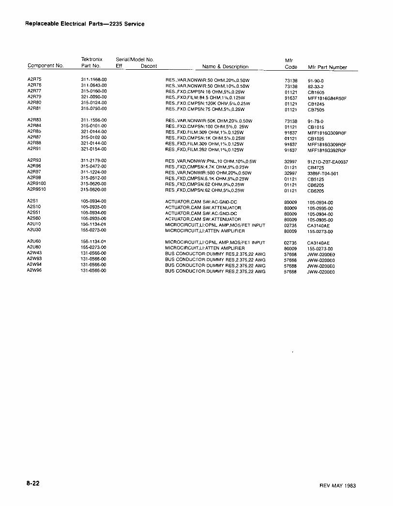
Replaceable Elect rical Parts-2235 Service
Tektronix
Serial/Model No .
MfrComponent No .
Part No .
E ff
Dscont
Name & Desc r i ption
Code
Mfr Part Number
A2R75
311-1568-00
RES.,VAR,NONWIR :50 ΟΗΜ,20%,0 .50W73138
91-90-0A2R76
311-0643-00
RES.,VAR,NONWIR :50 ΟΗΜ,10%,O .50W73138
82-33-2A21`1 77
315-0160-00
RES., FXD,CMPSN:16 ΟΗΜ,5%,0.25W01121
C61605A2R79
321-0090-00
RES., FXD,FI LM:84.5 οΗΜ,1%,0.125W91637
MFF1816G84R50FA2R80
315-0124-00
RES., FXD,CMPSN:120K ΟΗΜ,5%,0.25W01121
CB1245A2R81
315-0750-00
RES., FXD,CMPSN:75 ΟΗΜ,5%,0.25W01121
CB7505
A2R83
311-1556-00
RES.,VAR,NONW IR:50K ΟΗΜ,20%,0 .50W
73138
91-78-0A2R84
315-0101-00
RES., FXD,CMPSN:100 ΟΗΜ ,5%,0. 25W01121
CB1015A2R85
321-0144-00
RES ., FXD,FILM :309 ΟΗΜ,1%,0.125W
91637
MFF1816G309ROFΑ2R87
315-0102-00
RES.,FXD,CMPSN:I K ΟΗΜ ,5%,0.25W
01121
CB1025Α21188
321-0144-00
RES.,FXD,FILM :309 ΟΗΜ,1%,0.125W
91637
MFF1816G309ROFA2R91
321-0154-00
RES.,FXD,FILM :392 ΟΗΜ,1%,0.125W
91637
MFF1816G392ROF
A2R93
311-2179-00
RES.,VAR,NONWW: PNL,10ONΜ,10%,0 .5W32997 91 Ζ 1D-ΖΟ 7-ΕΑ0037A2R96
315-0472-00
RES.,FXD,CMPSN :4 .7 K ΟΗΜ,5%,0.25W01121
CB4725A2R97
311-1224-00
RES.,VAR,NONW IR:500 ΟΗΜ,20%,0 .50W32997
3386F- ΤΟ4-501A2R98
315-0512-00
RES.,FXD,CMPSN :5 .1 K ΟΗΜ,5%,0.25W01121
CB5125A2R9100
315-0620-00
RES., FXD,CMPSN :62 ΟΗΜ,5%,0.25W01121
C86205A2R9510
315-0620-00
RES.,FXD,CMPSN :62 ΟΗΜ,5%,0.25W01121
CB6205
A2S1
105-0934-00
ACTUATOR,CAM SW:AC-GND-DC
80009
105-0934-00A2S10
105-0935-00
ACTUATOR,CAM SW:ATTENUATOR80009
105-0935-00A2S51
105-0934-00
ACTUATOR,CAM SW:AC-GND-DC
80009
105-0934-00A2S60
105-0935-00
ACTUATOR,CAM SW:ATTENUATOR80009
105-0935-00A2U 10
156-1134-01
M ICROCIRCUIT,L I :OPNL AMP ,MOS/FET INPUT
02735
CA3140AEA2U30
155-0273-00
M ICROCIRCUIT, L I :ATTEN AMPLIFIER
80009
155-0273-00
A2U60
156-1134-01
M ICROCIRCUIT, L I :OPNL AMP,MOS/FET INPUT
02735
CA3140AEA2U80
155-0273-00
M ICROCIRCUIT, LI :ATTEN AMPLIFIER
80009
155-0273-00A2W43
131-0566-00
BUS CONDUCTOR:DUMMY RES,2.375,22 AWG
57668
JWW-0200ΕOA2W93
131-0566-00
BUS CONDUCTOR:DUMMY RES,2.375,22 AWG
57668
JWW-0200ΕOA2W94
131-0566-00
BUS CONDUCTOR:DUMMY RES,2.375,22 AWG
57668
JWW-0200ΕOA2W96
131-0566-00
BUS CONDUCTOR:DUMMY RES,2.375,22 AWG
57668
JWW-0200ΕO
8-22
REV ΜΑΥ 1983

Replaceable Electrical Parts-2235 Service
Tektronix
Serial/Model No .
MfrComponent No .
P art No .
Eff
Dscont
Name & Description
Code
Mfr Part Number
Α3
670-7611-00
CKT BOARD ASSY:FRONT PANEL
80009
670-7611-00
A3C376
283-0006-00
CAP.,FXD,CER DI :0 .02UF,+80-20%,500V
59660
0841545Z5VO0203ZA3C377
281-0576-00
CAP.,FXD,CER DI :11PF,5%,500V
59660
301-000COG0110JA3C379
283-0780-00
CAP.,FXD,MICA D:125PF,1%,500V
00853
D155F1250F0A3C380
281-0578-00
CAP.,FXD,CER DI :18PF,5%,500V
59660
301-05000G0180J
A3C987
281-0773-00
CAP.,FXD,CER DI :0 .01UF,10%,100V
04222
SA201C103KAAA3CR534
152-0141-02
SEMICOND DEVICE :SILICON,30V,150MA
01295
1N4152RA3CR537
152-0141-02
SEMICOND DEVICE :SΙLICON,30V,150MA
01295
1 N4152RA3CR538
152-0141-02
SEMICOND DEVICE :SILICON,30V,150MA
01295
114415219A3CR539
152-0141-02
SEMICOND DEVICE :SILICON,30V,150MA
01295
1 N4152RA3CR648
152-0141-02
SEMICOND DEVICE :SILICON,30V,150MA
01295
1 N4152R
A3CR988
152-0141-02
SEMICOND DEVICE :S1LICON,30V,150MA
01295
1 N4152RA3CR989
152-0141-02
SEMICOND DEVICE :SILICON,30V,150MA
01295
1 N4152RA3DS518
150-1029-00
LT EMITTING DIO:GREEN,565NM,35MA
53184
XC209GA3R89
315-0242-00
RES.,FXD,CMPSN:2 .4K ΟΗΜ ,5%,0.25W
01121
CB2425A3R92
315-0333-00
RES.,FXD,CMPSN:33K ΟΗΜ,5%,0.25W
01121
CB3335A3R111
321-0251-00
RES.,FXD,FILM :4 .02K ΟΗΜ,1%,0.125W
91637
MFF1816G40200F
A3R112
311-2178-00
RES.,VAR,NONWW:PNL,500 ΟΗΜ ,10%,O.5W
01121
W8650AA3R161
321-0251-00
RES.,FXD,FILM :4 .02K ΟΗΜ,1%,0.125W
91637
MFF1816G40200FA3R162
311-2178-00
RES.,VAR,NONWW:PNL,500 ΟΗΜ ,10%,O.5W
01121
W8650AA3R280
311-2147-00
RES.,VAR,NONWIR :PNL,5K ΟΗΜ,20%,O.50W
01121
W8615BA3R377
321-0807-00
RES.,FXD,FILM:900K ΟΗΜ,1%,0.125W
91637
HFF1104F90002FA3R378
321-0617-00
RES.,FXD,FILM:111K ΟΗΜ,1%,0.125W
91637
MFF1816G11102F
A3R379
315-0220-00
RES.,FXD,CMPSN:22 ΟΗΜ,5%,0.25W
01121
CB2205A3R380
321-0459-00
RES.,FXD,FILM:590K ΟΗΜ,1%,0.125W
91637
MFF1816G59002FA3R438
311-2178-00
RES.,VAR,NONWW:PNL,500 ΟΗΜ ,10%,O.5W
01121
W8650AA3R519
315-0682-00
RES.,FXD,CMPSN:6 .8K ΟΗΜ ,5%,0.25W
01121
CB6825A3R520
315-0912-00
RES.,FXD,CMPSN:9 .1 Κ ΟΗΜ,5%,0.25W
01121
CB9125A3R602
311-2147-00
RES.,VAR,NONWIR :PNL,5K ΟΗΜ,20%,0.50W
01121
W8615B
A3R726
311-2147-00
RES.,VAR,NONWIR :PNL,5K ΟΗΜ,20%,0.50W
01121
W8615BA3R982
311-1560-00
RES.,VAR,NONWIR :5KΟΗΜ,20%,O.50W
73138
91-82-0Α314983
315-0241-00
RES.,FXD,CMPSN:240 ΟΗΜ,5%,0.25W
01121
CB2415A3R985
315-0124-00
RES.,FXD,CMPSN:120K ΟΗΜ,5%,0.25W
01121
CB1245A3R986
315-0434-00
RES.,FXD,CMPSN:430K ΟΗΜ,5%,0.25W
01121
CB4345A3R987
315-0124-00
RES.,FXD,CMPSN:120K ΟΗΜ,5%,0.25W
01121
CB1245
A3R988
315-0182-00
RES.,FXD,CMPSN:1 .8K ΟΗΜ ,5%,0.25W
01121
CB1825A3R989
321-0239-00
RES.,FXD,FILM :3 .O1K ΟΗΜ,1%,0.125W
91637
MFF1816G30100FA3R990
321-0126-00
RES.,FXD,FILM:200 ΟΗΜ ,1%,0.125W
91637
MFF1816G200ROFA3R9376
315-0510-00
RES.,FXD,CMPSN:51 ΟΗΜ,5%,0.25W
01121
CB5105A3S90
260-1995-00
SWITCH,PUSH :DPDT,SLOPE
71590 Κ40352ΑΒA3S200
260-2111-00
SWITCH,PUSHA BUTTON,1 POLE,BEAM FIND
80009
260-2111-00
A3S226
260-2075-00
SWITCH,PUSH :SPDT,50VDC,500M AMP
80009
260-2075-00A3S380
260-2033-00
SWITCH,SLIDE:DPTT,125V,0 .5A
82389
OBDA3S390
260-2111-00
SWITCH,PUSHA BUTTON,1 POLE,BEAM FIND
80009
260-2111-00A3S392
260-2033-00
SWITCH,SLIDE:DPTT,125V,O .5A
82389 OBDA3S401
260-2110-00
SWITCH,PUSH :3 BUTTON,2 POLE,TRIG MODE
80009
260-2110-00A3S460
260-2075-00
SWITCH,PUSH :SPDT,50VDC,500M AMP
80009
260-2075-00
A3S532
260-2110-00
SWITCH,PUSH:3 BUTTON,2 POLE,TRIG MODE
80009
260-2110-00A3S545
260-2033-00
SWITCH,SLIDE:DPTT,125V,O .5Α
82389
OBDA3S550
260-2033-00
SWITCH,SLIDE:DPTT,125V,0.5A
82389
OBDA3S555
260-2033-00
SWITCH,SLIDE:DPTT,125V,O.5A
82389 OBDA3S602
260-2075-00
SWITCH,PUSH:SPDT,50VDC,500M AMP
80009
260-2075-00A3S648
260-2033-00
SWITCH,SLIDE:DPTT,125V,0.5A
82389 OBD
REV ΜΑΥ 1983 8-23

Replaceable Electrical Parts-2235 Service
Tektronix
Serial/Model No .
MfrComponent No .
Part No.
Eff
Dscont
Name & DescriptionCode
Mfr Part Number
A3U985
156-0067-00
ΜICROCIRCU ΙΤ , L I : OPERATIONAL AMPLIFIER
01295
M ICROA741CPA3W89
131-0566-00
BUSCONDUCTORDUMMY RES,2.375,22 AWG
57668
JWW-0200ΕOA3W515
131-0566-00
BUS CONDUCTORMUMMY RES,2.375,22 AWG
57668
JWW-0200ΕOA3W534
131-0566-00
BU S CONDUCTOR:DUMMY RES,2.375,22 AWG
57668
JWW-0200ΕOA3W539
131-0566-00
BUS CONDUCTOR:DUMMY RES,2.375,22 AWG
57668
JWW-0200ΕOA3W630
131-0566-00
BUS CONDUCTORDUMMY RES,2.375,22 AWG
57668
JWW-0200ΕO
8-2αREV ΜΑΥ 1983

Replaceable Electrical Parts-2235 Service
Tektronix
Serial/Model No .
MfrComponent No .
Part No .
E ff
Dscont
Name & DescriptionCo de
Mfr Part Number
Α4
670-7613-00
CKT BOARDASSYJIMING
80009
670-7613-00
A4C701
295-0194-00
CAP SET,MATCHED:2 ΕΑ 1.OUF,1 .5%,50V
90201
ΤΤΧ 100 + 100A4C702
283-0674-00
CAP.,FXD,MICA D:85PF,1%,500V
00853
D155F850FOA4C703
281-0207-00
CAP.,VAR,PLSTC:2-18PF,100V
80031 2807CΟ0218ΜΗ 02FΟA4C705
281-0813-00
CAP.,FXD CER DI :0.047UF,20%,50V
04222
GC705- Ε-473Μ
A4C706
281-0773-00
CAP.,FXD,CER DI :0 .01 UF,10%,100V
04222
SA201C103KAAA4C707
281-0773-00
CAP., FXD,CER DI :O .O1 UF,10%,100V
04222
SA201C103KAAA4C708
281-0756-00
CAP., FXD,CER DI :2 .2 PF,0 .5%,200V
12969
CGB2R2DFNA4C710
281-0813-00
CAP., FXD CER DI :0 .047 UF,20%,50V
04222
GC705-Ε-473ΜA4C712
283-0674-00
CAP., FXD,MICA D:85PF,1%,500V
00853
D155F850FOA4C713
281-0207-00
CAP.,VAR , PLSTC :2-18PF ,100V
80031 2807000218MH02FO
A4C714
281-0756-00
CAP., FXD,CER DI :2 .2 PF ,0 .5%,200V
12969
CGB2R2DFNA4C715
290-0776-00
CAP., FXD,ELCTLT:22UF,+50-10%,10V
55680
ULA1A220TEAA4C720
281-0775-00
CAP., FXD,CER DI :0 .1UF,20%,50V
04222
ΜΑ205Ε104ΜΑΑA4C724
281-0773-00
CAP.,FXD,CER DI :0 .01 UF,10%,100V
04222
SA201C103KAAA4C728
283-0203-00
CAP.,FXD,CER DI :0 .47UF,20%,50V
72982
8131M058Z5UO474MA4C749
281-0775-00
CAP.,FXD,CER DI :0 .1 UF,20%,50V
04222
ΜΑ20SΕ104ΜΑΑ
A4C750
290-0246-00
CAP.,FXD,ELCTLT:3 .3 UF,10%,15V
56289 162D335X9015CD2A4C751
281-0809-00
CAP.,FXD,CER DI :200PF,5%,100V
72982
8013T2ADDC1G201JA4C752
281-0775-00
CAP.,FXD,CER DI :O.l UF,20%,50V
04222
ΜΑ205Ε104ΜΑΑA4C755
283-0107-00
CAP.,FXD,CER DI :51 PF,5%,200V
96733
R3017A4CR732
152-0141-02
SEM ICOND DEVICE :SI LICON,30V,150MA
01295
1N4152RA4CR742
152-0141-02
SEM ICOND DEVICE :SI LICON,30V,150MA
01295
1N4152R
Α40701
151-0424-00
TRANSISTOR :SI LICON,NPN
04713
SPS8246Α40704
151-1042-00
SEMICOND DVC SEWATCHED PAIR FET
01295
SKA5390Α40706
151-0736-00
TRANSISTOR :SILICON,NPN
04713
SPS8317Α40709
151-0424-00
TRANSISTOR :SILICON,NPN
04713
SPS8246Α40710
151-1042-00
SEMICOND DVC SEWATCHED PAIR FET
01295
SKA5390Α40712
151-0736-00
TRANSISTOR : SILICON,NPN
04713
SPS8317
Α40732
151-0712-00
TRANSISTOR : SILICON,NPN
04713
SPS8223Α40737
151-0188-00
TRANSISTOR : SILICON,PNP
04713
SPS6868KΑ40742
151-0712-00
TRANSISTOR : SILICON,NPN
04713
SPS8223A4R701
307-0780-01
RES,NTWK ,FXD,FI :TIMING
80009 307-0780-01A4R702
322-0519-01
RES., FXD,FILM :2 .49M ΟΗΜ,0 .5%,0.25W
91637
HFF143G24903DA4R703
315-0100-00
RES., FXD,CMPSN :10 ΟΗΜ,5%,0.25W
01121
CB1005
A4R705
315-0151-00
RES., FXD,CMPSN:150 ΟΗΜ,5%,0.25W
01121
CB1515A4R707
301-0202-00
RES.,FXD,CMPSN:2 K ΟΗΜ,5%,O.50W
01121
ΕΒ2025A4R709
315-0100-00
RES., FXD,CMPSN:10ΟΗΜ,5%,0.25W
01121
CB1005A4R710
315-0151-00
RES., FXD,CMPSN:150 ΟΗΜ,5%,0.25ω
01121
CB1515A4R711
307-0780-01
RES,NTWK,FXD,FI :TIMING
80009 307-0780-01Α4P1713
301-0202-00
RES., FXD,CMPSN:2K ΟΗΜ,5%,O.50W
01121
ΕΒ2025
A4R715
321-0308-00
RES., FXD,FILM:15.8KΟΗΜ,1%,0.125W
91637
MFF1816G15801 FA4R716
321-0303-00
RES., FXD,FILM:14K ΟΗΜ,1%,0.125W
91637
MFF1816G14001 FA4R717
321-0306-00
RES., FXD,FILM:15K ΟΗΜ,1%,0.125W
91637
MFF1816G15001 FA4R718
321-0306-00
RES., FXD,FILM:15K ΟΗΜ ,1%,0.125W
91637
MFF1816G15001 FA4R719
315-0330-00
RES., FXD,CMPSN:33 ΟΗΜ,5%,0.25W
01121
CB3305A4R721
311-2151-00
RES.,VAR,NONW IR:PNL,500 ΟΗΜ,20%,O .5W,DPST
12697
OBD
A4R722
315-0201-00
RES., FXD,CMPSN:200 ΟΗΜ,5%,0.25W
01121
CB2015A4R724
315-0200-00
RES., FXD,CMPSN:20 ΟΗΜ,5%,0.25W
01121
CB2005A4R727
321-0246-00
RES., FXD,FILM :3 .57KΟΗΜ,1%,0.125W
91637
MFF1816G35700FA4R728
321-0211-00
RES., FXD,FILM :1 .54KΟΗΜ,1%,0.125W
91637
MFF1816G15400FA4R730
311-0635-00
RES.,VAR,NONW IR:1 K 0ΗΜ ,10%,0.5%,0.5W 73138 82Ρ-6-2-102ΚA4R731
321-0244-00
RES., FXD,FILM :3 .4KΟΗΜ,1%,0.125W
91637
MFF1816G34000F
REV ΜΑΥ 1983
8_25

Replaceable Electrical Parts-2235 Service
Tektronix
Serial/Model No .
MfrComponent No .
P art No .
E ff
Dscont
Name & Description
Code
Mfr Part Number
A4R732
321-0198-00
RES., FXD,FILM :1 .13KΟΗΜ,1 %,0.125W91637
MFF1816G11300FA4R733
321-0203-00
RES., FXD,FILM : 1 .27KΟΗΜ,1 %,0.125W91637
MFF1816G12700FA4R737
315-0392-00
RES., FXD,CMPSN:3 .9K ΟΗΜ ,5Ί,0 .25W
01121
CB3925A4R738
315-0512-00
RES., FXD,CMPSN:5 .I K ΟΗΜ ,5%,0.25W
01121
CB5125A4R740
311-0635-00
RES.,VAR,NONW IR:1K ΟΗΜ,10%ο,0 .5%ο,0 .5W
73138
82Ρ-6-2-102ΚΑ411741
321-0244-00
RES., FXD,FILM :3 .4KΟΗΜ,1 %,0.125W91637
MFF1816G34000F
A4R742
321-0198-00
RES., FXD,FILM :1 .13KΟΗΜ,1 %,0.125W91637
MFF1816G1130OFA4R743
321-0203-00
RES., FXD,FILM :1 .27KΟΗΜ,1 %,0.125W91637
MFF1816G12700FA4R745
321-0177-00
RES., FXD,FILM :681 ΟΗΜ ,1 %,0.125W91637
MFF1816G681 ROFA4R746
321-0184-00
RES., FXD,FILM :806 ΟΗΜ ,1 %,0.125W91637
MFF1816G806ROFA4R748
315-0113-00
RES., FXD,CMPSN:11 K OHM ,5%,0.25W
01121 CB1135Α4R749
311-1560-00
RES.,VAR,NONW IR:5K 0ΗΜ ,20°/,O.50W
73138 91-82-0
A4R750
315-0113-00
RES., FXD,CMPSN:11 K ΟΗΜ ,5
,0.25W01121
CB1135A4R751
321-0326-00
RES., FXD,FILM :24.3K0NΜ,1%,0.125W
91637 MFF1816G24301 FA4R752
315-0100-00
RES., FXD,CMPSN:10 ΟΗΜ,5%,0 .25W01121
CB1005A4R753
321-0216-00
RES., FXD,FILM :1 .74K0ΝΜ ,1 b,0.125W
91637
MFF1816G17400FA4R754
311-0622-00
RES.,VAR,NONW IR:1000HM,10%,0.50W
32997 3329N-G48-101A4R755
315-0121-00
RES., FXD,CMPSN:120 ΟΗΜ ,5%ο,0 .25W
01121
CB1215
A4RT715
307-0125-00
RES.,THERMAL:500 ΟΗΜ,10%,25 DEG C
50157
2D1595A4S701
260-2023-01
SWITCH,ROTARY:A/Β SWEEP
80009
260-2023-01A4U715
156-0067-00
M ICROCIRCUIT,LI:OPERATIONAL AMPLIFI ER
01295
M ICROA741CPA4U750
156-1150-00
M ICROCIRCUλ T,LI :VOLTAGE REGULATOR,NEGATIVE
04713
MC79LOSACPA4U760
155-0124-00
M ICROCIRCUIT,LI :HORIZONTALPREAMPL
80009
155-0124-00A4VR720
152-0744-00
SEMICOND DEVICE:ZEN ,SI,3.6V,5%,0.4W
04713
1 Ν747Α
A4VR749
152-0744-00
SEMICOND DEVICE:ZEN ,SI,3.6V,5%,0.4W
04713
1 Ν747ΑA4W709
131-0566-00
BUS CONDUCTOR :DUMMY RES,2.375,22 AWG
57668
JWW-0200ΕO
α -26 REV ΜΑΥ 1983

Replaceable Electrical Parts-2235 Service
Tektronix
Serial/Model No .
MfrComponent No .
P art No .
Eff
Dscont
Name & DescriptionCode
Mfr Part Number
Α5
670-7612-00
CKT BOARD ASSY:A LTERNATE SWEEP
80009
670-7612-00
A5C610
281-0862-00
CAP., FXD,CER DI :0 .001 UF,+80-20%,100V
20932
401-ES-100AD102ZA5C624
281-0826-00
CAP., FXD,CER D1 :2200PF,5%,100V
12969
CGC222KEXA5C627
281-0893-00
CAP., FXD,CER DI :4 .7PF, +/ -0.5 PF,100V
04222
MA101A4R7DAAA5C643
281-0811-00
CAP., FXD,CER DI :10PF,10%,100V
72982
8035D2AADC1G100K
A5C655
281-0773-00
CAP., FXD,CER DI :0 .01 UF,10%,100V
04222
SΑ201C103ΚΑΑA5C659
281-0773-00
CAP., FXD,CER DI :0 .01 UF,10%,100V
04222
SA201C103KAAA5C665
281-0810-00
CAP., FXD,CER DI :5 .6PF ,0 .5%,100V
04222
GC10-1A5R6DA5C671
281-0851-00
CAP., FXD,CER DI :180PF,5%,100VDC
20932
401EO100AD181JA5C672
281-0759-00
CAP., FXD,CER DI :22PF,10%,t00V
72982
8035D9AADClG220KA5C690
281-0772-00
CAP., FXD,CER DI :0 .0047UF,10%,100V
04222
GC701C472K
A5C693
290-0776-00
CAP., FXD,ELCTLT:22UF,+50-10%,10V
55680 ULA1A220TEAA5C694
281-0775-00
CAP., FXD,CER DI :0 .1UF,20%,50V
04222
ΜΑ205Ε104ΜΑΑA5CR680
152-0141-02
SEMICOND DEVICE :SILICON,30V,150MA
01295
1 N4152RA5CR685
152-0141-02
SEMICOND DEVICE : SILICON,30V,150MA
01295
1 N4152RA5CR816
152-0153-00
SEMICOND DEVICE :SILICON,15V,50MA
07263
FD7003A5CR817
152-0141-02
SEMICOND DEVICE :SILICON,30V,150MA
01295
1 N4152R
Α5Ο619
151-0712-00
TRANSISTOR:SILICON,NPN
04713 SPS8223Α50620
151-0712-00
TRANSISTOR :SILICON,ΝΡΝ
04713
SPS8223Α50630
151-0369-00
TRANSISTOR :SILICON,ΡΝΡ
01295
SKA6664Α50631
151-0369-00
TRANSISTOR :SILICON,ΡΝΡ
01295
SKA6664Α50637
151-0276-00
TRANSISTOR :SILICON,ΡΝΡ
80009
151-0276-00Α50643
151-0190-00
TRANSISTOR :SI LICON,NPN
07263
S032677
Α50680
151-0198-00
TRANSISTOR:SILICON,NPN,S EL FROM MPS918
04713
SPS8802-1Α50685
151-0198-00
TRANSISTOR :SI LICON,NPN,S EL FROM MPS918
04713
SPS8802-1A5R604
315-0242-00
RES., FXD,CMPSN:2 .4K ΟΗΜ ,5%,0.25W
01121
CB2425Α511605
321-0203-00
RES., FXD,FILM :1 .27KΟΗΜ,1%,0.125W
91637
MFF1816G12700FA5R606
321-0201-00
RES., FXD,FILM :1 .21 K ΟΗΜ,1%,0.125W
91637
MFF1816G1210OFΑ513609
315-0222-00
RES., FXD,CMPSN:2 .2K ΟΗΜ ,5%,0.25W
01121
CB2225
A5R610
315-0241-00
RES., FXD,CMPSN:240 ΟΗΜ,5%,0.25W
01121
CB2415A5R611
315-0470-00
RES., FXD,CMPSN:47 ΟΗΜ,5%,0.25W
01121
CB4705A5R614
315-0302-00
RES., FXD,CMPSN:3K ΟΗΜ,5%,0.25W
01121
CB3025A5R616
321-0207-00
RES., FXD,FILM :1 .4K ΟΗΜ,1%,0.125W
91637
MFF1816G14000FΑ511617
321-0197-00
RES., FXD,FILM :I .1 K ΟΗΜ,1%,0.125W
91637
MFF1816G11000FASR619
321-0092-00
RES., FXD,FILM:88.7 ΟΗΜ ,1%,0.125W
91637
MFF1816G88R70F
A5R620
321-0090-00
RES., FXD,FILM:84.5 ΟΗΜ ,1%,0.125W
91637
MFF1816G84R50FΑ513621
315-0271-00
RES., FXD,CMPSN:270 ΟΗΜ,5%,0.25W
01121
CB2715ASR623
315-0910-00
RES., FXD,CMPSN:91 ΟΗΜ,5%,0.25W
01121
CB9105Α511624
301-0430-00
RES., FXD,CMPSN:43 ΟΗΜ,5%,0.50W
01121
ΕΒ4305A5R625
315-0431-00
RES., FXD,CMPSN:430 ΟΗΜ,5%,0.25W
01121
CB4315A5R626
315-0431-00
RES., FXD,CMPSN:430 ΟΗΜ,5%,0.25W
01121
CB4315
A5R627
315-0201-00
RES., FXD,CMPSN:200 ΟΗΜ,5%,0.25W
01121
CB2015A5R629
315-0471-00
RES., FXD,CMPSN:470 ΟΗΜ,5%,0.25W
01121
CB4715A5R630
315-0471-00
RES., FXD,CMPSN:470 ΟΗΜ,5%,0.25W
01121
CB4715A5R631
315-0471-00
RES.,FXD,CMPSN:470 ΟΗΜ,5%,0.25W
01121
CB4715A5R632
315-0181-00
RES.,FXD,CMPSN:180 ΟΗΜ,5%,0.25W
01121
CB1815A5R633
315-0302-00
RES.,FXD,CMPSN:3K ΟΗΜ,5%,0.25W
01121
CB3025
A5R634
315-0201-00
RES., FXD,CMPSN:200 ΟΗΜ,5%,0.25W
01121
CB2015A5R637
315-0104-00
RES., FXD,CMPSN:100K ΟΗΜ ,5%,0.25W
01121
CB1045A5R638
315-0102-00
RES., FXD,CMPSN:1 Κ ΟΗΜ,5%,0.25W
01121
CB1025A5R640
315-0114-00
RES., FXD,CMPSN:110K ΟΗΜ ,5%,0.25W
01121
CB1145Α513642
321-0314-00
RES., FXD,FILM:18.2 K ΟΗΜ,1%,0.125W
91637
MFF1816G18201FΑ513643
321-0322-00
RES., FXD,FILM:22.1 K ΟΗΜ,1%,0.125W
91637
MFF1816G22101F
REV ΜΑΥ 1983 8-27

Replaceable Electrical Parts-2235 Service
Tektronix
Serial/Model No .
M frComponent No .
P art No .
Eff
Dscont
Name & Descri ptionCo de
Mfr Part Number
A5R644
315-0512-00
RES., FXD,CMPSN :5 .1 K OHM,5%,0.25W
01121
CB5125A5R651
321-0277-00
RES., FXD,FILM:7 .5K ΟΗΜ,1%,0.125W
91637
MFF1816G75000FASR652
311-1238-00
RES.,VAR,NONW IR:5K ΟΗΜ ,10%,0.50W
73138
72-27-0Α5ΡΙ653
321-0289-00
RES., FXD,FILM:10K ΟΗΜ ,1%,0.125W
91637
MFF1816G10001 FA5R657
315-0102-00
RES., FXD,CMPSN:1 Κ OHM,5%,0.25W
01121
CB1025Α513660
315-0471-00
RES., FXD,CMPSN:470 OHM,5%,0.25W
01121
CB4715
A5R662
315-0392-00
RES., FXD,CMPSN:3 .9K OHM,5%,0.25W
01121
CB3925A5R663
315-0102-00
RES., FXD,CMPSN:1 Κ OHM,5%,0.25W
01121
CB1025A5R664
315-0392-00
RES., FXD,CMPSN:3 .9K OHM,5%,0.25W
01121
CB3925A5R665
315-0204-00
RES.,FXD,CMPSN:200K OHM,5%,0.25W
01121
CB2045Α513666
315-0221-00
RES.,FXD,CMPSN:220 OHM,5%,0.25W
01121
CB2215ASR670
315-0512-00
RES.,FXD,CMPSN:5 .1 K OHM,5%,0 .25W
01121
CB5125
A5R671
315-0681-00
RES.,FXD,CMPSN :680 OHM,5%,0.25W
01121
C86815Α513672
315-0331-00
RES.,FXD,CMPSN :330 OHM,5%,0.25W
01121
CB3315A5R674
315-0512-00
RES.,FXD,CMPSN :5 .1KOHM,5%,0.25W
01121
CB5125A5R677
315-0471-00
RES.,FXD,CMPSN:470 OHM,5%,0.25W
01121
CB4715Α511690
315-0100-00
RES.,FXD,CMPSN:10 OHM,5%,0.25W
01121
CB1005A5R693
307-0106-00
RES.,FXD,CMPSN:4.7 OHM,5%,0.25W
01121
CB47G5
A5R816
315-0562-00
RES., FXD,CMPSN:5 .6K OHM,5%,0.25W
01121
CB5625A5R817
315-0302-00
RES., FXD,CMPSN:3K OHM,5%,0.25W
01121
CB3025A5U605
156-0534-00
M ICROCIRCUIT,LI :DUAL DIFF AMPL,14 LID DI P80009
156-0534-00A5U625
156-1641-00
M ICROCIRCUIT,DI : ECL,QUAD 2-INPUT NOR GATE80009
156-1641-00A5U655
156-1126-00
M ICROCIRCUIT,LLVOLTAGECOMPARATOR
51984
UPC311CA5U660
156-0385-02
M ICROCIRCUIT,DI : HEX INVERTER
01295
SN74LS04
Α51J665
156-0382-02
Μ ICROCIRCUIT,DI :QUAD 2-ΙΝΡ NAND GATE01295
SN74LS00Α51J670
156-1611-00
MICROCIRCUIT,DI:DUAL D TYPE EDGE-TRIGGERED
07263
74F74A5U680
156-0382-02
MICROCIRCUIT,DI :QUAD 2-ΙΝΡ NAND GATE01295
SN74LS00A5VR624
152-0195-00
SEMICOND DEVICE:ZENER ,0.4W,5 .1V,5%
04713
SZ11755A5VR660
152-0195-00
SEMICOND DEVICE:ZENER ,0 .4W,5 .1 V,5%
04713
SZ11755A5W637
131-0566-00
BUS CONDUCTOR :DUMMY RES,2.375,22 AWG
57668
JWW-0200ΕO
A5W638
131-0566-00
BUS CONDUCTOR:DUMMY RES,2.375,22 AWG
57668
JWW-0200ΕOA5W643
131-0566-00
BUS CONDUCTOR:DUMMY RES,2.375,22 AWG
57668
JWW-0200ΕOA5W655
131-0566-00
BUS CONDUCTORMUMMY RES,2.375,22 AWG
57668
JWW-0200ΕOA5W662
131-0566-00
BUS CONDUCTOR:DUMMY RES,2.375,22 AWG
57668
JWW-0200ΕOA5W668
131-0566-00
BUS CONDUCTOR:DUMMY RES,2.375,22 AWG
57668
JWW-0200ΕOA5W670
131-0566-00
BUS CONDUCTOR:DUMMY RES,2.375,22 AWG
57668
JWW-0200ΕO
A5W677
131-0566-00
BUS CONDUCTOR:DUMMY RES,2.375,22 AWG
57668
JWW-0200ΕOA5W678
131-0566-00
BUS CONDUCTOR:DUMMY RES,2.375,22 AWG
57668
JWW-0200ΕOA5W682
131-0566-00
BUS CONDUCTOR:DUMMY RES,2.375,22 AWG
57668
JWW-0200ΕOA5W690
131-0566-00
BUS CONDUCTOR:DUMMY RES,2.375,22 AWG
57668
JWW-0200ΕOA5W695
131-0566-00
BUS CONDUCTORMUMMY RES,2.375,22 AWG
57668
JWW-0200ΕOA5W696
131-0566-00
BUS CONDUCTOR:DUMMY RES,2.375,22 AWG
57668
JWW-0200ΕO
A5W698
131-0566-00
BUS CONDUCTOR :DUMMY RES,2.375,22 AWG
57668
JWW-0200ΕO
α -28 REV ΜΑΥ 1983

Replaceable Electrical Parts-2235 Service
Tektronix
Serial/Model No .
MfrComponent No .
P art No .
Eff
Dscont
Name & Description
Code
M fr Part Number
Α6
670-7615-00
CKT BOARD ASSY:EMI FILTER BOARD
80009
670-7615-00
A6C900
285-1252-00
CAP.,FXD,PLASTIC:0 .15UF,10%,250 VAC
26769
719JlMH154PM251SA6C902
285-1192-00
CAP.,FXD,PPR DI :0 .0022UF,20%,250VAC
OOOFG
ΡΜΕ271 Υ422A6C903
285-1192-00
CAP.,FXD,PPR DI :0 .0022UF,20%,250VAC
OOOFG
ΡΜΕ271 Υ422A6R901
301-0512-00
RES.,FXD,CMPSN :5 .1K ΟΗΜ,5%,O.50W
01121
ΕΒ5125
A6R903
301-0331-00
RES.,FXD,CMPSN :330 ΟΗΜ,5%,0.50W
01121
ΕΒ3315A6RT901
307-0863-00
RES,THERMAL:100 ΟΗΜ,10%,NTC
15454
SG13-5Α6Τ901
120-1449-00
XFMR,COM MODE :
02113
Ρ104Α6Τ903
120-1455-00
TRANSFORMER,RF:POT CORE
20462
OBDA6VR901
307-0456-00
RES,V SENSITIVE:
03508
MOV-V250LA15AA6W9011
196-0531-00
LEAD,ELECTRICAL:18 AWG,3.0 L ,8-01
80009
196-0531-00
A6W9091
196-0505-00
LEAD,ELECTRICAL:18 AWG,3.0 L ,8-9
80009
196-0505-00
CHASSIS PARTSDL9210
119-1515-00
DELAY LINE,ELEC :93NS,150 OHM,ASSY
80009
119-1515-00
F9001
159-0018-00
FUSE,CARTRIDGE :3AG,0.8A,250V,SLOW-BLOW
71400
MDL 8/10FL9001
119-1541-00
F ILTER,RFI :1 A,250VAC
05245
1 EF1J9100
131-0126-00
CONNECTOR,RCPT,:BNC,FEMALE
77820
9663-1 NT-34J9376
131-0955-00
COΝΝ,RCΡ7,ELEC :BNC,FEMALE
13511
31-279J9510
131-0126-00
CONNECTOR,RCPT,:BNC,FEMALE
77820
9663-1 NT-34J9800
131-0955-00
CONΝ,RCΡΤ , ELEC :BNC,FEMΑLE
13511
31-279
J9900
136-0387-01
JACK,TIP:BLACK
71279 450-4252-01-0310R9521
311-2146-00
RES.,VAR,NONWIR :50 ΟΗΜ,20%,0 .5W
12697
CM41773R9644
311-1183-01
RES.,VAR,WW:PNL,2K ΟΗΜ,5%,2W
32997
3540S-91-20239802Α,Β
311-2177-00
RES.,VAR,NONWW:PNL,1OK ΟΗΜ,20%,O.5W
12697
CM43517R9812
311-2177-00
RES.,VAR,NONWW:PNL,10K ΟΗΜ,20%,0.5W
12697
CM43517V9870
154-0861-00
ELECTRON TUBE:T4651-31-2
80009
154-0861-00
REV ΜΑΥ 1983 8-29

Symbols
DIAGRAMS AND CI RCU IT BOARD ILLUSTRATIONS
Graphic symbols and class designation letters arebased on ANSI Stand ard Υ32.2-1975.
Logic symbology is based on ANSI Υ32.14-1973 interms of positive logic. Logic symbols depict the logicfunction performed and may differ from the manufac-turer's data .
The overline on α signal name ind icates that the signalperforms its intended function when it is in the low state.
Abbreviations are based on ANSI Υ 1 .1-1972.
Capacitors - Values one or greater are in picofarads(pF) .Values less than one are in microfarads
Other ANSI standards that are used in the preparation
(pF) .of diagrams by Tektronix, Inc. are:
Resistors = Ohms (Ω) .
The information and special symbols below may appear in this manual .
Assembly Numbers and Grid CoordinatesThe schematic diagram and circuit board com ponent
Each assembly in the instrument is assigned an
location illustration have grids. Α lookup table with theassembly number (e.g ., Α20) . The assembly n umber
grid coordinates is provided for ease of locating theappears onthecircuit board outline onthediagram,iht he
component. Onlythecomponents illustrated onthefacingtitle for the circuit board component location illustration,
diagram are listed in the lookup table. When more thanand in the lookup table for the schematic diagram and
one schematic diagram is u sed to illustrate the circuitryoncorrespon ding component locator illustration . The
α circuit board , the circuit board illustration may onlyReplaceable Electrical Parts list isarranged byassemb lies
appear opposite the first diagram on which it was il-in numerical seq uence; the components are listed by
lustrated ; the looku p table will list the diagram number ofcomponent number '(see following illustration for
other diagrams t hat the circuitry of the circuit boardconstructing α component number).
appears on .
Cam Sw itc hClos u re C h art
_ :-
-,(Dot in dicatesswitc h closur e(
Etc h e d Circu it B oard ._Outlined in B lac k
R ef er [ ο Wavetor m
Function BlockOutli n e
670- ΧΧΧΧ -ΧΧλ
* [ΟΥΡΟΧΣΜΙ MIIYR f R ΕCλΥΡur
ΑΖ3,P~?, R1234I "I
Υ14.15, 1966
Drafting Practices .Υ14 .2, 1973
Line Conventions and Lettering .Υ10 .5, 1968
Letter Symbols for Quantities Used i nElectrical Science an d ElectricalEngineering.
Component Val uesElectrical components shown on the diagrams are in
the following units unless noted otherwise:
American National Stan dard Institute1430 Broadway
New York, New York 10018
Coaxial con n ectors :maletemaιePl u g I nd e x, sig nifies pi n No . Υ
Reg ΒηιΟ - - E xternal Screwdri ve r Adj .20κ~ _ s hiel d ing
τι 0~sr r"ιc ».,
θσχ - Ι dentifies Panelοη rols, Con n ectors and
In dicators
Selecte d val u e, see Pa rts L istand Μαίπ [e παη ce Section forSelection C riteria
Section 9-2235 Serv ice
Mod ified Component-SeeParts L ist (De picted in grey,o r wit h grey outli ne)

COMPOSITION
SMALL DISCι _
CAPACITORS
Ο1
2Ο and Ο3
- 1st, 2nd, and 3rd significant figu res
-m u ltip lier
0-temperatu re coefficient
-polar ity and voltage rati ng
-tolerance
GOLD
-
10-1 or 0.1
±5%
SI LVER
-
10-2 or 0.01
±10%
ΝΟΝΕ - --- ±20%
COLOR COD E
CER AM ICCAPACITORS
ΟΤ
and/or
TC
color co de may not be presen ton some capacitors
1
10
102 or 100
103 o r 1000
104 o r 10,000
105 or 100,000
106 or 1,000,000
Figure 9- 1 . Colo r codes fo r resistors and capacitors.
COLOR
I
SIG N I FICA NT
RESISTORS
CA PACITORS
DI PPEDFIGURES MUL TIPL I ER TO LERANCE MUL TI PL I ER
TOLERANCE
TANTALUMI
__1 VOLTAGEover 10 pF1
under 10 pF
I
RATING
BLACK 0 1 ---
BROWN 1 10
±1%
RED
2
102 o r 100
±2%
ORANGE3
103 o r 1 Κ
±3%
YELLOW
4
104 o r 10 Κ
±4%
GREEN
5
105 o r 100 Κ
±Υs%
BLUE
6
106 or 1 Μ
='/α°/ο
VIO LET 7 --- ±1/10%
GRAY
8
---
10 or 0.01
+80%-20%
±0.25 p F
WH ITE
9
---
---
16-' or 0.1
±10%
±1 pF
DIPPE DTANTALUMELECTROLYTICS
±20%
±2 pF
4 VDC
±1%
±0.1 pF
6 VDC
!2%
---
10 VDC
±3%
---
15 VDC
+100%-9%
---
20VDC
±5%
±0.5 ρF
25 VDC
---
---
35 VDC
---
---
50VDC
(1 861-20A)4206-31

C
META L CAS ETRANSISTO RS
711 &PUT FεΤ
712
Q254-255256-257
Q946 &
Q935Q947
FLAT PACK
INTEG RATED CI RCUITS
8IND E X Ι
INDEX
PLASTICCASE
TRANSISTORS
Figur e 9-2. Semiconducto r lead configurations.
TRAN SISTORSC R
FET
LEAD CONFIG UR ATION S AN D CAS E STY LE S ARE TYPICAL, BU T MAY VARY DUE TO VENDOR CHANGES ORIN STRUMENT MODI F ICATIONS.
(3826-17)4206-32

ϋΝ ιs,FΖωΖΟα
Ουϋ
ωΖ ,~- IL
ύάΟΧJW
2235 Service
To identify any componentmounted on α circuit board andto locate that component in theappropriate schematic d iagram
0
αοΦU
α
PULL OUT PAGETABS FOR CIRCUIT
BOARD ILLUSTRATION
5. Locate the Component on the Circuit Board
1 . Locate the Circuit Boa rd Illustration
α .
In the i nstrum ent identify the Assembly Nu mber of t hecircuit board in question . The Assembly Numbe r is usuallyprinte d on the upper left corner of t he ci rcuit boa rd on t hecomponent si de.
R
4
α .
In the manual, locate and pull out the tabbed pagewhosetitle and Assembly Nu mber correspond with the desiredci rcuit board . This information is on the back si de of t hetabs .
b.
U sing the Circu it Number and gr i d coordinates, locate thecomponent on the Circuit Board Illustration .
c.
In the circuit boa rd location illustration, determine thelocation of the circuit board in the instrument.
d .
F in d the circ uit board in t he instrument and compare itwith its illustration i n the manual to locate the d esi redcomponent on the board.
b .
Ιη the man ual locate and pull out tabbed page whose titleco rr es ponds wit h the Assembly Num b er of t he ci r cuit
boa rd. Ci r cuit board assembly numbers and boardnomenclature are pr inted on the back side of t he tabs(facing the rear of th e manual) .
ο~- " . .εα εατ ιο.ι~ εεη,ρεε.m ια. πεε..
α ,
ι ~'*'. .4
ι6+, ~
.
000 ρ
Ι
[6Ύα
ξ06~5 Γ
~ ~
τ8]0
Φι ς~ς533 . ι
ρ
000 6
2. Determine τ1
a. Comparethe desi rτίοη .
b . Scanthεfind the
c. Determi ιcompone
ASSEMBLY NUMBERAND CI RCUIT
ΙΙBOARD NAME
4. Determine the Circuit Board IllustratiiLocatio n
α.
From the sch ematic diagram, deιN umbe r of the ci rcuit board on ω-mounted. This information is boxesof the heavy line that d isting u έ she!
b .
Scan the Compo nent Location ΤεNumber ju st determined and f ίnd th+desi red component.
C. Under the BOARD LOCATION ccoordinates for the d esi red comps
Figure 9-3. Locating components on scl%

rcuit N umbe r
circuit boa rd wit h its illustration a nd locate
ιmροηe πτ by a r ea and sh ape on th e ill ust r a-
adjacenttot h e Ci r c u it Boa rd Ill u stration and
it Numb er of t he desi r ed component .
e Schematic Diag r am Number in whic h thelocated.
ISTR ATION FO RΙυΜεΝΤ CIRCU ITkR D LOCATIO N
nd Component
ne t h e Assemblyt he compo nen t islocated in a cornerboard Outline .
fo r t he Assemblycuit Num be r of t h e
in, r ead the g r i d
MANUA L BINDER
:ic diagrams and ci r cuit boa rd ill u strations .
Α6 CRT BOARD
COMPO NENTS LOCAT E D ON SCHEM ATIC DIAGRAM
2
2
0668('.6n3
C641 Ι
Ι Η 626Ια 62 7β 63 Πτα 632
δ~ Τ ς 643 R6 0 4C671
C651
β 605Ε 615
R6Π 8C616 060 6 R 609C617 Q610
R610C618
0615
R614Γ 619
0646
R616C624 0656 R623C626 0665 β 624
COMPONENTS LOCATED ON SCHEMATIC DIAGRAM
C670 0670 R 677('671 0672 Ρ 679C673 0673 β680C680('681
Α671
U617Ρ603 R673
υ 619Ρ607 Ρ674
υ 6190669 A67S
Α6 ASSEMBLY
CRT CI RCU IT DIAGRAM
CI RCU IT SCHEM BOARD CIRC U IT 5ςΗΕΜ BOARDNUMB E R ( L OCATION LOCATION ( NUMBER
LOCATION LOCATIONΙ
τ
Ι
3C Q656 2 F 2 ΘC603 1C Ι 1G Ι ρ665 1, 1 θC609' 4E 1-- 0668 2G 2 ΘC612 7C 3 ΕC615
7C 3D
R604
4C Ι 1 ΕC616 2 ς 3C R 605 5D 7 ΕC617 7D 3 Ρ R608 4E 7 1-,C618 7E 3E R 609 4E 2DC619
6Σ
3C
Ρ 61 α
7 θ
3EC624 4F 3D β 614 7C 3DC626 7G 2D R616 1C 3DC632 RG
R 623 4D 2Eς 643 3 D 4 0 R 625 7 F 2D_ς 651 Ι 3 Ε Ι 3 θ
7F 2DΘ R 627 7G 1D
CI RC U IT 5CΗΕΜ BOAR D CI RCU IT 5ςΗΕΜ BOARDNUMBER
~ LOCATIO N LOCATIO N
NUMBER
LOCATIO N LOCATION
1635
- 51
CHASSIS 1
υ 635
Ι
6J ~C HASSIS
COMPONENT LOCATION. TABLE _
will4100-1
CRT CIRCUIT D1
Β630 "
MANUA L BINDER

3. Locate the Component an the Schematic Diagram
α .
Locate and pull out tabbed page whose number and title
ε .
Under the SCHEM LOCATION col umn, read the gri dcorrespo nd with the Schematic Diagram Number just
coordinates for the desired component.determined in thetable. Sche matic diagramnomenclatureand numbe rs are printed on the front si de of t he tabsif acing the front of the manu al],
d .
Using the Ci rcuit Numbe r and gri d coordi n ates, locatet hecomponent on the schematic diagr am.
b.
Scan th e Component Location Table adjacent to theschematic diag ram and fi nd the Circ uit Num ber of thedesired component.
4
5
Β
7
Α _ Β
C
0 . Ι Ε
1'4,05
ι
~(
s svF~sa-s Ζ ΙΙ
ξ c ι,~s
r~2 κ
ι.+
UV`i., ΡτθΟb~
ΦΝ 4
~
_ ._ ηνR~M
` C
CΠΜ
Ι,I
όόΟ~υΓ
_
=RO++Ρα 5α_,
έΗΡ
'~Ι 3Ι~
ΗΟΜ 1
z- η~Ι S~491-4
Γ64 ιύ.0 ιi
β5432,2Κ
176ΟΛΉθ
ιααα76ι. Η
κί, ε
Rb4
R624 R623'Ι 2Κ
F
Numeral and letter at signal li nesto or f rom othe r diagramsindicates the gr id coordinates onanother sc hematic (far example :αΕ )
To identify any component in αschematic diagram and to locate
that component on its respectivecircuit board .
CRT C4RCUIT ίο
PULL OUTPAGE TABS
FOR SCHEMATICDIAG RAMS
SCHEMATIC DIAG RAMNAME AND NUMBER
ν 49J_3
ΙΙ
ς3516-81 4206-33

I NVERT
ATTENUATORS
CH 1 OR Χ
k-ow </,\>
CH 2 OR Υ 1 (0-.~
Ι
Ι
Ι
Ι
I TV FIELD
VERTICALMODE
BW L IMIT
TR IG V I EW
Α/Β SWP SEP
CH 1
BOTH
CH 2
ADD
ALT
CHOP
ω ωΖ_ m
ωύ cή ω άφ υ
VERTICAL
α °
ή.PREAMP
έ >AND
OUTPUT ΙAMPL
ΕΧΤI NPUT
Α TR I GGER LEVEL
CH 1
CH 2
BW L I M I T
CHOP ENABLE
TR IGGER V I EW S I GNAL
BEAM FI ND
CHOP BLANK
Ρ-Ρ AUTO
ΑSOURCE
NORM
SGL SWP
HOLDOFF
ΙΝΤ
L I NE
ΕΧΤ
VERT PLATE DEFL
VALT
SEP
ΑSWEEP
GENERATORAND
LOGIC
Α TR IGGER
Fig ure 9

LTAGES
TR I G'D/READYLED
VARHOLDOFF
HOLOOFF
DoiΑ SWEEP
ALT
Β S I GNAL
CH 1 SELECTED
ΧΥ
L I NE TR IGGER S I GNAL
lasic block diagram .
ώι
Ln Ln ώΟ Οau-)
- ~ - ~ UL)αΙ
αΙ °° Ι Μ
Β DELAY
-*-d
TIMEALTERNATE
POS I T I ONΒ
SWEEP
ΧΥAMPL/HOR I ZOUTPUT
οΗ
εαωm
Α
Β
ΧΥ
HOR IZMODE
Β I NTENS
Ζ DR I VE
HOR I Z PLATEDEFL VOLTAGES
Β D I SP
X-AXIS S I GNAL
BEAMΙ
Ι F I ND
PROBEADJUST
ΕΧΤ Ζ
L .V . SUPPL I ESTO ALL BOARDS
AC POWERI NPUT
BEAM F I ND
CHOP BLANK
Α & ΒΙΝΤΕΝ
AX I S
ω> υω
Ο F0
~ Ου >-
2235 Serv ice
CRT
POWERSUPPLYAND
Z-AX I SAMPL
4206-34
MwΌ LAΑΛ
σήΙ7αD

CH 1 0R Χ
[Η 2 OR Υ
R721SEC/0 I VVA R
R112CH 1
CH 1 [POSITION
R43AC-G NO-0[ Ι
S1 θ
Ι
CAL
Ι
C H 1 TRIG +
Ι
Ι
Ι
CH 1 -
CH 1 PRE MP
C H 1 T RIG -g Ιθ 2, Q1 θ 3
_
Ι
Ι
Ι
CH 1 +
g114 ι Q115CH 1 HIGH- Σ
CH 1
CN 1
CH 1
ι
U13 θΙΑ
ΝU ΑΤ 0R
ΒUF 0 Ε RQ3Ρ
L7
ΡΑ
VERTICAL
Α5ΕQ101
ΑΤ Ν U ΑΤΟR
'
AND OU 7FΑΜΡ L
Τ
ΙANDND INPUT
-
COUPL I NG
Q15, q18
R19
U3θ
CH 2 HIGH-7
CH 2ATTENUATOR
BUFFER ΑΜΡ IFAND I NPUT
06θ , Q63COUPL ING
ρ65, Q68
C H 1 ANDCH 2
Ι Ι
ΑΤΤΕΝUΑΤΟRS Ι Ι
AC-G NO-OC Ι
CH 2
551
- -
VO LTS/OI V
- - - Ι R93 - - - υΙ
Β SIG
Α TRIGG ER
ALT SYNC
Θ SIG
R9644
S6θ
Θ DEL AY
J
DELAY ΤΙΜΕTIME POSITION ΊΊ-~ ΙΡΠ 5 ΙΤΙΟΝ CΠMP A RATO R
U655
ΒΟΤΗ CHANNELVER Ι CAL
SW 1 ΤOM[ Η 2
C H 2
ΜΟD Ε
CH 2
LOGIC C HANNEL DEL.LΟ4- Σ
PA RAPHAS ES545
ADD
U537AΑΤΤ ΕΝ9ΑΤΟ R AMPL
ρLΤ
C HOP
SWITCH ρΙ1R69
U80
U54 0 Α
OSCI LLOATOR
Ι
CR200 , CR2θ 1
ρ 2 θ :
AND C HOP
CR202, CR2θ 3
Q2 ΘΕ
C HOP
BLA NK I NG
Q440 ι Q441
LU540B , υ 5379U537C , U5370
J θ TRIGG ER LEVEL CO MP ARATO RSCH MITT T RIGG ERSL O PE
U6 Θ 5 Α , θ , [, D, Ε , F
U625 A , Β , C, D
S6θ2
g6 Ιθ , 1162 θ
g630 , Q631
LEVEL
R6θ 2
CH 2 T RIG +
555 θ
ΓC Η 1
[Η 2 T RIG -
C H 2 -
C H 2 PREAMPg152, ρΙ 53g164, ρ 165
υιθθ
B TIMINGSW Ι TC H
AND RC
A LTERNAT E DISPLAY SWITCHING F--U66ΘΕ , U68ΘΑ , θθU67 ΘΒ , U665C
RUN AFT ER DIYQ637, U66 ΘΑ , D
8 SWEEP LOGIC
θ M I LLER 5 ΥΕΕΡU66θθ , F, U67 ΘΑ , U680C , 0
~ ρ 7 θ 9 , 771 ΘΑ , θg712
B END OF SWEEPCOMP A RATOR
Q643
TRIG V I EW52θθ
C HOP BL A NK
ΧΥ
CH 1 SELECTED
SEP
LOGICU665 B , DQ68 θ
ς/ \,
g685θ TI M I NG AND
\5/ALT ERNAT E θ SW EEP
Α TRIC
Figure 9-5. D

ΙΝΤΕΝ5 LVL
:νΕ L
4 Ρ SEP
Θ 4 LIMITΟ 284
CR226, CR227'85
CR226 , CR229
/Β SWP SEP
ΙθωLIMIT
Ι
ΙR280 '2,?F
ΧΥ
ad block diag ram .
PR08EADJUST
+ νΕRΤ DEFι- VERT DEFL
λ CH 1 TRIGGER--i AMPLIFIER
TRIGGER SWITCH
Q302, 0303U310
INTERNALUSSSA, Β , C, D
TR IGGERU S65B , C
ΑΜΡ Lϋ ' ERCH 2 TRIGGER
U352A, Β ,A MPL I F I ER
C, 0, ΕQ327, Q328
- i
0335
i
Α
TRIGGER SOURC ESOURCE
DIODE SWITCHING -
TNT TRIG5392
CR372 CR393,CR399, Q397
Q419
Α Ε XTCOUPLING
5380
X AXIS SICBEAM FIND
Ι
UNBLANKINGLOG ιε
Q586, C R 583CR551
POWER ΙΝΡΙΤ
PREREGULATOR'9θ 1 , VR9~1
'9θ8, Q928CR90
, CR9 0 1
Q930 , Q9 0 7~CR9~2, CR903
U930[R9 04
PROBE ADJUST U985
PROBE ADJU ST,ΧΥ AMPLIFIER,
HOR17ONTAL OUTPUT
Α DIS P
g732 Q737
+
AMPUF I ER,Β 01 S P
Q742 : U760Q77
0, Q775
8 S4P
Q779 , Q78OQ785, ρ789
FEED BACK
+43V
HORIFONTALR726 PO S ΙΤΙΟΝ
Α SWP
HORI£ ΡRΕΑΜΡΙ
HORI£ DUTPUT
-
+ ΗΟ 1 ΙΣ DEFL
TRIGGERING
5390
R893ΘΕΑΜ F IND
FOCUS
FOCUS CIRCUIT
FOCUS GRID0885
INTENSITYGRID _
XFMRI NVERTER Τ 948
Q938, Q939, Q944
LV POWERQ946, Q947
SUPPLIES
- ΗΟ R ΙΣ DEFL
ιν TOA LL
BLOCKSZ-AXIS AMPL ANDPOWER SUPPLY
2235 Service
4206-35
4206-35
ασr- M0 -4
πηΑΓ
νΜD v
3
Τ
ιι1Ο
Ν

2235 Service
TEST WAVEFORM AND VOLTAGE SETUPSWAVEFORM MEASUREMENTS
DC VOLTAGE MEASUREMENTS
On the left-hand pages preceding the schematic dia-
Typical voltage measurements, located on the schematicgrams are test waveform ill ustrations that are intended to
diagram, were obtained with the instrument operating underaid in troubleshooting the instrument . To test the instrument
the conditions specified in the Waveforms Measurementsfor these waveforms, make the initial control settings as
setup. Control-setting changes required for specific voltagesfollows:
are indicated on each waveforms page. Measurments arereferenced to chassis ground with the exception of the
Vertical (Both Channels)
Preregulator and Inverter voltages on Diagram 7. Thesevoltages are referenced as indicated on the schematicdiagram .
POSITION
MidrangeVERTICAL MOD ECH 1MIA/ ιιΜιΤ
Off (button out)VOLTS/DIV10mV
RECOMMENDED TEST EQU IPMENTVOLTS/DIV Variable
CAL detentINVERT
Off (button out)
Test equipment in Table 4-1 in the " Performance Check
AC-GND-DC
GND
Procedure", section 4 of this manual, meets the requiredspecifications for testing this instrument .
Horizontal
POSITION
MidrangeHORIZONTAL MODE
ΑΑ and Β SEC/DIV0.5 msSEC/DIV Variable
CAL detentΧ 10 Magnifier
Off (knob in)Β DELAY TIME POSITION5.0
Β TRIGGER
LEVEL
Fully clockwiseSLOPE
OUT
Α TRIGGER
VAR HOLDOFF
Minimum (fully ccw)Mode
Ρ-Ρ AUTOLEVEL
MidrangeΑ&Β ΙΝΤ
VERT MODEΑ SOURCE
ΙΝΤ
Changes to the control settings for specific waveformsare noted at the beginning of each set of waveforms. Inputsignals and hookups required are also indicated, if needed,for each set of waveforms.

POWER SUPPLY ISOLATION PROCEDURE
Each regulated supply has numerous feed points to
If α power supply comes up after lifting one of the mainexternal loads throughout the instrument . The power
jumpers from the power supply to isolate that supply, it isdistribution
diagram
is
used
in
conjunction
with
the
very probable that α short exists in the circuitry on that sup-schematic diagrams to determine those loads that can be
ply line . By lifting jumpers farther down the line, the circuit inisolated by removing service jumpers and those that cannot .
which α short exists may be located.
The power distribution and circuit board interconnections
Always set the POWER switch to OFF before solderingdiagrams are divided into circuit boards. Each power supply
or unsoldering service jumpers or other components andfeed to α circuit board is indicated by the schematic diagram
before attempting to measure component resistance values .number on which the voltage appears . The schematic d ia-gram grid location of α service jumper or component is givenad jacent to the component number on the power distribu-tion and circuit board interconnect diagrams.

C HASSIS MOUN TE D PA RTS
NUCIRCUIT
MBER Ι NUMBERSCHIM
ι LΟ CΑΤΙΟΝ Ι
NUCIRCUIT
MBER Ι NUMBE R ι LOCATIO N
C9272 2 8S Ρ 9870-14 7 8 ΡC9273 2 2S Ρ 9870-1 7 8 Ρ
Ρ 9870-2 7 8ΝDL9210 2 5 Κ Ρ 9870-3 7 7Ν
Ρ 9870-4 7 7ΝDS9150 7 8Α Ρ9870-5 7 6Ρ
Ρ 9870-7 7 5ΡF9001 7 5Α Ρ9870- 8 7 7Ρ
FL 9001 1 7 1 5Α I Q9070 1 7 1 8,1
J9100 1 1 Α R9100 1 1ΑJ9376 3 5Α R9272 2 8sJ9510 1 6Α R9273 2 2SJ9800 7 4Α R9376 3 5ΑJ9900 6 2E R9510 1 6Α
R9521 4 3ΑΡ 9272 7 5 Ρ R9644 5 5DΡ9273 7 5 Ρ R9802A 7 2ΑΡ 9778 7 4 Ρ R9802B 7 3ΑΡ9788 7 4ΡΡ9070-1 7 81 V9870 7 2 ΡΡ9070-2 7 SJΡ9070-3 7 8-1 W9272 2 8sΡ9870-10 7 4 ΡΡ9870-12 7 3 Ν

W9001 (Al TO Α3)DIAG NO.
DIAG NO.WIRE
& GRID
WIRE
& GRIDNO.
LINE NAME
COORDINATES
NO.
LINE NAME
COORDINATES
1
BEAM F IND
7,4F
21
HORIZ POS
6,3132
CH 1 POS CW
2,2D
22
+AUTO LEVEL CW
3,8Μ3
CH 1 POS CCW
2,3D
23
-AUTO LEVEL CCW
3,8Μ4
Α /Β SWP SEP
2,2L
24
Ρ -Ρ
4,8135
+8.6 VG
8,4Ρ
25
SS RESET
4,5Β6
TRIG VIEW
2,713
26
Β ONLY
5,2E7
CH 2 POS CW
2,8D
27
HALT
5,2E8
CH 2 POS CCW
2,9D
28
Β SLOPE
5,8F9
5H-2
2,613
29
TRIG'D LED
4,9K10
BW LIMIT
2,4Κ
30
SS
4,9811
CHOP ENABLE
3,4C
31
GND
3,6C12
-8.6 Vει
8,5Ρ
32
CH 1 Τ
3,2C13
VALT
5,2E
33
CH 2 Τ
3,3C14
CH 1
2,5Β
34
V MODE Τ
3,3C15
Α ONLY
5,1 E
35
ΕΧΤ
3,7C16
Β LEVEL
5,9F
36
LINE
3,6C17
TV TRIG ENABLE
4,9Β
37
TNT
3,7C18
Zy-
2C
38 GND
3,6C19
Α SLOPE
3,8Ν
39
ΕΧΤ ΙΝΡUΤ
3,5C20
Α TRIGGER LEVEL
3,8Μ
Ρ9700 (Α4 ΤΟ Α 1)
W9700 (Α 1 ΤΟ Α4)DIAG NO .
DIAG NO.PIN
& GRID
WIRE
& GRIDNO.
LINE NAME
COORDINATES
NO.
LINE NAME
COORDINATES
1
Α DISP
6,5E
1
Α DISP
6,5D2
Β DISP
6,5E
2
Β DISP
6,5D3
Β SWP
5,6E
3
Β SWP
5,6F4
Η .Ο.2
4,4D
4
Η . Ο.2
4,4D5
Η .Ο.1
4,4D
5
Η . Ο.1
4,4D6
H.O. COM
4,4D
6
H.O. COM
4,4D7
Α SWP
4,8Ν
7
Α SWP
4,8Μ8
GND
5,7E
8 GND
8,2Ν9
Β RETRACE
5,7E
9
Β RETRACE
5,6F10
Α GATE
4,7Ν
10
Α GATE
4,7Μ
W9400 (Α1 ΤΟ Α5)DIAG NO.
DIAG NO.
Ι
ΙΟ .
LINE NAME
Ι
COORDINATES
Ι
ΝΝ
Ο .
Ι
LINE NAME
Ι
COORDINATES
1
Β SIGNAL
5,9F
15
GND
8,6Ν2
Β SLOPE
5,9F
16
GND
8,6Ν3
GND
8,6Ν
17
Β RETRACE
5,6F4
Β LEVEL
5,9F
18
GND
8,6Ν5
Α DISP
5,1S
19
VALT
5,2F6
Β ONLY
5,2F
20
Α SWP
5,5F7
§ΕΡ
5,2S
21
ALT SYNC
5,1F8
Β I NTENSITY LEVEL
7,3C
22
Β SWP
5,6F9
Ζ D RIVE
7,3E
23
GND
8,6Ν10
HALT
5,2F
24 GND
8,6Ν11
Β DISP
5,2S
25
-8.6 VA
8,6Ν12
CH 1 SELECTED
5,2F
26
+5.2 VA
8,5Ν13
Α ONLY
5,1F
27
+8.6 VA
8,5Ν14
DT WIPER
5,5F

PINNO .
Ρ9705 (Α4 ΤΟ Α 1)
L I NE NAME
DIAG NO.& GRID
COORDINATES
1
GND
6,9E2 +SWP
6,5Κ3 -SWP
6,7Κ4 GND
6,9E5
Χ AXIS SIG
6,4E6
-8.6 Vc
6,9E7
+8.6 VB
6,8E8
+30 VB
6,8E
WI RENO.
12345678
W9705 (Α 1 ΤΟ Α 4)
L I NE NAME
GND+SWP-SWPGND
Χ AXIS SIG-8 .6 Vc+8.6 VB+30 VB
DIAG NO.& GRID
COORDINATES
8,3Ν6,5L6,7 L8,3Ν6,4E8,3Ν8,3Ν8,2Ν
W9000 (Α3 TO Al)DIAG NO .
DIAG NO.WI RE
& GRID
WIRE
Ι
& GRIDNO.
L INE NAME
COORDINATES
NO.
L I NE NAME
COOR DINATES
1
BEAM FIND
7,4F21
HOR IZ POS
6,382
CH 1 POS CW2,2D
22
+AUTO LEVEL CW
3,8L3
CH 1 POS CCW2,3D
23
-AUTO LEVEL CCW3,9 L4
Α /Β SWP SEP
2,2L24
Ρ-Ρ
4,8C5
+8.6 VG
8,4Ν
25
SS RESET
4,586
TRIG VI EW
2,613
26
Β ONLY
5,2E7
CH 2 POS CW2,8D
27
HALT
5,2E8
CH 2 POS CCW2,9D
28
Β SLOPE
5,9E9
CH 2
2,613
29
TR IG'D LED_
4,9Κ10
BW LI M IT
2,4Κ
30
SS
4,9Β11
CHOP ENABLE
3,4C
31
GND
3,6C12
-8.6 Vει
8,5Ν
32
CH 1 Τ
3,2C13
VALT
5,2E
33
CH 2 Τ
3,3C14
CH 1
2,58
34
V MODE Τ
3,3C15
Α ONLY
5,1 E
35
ΕΧΤ
3,7C16
Β LEVEL
5,9E
36
L I NE
3,6C17
TV TRIG ENABLE
4,98
37_
TNT
3,7C18
ΧΥ
3,2C
38
G Ν D
3,6C19
Α SLOPE
3,8Ν
39
ΕΧΤ I NPUT
3,5C20
Α TRIGGER LEVEL
3,8Μ
W9401 (Α 5 TO Α 1)DIAG NO.
DIAG NO.W IRE
& GRID
WIRE
Ι
& GRIDNO.
LINE NAME
COOR DINATES ]F NO.
L INE NAME
COORDINATES
1
Β SIGNAL5,9G
15
GND
5,4G2
Β SLOPE
5,9G
16
GND
5,4G3
GND
5,4G
17
B RETRACE
5,6G4
Β LEVEL
5,9G
18
GND
5,4G5
Α DIS P
5,1S
19
VALT
5,2G6
Β ONLY
5,2G
20
Α SWP_
5,5G7
SEP
5,2S
21
ALT SYNC
5,1G8
Β INTENSITY LEVEL
5,4Ρ
22
Β SWP
5,6G9
Ζ DR IVE
5,5S
23
GND
5,4G10 HALT
5,2G
24 GND
5,4G11
Β DISP5,2S
25
-8.6 VA
5,4G12
CH 1 SELECTED
5,2G
26
+5.2 VA
5,3G13
Α ONLY
5,1G
27
+8.6 VA
5,3G14
DT WI PER
5,5G

ω 9αΟο
' ω94 Ο15T-:-E
Ι SεεTABLE
TABLE
ΑΙ ΜΑi η I
Α5 ALT SWPLObIC
2235
CIRCUΙΤ EOARD ΙNTERCONNECT10Ν5azoe-zz
Γzc[
Γί
α

ισ
σααΖΨF
}ΟασΝααm
2235 Serv ice
2
3
4
2LL
©Static Sensitive Dev icesSee Maintenance Section
Α ι Β τ C r ~ ι Ε ι F
COMPONENT NUMBER EXAMPLE
Component NumberΑ23 Α2 R1234
Assembly j11
ΙΙ ----..Ι
Sc ύeεiε
cumatι ceΝυmύeι Subassembly N umber
Numb er (if used)
Ch assis mounte d ςpmpenenis h ave πα Aswmbly Nυmh eιρι eΙίκ-see end of ReplaceaUle EleCt FLCal Parts List
Figure 9-6. A2-Attenuator hoard .
4246-36

A2-ATTENUATO R BOA RD
CIRCUITNUMBER Ι NUMBR Ι
NUMSCHEM
BR Ι NUMB ERSCHEM
Ι NUMBER Ι
SCHEMUMBR Ι
NUMBERCIRCUIT
Ι UMBER
Α71
1 C90
1 R8
1 R60
1Α72
1 C91
1 R9
1 R61
1Α751
1 C93
1 R10
1 R63
1Α752
1 C94
1 R11
1 R64
1C2
1 C96
1 R13
1 R65
1C3
1 C97
1 R14
1 R67
1C4
1 CR 7
1 R15
1 R68
1C5
1 CR 18
1 R17
1 R69
1C6
1 CR 57
1 R18
1 R71
1C9
1 CR 68
1 R19
1 R72
1C10
1 E90
1 R21
1 R73
1C11
1 E91
1 R22
1 R75
1C12
1 L93
1 R23
1 R76
1C13
1 L96
1 R25
1 R77
1C17
1 Ρ 9103-1 1 R26
1 R79
1C21
1 Ρ 9103-2 1 R27
1 R80
1C26
1 Ρ 9103-3 1 R29
1 R81
1C27
1 Ρ 9103-4 1 R30
1 R83
1C30
1 Ρ9108-1 1 R31
1 R84
1C35
1 Ρ 9108-2 1 R33
1 R85
1C38
1 Ρ9108-3 1 R 34
1 R87
1C52
1 Ρ 9108-4 1 R 35
1 R88
1C53
1 Ρ 9200-1 1 R 37
1 R91
1C54
1 Ρ 9200-2 1 R 38
1 R93
1C55
1 Ρ9991-1 1 R 39
1 R96
1C56
1 Ρ9991-2 1 R 41
1 R97
1C59
1 Ρ9991-3 1 R 42
1 R98
1C60
1 Q13
1 R43
1 S1
1C61
1 Q15
1 R46
1 S10
1C62
1 018
1 R47
1 S51
1C63
1 063
1 R48
1 S60
1C67
1 Q65
1 R52
1 U 10
1C71
1 Q68
1 R53
1 U30
1C76
1 R2
1 R54
1 U60
1C77
1 R3
1 R55
1 U80
1C80
1 R4
1 R56
1 W43
1C85
1 R5
1 R57
1 W93
1C85
1 R6
1 R58
1 W94
1C88
1 R7
1 R59
1 W96
1

ASSEMBLY Α 2
ASSEMBLY Α3
Partial Α 3 also shown on diagrams 2, 3, 4, 5, 6, 7 and 8.
CHASSIS MOUNTED PARTS
CH 1 & CH 2 ATTENU ATO RS
J9100
1Α ~ CH ASSIS
R9100
1 Α
CH ASSISJ9510
6Α CH ASSIS Ι R9510 Ι 6Α CH ASSIS
CIRCUIT SCHEMNUMBER Ι L0CΑ7ΟΝ Ι LOCCAΤΟΝ Ι NUMBR Ι L OCATIO N Ι LOCATIO N Ι NUMBER Ι L OCATIO N Ι L 000ΑΙΟΝ Ι NUMBER Ι LOCATION Ι
BOARDLOCATIO N
ΑΤ00001 2D 2 Θ C93 98 2 F 87 2D 1 Β R63 5G 4DΑΤ2 2E 2C C94 3Η 1D R8 2 Β 2Α R64 613 4CΑΤ51 6D 4 Β C96 98 4 F R 9 2G 1C R65 7G 4DΑΤ52 6E 4C C97 7Η 3D R10 3G 1D R67 6 Η 3C
R11
3G
1E
R68
6 Η
3DC2 28 18 CR 7 1G 2C R13 1G 3D R69 6J 4DC3 2 F 2C CR 18 2Η 2C R14 2 Η 2C R71 7 L 3EC4 2D 2 Β CR 57 6G 4C R15 2G 2D R72 5 L 3EC5 2D 1 Β CR 68 6Η 4C R17 1 Η 1C R73 5 L 3EC6 113 2C R18 2 Η 1D R75 5 L 3EC9 213 2D E90 8Β 3 F R 19 1 .1 2D R76 7Μ 3DC10 3G 1C E91 8Β 3F R 21 3 L 1E R77 7 Ν 4EC11 2E 2C
R22 3Μ 1E R79 7 Ν 4EC12 2E 1C L93 9Β 3 F R 23 2Μ 1E R80 7 Ν 4EC13 1Η 2C L96 98 3 F R 25 2Μ 1E R81 8 Ν 4EC17 2Η 1C
R26 3Μ 2D R83 8Μ 4EC21 2 L 1E Ρ9103-1 2S 2 F R 27 2 Ν 2E R84 8 Ν 4EC26 3Μ 2E Ρ 9103-2 2S 2F R 29 2 Ν 2E R85 9 Ν 3EC27 3Ν 2E Ρ9103-3 3S 2F R 30 3Μ 3E R87 8 Ν 4EC30 3Μ 2E Ρ 9103-4 3S 2F R31 3 Ν 3E R88 9 Ρ 3EC35 5Ν 1E Ρ 9108-1 7S 4E R33 3Μ 3E R91 9Μ 3EC38 4Ρ 1E Ρ9108-2 6S 4E R34 4 Ν 3E R93 9Μ 4FC52 6 Β 3 Β Ρ 9108-3 SS 4E R35 5 Ν 1E R96 7 Η 3DC53 6F 3C Ρ9108-4 7S 4E R37 4 Ρ 2E R97 8 Η 3DC54 6D 48 Ρ9200-1 9L 3Α R38 4 Ρ 1E R98 8 Η 3DC55 6D 3 Β Ρ9200-2 9L 3Α R39 4 Ρ 1 FC56 6G 4C Ρ 9991-1 8 Β 3 F R41 4 Ρ 1E S1 4Β 2ΑC59 7G 3D Ρ 9991-2 9 Β 3 F R 42 5 Ρ 1 F S10 4Η 2DC60 7G 3C Ρ 9991-3 9 Β 3 F R 43 5 Ρ 2 F S51 5 Β 4ΑC61 6Ε 4C R46 3 Η 1D S60 5Η 4DC62 6E 3C Q13 1 Η 2C R47 3 Η 1DC63 6Η 4C Q15 2 Η 2D R48 3 Η 1D U10 2F 1CC67 6Η 3C 018 2 Η 1C R52 6Α 4Α U30 1 Ν 2EC71 7L 3E 063 6 Η 4C R53 6 F 3C U60 6F 3CC76 7Μ 3E Q65 7G 3D R54 68 4Α U80 6Ν 4EC77 7Ν 4E Q68 6 Η 3C R55 7 F 3CC80 8Μ 4E
R56 6G 4C W43 5 Ρ 1 FC85 9Ν 3E R2 2Α 2Α R57 6D 3 Β W93 9Μ 3 FC85 9 Ν 3E R3 2 F 1C R58 6 Β 4Α W94 9C 2 FC88 9Ρ 3E R4 28 2Α R59 7G 3C W96 9C 4 FC90 88 2F R5 2 F 1C R60 7G 3DC91 88 4F R6 2G 2C R61 7G 3E
CIRCUITNUMBER]
LOCATIO N ] LOCATIO N
Ι
NUMBER Ι LOCATIO N ] LOCATIO N
Ι
NUMBER Ι LOCATION Ι L OCATIO N
Ι NUMBER Ι LOCATIO N Ι
BOARDLOCATION
J9200-1 ~
9L
3C
Ι
R89
9Κ
2C
Ι S90
Γ . . 9Κ
t
2CJ9200-2 9 L 3C R92 9Κ 2C
BOARDNUMBER Ι
LOCATION Ι LOCATION
Ι
NUMBER Ι LOCATIO N Ι LOCATION(
NUMBER Ι LOCATIO N Ι LOCATIO N
Ι
NUMBER Ι LOCATIO N Ι LOCATIO N

CH ι OR ΧINPUTJ9ίΟο
Gιi z οα γINPUT355ιΟ
FΡΟηπW°49 λθΝ/α
π5s ιοω 2
~i~~d10Ι
R2 j
f C2 ΙΙΜ
RΛ -Ο~Υ~]Ι S.b Ιι
Ι
2235
sωιτcι ιεs s1Ι ~s ι Α5ΗΟωΝ INGNp Fς5ίΤ1ςςJ.
RBzz
R58z2
+~C9(B.bVC ~~'
$2μ,F
W9b
_θ.ώVLι 1
~2mχR
Ζ, ΑπΕtυυαΤοR SOARD
+θ.bug3 +8i bνgq
ϋ]ΜΡ~[ C531.8-1Ο
ε2132100 ςGι3
Cbι
CRT
Rφ oV4ΤΟςς
Ι
1 :Υ.bΚ
GA3140
ιωοι Ι ον 2
R9
0,Ι ι
-
ι.ΙΚ~ΙR5
ω
QISΙΙ Κ
s ιοόόΤ αΙ
α15Ι
fcιο
-αωυκ ιm
c9aΙ
zzοο
ο~ι,;ί
Ιι Ι
R10ι Ι
1ρΚ
-8.(αVΚΙ Ι
ο R11 -2.bVKΙ
, ι5χ
ΙΙ
~ΤεΑΙ ι
9~+ι
CSb.~ιyF
R5b4-TΟΚ
0.η3ιρα Cb3
-Β.φUςq .α3l υ
CRS-`
~ 'Cr
ΓQb?
~οοκ CA3tgo2 RS9-
ω
ι. ικ~R55 3
~c
ι / C
Υ~, ωb
ι Pro5~zzo~
ιαα .co,.
όSF2b ιFtb ~α.bνLι sκ
sτεΡBAL
CH2
+αων~
Rfo4WO
©sι stCA~~ 4
Cλ 3
-α.ωνΚ -αbν,
COMPORE h
Co-rΑ '
AsςemblyΝυmW ι
Γ
[:ha εsu mnuMCe ε r.αe ιι -seυ eσυ οιNUMERAL ANDOR MOM ΟΤΗΕ1F ΟΒ ΕΧΑΜΜΕ :

--IΚ r L ι Μ τ Ν τ Ρ τ S
z1Q*cπλχ
ΟΝrθ.ων~
Ν
Οιν
B.bVgq
2-ρ*
~2RW85 g ιρ
-θ.bΥι
9F,LF9Gοιτ-ι &1 R9-/ρ sοο
R98s- ικ
tive Devicesσπεe Section
HEXAMPLE
RSb4.~μ
πο λναοοΦι, Νυοι bοr7 σεε~ ιεαι eοπ, υsι
πsχσcLINES τσ& τΝε
=Elι 8C ΗΕΜλ71C
Ob-23
S54
ΙιΙ
4ΙΙΙιηΝγΕRΥ
BAL ιRT3 ι
Rk[Γ
c7
η.ρι,..ν R,5
α-ηR-11 Γ~ΔΙΝ Ο
Ι Αηί
αα-5
ι. R-T ΖIS-NO
C~U C-ι~-Γ-45 -4.7L5ρΚ ρ
215mv -E;ΙΧ -γCα
βλL
Α,~ ΡΑΙ :UΤΙΑLFRONT GANF-L ξιρΑΑD
1
11
Coo Rel04F-F
ξ 75
VV93
R35309
1C35Τ.m4-ν
6I Υ
ιιι- 14Rβ4{ R87 g~, +2~ CWιρΟ } Ι ΙΚλ
Α85
Τ.ΟΟ~ αιF
~ςω+z. ιιω
μγ43
R4233 Κ
-~bνC4 /~7 3Ο9
®Cη'+τ. ~lFιVER7Ep~( ~ςΕαsΖ
~.m1 ε
3~~~cω~μρΝ ιΝVEFRED)+Q~ω
C36
CH ι ~ CH 2 ΑττΕΝιυΑτοRs
απΙτ

0mz
71
2235 Service
5
wp
4
6
7
8
am.
15
-20
-25
-30
031
*These Components are located on the reverse side of the circuit board.Figure 9-7. Al-Main board.
R267
R266
R26C
R27-

4206-37
©Static Sensitive DevicesSee Maintenance Section
COMPONENT NUMBER EXAMPLE
Component Number
Α23 Α2 R1234Assemδφ }J
~
L 5ciιemα1fc
mbe ε sυbas+++
Numbe ε sem6lyLL ..~~
Giι cuitNumber
MumOer (i! υτ ed)
ChaasΙ-mourned cumpuoeuts h ave no AsaemhίyNumber
ρre5ε-see en d of Re p laceable Ε f ecirical Parts L ist_

Al-MAIN BOARD
CIRCUITNUMBER Ι NUMBER
SCHEMΙ NUMBER
CIRCUITΙ NUMBER
SCHEMΙ NUMBER Ι
SCHEMNUMBERSCHEM
1 NUMBER ι UMBR Ι
NUMBER ι NUMBER Ι
NUMBER Ι NUMBER
C114 2 C561 3 C R414 3 Q203 2 Ρ 131 2 R 266 2C115 2 C565 3 C R415 3 Q206 2 R 132 2 R 267 2C116 2 C590 8 C R 503 4 Q207 2 R 133 2 R 268 2C125 2 C603 5 CR 508 4 0230 2 R 135 2 R 269 2C126 2 C635 5 CR 509 4 0231 2 R 136 2 R 270 2C130 2 C646 5 C R 514 4 Q254 2 R 138 2 R 271 2C133 2 C647 5 CR 518 4 Q255 2 R 139 2 R 279 2C164 2 C648 5 C R 551 7 Q256 2 R 142 2 R 281 2C165 2 C649 5 C R 556 3 Q257 2 R 143 2 R 282 2C175 2 C673 5 CR 583 7 Q283 2 R 144 2 R 283 2C176 2 C762 6 CR 712 5 0284 2 R 145 2 R 284 2C180 2 C764 6 C R 764 6 Q285 2 R 150 2 R 285 2C198 2 C770 6 CR 765 6 Q302 3 R 151 2 R 286 2C200 8 C775 6 C R 768 6 Q303 3 R 152 2 R 287 2C201 8 C777 6 CR 770 6 Q327 3 R 153 2 R 288 2C210 2 C779 6 CR 780 6 Q328 3 Ρ 154 2 R 289 2C215 2 C780 6 C R 805 7 Q382 3 R 155 2 R 292 2C220 8 C782 6 C R 818 7 Q382 3 R 156 2 R 293 2C225 2 C785 6 CR 820 7 Q384 3 R 158 2 R 301 3C226 2 C787 6 C R 823 7 Q397 3 R 159 2 R 302 3C228 2 C789 6 CR 824 7 Q402 3 R 164 2 R 303 3C229 2 ς 796 8 CR 825 7 Q403 3 R 165 2 R 304 3C237 2 ς 797 8 C R 829 7 Q413 3 R 170 2 R 305 3C239 2 ς 799 8 CR 840 7 Q419 3 R 171 2 R 306 3C240 2 C824 7 CR 845 7 Q420 3 R 172 2 R 307 3C241 2 C825 7 C R 851 7 Q421 3 R 175 2 R 309 3C242 2 C828 7 C R 853 7 0422 3 R 176 2 R 310 3C250 2 C832 7 C R 854 7 Q423 3 R 180 2 R 311 3C251 2 C835 7 CR 855 7 Q428 3 R 181 2 R 312 3C255 2 C845 7 CR 879 7 Q429 3 R 182 2 R 314 3C262 2 C847 7 C R 901 7 Q440 2 R 183 2 R 315 3C274 8 C849 7 C R 902 7 Q441 2 R 185 2 R 317 3C281 2 C851 7 C R 903 7 Q460 3 R 186 2 R 318 3C292 2 C853 7 C R 904 7 Q463 3 R 188 2 R 319 3C312 3 C854 7 CR 907 7 Q509 4 R 189 2 R 321 3C337 3 C855 7 CR 908 7 Q511 4 R 192 2 R 322 3C363 3 C871 7 CR 920 7 Q525 4 R 193 2 R 324 3C369 3 C873 7 CR 945 7 Q576 4 R 194 2 R 326 3C381 3 C875 7 CR 946 7 Q578 4 R 195 2 R 327 3C389 3 C877 7 CR 947 7 Q586 7 R200 2 R 328 3C390 3 C879 7 CR 954 7 Q756 6 Ρ 202 2 R 329 3C392 3 C893 7 CR 955 7 Q770 6 R 203 2 R 330 3C396 7 C904 7 CR 956 7 Q775 6 R 204 2 R 331 3C397 3 C906 7 CR 957 7 Q779 6 R206 2 R 332 3C405 3 C907 7 C R 960 7 Q780 6 R207 2 R 335 3C408 3 C908 7 CR 961 7 0785 6 R 210 2 R 336 3C414 3 C917 7 C R 962 7 0789 6 R 212 2 R 337 3C415 3 C919 7 CR 963 7 Q804 7 R 213 2 R 339 3C418 3 C922 7 CR 967 7 Q814 7 R 215 2 Ρ 340 3C419 3 C925 7 C R 970 7 Q825 7 R 216 2 R 342 3C420 3 C940 7 DS856 7 Q829 7 R 217 2 R 343 3C421 3 C941 7 DS858 7 Q835 7 R 218 2 R 344 3C451 8 C942 7 DS870 7 Q840 7 R 219 2 R 346 3C453 3 C943 7 E200 8 Q845 7 R 220 8 R 347 3C459 3 C944 7 E201 8 Q885 7 R 222 2 R 349 3C473 3 C945 7 E272 8 Q908 7 R 223 2 R 350 3C479 3 C954 7 E590 8 Q928 7 R 225 2 R 351 3C480 3 C956 7 E907 7 Q930 7 R 226 2 R 352 3C494 8 C960 7 L 142 2 Q935 7 R 227 2 R 353 3C499 8 C961 7 L 143 2 Q938 7 R 230 2 R 356 3C501 4 C962 7 L 192 2 Q939 7 R 231 2 R 357 3C502 4 C963 7 L 193 2 0944 7 R 233 2 R 358 3C503 4 C968 7 L 960 7 Q946 7 R 234 2 R 359 3C504 4 C970 7 L961 7 Q947 7 R 235 2 R 360 3C505 4 C975 7 Ρ9644-1 5 R 100 2 R 236 2 R 361 3C506 4 C976 7 Ρ9644-2 5 R 101 2 R 239 2 R 363 3C507 8 C979 7 Ρ9644-3 5 R 102 2 R 240 2 R 365 3C517 4 CR 133 2 Ρ9802-1 7 R 103 2 R 241 2 R 366 3C518 4 CR 183 2 Ρ9802-2 7 R 104 2 R 242 2 R 367 3C519 4 CR 200 2 Ρ9802-3 7 R 105 2 R 244 2 R 369 3C520 4 CR 201 2 Ρ9802-4 7 R 106 2 R 245 2 R 372 3C525 4 CR 202 2 Ρ9802-5 7 R 108 2 R 250 2 R 374 3C527 4 CR 203 2 0102 2 R 109 2 R 251 2 R 381 3C531 4 CR 226 2 Q103 2 R 114 2 R 254 2 R 382 3C537 2 CR 227 2 Q114 2 R 115 2 R 255 2 R 384 3C538 2 CR 228 2 Q115 2 R 120 2 R 256 2 R 385 3C539 2 CR 229 2 Q152 2 R 121 2 R 257 2 R 386 3C540 2 C R 372 3 Q153 2 R 122 2 R 258 2 R 389 3C545 2 C R 381 3 0164 2 R 125 2 R 259 2 R 390 3C547 2 C R 393 3 0165 2 Ρ 126 2 R 261 2 R 392 3C553 3 C R 399 3 0202 2 R 130 2 R 262 2 R 393 3
TABLE (εΟΠt) Ι

Al-MAIN BOARD (cont)
CIRCUITNUMBER Ι NUMBER
SCHEMΙ
NUMBER Ι NUMBER Ι NUMBERCIRCUIT
Ι NUMBERSCHEM
Ι NUMBER
ΙSCHEMUMBER Ι NUMBER
Ι Ν UΜΒR Ι NUMBR
Ι NUMBERSCHEM
R395 3 R527 4 R832 7 ΤΡ537 2 W570 6 W 9070-2 7R397 7 R528 4 R834 7 ΤΡ842 7 W582 4 W 9070-3 7R398 7 R538 2 R835 7 ΤΡ900 7 W590 8 W 9103-1 2R399 3 R539 2 R836 7 ΤΡ940 7 W591 8 W 9103-2 2R402 3 R540 2 R840 7 ΤΡ950 7 W592 8 W 9103-3 2R405 3 R541 2 R841 7 ΤΡ961 8 W602 5 W 9103-4 2R407 3 R544 2 R842 7 U130 2 W603 5 W 9108-1 2R408 3 R545 2 R844 7 U180 2 W635 5 W 9108-2 2R411 3 R547 2 R845 7 U225 2 W649 5 W 9108-3 2R412 3 R548 2 R849 7 U310 3 W732 6 W 9108-4 2R413 3 R549 2 R851 7 U335 3 W770 6 W 9150-1 7R414 3 R555 3 R852 7 U350 3 W780 6 W9150-2 7R415 3 R556 3 R853 7 U350 3 W885 8 W9400-10 5R416 3 R558 3 R854 7 U350 3 W954 8 W 9400-11 5R417 3 R560 3 R858 7 U350 3 W955 8 W 9400-12 5R419 3 R561 3 R860 7 U350 3 W956 8 W9400-13 5R420 3 R562 3 R870 7 U426 3 W959 8 W9400-14 5R421 3 R564 3 R871 7 U426 3 W960 8 W9400-15 8R422 3 R565 3 R872 7 U460 3 W961 8 W9400-16 8R423 3 R566 6 R873 7 U460 3 W964 8 W9400-17 5R424 3 R568 4 R874 7 U460 3 W965 8 W9400-18 8R426 3 R569 4 R875 7 U460 3 W968 8 W9400-19 5R427 3 R571 4 R877 7 U460 3 W971 8 W9400-1 5R428 3 R572 4 R879 7 U460 3 W972 8 W9400-20 5R429 3 R573 4 R885 7 U480 3 W974 8 W9400-21 5R432 3 R574 4 R886 7 U480 3 W975 8 W9400-22 5R433 3 R576 4 R888 7 U480 3 W976 8 W9400-23 8R434 3 R577 4 R889 7 U480 3 W977 8 W9400-24 8R435 3 R578 4 R890 7 U502 4 W979 8 W9400-25 8R440 2 R580 4 R891 7 U504 4 W991 8 W9400-26 8R441 2 R586 7 R892 7 U504 4 W992 8 W9400-27 8R442 2 R645 5 R893 7 U506 4 W993 8 W9400-2 5R443 2 R646 5 R894 7 U506 4 W995 8 W9400-3 8R444 2 R647 5 R905 7 U532 4 W 997 8 W9400-4 5R446 3 R648 5 R906 7 U532 4 W998 8 W9400-5 5R448 2 R649 5 R907 7 U532 4 W999 8 W9400-6 5R449 2 R673 5 R908 7 U532 4 W9040 7 W9400-7 5R451 8 R676 6 R910 7 U537 2 W9190 7 W9400-8 7R452 3 R756 6 R912 7 U537 2 W9778 6 W9400-9 7R453 3 R757 6 R913 7 U537 2 W9788 6 W9440-1 2R455 3 R758 6 R914 7 U537 2 W9800 7 W9440-2 2R457 3 R759 6 R915 7 U540 2 W9001-10 2 W9440-3 2R458 3 R760 6 R916 7 U540 2 W9001-11 3 W9440-4 2R459 3 R761 6 R917 7 U555 3 W9001-12 8 W9700-10 4R460 3 R762 6 R919 7 U555 3 W9001-13 5 W9700-1 6R461 3 R764 6 R921 7 U555 3 W9001-14 2 W9700-2 6R462 3 R766 6 R922 7 U555 3 W9001-15 5 W9700-3 5R463 3 R768 6 R925 7 U565 3 W9001-16 5 W9700-4 4R464 3 R770 6 R926 7 U565 3 W9001-17 4 W9700-5 4R465 3 R773 6 R927 7 U565 3 W9001-18 3 W 9700-6 4R469 3 R775 6 R928 7 U758 6 W 9001-19 3 W9700-7 4R470 3 R776 6 R929 7 U930 7 W9001-1 7 W9700-8 8R471 3 R777 6 R930 7 U975 7 W 9001-20 3 W9700-9 5R473 3 R778 6 R934 7 VR200 2 W9001-21 6 W9705-1 8R474 3 R779 6 R935 7 VR645 5 W 9001-22 3 W9705-2 6R478 3 R780 6 R937 7 VR712 5 W 9001-23 3 W9705-3 6R479 3 R782 6 R938 7 VR764 6 W9001-24 4 W 9705-4 8R483 3 R783 6 R939 7 VR782 6 W9001-25 4 W9705-5 6R486 3 R785 6 R940 7 VR828 7 W9001-26 5 W9705-6 8R487 3 R786 6 R941 7 VR925 7 W9001-27 5 W 9705-7 8R494 8 R787 6 R942 7 VR935 7 W 9001-28 5 W 9705-8 8R499 8 β788 6 R943 7 VR943 7 W9001-29 4 W9870-10 7R501 4 R789 6 R944 7 W282 2 W 9001-2 2 W 9870-12 7R502 4 R792 6 R945 7 W283 2 W 9001-30 4 W9870-14 7R503 4 R793 6 R946 7 W310 3 W 9001-31 3 W 9870-1 7R504 4 R796 8 R947 7 W335 3 W9001-32 3 W9870-2 7R505 4 R797 8 R949 7 W350 3 W9001-33 3 W 9870-3 7R507 4 R799 8 R964 8 W351 3 W 9001-34 3 W 9870-4 7R509 4 R800 7 R966 8 W408 8 W9001-35 3 W 9870-5 7R510 4 R804 7 R971 7 W410 3 W 9001-36 3 W 9870-7 7R511 4 R805 7 R976 7 W419 3 W 9001-37 3 W 9870-8 7R512 4 R810 7 R978 7 W428 3 W9001-38 3 W 9991-1 8R513 4 R814 7 RΤ236 2 W429 3 W9001-39 3 W9991-2 8R514 4 R818 7 S901 7 W494 8 W9001-3 2 W9991-3 8R516 4 R820 7 Τ390 7 W535 2 W 9001-4 2R517 4 R822 7 Τ906 7 W537 2 W 9001-5 8R518 4 R823 7 Τ944 7 W538 2 W 9001-6 2R523 4 R825 7 Τ948 7 W555 3 W 9001-7 2R524 4 R826 7 ΤΡ397 3 W556 8 W 9001-8 2R525 4 R828 7 ΤΡ460 3 W558 3 W 9001-9 2R526 4 R830 7 ΤΡ504 4 W560 3 W 9070-1 7

30
β C390
~ {39Ζ ~ ό, m31 R342 0
-
Β393 ω -r-
21
0
15
6
9ΙΘΘΖ
υ9 ι6ο 04-- -onon -d
ωωκ
8
C364 ='
3'1? ςΡz, η . ε (R344 .
Ν ,79
R 312 1ε3 Ι?
ω114,4 44
ρ
ωR335 "$Α 336
R346Η34 ί
F,'λ~ L~h"ιΙΗ_' ϋRi44Ν '4λ
R342
Φ0,
02 i~R29,
ω999R 292
R ι 84Ηιθ;χιθ ,,
ο
Figur

27-ι -81 -ό1
α
291
Μ
0 +5 W96 Βο
"' -il2 ο
ε6,6 ~` ι
5.q αεiν
i+ αύ FA 31^-
Υ - ,
'a 110
e 9-8. Circu it view of Al-Main board.
Α 2
+Β .6 λ960
~~~ C ~4~ R9ιτW957
C962
'0 R914
W635 CR962
R ZC
CR960mό.
/
Ι Φ C,* ςσ20 α οD/~ σ η
ά zZώ
ο mΓ_1
DANGER100 VO LTS OC PRES ENT
Γt h S h
αι `~
8906Τ 3go
ι°". R890
Αθ8
ΑθΒ8
R886 °*
3 1 \ 2
/
. CR655
1\
\
, ssα978 ' Me '
CR85~,
ω919 σ®
R976
θ sα7ε - αΡε 7894
-
-
\ ωαααυ
Χ955ΤΡ 842
Η851 Φ
η RΒα2ΑΘ400
88CaM,10835
0840 wow.
W965
~
νRε ,ω
-
, _
_
= ρο84
RR780 0
6
W979
CB I LW974
ι fi'Ειr' ν R 84447.
11 R7970
W975
W537
. ΑΒ 32 ι ρ
R845W556
©c [Αβ23I
' CR8456 Α 796
, R830 -
R567
R 823 ,
R822_
q~
Α 826 i~
R182 '
I ^
ί
-J
R547 !.
α .
ya
R541 ω
047 '_RB 28 ο
C340
~'
Α548ώ C274 - Ρ544 ®+® * ο
000 0
α
153 ιΑ 545 0
F272 0
R262
2
'° Φ '° α 9
Ε
P.
Ρ
-~
11 σ537 4~3 ZJ V
α
ΖΑ ΖΙ &
ΤΡ537
3 . .
4206-38
2235 Service

DC Vo l tages
AC Waveforms
2235 CONTROL SETT I NGS
AC-CND-DC ( both )
GNDVOL TS/D I V (bot h )
θ , Ιγ
VERT I CAL MODEBOTH,CHOPΑ TRIGGER Mode
Ρ-Ρ AUTO
Α SWP -0+-*-θ SWP
θ . 4μs
μθ . θμs -0~
Η
L
Π L
Η
L
Η
Η
L
HI IN Α 0R 8LO IN ALT
-3γ SO WAVE REFERENCED TO-3V + OR - DEPEND ING ON
SETTI NG OF SEP POTAMPL ITUDE ALSO DEPENDSON SETTING OF SEP POT
42θ6-93

ASSEMBLY Α 1
VERTICAL PREAMP & OUTPUT AMPLI F I ER
CI R C U IT SCHEM BOARD CI R C U IT SCHEM BOARD CI R C U IT SCHEM BOARD CI R CU IT SCHEM BOARDNUMBER
LOCATIO N LOCATIO N
Ι
NUMBER Ι LOCATIO N 11 LOCATION ι
NUMBER
LOCATIO N LOCATIO N Ι
NUMBER
LOCATIO N L OCATIO N
C114 2D 3C 0206 4 J 1C R186 7 F 2D R289 2 Ν 2EC115 3D 3C Q207 6 J 1D R188 5 F 2D R292 1 Ν 2EC116 2E 3C 0230 7 Ν 2E R189 6 F 2E R293 1 Ν 2EC125 3E 3C Q231 3 Ν 1 E R192 8Η 2D R440 7 Η 6CC126 3 F 3C Q254 7 Ρ 1 F R 193 9Η 2D R441 7G 6CC130 3 F 2C Q255 3 Ρ 1 F R 194 8Η 2D R442 6G 6DC133 5 F 2G Q256 8 Ρ 2F R 195 9Η 2D R443 6G 6DC164 8D 3D 0257 2 Ρ 1 F R 200 5G 2D R444 6G 6DC165 9D 3D 0283 3Μ 2E R202 5 Η 2C R448 5 Η 2DC175 9E 3D Q284 2 Ν 2E R203 5 Η 2C R449 5 Η 2CC176 9 F 3D Q285 2 Ρ 2E R204 5 Η 2D R538 5E 5ΑC180 9 F 2D Q440 6G 6D R206 4 Η 2C R539 6C 5ΑC198 5 F 3C Q441 6G 6D R207 6-1 2D R540 5E 2ΗC210 5J 1D
R210 5 J 1C R541 5E 2 ΗC215 5J 1C R100 2Α 3C R212 5J 1C R544 5C 1 JC225 8J 2C R101 3Α 3C R213 5J 1D R545 5C 1 JC226 4Κ 1C R102 28 2D R215 5J 1C R547 4D 2 JC228 4L 1D R103 38 2C R216 4J 1C R548 4D 2 JC229 3 L 1D R104 2 Β 2C R217 6J 1D R549 4E 2 JC237 4Ν 1E R105 3 Β 2C R218 4J 1CC239 5Μ 2D R106 2 Θ 2C R219 6J 1D RT236 5 Ν 2EC240 5Μ 1E R108 2 Β 2C R222 5 Κ 1CC241 6Μ 1D R109 3 Β 3C R223 5Κ 1D ΤΡ537 4D 1 JC242 5Μ 2D R114 2D 3C R225 7J 1CC250 7Ν 2E R115 3D 3C R226 4L 1C U130 1 F 2CC251 3 Ν 1E R120 2E 3C R227 4Μ 1D U180 9 F 20C255 3 Ν 1E R121 3E 3C R230 7Μ 2E U225 7J 1CC262 5 Ρ 2G R122 3E 3C R231 3Μ 1E U537A 5D 1 JC281 2Μ 1 F R 125 2E 3C R233 5 Ν 1E U537B 4E 1JC292 1 Ν 2E R126 2E 3C R234 6Μ 2E U537C 5D 1 JC537 9Μ 1J R 130 2 F 3C R235 4Μ 1E U537D 5C 1 JC538 50 3G R131 3 F 3C R236 5 Ν 1E U540A 5E 2ΗC539 6D 3G R132 5 F 1G R239 5Μ 2E U540B 5C 2ΗC540 9Μ 2Η R133 5 F 2C R240 5Μ 1EC545 5C 1 J R 135 4 F 2C R241 5Μ 1D VR 200 5G 2DC547 4D 2J R 136 4 F 2C R242 5Μ 2D
R138 5 F 2C R244 5 L 2D W 282 3 L 4ECR 133 5F 2C R139 5G 2C R245 6 L 2D W 283 3Μ 3ECR 183 5F 2E R142 2 Η 2C R250 7 Ν 2E W 535 5D 7 FCR 200 5G 2C R143 4 Η 2C R251 3 Ν 1E W 537 5D 3 ΗCR 201 6Η 2D R144 2 Η 2C R254 7 Ν 1E W 538 5E 2 JCR 202 5Η 2C R145 3Η 2C R255 3 Ν 1E W 9001-10 4Κ 5ΑCR 203 6Η 2D R150 88 3E R256 8 Ρ 2F W9001-14 58 5ΑCR 226 4L 1D R151 98 3D R257 2 Ρ 1 F W9001-2 2D 4ΑCR 227 4L 7D R152 88 2E R258 7Ρ 2F W9001-3 3D 4ΑCR 228 4L 1D R153 9Β 2D R259 3 Ρ 1 F W9001-4 2 L 4ΑCR 229 4L 1D R154 8Β 2D R261 5Ρ 1 F W9001-6 7 Β 5Α
R155 9θ 2D R262 5Ρ 1G W9001-7 8D 5ΑL142 1G 2C R156 9θ 2D R266 7Ρ 1 F W9001-8 9D 5ΑL143 3G 2C R158 98 2D R267 3Ρ 1 F W9001-9 6 Β 5ΑL192 8G 2D R159 98 3D R268 6 Ρ 2 F W9103-1 2 Α 3CL193 9G 2D R164 8D 3D R269 4Ρ 1 F W9103-2 3Α 3C
R165 9D 3D R270 6 Ρ 2 F W9103-3 2Α 3CQ102 2 Θ 2C R170 9E 3D R271 5 Ρ 1 F W9103-4 3Α 3CQ103 3 Β 3C R171 9D 3D R279 3Μ 2E W9108-1 8Α 3D0114
2E
3C
R172
9E
3D
R281
2L1E
W9108-2
9Α
3D0115
3E
3C
R175
9E
3D
R282
2Μ
1E
W9108-3
8Α
3DQ152
8 Θ
2D
R176
8F3D
R283
3Μ
2E
W9108-4
9Α
3DQ153
9 θ
3D
R180
8F3D
R284
2 Ν
2E
W9440-1
5G
6DQ164 8 Ε 3D R181 9 F 3D R285 2 Ρ 2E W9440-2 5G 6DQ165 9E 3D R182 6 1F 2G R286 2 Ν 2E W9440-3 5G 6DQ202 5 Η 2C R183 6 F 2E R287 2 Ρ 2E W9440-4 5G 6DQ203 6J 2D R185 7 F 2D R288 2 Ν 1E
Partial Α 1 also shown on diagrams 3, 4, 5, 6, 7 and 8.
TABLE (COΠt) Ι
ς

ASSEMBLY Α3
Partial Α3 also shown on diagrams 1, 3, 4, 5, 6, 7 and 8.
CHASSIS MOUNTED PARTS
VERTICAL PREAMP & O UTPUT AMPLIFI ER (cont)
CIRCUIT SCHEMNUMBER Ι LOCATION Ι LOCATION
Ι
NUMBER Ι LOCATION Ι LOCATION
Ι
NUMBER
ILOCATON Ι LOCATION
Ι
NUMBER Ι LOCATION Ι LOCATION
CR 534 4Α 2 Β R162 9D 1C W534 58 3 Β W9000-7 SD 48CR 537 48 2 Β R280 2 L 1C W9000-10 4Κ 4 Β W9000-8 9D 48CR538 68 2 θ
W9000-14 58 48 W9000-9 68 4ΒS200 6Α 2 Β W9000-2 2D 4Α
R 111 2D 1 Β S226 3 Κ 2C W9000-3 3D 4ΑR112 3D 1 Β S545 4Α 2C W9000-4 2L 4ΑR161 9D 1C S550 5Α 2 Β W9000-6 78 4 θ
NUCIRCUIT
SCHEMMBER Ι LOCATION Ι LOCATION
Ι
NUMBER Ι LOCATION Ι LOCATION
Ι
NUMBER
(LOCATION Ι LOCATION
Ι
NUMBER Ι LOCATION Ι LOCATION
C9272
SS
~ CHASSIS
DL9210 ~
5 Κ
~ CHASSIS
R9273
2S
CHASSIS
W9273
2S
CHASSISC9273
2S
CHASSIS Ι R9272
SS
CHASSIS Ι W9272 1 8S
CHASSIS

FROM091025
ω9ιο3+Η.bνοιιGNO f--"--{
R102
To
ι-74ο2 ® R2a20
+ ιεα ι
_5ιG
Ι
RιοΟq3
QI~Z
Α3 PARTIAL FRONTRSO9
FΑΙΕ1- BOARD+8-6υ ι10
ω9000
-CAISIG ' f~101
F _q 9 3GND
Αι7CΗΑί7 D Ι ι ΟΡ
S2D0*
V ΕRτιιΑι ί R534Μσ~Ε
ιΑ
ιθ ι [ ι όθ 55σ --~,--
ε F G 4Υ
TRI~,
Ρ 9ΙΟ8b5
% ΥFRPMω63. [ α5382θ
Ζ235
+θ"6VρΙR ιΟ3
-τ 4Ο2
QS03
C41 1 [Η2Ι
ι
121082.Ο5Κ
R1091.96κ
αοτΗ
3-R.6,4,
ωηνε F ο s πιτs
W534
-9εΗΖTOCR539
ΙΒ
+ Ε 52ΟΟ ί5 Α ΜοΜΕΝτΑα`f $WΙΤcΗ
Α3 PARTIAL FRONTΡΑΝΕι ΒΟΑP-ο
ν1εωFROM
- ω9ΙΟ8GλιD i----F
'8 16ι" Vρ 1
Ις R
11 12 4Οτ+CΗ25 ιG ι R150
43
+8.6Vριρ1582.ΟSΚ
R ι 59ι ,q fi κ
R 1a6469
Rill CW-8.6V~ ,
4.02Κf
Rl2C4 ι
500R ισ5
ΙΙΟ ~ ρρ 51Τ1 ΟΝ
Q152
R ι 59ΙΙΟ
Rι564 δ 4
8.6 μE
.d
CHaP εΝΑΙ;ιε
RIG
ΤΟ5230303F
CHOP GNgl9Lρro
5555~ωgοΟΟ-ιΙ2θ 46
' -i VΑI..ϊ TO W9οοο-ι3θ2Ο
FRos9'9001-1
9
[Η 2
Φ
νιeω
+5i -ΥνΑιΖΙέ539$5.ΙΚ
W535
C539οοιΝ~
C11433 σ
Όςω(=CENTER
αι 14
R ιΥ 4L5Κ R120
Ι β77 1 -1 61,,'.
C116 R122ΙΡΟΟ k121 75-8 .6Vρ1
CIIS330
127- Β.GΥρωνRιΙ52,1 5χ
c κ }1λ3θ
Q~6CCW
CνυCεΝτεα©Cιω
+5.2μ, +5;2νΙ50 δ 5Τ0.ΑΤεC597 R54 7 R549
33 σ 1Rα§ 6 68ρ CHOP
Β ιΑΝΚλ
ιΑΝΚRK99
U70
537β\ CRe2474L5132 3F
+5.2νΑΙ +5 .2V1C R 537
ΤΡ537~ωαασσ
ω9οοι
ς 538
R538
ή455τDΆ
ξL R54oι -ι4 CHI ον
-οσιμF5 .ΙΚ 455ιο5
52
lQΙ4 οϊ $ Q
9
Ι 2
Ιι Ι
θ
Ι
3 W538
3 DΙΙ 9
ί3
53Ί[U537D
U537A λ 4τ4ι5ι3τ
ι-- αR
74L513εW537
74 ι5Ι 32
U5405 R5447gL574 49Ο
ALT SvN CF-αιΛ . ρ525
ΤF
R 1752.4 Κ
Cι25ι 47σρ
-Θ 6Υ ~
-.-9700.
C!FM 4
ΑΙ3Ο~S ι Ζ
R126ι.θΚ
ΟΙασΙθ
C1261500
Το ~Cw
R32τ0 ©GιΝTFR4F
-
_~CCw. ...
Φ4
οιcι6s
L
133ο `~ ~αΥ G5 161 C176
ISF
ISOOΗΙ 55
ι_g_ __g Τ2 .+Η_6 Vbl ΙΙΟ
,~~ 3R653
Α3 ΡΑRτ 1Α~ ΣRομτ~
C42
_Ζ9Ο2
Q153
ΡΑΝΕι ΗσΑ2D
φ5
γQι ~ΔΓ]
R~GGW
5--CH?
85
SIG
ι
r'; III +®
ΤΟ
Ο
Cw~q 43
R3Ζθ 3
CENTERGΝο Γ
_
l 5F-
(~ CGW
3R13151 y
R485Ιno
5 Ι ) Ι 35ΤRΑ7Εrt6
cι- ιz
αιθσ\
[Η τ
9αοα
ω9αοι
φ5
QKO4
51
Yz_7~cwy
CI6q R164
R ί 76y~0S17 l~μ
Ι330
Τ
τ_ ι5Κ
R L75
Ι . αΚι
-86Υ
29 Κ ίΗ 2 Ο. ρι .R162
`~ Ι -8.6νρ1
29~2Ι72
NF %5ΟΟ ~Cη5
5ιβσ- Θ . ένρΙ
Τ 5
C'7
.
-9"6V,TO
υ 5b5- ιρ2Ε
_ 8.6 Vε
3ι.5
υι 5οM84 F
ΨR132 R133 3ίς P,1.53S1ο 1 ίΟ
CΙ9θΥ R2001.001 v" .8
10VΙ.ΒΚ
G α 1g3
5R 48Z Rι83 Rιθ9ιΟ 1 ΙΟ
3κ
-α.~ νοι
7ο U565-4, Ι 29 Ε
+ο.Τ CHz0c1 ι ι ξ τιτι~υιεω
υ20Μθ4F
Κ186Ισο
ΙΙΙ 14
13
+τ.z
CH Ιcι+z
L 14Z6ΔιιΉ~-
L 143g + sΟι, Η
+ο.
CH Ι-ατ CHZ TRSG V sΣVJ
t8-6 VOyR2009 ιο cR2αο cR2o2
α1393Κ
2Τ77U"-86VE.
9
-3
Q441 CQ44C
R993 R9427θ.7 78.7
R444R 491 Ι .όκtoo R440
Ιοο
+ςz_.~ c ετ 2C κ 1
- Θ.6Υ[2
Α
Τ R Ι6TRIGGER VIEWLEVEL SIGFαοτη FROM
%ΝgΟοΙ-2ο Wg ΙoθΝη ΤΗη
1. 976Οημ
CHIGρlΝ
R 195C5Κ
ιι 936σηΗ
R;44510
R I4_ια
~η2α27
ι
CR26I
R t92ιοΟ
R19451 ρ

' Ι92ισ
βΙ93loo
ηω-24
+ Θ ,6"ρα
ρΖι6 R 2ιθ4β7 IM
02251οσ-
SZ261~W LIM1Y
R2222α. οκ
Ρ 223Ιι2ο. σκ Ι
(-) 1! 11
11 11 (-)
+5 .2V1
+5.2V1
Α3 PARTIAL FR O1"LΡΑ fAF L BOARD
5ΕΡFROM"N940.-7
zs
82839τΟ
W037 ω293
i
Q283R279
τΖκ
-8 .6ν 02514Ι 470
+abVη1Υ4
~ Ο
Ι4 [- Γzzzz�F
,.FCOMPO NENT NUMBER EXAMPLE
U54P
U537
U225
Componeril NumberΤ4L5Τ4 T4 LSI32, 741C
τ
τ
4
Α23 R1234-α'aVΕ
See ΜαίΝΓeιωπεe Sec fian©Static Sensitive Devices
~φmmν-
~=σhemατίσΝυ mΝΙ 5,Ο.-My
ΓτπιΓΝυ mη~1Nυmbcr ('Γϋ5¢ σ)
Ch-i, m πσπι¢σ-p-m5ηασ-~τεπικν ΗπmΙνιpιetia-see eπσ σ f Replaceable L)eclnral Ρe ds List.
HUM- ΑΝΟ LL77FR Α7 S~L LRΣS 70OR FRΦΡ 07ΗΕβ ΟΙΑΟ RβΜS ΙΝΟΙCβΤΕ5 ΤΝΕGSI~ ΕΟΟασ1ΝΑΤΕ8 ON ANOTHER ~KIVIATIC(FOR ΕΧΑΜΡ L Ε:7ΕΙ
Α1 PARTIAL MAW BOARO
R269ISO
ow LIMIT
ρzΤΙS50
Rτ 7αι Sο
C92733.3 ω927$--4' i ~(+1 ~RΤΡΡΣR
VERTICALοαριeεΤιοΝ
R92131S0
-P- ΤΟW9198ί)
+3OVgy
VERTICAL PREAMP ~ OUT PUT AMP L
R9ζ72ιΖο d (-) TO LOWER
CRTV εRTiCALDEFLECTSON~9272 Ρ L ΑΤΕ3.3 Ρ9Ζ"ιζ
55
PLATEΡ52~α5S

2235 Service
4
Η
Static Sensitive DevicesSee Maintenance Section
COMPONENT NUMBER EXAMPLE
Cοmραπeπ1 Nu mheεf-
IR23 Α2 R1234
Assembly~~Sc hematic
Number SυbassemblyCircuitNumber
number (ιΓ used)
'hmsis moueled co.po.euts have πα Assembly N um heιprelia-see ,πd αΙ R eplaceable Εlect,ical P ads L ist.
Figu re 9-9. A3-Front Panel board.4206-39

A3-FRONT PANEL BOARD
NUMBER
ΝUΜΘΕ Ι
ΝUMB E:R -
NUMBR'
NUMBER
NUMBER
C376 3 R 726 6 W9000-13 5C377 3 R982 7 Wθ 000-14 2C379 3 R983 7 W9000-15 5C380 3 R985 6 W9000-16 5C987 6 R986 6 Wθ 000-17 4CR534 2 R987 6 W9000-18 3CR537 2 R988 6 W9000-19 3CR538 2 R98θ 6 W9000-1 7CR 539 3 R990 6 W9000-20 3CR646 3 δ90 1 Wθ 000-21 6CR988 6 S200 2 W9000-22 3CR989 6 5226 2 W9000-23 305518 4 S380 3 W9000-74 4J 9200-1 1 S390 7 W9000-25 4J9200-2 1 5392 3 W9000-26 5J θ250-1 6 S401 4 W9000-27 5J 9250-2 3 S401 4 W9000-28 5J 9250-3 3 5401 4 W9000-29 4J 9250-4 4 S460 3 W9000-2 2Ρθ 006-1 7 S545 2 W9000-30 4Ρ9006-2 7 5550 2 W9000-31 3R89 1 5555 3 W9000-32 3R92 1 S602 5 ω9000-33 3R 111 2 S648 5 W9000-34 3R112 2 U985 6 W9000-35 3R161 2 W89 8 ω9000-36 3R162 7 W515 4 W9000-37 3R280 2 W534 2 W9000-38 3R377 3 W539 3 W9000-39 3R378 3 W630 3 W9000-3 2R379 3 W9520 4 W9000-4 2R380 3 W9521 4 W9000-5 8R438 3 W9900 6 W9000-6 2R519 4 W9000-10 2 W9000-7 2R520 4 W9000-11 3 W9000-8 2R602 5 W9000-12 8 W9000-9 2
Α5550
14 λ_ -{- ί-
CR537 τ ,- CR538C11534 , CR539
Figure 9-10. Circuit view ο1 A3-Front Panel board .

ASSEMBLY Α 1
TR IGGER ING
CIRCUIT SCHEMNUMBER Ι LΟ CΑΤΟΝ Ι LOCATION Ι NUMBER Ι LOCATION Ι LOCATION Ι
NUMBER Ι LOCATION Ι LOCATION Ι NUMBER ΙLΟ CΑΤ ON ΙLOCATION
C312 2 Η 4C R305 3G 3C R395 6F 5D ΤΡ397 6E 5DC337 5 Η 4D R306 1G 3C R399 6E 5C ΤΡ460 7-1 6CC363 1 Μ 4C R307 3G 3C R402 5Ν 7CC369 7F 5C R309 2G 4C R405 5Ρ 7C U310 1G 4CC381 5C 8Α R310 2G 4C R407 5Ρ 7C U335 4 Η 4DC389 5D 8Α R311 2G 4C R408 5Ν 7Β U350A 1 L 5CC390 4E 8Α R312 2Η 4C R411 8Η 7Α U350B 3Μ 5CC392 7D 7Α R314 3J 4C R412 9Η 6Β U350C 3L 5CC397 6F 4D R315 11 3D R413 9Η 7Β U350D 3Κ 5CC405 5 Ρ 7C R317 1F 3C R414 8Η 7Α U350E 1 Κ 5CC408 5 Ρ 7C R318 1G 3C R415 9-1 78 U426A 8Κ 68C414 81 68 R319 2Ν 4C R416 8 Η 6Β U426B 9Κ 68C415 9-1 68 R321 3-1 4C R417 9.1 6Β U460A 7L 6CC418 8Ε 5C R322 3-1 4C R419 8 F 5C U460B 7L 6CC419 7F 5C R324 3 Η 4C R420 7G 6C U460C 7L 6CC420 7-1 6Β R326 5G 30 R421 9.1 68 U460D 7Κ 6CC421 9Κ 6Β R327 4G 3D R422 SJ 6Β U460E 7Κ 6CC453 7Μ 6C R328 5G 3D R423 9-1 68 U460F 7Κ 6CC459 7 Ν 6C R329 4G 3D R424 7J 68 U480A 6Ρ 7CC473 4 Ρ 78 R330 5G 3D R426 81 68 U480B 5S 7CC479 6Μ 6C R331 4G 3D R427 91 68 U480C 5L 7CC480 1 Ρ 7C R332 5G 3D R428 8 Κ 68 U480D 5Μ 7CC553 3 Ρ 3E R335 5 Η 4D R429 9 Κ 7Β U555A 2D 4EC561 40 3G R336 5 Η 4D R432 9 Κ 68 U555B 1E 4EC565 4 F 6E R337 5 Η 4D R433 9 Κ 78 U555C 3E 4E
R339 5-1 4D R434 9 Κ 7Β U555D 3E 4ECR372 7G 5C R340 4-1 3D R435 9 Κ 7Β U565B 3F 2ΗCR381 5C 8Α R342 3F 3D R446 7Μ 6C U565C 2F 2ΗCR393 7F 6C R343 3G 4D R452 8 Κ 6C U565D 4F 2ΗCR399 7F 5C R344 5 J 4D R453 7L 6CCR414 8J 68 R346 6 J 4D R455 8L 6C W310 1J 4DCR415 91 68 R347 6-1 4D R457 6 Κ 6C W335 4-1 3DCR556 2D 4E R349 6 Η 4D R458 7L 6C W350 1 Κ 4D
R350 1 Κ 5C R459 7 Ν 6C W351 3 Κ 4D0302 2G 3C R351 3 Κ 5C R460 4Κ 7C W410 7G 6C0303 3G 3C R352 2 Κ 5C R461 7 Ρ 6C W419 8 Ε 5ΑQ327 4G 3D R353 2 Κ 5C R462 7Ρ 6C W428 8 Κ 6ΑQ328 5G 3D R356 1 L 5C R463 4L 6C W429 9 Κ 6ΑQ382A 5D 8Α R357 31- 5C R464 5L 7C W555 2D 4EQ382B 5D 8Α R358 2 Κ 5C R465 5Μ 7C W558 2D 4EQ384 5E 8Α R359 2L 5C R469 5Μ 7C W560 3D 4EQ397 6F 5D R360 3L 5D R470 5L 6C W9001-11 4C 5ΑQ402 5Ν 7C R361 3 Κ 5C R471 5L 7 Β W9001-18 2C 6Α0403 5Ν 7C R363 1 L 5C R473 6Ρ 7 Β W9001-19 8 Ν 6Α0413 9-1 78 R365 2Μ 5C R474 6Ν 7C W9001-20 8Μ 6ΑQ419 8F 5C R366 3L 5C R478 5Ν 7C W9001-22 8L 6ΑQ420 7-1 6C R367 4Μ 5C R479 6Μ 7C W9001-23 9L 6ΑQ421 9-1 6C R369 7 F 5C R483 6Μ 7C W9001-31 6C 8Α0422 7J 6 Β R372 7G 5C R486 5S 7C W9001-32 2C 8Α0423 9 Κ 68 R374 7G 5C R487 6Ρ 7C W9001-33 2C 8ΑQ428 8 Κ 6Β R381 5C 8Α R555 1C 58 W9001-34 3C 8Α0429 9 Κ 68 R382 5D 8Α R556 1D 3E W9001-35 7C ΒΑ0460 4Κ 6C R384 5D ΒΑ R558 2C 6Α W9001-36 6C 8ΑQ463 4L 6C R385 5E 7 Α R560 3C 6 Β W9001-37 7C 8Α
R386 6D 7Α R561 4D 5Α W9001-38 6C 8ΑR301 2G 3C R389 6D 8 Β R562 2E 2Η W9001-39 4C 8ΑR302 2G 3C R390 4D 88 R564 4 F 2 ΗR303 3G 3C R392 7D 7 Α R565 4 F 3ΗR304 2G 3C R393 7E 7 θ
Pa rtial Α 1 also shown on diag rams 2, 4, 5, 6, 7 and 8.
TABLE (ΕΟΠ t) Ι
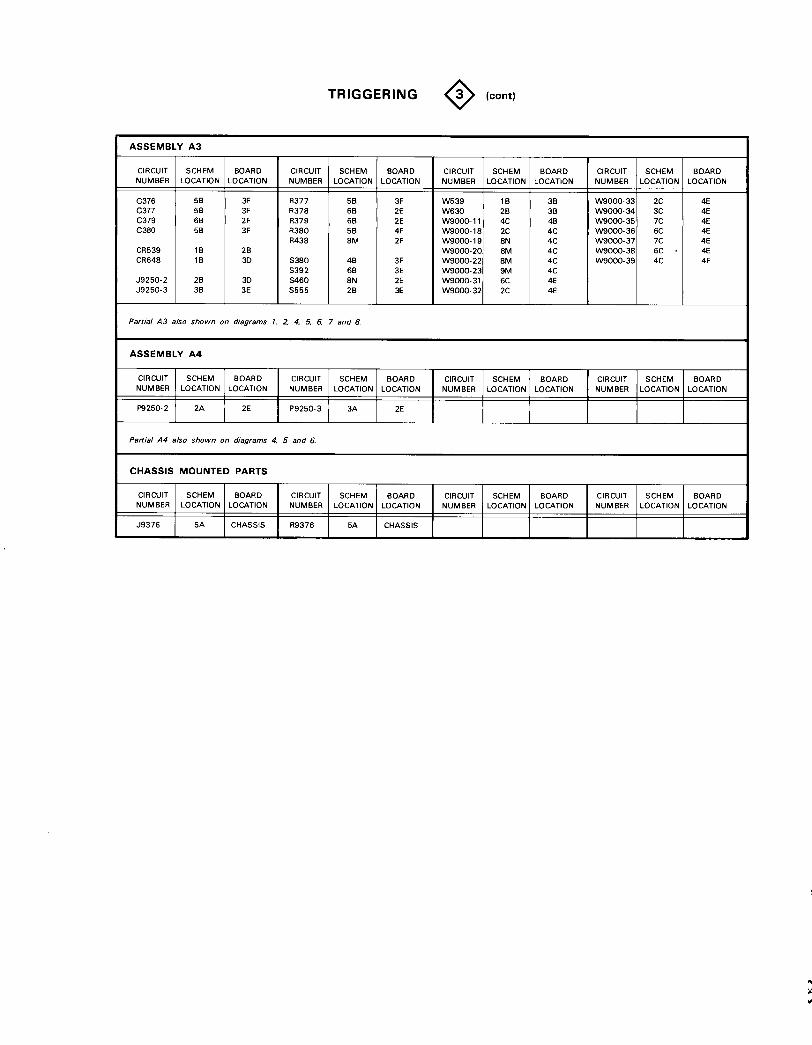
ASSEMBLY Α3
P artial Α 3 also shown on diagrams 1, 2 4, 5, 6, 7 and 8.
ASSEMBLY Α4
CHASSIS MOUNTED PARTS
TRIGGER I NG
Ρ9250-2 2Α 2E Ρ 9250-3 3Α 2E
Partial Α4 also shown on diagrams 4, 5 and 6.
J9376 Ι
5 Α
Ι CHASSIS Ι R9376 Ι
5Α
Ι CHASSIS
( εοητ )
CIRCUIT SCHEMNUMBER Ι L0CΑ7ΟΝ Ι LOCATIO N
Ι
NUMBER Ι LOCATION Ι LOCATIO N
Ι
NUMBER Ι LΟ CΑΤ ON Ι LOCATION
Ι NUMBER Ι L0CΑ7 ON Ι
BOARDLOCATION
C376 5Β 3F R 377 5Β 3F W539 1 Β 3Β W9000-33 2C 4EC377 58 3F R 378 6Β 2E W630 2 Β 3Β W9000-34 3C 4EC379 6Β 2 F R379 68 2E W9000-11 4C 4Β W9000-35 7C 4EC380 5Β 3F R380 58 4F W9000-18 2C 4C W9000-36 6C 4E
R438 8Μ 2F W9000-19 8 Ν 4C W9000-37 7C 4ECR 539 1 θ 2 Β
W9000-20 8Μ 4C W9000-38 6C 4ECR 648 18 3D S380 48 3F W9000-22 8Μ 4C W9000-39 4C 4F
S392 6Β 3E W9000-23 9Μ 4CJ9250-2 28 3D S460 8Ν 2E W9000-31 6C 4EJ9250-3 3Β 3E S555 2Β 3E W9000-32 2C 4E
CIRCUIT SCHEMNUMBER Ι LΟ CΑΤΟΝ Ι LOCATIO N Ι NUMBER Ι LOCATION Ι LOCATIO N
Ι NUMBER Ι LOCATIO N Ι LOCATION
Ι NUMB E R Ι LOCATIO N ΙBOARD
LOCATION
CIRCUIT SCHEMNUMBER Ι LOCATIO N Ι LOCATIO N
Ι
NUMBER Ι LOCATION Ι LOCATIO N
Ι
NUMBER Ι LOCATIO N Ι LOCATION
Ι NUMBER Ι LΟ CΑΤ ON Ι LOCATIO N

ω539
Ι Ι ξ8255
R556ο1ω9ασοΙ 7
5. ΙΚ-ε9_
-ΙΘ
ΜΥ
1 2
3W9Ο0Ι
ω555
V+m.z
ΧΥUSSSA
~ 74ι5Ο9
-321 -32 CH-j T cR556
5555 +s .zνAlΑ ξ Β
"SSGΙΝτ
5.1 Κι
-33Ι Ι -33 CH2T
W550
74RΥιΑι ΡRΟΝΤ νΑΝΕι 130ARU
GR3g ι
ΙΖο Ι 3
Q382~ ~~ εχτ
R346C3α9 9ισ0.Ο1μ F~
R399ΙΟ
R317 ®ο1-ιιται~ ρ 3ιΒck2 cαοιπ 1 .4iΚ c-Η7ΤRΙς, 1 . τ3ΚCR 539
V-( 70CR
ΗΑ Lτ
5 ι Ο9ΡCR539
CR551 7 2CFR0Μg~-Ι
Ι I+8.6Vp
Ο5.ίνg
Ι
_ _[ρ3ιο 2ε
R4,9II LIMST
W 419
L .9KF Rοm
wg4sl- το -1.Οοο
ι23Ο2 Q30 R306+CΝ 1 2ΖΟ
47 1ΟSIGNAL R304FROM4 Ιο 2
ι .s κ2Cι~
-Θ.6 Υ R310οιΙ .ΟακΟ
R3oS Rθοά
-Θ "6VσΙ
z20
Υ - C ΙλΙ 22 σ
0"S,Ds SIGI AL 2R 392
FROM
R305 kάα 7ι.yτκ gιο3 Q3O3
Βω ιτΜΙΤ
R3ΙιΙ -ο2 Κ
8103 Tς21GG6R
~Κ U5ηο -5.6 ι2 2ΚCHOf+ ΕΝΑ6ιΕ
6 F ©
ι3
!1
CH ι SELECT ED
ί ..13-R565
TO \Ν 9900- ιτ
ςρ 36c561
3ΟΟ C565 2FρV
+ Β.ΑVΑ
Ua6όD
97Ο
R390 C39o
g331Ιοα
ιοοΟ
R327 - α76 ο
FROM gι52
220
ω_ 3g εΚΤINPUT
Rα
R329 R335h
©θC
Q327
Ι.5κ
Ι .27ΚR3Η1
1C361
ιΚ3α~5
- 134 ΙΖΚ
Ι 6 . θ
-8.6VD1°ν 4389R9Β4 R3 B5
326
4.7
R336R328Β
Ι
ρ Ι"27Κ C-Β.6b 1FROM Q153
22Ο j
R33247 L
sc Q328 αs3οι.Sκ
G397Ο. σΙμF
C25~
31 Ι 1 31
Lima
ΤΡ397
R399-- ι-~~
-8.6 νΑ ΤιτSGGεR
ΙοοFROM R997
5392 ΒΙ
~αρ_j i8
LINE
- Β.,V,νρςοURCε "~
~ο--,-7
+8 .6V,,
R3g5-9'δναι
Η
ι ο
-36
3G LiNE !~
αθο9
910ΙΝτ -_ _ύ `
+Β.6γ(_
CR399 R369
R374LINE -_ -1
5
_37 ΙΙ -37 ιΝ7 ~
750 CR372
2Κε Α
. ..
TIR2ί2
1CR3g3
- 8.6V ο 1
ωαια-L c39z
P,393ΙΟΟο
29
[~9
ονR42o~5ΗσVιΝ ΙΝ
100Ι ΝΤ.t~οάΙΤΙΟΝ
Q419
ρ -Ρ FFR OMωgαοι-24
θID

+8.6Vς
R3 6θ
ς3ό3330ι0009
U35ΟΕ LJ35ΟΑw3so _ο.τ
υ~ι z7e
cg3,gz75 1Ι 3
Α
_
R34 αΙ .62 Κ
2Α77 Θ _z,7
νιεωGρ94Ο~ΤιΑ
b- 25
12339576
R346ι .48 χ
R3473 .1 .Κ
- Β " 6V D 1
ι9
Χ ΑΧΙ 5
+8.6VAR358
τtoo
σRS59
-157340 3c
Ον
υ926Ι458
6i5
g 5 ι~ιυgιτο α+ θ. δυς Ι
ω 9ροο- ι ` B 6V.i
R348R360
9F©qt2 +5 .2 V E,
R3 ια
Ζ
G553576
β 3519
4~~~
Ο .Ιμ F6
L]~ Jω3sι 4 τ
ιο
ιι a
U350G
cα3ΙΖ7ε
+5.2v,
i--ι ΟΑ3127Σ_
-Ο''
3
R3z~
U350D 5 7
R36
ι 9ϋ 5 Γο5
Ι 4c ο~1
_
93 Κ
ΕΑ3127 Ε t
74L503Ι .τατε
Β
α 36 ι
~S υ~sτ z Ατε -Θ.6νε ι
_ Q,-,
Ι
3
11555β
ιοΟ
NG
74LS0936Κ -8 .6 ν~ ι
-8 .6νDΙ
ΙΙ
9 Ίο υ
λι7
--8.6V,1
,5.'2 V,
+5 .Ζν ξ1 ; \N335
RA60
Κ4631,2
86.6
89.5
TV TRIG
~473
5760
m
m
ΕΝΑ $ιΕ FROΜ
~τυ F IELD 1 Ο00
ω
Q46o
~~λ 463
Μ19Ο0 Ι -17
ε---Ε9c-
- 0z-~ GH?
2709
Ο
11.9 χ2
1
Q469U49
ωια20D
Q403cr~ z
ι ι+0 .6ν
L~lJf IN Ρ- ΡΑιο Qq0
R97to
ία Β2
iz
1s
a
_
χα057 "sκ/4805
8C
ξ R965
9
ξ QΑ '? Β
7.5 Κ
~7 ΙΟΗΙΟ 2
ΙοΗΙΟ 2ιιι~ζ~~ι43σ
2.2k
63 ATR1GVe5i
Οι
ΊΙΚΔ
β5ΟΚ
Τ.01
Τ.cαιΥF
R Q56
¬ υs+ θ.6 VΑ
0Η
~
~hι
5 R47~
L-0 -8.6υ 1
AUTp ΝδR
ΆυΡΟ ~ό4zzC.1 I e. `~+
U926A
- αωνςz[ R414
3.3Ει f
3 1438- Θ .6 V~ ζ
νΡ ωττΟ
Al PARτ 1AL ΜΑίΝ ΒοΑ~ ρυ-8 .6 VA _θ.b VA -
~ ΙαΚ R479Ο ~SLO Pε
25ο
~9798AL
Ο
-t-4.l
rIZIGGER~5 Ε μ 517SV ίΤΥ
R483+s . τυ υU46DA
{ 39Ο
4 -5.2νρR 957
S
-CA3102F
I
U460F
ι .4οκ
ι 9
ι 3
+~.
+$LOPE
{ RAOςΑ3 ιο2 Ε 6 7
Ι
4
- ιορε
Lz7k
ι Ι 8
R Α 112τΡη60 '
Ι .2 ΙκU960D
R°48
~Α3i ο2Ε,"60r-
Αl Ισ 2 Ε+8 .6vq
+ θ . 6VA, R 9 S92 .4 Κ+B.6Vq C42a
&924
0.
F
U96ΟΣ υ46σΒ
RA53
220 Κ2οκ
,CΑ3 Ιο 2 ε ~Α3 Ια 7 Ε
α
47
~953+
ΙΟ
;
ι00Ο
Q420 4 Ζ.2 94
ιτsυθsτιτΑτe
(-
Ο
ο .b1 ρ - ρΑιπα
R-45z α4ss~
αΤQ1GGERNORM
2.7 Κ
1 ο
LΕνει τΟ R4417G Α SLOP-
R4 1424.κ
28
W90DI ω 9ΟΟο ω 9οοο-z0
-19-ο:ω
ν
ΝοRΜ +
t
ω4
` ~ ίυοτωι
_z2
-zx8416 ΡΡ
R 92 6-op- ΡΑυτα α 7 κ Αυτο 9δΟμ
2-
+ΑUΤΟ LΕνέιc~
l
ΝοRΜ
~Ω- ΡΑιπΟ
S960
Static Sensitive Device$-8.
ι κ6Vq~
R92$
Νοωκ
ι
3
© 5Μ Μαίπtαηαη ce SκtionΓ ] Ρ- ρΑιπα
Q428
sιοαε __+ Θ .6 VΑ
~NORM
Rg3 ααν
ΙΝ
Ζ
COMPONENT NUMBER EX A1λ PL L.
L Ρ - ΡΑυΤΟ
89ΖΚ (+iA U TO
5σο+B.6Vq~ +e.6Vq
- θ.6VΑ LΕ.νει
OUTα
Component Numb er
R47 ,14.3K
04591000
R4733-9K
Ν 1 TV FI ΕL tDLIZ:) Fλ5Ε
U4 CAιΟΗίΟ 2
R-187Α70
Τ RI GG ER ~NG 0
W1
R413
R434R9~5
R427
2 ει1
ι-
μΑ23 R1234Ιικ
24ΟΚ, ~ κ915
43Ο_
υ426Β
Ι
[::I-" -1kΡρ
1958
¢ΡΑυτ L7
ATRIGGERAuemnty ~1
~Ι~ενεΓ
ϋι7η R417 091 ς1}
+Σ
ω 4411 _οτ 1αοαιυι _23
-23
Num Π er
Sυbassembf-
7_yNum6er
~RΜ
97 χ y 3 .3f~F1`
Ν~Ε:Μ_
AUTO LEY£ L CCW
Num bei (ifusedJ
+®z Rιλ7lρ77AUTO
.iι
R429
Ch-.,πχυπ 1e d σσmρσπ ¢πϋ h ανe π t, Α-emh1y Νσ n ι b ~,
~7 Ύ LSίλή
R923
~>3ά2Μ
Ι Κ
Α3 ΡARTIAL F RONr pgμEL SOARPi .~-see en d σΙ Aeplacea h le E lectrical P arts [ist.
Ι ο
Q429
-8.6νΑQ9 Ί ~
R433
NQMEχ pL λχσ ιεττεα λτ :1QΝλ L LINES 70ιΙ 2
ατκ
ρ
f-1 ΑυΤσ
σα εασ Q στχε R οιλσχλπι~ ιΝειελ7ε s 7 ιε6Vq
QRID COORDINhTES ΟΝ λΝσ7Η4Α 5~ ΗΕΝλ7Ι~ίΌ')NORM+8 "` Β"6VA
R435
Ι
IFOp εΥλααΡιε~ σε7
Q 421
zι,πQ 423
Ρ - ρ Ρ[]Τ
ο[921R42~
ιΑ,F2 αΚ {--ε

m
βΖ
2235 Service
3
4
ΝΝηηασ
C-R742~ .
1ή~7ΌCib7l
Q712 ,ίΙ~732
- : Q7Π
., R713 , ι -R71,73d, Oil- ('1714 071 DA
07.108 -',c7το
C713'.
©Static Sensitive DevicesSee Maintenance Section
COMPONENT NUMBER EXAMPLE
Co mponent Number
Α23 2 R1234Asτem biy 5~ chem αδcNumber subasτembly
Cσ¢ υ"Nυmber
Number (! used]
Chαsss mσυπ[edcomponents have πσ Assembly Number0 p re fix-see en d σΣ Replaceable Electrical P arts List,
αβto
_
_
Η ιοι
e~7π 0R741 '
F igure 9-11 . A41-Timing board.
4206-41

A4-TIMING BOARD
CI R CU IT SCHEM CI R C U IT SCHEM CI R CU IT SCHEMNUMBER NUMBER NUMBER NUMBER NUMBER NUMBER
C701 4 Ρ9700-7 4 R721 4C701 4 Ρ9700-8 5 R722 4C701 5 Ρ9700-9 5 R724 6C701 5 Ρ9705-1 6 R727 6C702 4 Ρ9705-2 6 R728 6C703 4 Ρ9705-3 6 R730 6C705 4 Ρ 9705-4 6 R731 6C706 4 Ρ 9705-5 6 R732 6C707 6 Ρ 9705-6 6 R733 6C708 4 Ρ 9705-7 6 R737 6C710 5 Ρ 9705-8 6 R738 6C712 5 0701 4 R740 6C713 5 Q704 4 R741 6C714 5 Q704 4 R742 6C715 4 Q706 4 R743 6C720 4 0709 5 R745 6C724 6 0710 5 R746 6C728 6 0710 5 R748 6C749 6 Q712 5 R749 6C750 6 0732 6 R750 6C751 6 0737 6 R751 6C752 6 Q742 6 R752 6C755 6 R701 4 R753 6CR 732 6 R702 4 R754 6CR 742 6 R703 4 R755 6Ρ 9250-1 6 R705 4 S701 4Ρ 9250-2 3 R707 4 S701 4Ρ 9250-3 3 R709 5 S701 5Ρ 9250-4 4 R710 5 S721 6Ρ 9700-10 4 R711 5 U715 4Ρ 9700-1 6 R713 5 U750 6Ρ 9700-2 6 R715 4 U760 6Ρ 9700-3 5 R716 4 VR720 4Ρ 9700-4 4 R717 4 VR749 6Ρ9700-5 4 R718 4 W709 5Ρ 9700-6 4 R719 4

7 Λ GATE
ΦΦf
SET CH 1 AC-GΝ0-DC ΤΟ GΝD
END OF AUTO TIME-OUT
2235 CON T R OL SETT I NGSDC Vo l tages
Α I NTENSITY
M i drangeHORIZONTAL MODE
λΑ SE C/OIV
0 .1 msΑ T R IGGER Mode
Ρ-Ρ AUTO
AC Wave for πsVERT ICAL MODE
CH ICH Ι VOLTS/OIV
1VCH Ι AC-CND-OC
DCHORIZONTAL MODE
ΑΑ TRIGGER LEVEL
MidrangeΑ TR IGGER Mode
Ρ-Ρ A U TOΑ SOURCE
ΙΝΤΑδΒ ΙΝΤ
CH 1CH 1 I NPUT SIGNAL
1- k Hz sine wave, 4V Ρ-Ρ
+4 .4 V
+3 .4 V
Η
L
H +3 .5V HI ΙΝΤΕΝ+2 .6V LO ΙΝΤΕΝ
L
3 .5V
HOLOOFF TIMING
+I .9V
+Θ . 9 Υ
Η
L
Η
L
42θ6-97

ASSEMBLY Α 1
BOARDNUMBERCIRCUIT
SCHEM
BOARD
CIRCUIT
SCHEMΙ LOCATIO N Ι LOCATION
Ι
NUMBER Ι LOCATIO N Ι LOCATIONBOARD
CIRCUIT
SCHEMΙ
NUMBER Ι LOCATION Ι LOCATION
Ι
NUMBER
LOCATION LOCATIO N
C501 9 Ε 8C Q511 7Κ 7D Ρ 524 8D 6E U506A 6Η 7DC502 9 Ρ 7C Q525 7E 6D "525 8 Κ 6E U506B 7Η 70C503 9 Ρ 6D 0576 6 Κ 7D R 526 7 F 7E U532A 8Η 7DC504 5 F 6D 0578 7 L 7D R 527 7Μ 7E U532 B 7F 7DC505 6E 6D R 528 7 F
BID U532C 7G 7DC506 9Μ 7D R 501 9E 7C 8568
BID7D U532D 8F 7D
C517 7D 6D R 502 8Ε 7C R 569 8D 7CC518 6D 6D R 503 9E 8C R 571 8G 7D W582 7 L 7DC519 6E 6E R 504 5 F 6D R 572 7G 7D W9001-17 9Β 6ΑC520 6D 6E R 505 5E 6D R 573 8 Η
BIDW9001-24 8Β 6Α
C525 8 Κ 6E R 507 9F 8 Β R 574 7G 7D W9001-25 5Β 7ΑC527 8Μ 7E R 509 9 F 8C R 576 7 Κ 7D W9001-29 9Κ 7ΑC531 9 Ν
BIDR 510 91 8 Β R 577 7 L 7D W9001-30 98 7ΑR 511 8J 7D R 578 7 L 7D W9700-10 7Μ 7E
CR503 7E 6D R 512 7-1 7D R580 7 L 6D W9700-4 5Ο 7ECR508 BID
7 Β R 513 7-1 7D
W9700-5 5D 7ECR509 9F BB R 514 7Κ 7D ΤΡ504 7E 7E W9700-6 5D 7ECR514 7J 7D R 516 8J BID
W9700-7 8Μ 7ECR518 7E 6D R 517 8Η
BID U502 BE 8CR 518 6G 7D U504A 6F 6D
0509 9 F 8 Β R 523 7D 6E U504B 7D 6D
Partial Α 1 also shown on diagrams 2, 3, 5, 6, 7 and 8.
ASSEMBLY Α3
CIRCUITNUMBER Ι L
OSCHEMCATIO N Ι
BOARDLOCATIO N Ι
NUMBER Ι
SCHEMLOCATIO N I LOCOATIO N
ARD
Ι
CIRCUITNUMBER Ι
SCHEMLOCATION Ι LOCATION Ι
NUMBER ( LOCATIO N LOCATIO N
DS518 9L 2E R 520 3Β 2E W515 9Α 1 F W9000-25 5Β 4DW9520 4 Β 3E W9000-29 9Κ 4D
J9250-4 4 Β 3E S401A 5Α 2E W9521 38 3E W9000-30 9Β 4DS4018 8Α 2E W9000-17 9 Β 4C
R 519
3 Β
3E
S401C
9Α
2E
W9000-24
8 Β
4C
Partial Α 3 also shown on diagrams 1, ζ 3 5 6, 7 and 8.
ASSEMBLY Α4
Α SWEEP GENERATOR & LOGIC
Ο
CIRCUITNUMBER Ι L
OSCHEMCATIO N Ι LOCATIO N Ι
NUMBER Ι LOSCHEMCATION Ι LOCATIO N
Ι
CIRCUITNUMBER Ι
SCHEMLOCATIO N Ι LOCATION Ι
NUMBΟ LOCATIO N Ι LOCATIO N
C701A 1Μ 2C Ρ9700-10 7Ν 1D R701 1 F 2D R 722 2 F 4ΑC701 Β
1Μ
2C
Ρ 9700-4
4D
1D
R702
1G
2EC702 2Ν 2E Ρ 9700-5 4D 1D R703 1 Μ 2E S701A 11 3DC703 2Ν 2E Ρ 9700-6 4D 1D R705 2 Ρ 1 E S701B 1D 3DC705 2 Ρ 2E Ρ9700-7 8Ν 1D R707 1 Ρ 1CC706
3 Ρ
1D
R715
3E
4 Β
U715
2E
3 ΒC708
2 Ρ
1 E
0701
2Ν
1E
R716
3D
4CC715
3D
3 θ
Q704A
2 Ρ
2E
R717
2E
4 Β
VR720
2F
4ΑC720 3 F 4Α Q704B 3 Ρ 2E R718 2E 48
0706 2 Ρ 1D R 719 3 F 4ΑΡ9250-4 48 2E
R721 2 F 3Α
Partial Α 4 also shown on diagrams 3, 5 and 8.
CHASSIS MOUNTED PARTS
CIRCUITNUMBER Ι L
OSCHEMCATIO N Ι LOCATIO N Ι
NUMBER Ι L OCATIO N Ι LOCATIO N
Ι
NUMBER Ι LOCATIO N Ι LOCATION Ι
NUMBER
LOCATIO N Ι LOCATIO N
R9521
Ι
3Α
Ι CH ASSIS

νΑ RHOLOOFF
FN οR Μ
R) 5Z%5οΚ
μαχ ~cw
it 54ΟΙΑ IS ΑΜοΜεΝΤΑRΥ 5ω+τCΗ
5.101A*5GL
W9OPbΙ ιW94 ΡΙ
5ωρ
Τ --~-~-
-
-zSH-asΙ 2 Γ 3γ
>,
55 RESET
Ι
ΙΙΙΙ
SHOWN ιΝ Ι5Gι5ωΡ ΙRΣΑΟΥ ι
5401f3 ΙΙΡ_ρ ΕαιιΤΟ ι α 5 eq
Ι t86V.Ι
~ι
+8.6 ν,R519b.θΚ
R5209.1 Κ
J9~So~ W95~ 2~Έ
--24 Ρ-Ρ
NCSgοIG 4~6αUORM F Ι - y
7 2 3y+S.6% -3ο Ι -3Ο 55
%Υ
.2
TV TRIG ENABLEΤοR4Ο2~ςgη31~, Rg73qΜ
R52420-OK
-S .bVB
~Α3PARTIAL ΙRΟΝΤ ΡΑΝΕL 80ΑRD
ΑΕ PARTIAL MAIN BOARD
2235
9 Η . Ο. Ι
C R 508DI
R568 ~τξ5693.3Κ 9.3Κ
Τ~}
+5.ίνΑτλ414 ΣΓR951
Iz R 5ΟΖRS01 ξ 910s.ικ ια
KY Τσ Rl3-+~% 7κγ Το pgz5o-2
-~ XY To P9250-3
R 507390
2"2Κ
R-! ~522pF 15.8Κ Rll9 ζ12σ-8 .6Vς 33 o.l ηrF
!° RΤ1ί55οο
2 Q509
R So9
ΡαπΥιΑι 57σιαΑ AIJDs ΖΕClolV
R701 R7025,4.-ΝIN %γ
2,99 ΜΡο5ΙΤΙσαρ TIMING
977 gσΟΥ ΙΝΟΙCΑΤΕ$
2.25ΚPOSITIOH WHEN5ωΙΤCΗ S5 CLO$ςρ
Ι2Κ
4.5χ g
Α ΑΝU θ 3EC J 01Υ
ι~
Θ 2.5Κ
~"
9R722 4ι.2κ ιο
74Ιη Ι5.οκ Ιι ~το Rill©
seτ18 ; vRl2o ι
ΦΑ15 . οΚ 2" 7 3.G V R125 ISGAs`1G EO
R716
6 WITH S721Ια,ΟΚ 3t ιι
α
+5 .ΖVΑΙ
[5ο9 R504FΣ ΙΖΟΚ3.3η
CR509
2οο
α.Ι2κ
74
R721
3Ι θ "25Κ
5ΟΟ Ι
8.25Κ 2 Ιου~εs
Ιe7 ι7 ~ω ,
+5 .έ
U 532D P571IOHF02 2.2Κ
R57Ρ.,L

*?Q(.- Z"
s7οιρ
Α ΑΝσ ΒSΕC)
οη V5 ΗΟωωIN
Χ yΑ TIMING
Ρ'σθΙΤΙΟΝ +3ΟVgO-Tr.11701
R7 ο 70
2 κ_ιπ
ι 5 {
Ί ι
α.οιρ F Ιμ F
s ι ι ι ι --Τ
i ιι
ι
ι
ι
ι
ι
τ
ι
ι
ιΙ
we-1
Q701C703
ιΥο2
α
+a.6Yg2a6 gFΥ
Ι
Ι
Ι
ι
Ι
Ι τ
_ Ι
Ι
η
Ζ ΙΙ'
55ο7Ο5
57 ΟΙΙ5
Ι
Ι
Ι
Ι
f
=Υ--
Ι
Ν0I'M
5ΡθΕ9
r047μFΙ
r
Ι
Ι
Ι
Ι
Ι
Ι
ι
G
ASWP 7οΙ
ι
Ι
ι
ι
ι
ι
ι
ι
ι
4ΟTIMING ΓFΗ
Ι
Ι
Ι
1
Ι
Ι
Ι
Ι
GΙ Ι Ι
ι
ι
C70θλ Ι
Ι
Q70-IA s
2.2
R705 Q70(ο150
""
+
+
"
R517 i
R546η.3Κ
3.,)Κ
50 (.A.Ισκ l3Ι
Τ 5Δ
2
+8.άνρ
U 532AΙΟΗΙΟ2
RIS S ιΖ 4
3.9Κ
Q!31097ο
CS256.9
τ
5 σ σΟ σ Ο
! α σ
FΑρΛ1τ21, σ40 οb0
1213Β
Τ9Ι 1
57ΟιΑ ,gρΑ]ττΟΜ VSEw
ΤΟ W4ΔΟΟ-2Ο$F η
Μ τ Ν ι Ρ
έΣ- 3
Ι25779 κ 4
~~α
45784s7ε
U5066 +α.6 νρ 1576
szs7e10 μΙ S1
REIN 560
Soo15
CR 519 470 W582Vp 11
ago
R527 ωgταο
Ρ4700
Ι9
4.7 Κ
_fo
Ισ
ρGΑΤΕΙ9R4
R512
4511
R ηθΟ
ΤΟ CR583
AGA7 E4.3Κ
β525
1CO C57722 . ικ
α5Α Sw P
-τ Ι
Ι7 Ι
ΑSwPLλ1J~
1 Lf ύί
Α4 ΡλRΤιΑL TIMING BOARD
U504
U50 (E,
0532
~
~ U502yb1502 Ιοκι3ι ΙοΗιοζ 10 ι98
8
Α SWEEP GENERATOR $ LOGIC
9CQ0048
ς CTO6αοιμF
ι S
+5 .Ί
+t5'12%
+5.ZV~+5.2 Vς,+5. ΖV
Α2 ©Static Sensitive DevicesSee Μαίη1ε χα~5eε δυπΊΊ
χF
5Ο6
Ι C5
Ι C5Ν0.
3
4700
οι F
ο. σι ξ
COMPON ENT NUMBER EXA MPLE
10
ι
ιs~
1
16~
ι
ι6π
1
C-ponent Number
Α23 Α2
r~
R 1234
r~ εΠem ιπΑτ-em6φ
GπυιιΜυ mher SυΕαs7emOfy'-b'Number (,F -d)
Chd95ί 5+ΠρυΠΙρΟ ρΟΦρΟπ.πϋ h αν e ππ λsd¢ υι hΙ y Numberprefιx-ue end ΠΙ Θeplaceahlρ ΕΙρηπ[αΙ ΡαGS LΊ 5 Γ .
NUMERAL AM LEΠSR AT SIG- UNES ToOR FROM OTHER DIAGRAMS ΙΙΦΙ C ΑΤΕ S THEbσο CΟωισιΝΑΤεR ON ANOTHERSCHEMM9FOR ΕΠλΜΡLΕ- ΛΕ )
Re Αr- (AΟξ6) Μ~Τ
rnΖα
ΟΜ

2235 Service
2235 CONTROL SETT I NGSs
DC Voltages
AC Waveforms
AC-GND-DC (bot h )
GNO
VERTICAL MODE
CH 1Α TR IGGER Mode
NORM (sweep
CH 1 VOLTS/D I V5m Vnot runn ing)
AC-CND-DC (bot h )
DCHORIZONTAL MODE
ALTΑ SEC/DI V50 μsΒ SEC/DI V5 μsΒ DELAY TIME POSITION 5 .0Β TR IGGER LEVEL
Cμ-RUN AFTER DELAYΑ TR IGGER Mode
Ρ-Ρ AUTOΑ&Β ΙΝΤ
CH 1Α SOURCE
ΙΝΤ
μΗ .0 . ΤΙΜΕ
-~{
H . 0 .
ΤΙΜΕ
LO FOR Α d Α ΙΝΤHI FOR Β SWEEP
L
+12V
+0.8V
Η
If L
ΗΗ
HI IN Α 0R 8ι
φ
LO IN ALTL
Η
SET θ TR IGGER LEVELTO M IDRANGEπ π π ι
ι
Η
L
CH 1 I NPUT SIGNAL5- d iv > 1-kHz si ne wove
Η
L
L
Η
ι
42θ6-94

3
ON
400
©Static Sensitive DevicesSee Mai ntenance Section
COMPONENT NUMBER EXAMPLE
Component Number
Α23~R 1,
234,~SAssembly
chematlεCircυ~Number Subassembly Number
Nnmδer ρ7 nsed)
Chassis mounted components have no Assembly N um berprefix-see end of Rep laceable FJectrιcα l Parts List .
4-+-+-ε-+-
"-*--rt
- ιτ-y ί .
,
-;2η ,
ι
ι
,
ι
ε
σ
ι
ι -έ5 ί ιΑ
.t ι.42W42
Figure 9-12 . AS-Altn Sweep Logic board .
A5-ALTERNATESWEEP BOARD

ASSEMBLY Α 1
Partial Α 1 also shown on diagrams 2, 3, 4, 6, 7 and 8.
A5-ALTERNATE SWEEP BOARD
CIRCUITNUMBER Ι NUMBER
SCHEMΙ NUMBER Ι NUMBER
SCHEMΙ NUMBER Ι NUMBER Ι NUM
SCHEMBER Ι NUMBER
C610 5 R623 5 U605 5 W677 5C624 5 R624 5 U605 5 W678 5C627 5 R625 5 U605 5 W682 5C643 5 R626 5 U605 5 W690 5C655 5 R627 5 U605 5 W695 5C659 5 R629 5 U605 5 W696 5C665 5 R630 5 U625 5 W698 5C671 5 R631 5 U625 5 W9401-10 5C672 5 R632 5 U625 5 W9401-11 5C690 5 R633 5 U625 5 W9401-12 5C693 5 R634 5 U655 5 W9401-13 5C694 5 R637 5 U660 5 W9401-14 5CR680 5 R638 5 U660 5 W9401-15 5CR685 5 R640 5 U660 5 W9401-16 5CR816 5 R642 5 U660 5 W9401-17 5CR817 5 R643 5 U660 5 W9401-18 5Q619 5 R644 5 U660 5 W9401-19 5Q620 5 R651 5 U665 5 W9401-1 50630 5 R652 5 U665 5 W9401-20 5Q631 5 R653 5 U665 5 W9401-21 5Q637 5 R657 5 U665 5 W9401-22 5Q643 5 R660 5 U670 5 W9401-23 50680 5 R662 5 U670 5 W9401-24 50685 5 R663 5 U680 5 W 9401-25 5R604 5 R664 5 U680 5 W 9401-26 5R605 5 R665 5 U680 5 W 9401-27 5R606 5 R666 5 U680 5 W 9401-2 5R609 5 R670 5 VR624 5 W 9401-3 5R610 5 R671 5 VR660 5 W 9401-4 5R611 5 R672 5 W637 5 W 9401-5 5R614 5 R674 5 W638 5 W9401-6 5R616 5 R677 5 W643 5 W 9401-7 5R617 5 R690 5 W655 5 W9401-8 5R619 5 R693 5 W662 5 W9401-9 5R620 5 R816 5 W 668 5R621 5 R817 5 W 670 5
Β TIMING & ALTERNATE Β SWEEP
NUMBER LOCATION LOCATION Ι NUMBER LOCATION LOCATION Ι NUMBER LOCATION LOCATION Ι NUMBER LOCATION LOCATION
C603 9F 5E R645 4E 8Ε W 9001-13 2E 5Α W9400-20 5F 7EC635 2F 7F R646 5E SD W 9001-15 1E 6Α W9400-21 1 F 7EC646 5F 7E R647 5F 8Ε W 9001-16 9F 6Α W9400-22 6F 7EC647 3E 6E R648 1 F SD W9001-26 2E 7Α W9400-2 9 F 5EC648 1 F 6E R649 2E 8D W9001-27 2E 7Α W9400-4 9 F 6EC649 3 F 6E R673 6 F 7E W9001-28 9F 7Α W9400-5 1S 6EC673 7 F 7E
W9400-10 2F 6E W9400-6 2F 6ΕVR645
5E
SD
W9400-11
2S
6E
W9400-7
2S
6ECR 712 6F 7E VR712 6F 7E W9400-12 2 F 6E W9700-3 6F 7E
W9400-13 1F 6E W9700-9 6 F 7EΡ9644-1 4E 8 Ε W602 9 F 6E W9400-14 5 F 7EΡ 9644-2 5E 8 Ε W603 9 F 6E W9400-17 6 F 7EΡ 9644-3 5E 8Ε W635 2E 7F W9400-19 2 F 7EW649 2 F 6Ε W9400-1 9 F 5E
TABLE (εοηt) Ι
. .

ASSEMBLY Α3
NUMBER LOCATIO N L OCATION
R602 Ι 9E
S602 Ι SD
ASSEMBLY Α4
ASSEMBLY Α5
1 F
1E
CHASSIS MOUNTED PARTS
Β TIM I NG & ALTERNATE Β SWEEP
Partial Α3 also shown on diagrams 1, 2 3 4, 6, 7 and 8.
P artial Α 4 also show n on diagrams 3 4 and 6.
BOARDCIRCUIT SCHEMCIRCUITSCHEMNUMBER
Ι LOCATIO N Ι LOCATIO N
Ι
NUMBER
Ι LOCATION Ι LOCATIO N
Ι NUMBER
LOCATION Ι LOCATION
S648 2 Β 2D
W9000-13
2~
Ε
48
(cont)
W9000-15 ~
1 E
4C
W9000-27 ~
2E
4DW9000-16
9E
4C
Ι W9000-28
9E
4DW9000-26 2E 4D
CIRCUIT SCHEMNUMBER Ι LOCATIO N Ι LOCATION
Ι
NUMBER
Ι L OCATIO N Ι LOCATIO N
Ι
NUMBER
Ι LΟ CΑΤ ON Ι LOCATIO N
Ι NUMBER
Ι LΟ CΑΤ ON Ι LOCATIO N
C701C 6C 2C Ρ9700-3 6E 1D Q7108 7D 1D R713 6D 2CC701D 6D 2C Ρ9700-8 7E 1D Q712 7E 1CC710 7D 2D Ρ9700-9 6 Ε 1D
S701C 38 3DC712 7D 2C
R709 6C 2CC713 7D 2C Q709 6D 1D R 710 7D 1C W709 6 Ε 1DC714
7D
1C
Q71OA
7D
1D
R711
6Α
2C
BOARDNUMBER Ι LOCATIO N I LOCOATIO N
Ι
NUMBER I L OCATIO N I L OCATIO N
Ι NUMBER ILOCATON I LOCCA710N
Ι NUMB E R LOCATIO N Ι LOCATIO N
C610 91 3Α R620 7J 28 R 817 4 Ρ 3C W662 1 Κ 1EC624 3Η 2Α R 621 7J 2Α W668 5 L 1CC627 7 J 1 Α R623 81 2Α U605A 81 3Α W670 7 J 3CC643 6 Κ 3E R 624 3G 1Α U605B 91 3Α W677 2 Ρ 3 ΒC655 6 J 3C R625 81 2Α U605C 8G 3Α W678 2 J 2EC659 4Κ 3D R 626 7Κ 1 Α U605D 8 Η 3Α W682 4 Ν 2DC665 5 J 3C R 627 81 1 Α U605E 9 Η 3Α W690 4G 3DC671 2Μ 28 R 629 8Κ 2Α U605F 8 Η 3Α W695 7 Ρ 1CC672 7Μ 3C R630 7L 1 Α U625A 8 Κ 2Α W696 7 Ν 1DC690 4Η 3Β R 631 8L 18 U625B 7 Κ 2Α W698 7 Ν 1 θC693 4G 1E R 632 5Μ 28 U625C 8J 2Α W9401-10 2G 4ΒC694 4Η 18 R 633 7Μ 3 Β U625D 8 Κ 2Α W9401-11 2S 48
R634 7L 1 Β U655 5J 3C W9401-12 2G 4CC R 680 5 Ρ 2C R 637 9Κ 3 Β U660A 9Μ 2D W9401-13 1G 4CC R 685 4 Ρ 2C R 638 9L 2D U660B 5Μ 2D W9401-14 5G 4CC R 816 4 Ρ 2C R 640 9L 2D U660C 4 Ν 2D W9401-15 4G 4CC R 817 5 Ρ 3C R 642 6Κ 3D U660D 9 L 2D W9401-16 4G 4C
R 643
6Κ
3E
U660E
2L
2D
W9401-17
6G
4C0619 7Η 2Α R 644 6L 3E U660F 5 L 2D W9401-18 4G 4C0620 7 J 2Α R 651 5Η 3D U665A 5 L 2C W9401-19 2G 4DQ630 7 L 28 R 652 5Η 3D U6658 3 Ρ 2C W9401-1 9G 4ΑQ631 7 L 1 Β R 653 6Η 3D U665C 2 Ρ 2C W9401-20 5G 4DQ637 9 L 2D R 657 4-1 3D U665D 5 Ν 2C W9401-21 1G 4D0643 6 L 3D R660 3-1 38 U670A 4Μ 2Β W9401-22 6G 4D0680 5 Ρ 2C R 662 4Κ 3D U670B 1 Ν 2Β W9401-23 4G 4DQ685 3 Ρ 2C R 663 4J 3D U680A 1 Μ 2E W9401-24 4G 4D
R664 5Κ 3E U680B 2 L 2E W9401-25 4G 4DR 604 9G 3Α R 665 5 J 3C U680C 5 Κ 2E W9401-26 3G 4ER 605 BG 3Α R 666 2 Ρ 3C U680D 5 Κ 2E W9401-27 3G 4ER 606 9G 3Α R 670 2Κ 1D
W9401-2 9G 4ΑR 609 91 3Α R 671 1 Μ 1C VR624 3G 2Α W9401-3 4G 4ΑR 610 91 3Α R 672 6Μ 2C VR660 4J 3C W9401-4 9G 4ΑR 611 9-1 3Α R 674 2Ν 1 θ
W9401-5 1S 4ΑR 614 9 Η 3 θ R 677 1 Ρ 1 Β W637 2J 3C W9401-6 2G 4 ΒR 616 SG 28 R 690 4G 3 Θ W638 4 Η 2E W9401-7 2S 4 ΒR 617 SG 3 Β R 693 3G 3E W643 6 L 2D W9401-8 4 Ρ 48R 619 7 Η 2 θ R 816 4Ρ 2C W655 3 Η 3E W9401-9 5S 48
NUCIRCUIT
SCHEMMBER LOCATION LOCATION
Ι NUMBER I LOCATON Ι LOCATION
Ι NUMBER (L OCATIO N Ι LOCCATIO N
Ι NUMBER L ΟΟ CΑΤΟΝ LOCATIO N
CI R CU IT Ι SCHEM Ι BOARD Ι CI R C U IT Ι SCHEM Ι BOAR D
R9644 5D CHASSIS

Ρ7212F
Α4 PARTLAL TIMING BOA RS
2235
ωηνε FοRΜS
Α3 PARTIAL FR04T ηΑιυει θοηRD
S b4BΗOR I7oNYA L _-_
~πααε
Β7RIGGER
+ 5 .2VA
ω9οοοΙ Ιω9Οοί 96495.1 Κ
ω94οοΙ 3 Ι
1W9'"ΑαΝLΥ
-ι5 ι
. is
~_-ι
ί3
ΑοΝLΥ
10001 οΟ
FRO"
Γ21 Ι
Ι~2Ι
Α1-7 SV1JcGRSο9Ε 4
~®
VALT_ W635 - Ι9 _ιy VF~LTFΑΟΜ
4CΟ
C63S
+5
.2Υρ
~22ο0
IFRοΜ =12F
Ι-Ι2
C+41 5ΕιΕCΤΕD
Ι -R 649 R5b5Q I5. IX
ω6α9 qG
,6
!-6
Β οΝιΥ_ _2εν Η,ΑLΤ -2τ
-27
- ΙΟ
-10
ΗΑιτ
C647 C699ΙΟσσ Ιο 0Ο /
R6z4 W65°1-27 43
5701c5 Ο ο Ιί
Α ΑΝΟ Β SEC/ Dιν3°ο ο θ
Γ
βτιΙΝΙΝ6
Ρο 5ιτι0Ν
W9400
δz2pF ~~ οιρF-
ι
5ΝFRONTI
3`
~'σ 7
5 5 ι
- Ι 6Ζ ο
Ι 84 ο
α9 . !
ι
GN4
-23σ
5σ "
ι +8 .6VA
~4
S-70, 2ο ι
ιi3iΤΟΜ VVEW
Ια
ι
-15Ρ4644
2όόS
R6ρο Ο 6 ς o-rι '
α7οοι
-8.6Vρ7_Ζ,5
W690ΝΟΤΕ: m5 2 LHH ιDOT ΙΝD Ι [ΑΤδ5 Ι
ιΡΟ5 ίΤιρΝωΗΕΝ
.5
ι
ν.645.
SWITC_ ι5 [ισsRΡ
6_2ΥΒSWεΕΡ Rυ"AT
. Ι
ι
g
R6g72
5οms
T" 50" 5ο ι
ι
ρΕιΑΥ
τ
ΙΚ ω94 σιο4Υο ο.55 POSITIONS
ΤΙΜΕ
Α9644
--GF ΤΗΕ Θ SECj o1V
PO
2ι
ι
Ρο5ΙΤ 1οΝ
Κ
Οτ ω1ΡΕΑ5ωιτ0κ
Ιο
ι
Ι Ι Ι
C6464- ιF
j
'
ι
Ι
227.
R651μs
ΑSWP ~νzΟ '
, -2σ Α 5ωΡ
7.50κΙ
R646
-.5
ι
4 Κ2
FR0Μ. Ι
ι
ν ρΕLΑΥ
WθΙΟΟ -Ι η-"~9τΑRτ
Βιη q4
Ι1
ΟΕLΑΥσ 5
ι
"c ΝΟι
Ι Ι Ι Ι
Ι ι
+30Vg 6R,11
Ι
Ι Ι Ι Ι
Ι Ι
Ο
ΙΡ 97ΟσΙ ι ι Ι ι ι ι
ι Ι
[lσΙο*
7,R7t
!!!/3ς
4 Ι 2Κ
4
ΙΟ
1
Ι
1
Ι
Ι
7
1NF
ΖΚ Β 5WΡ
"-5
- LG "
'-4c Ο 7` ΙΥΙ
1
ς
Ι
Ι
Ι
Ι
R 7Ο9α2.5Κ
9 2
! ι ι ι Ι Ι
ι
1 ιο
0.Ιρs ΒκIS
[R712Ι
C1ο1C
~5ΡΕΕί) ΤΙππιμc9 ΙΙ
Ι f 1 ί
Ι
ΟΙ Η F VR ll2 ~4 ι .2 κ 82 .5Κ ιο 3
! έ ι 'Ι
α
Ο
Q709
R6τ3
Ιτ . νν-
°"
Ι
Ι
[
ή
Wlo9
9
_qq,, Κ
- Ι 7
Ιτ
Β l213TRACE6 Ι 858.2 ΣΚ
t τι 3
+B.Gvex
1 Ι
1
r
1C7 Ιοα-2 5
ι
4 Ι8
. οττ�F
[673
+5. ι5νΘ .τ5χ
ΡΙ
ι54.121t
7 12
~Ι
9
R6[7141 R70730 8Β(σFτ
ί~ίΙQΕλ
Νο
R7 ιο
Q~ ί2
~Ι Ι
L-
Ι
06lq
* cτοιc ξ cτοιD
ος~~j ~
ι g1
Ι=κοππARE ΡΑ"Τ of Α
Ι
1..47~0Β
3-
~W9ρφ-βΜΑΤCΗ α
SF.7,
C70iA G7016 Αι2ΕI1Ο CΑΤεο ΟΝ
Ο1R`- 8.6νι 6O9F
- Θ -6V μ
8 5LΟΡΣ
-4
8SIGNAL to
5UΒ 5 ΤRΑΤε ~ γ $+Θ"6Υςc3l
Ι,
136V- . mλ- LΕ V ΕLη R602 - Ι( 1
1- Ι6
W6ΟΖ
_41
ι_4
6 LEVEL5Κ
Ι
ΙΒ ιΕVει
-2
+5 . Ι5Υ
R616η ,g οκ 6
~605CΙ 1
+5 .15ν ιmR6o5 ξR61lΙ.27Κ S V .LOK
R76. q4Κ
� ΙR6o6L21 Κ
_ο ΙΟ 5ΗοωΓ1 ΙΝ χΥ
Α3 ΡΑRΤΙΑι F RΟΝΥ PANEL 5οΑRα
ΑΙ ΡΑRΤΙΑLMAN8opR
AS PART ΙΑL ALT 5\Nαl--

---ow +G-15V
----} +5 .2 VA3
"--~ ξ 5.2V ρΙ 18
>V - ι
GIG θogR~
s-τ7
R66o410
νR66σ
ljy 5. Ιν
R657
Ι 3 U625C 13 Ι5
Sι4 ΙΟΗΙσ 2 Αiά 5 Ι 2 R 629 4
4
1
U~25D
α7°
U625Α1 Οκιο z
10 ΗΙ01U6o5Fc Α 3 ιαzε U6DSA
CΑ 3ΙΟτΕ
5 ε
ΙU6055 12610
2e ε 4,31οzε 1000
b16,1111 1R 61σ
R614 47 2}Ο3Κ
Α6Ο92 .2 Κ
i" 6V ι~ ι
U670Α U660C74F7α 74 ιs α 4
3G62 Ι
41Κ
R632
2 53"Ι$ο ~
άιΒοΟορ=
3 ε
"A
o
Ι 1 ΟΚ
U (~ 60D74L504
UG70 V(.60 UG65 U680 U 625711Ρ7q 74ι5Ο4 74LSO0 74ι50Ο IoWloZ
©Static Sensitive DevicesSeeII Se ε lion
COMPONENT NUMBER EXAMPLE
A
Component NOmber
23 Τ RR 1234
L- .Assemb Ν $0-kςυευJ
Number SubassemhΓyΓ
ΝυmΒe ι ΓιΓνκω)
Νυmber
Ρπαττι s-mσυπτeα rnm φπeπη have πσ μ5embly ΝυΜ beιpreliσ -see ¢πδ ν1 ReplasxaGe ΕΙ ., Ι ,ιc αΙ Ραιϋ List.
ΝLΙΜΕRΑL AND LE77ER Α7 SIGNAL LINES ΤΟ0R ΕRσχ OTHER ΟΙΑ GβΑΜΒ ΙΝΟΙGΑΤΕ 5 THEGRI COORDINATES ON AN.-FR SCHEMATIC(FOR EXAMPLE: ιΕ)
+5,15V
Β TIMING ~ ALTERNATE B SWEEP
Ζ DR ινΕτσ
ω 94οσ-93Ε

φ
2235 CONTROL SETT I NGSOC Vo l tages
AC-GND-DC (bot h )
CNDHOR IZONTAL MODE
ΑΑ TR IGGER Mode
Ρ-Ρ AUTO
AC Wave f armsAC-GND-DC (bot h )
GNDHOR I ZONTAL MODE
ΑΧ1 θ Magnifier
Off (knob in)VAR HOLOOFF
MIN (fu ll y ccw)Α TR IGGER Mode
Ρ-Ρ AUTO
+12V
Z///-,. 7V
� +1 .9ν
a Zι -1 .9 V
+7θγ
+25V
Φ ZΙ+7θγ
+25V
+5 .95ν
+5 .85ν
+5 .95ν
+5 .e5V
0
-500mV
42θ6-95

ASSEMBLY Α 1
CIRCUIT SCHEMNUMBER Ι LOCATIO N Ι LOCA ΙΟΝ
Ι NUMBER Ι LOCATIO N Ι LOCATIO N Ι
NUMBER Ι LΟ CΑΤ ON Ι LOCATIO N
Ι NUMBER Ι LOCATIO N Ι LOCATION
C762 4D 5E Q770 7Μ 3 F R 770 7Μ 3 F VR764 6L 2GC764 6Μ 3G Q775 8Ρ 3E R773 8 Ρ 3 F VR782 5Ν 2 FC770 7Μ 3 F Q779 7Ρ 3E R775 8 Ν 3 FC775 8 Ν 3 F 0780 5 Ν 2 F R776 7 Ρ 3E W 570 5D 7EC777 7S 3E Q785 5 Ρ 2 F R777 6 Ρ 3 F W732 5C 6EC779 7 Ρ 3 F Q789 4 Ρ 2F R778 8S 3E W 770 7L 4EC780 5 Ν 3F R779 7 Ρ 3E W 780 5L 4EC782 5 Ν 2 F R566 5D 6E R780 5Μ 3 F W9778 SS 3EC785 4Ν 2 F R676 5C 6D R 782 5 Ν 2F W9788 4S 2EC787 4Ρ 2F R756 4C 5D R 783 5 Ρ 2 F W9001-21 38 6ΑC789 3 Ρ 2 F R757 3C 5C R 785 4Ν 2F W9700-1 5E 7E
R 758 4C 5D R 786 3 Ρ 2E W9700-2 5E 7ECR 764 61- 2G R759 4C 5D R 787 5 Ρ 2F W9705-2 5 L 5ECR 765 6Μ 3F R760 4D 5E R 788 4S 2E W9705-3 7 L 5ECR 768
6Μ
3F
R761
4C
5D
R789
4Ρ
2E
W9705-5
4D
5ECR770 6Μ 3G R 762 4C 5D R 792 5Ρ 3ECR780 5 L 3G R 764 6 L 3G R 793 6Ρ 3F
R 766 6Μ 3 F0756 4C 5D R 768 6 Ν 2F U 758 4C 5D
Partial Α 1 also shown on diagrams 2, 3, 4, 5, 7 and 8.
ASSEMBLY Α3
CIRCUITNUMBR Ι
LOSCHEMCATIO N Ι LOCATION
Ι
CIRCUITNUMBER Ι
SCHEMLOCATION Ι LOCATIO N Ι
NUMBER Ι
SCHEMLOCATION Ι LOCATIO N
Ι
CIRNUMBER Ι
SCHEMLOCATIO N Ι LOCATION
2 Β
2C2D
1D
1 J9250-1
1D
Ι R 7261D R 985
R 986
3E 3D R 987 2CR988 2C
3Β 1D R 989 2D2 Β 1D R990 2D1C 1D
1D
Ι U9851D2D W99001Β W9000-21
2C
2D38
C987
CR988C R989
Partial Α 3 also sh own on diag rams 1, 2, 3 4, 5, 7 a nd 8.
ASSEMBLY Α4
CI RCUITNUMBER
C707C724C728C749C750C751C752C755
CR 732C R 742
Ρ 9250-1Ρ 9700-1Ρ 9700-2
PRO BE ADJUST & ΧΥ AMPLIFI ER / HORIZO NTAL OUTPUT
6Ο
8 Ε8 Ε3 F2 J8J3 J6 Κ4J
5F5 F
3E5E5E
BOA R D CI R C U IT SCHEMLOCATION
Ι NUMBER Ι LOCATIO N
18183 Β283Α361 Β3Α
1C1C
2E1C1D
CHASSIS MOUNTED PARTS
Ρ9705-1Ρ 9705-2Ρ9705-3Ρ 9705-4Ρ 9705-5Ρ 9705-6Ρ9705-7Ρ 9705-8
0732Q737Q742
R724R727
Partial Α 4 also s hown on diagrams 3, 4 and 5.
9E5Κ7Κ9E4E9E8Ε8Ε
6G7G5G
8 F3 F
BOARDLOCATIO N
2Α R 7282Α R 7302Α R 7312Α R 7322Α R7332Α R7372Α R7382Α R740
R74128 R7423Β R7432Β R745
R7461Β R7484D R749
NUMBER Ι LOCATION I LOCATIO N
Ι NUMBER Ι LOCATION Ι LOCATIO N
3F6F6 F6G7G7G7G4 F4F4G5G6G5G6 J6J
4D181C1Β2Β4C38181C1 Β2 Β2 Β182Α1 Α
R 750R 751R752R753R754R755
S721
U750U760
VR 749
6J3J8F4J4 Κ4 Κ
3 J
8 Η3 Η
2 J
1D
1 Α4C
2Α2Α1Α2Α2Α3Α
3Α
2 Β2Α
2 Β

Ζ235
WAVEF ORMS
ΗοΑΗΖ PUS
RSBl43Οκ
C98τ�1 R9~T.ΟΙμF ί2ΟΚ
+α.εον6,ιszso
;k727Ι ~ r~zsoRτ7.b
_
ι -ιοRιz ιχ~s
~ι
_Ι
3.5`ικΟcΡrυτεR
ωsι~~ιοΙν -α.ων ι y Ι
11
ι~"sάκ}9E~
-1ς "Cάii~
ω9οοο-zι
-2ιω9ΟρΙ R75T
υ-
ΧΥF~ΜW9Γλί-1 Β βτ5b
ί0 ~\
9.1 Κ
©χν
χ ΑχιS~=Ν2Wκ=,b
1 UΊ5Ό2"Ν
'R ι5Β~b.Sκ
Yo.b
ΤΖτ59} RΤώz Clb25.9 ΟΚ$ 15κ 10
R590CR9H8 ~ 2φω99οCι Jg`309
R9ββ RςJ89 GFt9θ9ί.θΚ AOSVST
4Α~θΕ3.οίκ
-Θ.bUη{
Α3 ΡΑRΓ1ΑL ΡRΟΝΤ PANEL BQΑRD
5 ~
351+QΊ 5~Δ
S.bVglR7e~ ω9τ4S3 + 7 ~~ -5
-&6UC ι ~λ
R7w Ι Gα .ιΝι .ηακ
Ρ9τΟ5Ε
Ι-~
ω97ΟΟΙ Ρ9ΤΟΟ
Χ AXSS 5ιυ
α
ΑSWEEP(~] Α SWP
GAIN
Q7C1zθ SWΡ470
PROM5 RSbb
Ι _ΖτΚι5ρ
5ΙΟ
Η ΟΗ5Ρ
ω732
ως7Ο
-z
Ζ
θΟιsρ
-5νεΕΡRΟΜW94m- ΙΙ
Ιημ
©β SWP CRT3225ρτ
'έο
ι
Ι~Α 5WΡ
R5βώ1C Λ
.φ1β
RT2420
+8,bνΒΖΤC724"oιy.F
GND IN --(Ι4 ι ~
°Η "bUC6ΝD
----...{
1.Bε
11-θ.ιουι.
W9Τ052Ν~
η
R741
+4 "b 4SWΡ
Rτ42Α
~ Ι .13Κγ1~7 Ι
3ή4Οκ 0SSWΡSW ΕΕΑ~1~-i ιyFROM R-ΙΑο
+Β"μVθα7Οι~ ίΚ
ι2S/α\
Ι Rτ4b}
+Η.&οΕ
R732RΤ3 ι
ι .Ιθκ
SωεΒεΡ
3.4οκ
Γ\^~ SSWΙ-Ο-Λ
R-f3O
+©.
Α Sλ
εΛε
L
cp~ Qί32SWEEP RT45GΑιμ ώΒι
7ο
+Β"μνθ
Α733ι .z7κ
Α4 ρΑRΤ! Α L ΤΗΜΙΝG
Α PARTVAL MAIN 1
Ι
4Ζ

Δ0
νR799®3.bu
14 κοRιzsz0s
ΙΙ ΧSIG
15
ΙΖ MODEΥ
3ΟΑRD
οΑRη
e-28
+Β_bVB
ιωΙ 14
~~+SVCCGΤΑ9ΤΟ.~F
CSE
+3ονg5Ε -51
24.3Κ
ruFRξQ13
(~GομΡ C'1'5 ι 5ϊ2Ι2Φ
GAIN
3ουτU-(5Ο Ι
8
[_l Τ5t1`1Ρ
+1Cτ5οΤ3.3μΚ
Gτ55 ηΖο5Ι
ΡΤ 53L-7-4Κ
+4.4,
-5VΕΕ
Χιοτ
Ι---GANG=
Ι W ηΤΗΙ R7Ζ
ο_ι ο
RT4priΚ
ίΙΚ
RTSS
Ι `~ξΑΤ54
ΧΙΟGAIN
cνυ +3ονΗηRTA9
/Κ~
C~5ZMqG ~Ο. Ι1.ιFREGIS
RTSo
Ρ9Τ0S
3VfA
θ77CSTSMSNG
22ΟοCT85
4-).α-
ταΟ
W9ΤΕ8 LEFTCRT
Gττ6Β -τ' NoαtzRτ85
1οΟ DEF LECT ς0N+3WΑ
ι~σ.5Κ ςΤΒΖ
ΡLΑΤΕS
ΘΚο. ΙμF
Ρ44ΆΒ8
ω9τ05 R78ο
~ -=QZ
GT
_ Ζ WΤΘΔ 4Τ
VRl$2 R=1$3$ ;RτεsΤQ7~
1SV
Ι .Ζ1Κξ
$4Τ
-3
CRτlyl
+Β.ων Ε 1ι
+φ.bυΕ 1RΤb47 Ι
θξΑΜ FSND
WFRΟλΛ9oOS- Ι41=
ζϊGRτθq
Ζ2ο
RTbb+4 .
Ι33 GΑΤΓοθ +©.
VRTb4
` C
GRT6S
RΤώΒ
-ς-ς8οο. ι,,~Ρ
ΚΤΤ5Ιώ.5Κ
GTT5.Υε-3
5π5 τιΜΙΝG
ξξξRΤθ(CΤ89 $1 .33Κ_ο72ι+F
ΤΖΤΒ~ Q~ Ε39
Rτ925-3bsc
ΡΤ93s ω .z κ
+1OQVRT
α-7?.5
+ιαοVgl
'φ.bVFl
-fl.(aVFI
+14DVgl
12 .όΥ CΤb4
432
4
4Τ"α~
ίίίΣ4πΤ
+ ω Q7Ϊ
ΟCTTS22μF 11.33Κ_
νιττο'47-
24KQZZ9
Ρ773Τ6Β
©Static Sensitive DevicesSeeΜαίπ teπαπεe 5eεΙίαπ
COMPON EN T NUMBER EXAM PLE
Cοmφπeπ (~ Ν
Α23 Α2 Ν1234
Asembty ~~
ι-α SchemafκNumber 5'ο-6Υ eπε
NumberNumber (il ιrceφNUMERAL AM LETTER AT SIGNAL LINES TO
OR FROM OTHER ΦλΟRΑθβ ιΝσιCΑτεβ THEUR1σ C~dNA~S ΟΝ ANOTHER SCHEMATIC
Ch.--mσεnt¢d ω.φnertϋ h avenαΑssem h ly N umW11P0RΕΑΑΜΡLΕιαΕ)
Vells-see ¢πd π1 Replaιeahle E le ε lr ι cal Ραιk List.
υν~ΤΤα
ΡF2ΟΒΕ ADJUST ) ΧΥ AMPLIFIER ~ HOR IZONTAL OUTPUT
τοRIGFIΤr-R-7HORSzE)EF1ΣC7ιοΝΡLΑΤΕSΡ9`Γ7θ4
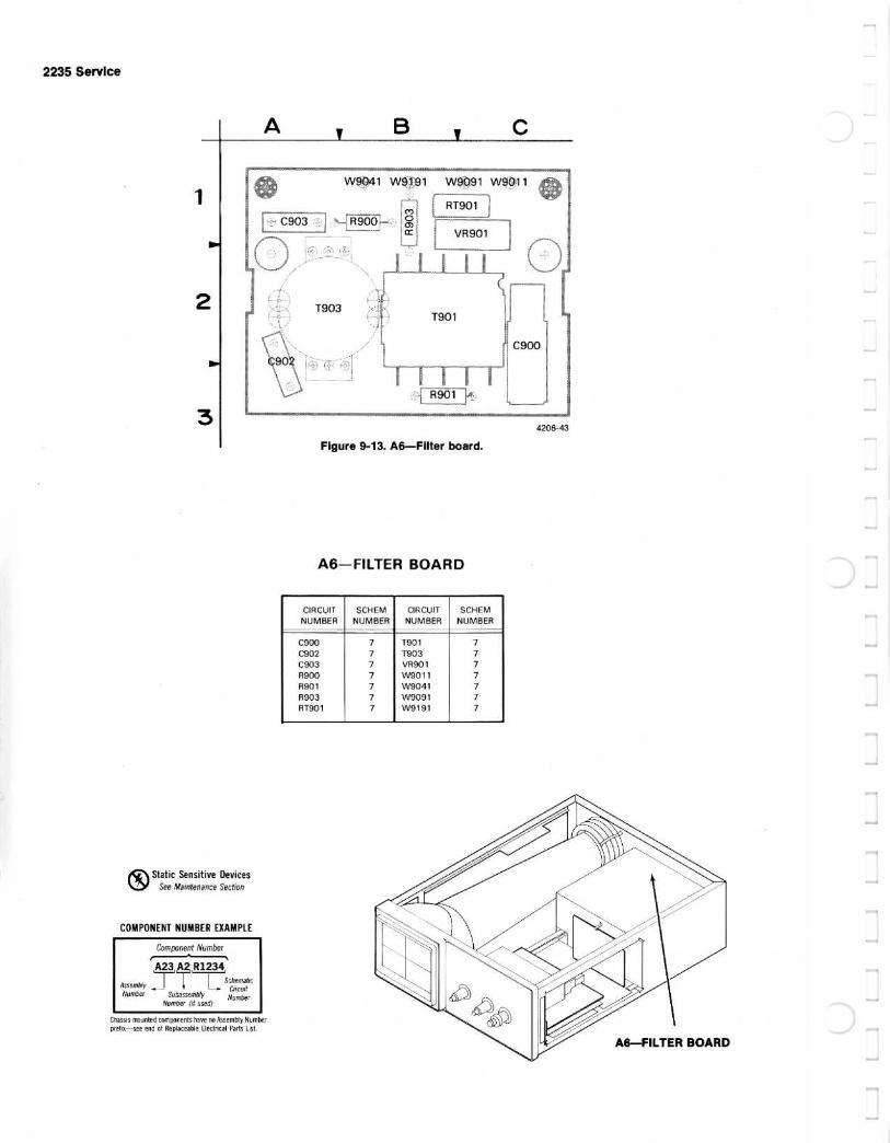
2235 Service
3
©Static Sensitive DevicesSee Maintenance Section
COMPONENT NUMBER EXAMPLE
Cοm Ασπ eπΓ Number
Α23 Α2 R1234
Asτem 10y ~rΙ
Ι
Scbemaλί c11 ΙΙΙ~~~ CircuitNumber Subassembly Number
Number (ίλ used)
Chassιs-mounted components have no Assembly N umberprefix see en d of R eplaceable Electrical P aris L ist.
W9041 W 91-91 λ ':'4C?91 W901
RT901
Figure 9-13. A6-Filte r board .
A6-FILTER BOAR D
SCHFMNUCIRCUITMBER Ι NUMBER
SCHFMΙ NU
circlMBER Ι NUMBER
C900 7 Τ 901 7C902 7 Τ903 7C903 7 υR901 7R900 7 W9011 7R901 7 W9041 7R903 7 W9091 7RT901 7 W9191 7
4206-43

ASSEMBLY Α 1
POWER SUPPLY, Ζ AXIS & C RT
NUMBER L OCATIO N LOCATIO N Ι NUMBER LOCATION LOCATION Ι NUMBER LOCATIO N L OCATIO N Ι NUMBER L OCATIO N LOCATIO N
C396 6D 4 Η CR 901 5E 5-1 R810 38 48 R929 6 F 7JC824 3E 6E CR 902 5E 5-1 R814 3 Β 4Β R930 6 F 7JC825 3 F 3 Η CR 903 5E 5-1 R818 1D 6E R934 9C 8JC828 4 F 3 Η CR904 5E 5-1 R820 2D 6E R935 9C 8JC832 2G 3 Η CR 907 7J 6Η R822 4E 2J R 937 9C 8ΗC835 4 Η 3-1 CR 908 8Η 7Η R823 3E 2.1 R938 9C 8-1C845 3 Η 3-1 CR 920 6-1 7-1 R825 3E 3J R 939 9C 8 ΗC847 3-1 3- CR 945 9F 8Η R826 3E 2-1 R940 9C 8 ΗC849 3-1 3-1 CR 946 9-1 8Η R828 4 F 2G R941 9E 8 .1C851 7Μ 6 Η CR 947 9-1 8Η R830 3G 2-1 R942 9D 8-1C853 7Μ 6G CR 954 6 Κ 6F R 832 3G 3-1 R943 9 Ε 8-1C854 6Μ 5G CR 955 7 Κ 6F R 834 4Ν 3J R 944 9 F 8-1C855 3Μ 5G CR 956 7 Κ 6F R 835 4G 3J R945 9 F 8 ΗC871 4S 1Η CR 957 7 Κ 6F R 836 4G 3 J R946 9 Η 8 ΗC873 5S 1 Η CR 960 8 Κ 7F R 840 4Η 3-1 R947 9 Η 7 ΗC875 6S 1 Η CR 961 9 Κ 8F R 841 3G 3-1 R949 9 Η 8 ΗC877 7S 1Η CR 962 9 Κ . 7F R 842 3 J 3-1 R971 9 L 8GC879 8Ν 5Η CR 963 9 Κ 8F R 844 3 Η 3 J R976 4 L 5GC893 7Ν 4G CR967 9 Κ SG R845 3 Η 3J R978 4L 5GC904 5D 4-1 CR970 9 Κ 8G R849 3-1 3-1C906 5F 5Η
R851 7Μ 3-1 S901 5D 4-1C907 7-1 6-1 DS856 5Μ 5G R852 7Μ 3JC908 6Η 5J DS858 5Μ 5G R853 7Μ 6G Τ390 6D 4 ΗC917 SD 7Η DS870 8L 5G R854 6Μ 5G Τ906 6J 6.1C919 8F 8-1 R858 6Μ 5G Τ944 9 Η 7 ΗC922 7F 7-1 E907 8Η 6Η R860 4Μ 5G Τ948 4-1 6GC925 6E 8J R 870 4S 1ΗC940 9G 6Η L960 81- 7F R 871 4S 1Η ΤΡ8 42 3J 3-1C941 9G 6 Η L961 91- 8 F R 872 5S 1Η ΤΡ900 9L BEC942 9D 8 Η R873 4S 1G ΤΡ940 9D 8-1C943 9C 8 Η Ρ 9802-1 3Β 4θ R874 6S 1G ΤΡ950 9C 7ΗC944 9F 7 Η Ρ 9802-2 3Β 4θ R875 6S 1GC945 9 F BJ Ρ 9802-3 2Β 48 R877 7S 1 Η U930 9G 7-1C954 6 Κ 6F Ρ 9802-4 3 θ 48 R879 ΒΝ 6F U 975 4 Κ 5 FC956 7 Κ 6F Ρ9802-5 28 48 R885 1 Κ 4ΗC960 9 L 6F
R886 2 L 4G VR 828 4F 3 ΗC961 9 L 8F Q586 1D 6D R888 1 L 4G VR 925 7F 7-1C962 9 L 7F Q804 28 58 R889 1Μ 4G VR 935 9C 8-1C963 9 L SF Q814 3C 5 Β R890 1Μ 4G VR 943 9E 8 JC968 9 L BG 0825 3F 3 J R 891 1 Μ 4GC970 9 L 8G Q829 3G 3 .1 R892 6Ν 4F W9040 5D 5 JC975 5 L 5G Q835 4Η 3 J R 893 6Ν 4F W9190 5D 5 ΗC976 5 L 5G Ο840 4-1 3-1 R894 6Μ 5 F W9800 4θ 3-1C979 5Μ 5G Q845 3-1 3-1 R905 6D 4J W9001-1 4F 4Α
Q885 1 L 4G R906 6D 5-1 W 9070-1 8Η 6 ΗCR551 2C 6D 0908 8 Η 7 Η R907 9-1 6 Η W9070-2 7 Η 6 ΗCR583 1C 6D 0928 6 F 7-1 R908 8Η 7-1 W9070-3 8 Η 7 ΗCR 805 2C 5 Β Q930 6G 7-1 R910 78 5Α W9150-1 7 Β 5ΑCR818 1D 6E Q935 98 8-1 R912 9C 7-1 W9150-2 8 Β 5ΑCR 820 2D 6E 0938 9D 81 R913 8C 7J W9400-8 3C 6ECR 823 3E 2Η Q939 9E 8-1 R914 BD 7 Η W9400-9 3E 6ECR 824 2F 2J Q944 9 F 8J R915 8D 7-1 W9870-1 4S 1ΗCR 825 3G 3J Q946 9 Η 8Η R916 8 F 7-1 W9870-1 3 Ν 4GCR 829 3 F 3-1 Q947 9 Η 7Η R917 SD 7 Η W9870-1 8 Ν 4GCR 840 4 Ν 3J R919 8 F 8-1 W9870-1 8 Ν 4GCR 845 3 Η 3 J R397 6D 5E R921 8 Ε 7J W9870-2 8 Ν 4GCR 851 7Μ 6G R398 6D 5E R922 8F 7.1 W9870-3 7 Ν 4GCR 853 6Μ 5G R586 1C 6E R925 6 F 7-1 W9870-4 7 Ν 4GCR 854 5Μ 5G R800 2Β 48 R926 5E 7-1 W9870-5 6S 1ΗCR 855 5Μ 5G R804 28 48 R927 7 F 7-1 W9870-7 5S 1ΗCR 879 8Μ 6G R805 28 5 Β R928 6 F 7-1 W9870-8 7S 1Η
Partial Α 1 also sh own on diagrams 2, 3, 4, 5, 6 and 8.
TABLE (cοηΥ ) Ι

ASSEMBLY Α3
POWER SUPPLY, Ζ AXIS & CRT (cont)
BOARDNUCIRCUIT
SCHEMMBER Ι LOCATION Ι LOCATIO N
Ι
NUCIRCUIT
SCHEMMBER Ι LOCATION Ι LOCATION
Ι
NUMBER Ι LOCATIO N I LOCATION
Ι
NUMBER Ι LOCATIO N Ι LOCATIO N
Ρ 9006-1
3S
2Α
R98
3S
2Α - Ι 5390
4E
2ΑΡ9006-2 3S 2Α R 983 3S 2Α
W 9000-1 4F 4Α
Partial Α 3 also shown on diagrams 1, 2, 3, 4, 5, 6 and 8.
ASSEMBLY Α6
NUCIRCUIT
SCHEMMBER Ι LOCATION
LOCBOARD
CIRCUIT
SCHEMATION
Ι
NUMBER Ι LOCATION Ι LOCATION
Ι
NUCIRCUITMBER Ι LOCATIO N I LOCATIO N
Ι
UCIRCUITMBER Ι L
OSCHEMCATIO N Ι LOCATIO N
C900 5 Β 2C R901 58 38 Τ901 58 2 Β W9011 5Α 1CC902 5C 2Α R 903 5C 18 Τ903 5C 2Α W9041 5C 18C903 5C 7Α
W9091 5Α 1CRT901 58 18 VR 901 5Β 1C W9191 5C 7 θ
R900 5C 1Β
CHASSIS MOUNTED PARTS
NUCIRCUIT
SCHEMMBER Ι LOCATION Ι LOCATION
Ι
NUMBER Ι LOCATIONSCHEM
Ι LOCATION
Ι
NUCIRCUITMBER Ι LOCATON I LOCATIO N
Ι
NUCIRCUITMBER Ι L
OSCHEMCATION Ι L OCATIO N
DS9150 8Α CH ASSIS Ρ9273 5 Ρ CH ASSIS Ρ9870-1 8 Ρ CHASSIS R9802A 2Α CHASSISΡ9778 4Ρ CH ASSIS Ρ9870-2 8Ν CHASSIS R9802 B 3Α CHASSIS
F9001 5Α CH ASSIS Ρ9788 4Ρ CH ASSIS Ρ9870-3 7Ν CHASSISΡ9070-1 8J CH ASSIS Ρ9870-4 7Ν CHASSIS V9870 2 Ρ CHASSIS
FL9001 5Α CH ASSIS Ρ9070-2 Β -1 CH ASSIS Ρ9870-5 6 Ρ CHASSISΡ9070-3 81 C H ASSIS Ρ9870-7 5Ρ CHASSIS
J9800 4Α CH ASSIS Ρ9870-10 4Ρ CH ASSIS Ρ9870-8 7Ρ CHASSISΡ9870-12 3Ν C H ASSIS
Ρ9272 5 Ρ CH ASSIS Ρ9870-14 8Ρ CH ASSIS Q9070 81 CHASSIS

Α ιΝΤΕΝ,"9602Α
ιακ
F31 ΝΤΕΝR9BO28
1οκ
J9αΟα(,ή
Ί \Ν5ΒοοΕΧΤ2ΑχιINPUT
αS9150
2235
if3.ΓσVξ -~ιΛπrR8o55.bK
Ρ13RΟ2 Ι RΡmΙ 6.8κ(----Γ- +BSavrr
Rρρ4ικ
-Β.6ΥFη
R βΙο6.8Κ~r+&bUς
ικL~ -8.bν1 1
Α6αΙιτεα ΒΟΑΡ E)
W9I50F~νιξR+5 .2ν,4 ι
_ΙR91o3w
R573c+5.2Vρ.1
FROM LDOWΤ32 Q`-~σ~σ9FROm CP,ς83Q5Τω
τι ®
RβΙθ CRESS3 Κ
)(YFα0ι~.1να9οαt-1α
1 Ο
βιΝτΕΙνLEVξ L
ΟΑ£Ος`
W-D400
Q8S4-α.GυΝ
ΑΝΙ 5ΟLΑΤΙΟΝ TRANSFORMERΜUΒΤΒΕυ SΕΟΙΝΗΕΝPROBING THE ΡRΙΜΑλΥCIRCUITRYOF THE POWERSUPPLY, τχ F PRIMARY VOLTAGES ARE NOTRE-1
EDTO CHASSIS OROUND
AC -80URςε POTENTIAL IS PRESENT IN THEPREREOULATOR AND IN ERTER CIRCUITRY.OISCONNΕ C7 THE POWER CORD FROM THE AC.POWERSOURCE 8ΕFΟRεΑΤΤΕΜΡΤΙΝG REPAIRS ORΡΕ SΙΒΤΑΝΕε MEASUREMENTS . SEE THEΜαιχτεχαχεεαειτrοΝοFτχιΧΜΑχυαμΒΕΟπσχ8,FOR TROUBLESHOOTING INSTRUCTIONS .
ΤΡ35ο0 1 R94b
2ΔΚα
ΤΡ54ο
ι
ΣαΒΖα3.ακ
CRS51~CR820
Α5 Ι~.ατΙηΐ αιτ sωεΕΡL~ ίc Βο~Rα
~ονυεRbsclτ
cs2a RS ΖbΦΙ3 ΙΟΟΚ
F9Cdl C90o R901Lα1Α ω9ΟΙι Ι 5μt S.1K
T11,1 ω9Ο41~'W904o j
I'M
9,1 -φ ,7 3-b
5
Ι
R9pVR9Ql
R90ο Ι +GR904 C347οΚ
Ι C5O4t e
Ζ
α 4ζλμλΙ
2
Ι 3 22οΟ CR90Z
55 R42b + C
ω9Ο,J
9Οέ
L
~ Rτ5ΟΙ Τ5Ο1
RSO3
ς9Ο2 W5Ι9ι ω9ιω~
ι
R ΖΙ5οΚ δΤS+`FFL9Cbl
Ι 1C
33Ο ;?205
R9p5 R9
CR9O1obΒΖΚ ΗΖΚ
R929~ 2
ι
3Κ
R915C917 1Ο.ΟΚίΟαo
LINETR)Grog397b6 <
R913
pal-7 ξξξ R914Ιο.οΚ
3ΟΚ ~Ι 34 .5Κ
R91235~
+Θ.ωVΒcι-ιοQ
It IΖ DRIVE
Β LΑΝΚ 1CR824W
FROM _ Cθ3Ζ94C0
υ53τ_b2 .ΟοΚ Ο"1μ.FΑβ25 4 ΕΤ 5
ρ GR825
R823}
~ υR 2α5. ιΚ ιο is
αβ22β225.1Κ
Α3 PARTIAL FRONτ'
Τα.bV1λΡΑΝΕ L gpARO
Q825 kθ.4V8R830s .sax gg29
-8α 5 CRS29CRθz3 3
+5.Ζν1 1141 +1zz .ιx
+1C925Τιοο, ιF
RB35z.3zκ Q835
ΒΕΑΜR5S~2θ
Ρ8~
Rt331bΚΙΝρ ~
11τΟ R834W9ορ1- ι RΖΔΡ2~
ΙαΟΑΝΟ
ω9~ο- Ι
CR7~4-
-Ε5390
F -
aszaR930ιοgΚ
R92T ΓιL~ναs25ιοοκ
0.1-F Fb
C9 ι9ΙΒΓ~3 4R9222οΚ
3Ρ521 RB1b3ΟΚ 5ΙΟμ
WARN ING
~
}339Ο
R 2'R92θΦ.ΒΚ
ι 2
13 8 ΠΙ 47
+SV RF F
C92z
R9ι9~ οΧιΙ_0λ7ΟRιικ
5
LSχις
R90ίi3 Κ
R934
R937
R941
τh VR943
R9A5
GSat
C94o.1+
R3 24--7K 1 Κ
R938 α Q93Β
α1,s
VR935
:f~ -8"bVQ~39
o- ι
CR9A$
τsα
Q9 5
G
5ιν
+ C943
Αί]J
R542
Q944
41 ααιν
Κ1
R944C944
3R935
R939
+ CggZ
R943
; ιΝ Fι2Ο Ι4_3Κ
T10J ιF
4.7Κ
Ι
R°_-

ι
+i00Vq
?ιCΟυΑ, RH49 0&47ΙΚ
~Κ
CRθ45
Cθ, ί4~Ο.1μ7
~ι4 CZ845οκ
τπ84z
CSCS _1 77-0C'
_
a
k4-.-ZCRBao
CR9Z0
1:50B220 τ °ρb
ιΟ b
ί
2 4
C9o7 ICR907Y
πηοτo.z
υ975
τ9αα ~ΙΙΙ 23
ι ~ ί ~Ιο
Ι Ι Ι
CR55 Α
Ιι
εο Ρ9Ο-ΤΟ
Ι~ -2
F2,1 Ι
j
Ο
ι
-3' 3 Ι G υ
Ι5
ι
~ό IQ]ΟΤΟ ιι
- Ι υ
ιΙ
Ε9Ο-Ι
1ΙιΙ
lp'l ~
Ι
ι
2
Ιt949 CR94T 'ι.ο ~
3 ιCR94ω
4 Ι1ΙΙ
b
5 ι
13 CR95 b
+3Ον
Ι4
ι5
CR95i
GR9S5
zs
24
zι
Ι8
Ι 9
RθΒ 5
ΑΒ8ς1 Rθθ9 ρΒ9ο RB9193Κ
5ΙοΚ 51ΟΚ 510Κ 510Κ
CR9T0
Q885 Rzιβακ
4
-α.ωνG
ΖΑχιs
RS-t(. 0.97θ$.1 Κ 5-1Κ
iC9~5 iG9Ζo.OyF Τ0.Ο~~
ώ
+ιmν
++ G9 ΙΑ33y"F
+lC95b
ίΆzτ0y.ε
ΑλιορΕ+gl yGη9ςριο TRAC E
ΓΙ ΕΟΤΑΤ 1 ΟΛ1R9B2
Ι _ Ι` . _ . C
ςγ,Ι 5χ
P9b1024~~
ω9Β r0 η-,2_ ιιr,
Α3 αΑπΤΙΑι sαflΝPANEL 1?Qλ.R9
'β935
CR$55
+cx~'υΑ
RW31 Gp-n512αΚ
GR ιu f ΤΟ. ι ~,.εC65ι ΤtΦΟ
8ΙΑ5 ΩΖbΟμ2 R65324οΚ
®η5e,-ro
CR9b2
+1C9ω1 +~C%3zz
~.
ααΟ,.ε
βαο s-βθV.
CR9b3 L9b L ΤΟIOyH -ΓΑ
R5~1o.b2 +5.2Υ
+ C9ι,13 + CID77ε36ιΟyF~Β4QλιF
Rθ~ρb2M
Ρ13925ιοΚ
0553-z ο C1τβΥ9
CST9 F8f9Ο.1μF~S ιοΚ
_4
\/9870
WAVEFOR MS
ι
L9(αΟGR~JΓoο ro�ια
+Θ ~αΥ,z0
+
+
static Sensitive DevicesC%ο C%z
CR9b1
~4ο~S
eAQ See Manieuce SnowCO MP ONENT NUMB ER EXAMPLE
POWER SUPPLY, Z AXIS
CRT
42οe -25
ComAnent Number
π-0yε h ematiε
Num¢~ Τ SvbassemWy~ ιευιΙ
ΝυmΙκν ίϋ α5¢d)
NumtreT
NUMERAL AND LETTER Α7 SIGNAL LLNES TO Chass ι snωυ Medcomponenlshaeenσkse,Gy Numά roR FR0Ν ΟΤΘΕ R οΙΑΟRλΗΒ INDICATES τχε
ριπ1 ίχ -$¢π eπΑ σι Repla[¢α b1 . ΕΙπ cΙπυΙ ΡαΠ S LιΑ.WiI0 COORDINATES ON ΑχΟτχεR ecχεΜλτιςMR
ΕΙΙΑΜΥLΕλει
Α1 PF+RτI4 L h"1ΑΙΝ SOPRo

2235 Service
Φ/Vvz
2235 CONTROL SETT I NGS
+3V
Θν
+15V
θν
+150MV
+100MV
+175V
0ν
Θν
-175V
PROBE GROUNDLEAD ON TP940
PROBE GROUNDLEAD ON TP940
PROBE GROUNDLEAD ON TP940
PROBE GROUNDLEAD ON TP940
VOLTAGE ANDDUTY CYCLEVARY W ITHINPUT L INEVOLTAGE
PROBE GROUNDLEAD ON TP940

AC Wavefor ms
DC Vo l tagesW ARN ΙNG
Preregu 1ατοr and Inverter voltages arereferenced to test point noted adjacen t toI nst rumen t must be connected to t he
the vo l tage . Power supp l y output vo l tagesac-power source using ο 1 :1 isolation
are referenced to chassis ground .t ransformer . Do not connect t he testosci ll oscope probe ground lead to t heInver ter circu it test poi n ts 1f t heInstrument is not isolated . AC-sourcevo l tage exists on reference poi n ts ΤΡ940and ΤΡ95θ .
V AR IE S WIT HI NTENSITY SETTING
+85V
+3θV
+80V
0V
+80V
0V
PROBE GROUNDLEAD ON TP950
PROBE GROUNDLEAD ON TP950
+0 .8 V
PROBE GROUNDLEAD ON TP950
0V
+BV ΘV

48
AC Wovefor msVERTICAL MODE
CH 1CH 1 VOLTS/D I V
5mVAC-CND-DC
DCHORIZONTAL MODE
ALTΑ SEC/D I V
SopsΒ SEC/DIVΒ DELAY TIME POSITION
5μθΒ TRIGGER LEVEL
RUN AFTER DELAY-CWΑ TRI GGER Mode
Ρ-Ρ AUTOΑ&Β ΙΝΤ
CH 1Α SOURCE
ΙΝΤCH 1 I NPUT SIGNAL
1-kHz sine wove, 5 div .
CRT BLANKED
Α I NTENSIFIED
Β SWEEPr-"
Γ- +3 . ΘV
+2 .6V
+45V
+30V
+15VAMPLITUDE VARIESWITH INTENS ITY

ASSEMBLY Α 1
Par tial Α 1 also sh own on diagrams 2, 3, 4, 5, 6 and 7.
ASSEMBLY Α3
POWER DISTR I BUTIO N
8Ο
CIRCUIT SCHEMNUMBER Ι LOCATIO N Ι LOCATIO N
Ι NUMBER
Ι LΟ CΑΤΙΟΝ Ι L Ο C0ΑΤΟΝ
Ι
NUMBER
Ι LΟ C Α 7 ON Ι L OCOATRION
C200 4Η 3E 7 Ρ961 7 Β 8Ε W993 9C 58C201 8 Η 3E W995 9C 68C220 4G 2D W408 9D 7Β W997 4G 4DC274 3C 2G W494 4E 5D W998 SG 4EC451 8F 6D W556 6C 2Η W999 8 Η 2EC494 4E 5D W590 7 Η 7C W9001-12 5 Ρ 5ΑC499 8Ε 5C W591 6 Η 7D W9001-5 4Ρ 5ΑC507 6E 6C W592 6G BC W9400-15 6Ν 7EC590 6Η 7D W885 7 Κ 4G W9400-16 6Ν 7EC796 8L 2G W954 1C 6 F W9400-18 6Ν 7EC797 4 Κ 3G W955 1C 4 Η W9400-23 6Ν 7EC799 2D 3F W956 2C 5 F W9400-24 6Ν 7E
W959
1 C
4E
W9400-25
6Ν
8ΕE200 4G 4E W960 3 Β 7F W 9400-26 6Ν 8ΕE201 8 Η 4E W961 7 Β 8F W 9400-27 5Ν 8ΕE272 3D 1G W964 2C 3 Η W9400-3 6Ν 6EE590 6G 8C W965 2C 3 Η W 9700-8 2Ν 7E
W968 6D 8 F W9705-1 3Ν 5ER220 4 Η 2D W971 3C 7E W9705-4 3Ν 5ER451 8 Ε 6D W972 3C 6 Ε W9705-6 3Ν 5ER494 4D 5E W974 4J 3 Η W9705-7 3Ν 5ER499 8 Ε 5E W975 4Κ 3 Η W9705-8 2Ν 5ER796 8 Κ 2G W976 7C 7E W9991-1 8Ν 5ER797 4 Κ 3G W977 7D 6E W9991-2 9Ν 5ER799 2C 3E W979 8Κ 3Η W9991-3 9Ν 5ER 964 6 θ 3 Η W991 4C 58R 966 6E 7E W992 4C 5Α
CIRCUIT SCHEMNUMBER Ι LOCATION Ι LOCATIO N
Ι NUMBER Ι LΟ CΑΤΙΟΝΙ LOCATIO N
Ι
NUMBER Ι LOCATIO N Ι L OCATION
W89 4Ρ 1C W9000-12 5 Ν 4Β W9000-5 4 Ν 4Α
Partial Α 3 also shown on diagrams 1, 2, 3, 4, 5, 6 and 7

+30VΙι . π
+B.bV ΙΡ9m
+5 .2ν lw9Μ
ωοεα
ω 9I'1
f\ Ι Ρ1λRΤΙΑL hΛΑΙΝ θΟΑΡρ
2235
ΙΝ95b
ω +~Α)ΟΟΟ9ώ4 w9b5
cz τa ε z -τz
ω99 ι
R9Co4
WSSbR% b4.~
R'τ
J; 7 . 2,,,F+52Vι ) ο~Ο
ΤΡ 9bι
WSID,
ω sτι ω~τz
+6-bνμ) ΟΟ 41
ω992
~+B.bVF) Ο Οτ
ω~7m
-Θ.bνΑ)Ο
W995
~ -Β .CσVτ ) Ο
ω9~Β
1.- ~Zk.lν�) Ο
----Ι
+~.~~α ,)οRα993. 3
W'.)7 7
W954
+Β .bνς) Ο
+θ,(σνρC494.C~1yF
499. οΙριF
- β . ωνς Ι)RR993-3
RA 511 Ο
g59a
~4τΟΟ -Β.eν~z)
R22o4Z~q~ 3.3
czocί , 2}
- Β ,βνρ
W592
4Ζο-

ω5~οα +52ν~} ρ
V4'Z!-Τ4 WC)-JS
α +$ .2V,ς}ρ
W9-[9
ow
i0 C~ι9~Ο- Ιμ~
ω6α5
+3Ονg
+εs_νν~
+α4,ν6
+α_bνρ
+s.zvn
ΙΟ
-3 .bνςλ
ORMF¢ι Αμρ LETTER Α7 SIGNAL LINES 70ROM ONEk σιΑG-5 ιχσιςΑΤΕ8 THEω10 coonDINATEs ΟΝ ΑΝΟ7ΗΕ R SΟΧειωτfε; ΕΟμ-ηρLΕ: ΛΕ/
ω'3-7ο-.) ΙGNU--,. -~ το
ι τ,
ω9το5β
i+8.bVg
Ι
ι
CNDi+B.bVg} ΟΓ
-41 C~Νρ
!-
~-t3 .bVς
υV5ΟΟΙ Ι Ι ,gCoc5-71
W'3,1ΡΟΙ-zτΗ+ΙΘ_bVq
_3 ι
POWER Di5TRISUTiON
Α3 ΡΑRΤΙλ<_, ΡRΟΝΤ PANEL Ι οΑRί7
ω85
r i}ΟΟ
ω--Η+g,bU
S 2
α+8 . ω46~ρ®Ο5 ©I>
α -θ. (.νΓ,,)ΟρΟΟ
+5 .2\/Νil+ Νρ
iGNDλ Gh1D
λ GΝδαGΝζ)αGNLD
i-Β. ωρ
Static Sensitive DevicesSee Μαίπεeπαπεe seεtipn
CO MPONENTNUMBER EXAMPLE
Cαmρσπ¢πΓ Numb eΓ
6 h αττ iεπιουυιΟ d επmσοπe πϋ pave πσ Αsse πιχγ rv υmαιρ'e fι e-se υπ d πι Θ eplueable γ7e[1r ιη1 Ροd τ (Ιτl

R760Χ
GAIN
R479TR IGGER
SENSITIVITY
R471SLOPEBAL
R435Γ- i
AUTO
R646D ELAYSTART
R241DL
CO MP2
C8240DL Ρ
COMP? C-
Al-MAIN BOARD ADJUS"

Ρ
:NT LOCATIONS
R874 R870ASTIG GEOM
4206-44
2235 Service

C5100ΧLF
COMP
C4100Χ
INPUT C
C55100ΧLF
COMP
C54100Χ
INPUT C
C6210ΧLF
COM P
R47C12
C3
CH 1C11
10Χ
CH 1
MF/LF10Χ LF N IF/LF GAIN
INPUT C
COMPCOMP
HAL
C6110Χ
I NPUT C
C53CH 2
ΝΙF/LFCOM P
R10CH 1STEPBAL
R26CH 12-mVGAI N
R25CH 1VARBAL
R97 R76 C76 R83CH 2
CH 2
CH 2
CH 2MF/LF 2-mV 2-mV 2/5-mVGAIN GAIN PEAK DCBAL
COMP BAL
A2-ATTENUATOR BOAR D AD JUSTME NT LOCATIONS
C26CH 12-mVPEAKCOMP
4206-45
R33CH 1
2/5-mVDCBAL
R75CH 2
INVERTBA L
R60CH 2STEPBAL

R749MAGREGIS
R 754Χ10GAIN
C713Β
R730 R740 H IGHΒ SWEEP
Α SWE EP
SPEEDGAIN GAIN TIM I NG
A4-TIMING BOARD ADJUSTMENT LOCATIONS
C703Α
H IGHSPEEDTIMING

AS-ALT SWEEP LOGIC BOARD ADJUSTMENT LOCATIO NS
α2α6- α7
2235 Service
R652D ELAYEN D

GENERAL NOTESΑ . Use schematic d iagrams, t he overa ll b loc k
d iagram, circu it board i ll ustrations, andcircu it descr i p tions when ana l yzi ng inst rumen tmal functions and locati ng test poi n ts . Theschematic d iagrams i nc l ude typ ica l waveformsand vo l tages t hat are i n tended as an ai din t roubleshooting .
θ . A l ways set the POWER switch to OFF and unp l ugt he line cord before swapp i ng, removi ng, orrep l aci ng componen ts, and before connecti ng ord isconnecti ng inst rumen t leads and cab les .
C . When ana l yzing ci rcuit ma l functions, consi derconnectors and cab les as possib l e causes offai lure .
SPEC I F I C NOTES1 . Set initial fron t-pane l con t ro l s as fo ll ows :
2 . Ver ify the low-vo l tage power supp l ies at t hefo ll owing test poi n ts :
SUPPLY
TEST POINT
TOLERANCE+5 .2V
W968
5 .04 το 5 .36V+8 .6V
W960
8 .43 το 8 .77V-8 .6V
ΤΡ961
-8.56 το -8 .64V+30V
W956
29 .1 to 30 .9V+1 00V
W954
97 το 103V
Ver ify t he -2kV suppl y at pin 2 of t he cr t sock et .The vo l tage shou ld be between -1900 and -210OV .
3 .
WARN I NGThe Preregu l ator and I nver ter ci rcuits have ο f l oati ngcommon reference wit h respect to chassis ground .Ac-source poten tial is presen t on the common referencepoi n ts . Connect t he i nstrumen t to t he ac-power sourcethrough an iso l ation t ransformer to preven t the pos-si b i l ity of persona l Injury or equ i pmen t damage whent roubleshooting t hese circu its .
TROUBLESHOOT I NGGU I DE
SET I N IT I ALFRONT-PANEL
CONTROL SETT I NGS(NOTE 1)
CONNECT POWER CORDTO Α SU I TABLE AC-POWER SOURCE ANDAPPLY POWER TOTHE I NSTRUMENT
POWER Switch
ON ( bu tton in)
DOES ΑΑ I NTENSITY
Midrange
BASE L I NE TRACEFOCUS
Midrange
APPEAR?Ver tica l POS I T I ON
M idrangeVERTICAL MODEC H 1CH 1 VOLTS/D I V
Θ .1 V
NOCH 1 VOLTS/D I V Var iab l e Ca l deten tCH 1 AC-GNO-DC
GNOHor izon ta l POS I T I ON
M idrange
PUSH IN ANDHOR IZONTAL MODE
Α
HOLD BEAM F I NDΑ SEC/D I V
θ .1ms
PUSH BUTTONΑ SEC/D I V Var iable
Cal deten tΧ 1 θ Magn ifierOff(knob in)Α TR I GGER Mode
Ρ-Ρ AUTOΑδΒ ΙΝΤ
VERT MODEΑ SOURCE
ΙΝΤDOES Α ~ YES
BASE L I NE TRACE r--iAPPEAR?
NO
VER I FY LOWNOTE
VOLTAGE SUPPLIESAND -2 kV SUPPLYΑ HV probe is requ i red to measure t he -2kV supp l y .
ARE IN TOLERANCETurn off t he power and ma k e the test equ i pmen t
(NOTE 2)connections to t he osci ll oscope . Set t he vo l tmeter1 ο read at least -3kV , t hen t urn t he osci ll oscopepower bac k on to take t he read ing . After ob tain i ngt he read i ng, turn off t he osci ll oscope power tod isconnect t he test equ i pmen t connections, andrep l ace the cr t soc k et cover .
ARE ALLPOWER SUPPLY
VOLTAGES0Κ? /
YES
YES
NO
NUMBER I NDIISCHEMATIC D

ATESAGRAM
TROUBLESHOOTPREREGULATORAND I NVERTERC I RCU I TRY .WARN I NG(NOTE 3)
7*
YES
ADJUST FOCUS ANDI NTENS I TY CONTROLSFOR Α WELL-DEF I NEDV IS I BLE D I SPLAY .
USE MANUALPERFORMANCE CHECK
PROCEDURE TOVER I FY I NSTRUMENT
FUNCT I ONS
RELEASE
YESBEAM F IND,
TURN I NTENSITYCONTROL FULLY
DOES Α\CW > AND ADJUST
BASE L I NE TRACETHE VERT I CAL
APPEAR?AND HORIZONTAL
POS I TIONCONTROLS
ΝΟ
ARE ALL
No~
TROUBLESHOOTVOLTAGES
FAULTY SUPPLYBAD?
7*
SEE MANUALADJUSTMENT
PROCEDURE TOADJUST CRTGR I D B I ASAND FOCUS
TROUBLESHOOTC I RCU I TRYASSOC I ATEDW ITH ANYFAULTY
FUNCT I ONSLOCATED
PRESS INAND HOLDBEAM F I ND
PUSHBUTTON
DOES ΑBASE L I NE TRACE
APPEAR?
ΝΟ
TURN CRTGR I D B I ASADJ R851FULLY
CLOCKW I SE7*
TROUBLESHOOT Z-AXISAND CRT CI RCU I TS
7*
RELEASE BEAM F I NDCHECK TP842 FOR Z-AXIS
UNBLANK I NG PULSE(VAR I ES FROM 10V TO 60V
Ρ-Ρ W I TH I NTENS I TYCONTROL)
7*
TROUBLESHOOTS
YES
DC RESTORERUNBLANK
ING PULSE
AND CRT`R SENT?
C IRCU I T7*
NO
CHECK R707 FOR THEΑ SWEEP SAWTOOTH
( ' 12V Ρ-Ρ )4*
Α SWEEP_IS CORRECT\
.iρ
GENERATORIΑ SWEEP SAWTOOTH }-
AND Α SWEEPPRESENT? /
Ι LOG I CC I RCU I TS
4*YES
CHECK CRT HORIZONTALDEFLECT I ON PLATE P I NSFOR Α SWEEP SAWTOOTH
(,' 40V Ρ-Ρ ON EACH LEAD)
/ IS CORRECTΑ SWEEP SAWTOOTH
NOPRESENT ON BOTH
P INS?
YES
YES
1S TRACENEARLY CENTERE
ΙΝ ΤΗΕ GRAT I CULEWITH BOTH POS I TION C(HORIZONTAL AND VEF\ENTERED IN THE
RANGE?
TROUBLESHOOT
TROUBLESHOOTHORIZONTALAMPL I FIERAND SWEEPSW I TCH I NGC IRCU I TS
5 ,6 *
YES

T RACECENTEREDJ ICULE AREA1 ΙΤΙΟΝ CONTROLSAND VERT I CAL)7 IN THE I R,N GE?
YES
TROUBLESHOOTHOR I ZONTALAMPL I F I ERCI RCU I TRY
6*
2235 Serv ice
zCCο
RELEASE BEAM πI S TRACE OFF
VERT ICALLY
F I N D BUTTONΝΟ
ςΕΝΤΕR HOR I ZONTALLY
OFF CENTER
AND MOMENTAR I LY
ΌOR VERT I CALLY?
SHORT ACROSS
ρDELAY L I NE LEADS
HOR IZONTALLY
ςOFF CENTER
Gm
/ DOES TRACE
NOCOME TO NEAR CENTEROF GRAT I CULE
AREA?
YES
TROUBLESHOOT VERTICALATTENUATOR X1/X10 AMPL >VERT I CAL PREAMPL I F I ER,AND DELAY L I NE DR I VER
FOR SOURCE OF I MBALANCE1 >2*
TROUBLESHOOTVERT I CALOUTPUT
AMPL I F I ER2*
TROUBLESHOOT I NG GU I DE4206-99

REPLACEABLEMECHANICAL PARTS
PARTS OR D ER I NG I NFORMATIO N
IN DENTATION SYSTEM
Replacement parts are available from o r through your local
Tektronix, I nc . F ield Office or representative .
Ch anges to Tek tro nix i nstru men ts are sometimes made to
1 2 3 4 5
Name & Descriptionaccommodate im proved components as they become availa ble,and to give you the benefit of the latest ci rcuit improvements
Assembly and/or Componentdeveloped in our engi neering department. It is therefore
Attaching parts fo r Assembly and/or Componentimporta nt, when o rd er i ng parts, to i ncl ude the followin g
- - -
- - -in formation in your o rder : Part number, in strument type or
Detail Part ο1 Assembly and/o r Componentnumber, serial number, and mod ificatio n numbe r if app licable .
Attaching parts fo r Detail Part
If α p art you have ordered has been replaced with α new or
Parts of Detail Partim pr oved
part,
your
local Te ktro nix,
Inc.
F ield Office or
Attaching parts fo r Parts of Detail Partrepresentative will contact you concerning any change in part
- - -
- - -number .
Cha nge info rmation , if any, is located at the rear of this
Attaching Parts always appea r i n the same indentation asma nu al .
the item it mounts, wh ile the d etail parts a re indented to the rig ht .I ndented items are pa rt of, and incl uded with, the next h ig her
SPECIAL NOTES AND SYMBOLS
ind entation. The separatio n symbol---'--- indicates the end ofattaching pa rts .
ΧΟΟΟ
Part first added at th is se rial number
ΟΟΧ
Part removed after this serial nu mber
Attachingparts must be purchased separately, unless otherwisespecified.
FIG URE AND INDEX NUMBERS
Items in this sectio n a re referenced by figure and indexnumbers to the illustrations.
In the Parts L ist, an Item Name is separated from thedescr i ption by α colon ( :) . Because of space lim itations, an ItemName may sometimes appea r as incomplete . For f ur ther ItemName identification, the U .S . Federal Catalogi ng HandbookΗ6-1can be u tilize d where possible .
ABBREVIATIONS
Section 10-2235 Service
This mechanical parts list is indented to indicate itemrelatio nships. F ollowi ng is an example of the indentation systemused in the desc r i ption column.
ITEM NAME
I NCH
ELCTRN
ELECTRON
IN
INCH
SE
SINGLE ENDε
NUMBER SIZE
ELECELECTRICAL
INCA ND
INCANDESCENT
SECT
SECTIONACTRACTUATOR
ELCTLT
ELECTROLYTIC
INSUL
INSULATOR
SEMICONDSEMICONDUCTORADPTR ADAPTER
ELEM ELEMENT
INTL INTERNAL
SHLD SHIELDA LIG N
A L IGNMENTEPL
ELECTR ICAL PARTS LIST
LPHLDR
LAMPHOLDER
SHLDR
SHOULDEREDA L ALUMINUM
EQPT EQUIPMENT
MACH MACHI NE
SKT SOCKETASSEM ASSEMBLED
ΕΧΤ EXTERNAL
MECH MECHANICAL
SL SLIDEASSY
ASSEMBLY
FIL
FILLISTER HEAD
MTG
MOUNTING
SLFLKG
SELF-LOCKINGΑΤΤΕΝ ATTENUATOR
FLEX FLEXIBLE
NIP NIPPLE
SLVG SLEEVINGAWG
AMERICAN WIRE GAGE
FLH
FLAT HEAD
NON W I RE NOTW I RE WOUND
SPR
SPR INGB D
BOARD
FLTR
FILTER
OBD
ORDER BY DESCRIPTIONSO
SQUAREBRKTBRACKETFR
FRAME or FRONT
OD
OUTSIDE DIAMETERSST
STAINLESS STEELBRS
BRASS
FSTNR
FASTENER
OVH
OVAL HEAD
STLST EELBRZ
BRONZE
FT
FOOT
ΡΗ BRZPH OSPHOR BRONZE
SW
SWITCHBSHG
BUSHI NG
FXD
F IX ED
PL
PLAIN o r PLATE
Τ
TUBECAB CABI NET
GSKT GASKET
PLSTC PLASTIC
TERM TERMINALCAPCAPACITOR
HDL
HANDLE
PIN
PART NUMBER
THD
THREADCER
CERAMIC
HEX
HEXAGON
ΡΝΗ
PAN HEAD
THK
THICKCHAS
CHASSIS
HEX HD
HEXAGONAL HEAD
PWR
POWER
TNSN
TENSION
.CKT
CIRCUIT
HEX SOC
HEXAGONAL SOCKET
RCPT
RECEPTACLE
TPG
TAPPINGCOMP
COMPOSITION
HLCPS
HELICAL COMPRESSION
RES
RESISTOR
TRH
TRUSS HEADCONN
CONNECTOR
HLEXT
HELICAL EXTENSION
RGD
RIGID
V
VOLTAGECOV
COVER
HV
HIGH VOLTAGE
RLF
RELIEF
VAR
VARIABLECPLG
COUPLING
IC
INTEGRATED CIRCUIT
RTNR
RETAINER
W/
W ITHCRT
CATHODE RAY TUBE
ID
INSIDE DIAMETER
SCH
SOCKET HEAD
WSHR
WASHERDEG DEGREE
(DENT IDENTIFICATION
SCOPE OSCILLOSCOPE
XFMR TRANSFORMERDWR DRAWER
IMPLR IMPELLER
SCR SCREW
XSTR TRANSISTOR

Replaceable Mechanical Parts-2235 Service
M fr . Code
Manufacture r
Address
City, State, Zip
00779
AMP, INC.
Ρ Ο BOX 3608
HARRISBURG, PA 1710501536
CAMCAR DIV OF TEXTRON INC. SEMSPRODUCTS UNIT
1818 CHRISTI NA ST .
ROCKFORD, IL 6110802768
ILL I NOIS TOOL WORKS, INC., FASTEX DIV.
195 ALGONQU IN ROAD
DES PLAINES, I L 6001605129
KILO ENGI NEER ING COMPANY
2015 D
LA VERNE, CA 9175006383
PANDU IT CORPORATION17301 RIDGELAND
TINLEY PARK, 1L 6047712327
FREEWAY CORPORATION9301ALLEN DRIVE
CLEVELAND, OH 4412512697
CLAROSTAT MFG. CO ., INC.
LOWER WASHINGTON STREET
DOVER, NH 0382013511
AMPHENOL CARDRE DIV., BUNKER RAMO CORP .
LOS GATOS, CA 9503016428
BELDEN CORP .
Ρ. Ο . BOX 1331
R ICHMOND, IN 4737422526
BERG ELECTRONICS, INC.
YOUK EXPRESSWAY
NEW CUMBERLAND, PA 1707024931
SPECIALITY CONNECTOR CO ., I NC.
2620 ENDRESS PLACE
GREENWOOD, IN 4614271400
BUSSMAN MFG., DIVISION OF MCGRAW-EDISON CO .
2536 W. UN IVERSITY ST.
ST. LOUIS, MO 6310773743
FISCHER SPECIAL MFG. CO .
446 MORGAN ST.
CI NCINNATI, OH 4520677820
BENDIX CORP ., THE, ELECTRICALCOMPONENTS DIVISION
SHERMAN AVE .
SIDNEY, NY 1383878189
ILLINOIS TOOL WORKS, INC.SHAKEPROOF DIVISIONST . CHARLES ROAD
ELGIN, IL 6012080009
TEKTRONIX, INC.
Ρ Ο BOX 500
BEAVERTON, OR9707780126
PACIFIC ELECTRICORD CO .
747 W . REDONDO BEACH,P Ο BOX 10
GARDENA, CA 9024783385
CENTRAL SCREW CO .
2530 CRESCENT DR.
BROADVIEW, I L 6015389663
REESE, J . RAMSEY, INC.
71 MURRAY STREET
NEWYORK , NY 1000793907
TEXTRON INC. CAMCAR DIV600 18TH AVE
ROCKFORD, IL 61101S3109
C/O PANEL COMPONENTS CORP .
Ρ.Ο. BOX 6626
SANTA ROSA, CA 95406S3629
PANELCOMPONENTS CORP .
2015 SECOND ST .
BERKELEY, CA 94170
10-2
CROSS INDEX-MFR. CODE NUMBER TO MANUFACTURER
REV ΜΑΥ 1983

Fig . &I ndex
Tektronix
Serial/Model No .
MfrNo .
Part No .
Eff
Dscont
Qty
1 2 3 4 5
Name & Description
Code
Mfr Part Number
1-1
334-5001-06
1
MARKER,IDENT:MARKED CAUTION U.S .A .
80009
334-5001-06334-5001-07
1
MARKER,[DENT:MARKED CAUTION U.K .
80009
334-5001-07-2 200-2538-00
1 COVER,REAR:PLASTIC
80009 200-2538-00"""""""(ATTACH ING PARTS)"""""'
-3
211-0691-00
2
SCREW,MACHINE:6-32 Χ 0.625, ΡΝΗ
01536
OBD""""""(END ATTACHING PARTS)""""'
-4
213-0882-00
1
SCREW,TAPP ING:6-32 Χ 0.437 TYPE C
01536
OBD-5
334-4714-00
1
MARKER,IDENT:MARKED HANDLE TAG
80009
334-4714-00-6 367-0289-00
1 HANDLE,CARRYI NG:13.855,SST
80009 367-0289-00""'*""""(ATTACHING PARTS)"""""'
-7
212-0144-00
2
SCREW,TPG,TF:8-16 Χ0.562 L
93907
225-38131-012'""""""(END ATTACHING PARTS)""""'
-8 390-0790-06
1 CABINET,SCOPE :W/FEET
80009 390-0790-00
REV ΜΑΥ 1983
Replaceable Mechanical Parts-2235 Service
10-3

ω'1Ι 1y1ι~
ΙΙ

2235 SERVICE
2

ΙΙ ΙΙΙΙ
U1
ς
~ ι
~ ΙΙυ φ
ι
Φ Φ
φ ©
6459
79

Fig . &Index
Tektronix
Serial/Model No .
M frNo .
P art No .
Eff
Dscont
Qty
1 2 3 4 5
Name & Description
Code
M fr P art Number
2-1
334-5002-00
1
PLATE,IDENT:MKD TEKTRONIX
80009
334-5002-00-2 426-1765-00
1 FRAME,CRT:
80009 426-1765-00"""""""(ATTACHING PARTS)"""""'
-3
211-0690-01
2
SCREW,MACHINE:6-32 Χ 0.875 PNH,TORX DR,SLO
93907
OBD""""""(END ATTACHING PARTS)""""'
-4 337-2775-00
1 SHLD,IMPLOSION :
80009 337-2775-00-5
366-1391-03
1
KNOB:DOVE GRAY,0.081 ID Χ 0.28 OD Χ 0.32 Η
80009
366-1391-03-6
366-2146-03
1
KNOB:DOVE GRAY,0.235 ID Χ 0.5 OD Χ 0.531 Η
80009
366-2146-03-7
366-1833-01
4
KNOB:DOVE GRAY,0.25 ID Χ0.392 OD Χ 0.466
80009
366-1833-01-8
366-1701-01
1
KNOB:GY,0.127 ID Χ 0.392 OD Χ 0.
80009
366-1701-01-9
210-0583-00
1
NUT,ΡLΑΙΝ ,ΗΕΧ:0 .25-32 Χ 0.312 INCH,BRS
73743
2Χ20317-402-10
210-0021-00
1
WASHER,LOCK : INTL,0 .476 ID Χ 0.60"ΟΟ ST
78189
1222-01-00-0541C-11
366-2152-00
2
KNOB:DOVE GRAY,0.284 ID Χ 0.392 OD Χ 0.466
80009
366-2152-00-12
366-2148-01
2
KNOB:GΥ,VΟLΤS/DIV 0.72 OD,0.79H
80009
366-2148-01-13
331-0328-00
1
DIAL,CONTROL :10 TURN FOR 0.25 DIA SHAFT
05129
461-S-70-14
210-0840-00
1
WASHER,FLAT : 0.39 ID Χ 0.562 INCH OD,STL
89663
644R-15
366-2013-00
9
PUSH,BUTTON:DIRTY GRAY,0.134 SO Χ 0.480
80009
366-2013-00-16
366-2049-00
2
KNOB:GY,0.712 ID Χ 0.41 OD Χ 0.496 H,W/BAR
80009
366-2049-00-17
131-0126-00
2
CONNECTOR, RCPT,:BNC,FEMALE
77820
9663-1 NT-34-18
366-2151-01
1
KNOBTLINT GRAY,0.22 ID Χ 0.392 OD Χ 0.466
80009
366-2151-01-19
210-0583-00
1
NUT,PLAIN,HEX:0 .25-32 Χ 0.312 INCH,BRS
73743
2Χ20317-402-20
366-1840-02
1
KNOB:GΥ,ΤΙΜΕ/DIV ,0 .127 ID Χ 0.855
80009
366-1840-02-21
366-1850-00
1
KNOB:CLΕΑR ,0.252 ID Χ 1.2 OD Χ 0
80009
366-1850-00-22 131-0955-00
1 CONN,RCPT,ELEC :BNC,FEMALE
13511 31-279-23
210-0255-00
1
TERM Ι NAL,LUG:0 .391 ID,LOCKING,BRS CD PL
80009
210-0255-00-24 333-2918-00
1 PANEL,FRONT:
80009 333-2918-00-25 386-4850-00
1 SUBPANEL,FRONT :
80009 386-4850-00"""""""(ATTACHING PARTS)"""""'
-26
213-0881-00
3
SCREW,TAPPING :6-32 Χ 0.25 ΤΥΡΕ C
01536
OBD-27
213-0882-00
2
SCREW,TAPPING:6-32 Χ 0.437 ΤΥΡΕ C
01536
OBD""""""(END ATTACHING PARTS)""""'
-28 348-0660-00
4 CUSHION,CRT:POLYURETHANE
80009 348-0660-00-29
361-1192-00
1
SPACER,SLEEVE :0.45 LΧ 0.25 ID,AL
80009
361-1192-00-30 407-2824-00
1 BRACKET,GROUND :PANEL
80009 407-2824-00"""""""(ATTACHING PARTS)"""""'
-31
210-0586-00
2
NUT,PL,ASSEM WA:4-40 Χ 0.25,STL
83385
OBD""""""(END ATTACHING PARTS)""""'
-32
214-3375-00
2
LEVER,SWITCH :AC-GND- DC,PLASTIC
80009
214-3375-00-33 441-1631-00
1 CHASSIS,SCOPE:FRONT
80009 441-1631-00-34
213-0881-00
4
SCREW,TAPPING:6-32 Χ 0.25 ΤΥΡΕ C
01536
OBD-35 386-4443-00
1 SUPPORT,SHIELD :CRT,FRONT,PLASTIC
80009 386-4443-00-36
200-2519-00
1 .
CAP.,CRT SOCKET:NATURAL LEXAN
80009
200-2519-00-37 214-1061-05
1 SPAING,GROUND:PLATED
80009 214-1061-05-38 426-1766-00
1 MOUNT,RESILIENT:CRT,REAR
80009 426-1766-00-39
344-0347-00
1
CLIP,ELECTRICAL :ANODE, 0.72 OD,NYLON
80009
344-0347-00-40
334-1379-00
1
LABEL: CRT,ADHESIVE BACK
80009
334-1379-00-41
334-1951-00
1
MARKER,IDENT :CRT WARNING
80009
334-1951-00-42
337-2774-00
1
SHIELD,ELEC:CRT,STEEL
80009
337-2774-00-43
----- -----
1
DELAY LINE,ELEC:93NS,150 ΟΗΜ,ΑSSΥ----- -----
-
(SEE DL9210 CHASSIS REPL)-44
346-0121-00
2
STRARELEC COMP:TIE DOWN,5 .0 LONG
06383
PLC1 .51-S8""""""'(ATTACHING PARTS)"""""'
-45
213-0882-00
2
.SCREW,TAPPING :6-32 Χ 0.437 ΤΥΡΕ C
01536
OBD""""'(END ATTACHING PARTS)""""'
-46
346-0128-00
1
STRAP,TIE DOWN:0 .1W Χ 8.0" LONG,NYLON
06383
PLT2M-47
136-0202-08
1
SKT,PL-1Ν ELEK:ELECTRON TUBE,14 CONTACT
80009
136-0202-08-48
334-4251-00
1
MARKER,IDENT :MKD CAUTION
80009
334-4251-00-49
337-2772-00
1
SHIELD,ELEC:POWER SUPPLY,AL
80009
337-2772-00"""""""(ATTACHING PARTS)"""""'
-50
211-0304-00
3
SCREW, MACHINE:4-40 Χ 0.312,ΡΝΗ
01536
OBD""""""(END ATTACHING PARTS)""""'
-51
348-0555-00
1
GROMMET,PLASTIC:SIL GY,U SHAPE,0.52 ID
80009
348-0555-00-52
344-0334-00
1
CLIRCIRCUIT BD:PLASTIC
80009
344-0334-00
REV ΜΑΥ 1983
Replaceable Mechanical Parts-2235 Service
10-5

Replaceable Mechanical Parts-2235 Service
F ig . &Index
Tektronix
Serial/Model No .
M frNo .
Part No .
Eff
Dscont
Qty
1 2 3 4 5
Name & Description
Code
Mfr Part Number
2-53
134-0158-00
2
BUTTON,PLUG:0 .187 DIA,NYLON02768
207-080501-00-54
200-2264-00
1
CAP.,FUSEHOLDER :3AG FUSES
S3629
FEK 031 1666-55 200-1388-03
1 COVER,FUSE,LEAD :POLYURETHANE
80009 200-1388-03-56
204-0833-00
1
BODY, FUSEHOLDER:3AG & 5 Χ 20ΜΜ FUSES
S3629
031.1653(MDLFEU )-57
210-1039-00
1
WASHER,LOCK : ΙΝΤ,0 .521 ID Χ 0.625 INCH Ο
24931
OBD-58 131-0955-00
1 CONN,RCPT,ELEC:BNC,FEMALE
13511 31-279-59
----- -----
1
FI LTER ,RF I:1A,250VAC----- -----
-
(SEE FL9001 CHASSIS REPL)..... .* ..*..'.(ATTACHING PARTS)"""""'
-60
211-0323-00
2
SCREW,MACHINΕ:4-40 Χ 0.312,FLH ,100 DEG
83385
OBD-61
210-0583-00
2
NUT,PLAIN,HEX:0 .25-32 Χ 0.312 INCH,BRS
73743
2Χ20317-402""""""(END ATTACHING PARTS)""""'
-62
200-2845-00
1
COVER,CKT BD :LINE FILTER
80009
200-2845-00-63
670-7615-00
1
CKT BOAR D ASSY :EM I FILTER BOARD
80009
670-7615-00----- -----
-
(SEE Α6 REPL). . . . . . . .. .....(ATTACHING PARTS)"""""'
-64
210-0586-00
2
NUT,PL,ASSEM WA:4-40 Χ 0.25,ST L83385
OBD.'..........(END ATTACHING PARTS)""""'
-65
129-0339-00
2
POST,ELEC-MECH:0 .27 LONG Χ 0.25 HEX BRS
80009
129-0339-00'....""""'(ATTAC H ING PARTS)"'."""'
-66
211-0303-00
2
SCREW,MACH INE:4-40 Χ 0.25, FLH 100 DEG
01536
OBD""""'...(EN D ATTACHING PARTS)""""'
-67
210-0202-00
1
TERMINAL,LUG:0 .146 ID, LOCKING,BRZ TINNED
78189
2104-06-00-252ΟΝ"(ATTACHING PARTS)"'."""'
-68
210-0457-00
1
NUT,PL,ASSEM WA:6-32 Χ 0.312,STL CD PL
83385
OBD""""""(END ATTACHING PARTS)""" ...
-69
334-3379-02
1
MARKER,IDENT:MARKED GROUND SYMBOL80009
334-3379-02-70
407-2729-00
1
BRACKET,HEAT SK:AL80009
407-2729-00............ . .(ATTACHING PARTS)""'.""'
-71
211-0304-00
1
SCREW,MACHINEA-40 Χ 0.312,ΡΝΗ
01536
OBD-72
210-0586-00
2
NUT,PL,ASSEM WA:4-40 Χ 0.25,STL83385
OBD""""."'(END ATTACHING PARTS)"".""
-73
211-0302-00
1
SCREW,MACHINE:4-40 Χ 0.75,ΡΝΗ
01536
ΟΒΟ-74
210-0586-00
1
NUT,PL,ASSEM WA:4-40 Χ 0.25,ST L83385
OBD-75 342-0582-01
1 INSULATOR,PLATE:TRANSISTOR,CERAMIC
80009 342-0582-01-76 343-1025-00
1 RETAINER,XSTR:
80009 343-1025-00-77
211-0691-00
1
SCREW,MACH INE:6-32 Χ 0.625,ΡΝΗ
01536
OBD-78
210-0408-00
1
NUT,PLAIN,HEX. :6-32 Χ 0.312 INCH,BRS
73743
3040-402-79
342-0555-00
1
INSULATOR,PLATE:HEAT SINK ,AL80009
342-0555-00-80
343-0969-00
1
RETAINER,XSTR:POLYPHENYLENE SULFIDE
80009
343-0969-00-81
361-1047-00
1
SPACER,VAR RES:0.3 Χ 0.615 Χ 0.55
80009
361-1047-00-82 441-1536-01
1 CHASSIS,SCOPE :REAR80009 441-1536-01-83
161-0104-00
1
CABLE ASSY,PWR,:3 WIRE,98.0" LONG
16428
ΚΗ8352----- -----
-
(ALSO SEE STANDARD ACCESSORIES)161-0104-06
1
CABLE ASSY,PWR:3 Χ0.75ΜΜ SQ,220V,98.OLS3109
OBD---- -----
-
(OPTION Α1 EUROPEAN)161-0104-07
1
CABLE ASSY,PWR:3 Χ 0.75ΜΜ SQ,240V,98.0 L
80126
OBD----- -----
-
(OPTION Α2 UNITED KINGDOM)161-0104-05
1
CABLEASSY,PWR:3,18 AWG,240V,98.0 L
S3109
OBD---- -----
-
(OPTION Α3AUSTRALIAN)161-0104-08
1
CABLEASSY,PWR:3,18 AWG,240V,98.0 L
80126
OBD----- -----
-
(OPTION Α4 NORTH AMERICAN)161-0167-00
1
CABLEASSY, PWR:3 .0 Χ 0.75,6A,240V,2 .5MS3109
OBD----- -----
-
(OPTION Α5)
10-6 REV ΜΑΥ 1983

Replaceable Mechanical Parts-2235 Service
Fig . &Index
Tektronix
Serial/Model No .
MfrNo .
Part No .
E ff
Dscont
Qty
1 2 3 4 5
Name & Description
Code
Mfr P art Number
3-1
334-4251-00
1
MARKER,IDENT:MKD CAUTION
80009
334-4251-00-2
337-2773-00
1
SHIELD,ELEC:POWER SUPPLY,LOWER,PLSTC
80009
337-2773-00"""'*"""(ATTACHING PARTS)""'*""'
-3
211-0304-00
1
SCREW,MACHINE:4-40 Χ 0.312,ΡΝΗ
01536
OBD""""""(END ATTACHING PARTS)""""'
-4
366-1480-02
1
PUSH BUTTOWGRAY
80009
366-1480-02-5
384-1576-01
1
EXTENSION SHAFT:12.809 L,PLASTIC
80009
384-1576-01-6
200-2735-00
1
COVER,POWER SW :
80009
200-2735-00-7
----- -----
1
SWITCH,PUSH :DPDT,4A,250VAC,W/BRKT----- -----
-
(SEE AlS901 REPL)-8
377-0512-00
6
INSERT,KNOB:0 .125 ID Χ 0.663 L,AL
80009
377-0512-00-9
670-7611-00
1
CKT BOARD ASSY :FRONT PANEL
80009
670-7611-00----- -----
-
(SEE Α3 REPL)-10
131-0608-00
2
.TERMINAL,PIN :0 .365 L Χ 0.025 ΡΗ BRZ GOLD
22526
47357-11
136-0499-02
3
.CONNECTOR,RCPT, :2 CONTACT
00779
3-380949-2-12
670-7612-00
1
CKT BOARD ASSY:ALTERNATE SWEEP
80009
670-7612-00----- -----
-
(SEE Α5 REPL)-13
131-0589-00
27
.TERMINAL,PIN :0 .46 L Χ 0.025 SQ
22526
48283-029-14
670-7560-00
1
CKT BOARD ASSY:MAIN
80009
670-7560-00----- -----
-
(SEE Al REPL)-15
131-0608-00
3
.TERMINAL,PIN:0.365 L Χ0.025 ΡΗ BRZ GOLD
22526
47357-16
131-0589-00
7
JΕRΜΙΝΑ L, PIN:0.46 L Χ 0.025 SQ
22526
48283-029-17
343-0088-00
1
.CLAMP,LOOP :0 .062 INCH DIA
80009
343-0088-00672-1064-00
1
CKT BOARD ASSY:ATTENUATOR/TIMING
80009
672-1064-00-18
346-0196-00
1
STRAP,GROUND:ATTEN,3 .0 Χ 0.75
80009
346-0196-00.* .......�.*(ATTACHING PARTS)"""""'-19
211-0325-00
2
.SCR,ASSEM WSHR:4-40 Χ 0.25,PNH,TORX DRIVE
01536
OBD-20
210-0801-00
1
.WASHER,FLAT :0 .14 ID Χ 0.025 THK,BRS ΝΙ
12327
OBD"""""'(END ATTACHING PARTS)""""'
-21
361-1191-00
1
SΡΑCΕR,CΚΤ BD:0 .222 Χ 0.125 Χ 0.25
80009
361-1191-00-22
337-3014-00
1
.SHIELD,ELEC :ATTENUATOR TOP
80009
337-3014-00"""""'(ATTACHING PARTS)"""""'
-23
211-0325-00
1
SCR,ASSEM WSHR:4-40Χ0.25,PNH,TORX DRIVE
01536
OBD-24
211-0326-00
2
.SCREW,MACHINE :4-40 Χ 1 .25,PNH,TORX DRIVE
93907
OBD""""'(END ATTACHING PARTS)""""'
-25
670-7561-00
1
CKT BOARD ASSY:ATTENUATOR
80009
670-7561-00----- -----
-
.(SEE Α2 REPL)""""""'(ATTACHING PARTS)"""""'
-26
211-0325-00
1
SCR,ASSEM WSHR:4-40 Χ 0.25,PNH,TORX DRIVE
01536
OBD-27
129-0986-00
1
.SPACER,POST :0.966 L ,4-40 THD BOTH ENDS
80009
129-0986-00""""'(END ATTACHING PARTS)"""""
-28
384-1056-00
2 .
..EXTENSION SHAFT:0 .125 OD Χ 6.58 INCH LON
80009
384-1056-00376-0209-00
2
..CPLG SHAFT,RGD:0 .127 ID,PLASTIC
80009
376-0209-00-29
401-0370-00
4
..BEARING,CAM SW:END,0 .6 DIA
80009
401-0370-00-30
210-0406-00
4
..NUT,ΡLΑΙΝ ,ΗΕΧ . :4-40 Χ 0.188 INCH,BRS
73743
12161-50-31
214-1126-01
6
.SPRING,FLAT :0.7 Χ 0.125,CU BE GRN CLR
80009
214-1126-01214-1126-02
2
..SPRING,FLAT :RED COLORED
80009
214-1126-02-32 214-1752-00
8 ..ROLLER,DETENT :
80009 214-1752-00-33
401-0369-00
2
..BEARING,CAM SW:CENTER,0.6 DIA
80009
401-0369-00""""""(ATTACHING PARTS)"""""'
-34
311-0325-00
2
..RES.,VAR,NONWIR :2 .5M ΟΗΜ,20Ί
12697
381-CM39666. . . .. . ......(END ATTACHING PARTS)""""'
-35
105-0934-00
2
..ACTUATOR,CAM SW:AC-GND-DC
80009
105-0934-00-36
105-0935-00
2
..ACTUATOR,CAM SW:ATTENUATOR
80009
105-0935-00-37
343-1020-00
2
..RETAINER,CONT:ABS GRAY
80009
343-1020-00""""""(ATTACHING PARTS)"""""'
-38
211-0325-00
4
..SCR,ASSEM WSHR:4-40 Χ 0.25,PNH,TORX DRIV
01536
OBD"""""(END ATTACHING PARTS)""""'
-39
361-1193-00
2
..SPACER,SLEEVE :0 .555 L Χ 0.13 ID
80009
361-1193-00-40
131-1758-11
2
.CONT ASSY,ELEC:8 CONTACTS
80009
131-1758-11131-1758-12
2
..CONT ASSY,ELEC:8 CONTACTS
80009
131-1758-12-41
131-0787-00
2
..CONTACT,ΕLEC:0 .64 INCH LONG
22526
47359-42
131-0608-00
11
..TERMINAL, ΡΙΝ:0.365 LΧ 0.025 ΡΗ BRZ GOLD
22526
47357
REV ΜΑΥ 1983
10-7

Replaceable Mechanical Parts-2235 Service
F ig . &In dex
Tektronix
Serial/ Model No .
M frNo .
P art No .
E ff
Dscont
Qty
1 2 3 4 5
Name & Description
Code
M fr Part Number
3-43
670-7613-00
1
CΚΤ BOARD ASSYMMING (SEE Α4 REPL)
80009
670-7613-00'*""""'(ATTACH ING PARTS)"""""'
-44
211-0325-00
3
SCR,ASSEM WSHR:4-40 Χ0.25,PNH,TORX DRIVE
01536
OBD""""'(END ATTACHING PARTS)"'"""'
-45
131-0608-00
18
TERM I NAL,PIN:0 .365 L Χ 0.025 ΡΗ BRZ GOLD
22526
47357-46
131-0787-00
4
-CONTACT,ELEC:0 .64 INCH LONG
22526
47359-47
337-2944-00
1
SHIELD,ELEC:SW BOARDS,BOTfOM80009
337-2944-00-48
210-0406-00
2
NUT,PLAIN,HEX.:4-40 Χ0.188 INCH,BRS
73743
12161-50-49
129-0906-00
2
SPACER ,POST:0 .685 L W/4-40 ΙΝΤ & ΕΧΤ ΤΗ
80009
129-0906-00
10-8
REV ΜΑΥ 1983

Α3Ο
Φ
5
4 lR

y
ν
Α2τs
ύas
Α4α3
2235 S ERVICE

WE45Ρι
F ig . &Index
Tektron ix
Se ria l / Model No .
MfrNo.
Part No,
Eff
Dscont
Qty 1 2 3 4 5
Nam e & Descr i ption
Cede
Mfr Part NumberSTANDARD ACCESSORIES
-1
010-6122-01
2 PROBE,VOLTACE :P6122,1 .5 ΜΕΤΕΑ , ΙΟΧ W/ACCESS
80009 010-6122-01161-0104-00
Σ CABLE ASSY,PWR, :3 WIRE,98 .0" LONG
Ι642Β ΚΗ8352--"-- -----
- (SEE FIG . 2 RMPL)070-4206-00
1 MANUAL,TECH :S£ RVICE,2235 OSCILLOSCOPE
80009 070-4206-00070-4207-00
1 MANUAL,TECH :OPERATORS,2235 OSCILLOSCOPE
80009 070-4207-00
OPTIONAL ACCESSORIES
-2 01 3-0191-00
2 TIP,PROBE :W/ΑCΤUΑΤΟΑ
80009 013-0191-00020-0672-00
1 ACCESSORY ΚΙΤ :
80009 020-0672-00-3 200-2520-00
1 . COVER,SCOPE :FRONT
80009 200-2520-00016--0677-00
1 . POUCH,ACCESSORY :
80009 016-0677-00-4 016-0535-01
1 , . POUCH,ACCESSORY :
80009 016-0535-01-5 386-4647-01
1 . , PLATE,MOUNTING :BAεK,ALUM
80009 386-4647-01-6
159-0019-00
1 . , FUSE CARTRIDGE :3AG,1A,250V ,SLO-BLO
71400 MDL1----- -----
1 C5C ΟΡΤΙΟΝ 4 CAMERA----- -----
- (SEE MANUAL 070-2824-ΧΧ )---- -----
1 2000 OR 2000 SCOPEMOBILES----- ---
- (SEE DATA SHEETS Οό2- Ι 538-00 OR 062-6644-00)016-0466-00
1 ADAPTER ,RACK :
80009 016-0466-00----- -----
-- (SEE MANUAL 070-4186-ΧΧ )
2235 SERVICE

MANUAL CHANGE INFORMATION
At Tektronix, we continually strive to keep up with latest electronic developmentsby adding circuit and component improvements to our instruments as soon as theyare developed and tested .
Sometimes, due to printing and shipping requirements, we can't get thesechanges immediately into printed manuals. Hence, your manual may contain newchange information on following pages .
Α single change may affect several sections . Sincethe change information sheetsare carried i n the manual until all changes are permanently entered, somed uplication may occur. If no such change pages appear following this page, yourmanual is correct as printed .

Tektronke
MANUAL CHANGE INFORMATIONcοπΜινΤΤεοΤοεχcευεηιcε
Date :
2-16-83
Change Reference :
Μ50226
Product :
2213, 2215, 2235, 2236
Manual Part No . :
See Below
2213 (070-3827-00)-Β029390
2215 (070-3826-00)-Β031640
2235 ( 070-4206-00)-ΒΟ 10380
2236 (070-4204-00)-Β010550
DESCRIPTION
REPLACEABLE ELECTRICAL PARTS LIST CHANGES
2213, 2215
CHANGE TO :
Α 10Τ940
120-1348-01
XFMR,PWR,SDN&SU : HIGH VOLTAGE
2235, 2236
CHANGE TO :
Α 1 Τ 948
120-1348-01
XFMR,PWR,SDN&SU : HIGH VOLTAGE
000-2775-00D
Page 1
of 1

Tektmnixa
MANUAL CHANGE INFORMATIONCOMMITTED TO EXCELLENCE
Date:
8-22-83
Change Reference:
02/0883
Product :
2235 SERVICE
Manual Part No . :
070-4206-00
Page 5-5
STEP 4
Adjust Astigmatism (R874) .
CHANGE TO:
ADD:
ADD:
DIAGRAM
DESCRIPTION
PG 46
TEXT CHANGES(EFFECTIVEALL SERIAL NUMBERS)
Change part b. to read as follows:b. Connect the leveled sine-wave generator output via α 50-Ω cable and α50-Ω termination to the CH 1 OR Χ input connector.
REPLACEABLE ELECTRICAL PARTS LIST CHANGES(SEE BELOW FOR EFFECTIVESERIAL NUMBERS)
Α1C785
ALL SN's
281-0214-00
CAP,VAR,CER DI : 0.5-3 PF,400V
PC9Α 1R122
Β010450
315-0820-00
RES, FXD,CMPSN : 82 ΟΗΜ,5%,0.25W
PC16Α1R172
Β010450
315-0820-00
RES, FXD,CMPSN : 82 ΟΗΜ,5%,0.25W
PC16Al R317
Β010450
321-0218-00
RES, FXD,CMPSN : 1 .82Κ ΟΗΜ,1%,0.125W
PC16Al R318
Β010450
321-0193-00
RES, FXD,CMPSN : 1Κ ΟΗΜ,1%,0.125W
PC16Al R319
Β010450
321-0212-00
RES, FXD,CMPSN : 1 .58Κ ΟΗΜ,1%,0.125W
PC16Al R322
Β010450
321-0238-00
RES, FXD,CMPSN : 2.94Κ ΟΗΜ,1%,0.125W
PC16Al R342
Β010450
321-0218-00
RES, FXD,CMPSN : 1 .82Κ ΟΗΜ,1%,0.125W
PC16Α 1R343
Β010450
321-0193-00
RES, FXD,CMPSN : 1Κ ΟΗΜ,1 %,0.125W
PC16Al R344
Β010450
321-0212-00
RES, FXD,CMPSN : 1 .58Κ ΟΗΜ,1%,0.125W
PC16Al R347
Β010450
321-0238-00
RES,FXD,CMPSN : 2.94Κ ΟΗΜ,1%,0.125W
PC16Al R352
Β010450
321-0274-00
RES, FXD,CMPSN : 6.98Κ ΟΗΜ,1%,0.125W
PC16All R353
Β010450
321-0274-00
RES, FXD,CMPSN : 6.98Κ ΟΗΜ,1%,0.125W
PC16
Α1C500
ALL SN's
281-0893-00
CAP, FXD,CER DI : 4.7 PF,±0.5PF,100V
PC11Α1 R354
Β010450
315-0272-00
RES, FXD,CMPSN : 2.7Κ ΟΗΜ,5%,0.25W
PC16Α1 R500
ALL SN's
315-0101-00
RES, FXD,CMPSN : 100 ΟΗΜ,5%,0.25W
PC11A3R201
ALL SN's
315-0200-00
RES, FXD,CMPSN : 20 ΟΗΜ,5%,0.25W
PC13A3R401
ALL SN's
315-0200-00
RES, FXD,CMPSN : 20 ΟΗΜ,5%,0.25W
PC10
CHASSIS PARTS LIST CHANGES(SEE BELOW FOR EFFECΤ/VF_ SERIAL NUMBERS)
R909
Β010395
315-0390-00
RES, FXD,CMPSN : 39 ΟΗΜ,5%,0.25W
PC17
DIAGRAM CHANGES(SEE BELOW FOR EFFECTIVE SERIAL NUMBERS)
VERTICAL PREAMP AND OUTPUT AMPL
Change R122 (location 3E) and R172 (location 9E) to 82 ohm resistors
8010450
PC16
Disconnect p i n 1 from ground on S200 (location 6Α) and S226 (location 3Κ) .These two pins are then connected together and R201 (20Ω ) is added fromthis connection to ground .
ALL SN's
PC13

Product:
DIAG RAM
DIAG RAM
DIAGRAM
001-0057-DOD
2235 SERVIC E
To ju nction ofU506A pin 6 andU408B pin 3.
R500100
TRIGGERING
890939
Date : α-22-83
DESC RIPTION
DIAGRAM CHANGES (coat)(SEE BELOWFOR EFFECTIVE SERIAL NUMBERS)
Α SWEEP GENERATOR & LOGIC
5.2Υ--J
Ρ 9οτο
Π
Ι
Q9070
5.2 ν
U50210 Ε MEG713
C
Q3
gδ Ε ΡΟβ1S
ΗΙ SΡΕΕΟ
C5004.7ρF
Page 2 of 2
Change Reference : C210883
Change R352 (location 2Κ ) and R353 (location 2Κ) to 6 .98Κ ohm resistors.
B010450
PC16Change 8322 (location 3J) and R347 (location 6J) to 2.94Κ ohm resistors .
B010450
PC16Change 8319 ( location 2Η) and R344 (location 5J) to 1 .58Κ ohm resisto rs .
B010450
PC16Change R318 (location 1G) and R343 (location 3G) to 1 .ΟΚ ohm resistors.
B010450
PC16Change R317 (location 1 F) and R342 (location 3F) to 1 .82Κ ohm resistors.
B010450
PC16Add R354 (2 .7Κ ohm) from the junction of p i ns θ and 14 of U350(location approximately 3Κ ) to -8.6 V
C1.
8010450
PC16
Disconnect pin 4 from ground on S401 Β (location 8Α) and add R401 (20 ohm)from p i n 4 to ground.
ALL SN's
PC10
Add C500 (4 .7pF) & R500 (100Ω) to U502 as shown below.
ALL SN's
PC20
POWER SUPPLY, Z-AXIS AND CRT
Add R909 (39 oh m) at location 8Η as shown below.
B010395
PC17