initial growth behavior and resulting microstructural properties of heteroepitaxial zno thin films...
TRANSCRIPT

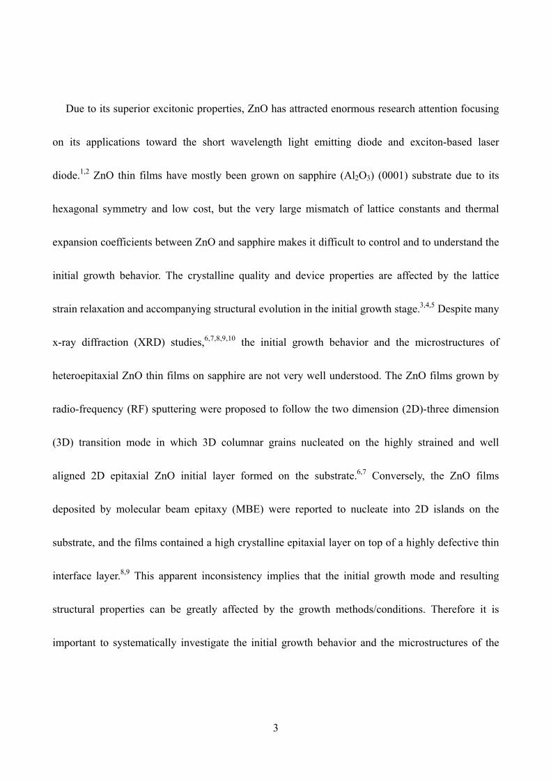
Initial growth behavior and resulting microstructural properties of heteroepitaxial ZnO thin
films on sapphire (0001) substrates
C. Liu,a) S. H. Chang, and T. W. Nohb)
ReCOE & FPRD, School of Physics and Astronomy, Seoul National University,
Seoul 151-747, Korea
M. Abouzaid and P. Ruterana
SIFCOM UMR 6176 CNRS-ENSICAEN, 6 Boulevard du Marechal Juin, 14050 Caen
Cedex, France
H. H. Lee
Pohang Accelerator Laboratory, POSTECH,Pohang, 790-784, Korea
D.-W. Kim
Department of Applied Physics, Hanyang University, Ansan, Kyunggi-Do 426-791,
Korea
J.-S. Chung
Department of Physics and CAMDRC, Soongsil University, Seoul, 156-743, Korea
a E-mail: [email protected] b E-mail: [email protected]
1

We have investigated the initial growth behavior and resulting microstructural properties of
heteroepitaxial ZnO thin films prepared by pulsed laser deposition on sapphire (0001) substrates.
High-resolution x-ray diffraction and transmission electron microscopy studies revealed that the
initial growth behavior and the microstructure of the films significantly depend on the growth
parameters. ZnO films grown at 700 oC with 20 mTorr O2 partial pressure initiated with a columnar
growth mode and contained two kinds of domains. These domains were in-plane orientated either
ZnO[ 0211 ]//Al2O3[ 0110 ] or ZnO[ 0110 ]//Al2O3[ 0110 ], and were surrounded by highly defective
domain boundaries with threading dislocations. The films grown at 800 oC with 1 mTorr O2 showed
2-dimensional layered growth with only one in-plane epitaxial relationship, ZnO[ 0211 ]//Al2O3[ 0110 ].
Most of the defects in the layered grown films were basal plane stacking faults near the interface
between ZnO and the substrate. The formation mechanism of the 30o-twisted domains with the in-
plane orientation of ZnO[ 0110 ]//Al2O3[ 0110 ] is discussed.
2
Due to its superior excitonic properties, ZnO has attracted enormous research attention focusing
on its applications toward the short wavelength light emitting diode and exciton-based laser
diode.1,2 ZnO thin films have mostly been grown on sapphire (Al2O3) (0001) substrate due to its
hexagonal symmetry and low cost, but the very large mismatch of lattice constants and thermal
expansion coefficients between ZnO and sapphire makes it difficult to control and to understand the
initial growth behavior. The crystalline quality and device properties are affected by the lattice
strain relaxation and accompanying structural evolution in the initial growth stage.3,4,5 Despite many
x-ray diffraction (XRD) studies,6, , , ,7 8 9 10 the initial growth behavior and the microstructures of
heteroepitaxial ZnO thin films on sapphire are not very well understood. The ZnO films grown by
radio-frequency (RF) sputtering were proposed to follow the two dimension (2D)-three dimension
(3D) transition mode in which 3D columnar grains nucleated on the highly strained and well
aligned 2D epitaxial ZnO initial layer formed on the substrate.6,7 Conversely, the ZnO films
deposited by molecular beam epitaxy (MBE) were reported to nucleate into 2D islands on the
substrate,8 and the films contained a high crystalline epitaxial layer on top of a highly defective thin
interface layer.8,9 This apparent inconsistency implies that the initial growth mode and resulting
structural properties can be greatly affected by the growth methods/conditions. Therefore it is
important to systematically investigate the initial growth behavior and the microstructures of the
3
heteroepitaxial ZnO initial layers in order to clearly understand the growth mechanism and to
control the initial growth for high quality ZnO epilayers.
In this letter, we report a detailed study on the initial growth behavior and the microstructural
properties of ultrathin ZnO films deposited by pulsed laser deposition (PLD) on sapphire (0001)
substrates, using high-resolution x-ray diffraction and transmission electron microscopy (TEM)
measurements.
ZnO thin films were deposited on sapphire (0001) substrates by ablating a ceramic ZnO target
(purity 99.999%). The sapphire substrates were annealed in a furnace at 1100 oC for 1 hr in air
ambient to obtain atomically flat surface. A KrF excimer laser with a wavelength of 248 nm was
used, and its fluence and repetition rate were about 3 J/cm2 and 3 Hz, respectively. The deposition
temperature of ZnO was varied as 600, 700, and 800 oC, and the O2 partial pressure was 1, 10, and
20 mTorr. Two deposition conditions: (a) 700 oC with an O2 partial pressure of 20 mTorr and (b)
800 oC with an O2 partial pressure of 1 mTorr, were used to investigate the initial growth behaviors
because the films grown at these two conditions showed typical (0002) ω-rocking curve profiles in
the XRD measurements as reported.6, 8 Films with thicknesses of 10, 20, and 40 nm were prepared
at both 700 oC / 20 mTorr and 800 oC / 1 mTorr to investigate the initial structural evolution of
heteroepitaxial ZnO films. The film thicknesses were estimated from x-ray reflectivity
measurements. The high-resolution XRD was measured with a lab source (Bruker D8 Discover) and
4
a synchrotron radiation source (Beamline 10C1, Pohang Light Source, Korea). TEM observations
were made to investigate the microstructural properties of ZnO initial layers using a 002B Topcon
high-resolution microscope operated at 200 kV.
Figure 1(a) shows (0002) ω-rocking curves of heteroepitaxial ZnO initial layers grown at 700
oC/20 mTorr with the variation of film thickness. The 11 nm-thick ZnO film showed only a sharp
peak with a full width at half maximum (FWHM) of about 0.02o. When the film thickness increased
to 18 nm, a weak and broad background peak appeared below the sharp peak. Further increase of
film thickness to 41 nm resulted in a significant increase of the intensity of the broad background
peak while the intensity of the central sharp peak increased slightly with no change in FWHM.
Similar two-peak feature and thickness dependence of the ω-rocking curve were reported for
heteroepitaxial ZnO thin films grown by radio-frequency magnetron sputtering.6 It was suggested
that the central sharp component in the rocking curve was originated from two-dimensional (2D)
ZnO initial layer which was well aligned to the sapphire substrate, whereas the broad component
was from three-dimensional (3D) ZnO islands which were nucleated on the 2D initial layer.6 The
origin of these two peaks will be further discussed later based on our detailed microstructural
analyses. Figure 1(b) shows (0002) ω-rocking curves of ZnO initial layers grown at 800 oC/1 mTorr
with the variation of film thickness. As in the film grown at 700 oC/20 mTorr, only a sharp peak was
observed when the film thickness was 9 nm. However, the broad component in the rocking curve
5
did not appear when the film thickness increased to 20 nm. Only weak Lorentzian tails appeared on
both sides of the strong and sharp central peak when the film thickness was 39 nm. A similar
rocking curve with weak Lorentzian tails was observed in a ZnO film grown by molecular beam
epitaxy, and was assumed to be related to a two-layer structure within the ZnO film: a highly
defective interface layer and a high crystalline epilayer on top of the defective interface.8 The
apparently different evolution of the out-of-plane rocking curve with film thickness indicates that
the initial growth mode and resulting crystallographic mosaicity of heteroepitaxial ZnO thin film
can be significantly influenced by the growth parameters. It is noted that the broad components in
the rocking curves in Fig. 1 became dominant with decreasing the growth temperature down to 600
oC and with increasing O2 partial pressure from 1 to 20 mTorr (not shown here). The lower growth
temperature and higher O2 partial pressure cause a reduction of adatom surface mobility/diffusion
length during the film growth, leading to poor crystalline films.11, ,12 13
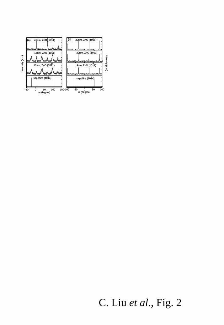
To investigate the in-plane lattice alignment, azimuthal phi (φ) scan measurements were
performed for the ZnO films grown at different growth conditions, as shown in Fig. 2. Figure 2(a)
shows the φ-scans along the azimuthal circles of ZnO { 1110 } flection for the ZnO thin films grown
at 700
re
oC/20 mTorr with the variation of thickness. It is noteworthy that there are two sets of peaks
with an angle difference of 30o in the φ–scans. One set of peaks is originated from aligned
heteroepitaxial ZnO domains with an in-plane epitaxial orientation of ZnO[ 0211 ]//Al2O3[ 0110 ],
6
which is typically observed in heteroepitaxial ZnO thin films on sapphire (0001) substrates due to
the reduced lattice mismatch of 18 %. The other set of peaks is attributed to the formation of 30o-
twisted heteroepitaxial ZnO domains with an in-plane orientation relationship of
ZnO[ 0110 ]//Al2O3[ 0110 ], which is energetically unfavorable due to the large lattice mismatch of
32 %. The formation mechanism of the 30o-twisted ZnO domains will be discussed later based on
our TEM analysis. As the film thickness increases from 11 nm to 41 nm, the intensity of the peaks
from 30o-twisted ZnO domains relatively decreases and became very weak while the peaks from
aligned domains becomes significantly strong and sharp. The relative evolution of the peaks in the
φ-scans indicates that 30o-twisted ZnO domains are metastable and can be dominant at the initial
stage of film growth in our growth condition although aligned domains are energetically favorable
in the heteroepitaxy and can overgrow the twisted domains with the increase of film thickness.
On the other hand, the φ-scans for the ZnO thin films grown at 800 oC /1 mTorr showed sharp
peaks only from the aligned domains, as shown in Fig. 2 (b). The FWHM of the sharp aligned peaks
was about 0.9o, which is much smaller than that of the aligned peaks in the φ-scan of 41 nm-thick
ZnO film grown at 700 oC/20 mTorr (about 2o) [Fig. 2(a)]. This result indicates that heteroepitaxial
ZnO films grown at higher temperature with lower O2 partial pressure have better in-plane lattice
alignment with only one in-plane orientation of ZnO[ 0211 ]//Al2O3[ 0110 ].
7
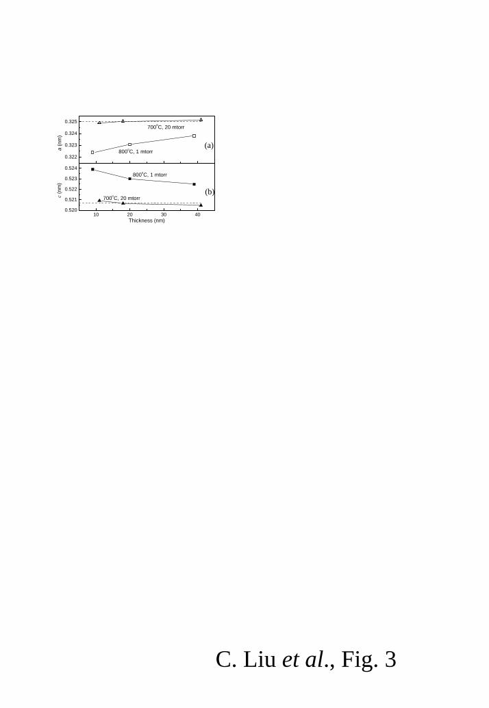
The in-plane domain alignment at the early stage of film growth can affect the microstructure
and strain status of the heteroepitaxial thin film because an in-plane twist between two domains on a
substrate results in the formation of low-angle grain boundary which typically consists of edge-type
threading dislocations.14,15 The grain boundaries formed during the coalescence process of initial
grains may develop inhomogeneous tensile strain in the film since the coalescence of grains reduces
the surface energy at the expense of elastic tensile strain energy.16 Thus, we measured the a- and c-
lattice constants of the ZnO films by combining XRD θ-2θ scans of ZnO (0002) and K-scans of
ZnO ( 2110 ) reflection to investigate the strain status of the films. Figures 3 (a) and 3 (b) show the a-
and c-lattice constants of the ZnO films, respectively. Figure 3 (a) clearly indicates that the in-plane
strain of ZnO films grown at 700 oC/20 mTorr was almost relaxed, while the films grown at 800
oC/1 mTorr were compressively in-plane strained, which is further supported by the consistent
evolution of c-lattice constants with the film thickness in Fig. 3 (b). The heteroepitaxial ZnO thin
films on sapphire substrates are expected to be compressively in-plane strained due to the large
lattice mismatch and the thermal expansion mismatch. Since the ZnO films grown at 700 oC/20
mTorr showed poor in-plane lattice alignment with two different types of domains [Fig. 2(a)], we
believe that the significant relaxation of compressive strain in the films can be mainly attributed to a
compressive strain compensation by a tensile strain developed at low-angle grain boundaries with
edge-type threading dislocations. The ZnO films grown at 800 oC/1 mTorr, which showed better in-
8
plane alignment with only aligned domains [Fig. 2 (b)], might have less low-angle grain boundaries
so that the compressive strain of the films is less compensated. It is noteworthy that the compressive
strain of 11 nm-thick ZnO film grown at 700 oC/20 mTorr was almost relaxed while the 9 nm-thick
ZnO film grown at 800 oC/1 mTorr was compressively strained, although both of them showed
well-aligned out-of-plane mosaicity in the ZnO (0002) ω–scans (Fig. 1). This implies that the in-
plane lattice alignment is more correlated to the strain relaxation mechanism than the out-of-plane
alignment of heteroepitaxial ZnO initial layers.
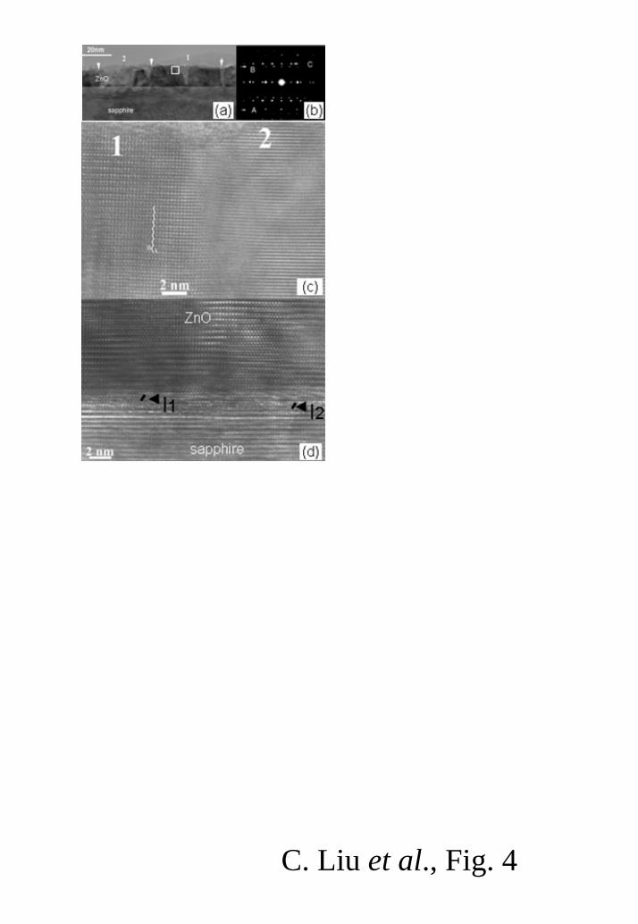
To further understand initial growth behaviors and the microstructures of the ZnO thin films,
high-resolution transmission electron microscopy (HRTEM) measurements were performed. The
HRTEM image in Fig. 4(a) shows that the ZnO film grown at 700 oC/20 mTorr has a columnar
structure formed by two kinds of domains. The dark areas, marked “1”, correspond to the aligned
domains, where the ZnO layer was imaged along its [ 0211 ] zone axis. The ABAB… stacking of the
hexagonal close-packing along the [0001] direction can be seen in the magnified image, shown in
Fig. 4(c). The bright areas, marked “2”, correspond to the 30o-twisted domains, where the ZnO
layer was imaged along the [ 0110 ] zone axis, and only the 0002 fringes were observed from these
domains, as shown in Fig. 4(c). The selected area diffraction pattern, presented in Fig. 4(b), also
shows two sets of domains with different in-plane epitaxial orientations, which is consistent with
the XRD result [Fig. 2(a)]. It is noteworthy that both aligned and 30o-twisted domains grow directly
9
on the substrate [Fig. 4(a)], implying that the formation mechanism of the twisted domains can be
related to the adsorption site preference of adatoms on the substrate surface during the first
monolayer deposition.
In contrast, TEM studies of ZnO film deposited at 800 oC/1 mTorr showed only one in-plane
epitaxial orientation relationship of ZnO[ 0211 ]//Al2O3[ 0110 ], which is also in good agreement with
the XRD result [Fig. 2(b)]. Figure 4(d) shows the HRTEM picture of ZnO initial layer deposited at
800 oC/1 mTorr, indicating that most defects are stacking faults lying in the (0001) basal plane near
the interface between ZnO and the substrate,17 some of which are marked with arrows. Away from
the interface, the TEM picture shows well-layered atomic stacking. The 2D layered growth mode at
800 oC and 1 mTorr O2 appears to have enough adatom mobility and migration time to form the
thermodynamically more stable state without forming the 30o-twisted domains at the initial stage of
film growth.
The formation of 30o-twisted domains in the initial ZnO thin films might be explained as a
competition between the local interface energy and epitaxial strain energy.18, 19 The fact that the 30o-
twisted domains are formed at lower temperature, although they are heteroepitaxially unfavorable
due to the large lattice mismatch, implies that on the atomically flat and clean substrate the interface
energy of the adsorption sites for the 30o-twisted ZnO domains are lower than that for the aligned
ones. At the very beginning of the deposition, an isolated adatom will preferentially adsorb at the
10
energetically lowest site on the sapphire surface. However, as the adatom coverage increases to
form an epitaxial monolayer, the adsorption sites for aligned domains will become energetically
more favorable because of the smaller lattice mismatch-induced epitaxial strain energy. Therefore,
the adatoms will have a driving force to shift toward the adsorption sites for aligned ZnO domains.
When the growth temperature of ZnO decreases, the kinetic process of the adatoms’ diffusion to the
adsorption sites for aligned ZnO domains will be suppressed, resulting in the formation of 30o-
twisted domains at the initial stage of growth.
The formation mechanism of 30o-twisted domains proposed above assumes the sapphire surface
is atomically flat and clean. We also deposited ZnO thin films on as-received sapphire substrates
without furnace annealing. The ZnO thin films on as-received sapphire substrates did not show 30o-
twisted domain peaks in the φ–scan spectra over the investigated growth temperature range. The as-
received sapphire surfaces might not have localized and strongly directed dangling bonds that favor
strong adatom-substrate chemical binding, which would result in lower diffusion energy barriers of
adatoms due to weaker interactions between adsorbate and substrate. Therefore, the adatoms on the
as-received sapphire substrates might easily diffuse from the initial adsorption sites to epitaxial
strain energy favorable adsorption sites to form aligned ZnO domains.
The microstructural properties revealed by TEM study also provide reasonable explanation for
the evolution features of the ω-rocking curves (Fig. 1) and for the different strain states (Fig. 3).
11
Although the out-of-plane rocking curve and its evolution with film thickness [Fig. 1(a)] show
apparently similar features with those from the RF sputtered films,6 the columnar structure directly
formed on the substrate surface [Fig. 4(a)] indicates that our PLD-grown ZnO did not follow the
2D-3D transition mode in which 3D columnar grains nucleate on highly strained and well aligned
2D epitaxial layers. Our XRD results showed that the sharp single peaks in the out-of-plane rocking
curves (Fig. 1) do not always indicate the formation of atomically well-stacked high quality 2D
epitaxial single layer. The occurrence of the broad components in the ω-scan profiles (Fig. 1) might
be related to the lateral overgrowth and coalescence processes of thermodynamically more
favorable columnar grains. As for the different strain states in Fig. 3, the significant relaxation of
compressive strain in the columnar structured films are mainly attributed to the defective columnar
domain boundaries with high density of threading dislocations as well as misfit dislocations at the
interface between the substrate and ZnO film. It is noted that the domains in the films grown at 700
oC/20 mTorr have relatively smaller in-plane domain size and two different types of in-plane
epitaxial orientations with poor in-plane domain alignments, compared to those in the films grown
at 800 oC/1 mTorr with enhanced 2D layered growth mode and less domain boundaries.
In summary, we have investigated the initial growth behavior and the microstructures of ZnO
thin films deposited on sapphire (0001) by pulsed laser deposition. The deposition of ZnO films at
relatively lower temperature with higher O2 partial pressure (700oC/20 mtorr O2) formed a
12
columnar domain structure consisting of two types of domains with in-plane epitaxial orientations
of ZnO[ 0211 ]//Al2O3[ 0110 ] and ZnO[ 0110 ]//Al2O3[ 0110 ]. The 30o-twisted domains formed at the
early stage of film growth and were metastable while the aligned domains were thermodynamically
stable. The deposition of ZnO films at relatively higher temperature with lower O2 partial pressure
(800oC/1 mtorr O2) favored 2D layered growth mode, resulting in highly crystalline strained
epitaxial layers with only one in-plane epitaxial orientation.
This study was financially supported by the Korean Science and Engineering Foundation
(KOSEF) through the Creative Research Initiative (CRI) program. The experiments at the Pohang
Light Source were supported by the Ministry of Science and Technology (MOST) and the Pohang
Steel Company (POSCO).
13

Figure caption:
FIG. 1. The (0002) ω-rocking curves of ZnO films grown at (a) 700 oC and 20 mTorr O2 and (b)
800 oC and 1 mTorr O2.
FIG. 2. The φ-scans for the { 1110 } reflection of ZnO films grown at (a) 700 oC and 20 mTorr O2
and (b) 800 oC and 1 mTorr O2.
FIG. 3. Thickness dependence of the (a) a-axis and (b) c-axis lattice constants. The dashed lines in
(a) and (b) show the value of the a-axis and c-axis lattice constants in bulk ZnO, respectively. The
solid line connecting the points is a visual guide.
FIG. 4. (a) High-resolution cross-sectional TEM picture of an 18 nm-thick ZnO film grown at
700oC/20 mTorr. The areas labeled “1” and “2” represent domains with ZnO[ 0211 ]//Al2O3 [ 0110 ]
and ZnO[ 0110 ]//Al2O3[ 0110 ], respectively. The white arrows indicate the domain boundaries. (b)
The selected area diffraction pattern from the corresponding crystallites. The spot lines labeled A
and B belong to the ZnO[ 0211 ] and ZnO[ 0110 ] zone axes, respectively. The Al2O3 [ 0110 ] axis is
labeled C. (c) Magnified TEM image of the rectangular area shown in (b). The ABAB…stacking is
indicated in the image. (d) The HRTEM image of ZnO film grown at 800oC /1 mTorr. Two stacking
faults have been underlined (arrows).
14
References:
1 Ü. Özgür, Ya. I. Alivov, C. Liu, A. Teke, M. A. Reshchikov, S. Doan, V. Avrutin, S.-J. Cho, and H.
Morkoç, J. Appl. Phys. 98, 041301 (2005).
2 A. Tsukazaki, A. Ohtomo, T. Onuma, M. Ohtani, T. Makino, M. Sumiya, K. Ohtani, S. F. Chichibu,
S. Fuke, Y. Segawa, H. Ohno, H. Koinuma, and M. Kawasaki, Nat. Mater. 4, 42 (2005).
3 A. B. M. Almamun Ashrafi, N. T. Binh, B. Zhang, and Y. Segawa, Appl. Phys. Lett. 84, 2814
(2004).
4 H. C. Ong, A. X. E. Zhu, and G. T. Du, Appl. Phys. Lett. 80, 941 (2002).
5 H. D. Li, S. F. Yu, A. P. Abiyasa, Clement Yuen, S. P. Lau, and H. Y. Y, Appl. Phys. Lett. 86,
261111 (2005).
6 S. I. Park, T. S. Cho, S. J. Doh, J. L. Lee, and J. H. Je, Appl. Phys. Lett. 77, 349 (2000).
7 T.-B. Hur, Y.-H. Hwang, H.-K. Kim, and H.-L. Park, J. Appl. Phys. 96, 1740 (2004).
8 Y. Chen, D. M. Bagnall, H. Koh, K. Park, K. Hiraga, Z. Zhu, and T. Yao, J. Appl. Phys. 84, 3912
(1998).
9 P. Fons, K. Iwata, S. Niki, A. Yamada, and K. Matsubara, J. Crystal Growth 201-202, 627 (1999).
10 I. W. Kim, Y. B. Kwon, J. M. Yi, J. H. Je, G. Nouet, T. Wojtowicz, P. Ruterana, and J. Kioseoglou,
J. Vac. Sci. Technol. A 22, 2159 (2004).
11 S. Choopun, R. D. Vispute, W. Noch, A. Balsamo, R. P. Sharma, T. Venkatesan, A. Iliadis, and D.
C. Look, Appl. Phys. Lett. 75, 3947 (1999).
12 R. D. Vispute, V. Talyansky, Z. Trajanovic, S. Choopun, M. Downes, R. P. Sharma, T. Venkatesan,
M. C. Woods, R. T. Lareau, K. A. Jones, and A. A. Iliadis, Appl. Phys. Lett. 70, 2735 (1997).
13 I. Ohkubo, A. Ohtomo, T. Ohnishi, Y. Mastumoto, H. Koinuma, and M. Kawasaki, Surf. Sci. 443,
15
L1043 (1999).
14 V. Potin, P. Ruterana, G. Nouet, R. C. Pond, and H. Morkoc, Phys. Rev. B. 61, 5587(2000).
15 F. A. Ponce, and D. P. Bour, Nature 386, 351 (1997).
16 T. Böttcher, S. Einfeldt, S. Figge, R. Chierchia, H. Heinke, D. Hommel, and J. S. Speck, Appl.
Phys. Lett. 78, 1976(2001).
17 J. Narayan, K. Dovidenko, A. K. Sharma, and S. Oktyabrsky, J. Appl. Phys. 84, 2597(1998).
18 T. Zywietz, J. Neugebauer, and M. Scheffler, Appl. Phys. Lett. 73, 487(1998).
19 J. Ohta, H. Fujioka, M. Oshima, K. Fujiwara, and A. Ishii, Appl. Phys. Lett. 83, 3075(2003).
16

16 17 18
Inte
nsity
(a.u
.)
41nm
18 nm
11 nm
(a)
ω (degree)16 17 18
ω (degree)
9nm
20nm
39nm
(b)
intensity (a.u.)
16 17 18
Inte
nsity
(a.u
.)
41nm
18 nm
11 nm
(a)
ω (degree)16 17 18
ω (degree)
9nm
20nm
39nm
(b)
intensity (a.u.)
C. Liu et al., Fig. 1
-100 -50 0 50 100
Φ (degree)
Intensity (a.u.)
(b)
20nm, ZnO (1011)
sapphire (1014)
9nm, ZnO (1011)
39nm, ZnO (1011)
-50 0 50 100 150
(a) 41nm, ZnO (1011)
sapphire (1014)
Φ (degree)
18nm, ZnO (1011)
Inte
nsity
(a.u
.)
11nm, ZnO (1011)
-100 -50 0 50 100
Φ (degree)
Intensity (a.u.)
(b)
20nm, ZnO (1011)
sapphire (1014)
9nm, ZnO (1011)
39nm, ZnO (1011)
-50 0 50 100 150
(a) 41nm, ZnO (1011)
sapphire (1014)
Φ (degree)
18nm, ZnO (1011)
Inte
nsity
(a.u
.)
11nm, ZnO (1011)
C. Liu et al., Fig. 2
(a)
(b)
10 20 30 400.520
0.521
0.522
0.523
0.524
700oC, 20 mtorr
800oC, 1 mtorr
700oC, 20 mtorrc (n
m)
Thickness (nm)
0.322
0.323
0.324
0.325
800oC, 1 mtorr
a (n
m)
C. Liu et al., Fig. 3
C. Liu et al., Fig. 4