influence of argon flow on deposition of hydrogenated nanocrystalline silicon (nc-si:h) films by...
TRANSCRIPT
Influence of Argon Flow on Deposition of Hydrogenated Nanocrystalline Silicon (nc-Si:H) Films by Plasma Chemical Vapor Deposition
A. M. Fundea, N. A. Bakra, T. S. Salvea, K. D. Diwatea, D. K. Kamblea,
R. R. Hawaldarb, D. P. Amalnerkarb, and S. R. Jadkarc*
aSchool of Energy Studies, University of Pune, Pune 411 007 (India) bCenter for Materials for Electronics Technology (C-MET), Pune 411 008 (India)
cDepartment of Physics, University of Pune, Pune 411 007 (India) *[email protected] (corresponding author)
[Submitted: 26th November, 2007; revised: 16th January, 2008; accepted: 23rd January, 2008]
Keywords: Chemical vapor deposition, Thin films, nc-Si:H, Raman spectra, FTIR spectroscopy.
Abstract. In this work we report synthesis and characterization of hydrogenated nanocrystalline silicon (nc-Si:H) thin films by plasma chemical vapor deposition (P-CVD) method at 200 0C on glass substrates. Film properties are carefully and systematically investigated as a function of argon (Ar) flow rate. Characterization of these films with Raman spectroscopy revealed that the addition of Ar into SiH4-H2 plasma endorses the growth of crystallinity in the films. The Fourier transform infrared (FTIR) spectroscopic analysis showed that with increasing Ar flow rate the hydrogen bonding in the films shifts from mono-hydride (Si-H) to di-hydride (Si-H2) and (Si-H2)n complexes. The hydrogen content in the films was found < 7 at. % over the entire range of studied Ar flow rate. The band gap of nc-Si:H films was found to be higher than hydrogenated amorphous silicon (a-Si:H) films (> 2 eV). The nc-Si:H films with dark conductivity 1.3x10⁻⁷ S/cm having deposition rate as high as 2.5 Å/s and of crystalline fraction 98 % have been obtained. 1. Introduction Synthesis of hydrogenated nanocrystalline silicon (nc-Si:H) on glass substrates at low temperature has gained considerable attention in recent years due to their outstanding opto-electronic properties for photovoltaic applications. Despite the fact that, it was prepared for the first time in 1968 by Veprek and Marecek [1], only recently its effective potentiality for photovoltaic conversion has been demonstrated with a reported efficiency up to 10.9 % for single p-i-n junction solar cell [2-4]. In preparation of nc-Si:H films by plasma chemical vapor deposition (P-CVD) method, various process parameters and dilution of silane (SiH4) with argon (Ar), hydrogen (H2) or helium (He) have a strong influence on the structure and morphology of the films. Some previous works indicated that the nc-Si:H films deposited by P-CVD do not show any direct relation between the hydrogen content and the optical band gap or edge width parameter due to the heterogeneity of the grown films [5]. However, some reports have shown that the crystallite size and their density can be controlled by the process parameters [6,7]. Furthermore, silicon solar cells prepared using nc-Si:H have been also reported with marked improvement in near infrared absorption of the solar spectrum and high stability against the prolonged light illumination in comparison to its amorphous counterpart [8,9]. Therefore, more detail and careful investigations on the synthesis and characterization of P-CVD grown nc-Si:H films are essential. With this motivation an attempt has been made to investigate the electrical, optical and structural properties of nc-Si:H films deposited by conventional P-CVD method as a function of Ar flow rate. Some groups have previously studied the effect of Ar flow rate on nc-Si:H thin films by P-CVD method. Knights et al. [10] first studied
Journal of Nano Research Vol. 5 (2009) pp 185-191online at http://www.scientific.net© (2009) Trans Tech Publications, SwitzerlandOnline available since 2009/Feb/06
All rights reserved. No part of contents of this paper may be reproduced or transmitted in any form or by any means without the written permission of thepublisher: Trans Tech Publications Ltd, Switzerland, www.ttp.net. (ID: 196.1.114.240-12/02/09,05:11:14)
the Si:H samples deposited from Ar diluted SiH4. They have reported that due to polymerization within SiH4 plasma the opto-electronic properties of the samples were not good. Das et al. [11]
suggested that Ar acts not only as a passive diluent gas but also plays an important role in the growth of the amorphous or microcrystalline network. Recently, Chen et al. [12] have reported that the hydrogen annealing incorporated Ar gas is an effective method to promote the performances of nc-Si:H thin films prepared by layer-by-layer technology.
In this paper, we report the details of investigation of electrical, optical and structural properties of nc-Si:H films deposited by conventional P-CVD method. These films are prepared at 200 0C on glass substrate in view of their use in solar cells. An attempt has been made to investigate the influence of Ar flow rate on film properties. We have observed that the film properties are greatly influenced by the Ar flow rate. 2. Experimental 2.1. Film preparation Undoped hydrogenated nanocrystalline silicon (nc-Si:H) films were prepared in a conventional P-CVD system (AELVA Corporation, Japan) by glow discharge decomposition of (SiH4 + H2 + Ar) gas mixture. The reactor was capacitively coupled, consisting of two parallel electrodes within the stainless steel chamber, operated at a radio frequency of 13.56 MHz. The lower electrode was coupled to the plasma generator via an impedance matching network, and the upper electrode grounded. The feed gases were mixed before they were admitted to the reactor. The films were deposited simultaneously on corning #7059 glasses to study optical and electrical, and c-Si wafers (5-10 Ω-cm, p-type) for structural characterizations. The flow rates of SiH4 and H2 were kept constant at 0.3 sccm and 90 sccm, respectively, and Ar flow rate was varied accurately between 5 and 50 sccm using mass flow controller (Tylan General, USA). Other deposition parameters are listed in Table 1. The glass substrates were initially clean with distilled water and then in hot chromate solution (70-80 0C) for about 15 minutes. Before the nitrogen flush the substrates were again cleaned with double distilled water. The c-Si wafers however given a HF etch to remove native oxide layer. The above cleaning method could give good adhesion of the films to substrates. The substrates were lodged to the substrate holder and then the deposition chamber was evacuated to the base pressure not less than 10-7 Torr. Prior to each deposition, the substrate holder and deposition chamber was baked for two hours at 2000 C to remove any water vapor absorbed on the substrate and to reduce the oxygen contamination in the film. After that, the substrate temperature (Tsub) was brought to desired value by appropriately setting the inbuilt thermocouple and temperature controller. The pressure during the deposition (Pdep) was kept constant by using throttle valve. The deposition was carried out for desired amount of time and films were allowed to cool to about 100 0C in vacuum. Then substrate cooling was put on which further cools the substrates to the room temperatures in vacuum. Then the films were taken out for characterization.
Table 1. Deposition parameters for undoped nc-Si:H films
RF power 200 Watt Deposition pressure (Pdep) 300 ± 5 mTorr Substrate temperature (Tsub) 200 ± 2 0C Gas flow rates: a) Silane (FSiH4) 0.3 sccm
b) Hydrogen (FH2) 30-90 sccm c) Argon (FAr) 5-50 sccm
Base pressure (Pr) 6-8 x10⁻⁷ Torr Distance between electrodes 4 cm
186 Journal of Nano Research Vol. 5
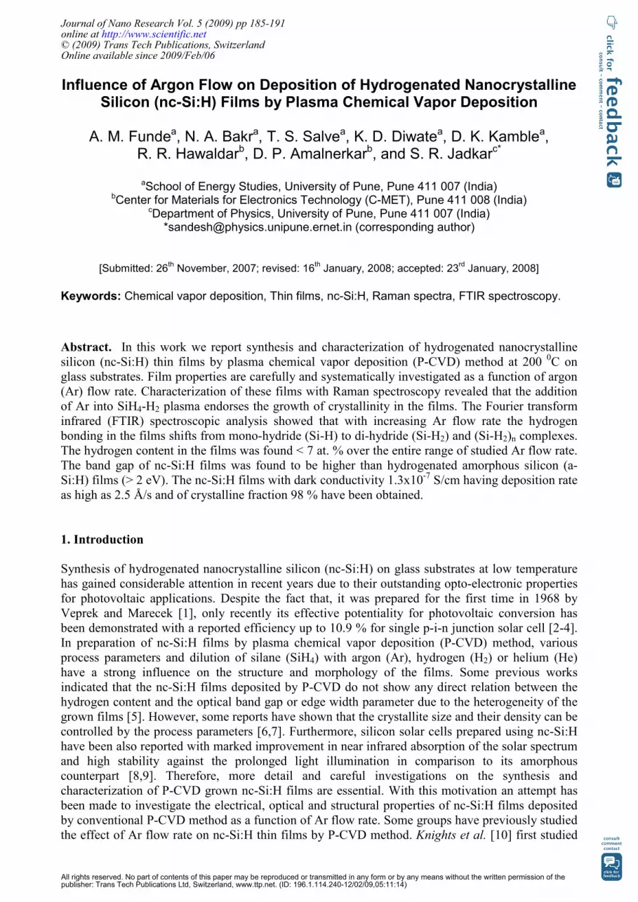
2.2. Film characterization The dark conductivity (σdark) and photoconductivity (σphoto) of the films were measured using samples of dimensions 3 cm x 1 cm deposited on glass substrate with coplanar Al electrodes of 0.5 mm apart deposited by vacuum evaporation. The measurements were carried out at room temperature and atmospheric pressure. Fourier transform infrared (FTIR) spectra of the films were recorded by using FTIR spectrophotometer (Shimadzu, Japan). Bonded H contents (CH) were calculated from Si-H wagging mode infrared absorption peaks using the method given by the Brodsky et al. [13]. The optical absorption coefficient (α) was determined from the transmission (T) and reflection (R) measurements using a double beam UV–Visible spectrophotometer (Hitachi-330, Japan) in the wavelength range of 200-900 nm. The optical band gaps (Eg) of the films were determined from the relation (αE)1/2 = B(E - Eg), where E = hυ is the photon energy. The extrapolation of (αhυ)1/2 versus hυ plot yields Eg. Raman spectra were recorded with micro-Raman spectroscopy (Jobin Yvon Horibra LABRAM-HR) in the wavelength range of 400-1100 nm. The spectrometer has backscattering geometry for detection of Raman spectrum with the resolution of 1 cm-1. The excitation source was 632.8 nm line of He-Ne laser. For the measurements of crystalline fraction (XRaman) and crystallite size (dRaman), we have followed the method given by Tsu et al. [14] and He et al. [15] respectively. Low angle x-ray diffraction spectra were obtained by-ray diffractometer (Bruker D8 Advance, Germany) using Cu Kα line (λ = 1.54056 Å). The spectra were taken at a grazing angle of 10. The average crystallite size was estimated using the classical Scherrer's formula [16]. The thickness of the films was determined by a Talystep profilometer (Taylor-Hobson Rank). 3. Results and Discussion Variation of deposition rate (rd) and dark conductivity (σDark) for nc-Si:H films deposited by P-CVD at various Ar flow rate (FAr) is shown in Fig. 1. The zero point indicates the values of rd and σDark for the films deposited with no Ar addition. As seen from the figure the rd increases with increasing FAr. The increase in rd can be attributed to the reduction of hydrogen coverage of growing surface with increasing FAr and the enhancement of dissociation of SiH4 by excited argon molecules, Ar* in SiH4-H2 plasma [17]. The values of σDark are 10-5-10-7 S/cm over the entire range of FAr studied. In fact it decreases from 1.7x10⁻⁵ S/cm to 1.3x10⁻⁷ S/cm as FAr increase from 15 sccm to 50 sccm. These values are consistent with those reported previously for nc-Si:H films grown under different plasma conditions [18,19]. The decrease in σDark can be attributed to the
change in hydrogen bonding configuration in the film from mono-hydrogen (Si-H) to di-hydrogen (Si-H2) and poly-hydrogen (Si-H2)n complexes with increasing Ar flow rate (discussed later). The shift of hydrogen bonding from Si-H to Si-H2 and (Si-H2)n complexes increases the number of dangling bonds and hence trapping density of charge carrier in the film. As a result, dark conductivity (σDark) decreases with increasing Ar flow rate (FAr).
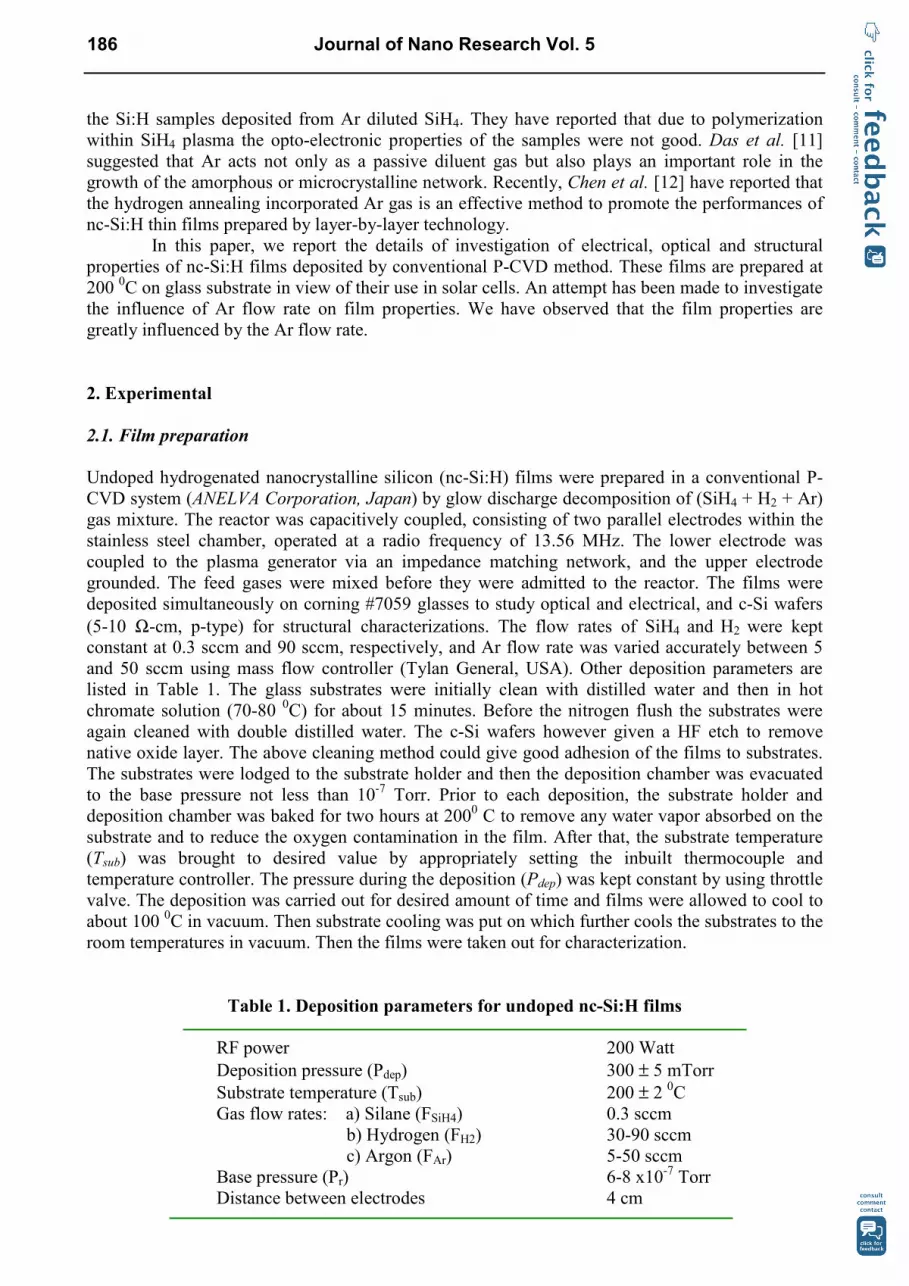
Fig. 2 displays the FTIR spectra of the nc-Si:H films, normalized to thickness deposited at different Ar flow rates (FAr). For clarity the spectra are shifted vertically. The film deposited at FAr = 0 sccm have major absorption bands ∼618 cm-1 and ∼2000 cm-1, which correspond to wagging and stretching modes respectively of vibrations of mono-hydride (Si-H) bonded species [20]. The absorption band in between 700 and 900 cm-1 has been also observed and can be assigned to stretching/bending vibrational modes of di-hydride (Si-H2) and (Si-H2)n complexes (isolated or coupled) [21] having comparatively lesser intensity. Thus, Si-H bonding configuration is dominant for the film deposited at FAr = 0 sccm. For nc-Si:H films prepared at various FAr, the Si-H wagging band is seen to decrease in absorption. Moreover, significant changes in shape and intensity of absorption band ∼2000 cm-1 have been observed. With increasing FAr the intensity of absorption band ∼2000 cm-1 increased and shifted further towards the higher wave number.
Journal of Nano Research Vol. 5 187

Thus, the nc-Si:H film deposited at FAr = 50 sccm show an additional broad shoulder centered ∼2110 cm-1. According to the literature the absorption peak ∼2110 cm-1 corresponds to stretching vibrational modes of Si-H2 and (Si-H2)n species [22,23]. These results clearly indicate that with addition of Ar in SiH4-H2 plasma the predominant hydrogen bonding configuration in the films changed from Si-H group to Si-H2 and (Si-H2)n complexes.
400 600 800 1900 2000 2100 2200 2300
Si-Si
15
0
25
Inte
nsity
(a.
u.)
2074 cm-1
2041 cm-1
618 cm-1 2113 cm-1
700-900 cm-1
50
503 cm-1
FAr
Si-H
Si-H2/(Si-H
2)n
Si-H
Wave number (cm-1)
Figure 2. The Fourier transform infrared (FTIR) spectra of some nc-Si:H films deposited by P-CVD at different Ar flow rates (FAr).
-10 0 10 20 30 40 50 6010-8
10-7
10-6
10-5
10-4
1.0
1.5
2.0
2.5
3.0Dar
k co
nduc
tivity
σDark
(S/c
m)
Ar Flow rate FAr (sccm)
Zero Point
Dep
osition
rat
e r d
(A/s) Figure 1. Deposition rate (rd)
and dark conductivity (σDark) as a function of Ar flow rate (FAr) for nc-Si:H films deposited by P-CVD. Note that the zero point indicates the values of rd and σDark for the films deposited with no Ar addition.
188 Journal of Nano Research Vol. 5
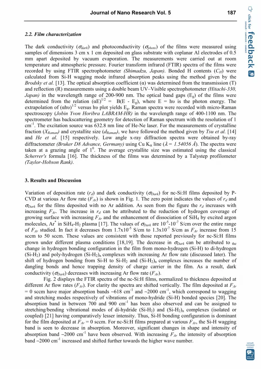
Raman spectra of nc-Si:H films normalized to thickness deposited by P-CVD at various Ar flow rate (FAr) is shown in Fig. 3. The corresponding crystalline fraction (Xc) and crystallite size (dRaman) are also indicated in the figure. The film deposited at FAr = 0 sccm has a shoulder centered ∼502 cm-1, associated with the amorphous and defective part of crystalline phase [24] and other centered ∼520 cm-1 attributed to silicon crystallites of different sizes in the film [25]. For this film, Xc is ~84 % and dRaman is ~7.7 nm. For the film deposited at FAr = 15 sccm, the peak corresponding to amorphous and defective nanocrystalline phases disappears and Xc in the film enhances (~94 %). Furthermore, with increasing FAr the intensity of the band centered ∼520 cm-1 increased and shifted to higher wave number. The shift of the peak towards higher wave number is related to increase in Xc while increase in intensity and sharpness are related to the decrease in dRaman in the film [26]. Thus, the film deposited at FAr = 50 sccm have Xc ~98 % and dRaman ~7.2 nm. These results indicate that addition of Ar into the SiH4-H2 plasma endorses the growth of crystallinity in the film, which is very important to promote the nc-Si:H films for the commercial applications. The disappearance of 502 cm-1 peak also supports this inference. The increase in crystallinity with increase in FAr can be attributed to increase in density of Ar* as well as by Ar+ ions. In SiH4-H2 plasma containing Ar, Ar* and Ar+ play an active role in dissociation of SiH4 and of H2. Hydrogen radical density can increase via reactions SiH4 + Ar* = SiH2 + 2H + Ar [27] and H2 + Ar+ = ArH+ + H [28]. These hydrogen radicals break weak Si-Si bonds involved in Si-H network and replaced by new film precursors to form a rigid and strong Si-Si bond in crystalline mode [29]. Furthermore, the energy released by de-excitation of Ar* leads to structural relaxation and reorientation [30] which thereby promotes the crystallization. The appearance of the band ∼508 cm-1 in FTIR spectra, corresponds to the Si-Si absorption [31], further supports this.
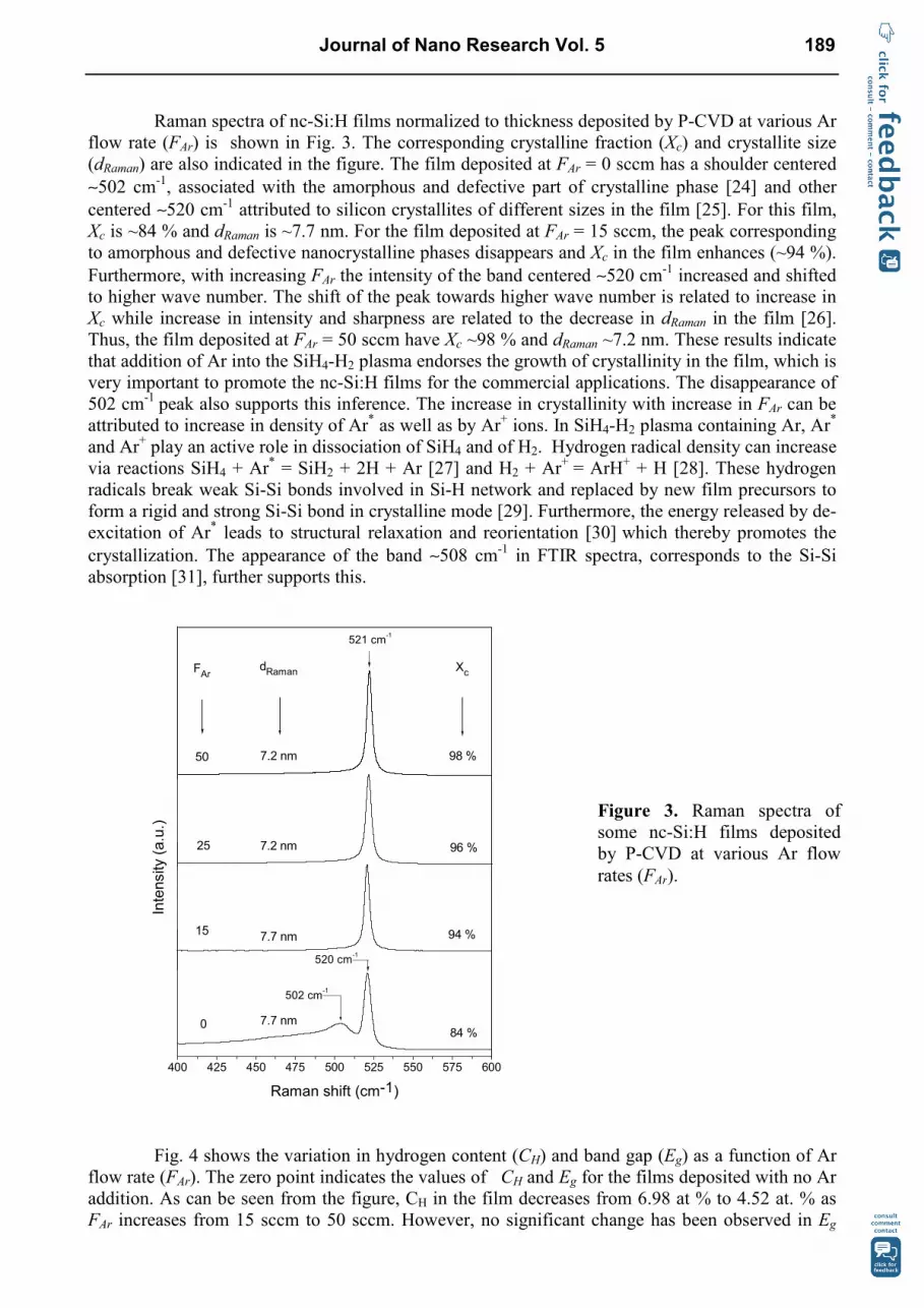
Fig. 4 shows the variation in hydrogen content (CH) and band gap (Eg) as a function of Ar flow rate (FAr). The zero point indicates the values of CH and Eg for the films deposited with no Ar addition. As can be seen from the figure, CH in the film decreases from 6.98 at % to 4.52 at. % as FAr increases from 15 sccm to 50 sccm. However, no significant change has been observed in Eg
400 425 450 475 500 525 550 575 600
502 cm-1
520 cm-1
84 %7.7 nm0
Raman shift (cm-1)
7.2 nm
7.2 nm
25
94 %
96 %
7.7 nm15
Inte
nsity
(a.
u.)
521 cm-1
98 %
XcdRamanFAr
50
Figure 3. Raman spectra of some nc-Si:H films deposited by P-CVD at various Ar flow rates (FAr).
Journal of Nano Research Vol. 5 189
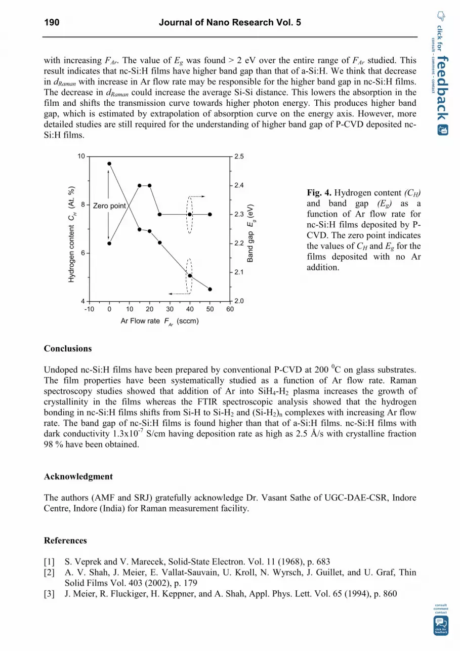
with increasing FAr. The value of Eg was found > 2 eV over the entire range of FAr studied. This result indicates that nc-Si:H films have higher band gap than that of a-Si:H. We think that decrease in dRaman with increase in Ar flow rate may be responsible for the higher band gap in nc-Si:H films. The decrease in dRaman could increase the average Si-Si distance. This lowers the absorption in the film and shifts the transmission curve towards higher photon energy. This produces higher band gap, which is estimated by extrapolation of absorption curve on the energy axis. However, more detailed studies are still required for the understanding of higher band gap of P-CVD deposited nc-Si:H films.
Conclusions Undoped nc-Si:H films have been prepared by conventional P-CVD at 200 0C on glass substrates. The film properties have been systematically studied as a function of Ar flow rate. Raman spectroscopy studies showed that addition of Ar into SiH4-H2 plasma increases the growth of crystallinity in the films whereas the FTIR spectroscopic analysis showed that the hydrogen bonding in nc-Si:H films shifts from Si-H to Si-H2 and (Si-H2)n complexes with increasing Ar flow rate. The band gap of nc-Si:H films is found higher than that of a-Si:H films. nc-Si:H films with dark conductivity 1.3x10⁻⁷ S/cm having deposition rate as high as 2.5 Å/s with crystalline fraction 98 % have been obtained. Acknowledgment The authors (AMF and SRJ) gratefully acknowledge Dr. Vasant Sathe of UGC-DAE-CSR, Indore Centre, Indore (India) for Raman measurement facility. References [1] S. Veprek and V. Marecek, Solid-State Electron. Vol. 11 (1968), p. 683 [2] A. V. Shah, J. Meier, E. Vallat-Sauvain, U. Kroll, N. Wyrsch, J. Guillet, and U. Graf, Thin
Solid Films Vol. 403 (2002), p. 179 [3] J. Meier, R. Fluckiger, H. Keppner, and A. Shah, Appl. Phys. Lett. Vol. 65 (1994), p. 860
-10 0 10 20 30 40 50 604
6
8
10
2.0
2.1
2.2
2.3
2.4
2.5
Hyd
roge
n co
nten
t CH (
At.
%)
Ar Flow rate FAr (sccm)
Zero point
Ban
d ga
p E
g (eV
)
Fig. 4. Hydrogen content (CH) and band gap (Eg) as a function of Ar flow rate for nc-Si:H films deposited by P-CVD. The zero point indicates the values of CH and Eg for the films deposited with no Ar addition.
190 Journal of Nano Research Vol. 5
[4] J. Meier, H. Dubail, L. Feitknecht, Y. Zeigler, P. Torres, C. Hof, U. Kroll, D. Fischer, J. Cuperus, H. Keppner, and A. Shah, Proceedings of the Second World Conference on Photovoltaic Solar Energy Conversion, Vienna, (1998)
[5] Y.H. Wang, J. Lin, and C.H. A. Huan, Mater. Sci. Eng. B Vol. 104 (2003), p. 80 [6] M. Acciarri, S. Binetti, M. Bollani, A. Comotti, L. Fumagalli, S. Pizzini, and H. Von Kanel,
Solar Ener. Mater. Solar Cells Vol. 87 (2005), p. 11 [7] H. Shirai, Y. Fujimura, and S. Jung, Thin Solid Films Vol. 407 (2002), p. 12 [8] K. Prasad, F. Finger, S. Dubail, A. Shah, and M. Schubert, J. Non-Cryst. Solids Vol. 137-138
(2002), p. 681 [9] J. Meier, P. Torres, R. Platz, S. Dubail, U. Kroll, J.A.N. Selvan, N. Pellaton Vaucher, Ch. Hof,
D. Fischer, H. Keppner, A. Shar, K.D.Ufert, P. Giannoules, and J. Koehler, Mater. Res. Soc. Symp. Proc. Vol. 420 (1996), p. 3
[10] J.C. Knights, R.A. Lujan, M. P. Rosenblum, R.A. Street, D.K. Biegelsen, and J.A. Reimer, Appl. Phys. Lett. Vol. 38 (1981), p. 331
[11] U.K. Das, P. Chaudhuri, and S.T. Kshirsagar, J. Appl. Phys. Vol. 80 (1996), p. 5389 [12] S. F. Chen, Y.K. Fang, T.H. Lee, C.Y. Lin, P.J. Lin, S.H. Chang, and T.H. Chou, Thin Solid
Films Vol. 515 (2007), p. 3844 [13] M.H. Brodsky, M. Cardona, and J.J. Cuomo, Phys. Rev. B Vol. (1977), p. 16, 3556H [14] R. Tsu, J. Gonzale, Z. Hernandez, S. S. Chao, S. C. Lee, and K. Tanaka, Appl. Phys. Lett.
Vol. 40 (1982), p. 534 [15] Y. He, C. Yin, G. Cheng, L. Wang, X. Liu, and G.Y. Hu, J. Appl. Phys. Vol. 75 (1994), p. 797 [16] Fritzsche, M. Tanielian, C. C. Tsai, and P. J. Gaczi, J. Appl. Phys. Vol. 50 (1979), p. 3366 [17] Ch. Hollenstein, U. Kroll, A. A. Howling, J. Dutta, J. L. Dorier, J. Meier, R. Tscharner, and A.
Shah, Proceedings of the 11th European PVSEC, Montreux, (1992), p. 132 [18] C. Goncalves, S. Charvet, A. Zeinert, M. Clin, and K. Zellama, Thin Solid Films Vol. 403
(2002), p. 91 [19] F. Liu, M. Zhu, Y. Feng, Y. Han, J. Liu, S. Kasouit, and R. Vanderhaghen, J. Non-Cryst.
Solids Vol. 299 (2002), p. 385 [20] G. Lucovsky, Solar Cells Vol. 2 (1980), p. 431 [21] J.C. Knights, G. Lucovsky, and R.J. Nemanich, J. Non-Cryst. Solids Vol. 32 (1979), p. 393 [22] S.F. Chen, Y. K. Fang, T.H. Lee, C. Y. Lin, P.J. Lin, S. H. Chang, and T.H. Chou, Thin Solid
Films Vol. 515 (2007), p. 3844 [23] P. John, I. M. Odch, and M.J. K. Thomas, Solid St. Commun. Vol. 41 (1982), p. 384 [24] C. Droz, E. Vallat-Sauvain, J. Bailat, L. Feitknecht, J. Meier, and A. Shah, Solar Ener. Mater.
Solar Cells Vol. 81 (2004), p. 61 [25] Z. Iqbal and S. Veprek, J. Phys. C. Vol. 15 (1982), p. 377 [26] H. Richter, Z. P. Wang, and L. Ley, Solid St. Commun. Vol. 39 (1981), p. 625 [27] M. J. Kushner, J. Appl. Phys. Vol. 63 (1988), p. 2532 [28] H. Makihara, A. Tabata, Y. Suzuoki, and T. Mizutanit, Vacuum Vol. 59 (2000), p. 785 [29] A. Matsuda, Thin Solid Films Vol. 337 (2001), p. 1 [30] U.K. Das, P. Chaudhuri, and S.T. Kshirsagar, J. Appl. Phys. Vol. 80 (1996), p. 5389 [31] D.R. Lide, CRC Handbook of Chemistry and Physics, CRC Press, New York NY, (1988)
Journal of Nano Research Vol. 5 191
Journal of Nano Research Vol. 5 doi:10.4028/0-00000-029-9Influence of Argon Flow on Deposition of Hydrogenated Nanocrystalline Silicon (nc-Si:H) Films by Plasma Chemical Vapor Deposition doi:10.4028/0-00000-029-9.185
192 Journal of Nano Research Vol. 5