implanted sio2 films and wide-bandgap a-si:h - citeseerx
TRANSCRIPT

Silicon-based light-emitting materials: Implanted Si02 films and widebandgap a-Si:H
Ivan Pelant*a, Kateina Luterováa, Petr FojtIka, Jean-Luc Rehspringer", Dominique Mullerc,Jean-Jacques Grobc, Juraj Diane', Jan Va1enta(t, Rolandas Tomasiunase, Bernd Honerlageb
aJn5tjte ofPhysics, Academy of Sciences ofthe Czech Republic, Cukrovarnická 10, 162 53Praha 6, Czech Republic
bInstit de Physique et Chimie des Matériaux de Strasbourg, UMR7504, CNRS, ULP, 23 ruedu Loess, 67037 Strasbourg, France
C Laboratoire PHASE, UPR292, CNRS, 23 rue du Loess, 67037 Strasbourg, Franced
Faculty ofMathematics and Physics, Charles University, Ke Karlovu 3, 121 16 Praha 2,Czech Republic
e Institute of Materials Science and Applied Research, Vilnius University, 2054 Vilnius,Lithuania
ABSTRACT
We review critically recent results ofinvestigation ofhydrogenated amorphous silicon (a-Si:H) and Si-implanted Si02 filmsfrom the point ofview oflight-emission applications. Wide bandgap a-Si:H with the energy gap ranging from 2.0 to 2.2 eVexhibits room temperature photoluminescence in the visible region. Electroluminescence, however, occurs after previou srecrystallization ofa-Si:H only and seems not to be perspective for large scale applications. Sit-implanted Si02 films contain,after proper annealing at 1000 - 1 100 °C, Si nanocrystals that luminesce in the red. In parallel another emission band canoccur (in the blue region) which is related to post-implantation defects. We demonstrate that in Si02 films homogeneouslyimplanted across the entire film thickness red electroluminescence can be easily observed, presumably due to injection ofelectron-hole pairs into Si nanocrystals. Finally, the present status ofprospects of stimulated emission achievement in low-dimensional Si structures is briefly summarized.
Keywords : amorphous silicon, implanted Si02, silicon nanocrystals, photoluminescence, electroluminescence
1. INTRODUCTION
Light emission in silicon represents a challenge for a long time. Silicon, a fundamental material for electronics andmicroelectronics, cannot be used for fabrication of active light-emitting devices. Realization of such a device would lead tointegration of optoelectronics with microelectronics. In recent years a large number of ways have been proposed how toovercome this obstacle arising from the indirect nature of the fundamental bandgap in Si'. One of the most extensivelypursued routes, following the first announcement that electrochemically etched Si gives efficient visible photoluminescenceat 300 K2, has been investigation of silicon in the form of Si nanocrystals (Si-nc). The quantum confinement effect in thesenanometer sized Si clusters together with surface passivation are believed to cause Si bandgap opening and lead to a hugeincrease in luminescence efficiency3'4.
*Correspondence: E-mail: [email protected]; Telephone: +420-2-20 318 502; Fax: +420-2-3 12 31 84tAlso at the Royal Institute of Technology, Department of Electronics, Kista-Stockholm, Sweden
Invited Paper
Optical Organic and Inorganic Materials, Steponas P. Ašmontas, Jonas Gradauskas, Editors,Proceedings of SPIE Vol. 4415 (2001) © 2001 SPIE · 0277-786X/01/$15.0066
Downloaded From: http://proceedings.spiedigitallibrary.org/ on 02/18/2016 Terms of Use: http://spiedigitallibrary.org/ss/TermsOfUse.aspx

In this contribution we report on some recent results concerning preparation, optical and optoelectronic p roperties of theseSi-nc. We shall focus on microscopic view of light emission from Si-nc, on a simple electroluminescent device and we shallalso comment on the exciting question of whether positive optical gain can be achieved in silicon based materials or not.However, we start briefly with considerations of another type of light-emitting Si-based material studied recently in ourlaboratories, namely, wide bandgap hydrogenated amorphous Si (a-Si:H)5.
2. WIDE BANDGAP a-Si:H
2. 1. Photoluminescence
Standard "device-grade" a-Si:H (with hydrogen content < 10%) is not suitable for light-emitting applications because itsroom temperature photoluminescence (PL) is negligible and relevant photon energy is low (-4 .2 eV). However, increasedcontent of hydrogen in a-Si:H is known to lead to a shift of the optical bandgap from 1.8 eV to 2.0 eV -2.1 eV and toappearance ofPL in the visible region at room temperature6. We have studied such wide bandgap a-Si:H films prepared inmicrowave plasma of SiH4 strongly diluted with He under electron cyclotron resonance conditions. The hydrogen contentin our samples varied between cca 1 3 and 51 at. %78•
Typicalroom temperature PL spectra ofseveral samples are
photon energy (eV) shown in Fig. 1, together with a reference PL spectrum of a
2 22 0 1 8 1 6 1 4 1 2device grade a-Si:H (78 K). The blue shift of PL spectra
. . . . . .with respect to device grade material is evident. To reveal
100 the microscopic origin of this red light emission, infrared—.% 90 (IR) absorption measurements turned out to be of basic: 80 importance. The JR absorption spectra ofour hydrogen rich
70 a-Si:H display a typical band peaked at 2080 -21 15 cm. In. 60 Fig. 2a) the PL intensity is plotted against the frequency of'- these JR vibration modes for the entire set of investigated: 50samples. It can be seen that the samples with the JR peak
40 located in the close neighbourhood of 2100 cni' exhibit the. 30 strongest PL. This result indicates that only hydrogen: 20 embedded in a specific manner contributes to the PLa. emission. The vibration frequencies 2090 - 21 17 cm' have
been previously ascribed to stretching vibration modes of0
oligosilanes -(SiH2)- embedded with voids in the a-Si:Hnetwork'°. An increasing number n (=1 2 ... 12) of the -
wavelength(nm) . . . . . .SiH2- units in the chain leads to a higher characteristicfrequency, as indicated at the top ofFig. 2a) for n=1, 2, ... 5.
Fig. 1. Photoluminescence emission spectra of several samples of The data in Fig. 2a) therefore strongly suggest that -(SiH2)2-wide bandgap a-Si:H (symbols). For comparison emission units form the most efficient luminescence centres. Thisspectrum ofa device-grade a-Si:H is represented by a dashed line, conclusion has been corroborated by Fig. 2b) where the PLtaken from .
intensity has been plotted as a function of the ratio121o1/(I2000+12o9o+121o+12164) resulting from decomposition of the JR absorption peak into four gaussians I, located at 2000 cm',2090 cm, 2101 cm' and 2164 cm'. Fig. 2b) then says that the PL intensity reaches its maximum value when the JRabsorption peak in the vicinity of 2101 cm' is narrow, i. e. when hydrogen is incorporated predominantly as -(SiH2)2- unit.
2. 2. Electroluminescence
Electroluminescence in p-i-n diodes fabricated from device grade a-Si:H was first reported in 1976g. Under forward biasconditions at 78 K the infrared EL emission occured which coincided spectrally with PL (maximum at 1 .28 eV).Extrapolating straight-forwardly this behaviour to wide gap a-Si:H, one could expect to obtain red light emission at roomtemperature in forward-biased p-i-n structures fabricated from wide gap a-Si:H. However, this is not the case.
Proc. SPIE Vol. 4415 67
Downloaded From: http://proceedings.spiedigitallibrary.org/ on 02/18/2016 Terms of Use: http://spiedigitallibrary.org/ss/TermsOfUse.aspx

S e.i C); C4 i=C4
60 •fl.T=300K 'XP3 a)
4Oc H-3O HCl)c:. 20 standad: (narrowgap) .ci 1 aSi;H
• •-:2000 2010 2090 2100 2110
wavenumber(cm1)
60
' ' I I I
b)
4020 -
00.0 0.2 0.4 0.6 0.8
I 1(1 +1 +1 +1 )2101 2000 2090 2101 2164
Fig. 2. a) Spectrally integrated photoluminescence intensity of different wide bandgap a-Si:H samples as a function of thewavenumber ofinfrared absorption band (in the interval 2000-21 15 cm'). This plot means that the photoluminescence is brightestin a sample (XP3) with the absorption maximum -21OO cm'.b) Plot ofphotoluminescence intensity (of the same set of samples as in a)) against a relative weight of the infrared absorptionband peaked at 2101 cm'.The curves are guides for the eye.
Our first attempts to detect an EL radiation from wide gap a-Si:H p-i-n structures revealed extremely low current densities(108 AIcm2) and no light emission. Subsequent studies of subgap optical absorption discovered the large band tails in thismaterial to be the cause of this disappointing behaviour. An example of the spectral course of the subgap absorptio ncoefficient ct(E) at 295 K wide gap sample XP3 (measured by the constant photocurrent method) is shown in Fig. 3 -thefull curve. The dotted curve denotes a(E) of a reference device grade a-Si:H sample TP14. Besides an evident overal blueshift, also a much higher value of reciprocal band tail slope in XP3 (70 meV) can be seen compared to TP14 (52 meV). Thisimplies a much more important disorder of the amorphous network in hydrogen-rich a-Si:H. Transport paths for electronsand holes are consequently shifted downwards into the tails where the wavefunctions of the localized states overla pnegligibly and transport is therefore made difficult.
1.0
Proc. SPIE Vol. 441568
Downloaded From: http://proceedings.spiedigitallibrary.org/ on 02/18/2016 Terms of Use: http://spiedigitallibrary.org/ss/TermsOfUse.aspx
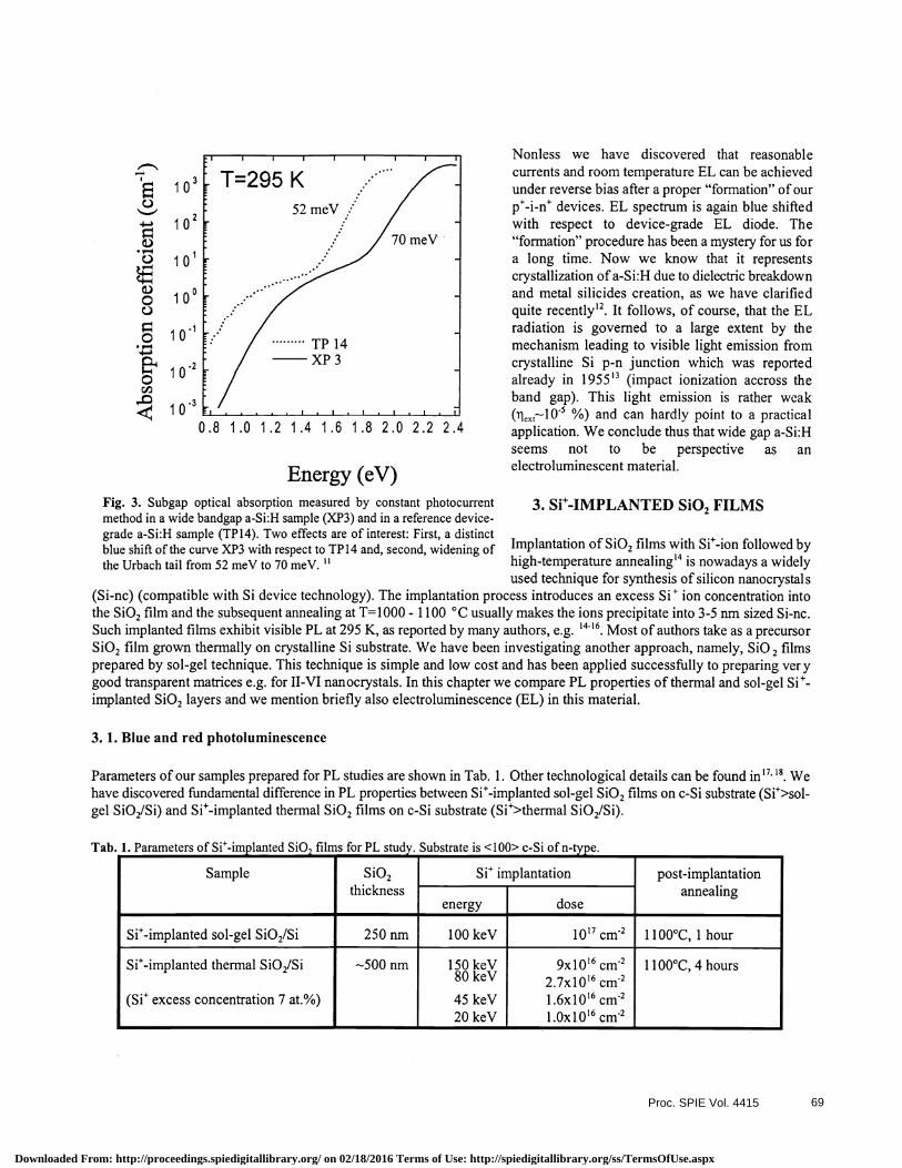
Fig. 3. Subgap optical absorption measured by constant photocurrentmethod in a wide bandgap a-Si:H sample (XP3) and in a reference device-grade a-Si:H sample (TP14). Two effects are of interest: First, a distinctblue shift of the curve XP3 with respect to TP14 and, second, widening ofthe Urbach tail from 52 meV to 70 meV.
Nonless we have discovered that reasonablecurrents and room temperature EL can be achievedunder reverse bias after a proper "formation" of ourp+-i-n+ devices. EL spectrum is again blue shiftedwith respect to device-grade EL diode. The"formation" procedure has been a mystery for us fora long time. Now we know that it representscrystallization ofa-Si:H due to dielectric breakdownand metal suicides creation, as we have clarifiedquite recently'2. It follows, of course, that the ELradiation is governed to a large extent by themechanism leading to visible light emission fromcrystalline Si p-n junction which was reportedalready in 1955 ' (impact ionization accross theband gap). This light emission is rather weak(1exi10 %) and can hardly point to a practicalapplication. We conclude thus that wide gap a-Si:Hseems not to be perspective as anelectroluminescent material.
3. Si-IMPLANTED Si02 FILMS
Implantation of 5i02 films with Sit-ion followed byhigh-temperature annealing'4 is nowadays a widelyused technique for synthesis of silicon nanocrystals
Tab. 1. Parameters of Si-implanted SiO, films for PL study. Substrate is <100> c-Si of n-tvne.
Sample Si02thickness
Si implantation post-implantationannealing
energy dose
Si-implanted sol-gel Si02/Si 250 nm 100 keV iO' cm2 1100°C, 1 hour
Si-implanted thermal Si02/Si
(Si excess concentration 7 at.%)
—500 nm 150 keV80 keV
45 keY20 keV
9xlO'6 cm22.7x 106 cm21.6x 1016 cm21.Ox 1016 cm2
1100°C, 4 hours
EC.)
C.)'—4
G.)0C)
0
1
102
I
100
10.1
10.2
100.8 1.0 1.2 1.4 1.6 1.8 2.0 2.2 2.4
Energy (eV)
(Si-nc) (compatible with Si device technology). The implantation process introduces an excess Si ion concentration intothe Si02 film and the subsequent annealing at T=1000 - 1100 °C usually makes the ions precipitate into 3-5 nm sized Si-nc.Such implanted films exhibit visible PL at 295 K, as reported by many authors, e.g. 1446• Most of authors take as a precursorSi02 film grown thermally on crystalline Si substrate. We have been investigating another approach, namely, 2 filmsprepared by sol-gel technique. This technique is simple and low cost and has been applied successfully to preparing verygood transparent matrices e.g. for Il-Yl nanocrystals. In this chapter we compare PL properties of thermal and sol-gel Si -implanted Si02 layers and we mention briefly also electroluminescence (EL) in this material.
3. 1. Blue and red photoluminescence
Parameters of our samples prepared for PL studies are shown in Tab. 1. Other technological details can be found 17 I8 Wehave discovered fundamental difference in PL properties between Si-implanted sol-gel Si02 films on c-Si substrate (Si>sol-gel SiO2/Si) and Si-implanted thermal Si02 films on c-Si substrate (Si>therma1 Si02/Si).
Proc. SPIE Vol. 4415 69
Downloaded From: http://proceedings.spiedigitallibrary.org/ on 02/18/2016 Terms of Use: http://spiedigitallibrary.org/ss/TermsOfUse.aspx

c
Cl)
0)
-J00.2
0.0
photon energy (eV)1.5
400 500 600 700 800 900 1000
wavelength (nm)
. 10
,r1= 1.8ns t1=3Oj.s io102
'r2148ns-r2=92ps
p0T=2K o T295K • . . I. .10Q'• , uk i '=
111 AA = nm
100 1 IiI J\ii1L1000 20 40 0 200 400 600
time delay (ns) time delay (ts)
Fig. 4. a) Room temperature photoluminescence spectra ofa Si-imp1anted Si02 film (red emission, full line) and ofa Sr-implantedsol-gel derived Si02 film (blue emission, dotted line). The spectra are normalized.b) Photoluminescence decay of both samples at 295 K (symbols) together with excitation pulses (shaded areas) and doubleexponential fits (lines). Note drastically different scale on the time axes.
A brief summary of this difference is contained in Fig. 4 18Typically, (Si>sol-gel Si02/Si) structures exhibit at T=295 Ka blue luminescence band peaked at 43Orim while (Si>thermal Si02/Si) samples has red PL band at —78O nm. RelevantPL emission spectra are shown in Fig. 4a. A striking difference in PL dynamicS demonstrates Fig. 4b. The blue emission band
a) 3 2.5 21.0
0.8
0.6
0.4
b)I 0 Si>soI-geI SIOJSi
E6
Cl)CC)
C-Ja-
Si>thenmI Si02/Si7at%
Proc. SPIE Vol. 441570
Downloaded From: http://proceedings.spiedigitallibrary.org/ on 02/18/2016 Terms of Use: http://spiedigitallibrary.org/ss/TermsOfUse.aspx
is very fast and decays in a few nanoseconds while the red one is slow -decay time ofthe order oftens microseconds. Weinterpret the blue band as originating in some defects, related probably to the implantation process. The red band is, inagreement with a general consensus nowadays, due to exciton recombination in Si-nc. This interpretation is based o nmeasurements of thermal variations of PL intensity18. We have modelled the temperature dependence of the red bandintensity within the framework of a simplified model of singlet-triplet splitting ofquantum-confined excitons in Si-nc 19•Wehave obtained the exchange energy splitting to be L\E =26 meV'8. Similar but more detailed experiments, completed by asimultaneous measurement of the PL decay rate, have been reported recently by Brongesma et al.20. They have obtained thesinglet-triplet splitting AE between 8.4 meV for large Si-nc (-5.5 nm) and 16.5 meV for small Si-nc (—2 nm).
The blue emission band, on the other hand, exhibits quite different temperature variations'8 that cannot be described by theabove model. This observation rules out the possibility that this light emission could have originated in tiny Si-nc (1-2 nm)with strong quantum confinement.
Tab. 2. Parameters of Sitimplanted Si02 film for EL study.
Sample Si02thickness
Si implantation post-implantationannealing
energy dose
ITO/Sitimplanted sol-gel Si02/Si 250 nm 70 keV40 keY
30 keY20 keY
3x10'6 cm2lxlO'6cm2
4.5x10'5 cm25.5x10'5 cni2
1100°C, 1 hour
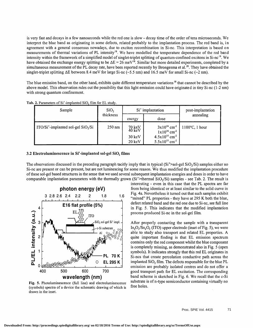
3.2 Electroluminescence in Si'-implanted sol-gel Si02 films
The observations discussed in the preceding paragraph tacitly imply that in typical (Si>sol-gel Si02/Si) samples either noSi-nc are present or can be present, but are not luminescing for some reason. We thus modified the implantation procedureof these sol-gel based structures in the sense that we used several subsequent implantation energies and doses in order to have
comparable implantation parameters with the thermally grown (Si>therma1 Si02/Si) samples -see Tab. 2. The result isinteresting - even in this case that the PL spectra are far
photon energy (eV) frombeing identical or at least similar to the solid curve in
3 2 8 2 6 2 4 2 2 2 1 8 1 6Fig. 4a. Nevertheless it turned out that such samples exhibit"mixed" PL properties - they have at 295 K both the blue,defect related band and the red one due to Si-nc, see full linein Fig. 5. This indicates that the modified implantationprocess produced Si-nc in the sol-gel film.
4
Cl)C2C)
C..Jw
a. 0400
wavelength (nm)Fig. 5. Photoluminescence (full line) and electroluminescence(symbols) spectra of a device the schematic drawing of which isdrawn in the inset.
After properly contacting the sample with a transparent1n203/Sn203 (ITO) upper electrode (inset ofFig. 5), we wereable to study also transport and related EL properties. Aquite important finding is that EL emission spectrumcontains only the red component whilst the blue componentis completely missing, as demonstrated also in Fig. 5 (opensymbols). It indicates strongly that this red EL originates inSi-ncs that create percolation conductive path across theimplanted Si02 film. The defects responsible for the blue PLemission are probably isolated centres and do not offer agood transport path for EL excitation. The correspondingband scheme is sketched in Fig. 6. We recall that the c-Sisubstrate is of n-type semiconductor containing virtually nofree holes.
3
1
E16 flat profile (5%)EL
500 600 700
Proc. SPIE Vol. 4415 71
Downloaded From: http://proceedings.spiedigitallibrary.org/ on 02/18/2016 Terms of Use: http://spiedigitallibrary.org/ss/TermsOfUse.aspx

No external bias
"Forward" bias:high electric current,electron-hole injection,(weak) electroluminescence
"Reverse" bias:high electric current,no e-h Injection,no electroluminescence
Fig. 6. Band scheme of our device consisting of (c-Si substrate/implanted sot-gel Si02/ITO contact). For the sake of simplicityonly one Si-nc is depicted. In fact there is an array of them across the entire Si02 film thickness (—250 nm) and the bias drop isdistributed over their surface barriers.
c-Si substrate(n-type)
ITOcontact
o 0 0
Proc. SPIE Vol. 441572
Downloaded From: http://proceedings.spiedigitallibrary.org/ on 02/18/2016 Terms of Use: http://spiedigitallibrary.org/ss/TermsOfUse.aspx
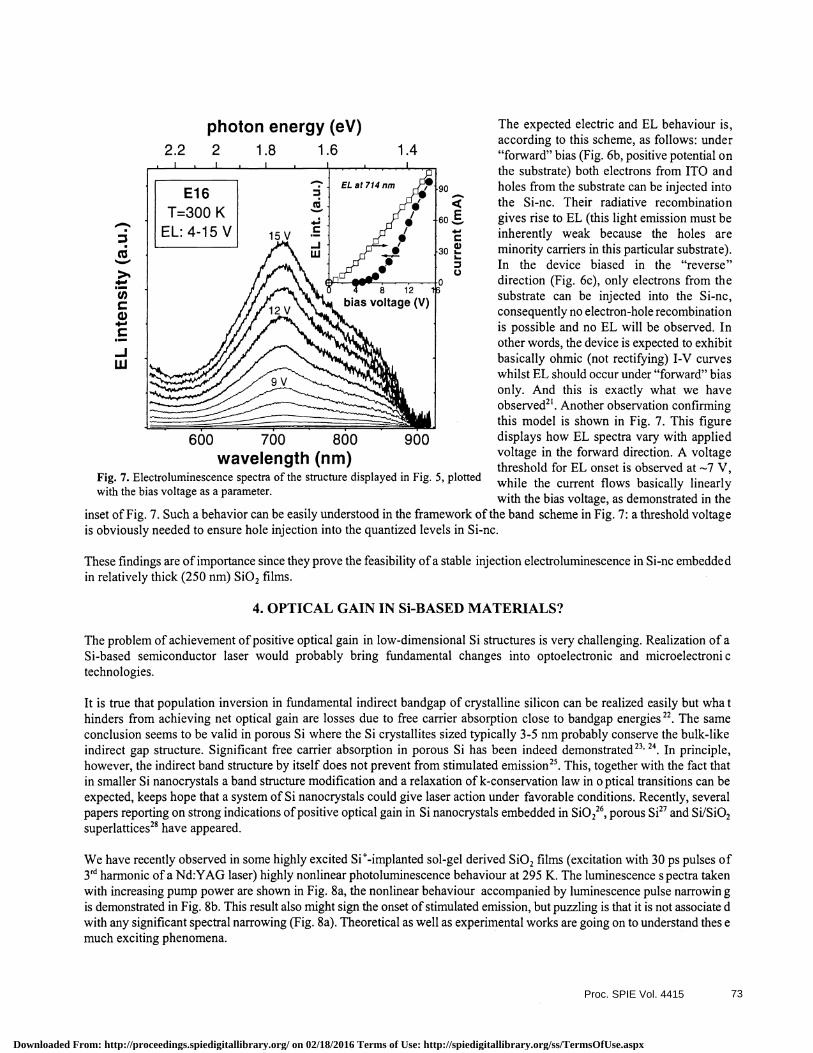
photon energy (eV) The expected electric and EL behaviour is,according to this scheme, as follows: under
2.2 2 1 .8 1 .6 1 .4 "forward" bias (Fig. 6b, positive potential onthe substrate) both electrons from ITO andholes from the substrate can be injected intothe Si-nc. Their radiative recombination
__ '- gives rise to EL (this light emission must be. inherently weak because the holes arec ! minority carriers in this particular substrate).
In the device biased in the "reverse"direction (Fig. 6c), only electrons from the
(I) substrate can be injected into the Si-nc,consequently no electron-hole recombination. is possible and no EL will be observed. In
.— otherwords, the device is expected to exhibitbasically ohmic (not rectifying) I-V curveswhilst EL should occur under "forward" biasonly. And this is exactly what we have
rv2' . Another observation confirmingthis model is shown in Fig. 7. This figure
600 700 800 900 displays how EL spectra vary with applied
wavelennth (nm'i voltage in the forward direction. A voltage' I threshold for EL onset is observed at 7 VFig. 7. Electroluminescence spectra ofthe structure displayed in Fig. 5, plotted while the current flows basically linearlywith the bias voltage as a parameter. . .with the bias voltage, as demonstrated in the
inset ofFig. 7. Such a behavior can be easily understood in the framework ofthe band scheme in Fig. 7: a threshold voltageis obviously needed to ensure hole injection into the quantized levels in Si-nc.
These findings are ofimportance since they prove the feasibility ofa stable injection electroluminescence in Si-nc embeddedin relatively thick (250 nm) 5i02 films.
4. OPTICAL GAIN IN Si-BASED MATERIALS?
The problem of achievement ofpositive optical gain in low-dimensional Si structures is very challenging. Realization of aSi-based semiconductor laser would probably bring fundamental changes into optoelectronic and microelectroni ctechnologies.
It is true that population inversion in fundamental indirect bandgap of crystalline silicon can be realized easily but whathinders from achieving net optical gain are losses due to free carrier absorption close to bandgap energies 22•The sameconclusion seems to be valid in porous Si where the Si crystallites sized typically 3-5nmprobably conserve the bulk-likeindirect gap structure. Significant free carrier absorption in porous Si has been indeed tr23' 24• In principle,however, the indirect band structure by itself does not prevent from stimulated emission25. This, together with the fact thatin smaller Si nanocrystals a band structure modification and a relaxation of k-conservation law in o ptical transitions can beexpected, keeps hope that a system of Si nanocrystals could give laser action under favorable conditions. Recently, severalpapers reporting on strong indications of positive optical gain in Si nanocrystals embedded in 5i0226, porous Si27 and Si/Si02superlattices28 have appeared.
We have recently observed in some highly excited Si-implanted sol-gel derived Si02 films (excitation with 30 ps pulses of3rd harmonic of a Nd:YAG laser) highly nonlinear photoluminescence behaviour at 295K. The luminescence spectra takenwith increasing pump power are shown in Fig. 8a, the nonlinear behaviour accompanied by luminescence pulse narrowin gis demonstrated in Fig. 8b. This result also might sign the onset of stimulated emission, but puzzling is that it is not associate dwith any significant spectral narrowing (Fig. 8a). Theoretical as well as experimental works are going on to understand thes e
much exciting phenomena.
Proc. SPIE Vol. 4415 73
Downloaded From: http://proceedings.spiedigitallibrary.org/ on 02/18/2016 Terms of Use: http://spiedigitallibrary.org/ss/TermsOfUse.aspx

Cl)CwCG)
C0)C.)Cl)0)CE
Cl)C0)C-J0.
0)CD
a)0)C
wavelength (nm)
excitation intensity (MWIcm2)Fig. 8. a) Room temperature photoluminescence spectra of a Si-ion sot-gel derived Si02 film (E40) excited withhighly focused —30 ps pulses of the third harmonic of a Nd:YAG laser (354 nm). Excitation densities areindicated.b) Spectrally integrated luminescence intensity from a) against the excitation density. A superlinear increase isevident. The line is a guide for the eye. The inset demonstrates corresponding luminescence pulse narrowing.
a)
b)
1.4
1.2
1.0
0.8
0.6
0.4
0.2
0.0
120
100
80
60
40
20
0
375 400 425 450 475 500 525 550
0 20 40 60 80 100
Proc. SPIE Vol. 441574
Downloaded From: http://proceedings.spiedigitallibrary.org/ on 02/18/2016 Terms of Use: http://spiedigitallibrary.org/ss/TermsOfUse.aspx

5. SUMMARY
(i) Wide bandgap a-Si:H, in spite ofits promising PL properties, is unlikely to succeed as a material for active optoelectronicdevices.(ii) Si implanted Si02 films show at room temperature a blue (defect related) and a red (Si-nc related) PL bands. Theirrelative weight is a function of many preparation parameters.(iii) Feasibility of room temperature red electroluminescence from Si-nc embedded in thick sol-gel 5i02 films wasdemonstrated.(iv) Search for stimulated emission in low-dimensional Si structures is under way.
ACKNOWLEDGEMENTS
This work was sponsored by the grant B 1 1 1 290 1 of GAAVCR and the project 202/98/0669 of GACR. Financial supportfrom the NATO HTECH.LG972051 linkage grant and the programme "Matériaux" of the CNRS are also gratefullyacknowledged. The authors thank Dr. A. Poruba for supplying the samples of wide bandgap a-Si:H. J. V. thanks to prof.Linnros for kind hospitality during his stay in the Royal Institute of Technology in Stockholm.
REFERENCES
1 . LightEmission in Silicon: From Physics to Devices, Semiconductors and Semimetals Vol. 49, Volume EditorDavid. J. Lockwood, Academic Press, San Diego, 1998.
2. L. T. Canham, "Silicon quantum wire array fabrication by electrochemical and chemical dissolution of wafers",Appl. Phys. Lett. 57, pp. 1046-1048, 1990.
3. Properties ofPorous Silicon, EMIS Datareviews Series No. 18, Ed. by L. Canham, 1NSPEC, London, 1997.4. M. V. Wolkin, J. Jorne, P. M. Fauchet, G. Allan and C. Delerue, "Electronic states and luminescence in porous
silicon quantum dots: The role ofoxygen", Phys. Rev. Lett. 82, pp. 197-200, 1999.5. K. Luterová, I. Pelant, P. FojtIk, M. Niki, I. Gregora, J. Koka, J. Dian, J. Valenta, P. Mali', J. Kudrna, J. tëpánek,
A. Poruba and P. Horváth, "Visible photoluminescence and electroluminescence in wide bandgap hydrogenatedamorphous silicon", Phil. Mag. B, in print.
6. D. J. Wolford, J. A. Reimer and B. A. Scott, Efficient visible photoluminescence in the binary a-Si:H alloysystem", Appl. Phys. Lett. 42, pp. 369-371, 1983.
7. K. Luterová, A. Poruba, J. Dian, 0. Salyk, P. Horváth, P. Knápek, J. Valenta, J. Koka, and I. Pelant, "Wide gaphydrogenated amorphous silicon for visible light emission", J. Porous Materials 7, pp. 135-138, 2000.
8. J. Dian, J. Valenta , J. Hála, A. Poruba, P. Horváth, K. Luterová, I. Gregora and I. Pelant, "Visiblephotoluminescence in hydrogenated amorphous silicon grown in microwave plasma from SiH4 strongly dilutedwith He", J. Appl. Phys. 86, pp. 1415-1419, 1999.
9. I. Pankove and D. E. Carlson, "Electroluminescence in amorphous silicon", Appl. Phys. Lett. 29, pp. 620-622,1976.
10. Furukawa and N. Matsumoto, "Effects ofpolysilane formation on the optical and electrical properties of binarySi:H alloys", Phys. Rev. B 31, pp. 21 14-2120, 1985.J.
11. A. Poruba, "Constant photocurrent method -study of optical properties of amorphous hydrogenated siliconprepared by microwave plasmas", PhD thesis, VUT Brno, 1998.
12. I. Pelant, P. FojtIk, K. Luterová, J. Koka, K. Kniek and J. tèpánek, "Room temperature electric field inducedcrystallization of wide bandgap hydrogenated amorphous silicon", Thin Solid Films, in print.
13. R. Newman, "Visible light from a silicon p-n junction", Phys.Rev. 100, pp. 700-703, 1955.14. T. Shimizu-Iwayama, M. Ohshima, T. Niimi, S. Nakao, K. Saitoh, T. Fujita and N. Itoh, "Visible
photoluminescence related to Si precipitates in Si-implanted SiO2t', J. Phys.: Cond. Matter 5, pp. L375-L380,1993.
15. 5. Guha, "Characterization of Siion-imp1anted Si02 films and silica glasses", J. Appl. Phys. 84, pp. 5210-5217,1998.
16. J. Linnros, N. Lalic, A. Galeckas ans V. Grivickas, "Analysis of the stretched exponential photoluminescencedecay from nanometer-sized silicon crystals in Si02', J. Appl. Phys. 86, pp. 6 128-6134, 1999.
Proc. SPIE Vol. 4415 75
Downloaded From: http://proceedings.spiedigitallibrary.org/ on 02/18/2016 Terms of Use: http://spiedigitallibrary.org/ss/TermsOfUse.aspx
17. J. Valenta, J. Dian, K. Luterová, P. Knápek, I. Pelant, M. Niki, D. Muller, J. J. Grob, J.-L. Rehspringer and B.Hönerlage, "Temperature behaviour ofoptical properties ofSi-implanted Si02", Eur. Phys. J. D 8, pp. 395-398,2000.
1 8. J. Dian, J. Valenta, K. Luterová, I. Pelant, M. Nikl, D. Muller, J. J. Grob, J.-L. Rehspringer and B. Hönerlage,"Optical properties of Siion-implanted sol-gel derived Si02 films", Materials Science and Engineering B69-70,pp. 564-569, 2000.
19. P. D. J. Calcott, K. J. Nash, L. T. Canham, M. J. Kane and D. Brunihead, "Spectroscopic identification of theluminescence mechanism ofhighly porous silicon", J. Luminescence 57, pp. 257-269, 1993.
20. M. L. Brongersma, P. G. Kik, A. Polman, K. S. Mm and H. A. Atwater, "Size-dependent electron-hole exchangeinteraction in Si nanocrystals", Appl. Phys. Lett. 76, pp. 35 1-353, 2000.
2 1 . K. Luterová, J. Valenta, J.-L. Rehspringer, D. Muller, J. J. Grob, J. Dian, B. Hönerlage and I. Pelant, "Redelectroluminescence in Si-implanted sol-gel derived 5i02 films", submitted to Appl. Phys. Lett.
22. W. P. Dumke, "Interband transitions and maser action", Phys. Rev. 127, pp. 1559-1563, 1962.23. J. von Behren, Y. Kostoulas, K. B. Uçer and P. M. Fauchet, "The femtosecond optical response of porous,
amorphous and crystalline silicon", I Non-Crystalline Solids 198-200, pp. 957-960, 1996.24. P. M. Fauchet, "The integration of nanoscale porous silicon light emitters: materials science, properties, and
integration with electronic circuitry", I Luminescence 80, pp. 53-64, 1999.25. H. Kalt, A. L. Smith and T. F. Boggess, "Stimulated emission in indirect gap AlGa1As", J. Appl. Phys. 65, pp.
294-299, 1989.26. L. Dal Negro, C. Mazzoleni, L. Pavesi, G. Franzo and F. Priolo, "Optical gain measurement in silicon
nanocrystals", E-MRS 2000, Strasbourg May 30 -June 2, paper G - 111.3.
27. M. Nayfeh, 0. Akcakir, J. Therrien, Z. Yamani, N. Barry, W. Yu and F. Gratton, "Highly nonlinearphotoluminescence threshold in porous silicon", Appl. Phys. Lett. 75, pp. 41 12-41 14, 1999.
28. L. Heikkilä, T. Kuusela and H.-P. Hedman, "Laser type of spectral narrowing in electroluminescent Si/Si02superlattices prepared by low-pressure chemical vapour deposition", Superlattices and Microstructures 26, pp.157-169, 1999.
Proc. SPIE Vol. 441576
Downloaded From: http://proceedings.spiedigitallibrary.org/ on 02/18/2016 Terms of Use: http://spiedigitallibrary.org/ss/TermsOfUse.aspx