i -78 - citeseerx
TRANSCRIPT

AD-AUH7 *39
UNCLASSIFIED
I oF |
ADACM7 238
ROME. AIR DtVE.LOPME.NT CENTER 6R1I-FISS AFB N Y TRENDS IN ARRAY ANTENNA RESEARCH» (U) JUN 77 R J MAILLOUX
RADC-TR-77-195
END
I -78
I 0 f - IHM == :;: la in
"- IM
1.6
I.I
•25 11.4
MICROCOPY RLSOLUHON 1LSI CHAR!
NATIONAL VtURlfiU W STMWtflBOa \ •< - %
T
RADC-TR-77-195 IN-HOUSE REPORT JUNE 1977
Trends in Array Antenna Research
ROBERT J. MAILLOUX
>4 Q. O
Approved for public r*l«as«; distribution unlimited
I D D C ?MrSB rj?
DEC 6 1977
ROME AIR DEVELOPMENT CENTER
AIR FORCE SYSTEMS COMMAND GRIFFISS AIR FORCE BASE, NEW YORK 13441
^tET5MT7T5
il^Lmt .—«.», J. .»••.,i.^...ju.».--...t.^.-.^- —:...,- ..-^.nt.....-,.,....^. »a.Ai^^.,.-,.,

I. «....., I F...I III •wwpwipwii^iwpwpnnimiw •»'» HJ1 ' IIFFJF-
. - _. -:-J. r 111.
. , /y^-
Unclassified SECURITY CLASSIFICATION OF THIS »AGE f»»l«n Dm gjjjWg
REPORT DOCUMENTATION PAGE
>. PERFORMING ORGANIZATION NAME AND AOORESS
Deputy for Electronic Technology (RADC/ETER) Hanscom AFB /V, Massachusetts 01731 [fit
II. CONTROLLING OFFICI NAM« AND ADDRESS Deputy for Electronic Technology (RADC/ETEI Hanscom AFB Massachusetts 01731 M. MONITC »OENCT JtAMt f AODRESSf« TRUSS htm Cmnlrolllnt OHIc.J IITprWlfi AGENCY »1AMt *
~7 Lxd
READ INSTRUCTIONS BEFORE CQMPLKTTNO FORM
10. PROGRAM ELEMENT, PROJECT, TASK ARE» A WORK UNITJIUMBC
23050401 / T*. RIKflHT OAT« •»
R/ //yjun»JH77 /
IS. SECURITY CLASS, fol »Im Import)
Unclassified IS«. OeCLASSlFlCATION/DOWNORAOIHO
SCHEDULE
IS. DISTRIBUTION STATEMENT (ml Mm Rmport)
Approved for public release;distribution unlimited.
IT. DISTRIBUTION STATEMENT (ml Hi. a».»«ef «.l.r.d In Hock 29. II mWotont Horn Ilaport;
IS. SUPPLEMENTARY NOTES
If. KEY WORDS (Conllnum on nWH •/*• II Mc«M7 and Imonlllr or Hook mmbot)
Phased array antennas Antenna scanning Antennas
IO\AB S0.\ABSTRACT (Conllnum on rmtmtmm mlmw II MSMMf an* loonlllr or olotk namooi) This paper describes a number of analytical developments in the history
of phased array research and analyzes the present state of maturity of that field. The main conclusion of this study is that the technology is evolving so rapidly, and the number of different array types and requirements growing so swiftly, that past analytical developments are vastly inadequate to handle the problems posed by present day array systems. The paper highlights those areas where intensified research is necessary.
DO.ßTn W3 EOITION OF I NOV «S IS OBSOLETE Unclassified SECURITY CLASSIFICATION OF THIS RASE PBS HE Em«
SOf <?S4 Ail
-

i, I...,., ..,...,« ..».,. i J^l^w^w 7
Contents
'—-
1. INTRODUCTION
2. THE ARRAY AS A BOUNDARY VALUE PROBLEM
2. 1 Introduction 2. 2 Solution for an Infinite Array 2.3 Analysis for a Finite Array 2.4 Array Radiation and the Concept of an Element Pattern 2. 5 Historical Perspective and the Blindness Phenomena
3. SPECIAL PURPOSE ARRAYS
3. 1 Conformal Arrays and Arrays for Hemispherical Coverage 3. 2 Low Sidelobe and Null Steered Arrays 3.3 Array Techniques for Limited Sector Coverage 3.4 Broadband and Multiple Frequency Arrays
4. NEW TECHNOLOGY
4. 1 New Technology as a Forcing Function 4. 2 Radomes, Polarizers, and Spatial Filters
4.2. 1 Metallic Grid Structures for Radomes, Dichroic Reflectors, and Polarizers
4. 2. 2 Spatial Filters for Sidelobe Suppression
5. CONCLUSION
REFERENCES
8 11 17 19 22
33
33 38 42 63
66
66 71
71 72
78
81
H^L^:-_
MtOHW »
»7« mm ««tui^r DJ3 Si.tl tKflM •
MMMMCEB G
i
mTIFIMIHM
3 IY NRiwraM/WAiiMiim ma
. i ;• Mi •. • - i iiWT
«L1 ~~ tL
D D C iiprTDrgpn nr? rjT
DEC 6 1977 j
IBStSirUTSÜl D

,.,i.-in P. ...... .... .....j!, •,,.).,li.i,»i>iii.,ii„,ii, i Ui.ii,ip,. ,u..^u«iyWWpW^w>ppp>^|ppp^>l»B^l,l ,.. in .11 in,...,_.nui i •HWMIJ.J. i.» -•;»,in» piyu.w
7"
Illustrations
1. Array Coordinates 9
2. Array Geometry — H-Plane Scan 14
3. Triangular and Rectangular Grid Lattices 26
4. Array Element Power Pattern Showing Array Blindness (From Farrel and Kuhn33) 27
5. K-ß Diagram Showing Null Locus 31
6. K-ß Diagram Showing Null Locus 31
7. Conformal Array Active Reflection Coefficient H-Plane Scan 34
8. Conformal Array Active Reflection Coefficient E-Plane Scan 34
9. Waveguide Array Used in Hemispherical Scan Experiments 3 6
10. Scan Data for Hemispherical Scan Array at 9. 5 GHz 36
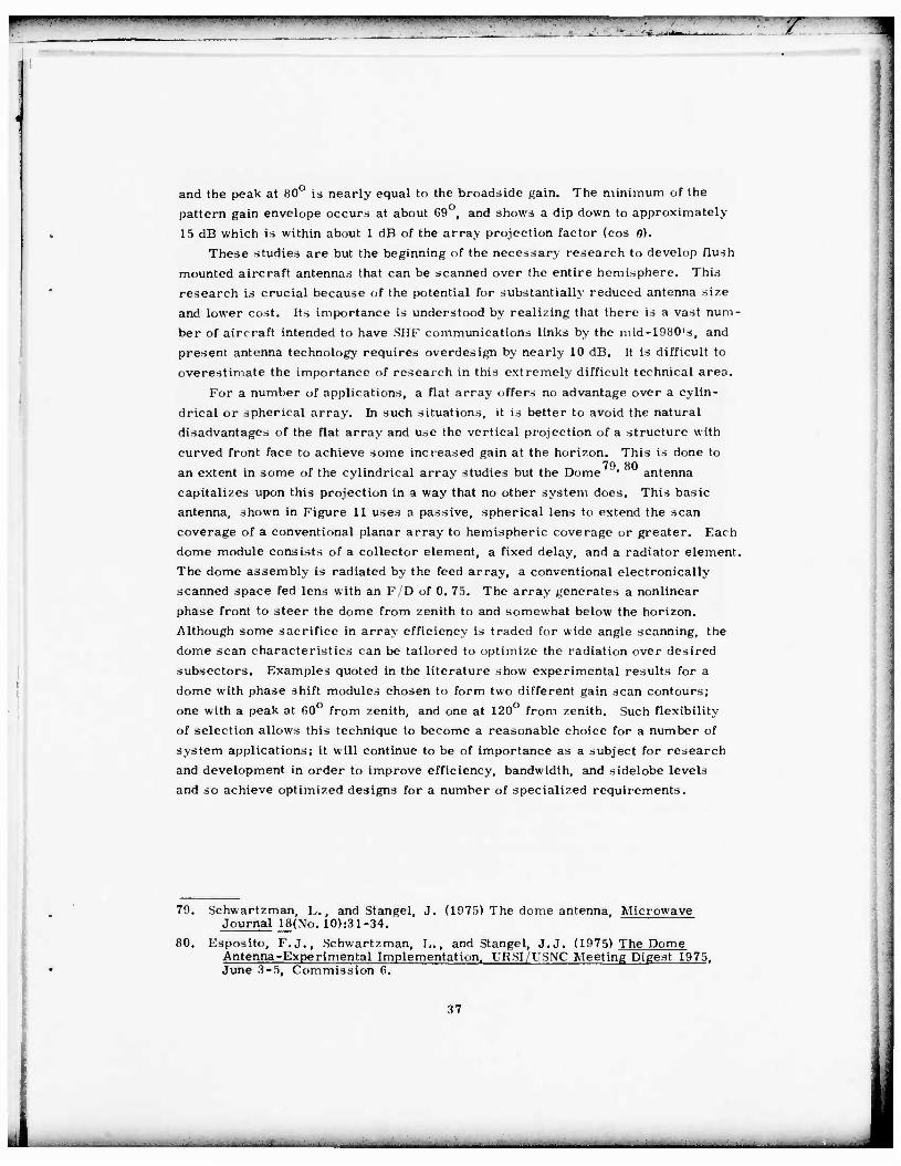
11. The Dome Antenna: A Technique for Hemispherical Scan 38
12. Reflector/Array Combination for Limited Sector Coverage 47
13. Precision Approach Radar Antenna AN/TPN-29 48
14. Scan Corrected Lens Antenna 48
15. Pattern Characteristics of Scan Corrected Lens 49
16. Periodic Array Grating Lobe Lattice 54
17. The Array Pattern, Element Factor Product 54
18. Element Location Diagram for the REST Array: A Technique for Limited Sector Coverage 54
19. Laboratory Model Multimode Scanning Array 57
20. Broadside Pattern Data (Eight Element Array) 57
21. End of Scan Pattern Data (Eight Element Array) 58
22. Ideal and Approximate Subarray Patterns for Overlapped Subarray 59
23. Aperture Illumination From Optically Overlapped Feed 61
24. Subaperture Far Field Pattern for Central Subaperture 61
25. Wideband Stripline Flared Notch Element 64
26. Dual Frequency Array Element 65
27. H-Plane Scanning Characteristics of Dual Frequency Array Element 65
28. Exciter, Phase Shifter and Array Element 67
29. Resistive Gate Phase Shifter 67
30. Micros trip Spiral Array Elements and Constrained Feed Network 69
31. Spatial Filter Element 74
32. Experimental Model Spatial Filter 75
33. Characteristics of Experimental Filter 76
34. Grating Lobe Suppression Using the Experimental Filter 77
• i
F!^ . •' '•' * "•* ••^- • • - Jt
I
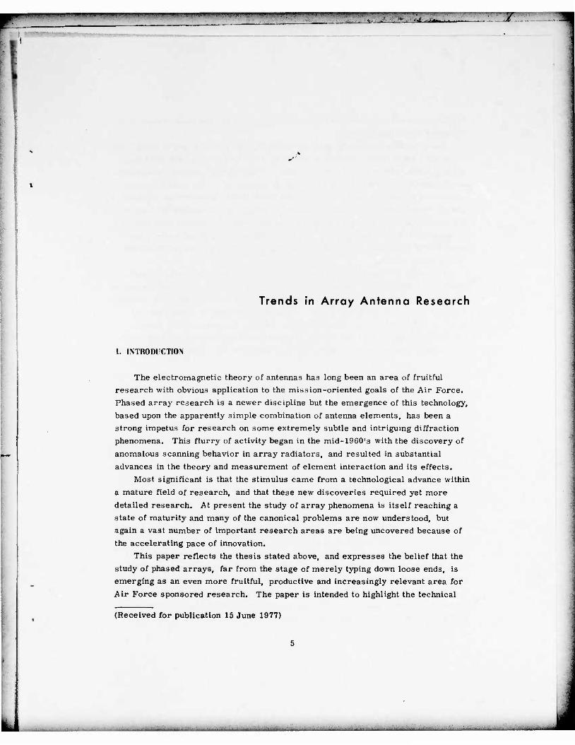
Trends in Array Antenna Research
1. INTRODUCTION
The electromagnetic theory of antennas has long been an area of fruitful
research with obvious application to the mission-oriented goals of the Air Force.
Phased array research is a newer discipline but the emergence of this technology,
based upon the apparently simple combination of antenna elements, has been a
strong impetus for research on some extremely subtle and intriguing diffraction
phenomena. This flurry of activity began in the mid-1960's with the discovery of
anomalous scanning behavior in array radiators, and resulted in substantial
advances in the theory and measurement of element interaction and its effects.
Most significant is that the stimulus came from a technological advance within
a mature field of research, and that these new discoveries required yet more
detailed research. At present the study of array phenomena is itself reaching a
state of maturity and many of the canonical problems are now understood, but
again a vast number of important research areas are being uncovered because of
the accelerating pace of innovation.
This paper reflects the thesis stated above, and expresses the belief that the
study of phased arrays, far from the stage of merely typing down loose ends, is
emerging as an even more fruitful, productive and increasingly relevant area for
Air Force sponsored research. The paper is intended to highlight the technical
(Received for publication 15 June 1977)
•iIIJ—tmnmm«I i i •• ••-•"»—•—« I-, i - -- •• •—• • -• • —.—,__ _.
iiM-u ..«i. I«'»I«IU»».' um, ...WIIIIM ^m •.-r^iivJ**.*'' rm'mt*• ••"•i<]iu--*v*m*r^frr***mm&'*!i''>'?*ir!^^'m" ^ ivnimvf'.n "m • <w»:.n" '"•• '»•" '•'»'" ' z
developments and requirements that provide stimulus, and the most obvious areas requiring intensified research.
Electronically scanned (phased) arrays have found practical use in applications requiring a rapid change in antenna pattern as a function of time, and fixed beam array antennas are used to produce certain specialized beam patterns that cannot be adequately reproduced by lens or reflector geometries. The most important application to date has been to large ground based array radars for surveillance and air traffic control, and this application is primarily responsible for most of the development that has taken place. Other important applications have been to multifunction aircraft arrays and various smaller communications arrays, but progress in these fields is limited by the weight, complexity, and primarily the cost of array systems.
The major factors influencing the future of array antennas are the weight of these past developments, the accelerating pace of technology, cost, and the burden of meeting new requirements imposed by systems that are currently being planned. As noted above, the most important factor to date has been the development ot
large ground based arrays like the FPS-85, Hapdar, Cobra Dane, and others. These major efforts have stimulated research into array element coupling, space and corporate feeds and microwave circuit components like diode and ferrite phase
shifters. Future trends in array research may not be so closely aligned to the needs of
ground based radar, but instead the more fruitful paths will originate from the requirements of a growing list of special purpose arrays; that is, arrays designed for the single application that is their intended use. Many new system specifica- tions require arrays with such unique characteristics that the only economical solution is to design the array tailored to the task at hand. Costs can be reduced by production methods, but in certain cases they are reduced far more dramatically by choice of array type. In addition to cost, new array systems will be required to meet increasinly difficult performance specifications. Most important of these are the low sidelobe characteristics required for defense against antiradiation missiles, and the null steering requirements of broadband antijam communication links. New system types place their own demands upon the antenna circuits, and the growth of satellite communications requirements has become a stimulus for both satellite and aircraft antenna technology. Similarly, the rate of growth of microwave technology itself is a stimulus to array development. Examples will be cited later to show that the fact of an advancing technology with new transmis- sion media and with solid state microwave transmitters or receivers available at each element, has become an increasingly strong driving force for array research. Conventional array elements are not well suited to couple into new stripline and microstrip transmission circuits, and thus a number of different
6
MMMMMMk. , - •- - > •••- i
"" •'"•' - - j rt— i i .
"W"~"
elements have recently been developed and many more will soon be developed for application to scanning arrays. This fact, coupled with the radiating and reflect- ing properties of active and adaptive antenna circuits, provide a collection of new and very difficult phased array analysis problems that will challenge the technology and chart the course of research for many years to come.
This survey attempts to deal with these historical forces and influences, that affect the future of array research. Section 2 describes the basic analytical for- mulation for a typical array problem. The presentation is tutorial in style; scalar equations are used wherever possible in order to avoid the added complexity of vectorial solutions. In general there has been no attempt to survey all of the possible kinds of analytical solution to any one problem; the analysis is included because it aids in explaining some of the physical phenomena observed in phased array systems, and because it serves to illustrate the magnitude of the analytical problem for the case of finite arrays. Section 3 describes several new array geometries categorized as "Special Purpose Arrays"; these are typical responses to specific system problems that require arrays subject to external constraints. The special purpose arrays considered are conformal arrays, arrays for hemis- pherical coverage and null steering, and array techniques for limited sector coverage and multiple frequency arrays. Section 4 describes certain aspects of new technology that will serve to force the development of arrays with novel kinds of stripline and microstrip elements. Radomes, polarizers and spatial filters are also described in Section 4; these components are undergoing an intense period of change and their design is becoming integral with the associated array or antenna design.
In addition to these / ?a , there are many other topics that can be expected to affect the future of ••ya ".ad array research. Some of these which have not been discussed here are pro'.lems associated with antennas over the earth, the science of HF ground scree... development, transient analysis of arrays, and the impact and technology of the various active and adaptive array techniques. These were omitted because their proper consideration is beyond the scope of this paper.
These are but a few of the requirements, the technology and the trends. Sub- ject to the author's personal biases and limited perspective, these describe the present state of the technology. Each of the contributing factors is discussed to present a cohesive exp .i tion of this one view of the future of array antennas.
—— ^-^

•'•>".tl»n,J'W*!*W*(«BfW'.IJ '" "' iy<i^^'i:"TJi nyiiji»JIWWHWH«WW!! ..HI» J»«Mim"»".':'•" '-""•
^-.A-;.^' -%>->-'•* •/,— r
2. THE ARRAY AS A ROUNDARY VALUE PROBLEM
2.1 Introduction
An analytical study of phased array radiation follows the conventional approach
from diffraction theory of obtaining solutions of Maxwell's equations for two SDatial
regions; the external region is free space and the internal region is the inside of
the various transmission lines or waveguide exciting the radiating elements. The
solution in the exterior region must satisfy the boundary conditions that apply on
the surface supporting the array, and this gives rise to the major problems in the
analysis of arrays conformal to specific structures like aircraft or spacecraft
antennas, or arrays mounted over the earth.
Most often the exterior region is considered to be unbounded or bounded by a
half space; in these circumstances the Greens function is derived from combina-
tions of retarded potential type terms.
The dyadic form of Green's symmetrical theorem gives the free space fields
in terms of integrals over all currents, charges, and aperture fields in the
exterior space or on its boundary.
Although arrays are as commonly comprised of wire elements as aperture
elements, this review will treat only the aperture case. The dual situation involv-
ing wire elements leads to field expressions derivable from vector potential inte-
grals over the currents in the wires and their images, and the resulting boundary
value problem arising at the array face is a series of integral equations on the sur-
faces of the wires. In these cases, the interior field solution is usually idealized
to the extent that the fields are replaced by a delta function voltage source as in 2
Hallen's equation. More recent work has removed some of these assumptions
about the idealized nature of the source and has considered the implications of the
use of an approximate kernal for the Greens function for wires.
The free space field in the half space bounded by a perfectly conducting half
plane with an array of apertures as shown in Figure 1 can be written in terms of
integrals over the aperture fields as shown.
1.
3.
Levine, H., and Schwinger, J. (1950, 1951) On the theory of electromagnetic wave diffraction by an aperture in an infinite plane conducting screen, Comm. on Pure and Applied Math 44:355-391.
Hallen, Erik (1938) Theoretical investigations into transmitting and receiving antennae. Nova Acta Regiae Soc. Sei. Upsaliensis (4) 11 (No. 1).
King, R.W. P., and Harrison, C.W. (1969) Antennas and Waves, a Modern Approach, MIT Press, Cambridge, MA, (See Section 3. 10).
_ - ^_

m-ri^mi-m^m-ww^i<iiii i. l< "'mmmiimiii. \ .m m!r^m*^^*mm^l^mlm^mww'•" ••<• •LI m^m.mtnn,,,,« , Lintii i UVBII.>.; WIU.J -....I.,,,»,,,,»^
i-A^iii T
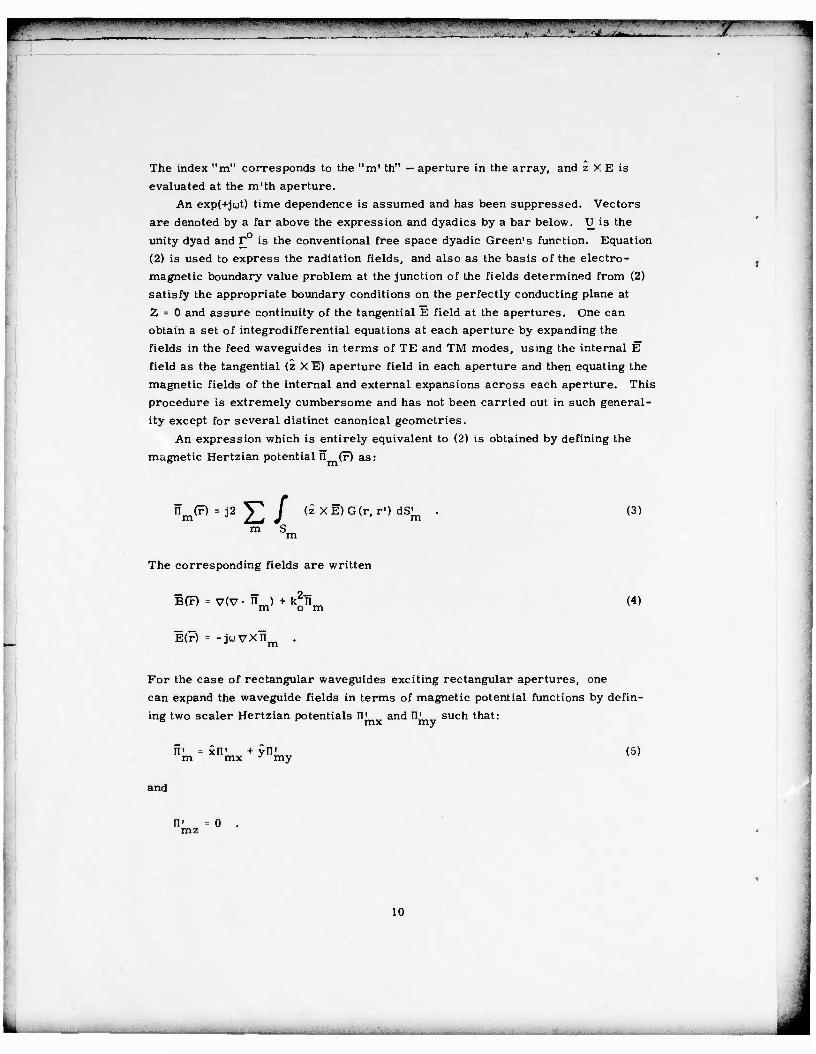
Figure 1. Array Coordinates. Element center locations x • md + A , y = nd x n* ' y
For z > 0
E(F) = j2upe ^ f r°(r, r') • (zxE) dS^
m S m
E(r) = 2
m S
VG(r, r') X (z X E) dSl m
where
and
r°(r, r') = /u+-\w\
-jk | r-T' |
G(r, r')
G(r, r') » 4jr| r - r'
and
|r -F'| = y<x -x')2 + (y -y')2 + z2
(1)
(2)
• • •••---• -- -- •
«•' """ ''Uli 1.111 Wlll.lll UWWW[.HPHIIRII|WP«WWW I • •• T
The index "m" corresponds to the "m1 th" — aperture in the array, and z y E is
evaluated at the m'th aperture.
An exp(+jut) time dependence is assumed and has been suppressed. Vectors
are denoted by a far above the expression and dyadics by a bar below. U is the
unity dyad and £ is the conventional free space dyadic Green's function. Equation
(2) is used to express the radiation fields, and also as the basis of the electro-
magnetic boundary value problem at the junction of the fields determined from (2)
satisfy the appropriate boundary conditions on the perfectly conducting plane at
Z = 0 and assure continuity of the tangential E field at the apertures. One can
obtain a set of integrodifferential equations at each aperture by expanding the
fields in the feed waveguides in terms of TE and TM modes, using the internal E
field as the tangential (z XB aperture field in each aperture and then equating the
magnetic fields of the internal and external expansions across each aperture. This
procedure is extremely cumbersome and has not been carried out in such general-
ity except for several distinct canonical geometries.
An expression which is entirely equivalent to (2) is obtained by defining the
magnetic Hertzian potential n (r) as:
"m^ = j2 y^ / <zXE)G(r, r>) dS^ . (3) m S m
The corresponding fields are written
1(F) = v(v • IT ) + k^fi (4) m o m
E(r) = -juvynm .
For the case of rectangular waveguides exciting rectangular apertures, one
can expand the waveguide fields in terms of magnetic potential functions by defin-
ing two sealer Hertzian potentials n' and n' such that: B mx my
a' * xIT + yri' (5) m mx * my
and
R] " 0 . mz
10
"u"""' -'«•-"••'.'•>•• 7
Equating tangential fields in the apertures leads to the following equations for the difference between internal and external Hertzian potential components.
+ -2-S- + k2 1 or ay2 o / mx 0 n ) = o mx
\&-x +-2-Ö- + k2\ (n> -n ) = o W 9y
2 °y my my
(6)
3x v" my 3yv"mx (7)
These three integrodifferential equations, repeated at each aperture, define all of the radiation and interelement coupling for the array of aperture. They are
4 similar to those obtained for a number of classical diffraction problems, and clearly show the vector nature of the solution unless 3/3x or 9/9y are zero. Arrays scanned ir a single plane and with translational invarience in the second plane can have scalar field solutions. In addition, it is often convenient and appropriate to neglect the crosspolarized component of radiation or coupling when that neglect can be shown to have no adverse effect upon the critical aspects of the solution. '
2.2 Solution for an Infinite Array
The kernal of Eq. (3) involves a summation of retarded field integrals over the elements ot an array. The special case oi an equally spaced infinite array pro- vides particularly simple form of kernal that has solutions with the form of Floquet's spatial harmonic series.
For a two-dimensional array with dimensions shown in Figure 1, the main beam of the array is scanned to an angle (e , <t> ) by application of incident fields In each waveguide (p, q) having the form:
E. = E e inc o -jk (u md +v nd > J o o x o y
(8)
6.
Bouwkamp, C.J. (1954) Diffraction theory, Reports on Progress in Physics 17:35-100.
Mailloux, R.J. (1969) Radiation and near-field coupling between two collinear open-ended waveguides, IEEE Trans. AP-17(No. l):49-55.
Lewin, L. (1970) On the inadequacy of discrete mode-matching techniques in some waveguide discontinuity problems, IEEE Trans. MTT-18(No. 7): 364-372.
11
• ' *"•' *mi ii i '-* • 'f • •
' 'f
where
u = sin 0 cos <A o o o
v = sin 0 sin A o o vo (9)
k = 2TT/X„ o o
and (u v ) are the direction cosines of the main beam position vector, o' o
This periodic incident field results in the same periodicity in the aperture
field and the accompanying simplification of the summations.
tor the case of an array scanned in one plane, summations of the form
U.± -Jkoy(x-x^)2 + (y-y')2 + z2
V! = -oo ^(x - x^)2 + (y - y')2 + z2
E(x^,y') (10)
become, using
E(xm, y) = E(xQ, y) e -ik u md J o o x
and using x1 = x' + md , the above yields:
/f J2» -jkn <x-x')(2) / I r\ /^(E(x..y.) £ e3om ° Ho(korVl-u^)
x1 y' m= -oo
(11)
V(y - y')2 + z2
where
and
u = u + m/d„ mo ' x
This form shows that the series is now summed over the spatial parameter u and 7 has the characteristics of a spatial harmonic series in this parameter. To
7. Brouillion, L. (1953) Wave Propagation in periodic Structures, Dover Publications, Inc.
12
•---- - • •
r•
complete the evaluation of Eq. (3), this equation must be integrated over the y'
parameter, and the near fields thus assume a relatively complex form in general.
In the special case of infinite slots in the y1 dimension with Oy 0 the series takes
on an extremely simple form even in the near field. After performing this inte-
gration, expression 11 becomes:
2n v^» -i(K z +k u x) •' m' ' o m
K F<V (12)
where
m o i
and
vl
jk u x' F(u ) = / E(x') e °
m dx* m
This expression is now clearly the sum over a series of waves that propagate
or decay outside of the array depending upon whether K is real or imaginary.
The sum is called a grating lobe series and the spatial angles at which
exp[K |z| 1 k u x| is unity are grating lobe angles. The field in space is thus
represented as an infinite series of waves with excitation coefficients I'(u ).
For an array scanned in both planes, the summations become:
M M OB °C
fix E x' y' n=-oo m=-oo
.4 JkoV(X-Xm)2+(y-yn)2
V <x x' )2 + <y - y')2 + z2
(13)
dd 2-f 2-< x y
-i(k u +k v +K ) J o m on mn F(u, v)
where here
K = k X 1 - u2 - v2
mn o T m n
13

„»M..W.. ..I-JMI «IM»T-T. i.<«jn.np>i v.<ii^ip^OTM,v.m • iniipiiiipmni. -r—fr^^iT*"^*^^^»"^"1 i. ^.«.i.« m\m- «'•Muni" > HI
' /
and
F(u, v) //
E(x',y') e jk (ux'+vy1)
For an array scanned in one plane and under certain special circumstances,
the array electromagnetic field can be scalar. Examples of such scalar problems
are the E-plane scan of a parallel plane array with TEM incident modes, and H-
plane scan of the array shown in Figure 2. This array geometry is a novel design
and uses the properties of dielectric slab loaded waveguides to support efficient
radiation at two frequencies that are separated by about an octave. Since 9y = 0
the array is equivalent to a parallel plane structure for H-plane scan. This equiv-
alence is shown by removal of the horizontal metal separators at y = -^- (2n - 1).
/
',
/
L
4-1 / /
DIELECTRIC CONSTANT c
-* x
7Z -a
Figure 2. Array Geometry — H-Plane Scan
The solution proceeds by expanding the waveguide fields in terms of an infinite
series of waveguide modes (LSE ) and using this field expansion in Eq. (6).
The interior potential function for a mode with transverse incident field dis-
tribution e (x) is:
14
- *

4
mmmmmmmm^m T • • • — • •'
Y„Z
n = e p e <x) - V rn e q e(x) p p L-t q q
(14)
where y and y are the modal propagation constants for the slab loaded waveguide.
The waveguide eigenfunctions e (x) are orthogonal and are normalized so that
a/2
-a/ 2
ep(x) eq(x) dx = 6^ c p = q (15)
0 P*q
The coefficients r give the amplitude and phase of the waves reflected from
the aperture face (z = 0) and include propagating and nonpropagating modes. The
aperture field for the incident mode P is (at z = 0)
an |,pep(X) + Srq7qeq(X)
q=l
(16)
Within the waveguides the magnetic field is given by
B = - ax2
(17)
and in the exterior region it is obtained from Eq. (4) as:
XP dx
a/2
P / vx,) £ -a/2 m=-o
-3ßtT1(x-xt) i dx' ^m
oo a/2 oo
E Vq / eq<X,) L * q=l -a/2 m=-oo
-jßm(x-x') S dx1
m
(18)
8. Seckelmann, R. (1966) Propagation of TE modes in dielectric loaded wave- guides, IEEE Trans. MTT-14:518-527.
9. Collin, R.E. (1960) Field Theory of Guided Waves, McGraw-Hill Book Co., Inc., New York.
15

ij • UI«Iw^rw*pH«*pi•• IIKIIII ] ^^m -w . ..»•» . . ä
where
JV7
f/3 2 m
for
for
ß2 >k2
' m o
02 , 2 ß < k 'm o
and
ß = k [u + m/d 1 . Hm ol o ; xJ
Equating these magnetic field expressions at z = 0, truncating the series at
q = Q, multiplying by e (x'), using orthogonality and defining the integral
a/2
tatq(0m)= J eq(X')e
-a/2
Wm* dx' (19)
one obtains a set of Q equations for the Q coefficients at r for the incident p'th
mode excitation:
r 2 i Q
L J q=l
Tq6qi+d^q^qi for 1 - 1 to Q
(20)
and where
M
A . = > I Int (-S ) Int. (ß ) Ja'ql / -< m q Mm jf Hm m=-M
Solution of the above matrix equation gives the waveguide field distribution at each
aperture, and includes all of the mutual coupling effects for the infinite array. The
particular array studied here uses two incident modes (p * 1, 2) at the high fre-
quency, and so the set of equations above must be solved twice to obtain a solution
for the combined two mode excitation. The series over m is truncated at ±M
(usually between 40 and several hundred terms) as required for convergence.
16
^^^^^^^^•^^^^H
T
2.3 Analysis for a Finite Array
Solutions like the above have been extremely useful for the analysis and design of large arrays such as those used for ground based radar. Smaller arrays with ten or fewer elements in each plane have behavior dominated by edge effects and for these the infinite array analysis has little meaning. There have been analytical treatments ' of semiinfinite arrays that give insight into the phenomena of edge effects in large arrays without including higher order modal effects. The vast majority of finite array studies have been performed using a scattering matrix that includes only a single waveguide mode; a procedure that can be highly inaccu- rate when the array is operated at a frequency or scan angle near which an array resonance can occur. These resonances or "blind-spots" have been the subject of substantial controversy over the past decade and will be described in more detail later.
Equation (20) can be rewritten as an infinite set of simultaneous equations and then truncated to yield a solution of any desired accuracy. This is accomplished by expanding the field in each mth waveguide in terms of a sum over all incident and reflected modes. In general this involves both components of the vector solu- tion, but again it is more convenient for the purposes of illustrations to restrict the analysis to a finite array of "M" of the infinite columns of Figure 2 for H-plane scan.
The potential function for the mth waveguide is written:
n(m) = am e e,(x')-> bq e q e(x') . (21) m l £^ m q q=l
Here it is assumed that only the single dominant mode is incident in each waveguide, but that all modes are reflected. The notation b " is the coefficient of m the q'th reflected mode in waveguide m. After obtaining the aperture electric field
E(m) = ju amTlel<X')e ' +S bm>qe * \• q=i
(22)
10. Borgiotti, G. V. (1971) Edge effects in finite arrays of uniform slits on a groundplane, IEEE Trans. AP-19(No. 5):593-599.
11. Wasylkiwskyj, W. (1973) Mutual coupling effects in semi-infinite arrays, IEEE Trans. AP-21(No. 3):277-285.
17
»—•^—•—WPW—Wli i l IP——p—w»i ii i i.I-III. jwn'« MI. i,^.. ..•..., „I,_„. ...,_-
'.-£._L^< K
and inserting this field in the integrodifferential Eq. (6) or into the equivalent
equation obtained by equating the tangential magnetic fields at both sides of the
aperture as in Eq. (20). The resulting equation, multiplied by the sequence of
e.(x) for I = 1 to Q and integrated over x yields a series of "Q" algebraic equa-
tions at each aperture and can be written in the form of a nultimodal scattering
matrix. The l'th equation at the mth waveguide is:
Q
E q=l
<J 2
N
b «* y- 6 , - V bq
m "q q, i Z-< n
n=l q mn
N
a 6 m q I 71+1] an7l rQ U
mn n=l
> i • l. Q
where
mn 2T1 f*xet(x)X* (x)
(23)
and
Xa,<--fe^)/.,<••> 7 -ik r-r'
. J o' -dx' dy'
for
*-V* kl\ I en<X'> dX'
|r -r'| - J (x -x')2 + (y')2 m n w
N such sets of equations are required, one set at each aperture, thus leading
to a set of N XQ equations to be solved to complete the array solution.
The numerical evaluation of solutions like the one above are indeed formidable,
and the solution is most often approximated using only one or two terms of the
series.
18
'WIJU •m»iwi«»i»MiipiiBWjnl f«ui.i.^ipi.p;i..,iiDiu.i.iuii muH m » ..w*»i«Mw.yii..nijji .1 i> »•"• •v^^^mr T*iinlifci
bq
m = Vsq a / i mn n n=l
Although the most common analytical practice is to assume a set of incident fields {a} and solve the set (23) for the reflected signals {b}q for all modes q, one could obviously assume a sequence of independent incident modes and solve the set for each incident a . This solution is the scattering matrix for each mode q of
the array.
or bq = Sq a . (24)
Written in this form there are Q such scattering matrices required to describe the Q waveguide modes reflected from the apertures (for a single mode incident on each).
It is important to observe that the whole set of higher order modes enters into the Eq. (24), and so the scattering coefficients Sq include the mutual coupling of these higher order modes.
Arrays with more than one incident mode (like that of Figure 2) can be analyzed by repeating the above procedure for the several incident modes and superimposing the solutions. Although this formulation gives a complete solution of the multi- element array radiation and interelement problem, the amount and complexity of the required numerical analysis of ten makes such a solution impractical. Suitable approximations include using only one or several modes in each waveguide, neglect- ing cross-polarized interactions, utilizing asymptotic approximations of the scat- tering coefficients for the widely spaced elements and neglecting the interaction between the higher order modes in the evaluation o*1 scattering coefficients. The implications of several of these approximations will be discussed in subsequent sections.
2. t Way Radiation and the Concept of an Klement Pattern
Equation (4) gives the complete radiated field for an array of apertures in a perfectly conducting plane. Determination of the tangential E fields in these aper- tures is achieved by solving the boundary value problem at the waveguide/aperture interface by the methods outlined in a previous section, or by other techniques to be mentioned later.
The far field approximation to Eq. (2) is obtained by using
|r -"r'| « RQ - ¥< • p (25)
where R is measured from the coordinate origin in the aperture to the given point in space at R , 0, <b and
19
—w '-•"-•" ll|L. ll*l|J*«M •P W ,nKllipjVlvIJill|l I IN- r
r1 = x x' + y y1
and
p =xu + yv+z cos 0 (26)
Using this approximation, it is customary to write
e"jkoRo jko(F'.p)
G(r, r') = 1UR
Evaluation of Eq. (2) for apertures in the plane z = 0 yields:
iK w-^re-R
-ik R J o o
m S
dSm [cos e ET(x^, yjj -zp. ET(x^, y^)] Tx m' ;m
12 where ET is the tangential field in the aperture.
This relationship is also given in the text by Amitay et al. " The tangential
field Em is a two component vector in general, but for the array of Figure 2 and
(approximately) for the case of thin slots, the aperture field can be described by
a single component. For tutorial purposes the remainder of this description will
treat the scalar case in which the cross-polarized radiation is neglected or iden-
tically zero and the waveguide polarization is in the y direction. In this case, the
aperture fields are written using Eq. (4). The field in the m'th waveguide (at
z = 0) is:
E = ju
Q
Tlel(x')+Ebm1'qeq(x,)
q = l
(27)
or, using the scattering matrix representation of Eq. (24)
E «Jw
M Q
am7 lel(x,)+EanEeq(X')SmnTc
n=l q=l
(28)
12. Amitay, N., Galindo, V., and Wu, C. P. (1972) Theory and Analysis of Phased Array Antennas. New York, Wiley Interscience.
20

•' «P «l.l!i.ll<W-BUWIJ«lH'" * *'.'•'«.•»••' • ...ji'"i^«w * .J^IIV*". PW'.L'III*( u*ip ip,«w*u, I iii.i I . I,IR.IHWII.1 ma II jj IN ,1 •?«V ->•.*••¥•, i ". •'•i'l/w-n "
Unlike the infinite array, Eq. (28) shows that a finite array with periodic
incident fields has nonperiodic aperture fields because of the lack of symmetry in
the element scattering matrices.
Defining the aperture integrals
T
a/2 b/2 jk (x'u+y"v) Iq(u, v) = / dx' / dy< eq(x\ y») e °
-a/2 -b/2
(29)
one obtains (neglecting constants) the following expression for the array far field
M , +ik (ux +vy )
F(M>= Yäe ° m
m = l >am7
M Q
lh(u,v) +]T an Y Sln 7q Iq(u, v! n-1 q=l
(30)
where x__ and y are the position coordinates for the m'th waveguide, mm This expression can be rewritten in the following form:
J^, jk (ux +vy ) F(ft,<j>) = 2_^ e Jua
r
m=l
M Q
*1 Xl(u- v) + Y £ Smn\VU'V)
n=l q=l
M (31)
y^ ^o^m+^m* m-1
a f (ft, 6) m m 'y
which makes it evident that ihe far-field is a superposition of fields due to each
element located at position x , y , excited by a coefficient a and having a spatial
variation f (0, $). For a large planar array forming a single pencil beam, one can
show that the main beam gain is related to the square of the magnitude of this sum
times cos ft except for angles very near to end-fire. Thus, for a large, two-
dimensional array
fm(0, <t>) Vcos ft
is the element pattern of the m'th element. The cos ft term is not present for a
column array.
21
, - - •-• I^H
I II IV I IHM >.*»,»iiWJH,i,n.>i.ii .[.mil in»»iimn i , , i.Jiy», i.iji mi U....I.I. i.M.
Like the aperture distribution, this element pattern differs for each element of a finite array. Furthermore, the element pattern has in it all of the effects of mutual coupling and so can be an extremely complex function of the space coordi- nates (0, <j>). Proper element pattern control is the prime requisite of arrsy design, and the formidable task of element pattern evaluation is not a choice to be taken lightly. Unfortunately, the history of phased array development reveals the closeted skeletons of arrays that were built using single mode approximations for mutual coupling. These and other details will be described in subsequent sections, but it is important to note here that the pattern f \j cos 0 of the m'th element is exactly what one measures in the far field when only that element is excited. Because of reciprocity it is also the signal received at that element from a distant transmitter, and so its measured value includes, for any given array, all of the coupling and higher order modal effects that will be observable when the array is excited as a whole. Element pattern measurement is thus an extremely powerful tool of array design, because it is possible to record this single mode parameter and still account for all of the subtleties that occur at the array face.
2.5 Historical Perspective and the Blindness Phenomena
The previous sections have shown one method of analyzing waveguide arrays including the mutual coupling between all array elements. Waveguide elements were chosen for these examples because they have been the subject of extensive research over the past ten years and because they conveniently illustrate many of the phenomena that will be described later. Early studies of mutual coupling were performed mainly for arrays of dipole elements ' with assumed sinusoidal current
14 15 distributions, and later ' for current distributions that contained several higher order terms to approximate the exact distribution. These analyses were based upon various forms of Hallen's integral equation and the discovery that higher order modes were important came about mainly through the diligence of researchers working in the field. These theoretical efforts were accompanied by extensive experimental programs, and the use of higher order current approximations was motivated primarily by a concern that any analytical solution for current and charge distributions be adequate to allow an accurate description of the near-field. Despite the fact that these earlier dipole array studies were performed many years ago,
13. Carter, P.S., Jr. (1900) Mutual impedance effects in large beam scanning arrays, IRE Trans. AP-8:27fi-285.
14. King, R.W.P. (19frfi) The Theory of Linear Antennas, Harvard University Press, Cambridge, MA.
15. King, R.W.P., and Sandier, S.S. (19(i4) The theory of broadside arrays, and the theory of endfire arrays, IEEE Trans on Antennas and Propagation AP-12:2(>9-275, 27(i-280. ' — ~
22
mmmmmmm*mm^*'*i -•• •-. **•.»•• '•*• •<*»
the dipole has remained a subject of continued interest. Recent analytical studies
have been based primarily on moment-method approaches ' which are applica-
ble to a wide variety of wire antenna shapes and orientations, and for which there
are now a number of available computer programs of very great generality. Air
Force sponsorship in this area has been a factor of major importance. Starting 13 14 15 with the basic studies of Carter and King ' and continuing to the present day,
the Air Force 6. 1 effort has funded many of the major analytical developments in
dipole antenna arrays.
The recent concern with waveguide arrays reflects the fact that by the mid-
1950's the analytical background for this technology lagged far behind that of dipole
arrays. Customary waveguide array solutions dealt almost exclusively with single
mode approximations to the waveguide field, but did properly account for the full
spatial harmonic series (grating lobe series) in the free space half space. Some
earlier studies of single radiating waveguides used stationary solutions of the
aperture integral equation in order to obtain variational formulas for input
impedance, ' but until the mid-60's there were no published multimodel solu-
tions of even this basic radiating geometry.
If little effort had been devoted to the single radiator problem, even less has
been done to describe the coupling between waveguides. One of the first studies of 20 this sort was performed by Wheeler who assumed the coupled radiators were in
21 the far-field of one another. In 1956, Levis derived general equations for a
variational formulation to obtain the coupling between a number of generally cylin-
drical waveguides radiating through a common ground plane. He applied the method 22 to a set of coupled annular slots. Galejs applied a stationary formulation due to
16. Harrington, R. F. (1968) Field Computation by Moment Methods, McMillan Co., New York.
17. Harrington, R.F., and Mautz, J.R. (1967) Straight wires with arbitrary excitation and loading, IEEE Trans. AP-15(No. 4):502-515.
18. Lewin, L. (1951) Advanced Theory of Waveguides, Iliffe and Sons, Ltd., London, Chapter 6.
19. Cohen, M.H., Crowley, T. H., and Levis, C.A. (1951) The Aperture Admit- tance of a Rectangular Waveguide Radiating into a Half Space, (ATI-133707) Antenna Laboratory, Ohio State University, Research Foundation, Rept. 339-22.
20. Wheeler, G. W. (1950) Coupled Slot Antennas. Ph.D. Thesis, Harvard University, Cambridge, MA.
21. Levis, C.A. (1956) Variational Calculations of the Impedance Parameters of Couplied Antennas. Ohio State University Research Foundation, Rept. 667-16, Contract AF33(616)3353.
22. Galejs, J. (1965) Self and mutual admittances of waveguides radiating into plasma layers. Radio Sei. J. Res. NBS/USNC-URSI 69D(No. 2):179-189.
23

i u uiiiiia i i « 1 *iw»i" I... i.if.t..^. -,....i. j, i), t
-•^•rfi— 1,1 .
?MpFH
23 Richmond to solve the problem of two parallel slots in a ground plane, with both slots backed by waveguides. His method yielded usable and convenient formulas; however, it includes the implicit assumption that the tangential magnetic field at the coupled waveguide aperture is the same as the magnetic field which would be present on the ground plane if the coupled aperture were not present. In this manner, Galejs avoided the problem of solving an integral equation.
Other researches that evolved from the point of view of antenna element coupl- 24 ing were the study by Lyon et al, to determine the power coupling between vari-
ous structures including arbitrarily oriented open ended waveguide and two studies by Mailloux ' that dealt with the multiple mode solution of collinear radiating waveguides, and the induction of cross-polarized fields in mutually coupled wave- guides with arbitrary orientation. This last paper described some approximate procedures to account for coupling in large arrays where the numerical evaluation of all the higher order terms would otherwise become unwieldy. The use of such interelement coupling approaches to array theory has not been popular until
27 28 recently, ' because the coupling integrals are two dimensional with singular kernals and the resulting matrices are often so large that it seemed unreasonable to consider including higher order effects unless there was an extremely good reason to do so. In recent years, this approach has gained some favor because of the availability of large computers and because of an increased awareness of the need for accurate array calculations.
The stimulus that intensified research into array mutual coupling phenomena was called array "blindness," and went undiscovered by university or government sponsored research programs. Its discovery occurred when several array sys- tems exhibited poor scanning performance and so to these investigators "array blindness" was not an interesting phenomenon but a plague; once uncovered, it was
23. Richmond, J.H. (1961) A reaction theorem and its applications to antenna impedance calculations, IRE Trans AP AP-8:515-520.
24. Lyon, J.A.M., Kalafus, R.M., Kwon, Y. K., Diegenis, C.J., Ibrahim, M. A.H., and Chen, C.C. (1966) Derivation of Aerospace Antenna Coupling — Factor Interference Predication Techniques. Tech. Rept. AFAL-TR-66-57, The University of Michigan, Radiation Laboratory.
25. Mailloux, R. J. (1969) Radiation and near-field coupling between two collinear open-ended waveguides, IEEE Trans on Antennas and Propagation AP-17: (No. l):49-55.
26. Mailloux, R.J. (1969) First-order solutions for mutual coupling between waveguides which propagate two orthogonal modes, IEEE Trans. AP-17; 740-746.
27. Bailey, M.C. (1974) Finite planar array of circular waveguide apertures in flat conductor, IEEE Trans. AP-22;178-184.
28. Steyskal, H. (1974) Mutual coupling analysis of a finite planar waveguide array, IEEE Trans. AP-22;594-597.
24
i ,,,-.„• ,.,, .„„i, i ii iipppii.|i.iiiw, •••'»..•!>l»yfji.iu;i i »11 .,..,.,.,.-i.. .,., '7**
found in numerous systems and proposed systems. Blindness is evidenced by a null well within the normal scan sector of an array. It is mainly a problem for large arrays and so was not found in tests of arrays that consisted of only a few elements in each plane. Before describing and commenting further on the history of this important development, I would stress that this was an area that should have been uncovered by researchers before it became a crisis to be discovered by system manufacturers. Given the cost and importance of such systems, there was clearly not an adequate concern for fundamental studies at a time when they could have averted the serious problems that followed.
The phenomenon of array blindness became a factor of extreme confusion for a number of years. Examples of this confusion abound throughout the early litera- ture where, for example, one author stresses the importance ol including waveguide higher-order modes in any analysis for predicting array blind spots, and another author uses a single-mode theory for a different structure to accurately predict an occurrence.
The reasons for this confusion, as explained by Knittel et al, 29 is that, depend- ing upon the array structure, there are two basic types of cancellation resonances: those that occur external to, and those that occur within the array waveguide apertures.
The waveguide higher-order modes play a dominant role for the internal-type resonance, but are relatively unimportant for an external resonance. This is because the external resonance occurs only for array- that have a structure of some kind beyond the array face, and the resonance is caused by the interaction between the radiating mode and a higher-order external mode supported by this structure. An internal resonance can be viewed as a cancellation effect between the dominant and a higher-order waveguide mode radiation. An awareness of this distinction is useful for categorizing the various reports of array blind spots.
The first convincing demonstration of the existence of an array null was ob- 30 tained experimentally by Lechtreck using an array of circularly polarized coaxial
horns with separate hemispherically shaped radomes ior each element. The null occurred for the electric field perpendicular to the ground plane, and was called
31 an external resonance by Oliner.
29. Knittel, G. H., Hessel, A., and Oliner, A.A. (1968) Element pattern nulls in phased arrays and their relation to guided waves, Proc. IEEE 56-1822- 1836.
30. Lechtreck, L. W. (1965) Cumulative coupling in antenna arrays, IEEE G-AP International Symposium Digest. 144-149.
31. Oliner, A.A., and Malech, R. G. (1966) Speculation on the role of surface waves, Microwave Scanning Antennas. Academic Press N.Y. Vol 2 308-322:
25
r- ••"•' • "'- wmmmmvfMwmi -'• -l ••'" •• WJMIPP- t ll.iu.F.,...,....,., DI...PJ.. y
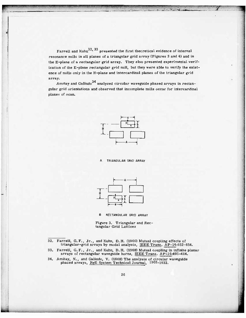
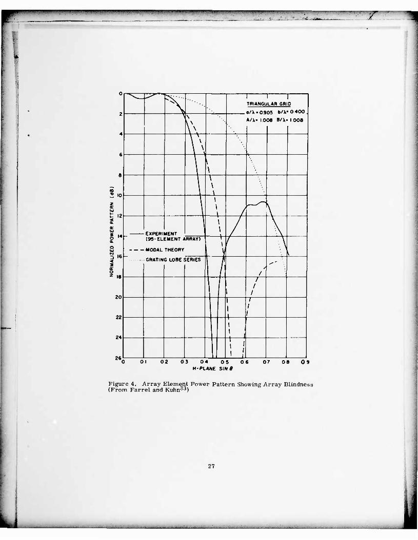
32 33 Farrell and Kuhn * presented the first theoretical evidence of internal resonance nulls in all planes of a triangular grid array (Figures 3 and 4) and in the E-plane of a rectangular grid array. They also presented experimental verif- ication of the E-plane rectangular grid null, but they were able to verify the exist- ence of nulls only in the H-plane and intercardinal planes of the triangular grid array.
34 Amitay and Galindo analyzed circular waveguide phased arrays in rectan- gular grid orientations and observed that incomplete nulls occur for intercardinal planes of scan.
B
JL
—1
y i T"
X _i_
1
A TRIANGULAR GRID ARRAY
rr^iT I 1 U_L I
B RECTANGULAR GRID ARRAV
Figure 3. Triangular and Rec- tangular Grid Lattices
32.
33.
34.
Farrell, G. F., Jr., and Kuhn, D.H. (1966) Mutual coupling effects of triangular-grid arrays by modal analysis, IEEE Trans. AP-14:652-654.
Farrell, G. F., Jr., and Kuhn, D.H. (1968) Mutual coupling in infinite planar arrays of rectangular waveguide horns, IEEE Trans. AP-16:405-414.
Amitay, N., and Galindo, V. (1968) The analysis of circular waveguide phased arrays, Bell System Technical Journal. 1903-1932.
26
ta-.
"' ••—"•••••• ' •"" • •"• •*" Ill IIII >--. ..
1 1 1 TRIANGULAR GRIO
a/XanOfl* h/X"0 400 \
\ \ A/X» 1008 B/X< 1008
\ \ \ \ \ \
\ \
\ \ \ \
\ \ \ I
EXPERI MENT
\ \
(95-ELEMENT /
MODAL THEORY
kRRAY) \ \
1 \ k 6RATIN G LOBE ! SERIES
/ •
\
/ /
/ /
/ 1
\ ;
!l
10
a. _ * o a.
12
14
_ 16 4 2 <r o 2 18
20
22
24
26 01 02 09 04 OS 06
N-PLANE SIN» 07 OB 09
Figure 4. Array Element Power Pattern Showing Array Blindness (From Farrel and Kuhn^^)
27
—"*"""•••••• •" •»'••»I»TI".I» )i i ii. nivauuii. i i.um.i i,wiiipn^i..w...... T
DuFort ' ' found nulls for a TE mode parallel plate array and a triangular
grid array of rectangular waveguides on an IJ-plane corrugated .surface, and 37 Mailloux found blind spots for the E-plane scan of an array of TEM mode parallel
plane waveguides with conducting fences between adjacent radiators. To the extent
that these effects occur because of the external structure, they are external
resonances.
External resonances associated with the use of dielectric layers were observed
experimentally by Bates and Byron and Krank, experimentally in a phased 40 39 array waveguide simulator by Hannan, Byron and Krank, ' and Gregorwich
41 49 29 43 et al, and predicted theoretically by Frazita, Knittel et al, and Karad 44 using one-mode approximations (grating lobe series), and by Galindo and Wu,
45 46 Wu and Galindo, and Borgiotti using higher-order modal analyses.
In addition to the growing list of blind-spot occurrences, the nature of the
phenomenon has become relatively well understood, and some techniques for avoid-
ing or eliminating the difficulties are available.
35. DuKort, E. C. (1968a) Design of corrugated plates for phased array matching IEEE Trans. AP-16:37-46.
36. DuFort, E.G. (1968a) A design procedure for matching volumetrically scanned waveguide arrays, Proc. IEEE 56:1851-1860.
37. Mailloux, R.J. (1972) Surface waves and anomalous wave radiation nulls on phased arrays of TEM waveguides with fences, IEEE Trans. AP-20: ir,0-16G.
38. Bates, R. H. T. (1965) Mode theory approach to arrays, IEEE Trans, and Propagation (Communications) AF-13;321-322.
39. Byron, E.V., and Frank, J. (19(i8a) Kost beams from a dielectric covered phased-array aperture, IEEE Trans. AP-16:496-499.
40. Hannan, P. W. (1967) Discovery of an array surface wave in a simulator, IEEE Trans. AP-15:574-576.
41. Gregorwich, W.S., Hessell, A., Knittel, G.H., and Oliver, A.A. (1968) A waveguide simulator for the determination of a phased-array resonance, IEEE G-AP International .Symposium Digest, 134-141.
42. Krazita, R.F. (19G7) Surface-wave behavior of a phased array analyzed by the grating-lobe series, IEEE Trans. AP-15:823-824.
43. Parad, K.I. (19G7) The input admittance to a slotted array with or without a dielectric sheet, IEEE Trans. (Communications) AP-15;302-304.
44. Galindo, V., and Wu, C. P. (19G8) Dielectric loaded and covered rectangular waveguide phased arrays, Bell System Technical Journal 47:93-11G.
45. Wu, C.P., and Galindo, V. (19G8) Surface wave effects on dielectric sheathed phased arrays of rectangular waveguides. Bell System Technical Journal 47:117-142. '
46. Borgiotti, G. V. (19G8) Modal analysis of periodic planar phased arrays of apertures, IEEE Proc. 56:1881-1892.
28

•ii.iiLii.ipi^»-i«iinniii»niiii i mini »L mvm-mmvm in »i».nu iiiuni m iu> n»ii i i i.u •••»J.T..U.»» inn .. mmi.i r
47 3o 48 The initial impression of Allen and Lechtreck, ' that the null was due
to coupling into a surface wave, gave an incomplete picture because the array ele-
ments are not reactively terminated and the elements are placed more than one-
half wavelength apart, thus eliminating any conventional surface wave propagation. 32 33 Farrell and Kuhn ' performed the first rigorous analysis of an array with a
blind spot, and they were the first to observe that certain waveguide higher-order
modes play a dominant role in achieving the cancellation necessary for a null. 49 46 Diamond and later Borgiotti confirmed all of these findings for waveguide
arrays. 50 Oliner and Malech suggested what is now generally accepted as true, that
the blind spot is associated with the normal mode solution of an equivalent reactively
loaded passive array, and that the condition for a complete null on the real array
occurs when the elements are phased to satisfy the boundary conditions for the 28 equivalent passive array. Knittel et al developed this theory and showed that in
the vicinity of the null the solution corresponds to a leaky wave of the passive
structure, but that a surface-wavelike field exists immediately at the null. This 45 is consistent with the results of an analysis made earlier by Wu and Galindo,
who demonstrated that the only radiating (fast) wave of the periodic structure spa-
tial harmonic spectrum is identically zero at a null, and that, for this reason, a
structure with a period greater than one-half wavelength can have a normal mode.
Along with these contributions to the understanding of the physics of a phased array
null, a number of authors showed that both the waveguide aperture and lattice 51-54 dimensions are critical in determining the likelihood of a blind spot. '
47. Allen, J.L. (1065) On surface-wave coupling between elements of large arrays, IEEE Trans. AP-13:638-639.
48. Lechtreck, L. W. (1968) Effects of coupling accumulation in antenna arrays, IEEE Trans. AP-16:31-37.
49. Diamond, B. L. (1968) A generalized approach to the analysis of infinite planar array antennas, Proc IEEE 5_6(No. 11):1837-1851.
50. Oliner, A.A., and Malech, R. G. (1964) Speculation on the Role of Surface Waves, Microwave Scanning Antennas, Academic Press, N.Y., Vol. 2, 308-322.
51. Ehlenberger, A.G., Schwartzman, L., and Topper, L. (1968) Design criteria for linearly polarized waveguide arrays, IEEE Proc. 56(No. 11): 1861-1872.
52. Byron, E.V., and Frank, J. (1968b) On the correlation between wideband arrays and array simulators, IEEE Trans. (Communications) AP-16: 601-603.
53. Hessel, A., and Knittel, G. H. (1969) A loaded groundplane for the elimination of blindness in a phased-array antenna, IEEE G-AP International Symposium Digest, 163-169.
54. Knittel, G. H. (1970) The choice of unit-cell size for a waveguide phased array and its relation to the blindness phenomenon, Presented at Boston Chapter Antennas and Propagation Group Meeting.
29
-- •• •
MM • in ii HI
^T
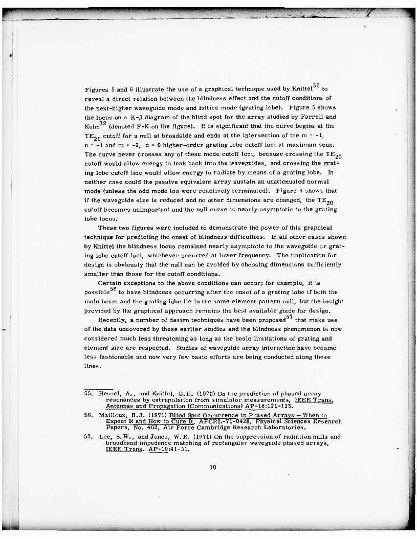
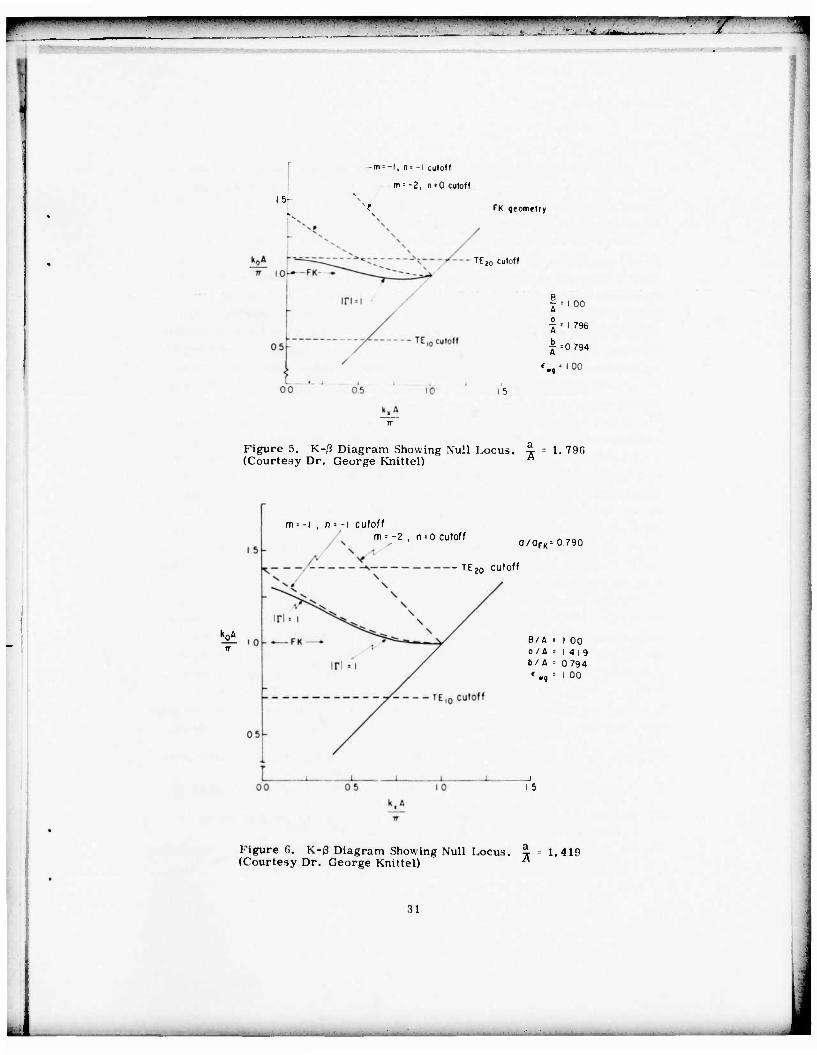
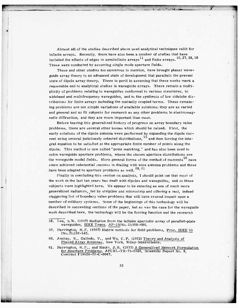
55 Figures 5 and G illustrate the use of a graphical technique used by Knittel to reveal a direct relation between the blindness effect and the cutoff conditions of the next-higher waveguide mode and lattice mode (grating lobe). Figure 5 shows the locus on a K-ß diagram of the blind spot for the array studied by Farrell and Kuhn (denoted F-K on the figure). It is significant that the curve begins at the TEon cutoff for a null at broadside and ends at the intersection of the m = -1, n = -1 and m = -2, n = 0 higher-order grating lobe cutoff loci at maximum scan. The curve never crosses any of these mode cutoff loci, because crossing the TE„0
cutoff would allow energy to leak back into the waveguides, and crossing the grat- ing lobe cutoff line would allow energy to radiate by means of a grating lobe. In neither case could the passive equivalent array sustain an unattenuated normal mode (unless the odd mode too were reactively terminated). Figure G shows that if the waveguide size is reduced and no other dimensions are changed, the TE2Q
cutoff becomes unimportant and the null curve is nearly asymptotic to the grating lobe locus.
These two figures were included to demonstrate the power of this graphical technique for predicting the onset of blindness difficulties. In all other cases shown by Knittel the blindness locus remained nearly asymptotic to the waveguide or grat- ing lobe cutoff loci, whichever occurred at lower frequency. The implication for design is obviously that the null can be avoided by choosing dimensions sufficiently smaller than those for the cutoff conditions.
Certain exceptions to the above conditions can occur; for example, it is 56 possible to have blindness occurring after the onset of a grating lobe if both the
main beam and the grating lobe lie in the same element pattern null, but the insight provided by the graphical approach remains the best available guide for design.
57 Recently, a number of design techniques have been proposed' that make use of the data uncovered by these earlier studies and the blindness phenomenon is now considered much less threatening as long as the basic limitations of grating and element size are respected. Studies of waveguide array interaction have become less fashionable and now very few basic efforts are being conducted along these lines.
55. Hessel, A., and Knittel, G.II. (1970) On the prediction of phased array resonances by extrapolation from simulator measurements, IEEE Trans. Antennas and Propagation (Communications) AP-18:121-123.
56. Mailloux, R.J. (1971) Blind Spot Occurrence in Phased Arrays — When to Expect It and How to Cure It. AFCRL-71-0428, Physical Sciences Research Papers, No. 462, Air Force Cambridge Research Laboratories.
57. Lee, S.W., and Jones, W. R. (1971) On the suppression of radiation nulls and broadband impedance matching of rectangular waveguide phased arrays, IEEE Trans. AP-19:41-51.
30
• • • . i i
.. I, ... •, ....,., I,.L .III.H |l M l.„,l....,^
••C./^m, i , - . ' *
.m«-i, a«-I cutoff
m = -2, n = 0 cutoff
15- FK geometry
TEj0 cutoff
00
> I 796
= 0 794
15
Figure 5. K-ß Diagram Showing Null Locus. ^ = 1.790 (Courtesy Dr. George Knittel) A
m = -i , n •- -i cutoff m« -2 , n = o cutoff
TE20 Cutoff
k0A
0/0FK-- 0 790
B/A • I 00 o / A = 14 19 b/ A i 0 794
I 5
Figure 0. K-/3 Diagram Showing Null Locus, t 1.419 (Courtesy Dr. George Knittel) A
31
rl —m nji iii i i—m-rnni mi n i i iiiiinii «i
- . - -I - -- '•* '— •'• '- -•»
Almost all of the studies described above used analytical techniques valid for
infinite arrays. Recently, there have also been a number of studies that have . , , j ., „ . i « 11 _ r- 10, 27, 28, 58 included the effects of edges in semiinfinite arrays and finite arrays. ' '
These were conducted by assuming single mode aperture fields.
These and other studies too numerous to mention, have brought planar wave-
guide array theory to an advanced state of development that parallels the present
state of dipole array theory. There is peril in assuming that these works mark a
reasonable end to analytical studies in waveguide arrays. There remain a multi-
plicity of problems relating to waveguides conformal to various structures, to
wideband and multifrequency waveguides, and to the synthesis of low sidelobe dis-
tributions for finite arrays including the mutually coupled terms. These remain-
ing problems are not simple variations of available solutions; they are as varied
and general and as fit subjects for research as any other problems in electromag-
netic diffraction, and they are more important than most.
Before leaving this generalized history of progress on array boundary value
problems, there are several other issues which should be raised. First, the
early solutions of the dipole antenna were performed by expanding the dipole cur- 15 rent using several judiciously selected distributions, and then forcing the inte-
gral equation to be satisfied at the appropriate finite number of points along the
dipole. This method is now called "point matching, " and has also been used to
solve waveguide aperture problems, where the chosen aperture distributions are 59 the waveguide modal fields. More general forms of the method of moments' have
since achieved substantial success in dealing with wire antenna problems and these
have been adapted to aperture problems as well. ' '
Finally in concluding this section on analysis, I should point out that most of
the work in the last ten years has dealt with dipoles and waveguides, and so these
subjects were highlighted here. We appear to be entering an era of much more
generalized radiators, fed by stripline and microstrip and offering a vast, indeed
staggering list of boundary value problems that will have crucial impact upon a
number of military systems. Some of the beginnings of this technology will be
described in succeeding sections of the paper, but as was the case for the waveguide
work described here, the technology will be the forcing function and the research
58. Lee, S.W. (1967) Radiation from the infinite aperiodic array of parallel-plate waveguides, IEEE Trans. AP-15(No. 5):598-606.
59. Harrington, R.F. (19(57) Matrix methods for field problems, Proc. IEEE 55 (No. 2):136-149. —
(i0. Amitay, N., Galindo, V., and Wu, C. P. (1972) Theory and Analysis of Phased Array Antennas, New York, Wiley-Interscience.
61. Harrington, R.F., and Mautz, J.R. (1975) A Generalized Network Formulation for Aperture Problems. AFCRL-TR-75-0589, Scientific Report No. 8, Contract F19628-73-C-0047.
32
P^^WW^W^WWP»—i 1111111 iti IM im .ijiu j.iiM». u,min .in • urn. in i ,i ,i minim ii ... i" ••• 'in""7 ••*••* •miimj^nn • ;jTJ'w
.. A- rV *'. **"*• '.it- • lih I _ . T
efforts will be highly directed toward specific problems. Present research funding
is not adequate to uncover all of the anomalous behavior with all of the geometries
and so research in this important area will be relevant for many years to come
and will in many cases be performed in a state of crisis.
3. SPECIAL PURPOSE ARRAYS
3.1 Conformal Arrays and Arrays for Hemispherical Coverage
Aerodynamic requirements for spacecraft and high performance aircraft have
stimulated an increasing concern for the design of low profile and conformal
antennas. The technological problems of these applications differ, and the tech-
nology of conformal arrays is really several technologies. Aircraft fuselage
mounted arrays, whether conformal or planar, are expected to provide nearly
hemispherical scanning. Spacecraft arrays are sometimes wrapped entirely
around the vehicle, and the major design requirement becomes the study of a com- eo or
mutating matrix for steering the beam. ' Arrays on cones have many special fifi—6ft
probljms; their radiated polarization is strongly angle dependent, there is
little room for the array feed near the tip, and finally, their steering control is
necessarily very complex. The specialized problems of an array on a concave 69 surface are discussed in a paper by Tsandoulas and Willwerth.
Common to all of these structures is the underlying fact that they are mounted
on nonplanar surfaces, and this alters their radiation and mutual interaction.
Analytical treatments have progressed to the rigorous solutions of coupling in
62. Shelley, B. (1968) A matrix-fed circular array for continuous scanning, IEEE Proc. 56(No. ll):2016-2027.
63. Holley, A.E., et al (1974) An electronically scanned beacon antenna, IEEE Trans. AP-22:3-12.
64. Bogner, B. F. (1974) Circularly symmetric r. f. commutor for cylindrical phased arrays, IEEE Trans. AP-22;78-81.
65. Boyns, J.E., et al (1970) Step-scanned circular-arrav antenna, IEEE Trans. AP-18(No. 5):590-595.
66. Munger, A.D., et al (1974) Conical array studies, IEEE Trans. AP-22:35-43.
67. Hsiao, J.K., and Cha, A.G. (1974) Patterns and polarizations of simultan- eously excited planar arrays on a conformal surface, IEEE Trans. AP-22: 81-84.
68. Gobert, W.B., and Young, R.F. H. (1974) A theory of antenna array con- formal to surface revolution, IEEE Trans. AP-22:87-91.
69. Tsandoulas, G. S., and Willwerth, F. G. (1973) Mutual coupling in concave cylindrical arrays, Microwave Journal 16(No. 10):29-32.
33
1

-mmmrnmm ii ..i v. "-"• ' • ' * rf
70 71 72 infinite arrays or slits on cylinders ' and on conical surfaces. ' Simpler
formulations have been developed using extensions of the geometrical theory of 73-75 diffraction, and with these it is now possible to perform analytical studies of
finite arrays on generalized conformal structures. Figures 7 and 8 show results 75 obtained by Steyskal for the reflection coefficient of the center element in an
array of 156 dielectric loaded circular waveguides mounted on a cylinder of 11. 6\
diameter for the two principal polarizations. Analytical results of this sort can
be applied for sylinders with radii of 2A or greater.
Studies of arrays on cylinders and designed for nearly hemispherical scan Ti 7r
coverage ' have emphasized the difficulty in using conventional array approaches
for such wide angle scan. By matching the array near the horizon (say 80 from
1.0-
0.8
0.6-
0.4
0.2
cylindrical array
oo ,
planar array
—i 1 1 1 1 1 1 1-
0.2 0.4 0.6 0.8 10
u = sin $
Figure 7. Conformal Array Active Reflection Coefficient H-Plane Scan
Figure 8. Conformal Array Active Reflection Coefficient E-Plane Scan
70. Borgiotti, G. V., and Balzano, Q. (1970) Mutual coupling analysis of a con- formal array of elements on a cylindrical surface, Trans. EEEE AP-18: 55-63.
71. Borgiotti, G. V., and Balzano, Q. (1972) Analysis of element pattern design of periodic array of circular apertures on conducting Cylinders, IEEE Trans. AP-20:547-553.
72. Balzano, Q., and Dowling, T.B. (1974) Mutual coupling analysis of arrays of aperture on cones (Communications), 7EEE Trans. AP-22.-92-97.
73.
74.
Golden, K. E., et al (1974) Approximation techniques for the mutual admit- tance of slot antennas in metallic cones, IEEE Trans. AP-22:44-48.
Shapira, J., et al (1974) Rav analysis of conformal arrav antennas, IEEE Trans. AP-22:49-63.
75. Stevskal, H. (1974) Mutual coupling analysis of cylindrical and conical arrays, IEEE/AP-S Int. Symp. Record, 293-294.
76. Maune, J.J. (1972) An SHF airborne receiving antenna. Twenty Second Annual Symposium on L'SAF Antenna Research and Development.
34

• 111(11 111 »If •.•III HUM I •••III JPII.II.|I,II|IPI..»I •.UKUIIinilllllllllipil, I IM II" »•• ••Ml lllllli I B» »..T|.|W»T •»ni iV..«ln.i I I ^ .»*...,•
the zenith), the array can be made to have gain variation of only about 6 dB over
the hemisphere but the array matched at this angle id mismatched at other scan
angles, and can suffer a gain reduction of up to 4 dB at broadside. ' Recent
studies sponsored by RADC/ET have demonstrated coupling into a surface-wave 77 78
mode or operation for near-endfire radiation. These efforts ' have included
the use of dielectric structures over or in the vicinity of the array, and have
shown that these means also improve gain coverage within the hemisphere so that
the envelope of peak radiation gain is always within about 6 dB of the maximum 78
radiation over a narrow frequency range. Computations have shown that the
coverage obtainable from an array with 23 dB nominal gain presents maximum
oscillations of 8 dB over a 10-percent bandwidth. This data was obtained for an
array covered with a layer of C =4 material 0. 075A thick extending over and
beyond the array. Such wide angle scanning does not seem feasible at present for
arrays with 30 dB gain.
Inhouse studies at RADC/ET have used the array in a conventional manner
except at endfire where coverage is provided by short circuiting the array elements
to form a corrugated surface that can support a surface wave for endfire radiation.
This technique can provide highly efficient radiation over a hemisphere for one
plane of scan, but is also gain limited at about 20 dB for a square array.
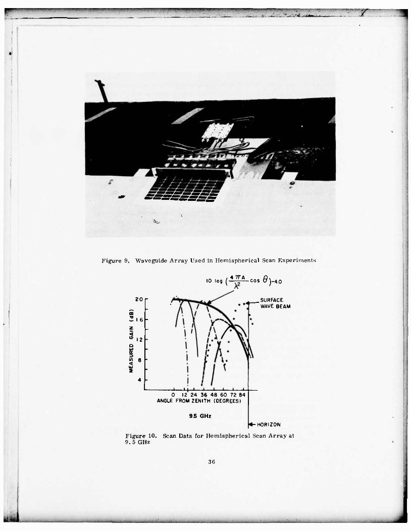
Figure 9 shows an array of 64 waveguide elements excited by an 8 element
feed. Although not shown in the figure, the array is also excited by a 64 way
power divider and 8 phase shifters to form a beam scanned in the elevation plane.
In practice, the waveguides would be short circuited by diodes or mechanical
shorting switches to form the corrugated surface for endfire radiation, but the
experiment was conducted using fixed short circuits.
The groundplane, partially shown in Figure 9, measured 6—ft wide and had a
4-ft curved surface with 84-inch radius extending in front of the antenna structure.
Figure 10 shows the measured array gain at 9. 5 GHz for a number of beams
within the sector including a beam scanned to the horizon and one formed by the
excited corrugated structure. A cosine envelope distribution is also included for
reference. The data show that the surface wave beam provides approximately 6 dB
gain increase at the horizon as compared with the scanned endfire beam, and that
in fact the achievable gain at the horizon is 17 dB; only 4 dB below the maximum.
77. Villeneuve, A.T., Behnke, M. C., and Kummer, W. H. (1973) Hemispheric cally Scanned Arrays, AFCRL-TR-74-0084, Contract No. F19628-72-C- 0145, Scientific Report No. 2. Also, see 1974 International IEEE AP-S Symposium Digest, 363-360.
78. Balzano, Q., Lewis, L.R., and Siwiak, K. (1973) Analysis of Dielectric Slab-Covered Waveguide Arrays on Large Cylinders. AFCRL-TR-73-0587, Contract No. F19628-72-C-0202, Scientific Report No. 1.
35
•• -•• - - _____^_________
• .1 ••..!• •> «• I. I • ii m <i>vui!.ai<u;i
J.. . -_ rJ{ rftr- 7
Figure 9. Waveguide Array Used in Hemispherical Scan Experiments
,0 log (47IA cos B\-
20
CD
2l6 z <
12 o 1 in s < 2
o
)-40
.SURFACE WAVE BEAM
_i • | • i. i i ' • 0 12 24 36 48 60 72 84
ANGLE FROM ZENITH (DEGREES)
9.5 GHz
•HORIZON
Figure 10. Scan Data for Hemispherical Scan Array at 9. 5 GHz
3G
mwM-mu'in^^^wppww. »•» W».HIUJHJ«B. iijum.n i UIIJU • IMI II i.i.y im. i » .L'"(»"'>J>. i. i i ,•
and the peak at 80° is nearly equal to the broadside gain. The minimum of the pattern gain envelope occurs at about G9 , and shows a dip down to approximately 15 dB which is within about 1 dB of the array projection factor (cos f)).
These studies are but the beginning of the necessary research to develop flush mounted aircraft antennas that can be scanned over the entire hemisphere. This research is crucial because of the potential for substantially reduced antenna size and lower cost. Its importance is understood by realizing that there is a vast num- ber of aircraft intended to have SHF communications links by the mid-1980'a, and present antenna technology requires overdesign by nearly 10 dB. It is difficult to overestimate the importance of research in this extremely difficult technical area.
For a number of applications, a flat array offers no advantage over a cylin- drical or spherical array. In such situations, it is better to avoid the natural disadvantages of the flat array and use the vertical projection of a structure with curved front face to achieve some increased gain at the horizon. This is done to
70 HO an extent in some of the cylindrical array studies but the Dome ' antenna capitalizes upon this projection in a way that no other system does. This basic antenna, shown in Figure 11 uses a passive, spherical lens to extend the scan coverage of a conventional planar array to hemispheric coverage or greater. Fach dome module consists of a collector element, a fixed delay, and a radiator element. The dome assembly is radiated by the feed array, a conventional electronically scanned space fed lens with an F 'D of 0. 75. The array generates a nonlinear phase front to steer the dome from zenith to and somewhat below the horizon. Although some sacrifice in array efficiency is traded for wide angle scanning, the dome scan characteristics can be tailored to optimize the radiation over desired subsectors. Examples quoted in the literature show experimental results for a dome with phase shift modules chosen to form two different gain scan contours; one with a peak at fiO from zenith, and one at 120 from zenith. Such flexibility of selection allows this technique to become a reasonable choice for a number of system applications; it will continue to be of importance as a subject for research and development in order to improve efficiency, bandwidth, and sidelobe levels and so achieve optimized designs for a number of specialized requirements.
79. Schwartzman, L., and Stängel, J. (1975) The dome antenna, Microwave Journal 18(No. 10):31-34.
80. Esposito, F.J., Schwartzman, L., and Stängel, J.J. (1975) The Dome Antenna-Experimental Implementation. URSI/USNC Meeting Digest 1975. June 3-5, Commission (i.
37
.
1 nvmmwmmmiuii • •" •-*•• i uiRM^HM^m '"""' Jl" "^.' •'••••'"» uppi '•l.fpui.iy ii.^yi.iii ii |, ,| j_ liiw
1
Figure 11. The Dome Antenna: A Technique for Hemispherical Scan
3.2 l.o« Sidelobe ;m«l Null Steered \rra\s
Among the areas of prime interest in radar and special purpose arrays are
the requirements of providing low sidelobe and null steered radiation patterns.
These two concerns have grown, because of the military threats presented by ARM
(Ant-Radiation Missiles) and the increased use of jammers. Obviously, the solu-
tion is just to use the well-known aperture distributions that have low sidelobe
Chebyshev or Taylor pattern functions and so reduce sidelobes to the theoretical
limits; but this solution seldom is applicable except to certain broadside arrays or
38

^mmmmmi^mmmmmmmmmmmt^mmmmmfwmfmmmmmmKmmm^mmmmiHmmmmmmmmmm^m^i^^'-m"'' ,,m '••'" ••- ""»»'" • »'•»»•«. , MWIPM. u r
slot arrays with fixed beam positions. Studies of random phase and ampli- tude effects and of pattern distortion due to phase quantization have led to statis- tical predictions of sidelobe levels for fixed beam and scanned arrays.
Another problem that limits the sidelobe ratio maintainable by an array is that the element pattern f (fl, <t>) differs for each element "m" in an array. Equation (31) gives a general expression for this complex function and shows that it depends upon all of the mutual coupling terms from everywhere in the array, and so only the elements near the array center have the same element patterns. The patterns for elements near the array edges are not only different in amplitude, but can have different spatial dependence than those for central elements. This means that any amplitude weighting specified for sidelobe suppression must vary with scan angle to achieve the lowest possible sidelobes. Problems of this sort have caused little concern in the past because edge effects are not dominant in large radar arrays, and because it has become common practice to leive a number of unexcited elements near the edges of these arrays so that the excited elements have more similar element patterns. Specifying extremely low sidelobes for small arrays may cause this problem area to grow until it poses a fundamental limitation on array performance. As yet there has been little research expended on this potentially troublesome area, but as better phase shifters and more accurate power division schemes become available, element pattern distortion will remain as the dominant limitation on sidelobe reduction for small arrays.
Among the more important areas of array research is the topic of pattern null steering to eliminate jamming interference. Most recent contributions to this
Q C Of?
subject ' have included consideration of mutual coupling effects and proceed from an equation similar to Eq. (31). Assuming only one mode in each aperture (Q = 1), Eq. (31) is written:
81. Ruze, J. (1952) Physical Limitations on Antennas. MIT Research Lab. Electronics Tech. Rept. 248.
82. Miller, C. J. (19G4) Minimizing the effects of phase quantization errors in an electronically scanned array, Proc. 1964 Symp. Electronically Scanned Array Techniques and Applications. RADC-TDR-R4-225, Vol. 1, 17-38 AD448421. "~
83. Allen, J.L. (19fi0, 19G1) Some extensions of the theory of random error effects on array patterns, in J. L. Allen et al., Phased Array Radar Studies. Tech. Rept. No. 23fi, Lincoln Laboratory, M.I.T.
84. Elliott, R.S. (1958) Mechanical and electrical tolerances for two-dimensional scanning antenna arrays, IRE Trans. AP-f>:l 14-120.
85. Mcllvenna, J.F., and Dräne, C.J. (1971) Maximum gain, mutual coupling and pattern control in array antennas, The Radio and Electronic Engineer 4UNo. 12):5fi9-572.
8fi. Mcllvenna, J., et al (197fi) The Effects of Excitation Errors in Null Steering Antenna Arrays, RADC-TR-7G-183, Rome Air Development Center.
39

."»WWmiw^WBBHIUPBPPIH»^.'!!11*!" •"Pun i.jjiiijLiij.11 Hi •";••'.'•. WH^FfMflB'Jl. 11^ iVllUJ'""#«ly"yjiHP|
-. -••-•..'.* ft- •
JH. k ux +vy ) F(0, <£) == 7j ^(S, ö) ju > e af
m --1
M
i+y s n=l
7- 1,(0, 6) juC e (32)
where C = (S + I) a, a is a column vector of excitations, and I is the M y M —
element identity matrix:
'II
and
jko(uxfvyi)
jko(uxM+vyM)
(33)
and
T T T C ' a <S + I) .
The power pattern has the form
P(9,<t>) « F(0, <>>) • F (0, Ö)
= I7i 2| 1,2 2 ,„•(
j<e,*)| W [C (e • e )C] (34)
l-rf I |lf<0,#)| uJ2a+ [(I + S)+ e e+(I * S)|a
where the symbol + denotes the combined transpose and complex conjugate
operations.
40
- -i - -- - -"-"- -|M i

... .. ,,..,..,., u T-j^r
Thus:
P(e.*) = \i\\ |i?(e,<*)| w2(a+ ä a)
where
(35)
A = (I + S) e e (I + S)
is a one term dyad.
The directive gain is defined as the ratio of this P(A, <£) to the total radiated
power P„, which is given by:
a+(I S S) a (3 6)
Thus a normalized quadratic form for directive gain, in terms of the scatter-
ing matrix S, assuming single mode excitation and only single mode contributions
present in the far field radiation expansion is:
G<o> • |i2(e,</>)| a+A a
a B a (37)
where
B = I S+S
This expression for gain is a quadratic form. It could include the computed
or measured scattering matrix data, and is a convenient form for optimizing sub-
ject to various constraints. Some details of an appropriate optimization are given
in the literature, ' and a recent report illustrates and details the specific
procedure used for optimizing the directive gain of the single mode waveguide
array problem described above. The procedure has been applied in a number of
situations for dipole and waveguide arrays with finite numbers of elements and
including mutual coupling. It has never been applied to situations that included
important higher order mutual coupling expressions. Of particular importance is
that the numerics of the problem becomes simpler as the number of constraints
are increased. Thus this sort of optimization has been used to place a number of
nulls close together within a sector of a pattern, and so produce a trough that would
eliminate the effects of narrowband jammers over a relatively wide spatial sector.
The recent study addresses the effects of random errors in phase and amplitude
41
m - _

il |^qpnppi««iu!«||iii|iii.iiiii.ii . i. i..IN» i - J II III I ipi IWI II '•-> » - -
control on null and trough formation, and concludes that 0. 1 dB of amplitude and
1° rms of phase control are necessary to maintain a -40 dB trough. When phase
shifters, power dividers, and engineering practices allow such, required toler-
ances can be obtained; then again the fundamental technical problem of higher order
radiating fields will remain and assume its dominance as the ultimate limit to rad-
iation suppression.
Techniques like the one mentioned above imply that good amplitude control is
available in addition to the required Dhase control. This is seldom the case, and
has been the major factor hindering the advance of technology based upon such
optimization. The increasing importance of antijamming protection will, however,
make these systems the subject of intensified research interest as pressures
increase to simplify feed networks and broaden system bandwidth. Several other
options for antijam array techniques will be discussed in subsequent sections of
the paper.
3.3 Array Techniques for Limited Sector Co\erafie
One of the most important classes of special purpose array techniques are
those which trade scan capability for decreased cost. These are called "limited
scan arrays, " and they exist because there are many military and civilian require-
ments for high gain, electronically scanned antennas that need scan only some
restricted sector of space. Military requirements include weapons locators,
antennas for synchronous satellites and for air traffic control. Civilian require-
ments are mainly for air traffic control.
Two general classes of arrays are used for limited scan systems; the first
class, which is historically the earliest and the most successful, is an array that
is placed in or near the focal region of a reflector or lens antenna to scan its
beam. The second class consists of large aperture elements and a beam forming
network that includes some means of suppressing the system grating lobes. In
either case, there exists a minimum number of control elements that are required
for beam scanning over any given sector and this serves as one measure of the
efficiency of the scanning system.
One measure of this minimum number is the number of orthogonal beams 87 within the scan sector. Another is the theorem of Stängel which states that the
minimum number of elements is:
h§ Go(f).<i>) dfi (38)
87. Stängel, J. J. (1974) A basic theorem concerning the electronic scanning capabilities of antennas, L'RSI Commission VI, Spring Meeting.
42

••"•'••"I" i..imiiij,i,wa-j»-i.mii li >i .n.ii . i.« •' .' » •» i.ii I. ipiii i i . n .. ... m..i. in mni-n ... ji .i.nnu I iii
-•'• -'• "_- 'J I*-
.
a
'•" -T"
where G (ft, o) id the maximum gain achievable by the antenna in the (n, 6) direc-
tion, and dp. is the increment of solid angle.
Another measure of the minimum number of array elements is contained in
the definition of a parameter introduced by Patton and called the "element use
factor." This parameter will be used in a somewhat generalized form to compare
the number of phase shifters in competing systems with unequal principal plane
beamwidths. The factor is N/N where N is the actual number of phase shifters ' min ' in the control array, and N is a reasonable number of control elements as min defined below:
Nmin= I "?M ' ^1 • (39)
1 2 f) and n max are the maximum scan angles in the two orthogonal principal planes 1 2 measured to the peak of each beam, and D., and fl., are the half power beamwidths
in these planes. Thus N - min is approximately four times the product of the num-
ber of beamwidths scanned in each principal plane, and as will be shown later, is
also approximately equal to the number of orthogonal beam positions for a rectan-
gular array with beams filling a rectangular sector in direction cosine space.
Although more general, Stangel's formula reduces to Patton's in the limiting case
of small scan angle and using the approximate formula
4.T (40)
and Integrating over a rectangular sector.
In the case of a periodic array with a square or rectangular grid, the condition
of the minimum phase control* can be shown to require that the following relation
be satisfied in each plant':
(!)•- 0 0 '• . (41) max v,i'
8H. Paltol», W.T. (1972) Limited »CUD array«, in Phased Array Antennas; Proc ot 'he 1970 Phased Arrav Antenna Symposium, edited bv A.A. Oliner and O.H. Knlttel, Artec« House, Inc., i\iA., :n2-:*4:j.
4i

U*U IW ¥»J" MiPUM • l -»7'l i iipiiw»!
89 A more recent study by Borgiotti describes a similar bound and presents a technique for synthesizing patterns with various sidelobe levels that satisfy the criterion of requiring a minimum number of controls.
Given that there is a minimum number of required controls for any given side- lobe level, beamwidth and scan or multiple beam coverage sector, the remaining issue is to investigate techniques for optimizing scanning systems, subject to given sidelobe requirements, so that their characteristics approach those of an ideal scanner.
Optical techniques that combine single or dual reflectors or lenses with phased arrays to achieve sector scanning have the advantage that they have grown out of techniques for large apertures and so naturally provide high gain. Alterna- tively, the array techniques that have existed in the past lend themselves to much greater control of aperture distributions for sidelobes, but are not so readily suited to the high gain requirements of present systems for limited scan coverage. Cost factors and the availability of technology have brought about an intense period of creative engineering that has resulted in the current state of optical feed limited scan systems.
Design of this class of systems is dominated by optical considerations, and problems of spill-over, aperture blockage, off axis focusing, and induced cross polarization often effect the design more than the ratio of beam positions to con- trol elements. Aperture efficiency is another parameter of importance for many applications. Many of the reflector or lens geometries require oversize apertures because the feed structure illuminates only a spot on the main aperture, and that spot moves with scan angle. For these devices, aperture efficiencies can be of the order of 25 percent instead of the usual 55 to 60 percent for nonscanning reflectors, and so scanning reflectors or lenses often require double the aperture of the more efficient fixed beam structures. The type of beam steering required is also a factor of great importance; the simplest being row and column steering with progressive phases in both planes. Certain antennas, however, require com- plex steering functions for off axis scans, and these result in slower beam steering and larger computer data storage.
Optical limited scan techniques have their origin in the development of mechan- ically scanned reflector and lens geometries using feed tilt and displacement, ' and in the development of feeds to correct the wide angle performance of beam
89.
90.
91.
Borgiotti, G. (1975) Design Criteria and Numerical Simulation of an Antenna System for One-Dimensional Limited Scan. AFCRF.-TR-75-0r>lf;.
Silver, S., and Pao, C.S. (1944) Paraboloid Antenna Characteristics as a Function of Feed Tiltr MIT Radiation Lab., Cambridge, MA, Hep 479.
Ruze, J. (19f>5) Lateral feed displacement in a paraboloid, IEEE Trans. Antennas Propagation AP-13:(i(i0-fi65.
44
1
HBB^WW^B II I I -•• '»•¥ ••>.** I
/
92 shaping reflectors. Present devices include single and dual reflection of lens
geometries in combination with a phased array, that produce an electronically
scanned beam using relatively few phase controls.
Design principles for such a wide ranging collection are themselves so varied
that they cannot be developed from basic principles in a text of this length. Instead,
this paper will outline some of the more important contributions to the technology
and to the analytical and conceptual tools that made the technology possible.
Several recent sources include comprehensive surveys of developments in these 93, 94 areas.
Many of the early studies on mechanical scanners were performed using geo-
metrical optics, and even today this method receives wide usage for computing
required feed locations, focusing conditions and phase shifter controls, and for 94
investigating general design parameters. Recent studies' have emphasized the
deficiencies of the geometrical optics approach for obtaining intensity information
about focal region fields and have demonstrated the use of physical optics for design.
Analytical methods used in design are noted in the descriptions that follow.
Early studies of scanning parabolas have uncovered a number of useful design 92 93 concepts. I'sing ray optical techniques, Sletten et al, ' ' have investigated the
location of focal (or caustic) surfaces for paraboloidal reflectors receiving off axis
plane waves, and have shown how these characteristics can be used to develop mid-
point correctors for elevation beam shaping while maintaining a narrow focused
beam in the azimuthal plane, and ridege line correctors for forming several pencil 91
beams in elevation without destroying azimuthal focus. Ruze' has used a scalar
plane wave theory to analyze the scanning characteristics ol a parabola with a
laterally displaced feed located at the Petzvai surface. This analysis was used to
obtain scanning patterns, to evaluate coma-lobe contributions and to derive equations
for the number of beamwidths scanned by such displacement for a -10. ."> dB coma
lobe at the scan limit. This number is given below as
N 0.44 I 22<f/D)2 .
94 Recent work by Rusch and Ludwig' has included a numerical evaluation of
focal region fields for a paraboloid receiving an off axis plane wave. Results of
92. Sletten, C.J., et al <1958) Corrective line sources for paraboloids, IEEE Trans. AP-fi(No. 3):239-251.
93. Collin, R.E., and Zucker, F.J. (19fi9) Antennas Theory, Part 2, McGraw- Hill Book Co., New York, Chapter 17.
94. Rusch, W.V.T., and Ludwig, A.C. (1973) Determination of the maximum scan-gain contours of a beam-scanning paraboloid and their relation to the pitzval surface, IEEE Trans. Antennas Propagation, AP-21:141-147.
45
Will
this study show that the maximum focal field locus, and therefore the position of
optimum feed location, does not coincide with the Petzval surface, but remains
relatively close to it for low f/D values. Reflectors with f/D greater than 0. 5 have
their optimum feed location closer to the focal point than the Petzval surface, but
this location tends toward that line for large scan angles. 95 Imbriale et al have also considered parabolic reflectors with large lateral
feed displacements, and have compared the results of Ruze's scalar theory with
the complete vector theory solution and experimental data for various feed displace-
ments. This study demonstrated that the coma-lobe level is sometimes vastly
underestimated by the scalar theory when used for feeds with large displacement. 96 Another recent work of significant import has been reported by Rudge who
has demonstrated the spatial fourier transform relationship between the aperture
fields of a parabolic reflector and its focal plane fields. In an extension of this 97 98
work, Rudge and Withers have also shown ' that the fields in a specified off
axis focal plane bear the same transform relationship to the aperture field under 99 the excitation of an inclined wave.
Not surprisingly, the first viable limited scan antennas consisted of a parabolic
reflector with an array placed between the reflector and the focal point as shown
in Figure 12. The array is then required to produce the complex conjugate of the
field that it would receive from a distant point source at a given angle, and the
extent to which it can do this determines the quality of the antenna radiation pattern.
Because of the complexity of the converging field. White and DeSize placed an
array of feeds on a spherical surface concentric with the parabola focal point, and
demonstrated scanning for that case. More recent structures do use parabolas
with nonlinear phase controls in the array, and achieve sidelobes at the -18 to
95. Imbraile, W.A., et al (1974) Large lateral feed displacements in a parabolic reflector, IEEE Trans. AP-22(No. 6):742-745.
96. Rudge, A.W. (1969) Focal plane field distribution of parabolic reflectors. Electronics Letters 5:610-612.
97. Rudge, A.W., and Withers, M.J, (1971) New techniques for beam steering with fixed parabolic reflectors, Proc. IEEE 118(No. 7):8o7-863.
98. Rudge, A.W., and Withers, M.J. (1969) Beam-scanning primary feed for parabolic reflectors, Electionic Letters 5:39-41.
99. Rudge, A.W., and Davies, D. E.N. (1970) Electronically controllable pri- mary feed for profile-error compensation of large parabolic reflectors, Proc. IEEE 117(No. 2):351-358.
100. Winter, C. (1968) Phase scanning experiments with two reflector antenna systems, Proc. IEEE 56(No. 10:1984-1999.
101. White, W. D., and DeSize, L.K. (1962) Scanning characteristics of two- reflector antenna systems, 1962 IRE International Conv. Record. Pt. 1, 44-70.
46
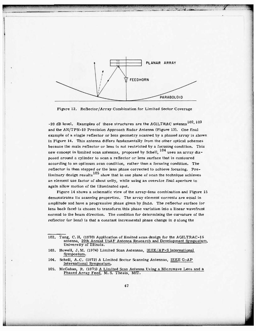
«••» • *W" ">y ••'•'•! - in i ipv j i i m wmm i
PLANAR ARRAY
Figure 12. Reflector/Array Combination for Limited Sector Coverage
102 103 -20 dB level. Examples of these structures are the AGILTRAC antenna
and the AN/TPN-19 Precision Approach Radar Antenna (Figure 13). One final
example of a single reflector or lens geometry scanned by a phased array is shown
in Figure 14. This antenna differs fundamentally from the other optical schemes
because the main reflector or lens is not restricted by a focusing condition. This 104
new concept in limited scan antennas, proposed by Schell, uses an array dis-
posed around a cylinder to scan a reflector or lens surface that is contoured
according to an optimum scan condition, rather than a focusing condition. The
reflector is then stepped or the lens phase corrected to achieve focusing. Pre- 105 liminary design results show that in one plane of scan the technique achieves
an element use factor of about unity, while using an oversize final aperture to
again allow motion of the illuminated spot.
Figure 14 shows a schematic view of the array-lens combination and Figure 15
demonstrates its scanning properties. The array element cor rents are equal in
amplitude and have a progressive phase given by ßnA0. The reflector surface (or
lens back face) is chosen to transform this phase variation into a linear wavefront
normal to the beam direction. The condition for determining the curvature of the
reflector (or lens) is that a constant incremental phase change in 0 along the
102. Tang, C.H. (1970) Application of limited scan design for the AGILTRAC-16 antenna, 20th Annual USAF Antenna Research and Development Symposium, University of Illinois.
103. Howell, J.M. (1974) Limited Scan Antennas, IEEE/AP-S International Symposium.
104. Schell, A.C. (1972) A Limited Sector Scanning Antennas, IEEE G-AP International Symposium.
105. McGahan, R. (1975) A Limited Scan Antenna Using a Microwave Lens and a Phased Array Feed, M.S. Thesis, MIT.
47
k.

„,i...I...., ,„i.. .I..,.»,.,.,„•. itunju i HHWWmmmmmimmii .. im..n i.»»«!;^^..!..! .*, u,.mi, M,M» M ly,,.» ,.
i .'• •_?* '-A -iiam -
, ^-•.
Figure 13. Precision Approach Radar Antenna AN/TPN-29
APERTURE
Figure 14. Scan Corrected Lens Antenna
48

..,. . IH I», na»».!—•»••»i.uiuii» :
0
-10
„ -20 m
z -30 < 0 o
-10
-20
-30 0
-10
-20
-30
—1 • T 1 1—
: a - 20
1 1 1 .,....,. ,- .,..,.
L.i-tin mv 0. '<' 1 I
1 I • III Ul • -/»Ail '\/\A
: ,r» . i 1 ^AJtAA/i/yi/i 1. 'VIAA. .• • • • i : ,i io L3-(in BW
'. ,t&e - ii2.
1.05 5'
' 1 l i—r .,....,.. ^...
n/y M •TTLft L .w *A». -AAAJVVIJ JJ_U±U_5L_L:
L3-<m mv • 1 ,JAfl - ISO
T I— T —I—T—T—
I. 20
T "T I 1 1 1 1 1 1 1 T 1 1 ~1 1 1— I '
Al W ^A, ~*^*A1A/L- AH , AlIIUl/tlU • 1. ^^±
-15 -10 -5 10 15
&B (degrees)
Figure 15. Pattern Characteristics of Scan Corrected Lens
circular arc tangent to the center of the back face of the lens, produces a constant incremental phase change in the "y" coordinate along the aperture.
Thus
-g^- -- Constant - R (42)
49
^m
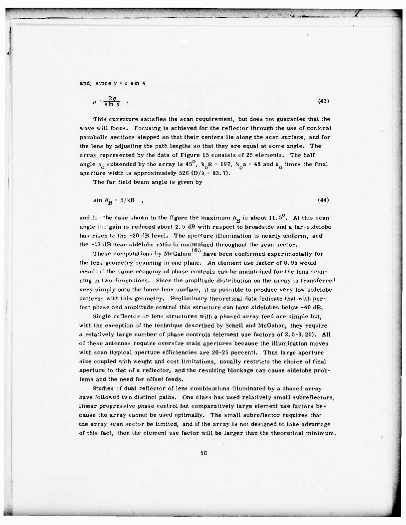
•• iu i. •>»• >• n
and, since y > p sin 0
RO sin e (43)
This curvature satisfies the scan requirement, but does not guarantee that the wave will focus. Focusing is achieved for the reflector through the use of confocal parabolic sections stepped so that their centers lie along the scan surface, and for the lens by adjusting the path lengths so that they are equal at some angle. The array represented by the data of Figure 15 consists of 25 elements. The half angle f) subtended by the array is 45°, k R = 197, k a - 48 and k times the final • o ' * ' o ' o o aperture width is approximately 52f> (D/A - 83.7).
The far field beam angle is given by
sin 0B • 0/kR , (44)
and Co *he case shown in the figure the maximum f)_ is about 11. 5 . At this scan angle tl -. gain is reduced about 2. 5 dB with respect to broadside and a far-sidelobe has risen to the -20 dB level. The aperture illumination is nearly uniform, and the -13 dB near sidelobe ratio is maintained throughout the scan sector.
105 These computations by McGahan have been confirmed experimentally for the lens geometry scanning in one plane. An element use factor of 0. 95 would result if the same economy of phase controls can be maintained for the lens scan- ning in two dimensions. Since the amplitude distribution on the array is transferred very simply onto the inner lens surface, it is possible to produce very low sidelobe patterns with this geometry. Preliminary theoretical data indicate that with per- fect phase and amplitude control this structure can have sidelobes below -40 dB.
Single reflector or lens structures with a phased array feed are simple but, with the exception of the technique described by Schell and McGahan, they require a relatively large number of phase controls (element use factors of 2. 5-3. 25). All of these antennas require oversize main apertures because the illumination moves with scan (typical aperture efficiencies are 20-25 percent). Thus large aperture size coupled with weight and cost limitations, usually restricts the choice of final aperture to that of a reflector, and the resulting blockage can cause sidelobe prob- lems and the need for offset feeds.
Studies i.f dual reflector of lens combinations illuminated by a phased array have followed two distinct paths. One cla.--> has used relatively small subreHectors, linear progressive phase control but comparatively large element use factors be- cause the array cannot be used optimally. The small subreflector requires that the array scan sector be limited, and if the array is not designed to take advantage of this fact, then the element use factor will be larger than the theoretical minimum.
50
1
IBipmPt^«MWI*^WPW^^^^^^»"^^^"""!. I" nu^i^BHWI!^«"PP^P"ww»^^«^»Wlppp»w.i<uii> IJIHI.I"II»I»#.J»J"I.»V ^MM" •> '' */*" '''
10fi. Fitzgerald, W. D. (1971) Limited Electronic Scanning with an Near Field Cassegrainian System, ESD-TR-71-271, Technical Report 484, Lincoln Laboratory.
107. Fitzgerald, W. D. (1971) Limited Electronic Scanning with an Offset-Feed Near-Field Gregorian System, ESD-TR-71-272, Technical Report 486, Lincoln Laboratory.
108. Miller, C.J., and Davis, D. (1972) LFOV Optimization Study. Final Report No. 77-0231, Westinghouse Defense and Electronic Systems Center, System Development Division, Baltimore,. Md., ESD-TR-72-102.
109. Tang, C.H., and Winter, C.F. (1973) Study of the Use of a Phased Array to Achieve Pencil Beam over Limited Sector Scan. AFCRL-TR-73-0482, ER 73-4292, Raytheon Co., Final Report Contract F19628-72-C-0213.
110. Tang, E., et al (1975) Limited Scan Antenna Technique Study. Final Report, AFCRL-TR-75-0448, Contract No. F19G28-73-C-0129.
51
Examples of this first category are the near field cassegrain geometry and the offset fed gregorian geometry of Fitzgerald. ' ' The second category of dual reflector or lens scanning antennas uses a much larger secondary aperture and an array that scans over wide angles. This type of antenna can have element use factors close to unity, but the required secondary aperture sizes make the structure bulky. Comparison of two antennas in this category ' with the Fitzgerald studies indicate that element use factors of 1.4 can be maintained using secondary apertures of approximately 0. 7 the diameter of the main reflector, but restricting the subreflector size to 0.35 to 0.25 of the main reflector diameter led to element use factors of between 2. 5 and 4. Larger subreflectors also allow more accurate control of the main reflector illumination and in one case resulted in approximately -20 dB sidelobes over the scan sector.
In addition to these combinations of array and optical structures, there is a growing class of antennas that scan efficiently over limited sectors using novel array techniques. Each achieves its relatively low cost by using large array ele- ments or subarrays and so reducing the number of required phase controls for a given size final aperture. This use of oversize elements in a periodic array results in grating lobes, which are suppressed by careful control of the subarray element pattern, or by scanning the element patterns to null certain of the lobes. Alternatively, other approaches have used pseudorandom array grids to reduce the peak levels of the grating lobes by redistributing their energy over a wider sector of space.
The radiated field of the array of aperture elements shown in Figure 1 given in direction-cosine space for a beam at (u . v ) is: r o' o
NX N 27T e(uv)\^\-^ JY<umd
x+^n
u+vndv)
E(u,v)=^£]>>mne X X n ^ (45) m = l n=l
iiii mwpii.iiMi i ij jfi. iwpju. ' «l«u".i JM»mi>f.4-yrt*w i»^iwK1u'ju'n.',tiii^v..'PV*Lu.i 'Pj- in • m^-M Mjt.i )|iw..yrpjj'^mir'"W 'WIIII.IIIUHJI .»i.wi» 1I' ! ^*r «^^y^"-
w ii fifcw r i
where
u - sin 9 cos
v - sin 9 sin §
and
Amn = mn e
-i —- (u md +u A +v nd ) A o xonoy
Here A is the signal at the element (m, n) located at the position mn x = md + A , y = nd as required to form the beam at (u , v ). I is the signal x n' * y M o o mn &
amplitude and e(u, v) is the element pattern of each aperture in the array.
N = N N is the number of elements in the array.
Assuming that the array is excited by a separable distribution so that H E I~. = I~ I , and assuming that the element pattern is also separable, then mn m n' °
e(u, v) = e (u)e (v) and this field distribution can be written in the following form: x y
N „
1 V^ H 3~T(u"Uo)mdxl
m=l
1 N
N
n=l
ln ey(v) e 3^[(v-vo)ndy+An(u-uo)]|
(46)
-- Ex(u)Ey(u, v) .
This pattern is not separable in general, but may be so for certain choices of
(A ). The choice of optimum (A ) for grating lobe reduction will be considered
later.
If the rows are not displaced, then the field is fully separable and the exponen-
tial forms in the above summations have principal maxima at the grating lobe
locations:
u u +^- P o dv
(47)
q o dy
52
•••

i.ii •» 'mj<pnxi,«m)n,iii-wniPiwj.i. . II.H '«IV'J"!»».', I, v"*""
for all p • q bounded by the inequality
K = -2l «h -u2 - v2< 27r
pq A V m vn~ X
These points are shown in (u, v) space as a regularly spaced grating lobe lattice about the main beam location (u , v ) in Figure 16. The circle with unity radius o o represents the bounds of the above inequality; all grating lobes within the circle represent those radiating into real space, and those outside do not radiate.
Figure 17 shows how the array factor and element pattern combine to produce the resulting radiated distribution in one principal plane. This figure illustrates how the effects of squinting or narrowing the element pattern or of destroying the periodicity can serve to reduce resulting grating lobes by altering either of the two factors in this product.
Efforts to maintain nonperiodic grids for grating lobe reduction have centered mostly about use of circularly disposed arrays with an aperiodic arrangement of elements of one or several sizes.
An example is the array investigated by Patton. This structure, shown schematically in Figure 18, consists of a circular array of dipole subarrays arranged in an aperiodic fashion. This array is locally periodic, and does have vestigal grating lobes, but these are considerably suppressed for a large array. Patton describes a 30-ft diameter array and a 10-ft diameter array at C-band. The 30-ft array consists of one thousand elements that scan a 0.3 6 beam approx- mately 5° with an element use factor of 1.3. The system has high average side- lobes at its maximum scan and losses which add to 5. 94 dB for the 10 ft model and a projected 4.21 dB for the 30 ft array. The transmission line interconnections may also make an X-band design somewhat less practical. Peak sidelobes were measured at the -15 dB level for the 10-ft diameter array, and are projected at -20. 9 dB for the 30 ft array, but the item of primary importance is the achieve- ment of this extremely low element use factor and the low generalized f/D ratio
achievable with aperiodic array technology. A similar antenna, but using unequal size elements has recently been described
by Manwarren and Minuti. This antenna has been designed to provide a 1° pencil beam at 1300 MHz to scan a conical sector with 8 half angle with 20 dB grating lobes. An S-band model has also been configured. The antenna consists
111. Patton, W.T. (1972) Limited scan arrays, in phased array antennas, Proc. of the 1970 Phased Array Antenna Symposium, edited by A. A. Oliner and G.H. Knittel, Artech House, Inc., MA, 332-343.
112. Manwarren, T.A., and Minuti, A.R. (1974) Zoom Feed Technique Study, RADC-TR-74-56, Final Technical Report.
53
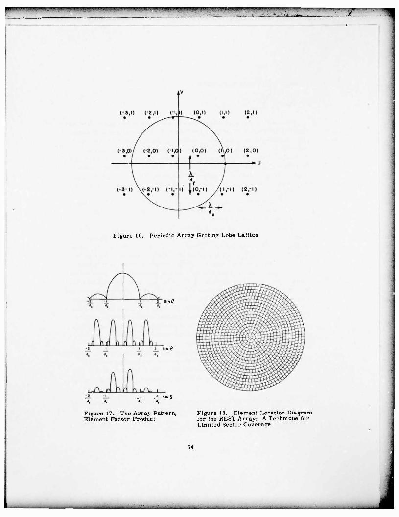
, ... ... wm LIM i i •«- mm ,i . n *i i JIIUI. JUIJ '"•""""l • •• i»uwn.^fg^^^wPWiiiinn.' ii \jfmm**w* "w»'..;'!1' y i|wuj"i!w*w I'-M^
Figure 16. Periodic Array Grating Lobe Lattice
SIN0
_L _L SINS
Figure 17. The Array Pattern, Element Factor Product
Figure 18. Element Location Diagram for the REST Array: A Technique for Limited Sector Coverage
54
- i • • • • •• - -• . - ..
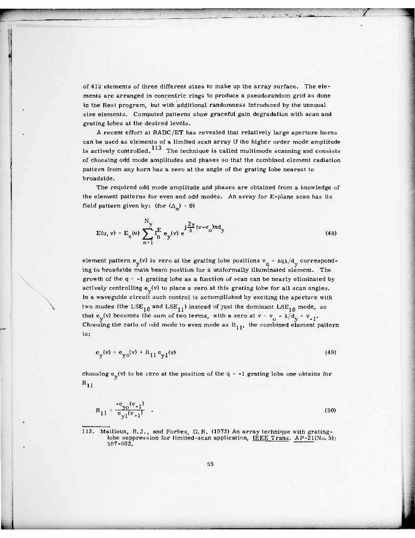
—«"-~——* •(•"»I »«"' «IN. •-«i-TTum HIHI imp^wv^p^m **,--* - ~ r-, - K^r^^._ r
of 412 elements of three different sizes to make up the array surface. The ele-
ments are arranged in concentric rings to produce a pseudorandom grid as done
in the Rest program, but with additional randomness introduced by the unequal
size elements. Computed patterns show graceful gain degradation with scan and
grating lobes at the desired levels.
A recent effort at RADC/ET has revealed that relatively large aperture horns
can be used as elements of a limited scan array if the higher order mode amplitude 113 is actively controlled. The technique is called multimode scanning and consists
of choosing odd mode amplitudes and phases so that the combined element radiation
pattern from any horn has a zero at the angle of the grating lobe nearest to
broadside.
The required odd mode amplitude and phases are obtained from a knowledge of
the element patterns for even and odd modes. An array for E-plane scan has its
field pattern given by: (for (A ) = 0)
N
E(u, v) = E (u) V* IE e (v) e x Z—i n y JT(v-Vo)ndy
(48)
n=l
\
element pattern e (v) is zero at the grating lobe positions v = ±qA/d correspond-
ing to broadside main beam position for a uniformally illuminated element. The
growth of the q - -1 grating lobe as a function of scan can be nearly eliminated by
actively controlling e (v) to place a zero at this grating lobe for all scan angles.
In a waveguide circuit such control is accomplished by exciting the aperture with
two modes (the LSE.Q and LSE..) instead of just the dominant LSE.n mode, so
that e (v) becomes the sum of two terms, with a zero at v v - >/d = v ,. y ' o "•' y -1
Choosing the ratio of odd mode to even mode as R. ., the combined element pattern
is:
ey(V) = eyo(v) + Rlleyl(V) (49)
choosing e (v) to be zero at the position of the q » -1 grating lobe one obtains for
Rll
-e (v ,) R yo -\
11 ey>-l> (50)
113. Mailloux, R.J., and Forbes, G.R. (1973) An array technique with grating- lobe suppression for limited-scan application, IEEE Trans. AP-21(No. 5): 597-G02.
55

"•""• ' —i um i MIIIIII ii » • in. J i m .mi i ii m . ^ .-
_. . •4 . * r
Since the various waveguide modes have constant phase aperture distribution e is a real function and e . is pure imaginary, so the R is pure imaginary and increases with scan in order to maintain the null position coincident with the center of the q -1 grating lobe. The celative odd mode phase is thus fixed at ±90 with respect to the even mode phase depending upon the sense of the scan angle. The allowable element spacing for E-plane horns is
<dy/x)sinsmax = 0.6 . (51)
The laboratory model shown in Figure 19 is an array designed for E-plane scan (±12°).
Figure 20 shows the E-plane pattern for the array phased at broadside and the elements excited with the central four at uniform amplitude, the second element in from each end of the array at -3 dB amplitude, and the outer elements at -(> dB amplitude. This taper should have first sidelobes at about -19 dB, but due to phase errors the level is approximately -17 dB. The grating lobes at ±19 ' (-Hi dB) and ±40 (-2(5 dB) can be reduced by using a dielectric lens in each horn.
Figure 21 shows two cases at the maximum scan angle ±12 . The dashed curve is the horn array radiation pattern without odd modes and shows that the main beam gain is reduced more than 5 dB with respect to the broadside array and the grating lobe at -7 is larger than the main beam by 1. 8 dB. Other grating lobes are at tolerable levels. The solid curve shows that when the element is excited by two modes the offending grating lobe is reduced to approximately the -20 dB level, and the main beam increased to -1.2 dB with respect to broadside because the new element pattern has its peak tilted toward the main beam. The second grating lobe (q = -2) is approximately the -12 dB level.
Conventional aperture tapering procedures can be used to reduce near side- lobe levels to -30 dB or less. The nulled grating lobe Is suppressed 20 to 25 dB at center frequency for a small array (8 elements), but substantially more for larger arrays. Residual grating lobes at wider angles are unaffected by array tapering and remain the major limitation of the technique.
Full two-dimensional scanning requires the suppression of three grating lobes, however, and so a total of three higher order modes must be controlled as a func- tion of scan. The dominant grating lobes to be cancelled are those nearest broad- side (p, q) - (-1,0), (-1, -1), (0-1) for general scan angles, and this control is achieved using four phase shifters for each multimode horn to form an element pattern that is separable in u-v space and positions the three nulls properly. In practice, it is also sometimes appropriate to narrow the horn II-plane patterns by
56

• '»'•. "J" • • " mi. ii i
Figure 19. Laboratory Model Multimode Scanning Array
>-
o
> <
36 0
ANGLE 'degrees)
36 72 108
Figure 20. Broadside Pattern Data (Eight Element Array)
57
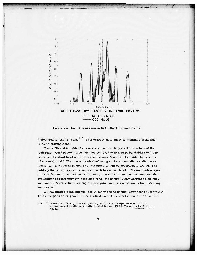
'••"•" III III II HOIK - I ' » -. .... v. . , , T
o Q:
* o
ANGLE ( degrees)
WORST CASE (12° SCAN) GRATING LOBE CONTROL
NO ODD MODE ODD MODE !
Figure 21. End of Scan Pattern Data (Eight Element Array)
114 dielectrically loading them. This correction is added to minimize broadside H-plane grating lobes.
Bandwidth and far sidelobe levels are the most important limitations of the technique. Good performance has been achieved over narrow bandwidths (~3 per- cent), and bandwidths of up to 10 percent appear feasible. Far sidelobe (grating lobe levels) of -20 dB can now be obtained using various aperiodic row displace- ments [A] and spatial filtering combinations as will be described later, but it is unlikely that sidelobes can be reduced much below that level. The main advantages of the technique in comparison with most of the reflector or lens schemes are the availability of extremely low near sidelobes, the naturally high aperture efficiency and small antenna volume for any desired gain, and the use of row-column steering commands.
A final limited-scan antenna type is described as having "overlapped subarrays." This concept is an outgrowth of the realization that the ideal element for a limited
114. Tsandoulas, G. N., and Fitzgerald, W.D. (1072) Aperture efficiency- enhancement in dielectrically loaded horns, IEEE Trans. AP-20(No. 1) 69-74.
58
A

"•"" • "•"• ««'•"•• •«•••'•'!- I »\ I "• !'i • « .M i ,
• »- .*•. i . .
scan system would have a flat top and no sidelobes. An element pattern like that
of Figure 22 would allow the beam to scan out to some maximum scan angle
(sin f) ) while suppressing all grating lobes as long as they did not occur within
the range -sin o 3 sin OS sin ft . Since the grating lobes occur at position.:,
given by Eq. (47), then for a very large array one can optimize the interelement
spacing for a given maximum scan angle by choosing
r~
(dx/A) sin *m 0. S (52)
where d is the intersubarray spacing. This condition was derived earlier
(Eq. 41) from the basis of satisfying the criteria given for minimizing the number
of phase controls, but here it results from choosing the widest possible flat-topped
subarray pattern consistent with good grating lobe suppression. In this case a
large array with main beam at sin fl (0. 5A,d ) for some arbitrarily small value
will have its nearest grating lobe at sin 0 -(0. 5A/d ), and all grating lobes will
be completely suppressed. Such an array is characterized as a limited scan design
because it can take advantage of limitations imposed upon the scan sector in order
to increase aperture .size d /A. In principle an arrav with sin f) - 0. 1 can use a K x' K p • m 5A interelement spacing while for sin f) 0. 05, a 10A spacing can be used. This
size increases and associated reductions in the number of required phase controls
for restricted coverage illustrate the goal of limited scan antenna designs.
/ \ '? /
/ i 0.8
.' i w 06-- • (- to q 0.4H u "- 0.2 +
r—• * T
-2sin6m -SinQn
— IDEAL FIELD STRENGTH PATTERN
-PATTERN FOR TRUNCATED APERTURE DISTRIBUTION
\ / T sm9m
w 2sin6n
sin©
Figure 22. Ideal and Approximate Subarray Patterns for Overlapped Subarray
59
' •• • L i»wy;nppni.«»lli in ».•>••• ••" ' 7
The aperture field corresponding to this far-field distribution is of the form:
»"(y*sin9m)
(TXsin*m)
i(x) = 1* U1L (53)
where x is the distance measured from the center of the subarray. If the maximum
ideal spacing d /> = (0. 5/sin 9 ) is used, then this aperture distribution has zeros
at x - ±nd excluding n 0, and one must include a number of elements in order to x °
reproduce the i(x) distribution faithfully. Thus, each phase -shifter must feed a
multiplicity of subarrays and the subarrays can be said to be overlapped. Obviously,
the ideal aperture field can only be approximated; it must be truncated and then
approximated by realizable distributions at each element. The dashed curve shown
in Figure 22 shows the flat-topped subarray pattern achievable if the i(x) is trun-
cated at x = ±3d . In this case, 20 dB grating lobe suppression can be obtained
for scan out to the angle
(dx/X) sin em = 0.43 . (54)
The required overlapped distribution implies the interconnection of a number
of array elements and so is extremely difficult to fabricate in microwave circuitry.
Consequently, the circuit approach has received only limited attention. Alterna-
tively, space feed systems can quite naturally achieve overlapped subarray dis-
tributions that have proven very practical. These systems use feedthrough lenses
or reflectors that can faithfully reproduce a substantial part of the f(x) distribution
as compared with microwave circuit systems.
Examples of such schemes for producing optically overlapped subarrays 115 includes the HIPSAF antenna and the dual reflector-array design of Tang
109 et al. Figure 23 shows schematically that exciting two adjacent feed horns
results in two overlapped aperture illuminations at the main reflector. These
"subarray" aperture distributions have approximately (sin x)x fields and so have
rectangular shaped radiation patterns as appropriate for good grating lobe sup-
pression. Figure 24 shows a calculated and a measured pattern from the central
subarray of the experimental reflector. Details of this extensive analytical and 109 experimental study are included in the reference, but in general the program
demonstrated that such optical techniques can produce low sidelobe (<-20 dB)
115. Tang, R. (1972) Survey of time-delay beam steering techniques, in Phased Array Antennas, Proceedings of the 1970 Phased Array Antenna Symposium, Artech House Inc., MA, 254-270.

• i ••. "WW,!tl,i. ,.liWI^PaWWHpfWP,|J»iy|Ji!HWIIii 1,1.' M.üLi^Bppypw ll.W.,jW,M!jl.U.I,liltfjri.|WW -r y
>— APERTURE
PARABOLIC / REFLECTOR / -)
/ >*5 — B j^5 — A
OVERLAPPING SUBAPERTURE ILLUMINATIONS
y\
/ \\\
\\
\ , ^-SPHERICAL LENS
%
B
Figure 2'.i. Aperture Illumination From Optically Overlapped Feed
•18°
Figure 24. Subaperture Far Field Pattern for Central Subaperture
61
-- - ••

11 i.i I I ». • i npinn.mii.il, HIHI UM til P.1. »!• ill I IJ »UllHini^lW—WI .1 lllilj», II)I||»»IIWJ^I»J>.
scanned patterns over limited spatial sectors using only about 1. 4 times the theoretical minimum number of phase controls.
Apart from these configurations using quasioptical techniques, the ultimate in overlapped circuitry for low sidelobe arrays will, of necessity, be synthesized using constrained feed distribution networks. This is a new area of technology and there has been relatively little work in this area. Several studies of overlapped subarrays are reported by Tang, and modifications of these have recently been implemented for fire control radars. In addition the subarray distribution that produces an approximate flat topped pattern can be approximated by higher order
11 fi mode distributions in horn apertures, so that the element spacings can be made equal to the distance d between subarrays. This work is an outgrowth of studies on the active odd-mode control of element radiation patterns, but the developments in overlapped subarrays differ in concept, in means and in results from the multi- mode scanning technique. The study describes a passive interconnecting network to synthesize a flat topped, symmetric, subari ay pattern, while the multimode scanning technique requires active control of odd-mode amplitude and achieves much greater scan per element (although slightly less per phase shifter).
The basic circuit allows an element size times scan angle product in the E- plane of approximately
(d /A) sin 0 =0.33 . (55)
The largest array grating lobes are less than -16 dB for maximum scan. Circuits have been devised to provide similar overlapped behavior for two planes of scan, but there is not yet sufficient data to compare the relative advantage gained by us- ing the second plane.
The discussion of limited scan arrays has dealt mainly with a description of methods devised to reduce array costs; and these methods form the basis of an evolving technology. The most significant change forthcoming in this area is the development of techniques for extremely low sidelobe control. These techniques will be aided by some established methods of sidelobe suppression (random element positions, and tunnel structures) and by the spatial filtering technique to be described later, but the basic antenna structures themselves must be substantially improved in order to achieve sidelobe levels between -35 and -45 dB. The only limited scan antenna with evidence showing that such sidelobe levels are achievable is the array-lens concept of Schell. These data are not yet published and consist at present of analytical calculations that neglect coupling and near field effects; but they confirm that the possibility of such extra-low sidelobe control exists.
11 f>. Mailloux, R.J. (1974) An overlapped subarray for limited scan application, IEEE Trans. AP-22.
62
^
A.

i j.i.i. ,i-. ••,., „miiiMm -in uiii II.IJI. i imm .>"•*. •ju.ii.juj.n.iii HUM linn . JJI JI.I ILIIT' '«M" •'•JI.-JJ -4 »ijuupM-j I-M M •'• • »•<" «n»uww »yyi»J, • w
_s- .'''•' * r' *<t i/J» . ' OT^ar-w««——'-^^_
Other quasioptical approaches can conceivably produce extremely low side-
lobes; in particular those schemes based upon overlapped subarraying approaches
should produce very low sidelobe distributions, although not out to the scan limits
given in this description.
None of the array techniques discussed here can produce patterns with such
low sidelobes except through the use of spatial filtering; but techniques based upon
constrained feed circuits for overlapped distributions can ultimately produce the
lowest sidelobe limited scan systems. As yet there has been relatively little
effort directed toward synthesizing such networks, and this remains an area where
much work is needed.
3.4 Broadband and Multiple frequency Arrays
Though considered together, broadband and multiple frequency arrays call
for fundmentally different technology. Wideband arrays have one beam formed by
a feed network and a set of phase shifters, but multiband technology has developed
by interleaving relatively narrow band elements with different center frequencies,
and with separate beamformers for each frequency.
The maximum theoretical bandwidth of linearly polarized rectangular wave-
guide phased arrays is about 60 percent. Studies * of such elements have
indeed shown that these bandwidths can be achieved with low VSWR and wide scan
coverage. Recent efforts sponsored by AFCRL (now RADC ET) have developed 120 121 double ridged waveguides and novel stripline radiators, see Figure 25, that
can provide good performance over an octave bandwidth (67 percent). Arrays with
circular polarization have much narrower bandwidths, with 25 percent seen as a 122 123 reasonable outer limit. '
117. Tsandoulas, G. N. (1972) Wideband limitations of waveguide arrays, Micro Microwave Journal 15(No. 9):49-56.
118. Chen, C.C. (1973) Broadband impedance matching of rectangular waveguide phased arrays, IEEE Trans. AP-21:298-302.
119. Laughlin, G.J., et al (1972) Very wide band phased array antenna, IEEE Trans. AP-20:699-704.
120. Chen, C.C. (1972) Octave band waveguide radiators for wide-angle scan phased arrays, IEEE AP-S Int. Symp. Record. 376-377.
121. Lewis, L.R., Fassett, M., and Hunt, J. (1974) A broadband stripline arrav element, IEEE AP-S Int. Symp. Record.
122. Chen, M.H., and Tsandoulas, G. N. (1973) Bandwidth properties of quadruple- ridged circular and square waveguide radiators, IEEE AP-S Int. Symp. Record. 391-394.
123. Tsandoulas, G. N., and Knittel, G. H. (1973) The analysis and design of dual-polarization square waveguide phased arrays, IEEE Trans. AP-21: 796-808.
63
• •-' • i •• niMMMUfHwr ii ii • _ „, 1 • - - f^f^H
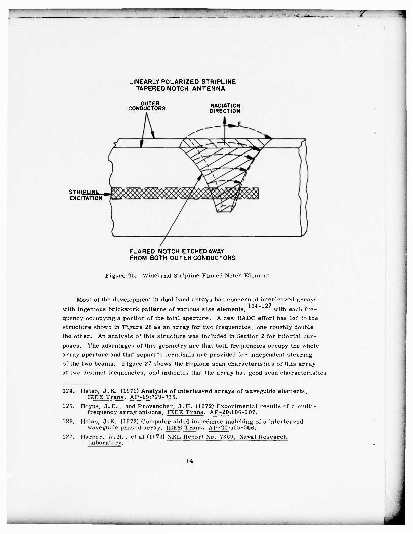
• ' ' ""—^»»»»'»—m—p^www»»»*
••i .*. /
LINEARLY POLARIZED STRIPLINE TAPERED NOTCH ANTENNA
OUTER CONDUCTORS RADIATION
DIRECTION
STRIPLINE EXCITATION
FLARED NOTCH ETCHEDAWAY FROM BOTH OUTER CONDUCTORS
Figure 25. Wideband Stripline Flared Notch Element
Most of the development in dual band arrays has concerned interleaved arrays 124-127 with ingenious brickwork patterns of various size elements, ' with each fre-
quency occupying a portion of the total aperture. A new RADC effort has led to the
structure shown in Figure 20 as an array for two frequencies, one roughly double
the other. An analysis of this structure was included in Section 2 for tutorial pur-
poses. The advantages of this geometry are that both frequencies occupy the whole
array aperture and that separate terminals are provided for independent steering
of the two beams. Figure 27 shows the H-plane scan characteristics of this array
at two distinct frequencies, and indicates that the array has good scan characteristics
124. Hsiao, J.K. (1971) Analysis of interleaved arrays of waveguide elements, IEEE Trans. AP-19:729-735.
125. Boyns, J.E., and Provencher, J. H. (1972) Experimental results of a multi- frequency array antenna, IEEE Trans. AP-20:10G-107.
12(i. Hsiao, J.K. (1972) Computer aided impedance matching of a interleaved waveguide phased array, IEEE Trans. AP-20:505-506.
127. Harper, U.U., et al (1972) NRL Report No. 73G9, Naval Research Laboratory.
84
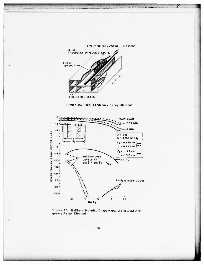
' " "• -•' ••' ' '».1 » • -•••• •—•»». —— ••^WWWWW
^
LOW FREQUENCY COAXIAL LINE INPUT
4 HIGH —f FREQUENCY WAVEGUIDE INPUTS
END OF BIFURCATION
4 DIELECTRIC SLABS
Figure 26. Dual Frequency Array Element
a. o
MAIN BEAM
2.56 GHz
6 GHz
e = 9.0 a • 4 755 cm• h c s 0.826cm 1 — t * 0.6 35 cm ( ••
c • 1 143 cm L 1 * 0.318 em
sin 8„
Figure 27. H-I'lane Scanning Characteristics of Dual Fre- quency Array Element
6S
_

1 ..»ii»»- i «».im . in mi. IM • i in.!.i i. jiuuiiuiiiaowi^ i in •»•••••»»• IIIL . i. IHII.1,11 PI,i j lum/iin IWMI • -• ii ini.iiui ..mm
. A- _«L. . -...'•i-.U^m . , 7 m
with no blind spots within the scan sector at either frequency. The proper use of array matching techniques should improve these characteristics and so make the technique viable for high power radiation at both frequencies.
Other multiple frequency arrays have been proposed and developed for distinct applications, and this area of technology is evidently destined to play an expanding role in the future of array antennas as the number of aircraft terminals grows to meet the needs of satellite communication systems.
t. NKÄ TECHNOLOGY
1.1 No» Technology as a Forcing Function
The techniques that have been discussed thus far represent major subject areas for research; the methods described represent present day solutions and may not correspond to ultimate solutions. The categorization "Special Purpose Arrays" thus defines an area that will be of major importance for many years. This section is addressed to a different kind of stimulus for array research; one based primarily upon the wide variety of transmission media. The thesis proposed is that the very rapid change in this technology can be a strong force that guides and propels a major part of the future of array antennas. The newer elements of technology include improved phase shifters, the emergence of microwave inte- grated circuit technology, and developments in stripline and microstrip transmis- sion circuits. These new developments compliment existing array technology, but in addition they act as a stimulus to further advances in array techniques.
Figure 28 shows a waveguide phase shifter developed by Raytheon Company. The phase shifter developed by Raytheon itself is a three bit analog nonreciprocal device that handles 3. 5 k\V peak and has 1 dB loss. The photograph shows the driven circuit incorporated into the body of the phase shifter. Both ends of the phase shifter are matched to the environment they occupy. The front face is a linearly polarized C-band waveguide loaded with dielectric that has been matched to provide good properties over the design scan sector, while the back face is matched to optimize pickup from the space feed network. The main reason for showing this illustration is to indicate that indeed such scan matching has become practice; array behavior is calculated or measured in simulators, and phase shifters are incorporated to achieve compact units that plug into the array and can be conveniently replaced.
A second item of technology that further illustrates some of the above is shown in Figure 29. This laboratory prototype developed by Hughes Corporation is a 3-bit resistive gate diode phase shifter operating at S-band. Total loss is approxi- mately 1. 9 dB, the device can control 300 VV of peak power with 5 W average. Its
06
ftfc
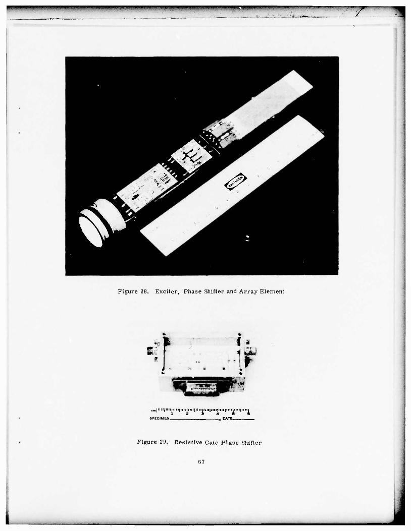
• • • I • • II . Ill IIJI • II >l- • Wl • n i .•wiiaiii i i i W»^-* <r. nuyn m «i 11 —--
1
^B^&k <i^^^^M
C" J %J* ^UT
Figure 28. Exciter, Phase Shifter and Array Element
• i»
•>.*»
cm|IIH|lllllliM|nillllll|IIIIIIU||||i||iiii|iiiiiiiii|Hiii
sprriMFN DATE
Figure 2.9. Resistive Gate Phase Shifter
(57
J
i i ii •mi mi i. •••.•i.nimi—P»ni»j-.«i..wmili.i]n. i .. i} m^^f/ff^fifffH^fg^^^mrWfmmm^mimx im nv. i "-rim,, «' . . u,t»Wn. ...„„M»^.,, ,,•.,.,,. '_,'»'• >>;»<• '"•
^
size is approximately 1 in. by 1 in. by 2 in., and it switches in lOpsec. Ths
chief advantage claimed for this device is that the phase shifter does not require
any forward bias current; the only bias current flowing through the device Is a
forward leakage current of several /^A. Alternatively, the commonly used PIN
diode phase shifters require 50-200 ma current at one volt forward and 100 volts
at 1 /jA reverse. Total power required for phase control per phase shifter and
driver combination may thus be on the order of 0. 3 to 0. G W. The total power for
a 2000 element array would thus be nearly 1 kW for the PIN diode array, but less
than 0. 2 W for a resistive gate diode array. This extremely low drive power
requirement makes it possible to control the array steerir.g from the beam steer-
ing computer without an additional driver and high power supply.
Apart from the obvious fact that diode phase shifters have come a long way,
the second issue raised by this technology is that the emergence of microstrip
transmission circuits has not carried through to microstrip scanned antennas.
There have been a number of developments in microstrip devices with fixed 1 ?ß — 1 ^ I
beams, but most of these early devices were not well suited to electronic
scanning. Figure 30 shows a microstrip array of spiral elements developed by
Raytheon Corporation. The array structure combines a corporate feed, power
dividers, baluns, and phase shifting network on one printed circuit board.
To date, there are no comprehensive theoretical treatments of even single
microstrip patch antennas. Nevertheless, the technology itself has advanced to
such a degree that many of the larger corporations are developing numerous varia-
tions of the original designs, and the day of full scanned arrays is clearly very
near. Research is needed in this important area in order to avoid some of the pit-
falls that led to the problems of array blindness. Air Force applications for this
type of lightweight, inexpensive, and conformable antenna array are many, and
extend f-om man-pack designs to flush-mounted aircraft antennas. Studies of
microstrip and the newer types of stripline antennas should be undertaken to assure
that a valid technological base exists, and that its depth is sufficient to sustain the
rapid technological growth that lies ahead.
A second technological area that has been a stimulus and could become a much
more important factor in array design is the growth of active m'crowave integrated
circuitry. Mixers, oscillators, and microwave amplifiers are now available
128. Munson, R.E. (1974) Conformal microstrip antennas and microstrip phased arrays, IEEE Trans. AP-22:74-78.
129. Howell, J.Q. (1975) Microstrip antennas, IEEE Trans. AP-23:90-P3.
130. Kaloi, C. (1975) Asymmetrically Fed Electric Microstrip Dipole Antenna, TR-75-03, Naval Missile Center, Point Magee, CA.
131. Dernervd, A. (1976) Linearly polarized microstrip antennas IEEE Trans. AP-24:84f>.
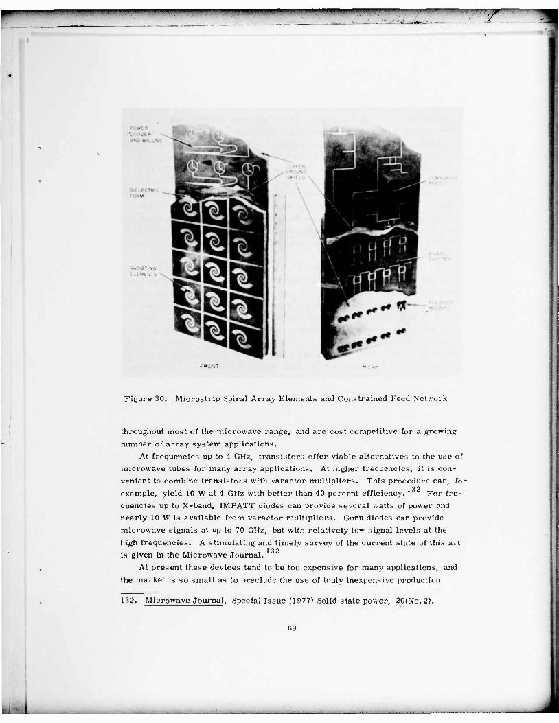
"""•' • ' ' • "" '"" •>•' •••>•"• • •"• • IL'"" •' wwmw • '• • •' ' • """ ..i."^i..F'li )>.>•
T
•.
• -
Figure 30. Microstrip Spiral Array Elements and Constrained Feed Network
throughout most of the microwave range, and are cost competitive for a growing
number of array system applications.
At frequencies up to 4 GHz, transistors offer viable alternatives to the use of
microwave tubes for many array applications. At higher frequencies, it is con-
venient to combine transistors with varactor multipliers. This procedure can, for 132 example, yield 10 W at 4 GHz with better than 40 percent efficiency. ' ' For fre-
quencies up to X-band, IMPATT diodes can provide several watts of power and
nearly 10 \V is available from varactor multipliers. Gunn diodes can provide
microwave signals at up to 70 GHz, but with relatively low signal levels at the
high frequencies. A stimulating and timely survey of the current state of this art 132 is given in the Microwave Journal.
At present these devices tend to be too expensive for many applications, and
the market is so small as to preclude the use of truly inexpensive production
132. Microwave Journal, Special Issue (1977) .Solid state power, 20(No. 2).
09

i.i •» i. i mi •••.,.. i .11,. .up i i. iiiui.i i i. HI i ... I^II KIMHIIII pniii p u | i •LI, . , , miniu. i. i- .-- ,,i m •
T
methods. With time the use of solid state transmitters and receivers at each
array element will become commonplace. This use will pi ovide further stimulus
for development of microstrip antenna types, and may also foster new developments
in nonuniform array synthesis. The reasons for this additional concern is that
such amplifiers are usually operated in a saturated mode, and it is difficult to
amplitude weight the array elements as would be required for sidelobe suppression.
The alternative is to allow uniform illumination and use nonuniform spacing for the
purposes of tapering. This practice is not new; it is implemented in several mili-
tary systems and numerous prototype design programs, but further exploration of
these techniques for sidelobe suppression without undue complication of beam
steering control requirements could bring about important advances in solid state
radar arrays.
The continuing need to produce lower cost arrays has also led to the concept
of an integrated subarray module approach. The array of Figure 30 is one early
example of the technology required for such an approach, but the concept could be
carried substantially further. Studies presently being undertaken by Hughes Air-
craft Company are directed toward advancing such technology. In this approach a
large number of radiators, phase shifters and a feed network are combined into an
integrated subarray module which is used as the basic building block of an antenna.
These components are combined on one common substrate of a high dielectric con-
stant material such as alumina using thick film printing techniques. This printing
technique can produce not only the conductor pattern of the circuits, but also the
microwave capacitors and resistors as well. Radiators such as metallic discs are
attached to the other side of the substrate (the ground plane side of the phase
shifter circuit). This approach eliminates most of the interconnections such as
coaxial cables and connectors, thereby reducing manufacturing and assembly labor
as well as improving reliability. Radio frequency (rf) testing is performed at the
subarray module level instead of the individual component level, hence, minimizing
the testing cost. The ultimate subarray would have a continuous scanning aperture,
that is, the phase shift across the radiating aperture is varied continuously for
beam scanning. For example, a ferrite slab can be used as a radiating aperture.
The index of refraction across the ferrite slab can be varied continuously by exter-
nal magnetization for beam scanning. Preliminary results with a scanned aperture 133 of this type have been demonstrated at Lincoln Laboratory.
This description brings us to a limiting case, but emphasizes one of the main
issues raised earlier. Array elements of the future may be very different from the
waveguides and dipoles of the present. This technology must be supported by the
133. Stern, E., and Tsandoulas, G. N. (1975) Ferroscan: Toward continuous• aperture scanning, IEEE Trans. AP-23(No. 1):1 5-20.
70
hA
Il.np.liil 11.1. in». »NU III»! mn, in. I ,!,,. .,,,|ii,i,u.im. •!.»»• .j.pt. HIII.UI-..in •,,.•...•,•..•. . ^ .. II w, »,n ^.»
same level of intense research activity that was necessary during the 60's because
mistakes will be even more costly in the future.
I.- Radomes, Polarizers, anil Spatial Fillers
4.2. 1 METALLIC GRID STRUCTURES FOR RADOMES. DICHROIC REFLECTORS AND POLARIZERS
The present state-of-the-art in dielectric radomes is summarized in 134 Walton. There is a growing use of metallic gratings for radomes, polarizers,
dichroic subreflectors, and, now possibly for spatial filters. These devices rep-
resent an area of research that is strongly influenced by, and can itself influence,
phased array research. 135 The survey by Wait ' compares various theories of wire grid and mesh
structures that are the basis of this new technology. Much of the basic analysis
was performed in the interest of developing improved ground plane surfaces and
not for radomes or polarizers. Studies of artificial dielectrics as summarized by 1 o r* 1 Q H
Collin ' are also directly applicable to the radome problem, as are the 138 139 140 work of Kieburtz and Ishimaru, ' Chen, ' Pelton and Monk, and the report
141 by Luebbers, which includes an extensive bibliography and presents a catalog-
ing of the various periodic slot array geometries analyzed using modal matching
techniques. There appear to be only several references that describe multiple 142 layers of metallic gratings, and these are restricted to identical gratings.
Apart from these analytical concerns, there has emerged an entirely new area
of technology that offers metallic grid radomes or combinations of dielectric layers
and metallic grids. The structures have been shown to have satisfactory wide-angle
134. Walton, J. D., editor (1970) Radome Engineering Handbook, Georgia Tech.
135. Wait, J.R. (1976) Theories of scattering from wire grid and mesh struc- tures, Proc. of National Conference on Electromagnetic Scattering, University of Illinois.
13R. Collin, R.E. (1955) Theory and design of wideband multisection quarter- wave transformers, Proc. IRE 43(No. 2):179-185.
137. Collin, R.E. (1900) Field Theory of Guided Waves, McGraw-Hill, 79-93.
138. Kieburtz, R.B., and Ishimaru, A. (19(>2) Aperture fields of an array of rectangular apertures, IRE Trans. AP-9:6C3-fi71.
139. Chen, C.C. (1971) Diffraction of electromagnetic waves by a conducting screen perforated periodically with circular holes, IEEE Trans. MTT-19 (No. 5):475-481.
140. Pelton, E. L. , and Monk, B.A. (1974) A streamlined metallic radome, IEEE Trans. AP-22(No. fi):799-804.
141. Luebbers, R.J. (197fi) Analysis of Various Periodic Slot Array Geometries Using Modal Matching, Report AFAL-TR-75-119, Ohio State University.
142. Monk, B.A., et al (1974) Transmission through a two layer array of loaded slots, IEEE Trans. AP-22:804-809.
71
m^^mjmm. .HHJHI >m um "• ...n f.iw.*•;•'• ,. IHI.HHII.M^.U^.11 HHUH MJ I I I ipyw-w >W^M'MI I U J.MHHIIU • •• .in..ni...i !•« •• un U,T,, » ,, , ll!W Im ,, , ;|| ,
— •»• .^w
y»'
transmission characteristics over moderate frequency ranges, and to incorporate
the advantages of rigid, lightweight metallic structures with the desired electro-
magnetic qualities. A logical extension of the radome studies, the use of such
grids for dichroic subreflectors has become common in recent years. Although
there appears to be no single reference that summarizes this work, the references 141 given in the Luebbers report serve as a good introduction to the subject.
The related subject of wave polarizers for use with reflectors or array anten- 143 144 nas is described in Young et al, and Lerner.
4. 2. 2 SPATIAL FILTERS FOR SIDELOBE SUPPRESSION
Low antenna sidelobe levels are a desirable attribute of ECM-resistant radar
and communications systems. For many applications, one of the best ECCM fea-
tures is a sidelobe level substantially below the range that is common to current
systems. In order to reduce the vulnerability of existing systems that do not have
very low sidelobes, it is often necessary to completely redesign the antenna. How-
ever, a new technology has been developed to provide an option that in certain
cases can upgrade the ECCM capability of a radar or communications system with-
out requiring antenna replacement. This technology is called spatial filtering.
Spatial filters are structures that are placed in front of an existing antenna to
provide minimally attenuated transmission in the angular region near the main
beam, while suppressing radiation in other directions. They consist of several
parallel layers of uniform dielectric or metallic gratings with reflection coefficients
of the layers and interlayer spacings chosen to produce the desired angular filter
characteristic. Tradeoffs can be made among the frequency bandwidth, angular
range of transmission, and filter characteristics by varying the physical parameters
of the filter.
To date, only one example of a microwave spatial filter is found in the litera- 145
ture. ' This filter was designed using dielectric layers and synthesized to have
Chebyshev characteristics in space.
The principles of layered dielectric frequency domain filters are well estab- 146
lished, and insofar as possible the techniques for analysis and synthesis have
been extended to the spatial domain. The fundamental difference between synthesis
143. Young, L., Robinson, L., and Hacking, C. (1973) Meanders-line polarizer, IEEE Trans. A P-21:37fi-378.
144. Lerner, D.S. (1965) A wave polarization converters for circular polariza- tion, IEEE Trans. AP-13:3-7.
145. Mailloux, R. J. (1970) Synthesis of spatial filters with Chebyshev character- istics, IEEE Trans. Antennas and Propagation AP-24(No. 2)1 74-1 81.
146. Cohn, S. B. (1955) Optimum design of stepped transmission-line trans- formers, IRE Trans. MTT MTT-3(No. 2)1 6-21.
72
^
L
i K'i'H I II. II II 7
in the frequency domain and in the spatial domain, arises because the transmis-
sion coefficients of layers that have a high dielectric constant are strongly fre-
quency dependent but relatively invariant with the angle of incidence. If a wave
from a medium having a low dielectric constant is incident on a medium of high
dielectric constant, then for any angle of incident the wave propagation direction
in the latter is almost perpendicular to the interface.
This property necessitates a fundamental change in filter design from the fre- 139 146-140 quency domain transformers synthesized by Collin ' ' and others, which
consist of various dielectric layers sandwiched together. The spatial domain fil-
ters synthesized to date consist of quarter-wave sections of dielectric separated
by half-wave or full-wave air spaces to produce a Chebyshev bandpass character-
istic for the transmission response over an angular region.
Collin used the wave matrix formalism to derive convenient expressions for 137 the transmission properties of layered impedance sections and to describe !he
spatial properties of abutting dielectric layers. ' The same formalism v. ill be
used here to derive properties of the stratefied dielectric filter. Consider the
basic filter section shown in Figure 31. The incident and reflected waves in
medium 1 are a. and b respectively. The incident electric fields are assumed
to be either parallel-polarized or perpendicularly polarized, with no cross -
polarized components excited. The input-output parameters of the section are
related by
'All A12
A21 A22
(56)
The parameters A can be related in terms of the conventional scattering matrix. r mn h
The wave matrix of a cascade of networks is the product of the wave matrices of
each network. A parameter of particular importance is
11 (07)
V°
147. Riblet, H.J. (1957) General synthesis of quarter-wave impedance trans- formers, IRE Trans. MTT MTTV5(No. 1)36-43.
148. Young, I,. (1959) Tables for cascaded homogeneous quarter-wave trans- formers, IRK Trans. MTT 1UTT-7(\o. 2)233-244.
149. Young, F,. (19G2) Stepped-impedance transformers and filter prototypes, IRE Trans. MTT MTT-10(No. 5):339-35B.
73
-• _—________ _____________ J

^^i •" ' » " i • • » ' ''I n i »• • ii ' •'•» • urn in - »•'. I.».. • ii. T
M Jfl. i /////////AW// '
f t
-Tjl-- Figure 31. Spatial Kilter Klement
which is the inverse of the filter transmission coefficient. Kor the case of near-
broadside incidence on a quarter-wave dielectric slab and air space of width S,
the wave matrix is approximately
/ ik7S |k SI
/All A12\ . /e "siie
A,, A.,.,/ »IS \ -jk S -jk S 21 22/ \ . •' z •' « 1 S e - e •11
w he re
S, . c " i , S... ~"JN^ and k k cos fl . I 1 c • 1 12. e • 1 Bo
The angle 0 is the polar angle from broadside in air.
The wave matrix of a filter comprised of a number of such sections is obtained
by multiplying in sequential order the matrices of the sections, as
N
|A| .... ~[A(S ., )| . (liO) 1 filter l n n • n 1
This procedure is used with exact, angle dependent values of S.. and S.„ to derive
the fUtor properties for parallel and perpendicular polarizations and arbitrary 14r)
angles of incidence, ' but the synthesis procedure is accomplished using the
broadside value-, of these parameters.
The procedure for filter synthesis depends on the properties of the polynomial l'<7
expression for the power loss ratio, defined by Colllfl as the power ratio assoc-
iated with the inverse of the filter transmission coefficient:
74
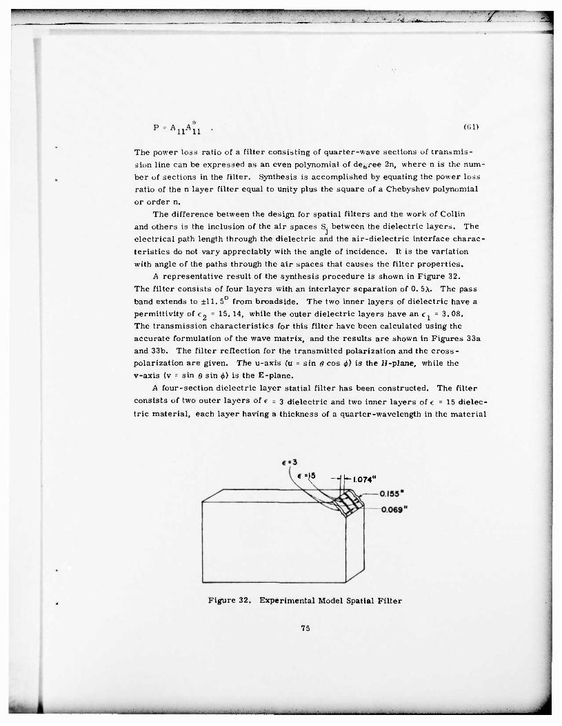
..... • . •• .j f.,, . , .. v , „ . i „i, ,. ,1, . i Mllll iiJJi.MPwi^y.iL •HUIRUWJ j«.m^: jjnpyw^ppniptf.WMJ'1! . jm»m»m*Wjm..»ii**.vmi!jwuwMWmfi 'HEU! \.vm*.t
AuAu (61)
The power loss ratio of a filter consisting of quarter-wave sections of transmis- sion line can be expressed as an even polynomial of debree 2n, where n is the num- ber of sections in the filter. Synthesis is accomplished by equating the power loss ratio of the n layer filter equal to unity plus the square of a Chebyshev polynomial or order n.
The difference between the design for spatial filters and the work of Collin and others is the inclusion of the air spaces S. between the dielectric layers. The electrical path length through the dielectric and the air-dielectric interface charac- teristics do not vary appreciably with the angle of incidence. It is the variation with angle of the paths through the air spaces that causes the filter properties.
A representative result of the synthesis procedure is shown in Figure 32. The filter consists of four layers with an interlayer separation of 0. 5X. The pass band extends to ±11. 5 from broadside. The two inner layers of dielectric have a permittivity of c„ = 15. 14, while the outer dielectric layers have an e, = 3.08. The transmission characteristics for this filter have been calculated using the accurate formulation of the wave matrix, and the results are shown in Figures 33a and 33b. The filter reflection for the transmitted polarization and the cross- polarization are given. The u-axis (u = sin 0 cos <ji) is the H-plane, while the v-axis (v = sin 9 sin <f>) is the E-plane.
A four-section dielectric layer statial filter has been constructed. The filter
consists of two outer layers of e = 3 dielectric and two inner layers of« =15 dielec- tric material, each layer having a thickness of a quarter-wavelength in the material
*~'\ Hh 1074"
Figure 32. Experimental Model Spatial Filter
75
— , ,

_ • .:. ,* "', '" '•£..• iim . . r ^
4-LAYER CHEBYSHEV «. = 3.08 «2=15.14
0 O.I 0.2 0.3 0.4 0.5 0.6 07 0.8 0.9 1.0
u = sin 80 cos 4>0
4-LAYER CHEBYSHEV «,»3.08
b)
0 0.1 0 2 0 3 0.4 0.5 0.6 0.7 0.8 0.9 1.0
u = s i n <9 cos«* O ' o
Figure 33. Characteristics of Fxperimental Filter
7fi

immmmuu—.'"i"-«»—.' '«• •'••» •—» "•'»'•""".-' ».jiioit,,;-»^»! ^ .111,11»—»^^win ..uuniuin»" 'i'5»"i»"i »»im,n . : " "WM I ^IM I
I 7
at 11 GHz. The spacing between layers is a free-space wavelength at 11 GHz.
Each layer is approximately 25 X 75 cm in planar extent, and styrofoam is used
between layers for stability.
Preliminary tests of this filter have been made using an array source. In
Figure 34 are shown the radiation patterns of the array alone and the array with
the filter. This array has a set of grating lobes that can be easily distinguished.
Note that the filter attenuated those lobes falling within the stopband of the filter,
but did not attenuate the grating lobe at 0 = GO , which is within the second pass-
band of the filter.
-2
-4
-61-
-8
-10
-12
-14
-16
-18
2 -20
ÜJ "22 ;
-i.4
-26
-28
-30
-32
-34
ARRAY PATTERN
WITHOUT FILTER WITH FILTER
-48 -36
Figure 34. Grating Lobe Suppression 1 sing the Experimental Filter
Although this preliminary study has been conducted using dielectric layers,
the use of metallic grid structures has obvious advantages in both weight and cost
as compared with dielectric layer- filters. Under the assumption that mutual
coupling can be neglected, the grid structures become shunt susceptances, and the
77
— -

p*.iiumL..unimuMi.w| ••"•'• " .HI . .n.M. mi ii •'.•• ,IL. i.. . vi» in-ji.^injpiw'if-wLi-^v-nvsfv» T
synthesis technique.^ described by Mathai and Young ' tan be used directly. To
date there are no rigorous analytical results available that treat the problem of
combining several unequal wire grids as required for spatial filter analysis.
Aside from the work described here, there is relatively little known about the
characteristics of such spatial filters and then- sidelobe suppression qualities.
The example concerned the special case of a limited scan array with grating lobes,
and even near the array the fields can be characterized by well defined plane waves.
The array also has near fields that are characterized as nonpropagating waves
(reactive fields), but these did not appear to have any significant influence on the
experimental results. Remaining questions include what benefit the spatial filter
can offer for far sidelobes that are due to random phase shifter errors or for side-
lobes due to aperture blockage.
Preliminary results indicate that although the filter will obviously not improve
the gain already reduced by blockage, it can reduce the resulting far sidelobe
structure. In addition to studies of metallic grating structures for use as filter-
elements, there is thus a need for studying near-field effects such U the use of a
filter near small diffrating obstacles, and in the presence of fields with pseudo-
random phase variations. The potential advantages of the use of such filters is
very great, but substantial research is required before this potential can be
realized.
."». CONCH MOV
The purpose of this paper has been to provide some data that can be useful in
predicting general trends in phased array technology over the next few years, and
to identify pertinent research areas that will rapport this technology. The method
chosen for developing these conclusions has been to describe some of UM history
of phased array research and then to show evidence of the acceleration pact of
technological innovation. I believe this changing technology will uncover even
more fundamental topics for array research than have been studied in prior years.
Stimulus for this growth is provided by military requirements for radar and
communication; in particular by the need for rapid scanning, wide or multiple
bandwidths, very low sidelobes, null steering and the constraints imposed by cost,
size and in some cases the physical environment near the arrav. Horn of this
increased activity and these new stimuli is the "special purpose arrav;' a collec-
tion of many different array types that are each designed to satisfy only one set of
lf>0. Mathai, 0., Young, I.., and Jones, K.M.T. (1964) Microwave Filters. Impedance Matching Networks and Coupling Structures, New York, McGraw-Hill, Chapter 9.
78

'-"••"•• •' 1 i ' m*fPW»BWii|BWs IIIIWIIU . I
/
requirements, and are economically viable because they trade off other capability not related to any primary requirement. The growth of this collection of arrays has become so rapid as to provide a major focal point for activity in electromag- netic research. Added to this variety of new topics, there is antenna technology growing in response to the availability of solid state devices; this has caused development of a variety microstrip and stripline antennas which are quite funda- mental new radiators with properties not yet fully investigated.
Finally, there is an area of growth that is occurring in response to uniquely military requirements, wideband antennas for ECM, multiple frequency antennas for satellite communication, extra low sidelobe and null steered arrays for ECCM radiation defense. Taken together, these forces have produced a major change in the direction of array research, and a need for increased research activity on a widening variety of topics within the general subject of array antennas.
79

' ' in » mi-mil Bipi.ii.m^m P i»»WCTP»mi II ,,.„..„..*.,,., IP, 11«, ,. '-"• • -•••-' •.»--»-Tr T ^
References
1. Levine, H. , and Schwinger, J. (1950, 1951) On the theory of electromagnetic wave diffraction by an aperture in an infinite plane conducting screen, Comm. on Pure and Applied Math 44:355-391.
2. Hallen, Erik (1938) Theoretical investigations into transmitting and receiving antennae, Nova Acta Regiae Soc. Sei. Upsaliensis (4) ll(No. 1).
3. King, R.W.P., and Harrison, C. W. (1969) Antennas and Waves, A Modern Approach, MIT Press, Cambridge, MA, (See Section 3. 10).
4. Bouwkamp, C.J. (1954) Diffraction theory, Reports on Progress in Physics n:35-100.
5. Mailloux, R. J. (1969) Radiation and near-field coupling between two collinear open-ended waveguides, IEEE Trans. AP-17(No. l):49-55.
6. Lewin, L. (1970) On the inadequacy of discrete mode-matching techniques in some waveguide discontinuity problems, IEEE Trans. MTT-18(No. 7): 364-372.
7. Brouillion, L. (1953) Wave Propagation in Periodic Structures. Dover Publications, Inc.
8. Seckelmann, R. (1966) Propagation of TE modes in dielectric loaded wave- guides, IEEE Trans. MTT-14:518-527.
9. Collin, R.E. (1960) Field Theory of Guided Waves, McGraw-Hill Book Co., Inc., New York.
10. Borgiotti, G. V. (1971) Edge effects in finite arrays ol uniform slits on a groundplane, IEEE Trans. AP-19(No. 5):593-599.
11. Wasylkhvskvj, W. (1973) Mutual coupling effects in semiinfinite arrays, IEEE Trans. AP-21(No. 3):277-285.
12. Amitay, N., Galindo, V., and Wu, C.P. (1972) Theory and Analysis of Phased Array Antennas, New York, Wiley Interscience.
13. Carter, P.S., Jr. (1960) Mutual impedance effects in large beam scanning arrays, IRE Trans. AP-8:276-285.
81
HU jiujiimin.i ,i it i LULU-, 'mi "'•~"i »»imp iipi.i,iipii«iiiii.iim!|Mi»igjiti!nwit'u. iuii|imi|iin| T
14. King, R.W. P. (1956) The Theory of Linear Antennas, Harvard University Press, Cambridge, MA.
15. King, R.W. P., and Sandler, S.S. (1964) The theory of broadside arrays, and the theory of endfire arrays, IEEE Trans on Antennas and Propagation AP-12:269-275, 276-280.
16. Harrington, R.F. (1968) Field Computation by Moment Methods, McMillan Co., New York.
17. Harrington, R.F., and Mautz, J.R. (1967) Straight wires with arbitrary excitation and loading, IEEE Trans. AP-15(No. 4):502-515.
18. Lewin, L. (1951) Advanced Theory of Waveguides, Iliffe and Sons, Ltd., London, Chapter 6.
19. Cohen, M.H., Crowley, T.H., and Levis, C.A. (1951) The Aperture Admit- tance of a Rectangular Waveguide Radiating into a Half Space, (ATI-133707) Antenna Laboratory, Ohio State University, Research Foundation, Rept. 339-22.
20. Wheeler, G. W. (1950) Coupled Slot Antennas, Ph.D. Thesis, Harvard University, Cambridge, MA.
21. Levis, C.A. (1956) Variational Calculations of the Impedance Parameters of Coupled Antennas, Ohio State University Research Foundation, Rept. 667-16, Contract AF33(616)3353.
22. Galejs, J. (1965) Self and mutual admittances of waveguides radiating into plasma layers. Radio Sei, J. Res. NBS/USNC-URSI 69D(No. 2):179-189.
23. Richmond, J. H. (1961) A reaction theorem and it's applications to antenna impedance calculations, IRE Trans AP AP-8:515-520.
24. Lyon, J.A.M., Kalafus, R. M., Kwon, Y.K., Diegenis, C.J., Ibrahim, M.A.H., and Chen, C. C. (1966) Derivation of Aerospace Antenna Coupling — Factor Interference Predication Techniques, Tech. Rept. AFAL-TR-66-57, The University of Michigan, Radiation Laboratory.
25. Mailloux, R.J. (1969) Radiation and near-field coupling between two collinear open-ended waveguides, IEEE Trans on Antennas and Propagation AP-17: (No.l):49-55.
26. Mailloux, R.J. (1969) First-order solutions for mutual coupling between waveguides which propagate two orthogonal modes, IEEE Trans. AP-17: 740-746.
27. Bailey, M.C. (1974) Finite planar array of circular waveguide apertures in flat conductor, IEEE Trans. AP-22:178-184.
28. Steyskal, H. (1974) Mutual coupling analysis of a finite planar waveguide array, IEEE Trans. AP-22:594-597.
29. Knittel, G. H., Hessel, A., and Oliner, A.A. (19R8) Element pattern nulls in phased arrays and their relation to guided waves, Proc. IEEE 56:1822- 1836. ~~
30. Lechtreck, L. W. (1965) Cumulative coupling in antenna arrays, IEEE G-AP International Symposium Digest, 144-149.
31. Oliner, A.A., and Malech, R. G. (1966) Speculation on the role of surface waves. Microwave Scanning Antennas, Academic Press, N. Y., Vol. 2, 308-322.
32. Farrell, G. F., Jr., and Kuhn, D.H. (1966) Mutual coupling effects of triangular-grid arrays by modal analysis, IEEE Trans. AP-14;652-H54.
82
_J

IM»«.I ••T»uj||iii.t..ia...i»!.»•,..um i.inn ii»»,ii.,ij»i,i'^»" ,».i•'!*!.HU i|iimi!iw.wli«»ii"|.|B'wnnwy» r ' ^
1
33. Farrell, G. F., Jr., and Kuhn, D.H. (1968) Mutual coupling in infinite planar arrays of rectangular waveguide horns, IEEE Trans. A P-10:405- 414.
34. Amitay, X., and Galindo, V. (1908) The analysis of circular waveguide phased arrays. Bell System Technical Journal, 1003-1032.
35. DuFort, E. C. (1968a) Design of corrugated plates for phased array match- ing, IEEE Trans. A P-10:3 7-40.
36. DuFort, E.G. (1068a) A design procedure for matching volumetrically scanned waveguide arrays, Proc. IEEE 56:1851-1860.
37. Mailloux, R.J, (1972) Surface waves and anomalous wave radiation nulls on phased arrays of TEM waveguides with fences, IEEE Trans. AP-20: 160-166. ~
38. Bates, R.II.T. (1065) Mode theory approach to arrays, IEEE Trans, and Propagation (Communications) AP-13-.321-322.
39. Byron, E.V., and Frank, J. (1068a) Lost beams from a dielectric covered phased-array aperture, IEEE Trans. AP-10:496-499.
40. Ilannan, P. W. (1067) Discovery of an array surface wave in a simulator, IEEE Trans. A P-15;574-576.
41. Gregorwich, W. S., Hessel, A., Knittel, G.U., and Oliver, A.A. (1068) A waveguide simulator for the determination of a phased-array resonance, IEEE G-AP International Symposium Digest, 134-141.
42. Frazita, R. F. (1967) Surface-wave behavior- of a phased array analyzed by the grating-lobe series, IEEE Trans. AP-15 :823-824.
43. Parad, L.I. (1967) The input admittance to a slotted array with or without a dielectric sheet, IEEE Trans. (Communications) AP-15:302-304.
44. Galindo, V., and Wu, C. P. (1968) Dielectric loaded and covered rectangular waveguide phased arrays, Bell System Technical Journal 47:93-116.
45. Wu, C.P. , and Galindo, V. (1968) Surface wave effects on dielectric sheathed phased arrays of rectangular waveguides, Bell System Technical Journal 47:117-142.
46. Borgiotti, G. V. (1968) Modal analysis of periodic planar phased arrays of apertures, IEEE Proc. 56:1881-1892.
47. Allen, J. L. (1965) On surface-wave coupling between elements of large arrays, IEEE Trans. A P-13:038-639.
4P. Lechtreck, L.W. (1968) Effects of coupling accumulation in antenna arrays, IEEE Trans. AP-16:3 1-37.
49. Diamond, B. L. (1068) A generalized approach to the analysis of infinite planar array antennas, Proc IEEE 56(No. 11): 1837-1851.
50. oliner, A.A., and Malech, R. G. (1964) Speculation on the Role of Surface Waves, Microwave Scanning Antennas, Academic Press, \. Y. , Vol. 2, 308-322.
51. Ehlenberger, A.G. , Schwartzman, F., and Topper, 1.. (1068) Design criteria for linearly polarized waveguide arrays, IEEE Proc. 56(No. 11): 1861-1872.
52. Byron, E.V., and Frank, J. (1968b) On the correlation between wideband arrays and array simulators, IEEE Trans. (Communications) AP-16: 601-003.
83
_
———^W—W^• I •» «».• I II WIJP^^WW^I II 1^^^^^^»P»^ I . •„„..,••,. .,.,„-. ., , 7"
53. Hess el, A., and Knittel, G. H. (19(>9) A loaded groundplane for the elimination of blindness in a phased-array antenna, IEEE G-AP International Symposium Digest, 163-169.
54. Knittel, G.I1. (1970) The choice of unit-cell size for a waveguide phased array and its relation to the blindness phenomenon, Presented at Boston Chapter Antennas and Propagation Group Meeting.
55. Hessel, A., and Knittel, G. H. (1970) On the prediction of phased array resonances by extrapolation from simulator measurements, IEEE Trans. Antennas and Propagation (Communications) AP-18:121-123.
56. Mailloux, R.J. (1971) Blind Spot Occurrence in Phased Arrays — When to Expect It and How to Cure It, AFCRL-71-0428, Physical Sciences Research Papers, No. 4f>2, Air Force Cambridge Research Laboratories.
57. lee, S.W., and Jones, W. R. (1971) On the suppression of radiation nulls and broadband impedance matching of rectangular waveguide phased arrays, IEEE Trans. AP-19:41-51.
58. Lee, S.W. (19(i7) Radiation from the infinite aperiodic array of parallel-plate waveguides, IEEE Trans. AP-15(No. 5):598-(i0fi.
59. Harrington, R. F. (1967) Matrix methods for field problems, Proc. IEEE 55 (No. 2):136-149.
(10. Amitay, N., Galindo, V., and Wu, C.P. (1972) Theory and Analysis of Phased Array Antennas, New York, Wiley-Interscience.
61. Harrington, R.F., and llautz, J.R. (1975) A Generalized Network Formulation for Aperture Problems, AFCRL-TR-75-0589, Scientific Report No. 8, Contract F19628-73-C-0047.
f)2. Shellev, B. (19(i8) A matrix-fed circular array for continuous scanning, IEEE Proe. 56(No. U):201G-2027.
63. Holley, A. E., et al (1974) An electronically scanned beacon antenna, IEEE Trans. AP-22:3-12.
64. Bogner, B.F. (1974) Circularly symmetric r. f. commutor for cylindrical phased arrays, IEEE Trans." AP-22:78-81.
65. Boyns, J.E., et al (1970) Step-scanned circular-array antenna, IEEE Trans. AP-18(No. 5):590-595.
66. Munger, A.D., et al (1974) Conical array studies, IEEE Trans. AP-22:35-4.j.
(i7. Hsiao, J.K., and Cha, A.G. (1974) Patterns and polarizations of simultan- eously excited planar arrays on a conformal surface, IEEE Trans. A P-22: 81-84. "
68. Gobert, W.B., and Young, R.F.II. (1974) A theory of antenna array con- formal to surface revolution, IEEE Trans. A P-22:87-91.
69. Tsandoulas, G.S., and Willwerth, F. G. (1973) Mutual coupling in concave cylindrical arrays, Microwave Journal lfi(\'o. 10):29-32.
70. Borgiotti, G. V. , and Balzano, Q. (1970) Mutual coupling analysis of a con- formal array of elements on a cylindrical surface, Trans. IEEEAP-18: 55-113.
71. Borgiotti, CI. V., and Balzano, Q. (1972) Analysis of element pattern design of periodic array of circular apertures on conducting cylinders, IEEE Trans. AP-20:547-553.
72. Balzano, Q. , and Dow ling, T.B. (1974) Mutual coupling analysis of arrays of aperture on cones (Communications), IEEE Trans. AP-22:92-97.
84
u_L
" mmim^mmmrm^^mr' m i •»•..' — "»•» IM—Mi»»j»!''^w*ii^^»iwiwipww»»»y«ipwi^w--^.;.'«i«iw • n HII.IUFHHIPJI »•
73. Golden, K. E., et al (1974) Approximation techniques for the mutual admit- tance of slot antennas in metallic coned, IEEE Trans. A P-22:44-48.
74. J. Shapira, et al (1974) Ray analysis of conformal array antennas, IEEE Trans. AP-22:49-n3.
75. Stevskal, H. (1974) Mutual coupling analysis of cylindrical and conical arrays, IEEE/AP-S Int. Symp. Record, 293-294.
7(i. Maune, J.J. (1972) An SHF airborne receiving antenna, Twenty Second Annual Symposium on FSAF Antenna Research and Development.
77. Villeneuve, A.T., Behnke, M.C., and Kummer, W.U. (1973) Hemispheri- cally Scanned Arrays, AFCRL-TR-74-0084, Contract No. F19fi28-72-C- 0145, Scientific Report No. 2. Also, see 1974 International IEEE AP-S Symposium Digest, 3(>3-3(ifi.
78. Balzano, O. , Lewis, L.R., and Siwiak, K. (1973) Analysis of Dielectric Slab-Covered Waveguide Arrays on Large Cylinders, AFCRL-TR-73-0587, Contract .Mo. F19(i28-72-C-0202, Scientific Report No. 1.
79. Schwartzman, L., and Stängel, J. (1975) The dome antenna. Microwave Journal 18(No. 10):31-34.
80. Esposito, F.J., Schwartzman, L. , and Stängel, J.J. (1975) The Dome Antenna-Experimental Implementation, URSI/USNC Meeting Digest 1975, June 3-5, Commission (i.
81. Ruze, J. (1952) Physical Limitations on Antennas, MIT Research Lab. Electronics Tech. Rept. 248.
82. Miller, C. J. (19f54) Minimizing the effects of phase quantization errors in an electronically scanned array, Proc. 19H4 Symp. Electronically Scanned Array Techniques and Applications, RADC-TDR-64-225, Vol. 1, 17-38, AD448421.
83. Allen, J.L. (I960, 19(!1) Some extensions of the theory of random error effects on array patterns, in J. L. Allen et al., Phased Array Radar Studies, Tech. Rept. No. 236, Lincoln Laboratory, M.I.T.
84. Elliott, R. S. (1958) Mechanical and electrical tolerances for two-dimensional scanning antenna arrays, IRE Trans. AP-6:114-120.
85. Mcllvenna, J. F. , and Dräne, C.J. (1971) Maximum gain, mutual coupling and pattern control in array antennas, The Radio and Electronic Engineer, 4JUNo. 12):5f,9-572.
8(i. Mcllvenna, J., et al (197f>) The Effects of Excitation Errors in Null Steering Antenna Arrays, RADC-TR-7C-183, Rome Air Development Center.
87. Stängel, J.J. (1974) A basic theorem concerning the electronic scanning capabilities of antennas, URSI Commission VI, Spring Meeting.
88. Patton, W. T. (1972) Limited scan arrays, in Phased Array Antennas; Proc of the 1970 Phased Array Antenna Symposium, edited by A.A. Oliner and G. H. Knittel, Artech House, Inc., MA., 332-343.
89. Borgiotti, G. (1975) Design Criteria and Numerical Simulation of an Antenna System for One-Dimensional Limited Scan, AFCRL-TR-75-0616.
90. Silver, S. , and Pao, C. S. (1944) Paraboloid Antenna Characteristics as a Function of Feed Tilt, MIT Radiation Lab., Cambridge, MA, Rep 479.
91. Ruze, J. (1905) Lateral feed displacement in a paraboloid, IEEE Trans. Antennas Propagation AP-13:660-665.
92. Sletten, C.J., et al (1958) Corrective line sources for paraboloids, IEEE Trans. AP-(!(No. 3):239-251.
85

m, ii.i.M-l«Plf .MJ.i WMWii-P iWHtKWmvmr^!*V**l.» •ii -I • Ji.Ji I Will HJ^IIH . »7"TK*.. I -•«..» ' »if i UP^ .)^,T • ^ T-yi - r
93. Collin, R.E., and Zucker, F.J. (1969) Antennas Theory, Part 2, McGraw- Hill Book Co., New York, Chapter 17.
94. Rusch, W.V.T., and Ludwig, A.C. (1973) Determination of the maximum scan-gain contours of a beam-scanning paraboloid and their relation to the pitzval surface, IEEE Trans. Antennas Propagation, A P-21:141-147.
95. Imbraile, W.A., et al (1974) Large lateral feed displacements in a para- bolic reflector, IEEE Trans. AP-22(No. G):742-745.
96. Rudge, A.W. (19G9) Focal plane field distribution of parabolic reflectors, Electronics Letters 5:610-612.
97. Rudge, A.W., and Withers, M.J. (1971) New techniques for beam steering with fixed parabolic reflectors, Proc. IEEE 118(\o. 7):857-ii(i3.
98. Rudge, A.W., and Withers, M.J. < 19fi°) Beam-scanning primary feed for parabolic reflectors, Electronic Letters 5:39-41.
99. Rudge, A.W., and Davies, D.E.N. (1970) Electronically controllable pri- mary feed for profile-error compensation of large parabolic reflectors, Proc. IEEE 117(No. 2):351-358.
100. Winter, C. (1958) Phase scanning experiments with two reflector antenna systems, Proc. IEEE 56(No. 11):1984-1999.
101. White, W.D., and De Size, L. K. (1962) Scanning characteristics of two- reflector antenna systems, 19G2 IRE International Conv. Record. Pt. 1, 44-70.
102. Tang, C. H. (1970) Application of limited scan design for the AGILTRAC-16 antenna, 20th Annual USAF Antenna Research and Development Symposium, University of Illinois.
103. Howell, J.M. (1974) Limited Scan Antennas, IEEE/AP-S International Symposium.
104. Schell, A.C. (1972) A Limited Sector Scanning Antennas, IEEE G-AP International Symposium.
105. McGahan, R. (1975) A Limited Scan Antenna 1'sing a Microwave Lens and a Phased Array Feed, M.S. Thesis, MIT.
106. Fitzgerald, W.D. (1971) Limited Electronic Scanning with an Near Field Cassegrainian System, ESD-TR-71-271, Technical Report 484, Lincoln Laboratory.
107. Fitzgerald, W.D. (1971) Limited Electronic Scanning with an Offset-Feed Near-Field Gregorian System, ESD-TR-71-272, Technical Report 486, Lincoln Laboratory.
108. Miller, C.J., and Davis, D. (1972) LFOV Optimization Study. Final Report No. 77-0231, Westinghouse Defense and Electronic Systems Center, System Development Division, Baltimore, Md., ESD-TR-72-102.
109. Tang, C. IT. , and Winter, C. F. (1973) Study of the I'se of a Phased Array to Achieve Pencil Beam over Limited Sector Scan. AFCRL-TR-73-0482, ER 73-4292, Raytheon Co., Final Report Contract F19628-72-C-0213.
110. Tang, E., et al (1975) Limited Scan Antenna Technique Study. Final Report, AFCRL-TR-75-0448, Contract No. F19628-73-C-0129.
111. Patton, W.T. (1972) Limited scan arrays, in phased array antennas, Proc. of the 1970 Phased Array Antenna Symposium, edited by A. A. Oliner and G.IL Knittel, Artech House, Inc., MA, 332-343.
112. Manwarren, T.A., and Minuti, A.R. (1974) Zoom Feed Technique Study, RADC-TR-74-56, Final Technical Report.
86
•I ' • mwi H»MWi.n if«»l".U I HJIJIHJ I
•r 1
113. Mailloux, R.J., and Forbes, G.R. (1073) An array technique with grating- lobe suppression for limited-scan application, IEEE Trans. AP-21(No. 5): 597-fi02.
114. Tsandoulas, G.N., and Fitzgerald, \V. D. (1972) Aperture efficiency enhancement in dielectricallv loaded horns, IEEE Trans. AP-20(No. 1) 09-74.
115. Tang, R. (1972) Survey of time-delay beam steering techniques, in Phased Array Antennas, Proceedings of the 1970 Phased Array Antenna
"Symposium, Artech House Inc., MA, 254-270.
116. Mailloux, R.J. (1974) An overlapped subarrav for limited scan application IEEE Trans. AP-22.
117. Tsandoulas, G. N. (1972) Wideband limitations of waveguide arrays, Microwave Journal 15(No. 9):49-5(i.
118. Chen, C.C. (1973) Broadband impedance matching of rectangular waveguide phased arrays, IEEE Trans. AP-21:298-302.
119. Laughlin, G.J., et al (1972) Very wide band phased array antenna, IEEE Trans. AP-20:699-704.
120. Chen, C.C. (1972) Octave band waveguide radiators for wide-angle scan phased arrays, IEEE AP-S Int. Symp. Record. 376-377.
121. Lewis, L.R., Fassett, M., and Hunt, J. (1974) A broadband stripline array element, IEEE AP-S Int. Symp. Record.
122. Chen, M. H. , and Tsandouias, C. N. (1973) Bandwidth properties of quadruple- ridged circular and square waveguide radiators, IEEE AP-S Int. Symp. Record. 391-394. —
123. Tsandoulas, G.N., and Knittel, G. H. (1973) The analysis and design of dual-polarization square waveguide phased arrays, IEEE Trans. AP-21: 796-808.
124. Hsiao, J. K. (1971) Analysis of interleaved arrays of waveguide elements IEEE Trans. AP-19:729-735.
125. Boyns, J.E., and Provencher, J.H. (1972) Experimental results of a multi- frequency array antenna, IEEE Trans. AP-20:106-107.
126. Hsiao, J. K. (1972) Computer aided impedance matching of a interleaved waveguide phased array, IEEE Trans. AP-20:505-506.
127. Harper, W. H., et al (1972) NRL Report No. 7369, Naval Research Laboratory.
128. Munson, R. E. (1974) Conformal microstrip antennas and microstrip phased arrays, IEEE Trans. AP-22:74-78.
129. Howell, J.Q. (1975) Microstrip antennas, IEEE Trans. AP-23:90-93.
130. Kaloi, C. (1975) Asymmetrically Fed Electric Microstrip Dipole Antenna, TR-75-03, Naval Missile Center, Point Magee, CA.
131. Derneryd, A. (1976) Linearly polarized microstrip antennas, IEEE Trans. AP-24:846.
132. Microwave Journal, Special Issue (1977) Solid State power, 20(No.2).
133. Stern, E., and Tsandoulas, G. N. (1975) Ferroscan: Toward continuous- aperture scanning, IEEE Trans. AP-23(No. l):15-20.
134. Walton, J. D., ed:tor (1970) Radome Engineering Handbook, Georgia Tech.
87
J
•'•" • " ' ' -y
135. Wait, J.R. (1976) Theories of scattering from wire grid and mesh struc- tures, Proc. of National Conference on Electromagnetic Scattering, University of Illinois.
136. Collin, R.E. (1955) Theory and design of wideband multisection quarter- wave transformers, Proc. IRE 43(No. 2):179-185.
137. Collin, R.E. (1960) Field Theory of Guided Waves, McGraw-Hill, 79-93. 138. Kieburtz, R.B., and Ishimaru, A. (1962) Aperture fields of an array of
rectangular apertures, IRE Trans. AP-9:663-671. 139. Chen, C.C. (1971) Diffraction of electromagnetic waves by a conducting
screen perforated periodically with circular holes, IEEE Trans. MTT-19 (No. 5):475-481.
140. Pelton, E.L., and Monk, B.A. (1974) A streamlined metallic radome, IEEE Trans. AP-22(No. 6):799-804.
141. Luebbers, R.J. (1976) Analysis of Various Periodic Slot Array Geometries Using Modal Matching, Report AFAL-TR-75-119, Ohio State University.
142. Monk, B.A., et al (1974) Transmission through a two layer array of loaded slots, IEEE Trans. AP-22:804-809.
143. Young, L., Robinson, L., and Hacking, C. (1973) Meanders-line polarizer, IEEE Trans. AP-21:376-378.
144. Lerner, D.S. (1965) A wave polarization converters for circular polariza- tion, IEEE Trans. AP-13:3-7.
145. Mailloux, R.J. (1976) Synthesis of spatial filters with Chebyshev character- istics, IEEE Trans. Antennas and Propagation AP-24(No. 2)174-181.
146. Conn, S. B. (1955) Optimum design of stepped transmission-line trans- formers, IRE Trans. MTT MTT-3(No. 2)16-21.
147. Riblet, H.J. (1957) General synthesis of quarter-wave impedance trans- formers, IRE Trans. MTT MTT-5(No. 1)3 6-43.
148. Young, L. (1959) Tables for cascaded homogeneous quarter-wave trans- formers, IRE Trans. MTT MTT-7(No. 2)233-244.
149. Young, L. (1962) Stepped-impedance transformers and filter prototypes, IRE Trans. MTT MTT-10(No. 5):339-359.
150. Mathai, G., Young, L., and Jones, E.M. T. (1964) Microwave Filters. Impedance Matching Networks and Coupling Structures. New York, McGraw-Hill, Chapter 9.
88
-**" —— —•'.".• ''•< »;
•r
MFrmic SYSTEM
BASE UNITS:
Quantity
length mass time electric current thermodynamk temperature amount of substance luminous intensity
SUPPLEMENTARY UNITS:
plane angle solid angle
DERIVED UNITS:
Acceleration activity (of a radioactive source) angular acceleration angular velocity area density electric capacitance electrical conductance electric field strength electric inductance electric potential difference electric resistance electromotive force energy entropy force frequency illuminance luminance luminous flux magnetic field strength magnetic flux magnetic flux density magnetomotive force power pressure quantity of electric ily quantity of heat radiant intensity specific heat stress thermal conductivity velocity viscosity, dynamic viscosity, kinematic voltage volume wavenumber work
Unit SI Symbol Formula
metre kilogram second ampere kelvin mole candela
radian steradian
» A K
rad •r
metre per second squared disintegration per second radian per second squared radian per second square metre kilogram per cubic metre farad Siemens volt per metre henry volt ohm volt joule joule per kelvin newton hertz lux candela per square metre lumen ampere per metre webet tesla ampere watt pascal coulomb joule watt per steradian joule per kilogram-kelvin pascal watt per metre-kclvin metre per second pascal-second square metre per second volt cubic metre reciprocal metre joule
K S
H V
V I
N Ht Ix
im
Wb T A W Pa C I
V
i
m/s (disintegration Vi rad/s rad/s m kg/m A-s/V A/V V/m V-s/A W/A V/A W/A N-m I* kg-mJs (cycle)/* Im/m cd/m cd-sr A/m V» Wb/m
a* N/m At N-m W/sr |/kg-K N/m W/m-K m/s Pe-f m/s W/A m (wBve)'m N-m
SI PREFIXES:
Multiplication Factors
A
1 oooooooooooo - 10" 1 000 000 000 • 10*
1 000 000 • 10* 1 000 • 10' 100= 10» 10= 10' 0.1 = 10"' 001 = 10-*
0 001 = io-' 0 000 001 • 10"*
0 000 000 001 « 10"* 0.000 000 000 001 - io- "
o.ooo no« oon ooo ooi to-" 000(1 000 000 000 1100 001 10 IM
To be avoided where possible
Prefix
tera S'H« mega kilo hacto* deka* decl* cenll* mllli micro nano pIco iHfnlo atto
SI Symbol
T C. M k h da d c m
n

Al LM
LU m
•
«
• r 0;X L r
&