hdl compiler for verilog rm: 8. writing circuit descriptions
TRANSCRIPT
v2000.05 HDL Compiler for Verilog Reference Manual
8Writing Circuit Descriptions 8
You can write many logically equivalent descriptions in Verilog todescribe a circuit design. However, some descriptions are moreefficient than others in terms of the synthesized circuit’s area andspeed. The way you write your Verilog source code can affectsynthesis.
This chapter describes how to write a Verilog description to ensurean efficient implementation. Topics include
• How Statements Are Mapped to Logic
• Don’t Care Inference
• Propagating Constants
• Synthesis Issues
• Designing for Overall Efficiency
/ 8-1HOME CONTENTS INDEX
v2000.05 HDL Compiler for Verilog Reference Manual
Here are some general guidelines for writing efficient circuitdescriptions:
• Restructure a design that makes repeated use of several largecomponents, to minimize the number of instantiations.
• In a design that needs some, but not all, of its variables or signalsstored during operation, minimize the number of latches or flip-flops required.
• Consider collapsing hierarchy for more-efficient synthesis.
How Statements Are Mapped to Logic
Verilog descriptions are mapped to logic by the creation of blocks ofcombinational circuits and storage elements. A statement or anoperator in a Verilog function can represent a block of combinationallogic or, in some cases, a latch or register.
When mapping complex operations, such as adders and subtracters,Design Compiler inserts arithmetic operators into the design as levelsof hierarchy.
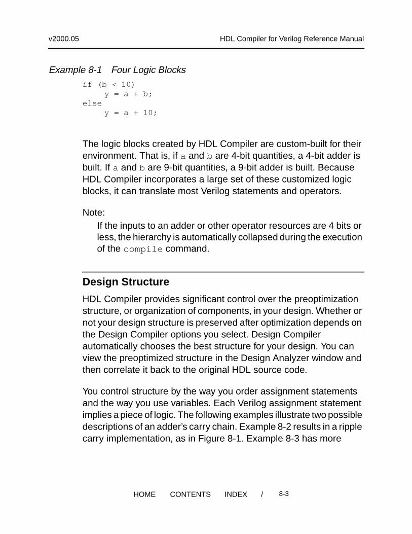
The description fragment shown in Example 8-1 represents four logicblocks:
• A comparator that compares the value of b with 10
• An adder that has a and b as inputs
• An adder that has a and 10 as inputs
• A multiplexer (implied by the if statement) that controls the finalvalue of y
/ 8-2HOME CONTENTS INDEX
v2000.05 HDL Compiler for Verilog Reference Manual
Example 8-1 Four Logic Blocksif (b < 10)
y = a + b;else
y = a + 10;
The logic blocks created by HDL Compiler are custom-built for theirenvironment. That is, if a and b are 4-bit quantities, a 4-bit adder isbuilt. If a and b are 9-bit quantities, a 9-bit adder is built. BecauseHDL Compiler incorporates a large set of these customized logicblocks, it can translate most Verilog statements and operators.
Note:If the inputs to an adder or other operator resources are 4 bits orless, the hierarchy is automatically collapsed during the executionof the compile command.
Design Structure
HDL Compiler provides significant control over the preoptimizationstructure, or organization of components, in your design. Whether ornot your design structure is preserved after optimization depends onthe Design Compiler options you select. Design Compilerautomatically chooses the best structure for your design. You canview the preoptimized structure in the Design Analyzer window andthen correlate it back to the original HDL source code.
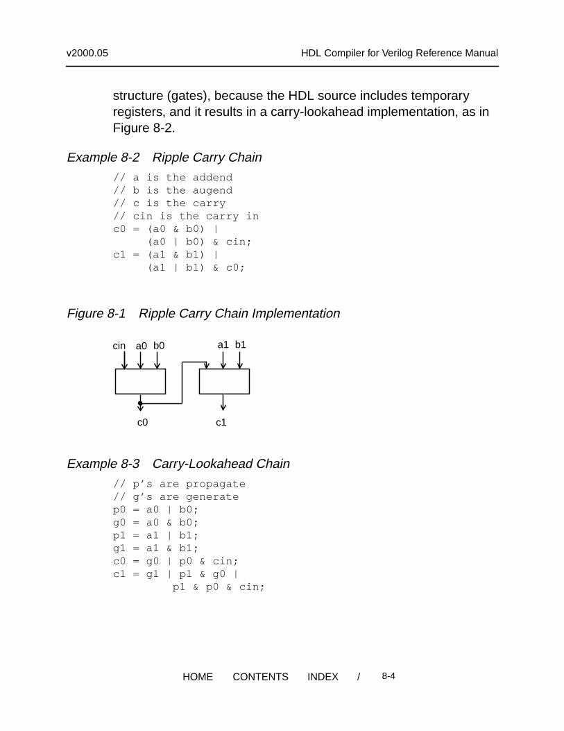
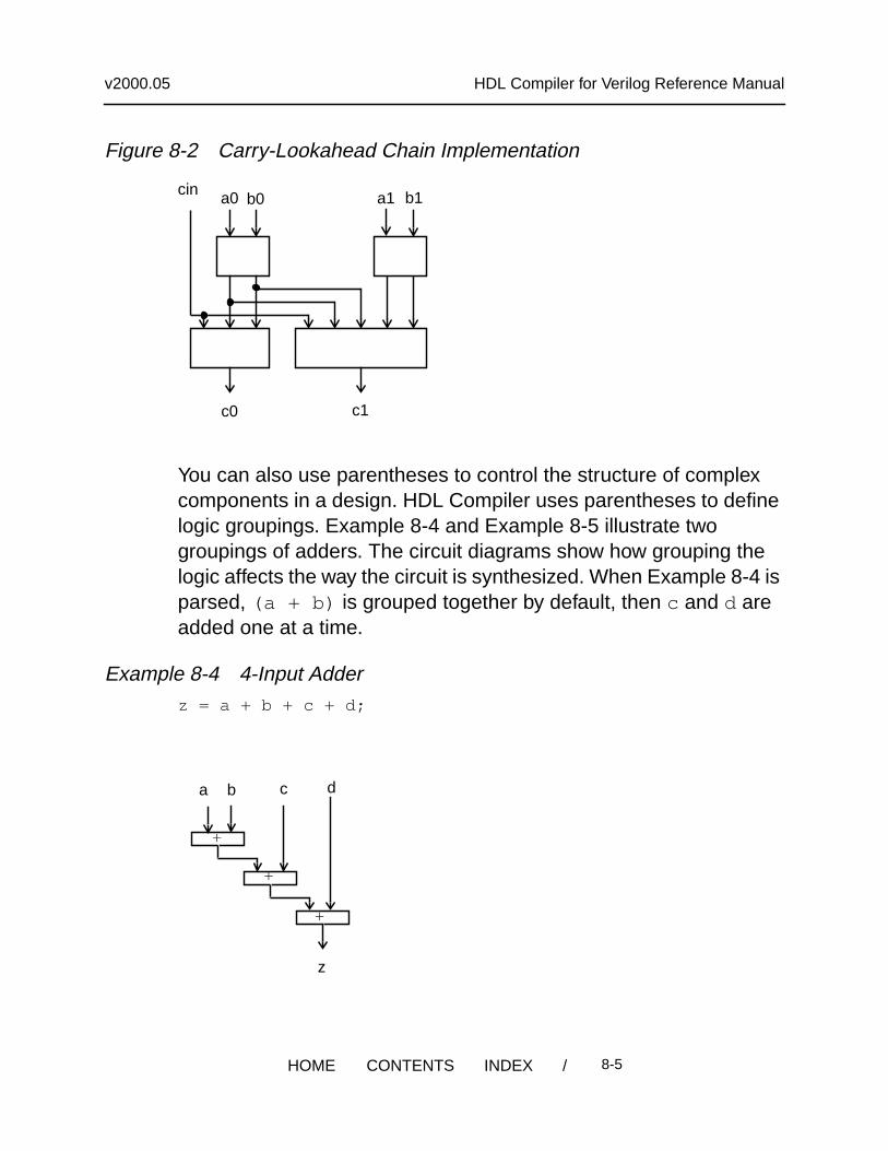
You control structure by the way you order assignment statementsand the way you use variables. Each Verilog assignment statementimplies a piece of logic. The following examples illustrate two possibledescriptions of an adder’s carry chain. Example 8-2 results in a ripplecarry implementation, as in Figure 8-1. Example 8-3 has more
/ 8-3HOME CONTENTS INDEX
v2000.05 HDL Compiler for Verilog Reference Manual
structure (gates), because the HDL source includes temporaryregisters, and it results in a carry-lookahead implementation, as inFigure 8-2.
Example 8-2 Ripple Carry Chain// a is the addend// b is the augend// c is the carry// cin is the carry inc0 = (a0 & b0) | (a0 | b0) & cin;c1 = (a1 & b1) | (a1 | b1) & c0;
Figure 8-1 Ripple Carry Chain Implementation
Example 8-3 Carry-Lookahead Chain// p’s are propagate// g’s are generatep0 = a0 | b0;g0 = a0 & b0;p1 = a1 | b1;g1 = a1 & b1;c0 = g0 | p0 & cin;c1 = g1 | p1 & g0 | p1 & p0 & cin;
a0cin a1 b1b0
c0 c1
/ 8-4HOME CONTENTS INDEX
v2000.05 HDL Compiler for Verilog Reference Manual
Figure 8-2 Carry-Lookahead Chain Implementation
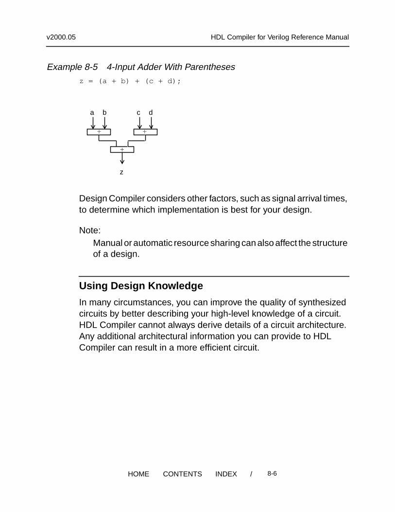
You can also use parentheses to control the structure of complexcomponents in a design. HDL Compiler uses parentheses to definelogic groupings. Example 8-4 and Example 8-5 illustrate twogroupings of adders. The circuit diagrams show how grouping thelogic affects the way the circuit is synthesized. When Example 8-4 isparsed, (a + b) is grouped together by default, then c and d areadded one at a time.
Example 8-4 4-Input Adderz = a + b + c + d;
a0 b0
c1c0
cin a1 b1
+
+
+
a b c d
z
/ 8-5HOME CONTENTS INDEX
v2000.05 HDL Compiler for Verilog Reference Manual
Example 8-5 4-Input Adder With Parenthesesz = (a + b) + (c + d);
Design Compiler considers other factors, such as signal arrival times,to determine which implementation is best for your design.
Note:Manual or automatic resource sharing can also affect the structureof a design.
Using Design Knowledge
In many circumstances, you can improve the quality of synthesizedcircuits by better describing your high-level knowledge of a circuit.HDL Compiler cannot always derive details of a circuit architecture.Any additional architectural information you can provide to HDLCompiler can result in a more efficient circuit.
+
+
z
+
a b c d
/ 8-6HOME CONTENTS INDEX
v2000.05 HDL Compiler for Verilog Reference Manual
Optimizing Arithmetic Expressions
Design Compiler uses the properties of arithmetic operators (suchas the associative and commutative properties of addition) torearrange an expression so that it results in an optimizedimplementation. You can also use arithmetic properties to control thechoice of implementation for an expression. Three forms of arithmeticoptimization are discussed in this section:
• Merging cascaded adders with a carry
• Arranging expression trees for minimum delay
• Sharing common subexpressions
Merging Cascaded Adders With a Carry
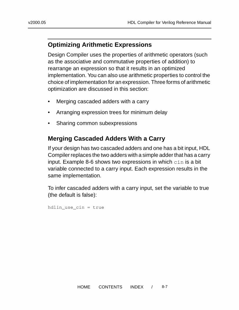
If your design has two cascaded adders and one has a bit input, HDLCompiler replaces the two adders with a simple adder that has a carryinput. Example 8-6 shows two expressions in which cin is a bitvariable connected to a carry input. Each expression results in thesame implementation.
To infer cascaded adders with a carry input, set the variable to true(the default is false):
hdlin_use_cin = true
/ 8-7HOME CONTENTS INDEX
v2000.05 HDL Compiler for Verilog Reference Manual
Example 8-6 Cascaded Adders With Carry Inputz <= a + b + cin;
t <= a + b;z <= t + cin;
Arranging Expression Trees for Minimum Delay
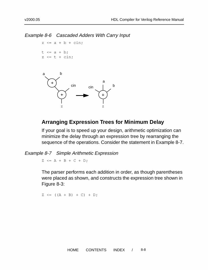
If your goal is to speed up your design, arithmetic optimization canminimize the delay through an expression tree by rearranging thesequence of the operations. Consider the statement in Example 8-7.
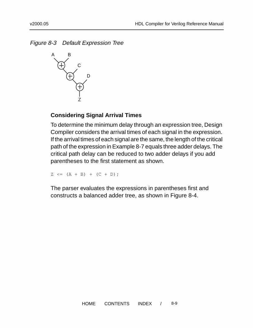
Example 8-7 Simple Arithmetic ExpressionZ <= A + B + C + D;
The parser performs each addition in order, as though parentheseswere placed as shown, and constructs the expression tree shown inFigure 8-3:
Z <= ((A + B) + C) + D;
a b
cin cin
ab
z z
/ 8-8HOME CONTENTS INDEX
v2000.05 HDL Compiler for Verilog Reference Manual
Figure 8-3 Default Expression Tree
Considering Signal Arrival Times
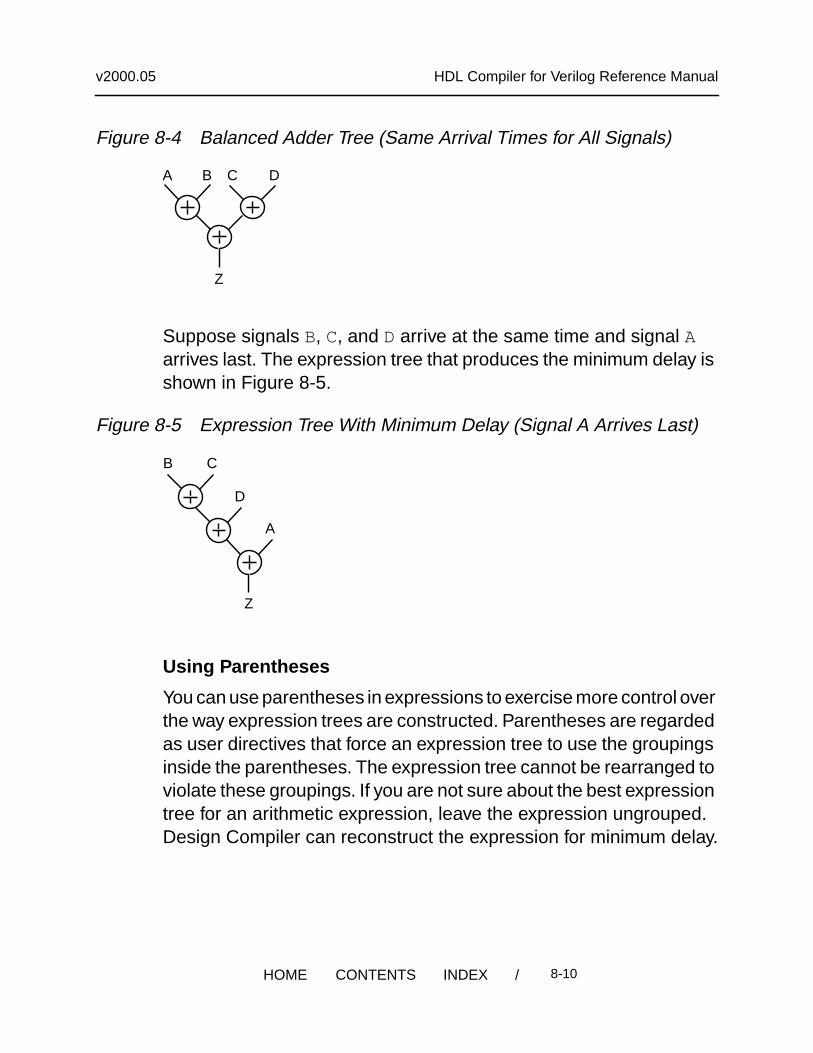
To determine the minimum delay through an expression tree, DesignCompiler considers the arrival times of each signal in the expression.If the arrival times of each signal are the same, the length of the criticalpath of the expression in Example 8-7 equals three adder delays. Thecritical path delay can be reduced to two adder delays if you addparentheses to the first statement as shown.
Z <= (A + B) + (C + D);
The parser evaluates the expressions in parentheses first andconstructs a balanced adder tree, as shown in Figure 8-4.
A B
C
D
Z
/ 8-9HOME CONTENTS INDEX
v2000.05 HDL Compiler for Verilog Reference Manual
Figure 8-4 Balanced Adder Tree (Same Arrival Times for All Signals)
Suppose signals B, C, and D arrive at the same time and signal Aarrives last. The expression tree that produces the minimum delay isshown in Figure 8-5.
Figure 8-5 Expression Tree With Minimum Delay (Signal A Arrives Last)
Using Parentheses
You can use parentheses in expressions to exercise more control overthe way expression trees are constructed. Parentheses are regardedas user directives that force an expression tree to use the groupingsinside the parentheses. The expression tree cannot be rearranged toviolate these groupings. If you are not sure about the best expressiontree for an arithmetic expression, leave the expression ungrouped.Design Compiler can reconstruct the expression for minimum delay.
A B C D
Z
A
B C
D
Z
/ 8-10HOME CONTENTS INDEX
v2000.05 HDL Compiler for Verilog Reference Manual
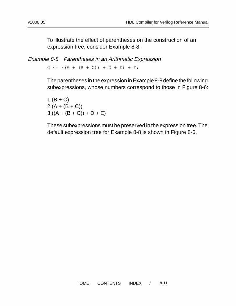
To illustrate the effect of parentheses on the construction of anexpression tree, consider Example 8-8.
Example 8-8 Parentheses in an Arithmetic ExpressionQ <= ((A + (B + C)) + D + E) + F;
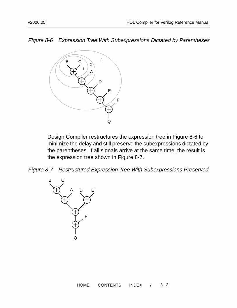
The parentheses in the expression in Example 8-8 define the followingsubexpressions, whose numbers correspond to those in Figure 8-6:
1 (B + C)2 (A + (B + C))3 ((A + (B + C)) + D + E)
These subexpressions must be preserved in the expression tree. Thedefault expression tree for Example 8-8 is shown in Figure 8-6.
/ 8-11HOME CONTENTS INDEX
v2000.05 HDL Compiler for Verilog Reference Manual
Figure 8-6 Expression Tree With Subexpressions Dictated by Parentheses
Design Compiler restructures the expression tree in Figure 8-6 tominimize the delay and still preserve the subexpressions dictated bythe parentheses. If all signals arrive at the same time, the result isthe expression tree shown in Figure 8-7.
Figure 8-7 Restructured Expression Tree With Subexpressions Preserved
A
B C
D
Q
E
F
12
3
A
B C
D
Q
E
F
/ 8-12HOME CONTENTS INDEX
v2000.05 HDL Compiler for Verilog Reference Manual
Design Compiler automatically optimizes expression trees to produceminimum delay. If you do not want HDL Compiler to optimize theexpression trees in your design, enter the following command:
dc_shell> set_minimize_tree_delay false
The set_minimize_tree_delay command applies to the currentdesign. The default for the command is true.
Considering Overflow Characteristics
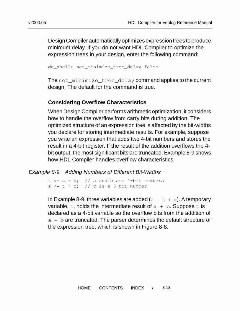
When Design Compiler performs arithmetic optimization, it considershow to handle the overflow from carry bits during addition. Theoptimized structure of an expression tree is affected by the bit-widthsyou declare for storing intermediate results. For example, supposeyou write an expression that adds two 4-bit numbers and stores theresult in a 4-bit register. If the result of the addition overflows the 4-bit output, the most significant bits are truncated. Example 8-9 showshow HDL Compiler handles overflow characteristics.
Example 8-9 Adding Numbers of Different Bit-Widthst <= a + b; // a and b are 4-bit numbersz <= t + c; // c is a 6-bit number
In Example 8-9, three variables are added (a + b + c ). A temporaryvariable, t , holds the intermediate result of a + b . Suppose t isdeclared as a 4-bit variable so the overflow bits from the addition ofa + b are truncated. The parser determines the default structure ofthe expression tree, which is shown in Figure 8-8.
/ 8-13HOME CONTENTS INDEX
v2000.05 HDL Compiler for Verilog Reference Manual
Figure 8-8 Default Expression Tree With 4-Bit Temporary Variable
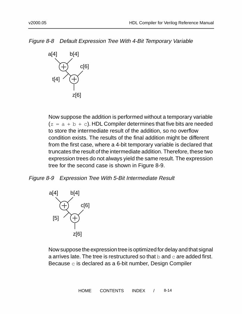
Now suppose the addition is performed without a temporary variable(z = a + b + c ). HDL Compiler determines that five bits are neededto store the intermediate result of the addition, so no overflowcondition exists. The results of the final addition might be differentfrom the first case, where a 4-bit temporary variable is declared thattruncates the result of the intermediate addition. Therefore, these twoexpression trees do not always yield the same result. The expressiontree for the second case is shown in Figure 8-9.
Figure 8-9 Expression Tree With 5-Bit Intermediate Result
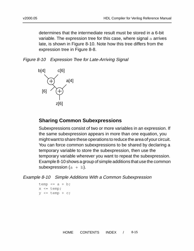
Now suppose the expression tree is optimized for delay and that signala arrives late. The tree is restructured so that b and c are added first.Because c is declared as a 6-bit number, Design Compiler
a[4] b[4]
c[6]
z[6]
t[4]
a[4] b[4]
c[6]
z[6]
[5]
/ 8-14HOME CONTENTS INDEX
v2000.05 HDL Compiler for Verilog Reference Manual
determines that the intermediate result must be stored in a 6-bitvariable. The expression tree for this case, where signal a arriveslate, is shown in Figure 8-10. Note how this tree differs from theexpression tree in Figure 8-8.
Figure 8-10 Expression Tree for Late-Arriving Signal
Sharing Common Subexpressions
Subexpressions consist of two or more variables in an expression. Ifthe same subexpression appears in more than one equation, youmight want to share these operations to reduce the area of your circuit.You can force common subexpressions to be shared by declaring atemporary variable to store the subexpression, then use thetemporary variable wherever you want to repeat the subexpression.Example 8-10 shows a group of simple additions that use the commonsubexpression (a + b ).
Example 8-10 Simple Additions With a Common Subexpressiontemp <= a + b;x <= temp;y <= temp + c;
a[4]
b[4] c[6]
z[6]
[6]
/ 8-15HOME CONTENTS INDEX
v2000.05 HDL Compiler for Verilog Reference Manual
Instead of manually forcing common subexpressions to be shared,you can let Design Compiler automatically determine whether sharingcommon subexpressions improves your circuit. You do not need todeclare a temporary variable to hold the common subexpression inthis case.
In some cases, sharing common subexpressions results in moreadders being built. Consider Example 8-11, where A + Bis a commonsubexpression.
Example 8-11 Sharing Common Subexpressionsif cond1
Y <= A + B;else
Y <= C + D;end;if cond2
Z <= E + F;else
Z <= A + B;end;
If the common subexpression A + B is shared, three adders areneeded to implement this section of code:
(A + B)(C + D)(E + F)
If the common subexpression is not shared, only two adders areneeded: one to implement the additions A + B and C + Dand oneto implement the additions E + F and A + B .
/ 8-16HOME CONTENTS INDEX
v2000.05 HDL Compiler for Verilog Reference Manual
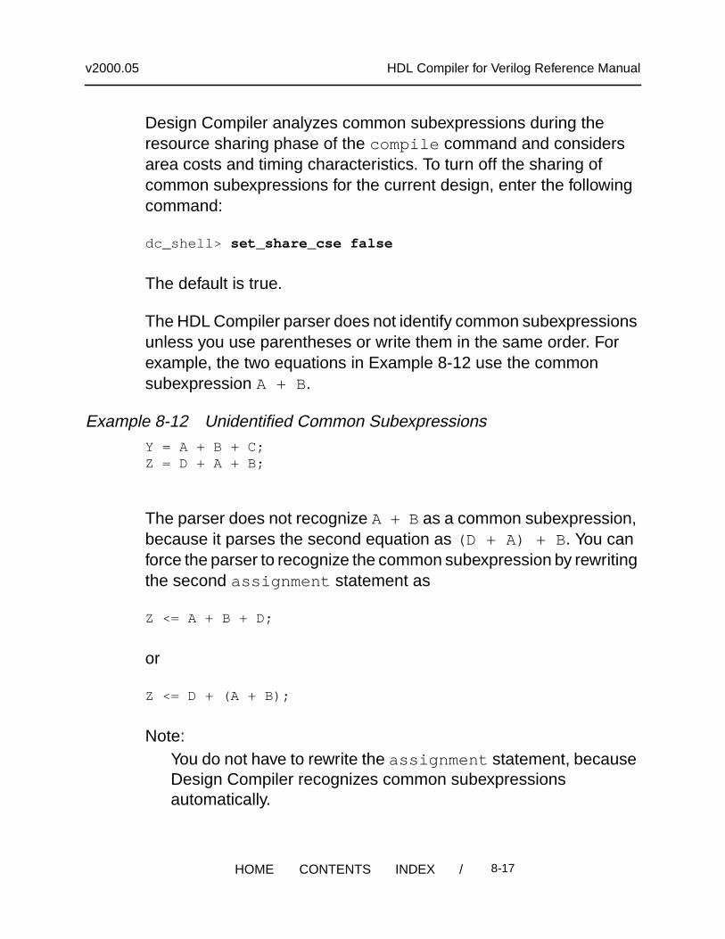
Design Compiler analyzes common subexpressions during theresource sharing phase of the compile command and considersarea costs and timing characteristics. To turn off the sharing ofcommon subexpressions for the current design, enter the followingcommand:
dc_shell> set_share_cse false
The default is true.
The HDL Compiler parser does not identify common subexpressionsunless you use parentheses or write them in the same order. Forexample, the two equations in Example 8-12 use the commonsubexpression A + B .
Example 8-12 Unidentified Common SubexpressionsY = A + B + C;Z = D + A + B;
The parser does not recognize A + Bas a common subexpression,because it parses the second equation as (D + A) + B . You canforce the parser to recognize the common subexpression by rewritingthe second assignment statement as
Z <= A + B + D;
or
Z <= D + (A + B);
Note:You do not have to rewrite the assignment statement, becauseDesign Compiler recognizes common subexpressionsautomatically.
/ 8-17HOME CONTENTS INDEX
v2000.05 HDL Compiler for Verilog Reference Manual
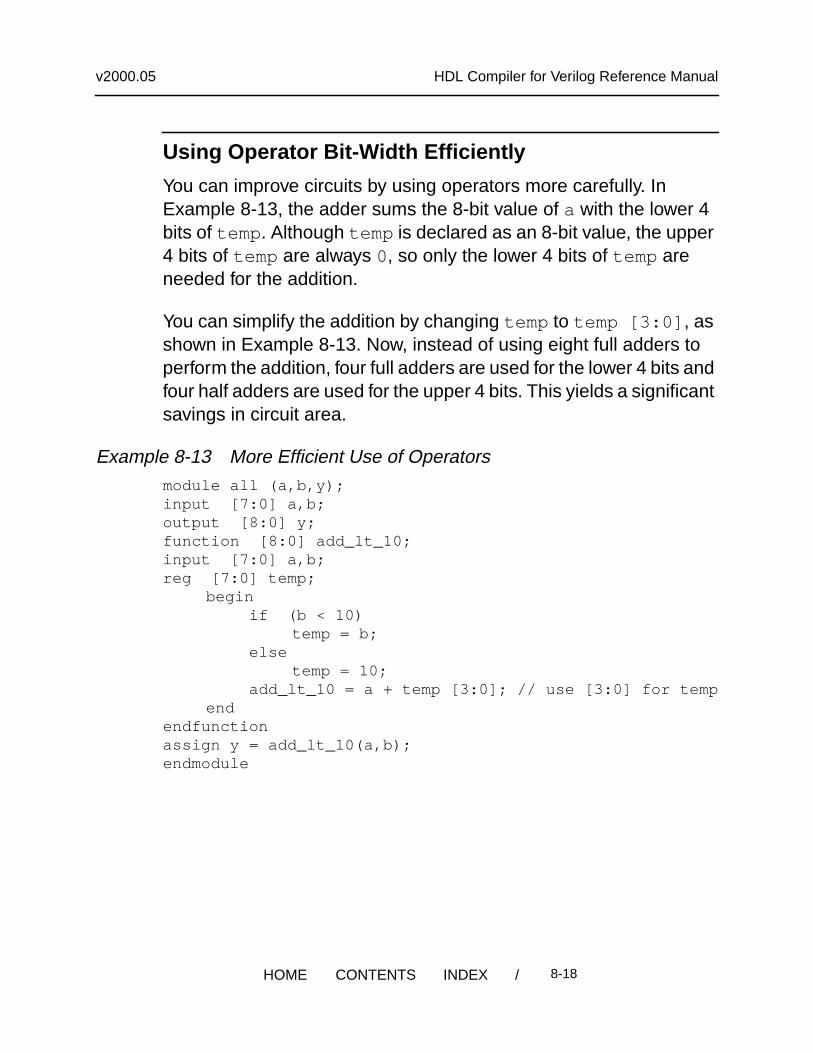
Using Operator Bit-Width Efficiently
You can improve circuits by using operators more carefully. InExample 8-13, the adder sums the 8-bit value of a with the lower 4bits of temp . Although temp is declared as an 8-bit value, the upper4 bits of temp are always 0, so only the lower 4 bits of temp areneeded for the addition.
You can simplify the addition by changing temp to temp [3:0] , asshown in Example 8-13. Now, instead of using eight full adders toperform the addition, four full adders are used for the lower 4 bits andfour half adders are used for the upper 4 bits. This yields a significantsavings in circuit area.
Example 8-13 More Efficient Use of Operatorsmodule all (a,b,y);input [7:0] a,b;output [8:0] y;function [8:0] add_lt_10;input [7:0] a,b;reg [7:0] temp;
beginif (b < 10)
temp = b;else
temp = 10;add_lt_10 = a + temp [3:0]; // use [3:0] for temp
endendfunctionassign y = add_lt_10(a,b);endmodule
/ 8-18HOME CONTENTS INDEX

v2000.05 HDL Compiler for Verilog Reference Manual
Using State Information
When you build finite state machines, you can often specify a constantvalue of a signal in a particular state. You can write your Verilogdescription so that Design Compiler produces a more efficient circuit.
Example 8-14 shows the Verilog description of a simple finite statemachine.
Example 8-14 A Simple Finite State Machinemodule machine (x, clock, current_state, z);
input x, clock;output [1:0] current_state;output z;
reg [1:0] current_state;reg z;/* Redeclared as reg so they can be assigned to in alwaysstatements. By default, ports are wires and cannot beassigned to in ’always’*/reg [1:0] next_state;reg previous_z;
parameter [1:0] set0 = 0,hold0 = 1,set1 = 2;
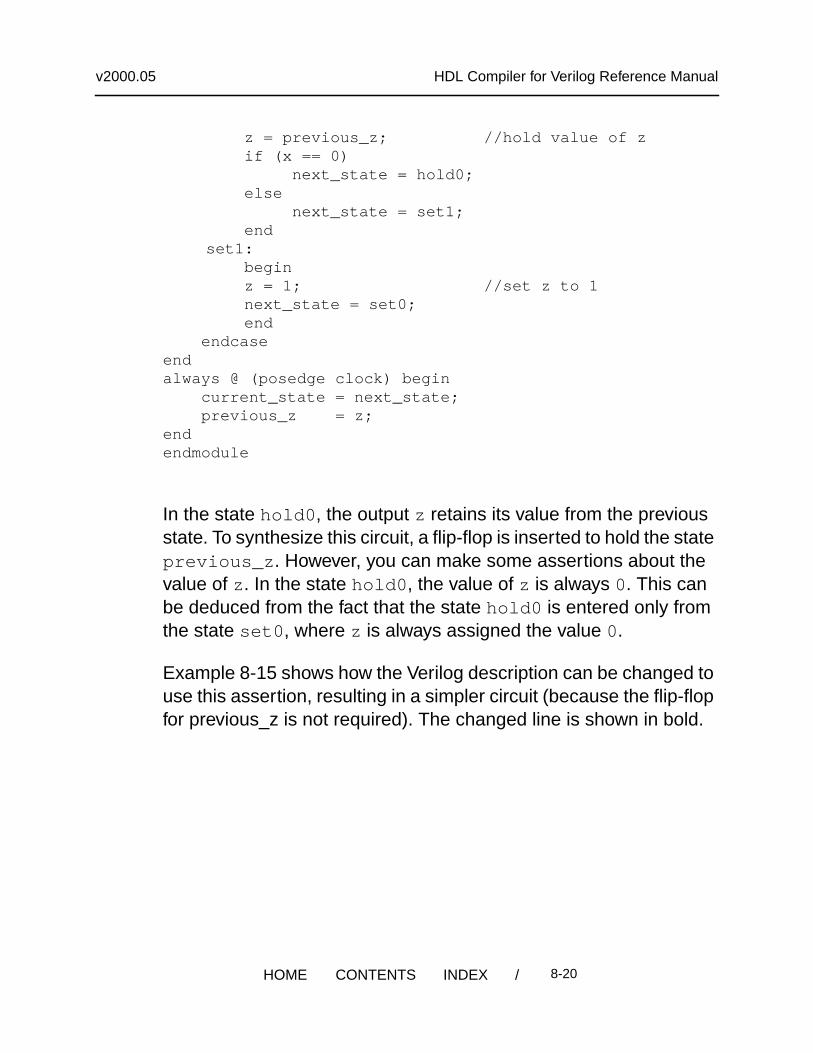
always @ (x or current_state) begin case (current_state) //synopsys full_case
/* declared full_case to avoid extraneous latches */set0: begin z = 0 ; //set z to 0 next_state = hold0; endhold0: begin
/ 8-19HOME CONTENTS INDEX
v2000.05 HDL Compiler for Verilog Reference Manual
z = previous_z; //hold value of z if (x == 0)
next_state = hold0; else
next_state = set1; endset1: begin z = 1; //set z to 1 next_state = set0; end
endcaseendalways @ (posedge clock) begin current_state = next_state; previous_z = z;endendmodule
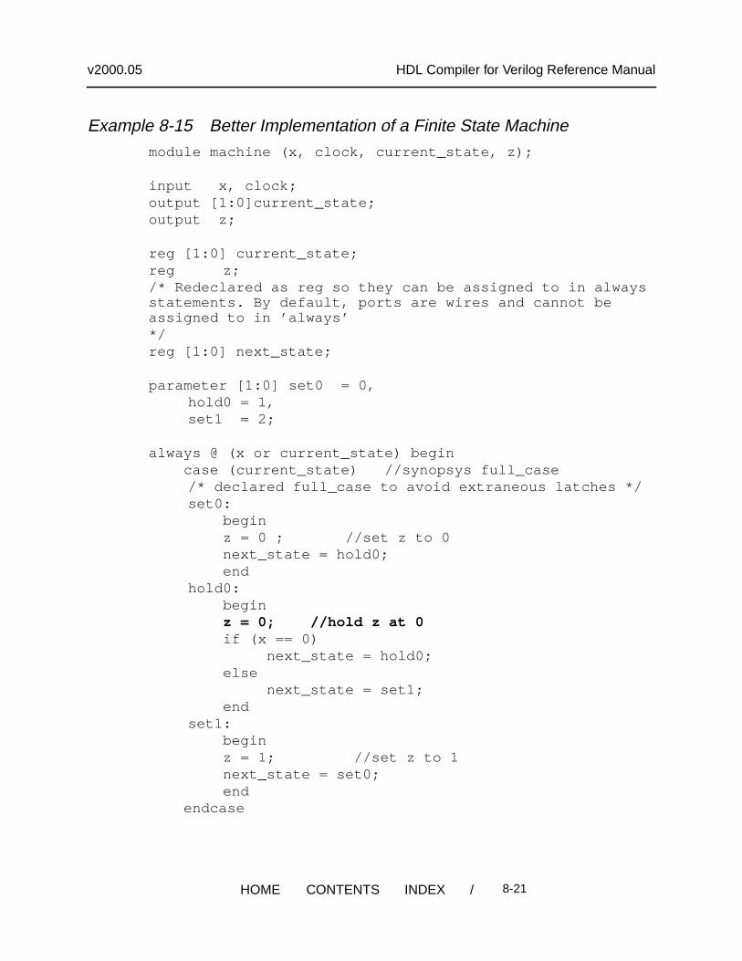
In the state hold0 , the output z retains its value from the previousstate. To synthesize this circuit, a flip-flop is inserted to hold the stateprevious_z . However, you can make some assertions about thevalue of z . In the state hold0 , the value of z is always 0. This canbe deduced from the fact that the state hold0 is entered only fromthe state set0 , where z is always assigned the value 0.
Example 8-15 shows how the Verilog description can be changed touse this assertion, resulting in a simpler circuit (because the flip-flopfor previous_z is not required). The changed line is shown in bold.
/ 8-20HOME CONTENTS INDEX
v2000.05 HDL Compiler for Verilog Reference Manual
Example 8-15 Better Implementation of a Finite State Machinemodule machine (x, clock, current_state, z);
input x, clock;output [1:0]current_state;output z;
reg [1:0] current_state;reg z;/* Redeclared as reg so they can be assigned to in alwaysstatements. By default, ports are wires and cannot beassigned to in ’always’*/reg [1:0] next_state;
parameter [1:0] set0 = 0,hold0 = 1,set1 = 2;
always @ (x or current_state) begin case (current_state) //synopsys full_case
/* declared full_case to avoid extraneous latches */set0: begin z = 0 ; //set z to 0 next_state = hold0; endhold0: begin
z = 0; //hold z at 0 if (x == 0)
next_state = hold0; else
next_state = set1; endset1: begin z = 1; //set z to 1 next_state = set0; end
endcase
/ 8-21HOME CONTENTS INDEX
v2000.05 HDL Compiler for Verilog Reference Manual
endalways @ (posedge clock) begin current_state = next_state;endendmodule
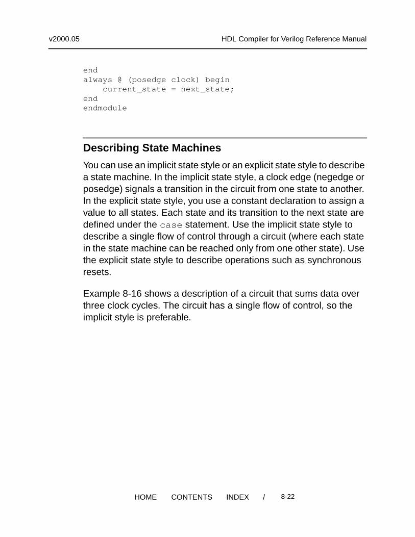
Describing State Machines
You can use an implicit state style or an explicit state style to describea state machine. In the implicit state style, a clock edge (negedge orposedge) signals a transition in the circuit from one state to another.In the explicit state style, you use a constant declaration to assign avalue to all states. Each state and its transition to the next state aredefined under the case statement. Use the implicit state style todescribe a single flow of control through a circuit (where each statein the state machine can be reached only from one other state). Usethe explicit state style to describe operations such as synchronousresets.
Example 8-16 shows a description of a circuit that sums data overthree clock cycles. The circuit has a single flow of control, so theimplicit style is preferable.
/ 8-22HOME CONTENTS INDEX
v2000.05 HDL Compiler for Verilog Reference Manual
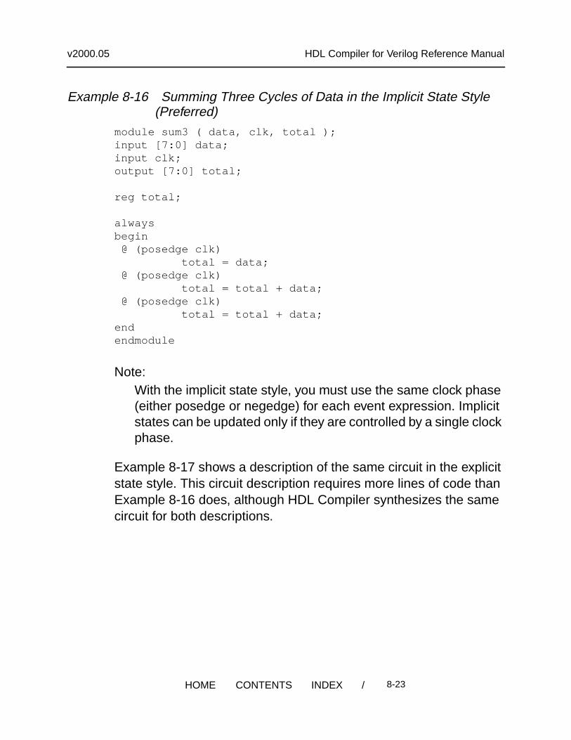
Example 8-16 Summing Three Cycles of Data in the Implicit State Style(Preferred)
module sum3 ( data, clk, total );input [7:0] data;input clk;output [7:0] total;
reg total;
alwaysbegin @ (posedge clk) total = data; @ (posedge clk) total = total + data; @ (posedge clk) total = total + data;endendmodule
Note:With the implicit state style, you must use the same clock phase(either posedge or negedge) for each event expression. Implicitstates can be updated only if they are controlled by a single clockphase.
Example 8-17 shows a description of the same circuit in the explicitstate style. This circuit description requires more lines of code thanExample 8-16 does, although HDL Compiler synthesizes the samecircuit for both descriptions.
/ 8-23HOME CONTENTS INDEX
v2000.05 HDL Compiler for Verilog Reference Manual
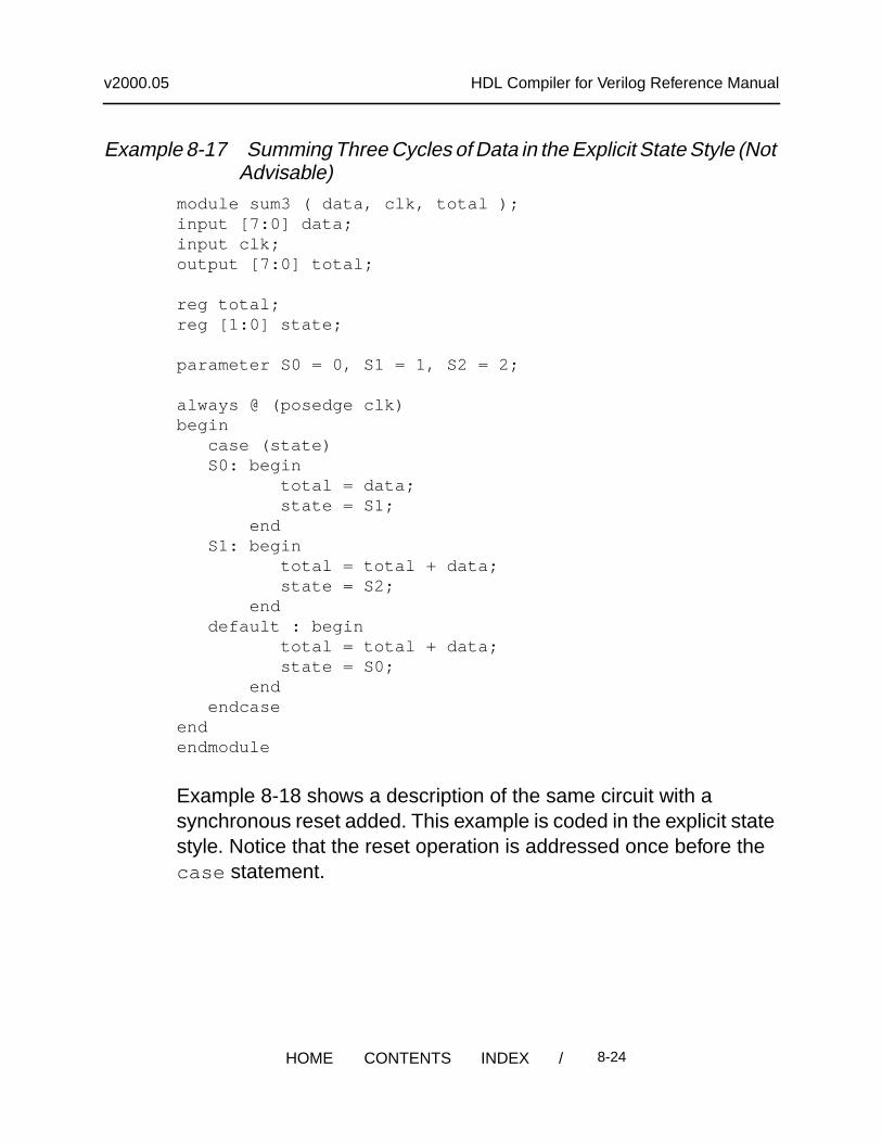
Example 8-17 Summing Three Cycles of Data in the Explicit State Style (NotAdvisable)
module sum3 ( data, clk, total );input [7:0] data;input clk;output [7:0] total;
reg total;reg [1:0] state;
parameter S0 = 0, S1 = 1, S2 = 2;
always @ (posedge clk)begin case (state) S0: begin total = data; state = S1; end S1: begin total = total + data; state = S2; end default : begin total = total + data; state = S0; end endcaseendendmodule
Example 8-18 shows a description of the same circuit with asynchronous reset added. This example is coded in the explicit statestyle. Notice that the reset operation is addressed once before thecase statement.
/ 8-24HOME CONTENTS INDEX

v2000.05 HDL Compiler for Verilog Reference Manual
Example 8-18 Synchronous Reset—Explicit State Style (Preferred)module SUM3 ( data, clk, total, reset );input [7:0] data;input clk, reset;output [7:0] total;
reg total;reg [1:0] state;
parameter S0 = 0, S1 = 1, S2 = 2;
always @ (posedge clk)begin if (reset) state = S0; else case (state) S0: begin total = data; state = S1; end S1: begin total = total + data; state = S2; end default : begin total = total + data; state = S0; end endcase;endendmodule
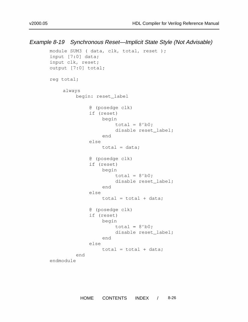
Example 8-19 shows how to describe the same function in the implicitstate style. This style is not as efficient for describing synchronousresets. In this case, the reset operation has to be addressed for everyalways @ statement.
/ 8-25HOME CONTENTS INDEX
v2000.05 HDL Compiler for Verilog Reference Manual
Example 8-19 Synchronous Reset—Implicit State Style (Not Advisable)module SUM3 ( data, clk, total, reset );input [7:0] data;input clk, reset;output [7:0] total;
reg total;
alwaysbegin: reset_label
@ (posedge clk)if (reset)
begintotal = 8’b0;disable reset_label;
endelse
total = data;
@ (posedge clk)if (reset)
begintotal = 8’b0;disable reset_label;
endelse
total = total + data;
@ (posedge clk)if (reset)
begintotal = 8’b0;disable reset_label;
endelse
total = total + data;end
endmodule
/ 8-26HOME CONTENTS INDEX
v2000.05 HDL Compiler for Verilog Reference Manual
Minimizing Registers
In an always block that is triggered by a clock edge, every variablethat has a value assigned has its value held in a flip-flop.
Organize your Verilog description so you build only as many registersas you need. Example 8-20 shows a description where extra registersare implied.
Example 8-20 Inefficient Circuit Description With Six Implied Registersmodule count (clock, reset, and_bits, or_bits, xor_bits);input clock, reset;output and_bits, or_bits, xor_bits;reg and_bits, or_bits, xor_bits;
reg [2:0] count;
always @(posedge clock) beginif (reset) count = 0;else count = count + 1;
and_bits = & count;or_bits = | count;xor_bits = ^ count;
endendmodule
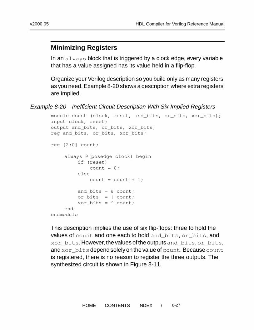
This description implies the use of six flip-flops: three to hold thevalues of count and one each to hold and_bits , or_bits , andxor_bits . However, the values of the outputs and_bits , or_bits ,and xor_bits depend solely on the value of count . Because countis registered, there is no reason to register the three outputs. Thesynthesized circuit is shown in Figure 8-11.
/ 8-27HOME CONTENTS INDEX
v2000.05 HDL Compiler for Verilog Reference Manual
Figure 8-11 Synthesized Circuit With Six Implied Registers
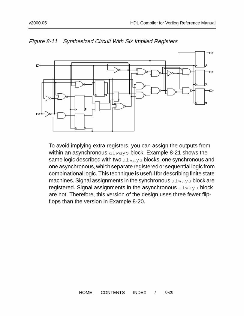
To avoid implying extra registers, you can assign the outputs fromwithin an asynchronous always block. Example 8-21 shows thesame logic described with two always blocks, one synchronous andone asynchronous, which separate registered or sequential logic fromcombinational logic. This technique is useful for describing finite statemachines. Signal assignments in the synchronous always block areregistered. Signal assignments in the asynchronous always blockare not. Therefore, this version of the design uses three fewer flip-flops than the version in Example 8-20.
/ 8-28HOME CONTENTS INDEX
v2000.05 HDL Compiler for Verilog Reference Manual
Example 8-21 Circuit With Three Implied Registersmodule count (clock, reset, and_bits, or_bits, xor_bits);input clock, reset;output and_bits, or_bits, xor_bits;reg and_bits, or_bits, xor_bits;
reg [2:0] count;
always @(posedge clock) begin//synchronousif (reset)
count = 0;else
count = count + 1;endalways @(count) begin//asynchronous
and_bits = & count;or_bits = | count;xor_bits = ^ count;
endendmodule
The more efficient version of the circuit is shown in Figure 8-12.
Figure 8-12 Synthesized Circuit With Three Implied Registers
/ 8-29HOME CONTENTS INDEX
v2000.05 HDL Compiler for Verilog Reference Manual
Separating Sequential and Combinational Assignments
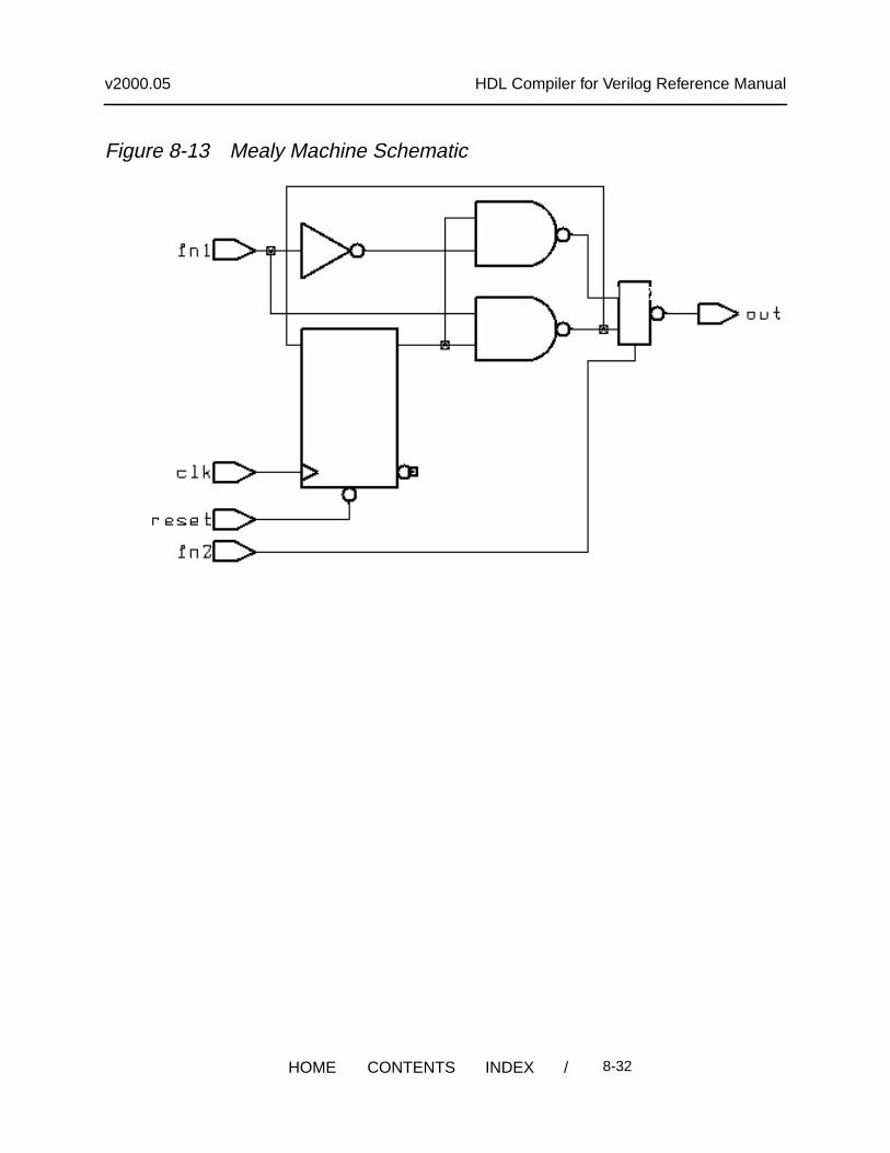
To compute values synchronously and store them in flip-flops, set upan always block with a signal edge trigger. To let other values changeasynchronously, make a separate always block with no signal edgetrigger. Put the assignments you want clocked in the always blockwith the signal edge trigger and the other assignments in the otheralways block. This technique is used for creating Mealy machines,such as the one in Example 8-22. Note that out changesasynchronously with in1 or in2 .
/ 8-30HOME CONTENTS INDEX
v2000.05 HDL Compiler for Verilog Reference Manual
Example 8-22 Mealy Machinemodule mealy (in1, in2, clk, reset, out);
input in1, in2, clk, reset;output out;reg current_state, next_state, out;
always @(posedge clk or negedge reset)// state vector flip-flops (sequential)
if (!reset)current_state = 0;
elsecurrent_state = next_state;
always @(in1 or in2 or current_state)// output and state vector decode (combinational)
case (current_state)0: begin
next_state = 1;out = 1’b0;
end1: if (in1) begin
next_state = 1’b0;out = in2;
endelse begin
next_state = 1’b1;out = !in2;
endendcase
endmodule
The schematic for this circuit is shown in Figure 8-13.
/ 8-31HOME CONTENTS INDEX
v2000.05 HDL Compiler for Verilog Reference Manual
Figure 8-13 Mealy Machine Schematic
/ 8-32HOME CONTENTS INDEX
v2000.05 HDL Compiler for Verilog Reference Manual
Design Compiler Optimization
After HDL Compiler translates your design description, you then useDesign Compiler to optimize the HDL description and synthesize thedesign.
Chapter 10, “Design Compiler Interface,” describes how to use DesignCompiler to read HDL descriptions through HDL Compiler. For acomplete description of the Design Compiler compile command,see the Design Compiler documentation. For the syntax of DesignCompiler commands, see the Synopsys man pages.
The Design Compiler commands set_flatten andset_structure set flatten and structure attributes for the compiler.Flattening reduces a design’s logical structure to a set of two-level(and/or) logic equations. Structuring attempts to find common factorsin the translated design’s set of logic equations.
Don’t Care Inference
You can greatly reduce circuit area by using don’t care values. To usea don’t care value in your design, create an enumerated type for thedon’t care value.
Don’t care values are best used as default assignments to variables.You can assign a don’t care value to a variable at the beginning of amodule, in the default section of a case statement, or in the elsesection of an if statement.
To take advantage of don’t care values during synthesis, use theDesign Compiler command set_flatten . For information onembedding this command in your description, see “EmbeddingConstraints and Attributes” on page 9-22.
/ 8-33HOME CONTENTS INDEX
v2000.05 HDL Compiler for Verilog Reference Manual
Limitations of Using Don’t Care Values
In some cases, using don’t care values as default assignments cancause these problems:
• Don’t care values create a greater potential for mismatchesbetween simulation and synthesis.
• Defaults for variables can hide mistakes in the Verilog code.
For example, you might assign a default don’t care value to VAR.If you later assign a value to VAR, expecting VARto be a don’t carevalue, you might have overlooked an intervening condition underwhich VAR is assigned.
Therefore, when you assign a value to a variable (or signal) thatcontains a don’t care value, make sure that the variable (or signal) isreally a don’t care value under those conditions. Note that assignmentto an x is interpreted as a don’t care value.
Differences Between Simulation and Synthesis
Don’t care values are treated differently in simulation and in synthesis,and there can be a mismatch between the two. To a simulator, a don’tcare is a distinct value, different from a 1 or a 0. In synthesis, however,a don’t care becomes a 0 or a 1 (and hardware is built that treats thedon’t care value as either a 0 or a 1).
Whenever a comparison is made with a variable whose value is don’tcare, simulation and synthesis can differ. Therefore, the safest wayto use don’t care values is to
• Assign don’t care values only to output ports
• Make sure that the design never reads output ports
/ 8-34HOME CONTENTS INDEX
v2000.05 HDL Compiler for Verilog Reference Manual
These guidelines guarantee that when you simulate within the scopeof the design, the only difference between simulation and synthesisoccurs when the simulator indicates that an output is a don’t carevalue.
If you use don’t care values internally to a design, expressions DesignCompiler compares with don’t care values (X) are synthesized asthough values are not equal to X.
For example,
if A == ’X’ then...
is synthesized as
if FALSE then...
If you use expressions comparing values with X, pre-synthesis andpost-synthesis simulation results might not agree. For this reason,HDL Compiler issues the following warning:
Warning: A partial don’t-care value was read in routine testline 24 in file ’test.v’ This may cause simulation todisagree with synthesis. (HDL-171)
Propagating Constants
Constant propagation is the compile-time evaluation of expressionsthat contain constants. HDL Compiler uses constant propagation toreduce the amount of hardware required to implement complexoperators. Therefore, when you know that a variable is a constant,
/ 8-35HOME CONTENTS INDEX
v2000.05 HDL Compiler for Verilog Reference Manual
specify it as a constant. For example, a + operator with a constant of1 as one of its arguments causes an incrementer, rather than ageneral adder, to be built. If both arguments of an operator areconstants, no hardware is constructed, because HDL Compiler cancalculate the expression’s value and insert it directly into the circuit.
Comparators and shifters also benefit from constant propagation.When you shift a vector by a constant, the implementation requiresonly a reordering (rewiring) of bits, so no logic is needed.
Synthesis Issues
The next two sections describe feedback paths and latches that resultfrom ambiguities insignal or variable assignments, and asynchronousbehavior.
Feedback Paths and Latches
Sometimes your Verilog source can imply combinational feedbackpaths or latches in synthesized logic. This happens when a signal ora variable in a combinational logic block (an always block without aposedge or negedge clock statement) is not fully specified. Avariable or signal is fully specified when it is assigned under allpossible conditions.
Synthesizing Asynchronous Designs
In a synchronous design, all registers use the same clock signal. Thatclock signal must be a primary input to the design. A synchronousdesign has no combinational feedback paths, one-shots, or delaylines. Synchronous designs perform the same function regardless of
/ 8-36HOME CONTENTS INDEX
v2000.05 HDL Compiler for Verilog Reference Manual
the clock rate, as long as the rate is slow enough to allow signals topropagate all the way through the combinational logic betweenregisters.
Synopsys synthesis tools offer limited support for asynchronousdesigns. The most common way to produce asynchronous logic inVerilog is to use gated clocks on registers. If you use asynchronousdesign techniques, synthesis and simulation results might not agree.Because Design Compiler does not issue warning messages forasynchronous designs, you are responsible for verifying thecorrectness of your circuit.
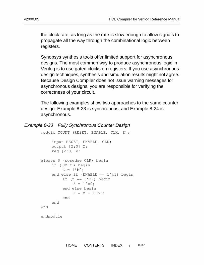
The following examples show two approaches to the same counterdesign: Example 8-23 is synchronous, and Example 8-24 isasynchronous.
Example 8-23 Fully Synchronous Counter Designmodule COUNT (RESET, ENABLE, CLK, Z);
input RESET, ENABLE, CLK;output [2:0] Z;reg [2:0] Z;
always @ (posedge CLK) beginif (RESET) begin
Z = 1’b0;end else if (ENABLE == 1’b1) begin
if (Z == 3’d7) beginZ = 1’b0;
end else beginZ = Z + 1’b1;
endend
end
endmodule
/ 8-37HOME CONTENTS INDEX
v2000.05 HDL Compiler for Verilog Reference Manual
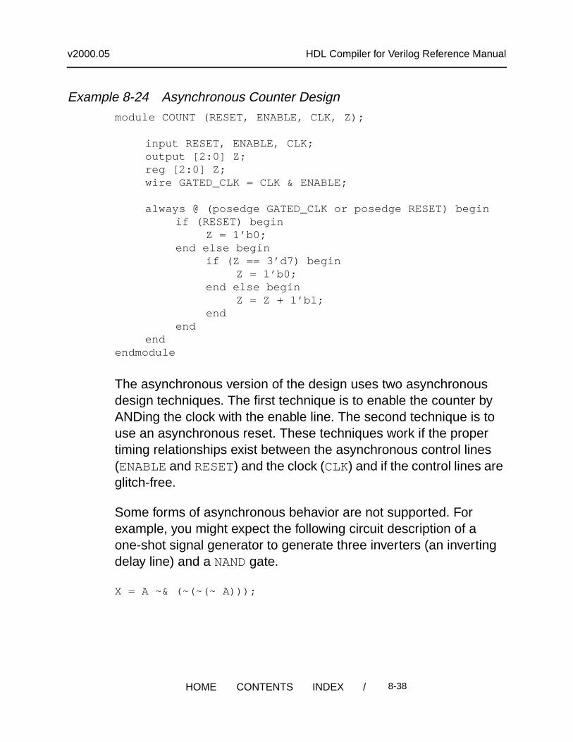
Example 8-24 Asynchronous Counter Designmodule COUNT (RESET, ENABLE, CLK, Z);
input RESET, ENABLE, CLK;output [2:0] Z;reg [2:0] Z;wire GATED_CLK = CLK & ENABLE;
always @ (posedge GATED_CLK or posedge RESET) beginif (RESET) begin
Z = 1’b0;end else begin
if (Z == 3’d7) beginZ = 1’b0;
end else beginZ = Z + 1’b1;
endend
endendmodule
The asynchronous version of the design uses two asynchronousdesign techniques. The first technique is to enable the counter byANDing the clock with the enable line. The second technique is touse an asynchronous reset. These techniques work if the propertiming relationships exist between the asynchronous control lines(ENABLEand RESET) and the clock (CLK) and if the control lines areglitch-free.
Some forms of asynchronous behavior are not supported. Forexample, you might expect the following circuit description of aone-shot signal generator to generate three inverters (an invertingdelay line) and a NAND gate.
X = A ~& (~(~(~ A)));
/ 8-38HOME CONTENTS INDEX
v2000.05 HDL Compiler for Verilog Reference Manual
However, this circuit description is optimized to
X = A ~& (~ A);then
X = 1;
Designing for Overall Efficiency
The efficiency of a synthesized design depends primarily on how youdescribe its component structure. The next two sections explain howto describe random logic and how to share complex operators.
Describing Random Logic
You can describe random logic with many different shorthand Verilogexpressions. HDL Compiler often generates the same optimized logicfor equivalent expressions, so your description style for random logicdoes not affect the efficiency of the circuit. Example 8-25 shows fourgroups of statements that are equivalent. (Assume that a, b, and care 4-bit variables.) HDL Compiler creates the same optimized logicin all four cases.
Example 8-25 Equivalent Statementsc = a & b;
c[3:0] = a[3:0] & b[3:0];
c[3] = a[3] & b[3];c[2] = a[2] & b[2];c[1] = a[1] & b[1];c[0] = a[0] & b[0];
for (i = 0; i <= 3; i = i + 1) c[i] = a[i] & b[i];
/ 8-39HOME CONTENTS INDEX
v2000.05 HDL Compiler for Verilog Reference Manual
Sharing Complex Operators
You can use automatic resource sharing to share most operators.However, some complex operators can be shared only if you rewriteyour source description more efficiently. These operators are
• Noncomputable array index
• Function call
• Shifter
Example 8-26 shows a circuit description that creates more functionalunits than necessary when automatic resource sharing is turned off.
/ 8-40HOME CONTENTS INDEX
v2000.05 HDL Compiler for Verilog Reference Manual
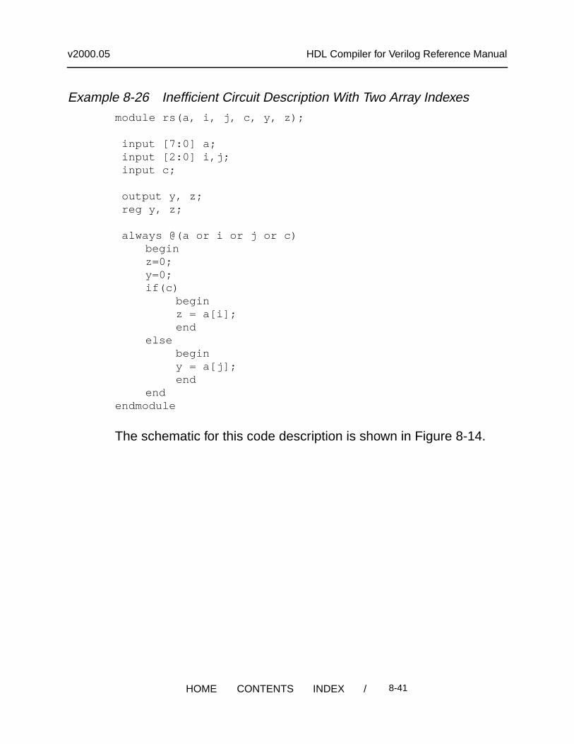
Example 8-26 Inefficient Circuit Description With Two Array Indexesmodule rs(a, i, j, c, y, z);
input [7:0] a; input [2:0] i,j; input c;
output y, z; reg y, z;
always @(a or i or j or c)beginz=0;y=0;if(c)
beginz = a[i];end
elsebeginy = a[j];end
endendmodule
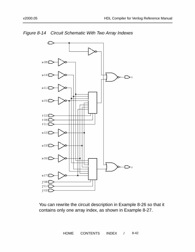
The schematic for this code description is shown in Figure 8-14.
/ 8-41HOME CONTENTS INDEX
v2000.05 HDL Compiler for Verilog Reference Manual
Figure 8-14 Circuit Schematic With Two Array Indexes
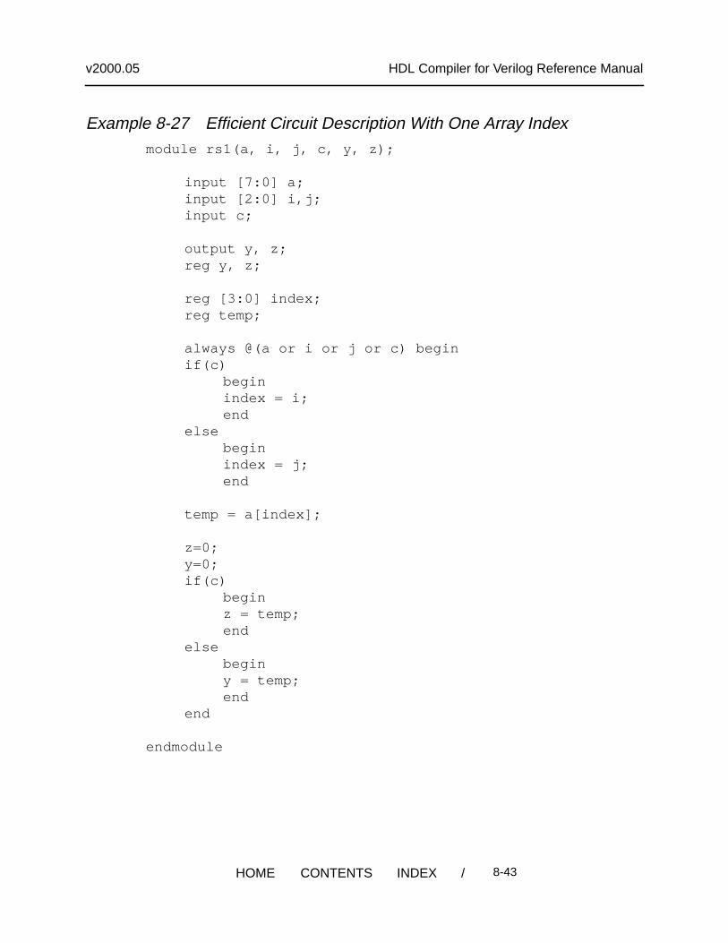
You can rewrite the circuit description in Example 8-26 so that itcontains only one array index, as shown in Example 8-27.
/ 8-42HOME CONTENTS INDEX
v2000.05 HDL Compiler for Verilog Reference Manual
Example 8-27 Efficient Circuit Description With One Array Indexmodule rs1(a, i, j, c, y, z);
input [7:0] a;input [2:0] i,j;input c;
output y, z;reg y, z;
reg [3:0] index;reg temp;
always @(a or i or j or c) beginif(c)
beginindex = i;end
elsebeginindex = j;end
temp = a[index];
z=0;y=0;if(c)
beginz = temp;end
elsebeginy = temp;end
end
endmodule
/ 8-43HOME CONTENTS INDEX
v2000.05 HDL Compiler for Verilog Reference Manual
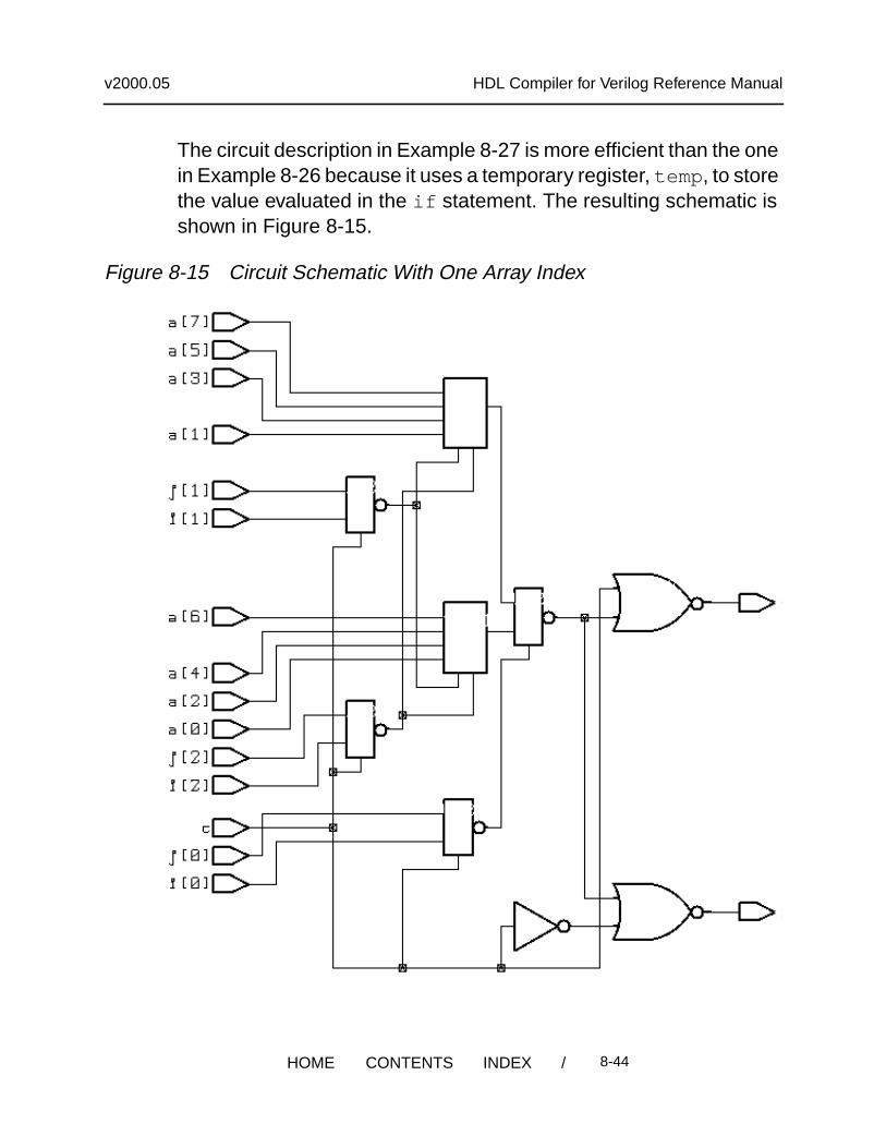
The circuit description in Example 8-27 is more efficient than the onein Example 8-26 because it uses a temporary register, temp , to storethe value evaluated in the if statement. The resulting schematic isshown in Figure 8-15.
Figure 8-15 Circuit Schematic With One Array Index
/ 8-44HOME CONTENTS INDEX
v2000.05 HDL Compiler for Verilog Reference Manual
Consider resource sharing whenever you use a complex operationmore than once. Complex operations include adders, multipliers,shifters (only when shifting by a variable amount), comparators, andmost user-defined functions. If you use automatic resource allocation,adders, subtracters, and comparators can be shared. Chapter 7,“Resource Sharing,” covers these topics in detail.
/ 8-45HOME CONTENTS INDEX

v2000.05 HDL Compiler for Verilog Reference Manual
/ 8-46HOME CONTENTS INDEX