fx-mg6006zh-06 x1h/uc
TRANSCRIPT
PIONEER CORPORATION 4-1, Meguro 1-Chome, Meguro-ku, Tokyo 153-8654, Japan PIONEER ELECTRONICS (USA) INC. P.O.Box 1760, Long Beach, CA 90801-1760 U.S.A.PIONEER EUROPE NV Haven 1087 Keetberglaan 1, 9120 Melsele, Belgium PIONEER ELECTRONICS ASIACENTRE PTE.LTD. 253 Alexandra Road, #04-01, Singapore 159936
C PIONEER CORPORATION 2002 K-ZZD. OCT. 2002 Printed in Japan
ORDER NO.
CRT2935
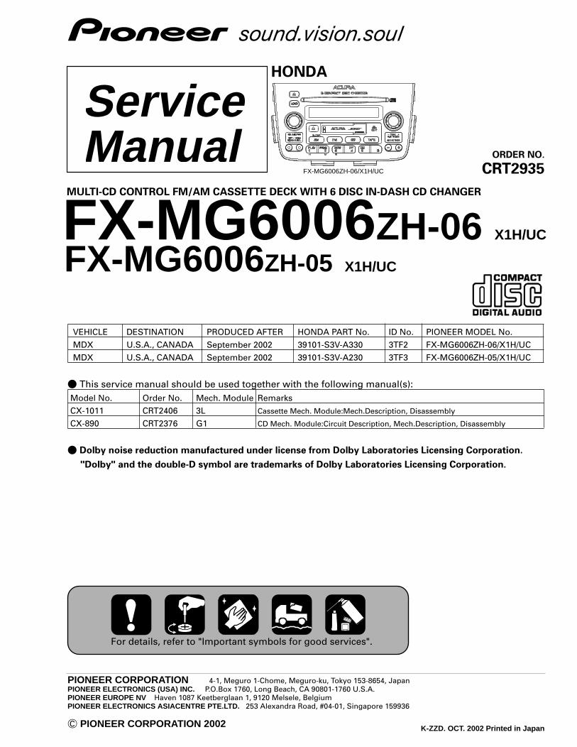
MULTI-CD CONTROL FM/AM CASSETTE DECK WITH 6 DISC IN-DASH CD CHANGER
ServiceManual
HONDA
FX-MG6006ZH-06/X1H/UC
FX-MG6006ZH-06 X1H/UC
For details, refer to "Important symbols for good services".
FX-MG6006ZH-05 X1H/UC
VEHICLE DESTINATION PRODUCED AFTER HONDA PART No. ID No. PIONEER MODEL No.
MDX U.S.A., CANADA September 2002 39101-S3V-A330 3TF2 FX-MG6006ZH-06/X1H/UC
MDX U.S.A., CANADA September 2002 39101-S3V-A230 3TF3 FX-MG6006ZH-05/X1H/UC
- This service manual should be used together with the following manual(s):Model No. Order No. Mech. Module Remarks
CX-1011 CRT2406 3L Cassette Mech. Module:Mech.Description, Disassembly
CX-890 CRT2376 G1 CD Mech. Module:Circuit Description, Mech.Description, Disassembly
- Dolby noise reduction manufactured under license from Dolby Laboratories Licensing Corporation.
"Dolby" and the double-D symbol are trademarks of Dolby Laboratories Licensing Corporation.
2
1 2 3 4
1 2 3 4
F
E
D
C
B
A
FX-MG6006ZH-06/X1H/UC
[ Important symbols for good services ]In this manual, the symbols shown-below indicate that adjustments, settings or cleaning should be made securely.When you find the procedures bearing any of the symbols, be sure to fulfill them:
2. Adjustments
To keep the original performances of the product, optimum adjustments or specification confirmation is indispensable. In accordance with the procedures or instructions described in this manual, adjustments should be performed.
3. Cleaning
For optical pickups, tape-deck heads, lenses and mirrors used in projection monitors, and other parts requiring cleaning,proper cleaning should be performed to restore their performances.
5. Lubricants, glues, and replacement partsAppropriately applying grease or glue can maintain the product performances. But improper lubrication or applying glue may lead to failures or troubles in the product. By following the instructions in this manual, be sure to apply theprescribed grease or glue to proper portions by the appropriate amount.For replacement parts or tools, the prescribed ones should be used.
4. Shipping mode and shipping screws
To protect the product from damages or failures that may be caused during transit, the shipping mode should be set orthe shipping screws should be installed before shipping out in accordance with this manual, if necessary.
1. Product safety
You should conform to the regulations governing the product (safety, radio and noise, and other regulations), and should keep the safety during servicing by following the safety instructions described in this manual.
- CD section precaution
1. Before disassembling the unit, be sure to turn off the
power. Unplugging and plugging the connectors dur-
ing power-on mode may damage the ICs inside the
unit.
2. To protect the pickup unit from electrostatic dis-
charge during servicing, take an appropriate treat-
ment (shorting pin) by referring to “the DISASSEM-
BLY” on page 79.
3. After replacing the pickup unit, be sure to check the
grating. (See p.71.)
SAFETY INFORMATION
This service manual is intended for qualified service technicians; it is not meant for the casual do-it-yourselfer.Qualified technicians have the necessary test equipment and tools, and have been trained to properly and safely repaircomplex products such as those covered by this manual.Improperly performed repairs can adversely affect the safety and reliability of the product and may void the warranty.If you are not qualified to perform the repair of this product properly and safely, you should not risk trying to do soand refer the repair to a qualified service technician.
3
5 6 7 8
F
E
D
C
B
A
5 6 7 8FX-MG6006ZH-06/X1H/UC
CONTENTS
SAFETY INFORMATION ............................................2
1. SPECIFICATIONS........................................................3
2. EXPLODED VIEWS AND PARTS LIST .......................5
3. BLOCK DIAGRAM AND SCHEMATIC DIAGRAM ...14
4. PCB CONNECTION DIAGRAM ................................34
5. ELECTRICAL PARTS LIST ........................................55
6. ADJUSTMENT..........................................................68
7. GENERAL INFORMATION .......................................73
7.1 DIAGNOSIS ........................................................73
7.1.1 TEST MODE..............................................73
7.1.2 DISASSEMBLY .........................................79
7.1.3 PCB LOCATIONS ......................................84
7.1.4 CONNECTOR FUNCTION DESCRIPTION.......85
7.2 PARTS .................................................................86
7.2.1 IC................................................................86
7.2.2 DISPLAY....................................................90
7.3 EXPLANATION ...................................................92
7.3.1 SYSTEM BLOCK DIAGRAM.....................92
7.3.2 OPERATIONAL FLOW CHART .................92
7.4 NOTES ON SERVICING .....................................93
7.1 CLEANING ...................................................93
7.2 FACTORY SETTINGS...................................93
8. OPERATIONS AND SPECIFICATIONS.....................94
1. SPECIFICATIONS
General
Power source .............13.2V DC (10.8— 16.0 V allowable)
Backup current .................................................5mA or less
Grounding system........................................Negative type
Dimensions(Chassis) ..............180(W)x102(H)x171(D)mm
(Grille) ....................216(W)x119(H)x18(D)mm
Weight..........................................................................2.7kg
Cassette player
Tape................................Compact cassette tape(C30-C90)
Tape speed ......4.76 cm/sec.(+0.14 cm/sec.,-0.05 cm/sec.)
Crosstalk ..........................................................40dB or less
Separation.....................................................30dB or more
S/N .................................................................40dB or more
Distortion.............................................................3% or less
CD player
System ...................................Compact disc audio system
Usable discs ..................................................Compact disc
Signal format .....................Sampling frequency : 44.1kHz
.....................................Number of guantization : 16;linear
S/N .................................................................60dB or more
Distortion..........................................................0.1% or less
FM tuner
Frequency.................................................87.75–107.9 MHz
S/N .................................................................50dB or more
Distortion..........................................................1.3% or less
IF interference ...............................................82dB or more
Image interference........................................46dB or more
AM tuner
Frequency ......................................................530–1710 kHz
Selectivity .......................................55dB or more(±10kHz)
S/N .................................................................44dB or more
Distortion..........................................................1.0% or less
IF interference ...............................................61dB or more
Image interference........................................51dB or more

4
1 2 3 4
1 2 3 4
F
E
D
C
B
A
FX-MG6006ZH-06/X1H/UC
5
5 6 7 8
F
E
D
C
B
A
5 6 7 8FX-MG6006ZH-06/X1H/UC
NOTE:
- Parts marked by “*” are generally unavailable because they are not in our Master Spare Parts List.
- Screws adjacent to ∇ mark on the product are used for disassembly.
- For the applying amount of lubricants or glue, follow the instructions in this manual.
( In the case of no amount instructions, apply as you think it appropriate.)
2
1
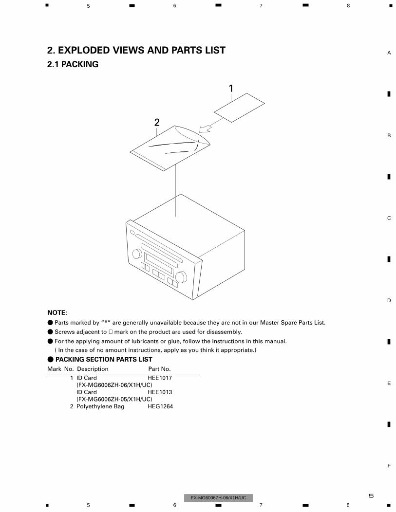
2. EXPLODED VIEWS AND PARTS LIST
2.1 PACKING
- PACKING SECTION PARTS LIST
Mark No. Description Part No.
1 ID Card HEE1017(FX-MG6006ZH-06/X1H/UC)ID Card HEE1013(FX-MG6006ZH-05/X1H/UC)
2 Polyethylene Bag HEG1264
6
1 2 3 4
1 2 3 4
F
E
D
C
B
A
FX-MG6006ZH-06/X1H/UC
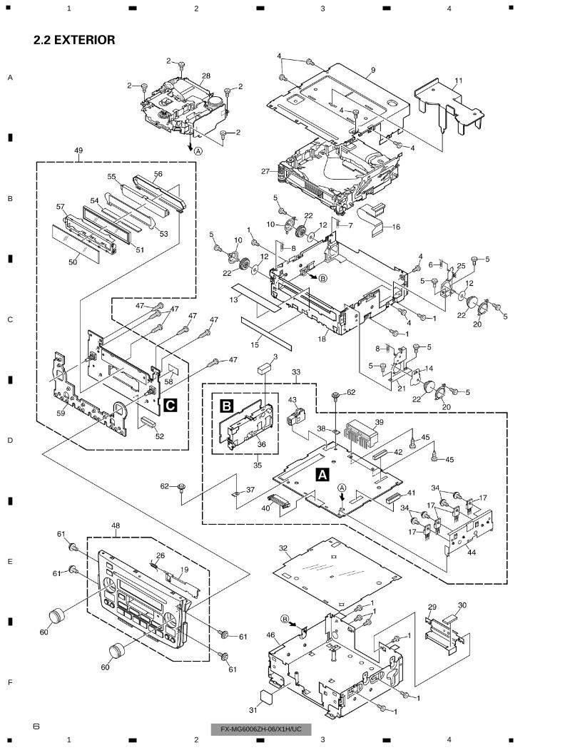
2.2 EXTERIOR
1 Screw BSZ26P040FMC2 Screw BSZ26P050FZK3 Cushion CNM68254 Screw BMZ26P030FMC5 Screw(M2x2) CBA1250
6 Spring CBH23617 Spring CBH23658 Spring CBH24099 Case CNB2451
10 Holder CNC7477
11 Bracket CNC787812 Sheet CNM598113 Insulator CNM624814 Sheet CNM631815 Insulator CNM6426
16 PCB CNP599417 Transistor(Q803,831,855,856) 2SB942A18 Chassis Unit CXB615819 Door See Contrast table(2)20 Holder CNC7826
21 Holder CNC822322 Damper CNV512023 •••••24 •••••25 Holder CNC8224
* 26 Spring HBH228627 Service Mechanism Assy(G1) CXX165028 Cassette Mechanism Module EXK421029 Holder HNC952530 Cushion HNM6427
31 Insulator HNM662232 Insulator HNM742333 Control Unit See Contrast table(2)34 Screw ASZ26P060FMC35 Tuner Unit CWE1531
36 Holder CNC677437 Terminal(CN402) CKF105938 Terminal(CN432) CKF105939 Plug(CN431) CKM130540 Plug(CN601) CKS3540
41 Connector(CN101) CKS356842 Connector(CN701) CKS393043 Antenna Jack(ANT401) CKX106044 Holder HNC891745 Screw PRZ30P060FSN
46 Chassis Unit HXB762347 Screw BPZ26P100FMC48 Grille Unit See Contrast table(2)49 Keyboard Unit See Contrast table(2)50 Plate CAH1752
51 LCD(LCD901) See Contrast table(2)52 Socket(CN901) CKS355353 Plate CNM743054 Connector CNV651955 Lighting Conductor CNV6839
56 Holder CNV684057 Holder HNC824158 Cushion HNM662359 Rubber HNV588260 Knob Unit HXB4014
61 Screw IMS30P050FMC62 Screw ISS26P055FUC
7
5 6 7 8
F
E
D
C
B
A
5 6 7 8FX-MG6006ZH-06/X1H/UC
Mark No. Description Part No. Mark No. Description Part No.
(1) EXTERIOR SECTION PARTS LIST
Part No.Mark No. Symbol and Description FX-MG6006ZH-06/X1H/UC FX-MG6006ZH-05/X1H/UC
19 Door CAT2382 CAT238333 Control Unit HWM8405 HWM854548 Grille Unit CXC1119 CXC112049 Keyboard Unit HWM8404 HWM854451 LCD(LCD901) CAW1728 CAW1598
(2) CONTRAST TABLE
FX-MG6006ZH-06/X1H/UC and FX-MG6006ZH-05/X1H/UC are constructed the same except for the fol-
lowing:
D
F
E
K
L
I
H
M
G
J
1
1:GEM10242:GEM1035
2
1
1
1
1
1
1
1
1
1
1
1
1
1
2
2
2
2
2
2
2
22
2
2
1
1
11
2
1
1
8
1 2 3 4
1 2 3 4
F
E
D
C
B
A
FX-MG6006ZH-06/X1H/UC
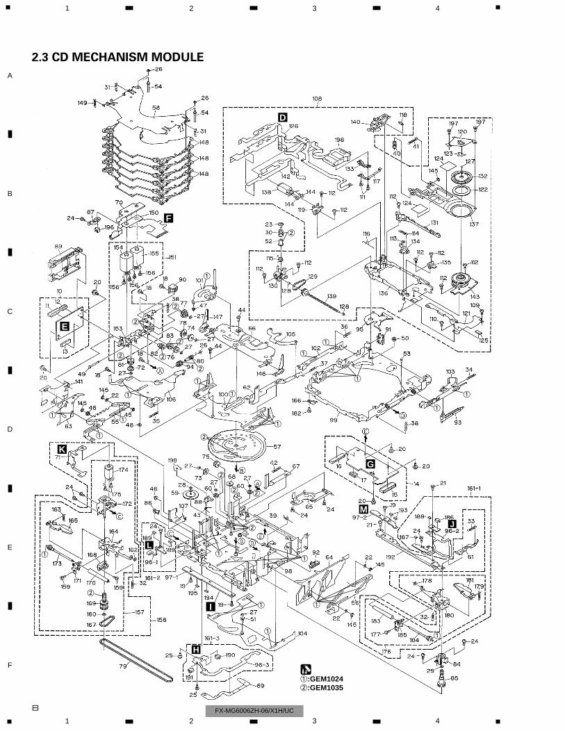
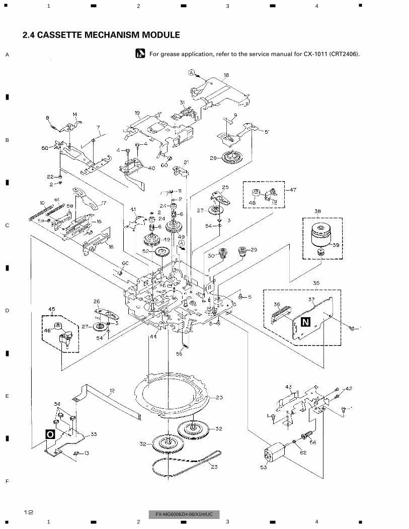
2.3 CD MECHANISM MODULE
9
5 6 7 8
F
E
D
C
B
A
5 6 7 8FX-MG6006ZH-06/X1H/UC
Mark No. Description Part No. Mark No. Description Part No.
1-9 •••••10 CD Core Unit(Servo Unit) CWX240911 Connector(CN101) CKS276412 Connector(CN301) CKS396613 Connector(CN201) CKS3991
14 CD Core Unit(STS Unit) CWX241015 Connector(CN701) CKS398916 Connector(CN801) CKS374117 Connector(CN802) CKS405418 Screw CBA1037
19 Screw CBA104120 Screw CBA107621 Screw CBA125022 Washer CBA152923 Screw CBA1452
24 Screw CBA145325 Screw CBA147926 Washer CBF103727 Washer CBF103828 Washer CBF1039
29 Washer CBF106430 Spring CBH200731 Spring CBH252032 Spring CBH227433 Spring CBH2014
34 Spring CBH201535 Spring CBH201636 Spring CBH201737 Spring CBH229038 Spring CBH2366
39 Spring CBH206440 Spring CBH219541 Spring CBH219642 Spring CBH222443 Spring CBH2250
44 Screw CBA108245 Roller CLA315446 Roller CLA315747 Roller CLA315948 Roller CLA3160
49 Shaft CLA317950 Spacer CLA319451 Roller CLA324852 Bush CLA3353
* 53 Shaft CLA3469
54 Shaft CLA369355 Steer CNC721556 Steer CNC721657 Cam CNC8774
* 58 Holder CNC7235
59 Gear CNC723660 Gear CNC951261 Lever CNC724362 Lever CNC724463 Lever CNC7245
64 Lever Unit CXB494465 Cover CNC858566 Holder Unit CXB494667 Lever CNC908868 Gear CNC8140
69 Sheet CNM684070 PCB CNP565871 PCB CNP568172 Gear CNR147973 Gear CNR1481
74 Gear CNR149575 Gear CNR150176 Gear CNR150277 Gear CNR154078 Gear CNR1541
79 Belt CNT108080 Worm Gear CNV680781 Gear CNV504782 Gear CNV504883 Gear CNV5049
84 Holder CNV505685 Pulley CNV505886 Arm CNV506187 Spacer CNV506688 Arm CNV6595
89 Cover CNV520790 Cover CNV680891 Cover CNV542592 Lever CNV542793 Arm CNV5491
94 Gear CNV551995 Holder CNV5648
* 96 Composite PCB CNX355797 Composite PCB CNX298998 Chassis Unit CXB5940
- CD MECHANISM MODULE SECTION PARTS LIST
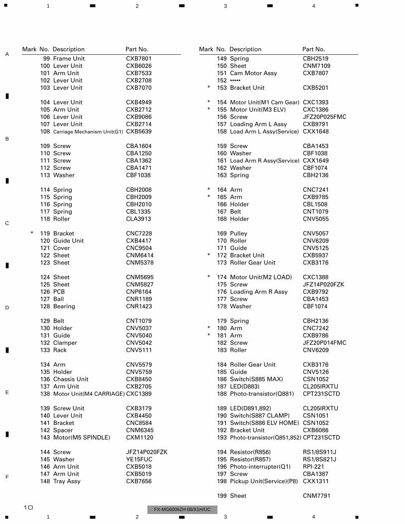
99 Frame Unit CXB7801100 Lever Unit CXB6026101 Arm Unit CXB7533102 Lever Unit CXB2708103 Lever Unit CXB7070
104 Lever Unit CXB4949105 Arm Unit CXB2712106 Lever Unit CXB9086107 Lever Unit CXB2714108 Carriage Mechanism Unit(G1) CXB5639
109 Screw CBA1604110 Screw CBA1250111 Screw CBA1362112 Screw CBA1471113 Washer CBF1038
114 Spring CBH2008115 Spring CBH2009116 Spring CBH2010117 Spring CBL1335118 Roller CLA3913
* 119 Bracket CNC7228120 Guide Unit CXB4417121 Cover CNC9504122 Sheet CNM6414123 Sheet CNM5378
124 Sheet CNM5695125 Sheet CNM5827126 PCB CNP6164127 Ball CNR1189128 Bearing CNR1423
129 Belt CNT1079130 Holder CNV5037131 Guide CNV5040132 Clamper CNV5042133 Rack CNV5111
134 Arm CNV5579135 Holder CNV5759136 Chassis Unit CXB8450137 Arm Unit CXB2705138 Motor Unit(M4 CARRIAGE) CXC1389
139 Screw Unit CXB3179140 Lever Unit CXB4450141 Bracket CNC8584142 Spacer CNM6345143 Motor(M5 SPINDLE) CXM1120
144 Screw JFZ14P020FZK145 Washer YE15FUC146 Arm Unit CXB5018147 Arm Unit CXB5019148 Tray Assy CXB7656
149 Spring CBH2519150 Sheet CNM7109151 Cam Motor Assy CXB7807152 •••••
* 153 Bracket Unit CXB5201
* 154 Motor Unit(M1 Cam Gear) CXC1393* 155 Motor Unit(M3 ELV) CXC1386
156 Screw JFZ20P025FMC157 Loading Arm L Assy CXB9791158 Load Arm L Assy(Service) CXX1648
159 Screw CBA1453160 Washer CBF1038161 Load Arm R Assy(Service) CXX1649162 Washer CBF1074163 Spring CBH2136
* 164 Arm CNC7241* 165 Arm CXB9785
166 Holder CBL1508167 Belt CNT1079168 Holder CNV5055
169 Pulley CNV5057170 Roller CNV6209171 Guide CNV5125
* 172 Bracket Unit CXB5937173 Roller Gear Unit CXB3176
* 174 Motor Unit(M2 LOAD) CXC1388175 Screw JFZ14P020FZK176 Loading Arm R Assy CXB9792177 Screw CBA1453178 Washer CBF1074
179 Spring CBH2136* 180 Arm CNC7242* 181 Arm CXB9786
182 Screw JFZ20P014FMC183 Roller CNV6209
184 Roller Gear Unit CXB3176185 Guide CNV5126186 Switch(S885 MAX) CSN1052187 LED(D883) CL205IRXTU188 Photo-transistor(Q881) CPT231SCTD
189 LED(D891,892) CL205IRXTU190 Switch(S887 CLAMP) CSN1051191 Switch(S886 ELV HOME) CSN1052192 Bracket Unit CXB6086193 Photo-transistor(Q851,852) CPT231SCTD
194 Resistor(R856) RS1/8S911J195 Resistor(R857) RS1/8S821J196 Photo-interrupter(Q1) RPI-221197 Screw CBA1387198 Pickup Unit(Service)(P8) CXX1311
199 Sheet CNM7791
10
1 2 3 4
1 2 3 4
F
E
D
C
B
A
FX-MG6006ZH-06/X1H/UC
Mark No. Description Part No. Mark No. Description Part No.

11
5 6 7 8
F
E
D
C
B
A
5 6 7 8FX-MG6006ZH-06/X1H/UC
2.4 CASSETTE MECHANISM MODULE
12
1 2 3 4
1 2 3 4
F
E
D
C
B
A
FX-MG6006ZH-06/X1H/UC
N
O
For grease application, refer to the service manual for CX-1011 (CRT2406).
13
5 6 7 8
F
E
D
C
B
A
5 6 7 8FX-MG6006ZH-06/X1H/UC
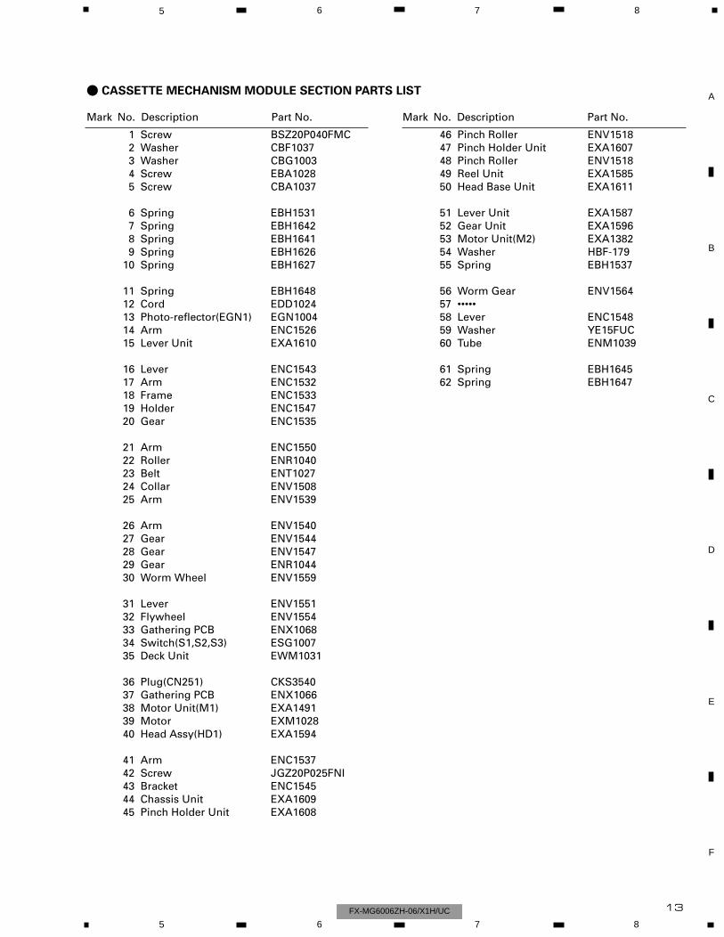
- CASSETTE MECHANISM MODULE SECTION PARTS LIST
1 Screw BSZ20P040FMC2 Washer CBF10373 Washer CBG10034 Screw EBA10285 Screw CBA1037
6 Spring EBH15317 Spring EBH16428 Spring EBH16419 Spring EBH1626
10 Spring EBH1627
11 Spring EBH164812 Cord EDD102413 Photo-reflector(EGN1) EGN100414 Arm ENC152615 Lever Unit EXA1610
16 Lever ENC154317 Arm ENC153218 Frame ENC153319 Holder ENC154720 Gear ENC1535
21 Arm ENC155022 Roller ENR104023 Belt ENT102724 Collar ENV150825 Arm ENV1539
26 Arm ENV154027 Gear ENV154428 Gear ENV154729 Gear ENR104430 Worm Wheel ENV1559
31 Lever ENV155132 Flywheel ENV155433 Gathering PCB ENX106834 Switch(S1,S2,S3) ESG100735 Deck Unit EWM1031
36 Plug(CN251) CKS354037 Gathering PCB ENX106638 Motor Unit(M1) EXA149139 Motor EXM102840 Head Assy(HD1) EXA1594
41 Arm ENC153742 Screw JGZ20P025FNI43 Bracket ENC154544 Chassis Unit EXA160945 Pinch Holder Unit EXA1608
46 Pinch Roller ENV151847 Pinch Holder Unit EXA160748 Pinch Roller ENV151849 Reel Unit EXA158550 Head Base Unit EXA1611
51 Lever Unit EXA158752 Gear Unit EXA159653 Motor Unit(M2) EXA138254 Washer HBF-17955 Spring EBH1537
56 Worm Gear ENV156457 •••••58 Lever ENC154859 Washer YE15FUC60 Tube ENM1039
61 Spring EBH164562 Spring EBH1647
Mark No. Description Part No. Mark No. Description Part No.
14
ELHOME
CLAMP
CD LOAD
POWER
CONTEMPH
ELVSNS
LOADSWDOORSW
MODESW
CG1
CG2
G15V
ELV1
ELV2LO1
LO2
PH3
PH2PH1
FM+B
MODESW
PICKUP UNIT(SERVICE)
MOTOR PCB(B)
MOTOR PCB(A)
CD CORE UNIT(SERVO UNIT)
PCB UNIT(D)
PCB UNIT(A)
PCB UNIT(C)
PCB UNIT(E) PCB UNIT(B)
LOAD MOTOR PCB
CD CORE UNIT(STS UNIT)
HOLOGRAMUNIT
FOCUS ACT
TRACKING ACT
MD
LD+
LD-LDMD
FO+
TO+
16
17
V5
Q101
Q102
PD
LD
CN101
IC 101UPC2572GS
RF AMP
IC 201UPD63702AGF
DIGITAL SERVOPROCESSOR
DIGITAL SIGNALPROCESSOR
µ-COMPUTERINTERFACE
35 69EFM
CD 4CH DRIVER
IC 301BA5986FM
14
11
16
15
22
BVDV5
MUTE
9
MD
/SD
/TD
/FD
74 10 11
VR
2
XTA
L
XTA
L
X2015V
VD
CONT
CN201 CN801
5V
VD
CN301
WDCKRFCKRAOVLRCKSCKODOUTMCK
IC 501CXD2511R
SHOCKPROOFCONTROLLER
BCKDATALRCK
XTLI39 5 12
IC 601AK4321VF
8fs DF D/A LPF CN701 CN701
6
18
DEMO
PD
IC 502MSM514400DP-60TS
4M DRAM
VDVD VDD
VDD
LCH
WD
SL/
CH
MO
/CH
MI
XW
RE
/XR
DE
/XQ
OK
XW
IH/X
EM
P/A
DR
MO
N/C
HD
T
V+5V IC 701BA05SFP
5V REGULATORVM
VD
POWER
CONTEMPH
4
2
1
XAO/XSTB/XSO/XSI/XSCK/XRST/SCONT
ELVSNS
LOADSWDOORSW
MODESW
S801
S802S803
MOTOR DRIVER
IC 802LB1836M
2
6
3
5
ELVSNS
MOTOR DRIVER
LB1836MIC 801
2
6
13
9
5
3
12
10
CG1
CG2
CG-
CG+
EL-
EL+ ELV1
ELV2LO1
LO2
MAXSW
PH2PH1
PVD
LO-
LO+
PVDPVD
Q801
VD
Q802LOAD
ELHOME
CLAMPCLAMP
ELHOME
CN802
CN101
M
BCL
SPINDLEMOTOR
CARRIAGEMOTOR
HOMESWITCH
ECVM
VCC
ST/SR
GND
HOME
MLOADINGMOTOR
MCAMGEARMOTOR
MELEVATIONMOTOR
Q851 Q852
D891 D892
PH1
PVD
Q881D883 PH2
S883
MAXSWITCH
PH1
PVD
PH1
PH2
MAXSW
LD MOTOR-
LD MOTOR+
MAXSW
PH2
PH1
PVD
ELV HOMES886
S887CLAMP
ELEVATIONSENSE
V+5V
5
14
15
4
3
1234
856
7
10
11
1 1
1
1
2
3
4
12
4
1
2
1
1
2
3
5
6
34
2
1
5
6
34
2
1
5
7
34
2
1
7
5
98
10
11
10 2
11 1
19
28
29
30
19
28
29
30
45
4446
42
8
9
43
42
3539
10
1
50
49
48
6
7
11
4
52
3
47
46
45
12
44
43
9
16
56
1
13
2753
26
79
172
18
6261
75
60
5958
57
78
77
76
55
6
5
72 69
12
41
50
1
2
3
45
44
40
47
4649
48
4
5
6
39
7
8
36
3537
32
33
39
41
41
43
48
50
BU
Lch TAL
LOAD CD LOAD
ELHOME
CLAMP
CONTEMPH
POWER
LOADSWDOORSW
CG1
CG2
G15V
ELV1
ELV2LO1
LO2
PH3
PH2PH1
Q151
Q152CD MUTE
CD MUTE
Q803
Q804
Q801
Q802
BU VDD
VDD
VCC
Q407
VDDVDDVCC
FM+B
Q406Q410
Q402
Q411
Q401
Q412
Q405
20
3
4
TUNER UNIT
CONTROL UNIT
25
26
FM FRONT ENDQ3
Q201 Q202
AM RF
FM/AM 1ST IF 10.7MHzT31 Q31 CF51
9 10
32 36
14
19
247 1191715
6189
7
30 28 27 40433138
34
6
41
23 25 16 18CF232
CF52 CF53 T51
FMOSC
AMOSC
FMT
V
AM
TV
AM
IFC
VC
O
MO
NO
SE
EK
IC 401LC72146MQ2
FMSL
AMSLFMSD
TUL
Q409Q408 9
11
6
13
19
17
161 24
X401
19 20 15 17 4 12 22 23
43 45 27
IC 2PA4024A
IC 1PA4023B
AM+B
Q701
VCC
VDD
1421
29
28
40
XOUT15bsen
CDLOAD
EREF
ELVSNS
EMPHCONT
CDCONT
POWER
cdmute
25
RESET
reset
XIN
adenaVREF
PD5851AIC 701
CN401ANT401
bsen
TUL
CDL
VDIN
PLL
Lch
B.U
MTLLOAD
5
1
4
21
3
4
11
20
8
DECK UNIT
IC251HA12216F
IC351PA2020A
DOLBY B NR
MECHANISMDRIVER
CN251CN252
CN254
CN255
CN253
7
18
FWDL-ch
REVL-ch
373639
18 19
3 1 5 6
8 7 10
CN2563 1 5 6
S1LOAD
S2MODE
EGN1REEL
SENSE
M
M
M2SUB
MOTOR
M1MAIN
MOTOR
521
REEL SENSE PCB
S370µs
4
LOAD
MTL8
11
16
4
B
DE
F
G
HI
J
K
L
M
A
N
O
1 2 3 4
1 2 3 4
F
E
D
C
B
A
FX-MG6006ZH-06/X1H/UC
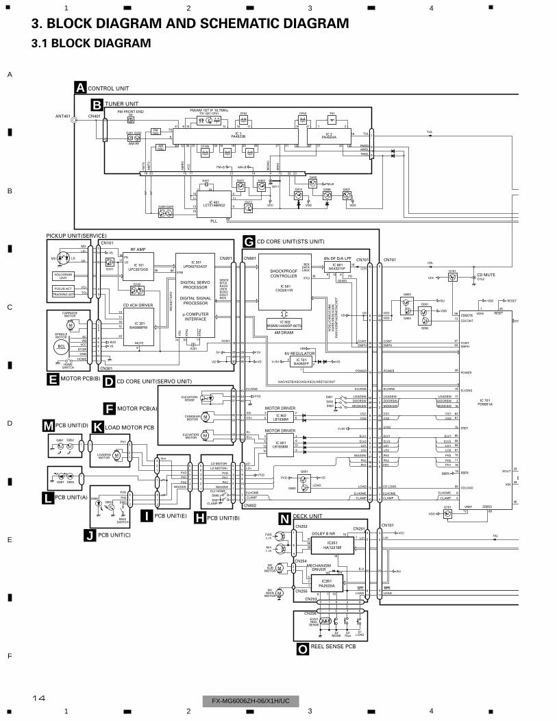
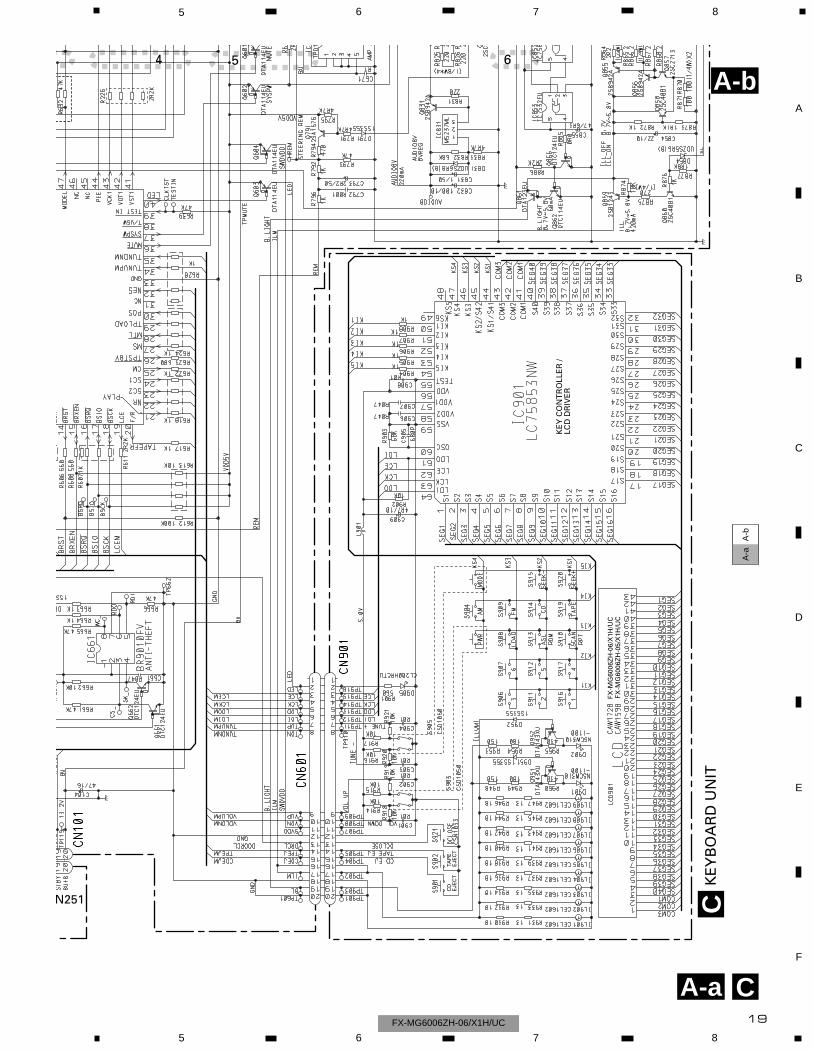
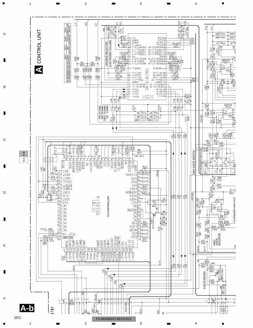
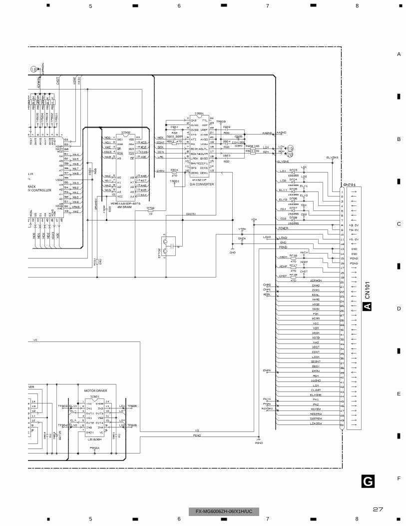
3. BLOCK DIAGRAM AND SCHEMATIC DIAGRAM
3.1 BLOCK DIAGRAM
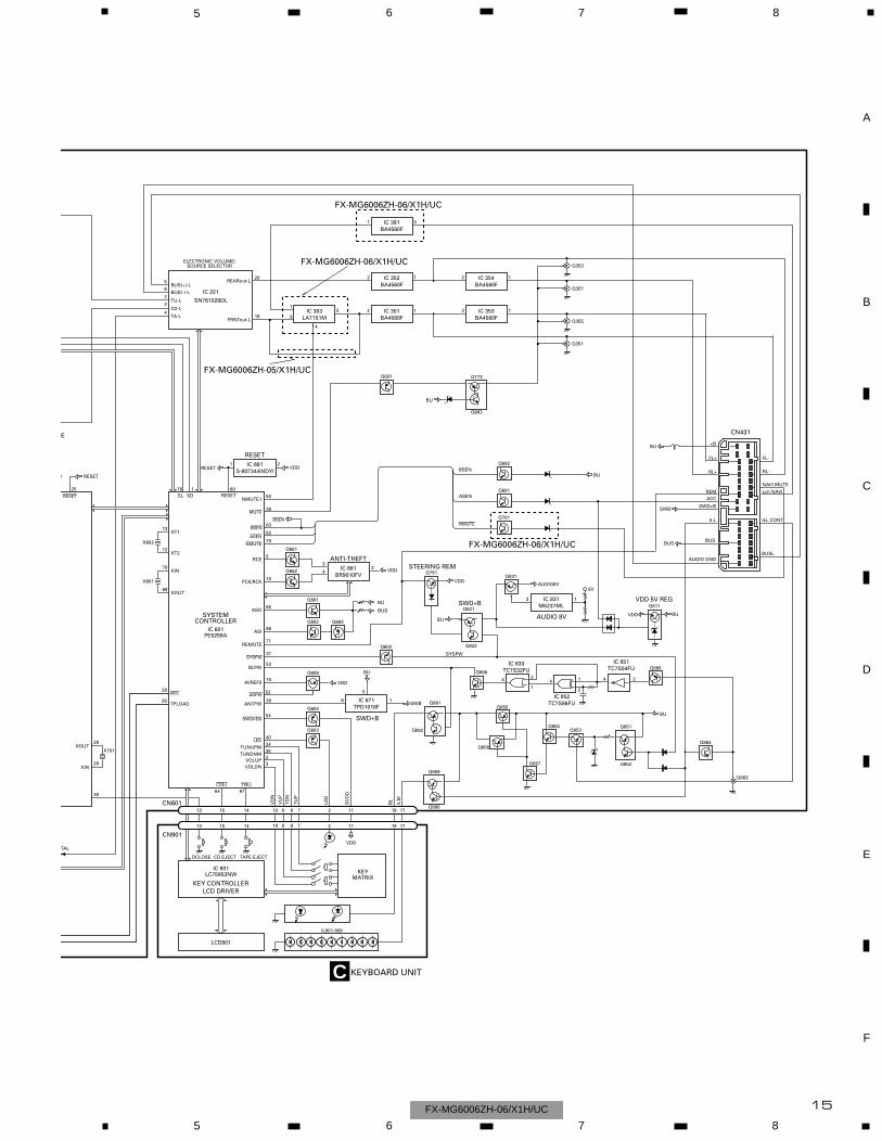
15
IL901-909
TAL
E
D
VDD
BUS
BU
X602
X601
X701
13 15 14
13 15
64 67
14 10 9 8 7
10 9 8 7
2
LC75853NWIC 901
LCD901
Q603
Q604
Q606
Q602
Q831Q791
2
11
11
19
19
17
17
DCLOSE CD EJECT TAPE EJECT
VDD
Q821
Q822
VDD
BU
AUDIO8V
nmute
ASEN
BSEN
Q864
Q863
Q351
Q355
Q357
Q353
Q781
Q691
Q692
IC 831M5237ML
BU
Q811
VDD BU
Q601 Q773
Q693
BU
IC 691S-80734ANDYI
IC 353BA4560F
2 1
IC 354BA4560F
2 1
IC 351BA4560F
2 1
IC 352BA4560F
25
20
50
6076 1
19
6
2
3
4
1
IC 303LA7151M
1
1
3
4
2
2
35
4
IC 391BA4560F
1 3
BUSLAUDIO GND
Lch NAVI
RL-RL+
FL+ FL-
ACC
NAVI MUTE
BUS
REM
ILL CONTILL
TA-L
CD-L
TU-L
BUS(-)-L
BUS(+)-LREARout-L
NMUTE1RESET
RESET
RESET
73XT1
72XT2
70XIN
69
29
28
40
XOUT
XOUT
25
RESET
reset
XIN
36
63
62
37
75AVREF0
Q68266
ASI
65ASO
10PCK/RCK
5RCE
52
53BLPW
54
4034
TUNUPM35
TUNDNM2
VOLUP3
VOLDN
79nmute
FRNTout-L
SN761029DL
IC 221
CONTROLLERSYSTEM
PE5258AIC 601
bsen
MATRIXKEY
CN431
ELECTRONIC VOLUME/SOURCE SELECTOR
CN601
CN901
8V
13
KEYBOARD UNIT
SL SD
VD
N
VU
P
TD
N
TU
P
LED
SV
DD
BL
ILM
BUS
Q681
Q683
Q661
Q662 IC 661BR9010FV
ANTI-THEFT
VDD
+BBU
SWD+BSWB
IC 671TPD1018F
6 1SWB
BU
5
ANTPW38
cdej tpej
led
swdvdd
adpw
syspw
asen
bsen
mute
SWD+B
AUDIO 8V
Q859
Q860
BUQ855
Q856
Q857
Q854Q853
Q851
Q852
KEY CONTROLLERLCD DRIVER
Q865Q866
Q861
Q862
IC 851TC7S04FU
IC 852TC7S86FU
IC 833TC7S32FU
2424 4 1
21mtl
TPLOAD
28
26
REMOTE77
VDD
SWD+B
STEERING REM
VDD 5V REG
SYSPW
FX-MG6006ZH-06/X1H/UC
FX-MG6006ZH-05/X1H/UC
FX-MG6006ZH-06/X1H/UC
FX-MG6006ZH-06/X1H/UC
C
5 6 7 8
F
E
D
C
B
A
5 6 7 8FX-MG6006ZH-06/X1H/UC
CDEJECT
TAPEEJECT
FX-MG6006ZH-06/X1H/UCFX-MG6006ZH-05/X1H/UC
FX-MG6006ZH-05/X1H/UC FX-MG6006ZH-06/X1H/UC
TC601Not usedCCL1046
C6078P2P
R631Not used47K
R63247KNot used
TUNER UNITB
CD CORE UNIT (STS UNIT)G
DE
CK
UN
ITN
CN
251
KEYBOARD UNIT
CN701
RESET
KEY CONTROLLER /LCD DRIVER
SYSTEM CONTROLLER
PLL
CD MUTE
C
ANTENNA
5
63
2
4 1FM:-26.0dBs(400Hz 22.5kHz dev)AM:-21.5dBs(400Hz 30% mod)
CD:+2.13dBs(1kHz 0dB)
TAPE:-6.0dBs(315Hz 200nwb)
16
1 2 3 4
1 2 3 4
F
E
D
C
B
A
FX-MG6006ZH-06/X1H/UC
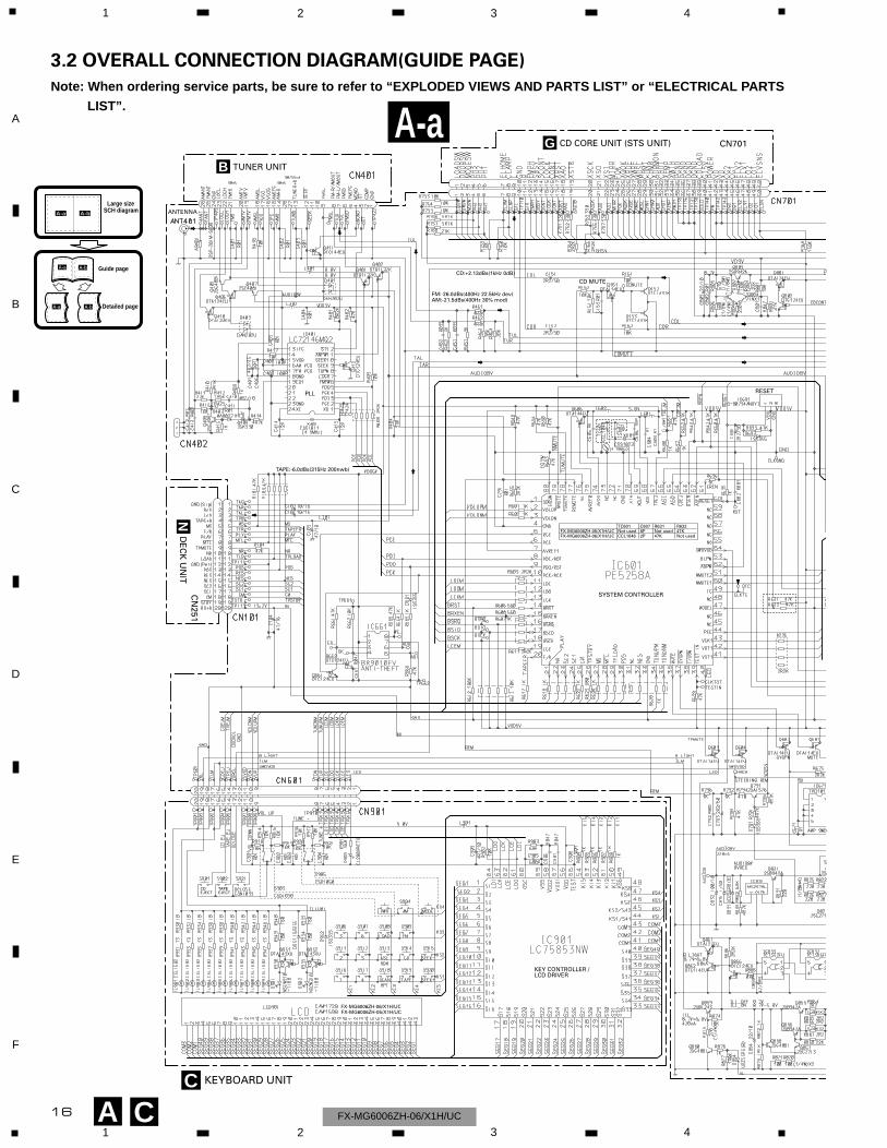
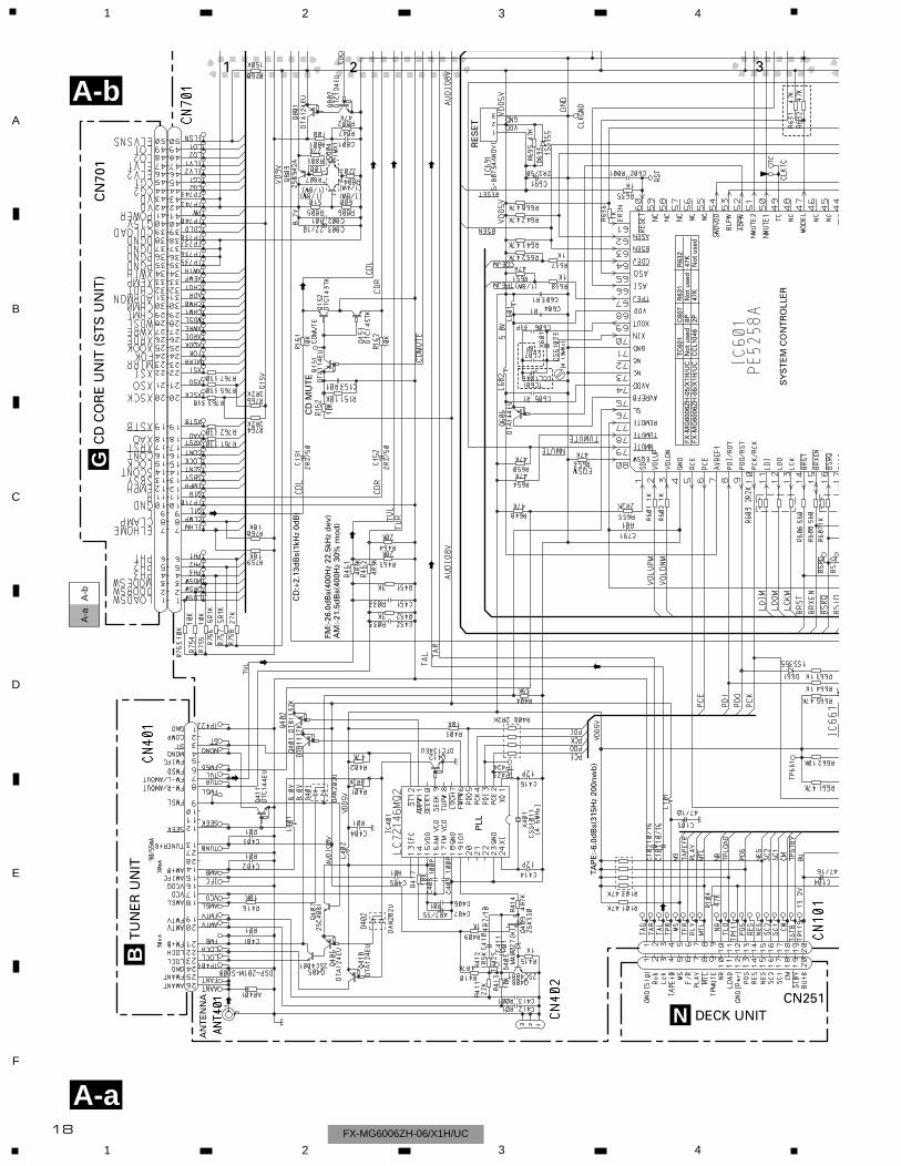
3.2 OVERALL CONNECTION DIAGRAM(GUIDE PAGE)
Note: When ordering service parts, be sure to refer to “EXPLODED VIEWS AND PARTS LIST” or “ELECTRICAL PARTS
LIST”.
A-a A-b
A-aA-a A-b A-b
A-b A-b A-a A-a
Large sizeSCH diagram
Guide page
Detailed page
A-a
A C
DCL
OSE
FX-MG6006ZH-06/X1H/UC
FX-MG6006ZH-05/X1H/UC
FX-MG6006ZH-05/X1H/UC
R271 R272 C253 C254FX-MG6006ZH-05/X1H/UC 0R0 0R0 Not used Not usedFX-MG6006ZH-06/X1H/UC Not used Not used 4R7/16 4R7/16
FX-MG6006ZH-06/X1H/UC
FX-MG6006ZH-05/X1H/UC
FX-MG6006ZH-06/X1H/UC
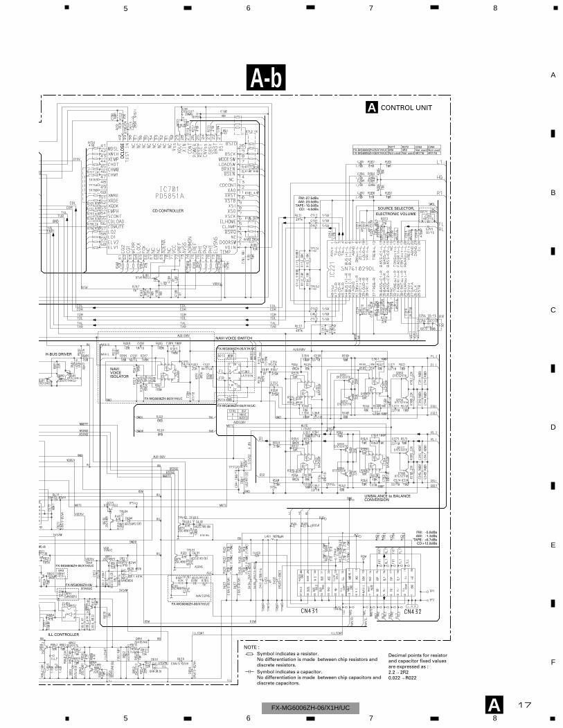
A CONTROL UNIT
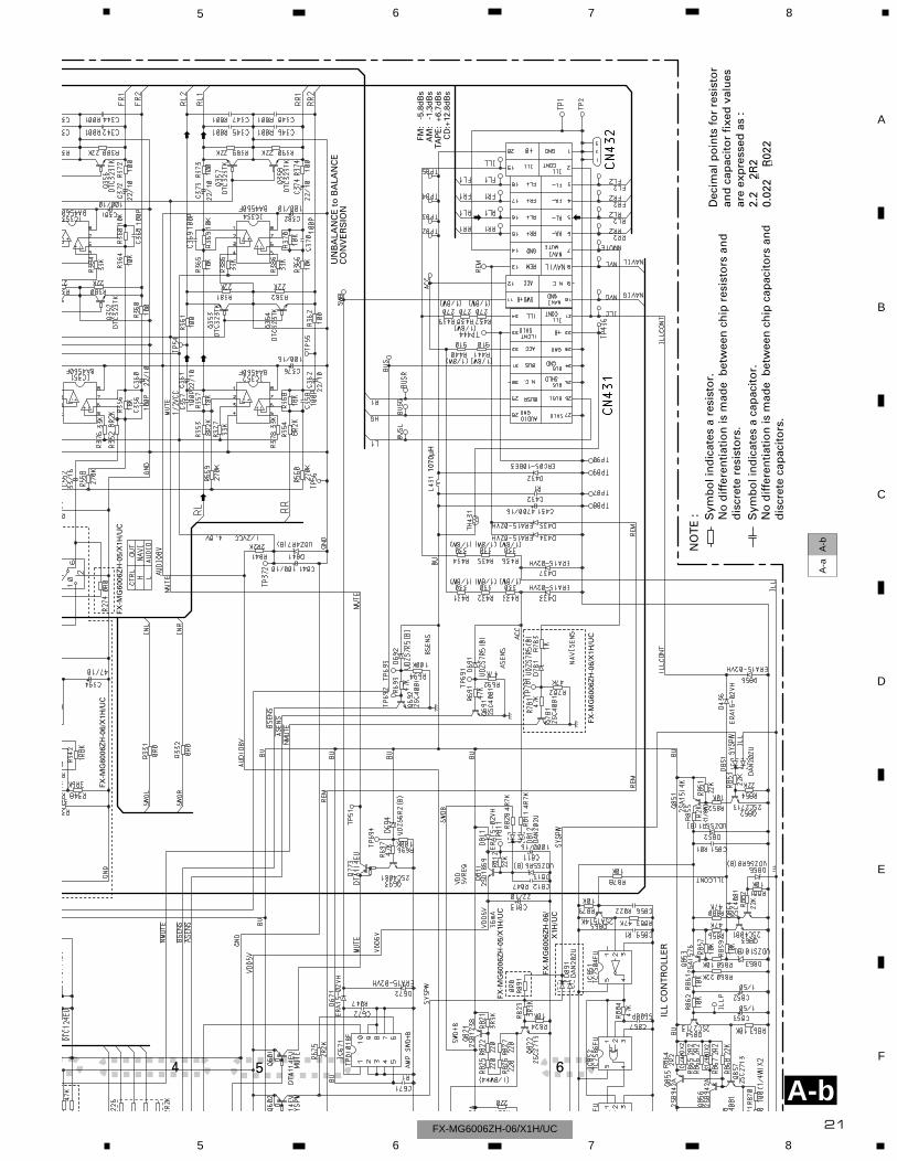
Decimal points for resistorand capacitor fixed valuesare expressed as :2.2 2R20.022 R022
← ←
Symbol indicates a resistor.No differentiation is made between chip resistors anddiscrete resistors.
NOTE :
Symbol indicates a capacitor.No differentiation is made between chip capacitors anddiscrete capacitors.
UNBALANCE to BALANCECONVERSION
NAVI VOICE SWITCH
NAVIVOICEISOLATOR
CD CONTROLLERSOURCE SELECTOR,
ELECTRONIC VOLUME
H-BUS DRIVER
ILL CONTROLLER
FM:-27.5dBsAM:-23.0dBs
TAPE:-10.0dBsCD: -4.0dBs
FM: -5.8dBsAM: -1.3dBs
TAPE: +6.7dBsCD:+12.8dBs
1070µH
17
5 6 7 8
F
E
D
C
B
A
5 6 7 8FX-MG6006ZH-06/X1H/UC
A-b
A
A-a
A-b
A-a
A-a
A-b1 2 3
FX-M
G60
06Z
H-0
5/X
1H/U
C
FX-M
G60
06Z
H-0
6/X
1H/U
C
TC
601
No
t u
sed
CC
L104
6
C60
78P 2P
R63
1N
ot
use
d47
K
R63
247
KN
ot
use
d
TU
NE
R U
NIT
B
CD
CO
RE
UN
IT (
ST
S U
NIT
)G
DECK UNITNCN251
CN
701
RE
SE
T
SY
ST
EM
CO
NT
RO
LLE
R
PLL
CD
MU
TE
AN
TE
NN
A
5
63
2
41
FM:-
26.0
dB
s(40
0Hz
22.5
kHz
dev
)A
M:-
21.5
dB
s(40
0Hz
30%
mo
d)
CD
:+2.
13d
Bs(
1kH
z 0d
B)
TAP
E:-
6.0d
Bs(
315H
z 20
0nw
b)
18
1 2 3 4
1 2 3 4
F
E
D
C
B
A
FX-MG6006ZH-06/X1H/UC
A-a
A-b
A-a
A-a
A-b
C
4 5 6
CD
EJE
CT
TAP
EE
JEC
T
FX-M
G60
06Z
H-0
6/X
1H/U
CFX
-MG
6006
ZH
-05/
X1H
/UC
N251
KE
YB
OA
RD
UN
IT
KE
Y C
ON
TR
OLL
ER
/LC
D D
RIV
ER
C
19
5 6 7 8
F
E
D
C
B
A
5 6 7 8FX-MG6006ZH-06/X1H/UC
A-a
A-b
A-b1 2 3
DCLOSE
FX-M
G60
06Z
H-0
6/X
1H/U
C
FX-M
G60
06Z
H-0
5/X
1H/U
C
R27
1R
272
C25
3C
254
FX-M
G60
06Z
H-0
5/X
1H/U
C0R
00R
0N
ot
use
dN
ot
use
dFX
-MG
6006
ZH
-06/
X1H
/UC
No
t u
sed
No
t u
sed
4R7/
164R
7/16
AC
ON
TR
OL
UN
IT
NA
VI V
OIC
E S
WIT
CH
NA
VI
VO
ICE
ISO
LAT
OR
CD
CO
NT
RO
LLE
RS
OU
RC
E S
ELE
CT
OR
,
ELE
CT
RO
NIC
VO
LUM
E
H-B
US
DR
IVE
R
FM:-
27.5
dB
sA
M:-
23.0
dB
sTA
PE
:-10
.0d
Bs
CD
: -4
.0d
Bs
20
1 2 3 4
1 2 3 4
F
E
D
C
B
A
FX-MG6006ZH-06/X1H/UC
A-a
A-b
A-b4 5 6
FX-M
G60
06Z
H-0
6/X
1H/U
C
FX-M
G60
06Z
H-0
5/X
1H/U
C
FX-M
G60
06Z
H-0
6/X
1H/U
C
FX-M
G60
06Z
H-0
5/X
1H/U
C
FX-M
G60
06Z
H-0
6/X
1H/U
C
Dec
imal
po
ints
fo
r re
sist
or
and
cap
acit
or
fixe
d v
alu
esar
e ex
pre
ssed
as
:2.
2
2R2
0.02
2
R02
2
←
←
Sym
bo
l in
dic
ates
a r
esis
tor.
No
dif
fere
nti
atio
n is
mad
e b
etw
een
ch
ip r
esis
tors
an
dd
iscr
ete
resi
sto
rs.
NO
TE
: Sym
bo
l in
dic
ates
a c
apac
ito
r.N
o d
iffe
ren
tiat
ion
is m
ade
bet
wee
n c
hip
cap
acit
ors
an
dd
iscr
ete
cap
acit
ors
.
UN
BA
LAN
CE
to
BA
LAN
CE
CO
NV
ER
SIO
N
ILL
CO
NT
RO
LLE
R
1070
µHFM
: -
5.8d
Bs
AM
: -
1.3d
Bs
TAP
E:
+6.7
dB
sC
D:+
12.8
dB
s
21
5 6 7 8
F
E
D
C
B
A
5 6 7 8FX-MG6006ZH-06/X1H/UC
22
B
A
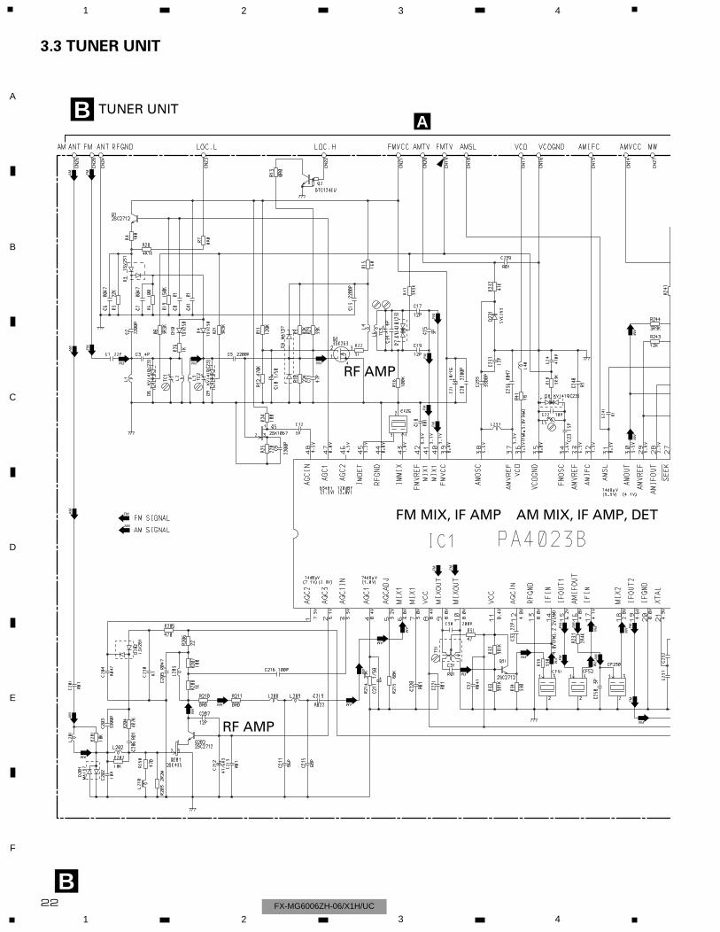
FM MIX, IF AMP AM MIX, IF AMP, DET
RF AMP
RF AMP
AM
AM
AM
AM
AM
AM
AM AM
AM
AM
AM
AM
AM
AM
AM
AM
AM
FM
FM
FM FM FM
FM
FMFM
FMFM FM
FM
FM
FM
FMFM FM
FM FMFM
FM
FM
TUNER UNITB
1 2 3 4
1 2 3 4
F
E
D
C
B
A
FX-MG6006ZH-06/X1H/UC
3.3 TUNER UNIT
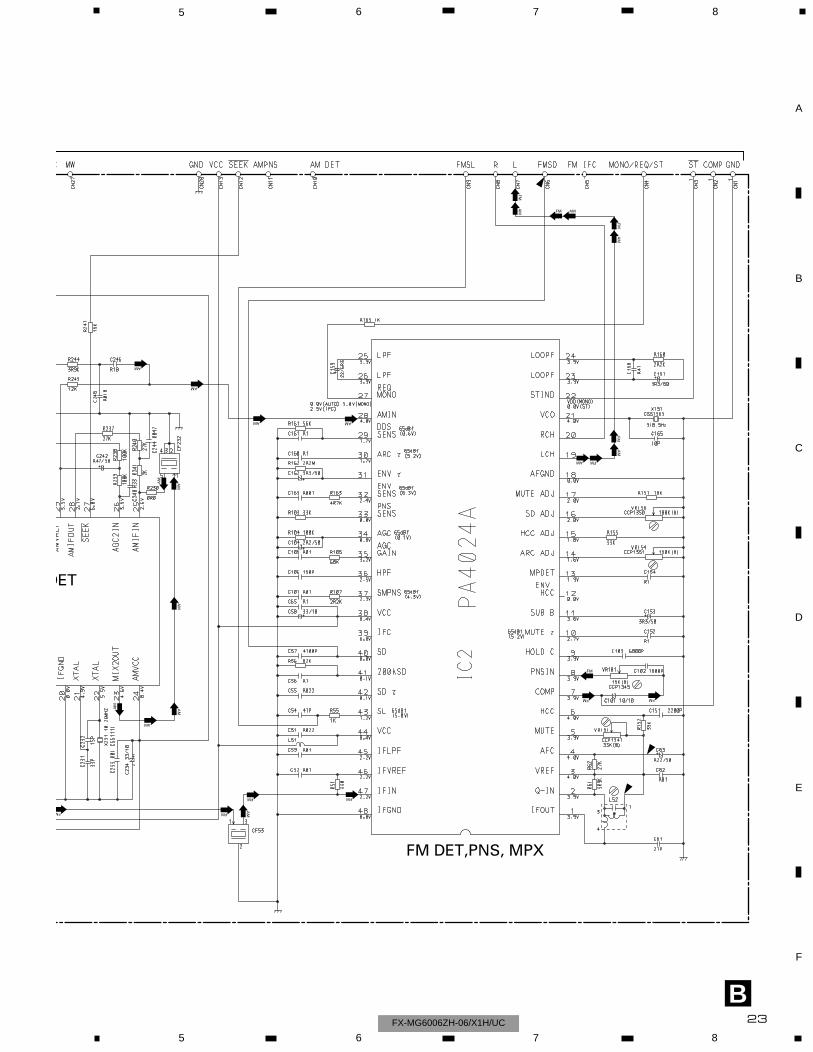
23
B
DET
FM DET,PNS, MPX
AM
AM
AM
AM
AMA
M
AM
AM
AM AM
AM
AM
AM
AM AM
FM FM
FM
AM
FM
FM FM
FM
FM
FMFM
FM
FM
5 6 7 8
F
E
D
C
B
A
5 6 7 8FX-MG6006ZH-06/X1H/UC
D E
PU UNIT(SERVICE)
M5 SPINDLECXM1120
DISC INSERT DETECT
M4 CARRIAGECXC1389
2.5V
RF AMP/AUTO POWERCONTROL
CD DRIVER
D
EMOTOR PCB(B)
CD CORE UNIT(SERVO UNIT)
24
1 2 3 4
1 2 3 4
F
E
D
C
B
A
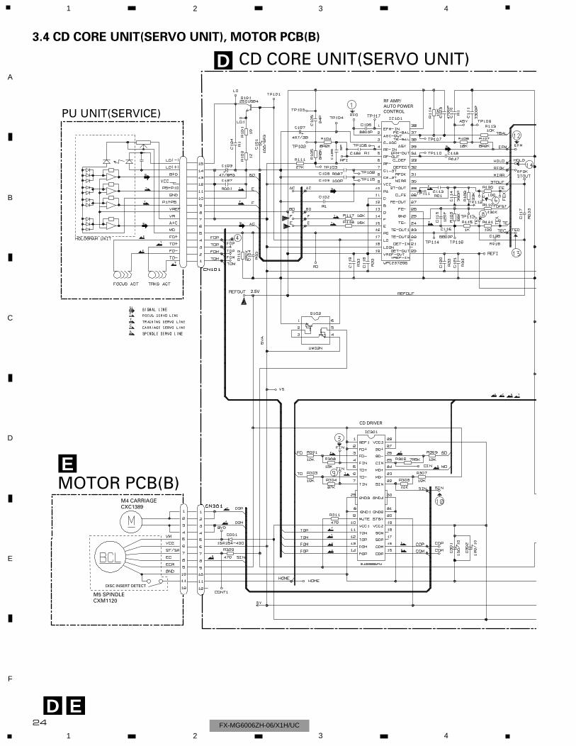
FX-MG6006ZH-06/X1H/UC
3.4 CD CORE UNIT(SERVO UNIT), MOTOR PCB(B)
D
16.934MHz
22/6
R3
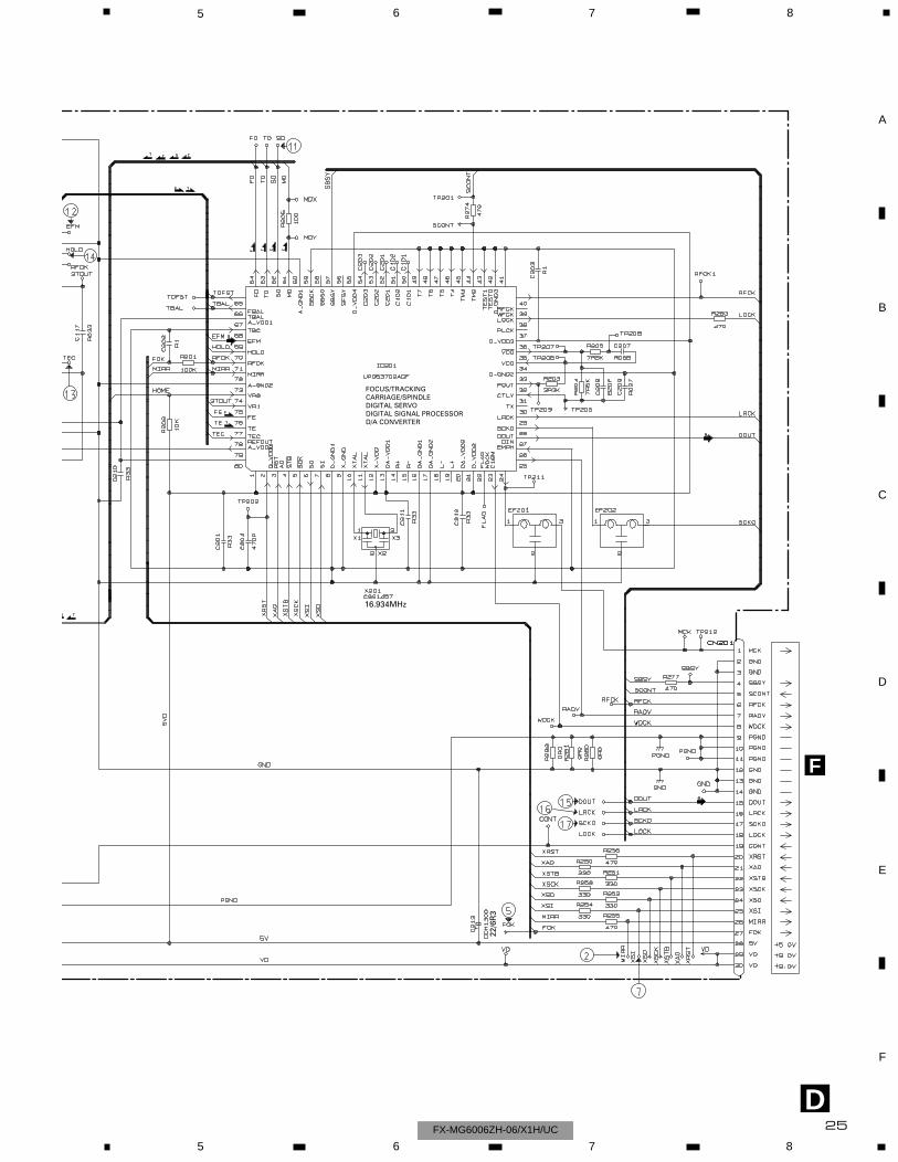
FOCUS/TRACKINGCARRIAGE/SPINDLEDIGITAL SERVODIGITAL SIGNAL PROCESSORD/A CONVERTER
F
25
5 6 7 8
F
E
D
C
B
A
5 6 7 8FX-MG6006ZH-06/X1H/UC
F G
M1
Q1 : RPI-221
M3
SURE TRACKMEMORY CONTROL
+5V REGULATOR
7.5V
9.0V
MOTOR DRIVER
G
F
D
H LOAD SWITCH
DOOR SWITCH
MODE SWITCH
CD CORE UNIT(STS UNIT)C
D C
OR
E U
NIT
(SE
RV
O U
NIT
)
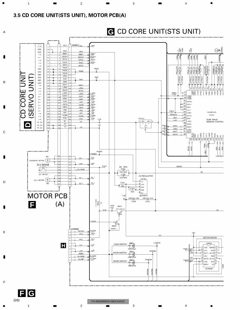
MOTOR PCB (A)
ELV SENSE
26
1 2 3 4
1 2 3 4
F
E
D
C
B
A
FX-MG6006ZH-06/X1H/UC
3.5 CD CORE UNIT(STS UNIT), MOTOR PCB(A)
G
22/6R3
RACKRY CONTROLLER
VERMOTOR DRIVER
4M DRAM
D/A CONVERTER
AC
N10
1
27
5 6 7 8
F
E
D
C
B
A
5 6 7 8FX-MG6006ZH-06/X1H/UC
28
1 2 3 4
1 2 3 4
F
E
D
C
B
A
FX-MG6006ZH-06/X1H/UC
1 RFO 0.5V/div. 0.2µs/div.Normal mode: play
1 CH1: RFO 1V/div.2 CH2: MIRR 5V/div.
Test mode: Tracking open
0.5ms/div.
1 CH1: RFO 1V/div.2 CH2: MIRR 5V/div.
Normal mode: The defect partpasses 500µs/div.
0.5ms/div.
3 CH1: FIN 0.5V/div.4 CH2: FOP 2V/div.
Test mode: No disc, Focus close
0.2s/div.3 CH1: FIN 0.5V/div.5 CH2: FOK 2V/div.
Normal mode: Focus close
0.2s/div.
6 CH1: FEY 0.5V/div.7 CH2: XSI 2V/div.
Normal mode: Focus close
1ms/div. 8 CH1: TEY 0.5V/div.9 CH2: TIN 0.5V/div.
Test mode: 32 tracks jump (FWD)
0.5ms/div. 8 CH1: TEY 0.5V/div.9 CH2: TIN 0.5V/div.
Test mode: Single jump (FWD)
0.5ms/div.
6 CH1: FEY 0.1V/div.3 CH2: FIN 0.2V/div.
Normal mode: Play
20ms/div. 3 CH1: FIN 0.5V/div.0 CH2: SIN 1V/div.
Normal mode: Focus close
0.5s/div.
GND →
GND →
GND →
GND →
- Waveforms
0 SIN 0.5V/div. 0.1s/div.
Normal mode: Play
REFOUT→ REFOUT→
REFOUT→
REFOUT→
REFOUT→
REFOUT→
REFOUT→
REFOUT→
REFOUT→
REFOUT→
REFOUT→
REFOUT→
REFOUT→
REFOUT→
REFOUT→
REFOUT→
1 RFO 0.5V/div. 0.5µs/div.Test mode
REFOUT→
REFOUT→
REFOUT→
Note:1. The encircled numbers denote measuring pointes in the circuit diagram.2. Reference voltage
REFOUT:2.5V
29
5 6 7 8
F
E
D
C
B
A
5 6 7 8FX-MG6006ZH-06/X1H/UC
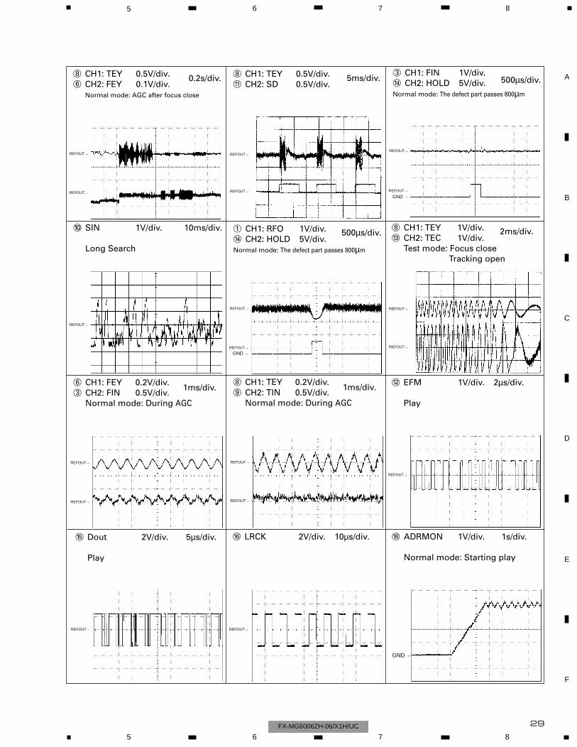
3 CH1: FIN 1V/div.$ CH2: HOLD 5V/div.Normal mode: The defect part passes 800µm
8 CH1: TEY 0.5V/div.6 CH2: FEY 0.1V/div.
Normal mode: AGC after focus close
8 CH1: TEY 0.5V/div.! CH2: SD 0.5V/div.
5ms/div.
0 SIN 1V/div. 10ms/div.
Long Search
8 CH1: TEY 1V/div.# CH2: TEC 1V/div.
Test mode: Focus closeTracking open
2ms/div.
6 CH1: FEY 0.2V/div.3 CH2: FIN 0.5V/div.
Normal mode: During AGC
1ms/div.@ EFM 1V/div. 2µs/div.
Play
0.2s/div.
% Dout 2V/div. 5µs/div.
Play
^ LRCK 2V/div. 10µs/div. * ADRMON 1V/div. 1s/div.
Normal mode: Starting play
GND →
REFOUT→
REFOUT→
REFOUT→
REFOUT→
REFOUT→
REFOUT→
REFOUT→
REFOUT→
REFOUT→
REFOUT→
REFOUT→
REFOUT→
REFOUT→ REFOUT→
1 CH1: RFO 1V/div.$ CH2: HOLD 5V/div.Normal mode: The defect part passes 800µm
500µs/div.
REFOUT→
REFOUT→
8 CH1: TEY 0.2V/div.9 CH2: TIN 0.5V/div.
Normal mode: During AGC
1ms/div.
REFOUT→
REFOUT→
GND →
GND →
500µs/div.
30
1 2 3 4
1 2 3 4
F
E
D
C
B
A
FX-MG6006ZH-06/X1H/UC
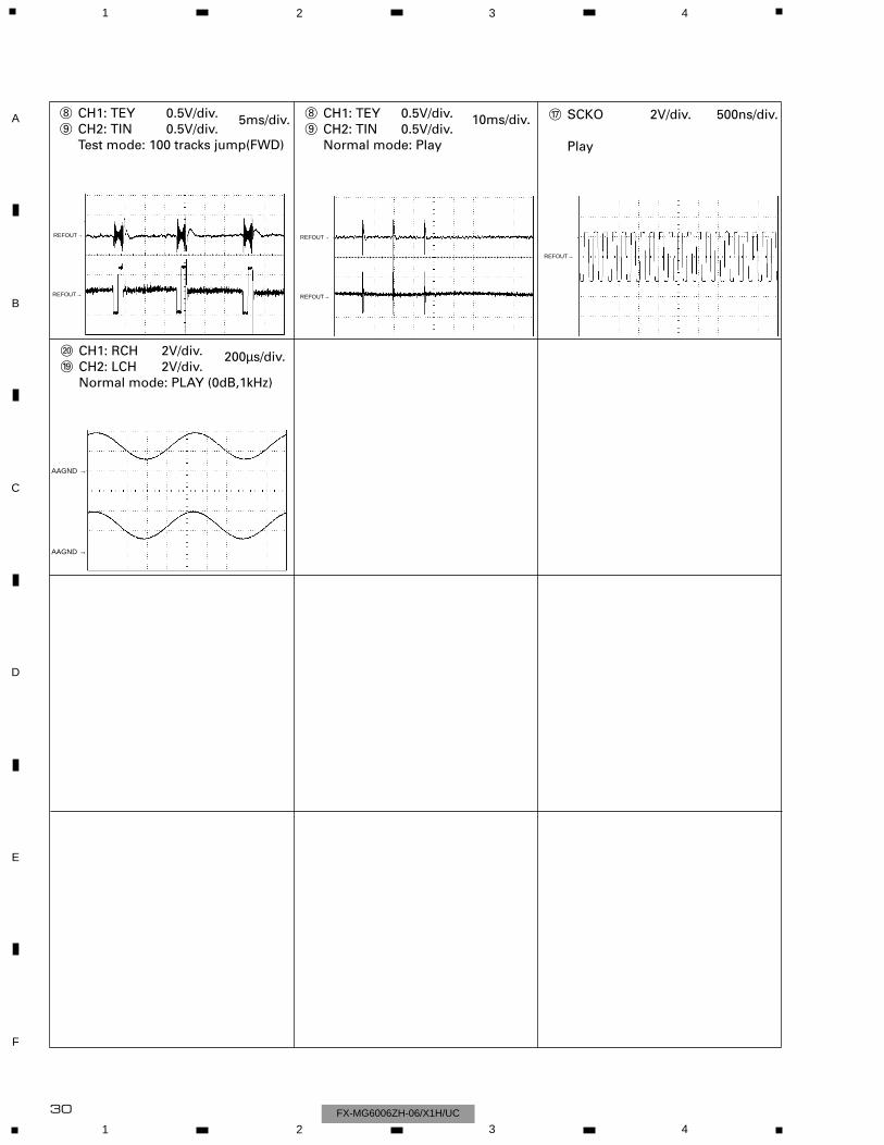
8 CH1: TEY 0.5V/div.9 CH2: TIN 0.5V/div.
Test mode: 100 tracks jump(FWD)
8 CH1: TEY 0.5V/div.9 CH2: TIN 0.5V/div.
Normal mode: Play
10ms/div.5ms/div.
REFOUT→
REFOUT→
& SCKO 2V/div. 500ns/div.
Play
REFOUT→
) CH1: RCH 2V/div.( CH2: LCH 2V/div.
Normal mode: PLAY (0dB,1kHz)
200µs/div.
AAGND →
AAGND →
REFOUT→
REFOUT→
L MJ KH I
HIJ
L
M
K
CXC1388
GCN802
MAX DETECT SWITCH
PCB UNIT(A)
PCB UNIT(C) PCB UNIT(E) PCB UNIT(B)
PCB UNIT(D)
LOAD MOTOR PCB
CPT231SCTD
CPT231SCTD
31
5 6 7 8
F
E
D
C
B
A
5 6 7 8FX-MG6006ZH-06/X1H/UC
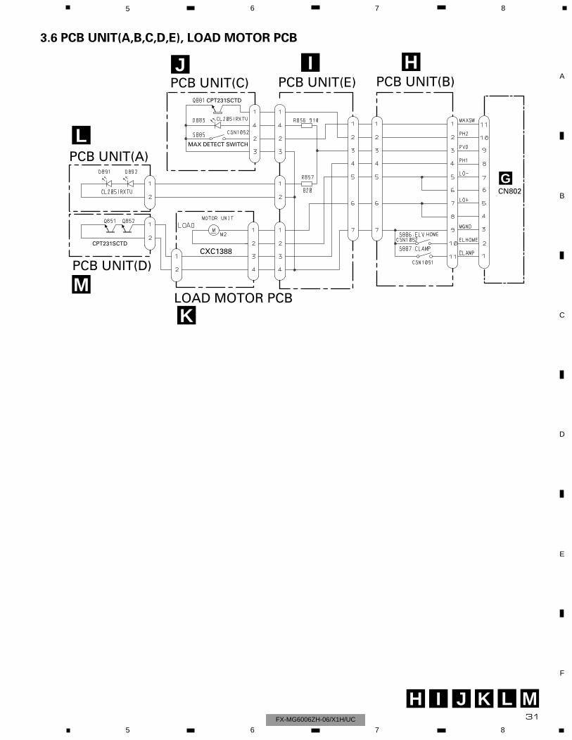
3.6 PCB UNIT(A,B,C,D,E), LOAD MOTOR PCB
N
A
N DECK UNIT
MU
TE
HA12216F
11121314151617181920
40393837363534333231
30 29 28 27 26 25 24 23 22 21
1 2 3 4 5 6 7 8 9 10
R256
180
R291
0R0
C271
1/50
R283 0R0
R284 0R0
R282 0R0
C253 390P
C254 390P
C252 390P
C251 390P
R281 0R0
R255
180
C25
6
R01
R258
18K
R40
2
3R3K
R403 910
R32
2
0R0
R293
0R0
C272 R1
R28
7
0R0
R28
50R
0
HD1HEAD ASSYEXA1594
TEST TAPENCT-150(400Hz, 200nWb/m)
RL
RR
FR
FL
C30
2
R1
VR302
33K(B)
-8.24dBs(300mV)±1dB
Fwd-R
Fwd-L
Rev-R
Rev-L
NFI(L)
RIN(L)
RIP
FIN(L)
GND
GND
FIN(R)
VREF
RIN(R)
NFI(R)
M-O
UT
(R)
EQ
OU
T(R
)
TA
I(R
)
BIA
S
RA
I(R
)
PB
OU
T(R
)
DE
T(L
)
MU
TE
MSGV(R)
MAOUT
MSI
MSDET
MSGV
F/R
120/70
NR
MO
UT
(L)
EQ
OU
T(L
)
TA
I(L) NC
RA
I(L)
PB
OU
T(L
)
NC
DE
T(L
)
MS
GV
(S)
CN252
CN251
DOLBY B NR
IC251
VR301
33K(B)
C31
0
R1
C30
9
R1
R32
1
0R0
VCC
CCP1280
CCP1280
NC
MSOUT
NC
NC
R260
13K
R26
2
270K
C40
1
3900
P
R40
1
15K
R27
6
100K
C40
2
R33
C404 R01
C40
3
R02
2R
274
0R0
R273
0R0
R27
2
0R0
R292
0R0
R27
1
18K
C30
1
R1
R294
0R0
R259
13K
C25
5
R01
R257
18K
R26
1
270K
CN101
32
1 2 3 4
1 2 3 4
F
E
D
C
B
A
FX-MG6006ZH-06/X1H/UC
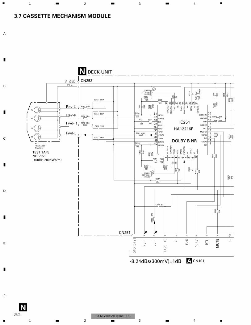
3.7 CASSETTE MECHANISM MODULE
33
5 6 7 8
F
E
D
C
B
A
5 6 7 8FX-MG6006ZH-06/X1H/UC
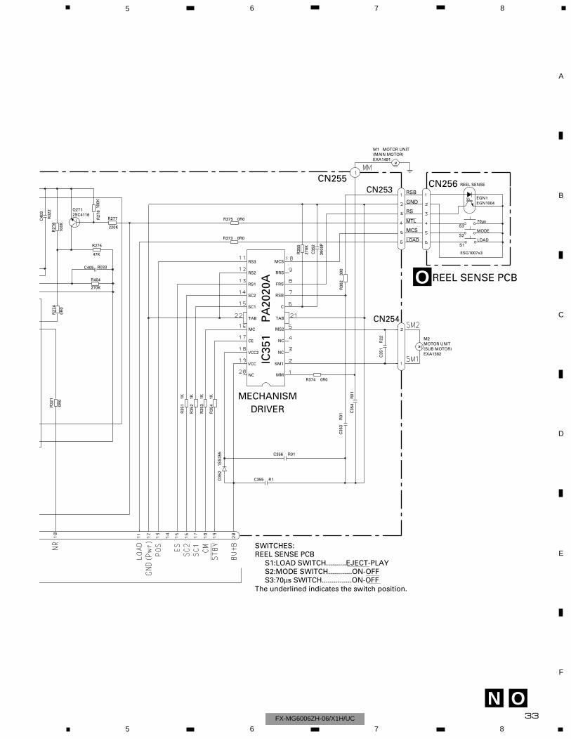
ON
O REEL SENSE PCB
SWITCHES:REEL SENSE PCB S1:LOAD SWITCH..........EJECT-PLAY S2:MODE SWITCH............ON-OFF S3:70µs SWITCH...............ON-OFFThe underlined indicates the switch position.
R275
47K
R35
11K
R35
21K
R35
31K
R35
41K
R373 0R0
R35
5
270K
C35
2
3900
P
R36
230
0
C35
1R
22
C35
3R
01
C35
4R
01
R374 0R0
C356 R01
C355 R1D35
21S
S35
5
M1 MOTOR UNIT(MAIN MOTOR)EXA1491
S1LOAD
ESG1007x3
S2MODE
REEL SENSE
EGN1EGN1004
M2MOTOR UNIT(SUB MOTOR)EXA1382
RS3
RS2
RS1
SC2
SC1
TAB
MC
CE
VCC2
NC
VCC
MCS
RRS
FRS
RSB
C
TAB
MS2
NC
NC
MM
SM1
RSB
GND
RS
mtl
MCS
load
CN255CN253
CN256
CN254
MECHANISMDRIVER
IC35
1
PA
2020
A
R32
1
0R0
R375 0R0
S370µs
R27
6
100K
C40
3
R02
2R
274
0R0
R404
270K
C405 R033
R277
220K
R27
810
0K
Q2712SC4116
34
CapacitorConnector
P.C.Board Chip Part
A
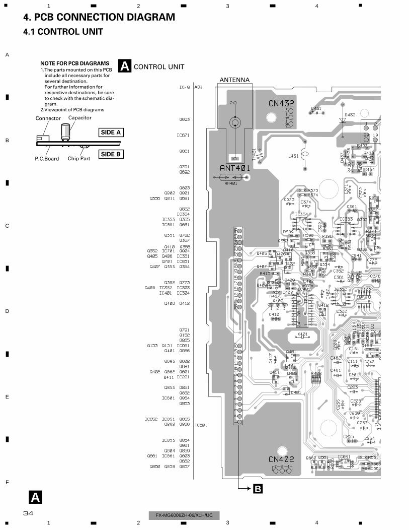
A CONTROL UNIT
SIDE B
SIDE A
NOTE FOR PCB DIAGRAMS
1.The parts mounted on this PCB include all necessary parts for several destination. For further information for respective destinations, be sure to check with the schematic dia- gram.2.Viewpoint of PCB diagrams
ANTENNAADJ
B
1 2 3 4
1 2 3 4
F
E
D
C
B
A
FX-MG6006ZH-06/X1H/UC
4. PCB CONNECTION DIAGRAM
4.1 CONTROL UNIT
35
A
SIDE A
FRONT
G CN701
N CN251
C CN901
CLKTST
CLKTC
CLKGND
5 6 7 8
F
E
D
C
B
A
5 6 7 8FX-MG6006ZH-06/X1H/UC
36
A
A CONTROL UNIT
1 2 3 4
1 2 3 4
F
E
D
C
B
A
FX-MG6006ZH-06/X1H/UC
37
A
SIDE B
5 6 7 8
F
E
D
C
B
A
5 6 7 8FX-MG6006ZH-06/X1H/UC
B
B TUNER UNITSIDE A
A
38
1 2 3 4
1 2 3 4
F
E
D
C
B
A
FX-MG6006ZH-06/X1H/UC
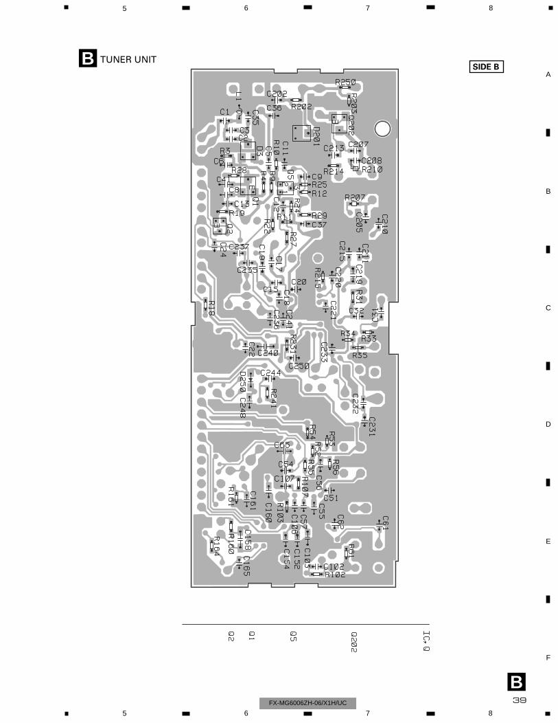
4.2 TUNER UNIT
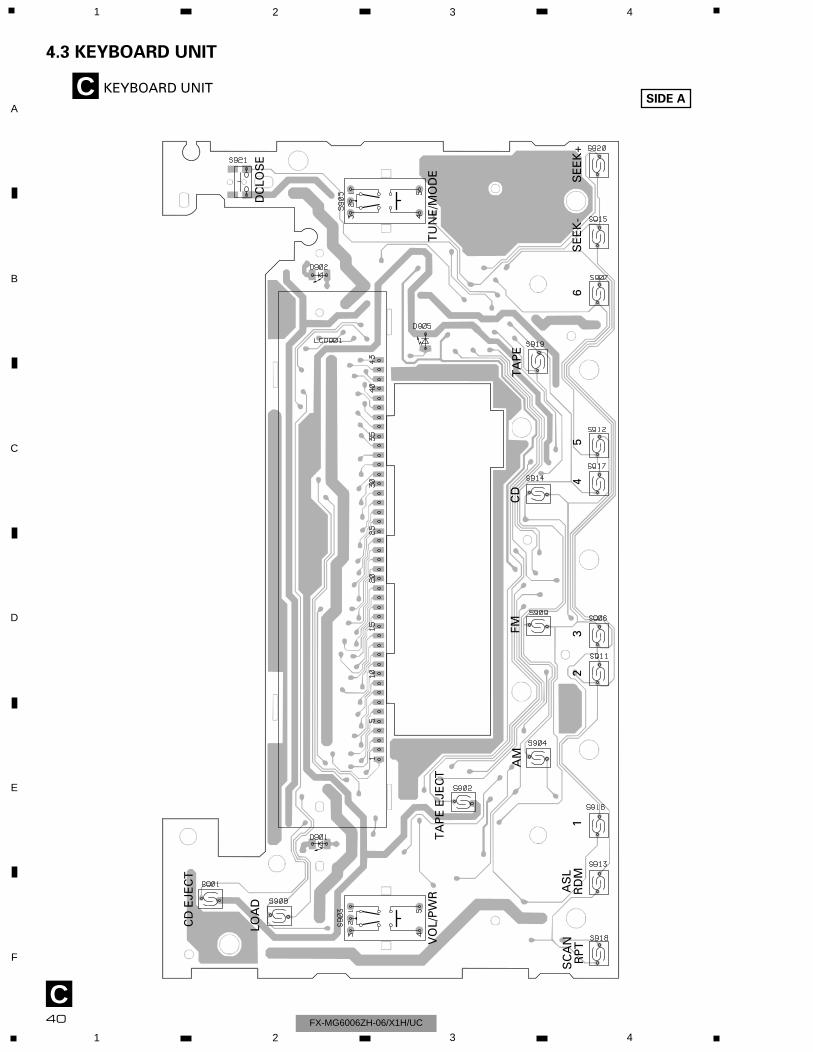
C KEYBOARD UNIT
B
B TUNER UNITSIDE B
39
5 6 7 8
F
E
D
C
B
A
5 6 7 8FX-MG6006ZH-06/X1H/UC
40
C
C KEYBOARD UNITSIDE A
LOA
D
SC
AN
RP
T
TA
PE
EJE
CT
AM
FMT
AP
EC
D
CD
EJE
CT
DC
LOS
E
12
34
56
AS
LR
DM
SE
EK
+S
EE
K-
TU
NE
/MO
DE
VO
L/P
WR
1 2 3 4
1 2 3 4
F
E
D
C
B
A
FX-MG6006ZH-06/X1H/UC
4.3 KEYBOARD UNIT
41
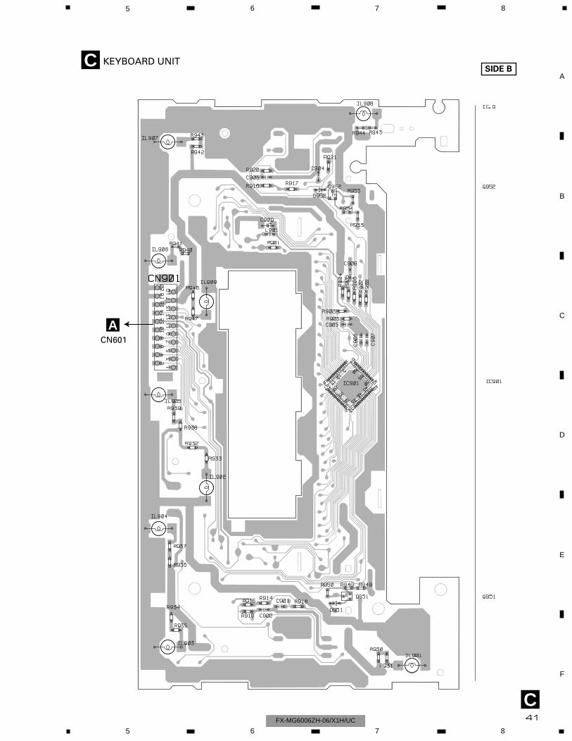
C
C KEYBOARD UNITSIDE B
ACN601
5 6 7 8
F
E
D
C
B
A
5 6 7 8FX-MG6006ZH-06/X1H/UC
D
E
F
REFOUT
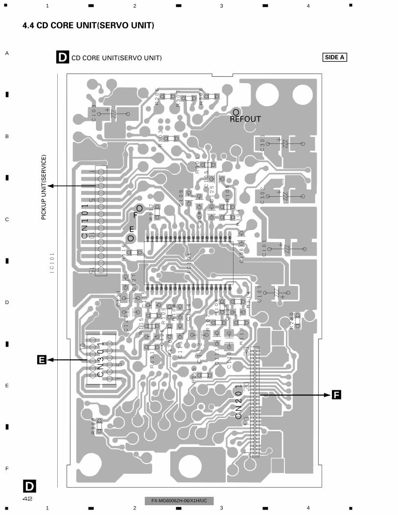
D CD CORE UNIT(SERVO UNIT) SIDE A
PIC
KU
P U
NIT
(SE
RV
ICE
)
E
F
42
1 2 3 4
1 2 3 4
F
E
D
C
B
A
FX-MG6006ZH-06/X1H/UC
4.4 CD CORE UNIT(SERVO UNIT)
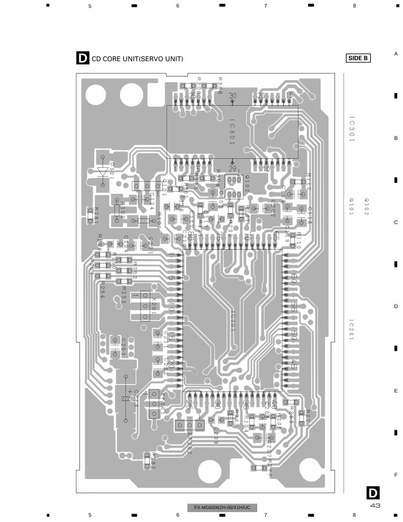
D
D CD CORE UNIT(SERVO UNIT) SIDE B
43
5 6 7 8
F
E
D
C
B
A
5 6 7 8FX-MG6006ZH-06/X1H/UC
LOAD
DOOR
MODE
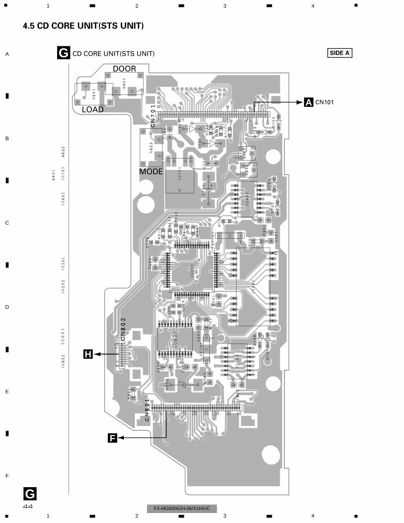
G
G CD CORE UNIT(STS UNIT) SIDE A
F
H
A CN101
44
1 2 3 4
1 2 3 4
F
E
D
C
B
A
FX-MG6006ZH-06/X1H/UC
4.5 CD CORE UNIT(STS UNIT)
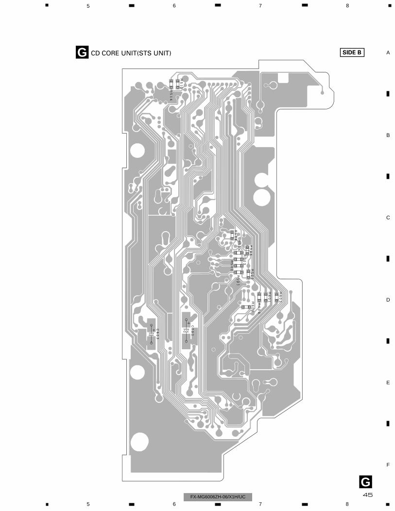
G
G CD CORE UNIT(STS UNIT) SIDE B
45
5 6 7 8
F
E
D
C
B
A
5 6 7 8FX-MG6006ZH-06/X1H/UC
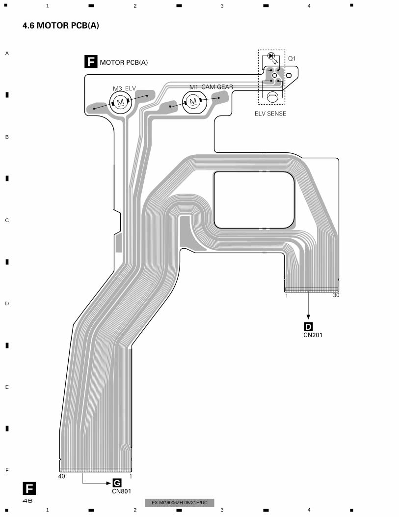
Q1
ELV SENSE
M
M1 CAM GEAR
M
M3 ELV
1 30
DCN201
140GCN801F
F MOTOR PCB(A)
46
1 2 3 4
1 2 3 4
F
E
D
C
B
A
FX-MG6006ZH-06/X1H/UC
4.6 MOTOR PCB(A)
I
I PCB UNIT(E)
SIDE A SIDE B
I PCB UNIT(E)
47
5 6 7 8
F
E
D
C
B
A
5 6 7 8FX-MG6006ZH-06/X1H/UC
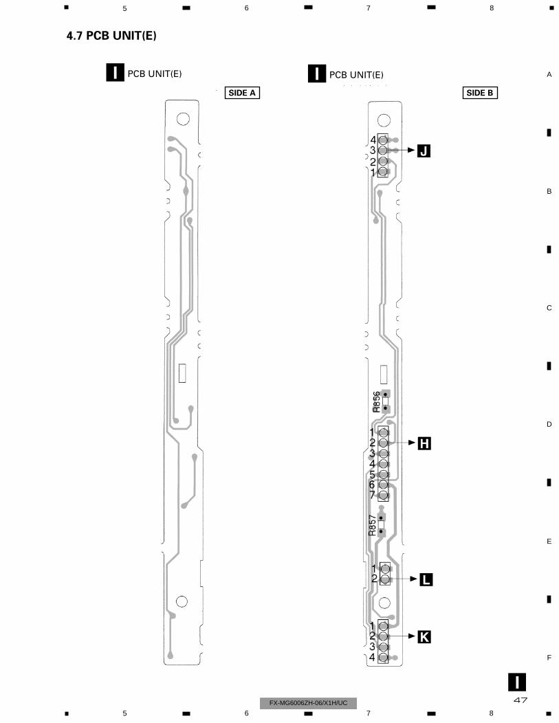
4.7 PCB UNIT(E)
SPINDLE MOTORM5
E
E MOTOR PCB(B)
48
1 2 3 4
1 2 3 4
F
E
D
C
B
A
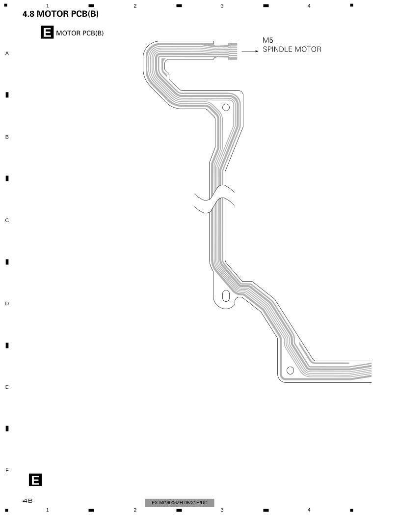
FX-MG6006ZH-06/X1H/UC
4.8 MOTOR PCB(B)
M
M4
CARRIAGE
112
DCN301
E49
5 6 7 8
F
E
D
C
B
A
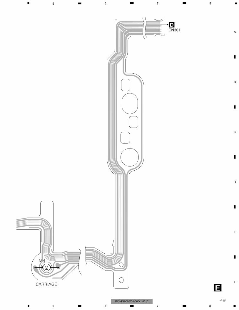
5 6 7 8FX-MG6006ZH-06/X1H/UC
S887CLAMP
1
1 7
S886ELV HOME
GCN802
I
11
H
H PCB UNIT(B) M PCB UNIT(D)
M50
1 2 3 4
1 2 3 4
F
E
D
C
B
A
FX-MG6006ZH-06/X1H/UC
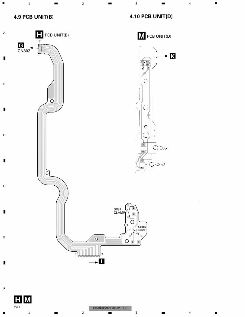
4.9 PCB UNIT(B) 4.10 PCB UNIT(D)
4
1
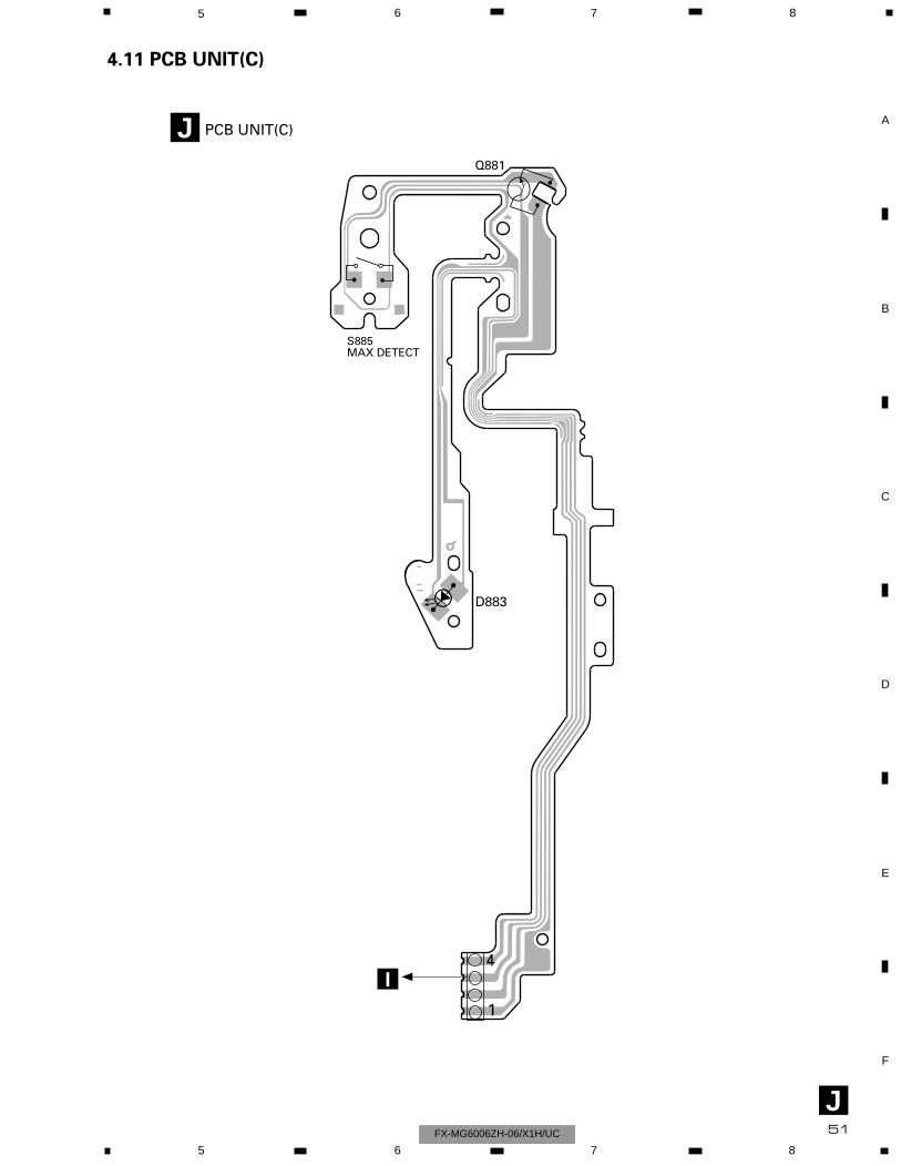
D883
S885MAX DETECT
Q881
I
J
J PCB UNIT(C)
51
5 6 7 8
F
E
D
C
B
A
5 6 7 8FX-MG6006ZH-06/X1H/UC
4.11 PCB UNIT(C)
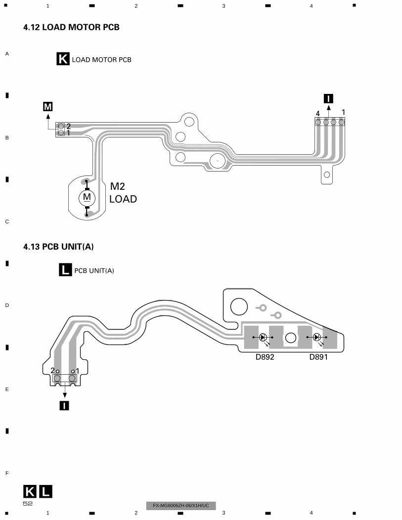
MM2LOAD
1
14
2
IMM
MI
D891D892
12
I
K
K LOAD MOTOR PCB
L
L PCB UNIT(A)
52
1 2 3 4
1 2 3 4
F
E
D
C
B
A
FX-MG6006ZH-06/X1H/UC
4.12 LOAD MOTOR PCB
4.13 PCB UNIT(A)
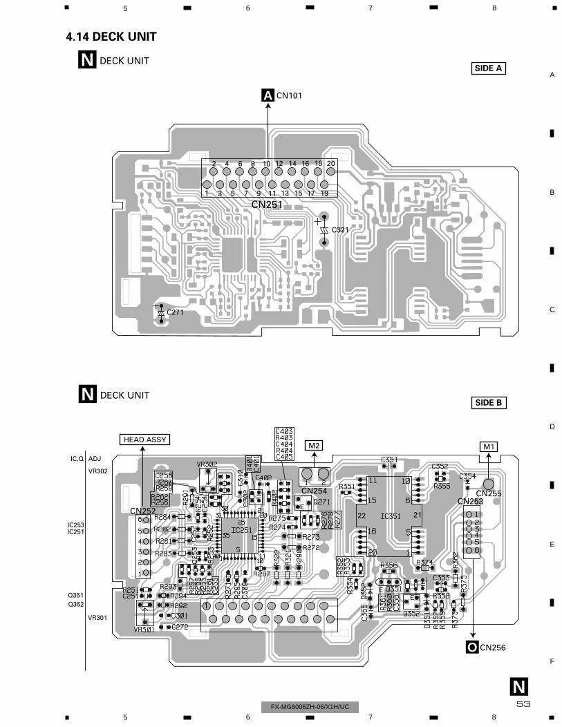
N
N DECK UNITSIDE A
N DECK UNITSIDE B
A CN101
O CN256
IC,Q
IC251
Q351Q352
ADJ
VR302
VR301
IC253
CN252
CN254CN253
CN255
M1M2HEAD ASSY
2122
C321
C271
191715131197531
161412108642 2018
CN251
1
53
5 6 7 8
F
E
D
C
B
A
5 6 7 8FX-MG6006ZH-06/X1H/UC
4.14 DECK UNIT
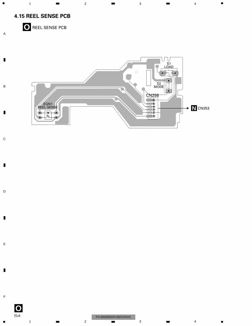
O
O REEL SENSE PCB
N CN253
123456
S1LOAD
S2MODE
CN256
EGN1REEL SENSE
54
1 2 3 4
1 2 3 4
F
E
D
C
B
A
FX-MG6006ZH-06/X1H/UC
4.15 REEL SENSE PCB
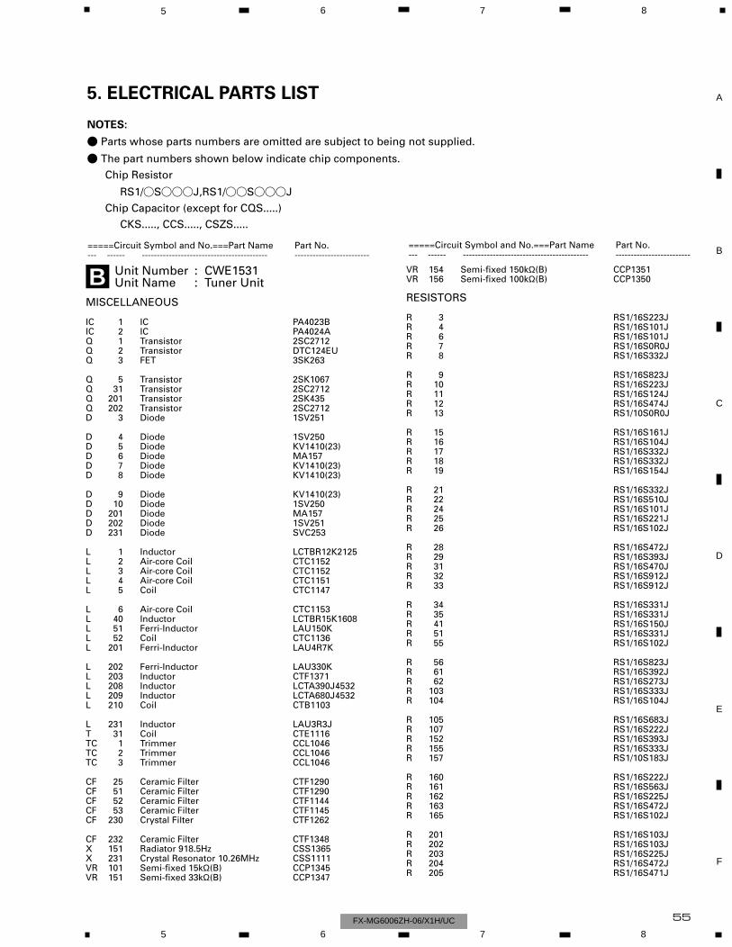
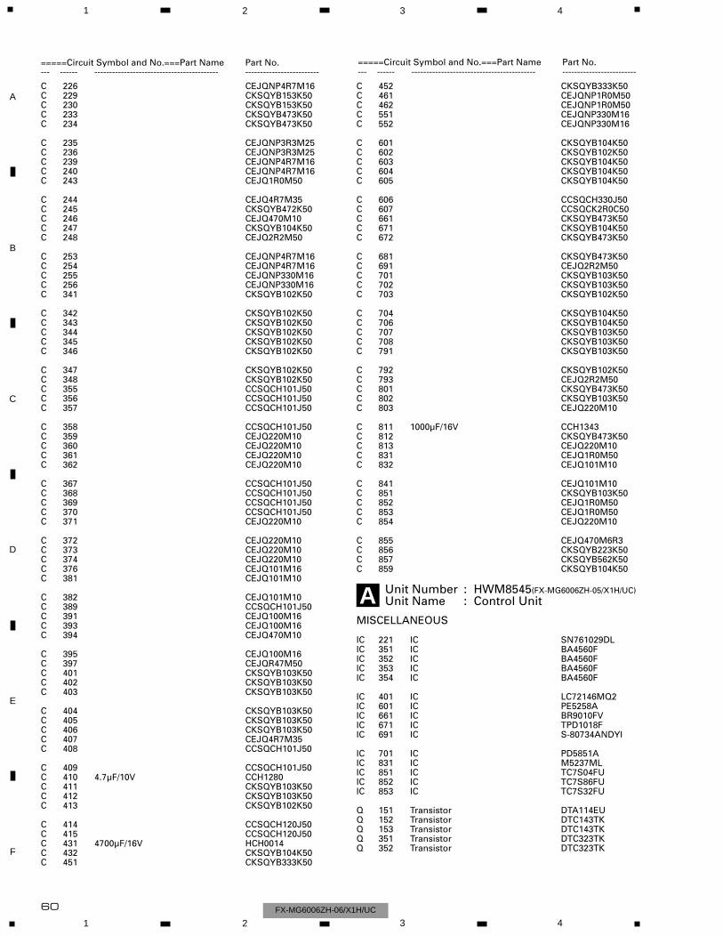
Unit Number : CWE1531Unit Name : Tuner Unit
MISCELLANEOUS
IC 1 IC PA4023BIC 2 IC PA4024AQ 1 Transistor 2SC2712Q 2 Transistor DTC124EUQ 3 FET 3SK263
Q 5 Transistor 2SK1067Q 31 Transistor 2SC2712Q 201 Transistor 2SK435Q 202 Transistor 2SC2712D 3 Diode 1SV251
D 4 Diode 1SV250D 5 Diode KV1410(23)D 6 Diode MA157D 7 Diode KV1410(23)D 8 Diode KV1410(23)
D 9 Diode KV1410(23)D 10 Diode 1SV250D 201 Diode MA157D 202 Diode 1SV251D 231 Diode SVC253
L 1 Inductor LCTBR12K2125L 2 Air-core Coil CTC1152L 3 Air-core Coil CTC1152L 4 Air-core Coil CTC1151L 5 Coil CTC1147
L 6 Air-core Coil CTC1153L 40 Inductor LCTBR15K1608L 51 Ferri-Inductor LAU150KL 52 Coil CTC1136L 201 Ferri-Inductor LAU4R7K
L 202 Ferri-Inductor LAU330KL 203 Inductor CTF1371L 208 Inductor LCTA390J4532L 209 Inductor LCTA680J4532L 210 Coil CTB1103
L 231 Inductor LAU3R3JT 31 Coil CTE1116TC 1 Trimmer CCL1046TC 2 Trimmer CCL1046TC 3 Trimmer CCL1046
CF 25 Ceramic Filter CTF1290CF 51 Ceramic Filter CTF1290CF 52 Ceramic Filter CTF1144CF 53 Ceramic Filter CTF1145CF 230 Crystal Filter CTF1262
CF 232 Ceramic Filter CTF1348X 151 Radiator 918.5Hz CSS1365X 231 Crystal Resonator 10.26MHz CSS1111VR 101 Semi-fixed 15kΩ(B) CCP1345VR 151 Semi-fixed 33kΩ(B) CCP1347
VR 154 Semi-fixed 150kΩ(B) CCP1351VR 156 Semi-fixed 100kΩ(B) CCP1350
RESISTORS
R 3 RS1/16S223JR 4 RS1/16S101JR 6 RS1/16S101JR 7 RS1/16S0R0JR 8 RS1/16S332J
R 9 RS1/16S823JR 10 RS1/16S223JR 11 RS1/16S124JR 12 RS1/16S474JR 13 RS1/10S0R0J
R 15 RS1/16S161JR 16 RS1/16S104JR 17 RS1/16S332JR 18 RS1/16S332JR 19 RS1/16S154J
R 21 RS1/16S332JR 22 RS1/16S510JR 24 RS1/16S101JR 25 RS1/16S221JR 26 RS1/16S102J
R 28 RS1/16S472JR 29 RS1/16S393JR 31 RS1/16S470JR 32 RS1/16S912JR 33 RS1/16S912J
R 34 RS1/16S331JR 35 RS1/16S331JR 41 RS1/16S150JR 51 RS1/16S331JR 55 RS1/16S102J
R 56 RS1/16S823JR 61 RS1/16S392JR 62 RS1/16S273JR 103 RS1/16S333JR 104 RS1/16S104J
R 105 RS1/16S683JR 107 RS1/16S222JR 152 RS1/16S393JR 155 RS1/16S333JR 157 RS1/10S183J
R 160 RS1/16S222JR 161 RS1/16S563JR 162 RS1/16S225JR 163 RS1/16S472JR 165 RS1/16S102J
R 201 RS1/16S103JR 202 RS1/16S103JR 203 RS1/16S225JR 204 RS1/16S472JR 205 RS1/16S471J
55
5 6 7 8
F
E
D
C
B
A
5 6 7 8FX-MG6006ZH-06/X1H/UC
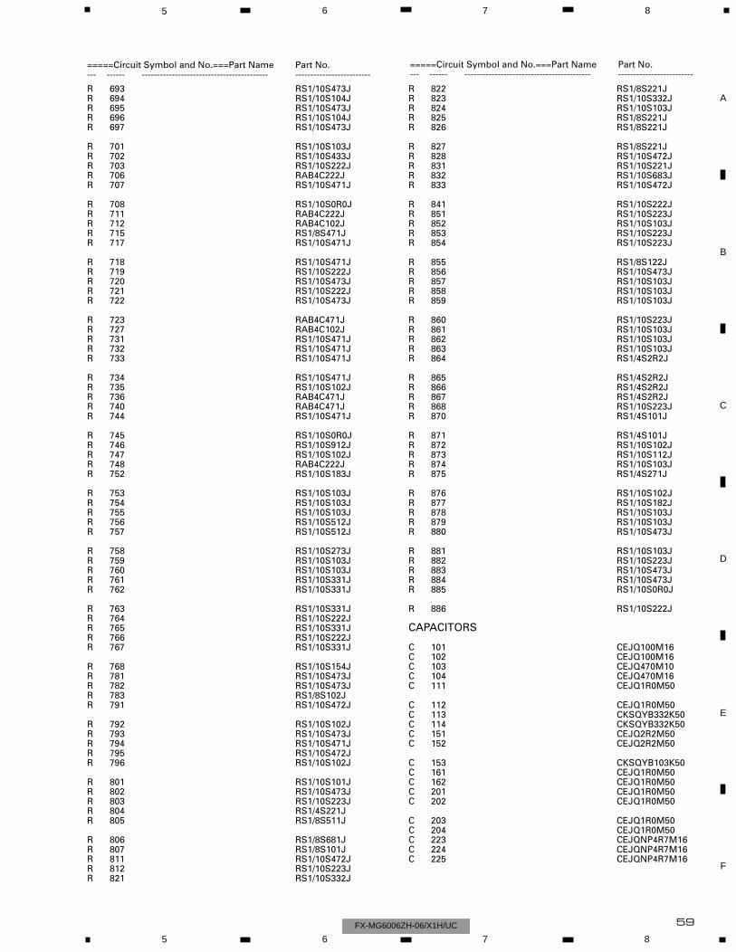
5. ELECTRICAL PARTS LIST
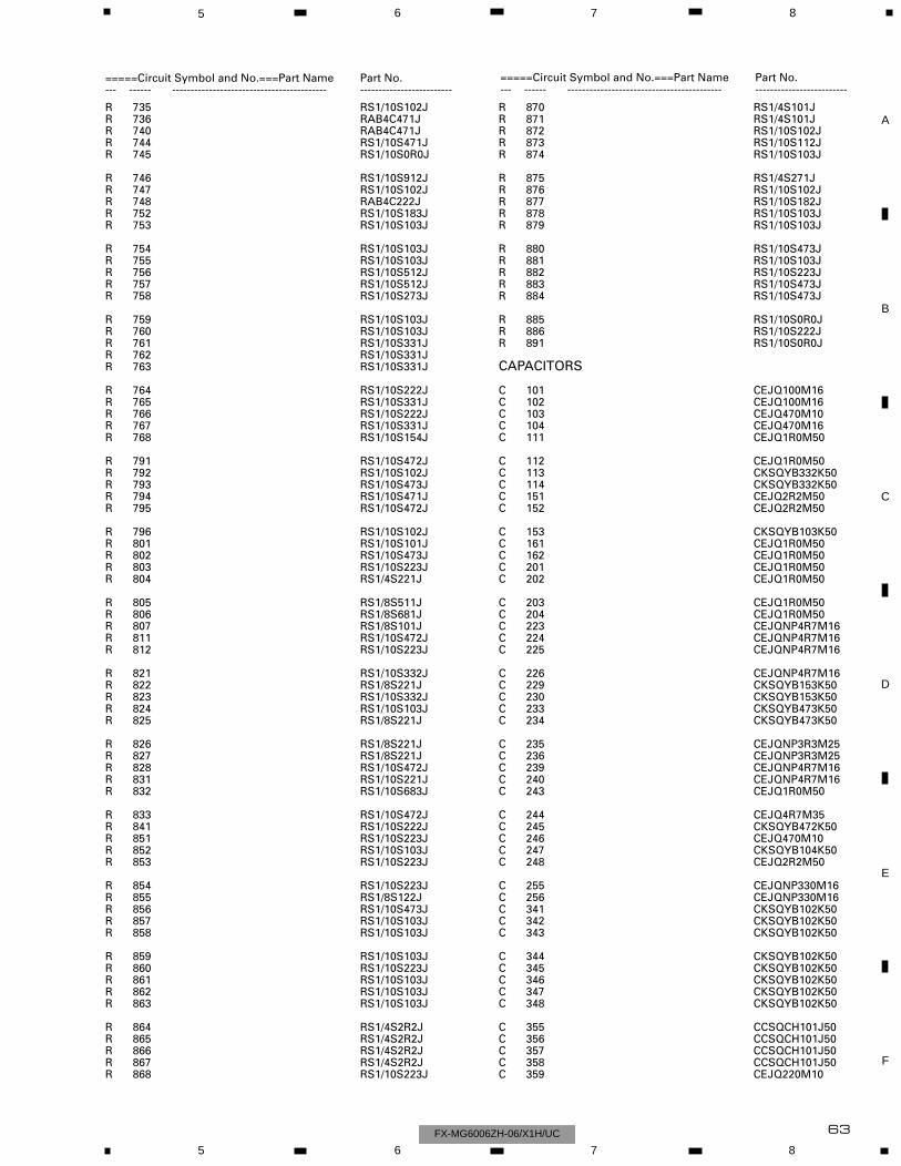
NOTES:
- Parts whose parts numbers are omitted are subject to being not supplied.
- The part numbers shown below indicate chip components.
Chip Resistor
RS1/_S___J,RS1/__S___J
Chip Capacitor (except for CQS.....)
CKS....., CCS....., CSZS.....
=====Circuit Symbol and No.===Part Name Part No.--- ------ ------------------------------------------ -------------------------
=====Circuit Symbol and No.===Part Name Part No.--- ------ ------------------------------------------ -------------------------
B
56
1 2 3 4
1 2 3 4
F
E
D
C
B
A
FX-MG6006ZH-06/X1H/UC
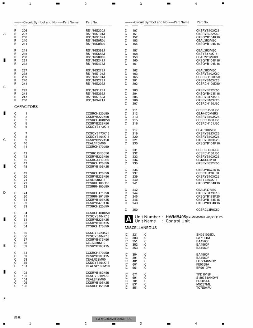
R 206 RS1/16S220JR 207 RS1/16S101JR 208 RS1/16S102JR 210 RS1/16S0R0JR 211 RS1/16S0R0J
R 214 RS1/16S393JR 215 RS1/16S683JR 230 RS1/16S0R0JR 231 RS1/16S242JR 232 RS1/16S473J
R 237 RS1/16S273JR 238 RS1/16S104JR 239 RS1/16S104JR 240 RS1/16S273JR 241 RS1/16S202J
R 243 RS1/16S123JR 244 RS1/16S392JR 247 RS1/10S153JR 250 RS1/16S471J
CAPACITORS
C 1 CCSRCH220J50C 2 CKSRYB222K50C 3 CCSRCH4R0D50C 5 CKSRYB222K50C 6 CKSQYB473K16
C 7 CKSQYB473K16C 8 CKSQYB104K16C 9 CKSRYB222K50C 10 CEAL1R0M50C 11 CCSRCH470J50
C 12 CCSRCJ3R0C50C 13 CKSRYB222K50C 15 CCSRCJ3R0D50C 17 CCSRCH120J50C 18 CKSRYB103K25
C 19 CCSRCH120J50C 20 CKSRYB222K50C 21 CEAL100M16C 22 CCSRRH100D50C 23 CCSRRH150J50
C 24 CCSRCH471J50C 30 CCSRRH201J50C 31 CKSRYB103K25C 32 CKSRYB473K16C 33 CCSRCH220J50
C 34 CCSRCH4R0D50C 41 CKSQYB104K16C 51 CKSRYB223K25C 52 CKSRYB103K25C 54 CCSRCH470J50
C 55 CKSQYB223K25C 56 CKSQYB104K16C 57 CKSRYB472K50C 58 CEJA330M10C 59 CKSRYB103K25
C 61 CCSRCH270J50C 62 CKSRYB103K25C 63 CEALR22M50C 65 CKSQYB104K16C 101 CEALNP100M10
C 102 CKSRYB182K50C 103 CKSQYB682K50C 104 CEAL2R2M50C 105 CKSRYB103K25C 106 CCSRCH151J50
C 107 CKSRYB103K25C 151 CKSRYB222K50C 152 CKSQYB104K16C 153 CEAL3R3M50C 154 CKSQYB104K16
C 157 CEAL3R3M50C 158 CKSYB474K16C 159 CEAL220M6R3C 160 CKSQYB104K16C 161 CKSQYB104K16
C 162 CEAL3R3M50C 163 CKSRYB102K50C 165 CCSRCH100D50C 201 CKSRYB103K25C 202 CCSRCH100D50
C 203 CKSRYB332K50C 204 CKSQYB473K16C 205 CKSRYB473K16C 206 CKSRYB103K25C 207 CCSRCH120J50
C 211 CCSRCH560J50C 212 CEJA470M6R3C 213 CKSRYB103K25C 215 CCSRCH680J50C 216 CCSRCH101J50
C 217 CEAL1R0M50C 219 CKSRYB223K25C 220 CKSRYB103K25C 221 CKSRYB103K25C 230 CKSQYB104K16
C 231 CCSRCH330J50C 232 CCSRCH150J50C 233 CKSRYB103K25C 234 CEJA330M10C 235 CKSRYB332K50
C 236 CKSQYB473K16C 237 CCSRTH120J50C 239 CKSRYB103K25C 240 CKSYB104K16C 241 CKSQYB104K16
C 242 CEALR47M50C 244 CKSRYB473K16C 245 CKSQYB183K25C 246 CKSQYB184K16C 248 CKSQYB334K16
C 250 CCSRCJ3R0C50
Unit Number : HWM8405(FX-MG6006ZH-06/X1H/UC)Unit Name : Control Unit
MISCELLANEOUS
IC 221 IC SN761029DLIC 303 IC LA7151MIC 351 IC BA4560FIC 352 IC BA4560FIC 353 IC BA4560F
IC 354 IC BA4560FIC 391 IC BA4560FIC 401 IC LC72146MQ2IC 601 IC PE5258AIC 661 IC BR9010FV
IC 671 IC TPD1018FIC 691 IC S-80734ANDYIIC 701 IC PD5851AIC 831 IC M5237MLIC 851 IC TC7S04FU
=====Circuit Symbol and No.===Part Name Part No.--- ------ ------------------------------------------ -------------------------
=====Circuit Symbol and No.===Part Name Part No.--- ------ ------------------------------------------ -------------------------
A
57
5 6 7 8
F
E
D
C
B
A
5 6 7 8FX-MG6006ZH-06/X1H/UC
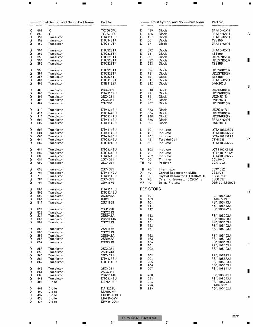
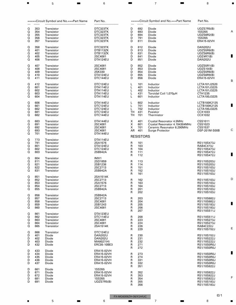
IC 852 IC TC7S86FUIC 853 IC TC7S32FUQ 151 Transistor DTA114EUQ 152 Transistor DTC143TKQ 153 Transistor DTC143TK
Q 351 Transistor DTC323TKQ 352 Transistor DTC323TKQ 353 Transistor DTC323TKQ 354 Transistor DTC323TKQ 355 Transistor DTC323TK
Q 356 Transistor DTC323TKQ 357 Transistor DTC323TKQ 358 Transistor DTC323TKQ 401 Transistor DTB113ZKQ 402 Transistor DTB113ZK
Q 405 Transistor 2SC4081Q 406 Transistor DTA124EUQ 407 Transistor 2SC4081Q 408 Transistor 2SC4081Q 409 Transistor 2SK330
Q 410 Transistor DTA124EUQ 411 Transistor DTC144EUQ 412 Transistor DTC124EUQ 601 Transistor DTA114EUQ 602 Transistor DTA114EU
Q 603 Transistor DTA114EUQ 604 Transistor DTA114EUQ 606 Transistor DTA144EUQ 661 Transistor DTC124EUQ 662 Transistor DTC124EU
Q 681 Transistor DTC124EUQ 682 Transistor DTC144EUQ 683 Transistor DTA144EUQ 691 Transistor 2SC4081Q 692 Transistor 2SC4081
Q 693 Transistor 2SC4081Q 701 Transistor DTA144EUQ 773 Transistor DTA114EUQ 781 Transistor 2SC4081Q 791 Transistor 2SA1576
Q 801 Transistor DTA124EUQ 802 Transistor DTC124EUQ 803 Transistor 2SB942AQ 804 Transistor IMX1Q 811 Transistor 2SD1859
Q 821 Transistor 2SB1238Q 822 Transistor 2SC2713Q 831 Transistor 2SB942AQ 851 Transistor 2SA1514KQ 852 Transistor 2SC2713
Q 853 Transistor 2SA1576Q 854 Transistor 2SC2713Q 855 Transistor 2SB942AQ 856 Transistor 2SB942AQ 857 Transistor 2SC2713
Q 858 Transistor 2SC4081Q 859 Transistor 2SB1243Q 860 Transistor 2SC4081Q 861 Transistor DTA123EUQ 862 Transistor DTC114EU
Q 863 Transistor 2SC4081Q 864 Transistor 2SC4081Q 865 Transistor 2SA1514KQ 866 Transistor DTC124EUD 401 Diode DAN202U
D 402 Diode DAN202UD 403 Diode MA8027(H)D 432 Diode ERC05-10BE3D 433 Diode ERA15-02VHD 434 Diode ERA15-02VH
D 435 Diode ERA15-02VHD 436 Diode ERA15-02VHD 437 Diode ERA15-02VHD 661 Diode 1SS355D 671 Diode ERA15-02VH
D 672 Diode ERA15-02VHD 681 Diode 1SS355D 691 Diode UDZS7R5(B)D 692 Diode UDZS7R5(B)D 693 Diode 1SS355
D 694 Diode UDZS6R2(B)D 781 Diode UDZS7R5(B)D 791 Diode 1SS355D 811 Diode ERA15-02VHD 812 Diode DAN202U
D 813 Diode UDZS5R6(B)D 831 Diode UDZS6R8(B)D 841 Diode UDZ4R7(B)D 851 Diode DAN202UD 852 Diode UDZS5R1(B)
D 853 Diode UDZS10(B)D 854 Diode UDZS5R6(B)D 855 Diode UDZS6R8(B)D 856 Diode ERA15-02VHD 891 Diode DAN202U
L 101 Inductor LCTA101J2520L 401 Inductor LCTA101J3225L 402 Inductor LCTA101J3225L 431 Toroidal Coil CTH1235L 601 Inductor LCTA100J3225
L 602 Inductor LCTB100K2125L 701 Inductor LCTB100K2125L 702 Inductor LCTA100J3225TC 601 Trimmer CCL1046TH 431 Posistor CCX1033
TH 701 Thermistor CCX1032X 401 Crystal Resonator 4.5MHz CSS1011X 601 Crystal Resonator 4.194304MHz CSS1023X 701 Ceramic Resonator 6.290MHz CSS1537AR 401 Surge Protector DSP-201M-S00B
RESISTORS
R 101 RS1/10S473JR 103 RAB4C473JR 104 RS1/10S473JR 111 RS1/10S472JR 112 RS1/10S472J
R 113 RS1/10S203JR 114 RS1/10S203JR 151 RS1/10S103JR 152 RS1/10S103JR 161 RS1/10S103J
R 162 RS1/10S103JR 163 RS1/10S103JR 164 RS1/10S103JR 201 RS1/10S103JR 202 RS1/10S103J
R 203 RS1/10S682JR 204 RS1/10S682JR 205 RS1/10S183JR 206 RS1/10S183JR 207 RS1/10S511J
R 208 RS1/10S511JR 223 RS1/10S273JR 224 RS1/10S273JR 226 RAB4C222JR 229 RS1/10S152J
=====Circuit Symbol and No.===Part Name Part No.--- ------ ------------------------------------------ -------------------------
=====Circuit Symbol and No.===Part Name Part No.--- ------ ------------------------------------------ -------------------------
58
1 2 3 4
1 2 3 4
F
E
D
C
B
A
FX-MG6006ZH-06/X1H/UC
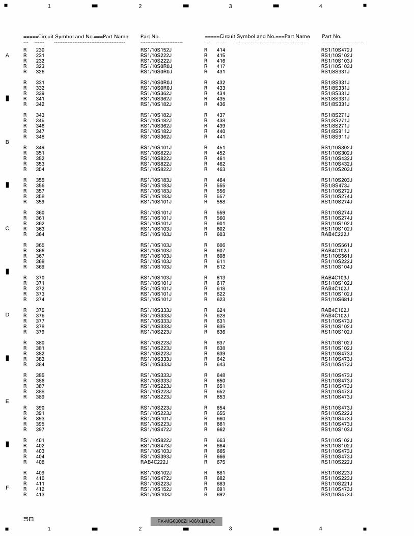
R 230 RS1/10S152JR 231 RS1/10S222JR 232 RS1/10S222JR 323 RS1/10S0R0JR 326 RS1/10S0R0J
R 331 RS1/10S0R0JR 332 RS1/10S0R0JR 339 RS1/10S362JR 341 RS1/10S362JR 342 RS1/10S182J
R 343 RS1/10S182JR 345 RS1/10S182JR 346 RS1/10S362JR 347 RS1/10S182JR 348 RS1/10S362J
R 349 RS1/10S101JR 351 RS1/10S822JR 352 RS1/10S822JR 353 RS1/10S822JR 354 RS1/10S822J
R 355 RS1/10S183JR 356 RS1/10S183JR 357 RS1/10S183JR 358 RS1/10S183JR 359 RS1/10S101J
R 360 RS1/10S101JR 361 RS1/10S101JR 362 RS1/10S101JR 363 RS1/10S103JR 364 RS1/10S103J
R 365 RS1/10S103JR 366 RS1/10S103JR 367 RS1/10S103JR 368 RS1/10S103JR 369 RS1/10S103J
R 370 RS1/10S103JR 371 RS1/10S101JR 372 RS1/10S101JR 373 RS1/10S101JR 374 RS1/10S101J
R 375 RS1/10S333JR 376 RS1/10S333JR 377 RS1/10S333JR 378 RS1/10S333JR 379 RS1/10S223J
R 380 RS1/10S223JR 381 RS1/10S223JR 382 RS1/10S223JR 383 RS1/10S333JR 384 RS1/10S333J
R 385 RS1/10S333JR 386 RS1/10S333JR 387 RS1/10S223JR 388 RS1/10S223JR 389 RS1/10S223J
R 390 RS1/10S223JR 391 RS1/10S223JR 393 RS1/10S101JR 395 RS1/10S223JR 397 RS1/10S472J
R 401 RS1/10S822JR 402 RS1/10S473JR 403 RS1/10S103JR 404 RS1/10S393JR 408 RAB4C222J
R 409 RS1/10S102JR 410 RS1/10S472JR 411 RS1/10S223JR 412 RS1/10S152JR 413 RS1/10S103J
R 414 RS1/10S472JR 415 RS1/10S102JR 416 RS1/10S103JR 417 RS1/10S103JR 431 RS1/8S331J
R 432 RS1/8S331JR 433 RS1/8S331JR 434 RS1/8S331JR 435 RS1/8S331JR 436 RS1/8S331J
R 437 RS1/8S271JR 438 RS1/8S271JR 439 RS1/8S271JR 440 RS1/8S911JR 441 RS1/8S911J
R 451 RS1/10S302JR 452 RS1/10S302JR 461 RS1/10S432JR 462 RS1/10S432JR 463 RS1/10S203J
R 464 RS1/10S203JR 555 RS1/8S473JR 556 RS1/10S272JR 557 RS1/10S274JR 558 RS1/10S274J
R 559 RS1/10S274JR 560 RS1/10S274JR 601 RS1/10S102JR 602 RS1/10S102JR 603 RAB4C222J
R 606 RS1/10S561JR 607 RAB4C102JR 608 RS1/10S561JR 611 RS1/10S222JR 612 RS1/10S104J
R 613 RAB4C103JR 617 RS1/10S102JR 618 RAB4C102JR 622 RS1/10S102JR 623 RS1/10S681J
R 624 RAB4C102JR 628 RAB4C102JR 631 RS1/10S473JR 635 RS1/10S102JR 636 RS1/10S102J
R 637 RS1/10S102JR 638 RS1/10S102JR 639 RS1/10S473JR 642 RS1/10S473JR 643 RS1/10S473J
R 648 RS1/10S473JR 650 RS1/10S473JR 651 RS1/10S473JR 652 RS1/10S473JR 653 RS1/10S473J
R 654 RS1/10S473JR 655 RS1/10S222JR 660 RS1/10S473JR 661 RS1/10S473JR 662 RS1/10S103J
R 663 RS1/10S102JR 664 RS1/10S102JR 665 RS1/10S473JR 666 RS1/10S473JR 675 RS1/10S222J
R 681 RS1/10S223JR 682 RS1/10S223JR 683 RS1/10S221JR 691 RS1/10S473JR 692 RS1/10S473J
=====Circuit Symbol and No.===Part Name Part No.--- ------ ------------------------------------------ -------------------------
=====Circuit Symbol and No.===Part Name Part No.--- ------ ------------------------------------------ -------------------------
59
5 6 7 8
F
E
D
C
B
A
5 6 7 8FX-MG6006ZH-06/X1H/UC
R 693 RS1/10S473JR 694 RS1/10S104JR 695 RS1/10S473JR 696 RS1/10S104JR 697 RS1/10S473J
R 701 RS1/10S103JR 702 RS1/10S433JR 703 RS1/10S222JR 706 RAB4C222JR 707 RS1/10S471J
R 708 RS1/10S0R0JR 711 RAB4C222JR 712 RAB4C102JR 715 RS1/8S471JR 717 RS1/10S471J
R 718 RS1/10S471JR 719 RS1/10S222JR 720 RS1/10S473JR 721 RS1/10S222JR 722 RS1/10S473J
R 723 RAB4C471JR 727 RAB4C102JR 731 RS1/10S471JR 732 RS1/10S471JR 733 RS1/10S471J
R 734 RS1/10S471JR 735 RS1/10S102JR 736 RAB4C471JR 740 RAB4C471JR 744 RS1/10S471J
R 745 RS1/10S0R0JR 746 RS1/10S912JR 747 RS1/10S102JR 748 RAB4C222JR 752 RS1/10S183J
R 753 RS1/10S103JR 754 RS1/10S103JR 755 RS1/10S103JR 756 RS1/10S512JR 757 RS1/10S512J
R 758 RS1/10S273JR 759 RS1/10S103JR 760 RS1/10S103JR 761 RS1/10S331JR 762 RS1/10S331J
R 763 RS1/10S331JR 764 RS1/10S222JR 765 RS1/10S331JR 766 RS1/10S222JR 767 RS1/10S331J
R 768 RS1/10S154JR 781 RS1/10S473JR 782 RS1/10S473JR 783 RS1/8S102JR 791 RS1/10S472J
R 792 RS1/10S102JR 793 RS1/10S473JR 794 RS1/10S471JR 795 RS1/10S472JR 796 RS1/10S102J
R 801 RS1/10S101JR 802 RS1/10S473JR 803 RS1/10S223JR 804 RS1/4S221JR 805 RS1/8S511J
R 806 RS1/8S681JR 807 RS1/8S101JR 811 RS1/10S472JR 812 RS1/10S223JR 821 RS1/10S332J
R 822 RS1/8S221JR 823 RS1/10S332JR 824 RS1/10S103JR 825 RS1/8S221JR 826 RS1/8S221J
R 827 RS1/8S221JR 828 RS1/10S472JR 831 RS1/10S221JR 832 RS1/10S683JR 833 RS1/10S472J
R 841 RS1/10S222JR 851 RS1/10S223JR 852 RS1/10S103JR 853 RS1/10S223JR 854 RS1/10S223J
R 855 RS1/8S122JR 856 RS1/10S473JR 857 RS1/10S103JR 858 RS1/10S103JR 859 RS1/10S103J
R 860 RS1/10S223JR 861 RS1/10S103JR 862 RS1/10S103JR 863 RS1/10S103JR 864 RS1/4S2R2J
R 865 RS1/4S2R2JR 866 RS1/4S2R2JR 867 RS1/4S2R2JR 868 RS1/10S223JR 870 RS1/4S101J
R 871 RS1/4S101JR 872 RS1/10S102JR 873 RS1/10S112JR 874 RS1/10S103JR 875 RS1/4S271J
R 876 RS1/10S102JR 877 RS1/10S182JR 878 RS1/10S103JR 879 RS1/10S103JR 880 RS1/10S473J
R 881 RS1/10S103JR 882 RS1/10S223JR 883 RS1/10S473JR 884 RS1/10S473JR 885 RS1/10S0R0J
R 886 RS1/10S222J
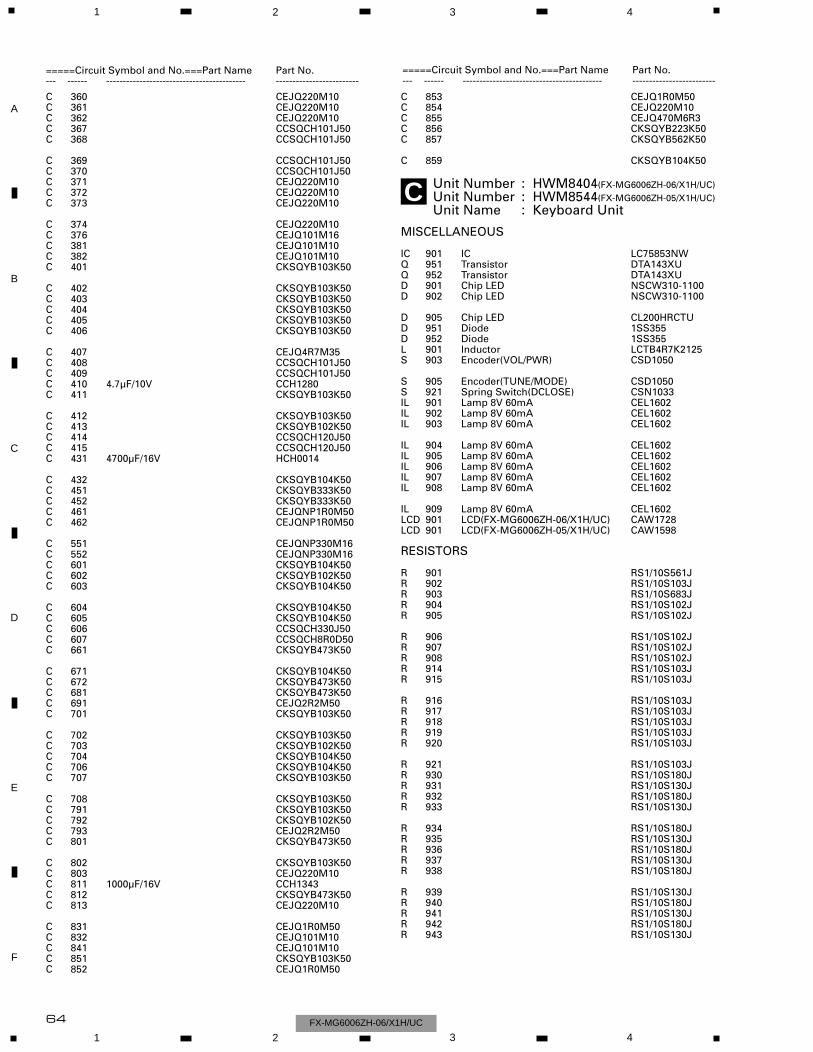
CAPACITORS
C 101 CEJQ100M16C 102 CEJQ100M16C 103 CEJQ470M10C 104 CEJQ470M16C 111 CEJQ1R0M50
C 112 CEJQ1R0M50C 113 CKSQYB332K50C 114 CKSQYB332K50C 151 CEJQ2R2M50C 152 CEJQ2R2M50
C 153 CKSQYB103K50C 161 CEJQ1R0M50C 162 CEJQ1R0M50C 201 CEJQ1R0M50C 202 CEJQ1R0M50
C 203 CEJQ1R0M50C 204 CEJQ1R0M50C 223 CEJQNP4R7M16C 224 CEJQNP4R7M16C 225 CEJQNP4R7M16
=====Circuit Symbol and No.===Part Name Part No.--- ------ ------------------------------------------ -------------------------
=====Circuit Symbol and No.===Part Name Part No.--- ------ ------------------------------------------ -------------------------
60
1 2 3 4
1 2 3 4
F
E
D
C
B
A
FX-MG6006ZH-06/X1H/UC
C 226 CEJQNP4R7M16C 229 CKSQYB153K50C 230 CKSQYB153K50C 233 CKSQYB473K50C 234 CKSQYB473K50
C 235 CEJQNP3R3M25C 236 CEJQNP3R3M25C 239 CEJQNP4R7M16C 240 CEJQNP4R7M16C 243 CEJQ1R0M50
C 244 CEJQ4R7M35C 245 CKSQYB472K50C 246 CEJQ470M10C 247 CKSQYB104K50C 248 CEJQ2R2M50
C 253 CEJQNP4R7M16C 254 CEJQNP4R7M16C 255 CEJQNP330M16C 256 CEJQNP330M16C 341 CKSQYB102K50
C 342 CKSQYB102K50C 343 CKSQYB102K50C 344 CKSQYB102K50C 345 CKSQYB102K50C 346 CKSQYB102K50
C 347 CKSQYB102K50C 348 CKSQYB102K50C 355 CCSQCH101J50C 356 CCSQCH101J50C 357 CCSQCH101J50
C 358 CCSQCH101J50C 359 CEJQ220M10C 360 CEJQ220M10C 361 CEJQ220M10C 362 CEJQ220M10
C 367 CCSQCH101J50C 368 CCSQCH101J50C 369 CCSQCH101J50C 370 CCSQCH101J50C 371 CEJQ220M10
C 372 CEJQ220M10C 373 CEJQ220M10C 374 CEJQ220M10C 376 CEJQ101M16C 381 CEJQ101M10
C 382 CEJQ101M10C 389 CCSQCH101J50C 391 CEJQ100M16C 393 CEJQ100M16C 394 CEJQ470M10
C 395 CEJQ100M16C 397 CEJQR47M50C 401 CKSQYB103K50C 402 CKSQYB103K50C 403 CKSQYB103K50
C 404 CKSQYB103K50C 405 CKSQYB103K50C 406 CKSQYB103K50C 407 CEJQ4R7M35C 408 CCSQCH101J50
C 409 CCSQCH101J50C 410 4.7µF/10V CCH1280C 411 CKSQYB103K50C 412 CKSQYB103K50C 413 CKSQYB102K50
C 414 CCSQCH120J50C 415 CCSQCH120J50C 431 4700µF/16V HCH0014C 432 CKSQYB104K50C 451 CKSQYB333K50
C 452 CKSQYB333K50C 461 CEJQNP1R0M50C 462 CEJQNP1R0M50C 551 CEJQNP330M16C 552 CEJQNP330M16
C 601 CKSQYB104K50C 602 CKSQYB102K50C 603 CKSQYB104K50C 604 CKSQYB104K50C 605 CKSQYB104K50
C 606 CCSQCH330J50C 607 CCSQCK2R0C50C 661 CKSQYB473K50C 671 CKSQYB104K50C 672 CKSQYB473K50
C 681 CKSQYB473K50C 691 CEJQ2R2M50C 701 CKSQYB103K50C 702 CKSQYB103K50C 703 CKSQYB102K50
C 704 CKSQYB104K50C 706 CKSQYB104K50C 707 CKSQYB103K50C 708 CKSQYB103K50C 791 CKSQYB103K50
C 792 CKSQYB102K50C 793 CEJQ2R2M50C 801 CKSQYB473K50C 802 CKSQYB103K50C 803 CEJQ220M10
C 811 1000µF/16V CCH1343C 812 CKSQYB473K50C 813 CEJQ220M10C 831 CEJQ1R0M50C 832 CEJQ101M10
C 841 CEJQ101M10C 851 CKSQYB103K50C 852 CEJQ1R0M50C 853 CEJQ1R0M50C 854 CEJQ220M10
C 855 CEJQ470M6R3C 856 CKSQYB223K50C 857 CKSQYB562K50C 859 CKSQYB104K50
Unit Number : HWM8545(FX-MG6006ZH-05/X1H/UC)Unit Name : Control Unit
MISCELLANEOUS
IC 221 IC SN761029DLIC 351 IC BA4560FIC 352 IC BA4560FIC 353 IC BA4560FIC 354 IC BA4560F
IC 401 IC LC72146MQ2IC 601 IC PE5258AIC 661 IC BR9010FVIC 671 IC TPD1018FIC 691 IC S-80734ANDYI
IC 701 IC PD5851AIC 831 IC M5237MLIC 851 IC TC7S04FUIC 852 IC TC7S86FUIC 853 IC TC7S32FU
Q 151 Transistor DTA114EUQ 152 Transistor DTC143TKQ 153 Transistor DTC143TKQ 351 Transistor DTC323TKQ 352 Transistor DTC323TK
=====Circuit Symbol and No.===Part Name Part No.--- ------ ------------------------------------------ -------------------------
=====Circuit Symbol and No.===Part Name Part No.--- ------ ------------------------------------------ -------------------------
A
61
5 6 7 8
F
E
D
C
B
A
5 6 7 8FX-MG6006ZH-06/X1H/UC
Q 353 Transistor DTC323TKQ 354 Transistor DTC323TKQ 355 Transistor DTC323TKQ 356 Transistor DTC323TKQ 357 Transistor DTC323TK
Q 358 Transistor DTC323TKQ 401 Transistor DTB113ZKQ 402 Transistor DTB113ZKQ 405 Transistor 2SC4081Q 406 Transistor DTA124EU
Q 407 Transistor 2SC4081Q 408 Transistor 2SC4081Q 409 Transistor 2SK330Q 410 Transistor DTA124EUQ 411 Transistor DTC144EU
Q 412 Transistor DTC124EUQ 601 Transistor DTA114EUQ 602 Transistor DTA114EUQ 603 Transistor DTA114EUQ 604 Transistor DTA114EU
Q 606 Transistor DTA144EUQ 661 Transistor DTC124EUQ 662 Transistor DTC124EUQ 681 Transistor DTC124EUQ 682 Transistor DTC144EU
Q 683 Transistor DTA144EUQ 691 Transistor 2SC4081Q 692 Transistor 2SC4081Q 693 Transistor 2SC4081Q 701 Transistor DTA144EU
Q 773 Transistor DTA114EUQ 791 Transistor 2SA1576Q 801 Transistor DTA124EUQ 802 Transistor DTC124EUQ 803 Transistor 2SB942A
Q 804 Transistor IMX1Q 811 Transistor 2SD1859Q 821 Transistor 2SB1238Q 822 Transistor 2SC2713Q 831 Transistor 2SB942A
Q 851 Transistor 2SA1514KQ 852 Transistor 2SC2713Q 853 Transistor 2SA1576Q 854 Transistor 2SC2713Q 855 Transistor 2SB942A
Q 856 Transistor 2SB942AQ 857 Transistor 2SC2713Q 858 Transistor 2SC4081Q 859 Transistor 2SB1243Q 860 Transistor 2SC4081
Q 861 Transistor DTA123EUQ 862 Transistor DTC114EUQ 863 Transistor 2SC4081Q 864 Transistor 2SC4081Q 865 Transistor 2SA1514K
Q 866 Transistor DTC124EUD 401 Diode DAN202UD 402 Diode DAN202UD 403 Diode MA8027(H)D 432 Diode ERC05-10BE3
D 433 Diode ERA15-02VHD 434 Diode ERA15-02VHD 435 Diode ERA15-02VHD 436 Diode ERA15-02VHD 437 Diode ERA15-02VH
D 661 Diode 1SS355D 671 Diode ERA15-02VHD 672 Diode ERA15-02VHD 681 Diode 1SS355D 691 Diode UDZS7R5(B)
D 692 Diode UDZS7R5(B)D 693 Diode 1SS355D 694 Diode UDZS6R2(B)D 791 Diode 1SS355D 811 Diode ERA15-02VH
D 812 Diode DAN202UD 813 Diode UDZS5R6(B)D 831 Diode UDZS6R8(B)D 841 Diode UDZ4R7(B)D 851 Diode DAN202U
D 852 Diode UDZS5R1(B)D 853 Diode UDZS10(B)D 854 Diode UDZS5R6(B)D 855 Diode UDZS6R8(B)D 856 Diode ERA15-02VH
L 101 Inductor LCTA101J2520L 401 Inductor LCTA101J3225L 402 Inductor LCTA101J3225L 431 Toroidal Coil 1,070µH CTH1235L 601 Inductor LCTA100J3225
L 602 Inductor LCTB100K2125L 701 Inductor LCTB100K2125L 702 Inductor LCTA100J3225TH 431 Posistor CCX1033TH 701 Thermistor CCX1032
X 401 Crystal Resonator 4.5MHz CSS1011X 601 Crystal Resonator 4.194304MHz CSS1023X 701 Ceramic Resonator 6.290MHz CSS1537AR 401 Surge Protector DSP-201M-S00B
RESISTORS
R 101 RS1/10S473JR 103 RAB4C473JR 104 RS1/10S473JR 111 RS1/10S472JR 112 RS1/10S472J
R 113 RS1/10S203JR 114 RS1/10S203JR 151 RS1/10S103JR 152 RS1/10S103JR 161 RS1/10S103J
R 162 RS1/10S103JR 163 RS1/10S103JR 164 RS1/10S103JR 201 RS1/10S103JR 202 RS1/10S103J
R 203 RS1/10S682JR 204 RS1/10S682JR 205 RS1/10S183JR 206 RS1/10S183JR 207 RS1/10S511J
R 208 RS1/10S511JR 223 RS1/10S273JR 224 RS1/10S273JR 226 RAB4C222JR 229 RS1/10S152J
R 230 RS1/10S152JR 231 RS1/10S222JR 232 RS1/10S222JR 271 RS1/10S0R0JR 272 RS1/10S0R0J
R 273 RS1/10S0R0JR 274 RS1/10S0R0JR 331 RS1/10S0R0JR 332 RS1/10S0R0JR 351 RS1/10S822J
R 352 RS1/10S822JR 353 RS1/10S822JR 354 RS1/10S822JR 355 RS1/10S183JR 356 RS1/10S183J
=====Circuit Symbol and No.===Part Name Part No.--- ------ ------------------------------------------ -------------------------
=====Circuit Symbol and No.===Part Name Part No.--- ------ ------------------------------------------ -------------------------
62
1 2 3 4
1 2 3 4
F
E
D
C
B
A
FX-MG6006ZH-06/X1H/UC
R 357 RS1/10S183JR 358 RS1/10S183JR 359 RS1/10S101JR 360 RS1/10S101JR 361 RS1/10S101J
R 362 RS1/10S101JR 363 RS1/10S103JR 364 RS1/10S103JR 365 RS1/10S103JR 366 RS1/10S103J
R 367 RS1/10S103JR 368 RS1/10S103JR 369 RS1/10S103JR 370 RS1/10S103JR 371 RS1/10S101J
R 372 RS1/10S101JR 373 RS1/10S101JR 374 RS1/10S101JR 375 RS1/10S333JR 376 RS1/10S333J
R 377 RS1/10S333JR 378 RS1/10S333JR 379 RS1/10S223JR 380 RS1/10S223JR 381 RS1/10S223J
R 382 RS1/10S223JR 383 RS1/10S333JR 384 RS1/10S333JR 385 RS1/10S333JR 386 RS1/10S333J
R 387 RS1/10S223JR 388 RS1/10S223JR 389 RS1/10S223JR 390 RS1/10S223JR 401 RS1/10S822J
R 402 RS1/10S473JR 403 RS1/10S103JR 404 RS1/10S393JR 408 RAB4C222JR 409 RS1/10S102J
R 410 RS1/10S472JR 411 RS1/10S223JR 412 RS1/10S152JR 413 RS1/10S103JR 414 RS1/10S472J
R 415 RS1/10S102JR 416 RS1/10S103JR 417 RS1/10S103JR 431 RS1/8S331JR 432 RS1/8S331J
R 433 RS1/8S331JR 434 RS1/8S331JR 435 RS1/8S331JR 436 RS1/8S331JR 437 RS1/8S271J
R 438 RS1/8S271JR 439 RS1/8S271JR 440 RS1/8S911JR 441 RS1/8S911JR 451 RS1/10S302J
R 452 RS1/10S302JR 461 RS1/10S432JR 462 RS1/10S432JR 463 RS1/10S203JR 464 RS1/10S203J
R 555 RS1/8S473JR 556 RS1/10S272JR 557 RS1/10S274JR 558 RS1/10S274JR 559 RS1/10S274J
R 560 RS1/10S274JR 601 RS1/10S102JR 602 RS1/10S102JR 603 RAB4C222JR 606 RS1/10S561J
R 607 RAB4C102JR 608 RS1/10S561JR 611 RS1/10S222JR 612 RS1/10S104JR 613 RAB4C103J
R 617 RS1/10S102JR 618 RAB4C102JR 622 RS1/10S102JR 623 RS1/10S681JR 624 RAB4C102J
R 628 RAB4C102JR 632 RS1/10S473JR 635 RS1/10S102JR 636 RS1/10S102JR 637 RS1/10S102J
R 638 RS1/10S102JR 639 RS1/10S473JR 642 RS1/10S473JR 643 RS1/10S473JR 648 RS1/10S473J
R 650 RS1/10S473JR 651 RS1/10S473JR 652 RS1/10S473JR 653 RS1/10S473JR 654 RS1/10S473J
R 655 RS1/10S222JR 660 RS1/10S473JR 661 RS1/10S473JR 662 RS1/10S103JR 663 RS1/10S102J
R 664 RS1/10S102JR 665 RS1/10S473JR 666 RS1/10S473JR 675 RS1/10S222JR 681 RS1/10S223J
R 682 RS1/10S223JR 683 RS1/10S221JR 691 RS1/10S473JR 692 RS1/10S473JR 693 RS1/10S473J
R 694 RS1/10S104JR 695 RS1/10S473JR 696 RS1/10S104JR 697 RS1/10S473JR 701 RS1/10S103J
R 702 RS1/10S433JR 703 RS1/10S222JR 706 RAB4C222JR 707 RS1/10S471JR 708 RS1/10S0R0J
R 711 RAB4C222JR 712 RAB4C102JR 715 RS1/8S471JR 717 RS1/10S471JR 718 RS1/10S471J
R 719 RS1/10S222JR 720 RS1/10S473JR 721 RS1/10S222JR 722 RS1/10S473JR 723 RAB4C471J
R 727 RAB4C102JR 731 RS1/10S471JR 732 RS1/10S471JR 733 RS1/10S471JR 734 RS1/10S471J
=====Circuit Symbol and No.===Part Name Part No.--- ------ ------------------------------------------ -------------------------
=====Circuit Symbol and No.===Part Name Part No.--- ------ ------------------------------------------ -------------------------
63
5 6 7 8
F
E
D
C
B
A
5 6 7 8FX-MG6006ZH-06/X1H/UC
R 735 RS1/10S102JR 736 RAB4C471JR 740 RAB4C471JR 744 RS1/10S471JR 745 RS1/10S0R0J
R 746 RS1/10S912JR 747 RS1/10S102JR 748 RAB4C222JR 752 RS1/10S183JR 753 RS1/10S103J
R 754 RS1/10S103JR 755 RS1/10S103JR 756 RS1/10S512JR 757 RS1/10S512JR 758 RS1/10S273J
R 759 RS1/10S103JR 760 RS1/10S103JR 761 RS1/10S331JR 762 RS1/10S331JR 763 RS1/10S331J
R 764 RS1/10S222JR 765 RS1/10S331JR 766 RS1/10S222JR 767 RS1/10S331JR 768 RS1/10S154J
R 791 RS1/10S472JR 792 RS1/10S102JR 793 RS1/10S473JR 794 RS1/10S471JR 795 RS1/10S472J
R 796 RS1/10S102JR 801 RS1/10S101JR 802 RS1/10S473JR 803 RS1/10S223JR 804 RS1/4S221J
R 805 RS1/8S511JR 806 RS1/8S681JR 807 RS1/8S101JR 811 RS1/10S472JR 812 RS1/10S223J
R 821 RS1/10S332JR 822 RS1/8S221JR 823 RS1/10S332JR 824 RS1/10S103JR 825 RS1/8S221J
R 826 RS1/8S221JR 827 RS1/8S221JR 828 RS1/10S472JR 831 RS1/10S221JR 832 RS1/10S683J
R 833 RS1/10S472JR 841 RS1/10S222JR 851 RS1/10S223JR 852 RS1/10S103JR 853 RS1/10S223J
R 854 RS1/10S223JR 855 RS1/8S122JR 856 RS1/10S473JR 857 RS1/10S103JR 858 RS1/10S103J
R 859 RS1/10S103JR 860 RS1/10S223JR 861 RS1/10S103JR 862 RS1/10S103JR 863 RS1/10S103J
R 864 RS1/4S2R2JR 865 RS1/4S2R2JR 866 RS1/4S2R2JR 867 RS1/4S2R2JR 868 RS1/10S223J
R 870 RS1/4S101JR 871 RS1/4S101JR 872 RS1/10S102JR 873 RS1/10S112JR 874 RS1/10S103J
R 875 RS1/4S271JR 876 RS1/10S102JR 877 RS1/10S182JR 878 RS1/10S103JR 879 RS1/10S103J
R 880 RS1/10S473JR 881 RS1/10S103JR 882 RS1/10S223JR 883 RS1/10S473JR 884 RS1/10S473J
R 885 RS1/10S0R0JR 886 RS1/10S222JR 891 RS1/10S0R0J
CAPACITORS
C 101 CEJQ100M16C 102 CEJQ100M16C 103 CEJQ470M10C 104 CEJQ470M16C 111 CEJQ1R0M50
C 112 CEJQ1R0M50C 113 CKSQYB332K50C 114 CKSQYB332K50C 151 CEJQ2R2M50C 152 CEJQ2R2M50
C 153 CKSQYB103K50C 161 CEJQ1R0M50C 162 CEJQ1R0M50C 201 CEJQ1R0M50C 202 CEJQ1R0M50
C 203 CEJQ1R0M50C 204 CEJQ1R0M50C 223 CEJQNP4R7M16C 224 CEJQNP4R7M16C 225 CEJQNP4R7M16
C 226 CEJQNP4R7M16C 229 CKSQYB153K50C 230 CKSQYB153K50C 233 CKSQYB473K50C 234 CKSQYB473K50
C 235 CEJQNP3R3M25C 236 CEJQNP3R3M25C 239 CEJQNP4R7M16C 240 CEJQNP4R7M16C 243 CEJQ1R0M50
C 244 CEJQ4R7M35C 245 CKSQYB472K50C 246 CEJQ470M10C 247 CKSQYB104K50C 248 CEJQ2R2M50
C 255 CEJQNP330M16C 256 CEJQNP330M16C 341 CKSQYB102K50C 342 CKSQYB102K50C 343 CKSQYB102K50
C 344 CKSQYB102K50C 345 CKSQYB102K50C 346 CKSQYB102K50C 347 CKSQYB102K50C 348 CKSQYB102K50
C 355 CCSQCH101J50C 356 CCSQCH101J50C 357 CCSQCH101J50C 358 CCSQCH101J50C 359 CEJQ220M10
=====Circuit Symbol and No.===Part Name Part No.--- ------ ------------------------------------------ -------------------------
=====Circuit Symbol and No.===Part Name Part No.--- ------ ------------------------------------------ -------------------------
64
1 2 3 4
1 2 3 4
F
E
D
C
B
A
FX-MG6006ZH-06/X1H/UC
C 360 CEJQ220M10C 361 CEJQ220M10C 362 CEJQ220M10C 367 CCSQCH101J50C 368 CCSQCH101J50
C 369 CCSQCH101J50C 370 CCSQCH101J50C 371 CEJQ220M10C 372 CEJQ220M10C 373 CEJQ220M10
C 374 CEJQ220M10C 376 CEJQ101M16C 381 CEJQ101M10C 382 CEJQ101M10C 401 CKSQYB103K50
C 402 CKSQYB103K50C 403 CKSQYB103K50C 404 CKSQYB103K50C 405 CKSQYB103K50C 406 CKSQYB103K50
C 407 CEJQ4R7M35C 408 CCSQCH101J50C 409 CCSQCH101J50C 410 4.7µF/10V CCH1280C 411 CKSQYB103K50
C 412 CKSQYB103K50C 413 CKSQYB102K50C 414 CCSQCH120J50C 415 CCSQCH120J50C 431 4700µF/16V HCH0014
C 432 CKSQYB104K50C 451 CKSQYB333K50C 452 CKSQYB333K50C 461 CEJQNP1R0M50C 462 CEJQNP1R0M50
C 551 CEJQNP330M16C 552 CEJQNP330M16C 601 CKSQYB104K50C 602 CKSQYB102K50C 603 CKSQYB104K50
C 604 CKSQYB104K50C 605 CKSQYB104K50C 606 CCSQCH330J50C 607 CCSQCH8R0D50C 661 CKSQYB473K50
C 671 CKSQYB104K50C 672 CKSQYB473K50C 681 CKSQYB473K50C 691 CEJQ2R2M50C 701 CKSQYB103K50
C 702 CKSQYB103K50C 703 CKSQYB102K50C 704 CKSQYB104K50C 706 CKSQYB104K50C 707 CKSQYB103K50
C 708 CKSQYB103K50C 791 CKSQYB103K50C 792 CKSQYB102K50C 793 CEJQ2R2M50C 801 CKSQYB473K50
C 802 CKSQYB103K50C 803 CEJQ220M10C 811 1000µF/16V CCH1343C 812 CKSQYB473K50C 813 CEJQ220M10
C 831 CEJQ1R0M50C 832 CEJQ101M10C 841 CEJQ101M10C 851 CKSQYB103K50C 852 CEJQ1R0M50
C 853 CEJQ1R0M50C 854 CEJQ220M10C 855 CEJQ470M6R3C 856 CKSQYB223K50C 857 CKSQYB562K50
C 859 CKSQYB104K50
Unit Number : HWM8404(FX-MG6006ZH-06/X1H/UC)Unit Number : HWM8544(FX-MG6006ZH-05/X1H/UC)Unit Name : Keyboard Unit
MISCELLANEOUS
IC 901 IC LC75853NWQ 951 Transistor DTA143XUQ 952 Transistor DTA143XUD 901 Chip LED NSCW310-1100D 902 Chip LED NSCW310-1100
D 905 Chip LED CL200HRCTUD 951 Diode 1SS355D 952 Diode 1SS355L 901 Inductor LCTB4R7K2125S 903 Encoder(VOL/PWR) CSD1050
S 905 Encoder(TUNE/MODE) CSD1050S 921 Spring Switch(DCLOSE) CSN1033IL 901 Lamp 8V 60mA CEL1602IL 902 Lamp 8V 60mA CEL1602IL 903 Lamp 8V 60mA CEL1602
IL 904 Lamp 8V 60mA CEL1602IL 905 Lamp 8V 60mA CEL1602IL 906 Lamp 8V 60mA CEL1602IL 907 Lamp 8V 60mA CEL1602IL 908 Lamp 8V 60mA CEL1602
IL 909 Lamp 8V 60mA CEL1602LCD 901 LCD(FX-MG6006ZH-06/X1H/UC) CAW1728LCD 901 LCD(FX-MG6006ZH-05/X1H/UC) CAW1598
RESISTORS
R 901 RS1/10S561JR 902 RS1/10S103JR 903 RS1/10S683JR 904 RS1/10S102JR 905 RS1/10S102J
R 906 RS1/10S102JR 907 RS1/10S102JR 908 RS1/10S102JR 914 RS1/10S103JR 915 RS1/10S103J
R 916 RS1/10S103JR 917 RS1/10S103JR 918 RS1/10S103JR 919 RS1/10S103JR 920 RS1/10S103J
R 921 RS1/10S103JR 930 RS1/10S180JR 931 RS1/10S130JR 932 RS1/10S180JR 933 RS1/10S130J
R 934 RS1/10S180JR 935 RS1/10S130JR 936 RS1/10S180JR 937 RS1/10S130JR 938 RS1/10S180J
R 939 RS1/10S130JR 940 RS1/10S180JR 941 RS1/10S130JR 942 RS1/10S180JR 943 RS1/10S130J
=====Circuit Symbol and No.===Part Name Part No.--- ------ ------------------------------------------ -------------------------
=====Circuit Symbol and No.===Part Name Part No.--- ------ ------------------------------------------ -------------------------
C
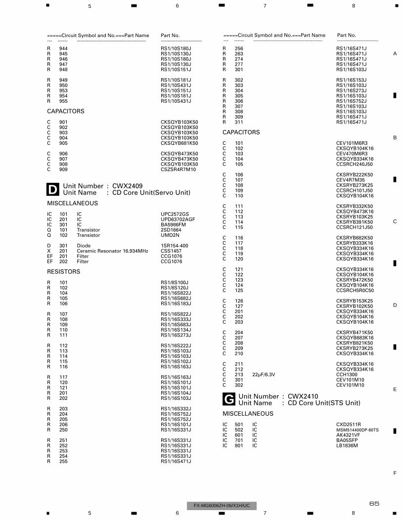
65
5 6 7 8
F
E
D
C
B
A
5 6 7 8FX-MG6006ZH-06/X1H/UC
R 944 RS1/10S180JR 945 RS1/10S130JR 946 RS1/10S180JR 947 RS1/10S130JR 948 RS1/10S151J
R 949 RS1/10S181JR 950 RS1/10S431JR 953 RS1/10S151JR 954 RS1/10S181JR 955 RS1/10S431J
CAPACITORS
C 901 CKSQYB103K50C 902 CKSQYB103K50C 903 CKSQYB103K50C 904 CKSQYB103K50C 905 CKSQYB681K50
C 906 CKSQYB473K50C 907 CKSQYB473K50C 908 CKSQYB103K50C 909 CSZSR4R7M10
Unit Number : CWX2409Unit Name : CD Core Unit(Servo Unit)
MISCELLANEOUS
IC 101 IC UPC2572GSIC 201 IC UPD63702AGFIC 301 IC BA5986FMQ 101 Transistor 2SD1664Q 102 Transistor UMD2N
D 301 Diode 1SR154-400X 201 Ceramic Resonator 16.934MHz CSS1457EF 201 Filter CCG1076EF 202 Filter CCG1076
RESISTORS
R 101 RS1/8S100JR 102 RS1/8S120JR 104 RS1/16S822JR 105 RS1/16S682JR 106 RS1/16S183J
R 107 RS1/16S822JR 108 RS1/16S333JR 109 RS1/16S683JR 110 RS1/16S134JR 111 RS1/16S273J
R 112 RS1/16S222JR 113 RS1/16S103JR 114 RS1/16S103JR 115 RS1/16S102JR 116 RS1/16S163J
R 117 RS1/16S163JR 120 RS1/16S101JR 121 RS1/16S101JR 201 RS1/16S104JR 202 RS1/16S103J
R 203 RS1/16S332JR 204 RS1/16S752JR 205 RS1/16S752JR 206 RS1/16S101JR 250 RS1/16S331J
R 251 RS1/16S331JR 252 RS1/16S331JR 253 RS1/16S331JR 254 RS1/16S331JR 255 RS1/16S471J
R 256 RS1/16S471JR 263 RS1/16S471JR 274 RS1/16S471JR 277 RS1/16S471JR 301 RS1/16S103J
R 302 RS1/16S153JR 303 RS1/16S103JR 304 RS1/16S273JR 305 RS1/16S103JR 306 RS1/16S752JR 307 RS1/16S103JR 308 RS1/16S103JR 309 RS1/16S471JR 311 RS1/16S471J
CAPACITORS
C 101 CEV101M6R3C 102 CKSQYB104K16C 103 CEV470M6R3C 104 CKSQYB334K16C 105 CCSRCH240J50
C 106 CKSRYB222K50C 107 CEV4R7M35C 108 CKSRYB273K25C 109 CCSRCH101J50C 110 CKSQYB104K16
C 111 CKSRYB332K50C 112 CKSQYB473K16C 113 CKSRYB103K25C 114 CKSRYB391K50C 115 CCSRCH121J50
C 116 CKSRYB682K50C 117 CKSRYB333K16C 118 CKSQYB334K16C 119 CKSQYB334K16C 120 CKSQYB334K16
C 121 CKSQYB334K16C 122 CKSQYB104K16C 123 CKSRYB472K50C 124 CKSQYB104K16C 125 CCSRCH5R0C50
C 126 CKSRYB153K25C 127 CKSRYB102K50C 201 CKSQYB334K16C 202 CKSQYB104K16C 203 CKSQYB104K16
C 204 CKSRYB471K50C 207 CKSQYB683K16C 208 CKSRYB821K50C 209 CKSRYB273K25C 210 CKSQYB334K16
C 211 CKSQYB334K16C 212 CKSQYB334K16C 213 22µF/6.3V CCH1300C 301 CEV101M10C 302 CEV101M10
Unit Number : CWX2410Unit Name : CD Core Unit(STS Unit)
MISCELLANEOUS
IC 501 IC CXD2511RIC 502 IC MSM514400DP-60TSIC 601 IC AK4321VFIC 701 IC BA05SFPIC 801 IC LB1836M
=====Circuit Symbol and No.===Part Name Part No.--- ------ ------------------------------------------ -------------------------
=====Circuit Symbol and No.===Part Name Part No.--- ------ ------------------------------------------ -------------------------
D
G
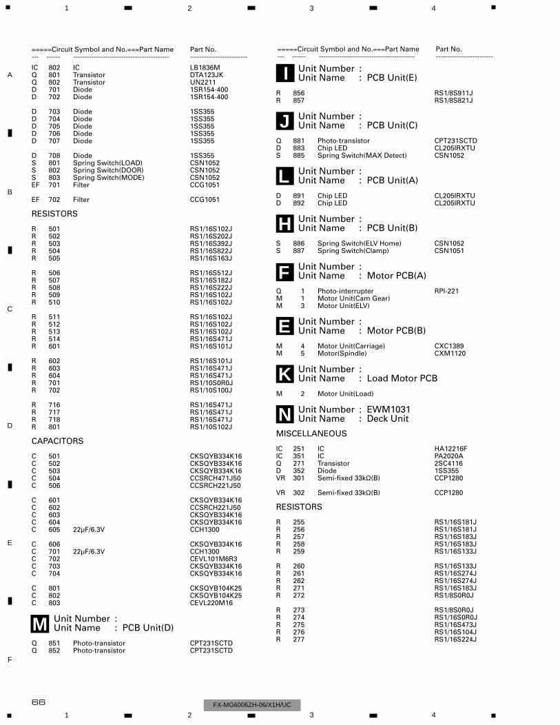
66
1 2 3 4
1 2 3 4
F
E
D
C
B
A
FX-MG6006ZH-06/X1H/UC
IC 802 IC LB1836MQ 801 Transistor DTA123JKQ 802 Transistor UN2211D 701 Diode 1SR154-400D 702 Diode 1SR154-400
D 703 Diode 1SS355D 704 Diode 1SS355D 705 Diode 1SS355D 706 Diode 1SS355D 707 Diode 1SS355
D 708 Diode 1SS355S 801 Spring Switch(LOAD) CSN1052S 802 Spring Switch(DOOR) CSN1052S 803 Spring Switch(MODE) CSN1052EF 701 Filter CCG1051
EF 702 Filter CCG1051
RESISTORS
R 501 RS1/16S102JR 502 RS1/16S202JR 503 RS1/16S392JR 504 RS1/16S822JR 505 RS1/16S163J
R 506 RS1/16S512JR 507 RS1/16S182JR 508 RS1/16S222JR 509 RS1/16S102JR 510 RS1/16S102J
R 511 RS1/16S102JR 512 RS1/16S102JR 513 RS1/16S102JR 514 RS1/16S471JR 601 RS1/16S101J
R 602 RS1/16S101JR 603 RS1/16S471JR 604 RS1/16S471JR 701 RS1/10S0R0JR 702 RS1/10S100J
R 716 RS1/16S471JR 717 RS1/16S471JR 718 RS1/16S471JR 801 RS1/10S102J
CAPACITORS
C 501 CKSQYB334K16C 502 CKSQYB334K16C 503 CKSQYB334K16C 504 CCSRCH471J50C 506 CCSRCH221J50
C 601 CKSQYB334K16C 602 CCSRCH221J50C 603 CKSQYB334K16C 604 CKSQYB334K16C 605 22µF/6.3V CCH1300
C 606 CKSQYB334K16C 701 22µF/6.3V CCH1300C 702 CEVL101M6R3C 703 CKSQYB334K16C 704 CKSQYB334K16
C 801 CKSQYB104K25C 802 CKSQYB104K25C 803 CEVL220M16
Unit Number :Unit Name : PCB Unit(D)
Q 851 Photo-transistor CPT231SCTDQ 852 Photo-transistor CPT231SCTD
Unit Number :Unit Name : PCB Unit(E)
R 856 RS1/8S911JR 857 RS1/8S821J
Unit Number :Unit Name : PCB Unit(C)
Q 881 Photo-transistor CPT231SCTDD 883 Chip LED CL205IRXTUS 885 Spring Switch(MAX Detect) CSN1052
Unit Number :Unit Name : PCB Unit(A)
D 891 Chip LED CL205IRXTUD 892 Chip LED CL205IRXTU
Unit Number :Unit Name : PCB Unit(B)
S 886 Spring Switch(ELV Home) CSN1052S 887 Spring Switch(Clamp) CSN1051
Unit Number :Unit Name : Motor PCB(A)
Q 1 Photo-interrupter RPI-221M 1 Motor Unit(Cam Gear)M 3 Motor Unit(ELV)
Unit Number :Unit Name : Motor PCB(B)
M 4 Motor Unit(Carriage) CXC1389M 5 Motor(Spindle) CXM1120
Unit Number :Unit Name : Load Motor PCB
M 2 Motor Unit(Load)
Unit Number : EWM1031Unit Name : Deck Unit
MISCELLANEOUS
IC 251 IC HA12216FIC 351 IC PA2020AQ 271 Transistor 2SC4116D 352 Diode 1SS355VR 301 Semi-fixed 33kΩ(B) CCP1280
VR 302 Semi-fixed 33kΩ(B) CCP1280
RESISTORS
R 255 RS1/16S181JR 256 RS1/16S181JR 257 RS1/16S183JR 258 RS1/16S183JR 259 RS1/16S133J
R 260 RS1/16S133JR 261 RS1/16S274JR 262 RS1/16S274JR 271 RS1/16S183JR 272 RS1/8S0R0J
R 273 RS1/8S0R0JR 274 RS1/16S0R0JR 275 RS1/16S473JR 276 RS1/16S104JR 277 RS1/16S224J
=====Circuit Symbol and No.===Part Name Part No.--- ------ ------------------------------------------ -------------------------
=====Circuit Symbol and No.===Part Name Part No.--- ------ ------------------------------------------ -------------------------
J
L
H
F
E
K
N
M
I
67
5 6 7 8
F
E
D
C
B
A
5 6 7 8FX-MG6006ZH-06/X1H/UC
R 278 RS1/16S104JR 281 RS1/8S0R0JR 282 RS1/8S0R0JR 283 RS1/8S0R0JR 284 RS1/8S0R0J
R 285 RS1/16S0R0JR 287 RS1/16S0R0JR 291 RS1/8S0R0JR 292 RS1/10S0R0JR 293 RS1/10S0R0J
R 294 RS1/10S0R0JR 321 RS1/8S0R0JR 322 RS1/8S0R0JR 351 RS1/16S102JR 352 RS1/16S102J
R 353 RS1/16S102JR 354 RS1/16S102JR 355 RS1/16S274JR 362 RS1/8S301JR 373 RS1/16S0R0J
R 374 RS1/8S0R0JR 375 RS1/8S0R0JR 401 RS1/16S153JR 402 RS1/16S332JR 403 RS1/16S911J
R 404 RS1/16S274J
CAPACITORS
C 251 CKSRYB391K50C 252 CKSRYB391K50C 253 CKSRYB391K50C 254 CKSRYB391K50C 255 CKSRYB103K50
C 256 CKSRYB103K50C 271 1µF/50V ECH0002C 272 CKSRYB104K16C 301 CKSRYB104K16C 302 CKSRYB104K16
C 309 CKSRYB104K16C 310 CKSRYB104K16C 351 CKSQYB224K25C 352 CKSRYB392K50C 353 CKSRYB103K50
C 354 CKSRYB103K50C 355 CKSQYB104K50C 356 CKSRYB103K50C 401 CKSRYB392K50C 402 CKSRYB334K10
C 403 CKSRYB223K25C 404 CKSRYB103K50C 405 CKSRYB333K16
Unit Number :Unit Name : Reel Sense PCB
MISCELLANEOUS
S 1 Switch(LOAD) ESG1007S 2 Switch(MODE) ESG1007S 3 Switch(70µS) ESG1007EGN 1 Photo-reflector EGN1004
Miscellaneous Parts List
M 1 Motor Unit(MAIN) EXA1491M 2 Motor Unit(SUB) EXA1382HD 1 Head Assy EXA1594
Pickup Unit(Service)(P8) CXX1311
=====Circuit Symbol and No.===Part Name Part No.--- ------ ------------------------------------------ -------------------------
O
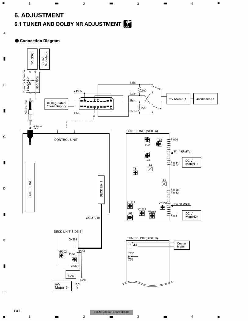
68
- Connection Diagram
FM S
SG
Ste
reo
M
od
ula
tor
50Ω
(37.
5Ω)
An
ten
na
Plu
gD
um
my
An
ten
na
50Ω
(75Ω
)
CONTROL UNIT
TU
NE
R U
NIT
Antenna Jack
mV Meter (1) OscilloscopeDC Regulated Power Supply
DE
CK
UN
IT
Lch+
Lch-
Rch+
Rch-
2kΩ
2kΩ
+13.2v
GND
VR302
mVMeter(2)
VR301
R-CHL-CH
Pin2Pin3
CN251
DECK UNIT(SIDE B)
DC VMeter(1)
Pin 1
Pin 14
Pin 13
Pin26
TUNER UNIT (SIDE A)
DC VMeter(2)
L5
TC3
L52
VR151
TC2
VR101VR154
VR156
TC1
T31L6
Pin 6(FMSD)
Pin 19(FMTV)
Pin 27
Pin 28
CenterMeter
C63
L52
TUNER UNIT(SIDE B)
GGD1019
1 2 3 4
1 2 3 4
F
E
D
C
B
A
FX-MG6006ZH-06/X1H/UC
6. ADJUSTMENT
6.1 TUNER AND DOLBY NR ADJUSTMENT
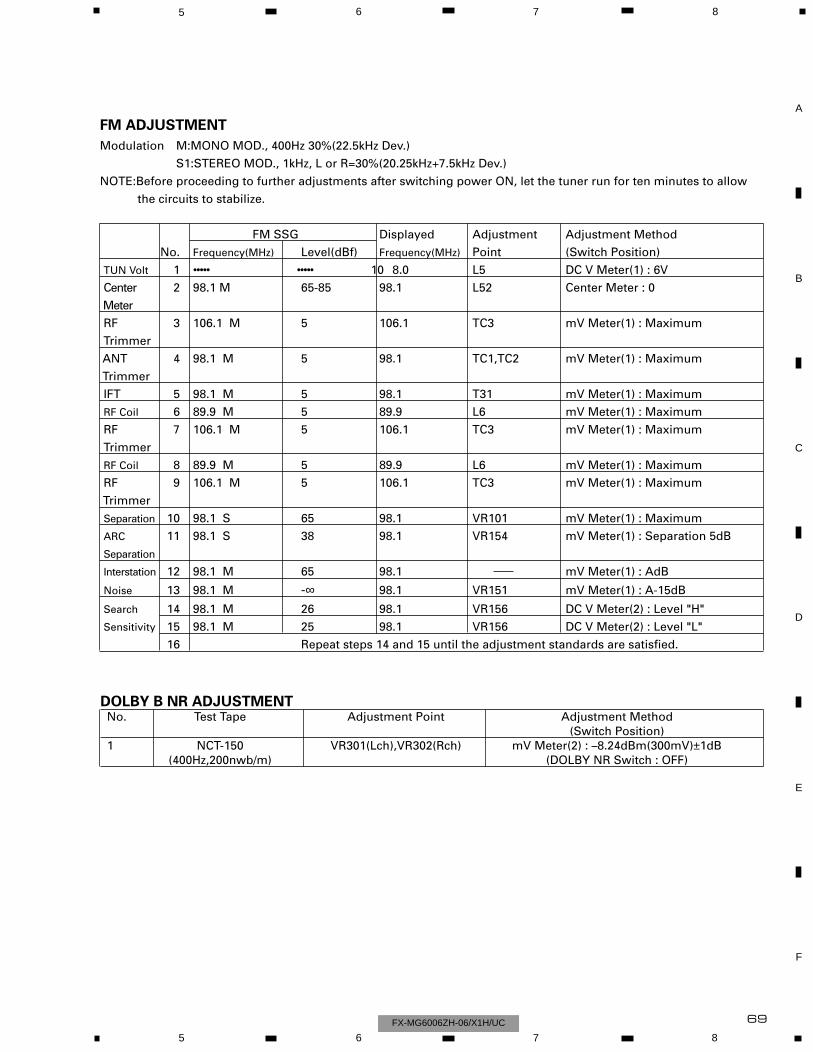
69
5 6 7 8
F
E
D
C
B
A
5 6 7 8FX-MG6006ZH-06/X1H/UC
FM ADJUSTMENT
Modulation M:MONO MOD., 400Hz 30%(22.5kHz Dev.)
S1:STEREO MOD., 1kHz, L or R=30%(20.25kHz+7.5kHz Dev.)
NOTE:Before proceeding to further adjustments after switching power ON, let the tuner run for ten minutes to allow
the circuits to stabilize.
FM SSG Displayed Adjustment Adjustment Method
No. Frequency(MHz) Level(dBf) Frequency(MHz) Point (Switch Position)
TUN Volt 1 ••••• ••••• 10 8.0 L5 DC V Meter(1) : 6V
Center 2 98.1 M 65-85 98.1 L52 Center Meter : 0
Meter
RF 3 106.1 M 5 106.1 TC3 mV Meter(1) : Maximum
Trimmer
ANT 4 98.1 M 5 98.1 TC1,TC2 mV Meter(1) : Maximum
Trimmer
IFT 5 98.1 M 5 98.1 T31 mV Meter(1) : Maximum
RF Coil 6 89.9 M 5 89.9 L6 mV Meter(1) : Maximum
RF 7 106.1 M 5 106.1 TC3 mV Meter(1) : Maximum
Trimmer
RF Coil 8 89.9 M 5 89.9 L6 mV Meter(1) : Maximum
RF 9 106.1 M 5 106.1 TC3 mV Meter(1) : Maximum
Trimmer
Separation 10 98.1 S 65 98.1 VR101 mV Meter(1) : Maximum
ARC 11 98.1 S 38 98.1 VR154 mV Meter(1) : Separation 5dB
Separation
Interstation 12 98.1 M 65 98.1 mV Meter(1) : AdB
Noise 13 98.1 M -∞ 98.1 VR151 mV Meter(1) : A-15dB
Search 14 98.1 M 26 98.1 VR156 DC V Meter(2) : Level "H"
Sensitivity 15 98.1 M 25 98.1 VR156 DC V Meter(2) : Level "L"
16 Repeat steps 14 and 15 until the adjustment standards are satisfied.
DOLBY B NR ADJUSTMENTNo. Test Tape Adjustment Point Adjustment Method
(Switch Position)1 NCT-150 VR301(Lch),VR302(Rch) mV Meter(2) : – 8.24dBm(300mV)±1dB
(400Hz,200nwb/m) (DOLBY NR Switch : OFF)
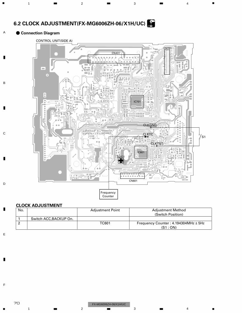
70
1 2 3 4
1 2 3 4
F
E
D
C
B
A
FX-MG6006ZH-06/X1H/UC
CONTROL UNIT(SIDE A)
CLKTST
CLKTC
CLKGND
FrequencyCounter
TC601
S1
IC601
CN601
IC701
CN701
CN431
CLOCK ADJUSTMENTNo. Adjustment Point Adjustment Method
(Switch Position)1 Switch ACC,BACKUP On.2 TC601 Frequency Counter : 4.194304MHz ± 5Hz
(S1 : ON)
- Connection Diagram
6.2 CLOCK ADJUSTMENT(FX-MG6006ZH-06/X1H/UC)
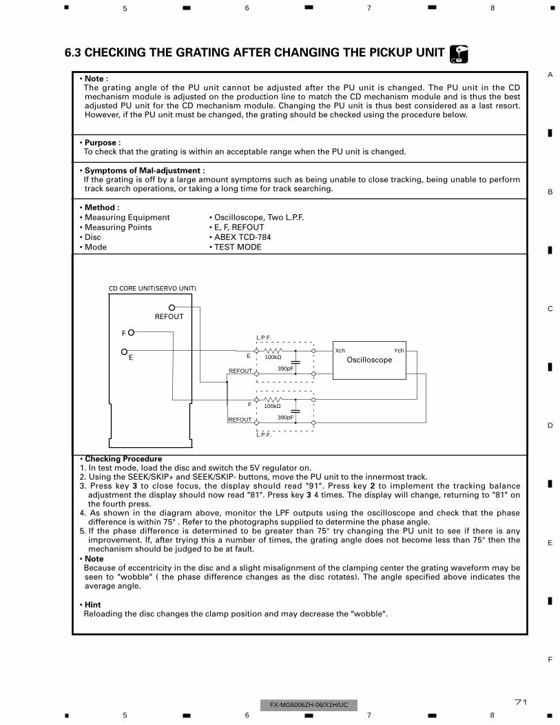
71
5 6 7 8
F
E
D
C
B
A
5 6 7 8FX-MG6006ZH-06/X1H/UC
• Note :The grating angle of the PU unit cannot be adjusted after the PU unit is changed. The PU unit in the CDmechanism module is adjusted on the production line to match the CD mechanism module and is thus the bestadjusted PU unit for the CD mechanism module. Changing the PU unit is thus best considered as a last resort.However, if the PU unit must be changed, the grating should be checked using the procedure below.
• Purpose :To check that the grating is within an acceptable range when the PU unit is changed.
• Symptoms of Mal-adjustment :If the grating is off by a large amount symptoms such as being unable to close tracking, being unable to performtrack search operations, or taking a long time for track searching.
• Method :
• Measuring Equipment • Oscilloscope, Two L.P.F.• Measuring Points • E, F, REFOUT• Disc • ABEX TCD-784• Mode • TEST MODE
• Checking Procedure1. In test mode, load the disc and switch the 5V regulator on.2. Using the SEEK/SKIP+ and SEEK/SKIP- buttons, move the PU unit to the innermost track.3. Press key 3 to close focus, the display should read "91". Press key 2 to implement the tracking balance
adjustment the display should now read "81". Press key 3 4 times. The display will change, returning to "81" onthe fourth press.
4. As shown in the diagram above, monitor the LPF outputs using the oscilloscope and check that the phasedifference is within 75° . Refer to the photographs supplied to determine the phase angle.
5. If the phase difference is determined to be greater than 75° try changing the PU unit to see if there is anyimprovement. If, after trying this a number of times, the grating angle does not become less than 75° then themechanism should be judged to be at fault.
• NoteBecause of eccentricity in the disc and a slight misalignment of the clamping center the grating waveform may beseen to "wobble" ( the phase difference changes as the disc rotates). The angle specified above indicates theaverage angle.
• HintReloading the disc changes the clamp position and may decrease the "wobble".
100kΩ
390pF
100kΩ
390pF
E
REFOUT
F
Xch Ych
Oscilloscope
L.P.F.
L.P.F.
E
F
REFOUT
REFOUT
CD CORE UNIT(SERVO UNIT)
6.3 CHECKING THE GRATING AFTER CHANGING THE PICKUP UNIT
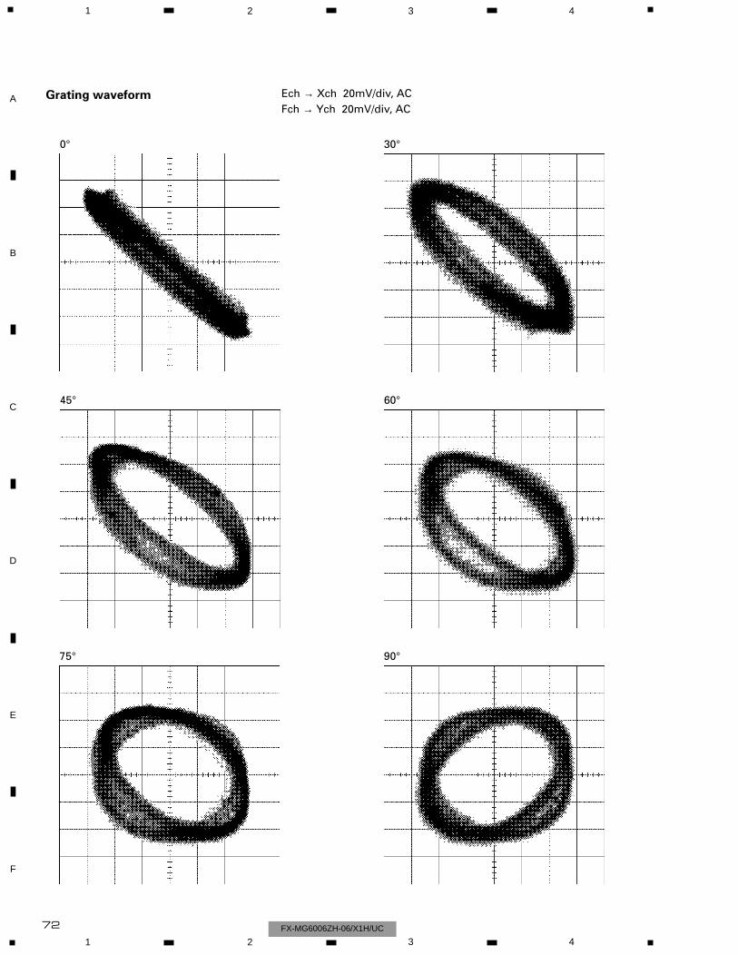
72
1 2 3 4
1 2 3 4
F
E
D
C
B
A
FX-MG6006ZH-06/X1H/UC
Grating waveform Ech → Xch 20mV/div, ACFch → Ych 20mV/div, AC
45°
0°
75°
60°
30°
90°
73
5 6 7 8
F
E
D
C
B
A
5 6 7 8FX-MG6006ZH-06/X1H/UC
7. GENERAL INFORMATION
7.1 DIAGNOSIS
7.1.1 TEST MODE
- CD Test Mode
1) Precautions on Adjustment• The unit employs a single voltage (+5V) for the
regulator, thus the reference potential of the signal isRFOUT (approximately 2.5V) rather than GND.Inadvertent contact of REFOUT and GND duringadjustment can result not only in disabling normalpotential measurement but also in exposing thepickup to strong impacts due to malfunctioning of theservo. Therefore, you are requested to observe thefollowing precautions.
• Make sure that the negative probe of the measuringinstrument is not connected to RFOUT or GND.Special care must be exercised so that the channel 1negative probe may not be connected to theoscilloscope and the channel 2 negative probe toGND. Since the frame of the measuring instrument isusually at the same potential as the negative probe,the frame of the measuring instrument must bechanged to floating status.When RFOUT is inadvertently connected to GND, youmust immediately turn off the regulator or powersupply.
• The regulator must be turned off before mounting ordismounting filters or wiring materials.
• You should not start adjustment or measurementimmediately after the regulator is turned on. It isrecommended to run the player for approximatelyone minute so that it may stabilize.
• When the test mode is turned on, various protectivefunctions from the software become unavailable.Thus, you must make sure that undesirable electric ormechanical shocks are not be given to the system.
• This model employs a photo-transistor for detectingdiscs at their loading or ejection. Thus, if its outercase is removed during repair work and internal partsare exposed to light of strong intensity, malfunctionsincluding the following can result:∗ The eject button becomes inoperable during play.
Pressing the eject button does not eject a disc andplay is continued.
∗ Loading becomes unavailable.If a malfunction is recognized, appropriate remedialactions must be taken. Such actions includechanging the light source position, changing the unitposition and applying a cover to the photo-transistor.
• When you press the EJECT key to eject a disc, youmust not touch any other key until the ejection iscomplete.
• If you press the SEEK/SKIP+ or SEEK/SKIP- for thefocus search in the test mode, you must turn thepower off immediately. (Otherwise, the lens will beforced to stick to the top or bottom, potentiallyresulting in the burning of the actuator.)
2) Description of the Test Mode• Turning on the Test Mode
Press the [4] and [6] keys simultaneously to turn onthe ACC and the backup.
• Ending the Test ModeApply the reset (the reset will be applied two minutesafter the power is turned from off).
• Operation of TR JUMPs (except 100TR) continuesafter your finger has left the key. CRG, MOVE and100TR JUMP are forced to the tracking close mode assoon as the key is released.
• Turning the power on or off resets the JUMP MODEto the Single TR.
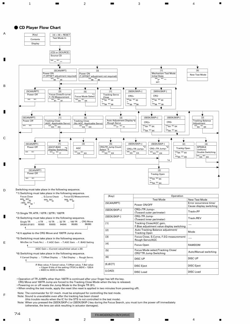
[SCAN/RPT]Power Off
MIN SEC
[3]Focus Close/S-curve/F, F0 Measurement
MIN SEC91 91
[5]
Focus Mode SelectMIN SEC
0X 0X
[1]Tracking ServoClose
MIN SEC00 00
[SCAN/RPT]Power ON(T.OFFSET adjustment required)
MIN SEC00 00
[3]Power ON(T.OFFSET adjustment not required)
MIN SEC99 99
[1]Mechanism Test ModeInitial State
MIN SEC0* **
[5]
New Test Mode
[CD] or [SOURCE]Source CD
MIN SEC** **
[SCAN/RPT]Power Off
[1]Tracking Close(AGC, Applicable Servo)
MIN SECXX XX
[5]Tracking Close(No AGC, Applicable Servo)
MIN SECXX XX
[3]Auto Adjustment Display/Rough Servo
MIN SEC?? ??
[2]Tracking Balance Adjustment
MIN SEC8X 8X
[Key]
Contents
Display
[4] + [6] + RESETTest Mode In
[3]
AGC
MIN SECXX XX
[5]CRG/TR Jump CountSelect
MIN SECXX XX
[SEEK/SKIP+]
CRG+/TR Jump+MIN SEC
XX XX
[SEEK/SKIP-]
CRG– /TR Jump–MIN SEC
XX XX
[4]SPINDLEUniform/Double Switching
MIN SECXX XX
[SCAN/RPT]Power Off
[1]AGC/F.BIASDisplay Switching
MIN SEC?? ??
MIN SEC99 99
or
[SEEK/SKIP+]
CRG+MIN SEC00 00
TRK MIN99 99
or
[SEEK/SKIP-]
CRG-MIN SEC00 00
MIN SEC99 99
or
[SEEK/SKIP+]
CRG+MIN SEC8X 8X
MIN SEC9X 9X
or
[SEEK/SKIP-]
CRG-MIN SEC8X 8X
MIN SEC9X 9X
or
[SCAN/RPT]Power Off
[2]
Trackig Open
MIN SEC8X 8X
MIN SEC9X 9X
or
[2]
Trackig Open
MIN SEC8X 8X
MIN SEC9X 9X
or
*1
*6
*5*3
*2 *2
*4
*1) Switching must take place in the following sequence.
MIN SEC00 00
( )MIN SEC99 99
S.Curve CheckMIN SEC
01 01
Focus EQ Measurement.Focus CloseMIN SEC
02 02
*2)
→ → → → →9X(8X):91(81)
4 TR92(82)
10 TR93(83)
32 TR94(84)
100 TR95(85)
CRG Move96(86)
Switching must take place in the following sequence.
*4)
→ → →F.AGC Gain T.AGC Gain F. BIAS Setting
(AGC Gain = (Current value/Initial value) x 20)
→ → →
→ →
Single TR /4TR / 10TR / 32TR / 100TR
Single TR
*3) Switching must take place in the following sequence.
It applies to the CRG Move and 100TR Jump alone.
Min/Sec (or Track No.)
*5) Switching must take place in the following sequence.
F.Cancel Display
*6) Switching must take place in the following sequence. T.Offset Display T.Bal Display Rough Servo.
(F.Bias value, F.Cancel value, T.Offset value, T.Bal value = (Upper 8 bits of the setting (7F[H] to 80[H] + 128)/4 = 63[D] to 32[D] to 00[D]).
•
••
Operation of TR JUMPs other than 100TR is continued after your finger has left the key. CRG Move and 100TR Jump are forced to the Tracking Close Mode when the key is released.Powering on or off resets the Jump Mode to the Single TR (91).When ending the test mode, apply the reset (the reset is applied in two minutes from powering off).
Note:Note:
Note:
The commander for G1 mech. must be employed for controlling the test mode.Sound is unavailable even after the tracking has been closed (this trouble results when the IC for the STS is not controlled in the test mode).When you pressed the [SEEK/SKIP+] or [SEEK/SKIP-] key during the Focus Search, you must turn the power off immediately (otherwise, the lens can stick resulting in actuator damages).
[Key]
[SCAN/RPT]
[SEEK/SKIP+]
[SEEK/SKIP-]
[1]
[2]
[3]
[4]
[5]
[6]
OperationTest Mode New Test Mode
Power ON/OFF
CRG+/TR Jump+(Toward outer perimeter)
Tracking Close/AGC gain,F.Bias adjustment value display switchingAuto Tracking Balance adjustment/Tracking OpenFocus Close, S.Curve, F.EQ measurement/Rough Servo/AGC
Focus Open
Focus Mode select/Tracking Close/CRG*TR Jump Switching
CRG-/TR Jump-(Toward inner perimeter)
Error occurrence time/Cause display switching
Track+/FF
Track-/REV
Mode
RAMDOM
Auto/Manual switching
MIN SEC
MIN SEC
MIN SEC
DISC UP DISC UP
[EJECT]
[LOAD]
DISC Eject DISC Eject
DISC Load DISC Load
RPT
- CD Player Flow Chart
74
1 2 3 4
1 2 3 4
F
E
D
C
B
A
FX-MG6006ZH-06/X1H/UC
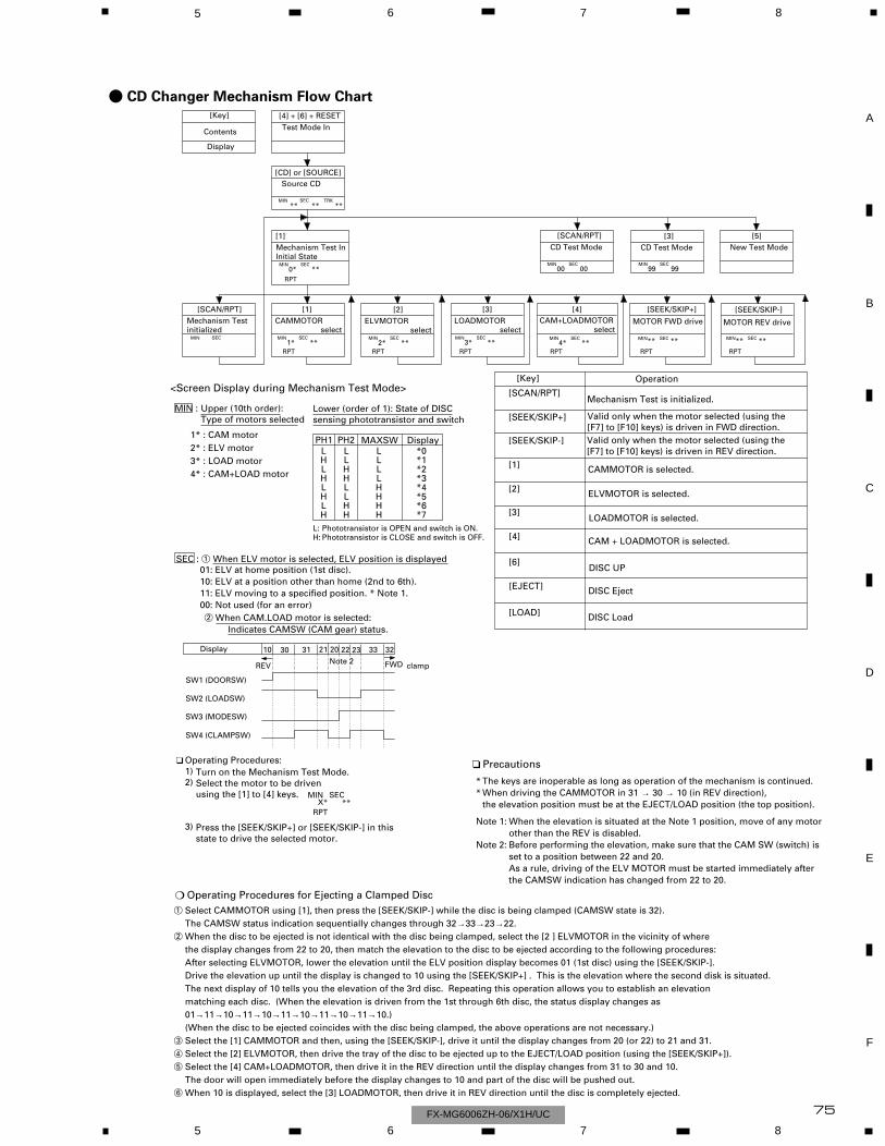
[SCAN/RPT]Mechanism Test initialized
MIN SEC
[1]CAMMOTOR selectMIN SEC
1* **
[2]ELVMOTOR select
MIN SEC2* **
[3]LOADMOTOR selectMIN SEC
3* **
[1]Mechanism Test InInitial State
MIN SEC0* **
[SCAN/RPT]CD Test Mode
MIN SEC00 00
[5]New Test Mode
Source CD
[Key]
Contents
Display
Test Mode In
[4]CAM+LOADMOTOR select
MIN SEC4* **
[SEEK/SKIP+]
MOTOR FWD drive
MIN SEC** **
[Key]
[SCAN/RPT] [SEEK/SKIP+] [SEEK/SKIP-] [1] [2] [3] [4]
Operation
Mechanism Test is initialized.
Valid only when the motor selected (using the[F7] to [F10] keys) is driven in FWD direction.
CAMMOTOR is selected.
[3]CD Test Mode
MIN SEC99 99
[SEEK/SKIP-]
MOTOR REV drive
MIN SEC** **
Valid only when the motor selected (using the [F7] to [F10] keys) is driven in REV direction.
ELVMOTOR is selected.
LOADMOTOR is selected.
CAM + LOADMOTOR is selected.
<Screen Display during Mechanism Test Mode>
MIN : Upper (10th order): Type of motors selected
Lower (order of 1): State of DISC sensing phototransistor and switch
1* : CAM motor2* : ELV motor3* : LOAD motor4* : CAM+LOAD motor
PH1 PH2 MAXSW DisplayLHLHLHLH
LLHHLLHH
LLLLHHHH
*0*1*2*3*4*5*6*7
L:H:
Phototransistor is OPEN and switch is ON.Phototransistor is CLOSE and switch is OFF.
SEC : 1 When ELV motor is selected, ELV position is displayed01: ELV at home position (1st disc).10: ELV at a position other than home (2nd to 6th).11: ELV moving to a specified position. * Note 1.00: Not used (for an error)2 When CAM.LOAD motor is selected:
Indicates CAMSW (CAM gear) status.
SW1 (DOORSW)
SW2 (LOADSW)
SW3 (MODESW)
SW4 (CLAMPSW)
Display 10 30 31 21 20 22 23 33 32
REV FWDNote 2
Precautions
**
Note 1:
Note 2:
The keys are inoperable as long as operation of the mechanism is continued.When driving the CAMMOTOR in 31 → 30 → 10 (in REV direction), the elevation position must be at the EJECT/LOAD position (the top position).
When the elevation is situated at the Note 1 position, move of any motor other than the REV is disabled.Before performing the elevation, make sure that the CAM SW (switch) is set to a position between 22 and 20. As a rule, driving of the ELV MOTOR must be started immediately after the CAMSW indication has changed from 22 to 20.
clamp
[CD] or [SOURCE]
TRKMIN SEC** ** **
[4] + [6] + RESET
RPT
RPTRPT RPT RPT RPT RPT
[6] [EJECT]
DISC UP
DISC Eject
[LOAD]
DISC Load
Operating Procedures:1)2)
3)
Turn on the Mechanism Test Mode.Select the motor to be driven using the [1] to [4] keys.
Press the [SEEK/SKIP+] or [SEEK/SKIP-] in this state to drive the selected motor.
RPT
MIN SECX* **
1
2
3
4
5
6
Select CAMMOTOR using [1], then press the [SEEK/SKIP-] while the disc is being clamped (CAMSW state is 32).The CAMSW status indication sequentially changes through 32→33→23→22.When the disc to be ejected is not identical with the disc being clamped, select the [2 ] ELVMOTOR in the vicinity of where the display changes from 22 to 20, then match the elevation to the disc to be ejected according to the following procedures:After selecting ELVMOTOR, lower the elevation until the ELV position display becomes 01 (1st disc) using the [SEEK/SKIP-]. Drive the elevation up until the display is changed to 10 using the [SEEK/SKIP+] . This is the elevation where the second disk is situated. The next display of 10 tells you the elevation of the 3rd disc. Repeating this operation allows you to establish an elevation matching each disc. (When the elevation is driven from the 1st through 6th disc, the status display changes as 01→11→10→11→10→11→10→11→10→11→10.) (When the disc to be ejected coincides with the disc being clamped, the above operations are not necessary.)Select the [1] CAMMOTOR and then, using the [SEEK/SKIP-], drive it until the display changes from 20 (or 22) to 21 and 31.Select the [2] ELVMOTOR, then drive the tray of the disc to be ejected up to the EJECT/LOAD position (using the [SEEK/SKIP+]).Select the [4] CAM+LOADMOTOR, then drive it in the REV direction until the display changes from 31 to 30 and 10. The door will open immediately before the display changes to 10 and part of the disc will be pushed out.When 10 is displayed, select the [3] LOADMOTOR, then drive it in REV direction until the disc is completely ejected.
Operating Procedures for Ejecting a Clamped Disc
- CD Changer Mechanism Flow Chart
75
5 6 7 8
F
E
D
C
B
A
5 6 7 8FX-MG6006ZH-06/X1H/UC
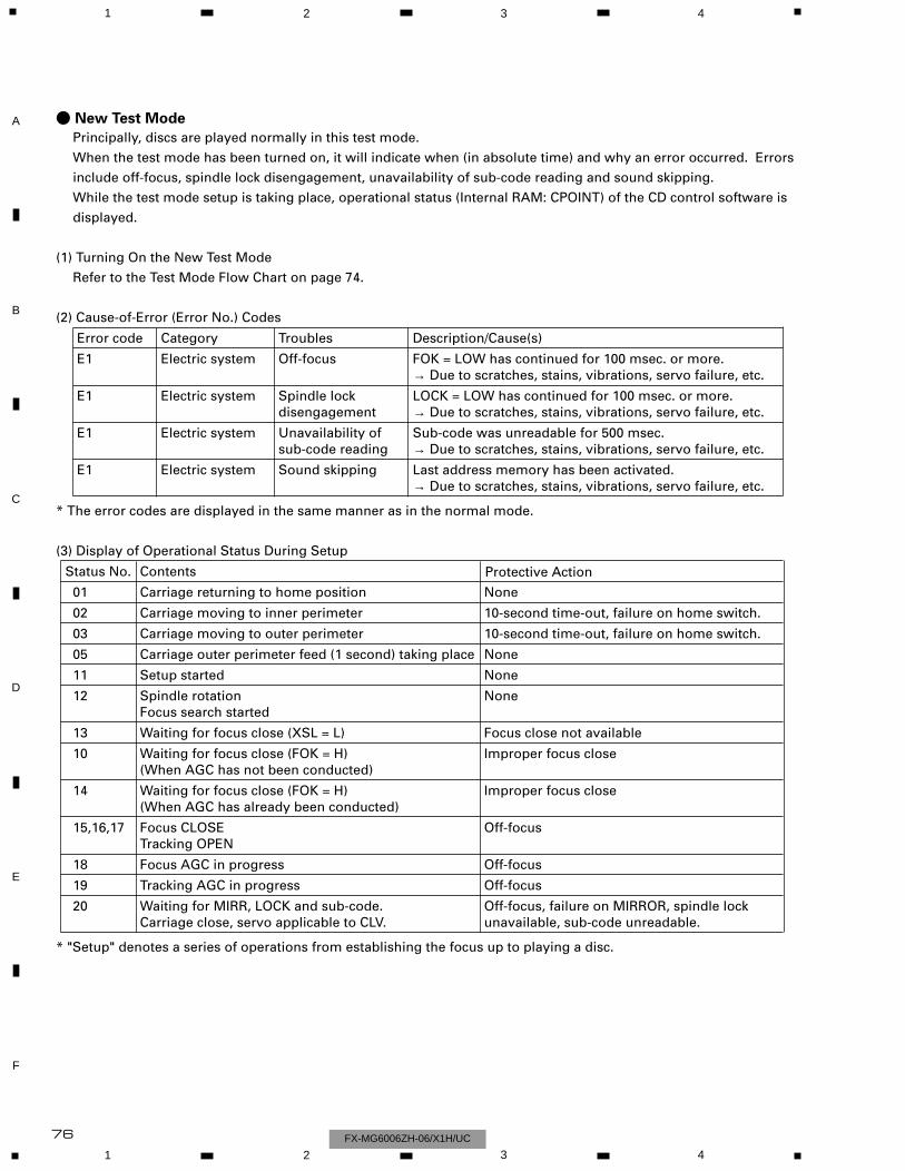
76
1 2 3 4
1 2 3 4
F
E
D
C
B
A
FX-MG6006ZH-06/X1H/UC
- New Test Mode
Principally, discs are played normally in this test mode.
When the test mode has been turned on, it will indicate when (in absolute time) and why an error occurred. Errors
include off-focus, spindle lock disengagement, unavailability of sub-code reading and sound skipping.
While the test mode setup is taking place, operational status (Internal RAM: CPOINT) of the CD control software is
displayed.
(1) Turning On the New Test Mode
Refer to the Test Mode Flow Chart on page 74.
(2) Cause-of-Error (Error No.) Codes
Error code Category Troubles Description/Cause(s)
E1 Electric system Off-focus FOK = LOW has continued for 100 msec. or more.→ Due to scratches, stains, vibrations, servo failure, etc.
E1 Electric system Spindle lock LOCK = LOW has continued for 100 msec. or more.disengagement → Due to scratches, stains, vibrations, servo failure, etc.
E1 Electric system Unavailability of Sub-code was unreadable for 500 msec.sub-code reading → Due to scratches, stains, vibrations, servo failure, etc.
E1 Electric system Sound skipping Last address memory has been activated.→ Due to scratches, stains, vibrations, servo failure, etc.
* The error codes are displayed in the same manner as in the normal mode.
(3) Display of Operational Status During Setup
Status No. Contents Protective Action
01 Carriage returning to home position None
02 Carriage moving to inner perimeter 10-second time-out, failure on home switch.
03 Carriage moving to outer perimeter 10-second time-out, failure on home switch.
05 Carriage outer perimeter feed (1 second) taking place None
11 Setup started None
12 Spindle rotation NoneFocus search started
13 Waiting for focus close (XSL = L) Focus close not available
10 Waiting for focus close (FOK = H) Improper focus close(When AGC has not been conducted)
14 Waiting for focus close (FOK = H) Improper focus close(When AGC has already been conducted)
15,16,17 Focus CLOSE Off-focusTracking OPEN
18 Focus AGC in progress Off-focus
19 Tracking AGC in progress Off-focus
20 Waiting for MIRR, LOCK and sub-code. Off-focus, failure on MIRROR, spindle lock Carriage close, servo applicable to CLV. unavailable, sub-code unreadable.
* "Setup" denotes a series of operations from establishing the focus up to playing a disc.
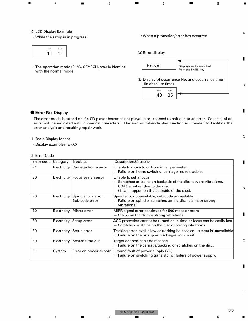
77
5 6 7 8
F
E
D
C
B
A
5 6 7 8FX-MG6006ZH-06/X1H/UC
(5) LCD Display Example
• While the setup is in progress
• The operation mode (PLAY, SEARCH, etc.) is identicalwith the normal mode.
• When a protection/error has occurred
(a) Error display
Display can be switched from the BAND key
(b) Display of occurrence No. and occurrence time (in absolute time)
Min
11Sec
11
Er– xx
Min
40Sec
05
- Error No. Display
The error mode is turned on if a CD player becomes not playable or is forced to halt due to an error. Cause(s) of anerror will be indicated with numerical characters. The error-number-display function is intended to facilitate theerror analysis and resulting repair work.
(1) Basic Display Means
• Display examples: Er-XX
(2) Error Code
Error code Category Troubles Description/Cause(s)
E1 Electricity Carriage home error Unable to move to or from inner perimeter→ Failure on home switch or carriage move trouble.
E0 Electricity Focus search error Unable to set a focus→ Scratches or stains on backside of the disc, severe vibrations,
CD-R is not written to the disc(it can happen on the backside of the disc).
E0 Electricity Spindle lock error Spindle lock unavailable, sub-code unreadableSub-code error → Failure on spindle, scratches on the disc, stains or strong
vibrations.
E0 Electricity Mirror error MIRR signal error continues for 500 msec or more→ Stains on the disc or strong vibrations.
E0 Electricity Setup error AGC protection cannot be turned on in time or focus can be easily lost→ Scratches or stains on the disc or strong vibrations.
E0 Electricity Setup error Tracking error level is low or tracking balance adjustment is unavailable→ Failure on the pickup or tracking-error circuit.
E0 Electricity Search time-out Target address can't be reached→ Failure on the carriage/tracking or scratches on the disc.
E1 System Error on power supply Ground fault of power supply (VD)→ Failure on switching transistor or failure of power supply.
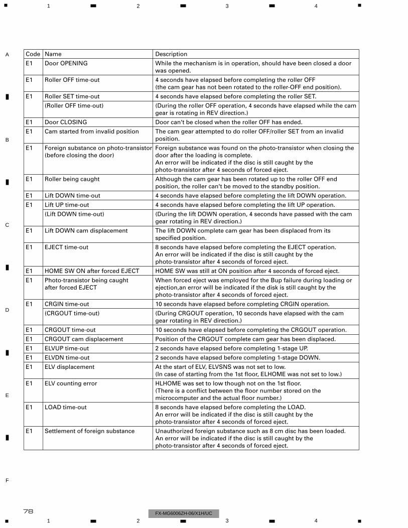
78
1 2 3 4
1 2 3 4
F
E
D
C
B
A
FX-MG6006ZH-06/X1H/UC
Code Name Description
E1 Door OPENING While the mechanism is in operation, should have been closed a door was opened.
E1 Roller OFF time-out 4 seconds have elapsed before completing the roller OFF(the cam gear has not been rotated to the roller-OFF end position).
E1 Roller SET time-out 4 seconds have elapsed before completing the roller SET.
(Roller OFF time-out) (During the roller OFF operation, 4 seconds have elapsed while the cam gear is rotating in REV direction.)
E1 Door CLOSING Door can't be closed when the roller OFF has ended.
E1 Cam started from invalid position The cam gear attempted to do roller OFF/roller SET from an invalid position.
E1 Foreign substance on photo-transistor Foreign substance was found on the photo-transistor when closing the (before closing the door) door after the loading is complete.
An error will be indicated if the disc is still caught by the photo-transistor after 4 seconds of forced eject.
E1 Roller being caught Although the cam gear has been rotated up to the roller OFF end position, the roller can't be moved to the standby position.
E1 Lift DOWN time-out 4 seconds have elapsed before completing the lift DOWN operation.
E1 Lift UP time-out 4 seconds have elapsed before completing the lift UP operation.
(Lift DOWN time-out) (During the lift DOWN operation, 4 seconds have passed with the cam gear rotating in REV direction.)
E1 Lift DOWN cam displacement The lift DOWN complete cam gear has been displaced from its specified position.
E1 EJECT time-out 8 seconds have elapsed before completing the EJECT operation.An error will be indicated if the disc is still caught by the photo-transistor after 4 seconds of forced eject.
E1 HOME SW ON after forced EJECT HOME SW was still at ON position after 4 seconds of forced eject.
E1 Photo-transistor being caught When forced eject was employed for the Bup failure during loading or after forced EJECT ejection,an error will be indicated if the disk is still caught by the
photo-transistor after 4 seconds of forced eject.
E1 CRGIN time-out 10 seconds have elapsed before completing CRGIN operation.
(CRGOUT time-out) (During CRGOUT operation, 10 seconds have elapsed with the cam gear rotating in REV direction.)
E1 CRGOUT time-out 10 seconds have elapsed before completing the CRGOUT operation.
E1 CRGOUT cam displacement Position of the CRGOUT complete cam gear has been displaced.
E1 ELVUP time-out 2 seconds have elapsed before completing 1-stage UP.
E1 ELVDN time-out 2 seconds have elapsed before completing 1-stage DOWN.
E1 ELV displacement At the start of ELV, ELVSNS was not set to low.(In case of starting from the 1st floor, ELHOME was not set to low.)
E1 ELV counting error HLHOME was set to low though not on the 1st floor.(There is a conflict between the floor number stored on the microcomputer and the actual floor number.)
E1 LOAD time-out 8 seconds have elapsed before completing the LOAD.An error will be indicated if the disc is still caught by the photo-transistor after 4 seconds of forced eject.
E1 Settlement of foreign substance Unauthorized foreign substance such as 8 cm disc has been loaded.An error will be indicated if the disc is still caught by the photo-transistor after 4 seconds of forced eject.
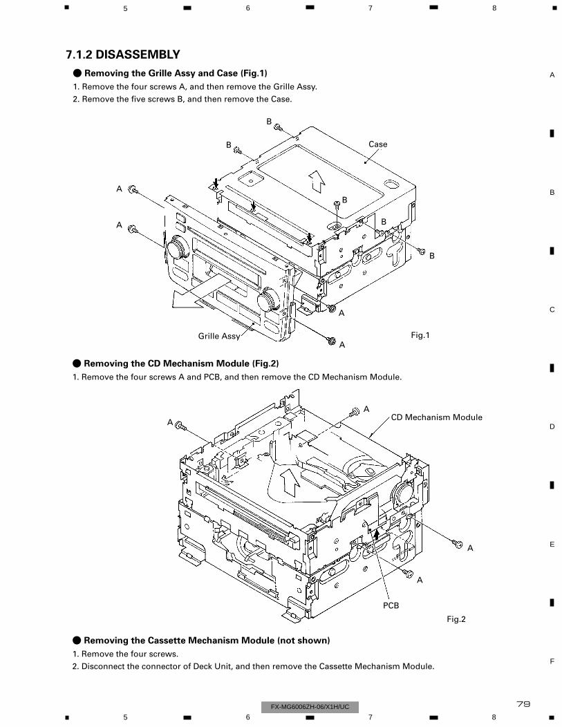
79
5 6 7 8
F
E
D
C
B
A
5 6 7 8FX-MG6006ZH-06/X1H/UC
- Removing the Grille Assy and Case (Fig.1)
1. Remove the four screws A, and then remove the Grille Assy.
2. Remove the five screws B, and then remove the Case.
Grille Assy
Case
A
B
- Removing the CD Mechanism Module (Fig.2)
1. Remove the four screws A and PCB, and then remove the CD Mechanism Module.
ACD Mechanism Module
PCB
- Removing the Cassette Mechanism Module (not shown)
1. Remove the four screws.
2. Disconnect the connector of Deck Unit, and then remove the Cassette Mechanism Module.
Fig.1
Fig.2
B
B
B
B
A
A
A
A
A
A
7.1.2 DISASSEMBLY
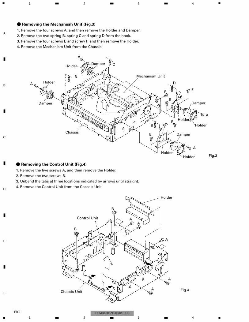
80
- Removing the Mechanism Unit (Fig.3)
1. Remove the four screws A, and then remove the Holder and Damper.
2. Remove the two spring B, spring C and spring D from the hook.
3. Remove the four screws E and screw F, and then remove the Holder.
4. Remove the Mechanism Unit from the Chassis.
DamperHolder
A
B
C
D
EF
Mechanism Unit
Chassis
- Removing the Control Unit (Fig.4)
1. Remove the five screws A, and then remove the Holder.
2. Remove the two screws B.
3. Unbend the tabs at three locations indicated by arrows until straight.
4. Remove the Control Unit from the Chassis Unit.
A
Chassis Unit
Control Unit
Fig.3
Fig.4
Holder
HolderHolder
Holder
Holder
Damper
Damper
Damper
A
A
A
B
E
E
E
AA
A
A
B
B
Holder
1 2 3 4
1 2 3 4
F
E
D
C
B
A
FX-MG6006ZH-06/X1H/UC
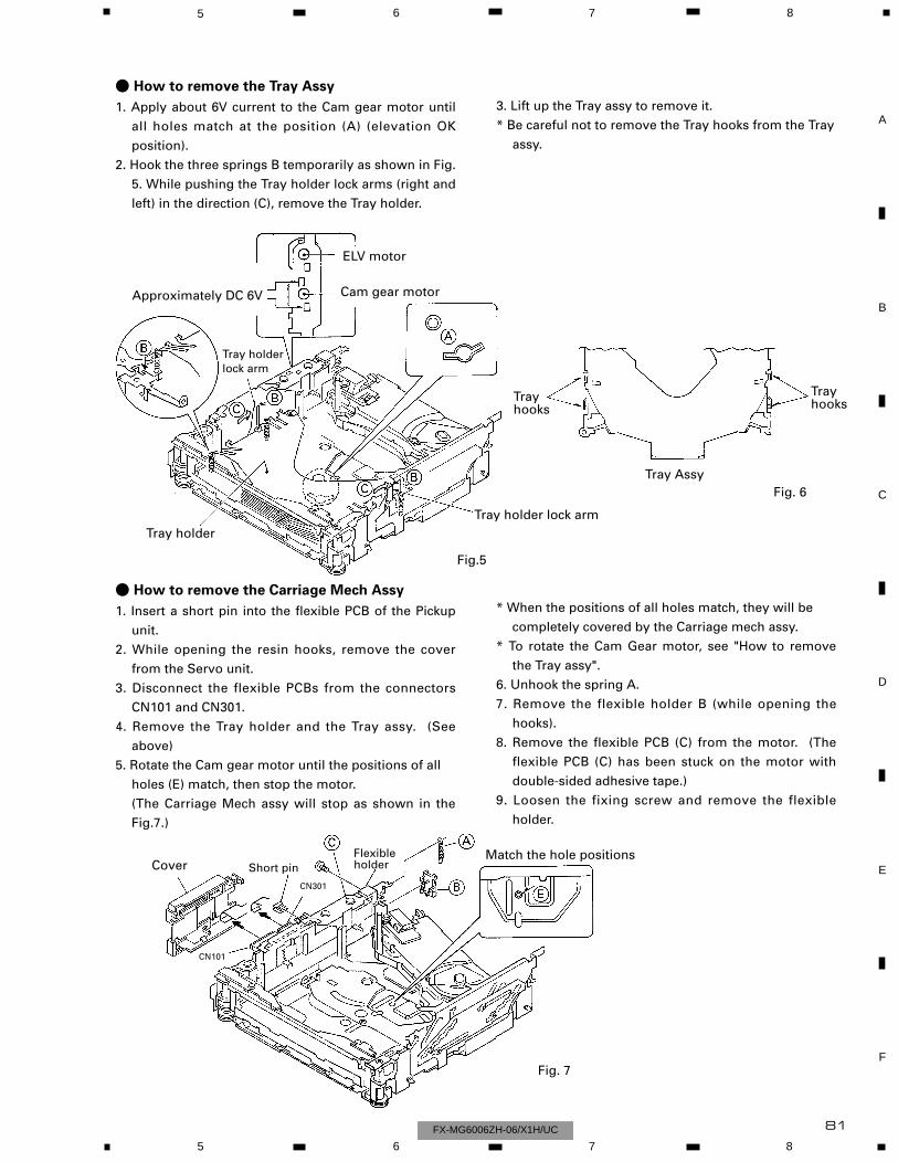
81
5 6 7 8
F
E
D
C
B
A
5 6 7 8FX-MG6006ZH-06/X1H/UC
- How to remove the Tray Assy
1. Apply about 6V current to the Cam gear motor until
all holes match at the position (A) (elevation OK
position).
2. Hook the three springs B temporarily as shown in Fig.
5. While pushing the Tray holder lock arms (right and
left) in the direction (C), remove the Tray holder.
3. Lift up the Tray assy to remove it.
* Be careful not to remove the Tray hooks from the Tray
assy.
- How to remove the Carriage Mech Assy
1. Insert a short pin into the flexible PCB of the Pickup
unit.
2. While opening the resin hooks, remove the cover
from the Servo unit.
3. Disconnect the flexible PCBs from the connectors
CN101 and CN301.
4. Remove the Tray holder and the Tray assy. (See
above)
5. Rotate the Cam gear motor until the positions of all
holes (E) match, then stop the motor.
(The Carriage Mech assy will stop as shown in the
Fig.7.)
* When the positions of all holes match, they will be
completely covered by the Carriage mech assy.
* To rotate the Cam Gear motor, see "How to remove
the Tray assy".
6. Unhook the spring A.
7. Remove the flexible holder B (while opening the
hooks).
8. Remove the flexible PCB (C) from the motor. (The
flexible PCB (C) has been stuck on the motor with
double-sided adhesive tape.)
9. Loosen the fixing screw and remove the flexible
holder.
ELV motor
Cam gear motorApproximately DC 6V
Tray holderTray holder lock arm
Tray holder lock arm
Tray hooks
Tray Assy
Cover
CN101
CN301
Match the hole positionsFlexible holder
Fig.5
Fig. 6
Fig. 7
Short pin
Tray hooks
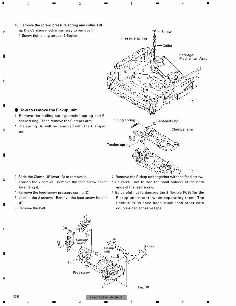
- How to remove the Pickup unit
1. Remove the pulling spring, torsion spring and E-
shaped ring. Then remove the Clamper arm.
* The spring (A) will be removed with the Clamper
arm.
10. Remove the screw, pressure spring and collar. Lift
up the Carriage mechanism assy to remove it.
* Screw tightening torque: 2.6kgfcm
2. Slide the Clamp UP lever (B) to remove it.
3. Loosen the 2 screws. Remove the feed-screw cover
by sliding it.
4. Remove the feed-screw pressure spring (D).
5. Loosen the 2 screws. Remove the feed-screw holder
(E).
6. Remove the belt.
7. Remove the Pickup unit together with the feed screw.
* Be careful not to lose the shaft holders at the both
ends of the feed screw.
* Be careful not to damage the 2 flexible PCBs(for the
Pickup and motor) when separating them. The
flexible PCBs have been stuck each other with
double-sided adhesive tape.
CarriageMechanism Assy
Screw
Collar
Pressure spring
Clamper arm
E-shaped ringPulling spring
Torsion spring
White
Black
Pickup unit
Feed screw
Belt
Carriagemotor
Fig. 8
Fig. 9
Fig. 10
82
1 2 3 4
1 2 3 4
F
E
D
C
B
A
FX-MG6006ZH-06/X1H/UC
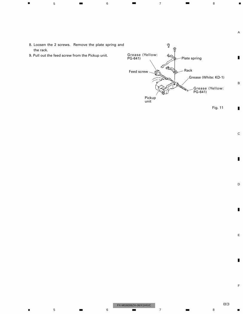
83
5 6 7 8
F
E
D
C
B
A
5 6 7 8FX-MG6006ZH-06/X1H/UC
8. Loosen the 2 screws. Remove the plate spring and
the rack.
9. Pull out the feed screw from the Pickup unit.
Rack
Plate spring
Feed screw
Pickup unit
Grease (White: KD-1)
Grease (Yellow:PG-641)
Fig. 11
Grease (Yellow:PG-641)
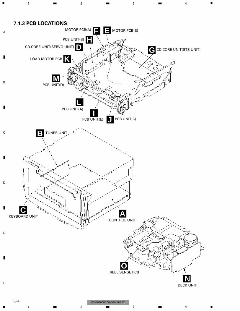
84
1 2 3 4
1 2 3 4
F
E
D
C
B
A
FX-MG6006ZH-06/X1H/UC
7.1.3 PCB LOCATIONS
E
AC
B
J
L
O
K
M
D
I
N
MOTOR PCB(B)
CD CORE UNIT(STS UNIT)G
PCB UNIT(C)
FH
PCB UNIT(E)
PCB UNIT(A)
PCB UNIT(D)
LOAD MOTOR PCB
CD CORE UNIT(SERVO UNIT)
PCB UNIT(B)
MOTOR PCB(A)
CONTROL UNITKEYBOARD UNIT
TUNER UNIT
DECK UNIT
REEL SENSE PCB
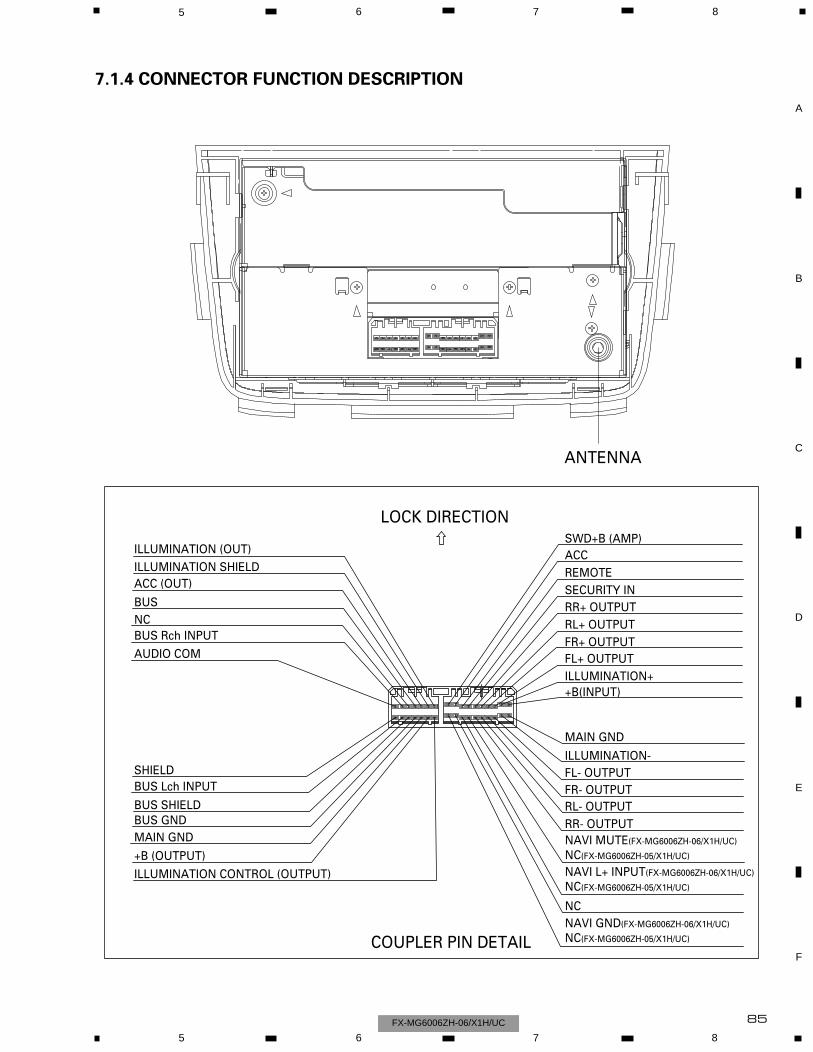
85
5 6 7 8
F
E
D
C
B
A
5 6 7 8FX-MG6006ZH-06/X1H/UC
LOCK DIRECTIONSWD+B (AMP)ACCREMOTESECURITY INRR+ OUTPUTRL+ OUTPUTFR+ OUTPUTFL+ OUTPUTILLUMINATION++B(INPUT)
MAIN GND
ILLUMINATION-FL- OUTPUTFR- OUTPUTRL- OUTPUTRR- OUTPUTNAVI MUTE(FX-MG6006ZH-06/X1H/UC)
NC(FX-MG6006ZH-05/X1H/UC)
NAVI L+ INPUT(FX-MG6006ZH-06/X1H/UC)
NC(FX-MG6006ZH-05/X1H/UC)
NCNAVI GND(FX-MG6006ZH-06/X1H/UC)
NC(FX-MG6006ZH-05/X1H/UC)COUPLER PIN DETAIL
ILLUMINATION CONTROL (OUTPUT)
+B (OUTPUT)
MAIN GNDBUS GNDBUS SHIELD
BUS Lch INPUTSHIELD
AUDIO COM
BUS Rch INPUTNCBUS
ACC (OUT)ILLUMINATION SHIELDILLUMINATION (OUT)
ANTENNA
7.1.4 CONNECTOR FUNCTION DESCRIPTION
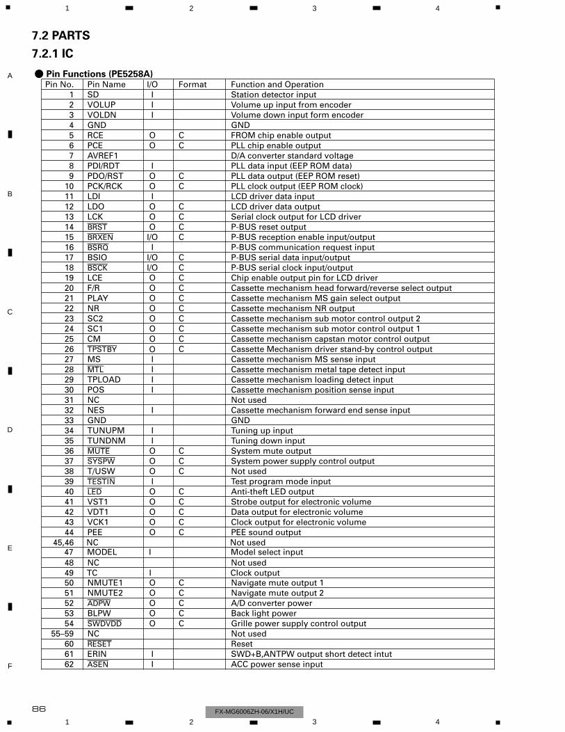
86
1 2 3 4
1 2 3 4
F
E
D
C
B
A
FX-MG6006ZH-06/X1H/UC
- Pin Functions (PE5258A)Pin No. Pin Name I/O Format Function and Operation
1 SD I Station detector input2 VOLUP I Volume up input from encoder3 VOLDN I Volume down input form encoder 4 GND GND5 RCE O C FROM chip enable output6 PCE O C PLL chip enable output7 AVREF1 D/A converter standard voltage8 PDI/RDT I PLL data input (EEP ROM data)9 PDO/RST O C PLL data output (EEP ROM reset)
10 PCK/RCK O C PLL clock output (EEP ROM clock)11 LDI I LCD driver data input12 LDO O C LCD driver data output13 LCK O C Serial clock output for LCD driver14 brst O C P-BUS reset output15 brxen I/O C P-BUS reception enable input/output16 bsrq I P-BUS communication request input17 BSIO I/O C P-BUS serial data input/output18 bsck I/O C P-BUS serial clock input/output19 LCE O C Chip enable output pin for LCD driver20 F/R O C Cassette mechanism head forward/reverse select output21 PLAY O C Cassette mechanism MS gain select output22 NR O C Cassette mechanism NR output23 SC2 O C Cassette mechanism sub motor control output 224 SC1 O C Cassette mechanism sub motor control output 125 CM O C Cassette mechanism capstan motor control output26 tpstby C Cassette Mechanism driver stand-by control output27 MS I Cassette mechanism MS sense input28 mtl I Cassette mechanism metal tape detect input29 TPLOAD I Cassette mechanism loading detect input30 POS I Cassette mechanism position sense input31 NC Not used32 NES I Cassette mechanism forward end sense input33 GND GND34 TUNUPM I Tuning up input35 TUNDNM I Tuning down input36 mute O C System mute output37 syspw O C System power supply control output38 T/USW O C Not used39 testin I Test program mode input40 led O C Anti-theft LED output41 VST1 O C Strobe output for electronic volume42 VDT1 O C Data output for electronic volume43 VCK1 O C Clock output for electronic volume44 PEE O C PEE sound output
45,46 NC Not used
50 NMUTE1 O C Navigate mute output 151 NMUTE2 O C Navigate mute output 252 adpw O C A/D converter power53 BLPW O C Back light power54 swdvdd O C Grille power supply control output
55– 59 NC Not used60 reset Reset61 ERIN I SWD+B,ANTPW output short detect intut62 asen I ACC power sense input
O
47 MODEL I Model select input
49 TC Clock output48 NC
INot used
7.2 PARTS
7.2.1 IC
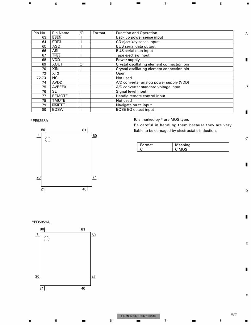
87
5 6 7 8
F
E
D
C
B
A
5 6 7 8FX-MG6006ZH-06/X1H/UC
801
20
21 40
41
60
61
*PE5258A IC's marked by * are MOS type.
Be careful in handling them because they are very
liable to be damaged by electrostatic induction.
Pin No. Pin Name I/O Format Function and Operation
66 ASI I BUS serial data input67 tpej I Tape eject sw input68 VDD Power supply69 XOUT O Crystal oscillating element connection pin70 XIN I Crystal oscillating element connection pin72 XT2 Open
72,73 NC Not used74 AVDD A/D converter analog power supply (VDD)75 AVREF0 A/D converter standard voltage input76 SL I Signal level input77 REMOTE I Handle remote control input78 TMUTE Not used79 nmute I Navigate mute input80 EQSW I BOSE EQ detect input
Format MeaningC C MOS
801
20
21 40
41
60
61
*PD5851A
63 bsen I Back up power sense input64 cdej I CD eject key sense input65 ASO I BUS serial data output
I
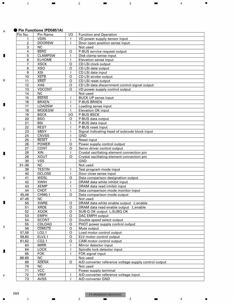
88
1 2 3 4
1 2 3 4
F
E
D
C
B
A
FX-MG6006ZH-06/X1H/UC
- Pin Functions (PD5851A)Pin No. Pin Name I/O Function and Operation
1 VDIN I VD power supply sensor input2 DOORSW I Door open position sense input3 NC Not used4 bsrq O P-BUS service request output5 CLAMPSW I Disk clamp sense input6 ELHOME I Elevation sense input7 XSCK O CD LSI clock output8 XSO O CD LSI data output9 XSI I CD LSI data input
10 xstb O CD LSI strobe output11 xrst O CD LSI reset output12 XA0 O CD LSI data discernment control signal output13 VDCONT O VD power supply control output14 NC Not used15 bsens I BUCK UP sense input16 BRXEN I P-BUS BRXEN17 LOADSW I Loading sense input18 MODESW I Elevation OK input19 BSCK I/O P-BUS BSCK20 BSO O P-BUS data output21 BSI I P-BUS data input22 REST I P-BUS reset input23 SBSY I Signal indicating head of subcode block input24 CNVSS I GND25 reset I Reset input26 POWER O Power supply control output27 CONT O Servo driver control output28 XIN I Crystal oscillating element connection pin29 XOUT O Crystal oscillating element connection pin30 VSS GND
31– 38 NC Not used39 TESTIN I Test program mode input40 DCLOSE I Door close sense input41 WDSL O Data comparison designation output42 XWIH I DRAM data white inhibit input43 XEMP I DRAM data read inhibit input44 CHDT I Data comparison mode monitor input
45,46 CHM0,1 O Data comparison mode output47-49 NC Not used
50 XWRE O DRAM data white enable output L:enable 51 XRDE O DRAM data read enable output L:enable 52 XQOK O SUB-Q OK output L:SUBQ OK53 EMPH O DAC EMPH output54 SCONT O Double speed select output55 CDLOAD O PHOT power supply control output56 cdmute O Mute output
57,58 LO2,1 O Load motor control output59,60 ELV2,1 O ELV motor control output61,62 CG2,1 O CAM motor control output
63 MIRR I Mirror detector input64 LOCK I Spindle lock detector input65 FOK I FOK signal input
66-68 NC Not used69 adena O A/D converter reference voltage supply control output70 NC Not used71 VCC Power supply terminal72 VREF I A/D converter reference voltage input73 AVSS I A/D converter GND
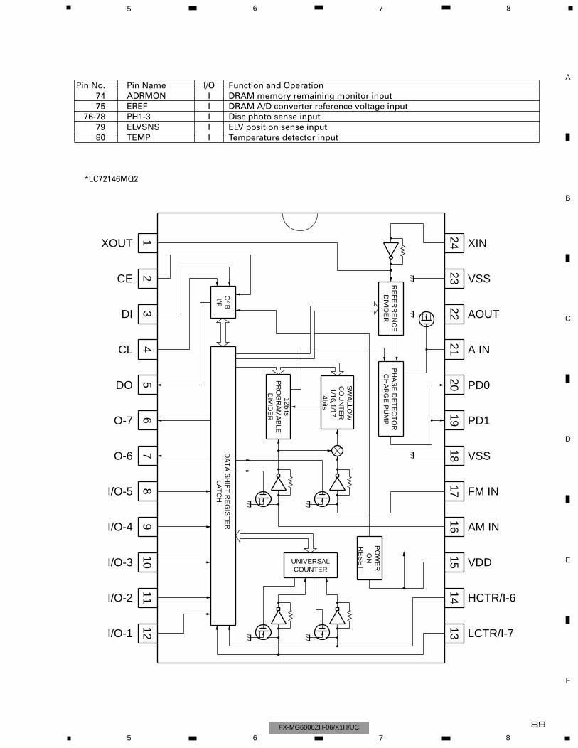
89
5 6 7 8
F
E
D
C
B
A
5 6 7 8FX-MG6006ZH-06/X1H/UC
Pin No. Pin Name I/O Function and Operation74 ADRMON I DRAM memory remaining monitor input75 EREF I DRAM A/D converter reference voltage input
76-78 PH1-3 I Disc photo sense input79 ELVSNS I ELV position sense input80 TEMP I Temperature detector input
24 XIN
VSS
AOUT
A IN
PD0
PD1
VSS
FM IN
AM IN
VDD
HCTR/I-6
LCTR/I-7
XOUT
CE
DI
CL
DO
O-7
O-6
I/O-5
I/O-4
I/O-3
I/O-2
I/O-1
2322
2120
1918
1716
1514
13
12
34
56
78
910
1112
RE
FE
RR
EN
CE
DIV
IDE
R
C2 B
I/F
PH
AS
E D
ET
EC
TO
RC
HA
RG
E P
UM
P
SW
ALLO
WC
OU
NT
ER
1/16,1/174bits
12bitsP
RO
GR
AM
AB
LED
IVID
ER
DA
TA
SH
IFT
RE
GIS
TE
RLA
TC
H
PO
WE
RO
NR
ES
ETUNIVERSAL
COUNTER
*LC72146MQ2
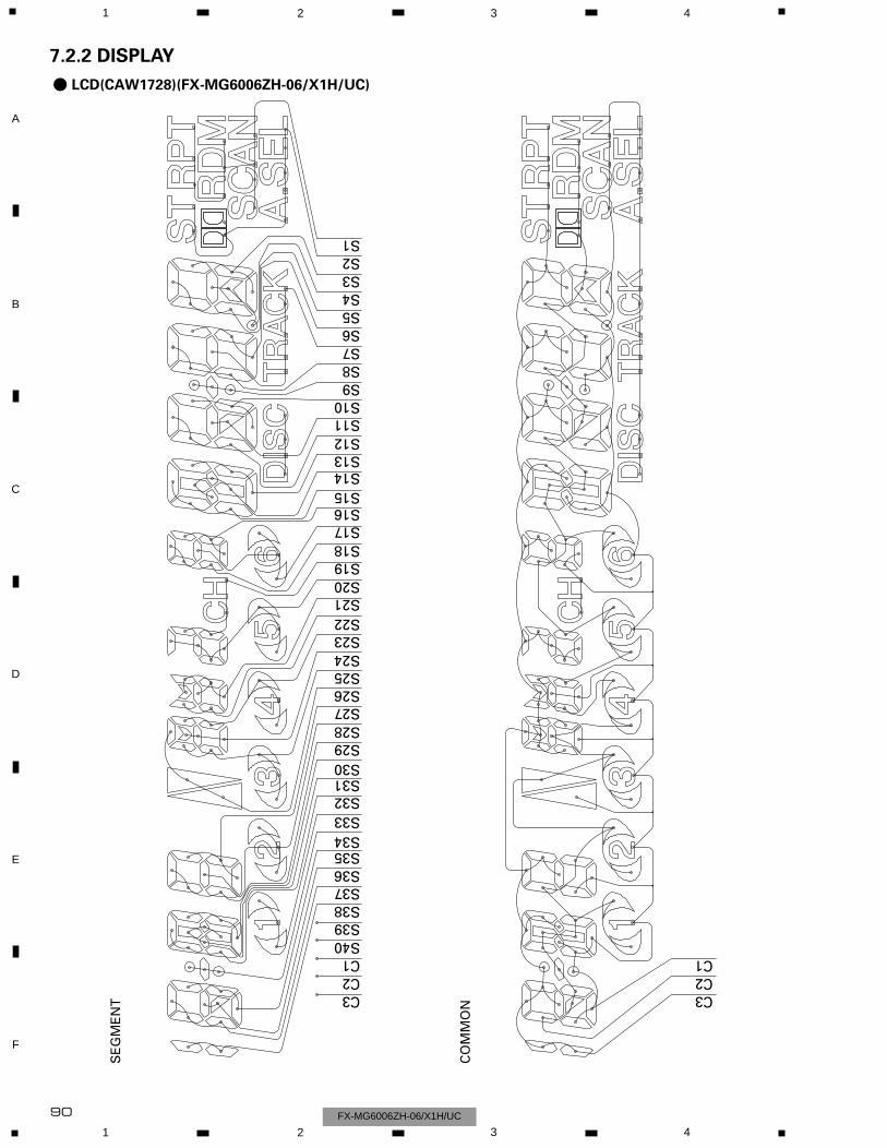
90
1 2 3 4
1 2 3 4
F
E
D
C
B
A
FX-MG6006ZH-06/X1H/UC
CO
MM
ON
SE
GM
EN
T
- LCD(CAW1728)(FX-MG6006ZH-06/X1H/UC)
C3C2C1S40
S9S8S7S6S5S4S3
S1S2
C3C2C1
S39S38S37S36S35S34S33S32S31S30S29S28S27S26S25S24S23S22S21S20S19S18S17S16S15S14S13S12S11S10
7.2.2 DISPLAY
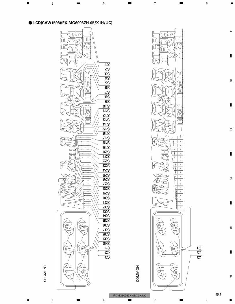
91
5 6 7 8
F
E
D
C
B
A
5 6 7 8FX-MG6006ZH-06/X1H/UC
CO
MM
ON
SE
GM
EN
T
- LCD(CAW1598)(FX-MG6006ZH-05/X1H/UC)
C3C2C1S40
S9S8S7S6S5S4S3
S1S2
C3C2C1
S39S38S37S36S35S34S33S32S31S30S29S28S27S26S25S24S23S22S21S20S19S18S17S16S15S14S13S12S11S10
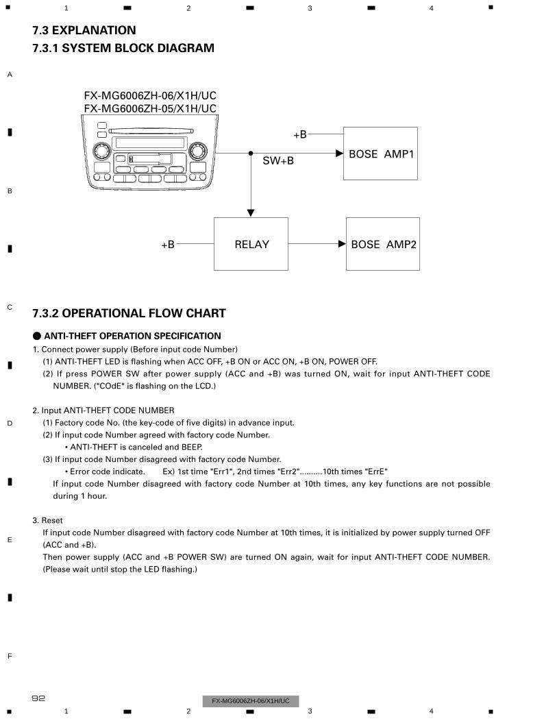
92
1 2 3 4
1 2 3 4
F
E
D
C
B
A
FX-MG6006ZH-06/X1H/UC
FX-MG6006ZH-06/X1H/UCFX-MG6006ZH-05/X1H/UC
BOSE AMP1
RELAY BOSE AMP2+B
+B
SW+B
7.3 EXPLANATION
7.3.1 SYSTEM BLOCK DIAGRAM
7.3.2 OPERATIONAL FLOW CHART
- ANTI-THEFT OPERATION SPECIFICATION
1. Connect power supply (Before input code Number)
(1) ANTI-THEFT LED is flashing when ACC OFF, +B ON or ACC ON, +B ON, POWER OFF.
(2) If press POWER SW after power supply (ACC and +B) was turned ON, wait for input ANTI-THEFT CODE
NUMBER. ("COdE" is flashing on the LCD.)
2. Input ANTI-THEFT CODE NUMBER
(1) Factory code No. (the key-code of five digits) in advance input.
(2) If input code Number agreed with factory code Number.
• ANTI-THEFT is canceled and BEEP.
(3) If input code Number disagreed with factory code Number.
• Error code indicate. Ex) 1st time "Err1", 2nd times "Err2"..........10th times "ErrE"
If input code Number disagreed with factory code Number at 10th times, any key functions are not possible
during 1 hour.
3. Reset
If input code Number disagreed with factory code Number at 10th times, it is initialized by power supply turned OFF
(ACC and +B).
Then power supply (ACC and +B POWER SW) are turned ON again, wait for input ANTI-THEFT CODE NUMBER.
(Please wait until stop the LED flashing.)
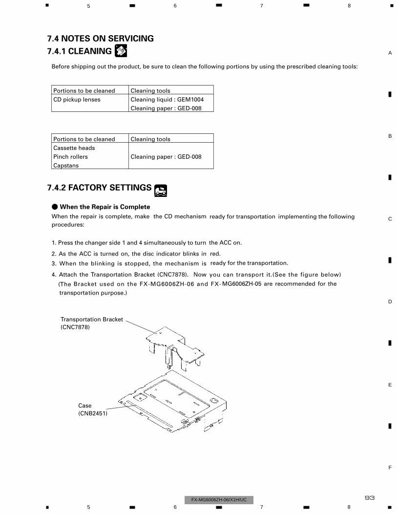
93
5 6 7 8
F
E
D
C
B
A
5 6 7 8FX-MG6006ZH-06/X1H/UC
Before shipping out the product, be sure to clean the following portions by using the prescribed cleaning tools:
Portions to be cleaned Cleaning tools
CD pickup lenses Cleaning liquid : GEM1004
Cleaning paper : GED-008
Portions to be cleaned Cleaning tools
Cassette heads
Pinch rollers Cleaning paper : GED-008
Capstans
7.4 NOTES ON SERVICING
7.4.1 CLEANING
7.4.2 FACTORY SETTINGS
- When the Repair is Complete
When the repair is complete, make the CD mechanism ready for transportation implementing the following
1. Press the changer side 1 and 4 simultaneously to turn the ACC on.
2. As the ACC is turned on, the disc indicator blinks in red.
3. When the blinking is stopped, the mechanism is ready for the transportation.
4. Attach the Transportation Bracket (CNC7878). Now you can transport it.(See the figure below)
(The Bracket used on the FX-MG6006ZH-06 and FX- MG6006ZH-05 are recommended for the
transportation purpose.)
Transportation Bracket(CNC7878)
Case(CNB2451)
procedures:
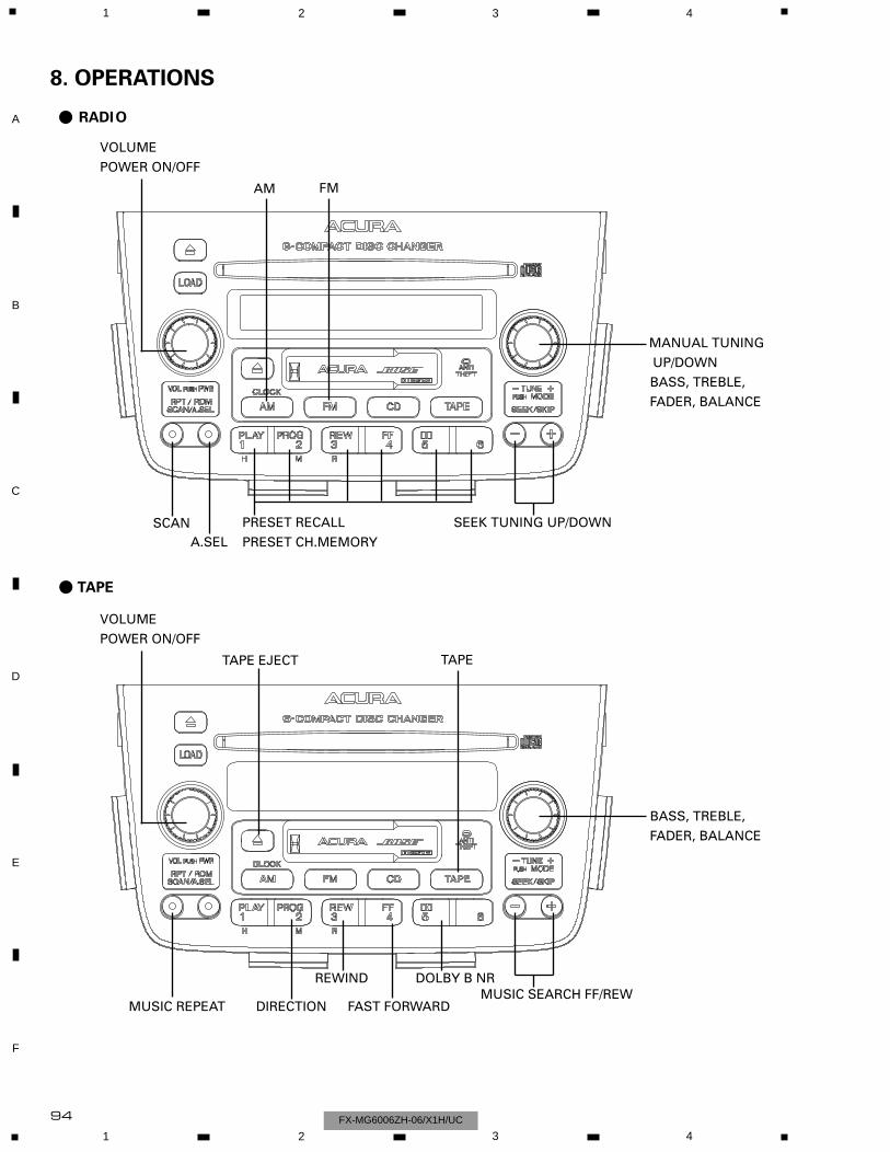
94
1 2 3 4
1 2 3 4
F
E
D
C
B
A
FX-MG6006ZH-06/X1H/UC
- RADIO
- TAPE
VOLUME
POWER ON/OFF
AM FM
PRESET RECALL
PRESET CH.MEMORY
SEEK TUNING UP/DOWN
MANUAL TUNING
UP/DOWNBASS, TREBLE,
FADER, BALANCE
VOLUME
POWER ON/OFF
TAPE
MUSIC SEARCH FF/REW
BASS, TREBLE,
FADER, BALANCE
TAPE EJECT
REWIND
DIRECTION FAST FORWARD
DOLBY B NR
MUSIC REPEAT
SCANA.SEL
8. OPERATIONS
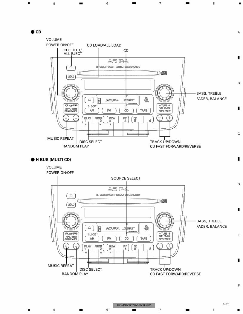
95
5 6 7 8
F
E
D
C
B
A
5 6 7 8FX-MG6006ZH-06/X1H/UC
- CD
VOLUME
POWER ON/OFF
CD
DISC SELECT TRACK UP/DOWN
BASS, TREBLE,
FADER, BALANCE
CD FAST FORWARD/REVERSERANDOM PLAY
MUSIC REPEAT
CD EJECT/ALL EJECT
CD LOAD/ALL LOAD
- H-BUS (MULTI CD)
VOLUME
POWER ON/OFF
SOURCE SELECT
DISC SELECT TRACK UP/DOWN
BASS, TREBLE,
FADER, BALANCE
RANDOM PLAY
MUSIC REPEAT
CD FAST FORWARD/REVERSE
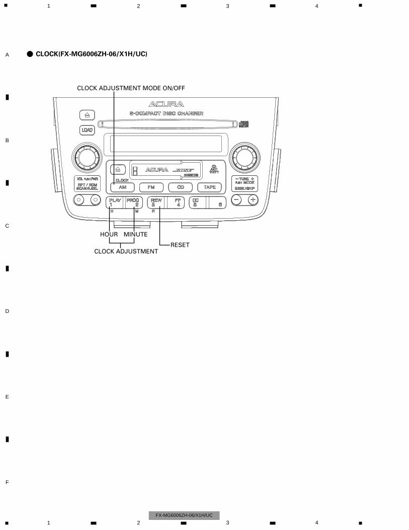
1 2 3 4
1 2 3 4
F
E
D
C
B
A
FX-MG6006ZH-06/X1H/UC
- CLOCK(FX-MG6006ZH-06/X1H/UC)
CLOCK ADJUSTMENT MODE ON/OFF
HOUR MINUTE
CLOCK ADJUSTMENTRESET