formation and dynamics of muonium centres in semiconductors—a new approach
TRANSCRIPT

INSTITUTE OF PHYSICS PUBLISHING JOURNAL OF PHYSICS: CONDENSED MATTER
J. Phys.: Condens. Matter 16 (2004) S4761–S4778 PII: S0953-8984(04)84861-6
Formation and dynamics of muonium centres insemiconductors—a new approach
Vyacheslav G Storchak1,4, Dmitry G Eshchenko2 and Jess H Brewer3
1 Kurchatov Institute, Kurchatov Square, 1 Moscow 123182, Russia2 Physik-Institut der Universitat Zurich, CH-8057 Zurich, Switzerland3 Canadian Institute for Advanced Research and Department of Physics and Astronomy,University of British Columbia, Vancouver, BC, V6T 1Z1, Canada
E-mail: [email protected]
Received 27 January 2004Published 24 September 2004Online at stacks.iop.org/JPhysCM/16/S4761doi:10.1088/0953-8984/16/40/018
AbstractVarious processes of muonium atom formation in semiconductors via electroncapture by a positive muon have been studied using µSR techniques, includingthose with applied electric field. Experiments in GaAs, GaP and CdS suggestthat the electron is initially captured into a highly excited state, from whichthe cascade down to the muonium ground state goes through an intermediateweakly bound state determined by the electron effective mass and the dielectricconstant of the host. The electronic structure of this weakly bound state is shownto be hydrogenic. The nature of the final (on the µSR timescale) muonium statedepends on the energy releasing mechanisms in the cascade process. We suggestthat muonium dynamics in semiconductors (including the effects of electric andmagnetic fields and temperature) reflect the electron dynamics in weakly boundmuonium state(s) in which the electron is delocalized over distances of about100 Å.
1. Introduction
Any process of recombination in semiconductors requires the transfer of a huge amount ofenergy—approximately the band gap—to some type(s) of crystal excitations. The question is,which excitations? Releasing this energy into the phonon subsystem is strongly suppressed,as it requires simultaneous emission of an enormous number of phonons. Therefore anysubdivision of the recombination energy into smaller steps—e.g. via an intermediate statein the gap—increases the probability of recombination significantly. Energy levels associatedwith dopants and defects may thus assist in the formation of shallow centres; however, phononscannot readily absorb enough energy for the formation of deep centres.
4 Author to whom any correspondence should be addressed.
0953-8984/04/404761+18$30.00 © 2004 IOP Publishing Ltd Printed in the UK S4761

S4762 V G Storchak et al
The pioneering work of Shockley and Read [1] and Hall [2] in the early 1950s suggestedthat the recombination of electrons and holes in solids could best be understood in terms ofthe mutual capture of an electron and a hole at a localization site (‘recombination centre’) inthe crystal. The first step—electron capture by an attractive centre (‘trapping centre’)—is animportant process on its own. The distinction between a trap and a recombination centre isa quantitative rather than a qualitative one. For the sake of definiteness the following pictureis accepted: an electron is captured at a centre; if the electron stays for some mean lifetimein the captured state and is then ejected (e.g. thermally), the centre is regarded as a trap. If,however, a hole is trapped at the same centre before thermal ejection of the electron can occur,recombination will take place and the centre may be regarded as a recombination centre. Indeedit was found [3] that Cu and Ni impurities in germanium behave as recombination centres atroom temperature, whereas at lower temperatures Cu behaves as a trap [4].
In µ+SR experiments one accumulates individual µ+ → e+νeνµ decay events into a timespectrum that reveals the time-dependent spin polarization of positive muons stopped in thesample. Each incoming 4 MeV muon creates an ionization track of excess electrons andions liberated during the µ+ thermalization process. Experiments in insulating [5–9] andsemiconducting media (Si [10], GaAs [11, 12], GaP [13] and CdS [14]) have shown thatthe ionization track products are very close to the thermalized muon. (The characteristicdistance is about 10−6–10−5 cm.) Some of the excess electrons generated in the end of the µ+
track are mobile enough to reach and be captured by the thermalized muon to form a muonium(Mu = µ+e−) atom. This process of ‘delayed’ muonium formation (DMF) [15] may be treatedas trapping of excess electrons by an attractive centre. As an analogue of Cu impurities ingermanium, Mu (or a filled trap) is typically found at lower temperatures, while a diamagneticstate (which could be an ionized trap or, alternatively, a recombination centre) is observed athigher temperatures.
The phenomenological description of an impurity as a trap or a recombination centremakes use of the cross section for the capture of an electron or a hole. The ‘giant’ capturecross sections (up to 10−12 cm2) observed for a wide variety of Coulomb attractive centres insemiconductors at low temperatures by the end of 1950s were puzzling: these cross sectionswere found to be several orders of magnitude higher than the geometrical cross sections forelectrons localized at the centre. Not only was there no explanation for the experimental crosssections, but the energy transfer mechanism was unknown: many of these centres involvebinding energies an order of magnitude higher than the Debye energy.
In solving this problem a decisive role was played by the idea of Lax [16, 17] that, insteadof being captured directly into the ground state, the electron is captured into one of the highlyexcited states with much larger radii, and then cascades down. The key point here is that theelectron must not only come to the vicinity of the centre, but it must also on arrival perform theunlikely task of depositing perhaps many times the Debye energy, requiring the simultaneousproduction of many phonons. Whereas multiphonon transitions to the ground state of the trapyield cross sections five to ten orders of magnitude too small [18], capture into excited stateswith a large radius followed by a cascade of one-phonon transitions leads to cross sections ofthe right order of magnitude [17].
This cascade model correctly predicts the temperature dependence of the ‘giant’ crosssections. The initial capture involves one phonon and takes place into one of the very excitedorbitals. Subsequent collisions may eject the electron or cause it to increase its binding energy.The ‘sticking probability’, or probability of eventual capture into the ground state, becomessignificant for binding energies of order kT . As the temperature is reduced, capture intoorbits of larger radius becomes effective and the cross section therefore increases rapidly withdecreasing temperature. Using Lax’s cascade model, Abakumov and Yassievich [19] found

Muonium centres in semiconductors—a new approach S4763
that the capture cross section for an isolated attractive centre can be expressed as
σ = 4
3
π
�0r3
T, (1)
where rT = e2/εkT is the characteristic capture radius at temperature T , ε is the dielectricconstant, �0 = vτE, v is the electron’s velocity and τE is its relaxation time in energy space.
Equation (1) has a transparent physical meaning in the framework of the classical paperof Thompson [20]: an electron is captured if (a) it enters a sphere of radius rT about the trap;and (b) it loses its energy. The probability of energy transfer is expressed by a factor rT/�0.The temperature dependence σ ∝ T −3, as well as the actual cross section values derived fromequation (1), are found to be in good agreement with various experimental data on electroncapture in Ge and Si into both shallow and deep attractive centres [21–23].
It has been customary to treat the dynamics of muonium centres in semiconductors in termsof the lowest electronic states (or long-lived metastable states) without explicitly consideringthe details of how these states are initially formed. Only recently have we begun to examine themuonium formation processes in detail with experiments designed to modify the final stagesof muon implantation and thermalization. Specifically, we have sought to probe interactionsbetween the muon and the carriers released during its implantation, particularly the initialcapture of an electron to form an atomic muonium defect state.
The phenomenon of delayed muonium formation (DMF) implies that as the electronapproaches the stopped muon it may be captured initially into a highly excited electronic statewith mesoscopic-sized orbits. Electron capture by a deep-level impurity is assumed to proceedby capture into an excited electronic state followed by a cascade to the lowest energy level.Since, within the effective mass model, any positively charged impurity can have a series ofweakly bound hydrogenic states (WBS), the initial capture may be into one of these statesrather than into a deep state. The key point here is that these WBS formed on initial captureshould be much more susceptible to effects of temperature, electric or magnetic fields becausetheir binding energy is much less than that of muonium in any deep state.
In this paper we present a number of experimental results and their interpretation usingthe cascade model, which suggests that the dynamics of muonium centres in semiconductorsis to a great extent determined by electron dynamics in WBS. We show that these initial eventsin the DMF process can no longer be ignored in studies of muonium centres.
2. The weakly bound muonium state in semiconductors
Muonium centres in semiconductors have been studied extensively for more than four decades.The typical justification for these studies comes from the idea that using the muonium atom as alight hydrogen isotope one can model the dynamics of the isolated H atom, whose observationis restricted because of its high reactivity. Although the µ+ is almost an order of magnitudelighter than the proton, it is so much heavier than the electron that the Mu reduced mass isalmost the same as that of the hydrogen atom. Therefore, Mu has almost the same ionizationpotential and electronic structure as the H atom. For this reason muonium may properly beconsidered a light hydrogen isotope;as such, and with due regard to isotope effects,muonium isexpected to provide an experimentally accessible model for hydrogen defect centres in matter.
Early muonium studies considerably modified established views concerning the stablesites and electronic structure of hydrogen in semiconductors such as Si, Ge and GaAs [24];muonium states were discovered for which the site and local electronic structure differedconsiderably from those of the expected trapped-atom state. We refer in particular to the so-called anomalous (or bond-centred) muonium state Mu0
BC in Si, GaAs etc, now understood

S4764 V G Storchak et al
to have a somewhat extended electron distribution associated with a bond-centre site, and adefect energy level that nonetheless lies quite deep in the energy gap; in Si in particular, Mu0
BCis suggested to provide a donor level 210 meV below the conduction band [25].
More recently these studies have moved on from spectroscopy to dynamics, revealing alargely unanticipated interplay of site and charge state suggested to be relevant to the deep-levelelectrical activity of hydrogen in these materials [26, 27].
Shallow muonium states (with binding energies of about 20 meV) have recently beenfound [28] in wide gap (notably II–VI) semiconductors. Stretching the analogy betweenmuonium and hydrogen, these results were interpreted as evidence that hydrogen may act asa donor, rather than as a neutralizing centre, in certain materials.
When employing muonium as a light hydrogen isotope, however, one should always bearin mind that hydrogen and muonium are introduced into a semiconductor in very differentways. Hydrogen is incorporated during the process of sample preparation and reaches thermaland chemical equilibrium long before measurements start, whereas muonium is observed afew nanoseconds after the injection of very energetic muons into the sample and only thosestates reached on the microsecond timescale of the muon lifetime can be studied [29].
As the energetic µ+ is slowed to an energy of a few tens of keV, inelastic muonscattering involves mainly the production of atomic excitations and ionizations. At lowerenergies, collective excitations and charge exchange become important. In insulators andsemiconductors the positive muon can pick up an electron to form an isolated hydrogen-likemuonium atom; generally the µ+ undergoes many cycles of electron capture and subsequentelectron loss. If the last such collision leaves atomic Mu in its neutral charge state, muoniumis said to have been formed promptly. If the µ+ thermalizes as a positive ion, leaving behindan ionization track of liberated electrons and ions, in many materials there is a high probabilitythat some of the excess electrons generated in this track can reach the stopped muon and formmuonium within the time range of a µ+SR experiment, which is set by a few times the muonlifetime (τµ = 2.197 × 10⁻⁶ s) [15]. This process of delayed muonium formation (DMF) iscrucially dependent on the electron’s interaction with its environment and especially on theelectron mobility. Recent experiments in insulating and semiconducting media [5–14] haveled to a major breakthrough in understanding of the muon’s interactions with the productsof its track—in fact, it is found that these products may determine much of the subsequentbehaviour of muonium/muon states in insulators and semiconductors.
An essential feature of DMF is that the muon stops some distance from the free electronscreated in its track; this property is the key to distinguishing experimentally between delayedand prompt Mu formation by applying external electric fields [5, 30]. Relatively weakexternal electric fields (∼104 V cm−1) can sometimes overcome the muon–electron Coulombattraction and thus reduce the probability of DMF, whereas electric fields of atomic strength(∼109 V cm−1) would be required to affect prompt (epithermal) Mu formation.
In most semiconductors two quite different types of muonium centres coexist with thediamagnetic state (or states) of the muon [24]. These centres are characterized by their differentmuon–electron hyperfine interactions. So-called ‘normal’ muonium has an isotropic hyperfineinteraction with a hyperfine coupling about half as strong as that in the free Mu atom and islocated at the tetrahedral interstitial site; it is therefore denoted Mu0
T. ‘Anomalous’ or ‘bond-centred’ muonium, with a small anisotropic hyperfine interaction, is located near the centre ofthe relaxed crystal bond and is thus denoted Mu0
BC.Recent experiments with semi-insulating GaAs [11, 12] have shown complete suppression
of the Mu0BC signal by an electric field. This phenomenon is illustrated in figure 1, which shows
the electric field dependence of the diamagnetic asymmetry and the sum of Mu0BC asymmetries
in semi-insulating GaAs at 10 K. Both directions of the electric field (E > 0 corresponding

Muonium centres in semiconductors—a new approach S4765
Figure 1. Electric field dependence of the diamagnetic asymmetry (filled circles) and the sum ofMu0
BC asymmetries (open circles) in GaAs at T = 10 K.
to the direction parallel to the incoming muon momentum) eventually cause a sharp decreaseof the Mu0
BC signal accompanied by a corresponding increase in the diamagnetic amplitude.The characteristic electric field is estimated to be about Echar ≈ 5 kV cm−1.
In semiconductors, due to the low effective mass of the electron and the high dielectricconstant, an electron and a positively charged centre can form a hydrogenic WBS withmesoscopic-sized orbits. In GaAs, the binding energy of a shallow donor state formed bypositive ion and a light electron in the �-valley is known [31] to amount to U ≈ 7 meV (theexciton state in GaAs has a similar U [32]) while the characteristic radius of such a state isa ≈ 8 × 10⁻⁷ cm [31]. The electric field Ei required to ionize this state can be estimated byequating the bias across the orbit, 2eEia, to the binding energy [33]. This rough estimate givesEi ∼ 5 kV cm−1, in good agreement with that observed experimentally [11, 12]. To ionizeground-state Mu0
BC muonium, atomic-scale electric fields (∼109 V cm−1) would be required.At low temperature, where the electron mobility is very high, electron motion is closer
to ballistic than to classical viscous flow. From the characteristic field one can estimate thetypical length scale of the interaction: Rchar ∼ √
e/(εEchar) ∼ 10−6 cm, where ε = 11.6 is thedielectric constant of GaAs. On the other hand, the mean free path of a band electron in GaAs at50 K is estimated to be � = (b/e)
√3kBT m∗ ∼ 6×10⁻⁶ cm (where b ∼ 1–2×104 cm2 V−1 s−1
is the electron mobility), which is greater than Rchar. From this estimate it is clear that even ifan electron starts far from the muon, under the process of recombination it will eventually form(or at least pass through) a mesoscopic-sized shallow quantum state—i.e. the WBS mentionedabove.
An external electric field will bias the shape of the Coulomb potential. In a weak externalelectric field, the electron ‘falls to the muon’ through this WBS. If the external electric field ishigher than Ei, the WBS never forms (and so neither does any deeper state) and the electronescapes.
Thus, formation of Mu0BC in GaAs may be expected to proceed through the intermediate
weakly bound Mu state (WBS), a metastable precursor for the final deep state [11, 12].It is important to recognize that this muonium WBS is not the same as any of the previously
studied Mu states in semiconductors. This is truly a fascinating observation—the involvement

S4766 V G Storchak et al
− 150 − 100 − 50 0 50 100 150
0. 02
0. 04
0. 06
0. 08
0. 10
Dia
mag
netic
Asy
mm
etry
Electric Field (kV/cm)
Figure 2. Electric field dependence of the diamagnetic asymmetry in a transverse magnetic fieldof B = 51 G for semi-insulating GaAs (10 K, open circles) and GaP (100 K, filled squares). Inboth cases the temperature is well below that causing ‘ionization’ of Mu in zero electric field.
of the WBS may in fact be a general phenomenon governing muonium formation in condensedmatter! Electron capture (from the ionization track) by a positive muon into a very excitedstate, followed by a cascade down through WBS to form a deep-level Mu state, is consistentwith Lax’s vision of electron capture in solids [17].
In order to understand the mechanism of energy loss in the muonium cascade we mustfirst examine the electronic structure of the WBS.
3. Electronic structure of the weakly bound muonium state
In GaAs, the binding energy derived from the characteristic electric field required to ‘ionize’the weakly bound Mu state is the same as for an electron bound to any other positive centre.This binding energy is determined by the electron effective mass and the dielectric constant ofthe medium.
If the scenario for muonium formation described in section 2 has general validity in solids,the binding energy as well as the characteristic radius of the electron orbit (and therefore thecharacteristic electric field) of this intermediate weakly bound Mu state formed on initialcapture should scale with the electron effective mass and dielectric constant of the host.
Here we present experimental evidence that formation of the final (deep) Mu state in GaPalso proceeds through an intermediate Mu WBS [13]. The characteristics of this shallow Mustate are found to be in good agreement with those expected for a hydrogenic atom withinthe effective mass approximation. Comparing the characteristic fields required to prohibitformation of the muonium ground state in GaAs and GaP demonstrates that they scale withthe electron effective mass and dielectric constant of the host very much as expected for initialelectron capture into the n = 1 orbital of a hydrogenic state associated with a positive muon.
The electric field dependence of the diamagnetic asymmetry in GaP is shown in figure 2,along with that observed in semi-insulating GaAs. Less detailed measurements in GaP atT = 20 K give virtually the same electric field dependence as at T = 100 K.
The large difference in electric field dependences for GaP and GaAs—the characteristicelectric fields differ by an order of magnitude (about 50 kV cm−1 in GaP versus about5 kV cm−1 in GaAs)—cannot be attributed to ‘ionization’ of the final (deep) muonium states.

Muonium centres in semiconductors—a new approach S4767
First, the electric field strength is 4–5 orders of magnitude less than atomic fields. Second, bothmuonium centres in GaP have hyperfine constants quite close to those for their counterpartsin GaAs [34]. Therefore we conclude that it is not ‘ionization’ of the final Mu state whichis observed in either case, but rather field ‘ionization’ (actually prevention of formation) of aweakly bound precursor (WBS) to the deep muonium final state.
We argue further that this muonium WBS is well described within the effective massapproximation of the hydrogenic model commonly used for shallow donors [31]. Specifically,in that model the characteristic electric field for ionization, estimated by equating the biasacross the orbit to the binding energy [33], may be expressed as
Ei = 1
4
e5
h4
m2∗ε3
=(m∗
m
)2 1
ε31.9 × 10⁹ V cm−1, (2)
where e is the electron charge, and m∗ is the effective mass of the electron. The ratio(m∗/m)2/ε3 makes Ei in semiconductors about five orders of magnitude less than atomic-scaleelectric fields. In the case of GaP with effective electron mass m∗ = 0.17m and dielectricconstant ε = 10.7, the characteristic field is Ei = 50 kV cm−1, in very good agreement withthe experimental value [13]. Comparison with GaAs (m∗ = 0.067m and ε = 12.9) whereEi = 5 kV cm−1 [12] allows us to conclude that the electric field required to ‘ionize’ this MuWBS scales with the electron effective mass and the dielectric constant of the host, as expectedfor a hydrogenic state.
The characteristic radius of the electron orbit within this model,
a = h2
e2
ε
m∗= m
m∗εa0, (3)
is 0.28 × 10⁻⁶ cm in GaP and 0.83 × 10⁻⁶ cm in GaAs. These values are about two orders ofmagnitude larger than the Bohr radius a0. This fact justifies the use of the hydrogenic model,as both the electron effective mass and the dielectric constant are essentially macroscopiccharacteristics of the medium.
The binding energy of such a WBS,
U = e4
2h2
m∗ε2
= m∗m
1
ε2× 13.6 eV, (4)
is 23 and 7 meV for GaP and GaAs, respectively. Both shallow donors and excitons in GaAshave a binding energy near 7 meV [31], in good agreement with the hydrogenic model. In GaP,the exciton binding energy is 21 meV [35], again close to the estimate from the hydrogenicmodel. In both semiconductors, the estimated binding energies for WBS are about three ordersof magnitude less than the atomic value, which suggests that this state should be relativelyeasy to ionize thermally.
In conclusion, these results imply that deep-level Mu formation in GaP (as well as in GaAs)proceeds through a weakly bound intermediate muonium state. Comparing the results in GaPand GaAs we find that the characteristic electric fields for ionization of this WBS (as well asestimated values for characteristic radii and binding energies) scale with the electron effectivemass and dielectric constant of the medium as expected for a hydrogenic effective-mass state.
4. Energy releasing mechanism for Mu atom formation
To understand the process of electron capture by a positive attractive centre in a semiconductor,µSR experiments using external electric fields have proved very useful [12, 13]: with

S4768 V G Storchak et al
Figure 3. Electric field dependence of the diamagnetic asymmetry (open circles) and muoniumasymmetry (filled circles) in intrinsic polycrystalline CdS at T = 11 K. The curves are to guidethe eye.
increasing electric field, those excited states for which the bias across the orbit is biggerthan the binding energy [33],
2Eean > Un, (5)
(where an is the radius and Un is the binding energy of the nth excited state) are removed fromthe excitation spectrum and the number of ‘valid’ excited states is decreased. Therefore, byscanning the electric field at any given temperature one can find the ‘bottleneck’ excited stategoverning eventual electron capture to the ground muonium state.
In order to deduce the energy loss mechanism in the cascade process, we compare electricfield effects in GaAs with those in CdS. The remarkable feature of the muonium state observedin CdS [28] is that the hyperfine interaction A is extremely small, amounting to only about 10−4
of the vacuum value. Muonium and diamagnetic signals in CdS are temperature dependent [28]:at low temperatures the muonium signal dominates, but the diamagnetic fraction increases atthe expense of the muonium fraction as the temperature is increased, although the temperaturedependence is weak up to 15 K. To reduce the influence of thermal processes, the electric fieldexperiments were performed at 11 K.
Both muonium and diamagnetic signals in CdS are strongly influenced by the externalelectric field (see figure 3). Application of the electric field in either direction eventuallycauses a decrease of the muonium amplitude accompanied by a corresponding increase in thediamagnetic amplitude. From figure 3 one can estimate the characteristic electric field to beEchar ∼ 8 kV cm−1.
In GaAs [12], the characteristic electric field was determined to be EGaAschar ∼ 5 kV cm−1.
Electrons are very light in GaAs; that is why even the ground hydrogenic state in GaAs israther shallow, with energy U1 = −13.6(m∗/mε2) eV � −7 × 10⁻³ eV. Note that this energyis less than the Debye temperature �D = 344 K in GaAs [36]. Therefore an electron caneasily lose its energy by a one-phonon emission cascade process starting from the bottom ofthe conduction band and going down through a sequence of excited hydrogenic states.

Muonium centres in semiconductors—a new approach S4769
By increasing the external electric field E one steadily removes excited states with quantumnumbers n, according to the expression
En = 1
n4
(m∗
m
)2 (1
ε3
)e5m2
4h4 < E (6)
for successive thresholds in electric field. Equation (6) is directly derived from equation (5) bysubstituting the appropriate expressions for the radius and the energy of the excited state withquantum number n within the hydrogenic model [13]. At low fields, electron transitions fromthe conduction band to states with small quantum numbers are still possible via one-phononemission. In GaAs the situation becomes critical when the lowest hydrogenic state with n = 1is ionized in electric fields higher than E1 ∼ 5 kV cm−1. In this case the cross section forelectron capture by the muon is dramatically reduced and muonium formation is prohibited.
The electron effective mass is rather large in CdS (m∗ = 0.2m [37]) while the dielectricconstant (ε = 9.1 [38]) is smaller than in GaAs. This should result in a much deeper hydrogenicstate in CdS (U1 = −13.6(m∗/mε2) eV � −3.5 × 10⁻² eV) compared with GaAs, with acorrespondingly larger electric field required to ionize the lowest hydrogenic state with n = 1(E1 ∼ 100 kV cm−1). This value is clearly inconsistent with the Echar ∼ 8 kV cm−1 observedexperimentally (see figure 3). However, the electric field required to ionize the first excitedhydrogenic state (the state with quantum number n = 2) in CdS is E2 = E1/16 ∼ 6 kV cm−1
(see equation (6)), much closer to the experimental value.This result can be explained by considering the cascade model for electron capture by a
positive centre [17]. The Debye temperature �D = 250–300 K in CdS [39] is smaller than thebinding energy of the ground hydrogenic state −U1 � 3.5×10⁻² eV = 390 K, so an electrontransition directly from the conduction band to the n = 1 level by emitting one phonon isunlikely. The binding energy of the level with n = 2 is −U2 = −U1/4 � 100 K, which issmaller than the Debye temperature; thus electron transitions with emission of one phononfrom the conduction band (or from any level with n > 2) to the level with n = 2 are possible.By increasing a still relatively small electric field one steadily removes excited states from thehydrogenic excitation spectrum (see equation (6)); however, electrons can still be captured byone-phonon emission to one of the un-ionized levels. The cross section for electron capture(or muonium formation) is dramatically reduced when the last state for which one-phonontransitions from the conduction band are possible is removed from the excitation spectrum. Inthe case of CdS, this ‘bottleneck’ of the capture process is the first excited hydrogenic level(the level with n = 2 in our notation).
Thus the interplay between the electron energy spectrum and the Debye temperature mayresult in a situation where the electron cannot be captured directly to the lowest hydrogenic statebut can still be captured into an excited hydrogenic state. The excited states will then determinethe temperature dependence of the muonium fraction: the electron is more likely to be thermallyionized from one of the excited states than from the deep one. This scenario of muoniumionization is supported by the observation of a remarkable shift in the muon precessionfrequency in CdS around the ionization temperature due to atomic diamagnetism [40]. Theinterpretation of the value of this shift involves an excited hydrogenic state with mesoscopic-sized electronic orbits that scale as n2. Note that the characteristic size of the electron orbitextracted from the diamagnetic shift (a ∼ 100a0, where a0 is the Bohr radius) is also consistentwith an n = 2 excited muonium state.
It should also be noted that the ground muonium state in CdS (which has not been detectedso far) may be as deep as ground Mu states in Si or GaAs. The ground state hydrogenic muon–electron complex (the shallow state with n = 1 in our notation) detected in CdS [28] maysimply be a very long-lived precursor for the deep Mu state.

S4770 V G Storchak et al
No matter how long the lifetime of any WBS, it is expected to be much more susceptible tothe influence of ambient conditions—temperatureand electromagnetic fields—than the groundMu state. Effects of temperature on the various ‘deep’ Mu states have been studied for about40 years, but as far the authors know these effects have never been attributed to WBS. Aswe have seen, recent studies of the effects of electric field on the formation and dynamics ofMu states in solids have clearly indicated that these effects are associated with WBS ratherthan with the ground Mu state. Below we present experimental evidence that the effects ofmagnetic field should also be attributed to WBS rather than to the ground Mu state.
5. Magnetic freeze-out of electrons into Mu atoms
The problem of weakly bound atoms in a magnetic field, at its simplest, concerns the dynamicsof the electron when submitted to the joint actions of Coulomb and magnetic fields ofcomparable strength. In spite of intense studies, the behaviour of even the hydrogen (ormuonium) atom with the simplest form of Hamiltonian [41]
H = p2
2− 1
r+
�L · �B2
+
(x2 + y2
)B2
8(7)
remains an unsolved problem for comparable Coulomb and magnetic interactions. Here thethird and last terms represent the Zeeman and diamagnetic interactions, respectively; �L is theangular momentum; the external magnetic field �B is given in atomic units (2.35 × 10⁵ T) andis taken to be in the z direction.
The last term in this Hamiltonian gives rise to the diamagnetism of weakly bound electronicsystems, theoretically established by Landau [42]. Experimental evidence for the diamagneticshift in atomic spectra was found for Na atoms and the existence of individual diamagneticlevels was observed for highly excited Ba atoms [43]. For the weakly bound Mu atom thediamagnetic shift was observed in CdS [40]. For the sake of brevity we will not discuss thiseffect here; instead we direct the reader to the original papers.
Difficulties arise because the Hamiltonian (7) is nonseparable, the Coulomb symmetrybeing broken by the action of an external field of different symmetry but similar strength. Inthe two perturbation limits when either the magnetic or the Coulomb interaction is dominant,the eigenvalues can easily be found and yield the Landau and Rydberg spectra, respectively.In the intermediate regime, however, where both interactions are comparable, a perturbationtreatment is not appropriate. Since the full Hamiltonian is not separable, determination of theeigenvalues becomes extremely difficult; it is this region of the spectrum that is of particularinterest, since it is here that the overall structure changes from Landau-like to Rydberg-like asthe electron is captured by an attractive centre.
It has been suggested that in bulk semiconductors the presence of an external magneticfield enhances the binding energy of the impurity atom [44]. The point here is the effectof competition between the magnetic energy and the Coulomb energy. The characteristicCoulomb interaction arises from a charged impurity centre with a binding energy expressedby equation (4). The strength of a magnetic field B , on the other hand, may be characterizedby the shift of the band edge due to the field, i.e. the zero-point energy of the lowest Landaulevel, given by
1
2hωc =
(eh
2m∗c
)B. (8)
Muonium centres in semiconductors—a new approach S4771
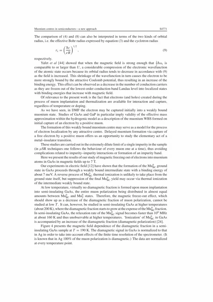
The comparison of (4) and (8) can also be interpreted in terms of the two kinds of orbitalradius, i.e. the effective Bohr radius expressed by equation (3) and the cyclotron radius
rc =(
hc
eB
)1/2
, (9)
respectively.Yafet et al [44] showed that when the magnetic field is strong enough that 1
2 hωc iscomparable to or larger than U , a considerable compression of the electronic wavefunctionof the atomic state occurs because its orbital radius tends to decrease in accordance with (9)as the field is increased. This shrinkage of the wavefunction in turn causes the electron to bemore strongly bound by the attractive Coulomb potential, thus resulting in an increase of thebinding energy. This effect can be observed as a decrease in the number of conduction carriersas they are frozen out of the lowest-order conduction band Landau level into localized stateswith binding energies that increase with magnetic field.
Of relevance to the present work is the fact that electrons (and holes) created during theprocess of muon implantation and thermalization are available for interaction and capture,regardless of temperature or doping.
As we have seen, in DMF the electron may be captured initially into a weakly boundmuonium state. Studies of GaAs and GaP in particular imply validity of the effective massapproximation within the hydrogenic model as a description of the muonium WBS formed oninitial capture of an electron by a positive muon.
The formation of this weakly bound muonium centre may serve as a model for the processof electron localization by any attractive centre. Delayed muonium formation via capture ofa free electron by a positive muon offers us an opportunity to study the elementary act of ametal–insulator transition.
These studies are carried out in the extremely dilute limit of a single impurity in the sample(in µSR techniques one follows the behaviour of every muon one at a time), thus avoidingcomplications related to impurity–impurity interactions or formation of an impurity band.
Here we present the results of our study of magnetic freezing out of electrons into muoniumatoms in GaAs in magnetic fields up to 7 T.
Our experiments in electric field [12] have shown that the formation of the Mu0BC ground
state in GaAs proceeds through a weakly bound intermediate state with a binding energy ofabout 7 meV. A reverse process of Mu0
BC thermal ionization is unlikely to take place from theground state itself, but suppression of the final Mu0
BC yield may occur via thermal ionizationof the intermediate weakly bound state.
At low temperature, virtually no diamagnetic fraction is formed upon muon implantationinto semi-insulating GaAs, the entire muon polarization being distributed in almost equalamounts between Mu0
BC and Mu0T states. Therefore, the magnetic freeze-out effect, which
should show up as a decrease of the diamagnetic fraction of muon polarization, cannot bestudied at low T . It can, however, be studied in semi-insulating GaAs at higher temperatures(about 200 K), where the diamagnetic fraction starts to grow at the expense of the Mu0
BC fraction.In semi-insulating GaAs, the relaxation rate of the Mu0
BC signal becomes faster than 108 MHzat about 160 K and thus unobservable at higher temperatures. ‘Ionization’ of Mu0
BC in GaAsis accompanied by an increase of the diamagnetic fraction (diamagnetic polarization) [24].
Figure 4 presents the magnetic field dependence of the diamagnetic fraction in a semi-insulating GaAs sample at T = 190 K. The diamagnetic signal in GaAs is normalized to thatin Ag in order to take into account effects of the finite time resolution of the spectrometer. (Itis known that in Ag 100% of the muon polarization is diamagnetic.) The data are normalizedat every temperature point.

S4772 V G Storchak et al
Figure 4. Magnetic field dependence of the diamagnetic fraction in semi-insulating GaAs atT = 190 K.
The reduction of the diamagnetic polarization at high magnetic field may be explained bymagnetic freezing out of free electrons into muonium atom energy levels when the characteristicenergy of the lowest-order conduction band Landau level becomes comparable to the bindingenergy of the weakly bound muonium atom. Within the hydrogenic model, an estimate ofthe magnetic field B0 required for 1
2 hωc to match Ry in the ground state of the weakly boundmuonium atom in GaAs yields
B0 = e3m∗c
hε2=
(m∗
m
)2 1
ε2× Ba ≈ 6.7 T, (10)
where Ba ≈ 2.2 × 10⁵ T is the atomic scale magnetic field.This value of B0 is characteristic of the n = 1 shallow donor state in GaAs [45]. Since in
delayed muonium formation the electron may be captured initially into an excited electronicstate, one may expect a reduction of the characteristic magnetic field required for a magneticfreeze-out effect in a weakly bound muonium atom. This circumstance may explain thereduction of the diamagnetic fraction with a corresponding increase of the Mu0
BC fraction atmagnetic fields almost an order of magnitude less than B0 (see figure 4).
It is worth noting that even B0 is about five orders of magnitude less than the magneticfield (Ba) required to affect the ground state of muonium or hydrogen in vacuum in the samemanner. Thus the effect of the magnetic field seems to be associated with muonium WBSrather than any deep muonium states. Accordingly, the characteristic electric field required to‘ionize’ a muonium atom in GaAs, GaP or CdS is about 4–5 orders of magnitude less than theatomic scale electric field [12–14]. It is therefore more consistent that ‘ionization’ of Mu0
BC,either thermally or by electric field, takes place from the weakly bound muonium state ratherthan from the deep state.
6. General considerations
The results of different experiments in electric fields [12–14] (see sections 2–4) and magneticfields (see section 5) suggest that the effects observed must be associated with highly excitedmuonium states rather than deep states. Indeed, to directly affect a deep muonium state,

Muonium centres in semiconductors—a new approach S4773
electric and magnetic fields of atomic scale would be required (∼109 V cm−1 and ∼105 T,respectively).
The binding energies for muonium WBS in GaAs [12], GaP [13] and CdS [14] areestimated to amount about 100 K. This value is more than an order of magnitude smaller thanthe binding energy of the ground Mu state. In particular, Mu0
BC in Si lies deeper than 2000 Kbelow the conduction band [25]. Therefore, it is more plausible that the thermal ‘ionization’of muonium takes place from one of the weakly bound muonium precursor states rather thanfrom any deep state. The excited states with electron orbits extended over distances 100 timesthe Bohr radius of the vacuum ground state then determine the temperature dependence ofthe muonium fraction (or the probability of electron capture by the positive muon). Thisconclusion is strongly supported by measurements of the muon precession frequency shift dueto atomic diamagnetism in CdS at the edge of muonium ionization [40]. Thus not only effectsof electric and magnetic fields but also effects of temperature may be associated with muoniumWBS rather than deep states.
This is consistent with the cascade model for electron capture in solids [17]: initiallycaptured into a very excited state, the electron is much more susceptible than in any deep stateto the action of fields and temperature.
Since the cascade model turns out to give a consistent description of muonium formationand dynamics in solids, we need to explore it here in more detail. Special attention is devotedto limitations of the cascade model and the consequences of those limitations with respect tomuonium dynamics in solids.
First, the cascade model assumes that the energy loss mechanism is elastic. It is suggestedthat the energy relaxation time is much less than that of the momentum. In other words,electrons are considered equally distributed over all degrees of freedom but the energy. Thispicture also suggests that energy relaxation may be treated as diffusion in energy space, whichmeans that the energy transfer in one collision,E , is much less than kT . For acoustic phononsin particular, if one works out both energy conservation and momentum conservation, it turnsout that the phonon cannot transfer energy of the order kT in one collision. Instead, the energytransfer in one collision, E = √
8m∗s2kT (where s is the velocity of sound), is much lessthan kT because the factor m∗s2 turns out to be small compared with the typical experimentaltemperature. (For example, in GaAs m∗s2 ∼ 0.5 K.) In the case of electron scattering onacoustic phonons, this sets a limit for application of the cascade theory:
kT m∗s2. (11)
In the opposite limiting case, the electron may be considered to be captured as the resultof a single one-phonon event: at low temperature (kT m∗s2) electron–phonon scatteringbecomes essentially inelastic. In this case the problem of electron capture by a positive centrecannot be considered as diffusion in energy space, because the characteristic energy loss in aone-phonon emission event is of the order of m∗s2. Therefore after a one-phonon emissionevent, any electron will find itself in a bound state with binding energy much higher than kT ;electron ejection into the conduction band then becomes very unlikely and such carriers maybe considered to be captured. In this case the capture process can be considered as a single-quantum transition from the conduction band into the bound state. The capture cross sectionfor such a process [19],
σ ∼(
e2
εkT
) (e2
εm∗s2
)2
, (12)
differs from expression (1) (which holds if kT m∗s2) by a factor ∼ (kT )2/(m∗s2)2. Thus,as the temperature drops below m∗s2, the increase of σ slows down and σ becomes ∝T −1
(versus σ ∝ T −3 at temperatures high enough that kT m∗s2).

S4774 V G Storchak et al
In either case, the cross section increases rapidly with decreasing temperature, andtherefore muonium formation via electron capture by a positive muon is favoured at lowtemperature, which is consistent with experimental results [24]. The transition from (12)to (1) should have no effect on the muonium formation process: either a single one-phononcapture event or a sequence of several one-phonon transitions down through the ladder ofstates into a WBS is completed with essentially the same result—the electron is captured intoa muonium WBS.
It should be noted that the cascade model in its classical form [17] and the entire discussionhere are both limited to consideration of one-phonon processes only. Processes with numbers ofphonons higher than one are suppressed by a factor of ( T
�D)i , where i is the number of phonons
involved in a single transition. Furthermore, the fact that the muonium WBS with quantumnumber n = 2 acts as a bottleneck for muonium formation in CdS [14] is the experimentalconfirmation of the dominant role of one-phonon events in the capture process. Indeed, iftwo-phonon events (or any other processes which involve many phonons) were essential thenthe electron could be captured directly into the n = 1 WBS, which is obviously in contradictionwith the experimental results at low temperature.
At higher temperatures, the cascade model breaks down when the thermal energy of anelectron becomes higher than the typical distance between energy levels δE in the vicinity ofthe ionization threshold: an electron which gets into a very excited bound state of the attractivecentre should be ejected back into the conduction band with high probability. In this case adirect capture of the electron from the conduction band into an n = 1 WBS may becomeessential. Binding energies of shallow donors in GaAs, Ge or Si are 70, 110 and about 400 K,respectively; the corresponding Debye energies are 340, 300 and 600 K [46]. Therefore, thedirect capture process (although strongly suppressed even at temperatures as high as 100 K)is still possible.
In other words, the cascade model works when the characteristic phonon energy involvedin the process of electron transition from the conduction band into a highly excited bound state(√
8m∗s2kT ) is higher than δE . In the framework of the quasi-classical approximation, thedistance between levels may be estimated using an expression for the density of states R(E):δE ≈ R−1(E). For the Coulomb centre the cascade model then works if [19]
kT U 3/4(2m∗s2
)1/4. (13)
(At higher temperature, optical phonon transitions may become important.) It is worth notingthat the inequality (13) is even stronger than necessary for the quasi-classical approximation tobe justified. Indeed, the quasi-classical approximation is justified if the de Broglie wavelengthof an electron (which is of the same order of magnitude as the wavelength of an emitted phonon)is less than the radius of the characteristic orbit (rT = e2/εkT ; see equation (1)):
h√2m∗kT
e2
εkT, e.g. kT U. (14)
The analysis of the experimental results, however, indicates that the cascade model adequatelydescribes the capture cross sections even at temperatures as high as U [17]. The probabilityof a cascade capture involving a sequence of one-phonon events is estimated to be higher thanthat for a direct (single) one-phonon event [47] by a factor of
U 7/2
(kT )2 (m∗s2
)3/2 . (15)
It is therefore obvious that, at temperatures below U , the cascade process is the dominantmechanism for electron capture by a positive centre.

Muonium centres in semiconductors—a new approach S4775
Electron capture by any centre may take place only when (and if) the electron approachesclose enough to the centre. So far we have assumed that the redistribution of the carriers inspace is fast enough that the electron concentration in the vicinity of the muon is well describedby the Boltzmann distribution. In other words, it is assumed that the capture process (muoniumformation) has no influence on the distribution of electron concentration in space. It is clearthat such an assumption is correct if the capture rate is low with respect to the rate of electronarrival into the vicinity of the muon where the capture can take place. In such semiconductorsas Si, Ge or GaAs this is typically the case. In semiconductors with low electron mobility,however, this is not the case, and the dynamics of the carriers in the vicinity of the centre maybe the ‘bottleneck’ of the capture process. In this case the concentration of electrons around thecentre turns out to be less than in cases governed by the Boltzmann distribution. This depletionhas a significant influence on the capture process. The theory of recombination (or electroncapture by a positive centre) under these conditions was first considered by Langevin [48]and then developed by Pekar [49, 50]. In particular, the theory shows that in cases where thelimiting process is the electron transport, the carrier concentration turns out to be uniform inspace instead of being Boltzmann-like. In such cases the theory predicts a capture coefficientc (c = σv, where v is the velocity of the carrier) given by
cL = 4πeb
ε(16)
so that cL is proportional to the electron mobility b. The remarkable feature of equation (16)is that it is independent of the capture mechanism itself. The only important point here isthat capture of the carrier from the vicinity of the centre occurs faster than the arrival of suchcarriers into the said vicinity. As shown by Lax [17] for such semiconductors as Si or Ge,equation (16) gives values for the capture coefficient several orders of magnitude higher thanexperimental values. Therefore it is not diffusion which limits the capture of carriers in thesesemiconductors. Indeed, for electron capture in Si it was found that equation (16) predicts ac three orders of magnitude higher than that determined in the experiment [51, 52]. In CdS,however, equation (16) estimates c = 10−6 cm3 s−1 at 100 K, which is close to experimentalvalues determined in this semiconductor [53, 54]. In CdS, therefore, it is suggested that electrontransport to a positive centre is the limiting mechanism in the capture process.
The distinction between the Thompson model [20] and the Langevin approach [48] can bebest understood in terms of the interplay of the electron mean free path � and the characteristicorbit radius rT (see equation (1)). If
� rT, (17)
the Thompson model applies, which assumes that the electron experiences quasi-free motionunder the influence of the central potential with very few scattering events (ballistic regime).A free electron (i.e. an electron with positive energy) passes by the centre with very smallprobability of scattering by a third body (acoustic phonon) and being captured into a boundorbit. On the other hand, a bound electron is associated with some particular orbit for along time until it experiences a scattering event which puts it into a different orbit. In thecase of scattering by acoustic phonons, the ratio �/rT is temperature independent and theinequality (17) can be expressed as
e2
2εm∗s2�0 1, (18)
where �0 is the characteristic length for electron energy loss (see equation (1)). For Si, Ge andGaAs the left-hand side of inequality (18) is about 5 × 10⁻², 2 × 10⁻² and 10−2, respectively,while in CdS it is of the order of 1.

S4776 V G Storchak et al
In the opposite limit
� rT, (19)
the electron transport mechanism is qualitatively different from that in the ballistic regime—it is diffusive. In the equilibrium case one may make use of the Einstein relation betweenthe mobility b and the diffusion coefficient D, and rewrite equation (16) as cL = 4πrT D.Comparing this capture coefficient with that in the Thompson limit (cT = 4πr3
T/3τE), onefinds that electron transport controls the capture process if√
3DτE rT, (20)
i.e. if the characteristic length for energy loss is much less than the characteristic capture radius.The interplay of the electron mean free path and the capture radius may play an important
role not only in the muonium formation process but also in determining spectroscopiccharacteristics of muonium centres in semiconductors. The entire discussion above is restrictedto the process of electron capture into muonium WBS. The question of how it gets down intothe deep state, in particular what energy transfer mechanisms are responsible for muoniumtransitions from WBS into the deep state, still remains an open problem.
Binding energies of muonium deep centres in semiconductors are much higher than thoseof muonium WBS (typically, 0.1–1 eV versus 0.01 eV). The energy differences betweenmuonium WBS and muonium deep states are much higher than most Debye energies (typicallyseveral hundred kelvins). Therefore, having captured into a very excited muonium state andcascaded down to a muonium WBS via phonon emission, an electron cannot cascade furtherdown into a deep muonium state via phonon emission. The multiphonon process into the deepstate is severely suppressed by a factor (T/�D)i , where i is ∼102 at T = 10 K, because thetypical energy transfer is
√8m∗s2kT (see above).
Energy release through photon emission is also ineffective: the characteristic radiationtime scales with the energy difference δE as (δE)−4, and the characteristic time for deep statemuonium formation with a binding energy of the order of 1 eV is estimated to be about 10−5 s,whereas the coherent muonium precession observed in magnetic fields as high as 7 T requiresthat the muonium formation time is at least an order of magnitude less than 10−11 s.
The only energy bath that can accept the energy difference between a muonium WBSand its deep state is the electron subsystem. We suggest that processes analogous to Augerrecombination in semiconductors are responsible for muonium formation in the deep state.The elementary act of Auger recombination requires three particles to participate. If all theseparticles are free carriers then the Auger process has a certain energy threshold [55] as aconsequence of momentum and energy conservation laws. Such a threshold makes the Augermechanism ineffective at low temperatures.
Auger processes may also occur as an electron is captured by a positive centre; the releasingenergy is then transferred to the second carrier. The mere presence of a heavy centre like thepositive muon removes the restriction coming from the momentum conservation law, andtherefore such processes can take place without any energy threshold. The absence of theenergy threshold makes this process very effective even at low temperatures. Such processeswere first observed in doped Ge crystals [56]. To date, a great body of information has beenaccumulated on Auger processes in different semiconductors (see e.g. [57]). In fact, at carrierconcentrations above about 1014–1015 cm−3 the Auger mechanism becomes the most efficientone in recombination processes which involve significant energy release [58, 59].
As the Auger mechanism is proportional to n2 (see e.g. [60]) it is essential to have a highelectron concentration n around the muon for these processes to be effective in the formationof a deep muonium state. It is known that ionization processes in the muon track may produce

Muonium centres in semiconductors—a new approach S4777
electron concentrations of about 1016 cm−3 [12]. These electrons, if transported to the vicinityof the muon, may act as third bodies in Auger processes. Therefore, in semiconductors withhigh electron mobility (such as Si, Ge, GaAs, etc) where the inequality (17) holds true, theThompson model may apply, and the Auger mechanism may be responsible for deep statemuonium formation. In fact, the Auger mechanism may be responsible for deep muoniumstate formation in some insulators—solid phases of Ne,Ar, Kr and Xe—which possess electronmobilities close to those in semiconductors. That is why the formation of a multi-electron trackis essential to DMF in these solids [9].
In semiconductors with low electron mobility (such as CdS, CdTe, GaN, etc) the Langevinmodel may apply, implying a depletion region around the muon. Then Auger processes areineffective, there is essentially no energy releasing mechanism by which the muonium WBS canbe transferred into a muonium deep state, and therefore the muonium WBS should live forever(on the µSR timescale). This conclusion is consistent with experimental findings [24, 28],bearing in mind that the WBS has such a weak hyperfine coupling between the muon and theelectron that its precession signal is practically indistinguishable from that of a diamagneticstate.
Further experiments designed to
(a) stabilize muonium WBS in Si, GaAs or GaP at low temperature (where the electron supplyto the muon may be suppressed), and
(b) force the muonium WBS in CdS to be transferred into a deep muonium state via artificialproduction of electron–hole pairs (by photoemission etc)
may help in understanding muonium formation and dynamics in semiconductors.
Acknowledgments
This work was supported by the Kurchatov Institute, the Canadian Institute for AdvancedResearch, the Natural Sciences and Engineering Research Council of Canada and the NationalResearch Council of Canada. Two of us (VGS and DGE) were also supported by the USANSF (DMR-0209727) and the Royal Society of London (through the International Award).
References
[1] Shockley W and Read W T 1952 Phys. Rev. 87 835[2] Hall R N 1952 Phys. Rev. 87 387[3] Burton J A, Hall G W, Morin F J and Severiens J C 1953 J. Phys. Chem. 57 853[4] Shulman R G and Wyluda B J 1956 Phys. Rev. 102 1455[5] Storchak V G, Brewer J H and Morris G D 1995 Phys. Rev. Lett. 75 2384[6] Storchak V G, Brewer J H and Morris G D 1996 Phys. Rev. Lett. 76 2969[7] Storchak V G, Brewer J H, Morris G D, Arseneau D J and Senba M 1999 Phys. Rev. B 59 10559[8] Storchak V G, Eshchenko D G, Brewer J H, Morris G D, Cottrell S P and Cox S F J 2000 Phys. Rev. Lett. 85
166[9] Eshchenko D G, Storchak V G, Brewer J H, Morris G D, Cottrell S P and Cox S F J 2002 Phys. Rev. B 66
035105[10] Storchak V G, Cox S F J, Cottrell S P, Brewer J H, Morris G D, Arseneau D J and Hitti B 1997 Phys. Rev. Lett.
78 2835[11] Eshchenko D G, Storchak V G and Morris G D 1999 Phys. Lett. A 264 226[12] Eshchenko D G, Storchak V G, Brewer J H and Lichti R L 2002 Phys. Rev. Lett. 89 226601[13] Storchak V G, Eshchenko D G, Lichti R L and Brewer J H 2003 Phys. Rev. B 67 121201[14] Eshchenko D G, Storchak V G, Cottrell S P and Cox S F J 2003 Phys. Rev. B 68 073201[15] Storchak V G, Brewer J H and Eshchenko D G 1997 Appl. Magn. Reson. 13 15[16] Lax M 1959 J. Phys. Chem. Solids 8 66

S4778 V G Storchak et al
[17] Lax M 1960 Phys. Rev. 119 1502[18] Gummel H and Lax M 1957 Ann. Phys. 2 28[19] Abakumov V N and Yassievich I N 1976 JETP 71 657[20] Thompson J J 1924 Phil. Mag. 47 337[21] Koenig S H, Brown R D and Shillinger W 1962 Phys. Rev. 128 1668[22] Norton P, Braggins T and Levinstein H 1973 Phys. Rev. Lett. 30 488[23] Grimmeiss H G, Janzen E and Skarstam B 1980 J. Appl. Phys. 51 4212[24] Patterson B D 1988 Rev. Mod. Phys. 60 69[25] Kreitzman S R, Hitti B, Lichti R L, Estle T L and Chow K H 1995 Phys. Rev. B 51 13117[26] Chow K H, Hitti B and Kiefl R F 1998 Identification of Defects in Semiconductors (Semiconductors and
Semimetals vol 51A) ed M Stavola (New York: Academic)[27] Lichti R L 1999 Hydrogen in Semiconductors vol 2, ed N Nickel (San Diego, CA: Academic)[28] Gil J M, Alberto H V, Vilao R C, Piroto Duarte J, Mendes P J, Ferreira L P, Aures de Campos N, Weidinger A,
Krauser J, Niedermayer Ch and Cox S F J 1999 Phys. Rev. Lett. 83 5294Gil J M, Alberto H V, Vilao R C, Piroto Duarte J, Aures de Campos N, Weidinger A, Krauser J, Davis E A,
Cottrell S P and Cox S F J 2001 Phys. Rev. B 64 075205[29] Schenck A 1986 Muon Spin Rotation: Principles and Applications in Solid State Physics (Bristol: Hilger)
Cox S F J 1987 J. Phys. C: Solid State Phys. 20 3187Brewer J H 1995 Muon spin rotation/relaxation/resonance Encyclopedia of Applied Physics ed G L Trigg (New
York: VCH)[30] Eshchenko D G 1996 PhD Thesis Kurchatov Institute, Moscow[31] Animalu A O E 1977 Intermediate Quantum Theory of Crystalline Solids (Englewood Cliffs, NJ: Prentice-Hall)[32] von Plessen G, Meier T, Koch M, Feldmann J, Thomas P, Koch S W, Goebel E O, Goossen K W, Kuo J M and
Kopf R F 1996 Phys. Rev. B 53 13688[33] Knox R S 1963 Theory of Excitons (New York: Academic)[34] Kiefl R F, Schneider J W, Keller H, Kundig W, Odermatt W, Patterson B D, Blazey K W, Estle T L and
Rudaz S L 1985 Phys. Rev. B 32 530[35] Zhang X, Dou K, Hong Q and Balkanski M 1990 Phys. Rev. B 41 1376[36] Goryunova N A 1968 Complex Diamond-Like Semiconductors (Moscow: Sovetskoye Radio)[37] Berchenko N N, Krevs V E and Sredin V G 1963 Semiconductor Solid Solutions and their Applications (Moscow:
Voenizdat)[38] Aven M and Prener J S (ed) 1967 Physics and Chemistry of II–VI Compounds (Amsterdam: North-Holland)[39] Abrikosov N Kh 1967 Semiconductors Compounds, their Manufacturing and Properties (Moscow: Nauka)[40] Storchak V G, Eshchenko D G, Cottrell S P, Cox S F J, Karlsson E, Waeppling R and Gil J M 2001 Phys. Lett.
A 290 181[41] Gallagher T F 1994 Rydberg Atoms (Cambridge: Cambridge University Press)[42] Landau L 1930 Z. Phys. 64 629[43] Garton W R S and Tomkins F S 1969 Astrophys. J. 158 839[44] Yafet Y, Keyes R W and Adams E N 1956 J. Phys. Chem. Solids 1 137[45] Zawadzki W, Pfeffer P, Najda S P, Yokoi H, Takeyama S and Miura N 1994 Phys. Rev. B 49 1705[46] Levinstein M, Rumyantsev S and Shur M 1996 Semiconductor Parameters (Singapore: World Scientific)[47] Gummel H and Lax M 1955 Phys. Rev. 97 1469[48] Langevin M P 1903 Ann. Chem. Phys. 28 289
Langevin M P 1903 Ann. Chem. Phys. 28 433[49] Pekar S I 1950 JETP 20 267[50] Pekar S I and Perlin Y E 1950 JETP 20 271[51] Preier H 1968 J. Appl. Phys. 39 194[52] Weber W H 1970 Appl. Phys. Lett. 16 396[53] Friedrich H 1964 Acta Phys. Pol. 26 655[54] Blazhko N A, Sal’kov E A and Khvostov V A 1977 Phys. Tech. Semicond. 11 2278[55] Beattie A R and Landsberg P T 1959 J. Phys. Chem. Solids 8 73[56] Karpova I V and Kalashnikov S G 1963 Fiz. Tverd. Tela 5 301[57] Landsberg P T and Robbins D J 1978 Solid State Electron. 21 1289[58] Bonch-Bruevitch V L and Gulyaev Yu V 1960 Fiz. Tverd. Tela 2 465[59] Robbins D J and Landsberg P T 1980 J. Phys. C: Solid State Phys. 13 2425[60] Bonch-Bruevitch V L and Kalashnikov S G 1977 Physics of Semiconductors (Moscow: Nauka)