fick's laws of diffusion - electrical and computer engineering
TRANSCRIPT

Fall 2008 EE 410/510:Microfabrication and Semiconductor Processes
M W 12:45 PM – 2:20 PMEB 239 Engineering Bldg.
Instructor: John D. Williams, Ph.D.Assistant Professor of Electrical and Computer Engineering
Associate Director of the Nano and Micro Devices CenterUniversity of Alabama in Huntsville
406 Optics BuildingHuntsville, AL 35899Phone: (256) 824-2898
Fax: (256) 824-2898email: [email protected]
Tables and Charts taken from Cambell, Science and Engineering of Microelectronic Fabrication, Oxford 2001And Wolf and Tauber, Introduction to Silicon Processing for the VLSI Era, Vol. II
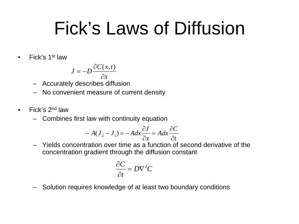
Fick’s Laws of Diffusion• Fick’s 1st law
– Accurately describes diffusion– No convenient measure of current density
• Fick’s 2nd law– Combines first law with continuity equation
– Yields concentration over time as a function of second derivative of the concentration gradient through the diffusion constant
– Solution requires knowledge of at least two boundary conditions
tCAdx
xJAdxJJA
∂∂
=∂∂
−=−− )( 12
CDtC 2∇=∂∂
xtxCDJ
∂∂
−=),(
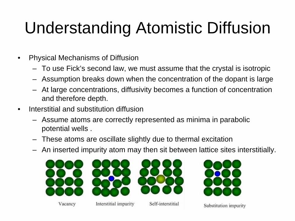
Understanding Atomistic Diffusion• Physical Mechanisms of Diffusion
– To use Fick’s second law, we must assume that the crystal is isotropic– Assumption breaks down when the concentration of the dopant is large– At large concentrations, diffusivity becomes a function of concentration
and therefore depth.• Interstitial and substitution diffusion
– Assume atoms are correctly represented as minima in parabolic potential wells .
– These atoms are oscillate slightly due to thermal excitation– An inserted impurity atom may then sit between lattice sites interstitially.

Understanding Atomistic Diffusion• Interstitial and substitution diffusion
– These impurities diffuse rapidly due to the sharp localized changes in potential energy and do not contribute to doping
– Diffusion, however allows the impurity to move into an empty lattice site, thereby substituting for its potential into the lattice in place of the matrix material
– Vacancies filled by substitution remain within the lattice site until sufficient energy is provided for the impurity to move to another empty lattice site. This is achieved by charge redistribution to minimize the free energy of the lattice
– Vacancies are very dilute in semiconductors at typical process conditions– Each of the possible sites can be treated as independent entities. – The diffusion coefficient then becomes the probability of all possible
diffusion coefficients, weighted by the probability of existence
∑=
+−
⎥⎥⎦
⎤
⎢⎢⎣
⎡⎟⎟⎠
⎞⎜⎜⎝
⎛+⎟⎟
⎠
⎞⎜⎜⎝
⎛+=
1a
aa
i
aa
ii D
npD
nnDD
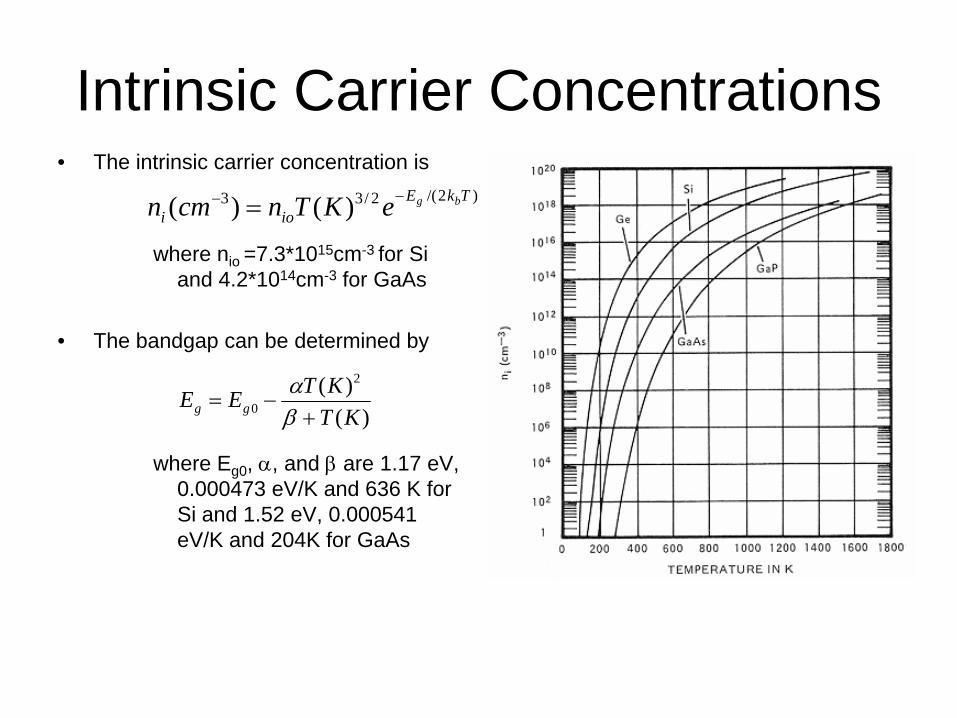
Intrinsic Carrier Concentrations • The intrinsic carrier concentration is
where nio =7.3*1015cm-3 for Si and 4.2*1014cm-3 for GaAs
• The bandgap can be determined by
where Eg0, α, and β are 1.17 eV, 0.000473 eV/K and 636 K for Si and 1.52 eV, 0.000541 eV/K and 204K for GaAs
)2/(2/33 )()( TkEioi
bgeKTncmn −− =
)()( 2
0 KTKTEE gg +
−=βα
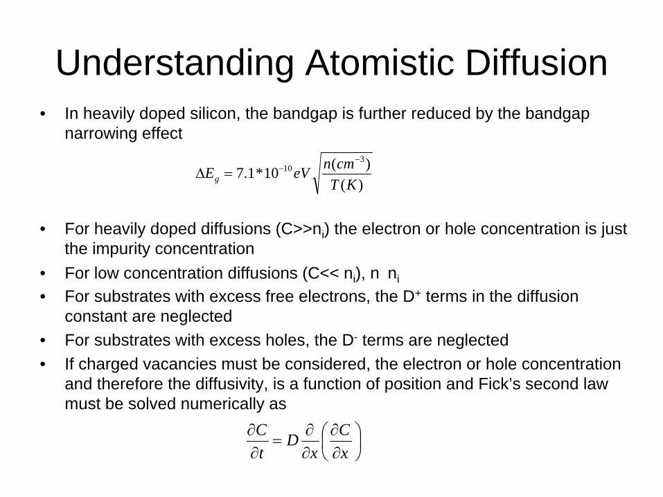
Understanding Atomistic Diffusion• In heavily doped silicon, the bandgap is further reduced by the bandgap
narrowing effect
• For heavily doped diffusions (C>>ni) the electron or hole concentration is just the impurity concentration
• For low concentration diffusions (C<< ni), n�ni
• For substrates with excess free electrons, the D+ terms in the diffusion constant are neglected
• For substrates with excess holes, the D- terms are neglected• If charged vacancies must be considered, the electron or hole concentration
and therefore the diffusivity, is a function of position and Fick’s second law must be solved numerically as
)()(10*1.7
310
KTcmneVEg
−−=Δ
⎟⎠⎞
⎜⎝⎛∂∂
∂∂
=∂∂
xC
xD
tC
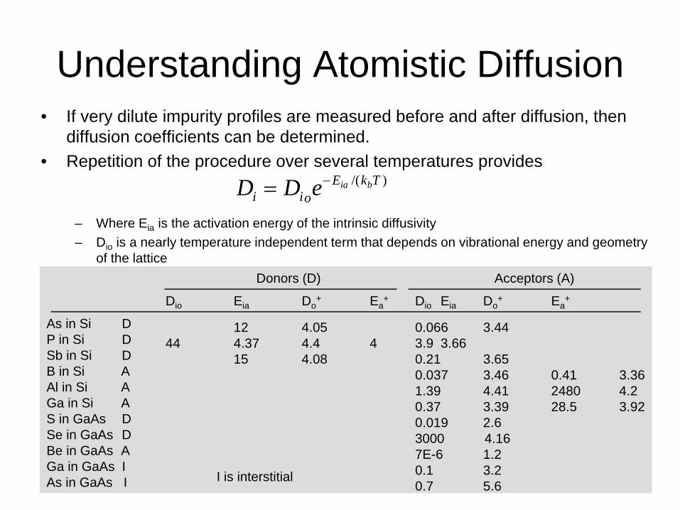
Understanding Atomistic Diffusion• If very dilute impurity profiles are measured before and after diffusion, then
diffusion coefficients can be determined.• Repetition of the procedure over several temperatures provides
– Where Eia is the activation energy of the intrinsic diffusivity– Dio is a nearly temperature independent term that depends on vibrational energy and geometry
of the lattice
)/( TkEoii
biaeDD −=
Donors (D) Acceptors (A)
Dio Eia Do+ Ea
+
0.066 3.443.9 3.660.21 3.650.037 3.46 0.41 3.361.39 4.41 2480 4.20.37 3.39 28.5 3.920.019 2.63000 4.167E-6 1.20.1 3.20.7 5.6
Dio Eia Do+ Ea
+
12 4.0544 4.37 4.4 4
15 4.08
As in Si DP in Si DSb in Si DB in Si AAl in Si AGa in Si AS in GaAs DSe in GaAs DBe in GaAs AGa in GaAs IAs in GaAs I I is interstitial
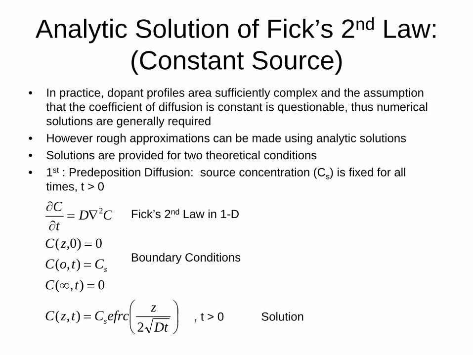
Analytic Solution of Fick’s 2nd Law: (Constant Source)
• In practice, dopant profiles area sufficiently complex and the assumption that the coefficient of diffusion is constant is questionable, thus numerical solutions are generally required
• However rough approximations can be made using analytic solutions• Solutions are provided for two theoretical conditions• 1st : Predeposition Diffusion: source concentration (Cs) is fixed for all
times, t > 0
⎟⎠⎞
⎜⎝⎛=
=∞==
∇=∂∂
DtzefrcCtzC
tCCtoC
zC
CDtC
s
s
2),(
0),(),(
0)0,(
2
Boundary Conditions
Solution, t > 0
Fick’s 2nd Law in 1-D
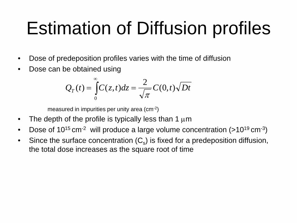
Estimation of Diffusion profiles• Dose of predeposition profiles varies with the time of diffusion• Dose can be obtained using
measured in impurities per unity area (cm-2)
• The depth of the profile is typically less than 1 μm • Dose of 1015 cm-2 will produce a large volume concentration (>1019 cm-3)• Since the surface concentration (Cs) is fixed for a predeposition diffusion,
the total dose increases as the square root of time
DttCdztzCtQT ),0(2),()(0 π
== ∫∞
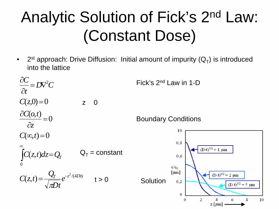
Analytic Solution of Fick’s 2nd Law: (Constant Dose)
• 2st approach: Drive Diffusion: Initial amount of impurity (QT) is introduced into the lattice
)4/(
0
2
2
),(
),(
0),(
0),(0)0,(
DtzT
T
eDt
QtzC
QdztzC
tCz
toCzC
CDtC
−
∞
=
=
=∞
=∂
∂=
∇=∂∂
∫
π
Boundary Conditions
Solution
z K 0
Fick’s 2nd Law in 1-D
QT = constant
t > 0

Analytic Solution of Fick’s 2nd Law: (Constant Dose)
• With dose is constant, surface concentration must decrease with time:
– At x = 0, dC/dz is zero for all t K 0.• One classic real world example of these two solutions is a predeposition surface
followed by drive in diffusion– Recall that the boundary condition for drive in was that the initial impurity concentration
was zero everywhere except at the surface– Thus drive in is a good approximation for diffusion provided that
• Boron (B) is diffusing into Si that as a uniform composition of phosphorus (P), CB.– Also assume that CS>>CB
– A depth will exist at which CS = CB
– Since B is p-type and P is n-type, a p-n junction will exist at this depth, xj:
⎥⎦
⎤⎢⎣
⎡=
DtCQDtx
B
Tj π
ln4
driveinpredep DtDt <<
DtQtCC T
s π== ),0(
⎥⎦
⎤⎢⎣
⎡= −
S
Bj C
CefrcDtx 12 PredepDrive in
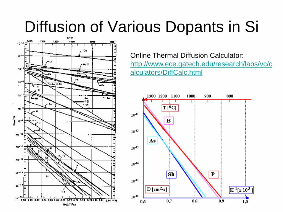
Diffusion of Various Dopants in SiOnline Thermal Diffusion Calculator:http://www.ece.gatech.edu/research/labs/vc/calculators/DiffCalc.html
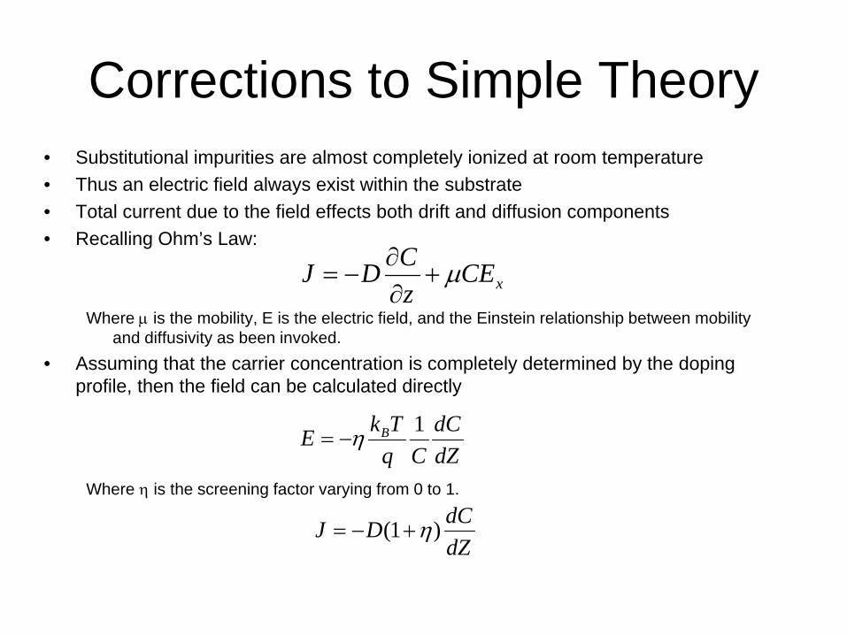
Corrections to Simple Theory• Substitutional impurities are almost completely ionized at room temperature• Thus an electric field always exist within the substrate• Total current due to the field effects both drift and diffusion components• Recalling Ohm’s Law:
Where μ is the mobility, E is the electric field, and the Einstein relationship between mobility and diffusivity as been invoked.
• Assuming that the carrier concentration is completely determined by the doping profile, then the field can be calculated directly
Where η is the screening factor varying from 0 to 1.
dZdC
CqTkE B 1η−=
xCEzCDJ μ+∂∂
−=
dZdCDJ )1( η+−=

Corrections for Doping under Oxides and Nitrides
• For (Cdoping >> ni, CSub), the profiles own electric filed will enhance movement of the impurity• Note that the equation is identical to Fick’s first law with the slight modification of the
screening factor multiplier• Comparison of inert, oxidizing, and nitridizing dopant diffusion experiments has provided the
following conclusions:– Diffusion of impurities depends directly on the concentration of impurities– Oxidized semiconductors produce a high concentration of excess interstitials at the oxide
semiconductor interface– Interstitial concentration decays with depth due to recombination– Near surface, these interstitials increase the diffusivity of B and P
• Therefore it is believed that B and P impurities diffuse primarily interstitially– Arsenic is diffusivity is found to decrease under oxidized conditions
• Excess interstitial concentration is expected to decrease local vacancy concentration, therefore, arsenic is primarily believed to diffuse through vacancy mechanisms (at least in oxidized systems)
– These results have been confirmed by using nitride silicon surfaces which are dominated primarily by vacancies and NOT interstitials.
• Dopant diffusivities under oxidizing conditions
Where the exponent n has been found experimentally to range from 0.3-0.6 and the α term is (+) for oxidation and (-) for nitridation
nox
dtdtDiDDiD ⎥⎦
⎤⎢⎣⎡+=Δ+= α
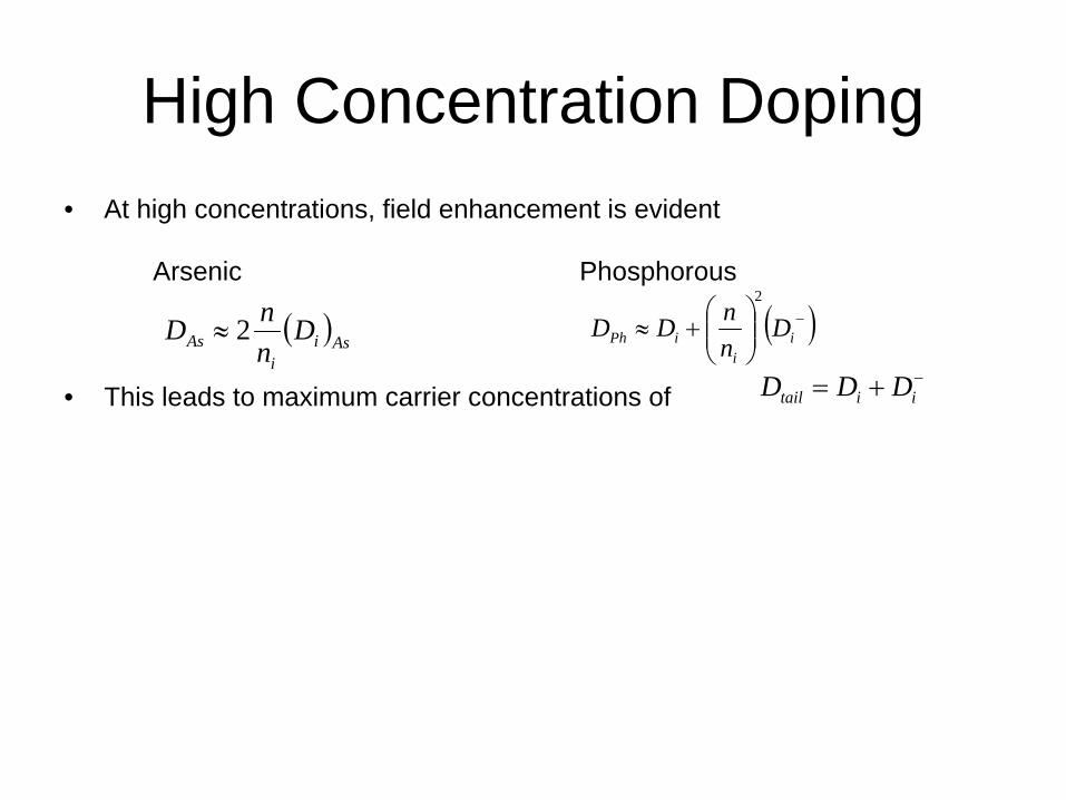
High Concentration Doping• At high concentrations, field enhancement is evident
• This leads to maximum carrier concentrations of
Arsenic Phosphorous
−+= iitail DDD
( )Asii
As DnnD 2≈ ( )−⎟⎟
⎠
⎞⎜⎜⎝
⎛+≈ i
iiPh D
nnDD
2
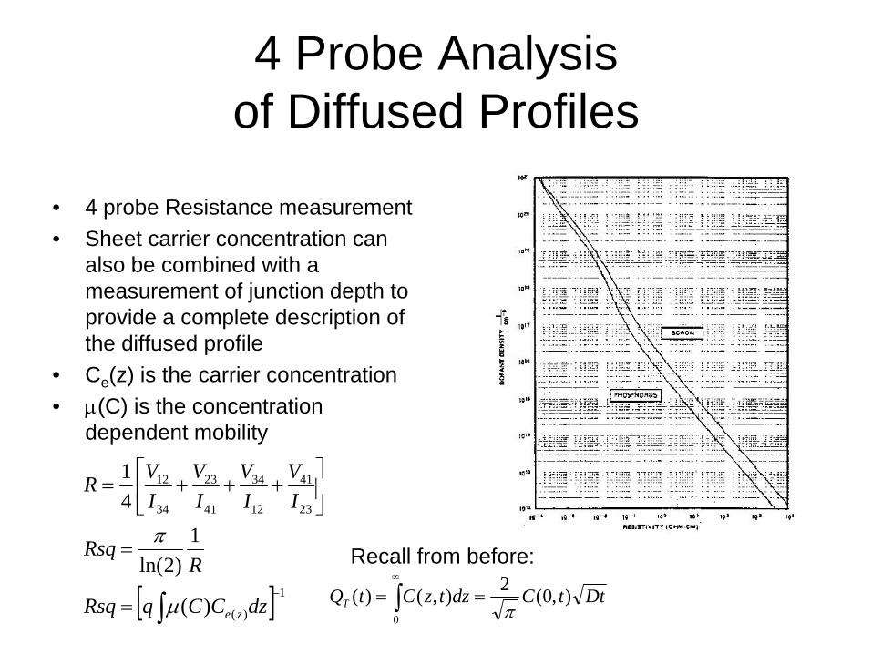
4 Probe Analysis of Diffused Profiles
• 4 probe Resistance measurement• Sheet carrier concentration can
also be combined with a measurement of junction depth to provide a complete description of the diffused profile
• Ce(z) is the carrier concentration• μ(C) is the concentration
dependent mobility
[ ] 1
)(
23
41
12
34
41
23
34
12
)(
1)2ln(
41
−
∫=
=
⎥⎦
⎤⎢⎣
⎡+++=
dzCCqRsq
RRsq
IV
IV
IV
IVR
zeμ
π
DttCdztzCtQT ),0(2),()(0 π
== ∫∞
Recall from before:

Hall effect Analsysis of Diffused Profiles
wBvVBvE
BvqF
zxh
zxy
=
=×=rrr
sej
h
xxje
X
e
x
ej
e
ej
xx
RCqx
qVBIxCDxC
DxCx
C
CqwxIv
j
j
1
1
0
0
=
==
=
=
∫
∫
μ
Hall Voltage
integrated carrier concentration
Lorentz Force
Hall mobility (for epitaxy considerations)