fast atomic-scale chemical imaging of crystalline materials and dynamic phase transformations
TRANSCRIPT

Fast Atomic-Scale Chemical Imaging of Crystalline Materials andDynamic Phase TransformationsPing Lu,*,† Ren Liang Yuan,‡ Jon F. Ihlefeld,† Erik David Spoerke,† Wei Pan,† and Jian Min Zuo‡
†Sandia National Laboratories, Albuquerque, New Mexico 87185 United States‡Department of Materials Science and Engineering, University of Illinois at Urbana−Champaign, 1304 W. Green Street, Urbana,Illinois 61801, United States
*S Supporting Information
ABSTRACT: Atomic-scale phenomena fundamentally influence materi-als form and function that makes the ability to locally probe and studythese processes critical to advancing our understanding and developmentof materials. Atomic-scale chemical imaging by scanning transmissionelectron microscopy (STEM) using energy-dispersive X-ray spectrosco-py (EDS) is a powerful approach to investigate solid crystal structures.Inefficient X-ray emission and collection, however, require longacquisition times (typically hundreds of seconds), making the techniqueincompatible with electron-beam sensitive materials and study ofdynamic material phenomena. Here we describe an atomic-scaleSTEM-EDS chemical imaging technique that decreases the acquisitiontime to as little as one second, a reduction of more than 100 times. Wedemonstrate this new approach using LaAlO3 single crystal and studydynamic phase transformation in beam-sensitive Li[Li0.2Ni0.2Mn0.6]O2(LNMO) lithium ion battery cathode material. By capturing a series of time-lapsed chemical maps, we show for the first timeclear atomic-scale evidence of preferred Ni-mobility in LNMO transformation, revealing new kinetic mechanisms. Theseexamples highlight the potential of this approach toward temporal, atomic-scale mapping of crystal structure and chemistry forinvestigating dynamic material phenomena.
KEYWORDS: Tim-resolved, atomic-scale, lattice-vector translation, dynamic, phase transformation
Chemical imaging at the atomic-scale provides a useful real-space approach to investigate material structures and has
been recently demonstrated in aberration corrected scanningtransmission electron microscopy (STEM).1−11 By scanning anangstrom-sized electron probe across a crystal sample alignedalong a low-axis orientation and collecting either electronenergy-loss spectra (EELS)1−4 or energy-dispersive X-rayspectra (EDS),5−11 chemical imaging at atomic-scale has beenachieved. Simultaneously recorded Z-contrast or high-angleannular dark-field (HAADF) images by using electrons thathave been scattered over large angles and exited through thespecimen are often used to provide reference images for atomiccolumns.1 Because unique chemical signals are used foridentification of the atomic columns in chemical imaging,determination of the lattice structures that might otherwise notbe possible by traditional imaging or diffraction techniques(e.g., electron, neutron, and X-ray diffraction) has also beendemonstrated.10
Arguably the greatest advantage of atomic-scale STEM EDSchemical imaging is that it allows for direct correlation betweenthe atomic structure and the chemical map. Current methods,however, are limited by inefficient X-ray generation andcollection. To compensate for this poor efficiency, STEMEDS datasets are often acquired as a series of frames, where the
same region is typically scanned several hundred times, relyingon spatial drift correction to build a high fidelity dataset.10,11
This process usually takes more than a few hundred seconds,subjecting the samples to high doses of electron irradiation.The requirement for extended acquisition times prevents theuse of this technique for any electron beam sensitive materialsand precludes the study of critical phase transformations anddynamics, which requires structural and chemical informationresolved on a much shorter time scale. On the other hand,although time-resolved structural techniques (e.g., such as X-raydiffraction) are available, those techniques typically haveinherent limitations on local structure and chemical determi-nation and require relatively large samples.12
Here we report the realization of rapid atomic-scale chemicalimaging by STEM EDS from small crystalline region achievedwith a total acquisition time of less than one or a few secondsunder normal high-resolution STEM imaging conditions. UsingLaAlO3 as a model crystal, we find averaged atomic-scalechemical maps for lanthanum and aluminum atoms can beextracted from an area of few 10 nm2 acquired with the
Received: January 29, 2016Revised: March 2, 2016
Letter
pubs.acs.org/NanoLett
© XXXX American Chemical Society A DOI: 10.1021/acs.nanolett.6b00401Nano Lett. XXXX, XXX, XXX−XXX

acquisition time of ∼2 s or less. The method is verified by aphenomenological model. Furthermore, we apply the techniqueto study of the phase transformation in Li[Li0.2Ni0.2Mn0.6]O2
(LNMO), a lithium ion battery cathode material known toundergo an electron-beam induced phase transformation.13−15
By obtaining atomic-scale structural information sequentially asa time series, it reveals for the first time that the transformationtakes place by preferably jumping of nickel atoms (relative tomanganese atoms) from the TM layers to the lithium layersonce the lithium atoms are removed by the high-energyelectrons. This capability opens up a new paradigm of studywhere chemical structure of materials susceptible to electronirradiation as well as phase transformation and dynamics can befollowed temporally at the atomic-scale.Our approach to overcome the limitation due to inefficient
X-ray generation and collection is based on the following keyconsiderations: (1) within the crystal area scanned (e.g., 10 ×10 unit cells) for atomic-scale STEM EDS mapping, theseemingly random and sparsely scattered X-ray signals
produced after a short acquisition time (i.e., less than a fewseconds) are not random but are statistically localized to atomiccolumns in the crystal; (2) the long-range order of the crystallattice creates chemically and structurally equivalent pixelpositions within the scanned image, separated by precise lattice-vector translations; and (3) the X-ray counts, distributed overthe large area, can be translated and summed across equivalentpositions within one unit cell via lattice-vector translations,forming averaged chemical maps for the crystal. In the otherwords, the technique consolidates the X-rays scattered over alarge area into a smaller, single unit cell area using lattice-vectortranslations, producing averaged chemical maps for the crystal.By concentrating X-ray signals into the smaller area, anacquisition time savings of over 100 times can be achieved.Localization of X-rays to atomic-columns is crucial to thesuccessful outcome of the atomic-scale mapping and can befulfilled by using a thin specimen and a small electronprobe.8,10,11 Below we first demonstrate the technique ondata obtained from a LaAlO3 crystal.
Figure 1. Fast STEM EDS atomic-scale chemical mapping achieved with a short collection time. (a) Projected LaAlO3 structure in a [001] direction;(b) raw X-ray count maps of La L (red-dot) and Al K (green-dot), obtained by STEM EDS with a total acquisition of 1.8 s (the overlaid blue linesshow the lattice of LaAlO3 with lanthanum columns at the crosses and aluminum columns at the grid centers); (c) the reference HAADF imageobtained simultaneously with EDS mapping (only one-fourth shown); (d,e) X-ray count maps (2 × 2 unit cells shown) for La L and Al K X-rays,respectively, obtained by the lattice-translation method using the X-ray map in (b); (f,g) obtained by 3-point smoothing of the maps in (d,e); (h)(La, Al) RGB map obtained with maps (f,g); (i) (La, Al) RGB map obtained by STEM EDS with a total acquisition of 0.6 s; and (j) (La, Al) RGBmap obtained STEM EDS with a total acquisition of ∼8 s. The blue dashed square in (a,c−e,h,−j) represents the projected LaAlO3 unit cell in [001].
Nano Letters Letter
DOI: 10.1021/acs.nanolett.6b00401Nano Lett. XXXX, XXX, XXX−XXX
B

LaAlO3 has a perovskite crystal structure with a rhombohe-dral unit cell (a = 0.3788 nm and α = 90.4°). For practicalconsiderations, it can be regarded as pseudocubic. Its projectedstructure in the [001] direction is shown Figure 1a. Figure 1bshows a raw EDS composite map (200 × 200 pixels) of La L(red-dot) and Al K (green-dot) X-rays, obtained after ∼1.8 scollection, corresponding to the sum of 3 frames (∼0.6 s perframe with an instantaneous dwell time on each pixel of 15 μs).The spectral image was acquired for a physical frame size of4.46 nm × 4.46 nm (∼0.022 nm/pixel). The reference HAADFimage obtained simultaneously is shown in Figure 1c (only one-fourth of the image is shown). The multislice simulations16 ofthe electron wave function distribution under the STEMconditions indicate that the electron density distribution ishighly localized to lanthanum and aluminum atomic columnsunder the experimental conditions (details available inSupporting Information), giving rise to localized X-ray emissionfrom these respective columns (Supporting Information FigureS1). The total La L and Al K X-ray counts in Figure 1b are 435and 135. The X-ray maps are sparsely populated and there arenot clear patterns. Using the reference HAADF image (Figure1c), the {100} lattice planes were overlaid on the map as bluelines in Figure 1b, where the line intersections represent thepositions of lanthanum columns (extending into the page), andthe centers of the grids represent the aluminum columns.Careful examination indicates that the X-ray distribution(Figure 1b) is not random. In particular, the red dots (La L)are found to be preferentially populated around the crosses(lanthanum columns).To see the statistical distribution, the La L X-rays on the map
were translated into a single unit cell using the lattice-translation operation (details available in Supporting Informa-tion) and the resulting map (displayed in 2 × 2 unit cells) isshown in Figure 1d. It is clear from Figure 1d that the La L X-ray signals preferentially occupy the corner of the unit cell. Thesame operation on Al K X-rays by the lattice-translation leads toa map shown in Figure 1e, indicating the Al K X-raydistribution is centered on the center of the unit cell. The
map for Al K X-rays (Figure 1e) is considerably noisier owingto fewer X-ray counts available for aluminum atoms. A three-pixel smoothing of the maps in Figure 1d,e leads to the imagesin Figure 1f,g. Finally, a composite RGB map (La in red, Al ingreen) (Figure 1h) clearly shows the chemical structure forLaAlO3 crystal in [001] projection.Attempts have also been made to acquire the EDS dataset at
an even shorter acquisition time. Figure 1i shows the (La, Al)RGB map obtained from the dataset acquired with only a singleframe scan (or a collection time of 0.6 s) and after undergoingthe same data processing described above. Under thiscondition, the total X-ray counts for La L and Al K in theimage are about 159 and 54, respectively. For this shortcollection time, the chemical map (Figure 1i) is relatively noisyand it would be difficult to recognize the atomic distributionwithout a priori knowledge. Increasing the acquisition time by afactor of 3−5 though makes the chemical mapping muchclearer as shown in Figure 1j, which is obtained with ∼8 scollection.Statistics play a critical role in the technique described. To
verify that the chemical map obtained by this method is indeedrepresentative of the averaged chemical structure, a phenom-enological model was developed to simulate the process. Ourmodel simulates a geometrical condition identical to ourexperiments, that is, the X-ray map of 200 × 200 pixels and thelattice made of the unit cells of 17 × 17 pixels (Figure 1b). Themodel generates random pixel-positions for X-rays to residewithin the map and assumes the map to contain both the signaland noise counts. Here we define the signal as the X-ray countsthat are generated randomly but localized around the respectiveatomic positions within a certain pixel radius. Conversely, thenoise counts are distributed randomly across the map regardlessof atomic positions. We assume the signal count is localizedaround the corner of the unit-cell with a radius of 6 pixels (orabout 0.13 nm), which was estimated based on currentexperimental conditions,11 and further assume that N = 3S1/2
where S is the total signal count and N is total noise count.Note that N = S1/2 is typically used for X-ray counting that
Figure 2. Chemical maps extracted from the phenomenological modeling. The chemical maps (2 × 2 unit cells shown) are obtained by the lattice-translation method using the X-ray count maps simulated by the phenomenological model under various S and N conditions: (a) S = 0, N = 1000;(b) S = 1000, N = 100; (c) S = 100, N = 30; and (d) S = 50, N = 21. The top-panel is the count map, and the bottom-panel is obtained by a 3-pointsmoothing of the top-panel.
Nano Letters Letter
DOI: 10.1021/acs.nanolett.6b00401Nano Lett. XXXX, XXX, XXX−XXX
C

obeys Gaussian statistics. Using N = 3S1/2 instead is a simpleacknowledgment that the noise level under our definition willbe higher because the TEM specimen is often not ideal and thatthe presence of an amorphous layer on the top and the bottomsurfaces of TEM sample would increase the nonlocalizedcounts or the noise.Using the model, the X-ray maps under various signal and
noise conditions were simulated (Supporting InformationFigure S2), and lattice-translation was used to extract theaveraged count distribution (or chemical map) within the unitcell (Figure 2). The modeling shows that if all counts arerandomly distributed (i.e., the counts are all noise), the lattice-translation operation cannot produce any useful atomic-scalemap (Figure 2a). For chemical maps with a total signal S ofgreater than 1000, a high-quality chemical map can be obtained(Figure 2b). At S of 100, the chemical map becomes noisy but aconsistent pattern can always be obtained and a chemicalstructure can be derived from the pattern (Figure 2c). At S of50 or below, the chemical map (Figure 2d) becomes very noisyand less consistent (Supporting Information Figure S3).The conditions used for modeling in Figure 2b,c,d are similar
to the conditions for experimentally obtaining Figure 1j,h,i,
respectively. The result confirms that the chemical mapextracted by the lattice-translation approach from theexperimental data is a result of the X-ray localization aroundthe atomic columns and is representative of the averagedchemical structure for the crystal. The result also indicates thatthe minimum X-ray count needed for producing a significantchemical map is around 100 for the given conditions(particularly, the unit cell size of 0.379 nm × 0.379 nm).Taking the minimum count to be ∼100, this requires anacquisition time of ∼0.5 s for lanthanum atoms and ∼1.5 s foraluminum atoms under the current experimental conditions. Itis likely that the acquisition time can be further shortened byoptimizing experimental conditions such as electron probecurrent and specimen thickness in such a way that the X-rayemission rate is increased but the localization condition is stillsatisfied. Note that the acquisition time specifies the number ofelectrons required for producing the chemical map. For anacquisition time of 1 s, the number of electrons is ∼5.9 × 10⁸,which is obtained by multiplying the probe current (∼95 pA forthe experimental conditions) with the acquisition time anddividing by the electron charge. The scanned area of 4.46 nm ×4.46 nm in the probe current of ∼95 pA gives rise to overall
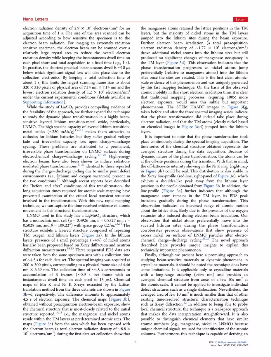
Figure 3. Time-resolved atomic-scale chemical imaging study of the phase transformation in Li[Li0.2Ni0.2Mn0.6]O2 (LNMO). (a) Projected LNMOstructure in [010] direction; (b−d) X-ray chemical maps of Mn K (left) and Ni K (right), obtained by using the lattice-translation method fromthree EDS spectral imaging data sets acquired sequentially from the same area (200 × 300 pixels, or 4.46 nm × 6.69 nm) with a collection time of∼4.5 s each; (e) X-ray line-profiles for Mn K (left) and Ni K (right) obtained from chemical maps in (b−d); (f,g) STEM HAADF images of theLNMO before (f) and after (g) the chemical mapping acquisition. LNMO has a monoclinic unit cell (a = 0.4926 nm, b = 0.8527 nm, c = 0.5028 nm,and β = 109.22°) with space group C2/m. Vectors a ⃗ and c ⃗ indicate the a- and c-axis of the unit cell.
Nano Letters Letter
DOI: 10.1021/acs.nanolett.6b00401Nano Lett. XXXX, XXX, XXX−XXX
D
electron radiation density of 2.9 × 10⁷ electrons/nm2 for anacquisition time of 1 s. The size of the area scanned can beadjusted according to how sensitive the specimen is to theelectron beam radiation. For imaging an extremely radiationsensitive specimen, the electron beam can be scanned over arelatively large crystal area to reduce the overall electronradiation density while keeping the instantaneous dwell time oneach pixel short and total acquisition to a fixed time (e.g., 1 s).In practice, the shortest practical instantaneous dwell is ∼10 μsbelow which significant signal loss will take place due to thecollection electronics. By keeping a total collection time ofabout 1 s, this limits the largest scanning frame size to about320 × 320 pixels or physical area of 7.14 nm × 7.14 nm and thelowest electron radiation density of 1.2 × 10⁷ electrons/nm2
under the current experimental conditions (details available inSupporting Information).While the study of LaAlO3 provides compelling evidence of
the feasibility of the approach, we further expand the techniqueto study the dynamic phase transformation in a highly beam-sensitive layered lithium transition-metal oxide, particularly,LNMO. The high specific-capacity of layered lithium transition-metal oxides (∼250 mAh/g)13−15 makes them attractive ascathodes for lithium batteries but they suffer gradual voltagefade and irreversible capacity loss upon charge−dischargecycling. These problems are attributed to a permanent,irreversible phase transformation on LNMO surfaces duringelectrochemical charge−discharge cycling.17−20 High-energyelectron beams have also been shown to induce radiation-mediated phase transformations,21,22 identical to those reportedduring the charge−discharge cycling due to similar point defectenvironments (i.e., lithium and oxygen vacancies) present inthe two conditions.22 Although recent reports have describedthe “before and after” conditions of this transformation, thelong acquisition times required for atomic-scale mapping haveprevented examination of the critical local transient structureinvolved in the transformation. With this new rapid mappingtechnique, we can capture the time-resolved evidence of atomicmovement in this structural transformation.LNMO used in this study has a Li2MnO3 structure, which
has a monoclinic unit cell (a = 0.4926 nm, b = 0.8527 nm, c =0.5028 nm, and β = 109.22°) with space group C2/m.23,24 Thestructure exhibits a layered structure composed of repeatingTM, oxygen, and lithium layers (Figure 3a). In the lithiumlayers, presence of a small percentage (∼4%) of nickel atomshas also been proposed based on X-ray diffraction and neutrondiffraction measurements.14,15 Three sequential EDS data setswere taken from the same specimen area with a collection timeof ∼4.5 s for each data set. The spectral imaging was acquired at200 × 300 pixels, corresponding to a physical frame size of 4.46nm × 6.69 nm. The collection time of ∼4.5 s corresponds toaccumulation of 5 frames (∼0.9 s per frame with aninstantaneous dwell time on each pixel of 15 μs). Chemicalmaps of Mn K and Ni K X-rays extracted by the lattice-translation method from the three data sets are shown in Figure3b−d, respectively. The difference amounts to approximately4.5 s of electron exposure. The chemical maps (Figure 3b),obtained without preacquisition electron-beam exposure, showthe chemical structure that is most-closely related to the initialstructure reported,14,15 i.e., the manganese and nickel atomsreside within the TM layers at predetermined atomic sites. Themaps (Figure 3c) from the area which has been exposed withthe electron beam (a total electron radiation density of ∼8.8 ×10⁷ electrons/nm2) during the first data set collection show that
the manganese atoms retained the lattice positions in the TMlayers, but the majority of nickel atoms in the TM layersjumped into the lithium sites during the beam exposure.Further electron beam irradiation (a total preacquisitionelectron radiation density of ∼1.77 × 10⁸ electrons/nm2)drove additional nickel atoms into the lithium sites but stillproduced no significant changes of manganese occupancy inthe TM layer (Figure 3d). This observation indicates that thephase transformation progresses as nickel atoms jumppreferentially (relative to manganese atoms) into the lithiumsites once the sites are vacated. This is the first clear, atomic-scale evidence of this phenomenon and was uniquely generatedby this fast mapping technique. On the basis of the observedatomic mobility in this short electron irradiation time, it is clearthat traditional mapping processes, requiring 100× moreelectron exposure, would miss this subtle but importantphenomenon. The STEM HAADF images in Figure 3f,g,taken before and after the three spectral imaging series, indicatethat the phase transformation did indeed take place duringelectron radiation, and that the TM atoms (clearly nickel basedon chemical images in Figure 3c,d) jumped into the lithiumlayers.It is important to note that the phase transformation took
place continuously during the spectral imaging acquisition. Thetime-series of the chemical structure obtained represents theaveraged structure during the data acquisition. Because ofdynamic nature of the phase transformation, the atoms can beat the off-site positions during the transition. With that in mind,the off-lattice-site intensity showing in the Ni K map (right-mapin Figure 3b) could be real. This distribution is also visible inthe X-ray line-profile (red-line, right-panel of Figure 3e), whichexhibits a shoulder-like peak away from the lithium layerposition in the profile obtained from Figure 3b. In addition, theline-profile (Figure 3e) further indicates that although themanganese atom remains in the TM layer, its EDS peakbroadens gradually during the phase transformation. Thisobservation indicates an increased range of atomic motionabout the lattice sites, likely due to the presence of the oxygenvacancies also induced during electron-beam irradiation. Ourobservation that nickel atoms preferentially move into thevacated lithium sites during the phase transformationcorroborates previous observations that show presence ofexcess nickel on surfaces of LNMO particles after electro-chemical charge−discharge cycling.25,26 The novel approachdescribed here provides unique insights to explain thistechnically important phenomenon.Finally, although we present here a promising approach to
studying beam-sensitive materials or dynamic phenomena incrystalline materials, it should be noted the technique does havesome limitations. It is applicable only to crystalline materialswith a long-range ordering (>few nm) and provides anaveraged chemical structure from areas of a few 10s nm2 atthe atomic-scale. It cannot be applied to investigate individualdefect structures such as a single dislocation. Nevertheless, theaveraged area of few 10 nm2 is much smaller than that of otherexisting time-resolved structural characterization techniquesuch as X-ray diffraction.12 In addition to being able to probelocal chemical structure, the technique is a real-space approachthat makes the data interpretation straightforward. It is alsopossible to distinguish chemical elements that have similaratomic numbers (e.g., manganese, nickel in LNMO) becauseunique chemical signals are used for identification of the atomiccolumns. Furthermore, this technique is capable of deriving an
Nano Letters Letter
DOI: 10.1021/acs.nanolett.6b00401Nano Lett. XXXX, XXX, XXX−XXX
E

averaged point defect distribution in the crystalline materials forapplications such as determination of dopant sites since thedopants are typically localized to specific and unique siteswithin the crystal so long as the dopant concentration is abovethe EDS detection limit.In summary, our results clearly demonstrate that atomic-scale
chemical imaging can be achieved with an acquisition time ofless than a few seconds using STEM EDS. The techniqueutilizes X-ray localization effect and a lattice-vector translationto derive an averaged atomic-scale chemical structure from acrystal area of few 10 nm2, effectively reducing the acquisitiontime by more than 100×. By applying the technique to thestudy of the phase transformation in a LNMO lithium-ioncathode material, we uniquely revealed a previously unknownstructural transformation mechanism involving the preferredjumping of nickel atoms (relative to manganese atoms) fromthe TM layers to the lithium layers. This development opens upexciting new possibilities for direct, time-resolved atomic-scalemapping of crystal structures and enables unprecedentedinvestigations of atomic-scale behaviors in dynamic materials.
■ ASSOCIATED CONTENT*S Supporting InformationThe Supporting Information is available free of charge on theACS Publications website at DOI: 10.1021/acs.nano-lett.6b00401.
Materials, methods, multislice simulation of electrondensity distribution, and modeling of X-ray count map bya phenomenological model. (PDF)
■ AUTHOR INFORMATIONCorresponding Author*E-mail: [email protected].
Author ContributionsP.L. performed STEM EDS experiments and data analysis/modeling. R.L.Y. and J.M.Z. performed multislice wave functionsimulations. All of authors participated in the discussions of theresults and manuscript revisions.
NotesThe authors declare no competing financial interest.
■ ACKNOWLEDGMENTSSandia National Laboratories is a multiprogram laboratorymanaged and operated by Sandia Corporation, a wholly ownedsubsidiary of Lockheed Martin Corporation, for the U.S.Department of Energy’s National Nuclear Security Admin-istration under contract DE-AC04-94AL85000. We thank Dr.Joseph Michael (Sandia National Laboratories) for criticalreview of the manuscript. Thanks also to Dr. Chong-Min Wang(Pacific Northwest National Laboratory) for providing theLi[Li0.2Ni0.2Mn0.6]O2 sample.
■ REFERENCES(1) Browning, N. D.; Chisholm, M. F.; Pennycook, S. J. Nature 1993,366, 143.(2) Kimoto, K.; Asaka, T.; Nagai, T.; Saito, M.; Matsui, Y.; Ishizuka,K. Nature 2007, 450, 702.(3) Muller, D. A.; Kourkoutis, L. F.; Murfitt, M.; Song, J. H.; Hwang,H. Y.; Silcox, J.; Dellby, N.; Krivanek, O. L. Science 2008, 319, 1073.(4) Allen, L. J.; Findlay, S. D.; Lupini, A. R.; Oxley, M. P.; Pennycook,S. J. Phys. Rev. Lett. 2003, 91, 105503.
(5) Allen, L. J.; D’Alfonso, A. J.; Freitag, B.; Klenov, D. O. MRS Bull.2012, 37, 47−52.(6) Bosman, M.; Keast, V. J.; Garcia-Munoz, J. L.; D’Alfonso, A. J.;Findlay, S. D.; Allen, L. J. Phys. Rev. Lett. 2007, 99, 086102.(7) Watanabe, M.; Kanno, M.; Okunishi, E. JEOL News 2010, 45, 8−15.(8) D’Alfonso, A. J.; Freitag, B.; Klenov, V.; Allen, L. J. Phys. Rev. B:Condens. Matter Mater. Phys. 2010, 81, 100101.(9) Chu, M. W.; Liou, S. C.; Chang, C. P.; Choa, F. S.; Chen, C. H.Phys. Rev. Lett. 2010, 104, 196101.(10) Lu, P.; Zhou, L.; Kramer, M. J.; Smith, D. J. Sci. Rep. 2014, 4,3945.(11) Lu, P.; Romero, E.; Lee, S.; MacManus-Driscoll, J. L.; Jia, Q.Microsc. Microanal. 2014, 20, 1782−1790.(12) Gras, C. H.; Charlot, F.; Gaffet, E.; Bernard, F.; Niepce, J. C.Acta Mater. 1999, 47, 2113−2123.(13) Zhang, X.; Xu, R.; Li, L.; Yu, C.; Ren, Y.; Belharouak, I. J.Electrochem. Soc. 2013, 160, A1079−A1083.(14) Fell, C. R.; Carroll, K. J.; Chi, M.; Meng, Y. S. J. Electrochem. Soc.2010, 157, A1202−A1211.(15) Lu, Z. H.; Beaulieu, L. Y.; Donaberger, R. A.; Thomas, C. L.;Dahn, J. R. J. Electrochem. Soc. 2002, 149, A778−A791.(16) Cowley, J. M. Diffraction Physics, 2nd ed.; Elsevier SciencePublishing: New York, 1984.(17) Gu, M.; Belharouak, I.; Zheng, J. M.; Wu, H. M.; Xiao, J.; Genc,A.; Amine, K.; Thevuthasan, S.; Baer, D. R.; Zhang, J.-G.; Browning, N.D.; Liu, J.; Wang, C. M. ACS Nano 2013, 7, 760−767.(18) Boulineau, A.; Simonin, L.; Colin, J.-F.; Bourbon, C.; Patoux, S.Nano Lett. 2013, 13, 3857−3863.(19) Xu, B.; Fell, C. R.; Chi, M.; Meng, Y. S. Energy Environ. Sci.2011, 4, 2223−2233.(20) Lin, F.; Markus, I. M.; Nordlund, D.; Weng, T.-C.; Asta, M. D.;Xin, H. L.; Doeff, M. M. Nat. Commun. 2014, 5, 3529−3537.(21) Lin, F.; Markus, I. M.; Doeff, M. M.; Xin, H. L. Sci. Rep. 2014, 4,5694.(22) Lu, P.; Yan, P. F.; Romero, E.; Spoerke, E. D.; Zhang, J.-G.;Wang, C.-M. Chem. Mater. 2015, 27, 1375−1380.(23) Strobel, P.; Lambert-Andron, B. J. Solid State Chem. 1988, 75,90.(24) Jarvis, K. A.; Deng, Z. Q.; Allard, L. F.; Manthiram, A.; Ferreira,P. J. Chem. Mater. 2011, 23, 3614−3621.(25) Gu, M.; Belharouak, I.; Genc, A.; Wang, Z. G.; Wang, D. P.;Amine, K.; Gao, F.; Zhou, G. W.; Thevuthasan, S.; Baer, D. R.; et al.Nano Lett. 2012, 12, 5186−5191.(26) Yan, P.; Nie, A.; Zheng, J. M.; Zhou, Y. G.; Lu, D. P.; Zhang, X.F.; Xu, R.; Belharouak, I.; Zu, X. T.; Xiao, J.; et al. Nano Lett. 2015, 15,514−522.
Nano Letters Letter
DOI: 10.1021/acs.nanolett.6b00401Nano Lett. XXXX, XXX, XXX−XXX
F