epitaxial graphene on single domain 3c-sic(100) thin films grown on off-axis si(100)
TRANSCRIPT

Epitaxial graphene on single domain 3C-SiC(100) thin films grown on off-axis Si(100)A. Ouerghi, A. Balan, C. Castelli, M. Picher, R. Belkhou et al. Citation: Appl. Phys. Lett. 101, 021603 (2012); doi: 10.1063/1.4734396 View online: http://dx.doi.org/10.1063/1.4734396 View Table of Contents: http://apl.aip.org/resource/1/APPLAB/v101/i2 Published by the American Institute of Physics. Related ArticlesAnisotropic surface properties of micro/nanostructured a-C:H:F thin films with self-assembly applications J. Appl. Phys. 111, 124323 (2012) Silicon layer intercalation of centimeter-scale, epitaxially grown monolayer graphene on Ru(0001) Appl. Phys. Lett. 100, 093101 (2012) Synthesis of zinc fulleride (ZnxC60) thin films with ultra-low thermal conductivity J. Appl. Phys. 110, 124320 (2011) Amorphous interface layer in thin graphite films grown on the carbon face of SiC Appl. Phys. Lett. 99, 101904 (2011) Structure of few-layer epitaxial graphene on 6H-SiC(0001) at atomic resolution Appl. Phys. Lett. 97, 201905 (2010) Additional information on Appl. Phys. Lett.Journal Homepage: http://apl.aip.org/ Journal Information: http://apl.aip.org/about/about_the_journal Top downloads: http://apl.aip.org/features/most_downloaded Information for Authors: http://apl.aip.org/authors

Epitaxial graphene on single domain 3C-SiC(100) thin films grown on off-axisSi(100)
A. Ouerghi,1 A. Balan,2 C. Castelli,2 M. Picher,1 R. Belkhou,3 M. Eddrief,4 M. G. Silly,3
M. Marangolo,4 A. Shukla,2 and F. Sirotti31Laboratoire de Photonique et de Nanostructures (LPN-CNRS), Route de Nozay, 91460 Marcoussis, France2Universite Pierre et Marie Curie (CNRS–IMPMC), 4 Pl. Jussieu, 75005 Paris, France3Synchrotron-SOLEIL, Saint-Aubin, BP48, F91192 Gif sur Yvette Cedex, France4Institut des NanoSciences de Paris, UPMC, CNRS UMR 7588, 4 Place Jussieu, 75252 Paris Cedex 5, France
(Received 21 May 2012; accepted 22 June 2012; published online 11 July 2012)
The current process of growing graphene by thermal decomposition of 3C-SiC(100) on silicon is
technologically attractive. Here, we study epitaxial graphene on single domain 3C-SiC films on
off-axis Si(100). The structural and electronic properties of such graphene layers are explored by
atomic force microscopy, x-ray photoelectron spectroscopy, and Raman spectroscopy. Using low
energy electron diffraction, we show that graphene exhibits single planar domains. Near-edge x-ray
absorption fine structure is used to characterize the sample, which confirms that the graphene
layers present sp2 hybridization and are homogeneously parallel to the substrate surface. VC 2012American Institute of Physics. [http://dx.doi.org/10.1063/1.4734396]
Graphene ranks highly as a promising material for future
nanoelectronics devices because of its exceptional electron
transport properties. It appears as a material of choice for
future electronic and optical applications, including conven-
tional components such as high frequency analog devices, as
well as devices in emerging fields such as spintronics, tera-
hertz oscillators, and single-molecule gas sensors.1,2
Conventional techniques, such as the micromechanical exfo-
liation of isolated graphene from bulk graphite2 or alterna-
tively the graphitization of bulk SiC have been developed.
This method is up to now the most promising but still suffers
very high production costs limiting industrial approaches.3,4
Concurrently, chemical vapor deposition (CVD) on metal
substrates has lately received much attention, due to low cost
and easiness of development aspects.5 Unfortunately, growth
on metals suffers from the disadvantage that electronic appli-
cations require graphene on an insulating substrate, and
although wafer-scale transfer is possible, it is a difficult pro-
cess.6 Developing graphene synthesis methods on silicon
substrates, compatible with silicon mass production indus-
tries, and conventional electronics could enable drastic
reduction of production cost and make graphene more rele-
vant nanoelectronics technologies. In order to address this
issue, the heteroepitaxy of cubic polytype (3C-SiC) on larger
diameter (600) silicon wafers was proposed.7–9 Nevertheless
high-quality growth of 3C-SiC epilayers remains delicate,
especially for (111) and (001) oriented films with high resid-
ual stress generating considerable bowing and possible film
cracking.10 Efforts are on to overcome these problems and
get a better insight in the defect generation during the growth
mechanism, making 3C-SiC(111)/Si heteroepilayers a suita-
ble template of great interest for graphene elaboration. Epi-
taxial graphene on 3C-SiC(100) has been recently
demonstrated11–13 with electronic properties similar to those
of epitaxial graphene on 6H-SiC bulk, including the massless
Dirac like energy dispersion relation for electrons. The
investigation of graphene on 3C-SiC thin films on silicon
wafers is especially important in order to decrease the cost
and to go towards large-scale applications. However, the 3C-
SiC(100) heteroepitaxial on-axis Si substrates exhibit a high
density of interfacial twins and antiphase domain (APD)
boundaries.12,13 In this context, the ability to obtain mono
domains of 3C-SiC is of prime importance for producing
large area graphene on 3C-SiC/Si. In our study we have
developed an original recipe for graphene growth based on
the use of 3C-SiC thin films directly grown on off-axis
Si(100). The APD boundaries are suppressed in the heteroe-
pitaxial off-axis substrate (vicinal), showing the single-
crystal nature of the 3C-SiC thin films.14
In this letter, we have studied the epitaxial graphene on
heteroepitaxial 3C-SiC(100) on off-axis Si(100) substrates
(henceforward noted 3C-SiC(100)/off-axis Si, with the axis
4� off toward h110i). The SiC thin films developed in this
study have no APD boundaries, i.e., the crystalline domains
have the same stacking on large scales. The graphene layer
is grown by thermal annealing of the sample at furnace pres-
sure, which is important for controlling the quality of the
layer. A detailed analysis of the synthesized graphene layers
was performed, including atomic force microscopy (AFM),
x-ray photoelectron spectroscopy (XPS), micro-Raman spec-
troscopy, and micro-Raman mapping. Additionally elec-
tronic characterization of graphene layers was performed
using near-edge x-ray absorption fine structure spectroscopy
(NEXAFS).
The 3C-SiC(100)/off-axis Si substrates were first studied
using dark-field low-energy electron microscopy (DF-
LEEM). In the LEEM instrument (Elmitec GmBH - LEEM
III), the electron gun and sample were biased at 20 kV. The
bias difference between the electron gun and sample is the
start voltage VST and eVST is roughly equal to the primary
electron-beam energy. The DF-LEEM images have been
obtained by selecting the corresponding low energy electron
diffraction (LEED) spots via an aperture (contrast aperture)
placed on the optical path of the microscope column.
Epitaxial graphene on unpolished 3C-SiC(001)/off-axis
Si substrates was grown in semi vacuum (10�5 Torr) by
0003-6951/2012/101(2)/021603/5/$30.00 VC 2012 American Institute of Physics101, 021603-1
APPLIED PHYSICS LETTERS 101, 021603 (2012)
electron-bombardment heating at 1300 �C. Substrates were
first degassed for several hours at 600 �C under UHV condi-
tions and then annealed under a (1 ML/min) Si flux to remove
the native oxide. Though the annealing temperatures are gen-
erally higher on 3C-SiC(111) (Refs. 7 and 8) similar prepara-
tion procedures were applied. The sequence of surface
reconstructions in the two cases however is completely differ-
ent. XPS and NEXAFS experiments were performed in ultra
high vacuum conditions at TEMPO beamline at the SOLEIL
Synchrotron facility (France).8 Raman spectroscopy was per-
formed at room temperature with a Renishaw spectrometer
using 514 nm laser light focused on the sample by a DMLM
Leica microscope with a 50� (NA¼ 0.75) objective.
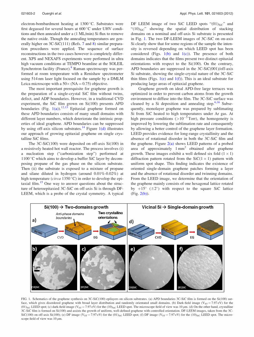
The most important prerequisite for graphene growth is
the preparation of a single-crystal SiC film without twins,
defect, and ADP boundaries. However, in a traditional CVD
experiment, the SiC film grown on Si(100) presents APD
boundaries (Fig. 1(a)).12,13 Epitaxial graphene formed on
these APD boundaries consists of many small domains with
different layer numbers, which deteriorate the intrinsic prop-
erties of ideal graphene. APD boundaries can be suppressed
by using off-axis silicon substrates.14 Figure 1(d) illustrates
our approach of growing epitaxial graphene on single crys-
talline SiC films.
The 3C-SiC(100) were deposited on off-axis Si(100) in
a resistively heated hot wall reactor. The process involves (i)
a nucleation step (“carbonization step”) performed at
1100 �C which aims to develop a buffer SiC layer by decom-
posing propane of the gas phase on the silicon substrate.
Then (ii) the substrate is exposed to a mixture of propane
and silane diluted in hydrogen (around 0.01%-0.02%) at
high temperature (circa 1350 �C) in order to develop the epi-
taxial film.15 One way to answer questions about the struc-
ture of heteroepitaxied 3C-SiC on off-axis Si is through DF-
LEEM, which is a probe of the crystal symmetry. A typical
DF LEEM image of two SiC LEED spots “(01)SiC” and
“(10)SiC” showing the spatial distribution of stacking
domains on a nominal and off-axis Si substrate is presented
in Fig. 1. The two DF-LEEM images of 3C-SiC on on-axis
Si clearly show that for some regions of the sample the inten-
sity is reversed depending on which LEED spot has been
considered (Figs. 1(b) and 1(c)). The presence of both
domains indicates that the films present two distinct epitaxial
orientations with respect to the Si(100). On the contrary,
APD boundaries are suppressed in the 3C-SiC(001)/off-axis
Si substrate, showing the single-crystal nature of the 3C-SiC
thin films (Figs. 1(e) and 1(f)). This is an ideal substrate for
producing large areas of epitaxial graphene.
Graphene growth on ideal APD-free large terraces was
optimized in order to prevent carbon atoms from the growth
environment to diffuse into the film. The 3C-SiC surface was
cleaned by a Si deposition and annealing step.6,16 Subse-
quently, monolayer graphene was prepared by sublimating
Si from SiC heated to high temperatures under Ar gas. At
high pressure conditions (>10�5 Torr), the homogeneity is
improved by lowering the sublimation rate and consequently
by allowing a better control of the graphene layer formation.
LEED provides evidence for long-range crystallinity and the
absence of rotational disorder in both the 3C-SiC film and
the graphene. Figure 2(a) shows LEED patterns of a probed
area of approximately 1 mm2 obtained after graphene
growth. These images exhibit a well defined six fold (1� 1)
diffraction pattern rotated from the SiC(1� 1) pattern with
uniform spot shape. This finding indicates the existence of
oriented single-domain graphene patches forming a layer
and the absence of rotational disorder and twinning domains.
From the LEED image, we determine that the orientation of
the graphene mainly consists of one hexagonal lattice rotated
by þ15� (62�) with respect to the square SiC lattice
(Fig. 2(b)).
FIG. 1. Schematics of the graphene synthesis on 3C-SiC(100) epilayers on silicon substrates. (a) APD boundaries 3C-SiC film is formed on the Si(100) sur-
face, which gives disordered graphene with broad layer distribution and randomly orientated small domains. (b) Dark-field image (VST¼ 7.97 eV) for the
(01)SiC LEED spot; (c) dark-field image (VST¼ 7.97 eV) for the (10)SiC LEED spot. The microscope field of view was 10 lm. (d) On the other hand, crystalline
3C-SiC film is formed on Si(100) and assists the growth of uniform, well-defined graphene with controlled orientation. DF-LEEM images, taken from the 3C-
SiC(100) on off-axis Si(100); (e) DF image (VST¼ 7.97 eV) for the (01)SiC LEED spot; (f) DF image (VST¼ 7.97 eV) for the (10)SiC LEED spot. The micro-
scope field of view was 10 lm.
021603-2 Ouerghi et al. Appl. Phys. Lett. 101, 021603 (2012)

In order to assess the morphology of the graphene layer,
AFM was performed in the tapping mode. Figures 2(c) and
2(d) show typical AFM images of this graphene. No pits and
anti-phase domain boundaries are seen. A characteristic fea-
ture of this sample was the appearance of terraces along the
h110i silicon direction. The surface consists of atomically
flat terraces with 600 nm widths separated by steps with mul-
tiple unit cell heights (1–2 nm). Terrace widening probably
resulted from the step formation induced by the step bunch-
ing of the epilayers in 3C-SiC(100)/off-axis Si. For compari-
son, growth of graphene on on-axis 3C-SiC(100) was
attempted using the method described in Ref. 13. The result-
ing surface morphology is shown in Fig. 2(d). This is charac-
terized by large terraces presenting height density of the
boundaries. The boundaries between the terraces (shown by
a few white arrows) of the sample can be correlated with the
ADP boundaries of the twofold symmetry of the 3C-
SiC(100).13 We thus establish that the graphene terraces are
bordered by the domains of the substrate. In our case, the
presence of argon molecules hinders the sublimation of
silicon atoms away from the 3C-SiC surface, reducing the
overall sublimation rate and allowing an increase in graphiti-
zation temperature and provides a smooth decomposition of
the SiC.3 Another advantage of the high pressure growth
conditions is to allow higher growth temperatures, which are
favorable to the carbon atoms diffusion rate and thus to the
rearrangement processes occurring during graphene forma-
tion. This leads to a better crystalline quality of the layer.
To further characterize the graphene layer, we used
scanning Micro-Raman spectroscopy (Fig. 3). We used a
laser with 514 nm wavelength as excitation. The Raman
spectra present three peaks at 1350, 1594, and 2718 cm�1,
which are attributed to the D, G, and 2D bands, respectively.
The presence of a single G and 2D bands indicates that our
graphene consists of a sp2 reorganization. The 2D peak
(overtone of the zone-boundary A1g phonon) at 2718 cm�1
originates from a two-phonon resonant process. In some
areas of the sample the 2D peak has a full-width-half-max-
ima (FWHM) of 60 cm�1 (Fig. 3(a), blue curve), but in the
majority areas of the sample it has a width around 90 cm�1
(Fig. 3(b), red curve) and a symmetrical shape, correspond-
ing to a bilayer.16 The observed D band is mostly the result
of a structural disorder and a high density of defects such as
domain boundaries, vacancies, and distortions.13,15 Both the
large width of the Raman lines and the D line intensity sug-
gest that defects are present in the graphene layer.
Compared with that on exfoliated graphene, the signifi-
cant blueshifts of the G-band (14 cm�1) and 2D-band
(38 cm�1) indicate that the epitaxial graphene is either com-
pressively strain during the cool down procedure or n-doped
by the substrate,16,17 as in graphene grown on single-
crystalline hexagonal 6H-SiC and 3C-SiC(111) on sili-
con.16,18,19 The influence of the charge has been studied by
Das et al.17 They observe an upshift of the G-peak frequency
by as much as 20 cm�1 when the graphene layer is doped
with electrons with a density of 4� 1013 cm�2. It is shown
that the dependence of doping on shift in the 2D-band is
very weak. It is roughly 10%-30% compared to that of G-
band (3 and 5 cm�1).17 Therefore, the 38 cm�1 2D-band shift
is too large to be achieved by electron/hole doping. If we
assume that the mismatch between the graphene and the sub-
strate is completely relaxed at the growth temperature a
FIG. 2. (a) LEED image (E¼ 130 eV) of epitaxial graphene on
3C-SiC(100)/off-axis Si showing the diffraction spots due to the SiC(100)
substrate and the graphene lattice; (b) the crystallographic axes of the cubic
substrate and graphene layer are determined from the LEED; (c) AFM image
of epitaxial graphene on 3C-SiC(100)/off-axis Si; (d) AFM image of gra-
phene on 3C-SiC(100)/on-axis Si (the white arrows show the ADP).
FIG. 3. Micro-Raman characterization of graphene and Raman mapping
images of 2D band. (a) Raman spectra taken on the epitaxial graphene
layers—red: bilayer, blue: monolayer; (b) false color 2D peak position car-
tography; (c) false color 2D peak FWHM cartography; (d) distribution of the
2D peak position; (e) 2D peak FWHM; the bar height indicates the percent-
age of the total points which had the position (respectively FWHM) in the
1 cm�1 (respectively 2 cm�1) range around the bar.
021603-3 Ouerghi et al. Appl. Phys. Lett. 101, 021603 (2012)

residual compressive strain should arise during sample cool-
ing to room temperature because of the large difference in
the coefficients of linear thermal expansion between gra-
phene and SiC. The strain in our layer can be deduced
(though we cannot exclude doping effects) at room tempera-
ture from the Raman shift of the 2D bands (38 cm�1). It is
close to 0.25%, which is in good agreement with the previ-
ously reported results of epitaxial graphene on SiC bulk.18
Since our aim is to investigate the homogeneity of this layer
we have performed large-area Raman-mapping. Figure 3(c)
maps in false color the position of the 2D peak collected in
points uniformly spaced over an area of 20� 20 lm2. Figure
3(d) presents the FWHM of the 2D peak as computed from
Lorentzian fits of the measured signal on the same surface.
Figure 3(b) presents the distribution of the positions (in red)
and FWHM (in blue) of the measured 2D peaks over the sur-
face. We can see that the position of the 2D peak has a very
tight distribution around 2718 cm�1, with 95% of the data
collected between 2714 and 2718 cm�1. The same for the
FWHM which is centered around 87 cm�1, as 95% of the
points have a width between 80 and 93 cm�1. Our Raman
and LEED results suggest that the considerably higher
annealing temperature and Ar flux appear to be the key fac-
tors for obtaining a large homogenous graphene layer. Ho-
mogenous sample desorption of Si, high diffusion of carbon,
and low nucleation rate may thus be of importance for
obtaining high quality graphene layers on 3C-SiC(100).
Synchrotron radiation based core-level spectroscopy
shows the dependence of the synthesis process on the three
annealing temperatures (1150 �C, 1200 �C, and 1250 �C).
The evolution of the C 1s spectra upon graphitization taken
at a photon energy of 340 eV is shown in Fig. 4(a). The C 1speak at 284.5 eV attributed to graphene appears clearly at
1200 �C. For higher temperature and longer annealing time,
this graphene peak intensity increases. At the C 1 core-level,
we can determine the average graphene film thicknesses by
measuring the attenuation of the SiC contribution (282.8 eV)
with respect to the graphene signal (284.5 eV).13 The synthe-
sis of an epitaxial graphene layer is supported by the follow-
ing observations: (i) the attenuation of the SiC component,
(ii) the C 1s peak position at 284.5 eV which confirms the
exclusive presence of sp2 hybridized C–C bonds, (iii) the
pronounced asymmetrical shape of the peak which confirms
the conductive state of carbon.
Typical C 1s spectra collected from the 1.5 monolayer
graphene sample at different photon energies (340 and
510 eV) are displayed in the inset of Fig. 4(a). It is interest-
ing to point out that after a single layer of graphene has
developed the bulk SiC signal disappears in the C 1s spec-
trum collected at the photon energy of 340 eV. When
increasing the incident energy, the lineshape and the position
of the graphene peak remain unaffected. This confirms the
absence of an interfacial graphitic layer covalently bound to
the 3C-SiC(100).11,12
In contrast to epitaxial graphene on SiC(111), where
three components can be observed (graphene, SiC, and inter-
face layer contributions), only two components can be
resolved on 3C-SiC(100).11 The SiC bulk component
appears at 282.8 eV binding energy and the graphene related
component at 284.5 eV. In the case of graphene on 3C-
SiC(111), covalent bonding gives rise to one surface related
component in the buffer layer, which remain unperturbed
during the graphene growth.
To determine the electronic properties of the carbon
overlayer on SiC, we studied its unoccupied electronic states
using NEXAFS spectroscopy. Figure 4(b) shows the C 1sNEXAFS spectra taken on the epitaxial graphene as a func-
tion of the angle h between the wavevector of the photoelec-
tron and the normal surface. The two sharp peaks at
285.5 eV and at 292 eV correspond to the 1s-p* excitations
at the K and M points and to the 1s-r* orbitals at the C point
of the Brillouin zone, respectively. Their in-plane and out-
of-plane characters are confirmed by the dependence from
the polarization of the incident photons. More specifically,
when the light polarization is in-plane, only the in-plane r*
states at 292 eV contribute to the C 1s edge, while when the
out of plane polarization component increases, the intensity
of the p* feature at 285 eV strongly increases.12,20 Note that,
in addition to these main features, other peaks are observed,
likely due to the substrate, as observed from a direct
FIG. 4. (a) Evolution of the C1s spectra upon
graphitization taken at a photon energy of
340 eV. Insert, C1s XPS spectra of graphene on
3C-SiC(100) films at different photon energies,
(b) carbon K-edge NEXAFS spectra of the gra-
phene layers on 3C-SiC(100) films, measured at
various incidence angles of x-rays. Peaks at
285.5 eV and 291.4 eV are assigned to 1s!p*
and 1s! r* transitions, respectively.
021603-4 Ouerghi et al. Appl. Phys. Lett. 101, 021603 (2012)

comparison with the absorption spectra of SiC.21 These
NEXAFS spectra confirm that the graphene layers present
sp2 hybridization and are homogeneously parallel to the sub-
strate surface. We focus on the peak detected at 286.5 eV
that can be clearly distinguished in the NEXAFS spectra. In
the past, different mechanisms have been cited as the origin
of this peak: (i) interaction with the underlying substrate, (ii)
disorder and edge states arising from the finite size domains
of graphene,22 (iii) predicted interlayer state,23 (iv) oxygen
contamination.24 However, our surface treatment has
removed oxygen contamination, as shown on our XPS O-1s
spectrum, which excludes the last hypothesis.
In conclusion, we report growth of epitaxial graphene
on 3C-SiC(100)/off-axis Si substrates. We have used investi-
gative techniques like LEED, NEXAFS, and Raman map-
ping to gauge the quality of graphene on 3C-SiC(100)/off-
axis Si substrates. These provide interesting information like
the modification in morphology due to the change in sub-
strate and the corresponding disappearance of anti-phase
boundaries. The Raman data indicate that problems remain,
like considerable intensity in the defect peak and broad
peak-width. Polarized NEXAFS provides proof of planar
growth and sp2 hybridization and the important fact that no
interface layer exists, excluding strong interaction with the
substrate. Further optimization of the growth process to
obtain more graphene monolayer coverage and better quality
should be possible by among other possibilities, controlling
the H2 etching treatments and the surface quality of the 3C-
SiC substrates.
We are grateful to A. Michon and M. Portail (CRHEA-
CNRS, Sophia Antipolis, France) for fruitful discussions and
providing 3C-SiC(001) on off-axis silicon, D. Martinotti for
his outstanding efforts and the technical assistance during
the LEEM experiments at the CEA/IRAMIS/SPCSI labora-
tory, and Olivier Beyssac for access to the Renishaw Raman
setup.
1K. S. Novoselov, A. K. Geim, S. V. Morozov, D. Jiang, M. I. Katsnelson,
I. V. Grigorieva, S. V. Dubonos, and A. A. Firsov, Nature (London) 438,
197 (2005).2K. S. Novoselov, Z. Jiang, Y. Zhang, S. V. Morozov, H. L. Stormer; U.
Zeitler, J. C. Maan, G. S. Boebinger, P. Kim, and A. K. Geim, Science
315, 1379 (2007).
3K. V. Emtsev, A. Bostwick, K. Horn, J. Jobst, G. L. Kellogg, L. Ley, J. L.
McChesney, T. Ohta, S. A. Reshanov, J. Rohrl, E. Rotenberg, A. K.
Schmid, D. Waldmann, H. B.Weber, and T. Seyller, Nat. Mater. 8, 203
(2009).4A. Ouerghi, M. G. Silly, M. Marangolo, C. Mathieu, M. Eddrief, M. Picher,
F. Sirotti, S. El Moussaoui, and R. Belkhou, ACS Nano (to be published).5A. Reina, X. Jia, J. Ho, D. Nezich, H. Son, V. Bulovic, M. S. Dresselhaus,
and J. Kong, Nano Lett. 9, 30 (2009).6C. Berger, Z. M. Song, X. B. Li, X. S. Wu, N. Brown, C. Naud, D. Mayo,
T. B. Li, J. Hass, A. N. Marchenkov, E. H. Conrad, P. N. First, and W. A.
de Heer, Science 312, 1191 (2006).7A. Ouerghi, R. Belkhou, M. Marangolo, M. G. Silly, S. El Moussaoui, M.
Eddrief, L. Largeau, M. Portail, and F. Sirotti, Appl. Phys. Lett. 97,
161905 (2010).8A. Ouerghi, M. Marangolo, R. Belkhou, S. El Moussaoui, M. G. Silly, M.
Eddrief, L. Largeau, M. Portail, B. Fain, and F. Sirotti, Phys. Rev. B 82,
125445 (2010).9M. Suemitsu and H. Fukidome, J. Phys. D: Appl. Phys. 43, 374012 (2010).
10H. P. Liaw and R. F. Davis, J. Electrochem. Soc. 132, 642 (1985).11C. Coletti, K. V. Emtsev, A. A. Zakharov, T. Ouisse, D. Chaussende, and
U. Starke, Appl. Phys. Lett. 99, 081904 (2011).12V. Y. Aristov, G. Urbanik, K. Kummer, D. V. Vyalikh, O. V. Molodtsova,
A. B. Preobrajenski, A. A. Zakharov, C. Hess, T. Hanke, B. Buchner, I.
Vobornik, J. Fujii, G. Panaccione, Y. A. Ossipyan, and M. Knupfer, Nano
Lett. 10, 992 (2010).13A. Ouerghi, M. Ridene, A. Balan, R. Belkhou, A. Barbier, N. Gogneau, M.
Portail, A. Michon, S. Latil, P. Jegou, and A. Shukla, Phys. Rev. B 83,
205429 (2011).14A. Powell, L. G. Matus, and M. A. Kuczmarski, C. M. Chorey, T. T.
Cheng, and P. Pirouz, Appl. Phys. Lett. 51, 823 (1987).15M. Portail, A. Michon, S. Vezian, D. Lefebvre, S. Chenot, E. Roudon, M.
Zielinski, T. Chassagne, A. Tiberj, J. Camassel, and Y. Cordier, J. Cryst.
Growth 349, 27–35 (2012).16Z. H. Ni, W. Chen, X. F. Fan, J. L. Kuo, T. Yu, A. T. S. Wee, and Z. X.
Shen, Phys. Rev. B 77, 115416 (2008).17A. Das, S. Pisana, B. Chakraborty, S. Piscanec, S. K. Saha, U. V. Wagh-
mare, K. S. Novoselov, H. R. Krishnamurthy, A. K. Geim, A. C. Ferrari,
and A. K. Sood, Nat. Nanotechnol. 3, 210 (2008).18N. Ferralis, R. Maboudian, and C. Carraro, Phys. Rev. Lett. 101, 156801
(2008).19A. Ouerghi, A. Kahouli, D. Lucot, M. Portail, L. Travers, J. Gierak, J.
Penuelas, P. Jegou, A. Shukla, T. Chassagne, and M. Zielinski, Appl.
Phys. Lett. 96, 191910 (2010).20D. A. Fischer, R. M. Wentzcovitch, R. G. Carr, A. Continenza, and A. J.
Freeman, Phys. Rev. B 44, 1427 (1991).21M. Pedio, A. Giglia, N. Mahne, S. Nannarone, S. Giovannini, C. Cepek, F.
Boscherini, R. Carboni, M. Benfatto, and S. D. Longa, Phys. Scr. T115,
308 (2005).22J. A. Brandesa, G. D. Codyb, D. Rumbleb, P. Haberstrohc, S. Wirickd, and
Y. Gelinase, Carbon 46, 1424 (2008).23R. A. Rosenberg, P. J. Love, and V. Rehn, Phys. Rev. B 33, 4034 (1986).24H.-K. Jeong, H. J. Noh, J. Y. Kim, L. Colakerol, P. A. Glans, M. H. Jin, K.
E. Smith, and Y. H. Lee, Phys. Rev. Lett. 102, 099701 (2009).
021603-5 Ouerghi et al. Appl. Phys. Lett. 101, 021603 (2012)