enhancing performance of analog mixed signal circuits using
TRANSCRIPT

Enhancing Performance of Analog Mixed Signal Circuits using Integrated Silicon-Photonics
by
Nandish Mehta
A dissertation submitted in partial satisfaction of the
requirements for the degree of
Doctor of Philosophy
in
Engineering - Electrical Engineering and Computer Science
in the
Graduate Division
of the
University of California, Berkeley
Committee in charge:
Professor Vladimir Stojanovic, ChairProfessor Eli Yablonovitch
Professor Jie Yao
Fall 2019

Enhancing Performance of Analog Mixed Signal Circuits using Integrated Silicon-Photonics
Copyright 2019by
Nandish Mehta

Abstract
Enhancing Performance of Analog Mixed Signal Circuits using Integrated Silicon-Photonics
by
Nandish MehtaDoctor of Philosophy in Engineering - Electrical Engineering and Computer Science
University of California, BerkeleyProfessor Vladimir Stojanovic, Chair
Silicon-photonics (SiPh) has emerged as a viable solution to handle exponentially growingdata traffic in today’s data centers. It transfers data faster and over a distance longer thanthat possible with traditional electronics, while leveraging efficiency and cost benefits of ex-isting high-volume CMOS manufacturing infrastructure. As the SiPh platforms mature, newhigh-performance photonics blocks integrated close to CMOS transistors are made available.By moving certain functionality to these optical blocks, the performance of conventionalanalog mixed-signal circuits can be improved to enable exciting new integrated applicationslike LiDAR, biosensing, high-performance computing, etc.
This thesis demonstrates an optical SiPh link with a reduced laser power requirementand an optically sampled analog-to-digital converter. Both of these systems benefit from theavailability of integrated SiPh blocks next to CMOS transistors. The laser power used bya SiPh link can be reduced by improving the optical receiver (Rx) sensitivity and reducingthe optical path loss. To improve the Rx sensitivity, a differential detector is monolithicallyintegrated with the low-noise CMOS analog frontend (AFE), while the optical path loss isreduced by adopting a laser-forwarded architecture. The differential detector enables thefully differential operation of AFE to suppress power supply and common-mode noise. Mea-surement and performance comparison of two variants of differential detector implementedon two test-chips is presented. The proposed microring resonator differential detector en-ables the receiver to achieve a record OMA sensitivity of -18 dBm at 12 Gb/s. Modelingand characterization of this detector are also covered in this thesis. Further, a coherentlaser-forwarded binary-phase-shift-keying (BPSK) link at 10 Gb/s is shown with all the re-quired photonic blocks, like phase modulator, 3-dB coupler, and balanced detectors, fullyintegrated into a monolithic zero-change 45nm SOI CMOS. This link operates with 3 dB lesslaser power than state-of-the-art NRZ monolithic SiPh links.
Lastly, the performance of conventional CMOS ADCs is often limited by sampling clock-jitter, input sampling bandwidth, and routing of input and clock to the sub-ADCs. Toovercome these limitations, this thesis demonstrates an optically sampled ADC that moves
1

the sampling function to the optical domain where ultra low-jitter (<10 fsrms) optical pulsesfrom a mode-locked laser sample an RF input signal with very high sampling bandwidth. AnADC prototype, realized in a 3D integrated silicon-photonic platform, achieves 37 dB SNDR(6b ENOB) for 45GHz input with <36fs estimated sampling jitter. Circuit techniques usedfor overcoming issues like single-ended to differential conversion and cross-talk are describedin detail.
2

Contents
Contents i
List of Figures iii
List of Tables viii
1 Introduction 11.1 Research Goal and Contributions . . . . . . . . . . . . . . . . . . . . . . . . 31.2 Thesis Organization . . . . . . . . . . . . . . . . . . . . . . . . . . . . . . . . 4
2 Monolithic Silicon-Photonic link using Microring Resonators 62.1 Microring resonators (MRR) . . . . . . . . . . . . . . . . . . . . . . . . . . . 82.2 MRR-based monolithic SiPh Optical links . . . . . . . . . . . . . . . . . . . 92.3 Problem of high power consumed by the laser source . . . . . . . . . . . . . 112.4 Monolithic Silicon-Photonics platform in 45nm SOI CMOS . . . . . . . . . . 13
3 High-Sensitivity Differential Optical Receiver 193.1 Review of high-sensitivity optical Rx . . . . . . . . . . . . . . . . . . . . . . 203.2 Sensitivity of a conventional single-ended (SE) optical Rx . . . . . . . . . . . 213.3 Noise Analysis of a Shunt-feedback (SF) TIA . . . . . . . . . . . . . . . . . . 243.4 Proposed fully differential (FD) optical Rx . . . . . . . . . . . . . . . . . . . 253.5 Version-1: Differential detector using a 3 dB coupler . . . . . . . . . . . . . . 303.6 Version-2: Split-Microring Resonant SiGe Photodetector . . . . . . . . . . . 323.7 Circuit Implementation . . . . . . . . . . . . . . . . . . . . . . . . . . . . . . 403.8 Realization and Experiments . . . . . . . . . . . . . . . . . . . . . . . . . . . 443.9 Summary . . . . . . . . . . . . . . . . . . . . . . . . . . . . . . . . . . . . . 56
4 Demonstration of a Laser-forwarded Coherent Optical Link 584.1 Coherent Link for Short-reach Optical I/O . . . . . . . . . . . . . . . . . . . 584.2 Principle of Coherent Balanced Detection . . . . . . . . . . . . . . . . . . . . 604.3 Laser-forwarded (LF) Coherent Link Architecture . . . . . . . . . . . . . . . 614.4 Optical Blocks in Monolithic Si-Ph platform . . . . . . . . . . . . . . . . . . 644.5 Transceiver Implementation . . . . . . . . . . . . . . . . . . . . . . . . . . . 67
i

CONTENTS ii
4.6 Realization and Experiment Results . . . . . . . . . . . . . . . . . . . . . . . 704.7 Summary . . . . . . . . . . . . . . . . . . . . . . . . . . . . . . . . . . . . . 76
5 Optically Sampled ADC: Architecture and Circuit Implementation 785.1 Performance Limitation of Conventional CMOS ADCs . . . . . . . . . . . . 785.2 Sampling an Electrical Signal using Optical Pulses . . . . . . . . . . . . . . . 835.3 Architecture of O-ADC . . . . . . . . . . . . . . . . . . . . . . . . . . . . . . 865.4 Comments on modulator and modulator driver . . . . . . . . . . . . . . . . . 955.5 Limitations and Tradeoffs of O-ADC building blocks . . . . . . . . . . . . . 985.6 Circuit Implementation . . . . . . . . . . . . . . . . . . . . . . . . . . . . . . 1015.7 Summary and Discussion . . . . . . . . . . . . . . . . . . . . . . . . . . . . . 106
6 Realization and Measurement of O-ADC chip 1086.1 Heterogeneous 3D Integration of CMOS and Silicon-Photonics at wafer-scale 1086.2 Optical Blocks . . . . . . . . . . . . . . . . . . . . . . . . . . . . . . . . . . . 1106.3 Test-chip packaging and fiber coupling . . . . . . . . . . . . . . . . . . . . . 1146.4 Test bench . . . . . . . . . . . . . . . . . . . . . . . . . . . . . . . . . . . . . 1156.5 Measurement Results . . . . . . . . . . . . . . . . . . . . . . . . . . . . . . . 1166.6 Summary . . . . . . . . . . . . . . . . . . . . . . . . . . . . . . . . . . . . . 123
7 Conclusion 124
Bibliography 127

List of Figures
1.1 Examples of More-than-Moore scaling: (a) integrating inductors in IC process[4] and the world’s first CMOS radios made using them [5] (b) World’s firstprocessor-memory communication using light [7] (c) Monolithic 3D integratedCMOS imagers [6]. . . . . . . . . . . . . . . . . . . . . . . . . . . . . . . . . . . 2
2.1 (a) Optical transceivers used in a data center racks (b) increase in IP trafficbetween optical transceivers. . . . . . . . . . . . . . . . . . . . . . . . . . . . . . 7
2.2 (a) Evolution of optical I/O technology in the data centers. (b) Switch ASICco-packaged with optics using dense short-reach electrical I/Os. . . . . . . . . . 7
2.3 Microring resonator (MRR) structure, characteristics, and transfer function. . . 82.4 Microring resonator (MRR) based single channel SiPh link [30, 28]. . . . . . . . 102.5 N -way DWDM SiPh optical link realized using MRR. . . . . . . . . . . . . . . . 112.6 Conventional IMDD link with optical path loss. . . . . . . . . . . . . . . . . . . 132.7 Cross section of 45-nm CMOS SOI process for monolithic (single-chip) silicon-
photonics integration [28]. Figure is not drawn to scale. . . . . . . . . . . . . . . 142.8 SF-TIA (a) noise contributors, (b) Bandwidth, and (c) Input-referred integrated
noise . . . . . . . . . . . . . . . . . . . . . . . . . . . . . . . . . . . . . . . . . . 162.9 Chip-on-board (a) before and (b) after substrate release process. . . . . . . . . . 172.10 Steps to release silicon substrate and transfer the released chip onto another glass
substrate. . . . . . . . . . . . . . . . . . . . . . . . . . . . . . . . . . . . . . . . 18
3.1 (a) Structure of a conventional single-ended (SE) optical receiver (Rx). (b) Break-down of various sensitivity components as reported in [53, 54]. . . . . . . . . . . 22
3.2 NRZ signal (a) with only thermal noise, (b) with all noise sources, and (c) in-crease sensitivity to recover BER. (d) Gaussian noise statistics. (e) BER andtransition error probabilities. (f) Effect of all noise sources on BER. Here, in,in= 0.325µArms, iPSN = 2 µA, ioff = 0.1 µA, and imin = 0.1µA. . . . . . . . . . . . 23
3.3 (a) Conventional SE Rx using a dummy TIA, (b) Capacitance at input/outputof SF-TIA (c) Structure of the proposed FD DDR Rx. . . . . . . . . . . . . . . 26
3.4 Effect of noise sources in Table. 3.1 on BER of SE and FD Rx. . . . . . . . . . 273.5 Signal swing at the output of: (a) a conventional SE TIA and a dummy TIA,
and (b) TIA in proposed FD configuration. . . . . . . . . . . . . . . . . . . . . 29
iii

LIST OF FIGURES iv
3.6 Optical and electrical signals in (a) a conventional SE Rx, and (b)FD Rx with a3 dB coupler and differential linear detectors. . . . . . . . . . . . . . . . . . . . 30
3.7 (a) Construction of differential detector using a 3 dB coupler and linear SiGedetectors (b) Micrograph of the Rx test-site showing coupling of light into a 3 dBcoupler. (c) Structure of linear SiGe detector . . . . . . . . . . . . . . . . . . . . 31
3.8 Basic MRR (a) topology and (b) transmission spectrum. . . . . . . . . . . . . . 333.9 (a) Realizing a PD using an MRR (b) 3D layout of an MRR PD. . . . . . . . . 343.10 (a) Equivalent circuit model for an MRR PD and (b) distributed elements in a
P -N spoke. . . . . . . . . . . . . . . . . . . . . . . . . . . . . . . . . . . . . . . 353.11 Micrograph of a test-chip used to model and characterize MRR PDs. . . . . . . 353.12 I-V plots of photodetector (a) log scale and (b) linear scale. (c) Junction capaci-
tance with reverse bias. . . . . . . . . . . . . . . . . . . . . . . . . . . . . . . . . 363.13 (a) Increase in responsivitiy with reverse bias and (b) optical transmission and
responsivity with wavelength. . . . . . . . . . . . . . . . . . . . . . . . . . . . . 373.14 (a) MRR cavity with integrated heater (b) distribution of heater resistance (c)
shift in optical transmission with VHeat. . . . . . . . . . . . . . . . . . . . . . . 383.15 3D layout of the proposed split-MRR resonant photodetector. . . . . . . . . . . 393.16 (a) Concept of a split photodetector and (b) it’s equivalent circuit. . . . . . . . 393.17 Measured optical performance and characterization of a split-MRR resonant pho-
todetector. . . . . . . . . . . . . . . . . . . . . . . . . . . . . . . . . . . . . . . . 413.18 Schematic of proposed FD optical Rx: (a) Version-1 design with 3 dB couple and
linear SiGe detector and (b) Version-2 design using split-MRR detector. . . . . . 423.19 Circuit diagram (a) Shunt-feedback TIA (SF-TIA), (b) Post-amp (GP) with offset
cancellation, and (c) modified StrongARM comparator. . . . . . . . . . . . . . . 423.20 Simulation results of the receiver analog front-end. (a) fT and bias current for
NMOS/PMOS, (b) total input-referred noise PSD, and (c) Comparator input-referred noise trade-off. . . . . . . . . . . . . . . . . . . . . . . . . . . . . . . . . 43
3.21 Digital backend used to characterize receiver performance. . . . . . . . . . . . . 443.22 A typical eye at the input of Rx and equations relating OMA, peak optical power,
and ER. . . . . . . . . . . . . . . . . . . . . . . . . . . . . . . . . . . . . . . . . 453.23 Calibration for variation in split ratio with λ and coupling position. . . . . . . . 463.24 (a) Photomicrograph of test-chip. Size is 3 mm X 3 mm with 73 I/O pads. (b)
Test setup with inset 12 Gb/s external reference modulator eye. . . . . . . . . . 473.25 Measured statistical eye, BER eye, bathtub curves and sensitivity plots for SE
and FD Rxs. . . . . . . . . . . . . . . . . . . . . . . . . . . . . . . . . . . . . . 483.26 Calibration for variation in split ratio with λ and coupling position. . . . . . . . 493.27 (a) Thermal tuning loop and (b) operation of tuning controller used to stabilize
resonant split-photodetector. . . . . . . . . . . . . . . . . . . . . . . . . . . . . . 503.28 Optical test-bench with inset of setup for coupling light into the test-chip and 12
Gb/s modulated input data eye. . . . . . . . . . . . . . . . . . . . . . . . . . . . 533.29 Die micrograph and microscope photo of a fiber coupled test-site. At resonance
the microring glows due to the light trapped inside. . . . . . . . . . . . . . . . . 53

LIST OF FIGURES v
3.30 Measured performance of the optical Rxs for a PRBS31 input pattern. For (a)-(e)input optical power of 0 dBm and ER of 13.2 dB is used. . . . . . . . . . . . . . 54
4.1 (a) Direct detection and (b) Coherent balanced detection. . . . . . . . . . . . . 604.2 An MRR-based LF coherent link concept [19]. . . . . . . . . . . . . . . . . . . . 624.3 (a) BER vs. laser power. and (b) Impact of path length mismatch. . . . . . . . 634.4 (a) MRR based O-DAC (b) Phase shift with O-DAC code. . . . . . . . . . . . . 664.5 (a) Integrated 3-dB adiabatic directional coupler (b) 3D layout of an MRR PD
(c) Balanced PD realized using a stack of two MRR PDs. . . . . . . . . . . . . . 684.6 Architecture of (a) BPSK transmitter (Tx) and (b) coherent receiver (Rx). . . . 684.7 (a) Phase drift due to thermal variations (b) operation of the thermal tuning
controller . . . . . . . . . . . . . . . . . . . . . . . . . . . . . . . . . . . . . . . 694.8 Block diagram of Tx clock path and bang-bang DPLL. . . . . . . . . . . . . . . 704.9 Structure of a conventional single-ended (SE) optical receiver (RX). . . . . . . . 714.10 Characterization of standalone coherent Rx using an external LiNbO3 phase mod-
ulator. . . . . . . . . . . . . . . . . . . . . . . . . . . . . . . . . . . . . . . . . . 724.11 Measured 10 Gb/s Tx eye (a) before and (b) after thermal stabilization . . . . 724.12 Optical setup to demonstrate LF coherent Tx-to-Rx link loop-back. . . . . . . . 734.13 (a) Test setup to compare IMDD and LF links (b) Comparison of generated
photocurrent under no modulation. . . . . . . . . . . . . . . . . . . . . . . . . . 734.14 Measured at 10 Gb/s: BER at fixed offset (a) without and (b) with path-length
mismatch compensation, (c) LF coherent link bathtub curves with LO power.The LO power is attenuated from 0 dBm to -3 dBm while keeping the signalpower constant. The simplest means to achieve this without adding additionalcomponents to the optical bench is to replace 50:50 coupler with 75:25 and scaledown the laser power to keep signal power the same. . . . . . . . . . . . . . . . 74
4.15 Electrical energy-efficiency breakdown at 10 Gb/s. . . . . . . . . . . . . . . . . . 754.16 Block diagram of a phase tracking loop. . . . . . . . . . . . . . . . . . . . . . . 774.17 Drift in the output of a balanced detector when the LO is (a) derived from an
independent local laser source, and (b) when the laser is forwarded. . . . . . . . 77
5.1 (a) Error in sampling input signal due to jitter in sampling clock and (b) Simpli-fied input signal sampling circuit. . . . . . . . . . . . . . . . . . . . . . . . . . . 79
5.2 ENOB of conventional as a function of input frequency for CMOS ADCs reportedin literature [83]. . . . . . . . . . . . . . . . . . . . . . . . . . . . . . . . . . . . 82
5.3 Illustration of timing jitter in (a) conventional electrical oscillators, and (b) opticalpulse train generated from a mode-locked lasers [87, 88, 89] . . . . . . . . . . . . 83
5.4 Concept of optical sampling in optically sampled ADC (O-ADC). . . . . . . . . 855.5 Concept of time-interleaved optical sampling. . . . . . . . . . . . . . . . . . . . 865.6 Architecture of optically sampled ADC (O-ADC) that uses low-jitter optical
pulses to sample the input signal. . . . . . . . . . . . . . . . . . . . . . . . . . . 88

LIST OF FIGURES vi
5.7 Optical pulse width at various nodes in pulse interleaver. The MLL parametersare obtained from [77]. . . . . . . . . . . . . . . . . . . . . . . . . . . . . . . . . 89
5.8 Optical pulse width at the input and output of MZM, double-ring filter banks,and photodetectors. . . . . . . . . . . . . . . . . . . . . . . . . . . . . . . . . . . 89
5.9 (a) Peak power and bandwidth of MLL to support N=4 and N=16. (b) FSR,channel spacing, and bandwidth of demux.Typical values of FSR is 2.2 THz, S is120 GHz and BWDM is 20 GHz [100]. . . . . . . . . . . . . . . . . . . . . . . . . 91
5.10 Simulated achievable ENOB lines for given input MLL power and O-ADC sam-pling rate contour. The numbers on each line highlight the achievable ENOBwhile the dotted lines show the effective power in the double-ring filter bank,which can induce additional distortion depending on the ring’s design. . . . . . . 92
5.11 Simulated: (a) SNR and SNDR, and (b) resulting ENOB. The distortion coeffi-cients uptill 5th harmonics are used whose values are obtained from measurementof double-ring filters designed in 3D integration platform discussed in Chapter-6. 94
5.12 (a) Interfering current pulses from adjacent channels. (b) Impact of cross-talkwith channel spacing for varying BWDR. . . . . . . . . . . . . . . . . . . . . . . 95
5.13 (a) An MZM driven by a driver, and (b) transfer function of an MZM. . . . . . 965.14 Analog modulation of MZM when biased at quadrature. . . . . . . . . . . . . . 975.15 Wavelength spectrum matching between MLL, demux, and double-ring filter bank.1005.16 Analog-front end and 8b asynchronous SAR ADC. . . . . . . . . . . . . . . . . 1015.17 O-ADC AFE timing diagram. . . . . . . . . . . . . . . . . . . . . . . . . . . . . 1025.18 Equivalent circuit for the switch-capacitor integrator. . . . . . . . . . . . . . . . 1035.19 Layout of 16 slices of ADC implemented in 65nm CMOS with summary of sim-
ulation results. . . . . . . . . . . . . . . . . . . . . . . . . . . . . . . . . . . . . 1045.20 On-chip CML clock distribution network and CML-to-CMOS converter at the
leaf nodes. . . . . . . . . . . . . . . . . . . . . . . . . . . . . . . . . . . . . . . . 1055.21 ENOB with input frequency for projected performance of ideal O-ADC with
state-of-the-art MLL and of O-ADC with practical limitations discussed in thischapter. . . . . . . . . . . . . . . . . . . . . . . . . . . . . . . . . . . . . . . . . 106
6.1 An overview of the wafer-scale heterogeneous platform with 3D integrated SiPhand 65-CMOS wafers. . . . . . . . . . . . . . . . . . . . . . . . . . . . . . . . . 109
6.2 (a) A reticle from initial wafer runs that were affected by microvoids (b) SAM ofa reticle and a wafer (W130) with zero microvoids. . . . . . . . . . . . . . . . . 110
6.3 A double-ring filter bank, it’s cross-section, and SEM image. . . . . . . . . . . . 1126.4 Drop-port response of a double-ring (a) around λ2 and (b) over a span of an FSR. 1136.5 (a) Heater driver circuit and (b) double-ring transmission before and after thermal
tuning. . . . . . . . . . . . . . . . . . . . . . . . . . . . . . . . . . . . . . . . . . 1136.6 (a) Measured I-V plot and (b) distribution of RHeat measured over 32 test-sites. 1146.7 Linear Ge-on-Si photodetector and it’s cross-section. . . . . . . . . . . . . . . . 1146.8 Wafer photo, packaged test-chip, and die photo with SAR ADC layout. . . . . . 1156.9 Fiber-to-chip edge coupling on a packaged test-chip. . . . . . . . . . . . . . . . . 116

LIST OF FIGURES vii
6.10 Test-bench used to characterize O-ADC performance. . . . . . . . . . . . . . . . 1176.11 (a) Bandwidth and (b) phase noise measurement of ELMO MLL-based optical
pulse source. . . . . . . . . . . . . . . . . . . . . . . . . . . . . . . . . . . . . . . 1186.12 Measured plots of (a) logID with detector bias current (b) Detector’s current with
incident optical power and (c) DNL/INL of the 8b asynchronous SAR. . . . . . 1206.13 Spectrum of equivalent time sampled signal with input tone at (a) 1.85 GHz and
(b) 44.73 GHz. . . . . . . . . . . . . . . . . . . . . . . . . . . . . . . . . . . . . 1206.14 Measured (a) SFDR and (b) SNDR with input frequency. . . . . . . . . . . . . . 121

List of Tables
1.1 Overview of various Si-Ph platforms . . . . . . . . . . . . . . . . . . . . . . . . 3
3.1 Breakdown of Optical Rx sensitivity at 12 Gb/s (AFE BW of 7 GHz) withBER=10-12 for same power consumption . . . . . . . . . . . . . . . . . . . . . . 27
3.2 Specifications of Photonic Blocks used in the Fully Differential Receiver . . . . . 513.3 Performance Summary and Comparison With State-of-the-Art Moderate to High-
Speed Optical Receivers . . . . . . . . . . . . . . . . . . . . . . . . . . . . . . . 55
4.1 Comparison with recently reported monolithic SiPh optical links that do not needan external optical amplifier. . . . . . . . . . . . . . . . . . . . . . . . . . . . . . 76
5.1 Estimated upper bound on sampling clock jitter for a target ENOB and inputfrequency . . . . . . . . . . . . . . . . . . . . . . . . . . . . . . . . . . . . . . . 81
6.1 Performance and loss summary of optical blocks in 3D integrated SiPh platform 1116.2 Performance summary and comparison with state-of-the-art high sampling band-
width ADCs . . . . . . . . . . . . . . . . . . . . . . . . . . . . . . . . . . . . . . 1226.3 Electrical and optical power breakdown of O-ADC . . . . . . . . . . . . . . . . . 122
viii

LIST OF TABLES ix
Acknowledgements
I was introduced to the fascinating field of integrated circuit design by stumbling upon thevideo lectures of Prof. Bob Broderson and Prof. Jan Rabaey hosted on the UC Berkeleywebcast. Since then I harbored a dream of pursuing research at Berkeley. Years later, as myaspirations turn to reality, I look back to realize they weren’t have been fulfilled without thesupport and help of many wonderful individuals. I take this opportunity to thank them.
Foremost, I wish to express my thanks and appreciation to my advisor Professor VladimirStojanovic. He taught me by example how to persevere for what you believe and how notto let setbacks (like the rejection of research papers) deter you from achieving the final goal.His ability to identify the right path forward and his foresight to avoid stepping on potentiallandmines is simply amazing. I am grateful to him for empowering me to look further byletting me stand on his shoulders.
I am grateful to Professors Eli Yablonovitch and Jie Yao for their invaluable feedbackon my research proposal and for serving on my thesis committee. I also thank them andProfessor Borivoje Nikolic for serving on my qualifying exam committee. During my Ph.D.,I had the pleasure of consulting with Professor Ming Wu on topics ranging from componentprocurement to measurement methods for device characterization. He also taught me a won-derful course on how optical components work and was very kind to share his lab equipmentwhenever I had the need. I thank him from the bottom of my heart. I would also like tothank Professor Johan Huijsing from the Delft University of Technology for his enthusiasticsupport and guidance that I received while designing a test-chip for a hobby project. I aminfinitely grateful to him for teaching me the finer nuances of analog circuits. I would alsolike to express my gratitude to Professor Ali Niknejad for teaching me two courses on RFcircuits and letting me serve as a GSI for one of them. I will always remember him for thehigh standards he applies to teaching and for being humble and down to earth person. I alsogratefully acknowledge the financial support I received from Prof. Bernard Boser during thefirst year of my Ph.D.
This thesis has benefited immensely from the extensive association with our academiccollaborators. I express my heartfelt appreciation to Professor Milos Popovic (Boston Univ.),Professor Michael Watts (MIT), and Professor Rajeev Ram (MIT). The optical devicesdesigned by their research groups were an integral part of this thesis. Specifically, I wishto thank Zhan Su, Jelena Notaros, and Erman Timurdogan from Professor Watt’s groupand Amir Atabaki from Professor Ram’s group, and Mark Wade and Fabio Pavanello fromProfessor Popovic’s group. I also wish to thank Anatoly Khilo and Professor Franz Kartnerfor extensive discussion on mode-locked lasers and its system-level implication in an opticallysampled ADC.
The test setups presented here to demonstrate the proposed electro-optic systems wouldnot have been possible without active support from our industry partners. The generosityof Joel Nelson and Kenn Wildnauer from Keysight Technologies knew no bounds. Joel wentout of his way to arrange a high-frequency PSG signal generator when I was caught in atime-critical situation, while Kenn was kind enough to provide an optical transceiver module

LIST OF TABLES x
for DCA which was used extensively to demonstrate the coherent link.Developing the test-bench for optically sampled ADC was one of the most challenging
tasks I undertook during my Ph.D. I am deeply grateful to all who made the accompanyingstress and frustration bearable. I am thankful to Simon Kocur (Menlo Systems Inc) forloaning mode-locked laser source, Max Wang (Lightel Technologies) for designing the opticalde-mux on a short notice, and folks at Integra Technologies: Kirk Feyerabend, Joe Foerstel,and Chau Vu, for their help with wafer-probing and dicing, chip assembly complying myunwieldy requirements, and wirebonding. I am indebted to Russell Wilcox (ATAP, LBNL)for teaching me how to measure mode-locked laser phase noise, how to be methodical inassembling the test-setup, and how to handle sensitive optical components. I would also liketo thank Guan-Lin and Jean-Etienne from Professor Ming Wu’s group for openheartedlysharing the lab components. A huge thanks are reserved for Terence Collier (CV Inc) forflip-chip assembly of several of my test-chips. His willingness to work on my project timelinehelped me enormously to meet several deadlines.
The Berkeley Wireless Research Center (BWRC) over the years has emerged as an inno-vation epicenter. I would like to thank the staff, all my friends, and colleagues that constituteBWRC and are responsible for making it an incredible place to conduct research. Specialthanks to Ajith Amerasekera for always being available when I needed suggestions or direc-tions on technical issues or otherwise. I also thank him for his active support during myjob search process. Thanks are due to Brian Richards for helping setup process PDKs, FredBurghardt for maintaining our lab and helping with equipment purchase, James Dunn formanaging licenses and help with PCB design, and Greg Pearson and Jeff Anderson-Lee forkeeping servers running. My heartiest thanks go out to BWRC administration staff Candyand Mikaela, and my graduate student advisor Shirley Salanio for all the help from man-aging funding to documenting conference travel expenses. They were very instrumental inshielding me from bureaucracy and cumbersome paperwork.
Making new friends is by far the most valuable perks of grad school. I was very fortunateto be a part of the Integrated Systems Group (ISG), which is as much of a research groupas its a family. The culture of collectively tackling tough problems is inscribed in the coreof ISG. When I joined, I was greeted by Chen Sun who had to spend enormous time toget me to speed. Throughout my Ph.D. I used some of the digital IPs and testing codesthat he developed. I am also greatly indebted to him for offering me an internship in hisstartup Ayar labs. I was fortunate to have colleagues like Sen Lin, Sajjad Moazeni, KrishnaSettaluri, Taehwan Kim, and Pavan Bhargava. I owe them my heartfelt gratitude for beingan amazing company. Sen is the nicest person I came across. His approach to any problemand the clarity of thinking is something I aspire to emulate. Sajjad was very kind to teach mehow to drive and how to avoid the lane to heaven (driving on top of lane marker). I owe it toKrishna for teaching me the importance of living a healthy lifestyle and the several debateswe had around this topic. I worked with Taehwan and Pavan on a couple of test-chips, andI thank them for their immense help in meeting the tape-out deadline. Specifically, I amindebted to Taehwan. During our first chip tape-out, his last-minute decision to retain oneof my IP blocks at the top-level gave me the first paper of my Ph.D. I also would like to

LIST OF TABLES xi
wish all the very best to current ISG members: Christos, Panos, Kourosh, Bohzi, Daniel,and others, in carrying out pioneering research that ISG is known for.
I also wish to thank folks at Ayar labs: John Fini, Roy Meade, Mark Wade, AlexandraWright, and Evelina Yeung, for technical discussion, mentorship, and guidance during myinternship.
At BWRC I had the pleasure of having stimulating discussions on subjects ranging fromcircuits to travel. I wish to thank Lorenzo Lotti for his help on career, travel, and circuitsrelated issues, Nima Baniasadi for his active support with RF measurements and meticulouslyorganizing RF connectors and cables, Sashank Krishnamurthy for exciting discussions oncircuits, cricket, and Indian politics, Jaeduk Han for several technical discussions we had,and Bonjern Yang for his inputs on what to anticipate on my trip to Japan. Special thanksare reserved for John Wright with whom I collaborated on a couple of test-chips. John hasbeen a great friend to me and every time I talk to him, I take away something new andinteresting. I also wish to thank him and Susan Luong for inviting me to Thanksgivingdinner for over 4 years, which now has turned into a yearly family ritual. Under the ableleadership of Susan, we also went on a backpacking trip to Tahoe. It was one of the mostmemorable I had that I will long cherish. I also wish to thank past and present grads atBWRC for their help with tape-outs and for contributing to my Berkeley experience: Brian,Stevo, Ben, Sameet, Nathan, Luke, Greg, Angie, Rachel, Antonio, Mirjana, Amanda, Alon,Nai-Chung, Chris, Nicolas, Ali, Keertana, Kosta, Amy,and Chris.
I extend my appreciation to brothers of Alpha Sigma Phi fraternity for allowing me tolive in the house for the first three years of my grad school. I could not have found a morefun-filled place to live in Berkeley. I also wish to thank Chaos hiking group and GCA garbagang for the wonderful fun times.
I owe my deepest gratitude to my wife Varsha for her love and care, and for making mesee the brighter side when dark clouds of bleakness closed in. I have heavily relied on herresourcefulness and ability to think outside the box when I couldn’t see a path forward. Isimply cant imagine how I would have survived grad school without her not being on myside. I am also grateful to my brother Boris for running errands for me on several occasions.
Today, I badly miss my loving grandpa, who passed away last year. He will be eternallyin my memory and his lessons on the value of family, health, and time in one’s life, will guideme in time to come.
Finally, and most importantly, I owe my heartfelt gratitude to my parents. If I havebraved through uncharted waters, it was for my parents who always encouraged me topursue my dreams. Their unending love is a reminder that no matter what, if I stumble orget knocked down, they will be always there for me. Their unwavering support has been acontinual source of strength. This work is the product of their endless love and blessings,and I dedicate it to them.

Chapter 1
Introduction
Since the invention of integrated circuits in the 1960s transistors have scaled from 50 µmminimum feature size with 10’s of components on a die to a feature size of less than 10nm with billions of transistors. Historically, a new generation of process technology nodeis developed on a two-year cadence with the minimum feature size scaling approximatelyby 0.7x and the area scaling by 0.5x. Thus, the density of transistors has been doublingevery two years, which was famously predicted by Gordon Moore [1, 2]. The primary driversbehind this technology scaling (or Moore’s law) have been the dramatic reduction in thecost-per-transistors and enhanced functionality. However, owing to the limitations imposedby electrostatic control, power, device density, and process variability the process is gettingcomplex and the number of photomasks is increasing. Subsequently, technology scaling isslowing down with recent technology nodes such as 14 nm and 10 nm are taking longer todevelop and are getting prohibitively expensive for all but highest-volume (100s of millionsof parts) applications [3].
While the cost-benefit of technology scaling is diminishing, the functional benefit can beenhanced by complementing transistors with beyond-silicon counterparts. This phase-2 ofMoore’s law is often referred to as More-than-Moore scaling, where the goal is to realize newsystems that provide functional benefits by integrating new devices in silicon and adoptingnew integration approaches. The benefits afforded by these new systems that are enabledby the beyond-silicon devices can far exceed the benefits any improved device by itself couldachieve. Figure 1.1 shows a few examples of such More-than-Moore systems. As shown inFig. 1.1(a), back in 1990, researchers in [4] integrated an inductor in conventional CMOSprocess, which enabled full CMOS radios [5] that lead to the mobile revolution. Along thesame vein, integration of optical blocks enabled the world’s first RISC-V microprocessor thatcommunicates with on-chip memory using optical links as shown in Fig. 1.1(b). Recently,researchers in [6] integrated two computation layers directly on top of a conventional sili-con imager, forming a 3D structure in Fig. 1.1(c), using carbon nanotubes. This enablesthe imager to convert the raw image data to actionable information for low-latency imageclassification or object detection. Thus, embracing the More-than-Moore scaling enhancesthe system functionality, and improves the processing speed and capacity. However, this
1

CHAPTER 1. INTRODUCTION 2
Figure 1.1: Examples of More-than-Moore scaling: (a) integrating inductors in IC process [4]and the world’s first CMOS radios made using them [5] (b) World’s first processor-memorycommunication using light [7] (c) Monolithic 3D integrated CMOS imagers [6].
must be done by enabling heterogeneous integration technologies that are compatible withthe mainstream CMOS manufacturing process as it can result in much tighter integration ofsilicon and beyond-silicon devices.
The integration of Silicon-Photonics (Si-Ph) with CMOS can have a practical and pro-found impact on several applications from data movement to RF signal processing and sens-ing to analog and mixed-signal circuits. The photonic devices fabricated on semiconductor-based chips, often referred to as photonic integrated circuits (PICs), offer low-cost, improvedmatching, and high-reliability. There are various ways in which Si-Ph can be integrated withCMOS. Table 1.1 summarizes various Si-Ph platforms reported in literature. In a hybridapproach the PIC and CMOS chips are vertically integrated either using C4 BGA bumps oreven Cu pillars/µ-bumps [8, 9, 10]. Typically, this approach often has challenges in terms ofpackaging and limited interconnect pitch. To overcome it, photonic blocks can be monolithi-cally integrated next to CMOS in a silicon-on-insulator (SOI) process [11, 12] or the photonicwafer and CMOS wafer can be 3D integrated at wafer-scale [13]. With small adjustmentsto the underlying CMOS process, it is also possible to integrate photonics in a bulk CMOS[14].
Whether it is hybrid or monolithic, the goal of both of these platforms is to bring Si-Phin close proximity to CMOS. Subsequently, interesting analog and mixed-signal applica-tions such as large-bandwidth high-resolution ADCs,low-phase noise signal sources, energy-efficient communication links, and photonic phase arrays, etc., can be realized. Because thephotonics is close to CMOS, some of the functions limiting the performance of CMOS-onlycircuit can be moved to the photonic domain, and vice versa - CMOS can help alleviate someimpairments of photonic devices (such as thermal tuning, equalizing limited bandwidth ofthe detector, etc). The goal of this thesis is to demonstrate such improvement in performancein an optical communication link and an analog-to-digital converter.

CHAPTER 1. INTRODUCTION 3
Table 1.1: Overview of various Si-Ph platforms
Integration Hybrid Monolithic
Structure†
Example Xilinx [8] Oracle [9] Fujitsu [10] Luxtera [11] Ayar Labs [12]Integration High Low Moderate Low Very-highDensity Density Density Density Density DensityProcess Independent Independent Independent Constrained ConstrainedOptimization to choose to choose to chooseSignal/Supply Wirebond Wirebond Bumping Wirebond Bumpingconnection e.g.C4 BGA e.g.C4 BGAFiber-to-chip Moderate Difficult Easy Moderate EasyassemblyPackaging Moderate Difficult Difficult Easy Easy†PIC: Photonic Integrated Chip, O/E: Optical/Electronics transceiver
1.1 Research Goal and Contributions
This thesis attempts to solve performance bottlenecks in traditional analog and mixed-signalsystems by leveraging the availability of silicon-photonics blocks close to CMOS circuits. Theresulting system achieves performance which is better than that of a traditional CMOS-alonesolution. To this end, this thesis demonstrates, first, an optical Si-Ph link that needs lesserlaser power and, second, an optically sampled ADC.
Improving Rx sensitivity is crucial to reduce Si-Ph link laser power requirement. For thispurpose, a high-sensitivity optical Rx is realized using a differential receiver with a low-noiseanalog front-end (AFE). Initial findings from version-1 test-chip appeared in the followingarticle:
• [15] N. Mehta, C. Sun, M. Wade, S. Lin, M. Popovic and V. Stojanovic, ”A 12Gb/s,8.6App input sensitivity, monolithic-integrated fully differential optical receiver inCMOS 45nm SOI process,” 42nd European Solid-State Circuits Conference (ESS-CIRC), Lausanne, Sept 2016, pp. 491-494.
Several monolithic Si-Ph platforms with varying performance are reported in the literature.A review and comparison of these state-of-the-art platforms, categorized by volume (i.e.research foundry or high-volume), are summarized in the reference below:
• [16] V. Stojanovic, R. Ram, M. Popovic, S. Lin, S. Moazeni, M. Wade, C. Sun, L.Alloatti, A. Atabaki, F. Pavanello, N. Mehta, and P. Bhargava, ”Monolithic silicon-photonic platforms in state-of-the-art CMOS SOI processes,” Optical Express 26, 13106-13121 (2018).

CHAPTER 1. INTRODUCTION 4
The limitations of version-1 test-chip are addressed in a re-spin version-2 test-chip. It usesa novel microring resonator (MRR) based differential split detector that achieves high re-sponsivity and occupies a small footprint while being amenable to DWDM. A comprehensivemeasurement and characterization of MRR-based split photodetector (MRR split-PD) arepublished in the article below:
• [17] N. Mehta, C. Sun, M. Wade and V. Stojanovic, ”A Differential Optical ReceiverWith Monolithic Split-Microring Photodetector,” in IEEE Journal of Solid-State Cir-cuits, vol. 54, no. 8, pp. 2230-2242, Aug. 2019.
The following paper covers design and characterization MRR PD along with a procedureto extract equivalent SPICE model parameters:
• [18] N. Mehta, S. Buchbinder, and V. Stojanovic, ”Design and characterization ofmonolithic microring resonator-based photodetector in 45nm SOI CMOS,” in 45thEuropean Solid-State Circuits/Devices Conference (ESSCIRC/ESSDERC), Krakow,Sep. 2019, pp. 206-209
In addition to improving Rx sensitivity, reducing optical path loss is equally importantto reduce the minimum laser power required by Si-Ph link. To do so, the article belowdemonstrates an integrated laser-forwarded coherent link whose architecture is first proposedin [19]. The SNR benefits from coherent detection are experimentally validated in this paper.
• [20] N. Mehta, S. Lin, B. Yin, S. Moazeni and V. Stojanovic, ”A Laser-forwardedCoherent 10Gb/s BPSK Transceiver using Monolithic Microring Resonators in 45nmSOI CMOS,” Symposium on VLSI Circuits, Kyoto, Japan, 2019, pp. C192-C193.
In the last half of this thesis, an optically sampled ADC (O-ADC) is demonstrated thataddresses the sampling clock jitter and the limited input bandwidth problem of conventionalCMOS ADCs. A test-chip in a heterogeneous 3D integrated platform with Si-Ph and 65-nm CMOS connected using high-density TOVs is realized. A test-bench that uses MLL togenerate the optical pulses is set up to characterize the performance of O-ADC. Subsequently,the O-ADC chip is extensively characterized for static and dynamic performance. The opticalpulse sources were measured to have less than 26 fsrms jitter, while the sampling bandwidthmeasured, was 45 GHz, which is substantially higher than state-of-the-art CMOS ADCs.
1.2 Thesis Organization
Chapter 2 of the thesis articulates laser power as a bottleneck to improving Si-Ph link energy-efficiency and subsequently motivates the need for high-sensitivity optical receivers. Variouserror sources that degrade Rx sensitivity are explained. It also introduces 45-nm SOI CMOSmonolithic Si-Ph platform and provides implementation details of version-1 test-chip thatrealizes a fully-differential receiver using an on-chip 3dB optical power splitter.

CHAPTER 1. INTRODUCTION 5
The limitation of version-1 test-chip, viz. poor responsivity, sizeable footprint, needfor calibration, and nonconformity to DWDM, are addressed by the version-2 test-chip asdetailed in Chapter-3. Design, modeling, and characterization of the microring resonator(MRR) based photodetector are also covered. Further, using the design techniques fromchapter-2 and 3, a coherent receiver is realized in chapter 4, which is used in a laser-forwardedcoherent link. Chapter 4 also discusses the architecture of the laser-forwarded link and itscapabilities to improve overall link energy efficiency by lowering the required laser power.
Chapter 5 explains the performance limitation of conventional CMOS ADCs and discussesthe architecture of O-ADC that can provide a potential solution. The limitations and variousdesign tradeoffs of O-ADC are detailed. Chapter 6 discusses the design details of the AFEthat integrates, amplifies, and quantizes the current pulse output from the photodetector.
An O-ADC test-chip is implemented in a heterogeneous 3D integration Si-Ph platform.An overview of this process along with packaging and test-chip assembly details are coveredin Chapter 7. The measurement results that demonstrate high input sampling bandwidth ofthe O-ADC are also shown. Lastly, chapter 8 concludes this thesis and outlines future op-portunities and new applications enabled by the integration of CMOS with silicon-photonics.

Chapter 2
Monolithic Silicon-Photonic link usingMicroring Resonators
With the proliferation of machine-learning workloads and cloud computing applications,the IP-data traffic in the hyper-scale data centers has increased rapidly. Many of theseapplications try to analyze and compute extremely large data sets to reveal patterns, trends,and associations, especially relating to human behavior and interactions. As a result, datatraffic between the optical transceivers shown in Fig. 2.1(a) is increasing rapidly. Over thenext few years, this data traffic within the rack is expected to increase by a factor of 3x [21].Figure 2.1(b) shows this trend between 2016-2021.
Moving the high volume of data is starting to get limited by the input/output ports’ (I/O)bandwidth. The traditional electrical I/Os (input/output) has hit the physical limit requiringthe reach to decrease as the data rate increases. The optical I/Os one the other hand, do notsuffer from the same limitation. Subsequently, they have emerged as a viable replacement forthe electrical I/Os. However, for ubiquitous adoption, along with high bandwidth density,the optical I/Os should provide high energy efficiency at low cost. To meet these challenges,as shown in Fig. 2.2(a), the optical I/Os have evolved from conventional pluggables to opticson-board to co-packaging of optics with high-performance SoCs like a switch ASIC. Witheach generation, the optics moves closer to the SoC reducing the reach for the electrical I/Osfrom 200 mm down to <10 mm. As a result, the electrical I/Os get denser with shorter-reach, and thus, more energy efficient reducing the total system-level power by >30% [22].To enable this, increased level of integration between the optical/electrical (O/E) transceiverchiplets and high performance SoC like a switch ASIC in Fig. 2.2(a) should be achieved.Eventually it leads to a densely co-packaged solution on a single substrate as shown in Fig.2.2(b).
In addition to achieving high-bandwidth density, the optical I/Os in the O/E chipletsshould also have good energy-efficiency in order to keep the power dissipation of the entirepackage to manageable level. A possible solution to achieving high-bandwidth density is toensure the optical I/Os are amenable to dense wavelength division multiplexing (DWDM).While better energy-efficiency can be achieved by realizing photonic blocks like modulator
6

CHAPTER 2. MONOLITHIC SILICON-PHOTONIC LINK USING MICRORING RESONATORS 7
Figure 2.1: (a) Optical transceivers used in a data center racks (b) increase in IP trafficbetween optical transceivers.
Figure 2.2: (a) Evolution of optical I/O technology in the data centers. (b) Switch ASICco-packaged with optics using dense short-reach electrical I/Os.
and photodetectors using microring resonators (MRR). As the MRR have small foorprintand thus, have small parasitics they exhibit excellent energy-efficiency [23, 24]. Thus, the(SiPh) optical I/Os using microring resonators (MRR) are well suited for co-packaged opticsof Fig. 2.2(b).

CHAPTER 2. MONOLITHIC SILICON-PHOTONIC LINK USING MICRORING RESONATORS 8
Figure 2.3: Microring resonator (MRR) structure, characteristics, and transfer function.
2.1 Microring resonators (MRR)
To better appreciate the operation of MRR-based SiPh links, first, the structure and charac-teristics of a microring resonator (MRR) are clarified. A typical MRR consists of a horizontalbus waveguide and circular or a ring waveguide are evanescently coupled with a couplingspace g, as illustrated in Fig. 2.3. The coupling (k) and transmission (t) coefficients dictatethe amount of optical power coupled into the ring and transmitted into the bus waveguide,respectively. For a lossless coupling, k2 + t2 = 1.The input (E1) and output (E2) opticalfields are related to the field in the circular waveguide (MRR cavity) by [25],
E2 = tE1 + ikE4 (2.1)
E3 = tE4 + ikE1 (2.2)
Further, the effect of light circulating inside the MRR cavity can be captured by round-tripphase shift θ and round-trip amplitude transmission factor a, and can be represented as,
E2 = aeiθE3 (2.3)
By solving (2.1)-(2.3), the ratio of output to input optical fields and the ratio of field inthe MRR cavity to input optical field can be obtained by as [26],
E2
E1
=t− ae−iθ
1− taeiθ· ei(π+θ) and
E3
E1
=ak
1− taeiθ· ei(π+θ) (2.4)
where,a roundtrip field amplitude transmission, a = e−αL/2
θ roundtrip phase-shift of the ring waveguide (MRR cavity), θ=(2π/λ)ηeffL
L circumference of the MRR cavity
α propagation loss in the MRR cavity
ηeff effective refractive index of the MRR cavity
ηg group refractive index, ηg = ηeff − λ∂ηeff
∂λ

CHAPTER 2. MONOLITHIC SILICON-PHOTONIC LINK USING MICRORING RESONATORS 9
The transmission intensity factor T, sketched in Fig. 2.3, and the stored intesity in theMRR cavity are given by the squared modulus of (2.4). They are expressed as,
T =∣∣∣E2
E1
∣∣∣2= t2 − 2tacosθ + a2
1− 2tacosθ + t2a2and I =
∣∣∣E3
E1
∣∣∣2= a2k2
1− 2tacosθ + t2a2(2.5)
Now, the wavelengths for which round-trip phase shift is integer multiple of 2π create con-structive interference that resonates the MRR. This creates a notch in the transmissionspectrum (Fig. 2.3), at the resonant wavelength, λ0, which is written as,
λ0 =ηeffL
mwhere, m = 1, 2, 3, ... (2.6)
The free spectral range (FSR) of the MRR is given by,
FSR =λ2
ηgL(2.7)
Assuming lossless coupler (α=0 and a=1) and resonance condition (e−iθ=1), the expressionin (2.5) can be simplified to,
T =∣∣∣ t− a1− ta
∣∣∣2 and I =∣∣∣ ak
1− ta
∣∣∣2 (2.8)
The value of T in (2.8) drops to 0 when t=a. This condition is referred as critical coupling.The Q-factor and the MRRs full-width half-maximum (FWHM) bandwidth (δλ) can bederived by assuming critical coupling and setting I = I/2 in (2.8) at resonance. The resultingexpression of Q-factor and FWHM is [27],
∂λ ≈ λ2α
ηgπ, Q =
λ
∂λ≈ ηgπ
λα(2.9)
The smaller value of ∂λ in (2.9) indicates the sharpness of the resonance notch in Fig. 2.3.The ratio of the FSR to δλ is referred as finesse (F) of the MRR, which represents thenumber of round-trips (within a factor of 2π) made by light in the ring before its energy isreduced to 1/e of its initial value.
The equations derived above, particularly, (2.5)-(2.9) are used while designing MRR-based photonic blocks such as MRR-based detector in Chapter-3 and MRR-based phasemodulator in Chapter-4.
2.2 MRR-based monolithic SiPh Optical links
A monolithic SiPh optical link can be realized using MRR as both modulators on the trans-mitter (Tx) side [28] and photodetector on the receiver (Rx) side [17]. A typical SiPh link

CHAPTER 2. MONOLITHIC SILICON-PHOTONIC LINK USING MICRORING RESONATORS 10
Figure 2.4: Microring resonator (MRR) based single channel SiPh link [30, 28].
is shown in Fig. 2.4. Here, the MRR-based modulator is realized by modulating an MRR’sresonance wavelength, while a detector is realized by leveraging MRR’s resonance. The con-struction of such a detector is discussed at length in Chapter-3. The strongest known effectthat enables photonics block in silicon is that of carrier plasma dispersion effect induced bythe free carrier absorption [29]. By injection or depleting carriers from the MRR cavity, theconcentration can be changed which induces a linear change in the index of refraction, andthus, enables modulation of light. The modulator in Fig. 2.4 on Tx-sides switches betweentwo resonances as depicted by the sketch of the transmission spectrum. While transmittingbit-0, the modulator is tuned to resonate at λ0, whereas to transmit bit-1 it is shifted by ∆λ.As a result, the through-port optical intensity modulates between T0 and T1. The ratio ofthe optical intensity between these two levels is defined as the extinction ratio (ER) whilethe difference is defined as optical modulation amplitude (OMA). The MRR modulator isinitially biased at λ0. At this point, there exists a finite insertion loss (IL), which can beminimized by moving bias point to the left. However, to achieve the same ER, a larger volt-age drive is needed for a fixed change in ∆λ per volt. Thus, it is extremely desirable to havea large change in resonant wavelength i.e. large ∆λ for a small drive voltage. Unfortunately,∆λ is limited by the concentration of the doping and the shape of P -N junction, which isnot straight forward to change in a monolithic zero-change process. The IL, ER, MRR’sbandwidth, and required drive voltage needed can be estimated from the Q-factor and res-onance shift-efficiency ∆λ/V (pm/V). Thus, they are the two popular figures-of-merits forthe MRR modulators.
In Fig. 2.4, to align the MRR’s resonance wavelength on Tx and Rx-side a closed-loopthermal tuning is implemented to lock the MRR to the target laser wavelength. This closed-loop tuning can calibrate for process variations and compensate for environmental and localthermal fluctuations. Thus, it is very critical for the stable operation of MRR-based modula-tors and detectors. Detailed implementation and measurement results of an Rx-side thermaltuning loop is discussed in Chapter-3, while a Tx-side thermal tuning loop is described inChapter-4. Once stabilized, the MRR-based devices have less parasitic capacitance due to

CHAPTER 2. MONOLITHIC SILICON-PHOTONIC LINK USING MICRORING RESONATORS 11
Figure 2.5: N -way DWDM SiPh optical link realized using MRR.
the small footprint. On the other hand, conventional optical Tx using Mach-Zehnder in-terferometer (MZI)-based modulators (MZM) are often millimeter-sized due to long phaseshifters needed to achieve the required π shift. Consequently, such modulators are energyinefficiency, have bandwidth limited by RC, and are costly [24].
As the MRR-based devices are highly wavelength selective, they can readily realize adense wavelength division multiplexed system simply by cascading them with a slightlydifferent radius on a common bus waveguide. For example, Fig. 2.5 shows a bank of MRR-based modulators coupled to a common bus waveguide at the Tx-side, while at the Rx-sideMRR-based detector sample the respective optical spectrum and extract transmitted bits.Similar to a single channel of Fig. 2.4, the MRR modulator, and detector operate in pairsthat are responsive to optical power around a single carrier wavelength from λ1 to λN . Thenumber of channels N of a WDM link is determined by Q-factor and channel spacing betweenthe two MRR as the FSR of each MRR is fixed. However, in practice, availability of low-coststable N -way laser source and power handling capability of bus waveguide often limit themaximum value of N .
A major benefit of realizing a DWDM system with MRRs is that no additional compo-nents like an optical multiplexer or a de-multiplexer. This minimizes the insertion loss (IL)and saves the area. Whereas, as the MZI-based modulators are not wavelength selective, theyneed extra optical multiplexer at the Tx and demultiplexer at the Rx. These Mux/Demuxalso require thermal tuning, which consumes more power than the thermal tuning needed tostabilize MRRs [31]. Subsequently, the MRR-based DWDM solution is both area and powerefficient.
2.3 Problem of high power consumed by the laser
source
Owing to their small footprint, MRR-based modulator and detectors often exhibit muchlower device parasitics. Consequently, monolithic SiPh links using MRR can provide high

CHAPTER 2. MONOLITHIC SILICON-PHOTONIC LINK USING MICRORING RESONATORS 12
bandwidth and improved energy-efficiency while reducing the overall system cost [30]. Be-sides, the MRR-based modulators and detectors are readily amenable to DWDM makingMRR-based SiPh links a great possible solution for co-packaged optics of Fig. 2.2(b). How-ever, the electrical power consumed by the laser source often dominates the overall link powerbudget and thus, becomes a bottleneck for further improving overall link energy-efficiency.The laser source must output enough optical power that would overcome the optical linkpath loss and limited Rx sensitivity while achieving the target BER. As the laser wall-plugefficiency is poor (<10%), the laser source consumes significant electrical power to deliverthe minimum optical power required by the link. This problem is exacerbated at higherdata-rates, as the Rx sensitivity degrades requiring a further increase in the input opticalpower.
To exemplify this problem, a conventional intensity modulation and direct detection(IMDD) link comprising of a laser source, a transmitter (Tx), and a direct detection receiver(Rx) are shown in Fig. 2.6. Assuming a perfect ER and the Rx electrical sensitivity of75µApp [32], the minimum input power detectable at the Rx is 150 µW. Considering thelink loses of 4 dB for fiber-to-chip coupling loss (αC) and modulator insertion loss (αIL) of5 dB, the minimum laser power required by this link is 7.5 mW, which is 50 times higherthan the power received at the Rx. A link margin of 2 dB combined with an uncooled laserwall-plug efficiency of 10 % makes the laser alone consume >0.12 W to operate a singleoptical channel. Besides, a typical laser source requires some form of thermal stabilization,which increases the electrical power consumption by another 3-4x. This is prohibitivelyhigh, especially for the co-packaged optics of Fig. 2.2(a)-(b) where an external multiportlaser module is envisioned to power as many as 512 optical I/Os needed to meet throughputrequirements of the next-generation switch ASICs [33].
As the laser source is off-chip, the optical path loss in Fig. 2.6 comprises at least threefiber-to-chip couplers making the coupling loss a notable factor. This loss is caused by themode mismatch resulting from a discrepancy in core diameter between the laser carryingfiber (≈10 µm) and the on-chip waveguide (100’s of nm). In practice, it is challenging tocompletely eliminate the coupling loss. It typically ranges from 2-4 dB [34, 35, 7]. In addition,depending on the type of modulator the insertion loss (IL) varies from 2-5 dB for MRR-based [36, 16], 4 dB for electro-absorption [35], and 5 dB for MZM-based [37]. The insertionloss trades-off with bandwidth and required driver voltage to achieve a certain ER. Thismakes it hard to minimize IL to arbitrarily low value. Also, in DWDM systems, additionalnon-negligible loss components such as the waveguide loss and the off-resonance ring lossesamount to 3-4 dB extra loss in the Tx chip alone. In addition, limited Rx sensitivityalso demands higher laser power. The Rx sensitivity can be improved by designing a lownoise, and power-supply/common-mode noise-tolerant analog front end (AFE) [38, 39, 18].However, most of the prior efforts have been for IMDD links that are spectrally inefficientas they use only one degree of freedom, namely, optical intensity. Thus, the IMDD linksreported recently require 7-13 dBm of laser power [12, 36, 40].
Besides, compared to IMDD, the coherent links enable complex modulation, such asbinary phase-shift keying (BPSK), and thus, are more spectrally efficient. However, due

CHAPTER 2. MONOLITHIC SILICON-PHOTONIC LINK USING MICRORING RESONATORS 13
Figure 2.6: Conventional IMDD link with optical path loss.
to cost, complexity, and power-hungry signal processing, they are not suitable for datacenter applications and are limited to long-haul and metro links. As the short-reach I/Osof data centers have less severe fiber propagation impairments, the signal processing canbe dramatically simplified to reduce the power consumption and cost [41]. While this newapproach permits the use of coherent links in the data center, it still needs a local laser source.This is not feasible for high-bandwidth density applications, like optical I/O utilizing N -wayDWDM, as it would require N independent local laser sources per I/O and many I/O ports.
These challenges are addressed in this thesis. A novel fully differential Rx is describedin Chapter-3 which improves the Rx sensitivity while a laser-forwarded coherent link [19] isdiscussed in Chapter-4 which suppresses the optical link loss by averaging signal path losswith a low-loss laser-forwarded path.
2.4 Monolithic Silicon-Photonics platform in 45nm
SOI CMOS
The SiPh links described in this thesis are integrated in a commercial CMOS 1P11M GFUS45-nm SOI process [42]. All the necessary photonic blocks and transceiver circuits are realizedin this platform resulting in a monolithic (single-chip) silicon-photonic solution.

CHAPTER 2. MONOLITHIC SILICON-PHOTONIC LINK USING MICRORING RESONATORS 14
Figure 2.7: Cross section of 45-nm CMOS SOI process for monolithic (single-chip) silicon-photonics integration [28]. Figure is not drawn to scale.
2.4.1 Process cross-section
Fig. 2.7 portrays the cross-section of this platform. All the photonic devices in this platformare designed conforming the design rules and without modifying the native CMOS SOIprocess. As no extra processing steps or special handling is required by the foundry, thedesigns in this platform are submitted through standard commercial multi-project waferservices. Thus, high fabrication yield is ensured without incurring any process developmentcosts. Recently, world’s first photonic processor-memory link addressing bandwidth andpower density issues is demonstrated in this platform [7], [28]. Nearly 70 million transistorsand 850 photonic devices were monolithic-integrated demonstrating efficacy of this platform.
A simple SiPh/CMOS circuit where the light is coupled into the chip and guided to thephotodetector connected to an NMOS transistor is shown in Fig. 2.7. The equivalent imple-mentation in terms of the process cross-section is also shown, where an optical fiber couplesinto the chip from the back. The grating couplers divert the light into a waveguide formedusing high-quality crystalline silicon (c-Si) layer sandwiched between the buried oxide layer(BOX) and the inter-metal dielectric (IMD). The light is then incident on the photodetectorwhich is connected to the NMOS transistor with <10 µm spacing between them. Tradi-

CHAPTER 2. MONOLITHIC SILICON-PHOTONIC LINK USING MICRORING RESONATORS 15
tionally, the c-Si layer is patterned to form the body of a transistor, which is repurposed asa high-index waveguide core as it is surrounded by lower-index IMD and BOX layers. Toconfine light within the waveguide sufficient IMD thickness is achieved by blocking metaldeposition above photonic blocks. However, the BOX dielectric under the waveguide has afixed thickness of <200nm, which is insufficient for isolating the waveguide from the siliconsubstrate. This creates high optical loss due to evanescent leakage. An etching process, asoutlined in sub-Section 2.4.3 below, is used to remove the substrate leaving air as the under-clad. As the refractive index of air is lower than that of the BOX, the light is confined in thec-Si waveguide reducing the optical loss to ≈3 dB/cm. Transistor performance is unaffectedmaintaining accuracy of device models, and existing foundry IP and timing libraries.
A full suite of photonic blocks is developed in this platform. Grating couplers are designedusing c-Si and poly-silicon (p-Si) layers where the p-Si layer provides high-directivity andlow-loss. The grating couplers used have 78nm bandwidth [43]. Active devices like resonantphotodetectors and modulators use 5µm radius microrings with Q-factor of >10,000 [28].The P -N spokes use the existing source/drain and well implant doping levels. Using thesespokes along the perimeter of MRR, resonant detector with 0.55A/W [44] and a modulatorwith >20GHz bandwidth [45] are demonstrated. The usability of this platform is commonbetween 1180nm to 1310nm, which recently is expanded till 1610nm to cover all the majortelecommunication bands [46].
2.4.2 Advantages of monolithic silicon-photonics integration
Monolithic-integration of photonics and electronics in a conventional CMOS process achievestighter integration and greatly simplifies packaging, verification, and testing. It specificallybenefits the design of optical Rx as it reduces parasitic capacitance by removing the ESDcapacitance, package parasitics, and bumps from the signal path. The reduced parasiticcapacitance results in higher bandwidth at lower power and cost. For example, as shownin the Fig. 2.8(a), the primary noise contributor in a TIA are the thermal noise of thefeedback resistor and the noise from the amplifier. The reduced CT allows for the use ofhigher feedback resistance RF for the same bandwidth. This helps to lower the thermal noisecontribution from RF. As shown in Fig. 2.8(b), for a bandwidth of 7 GHz, a CT of 100fF and 20 fF yields RF,max of 1 kΩ and 5 kΩ, respectively. In addition to the reduction inCT, the 45 nm SOI CMOS process chosen for monolithic integration has one of the highestfT among CMOS processes [16]. Higher fT increases transimpedance limit enabling the useof even larger RF, which reduces thermal noise, and suppresses input-referred contributionof residual offset and comparator minimum voltage. Reducing these noise sources is vitalas they limit the sensitivity once the FD operation eliminates the data-driven PSN andcommon-mode noise.
Further, lower CT and higher fT also reduce the voltage noise of SF-TIA amplifier thatscales with f 2. This voltage noise constitutes the flat part of the integrated noise in Fig.2.8(c) that reduces from 1.1 µA for CT of 100fF to 0.28 µA for CT of 20fF. Lastly, realizingnovel architectures of optical Rx, such as fully differential Rx described in Chapter-3, with-

CHAPTER 2. MONOLITHIC SILICON-PHOTONIC LINK USING MICRORING RESONATORS 16
Figure 2.8: SF-TIA (a) noise contributors, (b) Bandwidth, and (c) Input-referred integratednoise
out any performance penalty can only be achieved in a monolithic integration platform. Inalternate approaches where the CMOS and photonics are on two discrete chips [32, 47], adifferential Rx would double the number of wirebonds or the flip-chip bumps. The resultingadditional parasitic greatly reduces bandwidth, adversely affecting the input-referred noise.Besides, splitting the input laser source and coupling it into two discrete PDs further com-plicates assembly and packaging. Thus, the monolithic integration enables high-sensitivityoptical Rx by lowering the input-referred noise and by functionalizing differential operation.
2.4.3 Post-processing Substrate release process
As argued in Section-2.4.1, the thickness of BOX being <200 nm causes light to leak into thesubstrate. To prevent this, the silicon substrate is removed with XeF2 dry etching. Figure2.9(a) shows a picture of a test-chip flip-chip attached directly on the FR4 PCB. The totalchip thickness is about 254 µm of which the silicon substrate is around 100 µm thick. Forsubstrate thicker than >150 µm, die thining might be required to reduce overall processingtime. Once the back substrate is cleaned with isopropyl alcohol and N2 air gun, the chipalong with the board (Fig. 2.9(a)) is placed in the Xenon difluoride (XeF2) gas chamber.The silicon substrate exposed to XeF2 is isotropically etched, which stops at BOX as the etchprocess is highly selective between silicon and silicon dioxide (>500:1 Si:SiO2). A pulsed-etch technique, in which etch steps of 120 secs were interleaved with 60 secs periods duringwhich the by products of the reach like SiF4 are purged. For a chamber pressure of 3.5 Torr,the substrate removal process takes about 1030 cycles on an average with a yield of around80%. This method of substrate removal is used for both full and partial release of the siliconsubstrate.
Note that, the full substrate release through isotropic XeF2 dry etch is only used toenable the testing of multiple IPs and standalone photonic test-sites. This process can betime-consuming and thus, hard to scale to larger volumes. This issue can be addressed as

CHAPTER 2. MONOLITHIC SILICON-PHOTONIC LINK USING MICRORING RESONATORS 17
Figure 2.9: Chip-on-board (a) before and (b) after substrate release process.
follows. As only the substrate under the optical devices is required to be removed, a selectiveor partial substrate removal process can be performed. This is done by exposing only selectedsubstrate to XeF2 etch while covering the remaining with Kapton tapes or backend hardmask. Depending upon the silicon area, this process requires only 10 etch cycles insteadof 30+ cycles required for full substrate release. This reduces the post-processing time byas much as 2/3. Besides, retaining the silicon substrate under CMOS circuits allows forbetter heat distribution and enables contact to a heat sink. Furthermore, a similar localizedsubstrate removal (utilizing etch through the interconnect stack and localized Si trench)has already been commercially deployed in GlobalFoundries 90WG process, which is widelyavailable and qualified for volume production. Thus, it is viable to apply selective substrateremoval process at wafer-level as opposed to individual chip-level.
2.4.4 Substrate release and transfer process
For characterizing an individual photonic block, often a dedicated test-chip carrying teststructure variants of a photonic block is taped-out. Such a test-chip provides access toindividual photonic blocks using probe pads located at the top metal layer. As the test-chipis not flip-chip packaged before the substrate release, following steps are required to releasethe substrate, flip the chip, and transfer it onto another substrate to provide access to thetop metal probe pads:
1. First the test-chip attached to the first glass substrate using a crystal bond. To do so,the glass substrate is placed on the hot plate set to ∼130. A dab of crystal bond isapplied to this glass substrate. The test-chip is then placed face-down on the crystalbond. It is ensured that the crystal bond at least covers the bottom 10 µm of the chipto prevent the active area (where devices are patterned) from getting etched.
2. Silicon substrate is etched using XeF2 leaving the chip film in a well formed by hardenedcrystal bond. The chip at this point is as shown in Fig. 2.10 where the devices

CHAPTER 2. MONOLITHIC SILICON-PHOTONIC LINK USING MICRORING RESONATORS 18
Figure 2.10: Steps to release silicon substrate and transfer the released chip onto anotherglass substrate.
implemented on the chip are clearly visible through the BOX.
3. A second glass substrate is attached using a nano-optical adhesive (NOA), which iscured by UV exposure.
4. The entire assembly is then flipped, and the first glass substrate is released by dissolvingthe crystal bond using acetone wash. Lastly, the chip surface is wiped using isopropylalcohol. At this point, the chip from the top is as shown in Fig. 2.10 where the metalprobe pads are now accessible.
These steps were primarily performed on the test-chip used to model and characterize theperformance of MRR-based resonant photodetectors. These detectors enable high-sensitivityoptical receivers described in Chapter-3 and balanced detector used in laser-forwarded co-herent link discussed in Chapter-4.

Chapter 3
High-Sensitivity Differential OpticalReceiver
As argued in Section-2.3 in Chapter-2, limited Rx sensitivity forces the laser source tooutput more optical power and thus, consume increased electrical power. Designing a high-sensitivity optical Rx is crucial of improving overall link energy-efficiency. To this end, ahigh-sensitivity, fully-differential optical Rx is discussed in this chapter. The optical Rx istargetted for high-density photonic interconnects co-packaged with high-performance SoCssuch as that shown in Fig. 2.2 in Chapter-2. Such SoCs have are digital intensive innature with high switching activity. This creates common-mode and power-supply noise,which degrades the optical Rx sensitivity. To suppress these noise sources and enhanceRx sensitivity, an optical Rx is proposed that realizes fully-differential operation by usingimplementing a differential photodetector. For this purpose, in the version-1 test-chip, a3-dB power splitter and two linear SiGe photodetectors are used while in version-2 test-chip a new resonant splitmicroring photodetector is developed. The complete Rx circuitsalong with the differential detectors are implemented in a 45nm SOI CMOS with no processchanges. Details of this process are discussed in Section-2.4 of Chapter-2.
The version-1 test-chips operate at 12 Gb/s with BER<10-12 and input current sensitivityof 8.6 µApp while consuming 4.3mW. To understand the effectiveness of the proposed differ-ential detector, performance of a conventional single-ended (SE) Rx on the same testchip iscompared to that of the fully differential (FD) Rx. The measured sensitivity is >2x betterthan the closest state-of-the art design, achieving same energy per bit at higher data-rate.However, the linear detector had very poor responsivity, which limited the Rx OMA sensitiv-ity of only -4 dBm. Besides, the 3 dB coupler had a big footprint and requires calibration asit was sensitive to wavelength of operation. This issues were addressed in the version-2 test-chip by using an MRR-based split photodetector. When aptly biased, this detector outputsfully differential photocurrent with < ±0.3% splitting error. It has 0.52 A/W responsivityand bandwidth of 5.0 GHz. The Rx circuit is optimized to achieve BER<10-12 at 12 Gb/swith optical modulation amplitude (OMA) sensitivity of -18.2 dBm while consuming 7 mW.Compared to a conventional single-ended Rx on the same test-chip, the proposed Rx im-
19

CHAPTER 3. HIGH-SENSITIVITY DIFFERENTIAL OPTICAL RECEIVER 20
proves sensitivity from 13 µApp to 7.9 µApp without reducing the bandwidth or significantlyimpacting the Rx energy-efficiency. Theoretical analysis along with various design tradeoffs,performance characterization, and limitations learned from measurement of version-1 andversion-2 test-chip are discussed in this chapter.
3.1 Review of high-sensitivity optical Rx
In the applications such as co-packaging optics with high-performance SoCs (Fig. 2.2 inChapter-2), isolation of optical I/O power-supplies from the noisy digital supplies presentsa significant challenge. As a result, the optical Rx sensitivity can be adversely impacteddepending on the integration environment. This significantly impacts the laser power re-quirements and the overall link efficiency and robustness. As the analog front-end (AFE) ofa conventional optical Rx receives a single-ended (SE ) input from the photodetector (PD),its performance is vulnerable to the power-supply and common-mode noise. In practice,these noise sources dominate the Rx sensitivity [39]. Traditionally, a voltage regulator suchas an on-chip LDOs with a reasonable sized by-pass capacitor is used to lower the power-lineimpedance and suppress the power-supply noise. However, such a solution is most effectivein low-frequency range to a moderately high-frequency range (<1 GHz). Maintaining a lowpower line impedance and good regulation at high-frequencies requires a substantial increasein power consumption and an increase in the area due to the larger by-pass capacitor needed[48]. While these power and area penalties may not be severe for a standalone discrete TIAs,they are unaffordable in an optical Rx designed for high-density low-energy optical I/Os co-packaged with SoCs like a switch ASIC as they are strictly area and power-constrained.
Subsequently, prior works have tried to improve the Rx sensitivity by synthesizing dif-ferential operation using some form of single-ended to differential conversion circuits. In[39], active sensing and cancellation of supply noise achieve -9.7 dBm sensitivity at 25 Gb/s.However, the overall energy-per-bit degrades due to extra circuits realized for sensing thecommon-mode and power supply noise, and circuits to apply a necessary correction. Supplynoise to some extent can be suppressed by using dummy TIA with suppression limited bythe device mismatch [48]. However, in [49] the dummy TIA is used in a feedback loop tomake the Rx AFE more tolerant to power-supply noise. To realize a differential operation,in [50, 51], a PD is connected across the Rx input using AC coupling capacitors and largebias resistors. While this clever arrangement results in 2x larger swing at the input of Rx, itlimits the use of the receiver to a specific PRBS pattern. For instance, the PRBS31 NRZ testpattern that has the lowest frequency component around 5.6 Hz (12 Gbss/231) in its spec-trum. Using a series coupling capacitor would degrade BER by filtering the low-frequencycontent. Subsequently, in [50] a PRBS7 bit pattern is used to test the Rx. Besides, theincreased area due to the integrated coupling capacitor reduces the bandwidth density of theO/E chiplet.
These issues are addressed by the proposed optical Rx discussed in this chapter. Here,a 12 Gb/s fully-differential (FD) optical Rx for DWDM systems with significantly im-

CHAPTER 3. HIGH-SENSITIVITY DIFFERENTIAL OPTICAL RECEIVER 21
proved sensitivity compared to single-ended solutions is demonstrated in a monolithic silicon-photonic platform. The proposed idea of using a differential detector to suppress common-mode and supply noise is demonstrated through two versions of test-chips. In both ofthe test-chips, the Rx AFE sub-blocks, like a shunt-feedback TIA (SF-TIA) and a modi-fied StrongARM comparator, are optimized for low input-referred noise. Lastly, the use ofa monolithic silicon-photonic platform presents low parasitic capacitance at the Rx inputenabling SF-TIA with high-transimpedance gain, which further improves sensitivity. Theproposed Rxs in the two test-chips are fully compatible with commonly used equalizationschemes [38, 23], which can be incorporated to further improve the sensitivity and data-rate.
3.2 Sensitivity of a conventional single-ended (SE)
optical Rx
Figure 3.1 shows a typical single-ended (SE ) optical Rx AFE that consists of an SF-TIA,a post-amplifier (GP), and a comparator. The amplifier realizing SF-TIA has a finite gainof A and single dominant pole at fa. The total capacitance CT at the input of the Rx isthe sum of the detector’s capacitance CPD, wiring parasitic Cp between the detector andSF-TIA, and the SF-TIA input capacitance Cin. As depicted in Fig. 3.1, the Rx sensitivityis impaired by (A) total input-referred thermal noise, In,in, (B) Power-supply noise (PSN),∆VPSN, (C) residual offset voltage voff, and (D) Minimum comparator resolution voltage.
The total input-referred thermal noise In,in is obtained by integrating the input-referrednoise PSD of (A.6) (see Appendix). It comprises of RF thermal noise, the voltage noise ofSF-TIA amplifier, and post amplifier. The PSN is commonly generated in three ways: 1)Noise coupled to Rx AFE analog supply from high-activity digital circuit 2) data-drivenPSN due to single-ended PD input current [48, 47] and 3) data-driven transients coupling tothe supply through circuit parasitics [52]. The last two means are aggravated in a DWDMsystem where multiple Rxs switch simultaneously. Furthermore, the input offset voltagecan significantly deteriorate Rx sensitivity, mandating some form of offset correction. Thelimited resolution of offset correction circuit results in residual offset voff. Lastly, the Rxsensitivity is also affected by the comparator minimum resolution voltage, which is mainlydictated by the comparator’s minimum overdrive voltage vmin and the input-referred noisevnc. Using a dual-data rate (DDR) Rx topology gives the comparator extra regenerationtime, which considerably reduces vmin. This causes vnc to dominate the minimum resolutionvoltage.
As shown in Fig. 3.1, a single-ended PD with responsivity R converts the incident opticalpower Pinc to input peak-to-peak current Iin,pp (= R·Pinc). The Rx sensitivity in terms ofinput modulation current, Isen,pp, is the minimum Iin,pp required to achieve a target BER.In the presence of only the thermal noise, it is given by,
Isen,pp = 2Q ·
√I2n,in +
(vnc
ZT ·Gp
)2
(3.1)

CHAPTER 3. HIGH-SENSITIVITY DIFFERENTIAL OPTICAL RECEIVER 22
Figure 3.1: (a) Structure of a conventional single-ended (SE) optical receiver (Rx). (b)Breakdown of various sensitivity components as reported in [53, 54].
where a Q of 7 is required for BER <10-12 [55]. Considering additional impairment sourcesthe Rx sensitivity from (3.1) increases to [39],
I ′sen,pp = Isen,pp + IPSN + Imin + Ioff (3.2)
= 2Q
√I2n,in +
(vnc
ZT ·Gp
)2
+ 2
(∆VPSNZT ·GP︸ ︷︷ ︸IPSN
+vmin
ZT ·GP︸ ︷︷ ︸Imin
+voffZT︸︷︷︸Ioff
)(3.3)
where ZT is the total transimpedance of the SF-TIA given by (A.1), and ∆VPSN is referredto the output of the post-amplifier. Figure 3.2 intuitively illustrates (3.3). As shown in Fig.3.2(a), with thermal noise alone, the Iin,pp should be greater than or equal to Isen,pp for theRx to correctly identify received bits. When the Rx decision threshold ID is between I0 andI1 ((I0 + I1) /2), an optimum BER is achieved. However, in Fig. 3.2(b), the presence ofadditional impairments (B+C +D), shift ID to I′D (= ID + IPSN + Ioff). This significantlydegrades the BER. For a given Rx threshold ID, this incorrect identification of received bitsis expressed as,
BER =1
2· [P (0/1) + P (1/0)]
=1
4·[erfc
(I1 − ID√
2σn
)+ erfc
(ID − I0√
2σn
)](3.4)
Here, it’s assumed that 1s and 0s are equally likely i.e. P (1)=P (0)=0.5, and the variancein current I1 for bit-1 and I0 for bit-0 is equal to σn. P (0/1) (P (1/0)) represent conditionalprobability of receiving 0 (1) for 1 (0). The erfc is the complementary error function. Thus,in the presence of only thermal noise, Isen,pp should be large enough to overcome 2Q · in,in.

CHAPTER 3. HIGH-SENSITIVITY DIFFERENTIAL OPTICAL RECEIVER 23
Figure 3.2: NRZ signal (a) with only thermal noise, (b) with all noise sources, and (c)increase sensitivity to recover BER. (d) Gaussian noise statistics. (e) BER and transitionerror probabilities. (f) Effect of all noise sources on BER. Here, in,in = 0.325µArms, iPSN =2 µA, ioff = 0.1 µA, and imin = 0.1µA.
The BER expression in (3.4) indicate that it has a minimum value of d(BER)/dID = 0, whichyields the optimum value of ID = (I0 + I1)/2. For fixedR, the minimum optical power shouldbe atleast ID/R. The presence of data-driven PSN (B), offset (C ), and vmin (D) disturbsoptimum balance by shifting ID. As shown in Fig. 3.2(b), say ID shifts upwards to I′D. Evena minuscule noise in bit-1 will drop below I′D causing many bit-1 to be misinterpreted as bit-0. Thus, significantly increasing the BER. To recover the BER, input current signal swingshould be increased till I′D again is the average of bit-1 and bit-0 level. This equivalentlymeans degrading Rx sensitivity to a new increased value of I′sen,pp. Also the minimum opticalpower is now increased to atleast I′D/R, which degradets the overall link energy-efficiency.
By using (3.2) in (3.4), the BER and I′D can be related as [47],
BER =1
4·[erfc
(Iin,pp − 2 · (IPSN + Ioff + Imin)
2√
2σn
)+ erfc
(Iin,pp + 2 · (IPSN + Ioff + Imin)
2√
2σn
)](3.5)
To recover the BER, as shown in Fig. 3.2(c), the input current signal swing should beincreased until I′D is again set to the average of I1 and I0. Equivalently it means increasingRx current sensitivity to I′sen,pp, which is expressed by (3.3).
Alternatively, this effect can be understood by using Gaussian noise statistics sketchedin Fig. 3.2(d), and BER and transition probabilities of Fig. 3.2(e)-(f). The probability of

CHAPTER 3. HIGH-SENSITIVITY DIFFERENTIAL OPTICAL RECEIVER 24
error is equal to the area under the tails of the two Gaussian curves, in Fig. 3.2(d), thatextends beyond the receiver’s decision threshold ID. The two key parameters that governBER are: (1) Bit-1 and Bit-0 noise variance σn
2 and (2) difference between I1 and I0. As ID
shifts to I′D due to additional noise sources (B+C +D), P (0/1) great improves while P (1/0)degrades equally, which limits the BER as shown in Fig. 3.2(e). The simulated values ofvarious noise sources over bandwidth of 100 kHz to 10 GHz are:A = 0.325 µArms, B = 2 µA,C = 0.1 µA, D = 0.1 µA. Using these values in (3.5), the Rx sensitivity degrades atleastby 3.2 dB as evident from Fig. 3.2(f). 3dB. Consequently, the transmit power should beincreased by 3.2 dB, leading to more than 50% increase in laser power consumption.
3.3 Noise Analysis of a Shunt-feedback (SF) TIA
The SF-TIA in Fig. 3.1(a) is realized with amplifier having a finite gain A and singledominant pole fa. The input pole, 1/(RFCT) together with the amplifier’s dominant polecreates a second order system whose closed-loop transimpedance is given by,
ZT (s) = − A ·RF
(A+ 1)· 1
1 + s/(Qω0) + s2/ω20
(A.1)
where,
ω0 =
√2π(A+ 1) · fa
RFCTand Q =
√2πfa · (A+ 1) ·RFCT2πfa · (RFCT + 1)
(A.2)
For Q ≤ 1/√
2, undesired peaking in the closed-loop frequency response is avoided and a flatfrequency (Butterworth response) is ensured with <4.3% ringing in time-domain [55]. Theclosed-loop bandwidth for a Butterworth response is,
f3dB =1
2π·√
2A(A+ 1)
RFCT∼ 1
2π·√
2A
RFCT(A.3)
This bandwidth limits the maximum feedback resistor RF,max that can be used by SF-TIA,which is given by,
RF,max ≤ A · fa/(2π · CT · f 23dB) ≈ βfT/(2π · CT · f 2
3dB) (A.4)
Here, β relates the gain-bandwidth A·fa, as a fraction of fT.Further, the SF-TIA input-referred noise density in Fig. 3.1 is the sum of noise from RF,
amplifier current noise I2n,amp, and the input-referred noise of post-amplifier V2n,post,
I2n,in = I2
n,RF (s) + I2n,amp(s) + V 2
n,post/|ZT (s)|2
=4kT
RF
+4kTγ
gmR2F
· |1 + sRFCT |2 +4kTγ
gm,post · |ZT (s)|2(A.5)

CHAPTER 3. HIGH-SENSITIVITY DIFFERENTIAL OPTICAL RECEIVER 25
where, for Butterworth response (A.1) simplifies to, |ZT(s)| ≈ |1/(1 + s2/(2πf3dB)2)|.
I2n,in(f) =
4kT
RF
+4kTγ
gmR2F
+4kTγ
gm· (2πCT )2f 2
+4kTγ
gm,postR2F
+4kTγ
gm,postR2F
·(
f
f3dB
)4
(A.6)
For large RF, the terms in (A.6) with R2F in denominator can be ignored. The third term in
(A.6) shows amplifier noise, which is minimized when Cin = CPD+Cp [55]. This simplifies gm
of TIA as, gm = 2πfT·Cin = πfT·(CT/2). Replacing gm and RF from (A.4), (A.6) simplifiesto,
I2n,in(f) =
8kT · πCTf 23dB
βfT+ 16kTγ · πCT ·
f 2
fT
= 8kTπ ·(CTfT
)·(f 2
3dB
β+ 2γf 2
)(A.7)
3.4 Proposed fully differential (FD) optical Rx
The sensitivity of the proposed FD Rx is achieved by reducing all four impairment sourcesshown in Fig. 3.1. The thermal noise component is reduced by optimizing the designs ofthe SF-TIA and post-amplifier. A modified StrongARM comparator is used that has longerintegration time and thus, lower input-referred noise. The input offset is canceled usingconventional current DACs while the differential operation enabled by split-MRR based PDssuppress the PSN and common-mode noise components.
A conventional SE Rx is shown in Fig. 3.3(a). The detector is reverse biased by ensuringthe bias voltage VPD1 is higher than the sum of the diode built-in potential and the main TIAinput common-mode VCM. Consequently, it generates a single-ended current in response toan incident optical power. The effect of resulting PSN is reduced using a dummy TIA, whichnot only consumes additional power but also degrades Rx sensitivity by increasing the noisepower. A dummy capacitor, CDummy, is added to match the parasitic capacitance CT1 atthe input of the main amplifier. Here, δC is a small mismatch between CT1 and CDummy
due to the difference in the type of capacitors. This along with process mismatch makes theRx AFE asymmetric and mismatches the bandwidth of main and dummy signal path. As aresult, the PSN on AVDD appears differently at nodes 1a© and 1b©, which is then amplifiedby the differential gain of the post-amplifier. The main TIA, and the post-amplifier thatconverts the single-ended input to the differential, pulls a single-ended data-driven currentgiven by,
ITIA1 = −RF1 · IPDro1||ro2
and IGP1 =ZT · IPD2RTail
(3.6)
where ro1 and ro2 are the output impedance of M1 and M2 in Fig. 3.3(b), respectively, andRTail is the output impedance of the tail current source that biases the input differential

CHAPTER 3. HIGH-SENSITIVITY DIFFERENTIAL OPTICAL RECEIVER 26
Figure 3.3: (a) Conventional SE Rx using a dummy TIA, (b) Capacitance at input/outputof SF-TIA (c) Structure of the proposed FD DDR Rx.
pair of GP. The data-driven single-ended current of (3.6), combined with the data-driventransients that couple to the supply-rails through parasitics C1 - C4 in Fig. 3.3(b), contributesto supply-variations and thus to the total PSN of ∆VPSN at the output of the post-amplifier.As per (3.3), this affects Rx sensitivity.
Figure 3.3(c) shows the structure of the proposed FD DDR Rx where the conventionalsingle-ended PD is split into two and biased with VPD1 and VPD2 of opposing polarity. Bychoosing VPD1 = (|VPD| + VCM) and VPD2 = -(|VPD| - VCM), the two PD’s are biasedwith an equal reverse bias of VPD while accommodating the TIA’s input common-mode.This ensures generation of output signal currents that are equal in magnitude but 180 outof phase and enables a fully balanced Rx AFE with both TIAs driving the post-amplifierdifferentially. As a result, PSN on AVDD appears identically on 3a© and 3b©, which is thencanceled by the post-amplifier. Due to the differential operation, the current drawn from

CHAPTER 3. HIGH-SENSITIVITY DIFFERENTIAL OPTICAL RECEIVER 27
Table 3.1: Breakdown of Optical Rx sensitivity at 12 Gb/s (AFE BW of 7 GHz) withBER=10-12 for same power consumption
Parameter Unit SE Rx FD Rx
Feedback Resistor RF kΩ 3.4 5
Input ref. thermal Noise In,in (A) µArms 0.39 0.280
Power supply noise IPSN (B) µA 3.2 0.6
Residual offset voff (C) mV 0.5 0.5
Comparator minimum vnc mV 1.7 1.2
resolution voltage (D) vmin mV 0.8 0.8
Input current sensitivity Isen,pp µApp 12.2 5.5
OMA Sensitivity† dBm -16.3 -19.8
Laser power consumption ‡ mW 7.4 3.4†For PD with R = 0.52 A/W ‡Chip-to-chip Optical link loss = 15 dB [28]
Figure 3.4: Effect of noise sources in Table. 3.1 on BER of SE and FD Rx.
AVDD by the TIA (ITIA2) and the post-amplifier (IGP2) is fairly constant. This not onlyeliminates PSN but also eases the voltage regulator design. In addition, the data-driventransients are also canceled if the parasitic capacitance C1-C4 match well between the twoTIAs. Lastly, the PSN coupling from AVDD can be further rejected by ensuring the conditionC1 / C3 = C2 / C4 [52].
Table-3.1 provides a breakdown of the SE and FD Rx sensitivity for same power con-sumption over a simulation bandwidth of 100kHz to 10GHz. The SE Rx is simulated witha conventional StrongARM comparator while the FD Rx uses a modified StrongARM com-parator, discussed in Section-3.7, with improved noise performance. The values assumed inthe simulation are ZT = 74 dBΩ, GP = 4, δC = 5fF, PSN on AVDD of 50 mV at 7 GHz,

CHAPTER 3. HIGH-SENSITIVITY DIFFERENTIAL OPTICAL RECEIVER 28
and AVDD power-grid impedance of 10 Ω. Process variations and device mismatch are intro-duced using 50 Monte-Carlo simulation runs to get a true estimate of IPSN, which under theideal condition is fully eliminated by the FD Rx. The laser power consumption is calculatedassuming a wall-plug efficiency (η) of 10% [56]. To realize the differential operation, splittingMRR to realize two PDs also halves the junction capacitance CPD. Subsequently, the totalinput capacitance for FD Rx, CT2, is smaller than SE Rx input capacitance, CT1. In orderto keep the AFE bandwidth same, the RF1 in SE Rx is reduced as outlined in Table-3.1.
Using these values, Fig. 3.2(d) compares the Rx OMA sensitivity of the conventionalSE Rx of Fig. 3.1 under only thermal noise and a full set of impairments. The OMAsensitivity of SE Rx degrades by 3.5 dB due to the presence of additional impairments.This translates into 2.2x increases in the transmit laser power, which substantially degradesthe total link energy-efficiency and limits the allowed link insertion loss. As shown in Fig.3.4, the proposed FD Rx greatly suppresses PSN, and reduces In,in and vmin to improvesensitivity by 3.5 dB compared to SE Rx while having only 1.4 dB hit compared to thermalnoise limit. Furthermore, as CT2 is smaller than CT1, from (A.6), the input-referred noisegreatly improves without consuming additional power. Simulation shows FD Rx reducesthermal noise by 28 %.
3.4.1 SNR comparison between the SE and FD Rx
As the optical power is split into half, it often raises a doubt that the signal swing at theoutput of FD Rx AFE is half that of the SE Rx. This is not correct. Instead, if designedaptly, the FD Rx can result in higher SNR. To understand this argument, consider a SERx as shown in Fig. 3.5(a). Here, a PD with responsivity, R, converts the incident opticalpower, Pin, to IPD. The total input-referred current noise is In1. The main TIA amplifiesboth IPD and In1 generating V1. The next amplifier stage takes the difference of V1 andV2 to generate VOut1. The dummy TIA generates a reference voltage, VCM that tracks theVCM of the main TIA across PVT. Unfortunately, along with VCM it also generates noise asgiven by the expression for V2 in Fig. 3.5(a). Referring the noise component of VOut1 to theinput reveals that the dummy TIA doubles the noise power and degrades Rx sensitivity byabout 3 dB. Nevertheless, it is required to improve the immunity of SE TIA to power-supplyvariations. The resulting noise penalty from the dummy TIA can be reduced by loading itwith a capacitor. However, this approach induces bandwidth mismatch between main anddummy paths resulting in severe degradation of high-frequency power-supply rejection [23].Thus, even though dummy TIA consume extra power and degrades the Rx sensitivity, it isnecessary to ensure robust operation of SE TIA.
Further, as shown in Fig. 3.5(b), the FD Rx circumvents this inefficient use of dummyTIA. Here, the input optical power is split between the two PDs. The differential biasing ofthe two PDs generates +IPD/2 and -IPD/2 current going into Main-1 and Main-2 amplifier,respectively. The differential output VOut2 contains only the differential signal component.Comparing VOut1 and VOut2, it is clear that the proposed FD Rx approach does not losehalf signal as the signal swing is exactly the same in both cases. However, it is still possible

CHAPTER 3. HIGH-SENSITIVITY DIFFERENTIAL OPTICAL RECEIVER 29
Figure 3.5: Signal swing at the output of: (a) a conventional SE TIA and a dummy TIA,and (b) TIA in proposed FD configuration.
that the SNR of FD Rx is higher than that of the SE Rx. Assuming both SE and FD Rxare realized in a monolithic platform, depending on the realization of differential detectorCT2 is either equal or less than CT1. As shown in the Section-3.3, if CT2 is less than CT1, theamplifier noise contribution to the Rx sensitivity is lower for FD Rx. Thus, even though thethermal noise contribution from RF is the same the overall input-referred noise for FD Rx isless. Another way to look at it is that for the same bandwidth, larger RF can be used withFD Rx, decreasing the thermal noise contribution of the RF resistor to the input-referrednoise of the TIA. Consequently, the SNR at the output of FD TIA is better than that of SETIA for the same power consumption.
3.4.2 Need for dual-supplies VPD1 and VPD2
The differential detector requires two supplies, VPD1 and VPD2, in contrast to a single supplyused by a SE detector. For testing purposes, two discrete off-chip power supplies are used toreverse bias the differential PDs. These supplies are carefully filtered on the PCB. However,in future versions of test-chips, generating these supplies using integrated regulators shouldbe reasonably plausible. The primary purpose of these supplies is to strongly reverse-biasthe differential PDs. Under this condition, the PDs have very low dark current, whichensures high reverse impedance. This not only isolates the sensitive TIA input nodes fromthe VPD supplies but also reduces the loading on the VPD regulators relaxing the regulationrequirement. Further, even under illumination, the load provided by the differential PDs isfairly high-impedance. This enables the use of switched capacitor based voltage regulatorswith a reasonable size of the flying capacitor. Appropriate design and layout choice of theunit cell can ensure VPD1 and VPD2 are well balanced and have almost identical spectrum.
Note that the need for two power supplies is not a fundamental requirement for biasing

CHAPTER 3. HIGH-SENSITIVITY DIFFERENTIAL OPTICAL RECEIVER 30
Figure 3.6: Optical and electrical signals in (a) a conventional SE Rx, and (b)FD Rx witha 3 dB coupler and differential linear detectors.
the differential detectors. This approach is chosen for the ease of testing and exploring theoptical Rx performance limits without been bothered by the generation of power supplies.The only critical condition for the sound operation of the differential PDs is that their reversebias voltage should be equal. As the input and output common-mode of the TIA, poweredfrom AVDD supply, is AVDD/2, the extra PD supply can be eliminated by using VPD1 = AVDD
and VPD2 = 0V. This generates equal reverse bias voltage of AVDD/2 across the two PDs,which ensures equal parasitic capacitance and responsivity. The diode built-in potential isaround ∼0.6V. Hence, this approach requires AVDD >1.2V. Also, a low reverse-bias (<1.0V)degrades the responsivity and increases the depletion junction capacitance which reduces thebandwidth. Nevertheless, the integrated detectors can be optimized to operate under lowreverse-bias overcoming these limitations [57]. Hence, in the future, it is quite possible touse only one VPD supply similar to that used in a SE Rx.
3.5 Version-1: Differential detector using a 3 dB
coupler
A straight forward approach to realize a differential detector is to precede a linear detectorwith a 3-dB power splitter. In a conventional optical receiver of Fig. 3.6(a), the incidentoptical light is delivered as is to the photodetector which converts the optical power to thephotocurrent. However, in an FD Rx the incident optical power is first split equally into thetwo waveguides that carry it to the linear detectors. This is exemplified in Fig. 3.6(b). Theoptical power hitting the two photodetectors is still in-phase. However, as the detectors arebiased with opposing polarity, the photocurrent generated is equal in amplitude but 180
out of phase. Thus, the voltage swing at the output of the Rx AFE is fully differential.While this approach leads to a fully differential Rx AFE, it relies heavily on the successfulimplementation of a 3-dB power splitter. Implementing this approach on a discrete platformwould double the amount of interconnects between the photonic and electronic chip, whichleads to degradation in the input bandwidth. Hence, this approach is more suitable for a

CHAPTER 3. HIGH-SENSITIVITY DIFFERENTIAL OPTICAL RECEIVER 31
Figure 3.7: (a) Construction of differential detector using a 3 dB coupler and linear SiGedetectors (b) Micrograph of the Rx test-site showing coupling of light into a 3 dB coupler.(c) Structure of linear SiGe detector
monolithic platform where optical functionality, like the splitting of power, can be realizedwith no additional performance penalty.
The 3 dB coupler in Fig. 3.6(b) can be implemented using directional couplers or adia-batic couplers. These couplers rely on a basic premise that by bringing two optical waveg-uides close enough, the optical power from one waveguide is coupled into the other. Whilethe directional couplers have a small footprint, it requires a very precise coupling length toachieve a 3 dB power split ratio. Also, the coupling length is very sensitive to wavelengthand fabrication imperfections which not only makes it difficult to achieve the desired cou-pling ratio but also unfit for DWDM applications. This limitation arises because in a typicaldirectional coupler both the fundamental even and odd mode of the structure is excited.These modes then interfere with each other resulting in the characteristic power oscillationbetween the two waveguides of the coupler. On the other hand, the adiabatic couplers exciteonly the fundamental mode and adiabatically converts the mode of a single waveguide intoeither the even or odd mode in the two waveguides that are separated by a small gap. Thecloser this gap is, the shorter is the length of the coupler over which the adiabatic transitionoccurs. Once the adiabatic transition is complete, the optical power is naturally split into3 dB between the two arms. Thus, the adiabatic coupler does not require precise couplinglength, as long as it is long enough.

CHAPTER 3. HIGH-SENSITIVITY DIFFERENTIAL OPTICAL RECEIVER 32
Figure 3.7(a) shows the construction of the 3 dB adiabatic power splitter with a SiGephotodetector. The light is coupled into a grating coupler roughly at the coupling position,Y =0. Couplers are designed with c-Si and poly-silicon (p-Si) layers to achieve low-loss andhigh directivity. A c-Si taper directs optical modes into an adiabatic directional couplerwhich splits the optical power equally into two output waveguides. The 3 dB power split isachieved by slowly tapering the widths of the output waveguides, W1 and W2, such that theinput fundamental mode is maintained until the tapered waveguide widths are equal. At thispoint, the waveguides are quickly separated resulting in equal optical power split in the twooutput waveguides. Finally, Fig. 3.7(b) shows a micrograph of one of the Rx test-sites. Here,light is coupled into 3 dB coupler and as shown in Fig. 3.7(b), is well confined within thecrystalline silicon (c-Si) waveguide. To release the substrate the process steps as discussed inSection-2.4.3 of Chapter-2 are used. The germanium layer (Ge) used for strain engineer thePMOS transistor in the process is reused to form the p+ SiGe absorption layer (Fig. 3.7(c))of the photodetector [58]. The silicon nitride layer provides additional tensile stress to boostthe detectors quantum efficiency. At 1180nm, the PD has a responsivity of 0.023 A/W.Its device dimensions are a variant of the detector in [58] with slightly shifted geometries.The detector has poor responsivity as it absorption-length-limited. Its responsivity can beincreased by increasing the length, but that would also increase the capacitance and reducethe detector’s bandwidth [58].
3.6 Version-2: Split-Microring Resonant SiGe
Photodetector
Along with improving sensitivity, it is equally desirable for the optical Rx to be amenable toDWDM. This can be enabled by using MRR-based photodetectors (MRR PD). An MRR,as shown in Fig. 2.3 in Chapter-2, is essentially an optical notch filter that passes allthe wavelengths except the resonant wavelength λ0, which can be tuned by the thermaltuner. To extend this single-lane link to an N -way DWDM, N MRRs with slightly offsetresonant wavelengths can be coupled to the same waveguide or fiber achieving N times higheraggregate bandwidth per fiber as shown in Fig. 2.5 in Chapter-2.
In this section, design and characterization of MRR-based photodetector is discussed.Later, a differential detector is derived by modifying MRR-based PD. Such a detector isreferred in the test as split-MRR PD. The design details and performance characterizationof split-MRR PD are also discussed in this section.
3.6.1 Operation of the MRR-based photodetectors (MRR PD)
Although many forms of PD are known, in a monolithic silicon-photonic platform linearp-n or p-i-n PDs are most popular owing to their ease of integration. As the bandgap ofsilicon is 1.1eV, it is transparent down to wavelengths of around 1275nm (∼0.97eV) makingphotocurrent generation difficult. To alleviate this issue, the SiGe layer that enhances the

CHAPTER 3. HIGH-SENSITIVITY DIFFERENTIAL OPTICAL RECEIVER 33
Figure 3.8: Basic MRR (a) topology and (b) transmission spectrum.
mobility of the PFET transistors is grown in drain silicon pockets to shrink the bandgap ofsilicon [44]. Combining the reduced bandgap with the trap-assisted recombination processthrough the defect states located in the bandgap, a PD can be realized in a silicon process.Unfortunately, as no change to the underlying CMOS process is made, the optical absorptionis limited. For instance, a typical linear PD in the present monolithic platform, describedin Section-2.4 of Chapter-2, absorbs <2.5 % of Pinc over the detector length L of 100 µmresulting in only 0.023 A/W responsivity at 1180 nm [58, 15]. The responsivity under thelong-device limit is 0.2 A/W achieved by increasing the detector length, which increasesparasitic capacitance and reduces the bandwidth. To enhance the limited responsivity of thelinear PDs, the resonance in an MRR can be used. In Fig. 3.8(a) a basic MRR is evanescentlycoupled to a straight bus waveguide separated by coupling gap, g. The wavelengths for whichround-trip phase shift is integer multiple of 2π create constructive interference that resonatesthe MRR. This creates a notch in the transmission spectrum (Fig. 3.8(b)), at the resonantwavelength, λ0. The linewidth of the resonance is characterized by the full width at halfmaximum (FWHM), δλ, which depends upon round-trip optical loss and coupling strength.The coupling (k) and transmission (t) coefficients dictate the amount of optical power coupledinto the ring and transmitted into the bus waveguide, respectively. For a lossless coupling,k2 + t2 = 1.
Owing to constructive interference with the input optical power at resonance, the powerin the MRR is much higher than that in the bus waveguide. This optical power enhancementdepends on the Q-factor of the ring. Under critical coupling (i.e. k2=1-a2) it is given by,
Pring ≈Pin
(1− a2)=
(λ0
ηgL
)Q
π· Pin (3.7)
where Q=λ0/(δλ), ηg is the group index, and a is the round-trip amplitude transmission,which relates to propagation loss α by e(−αL/2). The expression in (3.7) can be readily derivedusing (2.5)-(2.8) from Chapter-2. In the present monolithic platform, the optical powerenhancement of (3.7) is between 25x to 35x ignoring the scattering loss. A PD implemented

CHAPTER 3. HIGH-SENSITIVITY DIFFERENTIAL OPTICAL RECEIVER 34
Figure 3.9: (a) Realizing a PD using an MRR (b) 3D layout of an MRR PD.
within such MRR cavity can have significantly higher responsitivity. As shown in Fig. 3.15,this is realized by placing interleaved P -I-N SiGe junctions along the MRR cavity yieldinga remarkable boost in responsitivity in an extremely compact form factor [59, 44]. A typicalMRR based PD has 0.55A/W responsivity with 5 µm radius resonant c-Si cavity [44], whilethe linear PDs are 50 µm long with only 0.023A/W responsivity [15].
3.6.2 Electrical and Optical Characterization of MRR PDs
To enable the design of an optical receiver a good electrical model of the MRR PD isrequired. This helps to co-simulation and optimize the Rx AFE for low-noise performance.An MRR PD is essentially a P -N diode that is modeled using a series resistance RS, junctioncapacitance Cj, reverse resistance Rj, and a current source IPD as shown in Fig. 3.10(a). Thephysical origin of these lumped components is represented by distributed rs and cj in Fig.3.10(b). The junction capacitance cj is the useful capacitance as the optical mode is convertedto photocurrent in this region. However, the parasitic capacitance cp between the two P -Nspokes in Fig. 3.10(b) is not useful and reduces the bandwidth of the MRR PD. To minimizethe parasitic capacitance one approach is to reduce the width of P -N spokes giving rise toa T-shape junction that is narrower towards the contact and wider at the junction where itmatters [44]. Narrowing the spokes increases the series resistance which to some extent ismitigated by using an outer n-well ring shown in Fig. 3.9(b).
To extract the model parameters of Fig. 3.10(a) and characterize the MRR PD per-formance, a test-chip as shown in Fig. 3.11 is designed. The bottom view shows the chiplooking through the BOX after substrate removal. Here, the flip-and-transfer process aftersubstrate removal is used. To gain access to the probe pads on the front side of the chip,it is flipped and transferred to a glass carrier substrate. At this point, the chip appears asshown by the top-view. The processing steps are outlined in Section-2.4.4 of Chapter-2. Thechip comprises of a total 104 test-sites with 24 variants of coupling gap, SiGe width, and 80variants of ring radius forming 5 filter banks. The reported device was chosen as it shows

CHAPTER 3. HIGH-SENSITIVITY DIFFERENTIAL OPTICAL RECEIVER 35
Figure 3.10: (a) Equivalent circuit model for an MRR PD and (b) distributed elements in aP -N spoke.
Figure 3.11: Micrograph of a test-chip used to model and characterize MRR PDs.
higher responsivity. A typical test-site consists of four-probe pads as shown in Fig. 3.11.For ease of testing, broadband (1170nm-1560nm) bi-directional couplers are used to couplelight in and out of the test-sites.
Figure 3.12(a) shows the PDs I-V curve under dark and illumination conditions. Underthe dark condition, the I-V curve is that of a typical diode with a built-in potential of 0.6V. The reverse saturation current is flat and forward current grows exponential. For reversebias of 0 to -8 V, the reverse current is in the order of nano-amps and the value of Rj iswithin 0.1 to 1 GΩ, which is mainly limited by the accuracy of the source meter. In theforward bias region, the series resistance RS is measured to 150 Ω as in Fig. 3.12(b). Atresonance and under illumination, the forward bias behavior of the PD is similar to thatunder dark condition. However, when reverse biased, the photocurrent does not plateau butrather continues to increase with a reverse bias voltage. At resonance, the light trappedin the MRR cavity generates carriers, which are swept out at a rate based on the strengthof the field determined by the reverse bias voltage. This creates an increasing trend in

CHAPTER 3. HIGH-SENSITIVITY DIFFERENTIAL OPTICAL RECEIVER 36
Figure 3.12: I-V plots of photodetector (a) log scale and (b) linear scale. (c) Junctioncapacitance with reverse bias.
photocurrent.Further, to determine the junction capacitance Cj, the reflection coefficient S11 using
a vector network analyzer (VNA) on a 50 Ω load. In order to accurately measure Cj, theVNA is first calibrated from 0.1 to 10 GHz and its reference plane is moved to the tip of theprobes. The capacitance from the probe pad to ground is around 40fF and between the padsis 7 fF. These capacitance values are de-embedded by using on-chip open pad structures.The resulting S11 parameter is that of the MRR PD alone. The junction capacitance is thenobtained by converting the S11 parameter to small-signal impedance. Figure 3.12(c) showsthe expected decreasing trend in Cj with the reverse bias voltage. Alternately, the n-typeand p-type doping concentrations are obtained from dedicated test-structures, which can beused to readily estimate Cj. While the shape of both plots matches, the difference betweenthem can be attributed to the circular spoked anode and cathode routing parasitic (cp inFig. 3.10(b)) which are not de-embedded from Cj.
In [60], a strong electric field across P-N junction is created by increasing the reversebias. This facilitates carrier tunneling which can greatly increase the absorption probabilityfor sub-bandgap photons, and thus the responsivity. A similar experiment is repeated herewith the reported MRR PD test-sites. Figure 3.13(a) shows the resulting improvement inresponsivity. By increasing the reverse bias voltage to -7.5V the PD responsivity increases to0.6 A/W. A reverse voltage of more than -8V causes a rapid increase in reverse current thateventually leads to junction breakdown. Hence, in Fig. 3.13(b) the MRR PD is characterizedwith -7V reverse bias. Figure 3.13(b) shows the optical transmission of the MRR PD withresonant wavelength at 1270nm. It is measured with a reverse bias of -7.0V. The MRR PDhas an FWHM of 0.16nm (29.8 GHz) and a free spectral range (FSR) of 17nm (3.2 THz).Thus, the Q-factor is 7.9K.
After extracting the model parameters, another important aspect of MRR PD to char-acterize is its 3-dB bandwidth. As the test-chip in Fig. 3.11 does not carry test-structureto faithfully characterize S21 of the MRR PD, bandwidth estimated from the statistical eye
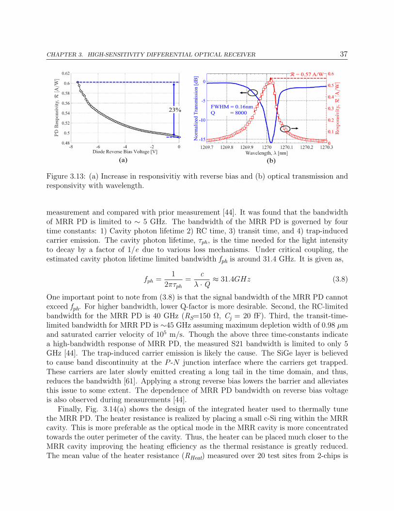
CHAPTER 3. HIGH-SENSITIVITY DIFFERENTIAL OPTICAL RECEIVER 37
Figure 3.13: (a) Increase in responsivitiy with reverse bias and (b) optical transmission andresponsivity with wavelength.
measurement and compared with prior measurement [44]. It was found that the bandwidthof MRR PD is limited to ∼ 5 GHz. The bandwidth of the MRR PD is governed by fourtime constants: 1) Cavity photon lifetime 2) RC time, 3) transit time, and 4) trap-inducedcarrier emission. The cavity photon lifetime, τph, is the time needed for the light intensityto decay by a factor of 1/e due to various loss mechanisms. Under critical coupling, theestimated cavity photon lifetime limited bandwidth fph is around 31.4 GHz. It is given as,
fph =1
2πτph=
c
λ ·Q≈ 31.4GHz (3.8)
One important point to note from (3.8) is that the signal bandwidth of the MRR PD cannotexceed fph. For higher bandwidth, lower Q-factor is more desirable. Second, the RC-limitedbandwidth for the MRR PD is 40 GHz (RS=150 Ω, Cj = 20 fF). Third, the transit-time-limited bandwidth for MRR PD is ∼45 GHz assuming maximum depletion width of 0.98 µmand saturated carrier velocity of 105 m/s. Though the above three time-constants indicatea high-bandwidth response of MRR PD, the measured S21 bandwidth is limited to only 5GHz [44]. The trap-induced carrier emission is likely the cause. The SiGe layer is believedto cause band discontinuity at the P -N junction interface where the carriers get trapped.These carriers are later slowly emitted creating a long tail in the time domain, and thus,reduces the bandwidth [61]. Applying a strong reverse bias lowers the barrier and alleviatesthis issue to some extent. The dependence of MRR PD bandwidth on reverse bias voltageis also observed during measurements [44].
Finally, Fig. 3.14(a) shows the design of the integrated heater used to thermally tunethe MRR PD. The heater resistance is realized by placing a small c-Si ring within the MRRcavity. This is more preferable as the optical mode in the MRR cavity is more concentratedtowards the outer perimeter of the cavity. Thus, the heater can be placed much closer to theMRR cavity improving the heating efficiency as the thermal resistance is greatly reduced.The mean value of the heater resistance (RHeat) measured over 20 test sites from 2-chips is

CHAPTER 3. HIGH-SENSITIVITY DIFFERENTIAL OPTICAL RECEIVER 38
Figure 3.14: (a) MRR cavity with integrated heater (b) distribution of heater resistance (c)shift in optical transmission with VHeat.
353.4 Ω (Fig. 3.14(b)). Considering the CMOS heater driver reliability, if the maximumVHeat applied across RHeat is limited to 1.5 V, then the heater dissipates 6.4 mW raising theMRR PD temperature by ∼110 K. As shown in Fig. 3.14(c), this induces a 5.5 nm (32% ofFSR) shift in the resonant wavelength. This amount of tuning is enough to compensate fortemperature and process variations in real-life applications.
3.6.3 Structure of Split-Microring Resonant SiGe Photodetector
Figure 3.15 shows the structure of the proposed split-MRR PD. The MRR cavity used inFig. 3.15 exploits a whispering gallery mode that is concentrated in the outer half of thering. To effectively separate the optical field, the metal contacts are placed in the center ofthe ring and connected with metal spokes. A 5 µm microring cavity is etched into the c-Silayer. A SiGe absorption region, responsible for carrier generation, is heteroepitaxially grownwithin a narrow 0.5 µm wide partially etched trench. This narrow SiGe layer width avoidscrystal dislocations [58]. Along the perimeter of the microring 30 lateral P -N junctions areinterleaved that use source/drain n-type and p-type implants. These junctions are arrangedin the middle of the SiGe layer. Spokes of n-type and p-type are used to connect the P -Njunctions with their respective contacts in the center of the ring.
To realize a fully differential PD, in [15], a 150 µm long 3 dB adiabatic splitter was usedto equally split the input optical power. Instead, in this work, two PDs are formed on thesame c-Si cavity by the selective wiring of P -N junctions. As shown in Fig. 3.16(a), half ofP (N) spokes are wired together to form the anode (cathode) node that connects to +Vsig
(VPD1). The other half are connected to VPD2 (-Vsig). Both of these PDs receive the sameincident optical power Pin, but due to opposite bias, namely VPD1 and VPD2, they outputfully-differential photocurrent. The two PDs are isolated by extending the middle two P-spokes in Fig 3.15 and biasing them with VPD2. The adjoining N spokes are biased at VPD1
creating a strong depletion region (shaded in Fig. 3.16(a)) that isolates the two PDs sharing

CHAPTER 3. HIGH-SENSITIVITY DIFFERENTIAL OPTICAL RECEIVER 39
Figure 3.15: 3D layout of the proposed split-MRR resonant photodetector.
Figure 3.16: (a) Concept of a split photodetector and (b) it’s equivalent circuit.
the same optical c-Si cavity. Unlike [59], splitting the SiGe layer minimizes the leakagecurrent between the detectors and further improves the isolation. To minimize reflectionscreated by a discontinuity in the SiGe layer, the separation gap dSiGe of 0.2 µm is chosen.The 3 dB power slitting inherent to the proposed PD is independent of wavelength andtemperature. This is a significant advantage compared to [15] as it requires no additionalcalibration. Furthermore, the split PD has multiple benefits like reduced size, boost inresponsitivity, amenability to DWDM realization, and reduced parasitic loss as drop-portand use of p-Si is no longer required.
3.6.4 Characterization of Split-Microring Resonant SiGePhotodetector
The free spectral range (FSR) of the split-MRR PD is 16.9nm (3.3THz) as shown in theoptical transmission plot in Fig. 3.17(a). The Q-factor of the ring around the resonantwavelength, λ0 of 1275nm is 7.7K with FWHM bandwidth of 0.165nm (30.5GHz) (Fig.

CHAPTER 3. HIGH-SENSITIVITY DIFFERENTIAL OPTICAL RECEIVER 40
3.17(b)). This value of Q and FSR can comfortably enable a 16-way DWDM receiver withnegligible crosstalk. The PD has peak responsivity (R) of 0.52A/W at λ0 as shown in Fig.3.17(b). Figure 3.17(c) shows PD’s I-V curve with the diode built-in potential of around0.6V. Under no illumination (dark), the I-V curve is that of a typical diode. The reversesaturation current is flat when reverse biased and forward current grows exponential whenforward biased. The dark current is in the order of nano-amps as the measurement is mainlylimited by the accuracy of the source meter. At resonance and under illumination, theforward bias behavior of the PD is similar to that under dark condition. However, whenreverse biased, the photocurrent does not plateau but rather continues to increase with areverse bias voltage. At resonance, the light trapped in the MRR cavity generates carriers,which are swiped out based on the strength of the field determined by the reverse bias voltage.This creates an increasing trend in photocurrent. Ideally, a reverse biased split-MRR PD(Fig. 3.16(b)) generates fully differential (180 out of phase) currents. However, due to amismatch in the input common-mode of the receiver, P -N junction profile, and other processinduced variations, some error between IPD1 and IPD2 exist as shown in Fig. 3.17(d). AtPin of -10 dBm this error is less than ±0.3%, which has a negligible impact on total CMRRand hence, can be neglected. Figure 3.17(e) and (f) show the thermal characteristic of thesplit-MRR PD. At the maximum DAC code, the heaters output 6.5 mW causing ∼110Ktemperature change, which shifts the resonance wavelength by 5.6nm (1.1THz) i.e. 33% ofFSR. This is sufficient to compensate for temperature variations in real-life applications.
3.7 Circuit Implementation
Figure 3.18 shows two FD optical Rx with half-rate architecture implemented over two test-chips. A CML clock receiver and distribution network delivers low-jitter off-chip clock to thereceiver. The interleaved clocks for the half-rate samplers are generated by the local clockbuffers. The threshold of the Rx circuit is set by current DACs at the input of optical Rx. Inthe version-1 design of Fig. 3.18(a), only pull down DAC was implemented while in version-2design in Fig. 3.18(b), both pull-up and pull-down current DACs were implemented. Theoutput bits (DA and DB) in Fig. 3.18(b) are retimed before being read by the digital backend.The circuit implementation of the Rx AFE is shown in Fig. 3.19(a)-(c). Only body-connecteddevices are used in the signal path to avoid hysteresis and threshold voltage variation due tofloating body effect. Both of the SF-TIAs are realized with a simple NMOS-PMOS inverterbased amplifier with 5 kΩ feedback resistor RF. The NMOS (MN) and PMOS (MP) arebiased at 1.1 mA drain current with a current density of 0.33 mA/µm and 0.2 mA/µm,respectively. This provides fT of 250 GHz for NMOS and 180 GHz for PMOS, which isclose to the maximum value as shown in Fig. 3.20(a). From (A.4) and (A.7), the high fTvalue increases the transimpedance limit and helps reduce the input-referred noise. An 8-bitpush-pull current DAC (IDAC), as shown in Fig. 3.19(a), at the input of the SF-TIA, isrequired to avoid sensitivity degradation due to transmit modulator finite extinction ratioand residual input offset. The total capacitance at the input of the SF-TIA is around 20

CHAPTER 3. HIGH-SENSITIVITY DIFFERENTIAL OPTICAL RECEIVER 41
(a) Optical transmission showingfree spectral range (FSR) of the de-tector.
(b) Close-in optical transmissionand detector’s responsivity withwavelength.
(c) Current-voltage characteristicsunder dark condition and illumina-tion at resonance.
(d) Error between IPD1 and IPD2with temperature at different in-put optical power.
(e) Optical transmission spectrumfor different heater DAC code set-tings.
(f) Resonant wavelength (λ0) andheater-power with heater DACcodes.
Figure 3.17: Measured optical performance and characterization of a split-MRR resonantphotodetector.
fF, which is composed of CPD of 10 fF, SF-TIA input capacitance Cin of 8 fF, and routingparasitic capacitance of 2 fF. Though the SF-TIA input-referred noise is optimal for Cin of12 fF (CPD+Cp) [55], it is not opted in order to reduce the TIA power consumption [23].This causes marginal (< 4%) increase in input-referred noise.
The two SF-TIA generate a fully-differential output to drive the post-amplifier Gp. Theinput pair M1 and M2 of Gp are sized to provide an open-loop gain of 4 resulting in a totalgain of 86 dBΩ with 3 dB bandwidth of 7 GHz. The load resistors RL absorb the kickbackfrom the comparator. A matching aware layout of RL and cascode devices for ITail are usedfor achieving a high CMRR to suppress PSN and common-mode noise. The simulation showsa CMRR of 25 dB is achieved at 7 GHz bandwidth. The cascodes M3 and M4 reduce theinput pair Miller capacitance easing the SF-TIA loading. It also provides a low-impedancenode to inject current for correcting the comparator offset. The offset DAC IOffset has 4-

CHAPTER 3. HIGH-SENSITIVITY DIFFERENTIAL OPTICAL RECEIVER 42
(a) (b)
Figure 3.18: Schematic of proposed FD optical Rx: (a) Version-1 design with 3 dB coupleand linear SiGe detector and (b) Version-2 design using split-MRR detector.
Figure 3.19: Circuit diagram (a) Shunt-feedback TIA (SF-TIA), (b) Post-amp (GP) withoffset cancellation, and (c) modified StrongARM comparator.
bit resolution with a structure similar to IDAC. Figure 3.20(b) shows the total noise PSDreferred at the input of the SF-TIA. The integrated noise over 7 GHz is about 280 nArms. Asevident, the thermal noise of RF and SF-TIA are the dominant noise contributor. The spotthermal noise PSD of RF is about 2.3 pA/
√Hz, which is comparable to other noise sources
at mid frequencies. At higher frequencies, the channel noise of SF-TIA, which scales as f 2,dominates. Also, as predicted by (A.6), the post-amplifier noise contribution increases withf 4, which after a point is even higher than that of SF-TIA. The devices of IDAC are sized forminimal noise contribution at all frequencies.
The comparator makes random decision errors (BER=0.5) if the input voltage is below itsminimum resolution voltage. This degrades the Rx sensitivity when referred to its input. Thecomparator’s minimum resolution voltage is dominated by its input-referred noise vnc, whichis inversely proportional to gm/ID of the input pair [62]. An effective means of increasing

CHAPTER 3. HIGH-SENSITIVITY DIFFERENTIAL OPTICAL RECEIVER 43
(a) (b) (c)
Figure 3.20: Simulation results of the receiver analog front-end. (a) fT and bias current forNMOS/PMOS, (b) total input-referred noise PSD, and (c) Comparator input-referred noisetrade-off.
gm/ID is to reduce the tail current but without affecting the regeneration time. To this end,Fig. 3.19(c) shows a modified strongARM comparator, where the tail device is split intotwo devices MT1 and MT2 with a 1:4 sizing ratio. The drain current of MT1, IT1 controlsthe integration time tINT during which the input pair effectively integrates the input signaland filters out high-frequency noise. This integration phase is initiated by the rising edge ofthe clock, which turns MT1 ON and starts the discharge of the internal nodes X -Y throughM1 and M2. The delay ∆tD controls tINT as long as ∆tD≤ Cout·VT,p /IT1, where VT,p isthe threshold voltage of M5 and M6. After the delay of ∆tD MT2 turns ON initiating theregeneration phase during which the drain current of MT2, IT2, along with IT1 determinesthe regeneration time treg. The use of two tail devices also helps to reduce kickback noise.To avoid significant speed penalty due to longer tINT, it is chosen such that tINT + treg ≤Tclk/2.
As shown in Fig. 3.20(c) increasing ∆tD delays the onset of MT2 making the input-pairintegrate longer. This increases the gm/ID and reduces the vnc. Thus, for ∆tD between 0 and50 ps the vnc improves by 30% dropping from 1.65 mV to 1.14 mV. When referred to theinput the equivalent current noise is 60 nArms, which is less than the dominant RF thermalnoise illustrated in Fig. 3.20(b). However, increasing ∆tD beyond 50 ps yields no additionalnoise reduction as gm/ID does not increase any further. This is because by then IT1 alreadydischarges the output below VT,p, which triggers regeneration. During regeneration, bothMT1 and MT2 are ON ensuring the total current and, thus the regeneration time constanttreg, is unchanged compared to the conventional comparator. For a brief period between MT2
turning OFF and precharge switches turning ON, crowbar current may exist. To minimizeit, M9 and M10 are appropriately sized.
The digital backend of Fig. 3.21 characterizes the performance of the receiver. On thetest-chip, it is shared between four receiver sites. A 2:16 deserializer (DeSer), one per receiver,parallelizes incoming serial bits to relax the timing and power consumption of the backend.

CHAPTER 3. HIGH-SENSITIVITY DIFFERENTIAL OPTICAL RECEIVER 44
Figure 3.21: Digital backend used to characterize receiver performance.
The PRBS generator can self-seed and generate a 31-bit PRBS pattern, which is comparedwith the bits received. The error counter increments if this comparison fails, which givesa BER value. Both of the counters are 41-bit wide to enable BER measurement in excessof 10−12. A 32-bit wide snapshot register captures receiver output, which is used for offsetcorrection and noise characterization. Lastly, pulse density modulators (PDM) thermallystabilize the split-MRR detectors by generating pulses whose position is controlled by a12-bit input control word.
3.8 Realization and Experiments
3.8.1 OMA and finite ER power penalty
Having a low ER (in the range of <6-7 dB) induces severe power penalty on the overall linkbudget. The resulting offset created due to finite zero power level (P0 in Fig. 3.22) can becorrected using the current DAC at the input of the Rx (IDAC). However, it comes at thecost of degradation in the Rx sensitivity due to noise contribution from the offset correctingcurrent DAC. Hence, to ensure that the true sensitivity of Rx is measured, it is crucial toensure an ER of at least 10 dB. As shown in Fig. 3.22, the ER is defined as P1/P0, whereP1 and P0 are the power levels representing binary-1 and 0, respectively. If P0 = 0 then theER is infinite, while for P0 > 0 ER is finite. When ER is finite, a non-zero optical power isemitted for a binary-0 level that appears as a DC offset. Consequently, to maintain the sameBER either the Rx threshold should be increased, which eats into the Rx sensitivity, or thetransmit laser optical power should be increased, which degrades overall link energy-efficiencyby making laser consume increased electrical power. This degradation in Rx sensitivity andthe increase in the transmit laser optical power due to low ER can be quantified as power

CHAPTER 3. HIGH-SENSITIVITY DIFFERENTIAL OPTICAL RECEIVER 45
Figure 3.22: A typical eye at the input of Rx and equations relating OMA, peak opticalpower, and ER.
penalty. This power penalty is severe, particularly for ER < 7 dB. Further, Rx can handlelow ER as long as P0 > 0 does not overload it. However, low ER corrupts the Rx sensitivitymeasurements impairing it from being a true representation of Rx performance. In addition,as shown in Fig. 3.22, if high ER is achieved then the sensitivity of Rx can be unambiguouslyquantified by OMA alone. The average sensitivity is then directly related to OMA and isequal to OMA/2. The same does not hold true for low ER. Owing to these reasons, an ERof at least >10 dB is ensured during measurements of the two test-chips.
3.8.2 Method to measure sensitivity of the optical Rx
Measuring the electrical peak-to-peak current sensitivity and the optical modulation ampli-tude (OMA) sensitivity are two of the most critical performance metrics of an optical Rx.Once, OMA is measured the current sensitivity is directly related to it through the respon-sivity R of the photodetector. The OMA is defined as the difference between P1 and P0,where P1 and P0 are the power levels representing bit-1 and 0, respectively. Thus, the OMAsensitivity of an optical Rx is the minimum difference between P1 and P0 required of the Rxto detect the received bits with a target BER of <10-12. Once OMA sensitivity is obtained,the average Rx sensitivity can be found using expressions shown in Fig. 3.22. Note that asargued earlier, it is necessary to ensure that ER is > 10 dB to accurately measure the Rxsensitivity.
Figure 3.23 shows the test-bench used to measure the Rx OMA sensitivity. The CW laseris modulated with the PRBS31 test pattern to generate an optical test signal. The easiestway to obtain the BER vs. OMA sensitivity plot is to sweep the input laser power andmonitor the BER. Unfortunately, the ER at the output of MZM (at node-A) is a function oflaser power and the applied DC bias (not shown in Fig. 3.23). This makes it challenging to

CHAPTER 3. HIGH-SENSITIVITY DIFFERENTIAL OPTICAL RECEIVER 46
Figure 3.23: Calibration for variation in split ratio with λ and coupling position.
measure OMA by simply sweeping the laser power. Besides, the CW laser source also hasa minimum output limit below which it cannot faithfully generate the output. Typically, itis around -15 dBm while for OMA measurement a laser power as small as -25 dBm mightbe required. To avoid this issue, the laser power is set to a fixed value and MZM is biasedat such that the ER at node-A is >10dB. While the laser power is attenuated by tuning thepolarization controller. The controller only attenuates the input optical power and retainsthe ER intact. As the controllers attenuation is unknown, its output is first connected toa power meter to measure the average power. As ER>10 dB, this average value readilytranslates into the OMA sensitivity of the optical Rx. When the input optical signal iscoupled into the Rx chip the differential detector pulls IPD1 and IPD2 from VPD1 and VPD2
SMU (Keithley 2612). The input OMA can be cross-verified by converting these averagecurrents to average power and thus, to the input OMA using the PD responsivity. Oncethe two value of the OMA match, we use the average current values to estimate the inputOMA. Lastly, for each OMA point, we perform multiple BER measurements using on-chipBERT and report the best-measured BER value. These steps are repeated for both thedata-rates of 6Gbps and 12Gbps. Note that the grating coupler loss is de-embedded fromthe OMA numbers reported in this thesis. Also note that to measure the OMA, the clockand the threshold of the optical Rx are set to a fixed offset where the best BER performanceis expected. This can be obtained by first measuring eye diagrams in statistical and BERmode.

CHAPTER 3. HIGH-SENSITIVITY DIFFERENTIAL OPTICAL RECEIVER 47
Figure 3.24: (a) Photomicrograph of test-chip. Size is 3 mm X 3 mm with 73 I/O pads. (b)Test setup with inset 12 Gb/s external reference modulator eye.
3.8.3 Version-1 Test-chip: Measurement Results
The optical receivers are fabricated in the GFUS 45-nm SOI CMOS process. Figure 3.24(a)shows the die-photo of the test-chip. It has 3 optical receiver sites, each having 4 analogreceiver cores sharing a BERT, eye-monitor, PRBS generator and clock buffers. Site-A has 4single-ended (SE ) receivers while sites -B and C each have 4 fully-differential (FD) receivers.Optical performance/loss numbers are extracted from the optical test structures designed in adedicated test-area. The test-chip is bumped with C4 balls, flipped and die-attached directlyto an FR4 PCB. The mounted chip is under-filled with electrically insulating adhesive andepoxy is applied on the edges. Underfill holds the chip during die-thinning process and epoxyprotects the edges during substrate release.
The test-bench to characterize receiver performance is shown in the Fig. 3.24(b). AJDSU lithium niobate (LiNbO3) Mach Zehnder interferometer (MZI) modulates the 1180nm laser with 231-1 PRBS data pattern generated by the Kintex-7 FPGA. MZI has electro-optic bandwidth of 30 GHz while the accompanying modulator driver JDSU H301-1210 has 3dB RF bandwidth of 11 GHz. Resulting 12 Gb/s modulated PRBS31 output is shown in Fig.3.24(b) inset. It has 5.5 ps RMS jitter and rise/fall times of 66/62 ps. The MZI is biased toachieve 11.6dB extinction ratio at 12 Gb/s. The PRBS31 modulated data is coupled into thetest-chip using lensed fiber with spot diameter of 2.5±0.5 µm. The photodetectors are biasedwith a reverse voltage of 5 V. The bandwidth and responsivity of the detectors is dependenton VPD1 and VPD2. Hence, they are chosen to maximize photodetectors responsivity to 0.023A/W while achieving 5 GHz bandwidth.
Results for SE Rx are measured from Site A in Fig. 3.24(a) whereas the results for FDreceivers are measured from one of the test-sites of Site B or Site C. Each test site is 300 µmx190 µm while each receiver site has area of 55 µm x 40 µm. Running from analog/digitalsupplies of 1.2V, the test site consumes 48 mW out of which each receiver consumes 4.7 mW.

CHAPTER 3. HIGH-SENSITIVITY DIFFERENTIAL OPTICAL RECEIVER 48
Figure 3.25: Measured statistical eye, BER eye, bathtub curves and sensitivity plots for SEand FD Rxs.
The on-chip BER checker has self-seeded 231-1 PRBS pattern generator which can lock tothe received PRBS31 pattern and compute BER. Both statistical and BER eye are obtainedat -0.2dBm input optical power-level (44 µApp). The receiver threshold is controlled througha 5 bit DAC at the input of the TIA with step size of 1.3 µApp/code. The input sensitivity ismeasured by applying 231-1 PRBS test pattern operating at 12 Gb/s. Figure 3.25(a) showsstatistical eye for SE and FD Rxs. It is apparent that SE eye is only partially open andshows significant deterioration due to common-mode noise and power supply noise. Figure3.25(b) shows the BER eye for both SE and FD Rxs. It can be seen that FD Rx can achieveBER <10-12 while SE Rx barely meets BER < 10-8. Figure 3.25(c) shows the bathtub curvesand the BER with the Rxs input sensitivity, Iph,min (µApp). The 12 Gb/s FD Rx has 0.3 UIof timing margin at BER < 10-12, at 8.6 µApp input current sensitivity. The SE Rx inputsensitivity at the same speed is 16.3 µApp but at higher BER. However, at lower data ratecommon-mode and supply noise are lowered. For example, at 6 Gb/s the difference betweenSE and FD sensitivity is not very significant. Timing margin for SE is about 0.4 UI andthat for FD is about 0.6 UI.
Finally, depending on wavelength, coupling angle and coupling position, multiple opticalmodes can propagate through power splitter affecting the power-split ratio. To circumventthis issue an off-chip calibration is applied. As shown in Fig. 3.24(b), VPD1 and VPD2 aretuned until the average current from the detectors are equal. As the tuning efficiency isonly 0.33 µA/V, correction range is limited. Figure 3.26 shows the variation in powersplitratio with λ and Y, and its effect on the BER. After calibration BER of <10-10 can beachieved over 40 nm wavelength band (∆λ). For high-density optical interconnect this rangeis sufficient to fit 36 wavelength multiplexed channels [28].

CHAPTER 3. HIGH-SENSITIVITY DIFFERENTIAL OPTICAL RECEIVER 49
Figure 3.26: Calibration for variation in split ratio with λ and coupling position.
3.8.4 Version-2 Test-chip: Thermal Tuning of Split-MRRPhotodetector
The strong thermo-optic coefficient of silicon (dnSi/dT= 1.8×10⁻⁴K−1) combined with highQ-factor of MRR changes the optical performance due to thermal effects. For 1 Kelvin tem-perature change λ0 drifts by 0.036nm, which is 22% of the FWHM bandwidth. Such thermaldependence is not specific to MRR, but common in real-life applications. For example, thedatacenter pluggables use VCSELs that have even higher temperature drift of 0.06nm/Krequiring strict regulation of ambient temperature [63] and broad channel spacing.
As the MRR for the Rx experiences lower incident optical power, the self-heating effectsare negligible. Thus, the dominant source of thermal drift is the ambient temperaturefluctuations. To compensate for it, a thermal tuning loop of Fig. 3.27(a) is used. Theoff-chip tuning algorithm locks the detector to a target average photocurrent, IPD by readingthe current from an external VPD1,2 source meter and controlling the PDM through a scan-chain register [64]. The PDM generates pulses with density depending on the input controlword over a fixed 0.17 ns period. The thermal impulse response of the detector is low-passwith 67 kHz cutoff [28], which averages the PDM output forming a 12-bit digital-to-analogconverter (DAC). A load capacitor, CF, of 1 pF reduces the slew-rate at the drain of NMOSheater driver, M1. The resulting output heater power is monotonic and linear with DACcode. The heater resistance, RHeater, measured from 10 detectors is between 250 Ω to 300Ω. From Fig. 3.17(e)-(f), the tuning efficiency of the loop is 0.86 nm/mW (5.9 µW/GHz)and resolution of 0.27 GHz/LSB.
Figure 3.27(b) depicts the behavior of the tuning loop. For a given target IPD the loopcan converge to either to the left (point A) or right (point B) of λ0. To ensure negativefeedback and thus, stable loop operation, left side point A is chosen [28]. If the detector isoperating at λ1 with IPD1 greater than the target IPD, the thermal tuning controller will heatthe detector until it shifts to point-C. Similarly, if the detector is operating at λ2 with IPD2
less than target IPD then the controller will reduce the heating (cooldown) until the detector

CHAPTER 3. HIGH-SENSITIVITY DIFFERENTIAL OPTICAL RECEIVER 50
Figure 3.27: (a) Thermal tuning loop and (b) operation of tuning controller used to stabilizeresonant split-photodetector.
reaches a point-D. During initialization, converging to a maximum change in temperature of110 K requires 10 secs. Each step of heating or cooling involves reading IPD and controllingthe PDM through a scan-chain, which takes a total time of 8ms. This speed is sufficient totrack ambient temperature change and stabilize the split-MRR detector during the BER andstatistical eye measurements. Faster tuning in the milliseconds range has been demonstratedpreviously by fully integrating the control loops [28].

CH
AP
TE
R3.
HIG
H-S
EN
SIT
IVIT
YD
IFFE
RE
NT
IAL
OP
TIC
AL
RE
CE
IVE
R51
Table 3.2: Specifications of Photonic Blocks used in the Fully Differential Receiver
c-Si Waveguide Grating Couplers Split-microring Resonant Photodetector
Measured† Measured† Best Device∗ [65] Measured† Best Device∗ [44]
Performance Single-mode Bandwidth, BW Bandwidth, BW R = 0.52 A/W R = 0.55 A/Wmetric (-1 dB) = 78 nm (-1dB)=100 nm @λ=1275 nm @λ=1176.9 nm
BW ∼ 5 GHz BW ∼ 5 GHzLoss Propagation Coupling Coupling Propagation loss, αring = 1.3 dB/cm
loss = 3 dB/cm loss = 4.5 dB loss = 1.2 dB αring = 1.1 dB/cm
Key Dimensions‡ W=0.4 µm W=6.3 µm, L1=10 µm, L2=25 µm r=5 µm, No. of spokes = 60, g = 0.23 µmdSiGe= 0.2 µm, WSiGe = 0.5µm
†Measured from the test-chip designed in this work. ∗Standalone devices reported in the recent literature. ‡Used in this work.

CHAPTER 3. HIGH-SENSITIVITY DIFFERENTIAL OPTICAL RECEIVER 52
3.8.5 Version-2 Test-chip: Measurement Results
Optical components like c-Si waveguide, vertical grating coupler, and split-MRR PD, areused to realize the FD optical Rx. Their performance is measured from the standalone teststructures on the same test-chip and summarized in Table. 3.2. The test-bench of Fig. 3.28characterizes the optical Rx performance from the test sites with co-integrated electronicsand photonics. A Lithium Niobate (LiNbO3) Mach-Zehnder modulator (MZM) with 25 GHzelectro-optic bandwidth modulates the 1275 nm continuous-wave (CW) input laser with 231-1 PRBS data pattern generated by the FPGA. The MZM pre-driver amplifies the FPGAoutput with 30 dB programmable gain and 18 GHz 3 dB RF bandwidth. The MZM isbiased to achieve 13.2dB extinction ratio (ER) and 7.3 dB insertion loss at 12 Gb/s. Theinset of Fig. 3.28 shows resulting 12 Gb/s modulated PRBS31 test data pattern, which isISI free with 1.6 ps RMS jitter and rise/fall times of 27/32 ps. It is coupled into the test-chipusing a lensed fiber with a spot diameter of 2.5 µm±0.5 µm. The PD power-supplies VPD1,2
are chosen such that the two split-MMR PDs are reverse biased with 5 V. This ensures amaximum responsivity while achieving ∼5 GHz bandwidth. Figure 3.29 shows the die-photoof the test-chip. It contains a total of 3 test sites, viz.: A, B, and C, each has 4 Rxs thatshare a common digital backend. Site-A has 4 SE Rxs while site-B and site-C each have 4FD Rxs.
Both SE and FD Rxs run from an analog supply (AVDD) of 1.5V and a digital supply(DVDD) of 0.9V. At 12 Gb/s the FD optical Rx consumes 7 mW (0.58 pJ/bit), of which theTIAs consumes 3 mW while the rest is consumed by the post-amplifier, comparator, andthe clock-buffers. Additionally, the digital backend, deserializer, and PDM along with pre-driver consume 18 mW, 0.8 mW, and 0.7 mW respectively. Both statistical and bit-errorrate (BER) eye are measured at 0 dBm input optical power generating 0.18 mA averagephotocurrent and output swing of 1.5Vpp. As all the Rx sites share the same power-supply,turning the neighboring sites ON with continuously toggling input current DACs generatesPSN and common-mode noise that couples into the Rx site under test. Consequently, thestatistical eye of SE Rx in Fig. 3.30(a) significantly deteriorates with a partial verticalopening limited to 50 IDAC codes while the same for FD Rx in Fig. 3.30(b) is 130 codes.Further, the rising edge in Fig. 3.30(b) is slightly faster than Fig. 3.30(a) as FD Rx has lowerPD capacitance (Fig. 3.3(c)). Comparing Fig. 3.30(d) and Fig. 3.30(e), the FD Rx achievesBER 10-12 while the SE Rx barely meets ∼10-8. The statistical and BER eye confirm theeffectiveness of the FD Rx in suppressing PSN and common-mode noise. Bathtub curvesand sensitivity plots of Fig. 3.30(c) & (f), further quantify the performance improvement.The OMA sensitivity is defined as a minimum difference between the high and low opticallevels that the receiver can detect with BER of <10-12 for at least one point on the bathtubcurve of Fig. 3.30(c). To measure high OMA sensitivity in Fig. 3.30(f), the input opticalpower should be reduced to less than -20 dBm while retaining the ER better than 10 dB.For this purpose, the input laser power and polarization controller are tuned. At 12Gb/s theFD receiver has 0.25UI timing margin at BER of 10-12 with OMA of -18.2 dBm. For BERof 10-8, the SE Rx has OMA sensitivity of -16.3 dBm whereas FD Rx has -19.1 dBm. The

CHAPTER 3. HIGH-SENSITIVITY DIFFERENTIAL OPTICAL RECEIVER 53
Figure 3.28: Optical test-bench with inset of setup for coupling light into the test-chip and12 Gb/s modulated input data eye.
Figure 3.29: Die micrograph and microscope photo of a fiber coupled test-site. At resonancethe microring glows due to the light trapped inside.
timing margin for SE is about 0.4UI and that for FD is about 0.6UI.

CHAPTER 3. HIGH-SENSITIVITY DIFFERENTIAL OPTICAL RECEIVER 54
(a) Statistical eye of SE Rx at12Gb/s.
(b) Statistical eye of FD Rx at12Gb/s.
(c) Bathtub curves at 0dBm inputoptical power.
(d) BER eye of SE Rx at 12Gb/s. (e) BER eye of FD Rx at 12Gb/s. (f) Sensitivity plots for SE and FDRxs.
Figure 3.30: Measured performance of the optical Rxs for a PRBS31 input pattern. For(a)-(e) input optical power of 0 dBm and ER of 13.2 dB is used.

CH
AP
TE
R3.
HIG
H-S
EN
SIT
IVIT
YD
IFFE
RE
NT
IAL
OP
TIC
AL
RE
CE
IVE
R55
Table 3.3: Performance Summary and Comparison With State-of-the-Art Moderate to High-Speed Optical Receivers
Reference [66] [47] [50] [67] [28] [15] [23] ThisISSCC JSSC ISSCC ISSCC JSSC ESSCIRC JSSC Work
2017 2018 2010 2013 2016 2016 2018
Process 14-nm 0.18µm SiGe 0.13µm 90nm 45-nm SOI 45-nm SOI 65-nm 45-nm SOIFinFET BiCMOS CMOS CMOS CMOS CMOS CMOS CMOS
Integration Wirebond Flip-chip Monolithic Wirebond Monolithic Monolithic Wirebond Monolithic
Data Rate 64∣∣∣ 32 50 10 9 10 12 12 12
[Gb/s] 64∣∣∣ 32
BER/PRBS 10−12/7 10−12/9 10−12/– 10−13/31 10−12/31 10−12/31 10−12/31 10−12/31[bits]
Photodetector 69 60 – 140 15-20 15-20 100 20cap [fF]
PD Respon- 0.52 0.8 0.8 0.55 0.023 0.023 0.75 0.52sivityR [A/W]
Area [mm2] 0.028 3.2 0.32 0.004 0.0025 0.0022 0.12 0.0021
Efficiency 1.4∣∣∣ 2.8 7.9 1.5 0.93 0.35 0.36 1.9 0.58
[pJ/bit]
Isen,pp [µApp]† 148‡ 96 6 174‡ 18 8.6 15‡ 7.9
OMA -5.5∣∣∣ -13 -9.2 – -5.0 -1.1 -4.3 -16.8 -18.2
Sensitivity -5.5∣∣∣ -13
[dBm] -5.5∣∣∣ -13
†Minimum photodetector current required by the receiver Full-chip including pads ‡Calculated from OMA and responsivity.

CHAPTER 3. HIGH-SENSITIVITY DIFFERENTIAL OPTICAL RECEIVER 56
Table 3.3 summarizes the performance of the proposed optical Rx and compares it withthe state-of-the-art. The split-MRR PD has a responsivity of 0.52 A/W which is comparablewith other designs. However, due to monolithic integration, the capacitance at the input ofthe receiver is less than 20 fF, which is one third compared to the recently reported flip-chipsolution [47]. Among monolithic designs, the proposed optical Rx achieves better sensitivityat 12 Gb/s with similar or better energy-efficiency. Estimating the OMA sensitivity of [50]was not possible as the dark current of the integrated PD is equal to the average currentsensitivity of the Rx. The optimized Rx AFE yields better input current sensitivity thanpreviously measured results [15]. Compared to 12 Gb/s Rxs across integration technologies,the proposed Rx achieves current sensitivity comparable to [50] and more than 1.4 dB betterOMA sensitivity, which can potentially lower the laser power consumption by 28 %, alongwith 3x lower energy-per-bit. Lastly, the receiver’s footprint area is small enough to enableDWDM systems [7]. The data-rate can be increased further by employing any of the recentlyreported equalization schemes [38, 23, 66].
3.9 Summary
To address the high power consumption of laser source improving the Rx sensitivity is crucial.In these regards, this chapter presented a high-sensitivity fully differential optical Rx forenergy efficient and high bandwidth density optical interconnects. The fully-differentialarchitecture, enabled by the differential detectors, suppresses common-mode and power-supply noise to improve sensitivity without reducing bandwidth or incurring power penalty.The Rx AFE is optimized to reduce the input-referred thermal noise. The comparatornoise contribution, which is quite substantial, is reduced by using a modified StrongARMcomparator with wider sampling aperture. The high-sensitivity, high-bandwidth density,and low energy are all enabled by the monolithic integration approach of photonic deviceswith high-performance transistors, which allows photonic-device and circuit co-design andoptimization.
The version-1 design carried a fully-differential detector realized using a 3 dB couplerand two linear SiGe detectors achieved electrical sensitivity of 8.6 µApp at 12 Gb/s with 0.36pJ/bit energy-efficiency. The linear detectors has a limited responsivity of 0.023 A/W whilethe 3 dB coupler was bulky and was sensitive to wavelength, which required calibrationto avoid BER degradation. These issues addressed in the version-2 test-chip where thedifferential detector is realized using a split MRR detector. As the Rx AFE and the detectorsare monolithic-integrated in 45nm SOI CMOS, the interface parasitic of <20 fF is achieved.This enables SF-TIA to use a large (5 kΩ) feedback resistor without amplifying its voltagenoise. The Rx sensitivity is thus greatly improved due to the reduction in input-referrednoise. The measurement results from the version-2 test-chip show high OMA sensitivity of-18.2 dBm at 12Gb/s and energy-efficiency of 0.58 pJ/bits while achieving BER < 10-12. Theenergy-efficiency is slightly degraded compared to version-1 test-chip due to additional powerspend for thermal tuning of the split detector. However, the footprint area of the receiver

CHAPTER 3. HIGH-SENSITIVITY DIFFERENTIAL OPTICAL RECEIVER 57
is only 0.0021 mm2 making it suitable for DWDM systems. From sensitivity viewpoint,the receiver compares favorably with state-of-the-art designs at 12 Gb/s, with significantimprovement in energy-efficiency.
Lastly, this chapter also described a procedure to extract parameters and performancecharacterization of the MRR-based photodetector. These PDs are characterized in terms ofresponsivity, dark current, RC bandwidth, and thermal tuning range. From the parameterextracted, an equivalent circuit model is built to aid electro-optic co-optimization and design.It was also observed that under sufficient reverse bias the MRR PD achieved a responsivityof 0.6 A/W at -7.5V reverse bias with a negligible dark current. The integrated heater,which is a crucial component for successful operation of MRR PDs, is also characterized.Measured from 20 test-sites over 2 chips, the heater had a mean resistance of 353 Ω and iscapable of raising the detector’s temperature by ∼110 K when the heater driver is poweredfrom 1.5 V supply.

Chapter 4
Demonstration of a Laser-forwardedCoherent Optical Link
For the silicon photonic links to meet the target bit error rate, the laser source must outputenough optical power to overcome the optical channel loss and limited receiver sensitivity.Combined with a poor wall-plug efficiency, this optical power requirement makes the elec-trical power consumed by the laser source a significant portion of the link energy cost. Toreduce the laser’s electrical power consumption the Rx sensitivity should be improved whilethe optical path loss should be minimized. In Chapter-3, a high-sensitivity optical Rx isdeveloped, which address a part of this problem. While in chapter laser-forwarded coher-ent link is demonstrated that greatly reduces the required laser optical power by averagingoptical path loss between the main and the forwarded path, and by further improving theRx sensitivity using a homodyne coherent detection. The link performance analysis revealsthat the laser forwarded link improves the laser power budget by ≈6-8 dB compared to aconventional intensity-modulation/direct detection link using typical photonic link compo-nents. To demonstrate the laser forwarded link, a microring resonator phase-modulator, abalanced detector, and a 3-dB coupler are integrated with CMOS circuits in a GFUS 45nmSOI process. The transmit driver and the receiver consume 40 fJ/bit and 450 fJ/bit, respec-tively. Aided by ≈8 dB boost from laser forwarding and the coherent detection gain, thereceiver achieves -15.6 dBm optical modulation amplitude sensitivity. The link operates at10 Gb/s with bit error rate <10-9 and electrical energy-efficiency of 2.3 pJ/bit.
4.1 Coherent Link for Short-reach Optical I/O
The IMDD link example discussed in Section-2.3 of Chapter-2, highlights the need for highoptical laser power due to limited Rx sensitivity and optical path loss. While some tech-niques, as briefed in Chapter-3, can be used to improve Rx sensitivity, minimizing opticalpath loss is not always that straight forward and often involves tight trade-off with otherimportant optical performance metrics like ER and voltage drive for a modulator. Addition-
58

CHAPTER 4. DEMONSTRATION OF A LASER-FORWARDED COHERENT OPTICAL LINK 59
aly, conventional IMDD links exploit only one degree of freedom, namely, optical intensity.Owing to these reason IMDD links reported in recent literature require 7-13 dBm of laserpower [12, 36, 40].
Compared to IMDD, the coherent links enable complex modulation, such as binary phase-shift keying (BPSK), and thus, are more spectrally efficient. However, coherent detectionoften is costly, complex, and involves power hungry signal processing. Consequently, coherentlinks are thought to be not suitable for data center applications and are limited to long-haul and metro links. However, the benefits of coherent detection has forced researchers toinnovate at architecture level and make deployment of coherent link possible within datacenter. One such effort is reported in [41]. Here the researchers identify that the short-reach optical I/Os of data centers have less severe fiber propagation impairments. Theserelaxed requirements can be exploited to dramatically simplify the signal processing andthus, reduce the power consumption and cost associated with coherent detection. Whilethis new approach permits the use of coherent links in the data center, it still needs a locallaser source. This is not feasible for high-bandwidth density applications such as optical I/Outilizing N -way DWDM. For instance, a 16-way DWDM shown in Fig. 2.5 of Chapter-2would require 16 local laser sources per I/O ports. If there are multiple I/O ports, then thenumber of laser sources would scale further.
To address the limitations imposed by limited Rx sensitivity, optical path loss, and needfor multiple local laser sources, this chapter discusses a laser-forwarded (LF) coherent linkarchitecture for short-reach optical I/Os. The basic idea is to forward some portion of thelaser power directly to the homodyne coherent Rx [19], bypassing the transmit chip IL. Asthe forwarded laser (LO at Rx) bypasses the major link losses, the overall photocurrentgenerated at the Rx is affected only by an average of the signal and LO path loss. Besides,it obviates the need for multiple local laser sources needed to realize DWDM Rx. Also,the homodyne coherent Rx improves the SNR due to a boost from the LO multiplicationand a 3-dB SNR gain due to coherent balanced detection. The coherent modulator anddemodulator are realized using MRRs as they are inherently wavelength selective and canrealize DWDM without using additional components for multiplexing or de-multiplexing.This minimizes the IL, saves area, achieves higher bandwidth density, and improves energy-efficiency [23, 24]. While the use of MRR for coherent communication is well-known [68, 69],the key link components remain off-chip. This chapter presents the first results of an MRR-based LF SiPh BPSK link fully integrated in a zero-change 45-nm SOI CMOS. The Txgenerates the 10 Gb/s BPSK data while being stabilized by an on-chip thermal tuning loopand clocked from a low-jitter digital phase-lock loop (DPLL). The Rx achieves an OMAsensitivity of -15.6 dBm enabled by an integrated 3-dB coupler and a balanced MRR-basedphotodetector (PD). Consequently, the demonstrated link requires less laser power comparedto the state-of-the-art IMDD links.

CHAPTER 4. DEMONSTRATION OF A LASER-FORWARDED COHERENT OPTICAL LINK 60
Figure 4.1: (a) Direct detection and (b) Coherent balanced detection.
4.2 Principle of Coherent Balanced Detection
A balanced detector is a key component of coherent homodyne Rx. To understand itsoperation, first, consider a direct detection as shown in Fig. 4.1(a). Here, a PD withresponsivity R is illuminated with a monochromatic lightwave, S =
√PSexp(j(ωLt+φin(t)),
where φin is the phase of the signal S. The output photocurrent is given by,
I(t) = R · PS (4.1)
As the direct detection measures the average power (|S|2=PS), the phase information in(4.1) is lost. In contrast, a coherent detector of Fig. 4.1(b) retains the phase information.Here, a 3-dB coupler, also referred as a 180 optical hybrid, mixes the signal S with theLO (=
√PLOexp(jωLt)). Each of the two input fields splits into the two output ports and
an additional phase-shift of 180 is introduced in one of the branches. Mathematically theoperation of a 3-dB coupler can be modeled as,[√
P1√P2
]=
1√2
[1 11 −1
]·[SLO
](4.2)
Simplifying (4.2) states that the output optical power P1 and P2 are proportional to the sumand difference of the inputs S and LO. They are given by,
P1 = (S + LO)2/2 and P2 = (S − LO)2/2 (4.3)
The resulting photocurrents I1(t) and I2(t) are,
I1(t), I2(t) =R2
(PS + PLO︸ ︷︷ ︸Unwanted DC term
±2√PSPLOcos(φin(t))) (4.4)
The DC terms in (4.4) increase the shot noise and can saturate Rx AFE, especially for astrong LO signal. A high-pass filter can eliminate these terms, but it deteriorates bit errorrate (BER) as it filters the lower-end of the spectrum. Alternately, a DC cancellation loop

CHAPTER 4. DEMONSTRATION OF A LASER-FORWARDED COHERENT OPTICAL LINK 61
can be used [70]. However, the offset canceling current source requires a careful low-noisedesign as its thermal noise appears directly at the input degrading the Rx sensitivity. Abetter approach is to subtract the two photocurrents using a balanced detector formed bystacking two PDs as shown in Fig. 4.1(b). The output current is expressed as,
I(t) = I1(t)− I2(t) = 2R√PSPLO · cos(φin(t)) (4.5)
There are no DC terms present in (4.5) and unlike (4.1) it retains the phase information thatenables coherent detection. Also, a balanced detector has superior common mode rejectionand adjacent channel suppression making it a good fit for co-packaged DWDM optical I/Oswhich operate next to an SoC with a noisy power-supply environment.
4.3 Laser-forwarded (LF) Coherent Link Architecture
The architecture of the LF coherent link using is shown in Fig. 4.2. A laser source outputsa continuous lightwave laser with wavelength λL, which is split between the signal path andthe forward laser path. On the signal path, the Tx uses an MRR-based O-DAC to modulatethe phase of incoming lightwave such that φin in (4.5) changes between 0 and π. At Rx,this results in a peak-to-peak signal current of 4R
√PSPLO. In an LF coherent link, both
the signal and LO are derived from the same laser source by splitting it with a factor k(0< k <1). Assuming the link loses of Fig. 2.4 in Chapter-2, the signal current is,
I(t)LFin = 4R ·√αTαC · k(1− k)PL (4.6)
where PL is the laser power and αT (=α3CαIL) is the signal path loss. The current in (4.6)
is maximized for k = 0.5, suggesting an even split of laser power between the signal and theLO. A multi-port laser source with equal output power per wavelength per port would bean ideal fit for this purpose. Subsequently, for the same laser power the peak-to-peak signalcurrent for LF and IMDD link is,
I(t)LFin = 2R ·√αTαCPL and I(t)IMDD
in = R · αTPL (4.7)
Comparing the two expressions in (4.7), the strength of LF architecture is evident. Thesignal current in an IMDD link is directly affected by the link loss, whereas in an LF link thesignal current is affected by the geometric mean of the loss in the signal path and the LOpath. Consequently, the gain of an LF coherent link over an IMDD link, can be expressedas,
ALF =ILFin (t)
IIMDDin (t)
= 2
√αCαT≈ 9 (4.8)
For the same link components, the gain ALF in (4.8) improves the SNR and thus, theRx sensitivity or for the same Rx sensitivity reduces the laser power, . The three mainreasons behind the gain ALF are: 1) the 3 dB SNR gain due to coherent balanced detectionas indicated by (4.5), 2) mixing with LO provides an optical gain of 2
√PLO/PS, and 3)
averaging of the signal and the LO path link loss. Furthermore, a portion of the coupledLO laser power can be used for the return transmit link, avoiding the need for extra fiber toroute the LO.

CHAPTER 4. DEMONSTRATION OF A LASER-FORWARDED COHERENT OPTICAL LINK 62
Figure 4.2: An MRR-based LF coherent link concept [19].
4.3.1 Coherent Rx sensitivity and Noise sources
A high sensitivity Rx AFE is necessary to support and preserve the SNR gains due to coherentbalanced detection. Assuming balanced PDs have negligible dark current, the sensitivity ofthe Rx AFE is dominated by the PD shot noise and thermal noise from the AFE. The rmsvalues of the shot noise (inS) and the thermal noise (inT ) are given as,
inS =√
2qRPi ·∆f and inT =√i2n,TIA ·∆f (4.9)
where Pi is the total power hitting a PD, ∆f is the AFE bandwidth, and in,TIA is the one-
sided total input-referred noise current density of the AFE expressed in pA/√Hz[71]. To
achieve a target BER, the input signal currents of (4.7) should be much higher than the totalrms noise. The relation between the two is given as,
BER =1
4
[erfc
(Iin,pp − 2Ith√
2σn1
)+ erfc
(Iin,pp + 2Ith√
2σn0
)](4.10)
assuming the ideal ER for the IMDD link. In practice additional shot and thermal noise arepresent at the Rx input due to ER (6-10 dB) and additional offset correction circuitry. Here,σn1 and σn0 represent total noise current for bit-1 and bit-0, respectively, while Ith modelsminimum receivable signal.
The values of σn1 and σn0 in (4.10) are given by,
IMDD link: σn1 =
√2qRαTPL∆f + i2nT ; σn0 = inT
LF link: σn1 = σn0 =
√qR(αT + αC)PL∆f + i2nT (4.11)
The shot noise in an LF link is generated from two different PDs. Thus, their variance addsup as they are independent. Using the signal current of (4.7) and noise of (4.11) in (4.10),the BER plots for IMDD and LF link are obtained as shown in Fig. 4.3(a). Here, inT=2.5

CHAPTER 4. DEMONSTRATION OF A LASER-FORWARDED COHERENT OPTICAL LINK 63
(a) (b)
Figure 4.3: (a) BER vs. laser power. and (b) Impact of path length mismatch.
µA over 20 GHz bandwidth and Ith=7.5 µA are assumed [39]. The losses are the same as fora typical IMDD link (Fig. 2.4 in Chapter-2). As evident from Fig. 4.3(a), the LF coherentlink meets the target BER at much reduced laser power. As the shot noise is included inFig. 4.3(a), the reduction in laser power is slightly lower than that predicted by (4.8).
Further, instead of forwarding the LO, a conventional BPSK link derives LO using alocal laser source. In this case, the peak-to-peak signal current is 4R
√PSPLO, while the
noise current σn1(=σn0) is
√2qR(αTPS + PLO)∆f + i2nT . Here, the LO power can only be
increased to a point beyond which the generated shot noise will dominate the total noise.Any further increase in the LO power does not improve the SNR as it gets limited by the shotnoise [72]. In contrast, SNR of an LF coherent link is proportional to PL. Thus, increasingPL will improve the SNR as long as the increase in the signal power stays within the MRR’spower handling capability. After this point, it gets harder to phase-modulate and thermallystabilize the MRR. Lastly, the relative intensity noise (RIN) of the laser due to intensityfluctuations from spontaneous emission also affects the Rx sensitivity. However, as the noisevariance of RIN is correlated between two output ports of the 3-dB coupler, the balanceddetector rejects it and makes its contribution negligible [72].
4.3.2 Impact of Laser Phase noise
Laser phase noise, an inevitable aspect of a free running laser, is caused by random spon-taneous emissions. In a practical LF link, the phase noise manifests itself through the pathlength mismatch ∆L between the signal and the LO path. When there is no path lengthmismatch, the LO is synchronous to the signal and the phase noise is canceled as it isperfectly correlated between the two paths. However, for finite path length mismatch theamount of phase noise influencing the link BER depends on ∆L and 3-dB linewidth ∆ν of

CHAPTER 4. DEMONSTRATION OF A LASER-FORWARDED COHERENT OPTICAL LINK 64
the laser source. To estimate the effect of the phase noise on BER, the signal current underno modulation (φin = 0) can be written using (4.5) and (4.6) as,
I(t)LFin = R ·√αTαCPLcos(φn(∆tp)) (4.12)
Here, φn(∆tp) is the net phase noise process related to the laser phase noise as φnl(t)-φnl(t-∆tp). Here, the propagation time difference ∆tp = ∆L/c′, where c′ is the velocity oflight in an optical fiber (2.1×10⁸ m/s).
The laser phase noise is a Weiner process defined as,
φnl(t) =
∫ t
0
φnl(τ) dτ =⇒ φn(∆tp) ∼ N(
0,4π
3∆ν∆tp︸ ︷︷ ︸σ2
n
)(4.13)
As φnl(t) is an integral of a zero-mean Gaussian process φnl(t), its difference φn(∆tp)is also a zero-mean Gaussian random variable with variance σ2
n as shown in (4.13) [72].Consequently, φn(∆tp) varies randomly and can potentially result in no signal current at allif it lingers close to π/2.
Since the exact method of determining BER for the LF link in the presence of phasenoise is rather complex, a simpler upper bound on BER can be obtained by noting that aONE is detected for a ZERO being transmitted if the phase noise φn(∆tp) > π/2. Thus, theBER is given by [72],
BER = Pr
[φn(∆tp) >
π
2
]= erfc
(π√8σn
)= erfc
(√3πc′
32∆ν∆L
)(4.14)
Fig. 4.3(b) plots the upper bound on BER as given by (4.14). As expected, the BERdeteriorates as laser linewidth and path length mismatch increases. For a typical distributedfeedback (DFB) laser used in data-com applications with a linewidth of 1 MHz, a maximumof 2.5 m of path-length mismatch can be tolerated while maintaining a BER of 10-12. Sim-ulations suggest this causes the gain of LF link over IMDD link to reduce from 7.6x in Fig.(4.3)(a) to 3.8x (∼6 dB). The BER bound of (4.14) can be improved by compensating forthe path-length mismatch using a phase tracking closed-loop at the Rx [19]. In practice,the typical path length mismatch should be less than this since the laser module can beco-located either on the same shelf or the same rack as the Tx chip.
4.4 Optical Blocks in Monolithic Si-Ph platform
The LF link uses crystalline silicon (c-Si) waveguide, grating couplers (GC), optical-DACbased MRR phase modulator, 3-dB coupler, and balanced MRR PDs. These devices along

CHAPTER 4. DEMONSTRATION OF A LASER-FORWARDED COHERENT OPTICAL LINK 65
with the transceiver circuits are fully integrated in a monolithic SiPh platform based ona 1P11M GFUS 45-nm SOI CMOS process. Realization and the salient features of thisplatform are detailed in [28, 16]. Its key aspect is the ability to integrate photonic devicesmicrons away from CMOS circuits. This improves overall system performance by minimizingrouting parasitic and enabling dense functional integration. Additional chip assembly stepsfor packaging and fiber coupling are outlined in [7, 18] while the substrate release processused is as described in Section-2.4.3 in Chapter-2.
4.4.1 MRR-based Optical-DAC (O-DAC) phase modulator
An MRR-based modulator is essentially a PN diode formed by interleaved P -N junctionphase shifters along the circular MRR cavity [73]. Using this modulator an O-DAC isrealized by segmenting the phase shifters and driving each of the segments independently[45]. The carrier density in the cavity can be controlled by the number of segments beingdepleted, which linearly varies the effective refractive index (ηeff). Consequently, the resonantwavelength shifts which change the phase of the optical output. To quantify the effect ofchange in ηeff on the amplitude and phase the ratio of transmitted (E2) and the incident(E1) optical field in Fig. 4.4(a) can be used. Depending on the transmission (t) and coupling(k) coefficients, a part of E1 is transmitted as E2 while the other is coupled into the MRRcavity. This relationship is derived in Chapter-2 and repeated below for clarity,
E2
E1
=t · e−iθ − a1− ta · eiθ
· eiθ, where θ =2πηeffL
λL(4.15)
Here, L is the round trip length of the MRR cavity, a is the round-trip amplitude trans-mission that relates to the propagation loss α [cm-1] by e -αL/2, and t is the transmissioncoefficient. Any change in ηeff changes the imaginary part of (4.15) strongly impacting thephase of E2. It can be written as,
φ = π + θ + atan
(tsinθ
a− tcosθ
)+ atan
(tasinθ
1− tacosθ
)(4.16)
The shape of phase response in (4.16) depends upon the relation between t and a. For t =a (critical coupling) the phase response of E2 abruptly shifts by π near resonance, while for t> a (under-coupled) the phase response is not monotonic and turns negative near resonance.However, a continuous and positive phase shift is necessary for phase modulation, whichonly over-coupled (t < a) MRRs can exhibit [74]. This condition is met for the O-DAC byappropriately designing the gap between the MRR cavity and the bus waveguide [45].
In [45], it is proven that O-DAC has better linearity and lesser complexity than itselectrical counterpart. As shown in Fig. 4.4(a), O-DAC segments are created by simplewiring of the interleaved P -N junction phase shifters. All the anode contacts are tied toVMod, while the cathodes are driven individually. Controlled by bits En0 to En15, theinverter-based modulator driver either depletes the P -N junction segment by connectingit to the ground or removes it by connecting it to AVDD. Thus, as shown in Fig. 4.4(b),

CHAPTER 4. DEMONSTRATION OF A LASER-FORWARDED COHERENT OPTICAL LINK 66
Figure 4.4: (a) MRR based O-DAC (b) Phase shift with O-DAC code.
increasing the O-DAC code from 2 to 15 changes the carrier concentration in the MRRcavity, which induces a change in ηeff due to carrier plasma dispersion effect. This resultsin shifting the transmission to the right and thus, changing the phase response as given by(4.16). Since the carrier injection modulators are slow, the O-DAC is operated in depletionmode by ensuring strong reverse biasing i.e. VMod > AVDD. A 32 segment (32 anodes and 32cathodes) O-DAC is used, while the upper limit set by the design rules for minimum alloweddoping regions width is 64.
Lastly, an important consideration while driving the O-DAC is to operate it in depletionmode. As in the carrier injection mode, electron/hole carriers are injected into the intrinsicregion of the O-DAC, its speed limited by the minority carrier lifetime. Subsequently, therequire pre-emphasis drive for high data rate operation. Besides, they consume static powerand show lower energy-efficiency due to forward-bias operation. In contrast, operating O-DAC in carrier-depletion mode avoids these issues as it only depletes the carriers from theO-DAC cavity.
4.4.2 Coherent Balanced Detector
The key blocks required to realize a coherent balanced detector are a 3-dB coupler andMRR-based balanced PDs. Figure 4.5(a) shows the structure of the adiabatic 3-dB coupler[15]. The light is coupled into a grating coupler (GC) with teeth designed using c-Si andpoly-silicon layers to achieve low-loss and high-directivity. The GCs at port-1 & 2 have abandwidth of 78 nm and a coupling loss of 4 dB [43]. A c-Si taper directs the optical modesinto the adiabatic coupler. The adiabatic coupling is achieved by placing the two waveguidesclose enough as permitted by the process rules, which is 120 nm for this work. The initialwidths W1 and W2 gradually tapered over a length of 400 µm such that the fundamentalmode is maintained until the tapered waveguide widths are equal to 0.4 µm. At this point,

CHAPTER 4. DEMONSTRATION OF A LASER-FORWARDED COHERENT OPTICAL LINK 67
the optical power is evenly divided in the two output waveguides which are then quicklyseparated resulting in the optical power at the port-3 (P1) & 4 (P2) as given by (4.3). Theparameters W1, W2, and L are determined using mode solver simulations.
Figure 4.5(b) shows the structure of an MRR-based PD. The c-Si cavity of the MRR isevanescently coupled to the bus waveguide. At resonance, the optical power in the MRR cav-ity constructively interferes with the input causing the power in the MRR cavity to be muchhigher than in the input bus waveguide. This optical power is converted to photocurrentby placing interleaved p-i-n junctions along the perimeter of the MRR cavity. The resultingdetector has much higher responsivity in an extremely compact form factor. A typical MRRPD using 5 µm radius cavity has a responsivity of >0.5 A/W with >5 GHz bandwidth, and<20 fF capacitance [44, 18]. To effectively separate the optical field concentrated in theouter half of the ring, the metal contacts are placed in the center and connected with metalspokes. The structure of MRR PD is similar to an O-DAC except for an SiGe absorptionregion that is responsible for carrier generation. To avoid crystal dislocations, the SiGe layeris heteroepitaxially grown within a 0.5 µm wide partially etched trench [58]. The 30 lateralP -N junctions use the same n-type and p-type implants as source/drain. Spokes of n-typeand p-type are used to connect the P -N junctions with their respective contacts in the centerof the ring. An MRR PD designed in this manner is used to realize a balanced PD in Fig.4.5(c) by stacking two PDs and appropriately wiring them. The process-induced mismatchin the resonance of the two PDs is tuned out by an integrated heater shown in Fig. 4.5(c).The mean value of the heater resistance measured over 20 test sites is 353.4 Ω with 10.65 Ωdeviation [20].
4.5 Transceiver Implementation
4.5.1 BPSK Transmitter Circuits
The architecture of the BPSK Tx consists of a data-path, clock-path, and a thermal tuningloop as shown in Fig. 4.6(a). In this work, a previously reported design is re-used [45]. Thetwo PRBS-31 blocks generate the transmit bits, which later are received and checked by theRx digital backend to compute the link BER. An inverter-based modulator driver, chosenfor its energy efficiency, drives the 16 individual anode segments in a thermometric mannerleading to a 4-bit binary O-DAC. These 16 codes are mapped such that the driver depleteszero to all P -N junctions. Out of these 16, the two specific codes yield phase shift keyingwhile keeping intensity nearly constant. These two codes are stored in the LUT throughscan registers. All the cathode segments are shared and connected to 2 V DC.
The transmission spectrum of an MRR drifts as much as 0.036 nm (or 7 GHz/K) for 1Kelvin temperature change. This drift in intensity induces equivalent phase drift ∆φdrift asshown in Fig. 4.7(a). An optical transceiver co-packaged with a switch ASIC experienceseven higher thermal drifts resulting in higher ∆φdrift. Hence, a closed-loop thermal tuningto stabilize the MRR modulator is realized in Fig. 4.6(a) using a weakly coupled drop-port

CHAPTER 4. DEMONSTRATION OF A LASER-FORWARDED COHERENT OPTICAL LINK 68
Figure 4.5: (a) Integrated 3-dB adiabatic directional coupler (b) 3D layout of an MRR PD(c) Balanced PD realized using a stack of two MRR PDs.
Figure 4.6: Architecture of (a) BPSK transmitter (Tx) and (b) coherent receiver (Rx).
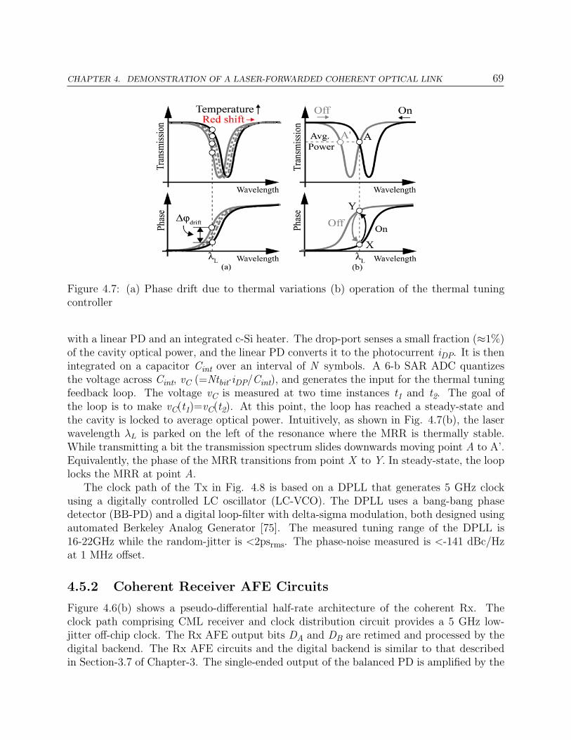
CHAPTER 4. DEMONSTRATION OF A LASER-FORWARDED COHERENT OPTICAL LINK 69
Figure 4.7: (a) Phase drift due to thermal variations (b) operation of the thermal tuningcontroller
with a linear PD and an integrated c-Si heater. The drop-port senses a small fraction (≈1%)of the cavity optical power, and the linear PD converts it to the photocurrent iDP. It is thenintegrated on a capacitor Cint over an interval of N symbols. A 6-b SAR ADC quantizesthe voltage across Cint, vC (=Ntbit·iDP/Cint), and generates the input for the thermal tuningfeedback loop. The voltage vC is measured at two time instances t1 and t2. The goal ofthe loop is to make vC(t1)=vC(t2). At this point, the loop has reached a steady-state andthe cavity is locked to average optical power. Intuitively, as shown in Fig. 4.7(b), the laserwavelength λL is parked on the left of the resonance where the MRR is thermally stable.While transmitting a bit the transmission spectrum slides downwards moving point A to A’.Equivalently, the phase of the MRR transitions from point X to Y. In steady-state, the looplocks the MRR at point A.
The clock path of the Tx in Fig. 4.8 is based on a DPLL that generates 5 GHz clockusing a digitally controlled LC oscillator (LC-VCO). The DPLL uses a bang-bang phasedetector (BB-PD) and a digital loop-filter with delta-sigma modulation, both designed usingautomated Berkeley Analog Generator [75]. The measured tuning range of the DPLL is16-22GHz while the random-jitter is <2psrms. The phase-noise measured is <-141 dBc/Hzat 1 MHz offset.
4.5.2 Coherent Receiver AFE Circuits
Figure 4.6(b) shows a pseudo-differential half-rate architecture of the coherent Rx. Theclock path comprising CML receiver and clock distribution circuit provides a 5 GHz low-jitter off-chip clock. The Rx AFE output bits DA and DB are retimed and processed by thedigital backend. The Rx AFE circuits and the digital backend is similar to that describedin Section-3.7 of Chapter-3. The single-ended output of the balanced PD is amplified by the

CHAPTER 4. DEMONSTRATION OF A LASER-FORWARDED COHERENT OPTICAL LINK 70
Figure 4.8: Block diagram of Tx clock path and bang-bang DPLL.
main TIA and converted to the differential by the post-amplifier. A dummy TIA is used toensure equal input common-mode on both terminals of the post-amplifier. This combinedwith a dummy capacitor CDummy, that matches the PD junction capacitance, improves thesupply noise immunity at the cost of degraded Rx sensitivity due to increased noise power.The two identical and independent thermal tuners tune the resonance of the balanced PDs.A 9-bit pulse density modulator generates pulses depending on the input control word overa fixed 0.17 ns period. These pulses are averaged by the 67 kHz cutoff low-pass thermalimpulse response. Similar to [18], the on-chip thermal tuning circuit is driven by an off-chiptuning algorithm that locks the two PDs to a target wavelength. The heater drivers arecapacitively loaded to reduce the output slew-rate.
4.6 Realization and Experiment Results
Figure. 4.9 shows the die-photo of the test chip and highlights key sub-blocks. It containsmultiple Tx and Rx test sites, and standalone photonic test structures. As evident fromFig. 4.9, the photonic blocks and CMOS circuits are closely integrated with a reasonablefootprint. The test-chip is flip-chip attached to the FR4 board using 50 µm C4 bumps[18]. The Tx circuits are powered from 1.0 V/1.5 V while the Rx circuits are powered from0.8V/1.2V power supply.
4.6.1 Measurement of Standalone Rx and Tx chips
The balanced PDs are biased such that both have an equal reverse bias of 2 V. This ensuresthe two PDs are well matched and avoids Rx sensitivity degradation due to offset from PDmismatch. As shown in Fig. 4.10(a), the on-chip 3-dB coupler operates with a 50:50 coupling

CHAPTER 4. DEMONSTRATION OF A LASER-FORWARDED COHERENT OPTICAL LINK 71
Figure 4.9: Structure of a conventional single-ended (SE) optical receiver (RX).
ratio only over a limited range of wavelengths. At 1272.5 nm it is exactly 50:50 with ∼0.6dB excess loss and ≤3.2 dB IL. Hence, the resonance of balance PDs and the O-DAC arethermally locked to 1272.5 nm. Figure 4.10(b) shows the BER plots of a standalone RX at10 Gb/s and 6 Gb/s. It is characterized using a reference LiNbO3 phase-modulator. Thebathtub curves are wider for higher LO power as it improves the eye-opening at the Rxinput. The OMA sensitivity measured at 10 Gb/s was -15.6 dBm OMA. Figure 4.11(a)shows the Tx eye de-modulated using an off-chip 3-dB coupler at 10 Gb/s before beingthermally stabilized. The O-DAC operates in the depletion mode with 2.0 V reverse bias.It has a Q-factor of ∼6K and is driven by 1.5 V swing. The BPSK eye is maximized whenthe difference between P1 and P2 (Fig. 4.2) is maximum while their sum is minimum. Thisis achieved by switching O-DAC between code 2 and 15 at an IL of 7 dB. The resulting Txoptical eye is shown in Fig. 4.11(b) after being thermally stabilized using an on-chip thermaltuning loop. The measured jitter is ∼2 psrms when Tx is clocked from the DPLL .
4.6.2 Laser Forwarded Coherent Link Demonstration
Figure 4.12 shows an LF coherent link set up between a Tx and an Rx chip. The laser sourcewith a linewidth of 500 kHz is used. Its output power is split using an off-chip fiber-coupler(FC) between the signal (PS) and the LO path (PLO). Polarization controllers (PC) adjustthe polarization to match the input polarization of the grating couplers. Lensed fibers areused to couple light in and out of the Tx/Rx chips and are secured using fiber trays to avoidmechanical disturbance. Figure 4.12 also shows optical power at key nodes due to variouslink losses. Comparing the signal power at node (6) and (7) a signal boost of 8.7 dB is

CHAPTER 4. DEMONSTRATION OF A LASER-FORWARDED COHERENT OPTICAL LINK 72
Figure 4.10: Characterization of standalone coherent Rx using an external LiNbO3 phasemodulator.
Figure 4.11: Measured 10 Gb/s Tx eye (a) before and (b) after thermal stabilization
evident due to mixing with LO. To improve link margin the O-DAC is biased at 3 dB IL.Compared to the LO path, the signal path has two extra lensed fibers to couple light
in and out of the Tx chip. The resulting path-length mismatch is compensated using asimple single-mode fiber (SMF) based delay line instead of the manual free-space opticaldelay line in [17]. Besides, the BER at an attenuated LO power of -3 dBm is measured byreplacing the 50:50 coupler with 75:25 coupler and reducing the laser power instead of usingan optical attenuator. Owing to these two simplifications, the fluctuations in the receivedeye are greatly subdued which improves the BER performance from 10-7 [17] to 10-9 in thiswork.
Figure 4.13(a) shows a setup that compares photocurrent generated in an IMDD and anLF coherent link for a fixed 4 dBm laser input with no modulation applied. As shown in Fig.4.13(b), a peak current of 17.5 µA is generated in an IMDD link while a peak current of ±45µA is generated in the LF link. In the LF link, the residual path-length mismatch is a sourceof two nonidealities. First, as explained in Section-4.3.2 and evident from Fig. 4.13(b), the

CHAPTER 4. DEMONSTRATION OF A LASER-FORWARDED COHERENT OPTICAL LINK 73
Figure 4.12: Optical setup to demonstrate LF coherent Tx-to-Rx link loop-back.
Figure 4.13: (a) Test setup to compare IMDD and LF links (b) Comparison of generatedphotocurrent under no modulation.
laser’s accumulated phase noise and slow frequency drift manifests through the path-lengthmismatch. This cuases peak-to-peak fluctuations in the balanced PD photocurrent. Second,the path-length mismatch induces a static phase-shift ∆φ that limits the amount of peakcurrent to Imax · cos(∆φ), where Imax is the peak current as estimated by (4.6) (for k=0.5).Consequently, the LF gain ALF reduces from 9×, as estimated by (4.8), to 5.2× in Fig.4.13(b). The addition of a low-speed phase tracking loop can fix the static phase offset,frequency fluctuations and in part filter-out some of the accumulated phase-noise due to thepath length mismatch [19].
Figure 4.14 shows the BER of the LF coherent link measured at 10 Gb/s. The pho-tocurrent in Figure 4.13(b) is only stable during a window of time-interval. Measuring BERduring these intervals can give a good idea about the link’s BER performance. This can beachieved by continuously measuring BER in real-time with the clock and the Rx threshold

CHAPTER 4. DEMONSTRATION OF A LASER-FORWARDED COHERENT OPTICAL LINK 74
Figure 4.14: Measured at 10 Gb/s: BER at fixed offset (a) without and (b) with path-lengthmismatch compensation, (c) LF coherent link bathtub curves with LO power. The LOpower is attenuated from 0 dBm to -3 dBm while keeping the signal power constant. Thesimplest means to achieve this without adding additional components to the optical benchis to replace 50:50 coupler with 75:25 and scale down the laser power to keep signal powerthe same.
fixed at an offset where the lowest BER is expected. Figure 4.14(a) and (b) shows BERmeasurement results with such an approach. Each BER point has 2 ms readout overhead.When the path-length mismatch is not compensated (SMF is removed), the fluctuations aremore rapid which limits the BER measurement to 10-7. When the path-length mismatch iscompensated the fluctuations are a bit more stable allowing a 10-9 BER measurement. Asthe BER is measured in real-time, it is inversely proportional to the time difference betweenthe two points. For example, in the zoomed plot of Fig. 4.14(b), the between time point0.72 s and 0.85 s, the BER is being continuously measured. For measuring a further lowerBER of 10-12 at 10 Gb/s, the photocurrent in Fig. 4.13(b) should be stable for more than100 secs, which can be only achieved by adding a phase tracking loop. Figure 4.14(c) showsthe LF link bathtub curves at the Rx chip for the data received from the Tx chip. Due toimproved test-setup, the timing margin of these curves is wider than in [17].
Lastly, Fig. 4.15 breaks down the energy consumed by each LF link sub-blocks. Amongthe Tx circuits, the DPLL consumes the most power as it is designed to support data ratesup to 40 Gb/s, while at the Rx end the Rx AFE consumes the most power amounting to450 fJ/bit. The Tx modulator driver consumes only 40 fJ/bit. With 1.2 mW/nm tuningefficiency, the Tx thermal tuner shifts the O-DAC resonance by 0.5nm while the Rx tunershifts the PDs resonance by 1 nm consuming a total of 290 fJ/bit. A thermal cross-talkof 20% is also observed between the two PDs which helps to reduce the power required bythe tuners. The total energy efficiency of the LF coherent link including Tx, Rx, thermaltuners, and clocking, is 2.3 pJ/bit. Table-4.1 summarizes the performance of the LF coherentlink and compares it with other state-of-the-art optical links. As apparent, this work is

CHAPTER 4. DEMONSTRATION OF A LASER-FORWARDED COHERENT OPTICAL LINK 75
Figure 4.15: Electrical energy-efficiency breakdown at 10 Gb/s.
the only BPSK transceiver reported in recent literature that is fully integrated in a SiPhplatform. Unlike [68] and [28], this work does not require any external off-chip componentslike an optical amplifier. The link achieves a comparable BER of 10-9 while operating at10 Gb/s. Owing to >8 dB LO boost and coherent SNR gain, the Rx achieves -15.6 dBmOMA sensitivity, which is significantly higher compared to prior works. As a result, the linkoperates with 4 dBm laser power, which is 3 dB [12, 40] and 9 dB [36] lower. Optimizationof SiPh devices particularly coupling loss of GC and implementation of a closed-loop phasetracking in future designs are expected to improve the link BER performance while furtherlowering the required laser power. In addition, the architecture of the LF link is compatiblewith commonly used Tx/Rx-side equalization schemes, which can be employed for fasterdata-rate operation and further improving Rx sensitivity.
4.6.3 Comment on closed-loop phase-tracking
In general, coherent demodulation requires local generation or some form of extraction ofthe carrier phase. Any noise or error in tracking the carrier phase leads to the degradation ofSNR. The results are shown in Fig. 4.13(b) and Fig. 4.14(a)-(b) are indicative of this effect.Here, the fluctuations in the Rx eye caused by laser phase-noise degrades the BER. However,owing to laser-forwarding architecture these drifts are slow as shown in Fig. 4.13(b). A simplephase tracking loop realized on the Rx-side can fix for these drifts and stabilize the Rx eye.As the fluctuations in Fig. 4.13(b) are slow, a simple thermal tuning based phase-shifter cancorrect the phase errors. Besides, the thermal tuning based phase-shifter can have a muchwider tuning range. A conceptual diagram of one such loop is shown in Fig. 4.16, where thephase shifter is realized in the LO path. It appears similar to a traditional clock recoveryloop but operates at much lower bandwidth.
Figure 4.17(a)-(b) shows the drift in the output photocurrent of a balanced detector whenan independent laser source is used as LO and when it is laser-forwarded. The use of a locallaser source is commonly employed in conventional BPSK links. Here, as evident from Fig.4.17(a), the current flips within <1 µs, while the same in LF coherent link takes about 5

CHAPTER 4. DEMONSTRATION OF A LASER-FORWARDED COHERENT OPTICAL LINK 76
Table 4.1: Comparison with recently reported monolithic SiPh optical links that do not needan external optical amplifier.
Reference This [12] [36] [40]Work HOTI’17 VLSI’18 VLSI’19
Integration Monolithic Monolithic Hybrid HybridTech- CMOS 45nm 45nm 14nm 16nmnology SOI SOI FinFET FinFET
SiPh CMOS CMOS 28nm SOI GeSi SOIModulation BPSK NRZ NRZ NRZData Rate 10 Gb/s 8 Gb/s 32 Gb/s 50 Gb/sBER/ PRBS [bits] 10-9/31 10-10/31 <10-9†/7 10-12/7Wavelength 1272 nm 1270 nm 1330 nm 1570 nmModulator ER 5 dB 5 dB 4.2 dB >3 dBPD capacitance 20 fF 20 fF 30 fF 90 fF∗
PD Responsivity 0.35A/W 0.5 A/W 0.9 A/W 1 A/WRx OMA -15.6 -11.7† -10.3 -10.9sensivity [dBm]Efficiency [pJ/bit] 2.3 2.6 0.23‡ 3.16Min. Link 4 dBm 7 dBm 13 dBm 7.5 dBm†Laser power†Estimated from plots or data given. ‡TIA+Tx driver only.∗Includes ESD and bump capacitance.
µs. This is a crucial differentiator, as the bandwidth of phase tracking loop required forconventional BPSK link is in the order of few GHz [76], while that with LF coherent linkwill be in the order of few kHz [19].
4.7 Summary
In the pursuit to lower the electrical power consumed by the laser source, this chapterdescribed a laser forwarded coherent link for short-reach optical I/Os. Its effectiveness isanalyzed and proven experimentally. The phase-modulators and coherent homodyne detec-tors are realized using microring resonators. The LF link reduces the required laser powerby improving Rx sensitivity and averaging the optical link losses. The photonic devices andtransceiver circuits are fully integrated in a 45-nm SOI monolithic SiPh platform making theLF link suitable for dense co-packaged optical I/Os. A 10 Gb/s BPSK link between a Tx and

CHAPTER 4. DEMONSTRATION OF A LASER-FORWARDED COHERENT OPTICAL LINK 77
Figure 4.16: Block diagram of a phase tracking loop.
Figure 4.17: Drift in the output of a balanced detector when the LO is (a) derived from anindependent local laser source, and (b) when the laser is forwarded.
an Rx chip is demonstrated. The overall link BER performance was limited by slow fluctu-ations in the received eye due to phase-drifts. This can be addressed by a closed-loop phasetracking loop. The LF link architecture can be readily scaled to support higher-order mod-ulation that relaxes the energy bottle-neck imposed by laser sources and further improvingthe link energy-efficiency.

Chapter 5
Optically Sampled ADC: Architectureand Circuit Implementation
Consistent with the primary goal of this thesis, another system benefiting from the closeintegration of CMOS circuits with SiPh is the optically-sampled analog-to-digital converter(O-ADC). This chapter discusses the architecture and circuit implementation of O-ADC. Thesampling clock jitter is one of the many limitations with conventional CMOS high-bandwidthADCs. By moving the sampling function into the optical domain O-ADC addresses thisproblem. The optical clock sources such as a mode-locked laser (MLL) can generate verynarrow optical pulses with jitter <10 fsrms [77, 78]. The architecture of O-ADC is suchthat it not only enables optical sampling and electronic quantization, it is also integrationfriendly. The architecture tradeoffs, benefits, and performance limitations of O-ADC arediscussed in this chapter. The circuit implementation of CMOS AFE and 8b asynchronousSAR quantizer are also discussed.
Owing to the performance benefits of the O-ADC architecture, this thesis reports thefirst optically sampled ADC that achieves >5b ENOB with CMOS and silicon photonics 3Dintegrated on a single chip. The implementation and measurement of O-ADC test-chip aredetailed in Chapter-6.
5.1 Performance Limitation of Conventional CMOS
ADCs
Analog-to-digital converters (ADC) perform the task of converting analog signals to digitalvalues that can be stored or further processed by digital signal processors. Applicationssuch as data communications (e.g. 400 Gb/s ITU-OTUs, fiber to home, etc), instrumenta-tion (high-speed oscilloscopes), broadband capture (Cable TV, software-defined radio, etc),etc demand ADCs to have effective number of bits resolution of >5b and input samplingbandwidth of >20 GHz. So far the conventional CMOS ADCs have successfully met thisdemand. However, the jitter in the sampling clock, limited input sampling bandwidth, and
78

CHAPTER 5. OPTICALLY SAMPLED ADC: ARCHITECTURE AND CIRCUIT IMPLEMENTATION 79
Figure 5.1: (a) Error in sampling input signal due to jitter in sampling clock and (b) Sim-plified input signal sampling circuit.
sampling clock and input signal distribution network is making it increasingly difficult toachieve higher ENOB at high input frequencies. These issues are further elaborated below.
5.1.1 Sampling clock jitter
An ADC performs two basic operations on the incoming continuous-time signal: samples intime-domain and quantization in the amplitude domain. The time sampling is realized byreferencing the input signal to a repetitive and stable reference signal often referred to as thesampling clock. At the precise time instances defined by the sampling clock, the quantizerthen quantizes the sampled signal resulting in the discretization of the input analog signal.
Any error or uncertainty in the ideal sampling instances of the sampling clock translatesto inaccurate discretization reducing the effective resolution of the ADC. These deviationsof sampling instances are often referred to as sampling clock jitter tj, whose RMS value isoften a figure-of-merit for the quality of the clock source. Further, the impact of clock jitteris even more severe for the high-frequency input signal. For instance, consider a clock withjitter tj in Fig. 5.1(a) sampling a low-frequency and a high-frequency signal. As evident theresulting error voltage ∆vj is higher for the high-frequency signal as its rate of change (V/s)is higher. Due to this reason, the clock jitter is harmless when sampling a DC signal, andits effect increases for higher input frequency.
The impact of sampling clock jitter tj can be predicted by quantifying the impact of ∆vj
in Fig. 5.1(a) on the SNR of the ADCs. To do so, assume an input signal as given by,
Vin(t) = A · sin(2πfint) (5.1)
The RMS value of the slope of the signal in Fig. 5.1(a) can be obtained by taking a derivativeof (5.1). This results in,
dVindt
∣∣∣∣∣rms
=∆vj,rmstj
=2πfinA√
2(5.2)

CHAPTER 5. OPTICALLY SAMPLED ADC: ARCHITECTURE AND CIRCUIT IMPLEMENTATION 80
Thus the RMS error voltage ∆vj,rms due to the clock jitter tj can be easily found by re-arranging (5.2) as shown below,
∆vj,rms =2πfinAtj√
2(5.3)
The last step is to convert the effect of RMS error voltage ∆vj,rms of (5.3) into SNR. Thiscan be simply done by taking the ratio of RMS input signal to ∆vj,rms as given by,
SNR = 20log10
[Vo/√
2
∆vj,rms
]= 20log10
[1
2πfintj
](5.4)
Note that the expression in (5.4) assumes that the SNR of ADC is only limited by theclock jitter, and the ADC has infinite resolution and, thus, no quantization noise. A similarexpression to quantify the impact of clock-skew on SNR can also be derived [79].
Using the SNR expression of (5.4), Table-5.1 outlines the maximum allowable clock jitterfor achieving a target ENOB for an input frequency of 10 GHz and 45 GHz. This reveals thesevere impact of sampling clock jitter on ADC’s SNR. For instance, to achieve an ENOB of6b at 10 GHz the clock jitter must be less than 203 fs, which is achievable by CMOS on-chipclock sources. However, when the input frequency is increased to 45 GHz, the clock jittershould be less than 45 fs. This can be quite challenging for CMOS clock sources to meet.Note that the expression in (5.4) includes only the impact of jitter on SNR and excludes theother ADC non-idealities. In [80], the overall signal-to-noise-plus-distortion ratio (SNDR) isshown that includes all of these effects. It is given as,
SNDR = 10log10
[12A2
(A2/22(N−1))(1/12 + 1/4σ2DNL + σ2
INL) + (√
2πfinAtj)2︸ ︷︷ ︸
Jitter
+σ2n
](5.5)
Here, the SNDR is affected by ADC non-idealities such as quantization noise (factor of 1/12in (5.5)), DNL, INL, noise (σn in 5.5), and jitter. One of the important points highlightedin (5.5) is that out of all the sources of non-idealities, only sampling clock jitter is signal-dependent. It also points to the fact that sampling clock jitter has the strongest impact fora full-scale input signal. Note that assuming a single-tone full-scale input is too pessimistic.The jitter specification can be relaxed by assuming a spectrum that resembles actual input[81, 82]. For instance, assuming a two-tone input would reduce the amplitude A in (5.3)by 6 dB, which reduces the RMS error ∆vj,rms and thus, tj by almost ∼2x. Also increasingthe input signal swing to full-scale increases the non-linearity of the ADC. It is captured byusing worst-case INL in (5.5).
5.1.2 Finite input sampling bandwidth
In addition to clock jitter, limited analog bandwidth of the input sampling circuit throwsanother challenge for high-ENOB high-sampling bandwidth ADC design. Figure 5.1(b)

CHAPTER 5. OPTICALLY SAMPLED ADC: ARCHITECTURE AND CIRCUIT IMPLEMENTATION 81
Table 5.1: Estimated upper bound on sampling clock jitter for a target ENOB and inputfrequency
ENOB
N [bits]
Sampling Clock Jitter
fin=10 GHz fin=45 GHz
14 0.8 fs 0.2 fs
12 3.2 fs 0.7 fs
10 12.7 fs 2.8 fs
8 50.8 fs 11.3 fs
6 203.2 fs 45 fs
shows a simplified model of a typical ADC’s sampling circuit. A series switch samples theinput analog signal on the sampling capacitor CS. Its value is determined based on noiserequirement (kT/C) or matching limitations. The sampling switch can be modeled by anRC π-network comprising the ON resistance RON of the switch and parasitic capacitanceCG. For a typical switch, CG=CGS + CGD + CGB.
The analog sampling bandwidth of the ADC is determined by RON, CG, and CS. Thereare several techniques in literature that aim to reduce RON. For example, boot-strappingcan be used to lower RON. However, it trades-off with device life-time. The dimensionsof sampling switch can be increased, but after a point the resulting device parasitics alsoincrease CG. Another common approach is to lower CS to improve the analog bandwidth.Unfortunately, this approach increases noise which requires increase in the input signal swingto keep SNR the same. With increased signal swing the distortion of ADC and the inputbuffer worsens, which lowers the overall SNDR as per (5.5). Lastly, from Fig. 5.1(b), itmight appear that using high transit frequency (fT) can help lower RON. While it is truethat increasing fT helps to realize a switch with lower RON and lower CG, to achieve highsampling rate time-interleaving is often employed which connects many sampling switchesin parallel. The resulting routing and presence of additional devices increase the parasiticcapacitance making the sampling bandwidth less dependent on fT. Thus, even employingDSM CMOS nodes with high fT is also not useful in improving sampling bandwidth [80].Consequently, the analog bandwidth of CMOS ADCs is still ∼20 GHz [80].
5.1.3 Routing of sampling clock and input signal
A common architecture for realizing high-speed CMOS ADCs is time-interleaving. Here,multiple identical ADCs are time multiplexed forming a parallel array of say M identicalADCs. Each ADC operates at a sampling rate of Fs, while all M ADCs combined achievea higher net sample rate of M Fs. In such situation, routing of input signal and samplingclock to each to the sub-ADCs further complicates design of high-performance high-speedADCs. Both the clock and input should be routed such that skew between the sub-ADCs isthe same. Else as argued in [79] the resulting skew can degrade the SNR of overall ADC.

CHAPTER 5. OPTICALLY SAMPLED ADC: ARCHITECTURE AND CIRCUIT IMPLEMENTATION 82
Figure 5.2: ENOB of conventional as a function of input frequency for CMOS ADCs reportedin literature [83].
Besides, coupling of input to clock or clock to input creates harmonic distortion. Forinstance, coupling of input signal to the clock branch creates second-order harmonic distor-tion.
5.1.4 Survey of CMOS ADcs: ENOB vs fin
Figure 5.2 plots the ENOB with the input signal frequency for the CMOS ADCs publishedin the literature. The impact of the limitations discussed above is visible here. The plot alsoshows jitter lines from 1 ps to 0.1 fs. While CMOS clock source can provide clocks with jitteraround 100 fs, optical clock sources might be needed when ADCs require jitter performancebetter than 10 fs and beyond [84].
As indicated by (5.5), the clock jitter reduces the ENOB with increasing input signalfrequency. This trend is visible in Fig. 5.2. It is very challenging to achieve high ENOBand high input frequencies. To realize design points in this region, optically sampled ADCsoffer a viable alternative. However, the challenge then is to realize sampling in the opticaldomain, quantization in the electrical domain, and the architecture of the optical ADCshould integration friendly to achieve a single-chip solution. These challenges are addressedby the O-ADC demonstrated in this thesis. As discussed in Chapter-6, the O-ADC test-chipachieves 6b ENOB with analog sampling bandwidth of >45 GHz and sampling jitter of <36fsrms. This design performance point is marked by F in Fig. 5.2.

CHAPTER 5. OPTICALLY SAMPLED ADC: ARCHITECTURE AND CIRCUIT IMPLEMENTATION 83
Figure 5.3: Illustration of timing jitter in (a) conventional electrical oscillators, and (b)optical pulse train generated from a mode-locked lasers [87, 88, 89]
5.2 Sampling an Electrical Signal using Optical Pulses
The ability of optical sources such as mode-locked laser (MLL) to produce ultra-low jitteroptical pulses was predicted back in 1993 [85]. Since the MLL has evolved with recentlyreported timing jitter to be <1 fs [86, 78]. This level of jitter performance is tempting forADC designers as the accuracy is greatly influenced by a stable and precise clock source.
To clarify the jitter benefits of MLL over conventional electrical oscillators, consider asimple time-domain illustration as shown in Fig. 5.3. In an electrical oscillator of Fig. 5.3(a),the zero crossings of the signal undergo a random walk due to fundamental noise sourcesaffiliated with the generation of oscillations. The standard deviation of these zero crossingsis equivalent to the integrated phase noise. This is also applicable to the optical pulse trainsource of Fig. 5.3(b). The losses in the resonator cavity of Fig. 5.3(a) are compensated byan amplifier to sustain the oscillations. Both the amplifier and loss mechanism contributestowards additive noise, which is determined using the fluctuation-dissipation theorem [87].This white noise leads to jitter in the zero crossings of the oscillation signal whose varianceincreases linearly over time. The rate of increase of the jitter variance can be given by [87],
σ2(∆tRF ) =1
(2π)2· T 2
0 ·1
Wmode
· kTτc,RF
(5.6)
where, T0 is the period of the oscillation, Wmode is the intra-cavity energy stored in theresonator mode, kT is the thermal energy, and τc,RF is the cavity delay time for the energystored in the resonator. A similar expression can be derived for the optical pulse trains

CHAPTER 5. OPTICALLY SAMPLED ADC: ARCHITECTURE AND CIRCUIT IMPLEMENTATION 84
generated from an MLL source shown in Fig. 5.3(b). It is given as,
σ2(∆tML) =π2
6· τ 2 · 1
Wpulse
· ~ωcτc,ML
(5.7)
where, τ is the pulse width, Wpulse is the intra-cavity pulse energy, ~ωc is the photon energywith pulse center frequency of ωc, and τc,ML is the cavity decay time. Comparing (5.6) and(5.7) assuming 1550 center wavelength and temperature of 300 K, it can appear that MLLsources have poor noise performance as ~ωc ≈ 30 · kT . However, the differentiating factoris the ultra-narrow pulse duration of optical pulses in the MLL source e.g. <200 fs [77]. Asmost of the photons are concentrated in short pulse duration, the pulse position is fairlystable against perturbations caused by the noise source. Consequently, the MLL can havetiming jitter almost two orders of magnitude lower than that of the electrical oscillators [87].
5.2.1 Types of optical ADCs
Optical ADCs is an active research topic today. Either sampling and/or quantization func-tions of conventional electronic ADCs are being replaced by equivalent optical counterparts.A good survey of published optical ADCs is outlined in [90]. The concept of optical ADCswas first reported back in the early 1970s [91, 92]. Since optical ADCs are actively re-searched with remarkable progress been reported in recent literature. In [93] an opticalquantizer based ADC is shown that uses spatial interferometry with 3.6 bits for a 1.25-GHzinput signal sampled at 40 GSa/s, while in [94] an integrated optical spatial quantizer basedADC achieved 3b ENOB for an 18-GHz signal. Researchers in [95] demonstrated the firstoptical quantizer and encoder based on time-interleaved ADC that uses nonlinear Sagnacloop mirrors and achieves 3.75n ENOB at 160 GS/s. While notable advances have beenmade, ADCs realized using optical quantizer has resolution limited to 3-4 bits. Currently,research efforts are in progress to further improve the accuracy.
On the other hand, an optically-assisted time-stretched ADCs is reported in [96, 97],where modulated optical pulses are significantly dispersed and temporally stretched so thata slow discrete electronic ADC can digitize the signal. Using this approach an optical ADCis demonstrated that digitizes 95.3 GHz tone at 10 TS/s with 4.5b ENOB [98]. Whilethis ADC achieved astonishing results, it requires dispersion compensated fiber which isnot straight forward to integrate on a SiPh chip. However, a slightly different approachof optical sampling employing a wavelength-demultiplexing scheme reported in [99] andthoroughly analyzed in [100] lends itself readily to single-chip SiPh and CMOS integration.The performance of such ADCs along with necessary calibration techniques and algorithmsare well studied in the literature. In [101], demonstrates a 9.8b ENOB for a 733 MHz inputsignal sampled at 505 MS/s. A similar architecture is adopted for the O-ADC test-chipdemonstrated in this thesis.

CHAPTER 5. OPTICALLY SAMPLED ADC: ARCHITECTURE AND CIRCUIT IMPLEMENTATION 85
Figure 5.4: Concept of optical sampling in optically sampled ADC (O-ADC).
5.2.2 Basic concept of time-interleaved optical sampling
To leverage the low-jitter performance of MLL source, a simple single-channel opticallysampled ADC can be realized as shown in Fig. 5.4. Here, an electro-optic modulator suchas Mach Zehnder (MZ) interferometer-based modulator intensity modulates the incomingoptical pulses from the MLL source with the input RF signal. The sampling process occursduring this electro-optic modulation of optical pulses. The modulated pulses at the outputof the modulator carry the RF signal values at the time instances defined by the temporalposition of the optical pulses. Lastly, the optical pulses are converted into electrical currentpulses using photodetectors and digitized by electronic ADCs. The operations illustrated inFig. 5.4 shows optical sampling and electronic quantization functions of an optically sampledADC (O-ADC).
The simple scheme of Fig. 5.4 ensures low-jitter sampling, but the sample rate is limitedby the spacing between the optical pulses, which is defined by the repetition rate of the MLLTR. This makes it difficult to achieve accurate sampling at high sample rate as increasingthe MLL repetition rate would require re-engineering of the MLL cavity, which can be verychallenging. Even if the problem of MLL repetition rate is resolved, the architecture of Fig.5.4 has another issue that it requires CMOS ADC to operate a full-rate. For instance, ifa sampling rate fS of 10 GS/s is desired then the CMOS ADCs should be also clocked at10 GHz (fclk). Both of these limitations can be addressed by employing wavelength andtime-interleaving as shown in Fig. 5.5. Here, the center wavelengths of the pulses at theinput of the modulator change periodically in time. Thus, for a system with N channelrequires N distinct wavelengths that are created by splitting the spectrum of MLL. As thisapproach requires passive filters that can be readily integrated in a SiPh chip, this approachis later adopted in this thesis. Thus, as shown in Fig. 5.5, an optical demultiplexer (optical

CHAPTER 5. OPTICALLY SAMPLED ADC: ARCHITECTURE AND CIRCUIT IMPLEMENTATION 86
Figure 5.5: Concept of time-interleaved optical sampling.
filter) splits the optical pulses at the output of MLL into sub-pulses centered at a differentwavelength. Note that the operation of optical demux is quite different from a time-demuxpopularly used as a logic gate. These pulses are then delayed with respect to each other usingpassive delay lines and combined into a single path using a N -to-1 multiplexer. The resultis a pulse train with a repetition rate increased by N. These pulses are separated both intime and in wavelength and are modulated by an input RF signal. These modulated pulsesare first separated and then converted to electrical current pulses, which are later digitizedby CMOS ADCs. Thus, the overall O-ADC achieves N · fS higher sample rate, while eachsub-ADCs operate at fS sample rate.
In summary, the major benefits provided by the architecture of Fig. 5.5 are: jitter of O-ADC is governed by the extremely low jitter of the optical pulses, due to use of passive opticalcomponents it is amenable to integration in any emerging CMOS and SiPh platforms, andthe sampling bandwidth is determined by electro-optical interaction in the modulator, whichcan be very fast. Thus, the O-ADC has the potential to enable ADCs with high-resolutionand high input sampling bandwidth.
5.3 Architecture of O-ADC
Using the topology discussed in Fig. 5.5, an O-ADC architecture as shown in Fig. 5.6 isimplemented in this work. The optical pulse train with repetition period TR is split intoN trains, each centered at a different wavelength, with a 1-to-N wavelength demultiplexer

CHAPTER 5. OPTICALLY SAMPLED ADC: ARCHITECTURE AND CIRCUIT IMPLEMENTATION 87
(optical filter). These trains pass through optical delay lines, which introduce incrementaldelays and are then recombined with a multiplexer to produce a pulse train with a repetitionperiod of TR/N . All of this setup is combined and represented as a simple optical pulse sourcein Fig. 5.6. The modulation of the optical pulse train with the RF signal, or in other wordsthe optical sampling, is performed using an off-chip electro-optic MZM. The modulated pulsetrain is then coupled into the test-chip, which is realized on a single-chip implemented in a3D integrated platform. These pulses are then taken apart into N channels using double-ring filters matched to the one used to realize optical pulse source. These pulses in all Nchannels are individually converted to the current pulses by the integrated photodetectors.The double-ring filters and detectors are realized on SiPh chip. The current pulses areamplified and digitized with CMOS ADCs realized in 65nm. The SiPh chip and the 65nmCMOS chip are integrated at the wafer-scale using through-oxide-vias (TOVs).
The CMOS ADCs are synchronized with the MLL pulses using the electrical clock out-put. The digitized samples stored in the on-chip memory back are read and post-processedto compensate for distortions and interleaved errors before obtaining the final digital repre-sentation of the RF signal. As mentioned earlier, the jitter of the overall O-ADC is governedby the jitter of the optical pulses. It will be shown later that the jitter in the CMOS clockdoes not influence the ADC performance. In addition, the interleaving scheme of Fig. 5.5not only increases the sample rate by a factor of N but also reduces the required analogbandwidth from the detectors and CMOS ADCs by N . Thus, O-ADCs with high samplerate and high sampling bandwidth can be realized by interleaving relatively low-speed com-ponents. This is another important advantage offered by the O-ADC architecture of Fig.5.6.
5.3.1 Sampling bandwidth of O-ADC
In addition to improving the sampling jitter, the O-ADC architecture of Fig. 5.6 also iscapable of increasing the input signal sampling bandwidth. Here, we evaluate and identifylimits on sampling bandwidth, and potential sources that are the bottleneck to achievingwider bandwidth. For this purpose, it is assumed that an MLL source is available as reportedin [77]. It outputs pulses with <0.2 ps pulse width at 1 GHz repetition rate with a full-widthhalf max (FWHM) of 17.5 nm (2.2 THz) and jitter with 22 fs. For simplicity, a rectangularoptical pulse of width 0.2 ps is used in the simulation as shown in Fig. 5.7. Note thatthe optical pulse source in Fig. 5.6 represents an MLL source combined with demux-delayline-mux interleaver.
The optical demux slices the spectrum of MLL into N with each slice centered arounda different wavelength. In Fig. 5.7, for example purpose, N of 4 is chosen. The FWHMbandwidth of the spectrum at the output of the optical demux (optical filter) is 0.65 nm.Consequently, the optical pulse expands from 0.2 ps to 5.5 ps. These optical pulses are thendelayed and combined. Both of these operations do not alter the optical pulse width. Thetime and wavelength spaced 4 optical pulses with color black, red, blue, and green, at theoutput of the multiplexer, are as shown in Fig. 5.7. Further, these pulses are modulated by

CHAPTER 5. OPTICALLY SAMPLED ADC: ARCHITECTURE AND CIRCUIT IMPLEMENTATION 88
Figure 5.6: Architecture of optically sampled ADC (O-ADC) that uses low-jitter opticalpulses to sample the input signal.
an MZM with a 10 GHz RF input signal. The modulated pulses are shown in the bottom-leftplot in Fig. 5.8.
At this point, there are two bandwidth limitations. First, the limit is imposed by thefinite pulse width of the optical pulses BW1 and the second limit is due to the electro-opticbandwidth of the modulator BW2. The bandwidth limit due to finite optical pulse widthcan be estimated simply by,
BW1 =1
2πτa≈ 29GHz (5.8)
where, τa is the optical pulse width after the demultiplexer. If the BW2<BW1 then theelectro-optic bandwidth of the modulator becomes a bottleneck. The modulator later used

CHAPTER 5. OPTICALLY SAMPLED ADC: ARCHITECTURE AND CIRCUIT IMPLEMENTATION 89
Figure 5.7: Optical pulse width at various nodes in pulse interleaver. The MLL parametersare obtained from [77].
Figure 5.8: Optical pulse width at the input and output of MZM, double-ring filter banks,and photodetectors.

CHAPTER 5. OPTICALLY SAMPLED ADC: ARCHITECTURE AND CIRCUIT IMPLEMENTATION 90
in Chapter-6 to measure O-ADC test-chip has 40 GHz bandwidth, while there are integratedmodulator demonstrated in the literature that have similar or higher bandwidth. Thus, toachieve high sampling bandwidth, the optical demux should have as wider bandwidth aspossible. However, due to limited FSR of the demux, realizing wider bandwidth often putsa limitation on the amount of channel that can be interleaved forcing the sample rate of theCMOS ADCs to increase to meet target overall sampling rate.
After modulation, the optical pulses are filtered, converted to current, and digitized.As the signal is already sampled, none of these steps affect the sampling bandwidth of theO-ADC.
5.3.2 Performance tradeoffs of O-ADC
For a fixed average optical power delivered from the MLL, the presence of optical losses andadditive thermal noise limits the resolution (ENOB) that can be achieved by the O-ADC.Assuming an ideal CMOS ADC, the ENOB of the O-ADC is primarily determined by theSNR at the output of the photodetector in Fig. 5.8. It is given as,
SNR = 10log10
[PSPn
]and ENOB =
SNR− 1.76
6.02(5.9)
where, PS is the signal power while Pn is the integrated noise power over the noiseequivalent bandwidth BWn. Assuming the dark current of the photodetector contributesnegligible shot noise, the noise power can be expressed as,
Pn = 2q · Imax + Imin2
·BWn = 2q · Imax2
(2−m) ·BWn (5.10)
where, Imax and Imin is the maximum and minimum current generated by the photodetec-tor for a modulation depth m applied by the modulator. Thus, Imin = (1−m)Imax. Further,the signal power PS can be expressed as,
PS =
(Imax − Imin
2
)2
=m2I2
max
4=
(mR
2
)2
· α2DLP
2inc (5.11)
where, R is the detector responsivity, α2DL is the drop-port loss of the double-ring filters
in Fig. 5.6, and Pinc is the incident optical power per channel in the bus-waveguide in Fig.5.6. The total optical power in the bus-waveguide is NPinc. Using (5.9) and (5.11) the SNRcan be expressed as,
SNR =
(m√
2−m
)2
· R2
4· αDLPinc
2qBWn
(5.12)
The expression of (5.12) reveals an important requirement of O-ADC. The SNR can beimproved by 1 bit by increasing modulation depth m by ∼2x. However, as will see in thesection later increasing modulation depth too much induces distortion in the modulator.

CHAPTER 5. OPTICALLY SAMPLED ADC: ARCHITECTURE AND CIRCUIT IMPLEMENTATION 91
Figure 5.9: (a) Peak power and bandwidth of MLL to support N=4 and N=16. (b) FSR,channel spacing, and bandwidth of demux.Typical values of FSR is 2.2 THz, S is 120 GHzand BWDM is 20 GHz [100].
While this distortion can be calibrated, there is a limit to which the calibration can beeffectively applied. For instance, making the modulation depth of 1 would induce strongclipping distortion which cannot be calibrated. Thus, the linearity performance of the O-ADC degrades greatly.
Further, the incident optical power Pinc in (5.11) can be further expressed as,
Pinc =
(BWDM
BWML
)︸ ︷︷ ︸Spectralfill
·αIILαMZIL αc︸ ︷︷ ︸
OpticalLoss
·PML
N(5.13)
where,BWDM Spectral bandwidth of the optical demultiplexer. Typical value is 1.1 nm.
BWML Spectral bandwidth of MLL source. Typical value is 17 nm.
αIIL Insertion loss of the interleaver (demux-delay line-mux). Typical value is 7 dB.
αMZIL Insertion loss of the MZ modulator. Typical value is 4 dB.
αc Fiber-to-chip coupling loss. Typical value for Fig. 5.6 is 3.5 dB.
PML Peak MLL output optical power per channel. Typical value is 0.1 W.
To maximize SNR, from (5.12), it is evident that Pinc should be maximized. On the otherhand, to increase the sampling rate the number of interleaved wavelengths should be in-creased as the sampling rate of the O-ADC is related to N and repetition rate FR of theMLL as given by,
FS = N · FR where, FR = 1/TR (5.14)
However for fixed MLL output power, from (5.13), increasing N would reduce Pinc as theMLL power is now split between more number of channels. This is clarified in Fig. 5.9(a)

CHAPTER 5. OPTICALLY SAMPLED ADC: ARCHITECTURE AND CIRCUIT IMPLEMENTATION 92
Figure 5.10: Simulated achievable ENOB lines for given input MLL power and O-ADCsampling rate contour. The numbers on each line highlight the achievable ENOB whilethe dotted lines show the effective power in the double-ring filter bank, which can induceadditional distortion depending on the ring’s design.
where an MLL spectrum with a peak output power of PML per channel is been divided into4 channels. Keeping the same average optical power, if the number of channels is increasedfrom 4 to 16, the PML should be reduced as it is distributed among more channels as shownin Fig. 5.9(a). A more practical scenario is described in Fig. 5.9(b) where an MLL withfixed output power and spectral bandwidth BWML is available. The bandwidth of demuxBWDM and channel spacing S is chosen such that it spans the MLL spectrum. Note thatthe FSR of the demux must be bigger than the BWML. To accommodate larger number ofchannels, the bandwidth of the demux and the channel spacing can be squeezed. However,as the bandwidth of the demux is lowered the spectral fill term in (5.13) also reduces whichin turn reduces Pinc and degrades SNR as per (5.12). In o
FSRDM ≥ BWML ≈ Nmax · (BWDM + S) (5.15)
where, Nmax is maximum number of interleaving channels possible for a given BWML, S, andBWDM.
The arguments made and analysis done for expressions (5.9)-(5.14) are put in perspectiveby Fig. 5.10. Here, the achievable ENOB is calculated from (5.9) for varying MLL opticalpower and the sampling rate of O-ADC defined by (5.14). As evident from Fig. 5.10, forfixed MLL optical power, increasing the sampling rate by increasing N will reduce ENOB.To keep ENOB constant, the MLL optical power should also be increased. This gives rise tothe ENOB lines in Fig. 5.10. As the MLL optical power increases so will the power in the

CHAPTER 5. OPTICALLY SAMPLED ADC: ARCHITECTURE AND CIRCUIT IMPLEMENTATION 93
double-ring filters, which is indicated by the dotted lines in Fig. 5.10. This leads to ENOBbeing further degraded due to distortion from the double-rings, which is covered later. Apreferred way to increase the sampling rate of O-ADC is to keep PML constant and increasethe repetition rate FR. However, as the analog bandwidth of the photodetector and thesampling rate of the CMOS ADC depend on FR, both of them should also be increased.
Thus, on one hand, the value of Nmax is limited by the FSR of demux while on the otherFR is limited by maximum achievable analog bandwidth of the detector and CMOS ADC. Insuch a scenario, responsivity R of the detector in (5.12) is the only knob that does not haveany tradeoffs attached. Increasing R not only linearly increases SNR but also reduces theoptical power needed in the double-ring and thereby lowering their distortion. In summary,the purpose of this analysis is to give a rough idea about the required input optical power,achievable resolution, and the importance of the number of interleaved channels. The keytake away is that for a given ENOB,
• the optical power must change in proportion to the number of interleaved channels.
• the power must change in proportion to the repetition rate.
• any change in the loss of the optical components must be compensated by adjustingthe optical power.
5.3.3 Impact of distortion from double-ring fitlers
In Fig. 5.10, it might be tempting to observe that high ENOB at a faster sampling rate can beachieved by simply increasing the MLL output optical power. While this intuition is correct,the distortion induced by the double-ring filters at high optical power puts a practical limiton maximum achievable ENOB. Any optical block designed using silicon waveguides willexperience two-photon absorption (TPA) because when two photons combine to overcomethe bandgap of silicon additional electron-hole pairs are generated. These TPA generatedfree electrons and holes act as absorption centers. This phenomenon is referred to in theliterature as free carrier absorption (FCA). The presence of these free carriers (electrons andholes) also changes the refractive index of the silicon (as discussed in Chapter-3) inducing thephenomenon called free-carrier dispersion (FCD) effect. All of these nonlinear phenomenagenerate nonlinear distortion, which eventually deteriorates linearity or the SFDR of theO-ADC. The impact of these nonlinearities is escalated at higher optical power. Thus, ifthe optical power is increased to achieve higher ENOB, the resulting increase in nonlinearitywould adversely affect the ENOB.
The combined effect of these three sources of distortion can be quantified by measuringthe traditional distortion coefficients. For this purpose, distortion coefficients till 5th orderis measured from the drop-port spectrum of the double-ring filters whose design and imple-mentation are discussed in Chapter-6. These distortion coefficients are then used along withthe simulated SNR values to get an estimate of the overall SNDR as shown in Fig. 5.11(a).The ENOB in Fig. 5.11(b) is then calculated from the simulated SNDR. As shown in Fig.

CHAPTER 5. OPTICALLY SAMPLED ADC: ARCHITECTURE AND CIRCUIT IMPLEMENTATION 94
Figure 5.11: Simulated: (a) SNR and SNDR, and (b) resulting ENOB. The distortion co-efficients uptill 5th harmonics are used whose values are obtained from measurement ofdouble-ring filters designed in 3D integration platform discussed in Chapter-6.
5.11(a), the SNR continual increases with the increasing MLL optical power. This behavioris also predicted by (5.12). However, the distortion is not modeled in the ENOB lines of Fig.5.13 always increases with MLL power. In the presence of distortion, the SNDR and ENOBplots are shown in Fig. 5.11(a) and (b), respectively. The SNDR degrades at high enoughMLL optical power due to the distortion arising in the double-ring filters. The distortioncontribution of the filters can be controlled by design to some extent [100]. Alternatively,digital calibration techniques can also be adopted at the cost of increased overall powerconsumption of O-ADC.
Note that during the development of test-bench to evaluate O-ADC test-chip performancein Chapter-6, the losses were significantly higher due to the use of discrete components. Thus,the MLL optical power was not sufficient, which was compensated using an off-chip Er-dopedFiber Amplifier (EDFA).
5.3.4 Impact of cross-talk due to double-ring filters
Like every other traditional optical or RF filter, the double-ring filters used in Fig. 5.6, havefinite rejection. Consequently, the optical power on the neighboring channel wavelength isrejection partially. This unrejected optical power drops onto the detector and creates cross-talk current pulses as shown in Fig. 5.12(a). Similar to any traditional filter design, therejection can be improved by implementing a higher-order filter or increasing the spacingbetween the two channels. However, achieving wider bandwidth and higher-order simultane-ously is challenging. Figure 5.12(b) illustrates this tradeoff. Here, the signal to interferenceratio is plotted against channel spacing for varying bandwidth. For lower bandwidth filters,

CHAPTER 5. OPTICALLY SAMPLED ADC: ARCHITECTURE AND CIRCUIT IMPLEMENTATION 95
Figure 5.12: (a) Interfering current pulses from adjacent channels. (b) Impact of cross-talkwith channel spacing for varying BWDR.
it is better to achieve higher rejection at the same channel spacing.An important aspect to notice in Fig. 5.12(a) is that the cross-talk current pulses are
separated in time due to the time-interleaving nature of the optical pulse source. This featureis later used to advantage in Section-5.5 where a switch-capacitor-based current integratingfront end with integration window designed such that it integrates current pulses from thepresent channel. Thus, it rejects the cross-talk current pulses to a great extent.
5.4 Comments on modulator and modulator driver
In Fig. 5.6, a Mach Zehnder interferometer-based modulator (MZM) is used that preferrablyrequires a material with strong eletro-optic effects. For demonstration purpose, a LiNbO3
MZM is used as they are easily available, wide-bandwidth, and compact. In future, theseMZM will be integrated on the O-ADC chips using other III-V semiconductor materials likeGaAs and InP that have equally strong electro-optic effects.
As shown in Fig. 5.13(a), the MZM comprises an input waveguide that is split intotwo paths that are later recombined into an output waveguide. The two paths make upthe two arms of the interferometer. The driver in Fig. 5.13(a) applies an RF input andalso provides the necessary bias for the MZM. The applied voltage creates an electric fieldacross each arm of MZM that induces change in the refractive index and thus, the opticalpath length modulating the phase of the optical signal in each arm. When the two paths arecombined, the different phase modulation in each arm translates into intensity modulation inthe output waveguide. To achieve a chirp free intensity modulation, meaning only intensityis modulated without occassional phase or frequency modulation, the phase modulation in

CHAPTER 5. OPTICALLY SAMPLED ADC: ARCHITECTURE AND CIRCUIT IMPLEMENTATION 96
Figure 5.13: (a) An MZM driven by a driver, and (b) transfer function of an MZM.
each arm should be exactly equal and opposite in sign.The RF input and the DC bias are applied to the MZM using two separate pairs of
electrodes. They are often referred as modulation and bias electrodes, respectively. In Fig.5.13(a), the MZM driver superimposes the modulation signal onto the bias voltage. Thus,for an RF input signal Vin(t) in Fig. 5.13(a), the transfer function of an intensity modulatoris given by,
Iout(t) = TmzIin2
[1 + sin
(πVin(t)
Vπ+ θ
)](5.16)
where,Vπ Voltage required to achieve a phase-shift of π
θ Deviation from the quadrature bias point
Tmz Transmission of the modulator
Iin Input optical intensity
Iout Output optical intensity that varies as a function of Vin(t)
Depending upon the application, the MZM is biased at an appropriate bias point. Fig.5.13(a) shows various bias points in the transfer function of an MZM. A voltage of Vπ shiftsthe transfer function from minimum to maximum or maximum to minimum. The MZM isbiased at this point for non-linear applications like NRZ transmission. If the input NRZ datahas an amplitude of Vπ then the output data is NRZ as well with improved signal qualityas overshoot and patterning are clipped by the non-linear transfer of the MZM.
However, for applications requiring high-linearity such as O-ADC, the MZM is biased atthe quadrature point (Q− or Q+ in Fig. 5.13(b)). When biased at the quadrature point thephase term θ in (5.16) is zero and the input signal utilizes the linear part of the transfer asshown in Fig. 5.14. Note that higher linearity is achieved by making sure that the inputmodulating signal has an amplitude much smaller than the Vπ of the modulator. However,improving linearity by reducing the modulation depth results into SNR degradation which

CHAPTER 5. OPTICALLY SAMPLED ADC: ARCHITECTURE AND CIRCUIT IMPLEMENTATION 97
Figure 5.14: Analog modulation of MZM when biased at quadrature.
would be explained in later section. Lastly, it should be mentioned that the value of Vπ
is also dependent on application. For application requiring high-linearity, it is desirable tohave low Vπ and thus, more gradual and linear transfer curve. However, for communicationapplications that use phase-shift keying like BPSK or DPSK, the value of Vπ should be assmall as possible to reduce the demand of high drive voltage swing and high sampling rates.
5.4.1 Modulator Linearization
As given by (5.16), the transfer characteristic of MZM is cos2-shaped. The resulting nonlin-earity can be much worse than that contributed by the double-ring filters in Fig. 5.11(a).This makes the MZM the dominant source of nonlinearity and limits the dynamic range orthe SNDR of the O-ADC. Thus, it is crucial to linearize the MZM transfer characteristic. Asimpler means to linearize is to use small modulation depth. However, choosing too smallof a modulation depth can be expensive from SNR perspective as given by (5.12). A betterapproach is to use moderate modulation depth (between 0.5 to 0.8), and calibrate for theresulting non-linearity. Note that maximum modulation depth (i.e. m=1 when output ofthe driver swings full Vπ) would induce hard distortion which cannot be calibrated [100].
The calibration of MZM transfer characteristic or linearization can be performed byobserving that the expression (5.16) is fairly static in nature, and thus, can be readilyinverted in the digital domain to fully recover the original input tone. Thus, if the outputof the ADC is VADCout for an input of Vin(t), then the calibration to be applied can beobtained by re-arranging (5.16) as shown below,
Vin,calib(t) =Vππ
[1
2· sin−1
(2VADCoutK1
− 1
)](5.17)

CHAPTER 5. OPTICALLY SAMPLED ADC: ARCHITECTURE AND CIRCUIT IMPLEMENTATION 98
Here, Vin,calib(t) is the calibrated value for Vin(t) from sampled and quantized ADC outputVADCout, while K1 is a constant proportional to the energy of the input optical pulses. Anyerror due to drift from the quadrature point (i.e. θ 6= 0) will result in an offset which iscalibrated using foreground calibration approach described in Chapter-6.
Using this approach researchers in [101] showed improvement in linearity of >80 dB anddemonstrated a discrete implementation of an optically sampled ADC with ∼10 b ENOB.However, this linearization method is not perfect and has some limitations. It can onlylinearize non-linearity resulting from interferometer transfer function given by (5.16). De-pending on the quality crystal used to implement MZM, the phase modulation in each of thearms of MZM can be different, and can exhibit nonlinear behavior. This added non-linearitycannot be calibrated by the approach described above. In addition, any non-linearity addedby the MZM driver (shown in Fig. 5.13(a)) will also be not calibrated. While developingthe test-bench for the O-ADC test-chips, these two aspects are actively kept in mind. Toavoid distrotion from phase modulator, a high quality LiNbO3 based MZM is used and thedistortion from driver is avoided by filter its output before it drives the MZM.
5.5 Limitations and Tradeoffs of O-ADC building
blocks
The architecture of O-ADC is Fig. 5.6 enables sampling of high-speed RF signal with low-jitter optical pulses. In the process, it requires a few additional components that influencethe overall ADC performance and offer certain design choices to make. The previous Section-5.3 covered them in detail. However, it also helps to outline these limitations and tradeoffson per block basis, which is shown in this section below. Here, the impact of each sub-blocksof Fig. 5.6 on overall O-ADC performance is summarized.
5.5.1 MLL optical pulse source
The low-jitter optical pulses for O-ADC are provided by the MLL source. The key metrics ofMLL that influence O-ADC performance are optical pulse width, jitter, output power, andrepetition rate. While the optical pulse width is determined by the bandwidth of the demux,the MLL is still required to have wide enough spectral bandwidth to accommodate the targetnumber of interleaving channels. The jitter of the MLL source directly translates into thesampling jitter of the O-ADC. Hence, having a low-jitter MLL is desirable. However, the fulladvantage of low-jitter of the MLL can only be taken if a high enough sampling bandwidthof the O-ADC is achievable.
Furthermore, the optical power of the MLL is another influential parameter that directlyimpacts O-ADC performance. The ENOB of the O-ADC improves with optical power untilit gets limited by the distortion from the double-ring filter bank. Lastly, the repetition rateof the MLL helps to achieve higher sampling rate O-ADC without requiring a large numberof interleaving channels which adversely impacts the ENOB. While the MLL designers focus

CHAPTER 5. OPTICALLY SAMPLED ADC: ARCHITECTURE AND CIRCUIT IMPLEMENTATION 99
on performance like achieving extremely narrow pulse-width or ultra-low jitter, an MLLdedicated for O-ADC would have slightly different design specifications owing to the reasonslisted above.
5.5.2 Demux-delay line-mux interleaver
The interleaver block comprising of the demultiplexer, delay lines, and a multiplexer is animportant element of O-ADC. Particularly, demux is the most crucial component as thespectral bandwidth of the demux controls the optical pulse width and thus, the samplingaperture of the O-ADC. Further, the FSR of the demux should also be larger than the spectralbandwidth of the MLL. To increase the number of interleaved channels while keeping theoptical pulse width wide enough, the demux should be designed with wide spectral bandwidthand sharp roll-off. Further, the smaller spectral bandwidth of the demux adversely impactsSNR as it degrades the spectral fill, represented in (5.13). Besides, controlling the delayrealized by the delay lines is crucial to avoid spurs in the O-ADC output spectrum due totiming mismatch. These spurs will degrade the SNDR and thus, the ENOB of O-ADC. Inchapter-6, the delay line is realized using optical fiber where the delay is implemented bytuning fiber length. This way of implementing the delay line ensures timing mismatch isminimized. However, it is hard to integrate. In [100], the delay line is implemented usingsilicon waveguides. While the precise delay cannot be ensured due to process variations,integrated heaters are used to tune out any timing mismatch. This approach does costincreased power consumption. Lastly, for the design of the multiplexer, it is important tominimize the insertion. This helps to increase the incident optical power and thus, the SNRfor the same MLL optical power.
5.5.3 Electro-optic modulator
The modulator is on the most important blocks of the O-ADC as it enables the samplingprocess. From the O-ADC system perspective, the bandwidth, linearity, and modulationdepth are the most critical parameters of the modulator. A high electro-optic (S21) band-width is crucial as it governs the maximum input RF signal rate at which the modulatorcan intensity modulate the optical pulse. This modulation should occur with good linearityin order to realize high ENOB at maximum input bandwidth. Lastly, the modulator shouldalso maintain good linearity while achieving good modulation depth. Researchers in [99]show that for an MZ modulator a modulation depth of 0.6 is optimal. A good modulationdepth further enables higher ENOB by maximizing the SNR. Additionally, to realize a trulysingle-chip solution, the driver in Fig 5.13(a) should also be integrated. In this case, theinput capacitance and Vπ of the modulator are also equally important as they require thedriver to produce high swing output at high frequencies while driving a large capacitive load.For instance, the MZM with 40 GHz bandwidth used in Chapter-6 to test the O-ADC test-chips requires 4.5 Vpp swings at 40 GHz, which can be challenging for a CMOS integrateddriver.

CHAPTER 5. OPTICALLY SAMPLED ADC: ARCHITECTURE AND CIRCUIT IMPLEMENTATION 100
Figure 5.15: Wavelength spectrum matching between MLL, demux, and double-ring filterbank.
5.5.4 Double-ring filter bank
As the double-ring filter bank receives sampled data, it does not influence the samplingbandwidth of the O-ADC. However, its spectral bandwidth, linearity, and roll-off do impactSNDR, and thus, the ENOB of the O-ADC. Firstly, due to power enhancement in thedouble-rings, it can generate distortion due mechanisms such as TPA, FCA, and FCD. Thecoefficients that control these distortions are a strong function of the device geometry. Thus,the design of double-ring filters should be done accounting for the distortion. [100]. Thespectral bandwidth is another crucial factor. The double-ring filter should be designed inconjunction with the spectral response of the MLL and the demux as shown in Fig. 5.15.The FSR of the double-ring FSRDR should be greater than or equal to the FSR of the demuxFSRDM, which in turn should be greater than the spectral bandwidth of the MLL. Lastly,the roll-off of the filter also matters as it controls the amount of cross-talk. A combination offilter design along with circuit trick like switch-capacitor based integrator can address thisissue.
5.5.5 Photodetector and CMOS AFE
The photodetectors convert the sampled and filter optical pulses to current while the CMOSAFE quantizes the samples resulting in the digitization of the RF input signal. The respon-sivity R of the photodetector is one of the most critical knobs in improving the O-ADCperformance as increasing it incurs no other O-ADC system tradeoffs and linearly improvesthe ENOB. Also, the analog bandwidth of the detector and AFE is crucial especially whenit is not possible to increase the number of interleaving channels and still improvement in asampling rate of the O-ADC is desired. In such a situation, the repetition rate of the MLL

CHAPTER 5. OPTICALLY SAMPLED ADC: ARCHITECTURE AND CIRCUIT IMPLEMENTATION 101
Figure 5.16: Analog-front end and 8b asynchronous SAR ADC.
should be increased which would require an increase in the analog bandwidth of the detectorand the AFE. Lastly, the input-referred noise of the AFE is crucial as it can marginallyreduce the overall ENOB.
5.6 Circuit Implementation
The optical pulses that are filtered by the double-ring filter are incident on the photodetec-tor, which generates current pulses in response. An analog frontend (AFE), comprising anintegrator and a pre-amplifier, and an 8b asynchronous SAR quantizes these current pulses.Figure 5.16 shows the overall circuit implementation of the AFE along with the SAR ADC.This circuit is primarily a switched capacitor-based whose timing diagram is shown in Fig.5.17. During φ1, the detector current is integrated on the sampling capacitors CS1 and CS2
for TInt duration. As the optical pulses have a fixed width, the integrator rather acts as anamplifier with gain τ/2CS and generates a single-ended voltage across CS1,2. To decreasesensitivity to supply and common-mode noise, the ADC is often implemented differentially.As the voltage across CS1,2 is single-ended, it needs to be converted to the differential. Forthis purpose, before transferring charge to CF in Fig. 5.16, the capacitor CS1 is flipped whileCS2 is connected as is. This is achieved by switching the bottom plate of CS1 and the topplate of CS2 during phase φ2. Note that while this operation achieves the desired single-ended to differential conversion, the charge transfer from CS2 is sensitive to the parasitics,which is mitigated by careful layout and proper sizing.
During φ2, in addition to the charge transfer, the SAR ADC samples the voltage on the

CHAPTER 5. OPTICALLY SAMPLED ADC: ARCHITECTURE AND CIRCUIT IMPLEMENTATION 102
Figure 5.17: O-ADC AFE timing diagram.
top plate of the 7b capacitive DAC. This improves the conversion speed by resolving thefirst bit without charge redistribution. Once the input is sampled, the asynchronous SARcontrol logic generates the necessary control signals and comparator clock loop φC until all8 bits are resolved. Later in Chapter-6, it is shown that the designed ADC achieves DNLand INL within ±1 LSB when measured at 500 MS/s.
5.6.1 Analog front-end (AFE) and its specifications
The purpose of the analog front-end (AFE) circuits is to convert the photodetector’s outputcurrent to a voltage such that it can be quantized by the succeeding CMOS ADC. As theoutput of the photodetector is single-ended the AFE, which is based on switch-capacitor,converts it to the differential. The AFE should perform these operations while maintainingthe noise and linearity so as to not degrade the O-ADC SNDR. The peak current expectedfrom the photodetector is around 1.6 mA. To achieve an ENOB of 8b the AFE is designedwith a total input-referred current noise of < 6µArms and is clocked at 500 MHz. Theanticipated width of the detector current pulses is around 10-20 ps.
The benefits of using a switch-capacitor based integrator as shown in Fig. 5.18 arethreefolds. First, by appropriately align the integration window around the current pulsesfrom the present channel the cross-talk current pulses can be completely eliminated. Thebenefit of this approach is experimentally proven in Chapter-6 where the integration windowis deliberately made wider to encompass even the cross-talk pulses. This results in additionalspurs in the output spectrum, which degrades the SNDR. Second, by integrating only overthe duration of TInt the signal current is adversely affected by the shot noise only in thatlimited duration. Thus, integrating the current pulses over a narrower integration windowhelps to minimize the impact of the shot noise. Third, by making the integration durationwide enough the jitter in the CMOS clock that affects the rising and the falling edges of theintegration pulse, as shown in Fig. 5.18, does not influence the overall O-ADC performance.However, in order to minimize shot noise if the integration window is significantly made

CHAPTER 5. OPTICALLY SAMPLED ADC: ARCHITECTURE AND CIRCUIT IMPLEMENTATION 103
Figure 5.18: Equivalent circuit for the switch-capacitor integrator.
narrower then the CMOS clock jitter can affect the O-ADC performance.
5.6.2 Asynchronous SAR ADC
As shown in Fig. 5.16, during φ2 the charge from CS1,2 is transferred to CF and the 7-bit binary-weighted capacitive DAC that samples the output of the pre-amplifier by topplate sampling. This helps to improve the settling speed and be energy efficient as the firstMSB bit can be resolved without redistributing any charge. Thus, for an N -bit ADC, thenumber of unit capacitors required in the capacitor DAC is half that of the conventional SARADC. As will be argued in chapter-6, to limit the distortion from the double-ring filters themaximum incident optical power is restricted. This translates into a maximum peak-to-peakdifferential swing of 0.7 V at the output of the pre-amplifier helping both the pre-amplifierand the ADC sampling circuit to maintain good linearity. The reference voltage (VREF)is supplied from an off-chip source and is filtered by a total of 640 pF on-chip decouplingcapacitor. On the falling edge of the charge transfer pulse in Fig. 5.17 the sample is acquired.After this, the SAR loop runs asynchronously until all bits are resolved. The main benefit ofthe asynchronous operation is that it removes the need for a high-speed external clock andits distribution network. Besides, it significantly improves the metastability performance ofthe comparator.
To achieve 8-bit accuracy a fully differential SAR ADC architecture with a monotonicdownward switching scheme is used [102]. Here, only one capacitor is switched for everybit cycle reducing the number of transitions and thus, improving total energy efficiency perconversion (pJ/bit). As a result, the common-mode voltage on the capacitor DAC slowlycollapses from half VREF to 0V. The SAR ADC conversion rate is limited by the DAC settling,comparator decision delay, and SAR logic delay. As the switching sequence used does notrequire an upward transition, the DAC settling is improved by optimizing the NMOS pull-down switches [103]. This is necessary as the impact of logic delay gets multiplied by thenumber of SAR conversion cycles. Further, the comparator used in Fig. 5.16 is similar to that

CHAPTER 5. OPTICALLY SAMPLED ADC: ARCHITECTURE AND CIRCUIT IMPLEMENTATION 104
Figure 5.19: Layout of 16 slices of ADC implemented in 65nm CMOS with summary ofsimulation results.
implemented in [103] except the input pair of the pre-amplifier is PMOS based to supportthe input common-mode as low as 0V. The comparator was preceded with a pre-amplifierthat absorbed the kickback noise. The capacitor array is realized using metal-oxide-metal(MoM) consisting of only 3 metal layers. This resulted in small capacitance density (pF/µm2)making the capacitor DAC occupy most of the area. As a small unit capacitor of 1 fF unitcapacitor is used to build the binary-weighted DAC, a parasitic aware routing scheme wasused.
5.6.3 Digital backend
The output of the ADC is stored in an on-chip memory bank. The size of the memory bankdepends upon the sample points needed to be stored, which further depends upon how lowthe noise floor in the ADC output spectrum should be. The spectrum of the ADC outputis obtained simply by computing its FFT, which comprises a series of M/2 points in thefrequency domain where M is the number of samples stored in the memory. These pointsare spaced apart by FS/M and each of these points is often referred to as frequency bins thatdetermine the resolution of the FFT. The noise floor of the FFT is equal to the sum of theSNR of the N -bit ADC and the processing gain, which is given as,
FFT Floor = 6.02N + 1.76 dB + 10log(M/2)︸ ︷︷ ︸Processinggain
≈ 77dB (5.18)

CHAPTER 5. OPTICALLY SAMPLED ADC: ARCHITECTURE AND CIRCUIT IMPLEMENTATION 105
Figure 5.20: On-chip CML clock distribution network and CML-to-CMOS converter at theleaf nodes.
Note that the ADC’s quantization noise spans only over the Nyquist bandwidth (i.e. dcto FS/2), while the FFT is a spectrum analyzer with a bandwidth of FS/M , which pushesthe noise down by an amount equal to the processing gain of the FFT as defined by (5.18).Thus, to study and observe all the distortion tones of O-ADC sufficient processing gain isnecessary.
The memory bank and the controller FSM are laid out as shown in Fig. 5.19. The mainpurpose of the FSM is to control the read and write access to the memory bank, and whenthe memory bank is full the FSM signals an over-flow to the off-chip FPGA, which then readsout the memory data. Lastly, the heater driver logic in Fig. 5.19 essentially implements aPDM based driver as discussed in Chapter-3. It is used to thermally tune the double-ringfilters.
5.6.4 CMOS clock distribution
The optical pulse source in Fig. 5.6 also outputs an electrical clock. To preserve the timeinstances of the optical pulses, the AFE and the SAR ADC operates by using this clock asa reference. The test-bench in chapter-6 gives more information on the locking the ADCclock to the electrical clock at the output of the MLL. As shown in Fig. 5.20, this electricalclock is coupled to the chip using GSSG probe pads. Alternatively, in the test-chip, thisclock can also be fed into the chip through wirebonded I/O pads. An H-tree formed usingCML buffers distributes the clock to four nodes that generate the CMOS clock for the 16ADC slices. Each of these nodes has CML-to-CMOS converter with duty cycle correctionand coarse and fine delay line for adjusting clock distribution skew. The circuit of Fig. 5.20

CHAPTER 5. OPTICALLY SAMPLED ADC: ARCHITECTURE AND CIRCUIT IMPLEMENTATION 106
Figure 5.21: ENOB with input frequency for projected performance of ideal O-ADC withstate-of-the-art MLL and of O-ADC with practical limitations discussed in this chapter.
is designed to distribute a maximum of 8 GHz clock and it is laid out as shown in Fig. 5.19.
5.7 Summary and Discussion
This part of the thesis demonstrates another system that benefits from the close integration ofSiPh with CMOS circuits and resolves the performance bottleneck by offloading certain tasksto the optical domain. In this view, an optically sampled ADC (O-ADC) is demonstratedwhere the sampling clock jitter and input sampling bandwidth problems are addressed bymoving the sampling function to the optical domain. An architecture of O-ADC is shownthat is amenable to integration on a single chip implemented in a 3D integration platform.It was identified that the operation of sampling in an O-ADC occurs when the optical pulsesare multiplied with the electrical RF input signal using an electro-optic modulator. Thebandwidth limitation involved during this process determines the overall sampling bandwidthof the O-ADC. Thus, the limited spectral bandwidth of the demux expands the pulsesand limits the bandwidth of the O-ADC, while the electro-optic bandwidth of the MZM(electro-optic modulator) limits the ability to modulate the intensity of the optical pulses.Additionally, a detailed analysis of SNR and linearity of O-ADC is presented that helpsto identify and quantify the impact of the number of interleaving channels, modulationdepth, and MLL optical power on the ENOB of O-ADC. This impact is highlighted in theperformance plot of Fig. 5.21 where the performance of the ideal O-ADC using state-of-the-art MLL source and a practical O-ADC with limitations discussed in this chapter is

CHAPTER 5. OPTICALLY SAMPLED ADC: ARCHITECTURE AND CIRCUIT IMPLEMENTATION 107
predicted.The limited rejection from double-ring filters introduces interference from the adjacent
channels. The magnitude of interference is a strong function of the bandwidth and channelspacing of the double-ring filters. Later, a switch-capacitor-based integrating front-end wasshown to completely eliminate the cross-talk by appropriately choosing the integration win-dow. Further, as the modulator’s nonlinearity directly translates into spurious harmonicsand performance degradation, a linearization approach is shown to minimize the modulator’sdistortion and enable the use of higher modulation depths. Note that it was shown earlier inthis chapter that achieving high modulation depth is crucial for achieving high SNR. Lastly,the limitations of each sub-blocks of O-ADC and their impact on overall performance areoutlined.
The implementation of the analog front end (AFE) is also discussed in this chapter.The AFE comprises switch-capacitor based integrator, amplifier, and an 8b asynchronousSAR ADC. A brief description of how these blocks meet the target specifications is outlinedalong with details of critical sub-blocks like clock distribution and memory bank that storesacquired samples.

Chapter 6
Realization and Measurement ofO-ADC chip
To demonstrate the ability of O-ADC architecture, described in Fig. 5.6 in Chapter-5, tosample a high-frequency RF signal with low-jitter optical pulses a test-chip is designed ina wafer-scale heterogeneous 3D integrated SiPh/65-nm CMOS process. This test-chip isintended to be a proof of concept. To simplify the implementation, the optical pulse sourceand MZM are not integrated on the chip for the time being. However, as the SiPh wafer isindependently optimized, new materials are constantly made available which can enable theintegration of all or some part of the optical source in the future test-chips. For example, in[104] a monolithically integrated erbium (Er)-doped tunable laser is already demonstrated inthis process, while the efforts to integrate other direct emission materials, such as Inp, GaN,and GaAs, on a manufacturable SiPh platform are already on their way [105]. This chaptercovers the details of the 3D integration process and its challenges, design of filter-banks anddetector, packaging, O-ADC test-bench, and measurement results.
6.1 Heterogeneous 3D Integration of CMOS and
Silicon-Photonics at wafer-scale
The O-ADC test-chip is implemented in a fully functional SiPh and 65-nm CMOS hetero-geneous 3D integration platform with through-oxide vias (TOVs) interconnects [13]. Thisprocess is fully compatible with 300 mm CMOS production that allows a direct transitionto volume manufacturing. The key integration process steps are shown in Fig. 6.1. It startswith two 300 mm wafers that are independently optimized for optical and electronics perfor-mance. The circuits are designed in 65 nm bulk CMOS LP-process, while the optical devicesare fabricated on a 300 mm SiPh SOI wafer with 220 nm Si thickness and 2 µm buried oxide(BOX). Both wafers are fabricated using a precision of 193 nm immersion lithography.
Next, the two wafers are face-to-face direct oxide bonded. The bonding tool aligns thereference alignment marks that are formed on the wafer during wafer processing. The oxide-
108

CHAPTER 6. REALIZATION AND MEASUREMENT OF O-ADC CHIP 109
Figure 6.1: An overview of the wafer-scale heterogeneous platform with 3D integrated SiPhand 65-CMOS wafers.
oxide direct wafer bonding relies on hydrogen bond formation resulting from water absorptionat the oxide surface. The two wafers, thus, are held together by a network of hydrogen bondsformed over the hydrated surface yielding higher effective bonding energy. While direct oxidebonding enables CMOS process compatible heterogeneous wafer stacking, it requires a cleanand atomically smooth surface to ensure a void-free high-bonding strength interface. Surfacevariations like long-range wafer-scale nonuniformity or pattern-induces topography, particles,or hydrophobic spots prevent hydrogen bond formation that creates a surface defect. Thesedefects are the sites for void nucleation that decrease the bond strength and compromise theprocess reliability. Figure 6.2(a) shows an image of a reticle with microvoids that appearas white dots all over the reticle. In [13], a specific surface cleaning recipe is used to bringthe RMS surface roughness down to 0.1-0.5 nm. Consequently, as shown by the SAM imagein Fig. 6.2(b), no white dots are visible indicating virtually zero microvoids over the entirewafer.
Further, once the two wafers are bonded the silicon handle of SiPh wafer is etched se-lectively stopping at the BOX. This process is done in multiple steps to reduce mechanicalstress on the bonded wafers. Lastly, the Cu TOVs are patterned and etched through theentire photonics stack with an aspect ratio of around ∼4:1. These TOVs are ultra-densewith a minimum of 7 µm pitch and have a parasitic capacitance of <3 fF. The dual TOVapproach in Fig. 6.1 improves yield by increasing TOV/M2 contact area and manufactura-bility by avoiding exposure to Cu contamination. Once the TOVs are formed, a backmetal(BM) layer, as shown in Fig. 6.1, connects the photonics and electronics TOVs together,

CHAPTER 6. REALIZATION AND MEASUREMENT OF O-ADC CHIP 110
Figure 6.2: (a) A reticle from initial wafer runs that were affected by microvoids (b) SAMof a reticle and a wafer (W130) with zero microvoids.
while also forming wirebond pads. The BM layer is formed just like the other damascenemetal levels by etching trenches into the BM IMD, metalized, and polished.
6.2 Optical Blocks
The key optical components used to realize O-ADC are Si waveguide, the edge coupler,tunable double-ring filter bank, and the linear Ge-on-Si detector. The optical performanceof these blocks is measured from dedicated test sites and summarized in Table. 6.1 alongwith salient features of the 3D integration platform.
6.2.1 Tunable Double-Ring Filters
A double-ring filter bank demultiplexes and diverts the optical power at a resonant wave-length from bus waveguide to the photodetector connected to its drop-port. This demul-tiplexing requires good alignment of the ring’s resonant wavelength to the incoming wave-lengths, which is challenging to maintain in presence of process mismatch and thermal drifts.An active thermo-optic control loop can address this issue. However, to enable such a loopthe tunable double-ring filters with integrated heaters are required. For realizing O-ADC,the tunable interior-ridge double-ring filters with integrated silicon heaters are used [106].
Figure 6.3 shows the structure, cross-section, and scanning electron microscope (SEM)image of a double-ring filter with a 3 µm radius. The bending loss common among rings

CHAPTER 6. REALIZATION AND MEASUREMENT OF O-ADC CHIP 111
Table 6.1: Performance and loss summary of optical blocks in 3D integrated SiPh platform
Parameters Value Parameters ValueWaveguide loss(1500-1600 nm) 3 dB/cm Filter bank: Ring radius 3 µmWaveguide width 400 nm Filter bank: Channel spacing 200 GHzProcess lithography 193 nm immersion TOV pitch 7 µmFiber-to-chip edge coupling loss 3 dB† Detector: Responsivity 0.9 A/WEdge coupler bandwidth 100 nm Detector: Bandwidth >30 GHzFilter bank: FSR measured 34 nm (4.3 THz) Detector: Saturation Power 15 mWFilter bank: Q-factor 2600 Thermal tuner:RHeat 1.5 kΩFilter bank: Drop-port BW 75 GHz Thermal tuner: Tuning eff. 0.88 nm/mW†Best measured standalone device With variation of < ±200 ‡Mean from 32 test-sites
with such a small radius is overcome by using ridge waveguide and fine line edge roughnessavailable in the SiPh platform. To create a ridge waveguide, the outer part of a wider MRRis formed with a 220 nm Si layer on 2 µm BOX while the internal part is etched down by110 nm. The TE optical mode is strongly confined in this outer ridge waveguide allowingto plant lossless contacts on the inner periphery of the ring without inducing optical losses.Doping offset of 800 nm (see cross-section in Fig. 6.3) reduces the resistance of the integratedSi heater, which is necessary for a wider tuning range as the CMOS heater drivers are oftensupply limited. The SEM image clearly shows the structure of the ridge waveguide andheater tethers with metal contacts.
For improving the SNR, the bandwidth of the double-ring filters should be wide enoughto capture most of the optical power around the resonant wavelength, while having a steeproll-off to avoid adjacent channel cross-talk. The drop-port response shown in Fig. 6.4(a)suggests a 3 dB FWHM bandwidth of around 75 GHz (0.6 nm) and better than 40 dBadjacent channel rejection, both of which are achieved by sizing the bus-to-ring and ring-to-drop gap of 127 nm while keeping 346 nm gap between the two rings. An uncorrupted FSR of34 nm (∼4 THz) is measured from the drop-port, as shown in Fig. 6.4(b), suggesting a single-mode operation. The resonance of the double-ring filter can shift due to process mismatchor thermal variations. To compensate, the integrated heaters are driven individually bythe NMOS drivers, which are controlled using a 10b PDM as shown in Fig. 6.5(a). Witha maximum tuning range of 2.5 nm and an efficiency of 0.27 GHz/code (9 µW/GHz), thethermal tuning circuit can move the filter’s response to the target wavelengths of λ1 (=1548.5nm) and λ2 (=1550.12 nm), as shown in Fig. 6.5(b).
Figure 6.6 shows the measurement and characterization of the resistance (RHeat) of theintegrated heater. A low value of RHeat helps dissipate more electrical power that eventualheats the ring and shifts the resonant wavelength. Thus, achieving lower RHeat increasesthe thermal tuning range. For this purpose, the integrated heaters are implanted with ap-type doping concentration of 1×1018 cm-3. The 8 heater tethers connect the integratedheater to the metal vias. These tethers are p+ type doped with concentration of 1×10²⁰

CHAPTER 6. REALIZATION AND MEASUREMENT OF O-ADC CHIP 112
Figure 6.3: A double-ring filter bank, it’s cross-section, and SEM image.
cm-3. Subsequently, the RHeat with a mean of 1.5 KΩ is achieved.
6.2.2 Vertical p-i-n junction Ge-on-Si Photodetector
Another important optical block of O-ADC is the linear photodetector. The structure ofthe Ge-on-Si detector is shown in Fig. 6.7. Its structure is described in detail in [107].The germanium layer is heteroepitaxially grown on top of heavily p-doped silicon formed onthe silicon. A vertical p-i-n junction is formed by doping the top of the germanium layerby n-type dopant. The metal contacts to the n-doped germanium and the p-doped siliconare routed to the TOVs BM pad, which is further connected to the CMOS O-ADC AFEby TOVs. The width of the germanium layer is 4 µm and the detector’s length is 12 µm.The detector is connected at the drop-port of the double-ring filter through a taper thatis coupled with 100 nm spacing. The measured dark current of the Ge-on-Si detectors was<10 nA with -1 V reverse bias, while its responsivity is 0.9 A/W at 1550nm with 30 GHzbandwidth. The measured saturation power of the detector is >10 mW, which is in line withthat reported in [107].

CHAPTER 6. REALIZATION AND MEASUREMENT OF O-ADC CHIP 113
Figure 6.4: Drop-port response of a double-ring (a) around λ2 and (b) over a span of anFSR.
Figure 6.5: (a) Heater driver circuit and (b) double-ring transmission before and after ther-mal tuning.

CHAPTER 6. REALIZATION AND MEASUREMENT OF O-ADC CHIP 114
Figure 6.6: (a) Measured I-V plot and (b) distribution of RHeat measured over 32 test-sites.
Figure 6.7: Linear Ge-on-Si photodetector and it’s cross-section.
6.3 Test-chip packaging and fiber coupling
The test-chip is fabricated at the wafer-level. Figure 6.8 shows the photo of the finished 3Dintegrated SiPh and 65 nm CMOS wafers. Each reticle carries 8 O-ADC chips with variantsof double-ring filter banks. An array of 16 SAR ADCs is implemented in each O-ADC chip.However, to keep the complexity in the generation of 16 interleaved pulses manageable, onlytwo adjacent SAR ADC slices in Fig. 6.8 are functionalized. The zoomed inset micrographof the photonic chip shows the structure of double-ring filters, a detector, and the connectionmade to the TOV BM pads. The IR image of the chip shows the glowing rings that suggestthe optical power is captured in the rings. The 3.3 mm × 5 mm test-chip is packaged in astandard PGA208 ceramic package.
To enable edge coupling, as shown in Fig. 6.9, the vertical edges of the chip are diced

CHAPTER 6. REALIZATION AND MEASUREMENT OF O-ADC CHIP 115
Figure 6.8: Wafer photo, packaged test-chip, and die photo with SAR ADC layout.
and wirebonds placement is limited only to the top and bottom edges of the chip. The chipis placed on a borosilicate glass pedestal to raise the chip above the PGA package cavityallowing fibers to couple into the chip edge. To achieve good coupling efficiency, lens fibersare used with 2.5 µm spot diameter.
6.4 Test bench
The O-ADC chips are characterized using the test-bench shown in Fig. 6.10. The keycomponents of the test-bench are a high-power ELMO MLL source (marked (1) in Fig. 6.10)[108] and a LiNbO3 MZM from EOSpace Inc with 40 GHz of 3-dB bandwidth (marked (7)in Fig. 6.10). The MLL outputs optical pulses with width 0.15 ps and a 100 MHz repetitionrate. The output of the MLL is first demultiplexed using a DWDM optical demultiplexerwith 200GHz spacing. This operation chops the spectral bandwidth of the MLL into two

CHAPTER 6. REALIZATION AND MEASUREMENT OF O-ADC CHIP 116
Figure 6.9: Fiber-to-chip edge coupling on a packaged test-chip.
smaller bandwidths around λ1 and λ2, which expands the pulses from 0.15 ps to 3 ps whilereducing the pulse amplitude equivalently. One of the output branches of the demultiplexeris delayed by 250 ps using an SMF fiber delay. The polarization of the two paths is thenadjusted and multiplexed again creating 250 ps spaced optical pulses. Due to attenuationfrom the demux-delay line-mux interleaver, the optical power at the output of the multiplexeris substantially small. An EDFA is used to restore the optical power before it is coupled intothe O-ADC test-chip.
While two interleaved optical pulses are enough to demonstrate, interleaving more pulseswould require additional fiber delays and polarization controllers that complicates the opticaltest-bench. However, the interleaver can be integrated into a future SiPh chip test-chips [109].
The measured phase noise of the optical pulses was better than 25.1 fsrms limited byequipment precision. The noise floor in Fig. 6.11(b) was determined by photodetector’s shotnoise. The pulse-width estimated using a femtosecond autocorrelator reveals a pulse-width of<3 ps, which is limited by the bandwidth of the optical demultiplexer. For further reductionin pulse-width, an optical demultiplexer with wider bandwidth is required.
6.5 Measurement Results
The static performance of the detector can be characterized by a logID-V plot as shown inFig. 6.12(a). It is apparent that under the dark condition at -1 V reverse bias the darkcurrent of the detector is <10 nA. As a result, the dark-current component of the shot-noise is negligible. Increasing the input optical power (Pinc in Fig. 6.5(a)) increases the

CHAPTER 6. REALIZATION AND MEASUREMENT OF O-ADC CHIP 117
Figure 6.10: Test-bench used to characterize O-ADC performance.

CHAPTER 6. REALIZATION AND MEASUREMENT OF O-ADC CHIP 118
Figure 6.11: (a) Bandwidth and (b) phase noise measurement of ELMO MLL-based opticalpulse source.
SNR. However, the double-ring filters often tend to distort for high incident optical power.This maximum incident optical power is depicted in Fig. 6.12(b) where the photocurrentin response to the optical power in the bus waveguide of the double-ring filter is shown.As evident, the double-ring filters operate linearly for optical power below 8 mW. However,for higher optical power it exhibits a compressive distortion, which can degrade the overallSNDR of the O-ADC. Thus, the input power to the test-chip is limited such that <8 mWpower hits the double-rings. Fig. 6.12(c) shows the measured DNL and INL at the outputof the SAR. While both DNL and INL are < ±1 LSB, the cubic form of INL indicatesodd-order distortion from the push-pull amplifier in the AFE being the dominant source.
Further, the performance of the O-ADC is evaluated using a single tone RF input appliedas a test signal driving the MZM. The output of the O-ADC is recorded on the on-chip mem-ory bank and readout using scan registers. To obtain an optimal ADC performance followingthe calibration procedure is applied to the raw data before the plotting the spectrum. Theprimary purpose of O-ADC is to demonstrate optical sampling. Subsequently, to simplifypost-processing foreground calibration is performed.
1. The mismatch between the two channels is first compensated. The offset is measuredin the foreground with no input applied and subtracted from the raw data.
2. The difference in gain of the AFE, the mismatch in the double-rings, and the mismatchin detector’s responsivity induces a gain error. To compensate for it, a known input isapplied and the raw data is scaled in the backend.
3. Lastly, the harmonic distortion of the MZM is canceled as shown in [110, 99]. Say the

CHAPTER 6. REALIZATION AND MEASUREMENT OF O-ADC CHIP 119
output of the two channels is y1 and y2, which is expressed as,
y1 = K1a · arcsin(K2a · Vin/K3a +K4a) (6.1)
y2 = K1b · arcsin(K2b · Vin/K3b +K4b) (6.2)
The overall the overall output of the O-ADC is yout is simply y1+y2. By appropriatelyscaling the coefficients K1a to K4b in (6.1) and (6.2) the nonlinearity of the MZM canbe completely eliminated as long as the AFE of the O-ADC is perfectly linear andhas high-enough bandwidth. In practice, as the AFE has finite nonlinearity, the MZMnonlinearity cannot be completely canceled.
4. As the sampling instance is set by the fiber delay, it is precise and stable. During themeasurements, significant timing error was not observed and hence, no calibration fortiming mismatch is performed.
After performing the calibration as outlined above, the O-ADC output spectrum is asshown in Fig. 6.13(a). As the pulses are 250 ps apart, the effective sampling rate achieved is 4GHz. The spectrum in Fig. 6.13(a) with gray lines is the one before calibration. Additionally,to study the impact of cross-talk the integration window is deliberately widened, by settingTInt=2tS, so that the current pulses from neighboring channels also get integrated on thesampling capacitors. This induces spurs that are identified by the ×marker. When TInt(=tS)is correctly chosen and proper calibration is applied the SNDR improves from 34 dB to 39.5dB as shown in Fig. 6.13(b). Figure 6.13(b) shows a spectrum for 44.73 GHz input tone at anequivalent sampling rate of 4 GS/s. While this sampling is below the Nyquist rate, the inputtone and all of its harmonics are aliased down to the Nyquist band, while preserving signal,distortion, and noise power. The estimated upper bound on the sampling jitter computedfrom the measured SNR of 40 dB is 36 fsrms. This done by using the following expression,
ta =1
2πfin
√(10−SNRH/20)2 − (10−SNRL/20)2 (6.3)
Here, ta is the sampling jitter, SNRH is the SNR at fin of 44.73 GHz, while SNRL is theSNR at low input frequency. The expression in (6.3) provides an estimate on sampling jitter.Getting an accurate measurement of ta is quite challenging as the jitter from the input signalor the jitter induced from the layout, signal routing, grounding, etc, cannot be isolated.
As illustrated in Fig. 6.13(b), the linearity at high frequency is limited by the residueHD3 from the MZM. This is also evident in Fig. 6.14(a)-(b), where the SFDR and thus,SNDR increases for higher input frequencies. Measurements beyond 45 GHz were limited bythe combination of the 3-dB bandwidth of the MZM and limited optical pulse width. Table6.2 summarizes the performance of the O-ADC and compares it with the recent state-of-the-art optically sampled ADCs and electronic ADCs. This design is the first demonstration ofan optically sampled ADC with 6b ENOB and being fabricated in a CMOS foundry. Thework in [111] requires the growth of GaAs to realize an optical switch, which may not be

CHAPTER 6. REALIZATION AND MEASUREMENT OF O-ADC CHIP 120
Figure 6.12: Measured plots of (a) logID with detector bias current (b) Detector’s currentwith incident optical power and (c) DNL/INL of the 8b asynchronous SAR.
Figure 6.13: Spectrum of equivalent time sampled signal with input tone at (a) 1.85 GHzand (b) 44.73 GHz.
fully compatible with CMOS manufacturing. Besides the large feedthrough capacitance inthe hold phase limits the performance of the ADC to only 4 bits. Further, the present designachieves the highest SNDR for >40 GHz input [83] and the first design to report SNDRmeasurement beyond 40 GHz. Table 6.3 shows the power breakdown of the test-chip andthe power consumed by the optical pulse generator. The optical pulse source consumes thepower of 4 W, a drawback common among systems that attempt to use optical pulses as atime reference. However, this pulse source can be relatively remote eliminating the need todraw this much power on the same chip as the O-ADC itself.

CHAPTER 6. REALIZATION AND MEASUREMENT OF O-ADC CHIP 121
Figure 6.14: Measured (a) SFDR and (b) SNDR with input frequency.

CH
AP
TE
R6.
RE
ALIZ
AT
ION
AN
DM
EA
SU
RE
ME
NT
OF
O-A
DC
CH
IP122
Table 6.2: Performance summary and comparison with state-of-the-art high sampling bandwidth ADCs
Parameters This Work [111] JSSC’03 [112] CLEO’11 [113] VLSI’18 [114] ISSCC’10Sampling Architecture Optical pulse based Electrical (Direct sampling)Technology 3D Integrated 250nm CMOS Discrete 14nm FinFET 65nm
SiPh w/ 65nm w/ LT GaAs off the shelf CMOS CMOSSupply Voltage [V] 1.2/1.5/2 2.5 2/5† 0.8/0.95∗ 1/1.2/2.5Resolution [bits] 8 4 9 10 6Conversion Rate [GS/s] 4 0.16 2 32 40SNDR at low input frequency [dB] 40.2 24† - 47.3 34.9High input frequency (fin,high) [GHz] 44.73 40 40∗∗ 39.8 18
SNDR at fin,high [dB] 36.9 23.4 43.8 37.8 25.2Power [mW] 88# 140# - 199 1500
SNDR at fin,high [dB] 36.9 23.4 43.8 37.8 25.2∗SAR ADCs/Interleaver+Sampler †Estimated from available data∗∗Signal source limited ‡Includes optical blocks #Electrical power only
Table 6.3: Electrical and optical power breakdown of O-ADC
Sub-blocks Supply Power Sub-blocks Supply Power
[V] [mW] [V] [mW]
AFE (Integrator + Amplifier) (x2) 1.5 42.2 CML Clk distb + delay lines 1.5 5.8
Async SAR @500 MS/s (x2) 1.5 24 Heater Driver (x4) 2.0 3
Thermal tuning logic @500 MHz (x4) 1.2 3.2 Memory bank + control logic 1.2 9.8
Optical power required by O-ADC 7 Optical pulse source power consumption 4000

CHAPTER 6. REALIZATION AND MEASUREMENT OF O-ADC CHIP 123
6.6 Summary
A realization and implementation details are covered in this chapter. A test-chip of O-ADCis implemented in a wafer-scale heterogeneous platform with 3D integrated CMOS 65nmand SiPh wafers. The two wafers are connected using high-density TOVs. The problem ofmicrovoid formation at the oxide interface was addressed by ensuring an atomically smoothwafer surface. The double-ring filter and linear Ge-on-Si detectors are designed in the 3DCMOS/SiPh platform. The O-ADC chip is packaged and wirebonded in a standard ceramicPGA208 package. A glass pedestal is used to elevate the chip and facilitate edge coupling.The performance of O-ADC is measured using an MLL-based optical test-bench that gener-ates optical pulses with 26fs jitter and 250ps spacing to sample the input signal. The incidentoptical power is limited to <8 mW to avoid distortion from double-ring filters. After apply-ing proper calibration, the performance of O-ADC is measured. It achieves 6b ENOB overan input range of 2MHz to 45GHz and 37dB SNDR at 45GHz input with <36 fs estimatedsampling jitter.

Chapter 7
Conclusion
While CMOS scaling is likely to continue, the development of recent technology nodes, suchas 14 nm and 10 nm, has taken longer than usual. Increased process complexity is in partresponsible for this slow down of CMOS scaling. Silicon photonics (SiPh) has emerged asa viable technology capable of extending and continuing Moore’s law. Just like integratingthe inductor revolutionized the CMOS RF design, integration of active and passive photonicdevices with CMOS is greatly positioned to revolutionize a number of analog and mixed-signal applications. This thesis is an attempt in that direction. Here, two systems aredescribed that benefit from close integration for photonics with CMOS. The performancebenefits derived are outlined below:
I. Optical links that requirer less laser powerThe SiPh links are well suited for co-packaging with SoCs that demand high-throughput,
like switch ASIC. However, due to high link losses, these SiPh links end up requiring substan-tial laser power. This limits the amount of improvement in energy-efficiency that SiPh linkscan achieve. To address this problem, in this thesis, it was identified that limited sensitivityof the optical receiver (Rx) and higher link losses are mainly responsible for the high laserpower requirement of SiPh links. Both, Rx sensitivity and link losses can be improved byleveraging the availability of photonics next to CMOS.
• The breakdown of various sources affecting sensitivity reveals power-supply and common-mode noise being one of the dominant factors. To suppress it, a fully differentialphotodetector using an adiabatic 3-dB coupler was implemented in version-1 of highsensitivity optical Rx test-chip. While the chip performed as expected, the couplingratio of the coupler was sensitive to the wavelength of operation. This requires addi-tional calibration steps, which can limit the practicality of the Rx. Besides, the couplerwas sizeable and nonconformal to DWDM realization.
• The drawbacks of version-1 test-chip were overcome in the version-2 chip, where a dif-ferential detector is realized using microring resonators (MRR). Due to the availability
124

CHAPTER 7. CONCLUSION 125
of a photonic design kit in a CMOS process, the functionality of differential operationwas realized simply by appropriately wiring of P-N junctions. The MRR PD had 0.55A/W responsivity at 1275 nm and a current splitting error of < ±0.3%. The low para-sitic capacitance of MRR PD increased the transimpedance limit and enabled the useof high feedback resistance to minimize the thermal noise. Consequently, the opticalRx achieves an OMA sensitivity of -18.2 dBm at 12 Gb/s, which is among one of thebest reported for mid-data rate receivers.
• Apart from sensitivity, reducing optical link loss is equally critical. For this purpose,using the improved sensitivity optical Rx a laser-forwarded (LF) link is demonstratedthat forwards a part of the laser directly to the Rx. Thus, the photocurrent at the Rxis only affected by a geometric mean of the lossy signal path and low-loss forwardedpath. All the necessary optical blocks like MRR phase-modulator, 3-dB coupler, andMRR balanced PD are integrated with CMOS circuits in a GFUS 45nm SOI monolithicSiPh platform. The link operates at 10 Gb/s with 2.3 pJ/bit energy-efficiency and BER<10-7, which was limited by phase-drift induced due to laser phase noise.
The design of SiPh links offers interesting and exciting challenges that can be explored inthe future. In the near term, the data-rates of the optical Rx and LF link demonstrated in thisthesis can be extended beyond moderate data rates (∼10 Gb/s) by employing equalizationschemes. To increase overall throughput, a dense wavelength division multiplexed Rx systemcan be readily realized using the Rx reported in this thesis. In the longer term, solving thepackaging problem for the SiPh links is another exciting research topic. Packaging SiPhlinks in a multi-chip module (MCM) along with SoCs such as FPGAs, graphical processingunits (GPUs), central processing units (CPUs), and switch ASICs. Such a hybrid packagesolution can enable rapid movement of data in and out of the SoCs that would be importantin applications like AI accelerators, handling machine learning workloads, etc. To encourageresearch in this direction DARPA recently launched a new program named, Photonics inthe Package for Extreme Scalability (PIPES) [115] aims to embed integrated SiPh links intocutting-edge MCMs and create advanced optical packaging to address the data movementdemands of highly parallel systems.
II. Optically sampled Analog-to-digital converters (O-ADC)Another system that takes advantage of the integration of SiPh with CMOS transistors is
the O-ADC. Here, the performance limitations imposed by finite input sampling bandwidth,sampling clock jitter, and challenging routing of input/ clock path, are resolved by usingoptical pulses. Thus, the task of sampling an input RF signal is moved to the optical domainwhere low-jitter optical pulses can readily realize precise sampling. To this end, a two-channelO-ADC is implemented in a wafer-scale heterogeneous platform with 3D integrated 65-nmCMOS and SiPh using high-density TOVs. An optical test-bench based on ELMO MLLgenerates optical pulses with 26 fsrms jitter pulses and 250 ps spacing. The measurement of

CHAPTER 7. CONCLUSION 126
the O-ADC chip demonstrates an ENOB of 6b over an input range of 2 MHz to 45 GHz and37 dB SNDR at 45 GHz input with <36 fs estimated sampling jitter.
The O-ADC system described in this thesis was mainly intended to serve as a demon-stration with many further improvements possible. First, the TInt generator should be ableto generate an arbitrary pulse width and not defined by the clock-edges. This would allowfor finer and closely spaced integration pulses. To realize a highly integrated O-ADC, theinterleaved should be integrated on the SiPh chip [109]. This would enable higher inter-leaved channels increasing the throughput of the O-ADC. Further, the MZM should alsobe integrated on the SiPh chip with the MZM pre-driver being implemented on the CMOSchip. This would enable an O-ADC system at a multi-chip scale. Lastly, for achieving 100GS/s O-ADC, increasing the repetition rate of the MLL is necessary. For instance, in [116],a 100 GS/s O-ADC is described that uses 10 GHz repetition rate MLL with 1.5 ps pulsewidth [117]. In the future, it might be possible to even integrate MLL source on the SiPhchip. Recently, DARPA announced a new program named, Lasers for Universal MicroscaleOptical Systems (LUMOS) with a goal to co-integrate direct-emission materials, such asInP, GaN, and GaAs, with low-loss dielectric materials such as silicon and silicon nitride tocreate accessible, manufacturable optical microsystems [105].
Finally, the systems discussed in this thesis are just two examples of many exciting pos-sibilities enabled by integrating silicon photonics with CMOS. Recently, many other novelapplications have started to emerge. Recently researchers in [118], have shown an opti-cal neural network that can handle inference tasks with significantly higher computationalspeed, while in [119] a highly sensitive MRR-based electrochemical biosensor is shown formultiparameter biomarker profiling that can open new modalities for molecular-level sensing.Besides, the high interconnect density between integrated transistor and photonics enablesnew applications like integrated LiDAR [120] and integrated CPU-memory links [28].
The main premise at the start of this thesis was that integrating CMOS and photonicsnot only reduces routing parasitics but also can enhance overall system performance byoffloading certain operations to the optical domain. Thereby the performance bottlenecksare resolved, which neither CMOS nor photonics can achieve on their own. As this thesisconcludes it is encouraging to witness emerging efforts that would package photonics withcutting-edge multi-chip modules [115, 121] or extend the usability of the SiPh platform byintegrating novel materials [105]. It is also encouraging to observe SiPh going beyond theshadows of being the technology of the future, and delivering real products that are rapidlyreplacing electrical I/Os in data centers. For instance, Luxtera shipped near 2 million SiPhtransceivers in 2018 before its acquisition by Cisco. Intel is already shipping 100G PSM4SiPh transceivers and in early 2019 demonstrated their SiPh transceiver product for the nextgeneration 400 GbE standard. Today, almost all major foundries have the SiPh platformas one of their process offerings. Combined this with the availability of photonic CADtools, design kits, and developed understanding of SiPh technology, the designers can nowrealize the full potential of integrating SiPh with CMOS. Consequently, like the integrationof inductors revolutionize CMOS radios, SiPh is also likely to revolutionize data movementand compute applications. It’s only a matter of time.

Bibliography
[1] G. E. Moore, “Cramming more components onto integrated circuits,” Electronics,vol. 38, no. 8, p. 114, April 1965.
[2] G. Moore, “CMOS scaling trends and beyond,” IEEE International Electron DevicesMeeting (IEDM) Technical Digest, vol. 37, no. 6, pp. 20–29, November 1975.
[3] M. T. Bohr and I. A. Young, “CMOS scaling trends and beyond,” IEEE Micro, vol. 37,no. 6, pp. 20–29, November 2017.
[4] N. M. Nguyen and R. G. Meyer, “Si IC-compatible inductors and LC passive filters,”IEEE Journal of Solid-State Circuits, vol. 25, no. 4, pp. 1028–1031, Aug 1990.
[5] J. C. Rudell, J. . Ou, T. B. Cho, G. Chien, F. Brianti, J. A. Weldon, and P. R. Gray,“A 1.9-GHz wide-band IF double conversion CMOS receiver for cordless telephoneapplications,” IEEE Journal of Solid-State Circuits, vol. 32, no. 12, pp. 2071–2088,Dec 1997.
[6] T. Srimani, G. Hills, C. Lau, and M. Shulaker, “Monolithic three-dimensional imagingsystem: Carbon nanotube computing circuitry integrated directly over silicon imager,”in 2019 Symposium on VLSI Technology, June 2019, pp. T24–T25.
[7] C. Sun and et. al., “Single-chip microprocessor that communicates directly with light,”Nature, vol. 528, no. 7583, pp. 534–538, April 2015.
[8] M. Raj, Y. Frans, S. L. C. Ambatipudi, D. Mahashin, P. D. Heyn, S. Balakrishnan,J. V. Campenhout, J. Grayson, M. Epitaux, and K. Chang, “A 50Gb/s hybrid in-tegrated Si-Photonic optical link in 16nm FinFET,” in IEEE Symposium on VLSICircuits, June 2019, pp. 192–193.
[9] X. Zheng, F. Liu, J. Lexau, D. Patil, G. Li, Y. Luo, H. D. Thacker, I. Shubin, J. Yao,K. Raj, R. Ho, J. E. Cunningham, and A. V. Krishnamoorthy, “Ultralow power 80Gb/s arrayed CMOS silicon photonic transceivers for WDM optical links,” Journal ofLightwave Technology, vol. 30, no. 4, pp. 641–650, Feb 2012.
[10] A. Hayakawa, M. Kibune, A. Toda, S. Tanaka, T. Simoyama, Y. Chen, T. Akiyama,S. Okumura, T. Baba, T. Akahoshi, S. Ueno, K. Maruyama, M. Imai, J. Jiang,
127

BIBLIOGRAPHY 128
P. Thachile, T. Riad, S. Sekiguchi, S. Akiyama, Y. Tanaka, K. Morito, D. Mizutani,T. Mori, T. Yamamoto, and H. Ebe, “A 25 Gbps silicon photonic transmitter and re-ceiver with a bridge structure for CPU interconnects,” in Optical Fiber CommunicationConference, 2015, p. Th1G.2.
[11] A. Narasimha, B. Analui, Y. Liang, T. J. Sleboda, S. Abdalla, E. Balmater, S. Gloeck-ner, D. Guckenberger, M. Harrison, R. G. M. P. Koumans, D. Kucharski, A. Mekis,S. Mirsaidi, D. Song, and T. Pinguet, “A fully integrated 4 × 10-Gb/s DWDM op-toelectronic transceiver implemented in a standard 0.13 µm CMOS SOI technology,”IEEE Journal of Solid-State Circuits, vol. 42, no. 12, pp. 2736–2744, Dec 2007.
[12] M. S. Akhter, P. Somogyi, C. Sun, M. Wade, R. Meade, P. Bhargava, S. Lin, andN. Mehta, “WaveLight: A monolithic low latency silicon-photonics communicationplatform for the next-generation disaggregated cloud data centers,” in IEEE 25th An-nual Symposium on High-Performance Interconnects (HOTI), Aug 2017, pp. 25–28.
[13] C. McDonough, D. L. Tulipe, D. Pascual, P. Tariello, J. Mucci, M. Smalley, A. Nguyen,T. Vo, C. Johnson, P. Nguyen, J. Hebdingh, G. Leake, M. Moresco, E. Timurdogan,V. Stojanovic, M. Watts, and D. Coolbaugh, “Heterogeneous integration of a 300mmsilicon photonics-CMOS wafer stack by direct oxide bonding and via-last 3D inter-connection,” Journal of Microelectronic and Electronic Packaging, vol. 13, no. 2, pp.71–76, 2016.
[14] A. Atabaki and et. al., “Integrating photonics with silicon nanoelectronics for the nextgeneration of systems on a chip,” Nature, vol. 556, pp. 349–354, April 2018.
[15] N. Mehta and et. al., “A 12Gb/s, 8.6µApp input sensitivity, monolithic-integrated fullydifferential optical receiver in CMOS 45nm SOI process,” in 42nd European Solid-StateCircuits Conference (ESSCIRC), Sept 2016, pp. 491–494.
[16] V. Stojanovic, R. J. Ram, M. Popovic, S. Lin, S. Moazeni, M. Wade, C. Sun, L. Alloatti,A. Atabaki, F. Pavanello, N. Mehta, and P. Bhargava, “Monolithic silicon-photonicplatforms in state-of-the-art CMOS SOI processes,” Opt. Express, vol. 26, no. 10, pp.13 106–13 121, May 2018.
[17] N. Mehta, C. Sun, M. Wade, and V. Stojanovi, “A differential optical receiverwith monolithic split-microring photodetector,” IEEE Journal of Solid-State Circuits,vol. 54, no. 8, pp. 2230–2242, Aug 2019.
[18] N. Mehta, S. Buchbinder, and V. Stojanovi, “Design and characterization of monolithicmicroring resonator based photodetector in 45nm SOI CMOS,” in 45th European Solid-State Circuits/Devices Conference (ESSCIRC/ESSDERC), Sept 2019, pp. 206–209.
[19] S. Lin, “Electronic-photonic co-design of silicon photonic interconnects,” Ph.D.dissertation, Dept. of EECS, University of California, Berkeley, Dec 2017.

BIBLIOGRAPHY 129
[Online]. Available: http://www2.eecs.berkeley.edu/Pubs/TechRpts/2017/EECS-2017-208.html
[20] N. Mehta, S. Lin, B. Yin, S. Moazeni, and V. Stojanovi, “A Laser-forwarded coherent10Gb/s BPSK transceiver using monolithic microring resonators in 45nm SOI CMOS,”in Symposium on VLSI Circuits, June 2019, pp. C192–C193.
[21] “Forecast and methodology, 2016-2021 white paper,” Cisco Global Cloud Index, Nov2018.
[22] A. Bechtolsheim, “Scaling the cloud network,” in 2018 Open compute project summit,March 2018. [Online]. Available: https://www.opencompute.org/files/OCP2018-AndyBechtolsheim-Final-1.pdf
[23] M. G. Ahmed, M. Talegaonkar, A. Elkholy, G. Shu, A. Elmallah, A. Rylyakov, andP. K. Hanumolu, “A 12-Gb/s -16.8 dBm OMA sensitivity 23-mW optical receiver in65-nm CMOS,” IEEE Journal of Solid-State Circuits, vol. 53, no. 2, pp. 445–457, Feb2018.
[24] S. Lin, S. Moazeni, K. T. Settaluri, and V. Stojanovi, “Electronicphotonic co-optimization of high-speed silicon photonic transmitters,” Journal of Lightwave Tech-nology, vol. 35, no. 21, pp. 4766–4780, Nov 2017.
[25] J. E. Heebner, Vincent Wong, A. Schweinsberg, R. W. Boyd, and D. J. Jackson, “Op-tical transmission characteristics of fiber ring resonators,” IEEE Journal of QuantumElectronics, vol. 40, no. 6, pp. 726–730, June 2004.
[26] D. G. Rabus, “Ring resonators: Theory and modeling,” in in Integrated Ring Res-onators, Berlin, Germany. Springer-Verlag, 2007, pp. 3–40.
[27] G. Li, A. V. Krishnamoorthy, I. Shubin, J. Yao, Y. Luo, H. Thacker, X. Zheng, K. Raj,and J. E. Cunningham, “Ring resonator modulators in silicon for interchip photoniclinks,” IEEE Journal of Selected Topics in Quantum Electronics, vol. 19, no. 6, pp.95–113, Nov 2013.
[28] C. Sun and et. al., “A 45 nm CMOS-SOI monolithic photonics platform with bit-statistics-based resonant microring thermal tuning,” IEEE Journal of Solid-State Cir-cuits, vol. 51, no. 4, pp. 893–907, April 2016.
[29] R. Soref and B. Bennett, “Electrooptical effects in silicon,” IEEE Journal of QuantumElectronics, vol. 23, no. 1, pp. 123–129, January 1987.
[30] A. H. Ahmed, A. Sharkia, B. Casper, S. Mirabbasi, and S. Shekhar, “Silicon-Photonicsmicroring links for datacenters, challenges and opportunities,” IEEE Journal of Se-lected Topics in Quantum Electronics, vol. 22, no. 6, pp. 194–203, Nov 2016.

BIBLIOGRAPHY 130
[31] A. Narasimha, B. Analui, Y. Liang, T. J. Sleboda, S. Abdalla, E. Balmater, S. Gloeck-ner, D. Guckenberger, M. Harrison, R. G. M. P. Koumans, D. Kucharski, A. Mekis,S. Mirsaidi, D. Song, and T. Pinguet, “A fully integrated 4 × 10-Gb/s DWDM op-toelectronic transceiver implemented in a standard 0.13 µm CMOS SOI technology,”IEEE Journal of Solid-State Circuits, vol. 42, no. 12, pp. 2736–2744, Dec 2007.
[32] K. Yu, H. Li, C. Li, A. Titriku, A. Shafik, B. Wang, Z. Wang, R. Bai, C. Chen,M. Fiorentino, P. Y. Chiang, and S. Palermo, “A 24Gb/s 0.71pJ/b Si-photonic source-synchronous receiver with adaptive equalization and microring wavelength stabiliza-tion,” in 2015 IEEE International Solid-State Circuits Conference - (ISSCC) Digestof Technical Papers, Feb 2015.
[33] C. Minkenberg and et. al., “Reimagining datacenter topologies with integrated siliconphotonics,” IEEE/OSA Journal of Optical Communications and Networking, vol. 10,no. 7, pp. 126–139, July 2018.
[34] B. Analui, D. Guckenberger, D. Kucharski, and A. Narasimha, “A fully integrated20-Gb/s optoelectronic transceiver implemented in a standard 0.13-µm CMOS SOItechnology,” IEEE Journal of Solid-State Circuits, vol. 41, no. 12, pp. 2945–2955, Dec2006.
[35] P. De Heyn and et. al., “Ultra-dense 16x56Gb/s NRZ GeSi EAM-PD arrays coupled tomulticore fiber for short-reach 896Gb/s optical links,” in Optical Fiber CommunicationConference. Optical Society of America, 2017, p. Th1B.7.
[36] M. Rakowski and et. al., “Hybrid 14nm FinFET-Silicon photonics technology for low-power Tb/s/mm2 optical I/O,” in IEEE Symposium on VLSI Technology, June 2018,pp. 221–222.
[37] J. S. Orcutt and et. al., “Monolithic silicon photonics at 25 Gb/s,” in Optical FiberCommunications Conference and Exhibition (OFC), March 2016, pp. 1–3.
[38] D. Li, G. Minoia, M. Repossi, D. Baldi, E. Temporiti, A. Mazzanti, and F. Svelto, “Alow-noise design technique for high-speed CMOS optical receivers,” IEEE Journal ofSolid-State Circuits, vol. 49, no. 6, pp. 1437–1447, June 2014.
[39] T. Takemoto, H. Yamashita, T. Yazaki, N. Chujo, Y. Lee, and Y. Matsuoka, “A 25-to-28 Gb/s high-sensitivity ( -9.7 dBm) 65 nm CMOS optical receiver for board-to-boardinterconnects,” IEEE Journal of Solid-State Circuits, vol. 49, no. 10, pp. 2259–2276,Oct 2014.
[40] M. Raj and et. al., “A 50Gb/s hybrid integrated Si-Photonic optical link in 16nmFinFET,” in IEEE Symposium on VLSI Circuits, June 2019, pp. 192–193.

BIBLIOGRAPHY 131
[41] J. K. Perin, A. Shastri, and J. M. Kahn, “Design of low-power dsp-free coherentreceivers for data center links,” Journal of Lightwave Technology, vol. 35, no. 21, pp.4650–4662, Nov 2017.
[42] S. Narasimha and et. al, “High performance 45-nm SOI technology with enhancedstrain, porous low-k BEOL, and immersion lithography,” in 2006 International ElectronDevices Meeting, Dec 2006.
[43] M. T. Wade, F. Pavanello, R. Kumar, C. M. Gentry, A. Atabaki, R. Ram, V. Sto-janovic, and M. A. Popovic, “75% efficient wide bandwidth grating couplers in a 45nm microelectronics CMOS process,” in 2015 IEEE Optical Interconnects Conference(OI), April 2015, pp. 46–47.
[44] L. Alloatti and R. J. Ram, “Resonance-enhanced waveguide-coupled silicon-germaniumdetector,” Applied Physics Letters, vol. 108, no. 7, Feb 2016.
[45] S. Moazeni, S. Lin, M. Wade, L. Alloatti, R. J. Ram, M. Popovic, and V. Stojanovic,“A 40-Gb/s PAM-4 transmitter based on a ring-resonator optical DAC in 45-nm SOICMOS,” IEEE Journal of Solid-State Circuits, vol. 52, no. 12, pp. 3503–3516, Dec2017.
[46] A. H. Atabaki, H. Meng, L. Alloatti, and R. J. Ram, “A high-speed photodetector fortelecom, ethernet, and FTTH applications in zero-change CMOS process,” in OpticalFiber Communications Conference (OFC), March 2016.
[47] T. Takemoto, Y. Matsuoka, H. Yamashita, Y. Lee, H. Arimoto, M. Kokubo, and T. Ido,“A 50-Gb/s high-sensitivity (-9.2 dBm) low-power (7.9 pJ/bit) optical receiver basedon 0.18-µm SiGe BiCMOS technology,” IEEE Journal of Solid-State Circuits, vol. 53,no. 5, pp. 1518–1538, May 2018.
[48] T. Takemoto, H. Yamashita, F. Yuki, N. Masuda, H. Toyoda, N. Chujo, Y. Lee,S. Tsuji, and S. Nishimura, “A 25-gb/s 2.2-w 65-nm cmos optical transceiver using apower-supply-variation-tolerant analog front end and data-format conversion,” IEEEJournal of Solid-State Circuits, vol. 49, no. 2, pp. 471–485, Feb 2014.
[49] T. Shiraishi, H. Oku, Y. Tsunoda, and S. Ide, “A 4 x 25.8-Gbps -13.7-dBm sensitivityoptical receiver with <0.3 db crosstalk penalty for 100-G short-reach application,”in Optical Fiber Communication Conference. Optical Society of America, 2016, p.Th4D.3.
[50] D. Kucharski, D. Guckenberger, G. Masini, S. Abdalla, J. Witzens, and S. Sahni,“10Gb/s 15mW optical receiver with integrated germanium photodetector and hybridinductor peaking in 0.13µm SOI CMOS technology,” in 2010 IEEE International Solid-State Circuits Conference - (ISSCC), Feb 2010, pp. 360–361.

BIBLIOGRAPHY 132
[51] E. Temporiti, G. Minoia, M. Repossi, D. Baldi, A. Ghilioni, and F. Svelto, “A 3D-integrated 25Gbps silicon photonics receiver in PIC25G and 65nm CMOS technolo-gies,” in European Solid State Circuits Conference (ESSCIRC), Sept 2014, pp. 131–134.
[52] I. Ozkaya, A. Cevrero, P. A. Francese, C. Menolfi, T. Morf, M. Brndli, D. M. Kuchta,L. Kull, C. W. Baks, J. E. Proesel, M. Kossel, D. Luu, B. G. Lee, F. E. Doany,M. Meghelli, Y. Leblebici, and T. Toifl, “A 64-Gb/s 1.4-pJ/b NRZ optical receiverdata-path in 14-nm CMOS FinFET,” IEEE Journal of Solid-State Circuits, vol. 52,no. 12, pp. 3458–3473, Dec 2017.
[53] T. Takemoto, F. Yuki, H. Yamashita, Y. Lee, T. Saito, S. Tsuji, and S. Nishimura, “Acompact 4 x 25-Gb/s 3.0 mW/Gb/s CMOS-based optical receiver for board-to-boardinterconnects,” Journal of Lightwave Technology, vol. 28, no. 23, pp. 3343–3350, Dec2010.
[54] T. Takemoto, H. Yamashita, T. Yazaki, N. Chujo, Y. Lee, and Y. Matsuoka, “A 425-to-28 Gb/s 4.9 mW/Gb/s 9.7 dBm high-sensitivity optical receiver based on 65nmCMOS for board-to-board interconnects,” in IEEE International Solid-State CircuitsConference Digest of Technical Papers, Feb 2013, pp. 118–119.
[55] E. Sackinger, Broadband Circuits for Optical Fiber Communication. Wiley Inter-science, 2005, New York, NY, USA.
[56] A. Ikyo, I. Marko, A. Adams, S. Arafin, M.-C. Amann, and S. Sweeney, “Temperaturestable mid-infrared GaInAsSb/GaSb vertical cavity surface emitting lasers (VCSELs),”Nature Scientific reports, no. 19595, April 2016.
[57] L. Alloatti, D. Cheian, A. Atabaki, and R. J. Ram, “Zero-change CMOS photodiodewith 0.44 A/W responsivity,” in Optical Fiber Communication Conference. OpticalSociety of America, 2016, p. Tu2D.8.
[58] L. Alloatti, S. Srinivasan, J. Orcutt, and R. Ram, “Waveguide-coupled detector inzero-change complementary metal-oxide-semiconductor,” Applied Physics Letters, vol.107, no. 4, July 2015.
[59] M. Wade, C. Sun, and N. Mehta, “Split photodetector for differential receivers,” U.S.Patent 62 761A1.
[60] M. Sakib, J. Sun, R. Kumar, J. Driscoll, K. Yeung, and H. Rong, “Demonstration of a50 Gb/s all-silicon waveguide photodetector for photonic integration,” in Conferenceon Lasers and Electro-Optics. Optical Society of America, 2018, p. JTh5A.7.
[61] J. E. Bowers and Y. G. Wey, “High-speed photodetectors, Second edition,” Handbookof Optics, vol. 1, pp. 17.1–17.29, 1995.

BIBLIOGRAPHY 133
[62] J. Kim, B. S. Leibowitz, J. Ren, and C. J. Madden, “Simulation and analysis ofrandom decision errors in clocked comparators,” IEEE Trans. on Circuits and SystemsI, vol. 56, no. 8, pp. 1844–1857, Aug 2009.
[63] T.-T. Shih, Y.-C. Chi, R.-N. Wang, C.-H. Wu, J. jang Huang, J.-J. Jou, T.-C. Lee,H.-C. Kuo, G.-R. Lin, and W.-H. Cheng, “Efficient heat dissipation of uncooled 400-Gbps (16x25-Gbps) optical transceiver employing multimode VCSEL and PD arrays,”Nature Scientific reports, no. 46608, April 2017.
[64] E. Timurdogan, A. Biberman, D. C. Trotter, C. Sun, M. Moresco, V. Stojanovic,and M. R. Watts, “Automated wavelength recovery for microring resonators,” in 2012Conference on Lasers and Electro-Optics (CLEO), May 2012.
[65] J. N. et. al., “Ultra-efficient CMOS fiber-to-chip grating couplers,” in Optical FiberCommunications Conference (OFC), March 2016.
[66] A. Cevrero, I. Ozkaya, P. A. Francese, C. Menolfi, T. Morf, M. Brandli, D. Kuchta,L. Kull, J. Proesel, M. Kossel, D. Luu, B. Lee, F. Doany, M. Meghelli, Y. Leblebici, andT. Toifl, “A 64Gb/s 1.4pJ/b NRZ optical-receiver data-path in 14nm CMOS FinFET,”in 2017 IEEE International Solid-State Circuits Conference (ISSCC), Feb 2017, pp.482–483.
[67] J. Proesel, A. Rylyakov, and C. Schow, “Optical receivers using DFE-IIR equalization,”in 2013 IEEE International Solid-State Circuits Conference Digest of Technical Papers,Feb 2013, pp. 130–131.
[68] Q. Li and et. al., “10-Gb/s BPSK link using silicon microring resonators for modulationand demodulation,” in Optical Fiber Communication Conference. Optical Society ofAmerica, 2014, p. Tu2E.5.
[69] K. Padmaraju and et. al., “Error-free transmission of microring-modulated BPSK,”Opt. Express, vol. 20, no. 8, pp. 8681–8688, Apr 2012.
[70] M. G. Ahmed, T. N. Huynh, C. Williams, Y. Wang, P. K. Hanumolu, and A. Rylyakov,“34-gbd linear transimpedance amplifier for 200-gb/s dp-16-qam optical coherent re-ceivers,” IEEE J. Solid-State Circuits, vol. 54, no. 3, pp. 834–844, March 2019.
[71] E. Sackinger, “The transimpedance limit,” IEEE Transactions on Circuits and SystemsI: Regular Papers, vol. 57, no. 8, pp. 1848–1856, Aug 2010.
[72] J. R. Barry and E. A. Lee, “Performance of coherent optical receivers,” Proc. of theIEEE, vol. 78, no. 8, pp. 1369–1394, Aug 1990.
[73] M. T. Wade and et. al., “Energy-efficient active photonics in a zero-change, state-of-the-art CMOS process,” in OFC 2014, March 2014, pp. 1–3.

BIBLIOGRAPHY 134
[74] W. Bogaerts and et. al., “Silicon microring resonators,” Laser & Photonics Reviews,vol. 6, no. 1, pp. 47–73, 2012.
[75] E. Chang, J. Han, W. Bae, Z. Wang, N. Narevsky, B. NikoliC, and E. Alon, “BAG2: Aprocess-portable framework for generator-based AMS circuit design,” in IEEE CustomIntegrated Circuits Conference (CICC), April 2018, pp. 1–8.
[76] H. Park, M. Lu, E. Bloch, T. Reed, Z. Griffith, L. Johansson, L. Coldren, and M. Rod-well, “40gbit/s coherent optical receiver using a costas loop,” Opt. Express, vol. 20,no. 26, pp. B197–B203, Dec 2012.
[77] H. Byun, M. Y. Sander, A. Motamedi, H. Shen, G. S. Petrich, L. A. Kolodziejski,E. P. Ippen, and F. X. Kartner, “Compact, stable 1 GHz femtosecond Er-doped fiberlasers,” Appl. Opt., vol. 49, no. 29, pp. 5577–5582, Oct 2010.
[78] T. K. Kim, Y. Song, K. Jung, C. Kim, H. Kim, C. H. Nam, and J. Kim, “Sub-100-astiming jitter optical pulse trains from mode-locked Er-fiber lasers,” Opt. Lett., vol. 36,no. 22, pp. 4443–4445, Nov 2011.
[79] N. Mehta, “Sampling time error calibration in Time-interleaved ADCs,” Ph.D.dissertation, Faculty of EEMCS, Delft University of Technology, Aug 2013.[Online]. Available: https://repository.tudelft.nl/islandora/object/uuid:e606b0a9-f273-425f-86ac-11840676e03d/
[80] L. Kull, “Low power CMOS ADCs for 100+(gb/s) wireline communication,” in IEEEISSCC Forum (F6), Feb 2015.
[81] N. Da Dalt, M. Harteneck, C. Sandner, and A. Wiesbauer, “On the jitter requirementsof the sampling clock for analog-to-digital converters,” IEEE Transactions on Circuitsand Systems I: Fundamental Theory and Applications, vol. 49, no. 9, pp. 1354–1360,Sep. 2002.
[82] B. Murmann, “A/D converter circuit and architecture design for high-speed data com-munication,” in Proceedings of the IEEE Custom Integrated Circuits Conference, Sep.2013, pp. 1–78.
[83] B. Murmann, “ADC performance survey 1997-2019,” [Online]. Available:http://web.stanford.edu/ murmann/adcsurvey.html, [Accessed in Nov. 2019].
[84] A. Khilo, S. J. Spector, M. E. Grein, A. H. Nejadmalayeri, C. W. Holzwarth, M. Y.Sander, M. S. Dahlem, M. Y. Peng, M. W. Geis, N. A. DiLello, J. U. Yoon, A. Mo-tamedi, J. S. Orcutt, J. P. Wang, C. M. Sorace-Agaskar, M. A. Popovic, J. Sun,G. Zhou, H. Byun, J. C., J. L. Hoyt, H. I. Smith, R. J. Ram, M. Perrott, T. M.Lyszczarz, E. P. Ippen, and F. X. Kartner, “Photonic adc: overcoming the bottleneckof electronic jitter,” Opt. Express, vol. 20, no. 4, pp. 4454–4469, Feb 2012.

BIBLIOGRAPHY 135
[85] H. A. Haus and A. Mecozzi, “Noise of mode-locked lasers,” IEEE Journal of QuantumElectronics, vol. 29, no. 3, pp. 983–996, March 1993.
[86] M. Xin, K. Safak, M. Y. Peng, A. Kalaydzhyan, W.-T. Wang, O. D. Mucke, andF. Kartner, “Attosecond precision multi-kilometer laser-microwave network.” LightScience & Applications, vol. 6, no. e16187, June 2017.
[87] J. Kim and F. Kartner, “Attosecondprecision ultrafast photonics,” Laser & PhotonicsReviews, vol. 4, pp. 432 – 456, 04 2010.
[88] F. Kartner, J. Kim, J. Chen, and A. Khilo, “Photonic analog-to-digital conversionwith femtosecond lasers,” Frequenz -Berlin-, vol. 62, pp. 171–174, 08 2008.
[89] M. Y. Peng, “System demonstration of an optically-sampled, wavelength-demultiplexed photonic analog-to-digital converter,” Master’s thesis, Dept. of Electri-cal Engineering and Computer Science, Massachusetts Institute of Technology., 2011.
[90] G. C. Valley, “Photonic analog-to-digital converters,” Opt. Express, vol. 15, no. 5, pp.1955–1982, Mar 2007.
[91] A. Siegman and D. Kuizenga, “Proposed method for measuring picosecond pulsewidthsand pulse shapes in CW mode-locked lasers,” IEEE Journal of Quantum Electronics,vol. 6, no. 4, pp. 212–215, April 1970.
[92] S. Wright, I. M. Mason, and M. G. F. Wilson, “High-speed electro-optic analogue-digital conversion,” Electronics Letters, vol. 10, no. 24, pp. 508–509, November 1974.
[93] J. Stigwall and S. Galt, “Demonstration and analysis of a 40-gigasample/s interfero-metric analog-to-digital converter,” Journal of Lightwave Technology, vol. 24, no. 3,pp. 1247–1256, March 2006.
[94] M. Jarrahi, R. F. W. Pease, D. A. B. Miller, and T. H. Lee, “Optical spatial quan-tization for higher performance analog-to-digital conversion,” IEEE Transactions onMicrowave Theory and Techniques, vol. 56, no. 9, pp. 2143–2150, Sep. 2008.
[95] Y. Miyoshi, S. Takagi, H. Nagaeda, S. Namiki, and K. Kitayama, “Toward tera-sample/s 5-bit all-optical analog-to-digital conversion,” in Conference on Optical FiberCommunication, March 2009, pp. 1–3.
[96] A. S. Bhushan, F. Coppinger, and B. Jalali, “Time-stretched analogue-to-digital con-version,” Electronics Letters, vol. 34, no. 9, pp. 839–841, April 1998.
[97] A. Mahjoubfar, D. V. Churkin, S. Barland, N. Broderick, S. K. Turitsyn, and B. Jalali,“Time stretch and its applications,” Nature Photonics, vol. 11, pp. 341–351, June 2017.
[98] J. Chou, O. Boyraz, D. Solli, and B. Jalali, “Femtosecond real-time single-shot digi-tizer,” Applied Physics Letters, vol. 91, pp. 161 105–161 105, 10 2007.

BIBLIOGRAPHY 136
[99] P. W. Juodawlkis, J. C. Twichell, G. E. Betts, J. J. Hargreaves, R. D. Younger,J. L. Wasserman, F. J. O’Donnell, K. G. Ray, and R. C. Williamson, “Opticallysampled analog-to-digital converters,” IEEE Transactions on Microwave Theory andTechniques, vol. 49, no. 10, pp. 1840–1853, Oct 2001.
[100] A. Khilo, “Integrated photonic analog-to-digital converters,” Ph.D. dissertation, Dept.of Electrical Engineering and Computer Science, Massachusetts Institute of Technol-ogy., Sept 2011. [Online]. Available: https://dspace.mit.edu/handle/1721.1/68490
[101] R. C. Williamson, R. D. Younger, P. W. Juodawlkis, J. J. Hargreaves, and J. Twichell,“Precision calibration of an optically sampled analog-to-digital converter,” 08 2003,pp. MC4.2/22 – MC4.2/23.
[102] C. Liu, S. Chang, G. Huang, and Y. Lin, “A 10-bit 50-MS/s SAR ADC with a mono-tonic capacitor switching procedure,” IEEE Journal of Solid-State Circuits, vol. 45,no. 4, pp. 731–740, April 2010.
[103] V. Tripathi and B. Murmann, “An 8-bit 450-MS/s single-bit/cycle SAR ADC in 65-nmCMOS,” in 2013 Proceedings of the ESSCIRC (ESSCIRC), Sep. 2013, pp. 117–120.
[104] N. Li, D. Vermeulen, Z. Su, E. S. Magden, M. Xin, N. Singh, A. Ruocco, J. Notaros,C. V. Poulton, E. Timurdogan, C. Baiocco, and M. R. Watts, “Monolithically inte-grated erbium-doped tunable laser on a cmos-compatible silicon photonics platform,”Opt. Express, vol. 26, no. 13, pp. 16 200–16 211, Jun 2018.
[105] D. Outreach, “Powering future optical microsystems with chip-scale integrated pho-tonics,” https://www.darpa.mil/news-events/2019-11-21, [Accessed in Nov. 2019].
[106] E. Timurdogan, Zhan Su, Jie Sun, M. Moresco, G. Leake, D. D. Coolbaugh, and M. R.Watts, “A high-Q tunable interior-ridge microring filter,” in Conference on Lasers andElectro-Optics (CLEO), no. SF2O.3, June 2014, pp. 1–2.
[107] M. J. Byrd, E. Timurdogan, Z. Su, C. V. Poulton, N. M. Fahrenkopf, G. Leake, D. D.Coolbaugh, and M. R. Watts, “Mode-evolution-based coupler for high saturation powerGe-on-Si photodetectors,” Opt. Lett., vol. 42, no. 4, pp. 851–854, Feb 2017.
[108] ELMO Femtosecond Fiber Laser 1560 nm, Menlo Systems, 10 2017, product Sheet.
[109] H. Gevorgyan, K. Qubaisi, M. S. Dahlem, and A. Khilo, “Silicon photonic time-wavelength pulse interleaver for photonic analog-to-digital converters,” Opt. Express,vol. 24, no. 12, pp. 13 489–13 499, Jun 2016.
[110] T. R. Clark, M. Currie, and P. J. Matthews, “Digitally linearized wide-band photoniclink,” IEEE Journal of Lightwave Technology, vol. 19, no. 2, pp. 172–179, Feb 2001.

BIBLIOGRAPHY 137
[111] L. Y. Nathawad, R. Urata, B. A. Wooley, and D. A. B. Miller, “A 40-ghz-bandwidth,4-bit, time-interleaved a/d converter using photoconductive sampling,” IEEE Journalof Solid-State Circuits, vol. 38, no. 12, pp. 2021–2030, Dec 2003.
[112] A. Nejadmalayeri, M. Grein, A. Khilo, J. Wang, M. Sander, M. Peng, C. Sorace,E. Ippen, and F. Krtner, “A 16-fs aperture-jitter photonic ADC: 7.0 ENOB at 40GHz,” p. CThI6, 05 2011.
[113] L. Kull, D. Luu, C. Menolfi, T. Morf, P. A. Francese, M. Braendli, M. Kossel,A. Cevrero, I. Ozkaya, and T. Toifl, “A 10-bit 2040 GS/s ADC with 37 dB SNDRat 40 GHz input using first order sampling bandwidth calibration,” in 2018 IEEESymposium on VLSI Circuits, June 2018, pp. 275–276.
[114] Y. M. Greshishchev, J. Aguirre, M. Besson, R. Gibbins, C. Falt, P. Flemke, N. Ben-Hamida, D. Pollex, P. Schvan, and S. Wang, “A 40GS/s 6b ADC in 65nm CMOS,” inIEEE International Solid-State Circuits Conference, Feb 2010, pp. 390–391.
[115] D. Outreach, “Bringing photonic signaling to digital microelectronics,”https://www.darpa.mil/news-events/2018-11-01, [Accessed in Nov. 2019].
[116] T. R. Clark and M. L. Dennis, “Toward a 100-Gsample/s photonic A-D converter,”IEEE Photonics Technology Letters, vol. 13, no. 3, pp. 236–238, Mar 2001.
[117] T. F. Carruthers and I. N. Duling, “10-GHz, 1.3-ps erbium fiber laser employing solitonpulse shortening,” Opt. Lett., vol. 21, no. 23, pp. 1927–1929, Dec 1996.
[118] Y. Shen, N. Harris, S. Skirlo, and et. al., “Deep learning with coherent nanophotoniccircuits,” Nature Photonics, vol. 11, pp. 441–446, June 2017.
[119] J. Juan-Cols, A. Parkin, K. Dunn, and et. al., “The electrophotonic silicon biosensor,”Nature Communication, vol. 7, no. 12769, Sept 2016.
[120] T. Kim, P. Bhargava, C. V. Poulton, J. Notaros, A. Yaacobi, E. Timurdogan,C. Baiocco, N. Fahrenkopf, S. Kruger, T. Ngai, Y. Timalsina, M. R. Watts, and V. Sto-janovi, “A single-chip optical phased array in a wafer-scale silicon photonics/CMOS3D-integration platform,” IEEE Journal of Solid-State Circuits, vol. 54, no. 11, pp.3061–3074, Nov 2019.
[121] A. Olofsoon, “Common heterogeneous integration and IP reuse strategies(CHIPS),” https://www.darpa.mil/program/common-heterogeneous-integration-and-ip-reuse-strategies, [Accessed in Nov. 2019].