engineering time-reversal invariant topological insulators with ultra-cold atoms
TRANSCRIPT
Engineering Time-Reversal Invariant Topological Insulators With Ultra-Cold Atoms
N. Goldman *,1 I. Satija,2, 3 P. Nikolic,2, 3 A. Bermudez,4 M. A. Martin-Delgado,4 M. Lewenstein,5, 6 and I. B. Spielman7
1Center for Nonlinear Phenomena and Complex Systems - Universite Libre de Bruxelles (U.L.B.),Code Postal 231, Campus Plaine, B-1050 Brussels, Belgium
2 Department of Physics, George Mason University, Fairfax, Virginia 22030, USA3National Institute of Standards and Technology, Gaithersburg, Maryland 20899, USA4 Departamento de Fısica Teorica I, Universidad Complutense, 28040 Madrid, Spain
5 ICFO-Institut de Ciencies Fotoniques, Parc Mediterrani de la Tecnologia, E-08860 Castelldefels (Barcelona), Spain6 ICREA - Instituciio Catalana de Recerca i Estudis Avancats, 08010 Barcelona, Spain
7Joint Quantum Institute, National Institute of Standards and Technology,and University of Maryland, Gaithersburg, Maryland, 20899, USA
(Dated: June 2, 2010)
Topological insulators are a broad class of unconven-tional materials that are insulating in the interior but con-duct along the edges. This edge transport is topologicallyprotected and dissipationless. Until recently, all existingtopological insulators, known as quantum Hall states, vi-olated time-reversal symmetry. However, the discovery ofthe quantum spin Hall effect demonstrated the existenceof novel topological states not rooted in time-reversal vi-olations. Here, we lay out an experiment to realize time-reversal topological insulators in ultra-cold atomic gasessubjected to synthetic gauge fields in the near-field of anatom-chip. In particular, we introduce a feasible schemeto engineer sharp boundaries where the “edge states” arelocalized. Besides, this multi-band system has a large pa-rameter space exhibiting a variety of quantum phase tran-sitions between topological and normal insulating phases.Due to their unprecedented controllability, cold-atom sys-tems are ideally suited to realize topological states of mat-ter and drive the development of topological quantumcomputing.
I. INTRODUCTION
The search of exotic states of matter has been one of thekey driving elements of condensed-matter physics. Amongthese unconventional phases, the quantum Hall effect has beenthe paradigm of topological phases not captured by Landausymmetry breaking. Recently, the subject of topological in-sulators has emerged as a new frontier, discovering noveltiesin the single-particle band theory and providing a new impe-tus to the constantly evolving quantum many-body physics ofstrongly correlated systems1. The topological classificationof insulators and superconductors points towards an inherentuniversality underlying these exotic states of matter2.
A new kind of topological insulator, based on the quantumspin Hall (QSH) effect3, was first theoretically predicted4–7,then experimentally confirmed in HgTe/CdTe quantum wells8
and three-dimensional Bi2Te39. Unlike quantum Hall effects,
both integer10 (IQHE) and fractional11, the QSH effect occursat zero magnetic field and thus respects time-reversal (TR)symmetry. The simplest model of the QSH effect consists ofnon-interacting charged spin-1/2 fermions where the two spin
components are described as IQHE states at equal but opposite“magnetic fields.” This composite system produces degener-ate (Kramers) pairs of counter-propagating chiral edge stateswith opposite spins. Residing in the bulk gap of the bandstructure, edge modes are gapless excitations that provide thebackbone for the topological classification of the insulators.In contrast to the usual IQHE where edge states carry electri-cal current with quantized conductance12, the edge states inQSH systems carry robust spin currents. In the ideal model,the latter are associated to a quantized spin-conductivity5,13.
In electronic materials QSH effects result from spin-orbit(S-O) coupling, and spin-mixing interactions destroy thequantization of the spin Hall conductivity. A simple way todetermine the fate of QSH insulators upon spin mixing is tocount the number of Kramers edge pairs inside the bulk gap.Due to TR symmetry, perturbations can only mix differentKramers pairs and gapless edge states are protected when theirnumber is odd. This signals a QSH insulator whose propertiesare topologically different from a normal band-insulator (NI)that presents an even number of edge states14,15. Therefore,a Z2 even/odd topological index captures the distinction be-tween QSH and NI quantum phases. The discovery of topo-logical QSH systems has opened the possibility to design newspintronic devices exploiting the spin-dependent direction ofedge or surface states in order to manipulate and transport spincurrent without dissipation.
Here, we propose an optical-lattice realization16,17 of suchquantum phases and show that cold atoms provide a simplesystem where quantum spin-Hall physics can be investigated.The origin of these QSH phases is rooted in engineered gaugefields18,19 rather than S-O coupling. We describe an originalscheme to synthesize gauge fields, exempt from spontaneousemission implicit in all previous proposals20–26. The great ver-satility offered by cold atom experiments allows us to reachthe purest realization of the QSH effect and to explore strik-ing aspects of this topological state of matter. Besides, thenon-interacting limit – the ideal realization of QSH phases –and the stability of the topological phases can be explored bymeans of Feschbach resonances and engineered disorder27.
arX
iv:1
002.
0219
v2 [
cond
-mat
.qua
nt-g
as]
1 J
un 2
010
2
II. THE SYSTEM
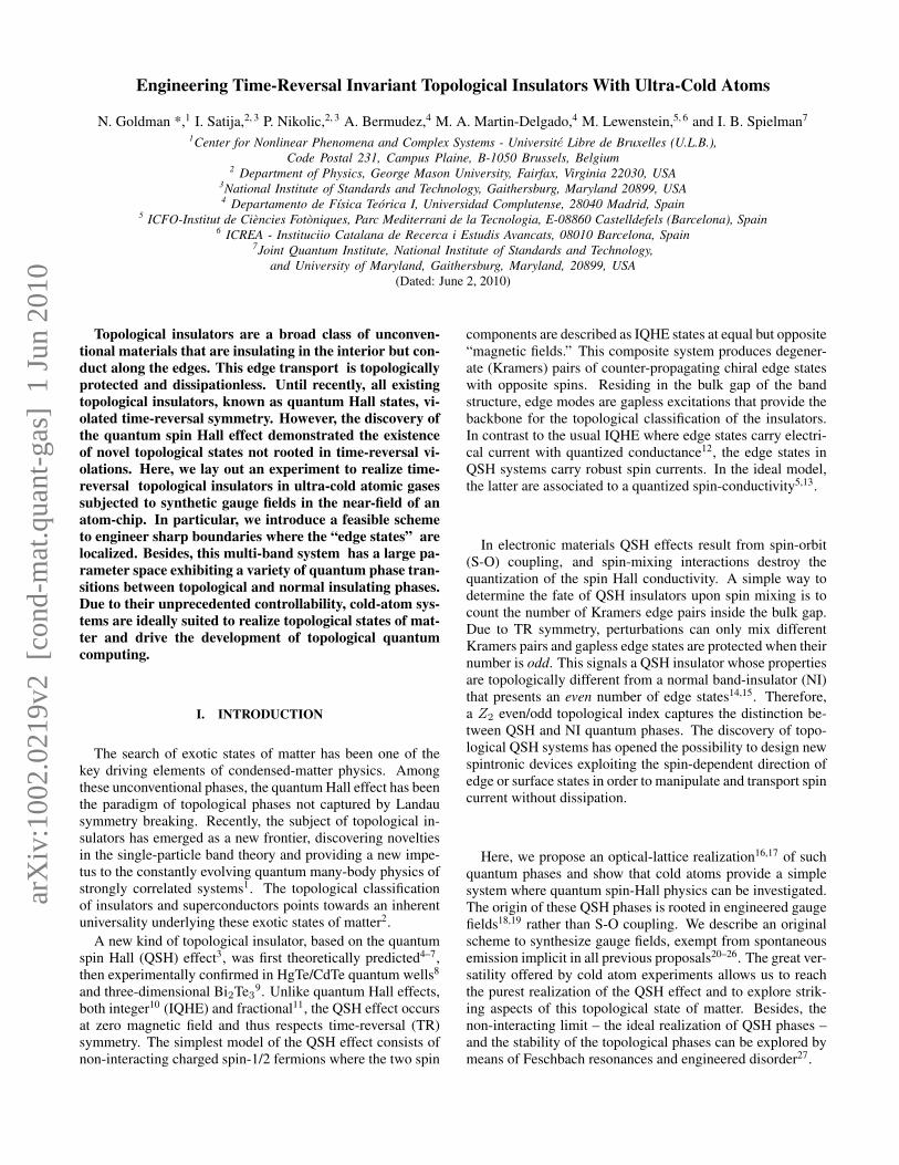
Realizing topological insulators with cold atoms is par-ticularly attractive 28,29, and we hereby provide a concretesetup using fermionic 6Li subjected to synthetic gauge fields.There are numerous proposals for creating Abelian20–24 andnon-Abelian25,26 gauge fields, leading to interesting phenom-ena30–33,35,36. The vast majority of these proposals depend onlaser-induced Raman coupling between internal atomic states;such a method was recently implemented with bosonic 87Rbatoms creating an Abelian gauge field18,19. For the alkaliatoms, the requisite coupling limits the possible detuning ofthe Raman laser beams from the ground S to first excited Ptransition, about to the excited state fine-structure splitting[7.1 THz for 87Rb, 1.7 THz for 40K, and only 10 GHz for6Li]. The very small detunings possible for fermionic atoms –40K and 6Li – imply large spontaneous emission rates and thusthe desired gauge fields must be synthesized through an alter-nate scheme. Here we describe such a setup that combinesstate-independent optical potentials, with micron scale state-dependent magnetic potentials in an atom chip. Our discus-sion focuses on harmonically trapped quantum degenerate 6Lisystems about 5 µm above the atom chip’s surface. Figure 1depicts how the required potentials for this proposal can be re-alized using a combination of static and radio-frequency mag-netic fields. By completely eliminating spontaneous emission,this approach makes practical the realization of gauge fieldsfor all alkali atoms.
Our proposal for realizing a fermionic model with a SU(2)gauge structure requires four atomic states |g1〉 = |F =1/2,mF = 1/2〉, |g2〉 = |3/2,−1/2〉, |e1〉 = |3/2, 1/2〉,and |e2〉 = |1/2,−1/2〉 [see Fig. 1 (a)], which are confined ina square optical lattice and described by the Hamiltonian
H =− t∑m,n
c†m+1,neiθxcm,n + c†m,n+1e
iθycm,n + h.c.
+ λstag
∑m,n
(−1)m c†m,ncm,n. (1)
cm,n is a 2-component field operator defined on a lattice site(x = ma, y = na), a is the lattice spacing, m,n are integers,and t is the nearest-neighbor hopping. In this model the ma-trices θx,y modify the hopping along the x, y-directions andresult from the synthetic gauge field [cf. below and Meth-ods]. Here, all the states experience a primary lattice potentialV1(x) = Vx sin2(kx) along x which gives rise to a hoppingamplitude t ≈ 0.4 kHz. A secondary much weaker latticeV2(x) = 2λstag sin2(kx/2) slightly staggers the primary lat-tice with λstag ≈ t. These lattices, with an approximate periodof 2 µm, are produced by two pairs of λ = 1064 nm lasers,slightly detuned from each other and incident on the reflec-tive surface of the atom chip [see. Fig 1 (b)]. Additionally,these beams create a lattice along z with a 0.55 µm period,confining the fermions to a 2D plane.
We propose to design the SU(2) hopping operators as fol-lows
θx = 2πγσx, and θy = 2πxασz, (2)
where we have set the units a = ~ = 1, and σx,z are Pauli ma-trices. In order to engineer these state-dependent tunnelings,the states |g〉 and |e〉 must experience oppositely-signed lat-tices realized along the y direction of the chip, as in Fig. 1 (c).This scheme exploits the Zeeman shift of an array of wireswith alternating currents ±I . The θy hopping operator in Eq.(2) involves x-dependent phases that can be realized with anadditional grid of wires spaced by a = 2 µm along x [cf.Methods]. Remarkably, these moving Zeeman lattices repro-duce the Raman-assisted hopping from previous schemes20–24
and lead to the operator θy. A potential gradient along y de-tunes this Raman coupling into resonance and is produced bysimply shifting the center of the harmonic potential – equiva-lent to adding a linear gradient. The specific form of the hop-ping operator θy is motivated by the fact that it correspondsto opposite “magnetic fluxes” ±α for each spin component,where α = p/q and p, q are mutually prime numbers. Finally,the additional contribution to the hopping θx that mixes the|e〉 and |g〉 states can be realized in a like manner. The cor-responding control parameter γ, and the additional staggeredpotential which induces alternate on-site energies ε = ±λstagalong the x-axis, are shown below to enrich the phase transi-tions in a novel manner. Let us emphasize that the Hamilto-nian (1)-(2) satisfies Time-Reversal invariance, since it com-mutes with the TR-operator defined as T = iσyK, whereK is the complex-conjugate operator. This fundamental sym-metry opens the possibility to realize the first instance of Z2-topological insulators in a cold-atom laboratory. Finally, westress that the two components of the field operators corre-spond in general to a pseudo-spin 1/2, but in our proposal referspecifically to spin components of 6Li in its electronic groundstate.
In this paper, we present results for the case α = 1/6,namely when the synthetic gauge field (2) corresponds toθy(m) = 2πmσz/6. This choice exhibits an extremely richphase diagram with almost all possible topological phase tran-sitions [cf. Figs. 4]. The topological phases discussed be-low are robust against small variations δα ∼ 0.01: indeed theproperties rely on the existence of bulk gaps which are contin-uously deformed when α is varied, as in the Hofstadter butter-fly37. Moreover, other configurations of the gauge field couldbe experimentally designed and would lead to similar effects.In Sect. III, we investigate the phase transitions between topo-logical insulators for a cylinder geometry in the absence of theconfining potential Vconf. We then show in Sect. IV how theseproperties can be detected when this confinement is applied.
III. TOPOLOGICAL INSULATORS AND PHASETRANSITIONS
When γ = 0, Eqs. (1)-(2) describe two uncoupled quan-tum Hall systems. For generic α = p/q, the fermion band-structure splits into q subbands, the lattice analogues of Lan-dau levels. These subbands are separated by gaps, or by“pseudogaps” exhibiting nodal Dirac fermions. Our setupthus provides a multi-band system, where a variety of band-insulators, separated by metal or semi-metal regions, can be
3
1 µm
4 µm
1064 nm beams
Gold surface
Fermi gas
Substrate“Raman”wires
State dependentlattice wires
ba
Lithium2S1/2
F = 3/2
F = 1/2
dc
Bias field
Ene
rgy
[arb
.]
Y Position (μm)-4
-4
-2
-2
0
0
2
2
4
4
Y Position (μm)
X P
ositi
on (μ
m)
0
h×230 kHz
h×22
8 M
Hz
h×50 kHz
θ2
θ1
-8 -4 0 4 8
Figure 1: Experimental realization using an atom-chip and resulting model (a)-(d): (a) Level diagram identifying the four required statesfrom within the ground 2S1/2 electronic manifold of fermionic 6Li. Each of the state-pairs |g1〉, |g2〉 and |e1〉, |e2〉 are clock state pairs(with the same magnetic moment) and the indices 1 and 2 label the SU(2) degree of freedom. Moreover the |g1,2〉 and |e1,2〉 pairs haveopposite magnetic moments, so they experience opposite-signed magnetic potentials. (b) Explicit experimental layout showing the origin ofoptical (state independent) and magnetic (state dependent) potentials and coupling fields. First, a state-independent, staggered, lattice along x isformed by the separate interference of two pairs of λ = 1064 nm laser beams slightly detuned from each other to eliminate cross interference.The respective intersection angles are chosen so the lattice period differ by a factor of two. Both beams reflect from the chip-surface andform vertically aligned lattices, trapping the degenerate Fermi gas about 5 µm above the surface. The inset shows the chip geometry, fromtop to bottom: a reflective chip-surface, gold wires aligned along y with a 1 µm spacing along x (producing the |g〉-|e〉 coupling), and finallygold wires aligned along x with a 2 µm spacing (producing the state dependent lattice). (c) Computed atomic potentials and coupling matrixelements. (d) The resulting lattice with couplings schematically illustrated.
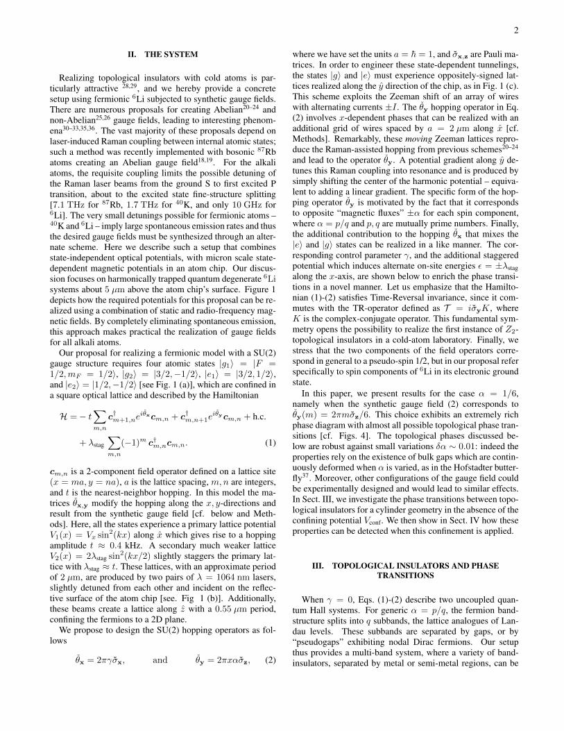
reached by varying the atomic filling factor. As discussedbelow, some of these insulators are topologically non-trivialand feature gapless edge states. The latter are localized at theboundaries of the sample, and correspond to gapless excita-tions. When the Fermi energy EF lies inside a bulk gap, thepresence of these states is responsible for the spin transportalong the edges.
Figure 2 (a) illustrates the energy spectrum obtained for acylindrical geometry [cf. Methods]. In this figure, the bulkbands [thick blue bands] are clearly differentiated from thegapless edge states within the bulk gaps [thin purple lines].In the lowest bulk gap, the edge state channel A, and its TR-conjugate B, correspond to localized excitations which travelin opposite directions [cf. Fig.2 (b)]. Each boundary is popu-
lated by a single pair of counter-propagating states, each cor-responding to an opposite spin [i.e. helical edge states]. Ac-cordingly, this lowest bulk gap describes a topological QSHphase. Conversely, the next gap located at E ≈ −1 is tra-versed by an even number of Kramers pairs, thus yielding anormal band insulator. Remarkably enough, different topo-logical insulators can be experimentally engineered in thismulti-band scenario by simply varying the atomic filling fac-tor. The Fermi surface at half-filling, namely EF = 0, corre-sponds to a discrete set of isolated points, and thus describesa semi-metal phase.
An alternative approach to the above even-odd criteria re-lies on the computation of a Z2 topological invariant that
4
0 /2 3 /2 2ky
E
-4
-2
0
2
4
A B
A
Bx = 0 x = L
ba
Figure 2: Bulk energy bands and edge-state channels: (a) Energyspectrum of the uncoupled system (γ = 0 and α = 1/6) computedin a cylindrical geometry: the bulk energy bands [thick blue bands]are traversed by edge states [thin purple lines]. The energy is in unitsof the tunneling amplitude t. (b) Schematic representation of thetwo edge states, A and B, that lie inside the first bulk energy gapdepicted in (a). The spins traveling around the edges are respectivelyrepresented by red and green arrows.
characterizes the bulk gaps [see Methods]. The QSH phaseis distinguished from the normal insulator by the Z2 indexIZ2
, which respectively takes the value IZ2(QSH) = 1 and
IZ2(NI) = 0. We computed this index inside the four gaps
depicted in Fig.2 (a), obtaining the following sequence
IZ2 = 1, 0, 0, 1,
in perfect agreement with the above edge-state analysis.Therefore, in the uncoupled case γ = 0 where spin is agood quantum number, the spin conductivity is quantized asσs = 2 IZ2
e4π and is related to the spin current js = j↑ − j↓.
Additionally, this quantized spin Hall conductivity is equal tothe difference of the Chern numbers associated to the up- anddown-spin [cf. Methods].
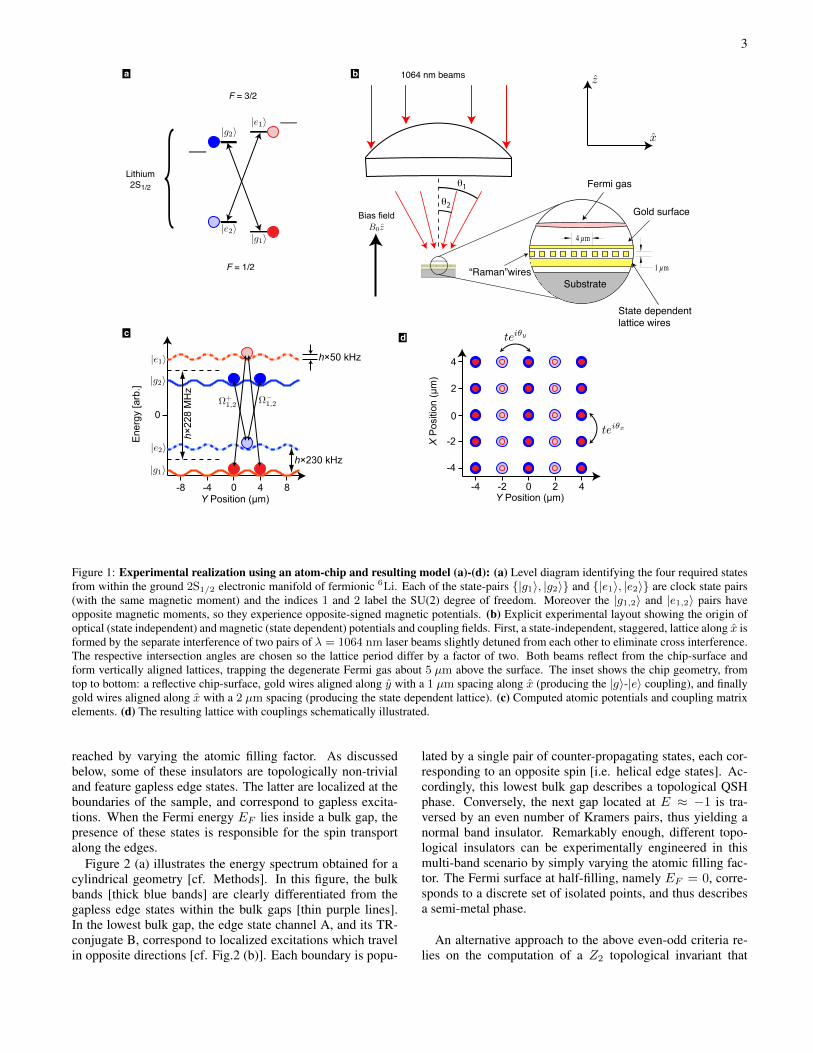
In our multi-band system, the lattice-potential distortionscan drive direct transitions between normal and topologicalinsulating states. Figure 3 shows the bulk gaps and edge statesfor increasing values of the staggered potential’s strengthλstag. In the simple case γ = 0, where two quantum Hall sys-tems are superimposed, we already obtain various realizationsof QSH phases. By tuning λstag, one can observe a NI to semi-metal transition, and more importantly, a semi-metal to QSHphase transition in the bulk gaps located around E = ±1.Remarkably enough, we have shown that the staggered poten-tial, which can be controlled in an optical-lattice experiment,induces a quantum phase transition from a NI to a QSH phaseat the critical value λstag = t [cf. Fig. 3 (b)]. At half-filling,the existence of Dirac points appear to resist the opening ofthe gap for small staggered potential and eventually lead to aNI phase for λstag > 1.25t [cf. Fig. 3 (d)]. As we describebelow, the latter situation radically changes as the coupling γis switched on.
024
-4-2
0 /2 3 /2 2
E
ky
a
024
-4-2
0 /2 3 /2 2
E
ky
c
024
-4-2
0 /2 3 /2 2
E
ky
b
024
-4-2
0 /2 3 /2 2
E
ky
d
QSH
QSH
NI
NI
] QSH
] QSH
]
]
QSH
QSH
QSH
] QSH]
] QSH]
] QSH]
]
QSH
QSH
NI
]
]
]
]
Figure 3: Energy bands E(ky) for γ = 0 and α = 1/6, in the presence of an external staggered potential (a)-(d): (a)λstag = 0.5t, (b) λstag = t, (c) λstag = 1.25t, (d) λstag = 1.5t. Thearrows point at the open bulk gaps and indicate their correspondingtopological phases. The purple rectangles highlight the NI to QSHphase transition that occurs aroundEF = 1. The energy is expressedin units of the tunneling amplitude t.
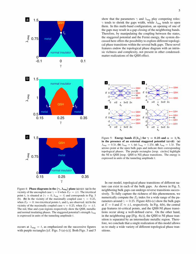
The parameter γ 6= 0 perturbs the ideal quantum spin Hallsystem and fundamentally changes the aforementioned phasetransitions. The Z2 invariant analysis provides a particularlyuseful and efficient tool to obtain the full phase diagram ofthe system in the (γ, λstag) parameters plane [cf. Methods].The phase diagram represented in Fig. 4(a) has been obtainednumerically by evaluating the Z2 index inside the bulk atE ≈±1 in the vicinity of γ = 0. Here we observe three distinctregions, namely the metallic (blue), QSH (red), and NI (cyan)phases. These three phases coexist at a tricritical point situatedat γ = 0 and λstag = t. It is interesting to highlight that theQSH phase occurs for a wide range of the parameter γ, whichindicates the robustness of this topological phase under smalllocal perturbations of the Hamiltonian (1).
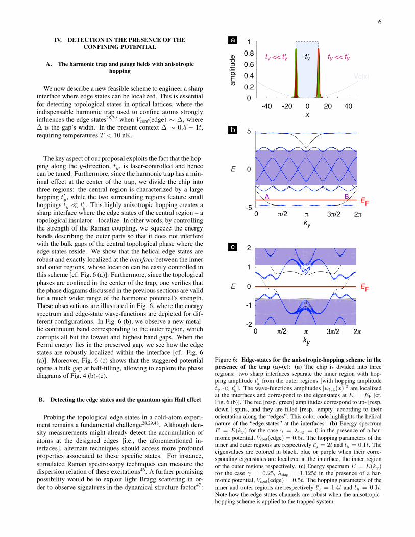
The wide range of possibilities offered by optical-lattice ex-periments enables us to consider the strong coupling regimecorresponding to γ = 0.25. In this limit, the previously in-dependent quantum Hall subsystems (γ = 0) become maxi-mally coupled, a fact that drastically modifies the topologicalphase transitions presented above. In Fig. 5, we illustrate thebulk bands and edge states for increasing values of the stag-gered potential. Each gap is associated to a QSH or a NI phaseaccording to the even-odd number of TR pairs. In this strong-coupled regime, we observe a completely different phase tran-sition associated to the bulk gap at half filling. Contrary to thesemi-metal to NI phase transition described in the uncoupledcase [cf. Figs. 3(a)-(d)], we identify here a QSH to NI tran-sition which occurs after a gap-closing at λstag = 1.25t. Thisprocess is emphasized on the figures with purple circles [cf.Figs. 5 (b)-(d)]. The QSH phase can only occur at half-fillingfor large couplings γ. Furthermore, one also notices that theneighboring bulk gaps at E ≈ ±1 present exactly the oppo-site phase transition, from a NI to a QSH phase. The latter
5
0.5
1.5
1
metal metal
normal insulator
QSH
0.350.250.15
stag
t1 t2
0
1.5
0.350.250.15
0.75
normal insulator
QSH
metalstag
0
1.5
0.75
0.10-0.1
stag
QSH
normal insulator
metal
a
c
b
tc
Figure 4: Phase diagrams in the (γ,λstag) plane (a)-(c): (a) In thevicinity of the uncoupled case γ = 0 whenEF = ±1. The tricriticalpoint tc is situated at (γ = 0, λstag = t) and corresponds to Fig. 3(b). (b) In the vicinity of the maximally coupled case γ = 0.25,whenEF = 0: two tricritical points t1 and t2 are observed. (c) In thevicinity of the maximally coupled case γ = 0.25, when EF = ±1.The red, blue and cyan regions respectively show the QSH, metallicand normal insulating phases. The staggered potential’s strength λstag
is expressed in units of the tunneling amplitude t.
occurs at λstag = t, as emphasized on the successive figureswith purple rectangles [cf. Figs. 5 (a)-(c)]. Both Figs. 3 and 5
show that the parameters γ and λstag play competing roles:γ tends to shrink the gaps width, while λstag tends to openthem. In this multi-band configuration, an opening of one ofthe gaps may result in a gap-closing of the neighboring bands.Therefore, by manipulating the coupling between the states,the staggered potential and the Fermi energy, the system dis-cussed here offers the possibility to explore different topologi-cal phase transitions within the several bulk gaps. These novelfeatures endow the topological phase diagram with an intrin-sic richness and complexity, not present in other condensed-matter realizations of the QSH effect.
QSH
QSH
QSH
]
]
]
QSH
QSH
QSH
]
]
NI]
]
] QSH
024
-4-2
0 /2 3 /2 2
E
ky
a b
dc
024
-4-2
0 /2 3 /2 2
E
ky
024
-4-2
0 /2 3 /2 2
E
ky
024
-4-2
0 /2 3 /2 2
E
ky
QSHNI
NIQSH
QSH]
]
]
]
]
]
]
QSHQSH
QSHQSH
]
]
Figure 5: Energy bands E(ky) for γ = 0.25 and α = 1/6,in the presence of an external staggered potential (a)-(d): (a)λstag = 0.5t, (b) λstag = t, (c) λstag = 1.25t, (d) λstag = 1.5t. Thearrows point at the open bulk gaps and indicate their correspondingtopological phases. The purple rectangles [resp. circles] highlightthe NI to QSH [resp. QSH to NI] phase transitions. The energy isexpressed in units of the tunneling amplitude t.
In our model, topological phase transitions of different na-ture can exist in each of the bulk gaps. As shown in Fig. 5,neighboring bulk gaps can undergo reverse transitions succes-sively. To fully capture the richness of this phenomenon, wenumerically compute the Z2 index for a wide range of the pa-rameters around γ = 0.25. Figure 4(b)-(c) show the bulk gapsat E = 0 and E ≈ ±1, respectively. In Fig. 4(b), the centralgap features tri-critical points, and the QSH-NI phase transi-tions occur along a well-defined curve. On the other hand,in the neighboring gap [Fig. 4(c)], the QSH to NI phase tran-sition is separated by an intermediate metallic region. There-fore, we conclude that a single realization of this model allowsus to study a wide variety of different topological phase tran-sitions.
6
IV. DETECTION IN THE PRESENCE OF THECONFINING POTENTIAL
A. The harmonic trap and gauge fields with anisotropichopping
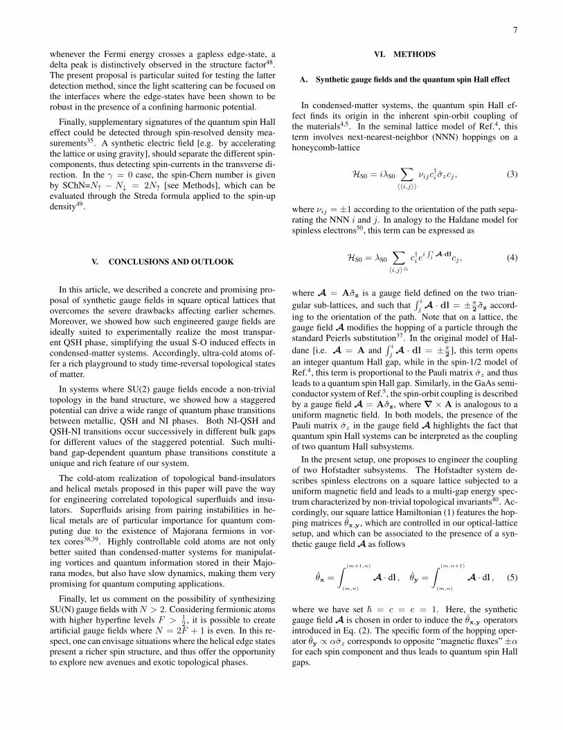
We now describe a new feasible scheme to engineer a sharpinterface where edge states can be localized. This is essentialfor detecting topological states in optical lattices, where theindispensable harmonic trap used to confine atoms stronglyinfluences the edge states28,29 when Vconf(edge) ∼ ∆, where∆ is the gap’s width. In the present context ∆ ∼ 0.5 − 1t,requiring temperatures T < 10 nK.
The key aspect of our proposal exploits the fact that the hop-ping along the y-direction, ty , is laser-controlled and hencecan be tuned. Furthermore, since the harmonic trap has a min-imal effect at the center of the trap, we divide the chip intothree regions: the central region is characterized by a largehopping t′y , while the two surrounding regions feature smallhoppings ty t′y . This highly anisotropic hopping creates asharp interface where the edge states of the central region – atopological insulator – localize. In other words, by controllingthe strength of the Raman coupling, we squeeze the energybands describing the outer parts so that it does not interferewith the bulk gaps of the central topological phase where theedge states reside. We show that the helical edge states arerobust and exactly localized at the interface between the innerand outer regions, whose location can be easily controlled inthis scheme [cf. Fig. 6 (a)]. Furthermore, since the topologicalphases are confined in the center of the trap, one verifies thatthe phase diagrams discussed in the previous sections are validfor a much wider range of the harmonic potential’s strength.These observations are illustrated in Fig. 6, where the energyspectrum and edge-state wave-functions are depicted for dif-ferent configurations. In Fig. 6 (b), we observe a new metal-lic continuum band corresponding to the outer region, whichcorrupts all but the lowest and highest band gaps. When theFermi energy lies in the preserved gap, we see how the edgestates are robustly localized within the interface [cf. Fig. 6(a)]. Moreover, Fig. 6 (c) shows that the staggered potentialopens a bulk gap at half-filling, allowing to explore the phasediagrams of Fig. 4 (b)-(c).
B. Detecting the edge states and the quantum spin Hall effect
Probing the topological edge states in a cold-atom experi-ment remains a fundamental challenge28,29,48. Although den-sity measurements might already detect the accumulation ofatoms at the designed edges [i.e., the aforementioned in-terfaces], alternate techniques should access more profoundproperties associated to these specific states. For instance,stimulated Raman spectroscopy techniques can measure thedispersion relation of these excitations46. A further promisingpossibility would be to exploit light Bragg scattering in or-der to observe signatures in the dynamical structure factor47:
0 /2 3 /2 2ky
-1
0
1
c
EF
0 /2 3 /2 2-2
ky
2
A B
x
Vc(x)
amplitude
00.20.40.60.81
-40 -20 0 20 40
t'y
a
E
0
b
-5
5
E
EF
ty t'y<< ty t'y<<
Figure 6: Edge-states for the anisotropic-hopping scheme in thepresence of the trap (a)-(c): (a) The chip is divided into threeregions: two sharp interfaces separate the inner region with hop-ping amplitude t′y from the outer regions [with hopping amplitudety t′y]. The wave-functions amplitudes |ψ↑,↓(x)|2 are localizedat the interfaces and correspond to the eigenstates at E = EF [cf.Fig. 6 (b)]. The red [resp. green] amplitudes correspond to up- [resp.down-] spins, and they are filled [resp. empty] according to theirorientation along the “edges”. This color code highlights the helicalnature of the “edge-states” at the interfaces. (b) Energy spectrumE = E(ky) for the case γ = λstag = 0 in the presence of a har-monic potential, Vconf(edge) = 0.5t. The hopping parameters of theinner and outer regions are respectively t′y = 2t and ty = 0.1t. Theeigenvalues are colored in black, blue or purple when their corre-sponding eigenstates are localized at the interface, the inner regionor the outer regions respectively. (c) Energy spectrum E = E(ky)for the case γ = 0.25, λstag = 1.125t in the presence of a har-monic potential, Vconf(edge) = 0.5t. The hopping parameters of theinner and outer regions are respectively t′y = 1.4t and ty = 0.1t.Note how the edge-states channels are robust when the anisotropic-hopping scheme is applied to the trapped system.
7
whenever the Fermi energy crosses a gapless edge-state, adelta peak is distinctively observed in the structure factor48.The present proposal is particular suited for testing the latterdetection method, since the light scattering can be focused onthe interfaces where the edge-states have been shown to berobust in the presence of a confining harmonic potential.
Finally, supplementary signatures of the quantum spin Halleffect could be detected through spin-resolved density mea-surements35. A synthetic electric field [e.g. by acceleratingthe lattice or using gravity], should separate the different spin-components, thus detecting spin-currents in the transverse di-rection. In the γ = 0 case, the spin-Chern number is givenby SChN=N↑ − N↓ = 2N↑ [see Methods], which can beevaluated through the Streda formula applied to the spin-updensity49.
V. CONCLUSIONS AND OUTLOOK
In this article, we described a concrete and promising pro-posal of synthetic gauge fields in square optical lattices thatovercomes the severe drawbacks affecting earlier schemes.Moreover, we showed how such engineered gauge fields areideally suited to experimentally realize the most transpar-ent QSH phase, simplifying the usual S-O induced effects incondensed-matter systems. Accordingly, ultra-cold atoms of-fer a rich playground to study time-reversal topological statesof matter.
In systems where SU(2) gauge fields encode a non-trivialtopology in the band structure, we showed how a staggeredpotential can drive a wide range of quantum phase transitionsbetween metallic, QSH and NI phases. Both NI-QSH andQSH-NI transitions occur successively in different bulk gapsfor different values of the staggered potential. Such multi-band gap-dependent quantum phase transitions constitute aunique and rich feature of our system.
The cold-atom realization of topological band-insulatorsand helical metals proposed in this paper will pave the wayfor engineering correlated topological superfluids and insu-lators. Superfluids arising from pairing instabilities in he-lical metals are of particular importance for quantum com-puting due to the existence of Majorana fermions in vor-tex cores38,39. Highly controllable cold atoms are not onlybetter suited than condensed-matter systems for manipulat-ing vortices and quantum information stored in their Majo-rana modes, but also have slow dynamics, making them verypromising for quantum computing applications.
Finally, let us comment on the possibility of synthesizingSU(N) gauge fields withN > 2. Considering fermionic atomswith higher hyperfine levels F > 1
2 , it is possible to createartificial gauge fields where N = 2F + 1 is even. In this re-spect, one can envisage situations where the helical edge statespresent a richer spin structure, and thus offer the opportunityto explore new avenues and exotic topological phases.
VI. METHODS
A. Synthetic gauge fields and the quantum spin Hall effect
In condensed-matter systems, the quantum spin Hall ef-fect finds its origin in the inherent spin-orbit coupling ofthe materials4,5. In the seminal lattice model of Ref.4, thisterm involves next-nearest-neighbor (NNN) hoppings on ahoneycomb-lattice
HS0 = iλS0
∑〈〈i,j〉〉
νijc†i σzcj , (3)
where νij = ±1 according to the orientation of the path sepa-rating the NNN i and j. In analogy to the Haldane model forspinless electrons50, this term can be expressed as
HS0 = λS0
∑〈i,j〉4
c†iei∫ ijA·dlcj , (4)
where A = Aσz is a gauge field defined on the two trian-gular sub-lattices, and such that
∫ ijA · dl = ±π2 σz accord-
ing to the orientation of the path. Note that on a lattice, thegauge field A modifies the hopping of a particle through thestandard Peierls substitution37. In the original model of Hal-dane [i.e. A = A and
∫ ijA · dl = ±π2 ], this term opens
an integer quantum Hall gap, while in the spin-1/2 model ofRef.4, this term is proportional to the Pauli matrix σz and thusleads to a quantum spin Hall gap. Similarly, in the GaAs semi-conductor system of Ref.5, the spin-orbit coupling is describedby a gauge field A = Aσz, where ∇ ×A is analogous to auniform magnetic field. In both models, the presence of thePauli matrix σz in the gauge field A highlights the fact thatquantum spin Hall systems can be interpreted as the couplingof two quantum Hall subsystems.
In the present setup, one proposes to engineer the couplingof two Hofstadter subsystems. The Hofstadter system de-scribes spinless electrons on a square lattice subjected to auniform magnetic field and leads to a multi-gap energy spec-trum characterized by non-trivial topological invariants40. Ac-cordingly, our square lattice Hamiltonian (1) features the hop-ping matrices θx,y, which are controlled in our optical-latticesetup, and which can be associated to the presence of a syn-thetic gauge field A as follows
θx =
∫ (m+1,n)
(m,n)
A · dl , θy =
∫ (m,n+1)
(m,n)
A · dl , (5)
where we have set ~ = c = e = 1. Here, the syntheticgauge field A is chosen in order to induce the θx,y operatorsintroduced in Eq. (2). The specific form of the hopping oper-ator θy ∝ ασz corresponds to opposite “magnetic fluxes” ±αfor each spin component and thus leads to quantum spin Hallgaps.
8
B. Experimental proposal
Here we describe our technique to create an atomic en-semble subject to a SU(2) gauge field (focusing on 6Li, butequally applicable to 40K) that combines state-independentoptical potentials, with micron scale state-dependent magneticpotentials near the surface of an atom chip. Our discussionfocuses on harmonically trapped quantum degenerate 6Li sys-tems a distance h = 5 µm above an atom chips surface, inthe presence of lattices with period a = 2 µm along x and y.We use ~kL = π~/a and EL = ~2k2
L/2m = h × 8.3 kHz –the recoil momentum and energy momentum – as the naturaldimensions of energy and momentum.
All proposals to create light-induced gauge fields for ultra-cold neutral atoms somehow involve Raman transitions thatcouple ground states of unlike spin that differ in momentumby ~δk by way of intermediary (and in practice off-resonant)excited states. For a typical system with two ground states, theresulting effective Hamiltonian has (potentially many) termsof the form
H ′(x) =Ω
2
(0 exp [i(δk · x + φ)]
exp [−i(δk · x + φ)] 0
)=
Ω
2[cos (δk · x + φ) σx − sin (δk · x + φ) σy] .
Formally this is the same as the linear Zeeman shift g~µ · ~B fora magnetic field in the x-y plane orbiting about z with spatialperiod 2π/|δk|. We take advantage of this formal similarityand constructs the requisite magnetic field near the surface ofan atom chip.
Our proposal for realizing an atomic model with a SU(2)gauge structure requires four atomic states with very specificproperties outlined below. These physically correspond to hy-perfine states, labeled by |F,mf 〉, in the 6Li 2S electronicground state: |g1〉 = |1/2, 1/2〉,|g2〉 = |3/2,−1/2〉,|e1〉 =|3/2, 1/2〉, and |e2〉 = |1/2,−1/2〉. For simplicity, the la-bels |g〉 and |e〉, have been preserved from Ref.25 where theydenoted physical ground and excited states.
(A) The atomic states must all experience a primary lat-tice potential V1(x) = Vx sin2(kx) along x; a lattice depthVx = 6EL ≈ h× 50 kHz produces a hopping matrix elementt ≈ 0.05EL ≈ h × 400 Hz. A secondary, much weaker lat-tice V2(x) = 2λstag sin2(kx/2) slightly staggers the primarylattice, where λstag ∼ t Vx. Figure 1 (b) shows two pairsof λ = 1064 nm lasers, slightly detuned from each other, in-cident on the atom chip’s reflective surface, producing latticeswith period λ/2 sin θ. For our base a = 2 µm lattice period,these angles [shown in Fig. 1] are θ1 ≈ 15 and θ2 ≈ 7.5.These beams also produce a lattice along z with a 550 nmperiod, confining the fermions to a 2D plane.
(B) The states |g〉 and |e〉 experience oppositely-signed lat-tice potentials along y as in Fig. 1 (c). This can be directlyimplemented with the Zeeman shift gµB |B| of atoms pro-vided that |g1,2〉 and |e1,2〉 have equal, but opposite magneticmoments g (i.e., are each on clock transitions). For the states– |g1〉, |g2〉, |e1〉, and |e2〉 – shown in Fig. 1 (a) the magneticmoments are correctly signed and differ by less than 1% inmagnitude at a bias field B = 0.25 G.
With these states, a state-dependent lattice potential can begenerated by an array of current carrying wires with alternat-ing +I and −I currents, spaced by a distance a (repeatingwith full period 2a = 4 µm); because the evanescent mag-netic field decays exponentially ∝ exp (−2πh/a), the heighth of the atoms above the surface must be comparable to a. Amodest I = 5 µA current34 in wires 3 µm below the chip-surface (8 µm from the atoms) produces a 6 EL Zeeman lat-tice, with a negligible 3 Hz hopping matrix element.
(C) Our model also requires hopping along y with an xdependent phase: ty exp(iqx). This can be realized withan additional grid of wires spaced by a = 2 µm along x,with currents Im. This provides moving Zeeman lattices withwave-vector q (leading to effective “Raman coupling”) whenIn = I0 sin(qma − ωt). The ω/2π ≈ 228 ± 0.23 MHztransitions indicated with arrows in Fig. 1 (c), |e1〉 → |g1〉and |e2〉 → |g2〉, are independently controllable in phase, am-plitude, and wave-vector by commanding concurrent runningwaves at the indicated resonant frequencies. For this studywe confine ourselves to the equal amplitude and wave-vectorcase. The minimum wavelength d = 2π/q of this movinglattice is Nyquist limited by d > 2a.
In the frame rotating at the angular frequency ω, and aftermaking the rotating wave approximation the coupling termshave the desired form t exp(iqma). In the model Hamilto-nian (1), the phase for hopping along y is α = qa/2π = a/din terms of physical parameters. In this proposal we focusedon α = 1/6, implying d = 6a far exceeding the 2a Nyquistlimit.
Our scheme also requires, a contribution to the hoppingalong x that mixes the |e〉 and |g〉. Like in (C) this can berealized using a Zeeman lattice moving along x, but tuned todrive transitions between |g1〉 → |g2〉 and |e1〉 → |e2〉.
(D) To create effective edges within the trapped cloud ofatoms, we propose to abruptly change ty from a larger value inthe bulk to a smaller value t′y as a function of x. Here, creatingsuch a change in ty can be simply implemented by making thecurrents I0 in our wires x-dependent such that they sharplychange from a large value in the center to a smaller value nearthe systems edge, as is schematically shown in Fig. 6 (a).
(E) Lastly, a potential gradient along y detunes into reso-nance the Raman fields providing the y tunneling and is pro-duced by simply shifting the center of the harmonic potential– equivalent to adding a linear gradient. This gradient impliesthat the coupling fields ω± will be slightly different in fre-quency to be simultaneously resonant. We select a gradientso the site-to-site (spaced by a) detuning is large comparedto both the ≈ 3 Hz bare and ≈ 400 Hz Raman stimulatedhopping along y, but small compared to the ≈ 20 kHz bandspacing along y. For example a 1 kHz/a = 500 Hz/µm gra-dient results from shifting a typical 40 Hz harmonic trap by500 µm. This can be effected more efficiently in the labora-tory by using the linear gradient at the side of gaussian laserbeams.
9
C. The cylindrical geometry description
In order to compute the edge states, we consider a cylin-drical geometry with boundaries at x = 0 and x = L.In this case, we apply periodic boundary conditions alongthe y-direction, and consider the partial Fourier transformcm,n =
∑kye−ikyncky (m). The Hamiltonian (1) becomes
a collection of independent tight-binding models along the x-axis H =
∑kyHTB(ky), where
HTB(ky) =− t∑m
cky (m+ 1)†eiθxcky (m) + h.c
+∑m
cky (m)†D(m)cky (m), (6)
and where the diagonal matrix yields
D(m) =− 2t diag(cos(2παm+ ky), cos(2παm− ky)
)+ λstag(−1)m I. (7)
The energy spectra computed with this method presents thebulk bands as well as the edge states lying inside the bulkenergy gaps [cf. Fig. 2].
D. The Z2 index and the spin-Chern numbers
In analogy to the topological characterization of the inte-ger quantum Hall effect by means of Chern numbers40–42, weevaluate the Z2 invariants of the QSH effect through the com-putation of the “spin-Chern-number”(SChN) 43–45. The lattertopological invariant is associated to the bulk and is there-fore defined on the torus obtained by closing the cylindricalgeometry [i.e. by identifying the two edges at x = 0 andx = L]. Remarkably, the non-triviality of the SChN witnessesthe presence of gapless edge-states, hence building an elegantbridge between the open and closed geometry descriptions 44.
The computation of the SChN requires the considerationof twisted-periodic-boundary conditions41,43,44: as a particlecrosses the boundary located at x = 0 = L, it acquires anextra phase eiθα , where α =↑, ↓ is the spin index. Since thespectral bulk gaps and their correspondong topological orderare immune to the boundary conditions, the topological SChNis obtained as the average of the Berry’s curvature over allthe phases aquired through the boundary. Here we set θ↑ =−θ↓ = qθ for conveniency43,45, and the twist-space spannedby (θ, ky) describes a torus: θ ∈ [0, 2π
q ] and ky ∈ [0, 2π].
Note that these boundary conditions break the translationalsymmetry along the x-direction, while preserving it along they-direction. Besides, the closing of the cylinder is consistentas long as L = integer × q. The single-particle Schrodingerequation can then be expressed in the form of a Harper-likedifference equation
Rψm+1 +R† ψm−1 +D(m)ψm = −Etψm , m 6= 1, L,
Rψ2 +R† e−iqθσzψL +D(1)ψ1 = −Etψ1,
R eiqθσzψ1 +R† ψL−1 +D(L)ψL = −EtψL, (8)
where ψm is a two-component spinor, R =(cos(2πγ) I +
i sin(2πγ)σx)
and D(m) is defined in Eq. 7.The topological invariant associated to the rth bulk energy
gap, SChN(r), is computed on a discrete Brillouin zone ac-cording to the expression
SChN(r) =i
2π
∑θ,ky
F(Ψ(θ, ky)). (9)
Here F(Ψ) represents the non-Abelian Berry’s curvature45
associated to the multiplet Ψ = (φ1, φ2, . . . , φN ), whereφλ denotes the single-particle wave-functions associated tothe energy bands Eλ lying below the rth bulk gap. The NIphase [i.e. IZ2
= 0] is reached in the rth bulk gap whenSChN(r) = 0 mod4, while this gap corresponds to the QSHphase [i.e. IZ2
= 1] when SChN(r) = ±2 mod4.
In the uncoupled regime γ = 0, our setup displays a dou-ble quantum Hall system in which particles with oppositespins are coupled to opposite magnetic fields, but not to eachother. Such a system exhibits TR-symmetry, and therefore,bands come in time-reversed pairs characterized by oppositeChern numbers: ChN↑ = −ChN↓ . The net Chern numberChN = ChN↑ + ChN↓ which accounts for the charge trans-port is zero, but the difference SChN = ChN↑ − ChN↓ isfinite and defines a quantized spin Hall conductivity. The suc-cessive energy bulk gaps shown in Fig. 2 are associated to theChern numbers [from top to bottom] ChN↑ = −1,−2, 2, 1in agreement with the computedZ2 indices IZ2
= 1, 0, 0, 1.However, bulk gaps associated to even Chern numbers lead toa vanishing spin Hall conductivity, as such a system has evenpairs of edge states. Therefore, in systems with TR symmetry,Z2 invariants are the key to distinguish QSH and NI phases.
References
1 M. Z. Hasan & Kane, C. L. Topological Insulators,arXiv:1002.3895vl
2 Kitaev, A. Periodic table for topological insulators and supercon-ductors. AIP Conf. Proc. 1134, 22 (2009).
3 Kane, C. L. & Mele, E. J. A new spin on the insulating state.
Science 314, 1692 (2006).4 Kane, C. L. & Mele, E. J. Quantum spin Hall effect in graphene.
Phys. Rev. Lett. 95, 226801 (2005).5 Bernevig, B. A. & Zhang, S.-C. Quantum spin Hall effect. Phys.
Rev. Lett. 96, 106802 (2006).6 Bernevig, B. A., Hughes, T. L. & Zhang, S.-C. Quantum spin Hall
effect and topological phase transition in HgTe quantum wells.
10
Science 314, 1757 (2006).7 Fu, L., Kane, C. L. & Mele, E. J. Topological insulators in three
dimensions. Phys.Rev. Lett. 98, 106803 (2007).8 Konig, M., et al. Quantum spin Hall insulator state in HeTe quan-
tum wells. Science 318, 766 (2007).9 Chen, Y. L. et al. Experimental realization of a three-dimensional
topological insulator, Bi2Te3. Science 325, 178 (2009).10 von Klitzing, K., Dorda, G., and Pepper, M. New method for
high-accuracy determination of the fine-structure constant basedon quantized Hall resistance. Phys. Rev. Lett. 45, 494 (1980).
11 Tsui, D. C., Stormer, H. L., and Gossard, A. C. Two-dimensionalmagnetotransport in the extreme quantum limit. Phys. Rev. Lett.48, 1559 (1982).
12 Hatsugai, Y. Edge states in the integer quantum Hall effect and theRiemann surface of the Bloch function. Phys. Rev. B 48, 11851(1993).
13 Kane C. L. & Mele, E. J. Z2 topological order and the quantumspin Hall effect. Phys. Rev. Lett. 95, 146802 (2005).
14 Wu, C., Bernevig, B. A. & Zhang, S.-C. Helical liquid and theedge of quantum spin Hall systems. Phys. Rev. Lett. 96, 106401(2006).
15 Xu, C. & Moore, J. Stability of the quantum spin Hall effect: Ef-fects of interactions, disorder, and Z2 topology. Phys. Rev. B. 73,045322 (2006).
16 Lewenstein, M. et al. Ultracold atomic gases in optical lattices:Mimicking condensed matter physics and beyond. Adv. Phys. 56,243 (2007).
17 Bloch, I., Dalibard, J. & Zwerger, W. Many-body physics withultracold gases. Rev. Mod. Phys. 80, 885 (2008).
18 Y.-J. Lin, et al. Bose-Einstein condensate in a uniform light-induced vector potential. Phys. Rev. Lett. 102, 130401 (2009).
19 Lin, Y.-J., Compton, R. L., Jimenez-Garcıa, K., Porto, J. V. &Spielman, I. B. Synthetic magnetic fields for ultracold neutralatoms. Nature 462, 628 (2009).
20 Jaksch, D. & Zoller, P. Creation of effective magnetic fields inoptical lattices: the Hofstadter butterfly for cold neutral atoms.New J. Phys. 5, 56 (2003).
21 Mueller, E. J. Artificial electromagnetism for neutral atoms: Es-cher staircase and Laughlin liquids. Phys. Rev. A. 70, 041603(R)(2004).
22 Sørensen, A. S., Demler, E. & Lukin, M. D. Fractional quantumHall states of atoms in optical lattices. Phys. Rev. Lett. 94, 086803(2004).
23 Spielman, I. B. Raman processes and effective gauge potentials.Phys. Rev. A. 79, 063613 (2009).
24 Gerbier, F. & Dalibard, J. Gauge fields for ultracold atoms in op-tical superlattices. To appear in New J. Phys. arXiv:0910.4606
25 Osterloh, K., Baig, M., Santos, L., Zoller, P. & Lewenstein, M.Cold atoms in non-Abelian gauge potentials: From the Hofstadter“Moth” to lattice gauge theory. Phys. Rev. Lett. 95, 010403 (2005).
26 Ruseckas, J., Juzeliunas, G., Ohberg, P. & Fleischhauer, M. Non-Abelian gauge potentials for ultracold atoms with degenerate darkstates. Phys. Rev. Lett. 95, 010404 (2005).
27 Sanchez-Palencia, L. & Lewenstein, M. Disordered quantumgases under control. Nature Physics 6, 87 (2010).
28 Stanescu, T. D. et al. Topological Insulators and Metals in AtomicOptical Lattices. Phys. Rev. A 79, 053639 (2009).
29 Stanescu, T. D., Galitski, V. & Das Sarma, S. Topological statesin two-dimensional optical lattices. arXiv:0912.3559
30 Goldman, N., Kubasiak, A., Gaspard, P. & Lewenstein, M. Ultra-cold atomic gases in non-Abelian gauge potentials: The case ofconstant Wilson loop. Phys. Rev. A. 79, 023624 (2009).
31 Goldman, N. et al. Non-Abelian optical lattices: Anomalousquantum Hall effect and Dirac fermions. Phys. Rev. Lett. 103,
035301 (2009).32 Satija, I., Dakin, D. C. & Clark, C. W. Metal-insulator transition
revisited for cold atoms in non-Abelian gauge potentials. Phys Revlett. 97, 216401, (2006).
33 Satija, I., Dakin, D. C., Vaishnav, J. Y. & Clark, C. W. Two-dimensional electron gas with cold atoms in non-Abelian gaugepotentials. Phys Rev A 77, 043410, (2008).
34 Trinker, M., Groth, S., Haslinger, S., Manz, S., Betz, T., Schnei-der, S., Bar-Joseph, I., Schumm, T., & Schmiedmayer, J. Mul-tilayer atom chips for versatile atom micromanipulation. Appl.Phys. Lett. 92, 254102, (2008).
35 Zhu, S.-L., Fu, H., Wu, C.-J., Zhang, S.-C. & Duan, L.-M.Spin Hall effects for cold atoms in a light-induced gauge potential.Phys. Rev. Lett. 97, 240401 (2006).
36 Liu, X.-J., Liu, X., Kwek, L. C. & Oh, C. H. Spin Hall effect inatoms. Phys. Rev. Lett. 98, 026602 (2007).
37 Hofstadter, D. Energy levels and wave functions of Bloch elec-trons in rational and irrational magnetic fields. Phys. Rev. B 14,2239 (1976).
38 Fu, L. & Kane, C. L. Superconducting proximity effect and Majo-rana fermions at the surface of a topological insulator. Phys. Rev.Lett. 100, 096407 (2008).
39 Qi, X.-L., Hughes, T. L., Raghu, S. & Zhang, S.-C. Time-reversal-invariant topological superconductors and superfluids intwo and three dimensions. Phys. Rev. Lett. 102, 187001 (2009).
40 Thouless, D. J., Kohmoto, M., Nightingale, M. P. & den Nijs,M. Quantized Hall conductance in a two-dimensional periodicpotential. Phys. Rev. Lett. 49, 405 (1982).
41 Niu, Q. Thouless, D. J. & Wu, Y.-S. Quantized Hall conductanceas a topological invariant. Phys. Rev. B 31, 3372 (1985).
42 Kohmoto, M. Topological invariant and the quantization of theHall conductance. Ann. Phys. 160, 343 (1985).
43 Sheng, D. N., Weng, Z. Y., Sheng, L. & Haldane, F. D. M. Quan-tum spin-Hall effect and topologically invariant Chern numbers.Phys. Rev. Lett. 97, 036808 (2006).
44 Qi, X.-L., Wu, Y.-S. & Zhang, S.-C. General theorem relating thebulk topological number to edge states in two-dimensional insu-lators. Phys. Rev. B 74, 045125 (2006).
45 Fukui, T. & Hatsugai, Y. Topological aspects of the quantum spin-Hall effect in graphene: Z2 topological order and spin Chern num-ber. Phys. Rev. B 75, 121403(R) (2007).
46 Dao, T.-L., Georges, A., Dalibard, J., Salomon, C. & Carusotto,I. Measuring the one-particle excitations of ultracold fermionicatoms by stimulated Raman spectroscopy. Phys. Rev. Lett. 98,240402 (2007).
47 Stamper-Kurn, D. M. et al. Excitation of phonons in a Bose-Einstein condensate by light scattering. Phys. Rev. Lett. 83, 2876(1999).
48 Liu, X.-J., Wu, C. & Sinova, J. Quantum anomalous Hall ef-fect with cold atoms trapped in a square lattice. Phys. Rev. A 81,033622 (2010).
49 Umucalilar, R. O., Zhai, H. & Oktel, M. O. Trapped Fermi Gasesin Rotating Optical Lattices: Realization and Detection of theTopological Hofstadter Insulator. Phys. Rev. Lett. 100, 070402(2008).
50 Haldane, F. D. M. Model for a quantum Hall effect without Lan-dau levels: Condensed-matter realization of the “parity anomaly”.Phys. Rev. Lett. 61, 2015 (1988).
11
Acknowledgments
N.G. thanks the F.R.S-F.N.R.S (Belgium) for financial sup-port. M. L. aknowledges the Grants of Spanish MINCIN(FIS2008-00784 and QOIT), EU (NAMEQUAM), ERC(QUAGATUA) and of Humboldt Foundation. A. B. and M.-A. M.-D. thank the Spanish MICINN grant FIS2009-10061,CAM research consortium QUITEMAD, European FET-7
grant PICC, UCM-BS grant GICC-910758 and FPU MECgrant. I. S. and P. N. are supported by the grant N00014-09-1-1025A by the Office of Naval Research, and the grant70NANB7H6138, Am 001 by the National Institute of Stan-dards and Technology. I. B. S. was supported by the NSFthrough the JQI Physics Frontier Center. Correspondence andrequests for materials should be addressed to N. G.