electroless nickel current collector for 3d-microbatteries
TRANSCRIPT
Seediscussions,stats,andauthorprofilesforthispublicationat:https://www.researchgate.net/publication/226190578
Electrolessnickelcurrentcollectorfor3D-microbatteries.JApplElectrochem
ARTICLEinJOURNALOFAPPLIEDELECTROCHEMISTRY·FEBRUARY2010
ImpactFactor:2.41·DOI:10.1007/s10800-009-0014-0
CITATIONS
12
READS
57
4AUTHORS,INCLUDING:
D.Golodnitsky
TelAvivUniversity
94PUBLICATIONS2,739CITATIONS
SEEPROFILE
E.Peled
TelAvivUniversity
170PUBLICATIONS5,463CITATIONS
SEEPROFILE
Availablefrom:D.Golodnitsky
Retrievedon:09February2016
ORIGINAL PAPER
Electroless nickel current collector for 3D-microbatteries
T. Ripenbein • D. Golodnitsky • M. Nathan •
E. Peled
Received: 4 May 2009 / Accepted: 25 September 2009 / Published online: 15 October 2009
� Springer Science+Business Media B.V. 2009
Abstract An electroless nickel process was used for the
preparation of a thin-film current collector for concentric
three-dimensional lithium and lithium-ion microbatteries.
Ni–P coatings were deposited autocatalytically with the use
of nickel sulfamate or nickel sulfate as a source of Ni2?
and sodium hypophosphite as a reducing agent. The syn-
ergistic effect of sodium acetate and citric acid was found
to provide marked improvement in the pH stability of the
sulfamate electrolyte. This enabled deposition of a con-
formal, fine-grained film on the high-aspect-ratio glass
capillary and perforated-silicon substrates.
Keywords Electroless nickel � Sulfamate electrolyte �Silicon � 3D-microbattery
1 Introduction
The miniaturization of medical and electronic devices
entails sub-mm-footprint primary or secondary micropower
sources. Lithium-ion batteries show the highest overall
performance, but the power and energy density of these
microbatteries in typical thin-film planar configuration are
limited to their footprint and, therefore, are insufficient for
many electronic and medical applications. In order to
increase the power and energy density per battery footprint,
it is essential to use three-dimensional (3D) architecture.
Several battery configurations have been recently proposed
to fit these requirements [1]. 3D-concentric microbatteries
(3D-CMB) on silicon and glass capillary microchannel
plates (MCP), which are under development in our labora-
tory, have shown the highest energy gain (a factor of 25) and
power gain (a factor of 10) per footprint. The 3D-CMB is
built onto a high-aspect-ratio perforated substrate. This
substrate consists of 20,000 to 30,000 cylindrical through-
holes per cm2 with complete lithium-ion battery units
assembled inside each hole and connected in parallel
(Fig. 1). The 3D-CMB is made of several conformal thin
films of nanosize materials: a nickel current collector, a
MoOxS2-x, MoO3, or V2O5 cathode, a hybrid polymer
electrolyte (HPE) and a lithiated-graphite anode [2, 3].
Nickel has been widely used as a current collector for both
negative and positive electrodes in lithium-ion cells. An
electroless Ni–P alloy deposit was found to be more stable
than pure nickel even for high-voltage cathodes ([3.8 V).
The fabrication of a high-quality nickel current collector
inside deep (500-lm long) and narrow (50-lm diameter)
microchannels is one of the key challenges to obtain good
performance of 3D concentric microbatteries.
Electroless deposition has undergone a renaissance in
recent years, because it is a low-cost, yet versatile route to an
even, selective coating of metals on complex-shaped sub-
strates. Over the past several years, electroless deposition has
been widely used in the electronic and semiconductor-device
industries for producing semiconductor junctions, making
ohmic contact, filling vias, and patterning printed-circuit
boards [4–9]. The greatest advantage of an electroless process
is its ability to plate a non-conductive surface. The main
T. Ripenbein � D. Golodnitsky (&) � E. Peled
School of Chemistry, Tel Aviv University, 69978 Tel Aviv,
Israel
e-mail: [email protected]
D. Golodnitsky
Wolfson Applied Materials Research Center, Tel Aviv
University, 69978 Tel Aviv, Israel
T. Ripenbein � M. Nathan
Department of Physical Electronics, Tel Aviv University, 69978
Tel Aviv, Israel
123
J Appl Electrochem (2010) 40:435–444
DOI 10.1007/s10800-009-0014-0
difference between metallic and nonmetallic surfaces is the
nature of the bond between substrate and coating. While
adhesion to metal is on an atomic level, adhesion to non-
conductive substrates is micromechanical. Poor surface
preparation is followed by lack of adhesion, deposit porosity,
high roughness, non-uniform coatings, and dark deposits, all
of which cause deterioration in the quality of the battery layers
and, as a result, in the energy and power characteristics of the
3D-CMB. In the worse case, poor adhesion of the nickel
current collector to the substrate may cause short-circuits in
the battery. There are numerous studies of electroless nickel
deposits with high- and low-phosphorus content on silicon
substrates [10–18]. However, as far as we know, no results of
investigations on the growth morphology, crystallinity, and
composition of electroless Ni–P deposits on 3D-Si and 3D-
glass high-aspect-ratio substrates have been published.
In this study, our main concern has been with the effect
of electrolyte composition and operating conditions on the
morphology and uniformity of electroless nickel coatings
on 3D-substrates. Also treated at some length is the
development of efficient surface-pretreatment procedures
for 3D perforated-silicon wafers and MCPs in order to
achieve high Ni–Si and Ni–glass adhesion.
2 Experimental
A silicon substrate containing arrays of through-holes was
prepared with the use of photolithography and double-sided
Deep Reactive-Ion Etching (DRIE). The (100) substrate was
a double-side polished, 440 lm-thick, 4 inch silicon wafer.
The wafer was coated with about 10 lm of AZ-4562 pho-
toresist, and arrays of square holes with a side dimension of
40 lm and inter-hole spacing of about 10 lm were defined.
Soda-lime glass is the most common and cheapest com-
mercial glass. The composition of soda-lime glass is
normally 60–75% SiO2, 12–18% Na2CO3, and 5–12% CaO–
MgO. The ductility of soda-lime glass at elevated temper-
atures allows the formation of precision glass capillary
tubes, which produce a uniform and mechanically rigid
structure when fused together. Such structures, thinly sliced,
can serve as substrates for the 3D concentric microbattery.
These glass capillary arrays (GCAs) (i.e., MCPs) are sold by
Burle Industries Inc. (http://www.burle.com/index.html).
Mikroglas Chemtech GmbH sells Foturan (http://cnd.vscht.
cz/projects/foturan.html), lithium–aluminum–silicate pho-
tosensitive glass, which enables patterning for a variety of
purposes.
All deposition experiments were performed in aqueous
solution, with water of 18 MX cm resistivity (Millipore,
Watford, UK). Analytical-grade reagents (Sigma–Aldrich)
were used for the preparation of etching solutions and
nickel electrolytes.
Foturan and soda-lime glass 2D and 3D samples were
degreased and etched in the solutions, the compositions of
which are shown in Table 1.
Prior to being coated with nickel, the substrates were
subjected to sensitization and activation procedures. Sen-
sitization was carried out in a solution containing
20–50 g L-1 SnCl2�H2O; 40–50 mL L-1 HCl (32%). In
the case of glass substrates, ethanol was added to the
solution in order to improve adsorption of Sn2? ions. The
activation bath contained 0.5–1.5 g L-1 PdCl2; 1.5–
10 mL L-1 HCl (32%).
Silicon substrates, before activation in Pd-containing
solution, were treated in the solutions listed in Table 2. In
order to ensure homogeneous coating of silicon by a thin
palladium layer, HF (40%) was added to the sensitization
solution.
Two electroless nickel-plating baths were used for
coating the substrates and for adhesion tests (Table 3).
A sulfate-based electrolyte was used for coating silicon
and Foturan. A sulfamate-based electrolyte was developed
for glass capillary arrays, but it was tested on silicon as
well.
Adhesion was examined with the help of adhesive tape.
A JSM-6300 scanning microscope (Jeol Co.) equipped with
a Link elemental analyzer and a silicon detector was used
to study surface morphology. X-ray-diffraction data were
obtained with the use of a h–h Scintag powder diffrac-
tometer equipped with a Cu Ka source and a liquid-nitro-
gen germanium solid-state detector.
Fig. 1 Scheme of 3D-CMB on perforated substrate
436 J Appl Electrochem (2010) 40:435–444
123
3 Results and discussion
3.1 Surface pretreatment of 3D-substrates
Before carrying out electroless nickel deposition, perfo-
rated-Foturan samples were cleaned either in acetone and
then in ethanol, or in cyclohexane followed by immersion
in a solution of chromo-sulfuric acid (see Sect. 2). The
latter pretreatment procedure was found to be more
effective.
The purchased Foturan samples have significantly dif-
ferent roughness levels inside the channels and on the
planar surface. The latter is polished, while the inner sur-
face of the channels is ground and has irregularities up to
Table 1 Surface pretreatment
steps of planar and 3D Foturan
and glass substrates
Procedure No. Constituents Composition (v/v) and
operating conditions
Degreasing 1 Ethanol
2 Acetone
3 Cyclohexane 80 oC
4 Detergent RT
Etching 1 Solution of chromo-sulfuric acid in water
(95% H2SO4; \2% CrO3)
1:4
2 HF (40%):H2SO4 (98%) 1:4
3 HF (0.8 M) and NH4F (0.5 M)
4 NaOH (10 M)
5 HNO3 (69%):H2SO4 (98%) 1:1
6 H2SO4 (98%)
7 CH3OH:HCl (32%) 1:1
8 H2SO4 (98%):H2O2 (30%) (Piranha solution) 3:1
Table 2 Solutions for etching of silicon samples
No. Constituents Composition
(v/v)
1 HF (40%):HNO3 (69%) 1:9
2 HF (40%):HNO3 (69%):H2O 2:5:4
3 HF (40%):HNO3 (69%):CH3COOH
(glacial)
4:7:4
4 HF (40%):HNO3 (69%):CH3COOH
(glacial)
2:15:5
5 HF (40%):HNO3 (69%):CH3COOH
(glacial)
7:4:4
6 HF (40%):CH3CH2OH (abs):H2O2 (30%) 1:1:1
7 HF (40%):CH3CH2OH (abs):H2O2 (30%) 1:1:2
Table 3 Compositions of the
Ni electroless baths for adhesion
tests
Constituents of the bath (g L-1) Concentration
Bath I Bath II
NiSO4�6H2O (Nickel sulfate) 20–40
Ni (SO3NH2)2�H2O (Nickel sulfamate) 15–30
Na3C6H5O7�2H2O (Sodium citrate); 30–90 30–90
CH3COONa (Sodium acetate) 10–20
CH4N2S (Thiourea) 0.05–0.2
C7H5NO3S (Saccharin) 0.01–0.03
CH3(CH2)11OSO3Na (Sodium lauryl sulfate) 0.005–0.02
NaPO2H2 H2O (Sodium hypophosphite) 10–40 10–40
NH4OH (25%) The amount needed to obtain the desirable pH value
Operating conditions
pH 6–9 9–9.5
Temperature (oC) 70–80 60–90
Plating time (min) 5–10 5–10
J Appl Electrochem (2010) 40:435–444 437
123

15–20 lm in size. The dissimilar roughness could result in
differences in the adhesion of the deposit. This, in turn,
could lead to peeling of the metal film from the planar
surface or to the creation of microneedles inside the
channels, which could tear the thin-film membrane and
cause short-circuits, degrading the performance of the
whole microbattery. In order to increase the roughness
level of the polished Foturan glass surface, and simulta-
neously polish the inner surface of the channels, the sam-
ples were treated with several etching solutions (Table 1).
The treatment of the sample with the first three solutions
did not improve the roughness level of the planar surface
and the adhesion of the nickel deposit was poor. Immersion
of Foturan substrates in a hot (80 �C) concentrated solution
of NaOH (solution 4 in Table 1) for 2.5 h resulted in
homogeneous etching of the surface and a roughness level
of 0.4 lm. The strongest adhesion of nickel to the planar
part of the Foturan samples was obtained by a sand-blast-
abrasion method.
The second candidate tested for application as a sub-
strate in 3DCMBs was a multichannel plate consisting of
glass capillary arrays. Figure 2 shows the SEM images of
the planar and cross-sectional view of a sample. The dif-
ferences in the roughness levels of the planar and the inner
surfaces of the capillary are those found in the commercial
samples of the MCPs. The electroless nickel deposit
adheres well and is homogeneous after the sample is etched
for 10 s in a solution of 4 M HF, 8 M H2SO4.
None of the etching solutions listed in Table 2 was
efficient for the preparation of nickel layers that were highly
adhesive to 3D silicon. As with the Foturan and MCP
substrates, after ICP perforation, the silicon wafers showed
a significant difference between the surface morphology
inside a microchannel and that of a flat area. Even after
etching in solutions 1–5, the flat area is rather smooth, with
a mean roughness of about 10 nm. The roughness inside a
microchannel varies from 16 to 100 nm. With the aim of
achieving uniform roughness of the silicon substrate, we
attempted to modify the method of metal-assisted etching
[19]. This is a two-step procedure which includes electro-
less coating of silicon with numerous sub-micron-size
islands of a noble metal, followed by etching in a solution
containing HF, oxidizing agents, and other additives. When
immersed in a solution containing an ion of a noble metal
and hydrofluoric acid, the silicon substrate functions as an
internal electron source for spontaneous metal deposition
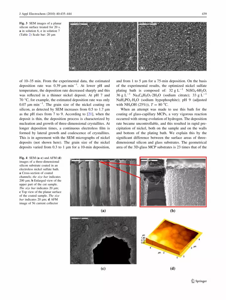
on its surface [20]. Figure 3a and b shows the surface of
silicon samples dipped in PdCl2/HF solution for 5 s and
then etched for 20 s in two solutions that differ only in the
concentration of hydrogen peroxide (solutions 6 and 7 from
Table 2). The size of the pits is uniform and their diameters
are about 0.3 lm. This roughness level results in very
strong adhesion of the electroless nickel deposit to silicon
and allows the consideration of silicon as a substrate for 3D
microbatteries.
Thermal treatment (400–420 �C for 5 min in an argon
atmosphere) of the nickel-coated silicon samples improved
adhesion still further. This was due to nickel diffusion into
the bulk of the silicon and the formation of a nickel silicide
layer about 100 nm thick on the interface between the
substrate and nickel, as found by the TOF–SIMS method.
3.2 Deposition of a nickel current collector
for 3D-CMBs from a nickel sulfate bath
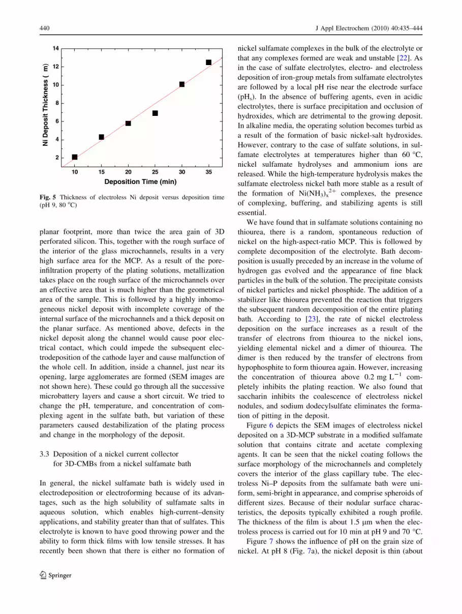
Figure 4 shows cross-sectional and planar SEM images of
the perforated-silicon substrate coated by an electroless
nickel layer. The plating was performed at pH 9, 80 �C for
10 min and the thickness of the nickel film was about
3 lm. As can be seen in the figure, a thin, conformal nickel
layer completely coats the planar surface and the interior of
a channel. The adhesion of the deposit, as detected by
adhesive-tape tests, is strong. Some peeling, shown in
Fig. 4, is due to the rough mechanical cut of the sample.
The AFM image (Fig. 4c) indicates an average roughness
level of the nickel film in the range of 0.7–1.5 lm.
In order to determine the optimal plating conditions, the
morphology and thickness of the deposit were tested.
Figure 5 shows a plot of the thickness of the electroless
nickel coating versus deposition time at pH 9 and 80 �C.
The thickness of the nickel deposit increases linearly with
deposition time, varying from 2 to 12 lm over a time range
Fig. 2 SEM images of MCP
(Burle). a The planar view of
the surface, b the tilted view of
a cross-section. The size barindicates 50 lm
438 J Appl Electrochem (2010) 40:435–444
123
of 10–35 min. From the experimental data, the estimated
deposition rate was 0.39 lm min-1. At lower pH and
temperature, the deposition rate decreased sharply and this
was reflected in a thinner nickel deposit. At pH 7 and
70 �C, for example, the estimated deposition rate was only
0.07 lm min-1. The grain size of the nickel coating on
silicon, as detected by SEM increases from 0.5 to 1.7 lm
as the pH rises from 7 to 9. According to [21], when the
deposit is thin, the deposition process is characterized by
nucleation and growth of three-dimensional crystallites. At
longer deposition times, a continuous electroless film is
formed by lateral growth and coalescence of crystallites.
This is in agreement with the SEM micrographs of nickel
deposits (not shown here). The grain size of the nickel
deposits varied from 0.3 to 1 lm for a 10-min deposition,
and from 1 to 5 lm for a 75-min deposition. On the basis
of the experimental results, the optimized nickel sulfate
plating bath is composed of: 32 g L-1 NiSO4�6H2O;
36 g L-1 Na3C6H5O7�2H2O (sodium citrate); 33 g L-1
NaH2PO2�H2O (sodium hypophosphite); pH 9 (adjusted
with NH4OH (25%)), T = 80 oC.
When an attempt was made to use this bath for the
coating of glass-capillary MCPs, a very vigorous reaction
occurred with strong evolution of hydrogen. The deposition
rate became uncontrollable, and this resulted in rapid pre-
cipitation of nickel, both on the sample and on the walls
and bottom of the plating bath. We explain this by the
significant difference between the surface areas of three-
dimensional silicon and glass substrates. The geometrical
area of the 3D-glass MCP substrates is 23 times that of the
Fig. 3 SEM images of a planar
silicon surface treated for 20 s.
a in solution 6, c in solution 7
(Table 2) Scale bar: 20 lm
Fig. 4 SEM (a–c) and AFM (d)
images of a three-dimensional
silicon substrate coated in an
electroless nickel sulfate bath.
a Cross-section of coated
channels; the size bar indicates
200 lm; b Enlarged view of the
upper part of the cut sample.
The size bar indicates 20 lm;
c Top view of the planar surface
of the coated sample. The sizebar indicates 20 lm; d AFM
image of Ni current collector
J Appl Electrochem (2010) 40:435–444 439
123
planar footprint, more than twice the area gain of 3D
perforated silicon. This, together with the rough surface of
the interior of the glass microchannels, results in a very
high surface area for the MCP. As a result of the pore-
infiltration property of the plating solutions, metallization
takes place on the rough surface of the microchannels over
an effective area that is much higher than the geometrical
area of the sample. This is followed by a highly inhomo-
geneous nickel deposit with incomplete coverage of the
internal surface of the microchannels and a thick deposit on
the planar surface. As mentioned above, defects in the
nickel deposit along the channel would cause poor elec-
trical contact, which could impede the subsequent elec-
trodeposition of the cathode layer and cause malfunction of
the whole cell. In addition, inside a channel, just near its
opening, large agglomerates are formed (SEM images are
not shown here). These could go through all the successive
microbattery layers and cause a short circuit. We tried to
change the pH, temperature, and concentration of com-
plexing agent in the sulfate bath, but variation of these
parameters caused destabilization of the plating process
and change in the morphology of the deposit.
3.3 Deposition of a nickel current collector
for 3D-CMBs from a nickel sulfamate bath
In general, the nickel sulfamate bath is widely used in
electrodeposition or electroforming because of its advan-
tages, such as the high solubility of sulfamate salts in
aqueous solution, which enables high-current–density
applications, and stability greater than that of sulfates. This
electrolyte is known to have good throwing power and the
ability to form thick films with low tensile stresses. It has
recently been shown that there is either no formation of
nickel sulfamate complexes in the bulk of the electrolyte or
that any complexes formed are weak and unstable [22]. As
in the case of sulfate electrolytes, electro- and electroless
deposition of iron-group metals from sulfamate electrolytes
are followed by a local pH rise near the electrode surface
(pHs). In the absence of buffering agents, even in acidic
electrolytes, there is surface precipitation and occlusion of
hydroxides, which are detrimental to the growing deposit.
In alkaline media, the operating solution becomes turbid as
a result of the formation of basic nickel-salt hydroxides.
However, contrary to the case of sulfate solutions, in sul-
famate electrolytes at temperatures higher than 60 �C,
nickel sulfamate hydrolyses and ammonium ions are
released. While the high-temperature hydrolysis makes the
sulfamate electroless nickel bath more stable as a result of
the formation of Ni(NH3)x2? complexes, the presence
of complexing, buffering, and stabilizing agents is still
essential.
We have found that in sulfamate solutions containing no
thiourea, there is a random, spontaneous reduction of
nickel on the high-aspect-ratio MCP. This is followed by
complete decomposition of the electrolyte. Bath decom-
position is usually preceded by an increase in the volume of
hydrogen gas evolved and the appearance of fine black
particles in the bulk of the solution. The precipitate consists
of nickel particles and nickel phosphide. The addition of a
stabilizer like thiourea prevented the reaction that triggers
the subsequent random decomposition of the entire plating
bath. According to [23], the rate of nickel electroless
deposition on the surface increases as a result of the
transfer of electrons from thiourea to the nickel ions,
yielding elemental nickel and a dimer of thiourea. The
dimer is then reduced by the transfer of electrons from
hypophosphite to form thiourea again. However, increasing
the concentration of thiourea above 0.2 mg L21 com-
pletely inhibits the plating reaction. We also found that
saccharin inhibits the coalescence of electroless nickel
nodules, and sodium dodecylsulfate eliminates the forma-
tion of pitting in the deposit.
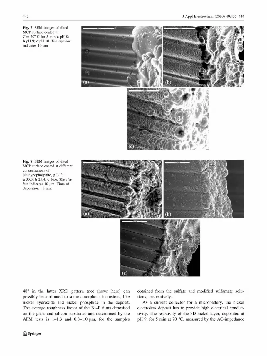
Figure 6 depicts the SEM images of electroless nickel
deposited on a 3D-MCP substrate in a modified sulfamate
solution that contains citrate and acetate complexing
agents. It can be seen that the nickel coating follows the
surface morphology of the microchannels and completely
covers the interior of the glass capillary tube. The elec-
troless Ni–P deposits from the sulfamate bath were uni-
form, semi-bright in appearance, and comprise spheroids of
different sizes. Because of their nodular surface charac-
teristics, the deposits typically exhibited a rough profile.
The thickness of the film is about 1.5 lm when the elec-
troless process is carried out for 10 min at pH 9 and 70 �C.
Figure 7 shows the influence of pH on the grain size of
nickel. At pH 8 (Fig. 7a), the nickel deposit is thin (about
10 15 20 25 30 35
2
4
6
8
10
12
14N
i Dep
osi
t T
hic
knes
s (µ
m)
Deposition Time (min)
Fig. 5 Thickness of electroless Ni deposit versus deposition time
(pH 9, 80 oC)
440 J Appl Electrochem (2010) 40:435–444
123
0.4 lm after 5 min of deposition); its surface is relatively
smooth, since the kinetics of nucleation is faster than the
rate of crystal growth. The spheroids are already noticeable
at this thickness. At pH 9 (Fig. 7b), the reduction of nickel
by hypophosphite is faster and crystal growth becomes
more significant. At pH 10, the deposition rate increases
further (Fig. 7c), leading to greater thickness (up to an
average of 1.2 lm) and larger spheroids, the size of which
approaches 1 lm. The electroless nickel coating becomes
highly non-homogeneous with compact agglomerates at
the top of the concave, finned part of the internal surface of
the microchannel.
High temperature accelerates the process, affecting
mainly the thickness of the coating, which increases from
*0.6 to 1 lm at 60 and 70 �C, respectively. While
somewhat larger ball-like particles appear at the surface,
the uniformity of nickel plating as well as the roughness
factor does not change much with temperature. The deposit
conformally follows both the internal 3D and planar sur-
faces of the MCP.
Figures 8 and 9 show the effect of the concentrations of
reducing and complexing agents in the electroless-nickel
bath on the morphology of nickel and the deposition rate.
Lowering the concentration of the sodium hypophosphite
leads to a decrease in the reaction rate, and thus, to a
reduction in the thickness of the deposit and the dimensions
of the spheroids. The average thickness of the nickel film
formed in a solution containing 16.6 g L21 NaH2PO2 is
less than half that obtained from the electrolyte with
33.3 g L21 of reducing agent. Rapid reduction of Ni2? at
high concentrations of hypophosphite causes vigorous
growth of spheroid particles on top of the convex ribs,
while the deposit on the concave parts between the ribs is
much thinner. This causes highly non-uniform nickel films
in the microchannels.
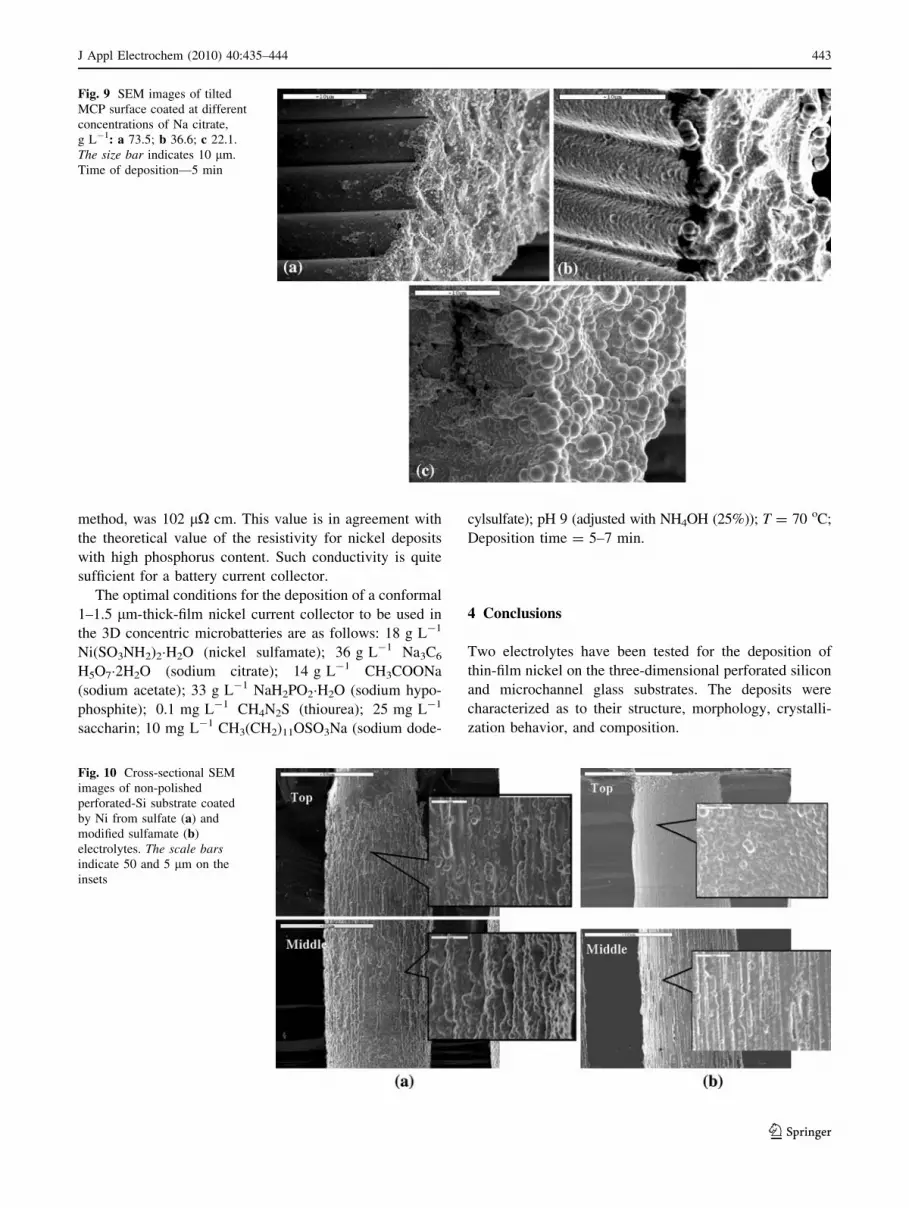
Citrate has the opposite effect on the deposit. Here,
increasing the sodium citrate concentration in the electro-
lyte leads to a reduction in the thickness of the deposit and
the radius of the spheroids (Fig. 9). For a deposition time
of 5 min, the thickness of the nickel deposit decreases
almost linearly from 0.95 to 0.2 lm as the concentration of
sodium citrate is increased from 22.1 to 73.5 g L21. SEM
images of the MCP coated by nickel (Fig. 9) show that
increasing the concentration of sodium citrate results in the
formation of a uniform deposit with a smooth, homoge-
neous surface.
In agreement with [24], we believe that at pH [ 8, cit-
rate forms NiHCit-, Ni2Cit(HCit)3-, and Ni2Cit24- com-
plexes which, in turn, prevent the formation of the
undesirable nickel hydroxide inclusions and detrimental
roughness of the plating. The presence of acetate, although
a weaker complexing agent than citrate, increases the
buffer capacity of the electrolyte.
The rate of electroless nickel deposition and the
phosphorus content are proportional to the rate at which
the nickel complex dissociates to form free nickel ion.
Thus, the plating rate is inversely related to the stability
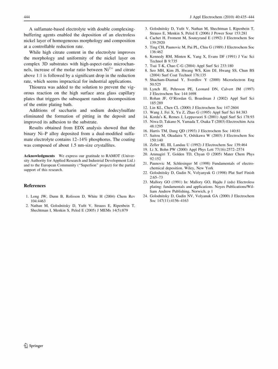
of the nickel complexes. The deposition rate of nickel
obtained from a modified sulfamate bath at pH 9 and
70 �C was 0.207 lm min-1. This deposition rate is lower
than the rate in a nickel sulfate bath, but the deposit is
much more uniform in thickness, conformal with a
smoother surface and smaller grain size (Fig. 10). It
should be noted, in addition, that both the roughness and
the uniformity of nickel obtained from a dual-modified
sulfamate electrolyte do not change much with time. The
concentration of phosphorus in a Ni–P alloy obtained by
EDS measurements is only slightly affected by the
deposition time. The phosphorus content increases by
1.5% when the duration of the reduction process is
increased from 2 to 10 min. When the thickness of the
nickel layer approaches 1.5 lm, the Ni–P deposit con-
tains 14.2% phosphorus. This composition remains
unchanged up to a film thickness of 4 lm. Structural
examination carried out by XRD revealed the presence
of a broad peak with a calculated crystallite size of
about 1.5 nm for nickel deposited from a modified sul-
famate electrolyte, whereas a sharp (111) peak with a
crystallite size of about 6 nm is obtained for the metal
from a sulfate bath. A small, broad shoulder appearing at
Fig. 6 SEM images of MCP
coated in an electroless nickel
sulfamate bath at pH 9, 70 �C,
10 min; a Cross-section of
coated channels; the size barindicates 200 lm; b Tilted view
of the surface of the coated
sample. The size bar indicates
20 lm
J Appl Electrochem (2010) 40:435–444 441
123
48� in the latter XRD pattern (not shown here) can
possibly be attributed to some amorphous inclusions, like
nickel hydroxide and nickel phosphide in the deposit.
The average roughness factor of the Ni–P films deposited
on the glass and silicon substrates and determined by the
AFM tests is 1–1.3 and 0.8–1.0 lm, for the samples
obtained from the sulfate and modified sulfamate solu-
tions, respectively.
As a current collector for a microbattery, the nickel
electroless deposit has to provide high electrical conduc-
tivity. The resistivity of the 3D nickel layer, deposited at
pH 9, for 5 min at 70 �C, measured by the AC-impedance
Fig. 7 SEM images of tilted
MCP surface coated at
T = 70o C for 5 min a pH 8;
b pH 9; c pH 10. The size barindicates 10 lm
Fig. 8 SEM images of tilted
MCP surface coated at different
concentrations of
Na-hypophosphite, g L-1:
a 33.3; b 25.4; c 16.6. The sizebar indicates 10 lm. Time of
deposition—5 min
442 J Appl Electrochem (2010) 40:435–444
123
method, was 102 lX cm. This value is in agreement with
the theoretical value of the resistivity for nickel deposits
with high phosphorus content. Such conductivity is quite
sufficient for a battery current collector.
The optimal conditions for the deposition of a conformal
1–1.5 lm-thick-film nickel current collector to be used in
the 3D concentric microbatteries are as follows: 18 g L-1
Ni(SO3NH2)2�H2O (nickel sulfamate); 36 g L-1 Na3C6
H5O7�2H2O (sodium citrate); 14 g L-1 CH3COONa
(sodium acetate); 33 g L-1 NaH2PO2�H2O (sodium hypo-
phosphite); 0.1 mg L-1 CH4N2S (thiourea); 25 mg L-1
saccharin; 10 mg L-1 CH3(CH2)11OSO3Na (sodium dode-
cylsulfate); pH 9 (adjusted with NH4OH (25%)); T = 70 oC;
Deposition time = 5–7 min.
4 Conclusions
Two electrolytes have been tested for the deposition of
thin-film nickel on the three-dimensional perforated silicon
and microchannel glass substrates. The deposits were
characterized as to their structure, morphology, crystalli-
zation behavior, and composition.
Fig. 9 SEM images of tilted
MCP surface coated at different
concentrations of Na citrate,
g L-1: a 73.5; b 36.6; c 22.1.
The size bar indicates 10 lm.
Time of deposition—5 min
Fig. 10 Cross-sectional SEM
images of non-polished
perforated-Si substrate coated
by Ni from sulfate (a) and
modified sulfamate (b)
electrolytes. The scale barsindicate 50 and 5 lm on the
insets
J Appl Electrochem (2010) 40:435–444 443
123
A sulfamate-based electrolyte with double complexing-
buffering agents enabled the deposition of an electroless
nickel layer of homogeneous morphology and composition
at a controllable reduction rate.
While high citrate content in the electrolyte improves
the morphology and uniformity of the nickel layer on
complex 3D substrates with high-aspect-ratio microchan-
nels, increase of the molar ratio between Ni2? and citrate
above 1:1 is followed by a significant drop in the reduction
rate, which seems impractical for industrial applications.
Thiourea was added to the solution to prevent the vig-
orous reaction on the high surface area glass capillary
plates that triggers the subsequent random decomposition
of the entire plating bath.
Additions of saccharin and sodium dodecylsulfate
eliminated the formation of pitting in the deposit and
improved its adhesion to the substrate.
Results obtained from EDX analysis showed that the
binary Ni–P alloy deposited from a dual-modified sulfa-
mate electrolyte contains 12–14% phosphorus. The coating
was composed of about 1.5 nm-size crystallites.
Acknowledgments We express our gratitude to RAMOT (Univer-
sity Authority for Applied Research and Industrial Development Ltd.)
and to the European Community (‘‘Superlion’’ project) for the partial
support of this research.
References
1. Long JW, Dunn B, Rolisson D, White H (2004) Chem Rev
104:4463
2. Nathan M, Golodnitsky D, Yufit V, Strauss E, Ripenbein T,
Shechtman I, Menkin S, Peled E (2005) J MEMs 14(5):879
3. Golodnitsky D, Yufit V, Nathan M, Shechtman I, Ripenbein T,
Strauss E, Menkin S, Peled E (2006) J Power Sour 153:281
4. Cachet H, Froment M, Souteyrand E (1992) J Electrochem Soc
139:2920
5. Ting CH, Paunovic M, Pai PL, Chiu G (1989) J Electrochem Soc
136:462
6. Kennedy RM, Minten K, Yang X, Evans DF (1991) J Vac Sci
Technol B 9:735
7. Tsai T-K, Chao C-G (2004) Appl Surf Sci 233:180
8. Seo MH, Kim JS, Hwang WS, Kim DJ, Hwang SS, Chun BS
(2004) Surf Coat Technol 176:135
9. Shacham-Diamad Y, Sverdlov Y (2000) Microelectron Eng
50:525
10. Lynch JE, Pehrsson PE, Leonard DN, Calvert JM (1997)
J Electrochem Soc 144:1698
11. Rohan JF, O’Riordan G, Boardman J (2002) Appl Surf Sci
185:289
12. Lin KL, Chen CL (2000) J Electrochem Soc 147:2604
13. Wang J, Fei X, Yu Z, Zhao G (1995) Appl Surf Sci 84:383
14. Korda0s K, Remes J, Leppavuori S (2001) Appl Surf Sci 178:93
15. Niwa D, Takano N, Yamada T, Osaka T (2003) Electrochim Acta
48:1295
16. Harris TM, Dang QD (1993) J Electrochem Soc 140:81
17. Saitou M, Okudaira Y, Oshikawa W (2003) J Electrochem Soc
150:140
18. Zeller RL III, Landau U (1992) J Electrochem Soc 139:464
19. Li X, Bohn PW (2000) Appl Phys Lett 77(16):2572–2574
20. Arunagiri T, Golden TD, Chyan O (2005) Mater Chem Phys
92:152
21. Paunovic M, Schlesinger M (1998) Fundamentals of electro-
chemical deposition. Wiley, New York
22. Golodnitsky D, Gudin N, Volyanyuk G (1998) Plat Surf Finish
2:65–73
23. Mallory GO (1991) In: Mallory GO, Hajdu J (eds) Electroless
plating: fundamentals and applications. Noyes Publications/Wil-
liam Andrew Publishing, Norwich, p 1
24. Golodnitsky D, Gudin NV, Volyanuk GA (2000) J Electrochem
Soc 147(11):4156–4163
444 J Appl Electrochem (2010) 40:435–444
123