electrochemically induced surface modifications in boron-doped diamond films: a raman spectroscopy...
TRANSCRIPT
www.elsevier.com/locate/tsf
Thin Solid Films 482
Electrochemically induced surface modifications in boron-doped diamond
films: a Raman spectroscopy study
P.C. Ricci*, A. Anedda, C.M. Carbonaro, F. Clemente, R. Corpino
Dipartimento di Fisica, INFM Universita di Cagliari, Cittadella Universitaria S.P. Monserrato-Sestu Km 0.700-09042 Monserrato (Ca), Italy
Available online 5 January 2005
Abstract
Owing to its unique properties such as chemical stability, large potential windows of water stability (up to 3 V) and mechanical resistance,
boron-doped diamond (BDD) thin films have been widely used as electrodes for electro-analysis and electrolysis.
In this work we have studied surface structural modifications in BDD thin films grown by hot filament chemical vapor deposition
(HFCVD) due to usage as anodic working electrode in H3PO4 aqueous solution (pH=1, 2) up to 1000 h. With the powerful tool of
Micro-Raman spectroscopy we show nonuniform structural variations of the diamond lattice. Modifications in the electrochemical
properties has been observed while BDD electrodes were used as anodes. Moreover, by modelling the Fano interaction between discrete
phonon states and the degenerate continuum of states, we point out an increase of the acceptor levels as a function of the electrode
working hours.
These experimental evidences indicate an anomalous behaviour of hydrogen loaded in the films during the growth process. A model
based on the hydrogen–boron interaction could explain the observed modifications in Fano coupling.
D 2004 Elsevier B.V. All rights reserved.
Keywords: Raman scattering; Boron-doped diamond (BDD); Fano interaction
1. Introduction
Because of its peculiar properties such as wide band gap,
high breakdown voltage, high thermal conductivity, and
small dielectric constant, diamond has been recognized as
suitable material for electronic devices which can operate at
high temperature, high frequency, and high power range.
Semiconducting p-type diamond can be prepared by
chemical vapor deposition with doping boron into the
lattice, adding diborane gas to methane–hydrogen gas
mixtures [1]. Boron-doped Diamond (BDD) films are
considered as one of the most ideal electrodes for electro-
analysis and electrolysis [2,3]. Actually, conductive dia-
mond has several superior characteristics compared to other
carbon materials and metals, including very low back-
ground current density and wide potential window in
aqueous solution [4,5]. However the stability of BDD thin
films working as anode is still a mandatory task to achieve
0040-6090/$ - see front matter D 2004 Elsevier B.V. All rights reserved.
doi:10.1016/j.tsf.2004.11.169
* Corresponding author.
E-mail address: [email protected] (P.C. Ricci).
[5,6]. In this work we analyse a commercial BDD thin films
working as anode in acid solution at different time step up
to 1000 h. The analysis has been performed by Raman
spectroscopy, which can provide useful information on
crystal structure without affecting the sample quality.
2. Experimental
Commercial Diamond films (CSEM, the Swiss Center
for Electronics and Microtechnology), 1 Am thick, were
grown by hot filament chemical vapor deposition at 850 8Cfrom a 0.5% H2/CH4 mixture at a pressure of 40 torr. The
substrate was a p-type polished silicon wafer (1 mm) with a
resistivity of about 10 mV cm�1. The nominal concen-
trations of Boron atoms in diamond lattice is 1020 cm�3.
Micro-Raman measurements have been carried out in
backscattering geometry by using the polarized 514.5 nm
line of an Argon-ion laser. Raman scattering measurements
have been performed in air at room temperature with a triple
spectrometer Jobin–Yvonne Dilor integrated system with a
(2005) 311–317
P.C. Ricci et al. / Thin Solid Films 482 (2005) 311–317312
spectral resolution of about 1 cm�1. Spectra have been
recorded in the Stokes region by a 1200 grooves/mm grating
monochromator and CCD detector system. Confocal micro-
scope Olympus B-201 has been used, with an objective of�100 with 0.90 numerical aperture. The spatial resolution
was less than 1 Am.
The electrochemical measurements have been performed
in a conventional three electrode cell with a platinum
counter-electrode and a saturated calomel electrode (SCE)
as reference. The electrode potential is given with respect to
the potential of the SCE.
The BDD films worked as anode in H3PO4 aqueous
solution (pH=1, 2), in dark condition, up to 1000 h. The
procedure was interrupt at regular step in order to measure
the Raman spectra and the voltage–current curves. The
density current was kept at 12 mA/cm2 and the relative
potential varied between 2.7 and 2.8 eV vs. SCE.
The V–I characteristic curves were taken in a 0,1 M
concentration H2SO4 acid solution in potentio-dinamic
regime with a scan rate of 20 mV s�1.
3. Results
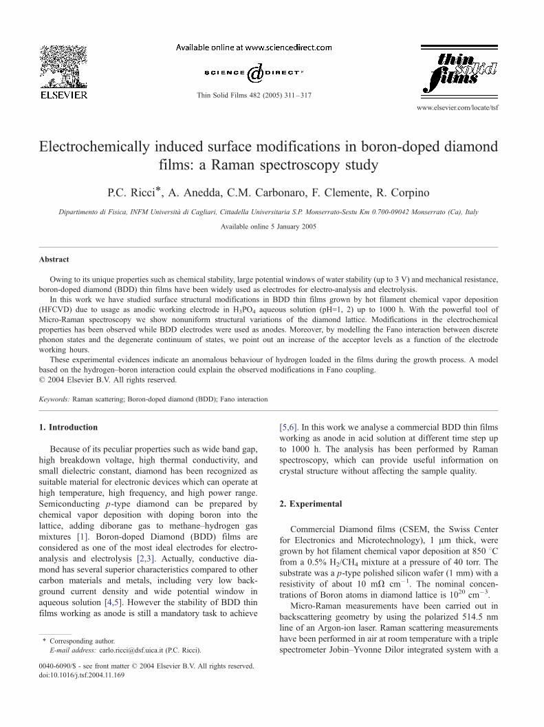
Fig. 1 reports the Raman spectrum of the as-prepared
sample. Silicon substrate peaks are located at 520.7 and
950 cm�1. The Raman peak at 1332 cm�1 is attributed to
the contribution of undoped diamond [7]. The two broad
band at the low energy side (about 1200 cm�1) and high
energy side (about 1500 cm�1) of the diamond line have
been previously attributed to reticular distortion of the
diamond structure [7,8] and to the presence of a graphite
Fig. 1. Raman spectrum of the as-prepared BDD sample, no variation have been o
taken after (a) 0, (b) 20, (c) 40, and (d) 60 working minutes.
phase, respectively [9]. The graphite phase in commercial
samples is not unusual; the possibility to reveal a few
percentage of the graphite phase in the diamond lattice
through the Raman analysis is due to the high Raman
efficiency of the graphite band with respect to the diamond
signal (about two orders of magnitude greater) [7,9]. It is
worth to note that no relievable difference has been
observed during the first 200 working hours in the Raman
spectra.
The inset in Fig. 1 reports the characteristic voltage–
current (V–I) curve registered during the first working hour.
Although Raman spectra are unchanged during the first 200
working hours, the V–I curves change drastically during the
first hour, there is a relative high increase of the resistivity
with working time; it is reasonable to suppose that the
electrochemical reaction at the electrode surface does not
change in this short period and the variation in the current
value could be due only to changes in the electrode
properties.
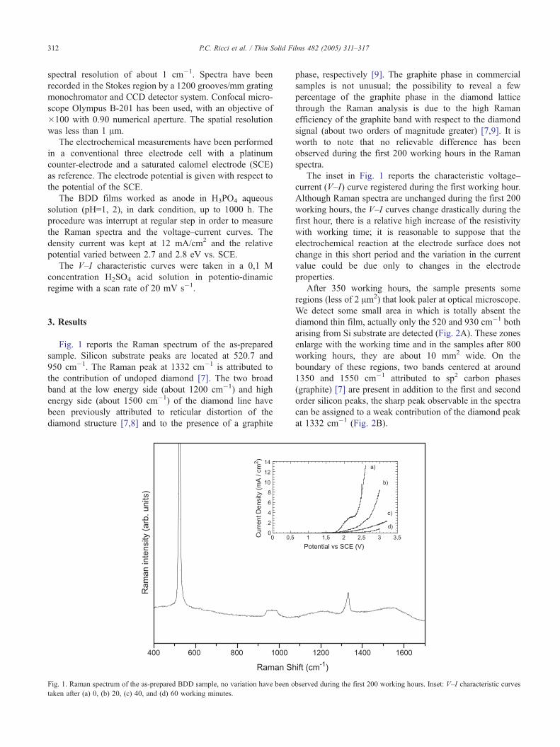
After 350 working hours, the sample presents some
regions (less of 2 Am2) that look paler at optical microscope.
We detect some small area in which is totally absent the
diamond thin film, actually only the 520 and 930 cm�1 both
arising from Si substrate are detected (Fig. 2A). These zones
enlarge with the working time and in the samples after 800
working hours, they are about 10 mm2 wide. On the
boundary of these regions, two bands centered at around
1350 and 1550 cm�1 attributed to sp2 carbon phases
(graphite) [7] are present in addition to the first and second
order silicon peaks, the sharp peak observable in the spectra
can be assigned to a weak contribution of the diamond peak
at 1332 cm�1 (Fig. 2B).
bserved during the first 200 working hours. Inset: V–I characteristic curves
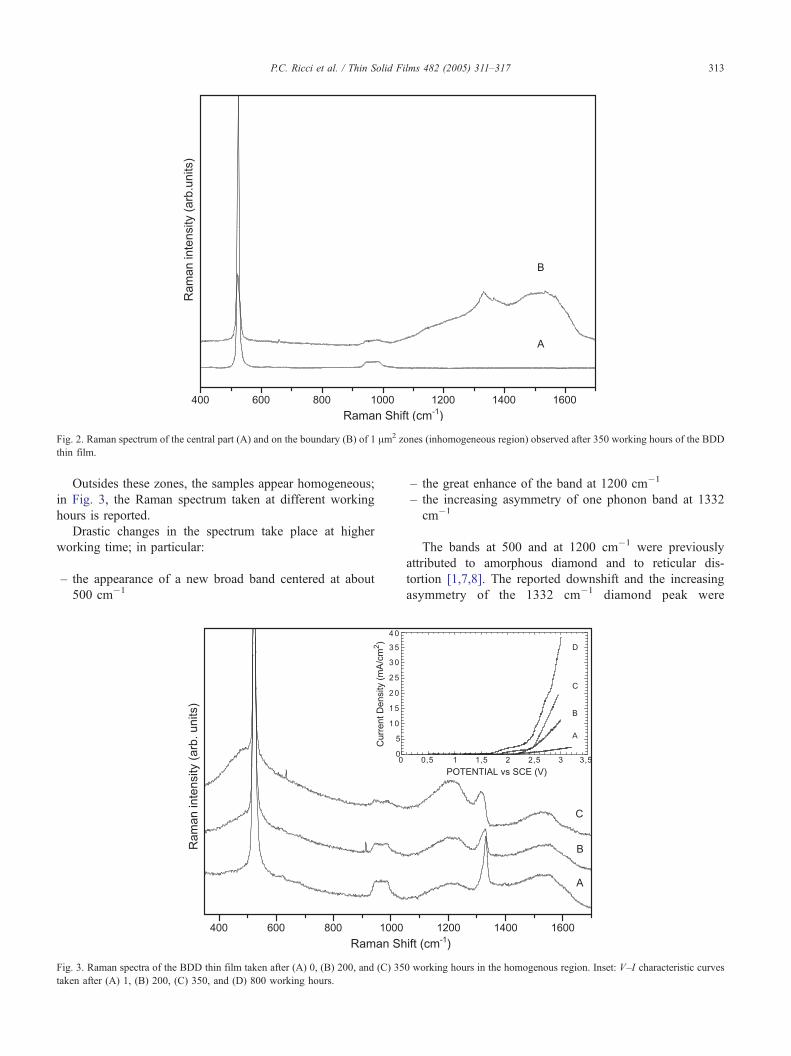
Fig. 2. Raman spectrum of the central part (A) and on the boundary (B) of 1 Am2 zones (inhomogeneous region) observed after 350 working hours of the BDD
thin film.
P.C. Ricci et al. / Thin Solid Films 482 (2005) 311–317 313
Outsides these zones, the samples appear homogeneous;
in Fig. 3, the Raman spectrum taken at different working
hours is reported.
Drastic changes in the spectrum take place at higher
working time; in particular:
– the appearance of a new broad band centered at about
500 cm�1
Fig. 3. Raman spectra of the BDD thin film taken after (A) 0, (B) 200, and (C) 35
taken after (A) 1, (B) 200, (C) 350, and (D) 800 working hours.
– the great enhance of the band at 1200 cm�1
– the increasing asymmetry of one phonon band at 1332
cm�1
The bands at 500 and at 1200 cm�1 were previously
attributed to amorphous diamond and to reticular dis-
tortion [1,7,8]. The reported downshift and the increasing
asymmetry of the 1332 cm�1 diamond peak were
0 working hours in the homogenous region. Inset: V–I characteristic curves
P.C. Ricci et al. / Thin Solid Films 482 (2005) 311–317314
reported by several authors and it was related to the
increasing of the so-called Fano’s interaction induced by
quantum mechanical interference between the discrete
phonons state with a degenerate electronic continuum
[10–15]. The continuum could be identified as the hole
continuum of the acceptors to valence excitations or
inter-valence transitions from the low energy level to
high energy level. Both these phenomena have been
related to the variation of Boron concentration in the
diamond structure [13,16]. Ager et al. [16] considered
that the Fano interference of the Raman phonon in
heavily B-doped diamond due to the transitions between
impurity band and valence band states as the more likely
mechanism, while in heavily boron-doped Silicon inter-
valence band, electronic Raman scattering generates the
Fano-type interference [17,18].
The inset in Fig. 3 shows the V–I characteristic curves
taken at different working time steps. Contrary to the trend
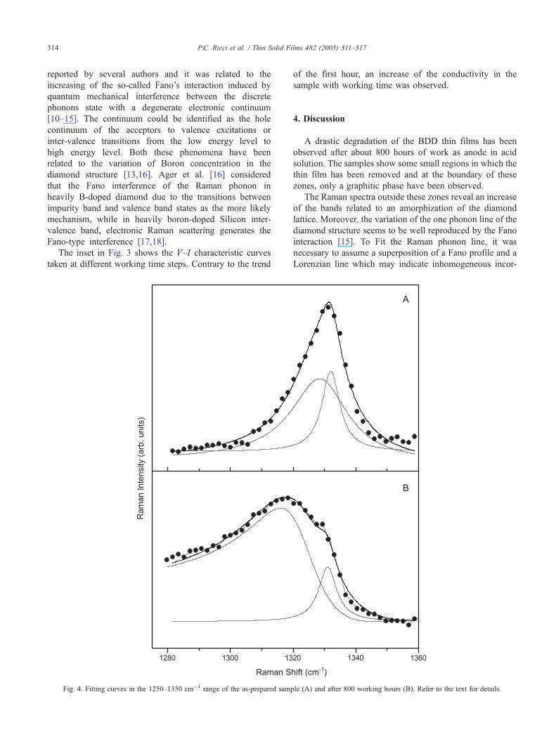
Fig. 4. Fitting curves in the 1250–1350 cm�1 range of the as-prepared samp
of the first hour, an increase of the conductivity in the
sample with working time was observed.
4. Discussion
A drastic degradation of the BDD thin films has been
observed after about 800 hours of work as anode in acid
solution. The samples show some small regions in which the
thin film has been removed and at the boundary of these
zones, only a graphitic phase have been observed.
The Raman spectra outside these zones reveal an increase
of the bands related to an amorphization of the diamond
lattice. Moreover, the variation of the one phonon line of the
diamond structure seems to be well reproduced by the Fano
interaction [15]. To Fit the Raman phonon line, it was
necessary to assume a superposition of a Fano profile and a
Lorenzian line which may indicate inhomogeneous incor-
le (A) and after 800 working hours (B). Refer to the text for details.
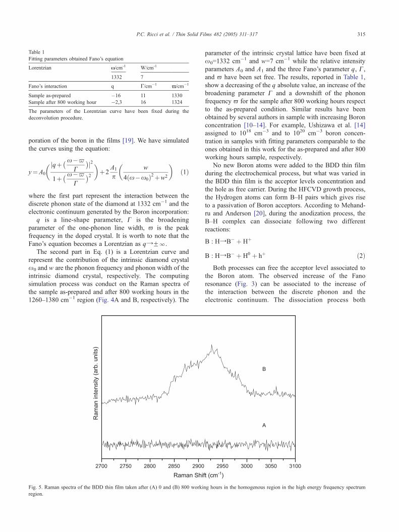
Table 1
Fitting parameters obtained Fano’s equation
Lorentzian N/cm-1 W/cm-1
1332 7
Fano’s interaction q G/cm�1 E/cm�1
Sample asQprepared �16 11 1330
Sample after 800 working hour �2,3 16 1324
The parameters of the Lorentzian curve have been fixed during the
deconvolution procedure.
P.C. Ricci et al. / Thin Solid Films 482 (2005) 311–317 315
poration of the boron in the films [19]. We have simulated
the curves using the equation:
y¼A0
� jqþ� x�$
C
�j2
1þ� x�$
C
�2�þ2
A1
p
�w
4 x�x0ð Þ2þw2
�ð1Þ
where the first part represent the interaction between the
discrete phonon state of the diamond at 1332 cm�1 and the
electronic continuum generated by the Boron incorporation:
q is a line-shape parameter, C is the broadening
parameter of the one-phonon line width, - is the peak
frequency in the doped crystal. It is worth to note that the
Fano’s equation becomes a Lorentzian as qYFl.
The second part in Eq. (1) is a Lorentzian curve and
represent the contribution of the intrinsic diamond crystal
x0 and w are the phonon frequency and phonon width of the
intrinsic diamond crystal, respectively. The computing
simulation process was conduct on the Raman spectra of
the sample as-prepared and after 800 working hours in the
1260–1380 cm�1 region (Fig. 4A and B, respectively). The
Fig. 5. Raman spectra of the BDD thin film taken after (A) 0 and (B) 800 worki
region.
parameter of the intrinsic crystal lattice have been fixed at
x0=1332 cm�1 and w=7 cm�1 while the relative intensity
parameters A0 and A1 and the three Fano’s parameter q, C,
and - have been set free. The results, reported in Table 1,
show a decreasing of the q absolute value, an increase of the
broadening parameter C and a downshift of the phonon
frequency - for the sample after 800 working hours respect
to the as-prepared condition. Similar results have been
obtained by several authors in sample with increasing Boron
concentration [10–14]. For example, Ushizawa et al. [14]
assigned to 1018 cm�3 and to 1020 cm�3 boron concen-
tration in samples with fitting parameters comparable to the
ones obtained in this work for the as-prepared and after 800
working hours sample, respectively.
No new Boron atoms were added to the BDD thin film
during the electrochemical process, but what was varied in
the BDD thin film is the acceptor levels concentration and
the hole as free carrier. During the HFCVD growth process,
the Hydrogen atoms can form B–H pairs which gives rise
to a passivation of Boron acceptors. According to Mehand-
ru and Anderson [20], during the anodization process, the
B–H complex can dissociate following two different
reactions:
B : HYB� þ Hþ
B : HYB� þ H0 þ hþ ð2Þ
Both processes can free the acceptor level associated to
the Boron atom. The observed increase of the Fano
resonance (Fig. 3) can be associated to the increase of
the interaction between the discrete phonon and the
electronic continuum. The dissociation process both
ng hours in the homogenous region in the high energy frequency spectrum
P.C. Ricci et al. / Thin Solid Films 482 (2005) 311–317316
increases the acceptor levels density (Fano interference due
to the interactions between the discrete phonon with
valence to impurity transitions) and increases the holes as
free carriers (Fano interference due to the interference
between the discrete phonon state and the inter-valence
band transitions).
Moreover, the conduction mechanism in BDD elec-
trode is strongly related to the concentration of the
acceptors levels and to the hole free carriers [21].
Opposite to the first working hour, during which the
resistivity increases with working time (inset of Fig. 1),
the resistivity decreases increasing the working time
(inset of Fig. 3). It has been proposed that the behavior
during the first hour arises from a passive layer,
generated on diamond surfaces by anodic pretreatment
[5]. The passive films is generated by the removal of
Hydrogen acting as acceptor in the subsurface region (H-
terminated diamond surface), leaving the trapped Hydro-
gen as H+B� dimers (O- termination surface). It is well
know that Hydrogen affects the electrical properties of
semiconductors, because of its fast diffusion and its
strong tendency to passivate electrically active sites. In
the case of p-type diamond, Hydrogen–Boron interactions
generate B–H pairs leading to a passivation of Boron
acceptors [5,22–24], reducing the hole concentration and
therefore the current intensity.
Therefore, the increased value of the current measured in
the V–I characteristic curves in along range of working time
can be related to the B–H dissociation process.
Moreover, in diamond films, the reduction of the
resistivity may also be due to the formation of the graphitic
phase. The distortion of the diamond structure has been
revealed by the formation of the band at 500 and 1200
cm�1 and can be due to the accumulation of Hydrogen at
the grain boundary of the polycrystalline film and in
interstitial sites. The increased concentration of Hydrogen
at the surface can be proved examining the Raman
spectrum of the degraded electrode in the high-frequency
region (Fig. 5). The broad and composite Raman band
between 2850 and 3000 cm�1 can be assigned to CHx
bonds [25]. It has been observed [25,26] that the CHx
bonds appear only after electrochemical treatment and,
according to Kondo et al. [5], the hydrogen-terminated
diamond surface is related to high concentration of hydro-
gen on the BDD surface.
The increased concentration of free H+ and H0, as well
their migration related to the electric field and diffusion
process generated by the fast oxidation process, can
accelerate the degradation of the diamond crystal and the
formation of the graphite phase. The process is not
uniform on the sample surface and we observe a random
degradation of the sample. This can be due to the
inhomogeneous formation of a graphite phase that under
the working electric voltage (about 2.7 V) determines fast
breaking of sp2 C–C bonds and removal of the BDD thin
film.
5. Conclusions
In the present study, the electrochemical stability of
Boron-doped Diamond thin film electrodes was studied
through Raman scattering analysis. Modifications of the
structure were observed from about 350 anode working
hours and a significant degradation of the sample was
revealed after 800 working hours. The Raman spectra show
the appearance and the enhancing of the band at 500 and
1200 cm�1 related to lattice distortion of the diamond
structure and the increasing of the Fano interaction, induced
by quantum mechanical interference between the diamond
discrete phonons state and the continuum (as acceptor to
band excitations and/or inter-valence transitions) by Boron
acceptor levels. We propose that the dissociation of the B–
H pairs during the anodising process enhances the accept-
ors concentration and the accumulation of free Hydrogen in
grain boundaries and in interstitial sites. This process can
affect the diamond crystal structure with the formation of
the graphitic phase randomly distributed in the electrode
and the progressive removal of the BDD thin film.
Acknowledgments
The authors would like to thank the Prof. Anna Maria
Polcaro for helping in the electrochemical measurements
and for the interesting discussions.
References
[1] R.J. Zhang, S.T. Lee, Y.W. Lam, Diamond Relat. Mater. 5 (1996)
1288.
[2] D. Gandini, E. Mahe, P.A. Michaud, W. Haenni, A. Perret, C.
Comminellis, J. Appl. Electrochem. 30 (2000) 1345.
[3] H.B. Suffredini, S.A.S. Machado, L.A. Avaca, J. Braz. Chem. Soc. 15
(2004) 16.
[4] R. DeClements, G. Mswain, J. Electrochem. Soc. 144 (1994) 3382.
[5] T. Kondo, K. Honda, D.A. Tryk, A. Fujishima, Electrochim. Acta 48
(2003) 2739.
[6] K. Hayashi, S. Yamanaka, H. Watanabe, T. Sekiguchi, H. Okushi, K.
Kajimura, J. Appl. Phys. 81 (1997) 744.
[7] P.G. Buckley, T.D. Moustakas, L. Ye, J. Varon, J. Appl. Phys. 66
(1989) 3595.
[8] P. Gonon, E. Gheeraert, A. Deneuville, F. Fontaine, L. Abello, G.
Lucazeau, J. Appl. Phys. 78 (1995) 7059.
[9] Y. Hishiyama, H. Irumano, Y. Kaburagi, Y. Soneda, Phys. Rev., B 63
(2001) 245406.
[10] K.W.R. Gilkes, S. Prawer, K.W. Nugent, J. Robertson, H.S. Sands, Y.
Lisfshitz, X. Shi, J. Appl. Phys. 87 (2000) 7283.
[11] K. Ushizawa, K. Watanabe, T. Ando, I. Sakaguchi, M. Nishitani-
Gamo, Y. Sato, H. Kanda, Diamond Relat. Mater. 7 (1998) 1719.
[12] Y. Wang, H. Li, Y. Xiong, S. Zhang, Z. Lin, K. Feng, Diamond Relat.
Mater. 9 (2000) 1708.
[13] F. Pruvost, A. Deneuville, Diamond Relat. Mater. 10 (2001) 531.
[14] K. Ushizawa, M.N. Gamo, F. Watanabe, I. Sakaguchi, Y. Sato, T.
Ando, J. Raman Spectrosc. 30 (1999) 957.
[15] M. Cardona, G. Guntherodt, Light scattering in solids IV 1984,
Springer, Berlin, 1978.
P.C. Ricci et al. / Thin Solid Films 482 (2005) 311–317 317
[16] J.W Ager, W. Walukiewicz, M. McCluskey, M.A. Plano, M.I.
Landstrass, Appl. Phys. Lett. 66 (1995) 616.
[17] F. Cerdeira, T.A. Fjeldly, M. Cardona, Phys. Rev., B 8 (1973)
4734.
[18] R. Gajic, D. Braun, F. Kuchar, A. Golubovic, R. Kortntner, H.
Loschner, J. Butschke, R. Springer, F. Letzkus, J. Phys. Chem., B
Condens. Mater. Surf. Interfaces Biophys. 15 (2003) 2923.
[19] R. Locher, J. Wagner, F. Fuchs, C. Wild, P. Hiesinger, P. Gonon, P.
Koidl, Mater. Sci. Eng., B, Solid-State Mater. Adv. Technol. 29 (1995)
211.
[20] S.P. Mehandru, A.B. Anderson, J. Mater. Res. 9 (1994) 383.
[21] B. Massarani, J.C. Bourgoin, R.M. Chrenko, Phys. Rev., B 17 (1978)
1758.
[22] K. Thonke, Semicond. Sci. Technol. 8 (2003) S20.
[23] D.A. Tryk, K. Tsunozaki, T.N. Rao, A. Fujishima, Diamond Relat.
Mater. 10 (2001) 1804.
[24] R. Zeisel, C.E. Nebel, M. Stutzmann, Diamond Relat. Mater. 9 (2000)
413.
[25] M. Bernard, A. Deneuville, E. Bustarret, Diamond Relat. Mater. 11
(2002) 662.
[26] G.H. Goeting, F. Marken, A. Gutierrez Sosa, R.G. Compton, J.S.
Foord, Diamond Relat. Mater. 9 (2000) 390.