development and implementation of a vhf high power
TRANSCRIPT

Development and Implementation of a VHF High Power Amplifier for the Multi-Channel
Coherent Radar Depth Sounder/Imager System
By
Reid William Crowe
B.Sc. Electrical Engineering
University of Kansas, 2009
Submitted to the graduate degree program in Electrical Engineering and Computer Science and
the Graduate Faculty of the University of Kansas in partial fulfillment of the requirements for the
degree of Master of Science.
________________________________
Chairperson Dr. Fernando Rodriguez-Morales
________________________________
Dr. Christopher Allen
________________________________
Dr. Carl Leuschen
Date Defended: 31 May 2013

ii
The Thesis Committee for Reid William Crowe
certifies that this is the approved version of the following thesis:
Development and Implementation of a VHF High Power Amplifier for the Multi-Channel
Coherent Radar Depth Sounder/Imager System
________________________________
Chairperson Dr. Fernando Rodriguez-Morales
Date approved: 31 May 2013

iii
Abstract
This thesis presents the implementation and characterization of a VHF high power
amplifier developed for the Multi-channel Coherent Radar Depth Sounder/Imager (MCoRDS/I)
system. MCoRDS/I is used to collect data on the thickness and basal topography of polar ice
sheets, ice sheet margins, and fast-flowing glaciers from airborne platforms. Previous surveys
have indicated that higher transmit power is needed to improve the performance of the radar,
particularly when flying over challenging areas.
The VHF high power amplifier system presented here consists of a 50-W driver amplifier
and a 1-kW output stage operating in Class C. Its performance was characterized and optimized
to obtain the best tradeoff between linearity, output power, efficiency, and conducted and
radiated noise. A waveform pre-distortion technique to correct for gain variations (dependent
on input power and operating frequency) was demonstrated using digital techniques.
The amplifier system is a modular unit that can be expanded to handle a larger number
of transmit channels as needed for future applications. The system can support sequential
transmit/receive operations on a single antenna by using a high-power circulator and a
duplexer circuit composed of two 90° hybrid couplers and anti-parallel diodes. The duplexer is
advantageous over switches based on PIN-diodes due to the moderately high power handling
capability and fast switching time. The system presented here is also smaller and lighter than
previous implementations with comparable output power levels.

iv
Table of Contents Abstract ........................................................................................................................................... iii
1 Introduction ............................................................................................................................. 1
1.1 Motivation ....................................................................................................................... 1
1.2 Previous Work ................................................................................................................. 6
1.2.1 Current Configuration ................................................................................................. 7
1.2.2 Link Budget.................................................................................................................. 9
1.3 This Work ...................................................................................................................... 11
1.4 Thesis Outline................................................................................................................ 12
2 Background ............................................................................................................................ 13
2.1 Power Amplifier Class Definitions ................................................................................. 13
2.1.1 Class A ....................................................................................................................... 14
2.1.2 Class B ....................................................................................................................... 15
2.1.3 Class AB ..................................................................................................................... 15
2.1.4 Class C ....................................................................................................................... 16
2.1.5 High Efficiency Modes ............................................................................................... 16
2.2 Figures of Merit ............................................................................................................. 17
2.2.1 Gain ........................................................................................................................... 17
2.2.2 Bandwidth ................................................................................................................. 18
2.2.3 Power Added Efficiency (PAE) .................................................................................. 18
2.2.4 Harmonic Power ....................................................................................................... 19
2.2.5 Intermodulation Distortion (IMD) ............................................................................ 20
2.2.6 Noise Figure .............................................................................................................. 22
2.2.7 Mean Time To Failure ............................................................................................... 23
2.2.8 Thermal Resistance ................................................................................................... 25
2.3 Power Amplifier Linearization ...................................................................................... 26
2.3.1 Pre-Distortion ............................................................................................................ 27
2.4 Duplexer Circuits ........................................................................................................... 30
2.4.1 T/R Switch ................................................................................................................. 31
2.4.2 Ferrite Circulators ..................................................................................................... 31
2.4.3 Diplexer circuits ........................................................................................................ 32
3 Duplexer Circuits .................................................................................................................... 33
3.1 Overview of T/R Switch Technologies .......................................................................... 33

v
3.1.1 Narrowband Implementation with Transmission Lines ........................................... 36
4 T/R Module ............................................................................................................................ 36
4.1 Initial Design .................................................................................................................. 36
4.2 Final Design ................................................................................................................... 36
5 1-kW Prototype Amplifier for MCoRDS/I .............................................................................. 37
5.1 Amplifier Design Overview ........................................................................................... 37
5.2 Measurements .............................................................................................................. 48
5.3 Output power................................................................................................................ 48
5.4 Gain Compression and the need for pre-distortion ..................................................... 48
5.5 Frequency Response ..................................................................................................... 52
5.6 Phase and Time Delay ................................................................................................... 54
5.7 Spurious Products ......................................................................................................... 56
5.7.1 Harmonic ................................................................................................................... 57
5.7.2 Intermodulation ........................................................................................................ 60
5.8 Added Noise .................................................................................................................. 70
5.8.1 Amplifier-generated Noise ........................................................................................ 70
5.8.2 Radiated Noise .......................................................................................................... 74
5.9 Heating Issues ............................................................................................................... 75
5.9.1 Heat Spreader Design ............................................................................................... 75
5.9.2 Thermal Measurements ............................................................................................ 77
6 Digital Pre-Distortion Implementation .................................................................................. 85
6.1 Driver Amplifier Correction ........................................................................................... 88
6.2 1-kW Amplifier Correction ............................................................................................ 91
6.3 System Correction ......................................................................................................... 93
6.4 System Power output verification ................................................................................ 96
7 Conclusions and Future Work ............................................................................................. 101
7.1 Conclusion ................................................................................................................... 101
7.2 Future work ................................................................................................................. 101
References .................................................................................................................................. 102
Appendix A WF_Correct.m MATLAB Code ............................................................................. 106
Appendix B findFrequency MATLAB Function ....................................................................... 112
Appendix C WF_First_Run MATLAB Function ........................................................................ 113
Appendix D saveTightFigure MATLAB Function ..................................................................... 114

vi
Table of Figures
Figure 1.1: Location of data shown in Figure 1.2 on Byrd glacier. Image produced by Dr. Jilu Li. 3
Figure 1.2: MCoRDS/I data from Byrd Glacier Antarctica 2011 showing the disappearing bed return through lossy ice. Image produced by Dr. Jilu Li. ............................................. 4
Figure 1.3: Location of data shown in Figure 1.4 on Byrd glacier. Image produced by Dr. Jilu Li. 4
Figure 1.4: MCoRDS/I data from Byrd Glacier Antarctica 2011 bed return outside the channel in less challenging ice. Image produced by Dr. Jilu Li. ..................................................... 5
Figure 1.5: Simplified block diagram of the MCoRDS/I system in its current configuration [17]. . 8
Figure 1.6: Block diagram of the current power amplifier slice configuration [18]. ...................... 9
Figure 2.1: Illustration of the four classic modes of amplifier operation [22]. ............................ 14
Figure 2.2: Illustration of the output signal spectrum showing intermodulation products [23] . 21
Figure 2.3: Plot of a typical failure rate as a function of time for a semiconductor device [32]. . 24
Figure 2.4: Illustration of the pre-distortion technique[35]. ........................................................ 27
Figure 2.5: Circuit diagram of a series diode pre-distorter [35]. .................................................. 28
Figure 2.6: Circuit diagram of an anti-parallel diode pre-distorter [35]. ...................................... 29
Figure 2.7: Simplified block diagram of a typical Digital Pre-Distortion system implementation [28]. .................................................................................................. 30
Figure 2.8: Diplexer implemented with 90° splitters and bandpass filters [36]. .......................... 32
Figure 3.1: Balanced duplexer design [37]. In our application the probe is replaced by the transmit/receive antenna. .......................................................................................... 34
Figure 3.2: Quadrature hybrid ports [37]. .................................................................................... 35
Figure 5.1: VHF TV broadcast reference design schematic diagram. ........................................... 43
Figure 5.2: Prototype power amplifier. ........................................................................................ 46
Figure 5.3: System Block Diagram................................................................................................. 47
Figure 5.4: Driver amplifier gain compression test setup............................................................. 49
Figure 5.5: 1-kW stage gain compression test setup .................................................................... 50
Figure 5.6: Measured Gain Vs. Input Power for the driver Amplifier ........................................... 51
Figure 5.7: Measured Gain Vs. Input Power for the high-power stage. ....................................... 52
Figure 5.8: Measured gain Vs. frequency of the driver amplifier stage operating in pulse mode for an input drive level of -8.4 dBm ............................................................................ 53

vii
Figure 5.9: Measured Gain Vs. Frequency of the high-power stage operating in pulse mode for an input drive level of 37 dBm. ................................................................................... 53
Figure 5.10: Measured Phase Vs. Frequency for the driver Amplifier for an input power level of -8.4 dBm. ................................................................................................................. 54
Figure 5.11: Measured Delay Vs. Frequency for the driver amplifier for an input power level of -8.4 dBm. ................................................................................................................. 55
Figure 5.12: Measured Phase Vs. Frequency for the 1-kW amplifier at 37 dBm drive level. ....... 55
Figure 5.13: Measured Delay Vs. Frequency for the 1-kW amplifier for an input drive level of 37 dBm. ....................................................................................................................... 56
Figure 5.14: Harmonic distortion test setup ................................................................................. 58
Figure 5.15: Measured output spectrum for the driver amplifier for an input tone of 194.9 MHz and -8.4 dBm of power. .............................................................................................. 59
Figure 5.16: Measured output spectrum for the 1-kW amplifier for an input tone of 194.9 MHz and 37 dBm of power. This measurement includes the effect of the driver amplifier...................................................................................................................................... 60
Figure 5.17: Driver amplifier two-tone test setup ........................................................................ 62
Figure 5.18: Output spectrum for the driver amplifier over the 2-600 MHz measured with two tones applied to the input. ......................................................................................... 64
Figure 5.19: Subset of driver two-tone spectrum ........................................................................ 65
Figure 5.20: 1-kW amplifier output spectrum from two-tone test .............................................. 68
Figure 5.21: Subset of 1-kW two-tone spectrum ......................................................................... 69
Figure 5.22: Amplifier-generated noise test setup block diagram. .............................................. 71
Figure 5.23: Amplifier Noise Test, Pulsed ..................................................................................... 72
Figure 5.24: Amplifier Noise Test, Not Pulsed .............................................................................. 73
Figure 5.25: Radiated noise test setup block diagram. ................................................................ 74
Figure 5.26: Radiated noise test results. ...................................................................................... 75
Figure 5.27: Thermal image of driver amplifier during nominal operation. ................................ 78
Figure 5.28: Thermal image of 1-kW Amplifier during nominal operation .................................. 79
Figure 5.29: Thermal image of circulator during nominal operation. .......................................... 80
Figure 5.30: Thermal image of directional coupler during nominal operation. ........................... 81
Figure 5.31: Thermal image of bandpass filter during nominal operation................................... 81
Figure 5.32: Duplexer at 60 dBm under nominal pulse conditions. ............................................. 82
Figure 5.33: Close up of duplexer diodes when operated at 60 dBm under nominal pulse conditions. ................................................................................................................... 83

viii
Figure 5.34: Thermal image of duplexer at 50 dBm under nominal pulse conditions. ................ 84
Figure 5.35: Close up thermal image of duplexer diodes at 50 dBm under nominal pulse conditions. ................................................................................................................... 84
Figure 6.1: Waveform Correction Flow Chart .................................. Error! Bookmark not defined.
Figure 6.26: Uncorrected Driver Amplifier Waveform and Envelope .......................................... 89
Figure 6.3: Reference Envelope Compared to Uncorrected Data and Output Envelopes ........... 89
Figure 6.46: Corrected Driver Amplifier Waveform and Envelope ............................................... 90
Figure 6.5: Reference Envelope Compared to Corrected Data and Output Envelopes ............... 90
Figure 6.6: Uncorrected Freescale Amplifier Output Waveform and Envelope .......................... 91
Figure 6.7: Uncorrected Freescale Amplifier ................................................................................ 92
Figure 6.8: Corrected Freescale Amplifier Waveform and Envelope ........................................... 92
Figure 6.9: Corrected Freescale Amplifier Data, Reference and DDS Envelopes ......................... 93
Figure 6.10: Uncorrected System Waveform and Envelope ........................................................ 94
Figure 6.11: System Uncorrected Data, Reference and DDS Envelopes ...................................... 94
Figure 6.12: Corrected System Waveform and Envelope ............................................................. 95
Figure 6.13: System Corrected Data, Reference and DDS Envelopes........................................... 95
Figure 6.14: Iteration 0 Output Power 20dBm to 65dBm ............................................................ 97
Figure 6.15: Iteration 0 Output Power 55dBm to 65dBm ............................................................ 97
Figure 6.16: Iteration 5 Output Power 20dBm to 65dBm ............................................................ 98
Figure 6.17: Iteration 0 Output Power 55dBm to 65dBm ............................................................ 98
Figure 6.18: Uncorrected Input Power ......................................................................................... 99
Figure 6.19: Corrected Input Power ........................................................................................... 100
Figure 6.20: Corrected Input Power, Linear Scale ...................................................................... 100

1
1 Introduction
1.1 Motivation
The National Science Foundation (NSF) established the Center for Remote Sensing of Ice
Sheets (CReSIS) in 2005 as a NSF Science and Technology Center [1]. The mission of CReSIS is:
To improve understanding of the processes causing rapid changes to outlet
glaciers and ice streams through targeted data collection campaigns combined
with theoretical development and data interpretation, and to incorporate this
understanding into numerical ice sheet models [2].
The data required to determine relevant boundary conditions and improve numerical ice sheet
models includes ice thickness, bedrock topography, and basal conditions. Several techniques
have been developed to obtain the required data sets, including ice cores, drilled to the bottom
of the ice sheet; seismic techniques, gravimetry, and radar measurements. Radar
measurements have several advantages over other techniques, including spatial and temporal
resolution, along with the ability to cover wide areas.
The Multi-Channel Coherent Radar Depth Sounder/Imager (MCoRDS/I) is an instrument
developed at CReSIS to enable routine measurements of ice thickness and bed topography from
an airborne platform [3]. The data collected with MCoRDS/I is used to produce three-
dimensional (3-D) images of the bed topography while providing information about the internal
ice structure the ice surface to the base.

2
One of the primary targets of interest for the MCoRDS/I system is the fast flowing
glacier areas and ice sheet margins. These targets are particularly challenging for radar
sounding because of surface clutter combined with a higher attenuation through ice. These two
factors combined can result in masking weak radar returns from the bed. Advanced signal and
array processing techniques (such as minimum variance distortionless response (MVDR)
algorithm) have been utilized with success on radar data to reduce the effect of clutter on many
such areas [4-6]. MCoRDS/I has been flown over very wide areas on board of different airborne
platforms. About 80% of the data used to generate an improved ice-bed map for the
Greenland ice sheet has been collected with MCoRDS/I or one of its predecessors [7]. Bed
maps for important outlet glaciers in Greenland and Antarctica have also been generated using
MCoRDS/I data. With its highest power configuration, however, there are performance
3
limitations that have precluded the system from sounding a limited extent of some of these
glaciers, producing small gaps in the data coverage.
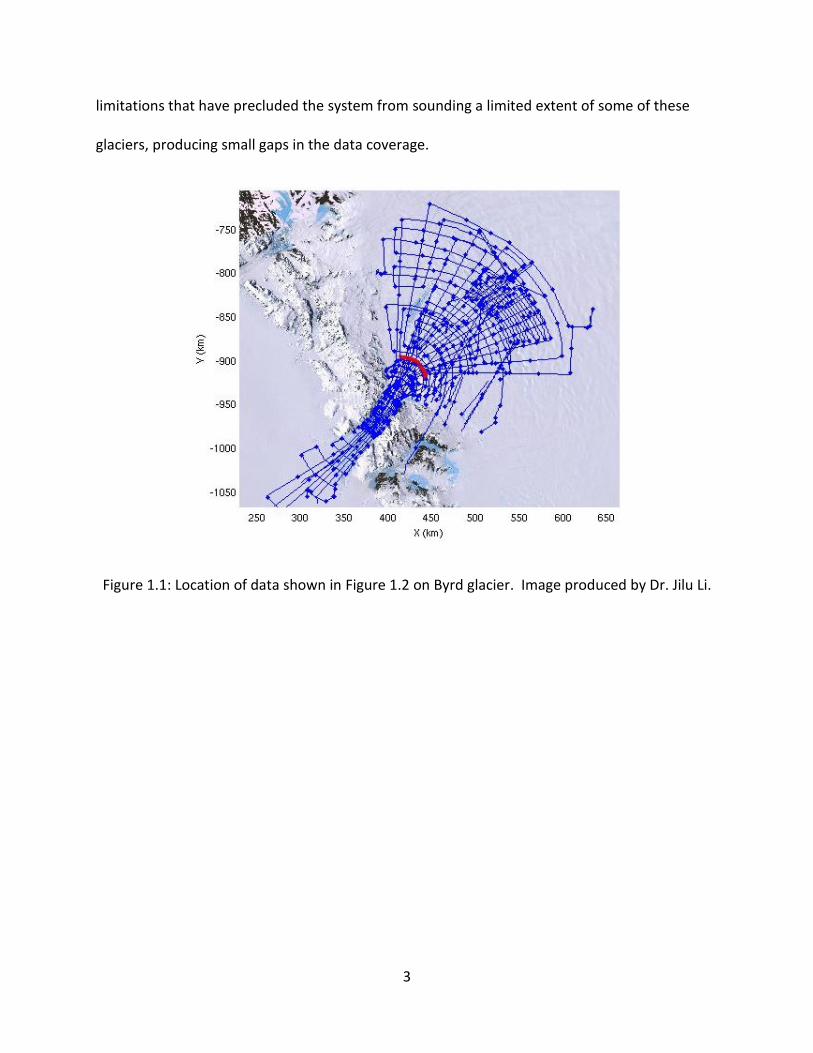
Figure 1.1: Location of data shown in Figure 1.2 on Byrd glacier. Image produced by Dr. Jilu Li.

4
Figure 1.2: MCoRDS/I data from Byrd Glacier Antarctica 2011 showing the disappearing bed
return through lossy ice. Image produced by Dr. Jilu Li.
Figure 1.3: Location of data shown in Figure 1.4 on Byrd glacier. Image produced by Dr. Jilu Li.

5
Figure 1.4: MCoRDS/I data from Byrd Glacier Antarctica 2011 bed return outside the channel in
less challenging ice. Image produced by Dr. Jilu Li.
Figure 1.2 shows an example of an echogram produced with data collected over Byrd
glacier in Antarctica in 2011. For comparison, a less lossy area, outside of the channel is shown
in Figure 1.4. With a total of about 500-W of peak power distributed across six transmit
antennas1 and flying almost 90 m above the ice surface, there was still a gap of a few km along
the deepest part of the glacier channel. Results like these suggest that increasing the
illumination power by a significant factor (4 to 10 times) could help enhance the performance
of the radar to a point where the gaps in the data are further reduced. An alternative approach
being explored to reduce such gaps is the use of lower operating frequencies [8].
1 1200 Watts combined across 7 antenna elements is the maximum amount of peak power that the system can
produce in its current configuration.

6
The goal of this thesis is to demonstrate a power amplifier circuit (and ancillary
components), capable of producing approximately 1 kW of RF power over at least 30 MHz of
bandwidth at a center frequency of 195 MHz. The combined use of multiple amplifiers with
such capability will push the boundary of output power of the MCoRDS/I system to enhance its
performance.
1.2 Previous Work
The power amplifiers used in the transmit section of previous renditions of the CReSIS
radar depth sounders have traditionally consisted of off the shelf linear amplifier units [9-12]
that were very large, heavy, inefficient, and expensive. These off the shelf systems were able to
reach power levels above 1000 W, but it was not practical to use these on individual channels
due to their size and cost. In addition, previous versions of the radar were designed to operate
with a single transmit channel. The signals from the high-power module were split to each
element in the transmit antenna array. Windowing of the power across antenna elements was
accomplished by using attenuators [9]. When the waveform generator was later upgraded to
support multiple channels, the power amplifier system was moved to lower power units, one
for each antenna element [3, 6]. This allowed the amplitude and phase of the signal fed to each
antenna be controlled individually to achieve digital beam forming and steering.
There have also been efforts to develop more efficient systems at CReSIS in the past.
These in house developed systems have investigated using higher efficiency modes of operation
using Class E amplification [13]. There have also been efforts to develop compact modules to
be used with the Meridian Uninhabited Aircraft System (UAS) MCoRDS system [14]. While both

7
of these efforts have been successful, the output from these prototype amplifiers are 3.5 W
and 150 W, respectively. Solutions at the 300-W level have been implemented successfully
using COTS modules from Polyfet devices [15], yet, successfully imaging the bed of a limited
extent of some outlet glaciers remains difficult in spite of the increased power.
1.2.1 Current Configuration
The MCoRDS/I system currently operates at 180 to 210 MHz with 250 watts per element
after losses. MCoRDS/I utilizes Peripheral Component Interconnect Extensions for
Instrumentation (PXI) a chassis from National Instruments (NI) to handle digitization, data
storage and control functions. This system also provides the graphical user interface (GUI) to
allow for operator control and visualization of unprocessed plot of return power as a function
of range (A-scope) and a scrolling echogram. The 8-channel direct digital synthesis (DDS)
waveform generator (WFG) described in [16], generates the 180 – 210 MHz chirp pulse used by
the radar system. The waveform generator also generates the digital control signals required
by other sub-systems. The transmitter power amplifier driver module filters the output from
the WFG and provides additional amplification to drive the power amplifiers. After this stage is
the current 300 W amplifier modules followed by transmit/receive switch and filters before
going to the antenna port.

8
Figure 1.5: Simplified block diagram of the MCoRDS/I system in its current configuration [17].
The received signal passes through the transmit/receive (T/R) switch, which feeds it to the Low
Noise Amplifiers (LNAs). From the LNAs, the signal goes through the variable-gain receiver
module where it is filtered and further amplified. The gain of the variable gain stage module is
controlled by the NI PXI chassis [17]. Finally, a set of 16 independent 14-bit A/D converters with
500 MHz of analog bandwidth and a sampling rate of 250 MS/ in the NI PXI system are used to

9
digitize the received signal. The data is streamed into a redundant array of independent disks
(RAID) for storage.
The current power amplifier combines the transmitter power amplifier section and T/R
switch module into one chassis. The circuitry for each transmit/receive channel is mounted on
a “slice plate” or “slice” that serves as a heat-sink for the power amplifier. This setup is given in
more detail by the block diagram shown in Figure 1.6 showing the components for each
individual slice.
Trilithic
H9BE195/32-3-KK
IL<0.75 dB
RF-Lambda
RFSP2TR0005MCR
IL<0.8 dB
Isolation>60 dB
Dual-power operat ion
<100mA@+5V
<100 mA@-12 V
T/R DIR = 1; J0->J2 (Tx)
T/R DIR = 0; J0->J1 (Rx)
Polyfet
PA PCHA109
300 W nominal
peak output power
T/R slice
Attn>67 dB @ 160 MHz
Attn>76 dB @ 230 MHz
TR
Sw
itch c
on
trol=
1T
R S
witc
h c
on
trol=
0
J0J2
J1
KR Electronics
KR2825
IL<2.5 dB
Attn>50 dBc @155 MHz
Attn>50 dBc @240 MHz
+28 V
Driver
board
TTL from E/O board
PA ENA=
PULSE_OUT_1
VAGC
(0-8 V)
TTL from E/O board
T/R DIR=
PULSE_OUT_0
ADG91, CMOS
Isolation 43 dB
IL=0.7 dB
P1dB= 17 dBm
Minicircuits
VLM-33+
IL=0.06 dB typ
Pinmax=30 dBm
Psat<12 dBm
TTL from E/O board
PA ISO=
PULSE_OUT_2
Renaissance Electronics
2B1NH Circulator
Forward power=300 W max
180-210 MHz; IL< 1dB;
Isolation> 34 dB
N-Type port
(to antenna)
BNC port
(to Rx)
BNC port
(from Tx)
1 2
3SM Electronics
ST4N-50, 0-8 GHz
50 W termination
50 W avg
1 kW peak for 5 us
(5% duty cycle)
Figure 1.6: Block diagram of the current power amplifier slice configuration [18].
The transmit power amplifier contains 7 slices that are identical to the one shown in the above
block diagram. This allows each antenna element to have its phase and amplitude controlled,
independent of the others.
1.2.2 Link Budget

10
The link budget for the current MCoRDS/I configuration is discussed in [17]. This budget
calculates power of the radar pulse returning from the ice surface. This calculation is useful for
determining the maximum power that will occur at the input to the receiver, but does not aid in
calculating the power returned from the bed. To find how much power is expected from the
bedrock return, the attenuation through the ice must be accounted for. The loss through ice in
Greenland varies from 23.3 dB/km, one way, for the ice margins to 10 dB/km, one way, in the
central ice sheet [19, 20]. The received power from the bed can be calculated as [21]
𝑃𝑟 = 𝑃𝑡 (𝜆
4𝜋)
2 𝐺𝑡𝐺𝑟𝑇air-ice2
[(ℎ + 𝑍 𝜂air-ice⁄ )]2𝐿ice2
|⟨𝑅ice-bed⟩|2 (1.1)
where ℎ is the height above the ice, 𝑍 is the ice thickness, 𝐿ice is the one way attenuation
through ice, 𝑛air-ice is the refraction index of the air-ice interface, 𝑇air-ice2 is the transmission
coefficient of the air-ice interface, 𝐺𝑡 is the gain of the transmit antenna, 𝐺𝑟 is the gain of the
receive antenna, |⟨𝑅ice-bed⟩|2 is the spatially averaged reflectivity of the ice-bed interface, 𝜆 is
the wavelength at the operating frequency (195 MHz in this case) and 𝑃𝑡 is the transmitted
power.
Results for the received power calculation for the MCoRDS/I radar during nominal
operation are shown in Table 1.1 for the current 300 W setup and the 1-kW configuration
proposed by this thesis. Although the calculations apply to any of the airborne platforms where
the system is typically deployed, Table 1.1 focuses on the case of 7 transmit antenna elements
used in the P-3 Airborne Science Laboratory from the National Aeronautics and Space
Administration (NASA). Furthermore, Table 1.1 uses a specular bed for the value of
|⟨𝑅ice-bed⟩|2. Although this calculation does not represent the worst-case scenario, it is

11
sufficient to illustrate the problem caused by lossy ice and the benefit of increased transmit
power. These calculations show that the lossy ice, at the edge of the ice sheet, significantly
reduces the return power of the radar signal. By simply increasing the transmit power, the
received signal could be improved. The improvement in received signal power will result in an
overall improvement in the signal to noise ratio (SNR).
Table 1.1: P-3 MCoRDS/I link budget with current and proposed configuration flown onboard the NASA P-3 Airborne Science Laboratory.
Transmit Power Per Element
[dBm] 54.760 60.000
Number of Elements
-- 7 7
Transmit/Receive Array Gain
dBi 15.450 15.450
λ m 1.538 1.538
𝜀𝑟ice -- 3.168 3.168
𝜂air-ice -- 1.780 1.780
𝑇air-ice -- 0.480 0.480
h m 457.2 457.2
Z m 2300 2300
|⟨𝑅ice-bed⟩|2 dB -35.000 -35.000
𝐿ice Central dB/km 10.000 10.000
𝐿ice Margin dB/km 23.300 23.300
Pr Central dBm -90.839 -85.599
Pr Margin dBm -152.019 -146.779
The minimum discernable signal (MDS) for MCoRDS/I is around -150 dBm. From the results of
the calculations, shown in Table 1.1, it can be seen that the current, lower output power
configuration would not be sufficient in sounding the bed for the given parameters. The
increased power solution does exceed the MDS for the MCoRDS/I system.
1.3 This Work

12
This thesis presents the implementation and characterization of an amplifier for the
MCoRDS/I system developed using a 1-kW amplifier pallet and reference design from Freescale
Semiconductor, Inc. The modifications needed to use a highly non-linear amplifier for ice
sounding radar are presented. The amplifier and ancillary components were integrated with a
set of low-noise switching power supplies to support transmit/receive operation using a
compact chassis. In addition, a T/R duplexer design commonly used in nuclear magnetic
resonance (NMR) spectroscopy for magnetic resonance imaging (MRI), is evaluated for use in
an ice-penetrating radar application.
This thesis presents the development, implementation and characterization of an
amplifier for the MCoRDS/I system developed using a 1-kW amplifier pallet and reference
design from Freescale Semiconductor, Inc. The modifications needed to use a highly non-linear
amplifier for ice sounding radar are presented. The amplifier and ancillary components were
integrated with a set of low-noise switching power supplies to support transmit/receive
operation using a compact chassis. In addition, a T/R duplexer design, commonly used in
nuclear magnetic resonance (NMR) spectroscopy , for magnetic resonance imaging (MRI), is
evaluated for use in an ice-penetrating radar application. A single-channel prototype T/R
system was constructed and characterized. The system can be easily extended to multiple
channels.
1.4 Thesis Outline
The thesis is organized in seven chapters outlined as follows. Introductory information,
such as previous work that this thesis builds upon and the motivation behind this work is given

13
in chapter 1. In chapter 2, background theory on concepts used in this thesis is presented.
Chapter 3 introduces the 90° hybrid coupler based duplexer circuit and describes the theory of
operation. Additional development work to make the 90° hybrid coupler a practical T/R
module is presented in chapter 4. Chapter 5 documents the characterization of the prototype
amplifier developed for this thesis. The digital predistortion system developed to allow shaping
of the output amplitude is described and characterized in chapter 6. Chapter 7 presents the
conclusions from this thesis and provides recommendations for future work.
2 Background
In this chapter, an overview of some basic definitions and concepts related to power
amplifiers and duplexers will be presented as a framework.
2.1 Power Amplifier Class Definitions
There are four modes of operation of RF power amplifiers that are considered to be the
classical configurations: Class A, Class B, Class AB and Class C. There are also more advanced
techniques of amplifier design that can be lumped into high efficiency modes. The high
efficiency modes of operation are the most actively researched today. A detailed overview of
the four classical modes of operation will be presented in this chapter. A brief overview of the
higher efficiency modes will also be given, as there are numerous techniques that do not apply
directly to the work presented in this thesis.

14
Figure 2.1: Illustration of the four classic modes of amplifier operation [22].
2.1.1 Class A
An amplifier is considered to be operating in Class A when it conducts for the entire 360
degrees of the input signal. This mode results in the least amount of distortion when compared
to an ideal amplifier as it fully reproduces the input signal at the output. This near perfect
linearity of the device comes at the price of efficiency. The theoretical maximum efficiency of a
Class A amplifier is 50% [23], where efficiency, 𝜂0, is defined as [24]:

15
𝜂0 =𝑃𝑟𝑓_𝑜𝑢𝑡
𝑃𝑑𝑐 (2.1)
with 𝑃𝑟𝑓_𝑜𝑢𝑡 being the output RF power and 𝑃𝑑𝑐 being the DC power at the operating point of
the amplifier. For a Field-Effect-Transistor (FET)-based amplifier, the 50% efficiency value
assumes the knee voltage, or gate voltage, at which the drain current becomes constant, is
zero. A device with a knee voltage of zero is not realizable in practice, and therefore the 50%
efficiency value is only theoretical. The actual realized efficiency is often much less than 50%
and makes this configuration problematic for situations where available DC power is limited.
2.1.2 Class B
The amplifier’s efficiency can be improved by lowering the DC-bias point of the
amplifier, which reduces the conduction angle. This is seen in the Class B amplifier. The Class B
amplifier conducts for 180 degrees of the input signal cycle resulting in higher efficiency, with a
theoretical maximum of 78.5%. The drawback to the Class B amplifier is harmonic distortion
[25]. By lowering the bias point of the amplifier, more distortion, as compared to Class A
amplifiers, is produced to where half of the input signal appears clipped at the output. This
sharp transition results in spurious signals being produced.
2.1.3 Class AB
The Class AB amplifier is the middle ground between the Class A and Class B
configurations. This type of amplifier is often implemented as two transistors in the so-called
push-pull configuration. In the push-pull amplifier configuration, two parallel transistors are
fed 180 degrees out of phase. When each transistor is biased in Class AB, the sum of the push-
pull circuit conducts for more than 180 degrees but less than 360 degrees. There is a small
discontinuity when the signal reaches the threshold voltage of the device, causing a short off

16
period. While there is some off time in this configuration, the distortion is much less than Class
B while still obtaining efficiency improvements from Class A. Efficiency values can be expected
to be between 50% and 78.5%, depending on how close the amplifier is biased to Class A or
Class B.
2.1.4 Class C
Reducing the conduction angle further than in Class B, less than 180 degrees of the
input cycle, the Class C amplifier becomes more efficient. Again, this increased efficiency
comes at a cost of linearity. Due to its highly nonlinear properties, the Class C amplifier is
usually reserved for applications with a constant envelope, such as FMCW radars.
Class C amplifiers can reach 100% efficiency as the conduction angle is reduced to zero.
Most practical implementations of a Class C amplifier will realize 50% to 75% efficiency [26].
The efficiency gain for Class C is accomplished by not conducting while the input signal is below
the gate threshold of the transistor. Due to the nonlinearity of conducting less than 90 degrees
of the input signal, the output must be filtered in some way. The trade off with Class C
operation is the amplification of the amplitude is not linear. Since most AM systems are very
sensitive to amplitude distortion, the Class C amplifier is not commonly used in cases where the
wave is anything other than CW.
2.1.5 High Efficiency Modes
Higher efficiency modes of amplifier operation are an area of active amplifier research.
The power requirements of battery powered cellular handsets have driven this topic. Examples
of these high efficiency modes of operation are Class D and Class E. These classes of amplifiers
rely on using the transistor as a switch, generating square waves. The harmonic frequencies

17
that make up the square wave are passed through a tuned output network so only a sine wave
remains. Both can practically realize 90%, or better, efficiency [22-25, 27]. These modes will
not be discussed further as they are beyond the scope of this thesis.
2.2 Figures of Merit
There are several figures of merit to quantify the performance of RF power amplifiers
relevant to radar performance. In this chapter, a summary of the most commonly used figures
of merit (gain, bandwidth, efficiency, distortion, etc.) will be given.
2.2.1 Gain
There are several approaches to defining the gain of an amplifier. Gain can be defined
as the transduce power gain, the available power gain or the maximum gain available. It is
important to understand which definition of gain is being used when talking about the gain of
an amplifier. The most useful definition for this application is the transducer gain. This is given
by Equation (2.2) as[27]:
𝐺𝑇 =power delivered to the load
power available from the source (2.2)
This definition of transducer gain will be used throughout this work, unless otherwise noted,
and will be referred to as “gain”. The transducer gain provides the amount of small signal gain
achieved at the output of the amplifier device compared to the small signal at the input of the
amplifier.
The other two measurements of gain: the maximum available power gain and the
available power gain are given in Equations (2.3) and (2.4) respectively[27].

18
𝐺𝐴 =power available from the network
power available from the source (2.3)
𝐺𝑃 =power delivered to the load
power delivered to the network (2.4)
The definition of maximum available power gain, shown in Equation (2.3), includes the DC
power that is available from the network, along with the RF power. Available power gain is the
ratio of RF power delivered to the load and the sum of the DC and RF power input into the
amplifier. The relationship between output RF power and input DC and RF power is shown in
Equation (2.4). The inclusion of DC power makes these metrics difficult to obtain from
measurements. Additionally, they depend on the efficiency of the amplifiers.
2.2.2 Bandwidth
There are key metrics of amplifier design that determine the bandwidth of a power
amplifier. Examples of these key metrics are gain, power added efficiency, output power, input
match and output match. The metrics that make up the bandwidth definition will depend on
the requirements of the design. We will define bandwidth as the upper and lower frequencies
at which the gain or output power drops by 3 dB.
2.2.3 Power Added Efficiency (PAE)
The power added efficiency (PAE) of an amplifier differs in the standard definition of
amplifier efficiency, as shown in Equation (2.1), in that the RF power input into the amplifier is
taken into account. The PAE is defined in Equation (2.5)[27].
𝑃𝐴𝐸 =output signal power - input signal power
DC power (2.5)

19
This metric is useful in finding the efficiency for each stage in a cascaded design. The harmonic
power must be included in the output signal power in order to obtain an accurate PAE
measurement.
2.2.4 Harmonic Power
Ideally, an amplifier is a linear device. It is practically impossible to create a perfectly
linear amplifier. For this reason, nonlinear effects must be taken into account in the design.
The nonlinear amplifier can be described by the Taylor series[26]. This series, in terms of the
input and output voltages of the amplifier (𝑣𝑖 𝑎𝑛𝑑 𝑣𝑜 , 𝑟𝑒𝑠𝑝𝑒𝑐𝑡𝑖𝑣𝑒𝑙𝑦), is shown in Equation
(2.6).
𝑣𝑜 = 𝑎0 + 𝑎1𝑣𝑖 + 𝑎2𝑣𝑖2 + 𝑎3𝑣𝑖
3 + ⋯ (2.6)
With the coefficients:
𝑎0 = 𝑣𝑜(0) (2.7)
𝑎1 =𝑑𝑣𝑜
𝑑𝑣𝑖|
𝑣𝑖=0
(2.8)
𝑎2 =𝑑2𝑣𝑜
𝑑𝑣𝑖|
𝑣𝑖=0
(2.9)
When a single tone, Equation (2.10), is applied to the input of the amplifier, it can be shown
that frequency products (harmonics) at multiples of the original (fundamental) tone are
produced.
𝑣𝑖 = 𝑉0 cos 𝜔0𝑡 (2.10)
Substituting (2.10) into (2.6) is shown in Equation (2.11), where terms out to the third harmonic
are shown.

20
𝑣𝑜 = (𝑎0 +1
2𝑎2𝑉0
2) + (𝑎1𝑉0 +3
4𝑎3𝑉0
3) cos 𝜔0𝑡
+1
2𝑎2𝑉0
2 cos 2𝜔0𝑡 +1
4𝑎3𝑉0
3 cos 3𝜔0𝑡 + ⋯
(2.11)
Equation (2.11) shows that the signal at the output of the amplifier is composed of the
fundamental frequency, ω0, as well as higher order terms. The amplitude of the harmonic
signals is a function of the input amplitude and the Taylor series coefficients. It can be shown
that the Taylor series coefficients are related to the nonlinearity of the amplifier. For this
reason, the more nonlinear the amplifier is, the larger the harmonic signals will be. The metric
for the harmonic amplitude is often described as dBc, decibels referenced to the carrier,
f0=2pi*ω0, amplitude.
In relatively narrowband systems, harmonic signals produced by the amplifier must be
suppressed to prevent interference to other users of the radio spectrum. The most direct way
of accomplishing this is to filter the harmonic frequencies. The downside to this method is that
power was taken away from the desired signal to produce these harmonics. This results in a
lower output power of the desired frequency and a lower efficiency of the amplifier. Another
method that is often employed by high efficiency mode amplifiers[23], is to feed the harmonics
back into the input of the amplifier in such a way that the harmonic frequencies are canceled
while the power at the fundamental frequency is retained.
2.2.5 Intermodulation Distortion (IMD)
Intermodulation Distortion is another metric of amplifier linearity. Intermodulation
Distortion occurs when two or more closely spaced tones are used as the input signal to the
amplifier. Ideally, only the two tones should be seen at the output of the amplifier. Due to the

21
effects of nonlinear components in the amplifier, additional frequency components are
generated, as described in Section 2.2.4. These same equations used in Section 2.2.5 can be
applied to the two tone case by substituting Equation (2.12) into Equation (2.6)[23].
𝑣𝑖 = 𝑉0(cos 𝜔1𝑡 + cos 𝜔2𝑡) (2.12)
This substitution will result in additional frequency components appearing at frequencies close
to the desired input tones. In nearly all cases, these will fall within the pass band of the
amplifiers output matching network as well as the output filtering circuit. This will result in a
distorted signal. The frequencies produced can be calculated by Equation (2.13) and the output
spectrum is illustrated in Figure 2.2.
𝜔𝑜 = 𝑚𝜔1 + 𝑛𝜔2 (2.13)
Where m,n=0,±1, ±2, ±3,…. The sum |m|+|n| is the order of the intermodulation product[23].
Figure 2.2: Illustration of the output signal spectrum showing intermodulation products [23]
The intermodulation products closest to the fundamental frequencies will be of the third-order.
For this reason, the third-order intermodulation product (IM3) is used as a common metric of
the linearity of the amplifier, along with the harmonic power.

22
2.2.6 Noise Figure
Thermal noise is generated by the thermal agitation of charge carriers and is one of the
most dominant contributors to the overall noise in RF amplifiers. The random motion of the
charge carriers produces noise at all frequencies with the same power density. The power of
the noise produced is expressed by the noise power PN, given as [22-25, 27-29],
PN = kTB [W] (2.14)
where k is the Boltzmann’s constant (1.38x10⁻²³ J/K); T is the operating temperature of the
device in Kelvin. For room temperature, T is equal to 290 K as per IEEE standards; and B is the
bandwidth of the system in Hz. Thermal noise is commonly quantified in terms of an equivalent
noise temperature. The relationship between noise power and noise temperature is defined as:
T =
PN
k [K] (2.15)
A power amplifier is commonly composed of multiple stages to achieve the required
gain and output power. Each amplification stage will not only amplify the signal but also
amplify the noise present at its input and add in the noise generated within each stage. A
common figure of merit to quantify the amount of noise power produced by a system is the
noise factor. When the noise factor is expressed in dB, the figure of merit is referred to as
figure (NF) of the system. As different stages are cascaded together the noise factor of the
system can be expressed as (2.16)

23
F = F1 +
F2 − 1
G1+
F3 − 1
G1G2+ ⋯ +
FN
G1G2 ⋯ GN-1 (2.16)
Where FN is the noise factor of the Nth stage N and GN is the gain of the Nth stage. From this
Equation, it can be seen that the noise factor of the system is strongly dependent on the noise
factor and gain of the first stage.
Small signal devices, such as low-noise amplifiers (LNA), are optimized to have a low NF.
The NF is a function of the DC-bias settings as well as the impedance presented to the active
devices within each stage. The matching and bias levels are designed in such a way that this
requirement is satisfied. RF power amplifiers are designed so the best impedance match and
maximum power output are achieved. RF power amplifiers are not optimized for minimum
noise, and thus noise figures exceeding 10 dB are not uncommon [30, 31].
2.2.7 Mean Time To Failure
The mean time to failure (MTTF) is a metric to quantify how long a semiconductor
device can operate reliably before failing. Devices typically have failure times on the order of
years under normal operating conditions. Devices can be expected to last between 10 and 100
years [27]. MTTF can be shorter if the devices are subject to extreme operating conditions such
as transients, extreme thermal cycling, or ESD events. The failure rate, λ, which is defined as
1/MTTF, is plotted in Figure 2.3 [32]. The failure rate of a device fits what is known as the
“bathtub” curve, where most failures occur in a very short period of time or toward the end of
the operational lifetime [24]. Assuming the specified junction temperature of the device is not
exceeded, it is safe to assume that if a device does not fail within the first few minutes or
seconds, it will last up to the wearout period. In between the early failure and wearout periods,

24
there will be random failures. These random failures occur at a much lower rate than the
failure mechanisms at the beginning and end of life.
Figure 2.3: Plot of a typical failure rate as a function of time for a semiconductor device [32].
The designed lifetime is determined at a specific junction temperature. By decreasing
the rated junction temperature, the device life can be extended and inversely, shortened by
exceeding the specified junction temperature. The relationship of junction temperature to the
lifetime of the device can be expressed by the Arrhenius model shown in Equation (2.17) [27]:
MTTF = C𝑒
EakTj
⁄ (2.17)
where C is a constant, Ea is the activation energy [eV], k is Boltzmann’s constant, and Tj is the
junction temperature. Equation (2.17) shows that the MTTF decreases exponentially with
temperature.

25
2.2.8 Thermal Resistance
During normal operation, the junction of the transistor is heated as power is dissipated
on the device. The amount of power dissipated is calculated by Equation (2.18) [33].
Pdiss = (RF input power + DC power(ID ∗ VD))
− (RF output power + RF reflected power)
(2.18)
The dissipated power is released as heat. The released heat causes a temperature increase in
the device because of thermal resistance to conduction, radiation, or convection. Thermal
resistance is the opposition to the dissipation of heat. The analog to thermal resistance in
electronics is the resistor; therefore it can modeled as such. The thermal resistance of a solid
using conduction to dissipate heat is described as
Rth =
ℎ
𝐾th(𝑊)(𝐿) [℃
W⁄ ] (2.19)
where ℎ is the height of the conducting solid, 𝑊 is the width of the heat source, 𝐿 is the length
of the heat source, and 𝐾th is the thermal conductivity of the conducting solid.
Rth =
ℎ
𝐾th(𝑊 + 2ℎ)(𝐿 + 2ℎ) [℃
W⁄ ] (2.20)
For the case where the area of the heat source is smaller than the heat sink, Equation (2.20)
incorporates the 45 degree thermal spreading angle through the solid.

26
Continuing with the electronics analogy, the temperature difference across a thermal
resistance can be modeled as a voltage. The power dissipated as heat is modeled as a current
source. From this, it can be seen that as the thermal resistance builds, so does the temperature
differential for a constant power dissipation.
∆T = PdissRth [℃] (2.21)
Equation (2.21) can be expanded to include the total heat dissipation system when Rth is the
total thermal resistance. The absolute temperature of a device, such as the transistor junction,
can be calculated by adding in the ambient temperature:
TD = (PdissRth)TA [℃] (2.22)
where TD is the temperature of the device and TA is the ambient temperature.
2.3 Power Amplifier Linearization
The linearization of a power amplifier is an important design aspect when trying to
realize practical amplifiers. Practical amplifiers have nonlinearities that can produce distortion
in both amplitude and phase. These non-ideal components need to be corrected in order to
achieve the maximum efficiency and the most faithful reproduction of the input signal.
For advanced radar imaging, the MCoRDS/I system requires that the range sidelobes be
suppressed by at least 50 dB. It has been shown by [34] that to accomplish this suppression of
range sidelobes, windowing the amplitude of the transmit waveform with a suitable profile
must occur. The effects of nonlinearities and frequency-dependent behavior in the power

27
amplifier need to be compensated to achieve the required level of range sidelobe suppression.
Without compensation, the envelope of the transmit waveform will exhibit strong amplitude
modulation, which will result in performance degradation.
Common techniques for correction of non-linear behavior include feedforward,
feedback and pre-distortion. In the feedforward linearization technique, the input and output
signals are compared and the IMD products are amplified by an error amplifier and fed back
into the signal path. This is done in a way that the IMD products cancel and only the input
signal remains [27]. Feedback in amplifiers can be used to correct gain variations with
frequency. In the feedback linearization technique, the output of the amplifier is fed back into
the input of the amplifier through a tuned network. This network adjusts the gain of the
desired frequency ranges to flatten the output of the amplifier [24].
2.3.1 Pre-Distortion
Signal pre-distortion is used to compensate for nonlinearities and can be realized using analog
or digital techniques. The goal of pre-distortion is to modify the input signal to cancel out any
nonlinearities produced at the output of the power amplifier. An example to illustrate how this
technique works is presented in Figure 2.4. The input signal with the pre-distortion, β(Vi), is
applied to the amplifier with the transfer function, F(α), to produce a linear output signal.
Figure 2.4: Illustration of the pre-distortion technique[35].

28
2.3.1.1 Analog Pre-Distortion
Traditional methods in analog pre-distortion include using diodes or variactor diodes to
produce second- and third-order transfer functions. As an example of such circuits, the
schematic diagram of a second-order and third-order pre-distortion circuit can be seen in Figure
2.5 and Figure 2.6, respectively. In the first case of Fig. 2.4, the diode biasing point and the
value of the parallel capacitor can be adjusted to match the distortion of the amplifier.
Figure 2.5: Circuit diagram of a series diode pre-distorter [35].
In the second example shown in Figure 2.6, the circuit generates third-order distortion that
cancels out the third-order IMD products. The matching and biasing circuits are left out of the
schematic in this example for clarity. There are other practical considerations for this design but
they are beyond the scope of this work.

29
Figure 2.6: Circuit diagram of an anti-parallel diode pre-distorter [35].
2.3.1.2 Digital Pre-Distortion
Digital pre-distortion (DPD) utilizes digital signal processing (DSP) techniques to
accomplish the same tasks as its analog counterpart. There are several advantages to DPD over
analog techniques, the first being the same advantage of any DSP system over its analog
counterpart. Once analog values are measured and digitized, the operations performed can be
considered ideal; there are no longer any issues with electronic components aging or tolerance
variations in component values. In addition, the point at which the pre-distortion is
implemented can be moved from RF down to baseband. This greatly relaxes the requirements
for the digital to analog converter (ADC). Adaptive algorithms can also be implemented easier
in the digital domain.
Some distortion effects can change with time. One example of a distortion mechanism
that changes with time is amplifier memory effects. When the output of an amplifier is
dependent not only on the input, but the past output of the amplifier, it is said to exhibit
memory. For time varying situations like memory, an adaptive DPD algorithm can be applied.

30
Figure 2.7: Simplified block diagram of a typical Digital Pre-Distortion system
implementation [28].
Figure 2.7 shows a block diagram of a typical DPD system implementation. The chapter to the
left of the Digital to Analog Converter (DAC) and ADC blocks are realized in software. If the DAC
is capable of directly generating an RF signal, the modulation and up-conversion (Mod &
Upconv) block can be omitted. The same is true for the ADC. If the ADC is fast enough to
directly sample the RF signal, the demodulation and down-conversion (Demod & Downconv)
can be omitted as well. Once the coupled RF output from the PA is digitized, it is used in the
Adaptation Algorithm. This algorithm compares the signal coming out of the PA to the input
signal, Vi. Since a linear amplifier should increase the amplitude of the input signal, and change
nothing else, Vi is used as the reference, or ideal signal. The reference signal is compared to the
output RF signal and corrections are placed in the lookup table. From the lookup table, the gain
and phase of the input to the DAC is adjusted so the output from the PA will be the same, with
respect to gain and phase, as the reference signal.
2.4 Duplexer Circuits
A duplexer is a circuit that enables the sharing of a single antenna for transmit and
receive operations. There are several methods commonly used to accomplish this. The most

31
common techniques in the context of radar applications are the use of T/R switches and ferrite
circulators. Other duplexer circuits, designed with RF techniques that vary according to the
frequency of operation, can also be used.
2.4.1 T/R Switch
The T/R switch allows a transmitter and receiver to share the same antenna and
transmission path by changing which input port on the switch is connected to the output. For
power levels exceeding 100 Watts, this is normally accomplished by a mechanical relay or by
PIN-diodes. The ability to handle high power in these types of switches comes at the expense
of relatively slow switching speeds. Switching speeds are normally quantified by measuring the
time for the RF to reach 90% at the maximum output, after the TTL signal has reached 50% of
its maximum, or above. Inversely, the turnoff time is determined by measuring how long the
RF output takes to reach 10% of maximum, from when the TTL reaches 50% or below. Fast
switching speeds in the order of 1-2 μs are required for the MCoRDS/I system, while switching
speeds on the order of 10 μs are typical for off-the shelf switches capable of handling 2 kW of
power. Another disadvantage of PIN diode switches is that they require high operating voltages
and produce large video feed through signals.
2.4.2 Ferrite Circulators
Ferrite circulators can also be used as a duplexer. Circulators can be configured to allow
for simultaneous transmit and receive using a single antenna. The disadvantage to using this
type of devices is that they possess narrow bandwidth and finite isolation in the reverse
direction. In addition, power that is reflected from the antenna will be sent to the receiver, so a
suitable blanking switch and limiting device need to be used to protect the receiver .

32
2.4.3 Diplexer circuits
Diplexers can be used as duplexing devices as well. A diplexer provides a constant
impedance at its input and can direct a signal, depending on the signal’s frequency, to different
outputs [36]. A diplexer can be implemented using discrete components, forming high pass and
low pass filters. If high enough frequencies are used, where 90° hybrid splitters are practical,
the diplexer can be implemented as shown in Figure 2.8.
Figure 2.8: Diplexer implemented with 90° splitters and bandpass filters [36].
The diplexer uses two 90° splitters and two identical bandpass filters. When signals are
rejected by the bandpass filter, the reflected power exits the bandstop output. Signals that are
allowed to pass through the bandpass filter are recombined and exit the bandpass port of the
second 90° splitter. This method of duplexing a signal relies on Frequency Division Multiple
Access (FDMA) principals, where the two signals have different frequencies, but allows for
transmit and receive at the same time. Although the FDMA scheme is not applicable to radar
systems, some of the concepts from diplexers will be used later in the duplexer system
proposed by this thesis.

33
3 Duplexer Circuits
3.1 Overview of T/R Switch Technologies
For pulsed radar applications, the time it takes for a radar to transition from transmit to
receive is known as the switching time. The pulse duration along with the switching time
makes up the blind range. The blind range is defined in Equation (3.1), where c is the speed of
light in m/s, τ is the duration of the pulse, and tswitch is the time the T/R switch takes to
transition from transmit to receive.
Rblind =cτ
2+ ctswitch [m] (3.1)
From this Equation, it can be seen that tswitch directly affects the length of pulse allowed by a set
blind range. In RF switches, tswitch is commonly quantified from 50% of the TTL control line high
to 90 % RF for turning on and 50% TTL control line low to 10% RF for turn off. For the specific
example of the MCoRDS/I system, the blind range must be no larger than 500 meters, the
nominal survey altitude for surveys [4].
In the past, CReSIS has used PIN-Diode switches to implement fast switching T/R
modules. As discussed in Section 2.4, there are tradeoffs in power handling for fast switch
times when using PIN-diodes. The tradeoffs associated with using these switches with the
MCoRDS/I system have made us consider other potential alternatives.
The balanced duplexer described in [37, 38] operates using many of the same principals
used in the diplexer implemented with 90° splitters, described in Section 2.4.3. In this
application, the bandpass filters are replaced with anti-parallel diode pairs, using 1N4148

34
devices. Now, instead of rejecting frequencies, low voltage signals are allowed to pass (cross-
diodes off) while high power signals are reflected. These voltage levels directly correspond to
power level within the 50 ohm system. Figure 3.1 shows the schematic for this design. This
method was borrowed from Nuclear Magnetic Resonance (NMR) imaging, more commonly
known as Magnetic Resonance Imaging (MRI), technology. The figure refers to a “probe”, while
this port would be connected to the antenna in our application.
Figure 3.1: Balanced duplexer design [37]. In our application the probe is replaced by the
transmit/receive antenna.
The quadrature hybrid (QH) ports are defined in Figure 3.2. When the transmitter or, in
the context of this thesis, amplifier output exceeds the threshold voltage of the antiparallel
diodes between the two QH couplers, they are forward biased and begin to conduct. This
presents a short to ports 2 and 3 on the QH. This short causes the incoming RF to complexly
reflect back into the QH, exiting port 1. This operates in the same fashion as a traditional T/R
switch, without the need for a control signal, relying only on the amplitude of the transmit
signal to forward bias the diodes.

35
Figure 3.2: Quadrature hybrid ports [37].
When the output of the transmit amplifier is below the voltage required to forward bias
the anti-parallel diode pairs, the output from the power amplifier, incident on port 4 of the first
QH, is passed through to the 50 ohm load. This increases isolation from the amplifier and
receiver. Additionally, any leakage during transmit goes into the 50 ohm load as well,
protecting the sensitive receiver.
This design is limited by the power handling capability of the QH devices and the current
handling ability of the diodes. The switching time of the balanced duplexer is set by the
response time of the diodes used. For the 1N4148 device, the diode switching time is 4 ns [39],
resulting in a 4 ns T/R switch time of the balanced duplexer. The diodes can handle 450 mA
repetitive peak forward current and 100 V repetitive peak reverse voltage. Given these
specifications, operation should not exceed 50 dBm, although [37] mentions higher operation.
To test this configuration, a prototype duplexer was assembled in the laboratory using high
power hybrids from Innovative Power Products (IPP-2269 [40]). The insertion loss and isolation
between different ports was measured with a network analyzer for low power condition. For
high power conditions, our laboratory tests confirmed the 50 dBm limit quoted by [37]. The
duplexer in this configuration worked for transmit powers of up to 1 kW for short amounts of

36
time, but the high transmit power resulted in excessive heating in the diodes to an unusable
level for extended operation.
3.1.1 Narrowband Implementation with Transmission Lines
The primary failure mechanism with semiconductor devices is exceeding the junction
temperature. This holds true with the 1N4148 diode. One method to reduce the heating of the
diode is to reduce the current flow. One method to accomplish the reduction in current
without sacrificing power is to use quarter-wave transmission lines between the QH and diode
pairs [38]. With the quarter-wave transmission line sections the short created by the diodes
appears as an open at the QH. This results in a full reflection with no current flow.
4 T/R Module
4.1 Initial Design
The initial design for the T/R module originally consisted of the duplexer described in
chapter 3. Since the power capability of the balanced duplexer as described in [37] was limited
to 100 Watts. The results from higher power levels into this circuit are presented in chapter
5.9.2.
4.2 Final Design
A circulator was selected for the high power path of the T/R module. There are two drawbacks
to using a circulator alone as a T/R module. This first is the insertion loss of the device. For the
selected circulator, insertion loss is 0.7 dB. At 60 dBm output from the amplifier, this results in
149 W of power loss through the device. The second disadvantage is any reflected power from
the antennas will be sent to the receiver. The antennas on the P-3 array are designed to have a

37
-10 dB worst case match. At 60 dBm output, this results in 50 dBm, or 100 W reflected power
into the receiver. This power level would result in the destruction of the receiver.
To deal with the reflected power from the antenna, the duplexer described in [37]was
employed. The input and output ports of the duplexer circuit were changed slightly to fulfill its
new role as an isolation switch. The topology of the circulator/duplexer based T/R switch can
be seen in Figure 5.3. Limiters were added to the low power output of the duplexer to reduce
the leakage from the circuit.
5 1-kW Prototype Amplifier for MCoRDS/I
The implementation and characterization of a high-power amplifier prototype capable
of producing power levels close to 1 kW will be discussed in this Chapter. A detailed description
of the measurement setup and results will be given.
5.1 Amplifier Design Overview
The design of the amplifier system began with defining the requirements of the amplifier
system. A summary of these requirements is listed in Table 5.1.
Table 5.1: System requirements.
Power Output: 1000 W
Frequency Response: 180-210 MHz
Gain: >60 dB
Gain Flatness: +/- 1 dB
Gain linearity: +/- 1dB
Efficiency: >70%
Pulse Droop: < 10%
Distortion, harmonic: < -40 dBc
Distortion, inter-modulation: < -20 dBc
Operating temperature: -40 to 100 C

38
Two of the key initial constraints in previous implementations of amplifiers for the MCoRDS/I
system were that the amplifier be linear and that the amplifier be turned off fast enough, by
removing the gate bias, during receive. The amplifier is turned off during receive to eliminate
noise produced by the amplifier and to reduce the average DC power consumption. When an
amplifier is on and no signal is present, it still amplifies noise incident at the input port. In
addition, the amplifier itself generates noise; this also appears at the output. The
implementation of the gate bias switching circuit is described in [14, 41]. Switching the gate
voltage on and off quickly is not trivial due to the resistive-capacitive (RC) time constant formed
in the input capacitance and the resistance of the input network to the gate. Another drawback
to the switching method is the circuit is constantly drawing current, reducing the amplifiers
overall efficiency.
Another factor that drives the need for a gate bias switching circuit is the requirement
that the amplifier be linear. To accomplish a truly linear amplifier, a Class A configuration must
be used. The gate is biased so the entirety of the input signal is conducted. By biasing the
amplifier this way, low amplitude signals, such as noise, are above the threshold and are also
amplified. These signals can be lowered below the threshold by lowering the bias point to
below the threshold voltage. This takes the amplifier out of Class A operation and puts it in
Class C mode. The Class C amplifier advantage is being off for half of the signal cycle and off
when no signal is present. This improves efficiency and has the same effect as switching the
gate bias off. Since the MCoRDS/I system is sensitive to external noise sources, added noise

39
from the amplifier cannot be tolerated. The efficiency requirement is driven mostly by the DC
power available in the aircraft where the system has been deployed, as well as volume and
weight. Although highly efficient design is beneficial in general, this constrain becomes
particularly important for a multi-channel system like MCoRDS/I. Previous implementations of
high-power amplifier required combining more than one power amplifier chassis of fair size and
weight to produce the required power. For instance, the configuration described in [11]
required a set of two amplifiers to obtain 800 W of total peak power at 150 MHz and another
set of two amplifiers to produce 1.6 kW at 450 MHz. The system used a passive network to
feed the antenna array, resulting in a maximum of 300 W per antenna element after losses, and
did not allow controlling the phase and amplitude of the signal fed to each antenna element.
The most recent configuration of MCoRDS/I features about 250-Watts of peak RF power per
channel using individual power amplifier modules. With a maximum of seven channels, a total
of about 1750 W of total peak power is achieved with this system [4]. With the implementation
presented here, the goal is to enable single channel modules with up to 1 kW of peak output
power per channel.
As mentioned above, another requirement for the MCoRDS/I system is the linearity of
the power amplifier. As discussed in chapter 2.2.5, multiple signals cause intermodulation
issues. For an amplifier used in communications systems, for instance, where multiple carriers
or multiple frequency components can be produced by a single transmitter at any given time,
the linearity of a Class C amplifier would be sub-optimal. Fortunately, for the case of the
narrow-band MCoRDS/I radar, only one tone is present at the input at any given time. This
means that only the harmonics of the fundamental tone are produced by a class-C amplifier

40
and the requirements for low IMD are relaxed. Any harmonics produced by the single tone are
filtered by the output matching network and harmonic-rejection band pass filter, which is
already present in the transmit/receive path. With the above considerations regarding narrow-
band pulse operation, efficiency and linearity, the class-C amplifier is a viable choice for the
power amplifier for the MCoRDS/I system. The gain of RF amplifiers is always affected by some
type of frequency dependence. Because of its non-linear behavior, Class C amplifiers also
exhibit a gain that depends on the amplitude of the input signal. It is possible to correct the
non-linear gain by adjusting input signal amplitude to produce the required output from the
amplifier. This process is also a form of pre-distortion.
Initial investigations proved that the design and test of a 60 dBm, 1000 watt amplifier is
not a trivial process. It requires the purchase of specialized test equipment for high power
measurements. Errors incurred during the testing phase can destroy active devices ($200-300
range per device), resulting in increased development costs. With this in mind and to reduce
development time, a commercial off the shelf (COTS) or semi-COTS solution was considered.
Choosing a semi-COTS solution also allowed us to direct our efforts toward the optimization of
the radar performance.
The frequency range of the MCoRDS/I system is 180 to 210 MHz. This is within the VHF
TV Broadcast band. Out of the available products, the Freescale VHF Digital TV Broadcast
Reference Design [42] was selected. This design uses the Freescale MRFE6VP61K25H transistor
[43]. Along with its gain and output power, the device was also selected for its ruggedness.
The transistor can withstand a load mismatch greater than 65:1 [43]. By using a device this

41
rugged, damage and destruction of the amplifier can be avoided during cases of operator
failure. Figure 5.1 shows the schematics of the design as taken from the Reference design [42].
The amplifier is comprised of four main sections: input matching, drain bias, gate bias
circuit, and output matching. The gain bias circuit contains a voltage regulator that uses a
transitor (Q1) with a simmular temperature coefficent as the [42] transistor. The voltage
regulator circuit adjusts the gate bias voltage to maintain the same quiessant current. This
keeps the gain and the bias level stable as the transistor heats up. The use of a low bias level is
important to reduce the noise produced and is critical to the operation of the system. This
circuit starts at VGS and continues through L1, where L1 serves at the RF choke.
Input matching is accomplished by coax 1-3, C8-C15, L3 and the microstrip sections
connecting them. Capacitors C12-C15 serve as DC blocks and provide the RF with a path to
ground. Coax 1 forms a narrowband 1:1 balanced to unbalanced transformer (balun),
converting the single needed input from the coax connector to the balanced signal, separated
by 180° phase shift. The balanced signal is needed by the transistor for push-pull operation.
Coax 2 and coax 3 are used to form a 4:1 balanced to balanced (balbal) transformer, lowering
the impedance from 50 ohms to 12.5 ohms. The other sections of the input matching network
serve to make the amplifier stable and further match the input to the 1.3 ohm input impedance
of the transistor.
The drain bias section includes everything between L2 and VDD. The inductor, L2, is an
RF choke, supplying the transistor with DC power. Capcitor C33-C38 filter the input power,
removing any RF.

42
The output matching is accomplished by everything shown from the transistor output to
the RF Output. The microstrip sections of the PCB are utilized in the tuning of the output,
adding inductance. Coax 4 and 5 form a 1:4 Balbal, stepping the impedance up, closer to 50
ohms. Capacitors C25-C32 form a DC block. So many capacitors are used in parallel to lower
the ESR and increase the power handling capacity. Coax 6 is used to form a 1:1 Balun.
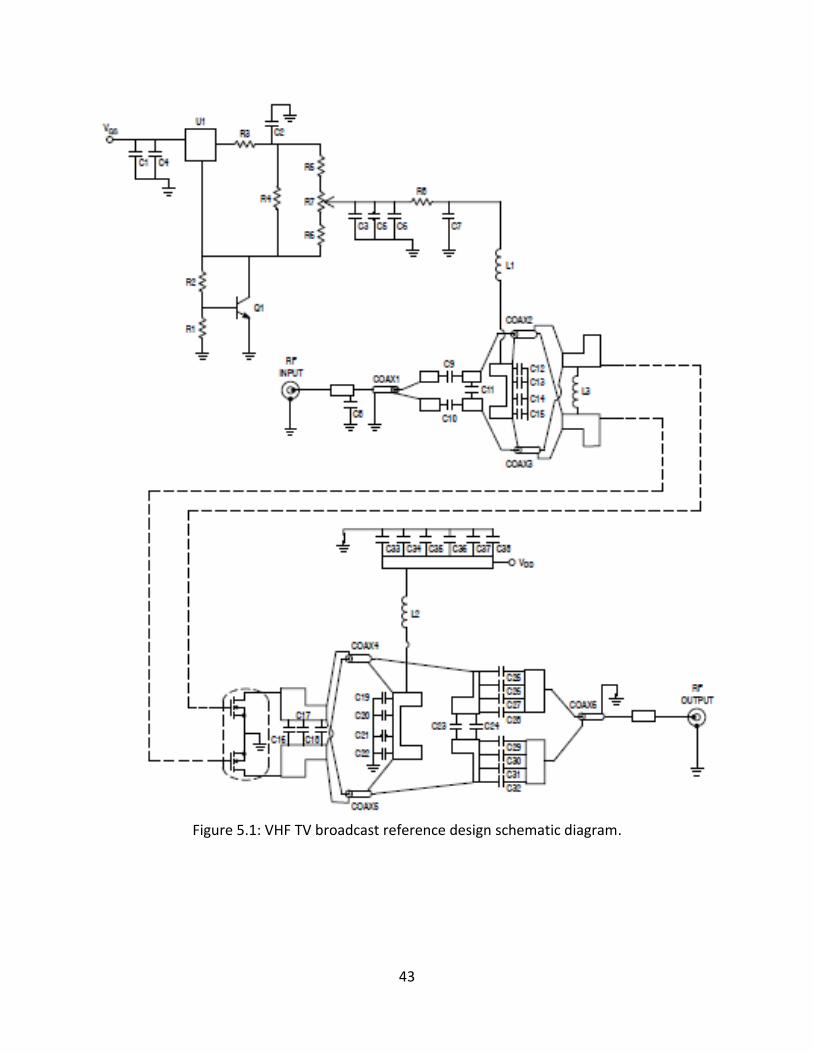
43
Figure 5.1: VHF TV broadcast reference design schematic diagram.
44
Another very important design consideration is the cooling of the transistor, as the
junction temperature directly affects the MTTF. To accomplish this task, the device must have
the heat removed from the package. Assuming a relatively ideal efficiency of 75% and a worse
case duty cycle of 40%, there would be 100 watts of power, in the form of heat. To keep the
device from exceeding the junction temperature, this heat must be removed from the device.
The method selected for heat extraction is the heat spreader. Another option would be to use
liquid cooling, but this proved to be too costly and cumbersome for operation of the radar in
the typical environments where CReSIS systems are deployed.
A prototype system was assembled in the laboratory. The amplifier consists of input
bandpass filter to remove any out of band emissions from the 8 channel WFG, 50 watt driver
amplifier that is transistor-transistor logic (TTL) switched, 1-kW Freescale DVB-T reference
amplifier, Renaissance Electronics 2B1NH circulator [44], and Trilithic H9BE195/32-3-KK 30MHz
wide bandpass filter centered at 195MHz to the antenna. The receive path consists of the
Trilithic bandpass filter, Circulator, Duplexer circuit, and CMOS isolation switch. There are
provisions in the mechanical layout for a LNA and low pass filter that are not populated at this
time.
Fast switching, high power, pin-diode T/R switches are not always practical for high power
designs because of the tradeoff between switching speed and high power. In addition they
require high voltages supplies which add complexity to the system. This makes them
impractical to implement in this design. The circulator and duplexer take the place of a
traditional T/R switch. The circulator alone cannot be used because of the amount of power

45
reflected from an antenna matched to -10 dB insertion loss during transmit is 100 watts. The
Duplexer alone cannot be used due to the power handling issues described in chapter 5.9.2.

46
Fi
gure
5.2
: Pro
toty
pe
po
wer
am
plif
ier.
1-k
W O
utp
ut
Am
plif
ier
Driver
Am
plif
ier
Pow
er
Supplie
s
Circula
tor
Outp
ut
Bandpass
Filt
er
Duple
xer
Directional
Couple
r
Input B
andpass
Filt
er

47
IO
FR
50
dB
1-k
W O
utp
ut
50
W D
rive
r
BN
C-F
N T
yp
e-F
50
W
Hea
lth
Mo
nito
rin
g Sy
stem
In90
°
0°
Iso
Hy
bri
dIn
90
°
0°
Iso
Hy
bri
d
50
W
50 W
CM
OS
Swit
ch
50
W
BNC-F
50
V28
V15
V6 V
12
V5 V
DD
S C
hir
p
Rec
eive
r
Figu
re 5
.3: S
yste
m B
lock
Dia
gram

48
5.2 Measurements
This chapter will present the measurement setup and data collected during lab tests of
the prototype amplifier system.
5.3 Output power
The output power of the entire system is dependent on both the output from the 1-kW
output amplifier and the losses in components to the output port. The power was measured
using the Agilent U2021x peak power meter, triggered to the pulse repetition interval (PRI) TTL
signal from the DDS. This signal is a TTL pulse indicating the start of the radar pulse. The pulse
length of the RF chrip used was 10 µs. 50 dB of attenuation was used between the amplifier
output and the pulse power meter. When the output of the 1-kW drive amplifier is 60 dBm, the
power at the output port is 58.22 dBm. The loss in power is attributed to the loss from the
circulator, directional coupler, output bandpass filter and coax.
5.4 Gain Compression and the need for pre-distortion
The gain of each amplifier stage was measured as a function of input power for five
discrete frequencies within the band of operation. These frequencies cover the nominal range
of operation of the 1-kW amplifier and that of MCoRDS/I. The measurements were
accomplished with a vector network analyzer (VNA) that was set to pulse the RF source. The
pulse duration was set to 10 µs with a pulse repetition frequency (PRF) of 12 kHz. These are the
same parameters that are nominally used with the 10 µs waveform during low-altitude
operation. The only difference between this measurement setup and the radar is that the
amplitude does not have a window (e.g. Tukey) applied to it. The driver amplifier consists of a
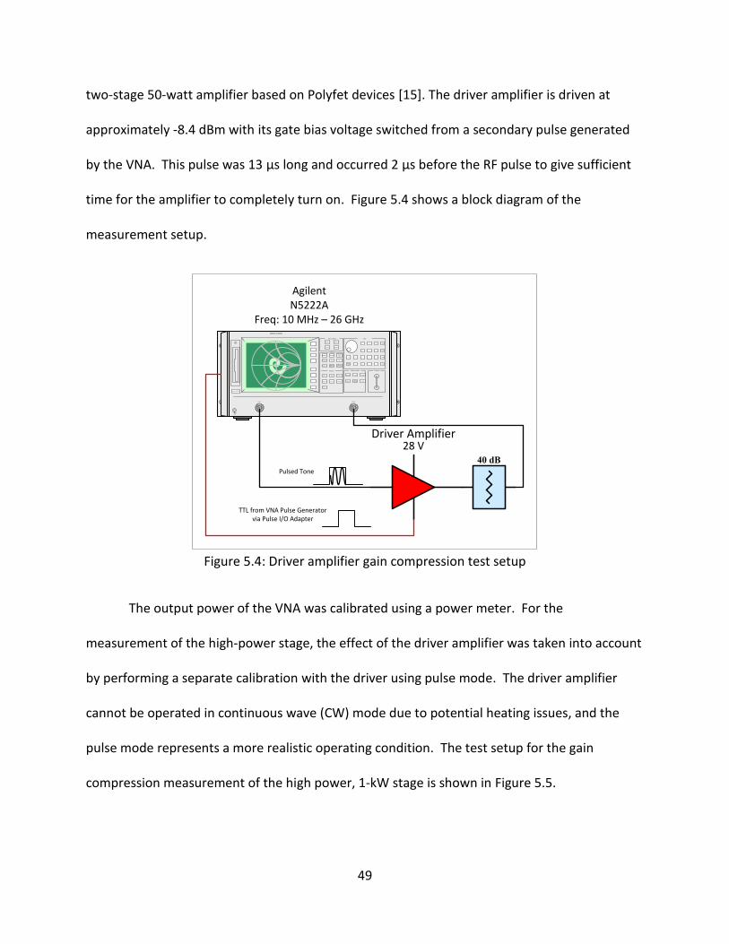
49
two-stage 50-watt amplifier based on Polyfet devices [15]. The driver amplifier is driven at
approximately -8.4 dBm with its gate bias voltage switched from a secondary pulse generated
by the VNA. This pulse was 13 µs long and occurred 2 µs before the RF pulse to give sufficient
time for the amplifier to completely turn on. Figure 5.4 shows a block diagram of the
measurement setup.
Chan 1 Chan 2
Chan 3 Chan 4
Measure FormatScale/
Ref
Display Avg Cal
MarkerMarkerSearch
MarkerFunction
Start Stop Power
Center Span Sweep
System Local Preset
VideoSave/Recall
Seq
Return
Response
Active Channel
Port 2Port 1
Entry
0 . - Hz
1 2 3 kHz
4 5 6 MHz
7 8 9 GHz
EntryOff
<-
/\ \/
Stimulus Instrument State R Channel
Line On/Off
DiskEject
Network Analyzer
AgilentN5222A
Freq: 10 MHz – 26 GHz
40 dB
TTL from VNA Pulse Generator via Pulse I/O Adapter
28 VDriver Amplifier
Pulsed Tone
Figure 5.4: Driver amplifier gain compression test setup
The output power of the VNA was calibrated using a power meter. For the
measurement of the high-power stage, the effect of the driver amplifier was taken into account
by performing a separate calibration with the driver using pulse mode. The driver amplifier
cannot be operated in continuous wave (CW) mode due to potential heating issues, and the
pulse mode represents a more realistic operating condition. The test setup for the gain
compression measurement of the high power, 1-kW stage is shown in Figure 5.5.

50
Chan 1 Chan 2
Chan 3 Chan 4
Measure FormatScale/
Ref
Display Avg Cal
MarkerMarkerSearch
MarkerFunction
Start Stop Power
Center Span Sweep
System Local Preset
VideoSave/Recall
Seq
Return
Response
Active Channel
Port 2Port 1
Entry
0 . - Hz
1 2 3 kHz
4 5 6 MHz
7 8 9 GHz
EntryOff
<-
/\ \/
Stimulus Instrument State R Channel
Line On/Off
DiskEject
Network Analyzer
AgilentN5222A
Freq: 10 MHz – 26 GHz
TTL from VNA Pulse Generator via Pulse I/O Adapter
Pulsed Tone
28 VDriver Amplifier
50 V1-kW Amplifier
50 dB
Figure 5.5: 1-kW stage gain compression test setup
When the power is pulsed during source calibration, the measurement must be adjusted
by a correction factor given by 10log10(% Duty Cycle). The correction is required because the
power measurement is done in terms of average power, not peak power [45]. Once the source
calibration has been completed, the receiver calibration follows to give the gain measurement
of the DUT. The measured gain of the driver amplifier for various levels of input power and
operating frequencies is shown in Figure 5.6. From this plot, it can be seen that the gain of the
amplifier is dependent on both frequency and input power. For all measured frequencies, the
device begins to experience gain compression effects for an input power close to 0 dBm. The 1
dB gain compression point occurs when the input power reaches approximately 7 dBm, which is
much higher than what is required to reach the desired output power at the high-power stage.
Since the driver amplifier will operate far from the compression region, the overall linearity of
the system will be dominated by the contribution of the 1-kW stage.

51
Figure 5.6: Measured Gain Vs. Input Power for the driver Amplifier
The plot of the measured gain of the high-power stage for various levels of input power
and a few discrete frequencies is shown in Figure 5.7. The gain profile leading to compression
changes much more rapidly than the gain profiles shown in Figure 5.6 for the driver amplifier.
It is possible to infer the output power from this plot, since both the gain and input power
levels are known for any given frequency. From this plot it can be seen that the amplifier needs
to operate in the compression region to accomplish the desired output power of 60 dBm.
Moreover, there is a significant variation in the gain as a function of operating frequency. The
operation of the radar requires an output waveform with a pre-defined windowed envelope
(typically a Tukey function) having 1-kW of peak power across the middle of the band. This can
be achieved using digital pre-distortion, as will be discussed in chapter 6.

52
Figure 5.7: Measured Gain Vs. Input Power for the high-power stage.
5.5 Frequency Response
The gain of each amplifer circuit is plotted against frequency for a given, constant, input
power of -8.4 dBm. The results of gain measurement for the driver amplifier is shown in Figure
5.8. The gain over frequency for the 1-kW output amplifier is shown in Figure 5.9.

53
Figure 5.8: Measured gain Vs. frequency of the driver amplifier stage operating in pulse mode
for an input drive level of -8.4 dBm
Figure 5.9: Measured Gain Vs. Frequency of the high-power stage operating in pulse mode for
an input drive level of 37 dBm.

54
5.6 Phase and Time Delay
The phase delay of the amplifier should have a linear rate of change with respect to the
change in frequency. This rate of change is known as the group delay[24]. The phase and time
delay are critical in a phased antenna array system. If one or more channels do not maintain
the same delay as the others, the antenna pattern will become skewed. In the application for
MCoRDS/I, this can lead to increased clutter, potentially masking weak bed returns.
The phase and time delays with respect to frequency from the driver and 1-kW
amplifiers are shown below.
Figure 5.10: Measured Phase Vs. Frequency for the driver Amplifier for an input power level
of -8.4 dBm.

55
Figure 5.11: Measured Delay Vs. Frequency for the driver amplifier for an input power level
of -8.4 dBm.
Figure 5.12: Measured Phase Vs. Frequency for the 1-kW amplifier at 37 dBm drive level.

56
Figure 5.13: Measured Delay Vs. Frequency for the 1-kW amplifier for an input drive level of
37 dBm.
The phase of the Driver amplifier, in Figure 5.10, decreases linearly as the frequency increases.
The 1-kW amplifier phase measurement, in Figure 5.12, shows that the phase change with
frequency is not perfectly linear. The change in group delay with the 1-kW amplifier is not
significant enough to require correction in this application.
5.7 Spurious Products
Single tone and two-tone spurious product measurements were conducted on the
driver and 1-kW output amplifiers. These two tests determined the linearity of the two
amplifiers. The single tone test was conducted with the Agilent 8648D signal generator to
generate the pulsed RF, Agilent 33522A arbitrary waveform generator to generate the TTL
pulse timing signals, and the Agilent E4407B spectrum analyzer to measure the output of the
amplifier.

57
The two-tone test measures the intermodulation distortion of the amplifier. This
measures the amount and strength of mixing between two tones within the amplifier. The
more nonlinear the circuit, the more mixing will occur. In this setup, the arbitrary waveform
generator is replaced by the vector network analyzer (VNA). The VNA serves as both a second
signal source and handles all of the TTL pulse timing.
5.7.1 Harmonic
To assess the spectral purity of the output signal at nominal operating levels, a test tone
of 194.9 MHz of -8.4 dBm of power was applied first to the driver alone and then to the
combination of driver and high-power stage while the output signal was monitored and
recorded on a spectrum analyzer (SA). A high power attenuator was placed between the
output of the amplifier under test and the SA to bring the signal to adequate levels. Figure 5.14
shows a block diagram of the experimental setup of the harmonic test with the driver amplifier.
The setup for the 1-kW output amplifier is identical, except the 1-kW amplifier follows the
driver amplifier in the RF chain.
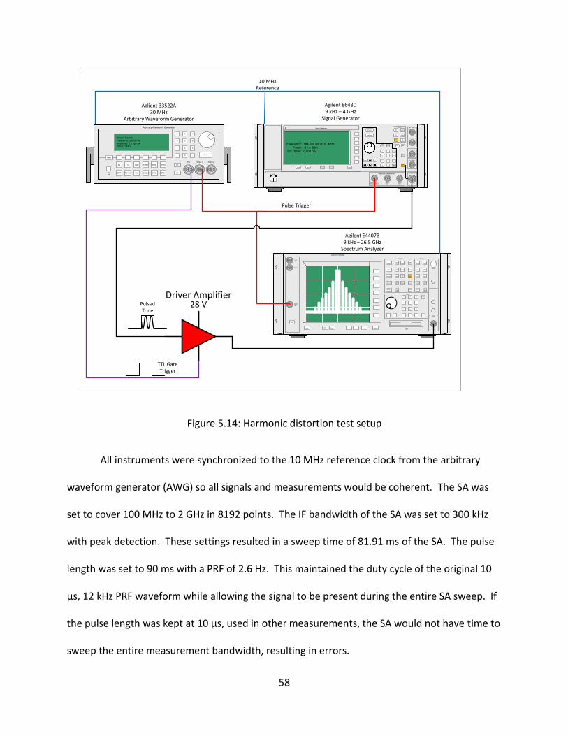
58
Line On/Off
DiskEject
\/ /\
Return><--ZoomNext
WindowHelp
1 2 3
4 5 6
7 8 9 Bksp
Enter0 . -
ModeModeSetup
System PresetInput/Output
Demod Couple File PrintTrace/View
BW/Avg
Trig Load SaveDisplay
Single Source MarkerPeak
SearchMeasSetup
Source FctnMarkerSetup
MeasControl
Frequency
Span
Measure
Restart
Amplitude
Control System
Volume
RF Input
I Input
Q Input
ExternalTriggerInput
Adjust
Input
Spectrum Analyzer
Frequency: 194.000 000 000 MHz
Power: -11.4 dBm
DC Offset: 0.000 mV
HoldIncSet
ContrastDecrease
0 LINE 1
ContrastIncrease
LocalPreset Return
7 8 9
4 5 6
1 2 3
0 .Back
Save Recall
Frequency
Amplitude
Trig Help
ModOn/Off
RFOn/Off
INTERNAL PULSE GENERATORRF OUTPUT
ALC INPUT
LF OUTPUT
EXT 1 INPUT MENU
AM Sweep
FM Utility
PulseLF Out
EXT 2 INPUT
GATE/PULSE/TRIGGER INPUT
VIDEOOUT
SYNCOUT
0 Signal Generator
Agilent E4407B9 kHz – 26.5 GHz
Spectrum Analyzer
Agilent 8648D9 kHz – 4 GHz
Signal Generator
10 MHz Reference
TTL GateTrigger
PulsedTone
28 VDriver Amplifier
Pulse Trigger
Shape: Square
Frequency: 2.6000 Hz
Amplitude: 3.3 Vpk-pk
Offset: 1.65 V
OnOff
AC
7
Sq Tri Saw Pulse Ampl Freq
Shift Period Trig Output Delay Offset
Menu
8 9
4 5 6
1 2 3
. 0 - < >
DC
Arbitrary Waveform Generator
Trig Output 2Output 1
Aglient 33522A30 MHz
Arbitrary Waveform Generator
Figure 5.14: Harmonic distortion test setup
All instruments were synchronized to the 10 MHz reference clock from the arbitrary
waveform generator (AWG) so all signals and measurements would be coherent. The SA was
set to cover 100 MHz to 2 GHz in 8192 points. The IF bandwidth of the SA was set to 300 kHz
with peak detection. These settings resulted in a sweep time of 81.91 ms of the SA. The pulse
length was set to 90 ms with a PRF of 2.6 Hz. This maintained the duty cycle of the original 10
µs, 12 kHz PRF waveform while allowing the signal to be present during the entire SA sweep. If
the pulse length was kept at 10 µs, used in other measurements, the SA would not have time to
sweep the entire measurement bandwidth, resulting in errors.

59
The measured harmonic power from the driver amplifier is shown in Figure 5.15. From
this plot, it can be seen that the second-harmonic is at -45.83 dBc while the third-harmonic is at
-37.18 dBc. Higher order harmonics were below the noise floor of the SA. Figure 5.16 shows
the harmonic power produced by the high-power amplifier stage. The harmonics generated
from the 194.9 MHz tone are much lower than with the driver amplifier. The second-order
harmonic is at -60.37 dBc and the third-order harmonic is at -50.89 dBc. This is attributed to
the narrow bandwidth of the matching network of the amplifier, as the latter severely
attenuates signals outside the band of operation. The spurious signal present at 298.3 MHz is
attributed to third-order intermodulation distortion produced by the 194.9 MHz test signal and
a 91.5 MHz (IP3 = 2*194-91.5 = 298.3) broadcast signal from nearby radio station.
Figure 5.15: Measured output spectrum for the driver amplifier for an input tone of 194.9 MHz
and -8.4 dBm of power.

60
Figure 5.16: Measured output spectrum for the 1-kW amplifier for an input tone of 194.9 MHz
and 37 dBm of power. This measurement includes the effect of the driver amplifier.
5.7.2 Intermodulation
The background of intermodulation distortion (IMD) was described in chapter 2.2.5. As
mentioned in chapter 3.1, for the case of the narrow-band MCoRDS/I radar in normal
operation, only one tone is present at the input at any given time. Linearity characteristics,
however, will be critical for adequate performance of future versions of MCoRDS/I that support
operation over wider bandwidth.
The IMD characteristics for both the river pre-amplifier and the 1-kW amplifier were
evaluated for completeness. Two separate tones at 194 MHz and 197 MHz, at suitable power
levels, were applied simultaneously to the amplifier under test using a power combiner, while
the output signal was monitored and recorded using a SA. The power of the input tones was -

61
11.4 dBm, 3 dB lower than the nominal -8.4 dBm, for the driver amplifier and high-power
stages.
The two-tone test setup for the driver amplifier is shown in Figure 5.17 below. All
instruments use the 10 MHz reference from the vector network analyzer (VNA). This ensures
that all signals are coherent and the two tones do not destructively interfere. The VNA is used
a second signal generator with the Agilent 8648D signal generator, as a second generator
capable of a pulsed signal was not available. The VNA also produces the control signals for the
pulse trigger of signal generator and the acquisition trigger of the SA. The VNA also produces
the TTL gate bias switching pulse for the driver amplifier.
The SA was set to cover a span from 1 MHz to 600 MHz at 8192 points, and IF
bandwidth of 300 kHz. These parameters created a sweep time of 81.91 ms. This sweep rate is
much slower than the 10 µs pulse used in other measurements. If 10 µs were used, much of
the signal would not be captured by the SA and would result in inaccurate measurements. For
this reason, the length of the pulse was increased to 90 ms and the PRF was extended to 2.6 Hz.
This maintained the same duty cycle as the 10 µs, 12 kHz PRF pulse, but allowed for the slower
sweep time of the SA.
Power output was verified using the U2021 peak power meter. The power acquisition
was triggered by the RF Pulse Trigger line, output by the VNA. The power measurement was
taken with the meter in peak power mode. The power from the VNA and signal generator was
measured, along with the output from the combiner.

62
Chan 1 Chan 2
Chan 3 Chan 4
Measure FormatScale/
Ref
Display Avg Cal
MarkerMarkerSearch
MarkerFunction
Start Stop Power
Center Span Sweep
System Local Preset
VideoSave/Recall
Seq
Return
Response
Active Channel
Port 2Port 1
Entry
0 . - Hz
1 2 3 kHz
4 5 6 MHz
7 8 9 GHz
EntryOff
<-
/\ \/
Stimulus Instrument State R Channel
Line On/Off
DiskEject
Network Analyzer
Line On/Off
DiskEject
\/ /\
Return><--ZoomNext
WindowHelp
1 2 3
4 5 6
7 8 9 Bksp
Enter0 . -
ModeModeSetup
System PresetInput/Output
Demod Couple File PrintTrace/View
BW/Avg
Trig Load SaveDisplay
Single Source MarkerPeak
SearchMeasSetup
Source FctnMarkerSetup
MeasControl
Frequency
Span
Measure
Restart
Amplitude
Control System
Volume
RF Input
I Input
Q Input
ExternalTriggerInput
Adjust
Input
Spectrum Analyzer
Frequency: 194.000 000 000 MHz
Power: -11.4 dBm
DC Offset: 0.000 mV
HoldIncSet
ContrastDecrease
0 LINE 1
ContrastIncrease
LocalPreset Return
7 8 9
4 5 6
1 2 3
0 .Back
Save Recall
Frequency
Amplitude
Trig Help
ModOn/Off
RFOn/Off
INTERNAL PULSE GENERATORRF OUTPUT
ALC INPUT
LF OUTPUT
EXT 1 INPUT MENU
AM Sweep
FM Utility
PulseLF Out
EXT 2 INPUT
GATE/PULSE/TRIGGER INPUT
VIDEOOUT
SYNCOUT
0 Signal Generator
1 2Σ
Agilent N5222A10 MHz – 26 GHz
Vector Network Analyzer
Agilent E4407B9 kHz – 26.5 GHz
Spectrum Analyzer
Agilent 8648D9 kHz – 4 GHz
Signal Generator
10 MHz Reference
TTL GateTrigger
Pulsed 2-Tone
28 VDriver Amplifier
RF Pulse Trigger
Figure 5.17: Driver amplifier two-tone test setup
Figure 5.18 and Figure 5.19 show the output spectrum of the driver amplifier during the
intermodulation distortion measurements. Figure 5.19 was sub-banded for greater detail. The
amplitude scale is in dB referenced to the carrier (dBc). From these plots, it can be seen that
the driver amplifier is fairly linear for the operating conditions used during the measurement,
with the largest spurious signal being -26.73 dBc at 3.048 MHz. Within the 180 MHz to 210
MHz of the output filter, the largest spurious emission is at -33.8 dBc. This is important to note,
because unlike the 3.048 MHz signal, spurious signals within the pass-band of the filter will not

63
be filtered out of the transmitted signal, thus causing distortion. IMD products below -20 to -30
dBc are normally acceptable for a linear amplifier[46].
The two-tone test of the 1-kW amplifier was conducted with a setup similar to that of
the driver amplifier, with the exception that the driver amplifier was placed at the input of the
1-kW amplifier. The resulting data from this test are shown in Figure 5.18. From this plot, it
can be seen that the IMD products measured for the driver amplifier are very different from
those measured at the output of the 1-kW . First, the second- and third-order IMD products
located outside the nominal operating frequencies of the amplifier (170-230 MHz) are greatly
attenuated. The highest value for any IMD product outside of the amplifier’s operating range is
-47.75 dBc, more than 10 times lower than the value recorded for driver amplifier. Near the
location of the third-order IMD products, within the amplifier’s range of operation, there are
many more products than predicted from the calculations presented in chapter 2.2.5. Figure
5.19 shows this in more detail.
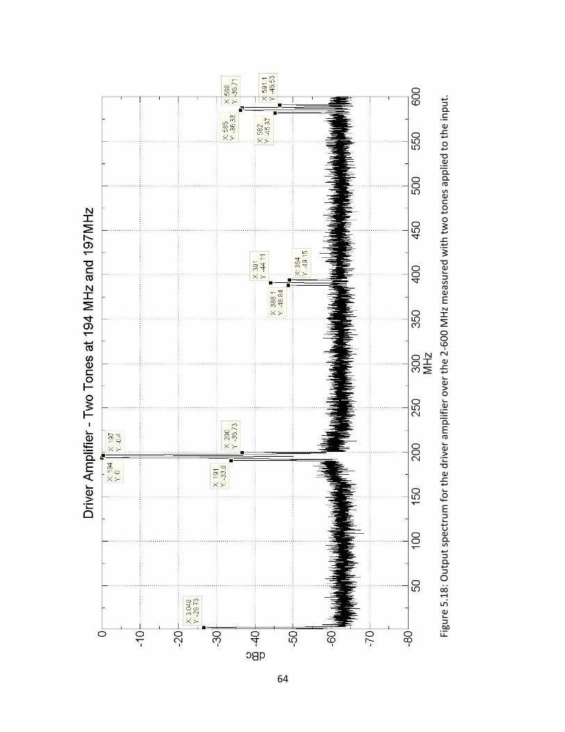
64
Fi
gure
5.1
8: O
utp
ut
spec
tru
m f
or
the
dri
ver
amp
lifie
r o
ver
the
2-6
00
MH
z m
easu
red
wit
h t
wo
to
nes
ap
plie
d t
o t
he
inp
ut.

65
Fi
gure
5.1
9: S
ub
set
of
dri
ver
two
-to
ne
spec
tru
m

66
Figure 5.20 shows the fundamental tones at 194 MHz and 197 MHz with amplitude of 0
dBc and -0.37 dBc respectively. The reason the amplitudes are not the same is because of a
slight amplitude imbalance of the input tones. Given the frequency of the two tones used in
this test, the second-order products can be calculated to be at 191 MHz and 200 MHz. These
products can be identified in Figure 5.21 with amplitudes of -26.94 dBc and -23.59 dBc, which
are considered to be two to four times higher than desired [24]. In addition, the other
frequency products present in the output spectrum are be attributed to higher order IMD
products. For linear amplifiers, only the third-order products are commonly considered when
evaluating IMD performance. For highly non-linear devices, such as this amplifier biased at
Idq=25mA, higher order IMD products do affect the output signal and need to be considered.
For example, it can be shown, the IMD product at 188 MHz is actually a fifth-order product
where 188 MHz = 3(194 MHz) – 2(197 MHz).
The two-tone test of the 1-kW amplifier was conducted with a setup similar to that of
the driver amplifier, with the exception that the driver amplifier was placed at the input of the
1-kW amplifier. The resulting data from this test are shown in Figure 5.20. From this plot, it
can be seen that the IMD products measured for the driver amplifier are very different from
those measured at the output of the 1-kW . First, the second- and third-order IMD products
located outside the nominal operating frequencies of the amplifier (170-230 MHz) are greatly
attenuated. The highest value for any IMD product outside of the amplifier’s operating range is
-47.75 dBc, more than 10 times lower than the value recorded for driver amplifier. Near the
location of the third-order IMD products, within the amplifier’s range of operation, there are

67
many more products than predicted from the calculations presented in Section 2.2.5. Figure
5.21 shows this in more detail.
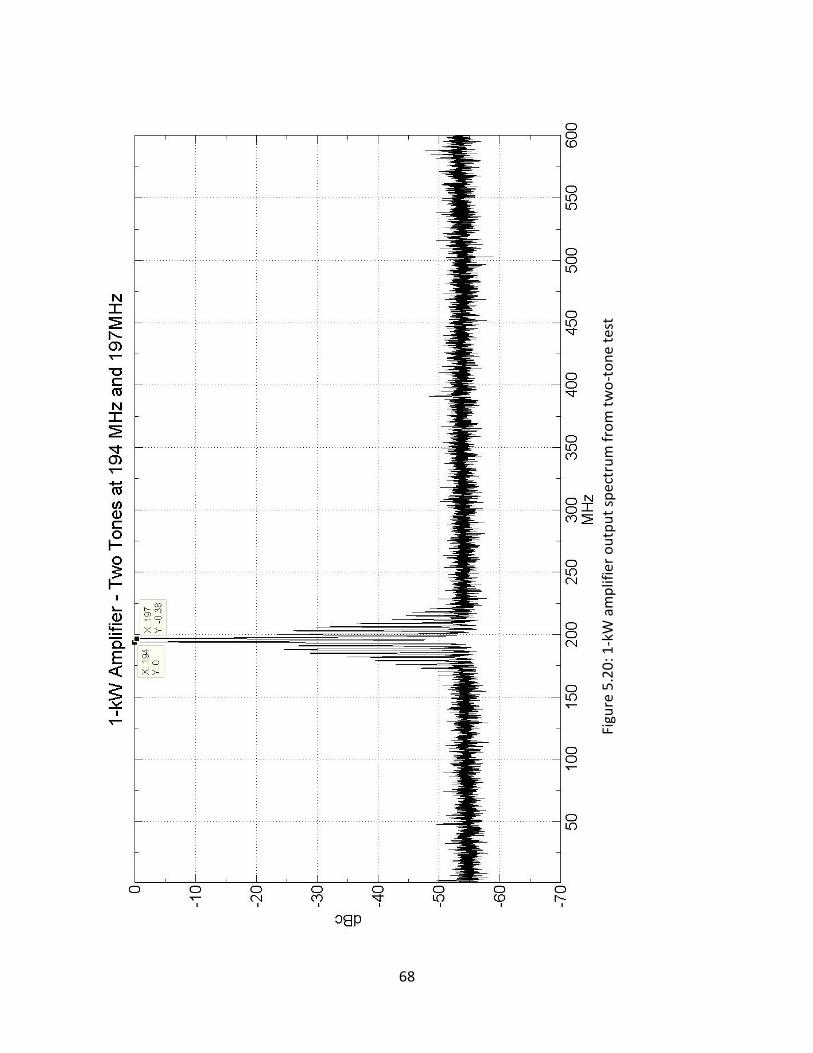
68
Fi
gure
5.2
0: 1
-kW
am
plif
ier
ou
tpu
t sp
ectr
um
fro
m t
wo
-to
ne
test

69
Fi
gure
5.2
1: S
ub
set
of
1-k
W t
wo
-to
ne
spec
tru
m

70
5.8 Added Noise
Noise coupled from the transmitter into the received radar signal will have negative
impact on the quality of the data collected, as interfering signals and noise can potentially mask
weak radar echoes. Coherent integration and inter-pulse modulation such as zero-pi [47] are
common digital techniques employed to increase signal-to-noise-ratio and reduce coherent
noise. Incoherent noise, however, is more difficult to eliminate in post-processing.
We have experienced noise issues from the power supplies biasing the power amplifiers in the
past [48].
Proper design practices considering electromagnetic-compatibility issues mitigate noise
problems. One of the steps implemented in past versions of the MCoRDS/I power amplifier
was to switch the gate bias voltage on the amplifier. The version proposed in this document
does not employ the gate switching solution but uses properties of the Class C amplifier to
achieve the same result.
5.8.1 Amplifier-generated Noise
The data in Figure 5.23 and Figure 5.24 were collected using the test setup shown in
Figure 5.22. Antennas and the anechoic chamber [49] were used to prevent any damage to the
equipment in case the output signal was larger than predicted. The amplifiers were turned on
without an input signal and the resulting noise was recorded. Two cases were tested, one with
the driver amplifier pulsed and the other with it constantly on. To keep the advantages gained
from increased transmit power, it was critical that the noise produced during receive did not
exceed the levels of the current system.

71
Figure 5.22: Amplifier-generated noise test setup block diagram.
The results of the pulsed test, in Figure 5.23 , show the results at different bias levels
compared to the noise produced by the driver, which served as the primary amplifier in the
past. The noise of the driver is shown in green in both figures. The bias level of 2.5A to 2A is
considered to put the 1-kW device in Class AB linear operation [42, 50]. A bias current of
200mA puts the amplifier into Class C mode of operation [50, 51]. Initial bias points were
selected using these values. Both tests show that even the noise produced by a bias current of
0.15A, slightly lower than the suggested bias for Class C, is more than 10 dB higher than the
driver. The bias current was decreased until it was close to the noise level of the driver. The
bias current of 0.01 A produced the most favorable results, but resulted in the gain being too
low. There was a dramatic increase in gain when Idq=0.05 A, but also in noise power. The bias
point of Idq=0.025 A was selected as a tradeoff between gain and amplifier-generated noise.
MCoRDS Digital System
LNA Chain
3 dB
DriverAmplifier
1-kW OutputAmplifier
Anechoic Chamber
50 W
7 m

72
Fi
gure
5.2
3: A
mp
lifie
r N
ois
e Te
st, P
uls
ed

73
Fi
gure
5.2
4: A
mp
lifie
r N
ois
e Te
st, N
ot
Pu
lsed

74
5.8.2 Radiated Noise
Noise radiated from the switching power supplies and amplifier circuits was measured
using the setup shown in Figure 5.25.
Figure 5.25: Radiated noise test setup block diagram.
Components contained within the dot-dashed line were all placed on top a foam cube that was
approximately 1 m by 1 m by 1 m. This was placed at distance of 7 m from the receive antenna.
Three test cases were considered: the amplifier system running at full output power, the
amplifier biased at operating conditions but no drive signal, and everything turned off. The full
power condition provides a load on the power supply that is the same during data collection.
The noise data were gated, so the data during transmit were not used, as this would not
represent the added noise and only show the transmit signal. The second condition, where the
amplifiers were biased on, but no RF drive signal was applied, shows the noise contributed by
the power supplies while idle and is used for comparison. The final test is used as a baseline for
the thermal noise of the chamber and noise generated by the data acquisition system. Figure
5.26 shows the results from these three tests.
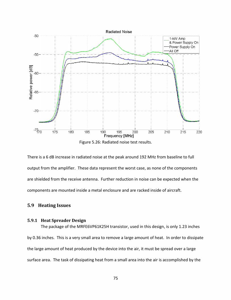
75
Figure 5.26: Radiated noise test results.
There is a 6 dB increase in radiated noise at the peak around 192 MHz from baseline to full
output from the amplifier. These data represent the worst case, as none of the components
are shielded from the receive antenna. Further reduction in noise can be expected when the
components are mounted inside a metal enclosure and are racked inside of aircraft.
5.9 Heating Issues
5.9.1 Heat Spreader Design
The package of the MRFE6VP61K25H transistor, used in this design, is only 1.23 inches
by 0.36 inches. This is a very small area to remove a large amount of heat. In order to dissipate
the large amount of heat produced by the device into the air, it must be spread over a large
surface area. The task of dissipating heat from a small area into the air is accomplished by the

76
heat spreader. In order to accurately know that the maximum junction temperature of the
device is not exceeded, the thermal resistance of the heat spreader system must be calculated.
To minimize the thermal resistance, the best thermal connection must be made in the heat
spreader system. The contact between the transistor package and copper block is an area that
is often overlooked. Large high power transistors, like the MRFE6VP61k25H, are often bolted
down with thermal grease between the transistor and the block. For better results, [52]
recommends the package be soldered down. This method was used in reducing the thermal
resistance. The results of the thermal resistance calculations, which are discussed in chapter
2.2.7, are shown in Table 5.2.
Table 5.2: Thermal resistance of 1-kW amplifier cooling system with 600 LFM air speed over heat spreader.
Transistor Case to Tj
Solder Copper Block Thermal
Conductive Grease
Cool Innovations
Heat Spreader
Width [m] 9.1440E-03 9.1440E-03 3.2004E-02 1.2700E-01
Length [m] 3.1242E-02 3.1242E-02 5.4102E-02 1.2700E-01
Height [m] 5.0800E-05 1.1430E-02 5.0800E-05 5.0800E-01
K_th [W/m K] 50 [53] 398 [54] 0.63 [55]
R_th [°C/W] 1.50E-01 [43] 3.56E-03 1.66E-02 4.66E-02 7.00E-02 [56]
R_th Total [°C/W] 2.87E-01
The Cool Innovations heat spreader [56] was selected for its low thermal resistance and
compact size. To produce 600 LFM over the 5 inch by 5 inch area of the heat spreader, a fan
capable of 104 CFM is required. The amplifier will be operated well above sea level, meaning
the effectiveness of the fan and heat spreader will be reduced. For this reason, the air
movement requirement was doubled and a fan capable of 200 CFM was selected for
impingement cooling of the heat spreader.

77
With the thermal resistance known, the junction temperature for a given ambient
temperature and operating conditions can be calculated. Using a worst case 40% duty cycle,
50% amplifier efficiency, the power dissipated by the device at 60 dBm output is 200 watts.
Since the air temperature inside of the aircraft utilized by CReSIS has been found to fluctuate
quite high, an ambient temperature of 32°C was used to find the transistor junction
temperature of 89.34°C. This temperature is much lower than the 225° C maximum [43].
Leaving such a large margin was done for two main reasons, to allow for any errors in
calculations and assumptions, and to allow the amplifier to be used for other applications in the
future.
5.9.2 Thermal Measurements
Using a device designed to produce 1000 watts provides many unique challenges, one of
those being heat management. For a device that comes after the amplifier, if it has as little as 1
dB insertion loss, it is absorbing 251 watts. This power must go somewhere, and is transformed
into heat. Devices used in the system including the power amplifier were checked for heating
issues using a FLIR® i7 camera [57]. All devices under test were painted flat black to achieve the
most accurate results possible. The use of a FLIR® camera was adventitious over an infrared
thermometer because hotspots within a device can be identified instead of an average
temperature over the measurement area.

78
Figure 5.27: Thermal image of driver amplifier during nominal operation.
The driver amplifier, shown in Figure 5.27 is being operated at -8.4 dBm input without
switching the gate bias voltage. This is a worst case situation, where switching the gate bias
voltage will allow the amplifier to run cooler. It can be seen that the case of the amplifier is
reaching 60°C. Other background objects on the bench are seen in Figure 5.27, such as the
table top fan at the bottom left.

79
Figure 5.28: Thermal image of 1-kW Amplifier during nominal operation
The image shown in Figure 5.28 shows the thermal image of the 1-kW amplifier while in
operation. This image demonstrates the need to use a thermal camera over an infrared
thermometer. It can be seen that the hottest parts around the transistor are the inductor that
is in box Ar1 and the capacitors that are in box Ar2. The overall average temperature would be
measured lower than those individual components. From this image, it was decided to add
additional cooling to the top of the amplifier. Identifying individual components that get too
hot during operation would be nearly impossible without the use of the FLIR® camera.

80
Figure 5.29: Thermal image of circulator during nominal operation.
Figure 5.29 shows the thermal image of the circulator and load that is used as an
isolator. As the image shows, the isolator does not get overly warm and the load is only slightly
warmer. The heating in the load can be attributed to the mismatch between the circulator and
the duplexer circuit. Keep in mind, a S11 measurement of -10 dB, considered to be an
acceptable match, is still 100 watts of power reflected back. Although, pulsed at a 24% duty
cycle, that is still a non-trivial amount of power reflected into the load.
The high power coupler is shown in Figure 5.30. The image shows this device does not
have much heating from the operation of the power amplifier. This corresponds to its low
insertion loss.
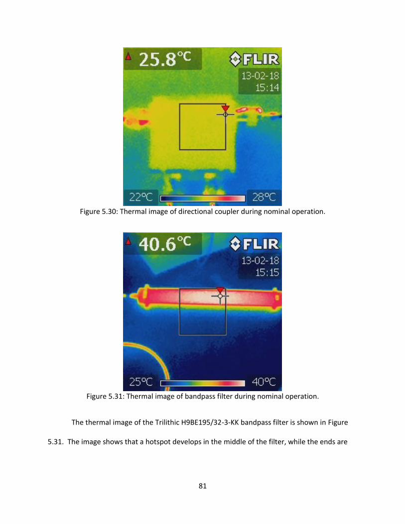
81
Figure 5.30: Thermal image of directional coupler during nominal operation.
Figure 5.31: Thermal image of bandpass filter during nominal operation.
The thermal image of the Trilithic H9BE195/32-3-KK bandpass filter is shown in Figure
5.31. The image shows that a hotspot develops in the middle of the filter, while the ends are

82
slightly cooler. While this is not critical for this application, as the temperature stays around
40°C, a cooling system could be developed around this measurement.
From the thermal imaging, it is clear that the only component that needs additional
cooling is the top of the 1-kW amplifier. The other components show that heating is minimal
and the current cooling is sufficient.
The use of thermal imagery was also critical in development of the duplexer, which is
discussed in detail in chapter 3 and chapter 4. When the duplexer was implemented as shown
in [37] and 60 dBm was applied, the diodes used overheated. This can be seen in Figure 5.32
that the diodes measure 165° C which is close to the 175° C maximum junction temperature of
the 1N4148 Diode [39].
Figure 5.32: Duplexer at 60 dBm under nominal pulse conditions.

83
Figure 5.33: Close up of duplexer diodes when operated at 60 dBm under nominal pulse
conditions.
Upon closer inspection, in Figure 5.33, the diodes actually exceeded the 175°C junction
temperature limit. This caused a topology change, to the one shown in Figure 5.3, where the
duplexer is switching the lower reflected power. Nominally, this reflected power should not
exceed 50 dBm for an antenna with a return loss of -10 dB.
After the diodes were replaced, the duplexer was then measured at 50 dBm. It was
found that some cooling of the diodes was needed, which was implemented with a fan. The
result from this test is shown in Figure 5.34. The maximum diode temperature, shown in Figure
5.35, is 45°C. This temperature is well within the limits of the 1N4148 diode.

84
Figure 5.34: Thermal image of duplexer at 50 dBm under nominal pulse conditions.
Figure 5.35: Close up thermal image of duplexer diodes at 50 dBm under nominal pulse
conditions.

85
6 Digital Pre-Distortion Implementation
An ideal DPD system continuously corrects the waveform in near real-time for
amplitude and phase distortions. Due to the limitations of the existing hardware of the
MCoRDS/I system, a less than ideal DPD system was implemented. The DPD system for the
amplifier does not include phase correction. This means that issues like memory effects cannot
be corrected. Since the amplitude variations have been found to be fairly constant during
operation, the DPD correction algorithm is not continuously ran.
The DPD system consists of the direct digital synthesis (DDS) signal generator, amplitude
correcting MATLAB script and the attenuated output of the amplifier connected to the input of
the National Instruments Data Acquisition (DAQ) system. This system allows for a feedback
network to be formed where the current input into the amplifier is based on its past outputs.
The amplitude correction also relies on a priori knowledge of the amplifier’s output power at
195MHz for a given input power. This allows for the output power to be maintained without
the need for calibrated measurements in the feedback system. All corrections are relative to
the amplitude of the DDS at 195MHz, allowing for easier setup and measurement during field
operation. A flow chart for the DPD algorithm is shown in Figure 5.1.
The first step for the DPD is to run the GUI software that programs the DDS without
loading an amplitude shape. The DDS GUI is initially loaded with the desired frequency and
duration settings and from this, it calculates the RAM size required for the waveform2. When
this value is entered, the software generates the initial, ideal, amplitude shape for the radar
2 The amplitude values are stored in a RAM as 1024 discrete values.

86
chirp. The amplitude is shaped by a 20% Tukey window, but it could be changed to an arbitrary
window. After the initial waveform is created with the correct number of points for the RAM
size, the DDS is programmed. The attenuated output of the amplifier is recorded using the DAQ
GUI. From this point, waveform correction software is executed again, and the previous
correction and recorded amplifier output is used to form a new DPD signal. This process is
iterated until the output signal presents the desired amplitude profile.
Results from the DPD correction process are shown in Sections 6.1 and 6.2. The results
for the driver amplifier are shown separately from those of the entire chain. This helps to show
the distortion that the signal experiences at each stage. The MATLAB code used to process and
extract the desired envelope profile is shown in the Appendix.

87
Figu
re 6
.1: W
avef
orm
co
rre
ctio
n f
low
char
t.

88
6.1 Driver Amplifier Correction
The uncorrected waveform and resulting envelope for the driver amplifier can be seen
Figure 6.26. From this plot, it can be seen that here is a significant, frequency dependent, drop
in gain. To correct this, the amplitude of the chirp must be adjusted for various frequency. This
adjustment can be seen in Figure 6.3.
The recorded data can be seen crossing the reference envelope in the middle of the
chirp. This occurs because the amplitude of the data is scaled so that the amplitude at 195
MHz, the middle of the chirp, is the same as a known value. The amplifier’s maximum power of
60 dBm was measured, for a 195 MHz tone, when the input to the Driver pre-amplifier was -8.4
dBm. Since an ideal amplifier should produce a signal that only differs in amplitude at the
output, we can scale the recorded data to match the DDS waveform amplitude.
After the first iteration, the corrected, or output, envelope is almost an exact inverse of
the recorded data envelope. However, these envelopes are not exact inverse. The error
function is defined in Equation (6.1)
error =
reference envelope+ε
data envelope+ε (6.1)
The value of ε is determined experimentally so that the correction does not overshoot and
cause damage by overdriving the amplifier.

89
Figure 6.26: Uncorrected Driver Amplifier Waveform and Envelope
Figure 6.3: Reference Envelope Compared to Uncorrected Data and Output Envelopes

90
Figure 6.46: Corrected Driver Amplifier Waveform and Envelope
Figure 6.5: Reference Envelope Compared to Corrected Data and Output Envelopes

91
The final results, after three iterations, are shown in Figure 6.46 and Figure 6.5. While
some noise is seen on the envelope of the recorded data, it fits the reference envelope much
closer than the uncorrected case.
6.2 1-kW Amplifier Correction
Continuing with the correction from chapter 6.1, the leveled Driver amplifier was used
to drive the Freescale DVB-T amplifier. By using the corrected driver, it is possible to see the
amplitude distortion caused by the 1-kW amplifier alone. The signal and envelope from the
uncorrected 1 kW amplifier is shown in Figure 6.6.
Figure 6.6: Uncorrected Freescale Amplifier Output Waveform and Envelope

92
Figure 6.7: Uncorrected Freescale Amplifier
Figure 6.8: Corrected Freescale Amplifier Waveform and Envelope

93
Figure 6.9: Corrected Freescale Amplifier Data, Reference and DDS Envelopes
After four iterations when the Driver amplitude was level, the Freescale amplifier
amplitude leveled out. The results of the fourth iteration are shown in Figure 6.8 and Figure
6.9.
6.3 System Correction
Both the driver pre-amplifier and the 1-kW final amplifier were corrected at the same
time for this test. The amplifier system output before correction is shown in Figure 6.10. The
first iteration corrected input compared to the data envelope and reference envelope is shown
in Figure 6.11. Figure 6.12 and Figure 6.13 show the resulting waveform and input power after
5 iterations.
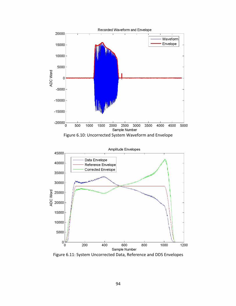
94
Figure 6.10: Uncorrected System Waveform and Envelope
Figure 6.11: System Uncorrected Data, Reference and DDS Envelopes

95
Figure 6.12: Corrected System Waveform and Envelope
Figure 6.13: System Corrected Data, Reference and DDS Envelopes

96
6.4 System Power output verification
The waveform correction process relies on relative measurements and corrections.
There is nothing, other than a priori knowledge, to set the output power. For this reason, the
waveform correction process needs to be verified so that the output power remains at 60 dBm,
as measured at 195 MHz. To test the power, the output of the final amplifier was passed
through a 49.9 dB attenuator to an Agilent U2021xa peak power meter [58]. Once the power
was recorded, the output from the final amplifier was connected to the NI System and the
amplitude was corrected as described above. This process was repeated for each iteration.
The power of the uncorrected pulse is shown in Figure 6.14 and Figure 6.15. It can be
seen that the power actually exceeds 60 dBm from 1.5 µs to 6.75 µs. After 6.75 µs, the power
quickly drops by 4 dB until the taper of the Tukey window effects the pulse around 10 µs. After
five iterations, the pulse becomes fairly flat and ideal. The power profile for the corrected pulse
can be seen in Figure 6.16 and Figure 6.17. From these plots, it is easy to see that the power
has been leveled out. Power fluctuations across the pulse are less than 1 dB.

97
Figure 6.14: Iteration 0 Output Power 20dBm to 65dBm
Figure 6.15: Iteration 0 Output Power 55dBm to 65dBm

98
Figure 6.16: Iteration 5 Output Power 20dBm to 65dBm
Figure 6.17: Iteration 0 Output Power 55dBm to 65dBm

99
The input power to the amplifier was also recorded for the uncorrected and
corrected cases. The output from the DDS was filtered and connected to the peak power
meter. From Figure 6.18, it is possible to see that there is some variation in power of the input
signal. This can be attributed to the filter used and in the output of the DDS. The amplitude
correction algorithm is able to compensate this along with the other amplitude distortions in
the system.
Figure 6.18: Uncorrected Input Power
The input power from the fifth iteration is shown in Figure 6.19. Comparing this result
plotted on a linear scale in Figure 6.20 with the corrected envelope in Figure 6.13, they can be
seen to closely match, as expected. The input power ranges from -6.3 dBm to -11.78 dBm, a
difference of 5.48 dB, or almost four times.

100
Figure 6.19: Corrected Input Power
Figure 6.20: Corrected Input Power, Linear Scale

101
7 Conclusions and Future Work
7.1 Conclusion
A power amplifier system for the MCoRDS/I radar depth sounder was developed and
implemented. The unit weights 23.4 kg for a single channel and can be extended to multiple
channels. This system was implemented using a COTS amplifier system, originally designed for
linear television broadcast transmission, was modified to operate in class C. By operating in
class C, the amplifier was able to meet the noise specifications set by previous amplification
systems while obtaining higher output power.
DPD allowed the amplifier to move away from linear schemes used in the past while
maintaining the ability for the radar to utilize amplitude shaping. The DPD technique was used
to correct amplitude variations as a function of frequency and the input power in the amplifier
was successfully corrected using digital techniques, resulting in the capability to produce 60
dBm +/- 1 dB across the 180-210 MHz frequency range of operation. The amplification system
also included a duplexer derived from NMR systems to facilitate the high power and fast
switching requirements of the MCoRDS/I radar.
7.2 Future work
The narrowband duplexer system, described in chapter 3.1.1, needs to be integrated
with the system. This will eliminate the need for the ferrite circulator, reducing weight and
loss, resulting in an increase of output power. The current DPD system requires manual
intervention from the operator. Future implementations should include an automated real-
time system for DPD error correction.

102
References
[1] "NSF Announces Intent to Establish Two New Science and Technology Centers," in National Science Foundation, ed, 2005.
[2] (2010) "Strategic and Implementation Plan: Center for Remote Sening of Ice Sheets," 2010. Available: https://www.cresis.ku.edu/sites/default/files/CReSIS_SI_Plan_2011.pdf
[3] C. Allen, L. Shi, R. Hale, C. Leuschen, J. Paden, B. Pazer, et al., "Antarctic ice depthsounding radar instrumentation for the NASA DC-8," Aerospace and Electronic Systems Magazine, IEEE, vol. 27, pp. 4-20, 2012.
[4] F. Rodriguez-Morales, S. Gogineni, C. Leuschen, J. Paden, J. Li, C. Lewis, et al., "Advanced Multi-Frequency Radar Instrumentation for Polar Research," IEEE Transactions on Geoscience and Remote Sensing, to be published.
[5] J. Li, S. Gogineni, J. Paden, C. Leuschen, F. Rodriguez-Morales, R. Crowe, et al., "Coherent and incoherent clutter reduction techniques to sound ice from high altitudes," in Synthetic Aperture Radar, 2012. EUSAR. 9th European Conference on, 2012, pp. 243-246.
[6] S. Gogineni, J. Li, J. Paden, L. Smith, R. Crowe, A. Hoch, et al., "Sounding and imaging of fast flowing glaciers and ice-sheet margins," in Synthetic Aperture Radar, 2012. EUSAR. 9th European Conference on, 2012, pp. 239-242.
[7] J. L. Bamber, J. A. Griggs, R. T. W. L. Hurkmans, J. A. Dowdeswell, S. P. Gogineni, I. Howat, et al., "A new bed elevation dataset for Greenland," The Cryosphere, vol. 7, pp. 499-510, 2013.
[8] A. Mahmood, J. B. Yan, R. Hale, F. Rodriguez-Morales, C. Leuschen, S. Keshmiri, et al., "Development of High Frequency Radar Depth Sounder," presented at the International Symposium on Radioglaciology, Lawrence, KS, to be published.
[9] A. Lohoefener, "Design and Development of a Multi-Channel Radar Depth Sounder," M.S. Thesis, Department of Electrical Engineering and Computer Science, University of Kansas, 2006.
[10] S. P. V. Namburi, "Design and Development of an Advanced Coherent Radar Depth Sounder," M.S. Thesis, Department of Electrical Engineering and Computer Science, University of Kansas, 2003.
[11] K. C. Jezek, S. Gogineni, X. Wu, E. Rodriguez, F. Rodriguez-Morales, A. Hoch, et al., "Two-Frequency Radar Experiments for Sounding Glacier Ice and Mapping the Topography of the Glacier Bed," Ieee Transactions on Geoscience and Remote Sensing, vol. 49, pp. 920-929, Mar 2011.
[12] K. C. Marathe, "Dual-band multi-channel airborne radar for mapping the internal and basal layers of polar ice sheets," M.S. Thesis, Department of Electrical Engineering and Computer Science, University of Kansas, 2008.
[13] T. Xie, "Design and Development of the Class E RF Power Amplifier Prototype by Using a Power MOSFET," M.S. Thesis, Department of Electrical Engineering and Computer Science, University of Kansas, 2007.
[14] K. M. Player, "Linearization using Digital Predistortion of a High-Speed, Pulsed, Radio Frequency Power Amplifier for VHF Radar Depth-Sounder Systems," M.S. Thesis,

103
Department of Electrical Engineering and Computer Science, University of Kansas, Lawrence, 2010.
[15] (May, 10). Polyfet Devices. Available: http://www.polyfet.com [16] J. Ledford, "Development of an eight channel waveform generator for beam-forming
applications," M.S. Thesis, University of Kansas, United States -- Kansas, 2008. [17] A. R. Arnett, "Design and Implementation of a Compact Receiver Module for an Ice
Penetrating Radar Depth Sounder," M.S. Thesis, Department of Electrical Engineering and Computer Science, University of Kansas, 2012.
[18] F. Rodriguez-Morales, K. Byers, and R. Crowe, "Power amplifier box #2 for the DC-8 radar," unpublished.
[19] J. Li, "Mapping of ice sheet deep layers and fast outlet glaciers with multi-channel-high-sensitivity radar," Ph.D. Dissertation, University of Kansas, 2009.
[20] J. D. Paden, C. T. Allen, S. Gogineni, K. C. Jezek, D. Dahl-Jensen, and L. B. Larsen, "Wideband measurements of ice sheet attenuation and basal scattering," Ieee Geoscience and Remote Sensing Letters, vol. 2, pp. 164-168, Apr 2005.
[21] D. R. Dunson, "A wideband synthetic aperture radar for ice sheet basal measurements," M.S. Thesis, Department of Electrical Engineering and Computer Science, The University of Kansas, 2006.
[22] H. W. Silver, The ARRL handbook for radio communications, 2005. Newington, CT: American Radio Relay League, 2004.
[23] S. C. Cripps, RF power amplifiers for wireless communications. Norwood, Massachusetts: Artech House, Inc., 2006.
[24] J. L. B. Walker, Handbook of RF and microwave power amplifiers. Cambridge; New York; Melbourne [etc]: Cambridge University Press, 2012.
[25] D. G. Reed, The ARRL handbook for radio communications 2012. Newington, CT: American Radio Relay League, 2011.
[26] D. M. Pozar, Microwave Engineering. Hoboken, New Jersey: John Wiley & Sons, Inc., 2005.
[27] I. J. Bahl, Fundamentals of RF and microwave transistor amplifiers. Hoboken, N.J.: Wiley, 2009.
[28] (2006, September) "Guide to Digital Predistortion," Agilent Technologies Inc., Application Note September 2006. Available: http://cp.literature.agilent.com/litweb/pdf/ads2006/pdf/dgpre.pdf
[29] F. T. Ulaby, A. K. Fung, and R. K. Moore, Microwave remote sensing : active and passive Vol. I, Microwave remote sensing fundamentals and radiometry vol. I. Reading, Mass.: Addison-Wesley Pub. Co., Advanced Book Program/World Science Division, 1981.
[30] Herley-Lancaster, "Model 3445 Datasheet," Datasheet. Available: http://www.herley.com/pdfs/3445.pdf
[31] Herley-Lancaster, "Model 3134 Datasheet," Datasheet. Available: http://www.herley.com/pdfs/3134.pdf
[32] J. Humphrey and G. Luettgenau, (1993) "Reliability Considerations in Design and Use of RF Integrated Circuits," Application Note 1993. Available: http://cache.freescale.com/files/rf_if/doc/app_note/AN1025.pdf

104
[33] M. Mahalingam and E. Mares, (2004) "Thermal Measurement Methodology of RF Power Amplifiers," Application Note 2004. Available: http://cache.freescale.com/files/rf_if/doc/app_note/AN1955.pdf
[34] J. Li, J. Paden, C. Leuschen, F. Rodriguez-Morales, R. D. Hale, E. J. Arnold, et al., "High-Altitude Radar Measurements of Ice Thickness Over the Antarctic and Greenland Ice Sheets as a Part of Operation IceBridge," IEEE Transactions on Geoscience and Remote Sensing, vol. 51, pp. 742-754, February 2013.
[35] P. B. Kenington, High-Linearity RF Amplifier Design. Norwood, Massachusetts: Artech House, 2000.
[36] P. Vizmuller, RF design guide : systems, circuits, and equations. Boston: Artech House, 1995.
[37] P. Cofrancesco, G. Moiraghi, and M. Villa, "A new NMR duplexer made with quadrature couplers," Measurement Science and Technology, vol. 2, pp. 147-149, 1999.
[38] R. Prigl and U. Haeberlen, "The theoretical and practical limits of resolution in multiple-pulse high-resolution NMR of solids," Advances in Magnetic and Optical Resonance, vol. 19, pp. 33-37, 1996.
[39] "1N4148; 1N4448 High-speed diodes," NXP Semiconductors, Datasheet. Available: http://www.nxp.com/documents/data_sheet/1N4148_1N4448.pdf
[40] "IPP-2269," Innovative Power Products, Datasheet. Available: http://innovativepp.com/drawings/ipp2269.pdf
[41] K. Player, L. Shi, C. Allen, C. Leuschen, J. Ledford, F. Rodriguez-Morales, et al. (2010, October) A Multi-Channel DepthSounding Radar with an Improved Power Amplifier. High Frequency Electronics. 18-30. Available: http://www.highfrequencyelectronics.com/Archives/Oct10/HFE1010_Player.pdf
[42] (2011, June) "VHF Digital TV Broadcast Reference Design," Freescale Semiconductor, Inc., Reference Design June 2011. Available: http://cache.freescale.com/files/rf_if/doc/support_info/RDMRFE6VP61K25H_VHF_BCAST.pdf
[43] (2013, March) "MRFE6VP61K25H," Freescale Semiconductor, Inc., Datasheet March 2013. Available: http://cache.freescale.com/files/rf_if/doc/data_sheet/MRFE6VP61K25H.pdf
[44] (5/15/2013). Renaissance Electronics 2B1NH Datasheet. Available: http://www.rec-usa.com/online/IC_Prod_Draw.asp?partnumber=2B1NH&part=yes
[45] (2011, May 17) "Active-Device Characterization in Pulsed Operation Usigh the PNA-X," Agilent Technologies Inc., Application Note May 17 2011. Available: http://cp.literature.agilent.com/litweb/pdf/5990-7781EN.pdf
[46] Handbook of RF and Microwave Power Amplifiers. New York, New York: Cambridge University Press, 2012.
[47] C. T. Allen, S. N. Mozaffar, and T. L. Akins, "Suppressing coherent noise in radar applications with long dwell times," Ieee Geoscience and Remote Sensing Letters, vol. 2, pp. 284-286, Jul 2005.
[48] K. Player, T. Stumpf, J.-B. Yan, F. Rodriguez-Morales, J. Paden, and S. Gogineni, "Characterization & Mitigation of RFI Signals in Radar Depth Sounder Data of Greenland Ice Sheet," IEEE Transactions on Electromagnetic Compatibility, 2013.

105
[49] (2013, May). Anechoic Chamber. Available: http://chamber.ku.edu/ [50] (2011, June) "2 Meter Amateur Reference Design," Freescale Semiconductor, Inc.,
Reference Design June 2011. Available: http://cache.freescale.com/files/rf_if/doc/support_info/RDMRFE6VP61K25H_2MTR_AMATEUR.pdf
[51] (2011, June) "FM Broadcast Reference Design," Freescale Semiconductor, Inc., Reference Design June 2011. Available: http://cache.freescale.com/files/rf_if/doc/support_info/RDMRFE6VP61K25H_FM_BCAST.pdf
[52] K. Nelson, Q. Li, L. Li, and M. Shah, (2011) "Solder Reflow Attach Method for High Power RF Devices in Air Cavity Packages," Freescale Semiconductor, Inc. 2011. Available: http://www.freescale.com/files/rf_if/doc/app_note/AN1908.pdf
[53] J. Wilson. (2006, May, 9). Thermal Conductivity of Solders. Available: http://www.electronics-cooling.com/2006/08/thermal-conductivity-of-solders/
[54] C. Allen. HSD Logic. Available: http://people.eecs.ku.edu/~callen/713/713_High-Speed_Digital_Logic-F11.ppt
[55] Chemtronics, (2006) "CircuitWorks Heat Sink Grease CT40," 2006. Available: http://www.chemtronics.com/products/americas/TDS/CT40tds.pdf
[56] (2013, May) "3-5050XXR," Cool Innovations, Datasheet May 2013. Available: http://www.coolinnovations.com/includes/pdf/heatsinks/3-5026XXR.pdf
[57] (5/15/2013). FLIR® i-Series Infrared Cameras. Available: http://www.flir.com/thermography/americas/us/view/?id=54156
[58] (2012) "Agilent U2020 X-Series USB Peak and Average Power Sensors Datasheet," Agilent Technologies Inc., Datasheet 2012. Available: http://cp.literature.agilent.com/litweb/pdf/5991-0310EN.pdf

106
Appendix A WF_Correct.m MATLAB Code
%% Correct the MCoRDS/I Pulsed Chirp Waveform % % This program corrects the frequency dependent amplitude distortion caused % by the Polyfet driver and Freescale 1KW DVB-T amplifiers. % % The function relies on data collected from the NI System to correct the % waveform. % % ------------------------------------------------------------------------- %% Correction Steps: % ----------------- % 1) Start MCoRDS/I DAQ GUI % % 2) Start DDS_GUI_amp % % 3) Load config for Amplitude Correction. % All settings, except for presums, should be the same as what % you're planning on running for data collection. Presums should % be set 1 and only one waveform should be used. % % 4) Select 'time enable' and click 'Program' % There will be several warnings/errors, this is normal for this % setup. Keep clicking 'continue' until they're cleared. % % 5) Deselect 'time enable' and click 'Program' % There will be several warnings/errors, this is normal for this % setup. Keep clicking 'continue' until they're cleared. % % 6) Turn on the main power to the PA (top switch). % % 7) Wait 10 seconds after main power switch is turned on, then turn on % PA Bias (bottom switch). % % 8) Enter the value from the 'ram size' box in the DDS_GUI_amp window % into the parameter value 'ramPoints' in the WF_Correct.m MATLAB % program and check that other parameters are correct as well. % % 9) Set 'firstRun' flag to 1 and run WF_Correct. % % 10) In the DDS_GUI_amp program, click the file open icon next to the % 'amp file' text box. Select 'DDS_AMP_Corr.bin' and click 'OK' % % 11) Click 'time enable' and then click 'Program' % After this step you should see the uncorrected output from the % amplifier on the A-Scope. % % 12) Record 3 files of data with the amplifier running. % % 13) In WF_Correct, change the 'firstRun' flag to 0. Run the program. % A window will popup, select the 2nd file (or any file that's % not the first or last) that was recorded and click OK. The % program will now correct the waveform. It may take a few % iterations to get it fairly level. The amount of "gain" the % correction has is controlled by 'eps,' the larger the number,

107
% the slower the corrections will be. Do not go much lower than % 20000, otherwise there will be a lot of overshoot. % % 14) Repeat steps 10 through 12 until you reach an acceptable result. % This usually takes 3 - 5 times. % %% % clc; clear all; close all
firstRun = 1; % 1 indicates this is the first time % the function is being ran. % 0 indicates this is an iteration % of the correction %% Parameters pulseLen = 10e-6; % Pulse length in seconds Fs = 1e9/9; % Sampling frequency [Hz] startF = 180e6; % Chirp start frequency [Hz] stopF = 210e6; % Chirp stop frequency [Hz] debug = 1; % Debugging Flag. Generates several
% plots savePlot = 0; ramPoints = 222; % The number of points required for
% the ram MaxDDS = 28350; % The DDS value to get the desired
% output at 195MHz eps = 3000; % Prevent correction from
% overshooting.
%% Constants fn_out = 'DDS_AMP_Corr.bin'; % DDS Amplitude shape filename fn_fulcor = 'LastCorr.mat'; whichBits = 0; % Number of LSBs to drop presums = 1; % Number of presums tukeyWinPer = 0.2; % Tukey windowing [%]
MCoRDS/I = 0; % Flag to indicate if the code is % being used on the MCoRDS/I system % or the single channel test system
%% Generate the ideal amplitude w/ no correction for the first iteration if firstRun == 1 WF = struct('pulseLen', pulseLen, 'Fs', Fs,'startF', startF, 'stopF',
stopF,... 'ramPoints', ramPoints,'MaxDDS', MaxDDS,'tukeyWinPer',
tukeyWinPer,... 'fn_out',fn_out,'fn_fulcor',fn_fulcor);
WF_First_Run(WF);
return; else %% After the first run, load recorded data and correct load(fn_fulcor);

108
%% Load desired data file [filename, pathname] = uigetfile('*.bin'); fn=sprintf('%s%s',pathname,filename); % fn = 'C:\kuband\kuband_01_20130409_141014_0043.bin';
param = struct('clk',Fs); param.wfs = [0]; param.recs = [1 1]; if MCoRDS/I == 0 [hdr, data] = basic_load_fmcw2(fn,param); else [hdr, data] = basic_load_MCoRDS/I2(fn,param); end data = data';
% Remove any DC offset DCoffset = mean(data(1:101)); data = data-DCoffset; if ((debug == 1) || (savePlot == 1)) h=figure; plot((data),'k') set(gca,'YTickLabel',num2str(get(gca,'YTick').')) title('Recorded Waveform') xlabel('Sample Number') ylabel('ADC Word') if savePlot == 1 saveTightFigure(h,sprintf('%sWaveform.jpg',pathname)); end
end
%% Shift Data start to 0 % Run pulse_compress from the CReSIS-Toolbox clear pc_param; pc_param.f0 = startF; pc_param.f1 = stopF; pc_param.Tpd = pulseLen; pc_param.tukey = tukeyWinPer; pc_param.rx_gain = 1;
Nt = hdr.wfs.num_sam; if MCoRDS/I == 0 t0 = hdr.wfs.Tadc; else t0 = hdr.wfs.t0; end dt = 1/Fs; BW = pc_param.f1-pc_param.f0; alpha = BW/pc_param.Tpd; pc_param.time = t0 + (0:dt:(Nt-1)*dt).';
signal = data'; signal(pc_param.time<0 | pc_param.time>pc_param.Tpd) = 0;

109
[pc_signal,pc_time] = pulse_compress(signal,pc_param);
if debug == 1 figure; %Plot pulse compressed signal plot(pc_time*1e6, lp(pc_signal,2)); xlabel('Time (us)'); ylabel('Relative power (dB)'); end
% Find start point at corresponding index to data
idx=find(pc_param.time<=pc_time(find(abs(pc_signal)==max(abs(pc_signal)),1,'f
irst'))... ,1,'last');
% Calculate the hilbert of the data if ((debug == 1)||(savePlot == 1)) h=figure; plot(data); hold on end data = abs(hilbert(data));
if ((debug == 1)||(savePlot == 1)) plot(data,'r','LineWidth', 2) hold on set(gca,'YTickLabel',num2str(get(gca,'YTick').')) title('Recorded Waveform and Envelope') ylabel('ADC Word') xlabel('Sample Number') legend('Waveform','Envelope','Location','Best') if savePlot == 1 saveTightFigure(h,sprintf('%sWave&Env.jpg',pathname)); end end
% Lowpass filter to smooth the data firFiltCoeff=1000; fir6dBCutoff=50e6; d=fdesign.lowpass('N,Fc',firFiltCoeff,fir6dBCutoff,Fs); Hd=design(d); data = filter(Hd,data);
% Shift data back to orig pos data = [data(1,(firFiltCoeff/2):end) data(1,1:((firFiltCoeff/2)-1))]; if debug == 1 figure;plot(data,'g') end % Shift the start of the pulse to 0 and truncate data =data(idx:(idx+ceil(pulseLen/dt))-1);
%% Scale the amplitude at 195MHz to MaxDDS % Find the sample number for the 195MHz point in the chirp sampleFor195 = findFrequency(195e6,startF,stopF,length(data));

110
% Make sure the value of MaxDDS is no bigger than the maximum value the
DDS % can produce: 65535 MaxDDS(MaxDDS>65535)=65535;
% Scale the data so the value at the 195MHz point is = to MaxDDS scaleFac = MaxDDS/data(1,sampleFor195); data = scaleFac*data;
refAmp = MaxDDS;
%% Generate Ref Chirp t = 0:1/Fs:pulseLen; theChirp = MaxDDS*(chirp(t,startF,max(t),stopF)); win = tukeywin(length(theChirp),tukeyWinPer);
% Apply Tukey Window to Chirp theChirp = (theChirp.*win');
if debug ==1 figure; plot(theChirp) end
%% Hilbert transform to get envelope theChirp = abs(hilbert(theChirp)); L = length(theChirp); theChirp = [theChirp zeros(1,(firFiltCoeff))]; theChirp = filter(Hd,theChirp); theChirp = [theChirp(1,(firFiltCoeff/2):end)
theChirp(1,1:((firFiltCoeff/2)-1))]; theChirp = theChirp(1,(1:L)); % Scale Ref Back Up scaleFac = MaxDDS/theChirp(1,sampleFor195);
%% Find error between ideal and actual. Create amplitude correction. error = ((theChirp+eps)./(data+eps)); corrLin = lastCorr.*error; corrLin(1,1) = 0; corrLin(1,end) = 0;
if ((debug ==1)||(savePlot == 1)) h=figure; plot(data) hold on plot(theChirp,'r') hold on plot(corrLin, 'g') set(gca,'YTickLabel',num2str(get(gca,'YTick').')) title('Amplitude Envelopes') ylabel('ADC Word') xlabel('Sample Number') legend('Data Envelope','Reference Envelope','Corrected
Envelope','Location','Best')

111
if savePlot == 1 saveTightFigure(h,sprintf('%sDataRefCorr.jpg',pathname)); end end
% Set current corrected value to the lastCorr variable lastCorr = corrLin; % Write lastCorr to file. This is used for the next iteration. save(fn_fulcor,'lastCorr') if debug == 1 figure; plot(corrLin) hold on plot(theChirp,'r') end %% Convert to 16-Bit Unsigned Int and write to file % Make sure corrLin is limited to 65535 corrLin(corrLin>65535)=65535;
% Convert to 16-Bit unsigned integer ddsAmpFile = uint16(corrLin); % Determine the new sample rate for the number of rampoints and decimate step = (floor(length(ddsAmpFile)/ramPoints)); ddsAmpFile = ddsAmpFile(1:step:(length(ddsAmpFile)-step));
% Pin the first and last value to 0 ddsAmpFile(1,1)=0; ddsAmpFile(1,end)=0;
if ((debug==1)||(savePlot == 1)) h=figure; plot(ddsAmpFile,'k','Linewidth',2) set(gca,'YTickLabel',num2str(get(gca,'YTick').')) title('DDS Amplitude') xlabel('Sample Number') ylabel('DDS Word') if savePlot == 1 saveTightFigure(h,sprintf('%sDDSWaveform.jpg',pathname)); end end % Reverse the order for the correction as the DDS reads the envelope in % backwards ddsAmpFile=fliplr(ddsAmpFile); if debug == 1 max(ddsAmpFile) end % Write the amplitude envelope to file fid = fopen(fn_out,'w'); fwrite(fid, ddsAmpFile,'uint16','b'); fclose(fid); if ((savePlot == 1)&&(debug ~= 1)) % close all pathname end end return;

112
Appendix B findFrequency MATLAB Function
function data=findFrequency(findFreq,startF,stopF,samples)
% Calcuate the frequency step size freqPerSamp = (stopF-startF)/samples;
distanceFromStart = findFreq-startF;
data = distanceFromStart/freqPerSamp;
return

113
Appendix C WF_First_Run MATLAB Function
function output = WF_First_Run(WF) % Geneate full length window function t = 0:1/WF.Fs:WF.pulseLen; lastCorr = [WF.MaxDDS*(chirp(t,WF.startF,max(t),WF.stopF))]; win = tukeywin(length(lastCorr),WF.tukeyWinPer); lastCorr = lastCorr.*win'; lastCorr = abs(hilbert(lastCorr)); save(WF.fn_fulcor,'lastCorr');
% Generate Window function for RAM win = tukeywin(WF.ramPoints,WF.tukeyWinPer); ramWin = win.*WF.MaxDDS; lastCorr = ramWin; ddsAmpFile = uint16(ramWin); fid = fopen(WF.fn_out,'w'); fwrite(fid, ddsAmpFile,'uint16','b'); fclose(fid); return;

114
Appendix D saveTightFigure MATLAB Function
function saveTightFigure(h,outfilename) % SAVETIGHTFIGURE(H,OUTFILENAME) Saves figure H in file OUTFILENAME without % the white space around it. % % by ``a grad student" % http://tipstrickshowtos.blogspot.com/2010/08/how-to-get-rid-of-white-
margin-in.html
% get the current axes ax = get(h, 'CurrentAxes');
% make it tight ti = get(ax,'TightInset'); set(ax,'Position',[ti(1) ti(2) 1-ti(3)-ti(1) 1-ti(4)-ti(2)]);
% adjust the papersize set(ax,'units','centimeters'); pos = get(ax,'Position'); ti = get(ax,'TightInset'); set(h, 'PaperUnits','centimeters'); set(h, 'PaperSize', [pos(3)+ti(1)+ti(3) pos(4)+ti(2)+ti(4)]); set(h, 'PaperPositionMode', 'manual'); set(h, 'PaperPosition',[0 0 pos(3)+ti(1)+ti(3) pos(4)+ti(2)+ti(4)]);
% save it saveas(h,outfilename);