dependence of dc characteristics of cnt mosfets on bandstructure models
TRANSCRIPT
Purdue UniversityPurdue e-Pubs
Other Nanotechnology Publications Birck Nanotechnology Center
7-1-2006
Dependence of DC characteristics of CNTMOSFETs on bandstructure modelsSiyuranga O. KoswattaPurdue University, [email protected]
Neophytos NeophytouPurdue University, [email protected]
Diego KienlePurdue University, [email protected]
Gianluca FioriUniversità di Pisa
Mark S. LundstromSchool of Electrical and Computer Engineering, Birck Nanotechnology Center, Purdue University, [email protected]
This document has been made available through Purdue e-Pubs, a service of the Purdue University Libraries. Please contact [email protected] foradditional information.
Koswatta, Siyuranga O.; Neophytou, Neophytos; Kienle, Diego; Fiori, Gianluca; and Lundstrom, Mark S., "Dependence of DCcharacteristics of CNT MOSFETs on bandstructure models" (2006). Other Nanotechnology Publications. Paper 37.http://docs.lib.purdue.edu/nanodocs/37

368 IEEE TRANSACTIONS ON NANOTECHNOLOGY, VOL. 5, NO. 4, JULY 2006
Dependence of DC Characteristics of CNT MOSFETson Bandstructure Models
Siyuranga O. Koswatta, Neophytos Neophytou, Student Member, IEEE, Diego Kienle, Gianluca Fiori, andMark S. Lundstrom, Fellow, IEEE
Abstract—Since their discovery in the early 1990s, the interestin carbon nanotube (CNT) electronics has exploded. One mainfactor that controls the device performance of CNT field-effecttransistors (CNT MOSFETs) is the electronic structure of the nan-otube. In this paper we use three different bandstructure models:1) extended Hückel theory (EHT); 2) orthogonal tight-binding(OTB); and 3) parabolic effective mass model (EFM) to investigatethe bandstructure effects on the device characteristics of a CNTMOSFET using semiclassical and quantum treatments of trans-port. We find that, after proper calibration, the OTB model isessentially identical to the EHT over the energy range of interest.We also find that an even simpler parabolic EFM facilitates CNTMOSFET simulations within practically applied bias ranges.
Index Terms—Bandstructure, Boltzmann transport, carbonnanotube (CNT) field-effect transistors (CNT MOSFETs),nonequilibrium Green’s function (NEGF), semiclassical.
I. INTRODUCTION
DURING THE last few years, it has been realized that aqualitative and particularly quantitative understanding of
nanoscale devices demand a rigorous treatment of electronicstructure and transport in order to properly treat effects dueto structure relaxation, quantum confinement, and scattering.Effective mass models (EFMs) have been commonly used tostudy conventional devices and have also been applied to newchannel materials such as carbon nanotubes (CNTs) and siliconnanowires [1]–[7]. However, these models often carry free pa-rameters that need to be adjusted using more rigorous calcula-tions in order to reproduce the physical bandstructure of the ma-terial, at least in the energy range of interest. Empirical modelsare very appealing, since the atomistic features of the materialcan be effectively captured by a few parameters such as the ef-fective mass tensor and the bandgap. One of the main drawbacksof these simplified bandstructure models, however, is their lim-ited range of validity.
Manuscript received January 25, 2006; revised March 13, 2006. This workwas supported by the NASA Institute for Nanoelectronics and Computing(NASA INAC NCC 2-1363), the Semiconductor Research Corporation (SRC),the Defense University Research Initiative in Nanotechnology (DURINT), andthe NSF Network for Computational Nanotechnology (NCN). The work of G.Fiori was supported by the EU through the SINANO Network of Excellence.The review of this paper was arranged by Associate Editor T. Hiramoto.
S. O. Koswatta, N. Neophytou, D. Kienle, and M. S. Lundstrom are with theDepartment of Electrical and Computer Engineering, Purdue University, WestLafayette, IN 47907 USA (e-mail: [email protected]).
G. Fiori is with the Dipartimento di Ingegneria dell’Informazione, Universitàdi Pisa, 56122 Pisa, Italy (e-mail: [email protected]).
Digital Object Identifier 10.1109/TNANO.2006.876916
On the other hand, tight-binding approaches for electronicstructure calculations are very popular due to their computa-tional efficiency, improved range of validity, and the atomisticnature of the treatment [8], [9]. In the case of CNTs, the orthog-onal tight-binding (OTB) treatment has been widely used inelectronic structure calculations [10]. Even though useful in de-scribing electronic bands of CNTs with diameter nm, asimple orbital model fails to accurately capture the curvatureinduced effects in smaller diameter CNTs nm . A morerigorous calculation that can accurately capture the curvatureinduced effects in CNTs is a treatment based on the extendedHückel theory (EHT) [11], [12]. Nevertheless, the range of va-lidity of simpler bandstructure models such as EFM and OTBcan be extended by calibrating them against more advanced cal-culations as EHT. For example, in the case of silicon nanowiresthe validity of the parabolic effective mass approximation hasbeen extended to wire diameters down to 1 nm by recali-brating the effective masses using tight-binding calcu-lations [13].
In this work we examine the validity of the OTB and theparabolic EFM models for the simulation of semiconductingzigzag CNT MOSFETs by comparing to the results obtainedfrom the EHT treatment. The limitations and the range ofvalidity of the parabolic EFM are examined. Calibration ofthe empirical fitting parameters of OTB and parabolic EFMmodels in order to extend their validity for smaller diameterCNTs is also presented. The dependence of current-voltage(I–V) characteristics on the bandstructure models is examinedusing both semiclassical and quantum transport simulation.For the case of semiclassical transport the Boltzmann transportequation (BTE) is solved in the ballistic limit [14]. We thenperform a quantum transport simulation using the nonequilib-rium Green’s functions (NEGF) formalism [15], [16]. We findthat both semiclassical and quantum transport calculations givesimilar results. We show that the I–V characteristics using aparabolic EFM approximation for the conduction band com-pares well with the more rigorous bandstructure model over awide range of applied biases.
II. BANDSTRUCTURE MODELS
The first model we consider for the dispersion is basedon EHT [11], where a Slater–Koster tight-binding scheme isemployed [17], whose main features are summarized here. Themain difference between a common OTB approach [10] andEHT is that the orbital basis functions are nonorthogonalin the latter, i.e., the overlap matrix where is the
1536-125X/$20.00 © 2006 IEEE

KOSWATTA et al.: DEPENDENCE OF DC CHARACTERISTICS OF CNT MOSFETs ON BANDSTRUCTURE MODELS 369
Kronecker’s delta function. In contrast to OTB, the EHT-basisfunctions are known explicitly, so that the matrix elements ofthe Hamiltonian are calculated by [11], [12]
where the onsite energy as well as are fit parameters.As described in more detail in [12] and [17], the matrix elements
are used to calculate the -dependent matrix elements
between all atoms and that are equivalent to the unit cellatoms and . Here, is the wavevector within the first Brillouinzone. The band dispersion is then determined by solvingfor each the generalized eigenvalue problem
, where denotes the eigenvector. The EHTparameters used here have been optimized and benchmarked toreproduce the bulk bandstructure of a two-dimensional (2-D)graphene sheet calculated within density functional theory usingthe general gradient approximation [18]. Afterwards, employingthese parameters in EHT calculation, the bandgaps for differentCNT chiralities have been compared to the gaps obtained fromsurface tunneling spectroscopy (STS) experiments reported in[19], and find a good quantitative match [12]. Since the elec-tronic dispersion determined from EHT does not require anyfurther parameter calibration in order to quantitatively matchthe ’s of three-dimensional (3-D) CNT structures, theEHT-model serves in this work as the reference to describe thelowest conduction band.
As the second model, we use a nearest neighbor OTB de-scription with a single orbital for each atom. This model isbased on the dispersion of a planar 2-D graphene sheet wherethe one-dimensional (1-D) dispersion of the CNT is calculatedby means of a zone-folding scheme [10]. Within the nearestneighbor approximation, the OTB band dispersion can be calcu-lated analytically, and for a zigzag nanotube with chiralityit is given by [10]
(1)where is the carbon–carbon bonding distance, is the tubechirality, is the subband index, and is the nearest neighborhopping parameter. The wavevector is taken within the firstBrillouin zone with values , where de-notes the 1-D translation vector along the transport direction. Atypical value for is 2.7 eV, but is generally a fitting parameteradjusted to match STS data close to the Fermi energy and is al-lowed to vary from 2.5 to 3.2 eV [10]. In this work we follow
TABLE I
the same philosophy and consider as a free parameter, whichis adjusted such that the same value for the bandgap as providedby the EHT reference is obtained.
The third model is a parabolic effective mass (EFM) descrip-tion of the conduction band which is based on the exact an-alytical expression for the OTB model, i.e., (1). Thedispersion of the conduction band within the parabolic EFMmodel is obtained by a second-order Taylor expansion of (1)around the -point of the 1-D Brillouin zone, and isgiven by
(2)where is the effective mass, is the tube diameter, and,
is the onsite energy. It is common to set eV,which means that the Fermi level (midgap in the case of intrinsicsemiconductors) is at zero energy.
III. RESULTS AND DISCUSSION
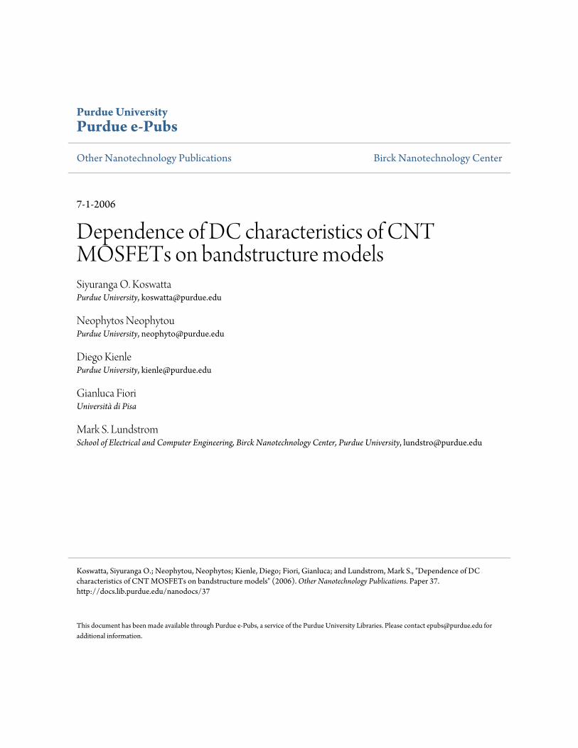
As mentioned earlier, in comparing the aforementioned band-structure models, the EHT results are treated as the referencecalculation. The parameter in (1) and (2) is considered a fittingparameter and adjusted such that the CNT bandgap determinedby OTB and parabolic EFM models agree with that given byEHT. Afterwards a comparison of the shape of the first conduc-tion band can be made in order to ascertain the energy range ofvalidity of the dispersions given by OTB and parabolicEFM models. Here, it should be noted that we concentrate onthe first conduction/valence bands, since they are the dominantsubbands participating in electrical transport in smaller diameterCNTs few nanometers . We have studied the electronicdispersion of three zigzag semiconducting CNTs: (13,0), (10,0),and (7,0). The parameters required in matching the bandgapsbetween OTB and parabolic EFM with EHT are reported inTable I. The of the first conduction band determined by thethree bandstructure models for the case of (13,0) CNT is shownin Fig. 1. We observe similar relations for (10,0) and (7,0)CNTs. It should be noted that the OTB dispersion agrees verywell with that of EHT for energies up to several ’s. How-ever, the parabolic EFM approximation is valid only up to fewhundred ’s, and the band nonparabolicity becomes impor-tant at higher energies. In the case of the (13,0) tube, parabolic
diverges from OTB and EHT for energies meV.Nevertheless, it can be concluded that with proper calibration,
370 IEEE TRANSACTIONS ON NANOTECHNOLOGY, VOL. 5, NO. 4, JULY 2006
Fig 1. Band dispersion of the first conduction band for a (13,0) CNT usingdifferent bandstructure models. Circles: EHT, solid: OTB, (1), and dashed: par-abolic EFM model (2). Parabolic EFM model agrees well with the other two upto E � 200 meV. (Color version available online at http://ieeexplore.ieee.org.)
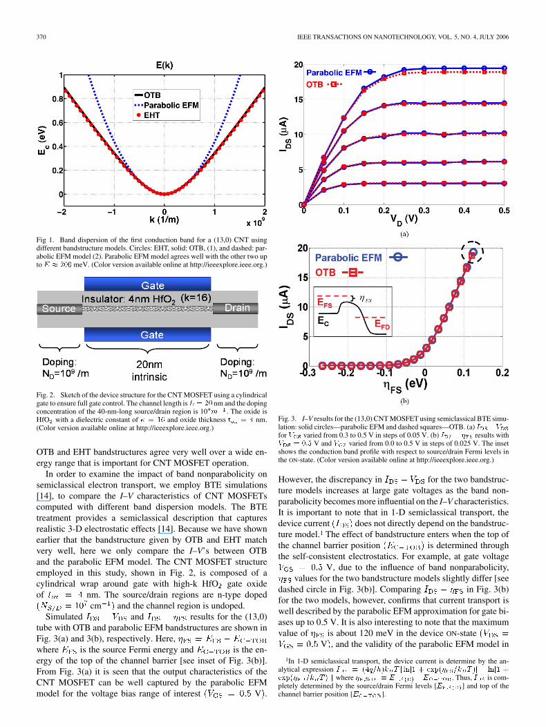
Fig. 2. Sketch of the device structure for the CNT MOSFET using a cylindricalgate to ensure full gate control. The channel length isL = 20nm and the dopingconcentration of the 40-nm-long source/drain region is 10 m . The oxide isHfO with a dielectric constant of � = 16 and oxide thickness t = 4 nm.(Color version available online at http://ieeexplore.ieee.org.)
OTB and EHT bandstructures agree very well over a wide en-ergy range that is important for CNT MOSFET operation.
In order to examine the impact of band nonparabolicity onsemiclassical electron transport, we employ BTE simulations[14], to compare the I–V characteristics of CNT MOSFETscomputed with different band dispersion models. The BTEtreatment provides a semiclassical description that capturesrealistic 3-D electrostatic effects [14]. Because we have shownearlier that the bandstructure given by OTB and EHT matchvery well, here we only compare the I–V’s between OTBand the parabolic EFM model. The CNT MOSFET structureemployed in this study, shown in Fig. 2, is composed of acylindrical wrap around gate with high-k HfO gate oxideof nm. The source/drain regions are n-type doped
cm and the channel region is undoped.Simulated and results for the (13,0)
tube with OTB and parabolic EFM bandstructures are shown inFig. 3(a) and 3(b), respectively. Here,where is the source Fermi energy and is the en-ergy of the top of the channel barrier [see inset of Fig. 3(b)].From Fig. 3(a) it is seen that the output characteristics of theCNT MOSFET can be well captured by the parabolic EFMmodel for the voltage bias range of interest V .
Fig. 3. I–V results for the (13,0) CNT MOSFET using semiclassical BTE simu-lation: solid circles—parabolic EFM and dashed squares—OTB. (a) I �Vfor V varied from 0.3 to 0.5 V in steps of 0.05 V. (b) I � � results withV = 0:5 V and V varied from 0.0 to 0.5 V in steps of 0.025 V. The insetshows the conduction band profile with respect to source/drain Fermi levels inthe ON-state. (Color version available online at http://ieeexplore.ieee.org.)
However, the discrepancy in for the two bandstruc-ture models increases at large gate voltages as the band non-parabolicity becomes more influential on the I–V characteristics.It is important to note that in 1-D semiclassical transport, thedevice current does not directly depend on the bandstruc-ture model.1 The effect of bandstructure enters when the top ofthe channel barrier position is determined throughthe self-consistent electrostatics. For example, at gate voltage
V, due to the influence of band nonparabolicity,values for the two bandstructure models slightly differ [see
dashed circle in Fig. 3(b)]. Comparing in Fig. 3(b)for the two models, however, confirms that current transport iswell described by the parabolic EFM approximation for gate bi-ases up to 0.5 V. It is also interesting to note that the maximumvalue of is about 120 meV in the device ON-state
V , and the validity of the parabolic EFM model in
1In 1-D semiclassical transport, the device current is determine by the an-alytical expression I = (4q=h)k Tfln[1 + exp(� =k T )] � ln[1 +exp(� =k T )]g where � = E �E . Thus, I is com-pletely determined by the source/drain Fermi levels [E ] and top of thechannel barrier position [E ].
KOSWATTA et al.: DEPENDENCE OF DC CHARACTERISTICS OF CNT MOSFETs ON BANDSTRUCTURE MODELS 371
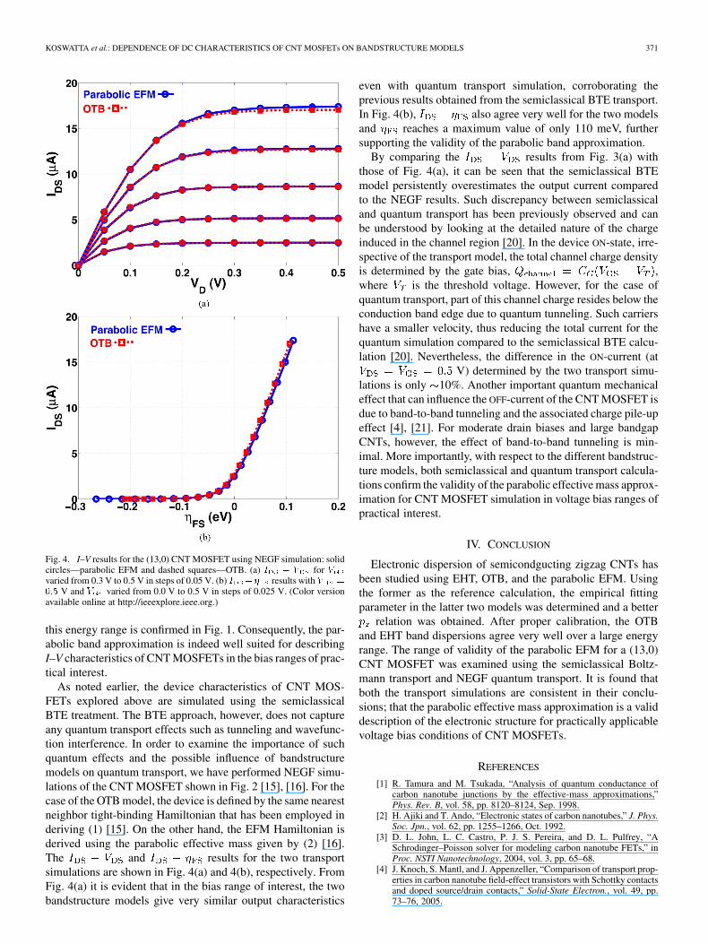
Fig. 4. I–V results for the (13,0) CNT MOSFET using NEGF simulation: solidcircles—parabolic EFM and dashed squares—OTB. (a) I � V for V
varied from 0.3 V to 0.5 V in steps of 0.05 V. (b) I �� results with V =
0:5 V and V varied from 0.0 V to 0.5 V in steps of 0.025 V. (Color versionavailable online at http://ieeexplore.ieee.org.)
this energy range is confirmed in Fig. 1. Consequently, the par-abolic band approximation is indeed well suited for describingI–V characteristics of CNT MOSFETs in the bias ranges of prac-tical interest.
As noted earlier, the device characteristics of CNT MOS-FETs explored above are simulated using the semiclassicalBTE treatment. The BTE approach, however, does not captureany quantum transport effects such as tunneling and wavefunc-tion interference. In order to examine the importance of suchquantum effects and the possible influence of bandstructuremodels on quantum transport, we have performed NEGF simu-lations of the CNT MOSFET shown in Fig. 2 [15], [16]. For thecase of the OTB model, the device is defined by the same nearestneighbor tight-binding Hamiltonian that has been employed inderiving (1) [15]. On the other hand, the EFM Hamiltonian isderived using the parabolic effective mass given by (2) [16].The and results for the two transportsimulations are shown in Fig. 4(a) and 4(b), respectively. FromFig. 4(a) it is evident that in the bias range of interest, the twobandstructure models give very similar output characteristics
even with quantum transport simulation, corroborating theprevious results obtained from the semiclassical BTE transport.In Fig. 4(b), also agree very well for the two modelsand reaches a maximum value of only 110 meV, furthersupporting the validity of the parabolic band approximation.
By comparing the results from Fig. 3(a) withthose of Fig. 4(a), it can be seen that the semiclassical BTEmodel persistently overestimates the output current comparedto the NEGF results. Such discrepancy between semiclassicaland quantum transport has been previously observed and canbe understood by looking at the detailed nature of the chargeinduced in the channel region [20]. In the device ON-state, irre-spective of the transport model, the total channel charge densityis determined by the gate bias, ,where is the threshold voltage. However, for the case ofquantum transport, part of this channel charge resides below theconduction band edge due to quantum tunneling. Such carriershave a smaller velocity, thus reducing the total current for thequantum simulation compared to the semiclassical BTE calcu-lation [20]. Nevertheless, the difference in the ON-current (at
V) determined by the two transport simu-lations is only 10%. Another important quantum mechanicaleffect that can influence the OFF-current of the CNT MOSFET isdue to band-to-band tunneling and the associated charge pile-upeffect [4], [21]. For moderate drain biases and large bandgapCNTs, however, the effect of band-to-band tunneling is min-imal. More importantly, with respect to the different bandstruc-ture models, both semiclassical and quantum transport calcula-tions confirm the validity of the parabolic effective mass approx-imation for CNT MOSFET simulation in voltage bias ranges ofpractical interest.
IV. CONCLUSION
Electronic dispersion of semicondgucting zigzag CNTs hasbeen studied using EHT, OTB, and the parabolic EFM. Usingthe former as the reference calculation, the empirical fittingparameter in the latter two models was determined and a better
relation was obtained. After proper calibration, the OTBand EHT band dispersions agree very well over a large energyrange. The range of validity of the parabolic EFM for a (13,0)CNT MOSFET was examined using the semiclassical Boltz-mann transport and NEGF quantum transport. It is found thatboth the transport simulations are consistent in their conclu-sions; that the parabolic effective mass approximation is a validdescription of the electronic structure for practically applicablevoltage bias conditions of CNT MOSFETs.
REFERENCES
[1] R. Tamura and M. Tsukada, “Analysis of quantum conductance ofcarbon nanotube junctions by the effective-mass approximations,”Phys. Rev. B, vol. 58, pp. 8120–8124, Sep. 1998.
[2] H. Ajiki and T. Ando, “Electronic states of carbon nanotubes,” J. Phys.Soc. Jpn., vol. 62, pp. 1255–1266, Oct. 1992.
[3] D. L. John, L. C. Castro, P. J. S. Pereira, and D. L. Pulfrey, “ASchrodinger–Poisson solver for modeling carbon nanotube FETs,” inProc. NSTI Nanotechnology, 2004, vol. 3, pp. 65–68.
[4] J. Knoch, S. Mantl, and J. Appenzeller, “Comparison of transport prop-erties in carbon nanotube field-effect transistors with Schottky contactsand doped source/drain contacts,” Solid-State Electron., vol. 49, pp.73–76, 2005.
372 IEEE TRANSACTIONS ON NANOTECHNOLOGY, VOL. 5, NO. 4, JULY 2006
[5] G. Pennington and N. Goldsman, “Semiclassical transport and phononscattering of electrons in semiconducting carbon nanotubes,” Phys.Rev. B, vol. 68, p. 045426, 2003.
[6] J. Wang, E. Polizzi, and M. Lundstrom, “A three-dimensional quantumsimulation of silicon nanowire transistors with the effective-mass ap-proximation,” J. Appl. Phys., vol. 96, no. 4, pp. 2192–2203, Aug. 2004.
[7] M. Bescond, N. Cavassilas, K. Kalna, K. Nehari, L. Raymond, J. L.Autran, M. Lannoo, and A. Asenov, “Ballistic transport in Si, Ge, andGaAs nanowire MOSFETs,” in IEDM Tech. Digest, 2005, pp. 533–536.
[8] P. Vogl, H. P. Hjalmarson, and J. D. Dow, “A semi-empirical tight-binding theory of the electronic structure of semiconductors,” J. Phys.Chem. Solids, vol. 44, no. 5, pp. 365–378, 1983.
[9] T. B. Boykin, G. Klimeck, and F. Oyafuso, “Valence band effective-mass expressions in the sp d s empirical tight-binding model ap-plied to a Si and Ge parametrization,” Phys. Rev. B, vol. 69, p. 115201,2004.
[10] R. Saito, G. Dresselhaus, and M. S. Dresselhaus, Physical Propertiesof Carbon Nanotubes. London, U.K.: Imperial College Press, 2003.
[11] J. N. Murrell and A. J. Harget, Semi-Empirical Self-Consistent Molec-ular Orbital Theory of Molecules. New York: Wiley Interscience,1972.
[12] D. Kienle, J. I. Cerda, and A. W. Ghosh, “Extended Hückel theory forelectronic structure, chemistry and transport. I. Carbon nanotubes,” J.Appl. Phys., accepted for publication.
[13] J. Wang, A. Rahman, A. Ghosh, G. Klimeck, and M. Lundstrom, “Onthe validity of the parabolic effective-mass approximation for the I–Vcalculation of silicon nanowire transistors,” IEEE Trans. Electron De-vices, vol. 52, no. 7, pp. 1589–1595, Jul. 2005.
[14] J.-H. Rhew, Z. Ren, and M. S. Lundstrom, “A numerical study of bal-listic transport in a nanoscale MOSFET,” Solid-State Electron., vol. 46,pp. 1899–1906, 2002.
[15] J. Guo, S. Datta, M. Lundstrom, and M. P. Anantram, “Multi-scalemodeling of carbon-nanotube transistors,” Int. J. Multiscale Comp.Eng., vol. 2, p. 257, 2004.
[16] S. Datta, “Nanoscale device modeling: The Green’s function method,”Superlattices Microstruct., vol. 28, no. 4, pp. 253–278, 2000.
[17] J. C. Slater and G. F. Koster, “Simplified LCAO method for the periodicpotential problem,” Phys. Rev., vol. 94, pp. 1498–1524, Jun. 1954.
[18] Jorge Iribas Cerda home page [Online]. Available: www.icmm.csic.es/jcerda/index.html
[19] J. W. G. Wildoer, L. C. Venema, A. G. Rinzler, R. E. Smalley, andC. Dekker, “Electronic structure of atomically resolved carbon nan-otubes,” Nature, vol. 391, no. 1, pp. 59–62, Jan. 1998.
[20] Z. Ren, R. Venugopal, S. Datta, and M. Lundstrom, “The ballisticnanotransistor: a simulation study,” in IEDM Tech. Digest, 2000, pp.715–718.
[21] G. Fiori, G. Iannaccone, and G. Klimeck, “Performance of carbon nan-otube field effect transistors with doped source and drain extensionsand arbitrary geometry,” in IEDM Tech. Digest, 2005, pp. 529–532.
Siyuranga Koswatta received the B.S in computerengineering (summa cum laude) from the Universityof Bridgeport, Bridgeport, CT in 2002 and theM.S.E.C.E. degree from Purdue University, WestLafayette, IN, in 2004. He is currently workingtoward the Ph.D. degree in electrical and computerengineering at Purdue University.
His research interests are mainly in quantumtransport and nanoscale device modeling. He hasbeen exploring novel applications and device physicsfor carbon nanotube transistors.
Neophytos Neophytou (S’03) received the B. S. de-gree in electrical and computer engineering and theM.S. degree in microelectronics and nanotechnologyfrom Purdue University, West Lafayette IN in 2001and 2003, respectively. He is currently working to-ward the Ph.D. degree at Purdue University.
His research interests include computationalmodeling of electron transport through carbon nan-otubes and III–V materials. He is currently workingon the effects of bandstructure on the electronicproperties of different materials and the effect of the
three-dimensional electrostatic environment on the electronic transport throughnanoscale devices.
Diego Kienle received the Diploma degree (M.S.) intheoretical physics from the University of Bayreuth,Germany, in 1997, working on dynamical correlationfunctions of one-dimensional Luttinger liquids. Hereceived the Ph.D. in theoretical physics from theUniversity of Saarland, Germany, in 2001, workingin the Research Center Juelich, Germany, on mod-eling and simulation of complex polymer fluids bymeans of Brownian dynamics (BD) with emphasison polymer-flow interaction.
He was a Research Assistant with the University ofSaarland until December 2002. From February 2003 to February 2006, he was aPostdoctoral Research Associate in the group of Prof. M. Lundstrom, workingon modeling of the electronic structure of nanostructures, computationalmodeling of quantum transport simulations, and nonorthogonal tight-bindingparametrizations with improved transferability. He is currently with PurdueUniversity, West Lafayette, IN. His research interests are empirical modelingof electronic structure of nanostructures using nonorthogonal tight-binding,quantum transport simulation through molecules and nanotubes using thenonequilibrium Green function, modeling of complex fluids using Browniandynamics, and hydrodynamic interaction in polymer systems.
Gianluca Fiori received the degree in electronic en-gineering and the Ph.D. degree from the Università diPisa, Pisa, Italy, in 2001 and 2005, respectively.
In autumn 2002, he was in SILVACO Internationaldeveloping quantum models, which are correntlyimplemented in the ATLAS simulator. In summer2004 and 2005, he was with Purdue University,West Lafayette, IN, working on models for thesimulation of transport in nanoscaled devices. Heis currently with the Dipartimento di Ingegneriadell’Informazione, Università di Pisa, holding a
postdoctoral position. His main field of research activity is the development ofmodels and codes for the simulations of ultrascaled semiconductor devices.
Mark S. Lundstrom (S’74–M’78–SM’80–F’94) re-ceived the B.E.E. and M.S.E.E. degrees from the Uni-versity of Minnesota, Minneapolis, in 1973 and 1974,respectively, and the Ph.D. degree in electrical engi-neering from Purdue University, West Lafayette, INin 1980.
From 1974 to 1977, he worked at Hewlett-PackardCorporation, Loveland, CO, on integrated circuitprocess development and manufacturing support. In1980, he joined the School of Electrical Engineering,Purdue University, where he is currently the Don and
Carol Scifres Distinguished Professor of Electrical and Computer Engineeringand the Founding Director of the Network for Computational Nanotechnology.From 1989 to 1993, he was Director of Purdue University’s OptoelectronicsResearch Center, and from 1991 to 1994, he was Assistant Dean of Engineering.His research interests center on carrier transport in semiconductors and thephysics of small electronic devices, especially nanoscale transistors.
Prof. Lundstrom currently serves as an IEEE Electron Device Society Distin-guished Lecturer. He is a Fellow of the American Physical Society. In 1992 hereceived the Frederick Emmons Terman Award from the American Society forEngineering Education. With his colleague, S. Datta, he was awarded the 2002IEEE Cledo Brunetti award for their work on nanoscale electronic devices. Inthe same year they shared the Semiconductor Research Corporation’s TechnicalExcellence Award. In 2005, he received the Semiconductor Industry Associa-tion’s University Researcher Award for his career contributions to the physicsand simulation of semiconductor devices.